
Electrical properties of ITO/benzylated cyclodextrins (β-CDs (Bz))/Al diode structures

Mg
AHa
b
c
d
a
ARRAA
KSOH
1
pcitTitOppharmbiib
(
0d
Synthetic Metals 161 (2011) 2397– 2404
Contents lists available at SciVerse ScienceDirect
Synthetic Metals
journa l h o me page: www.elsev ier .com/ locate /synmet
odification of ITO surface using aromatic small molecules with carboxylic acidroups for OLED applications
li Kemal Havarea,b, Mustafa Canb, Serafettin Demicb,∗, Salih Okura,∗, Mahmut Kusc,asan Aydına, Nesli Yagmurcukardesa, Suleyman Tarid
Physics Department, Izmir Institute of Technology, Urla/Izmir, TurkeyEnergy Department, Institute of Solar Energy, Ege University, Bornova/Izmir, TurkeySelc uk University, Advanced Technology Research and Application Center, TurkeyMicrophysics Laboratory, Department of Physics, University of Illinois at Chicago, USA
r t i c l e i n f o
rticle history:eceived 17 February 2011eceived in revised form 3 August 2011ccepted 8 September 2011
a b s t r a c t
4-[(3-Methylphenyl)(phenyl)amino]benzoic acid (MPPBA) was synthesized in order to facilitate thehole-injection in Organic Light Emitting Diodes (OLED). MPPBA was applied to form self-assembledmonolayer (SAM) on indium tin oxide (ITO) anode to align energy-level at the interface between organic
vailable online 15 October 2011
eywords:elf-assembledLEDole injection
semiconductor material (TPD) and inorganic anode (ITO) in OLED devices. The modified surface wascharacterized by X-ray photoelectron spectroscopy (XPS), atomic force microscopy (AFM) and Kelvinprobe force microscopy (KPFM). KPFM was used to measure the surface potential and work func-tion between the tip and the ITO surface modified by SAM technique using MPPBA. The OLED devices(ITO/MPPBA/TPD/Alq3/Al) fabricated with SAM-modified ITO substrates showed lower turn-on voltagesand enhanced diode current compare to the OLED devices fabricated with bare ITO substrates.
. Introduction
Interest on organic light-emitting device (OLED) has been grownrogressively during the last decade due to their potential appli-ations as commercial devices in organic electronics [1–5]. Thenterfacial phenomenon such as poor adhesion [6] is an impor-ant parameter in the performance and stability of an OLED device.herefore, a variety of interfacial treatments have been appliedn both cathode/organic [7,8] and anode/organic [9] interfaceso modify the ITO surface in order to enhance the efficiency ofLED devices [10]. Self-assembled monolayer technique (SAM)rovides various kinds of functionalities for the hydroxyl groupsresent on ITO surface by using different organic compoundsaving various functional groups such as phosphonic acids [11]nd carboxylic acids [12]. Moreover the other functions of SAMseported in the literature for OLED applications include the for-ation of current blocking layer [13] or a moisture penetration
locking layer [14,15], a dipolar surface layer to enhance charge
njection [16], changing the work function of ITO [17] and enhanc-ng the adhesion and stability of HTL layer [18]. ITO surface haseen modified with SAM technique using suitable materials for hole∗ Corresponding authors. Tel.: +90 232 750 7706x7675; fax: +90 232 750 7707.E-mail addresses: [email protected] (S. Demic), [email protected]
S. Okur).
379-6779/$ – see front matter. Crown Copyright © 2011 Published by Elsevier B.V. All rioi:10.1016/j.synthmet.2011.09.007
Crown Copyright © 2011 Published by Elsevier B.V. All rights reserved.
injection to improve the interfacial compatibility [19] with chargetransfer at the interface between ITO and organic hole-transportlayer (HTL) [20]. To enhance such charge transfers in an OLEDdevice, thereby improving turn-on voltage, brightness, and externalquantum efficiency, coating of triarylamine-based molecules withtrichlorosilane-binding groups on ITO as nanoscale layers were per-formed in the literature [21–23]. But, it is a very well-known factthat such kind of silane derivatives and trialkoxy silanes as wellhave a tendency to self-condensation in solution [24,25] causingthe formation of uniform monolayers difficult.
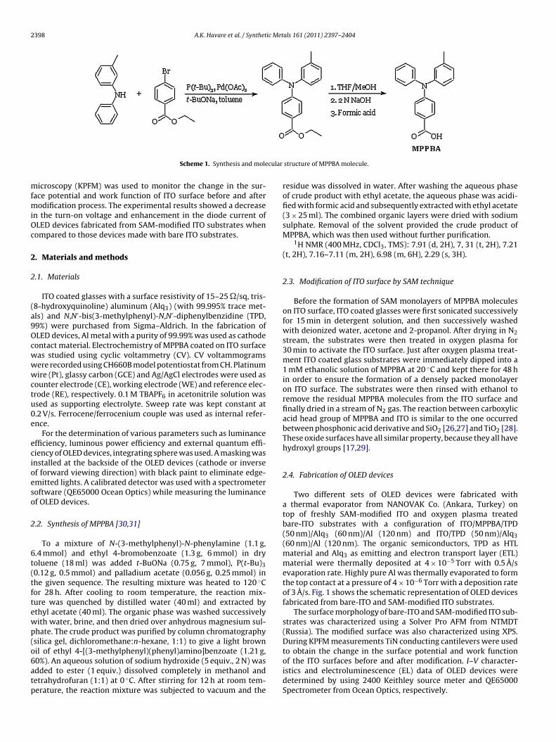
In this work, a SAM molecule, 4-[(3-methylphenyl)(phenyl)amino]benzoic acid (MPPBA), wassynthesized as hole injection layer (Scheme 1) due to its anchoringcarboxylic acid functional group and triarylamine structure toenhance charge injection. MPPBA, as a monolayer at the interfacebetween ITO surface and TPD (i.e. the hole transfer layer material),is expected to increase the number of inelastic tunneling channelsover its �-conjugated structure improving the hole injection bymodifying work function of ITO and HOMO level of HTL material.The carboxylic acid functional group on MPPBA molecule was usedto be anchored by hydroxyl groups present on ITO surfaces for theformation of ester bonds, and thus, modification of ITO surface is
achieved chemically by self-assembly process.The surface morphologies of ITO surface before and after SAMmodification were characterized by atomic force microscopy (AFM)and X-ray photoelectron spectroscopy (XPS). Kelvin probe force
ghts reserved.
2398 A.K. Havare et al. / Synthetic Metals 161 (2011) 2397– 2404
cular
mfmiOc
2
2
(a9Ocwwwctu0e
ecioeso
2
6t(tftewp(o6atp
During KPFM measurements TiN conducting cantilevers were usedto obtain the change in the surface potential and work function
Scheme 1. Synthesis and mole
icroscopy (KPFM) was used to monitor the change in the sur-ace potential and work function of ITO surface before and after
odification process. The experimental results showed a decreasen the turn-on voltage and enhancement in the diode current ofLED devices fabricated from SAM-modified ITO substrates whenompared to those devices made with bare ITO substrates.
. Materials and methods
.1. Materials
ITO coated glasses with a surface resistivity of 15–25 �/sq, tris-8-hydroxyquinoline) aluminum (Alq3) (with 99.995% trace met-ls) and N,N′-bis(3-methylphenyl)-N,N′-diphenylbenzidine (TPD,9%) were purchased from Sigma–Aldrich. In the fabrication ofLED devices, Al metal with a purity of 99.99% was used as cathodeontact material. Electrochemistry of MPPBA coated on ITO surfaceas studied using cyclic voltammetry (CV). CV voltammogramsere recorded using CH660B model potentiostat from CH. Platinumire (Pt), glassy carbon (GCE) and Ag/AgCl electrodes were used as
ounter electrode (CE), working electrode (WE) and reference elec-rode (RE), respectively. 0.1 M TBAPF6 in acetonitrile solution wassed as supporting electrolyte. Sweep rate was kept constant at.2 V/s. Ferrocene/ferrocenium couple was used as internal refer-nce.
For the determination of various parameters such as luminancefficiency, luminous power efficiency and external quantum effi-iency of OLED devices, integrating sphere was used. A masking wasnstalled at the backside of the OLED devices (cathode or inversef forward viewing direction) with black paint to eliminate edge-mitted lights. A calibrated detector was used with a spectrometeroftware (QE65000 Ocean Optics) while measuring the luminancef OLED devices.
.2. Synthesis of MPPBA [30,31]
To a mixture of N-(3-methylphenyl)-N-phenylamine (1.1 g,.4 mmol) and ethyl 4-bromobenzoate (1.3 g, 6 mmol) in dryoluene (18 ml) was added t-BuONa (0.75 g, 7 mmol), P(t-Bu)30.12 g, 0.5 mmol) and palladium acetate (0.056 g, 0.25 mmol) inhe given sequence. The resulting mixture was heated to 120 ◦Cor 28 h. After cooling to room temperature, the reaction mix-ure was quenched by distilled water (40 ml) and extracted bythyl acetate (40 ml). The organic phase was washed successivelyith water, brine, and then dried over anhydrous magnesium sul-hate. The crude product was purified by column chromatographysilica gel, dichloromethane:n-hexane, 1:1) to give a light brownil of ethyl 4-[(3-methylphenyl)(phenyl)amino]benzoate (1.21 g,
0%). An aqueous solution of sodium hydroxide (5 equiv., 2 N) wasdded to ester (1 equiv.) dissolved completely in methanol andetrahydrofuran (1:1) at 0 ◦C. After stirring for 12 h at room tem-erature, the reaction mixture was subjected to vacuum and thestructure of MPPBA molecule.
residue was dissolved in water. After washing the aqueous phaseof crude product with ethyl acetate, the aqueous phase was acidi-fied with formic acid and subsequently extracted with ethyl acetate(3 × 25 ml). The combined organic layers were dried with sodiumsulphate. Removal of the solvent provided the crude product ofMPPBA, which was then used without further purification.
1H NMR (400 MHz, CDCl3, TMS): 7.91 (d, 2H), 7, 31 (t, 2H), 7.21(t, 2H), 7.16–7.11 (m, 2H), 6.98 (m, 6H), 2.29 (s, 3H).
2.3. Modification of ITO surface by SAM technique
Before the formation of SAM monolayers of MPPBA moleculeson ITO surface, ITO coated glasses were first sonicated successivelyfor 15 min in detergent solution, and then successively washedwith deionized water, acetone and 2-propanol. After drying in N2stream, the substrates were then treated in oxygen plasma for30 min to activate the ITO surface. Just after oxygen plasma treat-ment ITO coated glass substrates were immediately dipped into a1 mM ethanolic solution of MPPBA at 20 ◦C and kept there for 48 hin order to ensure the formation of a densely packed monolayeron ITO surface. The substrates were then rinsed with ethanol toremove the residual MPPBA molecules from the ITO surface andfinally dried in a stream of N2 gas. The reaction between carboxylicacid head group of MPPBA and ITO is similar to the one occurredbetween phosphonic acid derivative and SiO2 [26,27] and TiO2 [28].These oxide surfaces have all similar property, because they all havehydroxyl groups [17,29].
2.4. Fabrication of OLED devices
Two different sets of OLED devices were fabricated witha thermal evaporator from NANOVAK Co. (Ankara, Turkey) ontop of freshly SAM-modified ITO and oxygen plasma treatedbare-ITO substrates with a configuration of ITO/MPPBA/TPD(50 nm)/Alq3 (60 nm)/Al (120 nm) and ITO/TPD (50 nm)/Alq3(60 nm)/Al (120 nm). The organic semiconductors, TPD as HTLmaterial and Alq3 as emitting and electron transport layer (ETL)material were thermally deposited at 4 × 10⁻⁵ Torr with 0.5 A/sevaporation rate. Highly pure Al was thermally evaporated to formthe top contact at a pressure of 4 × 10⁻⁶ Torr with a deposition rateof 3 A/s. Fig. 1 shows the schematic representation of OLED devicesfabricated from bare-ITO and SAM-modified ITO substrates.
The surface morphology of bare-ITO and SAM-modified ITO sub-strates was characterized using a Solver Pro AFM from NTMDT(Russia). The modified surface was also characterized using XPS.
of the ITO surfaces before and after modification. I–V character-istics and electroluminescence (EL) data of OLED devices weredetermined by using 2400 Keithley source meter and QE65000Spectrometer from Ocean Optics, respectively.

A.K. Havare et al. / Synthetic Metals 161 (2011) 2397– 2404 2399
Fs
3
owt
fMacIii
3m
ow
Abs
Table 1Maximum luminance in terms of L (cd/m2), luminous power efficiency, np (lm/W)and turn-on voltage (V) and the local contact potential difference (CPD) betweenSAM-modified ITO surface and conductive AFM tip (�˚) are given.
Max. L (cd/m2) np (lm/W) Turn-on (V) � (V) RMS (nm)
Bare-ITO 14.8 0.016 5.5 0.066 1.50
ig. 1. OLED device structure constructed on SAM-modified ITO coated on a glassubstrate.
. Results and discussion
MPPBA was synthesized in three steps according to the previ-usly published procedures [30,31] as described in Scheme 1. Itas used as SAM material to form a hole injecting monolayer on
he anode material (ITO).The number of MPPBA molecules self-assembled onto ITO sur-
ace is not limited by the surface hydroxyl content [32], sincePPBA can protonate both bridging oxides and hydroxyl-groups
lready present on the surface. This is a significant advantage toreate a strong covalent bond, since the surface hydroxyl content ofTO is notoriously low (approximately 1 OH nm2) [33,34]. The bond-ng carboxylic acid group of MPPBA molecule on ITO is illustratedn Fig. 2.
.1. Surface characterization and surface potentialeasurements using AFM and KPFM
Local contact potential difference (CPD) between SAM formedn ITO substrates and AFM conductive tip (TiN) was investigatedith KPFM.
The surface root mean square (RMS) roughness measured withFM gives valuable information about the surface morphology ofare- and SAM-modified ITO. AFM topography images of both sub-trates (bare-ITO and SAM-modified ITO surfaces) are presented
Fig. 2. The illustration of the bonding mechanism between
MPPBA-ITO 52.9 0.12 4.5 0.286 1.45
in Fig. 3(a) and (b). These images of ITO substrates after a care-ful cleaning procedures show almost similar surface topologieswith very close RMS roughness values (bare-ITO: 1.50 nm; SAM-modified ITO: 1.45 nm as shown in Table 1) indicating no morethan a single monolayer is present on both ITO surfaces. Fig. 3cand d shows the surface potential distribution of bare-ITO and ofSAM-modified ITO, respectively. The local contact potential differ-ence between TiN tip and bare-ITO was measured as 0.066 V and itwas obtained as 0.286 V for SAM-modified ITO surfaces using KPFMtechnique (Fig. 4).
The values obtained from KPFM measurements clarified that thework function of SAM-modified ITO surface increased as a result offorming a single monolayer of MPPBA molecules anchored ontothe ITO surface and HOMO level of SAM-modified ITO surface ispushed toward HOMO level of TPD layer. Table 1 shows the CPDdata between SAM-modified ITO surface and conductive AFM tip.
3.2. Cyclic voltammetry results of MPPBA
Further characterization of SAM-modified ITO surface was car-ried out by cyclic voltammetry (CV). First, cyclic voltammogramof SAM material (MPPBA) in solution was obtained (Fig. 5, solutionphase). MPPBA possesses a single reversible oxidation peak at 1.1 V,which arises from its triarylamine moiety as expected. This behav-ior can be attributed to the direct attachment of the carboxylic acidgroup into triarylamine moiety. Its attachment allows the electrondensity of triarylamine core to be redistributed to the electron-withdrawing carboxylic acid group, so that only a single reversibleoxidation peak is observed in the given potential range [35].
Oxidative CV measurement of SAM-modified ITO surface wasalso performed and its voltammogram is presented in Fig. 5 (solidphase). MPPBA based SAM on ITO surface shows a semi-reversibleoxidation peak of triarylamine core as observed in the solutionphase. In this case, the oxidation peak was observed at 0.99 V. This
slight shift can be attributed to the carbonyl group anchored toITO surface which decreases the electron affinity of carbonyl groupwhich might cause the formation of unstable oxidized species oncarboxylic acid group of MPPBA molecules and ITO.

2400 A.K. Havare et al. / Synthetic Metals 161 (2011) 2397– 2404
), surf
Io
dt
FS
Fig. 3. AFM topography images of bare ITO (a), SAM-modified ITO (b
TO surface. Then, the change in electron affinity leads to a reduction
f oxidation potential as compared to that of solution phase.HOMO level of MPPBA was calculated from the onset of oxi-ation potential by the intersection of two tangents drawn athe rising oxidation current and background current in its cyclic
ig. 4. The local contact potential difference measurement on bare ITO (circles) andAM-modified ITO substrates (squares) with conductive AFM tip.
ace potential distribution of bare ITO (c) and SAM-modified ITO (d).
voltammogram. The HOMO level of MPPBA was found to be −5.5 eVand −5.4 eV in solution phase and on ITO surface, respectively. Theincrease in the value of HOMO level of MPPBA coated ITO may beattributed to the decrease in the surface potential of ITO after SAMformation which will be discussed in the next part.
3.3. Effect of molecular dipole on ITO work function
The presence of a molecular dipole plays an important role inthe charge-injection properties of SAM layer in OLEDs. This concepthas been extensively studied and reported in the previous publica-tions [36–40]. Charge transfer from the COOH head group of MPPBAmolecule to ITO surface leads to the formation of C–O bond dueto electrostatic interaction between positively charged ITO surfaceand the delocalized electrons in the oxygen atom of carboxylategroup in MPPBA molecule [41]. There is a molecular dipole layerpresent at the interface between ITO and TPD. MPPBA moleculeshave a chemical bonding on ITO surface, as shown in Fig. 6a. Thedipole moment pointing toward the ITO surface effectively shiftsITO work function (�ITO) and decrease the barrier height for hole
transfer as shown in Fig. 6b and c. The difference between workfunctions of anode and the adjacent organic layer determines theenergy barrier at the interface during charge transfer from anodeto hole transport layer.
A.K. Havare et al. / Synthetic Metals 161 (2011) 2397– 2404 2401
Fig. 5. Cyclic voltammograms of MPPBA in the solution (a) and solid phase (b). Inset: First derivative of CV voltammogram of MPPBA in the solid phase. (In acetonitrile with0.1 M TBAPF6 as the supporting electrolyte with respect to the reference electrode Ag/AgCl; the scan rate was 0.2 V/s.)
Fig. 6. The molecular dipolar layer at the interface between ITO and TPD. MPPBA molecules make a chemical bond on ITO surface (a), diagram of the original work functionchanges due to the layer of dipole molecules present at the ITO surface (b), and energy band diagram of the OLED device (c).

2402 A.K. Havare et al. / Synthetic Metals 161 (2011) 2397– 2404
XPS C
uscIimb
3
gI
Fu
Fig. 7. XPS survey spectrum of SAM-modified ITO surface (a),
Change in HOMO level of ITO surface after SAM modificationsing MPPBA can also be determined by using Kelvin Probe mea-urement. The HOMO energy level of MPPBA by this method wasalculated as −5.09 eV. This value is between HOMO level of bare-TO (−4.8 eV) and the HTL material of TPD (−5.5 eV). This helps toncrease the rate of hole transfer from anode surface to the organic
aterial (TPD) via the SAM layer due to the interface energy statesetween ITO and TPD.
.4. XPS study of MPPBA coated ITO surface
X-ray photoelectron spectroscopy (XPS) was used to investi-ate chemical structure of COOH-terminated MPPBA molecules onTO. Fig. 7(a) shows an XPS survey spectrum of SAM-modified ITO
ig. 8. Current versus voltage characteristics for OLED devices made with SAM mnmodified/TPD/Alq3/Al devices (b).
1s spectrum of MPPBA (b), XPS O 1s spectrum of MPPBA (c).
surface after the modification process. The peaks, In 3d5/2, Sn 3d5/2,O 1s, N 1s and C 1s are seen in the spectra with binding ener-gies of 443.6, 485.6, 530.7, 398.4, and 284.6 eV, respectively. Inand Sn peaks confirm the existence of a very thin layer of MPPBAmolecules. Fig. 7(b) shows a high resolution spectrum of C 1s peak.The C peak was fit with a Shirley background and mixed singletpeak. The peaks at 288.3, 285.6 and 284.6 eV are assigned to O–C O,C–N or C–O and C–C bonds, respectively. The peak at 288.3 eV isa strong indication of the covalent bonding of O–C O connectionformed between COOH group of MPPBA molecule and hydroxyl
group of the ITO surface. This peak is attributed to carbon of car-boxyl groups in the formatted molecule. In order to explain theorigin of the peaks seen at 285.6, 288.3 and 284.6 eV in C 1s spec-tra, one should refer to the C 1s spectra in organic compounds.odified ITO and bare ITO (a) and EL spectrum of the ITO/SAM-modified or

A.K. Havare et al. / Synthetic Metals 161 (2011) 2397– 2404 2403
F ent de(
Smsataos
3
mwttOsacoocSsoeemt
ig. 9. Luminance (a), luminance efficiency (b) and luminous power efficiency–curr60 nm)/Al (120 nm).
imilar chemical shifts were also seen for C 1s in a wide range ofodel organic compounds [42–45]. O 1s spectra were fit and are
hown in Fig. 7(c). Three peaks at 529.9, 531.1 and 533.6 eV aressigned to O2−, carbonyl group (C O), and (C–O) or Sn–O, respec-ively [46–48]. In ITO films, the low binding energy O 1s componentt 529.9 eV is attributed to oxygen in the form of oxide, O2− presentn ITO surface [49,50]. Carbonyl group (C O) peak is the strongestignal among them.
.5. The OLED characteristics
I–V characteristics of the OLED device fabricated using SAM-odified ITO anode is shown in Fig. 8(a). According to this figure,hen the OLED device was positively forward biased with respect
o the cathode (Al) contact, a beneficial effect of SAM layer onhe turn-on voltage was clearly observed. The turn-on voltages ofLED devices made with SAM-modified and bare ITO were mea-
ured as 4.5 V and 5.5 V, respectively. On the SAM-modified ITOnode, a significantly increased hole injection current was obtainedompared to bare-ITO and, as a result of better hole injection, thebserved enhancement in the turn-on voltage was about 1 V. Thisbservation was also confirmed by an intensified electrolumines-ent emission (EL) obtained from the OLED device fabricated withAM-modified ITO anode (Fig. 8b). The increase in the EL intensityhould be a result of better hole transport due to the modification
f ITO surface. Increase in the current density at the interface can bexplained by inelastic tunneling mechanism over extra energy lev-ls formed between HOMO and LUMO levels of aromatic MPPBAolecules with �-conjugated structure used as tunnel barrier athe interface [51–53].
nsity (c) characteristics of OLEDs consisting of SAM-modified ITO/TPD (50 nm)/Alq3
3.6. External quantum efficiency–current characteristics of OLEDdevices
The luminance, luminance efficiency and luminous power effi-ciencies for all the devices, are shown in Fig. 9(a)–(c), respectively.The results show that OLED characteristics of the devices are clearlyaffected by the increased hole-current density as a result of SAMmodification.
At low voltage values, the luminance efficiency and luminouspower efficiencies of the devices with ITO substrates modified byusing MPPBA molecules are higher than that of the bare-ITO device,pointing out that increasing the hole-current density enhancesthe balance of charge carriers at low voltages. However, the lumi-nance efficiency and luminous power efficiencies of all the devicesdecrease in higher voltage.
4. Conclusion
A new type of SAM molecule, MPPBA as hole-injectionlayer, with �-conjugated structure and functional carboxylichead group was used to modify hydroxyl-rich ITO surfaces. TheSAM-modified ITO surface was characterized by XPS and KPFM.KPFM was used to measure the change in the surface potentialand work function before and after modification of ITO sur-face. The experimental results on MPPBA modified OLED devices(ITO/MPPBA/TPD/Alq3/Al) show a decrease in the turn-on voltages
and an enhancement in the diode current and EL intensity com-pared to OLED devices made with bare ITO substrates. The increasein the EL intensity of MPPBA modified OLED devices should be aresult of increasing hole transport due to SAM modification of ITO
2 ic Met
sctH�
A
1f
R
[[
[
[
[
[
[[
[
[[[
[
[
[[
[
[
[
[
[[
[
[
[[
[
[
[
[
[
[
[[
[
[
[
[
[
[
404 A.K. Havare et al. / Synthet
urface. The increase in the hole transport is related with tunnelingurrent density at the interface and can be explained with inelasticunneling mechanism over extra energy levels established betweenOMO and LUMO levels of aromatic MPPBA molecules with-conjugated structure used as tunneling barrier at the interface.
cknowledgements
This work was supported by TUBITAK under Grant No. TBAG-08T718. We would like to thank Dr. S. Sivananthan from UIC (US)or providing XPS facilities at Microphysics Lab.
eferences
[1] J.J. Kim, M.K. Han, Y.Y. Noh, Semiconductor Science and Technology 26 (2011)030301.
[2] Y. Yim, J. Park, B. Park, Journal of Display Technology 6 (2010) 252.[3] J.T. Lim, J.H. Lee, J.K. Park, B.J. Park, G.Y. Yeom, Surface and Coatings Technology
202 (2008) 5646.[4] E. Cantatore, D.M. de Leeuw, Materials Science in Semiconductor Processing 11
(2008) 199.[5] T.W. Kelley, P.F. Baude, C. Gerlach, D.E. Ender, D. Muyres, M.A. Haase, D.E. Vogel,
S.D. Theiss, Chemistry of Materials 16 (2004) 4413.[6] Y. Choi, E.Y. Lee, W.U. Desheng, INEC: 3rd International Nanoelectronics Con-
ference, 2010, p. 921.[7] F. Wang, T. Xiong, X. Qiao, D. Ma, Organic Electronics 10 (2009) 266.[8] M.A. Khan, W. Xu, K. Haq, X.W. Zhang, Y. Bai, X.Y. Jiang, Z.L. Zhang, W.Q. Zhu,
Journal of Physics D: Applied Physics 41 (2008) 225105.[9] M.B. Khalifa, D. Vaufrey, A. Bouazizi, J. Tardy, H. Maaref, Materials Science and
Engineering C 21 (2002) 277.10] J. Chu, Q. Huang, J.G.C. Veinot, H. Yan, T.J. Mark, Advanced Materials (2002) 14.11] S.F.J. Appleyard, S.R. Day, R.D. Pickford, M.R. Willis, Journal of Materials Chem-
istry 10 (2000) 169.12] A. Berlin, G. Zotti, G. Schianon, S. Zecchin, Journal of American Chemical Society
120 (1998) 13453.13] S. Besbes, H. Ben Ouada, J. Davenas, L. Ponsonnet, N. Jaffrezic, P. Alcouffe, Mate-
rials Science and Engineering C 26 (2006) 505.14] K.H. Lee, H.W. Jang, K.B. Kim, Y.H. Tak, J.L. Lee, Journal of Applied Physics (2004)
95.15] J. Chu, Q. Huang, J.G.C. Vienot, H. Yan, Q. Wang, G.R. Hutchison, A.G. Richter, G.
Evmenenko, P. Dutta, T.J. Mark, Langmuir 18 (2002) 9958.16] L.W. Chong, Y.L. Lee, T.C. Wen, Thin Solid Films 515 (5) (2007) 2833.17] J. Lee, B.J. Jung, J.I. Lee, H.Y. Chu, L.M. Dob, H.K. Shim, Journal of Materials
Chemistry 12 (2002) 3494.18] R.A. Hatton, M.R. Willis, M.A. Chesters, F.J.M. Rutten, D. Briggs, Journal of Mate-
rials Chemistry 13 (2003) 38.19] M.A. Baldo, M.E. Thompson, S.P. Forrest, Nature 403 (2000) 750.
20] A. Ulman, Chemical Reviews 96 (1996) 1533.21] Q.L. Huang, J.F. Li, G.A. Evmenenko, P. Dutta, T.J. Marks, Chemistry of Materials18 (2006) 2431.22] Q.L. Huang, G.A. Evmenenko, P. Dutta, P. Lee, N.R. Armstrong, T.J. Marks, Journal
of American Chemical Society 127 (2005) 10227.
[[[[
als 161 (2011) 2397– 2404
23] Q.L. Huang, G. Evmenenko, P. Dutta, T.J. Marks, Journal of American ChemicalSociety 125 (2003) 14704.
24] B.M. Silverman, K.A. Wieghaus, J. Schwartz, Langmuir 21 (2005) 225.25] I.L. Liakos, R.C. Newman, E. McAlpine, M.R. Alexander, Surface and Interface
Analysis 36 (2004) 347.26] E.L. Hanson, J. Schwartz, B. Nickel, N. Koch, M.F. Danisman, Journal of American
Chemical Society 125 (2003) 16074.27] K. Midwood, M.D. Carolus, M.P. Danahy, J. Schwarzbauer, J. Schwartz, Langmuir
20 (2004) 5501.28] M.P. Danahy, M.J. Avaltroni, K. Midwood, J. Schwarzbauer, J. Schwartz, Lang-
muir 20 (2004) 5333.29] K.L. Purvis, G. Lu, J. Schwartz, S.L. Bernasek, Journal of American Chemical Soci-
ety 122 (2000) 1808.30] M.C. Harris, S.L. Buchwald, Journal of Organic Chemistry 65 (2000) 5327.31] J. Dash, P.S. Shirude, S.D. Hsu, S. Balasubramanian, Journal of American Chemical
Society 130 (2008) 15950.32] A. Vioux, J. Le Bideau, P.H. Mutin, D. Leclercq, Topics in Current Chemistry 232
(2004) 145.33] D.J. Milliron, I.G. Hill, C. Shen, A. Kahn, J. Schwartz, Journal of Applied Physics
87 (2000) 572.34] V.M. Bermudez, A.D. Berry, H. Kim, A. Pique, Langmuir 22 (2006) 11113.35] J.A. Bardecker, H. Ma, T. Kim, F. Huang, M.S. Liu, Y.J. Cheng, G. Ting, A.K. Jen,
Advanced Functional Materials 18 (2008) 964.36] J.E. Malinsky, G.E. Jabbour, S.E. Shaheen, J.D. Anderson, A.G. Richter, T.J. Marks,
N.R. Armstrong, B. Kippelen, P. Dutta, N. Peyhambarian, Advanced Materials 11(1999) 227.
37] S.E. Koh, K.D. McDonald, D.H. Holt, C.S. Dulcey, J.A. Chaney, P.E. Pehrsson, Lang-muir 22 (2006) 6249.
38] S. Khodabakhsh, D. Poplavskyy, S. Heutz, J. Nelson, D.D.C. Bradley, F. Murata,T.S. Jones, Advanced Functional Materials 14 (2004) 1205.
39] M.P. de Jong, L.J. van Izendoorn, M.J.A. de Voigt, Applied Physics Letters 77(2000) 2255.
40] E.L. Hanson, J. Guo, N. Koch, J. Schwartz, S.L. Bernasek, Journal of AmericanChemical Society 127 (2005) 10058.
41] M.A.W. Fox, K. James, Organic Chemistry, 2nd ed., Massachusetts Jones andBartlett Publishers, Sudbury, 1997.
42] N. Moussaif, C. Pagnoullea, J. Rigab, R. Jeromea, Polymer 41 (2000) 3391.43] I.V. Plyuto, A.P. Shpak, J. Stoch, L.F. Sharanda, Y.V. Plyuto, I.V. Babich, M. Makkee,
J.A. Moulijn, Surface and Interface Analysis 38 (2006) 917.44] D.T. Clark, H.R. Thomas, Journal of Polymer Science Part A Polymer Chemistry
Edition 14 (1976) 1671.45] E.E. Ortelli, F. Geiger, T. Lippert, J. Wei, A. Wokaun, Macromolecules 33 (2000)
5090.46] D.W. Zeng, K.C. Yung, C.S. Xie, Surface and Coatings Technology 153 (2002)
210.47] F. Montagne, J. Polesel-Maris, R. Pugin, H. Heinzelmann, Langmuir 25 (2009)
983.48] E. Binkauskienea, A. Lugauskasa, M. Krunksb, I.O. Acikb, V. Jasulaitienea, G.
Saduikis, Synthetic Metals 160 (2010) 906.49] O.M. Diplas, L.H. Nordmark, D.M. Kepaptsoglou, J.M. Graff, C. Ladam, F. Tyholdt,
J.C. Walmsley, A.E. Gunnaes, R. Fagerbergb, A. Ulyashina, Surface and Interface
Analysis 42 (2010) 874.50] C. Yan, M. Zharnikov, A. Go, M. Grunze, Langmuir 16 (2000) 6208.51] M.G. Simonsen, R.V. Coleman, Physical Review B 8 (1973) 12.52] W. Wang, T. Lee, I. Kretzschmar, M.A. Reed, Nano Letters 4 (2004) 643.53] G.C. Bazan, Journal of Organic Chemistry 72 (2007) 8615.
Copyright © 2022 FDOKUMEN


![Impedance spectroscopic investigations of ITO modified by new Azo-calix[4]arene immobilised into electroconducting polymer (MEHPPV)](https://static.fdokumen.com/doc/165x107/634532ab596bdb97a908d170/impedance-spectroscopic-investigations-of-ito-modified-by-new-azo-calix4arene.jpg)


![An amperometric uric acid biosensor based on Bis[sulfosuccinimidyl] suberate crosslinker/3-aminopropyltriethoxysilane surface modified ITO glass electrode](https://static.fdokumen.com/doc/165x107/63129cf1fc260b71020eb9f6/an-amperometric-uric-acid-biosensor-based-on-bissulfosuccinimidyl-suberate-crosslinker3-aminopropyltriethoxysilane.jpg)
