Modeling of Tunnelling Currents in Hf-Based Gate Stacks as a Function of Temperature and Extraction...
28
Modelling of tunnelling currents in Hf-based gate stacks as a function of temperature and extraction of material parameters Andrea Campera, Giuseppe Iannaccone, Member, IEEE, Felice Crupi, Member, IEEE A. Campera and G. Iannaccone are with the University of Pisa, Dipartimento di Ingegneria dell’Informazione: Elettronica, Informatica, Telecomunicazioni, Via Caruso 16, 56122, Pisa, Italy (phone: +39 0502217677; fax: +39 0502217522; e-mail: [email protected], [email protected]). F. Crupi is with Dipartimento di Elettronica, Informatica e Sistemistica, Università della Calabria, I-87036 Arcavacata di Rende (CS), Italy (email: [email protected] ). Abstract—In this paper we show that through electrical characterization and detailed quantum simulations of the capacitance- voltage and current-voltage characteristics it is possible to extract a series of material parameters of alternative gate dielectrics. We have focused on HfO 2 and HfSi X O Y N Z gate stacks and have extracted information on the nature of localized states in the dielectric responsible for a trap-assisted tunneling current component and for the temperature behavior of the I-V characteristics. Simulations are based on a 1D Poisson-Schrödinger solver capable to provide the pure tunneling current and Trap Assisted Tunneling component. Energy and capture cross section of traps responsible for TAT current have been extracted. Index Terms—High-k dielectrics, Trap Assisted Tunneling, gate leakage, trap cross section. I. INTRODUCTION HE present research and development effort focused on replacing SiO 2 and SiON gate stacks with high dielectric permittivity (high-k) gate stacks is motivated by the need of increasing gate capacitance per unit area as device size shrinks while at the same time maintaining the leakage tunneling current under control. Among high-k dielectrics, HfO 2 and its silicates - in particular hafnium silicate nitride (HfSi X O Y N Z ) - are considered promising alternative gate dielectrics for CMOS technology at the 45 nm node and beyond [1,2,3]. In fact, as it is well known, high-k dielectrics exhibit strongly suppressed gate tunneling current with respect to silicon oxide for the same gate capacitance: of a factor for HfO 5 10 2 , and a factor for an HfSi 3 10 X O Y N Z stack [1]. Both materials have a rather large band gap, about 6 eV for HfO 2 and 7 eV for HfSi X O Y N Z [4,5]; band gap is lower with respect to conventional SiO 2 but the increased thickness, in any case, causes an overall T
-
Upload
independent -
Category
Documents
-
view
4 -
download
0
Transcript of Modeling of Tunnelling Currents in Hf-Based Gate Stacks as a Function of Temperature and Extraction...

Modelling of tunnelling currents in Hf-based gate stacks as a function of temperature and
extraction of material parameters Andrea Campera Giuseppe Iannaccone Member IEEE Felice Crupi Member IEEE
A Campera and G Iannaccone are with the University of Pisa Dipartimento di Ingegneria dellrsquoInformazione Elettronica Informatica
Telecomunicazioni Via Caruso 16 56122 Pisa Italy (phone +39 0502217677 fax +39 0502217522 e-mail andreacamperaietunipiit
giannacconeietunipiit)
F Crupi is with Dipartimento di Elettronica Informatica e Sistemistica Universitagrave della Calabria I-87036 Arcavacata di Rende (CS) Italy
(email crupiunicalit)
AbstractmdashIn this paper we show that through electrical characterization and detailed quantum simulations of the capacitance-
voltage and current-voltage characteristics it is possible to extract a series of material parameters of alternative gate dielectrics We
have focused on HfO2 and HfSiXOYNZ gate stacks and have extracted information on the nature of localized states in the dielectric
responsible for a trap-assisted tunneling current component and for the temperature behavior of the I-V characteristics Simulations
are based on a 1D Poisson-Schroumldinger solver capable to provide the pure tunneling current and Trap Assisted Tunneling component
Energy and capture cross section of traps responsible for TAT current have been extracted
Index TermsmdashHigh-k dielectrics Trap Assisted Tunneling gate leakage trap cross section
I INTRODUCTION
HE present research and development effort focused on replacing SiO2 and SiON gate stacks with high dielectric
permittivity (high-k) gate stacks is motivated by the need of increasing gate capacitance per unit area as device size
shrinks while at the same time maintaining the leakage tunneling current under control Among high-k dielectrics HfO2
and its silicates - in particular hafnium silicate nitride (HfSiXOYNZ) - are considered promising alternative gate dielectrics for
CMOS technology at the 45 nm node and beyond [123] In fact as it is well known high-k dielectrics exhibit strongly
suppressed gate tunneling current with respect to silicon oxide for the same gate capacitance of a factor for HfO510 2 and a
factor for an HfSi310 XOYNZ stack [1] Both materials have a rather large band gap about 6 eV for HfO2 and 7 eV for
HfSiXOYNZ [45] band gap is lower with respect to conventional SiO2 but the increased thickness in any case causes an overall
T
leakage current suppression
Although significant reduction of gate leakage has been achieved the nature of the stray currents and the frequently observed
flat band voltage shift and voltage bias instability [167] need further investigation The effect of polysilicon depletion which
will require the use of metal gates and the reduced effective channel mobility are other important issues which will become
more critical with the shrinking of the physical dimensions
The main aim of this work is the understanding of the tunneling mechanisms through such dielectrics In order to do this we
have investigated the current-voltage characteristics as a function of temperature We show that the temperature dependence of
I- V characteristics in HfO2 can be explained in terms of a microscopic model of Trap Assisted Tunneling (TAT) based on a
temperature dependent cross section Comparison of experiments with the results of our model allows us to exclude that relevant
traps for transport are localized at the HfO2 interfaces (confirming some experiments [8])
The paper is organized as follows in Section II we describe the structures under investigation In Section III we briefly
discuss the Poisson-Schroumldinger solver and how the tunneling current components are obtained In Section IV and V we
compare experimental and theoretical C-V and J-V characteristics respectively and extract the relevant physical parameters of
the materials In Section VI we discuss in some more detail the transport model we have used to explain the temperature
dependent transport in HfO2 and HfSiXOYNZ and the comparison with experiments and finally we will draw our conclusions
II EXPERIMENTS
We have experimentally investigated HfO2 and HfSiXOYNZ gate stacks the physical parameters of Hf-based dielectrics
depend on the fabrication process and on the specific resulting composition Indeed for example the dielectric constant of
HfSiXOYNZ depends on the nitrogen and hafnium molar fraction in the high-k layer [29] Therefore is important to extract with
sufficient precision the physical parameters of the high-k layer as we shall do by comparing experiments with simulations We
have considered three different gate stacks consisting of an interfacial layer (we assume it to be SiO2 for the HfO2 gate stack and
SiON for the HfSiXOYNZ gate stack) of thickness tint in contact with the silicon substrate and of an high-k layer of thickness thigh-
k covered by a n+ poly-silicon gate The gate dielectrics have been deposited by MOCVD after an IMEC-clean process In all
three cases the substrate is p-doped with NA=51023 m-3 Details on the layer structures are shown in Table I
Capacitance-voltage characteristics have been measured for capacitors of area 70 μm x 70 μm and current-voltage
characteristics have been measured for n-MOSFETs with width 10 μm and gate length 5 μm
III 1-D POISSON-SCHROumlDINGER SOLVER
In thin Equivalent Oxide Thickness (EOT) MOS structures such as those we are considering polysilicon depletion and finite
density of states in the bulk must be taken into account To simulate these structures we have used a one-dimensional self-
consistent Poisson-Schroumldinger solver that takes into account quantum confinement at the emitting region (being it the
polysilicon gate or the substrate depending on bias) mass anisotropy in silicon conduction band light and heavy holes wave
function penetration in the oxide For simplicity bands are parabolic The band profile is computed with the quasi-equilibrium
approximation ie assuming that the tunneling current is so low that the dielectric separates two regions in local equilibrium
with two different Fermi energies
From the band profile (eg the one shown in Fig 1) we can compute the tunneling current per unit area that is given by [10]
( )( )
( )( )
2
2
1 exp2 ( ) ln1 exp
1 exp4 ( ) ln1 exp
Fl ilt ril il
Fr ili
Fl itt l rit it
Fr iti
E E kTqkTJ m T EE E kT
E E kTqkT m m T EE E kT
νπ
νπ
⎧ ⎫⎡ ⎤+ minus⎪ ⎪⎣ ⎦= +⎨ ⎬⎡+ minus⎪ ⎣⎩
⎧ ⎫⎡ ⎤+ minus⎪ ⎪⎣ ⎦+ ⎨ ⎬⎡ ⎤+ minus⎪ ⎪⎣ ⎦⎩ ⎭
sum
sum
⎤ ⎪⎦ ⎭ (1)
where q is electron charge ħ the reduced Planck constant kB the Boltzmann constant T the absolute temperature mB t (ml) the
transversal (longitudinal) electron effective mass T(Eil) (T(Eit)) the transmission coefficients for the longitudinal (transversal)
effective mass υril (υrit) the attempt frequencies for the longitudinal (transversal) effective mass at the emitter computed by taking
into account the time spent by the electrons in the classically forbidden regions for each eigenfunction [11] Eil (Eit) the
longitudinal (transversal) eigenvalues and EFl (EFr) the Fermi level of the left (right) electrode The transmission coefficients are
obtained by solving the Schroumldinger equation for the barrier with open boundary conditions
IV CAPACITANCE-VOLTAGE SIMULATIONS
It is a well known fact that with respect to the ideal SiO2 case using an Hf-based gate stack a threshold voltage shift ΔVT is
observed for both n-MOS and p-MOS transistors [6712] This threshold voltage shift is positive for n+ poly-Si and negative for
p+ poly-Si gate and is caused by defects at the poly-Sihigh-k interface located in the upper part of the band gap ΔVT is larger
for p-MOS transistors with respect to n-MOS transistors Hobbs and coworkers have explained this effect in terms of Fermi level
pinning [67]
In Fig 2 we compare the experimental C-V characteristics of structure a with those obtained from quantum simulations
Fermi-level pinning can be simply and effectively taken into account by assuming an effective electron affinity of the gate
electrode in general different from that of the gate material The effective variation of the electron affinity can be obtained by
shifting the theoretical C-V curve along the voltage axis until it overlaps with the experimental one For structure a (hence for a
generic HfO2 stack since Fermi level pinning is an interfacial effect and does not depend on the thickness of the HfO2 layer) we
have found such quantity to be 035 V in good agreement with values reported in literature ( eg about 03 V in [67])
Interfacial charge and charge within the high-k layer can in the same manner contribute to the VT shift However in Ref [7] a
detailed investigation of the charge in the various gate stack layers is presented and the authors have observed that almost the
entire shift is caused by FLP The Fermi level pinning reported in Ref [7] depends on the hafnium molar fraction and is between
02 V and 035 V Given the lack of knowledge fixed charges in the stack we assumed that all the VT shift was entirely caused
by the FLP at the poly-high-k interface The value that we extracted is in good agreement with findings in Ref [7] hence we
assumed that the total VT shift was caused by the FLP It is important to note that in Fig 2 and Fig 3 we compare experimental
C-V characteristics measured at high frequency with theoretical low-frequency C-V characteristics hence the discrepancy at
positive voltages From the comparison between experimental and simulated C-V characteristics we can also extract the
dielectric constant We find a value of 25 for the relative dielectric constant of the hafnium oxide in good agreement with values
reported in literature (for example [4]) In addition from Fig 2 we can observe a smoother experimental C-V characteristic with
respect to simulations which means that the effect of interfacial traps is significant We want to remark that we are assuming
that the layer thicknesses are known with sufficient precision
We can repeat the same procedure for the HfSiXOYNZ gate stack (structures b and c) in order to extract the dielectric constant
and the Fermi level pinning In Figure 3 we report the C-V curves with and without FLP for structure b Fermi level pinning
extracted from the comparison is of 013 eV that agrees with values reported in literature [568] the dielectric constant of the
HfSiXOYNZ results to be 11 (very close to [8]) The very similar slope of the experimental and theoretical C-V profiles in Fig 3
also shows that HfSiXOYNZ has less interfacial traps
V CURRENT DENSITY-VOLTAGE SIMULATIONS
From the comparison between theoretical and experimental current density-voltage characteristics we are able to extract the
electronic affinity and the electron tunneling effective mass for HfO2 and HfSiXOYNZ and to evaluate the presence of transport
mechanisms additional to pure elastic tunneling The electron affinity and the effective mass have a slightly different effect on
the J-V characteristics Exploring the parameter space we could only find a set of values that allow us to fit both the J-V and the
C-V characteristics for positive and negative gate voltages In Fig 4 we plot experimental and theoretical (pure tunneling)
currents for HfO2 and HfSiXOYNZ stacks for negative and positive gate bias The extracted electron affinity and electron
effective mass are respectively 175 eV and 008 m0 for HfO2 197 eV and 024 m0 for HfSiXOYNZ that have to be compared
with values reported in literature [4591314]
Hole tunneling is not significant we have used a tunneling mass for holes of 05m0 (see for example [15]) although such
value is somewhat arbitrary since it cannot be verified in a straightforward way For the electron tunneling effective mass in
SiO2 we have used 05m0 The situation is more complicate for the SiON layer for which the electron effective mass and all the
other physical parameters depend on the molar fraction of nitrogen embedded in the oxide we have used a value of 045m0 an
electron affinity of 127 eV and a dielectric permittivity of 5 Such values allow us to fit the experiments and are in good
agreement with values reported in Ref [16] Extracted values for material parameters are summarized in Table II
We want to stress the fact that from Fig 4 it is clear that for the HfSiXOYNZ stack (structure c) and for the HfO2 stack
(structure a) the pure tunneling component is sufficient to fit the whole J-V characteristics except for low negative gate bias
between -1 and 0 V for structure c and between -2 and 0 V for structure a The higher measured current density can be ascribed
to two effects an additional transport mechanism assisted by interface traps in the silicon gap [17] and an higher current density
associated with the lateral source and drain n+ extensions not considered in the 1D simulations Consequently an higher overall
gate current density is measured in shorter channel length n-MOSFETs at low negative gate voltages as shown in Fig 5
VI TEMPERATURE DEPENDENCE OF CURRENT -VOLTAGE CHARACTERISTICS
HfO and HfSi O N show a different behavior as a function of temperature as we can see in Figs 6 and 7 respectively
Current in HfSi O N stack is substantially independent of temperature whereas in HfO a larger temperature dependence is
present for positive gate voltages lower for negative gate voltages We explain this behavior by introducing a temperature
dependent cross section in a microscopic model of Trap Assisted Tunneling Here we briefly report the basic physics of the
model addressing the interested readers to the original work [19] and describe in some more detail the features that we have
introduced to take into account the temperature dependence
2 X Y Z
X Y Z 2
Let us consider the band profile sketched in Fig 8 representing structure a with a positive gate applied voltage of 05 V an
electron state β in one band of one electrode and a Khon Sham state α representing a trap state in the dielectric stack The
probability per unit time that an electron tunnel from one band of one reservoir to the trap is given by the Fermi golden rule and
is
( ) ( )22 M h E Eβ α βπν β αrarr Γ= αminus (2)
where
( )( )2 2
1h E EE E
β α
β απΓ
Γminus = sdot
minus + Γ (3)
and Eβ Eα are the energy of the state β and α respectively In (2) we take into account for inelastic transitions by using a a
Lorentzian function of finite half width Г We can rewrite (2) as
( ) ( ) ( l l )J x T E fβ α β α β αν σ β σrarr = = sdot sdot E
)
(4)
if we define the energy dependent capture cross section as
( 0 h E Eβ α β ασ σ Γ= sdot minus (5)
( )J xβ is the probability current density impinging on the plane positioned at the same depth x of the trap while 0σ
expressed as m2middotJ is a compact parameter that contains all information on traps We want to stress the fact that our definition of
capture cross section is slightly different from the conventional one and allows us to introduce a dependence of the transition
rate upon the energy difference between initial and final states
Once we know the band profile we can compute the capture and emission rates (which we will call in the rest of this paper
generation and recombination rates respectively) ie the probability per unit time that an electron tunnels from one band of one
electrode to the trap and vice versa and then the trap assisted tunneling current density
2g f dβ α β ββ
ν ρ βrarr= int (6)
( )1r fβ α β ββ
dν ρ βrarr= minusint (7)
We can also write the TAT current density as [19]
1 2 2 1
1 2 1 2
g r g rJ q
g g r rminus
= sdot+ + +
(8)
where subscript 1 of the generation and recombination rates refers to states β in the substrate and subscript 2 to states β in the
gate electrode
The TAT current density temperature dependence can be included in an appropriate model for β ασ that includes its temperature
dependence
Traps in hafnium oxide have been recently investigated by Gavartin and coworkers [20] with ab-initio calculations From
simulations we have observed that traps must be within the energy range 1divide2 eV below the hafnium oxide conduction band in
order to allow us to reproduce the shape of the J-V characteristics at various temperatures In Ref [20] only one defect is in the
energy range above and is specifically located 16 eV below the hafnium oxide conduction band (O0O- defects) hence we
assume them to be the dominant traps for the TAT current In Fig 9 we report the band profile for structure a and the energetic
position of the considered traps
In order to simulate the TAT current we need to know the half width of the Lorentzian function Г and the capture cross
section We can extract Г from the slope of the J-V curve at 475 K (see Fig 10) Indeed we can reasonably assume and this is
confirmed by simulations that at 475 K the TAT current represents the entire current density because the pure tunneling current
depends only slightly on temperature
It is important to note that Γ strongly affects the slope of the J-V characteristics on the semilog scale whereas 0σ appears as a
multiplicative factor in J (Eq 8) so that a variation of 0σ only shifts vertically the J-V characteristics on the semilog scale On
the other hand from the experimental results shown in Fig 6 we can see that the J-V characteristics have a slope almost
independent of temperature and therefore we can assume that in our case Г is practically constant with temperature in the
operating regimes we consider
We now have to consider the temperature dependence of 0σ which is typically given by an Arrhenius-like behavior [21] We
shall assume
(0 exp BE k Tσσ σ infin= minus ) (9)
where σinfin is the capture cross section for T rarr infin Eσ is the activation energy of the capture process
For each temperature we determine the value of 0σ which provides the best fit between the theoretical and experimental J-V
characteristics The extracted 0σ is plotted in Fig 11 as a function of temperature as can be seen it perfectly fits an Arrhenius
function with an activation energy Eσ=0542 eV and σinfin = 0555 m2J We should note that the activation energy of the capture
cross section is rather high with respect to that typically found for SiO2 which is lower than 03 eV [22] but to our knowledge
no other data are available for hafnium oxide and we can not exclude a priori this value Indeed some materials such as a SiH
exhibit an activation energy even higher than that we have obtained (069 eV [23])
With the extracted values of Г and σ(T) the TAT current can be well reproduced for positive gate voltage as sketched in Fig
12 For negative gate applied voltage TAT current is less relevant because the traps have a much higher energy with respect to
the emitter Fermi level as we can see in Fig 13 In addition we must remark that an additional transport mechanism associated
with the lateral source and drain n+ extensions is present for relatively ldquolowrdquo negative gate voltage (-1ltVGlt0) and this is not
considered in our 1D simulations (see Fig 5) Then we have to focus on higher negative gate voltages (-16ltVGlt-1)
The agreement for negative gate applied voltages between theoretical and experimental curves is reasonable but not as good as
for positive voltages mainly because the low absolute values for the current density leads to an increased relative error as shown
in Fig 14 For the hafnium silicate nitride experiments show a very small temperature dependence which can be explained in
terms of pure tunneling current We cannot exclude that traps are present in the hafnium silicate nitride bulk but we point out
that are not responsible for a significant trap-assisted tunneling component In Fig 15 experiments and simulations at 298 and
400 K are reported for structure c they agree pretty well without any additional fitting parameter
The temperature dependent TAT model allows us to reproduce experiments if we assume that traps in hafnium oxide are
uniformly distributed in the layer We have checked that if we assume that traps are placed exclusively at one of the hafnium
oxide interfaces we are not able obtain a good agreement with measurements Indeed in this latter case the slope of the
theoretical curves would depend on temperatures while that of the experimental curves would not Our assumption that traps are
uniformly distributed in the hafnium oxide layer is also confirmed by some recent experiments [8]
VII CONCLUSION
We have shown that the temperature dependence of the leakage current in hafnium oxide can be explained in terms of a
microscopic model for TAT with temperature dependent capture cross section where the relevant traps are uniformly distributed
in the layer volume at 16 eV below the hafnium oxide conduction band The cross section has an Arrhenius-like behavior with a
rather high activation energy of 0542 eV For the samples of HfSi O N at hand we observe a much smaller dependence of the
leakage current on temperature that can be simply explained by considering only the pure tunneling component
X Y Z
VIII ACKNOWLEDGEMENTS
This work was supported in part by the SINANO Network of Excellence and by the MIUR-PRIN project ldquoAlternative
Models and Architectures for nanoMOSFETsrdquo The authors wish to thank G Groeseneken and IMEC for providing the samples
used in this work
REFERENCES
[1] G Groeseneken L Pantisano L-Ǻ Ragnarsson R Degraeve M Houssa T Kauerauf P Roussel S De Gendt and M Heyns ldquoAchievements and
Challenges for the Electrical Performance of MOSFETrsquos with High-k Gate Dielectricsrdquo in Proceedings of 11th IPFA 2004 Taiwan pp 147-155
[2] M Takayanagi T Watanabe R Iijima A Kaneko S Inumiya I Hirano K Sekine A Nishiyama K Eguchi and Y Tsunashima ldquoHfSiON Gate
Dielectrics for CMOS Applicationsrdquo in IGWI 2003 Tokyo pp 128-132
[3] Masayuki Terai Kensuke Takahashi Kenzo Manabe Takashi Hase Takashi Ogura Motofumi Saitoh Toshiyuki Iwamoto Toru Tatsumi and Hirohito
Watanabe ldquoHighly Reliable HfSiON CMOSFET with Phase Controlled NiSi (NFET)and Ni3Si (PFET) FUSI Gate Electroderdquo IEEE Symposium on VLSI
Technology Digest of Technical Paper 2005 pp 68-69
[4] J Robertson ldquoInterfaces and defects of high-k oxides on siliconrdquo Solid-State Electronics 49(2005) pp 283-293
[5] K Torii T Aoyama S Kamiyama Y Tamura S Miyazaki H Kitajima T Arikado ldquoDielectric breakdown mechanism of HfSiONSiO2 gate dielectricrdquo
IEEE Symposium on VLSI Technology Digest of Technical Paper 2004 pp 112-113
[6] CC Hobbs LRC Fonseca A Knizhnik V Dhandapani SB Samavedam WJ Taylor JM Grant LG Dip DH Triyoso RI Hedge DC Gilmer R
Garcia D Roan ML Lovejoy RS Rai EA Hebert H-H Tseng SGH Anderson BE White and PJ Tobin ldquoFermi-Level Pinning at the
PolysiliconMetalOxide Interface ndash Part Irdquo IEEE Trans Electron Devices vol 51 no 6 June 2004 pp 971-977
[7] CC Hobbs LRC Fonseca A Knizhnik V Dhandapani SB Samavedam WJ Taylor JM Grant LG Dip DH Triyoso RI Hedge DC Gilmer R
Garcia D Roan ML Lovejoy RS Rai EA Hebert H-H Tseng SGH Anderson BE White and PJ Tobin ldquoFermi-Level Pinning at the
PolysiliconMetalOxide Interface ndash Part IIrdquo IEEE Trans Electron Devices vol 51 no 6 June 2004 pp 978-984
[8] CD Young G Bersuker GA Brown C Lim P Lysaght P Zeitzoff RW Murto HR Huff ldquoCharge trapping in MOCVD hafnium-based field
dielectric stack structures and its impact on device performancerdquo IEEE Integrated Reliability Workshop Final Report 2003
Oct 2003 pp 28 ndash 35
[9] M Koyama A Kaneko T Ino M Koike Y Kamata R Iijima Y Kamimuta A Takashima M Suzuki C Hongo S Inumiya M Takanayagi and A
Nishiyama ldquoEffect of Nitrogen in HfSiON Gate Dielectric on the Electrical and Thermal Characteristicsrdquo IEDM 2002 pp 849-852
[10] G Iannaccone S Gennai ldquoProgram erase and retention times of thin-oxide Flash-EEPROMsrdquo VLSI DESIGN num 1-4 vol 13 pp 431-434 2001
[11] G Iannaccone B Pellegrini ldquoCompact formula for the density of states in a quantum wellrdquo PHRB vol 53 pp 2020-2025 1986
[12] K Shiraishi K Yamada K Torii Y Akasaka K Nakajima M Kohno T Chikyo H Kitajima and T Arikado ldquo Physics in Fermi Level Pinning at the
Poly-SiHf-based High-k Oxide Interfacerdquo IEEE Symposium on VLSI Technology Digest of Technical Paper 2004 pp 108-109
[13] J Zhang E Zhao Q Xiang J Chan J Jeon J-S Goo A Marathe B Ogle M-R Lin and K Taylor ldquoPolarity Dependent Reliability of Advanced
MOSFET Using MOCVD Nitrided Hf-silicate High-k Gate Dielectricrdquo IEEE IRW Final Report 2002 pp 92-95
[14] WJ Zhu T-P- Ma T Tamagawa J Kim and Y Di ldquoCurrent Transport in MetalHafnium OxideSilicon Structurerdquo IEEE Electron Device Letters vol
23 no 2 February 2002 pp 97-99
[15] K-N Yang H-T Huang M-C Chang C-M Chu Y-S Chen M-J Chen Y-M Lin M-C Yu SM Jang DCH Yu and MS Liang ldquoA Physical
Model for Hole Direct Tunneling Current in p+ Poly-Gate pMOSFETs with Ultrathin Gate Oxidesrdquo IEEE Trans Electron Devices vol 47 no 11
November 2000 pp 2161-2166
[16] M Togo K Watanabe T Yamamoto N Ikarashi T Tatsumi H Ono and T Mogami ldquoElectrical Properties of 15-nm SiON Gate-Dielectric Using
Radical Oxygen and Radical Nitrogenrdquo IEEE Tran Electron Devices vol 49 no 11 November 2002 pp1903-1909
[17] F Crupi C Ciofi A Germanograve G Iannaccone JH Stathis and S Lombardo ldquoOn the role of interface states in low-voltage leakage currents of metal-
oxide semiconductor structuresrdquo Appl Phys Lett vol80 no 24 17 June 2002 pp 4597-4599
[18] F Crupi R Degraeve A Kerber DH Kwak G Groeseneken ldquoCorrelation between Stress-Induced Leakage Current (SILC) and the HfO2 bulk trap
density in a SiO2HfO2 stackrdquo IEEE International Reliability Physics Symposium Proceedings 25-29 April 2004 pp 181-187
[19] G Iannaccone F Crupi B Neri and S Lombardo rdquoTheory and Experiments of Suppressed Shot Noise in Stress-Induced Leakage Currentsrdquo IEEE Tran
Electron Devicesvol 50 no 50 May 2003 pp 1363-1369
[20] JL Gavartin AL Shluger AS Foster and GI Bersuker ldquoThe role of nitrogen-related defects in high-k dielectric oxides Density-functional studiesrdquo
Jour Appl Phys vol 97 2005 053704- from 1 to 13
[21] J-U Sachse J Weber and H Lemke ldquoDeep-level transient spectroscopy of Pd-H complexes in siliconrdquo Physical Review B vol 61 no 3 15 January
2000 pp 1924-1934
[22] S Oumlzder I Atilgan and B Katircioğlu ldquoTemperature dependence of the capture cross section determined by DLTS on an MOS structurerdquo Semicond Sci
Technol vol 10 1995 pp 1510-1519
[23] H Okushi T Takahama Y Tokumaru S Yamasaki H Oheda and K Tanaka ldquoTemperature dependence of electron-capture cross section of localized
states in a-SiHrdquo Phys Rev B 27 5184ndash5187 (1983)
Figure 1 Band diagram and 2D subband energies obtained from the 1D Poisson-Schroumldinger solver for structure a (4 nm of HfO2 and 1 nm of SiO2) with an
applied gate voltage of 3V
Figure 2 Experimental and Theoretical Capacitance-Voltage characteristics (with and without Fermi level pinning) for structure a (4 nm of HfO2 and 1 nm of
SiO2)
Figure 3 Experimental and theoretical Capacitance-Voltage characteristics (with and without Fermi level pinning) for structure b (2 nm of HfSiXOYNZ and 1 nm
of SiON)
Figure 4 Experimental and theoretical Current-Voltage characteristics for structures a (4 nm of HfO2 and 1 nm of SiO2) and c (1 nm of HfSiXOYNZ and 1 nm of
SiON)
Figure 5 J-V comparison for different MOSFET channel length At low negative voltage the gate current density increases in shorter channel length MOSFET
Figure 6 Current density as a function of the gate voltage at different temperatures (from 298 to 473 K with a step of 25 K) for structure a (4 nm of HfO2 and 1
nm of SiO2) Reproduced from figure 7 of Ref [17]
Figure 7 Current density as a function of the gate voltage at different temperatures (from 298 to 448 K with a step of 25 K) for structure b (2 nm of HfSiXOYNZ
and 1 nm of SiON)
Figure 8 Band profile of structure a (4 nm of HfO2 and 1 nm of SiO2) with a positive gate applied voltage of 05 V In figure is also indicated the generation and
recombination rates and a trap state α in the hafnium oxide bulk
Figure 9 Band profile of structure a (4 nm of HfO2 and 1 nm of SiO2) with a positive gate applied voltage of 1 V as obtained by a Poisson-Schroumldinger
simulation The thicker line indicates the trap level 16 eV below the hafnium oxide conduction band
Figure 10 current density as a function of the gate voltage for various half width of the Lorentzian function The best fit is reached for 0081 eV of the half
width
Figure 11 Extracted capture cross section as a function of temperature and Arrhenius fitting curve In figure are also reported the activation energy and the
capture cross section for T rarr infin
Figure 12 Theoretical and experimental curves for positive gate applied voltage at various temperatures for structure a (4 nm of HfO2 and 1 nm of SiO2)
Figure 13 Band profile of structure a (4 nm of HfO2 and 1 nm of SiO2) with a negative gate applied voltage of -15 V With a thicker line is represented the trap
band 16 eV below the hafnium oxide conduction band
Figure 14 Theoretical and experimental curves for negative gate applied voltage at various temperatures for structure a (4 nm of HfO2 and 1 nm of SiO2)
Figure 15 Theoretical and experimental curves for positive gate applied voltage at various temperatures for structure c (1 nm of HfSiXOYNZ and 1 nm of SiON)
at 298 and 400 K
TABLE I GATE STACK STRUCTURES CONSIDERED
Structure a Structure b Structure c
high-k material HfO2 HfSiXOYNZ HfSiXOYNZ
thigh-k 4 nm 2 nm 1 nm
tint 1nm (SiO2) 1 nm (SiON) 1 nm (SiON)
EOT 163 nm 17 nm 135 nm
Table 1
Andrea Campera Giuseppe Iannaccone and Felice Crupi
IEEE Trans Electron Devices
-6-5-4-3-2-10123
Band diagram for Vg=3V longitudinal eigenvaluesen
ergy
(eV)
SiO2
HfO2
Figure 1 Andrea Campera Giuseppe Iannaccone and Felice Crupi
IEEE Trans Electron Devices
-30 -25 -20 -15 -10 -05 00 05 100
102030405060708090
Experiments Theory
a) HfO2
Cap
acita
nce
(pF)
Gate Voltage (V)
with FLP
without FLP
035 V
Figure 2 Andrea Campera Giuseppe Iannaccone and Felice Crupi
IEEE Trans Electron Devices
-25 -20 -15 -10 -05 00 050
1020304050607080
Experiments Theory
Cap
acita
nce
(pF)
Gate Voltage (V)
with FLP
without FLP
b) HfSiON
Figure 3 Andrea Campera Giuseppe Iannaccone and Felice Crupi
IEEE Trans Electron Devices
-3 -2 -1 0 1 2 310-5
10-3
10-1
101
103
105
107
HfO2 (a) Experiments Theory
HfO2 (a)
HfSiON (c)
Cur
rent
den
sity
(Am
2 )
Gate Voltage (V)
Figure 4 Andrea Campera Giuseppe Iannaccone and Felice Crupi
IEEE Trans Electron Devices
TABLE II SUMMARY OF PHYSICAL PARAMETERS EXTRACTED FOR HFO2 HFSION AND
SION
HfO2 HfSiON SiON
electron affinity 175 eV 197 eV 127 eV electron
effective mass 008 m0 024 m0 045 m0
relative dielectric constant
25 11 5
FLP 035 V 013 V -
Table 2 Andrea Campera Giuseppe Iannaccone and Felice Crupi
IEEE Trans Electron Devices
-3 -2 -1 0 1 2 310-4
10-2
100
102
104
106
HfSiON (b)
L = 05 μm L = 1 μm L = 5 μm
|JG (A
m2 )|
VG (V)
Figure 5 Andrea Campera Giuseppe Iannaccone and Felice Crupi
IEEE Trans Electron Devices
-15 -10 -05 00 05 1010-3
10-2
10-1
100
101
102
HfO2 (a)from T = 298 K to T = 473 K
|JG (A
m2 )|
Gate Voltage (V)
Figure 6 Andrea Campera Giuseppe Iannaccone and Felice Crupi
IEEE Trans Electron Devices
-2 -1 0 1 210-3
10-1
101
103
105
HfSiON (b)
from T = 298 Kto T = 448 K
|JG (A
m2 )|
Gate Voltage (V)
Figure 7 Andrea Campera Giuseppe Iannaccone and Felice Crupi
IEEE Trans Electron Devices
g1= g1c+ g1v g2= g2c+ g2v r1= r1c+ r1v r2= r2c+ r2v
Figure 8 Andrea Campera Giuseppe Iannaccone and Felice Crupi
IEEE Trans Electron Devices
Figure 9 Andrea Campera Giuseppe Iannaccone and Felice Crupi
IEEE Trans Electron Devices
04 05 06 07 08 09 101E-4
1E-3
001
01
1
10
Γ=01 eV
Γ=0081 eVΓ=005 eV
Γ=001 eV
measured 475 K
C
urre
nt d
ensi
ty (A
m2 )
Gate Voltage (V)
Γ=0001 eV
Figure 10 Andrea Campera Giuseppe Iannaccone and Felice Crupi
IEEE Trans Electron Devices
Figure 11
Andrea Campera Giuseppe Iannaccone and Felice Crupi
IEEE Trans Electron Devices
04 06 08 1010-3
10-2
10-1
100
101 theory experiments
Cur
rent
Den
sity
(Am
2 )
Gate Voltage (V)
T from 300 to 475 K
Figure 12 Andrea Campera Giuseppe Iannaccone and Felice Crupi
IEEE Trans Electron Devices
Figure 13 Andrea Campera Giuseppe Iannaccone and Felice Crupi
IEEE Trans Electron Devices
-14 -12 -101E-3
001
01
Experiments Theory
Cur
rent
Den
sity
(Am
2 )
Gate Voltage (V)
T from 300to 475 K
Figure 14 Andrea Campera Giuseppe Iannaccone and Felice Crupi
IEEE Trans Electron Devices
05 10 15 20100
101
102
103
104
105
106
Experiments 400 K Experiments 300 K Theory (pure tunneling)
Cur
rent
Den
sity
(Am
2 )
Gate Voltage (V)
HfSiON c)
Figure 15 Andrea Campera Giuseppe Iannaccone and Felice Crupi
IEEE Trans Electron Devices
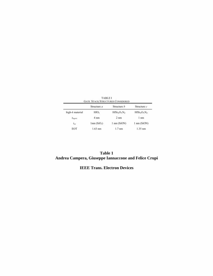

05 10 15 20100
101
102
103
104
105
106
Experiments 400 K Experiments 300 K Theory (pure tunneling)
Cur
rent
Den
sity
(Am
2 )
Gate Voltage (V)
HfSiON c)
Figure 15 Andrea Campera Giuseppe Iannaccone and Felice Crupi
IEEE Trans Electron Devices