
Migrating from STM32F1 to STM32F0
60
July 2012 Doc ID 023072 Rev 1 1/60 AN4088 Application note Migrating from STM32F1 to STM32F0 Introduction For designers of STM32 microcontroller applications, it is important to be able to easily replace one microcontroller type by another one in the same product family. Migrating an application to a different microcontroller is often needed, when product requirements grow, putting extra demands on memory size, or increasing the number of I/Os. On the other hand, cost reduction objectives may force you to switch to smaller components and shrink the PCB area. This application note is written to help you and analyze the steps you need to migrate from an existing STM32F1 device to an STM32F0 device. It gathers the most important information and lists the vital aspects that you need to address. To migrate your application from STM32F1 series to STM32F0 series, you have to analyze the hardware migration, the peripheral migration and the firmware migration. To benefit fully from the information in this application note, the user should be familiar with the STM32 microcontroller family. You can refer to the following documents that are available from www.st.com. ● The STM32F1 family reference manuals (RM0008 and RM0041), the STM32F1 datasheets, and the STM32F1 Flash programming manuals (PM0075, PM0063 and PM0068). ● The STM32F0 family reference manual (RM0091) and the STM32F0 datasheets. For an overview of the whole STM32 series and a comparison of the different features of each STM32 product series, please refer to AN3364 Migration and compatibility guidelines for STM32 microcontroller applications. Table 1 lists the microcontrollers and development tools concerned by this application note. Table 1. Applicable products Type Product sub-class Microcontroller STM32 F0 Entry-level STM32 F1 Mainstream www.st.com
-
Upload
khangminh22 -
Category
Documents
-
view
1 -
download
0
Transcript of Migrating from STM32F1 to STM32F0

July 2012 Doc ID 023072 Rev 1 1/60
AN4088Application note
Migrating from STM32F1 to STM32F0
IntroductionFor designers of STM32 microcontroller applications, it is important to be able to easily replace one microcontroller type by another one in the same product family. Migrating an application to a different microcontroller is often needed, when product requirements grow, putting extra demands on memory size, or increasing the number of I/Os. On the other hand, cost reduction objectives may force you to switch to smaller components and shrink the PCB area.
This application note is written to help you and analyze the steps you need to migrate from an existing STM32F1 device to an STM32F0 device. It gathers the most important information and lists the vital aspects that you need to address.
To migrate your application from STM32F1 series to STM32F0 series, you have to analyze the hardware migration, the peripheral migration and the firmware migration.
To benefit fully from the information in this application note, the user should be familiar with the STM32 microcontroller family. You can refer to the following documents that are available from www.st.com.
● The STM32F1 family reference manuals (RM0008 and RM0041), the STM32F1 datasheets, and the STM32F1 Flash programming manuals (PM0075, PM0063 and PM0068).
● The STM32F0 family reference manual (RM0091) and the STM32F0 datasheets.
For an overview of the whole STM32 series and a comparison of the different features of each STM32 product series, please refer to AN3364 Migration and compatibility guidelines for STM32 microcontroller applications.
Table 1 lists the microcontrollers and development tools concerned by this application note.
Table 1. Applicable products
Type Product sub-class
MicrocontrollerSTM32 F0 Entry-levelSTM32 F1 Mainstream
www.st.com

Contents AN4088
2/60 Doc ID 023072 Rev 1
Contents
1 Hardware migration . . . . . . . . . . . . . . . . . . . . . . . . . . . . . . . . . . . . . . . . . . 5
2 Boot mode compatibility . . . . . . . . . . . . . . . . . . . . . . . . . . . . . . . . . . . . . 6
3 Peripheral migration . . . . . . . . . . . . . . . . . . . . . . . . . . . . . . . . . . . . . . . . . 73.1 STM32 product cross-compatibility . . . . . . . . . . . . . . . . . . . . . . . . . . . . . . 7
3.2 System architecture . . . . . . . . . . . . . . . . . . . . . . . . . . . . . . . . . . . . . . . . . . 9
3.3 Memory mapping . . . . . . . . . . . . . . . . . . . . . . . . . . . . . . . . . . . . . . . . . . . 10
3.4 Reset and clock controller (RCC) interface . . . . . . . . . . . . . . . . . . . . . . . 13
3.5 DMA interface . . . . . . . . . . . . . . . . . . . . . . . . . . . . . . . . . . . . . . . . . . . . . . 16
3.6 Interrupt vectors . . . . . . . . . . . . . . . . . . . . . . . . . . . . . . . . . . . . . . . . . . . . 19
3.7 GPIO interface . . . . . . . . . . . . . . . . . . . . . . . . . . . . . . . . . . . . . . . . . . . . . 21
3.8 EXTI source selection . . . . . . . . . . . . . . . . . . . . . . . . . . . . . . . . . . . . . . . 23
3.9 FLASH interface . . . . . . . . . . . . . . . . . . . . . . . . . . . . . . . . . . . . . . . . . . . . 23
3.10 ADC interface . . . . . . . . . . . . . . . . . . . . . . . . . . . . . . . . . . . . . . . . . . . . . . 24
3.11 PWR interface . . . . . . . . . . . . . . . . . . . . . . . . . . . . . . . . . . . . . . . . . . . . . 26
3.12 Real-time clock (RTC) interface . . . . . . . . . . . . . . . . . . . . . . . . . . . . . . . . 27
3.13 SPI interface . . . . . . . . . . . . . . . . . . . . . . . . . . . . . . . . . . . . . . . . . . . . . . . 27
3.14 I2C interface . . . . . . . . . . . . . . . . . . . . . . . . . . . . . . . . . . . . . . . . . . . . . . . 28
3.15 USART interface . . . . . . . . . . . . . . . . . . . . . . . . . . . . . . . . . . . . . . . . . . . . 29
3.16 CEC interface . . . . . . . . . . . . . . . . . . . . . . . . . . . . . . . . . . . . . . . . . . . . . . 30
4 Firmware migration using the library . . . . . . . . . . . . . . . . . . . . . . . . . . 314.1 Migration steps . . . . . . . . . . . . . . . . . . . . . . . . . . . . . . . . . . . . . . . . . . . . . 31
4.2 RCC driver . . . . . . . . . . . . . . . . . . . . . . . . . . . . . . . . . . . . . . . . . . . . . . . . 31
4.3 FLASH driver . . . . . . . . . . . . . . . . . . . . . . . . . . . . . . . . . . . . . . . . . . . . . . 33
4.4 CRC driver . . . . . . . . . . . . . . . . . . . . . . . . . . . . . . . . . . . . . . . . . . . . . . . . 35
4.5 GPIO configuration update . . . . . . . . . . . . . . . . . . . . . . . . . . . . . . . . . . . . 36
4.5.1 Output mode . . . . . . . . . . . . . . . . . . . . . . . . . . . . . . . . . . . . . . . . . . . . . 36
4.5.2 Input mode . . . . . . . . . . . . . . . . . . . . . . . . . . . . . . . . . . . . . . . . . . . . . . . 36
4.5.3 Analog mode . . . . . . . . . . . . . . . . . . . . . . . . . . . . . . . . . . . . . . . . . . . . . 37
4.5.4 Alternate function mode . . . . . . . . . . . . . . . . . . . . . . . . . . . . . . . . . . . . . 37

AN4088 Contents
Doc ID 023072 Rev 1 3/60
4.6 EXTI Line0 . . . . . . . . . . . . . . . . . . . . . . . . . . . . . . . . . . . . . . . . . . . . . . . . 38
4.7 NVIC interrupt configuration . . . . . . . . . . . . . . . . . . . . . . . . . . . . . . . . . . . 39
4.8 ADC configuration . . . . . . . . . . . . . . . . . . . . . . . . . . . . . . . . . . . . . . . . . . 40
4.9 DAC driver . . . . . . . . . . . . . . . . . . . . . . . . . . . . . . . . . . . . . . . . . . . . . . . . 42
4.10 PWR driver . . . . . . . . . . . . . . . . . . . . . . . . . . . . . . . . . . . . . . . . . . . . . . . . 43
4.11 Backup data registers . . . . . . . . . . . . . . . . . . . . . . . . . . . . . . . . . . . . . . . . 44
4.12 CEC application code . . . . . . . . . . . . . . . . . . . . . . . . . . . . . . . . . . . . . . . . 45
4.13 I2C driver . . . . . . . . . . . . . . . . . . . . . . . . . . . . . . . . . . . . . . . . . . . . . . . . . 47
4.14 SPI driver . . . . . . . . . . . . . . . . . . . . . . . . . . . . . . . . . . . . . . . . . . . . . . . . . 51
4.15 USART driver . . . . . . . . . . . . . . . . . . . . . . . . . . . . . . . . . . . . . . . . . . . . . . 53
4.16 IWDG driver . . . . . . . . . . . . . . . . . . . . . . . . . . . . . . . . . . . . . . . . . . . . . . . 58
5 Revision history . . . . . . . . . . . . . . . . . . . . . . . . . . . . . . . . . . . . . . . . . . . 59

List of tables AN4088
4/60 Doc ID 023072 Rev 1
List of tables
Table 1. Applicable products . . . . . . . . . . . . . . . . . . . . . . . . . . . . . . . . . . . . . . . . . . . . . . . . . . . . . . . 1Table 2. STM32F1 series and STM32F0 series pinout differences . . . . . . . . . . . . . . . . . . . . . . . . . . 5Table 3. Boot modes. . . . . . . . . . . . . . . . . . . . . . . . . . . . . . . . . . . . . . . . . . . . . . . . . . . . . . . . . . . . . . 6Table 4. STM32 peripheral compatibility analysis F1 versus F0 series . . . . . . . . . . . . . . . . . . . . . . . 8Table 5. IP bus mapping differences between STM32F0 and STM32F1 series. . . . . . . . . . . . . . . . 10Table 6. RCC differences between STM32F1 and STM32F0 series . . . . . . . . . . . . . . . . . . . . . . . . 13Table 7. Example of migrating system clock configuration code from F1 to F0 . . . . . . . . . . . . . . . . 15Table 8. RCC registers used for peripheral access configuration. . . . . . . . . . . . . . . . . . . . . . . . . . . 16Table 9. DMA request differences between STM32F1 series and STM32F0 series . . . . . . . . . . . . 17Table 10. Interrupt vector differences between STM32F1 series and STM32F0 series. . . . . . . . . . . 19Table 11. GPIO differences between STM32F1 series and STM32F0 series . . . . . . . . . . . . . . . . . . 21Table 12. FLASH differences between STM32F1 series and STM32F0 series . . . . . . . . . . . . . . . . . 23Table 13. ADC differences between STM32F1 series and STM32F0 series . . . . . . . . . . . . . . . . . . . 24Table 14. PWR differences between STM32F1 series and STM32F0 series. . . . . . . . . . . . . . . . . . . 26Table 15. STM32F10x and STM32F0xx source clock API correspondence . . . . . . . . . . . . . . . . . . . 32Table 16. STM32F10x and STM32F0xx FLASH driver API correspondence. . . . . . . . . . . . . . . . . . . 33Table 17. STM32F10xx and STM32F0xx CRC driver API correspondence. . . . . . . . . . . . . . . . . . . . 35Table 18. STM32F10x and STM32F0xx MISC driver API correspondence . . . . . . . . . . . . . . . . . . . . 40Table 19. STM32F10x and STM32F0xx DAC driver API correspondence. . . . . . . . . . . . . . . . . . . . . 42Table 20. STM32F10x and STM32F0xx PWR driver API correspondence . . . . . . . . . . . . . . . . . . . . 43Table 21. STM32F10xx and STM32F0xx CEC driver API correspondence. . . . . . . . . . . . . . . . . . . . 45Table 22. STM32F10xx and STM32F0xx I2C driver API correspondence. . . . . . . . . . . . . . . . . . . . . 47Table 23. STM32F10xx and STM32F0xx SPI driver API correspondence. . . . . . . . . . . . . . . . . . . . . 51Table 24. STM32F10x and STM32F0xx USART driver API correspondence . . . . . . . . . . . . . . . . . . 54Table 25. STM32F10xx and STM32Fxx IWDG driver API correspondence. . . . . . . . . . . . . . . . . . . . 58Table 26. Document revision history . . . . . . . . . . . . . . . . . . . . . . . . . . . . . . . . . . . . . . . . . . . . . . . . . 59

AN4088 Hardware migration
Doc ID 023072 Rev 1 5/60
1 Hardware migration
The entry-level STM32F0 and general-purpose STM32F1xxx families are pin-to-pin compatible. All peripherals shares the same pins in the two families, but there are some minor differences between packages. The transition from the STM32F1 series to the STM32F0 series is simple as only a few pins are impacted (impacted pins are in bold in Table 2).
The migration from F1 to F0 has no impact on the pinout, except that the user wins 2 or 4 GPIOs for his/her application at VSS/VDD 2 and 4 locations, depending on the package used.
Table 2. STM32F1 series and STM32F0 series pinout differences
STM32F1 series STM32F0 series
QFP48 QFP64 Pinout QFP48 QFP64 Pinout
5 5 PD0 - OSC_IN 5 5 PH0 - OSC_IN
6 6 PD1 - OSC_OUT 6 6 PH1 - OSC_OUT
- 18 VSS_4 - 18 PF4
- 19 VDD_4 - 19 PF5
35 47 VSS_2 35 47 PF6
36 48 VDD_2 36 48 PF7
20 28 Boot1/PB2 20 28 PB2

Boot mode compatibility AN4088
6/60 Doc ID 023072 Rev 1
2 Boot mode compatibility
The way to select the boot mode on the F0 family differs from F1 devices. Instead of using two pins for this setting, F0 gets the nBOOT1 value from an option bit located in the User option bytes at 0x1FFFF800 memory address. Together with the BOOT0 pin, it selects the boot mode to the main Flash memory, the SRAM or to the System memory. Table 3 summarizes the different configurations available for selecting the Boot mode.
Note: The BOOT1 value is the opposite of the nBOOT1 option bit.
Table 3. Boot modes
F0/F1 Boot mode selectionBoot mode Aliasing
BOOT1 BOOT0
x 0 Main Flash memoryMain Flash memory is selected
as boot space
0 1 System memorySystem memory is selected as
boot space
1 1 Embedded SRAMEmbedded SRAM is selected as
boot space
AN4088 Peripheral migration
Doc ID 023072 Rev 1 7/60
3 Peripheral migration
As shown in Table 3, there are three categories of peripherals. The common peripherals are supported with the dedicated firmware library without any modification, except if the peripheral instance is no longer present. You can change the instance and, of course, all the related features (clock configuration, pin configuration, interrupt/DMA request).
The modified peripherals such as: ADC, RCC and RTC are different from the F1 series ones and should be updated to take advantage of the enhancements and the new features in F0 series.
All these modified peripherals in the F0 series are enhanced to obtain smaller silicon print with features designed to offer advanced high-end capabilities in economical end products and to fix some limitations present in the F1 series.
3.1 STM32 product cross-compatibilityThe STM32 series embeds a set of peripherals which can be classed in three categories:
● The first category is for the peripherals which are, by definition, common to all products. Those peripherals are identical, so they have the same structure, registers and control bits. There is no need to perform any firmware change to keep the same functionality, at the application level, after migration. All the features and behavior remain the same.
● The second category is for the peripherals which are shared by all products but have only minor differences (in general to support new features). The migration from one product to another is very easy and does not need any significant new development effort.
● The third category is for peripherals which have been considerably changed from one product to another (new architecture, new features...). For this category of peripherals, the migration will require new development, at the application level.
Table 4 gives a general overview of this classification.

Peripheral migration AN4088
8/60 Doc ID 023072 Rev 1
Table 4. STM32 peripheral compatibility analysis F1 versus F0 series
Peripheral F1 series F0 series
Compatibility
Feature Pinout FW driver
SPI Yes Yes++Two FIFO available, 4-bit to 16-bit data size selection
Identical Partial compatibility
WWDG Yes Yes Same features NA Full compatibility
IWDG Yes Yes+ Added a Window mode NA Full compatibility
DBGMCU Yes Yes No JTAG, No TraceIdentical for the SWD
Partial compatibility
CRC Yes Yes++Added reverse capability and initial CRC value
NA Partial compatibility
EXTI Yes Yes+Some peripherals are able to generate event in stop mode
Identical Full compatibility
CEC Yes Yes++
Kernel clock, arbitration lost flag and automatic transmission retry, multi-address config, wakeup from stop mode
Identical Partial compatibility
DMA Yes Yes1 DMA controller with 5 channels
NA Full compatibility
TIM Yes Yes+ Enhancement Identical Full compatibility
PWR Yes Yes+No Vref, Vdda can be greater than Vdd, 1.8 mode for core.
Identical for the same feature
Partial compatibility
RCC Yes Yes+ New HSI14 dedicated to ADCPD0 & PD1 => PF0 & PF1 for the osc
Partial compatibility
USART Yes Yes+Choice for independent clock sources, timeout feature, wakeup from stop mode
Identical Full compatibility
I2C Yes Yes++
Communication events managed by HW, FM+, wakeup from stop mode, digital filter
Identical New driver
DAC Yes Yes+ DMA underrun interrupt Identical Full compatibility
ADC Yes Yes++Same analogic part, but new digital interface
Identical Partial compatibility
RTC Yes Yes++
Subsecond precision, digital calibration circuit, time-stamp function for event saving, programmable alarm
Identical for the same feature
New driver
FLASH Yes Yes+ Option byte modified NA Partial compatibility
GPIO Yes Yes++ New peripheral 4 new GPIOs Partial compatibility

AN4088 Peripheral migration
Doc ID 023072 Rev 1 9/60
Note: Yes++ = New feature or new architectureYes+ = Same feature, but specification change or enhancementYes = Feature availableNA = Feature not available
3.2 System architectureThe STM32F0 MCU family has been designed to target an entry-level market, with low-power capabilities and easy handling. In order to fulfill this aim while keeping the advanced high-end features proper to the STM32, the core has been changed for a Cortex-M0. Its small silicon area, coupled to a minimal code footprint, allows for low-cost applications with 32 bits performance. Figure 1 shows the correspondence between the M3 and M0 sets of instructions. Moving from F1 to F0 requires a recompilation of the code to avoid the use of unavailable features.
CAN Yes NA NA NA NA
USB FS Device Yes NA NA NA NA
Ethernet Yes NA NA NA NA
SDIO Yes NA NA NA NA
FSMC Yes NA NA NA NA
Touch Sensing NA Yes NA NA NA
COMP NA Yes NA NA NA
SYSCFG NA Yes NA NA NA
Table 4. STM32 peripheral compatibility analysis F1 versus F0 series (continued)
Peripheral F1 series F0 series
Compatibility
Feature Pinout FW driver

Peripheral migration AN4088
10/60 Doc ID 023072 Rev 1
Figure 1. System architecture
Important modifications have been performed on the MCU organization too, starting by switching from a Harvard to Von Neumann architecture, decreasing the system complexity, or focusing on SW Debug in order to simplify this precise feature.
3.3 Memory mappingThe peripheral address mapping has been changed in the F0 series versus F1 series. The main change concerns the GPIOs which have been moved from the APB bus to the AHB bus to allow them to operate at the maximum speed.
Table 5 provides the peripheral address mapping correspondence between F0 and F1 series.
Table 5. IP bus mapping differences between STM32F0 and STM32F1 series
PeripheralSTM32 F0 series STM32 F1 series
Bus Base address Bus Base address
TSC
AHB1
0x40024000 NA NA
CRC 0x40023000
AHB
0x40023000
FLITF 0x40022000 0x40022000
RCC 0x40021000 0x40021000
DMA1/DMA 0x40020000 0x40020000

AN4088 Peripheral migration
Doc ID 023072 Rev 1 11/60
GPIOF
AHB2
0x48001400
APB2
0x40011800
GPIOD 0x48000C00 0x40011400
GPIOC 0x48000800 0x40011000
GPIOB 0x48000400 0x40010C00
GPIOA 0x48000000 0x40010800
DBGMCU
APB2
0x40015800 NA NA
TIM17 0x40014800 NA NA
TIM16 0x40014400 NA NA
TIM15 0x40014000 NA NA
USART1 0x40013800
APB2
0x40013800
SPI1 / I2S1 0x40013000 0x40013000
TIM1 0x40012C00 0x40012C00
ADC / ADC1 0x40012400 0x40012400
EXTIAPB2
(through SYSCFG)
0x40010400 0x40010400
SYSCFG + COMP APB2 0x40010000 NA NA
CEC
APB1
0x40007800
APB1
0x40007800
DAC 0x40007400 0x40007400
PWR 0x40007000 0x40007000
I2C2 0x40005800 0x40005800
I2C1 0x40005400 0x40005400
USART2 0x40004400 0x40004400
SPI2 0x40003800 0x40003800
IWWDG / IWDG Own Clock 0x40003000 0x40003000
WWDG APB1 0x40002C00 0x40002C00
RTCAPB1
(through PWR)
0x40002800 (inc. BKP registers)
0x40002800
Table 5. IP bus mapping differences between STM32F0 and STM32F1 series
PeripheralSTM32 F0 series STM32 F1 series
Bus Base address Bus Base address

Peripheral migration AN4088
12/60 Doc ID 023072 Rev 1
TIM14
APB1
0x40002000 NA NA
TIM6 0x40001000
APB1
0x40001000
TIM3 0x40000400 0x40000400
TIM2 0x40000000 0x40000000
USB device FS SRAM NA NA
APB1
0x40006000
USB device FS NA NA 0x40005C00
USART3 NA NA 0x40004800
TIM7 NA NA 0x40001400
TIM4 NA NA 0x40000800
FSMC Registers NA NA
AHB
0xA0000000
USB OTG FS NA NA 0x50000000
ETHERNET MAC NA NA 0x40028000
DMA2 NA NA 0x40020400
GPIOG NA NA APB2 0x40012000
SDIO NA NA AHB 0x40018000
TIM11 NA NA
APB2
0x40015400
TIM10 NA NA 0x40015000
TIM9 NA NA 0x40014C00
ADC2 NA NA 0x40012800
ADC3 NA NA 0x40013C00
TIM8 NA NA 0x40013400
Table 5. IP bus mapping differences between STM32F0 and STM32F1 series
PeripheralSTM32 F0 series STM32 F1 series
Bus Base address Bus Base address

AN4088 Peripheral migration
Doc ID 023072 Rev 1 13/60
Note: NA = feature not available.
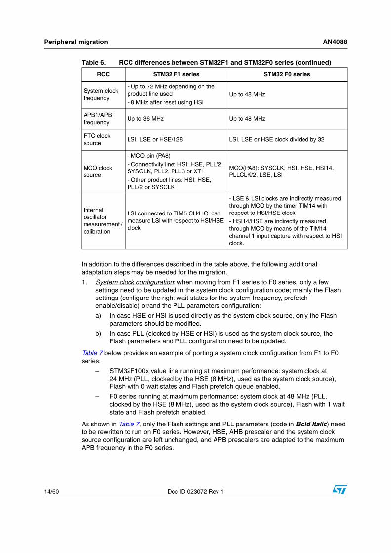
3.4 Reset and clock controller (RCC) interfaceThe main differences related to the RCC (Reset and clock controller) in the STM32F0 series versus STM32F1 series are presented in Table 6.
CAN2 NA NA
APB1
0x40006800
CAN1 NA NA 0x40006400
UART5 NA NA 0x40005000
UART4 NA NA 0x40004C00
SPI3/I2S3 NA NA 0x40003C00
TIM13 NA NA 0x40001C00
TIM12 NA NA 0x40001800
TIM5 NA NA 0x40000C00
BKP registers NA NA 0x40006C00
AFIO NA NA APB2 0x40010000
Table 5. IP bus mapping differences between STM32F0 and STM32F1 series
PeripheralSTM32 F0 series STM32 F1 series
Bus Base address Bus Base address
Table 6. RCC differences between STM32F1 and STM32F0 series
RCC STM32 F1 series STM32 F0 series
HSI 14 NAHigh speed internal oscillator dedicated to ADC
HSI 8 MHz RC factory-trimmed Similar
LSI 40 KHz RC Similar
HSE3 - 25 MHz depending on the product line used
4 - 32 MHz
LSE 32.768 KHz Similar
PLL
- Connectivity line: main PLL + 2 PLLs for I2S, Ethernet and OTG FS clock- Other product lines: main PLL
Main PLL
System clock source
HSI, HSE or PLL Similar
Peripheral migration AN4088
14/60 Doc ID 023072 Rev 1
In addition to the differences described in the table above, the following additional adaptation steps may be needed for the migration.
1. System clock configuration: when moving from F1 series to F0 series, only a few settings need to be updated in the system clock configuration code; mainly the Flash settings (configure the right wait states for the system frequency, prefetch enable/disable) or/and the PLL parameters configuration:
a) In case HSE or HSI is used directly as the system clock source, only the Flash parameters should be modified.
b) In case PLL (clocked by HSE or HSI) is used as the system clock source, the Flash parameters and PLL configuration need to be updated.
Table 7 below provides an example of porting a system clock configuration from F1 to F0 series:
– STM32F100x value line running at maximum performance: system clock at 24 MHz (PLL, clocked by the HSE (8 MHz), used as the system clock source), Flash with 0 wait states and Flash prefetch queue enabled.
– F0 series running at maximum performance: system clock at 48 MHz (PLL, clocked by the HSE (8 MHz), used as the system clock source), Flash with 1 wait state and Flash prefetch enabled.
As shown in Table 7, only the Flash settings and PLL parameters (code in Bold Italic) need to be rewritten to run on F0 series. However, HSE, AHB prescaler and the system clock source configuration are left unchanged, and APB prescalers are adapted to the maximum APB frequency in the F0 series.
System clock frequency
- Up to 72 MHz depending on the product line used - 8 MHz after reset using HSI
Up to 48 MHz
APB1/APB frequency
Up to 36 MHz Up to 48 MHz
RTC clock source
LSI, LSE or HSE/128 LSI, LSE or HSE clock divided by 32
MCO clock source
- MCO pin (PA8)
- Connectivity line: HSI, HSE, PLL/2, SYSCLK, PLL2, PLL3 or XT1
- Other product lines: HSI, HSE, PLL/2 or SYSCLK
MCO(PA8): SYSCLK, HSI, HSE, HSI14, PLLCLK/2, LSE, LSI
Internal oscillator measurement / calibration
LSI connected to TIM5 CH4 IC: can measure LSI with respect to HSI/HSE clock
- LSE & LSI clocks are indirectly measured through MCO by the timer TIM14 with respect to HSI/HSE clock- HSI14/HSE are indirectly measured through MCO by means of the TIM14 channel 1 input capture with respect to HSI clock.
Table 6. RCC differences between STM32F1 and STM32F0 series (continued)
RCC STM32 F1 series STM32 F0 series

AN4088 Peripheral migration
Doc ID 023072 Rev 1 15/60
Note: 1 The source code presented in Table 7 is intentionally simplified (timeout in wait loop removed) and is based on the assumption that the RCC and Flash registers are at their reset values.
2 For STM32F0xx, you can use the clock configuration tool, STM32F0xx_Clock_Configuration.xls, to generate a customized system_stm32f0xx.c file containing a system clock configuration routine, depending on your application requirements.
2. Peripheral access configuration: since the address mapping of some peripherals has been changed in F0 series versus F1 series, you need to use different registers to [enable/disable] or [enter/exit] the peripheral [clock] or [from reset mode].
Table 7. Example of migrating system clock configuration code from F1 to F0
STM32F100x Value Line running at 24 MHz (PLL as clock source) with 0 wait states
STM32F0xx running at 48 MHz (PLL as clock source) with 1 wait state
/* Enable HSE ----------------------------*/ RCC->CR |= ((uint32_t)RCC_CR_HSEON);
/* Wait till HSE is ready */ while((RCC->CR & RCC_CR_HSERDY) == 0) { } /* Flash configuration -------------------*/ /* Prefetch ON, Flash 0 wait state */ FLASH->ACR |= FLASH_ACR_PRFTBE | FLASH_ACR_LATENCY_0;
/* AHB and APB prescaler configuration --*/ /* HCLK = SYSCLK */ RCC->CFGR |= (uint32_t)RCC_CFGR_HPRE_DIV1; /* PCLK2 = HCLK */ RCC->CFGR |= (uint32_t)RCC_CFGR_PPRE2_DIV1; /* PCLK1 = HCLK */ RCC->CFGR |= (uint32_t)RCC_CFGR_PPRE1_DIV1;
/* PLL configuration = (HSE / 2) * 6 = 24 MHz */ RCC->CFGR |= (uint32_t)(RCC_CFGR_PLLSRC_PREDIV1 | RCC_CFGR_PLLXTPRE_PREDIV1_Div2 | RCC_CFGR_PLLMULL6);
/* Enable PLL */ RCC->CR |= RCC_CR_PLLON;
/* Wait till PLL is ready */ while((RCC->CR & RCC_CR_PLLRDY) == 0) { }
/* Select PLL as system clock source ----*/ RCC->CFGR &= (uint32_t)((uint32_t)~(RCC_CFGR_SW)); RCC->CFGR |= (uint32_t)RCC_CFGR_SW_PLL;
/* Wait till PLL is used as system clock source */ while ((RCC->CFGR & (uint32_t)RCC_CFGR_SWS) != (uint32_t)0x08) { }
/* Enable HSE ----------------------------*/ RCC->CR |= ((uint32_t)RCC_CR_HSEON);
/* Wait till HSE is ready */ while((RCC->CR & RCC_CR_HSERDY) == 0) { } /* Flash configuration -------------------*/ /* Prefetch ON, Flash 1 wait state */ FLASH->ACR |= FLASH_ACR_PRFTBE | FLASH_ACR_LATENCY;
/* AHB and APB prescaler configuration --*/ /* HCLK = SYSCLK */ RCC->CFGR |= (uint32_t)RCC_CFGR_HPRE_DIV1;
/* PCLK = HCLK */ RCC->CFGR |= (uint32_t)RCC_CFGR_PPRE_DIV1;
/* PLL configuration = HSE * 6 = 48 MHz -*/ RCC->CFGR |= (uint32_t)(RCC_CFGR_PLLSRC_PREDIV1 | RCC_CFGR_PLLXTPRE_PREDIV1 | RCC_CFGR_PLLMULL6); /* Enable PLL */ RCC->CR |= RCC_CR_PLLON;
/* Wait till PLL is ready */ while((RCC->CR & RCC_CR_PLLRDY) == 0) { }
/* Select PLL as system clock source ----*/ RCC->CFGR |= (uint32_t)RCC_CFGR_SW_PLL;
/* Wait till PLL is used as system clock source */ while ((RCC->CFGR & (uint32_t)RCC_CFGR_SWS) != (uint32_t)RCC_CFGR_SWS_PLL) { }

Peripheral migration AN4088
16/60 Doc ID 023072 Rev 1
To configure the access to a given peripheral, you have first to know to which bus this peripheral is connected; refer to Table 5 then, depending on the action needed, program the right register as described in Table 8 above. For example, if USART1 is connected to the APB2 bus, to enable the USART1 clock you have to configure APB2ENR register as follows:
RCC->APB2ENR |= RCC_APB2ENR_USART1EN;
3. Peripheral clock configuration: some peripherals have a dedicated clock source independent from the system clock, and used to generate the clock required for their operation:
a) ADC: in STM32F0 series, the ADC features two possible clock sources:
– The first one is based on the PCLK; a prescaler allows you to reduce the ADC input frequency by a factor 2 or 4 before getting to the ADC.
– The other one is a completely new feature on stingray; a dedicated 14 MHz oscillator (HSI14) is integrated on the chip and can be used for the ADC input frequency.
b) RTC: in STM32F0 series, the RTC features three possible clock sources:
– The first one is based on the HSE Clock; a prescaler divides its frequency by 32 before going to the RTC.
– The second one is the LSE oscillator.
– The third clock source is the LSI RC with a value of 40 KHz.
3.5 DMA interfaceSTM32F1 and STM32F0 series use the same fully compatible DMA controller.
The STM32F0 series uses one 5-channel DMA controller when STM32F1 uses two. Each channel is dedicated to managing memory access requests from one or more peripherals.
The table below presents the correspondence between the DMA requests of the peripherals in STM32F1 series and STM32F0 series.
Table 8. RCC registers used for peripheral access configuration
Bus Register Comments
AHBRCC_AHBRSTR Used to [enter/exit] the AHB peripheral from reset
RCC_AHBENR Used to [enable/disable] the AHB peripheral clock
APB1RCC_APB1RSTR Used to [enter/exit] the APB1 peripheral from reset
RCC_APB1ENR Used to [enable/disable] the APB1 peripheral clock
APB2RCC_APB2RSTR Used to [enter/exit] the APB2 peripheral from reset
RCC_APB2ENR Used to [enable/disable] the APB2 peripheral clock

AN4088 Peripheral migration
Doc ID 023072 Rev 1 17/60
Table 9. DMA request differences between STM32F1 series and STM32F0 series
Peripheral DMA request STM32F1 series STM32F0 series
ADC1/ADC ADC1/ADC DMA1_Channel1DMA_Channel1DMA_Channel2
ADC3 ADC3 DMA2_Channel5 NA
DACDAC_Channel1/DACDAC_Channel2
DMA2_Channel3 / DMA1_Channel3(1)
DMA2_Channel4 / DMA1_Channel4(1) DMA_Channel3
SPI1SPI1_RxSPI1_Tx
DMA1_Channel2
DMA1_Channel3
DMA_Channel2
DMA_Channel3
SPI2SPI2_RxSPI2_Tx
DMA1_Channel4
DMA1_Channel5
DMA_Channel4
DMA_Channel5
SPI3SPI3_RxSPI3_Tx
DMA2_Channel1
DMA2_Channel2NA
USART1USART1_RxUSART1_Tx
DMA1_Channel5
DMA1_Channel4
DMA_Channel3/DMA_Channel5
DMA_Channel2/DMA_Channel4
USART2USART2_RxUSART2_Tx
DMA1_Channel6
DMA1_Channel7
DMA_Channel6
DMA_Channel7
USART3USART3_RxUSART3_Tx
DMA1_Channel3
DMA1_Channel2NA
UART4UART4_RxUART4_Tx
DMA2_Channel3
DMA2_Channel5NA
UART5UART5_RxUART5_Tx
DMA2_Channel4
DMA2_Channel1NA
I2C1I2C1_RxI2C1_Tx
DMA1_Channel7
DMA1_Channel6
DMA_Channel7
DMA_Channel6
I2C2I2C2_RxI2C2_Tx
DMA1_Channel5
DMA1_Channel4
DMA_Channel5
DMA_Channel4
SDIO SDIO DMA2_Channel4 NA
TIM1
TIM1_UPTIM1_CH1TIM1_CH2TIM1_CH3TIM1_CH4TIM1_TRIGTIM1_COM
DMA1_Channel5DMA1_Channel2
DMA1_Channel3
DMA1_Channel6DMA1_Channel4
DMA1_Channel4
DMA1_Channel4
DMA_Channel5DMA_Channel2
DMA_Channel3
DMA_Channel6DMA_Channel4
DMA_Channel4
DMA_Channel4

Peripheral migration AN4088
18/60 Doc ID 023072 Rev 1
TIM8
TIM8_UPTIM8_CH1TIM8_CH2TIM8_CH3TIM8_CH4TIM8_TRIGTIM8_COM
DMA2_Channel1
DMA2_Channel3
DMA2_Channel5DMA2_Channel1
DMA2_Channel2
DMA2_Channel2DMA2_Channel2
NA
TIM2
TIM2_UPTIM2_CH1TIM2_CH2TIM2_CH3TIM2_CH4
DMA1_Channel2DMA1_Channel5
DMA1_Channel7
DMA1_Channel1DMA1_Channel7
DMA_Channel2DMA_Channel5
DMA_Channel3
DMA_Channel1DMA_Channel4
TIM3
TIM3_UPTIM3_CH1TIM3_TRIGTIM3_CH3TIM3_CH4
DMA1_Channel3
DMA1_Channel6DMA1_Channel6
DMA1_Channel2
DMA1_Channel3
DMA_Channel3
DMA_Channel4DMA_Channel4
DMA_Channel2
DMA_Channel3
TIM4
TIM4_UPTIM4_CH1TIM4_CH2TIM4_CH3
DMA1_Channel7
DMA1_Channel1DMA1_Channel4
DMA1_Channel5
NA
TIM5
TIM5_UPTIM5_CH1TIM5_CH2TIM5_CH3TIM5_CH4TIM5_TRIG
DMA2_Channel2
DMA2_Channel5
DMA2_Channel4DMA2_Channel2
DMA2_Channel1
DMA2_Channel1
NA
TIM6 TIM6_UP DMA2_Channel3 / DMA1_Channel3(1) DMA_Channel3
TIM7 TIM7_UP DMA2_Channe4 / DMA1_Channel4 (1) NA
TIM15
TIM15_UPTIM15_CH1TIM15_TRIGTIM15_COM
DMA1_Channel5
DMA1_Channel5DMA1_Channel5
DMA1_Channel5
DMA_Channel5
DMA_Channel5DMA_Channel5
DMA_Channel5
TIM16TIM16_UPTIM16_CH1
DMA1_Channel6
DMA1_Channel6
DMA_Channel3/DMA_Channel4
DMA_Channel3/DMA_Channel4
TIM17TIM17_UPTIM17_CH1
DMA1_Channel7
DMA1_Channel7
DMA_Channel1/DMA_Channel2
DMA_Channel1/DMA_Channel2
1. For high-density value line devices, the DAC DMA requests are mapped respectively on DMA1 Channel 3 and DMA1 Channel 4.
Table 9. DMA request differences between STM32F1 series and STM32F0 series (continued)
Peripheral DMA request STM32F1 series STM32F0 series

AN4088 Peripheral migration
Doc ID 023072 Rev 1 19/60
3.6 Interrupt vectorsTable 10 presents the interrupt vectors in STM32F0 series versus STM32F1 series.
The switch from Cortex-M3 to Cortex-M0 has introduced a reduction of the vector table. This leads to many differences between the two devices.
Table 10. Interrupt vector differences between STM32F1 series and STM32F0 series
Position STM32F1 series STM32F0 series
0 WWDG WWDG
1 PVD PVD
2 TAMPER RTC
3 RTC FLASH
4 FLASH RCC
5 RCC EXTI0_1
6 EXTI0 EXTI2_3
7 EXTI1 EXTI4_15
8 EXTI2 TSC
9 EXTI3 DMA_CH1
10 EXTI4 DMA_CH2_CH3
11 DMA1_Channel1 DMA_CH4_CH5
12 DMA1_Channel2 ADD_COMP
13 DMA1_Channel3 TIM1_BRK_UP_TRG_COM
14 DMA1_Channel4 TIM1_CC
15 DMA1_Channel5 TIM2
16 DMA1_Channel6 TIM3
17 DMA1_Channel7 TIM6_DAC
18 ADC1_2 Reserved
19 CAN1_TX / USB_HP_CAN_TX TIM14
20 CAN1_RX0 / USB_LP_CAN_RX0 TIM15
21 CAN1_RX1 TIM16
22 CAN1_SCE TIM17
23 EXTI9_5 I2C1
24 TIM1_BRK / TIM1_BRK _TIM9 I2C2
25 TIM1_UP / TIM1_UP_TIM10 SPI1
26TIM1_TRG_COM / TIM1_TRG_COM_TIM11
SPI2
27 TIM1_CC USART1
28 TIM2 USART2
29 TIM3 Reserved

Peripheral migration AN4088
20/60 Doc ID 023072 Rev 1
30 TIM4 CEC
31 I2C1_EV Reserved
32 I2C1_ER NA
33 I2C2_EV NA
34 I2C2_ER NA
35 SPI1 NA
36 SPI2 NA
37 USART1 NA
38 USART2 NA
39 USART3 NA
40 EXTI15_10 NA
41 RTC_Alarm NA
42 OTG_FS_WKUP / USBWakeUp NA
43 TIM8_BRK / TIM8_BRK_TIM12 (1) NA
44 TIM8_UP / TIM8_UP_TIM13 (1) NA
45TIM8_TRG_COM / TIM8_TRG_COM_TIM14 (1) NA
46 TIM8_CC NA
47 ADC3 NA
48 FSMC NA
49 SDIO NA
50 TIM5 NA
51 SPI3 NA
52 UART4 NA
53 UART5 NA
54 TIM6 NA
55 TIM7 NA
56 DMA2_Channel1 NA
57 DMA2_Channel2 NA
58 DMA2_Channel3 NA
59 DMA2_Channel4/DMA2_Channel4_5 (1) NA
60 DMA2_Channel5 NA
61 ETH NA
62 ETH_WKUP NA
63 CAN2_TX NA
Table 10. Interrupt vector differences between STM32F1 series and STM32F0 series
Position STM32F1 series STM32F0 series

AN4088 Peripheral migration
Doc ID 023072 Rev 1 21/60
3.7 GPIO interfaceThe STM32F0 GPIO peripheral embeds new features compared to F1 series, below the main features:
● GPIO mapped on AHB bus for better performance
● I/O pin multiplexer and mapping: pins are connected to on-chip peripherals/modules through a multiplexer that allows only one peripheral alternate function (AF) connected to an I/O pin at a time. In this way, there can be no conflict between peripherals sharing the same I/O pin.
● More possibilities and features for I/O configuration
The F0 GPIO peripheral is a new design and thus the architecture, features and registers are different from the GPIO peripheral in the F1 series. Any code written for the F1 series using the GPIO needs to be rewritten to run on F0 series.
For more information about STM32F0’s GPIO programming and usage, please refer to the "I/O pin multiplexer and mapping" section in the GPIO chapter of the STM32F0xx Reference Manual (RM0091).
The table below presents the differences between GPIOs in the STM32F1 series and STM32F0 series.
64 CAN2_RX01 NA
65 CAN2_RX1 NA
66 CAN2_SCE NA
67 OTG_FS NA
1. Depending on the product line used.
The cortex M0 core uses 2 bits to set the interrupt priority without a sub-priority. The user can define 4 levels of priorities in the Nested Vector Interrupt Controller. F1 and Cortex M3 core use 4 bits, thus it can reach 16 priority levels.
Table 10. Interrupt vector differences between STM32F1 series and STM32F0 series
Position STM32F1 series STM32F0 series
Table 11. GPIO differences between STM32F1 series and STM32F0 series
GPIO STM32F1 series STM32F0 series
Input modeFloating
PU
PD
Floating
PU
PD
General purpose outputPP
OD
PP
PP + PUPP + PD
OD
OD + PUOD + PD

Peripheral migration AN4088
22/60 Doc ID 023072 Rev 1
Alternate function mode
In STM32F1 series
1. The configuration to use an I/O as an alternate function depends on the peripheral mode used. For example, the USART Tx pin should be configured as an alternate function push-pull, while the USART Rx pin should be configured as input floating or input pull-up.
2. To optimize the number of peripheral I/O functions for different device packages (especially those with a low pin count), it is possible to remap some alternate functions to other pins by software. For example, the USART2_RX pin can be mapped on PA3 (default remap) or PD6 (by software remap).
In STM32F0 series
1. Whatever the peripheral mode used, the I/O must be configured as an alternate function, then the system can use the I/O in the proper way (input or output).
2. The I/O pins are connected to on-chip peripherals/modules through a multiplexer that allows only one peripheral’s alternate function to be connected to an I/O pin at a time. In this way, there can be no conflict between peripherals sharing the same I/O pin. Each I/O pin has a multiplexer with eight alternate function inputs (AF0 to AF7) that can be configured through the GPIOx_AFRL and GPIOx_AFRH registers:
– The peripheral alternate functions are mapped by configuring AF0 to AF7.
3. In addition to this flexible I/O multiplexing architecture, each peripheral has alternate functions mapped on different I/O pins to optimize the number of peripheral I/O functions for different device packages. For example, the USART2_RX pin can be mapped on PA3 or PA15 pin.
Alternate function output
PPOD
PP
PP + PU
PP + PDOD
OD + PU
OD + PD
Input / Output Analog Analog
Output speed2 MHz10 MHz
50 MHz
2 MHz10 MHz
48 MHz
Alternate function selection
To optimize the number of peripheral I/O functions for different device packages, it is possible to remap some alternate functions to some other pins (software remap).
Highly flexible pin multiplexing allows no conflict between peripherals sharing the same I/O pin.
Max IO toggle frequency 18 MHz 12 MHz
Table 11. GPIO differences between STM32F1 series and STM32F0 series (continued)
GPIO STM32F1 series STM32F0 series

AN4088 Peripheral migration
Doc ID 023072 Rev 1 23/60
Note: Please refer to the “Alternate function mapping” table in the STM32F0x datasheet for the detailed mapping of the system and the peripheral alternate function I/O pins.
4. Configuration procedure
– Configure the desired I/O as an alternate function in the GPIOx_MODER register
– Select the type, pull-up/pull-down and output speed via the GPIOx_OTYPER, GPIOx_PUPDR and GPIOx_OSPEEDER registers, respectively
– Connect the I/O to the desired AFx in the GPIOx_AFRL or GPIOx_AFRH register
3.8 EXTI source selectionIn STM32F1, the selection of the EXTI line source is performed through EXTIx bits in AFIO_EXTICRx registers, while in F0 series this selection is done through EXTIx bits in SYSCFG_EXTICRx registers.
Only the mapping of the EXTICRx registers has been changed, without any changes to the meaning of the EXTIx bits. However, the maximum range of EXTIx bit values is 0b0101 as the last PORT is F (in F1 series, the maximum value is 0b0110).
3.9 FLASH interfaceThe table below presents the difference between the FLASH interface of STM32F1 series and STM32F0 series, which can be grouped as follows:
● New interface, new technology
● New architecture
● New read protection mechanism, 3 read protection levels
Consequently, the F0 Flash programming procedures and registers are different from the F1 series, and any code written for the Flash interface in the F1 series needs to be rewritten to run on F0 series.
Table 12. FLASH differences between STM32F1 series and STM32F0 series
Feature STM32F1 series STM32F0 series
Main/Program memory
Start Address 0x0800 0000 0x0800 0000
End Address up to 0x080F FFFF Up to 0x0805 FFFF
GranularityPage size = 2 Kbytes
except for Low and Medium density page size = 1 Kbyte
64 pages of 1 Kbyte
EEPROM memoryStart Address
Available through SW emulation Available through SW emulationEnd Address
System memoryStart Address 0x1FFF F000 0x1FFF EC00
End Address 0x1FFF F7FF 0x1FFF F7FF

Peripheral migration AN4088
24/60 Doc ID 023072 Rev 1
3.10 ADC interfaceThe table below presents the differences between the ADC interface of STM32F1 series and STM32F0 series; these differences are the following:
● New digital interface
● New architecture and new features
Option BytesStart Address 0x1FFF F800 0x1FFF F800
End Address 0x1FFF F80F 0x1FFF F80B
Flash interface
Start address 0x4002 2000 0x4002 2000
Programming procedure Same for all product lines
Same as F1 series for Flash program and erase operations. Different from F1 series for Option byte programming
Read Protection
Unprotection Read protection disable
RDP = 0xA55A
Level 0 no protection
RDP = 0xAA
ProtectionRead protection enable
RDP != 0xA55A
Level 1 memory protection
RDP != (Level 2 & Level 0) Level 2: Lvl 1 + Debug disabled
Write protection Protection by 4-Kbyte block Protection by 4-Kbyte block
User Option bytes
STOP STOP
STANDBY STANDBY
WDG WDG
NA RAM_PARITY_CHECK
NA VDDA_MONITOR
NA nBOOT1
Erase granularity Page (1 or 2 Kbytes) Page (1 Kbyte)
Program mode Half word (16 bits) Half word (16 bits)
Table 12. FLASH differences between STM32F1 series and STM32F0 series (continued)
Feature STM32F1 series STM32F0 series
Table 13. ADC differences between STM32F1 series and STM32F0 series
ADC STM32F1 series STM32F0 series
ADC Type SAR structure SAR structure
Instances ADC1 / ADC2 / ADC3 ADC

AN4088 Peripheral migration
Doc ID 023072 Rev 1 25/60
Maximum sampling frequency 1 MSPS 1 MSPS
Number of channels Up to 21 channels Up to 16 channels + 3 internal
Resolution 12-bit 12-bit
Conversion modes Single / continuous / scan / discontinuous / dual mode
Single / continuous / scan / discontinuous / dual mode /
triple mode
DMA Yes Yes
External Trigger
Yes Yes
External event for regular group
For ADC1 and ADC2:
TIM1 CC1 TIM1 CC2
TIM1 CC3
TIM2 CC2 TIM3 TRGO
TIM4 CC4
EXTI line 11 / TIM8_TRGO
For ADC3:
TIM3 CC1 TIM2 CC3
TIM1 CC3
TIM8 CC1 TIM8 TRGO
TIM5 CC1
External event for injected group
For ADC1 and ADC2:
TIM1 TRGO TIM1 CC4
TIM2 TRGO
TIM2 CC1 TIM3 CC4
TIM4 TRGO
EXTI line15 / TIM8_CC4
For ADC3:
TIM1 TRGO TIM1 CC4
TIM4 CC3
TIM8 CC2 TIM8 CC4
TIM5 TRGO
External event
TIM1_TRGO
TIM1_CC4TIM2_TRGO
TIM3_TRGO
TIM15_TRGO
Supply requirement 2.4 V to 3.6 V 2.4 V to 3.6 V
Input range VREF- <= VIN <= VREF+ Vdd and 2.4 <= Vdda <= 3.6
Table 13. ADC differences between STM32F1 series and STM32F0 series
ADC STM32F1 series STM32F0 series

Peripheral migration AN4088
26/60 Doc ID 023072 Rev 1
3.11 PWR interfaceIn STM32F0 series the PWR controller presents some differences vs. F1 series, these differences are summarized in the table below. However, the programming interface is unchanged.
Table 14. PWR differences between STM32F1 series and STM32F0 series
PWR STM32F1 series STM32F0 series
Power supplies
1- VDD = 2.0 to 3.6 V: external power supply for I/Os and the internal regulator. Provided externally through VDD pins.
2- VSSA, VDDA = 2.0 to 3.6 V: external analog power supplies for ADC, Reset blocks, RCs and PLL. VDDA and VSSA must be connected to VDD and VSS, respectively.
3- VBAT = 1.8 to 3.6 V: power supply for RTC, external clock 32 kHz oscillator and backup registers (through power switch) when VDD is not present.
1- VDD = 2.0 to 3.6 V: external power supply for I/Os and the internal regulator. Provided externally through VDD pins.2- VSSA, VDDA = 2.0 to 3.6 V: external analog power supplies for ADC, DAC, Reset blocks, RCs and PLL. VDDA and VSSA must be connected to VDD and VSS, respectively.
3- VBAT = 1.8 to 3.6 V: power supply for RTC, external clock 32 kHz oscillator and backup registers (through power switch) when VDD is not present.
Battery backup domain
– Backup registers
– RTC– LSE
– PC13 to PC15 I/Os
– Backup registers
– RTC– LSE
– RCC Backup Domain Control Register
Power supply supervisor
Integrated POR / PDR circuitry
Programmable voltage detector (PVD)
Integrated POR / PDR circuitry
Programmable voltage detector (PVD)
Low-power modes
Sleep mode
Stop mode Standby mode (1.8V domain powered-off)
Sleep mode
Stop mode Standby mode (1.8V domain powered-off)
Wake-up sources
Sleep mode
– Any peripheral interrupt/wakeup eventStop mode
– Any EXTI line event/interrupt
Standby mode– WKUP pin rising edge
– RTC alarm
– External reset in NRST pin
– IWDG reset
Sleep and sleep low power modes
– Any peripheral interrupt/wakeup eventStop mode
– Any EXTI line event/interrupt
Standby mode– WKUP0 or WKUP1 pin rising edge
– RTC alarm
– External reset in NRST pin
– IWDG reset
AN4088 Peripheral migration
Doc ID 023072 Rev 1 27/60
3.12 Real-time clock (RTC) interfaceThe STM32F0 series embeds a new RTC peripheral versus the F1 series. The architecture, features and programming interface are different.
As a consequence, the F0 RTC programming procedures and registers are different from those of the F1 series, so any code written for the F1 series using the RTC needs to be rewritten to run on F0 series.
The F0 RTC provides best-in-class features:
● BCD timer/counter
● Time-of-day clock/calendar featuring subsecond precision with programmable daylight saving compensation
● A programmable alarm
● Digital calibration circuit
● Time-stamp function for event saving
● Accurate synchronization with an external clock using the subsecond shift feature.
● 5 backup registers (20 bytes) which are reset when a tamper detection event occurs
For more information about STM32F0’s RTC features, please refer to RTC chapter of STM32F0xx Reference Manual (RM0091).
For advanced information about the RTC programming, please refer to Application Note AN3371 Using the STM32 HW real-time clock (RTC).
3.13 SPI interfaceThe STM32F0 series embeds a new SPI peripheral versus the F1 series. The architecture, features and programming interface are modified to introduce new capabilities.
As a consequence, the F0 SPI programming procedures and registers are similar to those of the F1 series but with new features. The code written for the F1 series using the SPI needs little rework to run on F0 series, if it did not use new capabilities.
The F0 SPI provides best-in-class added features:
● Enhanced NSS control - NSS pulse mode (NSSP) and TI mode
● Programmable data frame length from 4-bit to 16-bit
● Two 32-bit Tx/Rx FIFO buffers with DMA capability and data packing access for frames fitted into one byte (up to 8-bit)
● 8-bit or 16-bit CRC calculation length for 8-bit and 16-bit data.
Furthermore, the SPI peripheral, available in the F0 family, fixes the CRC limitation present in the F1 family product. For more information about STM32F0 SPI features, please refer to SPI chapter of STM32F0xx Reference Manual (RM0091).

Peripheral migration AN4088
28/60 Doc ID 023072 Rev 1
3.14 I2C interfaceThe STM32F0 series embeds a new I2C peripheral versus the F1 series. The architecture, features and programming interface are different.
As a consequence, the F0 I2C programming procedures and registers are different from those of the F1 series, so any code written for the F1 series using the I2C needs to be rewritten to run on F0 series.
The F0 I2C provides best-in-class new features:
● Communication events managed by hardware.
● Programmable analog and digital noise filters.
● Independent clock source: HSI or SYSCLK.
● Wake-up from STOP mode.
● Fast mode + (up to 1MHz) with 20mA I/O output current drive.
● 7-bit and 10-bit addressing mode, multiple 7-bit slave address support with configurable masks.
● Address sequence automatic sending (both 7-bit and 10-bit) in master mode.
● Automatic end of communication management in master mode.
● Programmable Hold and Setup times.
● Command and Data Acknowledge control.
For more information about STM32F0 I2C features, please refer to I2C chapter of STM32F0xx Reference Manual (RM0091).

AN4088 Peripheral migration
Doc ID 023072 Rev 1 29/60
3.15 USART interfaceThe STM32F0 series embeds a new USART peripheral versus the F1 series. The architecture, features and programming interface are modified to introduce new capabilities.
As a consequence, the F0 USART programming procedures and registers are modified from those of the F1 series, so any code written for the F1 series using the USART needs to be updated to run on F0 series.
The F0 USART provides best-in-class added features:
● A choice of independent clock sources allowing
– UART functionality and wake-up from low power modes,
– convenient baud-rate programming independently of the APB clock reprogramming.
● Smartcard emulation capability: T=0 with auto retry and T=1
● Swappable Tx/Rx pin configuration
● Binary data inversion
● Tx/Rx pin active level inversion
● Transmit/receive enable acknowledge flags
● New Interrupt sources with flags:
– Address/character match
– Block length detection and timeout detection
● Timeout feature
● Modbus communication
● Overrun flag disable
● DMA disable on reception error
● Wake-up from STOP mode
● Auto baud rate detection capability
● Driver Enable signal (DE) for RS485 mode
For more information about STM32F0 USART features, please refer to USART chapter of STM32F0xx Reference Manual (RM0091).

Peripheral migration AN4088
30/60 Doc ID 023072 Rev 1
3.16 CEC interfaceThe STM32F0 series embeds a new CEC peripheral versus the F1 series. The architecture, features and programming interface are modified to introduce new capabilities.
As a consequence, the F0 CEC programming procedures and registers are different from those of the F1 series, so any code written for the F1 series using the CEC needs to be rewritten to run on F0 series.
The F0 CEC provides best-in-class added features:
● 32 KHz CEC kernel with dual clock
– LSE
– HSI/244
● Reception in listen mode
● Rx tolerance margin: standard or extended
● Arbitration (signal free time): standard (by H/W) or aggressive (by S/W)
● Arbitration lost detected flag/interrupt
● Automatic transmission retry supported in case of arbitration lost
● Multi-address configuration
● Wake-up from STOP mode
● Receive error detection
– Bit rising error (with stop reception)
– Short bit period error
– Long bit period error
● Configurable error bit generation
– on bit rising error detection
– on long bit period error detection
● Transmission under run detection
● Reception overrun detection
The following features present in the F1 family are now handled by the new F0 CEC features and thus are no more available.
● Bit timing error mode & bit period error mode, by the new error handler
● Configurable prescaler frequency divider, by the CEC fixed kernel clock
For more information about STM32F0 CEC features, please refer to CEC chapter of STM32F0xx Reference Manual (RM0091).

AN4088 Firmware migration using the library
Doc ID 023072 Rev 1 31/60
4 Firmware migration using the library
This section describes how to migrate an application based on STM32F1xx Standard Peripherals Library in order to use the STM32F0xx Standard Peripherals Library.
The STM32F1xx and STM32F0xx libraries have the same architecture and are CMSIS compliant; they use the same driver naming and the same APIs for all compatible peripherals.
Only a few peripheral drivers need to be updated to migrate the application from an F1 series to an F0 series product.
Note: In the rest of this chapter (unless otherwise specified), the term “STM32F0xx Library” is used to refer to the STM32F0xx Standard Peripherals Library, and the term “STM32F10x Library” is used to refer to the STM32F10x Standard Peripherals Library.
4.1 Migration stepsTo update your application code to run on STM32F0xx Library, you have to follow the steps listed below:
1. Update the toolchain startup files
a) Project files: device connections and Flash memory loader. These files are provided with the latest version of your toolchain that supports STM32F0xxx devices. For more information, please refer to your toolchain documentation.
b) Linker configuration and vector table location files: these files are developed following the CMSIS standard and are included in the STM32F0xx Library install package under the following directory: Libraries\CMSIS\Device\ST\STM32F0xx.
2. Add STM32F0xx Library source files to the application sources
a) Replace the stm32f10x_conf.h file of your application with stm32f0xx_conf.h provided in STM32F0xx Library.
b) Replace the existing stm32f10x_it.c/stm32f10x_it.h files in your application with stm32f0xx_it.c/Stm32f0xx_it.h provided in STM32F0xx Library.
3. Update the part of your application code that uses the RCC, PWR, GPIO, FLASH, ADC and RTC drivers. Further details are provided in the next section.
Note: The STM32F0xx Library comes with a rich set of examples (67 in total) demonstrating how to use the different peripherals (under Project\STM32F0xx_StdPeriph_Examples\).
4.2 RCC driver1. System clock configuration: as presented in section 3.4: Reset and clock controller
(RCC) interface, the STM32 F0 and F1 series have the same clock sources and configuration procedures. However, there are some differences related to the product voltage range, PLL configuration, maximum frequency and Flash wait state configuration. Thanks to the CMSIS layer, these differences are hidden from the application code; you only have to replace the system_stm32f10x.c file by system_stm32f0xx.c file. This file provides an implementation of SystemInit() function

Firmware migration using the library AN4088
32/60 Doc ID 023072 Rev 1
used to configure the microcontroller system at start-up and before branching to the main() program.
Note: For STM32F0xx, you can use the clock configuration tool, STM32F0xx_Clock_Configuration.xls, to generate a customized SystemInit() function depending on your application requirements. For more information, refer to AN4055 “Clock configuration tool for STM32F0xx microcontrollers”.
2. Peripheral access configuration: as presented in section 3.4: Reset and clock controller (RCC) interface, you need to call different functions to [enable/disable] or [enter/exit] the peripheral [clock] or [from reset mode]. For example, GPIOA is mapped on AHB bus on F0 series (APB2 bus on F1 series). To enable its clock, you have to use the RCC_AHBPeriphClockCmd(RCC_AHBPeriph_GPIOA, ENABLE);function instead of: RCC_APB2PeriphClockCmd(RCC_APB2Periph_GPIOA, ENABLE);in the F1 series. Refer to Table 5 for the peripheral bus mapping changes between F0 and F1 series.
3. Peripheral clock configuration
Some STM32F0xx peripherals support dual clock features. The table below summarizes the clock sources for those IPs in comparison with STM32F10xx peripherals.
Table 15. STM32F10x and STM32F0xx source clock API correspondence
Peripherals Source clock in STM32F10xx device Source clock in STM32F0xx device
ADC APB2 clock with prescaler- HSI14: by default- APB2 clock/2
- APB2 clock/4
CEC APB1 clock with prescaler
- HSI/244: by default
- LSE
- APB clock: Clock for the digital interface (used for register read/write access). This clock is equal to the APB2 clock.
I2C APB1 clock
1. I2C1can be clocked with:- System clock- HSI
2. I2C2 can be only clocked with:- HSI
SPI/I2S System clock System clock
USART
1. USART1 can be clocked with:- PCLK2 (72 MHz Max)
2. Other USARTs can be clocked with:- PCLK1 (36 MHz Max)
1. USART1 can be clocked with:- system clock- LSE clock- HSI clock- APB clock (PCLK)
2. USART2 can be only clocked with:- system clock

AN4088 Firmware migration using the library
Doc ID 023072 Rev 1 33/60
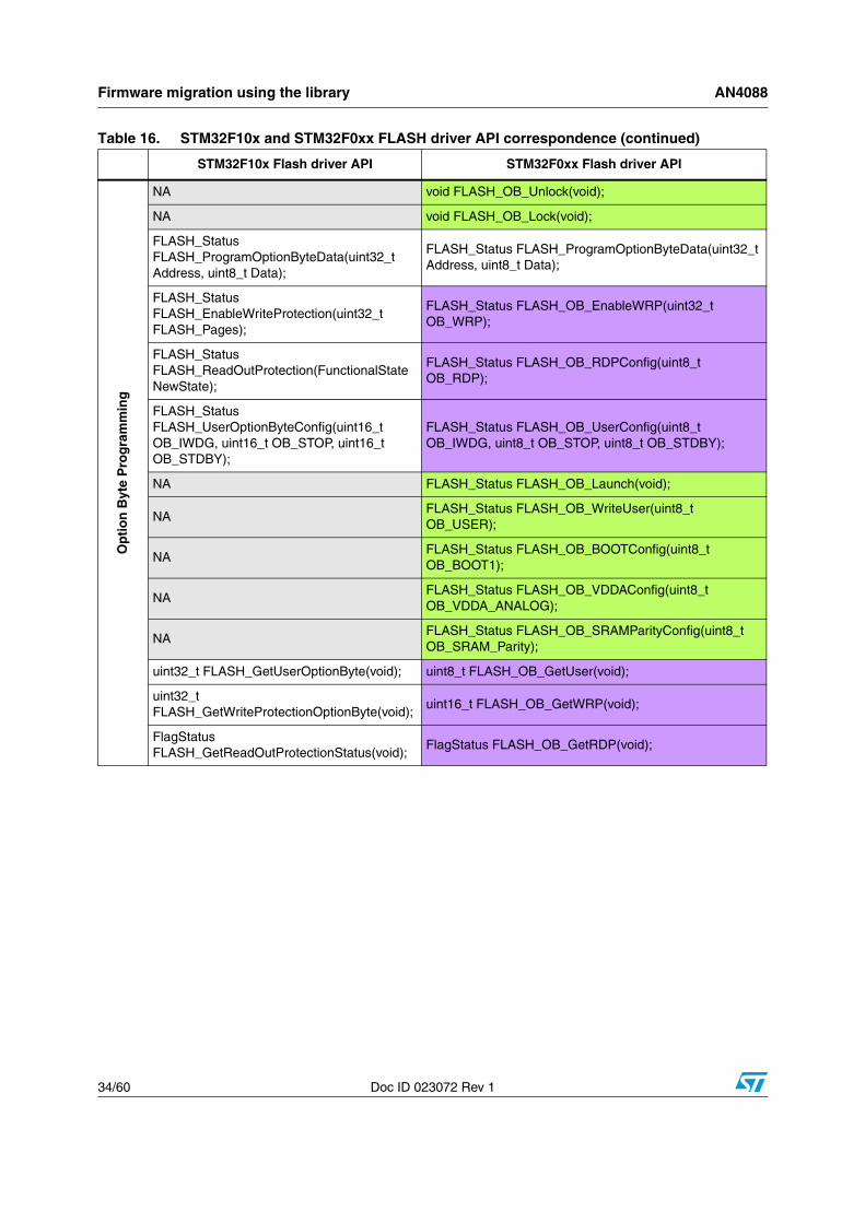
4.3 FLASH driverThe table below presents the FLASH driver API correspondence between STM32F10x and STM32F0xx Libraries. You can easily update your application code by replacing STM32F10x functions by the corresponding function in the STM32F0xx Library.
Table 16. STM32F10x and STM32F0xx FLASH driver API correspondence
STM32F10x Flash driver API STM32F0xx Flash driver API
Inte
rfac
e co
nfig
urat
ion void FLASH_SetLatency(uint32_t
FLASH_Latency);void FLASH_SetLatency(uint32_t FLASH_Latency);
void FLASH_PrefetchBufferCmd(uint32_t FLASH_PrefetchBuffer);
void FLASH_PrefetchBufferCmd(FunctionalState NewState);
void FLASH_HalfCycleAccessCmd(uint32_t FLASH_HalfCycleAccess);
NA
void FLASH_ITConfig(uint32_t FLASH_IT, FunctionalState NewState);
void FLASH_ITConfig(uint32_t FLASH_IT, FunctionalState NewState);
Mem
ory
Pro
gram
min
g
void FLASH_Unlock(void); void FLASH_Unlock(void);
void FLASH_Lock(void); void FLASH_Lock(void);
FLASH_Status FLASH_ErasePage(uint32_t Page_Address);
FLASH_Status FLASH_ErasePage(uint32_t Page_Address);
FLASH_Status FLASH_EraseAllPages(void); FLASH_Status FLASH_EraseAllPages(void);
FLASH_STATUS FLASH_ERASEOPTIONBYTES(void);
FLASH_STATUS FLASH_OB_ERASE(void);
FLASH_Status FLASH_ProgramWord(uint32_t Address, uint32_t Data);
FLASH_Status FLASH_ProgramWord(uint32_t Address, uint32_t Data);
FLASH_Status FLASH_ProgramHalfWord(uint32_t Address, uint16_t Data);
FLASH_Status FLASH_ProgramHalfWord(uint32_t Address, uint16_t Data);
Firmware migration using the library AN4088
34/60 Doc ID 023072 Rev 1
Opt
ion
Byt
e P
rogr
amm
ing
NA void FLASH_OB_Unlock(void);
NA void FLASH_OB_Lock(void);
FLASH_Status FLASH_ProgramOptionByteData(uint32_t Address, uint8_t Data);
FLASH_Status FLASH_ProgramOptionByteData(uint32_t Address, uint8_t Data);
FLASH_Status FLASH_EnableWriteProtection(uint32_t FLASH_Pages);
FLASH_Status FLASH_OB_EnableWRP(uint32_t OB_WRP);
FLASH_Status FLASH_ReadOutProtection(FunctionalState NewState);
FLASH_Status FLASH_OB_RDPConfig(uint8_t OB_RDP);
FLASH_Status FLASH_UserOptionByteConfig(uint16_t OB_IWDG, uint16_t OB_STOP, uint16_t OB_STDBY);
FLASH_Status FLASH_OB_UserConfig(uint8_t OB_IWDG, uint8_t OB_STOP, uint8_t OB_STDBY);
NA FLASH_Status FLASH_OB_Launch(void);
NAFLASH_Status FLASH_OB_WriteUser(uint8_t OB_USER);
NAFLASH_Status FLASH_OB_BOOTConfig(uint8_t OB_BOOT1);
NAFLASH_Status FLASH_OB_VDDAConfig(uint8_t OB_VDDA_ANALOG);
NAFLASH_Status FLASH_OB_SRAMParityConfig(uint8_t OB_SRAM_Parity);
uint32_t FLASH_GetUserOptionByte(void); uint8_t FLASH_OB_GetUser(void);
uint32_t FLASH_GetWriteProtectionOptionByte(void);
uint16_t FLASH_OB_GetWRP(void);
FlagStatus FLASH_GetReadOutProtectionStatus(void);
FlagStatus FLASH_OB_GetRDP(void);
Table 16. STM32F10x and STM32F0xx FLASH driver API correspondence (continued)
STM32F10x Flash driver API STM32F0xx Flash driver API

AN4088 Firmware migration using the library
Doc ID 023072 Rev 1 35/60
4.4 CRC driverThe table below presents the CRC driver API correspondence between STM32F10x and STM32F0xx Libraries.
FLA
G m
anag
emen
t
FlagStatus FLASH_GetFlagStatus(uint32_t FLASH_FLAG);
FlagStatus FLASH_GetFlagStatus(uint32_t FLASH_FLAG);
void FLASH_ClearFlag(uint32_t FLASH_FLAG);
void FLASH_ClearFlag(uint32_t FLASH_FLAG);
FLASH_Status FLASH_GetStatus(void); FLASH_Status FLASH_GetStatus(void);
FLASH_Status FLASH_WaitForLastOperation(uint32_t Timeout);
FLASH_Status FLASH_WaitForLastOperation(void);
FlagStatus FLASH_GetPrefetchBufferStatus(void);
FlagStatus FLASH_GetPrefetchBufferStatus(void);
Table 16. STM32F10x and STM32F0xx FLASH driver API correspondence (continued)
STM32F10x Flash driver API STM32F0xx Flash driver API
Color key: = New function
= Same function, but API was changed
= Function not available (NA)
Table 17. STM32F10xx and STM32F0xx CRC driver API correspondence
STM32F10xx CRC driver API STM32F0xx CRC driver API
Con
figur
atio
n
NA void CRC_DeInit(void);
void CRC_ResetDR(void); void CRC_ResetDR(void);
NAvoid CRC_ReverseInputDataSelect(uint32_t CRC_ReverseInputData);
NAvoid CRC_ReverseOutputDataCmd(FunctionalState NewState);
NA void CRC_SetInitRegister(uint32_t CRC_InitValue);
Com
puta
tion uint32_t CRC_CalcCRC(uint32_t CRC_Data); uint32_t CRC_CalcCRC(uint32_t CRC_Data);
uint32_t CRC_CalcBlockCRC(uint32_t pBuffer[], uint32_t BufferLength);
uint32_t CRC_CalcBlockCRC(uint32_t pBuffer[], uint32_t BufferLength);
uint32_t CRC_GetCRC(void); uint32_t CRC_GetCRC(void);

Firmware migration using the library AN4088
36/60 Doc ID 023072 Rev 1
4.5 GPIO configuration updateThis section explains how to update the configuration of the various GPIO modes when porting the application code from STM32 F1 series to F0 series.
4.5.1 Output modeThe example below shows how to configure an I/O in output mode (for example to drive a LED) in STM32 F1 series:GPIO_InitStructure.GPIO_Pin = GPIO_Pin_x;GPIO_InitStructure.GPIO_Speed = GPIO_Speed_xxMHz; /* 2, 10 or 50 MHz */GPIO_InitStructure.GPIO_Mode = GPIO_Mode_Out_PP; GPIO_Init(GPIOy, &GPIO_InitStructure);
In F0 series, you have to update this code as follows:GPIO_InitStructure.GPIO_Pin = GPIO_Pin_x;GPIO_InitStructure.GPIO_Mode = GPIO_Mode_OUT;GPIO_InitStructure.GPIO_OType = GPIO_OType_PP; /* Push-pull or open drain */GPIO_InitStructure.GPIO_PuPd = GPIO_PuPd_UP; /* None, Pull-up or pull-down */GPIO_InitStructure.GPIO_Speed = GPIO_Speed_xxMHz; /* 10, 2 or 50MHz */GPIO_Init(GPIOy, &GPIO_InitStructure);
4.5.2 Input modeThe example below shows how to configure an I/O in input mode (for example to be used as an EXTI line) in STM32 F1 series:GPIO_InitStructure.GPIO_Pin = GPIO_Pin_x;GPIO_InitStructure.GPIO_Mode = GPIO_Mode_IN_FLOATING;GPIO_Init(GPIOy, &GPIO_InitStructure);
In F0 series, you have to update this code as follows:GPIO_InitStructure.GPIO_Pin = GPIO_Pin_x;GPIO_InitStructure.GPIO_Mode = GPIO_Mode_IN;GPIO_InitStructure.GPIO_PuPd = GPIO_PuPd_NOPULL; /* None, Pull-up or pull-down */GPIO_Init(GPIOy, &GPIO_InitStructure);
IDR
acc
ess void CRC_SetIDRegister(uint8_t CRC_IDValue); void CRC_SetIDRegister(uint8_t CRC_IDValue);
uint8_t CRC_GetIDRegister(void);uint8_t CRC_GetIDRegister(void);
Table 17. STM32F10xx and STM32F0xx CRC driver API correspondence (continued)
STM32F10xx CRC driver API STM32F0xx CRC driver API
Color key: = New function
= Same function, but API was changed
= Function not available (NA)

AN4088 Firmware migration using the library
Doc ID 023072 Rev 1 37/60
4.5.3 Analog modeThe example below shows how to configure an I/O in analog mode (for example, an ADC or DAC channel) in STM32 F1 series:GPIO_InitStructure.GPIO_Pin = GPIO_Pin_x;GPIO_InitStructure.GPIO_Mode = GPIO_Mode_AIN;GPIO_Init(GPIOy, &GPIO_InitStructure);
In F0 series, you have to update this code as follows:GPIO_InitStructure.GPIO_Pin = GPIO_Pin_x ;GPIO_InitStructure.GPIO_Mode = GPIO_Mode_AN;GPIO_InitStructure.GPIO_PuPd = GPIO_PuPd_NOPULL ;GPIO_Init(GPIOy, &GPIO_InitStructure);
4.5.4 Alternate function modeIn STM32 F1 series
1. The configuration to use an I/O as an alternate function depends on the peripheral mode used; for example, the USART Tx pin should be configured as an alternate function push-pull while the USART Rx pin should be configured as an input floating or an input pull-up.
2. To optimize the number of peripheral I/O functions for different device packages, it is possible, by software, to remap some alternate functions to other pins. For example, the USART2_RX pin can be mapped on PA3 (default remap) or PD6 (by software remap).
In STM32 F0 series
1. Whatever the peripheral mode used, the I/O must be configured as an alternate function, then the system can use the I/O in the proper way (input or output).
2. The I/O pins are connected to onboard peripherals/modules through a multiplexer that allows only one peripheral’s alternate function to be connected to an I/O pin at a time. In this way, there can be no conflict between peripherals sharing the same I/O pin. Each I/O pin has a multiplexer with sixteen alternate function inputs (AF0 to AF15) that can be configured through the GPIO_PinAFConfig () function:
– After reset, all I/Os are connected to the system’s alternate function 0 (AF0)
– The peripherals’ alternate functions are mapped by configuring AF1 to AF7.
3. In addition to this flexible I/O multiplexing architecture, each peripheral has alternate functions mapped onto different I/O pins to optimize the number of peripheral I/O functions for different device packages; for example, the USART2_RX pin can be mapped on PA3 or PA15 pin.
4. Configuration procedure:
– Connect the pin to the desired peripherals' Alternate Function (AF) using GPIO_PinAFConfig() function
– Use GPIO_Init() function to configure the I/O pin:
- Configure the desired pin in alternate function mode using GPIO_InitStructure->GPIO_Mode = GPIO_Mode_AF;
- Select the type, pull-up/pull-down and output speed via GPIO_PuPd, GPIO_OType and GPIO_Speed members
The example below shows how to remap USART2 Tx/Rx I/Os on PD5/PD6 pins in STM32 F1 series: /* Enable APB2 interface clock for GPIOD and AFIO (AFIO peripheral is used to configure the I/Os software remapping) */

Firmware migration using the library AN4088
38/60 Doc ID 023072 Rev 1
RCC_APB2PeriphClockCmd(RCC_APB2Periph_GPIOD | RCC_APB2Periph_AFIO, ENABLE);
/* Enable USART2 I/Os software remapping [(USART2_Tx,USART2_Rx):(PD5,PD6)] */ GPIO_PinRemapConfig(GPIO_Remap_USART2, ENABLE);
/* Configure USART2_Tx as alternate function push-pull */ GPIO_InitStructure.GPIO_Pin = GPIO_Pin_5; GPIO_InitStructure.GPIO_Mode = GPIO_Mode_AF_PP; GPIO_InitStructure.GPIO_Speed = GPIO_Speed_50MHz; GPIO_Init(GPIOD, &GPIO_InitStructure);
/* Configure USART2_Rx as input floating */ GPIO_InitStructure.GPIO_Pin = GPIO_Pin_6; GPIO_InitStructure.GPIO_Mode = GPIO_Mode_IN_FLOATING; GPIO_Init(GPIOD, &GPIO_InitStructure);
In F0 series, you have to update this code as follows: /* Enable GPIOA's AHB interface clock */ RCC_AHBPeriphClockCmd(RCC_AHBPeriph_GPIOA, ENABLE);
/* Select USART2 I/Os mapping on PA14/15 pins [(USART2_TX,USART2_RX):(PA.14,PA.15)] */ /* Connect PA14 to USART2_Tx */ GPIO_PinAFConfig(GPIOA, GPIO_PinSource14, GPIO_AF_2); /* Connect PA15 to USART2_Rx*/ GPIO_PinAFConfig(GPIOA, GPIO_PinSource15, GPIO_AF_2);
/* Configure USART2_Tx and USART2_Rx as alternate function */ GPIO_InitStructure.GPIO_Pin = GPIO_Pin_14 | GPIO_Pin_15; GPIO_InitStructure.GPIO_Mode = GPIO_Mode_AF; GPIO_InitStructure.GPIO_Speed = GPIO_Speed_50MHz; GPIO_InitStructure.GPIO_OType = GPIO_OType_PP; GPIO_InitStructure.GPIO_PuPd = GPIO_PuPd_UP; GPIO_Init(GPIOA, &GPIO_InitStructure);
4.6 EXTI Line0The example below shows how to configure the PA0 pin to be used as EXTI Line0 in STM32 F1 series: /* Enable APB interface clock for GPIOA and AFIO */ RCC_APB2PeriphClockCmd(RCC_APB2Periph_GPIOA | RCC_APB2Periph_AFIO, ENABLE);
/* Configure PA0 pin in input mode */ GPIO_InitStructure.GPIO_Pin = GPIO_Pin_0; GPIO_InitStructure.GPIO_Mode = GPIO_Mode_IN_FLOATING; GPIO_Init(GPIOA, &GPIO_InitStructure);
/* Connect EXTI Line0 to PA0 pin */ GPIO_EXTILineConfig(GPIO_PortSourceGPIOA, GPIO_PinSource0);
/* Configure EXTI line0 */ EXTI_InitStructure.EXTI_Line = EXTI_Line0; EXTI_InitStructure.EXTI_Mode = EXTI_Mode_Interrupt; EXTI_InitStructure.EXTI_Trigger = EXTI_Trigger_Falling; EXTI_InitStructure.EXTI_LineCmd = ENABLE; EXTI_Init(&EXTI_InitStructure);
AN4088 Firmware migration using the library
Doc ID 023072 Rev 1 39/60
In F0 series, the configuration of the EXTI line source pin is performed in the SYSCFG peripheral (instead of AFIO in F1 series). As a result, the source code should be updated as follows: /* Enable GPIOA's AHB interface clock */ RCC_AHBPeriphClockCmd(RCC_AHBPeriph_GPIOA, ENABLE); /* Enable SYSCFG's APB interface clock */ RCC_APB2PeriphClockCmd(RCC_APB2Periph_SYSCFG, ENABLE);
/* Configure PA0 pin in input mode */ GPIO_InitStructure.GPIO_Pin = GPIO_Pin_0; GPIO_InitStructure.GPIO_Mode = GPIO_Mode_IN; GPIO_InitStructure.GPIO_PuPd = GPIO_PuPd_NOPULL; GPIO_Init(GPIOA, &GPIO_InitStructure);
/* Connect EXTI Line0 to PA0 pin */ SYSCFG_EXTILineConfig(EXTI_PortSourceGPIOA, EXTI_PinSource0);
/* Configure EXTI line0 */ EXTI_InitStructure.EXTI_Line = EXTI_Line0; EXTI_InitStructure.EXTI_Mode = EXTI_Mode_Interrupt; EXTI_InitStructure.EXTI_Trigger = EXTI_Trigger_Falling; EXTI_InitStructure.EXTI_LineCmd = ENABLE; EXTI_Init(&EXTI_InitStructure);
4.7 NVIC interrupt configurationThis section describes the configuration of the NVIC interrupts (IRQ).
In F1 series, the NVIC supports:
– up to 81 interrupts
– A programmable priority level of 0-15 for each interrupt (4 bits of interrupt priority are used). A higher level corresponds to a lower priority; level 0 is the highest interrupt priority.
– Grouping of priority values into group priority and subpriority fields.
– Dynamic changing of priority levels.
The Cortex-M3 exceptions are managed by CMSIS functions:
● Enable and configure the preemption priority and subpriority of the selected IRQ channels according to the Priority grouping configuration.
The example below shows how to configure the CEC interrupt in STM32 F1 series:/* Configure two bits for preemption priority */
NVIC_PriorityGroupConfig(NVIC_PriorityGroup_2);
/* Enable the CEC global Interrupt (with higher priority) */
NVIC_InitStructure.NVIC_IRQChannel = CEC_IRQn;
NVIC_InitStructure.NVIC_IRQChannelPreemptionPriority = 0;
NVIC_InitStructure.NVIC_IRQChannelSubPriority = 0;
NVIC_InitStructure.NVIC_IRQChannelCmd = ENABLE;
NVIC_Init(&NVIC_InitStructure);
In F0 series, the NVIC supports:
– Up to 32 interrupts
– 4 programmable priority levels (2 bits of interrupt priority are used).
– The priority level of an interrupt should not be changed after it is enabled.

Firmware migration using the library AN4088
40/60 Doc ID 023072 Rev 1
The Cortex-M0 exceptions are managed by CMSIS functions:
● Enable and configure the priority of the selected IRQ channels. The priority ranges between 0 and 3. Lower priority values give a higher priority.
In F0 series, the configuration of the CEC Interrupt source code should be updated as follows:/* Enable the CEC global Interrupt (with higher priority) */
NVIC_InitStructure.NVIC_IRQChannel = CEC_IRQn;
NVIC_InitStructure.NVIC_IRQChannelPriority = 0;
NVIC_InitStructure.NVIC_IRQChannelCmd = ENABLE;
NVIC_Init(&NVIC_InitStructure);
The table below presents the MISC driver API correspondence between STM32F10x and STM32F0xx Libraries.
4.8 ADC configurationThis section gives an example of how to port existing code from STM32 F1 series to F0 series.
The example below shows how to configure the ADC1 to convert continuously channel 14 in STM32 F1 series:
/* ADCCLK = PCLK2/4 */ RCC_ADCCLKConfig(RCC_PCLK2_Div4); /* Enable ADC's APB interface clock */ RCC_APB2PeriphClockCmd(RCC_APB2Periph_ADC1, ENABLE); /* Configure ADC1 to convert continously channel14 */ ADC_InitStructure.ADC_Mode = ADC_Mode_Independent; ADC_InitStructure.ADC_ScanConvMode = ENABLE; ADC_InitStructure.ADC_ContinuousConvMode = ENABLE; ADC_InitStructure.ADC_ExternalTrigConv = ADC_ExternalTrigConv_None; ADC_InitStructure.ADC_DataAlign = ADC_DataAlign_Right; ADC_InitStructure.ADC_NbrOfChannel = 1; ADC_Init(ADC1, &ADC_InitStructure); /* ADC1 regular channel14 configuration */ ADC_RegularChannelConfig(ADC1, ADC_Channel_14, 1, ADC_SampleTime_55Cycles5);
Table 18. STM32F10x and STM32F0xx MISC driver API correspondence
STM32F10xx MISC Driver API STM32F0xx MISC Driver API
void NVIC_Init(NVIC_InitTypeDef* NVIC_InitStruct);
void NVIC_Init(NVIC_InitTypeDef* NVIC_InitStruct);
void NVIC_SystemLPConfig(uint8_t LowPowerMode, FunctionalState NewState);
void NVIC_SystemLPConfig(uint8_t LowPowerMode, FunctionalState NewState);
void SysTick_CLKSourceConfig(uint32_t SysTick_CLKSource);
void SysTick_CLKSourceConfig(uint32_t SysTick_CLKSource);
NVIC_PriorityGroupConfig(uint32_t NVIC_PriorityGroup);
NA
void NVIC_SetVectorTable(uint32_t NVIC_VectTab, uint32_t Offset);
NA

AN4088 Firmware migration using the library
Doc ID 023072 Rev 1 41/60
/* Enable ADC1's DMA interface */ ADC_DMACmd(ADC1, ENABLE); /* Enable ADC1 */ ADC_Cmd(ADC1, ENABLE);
/* Enable ADC1 reset calibration register */ ADC_ResetCalibration(ADC1); /* Check the end of ADC1 reset calibration register */ while(ADC_GetResetCalibrationStatus(ADC1));
/* Start ADC1 calibration */ ADC_StartCalibration(ADC1); /* Check the end of ADC1 calibration */ while(ADC_GetCalibrationStatus(ADC1)); /* Start ADC1 Software Conversion */ ADC_SoftwareStartConvCmd(ADC1, ENABLE); ...
In F0 series, you have to update this code as follows:.../* ADCCLK = PCLK/2 */ RCC_ADCCLKConfig(RCC_ADCCLK_PCLK_Div2);
/* Enable ADC1 clock */ RCC_APB2PeriphClockCmd(RCC_APB2Periph_ADC1, ENABLE); /* ADC1 configuration */ ADC_InitStructure.ADC_Resolution = ADC_Resolution_12b; ADC_InitStructure.ADC_ContinuousConvMode = ENABLE; ADC_InitStructure.ADC_ExternalTrigConvEdge = ADC_ExternalTrigConvEdge_None;
ADC_InitStructure.ADC_ExternalTrigConv = ADC_ExternalTrigConv_T1_TRGO;; ADC_InitStructure.ADC_DataAlign = ADC_DataAlign_Right; ADC_InitStructure.ADC_ScanDirection = ADC_ScanDirection_Backward; ADC_Init(ADC1, &ADC_InitStructure); /* Convert the ADC1 Channel 1 with 55.5 Cycles as sampling time */ ADC_ChannelConfig(ADC1, ADC_Channel_11 , ADC_SampleTime_55_5Cycles);
/* ADC Calibration */ ADC_GetCalibrationFactor(ADC1);
/* ADC DMA request in circular mode */ ADC_DMARequestModeConfig(ADC1, ADC_DMAMode_Circular); /* Enable ADC_DMA */ ADC_DMACmd(ADC1, ENABLE); /* Enable ADC1 */ ADC_Cmd(ADC1, ENABLE);
/* Wait the ADCEN falg */ while(!ADC_GetFlagStatus(ADC1, ADC_FLAG_ADEN)); /* ADC1 regular Software Start Conv */ ADC_StartOfConversion(ADC1); ...

Firmware migration using the library AN4088
42/60 Doc ID 023072 Rev 1
4.9 DAC driverThe table below describes the difference between STM32F10x functions and the STM32F0xx Library.
(*) These functions exist only on STM32F10X_LD_VL, STM32F10X_MD_VL, and STM32F10X_HD_VL devices.
Table 19. STM32F10x and STM32F0xx DAC driver API correspondence
STM32F10x DAC driver API STM32F0xx DAC driver API
Con
figur
atio
n
void DAC_DeInit(void); void DAC_DeInit(void);
void DAC_Init(uint32_t DAC_Channel, DAC_InitTypeDef* DAC_InitStruct);
void DAC_Init(uint32_t DAC_Channel, DAC_InitTypeDef* DAC_InitStruct);
void DAC_StructInit(DAC_InitTypeDef* DAC_InitStruct);
void DAC_StructInit(DAC_InitTypeDef* DAC_InitStruct);
void DAC_Cmd(uint32_t DAC_Channel, FunctionalState NewState);
void DAC_Cmd(uint32_t DAC_Channel, FunctionalState NewState);
void DAC_SoftwareTriggerCmd(uint32_t DAC_Channel, FunctionalState NewState);
void DAC_SoftwareTriggerCmd(uint32_t DAC_Channel, FunctionalState NewState);
void DAC_SetChannel1Data(uint32_t DAC_Align, uint16_t Data);
void DAC_SetChannel1Data(uint32_t DAC_Align, uint16_t Data);
void DAC_SetChannel2Data(uint32_t DAC_Align, uint16_t Data);
NA
void DAC_SetDualChannelData(uint32_t DAC_Align, uint16_t Data2, uint16_t Data1);
NA
uint16_t DAC_GetDataOutputValue(uint32_t DAC_Channel);
uint16_t DAC_GetDataOutputValue(uint32_t DAC_Channel);
DM
A m
anag
emen
t
void DAC_DMACmd(uint32_t DAC_Channel, FunctionalState NewState);
void DAC_DMACmd(uint32_t DAC_Channel, FunctionalState NewState);
Inte
rrup
ts a
nd fl
ags
man
agem
ent void DAC_ITConfig(uint32_t DAC_Channel,
uint32_t DAC_IT, FunctionalState NewState);(*)void DAC_ITConfig(uint32_t DAC_Channel, uint32_t DAC_IT, FunctionalState NewState);
FlagStatus DAC_GetFlagStatus(uint32_t DAC_Channel, uint32_t DAC_FLAG);(*)
FlagStatus DAC_GetFlagStatus(uint32_t DAC_Channel, uint32_t DAC_FLAG);
void DAC_ClearFlag(uint32_t DAC_Channel, uint32_t DAC_FLAG);(*)
void DAC_ClearFlag(uint32_t DAC_Channel, uint32_t DAC_FLAG);
ITStatus DAC_GetITStatus(uint32_t DAC_Channel, uint32_t DAC_IT);(*)
ITStatus DAC_GetITStatus(uint32_t DAC_Channel, uint32_t DAC_IT);
void DAC_ClearITPendingBit(uint32_t DAC_Channel, uint32_t DAC_IT);(*)
void DAC_ClearITPendingBit(uint32_t DAC_Channel, uint32_t DAC_IT);

AN4088 Firmware migration using the library
Doc ID 023072 Rev 1 43/60
The main changes in the source code/procedure in F0 series versus F1 are described below:
● No Dual mode for DAC channels
● No Noise generator
● No Triangle generator
● In the DAC structure definition, only two fields (external trigger, OutputBuffer) should be initialized.
The example below shows how to configure the DAC channel 1 STM32 F1 series:
/* DAC channel1 Configuration */
DAC_InitStructure.DAC_Trigger = DAC_Trigger_None;
DAC_InitStructure.DAC_WaveGeneration = DAC_WaveGeneration_None;
DAC_InitStructure.DAC_OutputBuffer = DAC_OutputBuffer_Enable;
DAC_Init(DAC_Channel_1, &DAC_InitStructure);
In F0 series, you have to update this code as follows:
/* DAC channel1 Configuration */
DAC_InitStructure.DAC_Trigger = DAC_Trigger_None;
DAC_InitStructure.DAC_OutputBuffer = DAC_OutputBuffer_Enable;
/* DAC Channel1 Init */
DAC_Init(DAC_Channel_1, &DAC_InitStructure);
4.10 PWR driverThe table below presents the PWR driver API correspondence between STM32F10x and STM32F0xx Libraries. You can easily update your application code by replacing STM32F10x functions by the corresponding function in the STM32F0xx Library.
Table 20. STM32F10x and STM32F0xx PWR driver API correspondence
STM32F10x PWR driver API STM32F0xx PWR driver API
Inte
rfac
e
conf
igur
atio
n void PWR_DeInit(void); void PWR_DeInit(void);
void PWR_BackupAccessCmd(FunctionalState NewState);
void PWR_BackupAccessCmd(FunctionalState NewState);
PV
D
void PWR_PVDLevelConfig(uint32_t PWR_PVDLevel);
void PWR_PVDLevelConfig(uint32_t PWR_PVDLevel);
void PWR_PVDCmd(FunctionalState NewState); void PWR_PVDCmd(FunctionalState NewState);
Wak
eup
void PWR_WakeUpPinCmd(FunctionalState NewState);
void PWR_WakeUpPinCmd(uint32_t PWR_WakeUpPin, FunctionalState NewState);(*)
Pow
er M
anag
emen
t
NAvoid PWR_EnterSleepMode(uint8_t PWR_SLEEPEntry);
void PWR_EnterSTOPMode(uint32_t PWR_Regulator, uint8_t PWR_STOPEntry);
void PWR_EnterSTOPMode(uint32_t PWR_Regulator, uint8_t PWR_STOPEntry);
void PWR_EnterSTANDBYMode(void); void PWR_EnterSTANDBYMode(void);

Firmware migration using the library AN4088
44/60 Doc ID 023072 Rev 1
4.11 Backup data registersIn STM32 F1 series, the Backup data registers are managed through the BKP peripheral, while in F0 series they are a part of the RTC peripheral (there is no BKP peripheral).
The example below shows how to write to/read from Backup data registers in STM32 F1 series:
uint16_t BKPdata = 0;
... /* Enable APB2 interface clock for PWR and BKP */ RCC_APB1PeriphClockCmd(RCC_APB1Periph_PWR | RCC_APB1Periph_BKP, ENABLE);
/* Enable write access to Backup domain */ PWR_BackupAccessCmd(ENABLE);
/* Write data to Backup data register 1 */ BKP_WriteBackupRegister(BKP_DR1, 0x3210);
/* Read data from Backup data register 1 */ BKPdata = BKP_ReadBackupRegister(BKP_DR1);
In F0 series, you have to update this code as follows:
uint16_t BKPdata = 0;
... /* PWR Clock Enable */ RCC_APB1PeriphClockCmd(RCC_APB1Periph_PWR, ENABLE); /* Enable write access to RTC domain */ PWR_RTCAccessCmd(ENABLE);
/* Write data to Backup data register 1 */ RTC_WriteBackupRegister(RTC_BKP_DR1, 0x3220);
/* Read data from Backup data register 1 */ BKPdata = RTC_ReadBackupRegister(RTC_BKP_DR1);
FLA
G
man
agem
ent FlagStatus PWR_GetFlagStatus(uint32_t
PWR_FLAG);FlagStatus PWR_GetFlagStatus(uint32_t PWR_FLAG);
void PWR_ClearFlag(uint32_t PWR_FLAG); void PWR_ClearFlag(uint32_t PWR_FLAG);
(*) More Wake up pins are available on STM32 F0 series.
Table 20. STM32F10x and STM32F0xx PWR driver API correspondence (continued)
STM32F10x PWR driver API STM32F0xx PWR driver API
Color key: = New function
= Same function, but API was changed
= Function not available (NA)

AN4088 Firmware migration using the library
Doc ID 023072 Rev 1 45/60
The main changes in the source code in F0 series versus F1 are described below:
1. There is no BKP peripheral
2. Write to/read from Backup data registers are done through RTC driver
3. Backup data registers naming changed from BKP_DRx to RTC_BKP_DRx, and numbering starts from 0 instead of 1.
4.12 CEC application codeYou can easily update your CEC application code by replacing STM32F10x functions by the corresponding function in the STM32F0xx Library.The table below presents the CEC driver API correspondence between STM32F10x and STM32F0xx Libraries.
Table 21. STM32F10xx and STM32F0xx CEC driver API correspondence
STM32F10xx CEC driver API STM32F0xx CEC driver API
Inte
rfac
e C
onfig
urat
ion
void CEC_DeInit(void); void CEC_DeInit(void);
void CEC_Init(CEC_InitTypeDef* CEC_InitStruct); void CEC_Init(CEC_InitTypeDef* CEC_InitStruct);
NA void CEC_StructInit(CEC_InitTypeDef* CEC_InitStruct);
void CEC_Cmd(FunctionalState NewState); void CEC_Cmd(FunctionalState NewState);
NA void CEC_ListenModeCmd(FunctionalState NewState);
void CEC_OwnAddressConfig(uint8_t CEC_OwnAddress);
void CEC_OwnAddressConfig(uint8_t CEC_OwnAddress);
NA void CEC_OwnAddressClear(void);
void CEC_SetPrescaler(uint16_t CEC_Prescaler); NA
DAT
A T
rans
fers
void CEC_SendDataByte(uint8_t Data); void CEC_SendData(uint8_t Data);
uint8_t CEC_ReceiveDataByte(void); uint8_t CEC_ReceiveData(void);
void CEC_StartOfMessage(void); void CEC_StartOfMessage(void);
void CEC_EndOfMessageCmd(FunctionalState NewState);
void CEC_EndOfMessage(void);
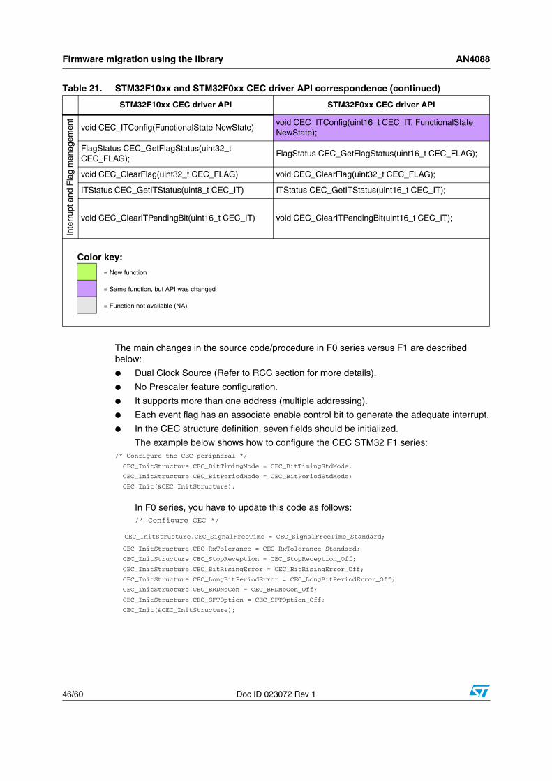
Firmware migration using the library AN4088
46/60 Doc ID 023072 Rev 1
The main changes in the source code/procedure in F0 series versus F1 are described below:
● Dual Clock Source (Refer to RCC section for more details).
● No Prescaler feature configuration.
● It supports more than one address (multiple addressing).
● Each event flag has an associate enable control bit to generate the adequate interrupt.
● In the CEC structure definition, seven fields should be initialized.
The example below shows how to configure the CEC STM32 F1 series:/* Configure the CEC peripheral */
CEC_InitStructure.CEC_BitTimingMode = CEC_BitTimingStdMode;
CEC_InitStructure.CEC_BitPeriodMode = CEC_BitPeriodStdMode;
CEC_Init(&CEC_InitStructure);
In F0 series, you have to update this code as follows:/* Configure CEC */
CEC_InitStructure.CEC_SignalFreeTime = CEC_SignalFreeTime_Standard; CEC_InitStructure.CEC_RxTolerance = CEC_RxTolerance_Standard;
CEC_InitStructure.CEC_StopReception = CEC_StopReception_Off;
CEC_InitStructure.CEC_BitRisingError = CEC_BitRisingError_Off;
CEC_InitStructure.CEC_LongBitPeriodError = CEC_LongBitPeriodError_Off;
CEC_InitStructure.CEC_BRDNoGen = CEC_BRDNoGen_Off;
CEC_InitStructure.CEC_SFTOption = CEC_SFTOption_Off;
CEC_Init(&CEC_InitStructure);
Inte
rrup
t and
Fla
g m
anag
emen
t
void CEC_ITConfig(FunctionalState NewState)void CEC_ITConfig(uint16_t CEC_IT, FunctionalState NewState);
FlagStatus CEC_GetFlagStatus(uint32_t CEC_FLAG);
FlagStatus CEC_GetFlagStatus(uint16_t CEC_FLAG);
void CEC_ClearFlag(uint32_t CEC_FLAG) void CEC_ClearFlag(uint32_t CEC_FLAG);
ITStatus CEC_GetITStatus(uint8_t CEC_IT) ITStatus CEC_GetITStatus(uint16_t CEC_IT);
void CEC_ClearITPendingBit(uint16_t CEC_IT) void CEC_ClearITPendingBit(uint16_t CEC_IT);
Table 21. STM32F10xx and STM32F0xx CEC driver API correspondence (continued)
STM32F10xx CEC driver API STM32F0xx CEC driver API
Color key: = New function
= Same function, but API was changed
= Function not available (NA)
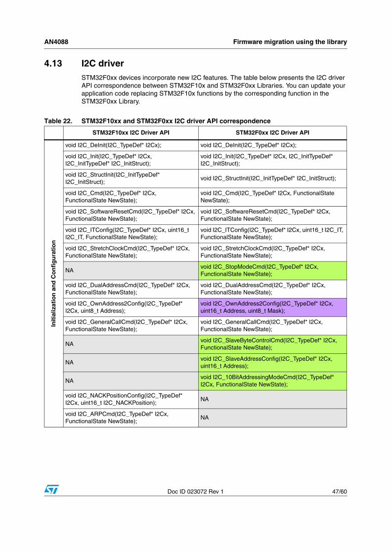
AN4088 Firmware migration using the library
Doc ID 023072 Rev 1 47/60
4.13 I2C driverSTM32F0xx devices incorporate new I2C features. The table below presents the I2C driver API correspondence between STM32F10x and STM32F0xx Libraries. You can update your application code replacing STM32F10x functions by the corresponding function in the STM32F0xx Library.
Table 22. STM32F10xx and STM32F0xx I2C driver API correspondence
STM32F10xx I2C Driver API STM32F0xx I2C Driver API
Initi
aliz
atio
n an
d C
onfig
urat
ion
void I2C_DeInit(I2C_TypeDef* I2Cx); void I2C_DeInit(I2C_TypeDef* I2Cx);
void I2C_Init(I2C_TypeDef* I2Cx, I2C_InitTypeDef* I2C_InitStruct);
void I2C_Init(I2C_TypeDef* I2Cx, I2C_InitTypeDef* I2C_InitStruct);
void I2C_StructInit(I2C_InitTypeDef* I2C_InitStruct);
void I2C_StructInit(I2C_InitTypeDef* I2C_InitStruct);
void I2C_Cmd(I2C_TypeDef* I2Cx, FunctionalState NewState);
void I2C_Cmd(I2C_TypeDef* I2Cx, FunctionalState NewState);
void I2C_SoftwareResetCmd(I2C_TypeDef* I2Cx, FunctionalState NewState);
void I2C_SoftwareResetCmd(I2C_TypeDef* I2Cx, FunctionalState NewState);
void I2C_ITConfig(I2C_TypeDef* I2Cx, uint16_t I2C_IT, FunctionalState NewState);
void I2C_ITConfig(I2C_TypeDef* I2Cx, uint16_t I2C_IT, FunctionalState NewState);
void I2C_StretchClockCmd(I2C_TypeDef* I2Cx, FunctionalState NewState);
void I2C_StretchClockCmd(I2C_TypeDef* I2Cx, FunctionalState NewState);
NAvoid I2C_StopModeCmd(I2C_TypeDef* I2Cx, FunctionalState NewState);
void I2C_DualAddressCmd(I2C_TypeDef* I2Cx, FunctionalState NewState);
void I2C_DualAddressCmd(I2C_TypeDef* I2Cx, FunctionalState NewState);
void I2C_OwnAddress2Config(I2C_TypeDef* I2Cx, uint8_t Address);
void I2C_OwnAddress2Config(I2C_TypeDef* I2Cx, uint16_t Address, uint8_t Mask);
void I2C_GeneralCallCmd(I2C_TypeDef* I2Cx, FunctionalState NewState);
void I2C_GeneralCallCmd(I2C_TypeDef* I2Cx, FunctionalState NewState);
NAvoid I2C_SlaveByteControlCmd(I2C_TypeDef* I2Cx, FunctionalState NewState);
NAvoid I2C_SlaveAddressConfig(I2C_TypeDef* I2Cx, uint16_t Address);
NAvoid I2C_10BitAddressingModeCmd(I2C_TypeDef* I2Cx, FunctionalState NewState);
void I2C_NACKPositionConfig(I2C_TypeDef* I2Cx, uint16_t I2C_NACKPosition);
NA
void I2C_ARPCmd(I2C_TypeDef* I2Cx, FunctionalState NewState);
NA

Firmware migration using the library AN4088
48/60 Doc ID 023072 Rev 1
Com
mun
icat
ions
han
dlin
g
NAvoid I2C_AutoEndCmd(I2C_TypeDef* I2Cx, FunctionalState NewState);
NAvoid I2C_ReloadCmd(I2C_TypeDef* I2Cx, FunctionalState NewState);
NAvoid I2C_NumberOfBytesConfig(I2C_TypeDef* I2Cx, uint8_t Number_Bytes);
NAvoid I2C_MasterRequestConfig(I2C_TypeDef* I2Cx, uint16_t I2C_Direction);
void I2C_GenerateSTART(I2C_TypeDef* I2Cx, FunctionalState NewState);
void I2C_GenerateSTART(I2C_TypeDef* I2Cx, FunctionalState NewState);
void I2C_GenerateSTOP(I2C_TypeDef* I2Cx, FunctionalState NewState);
void I2C_GenerateSTOP(I2C_TypeDef* I2Cx, FunctionalState NewState);
NAvoid I2C_10BitAddressHeaderCmd(I2C_TypeDef* I2Cx, FunctionalState NewState);
void I2C_AcknowledgeConfig(I2C_TypeDef* I2Cx, FunctionalState NewState);
void I2C_AcknowledgeConfig(I2C_TypeDef* I2Cx, FunctionalState NewState);
NA uint8_t I2C_GetAddressMatched(I2C_TypeDef* I2Cx);
NAuint16_t I2C_GetTransferDirection(I2C_TypeDef* I2Cx);
NAvoid I2C_TransferHandling(I2C_TypeDef* I2Cx, uint16_t Address, uint8_t Number_Bytes, uint32_t ReloadEndMode, uint32_t StartStopMode);
ErrorStatus I2C_CheckEvent(I2C_TypeDef* I2Cx, uint32_t I2C_EVENT)
NA
void I2C_Send7bitAddress(I2C_TypeDef* I2Cx, uint8_t Address, uint8_t I2C_Direction)
NA
Table 22. STM32F10xx and STM32F0xx I2C driver API correspondence (continued)
STM32F10xx I2C Driver API STM32F0xx I2C Driver API

AN4088 Firmware migration using the library
Doc ID 023072 Rev 1 49/60
SM
BU
S m
anag
emen
t
void I2C_SMBusAlertConfig(I2C_TypeDef* I2Cx, uint16_t I2C_SMBusAlert);
void I2C_SMBusAlertCmd(I2C_TypeDef* I2Cx, FunctionalState NewState);
NAvoid I2C_ClockTimeoutCmd(I2C_TypeDef* I2Cx, FunctionalState NewState);
NAvoid I2C_ExtendedClockTimeoutCmd(I2C_TypeDef* I2Cx, FunctionalState NewState);
NAvoid I2C_IdleClockTimeoutCmd(I2C_TypeDef* I2Cx, FunctionalState NewState);
NAvoid I2C_TimeoutAConfig(I2C_TypeDef* I2Cx, uint16_t Timeout);
NAvoid I2C_TimeoutBConfig(I2C_TypeDef* I2Cx, uint16_t Timeout);
void I2C_CalculatePEC(I2C_TypeDef* I2Cx, FunctionalState NewState);
void I2C_CalculatePEC(I2C_TypeDef* I2Cx, FunctionalState NewState);
NAvoid I2C_PECRequestCmd(I2C_TypeDef* I2Cx, FunctionalState NewState);
uint8_t I2C_GetPEC(I2C_TypeDef* I2Cx); uint8_t I2C_GetPEC(I2C_TypeDef* I2Cx);
Dat
a tr
ansf
ers uint32_t I2C_ReadRegister(I2C_TypeDef* I2Cx,
uint8_t I2C_Register);uint32_t I2C_ReadRegister(I2C_TypeDef* I2Cx, uint8_t I2C_Register);
void I2C_SendData(I2C_TypeDef* I2Cx, uint8_t Data);
void I2C_SendData(I2C_TypeDef* I2Cx, uint8_t Data);
uint8_t I2C_ReceiveData(I2C_TypeDef* I2Cx); uint8_t I2C_ReceiveData(I2C_TypeDef* I2Cx);
DM
A m
anag
emen
t void I2C_DMACmd(I2C_TypeDef* I2Cx, FunctionalState NewState);
void I2C_DMACmd(I2C_TypeDef* I2Cx, uint32_t I2C_DMAReq, FunctionalState NewState);
void I2C_DMALastTransferCmd(I2C_TypeDef* I2Cx, FunctionalState NewState);
NA
Table 22. STM32F10xx and STM32F0xx I2C driver API correspondence (continued)
STM32F10xx I2C Driver API STM32F0xx I2C Driver API

Firmware migration using the library AN4088
50/60 Doc ID 023072 Rev 1
Though some API functions are identical in STM32F1 and STM32F0, in most cases the application code needs to be rewritten when moving from STM32F1 to STM32F0. However, STMicroelectronics provides an "I2C Communication peripheral application library (CPAL)", which allows to move seamlessly from STM32F1 to STM32F0: user needs to modify only few settings without any changes on the application code. For more details about STM32F1 I2C CPAL, please refer to UM1029. For STM32F0, the I2C CPAL is provided within the Standard Peripherals Library package."
Inte
rrup
ts a
nd fl
ags
man
agem
ent FlagStatus I2C_GetFlagStatus(I2C_TypeDef*
I2Cx, uint32_t I2C_FLAG);FlagStatus I2C_GetFlagStatus(I2C_TypeDef* I2Cx, uint32_t I2C_FLAG);
void I2C_ClearFlag(I2C_TypeDef* I2Cx, uint32_t I2C_FLAG);
void I2C_ClearFlag(I2C_TypeDef* I2Cx, uint32_t I2C_FLAG);
ITStatus I2C_GetITStatus(I2C_TypeDef* I2Cx, uint32_t I2C_IT);
ITStatus I2C_GetITStatus(I2C_TypeDef* I2Cx, uint32_t I2C_IT);
void I2C_ClearITPendingBit(I2C_TypeDef* I2Cx, uint32_t I2C_IT);
void I2C_ClearITPendingBit(I2C_TypeDef* I2Cx, uint32_t I2C_IT);
Table 22. STM32F10xx and STM32F0xx I2C driver API correspondence (continued)
STM32F10xx I2C Driver API STM32F0xx I2C Driver API
Color key: = New function
= Same function, but API was changed
= Function not available (NA)

AN4088 Firmware migration using the library
Doc ID 023072 Rev 1 51/60
4.14 SPI driverThe STM32F0xx SPI includes some new features as compared with STM32F10xx SPI. Table 23 presents the SPI driver API correspondence between STM32F10x and STM32F0xx Libraries.
Table 23. STM32F10xx and STM32F0xx SPI driver API correspondence
STM32F10xx SPI driver API STM32F0xx SPI driver API
Initi
aliz
atio
n an
d C
onfig
urat
ion
void SPI_I2S_DeInit(SPI_TypeDef* SPIx); void SPI_I2S_DeInit(SPI_TypeDef* SPIx);
void SPI_Init(SPI_TypeDef* SPIx, SPI_InitTypeDef* SPI_InitStruct);
void SPI_Init(SPI_TypeDef* SPIx, SPI_InitTypeDef* SPI_InitStruct);
void I2S_Init(SPI_TypeDef* SPIx, I2S_InitTypeDef* I2S_InitStruct);
void I2S_Init(SPI_TypeDef* SPIx, I2S_InitTypeDef* I2S_InitStruct);
void SPI_StructInit(SPI_InitTypeDef* SPI_InitStruct); void SPI_StructInit(SPI_InitTypeDef* SPI_InitStruct);
void I2S_StructInit(I2S_InitTypeDef* I2S_InitStruct); void I2S_StructInit(I2S_InitTypeDef* I2S_InitStruct);
NAvoid SPI_TIModeCmd(SPI_TypeDef* SPIx, FunctionalState NewState);
NAvoid SPI_NSSPulseModeCmd(SPI_TypeDef* SPIx, FunctionalState NewState);
void SPI_Cmd(SPI_TypeDef* SPIx, FunctionalState NewState);
void SPI_Cmd(SPI_TypeDef* SPIx, FunctionalState NewState);
void I2S_Cmd(SPI_TypeDef* SPIx, FunctionalState NewState);
void I2S_Cmd(SPI_TypeDef* SPIx, FunctionalState NewState);
void SPI_DataSizeConfig(SPI_TypeDef* SPIx, uint16_t SPI_DataSize);
void SPI_DataSizeConfig(SPI_TypeDef* SPIx, uint16_t SPI_DataSize);
NAvoid SPI_RxFIFOThresholdConfig(SPI_TypeDef* SPIx, uint16_t SPI_RxFIFOThreshold);
NAvoid SPI_BiDirectionalLineConfig(SPI_TypeDef* SPIx, uint16_t SPI_Direction);
void SPI_NSSInternalSoftwareConfig(SPI_TypeDef* SPIx, uint16_t SPI_NSSInternalSoft);
void SPI_NSSInternalSoftwareConfig(SPI_TypeDef* SPIx, uint16_t SPI_NSSInternalSoft);
void SPI_SSOutputCmd(SPI_TypeDef* SPIx, FunctionalState NewState);
void SPI_SSOutputCmd(SPI_TypeDef* SPIx, FunctionalState NewState);
Dat
a Tr
ansf
ers void SPI_I2S_SendData(SPI_TypeDef* SPIx,
uint16_t Data);
void SPI_SendData8(SPI_TypeDef* SPIx, uint8_t Data);void SPI_I2S_SendData16(SPI_TypeDef* SPIx, uint16_t Data);
uint16_t SPI_I2S_ReceiveData(SPI_TypeDef* SPIx);uint8_t SPI_ReceiveData8(SPI_TypeDef* SPIx);
uint16_t SPI_I2S_ReceiveData16(SPI_TypeDef* SPIx);

Firmware migration using the library AN4088
52/60 Doc ID 023072 Rev 1
Har
dwar
e C
RC
Cal
cula
tion
func
tions
NAvoid SPI_CRCLengthConfig(SPI_TypeDef* SPIx, uint16_t SPI_CRCLength);
void SPI_TransmitCRC(SPI_TypeDef* SPIx); void SPI_TransmitCRC(SPI_TypeDef* SPIx);
void SPI_CalculateCRC(SPI_TypeDef* SPIx, FunctionalState NewState);
void SPI_CalculateCRC(SPI_TypeDef* SPIx, FunctionalState NewState);
uint16_t SPI_GetCRC(SPI_TypeDef* SPIx, uint8_t SPI_CRC);
uint16_t SPI_GetCRC(SPI_TypeDef* SPIx, uint8_t SPI_CRC);
uint16_t SPI_GetCRCPolynomial(SPI_TypeDef* SPIx);
uint16_t SPI_GetCRCPolynomial(SPI_TypeDef* SPIx);
DM
A tr
ansf
ers void SPI_I2S_DMACmd(SPI_TypeDef* SPIx, uint16_t
SPI_I2S_DMAReq, FunctionalState NewState);void SPI_I2S_DMACmd(SPI_TypeDef* SPIx, uint16_t SPI_I2S_DMAReq, FunctionalState NewState);
NAvoid SPI_LastDMATransferCmd(SPI_TypeDef* SPIx, uint16_t SPI_LastDMATransfer);
Inte
rrup
ts a
nd fl
ags
man
agem
ent
void SPI_I2S_ITConfig(SPI_TypeDef* SPIx, uint8_t SPI_I2S_IT, FunctionalState NewState);
void SPI_I2S_ITConfig(SPI_TypeDef* SPIx, uint8_t SPI_I2S_IT, FunctionalState NewState);
NAuint16_t SPI_GetTransmissionFIFOStatus(SPI_TypeDef* SPIx);
NAuint16_t SPI_GetReceptionFIFOStatus(SPI_TypeDef* SPIx);
FlagStatus SPI_I2S_GetFlagStatus(SPI_TypeDef* SPIx, uint16_t SPI_I2S_FLAG);
FlagStatus SPI_I2S_GetFlagStatus(SPI_TypeDef* SPIx, uint16_t SPI_I2S_FLAG);(*)
void SPI_I2S_ClearFlag(SPI_TypeDef* SPIx, uint16_t SPI_I2S_FLAG);
void SPI_I2S_ClearITPendingBit(SPI_TypeDef* SPIx, uint8_t SPI_I2S_IT);
void SPI_I2S_ClearFlag(SPI_TypeDef* SPIx, uint16_t SPI_I2S_FLAG);(*)
ITStatus SPI_I2S_GetITStatus(SPI_TypeDef* SPIx, uint8_t SPI_I2S_IT);
ITStatus SPI_I2S_GetITStatus(SPI_TypeDef* SPIx, uint8_t SPI_I2S_IT);(*)
(*) One more flag in STM32F0xx (TI frame format error) can generate an event in comparison with STM32F10xx driver API.
Table 23. STM32F10xx and STM32F0xx SPI driver API correspondence (continued)
STM32F10xx SPI driver API STM32F0xx SPI driver API
Color key: = New function
= Same function, but API was changed
= Function not available (NA)

AN4088 Firmware migration using the library
Doc ID 023072 Rev 1 53/60
4.15 USART driverThe STM32F0xx USART includes enhancements in comparison with STM32F10xx USART. Table9. presents the USART driver API correspondence between STM32F10x and STM32F0xx Libraries.

Firmware migration using the library AN4088
54/60 Doc ID 023072 Rev 1
Table 24. STM32F10x and STM32F0xx USART driver API correspondence
STM32F10xx USART driver API STM32F0xx USART driver API
Initi
aliz
atio
n an
d C
onfig
urat
ion
void USART_DeInit(USART_TypeDef* USARTx); void USART_DeInit(USART_TypeDef* USARTx);
void USART_Init(USART_TypeDef* USARTx, USART_InitTypeDef* USART_InitStruct);
void USART_Init(USART_TypeDef* USARTx, USART_InitTypeDef* USART_InitStruct);
void USART_StructInit(USART_InitTypeDef* USART_InitStruct);
void USART_StructInit(USART_InitTypeDef* USART_InitStruct);
void USART_ClockInit(USART_TypeDef* USARTx, USART_ClockInitTypeDef* USART_ClockInitStruct);
void USART_ClockInit(USART_TypeDef* USARTx, USART_ClockInitTypeDef* USART_ClockInitStruct);
void USART_ClockStructInit(USART_ClockInitTypeDef* USART_ClockInitStruct);
void USART_ClockStructInit(USART_ClockInitTypeDef* USART_ClockInitStruct);
void USART_Cmd(USART_TypeDef* USARTx, FunctionalState NewState);
void USART_Cmd(USART_TypeDef* USARTx, FunctionalState NewState);
NA
void USART_DirectionModeCmd(USART_TypeDef* USARTx, uint32_t USART_DirectionMode, FunctionalState NewState);
void USART_SetPrescaler(USART_TypeDef* USARTx, uint8_t USART_Prescaler);
void USART_SetPrescaler(USART_TypeDef* USARTx, uint8_t USART_Prescaler);
void USART_OverSampling8Cmd(USART_TypeDef* USARTx, FunctionalState NewState);
void USART_OverSampling8Cmd(USART_TypeDef* USARTx, FunctionalState NewState);
void USART_OneBitMethodCmd(USART_TypeDef* USARTx, FunctionalState NewState);
void USART_OneBitMethodCmd(USART_TypeDef* USARTx, FunctionalState NewState);
NAvoid USART_MSBFirstCmd(USART_TypeDef* USARTx, FunctionalState NewState);
NAvoid USART_DataInvCmd(USART_TypeDef* USARTx, FunctionalState NewState);
NAvoid USART_InvPinCmd(USART_TypeDef* USARTx, uint32_t USART_InvPin, FunctionalState NewState);
NAvoid USART_SWAPPinCmd(USART_TypeDef* USARTx, FunctionalState NewState);
NAvoid USART_ReceiverTimeOutCmd(USART_TypeDef* USARTx, FunctionalState NewState);
NAvoid USART_SetReceiverTimeOut(USART_TypeDef* USARTx, uint32_t USART_ReceiverTimeOut);
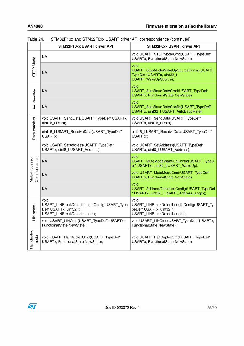
AN4088 Firmware migration using the library
Doc ID 023072 Rev 1 55/60
STO
P M
ode NA
void USART_STOPModeCmd(USART_TypeDef* USARTx, FunctionalState NewState);
NA
void USART_StopModeWakeUpSourceConfig(USART_TypeDef* USARTx, uint32_t USART_WakeUpSource);
Aut
oBau
dRat
e NAvoid USART_AutoBaudRateCmd(USART_TypeDef* USARTx, FunctionalState NewState);
NAvoid USART_AutoBaudRateConfig(USART_TypeDef* USARTx, uint32_t USART_AutoBaudRate);
Dat
a tr
ansf
ers void USART_SendData(USART_TypeDef* USARTx,
uint16_t Data);void USART_SendData(USART_TypeDef* USARTx, uint16_t Data);
uint16_t USART_ReceiveData(USART_TypeDef* USARTx);
uint16_t USART_ReceiveData(USART_TypeDef* USARTx);
Mul
ti-P
roce
ssor
Com
mun
icat
ion
void USART_SetAddress(USART_TypeDef* USARTx, uint8_t USART_Address);
void USART_SetAddress(USART_TypeDef* USARTx, uint8_t USART_Address);
NAvoid USART_MuteModeWakeUpConfig(USART_TypeDef* USARTx, uint32_t USART_WakeUp);
NAvoid USART_MuteModeCmd(USART_TypeDef* USARTx, FunctionalState NewState);
NAvoid USART_AddressDetectionConfig(USART_TypeDef* USARTx, uint32_t USART_AddressLength);
LIN
mod
e
void USART_LINBreakDetectLengthConfig(USART_TypeDef* USARTx, uint32_t USART_LINBreakDetectLength);
void USART_LINBreakDetectLengthConfig(USART_TypeDef* USARTx, uint32_t USART_LINBreakDetectLength);
void USART_LINCmd(USART_TypeDef* USARTx, FunctionalState NewState);
void USART_LINCmd(USART_TypeDef* USARTx, FunctionalState NewState);
Hal
f-du
plex
mod
e void USART_HalfDuplexCmd(USART_TypeDef* USARTx, FunctionalState NewState);
void USART_HalfDuplexCmd(USART_TypeDef* USARTx, FunctionalState NewState);
Table 24. STM32F10x and STM32F0xx USART driver API correspondence (continued)
STM32F10xx USART driver API STM32F0xx USART driver API

Firmware migration using the library AN4088
56/60 Doc ID 023072 Rev 1
Sm
art C
ard
mod
e
void USART_SmartCardCmd(USART_TypeDef* USARTx, FunctionalState NewState);
void USART_SmartCardCmd(USART_TypeDef* USARTx, FunctionalState NewState);
void USART_SmartCardNACKCmd(USART_TypeDef* USARTx, FunctionalState NewState);
void USART_SmartCardNACKCmd(USART_TypeDef* USARTx, FunctionalState NewState);
void USART_SetGuardTime(USART_TypeDef* USARTx, uint8_t USART_GuardTime);
void USART_SetGuardTime(USART_TypeDef* USARTx, uint8_t USART_GuardTime);
NAvoid USART_SetAutoRetryCount(USART_TypeDef* USARTx, uint8_t USART_AutoCount);
NAvoid USART_SetBlockLength(USART_TypeDef* USARTx, uint8_t USART_BlockLength);
IrD
A m
ode void USART_IrDAConfig(USART_TypeDef* USARTx,
uint32_t USART_IrDAMode);void USART_IrDAConfig(USART_TypeDef* USARTx, uint32_t USART_IrDAMode);
void USART_IrDACmd(USART_TypeDef* USARTx, FunctionalState NewState);
void USART_IrDACmd(USART_TypeDef* USARTx, FunctionalState NewState);
RS
485
mod
e
NAvoid USART_DECmd(USART_TypeDef* USARTx, FunctionalState NewState);
NAvoid USART_DEPolarityConfig(USART_TypeDef* USARTx, uint32_t USART_DEPolarity);
NAvoid USART_SetDEAssertionTime(USART_TypeDef* USARTx, uint32_t USART_DEAssertionTime);
NAvoid USART_SetDEDeassertionTime(USART_TypeDef* USARTx, uint32_t USART_DEDeassertionTime);
DM
A tr
ansf
ers void USART_DMACmd(USART_TypeDef* USARTx,
uint32_t USART_DMAReq, FunctionalState NewState);
void USART_DMACmd(USART_TypeDef* USARTx, uint32_t USART_DMAReq, FunctionalState NewState);
void USART_DMAReceptionErrorConfig(USART_TypeDef* USARTx, uint32_t USART_DMAOnError);
void USART_DMAReceptionErrorConfig(USART_TypeDef* USARTx, uint32_t USART_DMAOnError);
Table 24. STM32F10x and STM32F0xx USART driver API correspondence (continued)
STM32F10xx USART driver API STM32F0xx USART driver API

AN4088 Firmware migration using the library
Doc ID 023072 Rev 1 57/60
Inte
rrup
ts a
nd fl
ags
man
agem
ent
void USART_ITConfig(USART_TypeDef* USARTx, uint16_t USART_IT, FunctionalState NewState);
void USART_ITConfig(USART_TypeDef* USARTx, uint32_t USART_IT, FunctionalState NewState);
NAvoid USART_RequestCmd(USART_TypeDef* USARTx, uint32_t USART_Request, FunctionalState NewState);
NAvoid USART_OverrunDetectionConfig(USART_TypeDef* USARTx, uint32_t USART_OVRDetection);
FlagStatus USART_GetFlagStatus(USART_TypeDef* USARTx, uint16_t USART_FLAG);
FlagStatus USART_GetFlagStatus(USART_TypeDef* USARTx, uint32_t USART_FLAG);
void USART_ClearFlag(USART_TypeDef* USARTx, uint16_t USART_FLAG);
void USART_ClearFlag(USART_TypeDef* USARTx, uint32_t USART_FLAG);
ITStatus USART_GetITStatus(USART_TypeDef* USARTx, uint32_t USART_IT);
ITStatus USART_GetITStatus(USART_TypeDef* USARTx, uint32_t USART_IT);
void USART_ClearITPendingBit(USART_TypeDef* USARTx, uint32_t USART_IT);
void USART_ClearITPendingBit(USART_TypeDef* USARTx, uint32_t USART_IT);
Table 24. STM32F10x and STM32F0xx USART driver API correspondence (continued)
STM32F10xx USART driver API STM32F0xx USART driver API
Color key: = New function
= Same function, but API was changed
= Function not available (NA)

Firmware migration using the library AN4088
58/60 Doc ID 023072 Rev 1
4.16 IWDG driverExisting IWDG available on STM32F10xx and STM32F0xx devices have the same specifications, with window capability additional feature in F0 series which detect over frequency on external oscillators. The table below lists the IWDG driver APIs.
Table 25. STM32F10xx and STM32Fxx IWDG driver API correspondence
STM32F10xx IWDG driver API STM32F0xx IWDG driver API
Pre
scal
er a
nd C
ount
er
conf
igur
atio
n
void IWDG_WriteAccessCmd(uint16_t IWDG_WriteAccess);
void IWDG_WriteAccessCmd(uint16_t IWDG_WriteAccess);
void IWDG_SetPrescaler(uint8_t IWDG_Prescaler);void IWDG_SetPrescaler(uint8_t IWDG_Prescaler);
void IWDG_SetReload(uint16_t Reload); void IWDG_SetReload(uint16_t Reload);
void IWDG_ReloadCounter(void); void IWDG_ReloadCounter(void);
NA void IWDG_SetWindowValue(uint16_t WindowValue);
IWD
G
activ
atio
n
void IWDG_Enable(void); void IWDG_Enable(void);
Fla
g
man
agem
ent
FlagStatus IWDG_GetFlagStatus(uint16_t IWDG_FLAG);
FlagStatus IWDG_GetFlagStatus(uint16_t IWDG_FLAG);
Color key: = New function
= Same function, but API was changed
= Function not available (NA)

AN4088 Revision history
Doc ID 023072 Rev 1 59/60
5 Revision history
Table 26. Document revision history
Date Revision Changes
10-Jul-2012 1 Initial release

AN4088
60/60 Doc ID 023072 Rev 1
Please Read Carefully:
Information in this document is provided solely in connection with ST products. STMicroelectronics NV and its subsidiaries (“ST”) reserve theright to make changes, corrections, modifications or improvements, to this document, and the products and services described herein at anytime, without notice.
All ST products are sold pursuant to ST’s terms and conditions of sale.
Purchasers are solely responsible for the choice, selection and use of the ST products and services described herein, and ST assumes noliability whatsoever relating to the choice, selection or use of the ST products and services described herein.
No license, express or implied, by estoppel or otherwise, to any intellectual property rights is granted under this document. If any part of thisdocument refers to any third party products or services it shall not be deemed a license grant by ST for the use of such third party productsor services, or any intellectual property contained therein or considered as a warranty covering the use in any manner whatsoever of suchthird party products or services or any intellectual property contained therein.
UNLESS OTHERWISE SET FORTH IN ST’S TERMS AND CONDITIONS OF SALE ST DISCLAIMS ANY EXPRESS OR IMPLIEDWARRANTY WITH RESPECT TO THE USE AND/OR SALE OF ST PRODUCTS INCLUDING WITHOUT LIMITATION IMPLIEDWARRANTIES OF MERCHANTABILITY, FITNESS FOR A PARTICULAR PURPOSE (AND THEIR EQUIVALENTS UNDER THE LAWSOF ANY JURISDICTION), OR INFRINGEMENT OF ANY PATENT, COPYRIGHT OR OTHER INTELLECTUAL PROPERTY RIGHT.
UNLESS EXPRESSLY APPROVED IN WRITING BY TWO AUTHORIZED ST REPRESENTATIVES, ST PRODUCTS ARE NOTRECOMMENDED, AUTHORIZED OR WARRANTED FOR USE IN MILITARY, AIR CRAFT, SPACE, LIFE SAVING, OR LIFE SUSTAININGAPPLICATIONS, NOR IN PRODUCTS OR SYSTEMS WHERE FAILURE OR MALFUNCTION MAY RESULT IN PERSONAL INJURY,DEATH, OR SEVERE PROPERTY OR ENVIRONMENTAL DAMAGE. ST PRODUCTS WHICH ARE NOT SPECIFIED AS "AUTOMOTIVEGRADE" MAY ONLY BE USED IN AUTOMOTIVE APPLICATIONS AT USER’S OWN RISK.
Resale of ST products with provisions different from the statements and/or technical features set forth in this document shall immediately voidany warranty granted by ST for the ST product or service described herein and shall not create or extend in any manner whatsoever, anyliability of ST.
ST and the ST logo are trademarks or registered trademarks of ST in various countries.
Information in this document supersedes and replaces all information previously supplied.
The ST logo is a registered trademark of STMicroelectronics. All other names are the property of their respective owners.
© 2012 STMicroelectronics - All rights reserved
STMicroelectronics group of companies
Australia - Belgium - Brazil - Canada - China - Czech Republic - Finland - France - Germany - Hong Kong - India - Israel - Italy - Japan - Malaysia - Malta - Morocco - Philippines - Singapore - Spain - Sweden - Switzerland - United Kingdom - United States of America
www.st.com