MELSEC-L Flexible High-Speed I/O Control Module User's ...
312
MELSEC-L Flexible High-Speed I/O Control Module User's Manual -LD40PD01 -Flexible High-Speed I/O Control Module Configuration tool (SW1DNN-FLEXIOP-E)
-
Upload
khangminh22 -
Category
Documents
-
view
1 -
download
0
Transcript of MELSEC-L Flexible High-Speed I/O Control Module User's ...
MELSEC-L Flexible High-Speed I/O Control Module User's Manual
-LD40PD01-Flexible High-Speed I/O Control Module Configuration tool (SW1DNN-FLEXIOP-E)


SAFETY PRECAUTIONS(Read these precautions before using this product.)Before using this product, please read this manual and the relevant manuals carefully and pay full attention to safety to handle the product correctly.The precautions given in this manual are concerned with this product only. For the safety precautions of the programmable controller system, refer to the user's manual for the CPU module used.In this manual, the safety precautions are classified into two levels: " WARNING" and " CAUTION".
Under some circumstances, failure to observe the precautions given under " CAUTION" may lead to serious consequences.Observe the precautions of both levels because they are important for personal and system safety.Make sure that the end users read this manual and then keep the manual in a safe place for future reference.
[Design Precautions]
[Design Precautions]
WARNING● In an output circuit, when a load current exceeding the rated current or an overcurrent caused by a
load short-circuit flows for a long time, it may cause smoke and fire. To prevent this, configure an external safety circuit, such as a fuse.
● Do not write any data to the "system area" and "write-protect area" (R) of the buffer memory in the intelligent function module. Also, do not use any "use prohibited" signals as an output signal from the programmable controller CPU to the intelligent function module. Doing so may cause malfunction of the programmable controller system.
● Outputs may remain on or off due to a failure of a transistor for external output. Configure an external circuit for monitoring output signals that could cause a serious accident.
● When changing data and operating status of the running module from an external device such as a personal computer connected, configure an interlock circuit external to the programmable controller to ensure that the entire system always operates safely.In addition, before performing online operations, determine corrective actions to be taken between the external device and the module in case of a communication failure due to poor contact of cables.
CAUTION● Do not install the control lines or communication cables together with the main circuit lines or power
cables. Keep a distance of 150mm or more between them. Failure to do so may result in malfunction due to noise.
● During control of an inductive load such as a lamp, heater, or solenoid valve, a large current (approximately ten times greater than normal) may flow when the output is turned from off to on. Therefore, use a module that has a sufficient current rating.
WARNING Indicates that incorrect handling may cause hazardous conditions, resulting in death or severe injury.
CAUTION Indicates that incorrect handling may cause hazardous conditions, resulting in minor or moderate injury or property damage.
1

2
[Installation Precautions]
[Installation Precautions]
[Wiring Precautions]
WARNING● Shut off the external power supply (all phases) used in the system before mounting or removing a
module. Failure to do so may result in electric shock or cause the module to fail or malfunction.
CAUTION● Use the programmable controller in an environment that meets the general specifications in the Safety
Guidelines provided with the CPU module or head module. Failure to do so may result in electric shock, fire, malfunction, or damage to or deterioration of the product.
● To interconnect modules, engage the respective connectors and securely lock the module joint levers until they click. Incorrect interconnection may cause malfunction, failure, or drop of the module.
● Do not directly touch any conductive parts and electronic components of the module. Doing so can cause malfunction or failure of the module.
WARNING● Shut off the external power supply (all phases) used in the system before wiring. Failure to do so may
result in electric shock or cause the module to fail or malfunction.● When connecting a differential output terminal to a differential receiver of a drive unit, connect the
high-speed output common terminal to the differential receiver common terminal of the drive unit. Failure to do so may cause the module to fail or malfunction because of the potential difference that occurs between the high-speed output common terminal and the differential receiver common terminal.
[Wiring Precautions]
[Startup and Maintenance Precautions]
CAUTION● Individually ground the FG and LG terminals of the programmable controller with a ground resistance
of 100 ohms or less. Failure to do so may result in electric shock or malfunction.● Check the rated voltage and terminal layout before wiring to the module, and connect the cables
correctly. Connecting a power supply with a different voltage rating or incorrect wiring may cause a fire or failure.
● Connectors for external devices must be crimped with the tool specified by the manufacturer or must be correctly soldered. Incomplete connections may cause short circuit, fire, or malfunction.
● Place the cables in a duct or clamp them. If not, dangling cable may swing or inadvertently be pulled, resulting in damage to the module or cables or malfunction due to poor contact.
● Tighten the connector screws within the specified torque range. Undertightening can cause drop of the screw, short circuit, fire, or malfunction. Overtightening can damage the screw and/or module, resulting in drop, short circuit, fire, or malfunction.
● Prevent foreign matter such as dust or wire chips from entering the module. Such foreign matter can cause a fire, failure, or malfunction.
● A protective film is attached to the top of the module to prevent foreign matter, such as wire chips, from entering the module during wiring. Do not remove the film during wiring. Remove it for heat dissipation before system operation.
● Ground the shield cable on the encoder side (relay box). Always ground the FG and LG terminals to the protective ground conductor. Failure to do so may cause malfunction.
● Mitsubishi programmable controllers must be installed in control panels. Connect the main power supply to the power supply module in the control panel through a relay terminal block. Wiring and replacement of a power supply module must be performed by qualified maintenance personnel with knowledge of protection against electric shock. For wiring methods, refer to the MELSEC-L CPU Module User's Manual (Hardware Design, Maintenance and Inspection).
WARNING● Do not touch any terminal while power is on. Doing so will cause electric shock or malfunction.● Shut off the external power supply (all phases) used in the system before cleaning the module or
retightening the connector screws. Failure to do so may result in electric shock.
3
4
[Startup and Maintenance Precautions]
[Disposal Precautions]
CAUTION● Do not disassemble or modify the module. Doing so may cause failure, malfunction, injury, or a fire.● Shut off the external power supply (all phases) used in the system before mounting or removing a
module. Failure to do so may cause the module to fail or malfunction.● After the first use of the product (module and display unit), do not connect/disconnect the product
more than 50 times (in accordance with IEC 61131-2). Exceeding the limit may cause malfunction.● Tighten the connector screws within the specified torque range. Undertightening can cause drop of
the component or wire, short circuit, or malfunction. Overtightening can damage the screw and/or module, resulting in drop, short circuit, or malfunction.
● Before handling the module, touch a conducting object such as a grounded metal to discharge the static electricity from the human body. Failure to do so may cause the module to fail or malfunction.
● When performing online operations of the running module from an external device such as a personal computer connected, read the relevant manuals carefully and ensure that the operation is safe before proceeding.
● Before changing any setting of the module, read the relevant manuals carefully, ensure the safety, and change the operating status of the CPU module to STOP.Especially when operating the module in the network system, ensure the safety thoroughly because controlled machines are likely to be moved inadvertently. Improper operation may damage machines or cause accidents.
CAUTION● When disposing of this product, treat it as industrial waste.

CONDITIONS OF USE FOR THE PRODUCT(1) MELSEC programmable controller ("the PRODUCT") shall be used in conditions;
i) where any problem, fault or failure occurring in the PRODUCT, if any, shall not lead to any major or serious accident; and ii) where the backup and fail-safe function are systematically or automatically provided outside of the PRODUCT for the case of any problem, fault or failure occurring in the PRODUCT.
(2) The PRODUCT has been designed and manufactured for the purpose of being used in general industries.MITSUBISHI ELECTRIC SHALL HAVE NO RESPONSIBILITY OR LIABILITY (INCLUDING, BUT NOT LIMITED TO ANY AND ALL RESPONSIBILITY OR LIABILITY BASED ON CONTRACT, WARRANTY, TORT, PRODUCT LIABILITY) FOR ANY INJURY OR DEATH TO PERSONS OR LOSS OR DAMAGE TO PROPERTY CAUSED BY the PRODUCT THAT ARE OPERATED OR USED IN APPLICATION NOT INTENDED OR EXCLUDED BY INSTRUCTIONS, PRECAUTIONS, OR WARNING CONTAINED IN MITSUBISHI ELECTRIC USER'S, INSTRUCTION AND/OR SAFETY MANUALS, TECHNICAL BULLETINS AND GUIDELINES FOR the PRODUCT. ("Prohibited Application")Prohibited Applications include, but not limited to, the use of the PRODUCT in;• Nuclear Power Plants and any other power plants operated by Power companies, and/or any other cases in which the
public could be affected if any problem or fault occurs in the PRODUCT.• Railway companies or Public service purposes, and/or any other cases in which establishment of a special quality
assurance system is required by the Purchaser or End User.• Aircraft or Aerospace, Medical applications, Train equipment, transport equipment such as Elevator and Escalator,
Incineration and Fuel devices, Vehicles, Manned transportation, Equipment for Recreation and Amusement, and Safety devices, handling of Nuclear or Hazardous Materials or Chemicals, Mining and Drilling, and/or other applications where there is a significant risk of injury to the public or property.
Notwithstanding the above restrictions, Mitsubishi Electric may in its sole discretion, authorize use of the PRODUCT in one or more of the Prohibited Applications, provided that the usage of the PRODUCT is limited only for the specific applications agreed to by Mitsubishi Electric and provided further that no special quality assurance or fail-safe, redundant or other safety features which exceed the general specifications of the PRODUCTs are required. For details, please contact the Mitsubishi Electric representative in your region.
(3) Mitsubishi Electric shall have no responsibility or liability for any problems involving programmable controller trouble and system trouble caused by DoS attacks, unauthorized access, computer viruses, and other cyberattacks.
5
6
INTRODUCTIONThank you for purchasing the Mitsubishi Electric MELSEC-L series programmable controllers. This manual describes the functions and programming of a flexible high-speed I/O control module.
Before using this product, please read this manual and the relevant manuals carefully and develop familiarity with the functions and performance of the MELSEC-L series programmable controller to handle the product correctly.When applying the program examples introduced in this manual to an actual system, ensure the applicability and confirm that it will not cause system control problems.
Relevant productLD40PD01
Unless otherwise specified, this manual describes the program examples in which the I/O numbers of X/Y00 to X/Y1F are assigned for a flexible high-speed I/O control module. For I/O number assignment, refer to the following. MELSEC-L CPU Module User's Manual (Function Explanation, Program Fundamentals)
COMPLIANCE WITH EMC AND LOW VOLTAGE DIRECTIVES
Method of ensuring complianceTo ensure that Mitsubishi programmable controllers maintain EMC and Low Voltage Directives when incorporated into other machinery or equipment, certain measures may be necessary. Please refer to one of the following manuals. • MELSEC-L CPU Module User's Manual (Hardware Design, Maintenance and Inspection) • MELSEC-L CC-Link IE Field Network Head Module User's Manual • Safety Guidelines (This manual is included with the CPU module or head module.)The CE mark on the side of the programmable controller indicates compliance with EMC and Low Voltage Directives.
Additional measuresTo ensure that this product maintains EMC and Low Voltage Directives, please refer to the following.Page 37 External wiring precautions

MEMO
7
8
CONTENTSSAFETY PRECAUTIONS . . . . . . . . . . . . . . . . . . . . . . . . . . . . . . . . . . . . . . . . . . . . . . . . . . . . . . . . . . . . . . . . . . . .1CONDITIONS OF USE FOR THE PRODUCT . . . . . . . . . . . . . . . . . . . . . . . . . . . . . . . . . . . . . . . . . . . . . . . . . . . .5INTRODUCTION. . . . . . . . . . . . . . . . . . . . . . . . . . . . . . . . . . . . . . . . . . . . . . . . . . . . . . . . . . . . . . . . . . . . . . . . . . .6COMPLIANCE WITH EMC AND LOW VOLTAGE DIRECTIVES . . . . . . . . . . . . . . . . . . . . . . . . . . . . . . . . . . . . . .6RELEVANT MANUALS . . . . . . . . . . . . . . . . . . . . . . . . . . . . . . . . . . . . . . . . . . . . . . . . . . . . . . . . . . . . . . . . . . . . .12MANUAL PAGE ORGANIZATION. . . . . . . . . . . . . . . . . . . . . . . . . . . . . . . . . . . . . . . . . . . . . . . . . . . . . . . . . . . . .13TERMS . . . . . . . . . . . . . . . . . . . . . . . . . . . . . . . . . . . . . . . . . . . . . . . . . . . . . . . . . . . . . . . . . . . . . . . . . . . . . . . . .14PACKING LIST . . . . . . . . . . . . . . . . . . . . . . . . . . . . . . . . . . . . . . . . . . . . . . . . . . . . . . . . . . . . . . . . . . . . . . . . . . .14
CHAPTER 1 FLEXIBLE HIGH-SPEED I/O CONTROL MODULE 151.1 Features . . . . . . . . . . . . . . . . . . . . . . . . . . . . . . . . . . . . . . . . . . . . . . . . . . . . . . . . . . . . . . . . . . . . . . . . . . . . . . . 151.2 Application Example . . . . . . . . . . . . . . . . . . . . . . . . . . . . . . . . . . . . . . . . . . . . . . . . . . . . . . . . . . . . . . . . . . . . . 19
CHAPTER 2 PART NAMES 21
CHAPTER 3 SPECIFICATIONS 233.1 General Specifications . . . . . . . . . . . . . . . . . . . . . . . . . . . . . . . . . . . . . . . . . . . . . . . . . . . . . . . . . . . . . . . . . . . 233.2 Performance Specifications . . . . . . . . . . . . . . . . . . . . . . . . . . . . . . . . . . . . . . . . . . . . . . . . . . . . . . . . . . . . . . . 24
Number of parameter settings . . . . . . . . . . . . . . . . . . . . . . . . . . . . . . . . . . . . . . . . . . . . . . . . . . . . . . . . . . . . . . . 273.3 Function List . . . . . . . . . . . . . . . . . . . . . . . . . . . . . . . . . . . . . . . . . . . . . . . . . . . . . . . . . . . . . . . . . . . . . . . . . . . 283.4 List of I/O Signals . . . . . . . . . . . . . . . . . . . . . . . . . . . . . . . . . . . . . . . . . . . . . . . . . . . . . . . . . . . . . . . . . . . . . . . 293.5 List of Buffer Memory Addresses . . . . . . . . . . . . . . . . . . . . . . . . . . . . . . . . . . . . . . . . . . . . . . . . . . . . . . . . . . 30
CHAPTER 4 PROCEDURES BEFORE OPERATION 32
CHAPTER 5 SYSTEM CONFIGURATION 345.1 Overall Configuration . . . . . . . . . . . . . . . . . . . . . . . . . . . . . . . . . . . . . . . . . . . . . . . . . . . . . . . . . . . . . . . . . . . . 345.2 Applicable System. . . . . . . . . . . . . . . . . . . . . . . . . . . . . . . . . . . . . . . . . . . . . . . . . . . . . . . . . . . . . . . . . . . . . . . 355.3 Restrictions When the Flexible High-Speed I/O Control Module Is Connected to the Head Module . . . . 35
CHAPTER 6 INSTALLATION AND EXTERNAL WIRING 366.1 Installation Environment and Installation Position . . . . . . . . . . . . . . . . . . . . . . . . . . . . . . . . . . . . . . . . . . . . 366.2 External Wiring . . . . . . . . . . . . . . . . . . . . . . . . . . . . . . . . . . . . . . . . . . . . . . . . . . . . . . . . . . . . . . . . . . . . . . . . . 37
External wiring precautions . . . . . . . . . . . . . . . . . . . . . . . . . . . . . . . . . . . . . . . . . . . . . . . . . . . . . . . . . . . . . . . . . 37Connector for external devices . . . . . . . . . . . . . . . . . . . . . . . . . . . . . . . . . . . . . . . . . . . . . . . . . . . . . . . . . . . . . . 41Interface with external devices . . . . . . . . . . . . . . . . . . . . . . . . . . . . . . . . . . . . . . . . . . . . . . . . . . . . . . . . . . . . . . 43Connectable encoders. . . . . . . . . . . . . . . . . . . . . . . . . . . . . . . . . . . . . . . . . . . . . . . . . . . . . . . . . . . . . . . . . . . . . 50
6.3 Examples of Wiring Between a Controller and External Input Terminals . . . . . . . . . . . . . . . . . . . . . . . . . . 51Example of external wiring with a controller (Sync load type) . . . . . . . . . . . . . . . . . . . . . . . . . . . . . . . . . . . . . . . 51Example of external wiring with a controller (Source load type) . . . . . . . . . . . . . . . . . . . . . . . . . . . . . . . . . . . . . 51
6.4 Example of External Wiring Between the Flexible High-speed I/O Control Module and an Encoder . . . . 52Example of external wiring with an open collector output type encoder (24VDC). . . . . . . . . . . . . . . . . . . . . . . . 52Example of external wiring with a line driver (equivalent to AM26LS31) encoder . . . . . . . . . . . . . . . . . . . . . . . . 54Example of external wiring with the SSI encoder (serial communication) . . . . . . . . . . . . . . . . . . . . . . . . . . . . . . 55
6.5 Example of External Wiring with External Output Terminals . . . . . . . . . . . . . . . . . . . . . . . . . . . . . . . . . . . . 56Example of external wiring with output terminals (Sink output type) . . . . . . . . . . . . . . . . . . . . . . . . . . . . . . . . . . 56Example of external wiring with differential receivers (Differential output type) . . . . . . . . . . . . . . . . . . . . . . . . . 57

CO
NTE
NTS
CHAPTER 7 FUNCTIONS 587.1 Hardware Logic Control Function . . . . . . . . . . . . . . . . . . . . . . . . . . . . . . . . . . . . . . . . . . . . . . . . . . . . . . . . . . 587.2 Continuous Logging Function . . . . . . . . . . . . . . . . . . . . . . . . . . . . . . . . . . . . . . . . . . . . . . . . . . . . . . . . . . . . . 59
Transfer of continuous logging data . . . . . . . . . . . . . . . . . . . . . . . . . . . . . . . . . . . . . . . . . . . . . . . . . . . . . . . . . . 647.3 Error History Function . . . . . . . . . . . . . . . . . . . . . . . . . . . . . . . . . . . . . . . . . . . . . . . . . . . . . . . . . . . . . . . . . . . 687.4 Module Error Collection Function . . . . . . . . . . . . . . . . . . . . . . . . . . . . . . . . . . . . . . . . . . . . . . . . . . . . . . . . . . 717.5 Error Clear Function . . . . . . . . . . . . . . . . . . . . . . . . . . . . . . . . . . . . . . . . . . . . . . . . . . . . . . . . . . . . . . . . . . . . . 72
CHAPTER 8 FUNCTIONS OF THE CONFIGURATION TOOL 738.1 How to Install and Uninstall the Configuration Tool . . . . . . . . . . . . . . . . . . . . . . . . . . . . . . . . . . . . . . . . . . . 738.2 Starting and Exiting the Configuration Tool . . . . . . . . . . . . . . . . . . . . . . . . . . . . . . . . . . . . . . . . . . . . . . . . . . 748.3 Switching the Language . . . . . . . . . . . . . . . . . . . . . . . . . . . . . . . . . . . . . . . . . . . . . . . . . . . . . . . . . . . . . . . . . . 768.4 Window Layout . . . . . . . . . . . . . . . . . . . . . . . . . . . . . . . . . . . . . . . . . . . . . . . . . . . . . . . . . . . . . . . . . . . . . . . . . 77
Navigation window. . . . . . . . . . . . . . . . . . . . . . . . . . . . . . . . . . . . . . . . . . . . . . . . . . . . . . . . . . . . . . . . . . . . . . . . 79Element Selection window. . . . . . . . . . . . . . . . . . . . . . . . . . . . . . . . . . . . . . . . . . . . . . . . . . . . . . . . . . . . . . . . . . 80Work window . . . . . . . . . . . . . . . . . . . . . . . . . . . . . . . . . . . . . . . . . . . . . . . . . . . . . . . . . . . . . . . . . . . . . . . . . . . . 81Map display window . . . . . . . . . . . . . . . . . . . . . . . . . . . . . . . . . . . . . . . . . . . . . . . . . . . . . . . . . . . . . . . . . . . . . . 82
8.5 List of Menus of the Configuration Tool . . . . . . . . . . . . . . . . . . . . . . . . . . . . . . . . . . . . . . . . . . . . . . . . . . . . . 838.6 Printing. . . . . . . . . . . . . . . . . . . . . . . . . . . . . . . . . . . . . . . . . . . . . . . . . . . . . . . . . . . . . . . . . . . . . . . . . . . . . . . . 858.7 Project Management . . . . . . . . . . . . . . . . . . . . . . . . . . . . . . . . . . . . . . . . . . . . . . . . . . . . . . . . . . . . . . . . . . . . . 86
Creating a new project. . . . . . . . . . . . . . . . . . . . . . . . . . . . . . . . . . . . . . . . . . . . . . . . . . . . . . . . . . . . . . . . . . . . . 86Opening a project . . . . . . . . . . . . . . . . . . . . . . . . . . . . . . . . . . . . . . . . . . . . . . . . . . . . . . . . . . . . . . . . . . . . . . . . 86Saving a project file . . . . . . . . . . . . . . . . . . . . . . . . . . . . . . . . . . . . . . . . . . . . . . . . . . . . . . . . . . . . . . . . . . . . . . . 87Verifying a project file . . . . . . . . . . . . . . . . . . . . . . . . . . . . . . . . . . . . . . . . . . . . . . . . . . . . . . . . . . . . . . . . . . . . . 88Security . . . . . . . . . . . . . . . . . . . . . . . . . . . . . . . . . . . . . . . . . . . . . . . . . . . . . . . . . . . . . . . . . . . . . . . . . . . . . . . . 89
8.8 Windows for Creating the Hardware Logic . . . . . . . . . . . . . . . . . . . . . . . . . . . . . . . . . . . . . . . . . . . . . . . . . . . 91Hardware logic outline window . . . . . . . . . . . . . . . . . . . . . . . . . . . . . . . . . . . . . . . . . . . . . . . . . . . . . . . . . . . . . . 92Multi function counter block detail window . . . . . . . . . . . . . . . . . . . . . . . . . . . . . . . . . . . . . . . . . . . . . . . . . . . . . 93How to use blocks . . . . . . . . . . . . . . . . . . . . . . . . . . . . . . . . . . . . . . . . . . . . . . . . . . . . . . . . . . . . . . . . . . . . . . . . 94Adding a comment. . . . . . . . . . . . . . . . . . . . . . . . . . . . . . . . . . . . . . . . . . . . . . . . . . . . . . . . . . . . . . . . . . . . . . . 100
8.9 Library Function . . . . . . . . . . . . . . . . . . . . . . . . . . . . . . . . . . . . . . . . . . . . . . . . . . . . . . . . . . . . . . . . . . . . . . . 103Export . . . . . . . . . . . . . . . . . . . . . . . . . . . . . . . . . . . . . . . . . . . . . . . . . . . . . . . . . . . . . . . . . . . . . . . . . . . . . . . . 103Library operation . . . . . . . . . . . . . . . . . . . . . . . . . . . . . . . . . . . . . . . . . . . . . . . . . . . . . . . . . . . . . . . . . . . . . . . . 105
8.10 Online Functions . . . . . . . . . . . . . . . . . . . . . . . . . . . . . . . . . . . . . . . . . . . . . . . . . . . . . . . . . . . . . . . . . . . . . . . 106Start I/O number setting . . . . . . . . . . . . . . . . . . . . . . . . . . . . . . . . . . . . . . . . . . . . . . . . . . . . . . . . . . . . . . . . . . 106Writing data to the module. . . . . . . . . . . . . . . . . . . . . . . . . . . . . . . . . . . . . . . . . . . . . . . . . . . . . . . . . . . . . . . . . 107Reading data from the module . . . . . . . . . . . . . . . . . . . . . . . . . . . . . . . . . . . . . . . . . . . . . . . . . . . . . . . . . . . . . 108Verifying with the module. . . . . . . . . . . . . . . . . . . . . . . . . . . . . . . . . . . . . . . . . . . . . . . . . . . . . . . . . . . . . . . . . . 109Module operation. . . . . . . . . . . . . . . . . . . . . . . . . . . . . . . . . . . . . . . . . . . . . . . . . . . . . . . . . . . . . . . . . . . . . . . . 110Monitor. . . . . . . . . . . . . . . . . . . . . . . . . . . . . . . . . . . . . . . . . . . . . . . . . . . . . . . . . . . . . . . . . . . . . . . . . . . . . . . . 111
8.11 Watch Function . . . . . . . . . . . . . . . . . . . . . . . . . . . . . . . . . . . . . . . . . . . . . . . . . . . . . . . . . . . . . . . . . . . . . . . . 1138.12 Debug Function . . . . . . . . . . . . . . . . . . . . . . . . . . . . . . . . . . . . . . . . . . . . . . . . . . . . . . . . . . . . . . . . . . . . . . . . 117
Simulation function . . . . . . . . . . . . . . . . . . . . . . . . . . . . . . . . . . . . . . . . . . . . . . . . . . . . . . . . . . . . . . . . . . . . . . 117Logic analyzer function . . . . . . . . . . . . . . . . . . . . . . . . . . . . . . . . . . . . . . . . . . . . . . . . . . . . . . . . . . . . . . . . . . . 125Continuous logging . . . . . . . . . . . . . . . . . . . . . . . . . . . . . . . . . . . . . . . . . . . . . . . . . . . . . . . . . . . . . . . . . . . . . . 131
8.13 Pattern Generator Function . . . . . . . . . . . . . . . . . . . . . . . . . . . . . . . . . . . . . . . . . . . . . . . . . . . . . . . . . . . . . . 1328.14 Help Function. . . . . . . . . . . . . . . . . . . . . . . . . . . . . . . . . . . . . . . . . . . . . . . . . . . . . . . . . . . . . . . . . . . . . . . . . . 138
Checking the version of the configuration tool. . . . . . . . . . . . . . . . . . . . . . . . . . . . . . . . . . . . . . . . . . . . . . . . . . 138
9

10
CHAPTER 9 CREATING A HARDWARE LOGIC 1399.1 Main Blocks in the Hardware Logic Outline Window. . . . . . . . . . . . . . . . . . . . . . . . . . . . . . . . . . . . . . . . . . 139
External input block . . . . . . . . . . . . . . . . . . . . . . . . . . . . . . . . . . . . . . . . . . . . . . . . . . . . . . . . . . . . . . . . . . . . . . 142Y device terminal . . . . . . . . . . . . . . . . . . . . . . . . . . . . . . . . . . . . . . . . . . . . . . . . . . . . . . . . . . . . . . . . . . . . . . . . 145OUT terminal . . . . . . . . . . . . . . . . . . . . . . . . . . . . . . . . . . . . . . . . . . . . . . . . . . . . . . . . . . . . . . . . . . . . . . . . . . . 146Parallel encoder block . . . . . . . . . . . . . . . . . . . . . . . . . . . . . . . . . . . . . . . . . . . . . . . . . . . . . . . . . . . . . . . . . . . . 147SSI encoder block . . . . . . . . . . . . . . . . . . . . . . . . . . . . . . . . . . . . . . . . . . . . . . . . . . . . . . . . . . . . . . . . . . . . . . . 150Logical operation block . . . . . . . . . . . . . . . . . . . . . . . . . . . . . . . . . . . . . . . . . . . . . . . . . . . . . . . . . . . . . . . . . . . 158External output block. . . . . . . . . . . . . . . . . . . . . . . . . . . . . . . . . . . . . . . . . . . . . . . . . . . . . . . . . . . . . . . . . . . . . 159SI device terminal . . . . . . . . . . . . . . . . . . . . . . . . . . . . . . . . . . . . . . . . . . . . . . . . . . . . . . . . . . . . . . . . . . . . . . . 162
9.2 Multi Function Counter Block . . . . . . . . . . . . . . . . . . . . . . . . . . . . . . . . . . . . . . . . . . . . . . . . . . . . . . . . . . . . 163Internal blocks of multi function counter blocks . . . . . . . . . . . . . . . . . . . . . . . . . . . . . . . . . . . . . . . . . . . . . . . . . 166Input terminal. . . . . . . . . . . . . . . . . . . . . . . . . . . . . . . . . . . . . . . . . . . . . . . . . . . . . . . . . . . . . . . . . . . . . . . . . . . 170Latch input terminal . . . . . . . . . . . . . . . . . . . . . . . . . . . . . . . . . . . . . . . . . . . . . . . . . . . . . . . . . . . . . . . . . . . . . . 170Event input terminal. . . . . . . . . . . . . . . . . . . . . . . . . . . . . . . . . . . . . . . . . . . . . . . . . . . . . . . . . . . . . . . . . . . . . . 171Input signal event detection block . . . . . . . . . . . . . . . . . . . . . . . . . . . . . . . . . . . . . . . . . . . . . . . . . . . . . . . . . . . 172Latch event detection block. . . . . . . . . . . . . . . . . . . . . . . . . . . . . . . . . . . . . . . . . . . . . . . . . . . . . . . . . . . . . . . . 179Counter timer block . . . . . . . . . . . . . . . . . . . . . . . . . . . . . . . . . . . . . . . . . . . . . . . . . . . . . . . . . . . . . . . . . . . . . . 181Comparison block . . . . . . . . . . . . . . . . . . . . . . . . . . . . . . . . . . . . . . . . . . . . . . . . . . . . . . . . . . . . . . . . . . . . . . . 193Pattern generator block . . . . . . . . . . . . . . . . . . . . . . . . . . . . . . . . . . . . . . . . . . . . . . . . . . . . . . . . . . . . . . . . . . . 196Cam switch block. . . . . . . . . . . . . . . . . . . . . . . . . . . . . . . . . . . . . . . . . . . . . . . . . . . . . . . . . . . . . . . . . . . . . . . . 198Set/reset block. . . . . . . . . . . . . . . . . . . . . . . . . . . . . . . . . . . . . . . . . . . . . . . . . . . . . . . . . . . . . . . . . . . . . . . . . . 202Output terminal . . . . . . . . . . . . . . . . . . . . . . . . . . . . . . . . . . . . . . . . . . . . . . . . . . . . . . . . . . . . . . . . . . . . . . . . . 203Event output terminal. . . . . . . . . . . . . . . . . . . . . . . . . . . . . . . . . . . . . . . . . . . . . . . . . . . . . . . . . . . . . . . . . . . . . 204Pattern generator output terminal . . . . . . . . . . . . . . . . . . . . . . . . . . . . . . . . . . . . . . . . . . . . . . . . . . . . . . . . . . . 205Cam switch output terminal . . . . . . . . . . . . . . . . . . . . . . . . . . . . . . . . . . . . . . . . . . . . . . . . . . . . . . . . . . . . . . . . 205
9.3 Intelligent Function Module Interrupt . . . . . . . . . . . . . . . . . . . . . . . . . . . . . . . . . . . . . . . . . . . . . . . . . . . . . . 206
CHAPTER 10 BLOCK LINK EXAMPLES 20910.1 Coincidence Detection . . . . . . . . . . . . . . . . . . . . . . . . . . . . . . . . . . . . . . . . . . . . . . . . . . . . . . . . . . . . . . . . . . 21010.2 One-shot Timer . . . . . . . . . . . . . . . . . . . . . . . . . . . . . . . . . . . . . . . . . . . . . . . . . . . . . . . . . . . . . . . . . . . . . . . . 21510.3 Event Generation. . . . . . . . . . . . . . . . . . . . . . . . . . . . . . . . . . . . . . . . . . . . . . . . . . . . . . . . . . . . . . . . . . . . . . . 21910.4 Cam Switch . . . . . . . . . . . . . . . . . . . . . . . . . . . . . . . . . . . . . . . . . . . . . . . . . . . . . . . . . . . . . . . . . . . . . . . . . . . 22110.5 PWM Output . . . . . . . . . . . . . . . . . . . . . . . . . . . . . . . . . . . . . . . . . . . . . . . . . . . . . . . . . . . . . . . . . . . . . . . . . . . 22410.6 Fixed Cycle Output . . . . . . . . . . . . . . . . . . . . . . . . . . . . . . . . . . . . . . . . . . . . . . . . . . . . . . . . . . . . . . . . . . . . . 22710.7 Latch Counter . . . . . . . . . . . . . . . . . . . . . . . . . . . . . . . . . . . . . . . . . . . . . . . . . . . . . . . . . . . . . . . . . . . . . . . . . 23010.8 Ratio Conversion. . . . . . . . . . . . . . . . . . . . . . . . . . . . . . . . . . . . . . . . . . . . . . . . . . . . . . . . . . . . . . . . . . . . . . . 23310.9 Pulse Measurement. . . . . . . . . . . . . . . . . . . . . . . . . . . . . . . . . . . . . . . . . . . . . . . . . . . . . . . . . . . . . . . . . . . . . 238
CHAPTER 11 SETTINGS 24111.1 Adding the Module . . . . . . . . . . . . . . . . . . . . . . . . . . . . . . . . . . . . . . . . . . . . . . . . . . . . . . . . . . . . . . . . . . . . . 24111.2 Switch Setting . . . . . . . . . . . . . . . . . . . . . . . . . . . . . . . . . . . . . . . . . . . . . . . . . . . . . . . . . . . . . . . . . . . . . . . . . 24211.3 Auto Refresh . . . . . . . . . . . . . . . . . . . . . . . . . . . . . . . . . . . . . . . . . . . . . . . . . . . . . . . . . . . . . . . . . . . . . . . . . . 243
CHAPTER 12 DISPLAY UNIT 24412.1 Features . . . . . . . . . . . . . . . . . . . . . . . . . . . . . . . . . . . . . . . . . . . . . . . . . . . . . . . . . . . . . . . . . . . . . . . . . . . . . . 24412.2 Checking and Clearing Errors . . . . . . . . . . . . . . . . . . . . . . . . . . . . . . . . . . . . . . . . . . . . . . . . . . . . . . . . . . . . 245
CHAPTER 13 PROGRAMMING 24713.1 Programming Procedure . . . . . . . . . . . . . . . . . . . . . . . . . . . . . . . . . . . . . . . . . . . . . . . . . . . . . . . . . . . . . . . . 247

CO
NTE
NTS
13.2 When the Module Is Used with the Standard System Configuration . . . . . . . . . . . . . . . . . . . . . . . . . . . . . 24813.3 When the Module Is Connected to a Head Module . . . . . . . . . . . . . . . . . . . . . . . . . . . . . . . . . . . . . . . . . . . 254
Operations of the flexible high-speed I/O control module when the head module is connected . . . . . . . . . . . . 267
CHAPTER 14 TROUBLESHOOTING 26914.1 Checking Error Codes in the Module's Detailed Information Window of GX Works2 . . . . . . . . . . . . . . . 26914.2 Checking Error Codes with Latest Error Code (Un\G100) . . . . . . . . . . . . . . . . . . . . . . . . . . . . . . . . . . . . . . 27014.3 Checking Error Codes with the Module Error Collection Function of GX Works2 . . . . . . . . . . . . . . . . . . 27114.4 Troubleshooting with LEDs . . . . . . . . . . . . . . . . . . . . . . . . . . . . . . . . . . . . . . . . . . . . . . . . . . . . . . . . . . . . . . 272
RUN LED is flashing or turns off . . . . . . . . . . . . . . . . . . . . . . . . . . . . . . . . . . . . . . . . . . . . . . . . . . . . . . . . . . . . 272ERR. LED turns on . . . . . . . . . . . . . . . . . . . . . . . . . . . . . . . . . . . . . . . . . . . . . . . . . . . . . . . . . . . . . . . . . . . . . . 272
14.5 Troubleshooting by Symptom . . . . . . . . . . . . . . . . . . . . . . . . . . . . . . . . . . . . . . . . . . . . . . . . . . . . . . . . . . . . 273Inputs from external devices are not performed . . . . . . . . . . . . . . . . . . . . . . . . . . . . . . . . . . . . . . . . . . . . . . . . 273Incorrect inputs from external devices are performed . . . . . . . . . . . . . . . . . . . . . . . . . . . . . . . . . . . . . . . . . . . . 273Outputs to external devices are not performed . . . . . . . . . . . . . . . . . . . . . . . . . . . . . . . . . . . . . . . . . . . . . . . . . 273The hardware logic does not function . . . . . . . . . . . . . . . . . . . . . . . . . . . . . . . . . . . . . . . . . . . . . . . . . . . . . . . . 273A multi function counter does not start counting or does not count properly . . . . . . . . . . . . . . . . . . . . . . . . . . . 274Interrupt requests are not properly sent to the CPU module . . . . . . . . . . . . . . . . . . . . . . . . . . . . . . . . . . . . . . . 275
14.6 List of Error Codes . . . . . . . . . . . . . . . . . . . . . . . . . . . . . . . . . . . . . . . . . . . . . . . . . . . . . . . . . . . . . . . . . . . . . 27614.7 Checking the Status of the Flexible High-speed I/O Control Module with System Monitor. . . . . . . . . . . 278
APPENDICES 279Appendix 1 Details of I/O Signals . . . . . . . . . . . . . . . . . . . . . . . . . . . . . . . . . . . . . . . . . . . . . . . . . . . . . . . . . . . . . . . 279
Input signal . . . . . . . . . . . . . . . . . . . . . . . . . . . . . . . . . . . . . . . . . . . . . . . . . . . . . . . . . . . . . . . . . . . . . . . . . . . . 279Output signal . . . . . . . . . . . . . . . . . . . . . . . . . . . . . . . . . . . . . . . . . . . . . . . . . . . . . . . . . . . . . . . . . . . . . . . . . . . 283
Appendix 2 Details of Buffer Memory Areas . . . . . . . . . . . . . . . . . . . . . . . . . . . . . . . . . . . . . . . . . . . . . . . . . . . . . . 286Appendix 3 How to Get the Configuration Tool. . . . . . . . . . . . . . . . . . . . . . . . . . . . . . . . . . . . . . . . . . . . . . . . . . . . 294Appendix 4 Logic Analyzer Function (Executed with a Program) . . . . . . . . . . . . . . . . . . . . . . . . . . . . . . . . . . . . . 295Appendix 5 Checking Serial Number and Function Version . . . . . . . . . . . . . . . . . . . . . . . . . . . . . . . . . . . . . . . . . 299Appendix 6 Added and Changed Functions . . . . . . . . . . . . . . . . . . . . . . . . . . . . . . . . . . . . . . . . . . . . . . . . . . . . . . 301Appendix 7 External Dimensions . . . . . . . . . . . . . . . . . . . . . . . . . . . . . . . . . . . . . . . . . . . . . . . . . . . . . . . . . . . . . . . 303
INDEX 304
REVISIONS. . . . . . . . . . . . . . . . . . . . . . . . . . . . . . . . . . . . . . . . . . . . . . . . . . . . . . . . . . . . . . . . . . . . . . . . . . . . .306WARRANTY . . . . . . . . . . . . . . . . . . . . . . . . . . . . . . . . . . . . . . . . . . . . . . . . . . . . . . . . . . . . . . . . . . . . . . . . . . . .307TRADEMARKS . . . . . . . . . . . . . . . . . . . . . . . . . . . . . . . . . . . . . . . . . . . . . . . . . . . . . . . . . . . . . . . . . . . . . . . . . .308
11
12
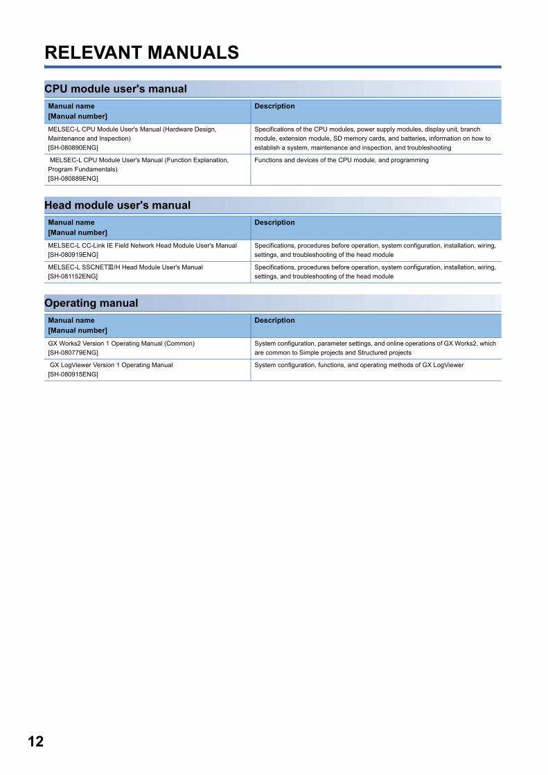
RELEVANT MANUALS
CPU module user's manual
Head module user's manual
Operating manual
Manual name[Manual number]
Description
MELSEC-L CPU Module User's Manual (Hardware Design, Maintenance and Inspection)[SH-080890ENG]
Specifications of the CPU modules, power supply modules, display unit, branch module, extension module, SD memory cards, and batteries, information on how to establish a system, maintenance and inspection, and troubleshooting
MELSEC-L CPU Module User's Manual (Function Explanation, Program Fundamentals)[SH-080889ENG]
Functions and devices of the CPU module, and programming
Manual name[Manual number]
Description
MELSEC-L CC-Link IE Field Network Head Module User's Manual[SH-080919ENG]
Specifications, procedures before operation, system configuration, installation, wiring, settings, and troubleshooting of the head module
MELSEC-L SSCNET/H Head Module User's Manual[SH-081152ENG]
Specifications, procedures before operation, system configuration, installation, wiring, settings, and troubleshooting of the head module
Manual name[Manual number]
Description
GX Works2 Version 1 Operating Manual (Common)[SH-080779ENG]
System configuration, parameter settings, and online operations of GX Works2, which are common to Simple projects and Structured projects
GX LogViewer Version 1 Operating Manual[SH-080915ENG]
System configuration, functions, and operating methods of GX LogViewer
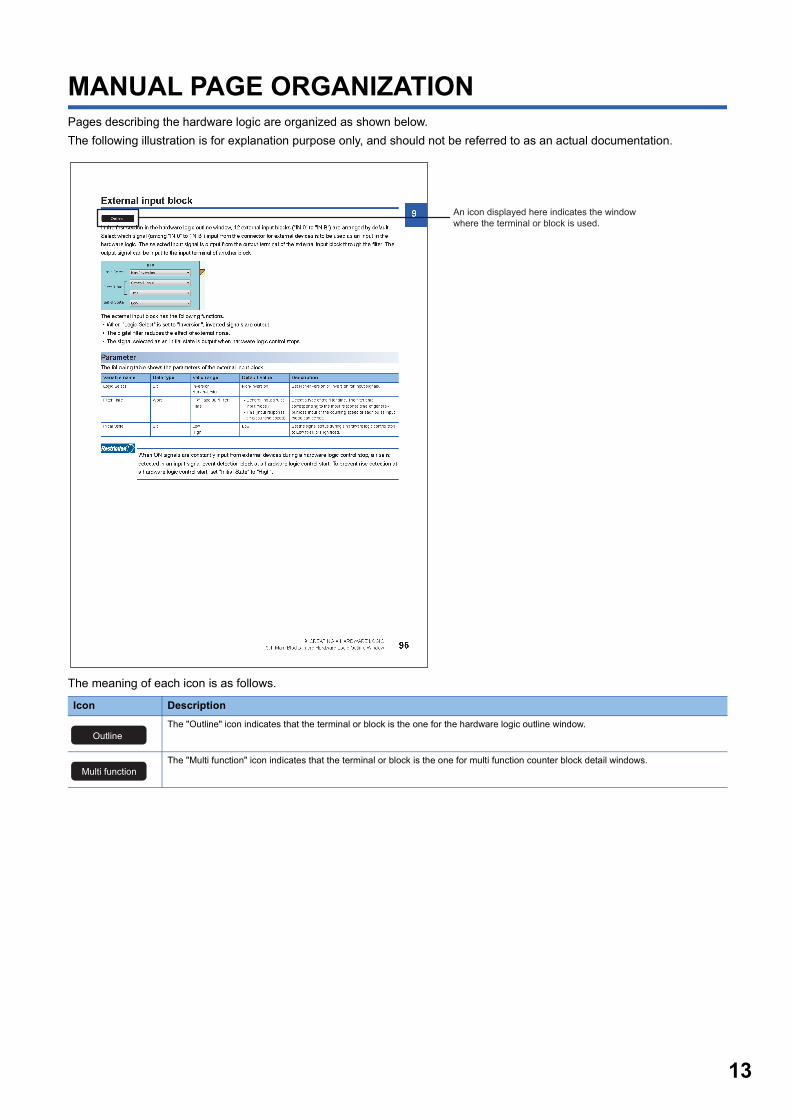
MANUAL PAGE ORGANIZATIONPages describing the hardware logic are organized as shown below.The following illustration is for explanation purpose only, and should not be referred to as an actual documentation.
The meaning of each icon is as follows.
Icon DescriptionThe "Outline" icon indicates that the terminal or block is the one for the hardware logic outline window.
The "Multi function" icon indicates that the terminal or block is the one for multi function counter block detail windows.
An icon displayed here indicates the window where the terminal or block is used.
Outline
Multi function
13

14
TERMSUnless otherwise specified, this manual uses the following terms.
PACKING LISTThe following items are included in the package of this product. Before use, check that all the items are included.
Term DescriptionBuffer memory A memory in an intelligent function module, where data (such as setting values and monitoring values) exchanged with
a CPU module are stored
Configuration tool An abbreviation for the configuration tool for flexible high-speed I/O control modules (SW1DNN-FLEXIOP-E)
Display unit A liquid LCD to be attached to the CPU module
Execution memory The memory in a flexible high-speed I/O control module where the hardware logic is written
External wiring Wiring between a flexible high-speed I/O control module and external devices
Flash ROM A non-volatile memory to which the hardware logic can be written. Although the number of writes to a flash ROM is limited, the written hardware logic is not deleted even after the power off and automatically read at the power-on.
Flexible high-speed I/O control module
An abbreviation for the MELSEC-L series flexible high-speed I/O control module LD40PD01
GX LogViewer The software for visually displaying execution results of the simulation function
GX Works2 The product name of the software package for the MELSEC programmable controllers
Hardware logic A control logic that users create graphically combining inputs, outputs, logical operation circuits, and counters with the configuration tool
Head module An abbreviation for the LJ72GF15-T2 CC-Link IE Field Network head module
Link To connect blocks or terminals on the configuration tool
Programming tool Another name for GX Works2
Flexible high-speed I/O control module
Module Before Using the Product

1
1 FLEXIBLE HIGH-SPEED I/O CONTROLMODULEFor the flexible high-speed I/O control module, users can easily create a high-speed, complicated hardware logic independent from the CPU module by graphically combining input/outputs, logical operation circuits, and counters with the configuration tool.
1.1 FeaturesControls that have been performed using a microcomputer board or an FPGA board or combining several modules can be performed only with the flexible high-speed I/O control module. • High-speed, high-response control with s orders • Controls with stable response time • Logic controls that requires rapidity • Measurement control with sensor inputs • Controls triggered by external inputs
By using this module instead of a microcomputer board or an FPGA board, which cannot be supplied steadily and constantly due to their high introduction cost and design cost, users can configure a system only with a programmable controller, reducing man-hours and the total system cost.
+ +
Microcomputer boardFPGA board Flexible high-speed I/O control module
Input module
Output module
Counter module
1 FLEXIBLE HIGH-SPEED I/O CONTROL MODULE1.1 Features 15

16
High-speed, stable I/O responseBecause the hardware logic inside the module performs controls without relying on the operation processing time and the bus transmission time of the CPU module, high-speed, stable I/O responses can be performed. As a result, variations of outputs to inputs can be reduced.
Flexible controlsI/O signals can be flexibly assigned.I/Os can be flexibly controlled with high-accuracy counters and timers.
Flexible high-speed I/O control module
The output variation depending on input can be reduced.
Existing programmable controller
Flexible high-speed I/O control module
High-speed operation processing of hardware
Transmission via bus
CPU module operation
Input
Output
Input
Output
Input
Output
Input
Output
Input 1
Input 2
Input 3
Input 4
Input 5
Output 1
Output 2
Output 3
Output 4
Output 5
Control 1
Control 2
Distribution
Wired OR
UP/DOWN
[↑] PRESET
[↓] LATCH
RUN
STOP
CLK 10MHz
SET
RESET
Encoder
Sensor
Counter NG output
Interrupt
CounterTrigger Output
Trigger
Output
OFF time
ON time
Sensor
NG output
Check value
"> Check value" "= ON time"
"= OFF time"
One-shot pulse output controlLength measurement monitor
1 FLEXIBLE HIGH-SPEED I/O CONTROL MODULE1.1 Features

1
Easy designing - select and connectUser can easily create a hardware logic with intuitive actions of "selecting" and "connecting".Simulation functionThe operation of a created hardware logic can be checked using simulation data instead of external input signals.
100ns1us10us100us1ms
Selecting DebuggingSetting parametersConnecting
Simulation data Execute the simulation with the module. Check the result with GX LogViewer.
Step unit time
Ste
p
Input 1Input 1Input 1 Input 2Input 2Input 2 Input 3Input 3Input 3 • • •
1 FLEXIBLE HIGH-SPEED I/O CONTROL MODULE1.1 Features 17

18
Filter for eliminating noiseA filter for reducing external noise has been implemented for external inputs. This filter eliminates chattering of input pulses.
Delay adjustment of output timingThe delay adjustment function has been implemented for external outputs. The delay adjustment function adjusts the output timing.
Interrupt functionWhen a signal that triggers an interrupt is detected, the flexible high-speed I/O control module will send an interrupt request to the CPU module.The flexible high-speed I/O control module enables a flexible, high-speed interrupt control with this function.
The timing variation due to electronic components can be adjusted.
Output A
Output B
Output C
Output D
Variation in output timing
Without delay adjustment
No variation
With delay adjustment
1 FLEXIBLE HIGH-SPEED I/O CONTROL MODULE1.1 Features
1
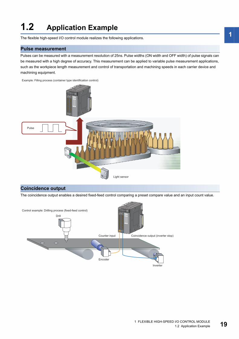
1.2 Application ExampleThe flexible high-speed I/O control module realizes the following applications.Pulse measurementPulses can be measured with a measurement resolution of 25ns. Pulse widths (ON width and OFF width) of pulse signals can be measured with a high degree of accuracy. This measurement can be applied to variable pulse measurement applications, such as the workpiece length measurement and control of transportation and machining speeds in each carrier device and machining equipment.
Coincidence outputThe coincidence output enables a desired fixed-feed control comparing a preset compare value and an input count value.
Light sensor
Pulse
Example: Filling process (container type identification control)
Encoder
Drill
Coincidence output (inverter stop)
Control example: Drilling process (fixed-feed control)
Inverter
Counter input
1 FLEXIBLE HIGH-SPEED I/O CONTROL MODULE1.2 Application Example 19

20
Cam switch outputAccording to an input count current value, outputs can be turned on or off at preset points without a program. ON/OFF controls can be performed with greater accuracy without being affected by scan time.
PWM outputPWM of 2MHz at a maximum can be output. The duty ratio can be changed in increments of 25ns, enabling a smooth output control. With PWM outputs, a dimming control with duty ratio changes can be performed.
ON
OFF
ON
OFF
ON
OFF
1000 2000 3000 4000 5000 6000 7000 8000
Output 1
Output 2
Output 3
Present count value
OFF
ON
Dim
Bright
Power for the lighting
LED light
PWM signal
PWM output ON time
PWM output cycle time
PWM output ON time Illuminance
Short
Long
LED light control with a PWM signal
Inverter circuit
1 FLEXIBLE HIGH-SPEED I/O CONTROL MODULE1.2 Application Example

2
2 PART NAMESThis chapter lists the part names of the flexible high-speed I/O control module.
*1 For differential output terminals, the LED indicates the ON/OFF status of each differential output+ signal.
No. Name Description(1) Module joint lever A lever for connecting two modules
(2) RUN LED This LED indicates the operating status.On: Normal operationFlashing: During simulationOff: When 5V power off or a watchdog timer error has occurred
(3) ERR. LED This LED indicates the error status.On: An error has occurred.Off: Normal operation
(4) Indicator LED This LED indicates the I/O status of external I/O terminals.
LED0(Upper section)
This LED indicates the input status of each external input terminal.• On: A voltage has been applied.• Off: No voltage has been applied.
0 to B indicate external input terminals (IN 0 to IN B).
LED1(Lower section)
This LED indicates the output status of each external output terminal.*1
• On: A signal output is on.• Off: A signal output is off.
0 to D indicate the following external output terminals.• 0 to 7: OUT 0 to OUT 7• 8 to D: OUT 0_DIF to OUT 5_DIF
(5) Connector for external devices (40 pins) A connector used to connect encoders and control devices. For the terminal layout, refer to the following.Page 43 Interface with external devices
(6) DIN rail hook A hook used to mount the module to a DIN rail
(7) Serial number marking Displays the serial number printed on the rating plate.
(1)
(2)
(4) (1)
(7) (1)
(5)
(6)
(3)
2 PART NAMES 21

22
MEMO
2 PART NAMES

3
3 SPECIFICATIONSThis chapter describes general specifications, performance specifications, functions, I/O signals, and buffer memory areas.
3.1 General SpecificationsFor the general specifications of the flexible high-speed I/O control module, refer to the following. Safety Guidelines, provided with the CPU module or head module
3 SPECIFICATIONS3.1 General Specifications 23

24
3.2 Performance SpecificationsThe following table lists the performance specifications of the flexible high-speed I/O control module.
Item Specifications
Differential DCNumber of input points 12 points (common for 5VDC/24VDC/differential)
Number of output points 6 points 8 points (5 to 24VDC, 0.1A/point)
Number of interrupts 8 points
Input response time 1s or less
Output response time 1s or less
Pulse input speed Max. 8Mpps (2MHz) Max. 200kpps (200kHz)
Pulse output speed Max. 8Mpps (2MHz) Max. 200kpps (200kHz)
Main block*1 External input block
Logic Select Inverted, not inverted
Filter Time General-purpose input:
0s, 10s, 50s, 0.1ms, 0.2ms, 0.4ms, 0.6ms, 1ms, 5ms
Pulse input: 10kpps, 100kpps, 200kpps, 500kpps, 1000kpps, 2000kpps, 4000kpps, 8000kpps
Initial State Low, High
Y device terminal Outputs the ON/OFF states of General command 0 to General command F (Y10 to Y1F) as signals.
OUT terminal Outputs the same signal as the one to be output from the external output block.
Parallel encoder block
Input Data Type Pure binary, Gray code, BCD
Data Length 1 bit to 12 bits
SSI encoder block
Input Data Type Pure binary, Gray code
Data Length 1 bit to 32 bits
Multi function counter block
Terminal Input terminal, latch input terminal, event input terminal, output terminal, event output terminal, cam switch output terminal, pattern generator output terminal
Input signal event detection block Combination of rise, fall, Low, and High
Latch event detection block Rise, fall
Counter timer block
Type Addition, subtraction, linear counter mode, ring counter mode, addition mode, preset counter function, latch counter function, internal clock function
Internal clock 25ns, 50ns, 0.1s, 1s, 10s, 100s, 1ms
Counting range 32-bit signed binary (-2147483648 to 2147483647)32-bit unsigned binary (0 to 4294967295)16-bit signed binary (-32768 to 32767)16-bit unsigned binary (0 to 65535)
Comparison block
Compare Value Same as the counting range
Compare Mode 16-bit counter: =, >, <, , , <>32-bit counter: =, >, <, , , <>
Pattern generator block
Number of output pattern points
8192 points
Cam switch block
Refreshing cycle
0.1s
Number of steps
Up to 16 steps
Set/reset block Uses the signal input to the Set terminal as a trigger to output the High fixed signal.Uses the signal input to the Reset terminal as a trigger to output the Low fixed signal.
Logical operation block
Logical operation type AND, OR, XOR
External output block
Logic Select Inverted, not inverted
Delay Time None, 12.5ns (1 to 64), 25ns (1 to 64), 50ns (1 to 64), 0.1s (1 to 64), 1s (1 to 64), 10s (1 to 64), 100s (1 to 64), 1ms (1 to 64)
Error-time Output Mode OFF, ON, HOLD
SI device terminal Interrupt to a CPU module
3 SPECIFICATIONS3.2 Performance Specifications

3
Main functions that can be performed with the combination of main blocks
Pulse count Count input signal
Phase 1-phase input (1 multiple/2 multiples), 2-phase input (1 multiple/2 multiples/4 multiples), CW/CCW
Counting speed
1 multiple 10kpps/100kpps/200kpps/ 500kpps/1Mpps/2Mpps
10kpps/100kpps/200kpps
2 multiples 10kpps/100kpps/200kpps/500kpps/1Mpps/2Mpps/4Mpps
4 multiples 10kpps/100kpps/200kpps/500kpps/1Mpps/2Mpps/4Mpps/8Mpps
Counting range Same as the counter timer block
Type Addition, subtraction, linear counter mode, ring counter mode, addition mode, preset counter function, latch counter function
Minimum count pulse width (duty ratio: 50%)
1-phase input (1 multiple/2 multiples), CW/CCW
1-phase input (1 multiple/2 multiples), CW/CCW
2-phase input (1 multiple/2 multiples/4 multiples)
2-phase input (1 multiple/2 multiples/4 multiples)
Coincidence detection
Comparison range 32-bit signed binary value, 32-bit unsigned binary value, 16-bit signed binary value, 16-bit unsigned binary value
Comparison method Setting value < count value, setting value = count value, setting value > count value
Interrupt Coincidence detection interrupt function
Cam switch Number of steps Up to 16 steps/1 block
Highly-accurate pulse output The ON/OFF timing can be adjusted in increments of 25ns at a minimum using trigger input as the starting point.
PWM output Output frequency range Max. 2MHz Max. 200kHz
Duty ratio The cycle time and ON time can be set in increments of 25ns at a minimum.
Ratio setting Ratio setting range Number of output pulses = (1 to 2147483647)/(1 to 2147483647) Number of input pulsesNote that a value obtained by dividing (1 to 2147483647) by (1 to 2147483647) should not exceed 1.
Pulse measurement
Measurement item Pulse width (ON width, OFF width, from a rising edge to the next rising edge, from a falling edge to the next falling edge)
Measurement resolution 25ns
Electrical interface conversion 24VDC/5VDC/differential
Processing time of the main hardware logic Logical operation: Min. 87.5ns, Coincidence output: Min. 137.5ns, Cam switch: Min. 262.5ns
Number of writes to a flash ROM Up to 10000 times
Internal current consumption (5VDC) 0.66A
Applicable wire size 40-pin connector 0.088 to 0.3 (28 to 22 AWG) (When the A6CON1 or A6CON4 is used)0.088 to 0.24 (28 to 24 AWG) (When the A6CON2 is used)
External wiring connector (sold separately) A6CON1, A6CON2, A6CON4
Number of occupied I/O points 32 points (I/O assignment: Intelligent, 32 points)
Item Specifications
Differential DC
0.5μs
0.25μs 0.25μs
5μs
2.5μs 2.5μs
0.125μs
0.5μs
0.25μs 0.25μs
5μs
20μs
10μs 10μs
3 SPECIFICATIONS3.2 Performance Specifications 25

26
*1 The basic blocks supplied by the configuration tool
Number of occupied modules 2
External dimensions Height 90mm
Width 45mm
Depth 95mm
Weight 0.18kg
Item Specifications
Differential DC
3 SPECIFICATIONS3.2 Performance Specifications

3
Number of parameter settingsSet the parameters of the auto refresh setting for the flexible high-speed I/O control module so that the number of the set parameters including the number of the parameters for other intelligent function modules will not exceed the maximum number of parameters that can be set for the CPU module.For the maximum number of parameters that can be set for the CPU module (maximum number of parameter settings), refer to the following. MELSEC-L CPU Module User's Manual (Hardware Design, Maintenance and Inspection) MELSEC-L CC-Link IE Field Network Head Module User's Manual
Number of parameters for the flexible high-speed I/O control moduleThe following table lists the number of parameters that can be set per flexible high-speed I/O control module.
Check methodThe number of parameter settings that are set for the intelligent function module and the maximum number of parameter settings can be checked with the following operation.
[Project window] [Intelligent Function Module] Right-click [Intelligent Function Module Parameter List]
Target module Initial setting Auto refresh settingLD40PD01 0 2 (maximum number of settings)
No. Description1) Total number of initial setting parameters selected in the window
2) Maximum number of initial setting parameter settings
3) Total number of auto refresh setting parameters selected in the window
4) Maximum number of auto refresh setting parameter settings
1) 2) 3) 4)
3 SPECIFICATIONS3.2 Performance Specifications 27

28
3.3 Function ListThe following table lists the functions of the flexible high-speed I/O control module.
Item Description ReferenceHardware logic control function Users can create the hardware logic to perform a desired control with the configuration
tool.Page 139 CREATING A HARDWARE LOGIC
Continuous logging function This function collects the status of the Output terminal of the external input blocks (IN 0 to IN B) continuously at a specified interval.
Page 59 Continuous Logging Function
Error history function The errors that occurred in the flexible high-speed I/O control module are stored in the buffer memory as error history.Up to 16 errors can be stored.
Page 68 Error History Function
Module error collection function The errors that occurred in the flexible high-speed I/O control module are collected in the CPU module.
Page 71 Module Error Collection Function
Error clear function When an error has occurred, the error can be cleared from the system monitor. Page 72 Error Clear Function
3 SPECIFICATIONS3.3 Function List

3
3.4 List of I/O SignalsThe following table lists the I/O signals of the flexible high-speed I/O control module to the CPU module.For details on the I/O signals, refer to the following.Page 279 Details of I/O Signals
• The I/O numbers (X/Y) listed above are shown on the assumption that the start I/O number of the flexible high-speed I/O control module is set to 0.
• The use prohibited signals listed above are used by the system and are not available for users. If a user uses these signals (turning off and on), the performance of the flexible high-speed I/O control module is not guaranteed.
Input (Signal direction: CPU module Flexible high-speed I/O control module)
Output (Signal direction: CPU module Flexible high-speed I/O control module)
Device No. Signal name Device No. Signal nameX0 Module ready Y0 Use prohibited
X1 Use prohibited Y1 Use prohibited
X2 Use prohibited Y2 Use prohibited
X3 Operating condition settings batch-reset complete flag Y3 Operating condition settings batch-reset command
X4 Hardware logic control flag Y4 Hardware logic control start request
X5 Use prohibited Y5 Hardware logic control stop request
X6 Use prohibited Y6 Hardware logic control stop signal at disconnection
X7 Hardware logic control stop flag at disconnection Y7 Hardware logic control stop flag clear request at disconnection
X8 Use prohibited Y8 Use prohibited
X9 Use prohibited Y9 Use prohibited
XA Use prohibited YA Use prohibited
XB Use prohibited YB Use prohibited
XC Use prohibited YC Use prohibited
XD Use prohibited YD Use prohibited
XE Use prohibited YE Use prohibited
XF Error flag YF Error clear request
X10 IN 0 Y10 General command 0
X11 IN 1 Y11 General command 1
X12 IN 2 Y12 General command 2
X13 IN 3 Y13 General command 3
X14 IN 4 Y14 General command 4
X15 IN 5 Y15 General command 5
X16 IN 6 Y16 General command 6
X17 IN 7 Y17 General command 7
X18 IN 8 Y18 General command 8
X19 IN 9 Y19 General command 9
X1A IN A Y1A General command A
X1B IN B Y1B General command B
X1C Use prohibited Y1C General command C
X1D Use prohibited Y1D General command D
X1E Use prohibited Y1E General command E
X1F Use prohibited Y1F General command F
3 SPECIFICATIONS3.4 List of I/O Signals 29

30
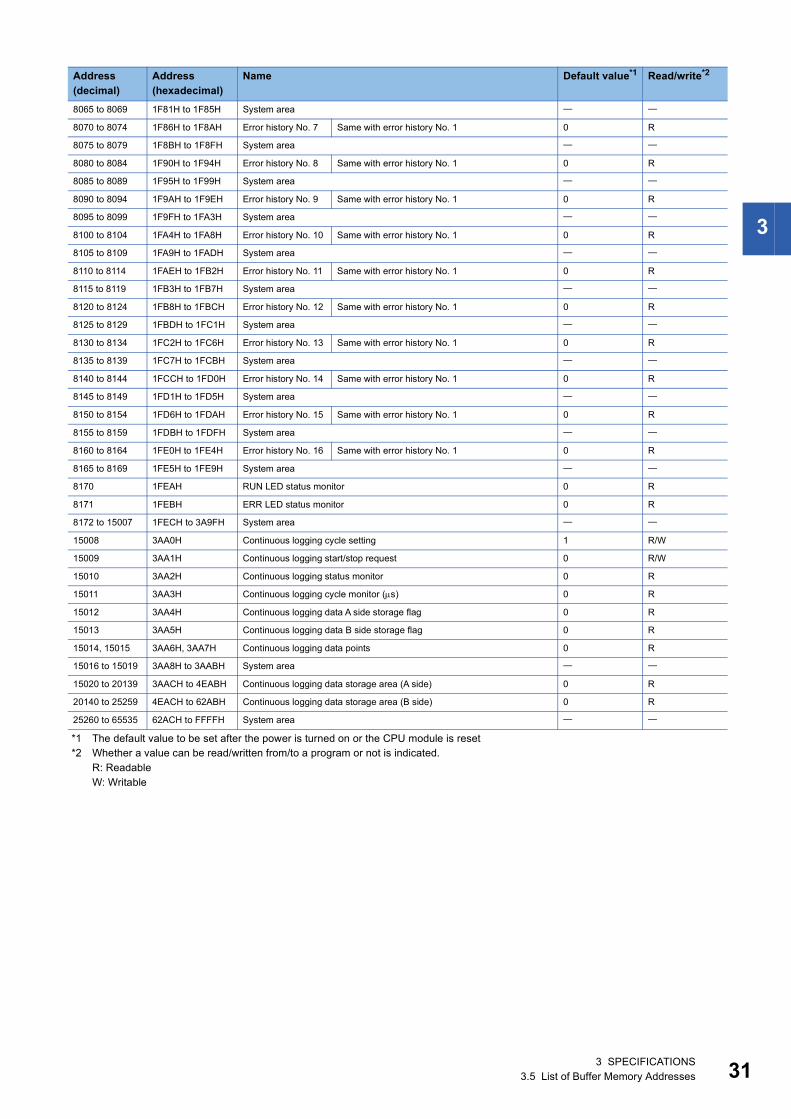
3.5 List of Buffer Memory AddressesThe following table lists the buffer memory addresses of the flexible high-speed I/O control module.For details on the buffer memory areas, refer to the following.Page 286 Details of Buffer Memory Areas
Do not write any data to the system area and write-protect area of the buffer memory. If data is written to these areas, a malfunction may occur.
Address(decimal)
Address(hexadecimal)
Name Default value*1 Read/write*2
0 to 99 0H to 63H System area
100 64H Latest error code 0 R
101 65H System area
102 66H Cumulative number of write accesses to a flash ROM 0 R
103 67H
104 to 109 68H to 6DH System area
110, 111 6EH, 6FH SSI receive data monitor 0 0 R
112, 113 70H, 71H System area
114, 115 72H, 73H SSI receive data monitor 1 0 R
116 to 119 74H to 77H System area
120 78H Trigger start request 0 R/W
121 79H Trigger stop request 0 R/W
122 7AH Trigger setting status monitor 0 R
123 7BH Trigger status monitor 0 R
124 7CH Sampling data acquired flag 0 R
125 to 127 7DH to 7FH System area
128, 129 80H, 81H Cumulative number of trigger setting writes 0 R
130 to 999 82H to 3E7H System area
1000 to 1029 3E8H to 405H Hardware logic area (High speed area) 0 R/W
1030 to 1099 406H to 44BH Hardware logic area (Low speed area) 0 R/W
1100 to 7999 44CH to 1F3FH System area
8000 1F40H Latest address of error history 0 R
8001 1F41H System area
8002 1F42H Clear setting of error history 0 R/W
8003 to 8009 1F43H to 1F49H System area
8010 1F4AH Error history No. 1 Error code 0 R
8011 1F4BH Error time First two digits of the year
Last two digits of the year
8012 1F4CH Month Day
8013 1F4DH Hour Minute
8014 1F4EH Second Day of the week
8015 to 8019 1F4FH to 1F53H System area
8020 to 8024 1F54H to 1F58H Error history No. 2 Same with error history No. 1 0 R
8025 to 8029 1F59H to 1F5DH System area
8030 to 8034 1F5EH to 1F62H Error history No. 3 Same with error history No. 1 0 R
8035 to 8039 1F63H to 1F67H System area
8040 to 8044 1F68H to 1F6CH Error history No. 4 Same with error history No. 1 0 R
8045 to 8049 1F6DH to 1F71H System area
8050 to 8054 1F72H to 1F76H Error history No. 5 Same with error history No. 1 0 R
8055 to 8059 1F77H to 1F7BH System area
8060 to 8064 1F7CH to 1F80H Error history No. 6 Same with error history No. 1 0 R
3 SPECIFICATIONS3.5 List of Buffer Memory Addresses
3
*1 The default value to be set after the power is turned on or the CPU module is reset*2 Whether a value can be read/written from/to a program or not is indicated.
R: ReadableW: Writable
8065 to 8069 1F81H to 1F85H System area
8070 to 8074 1F86H to 1F8AH Error history No. 7 Same with error history No. 1 0 R
8075 to 8079 1F8BH to 1F8FH System area
8080 to 8084 1F90H to 1F94H Error history No. 8 Same with error history No. 1 0 R
8085 to 8089 1F95H to 1F99H System area
8090 to 8094 1F9AH to 1F9EH Error history No. 9 Same with error history No. 1 0 R
8095 to 8099 1F9FH to 1FA3H System area
8100 to 8104 1FA4H to 1FA8H Error history No. 10 Same with error history No. 1 0 R
8105 to 8109 1FA9H to 1FADH System area
8110 to 8114 1FAEH to 1FB2H Error history No. 11 Same with error history No. 1 0 R
8115 to 8119 1FB3H to 1FB7H System area
8120 to 8124 1FB8H to 1FBCH Error history No. 12 Same with error history No. 1 0 R
8125 to 8129 1FBDH to 1FC1H System area
8130 to 8134 1FC2H to 1FC6H Error history No. 13 Same with error history No. 1 0 R
8135 to 8139 1FC7H to 1FCBH System area
8140 to 8144 1FCCH to 1FD0H Error history No. 14 Same with error history No. 1 0 R
8145 to 8149 1FD1H to 1FD5H System area
8150 to 8154 1FD6H to 1FDAH Error history No. 15 Same with error history No. 1 0 R
8155 to 8159 1FDBH to 1FDFH System area
8160 to 8164 1FE0H to 1FE4H Error history No. 16 Same with error history No. 1 0 R
8165 to 8169 1FE5H to 1FE9H System area
8170 1FEAH RUN LED status monitor 0 R
8171 1FEBH ERR LED status monitor 0 R
8172 to 15007 1FECH to 3A9FH System area
15008 3AA0H Continuous logging cycle setting 1 R/W
15009 3AA1H Continuous logging start/stop request 0 R/W
15010 3AA2H Continuous logging status monitor 0 R
15011 3AA3H Continuous logging cycle monitor (s) 0 R
15012 3AA4H Continuous logging data A side storage flag 0 R
15013 3AA5H Continuous logging data B side storage flag 0 R
15014, 15015 3AA6H, 3AA7H Continuous logging data points 0 R
15016 to 15019 3AA8H to 3AABH System area
15020 to 20139 3AACH to 4EABH Continuous logging data storage area (A side) 0 R
20140 to 25259 4EACH to 62ABH Continuous logging data storage area (B side) 0 R
25260 to 65535 62ACH to FFFFH System area
Address(decimal)
Address(hexadecimal)
Name Default value*1 Read/write*2
3 SPECIFICATIONS3.5 List of Buffer Memory Addresses 31
32
4 PROCEDURES BEFORE OPERATIONThis chapter describes the procedures before operation.
1. Installing the moduleInstall the flexible high-speed I/O control module with a desired configuration.Page 34 Overall Configuration
2. External wiringWire external devices to the flexible high-speed I/O control module.Page 37 External Wiring
3. Creating a hardware logicCreate a hardware logic with the configuration tool.Page 73 FUNCTIONS OF THE CONFIGURATION TOOL
4. Programming and debuggingCreate and check a program.Page 247 PROGRAMMING
4 PROCEDURES BEFORE OPERATION

4
MEMO
4 PROCEDURES BEFORE OPERATION 33
34
5 SYSTEM CONFIGURATIONThis chapter describes the overall system configuration, number of connectable modules, and compatible software versions of the flexible high-speed I/O control module.
5.1 Overall ConfigurationThe following figure shows a system configuration example of when the flexible high-speed I/O control module is used.
When connected to the CPU module
When connected to the head module
Power supplymodule CPU module
Display unit(optional)
I/O moduleorintelligent function module
ENDcover
Flexible high-speed I/O control module
Power supply module Head module
I/O module or intelligent function module END cover
Flexible high-speedI/O control module
5 SYSTEM CONFIGURATION5.1 Overall Configuration

5
5.2 Applicable System
Number of connectable modulesFor the number of connectable modules, refer to the following. MELSEC-L CPU Module User's Manual (Hardware Design, Maintenance and Inspection) MELSEC-L CC-Link IE Field Network Head Module User's Manual
Compatible software versionThe following table lists compatible software versions.
5.3 Restrictions When the Flexible High-Speed I/O Control Module Is Connected to the Head Module
This section describes the restrictions when the flexible high-speed I/O control module is connected to the head module. • The intelligent function module interrupt cannot be used.
Software VersionGX Works2 Version 1.535H or later
GX LogViewer Version 1.46Y or later
Configuration tool Version 1.000A or later
5 SYSTEM CONFIGURATION5.2 Applicable System 35

36
6 INSTALLATION AND EXTERNAL WIRINGThis chapter describes the installation and external wiring of the flexible high-speed I/O control module.
6.1 Installation Environment and Installation PositionFor precautions for the installation environment and installation position, refer to the following. MELSEC-L CPU Module User's Manual (Hardware Design, Maintenance and Inspection) MELSEC-L CC-Link IE Field Network Head Module User's Manual
6 INSTALLATION AND EXTERNAL WIRING6.1 Installation Environment and Installation Position

6
6.2 External WiringThis section describes wiring of encoders and controllers to the flexible high-speed I/O control module.
External wiring precautionsTo obtain the maximum performance from the functions of the flexible high-speed I/O control module and improve the system reliability, an external wiring with high durability against noise is required.This section describes the precautions for wiring of encoders and controllers.
Wiring • Different terminals are prepared depending on the voltage of the signal to be input. Connecting to a terminal with an
incorrect voltage may cause a malfunction of the module or failure of the connected devices. • In 1-phase pulse input, always connect a pulse input cable on the phase A side. • Install a fuse for each external terminal to prevent the external devices or module from being burnt out or damaged if a load
shorts in an output circuit. The following fuses have been tested by Mitsubishi.
Connector for external devices • Connectors for external devices must be soldered or crimped properly. A poor soldering or crimping may result in a
malfunction. • Securely connect the connectors for external devices to the connectors of the flexible high-speed I/O control module, and
securely tighten the two screws. • When disconnecting a cable from the flexible high-speed I/O control module, do not pull the cable holding the cable part.
Remove a cable supporting the connector part of the cable by hand. Pulling the cable being connected to the flexible high-speed I/O control module can cause a malfunction. In addition, a damage of the flexible high-speed I/O control module or cables can result.
Fuse model name Rated current Contact312.750 0.75A Littelfuse
www.littelfuse.com216.800 0.8A
6 INSTALLATION AND EXTERNAL WIRING6.2 External Wiring 37
38
Measures to reduce noiseThe flexible high-speed I/O control module may malfunction if pulse-like noise is input. Thus, take the following measures to reduce noise: • Always use a shielded twisted pair cable. • Arrange a shielded twisted pair cable keeping a distance of 150mm or more from the power cable, I/O cables, or other
cables that cause much noise. Wire the shielded twisted pair cable in the minimum distance to the extent possible. • Ground a shield wire on the encoder side (relay box). Always ground the FG and LG terminals to the protective ground
conductor. • Do not wire terminals that are not to be used. Doing so may result in malfunction due to noise.
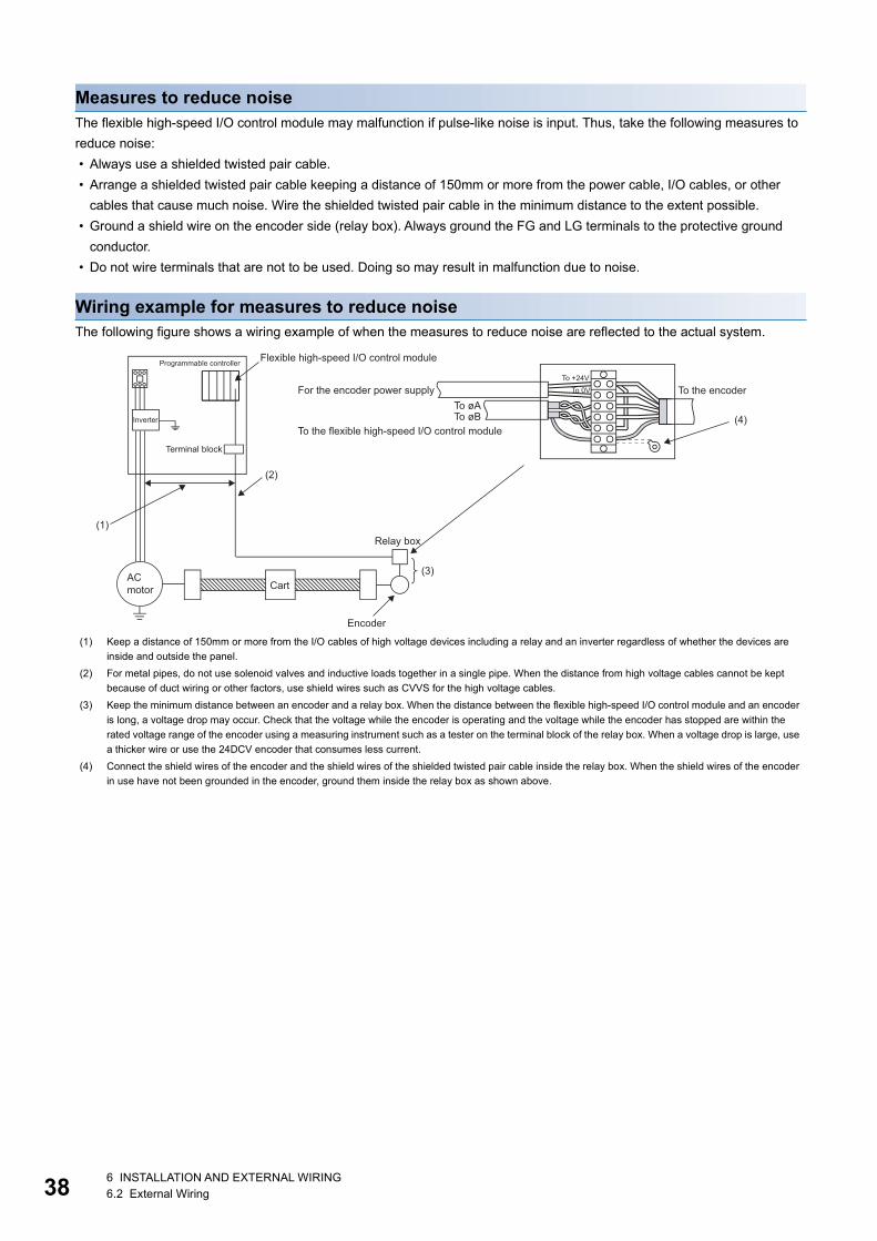
Wiring example for measures to reduce noiseThe following figure shows a wiring example of when the measures to reduce noise are reflected to the actual system.
(1) Keep a distance of 150mm or more from the I/O cables of high voltage devices including a relay and an inverter regardless of whether the devices are inside and outside the panel.
(2) For metal pipes, do not use solenoid valves and inductive loads together in a single pipe. When the distance from high voltage cables cannot be kept because of duct wiring or other factors, use shield wires such as CVVS for the high voltage cables.
(3) Keep the minimum distance between an encoder and a relay box. When the distance between the flexible high-speed I/O control module and an encoder is long, a voltage drop may occur. Check that the voltage while the encoder is operating and the voltage while the encoder has stopped are within the rated voltage range of the encoder using a measuring instrument such as a tester on the terminal block of the relay box. When a voltage drop is large, use a thicker wire or use the 24DCV encoder that consumes less current.
(4) Connect the shield wires of the encoder and the shield wires of the shielded twisted pair cable inside the relay box. When the shield wires of the encoder in use have not been grounded in the encoder, ground them inside the relay box as shown above.
(1)
(2)
(3)
(4)
Terminal block
AC motor
Relay box
Cart
Encoder
Inverter
Flexible high-speed I/O control moduleProgrammable controller
To øATo øB
To the flexible high-speed I/O control module
For the encoder power supplyTo +24V
To 0V To the encoder
6 INSTALLATION AND EXTERNAL WIRING6.2 External Wiring

6
Compliance with the EMC and Low Voltage DirectivesTake the following measures for compliance with the EMC and Low Voltage Directives. • Always attach a ferrite core on the DC power supply cable to be connected to the flexible high-speed I/O control module
and the one to be connected to a controller. Using the ESD-SR-250 ferrite core manufactured by NEC TOKIN Corporation is recommended.
• Install a DC power and the module in the same control panel. • Use a shielded cable for the DC power when the DC power supply cable is extended out of the control panel. • The length of the cables to be connected to the output section and external devices must be 2m or shorter for open
collector output or 10m or shorter for differential output. • Keep the length of the cables between the input section and the external devices to 30m or less. • Use a shielded twisted pair cable and ground the shielded part of the cable to the control panel with the AD75CK cable
clamp manufactured by Mitsubishi.
For details on the AD75CK, refer to the following. AD75CK-type Cable Clamping Instruction Manual • Take the following measures to reduce noise when wiring connectors for external devices.
■Wiring to use a shielded cableThe following figure shows a wiring example for measures to reduce noise using the A6CON1.
(1) Shorten the distance between the connector and shielded cable as far as possible.(2) Ground a FG cable of 2 or thicker in the minimum distance. Securely ground the cable in the control panel on the module side.(3) Shielded cables
AD75CK
Flexiblehigh-speed I/Ocontrol m
odule
20 to 30cm
Inside of control panel
A6CON1
(3)
(2)
(1)
6 INSTALLATION AND EXTERNAL WIRING6.2 External Wiring 39
40
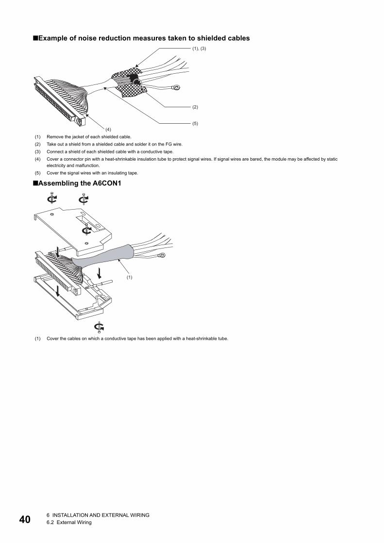
■Example of noise reduction measures taken to shielded cables
■Assembling the A6CON1
(1) Remove the jacket of each shielded cable.(2) Take out a shield from a shielded cable and solder it on the FG wire.(3) Connect a shield of each shielded cable with a conductive tape.(4) Cover a connector pin with a heat-shrinkable insulation tube to protect signal wires. If signal wires are bared, the module may be affected by static
electricity and malfunction.(5) Cover the signal wires with an insulating tape.
(1) Cover the cables on which a conductive tape has been applied with a heat-shrinkable tube.
(5)(4)
(2)
(1), (3)
(1)
6 INSTALLATION AND EXTERNAL WIRING6.2 External Wiring

6
Connector for external devices
Precautions • Tighten the connector screws within the specified tightening torque range.
• Use copper wires having temperature rating of 75 or more for the connectors. • Use UL listed connectors if necessary for UL compliance.
Applicable connectorsPrepare connectors for external devices to be used with the flexible high-speed I/O control module by users.The following table lists the applicable connectors, and the reference product of a crimping tool.
■40-pin connector
*1 When using 40 connectors, use wires whose sheath outside diameter is 1.3mm or less.Select the wire applicable to the current value to be used.
The A6CON3 (IDC type connector (Straight type)) cannot be used.
■40-pin connector crimping tool
For how to wire connectors and how to use the crimping tool, contact FUJITSU COMPONENT LIMITED.
Wiring methodFor the wiring method, refer to the following. MELSEC-L CPU Module User's Manual (Hardware Design, Maintenance and Inspection)
Screw Tightening torque rangeConnector screw (M2.6) 0.20 to 0.29Nm
Type Model Applicable wire sizeSoldering type connector (Straight type) A6CON1*1 0.088 to 0.3mm2 (28 to 22 AWG) (Stranded wire)
Crimping type connector (Straight type) A6CON2 0.088 to 0.24mm2 (28 to 24 AWG) (Stranded wire)
Soldering type connector (Dual purpose (straight/oblique) type) A6CON4*1 0.088 to 0.3mm2 (28 to 22 AWG) (Stranded wire)
Type Model ContactCrimping tool FCN-363T-T005/H FUJITSU COMPONENT LIMITED
www.fcl.fujitsu.com/en
6 INSTALLATION AND EXTERNAL WIRING6.2 External Wiring 41
42
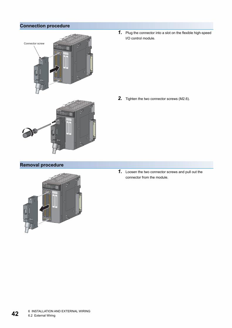
Connection procedure
Removal procedure
1. Plug the connector into a slot on the flexible high-speed I/O control module.
2. Tighten the two connector screws (M2.6).
1. Loosen the two connector screws and pull out the connector from the module.
Connector screw
6 INSTALLATION AND EXTERNAL WIRING6.2 External Wiring
6
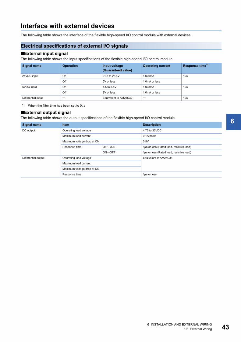
Interface with external devicesThe following table shows the interface of the flexible high-speed I/O control module with external devices.
Electrical specifications of external I/O signals■External input signalThe following table shows the input specifications of the flexible high-speed I/O control module.
*1 When the filter time has been set to 0s
■External output signalThe following table shows the output specifications of the flexible high-speed I/O control module.
Signal name Operation Input voltage (Guaranteed value)
Operating current Response time*1
24VDC input On 21.6 to 26.4V 4 to 6mA 1s
Off 5V or less 1.0mA or less
5VDC input On 4.5 to 5.5V 4 to 8mA 1s
Off 2V or less 1.0mA or less
Differential input Equivalent to AM26C32 1s
Signal name Item DescriptionDC output Operating load voltage 4.75 to 30VDC
Maximum load current 0.1A/point
Maximum voltage drop at ON 0.5V
Response time OFFON 1s or less (Rated load, resistive load)
ONOFF 1s or less (Rated load, resistive load)
Differential output Operating load voltage Equivalent to AM26C31
Maximum load current
Maximum voltage drop at ON
Response time 1s or less
6 INSTALLATION AND EXTERNAL WIRING6.2 External Wiring 43
44
Signal layout of a connector for external devicesThe following shows the signal layout of a connector for external devices of the flexible high-speed I/O control module.
Pin No. CON1 CON2
B A B A20 NC NC NC NC
19 IN 0_24V IN 0_5V IN 6_24V IN 6_5V
18 IN 0_DIF IN 0_COM IN 6_DIF IN 6_COM
17 IN 1_24V IN 1_5V IN 7_24V IN 7_5V
16 IN 1_DIF IN 1_COM IN 7_DIF IN 7_COM
15 IN 2_24V IN 2_5V IN 8_24V IN 8_5V
14 IN 2_DIF IN 2_COM IN 8_DIF IN 8_COM
13 IN 3_24V IN 3_5V IN 9_24V IN 9_5V
12 IN 3_DIF IN 3_COM IN 9_DIF IN 9_COM
11 IN 4_24V IN 4_5V IN A_24V IN A_5V
10 IN 4_DIF IN 4_COM IN A_DIF IN A_COM
9 IN 5_24V IN 5_5V IN B_24V IN B_5V
8 IN 5_DIF IN 5_COM IN B_DIF IN B_COM
7 OUT 0 OUT 1 OUT 4 OUT 5
6 OUT 2 OUT 3 OUT 6 OUT 7
5 OUT 0-3_COM OUT_DIF_GND OUT 4-7_COM OUT_DIF_GND
4 OUT 0_DIF+ OUT 0_DIF- OUT 3_DIF+ OUT 3_DIF-
3 OUT 1_DIF+ OUT 1_DIF- OUT 4_DIF+ OUT 4_DIF-
2 OUT 2_DIF+ OUT 2_DIF- OUT 5_DIF+ OUT 5_DIF-
1 NC NC NC NC
B20
CON1/CON2
B19B18B17B16B15B14B13B12B11B10B09B08B07B06B05B04B03B02B01
A20A19A18A17A16A15A14A13A12A11A10A09A08A07A06A05A04A03A02A01
6 INSTALLATION AND EXTERNAL WIRING6.2 External Wiring

6
■List of input signalsThe following table lists the input signals of the flexible high-speed I/O control module.
Pin No. CON1 CON2 Description
Symbol Signal name Symbol Signal nameB20 NC NC NC NC Empty pin
A20 NC NC NC NC
B19 IN 0_24V High-speed input 0 24VDC
IN 6_24V High-speed input 6 24VDC
Inputs the + (plus) side. (common for 5VDC/24VDC/differential)
A19 IN 0_5V High-speed input 0 5VDC
IN 6_5V High-speed input 6 5VDC
B18 IN 0_DIF High-speed input 0 differential
IN 6_DIF High-speed input 6 differential
A18 IN 0_COM High-speed input 0 common
IN 6_COM High-speed input 6 common
Inputs the - (minus) side.
B17 IN 1_24V High-speed input 1 24VDC
IN 7_24V High-speed input 7 24VDC
Inputs the + (plus) side. (common for 5VDC/24VDC/differential)
A17 IN 1_5V High-speed input 1 5VDC
IN 7_5V High-speed input 7 5VDC
B16 IN 1_DIF High-speed input 1 differential
IN 7_DIF High-speed input 7 differential
A16 IN 1_COM High-speed input 1 common
IN 7_COM High-speed input 7 common
Inputs the - (minus) side.
B15 IN 2_24V High-speed input 2 24VDC
IN 8_24V High-speed input 8 24VDC
Inputs the + (plus) side. (common for 5VDC/24VDC/differential)
A15 IN 2_5V High-speed input 2 5VDC
IN 8_5V High-speed input 8 5VDC
B14 IN 2_DIF High-speed input 2 differential
IN 8_DIF High-speed input 8 differential
A14 IN 2_COM High-speed input 2 common
IN 8_COM High-speed input 8 common
Inputs the - (minus) side.
B13 IN 3_24V High-speed input 3 24VDC
IN 9_24V High-speed input 9 24VDC
Inputs the + (plus) side. (common for 5VDC/24VDC/differential)
A13 IN 3_5V High-speed input 3 5VDC
IN 9_5V High-speed input 9 5VDC
B12 IN 3_DIF High-speed input 3 differential
IN 9_DIF High-speed input 9 differential
A12 IN 3_COM High-speed input 3 common
IN 9_COM High-speed input 9 common
Inputs the - (minus) side.
B11 IN 4_24V High-speed input 4 24VDC
IN A_24V High-speed input A 24VDC
Inputs the + (plus) side. (common for 5VDC/24VDC/differential)
A11 IN 4_5V High-speed input 4 5VDC
IN A_5V High-speed input A 5VDC
B10 IN 4_DIF High-speed input 4 differential
IN A_DIF High-speed input A differential
A10 IN 4_COM High-speed input 4 common
IN A_COM High-speed input A common
Inputs the - (minus) side.
B9 IN 5_24V High-speed input 5 24VDC
IN B_24V High-speed input B 24VDC
Inputs the + (plus) side. (common for 5VDC/24VDC/differential)
A9 IN 5_5V High-speed input 5 5VDC
IN B_5V High-speed input B 5VDC
B8 IN 5_DIF High-speed input 5 differential
IN B_DIF High-speed input B differential
A8 IN 5_COM High-speed input 5 common
IN B_COM High-speed input B common
Inputs the - (minus) side.
6 INSTALLATION AND EXTERNAL WIRING6.2 External Wiring 45
46
■List of output signalsThe following table lists the output signals of the flexible high-speed I/O control module.
Pin No. CON1 CON2 Description
Symbol Signal name Symbol Signal nameB7 OUT 0 High-speed output 0 OUT 4 High-speed output 4 5 to 24VDC output
A7 OUT 1 High-speed output 1 OUT 5 High-speed output 5
B6 OUT 2 High-speed output 2 OUT 6 High-speed output 6
A6 OUT 3 High-speed output 3 OUT 7 High-speed output 7
B5 OUT 0-3_COM High-speed output 0-3 common
OUT 4-7_COM High-speed output 4-7 common
High-speed output common
A5 OUT_DIF_GND High-speed output common
OUT_DIF_GND High-speed output common
High-speed output differential ground
B4 OUT 0_DIF+ High-speed output 0 differential+
OUT 3_DIF+ High-speed output 3 differential+
Outputs the differential output + (plus) side.
A4 OUT 0_DIF- High-speed output 0 differential-
OUT 3_DIF- High-speed output 3 differential-
Outputs the differential output - (minus) sides
B3 OUT 1_DIF+ High-speed output 1 differential+
OUT 4_DIF+ High-speed output 4 differential+
Outputs the differential output + (plus) side.
A3 OUT 1_DIF- High-speed output 1 differential-
OUT 4_DIF- High-speed output 4 differential-
Outputs the differential output - (minus) sides
B2 OUT 2_DIF+ High-speed output 2 differential+
OUT 5_DIF+ High-speed output 5 differential+
Outputs the differential output + (plus) side.
A2 OUT 2_DIF- High-speed output 2 differential-
OUT 5_DIF- High-speed output 5 differential-
Outputs the differential output - (minus) sides
B1 NC NC NC NC Empty pin
A1 NC NC NC NC
6 INSTALLATION AND EXTERNAL WIRING6.2 External Wiring
6
Internal circuit of the interface for external devicesThe following table lists the internal circuits of the interface for external devices of the flexible high-speed I/O control module.
I/O classification
Internal circuit Connector Signal name
CON1 CON2 CON1 CON2Input B19 B19 High-speed input 0
24VDCHigh-speed input 6 24VDC
A19 A19 High-speed input 0 5VDC
High-speed input 6 5VDC
B18 B18 High-speed input 0 differential
High-speed input 6 differential
A18 A18 High-speed input 0 common
High-speed input 6 common
B17 B17 High-speed input 1 24VDC
High-speed input 7 24VDC
A17 A17 High-speed input 1 5VDC
High-speed input 7 5VDC
B16 B16 High-speed input 1 differential
High-speed input 7 differential
A16 A16 High-speed input 1 common
High-speed input 7 common
B15 B15 High-speed input 2 24VDC
High-speed input 8 24VDC
A15 A15 High-speed input 2 5VDC
High-speed input 8 5VDC
B14 B14 High-speed input 2 differential
High-speed input 8 differential
A14 A14 High-speed input 2 common
High-speed input 8 common
B13 B13 High-speed input 3 24VDC
High-speed input 9 24VDC
A13 A13 High-speed input 3 5VDC
High-speed input 9 5VDC
B12 B12 High-speed input 3 differential
High-speed input 9 differential
A12 A12 High-speed input 3 common
High-speed input 9 common
B11 B11 High-speed input 4 24VDC
High-speed input A 24VDC
A11 A11 High-speed input 4 5VDC
High-speed input A 5VDC
B10 B10 High-speed input 4 differential
High-speed input A differential
A10 A10 High-speed input 4 common
High-speed input A common
4.1kΩ
IN 0_DIF(B18)IN 6_DIF(B18)
IN 0_5V(A19)IN 6_5V(A19)
IN 0_24V(B19)IN 6_24V(B19)
IN 0_COM(A18)IN 6_COM(A18)
270Ω240Ω820Ω
4.1kΩ
IN 1_DIF(B16)IN 7_DIF(B16)
IN 1_5V(A17)IN 7_5V(A17)
IN 1_24V(B17)IN 7_24V(B17)
IN 1_COM(A16)IN 7_COM(A16)
270Ω240Ω820Ω
4.1kΩ
IN 2_DIF(B14)IN 8_DIF(B14)
IN 2_5V(A15)IN 8_5V(A15)
IN 2_24V(B15)IN 8_24V(B15)
IN 2_COM(A14)IN 8_COM(A14)
270Ω240Ω820Ω
4.1kΩ
IN 3_DIF(B12)IN 9_DIF(B12)
IN 3_5V(A13)IN 9_5V(A13)
IN 3_24V(B13)IN 9_24V(B13)
IN 3_COM(A12)IN 9_COM(A12)
270Ω240Ω820Ω
4.1kΩ
IN 4_DIF(B10)IN A_DIF(B10)
IN 4_5V(A11)IN A_5V(A11)
IN 4_24V(B11)IN A_24V(B11)
IN 4_COM(A10)IN A_COM(A10)
270Ω240Ω820Ω
6 INSTALLATION AND EXTERNAL WIRING6.2 External Wiring 47
48
*1 The high-speed output common (A5) is connected with the common wire of high-speed output 0 to 5 differential.
Input B9 B9 High-speed input 5 24VDC
High-speed input B 24VDC
A9 A9 High-speed input 5 5VDC
High-speed input B 5VDC
B8 B8 High-speed input 5 differential
High-speed input B differential
A8 A8 High-speed input 5 common
High-speed input B common
Output B7 B7 High-speed output 0 High-speed output 4
A7 A7 High-speed output 1 High-speed output 5
B6 B6 High-speed output 2 High-speed output 6
A6 A6 High-speed output 3 High-speed output 7
B5 B5 High-speed output 0-3 common
High-speed output 4-7 common
A5 A5 High-speed output common*1
High-speed output common*1
B4 B4 High-speed output 0 differential+
High-speed output 3 differential+
A4 A4 High-speed output 0 differential-
High-speed output 3 differential-
B3 B3 High-speed output 1 differential+
High-speed output 4 differential+
A3 A3 High-speed output 1 differential-
High-speed output 4 differential-
B2 B2 High-speed output 2 differential+
High-speed output 5 differential+
A2 A2 High-speed output 2 differential-
High-speed output 5 differential-
I/O classification
Internal circuit Connector Signal name
CON1 CON2 CON1 CON2
4.1kΩ
IN 5_DIF(B8)IN B_DIF(B8)
IN 5_5V(A9)IN B_5V(A9)
IN 5_24V(B9)IN B_24V(B9)
IN 5_COM(A8)IN B_COM(A8)
270Ω240Ω820Ω
680Ω
680Ω
680Ω
680Ω
4.7kΩ
4.7kΩ
4.7kΩ
4.7kΩ
OUT 0-3_COM(B5)OUT 4-7_COM(B5)
OUT 3(A6)OUT 7(A6)
OUT 2(B6)OUT 6(B6)
OUT 1(A7)OUT 5(A7)
OUT 0(B7)OUT 4(B7)IO 5V
OUT 0_DIF+(B4)OUT 3_DIF+(B4)
OUT_DIF_GND(A5)*1
IO 5V
OUT 0_DIF-(A4)OUT 3_DIF-(A4)
OUT 1_DIF+(B3)OUT 4_DIF+(B3)
OUT_DIF_GND(A5)*1
OUT 1_DIF-(A3)OUT 4_DIF-(A3)
IO 5V
OUT 2_DIF+(B2)OUT 5_DIF+(B2)
OUT_DIF_GND(A5)*1
IO 5V
OUT 2_DIF-(A2)OUT 5_DIF-(A2)
6 INSTALLATION AND EXTERNAL WIRING6.2 External Wiring

6
■Input signal status in the hardware logic (High/Low)The input signal status (High/Low) in the hardware logic is determined depending on the input signals (ON/OFF) from external devices and logical selection.
*1 Set the logic selection with the parameters of the external input block. For details, refer to the following.Page 142 External input block
*2 The input signal status in the hardware logic is described as High and Low. For details, refer to the following.Page 140 Signal status name
■Status of an output signal to external devices (ON/OFF)The status of an output signal to external devices (ON/OFF) is determined depending on the status of Input terminal of the external output block (High/Low) and logic selection.
*1 Set the logic selection with the parameters of the external output block. For details, refer to the following.Page 159 External output block
*2 The output signal status in the hardware logic is described as High and Low. For details, refer to the following.Page 140 Signal status name
Logic selection*1 External wiring High/Low state of the external input signal IN 0 observed from the flexible high-speed I/O control module*2
Not inverted When a voltage is not applied (OFF) Low
When a voltage is applied (ON) High
Inverted When a voltage is not applied (OFF) High
When a voltage is applied (ON) Low
Output type Logic selection*1*2
Not inverted InvertedDC
Differential
IN 0
COM
24VDC
IN 0
COM
24VDC
IN 0
COM
24VDC
IN 0
COM
24VDC
High
Low
ON
OFF
Input terminal
OUT Output
High
Low
ON
OFF
Input terminal
OUT Output
High
Low
High
Low
High
Low
Input terminal
OUT_DIF +Output
OUT_DIF -Output
High
Low
High
Low
High
Low
Input terminal
OUT_DIF +Output
OUT_DIF -Output
6 INSTALLATION AND EXTERNAL WIRING6.2 External Wiring 49
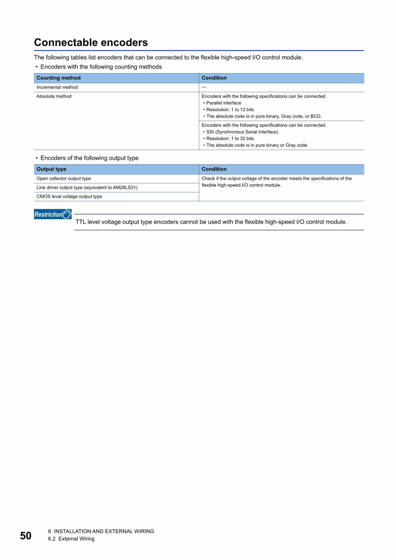
50
Connectable encodersThe following tables list encoders that can be connected to the flexible high-speed I/O control module. • Encoders with the following counting methods
• Encoders of the following output type
TTL level voltage output type encoders cannot be used with the flexible high-speed I/O control module.
Counting method ConditionIncremental method
Absolute method Encoders with the following specifications can be connected.• Parallel interface• Resolution: 1 to 12 bits• The absolute code is in pure binary, Gray code, or BCD.
Encoders with the following specifications can be connected.• SSI (Synchronous Serial Interface)• Resolution: 1 to 32 bits• The absolute code is in pure binary or Gray code.
Output type ConditionOpen collector output type Check if the output voltage of the encoder meets the specifications of the
flexible high-speed I/O control module.Line driver output type (equivalent to AM26LS31)
CMOS level voltage output type
6 INSTALLATION AND EXTERNAL WIRING6.2 External Wiring

6
6.3 Examples of Wiring Between a Controller and External Input Terminals
This section shows examples of wiring between a controller and external input terminals.
Example of external wiring with a controller (Sync load type)
Example of external wiring with a controller (Source load type)
IN 0_5V
IN 0_DIF
IN 0_24V
IN 0_COM
IN 1_DIF
IN 1_5V
IN 1_24V
IN 1_COM
4.1kΩ270Ω240Ω820Ω
4.1kΩ270Ω240Ω820Ω
B18
A19
B19
A18
B16
A17
B17
A16
24V
OUT
E
0V
5V
OUT
E
0V
Flexible high-speed I/O control module
IN 0(24V input)
IN 1(5V input)
Shielded twisted pair cable Controller A
External power supply
24VDC
Shielded twisted pair cable Controller B
External power supply
5VDC
IN 0_5V
IN 0_DIF
IN 0_24V
IN 0_COM
IN 1_DIF
IN 1_5V
IN 1_24V
IN 1_COM
4.1kΩ270Ω240Ω820Ω
4.1kΩ270Ω240Ω820Ω
B18
A19
B19
A18
B16
A17
B17
A16
OUT
GND
E
0V
OUT
GND
E
0V
Flexible high-speed I/O control module
IN 0(24V input)
IN 1(5V input)
Shielded twisted pair cable Controller A
External power supply
24VDC
Shielded twisted pair cable Controller B
External power supply
5VDC
6 INSTALLATION AND EXTERNAL WIRING6.3 Examples of Wiring Between a Controller and External Input Terminals 51

52
6.4 Example of External Wiring Between the Flexible High-speed I/O Control Module and an Encoder
This section shows an example of external wiring between the flexible high-speed I/O control module and an encoder.
Example of external wiring with an open collector output type encoder (24VDC)
4.1kΩ270Ω240Ω820Ω
IN 0_DIF
IN 0_5V
IN 0_24V
IN 0_COM
B18
A19
B19
A18
4.1kΩ270Ω240Ω820Ω
IN 1_DIF
IN 1_5V
IN 1_24V
IN 1_COM
B16
A17
B17
A16
4.1kΩ270Ω240Ω820Ω
IN 2_DIF
IN 2_5V
IN 2_24V
IN 2_COM
B14
A15
B15
A14
External power supply
Flexible high-speed I/O control module
IN 0(Phase A input)
IN 1(Phase B input)
IN 2(Phase Z input)
Shielded twisted pair cable Encoder
24VOUT
24VOUT
24VOUT
E
0V
24VDC
Phase A output
Phase B output
Phase Z output
6 INSTALLATION AND EXTERNAL WIRING6.4 Example of External Wiring Between the Flexible High-speed I/O Control Module and an Encoder

6
• For the wiring between the flexible high-speed I/O control module and an encoder, separate the power supply cables and signal wires.
• Do not wire the module and an encoder as shown in the figure below. Because a current flows through a shielded twisted pair cable in a single direction and the canceling effect disappears, the module is easy to be affected by electromagnetic induction.
24V
COM
0V
OUT
+24V
0V
E
Shielded twisted pair cablePulse input
Flexible high-speed I/O control module
Externalpowersupply
24VDC
Encoder
24V
COM
0V
OUT
+24V
0V
E
Shielded twisted pair cablePulse input
Flexible high-speed I/O control module
External power supply
24VDC
Encoder
6 INSTALLATION AND EXTERNAL WIRING6.4 Example of External Wiring Between the Flexible High-speed I/O Control Module and an Encoder 53

54
Example of external wiring with a line driver (equivalent to AM26LS31) encoder
IN 0_DIF
4.1kΩ270Ω240Ω820Ω
4.1kΩ270Ω240Ω820Ω
4.1kΩ270Ω240Ω820Ω
IN 0_5V
IN 0_24V
IN 0_COM
IN 1_DIF
IN 1_5V
IN 1_24V
IN 1_COM
IN 2_DIF
IN 2_5V
IN 2_24V
IN 2_COM
B18
A19
B19
A18
B16
A17
B17
A16
B14
A15
B15
A14
AA
BB
ZZ
E
Flexible high-speed I/O control module
IN 0(Phase A input)
IN 1(Phase B input)
IN 2(Phase Z input)
Shielded twisted pair cable
Encoder
Phase A input
Phase B input
Phase Z input
6 INSTALLATION AND EXTERNAL WIRING6.4 Example of External Wiring Between the Flexible High-speed I/O Control Module and an Encoder
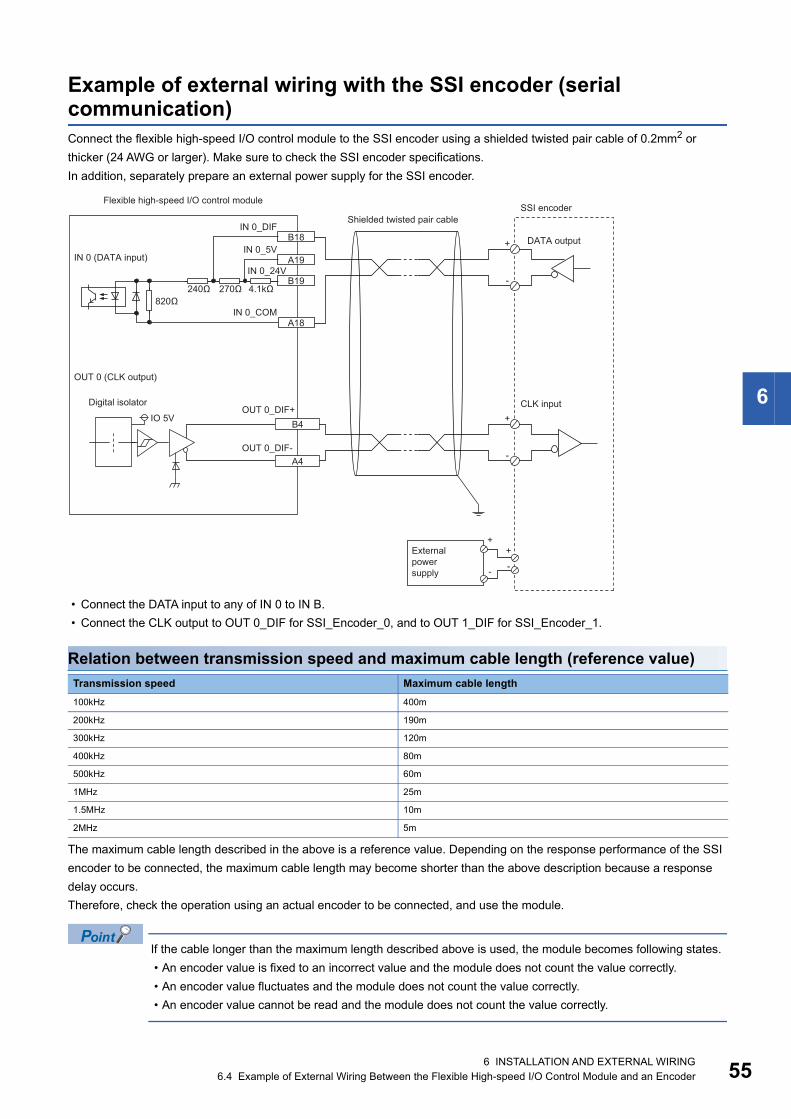
6
Example of external wiring with the SSI encoder (serial communication)Connect the flexible high-speed I/O control module to the SSI encoder using a shielded twisted pair cable of 0.2mm2 or thicker (24 AWG or larger). Make sure to check the SSI encoder specifications.In addition, separately prepare an external power supply for the SSI encoder.
• Connect the DATA input to any of IN 0 to IN B. • Connect the CLK output to OUT 0_DIF for SSI_Encoder_0, and to OUT 1_DIF for SSI_Encoder_1.
Relation between transmission speed and maximum cable length (reference value)
The maximum cable length described in the above is a reference value. Depending on the response performance of the SSI encoder to be connected, the maximum cable length may become shorter than the above description because a response delay occurs.Therefore, check the operation using an actual encoder to be connected, and use the module.
If the cable longer than the maximum length described above is used, the module becomes following states. • An encoder value is fixed to an incorrect value and the module does not count the value correctly. • An encoder value fluctuates and the module does not count the value correctly. • An encoder value cannot be read and the module does not count the value correctly.
Transmission speed Maximum cable length100kHz 400m
200kHz 190m
300kHz 120m
400kHz 80m
500kHz 60m
1MHz 25m
1.5MHz 10m
2MHz 5m
OUT 0_DIF+
OUT 0_DIF-
+
-
+
-
B4
A4
IO 5V
4.1kΩ270Ω240Ω820Ω
IN 0_DIF
IN 0_5V
IN 0_24V
IN 0_COM
B18
A19
B19
A18
+
-
+
-
External power supply
Digital isolator CLK input
SSI encoderFlexible high-speed I/O control module
Shielded twisted pair cable
IN 0 (DATA input)
OUT 0 (CLK output)
DATA output
6 INSTALLATION AND EXTERNAL WIRING6.4 Example of External Wiring Between the Flexible High-speed I/O Control Module and an Encoder 55
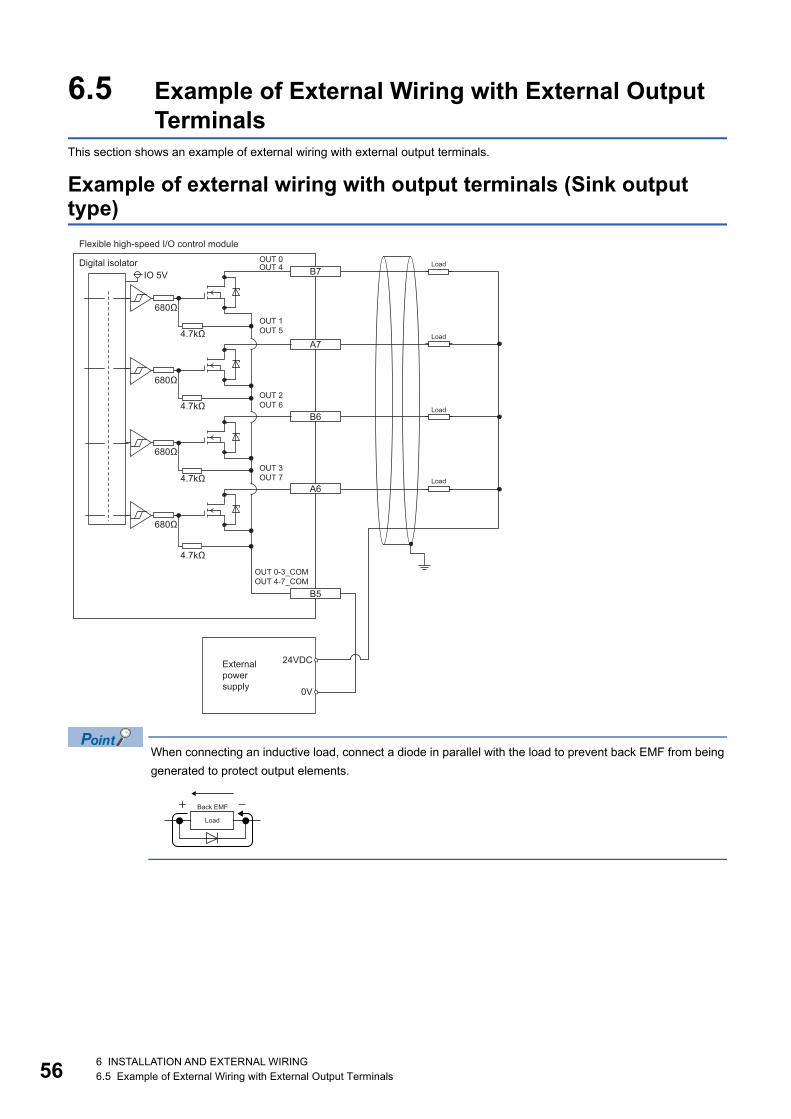
56
6.5 Example of External Wiring with External Output Terminals
This section shows an example of external wiring with external output terminals.
Example of external wiring with output terminals (Sink output type)
When connecting an inductive load, connect a diode in parallel with the load to prevent back EMF from being generated to protect output elements.
OUT 0-3_COMOUT 4-7_COM
OUT 0OUT 4
OUT 1OUT 5
OUT 2OUT 6
OUT 3OUT 7
IO 5V
680Ω
680Ω
680Ω
680Ω
4.7kΩ
4.7kΩ
4.7kΩ
4.7kΩ
B5
B7
A7
B6
A6
Load
Load
Load
Load
Externalpowersupply
24VDC
0V
Flexible high-speed I/O control module
Digital isolator
Load
Back EMF
6 INSTALLATION AND EXTERNAL WIRING6.5 Example of External Wiring with External Output Terminals
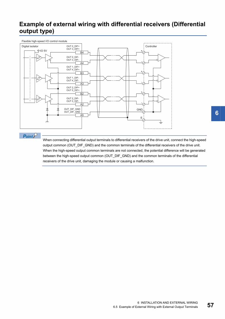
6
Example of external wiring with differential receivers (Differential output type)
When connecting differential output terminals to differential receivers of the drive unit, connect the high-speed output common (OUT_DIF_GND) and the common terminals of the differential receivers of the drive unit.When the high-speed output common terminals are not connected, the potential difference will be generated between the high-speed output common (OUT_DIF_GND) and the common terminals of the differential receivers of the drive unit, damaging the module or causing a malfunction.
OUT 0_DIF+OUT 3_DIF+
OUT 0_DIF-OUT 3_DIF-
+
-
B4
A4OUT 1_DIF+OUT 4_DIF+
OUT 1_DIF-OUT 4_DIF-
+
-
B3
A3OUT 2_DIF+OUT 5_DIF+
OUT 2_DIF-OUT 5_DIF-
OUT_DIF_GNDOUT_DIF_GND
+
-
GND
E
B2
A2
A5
IO 5V
Flexible high-speed I/O control module
Digital isolator Controller
6 INSTALLATION AND EXTERNAL WIRING6.5 Example of External Wiring with External Output Terminals 57

58
7 FUNCTIONSThis chapter describes the details on the functions that can be used in the flexible high-speed I/O control module and their setting methods.
7.1 Hardware Logic Control FunctionUsers can create the hardware logic to perform a desired control with the configuration tool.For details, refer to the following.Page 139 CREATING A HARDWARE LOGIC
7 FUNCTIONS7.1 Hardware Logic Control Function
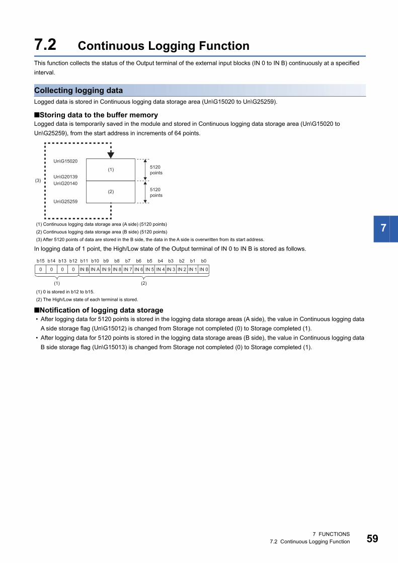
7
7.2 Continuous Logging FunctionThis function collects the status of the Output terminal of the external input blocks (IN 0 to IN B) continuously at a specified interval.
Collecting logging dataLogged data is stored in Continuous logging data storage area (Un\G15020 to Un\G25259).
■Storing data to the buffer memoryLogged data is temporarily saved in the module and stored in Continuous logging data storage area (Un\G15020 to Un\G25259), from the start address in increments of 64 points.
In logging data of 1 point, the High/Low state of the Output terminal of IN 0 to IN B is stored as follows.
■Notification of logging data storage • After logging data for 5120 points is stored in the logging data storage areas (A side), the value in Continuous logging data
A side storage flag (Un\G15012) is changed from Storage not completed (0) to Storage completed (1). • After logging data for 5120 points is stored in the logging data storage areas (B side), the value in Continuous logging data
B side storage flag (Un\G15013) is changed from Storage not completed (0) to Storage completed (1).
(1) Continuous logging data storage area (A side) (5120 points)(2) Continuous logging data storage area (B side) (5120 points)(3) After 5120 points of data are stored in the B side, the data in the A side is overwritten from its start address.
(1) 0 is stored in b12 to b15.(2) The High/Low state of each terminal is stored.
(1)
(2)
(3)
Un\G15020
Un\G20139Un\G20140
Un\G25259
5120 points
5120 points
0 0 0 0 IN B IN A IN 9 IN 8 IN 7 IN 6 IN 5 IN 0IN 1IN 2IN 3IN 4
b15 b14 b13 b12 b11 b10 b9 b8 b7 b6 b5 b0b1b2b3b4
(2)(1)
7 FUNCTIONS7.2 Continuous Logging Function 59
60
Starting continuous logging1. Write the hardware logic to the module and start hardware logic control. When the hardware logic control starts, the
value in Continuous logging status monitor (Un\G15010) changes from Disabled (0) to Start request waiting (1).
2. Set the continuous logging cycle (10s (1) to 1000s (3)) in Continuous logging cycle setting (Un\G15008).
3. Changing the value in Continuous logging start/stop request (Un\G15009) from Stop request (0) to Start request (1) starts the continuous logging on the set continuous logging cycle. At this time, the value in Continuous logging status monitor (Un\G15010) changes from Start request waiting (1) to In progress (2).
At the start of continuous logging, the values stored in the following buffer memory areas are initialized (cleared to 0). • Continuous logging data A side storage flag (Un\G15012) • Continuous logging data B side storage flag (Un\G15013) • Continuous logging data points (Un\G15014, Un\G15015)
■When a value out of range is set in Continuous logging cycle settingWhen a value out of range is set in Continuous logging cycle setting (Un\G15008) and the value in Continuous logging start/stop request (Un\G15009) is changed from Stop request (0) to Start request (1), the continuous logging cycle setting range error (error code: 10D6H) occurs and the continuous logging does not start.
■Disabling continuous loggingWhen Disabled (0) is stored in Continuous logging status monitor (Un\G15010) and the value in Continuous logging start/stop request (Un\G15009) is changed from Stop request (0) to Start request (1), an error occurs and the continuous logging does not start.When one of the following conditions is satisfied, Disabled (0) is stored in Continuous logging status monitor (Un\G15010). • During control of a hardware logic that uses Hardware logic area (High speed area) (Un\G1000 to Un\G1029) • During control of a hardware logic that uses an SSI encoder block • During simulation • During logic analyzer function execution • During hardware logic control stop
7 FUNCTIONS7.2 Continuous Logging Function
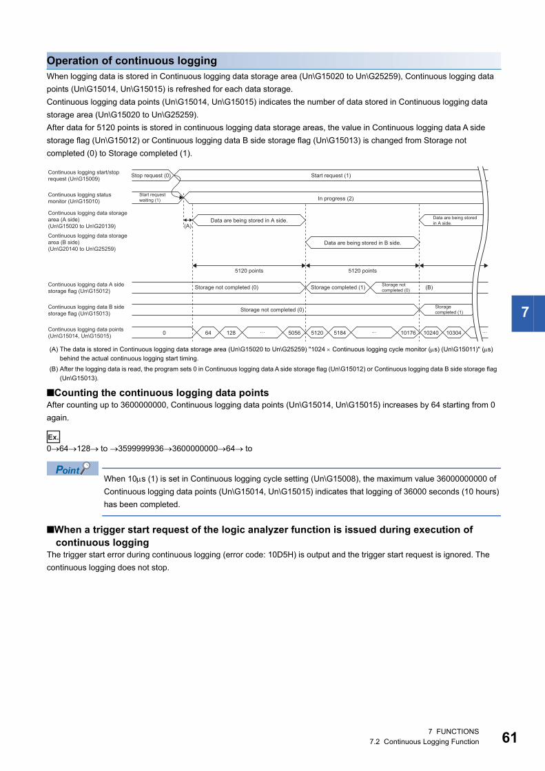
7
Operation of continuous loggingWhen logging data is stored in Continuous logging data storage area (Un\G15020 to Un\G25259), Continuous logging data points (Un\G15014, Un\G15015) is refreshed for each data storage.Continuous logging data points (Un\G15014, Un\G15015) indicates the number of data stored in Continuous logging data storage area (Un\G15020 to Un\G25259).After data for 5120 points is stored in continuous logging data storage areas, the value in Continuous logging data A side storage flag (Un\G15012) or Continuous logging data B side storage flag (Un\G15013) is changed from Storage not completed (0) to Storage completed (1).
■Counting the continuous logging data pointsAfter counting up to 3600000000, Continuous logging data points (Un\G15014, Un\G15015) increases by 64 starting from 0 again.
Ex.
064128 to 3599999936360000000064 to
When 10s (1) is set in Continuous logging cycle setting (Un\G15008), the maximum value 36000000000 of Continuous logging data points (Un\G15014, Un\G15015) indicates that logging of 36000 seconds (10 hours) has been completed.
■When a trigger start request of the logic analyzer function is issued during execution of continuous logging
The trigger start error during continuous logging (error code: 10D5H) is output and the trigger start request is ignored. The continuous logging does not stop.
(A) The data is stored in Continuous logging data storage area (Un\G15020 to Un\G25259) "1024 Continuous logging cycle monitor (s) (Un\G15011)" (s) behind the actual continuous logging start timing.
(B) After the logging data is read, the program sets 0 in Continuous logging data A side storage flag (Un\G15012) or Continuous logging data B side storage flag (Un\G15013).
0
(A)
(B)
64 128 5056 5120 5184 10176 10240 10304
� � �
Continuous logging start/stop request (Un\G15009) Stop request (0)
Start request waiting (1)
Data are being stored in A side.
Storage not completed (0)
Storage not completed (0)
Storage not completed (0)Storage completed (1)
Storage completed (1)
5120 points 5120 points
Data are being stored in A side.
Data are being stored in B side.
In progress (2)
Start request (1)
Continuous logging status monitor (Un\G15010)
Continuous logging data A side storage flag (Un\G15012)
Continuous logging data storage area (B side) (Un\G20140 to Un\G25259)
Continuous logging data B side storage flag (Un\G15013)
Continuous logging data points (Un\G15014, Un\G15015)
Continuous logging data storage area (A side) (Un\G15020 to Un\G20139)
7 FUNCTIONS7.2 Continuous Logging Function 61
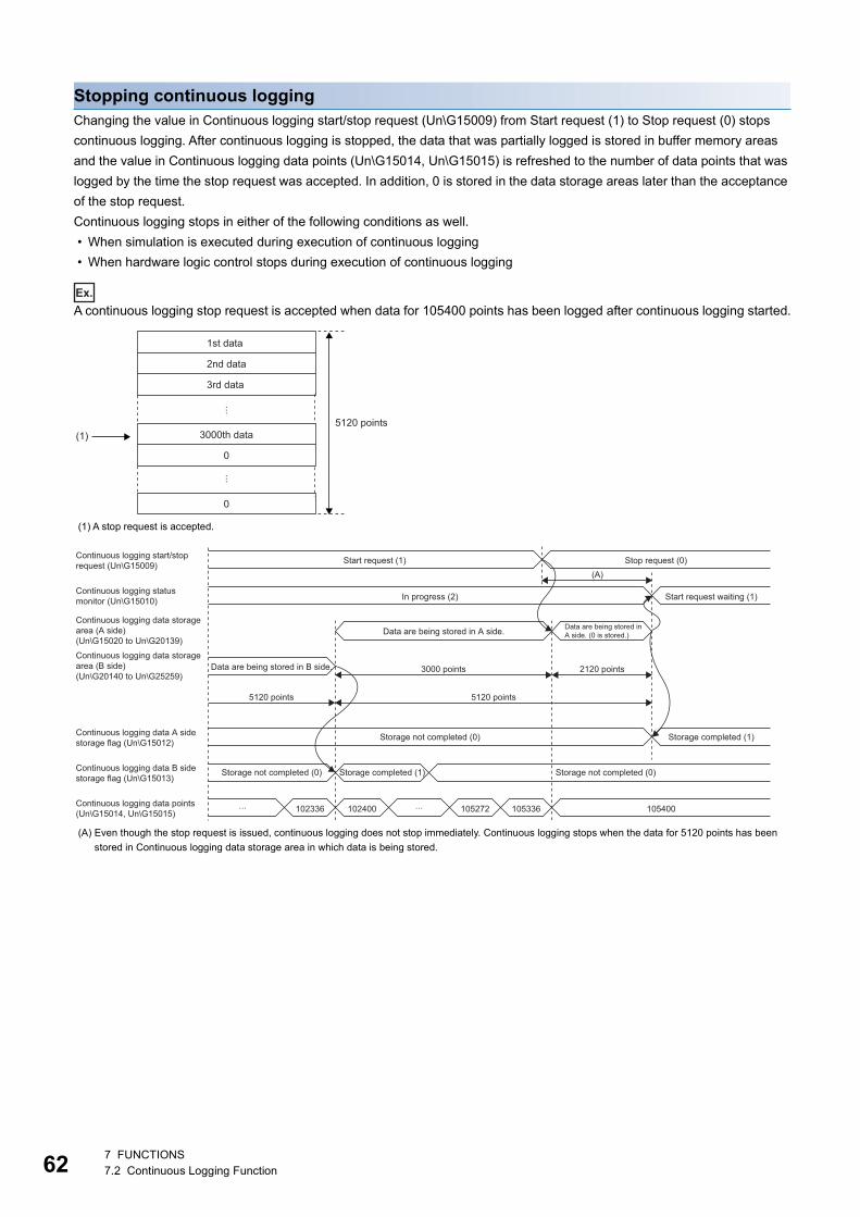
62
Stopping continuous loggingChanging the value in Continuous logging start/stop request (Un\G15009) from Start request (1) to Stop request (0) stops continuous logging. After continuous logging is stopped, the data that was partially logged is stored in buffer memory areas and the value in Continuous logging data points (Un\G15014, Un\G15015) is refreshed to the number of data points that was logged by the time the stop request was accepted. In addition, 0 is stored in the data storage areas later than the acceptance of the stop request.Continuous logging stops in either of the following conditions as well. • When simulation is executed during execution of continuous logging • When hardware logic control stops during execution of continuous logging
Ex.
A continuous logging stop request is accepted when data for 105400 points has been logged after continuous logging started.
(1) A stop request is accepted.
(A) Even though the stop request is issued, continuous logging does not stop immediately. Continuous logging stops when the data for 5120 points has been stored in Continuous logging data storage area in which data is being stored.
0
0
(1)
�
�
1st data
2nd data
3rd data
3000th data5120 points
102336
� �
102400 105272 105336 105400
(A)
Continuous logging start/stop request (Un\G15009) Start request (1)
In progress (2)
Data are being stored in A side.
Storage not completed (0)
Storage not completed (0)
Storage completed (1)
Storage completed (1) Storage not completed (0)
3000 points 2120 points
5120 points 5120 points
Data are being stored in A side. (0 is stored.)
Data are being stored in B side.
Start request waiting (1)
Stop request (0)
Continuous logging status monitor (Un\G15010)
Continuous logging data A side storage flag (Un\G15012)
Continuous logging data storage area (B side) (Un\G20140 to Un\G25259)
Continuous logging data B side storage flag (Un\G15013)
Continuous logging data points (Un\G15014, Un\G15015)
Continuous logging data storage area (A side) (Un\G15020 to Un\G20139)
7 FUNCTIONS7.2 Continuous Logging Function
7
■Restarting continuous loggingTo restart continuous logging after stopping it, perform the following operations.
1. Check that the value in Continuous logging status monitor (Un\G15010) is Start request waiting (1).
2. Change the value in Continuous logging start/stop request (Un\G15009) from Stop request (0) to Start request (1). When the value in Continuous logging status monitor (Un\G15010) is In progress (2), the start request is ignored.
After continuous logging is restarted, values are stored in Continuous logging data storage area (A side) (Un\G15020 to Un\G20139) from the start address. When continuous logging is restarted, the following buffer memory areas are initialized (cleared to 0). • Continuous logging data A side storage flag (Un\G15012) • Continuous logging data B side storage flag (Un\G15013) • Continuous logging data points (Un\G15014, Un\G15015)The values before the restart of continuous logging are held in Continuous logging data storage area (Un\G15020 to Un\G25259). Thus, before referring to the logging data, check that Storage completed (1) has been stored in Continuous logging data A side storage flag (Un\G15012) again.
7 FUNCTIONS7.2 Continuous Logging Function 63

64
Transfer of continuous logging dataLogging data can be transferred into the file register (ZR) of the CPU module by using the following items. • Interrupt function
Transfer of data with the interrupt functionThe interrupt program is executed on the timing when the logging data for 5120 points are stored in the buffer memory. Thus, logging data can be transferred into the file register (ZR) without depending on the scan time.
■Program example to transfer data with the interrupt function
Ex.
To start the continuous logging and continuously copy logging data for 102400 points and register them in the file register (ZR0 to ZR102399) of the CPU module • User devices
• Switch Setting
• Intelligent Function Module Interrupt Pointer Setting
Device DescriptionD10 Start position of the save destination file register
D20 Write position of the save destination file register
D30 Maximum value of the save destination file register
D40 Stop position of the save destination file register
Z4 Write position of the save destination file register (index register)
ZR0ZZ4 Save destination file register (with index register)
M0 Continuous logging start/stop
F0 An error
7 FUNCTIONS7.2 Continuous Logging Function
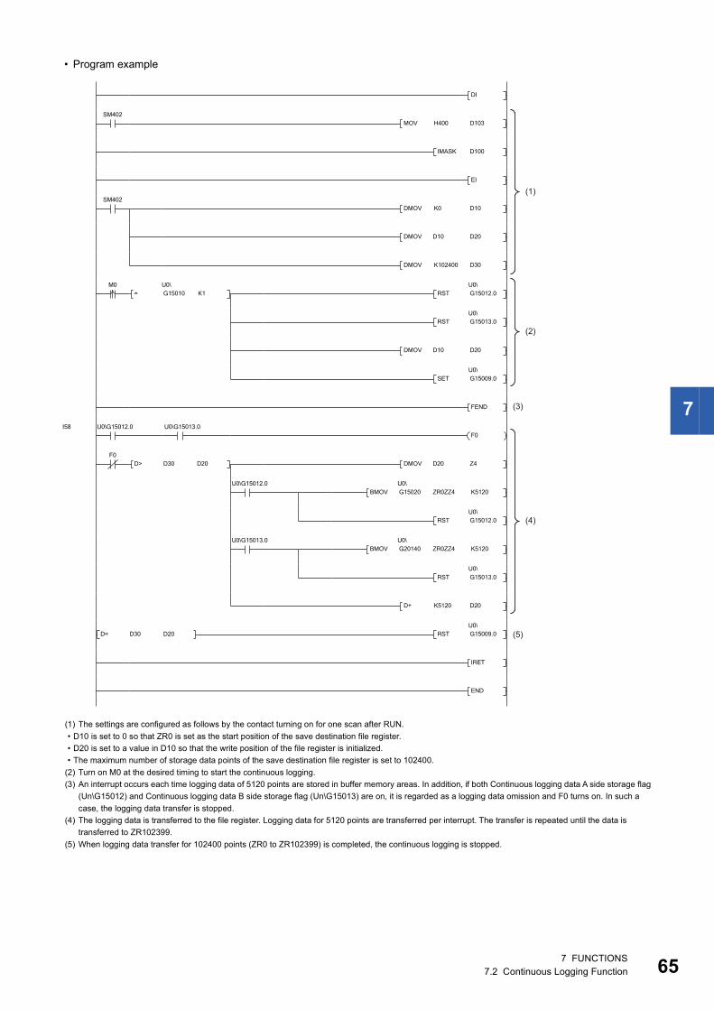
7
• Program example
(1) The settings are configured as follows by the contact turning on for one scan after RUN.• D10 is set to 0 so that ZR0 is set as the start position of the save destination file register.• D20 is set to a value in D10 so that the write position of the file register is initialized.• The maximum number of storage data points of the save destination file register is set to 102400.
(2) Turn on M0 at the desired timing to start the continuous logging.(3) An interrupt occurs each time logging data of 5120 points are stored in buffer memory areas. In addition, if both Continuous logging data A side storage flag
(Un\G15012) and Continuous logging data B side storage flag (Un\G15013) are on, it is regarded as a logging data omission and F0 turns on. In such a case, the logging data transfer is stopped.
(4) The logging data is transferred to the file register. Logging data for 5120 points are transferred per interrupt. The transfer is repeated until the data is transferred to ZR102399.
(5) When logging data transfer for 102400 points (ZR0 to ZR102399) is completed, the continuous logging is stopped.
(1)
(2)
(4)
(5)
(3)
7 FUNCTIONS7.2 Continuous Logging Function 65

66
■Starting the continuous logging againTo start the continuous logging again after the completion of logging data transfer, have the execution interval (ms) described below or longer between them. • Execution interval (ms) 5120 points Continuous logging cycle monitor (s) 1000 2
Ex.
When Continuous logging cycle monitor (s) (Un\G15011) is 10s • Execution interval (ms) 5120 points 10s 1000 2 = 102.4ms
■Precautions for creating the program • Each time logging data for 5120 points are stored in the flexible high-speed I/O control module, an interrupt program is
executed and the data is transferred to the file register. The approximate instruction processing time of the interrupt program is obtained by adding up the processing time of instructions accessing the buffer memory areas in the interrupt program (equivalent to a value of "5.12 times of FROM instruction (1000 points)*1 + 5 times of FROM instruction (1 point)*1 + 1 time of TO instruction (1 point)*1") and the processing time of the IRET instruction. If the exact instruction processing time is required, add up the processing time of all instructions used in the interrupt program. For details on the processing time of each instruction used in the interrupt program, refer to the MELSEC-Q/L Programming Manual (Common Instruction).
• The approximate processing time of the interrupt program is obtained by adding both the interrupt overhead time and the refresh processing time (when the refresh processing is set) at the interrupt execution to the instruction processing time of the interrupt program. The interrupt overhead time and the refresh processing time at the interrupt execution vary depending on the parameter settings of the CPU module. For details, refer to the MELSEC-L CPU Module User's Manual (Function Explanation, Program Fundamentals).
• The following table provides a calculation example for when the interrupt overhead time is 23.0s and the refresh processing time at the interrupt execution is 0s.
To prevent logging data omission, create the program so that a series of processing of the interrupt program (from the start to the completion) takes place within 49.2ms*2 after an interrupt factor (storage of continuous logging data for 5120 points) occurs.*1 This value indicates the maximum processing time of each instruction. ( MELSEC-Q/L Programming Manual (Common Instruction))*2 This value is for when the continuous logging is executed every 10s cycle. When using the continuous logging cycle different from
10s, calculate a reference value (ms) using the following calculation formula.Reference value (ms) = (Continuous logging cycle (s) 5120 (points)) 1000 - 2 (ms)
This processing time is a value for the case when the program consists of only the interrupt program which transfers continuous logging data. If other processing is added to the program, or another program is added, the processing time becomes longer. Please consider an actual application and configure the system.
Item Calculation formulaInstruction processing time (as a guide) of the interrupt program
= (Processing time of the FROM instruction (1000 points)) (5.12 times)+ (Processing time of the FROM instruction (1 point)) (5 times)+ (Processing time of the TO instruction (1 point)) (1 time)+ (Processing time of the IRET instruction) (1 time)
= 410.2s*1 5.12 + 23.6s*1 5 + 21.3s*1 1 + 1.0s*1 1= 2240.5s
Processing time (as a guide) of the interrupt program
= (Instruction processing time (as a guide) of the interrupt program) + (Interrupt overhead time)+ (Refresh processing time at the interrupt execution)
= 2240.5s + 23.0s + 0s= 2263.5s
7 FUNCTIONS7.2 Continuous Logging Function
7
Saving continuous logging dataThe logging data stored in the file register (ZR) can be written into an SD memory card as a CSV file and checked with spreadsheet software.Use the SP.FWRITE instruction to write the data into the SD memory card. For details on the SP.FWRITE instruction, refer to the following. MELSEC-Q/L Programming Manual (Common Instruction)
RestrictionsThe maximum response delay time of interrupt during the execution of continuous logging is 200s.
7 FUNCTIONS7.2 Continuous Logging Function 67
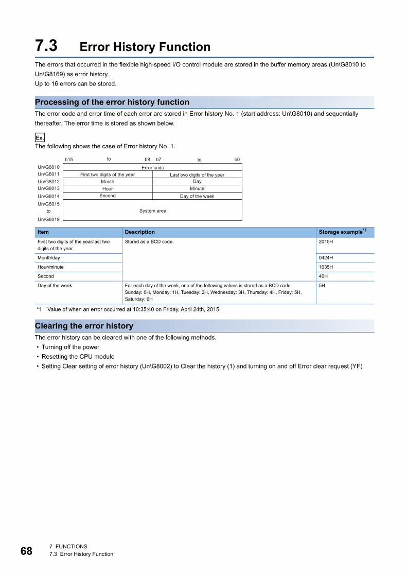
68
7.3 Error History FunctionThe errors that occurred in the flexible high-speed I/O control module are stored in the buffer memory areas (Un\G8010 to Un\G8169) as error history.Up to 16 errors can be stored.
Processing of the error history functionThe error code and error time of each error are stored in Error history No. 1 (start address: Un\G8010) and sequentially thereafter. The error time is stored as shown below.
Ex.
The following shows the case of Error history No. 1.
*1 Value of when an error occurred at 10:35:40 on Friday, April 24th, 2015
Clearing the error historyThe error history can be cleared with one of the following methods. • Turning off the power • Resetting the CPU module • Setting Clear setting of error history (Un\G8002) to Clear the history (1) and turning on and off Error clear request (YF)
Item Description Storage example*1
First two digits of the year/last two digits of the year
Stored as a BCD code. 2015H
Month/day 0424H
Hour/minute 1035H
Second 40H
Day of the week For each day of the week, one of the following values is stored as a BCD code.Sunday: 0H, Monday: 1H, Tuesday: 2H, Wednesday: 3H, Thursday: 4H, Friday: 5H, Saturday: 6H
5H
b15 b8 b7 b0to toError code
First two digits of the year Last two digits of the yearMonth DayHour Minute
Second Day of the week
System areato
Un\G8010
Un\G8014Un\G8013Un\G8012Un\G8011
Un\G8015
Un\G8019
7 FUNCTIONS7.3 Error History Function

7
Checking the error historyThe start address of the error history where the latest error has been stored can be checked with Latest address of error history (Un\G8000).
Ex.
The following shows the case in which the third error has occurred. The third error is stored in Error history No. 3 and 8030 (start address of Error history No.3) is stored in Latest address of error history (Un\G8000).
8010
8020
8030
8160
The start address of the error history where the latest error is stored is stored.
Error history No.1
Error history No.2
Error history No.3
Error history No.16
(Empty)
(Empty)
Latest
Address
1st error
2nd error
3rd error
An error history consists of the following data.
Details of error history
Error code
Error time
First two digits of the year Last two digits of the yearMonthHour
Second
DayMinute
Day of the week
Latest address of error history (Un\G8000)
7 FUNCTIONS7.3 Error History Function 69
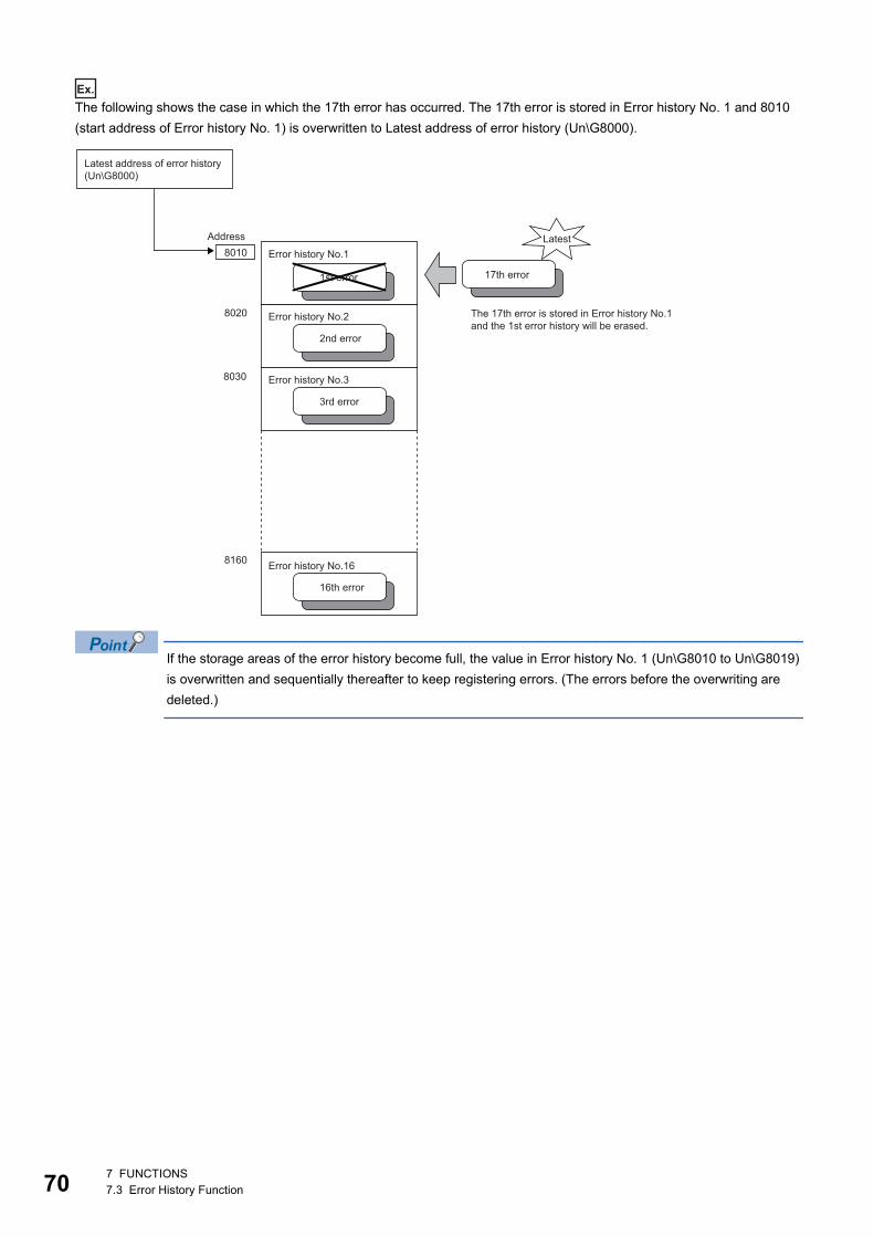
70
Ex.
The following shows the case in which the 17th error has occurred. The 17th error is stored in Error history No. 1 and 8010 (start address of Error history No. 1) is overwritten to Latest address of error history (Un\G8000).
If the storage areas of the error history become full, the value in Error history No. 1 (Un\G8010 to Un\G8019) is overwritten and sequentially thereafter to keep registering errors. (The errors before the overwriting are deleted.)
8010
8020
8030
8160
Error history No.1
Error history No.2
Error history No.3
Error history No.16
Latest
The 17th error is stored in Error history No.1 and the 1st error history will be erased.
Address
1st error
2nd error
3rd error
16th error
17th error
Latest address of error history (Un\G8000)
7 FUNCTIONS7.3 Error History Function

7
7.4 Module Error Collection FunctionThe errors that occurred in the flexible high-speed I/O control module are collected in the CPU module.To hold errors even after the power is turned off or the CPU module is reset, save the errors in the memory that can hold data during power failure in the CPU module.
For details on the module error collection function, refer to the following. MELSEC-L CPU Module User's Manual (Function Explanation, Program Fundamentals)
Error history (CPU module including built-in I/O and built-inCC-Link) and error log (intelligent function module) aredisplayed on one screen.
Errors that occurred in the entire system can be monitored in reverse chronological order.
Programming tool
[Example of screen display]
Error history display
19:2919:3319:3419:36
Module A CPU
Module B Module A
Error A1Error C1Error B1Error A2
Time Module in error Error codeError history
(CPU module) Module error log
Time Module in error Error code19:2919:3419:36
Module AModule BModule A
Error A1Error B1Error A2
19:33 Error C1
CPUModule A Module B
19:33 Error C1 occurred!19:29 Error A1 occurred! 19:36 Error A2 occurred!
19:34 Error B1 occurred!
7 FUNCTIONS7.4 Module Error Collection Function 71

72
7.5 Error Clear FunctionWhen an error has occurred, the error can be cleared from "System Monitor".Clicking the [Error Clear] button in "System Monitor" clears the latest error code stored in Latest error code (Un\G100) and turns off the ERR. LED. This action is the same action as the one to be taken when errors are cleared with Error clear request (YF) or the display unit.When Clear setting of error history (Un\G8002) has been set to Clear the history. (1), the error history is also cleared.For how to clear errors with Error clear request (YF) or the display unit, refer to the following.Page 285 Error clear request (YF)Page 245 Checking and Clearing Errors
7 FUNCTIONS7.5 Error Clear Function

8
8 FUNCTIONS OF THE CONFIGURATION TOOLThis chapter describes the configuration tool for creating the hardware logic and writing it into the flexible high-speed I/O control module.For how to get the configuration tool, refer to the following.Page 294 How to Get the Configuration Tool
8.1 How to Install and Uninstall the Configuration ToolFor the procedures of installing and uninstalling the configuration tool, refer to the following. Flexible High-Speed I/O Control Module Configuration Tool Installation Instructions
8 FUNCTIONS OF THE CONFIGURATION TOOL8.1 How to Install and Uninstall the Configuration Tool 73
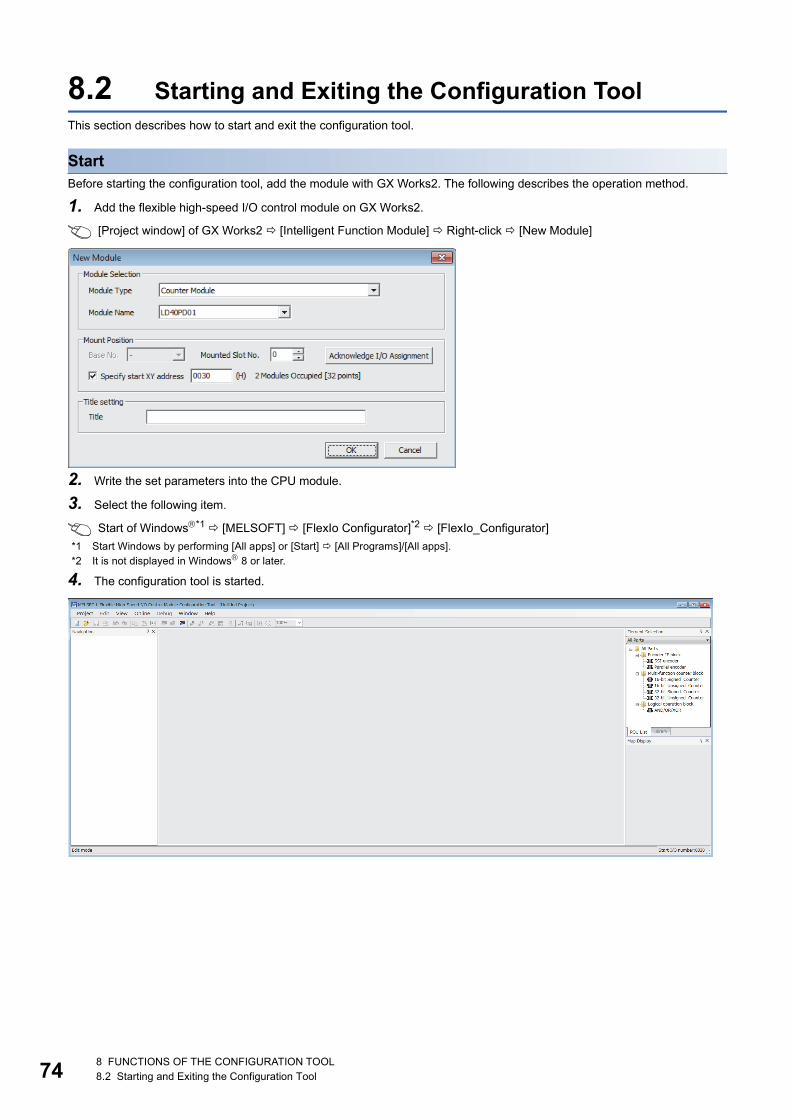
74
8.2 Starting and Exiting the Configuration ToolThis section describes how to start and exit the configuration tool.
StartBefore starting the configuration tool, add the module with GX Works2. The following describes the operation method.
1. Add the flexible high-speed I/O control module on GX Works2.
[Project window] of GX Works2 [Intelligent Function Module] Right-click [New Module]
2. Write the set parameters into the CPU module.
3. Select the following item.
Start of Windows*1 [MELSOFT] [FlexIo Configurator]*2 [FlexIo_Configurator]*1 Start Windows by performing [All apps] or [Start] [All Programs]/[All apps].*2 It is not displayed in Windows 8 or later.
4. The configuration tool is started.
8 FUNCTIONS OF THE CONFIGURATION TOOL8.2 Starting and Exiting the Configuration Tool
8
■Connection targetThe configuration tool acquires information of the connection destination from GX Works2 at its start-up. Therefore, when the connection destination has been changed on GX Works2 after the start-up of the configuration tool, exit from the configuration tool once. And start it again.
ExitSelect [Project] and [Exit] in the configuration tool.
8 FUNCTIONS OF THE CONFIGURATION TOOL8.2 Starting and Exiting the Configuration Tool 75

76
8.3 Switching the LanguageThe configuration tool supports multiple languages. Users can switch the language to be displayed in the menu on a personal computer.
How to switch the language[View] [Switching display language]
• When a selected language is different from the one set to the OS, character strings may be cut off and the window may not be properly displayed.
• When switching the language in Windows10, supplemental fonts of the language to be switched to are required. Supplemental fonts can be added by Start of Windows [Settings] [Apps] [Apps & features] [Manage optional features] [Add a feature].
8 FUNCTIONS OF THE CONFIGURATION TOOL8.3 Switching the Language

8
8.4 Window LayoutThe following figure shows the whole window layout.
For details on each item, refer to the following.
Window operation■Displaying a docking window
[View] [Docking Window] [(item to be displayed as a docking window)]
If a window is not displayed by the above operation from the menu, select [Window] [Return Window Layout to Initial Status].
Window ReferenceNavigation window Page 79 Navigation window
Work window Page 81 Work window
Element Selection window Page 80 Element Selection window
Map display window Page 82 Map display window
Watch window Page 113 Watch Function
Title bar
Menu bar
Toolbar
Navigation window
Work window
Status bar
Map display windowWatch window
Docking window
Element selection window
8 FUNCTIONS OF THE CONFIGURATION TOOL8.4 Window Layout 77
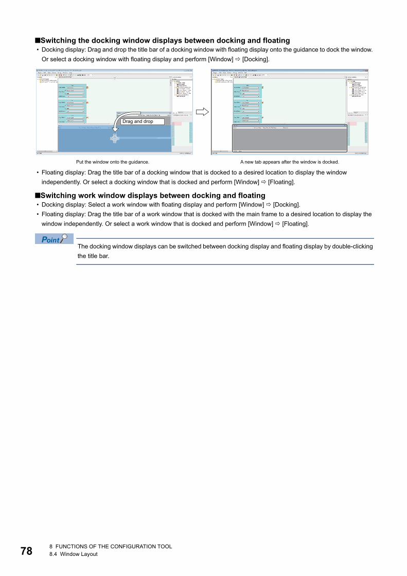
78
■Switching the docking window displays between docking and floating • Docking display: Drag and drop the title bar of a docking window with floating display onto the guidance to dock the window.
Or select a docking window with floating display and perform [Window] [Docking].
• Floating display: Drag the title bar of a docking window that is docked to a desired location to display the window independently. Or select a docking window that is docked and perform [Window] [Floating].
■Switching work window displays between docking and floating • Docking display: Select a work window with floating display and perform [Window] [Docking]. • Floating display: Drag the title bar of a work window that is docked with the main frame to a desired location to display the
window independently. Or select a work window that is docked and perform [Window] [Floating].
The docking window displays can be switched between docking display and floating display by double-clicking the title bar.
Drag and drop
Put the window onto the guidance. A new tab appears after the window is docked.
8 FUNCTIONS OF THE CONFIGURATION TOOL8.4 Window Layout
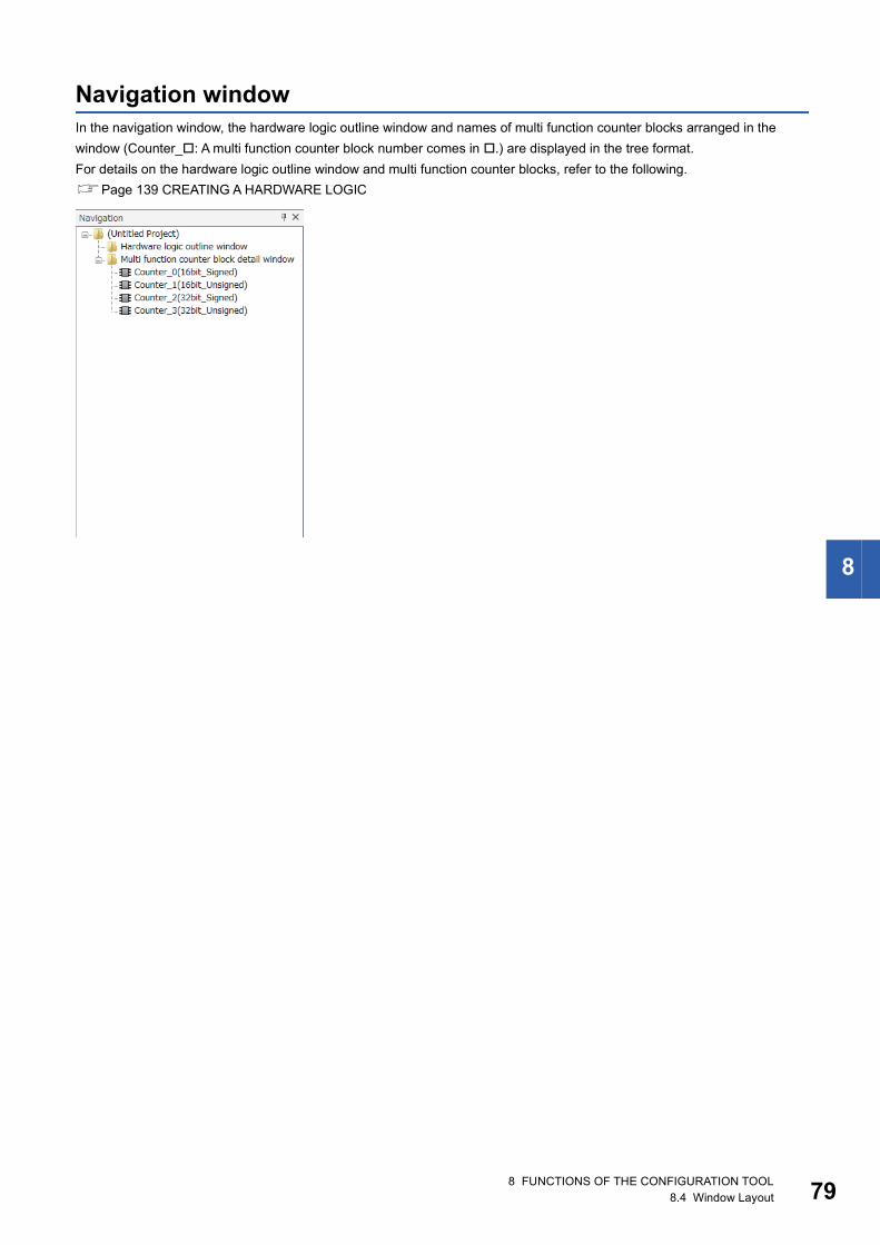
8
Navigation windowIn the navigation window, the hardware logic outline window and names of multi function counter blocks arranged in the window (Counter_: A multi function counter block number comes in .) are displayed in the tree format.For details on the hardware logic outline window and multi function counter blocks, refer to the following.Page 139 CREATING A HARDWARE LOGIC
8 FUNCTIONS OF THE CONFIGURATION TOOL8.4 Window Layout 79
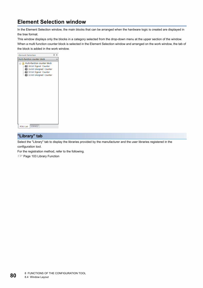
80
Element Selection windowIn the Element Selection window, the main blocks that can be arranged when the hardware logic is created are displayed in the tree format.This window displays only the blocks in a category selected from the drop-down menu at the upper section of the window.When a multi function counter block is selected in the Element Selection window and arranged on the work window, the tab of the block is added in the work window.
"Library" tabSelect the "Library" tab to display the libraries provided by the manufacturer and the user libraries registered in the configuration tool.For the registration method, refer to the following.Page 103 Library Function
8 FUNCTIONS OF THE CONFIGURATION TOOL8.4 Window Layout
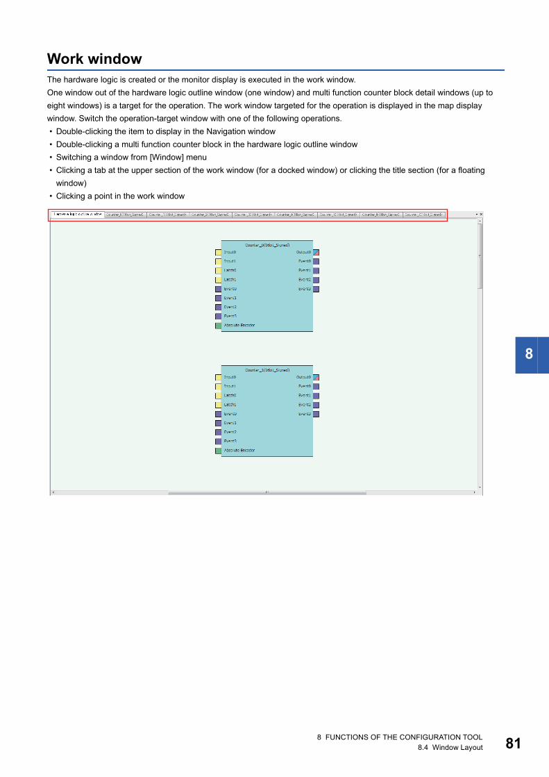
8
Work windowThe hardware logic is created or the monitor display is executed in the work window.One window out of the hardware logic outline window (one window) and multi function counter block detail windows (up to eight windows) is a target for the operation. The work window targeted for the operation is displayed in the map display window. Switch the operation-target window with one of the following operations. • Double-clicking the item to display in the Navigation window • Double-clicking a multi function counter block in the hardware logic outline window • Switching a window from [Window] menu • Clicking a tab at the upper section of the work window (for a docked window) or clicking the title section (for a floating
window) • Clicking a point in the work window
8 FUNCTIONS OF THE CONFIGURATION TOOL8.4 Window Layout 81
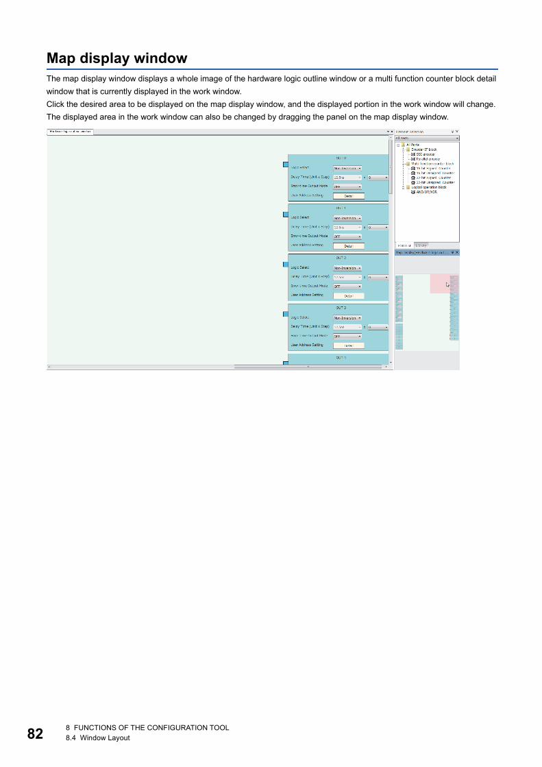
82
Map display windowThe map display window displays a whole image of the hardware logic outline window or a multi function counter block detail window that is currently displayed in the work window.Click the desired area to be displayed on the map display window, and the displayed portion in the work window will change. The displayed area in the work window can also be changed by dragging the panel on the map display window.
8 FUNCTIONS OF THE CONFIGURATION TOOL8.4 Window Layout

8
8.5 List of Menus of the Configuration Tool
[Project] menu
[Edit] menu
[View] menu
Menu Reference[Project] [New] Page 86 Creating a new project
[Project] [Open] Page 86 Opening a project
[Project] [Close]
[Project] [Save] Page 87 Saving an existing project
[Project] [Save As] Page 87 Saving a project with a new name
[Project] [Project Verify] Page 88 Verifying a project file
[Project] [Security] Page 89 Security
[Project] [Print] Page 85 Printing
[Project] [Exit] Page 75 Exit
Menu Reference[Edit] [Undo]
[Edit] [Redo]
[Edit] [Copy] Page 98 Copying a block
[Edit] [Paste] Page 99 Pasting a block
[Edit] [Insert and Paste]
[Edit] [Block Delete] Page 94 Deleting a block
[Edit] [Export block] Page 103 Library Function
[Edit] [Library Registration]
[Edit] [Library Delete]
[Edit] [Comment Insert] Page 100 Adding a comment
Menu Reference[View] [Switching display language] Page 76 Switching the Language
[View] [Zoom] [Set Zoom Factor]
[View] [Zoom] [Zoom In]
[View] [Zoom] [Zoom Out]
[View] [Comment Display] Page 100 Adding a comment
[View] [Docking Window] [Navigation] Page 79 Navigation window
[View] [Docking Window] [Element Selection] Page 80 Element Selection window
[View] [Docking Window] [Map Display] Page 82 Map display window
[View] [Docking Window] [Watch 1] to [Watch 4] Page 113 Watch Function
8 FUNCTIONS OF THE CONFIGURATION TOOL8.5 List of Menus of the Configuration Tool 83
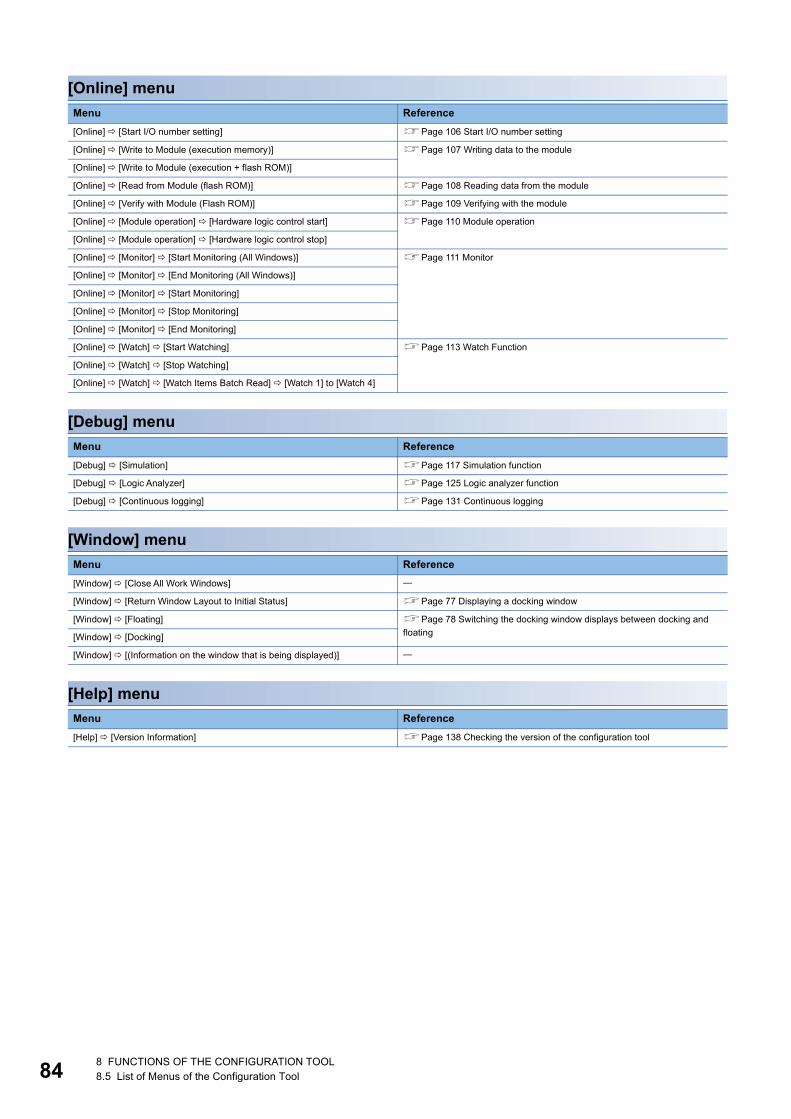
84
[Online] menu
[Debug] menu
[Window] menu
[Help] menu
Menu Reference[Online] [Start I/O number setting] Page 106 Start I/O number setting
[Online] [Write to Module (execution memory)] Page 107 Writing data to the module
[Online] [Write to Module (execution + flash ROM)]
[Online] [Read from Module (flash ROM)] Page 108 Reading data from the module
[Online] [Verify with Module (Flash ROM)] Page 109 Verifying with the module
[Online] [Module operation] [Hardware logic control start] Page 110 Module operation
[Online] [Module operation] [Hardware logic control stop]
[Online] [Monitor] [Start Monitoring (All Windows)] Page 111 Monitor
[Online] [Monitor] [End Monitoring (All Windows)]
[Online] [Monitor] [Start Monitoring]
[Online] [Monitor] [Stop Monitoring]
[Online] [Monitor] [End Monitoring]
[Online] [Watch] [Start Watching] Page 113 Watch Function
[Online] [Watch] [Stop Watching]
[Online] [Watch] [Watch Items Batch Read] [Watch 1] to [Watch 4]
Menu Reference[Debug] [Simulation] Page 117 Simulation function
[Debug] [Logic Analyzer] Page 125 Logic analyzer function
[Debug] [Continuous logging] Page 131 Continuous logging
Menu Reference[Window] [Close All Work Windows]
[Window] [Return Window Layout to Initial Status] Page 77 Displaying a docking window
[Window] [Floating] Page 78 Switching the docking window displays between docking and floating[Window] [Docking]
[Window] [(Information on the window that is being displayed)]
Menu Reference[Help] [Version Information] Page 138 Checking the version of the configuration tool
8 FUNCTIONS OF THE CONFIGURATION TOOL8.5 List of Menus of the Configuration Tool
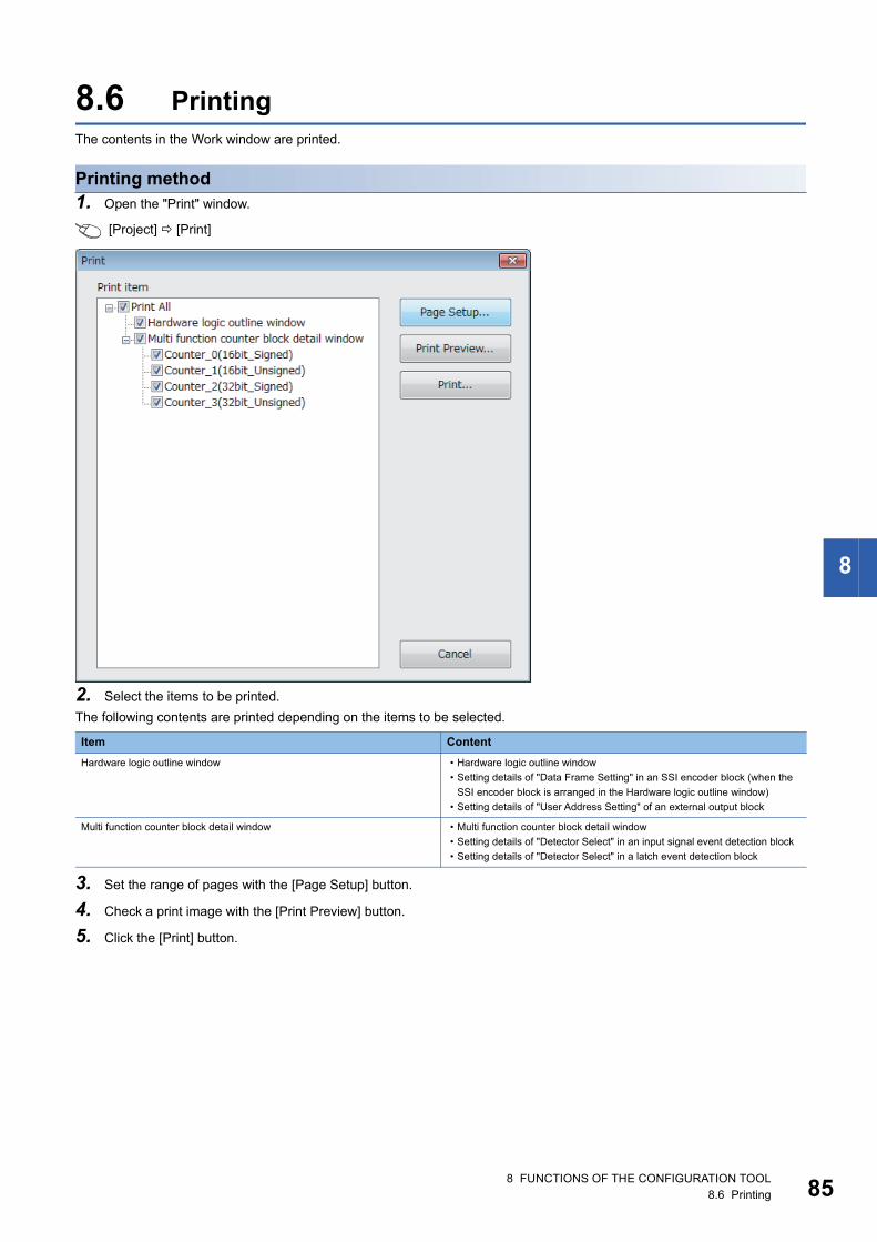
8
8.6 PrintingThe contents in the Work window are printed.
Printing method1. Open the "Print" window.
[Project] [Print]
2. Select the items to be printed.The following contents are printed depending on the items to be selected.
3. Set the range of pages with the [Page Setup] button.
4. Check a print image with the [Print Preview] button.
5. Click the [Print] button.
Item ContentHardware logic outline window • Hardware logic outline window
• Setting details of "Data Frame Setting" in an SSI encoder block (when the SSI encoder block is arranged in the Hardware logic outline window)
• Setting details of "User Address Setting" of an external output block
Multi function counter block detail window • Multi function counter block detail window• Setting details of "Detector Select" in an input signal event detection block• Setting details of "Detector Select" in a latch event detection block
8 FUNCTIONS OF THE CONFIGURATION TOOL8.6 Printing 85
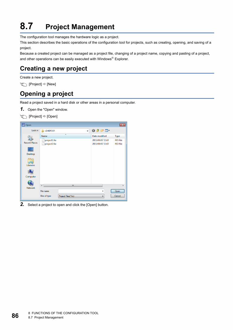
86
8.7 Project ManagementThe configuration tool manages the hardware logic as a project.This section describes the basic operations of the configuration tool for projects, such as creating, opening, and saving of a project.Because a created project can be managed as a project file, changing of a project name, copying and pasting of a project, and other operations can be easily executed with Windows Explorer.
Creating a new projectCreate a new project.
[Project] [New]
Opening a projectRead a project saved in a hard disk or other areas in a personal computer.
1. Open the "Open" window.
[Project] [Open]
2. Select a project to open and click the [Open] button.
8 FUNCTIONS OF THE CONFIGURATION TOOL8.7 Project Management
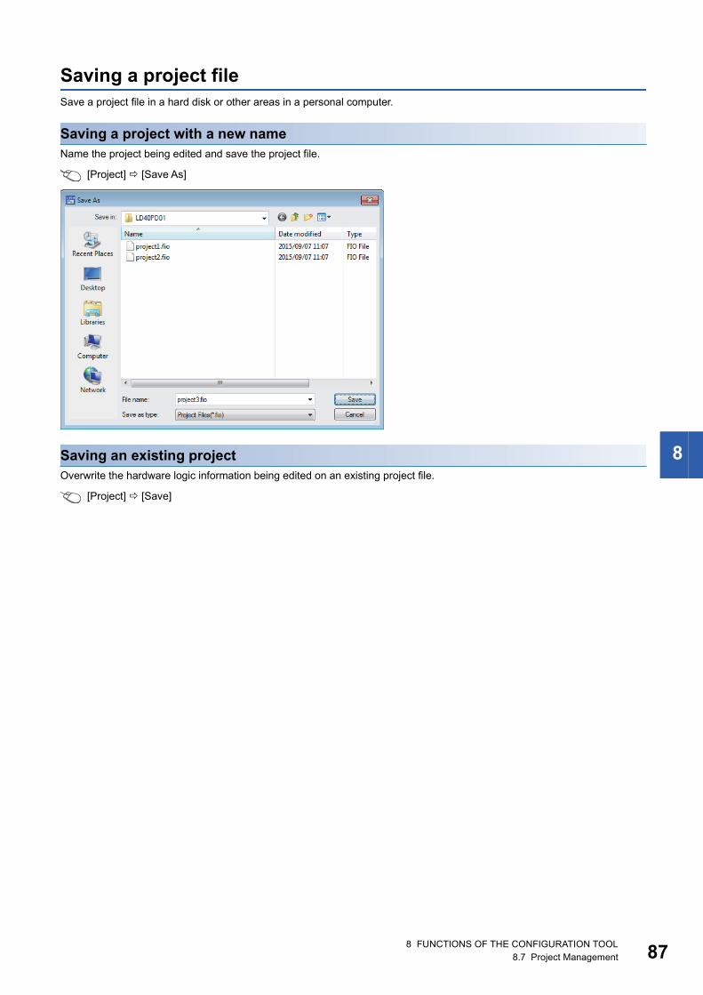
8
Saving a project fileSave a project file in a hard disk or other areas in a personal computer.
Saving a project with a new nameName the project being edited and save the project file.
[Project] [Save As]
Saving an existing projectOverwrite the hardware logic information being edited on an existing project file.
[Project] [Save]
8 FUNCTIONS OF THE CONFIGURATION TOOL8.7 Project Management 87

88
Verifying a project fileVerify the contents of a currently opened project and those of another project in a hard disk. Verification results are displayed in a list and mismatches can be checked.
Verifying the hardware logicThe following describes how to verify the hardware logic.
1. Select the following item.
[Project] [Project Verify]
2. Select a project in a hard disk to be verified.
3. Verification results are displayed.In the verification result window, the match/mismatch status (the links to the input terminals of each block, setting values of the block, and User Address) are displayed.
4. Double-click a mismatch to jump to the corresponding section in the work window. When the links are mismatched, the corresponding link in the work window is selected.
8 FUNCTIONS OF THE CONFIGURATION TOOL8.7 Project Management

8
SecurityWhen the hardware logic is written into a flash ROM, add a password to prevent inappropriate access to read the data.After the security is set to "Enable" and [Write to Module (execution + flash ROM)] in [Online] is executed, the password input window is displayed. After a password is input and writing data into the module is completed, the security becomes valid.To read the hardware logic to which the security has been enabled from a flash ROM to the module, input the set password. • When the security is enabled
• When the security is disabled
Setting method[Project] [Security] [Enable] or [Invalid]
When a new project is created, the security has been set to "Enable".
Operation details and restrictionsThe security setting is saved in a project.The security of the project created with the configuration tool of version 1.000A is set to "Invalid".
■Actions to be taken when "Write to Module (execution + flash ROM)" is executed
*1 When "Write to Module (execution memory)" is executed, the action same as the one to be taken when the security setting is "Invalid" is executed.
Security setting DescriptionEnable • The password registration window is displayed.
• The hardware logic is written with a password.
Invalid*1 • The password registration window is not displayed.• The hardware logic is written without a password.
LD40PD01
Write to Module (Execution memory + Flash ROM)
Password registration
Hardware logic + Password
Password matchedHardware logic
Password not matched
Password input
Hardware logic + Password
Read from Module (Flash ROM)
LD40PD01
Hardware logic
Hardware logic
Read from Module (Flash ROM)
Write to Module (Execution memory + Flash ROM)
8 FUNCTIONS OF THE CONFIGURATION TOOL8.7 Project Management 89

90
■Actions to be taken when "Read from Module (flash ROM)" is executed
■Operations that change the security settingWhen one of the following operations is performed, the security setting is changed.
Hardware logic in the module
Description
With a password • The password input window is displayed.• Only when the input password matches the password in the module, the hardware logic can be read.
Without a password • The password input window is not displayed.• The hardware logic can be always read.
Operation Security settingCreating a new project "Enable" is set.
Opening a project The project setting is reflected.
Reading data from the module The setting stored in the flash ROM of the flexible high-speed I/O control module is reflected.
8 FUNCTIONS OF THE CONFIGURATION TOOL8.7 Project Management

8
8.8 Windows for Creating the Hardware LogicThe following two types of window are prepared for creating the hardware logic. The window can be switched between the hardware logic outline window and the multi function counter block detail window.
Window DescriptionHardware logic outline window This window is for creating the outline of the hardware logic in the flexible
high-speed I/O control module. Multi function counter blocks are arranged, external I/O terminals are linked, and settings are configured in this window.
Multi function counter block detail window This window is for configuring the detail settings of the multi function counter blocks arranged in the hardware logic outline window.Switch multi function counter block detail windows (up to eight windows) and edit each multi function counter block.
Hardware logic outline window
Multi function counter block detail window
Double clickDouble click
Click
8 FUNCTIONS OF THE CONFIGURATION TOOL8.8 Windows for Creating the Hardware Logic 91

92
Hardware logic outline windowThe hardware logic outline window is composed of the following five sections. Depending on the section, the blocks that can be arranged differ.Change the setting and wiring of each block to create the hardware logic with various functions.
*1 For details on each block and terminal, refer to the following.Page 139 CREATING A HARDWARE LOGIC
Section Description Blocks and terminals that can be arranged*1
First section The blocks corresponding to inputs to the hardware logic have been arranged in this section.All the blocks in the first section are arranged when a project is started, and any blocks cannot be deleted or newly added from the Element Selection window.
• External input block• Y device terminal• OUT terminal
Second section Blocks corresponding to encoder inputs are arranged in this section. • Parallel encoder block• SSI encoder block
Third section Blocks that execute count with external input signals and the internal clock are arranged in this section.
Multi function counter block
Fourth section Blocks that calculate logical operations to input signals and outputs of multi function counter blocks are arranged in this section.
Logical operation block
Fifth section The blocks corresponding to outputs of the hardware logic have been arranged in this section.All the blocks in the fifth section are arranged when a project is started, and any blocks cannot be deleted or newly added from the Element Selection window.
• External output block• SI device terminal
8 FUNCTIONS OF THE CONFIGURATION TOOL8.8 Windows for Creating the Hardware Logic
8
Multi function counter block detail windowA multi function counter block detail window is composed of the following six sections.Change the setting and wiring of each block to create various count operations.
*1 For details on each block and terminal, refer to the following.Page 163 Multi Function Counter Block
*2 A cam switch block is arranged across the fourth and fifth sections.
Section Description Block and terminals that have been arranged*1
First section The terminals corresponding to inputs to a multi function counter block have been arranged in this section.An input to a multi function counter block in the hardware logic outline window is handled as an input in the multi function counter block detail window.
• Input terminal• Latch input terminal• Event input terminal
Second section Select a signal detection condition for each input signal.Desired conditions can be detected with the combinations of High/Low and rise/fall.
• Input signal event detection block
• Latch event detection block
Third section Counter timers that function depending on each event have been arranged.Switching of 16-bit signed counter/16-bit unsigned counter and 32-bit signed counter/32-bit unsigned counter is determined depending on the blocks arranged in the hardware logic outline window and cannot be changed in the multi function counter block detail window.
• Counter timer block (16bit_Unsigned)
• Counter timer block (16bit_Signed)
• Counter timer block (32bit_Unsigned)
• Counter timer block (32bit_Signed)
Fourth section An operation to compare a count value and a setting value of a counter timer is executed. Coincidence detections of count values can be executed with the comparison operation.
• Comparison block• Pattern generator block• Cam switch block*2
Fifth section Based on results of the comparison operation and event detections, the signals to be externally output are controlled.
• Set/reset block• Cam switch block*2
Sixth section The terminals corresponding to outputs of a multi function counter block have been arranged in this section.Outputs from the multi function counter block detail window are handled as outputs from the multi function counter block in the hardware logic outline window.
• Output terminal• Event output terminal• Pattern generator output
terminal• Cam switch output terminal
8 FUNCTIONS OF THE CONFIGURATION TOOL8.8 Windows for Creating the Hardware Logic 93
94
How to use blocks
Arranging blocksThe following describes how to arrange a block.
1. Select a block in the Element Selection window. Drag and drop the block into the hardware logic outline window.When a block is dragged into the hardware logic outline window, the area to which the block can be dropped is highlighted.
2. When the selected block is dropped into the work window, the block is automatically arranged in the highlighted area.
When three or more blocks have been arranged in the same section and blocks arranged between the top and bottom ones are deleted, that area becomes vacant. When a new block is arranged under this situation, the vacant area is highlighted and the block is arranged there.
Deleting a blockThe following describes how to delete a block.Only the blocks arranged from the Element Selection window can be deleted. The blocks that have been arranged by default cannot be deleted.When a block is deleted, the link of the block is also deleted.
1. Click the block to be deleted.The block is highlighted (displayed in yellow) and selected.
2. Right-click the block and select "Block Delete" from the context menu. Or press the key.When a block is deleted, the link of the block is also deleted.
• Users can also delete multi function counter blocks by right-clicking a multi function counter block name (Counter_) in the tree of the Navigation window and selecting "Block Delete" from the context menu.
• Select [Edit] [Block Delete] to perform the same operation as selecting "Block Delete" from the context menu.
Counter_0 Counter_0 Counter_0
Counter_1 Counter_1
Counter_2
Counter_3 Counter_3 Counter_3
Delete Counter_1 and Counter_2.
Place a new counter.
8 FUNCTIONS OF THE CONFIGURATION TOOL8.8 Windows for Creating the Hardware Logic
8
Block settingConfigure block settings by changing values in the drop-down lists and text boxes of each block.
■Input range of "User Address"
A single buffer memory address cannot be specified in several "User Address".For example, when the buffer memory address 1000 has been specified in "Count Value" and 1000 is specified in "Latch Value", the value in User Address is returned to the initial value.
No. Item name Description(1) Drop-down list Select a setting value from the drop-down list.
(2) Text box Input a one-byte numerical value (decimal).
(3) User Address • By assigning buffer memory addresses to "User Address", input terminal status and parameter setting values can be changed with programs and values of a hardware logic can be monitored during the hardware logic control. For details, refer to the following ( Page 169 Assignment of "User Address").
• Input decimal values in the setting.• The range of settable buffer memory addresses is 1000 to 1099 (High speed area: 1000 to 1029, low
speed area: 1030 to 1099). For details, refer to the following ( Page 95 Input range of "User Address").
Input range Description1000 to 1029 • The monitor items and setting items assigned in this area are read or written at a high speed (100s). These items are also read or
written when the flexible high-speed I/O control module sends an interrupt signal to the CPU module.• Assign even addresses to the parameters of two words (32 bits). Odd addresses cannot be assigned.
1030 to 1099 • The monitor items and setting items assigned in this area are read or written at a low speed (1ms).• Assign even addresses to the parameters of two words (32 bits). Odd addresses cannot be assigned.
(1)
(3)(2)
8 FUNCTIONS OF THE CONFIGURATION TOOL8.8 Windows for Creating the Hardware Logic 95
96
Linking blocksThe following describes how to link blocks.
1. Click the terminal to be a start point.The outer frame of the selected terminal is highlighted.
2. Click the terminal to be an end point.
The start point and end point are automatically linked.
Event terminals of a multi function counter block can be linked to Event terminals of another multi function counter block arranged in the same section.
8 FUNCTIONS OF THE CONFIGURATION TOOL8.8 Windows for Creating the Hardware Logic
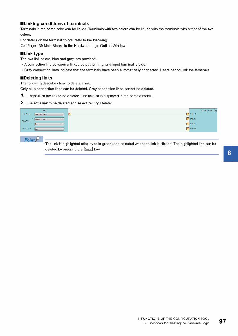
8
■Linking conditions of terminalsTerminals in the same color can be linked. Terminals with two colors can be linked with the terminals with either of the two colors.For details on the terminal colors, refer to the following.Page 139 Main Blocks in the Hardware Logic Outline Window
■Link typeThe two link colors, blue and gray, are provided. • A connection line between a linked output terminal and input terminal is blue. • Gray connection lines indicate that the terminals have been automatically connected. Users cannot link the terminals.
■Deleting linksThe following describes how to delete a link.Only blue connection lines can be deleted. Gray connection lines cannot be deleted.
1. Right-click the link to be deleted. The link list is displayed in the context menu.
2. Select a link to be deleted and select "Wiring Delete".
The link is highlighted (displayed in green) and selected when the link is clicked. The highlighted link can be deleted by pressing the key.
8 FUNCTIONS OF THE CONFIGURATION TOOL8.8 Windows for Creating the Hardware Logic 97

98
Copying a blockA block arranged in the hardware logic outline window can be copied by block unit. The setting values can be changed by block in a batch and an arranged block can be copied.
■Procedure of copying a blockThe following describes the procedure of copying a block.
1. Click the block to be copied.The block is highlighted (displayed in yellow) and selected.
2. Right-click the block and select "Copy" from the context menu.
• Users can also copy multi function counter blocks by right-clicking a multi function counter block name (Counter_) in the tree of the Navigation window and selecting "Copy" from the context menu.
• Select [Edit] [Copy] to perform the same operation as selecting "Copy" from the context menu.
■Operation details and restrictions • Multiple blocks cannot be copied at a time. Only a single block can be copied. • The link between the block to be copied and other blocks is not copied. However, when the block to be copied is a multi
function counter, link information in the multi function counter block detail window is also copied. • The following table shows which main blocks can be copied.
*1 This indicates a section in the hardware logic outline window.
Section*1 Target block Copying Item to be copied1 External input block Possible Setting values of the block
• Y device terminal• OUT terminal
Impossible
2 • Parallel encoder block• SSI encoder block
Possible Setting values of the block
3 Multi function counter block Possible • Setting values (the setting value of User Address is not included), links, and comments in the multi function counter block detail window
• Link between Event terminals of a multi function counter block in the hardware logic outline window (the links across blocks cannot be copied.)
4 Logical operation block Possible The setting value of the block
5 External output block Possible Setting values of the block
SI device terminal Impossible
8 FUNCTIONS OF THE CONFIGURATION TOOL8.8 Windows for Creating the Hardware Logic

8
Pasting a blockThis function pastes the copy of a block. Select [Edit] [Paste] for a block with the same type as the copy to overwrite the setting values with the ones of the copy at a time. Select [Edit] [Insert and Paste] to add the copy as a new block in the hardware logic outline window.
■Procedure of [Paste]The following describes the procedure of [Paste].
1. Click the block on which the copy is to be pasted.The block is highlighted (displayed in yellow) and selected.
2. Right-click the block and select "Paste" from the context menu.
3. The setting values of the block are overwritten with the ones of the copy.
• Users can also paste multi function counter blocks by right-clicking a multi function counter block name (Counter_) in the tree of the Navigation window and selecting "Paste" from the context menu.
• Select [Edit] [Paste] to perform the same operation as selecting "Paste" from the context menu.
■Procedure of [Insert and Paste]The following describes the procedure of [Insert and Paste].
1. Select the following item.
[Edit] [Insert and Paste]
2. The copy of a block is added as a new block in the hardware logic outline window.
■Operation details and restrictions • Selecting the block on which the copy of a block is to be pasted and selecting [Edit] [Paste] overwrites the setting values
of the target block with the ones of the copy at a time. • Selecting [Edit] [Insert and Paste] adds the copy of a block as a new block in the hardware logic outline window. • Only a block with the same type as the copy of a block can be specified as a "Paste" target. If a block whose type is
different from the one of the copy has been selected, the copy cannot be pasted. The setting values of a multi function counter block cannot be overwritten unless the data type of sign/unsigned and 16 bits/32 bits matches between the paste target and the copy.
8 FUNCTIONS OF THE CONFIGURATION TOOL8.8 Windows for Creating the Hardware Logic 99

10
Adding a commentComments can be arranged in the Work window.
Inserting a commentThe following describes the procedure of inserting a comment.
1. Right-click the area in which a comment is to be inserted in the Work window.
2. Select "Comment Insert" from the context menu.
Comments can also be inserted by selecting [Edit] [Comment Insert].
3. A new comment is inserted in the Work window. Enter a text in the comment.
4. To complete entering a text in the comment, click any area other than the comment in the Work window.The comment is not selected (displayed in yellow).
5. To enter a text in the comment again, double-click the comment.
0 8 FUNCTIONS OF THE CONFIGURATION TOOL8.8 Windows for Creating the Hardware Logic
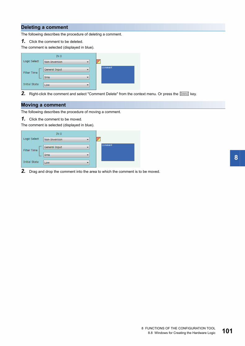
8
Deleting a commentThe following describes the procedure of deleting a comment.
1. Click the comment to be deleted.The comment is selected (displayed in blue).
2. Right-click the comment and select "Comment Delete" from the context menu. Or press the key.
Moving a commentThe following describes the procedure of moving a comment.
1. Click the comment to be moved.The comment is selected (displayed in blue).
2. Drag and drop the comment into the area to which the comment is to be moved.
8 FUNCTIONS OF THE CONFIGURATION TOOL8.8 Windows for Creating the Hardware Logic 101

10
Cutting, copying, and pasting a commentThe following describes the procedure of cutting, copying, and pasting a comment.
1. Click the comment to be cut or copied.The comment is selected (displayed in blue).
2. Right-click the comment, and select "Comment Cut" or "Comment Copy" from the context menu.
3. Right-click the area on which the comment is to be pasted in the Work window.
4. Select "Comment Paste" from the context menu.
5. The cut or copied comment is pasted in the Work window.
A comment can be overwritten with the cut or copied comment by selecting another comment and executing "Comment Paste".
Displaying or hiding a commentWhether to display or hide a comment can be switched.
[View] [Comment Display]The setting of whether to display or hide a comment is also reflected to printed results.
2 8 FUNCTIONS OF THE CONFIGURATION TOOL8.8 Windows for Creating the Hardware Logic
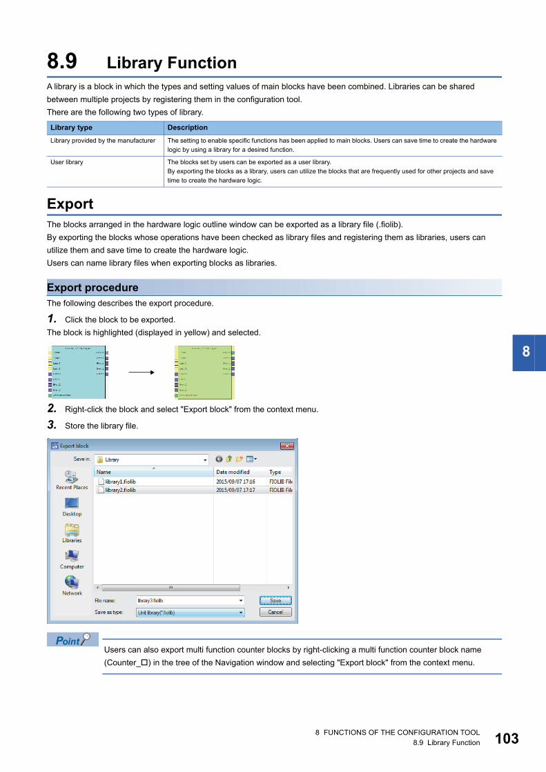
8
8.9 Library FunctionA library is a block in which the types and setting values of main blocks have been combined. Libraries can be shared between multiple projects by registering them in the configuration tool.There are the following two types of library.
ExportThe blocks arranged in the hardware logic outline window can be exported as a library file (.fiolib).By exporting the blocks whose operations have been checked as library files and registering them as libraries, users can utilize them and save time to create the hardware logic.Users can name library files when exporting blocks as libraries.
Export procedureThe following describes the export procedure.
1. Click the block to be exported.The block is highlighted (displayed in yellow) and selected.
2. Right-click the block and select "Export block" from the context menu.
3. Store the library file.
Users can also export multi function counter blocks by right-clicking a multi function counter block name (Counter_) in the tree of the Navigation window and selecting "Export block" from the context menu.
Library type DescriptionLibrary provided by the manufacturer The setting to enable specific functions has been applied to main blocks. Users can save time to create the hardware
logic by using a library for a desired function.
User library The blocks set by users can be exported as a user library.By exporting the blocks as a library, users can utilize the blocks that are frequently used for other projects and save time to create the hardware logic.
8 FUNCTIONS OF THE CONFIGURATION TOOL8.9 Library Function 103

10
Operation details and restrictions • Multiple blocks cannot be exported at a time. Only a single block can be exported. • The link between the block to be exported and other blocks is not exported. However, when the block to be exported is a
multi function counter block, the link information in the multi function counter block detail window and the link between Event terminals of a multi function counter block in the hardware logic outline window are also exported.
• The following table shows which main block can be exported.
*1 This indicates a section in the hardware logic outline window.
Section*1 Target block Export Item to be exported1 • External input block
• Y device terminal• OUT terminal
Impossible
2 • Parallel encoder block• SSI encoder block
Possible Setting values of the block
3 Multi function counter block Possible • Setting values (the setting value of User Address is not included), links, and comments in the multi function counter block detail window
• Link between Event terminals of a multi function counter block in the hardware logic outline window (the links across blocks cannot be exported.)
4 Logical operation block Impossible
5 • External output block• SI device terminal
Impossible
4 8 FUNCTIONS OF THE CONFIGURATION TOOL8.9 Library Function

8
Library operationThe following describes the library.
No library exists immediately after the installation of the configuration tool. Register libraries as necessary.
Registering a libraryRegister the libraries provided by the manufacturer and exported user libraries in the configuration tool. Registering libraries adds the blocks in library files in the "Library" tab in the Element Selection window.
1. Select the following item.
[Edit] [Library Registration]
2. Open a library file to be registered in the configuration tool.
3. The registered library is added in the "Library" tab in the Element Selection window.
How to use a libraryRegistered libraries can be selected from the Element Selection window and dragged and dropped into the work window to arrange them in the same way as main blocks.
1. Select a block in the Element Selection window. Drag and drop the block into the hardware logic outline window.When a block is dragged into the hardware logic outline window, the area to which the block can be dropped is highlighted.
2. When the selected block is dropped into the work window, the block is automatically arranged in the highlighted area.The block name of the arranged library is the same as the main block. For example, when a registered block as a library is a 16-bit unsigned counter, the name of the block arranged in the work window is "Counter_(16bit_Unsigned)".
How to delete a libraryLibraries that are no longer required can be deleted from the configuration tool.
1. Click the library to be deleted in the Element Selection window.
2. Right-click the library and select "Eliminate Registration of Library" from the context menu.Even though the library is deleted, the library file is not deleted from the storage folder. To use the library again, register the library again.
Select [Edit] [Library Delete] to perform the same operation as selecting "Eliminate Registration of Library" from the context menu.
8 FUNCTIONS OF THE CONFIGURATION TOOL8.9 Library Function 105
10
8.10 Online FunctionsConnect the computer in which the configuration tool has been installed and the CPU module, and read or write data from/to the flexible high-speed I/O control module through the CPU module. The following table lists the online functions.
*1 The statuses of I/O signals in the hardware logic are described as High and Low. For details, refer to the following.Page 140 Signal status name
If a communication error occurs while an online function is being executed, the possible cause is one of the following causes. Check the target module and communication status. • A module with the target start I/O number does not exist. • A communication error has occurred during online access. • Cable error
Start I/O number settingSet the start I/O number of the flexible high-speed I/O control module.
[Online] [Start I/O number setting]Setting the I/O assignment to GX Works2 and the configuration tool enables writing of data into the flexible high-speed I/O control module and the monitor display through the CPU module.However, match the I/O assignment of the flexible high-speed I/O control module in the configuration tool and that in GX Works2. If the I/O assignment is changed on GX Works2 and data writing to the module, the monitor display, or simulation is executed after the start I/O number has been set with the configuration tool, a communication error will occur.
Function Description ReferenceStart I/O number setting Sets the start I/O number of the flexible high-speed I/O control module. Page 106 Start I/O
number setting
Write to Module (Execution memory)
Writes the hardware logic to only the execution memory. Page 107 Writing data to the module
Write to Module (Execution memory + Flash ROM)
Writes the hardware logic to both the execution memory and the flash ROM.
Read from Module (Flash ROM) Reads the hardware logic saved in the flash ROM to the configuration tool. Page 108 Reading data from the module
Verify with Module (Flash ROM) Verifies the hardware logic in the configuration tool and the setting data written in the flash ROM.
Page 109 Verifying with the module
Module operation Starts/stops the hardware logic control. Page 110 Module operation
Monitor Monitors the on/off states of I/O terminals and count values.The following lists the items that can be monitored.*1
• ON/OFF states of external input terminals corresponding to external input blocks (hardware logic outline window)
• High/Low states of output terminals in an external input block (hardware logic outline window)
• High/Low states of the Output 0 terminal in a multi function counter block (hardware logic outline window)
• High/Low states of input terminals in an external output block (hardware logic outline window)
• ON/OFF states of external output terminals corresponding to external output blocks (hardware logic outline window)
• Internal action states of input terminals and count values in a counter timer block (multi function counter block detail window)
Page 111 Monitor
6 8 FUNCTIONS OF THE CONFIGURATION TOOL8.10 Online Functions
8
Writing data to the moduleWrite the hardware logic to the execution memory of the flexible high-speed I/O control module.The execution memory and the flash ROM can be selected as the write destination of the data. Select only the execution memory or both the execution memory and the flash ROM as the write destination.Because the hardware logic written into the flash ROM is read to the execution memory at power-on, a control can be started without re-setting. However, the number of writable times to a flash ROM is 10000 times. Thus, using different write destinations as shown in the following examples is recommended. • When the adjustment is repeated with changing the settings, select "Write to Module (execution memory)". • After the adjustment is completed, select "Write to Module (execution + flash ROM)".Users can set a password for the hardware logic by setting "Enable" in the [Security] menu of [Project]. For the hardware logic with a password, users are required to input the password for reading the hardware logic from the module.
Writing dataThe following describes how to write data.
1. Select a writing method depending on a selected write destination.
[Online] [Write to Module (execution memory)] or [Write to Module (execution + flash ROM)]When "Write to Module (execution + flash ROM)" has been selected and the number of writes to flash ROM exceeds 10000 times, the error window is displayed. Data can be written to the module even in such situation. However, the data written in the flash ROM is not guaranteed.
2. When the following conditions are satisfied, set a password. • "Enable" has been set in the [Security] menu of [Project]. • [Write to Module (execution + flash ROM)] has been selected.
• If data writing is executed while the hardware logic control is operating, the hardware logic control will stop and the data will be written to the module. After the data writing is completed, the hardware logic control restarts.
• If data writing is executed while the hardware logic control has stopped, the stop status of the hardware logic control will continue.
8 FUNCTIONS OF THE CONFIGURATION TOOL8.10 Online Functions 107
10
Reading data from the moduleRead the hardware logic saved in the flash ROM of the flexible high-speed I/O control module to the configuration tool.The hardware logic being edited is overwritten by the read data. Save the hardware logic before the data reading as necessary.
Reading dataThe following describes how to read data.
1. Select the following item.
[Online] [Read from Module (flash ROM)]
2. To read the hardware logic with a password, input the password set when the data was written to the module.
8 8 FUNCTIONS OF THE CONFIGURATION TOOL8.10 Online Functions
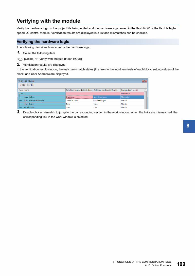
8
Verifying with the moduleVerify the hardware logic in the project file being edited and the hardware logic saved in the flash ROM of the flexible high-speed I/O control module. Verification results are displayed in a list and mismatches can be checked.
Verifying the hardware logicThe following describes how to verify the hardware logic.
1. Select the following item.
[Online] [Verify with Module (Flash ROM)]
2. Verification results are displayed.In the verification result window, the match/mismatch status (the links to the input terminals of each block, setting values of the block, and User Address) are displayed.
3. Double-click a mismatch to jump to the corresponding section in the work window. When the links are mismatched, the corresponding link in the work window is selected.
8 FUNCTIONS OF THE CONFIGURATION TOOL8.10 Online Functions 109
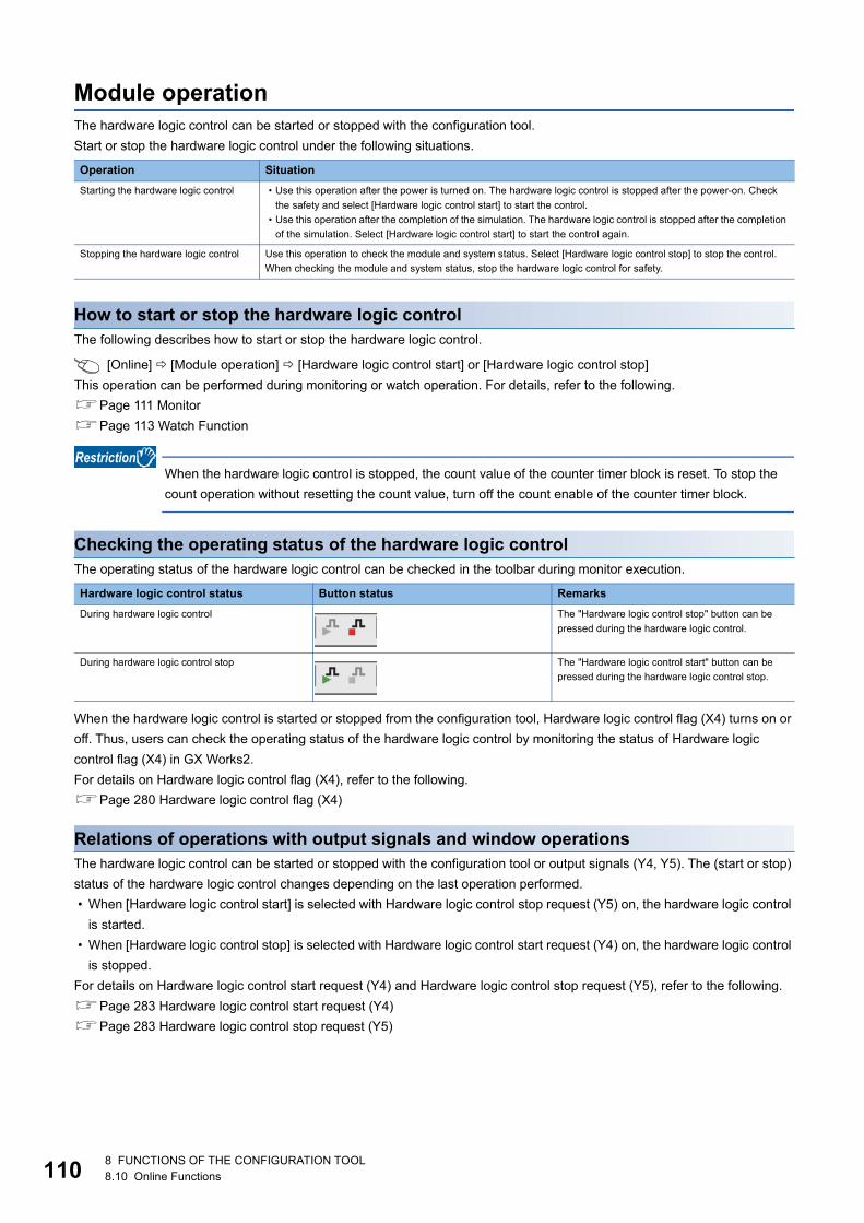
11
Module operationThe hardware logic control can be started or stopped with the configuration tool.Start or stop the hardware logic control under the following situations.
How to start or stop the hardware logic controlThe following describes how to start or stop the hardware logic control.
[Online] [Module operation] [Hardware logic control start] or [Hardware logic control stop]This operation can be performed during monitoring or watch operation. For details, refer to the following.Page 111 MonitorPage 113 Watch Function
When the hardware logic control is stopped, the count value of the counter timer block is reset. To stop the count operation without resetting the count value, turn off the count enable of the counter timer block.
Checking the operating status of the hardware logic controlThe operating status of the hardware logic control can be checked in the toolbar during monitor execution.
When the hardware logic control is started or stopped from the configuration tool, Hardware logic control flag (X4) turns on or off. Thus, users can check the operating status of the hardware logic control by monitoring the status of Hardware logic control flag (X4) in GX Works2.For details on Hardware logic control flag (X4), refer to the following.Page 280 Hardware logic control flag (X4)
Relations of operations with output signals and window operationsThe hardware logic control can be started or stopped with the configuration tool or output signals (Y4, Y5). The (start or stop) status of the hardware logic control changes depending on the last operation performed. • When [Hardware logic control start] is selected with Hardware logic control stop request (Y5) on, the hardware logic control
is started. • When [Hardware logic control stop] is selected with Hardware logic control start request (Y4) on, the hardware logic control
is stopped.For details on Hardware logic control start request (Y4) and Hardware logic control stop request (Y5), refer to the following.Page 283 Hardware logic control start request (Y4)Page 283 Hardware logic control stop request (Y5)
Operation SituationStarting the hardware logic control • Use this operation after the power is turned on. The hardware logic control is stopped after the power-on. Check
the safety and select [Hardware logic control start] to start the control.• Use this operation after the completion of the simulation. The hardware logic control is stopped after the completion
of the simulation. Select [Hardware logic control start] to start the control again.
Stopping the hardware logic control Use this operation to check the module and system status. Select [Hardware logic control stop] to stop the control. When checking the module and system status, stop the hardware logic control for safety.
Hardware logic control status Button status RemarksDuring hardware logic control The "Hardware logic control stop" button can be
pressed during the hardware logic control.
During hardware logic control stop The "Hardware logic control start" button can be pressed during the hardware logic control stop.
0 8 FUNCTIONS OF THE CONFIGURATION TOOL8.10 Online Functions

8
MonitorThe High/Low states of I/O terminals and count values are displayed in the hardware logic outline window or a multi function counter block detail window.The following lists the items that can be monitored.
How to useThe following shows how to start, stop, and end the monitoring.
[Online] [Monitor] [Start Monitoring] (or [Start Monitoring (All Windows)], [Stop Monitoring], or [End Monitoring] (or [End Monitoring (All Windows)])
The monitoring can be started, stopped, or ended under the following conditions.
*1 The current window mode can be checked on the status bar.
The monitoring and watch can be simultaneously started or stopped by performing [Online] [Monitor] [Start Monitoring (All Windows)] or [End Monitoring (All Windows)].For details on the watch function, refer to the following.Page 113 Watch Function
Although switching of the window between the hardware logic outline window and multi function counter block detail windows and changing of the display position by the map display window are allowed even during monitoring, operations other than them cannot be executed.
Window Block ItemHardware logic outline window External input block ON/OFF state of the corresponding external input
terminal
High/Low state of the output terminal
Multi function counter block High/Low state of the Output 0 terminal
External output block High/Low state of the input terminal
ON/OFF state of the corresponding external output terminal
Multi function counter block detail window
Counter timer block • Internal action state of the input terminal• Count value
Operation Condition[Start Monitoring] Can be used when the window mode*1 is "Edit Mode" or "Monitor Mode".
[Start Monitoring (All Windows)] Can be used other than in the situation where no project is opened.
[Stop Monitoring] Can be used when the window mode*1 is "Monitor Mode".
[End Monitoring] Can be used when the window mode*1 is "Monitor Mode".
[End Monitoring (All Windows)] Can be used other than in the situation where no project is opened.
8 FUNCTIONS OF THE CONFIGURATION TOOL8.10 Online Functions 111
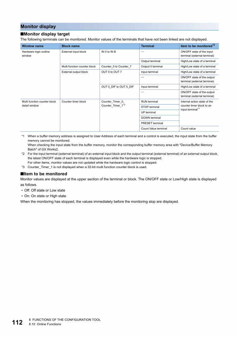
11
Monitor display■Monitor display targetThe following terminals can be monitored. Monitor values of the terminals that have not been linked are not displayed.
*1 When a buffer memory address is assigned to User Address of each terminal and a control is executed, the input state from the buffer memory cannot be monitored.When checking the input state from the buffer memory, monitor the corresponding buffer memory area with "Device/Buffer Memory Batch" of GX Works2.
*2 For the input terminal (external terminal) of an external input block and the output terminal (external terminal) of an external output block, the latest ON/OFF state of each terminal is displayed even while the hardware logic is stopped.For other items, monitor values are not updated while the hardware logic control is stopped.
*3 Counter_Timer_1 is not displayed when a 32-bit multi function counter block is used.
■Item to be monitoredMonitor values are displayed at the upper section of the terminal or block. The ON/OFF state or Low/High state is displayed as follows. • Off: Off state or Low state • On: On state or High stateWhen the monitoring has stopped, the values immediately before the monitoring stop are displayed.
Window name Block name Terminal Item to be monitored*2
Hardware logic outline window
External input block IN 0 to IN B ON/OFF state of the input terminal (external terminal)
Output terminal High/Low state of a terminal
Multi function counter block Counter_0 to Counter_7 Output 0 terminal High/Low state of a terminal
External output block OUT 0 to OUT 7 Input terminal High/Low state of a terminal
ON/OFF state of the output terminal (external terminal)
OUT 0_DIF to OUT 5_DIF Input terminal High/Low state of a terminal
ON/OFF state of the output terminal (external terminal)
Multi function counter block detail window
Counter timer block Counter_Timer_0, Counter_Timer_1*3
RUN terminal Internal action state of the counter timer block to an input terminal*1
STOP terminal
UP terminal
DOWN terminal
PRESET terminal
Count Value terminal Count value
2 8 FUNCTIONS OF THE CONFIGURATION TOOL8.10 Online Functions
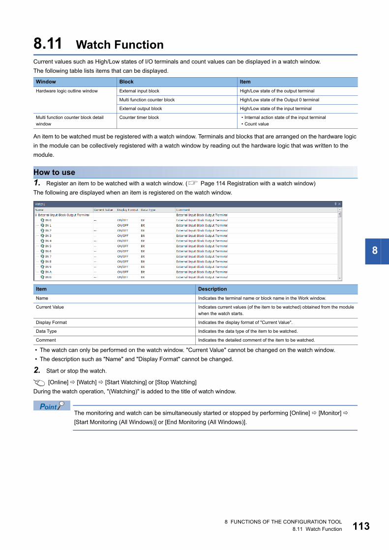
8
8.11 Watch FunctionCurrent values such as High/Low states of I/O terminals and count values can be displayed in a watch window.The following table lists items that can be displayed.
An item to be watched must be registered with a watch window. Terminals and blocks that are arranged on the hardware logic in the module can be collectively registered with a watch window by reading out the hardware logic that was written to the module.
How to use1. Register an item to be watched with a watch window. ( Page 114 Registration with a watch window)The following are displayed when an item is registered on the watch window.
• The watch can only be performed on the watch window. "Current Value" cannot be changed on the watch window. • The description such as "Name" and "Display Format" cannot be changed.
2. Start or stop the watch.
[Online] [Watch] [Start Watching] or [Stop Watching]During the watch operation, "(Watching)" is added to the title of watch window.
The monitoring and watch can be simultaneously started or stopped by performing [Online] [Monitor] [Start Monitoring (All Windows)] or [End Monitoring (All Windows)].
Window Block ItemHardware logic outline window External input block High/Low state of the output terminal
Multi function counter block High/Low state of the Output 0 terminal
External output block High/Low state of the input terminal
Multi function counter block detail window
Counter timer block • Internal action state of the input terminal• Count value
Item DescriptionName Indicates the terminal name or block name in the Work window.
Current Value Indicates current values (of the item to be watched) obtained from the module when the watch starts.
Display Format Indicates the display format of "Current Value".
Data Type Indicates the data type of the item to be watched.
Comment Indicates the detailed comment of the item to be watched.
8 FUNCTIONS OF THE CONFIGURATION TOOL8.11 Watch Function 113
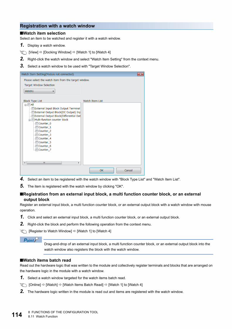
11
Registration with a watch window■Watch item selectionSelect an item to be watched and register it with a watch window.
1. Display a watch window.
[View] [Docking Window] [Watch 1] to [Watch 4]
2. Right-click the watch window and select "Watch Item Setting" from the context menu.
3. Select a watch window to be used with "Target Window Selection".
4. Select an item to be registered with the watch window with "Block Type List" and "Watch Item List".
5. The item is registered with the watch window by clicking "OK".
■Registration from an external input block, a multi function counter block, or an external output block
Register an external input block, a multi function counter block, or an external output block with a watch window with mouse operation.
1. Click and select an external input block, a multi function counter block, or an external output block.
2. Right-click the block and perform the following operation from the context menu.
[Register to Watch Window] [Watch 1] to [Watch 4]
Drag-and-drop of an external input block, a multi function counter block, or an external output block into the watch window also registers the block with the watch window.
■Watch items batch readRead out the hardware logic that was written to the module and collectively register terminals and blocks that are arranged on the hardware logic in the module with a watch window.
1. Select a watch window targeted for the watch items batch read.
[Online] [Watch] [Watch Items Batch Read] [Watch 1] to [Watch 4]
2. The hardware logic written in the module is read out and items are registered with the watch window.
4 8 FUNCTIONS OF THE CONFIGURATION TOOL8.11 Watch Function

8
■Watch item deletionAn item registered with a watch window can be deleted.
1. Click and select an item to be deleted from a watch window.
2. Right-click the item and select "Delete" from the context menu. Or press the key.
8 FUNCTIONS OF THE CONFIGURATION TOOL8.11 Watch Function 115

11
Watch display■Watch targetThe following table lists terminals targeted for the watch.
*1 When a buffer memory address is assigned to User Address of each terminal and a control is executed, the input state from the buffer memory cannot be monitored.When checking the input state from the buffer memory, monitor the corresponding buffer memory area with "Device/Buffer Memory Batch" of GX Works2.
*2 "Current Value" is not updated while the hardware logic control is stopped.*3 Counter_Timer_1 is not displayed when a 32-bit multi function counter block is used.
■"Current Value" displayThe ON/OFF state or Low/High state is displayed as follows. • OFF: OFF state or Low state • ON: ON state or High stateWhen the watch operation has stopped, the value immediately before the stop is still displayed.
Window name Block name Terminal "Current Value" display*2
Hardware logic outline window
External input block IN 0 to IN B Output terminal High/Low state of a terminal
Multi function counter block Counter_0 to Counter_7 Output 0 terminal High/Low state of a terminal
External output block OUT 0 to OUT 7 Input terminal High/Low state of a terminal
OUT 0_DIF to OUT 5_DIF Input terminal High/Low state of a terminal
Multi function counter block detail window
Counter timer block Counter_Timer_0, Counter_Timer_1*3
RUN terminal Internal action state of the counter timer block to an input terminal*1
STOP terminal
UP terminal
DOWN terminal
PRESET terminal
Count Value terminal Count value
6 8 FUNCTIONS OF THE CONFIGURATION TOOL8.11 Watch Function
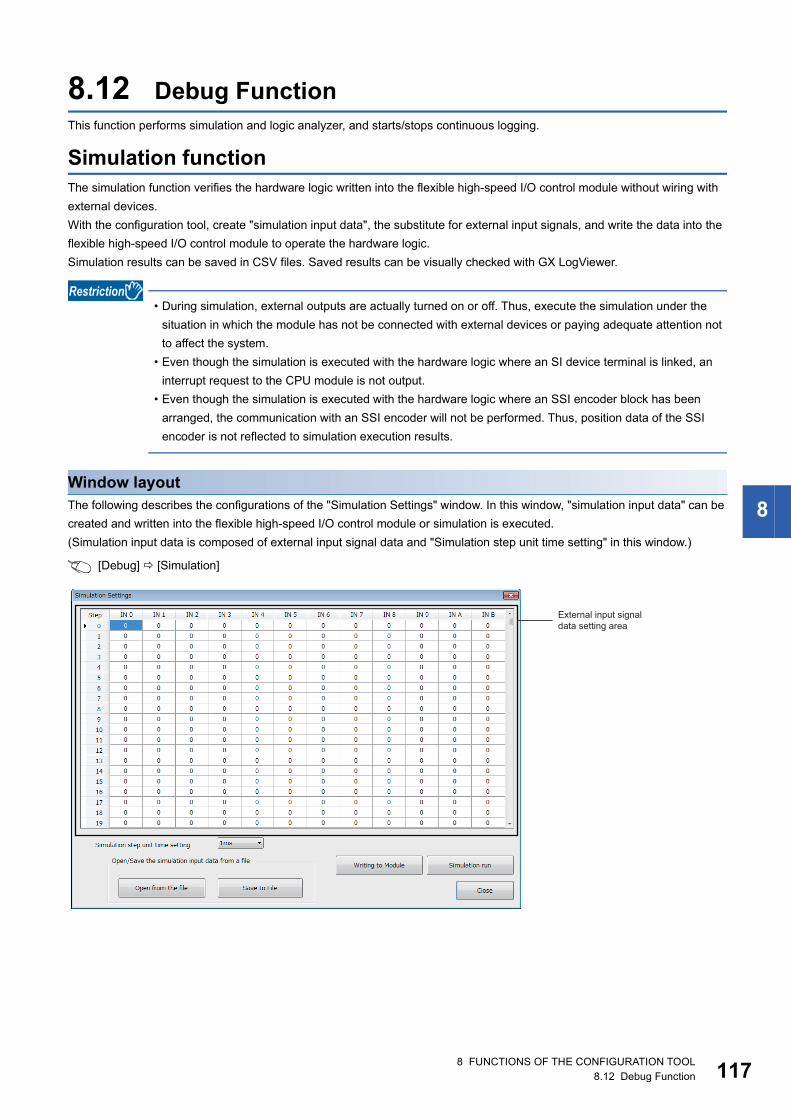
8
8.12 Debug FunctionThis function performs simulation and logic analyzer, and starts/stops continuous logging.
Simulation functionThe simulation function verifies the hardware logic written into the flexible high-speed I/O control module without wiring with external devices.With the configuration tool, create "simulation input data", the substitute for external input signals, and write the data into the flexible high-speed I/O control module to operate the hardware logic.Simulation results can be saved in CSV files. Saved results can be visually checked with GX LogViewer.
• During simulation, external outputs are actually turned on or off. Thus, execute the simulation under the situation in which the module has not be connected with external devices or paying adequate attention not to affect the system.
• Even though the simulation is executed with the hardware logic where an SI device terminal is linked, an interrupt request to the CPU module is not output.
• Even though the simulation is executed with the hardware logic where an SSI encoder block has been arranged, the communication with an SSI encoder will not be performed. Thus, position data of the SSI encoder is not reflected to simulation execution results.
Window layoutThe following describes the configurations of the "Simulation Settings" window. In this window, "simulation input data" can be created and written into the flexible high-speed I/O control module or simulation is executed.(Simulation input data is composed of external input signal data and "Simulation step unit time setting" in this window.)
[Debug] [Simulation]
External input signal data setting area
8 FUNCTIONS OF THE CONFIGURATION TOOL8.12 Debug Function 117
11
The following table lists the items to be displayed in the "Simulation Settings" window.
Data that can be acquired as simulation execution resultsUsers can acquire the following data by executing simulation. The execution result data acquired after simulation can be saved in a CSV format file. The file can be visually checked with GX LogViewer.
*1 Simulation results of the blocks arranged in the hardware logic outline window are acquired.*2 Data of Counter_Timer_1 is not acquired when a 32-bit multi function counter block is used.
Item DescriptionExternal input signal data setting area To verify the hardware logic, set the status of data to be imported as external
input signals (IN 0 to IN B).The setting value 0 indicates that an external input signal is off, and the setting value 1 indicates that an external input signal is on.Click a cell and switch the value between 0 (OFF) to 1 (ON).Columns in the area indicate the 12 points of the external input signals (IN 0 to IN B) and rows indicate 2048 steps (0 to 2047).In the simulation, the hardware logic is executed one step by one step at every cycle which is set in "Simulation step unit time setting".
"Simulation step unit time setting" Set the cycle to switch external input signal data to the next step.Sampling of simulation results is also executed at this set cycle.
"Open from the file" button Reads the simulation input data saved in a CSV file to the "Simulation Settings" window.
"Save to File" button Saves the simulation input data in the "Simulation Settings" window into a CSV file.
"Writing to Module" button Writes the simulation input data set in the "Simulation Settings" window into the module. The written data is held until the flexible high-speed I/O control module is powered off.To execute the simulation, write simulation input data into the module in advance.
"Simulation run" button Executes the simulation with the simulation input data and hardware logic written into the module.After the completion of the simulation, the "A simulation execution result is saved." dialog box is displayed. Save the simulation execution result.
"Close" button Closes the "Simulation Settings" window.
Window name Block name Terminal Data to be acquiredHardware logic outline window
External input block IN 0 to IN B Output terminal High/Low state of a terminal
External output block OUT 0 to OUT 7 Input terminal
OUT 0_DIF to OUT 5_DIF Input terminal
Multi function counter block detail window*1
Counter timer block Counter_Timer_0, Counter_Timer_1*2
RUN terminal Internal action state of the counter timer block to an input terminal
STOP terminal
UP terminal
DOWN terminal
PRESET terminal
Count Value terminal Count value
8 8 FUNCTIONS OF THE CONFIGURATION TOOL8.12 Debug Function
8
How to useThe following describes how to use the simulation function.
1. Open the "Simulation Settings" window.
[Debug] [Simulation]
2. Click each cell in the external input signal data setting area and switch "0: External input signal OFF" and "1: External input signal ON". By default, "0: External input signal OFF" have been set in all cells.
8 FUNCTIONS OF THE CONFIGURATION TOOL8.12 Debug Function 119
12
3. Set "Simulation step unit time setting".Changing "Simulation step unit time setting" changes the following timing. • Timing to move external input data to the next step (Data is changed one step by one step at the set unit time.) • Acquisition interval of execution result data (An execution result for one step is acquired at the set unit time.)
Users can save the set simulation input data with the "Save to File" button (Data is saved only in CSV format).The following shows the CSV file format specifications. When creating a CSV file with any method other than the one using the "Simulation Settings" window, create the file in the same format.
Users can open a saved CSV file from "Open from the file" of "Open/Save the simulation input data from a file".
• The "Writing to Module" button only writes simulation input data into the module. Write the hardware logic into the module in advance.
• The simulation input data written into the module is cleared when the module is powered off. • When the external input signal data in the CSV file selected from "Open from the file" has less than 2048
steps or 12 rows, the data is not reflected in the "Simulation Settings" window. When the data has 2048 steps or more or 12 rows or more, the external input signal data of 2048 steps or 12 rows is read. The data that is not the read target is discarded.
Item name CharacterDelimiter Comma (,)
Return code CRLF (0x0D, 0x0A)
Row Description1st row The simulation step unit time setting is output.
Simulation step unit time setting Value output into a CSV file
1ms 8
100s 7
10s 6
1s 5
0.1s 4
50ns 3
25ns 2
2nd to 2049th row One row indicates one step, and external input signal data is output as "0: OFF" or "1: ON" in order of IN 0, IN 1 to IN B starting from the left row.
0 8 FUNCTIONS OF THE CONFIGURATION TOOL8.12 Debug Function
8
4. Click "Writing to Module" to write the simulation input data into the flexible high-speed I/O control module.
If a communication error has occurred during the communication with the module with the simulation function, the possible cause is one of the following causes. Check the target module and communication status. • A module with the target start I/O number does not exist. • A communication error has occurred during online access. • Cable error
5. Click "Simulation run" to execute the simulation of the written simulation input data.The simulation is executed by using the hardware logic and simulation input data written into the module. When the simulation input data has been edited, always press the "Write to Module" button to write the data into the module in advance.
• If the simulation is started during a hardware logic control, the hardware logic control will stop. After the completion of the simulation, the stop status of the hardware logic control will continue. To start the hardware logic control after the simulation, turn on Hardware logic control start request (Y4).
• If Hardware logic control start request (Y4) or Hardware logic control stop request (Y5) is turned on during the simulation, simulation execution results cannot be properly acquired.
• If Hardware logic control start request (Y4) is turned on while simulation execution results are being acquired after the simulation, the acquisition of the simulation execution results will stop.
• When the simulation is executed during execution of the logic analyzer function, the logic analyzer function stops. The logic analyzer function will not restart after completion of the simulation execution. To restart it, issue a trigger start request.
• When the simulation is executed during continuous logging, the continuous logging stops. The continuous logging will not restart after completion of the simulation execution. To restart it, issue a continuous logging start request.
8 FUNCTIONS OF THE CONFIGURATION TOOL8.12 Debug Function 121

12
6. Save the simulation execution results. (Data is saved only in the CSV format.)
7. The simulation execution results can be visually checked with GX LogViewer.
For details on GX LogViewer, refer to the following. GX LogViewer Version 1 Operating Manual
2 8 FUNCTIONS OF THE CONFIGURATION TOOL8.12 Debug Function
8
CSV file format of simulation execution resultsThe following shows the CSV format specifications of simulation execution results.
■1st row[LOGGING], LD40PD01_1, 2, 3, and 4 are output (fixed output).
■2nd rowThe data type of the simulation execution result is output.
TRIGGER[*] is output in the last column of the 2nd row (fixed output).
■3rd rowThe name of each input or output terminal is output.
Trigger is output in the last column of the 3rd row (fixed output).
■4th to 2051st rowThe acquired data is chronologically output (at the set simulation step unit time).
*1 Data of Counter_Timer_1 is not acquired when a 32-bit multi function counter block is used.[*] is output in the last column of the 4th row (fixed output).
Item name CharacterDelimiter Comma (,)
Return code CRLF (0x0D, 0x0A)
Data type Bit Word (unsigned)Double word (unsigned)
Word (signed)Double word (signed)
Value output into a CSV file BIT[1;0] ULONG[DEC.0] LONG[DEC.0]
I/O terminal Name to be output• Input terminal in the hardware logic outline window• Output terminal in the hardware logic outline window
Block name, terminal name
• Input terminal in a multi function counter block detail window• Output terminal in a multi function counter block detail window
Multi function counter block name, block name, terminal name
Window name Block name Terminal Data type Data to be acquiredHardware logic outline window
External input block IN 0 to IN B Output terminal BIT[1;0] Indicates the High/Low state of a terminal.0: Low state1: High state
External output block OUT 0 to OUT 7 Input terminal BIT[1;0]
OUT 0_DIF to OUT 5_DIF
Input terminal BIT[1;0]
Multi function counter block detail window
Counter timer block Counter_Timer_0, Counter_Timer_1*1
Count Value terminal
ULONG[DEC.0]/LONG[DEC.0]
Count value
UP terminal BIT[1;0] Indicates the internal action state of the counter timer block to an input terminal.0: Internal action stop status1: Internal action execution status
DOWN terminal BIT[1;0]
PRESET terminal BIT[1;0]
RUN terminal BIT[1;0]
STOP terminal BIT[1;0]
8 FUNCTIONS OF THE CONFIGURATION TOOL8.12 Debug Function 123
12
The data in the 0th step of the simulation input data is reflected to the initial value of the Output terminal in the external input block.Because the processing time of the hardware logic affects the simulation step, the following time is required until the simulation input data changes the Output terminal in the external input block. • When "Simulation step unit time setting" is "25ns", it takes time of 2 steps. • When "Simulation step unit time setting" is other than "25ns", it takes time of 1 step.
Ex.
When simulation is executed with the simulation step unit time of 25ns and the external input block filter time of 0s, the simulation result of an external input block is reflected as follows.(When the filter time has been set, the simulation result is reflected after the time of the steps for the filter time passes.)
(1) Reflected to the initial values.(2) Reflected to the processing of external input blocks after two steps.
(2)
(1)
Initial value
0th step
1st step
2nd step
3rd step
4 8 FUNCTIONS OF THE CONFIGURATION TOOL8.12 Debug Function

8
Logic analyzer functionWhen the trigger setting that has been set in advance and the status of the hardware logic match, the logic analyzer function acquires the status of the hardware logic before and after the match timing as sampling data.Acquired sampling data can be saved in CSV files. Saved results can be visually checked with GX LogViewer.
Window layoutThe following describes the configurations of the "Logic Analyzer" window. Setting a trigger, monitoring the trigger status, and reading sampling data can be performed in this window.Open the "Logic Analyzer" window by performing any of the following operations.
Method OperationOpening the window from the menu bar [Debug] [Logic Analyzer]
Opening the window from an external input block or a multi function counter block
(1) Click and select an external input block or a multi function counter block.(2) Right-click the block and select "Logic Analyzer" from the context menu.(3) When a dialog box asking whether to set the selected block for a trigger is
displayed, select [Yes].
8 FUNCTIONS OF THE CONFIGURATION TOOL8.12 Debug Function 125

12
The following table lists the items to be displayed in the "Logic Analyzer" window.
■Using different write destinationsThe execution memory and the flash ROM can be selected as the write destination of the data. Select only the execution memory or both the execution memory and the flash ROM as the write destination.Because the trigger setting written into the flash ROM is read to the execution memory at power-on, the logic analyzer function can be started without re-setting. However, the number of writable times to a flash ROM is 10000 times. Thus, using different write destinations as shown in the following examples is recommended. • When the adjustment is repeated with changing the settings, write data only to the execution memory. • After the adjustment is completed, write data to both the execution memory and flash ROM.
Item DescriptionTrigger Signal Select a signal to be a trigger.
• When the "Logic Analyzer" window is opened from an external input block, the selected external input block is set for "Trigger Signal".
• When the "Logic Analyzer" window is opened from a multi function counter block, the selected multi function counter block is set for "Trigger Signal".
Trigger Condition Select a trigger condition from a rise or fall of the signal set for "Trigger Signal".
Sampling Setting Sampling Cycle Set a cycle to acquire sampling data.
Sampling Point Set the total number of points of sampling data to be acquired.
Before Trigger Point Set how many points of sampling data before a trigger occurs are to be acquired.A value equal to or smaller than the setting value in "Sampling Point" can be set.
After Trigger Point A difference between "Sampling Point" and "Before Trigger Point" is automatically stored.
Auto Trigger Active When this item is selected, the status switches to the trigger ready automatically when the hardware logic control is started.
Monitor status display label The status of the monitor ("Monitoring" or "Stopping") is displayed on the monitor status display label.Switch the status of the monitor by using the "Start Monitoring" button or the "Stop Monitoring" button.• The "Stop Monitoring" button is displayed during monitoring.• The "Start Monitoring" button is displayed while the monitoring is stopped.
"Start Monitoring" button("Stop Monitoring" button)
"Write to Module" button Write the trigger setting to the flexible high-speed I/O control module.Select the write destination from only the execution memory or both the execution memory and the flash ROM. For how to use different write destinations, refer to Page 126 Using different write destinations.
"Read from Module" button Read data for the logic analyzer function from the flexible high-speed I/O control module and reflect the data to the "Logic Analyzer" window.
"Trigger Setting Delete" button Delete the trigger setting written in the flexible high-speed I/O control module.
"Start" button("Stop" button)
Switch the start state or stop state of the logic analyzer function.• When the logic analyzer function is in the start state, the "Stop" button is displayed.• When the logic analyzer function is in the stop state, the "Start" button is displayed.
For details on the start state and stop state, refer to the following.Page 129 Switching the trigger status between the trigger ready and trigger stop
Logic Analyzer Processing State Executing State Display the execution status of the logic analyzer function of the flexible high-speed I/O control module.
"Data Read" button Read sampling data stored in the flexible high-speed I/O control module and save them in CSV files after the trigger condition is satisfied.
"Apply" button Hold the contents of the trigger setting in the tool.
"Close" button Close the "Logic Analyzer" window.
6 8 FUNCTIONS OF THE CONFIGURATION TOOL8.12 Debug Function

8
Data that can be acquired as sampling data
*1 Sampling data of the blocks arranged in the Hardware logic outline window are acquired.*2 Data of Counter_Timer_1 is not acquired when a 32-bit multi function counter block is used.
How to useThe following describes how to use the logic analyzer function.
1. Write the hardware logic to the flexible high-speed I/O control module in advance.
2. Open the "Logic Analyzer" window.
3. Select a signal to be a trigger in "Trigger Signal".
4. In "Trigger Condition", select a trigger condition from a rise or fall of the signal set in "Trigger Signal".
5. In "Sampling Setting", set a cycle to acquire the sampling data.
6. To switch the trigger status to the trigger ready automatically when the hardware logic control is started, select "Auto Trigger Active".
7. Click "Write to Module" to write the trigger setting to the flexible high-speed I/O control module.In addition, the trigger setting written in the flexible high-speed I/O control module can be operated with the following buttons. • The trigger setting written in the flexible high-speed I/O control module can be read with the "Read from Module" button. • The trigger setting written in the flexible high-speed I/O control module can be deleted with the "Trigger Setting Delete"
button.
Window name Block name Terminal Data to be acquiredHardware logic outline window
External input block IN 0 to IN B Output terminal High/Low state of a terminal
External output block OUT 0 to OUT 7 Input terminal
OUT 0_DIF to OUT 5_DIF Input terminal
Multi function counter block detail window*1
Counter timer block Counter_Timer_0, Counter_Timer_1*2
RUN terminal Internal action state of the counter timer block to an input terminal
STOP terminal
UP terminal
DOWN terminal
PRESET terminal
Count Value terminal Count value
8 FUNCTIONS OF THE CONFIGURATION TOOL8.12 Debug Function 127
12
If a communication error has occurred during the communication with the module with the logic analyzer function, the possible cause is one of the following causes. Check the target module and communication status. • A module with the target start I/O number does not exist. • A communication error has occurred during online access. • Cable error
8. Click the "Start" button to switch the trigger status of the flexible high-speed I/O control module to the trigger ready.
9. When the trigger condition is satisfied and the sampling for the points specified in "After Trigger Point" is completed, "Executing State" becomes "Data Collection Complete". Click the "Data Read" button to save sampling data. (Data is saved only in the CSV format.)
If the trigger condition is satisfied again before the completion of sampling for the points specified in "After Trigger Point", next sampling starts at the timing when the second trigger condition is satisfied. For details, refer to the following.Page 298 When the trigger condition is satisfied twice or more times
10. The sampling data can be visually checked with GX LogViewer.
For details on GX LogViewer, refer to the following. GX LogViewer Version 1 Operating Manual
8 8 FUNCTIONS OF THE CONFIGURATION TOOL8.12 Debug Function

8
Switching the trigger status between the trigger ready and trigger stopThe following describes how to switch the trigger status between the trigger ready and trigger stop.
■Switching the trigger stop to the trigger readySwitch the trigger stop to the trigger ready with one of the following methods. • Enabling the auto trigger and starting the hardware logic control • Setting Start request (1) in Trigger start request (Un\G120) in a program • Clicking "Trigger Start" in the "Logic Analyzer" window
■Switching the trigger ready to the trigger stopSwitch the trigger ready to the trigger stop with one of the following methods. • Stopping the hardware logic control • Executing "Write to Module (execution memory)" or "Write to Module (execution + flash ROM)" • Setting Stop request (1) to Trigger stop request (Un\G121) in a program • Clicking "Trigger Stop" in the "Logic Analyzer" window • Detection of a trigger
When the hardware logic control is stopped during hardware logic control and in the trigger ready, the trigger status switches to the trigger stop. At this time, the trigger stop is kept even if the hardware logic control is restarted. To switch the trigger status to the trigger ready, issue a trigger start request again.
8 FUNCTIONS OF THE CONFIGURATION TOOL8.12 Debug Function 129
13
CSV file format of sampling dataThe following shows the CSV file format specifications of sampling data.
■1st row[LOGGING], LD40PD01_1, 2, 3, and 4 are output (fixed output).
■2nd row • DATETIME[YYYY/MM/DD hh:mm:ss,us] and INDEX are output in the 1st to 3rd columns (fixed output). • The data type of the sampling data is output in the 4th and later columns.
TRIGGER[*] is output in the last column of the 2nd row (fixed output).
■3rd row • TIME, usec, and INDEX are output in the 1st to 3rd columns (fixed output). • The name of each input terminal is output in the 4th and later columns.
Trigger is output in the last column of the 3rd row (fixed output).
■4th to 2051st row • The time at which the sampling data is acquired is chronologically output (at the sampling cycle) in the first and second
columns. The year/month/day hour:minute:second are output in the first column and the millisecond is output in increments of seconds in the second column.
• The acquired data is chronologically output (at the sampling cycle) in the third and later columns.
*1 Data of Counter_Timer_1 is not acquired when a 32-bit multi function counter block is used.[*] is output in the last column of the row where the trigger is detected (fixed output).
Item name CharacterDelimiter Comma (,)
Return code CRLF (0x0D, 0x0A)
Data type Bit Word (unsigned)Double word (unsigned)
Word (signed)Double word (signed)
Value output into a CSV file BIT[1;0] ULONG[DEC.0] LONG[DEC.0]
I/O terminal Name to be output• Input terminal in the hardware logic outline window• Output terminal in the hardware logic outline window
Block name
• Input terminal in a multi function counter block detail window• Output terminal in a multi function counter block detail window
Multi function counter block name, block name, terminal name
Window name Block name Terminal Data type Data to be acquiredHardware logic outline window
External input block IN 0 to IN B Output terminal BIT[1;0] Indicates the High/Low state of a terminal.0: Low state1: High state
External output block OUT 0 to OUT 7 Input terminal BIT[1;0]
OUT 0_DIF to OUT 5_DIF
Input terminal BIT[1;0]
Multi function counter block detail window
Counter timer block Counter_Timer_0, Counter_Timer_1*1
Count Value terminal ULONG[DEC.0]/LONG[DEC.0]
Count value
UP terminal BIT[1;0] Indicates the internal action state of the counter timer block to an input terminal.0: Internal action stop status1: Internal action execution status
DOWN terminal BIT[1;0]
PRESET terminal BIT[1;0]
RUN terminal BIT[1;0]
STOP terminal BIT[1;0]
0 8 FUNCTIONS OF THE CONFIGURATION TOOL8.12 Debug Function
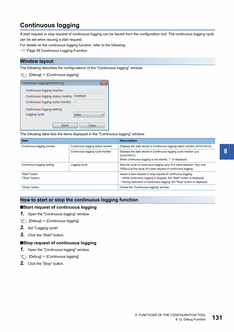
8
Continuous loggingA start request or stop request of continuous logging can be issued from the configuration tool. The continuous logging cycle can be set when issuing a start request.For details on the continuous logging function, refer to the following.Page 59 Continuous Logging Function
Window layoutThe following describes the configurations of the "Continuous logging" window.
[Debug] [Continuous logging]
The following table lists the items displayed in the "Continuous logging" window.
How to start or stop the continuous logging function■Start request of continuous logging1. Open the "Continuous logging" window.
[Debug] [Continuous logging]
2. Set "Logging cycle".
3. Click the "Start" button.
■Stop request of continuous logging1. Open the "Continuous logging" window.
[Debug] [Continuous logging]
2. Click the "Stop" button.
Item DescriptionContinuous logging monitor Continuous logging status monitor Displays the data stored in Continuous logging status monitor (Un\G15010).
Continuous logging cycle monitor Displays the data stored in Continuous logging cycle monitor (s) (Un\G15011).When continuous logging is not started, "-" is displayed.
Continuous logging setting Logging cycle Sets the cycle of continuous logging (any of a value between 10s and 1000s) at the issue of a start request of continuous logging.
"Start" button("Stop" button)
Issues a start request or stop request of continuous logging.• While continuous logging is stopped, the "Start" button is displayed.• During execution of continuous logging, the "Stop" button is displayed.
"Close" button Closes the "Continuous logging" window.
8 FUNCTIONS OF THE CONFIGURATION TOOL8.12 Debug Function 131
13
8.13 Pattern Generator FunctionThe pattern generator function performs output from the external output terminals according to the output pattern data consisting of up to 8192 points that have been registered in the flexible high-speed I/O control module in advance.If a counter timer block and pattern generator block are used together, periodic pattern output according to the clock in the flexible high-speed I/O control module and High/Low output corresponding to the input pulse from the external input terminals can be performed.Users can easily create output pattern data, which eliminates the need for creating complicated hardware logic or programs and reduces the design man-hours.
Output pattern dataOutput pattern data is a High/Low pattern table output from the external output terminals. The data consists of up to 8192 points and 10 output patterns can be created. When one of 10 output patterns is set for a pattern generator block, output from the external output terminals can be performed.In the "Pattern generator output pattern setting" window, 10 output patterns can be created with simple mouse operation.Created output pattern data can be saved in CSV files. In addition, by reading saved CSV files to the "Pattern generator output pattern setting" window, users can utilize the output pattern data that is already created for other projects.
2 8 FUNCTIONS OF THE CONFIGURATION TOOL8.13 Pattern Generator Function
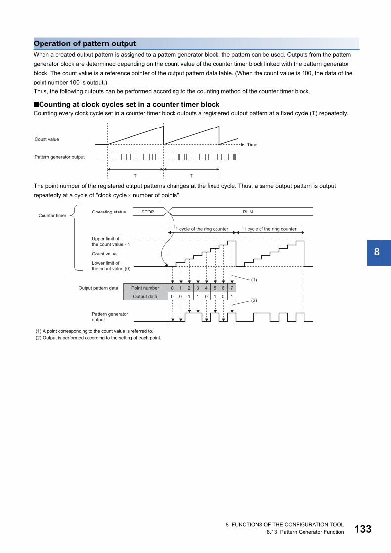
8
Operation of pattern outputWhen a created output pattern is assigned to a pattern generator block, the pattern can be used. Outputs from the pattern generator block are determined depending on the count value of the counter timer block linked with the pattern generator block. The count value is a reference pointer of the output pattern data table. (When the count value is 100, the data of the point number 100 is output.)Thus, the following outputs can be performed according to the counting method of the counter timer block.
■Counting at clock cycles set in a counter timer blockCounting every clock cycle set in a counter timer block outputs a registered output pattern at a fixed cycle (T) repeatedly.
The point number of the registered output patterns changes at the fixed cycle. Thus, a same output pattern is output repeatedly at a cycle of "clock cycle number of points".
(1) A point corresponding to the count value is referred to.(2) Output is performed according to the setting of each point.
T T
TimeCount value
Pattern generator output
STOP RUN
0
(1)
(2)
1 2 3 4 5 6 7
0 1 0 10 0 1 1
1 cycle of the ring counter
Counter timerOperating status
Upper limit of the count value - 1
Count value
Lower limit of the count value (0)
Output pattern data
Pattern generator output
1 cycle of the ring counter
Point number
Output data
8 FUNCTIONS OF THE CONFIGURATION TOOL8.13 Pattern Generator Function 133
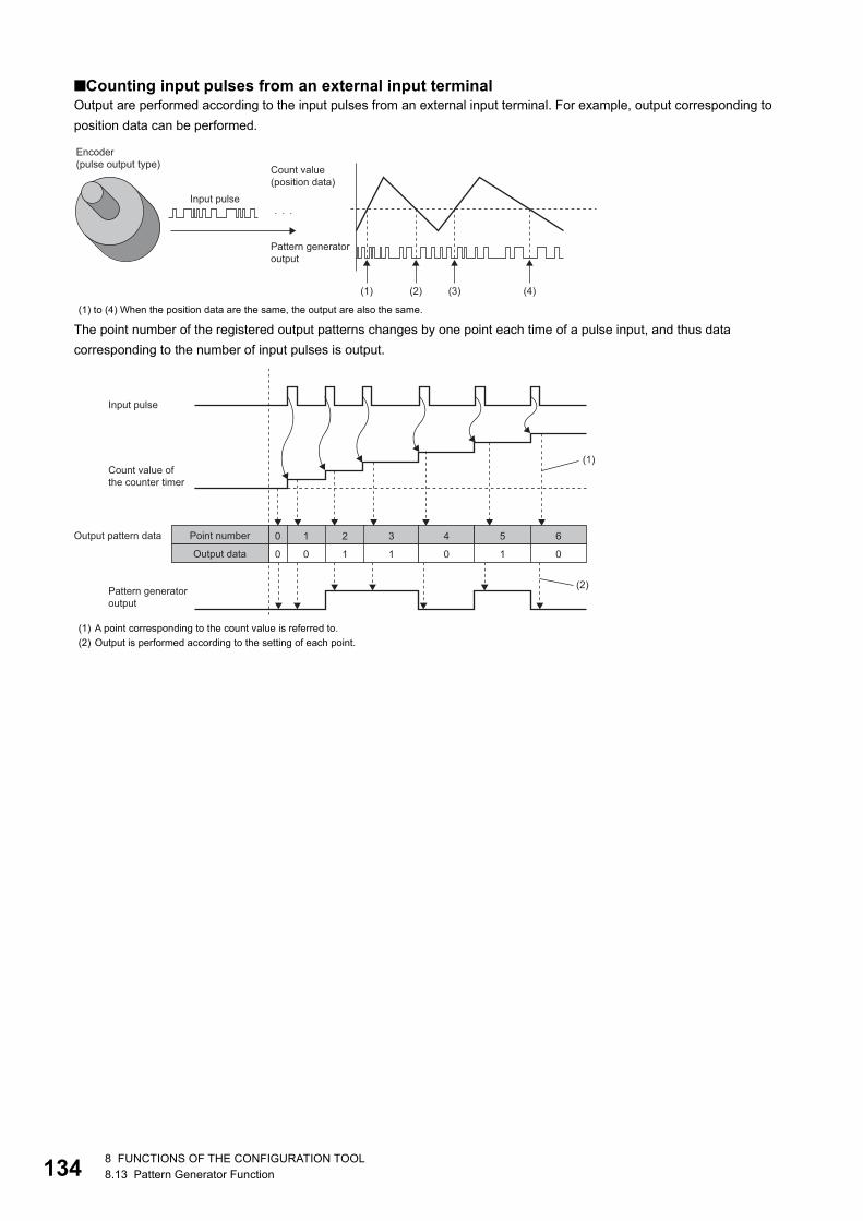
13
■Counting input pulses from an external input terminalOutput are performed according to the input pulses from an external input terminal. For example, output corresponding to position data can be performed.
The point number of the registered output patterns changes by one point each time of a pulse input, and thus data corresponding to the number of input pulses is output.
(1) to (4) When the position data are the same, the output are also the same.
(1) A point corresponding to the count value is referred to.(2) Output is performed according to the setting of each point.
(1) (2) (3) (4)
Encoder (pulse output type)
Input pulse
Count value (position data)
Pattern generator output
(1)
(2)
0 1 2 3 4 5 6
0 0 1 1 0 1 0
Input pulse
Count value of the counter timer
Output pattern data
Pattern generator output
Point number
Output data
4 8 FUNCTIONS OF THE CONFIGURATION TOOL8.13 Pattern Generator Function
8
Window layoutThe following describes the configurations of the "Pattern generator output pattern setting" window. Set the output pattern data in this window.To display the "Pattern generator output pattern setting" window, click "Detail" of the pattern generator block in the Multi function counter block detail window (Counter_(16bit_Unsigned)). • Set output patterns at the upper section of the window. • The images of set output patterns are displayed at the lower section of the window.
The following table lists the items to be displayed in the "Pattern generator output pattern setting" window.
Item DescriptionOutput pattern setting area "Pattern selection" Specify the pattern number to be assigned to a pattern generator block.
Click the "OK" button to reflect the specified pattern number to "Pattern No." of the pattern generator block.
"Points" Set the number of points that compose an output pattern. The default value is 0, and 1 to 8192 can be set.• When 0 is set, the corresponding output pattern is disabled.• When 1 or larger number is set, the output pattern of the set number of points is enabled.
"0" to "8191" Set the output pattern of the pattern generator block from "0: Low output" or "1: High output" for each point number.The default value is "0: Low output". Every time the cell is clicked, the output pattern switches between "0: Low output" and "1: High output".Output patterns can be set for the number of output pattern points set in "Points".
"Start" Set the start point from which the image of an output pattern is to be displayed.
"Display position change" button Change the start position of the image of an output pattern displayed in the window.
"Full display" Switch the display range of the image of an output pattern.• Selected: Display the whole image with the range of the setting value in "Points".• Not selected: Display the image of the 20 points displayed at the upper section of the
window.
"Pattern clear" button Set "0: Low output" for all the selected output patterns.
"Pattern image" Display the High/Low image of the selected output pattern from the start point.
"Read from the file" button Read the output pattern data saved in a CSV file to the "Pattern generator output pattern setting" window.
"Save to file" button Save the output pattern data in the "Pattern generator output pattern setting" window into a CSV file.
"OK" button Set the output pattern set in the "Pattern generator output pattern setting" window for the hardware logic. The following items can be changed automatically according to the output pattern.• "Upper Limit" of "Counter_Timer_0"• "Lower Limit" of "Counter_Timer_0"
To reflect the hardware logic where the output pattern has been set to the module, write the data into module.
"Cancel" button Close the "Pattern generator output pattern setting" window.
Output pattern setting area
8 FUNCTIONS OF THE CONFIGURATION TOOL8.13 Pattern Generator Function 135
13
Setting methodThe following describes the setting method of the "Pattern generator output pattern setting" window.
1. Click "Detail" of a pattern generator block in the Multi function counter block detail window (Counter_(16bit_Unsigned)) to open the "Pattern generator output pattern setting" window.
2. Select a pattern to be output in "Pattern selection".
3. Set the number of output pattern points in "Points".
4. Click each cell of "0" to "8191" and switch the output pattern between "0: Low output" and "1: High output". By default, "0: Low output" has been set in all cells.
Setting the output pattern "0: Low output" for the point number 0 is recommended. When the output pattern for the point number 0 is "1: High output", the output status is High because the count value when the hardware logic control is started is 0.
5. Save the set output pattern with the "Save to file" button (Data is saved only in the CSV format). Users can open a saved CSV file from the "Read from the file" button.
6. Click the "OK" button to set the output pattern set in the "Pattern generator output pattern setting" window for the hardware logic.
• Created output pattern data can be saved in CSV files with the "Save to file" button. Thus, by opening the saved CSV files with the "Read from the file" button, users can utilize the output pattern data for other projects.
• Output pattern of up to 8192 points cannot be displayed in the "Pattern generator output pattern setting" window at a time. In addition, clicking each point takes time. For convenience, edit output pattern data with a text editor and save it in the CSV format in advance. Then, read the CSV files to the "Pattern generator output pattern setting" window with the "Read from the file" button.
6 8 FUNCTIONS OF THE CONFIGURATION TOOL8.13 Pattern Generator Function

8
CSV file format of output pattern dataThe following shows the CSV file format specifications of output pattern data.
■Contents of rowsThe rows correspond to the pattern numbers of output patterns. For example, the 1st row corresponds to the pattern number 1 of the output pattern.
■First columnThe 1st column corresponds to the number of output pattern points. The following values can be set.
When a CSV file in which a value out of the above setting range has been set is read to the "Pattern generator output pattern setting" window, an error dialog box is displayed.
■2nd to 8193rd columns • The columns correspond to output patterns. The point numbers 0 to 8191 are assigned to the 2nd to 8193rd columns in
ascending order. "0: Low output" or "1: High output" can be set for each point number. • The output pattern settings of the points later than the set number are disabled. • When a CSV file in which a value other than "0: Low output" and "1: High output" has been set is read to the "Pattern
generator output pattern setting" window, an error dialog box is displayed.
Item name CharacterDelimiter Comma (,)
Return code CRLF (0x0D, 0x0A)
Value Description0 No output pattern is used. Output patterns in the 2nd column or later are
disabled.
1 to 8191 The values are for setting values of the number of output pattern points. Set output patterns in the 2nd column or later. The output patterns of the points later than the setting value are disabled.
8 FUNCTIONS OF THE CONFIGURATION TOOL8.13 Pattern Generator Function 137

13
8.14 Help FunctionAs the help function, the software version of the configuration tool can be checked.
Checking the version of the configuration toolInformation including the software version of the configuration tool is displayed.
[Help] [Version Information]
8 8 FUNCTIONS OF THE CONFIGURATION TOOL8.14 Help Function
9
9 CREATING A HARDWARE LOGICThis chapter describes how to create a hardware logic.9.1 Main Blocks in the Hardware Logic Outline Window
With the flexible high-speed I/O control module, various controls are possible by arranging multi function counter blocks and various function blocks and linking these blocks.In the hardware logic outline window, all of external input blocks, Y device terminals, and OUT terminals are arranged in the first section and all of external output blocks and SI device terminals are arranged in the fifth section when a project is started. No blocks are arranged in the second to fourth sections. Arrange blocks and link them according to the control to be executed with the flexible high-speed I/O control module.
The following table shows sections where each main block can be arranged and the number of blocks that can be arranged in each section in the hardware logic outline window.
*1 The number in () indicates the number of blocks that are arranged by default and no additional blocks can be arranged.
Section Item name Number of blocks that can be arranged*1
Remarks
First section External input block (12)
Y device terminal (16) General command 0 to General command F (Y10 to Y1F) can be used as input signals.
OUT terminal DC output (8) Output signals from external output blocks in the fifth section can be used as input signals for the first section.Differential output (6)
Second section Parallel encoder block 1
SSI encoder block 2
Third section Multi function counter block 8
Fourth section Logical operation block 14
Fifth section External output block DC output (8) "OUT 0" to "OUT 7" are for DC output.
Differential output (6) "OUT 0_DIF" to "OUT 5_DIF" are for differential output.
SI device terminal (8)
9 CREATING A HARDWARE LOGIC9.1 Main Blocks in the Hardware Logic Outline Window 139
14
Relationship of I/O in the hardware logicThis section describes the relationship between the I/O in the hardware logic and the I/O of X/Y devices and of the connectors for external devices.
■Signal status nameIn the flexible high-speed I/O control module, each signal status is called as shown below.
Input terminal Output terminalY 10 Y device terminal OUT 0 External output block
IN 0 External input block OUT 1 External output block
OUT 1 OUT terminal OUT 2 External output block
Signal status NameStatus of input signals from external devices ON OFF
Status of internal signals (terminals) of the hardware logic High Low
Status of DC output signals to external devices ON OFF
Status of differential output signals to external devices High Low
IN 0
OUT 0
OUT 1
OUT 2
Y10
Y10
X10
IN 0
OUT 1
OUT 0
OUT 1
OUT 2
Connector for external devices (input)
Connector for external devices (output)
CPU module Flexible high-speed I/O control module
Program Hardware logic
Processing
Processing
Processing
0 9 CREATING A HARDWARE LOGIC9.1 Main Blocks in the Hardware Logic Outline Window
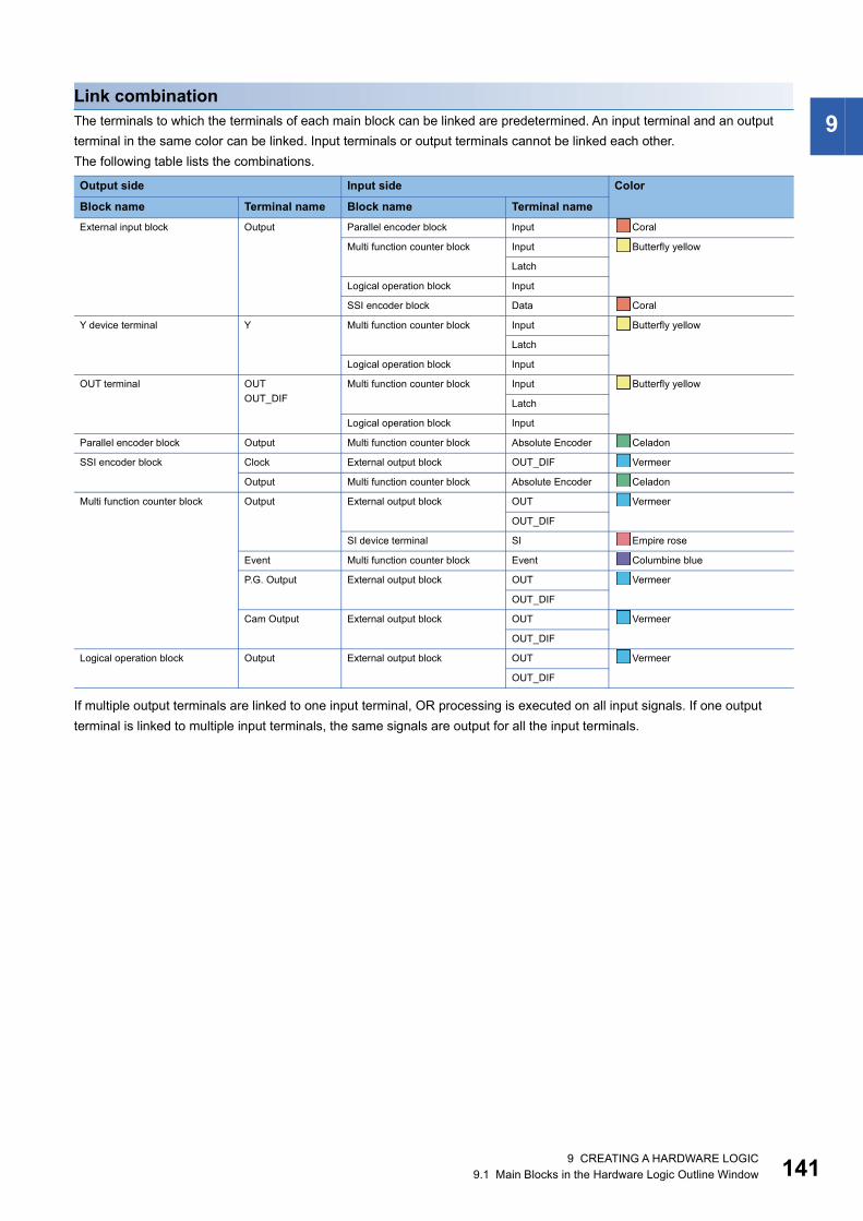
9
Link combinationThe terminals to which the terminals of each main block can be linked are predetermined. An input terminal and an output terminal in the same color can be linked. Input terminals or output terminals cannot be linked each other.The following table lists the combinations.If multiple output terminals are linked to one input terminal, OR processing is executed on all input signals. If one output terminal is linked to multiple input terminals, the same signals are output for all the input terminals.
Output side Input side Color
Block name Terminal name Block name Terminal nameExternal input block Output Parallel encoder block Input Coral
Multi function counter block Input Butterfly yellow
Latch
Logical operation block Input
SSI encoder block Data Coral
Y device terminal Y Multi function counter block Input Butterfly yellow
Latch
Logical operation block Input
OUT terminal OUTOUT_DIF
Multi function counter block Input Butterfly yellow
Latch
Logical operation block Input
Parallel encoder block Output Multi function counter block Absolute Encoder Celadon
SSI encoder block Clock External output block OUT_DIF Vermeer
Output Multi function counter block Absolute Encoder Celadon
Multi function counter block Output External output block OUT Vermeer
OUT_DIF
SI device terminal SI Empire rose
Event Multi function counter block Event Columbine blue
P.G. Output External output block OUT Vermeer
OUT_DIF
Cam Output External output block OUT Vermeer
OUT_DIF
Logical operation block Output External output block OUT Vermeer
OUT_DIF
9 CREATING A HARDWARE LOGIC9.1 Main Blocks in the Hardware Logic Outline Window 141

14
External input block
In the first section in the hardware logic outline window, 12 external input blocks ("IN 0" to "IN B") are arranged by default.Select which signal (among "IN 0" to "IN B") input from the connector for external devices is to be used as an input signal in the hardware logic. The selected input signal is output from the output terminal of the external input block through the filter. The output signal can be input to the input terminal of another block.
The external input block has the following functions. • When "Logic Select" is set to "Inversion", inverted signals are output. • The digital filter reduces the effect of external noise. • The signal selected as an initial state is output when hardware logic control stops.
ParameterThe following table shows the parameters of the external input block.
Variable name Data type Valid range Default value DescriptionLogic Select Bit Non-Inversion
InversionNon-Inversion Set Non-Inversion or Inversion for input signals.
Filter Time Word Page 143 "Filter Time"
• General Input (Pulse input mode)
• 1ms (Input response time/counting speed)
Select a type of the filter time. The filter time corresponding to the input response time of general-purpose input or the counting speed of each pulse input mode can be set.
Initial State Bit LowHigh
Low Set the signal status during a hardware logic control stop to Low fixed or High fixed.
Outline
2 9 CREATING A HARDWARE LOGIC9.1 Main Blocks in the Hardware Logic Outline Window

9
■"Filter Time"General-purpose input or pulse input count can be selected for "Filter Time". • General-purpose input (General Input 0s to General Input 5ms)Set this method to reduce noise. When a pulse width is less than the setting value of "Filter Time", the pulse is not detected as an input signal. If the setting value is too large, pulses other than noise cannot be detected. Thus, set the filter time suitable for the operating environment.• Pulse input count (1-Phase Multiple of 1 (CW/CCW) 10kpps to 2-Phase Multiple of 4 8000kpps)Set this method to count input pulses. A setting according to the pulse input mode and counting speed prevents incorrect count.
■Setting method of "Filter Time"1. Select a pulse input mode in the upper list box.
2. Select an item in the lower list box. • When "General Input" has been selected in the upper list box, select an input response time. • When an item other than "General Input" has been selected in the upper list box, select a counting speed.If the item in the upper list box is changed to another one after an item is selected in the lower list box, the selection status of the lower list box returns to the default value.
Input response time0s 10s 50s 0.1ms 0.2ms 0.4ms 0.6ms 1ms (default value) 5ms
Pulse input mode Counting speed1-Phase Multiple of 1 (CW/CCW) 10kpps
(default value)
100kpps 200kpps 500kpps 1000kpps 2000kpps
1-Phase Multiple of 2 10kpps (default value)
100kpps 200kpps 500kpps 1000kpps 2000kpps 4000kpps
2-Phase Multiple of 1 10kpps (default value)
100kpps 200kpps 500kpps 1000kpps 2000kpps
2-Phase Multiple of 2 10kpps (default value)
100kpps 200kpps 500kpps 1000kpps 2000kpps 4000kpps
2-Phase Multiple of 4 10kpps (default value)
100kpps 200kpps 500kpps 1000kpps 2000kpps 4000kpps 8000kpps
9 CREATING A HARDWARE LOGIC9.1 Main Blocks in the Hardware Logic Outline Window 143
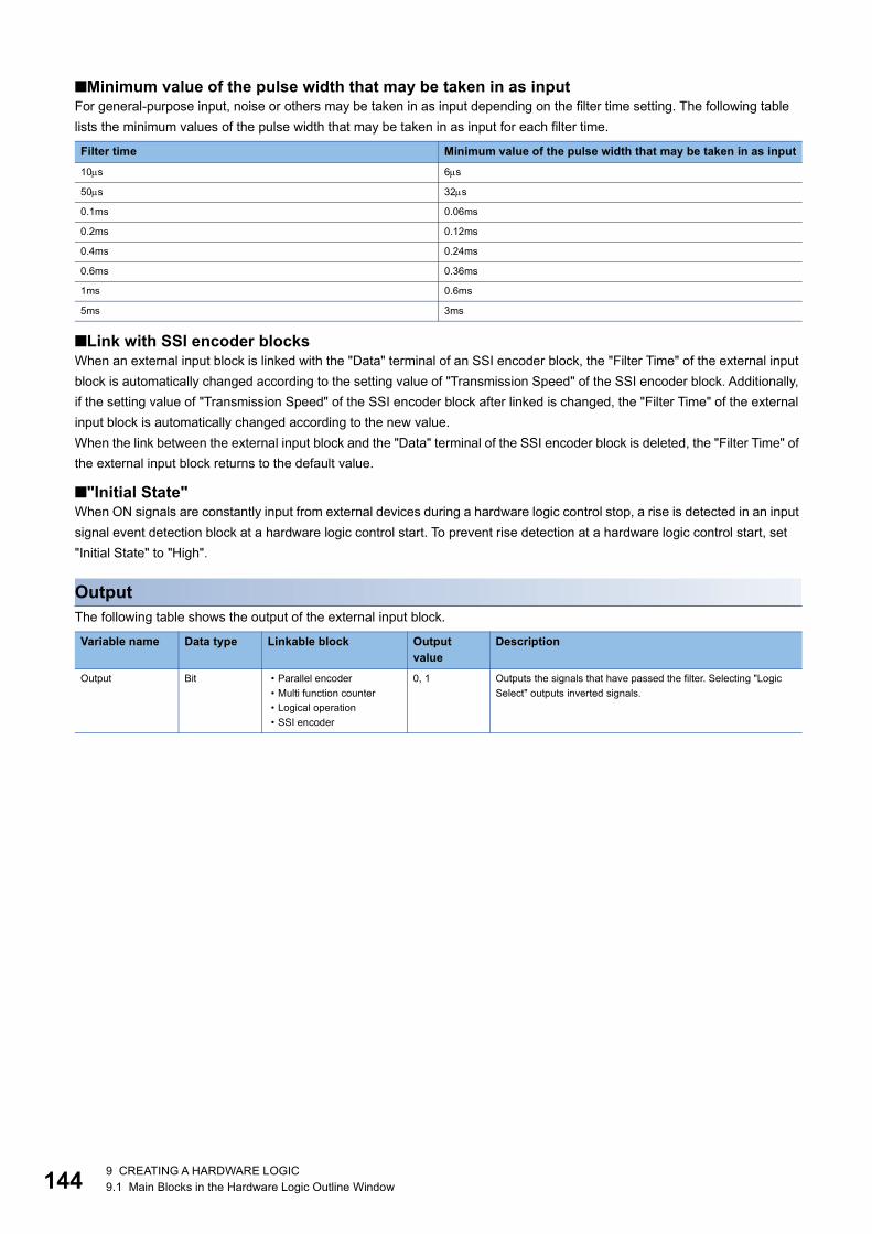
14
■Minimum value of the pulse width that may be taken in as inputFor general-purpose input, noise or others may be taken in as input depending on the filter time setting. The following table lists the minimum values of the pulse width that may be taken in as input for each filter time.
■Link with SSI encoder blocksWhen an external input block is linked with the "Data" terminal of an SSI encoder block, the "Filter Time" of the external input block is automatically changed according to the setting value of "Transmission Speed" of the SSI encoder block. Additionally, if the setting value of "Transmission Speed" of the SSI encoder block after linked is changed, the "Filter Time" of the external input block is automatically changed according to the new value.When the link between the external input block and the "Data" terminal of the SSI encoder block is deleted, the "Filter Time" of the external input block returns to the default value.
■"Initial State"When ON signals are constantly input from external devices during a hardware logic control stop, a rise is detected in an input signal event detection block at a hardware logic control start. To prevent rise detection at a hardware logic control start, set "Initial State" to "High".
OutputThe following table shows the output of the external input block.
Filter time Minimum value of the pulse width that may be taken in as input10s 6s
50s 32s
0.1ms 0.06ms
0.2ms 0.12ms
0.4ms 0.24ms
0.6ms 0.36ms
1ms 0.6ms
5ms 3ms
Variable name Data type Linkable block Output value
Description
Output Bit • Parallel encoder• Multi function counter• Logical operation• SSI encoder
0, 1 Outputs the signals that have passed the filter. Selecting "Logic Select" outputs inverted signals.
4 9 CREATING A HARDWARE LOGIC9.1 Main Blocks in the Hardware Logic Outline Window
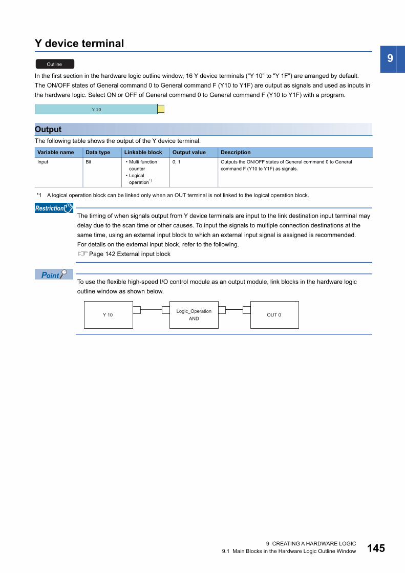
9
Y device terminalIn the first section in the hardware logic outline window, 16 Y device terminals ("Y 10" to "Y 1F") are arranged by default.The ON/OFF states of General command 0 to General command F (Y10 to Y1F) are output as signals and used as inputs in the hardware logic. Select ON or OFF of General command 0 to General command F (Y10 to Y1F) with a program.
OutputThe following table shows the output of the Y device terminal.
*1 A logical operation block can be linked only when an OUT terminal is not linked to the logical operation block.
The timing of when signals output from Y device terminals are input to the link destination input terminal may delay due to the scan time or other causes. To input the signals to multiple connection destinations at the same time, using an external input block to which an external input signal is assigned is recommended.For details on the external input block, refer to the following.Page 142 External input block
To use the flexible high-speed I/O control module as an output module, link blocks in the hardware logic outline window as shown below.
Variable name Data type Linkable block Output value DescriptionInput Bit • Multi function
counter• Logical
operation*1
0, 1 Outputs the ON/OFF states of General command 0 to General command F (Y10 to Y1F) as signals.
Outline
Y 10 AND
OUT 0 Logic_Operation
9 CREATING A HARDWARE LOGIC9.1 Main Blocks in the Hardware Logic Outline Window 145

14
OUT terminal
In the first section in the hardware logic outline window, eight OUT terminals for DC output ("OUT 0" to "OUT 7") and six OUT terminals for differential output ("OUT 0_DIF" to "OUT 5_DIF") are arranged by default.Signals output from external output blocks in the fifth section can be used as inputs in the hardware logic. For details on the external output block, refer to the following.Page 159 External output block
OutputThe following table shows the output of the OUT terminal.
*1 Any of OUT 0 to OUT 7 or OUT 0_DIF to OUT 5_DIF can be linked to a logical operation block when a Y device terminal is not linked to the logical operation block.
When "Logic Select" of an external output block is set to "Inversion", signals input to the external output block are inverted and output from the OUT terminal.For details on the external output block, refer to the following.Page 159 External output block
Variable name Data type Linkable block Valid range DescriptionInput Bit • Multi function
counter• Logical
operation*1
0, 1 When no external output blocks are linked, no signals are output from this terminal.
Outline
6 9 CREATING A HARDWARE LOGIC9.1 Main Blocks in the Hardware Logic Outline Window

9
Parallel encoder blockIn the second section in the hardware logic outline window, one parallel encoder block ("Parallel_Encoder") can be arranged.The parallel encoder block transmits data with the encoder for parallel transmission and receives the data of the bit points set in the data length setting as the data of Input Data Type to convert this data into word data.
InputThe following table shows the inputs of the parallel encoder block.
Variable name Data type Linkable block Valid range DescriptionInput 0 Bit External input 0, 1 These are input terminals of the parallel encoder.
When the data length is changed, the number of displayed Input terminals is changed according to the data length. Then, the Input terminals are automatically linked to external input blocks in order from the first one ("IN 0"). The order of linking the Input terminals and the external input blocks cannot be changed.
Input 1
Input 2
Input 3
Input 4
Input 5
Input 6
Input 7
Input 8
Input 9
Input A
Input B
Outline
9 CREATING A HARDWARE LOGIC9.1 Main Blocks in the Hardware Logic Outline Window 147
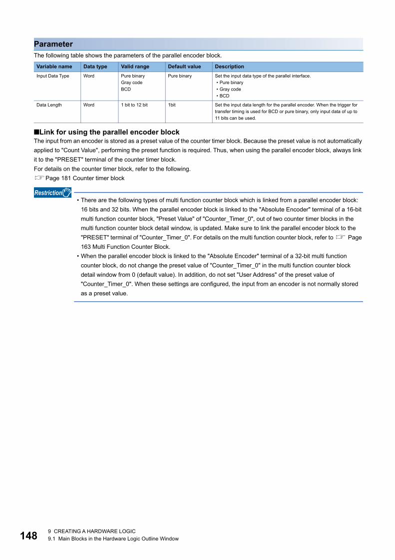
14
ParameterThe following table shows the parameters of the parallel encoder block.
■Link for using the parallel encoder blockThe input from an encoder is stored as a preset value of the counter timer block. Because the preset value is not automatically applied to "Count Value", performing the preset function is required. Thus, when using the parallel encoder block, always link it to the "PRESET" terminal of the counter timer block.For details on the counter timer block, refer to the following.Page 181 Counter timer block
• There are the following types of multi function counter block which is linked from a parallel encoder block: 16 bits and 32 bits. When the parallel encoder block is linked to the "Absolute Encoder" terminal of a 16-bit multi function counter block, "Preset Value" of "Counter_Timer_0", out of two counter timer blocks in the multi function counter block detail window, is updated. Make sure to link the parallel encoder block to the "PRESET" terminal of "Counter_Timer_0". For details on the multi function counter block, refer to Page 163 Multi Function Counter Block.
• When the parallel encoder block is linked to the "Absolute Encoder" terminal of a 32-bit multi function counter block, do not change the preset value of "Counter_Timer_0" in the multi function counter block detail window from 0 (default value). In addition, do not set "User Address" of the preset value of "Counter_Timer_0". When these settings are configured, the input from an encoder is not normally stored as a preset value.
Variable name Data type Valid range Default value DescriptionInput Data Type Word Pure binary
Gray codeBCD
Pure binary Set the input data type of the parallel interface.• Pure binary• Gray code• BCD
Data Length Word 1 bit to 12 bit 1bit Set the input data length for the parallel encoder. When the trigger for transfer timing is used for BCD or pure binary, only input data of up to 11 bits can be used.
8 9 CREATING A HARDWARE LOGIC9.1 Main Blocks in the Hardware Logic Outline Window
9
■Setting and link of the encoder for which Input Data Type is set to Pure binary or BCDWhen data is input from the encoder for which Input Data Type is set to Pure binary or BCD, an error of 2 bits or more is generated depending on the timing of reading data. Because of this, when data is input from the encoder for which Input Data Type is set to Pure binary or BCD, specifying the read timing using a trigger signal for transfer timing is recommended.To specify the read timing, follow the instructions below. • Set "Data Length" to 11 bits or less. • Link the terminal outputting the transfer timing signal to the "PRESET" terminal of the counter timer block.OutputThe following table shows the output of the parallel encoder block.
■Link diagram of the hardware logic outline window
■Link diagram of the multi function counter block detail window
Variable name Data type Linkable block Output value DescriptionOutput Word Multi function
counter0 to 4095 Inputs the value from the parallel encoder to the "Absolute Encoder"
terminal of the multi function counter to use the value as a preset value of the multi function counter.
IN 0
IN 1
IN 2
IN 3
IN 4
IN 5
IN 6
IN 7
IN 8
IN 9
IN A
IN B
Input0Parallel_Encoder
Input1
Input2
Input3
Input4
Input5
Input6
Input0
Absolute Encoder
Input7
Input9
InputA
InputB
Input8
OutputCounter
PRESET
(Only A: Rise is on.)
Input 0Counter
Input_Signal_Event
9 CREATING A HARDWARE LOGIC9.1 Main Blocks in the Hardware Logic Outline Window 149

15
SSI encoder block
In the second section in the hardware logic outline window, two SSI encoder blocks ("SSI_Encoder_") can be arranged.The SSI encoder blocks perform serial communication with the absolute encoder having the SSI (Synchronous Serial Interface) output and acquire position data. The acquired position data is stored as a count value of the multi function counter block linked to this block. • When "Signal Error Detection" is set to "Enable", a signal error detection processing is performed. If an error occurs on the
external wiring to the SSI encoder, the SSI encoder block DATA signal wire reverse error (error code: 109H) or the SSI encoder block DATA signal error (error code: 10AH) is output.
• When "Parity" of "Data Frame Setting" is set to "Even" or "Odd", a parity check is performed. If an error is detected by the parity check, the SSI encoder block parity error (error code: 10BH) is output.
• If any of the above errors (error code: 109H to 10BH) is output during data receipt from the absolute encoder, the count value of the multi function counter block linked to this block does not change. The position data is reflected to the count value when data has been received properly at next transmission.
InputThe following table shows the input of the SSI encoder block.
Variable name Data type Linkable block Valid range DescriptionData Bit External input 0, 1 Inputs data from the SSI encoder.
Outline
0 9 CREATING A HARDWARE LOGIC9.1 Main Blocks in the Hardware Logic Outline Window
9
ParameterThe following table shows the parameters of the SSI encoder block.Variable name Data type Valid range Default value DescriptionEncoder Type Word Single Turn
Multi TurnSingle Turn Set the type of the SSI encoder.
• Single Turn• Multi Turn
Transmission Speed Word 100kHz200kHz300kHz400kHz500kHz1.0MHz1.5MHz2.0MHz
100kHz Set the frequency of the clock signal to perform synchronous data communication with the SSI encoder.
Monoflop Time Word 10 to 10000 (s) 10 (s) Indicates the time until the next communication is ready to start after the output of the last clock signal. Set the monoflop time according to the specifications of the SSI encoder to be connected.For details on the monoflop time, refer to the following.Page 156 Monoflop time
Signal Error Detection
Word DisableEnable
Disable Set whether to detect an error (disconnection, short-circuit) of the data signal wire externally connected to the SSI encoder.• Error detection disabled: Disable• Error detection enabled: Enable
For details on the signal error detection, refer to the following.Page 157 Signal error detection
Direction Word ForwardReverse
Forward The counting direction of received data from the SSI encoder can be changed by setting this item.• Forward• Reverse
For details on Direction, refer to the following.Page 156 Counting direction
Data Frame Setting Click the [Detail] button to open the "Data Frame Setting" window in which the details of a data frame can be set.
9 CREATING A HARDWARE LOGIC9.1 Main Blocks in the Hardware Logic Outline Window 151
15
• Parameters of "Data Frame Setting"
*1 Set values so that the total of set values for "Multi Turn Data Length" and "Single Turn Data Length" is equal to or smaller than the value set for "Data Frame Length". Note that the parity bit length is not included in these values.
*2 A value larger than the maximum value representable by "Single Turn Data Length" cannot be set for "Encoder Resolution".*3 When using the encoder with the encoder type being multi turn and the input data type being gray code, make sure that its resolution of
single turn data is equal to 2n.
Variable name Data type Valid range Default value DescriptionInput Data Type Word Pure binary
Gray codePure binary Set the type of input data from the SSI encoder.
• Pure binary• Gray code*3
Data Frame Length Word 1 to 32 (bit) 1 (bit) Specify the effective bit length of a received data frame from the SSI encoder.*1
Multi Turn Data Length
Word 0 to 32 (bit) 0 (bit) Specify the effective bit length of multi turn data.*1
When "Encoder Type" is set to "Multi Turn", this setting is enabled.When this setting is disabled, a default value is set.
Multi Turn Start Bit Word 0 to 31 (bit) 0 (bit) Specify the start bit position of multi turn data.When "Encoder Type" is set to "Multi Turn", this setting is enabled.When this setting is disabled, a default value is set.
Encoder Resolution Word 0 to 4294967295 0 Set the encoder resolution to use the encoder with its resolution of single turn data not equal to 2n (n: single turn data length).*2
When the resolution is equal to 2n, the setting change from the initial value (0) is not required. (When 0 is set, the resolution is regarded as equal to 2n.)When "Encoder Type" is set to "Multi Turn" and "Input Data Type" is set to "Gray code", this setting is disabled. When this setting is disabled, a default value is set.
Single Turn Data Length
Word 0 to 32 (bit) 0 (bit) Specify the effective bit length of single turn data.*1
Single Turn Start Bit Word 0 to 31 (bit) 0 (bit) Specify the start bit position of single turn data.When "Encoder Type" is set to "Single Turn", this setting is enabled.When this setting is disabled, a default value is set.
Parity Word NoneEvenOdd
None Set whether to perform the parity check or the type of the parity check (even or odd) according to the SSI encoder to be connected.• No parity check: None• Even parity: Even• Odd parity: Odd
2 9 CREATING A HARDWARE LOGIC9.1 Main Blocks in the Hardware Logic Outline Window
9
OutputThe following table shows the outputs of the SSI encoder block.*1 The "Absolute Encoder" terminal of a 32-bit unsigned multi function counter block can be linked.
The refreshing cycle of a count value is calculated by the following formula because the module processing time fluctuates within the range of 0 to 100s.Refreshing cycle = (Data frame length + P + 1) Clock cycle + Monoflop time + Module processing time (0 to 100s) • P: 1 (for with parity) or 0 (for without parity) • Clock cycle: Inverse of the transmission speed (for the transmission speed of 100kHz: 1/100000s = 10s)Note that if an SI device terminal is used, up to 200s may be added to the refreshing cycle above as a delay time of the refreshing.
Variable name Data type Linkable block Output value DescriptionClock Bit External output 0, 1 Outputs the clock signal to perform synchronous data communication
with the SSI encoder.When an SSI encoder block is arranged in the hardware logic outline window, the "Clock" terminal of the SSI encoder block and the "Input" terminal of an external output block are automatically linked. The link cannot be deleted or changed.The following are the link destinations.• SSI_Encoder_0: OUT 0_DIF• SSI_Encoder_1: OUT 1_DIF
Output Word Multi function counter*1
0 to 4294967295 Sets the position data acquired from the SSI encoder to a count value of the multi function counter block linked.
9 CREATING A HARDWARE LOGIC9.1 Main Blocks in the Hardware Logic Outline Window 153
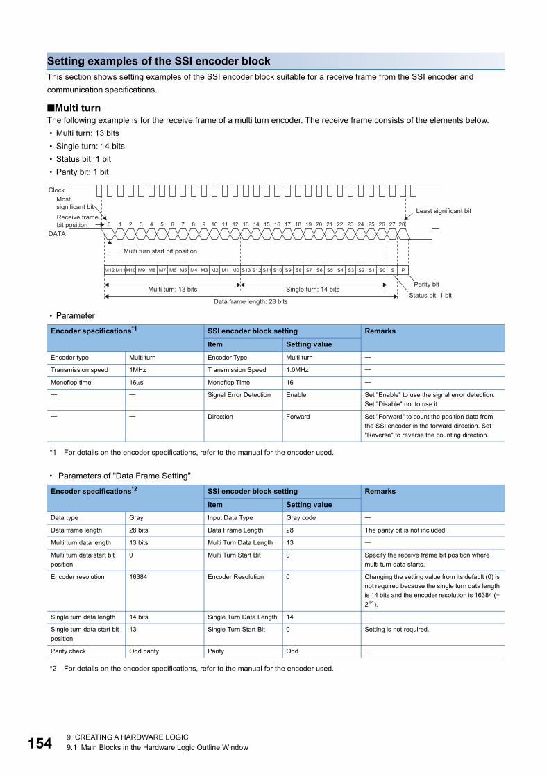
15
Setting examples of the SSI encoder blockThis section shows setting examples of the SSI encoder block suitable for a receive frame from the SSI encoder and communication specifications.
■Multi turnThe following example is for the receive frame of a multi turn encoder. The receive frame consists of the elements below. • Multi turn: 13 bits • Single turn: 14 bits • Status bit: 1 bit • Parity bit: 1 bit
• Parameter
*1 For details on the encoder specifications, refer to the manual for the encoder used.
• Parameters of "Data Frame Setting"
*2 For details on the encoder specifications, refer to the manual for the encoder used.
Encoder specifications*1 SSI encoder block setting Remarks
Item Setting valueEncoder type Multi turn Encoder Type Multi turn
Transmission speed 1MHz Transmission Speed 1.0MHz
Monoflop time 16s Monoflop Time 16
Signal Error Detection Enable Set "Enable" to use the signal error detection. Set "Disable" not to use it.
Direction Forward Set "Forward" to count the position data from the SSI encoder in the forward direction. Set "Reverse" to reverse the counting direction.
Encoder specifications*2 SSI encoder block setting Remarks
Item Setting valueData type Gray Input Data Type Gray code
Data frame length 28 bits Data Frame Length 28 The parity bit is not included.
Multi turn data length 13 bits Multi Turn Data Length 13
Multi turn data start bit position
0 Multi Turn Start Bit 0 Specify the receive frame bit position where multi turn data starts.
Encoder resolution 16384 Encoder Resolution 0 Changing the setting value from its default (0) is not required because the single turn data length is 14 bits and the encoder resolution is 16384 (= 214).
Single turn data length 14 bits Single Turn Data Length 14
Single turn data start bit position
13 Single Turn Start Bit 0 Setting is not required.
Parity check Odd parity Parity Odd
0 1 2 3 4 5 6 7 8 9 10 11 12 13 14 15 16 17 18 19 20 21 22 23 24 25 26 27 28
M12 M11M10 M9 M8 M7 M6 M5 M4 M3 M2 M1 M0 S13 S12 S11 S10 S9 S8 S7 S6 S5 S4 S3 S2 S1 S0 S P
Clock
DATA
Multi turn start bit position
Receive frame bit position
Most significant bit Least significant bit
Multi turn: 13 bits Single turn: 14 bits
Data frame length: 28 bits
Parity bit
Status bit: 1 bit
4 9 CREATING A HARDWARE LOGIC9.1 Main Blocks in the Hardware Logic Outline Window
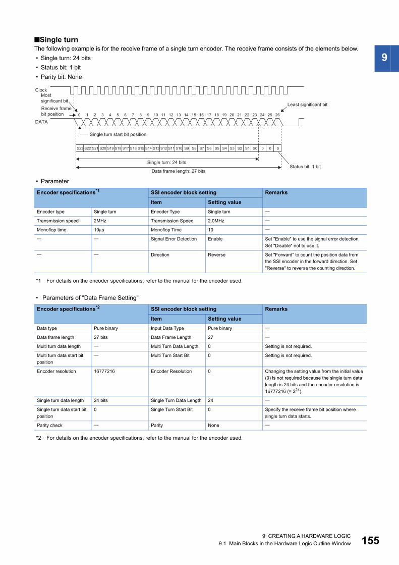
9
■Single turnThe following example is for the receive frame of a single turn encoder. The receive frame consists of the elements below. • Single turn: 24 bits • Status bit: 1 bit • Parity bit: None• Parameter
*1 For details on the encoder specifications, refer to the manual for the encoder used.
• Parameters of "Data Frame Setting"
*2 For details on the encoder specifications, refer to the manual for the encoder used.
Encoder specifications*1 SSI encoder block setting Remarks
Item Setting valueEncoder type Single turn Encoder Type Single turn
Transmission speed 2MHz Transmission Speed 2.0MHz
Monoflop time 10s Monoflop Time 10
Signal Error Detection Enable Set "Enable" to use the signal error detection. Set "Disable" not to use it.
Direction Reverse Set "Forward" to count the position data from the SSI encoder in the forward direction. Set "Reverse" to reverse the counting direction.
Encoder specifications*2 SSI encoder block setting Remarks
Item Setting valueData type Pure binary Input Data Type Pure binary
Data frame length 27 bits Data Frame Length 27
Multi turn data length Multi Turn Data Length 0 Setting is not required.
Multi turn data start bit position
Multi Turn Start Bit 0 Setting is not required.
Encoder resolution 16777216 Encoder Resolution 0 Changing the setting value from the initial value (0) is not required because the single turn data length is 24 bits and the encoder resolution is 16777216 (= 224).
Single turn data length 24 bits Single Turn Data Length 24
Single turn data start bit position
0 Single Turn Start Bit 0 Specify the receive frame bit position where single turn data starts.
Parity check Parity None
0 1 2 3 4 5 6 7 8 9 10 11 12 13 14 15 16 17 18 19 20 21 22 23 24 25 26
S13S14S15S16S17S18S19S20S21S22S23 S12 S11 S10 S9 S8 S7 S6 S5 S4 S3 S2 S1 S0 S00
Clock
DATA
Single turn start bit position
Receive frame bit position
Most significant bit
Least significant bit
Single turn: 24 bits
Data frame length: 27 bitsStatus bit: 1 bit
9 CREATING A HARDWARE LOGIC9.1 Main Blocks in the Hardware Logic Outline Window 155

15
Monoflop timeThe monoflop time indicates the time set aside to refresh position data of the SSI encoder. The time is stipulated by an encoder type. If the monoflop time is set to be shorter than the stipulated time, correct position data cannot be received.When CLK transmission from the connected device is stopped by the monoflop time, the DATA signal from the SSI encoder returns to High. This state indicates that the SSI encoder waits to start communication. At the timing the first fall of CLK from this state is detected, position data is refreshed to the latest value. And then, at a rise of CLK, data transmission resumes in order from the most significant bit.With SSI communication specifications, after the receipt of the last bit of the receive frame, if CLK transmission resumes before the encoder-wait-to-start-communication state is established, the position data of the previous receive frame is sent from the encoder and received in the flexible high-speed I/O control module. In other words, if CLK transmission resumes before the monoflop time elapsed, the latest position data is not latched in the encoder, and thus the latest position data cannot be received in the flexible high-speed I/O control module.
Counting directionSet the counting direction of received position data from the SSI encoder.When "Direction" is set to "Reverse", the position data from the encoder is processed using the calculation formulas in the table below.
Ex.
The following is the example of using the encoder with multi turn data length of 12 bits and encoder resolution of 4096 (= 12 bits) and counting in the addition direction.Count value = (212 4096 - 1) - Position data = (224 - 1) - Position data
Encoder type Calculation formulaMulti turn Count value = (2m Encoder resolution - 1) - Position data
(m: Multi turn data length)
Single turn Count value = (Encoder resolution - 1) - Position data
Most significant bit
Least significant bit
Monoflop time
CLK
DATA
224
0
Count value
Count value when "Direction" is set to "Reverse"
Count value when "Direction" is set to "Forward"
Addition direction
6 9 CREATING A HARDWARE LOGIC9.1 Main Blocks in the Hardware Logic Outline Window

9
Receive data monitorOut of the data frame received from the SSI encoder, the information for the number of bits specified with "Data Frame Length" is stored in the following buffer memory areas. (The parity bit is not included.)Some SSI encoders output not only position data (multi turn data, single turn data) but also status data in the data frame. The status of encoder can be checked by reading out values of above buffer memory areas with a program.In addition, when a count value is not refreshed properly, its cause (whether it is a receive data error or a parameter setting error) can be identified by checking multi turn data and single turn data contained in the receive data monitor.
Ex.
The example shows the receive data monitor of when the SSI encoder with the data frame of the following configuration is used. • Data frame length: 28 bits • Multi turn data: 14 bits • Single turn data: 13 bits • Status: 1 bit • Parity bit: 1 bit
Signal error detectionAn error of the external wiring to the SSI encoder can be detected.When "Signal Error Detection" is set to "Enable", a signal error detection processing is performed. If an error occurs on the external wiring to the SSI encoder, the SSI encoder block DATA signal wire reverse error (error code: 109H) or the SSI encoder block DATA signal error (error code: 10AH) is output.In addition, in the cycle where data is received from the SSI encoder with an error detected, the count value of the multi function counter block linked to the SSI encoder block is not refreshed.
Buffer memory address SSI encoder blockUn\G110, Un\G111 SSI_Encoder_0
Un\G114, Un\G115 SSI_Encoder_1
b31 b28 b27 b0
Receive frame from SSI encoder
Data frame length: 28 bits
Multi turn14 bits
Single turn13 bits
Status1 bit
Status1 bit
Multi turn14 bits0 (fixed) Single turn
13 bits
Parity1 bit
SSI receive data monitor 0(Un/G110, Un/G111)
This is not reflected in SSI receive data monitor.
9 CREATING A HARDWARE LOGIC9.1 Main Blocks in the Hardware Logic Outline Window 157
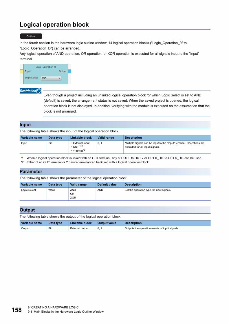
15
Logical operation block
In the fourth section in the hardware logic outline window, 14 logical operation blocks ("Logic_Operation_0" to "Logic_Operation_D") can be arranged.Any logical operation of AND operation, OR operation, or XOR operation is executed for all signals input to the "Input" terminal.
Even though a project including an unlinked logical operation block for which Logic Select is set to AND (default) is saved, the arrangement status is not saved. When the saved project is opened, the logical operation block is not displayed. In addition, verifying with the module is executed on the assumption that the block is not arranged.
InputThe following table shows the input of the logical operation block.
*1 When a logical operation block is linked with an OUT terminal, any of OUT 0 to OUT 7 or OUT 0_DIF to OUT 5_DIF can be used.*2 Either of an OUT terminal or Y device terminal can be linked with a logical operation block.
ParameterThe following table shows the parameter of the logical operation block.
OutputThe following table shows the output of the logical operation block.
Variable name Data type Linkable block Valid range DescriptionInput Bit • External input
• OUT*1*2
• Y device*2
0, 1 Multiple signals can be input to the "Input" terminal. Operations are executed for all input signals.
Variable name Data type Valid range Default value DescriptionLogic Select Word AND
ORXOR
AND Set the operation type for input signals.
Variable name Data type Linkable block Output value DescriptionOutput Bit External output 0, 1 Outputs the operation results of input signals.
Outline
8 9 CREATING A HARDWARE LOGIC9.1 Main Blocks in the Hardware Logic Outline Window
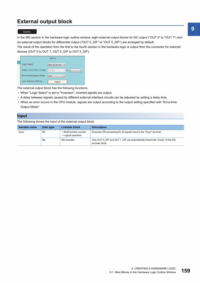
9
External output blockIn the fifth section in the hardware logic outline window, eight external output blocks for DC output ("OUT 0" to "OUT 7") and six external output blocks for differential output ("OUT 0_DIF" to "OUT 5_DIF") are arranged by default.The result of the operation from the first to the fourth section in the hardware logic is output from the connector for external devices (OUT 0 to OUT 7, OUT 0_DIF to OUT 5_DIF).
The external output block has the following functions. • When "Logic Select" is set to "Inversion", inverted signals are output. • A delay between signals caused by different external interface circuits can be adjusted by setting a delay time. • When an error occurs in the CPU module, signals are output according to the output setting specified with "Error-time
Output Mode".
InputThe following shows the input of the external output block.
Variable name Data type Linkable block DescriptionInput Bit • Multi function counter
• Logical operationExecutes OR processing for all signals input to the "Input" terminal.
Bit SSI encoder Only OUT 0_DIF and OUT 1_DIF are automatically linked with "Clock" of the SSI encoder block.
Outline
9 CREATING A HARDWARE LOGIC9.1 Main Blocks in the Hardware Logic Outline Window 159

16
ParameterThe following table shows the parameters of the external output block.
• Parameters of "User Address Setting"
*1 The available buffer memory addresses are common in OUT 0 to OUT 7 and OUT 0_DIF to OUT 5_DIF. Each external output block is assigned to the bits of the specified buffer memory as follows.
*2 The external output block where Forced output enabled (1) is set outputs a signal according to the setting value (forced output value) of the buffer memory area specified with "Forced Output". The input from the "Input" terminal is not reflected to the external output.
Variable name Data type Valid range Default value DescriptionLogic Select Bit Non-Inversion
InversionNon-Inversion Set Non-Inversion or Inversion for input signals.
Delay Time (Step) Word 0 to 64 0 Adjust the signal output timing. A delay time can be set with the combination of "Delay Time (Step)" and "Delay Time (Unit)". Setting the number of steps to 0 disables the delay.
Delay Time (Unit) Word 12.5ns25ns50ns0.1s1s10s100s1ms
12.5ns Adjust the signal output timing. A delay time can be set with the combination of "Delay Time (Unit)" and "Delay Time (Step)".
Error-time Output Mode
Word OFFONHOLD
OFF Set output signals at occurrence of an error in the CPU module to OFF fixed, ON fixed, or holding output status. This setting is also applied to output signals at a hardware logic control stop.
User Address Setting
Set the buffer memory addresses used in the external output block. Click the [Detail] button to open the "User Address Setting" window.
Variable name Data type Valid range DescriptionEnable Forced Output
Word 1000 to 1099 Specify the buffer memory address to enable or disable the forced output.*1
Whether the forced output is enabled or disabled can be set by setting the following values for the specified buffer memory.*2
0: Forced output disabled1: Forced output enabled
Forced Output Word 1000 to 1099 Specify the buffer memory address to set the status of the forced output signal.*1
Whether the signal status is set to off or on can be set by setting the following values for the specified buffer memory.0: OFF output1: ON output
External terminal monitor
Word 1000 to 1099 Specify the buffer memory address to store the external terminal status.*1
0: OFF output1: ON output
bit15 bit14 bit13 bit12 bit11 bit10 bit9 bit8 bit7 bit6 bit5 bit4 bit3 bit2 bit1 bit0
00OUT
0_DIFOUT
1_DIFOUT
2_DIFOUT
3_DIFOUT
4_DIFOUT
5_DIF OUT 7 OUT 6 OUT 5 OUT 4 OUT 3 OUT 2 OUT 1 OUT 0
0 9 CREATING A HARDWARE LOGIC9.1 Main Blocks in the Hardware Logic Outline Window

9
■Delay timeA delay time is calculated by multiplying "Delay Time (Unit)" by "Delay Time (Step)".An error of one unit time may be generated in delay time. However, the error can be reduced by setting the delay time as shown below. • Change the value of "Delay Time (Unit)" as small as possible. • Set a large value for "Delay Time (Step)".Ex.
The following table lists examples of the delay time of 20s. Compared with example 2, an error is smaller in the setting of example 1.
■Link with SSI encoder blocksWhen an SSI encoder block is arranged in the hardware logic outline window, the "Clock" terminal of the SSI encoder block and the "Input" terminal of an external output block are automatically linked.The default value is set for the setting value of the external output block automatically linked and the value cannot be changed.
High/Low states of external output signalsThe following table lists the High/Low states of external output signals in each setting combination of input signals to external output blocks and "Logic Select".
When an error occurs in the CPU module, a signal is output according to the output setting of "Error-time Output Mode" independent of the setting of Inversion or Not-Inversion.
Example Delay Time(Step) Delay Time(Unit) ErrorExample 1 1s 20 steps An error of maximum 1s is generated in the output timing.
Example 2 10s 2 steps An error of maximum 10s is generated in the output timing.
Output type "Logic Select"
"Non-Inversion" "Inversion"DC
Differential
High
Low
ON
OFF
Input terminal
OUT Output
High
Low
ON
OFF
Input terminal
OUT Output
High
Low
High
Low
High
Low
Input terminal
OUT_DIF +Output
OUT_DIF -Output
High
Low
High
Low
High
Low
Input terminal
OUT_DIF +Output
OUT_DIF -Output
9 CREATING A HARDWARE LOGIC9.1 Main Blocks in the Hardware Logic Outline Window 161

16
SI device terminal
In the fifth section in the hardware logic outline window, eight SI device terminals ("SI 0" to "SI 7") are arranged by default.When a signal is input to an SI device terminal, an interrupt request is output to the CPU module to start an interrupt program.The interrupt program corresponding to each SI device terminal needs to be set in GX Works2 in advance.
OutputThe following table shows the output of the SI device terminal.
*1 An SI device terminal can be linked to any of the Output terminals of the multi function counter block Counter_0 to Counter_7.
When multiple SI device terminals are turned to High at the same time, the interrupt programs are started in order from the program corresponding to the terminal with a smaller number. When multiple SI device terminals are linked, link the terminals so that terminals corresponding to interrupt programs with higher priority have smaller numbers.
Variable name Data type Linkable block Valid range DescriptionOutput Bit Multi function
counter*10, 1 For details on interruption, refer to the following.
Page 206 Setting intelligent function module interrupt pointers
Outline
2 9 CREATING A HARDWARE LOGIC9.1 Main Blocks in the Hardware Logic Outline Window
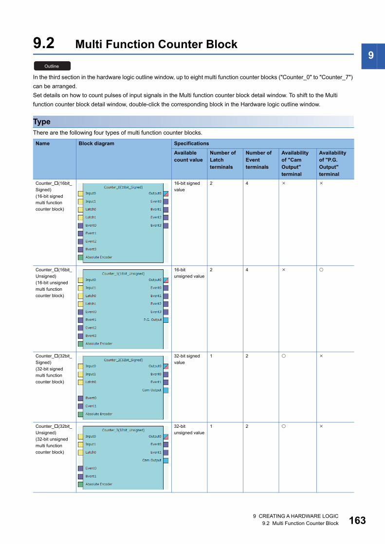
9
9.2 Multi Function Counter BlockIn the third section in the hardware logic outline window, up to eight multi function counter blocks ("Counter_0" to "Counter_7") can be arranged.Set details on how to count pulses of input signals in the Multi function counter block detail window. To shift to the Multi function counter block detail window, double-click the corresponding block in the Hardware logic outline window.
TypeThere are the following four types of multi function counter blocks.
Name Block diagram Specifications
Available count value
Number of Latch terminals
Number of Event terminals
Availability of "Cam Output" terminal
Availability of "P.G. Output" terminal
Counter_(16bit_Signed)(16-bit signed multi function counter block)
16-bit signed value
2 4
Counter_(16bit_Unsigned)(16-bit unsigned multi function counter block)
16-bit unsigned value
2 4
Counter_(32bit_Signed)(32-bit signed multi function counter block)
32-bit signed value
1 2
Counter_(32bit_Unsigned)(32-bit unsigned multi function counter block)
32-bit unsigned value
1 2
Outline
9 CREATING A HARDWARE LOGIC9.2 Multi Function Counter Block 163
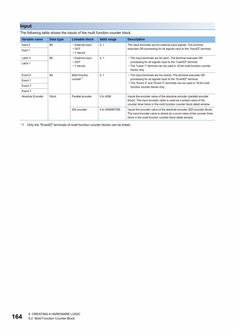
16
InputThe following table shows the inputs of the multi function counter block.
*1 Only the "Event" terminals of multi function counter blocks can be linked.
Variable name Data type Linkable block Valid range DescriptionInput 0 Bit • External input
• OUT• Y device
0, 1 The input terminals are for external input signals. The terminal executes OR processing for all signals input to the "Input" terminal.Input 1
Latch 0 Bit • External input• OUT• Y device
0, 1 • The input terminals are for latch. The terminal executes OR processing for all signals input to the "Latch" terminal.
• The "Latch 1" terminal can be used in 16-bit multi function counter blocks only.
Latch 1
Event 0 Bit Multi function counter*1
0, 1 • The input terminals are for events. The terminal executes OR processing for all signals input to the "Event" terminal.
• The "Event 2" and "Event 3" terminals can be used in 16-bit multi function counter blocks only.
Event 1
Event 2
Event 3
Absolute Encoder Word Parallel encoder 0 to 4095 Inputs the encoder value of the absolute encoder (parallel encoder block). The input encoder value is used as a preset value of the counter timer block in the multi function counter block detail window.
SSI encoder 0 to 4294967295 Inputs the encoder value of the absolute encoder (SSI encoder block). The input encoder value is stored as a count value of the counter timer block in the multi function counter block detail window.
4 9 CREATING A HARDWARE LOGIC9.2 Multi Function Counter Block
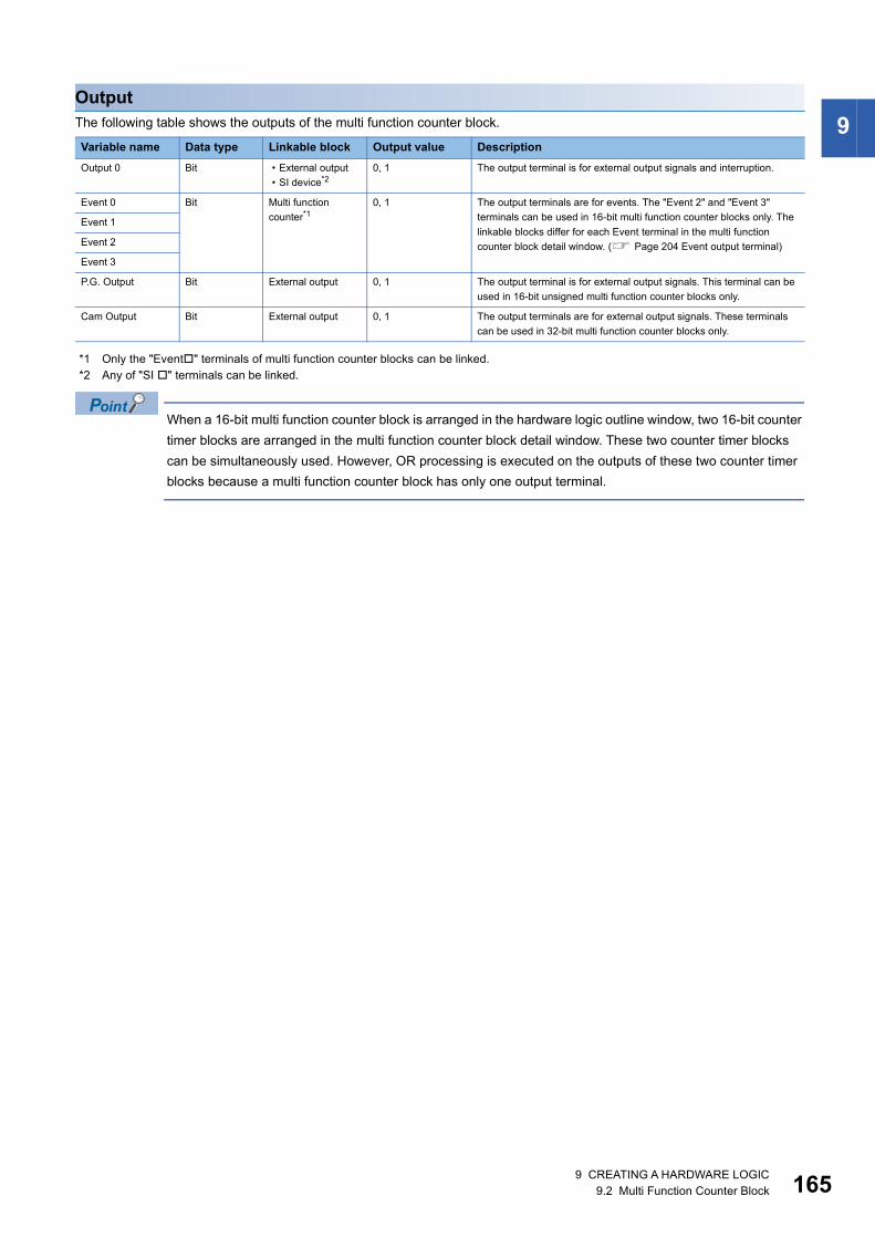
9
OutputThe following table shows the outputs of the multi function counter block.*1 Only the "Event" terminals of multi function counter blocks can be linked.*2 Any of "SI " terminals can be linked.
When a 16-bit multi function counter block is arranged in the hardware logic outline window, two 16-bit counter timer blocks are arranged in the multi function counter block detail window. These two counter timer blocks can be simultaneously used. However, OR processing is executed on the outputs of these two counter timer blocks because a multi function counter block has only one output terminal.
Variable name Data type Linkable block Output value DescriptionOutput 0 Bit • External output
• SI device*20, 1 The output terminal is for external output signals and interruption.
Event 0 Bit Multi function counter*1
0, 1 The output terminals are for events. The "Event 2" and "Event 3" terminals can be used in 16-bit multi function counter blocks only. The linkable blocks differ for each Event terminal in the multi function counter block detail window. ( Page 204 Event output terminal)
Event 1
Event 2
Event 3
P.G. Output Bit External output 0, 1 The output terminal is for external output signals. This terminal can be used in 16-bit unsigned multi function counter blocks only.
Cam Output Bit External output 0, 1 The output terminals are for external output signals. These terminals can be used in 32-bit multi function counter blocks only.
9 CREATING A HARDWARE LOGIC9.2 Multi Function Counter Block 165
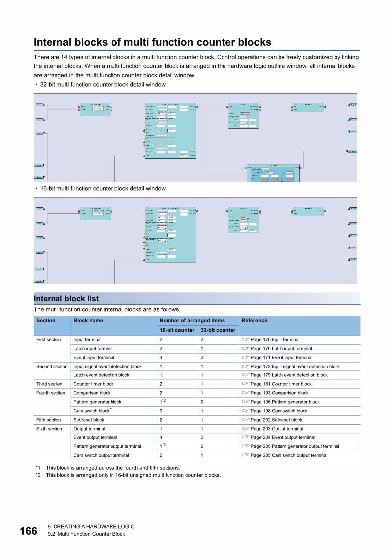
16
Internal blocks of multi function counter blocksThere are 14 types of internal blocks in a multi function counter block. Control operations can be freely customized by linking the internal blocks. When a multi function counter block is arranged in the hardware logic outline window, all internal blocks are arranged in the multi function counter block detail window. • 32-bit multi function counter block detail window
• 16-bit multi function counter block detail window
Internal block listThe multi function counter internal blocks are as follows.
*1 This block is arranged across the fourth and fifth sections.*2 This block is arranged only in 16-bit unsigned multi function counter blocks.
Section Block name Number of arranged items Reference
16-bit counter 32-bit counterFirst section Input terminal 2 2 Page 170 Input terminal
Latch input terminal 2 1 Page 170 Latch input terminal
Event input terminal 4 2 Page 171 Event input terminal
Second section Input signal event detection block 1 1 Page 172 Input signal event detection block
Latch event detection block 1 1 Page 179 Latch event detection block
Third section Counter timer block 2 1 Page 181 Counter timer block
Fourth section Comparison block 2 1 Page 193 Comparison block
Pattern generator block 1*2 0 Page 196 Pattern generator block
Cam switch block*1 0 1 Page 198 Cam switch block
Fifth section Set/reset block 2 1 Page 202 Set/reset block
Sixth section Output terminal 1 1 Page 203 Output terminal
Event output terminal 4 2 Page 204 Event output terminal
Pattern generator output terminal 1*2 0 Page 205 Pattern generator output terminal
Cam switch output terminal 0 1 Page 205 Cam switch output terminal
6 9 CREATING A HARDWARE LOGIC9.2 Multi Function Counter Block

9
Link combinationAn input terminal and output terminal in the same color can be linked among the internal blocks. Input terminals or output terminals cannot be linked each other.The following table lists the combinations.*1 The terminals are linked by default. The links cannot be deleted.*2 The terminals can be linked when a 16-bit multi function counter block is used. They cannot be linked when a 32-bit multi function
counter block is used.If multiple output terminals are linked to one input terminal, OR processing is executed on all input signals. If one output terminal is linked to multiple input terminals, the same signals are output for all the input terminals.
Output side Input side Color
Block name Terminal name Block name Terminal nameInput terminal Input Input signal event detection block Input*1 Coral
Latch input terminal Latch Latch event detection block Input*1 Pale orange
Event input terminal Event Counter timer block RUN Butterfly yellow
STOP
UP
DOWN
PRESET
Latch
Input signal event detection block Output Counter timer block RUN Hop green
STOP
UP
DOWN
PRESET
Set/reset block Set
Reset
Output terminal Output
Event output terminal Event*2
Latch event detection block Output Counter timer block Latch*1 Celadon
Counter timer block Count Value Comparison block Input*1 Cyan blue
Cam switch block Input*1
Pattern generator block Input*1
Comparison block Output Set/reset block Set Vermeer
Reset
Event output terminal Event
Cam switch block Output Cam switch output terminal Cam Output*1 Columbine blue
Pattern generator block Output Pattern generator output terminal P.G. Output*1 Columbine blue
Set/reset block Output Output terminal Output Lilac
9 CREATING A HARDWARE LOGIC9.2 Multi Function Counter Block 167
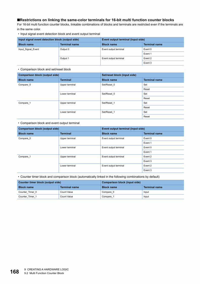
16
■Restrictions on linking the same-color terminals for 16-bit multi function counter blocksFor 16-bit multi function counter blocks, linkable combinations of blocks and terminals are restricted even if the terminals are in the same color. • Input signal event detection block and event output terminal
• Comparison block and set/reset block
• Comparison block and event output terminal
• Counter timer block and comparison block (automatically linked in the following combinations by default)
Input signal event detection block (output side) Event output terminal (input side)
Block name Terminal name Block name Terminal nameInput_Signal_Event Output 0 Event output terminal Event 0
Event 1
Output 1 Event output terminal Event 2
Event 3
Comparison block (output side) Set/reset block (input side)
Block name Terminal Block name Terminal nameCompare_0 Upper terminal Set/Reset_0 Set
Reset
Lower terminal Set/Reset_0 Set
Reset
Compare_1 Upper terminal Set/Reset_1 Set
Reset
Lower terminal Set/Reset_1 Set
Reset
Comparison block (output side) Event output terminal (input side)
Block name Terminal Block name Terminal nameCompare_0 Upper terminal Event output terminal Event 0
Event 1
Lower terminal Event output terminal Event 0
Event 1
Compare_1 Upper terminal Event output terminal Event 2
Event 3
Lower terminal Event output terminal Event 2
Event 3
Counter timer block (output side) Comparison block (input side)
Block name Terminal name Block name Terminal nameCounter_Timer_0 Count Value Compare_0 Input
Counter_Timer_1 Count Value Compare_1 Input
8 9 CREATING A HARDWARE LOGIC9.2 Multi Function Counter Block
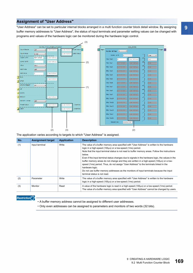
9
Assignment of "User Address""User Address" can be set to particular internal blocks arranged in a multi function counter block detail window. By assigning buffer memory addresses to "User Address", the status of input terminals and parameter setting values can be changed with programs and values of the hardware logic can be monitored during the hardware logic control.The application varies according to targets to which "User Address" is assigned.
• A buffer memory address cannot be assigned to different user addresses. • Only even addresses can be assigned to parameters and monitors of two words (32 bits).
No. Assignment target Application Description(1) Input terminal Write The value of a buffer memory area specified with "User Address" is written to the hardware
logic in a high-speed (100s) or a low-speed (1ms) period.Note that the input terminal status is not read to buffer memory areas. Follow the instructions below.Even if the input terminal status changes due to signals in the hardware logic, the values in the buffer memory areas do not change and they are written in a high-speed (100s) or a low-speed (1ms) period. Thus, do not assign "User Address" to the terminals linked in the hardware logic.Do not use buffer memory addresses as the monitors of input terminals because the input terminal status is not read.
(2) Parameter Write The value of a buffer memory area specified with "User Address" is written to the hardware logic in a high-speed (100s) or a low-speed (1ms) period.
(3) Monitor Read A value of the hardware logic is read in a high-speed (100s) or a low-speed (1ms) period. The value of a buffer memory area specified with "User Address" cannot be changed by users.
(3)
(3)
(2)
(2)
(1)
(2)
9 CREATING A HARDWARE LOGIC9.2 Multi Function Counter Block 169
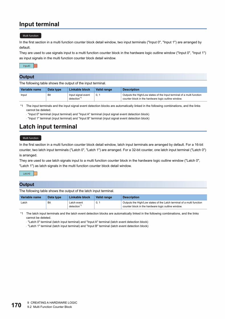
17
Input terminal
In the first section in a multi function counter block detail window, two input terminals ("Input 0", "Input 1") are arranged by default.They are used to use signals input to a multi function counter block in the hardware logic outline window ("Input 0", "Input 1") as input signals in the multi function counter block detail window.
OutputThe following table shows the output of the input terminal.
*1 The input terminals and the input signal event detection blocks are automatically linked in the following combinations, and the links cannot be deleted. "Input 0" terminal (input terminal) and "Input A" terminal (input signal event detection block) "Input 1" terminal (input terminal) and "Input B" terminal (input signal event detection block)
Latch input terminal
In the first section in a multi function counter block detail window, latch input terminals are arranged by default. For a 16-bit counter, two latch input terminals ("Latch 0", "Latch 1") are arranged. For a 32-bit counter, one latch input terminal ("Latch 0") is arranged.They are used to use latch signals input to a multi function counter block in the hardware logic outline window ("Latch 0", "Latch 1") as latch signals in the multi function counter block detail window.
OutputThe following table shows the output of the latch input terminal.
*1 The latch input terminals and the latch event detection blocks are automatically linked in the following combinations, and the links cannot be deleted. "Latch 0" terminal (latch input terminal) and "Input A" terminal (latch event detection block) "Latch 1" terminal (latch input terminal) and "Input B" terminal (latch event detection block)
Variable name Data type Linkable block Valid range DescriptionInput Bit Input signal event
detection*10, 1 Outputs the High/Low states of the Input terminal of a multi function
counter block in the hardware logic outline window.
Variable name Data type Linkable block Valid range DescriptionLatch Bit Latch event
detection*10, 1 Outputs the High/Low states of the Latch terminal of a multi function
counter block in the hardware logic outline window.
Multi function
Multi function
0 9 CREATING A HARDWARE LOGIC9.2 Multi Function Counter Block

9
Event input terminalIn the first section in a multi function counter block detail window, event input terminals are arranged by default. For a 16-bit counter, four event input terminals ("Event 0" to "Event 3") are arranged. For a 32-bit counter, two event input terminals ("Event 0", "Event 1") are arranged.They are used to use signals input to a multi function counter block in the hardware logic outline window ("Event 0" to "Event 3") as event signals in the multi function counter block detail window.
OutputThe following table shows the output of the event input terminal.
*1 The event input terminal can link with all the terminals of a counter timer block.
Variable name Data type Linkable block Valid range DescriptionEvent Bit Counter timer*1 0, 1 Outputs the High/Low states of Event terminals of a multi function
counter block in the hardware logic outline window.
Multi function
9 CREATING A HARDWARE LOGIC9.2 Multi Function Counter Block 171

17
Input signal event detection block
In the second section in a multi function counter block detail window, one input signal event detection block ("Input_Signal_Event") is arranged by default.Set conditions to detect input signals of a multi function counter block. When the detection conditions are satisfied, the Output terminal turns to High. This operation can be utilized for the count-up or other functions of the counter timer block.
InputThe following table shows the inputs of the input signal event detection block.
*1 The input terminals and the input signal event detection blocks are automatically linked in the following combinations, and the links cannot be deleted. "Input 0" terminal (input terminal) and "Input A" terminal (input signal event detection block) "Input 1" terminal (input terminal) and "Input B" terminal (input signal event detection block)
Variable name Data type Linkable block Valid range DescriptionInput A Bit Input*1 0, 1 Signals from Input terminals are input. "Input A" is for a phase-A input,
and "Input B" is for a phase-B input.Input B
Multi function
2 9 CREATING A HARDWARE LOGIC9.2 Multi Function Counter Block
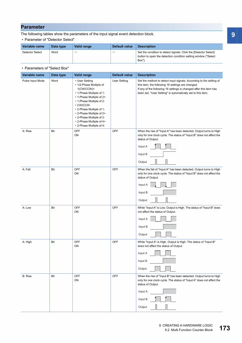
9
ParameterThe following tables show the parameters of the input signal event detection block. • Parameter of "Detector Select"• Parameters of "Select Box"
Variable name Data type Valid range Default value DescriptionDetector Select Word Set the condition to detect signals. Click the [Detector Select]
button to open the detection condition setting window ("Select Box").
Variable name Data type Valid range Default value DescriptionPulse Input Mode Word • User Setting
• 1/2-Phase Multiple of 1(CW/CCW)+
• 1-Phase Multiple of 1-• 1-Phase Multiple of 2+• 1-Phase Multiple of 2-• CW/CCW-• 2-Phase Multiple of 1-• 2-Phase Multiple of 2+• 2-Phase Multiple of 2-• 2-Phase Multiple of 4+• 2-Phase Multiple of 4-
User Setting Set the method to detect input signals. According to the setting of this item, the following 16 settings are changed.If any of the following 16 settings is changed after this item has been set, "User Setting" is automatically set to this item.
A: Rise Bit OFFON
OFF When the rise of "Input A" has been detected, Output turns to High only for one clock cycle. The status of "Input B" does not affect the status of Output.
A: Fall Bit OFFON
OFF When the fall of "Input A" has been detected, Output turns to High only for one clock cycle. The status of "Input B" does not affect the status of Output.
A: Low Bit OFFON
OFF While "Input A" is Low, Output is High. The status of "Input B" does not affect the status of Output.
A: High Bit OFFON
OFF While "Input A" is High, Output is High. The status of "Input B" does not affect the status of Output.
B: Rise Bit OFFON
OFF When the rise of "Input B" has been detected, Output turns to High only for one clock cycle. The status of "Input A" does not affect the status of Output.
Input A
Input B
Output
Output
Input A
Input B
Input A
Input B
Output
Input A
Input B
Output
Input A
Input B
Output
9 CREATING A HARDWARE LOGIC9.2 Multi Function Counter Block 173

17
B: Fall Bit OFFON
OFF When the fall of "Input B" has been detected, Output turns to High only for one clock cycle. The status of "Input A" does not affect the status of Output.
B: Low Bit OFFON
OFF While "Input B" is Low, Output is High. The status of "Input A" does not affect the status of Output.
B: High Bit OFFON
OFF While "Input B" is High, Output is High. The status of "Input A" does not affect the status of Output.
A: Rise+B: Low Bit OFFON
OFF When the rise of "Input A" and the Low state of "Input B" have been detected, Output turns to High only for one clock cycle.
A: Rise+B: High Bit OFFON
OFF When the rise of "Input A" and the High state of "Input B" have been detected, Output turns to High only for one clock cycle.
A: Fall+B: Low Bit OFFON
OFF When the fall of "Input A" and the Low state of "Input B" have been detected, Output turns to High only for one clock cycle.
A: Fall+B: High Bit OFFON
OFF When the fall of "Input A" and the High state of "Input B" have been detected, Output turns to High only for one clock cycle.
A: Low+B: Rise Bit OFFON
OFF When the Low state of "Input A" and the rise of "Input B" have been detected, Output turns to High only for one clock cycle.
Variable name Data type Valid range Default value Description
Input A
Input B
Output
Input A
Input B
Output
Input A
Input B
Output
Input A
Input B
Output
Input A
Input B
Output
Input A
Input B
Output
Input A
Input B
Output
Input A
Input B
Output
4 9 CREATING A HARDWARE LOGIC9.2 Multi Function Counter Block
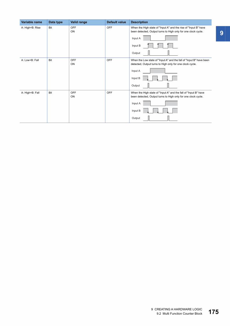
9
A: High+B: Rise Bit OFFONOFF When the High state of "Input A" and the rise of "Input B" have
been detected, Output turns to High only for one clock cycle.
A: Low+B: Fall Bit OFFON
OFF When the Low state of "Input A" and the fall of "Input B" have been detected, Output turns to High only for one clock cycle.
A: High+B: Fall Bit OFFON
OFF When the High state of "Input A" and the fall of "Input B" have been detected, Output turns to High only for one clock cycle.
Variable name Data type Valid range Default value Description
Input A
Input B
Output
Input A
Input B
Output
Input A
Input B
Output
9 CREATING A HARDWARE LOGIC9.2 Multi Function Counter Block 175

17
■Pulse input modes and count timingThe following table shows the relationships between each pulse input mode and count timing.
"Pulse Input Mode" Count timing1-phase multiple of 1 (1-Phase Multiple of 1+, 1-Phase Multiple of 1-)
At up count The value is counted up at the rise () of A.B is Low.
At down count The value is counted down at the fall () of A.B is High.
1-phase multiple of 2 (1-Phase Multiple of 2+, 1-Phase Multiple of 2-)
At up count The value is counted up at the rise () and fall () of A.B is Low.
At down count The value is counted down at the rise () and fall () of A.B is High.
CW/CCW (CW/CCW+, CW/CCW-) At up count The value is counted up at the rise () of A.B is Low.
At down count A is Low.The value is counted down at the rise () of B.
2-phase multiple of 1 (2-Phase Multiple of 1+, 2-Phase Multiple of 1-)
At up count When B is Low, the value is counted up at the rise () of A.
At down count When B is Low, the value is counted down at the fall () of A.
2-phase multiple of 2 (2-Phase Multiple of 2+, 2-Phase Multiple of 2-)
At up count When B is Low, the value is counted up at the rise () of A.When B is High, the value is counted up at the fall () of A.
At down count When B is High, the value is counted down at the rise () of A.When B is Low, the value is counted down at the fall () of A.
2-phase multiple of 4 (2-Phase Multiple of 4+, 2-Phase Multiple of 4-)
At up count When B is Low, the value is counted up at the rise () of A.When A is High, the value is counted up at the rise () of B.When B is High, the value is counted up at the fall () of A.When A is Low, the value is counted up at the fall () of B.
At down count When A is Low, the value is counted down at the rise () of B.When B is High, the value is counted down at the rise () of A.When A is High, the value is counted down at the fall () of B.When B is Low, the value is counted down at the fall () of A.
ΦA
ΦB
ΦA
ΦB
ΦA
ΦB
ΦA
ΦB
ΦA
ΦB
ΦA
ΦB
ΦA
ΦB
ΦA
ΦB
ΦA
ΦB
ΦA
ΦB
ΦA
ΦB
ΦA
ΦB
6 9 CREATING A HARDWARE LOGIC9.2 Multi Function Counter Block
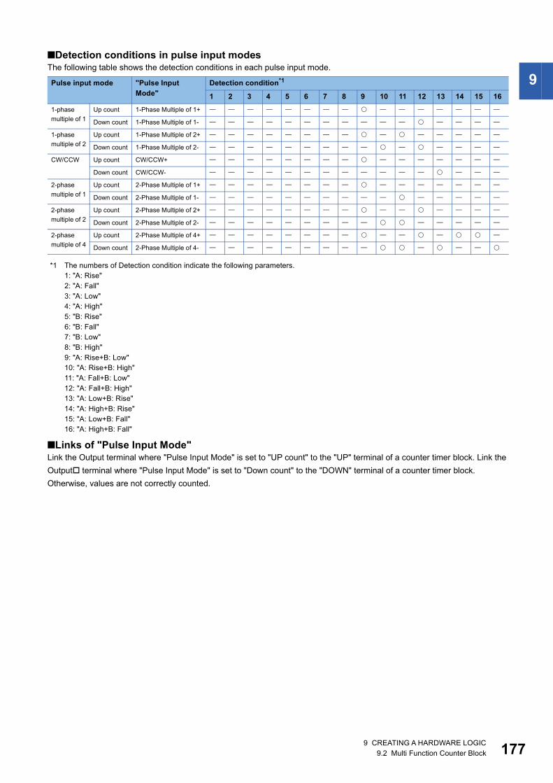
9
■Detection conditions in pulse input modesThe following table shows the detection conditions in each pulse input mode.*1 The numbers of Detection condition indicate the following parameters.1: "A: Rise"2: "A: Fall"3: "A: Low"4: "A: High"5: "B: Rise"6: "B: Fall"7: "B: Low"8: "B: High"9: "A: Rise+B: Low"10: "A: Rise+B: High"11: "A: Fall+B: Low"12: "A: Fall+B: High"13: "A: Low+B: Rise"14: "A: High+B: Rise"15: "A: Low+B: Fall"16: "A: High+B: Fall"
■Links of "Pulse Input Mode"Link the Output terminal where "Pulse Input Mode" is set to "UP count" to the "UP" terminal of a counter timer block. Link the Output terminal where "Pulse Input Mode" is set to "Down count" to the "DOWN" terminal of a counter timer block.Otherwise, values are not correctly counted.
Pulse input mode "Pulse Input Mode"
Detection condition*1
1 2 3 4 5 6 7 8 9 10 11 12 13 14 15 161-phase multiple of 1
Up count 1-Phase Multiple of 1+
Down count 1-Phase Multiple of 1-
1-phase multiple of 2
Up count 1-Phase Multiple of 2+
Down count 1-Phase Multiple of 2-
CW/CCW Up count CW/CCW+
Down count CW/CCW-
2-phase multiple of 1
Up count 2-Phase Multiple of 1+
Down count 2-Phase Multiple of 1-
2-phase multiple of 2
Up count 2-Phase Multiple of 2+
Down count 2-Phase Multiple of 2-
2-phase multiple of 4
Up count 2-Phase Multiple of 4+
Down count 2-Phase Multiple of 4-
9 CREATING A HARDWARE LOGIC9.2 Multi Function Counter Block 177
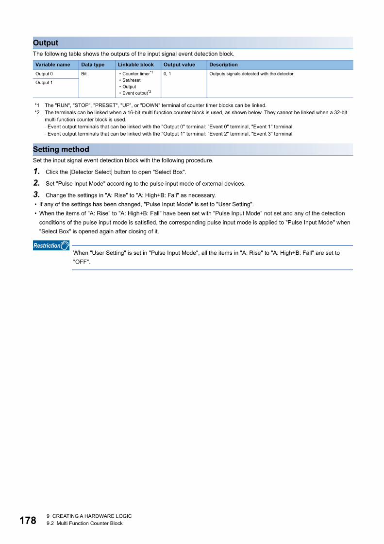
17
OutputThe following table shows the outputs of the input signal event detection block.
*1 The "RUN", "STOP", "PRESET", "UP", or "DOWN" terminal of counter timer blocks can be linked.*2 The terminals can be linked when a 16-bit multi function counter block is used, as shown below. They cannot be linked when a 32-bit
multi function counter block is used. Event output terminals that can be linked with the "Output 0" terminal: "Event 0" terminal, "Event 1" terminal Event output terminals that can be linked with the "Output 1" terminal: "Event 2" terminal, "Event 3" terminal
Setting methodSet the input signal event detection block with the following procedure.
1. Click the [Detector Select] button to open "Select Box".
2. Set "Pulse Input Mode" according to the pulse input mode of external devices.
3. Change the settings in "A: Rise" to "A: High+B: Fall" as necessary. • If any of the settings has been changed, "Pulse Input Mode" is set to "User Setting". • When the items of "A: Rise" to "A: High+B: Fall" have been set with "Pulse Input Mode" not set and any of the detection
conditions of the pulse input mode is satisfied, the corresponding pulse input mode is applied to "Pulse Input Mode" when "Select Box" is opened again after closing of it.
When "User Setting" is set in "Pulse Input Mode", all the items in "A: Rise" to "A: High+B: Fall" are set to "OFF".
Variable name Data type Linkable block Output value DescriptionOutput 0 Bit • Counter timer*1
• Set/reset• Output• Event output*2
0, 1 Outputs signals detected with the detector.
Output 1
8 9 CREATING A HARDWARE LOGIC9.2 Multi Function Counter Block
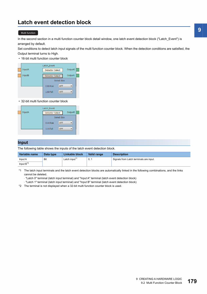
9
Latch event detection blockIn the second section in a multi function counter block detail window, one latch event detection block ("Latch_Event") is arranged by default.Set conditions to detect latch input signals of the multi function counter block. When the detection conditions are satisfied, the Output terminal turns to High. • 16-bit multi function counter block
• 32-bit multi function counter block
InputThe following table shows the inputs of the latch event detection block.
*1 The latch input terminals and the latch event detection blocks are automatically linked in the following combinations, and the links cannot be deleted. "Latch 0" terminal (latch input terminal) and "Input A" terminal (latch event detection block) "Latch 1" terminal (latch input terminal) and "Input B" terminal (latch event detection block)
*2 The terminal is not displayed when a 32-bit multi function counter block is used.
Variable name Data type Linkable block Valid range DescriptionInput A Bit Latch input*1 0, 1 Signals from Latch terminals are input.
Input B*2
Multi function
9 CREATING A HARDWARE LOGIC9.2 Multi Function Counter Block 179

18
ParameterThe following tables show the parameters of the latch event detection block. • Parameter of "Detector Select"
• Parameters of "Select Box"
OutputThe following table shows the outputs of the latch event detection block.
*1 The latch event detection block and the Latch terminals of the counter timer blocks are automatically linked in the following combinations, and the links cannot be deleted. "Output 0" terminal (latch event detection block) and "Latch" terminal ("Counter_Timer_0") "Output 1" terminal (latch event detection block) and "Latch" terminal ("Counter_Timer_1") (This combination cannot be used for 32-bit multi function counter blocks.)
*2 The terminal is not displayed when a 32-bit multi function counter block is used.
Variable name Data type Valid range Default value DescriptionDetector Select Word Set the condition to detect signals. Click the [Detector Select] button to
open the "Select Box" window.The Detector Select on the upper side is for detecting signals of "Input A".The Detector Select on the lower side is for detecting signals of "Input B".
Variable name Data type Valid range Default value DescriptionA: Rise("B: Rise" for lower-side Detector Select for a 16-bit multi function counter block)
Bit OFFON
OFF When the rise of Input has been detected, Output turns to High only for one clock cycle.
A: Fall("B: Fall" for lower-side Detector Select for a 16-bit multi function counter block)
Bit OFFON
OFF When the fall of Input has been detected, Output turns to High only for one clock cycle.
Variable name Data type Linkable block Valid range DescriptionOutput 0 Bit Counter timer*1 0, 1 Outputs signals detected with the detector.
Output 1*2
Input � terminal
Output � terminal
Input � terminal
Output � terminal
0 9 CREATING A HARDWARE LOGIC9.2 Multi Function Counter Block
9
Counter timer blockIn the third section in a multi function counter block detail window, counter timer blocks are arranged by default. For a 16-bit counter timer block, two counter timer blocks ("Counter_Timer_0"(16bit_Unsigned/Signed), "Counter_Timer_1"(16bit_Unsigned/Signed)) are arranged. For a 32-bit counter timer block, one counter timer block ("Counter_Timer_0"(32bit_Unsigned/Signed)) is arranged.The counter operates according to the signals of the event input terminals, the input signal event detection block, and the latch event detection block and the count values are output. • 16-bit multi function counter block
Multi function
9 CREATING A HARDWARE LOGIC9.2 Multi Function Counter Block 181
18
• 32-bit multi function counter block
The counter timer block has the following functions. • Input pulses are counted. • Input pulses are counted per clock cycle. • Either of the ring counter mode or the linear counter mode can be selected (For 16-bit counter timer blocks, only the ring
counter mode can be selected). • Count values can be preset and latched. • Addition values can be set (addition mode). • For 32-bit counter timer blocks, an overflow and an underflow can be detected.
2 9 CREATING A HARDWARE LOGIC9.2 Multi Function Counter Block
9
InputThe following table shows the inputs of the counter timer block.*1 When a buffer memory address is assigned to "User Address", control can be performed with a program without link. Assign the same buffer memory address to the "RUN" terminal and the "STOP" terminal. (bit 0: RUN, bit 1: STOP)
*2 When the addition mode is on, the addition value is added or subtracted.*3 Events are detected every clock cycle of the counter timer block. Thus, while a High-state signal is input to an Event terminal, an event
occurs every clock cycle.*4 The latch event detection block and the "Latch" terminals of the counter timer blocks are automatically linked in the following
combinations, and the links cannot be deleted. "Output 0" terminal (latch event detection block) and "Latch" terminal ("Counter_Timer_0") "Output 1" terminal (latch event detection block) and "Latch" terminal ("Counter_Timer_1")
*5 On the rising edge (Low state High state) of the event input terminal, the count value is latched.*6 Do not link these terminals when an SSI encoder block is linked with a multi function counter block in the hardware logic outline window.
Otherwise, correct encoder values may not be acquired.
The High/Low states of the input terminals are detected per clock cycle. When the High states of multiple terminals are detected, only the input of the terminal with the highest priority becomes valid. The inputs of terminals with lower priority become invalid. Link the terminals so that multiple signals are not input at the same time. (Creating a hardware logic where the input to the STOP terminal is detected during the High state is recommended.)The following shows the priority of the terminals.1. "PRESET" terminal2. "STOP" terminal3. "RUN" terminal4. "UP" terminal5. "DOWN" terminalThe RUN terminal holds an event. Thus, when the High states of the PRESET terminal and the RUN terminal for one clock cycle are detected, the PRESET terminal becomes valid. The RUN terminal becomes valid in the next clock cycle.
Variable name Data type Linkable block Valid range DescriptionRUN*1*6 Bit • Event input
• Input signal event detection
0, 1 Adds 1 to the count value per preset clock cycle.*2
Multiple signals can be input to the terminal. OR processing is executed for all input signals.
STOP*1*6 Bit • Event input• Input signal event
detection
0, 1 Stops the counter.Multiple signals can be input to the terminal. OR processing is executed for all input signals.
UP*3*6 Bit • Event input• Input signal event
detection
0, 1 Adds an addition value to the count value when a signal generated in the previous block is input to the terminal. When the addition mode is off, 1 is added to the count value.*2
Multiple signals can be input to the terminal. OR processing is executed for all input signals.
DOWN*3*6 Bit • Event input• Input signal event
detection
0, 1 Subtracts an addition value from the count value when a signal generated in the previous block is input to the terminal. When the addition mode is off, 1 is subtracted from the count value.*2
Multiple signals can be input to the terminal. OR processing is executed for all input signals.
PRESET*1*3 Bit • Event input• Input signal event
detection
0, 1 Presets the count value.Multiple signals can be input to the terminal. OR processing is executed for all input signals.
Latch*4 Bit • Latch event detection
• Event input*5
0, 1 Latches the count value to a register.
User Address Word 1000 to 1099 Assign a buffer memory address to change the terminal status with a program during operation. Changing the value of the buffer memory area whose address is assigned changes the set value in the hardware logic.
b150
b140
b130
b120
b110
b100
b90
b80
b70
b60
b50
b40
b30
b20
b1STOP
b0RUN
9 CREATING A HARDWARE LOGIC9.2 Multi Function Counter Block 183
18
ParameterThe following table shows the parameters of the counter timer block.
*1 The valid range is determined by the type of the multi function counter block arranged in the hardware logic outline window.
Variable name Data type Valid range Default value DescriptionCount Enable Bit OFF
ONON Set the count enable to valid or invalid.
OFF: InvalidON: Valid
Count Mode Bit LinearRing
Linear Set the counter mode to the ring counter or the linear counter. The counter mode is fixed to "Ring" for 16-bit counter timer blocks.Linear: Linear counterRing: Ring counter
Upper Limit Word 16-bit signed counter*1
-32768 to 32767 32767 Set the upper limit value of the counter timer.
16-bit unsigned counter*1
0 to 65535 65535
32-bit signed counter*1
-2147483648 to 2147483647
2147483647
32-bit unsigned counter*1
0 to 4294967295 4294967295
Lower Limit Word 16-bit signed counter*1
-32768 to 32767 -32768 Set the lower limit value of the counter timer.
16-bit unsigned counter*1
0 to 65535 0
32-bit signed counter*1
-2147483648 to 2147483647
-2147483648
32-bit unsigned counter*1
0 to 4294967295 0
Clock Word 25ns50ns0.1s1s10s100s1ms
25ns Set the clock cycle.To count input pulses, set "25ns" for "Clock". Setting a value other than "25ns" may not count the input pulses correctly.
Add Mode Bit OFFON
OFF Set the addition mode to valid or invalid.OFF: InvalidON: Valid
Add Value Word 16-bit signed counter*1
0 to 65535 0 Set the value of addition/subtraction for count.
16-bit unsigned counter*1
32-bit signed counter*1
0 to 4294967295
32-bit unsigned counter*1
STOP PRESET
Bit OFFON
OFF Set whether to perform the preset function or not at an occurrence of a STOP event.OFF: The preset function is not performed.ON: The preset function is performed.
PRESET STOP
Bit OFFON
OFF Set whether to stop counting or not at an occurrence of a PRESET event.OFF: Counting is continued.ON: Counting is stopped.
Preset Value Word 16-bit signed counter*1
-32768 to 32767 0 Set the preset value.
16-bit unsigned counter*1
0 to 65535
32-bit signed counter*1
-2147483648 to 2147483647
32-bit unsigned counter*1
0 to 4294967295
4 9 CREATING A HARDWARE LOGIC9.2 Multi Function Counter Block
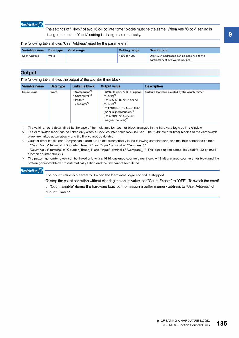
9
The settings of "Clock" of two 16-bit counter timer blocks must be the same. When one "Clock" setting is changed, the other "Clock" setting is changed automatically.The following table shows "User Address" used for the parameters.
OutputThe following table shows the output of the counter timer block.
*1 The valid range is determined by the type of the multi function counter block arranged in the hardware logic outline window.*2 The cam switch block can be linked only when a 32-bit counter timer block is used. The 32-bit counter timer block and the cam switch
block are linked automatically and the link cannot be deleted.*3 Counter timer blocks and Comparison blocks are linked automatically in the following combinations, and the links cannot be deleted.
"Count Value" terminal of "Counter_Timer_0" and "Input" terminal of "Compare_0" "Count Value" terminal of "Counter_Timer_1" and "Input" terminal of "Compare_1" (This combination cannot be used for 32-bit multi function counter blocks.)
*4 The pattern generator block can be linked only with a 16-bit unsigned counter timer block. A 16-bit unsigned counter timer block and the pattern generator block are automatically linked and the link cannot be deleted.
The count value is cleared to 0 when the hardware logic control is stopped.To stop the count operation without clearing the count value, set "Count Enable" to "OFF". To switch the on/off of "Count Enable" during the hardware logic control, assign a buffer memory address to "User Address" of "Count Enable".
Variable name Data type Valid range Setting range DescriptionUser Address Word 1000 to 1099 Only even addresses can be assigned to the
parameters of two words (32 bits).
Variable name Data type Linkable block Output value DescriptionCount Value Word • Comparison*3
• Cam switch*2
• Pattern generator*4
• -32768 to 32767 (16-bit signed counter)*1
• 0 to 65535 (16-bit unsigned counter)*1
• -2147483648 to 2147483647 (32-bit signed counter)*1
• 0 to 4294967295 (32-bit unsigned counter)*1
Outputs the value counted by the counter timer.
9 CREATING A HARDWARE LOGIC9.2 Multi Function Counter Block 185
18
MonitorThe following table shows the monitors of the counter timer block.
*1 Even when no "User Address" is assigned, an overflow and an underflow are detected and the multi function counter block overflow error (error code: 100H) and the multi function counter block underflow error (error code: 101H) occur. These errors are detected only when the linear counter mode is set for 32-bit counter timer blocks.
The following table shows "User Address" used for the monitors.
Variable name Data type DescriptionCount Value Word A count value is stored in the buffer memory area specified with "User Address".
Latch Value Word A latched count value is stored in the buffer memory area specified with "User Address".
Overflow Word When an overflow is detected, 1 is stored in the buffer memory area specified with "User Address".*1
Underflow Word When an underflow is detected, 1 is stored in the buffer memory area specified with "User Address".*1
Variable name Data type Linkable block Valid range DescriptionUser Address Word 1000 to 1099 Only even addresses can be assigned to monitors of two words (32
bits).
6 9 CREATING A HARDWARE LOGIC9.2 Multi Function Counter Block

9
Counting methodIn the flexible high-speed I/O control module, the following counting methods are provided: counting addition pulses and subtraction pulses from external devices and performing up count per clock cycle. The counting method can be set by linking blocks in the hardware logic.In a counter timer block where the "UP" terminal, "DOWN" terminal, "RUN" terminal, and "STOP" terminal are linked, either of the above counting methods can be used.
■Operation of when input pulses from external devices are countedWhen the High state of the "UP" terminal is detected, the addition value is added to the count value. When the High state of the "DOWN" terminal is detected, the addition value is subtracted from the count value. When the High states of the "UP" terminal and the "DOWN" terminal are detected at the same time, the addition value is added to the count value and the detection of the High state of the "DOWN" terminal is ignored.
While input pulses are counted, the count operation can be stopped externally because the "STOP" terminal has higher priority than the "UP" terminal and the "DOWN" terminal.
■Operation of when counting is performed based on the clock cycle inside the moduleThe count operation is performed as a timer. When the High state of the "RUN" terminal is detected, counting up the count value is started. Set the up count cycle with "Clock". When the High state of the "STOP" terminal is detected, counting up the count value is stopped. When the High states of the "RUN" terminal and the "STOP" terminal are detected at the same time, only the High state of the "STOP" terminal becomes valid. The detection of the High state of the "RUN" terminal is ignored.
Counting method Link in hardware logicCounting the input pulses from external devices Link the "Output" terminals of the input signal event detection block where the
pulse input mode is set according to the external input pulse to the "UP" terminal and "DOWN" terminal of the counter timer block.
Counting based on the clock cycle inside the module Link terminals to the "RUN" terminal and the "STOP" terminal.
9 CREATING A HARDWARE LOGIC9.2 Multi Function Counter Block 187

18
Linear counter modeWhen the linear counter mode is selected, the count operation is performed between the lower limit value and the upper limit value. The following table shows the setting ranges (lower limit value and upper limit value).
The linear counter mode can be set only for a 32-bit counter timer block.
If "Count Value" has reached the upper limit value in up count, "Count Value" does not change in the next up count and the overflow error (error code: 100H) occurs. "Count Value" does not change until the preset function is performed even if down count is performed.If "Count Value" has reached the lower limit value in down count, "Count Value" does not change in the next down count and the underflow error (error code: 101H) occurs. "Count Value" does not change until the preset function is performed even if up count is performed.
Ex.
The following figure shows how the counting range and the count value change in a 32-bit signed counter timer block when the preset function is performed with the following settings: the upper limit value is 2147483647, the lower limit value is -2147483648, and "Preset Value" is 500.
Multi function counter block Setting range32-bit unsigned 0 to 4294967295
32-bit signed -2147483648 to 2147483647
(1) If "Count Value" has reached the lower limit value, an underflow occurs when a subtraction pulse is counted.(2) If "Count Value" has reached the upper limit value, an overflow occurs when an addition pulse is counted.
Counting upCounting down0
Upper limit value
Lower limit value
Count value
-2147483648
500
2147483647-2147483647-2147483648 2147483646
2147483647
498 499 500 501 502
(1) (2)
Upper limit value
to to
Lower limit value Upper limit value
Lower limit value
Counting range
Count value
8 9 CREATING A HARDWARE LOGIC9.2 Multi Function Counter Block

9
■Overflow/underflow error • In a 32-bit counter timer block with the linear counter mode setting, when "Count Value" exceeds the upper limit value in upcount, the overflow error (error code: 100H) is stored in Latest error code (Un\G100). When "Count Value" falls below the lower limit value in down count, the underflow error (error code: 101H) is stored in Latest error code (Un\G100).
• When the overflow error or underflow error has occurred, the count stops and "Count Value" does not change even if up count or down count is performed.
• These errors can be cleared by performing the preset function. Performing the preset function stores a preset value in "Count Value" and restarts the count. The value stored in Latest error code (Un\G100) is held until the error is reset. Clear the error using Error clear request (YF).
In the linear counter mode, set the values as follows. • Set the upper limit value and the lower limit value so that the lower limit value is smaller than the upper limit
value. When the upper limit value is equal to or smaller than the lower limit value, the overflow error or underflow error occurs and the count operation is not performed.
• Set the preset value so that the preset value is larger than or equal to the lower limit value, and smaller than or equal to the upper limit value.
9 CREATING A HARDWARE LOGIC9.2 Multi Function Counter Block 189

19
Ring counter modeWhen the ring counter mode is selected, the count operation is performed between "Lower Limit" and "Upper Limit" repeatedly. The overflow error and underflow error do not occur.
■Lower limit value Count value < Upper limit valueIn up count, when "Count Value" has reached "Upper Limit", the value of "Lower Limit" is stored in "Count Value" automatically. In down count, the count value is held at the value of "Lower Limit" even if "Count Value" has reached "Lower Limit", and the value obtained by subtracting 1 from "Upper Limit" is stored in the count value in the next down count.In both up count and down count, the value of "Upper Limit" is not stored in "Count Value". However, these specifications exclude the case where "Count Enable" is turned on from off or the values of "Count Value" and "Upper Limit" are the same when the preset function is performed.
Ex.
The following figure shows how the counting range and the count value change when the preset function is performed with the following settings: "Lower Limit" is 0, "Upper Limit" is 2000, and "Preset Value" is 500.
When the same values are set for "Upper Limit" and "Lower Limit", the ring counter operation can be performed with the maximum valid range.The following show examples for a 32-bit signed counter timer block. • When up count is performed with the count value 2147483647, the count value becomes -2147483648. • When down count is performed with the count value -2147483648, the count value becomes 2147483647.When up count is performed from 2147483646 with "Upper Limit" = 2147483647 and "Lower Limit" = -2147483648, the count value becomes -2147483648. Thus, the count range is one less than that of when the same value is set to the "Upper Limit" and the "Lower Limit".
(1) The value 2000 of "Upper Limit" is not stored in "Count Value".
0
Counting upCounting down
Upper limit value
Lower limit value
Count value
-2147483648
0
500
2000
2147483647
(2000)500 501 1998 1999 0
(1)
1 2 498 499to to
Counting range
"Upper Limit"
"Lower Limit""Upper Limit"Count value
"Lower Limit"
Count value
0 9 CREATING A HARDWARE LOGIC9.2 Multi Function Counter Block
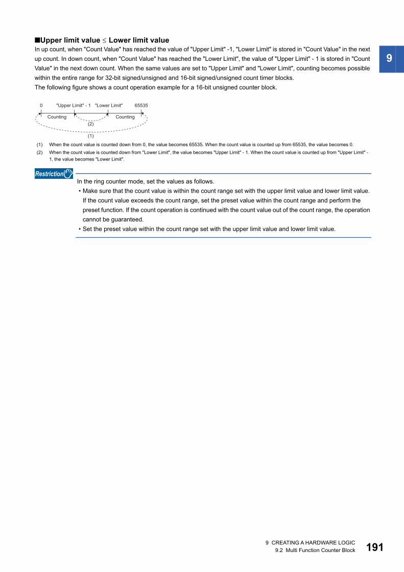
9
■Upper limit value Lower limit valueIn up count, when "Count Value" has reached the value of "Upper Limit" -1, "Lower Limit" is stored in "Count Value" in the next up count. In down count, when "Count Value" has reached the "Lower Limit", the value of "Upper Limit" - 1 is stored in "Count Value" in the next down count. When the same values are set to "Upper Limit" and "Lower Limit", counting becomes possible within the entire range for 32-bit signed/unsigned and 16-bit signed/unsigned count timer blocks.The following figure shows a count operation example for a 16-bit unsigned counter block.In the ring counter mode, set the values as follows. • Make sure that the count value is within the count range set with the upper limit value and lower limit value.
If the count value exceeds the count range, set the preset value within the count range and perform the preset function. If the count operation is continued with the count value out of the count range, the operation cannot be guaranteed.
• Set the preset value within the count range set with the upper limit value and lower limit value.
(1) When the count value is counted down from 0, the value becomes 65535. When the count value is counted up from 65535, the value becomes 0.(2) When the count value is counted down from "Lower Limit", the value becomes "Upper Limit" - 1. When the count value is counted up from "Upper Limit" -
1, the value becomes "Lower Limit".
0 65535
(1)
(2)
"Upper Limit" - 1 "Lower Limit"
Counting Counting
9 CREATING A HARDWARE LOGIC9.2 Multi Function Counter Block 191

19
Addition modeWhen "Add Mode" is set to "ON", the following operations are performed. • For the count in clock cycles, a value set as the addition value is added per clock cycle. • For counting input pulses, a value set with "Add Value" is added when an addition pulse is input and a value set with "Add
Value" is subtracted when a subtraction pulse is input.
■When the addition mode is on in the linear counter modeWhen the addition mode is on in the linear counter mode, the count value does not change even if the count operation is performed with the following status."Count Value" + "Add Value" > "Upper Limit"
Ex.
When "Add Value" is 5, "Upper Limit" is 1000, and "Count Value" is 998 in a 32-bit signed counter timer block, "Count Value" remains 998 even if up count is performed, and an overflow occurs.
■When the addition mode is on in the ring counter modeWhen the addition mode is on in the ring counter mode and up count is performed in the state in which the total of "Count Value" and "Add Value" exceeds "Upper Limit", the count value is as follows.Count value after addition = "Lower Limit" + ("Add Value" - ("Upper Limit" - Current count value))
Ex.
When "Add Value" is 5, "Upper Limit" is 1000, "Lower Limit" is 0, "Count Value" is 998, and up count is performed, the current count value becomes 3.
To turn on the addition mode in the ring counter mode, set a value which satisfies the following condition for "Add Value". When a value which does not satisfy the following condition is set, "Count Value" may exceed "Upper Limit" or fall below "Lower Limit". • "Add Value" < ("Upper Limit" - "Lower Limit")
■When a buffer memory address is assigned to the addition valueWhen a buffer memory address is assigned to the addition value and the buffer memory address is changed with a program, handle the buffer memory value in hexadecimal to change the value with a program.
2 9 CREATING A HARDWARE LOGIC9.2 Multi Function Counter Block
9
Comparison blockIn the fourth section in a multi function counter block detail window, comparison blocks are arranged by default. For a 16-bit counter, two comparison blocks ("Compare_0", "Compare_1") are arranged. For a 32-bit counter, one comparison block ("Compare_0") is arranged."Count Value" in a counter timer block is compared with the value set with the parameter. If a condition is satisfied, the state of the "Output" terminal turns to High. Two comparison conditions can be set for one counter timer block.
InputThe following table shows the input of the comparison block.
*1 The valid range is determined by the type of the multi function counter block arranged in the hardware logic outline window.
■Automatic linkCounter timer blocks and comparison blocks are linked automatically in the following combinations, and the links cannot be deleted.
Variable name Data type Linkable block Valid range DescriptionInput Word Counter timer • -32768 to 32767 (16-bit signed
counter)*1
• 0 to 65535 (16-bit unsigned counter)*1
• -2147483648 to 2147483647 (32-bit signed counter)*1
• 0 to 4294967295 (32-bit unsigned counter)*1
Inputs the count value of the counter timer block.
Multi function counter block
Counter timer block Comparison block
16-bit multi function counter block
"Count Value" terminal of "Counter_Timer_0" "Input" terminal of "Compare_0"
"Count Value" terminal of "Counter_Timer_1" "Input" terminal of "Compare_1"
32-bit multi function counter block
"Count Value" terminal of "Counter_Timer_0" "Input" terminal of "Compare_0"
Multi function
9 CREATING A HARDWARE LOGIC9.2 Multi Function Counter Block 193
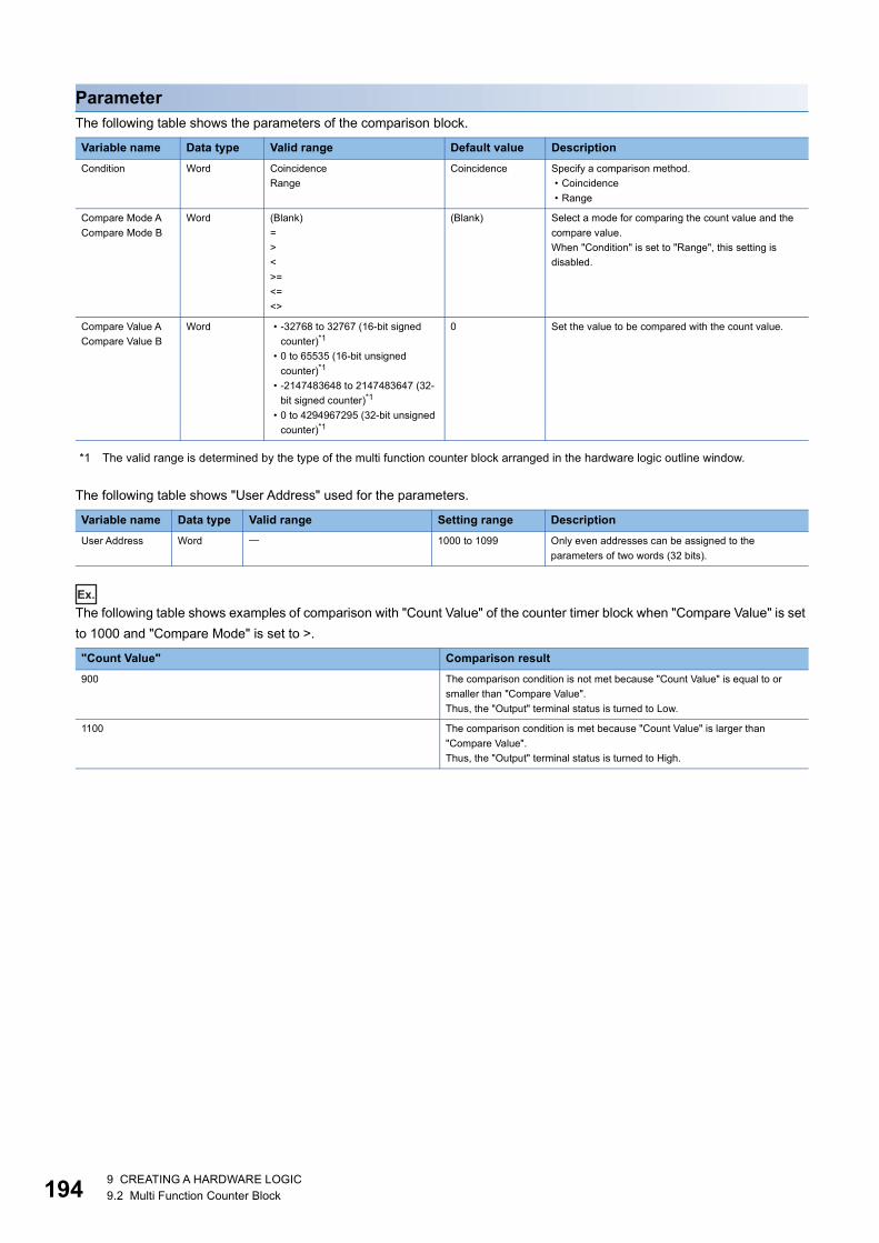
19
ParameterThe following table shows the parameters of the comparison block.
*1 The valid range is determined by the type of the multi function counter block arranged in the hardware logic outline window.
The following table shows "User Address" used for the parameters.
Ex.
The following table shows examples of comparison with "Count Value" of the counter timer block when "Compare Value" is set to 1000 and "Compare Mode" is set to >.
Variable name Data type Valid range Default value DescriptionCondition Word Coincidence
RangeCoincidence Specify a comparison method.
• Coincidence• Range
Compare Mode ACompare Mode B
Word (Blank)=><>=<=<>
(Blank) Select a mode for comparing the count value and the compare value.When "Condition" is set to "Range", this setting is disabled.
Compare Value ACompare Value B
Word • -32768 to 32767 (16-bit signed counter)*1
• 0 to 65535 (16-bit unsigned counter)*1
• -2147483648 to 2147483647 (32-bit signed counter)*1
• 0 to 4294967295 (32-bit unsigned counter)*1
0 Set the value to be compared with the count value.
Variable name Data type Valid range Setting range DescriptionUser Address Word 1000 to 1099 Only even addresses can be assigned to the
parameters of two words (32 bits).
"Count Value" Comparison result900 The comparison condition is not met because "Count Value" is equal to or
smaller than "Compare Value".Thus, the "Output" terminal status is turned to Low.
1100 The comparison condition is met because "Count Value" is larger than "Compare Value".Thus, the "Output" terminal status is turned to High.
4 9 CREATING A HARDWARE LOGIC9.2 Multi Function Counter Block
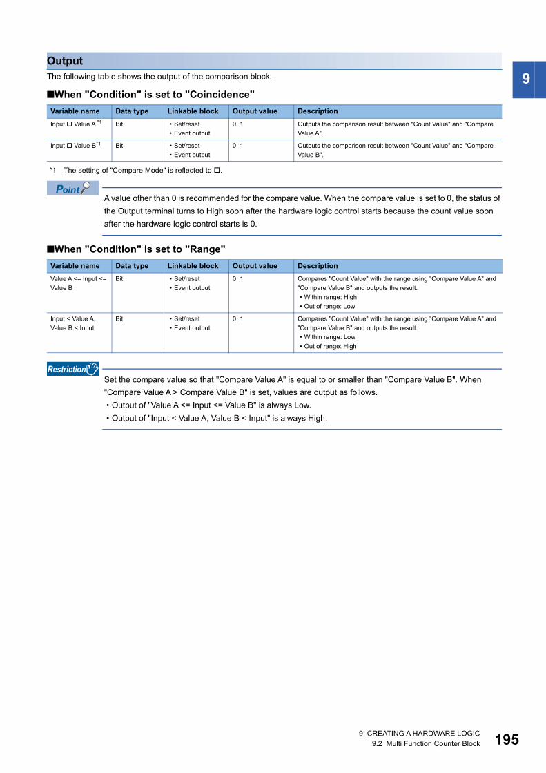
9
OutputThe following table shows the output of the comparison block.■When "Condition" is set to "Coincidence"
*1 The setting of "Compare Mode" is reflected to .
A value other than 0 is recommended for the compare value. When the compare value is set to 0, the status of the Output terminal turns to High soon after the hardware logic control starts because the count value soon after the hardware logic control starts is 0.
■When "Condition" is set to "Range"
Set the compare value so that "Compare Value A" is equal to or smaller than "Compare Value B". When "Compare Value A > Compare Value B" is set, values are output as follows. • Output of "Value A <= Input <= Value B" is always Low. • Output of "Input < Value A, Value B < Input" is always High.
Variable name Data type Linkable block Output value DescriptionInput Value A *1 Bit • Set/reset
• Event output0, 1 Outputs the comparison result between "Count Value" and "Compare
Value A".
Input Value B*1 Bit • Set/reset• Event output
0, 1 Outputs the comparison result between "Count Value" and "Compare Value B".
Variable name Data type Linkable block Output value DescriptionValue A <= Input <= Value B
Bit • Set/reset• Event output
0, 1 Compares "Count Value" with the range using "Compare Value A" and "Compare Value B" and outputs the result.• Within range: High• Out of range: Low
Input < Value A, Value B < Input
Bit • Set/reset• Event output
0, 1 Compares "Count Value" with the range using "Compare Value A" and "Compare Value B" and outputs the result.• Within range: Low• Out of range: High
9 CREATING A HARDWARE LOGIC9.2 Multi Function Counter Block 195
19
Pattern generator block
In the fourth section in the multi function counter block detail window (Counter_(16bit_Unsigned)), one pattern generator block ("Pattern_Generator") is arranged by default. No pattern generator block is arranged in the multi function counter block detail window (Counter_(16bit_Signed)), (Counter_(32bit_Signed)), or (Counter_(32bit_Unsigned)).A pattern generator block performs pattern output according to the output pattern data consisting of up to 8192 points that have been set for the block. Set Low output (0) or High output (1) for the output pattern of each point number. The count value of a counter timer block linked with the Input terminal is a point number. Thus, changing the count value continuously allows performing pattern output.
InputThe following table shows the input of the pattern generator block.
*1 When the value exceeds the range of 0 to 8191, it is regarded as a lower 13-bit value. For example, when 8192 is input, it is regarded as 0 and when 10000 is input, it is regarded as 1808.
*2 The "Count Value" terminal of "Counter_Timer_0" and the pattern generator block are linked automatically and the link cannot be deleted.
ParameterThe following table shows the parameters of the pattern generator block.
For details on the "Pattern generator output pattern setting" window, refer to the following.Page 132 Pattern Generator Function
OutputThe following table shows the output of the pattern generator block.
Variable name Data type Linkable block Valid range DescriptionInput Word Counter timer*2 • 0 to 8191*1 Inputs the count value of the counter timer block.
Variable name Data type Valid range Default value DescriptionPattern No. Word Disable
1 to 10Disable Specify the output pattern number of an output pattern output from the
pattern generator block. An output pattern number indicates the number of the output pattern data created in the "Pattern generator output pattern setting" window.
Pattern Setting Click the [Detail] button to open the "Pattern generator output pattern setting" window.
Variable name Data type Linkable block Output value DescriptionOutput Bit Pattern generator output 0, 1 Outputs the output pattern according to the output pattern set for
"Pattern No.". When "Disable" is set for "Pattern No.", the output value is 0.
Multi function
6 9 CREATING A HARDWARE LOGIC9.2 Multi Function Counter Block
9
Operation details■Change timing of the pattern generator outputThe pattern generator output switches when the count value of the counter timer block is changed.Ex.
The following shows an operation example when output patterns of 6 points are set.
■When a count value exceeding the number of output pattern points is inputWhen a count value exceeding the number of output pattern points is input, the pattern generator output is Low.
Ex.
When the number of output pattern points is 100 and the count value is within the range of 100 to 8191, the pattern generator output is Low.
■When a count value exceeding 8191 (8192 to 65535) is inputWhen a count value exceeding 8191 (8192 to 65535) is input, the count value input to the pattern generator block is converted into a value within the range of 0 to 8191 according to the following formula. • Remainder of "Count value divided by 8192"
Ex.
When the count value is 20000, a value obtained by dividing 20000 by 8192 is 2 with a remainder of 3616 according to the above formula. Thus, the point number is 3616.
Item Setting valueCounter timer block "Count Mode" "Ring"
"Upper Limit" 6
"Lower Limit" 0
Output pattern Number of points 6
Output value of the point 0 0
Output value of the point 1 0
Output value of the point 2 1
Output value of the point 3 1
Output value of the point 4 0
Output value of the point 5 1
No. Description(1) When the count value is changed from 1 to 2, the output turns to High, which is the output value of the point 2.
(2) When the count value is changed from 3 to 4, the output turns to Low, which is the output value of the point 4.After that, the output switches between Low and High depending on the output value of the point same as the count value.
High
Low
1 2 3 4 5
1 2 3 4 5 0
0
(1) (2)
0
0Point
"Output" terminal
"Count Value"
9 CREATING A HARDWARE LOGIC9.2 Multi Function Counter Block 197

19
Cam switch block
In a multi function counter block detail window, one cam switch block ("Cam_Switch") linked to a counter timer block is arranged across the fourth and fifth sections. However, no cam switch block is arranged in a 16-bit multi function counter block.The values in the cam switch block are compared with "Count Value" in the counter timer block and the High/Low signals are output.
InputThe following table shows the input of the cam switch block.
*1 "Count Value" in the counter timer block and the cam switch block are linked automatically and the link cannot be deleted.*2 The valid range is determined by the type of the multi function counter block arranged in the hardware logic outline window.*3 When "User Address" is used, variability of 100ns or less occurs when the output turns to High or Low.
Variable name Data type Linkable block Valid range DescriptionInput Word Counter timer*1 • -2147483648 to 2147483647
(32-bit signed counter)*2
• 0 to 4294967295 (32-bit unsigned counter)*2
Inputs the compare value of the counter timer block.When "User Address" of the step No. is not used, set the refreshing cycle of the count value to 0.1s or more. When "User Address" is used, set it to 0.2s or more.*3
Multi function
8 9 CREATING A HARDWARE LOGIC9.2 Multi Function Counter Block

9
ParameterThe following table shows the parameters of the cam switch block.*1 The valid range is determined by the type of the multi function counter block arranged in the hardware logic outline window.The following table shows "User Address" used for the parameters.
Variable name Data type Valid range Default value DescriptionNumber of Step Word 1 to 16 1 Set the number of steps of the cam switch. A step
indicates the point in which the Low state is switched to the High state or the High state is switched to the Low state. The valid Step No. is determined according to the set value of "Number of Step".
Lower Limit Word The value set with "Lower Limit" in the counter timer block is applied.Change the setting value in the counter timer block.
Lower Limit Output State
Word LowHigh
Low Set the initial state of output. When "Count Value" of the counter timer block is less than the input value of "Step No.0", the output status turns to the initial state.The output status of the step No. later than "Step No.0" inverts to the High state or the Low state for every step No.
Step No.0 Word • -2147483648 to 2147483647 (32-bit signed counter)*1
• 0 to 4294967295 (32-bit unsigned counter)*1
0 Compares the values of step numbers with "Count Value" in the counter timer block. When "Count Value" is equal to or larger than the input value, the previous status is inverted.
Step No.1 Maximum value in the valid rangeStep No.2
Step No.3
Step No.4
Step No.5
Step No.6
Step No.7
Step No.8
Step No.9
Step No.10
Step No.11
Step No.12
Step No.13
Step No.14
Step No.15
Upper Limit Word The value set with "Upper Limit" in the counter timer block is applied.Change the setting value in the counter timer block.
Variable name Data type Valid range DescriptionUser Address Word 1000 to 1098 Only even addresses can be assigned to the parameters of two words
(32 bits).
9 CREATING A HARDWARE LOGIC9.2 Multi Function Counter Block 199
20
OutputThe following table shows the output of the cam switch block.
*1 The cam switch block and "Cam Output" terminal are linked automatically and the link cannot be deleted.
Operation examplesThe following describes operation examples of the cam switch block.
■When the number of steps is set to 6 • Setting details
*1 Set it in the counter timer block. • Operation
Variable name Data type Linkable block Output value DescriptionOutput Bit Cam switch output*1 0, 1 Outputs signals created in the cam switch block. Only the "Cam
Output" terminal can be linked to the "Output" terminal.
Item Setting valueNumber of Step 6
Lower Limit*1 -2147483648
Lower Limit Output State Low
Step No.0 100
Step No.1 250
Step No.2 400
Step No.3 550
Step No.4 700
Step No.5 850
Upper Limit*1 2147483647
No. Description(1) For "Lower Limit" Count value < "Step No.0", the output status set with "Lower Limit Output State" is applied.
When the count value is equal to or larger than the set value of "Step No.0", the output status turns to High.
(2) When the count value is equal to or larger than the set value of "Step No.1", the output status turns to Low.After that, the output status turns to High or Low depending on the magnitude relationship between the count value and "Step No.".
ONOFF
0
(1)
(2)
1 2 3 4 5
100 250 400 550 700 850
Step No.
"Output" terminal
"Count Value"
0 9 CREATING A HARDWARE LOGIC9.2 Multi Function Counter Block
9
■When the number of steps is set to 2 • Setting details*1 Set it in the counter timer block.*2 When "Low" is set, operations of output within the range are performed. When "High" is set, operations of output out of the range are
executed. • Operation
Setting methodSet the cam switch block with the following procedure.
1. Set the number of steps of the cam switch for "Number of Step".
2. Set "Step No.0" to "Step No.15" so that the setting values in "Lower Limit", "Step No.0" to "Step No.15", and "Upper Limit" are arranged in ascending order.
When the setting values in "Lower Limit", "Step No.0" to "Step No.15", and "Upper Limit" are not arranged in ascending order, the control for the cam switch block is not normally performed.
Item Setting valueNumber of Step 2
Lower Limit*1 -2147483648
Lower Limit Output State Low*2
Step No.0 1000
Step No.1 2000
Upper Limit*1 2147483647
No. Description(1) For "Lower Limit" Count value < "Step No.0", the output status set with "Lower Limit Output State" is applied.
When the count value is equal to or larger than the set value of "Step No.0", the output status turns to High.
(2) When the count value is equal to or larger than the set value of "Step No.1", the output status turns to Low.
ONOFF
0
(1)
(2)
1
1000 2000
Step No.
"Output" terminal
"Count Value"
9 CREATING A HARDWARE LOGIC9.2 Multi Function Counter Block 201
20
Set/reset block
In the fifth section in a multi function counter block detail window, set/reset blocks are arranged by default. For a 16-bit counter, two set/reset blocks ("Set/Reset_0" and "Set/Reset_1") are arranged. For a 32-bit counter, one set/reset block ("Set/Reset_0") is arranged.The signal input to the "Set" terminal is used as a trigger to output High fixed signals or the signal input to the "Reset" terminal is used as a trigger to output Low fixed signals.
InputThe following table shows the inputs of the set/reset block.
• When both the "Set" terminal status and "Reset" terminal status turn to High at the same time, the "Reset" terminal becomes valid.
■Link of the set/reset block • The set/reset block in a 16-bit counter can be linked to the following comparison blocks.
OutputThe following table shows the output of the set/reset block.
Variable name Data type Linkable block Valid range DescriptionSet Bit • Input signal event
detection• Comparison
0, 1 Outputs the High fixed signal when an input signal is detected. Even if the input signal turns to Low, output continues until a signal is input to "Reset".
Reset Bit • Input signal event detection
• Comparison
0, 1 Outputs the Low fixed signal when an input signal is detected.
Set/reset block Comparison block"Set/Reset_0" "Compare_0"
"Set/Reset_1" "Compare_1"
Variable name Data type Linkable block Output value DescriptionOutput Bit Output 0, 1 Outputs High fixed or Low fixed signals.
Multi function
2 9 CREATING A HARDWARE LOGIC9.2 Multi Function Counter Block
9
Output terminalIn the sixth section in a multi function counter block detail window, one output terminal ("Output 0") is arranged by default.When terminals have been linked to the output terminal, the signals input to the output terminal can be output from the "Output 0" terminal in the multi function counter block arranged in the hardware logic outline window.
OutputThe following table shows the output of the output terminal.
Variable name Data type Linkable block Valid range DescriptionOutput Bit • Input signal event
detection• Set/reset
0, 1 Outputs the High/Low states of the "Output 0" terminal of a multi function counter block in the hardware logic outline window. This terminal is used for link in the multi function counter block detail window. Multiple signals can be input to the terminal. OR processing is executed for all input signals.
Multi function
9 CREATING A HARDWARE LOGIC9.2 Multi Function Counter Block 203

20
Event output terminal
In the sixth section in a multi function counter block detail window, event output terminals are arranged by default. For a 16-bit counter, four event output terminals ("Event 0" to "Event 3") are arranged. For a 32-bit counter, two event output terminals ("Event 0", "Event 1") are arranged.Event output terminals output the input signals from "Event" terminals in the multi function counter block. • 16-bit multi function counter block
• 32-bit multi function counter block
OutputThe following table shows the output of the event output terminal.
■Link of event output terminals • The event output terminals in a 16-bit counter can be linked to the following comparison blocks.
• For event output terminals in a 16-bit counter, linkable "Output" terminals of the input signal event detection block are different as shown below. Event output terminals are not linkable in a 32-bit counter.
Variable name Data type Linkable block Valid range DescriptionEvent Bit • Input signal event
detection• Comparison
0, 1 Outputs the High/Low states of "Event" terminals of a multi function counter block in the hardware logic outline window. This terminal is used for link in the multi function counter block detail window. Multiple signals can be input to the terminal. OR processing is executed for all input signals.
Event output terminal Comparison block• "Event 0"• "Event 1"
"Compare_0"
• "Event 2"• "Event 3"
"Compare_1"
Event output terminal Input signal event detection block• "Event 0"• "Event 1"
"Output 0"
• "Event 2"• "Event 3"
"Output 1"
Multi function
4 9 CREATING A HARDWARE LOGIC9.2 Multi Function Counter Block
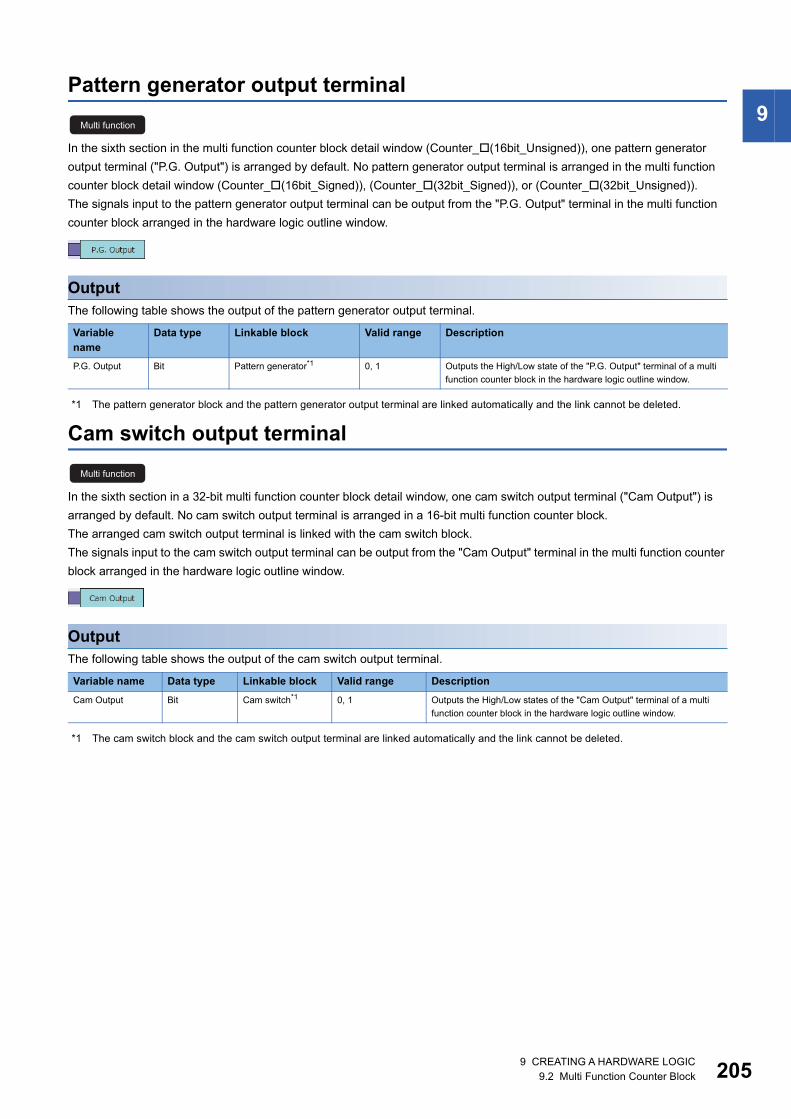
9
Pattern generator output terminalIn the sixth section in the multi function counter block detail window (Counter_(16bit_Unsigned)), one pattern generator output terminal ("P.G. Output") is arranged by default. No pattern generator output terminal is arranged in the multi function counter block detail window (Counter_(16bit_Signed)), (Counter_(32bit_Signed)), or (Counter_(32bit_Unsigned)).The signals input to the pattern generator output terminal can be output from the "P.G. Output" terminal in the multi function counter block arranged in the hardware logic outline window.
OutputThe following table shows the output of the pattern generator output terminal.
*1 The pattern generator block and the pattern generator output terminal are linked automatically and the link cannot be deleted.
Cam switch output terminal
In the sixth section in a 32-bit multi function counter block detail window, one cam switch output terminal ("Cam Output") is arranged by default. No cam switch output terminal is arranged in a 16-bit multi function counter block.The arranged cam switch output terminal is linked with the cam switch block.The signals input to the cam switch output terminal can be output from the "Cam Output" terminal in the multi function counter block arranged in the hardware logic outline window.
OutputThe following table shows the output of the cam switch output terminal.
*1 The cam switch block and the cam switch output terminal are linked automatically and the link cannot be deleted.
Variable name
Data type Linkable block Valid range Description
P.G. Output Bit Pattern generator*1 0, 1 Outputs the High/Low state of the "P.G. Output" terminal of a multi function counter block in the hardware logic outline window.
Variable name Data type Linkable block Valid range DescriptionCam Output Bit Cam switch*1 0, 1 Outputs the High/Low states of the "Cam Output" terminal of a multi
function counter block in the hardware logic outline window.
Multi function
Multi function
9 CREATING A HARDWARE LOGIC9.2 Multi Function Counter Block 205

20
9.3 Intelligent Function Module InterruptThis function notifies the CPU module that either of the following conditions is satisfied as an interrupt request. • A signal is input to the SI device terminal of the hardware logic. • The logging data for 5120 points is stored in Continuous logging data storage area (Un\G15020 to Un\G25259).
An interrupt program execution has a priority and interrupts the other processing in progress. Therefore, if interrupt programs are created in advance, processing for when a match of multi function counter block is detected in the hardware logic, fail-safe processing, file register transfer processing for logging data, and other processing can be executed immediately.
Operation • When an input signal event is detected or a comparison condition is satisfied, a signal is input from the "Output" terminal of
a multi function counter block to an SI device terminal. The interrupt program corresponding to the SI device terminal to which the signal has been input is executed.
• After logging data for 5120 points has been stored by the continuous logging function, the interrupt program is executed.
Setting methodThe following describes the setting method for when a signal is input to the SI device terminal of the hardware logic.To use the intelligent function module interrupt, intelligent function module interrupt pointers and a hardware logic are required to be set in advance.
■Setting intelligent function module interrupt pointersSet interrupt factors (SI) and interrupt pointers of the CPU module in the intelligent function module interrupt pointer setting.
Project window [PLC Parameter] [PLC System] [Interrupt Pointer Setting]
*1 Always set the described value.
Item Setting rangeInterrupt Pointer Start No. 50 to 248
Interrupt Pointer Count 9 (fixed)*1
Start I/O No. 0000 to 0FE0
Start SI No. 0 (fixed)*1
6 9 CREATING A HARDWARE LOGIC9.3 Intelligent Function Module Interrupt
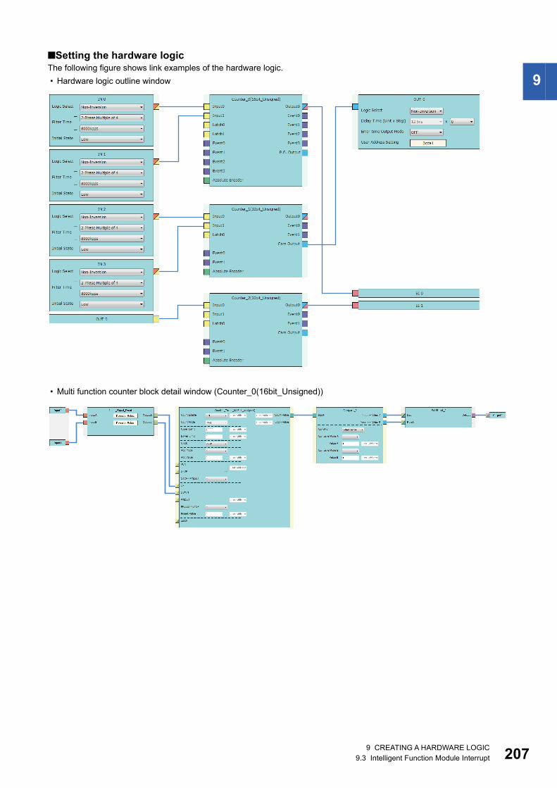
9
■Setting the hardware logicThe following figure shows link examples of the hardware logic. • Hardware logic outline window• Multi function counter block detail window (Counter_0(16bit_Unsigned))
9 CREATING A HARDWARE LOGIC9.3 Intelligent Function Module Interrupt 207

20
• Multi function counter block detail window (Counter_1(32bit_Unsigned))
• Multi function counter block detail window (Counter_2(32bit_Unsigned))
• When interrupt pointers of the CPU module is not set, an error occurs in the CPU module if an SI device terminal in the hardware logic turns to High or logging data for 5120 points is stored by the continuous logging function.
• To issue an interrupt request to the CPU module when continuous logging data for 5120 points is stored, set "Enable" in "Continuous logging data storage interrupt enable/disable" of "Switch Setting" in addition to setting interrupt pointers of the CPU module.
• An interrupt request to the CPU module can also be output using a detection in the input signal event detection block as a trigger. The following figure shows a link example in the hardware logic outline window and the multi function counter block detail window.
• For the linking of the multi function counter block detail window (Counter_0(16bit_Unsigned)), a value other than 0 is recommended for "Compare Value". If 0 is set in "Compare Value", an interrupt request is output to the CPU module when the operation of the hardware logic starts (when the count value starts to be counted from 0).
• An interrupt request to the CPU module is output every 50s. If the same interrupt factor (SI) occurs several times within 50s, the second and later factors (SI) are ignored.
• When the continuous logging function is used, the maximum response delay time of interrupt is 200s.
IN 0
SI 0
Multi function counter_0
Hardware logic outline windowInput signal event detection block
Multi function counter block detail window
Input 0 Output 0 Output 0Input 0
(A:Rise)
8 9 CREATING A HARDWARE LOGIC9.3 Intelligent Function Module Interrupt
10
10 BLOCK LINK EXAMPLESVarious controls can be performed with the combinations of various blocks. This chapter shows link examples to perform the following controls.
Control name Description ReferenceCoincidence detection Turns on the output of the multi function counter block at coincidence detection. Page 210 Coincidence Detection
One-shot timer Turns on the output of the multi function counter block for the specified time period. After the specified time period, the output is turned off until the next event detection.
Page 215 One-shot Timer
Event generation Outputs an external input signal as an event signal. The output signal can be linked as an event signal of other multi function counter blocks.
Page 219 Event Generation
Cam switch Turns on or off the output when a count value within the upper and lower limit value range becomes equal to or larger than the setting value of the corresponding steps.
Page 221 Cam Switch
PWM output Outputs a PWM wave with the specified cycle and duty ratio. Page 224 PWM Output
Fixed cycle output Outputs one pulse at every specified cycle. Page 227 Fixed Cycle Output
Latch counter Latches (holds) a count value. Page 230 Latch Counter
Ratio conversion Outputs an input signal multiplied with the set ratio (x/y). Page 233 Ratio Conversion
Pulse measurement Measures the ON width and OFF width of an input pulse. Page 238 Pulse Measurement
10 BLOCK LINK EXAMPLES 209
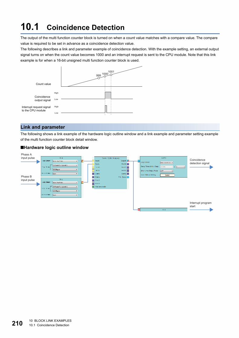
21
10.1 Coincidence DetectionThe output of the multi function counter block is turned on when a count value matches with a compare value. The compare value is required to be set in advance as a coincidence detection value.The following describes a link and parameter example of coincidence detection. With the example setting, an external output signal turns on when the count value becomes 1000 and an interrupt request is sent to the CPU module. Note that this link example is for when a 16-bit unsigned multi function counter block is used.
Link and parameterThe following shows a link example of the hardware logic outline window and a link example and parameter setting example of the multi function counter block detail window.
■Hardware logic outline window
High
Low
10001001
High
Low
999
Count value
Coincidence output signal
Interrupt request signal to the CPU module
Phase A input pulse
Phase B input pulse
Coincidence detection signal
Interrupt program start
0 10 BLOCK LINK EXAMPLES10.1 Coincidence Detection

10
■Multi function counter block detail window
The items other than the above need not to be set.
Block Variable name Setting value DescriptionInput 0
Input 1
Input_Signal_Event Detector Select 1/2-Phase Multiple of 1(CW/CCW)+
Set this parameter to detect an addition pulse.
Detector Select 2-Phase Multiple of 1- Set this parameter to detect a subtraction pulse.
Counter_Timer_0 Count Enable ON Set this parameter to "ON".
Count Mode Ring Set this parameter according to the control.
Upper Limit 2000 Set this parameter according to the control.
Lower Limit 0 Set this parameter according to the control.
Clock 25ns Set this parameter to "25ns". (to prevent input pulses from missing)
Add Mode OFF Set this parameter to "OFF", because the addition mode is not used in this link example.Add Value 0
Compare_0 Condition Range Set this parameter to "Range".
Compare Mode A >= Set this parameter to ">=".
Compare Mode B <= Set this parameter to "<=".
Compare Value A 1000 Set a value used as a "coincidence detection value".
Compare Value B 1000 Set a value used as a "coincidence detection value".
Set/Reset_0
Output 0
10 BLOCK LINK EXAMPLES10.1 Coincidence Detection 211
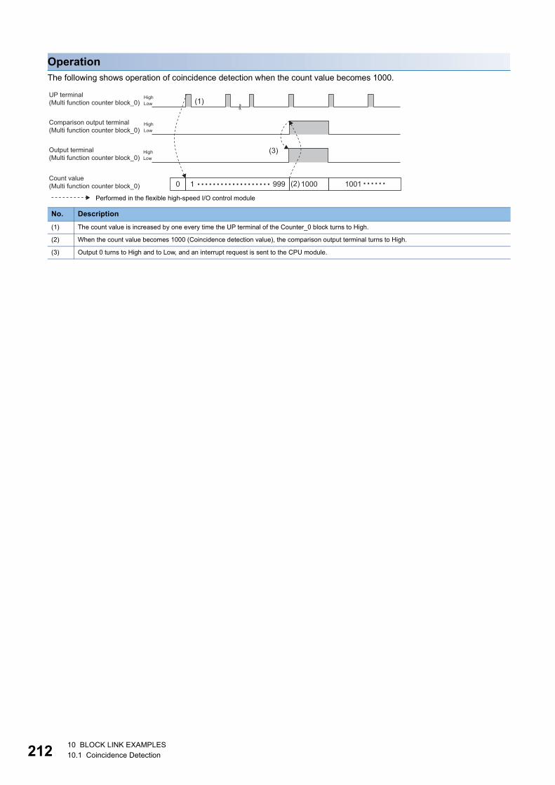
21
OperationThe following shows operation of coincidence detection when the count value becomes 1000.
Performed in the flexible high-speed I/O control module
No. Description(1) The count value is increased by one every time the UP terminal of the Counter_0 block turns to High.
(2) When the count value becomes 1000 (Coincidence detection value), the comparison output terminal turns to High.
(3) Output 0 turns to High and to Low, and an interrupt request is sent to the CPU module.
1 999 1000 1001
HighLow (1)
0
HighLow
HighLow
(3)
(2)................... ......Count value (Multi function counter block_0)
UP terminal (Multi function counter block_0)
Comparison output terminal(Multi function counter block_0)
Output terminal (Multi function counter block_0)
2 10 BLOCK LINK EXAMPLES10.1 Coincidence Detection
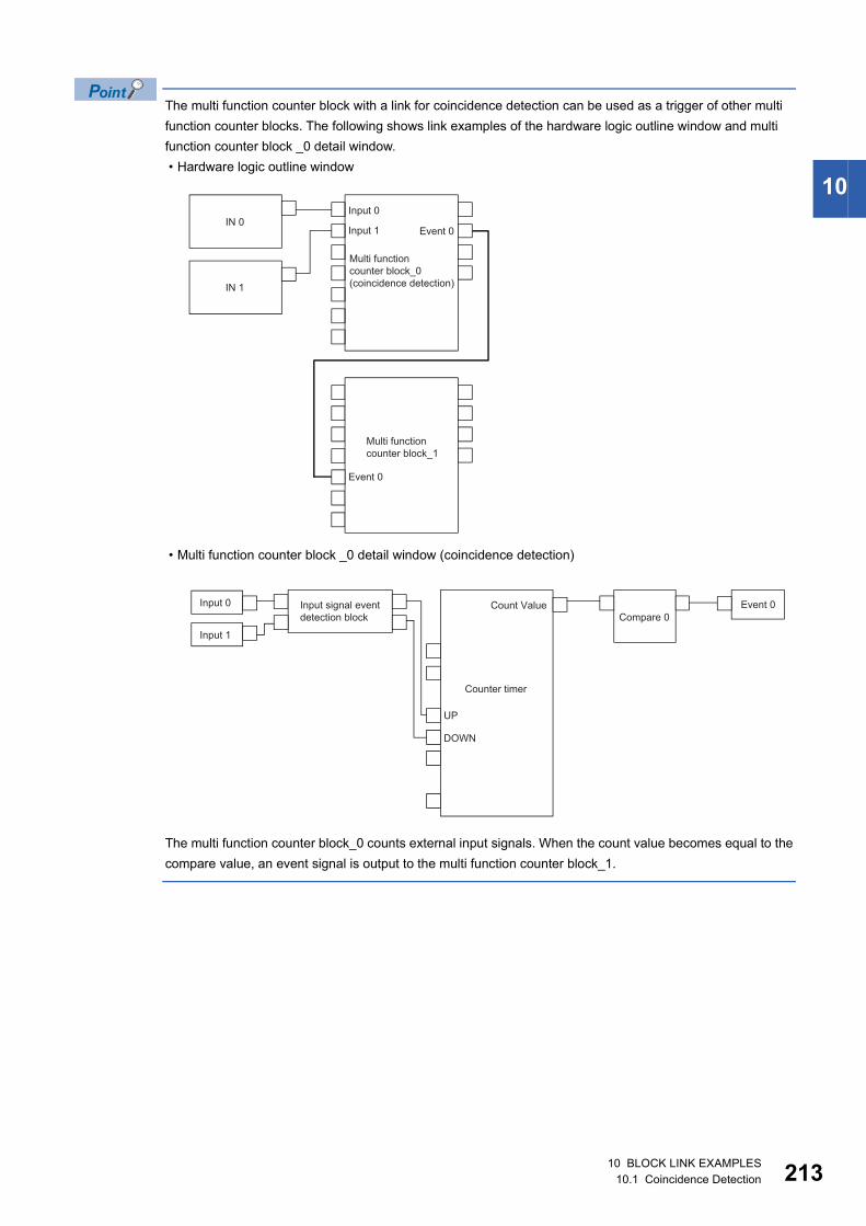
10
The multi function counter block with a link for coincidence detection can be used as a trigger of other multi function counter blocks. The following shows link examples of the hardware logic outline window and multi function counter block _0 detail window. • Hardware logic outline window
• Multi function counter block _0 detail window (coincidence detection)
The multi function counter block_0 counts external input signals. When the count value becomes equal to the compare value, an event signal is output to the multi function counter block_1.
IN 0
IN 1
Multi function counter block_0 (coincidence detection)
Multi function counter block_1
Input 0
Input 1 Event 0
Event 0
UP
DOWN
Compare 0
Counter timer
Input signal event detection block
Input 0
Input 1
Event 0Count Value
10 BLOCK LINK EXAMPLES10.1 Coincidence Detection 213

21
Precautions for using 32-bit multi function counter blocksCoincidence detection control can be set even with 32-bit multi function counter blocks. However, usable blocks are different. The following shows link examples of the hardware logic outline window and multi function counter block detail window. • Hardware logic outline window
• Multi function counter block _0 detail window (coincidence detection)
Create the hardware logic by using a cam switch block, as shown in the dotted line frame.
IN 0
IN 1
OUT 0
SI 0 Multi function counter block_0 (coincidence detection)
Input 0
Input 1
Output 0
UP
DOWN
Cam Switch
Counter timer
Input signal event detection block
Input 0 Count Value
Input 1
Cam Output
4 10 BLOCK LINK EXAMPLES10.1 Coincidence Detection
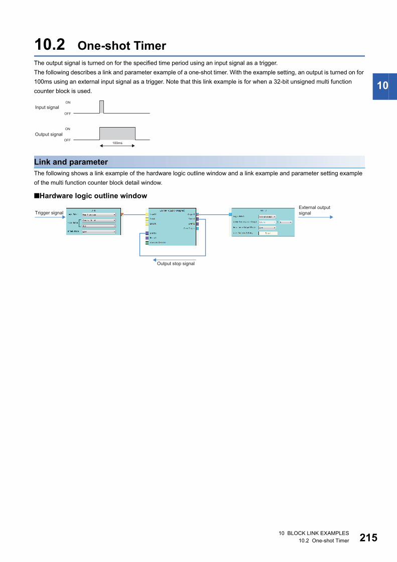
10
10.2 One-shot TimerThe output signal is turned on for the specified time period using an input signal as a trigger.The following describes a link and parameter example of a one-shot timer. With the example setting, an output is turned on for 100ms using an external input signal as a trigger. Note that this link example is for when a 32-bit unsigned multi function counter block is used.
Link and parameterThe following shows a link example of the hardware logic outline window and a link example and parameter setting example of the multi function counter block detail window.
■Hardware logic outline window
100ms
ON
OFF
ON
OFF
Input signal
Output signal
External output signalTrigger signal
Output stop signal
10 BLOCK LINK EXAMPLES10.2 One-shot Timer 215

21
■Multi function counter block detail window
*1 Output ON time = Clock cycle (Compare value - Preset value + 1)*2 In the addition mode, the output ON time calculated from the following is applied.
Output ON time = (Clock cycle (Compare value - Preset value + 1)) Addition valueThe items other than the above need not to be set.
Block Variable name Setting value DescriptionInput 0
Event 0
Input_Signal_Event Detector Select User Setting (ON only in A: High)
Set this parameter to detect the phase A input signal.
Detector Select User Setting (ON only in A: Rise)
Counter_Timer_0 Count Enable ON Set this parameter to "ON".
Count Mode Linear Set this parameter according to the control.
Upper Limit 4294967295 Set this parameter according to the control.
Lower Limit 0 Set this parameter according to the control.
Clock 1ms Set this parameter according to the control.*1
Add Mode OFF Set this parameter according to the control.*2
Add Value 0
STOP PRESET ON Set this parameter to "ON", to perform a preset when a stop event occurs.
PRESET STOP OFF Set this parameter to "OFF".
Preset Value 1 Set this parameter according to the control.*1
Compare_0 Condition Coincidence Set this parameter to "Coincidence".
Compare Mode A = Set this parameter to "=".
Compare Value A 100 Set this parameter according to the control.*1
Set/Reset_0
Output 0
6 10 BLOCK LINK EXAMPLES10.2 One-shot Timer
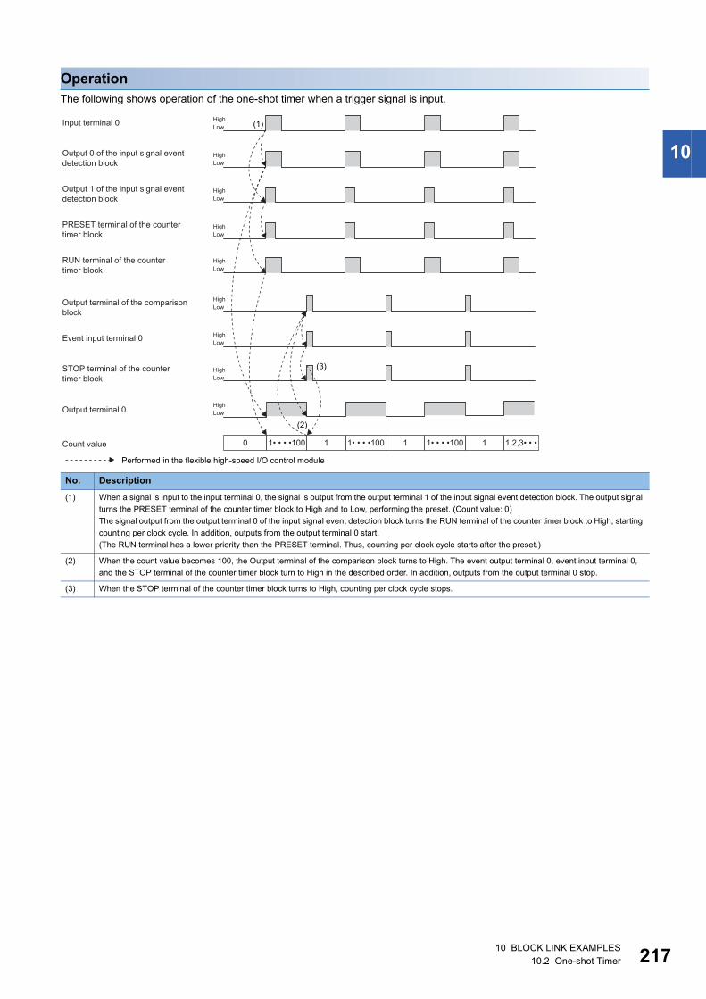
10
OperationThe following shows operation of the one-shot timer when a trigger signal is input.
Performed in the flexible high-speed I/O control module
No. Description(1) When a signal is input to the input terminal 0, the signal is output from the output terminal 1 of the input signal event detection block. The output signal
turns the PRESET terminal of the counter timer block to High and to Low, performing the preset. (Count value: 0)The signal output from the output terminal 0 of the input signal event detection block turns the RUN terminal of the counter timer block to High, starting counting per clock cycle. In addition, outputs from the output terminal 0 start.(The RUN terminal has a lower priority than the PRESET terminal. Thus, counting per clock cycle starts after the preset.)
(2) When the count value becomes 100, the Output terminal of the comparison block turns to High. The event output terminal 0, event input terminal 0, and the STOP terminal of the counter timer block turn to High in the described order. In addition, outputs from the output terminal 0 stop.
(3) When the STOP terminal of the counter timer block turns to High, counting per clock cycle stops.
1• • • •100
(2)
HighLow
1 1• • • •100 1 1• • • •100 1 1,2,3• • •0
HighLow
HighLow
HighLow
HighLow
(1)
HighLow
HighLow
HighLow
HighLow
(3)
Count value
Input terminal 0
Output 0 of the input signal event detection block
Output 1 of the input signal event detection block
PRESET terminal of the counter timer block
RUN terminal of the counter timer block
STOP terminal of the counter timer block
Output terminal 0
Event input terminal 0
Output terminal of the comparison block
10 BLOCK LINK EXAMPLES10.2 One-shot Timer 217

21
If the multi function counter block with a link for one-shot timer is used together with other blocks with links for coincidence detection or other functions, any output ON time for external devices can be set. The following shows link examples of the hardware logic outline window and multi function counter block_1 detail window. • Hardware logic outline window
• Multi function counter block_1 detail window (one-shot timer)
IN 0
IN 1
Out 0
OUT 0
OUT 1 Multi function counter block_0 (coincidence detection)
Multi function counter block_1 (one-shot timer)
Input 0
Input 1
Cam Output
Output 0
Event 0
Input 0
Event 0
RUN
STOP
PRESET
Counter timer
Input signal event detection block Compare 0 Set/reset
Input 0
Event 0
Count Value Output 0
Event 0
8 10 BLOCK LINK EXAMPLES10.2 One-shot Timer
10
10.3 Event GenerationAn external input signal is output as an event signal.Only two event signals can be generated with one multi function counter block. If several multi function counter blocks are used together, three or more event signals can be used with one multi function counter block.The following describes a link and parameter example of event generation. With the example setting, an event is generated under the following condition and input to the Event terminal of another multi function counter block as an event signal. • A signal output from the Event 0 terminal of the multi function counter block _0: Rise of the phase A input • A signal output from the Event 2 terminal of the multi function counter block _0: High of the phase B inputNote that this link example is for when a 16-bit unsigned multi function counter block is used. Event generation is supported only by 16-bit multi function counter blocks.
Link and parameterThe following shows a link example of the hardware logic outline window and a link example and parameter setting example of the multi function counter block detail window.
■Hardware logic outline window
Rise detection event signal
High level detection event signal
Multi function counter block for event generation
10 BLOCK LINK EXAMPLES10.3 Event Generation 219
22
■Multi function counter block detail window
OperationThe following shows operation where the input signal 1 turns to High when a rise of the input signal 0 is detected.
Block Variable name Setting value DescriptionInput 0
Input 1
Input_Signal_Event Detector Select User Setting (ON only in A: Rise)
Set conditions to generate an event signal.
Detector Select User Setting (ON only in B: High)
Event 0
Event 2
Performed in the flexible high-speed I/O control module
No. Description(1) When a rise of the input terminal 0 is detected, the event output terminal 0 turns to High and to Low.
(2) When a rise of the input terminal 1 is detected, the event output terminal 2 turns to High.
(3) When a fall of the input terminal 1 is detected, the event output terminal 2 turns to Low.
HighLow
(3)
HighLow
(2)HighLow
HighLow
(1)
Event output terminal 0
Event output terminal 2
Input terminal 1
Input terminal 0
0 10 BLOCK LINK EXAMPLES10.3 Event Generation

10
10.4 Cam SwitchThe preset output status of the coincidence output range is compared with a count value to switch on or off the output of the multi function counter block at each step.The following is an example assuming that an output is switched by seven steps as follows. Note that this link example is for when a 32-bit unsigned multi function counter block is used. (The cam switch is not supported by 16-bit multi function counter blocks.)
Link and parameterThe following shows a link example of the hardware logic outline window and a link example and parameter setting example of the multi function counter block detail window.
■Hardware logic outline window
Step No. Count value Output 0 (lower limit value) to 999 Low
0 1000 to 1999 High
1 2000 to 2999 Low
2 3000 to 3999 High
3 4000 to 4999 Low
4 5000 to 5999 High
5 6000 to 6999 Low
6 7000 to 10000 (upper limit value) High
ONOFF
1000 2000 3000 4000 5000 6000 7000
Cam switch output terminal
Count value
Phase A input pulse
Phase B input pulse
Cam switch output signal
10 BLOCK LINK EXAMPLES10.4 Cam Switch 221

22
■Multi function counter block detail window
The items other than the above need not to be set.
Block Variable name Setting value DescriptionInput 0
Input 1
Input_Signal_Event Detector Select 1/2-Phase Multiple of 1(CW/CCW)+
Set this parameter to detect an addition pulse.
Detector Select 2-Phase Multiple of 1- Set this parameter to detect a subtraction pulse.
Counter_Timer_0 Count Enable ON Set this parameter to "ON".
Count Mode Ring Set this parameter according to the control.
Upper Limit 10000 Set this parameter according to the control.
Lower Limit 0 Set this parameter according to the control.
Clock 25ns Set this parameter to "25ns". (to prevent input pulses from missing)
Add Mode OFF Set this parameter according to the control.
Add Value 0
Cam_Switch Number of Step 7 Set "7", which is the number of steps of the cam switch, to enable the step No. 0 to 6.
Lower Limit Output State Low Set this parameter according to the control.
Step No.0 1000 Set a count value at which the output status of the subsequent step is enabled.Step No.1 2000
Step No.2 3000
Step No.3 4000
Step No.4 5000
Step No.5 6000
Step No.6 7000
Cam Output
2 10 BLOCK LINK EXAMPLES10.4 Cam Switch

10
OperationThe following shows operation where a count value is compared with the setting value of each step.
Performed in the flexible high-speed I/O control module
No. Description(1) The count value is increased by one every time the UP terminal turns to High.
(2) When the count value reaches the setting value of the step No. 0, an external output is inversed.Also, every time the count value reaches each setting value of the step No. 1 or later, an external output is inversed.
HighLow
HighLow
(1) (2)
1⋅⋅⋅999 1000⋅⋅1999 2000⋅⋅2999 3000⋅⋅3999 4000⋅⋅4999 5000⋅⋅59990
0 1 2 3 4 5
6000⋅⋅6999 7000⋅⋅⋅
6
Cam switch output terminal
Count value
UP terminal
Step No.
10 BLOCK LINK EXAMPLES10.4 Cam Switch 223
22
10.5 PWM OutputThe multi function counter block outputs a PWM wave with a specified duty ratio.The following describes a link and parameter example of a PWM output. With the example setting, when a rise of the input signal 0 is detected, output of the following PWM wave starts, and when a rise of the input signal 1 is detected, the output stops. Note that this link example is for when a 16-bit unsigned multi function counter block is used.
Link and parameterThe following shows a link example of the hardware logic outline window and a link example and parameter setting example of the multi function counter block detail window.
■Hardware logic outline window
7ms3ms 7ms
ONOFF
3ms
Cycle time ON time
Output signal
PWM output start signal
PWM output stop signal
PWM wave output
4 10 BLOCK LINK EXAMPLES10.5 PWM Output
10
■Multi function counter block detail window
*1 Cycle time = (Upper limit value - Lower limit value) Clock cycle*2 ON time = Cycle time - (Compare value A Clock cycle). Set the value of compare value A + ON time for the compare value B.*3 In the addition mode, the cycle time calculated from the following is applied.
Cycle time = (Upper limit value - Lower limit value) Addition value Clock cycleThe items other than the above need not to be set.
Block Variable name Setting value DescriptionInput 0
Input 1
Input_Signal_Event Detector Select User Setting (ON only in A: Rise)
Set conditions to detect a PWM output start signal.
Detector Select User Setting (ON only in B: Rise)
Set conditions to detect a PWM output stop signal.
Counter_Timer_0 Count Enable ON Set this parameter to "ON".
Count Mode Ring Set this parameter to "Ring".
Upper Limit 10 Set this parameter according to the control.*1
Lower Limit 0 Set this parameter according to the control.*1
Clock 1ms Set this parameter according to the control.*1*2
Add Mode OFF Set this parameter according to the control.*3
Add Value 0
STOP PRESET ON Set this parameter to "ON", to perform a preset when a stop event occurs.
Preset Value 0 Set the same value as that in "Lower Limit".
Compare_0 Condition Range Set this parameter to "Range".
Compare Mode A >= Set this parameter to ">=".
Compare Mode B <= Set this parameter to "<=".
Compare Value A 3 Set this parameter according to the control.*2
Compare Value B 9 Set this parameter according to the control.*2
Output 0
10 BLOCK LINK EXAMPLES10.5 PWM Output 225
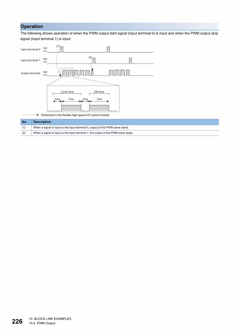
22
OperationThe following shows operation of when the PWM output start signal (input terminal 0) is input and when the PWM output stop signal (input terminal 1) is input.
Performed in the flexible high-speed I/O control module
No. Description(1) When a signal is input to the input terminal 0, output of the PWM wave starts.
(2) When a signal is input to the input terminal 1, the output of the PWM wave stops.
(1)
HighLow
7ms 3ms
HighLow
HighLow
(2)
3ms 7ms
Cycle time ON time
Output terminal
Input terminal 1
Input terminal 0
6 10 BLOCK LINK EXAMPLES10.5 PWM Output
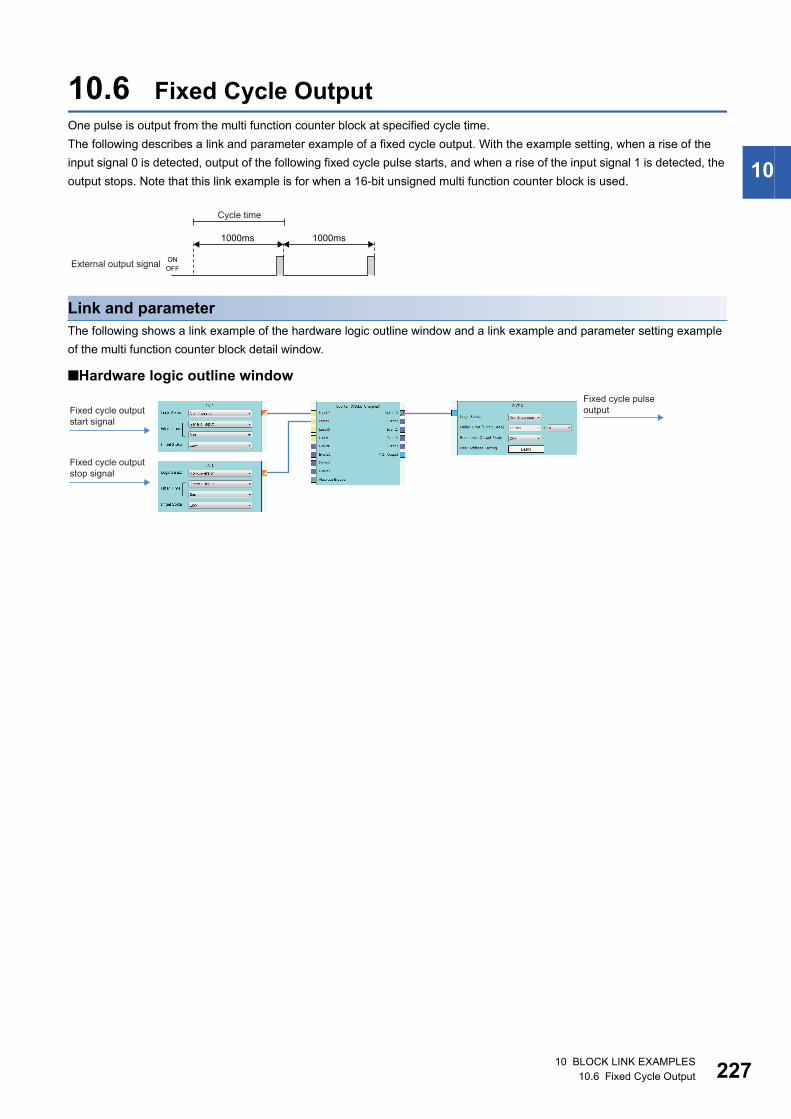
10
10.6 Fixed Cycle OutputOne pulse is output from the multi function counter block at specified cycle time.The following describes a link and parameter example of a fixed cycle output. With the example setting, when a rise of the input signal 0 is detected, output of the following fixed cycle pulse starts, and when a rise of the input signal 1 is detected, the output stops. Note that this link example is for when a 16-bit unsigned multi function counter block is used.
Link and parameterThe following shows a link example of the hardware logic outline window and a link example and parameter setting example of the multi function counter block detail window.
■Hardware logic outline window
1000ms
ONOFF
1000ms
Cycle time
External output signal
Fixed cycle output start signal
Fixed cycle output stop signal
Fixed cycle pulse output
10 BLOCK LINK EXAMPLES10.6 Fixed Cycle Output 227
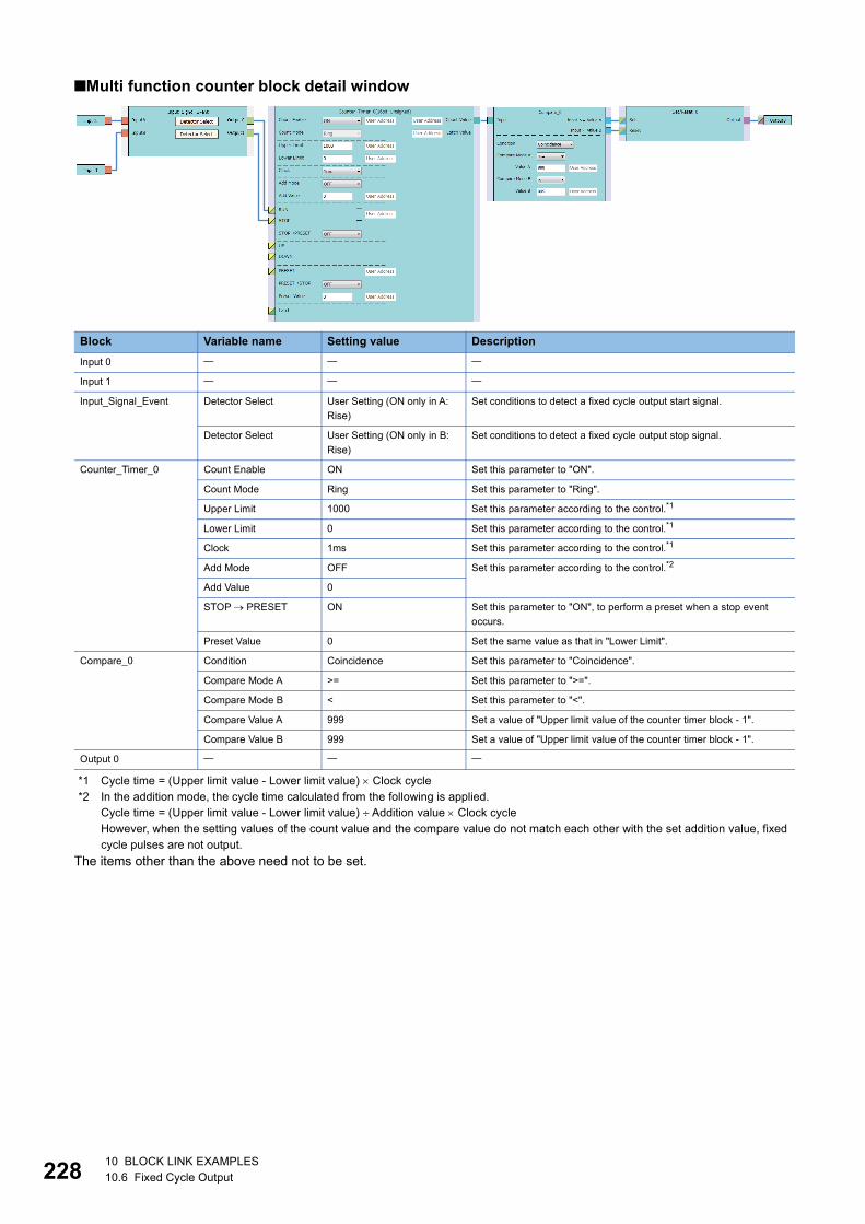
22
■Multi function counter block detail window
*1 Cycle time = (Upper limit value - Lower limit value) Clock cycle*2 In the addition mode, the cycle time calculated from the following is applied.
Cycle time = (Upper limit value - Lower limit value) Addition value Clock cycleHowever, when the setting values of the count value and the compare value do not match each other with the set addition value, fixed cycle pulses are not output.
The items other than the above need not to be set.
Block Variable name Setting value DescriptionInput 0
Input 1
Input_Signal_Event Detector Select User Setting (ON only in A: Rise)
Set conditions to detect a fixed cycle output start signal.
Detector Select User Setting (ON only in B: Rise)
Set conditions to detect a fixed cycle output stop signal.
Counter_Timer_0 Count Enable ON Set this parameter to "ON".
Count Mode Ring Set this parameter to "Ring".
Upper Limit 1000 Set this parameter according to the control.*1
Lower Limit 0 Set this parameter according to the control.*1
Clock 1ms Set this parameter according to the control.*1
Add Mode OFF Set this parameter according to the control.*2
Add Value 0
STOP PRESET ON Set this parameter to "ON", to perform a preset when a stop event occurs.
Preset Value 0 Set the same value as that in "Lower Limit".
Compare_0 Condition Coincidence Set this parameter to "Coincidence".
Compare Mode A >= Set this parameter to ">=".
Compare Mode B < Set this parameter to "<".
Compare Value A 999 Set a value of "Upper limit value of the counter timer block - 1".
Compare Value B 999 Set a value of "Upper limit value of the counter timer block - 1".
Output 0
8 10 BLOCK LINK EXAMPLES10.6 Fixed Cycle Output

10
OperationThe following shows operation of when the fixed cycle output start signal (input terminal 0) is input and when the fixed cycle output stop signal (input terminal 1) is input.
Performed in the flexible high-speed I/O control module
No. Description(1) When a signal is input to the input terminal 0, pulse output starts. One pulse is output per cycle.
(2) When a signal is input to the input terminal 1, the pulse output stops.
1000ms1ms
(1)
(2)
HighLow
HighLow
HighLowOutput terminal
Input terminal 1
Input terminal 0
Cycle timeON time
10 BLOCK LINK EXAMPLES10.6 Fixed Cycle Output 229

23
10.7 Latch CounterThe current value is latched (held) as a latch count value.The following describes a link and parameter example of a latch counter. With the example setting, when a rise of the latch input signal is detected, the current value is latched. Note that this link example is for when a 32-bit unsigned multi function counter block is used.
Link and parameterThe following shows a link example of the hardware logic outline window and a link example and parameter setting example of the multi function counter block detail window.
■Hardware logic outline window
Phase A input pulse
Phase B input pulse
Latch signal
0 10 BLOCK LINK EXAMPLES10.7 Latch Counter

10
■Multi function counter block detail window
The items other than the above need not to be set.
Block Variable name Setting value DescriptionInput 0
Input 1
Latch 0
Input_Signal_Event Detector Select 2-Phase Multiple of 1+ Set this parameter to detect an addition pulse.
Detector Select 2-Phase Multiple of 1- Set this parameter to detect a subtraction pulse.
Latch_Event Detector Select A: Rise Set conditions to detect a latch signal.
Counter_Timer_0 Count Enable ON Set this parameter to "ON".
Count Mode Ring Set this parameter according to the control.
Upper Limit 20000 Set this parameter according to the control.
Lower Limit 0 Set this parameter according to the control.
Clock 25ns Set this parameter to "25ns". (to prevent input pulses from missing)
Add Mode OFF Set this parameter according to the control.
Add Value 0
Preset Value 0 Set the same value as that in "Lower Limit".
Latch Value(User Address)
1000 Assign a buffer memory address.
10 BLOCK LINK EXAMPLES10.7 Latch Counter 231
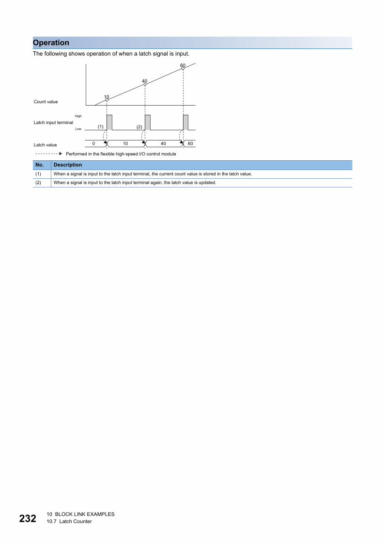
23
OperationThe following shows operation of when a latch signal is input.
Performed in the flexible high-speed I/O control module
No. Description(1) When a signal is input to the latch input terminal, the current count value is stored in the latch value.
(2) When a signal is input to the latch input terminal again, the latch value is updated.
High
Low
10
40
60
0 10 40 60
(1) (2)
Latch value
Latch input terminal
Count value
2 10 BLOCK LINK EXAMPLES10.7 Latch Counter

10
10.8 Ratio ConversionAn input signal multiplied with the set ratio (x/y) is output from the multi function counter block.Ratio conversion enables the following controls. • An encoder output of the motor at the unwinding part is input to the programmable controller to control the motor speed of
lines with distribution output. • The motor speed of multiple lines, for example, a printer, can be controlled.
The ratio (x/y) used in ratio conversion must be "y x" when a signal multiplied by x/y is output to an input signal. Conversions with the ratio exceeding one time cannot be performed.The following describes a link and parameter example of a ratio conversion. With the example setting, when a 1ms input signal is output for 1ms after multiplied with 3/10. Note that this link example is for when a 16-bit unsigned multi function counter block is used.
Printing machine
Rolling out
Printing
Rolling up
ONOFF
ONOFF
1ms
1ms
Input signal
Output signal
Ratio conversion 310
10 BLOCK LINK EXAMPLES10.8 Ratio Conversion 233
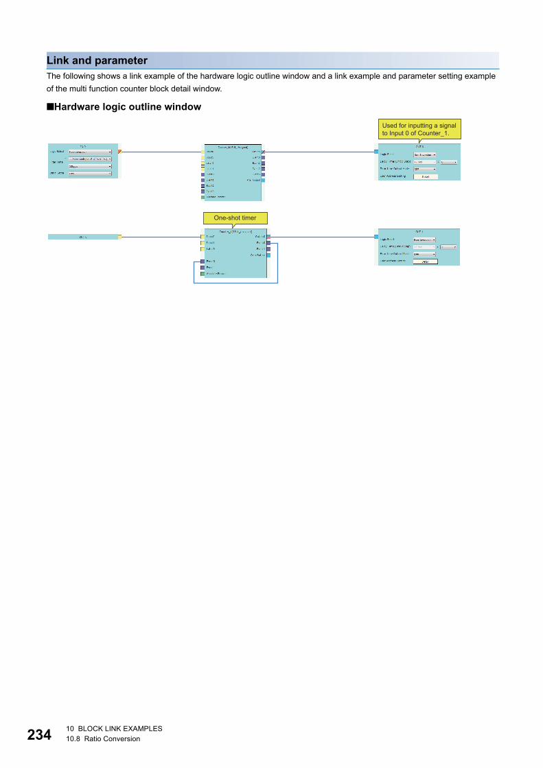
23
Link and parameterThe following shows a link example of the hardware logic outline window and a link example and parameter setting example of the multi function counter block detail window.
■Hardware logic outline windowUsed for inputting a signal to Input 0 of Counter_1.
One-shot timer
4 10 BLOCK LINK EXAMPLES10.8 Ratio Conversion
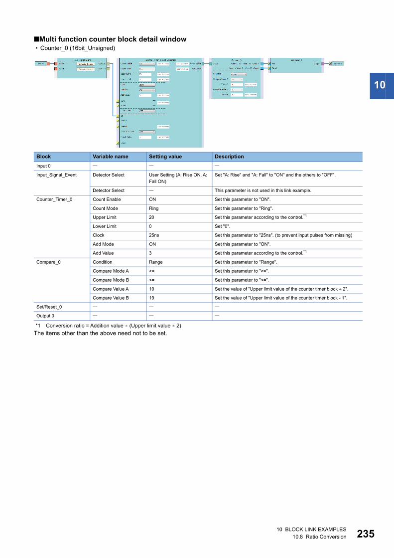
10
■Multi function counter block detail window • Counter_0 (16bit_Unsigned)
*1 Conversion ratio = Addition value (Upper limit value 2)The items other than the above need not to be set.
Block Variable name Setting value DescriptionInput 0
Input_Signal_Event Detector Select User Setting (A: Rise ON, A: Fall ON)
Set "A: Rise" and "A: Fall" to "ON" and the others to "OFF".
Detector Select This parameter is not used in this link example.
Counter_Timer_0 Count Enable ON Set this parameter to "ON".
Count Mode Ring Set this parameter to "Ring".
Upper Limit 20 Set this parameter according to the control.*1
Lower Limit 0 Set "0".
Clock 25ns Set this parameter to "25ns". (to prevent input pulses from missing)
Add Mode ON Set this parameter to "ON".
Add Value 3 Set this parameter according to the control.*1
Compare_0 Condition Range Set this parameter to "Range".
Compare Mode A >= Set this parameter to ">=".
Compare Mode B <= Set this parameter to "<=".
Compare Value A 10 Set the value of "Upper limit value of the counter timer block 2".
Compare Value B 19 Set the value of "Upper limit value of the counter timer block - 1".
Set/Reset_0
Output 0
10 BLOCK LINK EXAMPLES10.8 Ratio Conversion 235

23
• Counter_1 (32bit_Unsigned)
*2 Output ON time = Clock cycle (Compare value - Preset value + 1)*3 In the addition mode, the output ON time calculated from the following is applied.
Output ON time = (Clock cycle (Compare value - Preset value + 1)) Addition valueThe items other than the above need not to be set.
Block Variable name Setting value DescriptionInput 0
Input_Signal_Event Detector Select User Setting (ON only in A: High)
Set this parameter to detect the phase A input signal.
Detector Select User Setting (ON only in A: Rise)
Counter_Timer_0 Count Enable ON Set this parameter to "ON".
Count Mode Linear Set this parameter according to the control.
Upper Limit 4294967295 Set this parameter according to the control.
Lower Limit 0 Set this parameter according to the control.
Clock 25ns Set this parameter according to the control.*2
Add Mode OFF Set this parameter according to the control.*3
Add Value 0
STOP PRESET ON Set this parameter to "ON", to perform a preset when a stop event occurs.
PRESET STOP OFF Set this parameter to "OFF".
Preset Value 1 Set this parameter according to the control.*2
Compare_0 Condition Coincidence Set this parameter to "Coincidence".
Compare Mode A = Set this parameter to "=".
Compare Value A 40000 Set this parameter according to the control.*2
Set/Reset_0
Output 0
Event 0
6 10 BLOCK LINK EXAMPLES10.8 Ratio Conversion
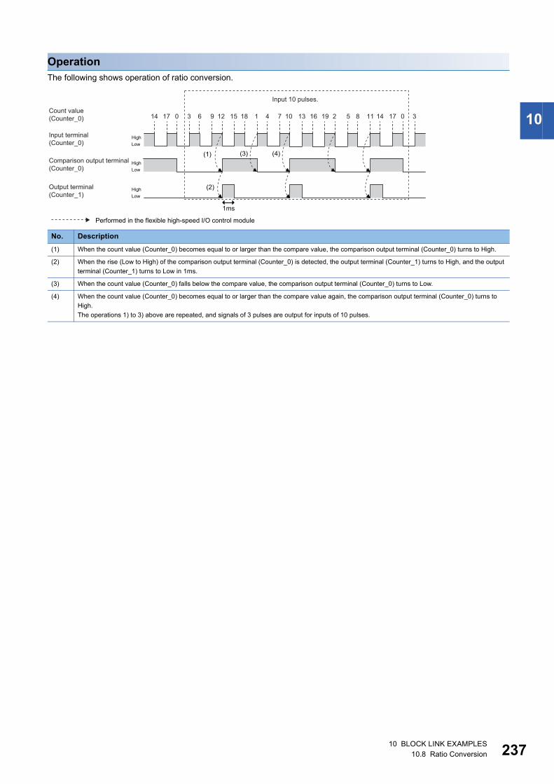
10
OperationThe following shows operation of ratio conversion.
Performed in the flexible high-speed I/O control module
No. Description(1) When the count value (Counter_0) becomes equal to or larger than the compare value, the comparison output terminal (Counter_0) turns to High.
(2) When the rise (Low to High) of the comparison output terminal (Counter_0) is detected, the output terminal (Counter_1) turns to High, and the output terminal (Counter_1) turns to Low in 1ms.
(3) When the count value (Counter_0) falls below the compare value, the comparison output terminal (Counter_0) turns to Low.
(4) When the count value (Counter_0) becomes equal to or larger than the compare value again, the comparison output terminal (Counter_0) turns to High.The operations 1) to 3) above are repeated, and signals of 3 pulses are output for inputs of 10 pulses.
HighLow
HighLow
HighLow
14
(1) (3)
(2)
(4)
1ms
17 0 3 6 9 12 15 18 1 4 7 13 16 19 2 5 8 11 14 17 0 310
Input terminal (Counter_0)
Comparison output terminal(Counter_0)
Count value (Counter_0)
Output terminal (Counter_1)
Input 10 pulses.
10 BLOCK LINK EXAMPLES10.8 Ratio Conversion 237
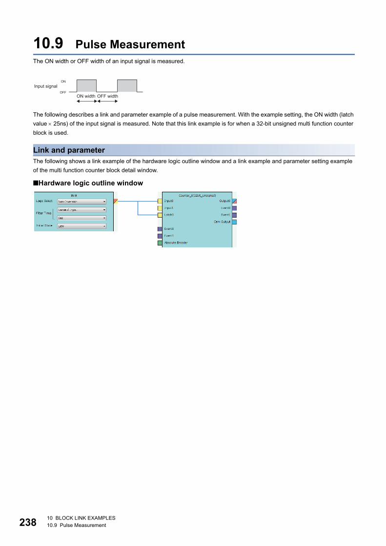
23
10.9 Pulse MeasurementThe ON width or OFF width of an input signal is measured.
The following describes a link and parameter example of a pulse measurement. With the example setting, the ON width (latch value 25ns) of the input signal is measured. Note that this link example is for when a 32-bit unsigned multi function counter block is used.
Link and parameterThe following shows a link example of the hardware logic outline window and a link example and parameter setting example of the multi function counter block detail window.
■Hardware logic outline window
ON
OFF
Input signal
ON width OFF width
8 10 BLOCK LINK EXAMPLES10.9 Pulse Measurement
10
■Multi function counter block detail window
*1 Set the following to measure the OFF width."Detector Select" of "Input_Signal_Event" linked with the RUN terminal: ON only in A: Fall"Detector Select" of "Input_Signal_Event" linked with the STOP terminal: ON only in A: Rise"Detector Select" of "Latch_Event" linked with the Latch terminal: ON only in A: Rise
The items other than the above need not to be set.
Block Variable name Setting value DescriptionInput 0
Latch 0
Input_Signal_Event Detector Select User Setting (ON only in A: Rise)*1
Set ON only in "A: Rise".
Detector Select User Setting (ON only in A: Fall)*1
Set ON only in "A: Fall".
Latch_Event Detector Select User Setting (ON only in A: Fall)*1
Set ON only in "A: Fall".
Counter_Timer_0 Count Enable ON Set this parameter to "ON".
Count Mode Linear Set this parameter to "Linear".
Upper Limit 4294967295 Set "4294967295", to widen the pulse measurement width.
Lower Limit 0 Set "0".
Clock 25ns Set this parameter to "25ns". (to prevent input pulses from missing)
Add Mode OFF Set the addition mode to "OFF". (No addition in this example)
Add Value 0
STOP PRESET ON Set this parameter to "ON", to perform a preset when a stop event occurs.
Preset Value 0 Set this parameter to 0.
Latch Value(User Address)
1000 Assign a buffer memory address.
10 BLOCK LINK EXAMPLES10.9 Pulse Measurement 239
24
OperationThe following shows operation of pulse measurement.
Performed in the flexible high-speed I/O control module
No. Description(1) When the input signal is turned on, the RUN terminal turns to High and counting per clock cycle starts.
(2) When the input signal is turned off, the following two operations are simultaneously performed.• The Latch terminal turns to High and the current count value is latched.• The STOP terminal turns to High, counting per clock cycle stops and preset is performed.
0
10
0 10
(1)(2)OFF
ON
LowHigh
LowHigh
LowHigh
Latch terminal
STOP terminal
Input signal
RUN terminal
Count value
Latch value
0 10 BLOCK LINK EXAMPLES10.9 Pulse Measurement

11
11 SETTINGSThis chapter describes the setting methods for the flexible high-speed I/O control module.
• To enable the settings of adding a new module and auto refresh, write the changed settings in the CPU module, and reset the CPU module, set the RUN/STOP/RESET switch from STOP to RUN twice, or turn off and on the power.
• To enable the switch setting, write the changed setting in the CPU module, and reset the CPU module or turn off and on the power.
11.1 Adding the ModuleAdd the model name of the flexible high-speed I/O control module used in the project.
Addition methodAdd the model name in "New Module".
[Project window] [Intelligent Function Module] Right-click [New Module]
Item DescriptionModule Selection Module Type Set "Counter Module".
Module Name Set the module model name to be connected.
Mount Position Mounted Slot No. Set a slot number where the target module is connected.
Specify start XY address The start I/O number (hexadecimal) of the target module is set according to the slot number where the module is connected. An arbitrary number can also be set.
Title setting Title Set any title.
11 SETTINGS11.1 Adding the Module 241
24
11.2 Switch SettingSet whether to enable or disable the hardware logic control at disconnection and to enable or disable the continuous logging data storage interrupt.
[Project window] [Intelligent Function Module] Module model name [Switch Setting]
Item Description Setting valueHardware logic control at disconnection enable/disable
Set the hardware logic control status of when the own station is disconnected during hardware logic control.
Disable (default value)Enable
Continuous logging data storage interrupt enable/disable
Set whether to send an interrupt request to the CPU module or not at the continuous logging data storage.
Disable (default value)Enable
2 11 SETTINGS11.2 Switch Setting

11
11.3 Auto RefreshSet the buffer memory areas of the flexible high-speed I/O control module to be refreshed automatically.The auto refresh setting eliminates the need for reading data by using a program.
Setting methodSet the auto refresh in "Auto Refresh".
1. Open the "Auto Refresh" window.
[Project window] [Intelligent Function Module] Module model name [Auto Refresh]
2. Click the item to be set to enter the auto refresh target device.
The usable devices are X, Y, M, L, B, T, C, ST, D, W, R, and ZR.When the bit device X, Y, M, L, or B is used, set a number that is divisible by 16 points, such as X10, Y120, and M16. Buffer memory data of 16 points is stored from the set device number. (Example: When X10 is set, data is stored in X10 to X1F.)
11 SETTINGS11.3 Auto Refresh 243
24
12 DISPLAY UNITThis chapter describes display unit functions that can be used for the flexible high-speed I/O control module.For details on operations, functions, and menu structure of the display unit, refer to the following. MELSEC-L CPU Module User's Manual (Function Explanation, Program Fundamentals)
12.1 FeaturesThe display unit is a liquid crystal display that can be connected to the CPU module. Connecting it to the CPU module allows checking the system status without using software packages.When a trouble occurs, the display unit displays error information and a cause of the trouble can be specified.
4 12 DISPLAY UNIT12.1 Features
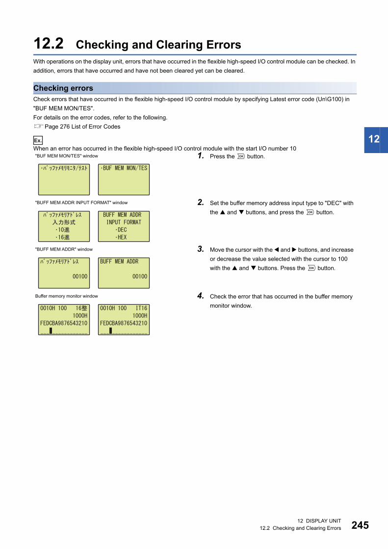
12
12.2 Checking and Clearing ErrorsWith operations on the display unit, errors that have occurred in the flexible high-speed I/O control module can be checked. In addition, errors that have occurred and have not been cleared yet can be cleared.
Checking errorsCheck errors that have occurred in the flexible high-speed I/O control module by specifying Latest error code (Un\G100) in "BUF MEM MON/TES".For details on the error codes, refer to the following.Page 276 List of Error Codes
Ex.
When an error has occurred in the flexible high-speed I/O control module with the start I/O number 10"BUF MEM MON/TES" window 1. Press the button.
"BUFF MEM ADDR INPUT FORMAT" window 2. Set the buffer memory address input type to "DEC" with the and buttons, and press the button.
"BUFF MEM ADDR" window 3. Move the cursor with the and buttons, and increase or decrease the value selected with the cursor to 100 with the and buttons. Press the button.
Buffer memory monitor window 4. Check the error that has occurred in the buffer memory monitor window.
OK
OK
OK
12 DISPLAY UNIT12.2 Checking and Clearing Errors 245
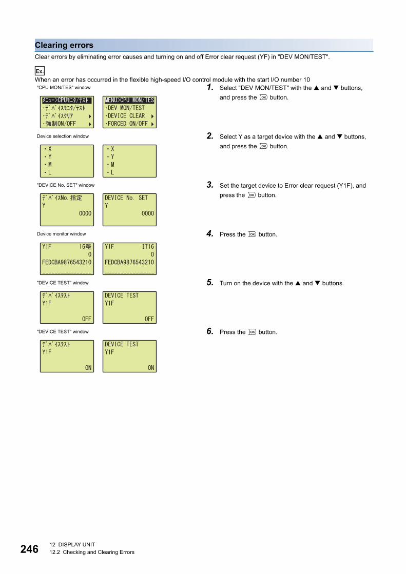
24
Clearing errorsClear errors by eliminating error causes and turning on and off Error clear request (YF) in "DEV MON/TEST".
Ex.
When an error has occurred in the flexible high-speed I/O control module with the start I/O number 10"CPU MON/TES" window 1. Select "DEV MON/TEST" with the and buttons,
and press the button.
Device selection window 2. Select Y as a target device with the and buttons, and press the button.
"DEVICE No. SET" window 3. Set the target device to Error clear request (Y1F), and press the button.
Device monitor window 4. Press the button.
"DEVICE TEST" window 5. Turn on the device with the and buttons.
"DEVICE TEST" window 6. Press the button.
OK
OK
OK
OK
OK
6 12 DISPLAY UNIT12.2 Checking and Clearing Errors
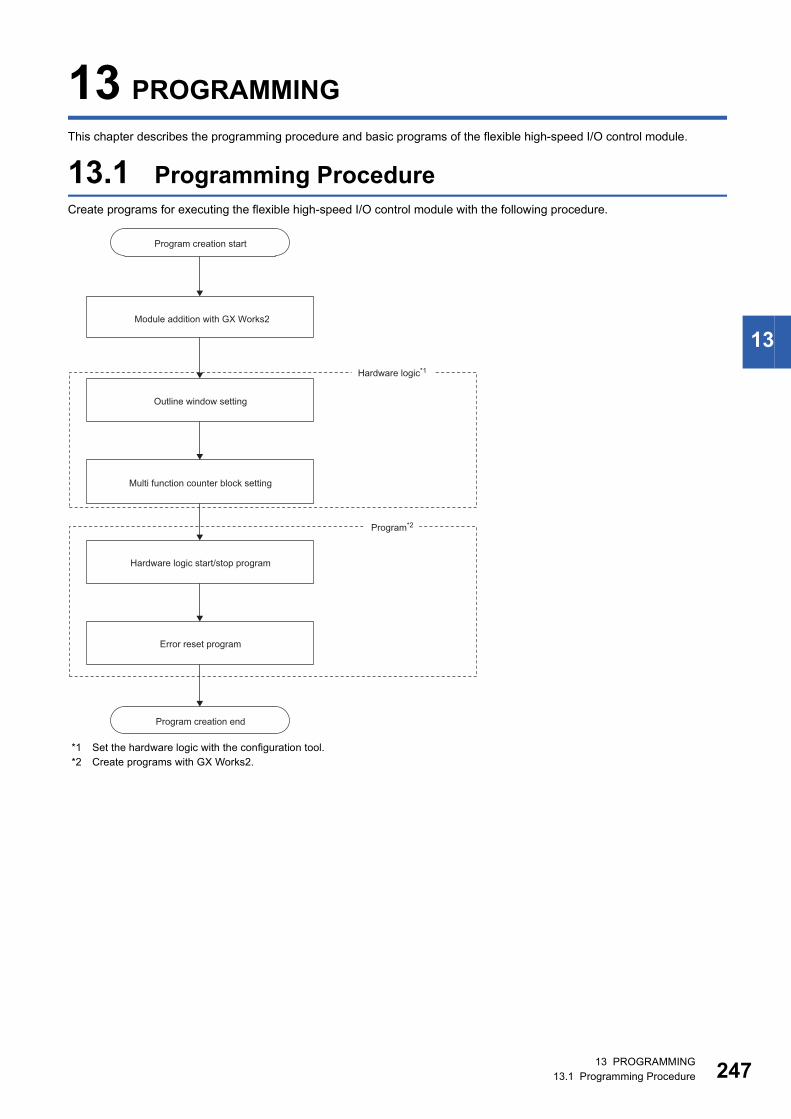
13
13 PROGRAMMINGThis chapter describes the programming procedure and basic programs of the flexible high-speed I/O control module.
13.1 Programming ProcedureCreate programs for executing the flexible high-speed I/O control module with the following procedure.
*1 Set the hardware logic with the configuration tool.*2 Create programs with GX Works2.
Program creation start
Outline window setting
Hardware logic start/stop program
Module addition with GX Works2
Program creation end
Error reset program
Program*2
Multi function counter block setting
Hardware logic*1
13 PROGRAMMING13.1 Programming Procedure 247

24
13.2 When the Module Is Used with the Standard System Configuration
This section shows a program example with the following system configuration and conditions.
System configurationThe following figure shows a system configuration example.
Programming conditionsThe program counts pulses (2-phase multiple of 4) input to the flexible high-speed I/O control module with the multi function counter block.
Adding the moduleAdd the flexible high-speed I/O control module on GX Works2.For details on adding the module, refer to the following.Page 241 Adding the ModuleUse the default values for the switch setting and auto refresh setting in these program examples.
Starting the configuration toolStart the configuration tool with the following procedure.Page 74 Starting and Exiting the Configuration Tool
LD40PD01
Power supply module (L61P) END cover (L6EC)
CPU module (L26CPU-BT)
X/Y00 to X/Y0F
X/Y30 to X/Y4F
X/Y10 to X/Y2F
8 13 PROGRAMMING13.2 When the Module Is Used with the Standard System Configuration

13
Creating a hardware logicCreate a hardware logic with the configuration tool.
■Link and settings in the hardware logic outline window1. Arrange a 32-bit unsigned multi function counter block in the hardware logic outline window, and link it to external input
blocks. • To perform external outputs according to the counting result, link the multi function counter block to an external output
block. • To start an interrupt program according to the counting result, link the multi function counter block to an SI device terminal.
( Page 253 Interrupt program example)
2. Set the external input blocks according to the specifications of external input signals.
3. To use the external output block, set it according to the specifications of external output signals and desired output timings.
13 PROGRAMMING13.2 When the Module Is Used with the Standard System Configuration 249
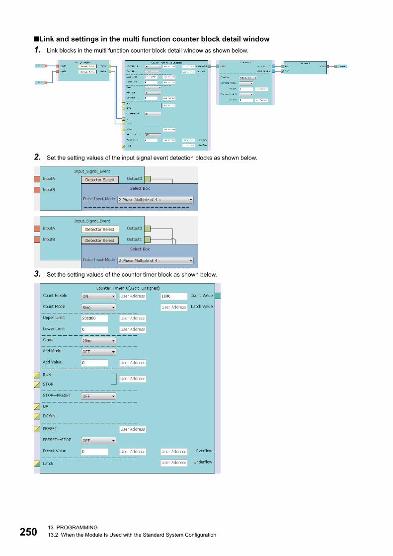
25
■Link and settings in the multi function counter block detail window1. Link blocks in the multi function counter block detail window as shown below.
2. Set the setting values of the input signal event detection blocks as shown below.
3. Set the setting values of the counter timer block as shown below.
0 13 PROGRAMMING13.2 When the Module Is Used with the Standard System Configuration

13
4. Set the setting values of the comparison block as shown below.
■Writing data to the moduleWrite a project to the CPU module with GX Works2. Write the hardware logic to the flexible high-speed I/O control module with the configuration tool.
13 PROGRAMMING13.2 When the Module Is Used with the Standard System Configuration 251

25
Program example■User devices
■Program example
Device DescriptionM0 Hardware logic control start
M1 Hardware logic control stop
M2 Operating condition settings batch-reset
M3 Error reset command
X30 Module ready
X33 Operating condition settings batch-reset complete flag
X34 Hardware logic control flag
X3F Error flag
Y33 Operating condition settings batch-reset command
Y34 Hardware logic control start request
Y35 Hardware logic control stop request
Y3F Error clear request
Store a value of Clear setting of error history.
Turn on Error clear request.
Turn off Error clear request.
Turn on Hardware logic control start request.
Turn off Hardware logic control start request.
Turn on Hardware logic control stop request.
Turn off Hardware logic control stop request.
Turn on Operating condition settings batch-reset command.
Turn off Operating condition settings batch-reset command.
2 13 PROGRAMMING13.2 When the Module Is Used with the Standard System Configuration

13
Interrupt program example■Interrupt pointer setting
Project window [Parameter] [PLC Parameter] [PLC System] "Intelligent Function Module Setting" [Interrupt Pointer Setting] button
■User devices
■Program exampleBefore using an interrupt pointer, enable an interrupt with the IMASK instruction.
• When the program above is executed, the I50 interrupt program is enabled, and all other interrupt programs are disabled. To execute any interrupt program other than the I50 interrupt program, set the bit that corresponds to the target interrupt pointer to "1: enabled".
• For details on the IMASK instruction, refer to the following ( MELSEC-Q/L Programming Manual (Common Instruction)).
Device DescriptionD100 to D115 Interrupt enable flag storage for IMASK instruction
Interrupt disabled
Interrupt enabled
Interrupt of I50 enabled
Turn on the 50th bit from D100.
Main routine program completed
Interrupt program processing completed
Program of the flexible high-speed I/O control module
Interrupt program
13 PROGRAMMING13.2 When the Module Is Used with the Standard System Configuration 253
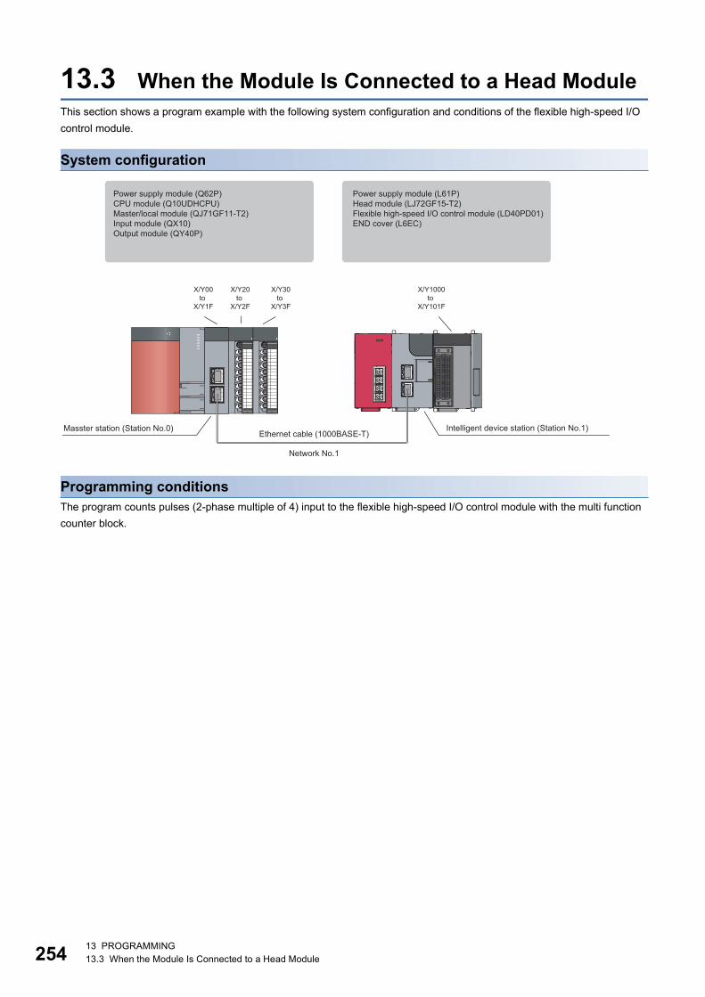
25
13.3 When the Module Is Connected to a Head ModuleThis section shows a program example with the following system configuration and conditions of the flexible high-speed I/O control module.
System configuration
Programming conditionsThe program counts pulses (2-phase multiple of 4) input to the flexible high-speed I/O control module with the multi function counter block.
Network No.1
Ethernet cable (1000BASE-T)
X/Y1000to
X/Y101F
Masster station (Station No.0) Intelligent device station (Station No.1)
Power supply module (Q62P)CPU module (Q10UDHCPU)Master/local module (QJ71GF11-T2)Input module (QX10)Output module (QY40P)
Power supply module (L61P)Head module (LJ72GF15-T2)Flexible high-speed I/O control module (LD40PD01)END cover (L6EC)
X/Y00to
X/Y1F
X/Y20to
X/Y2F
X/Y30to
X/Y3F
4 13 PROGRAMMING13.3 When the Module Is Connected to a Head Module

13
User devicesDevice DescriptionM100 Setting start command
M110 Hardware logic control start command
M111 Hardware logic control stop command
M112 Count value read command
M113 Operating condition batch-reset command
M114 Hardware logic control stop flag clear command at disconnection
M120 Error reset command
M200, M201 Write complete flag
M210, M211 Read complete flag 1
M220, M221 Read complete flag 2
M300 Count value reading flag
M310 Number of writes to a flash ROM reading flag
M1000 Communication ready flag (station number 1)
M1001 Setting request at a startup
M1002 Setting request signal
M1003 Setting complete flag at a startup
D100 (W1010) Storing the latest error code
D200, D201 Storing the cumulative number of write accesses to a flash ROM
D1000 Storing the clear setting of error history
D1010, D1011 Count value
F200 Parameter write complete with an error
F210 Count value read complete with an error
F220 Number of writes to a flash ROM read complete with an error
13 PROGRAMMING13.3 When the Module Is Connected to a Head Module 255

25
Settings on the master station side1. Create a project of GX Works2.Select "QCPU (Q mode)" in "Series" and select "Q10UDH" in "Type".
[Project] [New]
2. Display the setting window for the network parameters and set the values as follows.
[Project window] [Parameter] [Network Parameter] [Ethernet / CC IE / MELSECNET]
3. Display the setting window for the network configuration settings and set the values as follows.
[Project window] [Parameter] [Network Parameter] [Ethernet / CC IE / MELSECNET] button
6 13 PROGRAMMING13.3 When the Module Is Connected to a Head Module

13
4. Display the setting window for the refresh parameters and set the values as follows.
[Project window] [Parameter] [Network Parameter] [Ethernet / CC IE / MELSECNET] button
5. Write the set parameters to the CPU module on the master station. Then reset the CPU module or power off and on the programmable controller.
[Online] [Write to PLC]
RESETor Power OFF ON
13 PROGRAMMING13.3 When the Module Is Connected to a Head Module 257
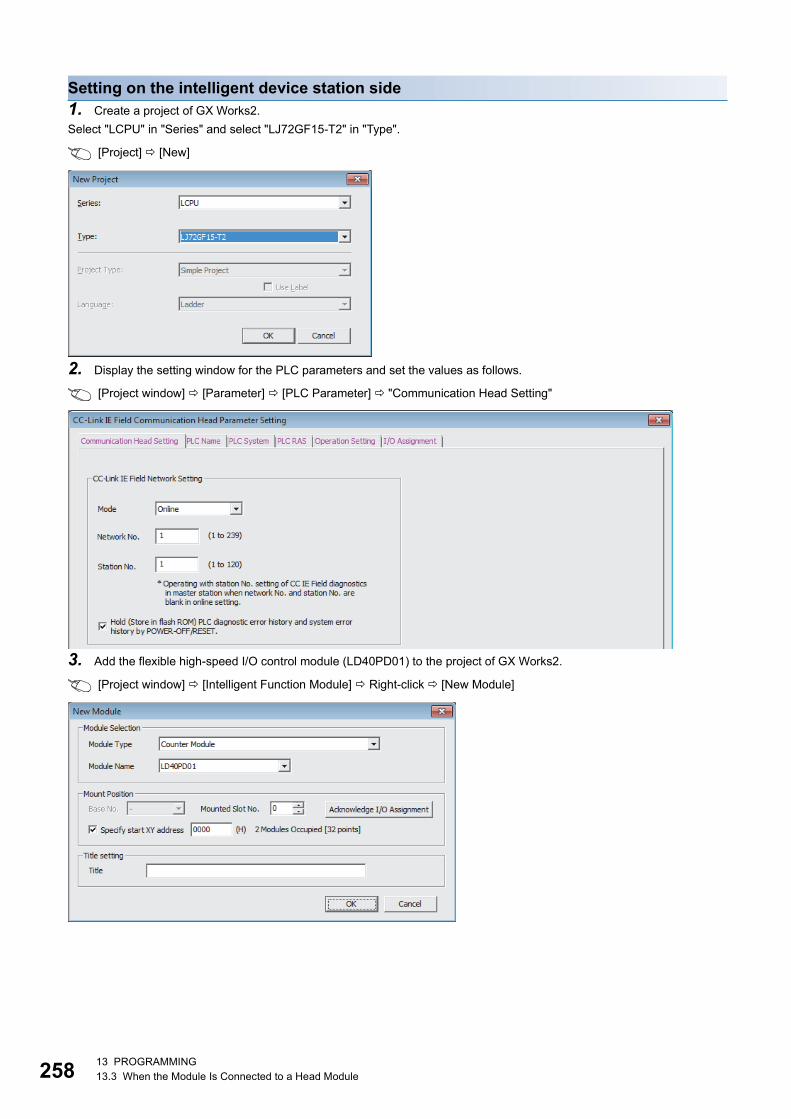
25
Setting on the intelligent device station side1. Create a project of GX Works2.Select "LCPU" in "Series" and select "LJ72GF15-T2" in "Type".
[Project] [New]
2. Display the setting window for the PLC parameters and set the values as follows.
[Project window] [Parameter] [PLC Parameter] "Communication Head Setting"
3. Add the flexible high-speed I/O control module (LD40PD01) to the project of GX Works2.
[Project window] [Intelligent Function Module] Right-click [New Module]
8 13 PROGRAMMING13.3 When the Module Is Connected to a Head Module

13
4. Display the setting window for the intelligent function module detailed setting of the flexible high-speed I/O control module (LD40PD01) and set the values as follows.
[Project window] [Parameter] [PLC Parameter] [I/O Assignment] button
5. Display the setting window for the switch setting of the flexible high-speed I/O control module (LD40PD01) and set the value as follows.
[Project window] [Intelligent Function Module] Module model name [Switch Setting]
When the own station is disconnected, the operations of the flexible high-speed I/O control module differ depending on the setting of "Hardware logic control at disconnection enable/disable" in the switch setting or that of "Error Time Output Mode" in the intelligent function module detailed setting. For details, refer to the following.Page 267 Operations of the flexible high-speed I/O control module when the head module is connected
6. Display the setting window for the auto refresh setting of the flexible high-speed I/O control module (LD40PD01) and set the values as follows.
[Project window] [Intelligent Function Module] Module model name [Auto Refresh]
13 PROGRAMMING13.3 When the Module Is Connected to a Head Module 259

26
7. Write the set parameters to the head module. Then reset the head module or power off and on the programmable controller.
[Online] [Write to PLC]
or Power OFF ON
0 13 PROGRAMMING13.3 When the Module Is Connected to a Head Module

13
Creating a hardware logicCreate a hardware logic with the configuration tool.
■Link and settings in the hardware logic outline window1. Arrange a 32-bit unsigned multi function counter block in the hardware logic outline window, and link it to external input
blocks. • To perform external outputs according to the counting result, link the multi function counter block to an external output
block.
2. Set the external input blocks according to the specifications of external input signals.
3. To use the external output block, set it according to the specifications of external output signals and desired output timings.
13 PROGRAMMING13.3 When the Module Is Connected to a Head Module 261

26
■Link and settings in the multi function counter block detail window1. Link blocks in the multi function counter block detail window as shown below.
2. Set the setting values of the input signal event detection blocks as shown below.
3. Set the setting values of the counter timer block as shown below.
2 13 PROGRAMMING13.3 When the Module Is Connected to a Head Module

13
4. Set the setting values of the comparison block as shown below.
■Writing data to the moduleWrite the hardware logic to the flexible high-speed I/O control module with the configuration tool.
13 PROGRAMMING13.3 When the Module Is Connected to a Head Module 263
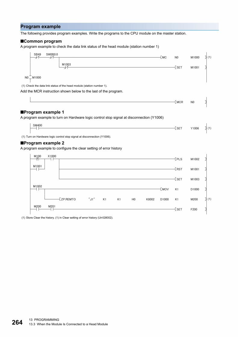
26
Program exampleThe following provides program examples. Write the programs to the CPU module on the master station.
■Common programA program example to check the data link status of the head module (station number 1)
Add the MCR instruction shown below to the last of the program.
■Program example 1A program example to turn on Hardware logic control stop signal at disconnection (Y1006)
■Program example 2A program example to configure the clear setting of error history
(1) Check the data link status of the head module (station number 1).
(1) Turn on Hardware logic control stop signal at disconnection (Y1006).
(1) Store Clear the history. (1) in Clear setting of error history (Un\G8002).
(1)
(1)
(1)
4 13 PROGRAMMING13.3 When the Module Is Connected to a Head Module
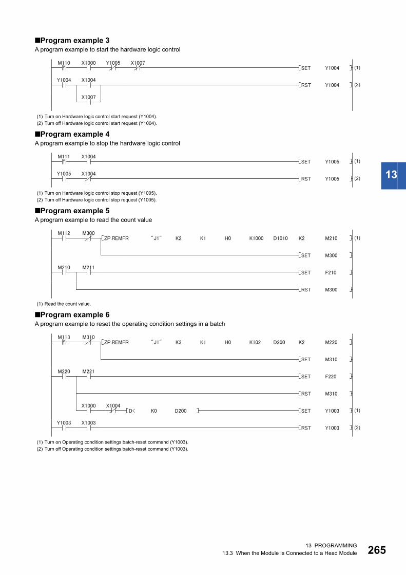
13
■Program example 3A program example to start the hardware logic control
■Program example 4A program example to stop the hardware logic control
■Program example 5A program example to read the count value
■Program example 6A program example to reset the operating condition settings in a batch
(1) Turn on Hardware logic control start request (Y1004).(2) Turn off Hardware logic control start request (Y1004).
(1) Turn on Hardware logic control stop request (Y1005).(2) Turn off Hardware logic control stop request (Y1005).
(1) Read the count value.
(1) Turn on Operating condition settings batch-reset command (Y1003).(2) Turn off Operating condition settings batch-reset command (Y1003).
(1)
(2)
(1)
(2)
(1)
(1)
(2)
13 PROGRAMMING13.3 When the Module Is Connected to a Head Module 265

26
■Program example 7A program example to turn off Hardware logic control stop flag at disconnection (X1007).
■Program example 8A program example to read the latest error code and reset the error
(1) Turn on Hardware logic control stop flag clear request at disconnection (Y1007).(2) Turn off Hardware logic control stop flag clear request at disconnection (Y1007).
(1) Read Latest error code (Un\G100).(2) Turn on Error clear request (Y100F).(3) Turn off Error clear request (Y100F).
(1)
(2)
(1)
(2)
(3)
6 13 PROGRAMMING13.3 When the Module Is Connected to a Head Module

13
Operations of the flexible high-speed I/O control module when the head module is connectedThe following describes the operations of the flexible high-speed I/O control module when the own station is disconnected.The operations differ depending on the combination of the setting of "Hardware logic control at disconnection enable/disable" in the switch setting and that of "Error Time Output Mode" in the intelligent function module detailed setting.
"Hardware logic control at disconnection enable/disable" is "Enable"When Hardware logic control stop signal at disconnection (Y6) is off, the hardware logic control is not executed. When Hardware logic control stop signal at disconnection (Y6) is turned off during hardware logic control, the hardware logic control is stopped.When "Enable" is set for "Hardware logic control at disconnection enable/disable", the operation differs depending on the setting of "Error Time Output Mode" as follows.
After the head module is returned, turn on Hardware logic control start request (Y4) to restart the hardware logic control.
"Hardware logic control at disconnection enable/disable" is "Disable"When "Disable" is set for "Hardware logic control at disconnection enable/disable", the operation differs depending on the setting of "Error Time Output Mode" as follows.
To continue the hardware logic control when the head module is disconnected, set "Disable" for "Hardware logic control at disconnection enable/disable".If "Hardware logic control at disconnection enable/disable" is set to "Disable", a hardware logic control stop request cannot be issued from a program in the disconnection state.
"Error Time Output Mode" OperationClear Hardware logic control stop signal at disconnection (Y6) is turned off at the
head module disconnection, and thus the hardware logic control stops.External output at the hardware logic control stop varies depending on "Error-time Output Mode" of the external output block.
Hold Hardware logic control stop signal at disconnection (Y6) is not turned off at the disconnection, and thus the hardware logic control will continue.
"Error Time Output Mode" OperationClear Even though the head module is disconnected, the hardware logic control
continues. However, all the Y device terminals of the hardware logic will be turned to Low because the Y signal is turned off.Note that the operation changes when a created hardware logic includes Y device terminals.
Hold Even though the head module is disconnected, the hardware logic control continues.
13 PROGRAMMING13.3 When the Module Is Connected to a Head Module 267
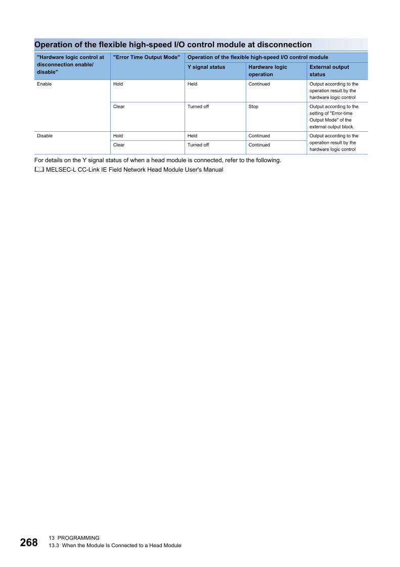
26
Operation of the flexible high-speed I/O control module at disconnection
For details on the Y signal status of when a head module is connected, refer to the following. MELSEC-L CC-Link IE Field Network Head Module User's Manual
"Hardware logic control at disconnection enable/disable"
"Error Time Output Mode" Operation of the flexible high-speed I/O control module
Y signal status Hardware logic operation
External output status
Enable Hold Held Continued Output according to the operation result by the hardware logic control
Clear Turned off Stop Output according to the setting of "Error-time Output Mode" of the external output block
Disable Hold Held Continued Output according to the operation result by the hardware logic control
Clear Turned off Continued
8 13 PROGRAMMING13.3 When the Module Is Connected to a Head Module
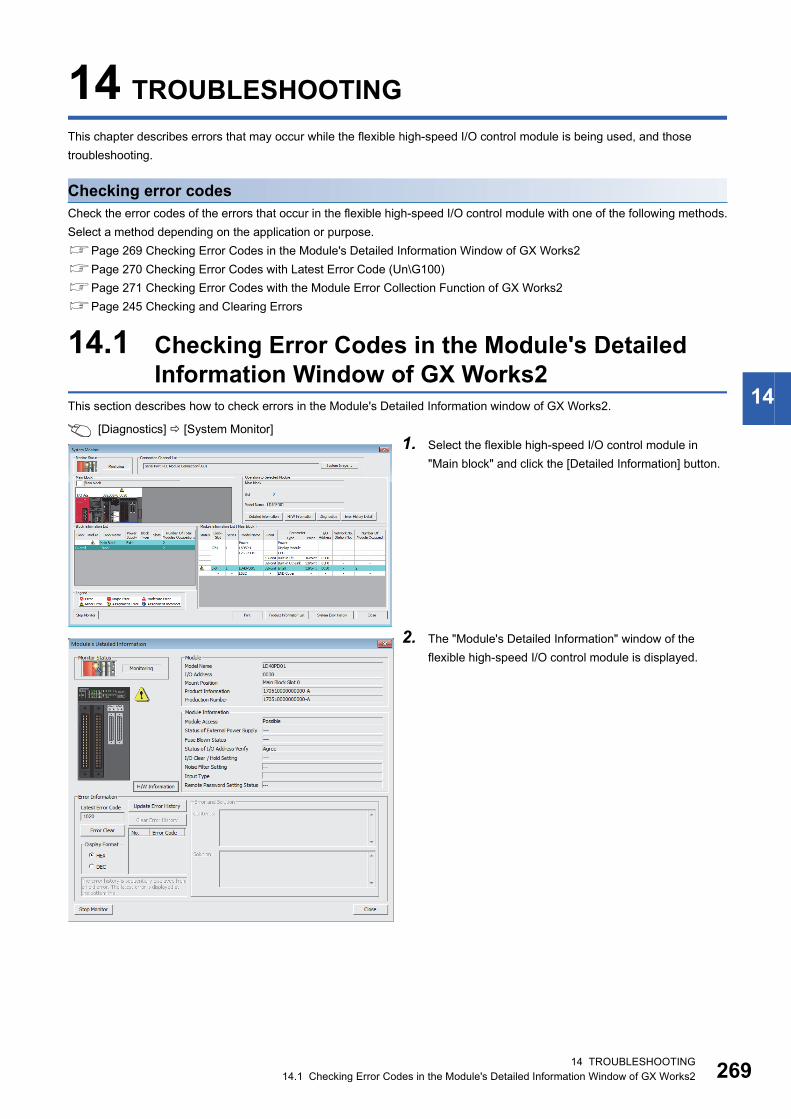
14
14 TROUBLESHOOTINGThis chapter describes errors that may occur while the flexible high-speed I/O control module is being used, and those troubleshooting.
Checking error codesCheck the error codes of the errors that occur in the flexible high-speed I/O control module with one of the following methods.Select a method depending on the application or purpose.Page 269 Checking Error Codes in the Module's Detailed Information Window of GX Works2Page 270 Checking Error Codes with Latest Error Code (Un\G100)Page 271 Checking Error Codes with the Module Error Collection Function of GX Works2Page 245 Checking and Clearing Errors
14.1 Checking Error Codes in the Module's Detailed Information Window of GX Works2
This section describes how to check errors in the Module's Detailed Information window of GX Works2.
[Diagnostics] [System Monitor]1. Select the flexible high-speed I/O control module in
"Main block" and click the [Detailed Information] button.
2. The "Module's Detailed Information" window of the flexible high-speed I/O control module is displayed.
14 TROUBLESHOOTING14.1 Checking Error Codes in the Module's Detailed Information Window of GX Works2 269

27
14.2 Checking Error Codes with Latest Error Code (Un\G100)
This section describes how to check errors with Latest error code (Un\G100).
[Online] [Monitor] [Device/Buffer Memory Batch]
If multiple errors have occurred, the latest error code is stored in Latest error code (Un\G100).
0 14 TROUBLESHOOTING14.2 Checking Error Codes with Latest Error Code (Un\G100)
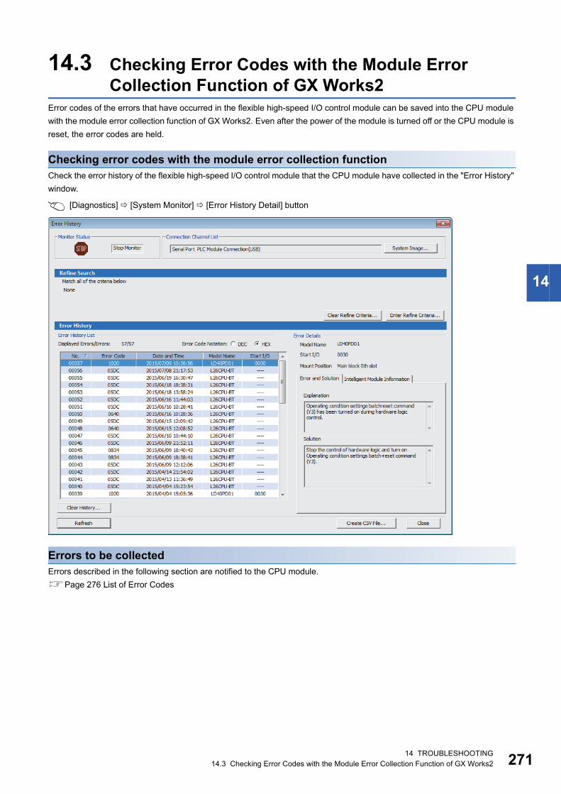
14
14.3 Checking Error Codes with the Module Error Collection Function of GX Works2
Error codes of the errors that have occurred in the flexible high-speed I/O control module can be saved into the CPU module with the module error collection function of GX Works2. Even after the power of the module is turned off or the CPU module is reset, the error codes are held.
Checking error codes with the module error collection functionCheck the error history of the flexible high-speed I/O control module that the CPU module have collected in the "Error History" window.
[Diagnostics] [System Monitor] [Error History Detail] button
Errors to be collectedErrors described in the following section are notified to the CPU module.Page 276 List of Error Codes
14 TROUBLESHOOTING14.3 Checking Error Codes with the Module Error Collection Function of GX Works2 271
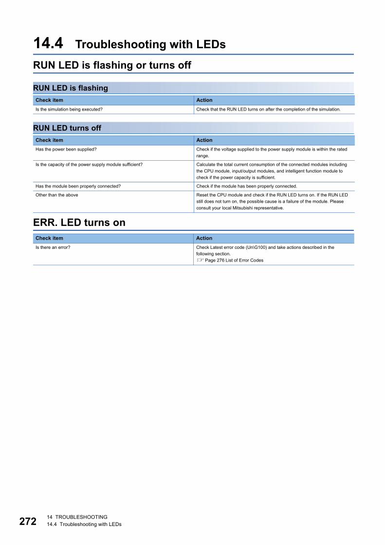
27
14.4 Troubleshooting with LEDsRUN LED is flashing or turns off
RUN LED is flashing
RUN LED turns off
ERR. LED turns on
Check item ActionIs the simulation being executed? Check that the RUN LED turns on after the completion of the simulation.
Check item ActionHas the power been supplied? Check if the voltage supplied to the power supply module is within the rated
range.
Is the capacity of the power supply module sufficient? Calculate the total current consumption of the connected modules including the CPU module, input/output modules, and intelligent function module to check if the power capacity is sufficient.
Has the module been properly connected? Check if the module has been properly connected.
Other than the above Reset the CPU module and check if the RUN LED turns on. If the RUN LED still does not turn on, the possible cause is a failure of the module. Please consult your local Mitsubishi representative.
Check item ActionIs there an error? Check Latest error code (Un\G100) and take actions described in the
following section.Page 276 List of Error Codes
2 14 TROUBLESHOOTING14.4 Troubleshooting with LEDs
14
14.5 Troubleshooting by SymptomInputs from external devices are not performed
Incorrect inputs from external devices are performed
Outputs to external devices are not performed
The hardware logic does not function
Check item ActionIs the LED0 on? Check the external wiring and make necessary corrections.
Is the control of the hardware logic working? When Hardware logic control flag (X4) is off, turn on Hardware logic control start request (Y4) to start the hardware logic control.
Are the block layout and links between blocks in the hardware logic correct? Check the block layout and links between blocks in the hardware logic and make necessary corrections.
Check item ActionMeasures to reduce noise
Is the filter time setting of external input blocks correct? Set the filter time of the external input blocks longer.
Have twisted pair shielded cables been used for the pulse input cables?
Use twisted pair shielded cables for the pulse input cables.
Have measures to reduce noise been taken in the control panel or for adjacent devices?
Take measures to reduce noise such as attaching a CR surge suppressor to the magnet switch or other device.
Is there a sufficient distance between the high voltage device and the pulse input cables?
Wire the pulse input cables alone when placing them in a duct, and keep a distance of 150mm or more from the power cables in the control panel.
Is the module affected by noise through the grounding area? Separate the grounding cable of the flexible high-speed I/O control module from the grounding area.
Are the power cables and I/O cables bundled together? Do not bundle the power cables and I/O cables together.
Is the external wiring connected to unused terminals? Do not connect the external wiring to unused terminals.
Check item ActionIs the LED1 on? Check the block layout and links between blocks in the hardware logic and
make necessary corrections.
Is the external wiring correct? Check the external wiring and make necessary corrections.
Is the control of the hardware logic working? When Hardware logic control flag (X4) is off, turn on Hardware logic control start request (Y4) to start the hardware logic control.
Are the block layout and links between blocks in the hardware logic correct? Check the block layout and links between blocks in the hardware logic and make necessary corrections.
Check item ActionIs the control of the hardware logic working? When Hardware logic control flag (X4) is off, turn on Hardware logic control
start request (Y4) to start the hardware logic control.
Are the block layout and links between blocks in the hardware logic correct? Check the block layout and links between blocks in the hardware logic and make necessary corrections.
Is the CPU module indicating an error? If the CPU module is in an error status, refer to the troubleshooting in the user's manual for the CPU module used and take corrective actions to restore normal operation of the CPU module.
14 TROUBLESHOOTING14.5 Troubleshooting by Symptom 273
27
A multi function counter does not start counting or does not count properly
The module does not start counting
The module does not count properly
Check item ActionHas Count Enable been set to ON? Set Count Enable to ON using a program or the configuration tool.
Is any LED of the CPU module indicating an error? If the LED indicates an error, refer to the troubleshooting in the manual for the CPU module used and take corrective actions to restore normal operation of the CPU module.
Is the external wiring for A and B correct? Check the external wiring and make necessary corrections.
Is the control of the hardware logic working? When Hardware logic control flag (X4) is off, turn on Hardware logic control start request (Y4) to start the hardware logic control.
Are the block layout and links between blocks in the hardware logic correct? Check the block layout and links between blocks in the hardware logic and make necessary corrections.
Check item ActionAre the current value or other values read in increments of one word (16 bits) using a program when 32-bit counter timer blocks are used?
Read the values of two words (32 bits) in a batch.
Was the preset function performed within the count range of a counter? Reset the preset value within the count range and perform the preset function again.
Is the filter time setting of external input blocks correct? Check the filter time setting and make necessary corrections.
When the same pulse is input to the multi function counter blocks that have the same links, is the same value counted?
If the count values are different, the possible cause is a failure of the module. Please consult your local Mitsubishi representative.
Does the input pulse wave satisfy the performance specifications? Observe and check the pulse wave with a synchroscope. If the input pulse does not satisfy the performance specifications, input pulses that satisfy the performance specifications.
Is the external wiring with the SSI encoder correct? Check the external wiring. ( Page 55 Example of external wiring with the SSI encoder (serial communication))
Is the setting value of the SSI encoder block correct? Check and correct the value according to the SSI encoder to be connected.
Is the cable length within the range of the maximum cable length? Check the cable length and size. ( Page 55 Example of external wiring with the SSI encoder (serial communication))Or slow the SSI transmission speed.
Are shielded twisted pair cables used? Use shielded twisted pair cables.
Does noise affect anything? Take measures to reduce noise such as attaching a surge suppressor to the magnet switch.
Is there a sufficient distance between the high voltage device and the signal wires?
Wire the signal wires alone and keep them 150mm or more away from power cables.
4 14 TROUBLESHOOTING14.5 Troubleshooting by Symptom

14
■Pulse shaping methodAs one of measures against external noise or waveform distortion, the following describes the shaping method of a pulse waveform with dummy resistors.An effective method for pulse shaping is to apply dummy resistors of several hundreds ohms (/several watts) across pulse input terminals connected to an encoder to increase a load current through the cables. This method becomes more effective as the load current value increases.With this shaping method, the following effects can be obtained. • When the wiring distance between an encoder and the flexible high-speed I/O control module is long, this shaping method
improves the waveform distortion and the pulse waveform becomes stable. • When the pulse waveform is unstable due to noise such as external noise, this shaping method stabilizes the pulse
waveform and the noise effects can be reduced.
Ex.
The following figure shows a connection example of dummy resistors at 24VDC.
The following example describes how to select a dummy resistor (how to calculate a resistance constant and rated power of a dummy resistor).
As a result of the above calculations, apply dummy resistors of 680 (/2W) across pulse input terminals in this case.
Interrupt requests are not properly sent to the CPU module
Target Calculation methodResistance constant of a dummy resistor (at 24VDC input) Calculate a resistance constant (R) as follows.
• R = V I = 24V 35mA = 680
Rated power of a dummy resistor (at 24VDC input) Calculate the power (P1) as follows.• P1 = V I = 24V 35mA = 0.84W (Approx. 1W)
Calculate the power (P2) including margins from the power (P1).• P2 = P1 2 = 0.84 2 = 1.68W (Approx. 2W)
Check item ActionIs a link to the SI device terminal in the hardware logic correct? Check the block layout and links between blocks in the hardware logic and
make necessary corrections.
Is the coincidence detection disabled because the addition mode has been applied?
To use the coincidence detection interrupt and addition mode together, preset the value used for the coincidence detection.
Is the intelligent function module interrupt pointer setting of the PLC parameter correct?
Review the intelligent function module interrupt pointer setting.
24VOUT
24VOUT
E
IN 0_DIF
IN 0_5V
IN 0_24V
B18
A19
B19
A18
B16
A17
B17
A16
IN 0_COM
IN 1_DIF
IN 1_5V
IN 1_24V
IN 1_COM
820Ω
820Ω
4.1kΩ270Ω240Ω
4.1kΩ270Ω240Ω
Flexible high-speed I/O control module
IN 0 (24V input)
IN 1 (24V input)
Shielded twisted pair cable
Install a dummy resistor of hundreds of ohms (/a few watts) between pulse input terminals (24V-COM).
14 TROUBLESHOOTING14.5 Troubleshooting by Symptom 275
27
14.6 List of Error CodesThis section lists the codes of errors that may occur in the use of the I/O control module.The error codes are stored in Latest error code (Un\G100) and also reported to the CPU module.The in the error code indicates the number of the multi function counter block where an error has occurred.
Error code (hexadecimal)
Error name Description and cause Operation at the error Action
100H Multi function counter block overflow error
A count value has exceeded the upper limit value when 32-bit multi function counter block is set to linear counter mode.
The count operation stops for the corresponding multi function counter block.
Perform the preset function to the corresponding multi function counter block.
101H Multi function counter block underflow error
A count value has fallen below the lower limit value when 32-bit multi function counter block is set to linear counter mode.
The count operation stops for the corresponding multi function counter block.
Perform the preset function to the corresponding multi function counter block.
1020H Reset error during hardware logic control
Operating condition settings batch-reset command (Y3) has been turned on during hardware logic control.
The control of hardware logic continues.
Stop the control of hardware logic and turn on Operating condition settings batch-reset command (Y3).
1040H Reset error without any data writes to a flash ROM
Operating condition settings batch-reset command (Y3) has been turned on while any setting data has not been written to a flash ROM.
The operating condition settings batch-reset for hardware logic is not performed.
Set operating conditions in a flash ROM and turn on Operating condition settings batch-reset command (Y3).
1060H Flash ROM data error
The setting data in the flash ROM are faulty.
The control can be started with non-wired hardware logic.
Write the setting data again with a configuration tool. Take measures to reduce noise with a shielded cable for connection.If the error occurs again, the possible cause is a failure of the module. Please consult your local Mitsubishi representative.
1061H Trigger setting data error
The trigger setting data in the flash ROM are faulty.
The trigger setting becomes disabled, and thus the logic analyzer function cannot be started.
Write the trigger setting again with a configuration tool. Take measures to reduce noise with a shielded cable for connection.If the error occurs again, the possible cause is a failure of the module. Please consult your local Mitsubishi representative.
1080H Number of writes to a flash ROM over error
The number of writes to a flash ROM has exceeded 10000 times.
The control of hardware logic can be started.
Any further writes to a flash ROM may not be reflected correctly.
1081H Number of trigger setting writes over error
The number of trigger setting writes to a flash ROM has exceeded 10000 times.
The logic analyzer function can be started.
Any further trigger setting writes to a flash ROM may not be reflected correctly.
109H SSI encoder block DATA signal wire reverse error
The positive and negative of the DATA signal wire are reversely connected.
Position data from the encoder cannot be received properly.
Check the external wiring for the DATA signal.
10AH SSI encoder block DATA signal error
The DATA signal input state is Low at the start of data transfer, or is High just after the transfer is completed.
Check the SSI transmission speed and SSI code length. In addition, consider the possibility of noise effects. Check the cable laying, shielding, and cable length.
10BH SSI encoder block parity error
A parity error has occurred. Check the external wiring to the SSI encoder and settings of the SSI encoder block.
10C0H Trigger start error at trigger setting disabled
The trigger start request was issued while the trigger setting for the logic analyzer function was disabled.
Trigger status monitor (Un\G123) remains set to Trigger stop (0).
Write the trigger setting with a configuration tool and issue the trigger start request.
10C1H Trigger start error during simulation execution
The trigger start request was issued while the simulation was being executed.
Trigger status monitor (Un\G123) remains set to Trigger stop (0).
Issue the trigger start request after the simulation execution is completed.
6 14 TROUBLESHOOTING14.6 List of Error Codes

14
10D0H Hardware logic setting error at the start of continuous logging
The continuous logging was started with the following settings configured in the hardware logic in operation.• "User Address" is assigned to
Hardware logic area (High speed area) (Un\G1000 to Un\G1029)
• SSI encoder block
The continuous logging is not started.
Start the continuous logging with the following settings not configured in the hardware logic.• "User Address" is assigned to
Hardware logic area (High speed area) (Un\G1000 to Un\G1029)
• SSI encoder block(When using "User Address", assign it to Hardware logic area (Low speed area) (Un\G1030 to Un\G1099).)
10D1H Continuous logging start error during simulation
The continuous logging was started during simulation.
The continuous logging is not started.
Start the continuous logging after the completion of the simulation.
10D2H Continuous logging start error with the logic analyzer function operating
The continuous logging was started while the logic analyzer function was operating.
The continuous logging is not started.
Start the continuous logging after the logic analyzer function is stopped.(Check that Trigger stop (0) is stored in Trigger status monitor (Un\G123) to confirm that the logic analyzer function is stopped.)
10D4H Continuous logging start error with hardware logic control stopped
The continuous logging was started while the hardware logic control was stopped.
The continuous logging is not started.
Start the continuous logging after the start of hardware logic control.
10D5H Trigger start error during continuous logging
The trigger start request was issued from a program during continuous logging.
The logic analyzer function is not started.
Issue the trigger start request after the continuous logging is stopped.
10D6H Continuous logging cycle setting range error
A value other than 10s (1) to 1000s (3) is set in Continuous logging cycle setting.
The continuous logging is not started.
Set Continuous logging cycle setting to a value within 10s (1) to 1000s (3).
10D7H Continuous logging start error with an inapplicable module
The continuous logging was started for a module that does not support the continuous logging function.
The continuous logging is not started.
Use the LD40PD01 with a product information (first five digits) of "19102" or later.
3001H Hardware error A hardware error has occurred. The control of hardware logic stops.
Turn off and on the power, or reset the CPU module.If the error occurs again, the possible cause is a failure of the module. Please consult your local Mitsubishi representative.
Error code (hexadecimal)
Error name Description and cause Operation at the error Action
14 TROUBLESHOOTING14.6 List of Error Codes 277

27
14.7 Checking the Status of the Flexible High-speed I/O Control Module with System Monitor
Select "H/W Information" of the flexible high-speed I/O control module in the system monitor of GX Works2 and check the LED status and the setting status of the switch setting.
H/W LED InformationThe LED on/off status is displayed.
H/W SW InformationThe setting status of the switch setting is displayed.
No. LED name On/off status(1) RUN LED 0000H: The LED is off.
0001H: The LED is on.Alternately displayed 0000H and 0001H: The LED flashes. (As the state in communication is displayed, 0000H and 0001H are not always displayed for the same period of time.)
(2) ERR. LED
Switch Setting Display in H/W SW Information"Hardware logic control at disconnection enable/disable"
When "Disable" is set 0000 is displayed for "HWL CTRL".
When "Enable" is set 0001 is displayed for "HWL CTRL".
"Continuous logging data storage interrupt enable/disable"
When "Disable" is set 0000 is displayed for "CONT LOG".
When "Enable" is set 0001 is displayed for "CONT LOG".
(1)(2)
8 14 TROUBLESHOOTING14.7 Checking the Status of the Flexible High-speed I/O Control Module with System Monitor
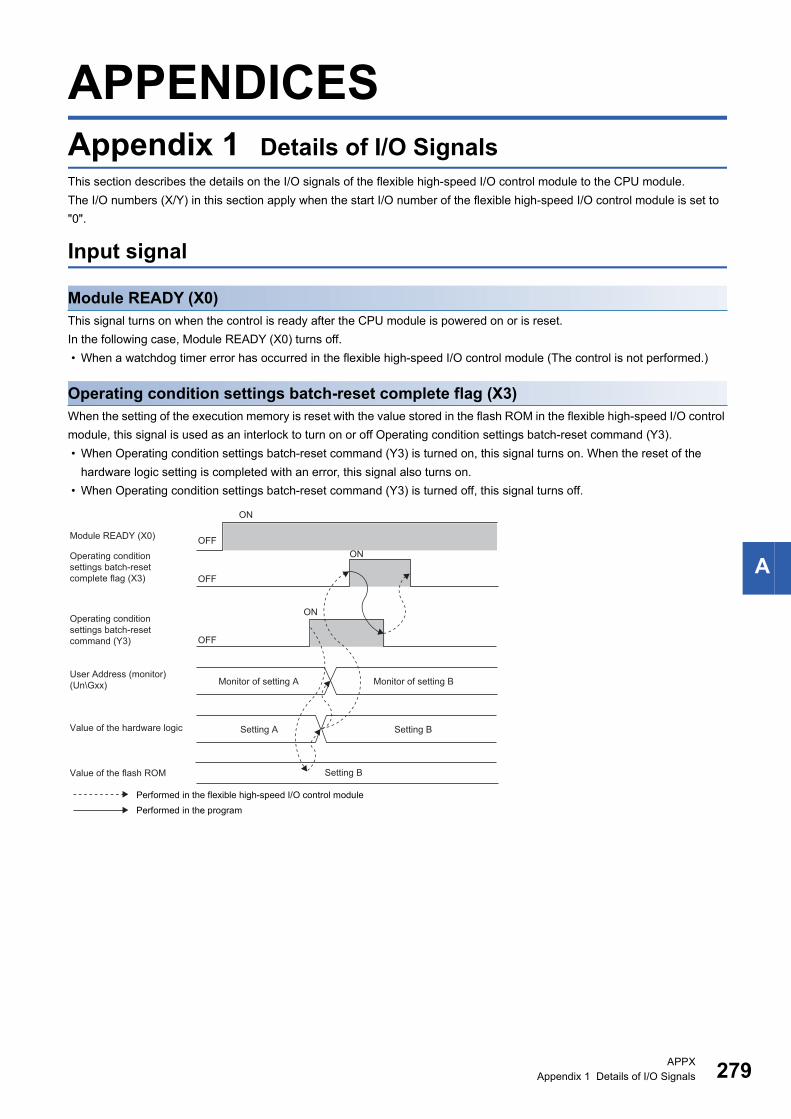
A
APPENDICESAppendix 1 Details of I/O SignalsThis section describes the details on the I/O signals of the flexible high-speed I/O control module to the CPU module.The I/O numbers (X/Y) in this section apply when the start I/O number of the flexible high-speed I/O control module is set to "0".
Input signal
Module READY (X0)This signal turns on when the control is ready after the CPU module is powered on or is reset.In the following case, Module READY (X0) turns off. • When a watchdog timer error has occurred in the flexible high-speed I/O control module (The control is not performed.)
Operating condition settings batch-reset complete flag (X3)When the setting of the execution memory is reset with the value stored in the flash ROM in the flexible high-speed I/O control module, this signal is used as an interlock to turn on or off Operating condition settings batch-reset command (Y3). • When Operating condition settings batch-reset command (Y3) is turned on, this signal turns on. When the reset of the
hardware logic setting is completed with an error, this signal also turns on. • When Operating condition settings batch-reset command (Y3) is turned off, this signal turns off.
Performed in the flexible high-speed I/O control modulePerformed in the program
OFF
ON
OFF
ON
OFF
ON
Module READY (X0)
Operating condition settings batch-reset complete flag (X3)
Operating condition settings batch-reset command (Y3)
User Address (monitor) (Un\Gxx)
Value of the hardware logic
Value of the flash ROM
Monitor of setting A Monitor of setting B
Setting A
Setting B
Setting B
APPXAppendix 1 Details of I/O Signals 279
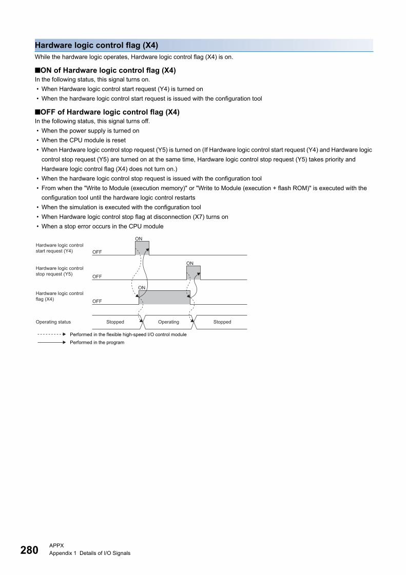
28
Hardware logic control flag (X4)While the hardware logic operates, Hardware logic control flag (X4) is on.
■ON of Hardware logic control flag (X4)In the following status, this signal turns on. • When Hardware logic control start request (Y4) is turned on • When the hardware logic control start request is issued with the configuration tool
■OFF of Hardware logic control flag (X4)In the following status, this signal turns off. • When the power supply is turned on • When the CPU module is reset • When Hardware logic control stop request (Y5) is turned on (If Hardware logic control start request (Y4) and Hardware logic
control stop request (Y5) are turned on at the same time, Hardware logic control stop request (Y5) takes priority and Hardware logic control flag (X4) does not turn on.)
• When the hardware logic control stop request is issued with the configuration tool • From when the "Write to Module (execution memory)" or "Write to Module (execution + flash ROM)" is executed with the
configuration tool until the hardware logic control restarts • When the simulation is executed with the configuration tool • When Hardware logic control stop flag at disconnection (X7) turns on • When a stop error occurs in the CPU module
Performed in the flexible high-speed I/O control modulePerformed in the program
OFF
ON
OFF
ON
OFF
ON
Hardware logic control start request (Y4)
Hardware logic control stop request (Y5)
Hardware logic control flag (X4)
Operating status Stopped Operating Stopped
0 APPXAppendix 1 Details of I/O Signals
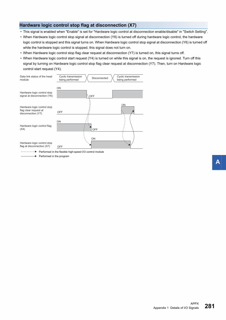
A
Hardware logic control stop flag at disconnection (X7) • This signal is enabled when "Enable" is set for "Hardware logic control at disconnection enable/disable" in "Switch Setting". • When Hardware logic control stop signal at disconnection (Y6) is turned off during hardware logic control, the hardware
logic control is stopped and this signal turns on. When Hardware logic control stop signal at disconnection (Y6) is turned off while the hardware logic control is stopped, this signal does not turn on.
• When Hardware logic control stop flag clear request at disconnection (Y7) is turned on, this signal turns off. • When Hardware logic control start request (Y4) is turned on while this signal is on, the request is ignored. Turn off this
signal by turning on Hardware logic control stop flag clear request at disconnection (Y7). Then, turn on Hardware logic control start request (Y4).
Performed in the flexible high-speed I/O control modulePerformed in the program
OFF
ON
OFF
ON
OFF
ON
ON
OFF
OFF
Hardware logic control stop signal at disconnection (Y6)
Data link status of the head module
Hardware logic control stop flag clear request at disconnection (Y7)
Hardware logic control flag (X4)
Hardware logic control stop flag at disconnection (X7)
Cyclic transmission being performed Disconnected Cyclic transmission
being performed
APPXAppendix 1 Details of I/O Signals 281

28
Error flag (XF)This signal turns on when an error occurs.
■OFF of Error flag (XF)When the error cause has been eliminated and Error clear request (YF) is turned on and off, the following flag and error code are cleared. • Error flag (XF) • Latest error code (Un\G100)When Clear setting of error history (Un\G8002) has been set to Clear the history. (1), Error history No. (Un\G8010 to Un\G8169) is also cleared.
IN 0 to IN B (X10 to X1B)Set input values to external input blocks ("IN 0" to "IN B").
Performed in the flexible high-speed I/O control modulePerformed in the program
OFF
OFF
OFF
OFF
ON
0 0
ON
Error
Error flag (XF)
Latest error code (Un\G100)
Error clear request (YF)
2 APPXAppendix 1 Details of I/O Signals
A
Output signal
Operating condition settings batch-reset command (Y3)This signal is used to reset the setting of the execution memory with the value stored in the flash ROM in the flexible high-speed I/O control module. When this signal is turned on, the values in the execution memory and Hardware logic area (Un\G1000 to Un\G1099) are reset to the values stored in the flash ROM.For the timing of turning on and off this signal, refer to the following.Page 279 Operating condition settings batch-reset complete flag (X3)
■Precautions • Turn on this signal while the hardware logic stops. When this signal is turned on in the operation of the hardware logic, the
reset error during hardware logic control (error code: 1020H) occurs. The setting of the hardware logic is not reset and the operation of the hardware logic continues.
• When no data has been written to the flash ROM and this signal is turned on, the reset error without any data writes to a flash ROM (error code: 1040H) occurs.
Hardware logic control start request (Y4)This signal is used to start the operation of the hardware logic. Because the operation of the hardware logic is stopped when the power supply is turned on, this signal needs to be turned on to start the operation.When the auto trigger of the logic analyzer function is enabled, a trigger start request is issued at the same time as when the hardware logic control is started.For the timing of turning on and off this signal, refer to the following.Page 280 Hardware logic control flag (X4)
Hardware logic control stop request (Y5)This signal is used to stop the operation of the hardware logic. When the operation of the hardware logic is stopped by turning on this signal, the count value is reset. To stop only the count operation without resetting the count value, set "OFF" for "Count Enable" of the counter timer block.When the hardware logic control is stopped while Trigger ready (1) is stored in Trigger status monitor (Un\G123), the logic analyzer function is stopped. In addition, Trigger stop (0) is stored in Trigger status monitor (Un\G123).For the timing of turning on and off this signal, refer to the following.Page 280 Hardware logic control flag (X4)
APPXAppendix 1 Details of I/O Signals 283
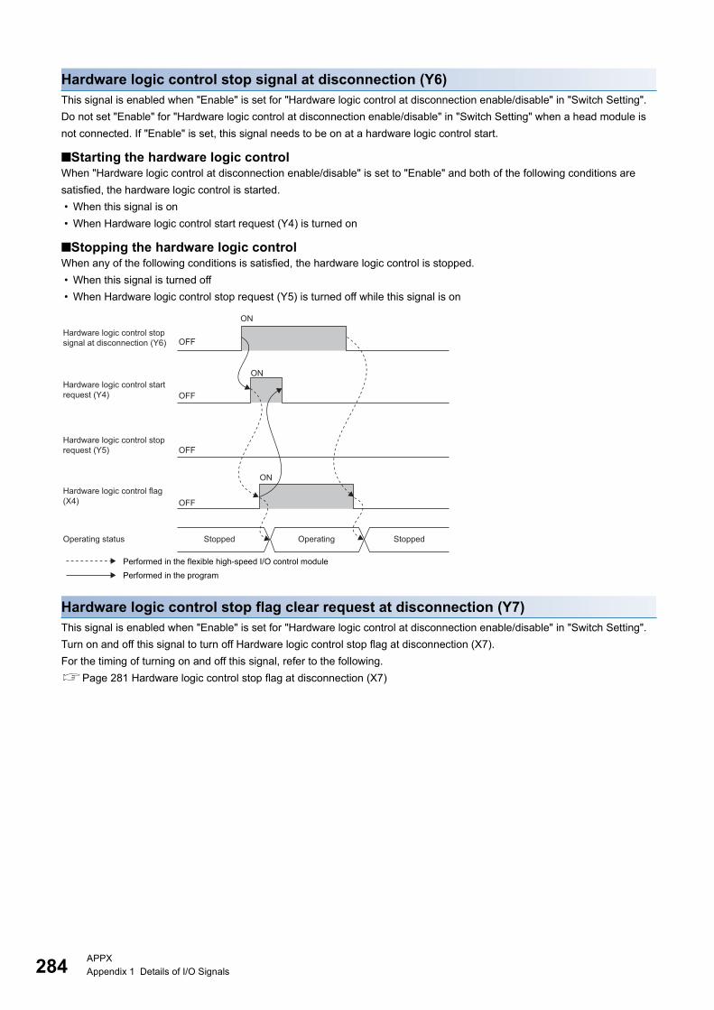
28
Hardware logic control stop signal at disconnection (Y6)This signal is enabled when "Enable" is set for "Hardware logic control at disconnection enable/disable" in "Switch Setting".Do not set "Enable" for "Hardware logic control at disconnection enable/disable" in "Switch Setting" when a head module is not connected. If "Enable" is set, this signal needs to be on at a hardware logic control start.
■Starting the hardware logic controlWhen "Hardware logic control at disconnection enable/disable" is set to "Enable" and both of the following conditions are satisfied, the hardware logic control is started. • When this signal is on • When Hardware logic control start request (Y4) is turned on
■Stopping the hardware logic controlWhen any of the following conditions is satisfied, the hardware logic control is stopped. • When this signal is turned off • When Hardware logic control stop request (Y5) is turned off while this signal is on
Hardware logic control stop flag clear request at disconnection (Y7)This signal is enabled when "Enable" is set for "Hardware logic control at disconnection enable/disable" in "Switch Setting".Turn on and off this signal to turn off Hardware logic control stop flag at disconnection (X7).For the timing of turning on and off this signal, refer to the following.Page 281 Hardware logic control stop flag at disconnection (X7)
Performed in the flexible high-speed I/O control modulePerformed in the program
OFF
ON
OFF
OFF
ON
OFF
ON
Hardware logic control stop signal at disconnection (Y6)
Hardware logic control start request (Y4)
Hardware logic control stop request (Y5)
Hardware logic control flag (X4)
Operating status Stopped Operating Stopped
4 APPXAppendix 1 Details of I/O Signals
A
Error clear request (YF)To clear Error flag (XF), Latest error code (Un\G100), and Error history No. (Un\G8010 to Un\G8169), turn on and off this signal.For the timing of turning on and off this signal, refer to the following.Page 282 Error flag (XF)
General command 0 to General command F (Y10 to Y1F)Signals in the hardware logic can be controlled from a program.Turning on or off General command 0 to General command F (Y10 to Y1F) outputs the internal signals of the hardware logic in High or Low state from Y device terminals.For details on the Y device terminals, refer to the following.Page 145 Y device terminal
APPXAppendix 1 Details of I/O Signals 285
28
Appendix 2 Details of Buffer Memory AreasThis chapter describes the details on the buffer memory areas of the flexible high-speed I/O control module.
Latest error code (Un\G100)This area stores the latest error code detected in the flexible high-speed I/O control module.For details on the error codes, refer to the following.Page 276 List of Error Codes
■How to clear an errorTurn on and off Error clear request (YF).
Cumulative number of write accesses to a flash ROM (Un\G102, Un\G103)This area stores the cumulative number of writes to a flash ROM. When a hardware logic is written to the flash ROM of the flexible high-speed I/O control module with the setting tool, the stored value is increased by one.When the number of writes exceeds the allowable number of writes to the flash ROM (10000 times), the written hardware logic data cannot be assured. To decrease the number of writes to the flash ROM, write hardware logics to the execution memory for adjustment. After the adjustment is completed, write the hardware logic to the flash ROM.
SSI receive data monitor 0 (Un\G110, Un\G111)Out of the data frames received from SSI encoder 0, the information for the number of bits specified with "Data Frame Length" is stored in this area at the communication cycle of the SSI encoder.The parity bit is not reflected to this area.When the data frame length is smaller than 32 bits, the least significant bit of the data frame is stored in the bit 0 of Un\G110.For details, refer to the following.Page 150 SSI encoder block
SSI receive data monitor 1 (Un\G114, Un\G115)Out of the data frames received from SSI encoder 1, the information for the number of bits specified with "Data Frame Length" is stored in this area at the communication cycle of the SSI encoder.The data to be stored in this area is the same as the one of SSI receive data monitor 0 (Un\G110, Un\G111).
6 APPXAppendix 2 Details of Buffer Memory Areas
A
Trigger start request (Un\G120)This area issues a trigger start request of the logic analyzer function.When Start request (1) is set in Trigger start request (Un\G120) during the hardware logic control after the trigger setting has been written to the flexible high-speed I/O control module, the trigger status of the flexible high-speed I/O control module is switched to the trigger ready. After the trigger status has been switched to the trigger ready, No request (0) is automatically stored in Trigger start request (Un\G120).
• When a value other than the above is set, the value is handled as No request (0). • When Start request (1) is set in Trigger start request (Un\G120) before the trigger setting is written to the flexible high-speed
I/O control module, a trigger start error at trigger setting disabled (error code: 10C0H) occurs and the trigger status is not switched to the trigger ready.
• When Start request (1) is set in Trigger start request (Un\G120) during simulation, a trigger start error during simulation execution (error code: 10C1H) occurs and the trigger status is not switched to the trigger ready.
• When Start request (1) is set in Trigger start request (Un\G120) while Trigger ready (1) is stored in Trigger status monitor (Un\G123), the trigger ready is continued.
Trigger stop request (Un\G121)This area clears the trigger ready of the logic analyzer function.When Stop request (1) is set in Trigger stop request (Un\G121) while Trigger ready (1) is stored in Trigger status monitor (Un\G123), the flexible high-speed I/O control module clears the trigger ready and the trigger status is switched to the trigger stop. After the status has been switched to the trigger stop, No request (0) is automatically stored in Trigger stop request (Un\G121).
• When a value other than the above is set, the value is processed as No request (0). • When Stop request (1) is set in Trigger stop request (Un\G121) while Trigger stop (0) is stored in Trigger status monitor
(Un\G123), the trigger stop is continued.
Setting value Setting details0 No request
1 Start request
Setting value Setting details0 No request
1 Stop request
APPXAppendix 2 Details of Buffer Memory Areas 287

28
Trigger setting status monitor (Un\G122)This area stores the trigger setting status of the logic analyzer function.
• Write the trigger setting to the flexible high-speed I/O control module with the configuration tool. ( Page 125 Logic analyzer function)
• If the trigger setting is written to the flash ROM, the trigger setting is read from the flash ROM at power-on of the module. As a result, Trigger setting enable (Auto trigger disable) (1) or Trigger setting enable (Auto trigger enable) (2) is stored in this area at power-on of the module.
Trigger status monitor (Un\G123)This area stores the trigger status of the logic analyzer function.
■Storing Trigger stop (0)This value indicates a status in which generating sampling data by the logic analyzer function is stopped because of any of the following conditions. • After the trigger condition is satisfied, acquisition of sampling data is completed. • Stop request (1) is stored in Trigger stop request (Un\G121). • A trigger stop request from the configuration tool is received. • The trigger is stopped due to simulation execution. • The hardware logic control is stopped by a hardware logic control stop request from the configuration tool or Hardware logic
control stop request (Y5). • "Write to Module (execution memory)" or "Write to Module (execution + flash ROM)" is executed with the configuration tool.
■Storing Trigger ready (1)This value indicates a status in which sampling data is being generated until the trigger condition is satisfied after a trigger start request is received because of any of the following conditions. • Start request (1) is stored in Trigger start request (Un\G120) during the hardware logic control. • A trigger start request from the configuration tool is received during the hardware logic control. • When the auto trigger is enabled, the hardware logic control is started by a hardware logic control start request from the
configuration tool or Hardware logic control start request (Y4).
Stored value Description0 Trigger setting disable
1 Trigger setting enable (Auto trigger disable)
2 Trigger setting enable (Auto trigger enable)
Stored value Description0 Trigger stop
1 Trigger ready
8 APPXAppendix 2 Details of Buffer Memory Areas
A
Sampling data acquired flag (Un\G124)This area stores the sampling data acquisition status of the logic analyzer function.
• When the trigger is detected while Trigger ready (1) is stored in Trigger status monitor (Un\G123), the flexible high-speed I/O control module generates sampling data. After the generation is completed, Sampling data is acquired (1) is stored in Sampling data acquired flag (Un\G124).
• While Sampling data is acquired (1) is stored in Sampling data acquired flag (Un\G124), sampling data can be read. • When the value in Trigger start request (Un\G120) is changed from No request (0) to Start request (1), Sampling data is not
acquired (0) is stored in Sampling data acquired flag (Un\G124). • When the simulation is executed, Sampling data is not acquired (0) is stored in Sampling data acquired flag (Un\G124). • When "Write to Module (execution memory)" or "Write to Module (execution + flash ROM)" is executed with the
configuration tool, Sampling data is not acquired (0) is stored in Sampling data acquired flag (Un\G124). • When Operating condition settings batch-reset command (Y3) is turned on, Sampling data is not acquired (0) is stored in
Sampling data acquired flag (Un\G124).
Cumulative number of trigger setting writes (Un\G128, Un\G129)This area stores the cumulative number of writes of the trigger setting to a flash ROM. When the trigger setting is written to the flash ROM of the flexible high-speed I/O control module with the configuration tool, the stored value is increased by one. In addition, when "Trigger Setting Delete" is clicked in the "Logic Analyzer" window of the configuration tool, the stored value is increased by one.When the number of writes exceeds the allowable number of writes to the flash ROM (10000 times), the written trigger setting data quality cannot be guaranteed. To decrease the number of writes to the flash ROM, write trigger settings to the execution memory for adjustment. After the adjustment is completed, write the trigger setting to the flash ROM.
Hardware logic area (Un\G1000 to Un\G1099)The monitor items and setting items of the hardware logic can be assigned to buffer memory addresses.There are two types of areas for the buffer memory areas: High speed area and low speed area. For each area, the addresses are assigned as follows.
These items are also read or written when an interrupt signal is sent to the CPU module.
Stored value Description0 Sampling data is not acquired
1 Sampling data is acquired
Area Buffer memory address DescriptionHigh speed area Un\G1000 to Un\G1029 • The items of the input terminals and parameters that are assigned to these areas
are written in a high-speed period (100s).• The items of the monitors assigned to these areas are read in a high-speed period
(100s).
Low speed area Un\G1030 to Un\G1099 • The items of the input terminals and parameters that are assigned to these areas are written in a low-speed period (1ms).
• The items of the monitors assigned to these areas are read in a low-speed period (1ms).
APPXAppendix 2 Details of Buffer Memory Areas 289

29
■Assignable monitor items and setting itemsThe following items can be assigned to these areas.
*1 The output values of each block in the hardware logic are "R" and the input values of each block in the hardware logic are "R/W".*2 Assign a parameter of two words (32 bits) to an even address.*3 The setting and storage ranges are determined depending on the type of a counter timer block.*4 The item cannot be assigned in a 16-bit counter timer block.
Latest address of error history (Un\G8000)This area stores the buffer memory address which has the latest error code among the addresses of Error history No. (Un\G8010 to Un\G8169).
Block Type Variable name R/W*1 Setting value/Stored value
Description
Counter timer block
Input terminal RUN /STOP R/W 0 Both the "RUN" and "STOP" terminals turn to Low.
1 The "RUN" terminal turns to High and the "STOP" terminal turns to Low.
2 The "RUN" terminal turns to Low and the "STOP" terminal turns to High.
3 Both the "RUN" and "STOP" terminals turn to High.
PRESET R/W 0 The "PRESET" terminal turns to Low.
1 The "PRESET" terminal turns to High.
Parameter Count Enable R/W 0 Count Enable is off.
1 Count Enable is on.
Upper Limit*2 R/W *3 Set the upper limit value.
Lower Limit*2 R/W *3 Set the lower limit value.
Add Value*2 R/W *3 Set the addition value.
Preset Value*2 R/W *3 Set the preset value.
Monitor Count Value*2 R *3 A count value is stored.
Latch Value*2 R *3 A latch value is stored.
Overflow*4 R 0 No overflow occurs.
1 An overflow has been occurred.
Underflow*4 R 0 No underflow occurs.
1 An underflow has been occurred.
Cam switch block Parameter Step No.0
Step No. 15*2
R/W *3 Step No. 0
Step No. 15
Comparison block
Parameter Compare Value R/W *3 Value compared with a count value of the counter timer
External output block
Parameter Enable Forced Output
R/W 0 The forced output is disabled.
1 The forced output is enabled.
Parameter Forced Output R/W 0 The forced output status of the external terminal is off (0: OFF).
1 The forced output status of the external terminal is on (1: ON).
Monitor External terminal monitor
R 0 The output status (0: OFF) of the external output terminal is stored.
1 The output status (1: ON) of the external output terminal is stored.
0 APPXAppendix 2 Details of Buffer Memory Areas

A
Clear setting of error history (Un\G8002)Set whether to clear an error history when Error clear request (YF) is turned on.
■Enabling the settingThe setting is enabled immediately after a value is set in the buffer memory area.
■Default valueThe default value is Do not clear the history. (0).
Error history No. (Un\G8010 to Un\G8169)This area stores up to 16 errors that have occurred in the module.For details on the error history function, refer to the following.Page 68 Error History Function
*1 Value for when an error occurred at 10:35:40 on Friday, April 24th, 2015
RUN LED status monitor (Un\G8170)This area stores the current status of the RUN LED.For details on the RUN LED, refer to the following.Page 21 PART NAMES
ERR LED status monitor (Un\G8171)This area stores the current status of the ERR. LED.For details on the ERR. LED, refer to the following.Page 21 PART NAMES
Clear setting of error history Setting valueDo not clear the history. 0
Clear the history. 1
Item Description Storage example*1
First two digits of the year/last two digits of the year
Stored as a BCD code. 2015H
Month/day 0424H
Hour/minute 1035H
Second 40H
Day of the week For each day of the week, one of the following values is stored as a BCD code.Sunday: 0H, Monday: 1H, Tuesday: 2H, Wednesday: 3H, Thursday: 4H, Friday: 5H, Saturday: 6H
5H
RUN LED status Stored value DescriptionOff 0 The RUN LED turns off.
On 1 The RUN LED turns on.
Flashing 2 The RUN LED is flashing.
ERR. LED status Stored value DescriptionOff 0 The ERR. LED turns off.
On 1 The ERR. LED turns on.
b15 b8 b7 b0to toError code
First two digits of the year Last two digits of the yearMonth DayHour Minute
Second Day of the week
System areato
Un\G8010
Un\G8014Un\G8013Un\G8012Un\G8011
Un\G8015
Un\G8019
APPXAppendix 2 Details of Buffer Memory Areas 291

29
Continuous logging cycle setting (Un\G15008)Set the logging cycle for the continuous logging function.
If a value other than the above is set, the continuous logging cycle setting range error (error code: 10D6H) occurs and the continuous logging does not start.
■Default valueThe default value is 10s (1).
Continuous logging start/stop request (Un\G15009)Set whether to start or stop continuous logging.
• Changing Continuous logging start/stop request (Un\G15009) from Stop request (0) to Start request (1) starts the continuous logging.
• Changing Continuous logging start/stop request (Un\G15009) from Start request (1) to Stop request (0) stops the continuous logging.
• If a value other than the above is set, the request is ignored and the operation of continuous logging does not change.
■Default valueThe default value is Stop request (0).
Continuous logging status monitor (Un\G15010)The execution status of the continuous logging function is stored.
Continuous logging cycle monitor (s) (Un\G15011)The logging cycle (unit: s) for the continuous logging function is stored.
Ex.
When 1000s (3) is set in Continuous logging cycle setting (Un\G15008), 1000 is stored in this area.
Setting value Setting details1 10s
2 100s
3 1000s
Setting value Setting details0 Stop request
1 Start request
Stored value Description0 Disabled
1 Start request waiting
2 In progress
2 APPXAppendix 2 Details of Buffer Memory Areas

A
Continuous logging data storage flag (Un\G15012, Un\G15013)Use these buffer memory areas to check that data of 5120 points is stored in continuous logging data storage areas during continuous logging.These areas consist of Continuous logging data A side storage flag (Un\G15012) for checking that data is stored in the first 5120 points area (A side) and Continuous logging data B side storage flag (Un\G15013) for checking that data is stored in the last 5120 points area (B side).
• Storage completed (1) is stored every time logging data for the first 5120 points (A side) or the last 5120 points (B side) has been stored.
• When logging data storage in the file register of the CPU module is completed, set Storage not completed (0) in either of the areas to accept the next storage flag.
• When Continuous logging start/stop request (Un\G15009) is changed from Stop request (0) to Start request (1), these areas are cleared to 0.
■Default valueThe default value is Storage not completed (0).
Continuous logging data points (Un\G15014, Un\G15015)The number of logging data points stored in continuous logging data storage areas can be checked during continuous logging. • After continuous logging is started, Continuous logging data points (Un\G15014, Un\G15015) increases by 64 every time
logging data of 64 points is stored. When the data count reaches 3600000000, Continuous logging data points (Un\G15014, Un\G15015) returns to 0 and then increases by 64 again.
• When Continuous logging start/stop request (Un\G15009) is changed from Stop request (0) to Start request (1), these areas are cleared to 0.
Continuous logging data storage area (Un\G15020 to Un\G25259)These areas store the data logged with the continuous logging function. Up to 10240 points of data can be stored.
Setting value Setting details0 Storage not completed
1 Storage completed
APPXAppendix 2 Details of Buffer Memory Areas 293
294 APPXAppendix 3 How to Get the Configuration Tool
Appendix 3 How to Get the Configuration ToolFor the configuration tool, please consult your local Mitsubishi representative.
A
Appendix 4 Logic Analyzer Function (Executed with a Program)
The logic analyzer function verifies the hardware logic control in the flexible high-speed I/O control module during the system operation. Users can check that the hardware logic written to the module operates properly by using the signals input to the external input terminals of the flexible high-speed I/O control module.The logic analyzer function can be used by setting a trigger condition and executing the trigger start with the configuration tool.The trigger start can be controlled with a program as well. Users can start acquiring sampling data (trigger start) or stop acquiring sampling data (trigger stop) at a desired timing by performing the control with a program.
Items that can be controlled with a programThe following table lists the items that can be controlled with a program.
Buffer memory areas to be usedThe following table lists the buffer memory areas to be used for the control of the logic analyzer function.
For details on the buffer memory areas, refer to the following.Page 286 Details of Buffer Memory Areas
Item DescriptionTrigger start Enables the trigger condition set with the configuration tool.
If the trigger condition is satisfied, sampling data is generated in the module.
Trigger stop Disables the trigger condition enabled by the trigger start.
Buffer memory address Name Data typeUn\G120 Trigger start request Control
Un\G121 Trigger stop request Control
Un\G122 Trigger setting status monitor Monitor
Un\G123 Trigger status monitor Monitor
Un\G124 Sampling data acquired flag Monitor
APPXAppendix 4 Logic Analyzer Function (Executed with a Program) 295

29
Setting methodSet the trigger condition in the "Logic Analyzer" window of the configuration tool in advance. For details, refer to the following.Page 125 Logic analyzer function
■Trigger start requestWhen Start request (1) is set in Trigger start request (Un\G120) while the hardware logic control is operating and Trigger stop (0) is stored in Trigger status monitor (Un\G123), a trigger start request is issued.After the trigger start request is issued, when Trigger ready (1) is stored in Trigger status monitor (Un\G123), sampling data generation starts.
When the auto trigger is enabled, a trigger start request is issued automatically at the same time as when the hardware logic control is started. Thus, issuing a trigger start request is not required.When the auto trigger is disabled or sampling data needs to be acquired again after acquisition of sampling data resulting from the trigger condition satisfied after the trigger start, issue a trigger start request.
■Trigger stop requestWhen Stop request (1) is set in Trigger stop request (Un\G121) while Trigger ready (1) is stored in Trigger status monitor (Un\G123), a trigger stop request is issued.After the trigger stop, sampling data is not generated in the module even if the trigger condition is satisfied before a trigger start request is issued.
OperationThe following shows the operations of the logic analyzer function.
■Trigger start requestWhen Start request (1) is set in Trigger start request (Un\G120) while the hardware logic control is operating and Trigger stop (0) is stored in Trigger status monitor (Un\G123), a trigger start request is issued.After the trigger start request is received, Trigger ready (1) is stored in Trigger status monitor (Un\G123) and Sampling data is not acquired (0) is stored in Sampling data acquired flag (Un\G124). In addition, sampling data generation starts in a module according to the sampling cycle set with the configuration tool.
(1) When a trigger start request is issued, the trigger status is switched to the trigger ready. ( Page 296 Trigger start request)(2) Sampling data generation starts at the same time as when the trigger status is switched to the trigger ready.(3) After the trigger condition is satisfied, acquisition of the sampling data is completed, and then the trigger status is switched to the trigger stop. ( Page
297 Sampling data acquisition completion)(4) Even if the trigger condition is satisfied during the trigger stop, sampling data is not generated.(5) When executing sampling repeatedly, issue a trigger start request again.(6) When a trigger stop request is issued in the trigger ready, acquisition of sampling data is stopped. ( Page 297 Trigger stop request)
ON
ON
ONOFF
OFF
0 1
0
1
0
1
0
0
1
0 0
1-
OFF
(5)
(1)
(4)(3)(2)
(6)
Trigger stop request (Un\G121)
Trigger start request (Un\G120)
Trigger status monitor (Un\G123)
Sampling data acquired flag (Un\G124)
Sampling data generation(internal processing of the module)
Trigger condition
6 APPXAppendix 4 Logic Analyzer Function (Executed with a Program)
A
• When Start request (1) is set in Trigger start request (Un\G120) before a trigger condition is set, a trigger start error at trigger setting disabled (error code: 10C0H) occurs.
• When the hardware logic control is stopped in the trigger ready, the trigger status is switched to the trigger stop.
• When Start request (1) is set in Trigger start request (Un\G120) during simulation, a trigger start error during simulation execution (error code: 10C1H) occurs. In addition, the trigger status is not switched to the trigger ready.
■Sampling data acquisition completionWhen the trigger condition is satisfied while Trigger ready (1) is stored in Trigger status monitor (Un\G123), sampling data is generated according to the trigger setting. In addition, Trigger stop (0) is stored in Trigger status monitor (Un\G123) and Sampling data is acquired (1) is stored in Sampling data acquired flag (Un\G124).Sampling data can be read only when Sampling data is acquired (1) is stored in Sampling data acquired flag (Un\G124).
Sampling data generated before the trigger start is discarded by a trigger start request or execution of the simulation function. When "Write to Module (execution memory)" or "Write to Module (execution + flash ROM)" is executed with the configuration tool or Operating condition settings batch-reset command (Y3) is turned on, Sampling data is not acquired (0) is stored in Sampling data acquired flag (Un\G124). If sampling data needs to be acquired repeatedly, read the sampling data, and then issue a trigger start request.
■Trigger stop requestWhen Stop request (1) is set in Trigger stop request (Un\G121) while Trigger ready (1) is stored in Trigger status monitor (Un\G123), a trigger stop request is issued.After the trigger stop request is received, Trigger stop (0) is stored in Trigger status monitor (Un\G123). In addition, the sampling data generation stops in a module.After the trigger stop, sampling data is not generated until a trigger start request is issued again even if the trigger condition is satisfied.
• When simulation is executed with the configuration tool while the logic analyzer function is operating (while Trigger ready (1) is stored in Trigger status monitor (Un\G123)), the logic analyzer function stops automatically. At a logic analyzer function stop, Trigger stop (0) is stored in Trigger status monitor (Un\G123). The logic analyzer function will not restart automatically after the simulation completion. To restart the logic analyzer function, issue a trigger start request again.
• When "Write to Module (execution memory)" or "Write to Module (execution + flash ROM)" is executed with the configuration tool while the logic analyzer function is operating (while Trigger ready (1) is stored in Trigger status monitor (Un\G123)), the hardware logic control is suspended, and thus the logic analyzer stops. When the auto trigger is enabled, the logic analyzer restarts after writing data into the module is completed.
APPXAppendix 4 Logic Analyzer Function (Executed with a Program) 297
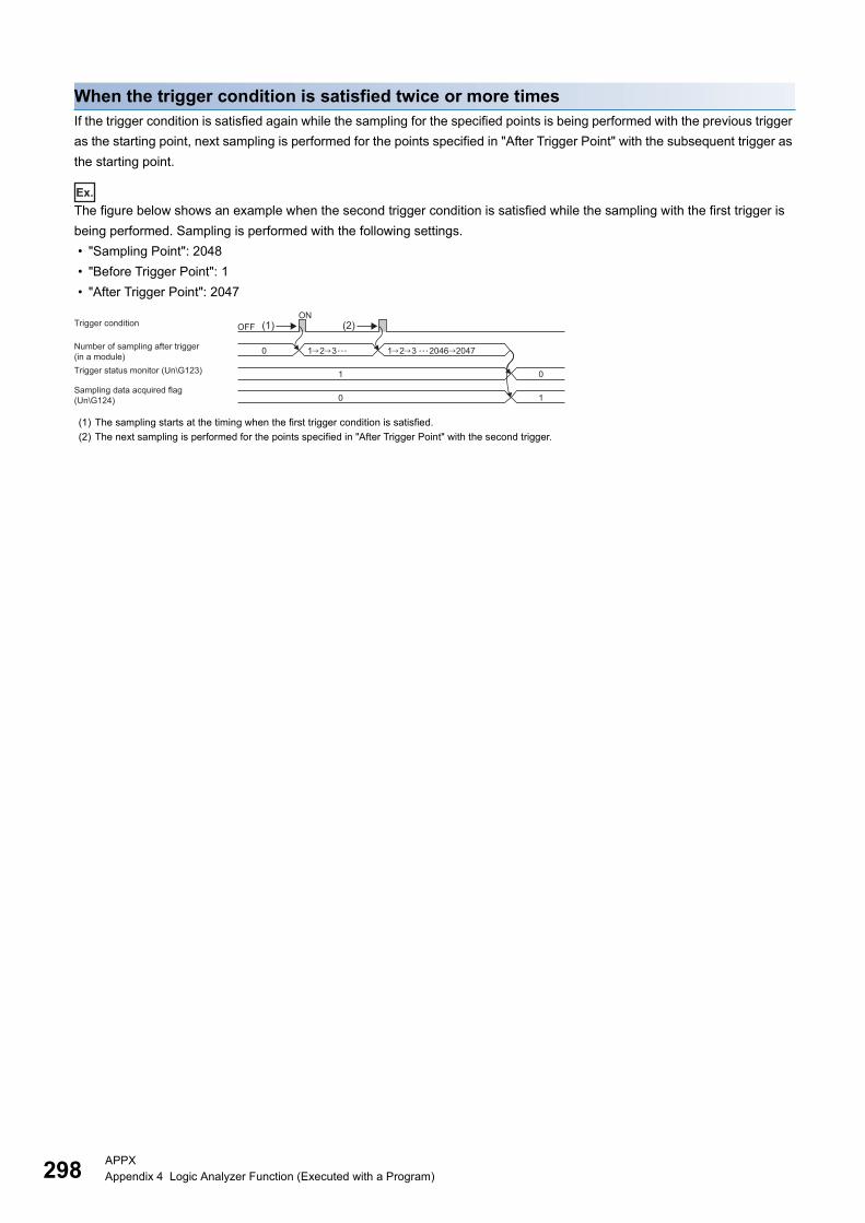
29
When the trigger condition is satisfied twice or more timesIf the trigger condition is satisfied again while the sampling for the specified points is being performed with the previous trigger as the starting point, next sampling is performed for the points specified in "After Trigger Point" with the subsequent trigger as the starting point.
Ex.
The figure below shows an example when the second trigger condition is satisfied while the sampling with the first trigger is being performed. Sampling is performed with the following settings. • "Sampling Point": 2048 • "Before Trigger Point": 1 • "After Trigger Point": 2047
(1) The sampling starts at the timing when the first trigger condition is satisfied.(2) The next sampling is performed for the points specified in "After Trigger Point" with the second trigger.
ON
1 2 3 0
OFF (1) (2)
1
0
0
1
2046 2047… 1 2 3 …
Trigger condition
Number of sampling after trigger (in a module)Trigger status monitor (Un\G123)
Sampling data acquired flag (Un\G124)
8 APPXAppendix 4 Logic Analyzer Function (Executed with a Program)
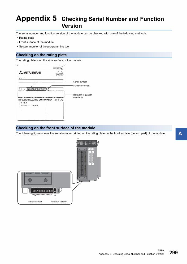
A
Appendix 5 Checking Serial Number and Function Version
The serial number and function version of the module can be checked with one of the following methods. • Rating plate • Front surface of the module • System monitor of the programming tool
Checking on the rating plateThe rating plate is on the side surface of the module.
Checking on the front surface of the moduleThe following figure shows the serial number printed on the rating plate on the front surface (bottom part) of the module.
170510000000000 -A
Serial number
Function version
Relevant regulation standards
170510000000000- A
Serial number Function version
APPXAppendix 5 Checking Serial Number and Function Version 299
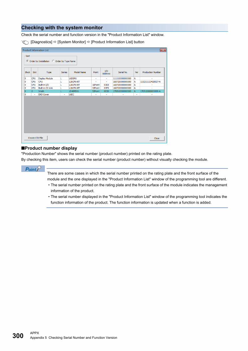
30
Checking with the system monitorCheck the serial number and function version in the "Product Information List" window.
[Diagnostics] [System Monitor] [Product Information List] button
■Product number display"Production Number" shows the serial number (product number) printed on the rating plate.By checking this item, users can check the serial number (product number) without visually checking the module.
There are some cases in which the serial number printed on the rating plate and the front surface of the module and the one displayed in the "Product Information List" window of the programming tool are different. • The serial number printed on the rating plate and the front surface of the module indicates the management
information of the product. • The serial number displayed in the "Product Information List" window of the programming tool indicates the
function information of the product. The function information is updated when a function is added.
0 APPXAppendix 5 Checking Serial Number and Function Version
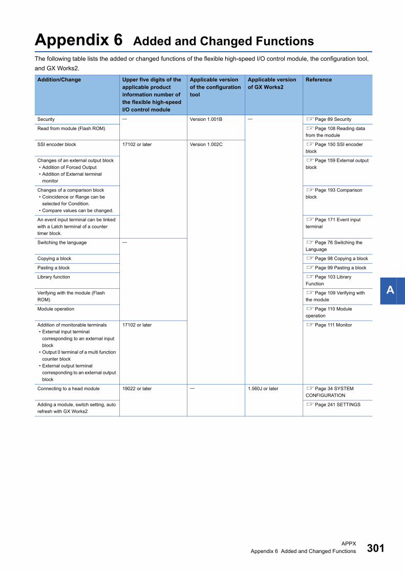
A
Appendix 6 Added and Changed FunctionsThe following table lists the added or changed functions of the flexible high-speed I/O control module, the configuration tool, and GX Works2.
Addition/Change Upper five digits of the applicable product information number of the flexible high-speed I/O control module
Applicable version of the configuration tool
Applicable version of GX Works2
Reference
Security Version 1.001B Page 89 Security
Read from module (Flash ROM) Page 108 Reading data from the module
SSI encoder block 17102 or later Version 1.002C Page 150 SSI encoder block
Changes of an external output block• Addition of Forced Output• Addition of External terminal
monitor
Page 159 External output block
Changes of a comparison block• Coincidence or Range can be
selected for Condition.• Compare values can be changed.
Page 193 Comparison block
An event input terminal can be linked with a Latch terminal of a counter timer block.
Page 171 Event input terminal
Switching the language Page 76 Switching the Language
Copying a block Page 98 Copying a block
Pasting a block Page 99 Pasting a block
Library function Page 103 Library Function
Verifying with the module (Flash ROM)
Page 109 Verifying with the module
Module operation Page 110 Module operation
Addition of monitorable terminals• External input terminal
corresponding to an external input block
• Output 0 terminal of a multi function counter block
• External output terminal corresponding to an external output block
17102 or later Page 111 Monitor
Connecting to a head module 19022 or later 1.560J or later Page 34 SYSTEM CONFIGURATION
Adding a module, switch setting, auto refresh with GX Works2
Page 241 SETTINGS
APPXAppendix 6 Added and Changed Functions 301

30
Printing Version 1.003D Page 85 Printing
Closing a project
Verifying a project Page 88 Verifying a project file
Undoing, redoing
Zooming in, zooming out
Start I/O number setting Page 106 Start I/O number setting
Configuration tool supports Windows8 and Windows10.
Comment 19102 or later Page 100 Adding a comment
Logic analyzer function Page 125 Logic analyzer function
Pattern generator function• Pattern generator block• Pattern generator output terminal
Page 132 Pattern Generator Function
Watch function Page 113 Watch Function
Continuous logging function 1.570U or later Page 59 Continuous Logging Function
Addition of monitor items to the "Continuous logging" window
Version 1.004E Page 131 Continuous logging
Change of block names and item names (from English to the language used)
Addition/Change Upper five digits of the applicable product information number of the flexible high-speed I/O control module
Applicable version of the configuration tool
Applicable version of GX Works2
Reference
2 APPXAppendix 6 Added and Changed Functions
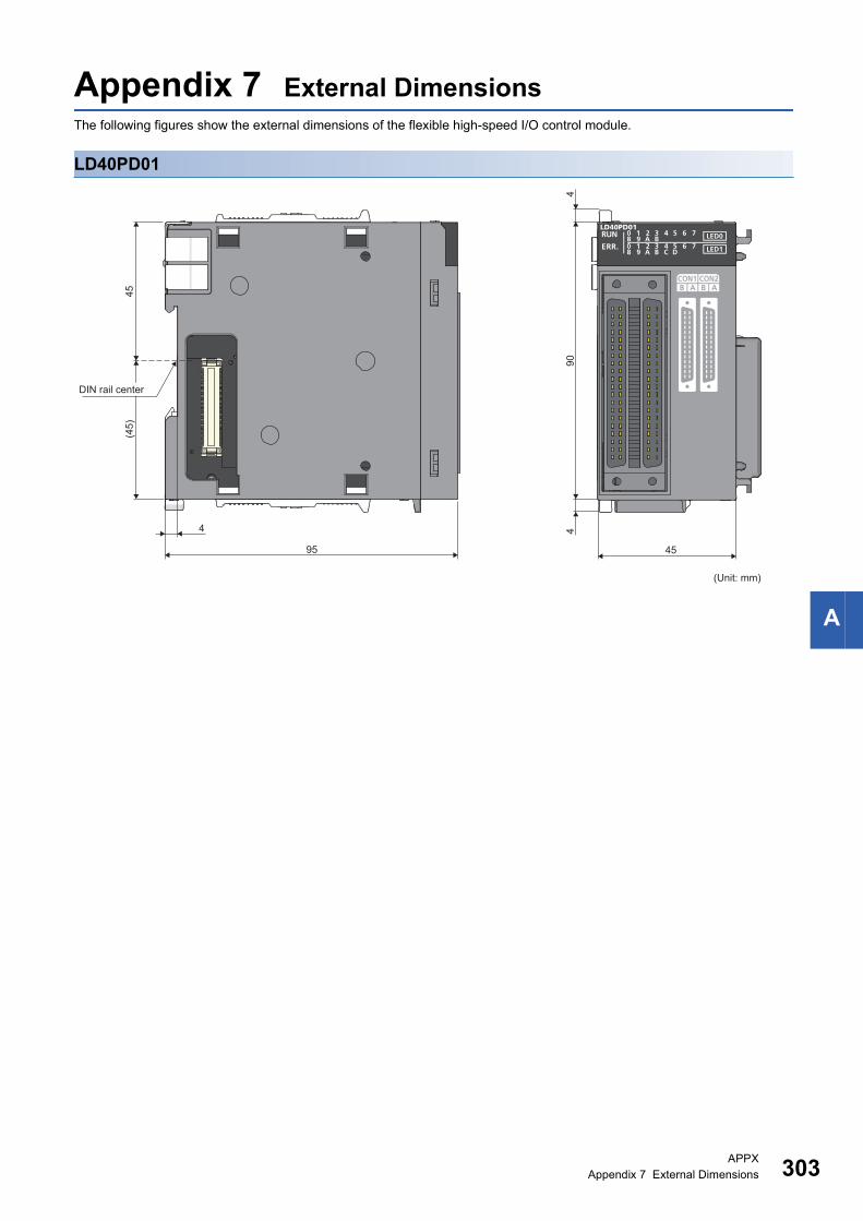
APPXAppendix 7 External Dimensions 303
A
Appendix 7 External DimensionsThe following figures show the external dimensions of the flexible high-speed I/O control module.
LD40PD01
4595
4 490
45(4
5)
4(Unit: mm)
DIN rail center

30
INDEX
AAdding the module . . . . . . . . . . . . . . . . . . . . . 241Auto refresh . . . . . . . . . . . . . . . . . . . . . . . . . . 243
CCam switch block . . . . . . . . . . . . . . . . . . . . . . 198Cam switch output terminal . . . . . . . . . . . . . . . 205Checking the version of the configuration tool . . 138Clear setting of error history (Un\G8002) . . . . . . 291Comparison block . . . . . . . . . . . . . . . . . . . . . . 193Configuration tool . . . . . . . . . . . . . . . . . . . . . . . 14Connector for external devices . . . . . . . . . . . . . . 21Continuous logging cycle monitor . . . . . . . . . . . 292Continuous logging cycle setting. . . . . . . . . . . . 292Continuous logging data A side storage flag. . . . 293Continuous logging data B side storage flag. . . . 293Continuous logging data points. . . . . . . . . . . . . 293Continuous logging data storage area . . . . . . . . 293Continuous logging function . . . . . . . . . . . . . . . . 59Continuous logging start/stop request . . . . . . . . 292Continuous logging status monitor . . . . . . . . . . 292Copying a block . . . . . . . . . . . . . . . . . . . . . . . . 98Counter timer block . . . . . . . . . . . . . . . . . . . . . 181Cumulative number of trigger setting writes . . . . 289Cumulative number of write accesses to a flash ROM (Un\G102, Un\G103). . . . . . . . . . . . . . . . 286
DDIN rail hook . . . . . . . . . . . . . . . . . . . . . . . . . . 21Display unit . . . . . . . . . . . . . . . . . . . . . . . . . . 244
EElement Selection window . . . . . . . . . . . . . . . . . 80ERR LED status monitor (Un\G8171) . . . . . . . . 291ERR. LED . . . . . . . . . . . . . . . . . . . . . . . . . . . . 21Error clear function . . . . . . . . . . . . . . . . . . . . . . 72Error clear request (YF) . . . . . . . . . . . . . . . . . . 285Error flag (XF). . . . . . . . . . . . . . . . . . . . . . . . . 282Error history function . . . . . . . . . . . . . . . . . . . . . 68Error history No.1-16 (Un\G8010 to Un\G8169). . . . . . . . . . . . . . . . . . . . . . . . . . . . . . . . . . . 291Event input terminal . . . . . . . . . . . . . . . . . . . . 171Event output terminal. . . . . . . . . . . . . . . . . . . . 204Execution memory . . . . . . . . . . . . . . . . . . . . . . 14Export . . . . . . . . . . . . . . . . . . . . . . . . . . . . . . 103External input block. . . . . . . . . . . . . . . . . . . . . 142External output block . . . . . . . . . . . . . . . . . . . . 159External wiring . . . . . . . . . . . . . . . . . . . . . . . . . 14
GGeneral command 0 to General command F (Y10 to Y1F). . . . . . . . . . . . . . . . . . . . . . . . . . 285
HHardware logic . . . . . . . . . . . . . . . . . . . . . . . . . 14Hardware logic area (Un\G1000 to Un\G1099) . . 289
Hardware logic control flag (X4) . . . . . . . . . . . . .280Hardware logic control function . . . . . . . . . . . . . .58Hardware logic control start request (Y4). . . . . . .283Hardware logic control stop flag at disconnection (X7). . . . . . . . . . . . . . . . . . . . . . . . . . . . . . . . .281Hardware logic control stop flag clear request at disconnection (Y7) . . . . . . . . . . . . . . . . . . . .284Hardware logic control stop request (Y5). . . . . . .283Hardware logic control stop signal at disconnection (Y6). . . . . . . . . . . . . . . . . . . . . . . . . . . . . . . . .284Hardware logic outline window . . . . . . . . . . . . . . .92
IIN 0 to IN B (X10 to X1B). . . . . . . . . . . . . . . . . .282Indicator LED . . . . . . . . . . . . . . . . . . . . . . . . . . .21Input signal event detection block. . . . . . . . . . . .172Input terminal . . . . . . . . . . . . . . . . . . . . . . . . . .170Intelligent function module interrupt . . . . . . . . . .206
LLatch event detection block . . . . . . . . . . . . . . . .179Latch input terminal . . . . . . . . . . . . . . . . . . . . .170Latest address of error history (Un\G8000) . . . . .290Latest error code (Un\G100) . . . . . . . . . . . . . . .286Library. . . . . . . . . . . . . . . . . . . . . . . . . . . . . . .105Link. . . . . . . . . . . . . . . . . . . . . . . . . . . . . . . . . .14List of error codes. . . . . . . . . . . . . . . . . . . . . . .276Logical operation block . . . . . . . . . . . . . . . . . . .158
MMap display window . . . . . . . . . . . . . . . . . . . . . .82Module error collection function . . . . . . . . . . . . . .71Module joint lever . . . . . . . . . . . . . . . . . . . . . . . .21Module operation . . . . . . . . . . . . . . . . . . . . . . .110Module READY (X0) . . . . . . . . . . . . . . . . . . . . .279Monitor . . . . . . . . . . . . . . . . . . . . . . . . . . . . . .111Multi function counter block . . . . . . . . . . . . . . . .163Multi function counter block detail window . . . . . . .93
NNavigation window . . . . . . . . . . . . . . . . . . . . . . .79
OOperating condition settings batch-reset command (Y3). . . . . . . . . . . . . . . . . . . . . . . . . . . . . . . . .283Operating condition settings batch-reset complete flag (X3) . . . . . . . . . . . . . . . . . . . . . . . . . . . . .279OUT terminal . . . . . . . . . . . . . . . . . . . . . . . . . .146Output terminal. . . . . . . . . . . . . . . . . . . . . . . . .203
PParallel encoder block . . . . . . . . . . . . . . . . . . . .147Pasting a block. . . . . . . . . . . . . . . . . . . . . . . . . .99Pattern generator block . . . . . . . . . . . . . . . . . . .196Pattern generator output terminal . . . . . . . . . . . .205
4

I
Programming . . . . . . . . . . . . . . . . . . . . . . . . . 247
RReading data from the module . . . . . . . . . . . . . 108RUN LED. . . . . . . . . . . . . . . . . . . . . . . . . . . . . 21RUN LED status monitor (Un\G8170) . . . . . . . . 291
SSampling data acquired flag . . . . . . . . . . . . . . . 289Security . . . . . . . . . . . . . . . . . . . . . . . . . . . . . . 89Serial number marking. . . . . . . . . . . . . . . . . . . . 21Set/reset block . . . . . . . . . . . . . . . . . . . . . . . . 202SI device terminal . . . . . . . . . . . . . . . . . . . . . . 162Simulation function . . . . . . . . . . . . . . . . . . . . . 117SSI encoder block. . . . . . . . . . . . . . . . . . . . . . 150SSI receive data monitor 0 (Un\G110, Un\G111). . . . . . . . . . . . . . . . . . . . . . . . . . . . . . . . . . . 286SSI receive data monitor 1 (Un\G114, Un\G115). . . . . . . . . . . . . . . . . . . . . . . . . . . . . . . . . . . 286Switch setting . . . . . . . . . . . . . . . . . . . . . . . . . 242
TTrigger setting status monitor . . . . . . . . . . . . . . 288Trigger start request . . . . . . . . . . . . . . . . . . . . 287Trigger status monitor . . . . . . . . . . . . . . . . . . . 288Trigger stop request . . . . . . . . . . . . . . . . . . . . 287
VVerifying with the module . . . . . . . . . . . . . . . . . 109
WWatch function . . . . . . . . . . . . . . . . . . . . . . . . 113Work window . . . . . . . . . . . . . . . . . . . . . . . . . . 81Writing data to the module . . . . . . . . . . . . . . . . 107
YY device terminal . . . . . . . . . . . . . . . . . . . . . . 145
305
306
REVISIONS*The manual number is given on the bottom left of the back cover.
Japanese manual number: SH-081531-G
2015 MITSUBISHI ELECTRIC CORPORATION
Revision date *Manual number DescriptionOctober 2015 SH(NA)-081532ENG-A First edition
March 2017 SH(NA)-081532ENG-B ■Added or modified partsSAFETY PRECAUTIONS, INTRODUCTION, COMPLIANCE WITH EMC AND LOW VOLTAGE DIRECTIVES, RELEVANT MANUALS, MANUAL PAGE ORGANIZATION, TERMS, Chapter 2, Section 3.1 to 3.4, 5.1, 5.2, 6.1, 6.2, 6.5, 8.2, 8.9, 8.10, 9.1 to 9.3, Chapter 11, Section 13.1 to 13.3, 14.4, 14.5, 14.7, Appendix 1, 2, 5
January 2018 SH(NA)-081532ENG-C ■Added or modified partsSection 3.2, 3.3, 3.5, 5.3, 7.2, 8.2 to 8.13, 9.1 to 9.3, 10.1 to 10.9, 11.2, Chapter 13, Section 14.2,14.3, 15.6, 15.7, Appendix 1, 2, 4, 6
July 2018 SH(NA)-081532ENG-D ■Added or modified partsSection 3.2,3.3, 6.2, 6.4, 7.2, 8.4 to 8.13, 9.1, 9.2, 10.1 to 10.9, 13.2, 13.3, 14.6, Appendix 2, 6
January 2021 SH(NA)-081532ENG-E ■Added or modified partsSection 7.2, 8.3
This manual confers no industrial property rights or any rights of any other kind, nor does it confer any patent licenses. Mitsubishi Electric Corporation cannot be held responsible for any problems involving industrial property rights which may occur as a result of using the contents noted in this manual.
307
WARRANTYPlease confirm the following product warranty details before using this product.
1. Gratis Warranty Term and Gratis Warranty RangeIf any faults or defects (hereinafter "Failure") found to be the responsibility of Mitsubishi occurs during use of the product within the gratis warranty term, the product shall be repaired at no cost via the sales representative or Mitsubishi Service Company.However, if repairs are required onsite at domestic or overseas location, expenses to send an engineer will be solely at the customer's discretion. Mitsubishi shall not be held responsible for any re-commissioning, maintenance, or testing on-site that involves replacement of the failed module.[Gratis Warranty Term]The gratis warranty term of the product shall be for one year after the date of purchase or delivery to a designated place.Note that after manufacture and shipment from Mitsubishi, the maximum distribution period shall be six (6) months, and the longest gratis warranty term after manufacturing shall be eighteen (18) months. The gratis warranty term of repair parts shall not exceed the gratis warranty term before repairs.[Gratis Warranty Range](1) The range shall be limited to normal use within the usage state, usage methods and usage environment, etc., which
follow the conditions and precautions, etc., given in the instruction manual, user's manual and caution labels on the product.
(2) Even within the gratis warranty term, repairs shall be charged for in the following cases.1. Failure occurring from inappropriate storage or handling, carelessness or negligence by the user. Failure caused
by the user's hardware or software design.2. Failure caused by unapproved modifications, etc., to the product by the user.3. When the Mitsubishi product is assembled into a user's device, Failure that could have been avoided if functions
or structures, judged as necessary in the legal safety measures the user's device is subject to or as necessary by industry standards, had been provided.
4. Failure that could have been avoided if consumable parts (battery, backlight, fuse, etc.) designated in the instruction manual had been correctly serviced or replaced.
5. Failure caused by external irresistible forces such as fires or abnormal voltages, and Failure caused by force majeure such as earthquakes, lightning, wind and water damage.
6. Failure caused by reasons unpredictable by scientific technology standards at time of shipment from Mitsubishi.7. Any other failure found not to be the responsibility of Mitsubishi or that admitted not to be so by the user.
2. Onerous repair term after discontinuation of production(1) Mitsubishi shall accept onerous product repairs for seven (7) years after production of the product is discontinued.
Discontinuation of production shall be notified with Mitsubishi Technical Bulletins, etc.(2) Product supply (including repair parts) is not available after production is discontinued.
3. Overseas serviceOverseas, repairs shall be accepted by Mitsubishi's local overseas FA Center. Note that the repair conditions at each FA Center may differ.
4. Exclusion of loss in opportunity and secondary loss from warranty liabilityRegardless of the gratis warranty term, Mitsubishi shall not be liable for compensation to:(1) Damages caused by any cause found not to be the responsibility of Mitsubishi.(2) Loss in opportunity, lost profits incurred to the user by Failures of Mitsubishi products.(3) Special damages and secondary damages whether foreseeable or not, compensation for accidents, and
compensation for damages to products other than Mitsubishi products.(4) Replacement by the user, maintenance of on-site equipment, start-up test run and other tasks.
5. Changes in product specificationsThe specifications given in the catalogs, manuals or technical documents are subject to change without prior notice.

308
TRADEMARKSMicrosoft and Windows are either registered trademarks or trademarks of Microsoft Corporation in the United States and/or other countries.The company names, system names and product names mentioned in this manual are either registered trademarks or trademarks of their respective companies.In some cases, trademark symbols such as '' or '' are not specified in this manual.
SH(NA)-081532ENG-E


SH(NA)-081532ENG-E(2101)MEEMODEL: LD40PD01-U-EMODEL CODE: 13JX37
Specifications subject to change without notice.
When exported from Japan, this manual does not require application to theMinistry of Economy, Trade and Industry for service transaction permission.
HEAD OFFICE : TOKYO BUILDING, 2-7-3 MARUNOUCHI, CHIYODA-KU, TOKYO 100-8310, JAPANNAGOYA WORKS : 1-14 , YADA-MINAMI 5-CHOME , HIGASHI-KU, NAGOYA , JAPAN