Environmental Toxicity of Nanomaterials - Taylor & Francis eBooks
Nanoscale
FEATURE ARTICLE
Publ
ishe
d on
11
Apr
il 20
14. D
ownl
oade
d by
Uni
vers
ity o
f W
isco
nsin
- M
adis
on o
n 10
/06/
2014
17:
07:0
8.
View Article OnlineView Journal | View Issue
Department of Materials Science and Engin
Madison, WI 53706, USA. E-mail: xudong@
Cite this: Nanoscale, 2014, 6, 6398
Received 21st February 2014Accepted 9th April 2014
DOI: 10.1039/c4nr00973h
www.rsc.org/nanoscale
6398 | Nanoscale, 2014, 6, 6398–6414
Mechanisms in the solution growth of free-standing two-dimensional inorganic nanomaterials
Fei Wang and Xudong Wang*
Free-standing two-dimensional (2D) nanomaterials have attracted extensive and growing research interest
owing to their exotic physical and mechanical properties, which have enabled their applications in
electronics, optoelectronics, electrochemical and biomedical devices. Current synthesis strategies rely
largely on top-down approaches such as etching and exfoliation. Among bottom-up approaches in
literature, there lacks a systematic understanding of the mechanisms of 2D crystal growth, unlike one-
dimensional nanomaterials whose growth mechanisms have been well documented. To date, the growth
design of free-standing 2D nanomaterials has remained a case-by-case practice. This review focuses on
the bottom-up solution synthesis of free-standing 2D nanomaterials and summarizes the general
mechanisms and empirical methodologies that can lead to 2D crystal growth. A brief outlook on the
development of synthesis and application of solution-grown 2D nanomaterials is also presented.
1. Introduction
Free-standing two-dimensional (2D) nanomaterials have drawnextensive and growing interest in the research frontier ofnanoscience and nanotechnology.1,2 Their dimensionality candrastically alter their physical, chemical, and optical propertiesas compared to their bulk or other dimensional counterpart,which provides them with great potential in electronics, opto-electronics, electrochemical, and biomedical applications. Themost representative examples are graphene and single-layerMoS2, which have disparate electronic structures compared totheir bulk counterpart, and have been demonstrated as candi-dates for advanced functional devices such as thin-lm tran-sistors, photodetectors, light-emitting diodes, and hydrogenreduction electrodes.3–5 In addition, 2D nanomaterials offergreat mechanical exibility (best exemplied by semiconductornanomembranes6–8) and are very fabrication friendly, which isessential to the realization of transparent and exible elec-tronics9–12 and conformal biomedical devices.13,14
Despite their great scientic value and application potential,the success of 2D nanomaterials has been limited to only a fewmaterials to date. The major challenge in exploring the prop-erties and applications of the 2D nanostructure of a wider rangeof materials lies in the difficulty of their synthesis. Currently, amajority of 2D nanomaterials are prepared by either selectiveetching of sacricial layers15 or exfoliation of crystals with anintrinsic layered structure.16,17 For materials without a layeredcrystal structure, strategies for the bottom-up growth of 2Dnanostructures need to be developed to meet the demand for a
eering, University of Wisconsin–Madison,
engr.wisc.edu
diverse portfolio of 2D nanomaterials. The growth of one-dimensional nanomaterials, namely, nanowires and nano-tubes, can usually be well explained and rationally designed byestablished mechanisms such as catalyzed vapor–liquid–solid(VLS),18 vapor–solid–solid (VSS),19 and solution–liquid–solid(SLS) growth,20,21 growth kinetics anisotropy, and screw dislo-cation-driven growth.22,23 In contrast, there has yet to be amechanism that explains a wide range of 2D crystal growth. Todate, the growth design of 2D nanomaterials has remained acase-by-case practice, although a good number of syntheses of2D nanomaterials have been reported.24 An understanding ofthe driving force and fundamental principles that govern 2Dcrystal growth needs to be acquired to optimize the existingsyntheses and extend them to untapped materials.
In this review, we focus on solution-based syntheses of 2Dnanomaterials with their thickness ranging from a few hundrednanometers to a few atomic layers or a single atomic layer.Depending on the size, thickness, and exibility, these 2Dnanomaterials are referred to as nanomembranes, nanoplates,or nanosheets in literature. These terms are interchangeable,and we will use the names originally given by the authors of thecited literature. It would be a daunting task to include all thereports in this area. Our objective is to rather discuss the typicalexamples in detail and present the possible general growthmechanisms that could lead to 2D crystal growth by sortingthese reports according to the growth mechanisms, which areeither explicitly elucidated by their authors or reckoned by us.For those cases when the growth mechanisms are not clear dueto limited experimental investigation, we link them by thesimilarities in their synthesis methods and crystal structures. Insome examples, we also highlight the main differences betweenthe syntheses of 2D nanomaterials and the growth of 1D
This journal is © The Royal Society of Chemistry 2014
Feature Article Nanoscale
Publ
ishe
d on
11
Apr
il 20
14. D
ownl
oade
d by
Uni
vers
ity o
f W
isco
nsin
- M
adis
on o
n 10
/06/
2014
17:
07:0
8.
View Article Online
morphology from the same or similar materials. We only lookinto bottom-up approaches in order to discuss what could drive2D crystal growth; therefore, well-documented exfoliationmethods for layered-structure crystals such as graphene, boronnitride, and transition-metal dichalcogenides are not covered.We will also feature a surfactant monolayer-guided approachdeveloped by our group for producing large-area, free-standingnanomembranes. Although we sort all the syntheses in fourcategories (Section 2 to 5), most of them do not exclusivelybelong to a single category. These four categories are rather fourdifferent aspects of one framework. In the end, a brief review ofthe applications of 2D nanomaterials and an outlook on thedevelopment of novel synthesis strategies of 2D nanomaterialsare given.
2. 2D oriented attachment
Oriented attachment is a non-classical crystal growth mecha-nism and oen produces nanocrystals with well-dened shapesand stringent size control. There have been a number of good
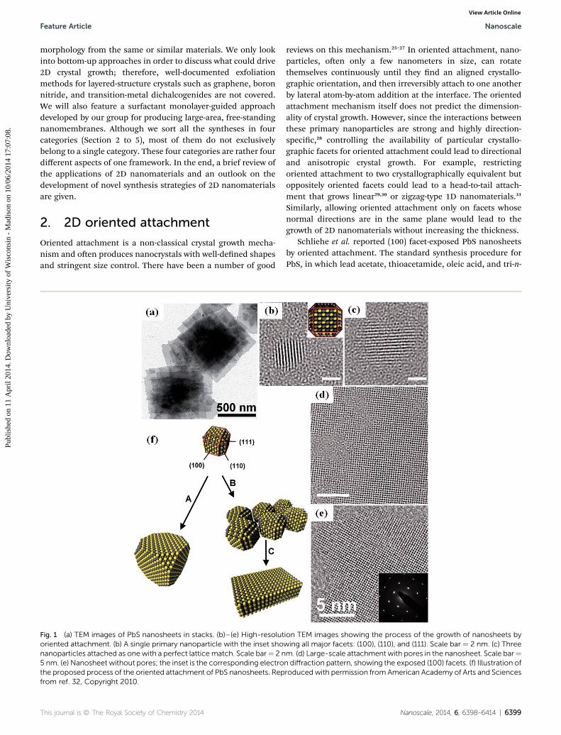
Fig. 1 (a) TEM images of PbS nanosheets in stacks. (b)–(e) High-resolutoriented attachment. (b) A single primary nanoparticle with the inset shonanoparticles attached as one with a perfect latticematch. Scale bar¼ 2 n5 nm. (e) Nanosheet without pores; the inset is the corresponding electrothe proposed process of the oriented attachment of PbS nanosheets. Repfrom ref. 32, Copyright 2010.
This journal is © The Royal Society of Chemistry 2014
reviews on this mechanism.25–27 In oriented attachment, nano-particles, oen only a few nanometers in size, can rotatethemselves continuously until they nd an aligned crystallo-graphic orientation, and then irreversibly attach to one anotherby lateral atom-by-atom addition at the interface. The orientedattachment mechanism itself does not predict the dimension-ality of crystal growth. However, since the interactions betweenthese primary nanoparticles are strong and highly direction-specic,28 controlling the availability of particular crystallo-graphic facets for oriented attachment could lead to directionaland anisotropic crystal growth. For example, restrictingoriented attachment to two crystallographically equivalent butoppositely oriented facets could lead to a head-to-tail attach-ment that grows linear29,30 or zigzag-type 1D nanomaterials.31
Similarly, allowing oriented attachment only on facets whosenormal directions are in the same plane would lead to thegrowth of 2D nanomaterials without increasing the thickness.
Schliehe et al. reported (100) facet-exposed PbS nanosheetsby oriented attachment. The standard synthesis procedure forPbS, in which lead acetate, thioacetamide, oleic acid, and tri-n-
ion TEM images showing the process of the growth of nanosheets bywing all major facets: (100), (110), and (111). Scale bar ¼ 2 nm. (c) Threem. (d) Large-scale attachment with pores in the nanosheet. Scale bar¼n diffraction pattern, showing the exposed (100) facets. (f) Illustration ofroduced with permission from American Academy of Arts and Sciences
Nanoscale, 2014, 6, 6398–6414 | 6399

Fig. 2 TEM images of (a) CeO2 nanosheets. (b) Aggregates of SnO2
nanosheets. The upper inset is a photo of the SnO2 nanosheetsuspension, and the lower inset is the electron diffraction pattern. (c)SnO2 nanosheets obtained after a reaction time of 4 hours withpolycrystalline nature. (d) SnO2 nanosheets obtained at 6 hours with asingle-crystalline nature. (a) Reproduced from ref. 34 with permissionfromWiley, Copyright 2010. (b)–(d) Reproduced with permission fromAmerican Chemical Society from ref. 36, Copyright 2012.
Nanoscale Feature Article
Publ
ishe
d on
11
Apr
il 20
14. D
ownl
oade
d by
Uni
vers
ity o
f W
isco
nsin
- M
adis
on o
n 10
/06/
2014
17:
07:0
8.
View Article Online
octylphosphine are added to diphenylether, typically producesnearly spherical PbS nanoparticles.32 The major difference inthe synthesis of PbS nanosheets by Schliehe et al. was the use ofchlorine-containing compounds such as 1,2-dichloroethane(DCE) as a co-solvent. Fig. 1a shows a TEM image of stacked PbSnanosheets about 500 nm in size. The oriented attachmentmechanism during the growth of PbS nanosheets was demon-strated by monitoring the evolution of crystals by an HRTEMstudy. As shown in Fig. 1b, the crystal growth started with theappearance of �2.8 nm PbS nanoparticles. Fig. 1c shows anaggregate of three nanocrystals bonded together in a way thattheir crystallographic orientations were perfectly matched. Thenanoparticles could assemble on a much larger scale with poreswithin the sheets (Fig. 1d), and these pores were then lled byrecrystallization. The corresponding electron diffraction patternshowed that the exposed facet was (100) (Fig. 1e). Absorptionand emission spectra also supported the appearance anddisappearance of PbS nanoparticles from 50 to 70 seconds intothe reaction. The authors elaborated the process of the orientedattachment of PbS nanoparticles and pointed out that theoriented attachment occurred exclusively between the (110)facets. The process is illustrated in Fig. 1f. The initial PbSnanoparticles have a truncated cuboctahedron shape (the topparticle in Fig. 1f) with 6 (100), 8 (111), and 12 (110) facets. Dueto the fast growth of the (110) facets, the nanoparticles wouldnormally grow bigger into a truncated octahedron without the(110) facets being exposed (growth route A). The addition ofchlorine compounds altered the kinetics of nucleation andgrowth, yielding �3 nm nanoparticles with exposed (110) facetsavailable for oriented attachment (growth route B). Orientedattachment through the (110) facets gave an egg-tray structureof particles, and at nanosheets formed thereaer via surfacereconstructions (growth route C). The other requirement of this2D growth is to thwart the particle attachment along the normaldirection of the nanosheet's surface. This was attributed to thedense and ordered bonding of oleic acid on the surface ofnanosheets.
Oriented attachment can also occur subsequent to a mis-oriented attachment driven by the relaxation of stress at theincoherently attached interfaces.33 Yu et al. synthesized singlecrystal CeO2 nanosheets in 95 �C aqueous solution by orientedattachment.34 Fig. 2a shows a TEM image of the nanosheets,which are a few hundred nanometers in size and 2 nm in thick-ness. CeO2 nanoparticles (2 to 2.5 nm) were found 15minutes intothe reaction, and aer 75 minutes, a-few-hundred-nanometer-wide, a-few-nanometer-thick nanosheets were obtained. It wasfound that polycrystalline nanosheets were also present aer 15minutes of reaction. These mis-aligned nanoparticles trans-formed into single crystal nanosheets as the reaction proceeded.The key to successful nanosheet growth was the use of a syringepump to add Ce(NO3)3 evenly and slowly into the reactor over 75minutes of reaction time. Control experiments, in which Ce(NO3)3was added all at once, resulted in only nanoparticles over 5 nm insize. The authors concluded that the formation of small-sized (2 to2.5 nm) CeO2 nanoparticles was a prerequisite for the orientedattachment. This agrees with Shen et al.'s observation that theprimary Cu2S nanoparticles larger than 5 nm could not grow into
6400 | Nanoscale, 2014, 6, 6398–6414
nanorods or nanodiscs via oriented attachment, unlike smallernanoparticles.35 However, the reason for the slow injection ofprecursor producing small-sized CeO2 nanoparticles was notdiscussed. It would also be interesting to see how the ow rate ofthe precursor in the syringe pump would affect the size of theprimary nanoparticle and the process of their orientedattachment.
Wang et al. synthesized rutile SnO2 nanosheets in a sol-vothermal method and identied oriented attachment as theformation mechanism. This is another example that mis-aligned nanoparticles can rotate themselves and become singlecrystals. In their synthesis, SnCl2$2H2O was used as a Snprecursor and ammonia or urea was also added into anethanol–water mixed solvent.36 The solvothermal process wasconducted at 120 �C for 48 hours. The SnO2 nanosheets were100 nm in lateral dimension and �5 nm in thickness, as shownin Fig. 2b. The formation of SnO2 started with the formation ofpoorly crystallized Sn6O4(OH)4 prior to the hydrothermal treat-ment. TEM characterization of reaction products at differentreaction times revealed that the decomposition of Sn6O4(OH)4during the hydrothermal process yielded clusters of randomlyoriented SnO2 nanoparticles, which rotated and fused into SnO2
nanosheets. Fig. 2c shows a TEM image of the 4 hour productswithmultiple grains present in the nanosheet. Aer 6 hours, thereaction completely converted the nanosheets into a singlecrystal (Fig. 2d). Prior to this work, Li et al. used a similarmethod and obtained slightly larger (100–200 nm) rutile SnO2
nanosheets and similar thickness (2–3 nm) with much better
This journal is © The Royal Society of Chemistry 2014

Feature Article Nanoscale
Publ
ishe
d on
11
Apr
il 20
14. D
ownl
oade
d by
Uni
vers
ity o
f W
isco
nsin
- M
adis
on o
n 10
/06/
2014
17:
07:0
8.
View Article Online
crystallinity.37 The difference in their synthesis was the use ofNaOH in place of ammonia or urea and a higher temperature(180 �C). The formation mechanism was not discussed, but theydid point out that the exposed (110) facet had a lower surfaceenergy than any other major facets. Given the signicant simi-larity between the two syntheses, the propensity for orientedattachment in SnO2 systems38 and the ubiquity of orientedattachment in hydrothermal synthesis, it is reasonable tobelieve that the SnO2 nanosheets synthesized by Li et al. wereformed by oriented attachment. We hypothesize that theoriented attachment between the non-(110) facets in rutile SnO2
outrivaled the oriented attachment between the (110) facets;therefore, (110) facet-exposed nanosheets were obtained.
3. 2D growth driven by screwdislocations
Screw dislocation-driven growth is a fundamental crystalgrowth mechanism that exists in a vast variety of materials andin different supersaturation regimes. It is particularly prom-inent at low supersaturation when layer-by-layer growth anddendrite growth are suppressed. In screw dislocation-driven
Fig. 3 (a) SEM image of hexagonal ZHS nanoplates. The inset is a highenanoplates with surface hillocks. The inset is a higher magnification imagthe hillock. (d) TEM image of a ZHS nanoplate with contrast contours usucontrast contours and an open core that is associated with screw dislocduring screw dislocation-driven growth. The degree of supersaturatmorphologies. (g)–(i) SEM images of a-Co(OH)2, Ni(OH)2, and Au nanoplnanoplates synthesized by Srinivasan et al. (j) and by Forticaux et al. (k) bsented in (f). (a)–(i) and (k), Reproduced with permission from Americarespectively. (j) Reproduced with permission from Royal Society of Chem
This journal is © The Royal Society of Chemistry 2014
growth, the axial screw dislocations provide self-perpetuatingsteps, which propagate in a spiral trajectory around the Burgersvector of the screw dislocation. It has been demonstrated as oneof the predominant mechanisms that explain the 1D crystalgrowth of many materials.22,23,39,40 However, crystal growthinvolving screw dislocations does not necessarily lead to 1Dmaterials; moreover, crystal growth rarely occurs by a singlemechanism. Thus, the competition between spiral growth andlateral growth essentially dictates the nal morphology ofcrystals.
Morin et al. reported the growth of zinc hydroxyl sulfate(3Zn(OH)2$ZnSO4$0.5H2O, ZHS) nanoplates driven by screwdislocations.41 In a typical synthesis, aqueous solutions of 3 mMZnSO4, 3 mM Zn(NO3)2 and 6 mM methylenetriamine (HMT)were heated at 95 �C for 2 hours and a silicon substrate was usedto collect the products. SEM images (Fig. 3a) show that theproducts were hexagonal nanoplates with diameters of 10–20mm and thicknesses of 50–100 nm. Characterization using SEMimaging (Fig. 3b) and AFM topography scan (Fig. 3c) show thatall nanoplates have the helical surface topology, which is acharacteristic of screw dislocations. Bright-eld TEM images(exemplied by Fig. 3d) of many of these nanoplates exhibited
r magnification image of one with a flat surface. (b) SEM image of ZHSe of one of the hillocks. (c) AFM topography scan showing the steps ofally explained as bend contours. (e) TEM image of a ZHS nanoplate withations. (f) Schematic illustration of the two growth velocities, no and nc,ion and the relative strength between no and nc lead to differentates synthesized from screw dislocation-driven growth. (j)–(k) CuGaO2
y using a modified synthesis condition guided by the framework pre-n Chemical Society from ref. 41 and 43, Copyrights 2011 and 2013,istry from ref. 42, Copyright 2008.
Nanoscale, 2014, 6, 6398–6414 | 6401

Fig. 4 (a) pH-temperature diagram showing regions of differentsupersaturations in the hydrothermal synthesis of Au nanostructureswith 1 mM Au precursor. The curves separating different coloredregions are iso-supersaturation lines. Dots and triangles representexperiments in which 3D and 2D products were produced, respec-tively. (b)–(e) TEM images of Au, Pt, Ag, and Pd nanoplates, respec-tively, with visible bend contours. (f) SEM image of Pt nanoplates,which have surface hillocks. (g) TEM image of Pt nanoplate withspider-like contours indicating screw dislocation-driven growth.Reproduced with permission from IOP Publishing from ref. 44,Copyright 2008.
Nanoscale Feature Article
Publ
ishe
d on
11
Apr
il 20
14. D
ownl
oade
d by
Uni
vers
ity o
f W
isco
nsin
- M
adis
on o
n 10
/06/
2014
17:
07:0
8.
View Article Online
contrast contours (commonly explained as bending contours),which are associated with thin nanoplates conforming to theuneven TEM grid. Here, the authors reasoned that some of thecontrast contours were actually resulted from strains associatedwith screw dislocations that perturbed the crystal lattice, assuggested by the existence of open cores at the center of thecontours (Fig. 3e).
To elucidate the screw dislocation-driven 2D spiral growthmotion and formation process of surface hillocks, the lateralgrowth velocity at the steps on the dislocation hillocks wasdiscussed. In Fig. 3f, the lateral growth velocity of steps at thecore was labeled as nc, and that at the outer edges of thedislocation hillocks was labeled as no. If no is much less than nc
(possibly due to more adsorbed surfactants or slower masstransport), newly generated stops would quickly catch theearlier formed base, producing 1D materials with step-free sidefacets. If no is equal to nc, all steps would propagate at the samevelocity; thus, the steps would spread in 2D. It was also pointedout that low supersaturation was needed to suppress layer-by-layer growth and achieve the screw dislocation-driven 2Dgrowth. The authors also synthesized a-Co(OH)2, Ni(OH)2 andAu nanoplates using modied procedures from literature.a-Co(OH)2 and Ni(OH)2 were produced in high density onsubstrates and similar surface hillocks were observed as shownin Fig. 3g and h, indicating screw dislocation-driven growth inboth cases. Au nanoplates were also obtained with a highdensity, but their shape and size exhibited a large variation andonly a small portion clearly showed dislocation spirals (Fig. 3i).While this could be a result of mixed growthmechanisms, it wasargued that the dislocation step edges might be too small toresolve empirically on the Au nanoplates without conspicuoushillocks.
CuGaO2 nanoplates were also grown by screw dislocations.In an earlier synthesis by the hydrothermal method, Srinivasanet al. produced aggregates of few-hundred-nanometer-sizedCuGaO2 nanoplates as shown in Fig. 3j.42 Guided by the ratio-nale that low supersaturation favors screw dislocation-driven2D growth, Forticaux et al. modied Srinivasan's synthesisprocedure by reducing the precursor concentration (and thusthe supersaturation) and replacing ethylene glycol with ethyl-enediamine, and obtained CuGaO2 nanoplates with a muchlarger lateral dimension as shown in Fig. 3k.43
There are also examples where 2D screw dislocation-drivengrowth could be responsible for the formation of 2D nano-materials but were not explicitly discussed. Viswanath et al.conducted a systematic study on the hydrothermal synthesis ofvarious metal nanoplates, including Au, Ag, Pt, and Pd.44 Thechange in the Gibbs free energy (DG) of each reaction atdifferent pH values and temperatures was calculated for eachreaction of the corresponding metal nanoplates. In thesesyntheses, no surfactant molecules were used and the controlover morphology was achieved solely by tuning DG through thecontrol of precursor concentration, pH value, and reactiontemperature. The authors proposed two growth modes in thesesyntheses: continuous growth mode for 3D materials at a highdriving force and 2D nucleation mode for nanoplate growth at alow driving force. It was argued that the 2D nucleation mode
6402 | Nanoscale, 2014, 6, 6398–6414 This journal is © The Royal Society of Chemistry 2014

Feature Article Nanoscale
Publ
ishe
d on
11
Apr
il 20
14. D
ownl
oade
d by
Uni
vers
ity o
f W
isco
nsin
- M
adis
on o
n 10
/06/
2014
17:
07:0
8.
View Article Online
has to rely on the formation of steps and a lateral motion ofsteps on the surface. Fig. 4a is a pH-temperature diagram thatillustrates driving force regimes, in which the 2D nucleationmode (yellow) and the 3D continuous growth (red) is operativefor the growth of Au using 1 mMHAuCl4 solution, and the greenregion represents the transition regime. A series of experimentswere carried out at different pH values and temperatures, whichyielded nanoplates and irregularly shaped particles labeled bytriangular and spherical dots, respectively, on the diagram. Thecritical value for 2D nucleation is dened as DGcrit
2D ¼ sg/a, wheres is the interfacial energy between the crystal and themedium, gis a measure of the diffuseness of the interface (taken to be 1 fora sharp interface), and a is the monatomic step height on thesurface. At a lower temperature and a low pH value (yellowregion) where the change in the Gibbs free energy is smallerthan DGcrit
2D , metal nanoplates were obtained. The experimentresults were in accordance with calculations of the Gibbs freeenergy. A similar diagram for the synthesis of Ag nanoplates wasalso presented in their report, and consistent results wereobtained. Fig. 4b–e are the SEM images of Au, Pt, Ag, and Pdnanoplates, respectively. Bend contours were observed in all thecases.
A closer look at the surface of these nanoplates by secondary-electron image (Fig. 4f for Pt) revealed the surface steps. Bright-eld TEM image (Fig. 4g) showed that some of the nanoplateshave spider-like contrast contours. Both are characteristics ofscrew dislocation-driven growth. Although Viswanath et al.described the surface steps as 2D nucleation, it is very likely thatat least some of these nanoplates were grown by screw disloca-tions. Their mechanism uses DG to describe the crystal growthin 2D and 3D, which is equivalent to the supersaturation analysisprovided by Morin et al., as shown in Fig. 3f. Both argumentsagree with each other on the dominant role of low supersatu-ration in driving 2D crystal growth. Unlike preferential adsorp-tion, Morin et al. pointed out that the role of surfactants andinorganic ions in screw dislocation-driven 2D growth is tomodify the lateral growth velocity of screw dislocation steps.
4. Surfactant-assisted synthesis of 2Dnanomaterials
Surfactants are pervasively used in tuning the morphology ofinorganic nanomaterials, from 1D to 3D. In this section, weintroduce three different roles that surfactants may play in thesynthesis of 2D nanomaterials.
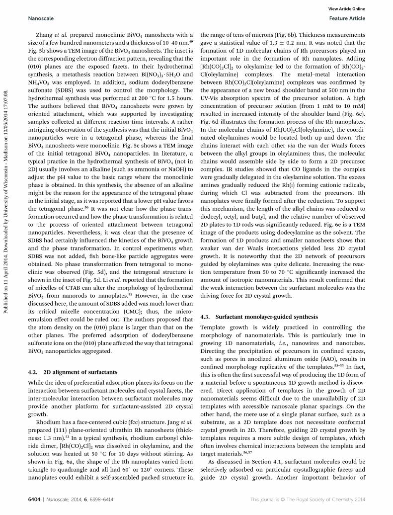
Fig. 5 TEM images of (a) Pd nanosheets with a well-defined hexagonalshape. The inset is a picture of a cuvette Pd nanosheet dispersed inethanol, which forms a blue ink. (b) BiVO4 nanosheets with a mono-clinic crystal structure and (010) facets exposed. (c) BiVO4 nano-particles with a tetragonal crystal structure at the initial stages of thesynthesis. (d) Fish bone-like aggregates of the tetragonal crystalstructure. The upper inset is an electron diffraction pattern, and thelower inset is a lower-magnification image. (a) Reproduced withpermission from Nature Publishing Group from ref. 48, Copyright2011. (b)–(d) Reproduced with permission from American ChemicalSociety from ref. 49, Copyright 2006.
4.1. Preferential adsorption
Although sometimes over-emphasized, preferential adsorptionis perhaps the most commonly cited concept that has been usedto explain the role of surfactants in the synthesis of inorganicmaterials, including 1D nanomaterials and nanocrystals withdened facets.45–47 The adsorbed species can be surfactantmolecules (including polymer surfactants), inorganic ions, orsmall molecules. They slow down the crystal growth of certaincrystal facets, on which surfactant molecules are adsorbed,while promoting the growth of other facets.
This journal is © The Royal Society of Chemistry 2014
Huang et al. reported a synthesis of palladium nanosheetsvia a solvothermal method using palladium(II) acetylacetonate,PVP, and a halide salt dissolved in a solvent such as dime-thylformamide or benzyl alcohol.48 The reaction was conductedin a glass pressure vessel that was lled with CO to 1 bar andmaintained at 100 �C for 3 hours. This process yielded well-dened hexagonal nanosheets with controllable edge lengthsfrom 20 to 160 nm (Fig. 5a), leading to tunable surface plasmonresonance (SPR). The inset picture of Fig. 5a shows a dispersionof Pd nanosheets in ethanol with a SPR-induced blue color.Similar to Rh nanosheets, the exposed surface of Pd nanosheetswas the (111) facet. Without CO, only twinned nanoparticleswere obtained. It was believed that the strong adsorption of COmolecules on the (111) planes of Pd crystals suppressed thegrowth along the [111] direction. The presence of CO adsorptionon the (111) surfaces of freshly prepared Pd nanosheets wasconrmed by CO stripping voltammetry. Fourier trans-formation infrared (FTIR) studies indicated that CO wasadsorbed in a bridge conguration. PVP was used to stabilizethe nanosheets from aggregation. When PVP was absent,aggregates of irregularly shaped Pd nanosheets were received.The halide salt used in the synthesis could be a variety ofcompounds, including cetyltrimethylammonium bromide(CTAB) and NaX (X ¼ Cl, Br, I). The role that halide ions playedwas to dene the hexagonal shape of the nanosheets by bindingto the (100) planes (side surfaces of hexagons).
Nanoscale, 2014, 6, 6398–6414 | 6403
Nanoscale Feature Article
Publ
ishe
d on
11
Apr
il 20
14. D
ownl
oade
d by
Uni
vers
ity o
f W
isco
nsin
- M
adis
on o
n 10
/06/
2014
17:
07:0
8.
View Article Online
Zhang et al. prepared monoclinic BiVO4 nanosheets with asize of a few hundred nanometers and a thickness of 10–40 nm.49
Fig. 5b shows a TEM image of the BiVO4 nanosheets. The inset isthe corresponding electron diffraction pattern, revealing that the(010) planes are the exposed facets. In their hydrothermalsynthesis, a metathesis reaction between Bi(NO3)3$5H2O andNH4VO3 was employed. In addition, sodium dodecylbenzenesulfonate (SDBS) was used to control the morphology. Thehydrothermal synthesis was performed at 200 �C for 1.5 hours.The authors believed that BiVO4 nanosheets were grown byoriented attachment, which was supported by investigatingsamples collected at different reaction time intervals. A ratherintriguing observation of the synthesis was that the initial BiVO4
nanoparticles were in a tetragonal phase, whereas the nalBiVO4 nanosheets were monoclinic. Fig. 5c shows a TEM imageof the initial tetragonal BiVO4 nanoparticles. In literature, atypical practice in the hydrothermal synthesis of BiVO4 (not in2D) usually involves an alkaline (such as ammonia or NaOH) toadjust the pH value to the basic range where the monoclinicphase is obtained. In this synthesis, the absence of an alkalinemight be the reason for the appearance of the tetragonal phasein the initial stage, as it was reported that a lower pH value favorsthe tetragonal phase.50 It was not clear how the phase trans-formation occurred and how the phase transformation is relatedto the process of oriented attachment between tetragonalnanoparticles. Nevertheless, it was clear that the presence ofSDBS had certainly inuenced the kinetics of the BiVO4 growthand the phase transformation. In control experiments whenSDBS was not added, sh bone-like particle aggregates wereobtained. No phase transformation from tetragonal to mono-clinic was observed (Fig. 5d), and the tetragonal structure isshown in the inset of Fig. 5d. Li et al. reported that the formationof micelles of CTAB can alter the morphology of hydrothermalBiVO4 from nanorods to nanoplates.51 However, in the casediscussed here, the amount of SDBS added wasmuch lower thanits critical micelle concentration (CMC); thus, the micro-emulsion effect could be ruled out. The authors proposed thatthe atom density on the (010) plane is larger than that on theother planes. The preferred adsorption of dodecylbenzenesulfonate ions on the (010) plane affected the way that tetragonalBiVO4 nanoparticles aggregated.
4.2. 2D alignment of surfactants
While the idea of preferential adsorption places its focus on theinteraction between surfactant molecules and crystal facets, theinter-molecular interaction between surfactant molecules mayprovide another platform for surfactant-assisted 2D crystalgrowth.
Rhodium has a face-centered cubic (fcc) structure. Jang et al.prepared (111) plane-oriented ultrathin Rh nanosheets (thick-ness: 1.3 nm).52 In a typical synthesis, rhodium carbonyl chlo-ride dimer, [Rh(CO)2Cl]2 was dissolved in oleylamine, and thesolution was heated at 50 �C for 10 days without stirring. Asshown in Fig. 6a, the shape of the Rh nanoplates varied fromtriangle to quadrangle and all had 60� or 120� corners. Thesenanoplates could exhibit a self-assembled packed structure in
6404 | Nanoscale, 2014, 6, 6398–6414
the range of tens of microns (Fig. 6b). Thickness measurementsgave a statistical value of 1.3 � 0.2 nm. It was noted that theformation of 1D molecular chains of Rh precursors played animportant role in the formation of Rh nanoplates. Adding[Rh(CO)2Cl]2 to oleylamine led to the formation of Rh(CO)2-Cl(oleylamine) complexes. The metal–metal interactionbetween Rh(CO)2Cl(oleylamine) complexes was conrmed bythe appearance of a new broad shoulder band at 500 nm in theUV-Vis absorption spectra of the precursor solution. A highconcentration of precursor solution (from 1 mM to 10 mM)resulted in increased intensity of the shoulder band (Fig. 6c).Fig. 6d illustrates the formation process of the Rh nanoplates.In the molecular chains of Rh(CO)2Cl(oleylamine), the coordi-nated oleylamines would be located both up and down. Thechains interact with each other via the van der Waals forcesbetween the alkyl groups in oleylamines; thus, the molecularchains would assemble side by side to form a 2D precursorcomplex. IR studies showed that CO ligands in the complexwere gradually delegated in the oleylamine solution. The excessamines gradually reduced the Rh(I) forming cationic radicals,during which Cl was subtracted from the precursors. Rhnanoplates were nally formed aer the reduction. To supportthis mechanism, the length of the alkyl chains was reduced tododecyl, octyl, and butyl, and the relative number of observed2D plates to 1D rods was signicantly reduced. Fig. 6e is a TEMimage of the products using dodecylamine as the solvent. Theformation of 1D products and smaller nanosheets shows thatweaker van der Waals interactions yielded less 2D crystalgrowth. It is noteworthy that the 2D network of precursorsguided by oleylamines was quite delicate. Increasing the reac-tion temperature from 50 to 70 �C signicantly increased theamount of isotropic nanomaterials. This result conrmed thatthe weak interaction between the surfactant molecules was thedriving force for 2D crystal growth.
4.3. Surfactant monolayer-guided synthesis
Template growth is widely practiced in controlling themorphology of nanomaterials. This is particularly true ingrowing 1D nanomaterials, i.e., nanowires and nanotubes.Directing the precipitation of precursors in conned spaces,such as pores in anodized aluminum oxide (AAO), results inconned morphology replicative of the templates.53–55 In fact,this is oen the rst successful way of producing the 1D form ofa material before a spontaneous 1D growth method is discov-ered. Direct application of templates in the growth of 2Dnanomaterials seems difficult due to the unavailability of 2Dtemplates with accessible nanoscale planar spacings. On theother hand, the mere use of a single planar surface, such as asubstrate, as a 2D template does not necessitate conformalcrystal growth in 2D. Therefore, guiding 2D crystal growth bytemplates requires a more subtle design of templates, whichoen involves chemical interactions between the template andtarget materials.56,57
As discussed in Section 4.1, surfactant molecules could beselectively adsorbed on particular crystallographic facets andguide 2D crystal growth. Another important behavior of
This journal is © The Royal Society of Chemistry 2014
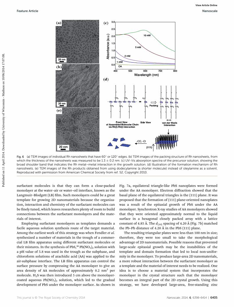
Fig. 6 (a) TEM images of individual Rh nanosheets that have 60� or 120� edges. (b) TEM images of the packing structure of Rh nanosheets, fromwhich the thickness of the nanosheets was measured to be 1.3 � 0.2 nm. (c) UV-Vis absorption spectra of the precursor solution, showing thebroad shoulder band that indicates the Rh metal–metal interaction in the growth solution. (d) Illustration of the formation mechanism of Rhnanosheets. (e) TEM images of the Rh products obtained from using dodecylamine (a shorter molecule) instead of oleylamine as a solvent.Reproduced with permission from American Chemical Society from ref. 52, Copyright 2010.
Feature Article Nanoscale
Publ
ishe
d on
11
Apr
il 20
14. D
ownl
oade
d by
Uni
vers
ity o
f W
isco
nsin
- M
adis
on o
n 10
/06/
2014
17:
07:0
8.
View Article Online
surfactant molecules is that they can form a close-packedmonolayer at the water–air or water–oil interface, known as theLangmuir–Blodgett (LB) lm. Such monolayers could be a greattemplate for growing 2D nanomaterials because the organiza-tion, interaction and chemistry of the surfactant molecules canbe nely tuned, which leaves researchers plenty of room to buildconnections between the surfactant monolayers and the mate-rials of interest.
Employing surfactant monolayers as templates demands afacile aqueous solution synthesis route of the target material.Among the earliest work of this strategy was when Fendler et al.synthesized a number of materials in the trough of a commer-cial LB lm apparatus using different surfactant molecules ortheir mixtures. In the synthesis of PbS,58 Pb(NO3)2 solution witha pH value of 5.8 was used in the trough as the subphase, andchloroform solutions of arachidic acid (AA) was applied to theair-subphase interface. The LB lm apparatus can control thesurface pressure by compressing the AA monolayer to give anarea density of AA molecules of approximately 0.2 nm2 permolecule. H2S was then introduced 5 cm above the monolayer-coated aqueous Pb(NO3)2 solution, which led to the gradualdevelopment of PbS under the monolayer surface. As shown in
This journal is © The Royal Society of Chemistry 2014
Fig. 7a, equilateral triangle-like PbS nanoplates were formedunder the AA monolayer. Electron diffraction showed that thebasal plane of the equilateral triangles is the (111) plane. It wasproposed that the formation of (111) plane-oriented nanoplateswas a result of the epitaxial growth of PbS under the AAmonolayer. Synchrotron X-ray studies of AA monolayers showedthat they were oriented approximately normal to the liquidsurface in a hexagonal closely packed array with a latticeconstant of 4.85 A. The d{10} spacing of 4.20 A (Fig. 7b) matchedthe Pb–Pb distance of 4.20 A in the PbS (111) plane.
The resulting triangular plates were less than 100 nm in size;therefore, they were too small to take the morphologicaladvantage of 2D nanomaterials. Possible reasons that preventedlarge-scale epitaxial growth may be the instabilities of thetemplate and domain formation that led to local non-unifor-mity in themonolayer. To produce large-area 2D nanomaterials,a more robust interaction between the surfactant monolayer asa template and the material of interest needs to be realized. Oneidea is to choose a material system that incorporates themonolayer in the crystal structure such that the monolayerbecomes an integral part of the 2D crystal growth. Using thisstrategy, we have developed large-area, free-standing zinc
Nanoscale, 2014, 6, 6398–6414 | 6405

Fig. 7 (a) TEM image of triangular PbS nanoplates. The inset is theelectron diffraction pattern of a single nanoplate, and the exposedsurface is identified as (111). (b) Schematic illustration of the hexagonalpacking of the headgroups of arachidic acid molecules on the watersurface. The distance between two columns of headgroups is 4.20 nm.Reproduced with permission from American Chemical Society fromref. 58, Copyright 1995.
Nanoscale Feature Article
Publ
ishe
d on
11
Apr
il 20
14. D
ownl
oade
d by
Uni
vers
ity o
f W
isco
nsin
- M
adis
on o
n 10
/06/
2014
17:
07:0
8.
View Article Online
hydroxyl dodecylsulfate (ZHDS) nanomembranes that can coverthe entire water surface.2,59
Zn(NO3)2 and hexamethylenetetramine (HMTA) arecommonly used precursors for 1D ZnO nanostructure growth.
Fig. 8 (a) Optical microscopy image of the ZHDS nanomembranes. Thewater surface in a glass dish. (b) AFM topography scan. (c)–(e) TEM imageshown by the electron diffraction pattern in the inset. (d) Flat surface ongrains. (f) Schematic illustration of the formation process of ZHDS NMsfrom American Chemical Society from ref. 59, Copyright 2012.
6406 | Nanoscale, 2014, 6, 6398–6414
However, in the presence of sulfate ions, elemental zinc andZn2+ ions oen mineralize to zinc hydroxyl sulfate hydrates.Therefore, the surfactant used in this work was dodecylsulfate(DS) to ensure that the sulfate headgroups would direct thenucleation and growth of ZHDS in which the DS monolayer isthe starting crystallographic layer. In a typical synthesis, 25 mMZn(NO3)2 and HMTA were used along with 20 mM sodium DS(above its critical micelle concentration), and the reactor wasplaced in a 90 �C convection oven for 4 hours. Fig. 8a is animage from an optical microscope where large area nano-membranes on the Si substrate are presented with a few cracksand wrinkles formed during the transfer process. The inset inFig. 8a is a picture of the as-grown ZHDS nanomembrane,which covered the entire surface of the growth solution in aglass dish. The color contrast in Fig. 8a resulted from thicknessvariations. Fig. 8b is an AFM topography scan of the nano-membranes, and the thickness was measured to be 150 nm.TEM characterization revealed that the continuous ZHDSnanomembranes are composed of tens of micron-sized hexag-onal single crystal plates (Fig. 8c). These single crystal plateshave either a at surface as shown in Fig. 8d or a surface withhexagonal helical contours (Fig. 8e), indicating a screw-
inset is a picture of the as-grown intact nanomembranes afloat on thes. (c) Single-crystal grains overlap forming a large-scale single crystal assome hexagonal grains. (e) Spiral surface hillocks on other hexagonalat the water surface assisted by DS ions. Reproduced with permission
This journal is © The Royal Society of Chemistry 2014
Feature Article Nanoscale
Publ
ishe
d on
11
Apr
il 20
14. D
ownl
oade
d by
Uni
vers
ity o
f W
isco
nsin
- M
adis
on o
n 10
/06/
2014
17:
07:0
8.
View Article Online
dislocation driven growth. Fig. 8f illustrates the schematicformation process of ZHDS nanomembranes at the watersurface assisted by DS ions: DS ions form a negatively chargedmonolayer at the wafer surface, under which zinc cations areenriched and an electrostatic double layer is formed. As thetemperature increases, the pH value of the solution, buffered byHMTA and its thermal decomposition to ammonia alsoincreases, which initiates the crystallization of ZHDS bothunderneath the DS ion monolayer and in the bulk solution.
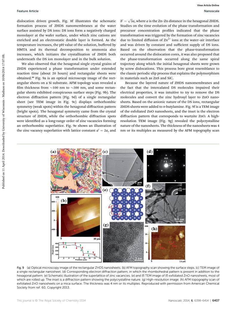
We also observed that the hexagonal single crystal grains ofZHDS experienced a phase transformation under extendedreaction time (about 20 hours) and rectangular sheets wereobtained.60 Fig. 9a is an optical microscopy image of the rect-angular sheets on a Si substrate. AFM topology scan revealed alm thickness from �100 nm to �300 nm, and some rectan-gular sheets exhibited conspicuous surface steps (Fig. 9b). Theelectron diffraction pattern (Fig. 9d) of a single rectangularsheet (see TEM image in Fig. 9c) displays orthorhombicsymmetry (weak spots) within the hexagonal diffraction pattern(bright spots). The hexagonal symmetry came from the crystalstructure of ZHDS, while the orthorhombic diffraction spotswere identied as a long-range order of zinc vacancies formingan orthorhombic superlattice. Fig. 9e shows an illustration ofthe zinc vacancy superlattice with lattice constant a0 ¼ 2a, and
Fig. 9 (a) Optical microscopy image of the rectangular ZHDS nanosheetsa single rectangular nanosheet. (d) Corresponding electron diffraction phexagonal pattern. (e) Schematic illustration of the superlattice of zinc vawhich are rolled up. The inset is a diffraction pattern showing the polycryexfoliated ZnO nanosheets on a mica surface. The thickness was 4 nm oSociety from ref. 60, Copyright 2013.
This journal is © The Royal Society of Chemistry 2014
b0 ¼ ffiffiffi
3p
a, where a is the Zn–Zn distance in the hexagonal ZHDS.Studies on the time evolution of the phase transformation andprecursor concentration proles indicated that the phasetransformation was triggered by the formation of zinc vacanciesdue to limited diffusion of Zn2+ ions at the water–air interfaceand was driven by constant and sufficient supply of DS ions.Based on the observation that the phase-transformationoccurred around the dislocation cores, it was also proposed thatthe phase-transformation occurred along the same spiraltrajectory along which the initial hexagonal sheets were grownby screw dislocations. This process bore great resemblance tothe classic periodic slip process that explains the polymorphismin materials such as ZnS and SiC.
Because the layered nature of ZHDS nanomembranes andthe fact that the intercalated DS molecules impaired theirelectrical properties, it was intuitive to try to remove the DSmolecules and convert the zinc hydroxyl layer to ZnO nano-sheets. Based on the anionic nature of the DS ions, rectangularZHDS sheets were added to n-butylamine. Fig. 9f is a TEM imageof the exfoliated ZnO nanosheets, and the inset is the electrondiffraction pattern that corresponds to wurtzite ZnO. A high-resolution TEM image (Fig. 9g) revealed the polycrystallinenature of the nanosheets. The thickness of the nanosheets was 4nm or its multiples as measured by the AFM topography scan
. (b) AFM topography scan showing the surface steps. (c) TEM image ofattern, in which the rhombohedral pattern is present in addition to thecancies. (e) and (f) TEM image of (f) exfoliated ZnO nanosheets, most ofstalline nature. (g) High-resolution image. (h) AFM topography scan ofr its multiples. Reproduced with permission from American Chemical
Nanoscale, 2014, 6, 6398–6414 | 6407

Nanoscale Feature Article
Publ
ishe
d on
11
Apr
il 20
14. D
ownl
oade
d by
Uni
vers
ity o
f W
isco
nsin
- M
adis
on o
n 10
/06/
2014
17:
07:0
8.
View Article Online
shown in Fig. 9h. In the zinc hydroxyl layer of ZHDS, O–Hgroups are strongly polarized and the H atoms have a strongpropensity for forming H-bonds, particularly with the N atomson n-butylamine. We believe that the role of n-butylamine is toremove the protons from the O–H groups and form cationicamines, which subsequently remove DS ions from ZHDS. Thereaction can be written as Zn(OH)2$Zn(DS)2 + 2C4H11N/ 2ZnO+ 2C4H11NH
+$DS�.
5. Other processes in solvothermalsyntheses
We have introduced some solvothermal syntheses in the abovesections when the growth mechanism can be categorized asoriented attachment, screw dislocation-driven growth, orsurfactant-assisted growth. These mechanisms do not exclu-sively occur in solvothermal processes. In this section, we focuson solvothermal synthesis as an experimental method anddiscuss other processes that occur in the solvothermal growthof 2D nanomaterials. We nd that thermodynamic factors, suchas the relative energy among different facets, oen determinethe 2D geometry of the products. An important feature of sol-vothermal synthesis is that the autoclaves can create a high-temperature and high-pressure condition, under which water aswell as other solvents exhibit signicantly different chemicaland physical properties, such as dissociation constant,viscosity, and dielectric constant. As a result, solubility, reac-tivity, and mass transport in solvothermal synthesis can bevaried signicantly under different system conditions.61
Fig. 10 (a) TEM image of La2Ti2O7 nanosheets. The inset is the elec-tron diffraction pattern taken from a nanosheet area labeled by thesquare black dot marked by the arrow. (b) Illustration of the mono-clinic-layered structure of La2Ti2O7, in which the bonding betweencorners of the TiO6 octahedra is broken between layers. (c) Projectionof the crystal structure of TiO2(B) along the c-axis. (d) SEM image of theaggregates of TiO2(B) nanosheets. (e) SEM image of individual VO2(B)nanosheets. (a) Reproduced with permission from IOP Publishing fromref. 62, Copyright 2006. (b) Reproduced with permission from Amer-ican Chemical Society from ref. 63, Copyright 2006. (c) Reproducedwith permission from American Chemical Society from ref. 66,Copyright 2013. (d) Reproduced with permission from Wiley from ref.67, Copyright 2012. (e) Reproduced with permission from Springerfrom ref. 68, Copyright 2005.
5.1. Metal oxide with layered crystal structure
Several metal oxides with a monoclinic structure have beensynthesized in the form of nanosheets by hydrothermalmethods. Lanthanide titanate (La2Ti2O7) is one of them. A-few-atomic-layer-thick La2Ti2O7 nanosheets were synthesizedhydrothermally by Li et al.62 Lanthanum nitrate and titaniumsulfate were used as lanthanum and titanium precursors,respectively. As in a typical hydrothermal synthesis of metaloxide, NaOH was used and the reaction was conducted at 200 �Cfor 24 hours. TEM images showed that the nanosheets were in arectangular shape and a few microns wide (Fig. 10a). It wasnoted that an appropriate amount of NaOH was essential toobtain La2Ti2O7 rather than TiO2 or La(OH)3. It was not dis-cussed in this work how the La2Ti2O7 grew in 2D, but the layeredmonoclinic crystal structure and the feeble bonding betweenlayers were considered to be critical in the 2D growth. In themonoclinic crystal structure of La2Ti2O7 (illustrated inFig. 10b),63 the layers are built from (110) perovskite slabs, witheach slab containing La ions and corner-sharing TiO6 octahe-drons. Adjacent layers are staggered by half of a TiO6 height,where the TiO6 octahedrons are disconnected and only weaklybonded through the interaction with La ions.
First synthesized by Marchand et al.,64 TiO2(B) is a mono-clinic polymorph of TiO2 and has exotic properties in photo-catalysis,65 electrochemistry, and Li-ion battery applications.66 Itcan be viewed as a layered structure because it has open
6408 | Nanoscale, 2014, 6, 6398–6414
channels parallel to the b-axis. As shown in Fig. 10c, the layersare staggered and contain TiO6 octahedra sharing their edgesin-plane and sharing corners between layers. Liu et al. synthe-sized petal-like aggregates of TiO2(B) nanosheets with thick-nesses of 5–10 nm by the solvothermal method (Fig. 10d).67 Intheir process, TiCl4 was dissolved in ethylene glycol understirring for 2 hours prior to adding 25% ammonium hydroxide.TiO2(B) could be obtained aer a 24-hour solvothermal treat-ment at 150 �C. The crystallinity of TiO2(B) was greatly improvedby calcination at 350 �C for 2 hours. The exposed surface ofTiO2(B) nanosheets was the (001) facet. In another synthesis ofTiO2(B) nanosheets by Yu et al., anatase TiO2 powder producedby calcination of Ti(OH)4 ethanol-gel at 500 �C was used as the
This journal is © The Royal Society of Chemistry 2014

Feature Article Nanoscale
Publ
ishe
d on
11
Apr
il 20
14. D
ownl
oade
d by
Uni
vers
ity o
f W
isco
nsin
- M
adis
on o
n 10
/06/
2014
17:
07:0
8.
View Article Online
precursor, which was then added to 10 M NaOH solution andtreated hydrothermally at 200 �C for 72 hours.68 Similar to Liuet al.'s work, the hydrothermal treatment yielded amorphousnanosheets, which were topotactically transformed to TiO2(B)nanosheets by rinsing with HCl for 30min in a supersonic batchand calcinating at 500 �C. As a structural analog of TiO2(B),petal-like aggregates of VO2(B) nanosheets were also synthe-sized by the hydrothermal method, in which ammoniumvanadate was used as the precursor and the reaction was con-ducted at 180 �C for 72 hours.69 In another synthesis by Whit-taker et al., in which V2O5 was used as the precursor along withethanol or acetone as the reducing agent, �100 nm thick indi-vidual single crystal rectangular nanosheets were obtained(Fig. 10e).70 The hydrothermal treatment in this synthesis wasconducted at 210 �C for 72 hours.
In these examples of TiO2(B) and VO2(B) nanosheets, as wellas La2Ti2O7 nanosheets, no surfactant was used. Comparing thecrystal structure of the materials and the hydrothermal reactionconditions in these examples, we nd that there is an intrinsicdriving force for the formation of nanosheets of layered,monoclinic materials, although the kinetic mechanism of the2D growth in these examples is still unknown (be it orientedattachment, screw-dislocation growth, or layer-by-layer growth).This makes sense given the fact that the surface of individuallayers is more stable than the edges which are under-coordi-nated and thermodynamically unfavorable.71 One may arguethat there are a number of reports where TiO2(B) and VO2(B) canalso be hydrothermally synthesized in a 1D form withoutsurfactants; however, they are oen grown indirectly and aconversion from other polymorphs is needed. For example,anatase TiO2 or metal (Na or K) titanate hydroxide (e.g.NaxH2�xTi3O7) nanowires/nanotubes were oen found to haveformed rst hydrothermally before being converted into TiO2(B)through acid wash and thermal calcination.72–75 In the light ofprecursor selection for both TiO2(B) and VO2(B), when a solubleprecursor is used, aggregates of smaller nanosheets wereobtained, whereas when a solid oxide was used, the productswere larger individual nanosheets. Therefore, the state ofprecursors should have a great inuence on the growth mech-anism, possibly through the control of intermediate speciesthat nally crystallize into the nanosheet materials.
A number of other solvothermal and non-solvothermalsyntheses also indicate that there is an intrinsic driving force tothe formation of nanosheets of layered crystals with monoclinicand other symmetries. BiOCl has a layered tetragonal structurein which Bi2O2 slabs are interleaved by double slabs of Cl atomsin the tetragonal matlockite structure. Ye et al. reported thesynthesis of BiOCl nanosheets by a non-solvothermal method.76
In their synthesis, BiCl3 was dissolved in ethanol, and thiourea(Tu) was added slowly to form Bin(Tu)xCl3n molecular precur-sors. BiOCl nanosheets were obtained 20 minutes aer addingthis precursor to deionized water under sonication. Theexposed facets are (001), similar to BiOCl nanoplates reportedby Geng et al. and Lei et al.77,78 Through a solvothermal methodusing Bi(NO3)3 as the Bi precursor and NaOH as themineralizer,BiOBr nanosheets were synthesized by Lin et al. where KBr wasused to provide the halide ions.79 Moreover, BiOCl and BiOBr
This journal is © The Royal Society of Chemistry 2014
nanobelts with the exposed (001) facets were synthesized byDeng et al. by using CTAC (cetyltrimethylammonium chloride)and CTAB, respectively.80
5.2. Dissolution–recrystallization process in solvothermalmethod
Crystal growth from solution is essentially a precipitation process,which involves dynamic dissolution–recrystallization processes.The classic Ostwald ripening process, in which the differencebetween the solubility of small and large nanoparticles leads to adefocusing in particle size (i.e. big nanoparticles grow even biggerat the expense of smaller particles), is a perfect example of thisdissolution–recrystallization process. Another consequence ofdynamic dissolution–recrystallization is spontaneous phasetransformation from kinetic products to thermodynamic prod-ucts and morphology evolution during the crystal growth insolution. In fact, crystal growth in solution oen starts with athermodynamically unstable phase, followed by a phase trans-formation to thermodynamically stable phases. This is referred toas the Ostwald's rule of stages.81,82 Similarly, crystal growth canalso start with a thermodynamically unstable morphology due tokinetics, and then recrystallize to a thermodynamically stablemorphology. In the case of the solution synthesis of 2D nano-materials, 2D morphology can be transformed from othermorphologies aer an extended reaction time.
Yang et al. synthesized b-Co(OH)2 and Co3O4 nanosheets bythe hydrothermal method.83,84 b-Co(OH)2 nanosheets weresynthesized on a nickel foam by using Co(NO3)2$6H2O as the Coprecursor, and NH4F along with urea as the mineralizer. Toobtain Co3O4 nanosheets, the Co(OH)2 nanosheets were loadedin the Teon-lined stainless steel autoclave again with theaddition of Co2+ salts and a base (urea or HMT). This secondaryhydrothermal treatment was considered a coordinating etchingand recrystallization process. The excess urea or HMT intro-duced to the solution was able to coordinate the etching ofCo(OH)2 by forming a soluble complex and releasing OH� ionsto facilitate the recrystallization. The addition of Co2+ saltshould help the recrystallization too. Fig. 11a–e show themorphology evolution from b-Co(OH)2 to Co3O4 before ((a),b-Co(OH)2) and during the secondary hydrothermal treatmentat 3, 6, 9, and 12 hours, respectively. The b-Co(OH)2 nanosheetswere quite thick (about 200 nm). Aer 3 hours, the nanosheetswere signicantly thinner, indicating the dissolution ofb-Co(OH)2, and Co3O4 nanowires started to grow on the surfacesof the nanosheets. The b-Co(OH)2 nanosheets disappearedalmost completely by 6 hours (c). Then, these nanowires weregrown into Co3O4 nanosheets aer 9 hours (d), and nally theyevolved into nanosheets with better crystallinity and well-dened surface and edge facets (e).
Zhao et al. reported the hydrothermal synthesis of meta-stable phase FeVO4-II nanosheets (orthorhombic) with exposed(010) facets.85 The obtained nanosheets were rectangular andwere �50 nm thick and a few microns in size. The growthsolution contained equal amounts of FeCl3 and NH4VO3, andthe pH value was adjusted to 3. Unlike the synthesis of BiVO4
that was introduced in Section 4.1, no surfactant was used in
Nanoscale, 2014, 6, 6398–6414 | 6409
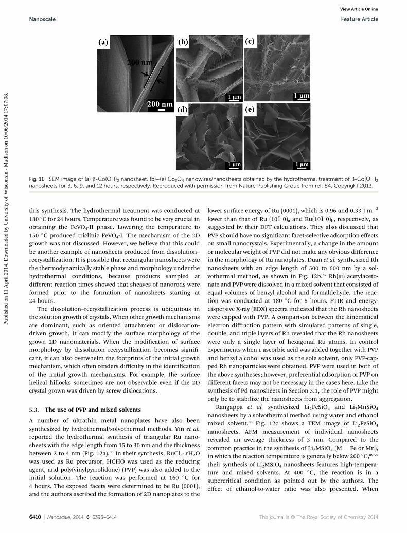
Fig. 11 SEM image of (a) b-Co(OH)2 nanosheet. (b)–(e) Co3O4 nanowires/nanosheets obtained by the hydrothermal treatment of b-Co(OH)2nanosheets for 3, 6, 9, and 12 hours, respectively. Reproduced with permission from Nature Publishing Group from ref. 84, Copyright 2013.
Nanoscale Feature Article
Publ
ishe
d on
11
Apr
il 20
14. D
ownl
oade
d by
Uni
vers
ity o
f W
isco
nsin
- M
adis
on o
n 10
/06/
2014
17:
07:0
8.
View Article Online
this synthesis. The hydrothermal treatment was conducted at180 �C for 24 hours. Temperature was found to be very crucial inobtaining the FeVO4-II phase. Lowering the temperature to150 �C produced triclinic FeVO4-I. The mechanism of the 2Dgrowth was not discussed. However, we believe that this couldbe another example of nanosheets produced from dissolution–recrystallization. It is possible that rectangular nanosheets werethe thermodynamically stable phase and morphology under thehydrothermal conditions, because products sampled atdifferent reaction times showed that sheaves of nanorods wereformed prior to the formation of nanosheets starting at24 hours.
The dissolution–recrystallization process is ubiquitous inthe solution growth of crystals. When other growthmechanismsare dominant, such as oriented attachment or dislocation-driven growth, it can modify the surface morphology of thegrown 2D nanomaterials. When the modication of surfacemorphology by dissolution–recrystallization becomes signi-cant, it can also overwhelm the footprints of the initial growthmechanism, which oen renders difficulty in the identicationof the initial growth mechanisms. For example, the surfacehelical hillocks sometimes are not observable even if the 2Dcrystal grown was driven by screw dislocations.
5.3. The use of PVP and mixed solvents
A number of ultrathin metal nanoplates have also beensynthesized by hydrothermal/solvothermal methods. Yin et al.reported the hydrothermal synthesis of triangular Ru nano-sheets with the edge length from 15 to 30 nm and the thicknessbetween 2 to 4 nm (Fig. 12a).86 In their synthesis, RuCl3$xH2Owas used as Ru precursor, HCHO was used as the reducingagent, and poly(vinylpyrrolidone) (PVP) was also added to theinitial solution. The reaction was performed at 160 �C for4 hours. The exposed facets were determined to be Ru (0001),and the authors ascribed the formation of 2D nanoplates to the
6410 | Nanoscale, 2014, 6, 6398–6414
lower surface energy of Ru (0001), which is 0.96 and 0.33 J m�2
lower than that of Ru (10�1 0)a and Ru(10�1 0)b, respectively, assuggested by their DFT calculations. They also discussed thatPVP should have no signicant facet-selective adsorption effectson small nanocrystals. Experimentally, a change in the amountor molecular weight of PVP did not make any obvious differencein the morphology of Ru nanoplates. Duan et al. synthesized Rhnanosheets with an edge length of 500 to 600 nm by a sol-vothermal method, as shown in Fig. 12b.87 Rh(III) acetylaceto-nate and PVP were dissolved in amixed solvent that consisted ofequal volumes of benzyl alcohol and formaldehyde. The reac-tion was conducted at 180 �C for 8 hours. FTIR and energy-dispersive X-ray (EDX) spectra indicated that the Rh nanosheetswere capped with PVP. A comparison between the kinematicalelectron diffraction pattern with simulated patterns of single,double, and triple layers of Rh revealed that the Rh nanosheetswere only a single layer of hexagonal Ru atoms. In controlexperiments when L-ascorbic acid was added together with PVPand benzyl alcohol was used as the sole solvent, only PVP-cap-ped Rh nanoparticles were obtained. PVP were used in both ofthe above syntheses; however, preferential adsorption of PVP ondifferent facets may not be necessary in the cases here. Like thesynthesis of Pd nanosheets in Section 3.1, the role of PVP mightonly be to stabilize the nanosheets from aggregation.
Rangappa et al. synthesized Li2FeSiO4 and Li2MnSiO4
nanosheets by a solvothermal method using water and ethanolmixed solvent.88 Fig. 12c shows a TEM image of Li2FeSiO4
nanosheets. AFM measurement of individual nanosheetsrevealed an average thickness of 3 nm. Compared to thecommon practice in the synthesis of Li2MSiO4 (M ¼ Fe or Mn),in which the reaction temperature is generally below 200 �C,89,90
their synthesis of Li2MSiO4 nanosheets features high-tempera-ture and mixed solvents. At 400 �C, the reaction is in asupercritical condition as pointed out by the authors. Theeffect of ethanol-to-water ratio was also presented. When
This journal is © The Royal Society of Chemistry 2014
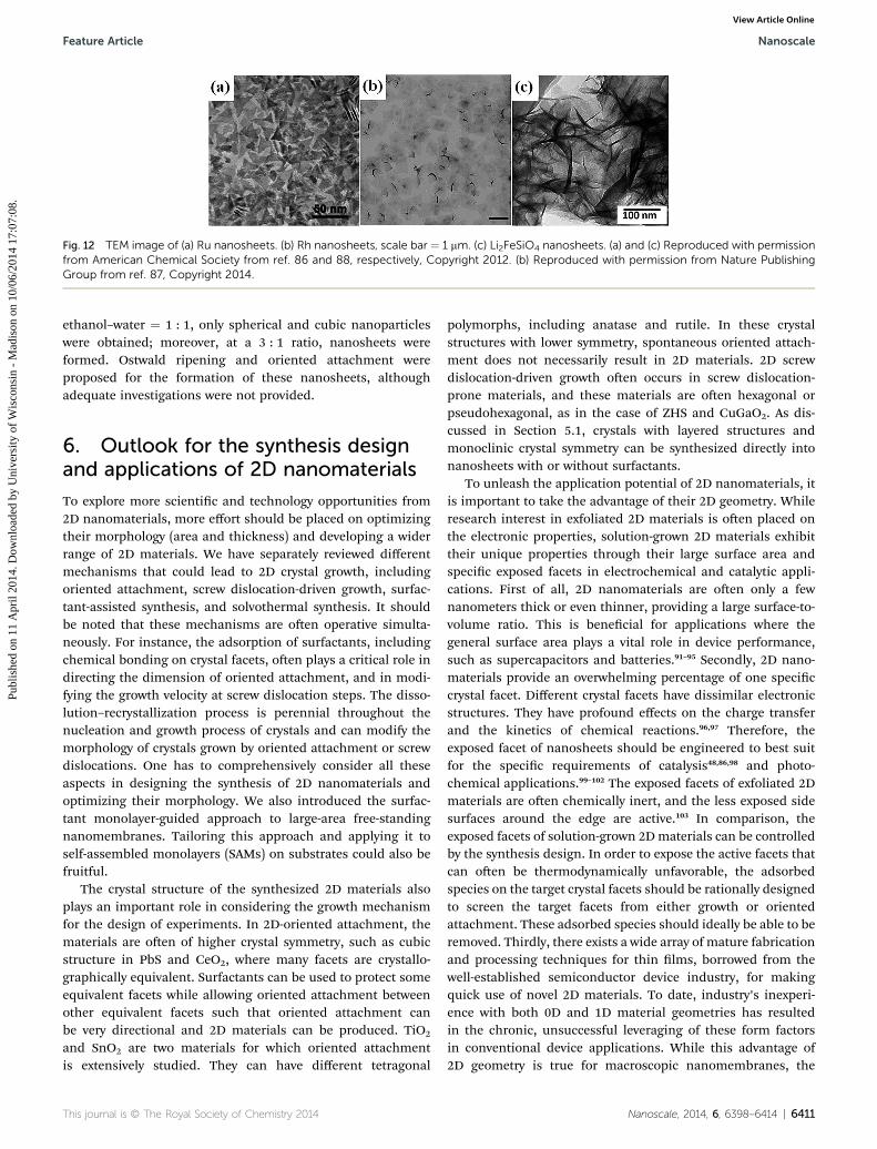
Fig. 12 TEM image of (a) Ru nanosheets. (b) Rh nanosheets, scale bar ¼ 1 mm. (c) Li2FeSiO4 nanosheets. (a) and (c) Reproduced with permissionfrom American Chemical Society from ref. 86 and 88, respectively, Copyright 2012. (b) Reproduced with permission from Nature PublishingGroup from ref. 87, Copyright 2014.
Feature Article Nanoscale
Publ
ishe
d on
11
Apr
il 20
14. D
ownl
oade
d by
Uni
vers
ity o
f W
isco
nsin
- M
adis
on o
n 10
/06/
2014
17:
07:0
8.
View Article Online
ethanol–water ¼ 1 : 1, only spherical and cubic nanoparticleswere obtained; moreover, at a 3 : 1 ratio, nanosheets wereformed. Ostwald ripening and oriented attachment wereproposed for the formation of these nanosheets, althoughadequate investigations were not provided.
6. Outlook for the synthesis designand applications of 2D nanomaterials
To explore more scientic and technology opportunities from2D nanomaterials, more effort should be placed on optimizingtheir morphology (area and thickness) and developing a widerrange of 2D materials. We have separately reviewed differentmechanisms that could lead to 2D crystal growth, includingoriented attachment, screw dislocation-driven growth, surfac-tant-assisted synthesis, and solvothermal synthesis. It shouldbe noted that these mechanisms are oen operative simulta-neously. For instance, the adsorption of surfactants, includingchemical bonding on crystal facets, oen plays a critical role indirecting the dimension of oriented attachment, and in modi-fying the growth velocity at screw dislocation steps. The disso-lution–recrystallization process is perennial throughout thenucleation and growth process of crystals and can modify themorphology of crystals grown by oriented attachment or screwdislocations. One has to comprehensively consider all theseaspects in designing the synthesis of 2D nanomaterials andoptimizing their morphology. We also introduced the surfac-tant monolayer-guided approach to large-area free-standingnanomembranes. Tailoring this approach and applying it toself-assembled monolayers (SAMs) on substrates could also befruitful.
The crystal structure of the synthesized 2D materials alsoplays an important role in considering the growth mechanismfor the design of experiments. In 2D-oriented attachment, thematerials are oen of higher crystal symmetry, such as cubicstructure in PbS and CeO2, where many facets are crystallo-graphically equivalent. Surfactants can be used to protect someequivalent facets while allowing oriented attachment betweenother equivalent facets such that oriented attachment canbe very directional and 2D materials can be produced. TiO2
and SnO2 are two materials for which oriented attachmentis extensively studied. They can have different tetragonal
This journal is © The Royal Society of Chemistry 2014
polymorphs, including anatase and rutile. In these crystalstructures with lower symmetry, spontaneous oriented attach-ment does not necessarily result in 2D materials. 2D screwdislocation-driven growth oen occurs in screw dislocation-prone materials, and these materials are oen hexagonal orpseudohexagonal, as in the case of ZHS and CuGaO2. As dis-cussed in Section 5.1, crystals with layered structures andmonoclinic crystal symmetry can be synthesized directly intonanosheets with or without surfactants.
To unleash the application potential of 2D nanomaterials, itis important to take the advantage of their 2D geometry. Whileresearch interest in exfoliated 2D materials is oen placed onthe electronic properties, solution-grown 2D materials exhibittheir unique properties through their large surface area andspecic exposed facets in electrochemical and catalytic appli-cations. First of all, 2D nanomaterials are oen only a fewnanometers thick or even thinner, providing a large surface-to-volume ratio. This is benecial for applications where thegeneral surface area plays a vital role in device performance,such as supercapacitors and batteries.91–95 Secondly, 2D nano-materials provide an overwhelming percentage of one speciccrystal facet. Different crystal facets have dissimilar electronicstructures. They have profound effects on the charge transferand the kinetics of chemical reactions.96,97 Therefore, theexposed facet of nanosheets should be engineered to best suitfor the specic requirements of catalysis48,86,98 and photo-chemical applications.99–102 The exposed facets of exfoliated 2Dmaterials are oen chemically inert, and the less exposed sidesurfaces around the edge are active.103 In comparison, theexposed facets of solution-grown 2Dmaterials can be controlledby the synthesis design. In order to expose the active facets thatcan oen be thermodynamically unfavorable, the adsorbedspecies on the target crystal facets should be rationally designedto screen the target facets from either growth or orientedattachment. These adsorbed species should ideally be able to beremoved. Thirdly, there exists a wide array of mature fabricationand processing techniques for thin lms, borrowed from thewell-established semiconductor device industry, for makingquick use of novel 2D materials. To date, industry’s inexperi-ence with both 0D and 1D material geometries has resultedin the chronic, unsuccessful leveraging of these form factorsin conventional device applications. While this advantage of2D geometry is true for macroscopic nanomembranes, the
Nanoscale, 2014, 6, 6398–6414 | 6411

Nanoscale Feature Article
Publ
ishe
d on
11
Apr
il 20
14. D
ownl
oade
d by
Uni
vers
ity o
f W
isco
nsin
- M
adis
on o
n 10
/06/
2014
17:
07:0
8.
View Article Online
assembly and fabrication of microscopic nanoplates andnanosheets into electronic and optoelectronic devices remainschallenging. Lastly, although the mechanical exibility of 2Dnanomaterials have unlocked their applications in exibleelectronics and conformal biomedical devices, other aspects oftheir mechanical properties have not yet been investigated andutilized extensively.104 We have demonstrated that rectangularZHDS nanosheets behave like structural polymers in nano-indentation experiments.60 However, more effort should beplaced on exploring the application implication of themechanical properties of 2D nanomaterials.105,106
Acknowledgements
The authors acknowledge the nancial support from Air Forceunder Award FA9550-13-1-0168 and National Science Founda-tion under Award CMMI-1148919.
References
1 C. N. R. Rao, A. K. Sood, K. S. Subrahmanyam andA. Govindaraj, Angew. Chem., Int. Ed., 2009, 48, 7752.
2 B. Nikoobakht and X. Li, ACS Nano, 2012, 6, 1883.3 F. Bonaccorso, Z. Sun, T. Hasan and A. C. Ferrari, Nat.Photonics, 2010, 4, 611.
4 Q. H. Wang, K. Kalantar-Zadeh, A. Kis, J. N. Coleman andM. S. Strano, Nat. Nanotechnol., 2012, 7, 699.
5 B. Radisavljevic, A. Radenovic, J. Brivio, V. Giacometti andA. Kis, Nat. Nanotechnol., 2011, 6, 147.
6 J. A. Rogers, M. G. Lagally and R. G. Nuzzo, Nature, 2011,477, 45.
7 I. Monch, J. Schumann, M. Stockmann, K. F. Arndt andO. G. Schmidt, Smart Mater. Struct., 2011, 20, 085016.
8 M. H. Huang, F. Cavallo, F. Liu andM. G. Lagally,Nanoscale,2011, 3, 96.
9 G. Eda, G. Fanchini and M. Chhowalla, Nat. Nanotechnol.,2008, 3, 270.
10 S. I. Park, Y. J. Xiong, R. H. Kim, P. Elvikis, M. Meitl,D. H. Kim, J. Wu, J. Yoon, C. J. Yu, Z. J. Liu, Y. G. Huang,K. Hwang, P. Ferreira, X. L. Li, K. Choquette andJ. A. Rogers, Science, 2009, 325, 977.
11 V. P. Verma, S. Das, I. Lahiri and W. Choi, Appl. Phys. Lett.,2010, 96, 203108.
12 H. C. Yuan, G. K. Celler and Z. Q. Ma, J. Appl. Phys., 2007,102, 034501.
13 R. H. Kim, D. H. Kim, J. L. Xiao, B. H. Kim, S. I. Park,B. Panilaitis, R. Ghaffari, J. M. Yao, M. Li, Z. J. Liu,V. Malyarchuk, D. G. Kim, A. P. Le, R. G. Nuzzo,D. L. Kaplan, F. G. Omenetto, Y. G. Huang, Z. Kang andJ. A. Rogers, Nat. Mater., 2010, 9, 929.
14 J. Viventi, D. H. Kim, J. D. Moss, Y. S. Kim, J. A. Blanco,N. Annetta, A. Hicks, J. L. Xiao, Y. G. Huang, D. J. Callans,J. A. Rogers and B. Litt, Sci. Transl. Med., 2010, 2, 24ra22.
15 J. Yoon, S. Jo, I. S. Chun, I. Jung, H. S. Kim, M. Meitl,E. Menard, X. L. Li, J. J. Coleman, U. Paik andJ. A. Rogers, Nature, 2010, 465, 329.
6412 | Nanoscale, 2014, 6, 6398–6414
16 M. Naguib, M. Kurtoglu, V. Presser, J. Lu, J. J. Niu, M. Heon,L. Hultman, Y. Gogotsi and M. W. Barsoum, Adv. Mater.,2011, 23, 4248.
17 H. S. S. R. Matte, A. Gomathi, A. K. Manna, D. J. Late,R. Datta, S. K. Pati and C. N. R. Rao, Angew. Chem., Int.Ed., 2010, 49, 4059.
18 R. S. Wagner and W. C. Ellis, Appl. Phys. Lett., 1964,4, 89.
19 A. I. Persson, M. W. Larsson, S. Stenstrom, B. J. Ohlsson,L. Samuelson and L. R. Wallenberg, Nat. Mater., 2004, 3,677.
20 T. J. Trentler, K. M. Hickman, S. C. Goel, A. M. Viano,P. C. Gibbons and W. E. Buhro, Science, 1995, 270, 1791.
21 J. D. Holmes, K. P. Johnston, R. C. Doty and B. A. Korgel,Science, 2000, 287, 1471.
22 S. A. Morin, M. J. Bierman, J. Tong and S. Jin, Science, 2010,328, 476.
23 F. Meng, S. A. Morin, A. Forticaux and S. Jin, Acc. Chem. Res.,2013, 46, 1616.
24 X. D. Zhang and Y. Xie, Chem. Soc. Rev., 2013, 42, 8187.25 C. J. Dalmaschio, C. Ribeiro and E. R. Leite, Nanoscale,
2010, 2, 2336.26 J. Zhang, F. Huang and Z. Lin, Nanoscale, 2010, 2, 18.27 N. D. Burrows, V. M. Yuwono and R. L. Penn, MRS Bull.,
2010, 35, 133.28 D. S. Li, M. H. Nielsen, J. R. I. Lee, C. Frandsen, J. F. Baneld
and J. J. De Yoreo, Science, 2012, 336, 1014.29 Z. Y. Tang, N. A. Kotov and M. Giersig, Science, 2002, 297,
237.30 C. Pacholski, A. Kornowski and H. Weller, Angew. Chem.,
Int. Ed., 2002, 41, 1188.31 K. S. Cho, D. V. Talapin, W. Gaschler and C. B. Murray,
J. Am. Chem. Soc., 2005, 127, 7140.32 C. Schliehe, B. H. Juarez, M. Pelletier, S. Jander,
D. Greshnykh, M. Nagel, A. Meyer, S. Foerster,A. Kornowski, C. Klinke and H. Weller, Science, 2010, 329,550.
33 H. L. Zhu and R. S. Averback, Philos. Mag. Lett., 1996, 73, 27.34 T. Yu, B. Lim and Y. N. Xia, Angew. Chem., Int. Ed., 2010, 49,
4484.35 S. L. Shen, J. Zhuang, X. X. Xu, A. Nisar, S. Hu and X. Wang,
Inorg. Chem., 2009, 48, 5117.36 C. Wang, G. H. Du, K. Stahl, H. X. Huang, Y. J. Zhong and
J. Z. Jiang, J. Phys. Chem. C, 2012, 116, 4000.37 Y. Li, Y. Q. Guo, R. Q. Tan, P. Cui, Y. Li and W. J. Song,
Mater. Lett., 2009, 63, 2085.38 C. Ribeiro, E. Longo and E. R. Leite, Appl. Phys. Lett., 2007,
91, 103105.39 F. Meng and S. Jin, Nano Lett., 2012, 12, 234.40 Y. G. Li and Y. Y. Wu, Chem. Mater., 2010, 22, 5537.41 S. A. Morin, A. Forticaux, M. J. Bierman and S. Jin, Nano
Lett., 2011, 11, 4449.42 R. Srinivasan, B. Chavillon, C. Doussier-Brochard, L. Cario,
M. Paris, E. Gautron, P. Deniard, F. Odobel and S. Jobic,J. Mater. Chem., 2008, 18, 5647.
43 A. Forticaux, S. Hacialioglu, J. P. DeGrave, R. Dziedzic andJ. Song, ACS Nano, 2013, 7, 9.
This journal is © The Royal Society of Chemistry 2014

Feature Article Nanoscale
Publ
ishe
d on
11
Apr
il 20
14. D
ownl
oade
d by
Uni
vers
ity o
f W
isco
nsin
- M
adis
on o
n 10
/06/
2014
17:
07:0
8.
View Article Online
44 B. Viswanath, P. Kundu, B. Mukherjee and N. Ravishankar,Nanotechnology, 2008, 19, 195603.
45 E. J. W. Crossland, N. Noel, V. Sivaram, T. Leijtens,J. A. Alexander-Webber and H. J. Snaith, Nature, 2013,495, 215.
46 W. Y. Li, P. H. C. Camargo, X. M. Lu and Y. N. Xia, NanoLett., 2009, 9, 485.
47 L. H. Pei, K. Mori and M. Adachi, Langmuir, 2004, 20, 7837.48 X. Q. Huang, S. H. Tang, X. L. Mu, Y. Dai, G. X. Chen,
Z. Y. Zhou, F. X. Ruan, Z. L. Yang and N. F. Zheng, Nat.Nanotechnol., 2011, 6, 28.
49 L. Zhang, D. R. Chen and X. L. Jiao, J. Phys. Chem. B, 2006,110, 2668.
50 A. P. Zhang, J. Z. Zhang, N. Y. Cui, X. Y. Tie, Y. W. An andL. J. Li, J. Mol. Catal. A: Chem., 2009, 304, 28.
51 H. B. Li, G. C. Liu, S. G. Chen, Q. C. Liu and W. M. Lu, Phys.E, 2011, 43, 1323.
52 K. Jang, H. J. Kim and S. U. Son, Chem. Mater., 2010, 22,1273.
53 Z. Miao, D. S. Xu, J. H. Ouyang, G. L. Guo, X. S. Zhao andY. Q. Tang, Nano Lett., 2002, 2, 717.
54 Y. K. Zhou, C. M. Shen and H. L. Li, Solid State Ionics, 2002,146, 81.
55 J. L. Zhang and G. Y. Hong, J. Solid State Chem., 2004, 177,1292.
56 W. T. Bi, M. Zhou, Z. Y. Ma, H. Y. Zhang, J. B. Yu and Y. Xie,Chem. Commun., 2012, 48, 9162.
57 X. Huang, S. Z. Li, Y. Z. Huang, S. X. Wu, X. Z. Zhou, S. Z. Li,C. L. Gan, F. Boey, C. A. Mirkin and H. Zhang, Nat.Commun., 2011, 2, 292.
58 J. P. Yang and J. H. Fendler, J. Phys. Chem., 1995, 99, 5505.59 F. Wang, J. H. Seo, Z. Q. Ma and X. D. Wang, ACS Nano,
2012, 6, 2602.60 F. Wang, J. E. Jakes, D. L. Geng and X. D. Wang, ACS Nano,
2013, 7, 6007.61 A. Rabenau, Angew. Chem., Int. Ed., 1985, 24, 1026.62 K. Li, Y. Wang, H. Wang, M. K. Zhu and H. Yan,
Nanotechnology, 2006, 17, 4863.63 R. Abe, M. Higashi, K. Sayama, Y. Abe and H. Sugihara,
J. Phys. Chem. B, 2006, 110, 2219.64 R. Marchand, L. Brohan and M. Tournoux,Mater. Res. Bull.,
1980, 15, 1129.65 D. J. Yang, H. W. Liu, Z. F. Zheng, Y. Yuan, J. C. Zhao,
E. R. Waclawik, X. B. Ke and H. Y. Zhu, J. Am. Chem. Soc.,2009, 131, 17885.
66 A. G. Dylla, G. Henkelman and K. J. Stevenson, Acc. Chem.Res., 2013, 46, 1104.
67 S. H. Liu, H. P. Jia, L. Han, J. L. Wang, P. F. Gao, D. D. Xu,J. Yang and S. N. Che, Adv. Mater., 2012, 24, 3201.
68 Y. Wu and B. Q. Xu, Chin. Sci. Bull., 2005, 50, 2153.69 C. Nethravathi, C. R. Rajamathi, M. Rajamathi,
U. K. Gautam, X. Wang, D. Golberg and Y. Bando, ACSAppl. Mater. Interfaces, 2013, 5, 2708.
70 L. Whittaker, H. Zhang and S. Banerjee, J. Mater. Chem.,2009, 19, 2968.
71 R. Tenne and M. Redlich, Chem. Soc. Rev., 2010, 39,1423.
This journal is © The Royal Society of Chemistry 2014
72 B. Liu, A. Khare and E. S. Aydil, ACS Appl. Mater. Interfaces,2011, 3, 4444.
73 J. M. Li, W. Wan, H. H. Zhou, J. J. Li and D. S. Xu, Chem.Commun., 2011, 47, 3439.
74 A. R. Armstrong, G. Armstrong, J. Canales, R. Garcia andP. G. Bruce, Adv. Mater., 2005, 17, 862.
75 A. R. Armstrong, G. Armstrong, J. Canales and P. G. Bruce,Angew. Chem., Int. Ed., 2004, 43, 2286.
76 L. Q. Ye, L. Zan, L. H. Tian, T. Y. Peng and J. J. Zhang, Chem.Commun., 2011, 47, 6951.
77 J. Geng, W. H. Hou, Y. N. Lv, J. J. Zhu and H. Y. Chen, Inorg.Chem., 2005, 44, 8503.
78 Y. Q. Lei, G. H. Wang, S. Y. Song, W. Q. Fan and H. J. Zhang,CrystEngComm, 2009, 11, 1857.
79 W. Lin, X. Wang, Y. Wang, J. Zhang, L. Zhang, B. Zhang andF. Huang, Chem. Commun., 2013, DOI: 10.1039/c3cc41498a.
80 H. Deng, J. W. Wang, Q. Peng, X. Wang and Y. D. Li, Chem.–Eur. J., 2005, 11, 6519.
81 T. P. Feenstra and P. L. Debruyn, J. Colloid Interface Sci.,1981, 84, 66.
82 J. Nyvlt, Cryst. Res. Technol., 1995, 30, 443.83 Q. Yang, Z. Y. Lu, Z. Chang, W. Zhu, J. Q. Sun, J. F. Liu,
X. M. Sun and X. Duan, RSC Adv., 2012, 2, 1663.84 Q. Yang, Z. Y. Lu, X. M. Sun and J. F. Liu, Sci. Rep., 2013, 3,
3537.85 Y. Zhao, K. Yao, Q. Cai, Z. J. Shi, M. Q. Sheng, H. Y. Lin and
M. W. Shao, CrystEngComm, 2014, 16, 270.86 A. X. Yin, W. C. Liu, J. Ke, W. Zhu, J. Gu, Y. W. Zhang and
C. H. Yan, J. Am. Chem. Soc., 2012, 134, 20479.87 H. Duan, N. Yan, R. Yu, C. R. Chang, G. Zhou, H. S. Hu,
H. Rong, Z. Niu, J. Mao, H. Asakura, T. Tanaka,P. J. Dyson, J. Li and Y. Li, Nat. Commun., 2014, 5, 3093.
88 D. Rangappa, K. D. Murukanahally, T. Tomai, A. Unemotoand I. Honma, Nano Lett., 2012, 12, 1146.
89 M. Zhang, Q. P. Chen, Z. X. Xi, Y. G. Hou and Q. L. Chen,J. Mater. Sci., 2012, 47, 2328.
90 D. C. Xiao, L. Y. Shao, R. Ma, M. Shui, J. Q. Gao, F. T. Huang,K. Q. Wu, S. S. Qian, D. J. Wang, N. B. Long, Y. L. Ren andJ. Shu, Int. J. Electrochem. Sci., 2013, 8, 7581.
91 J. Du, G. Zhou, H. M. Zhang, C. Cheng, J. M. Ma, W. F. Wei,L. B. Chen and T. H. Wang, ACS Appl. Mater. Interfaces,2013, 5, 7405.
92 L.-H. Gan, D. Deng, Y. Zhang, G. Li, X. Wang, L. Jiang andC.-R. Wang, J. Mater. Chem. A, 2014, 2, 2461.
93 J. S. Chen, L. A. Archer and X. W. Lou, J. Mater. Chem., 2011,21, 9912.
94 J. Feng, X. Sun, C. Z. Wu, L. L. Peng, C. W. Lin, S. L. Hu,J. L. Yang and Y. Xie, J. Am. Chem. Soc., 2011, 133, 17832.
95 H. Chen, L. Hu, M. Chen, Y. Yan and L. Wu, Adv. Funct.Mater., 2013, 23, 934.
96 M. Sun, S. J. Xiong, X. L. Wu, C. Y. He, T. H. Li andP. K. Chu, Adv. Mater., 2013, 25, 2035.
97 W. J. Ong, L. L. Tan, S. P. Chai, S. T. Yong andA. R. Mohamed, Nanoscale, 2014, 6, 1946.
98 Q. Liu, D. Wu, Y. Zhou, H. Su, R. Wang, C. Zhang, S. Yan,M. Xiao and Z. Zou, ACS Appl. Mater. Interfaces, 2014, 6,2356.
Nanoscale, 2014, 6, 6398–6414 | 6413

Nanoscale Feature Article
Publ
ishe
d on
11
Apr
il 20
14. D
ownl
oade
d by
Uni
vers
ity o
f W
isco
nsin
- M
adis
on o
n 10
/06/
2014
17:
07:0
8.
View Article Online
99 Y. P. Xie, G. Liu, L. C. Yin and H. M. Cheng, J. Mater. Chem.,2012, 22, 6746.
100 X. Y. Chen, Y. Zhou, Q. Liu, Z. D. Li, J. G. Liu and Z. G. Zou,ACS Appl. Mater. Interfaces, 2012, 4, 3372.
101 X. G. Han, Q. Kuang, M. S. Jin, Z. X. Xie and L. S. Zheng,J. Am. Chem. Soc., 2009, 131, 3152.
102 C. Hu, X. Zhang, W. Li, Y. Yan, G. Xi, H. Yang, J. Li andH. Bai, J. Mater. Chem. A, 2014, 2, 2040.
103 M. A. Lukowski, A. S. Daniel, F. Meng, A. Forticaux, L. S. Liand S. Jin, J. Am. Chem. Soc., 2013, 135, 10274.
6414 | Nanoscale, 2014, 6, 6398–6414
104 M. Aksit, B. C. Hoselton, H. J. Kim, D.-H. Ha andR. D. Robinson, ACS Appl. Mater. Interfaces, 2013, 5,8998.
105 X. D. Zhang, J. G. Xu, H. Wang, J. J. Zhang, H. B. Yan,B. C. Pan, J. F. Zhou and Y. Xie, Angew. Chem., Int. Ed.,2013, 52, 4361.
106 Y. Q. Shi, S. H. Jiang, K. Q. Zhou, C. L. Bao, B. Yu,X. D. Qian, B. B. Wang, N. N. Hong, P. Y. Wen, Z. Gui,Y. Hu and R. K. K. Yuen, ACS Appl. Mater. Interfaces, 2014,6, 429.
This journal is © The Royal Society of Chemistry 2014
Copyright © 2022 FDOKUMEN