MD6601 Not Recommended for New Designs
318
MD6601 - DS Rev.1.0 SANKEN ELECTRIC CO.,LTD. 1 Mar. 06, 2014 http://www.sanken-ele.co.jp/en/ Mixed Signal MCU MD6601 Data Sheet MD6601 Data Sheet Rev. 1.0 Date of issue 2014.03.06 Publication SANKEN ELECTRIC CO.,LTD. Editing SANKEN ELECTRIC CO.,LTD. Copyright (C) 2014 SANKEN ELECTRIC CO.,LTD. Not Recommended for New Designs
-
Upload
khangminh22 -
Category
Documents
-
view
1 -
download
0
Transcript of MD6601 Not Recommended for New Designs

MD6601 - DS Rev.1.0 SANKEN ELECTRIC CO.,LTD. 1 Mar. 06, 2014 http://www.sanken-ele.co.jp/en/
Mixed Signal MCU
MD6601 Data Sheet
MD6601 Data Sheet Rev. 1.0
Date of issue 2014.03.06
Publication SANKEN ELECTRIC CO.,LTD.
Editing SANKEN ELECTRIC CO.,LTD.
Copyright (C) 2014 SANKEN ELECTRIC CO.,LTD.
Not Reco
mmended
for N
ew D
esign
s
MD6601
MD6601 - DS Rev.1.0 SANKEN ELECTRIC CO.,LTD. C-1 Mar. 06, 2014
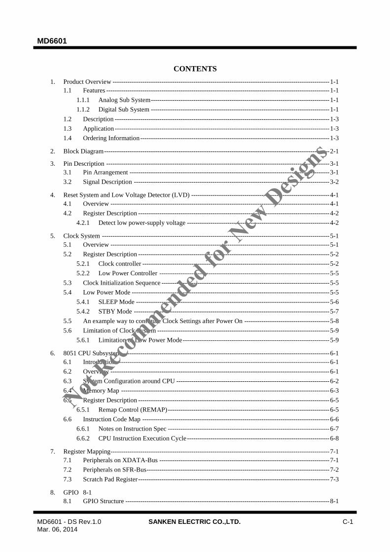
CONTENTS
1. Product Overview ------------------------------------------------------------------------------------------------------ 1-1
1.1 Features --------------------------------------------------------------------------------------------------------- 1-1
1.1.1 Analog Sub System ------------------------------------------------------------------------------------ 1-1
1.1.2 Digital Sub System ------------------------------------------------------------------------------------ 1-1
1.2 Description ----------------------------------------------------------------------------------------------------- 1-3
1.3 Application ----------------------------------------------------------------------------------------------------- 1-3
1.4 Ordering Information ----------------------------------------------------------------------------------------- 1-3
2. Block Diagram ---------------------------------------------------------------------------------------------------------- 2-1
3. Pin Description --------------------------------------------------------------------------------------------------------- 3-1
3.1 Pin Arrangement ---------------------------------------------------------------------------------------------- 3-1
3.2 Signal Description -------------------------------------------------------------------------------------------- 3-2
4. Reset System and Low Voltage Detector (LVD) ----------------------------------------------------------------- 4-1
4.1 Overview ------------------------------------------------------------------------------------------------------- 4-1
4.2 Register Description ------------------------------------------------------------------------------------------ 4-2
4.2.1 Detect low power-supply voltage ------------------------------------------------------------------- 4-2
5. Clock System ----------------------------------------------------------------------------------------------------------- 5-1
5.1 Overview ------------------------------------------------------------------------------------------------------- 5-1
5.2 Register Description ------------------------------------------------------------------------------------------ 5-2
5.2.1 Clock controller ---------------------------------------------------------------------------------------- 5-2
5.2.2 Low Power Controller -------------------------------------------------------------------------------- 5-5
5.3 Clock Initialization Sequence ------------------------------------------------------------------------------- 5-5
5.4 Low Power Mode --------------------------------------------------------------------------------------------- 5-5
5.4.1 SLEEP Mode ------------------------------------------------------------------------------------------- 5-6
5.4.2 STBY Mode -------------------------------------------------------------------------------------------- 5-7
5.5 An example way to configure Clock Settings after Power On ---------------------------------------- 5-8
5.6 Limitation of Clock System --------------------------------------------------------------------------------- 5-9
5.6.1 Limitation of Low Power Mode --------------------------------------------------------------------- 5-9
6. 8051 CPU Subsystem -------------------------------------------------------------------------------------------------- 6-1
6.1 Introduction ---------------------------------------------------------------------------------------------------- 6-1
6.2 Overview ------------------------------------------------------------------------------------------------------- 6-1
6.3 System Configuration around CPU ------------------------------------------------------------------------ 6-2
6.4 Memory Map -------------------------------------------------------------------------------------------------- 6-3
6.5 Register Description ------------------------------------------------------------------------------------------ 6-5
6.5.1 Remap Control (REMAP) ---------------------------------------------------------------------------- 6-5
6.6 Instruction Code Map ---------------------------------------------------------------------------------------- 6-6
6.6.1 Notes on Instruction Spec ---------------------------------------------------------------------------- 6-7
6.6.2 CPU Instruction Execution Cycle ------------------------------------------------------------------- 6-8
7. Register Mapping------------------------------------------------------------------------------------------------------- 7-1
7.1 Peripherals on XDATA-Bus -------------------------------------------------------------------------------- 7-1
7.2 Peripherals on SFR-Bus -------------------------------------------------------------------------------------- 7-2
7.3 Scratch Pad Register ------------------------------------------------------------------------------------------ 7-3
8. GPIO 8-1
8.1 GPIO Structure ------------------------------------------------------------------------------------------------ 8-1
Not Reco
mmended
for N
ew D
esign
s
MD6601
MD6601 - DS Rev.1.0 SANKEN ELECTRIC CO.,LTD. C-2 Mar. 06, 2014
8.2 Register Description ------------------------------------------------------------------------------------------ 8-3
8.2.1 Pin Function Select for GPIO0 (PFS0) ------------------------------------------------------------- 8-4
8.2.2 Pin Function Select for GPIOn (PFSn) (n=1-3) -------------------------------------------------- 8-4
8.2.3 Pin Data Direction for GPIOn (PDDn) (n=0-3) -------------------------------------------------- 8-5
8.2.4 Pin Data for GPIOn (PDRn) (n=0-3) --------------------------------------------------------------- 8-5
8.2.5 Pin Pull Up Control for GPIOn (PPUn) (n=0-3) ------------------------------------------------- 8-6
8.2.6 Pin Interrupt Enable for GPIOn (PIEn) (n=0-3) -------------------------------------------------- 8-6
8.2.7 Pin Interrupt Flag for GPIOn (PIFn) (n=0-3) ----------------------------------------------------- 8-7
8.2.8 Pin Interrupt Sense for GPIOn (PISn) (n=0-3) ---------------------------------------------------- 8-7
8.2.9 Pin Interrupt Level for GPIOn (PILn) (n=0-3) ---------------------------------------------------- 8-8
8.2.10 Pin Interrupt Both Edge for GPIOn (PIBn) (n=0-3) --------------------------------------------- 8-8
8.2.11 ADC Event Select from GPIOn (PEADCn) (n=0-3) -------------------------------------------- 8-9
8.2.12 PWM Event Select from GPIOn (PEPWMn) (n=0-3) ------------------------------------------ 8-9
8.2.13 PWM Event Gathering Method (PEMETHOD) ----------------------------------------------- 8-10
9. Event Connections in the LSI --------------------------------------------------------------------------------------- 9-1
10. Interrupt Controller -------------------------------------------------------------------------------------------------- 10-1
10.1 Overview ----------------------------------------------------------------------------------------------------- 10-1
10.2 Interrupt Vectors -------------------------------------------------------------------------------------------- 10-2
10.3 Register Description ---------------------------------------------------------------------------------------- 10-3
10.3.1 INTMST ---------------------------------------------------------------------------------------------- 10-3
10.3.2 INTENA ---------------------------------------------------------------------------------------------- 10-4
10.3.3 INTLVL ----------------------------------------------------------------------------------------------- 10-4
10.3.4 INTCFG ----------------------------------------------------------------------------------------------- 10-5
10.3.5 INTFLG ----------------------------------------------------------------------------------------------- 10-5
10.4 Operation ----------------------------------------------------------------------------------------------------- 10-6
10.4.1 Initial setting ----------------------------------------------------------------------------------------- 10-6
10.4.2 Interrupt flag ----------------------------------------------------------------------------------------- 10-6
10.4.3 Interrupt level ---------------------------------------------------------------------------------------- 10-6
10.4.4 Interrupt of external pins --------------------------------------------------------------------------- 10-8
11. DSAC (Direct SFR Access Controller) --------------------------------------------------------------------------- 11-1
11.1 Overview ----------------------------------------------------------------------------------------------------- 11-1
11.2 Event ---------------------------------------------------------------------------------------------------------- 11-2
11.3 Register Description ---------------------------------------------------------------------------------------- 11-3
11.3.1 DSACNTAn (DSAC Control A Register) ------------------------------------------------------- 11-4
11.3.2 DSACNTBn (DSAC Control B Register) ------------------------------------------------------- 11-5
11.3.3 DSASRCn (DSAC Source address Register) --------------------------------------------------- 11-5
11.3.4 DSADSTn (DSAC Destination address Register) --------------------------------------------- 11-6
11.4 Operation ----------------------------------------------------------------------------------------------------- 11-6
11.5 Initialization sequence -------------------------------------------------------------------------------------- 11-8
11.6 Limitation of DSAC ---------------------------------------------------------------------------------------- 11-8
11.6.1 Disabling DSAC ------------------------------------------------------------------------------------- 11-8
12. FLASH Memory Control ------------------------------------------------------------------------------------------- 12-1
12.1 Overview ----------------------------------------------------------------------------------------------------- 12-1
12.2 Flash memory mat structure ------------------------------------------------------------------------------- 12-3
12.3 Register Description ---------------------------------------------------------------------------------------- 12-4
12.3.1 FMTIME ---------------------------------------------------------------------------------------------- 12-4
Not Reco
mmended
for N
ew D
esign
s
MD6601
MD6601 - DS Rev.1.0 SANKEN ELECTRIC CO.,LTD. C-3 Mar. 06, 2014
12.3.2 FMPAGE --------------------------------------------------------------------------------------------- 12-5
12.3.3 FMROW ---------------------------------------------------------------------------------------------- 12-5
12.3.4 FMCOL ----------------------------------------------------------------------------------------------- 12-6
12.3.5 FMCTRL --------------------------------------------------------------------------------------------- 12-6
12.3.6 FMEXE ----------------------------------------------------------------------------------------------- 12-7
12.3.7 FMRPD0-3 ------------------------------------------------------------------------------------------- 12-8
12.3.8 FMRMOD -------------------------------------------------------------------------------------------- 12-8
12.4 Operation ----------------------------------------------------------------------------------------------------- 12-9
12.4.1 Instruction fetch ------------------------------------------------------------------------------------- 12-9
12.4.2 Flash programming --------------------------------------------------------------------------------- 12-9
12.4.2.1. Mass Erase ---------------------------------------------------------------------------------- 12-9
12.4.2.2. Page Erase ---------------------------------------------------------------------------------- 12-10
12.4.2.3. Row Programming ------------------------------------------------------------------------ 12-11
12.4.2.4. Row Data Read ---------------------------------------------------------------------------- 12-12
12.4.2.5. Protecting Release ------------------------------------------------------------------------ 12-13
12.5 Flash protecting level control ---------------------------------------------------------------------------- 12-13
12.6 Limitation of FLC ------------------------------------------------------------------------------------------ 12-14
12.6.1 Going to low power mode ------------------------------------------------------------------------ 12-14
12.6.2 Clock frequency for flash program -------------------------------------------------------------- 12-14
12.6.3 Row programming time --------------------------------------------------------------------------- 12-14
12.6.4 Protect function ------------------------------------------------------------------------------------- 12-14
13. Tiny DSP -------------------------------------------------------------------------------------------------------------- 13-1
13.1 Overview ----------------------------------------------------------------------------------------------------- 13-1
13.2 Block Diagram----------------------------------------------------------------------------------------------- 13-2
13.3 Resources ----------------------------------------------------------------------------------------------------- 13-3
13.4 Instructions --------------------------------------------------------------------------------------------------- 13-4
13.4.1 Instruction Format ----------------------------------------------------------------------------------- 13-4
13.4.2 Instruction Set ---------------------------------------------------------------------------------------- 13-5
13.5 Operation ----------------------------------------------------------------------------------------------------- 13-6
13.6 Event Outputs ------------------------------------------------------------------------------------------------ 13-8
13.7 Program Memory ------------------------------------------------------------------------------------------- 13-8
13.8 Example of Application ------------------------------------------------------------------------------------ 13-9
13.9 Register Description --------------------------------------------------------------------------------------- 13-10
13.9.1 DSPn Control Register (DSPnCTRL) (n=0-1) ------------------------------------------------ 13-13
13.9.2 DSPn Execution Register (DSPnEXEC) (n=0-1) --------------------------------------------- 13-13
13.9.3 DSPn Debug Register (DSPnDBG) ------------------------------------------------------------- 13-14
13.9.4 DSPn Rx LSB Side (DSPn_Rx_L) (n=0-1, x=0-7) ------------------------------------------- 13-15
13.9.5 DSPn Rx MSB Side (DSPn_Rx_H) (n=0-1,x=0-7) ------------------------------------------ 13-16
13.9.6 DSPn Rx LSB Side (DSPn_Rx_L) (n=0-1,x=8-15) ------------------------------------------ 13-17
13.9.7 DSPn Rx MSB Side (DSPn_Rx_H) (n=0-1,x=8-15) ----------------------------------------- 13-17
13.9.8 DSPn ACC (DSPn_ACC_x) (n=0-1,x=0-4) --------------------------------------------------- 13-18
13.9.9 DSPn Program Memory LSB/MSB Side (DSPn_PRG_DATL/H) (n=0-1) -------------- 13-19
13.9.10 DSPn Program Memory Address (DSPn_PRG_ADR) (n=0-1) ---------------------------- 13-19
13.9.11 DSPn Execution Trigger Status (DSPnTRG) (n=0-1) ---------------------------------------- 13-20
13.9.12 DSPn Access Counter Clear Register (DSPnRST) (n=0-1) --------------------------------- 13-20
13.10 Caution of operation --------------------------------------------------------------------------------------- 13-21
13.10.1 Restriction about the TinyDSP interrupt enable bits ------------------------------------------ 13-21
Not Reco
mmended
for N
ew D
esign
s

MD6601
MD6601 - DS Rev.1.0 SANKEN ELECTRIC CO.,LTD. C-4 Mar. 06, 2014
13.10.2 DSP_SS asserted in the DIV instruction ------------------------------------------------------- 13-21
14. High-Resolution PWM ---------------------------------------------------------------------------------------------- 14-1
14.1 Overview ----------------------------------------------------------------------------------------------------- 14-1
14.2 Block Diagram----------------------------------------------------------------------------------------------- 14-1
14.3 Resources ----------------------------------------------------------------------------------------------------- 14-2
14.4 Clock Source selection ------------------------------------------------------------------------------------- 14-3
14.5 Operation ----------------------------------------------------------------------------------------------------- 14-3
14.5.1 Direct Mode and Buffer Mode -------------------------------------------------------------------- 14-8
14.5.2 PWM Mode 0 ---------------------------------------------------------------------------------------- 14-9
14.5.3 PWM Mode 1 (Auto Dead Time) ---------------------------------------------------------------- 14-10
14.5.4 PWM Mode 2 (Phase Shift) ---------------------------------------------------------------------- 14-14
14.5.5 PWM Mode 3 (Phase Shift + Auto Dead Time) ----------------------------------------------- 14-15
14.6 Contentions or Output Control Conditions ------------------------------------------------------------ 14-19
14.7 Operation Timing ------------------------------------------------------------------------------------------ 14-20
14.8 Re-Trigger Operations ------------------------------------------------------------------------------------ 14-25
14.8.1 Events for re-trigger-------------------------------------------------------------------------------- 14-25
14.8.2 Re-Trigger Operation Mode A ------------------------------------------------------------------- 14-26
14.8.3 Re-Trigger Operation Mode B ------------------------------------------------------------------- 14-27
14.8.4 Re-Trigger Operation Mode C ------------------------------------------------------------------- 14-28
14.8.5 Re-Trigger Operation D --------------------------------------------------------------------------- 14-29
14.8.6 Re-Trigger Mask Operation ---------------------------------------------------------------------- 14-30
14.8.7 Detail method to change Waveform Level by Re-Trigger ----------------------------------- 14-30
14.9 Event Output ------------------------------------------------------------------------------------------------ 14-31
14.10 Interrupt Output -------------------------------------------------------------------------------------------- 14-31
14.11 Register Access --------------------------------------------------------------------------------------------- 14-31
14.12 Register Description --------------------------------------------------------------------------------------- 14-33
14.12.1 PWMENBL ----------------------------------------------------------------------------------------- 14-35
14.12.2 PWMCSC0 ------------------------------------------------------------------------------------------ 14-35
14.12.3 PWMCSC1 ------------------------------------------------------------------------------------------ 14-36
14.12.4 PWMCNTS ----------------------------------------------------------------------------------------- 14-37
14.12.5 PWMnCSS (n=0~3) ------------------------------------------------------------------------------- 14-37
14.12.6 PWMnEVO0/1/T (n=0~3) ------------------------------------------------------------------------ 14-38
14.12.7 PWMnINTS0/1(n=0~3) --------------------------------------------------------------------------- 14-39
14.12.8 PWMnINTF(n=0~3) ------------------------------------------------------------------------------- 14-40
14.12.9 PWMnACCLR (n=0~3) --------------------------------------------------------------------------- 14-41
14.12.10 PWMnACSTS (n=0~3) ----------------------------------------------------------------------- 14-42
14.12.11 CNTn(n=0~3) --------------------------------------------------------------------------------------- 14-43
14.12.12 CMP_xxxn(n=0~3) ---------------------------------------------------------------------------- 14-44
14.12.13 PWMnCNTMD(n=0~3) ---------------------------------------------------------------------- 14-46
14.12.14 PWMnHCR0(n=0~3) -------------------------------------------------------------------------- 14-47
14.12.15 PWMnLCR0(n=0~3) -------------------------------------------------------------------------- 14-48
14.12.16 PWMnHCR1 (n=0~3) ------------------------------------------------------------------------- 14-49
14.12.17 PWMnLCR1 (n=0~3) ------------------------------------------------------------------------- 14-49
14.12.18 PWMnMODE (n=0~3) ------------------------------------------------------------------------ 14-50
14.12.19 PWMnRTRG(n=0~3) ------------------------------------------------------------------------- 14-51
14.12.20 PWMnRTRS (n=0~3) ------------------------------------------------------------------------- 14-51
14.12.21 PWMnRTGC (n=0~3) ------------------------------------------------------------------------- 14-52
Not Reco
mmended
for N
ew D
esign
s

MD6601
MD6601 - DS Rev.1.0 SANKEN ELECTRIC CO.,LTD. C-5 Mar. 06, 2014
14.12.22 PWMnRTL (n=0~3) --------------------------------------------------------------------------- 14-53
14.12.23 PWMnRTMC (n=0~3) ------------------------------------------------------------------------ 14-54
14.12.24 PWMnRTMP (n=0~3) ------------------------------------------------------------------------- 14-54
14.12.25 BUF_MIN/MAXn(n=0~3) ------------------------------------------------------------------- 14-55
14.12.26 BUF_A/B/C/Dn (n=0~3) --------------------------------------------------------------------- 14-56
14.13 Caution of Operation -------------------------------------------------------------------------------------- 14-58
14.13.1 Restrictions about Auto Dead Time Mode of PWM ------------------------------------------ 14-58
14.13.2 Restriction about PWM Mode 2/3 (Phase Shift Mode) -------------------------------------- 14-59
14.13.3 Restriction about PWM Re-Trigger Mode ----------------------------------------------------- 14-60
14.13.4 Restriction about PWM Re-Trigger Mask ----------------------------------------------------- 14-61
15. Watch Dog Timer ---------------------------------------------------------------------------------------------------- 15-1
15.1 Overview ----------------------------------------------------------------------------------------------------- 15-1
15.2 Register Description ---------------------------------------------------------------------------------------- 15-1
15.2.1 WDT Control register------------------------------------------------------------------------------- 15-2
15.3 Reset diagram ------------------------------------------------------------------------------------------------ 15-3
15.4 Interrupt diagram -------------------------------------------------------------------------------------------- 15-3
15.5 Prescaler ------------------------------------------------------------------------------------------------------ 15-4
15.6 Operation ----------------------------------------------------------------------------------------------------- 15-5
15.6.1 How to write into WTCNT and WTCSR -------------------------------------------------------- 15-5
15.6.2 Watch dog timer mode ------------------------------------------------------------------------------ 15-6
15.6.3 Interval Timer Mode -------------------------------------------------------------------------------- 15-7
16. 16 bit Timer (TMR) -------------------------------------------------------------------------------------------------- 16-1
16.1 Overview ----------------------------------------------------------------------------------------------------- 16-1
16.2 Register Description ---------------------------------------------------------------------------------------- 16-2
16.2.1 Timer control Mode Register (TMOD0) -------------------------------------------------------- 16-3
16.2.2 Timer control Mode Register (TMOD1) -------------------------------------------------------- 16-4
16.2.3 Timer n Status Register (TMSRn) (n=0-1) ------------------------------------------------------ 16-5
16.2.4 Timer n Control register (TMCRn) (n=0-1) ---------------------------------------------------- 16-6
16.2.5 Timer n event clear register (TMECRn) (n=0-1) ---------------------------------------------- 16-7
16.2.6 Timer n compare match A-L (TCMPALn) (n=0-1) -------------------------------------------- 16-7
16.2.7 Timer n compare match A-H (TCMPAHn) (n=0-1) ------------------------------------------- 16-8
16.2.8 Timer n compare match B-L (TCMPBLn) (n=0-1) -------------------------------------------- 16-8
16.2.9 Timer n compare match B-H (TCMPBHn) (n=0-1) ------------------------------------------- 16-8
16.2.10 Timer n counter L (TCNTLn) (n=0-1) ----------------------------------------------------------- 16-9
16.2.11 Timer n counter H (TCNTHn) (n=0-1) ---------------------------------------------------------- 16-9
16.3 Operation ----------------------------------------------------------------------------------------------------- 16-9
16.3.1 16 bit Register access ------------------------------------------------------------------------------- 16-9
16.3.2 Counter Operation ---------------------------------------------------------------------------------- 16-10
16.3.3 Compare match operation ------------------------------------------------------------------------- 16-10
16.3.4 Auto Clear ------------------------------------------------------------------------------------------- 16-10
16.3.5 PWM Event Clear ---------------------------------------------------------------------------------- 16-10
16.3.6 32bit Counter Mode -------------------------------------------------------------------------------- 16-10
16.3.7 Compare match timing ---------------------------------------------------------------------------- 16-10
17. SPI 17-1
17.1 Overview ----------------------------------------------------------------------------------------------------- 17-1
17.2 Register Description ---------------------------------------------------------------------------------------- 17-2
Not Reco
mmended
for N
ew D
esign
s
MD6601
MD6601 - DS Rev.1.0 SANKEN ELECTRIC CO.,LTD. C-6 Mar. 06, 2014
17.2.1 SPI Control Register (SPICR) --------------------------------------------------------------------- 17-3
17.2.2 SPI CLOCK DIV Register (SPICLK) ----------------------------------------------------------- 17-5
17.2.3 SPI data format Register (SPIFMT) -------------------------------------------------------------- 17-5
17.2.4 SPI Status register (SPISR) ------------------------------------------------------------------------ 17-6
17.2.5 SPI Error Status register (SPIESR) --------------------------------------------------------------- 17-6
17.2.6 SPI Interrupt Enable Register (SPIIER) --------------------------------------------------------- 17-7
17.2.7 SPI Data Register L (SPIDRL) -------------------------------------------------------------------- 17-8
17.2.8 SPI Data Register H (SPIDRH) ------------------------------------------------------------------- 17-8
17.3 Interrupt generation ----------------------------------------------------------------------------------------- 17-9
17.3.1 INT_TX ----------------------------------------------------------------------------------------------- 17-9
17.3.2 INT_RX ---------------------------------------------------------------------------------------------- 17-10
17.4 Timing chart and Connection ---------------------------------------------------------------------------- 17-11
17.4.1 Master mode----------------------------------------------------------------------------------------- 17-11
17.4.2 Slave Mode ------------------------------------------------------------------------------------------ 17-13
17.5 Operation ---------------------------------------------------------------------------------------------------- 17-14
17.5.1 Master mode----------------------------------------------------------------------------------------- 17-14
17.5.2 Slave Mode ------------------------------------------------------------------------------------------ 17-17
18. I2C (SMBUS) --------------------------------------------------------------------------------------------------------- 18-1
18.1 Overview ----------------------------------------------------------------------------------------------------- 18-1
18.2 Register Description ---------------------------------------------------------------------------------------- 18-2
18.2.1 I2C Bus Control Register (ICCR) ---------------------------------------------------------------- 18-3
18.2.2 I2C Bus Status Register (ICSR) ------------------------------------------------------------------ 18-4
18.2.3 I2C Bus Receive Data Register (ICRXDR) ----------------------------------------------------- 18-6
18.2.4 I2C Bus Transmit Data Register (ICTXDR) ---------------------------------------------------- 18-7
18.2.5 Transmit Address Register (ICTSAR) ----------------------------------------------------------- 18-7
18.2.6 Slave Address Register (ICSAR) ----------------------------------------------------------------- 18-8
18.2.7 Clock Divid Register (ICCLK) ------------------------------------------------------------------- 18-8
18.2.8 I2C Command Register (ICCMD) --------------------------------------------------------------- 18-9
18.2.9 I2C Bus SDA Setup Time Register (ICSSTR) ------------------------------------------------ 18-10
18.2.10 I2C Bus SDA Hold Time Register (ICSHTR) ------------------------------------------------ 18-11
18.2.11 I2C Bus SDA Hardware Status Register 0(ICHDSR0) -------------------------------------- 18-12
18.2.12 I2C Bus SDA Hardware Status Register 1(ICHDSR1) -------------------------------------- 18-12
18.2.13 I2C Time Base Register --------------------------------------------------------------------------- 18-13
18.2.14 SMBUS INT Status Register --------------------------------------------------------------------- 18-13
18.3 I2C bus data format ---------------------------------------------------------------------------------------- 18-14
18.4 Slave receiver operation ---------------------------------------------------------------------------------- 18-15
18.5 Slave transmitter operation ------------------------------------------------------------------------------- 18-17
18.6 Master receiver operation --------------------------------------------------------------------------------- 18-19
18.7 Master transmitter operation ----------------------------------------------------------------------------- 18-21
18.8 Noise Filter -------------------------------------------------------------------------------------------------- 18-23
19. UART 19-1
19.1 Overview ----------------------------------------------------------------------------------------------------- 19-1
19.2 External (off-chip) connections --------------------------------------------------------------------------- 19-2
19.3 Register Description ---------------------------------------------------------------------------------------- 19-3
19.3.1 Receiver Buffer Register/Transmitter Holding Register -------------------------------------- 19-3
19.3.2 Interrupt Enable Register (IER) ------------------------------------------------------------------- 19-3
Not Reco
mmended
for N
ew D
esign
s
MD6601
MD6601 - DS Rev.1.0 SANKEN ELECTRIC CO.,LTD. C-7 Mar. 06, 2014
19.3.3 Interrupt Identification Register (IIR)------------------------------------------------------------ 19-4
19.3.4 FIFO Control Register (FCR) --------------------------------------------------------------------- 19-5
19.3.5 Line Control Register (LCR) ---------------------------------------------------------------------- 19-6
19.3.6 Line Status Register (LSR) ------------------------------------------------------------------------ 19-7
19.3.7 Divisor Latches -------------------------------------------------------------------------------------- 19-8
19.3.8 Baud rate ---------------------------------------------------------------------------------------------- 19-9
19.4 Operation ---------------------------------------------------------------------------------------------------- 19-10
19.5 Caution of operation --------------------------------------------------------------------------------------- 19-10
19.5.1 Restriction about the UART register access --------------------------------------------------- 19-10
20. Analog Inter-Connection Network -------------------------------------------------------------------------------- 20-1
20.1 Overview ----------------------------------------------------------------------------------------------------- 20-1
21. High Speed 10bit SAR ADC --------------------------------------------------------------------------------------- 21-1
21.1 Overview ----------------------------------------------------------------------------------------------------- 21-1
21.2 Register Description ---------------------------------------------------------------------------------------- 21-3
21.2.1 ADCn (ADC Configuration Register) ----------------------------------------------------------- 21-5
21.2.2 ADSMn (ADC Sample Mode Register) --------------------------------------------------------- 21-6
21.2.3 ADSLn (ADC Channel Sequence L Register) ------------------------------------------------- 21-6
21.2.4 ADSHn (ADC Channel Sequence H Register) ------------------------------------------------- 21-7
21.2.5 ADTRGLn (ADC Event Source L Register) --------------------------------------------------- 21-8
21.2.6 ADTRGHn (ADC Event Source H Register) --------------------------------------------------- 21-8
21.2.7 ADENn (ADC Enable Register) ------------------------------------------------------------------ 21-9
21.2.8 ADACCLRn (ADC Access Counter Clear Register) ----------------------------------------- 21-9
21.2.9 ADUPTHL0n (ADC Ch0 Update Threshold L Register) ----------------------------------- 21-10
21.2.10 ADUPTHH0n (ADC Ch0 Update Threshold H Register) ----------------------------------- 21-10
21.2.11 ADNUPCNTn (ADC Ch0 Non-update Count Register) ------------------------------------ 21-11
21.2.12 ADOLXn (ADC ChX Offset Data L Register, n=0-1) --------------------------------------- 21-12
21.2.13 ADOHXn (ADC ChX Offset Data H Register, n=0-1) -------------------------------------- 21-13
21.2.14 ADLXn (ADC ChX Data L Register, n=0-1) -------------------------------------------------- 21-14
21.2.15 ADHXn (ADC ChX Data H Register, n=0-1) ------------------------------------------------- 21-15
21.2.16 ADT (ADC Trigger Register) -------------------------------------------------------------------- 21-16
21.2.17 ADI (ADC Interrupt Register) ------------------------------------------------------------------- 21-17
21.3 Operation ---------------------------------------------------------------------------------------------------- 21-18
21.3.1 Basic operation ------------------------------------------------------------------------------------- 21-18
21.3.2 Conversion Mode ---------------------------------------------------------------------------------- 21-19
21.3.2.1. “Burst until Sequence End” mode ------------------------------------------------------ 21-19
21.3.2.2. “Step and Round Sequence” Mode ---------------------------------------------------- 21-20
21.3.3 Dual Sample/Hold ---------------------------------------------------------------------------------- 21-21
21.3.4 Conversion start trigger --------------------------------------------------------------------------- 21-22
21.3.5 Converted data offset adjustment ---------------------------------------------------------------- 21-22
21.3.6 Interrupts --------------------------------------------------------------------------------------------- 21-22
21.3.7 ADC Event ------------------------------------------------------------------------------------------ 21-23
21.3.8 Reading converted data ---------------------------------------------------------------------------- 21-23
21.3.9 Threshold for conversion data update ----------------------------------------------------------- 21-23
21.3.10 Initialization sequence ----------------------------------------------------------------------------- 21-24
21.4 Limitation of ADC10 -------------------------------------------------------------------------------------- 21-25
21.4.1 Disabling ADC -------------------------------------------------------------------------------------- 21-25
Not Reco
mmended
for N
ew D
esign
s
MD6601
MD6601 - DS Rev.1.0 SANKEN ELECTRIC CO.,LTD. C-8 Mar. 06, 2014
21.4.2 Going to standby mode ---------------------------------------------------------------------------- 21-25
21.4.3 Clock frequency setting --------------------------------------------------------------------------- 21-25
22. High Precision 12 bit SAR ADC ---------------------------------------------------------------------------------- 22-1
22.1 Overview ----------------------------------------------------------------------------------------------------- 22-1
22.2 Register Description ---------------------------------------------------------------------------------------- 22-3
22.2.1 ADC2 (ADC Configuration Register) ----------------------------------------------------------- 22-5
22.2.2 ADSL2 (ADC Channel Sequence L Register) ------------------------------------------------- 22-6
22.2.3 ADSH2 (ADC Channel Sequence H Register) ------------------------------------------------- 22-6
22.2.4 ADTRGL2 (ADC Event Source L Register) --------------------------------------------------- 22-7
22.2.5 ADTRGH2 (ADC Event Source H Register) --------------------------------------------------- 22-7
22.2.6 ADEN2 (ADC Enable Register) ------------------------------------------------------------------ 22-8
22.2.7 ADACCLR2 (ADC Access Counter Clear Register) ----------------------------------------- 22-8
22.2.8 ADUPTHL02 (ADC Ch0 Update Threshold L Register) ------------------------------------ 22-9
22.2.9 ADUPTHH02 (ADC Ch0 Update Threshold H Register) ------------------------------------ 22-9
22.2.10 ADNUPCNT2 (ADC Ch0 Non-update Count Register) ------------------------------------- 22-9
22.2.11 ADOLX2 (ADC ChX Offset Data L Register) ------------------------------------------------ 22-10
22.2.12 ADOHX2 (ADC ChX Offset Data H Register, X=0-9) ------------------------------------- 22-11
22.2.13 ADLX2 (ADC ChX Data L Register) ---------------------------------------------------------- 22-12
22.2.14 ADHX2 (ADC ChX Data H Register) ---------------------------------------------------------- 22-13
22.2.15 ADT (ADC Trigger Register) -------------------------------------------------------------------- 22-13
22.2.16 ADI (ADC Interrupt Register) ------------------------------------------------------------------- 22-13
22.3 Operation ---------------------------------------------------------------------------------------------------- 22-14
22.3.1 Basic operation ------------------------------------------------------------------------------------- 22-14
22.3.2 Conversion Mode ---------------------------------------------------------------------------------- 22-15
22.3.2.1. Burst until Sequence End mode -------------------------------------------------------- 22-15
22.3.2.2. Step and Round Sequence Mode ------------------------------------------------------- 22-16
22.3.3 Conversion start trigger --------------------------------------------------------------------------- 22-17
22.3.4 Converted data offset adjustment ---------------------------------------------------------------- 22-17
22.3.5 Interrupts --------------------------------------------------------------------------------------------- 22-18
22.3.6 ADC Event ------------------------------------------------------------------------------------------ 22-18
22.3.7 Reading converted data ---------------------------------------------------------------------------- 22-18
22.3.8 Threshold for conversion data update ----------------------------------------------------------- 22-18
22.3.9 Initialization sequence ----------------------------------------------------------------------------- 22-19
22.4 Limitation of ADC12 -------------------------------------------------------------------------------------- 22-20
22.4.1 Disabling ADC -------------------------------------------------------------------------------------- 22-20
22.4.2 Going to standby mode ---------------------------------------------------------------------------- 22-20
22.5 Caution of operation --------------------------------------------------------------------------------------- 22-20
22.5.1 Restriction about the conversion time of the 12 bits ADC ---------------------------------- 22-20
23. High Precision 12 bit DAC ----------------------------------------------------------------------------------------- 23-1
23.1 Overview ----------------------------------------------------------------------------------------------------- 23-1
23.2 Block Diagram----------------------------------------------------------------------------------------------- 23-1
23.3 Register Description ---------------------------------------------------------------------------------------- 23-2
23.3.1 Mix DAC Configuration (MIXDAC) ------------------------------------------------------------ 23-2
23.3.2 Mix DAC Data L (MIXDAL) --------------------------------------------------------------------- 23-3
23.3.3 Mix DAC Data H (MIXDAH) -------------------------------------------------------------------- 23-3
23.3.4 Mix DAC Read Data L (MIXDARDL) ---------------------------------------------------------- 23-3
Not Reco
mmended
for N
ew D
esign
s

MD6601
MD6601 - DS Rev.1.0 SANKEN ELECTRIC CO.,LTD. C-9 Mar. 06, 2014
23.3.5 Mix DAC Read Data H (MIXDARDH) --------------------------------------------------------- 23-4
23.3.6 Mix DAC Access Counter Clear Register (DACACCLR) ----------------------------------- 23-4
23.3.7 Mix DAC Output select Register (DACOUT) ------------------------------------------------- 23-5
23.4 Operation ----------------------------------------------------------------------------------------------------- 23-6
23.5 Limitation of DAC ------------------------------------------------------------------------------------------ 23-6
23.5.1 MIXDAL/H register access ------------------------------------------------------------------------ 23-6
24. OPAMP ---------------------------------------------------------------------------------------------------------------- 24-1
24.1 Overview ----------------------------------------------------------------------------------------------------- 24-1
24.2 Register Description ---------------------------------------------------------------------------------------- 24-1
24.2.1 Mix OPAMPn Configuration (MIXOPAn) (n=0-1) ------------------------------------------- 24-2
24.2.2 Mix OPAMPn PGA Configuration (MIXPGAn)(n=0-1) ------------------------------------- 24-2
24.2.3 Notice of OPAMP ----------------------------------------------------------------------------------- 24-3
24.2.3.1. Resistance of analog switch that exists between OPAMP output and PIN ------- 24-3
25. Comparator ------------------------------------------------------------------------------------------------------------ 25-1
25.1 Overview ----------------------------------------------------------------------------------------------------- 25-1
25.2 Register Description ---------------------------------------------------------------------------------------- 25-2
25.2.1 Mix Comparator n Configuration (MIXCMPn) (n=0-3)-------------------------------------- 25-3
25.2.2 Mix Comparator n Functional Select (MIXCMSn) (n=0-3) --------------------------------- 25-4
25.2.3 Comparator n Result (MIXCMRn) (n=0-3)----------------------------------------------------- 25-6
25.2.4 Mix Comparator Interrupt(CMI) ------------------------------------------------------------------ 25-7
25.3 Operation ----------------------------------------------------------------------------------------------------- 25-8
26. Voltage Reference (VREF) ----------------------------------------------------------------------------------------- 26-1
26.1 Overview ----------------------------------------------------------------------------------------------------- 26-1
27. Temperature Sensor (TEMP) --------------------------------------------------------------------------------------- 27-1
27.1 Overview ----------------------------------------------------------------------------------------------------- 27-1
27.2 Register Description ---------------------------------------------------------------------------------------- 27-1
27.2.1 Temperature sensor Control (TEMP) ------------------------------------------------------------ 27-1
28. POC (PWM Output Controller) ------------------------------------------------------------------------------------ 28-1
28.1 Overview ----------------------------------------------------------------------------------------------------- 28-1
28.2 Register Description ---------------------------------------------------------------------------------------- 28-2
28.2.1 POCCRn (POC Control Register) ---------------------------------------------------------------- 28-2
28.2.2 POCSTS (POC Status Register) ------------------------------------------------------------------ 28-3
28.3 Operation ----------------------------------------------------------------------------------------------------- 28-4
29. Electrical Characteristics -------------------------------------------------------------------------------------------- 29-1
29.1 Absolute Maximum Ratings ------------------------------------------------------------------------------ 29-1
29.2 Recommended Operating Conditions ------------------------------------------------------------------- 29-1
29.3 Package Information ---------------------------------------------------------------------------------------- 29-1
29.4 Current Consumption --------------------------------------------------------------------------------------- 29-2
29.5 Low Voltage Detector -------------------------------------------------------------------------------------- 29-2
29.6 Reset Operation --------------------------------------------------------------------------------------------- 29-2
29.7 Clock Operation --------------------------------------------------------------------------------------------- 29-2
29.8 10 bit ADC --------------------------------------------------------------------------------------------------- 29-3
29.9 12 bit ADC --------------------------------------------------------------------------------------------------- 29-3
29.10 12 bit DAC --------------------------------------------------------------------------------------------------- 29-3
29.11 OPAMP ------------------------------------------------------------------------------------------------------- 29-4
Not Reco
mmended
for N
ew D
esign
s

MD6601
MD6601 - DS Rev.1.0 SANKEN ELECTRIC CO.,LTD. C-10 Mar. 06, 2014
29.12 Comparator --------------------------------------------------------------------------------------------------- 29-4
29.13 Voltage Reference ------------------------------------------------------------------------------------------ 29-5
29.14 Temperature Sensor----------------------------------------------------------------------------------------- 29-5
29.15 Analog GND ------------------------------------------------------------------------------------------------- 29-5
29.16 Digital I/O DC Spec ---------------------------------------------------------------------------------------- 29-5
29.17 Digital I/O AC Spec ---------------------------------------------------------------------------------------- 29-6
29.17.1 Timing of PWM ------------------------------------------------------------------------------------- 29-6
29.17.2 Timing of SPI ---------------------------------------------------------------------------------------- 29-6
29.17.3 Timing of I2C ---------------------------------------------------------------------------------------- 29-7
30. Packaging information----------------------------------------------------------------------------------------------- 30-1
30.1 QFN40_PKG_dimensional outline drawing ------------------------------------------------------------ 30-1
30.2 LQFP44_PKG_dimensional outline drawing ---------------------------------------------------------- 30-2
Not Reco
mmended
for N
ew D
esign
s

MD6601
MD6601 - DS Rev.1.0 SANKEN ELECTRIC CO.,LTD. 1-1 Mar. 06, 2014
MD6601 (Mixed Signal MCU)
1. Product Overview
1.1 Features
1.1.1 Analog Sub System
High Speed 10bit SAR ADC 2 Units (Independent)
10 Inputs/unit
Conversion Speed: 4MSPS
(4MSPS includes Sampling Time)
Simultaneous Sampling
Sequence Conversion
Configurable Conversion Triggers
Configurable Result Offset
High Precision 12bit SAR ADC 1 Unit
10 inputs
Conversion Speed: 1MSPS
Sequence Conversion
Configurable Conversion Triggers
Configurable Result Offset
High Precision 12bit DAC 1 Units
Update Rate: 1MSPS
Configurable Update Triggers
High Speed Analog Comparator 4 Units
Response Time: 20ns
Rail-to-Rail Input
Digital Hazard Filter
Configurable Event Generation
Operational Amplifier (OPAMP) 2 Units
Rail-to-Rail Input / Output
Standalone or Unity, Selectable
Voltage Reference Generate 1.2V
Temperature Sensor Measures Junction Temparature
Read from Internal ADC
Analog Inter-Connection Network Configurable Inter-Connections among In/Out
Signals of Analog Modules and External Pins
1.1.2 Digital Sub System
Pipelined 8bit CPU 8051 Compatible Instructions
Pipeline with 3-5 stages
50MHz, 1cycle/8bit-instruction
256bytes Internal RAM
1-wire On-Chip-Debug Interface R/W to all Internal Resources
Go / Step / Stop
PC Break / Data Access Break
Reset
FLASH Program / Erase
FLASH Memory 16KB
Feeds 8bit Instruction in 1cyc
Protection Supported
Internal RAM 1KB
Tiny DSP 2 Units (Independent)
16bit Fixed Point
Sequence Programmable
32step Instruction Memory
16 Data Registers + Accumulator
Instructions: Multiply, Division, MAC,
Barrel-Shift, Move, Jump
Hardware Divider Supported
Event Synchronized Sequence
Configurable Event Generation
Example: 2P3Z IIR Filter10 cyc
High Resolution PWM 8-outputs (4-pairs for Hi/Lo Sides)
4 x 16bit Counters for each pair
Counters can be Synchronized
PWM Resolution: 1ns
Configurable PWM Duty (0%-100%) and Carrier
Frequency in every PWM cycle
Configurable Non-Overlap Time
Counter Modes: Up and Up/Down
Phase Shift Mode Supported
Re-Trigger Operations by Internal /external Events
Direct SFR Access Controller Direct Data Transfer between Peripheral Registers
(SFR: Special Function Register)
Selectable Transfer Trigger Event
Not Reco
mmended
for N
ew D
esign
s

MD6601
MD6601 - DS Rev.1.0 SANKEN ELECTRIC CO.,LTD. 1-2 Mar. 06, 2014
Interrupt Timers 2 Units
16bit Counter
Compare Match generates Event
synchronization with PWM
SPI 1 Unit, Master/Slave
3-wires (Clock, MOSI, MISO)
Dedicated Baud Rate Generator
I2C (SMBUS) 1 Unit, Master/Slave
Dedicated Baud Rate Generator
SMBUS Compatible I/O Buffer
UART 1 Unit
Dedicated Baud Rate Generator
GPIO Digital & Analog Multiplexed
Pull-Up MOS
Configurable as Interrupt Sources
Interrupt Controller
Watch Dog Timer (WDT)
Low Voltage Detector (LVD)
Reset Control External Reset
Internal Power On Reset (POR)
Clock Control External XTAL Oscillator
Internal Ring Oscillator (IRC)
PLL
External Power Supply Voltage 3.3V for each DVCC and AVCC
Internal Core Voltage Regulator
Package QFN-40 (6x6mm, P0.5)
LQFP-44 (10x10mm, P0.8)
Not Reco
mmended
for N
ew D
esign
s

MD6601
MD6601 - DS Rev.1.0 SANKEN ELECTRIC CO.,LTD. 1-3 Mar. 06, 2014
1.2 Description
The LSI is a MCU (Micro Controller Unit) with Rich and Powerful Analog Elements such as High Speed 10bit ADC,
High Precision 12bit ADC/DAC, High Speed Comparators, and Operational Amplifiers. These analog blocks can be
connected via inter-connection-network to configure the LSI as a user-defined mixed signal device. Moreover, this LSI
integrates not only CPU but also Dedicated Tiny DSP separated from CPU, High-Resolution PWM, and Automatic Data
Transfer Scheme in one chip, which realize Self-Running Feedback Control System without CPU. In such system, CPU
can engage in other tasks such as intelligent controls, communications, system watches, error detections and non-linear
controls, etc. and then, the LSI will provide you high performance control system
1.3 Application
Digital DC-DC Power Supply
Digital AC-DC Power Supply
Digital Assist Power Supply
LED Lighting Control
LED Signage
Wireless Charger
MPPT Solar Controller
Inverter for Solar Battery
Inverter for Motor Control
E-Bike, E-Assist Bicycle
EV Charger
…
1.4 Ordering Information
Part # FLASH/RAM Vcc Package Note
MD6601FNV 16KB/1KB 3.3V QFN-40 Tray
MD6601FNVL 16KB/1KB 3.3V QFN-40 Tape & Reel
MD6601FLV 16KB/1KB 3.3V LQFP-44
Figure 1-1 MSM Internal Functions
Not Reco
mmended
for N
ew D
esign
s
MD6601
MD6601 - DS Rev.1.0 SANKEN ELECTRIC CO.,LTD. 2-1 Mar. 06, 2014
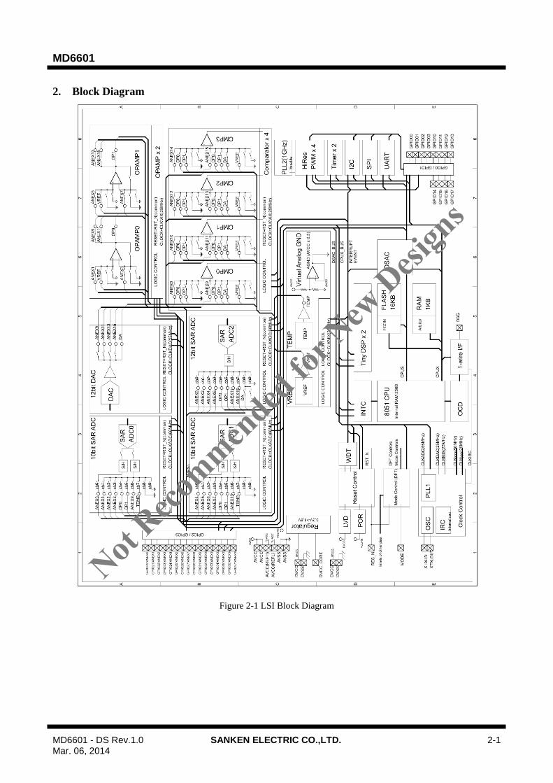
2. Block Diagram
Figure 2-1 LSI Block Diagram
Not Reco
mmended
for N
ew D
esign
s

MD6601
MD6601 - DS Rev.1.0 SANKEN ELECTRIC CO.,LTD. 3-1 Mar. 06, 2014
3. Pin Description
3.1 Pin Arrangement
Figure 3-1 Pin Arrangement for QFN-40 (QFN-41)
Figure 3-2 Pin Arrangement for LQFP-44
1 10
11
20
2130
31
40
41 DVSS
Exposed Die Paddle
only in QFN Package
Top ViewGPIO31/ANEX9
GPIO30/ANEX8
GPIO20/ANEX0
GPIO21/ANEX1
GPIO22/ANEX2
GPIO23/ANEX3
GPIO24/ANEX4
AV
CC
1
AV
SS
GPIO27/ANEX7
GP
IO32
/AN
EX
10
GP
IO33
/AN
EX
11
DV
SS
DB
G
/RE
S
XT
AL
IN
XT
AL
OU
T
MO
DE
DV
CC
DV
CC
_C
OR
EGPIO25/ANEX5
GPIO26/ANEX6
GP
IO34
/AN
EX
12
GP
IO35
/AN
EX
13
GP
IO36
/AN
EX
14
GPIO10/PWM0H
GPIO11/PWM0L
GPIO12/PWM1H
GPIO13/PWM1L
GPIO14/PWM2H
GPIO15/PWM2L
GP
IO37
/AN
EX
15
GP
IO16
/PW
M3
H
GP
IO17
/PW
M3
L
GPIO00/SDA/CLKMON/SS_N
GPIO01/SCL/SCK
GPIO02/TXD/SO
GPIO03/RXD/SI
AV
CC
2
AV
SS
1 1112
22
2333
34
44 Top ViewGPIO31/ANEX9
GPIO30/ANEX8
GPIO20/ANEX0
GPIO21/ANEX1
GPIO22/ANEX2
GPIO23/ANEX3
GPIO24/ANEX4
AV
CC
1
AV
SS
GPIO27/ANEX7
GP
IO32
/AN
EX
10
DV
CC
_C
OR
E
DB
G
/RE
S
XT
AL
IN
XT
AL
OU
T
MO
DE
DV
CC
DV
SS
GPIO25/ANEX5
GPIO26/ANEX6
GP
IO33
/AN
EX
11
GP
IO34
/AN
EX
12
GP
IO35
/AN
EX
13
GP
IO36
/AN
EX
14
GPIO10/PWM0H
GPIO11/PWM0L
GPIO12/PWM1H
GPIO13/PWM1L
GPIO14/PWM2H
GPIO15/PWM2L
GP
IO37
/AN
EX
15
GP
IO16
/PW
M3
H
GP
IO17
/PW
M3
L
GPIO00/SDA/CLKMON/SS_N
GPIO01/SCL/SCK
GPIO02/TXD/SO
GPIO03/RXD/SI
DVSS
DV
SS
AV
CC
2
AV
SS
DVSS
DV
CC
Not Reco
mmended
for N
ew D
esign
s

MD6601
MD6601 - DS Rev.1.0 SANKEN ELECTRIC CO.,LTD. 3-2 Mar. 06, 2014
3.2 Signal Description
Class QFN Pin
No.
LQFP Pin
No.
Pin Name I/O
PUP
Description INT
5V
In
Sch
mitt
Logic
Level
3.3V
Iout
Digital
Power
Supply
27 25,30 DVCC - - Digital 3.3V
26,41 11,162
9,34
DVSS
- - Digital 0V
25 28 DVCC_CORE
- - Digital Power for Internal Logic (Connect Capacitor.)
Analog
Power Supply
2 2 AVCC1 - - Analog 3.3V
10 10 AVCC2 - - Analog 3.3V
1,9 1,9 AVSS - - Analog 0V
System 28 31 MODE IN - Chip Mode (Fixed to 0) Yes LVTTL
OSC
29 32 /RES IN U Reset Input Yes LVTTL
24 27 XTALIN IN - XTAL Input
23 26 XTALOUT O - XTAL Output
Debug 30 33 DBG I/O U 1-wire Debug Port (open drain) Yes LVTTL 4mA
Serial
11 12 GPIO00/SDA/
CLKMON/SS_N I/O U
GPIO or SDA (od) or
CLKMON or SS_N(SPI) Yes Yes LVTTL 4mA
12 13 GPIO01/SCL/SCK I/O U GPIO or SCL (od) or SCK(SPI) Yes Yes LVTTL 4mA
13 14 GPIO02/TXD/SO I/O U GPIO or TXD or SO(SPI) Yes Yes LVTTL 4mA
14 15 GPIO03/RXD/SI I/O U GPIO or RXD or SI(SPI) Yes Yes LVTTL 4mA
PWM
15 17 GPIO10/PWM0H I/O U GPIO or PWM0H Yes Yes LVTTL 16mA
16 18 GPIO11/PWM0L I/O U GPIO or PWM0L Yes Yes LVTTL 16mA
17 19 GPIO12/PWM1H I/O U GPIO or PWM1H Yes Yes LVTTL 16mA
18 20 GPIO13/PWM1L I/O U GPIO or PWM1L Yes Yes LVTTL 16mA
19 21 GPIO14/PWM2H I/O U GPIO or PWM2H Yes Yes LVTTL 16mA
20 22 GPIO15/PWM2L I/O U GPIO or PWM2L Yes Yes LVTTL 16mA
21 23 GPIO16/PWM3H I/O U GPIO or PWM3H Yes Yes LVTTL 16mA
22 24 GPIO17/PWM3L I/O U GPIO or PWM3L Yes Yes LVTTL 16mA
Analog
31 35 GPIO20/ANEX0 I/O U GPIO or Analog External 0 Yes LVTTL 4mA
32 36 GPIO21/ANEX1 I/O U GPIO or Analog External 1 Yes LVTTL 4mA
33 37 GPIO22/ ANEX2 I/O U GPIO or Analog External 2 Yes LVTTL 4mA
34 38 GPIO23/ ANEX3 I/O U GPIO or Analog External 3 Yes LVTTL 4mA
35 39 GPIO24/ ANEX4 I/O U GPIO or Analog External 4 Yes LVTTL 4mA
36 40 GPIO25/ ANEX5 I/O U GPIO or Analog External 5 Yes LVTTL 4mA
37 41 GPIO26/ ANEX6 I/O U GPIO or Analog External 6 Yes LVTTL 4mA
38 42 GPIO27/ ANEX7 I/O U GPIO or Analog External 7 Yes LVTTL 4mA
39 43 GPIO30/ANEX8 I/O U GPIO or Analog External 8 Yes LVTTL 4mA
40 44 GPIO31/ANEX9 I/O U GPIO or Analog External 9 Yes LVTTL 4mA
3 3 GPIO32/ ANEX10 I/O U GPIO or Analog External 10 Yes LVTTL 4mA
4 4 GPIO33/ ANEX11 I/O U GPIO or Analog External 11 Yes LVTTL 4mA
5 5 GPIO34/ ANEX12 I/O U GPIO or Analog External 12 Yes LVTTL 4mA
6 6 GPIO35/ ANEX13 I/O U GPIO or Analog External 13 Yes LVTTL 4mA
7 7 GPIO36/ ANEX14 I/O U GPIO or Analog External 14 Yes LVTTL 4mA
8 8 GPIO37/ ANEX15 I/O U GPIO or Analog External 15 Yes LVTTL 4mA
Not Reco
mmended
for N
ew D
esign
s
MD6601
MD6601 - DS Rev.1.0 SANKEN ELECTRIC CO.,LTD. 4-1 Mar. 06, 2014
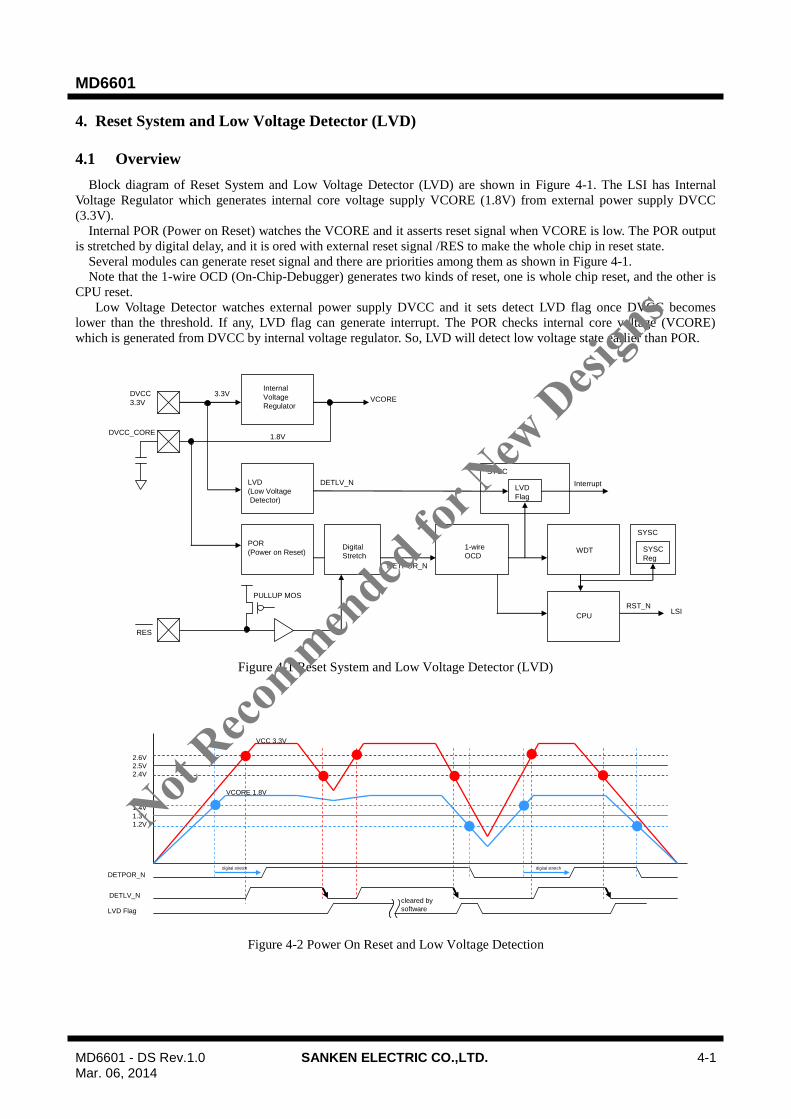
4. Reset System and Low Voltage Detector (LVD)
4.1 Overview
Block diagram of Reset System and Low Voltage Detector (LVD) are shown in Figure 4-1. The LSI has Internal
Voltage Regulator which generates internal core voltage supply VCORE (1.8V) from external power supply DVCC
(3.3V).
Internal POR (Power on Reset) watches the VCORE and it asserts reset signal when VCORE is low. The POR output
is stretched by digital delay, and it is ored with external reset signal /RES to make the whole chip in reset state.
Several modules can generate reset signal and there are priorities among them as shown in Figure 4-1.
Note that the 1-wire OCD (On-Chip-Debugger) generates two kinds of reset, one is whole chip reset, and the other is
CPU reset.
Low Voltage Detector watches external power supply DVCC and it sets detect LVD flag once DVCC becomes
lower than the threshold. If any, LVD flag can generate interrupt. The POR checks internal core voltage (VCORE)
which is generated from DVCC by internal voltage regulator. So, LVD will detect low voltage state earlier than POR.
Figure 4-1 Reset System and Low Voltage Detector (LVD)
Figure 4-2 Power On Reset and Low Voltage Detection
POR
(Power on Reset)
LVD
(Low Voltage
Detector)
LVD
Flag
Interrupt
SYSC
RES
PULLUP MOS
WDT1-wire
OCD
RST_N
DVCC_CORE
Internal
Voltage
Regulator
DVCC
3.3V
1.8V
DETPOR_N
VCORE
Digital
Stretch
DETLV_N
CPULSI
3.3V
SYSC
SYSC
Reg
1.4V
1.3V
1.2V
2.6V
2.5V
2.4V
VCC 3.3V
VCORE 1.8V
DETPOR_N
DETLV_N
LVD Flag
cleared by
software
digital stretch digital stretch
Not Reco
mmended
for N
ew D
esign
s

MD6601
MD6601 - DS Rev.1.0 SANKEN ELECTRIC CO.,LTD. 4-2 Mar. 06, 2014
Table 4-1 Reset Sources and Each Effect
Reset Source OCD is… WDT is… LVD flag is… SYSC is… Others are…
/RES Initialized Initialized Initialized Initialized Initialized
POR Initialized Initialized Initialized Initialized Initialized
WDT Not-Initialized Not-Initialized Not-Initialized Initialized Initialized
OCD
(whole chip) Not-Initialized Initialized Initialized Initialized Initialized
OCD
(CPU reset) Not-Initialized Not-Initialized Not-Initialized Not-Initialized Initialized
4.2 Register Description
Table 4-2 List of Resister
Symbol Name Address initial
value
LVDCTRL LVD Control 0xFF90 0x00
4.2.1 Detect low power-supply voltage
Register LVDCTRL LVD Control Address 0xFF90
Bit Bit Name R/W Initial Description Note
7 LVDE R/W 0 LVD Enable
0: LVD Disable
1: LVD Enable
6 reserved R 0 Read value is 0. Write only 0.
5 reserved R 0 Read value is 0. Write only 0.
4 LVDIE R/W 0 LVD Interrupt Enable
0: LVD Interrupt Disable
1: LVD Interrupt Enable
3 reserved R 0 Read value is 0. Write only 0.
2 reserved R 0 Read value is 0. Write only 0.
1 reserved R 0 Read value is 0. Write only 0.
0 LVDIF R/C 0 LVD Interrupt Flag
(before mask; independent LVDIE)
Read 0: No Request
Read 1: Interrupt Event Occurred
Write 0: No effect
Write 1: To clear corresponding bit
While LVD flag is set, LVD can not detect low voltage state.
Once LVD flag is cleared, LVD can detect low voltage state after having five clock wait.
Not Reco
mmended
for N
ew D
esign
s
MD6601
MD6601 - DS Rev.1.0 SANKEN ELECTRIC CO.,LTD. 5-1 Mar. 06, 2014
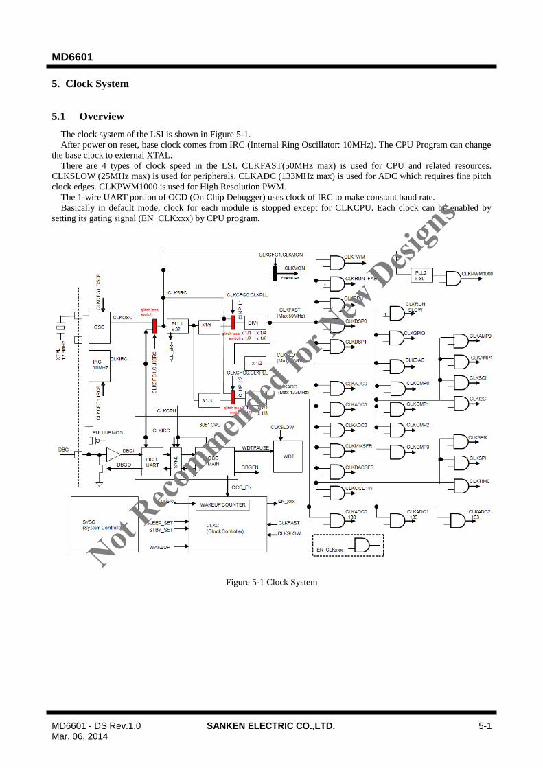
5. Clock System
5.1 Overview
The clock system of the LSI is shown in Figure 5-1.
After power on reset, base clock comes from IRC (Internal Ring Oscillator: 10MHz). The CPU Program can change
the base clock to external XTAL.
There are 4 types of clock speed in the LSI. CLKFAST(50MHz max) is used for CPU and related resources.
CLKSLOW (25MHz max) is used for peripherals. CLKADC (133MHz max) is used for ADC which requires fine pitch
clock edges. CLKPWM1000 is used for High Resolution PWM.
The 1-wire UART portion of OCD (On Chip Debugger) uses clock of IRC to make constant baud rate.
Basically in default mode, clock for each module is stopped except for CLKCPU. Each clock can be enabled by
setting its gating signal (EN_CLKxxx) by CPU program.
Figure 5-1 Clock System
Not Reco
mmended
for N
ew D
esign
s

MD6601
MD6601 - DS Rev.1.0 SANKEN ELECTRIC CO.,LTD. 5-2 Mar. 06, 2014
5.2 Register Description
Table 5-1 List of Resisters
Symbol Name Address Initial value
CLKCFG0 Clock Configuration 0xFF80 0x00
CLKCFG1 Clock Configuration 0xFF81 0x01
MCLKE0 Module Clock Enable 0 0xFF84 0x00
MCLKE1 Module Clock Enable 1 0xFF85 0x00
MCLKE2 Module Clock Enable 2 0xFF86 0x00
MCLKE3 Module Clock Enable 3 0xFF87 0x00
LPCTRL Low Power Control 0xFFA0 0x00
5.2.1 Clock controller
Register CLKCFG0 Clock Configuration Address 0xFF80
Bit Bit Name R/W Initial Description Note
7 PLLERR R 0 PLL1 Error
0: PLL1 is in normal state
1: PLL1 says something error.
6 PLLEN R/W 0 PLL1 Enable
0: PLL1 Disable
1: PLL1 Enable
5 CLKPLL R/W 0 PLL Clock Select
0: CLKPLL1 and CLKPLL2 are connected to
CLKSRC
1: CLKPLL1 and CLKPLL2 are connected to
PLL1 output through fix dividers : 1/8 and
1/3.
Note: Even if CLKPLL is 0, the PLL1 runs in
user mode.
4 reserved R 0 Read value is 0. Write only 0.
3 DIV11 R/W 0 Main Divider Configuration
00: x1/8
01: x1/4
10: x1/2
11: x1/1
2 DIV10 R/W 0
1 DIV01 R/W 0 CLKADC Divider Configuration
00: x1/8
01: x1/4
10: x1/2
11: x1/1
0 DIV00 R/W 0
Note:
When PLL disabled, "1" cannot be set in CLKPLL.
DIVXX and CLKPLL can read the present preset value by setting CLKC.
Not Reco
mmended
for N
ew D
esign
s
MD6601
MD6601 - DS Rev.1.0 SANKEN ELECTRIC CO.,LTD. 5-3 Mar. 06, 2014
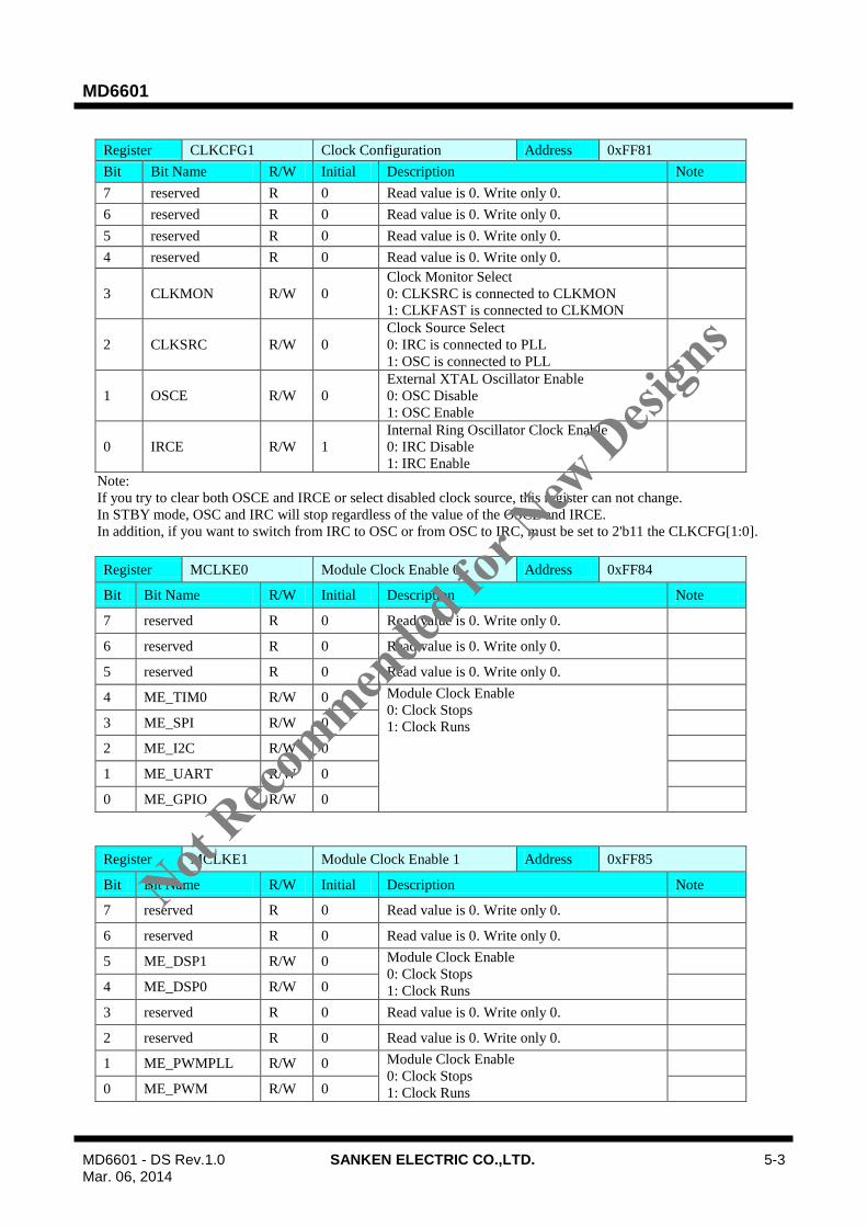
Register CLKCFG1 Clock Configuration Address 0xFF81
Bit Bit Name R/W Initial Description Note
7 reserved R 0 Read value is 0. Write only 0.
6 reserved R 0 Read value is 0. Write only 0.
5 reserved R 0 Read value is 0. Write only 0.
4 reserved R 0 Read value is 0. Write only 0.
3 CLKMON R/W 0
Clock Monitor Select
0: CLKSRC is connected to CLKMON
1: CLKFAST is connected to CLKMON
2 CLKSRC R/W 0
Clock Source Select
0: IRC is connected to PLL
1: OSC is connected to PLL
1 OSCE R/W 0
External XTAL Oscillator Enable
0: OSC Disable
1: OSC Enable
0 IRCE R/W 1
Internal Ring Oscillator Clock Enable
0: IRC Disable
1: IRC Enable
Note:
If you try to clear both OSCE and IRCE or select disabled clock source, this register can not change.
In STBY mode, OSC and IRC will stop regardless of the value of the OSCE and IRCE.
In addition, if you want to switch from IRC to OSC or from OSC to IRC, must be set to 2'b11 the CLKCFG[1:0].
Register MCLKE0 Module Clock Enable 0 Address 0xFF84
Bit Bit Name R/W Initial Description Note
7 reserved R 0 Read value is 0. Write only 0.
6 reserved R 0 Read value is 0. Write only 0.
5 reserved R 0 Read value is 0. Write only 0.
4 ME_TIM0 R/W 0 Module Clock Enable
0: Clock Stops
1: Clock Runs
3 ME_SPI R/W 0
2 ME_I2C R/W 0
1 ME_UART R/W 0
0 ME_GPIO R/W 0
Register MCLKE1 Module Clock Enable 1 Address 0xFF85
Bit Bit Name R/W Initial Description Note
7 reserved R 0 Read value is 0. Write only 0.
6 reserved R 0 Read value is 0. Write only 0.
5 ME_DSP1 R/W 0 Module Clock Enable
0: Clock Stops
1: Clock Runs
4 ME_DSP0 R/W 0
3 reserved R 0 Read value is 0. Write only 0.
2 reserved R 0 Read value is 0. Write only 0.
1 ME_PWMPLL R/W 0 Module Clock Enable
0: Clock Stops
1: Clock Runs
0 ME_PWM R/W 0
Not Reco
mmended
for N
ew D
esign
s

MD6601
MD6601 - DS Rev.1.0 SANKEN ELECTRIC CO.,LTD. 5-4 Mar. 06, 2014
Register MCLKE2 Module Clock Enable 2 Address 0xFF86
Bit Bit Name R/W Initial Description Note
7 reserved R 0 Read value is 0. Write only 0.
6 ME_ADC2 R/W 0
CLKADC2 Enable
0: Clock Stops
1: Clock Runs
5 ME_ADC1 R/W 0
CLKADC1 & CLKADC1_133 Enable
0: Clock Stops
1: Clock Runs
4 ME_ADC0 R/W 0
CLKADC0 & CLKADC0_133 Enable
0: Clock Stops
1: Clock Runs
3 reserved R 0 Read value is 0. Write only 0.
2 reserved R 0 Read value is 0. Write only 0.
1 reserved R 0 Read value is 0. Write only 0
0 ME_DAC R/W 0
Module Clock Enable
0: Clock Stops
1: Clock Runs
Register MCLKE3 Module Clock Enable 3 Address 0xFF87
Bit Bit Name R/W Initial Description Note
7 ME_SPR R/W 0
Module Clock Enable
0: Clock Stops
1: Clock Runs
6 reserved R 0 Read value is 0. Write only 0.
5 ME_AMP1 R/W 0
Module Clock Enable
0: Clock Stops
1: Clock Runs
4 ME_AMP0 R/W 0
3 ME_CMP3 R/W 0
2 ME_CMP2 R/W 0
1 ME_CMP1 R/W 0
0 ME_CMP0 R/W 0
Note:
There are clocks which are not directly controlled by registers. Table5-2 shows conditions that clocks enable or
disable.
Table 5-2: clock’s enabler condition and disabler condition
Clock name Enable Condition Disable Conditon
CLKCPU By reset
Return from SLEEP or STBY mode Being SLEEP or STBY mode
CLKMIXSFR Any of CLKCMPn or CLKADCn enable All of CLKCMPn and CLKADCn
disable
CLKDACSFR CLKDAC enable CLKDAC disable
CLKOCD1W DBG pin has been once driven “Low”. DBG pin has been never driven “Low”.
Not Reco
mmended
for N
ew D
esign
s

MD6601
MD6601 - DS Rev.1.0 SANKEN ELECTRIC CO.,LTD. 5-5 Mar. 06, 2014
5.2.2 Low Power Controller
Register LPCTRL Low Power Control Address 0xFFA0
Bit Bit Name R/W Initial Description Note
7
WUPTM
R/W
0
00:26ms(Details time→TBD)
01:13ms
10:6.6ms
11:3.3ms
6
5 reserved R 0 Read value is 0. Write only 0.
4 reserved R 0 Read value is 0. Write only 0.
3 reserved R 0 Read value is 0. Write only 0.
2 DISWC R/W 0
Disable Wake Up Counter
0: Use Wake Up Counter
1: Disable Wake Up Counter which makes
immediate wake up.
(This bit should be used only for test.)
1 LPSEL R/W 0
Low Power Mode Select
0: SLEEP (Only CPU Stops)
1: STBY (Entire Chip Stops)
0 GOTOLPM R/W 0
Go to Low Power Mode
0: Normal Mode
1: Low Power Mode
5.3 Clock Initialization Sequence
(1) After power on reset, IRC is enabled and its output IRCOUT is connected through CLKIRC, CLKSRC and
CLKPLL. Note that after power on reset, PLL is not used.
(2) If user wants to use IRC continuously, enable the PLL1. After waiting for PLL1 stable time (by software loop),
change master clock from CLKSRC to CLKPLL.
(3) Or, if user wants to use OSC (external XTAL) instead of IRC, connect CLKOSC to CLKSRC, and enable the
PLL1. After waiting for PLL1 stable time (by software loop), change master clock from CLKSRC to CLKPLL.
5.4 Low Power Mode
(1) There are two modes in Low Power state. One is SLEEP, the other is STBY.
(2) In SLEEP mode, only CPU clock stops. In STBY mode, entire chip clock stops. Even if EN_CLKxxx is set,
corresponding to EN_CLKCLK = ~(SLEEP | STBY) or EN_CLKxxx = ME_xxx & ~STBY
(3) By setting GOTOLPM bit, the LSI enters in Low Power Mode. Physically, GOTOLPM bit is 1 during Low
Power Mode until waking up. Read the value of GPTOLPM corresponding to SLEEP | STBY.
(4) Any interrupts from external pins or internal modules can make CPU awake from SLEEP mode.
(5) Only interrupts from external pins can make CPU awake from STBY mode. At that time, to wait for stable clock
oscillation and stable PLL output, internal Wake-Up-Counter is used. Interrupts from external pins immediately
start OSC, IRC and PLL, and the Wake-Up-Counter starts its count-up. Once the counter overflows, system
signal STBY is negated. Wake up period will be less than10ms .
Not Reco
mmended
for N
ew D
esign
s

MD6601
MD6601 - DS Rev.1.0 SANKEN ELECTRIC CO.,LTD. 5-6 Mar. 06, 2014
5.4.1 SLEEP Mode
In sleep mode, only CPU clock stops. Sequences shifting to and returning from sleep mode are shown in Figure 5-2.
The system instantly returns from sleep mode by occurring event (multiple choice allowed) of interrupt setting in
advance. At that time, CLKC automatically clears GOTOLPM bit of LPCTRL register.
Figure 5-2 Sleep Mode Sequence
Set Mode Select
LPCTRL.LPSEL=0
Set LowPowerMode start
LPCTRL.GOTOLPM=1
Start
int_request
Y
N
clear LPCTRL.GOTOLPM=0
End
Set event of interrupt
INTENA0/INTENA1
INTENA2/INTENA3
Not Reco
mmended
for N
ew D
esign
s
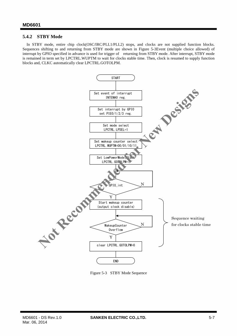
MD6601
MD6601 - DS Rev.1.0 SANKEN ELECTRIC CO.,LTD. 5-7 Mar. 06, 2014
5.4.2 STBY Mode
In STBY mode, entire chip clock(OSC/IRC/PLL1/PLL2) stops, and clocks are not supplied function blocks.
Sequences shifting to and returning from STBY mode are shown in Figure 5-3Event (multiple choice allowed) of
interrupt by GPIO specified in advance is used for trigger of returning from STBY mode. After interrupt, STBY mode
is remained in term set by LPCTRL.WUPTM to wait for clocks stable time. Then, clock is resumed to supply function
blocks and, CLKC automatically clear LPCTRL.GOTOLPM.
Figure 5-3 STBY Mode Sequence
START
Set event of interrupt
INTENA0 reg.
Set interrupt by GPIO
set PIE0/1/2/3 reg.
Set mode select
LPCTRL.LPSEL=1
Set wakeup counter select
LPCTRL.WUPTM=00/01/10/11
Set LowPowerMode start
LPCTRL.GOTOLPM=1
GPIO_int
Start wakeup counter
(output clock disable)
WakeupCounter
Overflow
Y
N
Y
N
clear LPCTRL.GOTOLPM=0
END
Sequence waiting
for clocks stable time
Not Reco
mmended
for N
ew D
esign
s

MD6601
MD6601 - DS Rev.1.0 SANKEN ELECTRIC CO.,LTD. 5-8 Mar. 06, 2014
5.5 An example way to configure Clock Settings after Power On
Power ON
(AVCC,DVCC)
wait for
reset sequence end
CLKCFG1.OSCE = 1
use XTAL?
wait for OSC stable time
CLKCFG1.CLKSRC = 1
CLKCFG1.CLKSRC = 1?
use PLL?
CLKCFG0.PLLEN = 1
wait for PLL stable time
CLKCFG0.CLKPLL = 1
CLKCFG0.CLKPLL = 1?
set divider configuration
CLKCFG0.DIV**
Clock Change End
verify divider configuration?
CLKCFG0.DIV**
Y
N
Y
N
N
N
N
Y
Y
Y
Figure 5-4 A example way to configure Clock Settings after Power On
Not Reco
mmended
for N
ew D
esign
s

MD6601
MD6601 - DS Rev.1.0 SANKEN ELECTRIC CO.,LTD. 5-9 Mar. 06, 2014
5.6 Limitation of Clock System
5.6.1 Limitation of Low Power Mode
Once 1-wire OCD has accessed the system, the system can not enter Low power Mode.
Not Reco
mmended
for N
ew D
esign
s
MD6601
MD6601 - DS Rev.1.0 SANKEN ELECTRIC CO.,LTD. 6-1 Mar. 06, 2014
6. 8051 CPU Subsystem
6.1 Introduction
The UL8051 is a CPU core with Intel MCS-51 (8051 family) compatible ISA (Instruction Set Architecture).
Note that the UL8051 is actually compatible with 8052 type core, we call it UL8051.
The UL8051 has some enhanced features compared to original 8052. The UL8051 can execute one byte instruction in
only 1 cycle by its pipelined micro architecture and 4-byte pre-fetch operation.
The UL8051 also has the flexible on-chip debugger with simple 1-wire interface which can prevent from increasing
pin counts.
6.2 Overview
Table 6-1 shows brief specification of UL8051.
Table 6-1 Feature of UL8051
No. Item Description Note
1 Instruction Set MCS-51 (8052) Compatible
2 Execution Cycle 1cycle/1byte-fetch (1T Core).
3 Pipeline Yes
4 Instruction Bus 8bit Width (XPROG Bus)
5 Data Bus 8bit Width (XDATA Bus)
6 SFR Bus 8bit Width with Bit Write Strobe
7 Interrupt Maximum 32 Interrupt sources
8 On Chip Debugger Full debugging features with simple 1-wire
interface
Not Reco
mmended
for N
ew D
esign
s
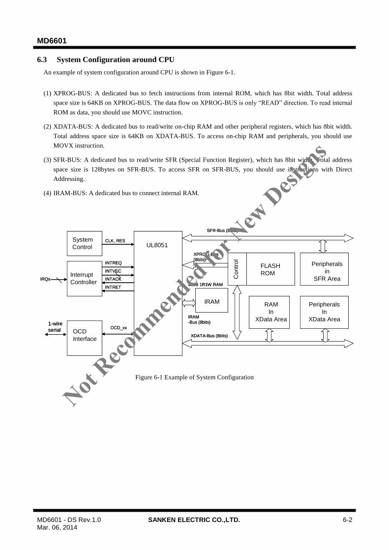
MD6601
MD6601 - DS Rev.1.0 SANKEN ELECTRIC CO.,LTD. 6-2 Mar. 06, 2014
6.3 System Configuration around CPU
An example of system configuration around CPU is shown in Figure 6-1.
(1) XPROG-BUS: A dedicated bus to fetch instructions from internal ROM, which has 8bit width. Total address
space size is 64KB on XPROG-BUS. The data flow on XPROG-BUS is only “READ” direction. To read internal
ROM as data, you should use MOVC instruction.
(2) XDATA-BUS: A dedicated bus to read/write on-chip RAM and other peripheral registers, which has 8bit width.
Total address space size is 64KB on XDATA-BUS. To access on-chip RAM and peripherals, you should use
MOVX instruction.
(3) SFR-BUS: A dedicated bus to read/write SFR (Special Function Register), which has 8bit width. Total address
space size is 128bytes on SFR-BUS. To access SFR on SFR-BUS, you should use instructions with Direct
Addressing.
(4) IRAM-BUS: A dedicated bus to connect internal RAM.
Figure 6-1 Example of System Configuration
UL8051
RAM
In
XData Area
FLASH
ROM
Co
ntr
ol
XPROG-Bus
(8bits)
SFR-Bus (8bits)
Peripherals
in
SFR Area
XDATA-Bus (8bits)
Peripherals
In
XData Area
System
ControlCLK, RES
Interrupt
Controller
INTVEC
OCD_xx
IRQs
INTREQ
INTACK
INTRET
OCD
Interface
1-wire
serial
IRAM
IRAM
-Bus (8bits)
256B 1R1W RAM
UL8051
RAM
In
XData Area
FLASH
ROM
Co
ntr
ol
XPROG-Bus
(8bits)
SFR-Bus (8bits)
Peripherals
in
SFR Area
XDATA-Bus (8bits)
Peripherals
In
XData Area
System
ControlCLK, RES
Interrupt
Controller
INTVEC
OCD_xx
IRQs
INTREQ
INTACK
INTRET
OCD
Interface
1-wire
serial
IRAM
IRAM
-Bus (8bits)
256B 1R1W RAM
Not Reco
mmended
for N
ew D
esign
s

MD6601
MD6601 - DS Rev.1.0 SANKEN ELECTRIC CO.,LTD. 6-3 Mar. 06, 2014
6.4 Memory Map
System Address Maps is shown in Figure 6-2.
(1) Internal Data Memory of 8052 architecture is divided into 3 blocks.
(2) Internal Data Memory (1): Address space is 0x00-0x7F (128bytes). It includes CPU registers (4bank, 32bytes),
Bit Address Area (16bytes) and General IRAM_1 (80bytes).
(3) Internal Data Memory (2): Address space is 0x80-0xFF (128bytes). To access here, you should use Indirect
Address Mode. It includes General IRAM_2 (128bytes).
(4) Internal Data Memory (3): Address space is 0x80-0xFF (128bytes). To access here, you should use Direct
Address Mode. It includes Special Function Registers (SFR). Most resources in SFR are connected on SFR-Bus.
In the SFR area, each byte on address 0xX0 (X=8-F) can be accessed by instructions with bit addressing.
(5) Program Memory Space: Dedicated instruction memory space. Address space is 0x0000-0xFFFF. Typically,
FLASH ROM is assigned from bottom address. The devices in this space are connected on XPROG-Bus. Use
MOVC instruction to read the space as data.
(6) Data Memory Space: Dedicated data memory space. Address space is 0x0000-0xFFFF. The devices in this space
are connected on XDATA-Bus. Use MOVX instruction to access in the space.
(7) Peripheral Registers: Note that peripheral registers in the LSI are assigned in both SFR area and Data Memory
Space.
Not Reco
mmended
for N
ew D
esign
s
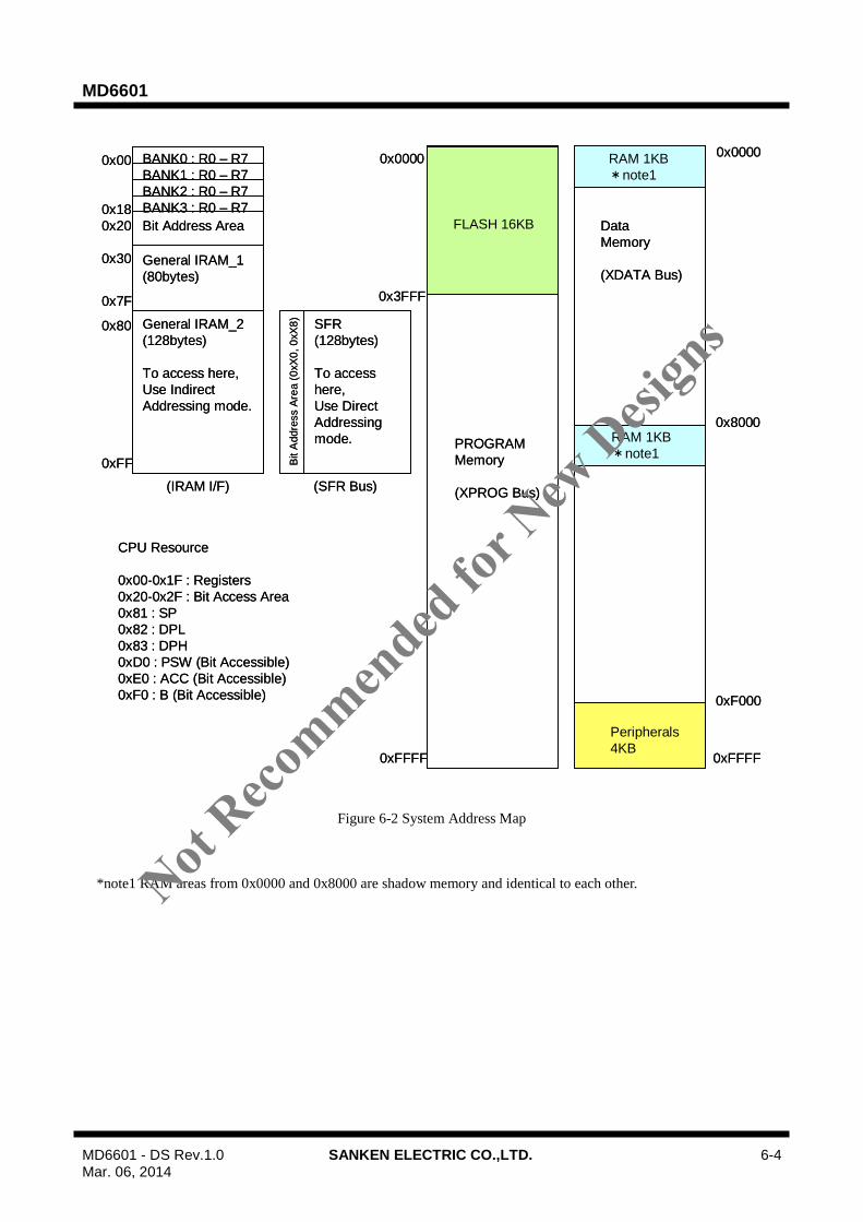
MD6601
MD6601 - DS Rev.1.0 SANKEN ELECTRIC CO.,LTD. 6-4 Mar. 06, 2014
Figure 6-2 System Address Map
*note1 RAM areas from 0x0000 and 0x8000 are shadow memory and identical to each other.
0x00
0x18
BANK0 : R0 – R7
BANK1 : R0 – R7
BANK2 : R0 – R7
BANK3 : R0 – R7
0x20 Bit Address Area
0x30
0x7F
General IRAM_1
(80bytes)
General IRAM_2
(128bytes)
To access here,
Use Indirect
Addressing mode.
0x80
0xFF
SFR
(128bytes)
To access
here,
Use Direct
Addressing
mode.
Bit A
ddre
ss A
rea (
0xX
0,
0xX
8)
CPU Resource
0x00-0x1F : Registers
0x20-0x2F : Bit Access Area
0x81 : SP
0x82 : DPL
0x83 : DPH
0xD0 : PSW (Bit Accessible)
0xE0 : ACC (Bit Accessible)
0xF0 : B (Bit Accessible)
0x0000
0xFFFF
PROGRAM
Memory
(XPROG Bus)
Data
Memory
(XDATA Bus)
0x3FFF
FLASH 16KB
RAM 1KB
*note1
Peripherals
4KB
0xF000
(IRAM I/F) (SFR Bus)
RAM 1KB
*note1
0xFFFF
0x8000
0x00000x00
0x18
BANK0 : R0 – R7
BANK1 : R0 – R7
BANK2 : R0 – R7
BANK3 : R0 – R7
0x20 Bit Address Area
0x30
0x7F
General IRAM_1
(80bytes)
General IRAM_2
(128bytes)
To access here,
Use Indirect
Addressing mode.
0x80
0xFF
SFR
(128bytes)
To access
here,
Use Direct
Addressing
mode.
Bit A
ddre
ss A
rea (
0xX
0,
0xX
8)
CPU Resource
0x00-0x1F : Registers
0x20-0x2F : Bit Access Area
0x81 : SP
0x82 : DPL
0x83 : DPH
0xD0 : PSW (Bit Accessible)
0xE0 : ACC (Bit Accessible)
0xF0 : B (Bit Accessible)
0x0000
0xFFFF
PROGRAM
Memory
(XPROG Bus)
Data
Memory
(XDATA Bus)
0x3FFF
FLASH 16KB
RAM 1KB
*note1
Peripherals
4KB
0xF000
(IRAM I/F) (SFR Bus)
RAM 1KB
*note1
0xFFFF
0x8000
0x0000
Not Reco
mmended
for N
ew D
esign
s

MD6601
MD6601 - DS Rev.1.0 SANKEN ELECTRIC CO.,LTD. 6-5 Mar. 06, 2014
6.5 Register Description
6.5.1 Remap Control (REMAP)
Register REMAP Remap Control Address 0xFFC0
Bit Bit Name R/W Initial Description Note
7 reserved R 0 Read value is 0. Write only 0.
6 reserved R 0 Read value is 0. Write only 0.
5 reserved R 0 Read value is 0. Write only 0.
4 reserved R 0 Read value is 0. Write only 0.
3 reserved R 0 Read value is 0. Write only 0.
2 reserved R 0 Read value is 0. Write only 0.
1 reserved R 0 Read value is 0. Write only 0.
0 REMAP R/W 0 Remap Control
0: Normal
1: Remapped
If REMAP is set to 1,the data of the internal RAM are copied on FLASH memory area from 0x0000 to 0x03FF(1kB).
Not Reco
mmended
for N
ew D
esign
s

MD6601
MD6601 - DS Rev.1.0 SANKEN ELECTRIC CO.,LTD. 6-6 Mar. 06, 2014
6.6 Instruction Code Map
Table 6-2 Instruction Code Map
U
pper
Low
er00
0000
0100
1000
1101
0001
0101
1001
1110
0010
0110
1010
1111
0011
0111
1011
11U
pper
.Low
er
0000
NO
PA
JM
Pad
dr11
LJM
Pad
dr16
RR A
INC A
INC
dire
ct00
00
0001
JB
Cbi
t, r
elA
CA
LL
addr
11LC
ALL
addr
16R
RC
AD
EC
AD
EC
dire
ct00
01
0010
JB
bit, r
elA
JM
Pad
dr11
RET
RL A
AD
DA
, #d
ata
AD
DA
, di
rect
0010
0011
JN
Bbi
t re
lA
CA
LL
addr
11R
ETI
RLC
AA
DD
CA
, #d
ata
AD
DC
A, di
rect
0011
0100
JC rel
AJM
Pad
dr11
OR
Ldi
rect
, A
OR
Ldi
rect
, #
OR
LA
, #d
ata
OR
LA
, di
rect
0100
0101
JN
Cre
lA
CA
LL
addr
11A
NL
dire
ct, A
AN
Ldi
rect
, #
AN
LA
, #d
ata
AN
LA
, di
rect
0101
0110
JZ rel
AJM
Pad
dr11
XR
Ldi
rect
, A
XR
Ldi
rect
, #
XR
LA
, #d
ata
XR
LA
, di
rect
0110
0111
JN
Zre
lA
CA
LL
addr
11O
RL
C, bi
tJM
P@
A+D
PM
OV
A, #d
ata
MO
Vd,
#da
ta01
11
1000
SJM
Pre
lA
JM
Pad
dr11
AN
LC
, bi
tM
OV
CA
, @
A+P
DIV
AB
MO
VdD
, dS
1000
1001
MO
VD
PTR
, #
AC
ALL
addr
11M
OV
bit, C
MO
VC
A, @
A+D
SU
BA
, #d
ata
SU
BA
, di
rect
1001
1010
OR
LC
, /b
itA
JM
Pad
dr11
MO
VC
, bi
tIN
CD
PTR
MU
LA
B(S
BR
K0x
0103
)10
10
1011
AN
LC
, /b
itA
CA
LL
addr
11C
PL
bit
CPL
CC
JN
EA
, #,
rel
CJN
EA
, d,
rel
1011
1100
PU
SH
dire
ctA
JM
Pad
dr11
CLR
bit
CLR
CSW
AP
AXC
HA
, di
rect
1100
1101
PO
Pdi
rect
AC
ALL
addr
11SETB
bit
SETB
CD
A AD
JN
Zd,
rel
1101
1110
MO
VX
A, @
DP
AJM
Pad
dr11
CLR
AM
OV
A, di
rect
1110
1111
MO
VX
@D
P,A
AC
ALL
addr
11C
PL
AM
OV
dire
ct, A
1111
INC
@R
iIN
CR
n
DEC
@R
iD
EC
Rn
AD
DA
, @
Ri
AD
DA
, R
n
AD
DC
A, @
Ri
AD
DC
A, R
n
OR
LA
, @
Ri
OR
LA
, R
n
AN
LA
, @
Ri
AN
LA
, R
n
XR
LA
, @
Ri
XR
LA
, R
n
MO
V@
Ri,
#dat
aM
OV
Rn,
#da
ta
MO
Vdi
rect
, @
Ri
MO
Vdi
rect
, R
n
SU
BA
, @
Ri
SU
BA
, R
n
MO
V@
Ri,
dire
ctM
OV
Rn,
direc
t
CJN
E@
Ri,
#dat
a, r
elC
JN
ER
n, #
data
, re
l
XC
HA
, @
Ri
XC
HA
, R
n
XC
HD
A, @
Ri
DJN
ZR
n re
l
MO
VX
A, @
Ri
MO
VA
, @
Ri
MO
VA
, R
n
MO
VX
@R
i, A
MO
V@
Ri,
AM
OV
Rn,
A
Not Reco
mmended
for N
ew D
esign
s
MD6601
MD6601 - DS Rev.1.0 SANKEN ELECTRIC CO.,LTD. 6-7 Mar. 06, 2014
6.6.1 Notes on Instruction Spec
(1) Operation of Undefined Instruction (0xa5)
This code (0xa5) acts as "Software Break : SBRK 0x0103". The Functionality is almost similar to LCALL
0x0103 (call fixed address), but the return address (PC written to stack) is the address of itself (where 0xa5 code
is placed).
(2) Operation of division by zero in DIV AB
If B=0, result of A(Quotient) is 255 and B(Remainder) is initial value of A, and OV is set.
(3) Stack Pointer
The initial value of Stack Pointer (SP) is 0x07, so please ensure NOT TO OVERLAP stack area with CPU
resource area to be used in your program, such as R0-R7 (bank0-bank3), Bit Addressable Area, and other internal
RAM area to be used.
Not Reco
mmended
for N
ew D
esign
s
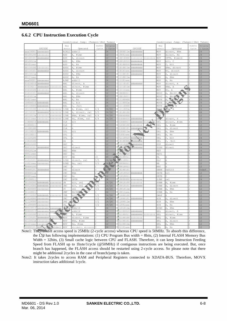
MD6601
MD6601 - DS Rev.1.0 SANKEN ELECTRIC CO.,LTD. 6-8 Mar. 06, 2014
6.6.2 CPU Instruction Execution Cycle
Note1: The FLASH access speed is 25MHz (2-cycle access) whereas CPU speed is 50MHz. To absorb this difference,
the LSI has following implementations: (1) CPU Program Bus width = 8bits, (2) Internal FLASH Memory Bus
Width = 32bits, (3) Small cache logic between CPU and FLASH. Therefore, it can keep Instruction Feeding
Speed from FLASH up to 1byte/1cycle (@50MHz) if contiguous instructions are being executed. But, once
branch has happened, the FLASH access should be restarted using 2-cycle access. So please note that there
might be additional 2cycles in the case of branch/jump is taken.
Note2: It takes 2cycles to access RAM and Peripheral Registers connected to XDATA-BUS. Therefore, MOVX
instruction takes additional 1cycle.
Conditional Jump: (Taken)/(Not Taken) Conditional Jump: (Taken)/(Not Taken)
aaa10001 aaaaaaaa ACALL addr11 4 24 1000011m dddddddd MOV direct, @Rm 2 24
00100100 iiiiiiii ADD A, #imm 2 12 10001nnn dddddddd MOV direct, Rn 2 24
00100101 dddddddd ADD A, direct 3 12 10010000 iiiiiiii iiiiiiii MOV DPTR, #imm16 3 24
0010011m ADD A, @Rm 2 12 10010010 bbbbbbbb MOV bit, C 3 24
00101nnn ADD A, Rn 1 12 10100010 bbbbbbbb MOV C, bit 3 12
00110100 iiiiiiii ADDC A, #imm 2 12 1010011m dddddddd MOV @Rm, direct 3 24
00110101 dddddddd ADDC A, direct 3 12 10101nnn dddddddd MOV Rn, direct 3 24
0011011m ADDC A, @Rm 2 12 11100101 dddddddd MOV A, direct 3 12
00111nnn ADDC A, Rn 1 12 1110011m MOV A, @Rm 2 12
aaa00001 aaaaaaaa AJMP addr11 3 24 11101nnn MOV A, Rn 1 12
01010010 dddddddd ANL direct, A 3 12 11110101 dddddddd MOV direct, A 2 12
01010011 dddddddd iiiiiiii ANL direct, #imm 3 24 1111011m MOV @Rm, A 1 12
01010100 iiiiiiii ANL A, #imm 2 12 11111nnn MOV Rn, A 1 12
01010101 dddddddd ANL A, direct 3 12 10000011 MOVC A, @A+PC 4 24
0101011m ANL A, @Rm 2 12 10010011 MOVC A, @A+DPTR 4 24
01011nnn ANL A, Rn 1 12 11100000 MOVX A, @DPTR 3 24
10000010 bbbbbbbb ANL C, bit 3 24 1110001m MOVX A, @Rm 3 24
10110000 bbbbbbbb ANL C, /bit 3 24 11110000 MOVX @DPTR, A 1 24
10110100 iiiiiiii rrrrrrrr CJNE A, #imm, rel 4/4 24/24 1111001m MOVX @Rm, A 1 24
10110101 dddddddd rrrrrrrr CJNE A, direct, rel 5/5 24/24 10100100 MUL AB 1 48
1011011m iiiiiiii rrrrrrrr CJNE @Rm, #imm, rel 4/4 24/24 00000000 NOP 1 12
10111nnn iiiiiiii rrrrrrrr CJNE Rn, #imm, rel 4/4 24/24 01000010 dddddddd ORL direct, A 3 12
11000010 bbbbbbbb CLR bit 3 12 01000011 dddddddd iiiiiiii ORL direct, #imm 3 24
11000011 CLR C 1 12 01000100 iiiiiiii ORL A, #imm 2 12
11100100 CLR A 1 12 01000101 dddddddd ORL A, direct 3 12
10110010 bbbbbbbb CPL bit 3 12 0100011m ORL A, @Rm 2 12
10110011 CPL C 1 12 01001nnn ORL A, Rn 1 12
11110100 CPL A 1 12 01110010 bbbbbbbb ORL C, bit 3 24
11010100 DA A 1 12 10100000 bbbbbbbb ORL C, /bit 3 24
00010100 DEC A 1 12 11010000 dddddddd POP direct 2 24
00010101 dddddddd DEC direct 3 12 11000000 dddddddd PUSH direct 3 24
0001011m DEC @Rm 2 12 00100010 RET 5 24
00011nnn DEC Rn 1 12 00110010 RETI 5 24
10000100 DIV AB 10 48 00100011 RL A 1 12
11010101 dddddddd rrrrrrrr DJNZ direct, rel 5/5 24/24 00110011 RLC A 1 12
11011nnn rrrrrrrr DJNZ Rn, rel 3/3 24/24 00000011 RR A 1 12
00000100 INC A 1 12 00010011 RRC A 1 12
00000101 dddddddd INC direct 3 12 10100101 SBRK 0x0103 4 Undef.
0000011m INC @Rm 2 12 11010010 bbbbbbbb SETB bit 3 12
00001nnn INC Rn 1 12 11010011 SETB C 1 12
10100011 INC DPTR 1 24 10000000 rrrrrrrr SJMP rel 3 24
00100000 bbbbbbbb rrrrrrrr JB bit, rel 5/5 24/24 10010100 iiiiiiii SUBB A, #imm 2 12
00010000 bbbbbbbb rrrrrrrr JBC bit, rel 5/5 24/24 10010101 dddddddd SUBB A, direct 3 12
01000000 rrrrrrrr JC rel 3/2 24/24 1001011m SUBB A, @Rm 2 12
01110011 JMP @A+DPTR 3 24 10011nnn SUBB A, Rn 1 12
00110000 bbbbbbbb rrrrrrrr JNB bit, rel 5/5 24/24 11000100 SWAP A 1 12
01010000 rrrrrrrr JNC rel 3/2 24/24 11000101 dddddddd XCH A, direct 3 12
01110000 rrrrrrrr JNZ rel 3/2 24/24 1100011m XCH A, @Rm 2 12
01100000 rrrrrrrr JZ rel 3/2 24/24 11001nnn XCH A, Rn 1 12
00010010 aaaaaaaa aaaaaaaa LCALL addr16 4 24 1101011m XCHD A, @Rm 2 12
00000010 aaaaaaaa aaaaaaaa LJMP addr16 4 24 01100010 dddddddd XRL direct, A 3 12
01110100 iiiiiiii MOV A, #imm 2 12 01100011 dddddddd iiiiiiii XRL direct, #imm 3 24
01110101 dddddddd iiiiiiii MOV direct, #imm 3 24 01100100 iiiiiiii XRL A, #imm 2 12
0111011m iiiiiiii MOV @Rm, #imm 2 12 01100101 dddddddd XRL A, direct 3 12
01111nnn iiiiiiii MOV Rn, #imm 2 12 0110011m XRL A, @Rm 2 12
10000101 ddd(src) ddd(dst) MOV dir(dst), dir(src) 3 24 01101nnn XRL A, Rn 1 12
Origina
l CycleOPCODE
Mne
monic Operand
UL8051
Cycle
Origina
l CycleOPCODE
Mne
monic Operand
UL8051
Cycle
Not Reco
mmended
for N
ew D
esign
s
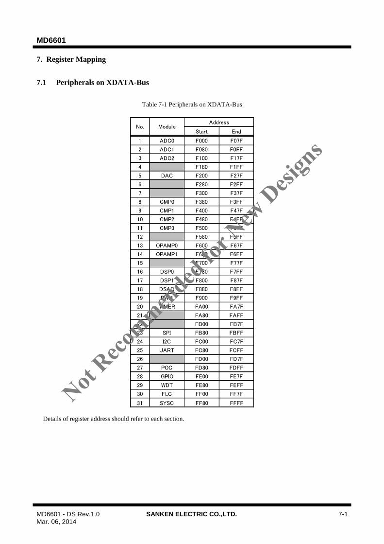
MD6601
MD6601 - DS Rev.1.0 SANKEN ELECTRIC CO.,LTD. 7-1 Mar. 06, 2014
7. Register Mapping
7.1 Peripherals on XDATA-Bus
Table 7-1 Peripherals on XDATA-Bus
Start End
1 ADC0 F000 F07F
2 ADC1 F080 F0FF
3 ADC2 F100 F17F
4 F180 F1FF
5 DAC F200 F27F
6 F280 F2FF
7 F300 F37F
8 CMP0 F380 F3FF
9 CMP1 F400 F47F
10 CMP2 F480 F4FF
11 CMP3 F500 F57F
12 F580 F5FF
13 OPAMP0 F600 F67F
14 OPAMP1 F680 F6FF
15 F700 F77F
16 DSP0 F780 F7FF
17 DSP1 F800 F87F
18 DSAC F880 F8FF
19 PWM F900 F9FF
20 TIMER FA00 FA7F
21 FA80 FAFF
22 FB00 FB7F
23 SPI FB80 FBFF
24 I2C FC00 FC7F
25 UART FC80 FCFF
26 FD00 FD7F
27 POC FD80 FDFF
28 GPIO FE00 FE7F
29 WDT FE80 FEFF
30 FLC FF00 FF7F
31 SYSC FF80 FFFF
No. ModuleAddress
Details of register address should refer to each section.
Not Reco
mmended
for N
ew D
esign
s
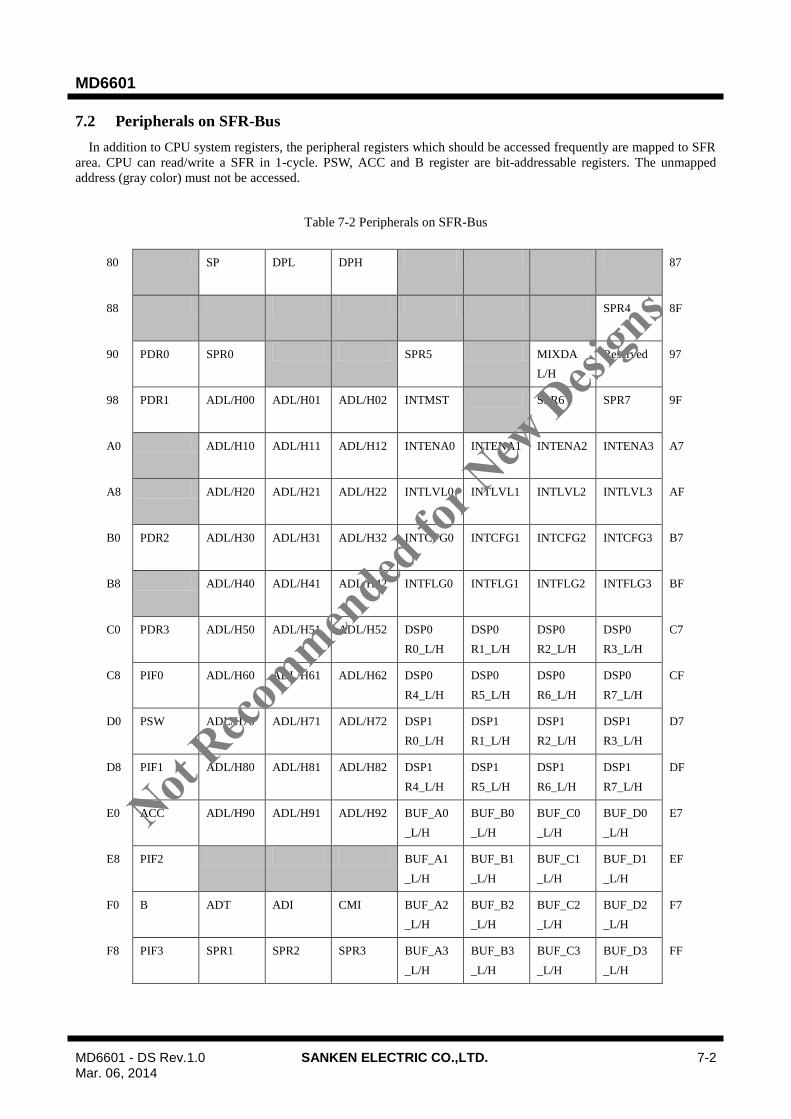
MD6601
MD6601 - DS Rev.1.0 SANKEN ELECTRIC CO.,LTD. 7-2 Mar. 06, 2014
7.2 Peripherals on SFR-Bus
In addition to CPU system registers, the peripheral registers which should be accessed frequently are mapped to SFR
area. CPU can read/write a SFR in 1-cycle. PSW, ACC and B register are bit-addressable registers. The unmapped
address (gray color) must not be accessed.
Table 7-2 Peripherals on SFR-Bus
80 SP DPL DPH 87
88 SPR4 8F
90 PDR0 SPR0 SPR5 MIXDA
L/H
Reserved 97
98 PDR1 ADL/H00 ADL/H01 ADL/H02 INTMST SPR6 SPR7 9F
A0 ADL/H10 ADL/H11 ADL/H12 INTENA0 INTENA1 INTENA2 INTENA3 A7
A8 ADL/H20 ADL/H21 ADL/H22 INTLVL0 INTLVL1 INTLVL2 INTLVL3 AF
B0 PDR2 ADL/H30 ADL/H31 ADL/H32 INTCFG0 INTCFG1 INTCFG2 INTCFG3 B7
B8 ADL/H40 ADL/H41 ADL/H42 INTFLG0 INTFLG1 INTFLG2 INTFLG3 BF
C0 PDR3 ADL/H50 ADL/H51 ADL/H52 DSP0
R0_L/H
DSP0
R1_L/H
DSP0
R2_L/H
DSP0
R3_L/H
C7
C8 PIF0 ADL/H60 ADL/H61 ADL/H62 DSP0
R4_L/H
DSP0
R5_L/H
DSP0
R6_L/H
DSP0
R7_L/H
CF
D0 PSW ADL/H70 ADL/H71 ADL/H72 DSP1
R0_L/H
DSP1
R1_L/H
DSP1
R2_L/H
DSP1
R3_L/H
D7
D8 PIF1 ADL/H80 ADL/H81 ADL/H82 DSP1
R4_L/H
DSP1
R5_L/H
DSP1
R6_L/H
DSP1
R7_L/H
DF
E0 ACC ADL/H90 ADL/H91 ADL/H92 BUF_A0
_L/H
BUF_B0
_L/H
BUF_C0
_L/H
BUF_D0
_L/H
E7
E8 PIF2 BUF_A1
_L/H
BUF_B1
_L/H
BUF_C1
_L/H
BUF_D1
_L/H
EF
F0 B ADT ADI CMI BUF_A2
_L/H
BUF_B2
_L/H
BUF_C2
_L/H
BUF_D2
_L/H
F7
F8 PIF3 SPR1 SPR2 SPR3 BUF_A3
_L/H
BUF_B3
_L/H
BUF_C3
_L/H
BUF_D3
_L/H
FF
Not Reco
mmended
for N
ew D
esign
s

MD6601
MD6601 - DS Rev.1.0 SANKEN ELECTRIC CO.,LTD. 7-3 Mar. 06, 2014
7.3 Scratch Pad Register
Scratch Pad Registers are used for temporary storage of preliminary data. There are eight Scratch Pad Registers,
SPR0 ~ SPR7, which are mapped SFR area.
Also DSAC can access these Scratch Pad Registers. Information of these registers is shown in Table 7-3.
Table 7-3 Scratch Pad Register
Register SPR0 Scratch Pad Register 0 Address 0x91
Register SPR1 Scratch Pad Register 1 Address 0xF9
Register SPR2 Scratch Pad Register 2 Address 0xFA
Register SPR3 Scratch Pad Register 3 Address 0xFB
Register SPR4 Scratch Pad Register 4 Address 0x8F
Register SPR5 Scratch Pad Register 5 Address 0x94
Register SPR6 Scratch Pad Register 6 Address 0x9E
Register SPR7 Scratch Pad Register 7 Address 0x9F
Bit Bit Name R/W Initial Description Note
7 SPR_7 R/W 0 The Register is used for temporary storage of
preliminary data.
6 SPR_6 R/W 0
5 SPR_5 R/W 0
4 SPR_4 R/W 0
3 SPR_3 R/W 0
2 SPR_2 R/W 0
1 SPR_1 R/W 0
0 SPR_0 R/W 0
Not Reco
mmended
for N
ew D
esign
s

MD6601
MD6601 - DS Rev.1.0 SANKEN ELECTRIC CO.,LTD. 8-1 Mar. 06, 2014
8. GPIO This LSI has the General Purpose I/O(GPIO) function with all function pins. Each pin function can be selected
independently. If the function is GPIO, the signal direction can be selected independently, too. Each pin has Pull Up
MOS (PUP) and can be independently ON/OFF by software.
8.1 GPIO Structure
Pins
/RES
MODE
Topology + Spec Signals
in
in
Signal Level (power)
DVCC(3.3V)
DVCC (3.3V)
PUP
MOS
always ON
always ONin
Schmitt
DVCC3.3V
DVCC3.3V
Reset/Mode signals are required to stay at 3.3V, because internal regulator may notbe in ready during reset.
3.3V
PUP
MOSalways OFF
always ONin
Schmitt
DVCC3.3V
DVCC3.3V
3.3V
Pins
DBGGPIO00GPIO01GPIO02GPIO03
GPIO10GPIO11GPIO12GPIO13GPIO14GPIO15GPIO16GPIO17
Topology + Spec Signals
od
pp
i
od
pp
i
Signal Level (power)
DVCC_CORE(1.8V)
DVCC_CORE(1.8V)
DVCC_CORE(1.8V)
DVCC_CORE(1.8V)
DVCC_CORE(1.8V)
DVCC_CORE(1.8V)
CMOS
Driver
PUP
MOS
L/S
L/S
od
pp
i
4mA
DVCC3.3V
DVCC3.3V
CMOS
Driver
PUP
MOS
L/S
L/Spp
i
16mA
DVCC3.3V
DVCC3.3V
5VTolerant
5VTolerant
3.3V
3.3V
I2C Spec=SMBUS
L/S
L/Sod
Not Reco
mmended
for N
ew D
esign
s

MD6601
MD6601 - DS Rev.1.0 SANKEN ELECTRIC CO.,LTD. 8-2 Mar. 06, 2014
Figure 8-1 GPIO/PIN Structures
Pins
GPIO20GPIO21GPIO22GPIO23GPIO24GPIO25GPIO26GPIO27GPIO30GPIO31GPIO32GPIO33GPIO34GPIO35GPIO36GPIO37
XTALINXTALOUT
Topology + Spec Signals
od
pp
ie
aio
i
ei
Signal Level (power)
DVCC_CORE(1.8V)
DVCC_CORE(1.8V)
DVCC_CORE(1.8V)DVCC_CORE(1.8V)
AVCC (3.3V)
DVCC_CORE(1.8V)
DVCC_CORE(1.8V)
CMOS
Driver
PUP
MOS
L/S
L/S
L/S
pp
ie
4mA
AVCC3.3V
AVCC3.3V
3.3V
AVCC3.3V
aio
L/S
L/Si
eiDVCC3.3V XTALIN
XTALOUT
3.3V
od L/S
Not Reco
mmended
for N
ew D
esign
s

MD6601
MD6601 - DS Rev.1.0 SANKEN ELECTRIC CO.,LTD. 8-3 Mar. 06, 2014
8.2 Register Description
Each bit may not have corresponding physical pin. In the case the bit is reserved and its read value is always 0 and
write value should be always 0.
Table 8-1 GPIO Registers
Symbol Name Address initial value
PFS0 Pin Function Select for GPIO0 0xFE00 0x00
PFS1 Pin Function Select for GPIO1 0xFE01 0x00
PFS2 Pin Function Select for GPIO2 0xFE02 0x00
PFS3 Pin Function Select for GPIO3 0xFE03 0x00
PDD0 Pin Data Direction for GPIO0 0xFE04 0x00
PDD1 Pin Data Direction for GPIO1 0xFE05 0x00
PDD2 Pin Data Direction for GPIO2 0xFE06 0x00
PDD3 Pin Data Direction for GPIO3 0xFE07 0x00
PDR0 Pin Data for GPIO0 0x90 0x00
PDR1 Pin Data for GPIO1 0x98 0x00
PDR2 Pin Data for GPIO2 0xB0 0x00
PDR3 Pin Data for GPIO3 0xC0 0x00
PPU0 Pin Pull Up Control for GPIO0 0xFE08 0xFF
PPU1 Pin Pull Up Control for GPIO1 0xFE09 0xFF
PPU2 Pin Pull Up Control for GPIO2 0xFE0A 0xFF
PPU3 Pin Pull Up Control for GPIO3 0xFE0B 0xFF
PIE0 Pin Interrupt Enable for GPIO0 0xFE10 0x00
PIE1 Pin Interrupt Enable for GPIO1 0xFE11 0x00
PIE2 Pin Interrupt Enable for GPIO2 0xFE12 0x00
PIE3 Pin Interrupt Enable for GPIO3 0xFE13 0x00
PIF0 Pin Interrupt Flag for GPIO0 0xC8 0x00
PIF1 Pin Interrupt Flag for GPIO1 0xD8 0x00
PIF2 Pin Interrupt Flag for GPIO2 0xE8 0x00
PIF3 Pin Interrupt Flag for GPIO3 0xF8 0x00
PIS0 Pin Interrupt Sense for GPIO0 0xFE14 0x00
PIS1 Pin Interrupt Sense for GPIO1 0xFE15 0x00
PIS2 Pin Interrupt Sense for GPIO2 0xFE16 0x00
PIS3 Pin Interrupt Sense for GPIO3 0xFE17 0x00
PIL0 Pin Interrupt Level for GPIO0 0xFE18 0x00
PIL1 Pin Interrupt Level for GPIO1 0xFE19 0x00
PIL2 Pin Interrupt Level for GPIO2 0xFE1A 0x00
PIL3 Pin Interrupt Level for GPIO3 0xFE1B 0x00
PIB0 Pin Interrupt Both Edge for GPIO0 0xFE1C 0x00
PIB1 Pin Interrupt Both Edge for GPIO1 0xFE1D 0x00
PIB2 Pin Interrupt Both Edge for GPIO2 0xFE1E 0x00
PIB3 Pin Interrupt Both Edge for GPIO3 0xFE1F 0x00
PEADC0 ADC Event Select from GPIO0 0xFE20 0x00
PEADC1 ADC Event Select from GPIO1 0xFE21 0x00
PEADC2 ADC Event Select from GPIO2 0xFE22 0x00
PEADC3 ADC Event Select from GPIO3 0xFE23 0x00
PEPWM0 PWM Event Select from GPIO0 0xFE24 0x00
PEPWM1 PWM Event Select from GPIO1 0xFE25 0x00
PEPWM2 PWM Event Select from GPIO2 0xFE26 0x00
PEPWM3 PWM Event Select from GPIO3 0xFE27 0x00
PEMETHOD PWM Event Gathering Method 0xFE28 0x00
Not Reco
mmended
for N
ew D
esign
s
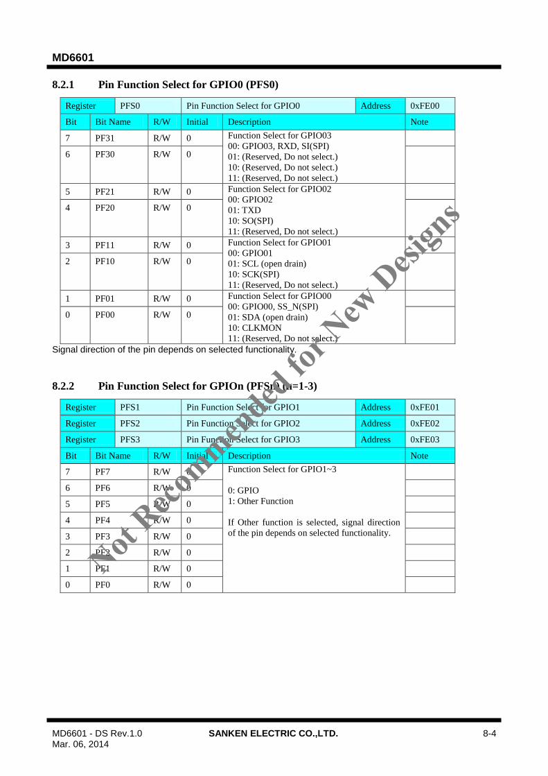
MD6601
MD6601 - DS Rev.1.0 SANKEN ELECTRIC CO.,LTD. 8-4 Mar. 06, 2014
8.2.1 Pin Function Select for GPIO0 (PFS0)
Register PFS0 Pin Function Select for GPIO0 Address 0xFE00
Bit Bit Name R/W Initial Description Note
7 PF31 R/W 0 Function Select for GPIO03
00: GPIO03, RXD, SI(SPI)
01: (Reserved, Do not select.)
10: (Reserved, Do not select.)
11: (Reserved, Do not select.)
6 PF30 R/W 0
5 PF21 R/W 0 Function Select for GPIO02
00: GPIO02
01: TXD
10: SO(SPI)
11: (Reserved, Do not select.)
4 PF20 R/W 0
3 PF11 R/W 0 Function Select for GPIO01
00: GPIO01
01: SCL (open drain)
10: SCK(SPI)
11: (Reserved, Do not select.)
2 PF10 R/W 0
1 PF01 R/W 0 Function Select for GPIO00
00: GPIO00, SS_N(SPI)
01: SDA (open drain)
10: CLKMON
11: (Reserved, Do not select.)
0 PF00 R/W 0
Signal direction of the pin depends on selected functionality.
8.2.2 Pin Function Select for GPIOn (PFSn) (n=1-3)
Register PFS1 Pin Function Select for GPIO1 Address 0xFE01
Register PFS2 Pin Function Select for GPIO2 Address 0xFE02
Register PFS3 Pin Function Select for GPIO3 Address 0xFE03
Bit Bit Name R/W Initial Description Note
7 PF7 R/W 0 Function Select for GPIO1~3
0: GPIO
1: Other Function
If Other function is selected, signal direction
of the pin depends on selected functionality.
6 PF6 R/W 0
5 PF5 R/W 0
4 PF4 R/W 0
3 PF3 R/W 0
2 PF2 R/W 0
1 PF1 R/W 0
0 PF0 R/W 0
Not Reco
mmended
for N
ew D
esign
s

MD6601
MD6601 - DS Rev.1.0 SANKEN ELECTRIC CO.,LTD. 8-5 Mar. 06, 2014
8.2.3 Pin Data Direction for GPIOn (PDDn) (n=0-3)
Register PDD0 Pin Data Direction for GPIO0 Address 0xFE04
Register PDD1 Pin Data Direction for GPIO1 Address 0xFE05
Register PDD2 Pin Data Direction for GPIO2 Address 0xFE06
Register PDD3 Pin Data Direction for GPIO3 Address 0xFE07
Bit Bit Name R/W Initial Description Note
7 DD7 R/W 0 Pin Data Direction Select
0: Input
1: Output
Each bit makes sense when the pin is selected
as GPIO.
6 DD6 R/W 0
5 DD5 R/W 0
4 DD4 R/W 0
3 DD3 R/W 0
2 DD2 R/W 0
1 DD1 R/W 0
0 DD0 R/W 0
8.2.4 Pin Data for GPIOn (PDRn) (n=0-3)
Register PDR0 Pin Data for GPIO0 Address 0x90
Register PDR1 Pin Data for GPIO1 Address 0x98
Register PDR2 Pin Data for GPIO2 Address 0xB0
Register PDR3 Pin Data for GPIO3 Address 0xC0
Bit Bit Name R/W Initial Description Note
7 PD7 R/W 0 Pin Data
Read 0: The pin state is in low level
Read 1: The pin state is in high level.
Write 0: If the pin is GPIO output, the pin
level will be low.
Write 1: If the pin is GPIO output, the pin
level will be high.
If the pin is GPIO input or another digital
function, read value shows external pin level,
and write value has no effect.
If the pin is GPIO output, write value will be
output level of the pin and read value shows
external pin level (not written value if external
signal contention happens, for instance).
If the pin is in analog function, read value is
always zero, and write value has no effect.
Note that write value is stored to internal
register, so when pin function or pin direction
are changed, output pin level might be
affected by the register value.
6 PD6 R/W 0
5 PD5 R/W 0
4 PD4 R/W 0
3 PD3 R/W 0
2 PD2 R/W 0
1 PD1 R/W 0
0 PD0 R/W 0
Not Reco
mmended
for N
ew D
esign
s

MD6601
MD6601 - DS Rev.1.0 SANKEN ELECTRIC CO.,LTD. 8-6 Mar. 06, 2014
8.2.5 Pin Pull Up Control for GPIOn (PPUn) (n=0-3)
Register PPU0 Pin Pull Up Control for GPIO0 Address 0xFE08
Register PPU1 Pin Pull Up Control for GPIO1 Address 0xFE09
Register PPU2 Pin Pull Up Control for GPIO2 Address 0xFE0A
Register PPU3 Pin Pull Up Control for GPIO3 Address 0xFE0B
Bit Bit Name R/W Initial Description Note
7 PPU7 R/W 1 Pin Pull Up Enable
0: Pull Up MOS is OFF
1: Pull Up MOS is ON
If the pin function is analog, this bit will be
ignored.
6 PPU6 R/W 1
5 PPU5 R/W 1
4 PPU4 R/W 1
3 PPU3 R/W 1
2 PPU2 R/W 1
1 PPU1 R/W 1
0 PPU0 R/W 1
8.2.6 Pin Interrupt Enable for GPIOn (PIEn) (n=0-3)
Register PIE0 Pin Interrupt Enable for GPIO0 Address 0xFE10
Register PIE1 Pin Interrupt Enable for GPIO1 Address 0xFE11
Register PIE2 Pin Interrupt Enable for GPIO2 Address 0xFE12
Register PIE3 Pin Interrupt Enable for GPIO3 Address 0xFE13
Bit Bit Name R/W Initial Description Note
7 PIE7 R/W 0 Pin Interrupt Enable
0: Disable
1: Enable
If the pin function is analog, this bit will be
ignored. If the pin function is digital, this bit is
effective regardless of pin function or pin
direction.
This means PWM toggle can make interrupts.
6 PIE6 R/W 0
5 PIE5 R/W 0
4 PIE4 R/W 0
3 PIE3 R/W 0
2 PIE2 R/W 0
1 PIE1 R/W 0
0 PIE0 R/W 0
Not Reco
mmended
for N
ew D
esign
s

MD6601
MD6601 - DS Rev.1.0 SANKEN ELECTRIC CO.,LTD. 8-7 Mar. 06, 2014
8.2.7 Pin Interrupt Flag for GPIOn (PIFn) (n=0-3)
Register PIF0 Pin Interrupt Flag for GPIO0 Address 0xC8
Register PIF1 Pin Interrupt Flag for GPIO1 Address 0xD8
Register PIF2 Pin Interrupt Flag for GPIO2 Address 0xE8
Register PIF3 Pin Interrupt Flag for GPIO3 Address 0xF8
Bit Bit Name R/W Initial Description Note
7 PIF7 R/C 0 Pin Interrupt Flag
(before mask; independent PIEx)
Read 0: No Request
Read 1: Interrupt Event Occurred
Write 0: No effect
Write 1: To clear corresponding bit
6 PIF6 R/C 0
5 PIF5 R/C 0
4 PIF4 R/C 0
3 PIF3 R/C 0
2 PIF2 R/C 0
1 PIF1 R/C 0
0 PIF0 R/C 0
8.2.8 Pin Interrupt Sense for GPIOn (PISn) (n=0-3)
Register PIS0 Pin Interrupt Sense for GPIO0 Address 0xFE14
Register PIS1 Pin Interrupt Sense for GPIO1 Address 0xFE15
Register PIS2 Pin Interrupt Sense for GPIO2 Address 0xFE16
Register PIS3 Pin Interrupt Sense for GPIO3 Address 0xFE17
Bit Bit Name R/W Initial Description Note
7 PIS7 R/W 0 Pin Interrupt Sense Select
0: Level
1: Edge
Implementation of edge sense is analog delay
type (with some proper noise filter) to realize
wake-up function.
6 PIS6 R/W 0
5 PIS5 R/W 0
4 PIS4 R/W 0
3 PIS3 R/W 0
2 PIS2 R/W 0
1 PIS1 R/W 0
0 PIS0 R/W 0
Not
Recommen
ded fo
r New
Desi
gns
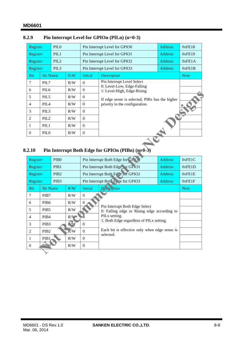
MD6601
MD6601 - DS Rev.1.0 SANKEN ELECTRIC CO.,LTD. 8-8 Mar. 06, 2014
8.2.9 Pin Interrupt Level for GPIOn (PILn) (n=0-3)
Register PIL0 Pin Interrupt Level for GPIO0 Address 0xFE18
Register PIL1 Pin Interrupt Level for GPIO1 Address 0xFE19
Register PIL2 Pin Interrupt Level for GPIO2 Address 0xFE1A
Register PIL3 Pin Interrupt Level for GPIO3 Address 0xFE1B
Bit Bit Name R/W Initial Description Note
7 PIL7 R/W 0 Pin Interrupt Level Select
0: Level-Low, Edge-Falling
1: Level-High, Edge-Rising
If edge sense is selected, PIBx has the higher
priority in the configuration.
6 PIL6 R/W 0
5 PIL5 R/W 0
4 PIL4 R/W 0
3 PIL3 R/W 0
2 PIL2 R/W 0
1 PIL1 R/W 0
0 PIL0 R/W 0
8.2.10 Pin Interrupt Both Edge for GPIOn (PIBn) (n=0-3)
Register PIB0 Pin Interrupt Both Edge for GPIO0 Address 0xFE1C
Register PIB1 Pin Interrupt Both Edge for GPIO1 Address 0xFE1D
Register PIB2 Pin Interrupt Both Edge for GPIO2 Address 0xFE1E
Register PIB3 Pin Interrupt Both Edge for GPIO3 Address 0xFE1F
Bit Bit Name R/W Initial Description Note
7 PIB7 R/W 0
Pin Interrupt Both Edge Select
0: Falling edge or Rising edge according to
PILx setting.
1: Both Edge regardless of PILx setting.
Each bit is effective only when edge sense is
selected.
6 PIB6 R/W 0
5 PIB5 R/W 0
4 PIB4 R/W 0
3 PIB3 R/W 0
2 PIB2 R/W 0
1 PIB1 R/W 0
0 PIB0 R/W 0
Not
Recommen
ded fo
r New
Desi
gns

MD6601
MD6601 - DS Rev.1.0 SANKEN ELECTRIC CO.,LTD. 8-9 Mar. 06, 2014
8.2.11 ADC Event Select from GPIOn (PEADCn) (n=0-3)
Register PEADC0 ADC Event Select from GPIO0 Address 0xFE20
Register PEADC1 ADC Event Select from GPIO1 Address 0xFE21
Register PEADC2 ADC Event Select from GPIO2 Address 0xFE22
Register PEADC3 ADC Event Select from GPIO3 Address 0xFE23
Bit Bit Name R/W Initial Description Note
7 EVTADC7 R/W 0 ADC Event Select
0: An input signal is not used as an event for
ADC.
1: An input signal is used as an event for
ADC.
Selected GPIO signals, EVTADC[7:0] are
set “1”, will be ORed, or ANDed according to
PEMETHOD Register, and this will be sent to
all ADC as the start trigger.
6 EVTADC6 R/W 0
5 EVTADC5 R/W 0
4 EVTADC4 R/W 0
3 EVTADC3 R/W 0
2 EVTADC3 R/W 0
1 EVTADC1 R/W 0
0 EVTADC0 R/W 0
8.2.12 PWM Event Select from GPIOn (PEPWMn) (n=0-3)
Register PEPWM0 PWM Event Select from GPIO0 Address 0xFE24
Register PEPWM1 PWM Event Select from GPIO1 Address 0xFE25
Register PEPWM2 PWM Event Select from GPIO2 Address 0xFE26
Register PEPWM3 PWM Event Select from GPIO3 Address 0xFE27
Bit Bit Name R/W Initial Description Note
7 EVTPWM7 R/W 0 PWM Event Select
0: An input signal is not used as an event for
PWM.
1: An input signal is used as an event for
PWM.
Selected GPIO signals, EVTPWM[7:0] are
set “1”, will be ORed, or ANDed according to
PEMETHOD Register, and this will be sent to
all PWM blocks for the Re-trigger Operation.
6 EVTPWM6 R/W 0
5 EVTPWM5 R/W 0
4 EVTPWM4 R/W 0
3 EVTPWM3 R/W 0
2 EVTPWM2 R/W 0
1 EVTPWM1 R/W 0
0 EVTPWM0 R/W 0
Not
Recommen
ded fo
r New
Desi
gns

MD6601
MD6601 - DS Rev.1.0 SANKEN ELECTRIC CO.,LTD. 8-10 Mar. 06, 2014
8.2.13 PWM Event Gathering Method (PEMETHOD)
Register PEMETHOD PWM Event Gathering Method Address 0xFE28
Bit Bit Name R/W Initial Description Note
7 MPEPWM3 R/W 0 PWM Event Gathering Method
0: By ORed
1: By ANDed
Each bit is corresponding to Register
PEPWM0-3.
6 MPEPWM2 R/W 0
5 MPEPWM1 R/W 0
4 MPEPWM0 R/W 0
3 MPEADC3 R/W 0 ADC Event Gathering Method
0: By ORed
1: By ANDed
Each bit is corresponding to Register
PEADC0-3,
2 MPEADC2 R/W 0
1 MPEADC1 R/W 0
0 MPEADC0 R/W 0
Not Reco
mmended
for N
ew D
esign
s
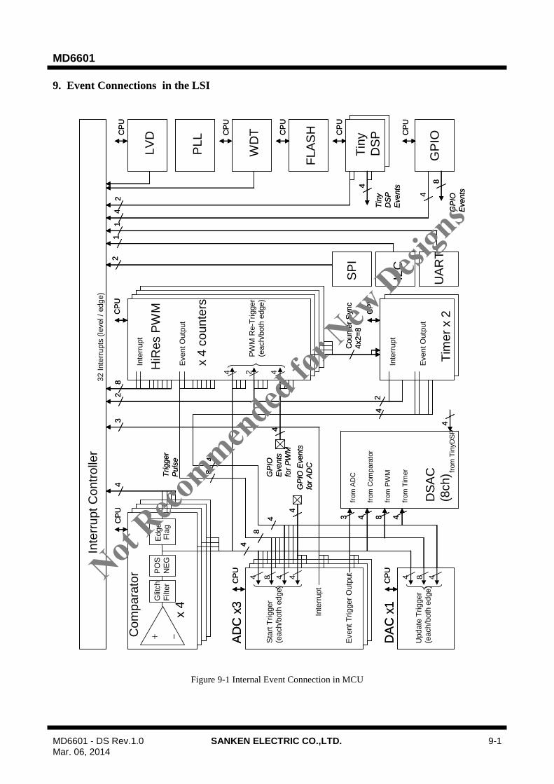
MD6601
MD6601 - DS Rev.1.0 SANKEN ELECTRIC CO.,LTD. 9-1 Mar. 06, 2014
9. Event Connections in the LSI
Figure 9-1 Internal Event Connection in MCU
+ -
Glit
ch
Filt
er
Edge
Fla
g
CP
U
x 4
Co
mp
ara
tor
AD
C x
3C
PU
4
4
4
DA
C x
1C
PU
4
Inte
rru
pt
Co
ntr
olle
r
CP
U
HiR
es
PW
M
x 4
co
un
ters
8
8
8 8
PO
S
NE
G
8
Trigger
Puls
e
2
4
4 4
4
4
Update
Tri
gger
(each/b
oth
edge)
Sta
rt T
rigger
(each/b
oth
edge)
PW
M R
e-T
rigger
(each/b
oth
edge)
GP
IO E
vents
for
AD
C
2
24
GP
IO
Events
for
PW
M
Inte
rrupt
Event O
utp
ut
Inte
rrupt
Event O
utp
ut
Tim
er
x 2
Counte
r S
ync
4x2=
8
Inte
rrupt
3
32 I
nte
rrupts
(le
vel /
edge)
LV
D
CP
U
CP
U
PL
L
WD
TCP
U
FL
AS
HCP
U
CP
U
2
Tin
y
DS
P CP
U
GP
IO
SP
I
I2C
UA
RT
11
24
4D
SA
C
(8ch
)
Event T
rigger
Outp
ut
3 4 8
4
Tin
y
DS
P
Events
4fr
om
Tin
yD
SP
4
from
AD
C
from
Com
para
tor
from
PW
M
from
Tim
er
8
GP
IO
Events
44
44
Not Reco
mmended
for N
ew D
esign
s
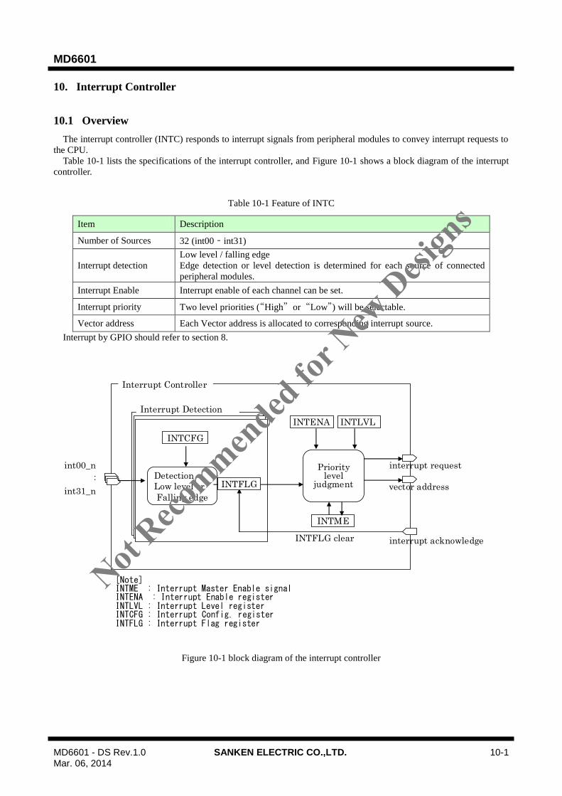
MD6601
MD6601 - DS Rev.1.0 SANKEN ELECTRIC CO.,LTD. 10-1 Mar. 06, 2014
10. Interrupt Controller
10.1 Overview
The interrupt controller (INTC) responds to interrupt signals from peripheral modules to convey interrupt requests to
the CPU.
Table 10-1 lists the specifications of the interrupt controller, and Figure 10-1 shows a block diagram of the interrupt
controller.
Table 10-1 Feature of INTC
Item Description
Number of Sources 32 (int00 – int31)
Interrupt detection
Low level / falling edge
Edge detection or level detection is determined for each source of connected
peripheral modules.
Interrupt Enable Interrupt enable of each channel can be set.
Interrupt priority Two level priorities (“High” or “Low”) will be selectable.
Vector address Each Vector address is allocated to corresponding interrupt source.
Interrupt by GPIO should refer to section 8.
Interrupt Controller
:
INTME
INTENA
INTCFG
INTLVL
INTFLG clear
interrupt request
interrupt acknowledge
Prioritylevel
judgment vector address
Interrupt Detection
Detection
Low level or
Falling edge
[Note]INTME : Interrupt Master Enable signalINTENA : Interrupt Enable registerINTLVL : Interrupt Level registerINTCFG : Interrupt Config. registerINTFLG : Interrupt Flag register
int00_n
int31_nINTFLG
Figure 10-1 block diagram of the interrupt controller
Not Reco
mmended
for N
ew D
esign
s
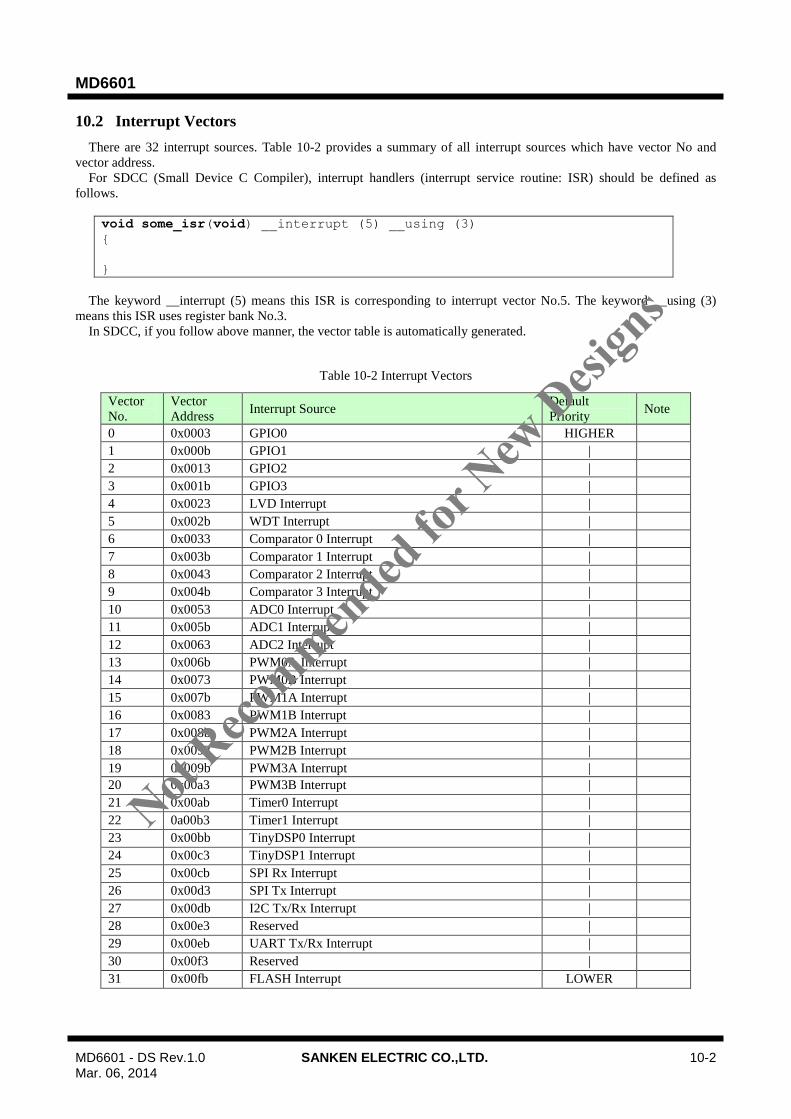
MD6601
MD6601 - DS Rev.1.0 SANKEN ELECTRIC CO.,LTD. 10-2 Mar. 06, 2014
10.2 Interrupt Vectors
There are 32 interrupt sources. Table 10-2 provides a summary of all interrupt sources which have vector No and
vector address.
For SDCC (Small Device C Compiler), interrupt handlers (interrupt service routine: ISR) should be defined as
follows.
void some_isr(void) __interrupt (5) __using (3)
{
}
The keyword __interrupt (5) means this ISR is corresponding to interrupt vector No.5. The keyword __using (3)
means this ISR uses register bank No.3.
In SDCC, if you follow above manner, the vector table is automatically generated.
Table 10-2 Interrupt Vectors
Vector
No.
Vector
Address Interrupt Source
Default
Priority Note
0 0x0003 GPIO0 HIGHER
1 0x000b GPIO1 |
2 0x0013 GPIO2 |
3 0x001b GPIO3 |
4 0x0023 LVD Interrupt |
5 0x002b WDT Interrupt |
6 0x0033 Comparator 0 Interrupt |
7 0x003b Comparator 1 Interrupt |
8 0x0043 Comparator 2 Interrupt |
9 0x004b Comparator 3 Interrupt |
10 0x0053 ADC0 Interrupt |
11 0x005b ADC1 Interrupt |
12 0x0063 ADC2 Interrupt |
13 0x006b PWM0A Interrupt |
14 0x0073 PWM0B Interrupt |
15 0x007b PWM1A Interrupt |
16 0x0083 PWM1B Interrupt |
17 0x008b PWM2A Interrupt |
18 0x0093 PWM2B Interrupt |
19 0x009b PWM3A Interrupt |
20 0x00a3 PWM3B Interrupt |
21 0x00ab Timer0 Interrupt |
22 0a00b3 Timer1 Interrupt |
23 0x00bb TinyDSP0 Interrupt |
24 0x00c3 TinyDSP1 Interrupt |
25 0x00cb SPI Rx Interrupt |
26 0x00d3 SPI Tx Interrupt |
27 0x00db I2C Tx/Rx Interrupt |
28 0x00e3 Reserved |
29 0x00eb UART Tx/Rx Interrupt |
30 0x00f3 Reserved |
31 0x00fb FLASH Interrupt LOWER
Not Reco
mmended
for N
ew D
esign
s
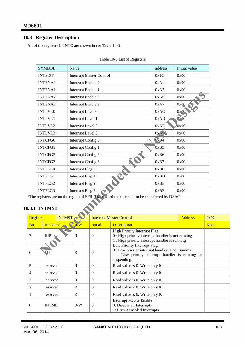
MD6601
MD6601 - DS Rev.1.0 SANKEN ELECTRIC CO.,LTD. 10-3 Mar. 06, 2014
10.3 Register Description
All of the registers in INTC are shown in the Table 10-3
Table 10-3 List of Registers
SYMBOL Name address Initial value
INTMST Interrupt Master Control 0x9C 0x00
INTENA0 Interrupt Enable 0 0xA4 0x00
INTENA1 Interrupt Enable 1 0xA5 0x00
INTENA2 Interrupt Enable 2 0xA6 0x00
INTENA3 Interrupt Enable 3 0xA7 0x00
INTLVL0 Interrupt Level 0 0xAC 0x00
INTLVL1 Interrupt Level 1 0xAD 0x00
INTLVL2 Interrupt Level 2 0xAE 0x00
INTLVL3 Interrupt Level 3 0xAF 0x00
INTCFG0 Interrupt Config 0 0xB4 0x00
INTCFG1 Interrupt Config 1 0xB5 0x00
INTCFG2 Interrupt Config 2 0xB6 0x00
INTCFG3 Interrupt Config 3 0xB7 0x00
INTFLG0 Interrupt Flag 0 0xBC 0x00
INTFLG1 Interrupt Flag 1 0xBD 0x00
INTFLG2 Interrupt Flag 2 0xBE 0x00
INTFLG3 Interrupt Flag 3 0xBF 0x00
*The registers are on the region of SFR. The data of them are not to be transferred by DSAC.
10.3.1 INTMST
Register INTMST Interrupt Master Control Address 0x9C
Bit Bit Name R/W Initial Description Note
7 HIP R 0
High Priority Interrupt Flag
0 : High priority interrupt handler is not running.
1 : High priority interrupt handler is running.
6 LIP R 0
Low Priority Interrupt Flag
0 : Low priority interrupt handler is not running.
1 : Low priority interrupt handler is running or
suspending.
5 reserved R 0 Read value is 0. Write only 0.
4 reserved R 0 Read value is 0. Write only 0.
3 reserved R 0 Read value is 0. Write only 0.
2 reserved R 0 Read value is 0. Write only 0.
1 reserved R 0 Read value is 0. Write only 0.
0 INTME R/W 0
Interrupt Master Enable
0: Disable all Interrupts
1: Permit enabled Interrupts
Not Reco
mmended
for N
ew D
esign
s
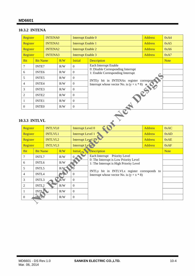
MD6601
MD6601 - DS Rev.1.0 SANKEN ELECTRIC CO.,LTD. 10-4 Mar. 06, 2014
10.3.2 INTENA
Register INTENA0 Interrupt Enable 0 Address 0xA4
Register INTENA1 Interrupt Enable 1 Address 0xA5
Register INTENA2 Interrupt Enable 2 Address 0xA6
Register INTENA3 Interrupt Enable 3 Address 0xA7
Bit Bit Name R/W Initial Description Note
7 INTE7 R/W 0 Each Interrupt Enable
0: Disable Corresponding Interrupt
1: Enable Corresponding Interrupt
INTEy bit in INTENAx register corresponds to
Interrupt whose vector No. is (y + x * 8)
6 INTE6 R/W 0
5 INTE5 R/W 0
4 INTE4 R/W 0
3 INTE3 R/W 0
2 INTE2 R/W 0
1 INTE1 R/W 0
0 INTE0 R/W 0
10.3.3 INTLVL
Register INTLVL0 Interrupt Level 0 Address 0xAC
Register INTLVL1 Interrupt Level 1 Address 0xAD
Register INTLVL2 Interrupt Level 2 Address 0xAE
Register INTLVL3 Interrupt Level 3 Address 0xAF
Bit Bit Name R/W Initial Description Note
7 INTL7 R/W 0 Each Interrupt Priority Level
0: The Interrupt is Low Priority Level
1: The Interrupt is High Priority Level
INTLy bit in INTLVLx register corresponds to
Interrupt whose vector No. is (y + x * 8)
6 INTL6 R/W 0
5 INTL5 R/W 0
4 INTL4 R/W 0
3 INTL3 R/W 0
2 INTL2 R/W 0
1 INTL1 R/W 0
0 INTL0 R/W 0
Not
Recommen
ded fo
r New
Desi
gns
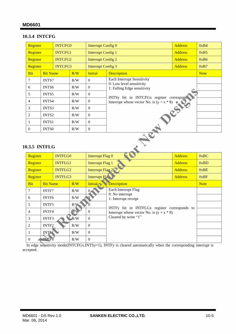
MD6601
MD6601 - DS Rev.1.0 SANKEN ELECTRIC CO.,LTD. 10-5 Mar. 06, 2014
10.3.4 INTCFG
Register INTCFG0 Interrupt Config 0 Address 0xB4
Register INTCFG1 Interrupt Config 1 Address 0xB5
Register INTCFG2 Interrupt Config 2 Address 0xB6
Register INTCFG3 Interrupt Config 3 Address 0xB7
Bit Bit Name R/W Initial Description Note
7 INTS7 R/W 0 Each Interrupt Sensitivity
0: Low level sensitivity
1: Falling Edge sensitivity
INTSy bit in INTCFGx register corresponds to
Interrupt whose vector No. is (y + x * 8)
6 INTS6 R/W 0
5 INTS5 R/W 0
4 INTS4 R/W 0
3 INTS3 R/W 0
2 INTS2 R/W 0
1 INTS1 R/W 0
0 INTS0 R/W 0
10.3.5 INTFLG
Register INTFLG0 Interrupt Flag 0 Address 0xBC
Register INTFLG1 Interrupt Flag 1 Address 0xBD
Register INTFLG2 Interrupt Flag 2 Address 0xBE
Register INTFLG3 Interrupt Flag 3 Address 0xBF
Bit Bit Name R/W Initial Description Note
7 INTF7 R/W 0 Each Interrupt Flag
0: No interrupt
1: Interrupt receipt
INTFy bit in INTFLGx register corresponds to
Interrupt whose vector No. is (y + x * 8)
Cleared by write “1”
6 INTF6 R/W 0
5 INTF5 R/W 0
4 INTF4 R/W 0
3 INTF3 R/W 0
2 INTF2 R/W 0
1 INTF1 R/W 0
0 INTF0 R/W 0
In edge sensitivity mode(INTCFGx.INTSy=1), INTFy is cleared automatically when the corresponding interrupt is
accepted.
Not Reco
mmended
for N
ew D
esign
s
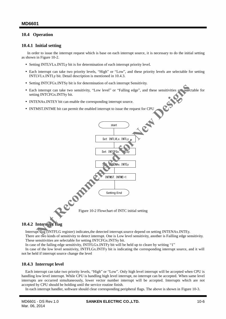
MD6601
MD6601 - DS Rev.1.0 SANKEN ELECTRIC CO.,LTD. 10-6 Mar. 06, 2014
10.4 Operation
10.4.1 Initial setting
In order to issue the interrupt request which is base on each interrupt source, it is necessary to do the initial setting
as shown in Figure 10-2.
Setting INTLVLx.INTLy bit is for determination of each interrupt priority level.
Each interrupt can take two priority levels, “High” or “Low”, and these priority levels are selectable for setting
INTLVLx.INTLy bit. Detail description is mentioned in 10.4.3.
Setting INTCFGx.INTSy bit is for determination of each interrupt Sensitivity.
Each interrupt can take two sensitivity, “Low level” or “Falling edge”, and these sensitivities are selectable for
setting INTCFGx.INTSy bit.
INTENAx.INTEY bit can enable the corresponding interrupt source.
INTMST.INTME bit can permit the enabled interrupt to issue the request for CPU
INTMST.INTME=1
Set INTENAx.INTEy
Set INTLVLx.INTLy
Set INTCFGx. INTSy
start
Setting End
Figure 10-2 Flowchart of INTC initial setting
10.4.2 Interrupt flag
Interrupt flag (INTFLG register) indicates,the detected interrupt.source depend on setting INTENAx.INTEy.
There are two kinds of sensitivity to detect interrupt. One is Low level sensitivity, another is Failling edge sensitivity.
These sensitivities are selectable for setting INTCFGx.INTSy bit.
In case of the failing edge sensitivity, INTFLGx.INTFy bit will be held up to cleare by writing “1”
In case of the low level sensitivity, INTFLGx.INTFy bit is indicating the corresponding interrupt source, and it will
not be held if interrupt source change the level
10.4.3 Interrupt level
Each interrupt can take two priority levels, “High” or “Low”. Only high level interrupt will be accepted when CPU is
handling low level interrupt. While CPU is handling high level interrupt, no interrupt can be accepted. When same level
interrupts are occurred simultaneously, lower vector number interrupt will be accepted. Interrupts which are not
accepted by CPU should be holding until the service routine finish.
In each interrupt handler, software should clear corresponding peripheral flags. The above is shown in Figure 10-3.
Not Reco
mmended
for N
ew D
esign
s

MD6601
MD6601 - DS Rev.1.0 SANKEN ELECTRIC CO.,LTD. 10-7 Mar. 06, 2014
Note: It is impossible to generate new interrupt signals at such time as below.
When executing RETI instruction.
The time before receiving acknowledgement of CPU after issuing the interrupt request, and doing it.
No Interrupt Low Level
Interrupt
High Level
Interrupt(1)
INTACK INTACK
RETI RETI
High Level
Interrupt(2)
INTACK
RETI
Figure 10-3 diagram of INTC state transition
By executing RETI instruction at end of interrupt routine, it is cleared that INTMST.HIP/LIP bits corresponding to
priority of this routine.
Detecting interrupt
INTMST.INTME==1
INTENAx.INTEy==1
INTMST.HIP==0
INTLVLx.INTLy==1
INTMST.LIP==0
Y
N
Y
N
Y
N
Y
N
Y
NINTMST.HIP=1
INTMST.LIP=1
Ignoring interrupt
Accepting interrupt
Figure 10-4 Flowchart of INTC accepting interrupt
Decisions of Figure 10-4 are processed by hardware.
Not Reco
mmended
for N
ew D
esign
s

MD6601
MD6601 - DS Rev.1.0 SANKEN ELECTRIC CO.,LTD. 10-8 Mar. 06, 2014
10.4.4 Interrupt of external pins
All GPIO can be used external interrupt pin in accord with GPIO register settings. Signals of interrupt by GPIO are
ORed. The signals ORed is input on INTC after it is converted. Logic diagaram of interrupt by GPIO is shown in Figure
10-5. Wave form diagram of generating interrupt by GPIO is shown in Figure 10-6. Vector addresses of each GPIO
refer to Table 10-2. Details information of external interrupt by GPIO is described in section.8.
NoiseCanceller
Edgedetector
SClear PIF
PIFm.PIFnGPIOmn
CLKRUN_FAST(max 50MHz)
Detecting level
Detecting edge
PISm.PISn
1 or under 1 cycle of CLKGPIO
Interrupt by GPIOm
PIEm.PIEn:
Int0m_n
Figure 10-5 Logic diagram of interrupt by GPIO
GPIOmn
CLKRUN_FAST
Output Noise Canceler
Output Edge Detector
FLAG holding Edge
Level sensitivity
edge sensitivity
interrupt by GPIO
int0m_n
Figure 10-6 Wave form diagram of interrupt by GPIO
Not Reco
mmended
for N
ew D
esign
s
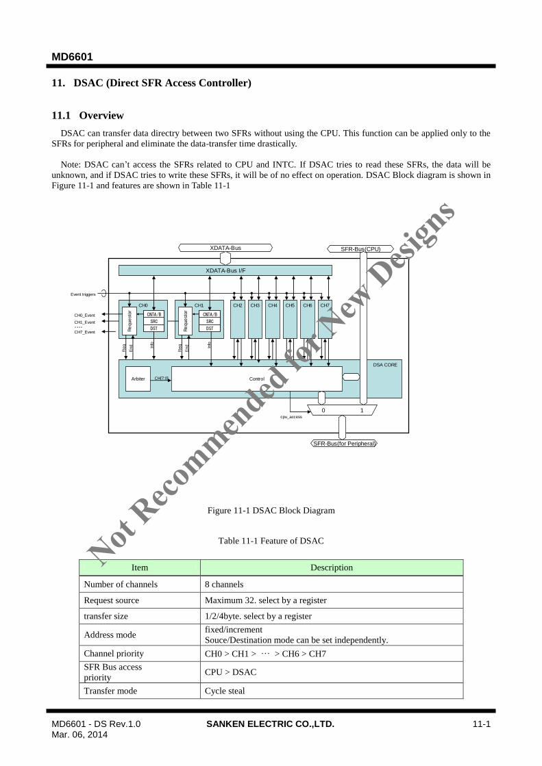
MD6601
MD6601 - DS Rev.1.0 SANKEN ELECTRIC CO.,LTD. 11-1 Mar. 06, 2014
11. DSAC (Direct SFR Access Controller)
11.1 Overview
DSAC can transfer data directry between two SFRs without using the CPU. This function can be applied only to the
SFRs for peripheral and eliminate the data-transfer time drastically.
Note: DSAC can’t access the SFRs related to CPU and INTC. If DSAC tries to read these SFRs, the data will be
unknown, and if DSAC tries to write these SFRs, it will be of no effect on operation. DSAC Block diagram is shown in
Figure 11-1 and features are shown in Table 11-1
CH1
Re
que
sto
r
SRC
DST
CNTA/B
XDATA-Bus
DSA CORE
cpu_access
XDATA-Bus I/F
CH0
Re
que
sto
r
SRC
DST
CNTA/B
CH2 CH3 CH4 CH5 CH6 CH7
Event triggers
Req
End
Req
EndInfo
Info
Arbiter
SFR-Bus(CPU)
ControlCH[7:0]
0 1
SFR-Bus(for Peripheral)
CH0_Event
CH1_Event
・・・・CH7_Event
Figure 11-1 DSAC Block Diagram
Table 11-1 Feature of DSAC
Item Description
Number of channels 8 channels
Request source Maximum 32. select by a register
transfer size 1/2/4byte. select by a register
Address mode fixed/increment
Souce/Destination mode can be set independently.
Channel priority CH0 > CH1 > … > CH6 > CH7
SFR Bus access
priority CPU > DSAC
Transfer mode Cycle steal
Not Reco
mmended
for N
ew D
esign
s
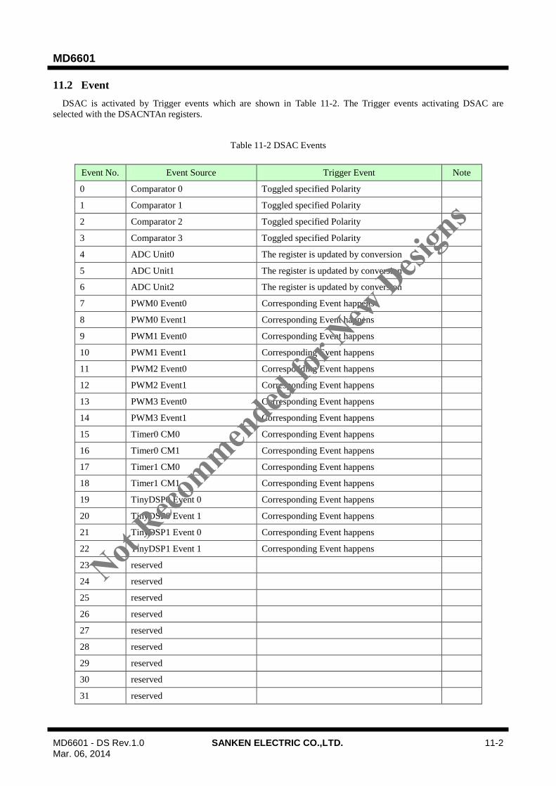
MD6601
MD6601 - DS Rev.1.0 SANKEN ELECTRIC CO.,LTD. 11-2 Mar. 06, 2014
11.2 Event
DSAC is activated by Trigger events which are shown in Table 11-2. The Trigger events activating DSAC are
selected with the DSACNTAn registers.
Table 11-2 DSAC Events
Event No. Event Source Trigger Event Note
0 Comparator 0 Toggled specified Polarity
1 Comparator 1 Toggled specified Polarity
2 Comparator 2 Toggled specified Polarity
3 Comparator 3 Toggled specified Polarity
4 ADC Unit0 The register is updated by conversion
5 ADC Unit1 The register is updated by conversion
6 ADC Unit2 The register is updated by conversion
7 PWM0 Event0 Corresponding Event happens
8 PWM0 Event1 Corresponding Event happens
9 PWM1 Event0 Corresponding Event happens
10 PWM1 Event1 Corresponding Event happens
11 PWM2 Event0 Corresponding Event happens
12 PWM2 Event1 Corresponding Event happens
13 PWM3 Event0 Corresponding Event happens
14 PWM3 Event1 Corresponding Event happens
15 Timer0 CM0 Corresponding Event happens
16 Timer0 CM1 Corresponding Event happens
17 Timer1 CM0 Corresponding Event happens
18 Timer1 CM1 Corresponding Event happens
19 TinyDSP0 Event 0 Corresponding Event happens
20 TinyDSP0 Event 1 Corresponding Event happens
21 TinyDSP1 Event 0 Corresponding Event happens
22 TinyDSP1 Event 1 Corresponding Event happens
23 reserved
24 reserved
25 reserved
26 reserved
27 reserved
28 reserved
29 reserved
30 reserved
31 reserved
Not Reco
mmended
for N
ew D
esign
s

MD6601
MD6601 - DS Rev.1.0 SANKEN ELECTRIC CO.,LTD. 11-3 Mar. 06, 2014
11.3 Register Description
Table 11-3 XDATA-Bus registers
Symbol Name Address Initial value
DSACNTA0 DSA Control A Channel 0 0xF880 0x00
DSACNTB0 DSA Control B Channel 0 0xF881 0x00
DSASRC0 DSA Source Address Channel 0 0xF882 0x80
DSADST0 DSA Destination Address Channel 0 0xF883 0x80
DSACNTA1 DSA Control A Channel 1 0xF884 0x00
DSACNTB1 DSA Control B Channel 1 0xF885 0x00
DSASRC1 DSA Source Address Channel 1 0xF886 0x80
DSADST1 DSA Destination Address Channel 1 0xF887 0x80
DSACNTA2 DSA Control A Channel 2 0xF888 0x00
DSACNTB2 DSA Control B Channel 2 0xF889 0x00
DSASRC2 DSA Source Address Channel 2 0xF88A 0x80
DSADST2 DSA Destination Address Channel 2 0xF88B 0x80
DSACNTA3 DSA Control A Channel 3 0xF88C 0x00
DSACNTB3 DSA Control B Channel 3 0xF88D 0x00
DSASRC3 DSA Source Address Channel 3 0xF88E 0x80
DSADST3 DSA Destination Address Channel 3 0xF88F 0x80
DSACNTA4 DSA Control A Channel 4 0xF890 0x00
DSACNTB4 DSA Control B Channel 4 0xF891 0x00
DSASRC4 DSA Source Address Channel 4 0xF892 0x80
DSADST4 DSA Destination Address Channel 4 0xF893 0x80
DSACNTA5 DSA Control A Channel 5 0xF894 0x00
DSACNTB5 DSA Control B Channel 5 0xF895 0x00
DSASRC5 DSA Source Address Channel 5 0xF896 0x80
DSADST5 DSA Destination Address Channel 5 0xF897 0x80
DSACNTA6 DSA Control A Channel 6 0xF898 0x00
DSACNTB6 DSA Control B Channel 6 0xF899 0x00
DSASRC6 DSA Source Address Channel 6 0xF89A 0x80
DSADST6 DSA Destination Address Channel 6 0xF89B 0x80
DSACNTA7 DSA Control A Channel 7 0xF89C 0x00
DSACNTB7 DSA Control B Channel 7 0xF89D 0x00
DSASRC7 DSA Source Address Channel 7 0xF89D 0x80
DSADST7 DSA Destination Address Channel 7 0xF89F 0x80
Not Reco
mmended
for N
ew D
esign
s
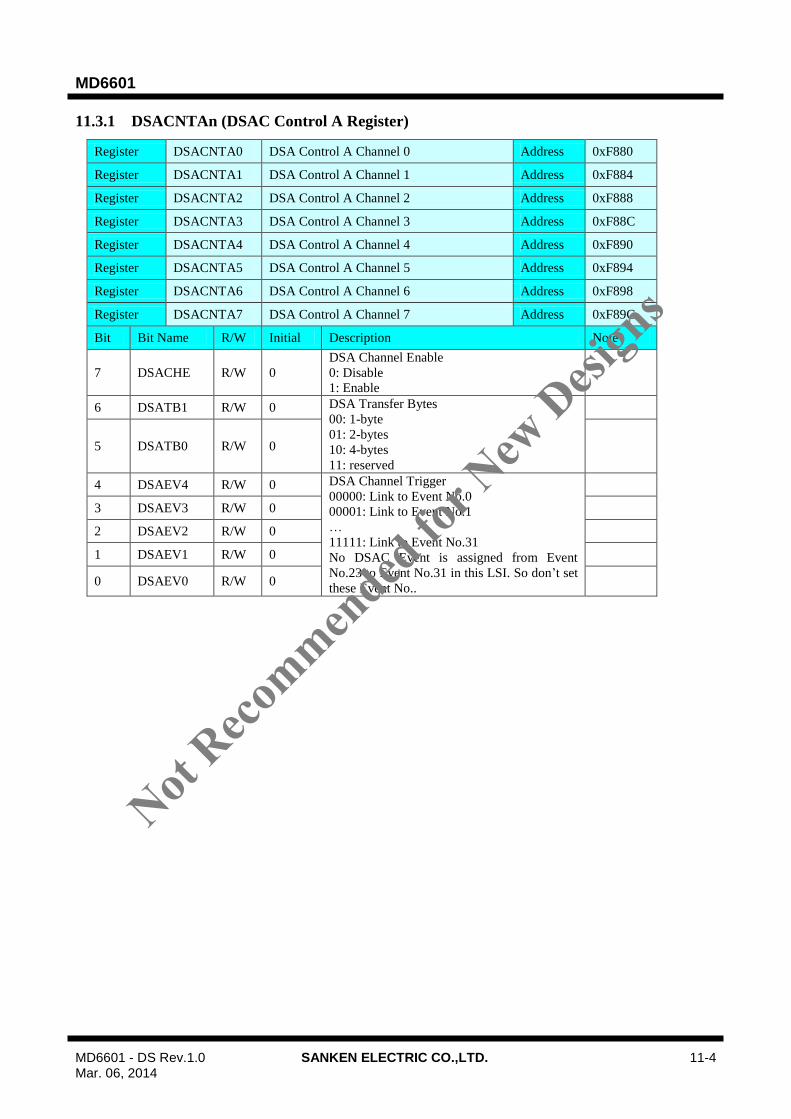
MD6601
MD6601 - DS Rev.1.0 SANKEN ELECTRIC CO.,LTD. 11-4 Mar. 06, 2014
11.3.1 DSACNTAn (DSAC Control A Register)
Register DSACNTA0 DSA Control A Channel 0 Address 0xF880
Register DSACNTA1 DSA Control A Channel 1 Address 0xF884
Register DSACNTA2 DSA Control A Channel 2 Address 0xF888
Register DSACNTA3 DSA Control A Channel 3 Address 0xF88C
Register DSACNTA4 DSA Control A Channel 4 Address 0xF890
Register DSACNTA5 DSA Control A Channel 5 Address 0xF894
Register DSACNTA6 DSA Control A Channel 6 Address 0xF898
Register DSACNTA7 DSA Control A Channel 7 Address 0xF89C
Bit Bit Name R/W Initial Description Note
7 DSACHE R/W 0
DSA Channel Enable
0: Disable
1: Enable
6 DSATB1 R/W 0 DSA Transfer Bytes
00: 1-byte
01: 2-bytes
10: 4-bytes
11: reserved
5 DSATB0 R/W 0
4 DSAEV4 R/W 0 DSA Channel Trigger
00000: Link to Event No.0
00001: Link to Event No.1
…
11111: Link to Event No.31
No DSAC Event is assigned from Event
No.23 to Event No.31 in this LSI. So don’t set
these Event No..
3 DSAEV3 R/W 0
2 DSAEV2 R/W 0
1 DSAEV1 R/W 0
0 DSAEV0 R/W 0
Not Reco
mmended
for N
ew D
esign
s

MD6601
MD6601 - DS Rev.1.0 SANKEN ELECTRIC CO.,LTD. 11-5 Mar. 06, 2014
11.3.2 DSACNTBn (DSAC Control B Register)
Register DSACNTB0 DSA Control B Channel 0 Address 0xF881
Register DSACNTB1 DSA Control B Channel 1 Address 0xF885
Register DSACNTB2 DSA Control B Channel 2 Address 0xF889
Register DSACNTB3 DSA Control B Channel 3 Address 0xF88D
Register DSACNTB4 DSA Control B Channel 4 Address 0xF891
Register DSACNTB5 DSA Control B Channel 5 Address 0xF895
Register DSACNTB6 DSA Control B Channel 6 Address 0xF899
Register DSACNTB7 DSA Control B Channel 7 Address 0xF89D
Bit Bit Name R/W Initial Description Note
7 reserved R 0 Read value is 0. Write only 0
6 reserved R 0 Read value is 0. Write only 0
5 reserved R 0 Read value is 0. Write only 0
4 reserved R 0 Read value is 0. Write only 0
3 reserved R 0 Read value is 0. Write only 0
2 reserved R 0 Read value is 0. Write only 0
1 DSADSTC R/W 0
Destination Address Control
0: Address stays at same value.
1: Increment according to DSATB[1:0] setting
0 DSASRCC R/W 0
Source Address Control
0: Address stays at same value.
1: Increment according to DSATB[1:0] setting
11.3.3 DSASRCn (DSAC Source address Register)
Register DSASRC0 DSA Source Address Channel 0 Address 0xF882
Register DSASRC1 DSA Source Address Channel 1 Address 0xF886
Register DSASRC2 DSA Source Address Channel 2 Address 0xF88A
Register DSASRC3 DSA Source Address Channel 3 Address 0xF88E
Register DSASRC4 DSA Source Address Channel 4 Address 0xF892
Register DSASRC5 DSA Source Address Channel 5 Address 0xF896
Register DSASRC6 DSA Source Address Channel 6 Address 0xF89A
Register DSASRC7 DSA Source Address Channel 7 Address 0xF89D
Bit Bit Name R/W Initial Description Note
7 reserved R 1 Read value is 1. Write only 1
6 DSASA6 R/W 0 SFR Source Address
(Corresponding to 0x80 – 0xFF)
5 DSASA5 R/W 0
4 DSASA4 R/W 0
3 DSASA3 R/W 0
2 DSASA2 R/W 0
1 DSASA1 R/W 0
0 DSASA0 R/W 0
Not Reco
mmended
for N
ew D
esign
s
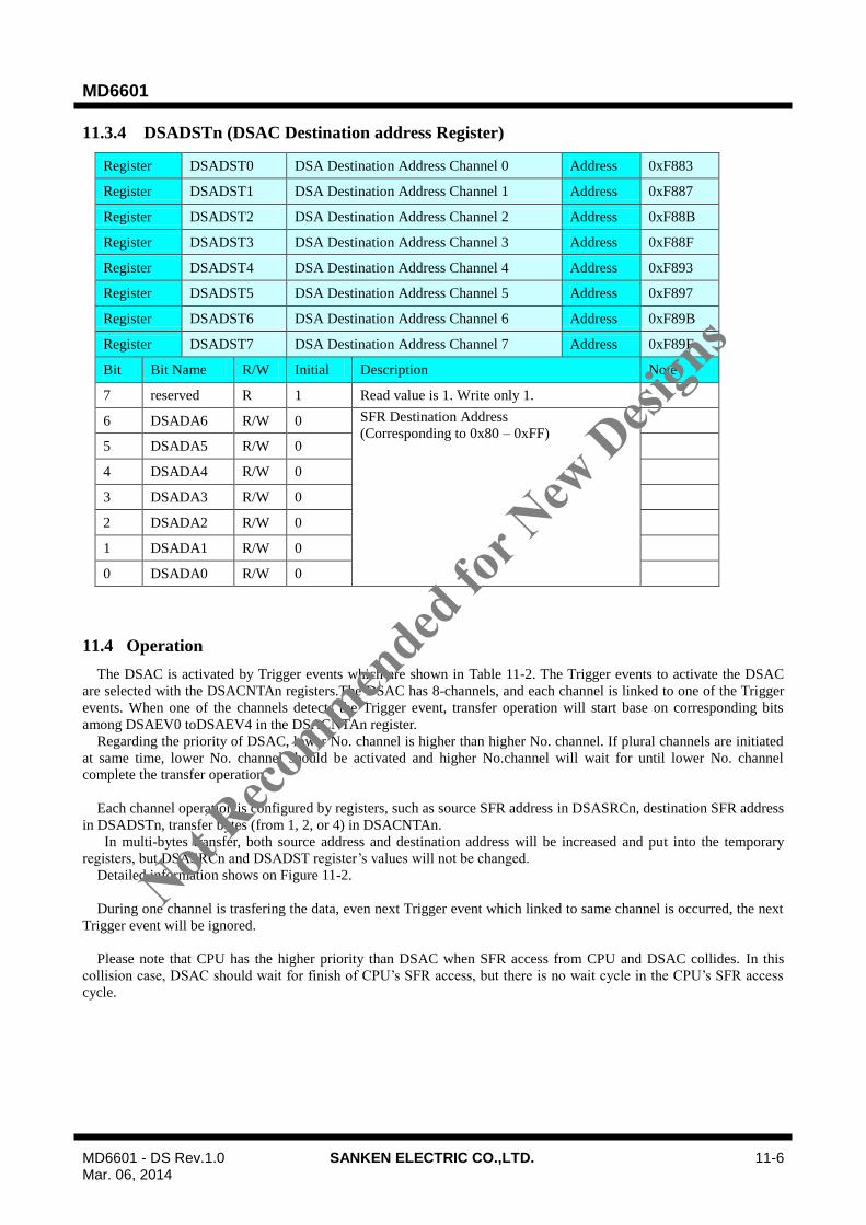
MD6601
MD6601 - DS Rev.1.0 SANKEN ELECTRIC CO.,LTD. 11-6 Mar. 06, 2014
11.3.4 DSADSTn (DSAC Destination address Register)
Register DSADST0 DSA Destination Address Channel 0 Address 0xF883
Register DSADST1 DSA Destination Address Channel 1 Address 0xF887
Register DSADST2 DSA Destination Address Channel 2 Address 0xF88B
Register DSADST3 DSA Destination Address Channel 3 Address 0xF88F
Register DSADST4 DSA Destination Address Channel 4 Address 0xF893
Register DSADST5 DSA Destination Address Channel 5 Address 0xF897
Register DSADST6 DSA Destination Address Channel 6 Address 0xF89B
Register DSADST7 DSA Destination Address Channel 7 Address 0xF89F
Bit Bit Name R/W Initial Description Note
7 reserved R 1 Read value is 1. Write only 1.
6 DSADA6 R/W 0 SFR Destination Address
(Corresponding to 0x80 – 0xFF)
5 DSADA5 R/W 0
4 DSADA4 R/W 0
3 DSADA3 R/W 0
2 DSADA2 R/W 0
1 DSADA1 R/W 0
0 DSADA0 R/W 0
11.4 Operation
The DSAC is activated by Trigger events which are shown in Table 11-2. The Trigger events to activate the DSAC
are selected with the DSACNTAn registers.The DSAC has 8-channels, and each channel is linked to one of the Trigger
events. When one of the channels detects the Trigger event, transfer operation will start base on corresponding bits
among DSAEV0 toDSAEV4 in the DSACNTAn register.
Regarding the priority of DSAC, lower No. channel is higher than higher No. channel. If plural channels are initiated
at same time, lower No. channel should be activated and higher No.channel will wait for until lower No. channel
complete the transfer operation.
Each channel operation is configured by registers, such as source SFR address in DSASRCn, destination SFR address
in DSADSTn, transfer bytes (from 1, 2, or 4) in DSACNTAn.
In multi-bytes transfer, both source address and destination address will be increased and put into the temporary
registers, but DSASRCn and DSADST register’s values will not be changed.
Detailed information shows on Figure 11-2.
During one channel is trasfering the data, even next Trigger event which linked to same channel is occurred, the next
Trigger event will be ignored.
Please note that CPU has the higher priority than DSAC when SFR access from CPU and DSAC collides. In this
collision case, DSAC should wait for finish of CPU’s SFR access, but there is no wait cycle in the CPU’s SFR access
cycle.
Not Reco
mmended
for N
ew D
esign
s
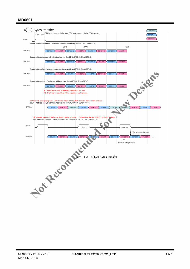
MD6601
MD6601 - DS Rev.1.0 SANKEN ELECTRIC CO.,LTD. 11-7 Mar. 06, 2014
4(1,2) Bytes transfer
Event
1cyc=50MHz
CPU R/W
DSADSTDSASRC DSADST+1DSASRC+1 DSADST+2DSASRC+2 DSADST+3DSASRC+3SFR Bus
Source Address: Increment, Destination Address: Increment (DSASRCC=1, DSADSTC=1)
DSAC Write
DSAC Read
DSADSTDSASRC DSADSTDSASRC+1 DSADSTDSASRC+2 DSADSTDSASRC+3SFR Bus
Source Address:Increment, Destination Address :fixed(DSASRCC=1, DSADSTC=0)
DSADSTDSASRC DSADST+1DSASRC DSADST+2DSASRC DSADST+3DSASRCSFR Bus
Source Address:fixed, Destination Address: Increment(DSASRCC=0, DSADSTC=1)
DSASRC DSASRC DSASRC DSASRCSFR Bus
Source Address: fixed, Destination Address: fixed (DSASRCC=0, DSADSTC=0)
DSADST DSADST DSADST DSADST
* 1 Byte transfer case, Read→Write repetition is one time .* 2 Byte transfer case, Read→Write repetitions are two times.
DSASRC DSASRC DSASRC DSASRCSFR Bus
CPU access takes priority when CPU access occurs during DSAC transfer. DSA transfer is waited.
Source Address: fixed, Destination Address: fixed (DSASRCC=0, DSADSTC=0)
DSADST DSADST DSADST DSADSTCPU R/W CPU R/W CPU R/W
Event
DSADSTDSASRC DSADST+1DSASRC+1 DSADST+2DSASRC+2 DSADST+3DSASRC+3SFR Bus
The following event on the channel during transfer is ignored. The event on the last DSADST writing is accepted.
Source Address: increment, Destination Address: increment(DSASRCC=1, DSADSTC=1)
DSADSTDSASRC
Ignored Accepted
The last writing transfer
The next transfer start
・・・
1Byte 2Byte 4Byte
CPU access takes priority when CPU access occurs during DSAC transfer
Figure 11-2 4(1,2) Bytes transfer
Not Reco
mmended
for N
ew D
esign
s
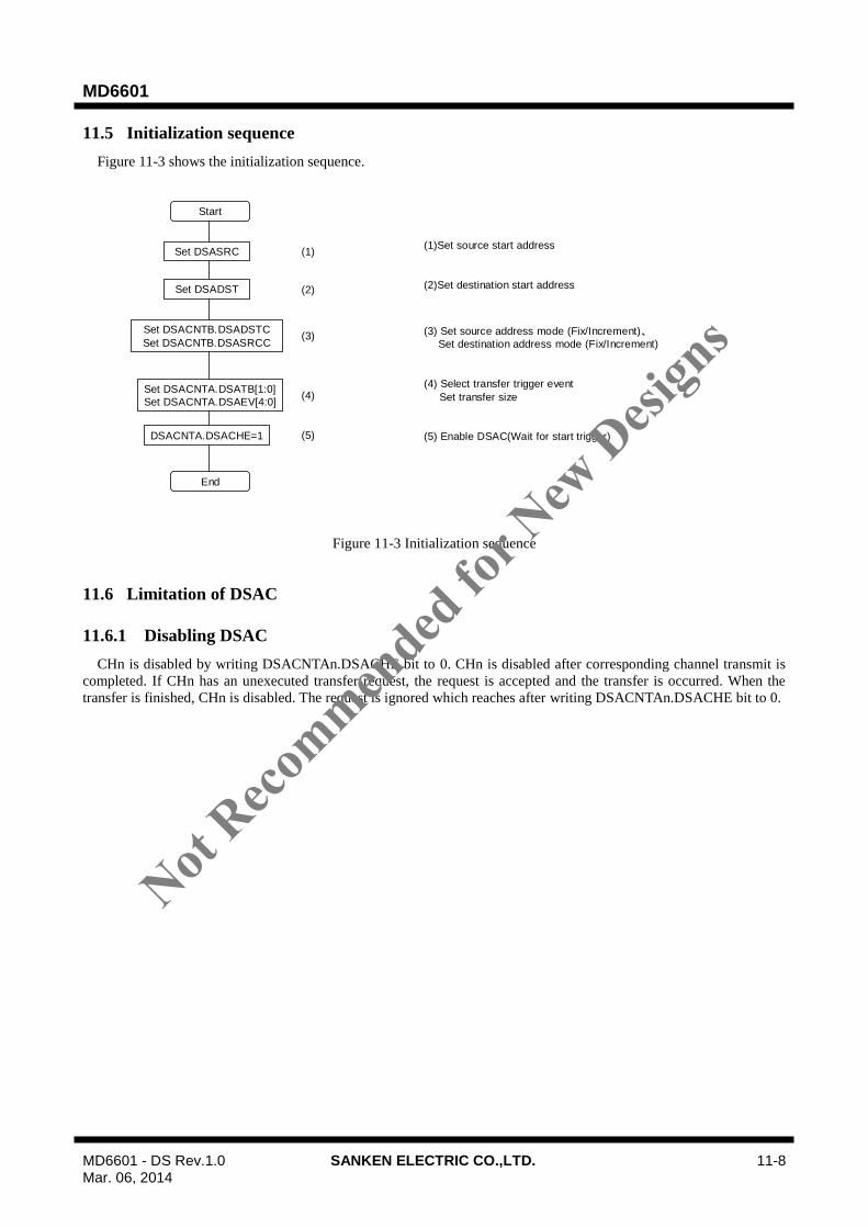
MD6601
MD6601 - DS Rev.1.0 SANKEN ELECTRIC CO.,LTD. 11-8 Mar. 06, 2014
11.5 Initialization sequence
Figure 11-3 shows the initialization sequence.
Start
DSACNTA.DSACHE=1
End
Set DSADST
Set DSACNTA.DSATB[1:0]
Set DSACNTA.DSAEV[4:0]
(2)Set destination start address
(3) Set source address mode (Fix/Increment)、Set destination address mode (Fix/Increment)
(4) Select transfer trigger event
Set transfer size
(5) Enable DSAC(Wait for start trigger)
Set DSASRC (1)(1)Set source start address
(2)
(3)
(4)
(5)
Set DSACNTB.DSADSTC
Set DSACNTB.DSASRCC
Figure 11-3 Initialization sequence
11.6 Limitation of DSAC
11.6.1 Disabling DSAC
CHn is disabled by writing DSACNTAn.DSACHE bit to 0. CHn is disabled after corresponding channel transmit is
completed. If CHn has an unexecuted transfer request, the request is accepted and the transfer is occurred. When the
transfer is finished, CHn is disabled. The request is ignored which reaches after writing DSACNTAn.DSACHE bit to 0.
Not Reco
mmended
for N
ew D
esign
s
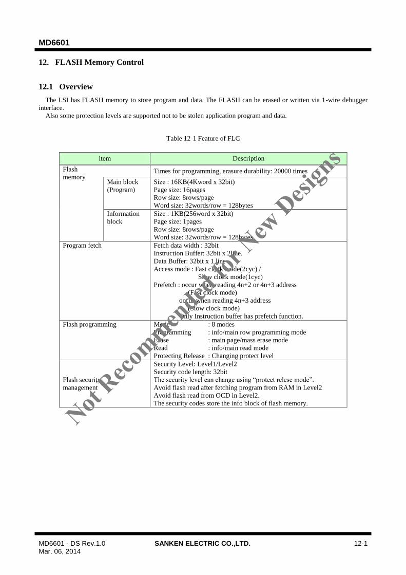
MD6601
MD6601 - DS Rev.1.0 SANKEN ELECTRIC CO.,LTD. 12-1 Mar. 06, 2014
12. FLASH Memory Control
12.1 Overview
The LSI has FLASH memory to store program and data. The FLASH can be erased or written via 1-wire debugger
interface.
Also some protection levels are supported not to be stolen application program and data.
Table 12-1 Feature of FLC
item Description
Flash
memory
Times for programming, erasure durability: 20000 times
Main block
(Program)
Size : 16KB(4Kword x 32bit)
Page size: 16pages
Row size: 8rows/page
Word size: 32words/row = 128bytes
Information
block
Size : 1KB(256word x 32bit)
Page size: 1pages
Row size: 8rows/page
Word size: 32words/row = 128bytes
Program fetch Fetch data width : 32bit
Instruction Buffer: 32bit x 2line.
Data Buffer: 32bit x 1 line
Access mode : Fast clock mode(2cyc) /
Slow clock mode(1cyc)
Prefetch : occur when reading 4n+2 or 4n+3 address
(Fast clock mode)
occur when reading 4n+3 address
(Slow clock mode)
Only Instruction buffer has prefetch function.
Flash programming Mode : 8 modes
Programming : info/main row programming mode
Erase : main page/mass erase mode
Read : info/main read mode
Protecting Release : Changing protect level
Flash security
management
Security Level: Level1/Level2
Security code length: 32bit
The security level can change using “protect relese mode”.
Avoid flash read after fetching program from RAM in Level2
Avoid flash read from OCD in Level2.
The security codes store the info block of flash memory.
Not Reco
mmended
for N
ew D
esign
s

MD6601
MD6601 - DS Rev.1.0 SANKEN ELECTRIC CO.,LTD. 12-2 Mar. 06, 2014
Protect Level
Release Protecting
XD
AT
A B
us
Bus I
/F
Program/Erase
Control
Protect Level
Control
Instruction Fetch
Control
Flash Memory
16KB
FMTIME
FMPAGE
FMROW
FMCOL
FMCTRL
FMEXE
FMROW
XP
RO
G B
us
Instr
uction B
uff
er
4byte
s
FMRMOD
Control
Select
Low Power control signal
FMRPD0-3
Instr
uction B
uff
er
4byte
s
Data
Buff
er
4byte
s
32
32 32
8
8
8
Figure 12-1 Block Diagram of FLC
Not Reco
mmended
for N
ew D
esign
s
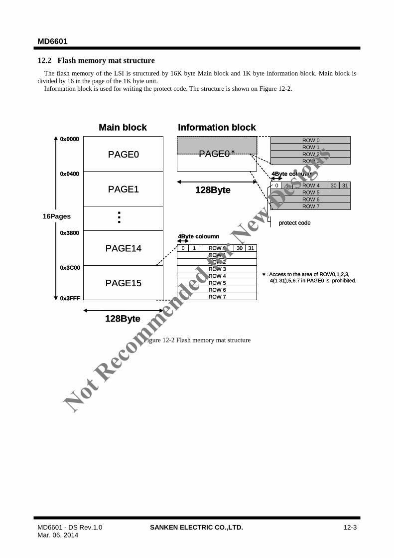
MD6601
MD6601 - DS Rev.1.0 SANKEN ELECTRIC CO.,LTD. 12-3 Mar. 06, 2014
12.2 Flash memory mat structure
The flash memory of the LSI is structured by 16K byte Main block and 1K byte information block. Main block is
divided by 16 in the page of the 1K byte unit.
Information block is used for writing the protect code. The structure is shown on Figure 12-2.
Figure 12-2 Flash memory mat structure
Main block Information block
PAGE0
PAGE1
PAGE14
PAGE15
…16Pages
128Byte
128Byte
ROW 0
ROW 1
ROW 2
ROW 3
ROW 4
ROW 5
ROW 6
ROW 7
PAGE0*
ROW 0
ROW 1
ROW 2
ROW 3
ROW 4
ROW 5
ROW 6
ROW 7
0 1 3130
0 1 3130
4Byte coloumn
4Byte coloumn
protect code
0x0000
0x0400
0x3FFF
0x3C00
0x3800
*:Access to the area of ROW0,1,2,3,
4(1-31),5,6,7 in PAGE0 is prohibited.
Not Reco
mmended
for N
ew D
esign
s
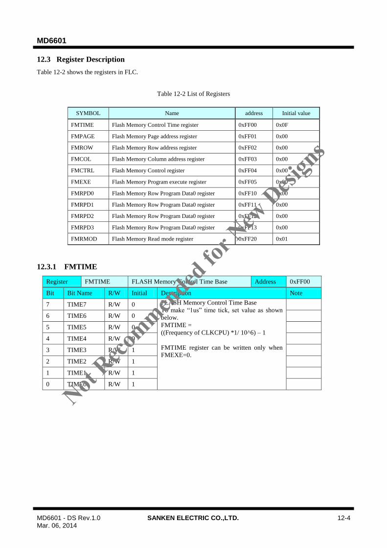
MD6601
MD6601 - DS Rev.1.0 SANKEN ELECTRIC CO.,LTD. 12-4 Mar. 06, 2014
12.3 Register Description
Table 12-2 shows the registers in FLC.
Table 12-2 List of Registers
SYMBOL Name address Initial value
FMTIME Flash Memory Control Time register 0xFF00 0x0F
FMPAGE Flash Memory Page address register 0xFF01 0x00
FMROW Flash Memory Row address register 0xFF02 0x00
FMCOL Flash Memory Column address register 0xFF03 0x00
FMCTRL Flash Memory Control register 0xFF04 0x00
FMEXE Flash Memory Program execute register 0xFF05 0x00
FMRPD0 Flash Memory Row Program Data0 register 0xFF10 0x00
FMRPD1 Flash Memory Row Program Data0 register 0xFF11 0x00
FMRPD2 Flash Memory Row Program Data0 register 0xFF12 0x00
FMRPD3 Flash Memory Row Program Data0 register 0xFF13 0x00
FMRMOD Flash Memory Read mode register 0xFF20 0x01
12.3.1 FMTIME
Register FMTIME FLASH Memory Control Time Base Address 0xFF00
Bit Bit Name R/W Initial Description Note
7 TIME7 R/W 0 FLASH Memory Control Time Base
To make “1us” time tick, set value as shown
below.
FMTIME =
((Frequency of CLKCPU) *1/ 10^6) – 1
FMTIME register can be written only when
FMEXE=0.
6 TIME6 R/W 0
5 TIME5 R/W 0
4 TIME4 R/W 0
3 TIME3 R/W 1
2 TIME2 R/W 1
1 TIME1 R/W 1
0 TIME0 R/W 1
Not Reco
mmended
for N
ew D
esign
s
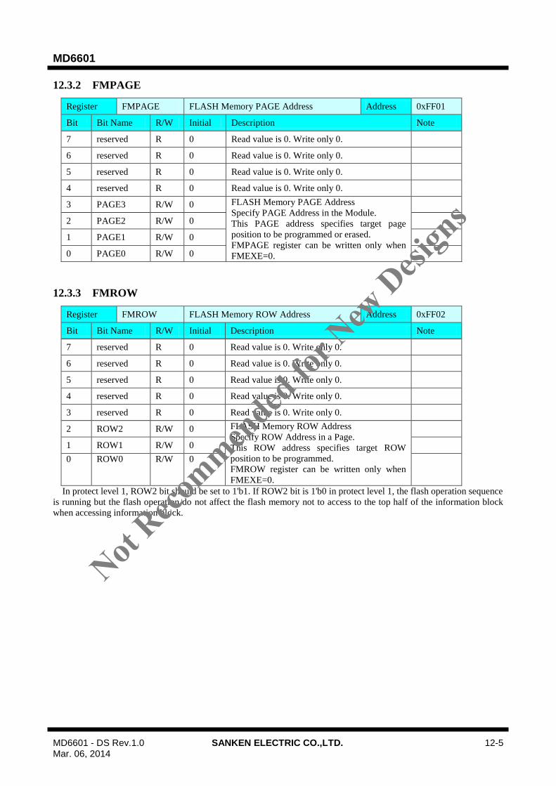
MD6601
MD6601 - DS Rev.1.0 SANKEN ELECTRIC CO.,LTD. 12-5 Mar. 06, 2014
12.3.2 FMPAGE
Register FMPAGE FLASH Memory PAGE Address Address 0xFF01
Bit Bit Name R/W Initial Description Note
7 reserved R 0 Read value is 0. Write only 0.
6 reserved R 0 Read value is 0. Write only 0.
5 reserved R 0 Read value is 0. Write only 0.
4 reserved R 0 Read value is 0. Write only 0.
3 PAGE3 R/W 0 FLASH Memory PAGE Address
Specify PAGE Address in the Module.
This PAGE address specifies target page
position to be programmed or erased.
FMPAGE register can be written only when
FMEXE=0.
2 PAGE2 R/W 0
1 PAGE1 R/W 0
0 PAGE0 R/W 0
12.3.3 FMROW
Register FMROW FLASH Memory ROW Address Address 0xFF02
Bit Bit Name R/W Initial Description Note
7 reserved R 0 Read value is 0. Write only 0.
6 reserved R 0 Read value is 0. Write only 0.
5 reserved R 0 Read value is 0. Write only 0.
4 reserved R 0 Read value is 0. Write only 0.
3 reserved R 0 Read value is 0. Write only 0.
2 ROW2 R/W 0 FLASH Memory ROW Address
Specify ROW Address in a Page.
This ROW address specifies target ROW
position to be programmed.
FMROW register can be written only when
FMEXE=0.
1 ROW1 R/W 0
0 ROW0 R/W 0
In protect level 1, ROW2 bit should be set to 1'b1. If ROW2 bit is 1'b0 in protect level 1, the flash operation sequence
is running but the flash operation do not affect the flash memory not to access to the top half of the information block
when accessing information block.
Not Reco
mmended
for N
ew D
esign
s
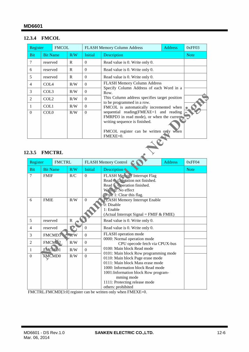
MD6601
MD6601 - DS Rev.1.0 SANKEN ELECTRIC CO.,LTD. 12-6 Mar. 06, 2014
12.3.4 FMCOL
Register FMCOL FLASH Memory Column Address Address 0xFF03
Bit Bit Name R/W Initial Description Note
7 reserved R 0 Read value is 0. Write only 0.
6 reserved R 0 Read value is 0. Write only 0.
5 reserved R 0 Read value is 0. Write only 0.
4 COL4 R/W 0 FLASH Memory Column Address
Specify Column Address of each Word in a
Row.
This Column address specifies target position
to be programmed in a row.
FMCOL is automatically incremented when
sequential reading(FMEXE=1 and reading
FMRPD3 in read mode), or when the current
writing sequence is finished.
FMCOL register can be written only when
FMEXE=0.
3 COL3 R/W 0
2 COL2 R/W 0
1 COL1 R/W 0
0 COL0 R/W 0
12.3.5 FMCTRL
Register FMCTRL FLASH Memory Control Address 0xFF04
Bit Bit Name R/W Initial Description Note
7 FMIF R/C 0 FLASH Memory Interrupt Flag
Read 0: Operation not finished.
Read 1: Operation finished.
Write 0: No effect
Write 1: Clear this flag.
6 FMIE R/W 0 FLASH Memory Interrupt Enable
0: Disable
1: Enable
(Actual Interrupt Signal = FMIF & FMIE)
5 reserved R 0 Read value is 0. Write only 0.
4 reserved R 0 Read value is 0. Write only 0.
3 FMCMD3 R/W 0 FLASH operation mode
0000: Normal operation mode
CPU opecode fetch via CPUX-bus
0100: Main block Read mode
0101: Main block Row programming mode
0110: Main block Page erase mode
0111: Main block Mass erase mode
1000: Information block Read mode
1001:Information block Row program-
mming mode
1111: Protecting release mode
others: prohibited
2 FMCMD2 R/W 0
1 FMCMD1 R/W 0
0 FMCMD0 R/W 0
FMCTRL.FMCMD[3:0] register can be written only when FMEXE=0.
Not Reco
mmended
for N
ew D
esign
s
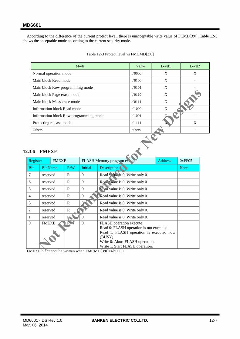
MD6601
MD6601 - DS Rev.1.0 SANKEN ELECTRIC CO.,LTD. 12-7 Mar. 06, 2014
According to the difference of the current protect level, there is unacceptable write value of FCMD[3:0]. Table 12-3
shows the acceptable mode according to the current security mode.
Table 12-3 Protect level vs FMCMD[3:0]
Mode Value Level1 Level2
Normal operation mode b'0000 X X
Main block Read mode b'0100 X -
Main block Row programming mode b'0101 X -
Main block Page erase mode b'0110 X -
Main block Mass erase mode b'0111 X -
Information block Read mode b'1000 X -
Information block Row programming mode b'1001 X -
Protecting release mode b'1111 X X
Others others - -
12.3.6 FMEXE
Register FMEXE FLASH Memory program execute Address 0xFF05
Bit Bit Name R/W Initial Description Note
7 reserved R 0 Read value is 0. Write only 0.
6 reserved R 0 Read value is 0. Write only 0.
5 reserved R 0 Read value is 0. Write only 0.
4 reserved R 0 Read value is 0. Write only 0.
3 reserved R 0 Read value is 0. Write only 0.
2 reserved R 0 Read value is 0. Write only 0.
1 reserved R 0 Read value is 0. Write only 0.
0 FMEXE R/W 0 FLASH operation execute
Read 0: FLASH operation is not executed.
Read 1: FLASH operation is executed now
(BUSY).
Write 0: Abort FLASH operation.
Write 1: Start FLASH operation.
FMEXE bit cannot be written when FMCMD[3:0]=4'b0000.
Not Reco
mmended
for N
ew D
esign
s
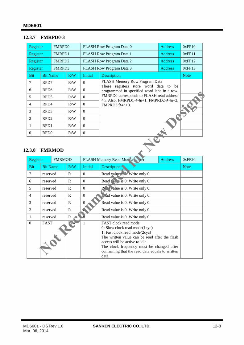
MD6601
MD6601 - DS Rev.1.0 SANKEN ELECTRIC CO.,LTD. 12-8 Mar. 06, 2014
12.3.7 FMRPD0-3
Register FMRPD0 FLASH Row Program Data 0 Address 0xFF10
Register FMRPD1 FLASH Row Program Data 1 Address 0xFF11
Register FMRPD2 FLASH Row Program Data 2 Address 0xFF12
Register FMRPD3 FLASH Row Program Data 3 Address 0xFF13
Bit Bit Name R/W Initial Description Note
7 RPD7 R/W 0 FLASH Memory Row Program Data
These registers store word data to be
programmed in specified word lane in a row.
FMRPD0 corresponds to FLASH read address
4n. Also, FMRPD14n+1, FMPRD24n+2,
FMPRD34n+3.
6 RPD6 R/W 0
5 RPD5 R/W 0
4 RPD4 R/W 0
3 RPD3 R/W 0
2 RPD2 R/W 0
1 RPD1 R/W 0
0 RPD0 R/W 0
12.3.8 FMRMOD
Register FMRMOD FLASH Memory Read Mode register Address 0xFF20
Bit Bit Name R/W Initial Description Note
7 reserved R 0 Read value is 0. Write only 0.
6 reserved R 0 Read value is 0. Write only 0.
5 reserved R 0 Read value is 0. Write only 0.
4 reserved R 0 Read value is 0. Write only 0.
3 reserved R 0 Read value is 0. Write only 0.
2 reserved R 0 Read value is 0. Write only 0.
1 reserved R 0 Read value is 0. Write only 0.
0 FAST R/W 1 FAST clock read mode
0: Slow clock read mode(1cyc)
1: Fast clock read mode(2cyc)
The written value can be read after the flash
access will be active to idle.
The clock frequency must be changed after
confirming that the read data equals to written
data.
Not Reco
mmended
for N
ew D
esign
s

MD6601
MD6601 - DS Rev.1.0 SANKEN ELECTRIC CO.,LTD. 12-9 Mar. 06, 2014
12.4 Operation
12.4.1 Instruction fetch
The Instruction Fetch Controller (IFC) controls instruction fetch from Flash to CPU. IFC has a 4bytes x 2 lines
instruction buffer (IBUF). IFC reads 4bytes instruction code from Flash, then returns 1byte instruction code to CPU and
writes fetched 4bytes instruction code to the instruction buffer. If the instruction buffer has the code that CPU requests
to fetch, IFC returns the instruction code in the instruction buffer without wait states. This mechanism reduces number
of flash access and avoids to decrease CPU performance.
IFC also has constant data buffer (DBUF). DBUF consist of 4bytes x 1line buffer. When CPU reads constant value
from Flash using MOVC instruction, IFC reads 4bytes constant value from FLASH, then returns 1byte value to CPU
and writes fetched 4bytes constant value to the data buffer.
IFC has two flash access modes: Fast clock mode and Slow clock mode. The flash access mode can be selected by
FMRMOD register. In Fast clock mode, IFC accesses to flash memory by two cycles. In Slow clock mode, IFC access
to flash memory by one cycle. When the frequency of CLKFAST is less than 25MHz, Slow clock mode can be used.
When the frequency of CLKFAST is more than 25MHz, Fast clock mode must be used.
IBUF has instruction prefetch mechanism to avoid reducing CPU performance. In Fast clock mode, the prefetch
starts when CPU fetches instruction code from address 4n+2 or 4n+3 (n>=0). In Slow clock mode, the prefetch starts
when CPU fetches it from address 4n+3(n>=0). If the prefetch is successful, CPU can fetch instructions without
prefetch missing penalty. If the prefetch is failed due to JMP instruction, etc, IFC fetches instruction code again from
correct address with prefetch missing penalty. CPU waits for finishing instruction re-fetch.
In protect level2,
(1) The flash cannot be read after CPU fetches the instruction from outside of flash area.
(2) The flash cannot be read after CPU accesses the data located 0x8000-0xFFFF using MOVC instruction.
(3) The flash cannot be read for OCD.
12.4.2 Flash programming
12.4.2.1. Mass Erase
The Mass Erase operation erases whole block of the data area. Main block erase mode
(FMCTRL.FMCMD[3:0]=b'0111). After setting FMCTRL register, the Mass erase operation starts when setting
FMEXE.FMEXE=1. During mass erasing, the FMEXE bit stays 1 to inform busy status, and will be cleared zero when
the mass erase is finished. When finished, FMIF flag is set. If FMIE bit is set, interrupt request from FLASH memory is
issued. FMIF should be cleared in the interrupt service routine.
The Main block erase mode operation can be executed in protecting level1.
Figure 12-3 shows mass erase operation sequence.
Start
FMEXE=1
End
FMIF==1?No
Yes
(2) (2) If FMIE=1, the interrupt occur when FMIF=1. FMEXE is cleared
automatically by hardware.
clear FMIF(3) FMIF is cleared by writing 1’b1 to FMIF.(3)
Set FMCTRL.FMCMD[3:0] (1) (1) FMCMD[3:0]=4’b0111: Main block mass erase mode.
Figure 12-3 Mass erase operation sequence
Not Reco
mmended
for N
ew D
esign
s
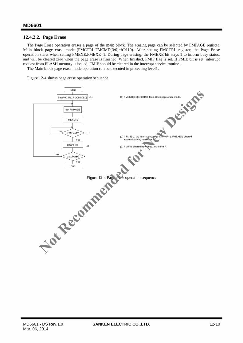
MD6601
MD6601 - DS Rev.1.0 SANKEN ELECTRIC CO.,LTD. 12-10 Mar. 06, 2014
12.4.2.2. Page Erase
The Page Erase operation erases a page of the main block. The erasing page can be selected by FMPAGE register.
Main block page erase mode (FMCTRL.FMCMD[3:0]=b'0110). After setting FMCTRL register, the Page Erase
operation starts when setting FMEXE.FMEXE=1. During page erasing, the FMEXE bit stays 1 to inform busy status,
and will be cleared zero when the page erase is finished. When finished, FMIF flag is set. If FMIE bit is set, interrupt
request from FLASH memory is issued. FMIF should be cleared in the interrupt service routine.
The Main block page erase mode operation can be executed in protecting level1.
Figure 12-4 shows page erase operation sequence.
Start
FMEXE=1
End
Set FMPAGE
FMIF==1?No
Yes
Last Page?No
Yes
(1)
(2) If FMIE=1, the interrupt occur when FMIF=1. FMEXE is cleared
automatically by hardware.
clear FMIF(3) FMIF is cleared by writing 1’b1 to FMIF.(2)
Set FMCTRL.FMCMD[3:0] (1) (1) FMCMD[3:0]=4’b0110: Main block page erase mode.
Figure 12-4 Page erase operation sequence
Not Reco
mmended
for N
ew D
esign
s

MD6601
MD6601 - DS Rev.1.0 SANKEN ELECTRIC CO.,LTD. 12-11 Mar. 06, 2014
12.4.2.3. Row Programming
The Row Programming operation writes program data to the specified address of Info/Main block area. The Row
programming operation has two modes: Info block Row programming mode(FMCTRL.FMCMD[3:0]=b'1001) and
Main block Row programming mode(FMCTRL.FMCMD[3:0]=b'0110). At first FMCTRL register should be set to Row
programming operation mode. After that, to program FLASH, user should specify Page Address(FMPAGE register),
Row Address(FMROW register) and Initial Column Address(FMCOL register) in advance. Then the Row programming
operation becomes ready to start when setting FMEXE.FMEXE=1. The specified column address programming starts
when FMPRD3 is written. The programmed data is the value of FMPRD0 to FMPRD3 when FMPRD3 is just written.
During the word is programming, FMEXE bit stays 1 to inform busy status, and will be cleared zero when the word
programming is finished or the current column address programming when FMEXE bit is set to b'0 is finished. When it
is finished, FMIF flag is set. If FMIE bit is set, interrupt request from FLASH memory is issued. FMIF should be
cleared in the interrupt service routine. FMCOL register is incremented by hardware. If user wants to program next
column, prepare the next word data in FMPRD0 to FMPRD3 again.
The Info/Main block Row programming mode operation can be executed in protecting level1.
Figure 12-5 shows Page/Mass erase operation sequence.
Start
FMEXE=1
Last coloumn?No
End
Set FMPAGE
Set FMROW
Set Initial FMCOL
Set FMRPD0 ~FMRPD3
Yes
Wait for 23us
FMIF==1?No
Yes
Last Row?No
Yes
(FMEXE=0)
Last Page?No
Yes
Yes
(2)
(3)
(4)
(5)
(2)Set program data. The program operation starts when FMRPD3
register is written.
(3) The debugger access interval is very wide. Therefore, the debugger
does not have to care the wait time. FMRPD0-2 can be re-written
while programming instead of waiting.
(4) FMEXE is cleared automatically by hardware when the program of
the last column(COL[4:0]=31) in its ROW is finishing.
At this time,software clear should not be applied.
(5) If FMIE=1, the interrupt occur when FMIF=1.
clear FMIF (6) FMIF is cleared by writing 1’b1 to FMIF.(6)
Set FMCTRL.FMCMD[3:0] (1) (1) FMCMD[3:0]=4’b0101: Main block programming mode, 4’b1001:
Information block programming mode.
Figure 12-5 Row program operation sequence
Not Reco
mmended
for N
ew D
esign
s
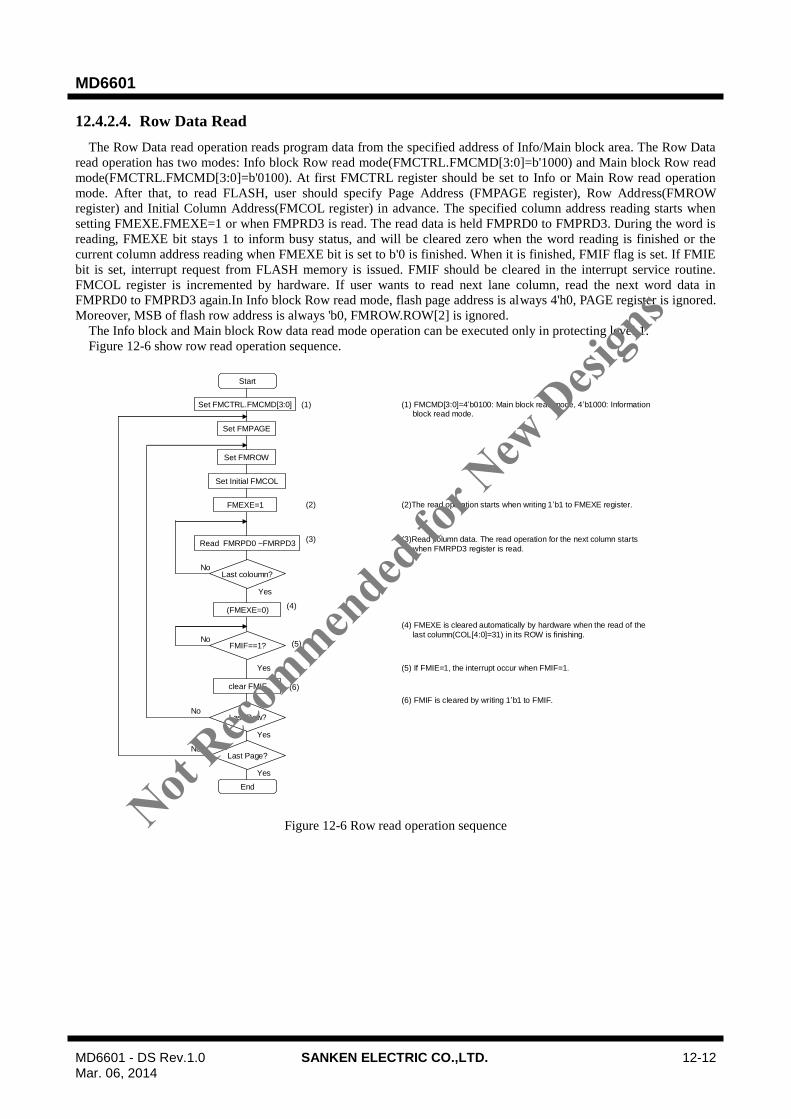
MD6601
MD6601 - DS Rev.1.0 SANKEN ELECTRIC CO.,LTD. 12-12 Mar. 06, 2014
12.4.2.4. Row Data Read
The Row Data read operation reads program data from the specified address of Info/Main block area. The Row Data
read operation has two modes: Info block Row read mode(FMCTRL.FMCMD[3:0]=b'1000) and Main block Row read
mode(FMCTRL.FMCMD[3:0]=b'0100). At first FMCTRL register should be set to Info or Main Row read operation
mode. After that, to read FLASH, user should specify Page Address (FMPAGE register), Row Address(FMROW
register) and Initial Column Address(FMCOL register) in advance. The specified column address reading starts when
setting FMEXE.FMEXE=1 or when FMPRD3 is read. The read data is held FMPRD0 to FMPRD3. During the word is
reading, FMEXE bit stays 1 to inform busy status, and will be cleared zero when the word reading is finished or the
current column address reading when FMEXE bit is set to b'0 is finished. When it is finished, FMIF flag is set. If FMIE
bit is set, interrupt request from FLASH memory is issued. FMIF should be cleared in the interrupt service routine.
FMCOL register is incremented by hardware. If user wants to read next lane column, read the next word data in
FMPRD0 to FMPRD3 again.In Info block Row read mode, flash page address is always 4'h0, PAGE register is ignored.
Moreover, MSB of flash row address is always 'b0, FMROW.ROW[2] is ignored.
The Info block and Main block Row data read mode operation can be executed only in protecting level 1.
Figure 12-6 show row read operation sequence.
Start
FMEXE=1
Last coloumn?No
End
Set FMPAGE
Set FMROW
Set Initial FMCOL
Read FMRPD0 ~FMRPD3
FMIF==1?No
Yes
Last Row?No
Yes
(FMEXE=0)
Last Page?No
Yes
Yes
(3)
(4)
(5)
(3)Read column data. The read operation for the next column starts
when FMRPD3 register is read.
(4) FMEXE is cleared automatically by hardware when the read of the
last column(COL[4:0]=31) in its ROW is finishing.
(5) If FMIE=1, the interrupt occur when FMIF=1.
clear FMIF
(6) FMIF is cleared by writing 1’b1 to FMIF.
(6)
(2) (2)The read operation starts when writing 1’b1 to FMEXE register.
Set FMCTRL.FMCMD[3:0] (1) (1) FMCMD[3:0]=4’b0100: Main block read mode, 4’b1000: Information block read mode.
Figure 12-6 Row read operation sequence
Not Reco
mmended
for N
ew D
esign
s

MD6601
MD6601 - DS Rev.1.0 SANKEN ELECTRIC CO.,LTD. 12-13 Mar. 06, 2014
12.4.2.5. Protecting Release
The Protecting Release operation re-configures the current protecting level. The Protecting Release operation is selected
by FMCTRL.FMCMD[3:0]=b'1111. FMPRD0 to FMPRD3 register are for setting protecting code. The Protecting
Release operation starts when FMEXE.FMEXE bit is set to b'1. When the current protecting level is level2, the next
protecting level will be level1 if the value of FMPRD0 to FMPRD3 equal to protecting code which flash memory holds.
Figure 12-7 shows protecting release operation sequence.
Start
FMEXE=1
End
Set FMRPD0 ~FMRPD3
FMIF==1?No
Yes
(2)(2) If FMIE=1, the interrupt occur when FMIF=1. FMEXE is cleared
automatically by hardware.
clear FMIF (3) FMIF is cleared by writing 1’b1 to FMIF.(3)
(1) Set Level protect code.(1)
Figure 12-7 Protecting release operation sequence
12.5 Flash protecting level control
The Flash protecting level controller (PLC) manages flash program/erase/read rights to save user program from the
attackers. PLC has 2 protecting levels: Level1 or Level2.
Protect Level 1: Inhibit Erase in Information Block Area.
Protect Level 2: Available only normal operations for user. Note that OCD can not access to Flash. And User can
not access to FLASH after fetching instructions from internal RAM.
Table 12-4 shows the functions which can be executed in each protect level.
Table 12-4 Flash Protect Level
Protect Level
Mas
s er
ase
(Mai
n)
Info
pro
g.
Info
rea
d
Mai
n e
rase
Mai
n p
rog.
Mai
n r
ead
No
rmal
Op.
1 After Program
○ ○ ○ ○ ○ ○ ○ After Mass erase
(Main)
2
When USER uses
× × × × × ×
○
OCD
× After Instruction fetch from RAM
According to protecting release operation, the user can change protect level. For more details, please see 12.4.2.5.
Not Reco
mmended
for N
ew D
esign
s

MD6601
MD6601 - DS Rev.1.0 SANKEN ELECTRIC CO.,LTD. 12-14 Mar. 06, 2014
12.6 Limitation of FLC
12.6.1 Going to low power mode
Note that if the LSI goes to low power mode, ten or more NOP instructions must be added after writing to LPCTRL
register.
12.6.2 Clock frequency for flash program
The clock frequency must be less than 25MHz when doing flash program, read and erase operation.
12.6.3 Row programming time
The Row programming time (during FMEXE=1) must be less than 4ms.
12.6.4 Protect function
Protect function is not guaranteed to operate as it is not tested.
Please use Protect function after evaluating by a user.
Not Reco
mmended
for N
ew D
esign
s
MD6601
MD6601 - DS Rev.1.0 SANKEN ELECTRIC CO.,LTD. 13-1 Mar. 06, 2014
13. Tiny DSP
13.1 Overview
Tiny DSP is a dedicated processing unit for calculation of digital filter. It is independent of CPU, thus CPU and Tiny
DSP can process each operation concurrently. The LSI integrates 2-sets of Tiny DSP and they can simultaneously
operate.
Tiny DSP is based on 16bit fixed point calculation. User can configure its program sequence using simple
instructions such as Multiply, Division, MAC (Multiply and Accumulate), Barrel-Shift, Move, Jump etc. Each Tiny
DSP unit has 16 x 16bit Data Registers to store input / output data, coefficients and temporary data, and also 1x 36bit
Accumulator. The Tiny DSP also supports hardware division to improve system performance.
The calculation sequence is initiated and controlled by writing Data Registers by CPU or DSAC. This scheme is
fully configurable by user. For example, the DSAC can transfer data to Tiny DSP by some events occurred in the LSI
such as End of A/D Conversion, so the Tiny DSP sequence can be triggered by internal hardware, that is fully
independent of CPU operation.
When Tiny DSP finishes its sequence, it can generate event trigger, for example, to the DSAC, and the DSAC can
transfer result data from Tiny DSP towards High-Resolution PWM as a PWM duty data. Therefore, in this whole
scheme, all operation can be done without CPU.
Table 13-1 Feature of Tiny DSP
Item Description Note
Unit Count 2 units / LSI
Operation 16bit Fixed Point
Program Memory 32 steps/unit
Data Memory 16 x 16bit Data Register + 1 x 36bit Accumulator
Instructions Multiply, Division, MAC, Shift, Move, Jump
Hardware Divider Integrated
Sequence Control Initiated and Controlled by Internal Events.
Event Output Configurable Output at any sequence step.
Performance 3P2Z IIR: 10cycles
Not Reco
mmended
for N
ew D
esign
s

MD6601
MD6601 - DS Rev.1.0 SANKEN ELECTRIC CO.,LTD. 13-2 Mar. 06, 2014
13.2 Block Diagram
Figure 13-1 Block Diagram of Tiny DSP
InterruptsEvents
XData Bus(CPU)
XData Bus(CPU)
R14
R13
R12
R11
R10
R9
R8
R7
R6
R5
R4
R3
R2
R1
R0
MUL16bx16b,<< 0~15
Sign4b+32b36b
Shifter>> 0~15
_ Saturate calc._ Rounding
(under) 16b
36b
36b
Register File16b x 16wProgram
Memory16b x 32step
ControlRegisters
Execution Unit
Control Unit
ACC
36b
16b 16b16b 16b
Divider16b / 16b
8 step
Sign4b+32b
ALU36b+36bSaturate calc.
R15
XData Bus(CPU)
SFR Bus (R0-R7)(CPU/DSAC)
XData Bus (R8-R15)(CPU)
DSP0
DSP1
Not Reco
mmended
for N
ew D
esign
s
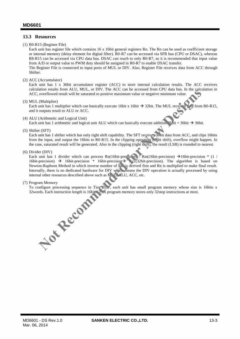
MD6601
MD6601 - DS Rev.1.0 SANKEN ELECTRIC CO.,LTD. 13-3 Mar. 06, 2014
13.3 Resources
(1) R0-R15 (Register File)
Each unit has register file which contains 16 x 16bit general registers Rn. The Rn can be used as coefficient storage
or internal memory (delay element for digital filter). R0-R7 can be accessed via SFR bus (CPU or DSAC), whereas
R8-R15 can be accessed via CPU data bus. DSAC can reach to only R0-R7, so it is recommended that input value
from A/D or output value to PWM duty should be assigned in R0-R7 to enable DSAC transfer.
The Register File is connected to input ports of MUL or DIV. Also, Register File receives data from ACC through
Shifter.
(2) ACC (Accumulator)
Each unit has 1 x 36bit accumulator register (ACC) to store internal calculation results. The ACC receives
calculation results from ALU, MUL, or DIV. The ACC can be accessed from CPU data bus. In the calculation in
ACC, overflowed result will be saturated to positive maximum value or negative minimum value.
(3) MUL (Multiplier)
Each unit has 1 multiplier which can basically execute 16bit x 16bit 32bit. The MUL receives data from R0-R15,
and it outputs result to ALU or ACC.
(4) ALU (Arithmetic and Logical Unit)
Each unit has 1 arithmetic and logical unit ALU which can basically execute addition 36bit + 36bit 36bit.
(5) Shifter (SFT)
Each unit has 1 shifter which has only right shift capability. The SFT receives 36bit data from ACC, and clips 16bits
from the input, and output the 16bits to R0-R15. In the clipping operation (right shift), overflow might happen. In
the case, saturated result will be generated. Also in the clipping (right shift), the result (LSB) is rounded to nearest.
(6) Divider (DIV)
Each unit has 1 divider which can process Rn(16bit-precision) / Rm(16bit-precision) 16bit-precision * (1 /
16bit-precision) 16bit-precision * 16bit-precision Acc(32bit-precision). The algorithm is based on
Newton-Raphson Method in which inverse number of Rm is derived first and Rn is multiplied to make final result.
Internally, there is no dedicated hardware for DIV which means the DIV operation is actually processed by using
internal other resources described above such as MUL, ALU, ACC, etc.
(7) Program Memory
To configure processing sequence in Tiny DSP, each unit has small program memory whose size is 16bits x
32words. Each instruction length is 16bits. This program memory stores only 32step instructions at most.
Not Reco
mmended
for N
ew D
esign
s
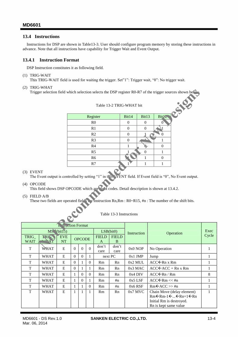
MD6601
MD6601 - DS Rev.1.0 SANKEN ELECTRIC CO.,LTD. 13-4 Mar. 06, 2014
13.4 Instructions
Instructions for DSP are shown in Table13-3. User should configure program memory by storing these instructions in
advance. Note that all instructions have capability for Trigger Wait and Event Output.
13.4.1 Instruction Format
DSP Instruction constitutes it as following field.
(1) TRIG-WAIT
This TRIG-WAIT field is used for waiting the trigger. Set”1”: Trigger wait, “0”: No trigger wait.
(2) TRIG-WHAT
Trigger selection field which selection selects the DSP register R0-R7 of the trigger sources shown below.
Table 13-2 TRIG-WHAT bit
Register Bit14 Bit13 Bit12
R0 0 0 0
R1 0 0 1
R2 0 1 0
R3 0 1 1
R4 1 0 0
R5 1 0 1
R6 1 1 0
R7 1 1 1
(3) EVENT
The Event output is controlled by setting “1” in this EVENT field. If Event field is “0”, No Event output.
(4) OPCODE
This field shows DSP OPCODE which are eight codes. Detail description is shown at 13.4.2.
(5) FIELD A/B
These two fields are operated fields for Instruction Rn,Rm : R0~R15, #n : The number of the shift bits.
Table 13-3 Instructions
Instruction Format
Instruction Operation Exec
Cycle MSB(bit15) LSB(bit0)
TRIG_
WAIT
TRIG_
WHAT
EVE
NT OPCODE
FIELD
A
FIELD
B
T WHAT E 0 0 0 don’t
care
don’t
care 0x0 NOP No Operation 1
T WHAT E 0 0 1 next PC 0x1 JMP Jump 1
T WHAT E 0 1 0 Rm Rn 0x2 MUL ACCRn x Rm 1
T WHAT E 0 1 1 Rm Rn 0x3 MAC ACCACC + Rn x Rm 1
T WHAT E 1 0 0 Rm Rn 0x4 DIV ACCRn / Rm 8
T WHAT E 1 0 1 Rm #n 0x5 LSF ACCRm << #n 1
T WHAT E 1 1 0 Rm #n 0x6 RSF RmACC >> #n 1
T WHAT E 1 1 1 Rm Rn 0x7 MVC Chain Move (delay element)
RmRm-1...Rn+1Rn
Initial Rm is destroyed.
Rn is kept same value
1
Not Reco
mmended
for N
ew D
esign
s

MD6601
MD6601 - DS Rev.1.0 SANKEN ELECTRIC CO.,LTD. 13-5 Mar. 06, 2014
13.4.2 Instruction Set
(1) 0x0 NOP No operation. Only PC is incremented.
(2) 0x1 JMP Jump to specified PC position (5bit).
(3) 0x2 MUL Rn(16bit) and Rm(16bit) are multiplied and the result is stored in lower 32bits of ACC. Higher 4bits of ACC will
be same as signed bit of the multiplied result.
(4) 0x3 MAC Rn(16bit) and Rm(16bit) are multiplied and the 36bit result (32bit with 4-bit sign extended) is accumulated onto
ACC as 36bit value. In the accumulation (addition), overflow towards positive will be saturated to
0x7_FFFF_FFFF and overflow towards negative will be saturated to 0x8_0000_0000.
(5) 0x4 DIV First of all, the instruction derives inverse number of Rm(16bit) and internally generate the result as 16bit precision
value. Finally, the result(16bit precision) is multiplied by Rn(16bit) and generate 32bit precision value in ACC.
Higher 4bits of ACC will be sign extended field.
Regarding decimal point, it resides only in programmer’s thought. If its position of source value Rm is supposed
between bit 0 and bit -1 (this means the Rm is integer value), decimal point of inverse number of Rm (1/Rm) is
located between bit 15 (sign bit) and bit14. And if decimal point of Rn is also located between bit0 and bit -1 (it is
integer), final result in ACC has decimal point located between bit15 and bit14. User can take any 16bit field in
ACC and store it in Register File by using RSF instruction.
Only the DIV is multi-cycle instruction.
(6) 0x5 LSF Rm is shifted left by n-bits and the value is stored to ACC. The left shifting is implemented by using multiplier
(MUL) in the data path. Higher ACC field will be buried by sign extended value. Lower ACC field will be buried
by zero.
(7) 0x6 RSF ACC (36bit) is shifted right by n-bits and the value is stored to Register File Rm. This means that RSF instruction
receives 36bit data from ACC, and clips 16bits from the input, and output the 16bits to Rm. In the clipping
operation (right shift), overflow might happen. In the case, saturated result will be generated. Also in the clipping
(right shift), the result (LSB) is rounded to nearest.
(8) 0x7 MVC The MVC moves data in Register File like as chain-manner to implement delay element for digital filter. Targets of
chain move are contiguous numbered register file. According to instruction field (m and n), Rm receives data from
Rm-1, and Rm-1 receives from Rm-2, and so on. Also Rn+2 receives data from Rn+1, and Rn+1 receives from Rn.
Initial value of Rm will be destroyed. And data in Rn will be kept.
If user specifies m<=n, this instruction will operate as same as NOP.
Not Reco
mmended
for N
ew D
esign
s
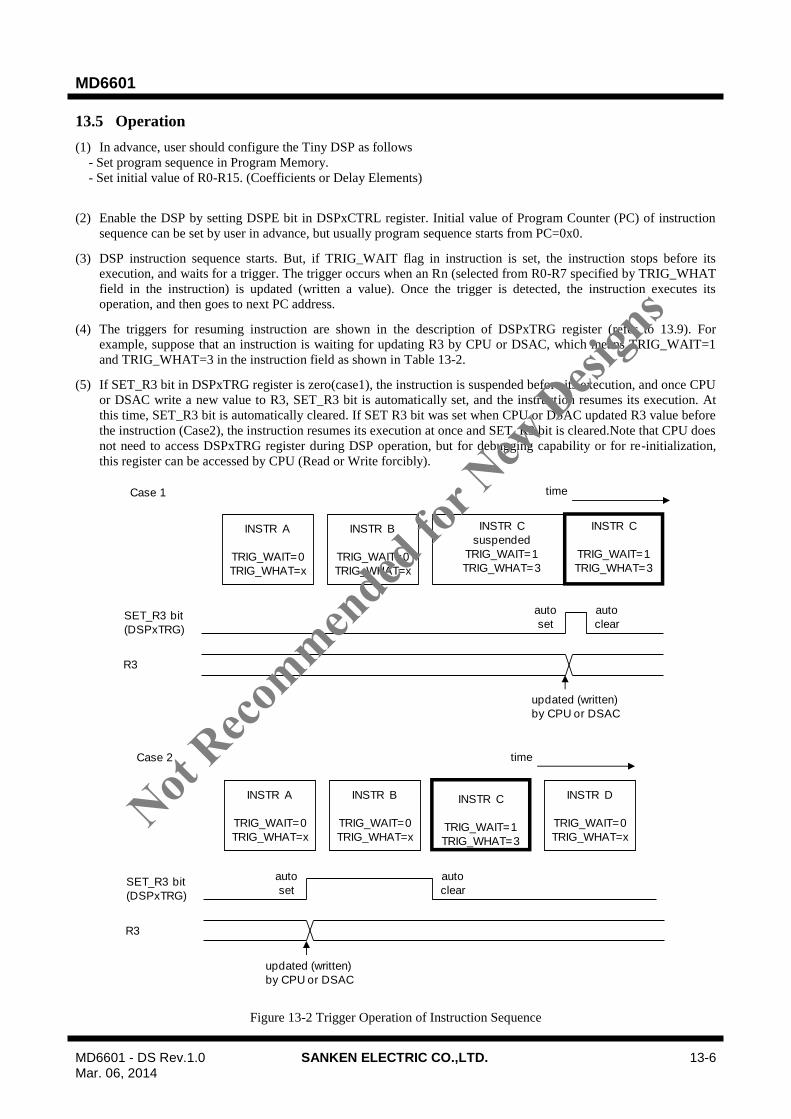
MD6601
MD6601 - DS Rev.1.0 SANKEN ELECTRIC CO.,LTD. 13-6 Mar. 06, 2014
13.5 Operation
(1) In advance, user should configure the Tiny DSP as follows
- Set program sequence in Program Memory.
- Set initial value of R0-R15. (Coefficients or Delay Elements)
(2) Enable the DSP by setting DSPE bit in DSPxCTRL register. Initial value of Program Counter (PC) of instruction
sequence can be set by user in advance, but usually program sequence starts from PC=0x0.
(3) DSP instruction sequence starts. But, if TRIG_WAIT flag in instruction is set, the instruction stops before its
execution, and waits for a trigger. The trigger occurs when an Rn (selected from R0-R7 specified by TRIG_WHAT
field in the instruction) is updated (written a value). Once the trigger is detected, the instruction executes its
operation, and then goes to next PC address.
(4) The triggers for resuming instruction are shown in the description of DSPxTRG register (refer to 13.9). For
example, suppose that an instruction is waiting for updating R3 by CPU or DSAC, which means TRIG_WAIT=1
and TRIG_WHAT=3 in the instruction field as shown in Table 13-2.
(5) If SET_R3 bit in DSPxTRG register is zero(case1), the instruction is suspended before its execution, and once CPU
or DSAC write a new value to R3, SET_R3 bit is automatically set, and the instruction resumes its execution. At
this time, SET_R3 bit is automatically cleared. If SET R3 bit was set when CPU or DSAC updated R3 value before
the instruction (Case2), the instruction resumes its execution at once and SET_R3 bit is cleared.Note that CPU does
not need to access DSPxTRG register during DSP operation, but for debugging capability or for re-initialization,
this register can be accessed by CPU (Read or Write forcibly).
Figure 13-2 Trigger Operation of Instruction Sequence
INSTR A
TRIG_WAIT=0
TRIG_WHAT=x
INSTR B
TRIG_WAIT=0
TRIG_WHAT=x
SET_R3 bit
(DSPxTRG)
auto
set
auto
clear
R3
updated (written)
by CPU or DSAC
time
INSTR C
suspended
TRIG_WAIT=1
TRIG_WHAT=3
INSTR A
TRIG_WAIT=0
TRIG_WHAT=x
INSTR B
TRIG_WAIT=0
TRIG_WHAT=x
SET_R3 bit
(DSPxTRG)
auto
set
auto
clear
R3
updated (written)
by CPU or DSAC
time
INSTR D
TRIG_WAIT=0
TRIG_WHAT=x
INSTR C
TRIG_WAIT=1
TRIG_WHAT=3
INSTR C
TRIG_WAIT=1
TRIG_WHAT=3
Case 1
Case 2
Not Reco
mmended
for N
ew D
esign
s

MD6601
MD6601 - DS Rev.1.0 SANKEN ELECTRIC CO.,LTD. 13-7 Mar. 06, 2014
(6) During DSP instruction sequence, its PC reaches last address (0x1F), the PC rewinds to 0x0 and DSP continues
instruction sequence.
(7) An instruction with EVENT flag =1 is finished its operation, DSP interrupt flag (DSPIF bit in DSPxCTRL register)
is set to 1. Also internal event pulse is generated toward other modules. If DSPIE bit in DSPxCTRL register is set,
interrupt signal is asserted towards INTC (Interrupt Controller).
(8) If Saturation is occurred during instruction operation, DSP_SA (for ALU) or DSP_SS (for Shifter) in DSPxCTRL
register are set to 1 and inform CPU to such situation. Only the “Occurrence” is informed. Each flag can be cleared
by CPU.
(9) If DSP_DBG bit in DSPxDBG register is set, the DSP unit enters in debug mode. In debug mode, DSP executes
program sequence only step by step. The initiation for step execution is done only by setting DSP_STP bit. Note
that if DSP_DBG and DSP_STP are set at same time, step execution is not processed. The step execution is done
by setting DSP_STP during DSP_DBG=1. Even if the TRIG_WAIT flag in instruction has been set, this step
operation forces to execute the instruction. If PC designates last address, the step operation rewinds PC to 0 and
repeat from first address.
(10) Regarding Register or Storage resources which can be accessed by both CPU/DSAC and DSP itself, if CPU/DSAC
and DSP access same resource at same time (access contention), CPU/DSAC has higher priority than DSP. In the
case, DSP internally stalls its operation.
DSP Registers belong to the Register File are assigned in SFR area(R0-R7) and XBUS area(R8-R15), and their data
width are 16bit. However, pair of Low Side (LSB Side) register and High Side (MSB Side) register for 16bit value are
assigned on SAME address. In order to take the 16bit-write access, 1st writing on the address reaches to Temporary
Register for Low Side and 2nd
writing reaches to High Side. At this 2nd
access, Temporary and High Side data are
transferred to both Low Side and High Side registers. In read access, 1st access gets Low Side data to the bus and High
Side data reaches to temporary register, and then 2nd
read access receives High Side data from temporary register. The
LSB/MSB Side is selected by CPU/DSAC access counter. When CPU reads from R0-15, CPU counter is incremented.
If DSPnRST.CPUACCLA bit is set to 1'b1, Both the CPU SFR BUS access counter and the CPU XBUS access counter
are cleared. After that, the LSB Side can be read by CPU. When DSAC reads from ADL/H register, DSAC counter is
incremented. If DSPnRST.DSACACCLA bit is set to 1'b1, the DSAC access counter is cleared. After that, the LSB Side
can be read by DSAC.
Regarding the rest of register of each peripheral assigned in XBUS area(DSPPRG*), each Low Side (LSB Side)
register and High Side (MSB Side) register for 16bit value is assigned independent contiguous address. The Low Side is
on lower address, the High Side is on higher address, which follows Little-Endian manner.
Figure 13-3 Rn Register Access
Rn_L Rn_H
Temp. for Rn_L
8bit
2nd access
1st access
2nd access
Rn Register
Rn_L Rn_H
Temp. for Rn_H
8bit
2nd access
1st access1st access
Rn Register
Rn_L Rn_H
Temp. for Rn_L
8bit
2nd access
1st access
2nd access
Rn Register
Rn_L Rn_H
Temp. for Rn_L
8bit
2nd access
1st access
2nd access
Rn Register
Rn_L Rn_H
Temp. for Rn_H
8bit
2nd access
1st access1st access
Rn Register
Rn_L Rn_H
Temp. for Rn_H
8bit
2nd access
1st access1st access
Rn Register
Not Reco
mmended
for N
ew D
esign
s

MD6601
MD6601 - DS Rev.1.0 SANKEN ELECTRIC CO.,LTD. 13-8 Mar. 06, 2014
13.6 Event Outputs
Each TinyDSP can issue 2-event outputs (event0, event1) towards DSAC.
TinyDSP0 Event 0
TinyDSP0 Event 1
TinyDSP1 Event 0
TinyDSP1 Event 1
The event output can be controlled by E-field in each instruction code. Following shows how to select from event0 or
event1.
If E==1 and WHAT != 7, then output Event0.
If E==1 and WHAT == 7, then output Event1.
[Note]
(1) If T==1 in addition to above, still the DSP will wait for writing to R7.
(2) If T==1 and E==1, the instruction will wait for register writing, and after its restart, event output should be output.
(3) If TinyDSPx outputs event0 or event1, the DSPIF (interrupt) flag in DSPxCTRL register is set.
13.7 Program Memory
Program memory has only 32step storage size as shown in Figure 13-4.
MSB (bit15) LSB (bit 0)
Address (PC)
(DSPx_PRG_ADDR)
Program Memory to store Instructions (16bit width)
(assigned as register located in CPU data area)
0x0~1F DSPx_PRG_H DSPx_PRG_L
Figure 13-4 Program Memory
Not Reco
mmended
for N
ew D
esign
s

MD6601
MD6601 - DS Rev.1.0 SANKEN ELECTRIC CO.,LTD. 13-9 Mar. 06, 2014
13.8 Example of Application
Implementation of typical digital filer application is shown in Figure 13-5.
Figure 13-5 Example Application
Z1 = Rin;
Acc += b3 x Z3;
Acc += a3 x Z3;
Acc += a2 x Z2;
Acc += a1 x Z1;
Acc = C x Rin;
Acc += b1 x Z1;
Acc += b2 x Z2;
Rin = Shift (Acc);
IIR
Rout = Shift (Acc) ;
5:R[m] << n => ACC
4:R[n]/R[m] => ACC
2:R[11] x R[1] => ACC
b3
b2
b1
a3
a2
a1
Rout
Z3
Z2
Z1
C
Mul
Adder Shifter
AccRin Ex_in
16*16=>32
32+32=>32
(11.21)
(11.21)
(7.9)
(3.13)
(4.12)
(1.15)
(8.8)
>>13
3:R[7] x R[4] + ACC => ACC
3:R[6] x R[3] + ACC => ACC
3:R[5] x R[2] + ACC => ACC
3:R[10] x R[4] + ACC => ACC
6:ACC >> 13 => R[1]
>>6
Z3 = Z2;
Z2 = Z1;
3:R[9] x R[3] + ACC => ACC
3:R[8] x R[2] + ACC => ACC
7:Chain R[4:1]
6:ACC >> 6 => R[0]
R[10]
R[9]
R[8]
R[7]
R[6]
R[5]
R[0]
R[4]
R[3]
R[2]
R[11]
R[1]
Ex_out
Instruction
10step
Unused
Z1 Z2 Z3
Note R[7:0]: SFR, R[15:8]: Xbus registers
Not Reco
mmended
for N
ew D
esign
s
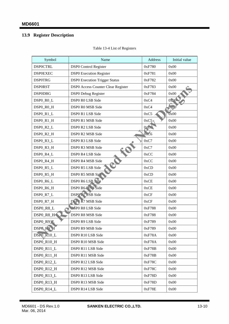
MD6601
MD6601 - DS Rev.1.0 SANKEN ELECTRIC CO.,LTD. 13-10 Mar. 06, 2014
13.9 Register Description
Table 13-4 List of Registers
Symbol Name Address Initial value
DSP0CTRL DSP0 Control Register 0xF780 0x00
DSP0EXEC DSP0 Execution Register 0xF781 0x00
DSP0TRG DSP0 Execution Trigger Status 0xF782 0x00
DSP0RST DSP0 Access Counter Clear Register 0xF783 0x00
DSP0DBG DSP0 Debug Register 0xF784 0x00
DSP0_R0_L DSP0 R0 LSB Side 0xC4 0x00
DSP0_R0_H DSP0 R0 MSB Side 0xC4 0x00
DSP0_R1_L DSP0 R1 LSB Side 0xC5 0x00
DSP0_R1_H DSP0 R1 MSB Side 0xC5 0x00
DSP0_R2_L DSP0 R2 LSB Side 0xC6 0x00
DSP0_R2_H DSP0 R2 MSB Side 0xC6 0x00
DSP0_R3_L DSP0 R3 LSB Side 0xC7 0x00
DSP0_R3_H DSP0 R3 MSB Side 0xC7 0x00
DSP0_R4_L DSP0 R4 LSB Side 0xCC 0x00
DSP0_R4_H DSP0 R4 MSB Side 0xCC 0x00
DSP0_R5_L DSP0 R5 LSB Side 0xCD 0x00
DSP0_R5_H DSP0 R5 MSB Side 0xCD 0x00
DSP0_R6_L DSP0 R6 LSB Side 0xCE 0x00
DSP0_R6_H DSP0 R6 MSB Side 0xCE 0x00
DSP0_R7_L DSP0 R7 LSB Side 0xCF 0x00
DSP0_R7_H DSP0 R7 MSB Side 0xCF 0x00
DSP0_R8_L DSP0 R8 LSB Side 0xF788 0x00
DSP0_R8_H DSP0 R8 MSB Side 0xF788 0x00
DSP0_R9_L DSP0 R9 LSB Side 0xF789 0x00
DSP0_R9_H DSP0 R9 MSB Side 0xF789 0x00
DSP0_R10_L DSP0 R10 LSB Side 0xF78A 0x00
DSP0_R10_H DSP0 R10 MSB Side 0xF78A 0x00
DSP0_R11_L DSP0 R11 LSB Side 0xF78B 0x00
DSP0_R11_H DSP0 R11 MSB Side 0xF78B 0x00
DSP0_R12_L DSP0 R12 LSB Side 0xF78C 0x00
DSP0_R12_H DSP0 R12 MSB Side 0xF78C 0x00
DSP0_R13_L DSP0 R13 LSB Side 0xF78D 0x00
DSP0_R13_H DSP0 R13 MSB Side 0xF78D 0x00
DSP0_R14_L DSP0 R14 LSB Side 0xF78E 0x00
Not Reco
mmended
for N
ew D
esign
s

MD6601
MD6601 - DS Rev.1.0 SANKEN ELECTRIC CO.,LTD. 13-11 Mar. 06, 2014
Symbol Name Address Initial value
DSP0_R14_H DSP0 R14 MSB Side 0xF78E 0x00
DSP0_R15_L DSP0 R15 LSB Side 0xF78F 0x00
DSP0_R15_H DSP0 R15 MSB Side 0xF78F 0x00
DSP0_ACC_0 DSP0 ACC[7:0] 0xF790 0x00
DSP0_ACC_1 DSP0 ACC[15:8] 0xF791 0x00
DSP0_ACC_2 DSP0 ACC[23:15] 0xF792 0x00
DSP0_ACC_3 DSP0 ACC[31:24] 0xF793 0x00
DSP0_ACC_4 DSP0 ACC[36:32] 0xF794 0x00
DSP0_PRG_DATL DSP0 Program Memory LSB Side 0xF7A0 0x00
DSP0_PRG_DATH DSP0 Program Memory MSB Side 0xF7A1 0x00
DSP0_PRG_ADR DSP0 Program Memory Address 0xF7A2 0x00
DSP1CTRL DSP1 Control Register 0xF800 0x00
DSP1EXEC DSP1 Execution Register 0xF801 0x00
DSP1TRG DSP1 Execution Trigger Status 0xF802 0x00
DSP1RST DSP1 Access Counter Clear Register 0xF803 0x00
DSP1DBG DSP1 Debug Register 0xF804 0x00
DSP1_R0_L DSP1 R0 LSB Side 0xD4 0x00
DSP1_R0_H DSP1 R0 MSB Side 0xD4 0x00
DSP1_R1_L DSP1 R1 LSB Side 0xD5 0x00
DSP1_R1_H DSP1 R1 MSB Side 0xD5 0x00
DSP1_R2_L DSP1 R2 LSB Side 0xD6 0x00
DSP1_R2_H DSP1 R2 MSB Side 0xD6 0x00
DSP1_R3_L DSP1 R3 LSB Side 0xD7 0x00
DSP1_R3_H DSP1 R3 MSB Side 0xD7 0x00
DSP1_R4_L DSP1 R4 LSB Side 0xDC 0x00
DSP1_R4_H DSP1 R4 MSB Side 0xDC 0x00
DSP1_R5_L DSP1 R5 LSB Side 0xDD 0x00
DSP1_R5_H DSP1 R5 MSB Side 0xDD 0x00
DSP1_R6_L DSP1 R6 LSB Side 0xDE 0x00
DSP1_R6_H DSP1 R6 MSB Side 0xDE 0x00
DSP1_R7_L DSP1 R7 LSB Side 0xDF 0x00
DSP1_R7_H DSP1 R7 MSB Side 0xDF 0x00
DSP1_R8_L DSP1 R8 LSB Side 0xF808 0x00
DSP1_R8_H DSP1 R8 MSB Side 0xF808 0x00
DSP1_R9_L DSP1 R9 LSB Side 0xF809 0x00
DSP1_R9_H DSP1 R9 MSB Side 0xF809 0x00
DSP1_R10_L DSP1 R10 LSB Side 0xF80A 0x00
DSP1_R10_H DSP1 R10 MSB Side 0xF80A 0x00
Not Reco
mmended
for N
ew D
esign
s

MD6601
MD6601 - DS Rev.1.0 SANKEN ELECTRIC CO.,LTD. 13-12 Mar. 06, 2014
Symbol Name Address Initial value
DSP1_R11_L DSP1 R11 LSB Side 0xF80B 0x00
DSP1_R11_H DSP1 R11 MSB Side 0xF80B 0x00
DSP1_R12_L DSP1 R12 LSB Side 0xF80C 0x00
DSP1_R12_H DSP1 R12 MSB Side 0xF80C 0x00
DSP1_R13_L DSP1 R13 LSB Side 0xF80D 0x00
DSP1_R13_H DSP1 R13 MSB Side 0xF80D 0x00
DSP1_R14_L DSP1 R14 LSB Side 0xF80E 0x00
DSP1_R14_H DSP1 R14 MSB Side 0xF80E 0x00
DSP1_R15_L DSP1 R15 LSB Side 0xF80F 0x00
DSP1_R15_H DSP1 R15 MSB Side 0xF80F 0x00
DSP1_ACC_0 DSP1 ACC[7:0] 0xF810 0x00
DSP1_ACC_1 DSP1 ACC[15:8] 0xF811 0x00
DSP1_ACC_2 DSP1 ACC[23:15] 0xF812 0x00
DSP1_ACC_3 DSP1 ACC[31:24] 0xF813 0x00
DSP1_ACC_4 DSP1 ACC[36:32] 0xF814 0x00
DSP1_PRG_DATL DSP1 Program Memory LSB Side 0xF820 0x00
DSP1_PRG_DATH DSP1 Program Memory MSB Side 0xF821 0x00
DSP1_PRG_ADR DSP1 Program Memory Address 0xF822 0x00
Not Reco
mmended
for N
ew D
esign
s
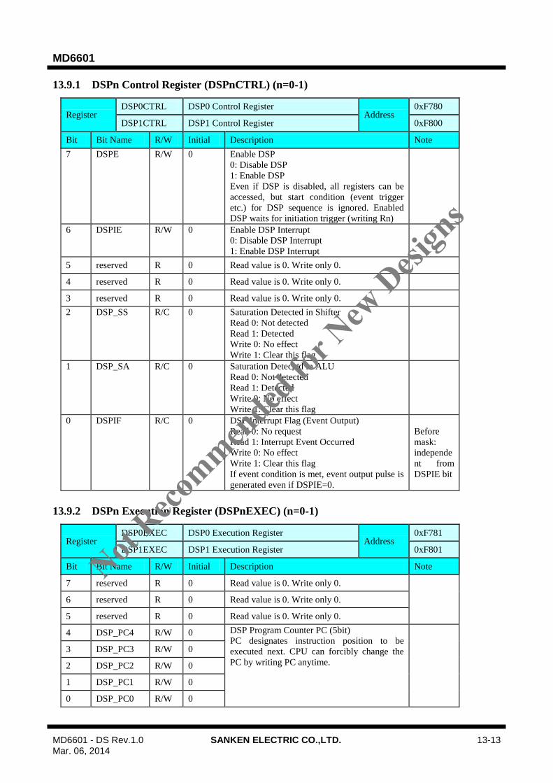
MD6601
MD6601 - DS Rev.1.0 SANKEN ELECTRIC CO.,LTD. 13-13 Mar. 06, 2014
13.9.1 DSPn Control Register (DSPnCTRL) (n=0-1)
Register DSP0CTRL DSP0 Control Register
Address 0xF780
DSP1CTRL DSP1 Control Register 0xF800
Bit Bit Name R/W Initial Description Note
7 DSPE R/W 0 Enable DSP
0: Disable DSP
1: Enable DSP
Even if DSP is disabled, all registers can be
accessed, but start condition (event trigger
etc.) for DSP sequence is ignored. Enabled
DSP waits for initiation trigger (writing Rn)
6 DSPIE R/W 0 Enable DSP Interrupt
0: Disable DSP Interrupt
1: Enable DSP Interrupt
5 reserved R 0 Read value is 0. Write only 0.
4 reserved R 0 Read value is 0. Write only 0.
3 reserved R 0 Read value is 0. Write only 0.
2 DSP_SS R/C 0 Saturation Detected in Shifter
Read 0: Not detected
Read 1: Detected
Write 0: No effect
Write 1: Clear this flag
1 DSP_SA R/C 0 Saturation Detected in ALU
Read 0: Not detected
Read 1: Detected
Write 0: No effect
Write 1: Clear this flag
0 DSPIF R/C 0 DSP Interrupt Flag (Event Output)
Read 0: No request
Read 1: Interrupt Event Occurred
Write 0: No effect
Write 1: Clear this flag
If event condition is met, event output pulse is
generated even if DSPIE=0.
Before
mask:
independe
nt from
DSPIE bit
13.9.2 DSPn Execution Register (DSPnEXEC) (n=0-1)
Register DSP0EXEC DSP0 Execution Register
Address 0xF781
DSP1EXEC DSP1 Execution Register 0xF801
Bit Bit Name R/W Initial Description Note
7 reserved R 0 Read value is 0. Write only 0.
6 reserved R 0 Read value is 0. Write only 0.
5 reserved R 0 Read value is 0. Write only 0.
4 DSP_PC4 R/W 0 DSP Program Counter PC (5bit)
PC designates instruction position to be
executed next. CPU can forcibly change the
PC by writing PC anytime.
3 DSP_PC3 R/W 0
2 DSP_PC2 R/W 0
1 DSP_PC1 R/W 0
0 DSP_PC0 R/W 0
Not Reco
mmended
for N
ew D
esign
s

MD6601
MD6601 - DS Rev.1.0 SANKEN ELECTRIC CO.,LTD. 13-14 Mar. 06, 2014
13.9.3 DSPn Debug Register (DSPnDBG)
Register DSP0DBG DSP0 Debug Register
Address 0xF784
DSP1DBG DSP1 Debug Register 0xF804
Bit Bit Name R/W Initial Description Note
7 DSP_DBG R/W 0 Debug Mode
0: Normal Mode
1: Debug Mode
In debug mode, DSP executes program
sequence only step by step. The initiation for
step execution is done only by setting
DSP_STP bit.
6 DSP_STP R/S 0 Stop Execution
Read value is always 0.
Write 0: No effect
Write 1: If DSP_DBG=1, execute program
sequence in step by step. Note that if
DSP_DGB and DSP_STP are set at same
time, step execution is not processed. The step
execution is done by setting DSP_STP during
DSP_DBG=1. Even if the TRIG_WAIT flag
in instruction has been set, this step operation
forces to execute its instruction. If PC
designates last address, this step operation
rewinds PC to 0 and repeat from first address.
5-0 reserved R 0 Read value is 0. Write only 0.
Not Reco
mmended
for N
ew D
esign
s

MD6601
MD6601 - DS Rev.1.0 SANKEN ELECTRIC CO.,LTD. 13-15 Mar. 06, 2014
13.9.4 DSPn Rx LSB Side (DSPn_Rx_L) (n=0-1, x=0-7)
Register
DSP0_R0_L DSP0 R0 LSB Side Address 0xC4
DSP0_R1_L DSP0 R1 LSB Side Address 0xC5
DSP0_R2_L DSP0 R2 LSB Side Address 0xC6
DSP0_R3_L DSP0 R3 LSB Side Address 0xC7
DSP0_R4_L DSP0 R4 LSB Side Address 0xCC
DSP0_R5_L DSP0 R5 LSB Side Address 0xCD
DSP0_R6_L DSP0 R6 LSB Side Address 0xCE
DSP0_R7_L DSP0 R7 LSB Side Address 0xCF
DSP1_R0_L DSP1 R0 LSB Side Address 0xD4
DSP1_R1_L DSP1 R1 LSB Side Address 0xD5
DSP1_R2_L DSP1 R2 LSB Side Address 0xD6
DSP1_R3_L DSP1 R3 LSB Side Address 0xD7
DSP1_R4_L DSP1 R4 LSB Side Address 0xDC
DSP1_R5_L DSP1 R5 LSB Side Address 0xDD
DSP1_R6_L DSP1 R6 LSB Side Address 0xDE
DSP1_R7_L DSP1 R7 LSB Side Address 0xDF
Bit Bit Name R/W Initial Description Note
7 DSP_REG7 R/W 0 DSP Register File Low Side Data
Each R0-R7 is assigned in SFR area.
This register can access Low Side data of
each Rn (1st access).
6 DSP_REG6 R/W 0
5 DSP_REG5 R/W 0
4 DSP_REG4 R/W 0
3 DSP_REG3 R/W 0
2 DSP_REG2 R/W 0
1 DSP_REG1 R/W 0
0 DSP_REG0 R/W 0
Not Reco
mmended
for N
ew D
esign
s

MD6601
MD6601 - DS Rev.1.0 SANKEN ELECTRIC CO.,LTD. 13-16 Mar. 06, 2014
13.9.5 DSPn Rx MSB Side (DSPn_Rx_H) (n=0-1,x=0-7)
Register DSP0_R0_H DSP0 R0 MSB Side Address 0xC4
Register DSP0_R1_H DSP0 R1 MSB Side Address 0xC5
Register DSP0_R2_H DSP0 R2 MSB Side Address 0xC6
Register DSP0_R3_H DSP0 R3 MSB Side Address 0xC7
Register DSP0_R4_H DSP0 R4 MSB Side Address 0xCC
Register DSP0_R5_H DSP0 R5 MSB Side Address 0xCD
Register DSP0_R6_H DSP0 R6 MSB Side Address 0xCE
Register DSP0_R7_H DSP0 R7 MSB Side Address 0xCF
Register DSP1_R0_H DSP1 R0 MSB Side Address 0xD4
Register DSP1_R1_H DSP1 R1 MSB Side Address 0xD5
Register DSP1_R2_H DSP1 R2 MSB Side Address 0xD6
Register DSP1_R3_H DSP1 R3 MSB Side Address 0xD7
Register DSP1_R4_H DSP1 R4 MSB Side Address 0xDC
Register DSP1_R5_H DSP1 R5 MSB Side Address 0xDD
Register DSP1_R6_H DSP1 R6 MSB Side Address 0xDE
Register DSP1_R7_H DSP1 R7 MSB Side Address 0xDF
Bit Bit Name R/W Initial Description Note
7 DSP_REG7 R/W 0 DSP Register File High Side Data
Each R0-R7 is assigned in SFR area.
This register can access High Side data of
each Rn (2nd
access).
6 DSP_REG6 R/W 0
5 DSP_REG5 R/W 0
4 DSP_REG4 R/W 0
3 DSP_REG3 R/W 0
2 DSP_REG2 R/W 0
1 DSP_REG1 R/W 0
0 DSP_REG0 R/W 0
Not Reco
mmended
for N
ew D
esign
s
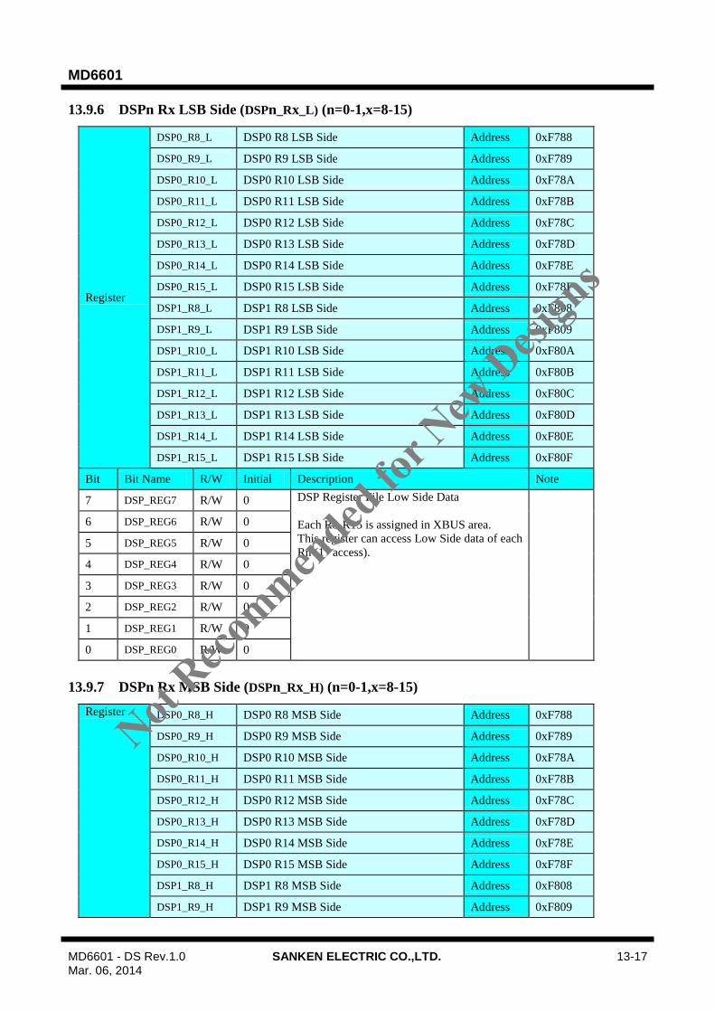
MD6601
MD6601 - DS Rev.1.0 SANKEN ELECTRIC CO.,LTD. 13-17 Mar. 06, 2014
13.9.6 DSPn Rx LSB Side (DSPn_Rx_L) (n=0-1,x=8-15)
Register
DSP0_R8_L DSP0 R8 LSB Side Address 0xF788
DSP0_R9_L DSP0 R9 LSB Side Address 0xF789
DSP0_R10_L DSP0 R10 LSB Side Address 0xF78A
DSP0_R11_L DSP0 R11 LSB Side Address 0xF78B
DSP0_R12_L DSP0 R12 LSB Side Address 0xF78C
DSP0_R13_L DSP0 R13 LSB Side Address 0xF78D
DSP0_R14_L DSP0 R14 LSB Side Address 0xF78E
DSP0_R15_L DSP0 R15 LSB Side Address 0xF78F
DSP1_R8_L DSP1 R8 LSB Side Address 0xF808
DSP1_R9_L DSP1 R9 LSB Side Address 0xF809
DSP1_R10_L DSP1 R10 LSB Side Address 0xF80A
DSP1_R11_L DSP1 R11 LSB Side Address 0xF80B
DSP1_R12_L DSP1 R12 LSB Side Address 0xF80C
DSP1_R13_L DSP1 R13 LSB Side Address 0xF80D
DSP1_R14_L DSP1 R14 LSB Side Address 0xF80E
DSP1_R15_L DSP1 R15 LSB Side Address 0xF80F
Bit Bit Name R/W Initial Description Note
7 DSP_REG7 R/W 0 DSP Register File Low Side Data
Each R8-R15 is assigned in XBUS area.
This register can access Low Side data of each
Rn (1st access).
6 DSP_REG6 R/W 0
5 DSP_REG5 R/W 0
4 DSP_REG4 R/W 0
3 DSP_REG3 R/W 0
2 DSP_REG2 R/W 0
1 DSP_REG1 R/W 0
0 DSP_REG0 R/W 0
13.9.7 DSPn Rx MSB Side (DSPn_Rx_H) (n=0-1,x=8-15)
Register DSP0_R8_H DSP0 R8 MSB Side Address 0xF788
DSP0_R9_H DSP0 R9 MSB Side Address 0xF789
DSP0_R10_H DSP0 R10 MSB Side Address 0xF78A
DSP0_R11_H DSP0 R11 MSB Side Address 0xF78B
DSP0_R12_H DSP0 R12 MSB Side Address 0xF78C
DSP0_R13_H DSP0 R13 MSB Side Address 0xF78D
DSP0_R14_H DSP0 R14 MSB Side Address 0xF78E
DSP0_R15_H DSP0 R15 MSB Side Address 0xF78F
DSP1_R8_H DSP1 R8 MSB Side Address 0xF808
DSP1_R9_H DSP1 R9 MSB Side Address 0xF809
Not Reco
mmended
for N
ew D
esign
s
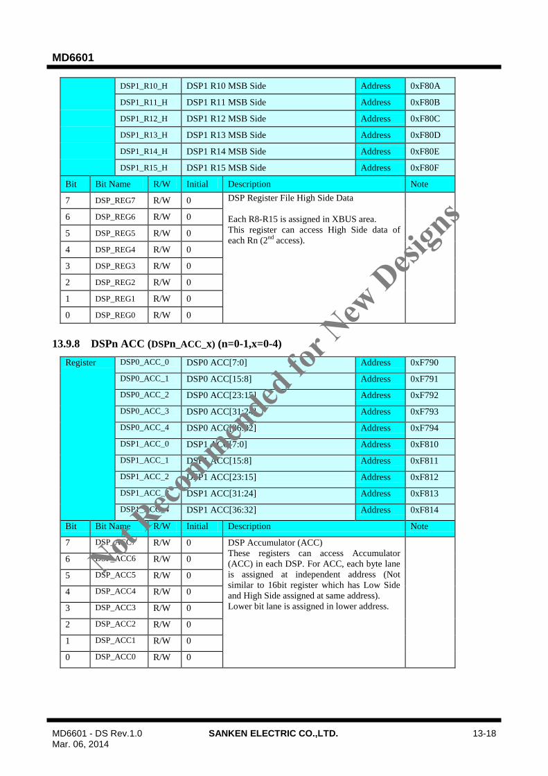
MD6601
MD6601 - DS Rev.1.0 SANKEN ELECTRIC CO.,LTD. 13-18 Mar. 06, 2014
DSP1_R10_H DSP1 R10 MSB Side Address 0xF80A
DSP1_R11_H DSP1 R11 MSB Side Address 0xF80B
DSP1_R12_H DSP1 R12 MSB Side Address 0xF80C
DSP1_R13_H DSP1 R13 MSB Side Address 0xF80D
DSP1_R14_H DSP1 R14 MSB Side Address 0xF80E
DSP1_R15_H DSP1 R15 MSB Side Address 0xF80F
Bit Bit Name R/W Initial Description Note
7 DSP_REG7 R/W 0 DSP Register File High Side Data
Each R8-R15 is assigned in XBUS area.
This register can access High Side data of
each Rn (2nd
access).
6 DSP_REG6 R/W 0
5 DSP_REG5 R/W 0
4 DSP_REG4 R/W 0
3 DSP_REG3 R/W 0
2 DSP_REG2 R/W 0
1 DSP_REG1 R/W 0
0 DSP_REG0 R/W 0
13.9.8 DSPn ACC (DSPn_ACC_x) (n=0-1,x=0-4)
Register DSP0_ACC_0 DSP0 ACC[7:0] Address 0xF790
DSP0_ACC_1 DSP0 ACC[15:8] Address 0xF791
DSP0_ACC_2 DSP0 ACC[23:15] Address 0xF792
DSP0_ACC_3 DSP0 ACC[31:24] Address 0xF793
DSP0_ACC_4 DSP0 ACC[36:32] Address 0xF794
DSP1_ACC_0 DSP1 ACC[7:0] Address 0xF810
DSP1_ACC_1 DSP1 ACC[15:8] Address 0xF811
DSP1_ACC_2 DSP1 ACC[23:15] Address 0xF812
DSP1_ACC_3 DSP1 ACC[31:24] Address 0xF813
DSP1_ACC_4 DSP1 ACC[36:32] Address 0xF814
Bit Bit Name R/W Initial Description Note
7 DSP_ACC7 R/W 0 DSP Accumulator (ACC)
These registers can access Accumulator
(ACC) in each DSP. For ACC, each byte lane
is assigned at independent address (Not
similar to 16bit register which has Low Side
and High Side assigned at same address).
Lower bit lane is assigned in lower address.
6 DSP_ACC6 R/W 0
5 DSP_ACC5 R/W 0
4 DSP_ACC4 R/W 0
3 DSP_ACC3 R/W 0
2 DSP_ACC2 R/W 0
1 DSP_ACC1 R/W 0
0 DSP_ACC0 R/W 0
Not Reco
mmended
for N
ew D
esign
s
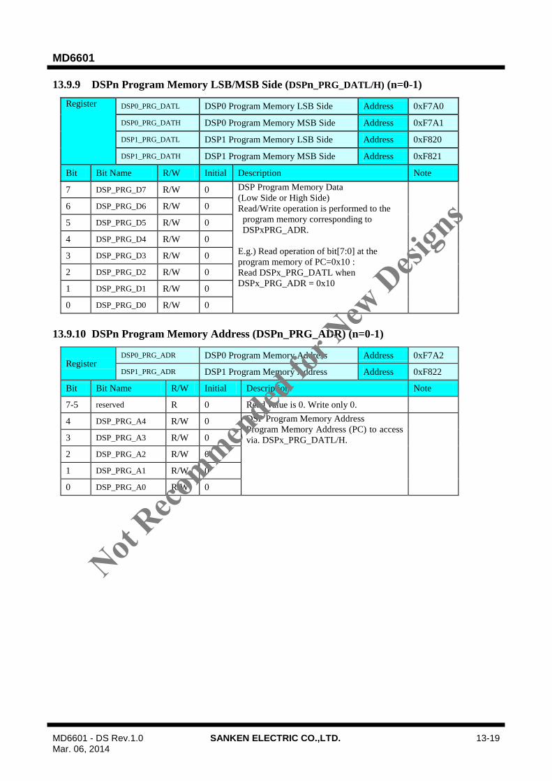
MD6601
MD6601 - DS Rev.1.0 SANKEN ELECTRIC CO.,LTD. 13-19 Mar. 06, 2014
13.9.9 DSPn Program Memory LSB/MSB Side (DSPn_PRG_DATL/H) (n=0-1)
Register DSP0_PRG_DATL DSP0 Program Memory LSB Side Address 0xF7A0
DSP0_PRG_DATH DSP0 Program Memory MSB Side Address 0xF7A1
DSP1_PRG_DATL DSP1 Program Memory LSB Side Address 0xF820
DSP1_PRG_DATH DSP1 Program Memory MSB Side Address 0xF821
Bit Bit Name R/W Initial Description Note
7 DSP_PRG_D7 R/W 0 DSP Program Memory Data
(Low Side or High Side)
Read/Write operation is performed to the
program memory corresponding to
DSPxPRG_ADR.
E.g.) Read operation of bit[7:0] at the
program memory of PC=0x10 :
Read DSPx_PRG_DATL when
DSPx_PRG_ADR = 0x10
6 DSP_PRG_D6 R/W 0
5 DSP_PRG_D5 R/W 0
4 DSP_PRG_D4 R/W 0
3 DSP_PRG_D3 R/W 0
2 DSP_PRG_D2 R/W 0
1 DSP_PRG_D1 R/W 0
0 DSP_PRG_D0 R/W 0
13.9.10 DSPn Program Memory Address (DSPn_PRG_ADR) (n=0-1)
Register DSP0_PRG_ADR DSP0 Program Memory Address Address 0xF7A2
DSP1_PRG_ADR DSP1 Program Memory Address Address 0xF822
Bit Bit Name R/W Initial Description Note
7-5 reserved R 0 Read value is 0. Write only 0.
4 DSP_PRG_A4 R/W 0 DSP Program Memory Address
Program Memory Address (PC) to access
via. DSPx_PRG_DATL/H.
3 DSP_PRG_A3 R/W 0
2 DSP_PRG_A2 R/W 0
1 DSP_PRG_A1 R/W 0
0 DSP_PRG_A0 R/W 0
Not Reco
mmended
for N
ew D
esign
s

MD6601
MD6601 - DS Rev.1.0 SANKEN ELECTRIC CO.,LTD. 13-20 Mar. 06, 2014
13.9.11 DSPn Execution Trigger Status (DSPnTRG) (n=0-1)
Register DSP0TRG DSP0 Execution Trigger Status Address 0xF782
DSP1TRG DSP1 Execution Trigger Status Address 0xF802
Bit Bit Name R/W Initial Description Note
7 SET_R7 R/W 0 DSP Execution Trigger Status
Each bit shows corresponding register file
(R0-R7) is written or not.
When CPU or DSAC writes a value to R0-7 at
DSPxCTRL.DSPE = 1, the corresponding bit
is automatically set.
6 SET_R6 R/W 0
5 SET_R5 R/W 0
4 SET_R4 R/W 0
3 SET_R3 R/W 0
2 SET_R2 R/W 0
1 SET_R1 R/W 0
0 SET_R0 R/W 0
DSP instruction whose TRIG_WAIT flag is set temporary stops before its execution and watches SET_R0 - SET_R7
according to its trigger selection TRIG_WHAT and if corresponding bit in this register is set (detected update of R0-R7),
the instruction will be executed and go to next sequence. At this time, corresponding SET_Rx is cleared automatically.
Note that the register basically shows only trigger status and CPU does not need to access it. But for debugging
capability or for re-initialization, this register can be accessed by CPU (Read or Write forcibly).
13.9.12 DSPn Access Counter Clear Register (DSPnRST) (n=0-1)
Register DSP0RST DSP0 Access Counter Clear Register Address 0xF783
DSP1RST DSP1 Access Counter Clear Register Address 0xF803
Bit Bit Name R/W Initial Description Note
7 CPUACCLA R/C 0 Clear SFR CPU Access counter and XBUS
CPU access counter.
Read value is 0.
Write 0: No effect
Write 1: Clear Register CPU Access counter.
6 DSACACCLA R/C 0 Clear R0 – R7 DSAC Access Counter
Read value is 0.
Read : No Request
Write 0: No effect
Write 1: Clear Register DSAC Access counter.
5 reserved R 0 Read value is 0. Write only 0.
4 reserved R 0 Read value is 0. Write only 0.
3 reserved R 0 Read value is 0. Write only 0.
2 reserved R 0 Read value is 0. Write only 0.
1 reserved R 0 Read value is 0. Write only 0.
0 reserved R 0 Read value is 0. Write only 0.
Not Reco
mmended
for N
ew D
esign
s

MD6601
MD6601 - DS Rev.1.0 SANKEN ELECTRIC CO.,LTD. 13-21 Mar. 06, 2014
13.10 Caution of operation
13.10.1 Restriction about the TinyDSP interrupt enable bits
(1) Description
Interrupt signals from TinyDSP are always generated and are sent to interrupt controller without relation to setting
of interrupt enable bits of Tiny DSP (DSPnCTRL.DSPIE) when corresponding interrupt flags are set
(DSPnCTRL.DSPIF =1).
(2) Countermeasure
When interrupt from TinyDSP is not necessary, please mask interrupt by setting each interrupt enable bits in the
interrupt controller to 0 (Refer to following table).
DSP Channel Vector No. Interrupt enable bits
0 23 INTENA2.INTE7
1 24 INTENA3.INTE0
13.10.2 DSP_SS asserted in the DIV instruction
In the DIV instruction, DSP_SS is asserted when 0x0001 is specified for Divisor Rm. The reason is that Shifter is
used in calculating inverse of Rm.
Not Reco
mmended
for N
ew D
esign
s

MD6601
MD6601 - DS Rev.1.0 SANKEN ELECTRIC CO.,LTD. 14-1 Mar. 06, 2014
14. High-Resolution PWM
14.1 Overview
This module can generate high resolution 8 (4-pairs) PWM signals. Each pair can form non-overlap PWM signals.
Also, phase shift type signal can be generated by proper configuration. This module can accept internal event signals
from other modules and can re-trigger the output signals or counter operations. Also this module can generate interrupts
and internal event pulse according to internal compare match states.
Output PWM resolution is 1ns (min).
14.2 Block Diagram
Figure 14-1 Block Diagram of High-Resolution PWM
CNT
CMP_A
+/-1up/down
BUF_A
CMP_BBUF_B
Comparator
CMP_CBUF_C
CMP_DBUF_D
16bit
Comparator
Comparator
Comparator
PWM0H
PWM0L
BUF_MIN CMP_MIN Comparator
clear or up/down control
PWM1H
PWM1L
PWM2H
PWM2L
PWM3H
PWM3L
1GHz Operation
or
1GHz Equivalent Operation
on Output Wave Behaviors
Counter Block #0 (PWM Channel #0)
Counter Block #1(PWM Channel #1)
Counter Block #2(PWM Channel #2)
Counter Block #3(PWM Channel #3)
Operation Unit
BUF_MAX CMP_MAX Comparator
+1up DCNTC
16bit
+1up DCNTD
16bitComparator
Comparator
C
D
Outp
ut
Co
ntr
ol
CLK SOURCE
Common Register
PWMENBL
PWMCSC0
PWMCSC1
PWMCNTS
PWMnCSS
Not Reco
mmended
for N
ew D
esign
s

MD6601
MD6601 - DS Rev.1.0 SANKEN ELECTRIC CO.,LTD. 14-2 Mar. 06, 2014
14.3 Resources
The module has maximum 4 counter blocks according to product spec as shown in Figure 14-1.
Each block has following resources.
(1) 16bit Up/Down Counter (CNT)
Maximum frequency of each counter is 1GHz. The plural counters among counter blocks can be synchronized
each other. There are 2 modes in counter operation. One is Up Mode, in which counter is always in up-count
operation and is cleared when CNT matches to CMP_MAX and re-load counter value from CMP_MIN. The
other is Up-Down Mode, in which counter is in up-count operation until it reaches to CMP_MAX and then the
counter enters in down-count operation until it reaches to CMP_MIN, and then the counter re-enters in up-count
operation again.
Note that user can assume counter value not only unsigned but also signed value because of existence of Min and
Max values.
Note:
As for CH0 and CH1, you can specify any value in CMP_MIN and CMP_MAX. Whereas, as for CH2 and CH3,
the lower 3bits of CMP_MIN should be 3’b000 and the lower 3bits of CMP_MAX should be 3’b111. Moreover,
for all channels, distance between CMP_MIN and CMP_MAX should be 8 or more. (i.e. CMP_MAX –
CMP_MIN >= 8)
As a result, for CH0 and CH1, the minimum PWM cycle is 9ns and minimum resolution of PWM cycle is 1ns. As
for CH2 and CH3, the minimum PWM cycle is 16ns and minimum resolution of PWM cycle is 8ns. Note that
minimum resolution of PWM duty (edge position of PWMxL/PWMxH output) is 1ns for all PWM channels.
(2) Compare Register A and B (CMP_A, CMP_B)
These registers control PWMxH/PWMxL signal operation. When counter matches each compare register, output
signal either PWMxH or PWMxL is set or reset according to the configuration. These registers can be changed at
any time if necessary, but it is recommended to change these registers by using buffer mode.
(3) Compare Register C and D (CMP_C, CMP_D)
In PWM Mode 0 & 2, these registers control PWMxH/PWMxL signal operation.
In PWM Mode 1 & 3, these registers are compared with Dead Time counters (DCNTC & DCNTD) in order to
insert Dead Time automatically.
(4) Compare Register Max and Min (CMP_MAX, CMP_MIN)
This register specifies counter cycle and range of counter value. In Up Mode, when counter value matches to
CMP_MAX, the counter re-loads its value from CMP_MIN. In Up-Down Mode, when counter value matches to
CMP_MAX, the counter operation is changed to down count mode from up count, and when counter value
matches to CMP_MIN, the counter operation is changed to up count mode. These registers can be changed at any
time if necessary, but it is recommended to change these registers by using buffer mode.
The operation of CH2 and CH3 is different from that of CH0 and CH1. In CH2 and CH3, the least 3bit of
CMP_MAX register is fixed to 3'b111, and the least 3bit of CMP_MIN register is fixed to 3'b000. The PWM
period is multiples of 8.
(5) Buffer Register A, B, C, D, MAX and MIN (BUF_A, BUF_B, BUF_C, BUF_D, BUF_MAX, BUF_MIN)
These registers are prepared for Buffer Mode. At some specified timing, each BUF_xx value is transferred to
CMP_xx. Detail operation is described in later section.
The operation of CH2 and CH3 is different from that of CH0 and CH1. In CH2 and CH3, the least 3bit of
BUF_MAX register must be fixed to 3'b111, and the least 3bit of BUF_MIN register must be fixed to 3'b000. The
PWM period is multiples of 8.
(6) 16bit Dead Time Counter (DCNTC, DCNTD)
These counters are prepared to generate automatic dead time period in PWMxH and PWMxL outputs.
Dead time period is set by CMP_C and CMP_D , not DCNTC and DCNTD.
Not Reco
mmended
for N
ew D
esign
s

MD6601
MD6601 - DS Rev.1.0 SANKEN ELECTRIC CO.,LTD. 14-3 Mar. 06, 2014
14.4 Clock Source selection
Figure 14-2 shows the clock source for PWM.
Figure 14-2 Block Diagram of PWM clock source
There are four clock sources for PWM channels, Clock source A, B, C and D. Each channel must select one of the
clock sources at first. The clock selection sequence is as follows:
1. Select the input clock for the Clock source A/B/C/D by setting PWMCS0/1.PWMCCx[3:0].
2. Select Clock source A/B/C/D for each PWM CHn(n=0,1,2,3)by setting PWMxCSS.PWMCSS[1:0],( x=0,1,2,3.)
3. Enable the clock source by setting PWMENBL.PWMyE (y=A,B,C,D).
Do not read/write PWM registers except clock source selection registers(PWMENBL, PWMCSC0, PWMCSC1 and
PWMxCSS) before doing clock source selection.
When the clock sources want to be changed, PWMENBL.PWMyE must be set to 0 at first. After that, requires idle
state at least 6 COUNT CLOCK CYCLES. Then clock source can be changed by the clock source selection sequence
mentioned above.
The PWM channel counters which selected the same clock source, can start simultaneously(synchronized).
14.5 Operation
Operation modes of High-Resolution PWM are shown in Table 14-1 and simple description is mentioned below
1) PWM mode has four modes which are mode 0,1,2 and 3
2) In PWM Mode 0 &1, the registers can be changed by Direct mode writting directly
PLL2(x80)
PreScaler1 - 1/256
PWMENBL.PWMAE
PWMCSC0.PWMCCA[3:0]
Clock Source A
CLKSRC(IRC or OSC)
・・・
PWMENBL.PWMBE
PWMCSC0.PWMCCB[3:0]
PWMENBL.PWMCE
PWMCSC1.PWMCCC[3:0]
PWMENBL.PWMDE
PWMCSC1.PWMCCD[3:0]
1/1
1/256
PWM0CSS.PWMCSS[1:0]
PWM1CSS.PWMCSS[1:0]
PWM2CSS.PWMCSS[1:0]
PWM3CSS.PWMCSS[1:0]
・・・
・・・
・・・
Clock Source B
Clock Source C
Clock Source D
PWM CH0 Clock
PWM CH1 Clock
PWM CH2 Clock
PWM CH3 Clock
1GHzMax
Not Reco
mmended
for N
ew D
esign
s

MD6601
MD6601 - DS Rev.1.0 SANKEN ELECTRIC CO.,LTD. 14-4 Mar. 06, 2014
and Buffer mode via buffer. Mode 2 & 3 can operate at only Buffer mode.
3) The outline operation of four PWM Modes is as follows.
(i) PWM Mode 0: PWM is generated without using Dead time counter.
(ii) PWM Mode 1: PWM is generated inserting Dead time automatically with using Dead time counter(DCNTC
& DCNTD).
(iii) PWM Mode 2: Dead time counter is not used in Phase shift.
(iv) PWM Mode 3: Dead time counter is used in Phase shift.
Ways of decision for next CMP_xx in Buffer Mode are shown in Table 14-2.
Table 14-1 Operation Mode of High-Resolution PWM
Mode Configuration Update Timing of
CMP_xx
Next CMP_xx
Vaule
DCNTC Operation
DCNTD Operation
Output Level Changes to specified value at
PWMxH PWMxL
PWM
Mode
0
Direct
Mode
Up
Mode
When CPU
writes to.
Immediately
updated by CPU
Stop Stop VH0 at (CNT==
CMP_C) or
VH1 at (CNT== CMP_B)
VL0 at (CNT==
CMP_A) or
VL1 at (CNT== CMP_D)
Up
Down Mode
Stop Stop VH0 at
(CNT(UP)== CMP_C)
VH1 at
(CNT(DN)==
CMP_C)
VL0 at
(CNT(UP)== CMP_A)
VL1 at
(CNT(DN)==
CMP_A)
Buffer
Mode
Up
Mode
When CNT
reaches to CMP_MAX. At
this moment,
CNT reloads CMP_MIN.
See Table 14-2 Stop Stop VH0 at (CNT==
CMP_C) or VH1 at (CNT==
CMP_B)
VL0 at (CNT==
CMP_A) or VL1 at (CNT==
CMP_D)
Up
Down
Mode
When count
direction is
changed. Selectable from
both or either.
That is at
CNT ==CMP_
MAX, or CNT ==CMP_
MIN.
Stop Stop VH0 at
(CNT(UP)==
CMP_C) VH1 at
(CNT(DN)==
CMP_C)
VL0 at
(CNT(UP)==
CMP_A) VL1 at
(CNT(DN)==
CMP_A)
Not Reco
mmended
for N
ew D
esign
s
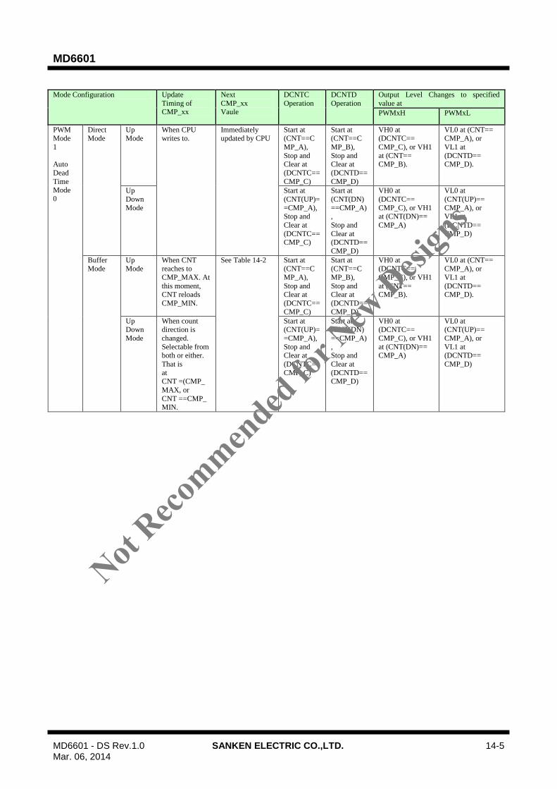
MD6601
MD6601 - DS Rev.1.0 SANKEN ELECTRIC CO.,LTD. 14-5 Mar. 06, 2014
Mode Configuration Update
Timing of CMP_xx
Next
CMP_xx Vaule
DCNTC
Operation
DCNTD
Operation
Output Level Changes to specified
value at
PWMxH PWMxL
PWM Mode
1
Auto
Dead
Time Mode
0
Direct Mode
Up Mode
When CPU writes to.
Immediately updated by CPU
Start at (CNT==C
MP_A),
Stop and Clear at
(DCNTC==
CMP_C)
Start at (CNT==C
MP_B),
Stop and Clear at
(DCNTD==
CMP_D)
VH0 at (DCNTC==
CMP_C), or VH1
at (CNT== CMP_B).
VL0 at (CNT== CMP_A), or
VL1 at
(DCNTD== CMP_D).
Up
Down
Mode
Start at
(CNT(UP)=
=CMP_A), Stop and
Clear at
(DCNTC==CMP_C)
Start at
(CNT(DN)
==CMP_A),
Stop and
Clear at (DCNTD==
CMP_D)
VH0 at
(DCNTC==
CMP_C), or VH1 at (CNT(DN)==
CMP_A)
VL0 at
(CNT(UP)==
CMP_A), or VL1 at
(DCNTD==
CMP_D)
Buffer Mode
Up Mode
When CNT reaches to
CMP_MAX. At
this moment, CNT reloads
CMP_MIN.
See Table 14-2 Start at (CNT==C
MP_A),
Stop and Clear at
(DCNTC==
CMP_C)
Start at (CNT==C
MP_B),
Stop and Clear at
(DCNTD==
CMP_D)
VH0 at (DCNTC==
CMP_C), or VH1
at (CNT== CMP_B).
VL0 at (CNT== CMP_A), or
VL1 at
(DCNTD== CMP_D).
Up Down
Mode
When count direction is
changed.
Selectable from both or either.
That is
at CNT =(CMP_
MAX, or
CNT ==CMP_MIN.
Start at (CNT(UP)=
=CMP_A),
Stop and Clear at
(DCNTC==
CMP_C)
Start at (CNT(DN)
==CMP_A)
, Stop and
Clear at
(DCNTD==CMP_D)
VH0 at (DCNTC==
CMP_C), or VH1
at (CNT(DN)== CMP_A)
VL0 at (CNT(UP)==
CMP_A), or
VL1 at (DCNTD==
CMP_D)
Not Reco
mmended
for N
ew D
esign
s
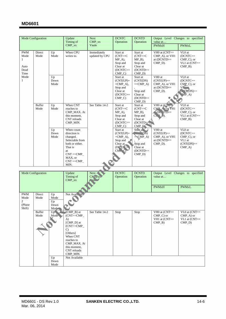
MD6601
MD6601 - DS Rev.1.0 SANKEN ELECTRIC CO.,LTD. 14-6 Mar. 06, 2014
Mode Configuration Update
Timing of CMP_xx
Next
CMP_xx Vaule
DCNTC
Operation
DCNTD
Operation
Output Level Changes to specified
value at…
PWMxH PWMxL
PWM Mode
1
Auto
Dead
Time Mode
1
Direct Mode
Up Mode
When CPU writes to.
Immediately updated by CPU
Start at (CNT==C
MP_A),
Stop and Clear at
(DCNTC==
CMP_C)
Start at (CNT==C
MP_B),
Stop and Clear at
(DCNTD==
CMP_D)
VH0 at (CNT== CMP_A), or VH1
at (DCNTD==
CMP_D).
VL0 at (DCNTC==
CMP_C), or
VL1 at (CNT== CMP_B).
Up
Down
Mode
Start at
(CNT(UP)=
=CMP_A), Stop and
Clear at
(DCNTC==CMP_C)
Start at
(CNT(DN)
==CMP_A),
Stop and
Clear at (DCNTD==
CMP_D)
VH0 at
(CNT(UP)==
CMP_A), or VH1 at (DCNTD==
CMP_D).
VL0 at
(DCNTC==
CMP_C), or VL1 at
(CNT(DN)==
CMP_A)
Buffer Mode
Up Mode
When CNT reaches to
CMP_MAX. At
this moment, CNT reloads
CMP_MIN.
See Table 14-2 Start at (CNT==C
MP_A),
Stop and Clear at
(DCNTC==
CMP_C)
Start at (CNT==C
MP_B),
Stop and Clear at
(DCNTD==
CMP_D)
VH0 at (CNT== CMP_A), or VH1
at (DCNTD==
CMP_D).
VL0 at (DCNTC==
CMP_C), or
VL1 at (CNT== CMP_B).
Up Down
Mode
When count direction is
changed.
Selectable from both or either.
That is
at CNT ==CMP_
MAX, or
CNT ==CMP_MIN.
Start at (CNT(UP)=
=CMP_A),
Stop and Clear at
(DCNTC==
CMP_C)
Start at (CNT(DN)
==CMP_A)
, Stop and
Clear at
(DCNTD==CMP_D)
VH0 at (CNT(UP)==
CMP_A), or VH1
at (DCNTD== CMP_D).
VL0 at (DCNTC==
CMP_C), or
VL1 at (CNT(DN)==
CMP_A)
Mode Configuration Update
Timing of CMP_xx
Next
CMP_xx Vaule
DCNTC
Operation
DCNTD
Operation
Output Level Changes to specified
value at…
PWMxH PWMxL
PWM Mode
2
(Phase Shift)
Direct Mode
Up Mode
Not Available
Up
Down Mode
Buffer
Mode
Up
Mode
[CMP_B] at
(CNT==CMP_
A) [CMP_D] at
(CNT==CMP_
C) [Others]
When CNT
reaches to CMP_MAX. At
this moment, CNT reloads
CMP_MIN.
See Table 14-2 Stop Stop VH0 at (CNT==
CMP_C) or
VH1 at (CNT== CMP_B)
VL0 at (CNT==
CMP_A) or
VL1 at (CNT== CMP_D)
Up
Down Mode
Not Available
Not Reco
mmended
for N
ew D
esign
s

MD6601
MD6601 - DS Rev.1.0 SANKEN ELECTRIC CO.,LTD. 14-7 Mar. 06, 2014
Mode Configuration Update
Timing of CMP_xx
Next
CMP_xx Vaule
DCNTC
Operation
DCNTD
Operation
Output Level Changes to specified
value at…
PWMxH PWMxL
PWM Mode
3
(Phase Shift)
Auto Dead
Time
Mode 0
Direct Mode
Up Mode
Not Available
Up
Down Mode
Buffer
Mode
Up
Mode
[CMP_B] at
(CNT==CMP_
A) [Others]
When CNT reaches to
CMP_MAX. At
this moment, CNT reloads
CMP_MIN.
See Table 14-2 Start at
(CNT==C
MP_A), Stop and
Clear at (DCNTC==
CMP_C)
Start at
(CNT==CM
P_B), Stop and
Clear at (DCNTD==
CMP_D)
VH0 at
(DCNTC==
CMP_C), or VH1 at (CNT==
CMP_B).
VL0 at (CNT==
CMP_A), or
VL1 at (DCNTD==
CMP_D).
Up
Down Mode
Not Available
Mode Configuration Update
Timing of
CMP_xx
Next
CMP_xx
Vaule
DCNTC
Operation
DCNTD
Operation
Output Level Changes to specified
value at…
PWMxH PWMxL
PWM
Mode 3
(Phase
Shift)
Auto
Dead Time
Mode
1
Direct
Mode
Up
Mode
Not Available
Up
Down
Mode
Buffer
Mode
Up
Mode
[CMP_B] at
(CNT==CMP_
A)
[Others] When CNT
reaches to
CMP_MAX. At this moment,
CNT reloads CMP_MIN.
See Table 14-2 Start at
(CNT==C
MP_A),
Stop and Clear at
(DCNTC==
CMP_C)
Start at
(CNT==C
MP_B),
Stop and Clear at
(DCNTD==
CMP_D)
VH0 at (CNT==
CMP_A), or VH1
at (DCNTD==
CMP_D).
VL0 at
(DCNTC==
CMP_C), or
VL1 at (CNT== CMP_B).
Up
Down
Mode
Not Available
Not Reco
mmended
for N
ew D
esign
s
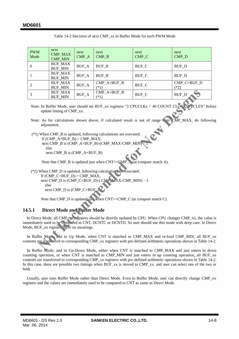
MD6601
MD6601 - DS Rev.1.0 SANKEN ELECTRIC CO.,LTD. 14-8 Mar. 06, 2014
Table 14-2 Decision of next CMP_xx in Buffer Mode for each PWM Mode
PWM
Mode
next
CMP_MAX
CMP_MIN
next
CMP_A
next
CMP_B
next
CMP_C
next
CMP_D
0 BUF_MAX
BUF_MIN BUF_A BUF_B BUF_C BUF_D
1 BUF_MAX
BUF_MIN BUF_A BUF_B BUF_C BUF_D
2 BUF_MAX
BUF_MIN BUF_A
CMP_A+BUF_B
(*1) BUF_C
CMP_C+BUF_D
(*2)
3 BUF_MAX
BUF_MIN BUF_A
CMP_A+BUF_B
(*1) BUF_C BUF_D
Note: In Buffer Mode, user should set BUF_xx registers “3 CPUCLKs + 40 COUNT CLOCK CYCLES” before
update timing of CMP_xx.
Note: As for calculations shown above, if calculated result is out of range over CMP_MAX, do following
adjustment.
(*1) When CMP_B is updated, following calculations are executed.
If (CMP_A+BUF_B) > CMP_MAX,
next CMP_B is (CMP_A+BUF_B)-(CMP_MAX-CMP_MIN) – 1
else
next CMP_B is (CMP_A+BUF_B)
Note that CMP_B is updated just when CNT==CMP_A (at compare match A).
(*2) When CMP_D is updated, following calculations are executed.
If (CMP_C+BUF_D) > CMP_MAX,
next CMP_D is (CMP_C+BUF_D)-( CMP_MAX-CMP_MIN) – 1
else
next CMP_D is (CMP_C+BUF_D)
Note that CMP_D is updated just when CNT==CMP_C (at compare match C).
14.5.1 Direct Mode and Buffer Mode
In Direct Mode, all CMP_xx registers should be directly updated by CPU. When CPU changes CMP_xx, the value is
immediately used to be compared to CNT, DCNTC or DCNTD. So user should use this mode with deep care. In Direct
Mode, BUF_xx registers have no meanings.
In Buffer Mode, and in Up Mode, when CNT is matched to CMP_MAX and re-load CMP_MIN, all BUF_xx
contents are transferred to corresponding CMP_xx registers with pre-defined arithmetic operations shown in Table 14-2.
In Buffer Mode, and in Up-Down Mode, either when CNT is matched to CMP_MAX and just enters in down
counting operation, or when CNT is matched to CMP_MIN and just enters in up counting operation, all BUF_xx
contents are transferred to corresponding CMP_xx registers with pre-defined arithmetic operations shown in Table 14-2.
In this case, there are possible two timings when BUF_xx is moved to CMP_xx, and user can select one of the two or
both.
Usually, user uses Buffer Mode rather than Direct Mode. Even in Buffer Mode, user can directly change CMP_xx
registers and the values are immediately used to be compared to CNT as same as Direct Mode.
Not Reco
mmended
for N
ew D
esign
s

MD6601
MD6601 - DS Rev.1.0 SANKEN ELECTRIC CO.,LTD. 14-9 Mar. 06, 2014
14.5.2 PWM Mode 0
All PWM output wave timings should be specified by user. This mode can be operated in both Direct Mode and
Buffer Mode without using the Dead Time counter
(1) PWM Mode0 + Up Mode
CNT starts counting from it’s initial value to the CMP_MAX value. After CNT and CMP_MAX are matched, CNT
reloads the CMP_MIN value and starts counting from this value to the CMP_MAX value.
If CNT and CMP_A are matched, PWMxL is changed to specified level VL0.
If CNT and CMP_C are matched, PWMxH is changed to specified level VH0.
If CNT and CMP_B are matched, PWMxH is changed to specified level VH1.
If CNT and CMP_D are matched, PWMxL is changed to specified level VL1.
Each level VH0, VH1, VL0, VL1 is selected from NOP, Low, High or Toggle.
Figure 14-3 PWM Mode0 (Up Mode)
(2) PWM Mode0 + Up-Down Mode
CNT starts Up-counting from it’s initial value to the CMP_MAX value. When CNT and CMP MAX are matched,
CNT starts Down-counting to the CMP_MIN value. When CNT and CMP_MIN are matched, starts CNT return
Up-count ing to the CMP_MAX. CNT restarts Up-counting regardless of count direction when CNT stops by writing
PWMCNTS.PWMCSy = 0.
If CNT(UP) and CMP_A are matched, PWMxL is changed to specified level VL0.
If CNT(UP) and CMP_C are matched, PWMxH is changed to specified level VH0.
If CNT(DOWN) and CMP_C are matched, PWMxH is changed to specified level VH1.
If CNT(DOWN) and CMP_A are matched, PWMxL is changed to specified level VL1.
Each level VH0, VH1, VL0, VL1 is selected from NOP, Low, High or Toggle.
In Up-Down mode and Buffer mode, there are possible two timings when BUF_xx is transffered to CMP_xx, and
user can select one of the two or both.
CNTCMP_MAX
CMP_C
CMP_B
CMP_A
CMP_D
PWMxH
PWMxL
CMP_MAX
CMP_C
CMP_B
CMP_A
CMP_D
In Buffer Mode,
Values in CMP_xxx are
updated at this timing.
CMP_MIN CMP_MIN
Duty
Dead Time
Dead Time
VH0 VH1
VL0 VL1
VH0 VH1
VL0 VL1
Not Reco
mmended
for N
ew D
esign
s

MD6601
MD6601 - DS Rev.1.0 SANKEN ELECTRIC CO.,LTD. 14-10 Mar. 06, 2014
Figure 14-4 PWM Mode 0 (Up-Down Mode)
14.5.3 PWM Mode 1 (Auto Dead Time)
Dead Time is automatically measured by using Dead Time counter (DCNTC & DCNTD).
It is necessary to set Dead Time into CMP_C and CMP_D. CMP_C and CMP_D setting method are differenrt from
mode 0. There are two Dead Time Modes by changing PWMxH and PWMxL.
These are Auto Dead Time Mode 0 and Mode 1.
(1) PWM Mode1 + Up Mode + Auto Dead Time Mode 0
CNT starts counting from it’s initial value to the CMP_MAX value. After CNT and CMP_MAX are matched, CNT
reloads the CMP_MIN value and starts counting from this value to the CMP_MAX value.
If CNT and CMP_A are matched, PWMxL is changed to specified level VL0.
DCNTC starts up-counting from “0”.
If DCNTC and CMP_C are matched, PWMxH is changed to specified level VH0.
DCNTC is cleared to “0” and stop.
If CNT and CMP_B are matched, PWMxH is changed to specified level VH1.
DCNTD starts up-counting from “0”.
If DCNTD and CMP_D are matched, PWMxL is changed to specified level VL1.
DCNTD is cleared to “0” and stop.
In Direct mode, it is necessary to change CMP_XX register in advance of 3CPUCLKs+40count cycles or more.
DCNTC will be cleared if matching of CNT and CMP_A occurs before matching of DCNTC and CMP_C.In the
same way, DCNTD will be cleared if matching of CNT and CMP_B occurs before matching of DCNTD and
CMP_D.
In Buffer mode, the change of each CMP_XX occurs when CMP reloads the value of CMP_MIN.
CNT
CMP_MAX
CMP_C
CMP_A
PWMxH
PWMxL
CMP_MAX
CMP_C
CMP_A
In Buffer Mode,
Values in CMP_xxx can
be updated at this timing.
(selectable)
CMP_C
CMP_A
In Buffer Mode,
Values in CMP_xxx can
be updated at this timing.
(selectable)
CMP_MIN CMP_MIN
VH0 VH1
VL0 VL1
VH0 VH1
VL0 VL1
Not Reco
mmended
for N
ew D
esign
s

MD6601
MD6601 - DS Rev.1.0 SANKEN ELECTRIC CO.,LTD. 14-11 Mar. 06, 2014
(2) PWM Mode1 + Up Mode + Auto Dead Time Mode 1
CNT starts counting from it’s initial value to the CMP_MAX value. After CNT and CMP_MAX are matched, CNT
reloads the CMP_MIN value and starts counting from this value to the CMP_MAX value.
If CNT and CMP_A are matched, PWMxH is changed to specified level VH0.
DCNTC starts up-counting from “0”.
If DCNTC and CMP_C are matched, PWMxL is changed to specified level VL0.DCNTC is cleared to “0” and stop.
If CNT and CMP_B are matched, PWMxL is changed to specified level VL1.DCNTD starts up-counting from “0”.
If DCNTD and CMP_D are matched, PWMxH is changed to specified level VH1.
DCNTD is cleared to “0” and stop.
Each level VH0, VH1, VL0, VL1 is selected from NOP, Low, High or Toggle.
In Direct mode, it is necessary to change CMP_XX register in advance of 3CPUCLKs+40count cycles or more.
Note: During DCNTx is incrementing, if corresponding CMP_A/B (which is start trigger of DCNTx) is happened,
the DCNTx re-starts from 0. And as the result, the dead time is stretched.
Note: If CMP_C=0 or CMP_D=0, corresponding dead time period is 1-counter-cycle.
Figure 14-5 PWM Mode1 + Up Mode
CNTCMP_MAX
CMP_C
CMP_B
CMP_A
CMP_D
PWMxH
PWMxL
CMP_MAX
CMP_C
CMP_B
CMP_A
In Buffer Mode,
Values in CMP_xxx are
updated at this timing.
CMP_MIN CMP_MIN
Duty
Dead Time
Dead Time
0
DCNTC
DCNTD
0
CMP_D
Dead Time
Dead Time
Duty
0
0
VH0VH1
VH0VH1
VL0 VL0VL1 VL1
PWMxH
PWMxL
Duty
Dead Time
Dead Time
Dead Time
Dead Time
Duty
VH0VH1
VH0 VH1
VL0VL0
VL1 VL1
Auto Dead Time
Mode 0
Auto Dead Time
Mode 1
Not Reco
mmended
for N
ew D
esign
s
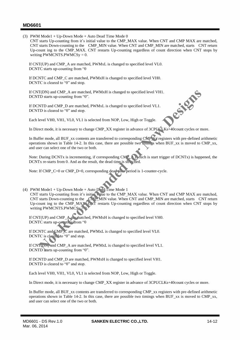
MD6601
MD6601 - DS Rev.1.0 SANKEN ELECTRIC CO.,LTD. 14-12 Mar. 06, 2014
(3) PWM Mode1 + Up-Down Mode + Auto Dead Time Mode 0
CNT starts Up-counting from it’s initial value to the CMP_MAX value. When CNT and CMP MAX are matched,
CNT starts Down-counting to the CMP_MIN value. When CNT and CMP_MIN are matched, starts CNT return
Up-count ing to the CMP_MAX. CNT restarts Up-counting regardless of count direction when CNT stops by
writing PWMCNTS.PWMCSy = 0.
If CNT(UP) and CMP_A are matched, PWMxL is changed to specified level VL0.
DCNTC starts up-counting from “0
If DCNTC and CMP_C are matched, PWMxH is changed to specified level VH0.
DCNTC is cleared to “0” and stop.
If CNT(DN) and CMP_A are matched, PWMxH is changed to specified level VH1.
DCNTD starts up-counting from “0”.
If DCNTD and CMP_D are matched, PWMxL is changed to specified level VL1.
DCNTD is cleared to “0” and stop.
Each level VH0, VH1, VL0, VL1 is selected from NOP, Low, High or Toggle.
In Direct mode, it is necessary to change CMP_XX register in advance of 3CPUCLKs+40count cycles or more.
In Buffer mode, all BUF_xx contents are transferred to corresponding CMP_xx registers with pre-defined arithmetic
operations shown in Table 14-2. In this case, there are possible two timings when BUF_xx is moved to CMP_xx,
and user can select one of the two or both.
Note: During DCNTx is incrementing, if corresponding CMP_A (which is start trigger of DCNTx) is happened, the
DCNTx re-starts from 0. And as the result, the dead time is stretched.
Note: If CMP_C=0 or CMP_D=0, corresponding dead time period is 1-counter-cycle.
(4) PWM Mode1 + Up-Down Mode + Auto Dead Time Mode 1
CNT starts Up-counting from it’s initial value to the CMP_MAX value. When CNT and CMP MAX are matched,
CNT starts Down-counting to the CMP_MIN value. When CNT and CMP_MIN are matched, starts CNT return
Up-count ing to the CMP_MAX. CNT restarts Up-counting regardless of count direction when CNT stops by
writing PWMCNTS.PWMCSy = 0.
If CNT(UP) and CMP_A are matched, PWMxH is changed to specified level VH0.
DCNTC starts up-counting from “0
If DCNTC and CMP_C are matched, PWMxL is changed to specified level VL0.
DCNTC is cleared to “0” and stop.
If CNT(DN) and CMP_A are matched, PWMxL is changed to specified level VL1.
DCNTD starts up-counting from “0”.
If DCNTD and CMP_D are matched, PWMxH is changed to specified level VH1.
DCNTD is cleared to “0” and stop.
Each level VH0, VH1, VL0, VL1 is selected from NOP, Low, High or Toggle.
In Direct mode, it is necessary to change CMP_XX register in advance of 3CPUCLKs+40count cycles or more.
In Buffer mode, all BUF_xx contents are transferred to corresponding CMP_xx registers with pre-defined arithmetic
operations shown in Table 14-2. In this case, there are possible two timings when BUF_xx is moved to CMP_xx,
and user can select one of the two or both.
Not Reco
mmended
for N
ew D
esign
s
MD6601
MD6601 - DS Rev.1.0 SANKEN ELECTRIC CO.,LTD. 14-13 Mar. 06, 2014
Note: During DCNTx is incrementing, if corresponding CMP_A (which is start trigger of DCNTx) is happened, the
DCNTx re-starts from 0. And as the result, the dead time is stretched.
Note: If CMP_C=0 or CMP_D=0, corresponding dead time period is 1-counter-cycle.
Figure 14-6 PWM Mode1 +Up-Down Mode
CNT
CMP_MAX
CMP_C
CMP_A
CMP_MAX
CMP_A
In Buffer Mode,
Values in CMP_xxx can
be updated at this timing.
(selectable)
CMP_D
CMP_A
In Buffer Mode,
Values in CMP_xxx can
be updated at this timing.
(selectable)
CMP_MIN CMP_MIN
0CMP_D
0
CMP_C
0
DCNTC
DCNTD
PWMxH
PWMxL
Duty
Dead Time
Dead Time
VH0
VH1
VL1
VH0
VL0 VL0
VH1
VL1
PWMxH
PWMxL
Duty
Dead Time
Dead Time
VH0 VH1
VL1
VH0
VL0 VL0
VH1
VL1
Auto Dead Time
Mode 0
Auto Dead Time
Mode 1
Not Reco
mmended
for N
ew D
esign
s
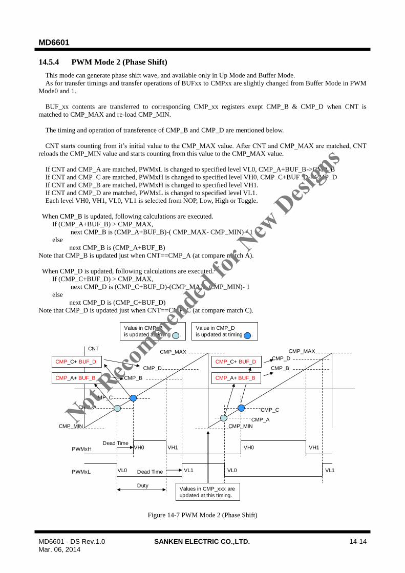
MD6601
MD6601 - DS Rev.1.0 SANKEN ELECTRIC CO.,LTD. 14-14 Mar. 06, 2014
14.5.4 PWM Mode 2 (Phase Shift)
This mode can generate phase shift wave, and available only in Up Mode and Buffer Mode.
As for transfer timings and transfer operations of BUFxx to CMPxx are slightly changed from Buffer Mode in PWM
Mode0 and 1.
BUF_xx contents are transferred to corresponding CMP_xx registers exept CMP_B & CMP_D when CNT is
matched to CMP_MAX and re-load CMP_MIN.
The timing and operation of transference of CMP_B and CMP_D are mentioned below.
CNT starts counting from it’s initial value to the CMP_MAX value. After CNT and CMP_MAX are matched, CNT
reloads the CMP_MIN value and starts counting from this value to the CMP_MAX value.
If CNT and CMP_A are matched, PWMxL is changed to specified level VL0, CMP_A+BUF_B->CMP_B
If CNT and CMP_C are matched, PWMxH is changed to specified level VH0, CMP_C+BUF_D->CMP_D
If CNT and CMP_B are matched, PWMxH is changed to specified level VH1.
If CNT and CMP_D are matched, PWMxL is changed to specified level VL1.
Each level VH0, VH1, VL0, VL1 is selected from NOP, Low, High or Toggle.
When CMP_B is updated, following calculations are executed.
If (CMP_A+BUF_B) > CMP_MAX,
next CMP_B is (CMP_A+BUF_B)-( CMP_MAX- CMP_MIN) - 1
else
next CMP_B is (CMP_A+BUF_B)
Note that CMP_B is updated just when CNT==CMP_A (at compare match A).
When CMP_D is updated, following calculations are executed.
If (CMP_C+BUF_D) > CMP_MAX,
next CMP_D is (CMP_C+BUF_D)-(CMP_MAX- CMP_MIN)- 1
else
next CMP_D is (CMP_C+BUF_D)
Note that CMP_D is updated just when CNT==CMP_C (at compare match C).
Figure 14-7 PWM Mode 2 (Phase Shift)
CNTCMP_MAX
CMP_C
CMP_B
CMP_A
CMP_D
PWMxH
PWMxL
CMP_MAX
CMP_C
CMP_B
CMP_A
CMP_D
Values in CMP_xxx are
updated at this timing.
CMP_MIN CMP_MIN
Duty
Dead Time
Dead Time
CMP_A+ BUF_B
CMP_C+ BUF_D CMP_C+ BUF_D
CMP_A+ BUF_B
Value in CMP_B
is updated at timing .
Value in CMP_D
is updated at timing .
VH0 VH1
VL0 VL1
VH0 VH1
VL0 VL1
Not Reco
mmended
for N
ew D
esign
s
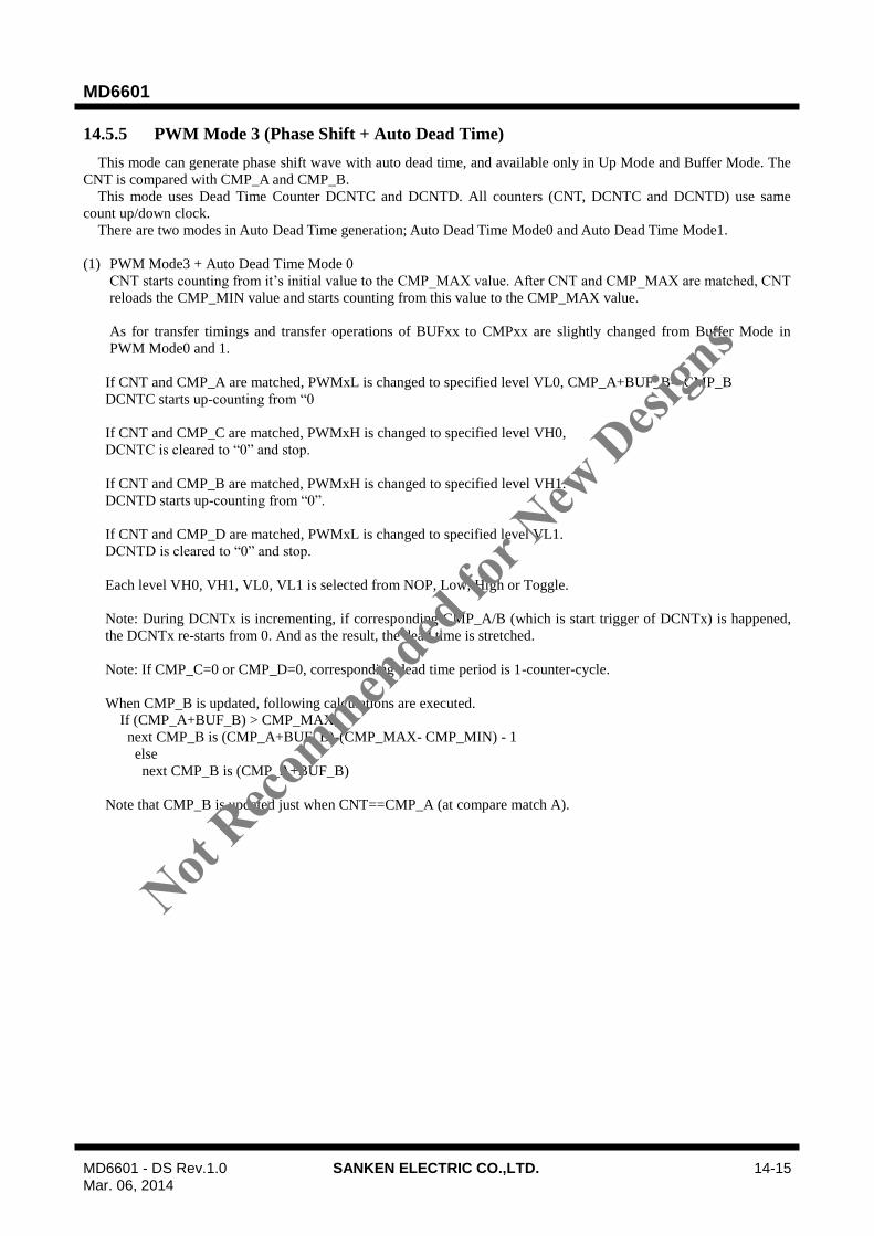
MD6601
MD6601 - DS Rev.1.0 SANKEN ELECTRIC CO.,LTD. 14-15 Mar. 06, 2014
14.5.5 PWM Mode 3 (Phase Shift + Auto Dead Time)
This mode can generate phase shift wave with auto dead time, and available only in Up Mode and Buffer Mode. The
CNT is compared with CMP_A and CMP_B.
This mode uses Dead Time Counter DCNTC and DCNTD. All counters (CNT, DCNTC and DCNTD) use same
count up/down clock.
There are two modes in Auto Dead Time generation; Auto Dead Time Mode0 and Auto Dead Time Mode1.
(1) PWM Mode3 + Auto Dead Time Mode 0
CNT starts counting from it’s initial value to the CMP_MAX value. After CNT and CMP_MAX are matched, CNT
reloads the CMP_MIN value and starts counting from this value to the CMP_MAX value.
As for transfer timings and transfer operations of BUFxx to CMPxx are slightly changed from Buffer Mode in
PWM Mode0 and 1.
If CNT and CMP_A are matched, PWMxL is changed to specified level VL0, CMP_A+BUF_B->CMP_B
DCNTC starts up-counting from “0
If CNT and CMP_C are matched, PWMxH is changed to specified level VH0,
DCNTC is cleared to “0” and stop.
If CNT and CMP_B are matched, PWMxH is changed to specified level VH1.
DCNTD starts up-counting from “0”.
If CNT and CMP_D are matched, PWMxL is changed to specified level VL1.
DCNTD is cleared to “0” and stop.
Each level VH0, VH1, VL0, VL1 is selected from NOP, Low, High or Toggle.
Note: During DCNTx is incrementing, if corresponding CMP_A/B (which is start trigger of DCNTx) is happened,
the DCNTx re-starts from 0. And as the result, the dead time is stretched.
Note: If CMP_C=0 or CMP_D=0, corresponding dead time period is 1-counter-cycle.
When CMP_B is updated, following calculations are executed.
If (CMP_A+BUF_B) > CMP_MAX,
next CMP_B is (CMP_A+BUF_B)-(CMP_MAX- CMP_MIN) - 1
else
next CMP_B is (CMP_A+BUF_B)
Note that CMP_B is updated just when CNT==CMP_A (at compare match A).
Not Reco
mmended
for N
ew D
esign
s

MD6601
MD6601 - DS Rev.1.0 SANKEN ELECTRIC CO.,LTD. 14-16 Mar. 06, 2014
Figure 14-8 PWM Mode 3 (Phase Shift, Auto Dead Time Mode 0)
CNTCMP_MAX
CMP_C
CMP_B
CMP_A
CMP_D
PWMxH
PWMxL
CMP_MAX
CMP_C
CMP_B
CMP_A
Values in CMP_xxx
except for CMP_B are
updated at this timing.
CMP_MIN CMP_MIN
Duty
Dead Time
Dead Time
0
DCNTC
DCNTD
0
CMP_D
Dead Time
Dead Time
Duty
0
0
CMP_A+ BUF_BCMP_A+ BUF_B
Value in CMP_B
is updated at timing .
VH0
VH1
VHD
VL0
VL1
VLD
VH0
VH1
VHD
VL0
VL1
VLD
Not Reco
mmended
for N
ew D
esign
s

MD6601
MD6601 - DS Rev.1.0 SANKEN ELECTRIC CO.,LTD. 14-17 Mar. 06, 2014
(2) PWM Mode3 + Auto Dead Time Mode 1
CNT starts counting from it’s initial value to the CMP_MAX value. After CNT and CMP_MAX are matched, CNT
reloads the CMP_MIN value and starts counting from this value to the CMP_MAX value.
As for transfer timings and transfer operations of BUFxx to CMPxx are slightly changed from Buffer Mode in
PWM Mode0 and 1.
If CNT and CMP_A are matched, PWMxH is changed to specified level VH0, CMP_A+BUF_B->CMP_B
DCNTC starts up-counting from “0
If CNT and CMP_C are matched, PWMxL is changed to specified level VL0,
DCNTC is cleared to “0” and stop.
If CNT and CMP_B are matched, PWMxL is changed to specified level VL1.
DCNTD starts up-counting from “0”.
If CNT and CMP_D are matched, PWMxH is changed to specified level VH1.
DCNTD is cleared to “0” and stop.
Each level VH0, VH1, VL0, VL1 is selected from NOP, Low, High or Toggle.
Note: During DCNTx is incrementing, if corresponding CMP_A/B (which is start trigger of DCNTx) is happened,
the DCNTx re-starts from 0. And as the result, the dead time is stretched.
Note: If CMP_C=0 or CMP_D=0, corresponding dead time period is 1-counter-cycle.
When CMP_B is updated, following calculations are executed.
If (CMP_A+BUF_B) > CMP_MAX,
next CMP_B is (CMP_A+BUF_B)-(CMP_MAX-CMP_MIN) - 1
else
next CMP_B is (CMP_A+BUF_B)
Note that CMP_B is updated just when CNT==CMP_A (at compare match A).
Not Reco
mmended
for N
ew D
esign
s
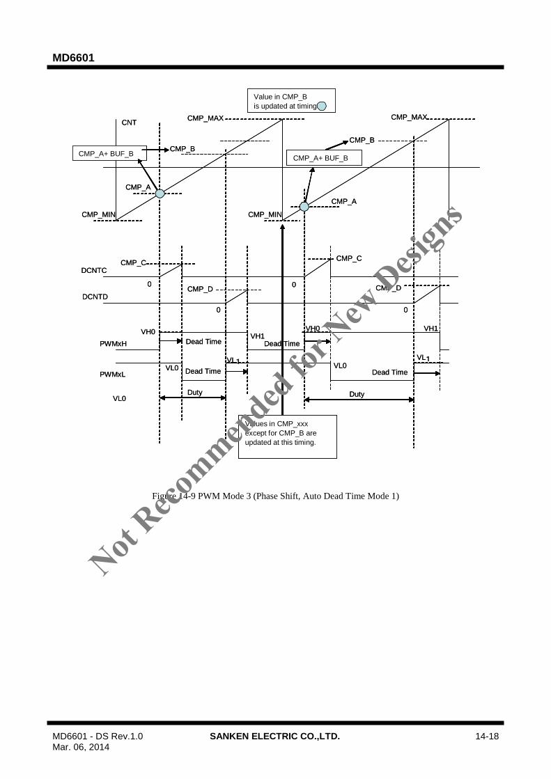
MD6601
MD6601 - DS Rev.1.0 SANKEN ELECTRIC CO.,LTD. 14-18 Mar. 06, 2014
Figure 14-9 PWM Mode 3 (Phase Shift, Auto Dead Time Mode 1)
CNTCMP_MAX
CMP_C
CMP_B
CMP_A
CMP_D
PWMxH
PWMxL
CMP_MAX
CMP_C
CMP_B
CMP_A
Values in CMP_xxx
except for CMP_B are
updated at this timing.
CMP_MIN CMP_MIN
Duty
Dead Time
Dead Time
0
DCNTC
DCNTD
0
CMP_D
Dead Time
Dead Time
Duty
0
0
CMP_A+ BUF_BCMP_A+ BUF_B
Value in CMP_B
is updated at timing
VH0VH1
VL0
VL1
VH0 VH1
VL0VL1
VL0
Not Reco
mmended
for N
ew D
esign
s

MD6601
MD6601 - DS Rev.1.0 SANKEN ELECTRIC CO.,LTD. 14-19 Mar. 06, 2014
14.6 Contentions or Output Control Conditions
Output Control Operations, when plural Compare matches are happened at same time, are shown in Table 14-3. In
each Auto Dead Time Mode, even if such contentions are happened, DCNTC and DCNTD will normally start by
defined conditions.
Table 14-3 Contentions or Output Control Conditions
Mode Priority in PWMxH output control Priority in PWMxL output control Note
PWM
Mode 0
+
Up Mode
Lowest
Highest
Lowest
Highest
CMP_MAX for PWMxH CMP_MAX for PWMxL
VH0 event VL0 event
VH1 event VL1 event
VTH event VTL event
PWM
Mode 0
+
Up-Down
Mode
Lowest
Highest
CMP_MIN for PWMxH Lowest
Highest
CMP_MIN for PWMxL
CMP_MAX for PWMxH CMP_MAX for PWMxL
VH0 event VL0 event
VH1 event VL1 event
VTH event VTL event
PWM
Mode 1
+
Up Mode
Lowest
Highest
Lowest
Highest
CMP_MAX for PWMxH CMP_MAX for PWMxL
VH0 event VL0 event
VH1 event VL1 event
VTH event VTL event
PWM
Mode 1
+
Up-Down
Mode
Lowest
Highest
CMP_MIN for PWMxH Lowest
Highest
CMP_MIN for PWMxL
CMP_MAX for PWMxH CMP_MAX for PWMxL
VH0 event VL0 event
VH1 event VL1 event
VTH event VTL event
PWM
Mode 2 Lowest
Highest
Lowest
Highest
CMP_MAX for PWMxH CMP_MAX for PWMxL
VH0 event VL0 event
VH1 event VL1 event
VTH event VTL event
PWM
Mode 3
Lowest
Highest
Lowest
Highest
CMP_MAX for PWMxH CMP_MAX for PWMxL
VH0 event VL0 event
VH1 event VL1 event
VTH event VTL event
Common Just when Compare Match, CMP_x is changed to another value.
old CMP_x operation is taken.
Just when CMP_x is changed, Compare Match happens by new value.
new CMP_x operation is NOT taken.
Just when Compare Match, CNT is forcibly changed to another value.
old CMP_x operation is taken.
Just when CNT is forcibly changed, Compare Match happens by new value.
new CMP_x operation is NOT taken
Not Reco
mmended
for N
ew D
esign
s

MD6601
MD6601 - DS Rev.1.0 SANKEN ELECTRIC CO.,LTD. 14-20 Mar. 06, 2014
14.7 Operation Timing
(1) Compare Match Timing
Compare Match Timing is shown in Figure 14-10. Conditions of this example are
(i) Module System clock :1GHz
(ii) Count Up/Down Timing:1GHz
The CNT is changed by the Count Up/Down timimg:1GHz, and Compare match is occurred at the end of the
CNT value which same as CMP_X
Figure 14-10 Compare Match Timing
Module System Clock (1GHz)
CNT
N CMP_x
PWMxx
N-1 N N+1 N-2 N+2
Compare Match Timing
Not Reco
mmended
for N
ew D
esign
s

MD6601
MD6601 - DS Rev.1.0 SANKEN ELECTRIC CO.,LTD. 14-21 Mar. 06, 2014
(2) CNT Clear Timing in Up-Down Mode
The CNT Clear Timing in Up-Down Mode is shown in Figure 14-11. Conditions of this example are
(i) Module System clock :1GHz
(ii) Count Up/Down Timing:1GHz
The CNT is reloaded to the CMP _MIN value at the next CNT cycle of CMP_MAX value
Figure 14-11 Counter Clear Timing in Up-Count Mode
Module System Clock (1GHz)
CNT
MAX CMP_MAX
MIN CMP_MIN
MAX-1 MAX MIN MIN+1 MAX-2 MIN+2
Not Reco
mmended
for N
ew D
esign
s

MD6601
MD6601 - DS Rev.1.0 SANKEN ELECTRIC CO.,LTD. 14-22 Mar. 06, 2014
(3) CNT Up to Down changing Timing in Up-Down Mode
The CNT Changing Timing from Up count to Down count is shown in Figure 14-12. Conditions of this example
are
(i) Module System clock :1GHz
(ii) Count Up/Down Timing:1GHz
The CNT first value in countdown operation is same as the CNT last value in count up operation. This means
CMP_MAX value is kept in two cycles of the CNT Count Up/Down Timing.
Figure 14-12 Counter Up to Down Change Timing in Up-Down Mode
Count Up/Down CNT
CNT
MAX CCMP_MAX
Module System Clock (1GHz)
count count up
count count down
MAX-1 MAX MAX MAX-1 MAX-2 MAX-2 MAX-3
Not Reco
mmended
for N
ew D
esign
s
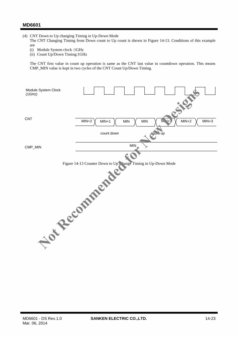
MD6601
MD6601 - DS Rev.1.0 SANKEN ELECTRIC CO.,LTD. 14-23 Mar. 06, 2014
(4) CNT Down to Up changing Timing in Up-Down Mode
The CNT Changing Timing from Down count to Up count is shown in Figure 14-13. Conditions of this example
are
(i) Module System clock :1GHz
(ii) Count Up/Down Timing:1GHz
The CNT first value in count up operation is same as the CNT last value in countdown operation. This means
CMP_MIN value is kept in two cycles of the CNT Count Up/Down Timing.
Figure 14-13 Counter Down to Up Change Timing in Up-Down Mode
Module System Clock (1GHz)
CNT
MIN CMP_MIN
count down count up
MIN+2 MIN+1 MIN MIN MIN+1 MIN+2 MIN+3
Not Reco
mmended
for N
ew D
esign
s

MD6601
MD6601 - DS Rev.1.0 SANKEN ELECTRIC CO.,LTD. 14-24 Mar. 06, 2014
Figure 14-14 Example Operation (PWM Mode 1 + Auto Dead Time Mode 0 + Up Mode + Buffer Mode)
NOTE1: Compare Match Judges should be executed every time. even just after re-load CNT.
NOTE2: Minimum Pulse width should be a period of counter updating (+/-1) clock (1ns at 1GHz). Very narrow pulse
width might be disappeared due to rise/fall time.
NOTE3: Actual toggling on PWMxH and PWMxL has latency delay from internal compare match events.
Module System Clock
Equivalent Clock (1GHz)
Count Up/Down
Timing
BUF_A
BUF_B
BUF_C
BUF_D
CNT 21 22 -1
5
-1
22 25
-2
BUF_MAX
BUF_MIN
4
2 3
3 2
CMP_A
CMP_B
CMP_C
CMP_D
CMP_MAX
CMP_MIN
5
-1
22
2
3
3
25
-2
4
3
2
0 1 2 3 4 5 6 7 8 9
PWMxH
-13
-1
1 2 30DCNTC 0
PWMxL 1 20DCNTD
20
0
10
4
3
5
Updated by CPU or DSAC
24 25 -2 -1 0 1
20
0
10
4
3
5
Not Reco
mmended
for N
ew D
esign
s

MD6601
MD6601 - DS Rev.1.0 SANKEN ELECTRIC CO.,LTD. 14-25 Mar. 06, 2014
14.8 Re-Trigger Operations
Each counter block can be configured as Re-Trigger operation Mode. Each Output Signal or Counter value can be
retriggered by specified events.There are five Re-trigger operations,Mode A/B/C/D and Mask operation, which can
control output levels of both PWMxH and PWMxL.
14.8.1 Events for re-trigger
There are sixteen Events for re-trigger as shown in Table 14-4.
Table 14-4 Events for Re-trigger
No. Source Note
0 CPU Access
1 reserved
2 Trigger Pulse from Timer0_CMA
3 Trigger Pulse from Timer1_CMA
4 Trigger Pulse from Comparator 0
5 Trigger Pulse from Comparator 1
6 Trigger Pulse from Comparator 2
7 Trigger Pulse from Comparator 3
8 Event Positive Edge Signal from GPIO0
9 Event Positive Edge Signal from GPIO1
10 Event Positive Edge Signal from GPIO2
11 Event Positive Edge Signal from GPIO3
12 Event Negative Edge Signal from GPIO0
13 Event Negative Edge Signal from GPIO1
14 Event Negative Edge Signal from GPIO2
15 Event Negative Edge Signal from GPIO3
Not Reco
mmended
for N
ew D
esign
s
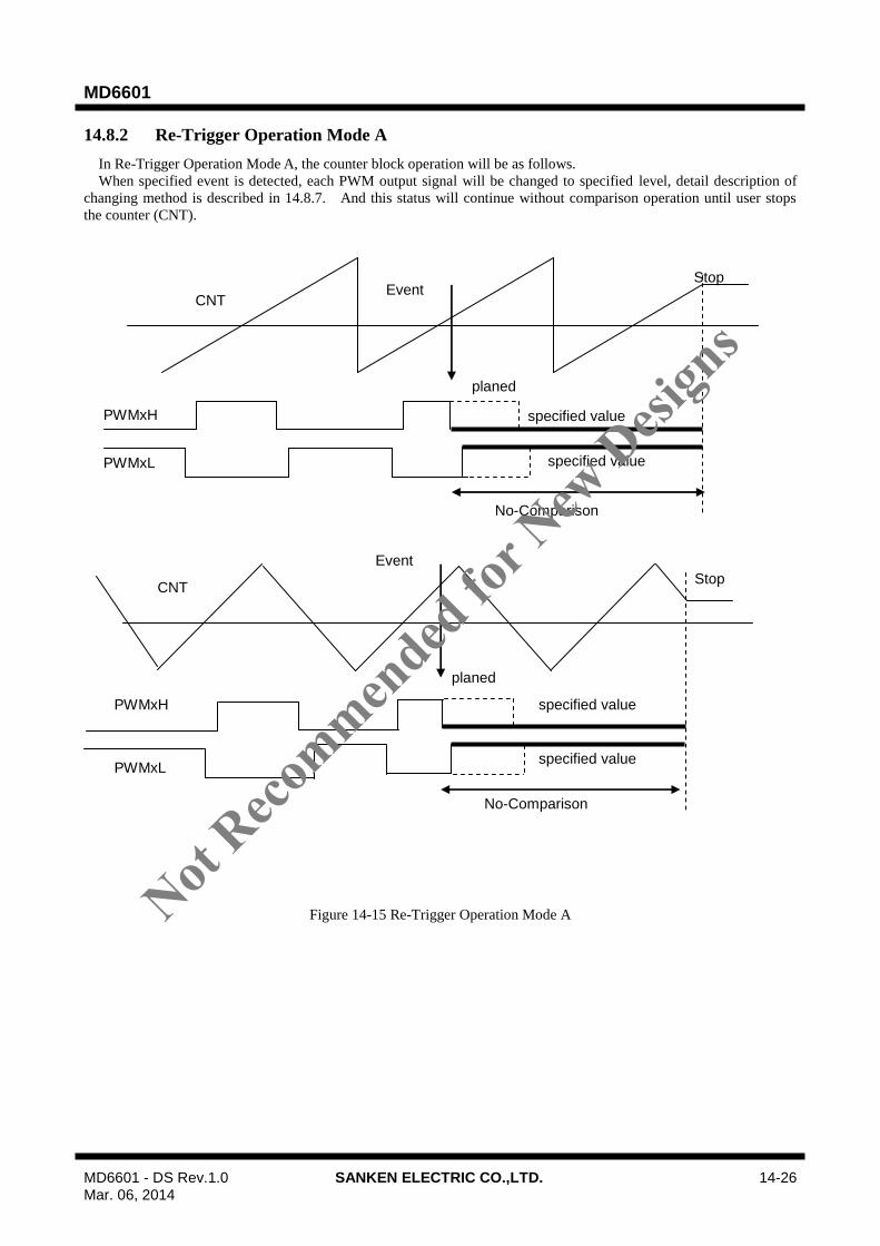
MD6601
MD6601 - DS Rev.1.0 SANKEN ELECTRIC CO.,LTD. 14-26 Mar. 06, 2014
14.8.2 Re-Trigger Operation Mode A
In Re-Trigger Operation Mode A, the counter block operation will be as follows.
When specified event is detected, each PWM output signal will be changed to specified level, detail description of
changing method is described in 14.8.7. And this status will continue without comparison operation until user stops
the counter (CNT).
Figure 14-15 Re-Trigger Operation Mode A
Stop
CNT
planed
Event
No-Comparison
PWMxH
PWMxL
specified value
specified value
CNT
No-Comparison
PWMxH
PWMxL
specified value
specified value
Event
planed
Stop
Not Reco
mmended
for N
ew D
esign
s

MD6601
MD6601 - DS Rev.1.0 SANKEN ELECTRIC CO.,LTD. 14-27 Mar. 06, 2014
14.8.3 Re-Trigger Operation Mode B
In Re-Trigger Operation Mode B, the counter block operation will be as follows.
When specified event is detected, each PWM output signal will be changed to specified level, detail description of
changing method is described in 14.8.7. And this status will continue without comparison operation until the counter
(CNT) reaches CMP_MIN. From the timing at CNT==CMP_MIN, the normal comparison operation starts again.
Figure 14-16 Re-Trigger Operation Mode B
No-Comparison
CNT
planed
Event
No-Comparison
PWMxH
PWMxL
specified value
specified value
CNT
PWMxH
PWMxL
specified value
specified value
Event
CMP_MIN planed
CMP_MIN
Not Reco
mmended
for N
ew D
esign
s
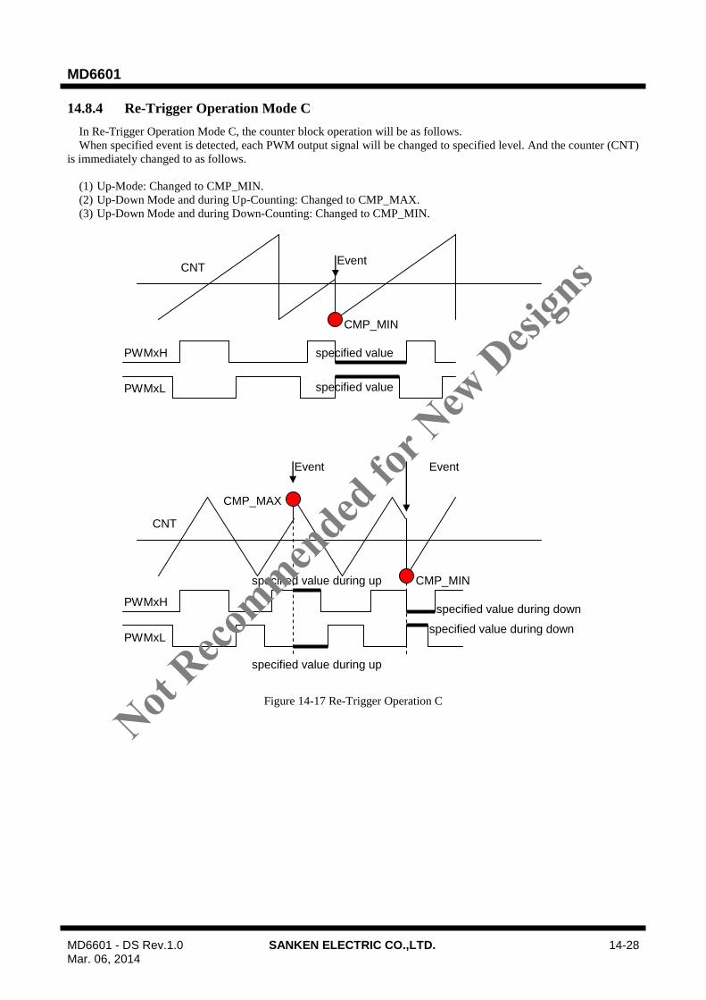
MD6601
MD6601 - DS Rev.1.0 SANKEN ELECTRIC CO.,LTD. 14-28 Mar. 06, 2014
14.8.4 Re-Trigger Operation Mode C
In Re-Trigger Operation Mode C, the counter block operation will be as follows.
When specified event is detected, each PWM output signal will be changed to specified level. And the counter (CNT)
is immediately changed to as follows.
(1) Up-Mode: Changed to CMP_MIN.
(2) Up-Down Mode and during Up-Counting: Changed to CMP_MAX.
(3) Up-Down Mode and during Down-Counting: Changed to CMP_MIN.
Figure 14-17 Re-Trigger Operation C
CNTEvent
PWMxH
PWMxL
specified value
specified value
CNT
CMP_MAX
CMP_MIN
Event Event
PWMxH
PWMxL
specified value during up
specified value during up
specified value during down
specified value during down
CMP_MIN
Not Reco
mmended
for N
ew D
esign
s
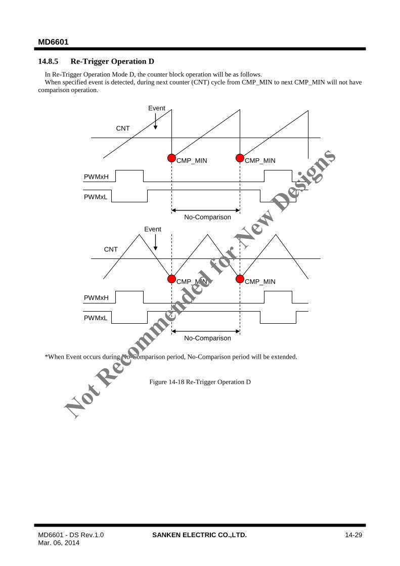
MD6601
MD6601 - DS Rev.1.0 SANKEN ELECTRIC CO.,LTD. 14-29 Mar. 06, 2014
14.8.5 Re-Trigger Operation D
In Re-Trigger Operation Mode D, the counter block operation will be as follows.
When specified event is detected, during next counter (CNT) cycle from CMP_MIN to next CMP_MIN will not have
comparison operation.
*When Event occurs during No-Comparison period, No-Comparison period will be extended.
Figure 14-18 Re-Trigger Operation D
CNT
Event
PWMxH
PWMxL
CMP_MINCMP_MIN
No-Comparison
CNT
Event
PWMxH
PWMxL
CMP_MINCMP_MIN
No-Comparison
Not Reco
mmended
for N
ew D
esign
s

MD6601
MD6601 - DS Rev.1.0 SANKEN ELECTRIC CO.,LTD. 14-30 Mar. 06, 2014
14.8.6 Re-Trigger Mask Operation
Re-Trigger event can be masked (ignored) if user desires. Start point of mask period is selected from output signal
edges (PWMxH or PWMxL, rise or fall). Length of mask period is defined as Cycles of [Count Clock Frequency / 8]
[Count Clock Frequency / 16] or [Count Clock Frequency / 32].
Figure 14-19 Re-Trigger Operation D
14.8.7 Detail method to change Waveform Level by Re-Trigger
According to PWM Mode, the Waveform Levels are changed by following manner.
Specified value VTH is fix level for PWMxH and is determined by seting PWMnRTL.
Specified value VTL is fix level for PWMxL and is determined by seting PWMnRTL.
Table 14-5 Method to change Waveform Level by Re-Trigger
Mode PWMxH PWMxL Note
PWM Mode 0 Immediately Changed to specified
value VTH.
Immediately Changed to specified
value VTL.
PWM Mode 1
Auto Dead Time
Mode 0
Immediately Changed to specified
value VTH.
Start DCNTD from 0 until
CMP_D, and clear it.
If DCND is matched to CMP_D,
changed to VTL.
PWM Mode 1
Auto Dead Time
Mode 1
If DCND is matched to CMP_D,
changed to VTH.
Immediately Changed to specified
value VTL.
Start DCNTD from 0 until
CMP_D, and clear it.
PWM Mode 2 Immediately Changed to specified
value VTH.
Immediately Changed to specified
value VTL.
PWM Mode 3
Auto Dead Time
Mode 0
Immediately Changed to specified
value VTH.
Start DCNTD from 0 until
CMP_D, and clear it.
If DCND is matched to CMP_D,
changed to VTL.
PWM Mode 3
Auto Dead Time
Mode 1
If DCND is matched to CMP_D,
changed to VTH.
Immediately Changed to specified
value VTL.
Start DCNTD from 0 until
CMP_D, and clear it.
Note: For both Up-Mode and Up-Down-Mode.
CNT
planed
Event
PWMxH
PWMxL
specified value
specified value
Event Mask PeriodEvent Mask Period
Event
IGNORED
Not Reco
mmended
for N
ew D
esign
s
MD6601
MD6601 - DS Rev.1.0 SANKEN ELECTRIC CO.,LTD. 14-31 Mar. 06, 2014
14.9 Event Output
Each counter block has 3 event outputs.
PWMn EVENT0
PWMn EVENT1
PWMn TIMERSYNC (which resets Timer’s Counter Value)
Each event can be selected from compare matches shown below.
CMP_MIN
CMP_MAX
VH1 match
VH0 match
VL1 match
VL0 match
Re-trigger(T)
CMP_MIN event does not occur when UP count mode.
14.10 Interrupt Output
Each counter block has 2 interrupt outputs.
PWMnINT0
PWMnINT1
Each interrupt can be selected from compare matches shown below.
CMP_MIN
CMP_MAX
VH1 match
VH0 match
VL1 match
VL0 match
Re-trigger(T)
CMP_MIN interrupt does not occur when UP count mode.
14.11 Register Access
In the module, there are several 16bit registers such as BUF_xx, CMP_xx and CNT. When CPU or DSAC writes to
these register, it should write LSB side register first. In the Low side write operation, the write value is stored in a
dedicated temporary register, and when High side register is written next, the value in temporary register is transferred
to Low side simultaneously. By this scheme, the entire bits in 16bit register are updated at same time.
Regarding 16bit width register of PWM assigned in SFR area, each Low Side (LSB Side) register and High Side
(MSB Side) register for 16bit value is assigned on SAME address.
Regarding 16bit width register of PWM assigned in XDATA-Bus area, each Low Side (LSB Side) register and High
Side (MSB Side) register for 16bit value is assigned independent contiguous address. The Low Side is on lower address,
the High Side is on higher address, which follows Little-Endian manner.
Following operation is still important in Timer Function.
Regarding 16bit width register of PWM assigned in not only SFR area but also Data Area, in write access, 1st writing
on the address reaches to Temporary Register for Low Side and 2nd
writing reaches to High Side. At this 2nd
access,
Temporary and High Side data are transferred to both Low Side and High Side registers. In read access, 1st access gets
Low Side data to the bus and High Side data to temporary register, and then 2nd
read access receives High Side data
from temporary register.
Not Reco
mmended
for N
ew D
esign
s

MD6601
MD6601 - DS Rev.1.0 SANKEN ELECTRIC CO.,LTD. 14-32 Mar. 06, 2014
Figure 14-20 Scheme for writing 16 bit register
PWMnACSTS.XREGACS bit is the write access flag for XBUS register.
When PWMnACSTS.XREGACS=1, the XDATA-Bus register write operation is on-going. The next new write
operation cannot be accepted. PWMnACSTS.XREGACS is set to 1’b1 when one of the PWMnH/LCR0/1,
PWMnMODE, PWMnRTx and the High Side of CNTn, CMP_xxx and BUF_MIN/MAX is written. Please write these
register when PWMnACSTS.XREGACS=0.
PWMnACSTS.SFRACS bit is the write access flag for SFRs. When PWMnACSTS.SFRACS=1, the SFR write
opetration is on-going. PWMnACSTS.XREGACS is set to 1’b1 when the High Side of BUF_A/B/C/D register is
written. BUF_A/B/C/D reisters can be written sequentially only once when PWMnACSTS.SFRACS=1. For example,
writing BUF_Ax_L -> BUF_Ax_H -> BUF_Bx_L -> BUF_Bx_H -> BUF_Cx_L -> BUF_Cx_H -> BUF_Dx_L ->
BUF_Dx_H can be accepted. The re-writing BUF_A/B/C/D register after previous BUF_A/B/C/D register write
operation must be executed after confirming PWMnACSTS.SFRACS=0.
The previous XDATA-Bus register and SFR write operation spends 6 CPUCLKs + 24 PWM counter clocks.
xxx_L xxx_H
Temp for xxx_L
16bit Register
8bit
Not Reco
mmended
for N
ew D
esign
s
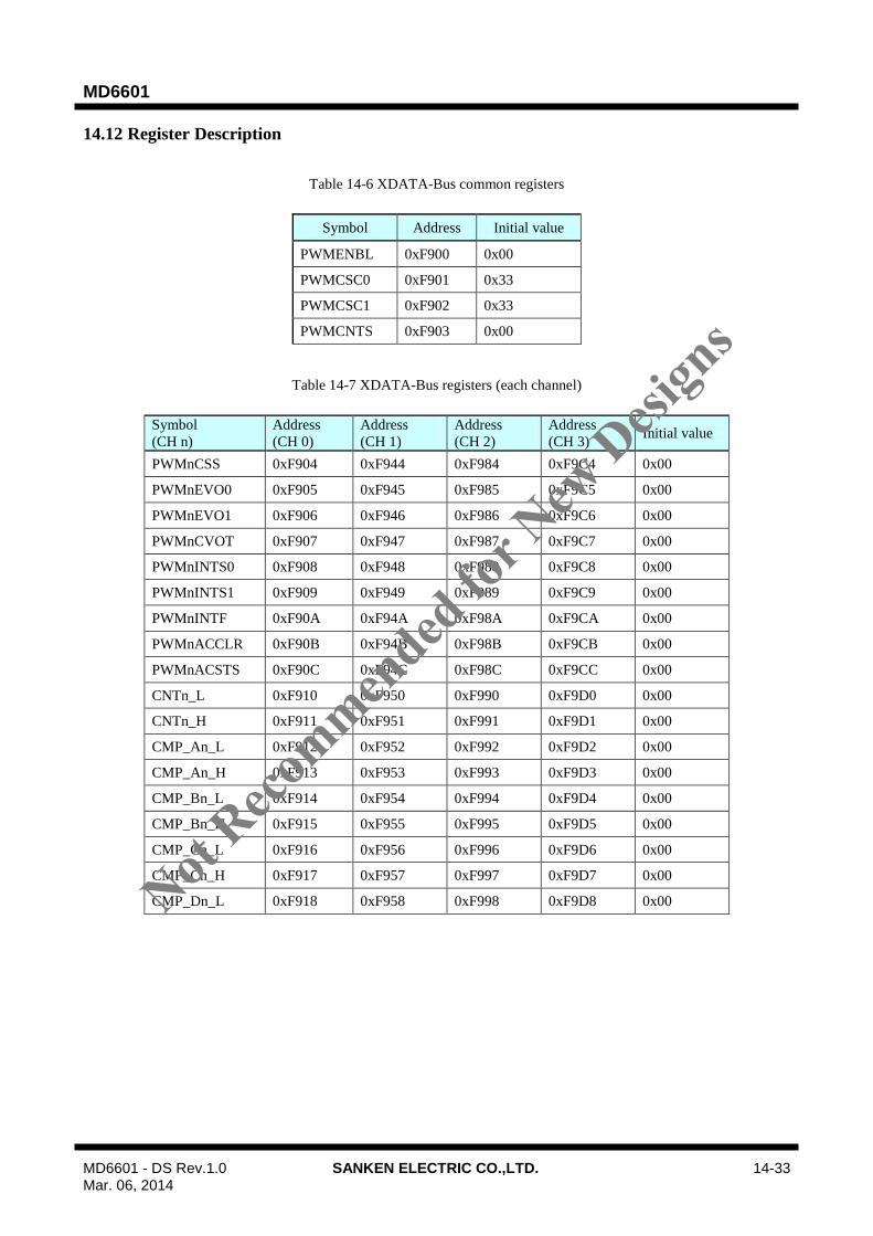
MD6601
MD6601 - DS Rev.1.0 SANKEN ELECTRIC CO.,LTD. 14-33 Mar. 06, 2014
14.12 Register Description
Table 14-6 XDATA-Bus common registers
Symbol Address Initial value
PWMENBL 0xF900 0x00
PWMCSC0 0xF901 0x33
PWMCSC1 0xF902 0x33
PWMCNTS 0xF903 0x00
Table 14-7 XDATA-Bus registers (each channel)
Symbol
(CH n)
Address
(CH 0)
Address
(CH 1)
Address
(CH 2)
Address
(CH 3) Initial value
PWMnCSS 0xF904 0xF944 0xF984 0xF9C4 0x00
PWMnEVO0 0xF905 0xF945 0xF985 0xF9C5 0x00
PWMnEVO1 0xF906 0xF946 0xF986 0xF9C6 0x00
PWMnCVOT 0xF907 0xF947 0xF987 0xF9C7 0x00
PWMnINTS0 0xF908 0xF948 0xF988 0xF9C8 0x00
PWMnINTS1 0xF909 0xF949 0xF989 0xF9C9 0x00
PWMnINTF 0xF90A 0xF94A 0xF98A 0xF9CA 0x00
PWMnACCLR 0xF90B 0xF94B 0xF98B 0xF9CB 0x00
PWMnACSTS 0xF90C 0xF94C 0xF98C 0xF9CC 0x00
CNTn_L 0xF910 0xF950 0xF990 0xF9D0 0x00
CNTn_H 0xF911 0xF951 0xF991 0xF9D1 0x00
CMP_An_L 0xF912 0xF952 0xF992 0xF9D2 0x00
CMP_An_H 0xF913 0xF953 0xF993 0xF9D3 0x00
CMP_Bn_L 0xF914 0xF954 0xF994 0xF9D4 0x00
CMP_Bn_H 0xF915 0xF955 0xF995 0xF9D5 0x00
CMP_Cn_L 0xF916 0xF956 0xF996 0xF9D6 0x00
CMP_Cn_H 0xF917 0xF957 0xF997 0xF9D7 0x00
CMP_Dn_L 0xF918 0xF958 0xF998 0xF9D8 0x00
Not Reco
mmended
for N
ew D
esign
s

MD6601
MD6601 - DS Rev.1.0 SANKEN ELECTRIC CO.,LTD. 14-34 Mar. 06, 2014
Symbol
(CH n)
Address
(CH 0)
Address
(CH 1)
Address
(CH 2)
Address
(CH 3) Initial value
CMP_Dn_H 0xF919 0xF959 0xF999 0xF9D9 0x00
CMP_MINn_L 0xF91A 0xF95A 0xF99A 0xF9DA 0x00
CMP_MINn_H 0xF91B 0xF95B 0xF99B 0xF9DB 0x00
CMP_MAXn_L 0xF91C 0xF95C 0xF99C 0xF9DC 0x00
CMP_MAXn_H 0xF91D 0xF95D 0xF99D 0xF9DD 0x00
PWMnCNTMD 0xF920 0xF960 0xF9A0 0xF9E0 0x00
PWMnHCR0 0xF921 0xF961 0xF9A1 0xF9E1 0x00
PWMnLCR0 0xF922 0xF962 0xF9A2 0xF9E2 0x00
PWMnHCR1 0xF923 0xF963 0xF9A3 0xF9E3 0x00
PWMnLCR1 0xF924 0xF964 0xF9A4 0xF9E4 0x00
PWMnMODE 0xF925 0xF965 0xF9A5 0xF9E5 0x00
PWMnRTRG 0xF926 0xF966 0xF9A6 0xF9E6 0x00
PWMnRTRS 0xF927 0xF967 0xF9A7 0xF9E7 0x00
PWMnRTGC 0xF928 0xF968 0xF9A8 0xF9E8 0x00
PWMnRTL 0xF929 0xF969 0xF9A9 0xF9E9 0x00
PWMnRTMC 0xF92A 0xF96A 0xF9AA 0xF9EA 0x00
PWMnRTMP 0xF92B 0xF96B 0xF9AB 0xF9EB 0x00
BUF_MINn_L 0xF92C 0xF96C 0xF9AC 0xF9EC 0x00
BUF_MINn_H 0xF92D 0xF96D 0xF9AD 0xF9ED 0x00
BUF_MAXn_L 0xF92E 0xF96E 0xF9AE 0xF9EE 0x00
BUF_MAXn_H 0xF92F 0xF96F 0xF9AF 0xF9EF 0x00
Table 14-8 SFRs (each channel)
Symbol
(CH n)
Address
(CH 0)
Address
(CH 1)
Address
(CH 2)
Address
(CH 3) Initial value
BUF_An_L 0xE4 0xEC 0xF4 0xFC 0x00
BUF_An_H 0xE4 0xEC 0xF4 0xFC 0x00
BUF_Bn_L 0xE5 0xED 0xF5 0xFD 0x00
BUF_Bn_H 0xE5 0xED 0xF5 0xFD 0x00
BUF_Cn_L 0xE6 0xEE 0xF6 0xFE 0x00
BUF_Cn_H 0xE6 0xEE 0xF6 0xFE 0x00
BUF_Dn_L 0xE7 0xEF 0xF7 0xFF 0x00
BUF_Dn_H 0xE7 0xEF 0xF7 0xFF 0x00
Not Reco
mmended
for N
ew D
esign
s

MD6601
MD6601 - DS Rev.1.0 SANKEN ELECTRIC CO.,LTD. 14-35 Mar. 06, 2014
14.12.1 PWMENBL
Register PWMENBL PWM Enable Control Address 0xF900
Bit Bit Name R/W Initial Description Note
7 reserved R 0 Read value is 0. Write only 0.
6 reserved R 0 Read value is 0. Write only 0.
5 reserved R 0 Read value is 0. Write only 0.
4 reserved R 0 Read value is 0. Write only 0.
3 PWMDE R/W 0 Enable Counter Clock Source A~D
0: Disable
1: Enable
2 PWMCE R/W 0
1 PWMBE R/W 0
0 PWMAE R/W 0
14.12.2 PWMCSC0
Register PWMCSC0 PWM Clock Source Control 0 Address 0xF901
Bit Bit Name R/W Initial Description Note
7 PWMCCB[3] R/W 0 Clock source B Clock select
Counter Clock Frequency =
PLL2 Clock / (2 ^ PWMCCB[3:0])
(Max 1GHz)
Note: PWMCCB[3:0] should be 0x0~0x8. Do
not set 0x9~0xF.
6 PWMCCB[2] R/W 0
5 PWMCCB[1] R/W 1
4 PWMCCB[0] R/W 1
3 PWMCCA[3] R/W 0 Clock source A Clock select
Counter Clock Frequency =
PLL2 Clock / (2 ^ PWMCCA[3:0])
(Max 1GHz)
Note: PWMCCA[3:0] should be 0x0~0x8. Do
not set 0x9~0xF.
2 PWMCCA[2] R/W 0
1 PWMCCA[1] R/W 1
0 PWMCCA[0] R/W 1
Not Reco
mmended
for N
ew D
esign
s
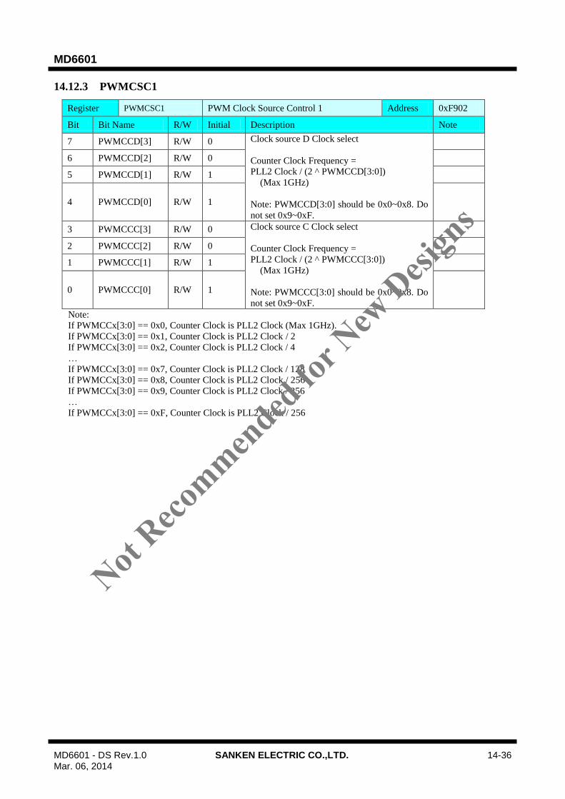
MD6601
MD6601 - DS Rev.1.0 SANKEN ELECTRIC CO.,LTD. 14-36 Mar. 06, 2014
14.12.3 PWMCSC1
Register PWMCSC1 PWM Clock Source Control 1 Address 0xF902
Bit Bit Name R/W Initial Description Note
7 PWMCCD[3] R/W 0 Clock source D Clock select
Counter Clock Frequency =
PLL2 Clock / (2 ^ PWMCCD[3:0])
(Max 1GHz)
Note: PWMCCD[3:0] should be 0x0~0x8. Do
not set 0x9~0xF.
6 PWMCCD[2] R/W 0
5 PWMCCD[1] R/W 1
4 PWMCCD[0] R/W 1
3 PWMCCC[3] R/W 0 Clock source C Clock select
Counter Clock Frequency =
PLL2 Clock / (2 ^ PWMCCC[3:0])
(Max 1GHz)
Note: PWMCCC[3:0] should be 0x0~0x8. Do
not set 0x9~0xF.
2 PWMCCC[2] R/W 0
1 PWMCCC[1] R/W 1
0 PWMCCC[0] R/W 1
Note:
If PWMCCx[3:0] == 0x0, Counter Clock is PLL2 Clock (Max 1GHz).
If PWMCCx[3:0] == 0x1, Counter Clock is PLL2 Clock / 2
If PWMCCx[3:0] == 0x2, Counter Clock is PLL2 Clock / 4
…
If PWMCCx[3:0] == 0x7, Counter Clock is PLL2 Clock / 128
If PWMCCx[3:0] == 0x8, Counter Clock is PLL2 Clock / 256
If PWMCCx[3:0] == 0x9, Counter Clock is PLL2 Clock / 256
…
If PWMCCx[3:0] == 0xF, Counter Clock is PLL2 Clock / 256
Not Reco
mmended
for N
ew D
esign
s
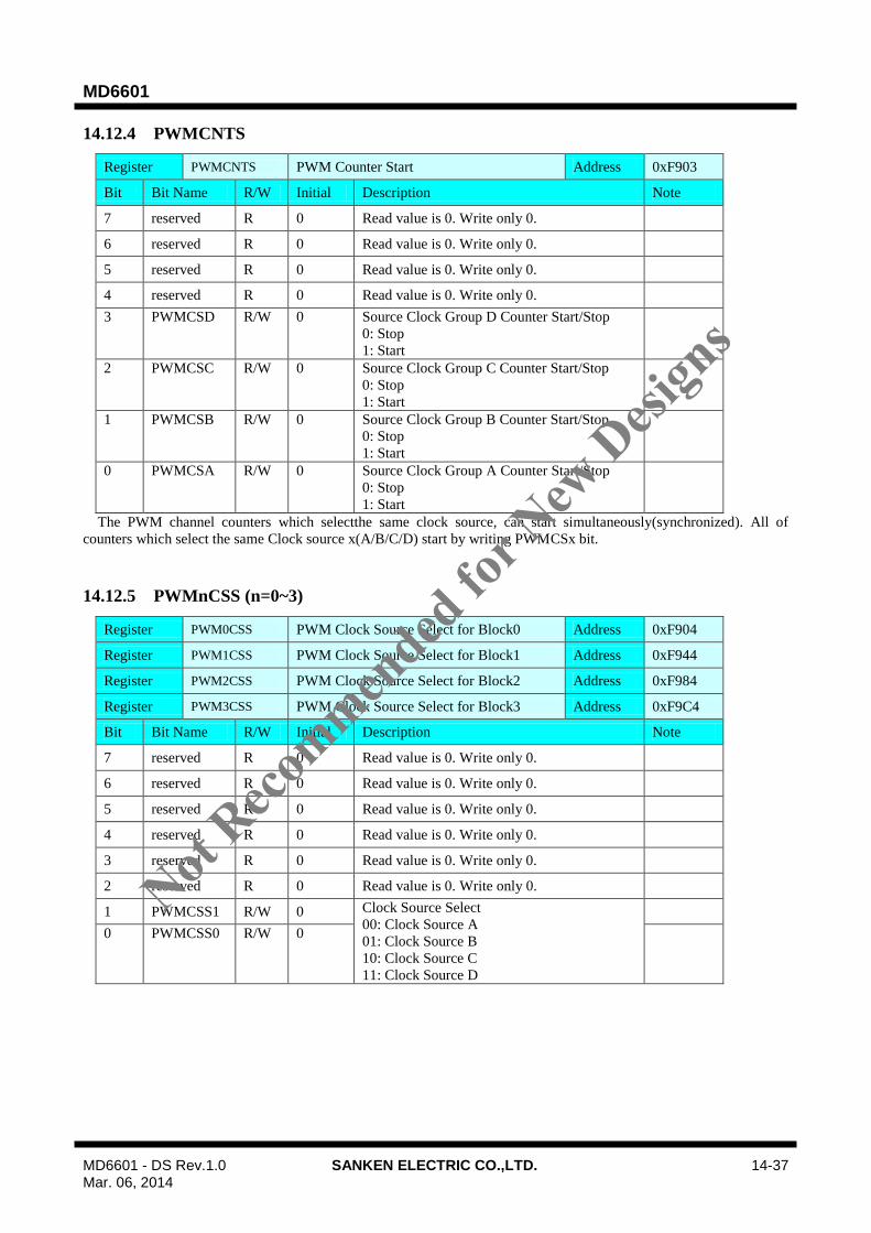
MD6601
MD6601 - DS Rev.1.0 SANKEN ELECTRIC CO.,LTD. 14-37 Mar. 06, 2014
14.12.4 PWMCNTS
Register PWMCNTS PWM Counter Start Address 0xF903
Bit Bit Name R/W Initial Description Note
7 reserved R 0 Read value is 0. Write only 0.
6 reserved R 0 Read value is 0. Write only 0.
5 reserved R 0 Read value is 0. Write only 0.
4 reserved R 0 Read value is 0. Write only 0.
3 PWMCSD R/W 0 Source Clock Group D Counter Start/Stop
0: Stop
1: Start
2 PWMCSC R/W 0 Source Clock Group C Counter Start/Stop
0: Stop
1: Start
1 PWMCSB R/W 0 Source Clock Group B Counter Start/Stop
0: Stop
1: Start
0 PWMCSA
R/W 0 Source Clock Group A Counter Start/Stop
0: Stop
1: Start
The PWM channel counters which selectthe same clock source, can start simultaneously(synchronized). All of
counters which select the same Clock source x(A/B/C/D) start by writing PWMCSx bit.
14.12.5 PWMnCSS (n=0~3)
Register PWM0CSS PWM Clock Source Select for Block0 Address 0xF904
Register PWM1CSS PWM Clock Source Select for Block1 Address 0xF944
Register PWM2CSS PWM Clock Source Select for Block2 Address 0xF984
Register PWM3CSS PWM Clock Source Select for Block3 Address 0xF9C4
Bit Bit Name R/W Initial Description Note
7 reserved R 0 Read value is 0. Write only 0.
6 reserved R 0 Read value is 0. Write only 0.
5 reserved R 0 Read value is 0. Write only 0.
4 reserved R 0 Read value is 0. Write only 0.
3 reserved R 0 Read value is 0. Write only 0.
2 reserved R 0 Read value is 0. Write only 0.
1 PWMCSS1 R/W 0 Clock Source Select
00: Clock Source A
01: Clock Source B
10: Clock Source C
11: Clock Source D
0 PWMCSS0 R/W 0
Not Reco
mmended
for N
ew D
esign
s
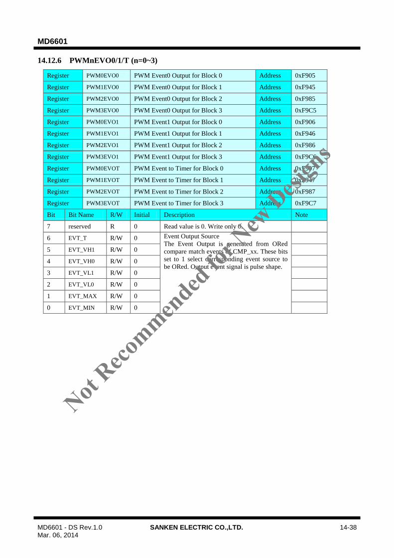
MD6601
MD6601 - DS Rev.1.0 SANKEN ELECTRIC CO.,LTD. 14-38 Mar. 06, 2014
14.12.6 PWMnEVO0/1/T (n=0~3)
Register PWM0EVO0 PWM Event0 Output for Block 0 Address 0xF905
Register PWM1EVO0 PWM Event0 Output for Block 1 Address 0xF945
Register PWM2EVO0 PWM Event0 Output for Block 2 Address 0xF985
Register PWM3EVO0 PWM Event0 Output for Block 3 Address 0xF9C5
Register PWM0EVO1 PWM Event1 Output for Block 0 Address 0xF906
Register PWM1EVO1 PWM Event1 Output for Block 1 Address 0xF946
Register PWM2EVO1 PWM Event1 Output for Block 2 Address 0xF986
Register PWM3EVO1 PWM Event1 Output for Block 3 Address 0xF9C6
Register PWM0EVOT PWM Event to Timer for Block 0 Address 0xF907
Register PWM1EVOT PWM Event to Timer for Block 1 Address 0xF947
Register PWM2EVOT PWM Event to Timer for Block 2 Address 0xF987
Register PWM3EVOT PWM Event to Timer for Block 3 Address 0xF9C7
Bit Bit Name R/W Initial Description Note
7 reserved R 0 Read value is 0. Write only 0.
6 EVT_T R/W 0 Event Output Source
The Event Output is generated from ORed
compare match events of CMP_xx. These bits
set to 1 select corresponding event source to
be ORed. Output event signal is pulse shape.
5 EVT_VH1 R/W 0
4 EVT_VH0 R/W 0
3 EVT_VL1 R/W 0
2 EVT_VL0 R/W 0
1 EVT_MAX R/W 0
0 EVT_MIN R/W 0
Not Reco
mmended
for N
ew D
esign
s

MD6601
MD6601 - DS Rev.1.0 SANKEN ELECTRIC CO.,LTD. 14-39 Mar. 06, 2014
14.12.7 PWMnINTS0/1(n=0~3)
Register PWM0INTS0 PWM Interrupt 0 Select for Block 0 Address 0xF908
Register PWM1INTS0 PWM Interrupt 0 Select for Block 1 Address 0xF948
Register PWM2INTS0 PWM Interrupt 0 Select for Block 2 Address 0xF988
Register PWM3INTS0 PWM Interrupt 0 Select for Block 3 Address 0xF9C8
Register PWM0INTS1 PWM Interrupt 1 Select for Block 0 Address 0xF909
Register PWM1INTS1 PWM Interrupt 1 Select for Block 1 Address 0xF949
Register PWM1INTS1 PWM Interrupt 1 Select for Block 2 Address 0xF989
Register PWM2INTS1 PWM Interrupt 1 Select for Block 3 Address 0xF9C9
Bit Bit Name R/W Initial Description Note
7 reserved R 0 Read value is 0. Write only 0.
6 INT_T R/W 0 Interrupt Source
The Interrupt Flag is set from ORed compare
match events of CMP_xx. These bits set to 1
select corresponding interrupt source to be
ORed.
5 INT_VH1 R/W 0
4 INT_VH0 R/W 0
3 INT_VL1 R/W 0
2 INT_VL0 R/W 0
1 INT_MAX R/W 0
0 INT_MIN R/W 0
Not Reco
mmended
for N
ew D
esign
s
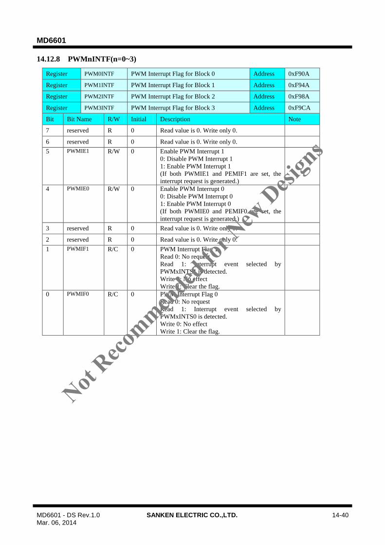
MD6601
MD6601 - DS Rev.1.0 SANKEN ELECTRIC CO.,LTD. 14-40 Mar. 06, 2014
14.12.8 PWMnINTF(n=0~3)
Register PWM0INTF PWM Interrupt Flag for Block 0 Address 0xF90A
Register PWM1INTF PWM Interrupt Flag for Block 1 Address 0xF94A
Register PWM2INTF PWM Interrupt Flag for Block 2 Address 0xF98A
Register PWM3INTF PWM Interrupt Flag for Block 3 Address 0xF9CA
Bit Bit Name R/W Initial Description Note
7 reserved R 0 Read value is 0. Write only 0.
6 reserved R 0 Read value is 0. Write only 0.
5 PWMIE1 R/W 0 Enable PWM Interrupt 1
0: Disable PWM Interrupt 1
1: Enable PWM Interrupt 1
(If both PWMIE1 and PEMIF1 are set, the
interrupt request is generated.)
4 PWMIE0 R/W 0 Enable PWM Interrupt 0
0: Disable PWM Interrupt 0
1: Enable PWM Interrupt 0
(If both PWMIE0 and PEMIF0 are set, the
interrupt request is generated.)
3 reserved R 0 Read value is 0. Write only 0.
2 reserved R 0 Read value is 0. Write only 0.
1 PWMIF1 R/C 0 PWM Interrupt Flag 1
Read 0: No request
Read 1: Interrupt event selected by
PWMxINTS1 is detected.
Write 0: No effect
Write 1: Clear the flag.
0 PWMIF0 R/C 0 PWM Interrupt Flag 0
Read 0: No request
Read 1: Interrupt event selected by
PWMxINTS0 is detected.
Write 0: No effect
Write 1: Clear the flag.
Not Reco
mmended
for N
ew D
esign
s

MD6601
MD6601 - DS Rev.1.0 SANKEN ELECTRIC CO.,LTD. 14-41 Mar. 06, 2014
14.12.9 PWMnACCLR (n=0~3)
Register PWM0ACCL
R
PWM Access Counter Clear Register for
Block0
Address 0xF90B
Register PWM1ACCL
R
PWM Access Counter Clear Register for
Block1
Address 0xF94B
Register PWM2ACCL
R
PWM Access Counter Clear Register for
Block2
Address 0xF98B
Register PWM3ACCL
R
PWM Access Counter Clear Register for
Block3
Address 0xF9CB
Bit Bit Name R/W Initial Description Note
7 CLRCPUACC W 0 Clear SFR Access counter for CPU
0: No effect
1: Register CPU Access counter clear
Read : No Request
Write 0: No effect
Write 1: Clear Register CPU Access counter.
(Clear SFR access counter for CPU.)
6 CLRDSAACC W 0 Clear SFR Access counter for DSAC
0: No effect
1: Register DSAC Access counter clear
Read : No Request
Write 0: No effect
Write 1: Clear Register DSAC Access counter.
(Clear SFR access counter for DSAC.)
5 reserved R 0 Read value is 0. Write only 0.
4 reserved R 0 Read value is 0. Write only 0.
3 reserved R 0 Read value is 0. Write only 0.
2 reserved R 0 Read value is 0. Write only 0.
1 reserved R 0 Read value is 0. Write only 0.
0 reserved R 0 Read value is 0. Write only 0.
Not Reco
mmended
for N
ew D
esign
s

MD6601
MD6601 - DS Rev.1.0 SANKEN ELECTRIC CO.,LTD. 14-42 Mar. 06, 2014
14.12.10 PWMnACSTS (n=0~3)
Register PWM0ACSTS PWM Access Status Register for Block0 Address 0xF90C
Register PWM1ACSTS PWM Access Status Register for Block1 Address 0xF94C
Register PWM2ACSTS PWM Access Status Register for Block2 Address 0xF98C
Register PWM3ACSTS PWM Access Status Register for Block3 Address 0xF9CC
Bit Bit Name R/W Initial Description Note
7 reserved R 0 Read value is 0. Write only 0.
6 reserved R 0 Read value is 0. Write only 0.
5 reserved R 0 Read value is 0. Write only 0.
4 reserved R 0 Read value is 0. Write only 0.
3 reserved R 0 Read value is 0. Write only 0.
2 reserved R 0 Read value is 0. Write only 0.
1 SFRACS R 0 SFR Access flag
0: Not accessing a SFR
1: Writing a SFR
In case of writing the same SFR sequentially,
the folloing write access must be issued after
confirming SFRACS=0.
0 XREGACS R 0 REG Access flag
0: Not accessing a SFR
1: Writing a SFR
Please confirm XREGACS=0 before writing
to XBUS register.
Not Reco
mmended
for N
ew D
esign
s

MD6601
MD6601 - DS Rev.1.0 SANKEN ELECTRIC CO.,LTD. 14-43 Mar. 06, 2014
14.12.11 CNTn(n=0~3)
Register CNT0_L Counter 0 LSB Side Address 0xF910
Register CNT1_L Counter 1 LSB Side Address 0xF950
Register CNT2_L Counter 2 LSB Side Address 0xF990
Register CNT3_L Counter 3 LSB Side Address 0xF9D0
Bit Bit Name R/W Initial Description Note
7:0 CNT[7:0] R/W 0 Counter LSB Side
Register CNT0_H Counter 0 MSB Side Address 0xF911
Register CNT1_H Counter 1 MSB Side Address 0xF951
Register CNT2_H Counter 2 MSB Side Address 0xF991
Register CNT3_H Counter 3 MSB Side Address 0xF9D1
Bit Bit Name R/W Initial Description Note
7:0 CNT[15:8] R/W 0 Counter MSB Side
Note: Address assignment for xxx_H and xxx_L should be based on “14.11 Register Access”. Other registers should
follow same manner.
Do not write this register during PWMnACSTS.XREGACS=1.
Not Reco
mmended
for N
ew D
esign
s

MD6601
MD6601 - DS Rev.1.0 SANKEN ELECTRIC CO.,LTD. 14-44 Mar. 06, 2014
14.12.12 CMP_xxxn(n=0~3)
Register CMP_MIN0_L CMP_MIN for Block 0 LSB Side Address 0xF91A
Register CMP_MIN1_L CMP_MIN for Block 1 LSB Side Address 0xF95A
Register CMP_MIN2_L CMP_MIN for Block 2 LSB Side Address 0xF99A
Register CMP_MIN3_L CMP_MIN for Block 3 LSB Side Address 0xF9DA
Register CMP_MAX0_L CMP_MAX for Block 0 LSB Side Address 0xF91C
Register CMP_MAX1_L CMP_MAX for Block 1 LSB Side Address 0xF95C
Register CMP_MAX2_L CMP_MAX for Block 2 LSB Side Address 0xF99C
Register CMP_MAX3_L CMP_MAX for Block 3 LSB Side Address 0xF9DC
Register CMP_A0_L CMP_A for Block 0 LSB Side Address 0xF912
Register CMP_A1_L CMP_A for Block 1 LSB Side Address 0xF952
Register CMP_A2_L CMP_A for Block 2 LSB Side Address 0xF992
Register CMP_A3_L CMP_A for Block 3 LSB Side Address 0xF9D2
Register CMP_B0_L CMP_B for Block 0 LSB Side Address 0xF914
Register CMP_B1_L CMP_B for Block 1 LSB Side Address 0xF954
Register CMP_B2_L CMP_B for Block 2 LSB Side Address 0xF994
Register CMP_B3_L CMP_B for Block 3 LSB Side Address 0xF9D4
Register CMP_C0_L CMP_C for Block 0 LSB Side Address 0xF916
Register CMP_C1_L CMP_C for Block 1 LSB Side Address 0xF956
Register CMP_C2_L CMP_C for Block 2 LSB Side Address 0xF996
Register CMP_C3_L CMP_C for Block 3 LSB Side Address 0xF9D6
Register CMP_D0_L CMP_D for Block 0 LSB Side Address 0xF918
Register CMP_D1_L CMP_D for Block 1 LSB Side Address 0xF958
Register CMP_D2_L CMP_D for Block 2 LSB Side Address 0xF998
Register CMP_D3_L CMP_D for Block 3 LSB Side Address 0xF9D8
Bit Bit Name R/W Initial Description Note
7:0 CMP_xxx
[7:0] R/W 0 CMP_xxx LSB Side
Do not write this register during PWMnACSTS.XREGACS=1.
Not Reco
mmended
for N
ew D
esign
s

MD6601
MD6601 - DS Rev.1.0 SANKEN ELECTRIC CO.,LTD. 14-45 Mar. 06, 2014
Register CMP_MIN0_H CMP_MIN for Block 0 MSB Side Address 0xF91B
Register CMP_MIN1_H CMP_MIN for Block 1 MSB Side Address 0xF95B
Register CMP_MIN2_H CMP_MIN for Block 2 MSB Side Address 0xF99B
Register CMP_MIN3_H CMP_MIN for Block 3 MSB Side Address 0xF9DB
Register CMP_MAX0_H CMP_MAX for Block 0 MSB Side Address 0xF91D
Register CMP_MAX1_H CMP_MAX for Block 1 MSB Side Address 0xF95D
Register CMP_MAX2_H CMP_MAX for Block 2 MSB Side Address 0xF99D
Register CMP_MAX3_H CMP_MAX for Block 3 MSB Side Address 0xF9DD
Register CMP_A0_H CMP_A for Block 0 MSB Side Address 0xF913
Register CMP_A1_H CMP_A for Block 1 MSB Side Address 0xF953
Register CMP_A2_H CMP_A for Block 2 MSB Side Address 0xF993
Register CMP_A3_H CMP_A for Block 3 MSB Side Address 0xF9D3
Register CMP_B0_H CMP_B for Block 0 MSB Side Address 0xF915
Register CMP_B1_H CMP_B for Block 1 MSB Side Address 0xF955
Register CMP_B2_H CMP_B for Block 2 MSB Side Address 0xF995
Register CMP_B3_H CMP_B for Block 3 MSB Side Address 0xF9D5
Register CMP_C0_H CMP_C for Block 0 MSB Side Address 0xF917
Register CMP_C1_H CMP_C for Block 1 MSB Side Address 0xF957
Register CMP_C2_H CMP_C for Block 2 MSB Side Address 0xF997
Register CMP_C3_H CMP_C for Block 3 MSB Side Address 0xF9D7
Register CMP_D0_H CMP_D for Block 0 MSB Side Address 0xF919
Register CMP_D1_H CMP_D for Block 1 MSB Side Address 0xF959
Register CMP_D2_H CMP_D for Block 2 MSB Side Address 0xF999
Register CMP_D3_H CMP_D for Block 3 MSB Side Address 0xF9D9
Bit Bit Name R/W Initial Description Note
7:0 CMP_xxx
[15:8] R/W 0 CMP_xxx MSB Side
Do not write this register during PWMnACSTS.XREGACS=1.
Not Reco
mmended
for N
ew D
esign
s
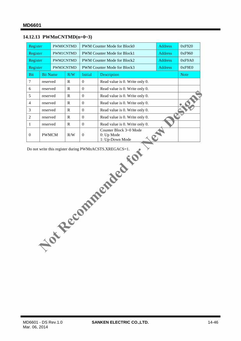
MD6601
MD6601 - DS Rev.1.0 SANKEN ELECTRIC CO.,LTD. 14-46 Mar. 06, 2014
14.12.13 PWMnCNTMD(n=0~3)
Register PWM0CNTMD PWM Counter Mode for Block0 Address 0xF920
Register PWM1CNTMD PWM Counter Mode for Block1 Address 0xF960
Register PWM2CNTMD PWM Counter Mode for Block2 Address 0xF9A0
Register PWM3CNTMD PWM Counter Mode for Block3 Address 0xF9E0
Bit Bit Name R/W Initial Description Note
7 reserved R 0 Read value is 0. Write only 0.
6 reserved R 0 Read value is 0. Write only 0.
5 reserved R 0 Read value is 0. Write only 0.
4 reserved R 0 Read value is 0. Write only 0.
3 reserved R 0 Read value is 0. Write only 0.
2 reserved R 0 Read value is 0. Write only 0.
1 reserved R 0 Read value is 0. Write only 0.
0 PWMCM R/W 0
Counter Block 3~0 Mode
0: Up Mode
1: Up-Down Mode
Do not write this register during PWMnACSTS.XREGACS=1.
Not Reco
mmended
for N
ew D
esign
s

MD6601
MD6601 - DS Rev.1.0 SANKEN ELECTRIC CO.,LTD. 14-47 Mar. 06, 2014
14.12.14 PWMnHCR0(n=0~3)
Register PWM0HCR0 PWM0H Output Control 0 Address 0xF921
Register PWM1HCR0 PWM1H Output Control 0 Address 0xF961
Register PWM2HCR0 PWM2H Output Control 0 Address 0xF9A1
Register PWM3HCR0 PWM3H Output Control 0 Address 0xF9E1
Bit Bit Name R/W Initial Description Note
7 PWM_MAX1 R/W 0 Output Control at CMP_MAX match for
PWMxH
00: No Change (NOP)
01: Set Low
10: Set High
11: Toggle
6 PWM_MAX0 R/W 0
5 PWM_MIN1 R/W 0 Output Control at CMP_MIN match for
PWMxH. Effective only in up-down counter
mode.
00: No Change (NOP)
01: Set Low
10: Set High
11: Toggle
4 PWM_MIN0 R/W 0
3 reserved R 0 Read value is 0. Write only 0.
2 reserved R 0 Read value is 0. Write only 0.
1 PWM_SET1 W 0 Initialize Output Level for PWMxH
00: No Change (NOP)
01: Set Low
10: Set High
11: do not write
Write to these bits will change output level
with the higher priority than any other
compare matches which change output level.
Read values of these bits are always Zero.
0 PWM_SET0 W 0
Do not write this register during PWMnACSTS.XREGACS=1.
Not Reco
mmended
for N
ew D
esign
s
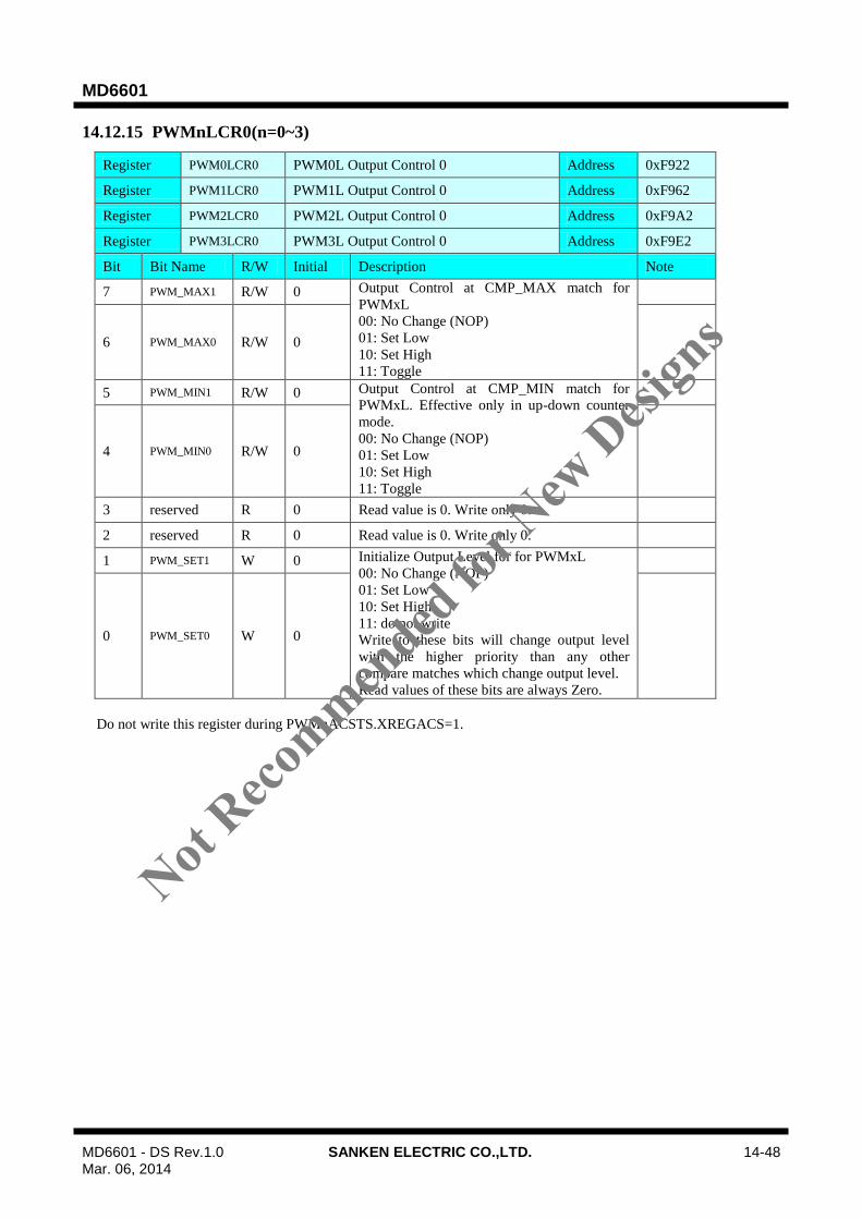
MD6601
MD6601 - DS Rev.1.0 SANKEN ELECTRIC CO.,LTD. 14-48 Mar. 06, 2014
14.12.15 PWMnLCR0(n=0~3)
Register PWM0LCR0 PWM0L Output Control 0 Address 0xF922
Register PWM1LCR0 PWM1L Output Control 0 Address 0xF962
Register PWM2LCR0 PWM2L Output Control 0 Address 0xF9A2
Register PWM3LCR0 PWM3L Output Control 0 Address 0xF9E2
Bit Bit Name R/W Initial Description Note
7 PWM_MAX1 R/W 0 Output Control at CMP_MAX match for
PWMxL
00: No Change (NOP)
01: Set Low
10: Set High
11: Toggle
6 PWM_MAX0 R/W 0
5 PWM_MIN1 R/W 0 Output Control at CMP_MIN match for
PWMxL. Effective only in up-down counter
mode.
00: No Change (NOP)
01: Set Low
10: Set High
11: Toggle
4 PWM_MIN0 R/W 0
3 reserved R 0 Read value is 0. Write only 0.
2 reserved R 0 Read value is 0. Write only 0.
1 PWM_SET1 W 0 Initialize Output Level for for PWMxL
00: No Change (NOP)
01: Set Low
10: Set High
11: do not write
Write to these bits will change output level
with the higher priority than any other
compare matches which change output level.
Read values of these bits are always Zero.
0 PWM_SET0 W 0
Do not write this register during PWMnACSTS.XREGACS=1.
Not Reco
mmended
for N
ew D
esign
s

MD6601
MD6601 - DS Rev.1.0 SANKEN ELECTRIC CO.,LTD. 14-49 Mar. 06, 2014
14.12.16 PWMnHCR1 (n=0~3)
Register PWM0HCR1 PWM0H Output Control 1 Address 0xF923
Register PWM1HCR1 PWM1H Output Control 1 Address 0xF963
Register PWM2HCR1 PWM2H Output Control 1 Address 0xF9A3
Register PWM3HCR1 PWM3H Output Control 1 Address 0xF9E3
Bit Bit Name R/W Initial Description Note
7 reserved R 0 Read value is 0. Write only 0.
6 reserved R 0 Read value is 0. Write only 0.
5 reserved R 0 Read value is 0. Write only 0.
4 reserved R 0 Read value is 0. Write only 0.
3 VH1[1] R/W 0 Output Level VH1
00: No Change (NOP)
01: Set Low
10: Set High
11: Toggle
2 VH1[0] R/W 0
1 VH0[1] R/W 0 Output Level VH0
00: No Change (NOP)
01: Set Low
10: Set High
11: Toggle
0 VH0[0] R/W 0
Do not write this register during PWMnACSTS.XREGACS=1.
14.12.17 PWMnLCR1 (n=0~3)
Register PWM0LCR1 PWM0L Output Control 1 Address 0xF924
Register PWM1LCR1 PWM1L Output Control 1 Address 0xF964
Register PWM2LCR1 PWM2L Output Control 1 Address 0xF9A4
Register PWM3LCR1 PWM3L Output Control 1 Address 0xF9E4
Bit Bit Name R/W Initial Description Note
7 reserved R 0 Read value is 0. Write only 0.
6 reserved R 0 Read value is 0. Write only 0.
5 reserved R 0 Read value is 0. Write only 0.
4 reserved R 0 Read value is 0. Write only 0.
3 VL1[1] R/W 0 Output Level VL1
00: No Change (NOP)
01: Set Low
10: Set High
11: Toggle
2 VL1[0] R/W 0
1 VL0[1] R/W 0 Output Level VL0
00: No Change (NOP)
01: Set Low
10: Set High
11: Toggle
0 VL0[0] R/W 0
Do not write this register during PWMnACSTS.XREGACS=1.
Not Reco
mmended
for N
ew D
esign
s

MD6601
MD6601 - DS Rev.1.0 SANKEN ELECTRIC CO.,LTD. 14-50 Mar. 06, 2014
14.12.18 PWMnMODE (n=0~3)
Register PWM0MODE PWM0 Operation Mode Address 0xF925
Register PWM1MODE PWM1 Operation Mode Address 0xF965
Register PWM2MODE PWM2 Operation Mode Address 0xF9A5
Register PWM3MODE PWM3 Operation Mode Address 0xF9E5
Bit Bit Name R/W Initial Description Note
7 ADM R/W 0 Auto Dead Time Mode
0: Auto Dead Time Mode 0
1: Auto Dead Time Mode 1
(Effective only in PWM Mode 1, 3)
6 BUFM R/W 0 Buffer Mode
0: Direct Mode
1: Buffer Mode
(Effective only in PWM Mode 0, 1)
(PWM Mode 2, 3 are usually in Buffer Mode
regardless of this bit.)
5 UDMB1 R/W 0 Buffering Timing in Up-Down Mode
In Up-Down Mode, specify which timings are
the transfer timing from BUFxx to CMPxx.
{PWMxBT1:PWMxBT0}
00: reserved
01: Top Timing
10: Bottom Timing
11: Both Top and Bottom Timing
This field has its meaning only in Up-Down
Mode and Buffer Mode.
Note: In Up Mode, transfer timing from
BUFxx to CMPxx is only at the counter clear
timing.
4 UDBM0 R/W 0
3 reserved R 0 Read value is 0. Write only 0.
2 reserved R 0 Read value is 0. Write only 0.
1 PWMMD1 R/W 0 PWM Mode
00: PWM Mode 0
01: PWM Mode 1
10: PWM Mode 2
11: PWM Mode 3
0 PWMMD0 R/W 0
Do not write this register during PWMnACSTS.XREGACS=1.
Not Reco
mmended
for N
ew D
esign
s
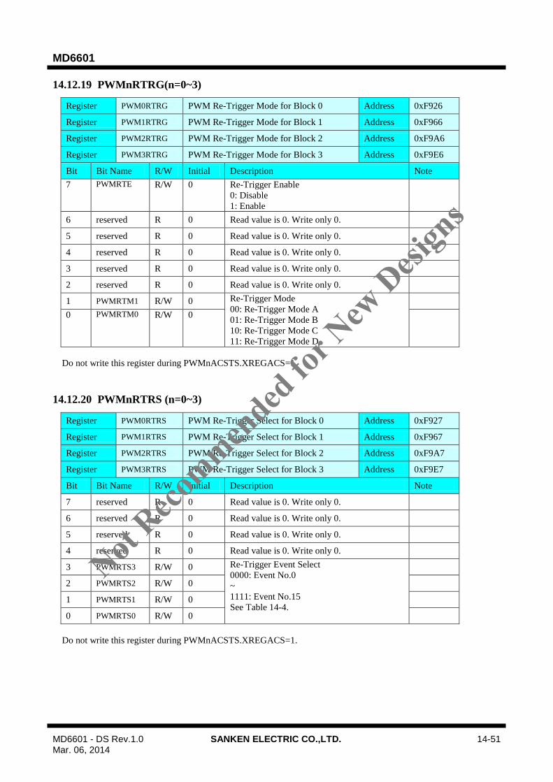
MD6601
MD6601 - DS Rev.1.0 SANKEN ELECTRIC CO.,LTD. 14-51 Mar. 06, 2014
14.12.19 PWMnRTRG(n=0~3)
Register PWM0RTRG PWM Re-Trigger Mode for Block 0 Address 0xF926
Register PWM1RTRG PWM Re-Trigger Mode for Block 1 Address 0xF966
Register PWM2RTRG PWM Re-Trigger Mode for Block 2 Address 0xF9A6
Register PWM3RTRG PWM Re-Trigger Mode for Block 3 Address 0xF9E6
Bit Bit Name R/W Initial Description Note
7 PWMRTE R/W 0 Re-Trigger Enable
0: Disable
1: Enable
6 reserved R 0 Read value is 0. Write only 0.
5 reserved R 0 Read value is 0. Write only 0.
4 reserved R 0 Read value is 0. Write only 0.
3 reserved R 0 Read value is 0. Write only 0.
2 reserved R 0 Read value is 0. Write only 0.
1 PWMRTM1 R/W 0 Re-Trigger Mode
00: Re-Trigger Mode A
01: Re-Trigger Mode B
10: Re-Trigger Mode C
11: Re-Trigger Mode D
0 PWMRTM0 R/W 0
Do not write this register during PWMnACSTS.XREGACS=1.
14.12.20 PWMnRTRS (n=0~3)
Register PWM0RTRS PWM Re-Trigger Select for Block 0 Address 0xF927
Register PWM1RTRS PWM Re-Trigger Select for Block 1 Address 0xF967
Register PWM2RTRS PWM Re-Trigger Select for Block 2 Address 0xF9A7
Register PWM3RTRS PWM Re-Trigger Select for Block 3 Address 0xF9E7
Bit Bit Name R/W Initial Description Note
7 reserved R 0 Read value is 0. Write only 0.
6 reserved R 0 Read value is 0. Write only 0.
5 reserved R 0 Read value is 0. Write only 0.
4 reserved R 0 Read value is 0. Write only 0.
3 PWMRTS3 R/W 0 Re-Trigger Event Select
0000: Event No.0
~
1111: Event No.15
See Table 14-4.
2 PWMRTS2 R/W 0
1 PWMRTS1 R/W 0
0 PWMRTS0 R/W 0
Do not write this register during PWMnACSTS.XREGACS=1.
Not Reco
mmended
for N
ew D
esign
s
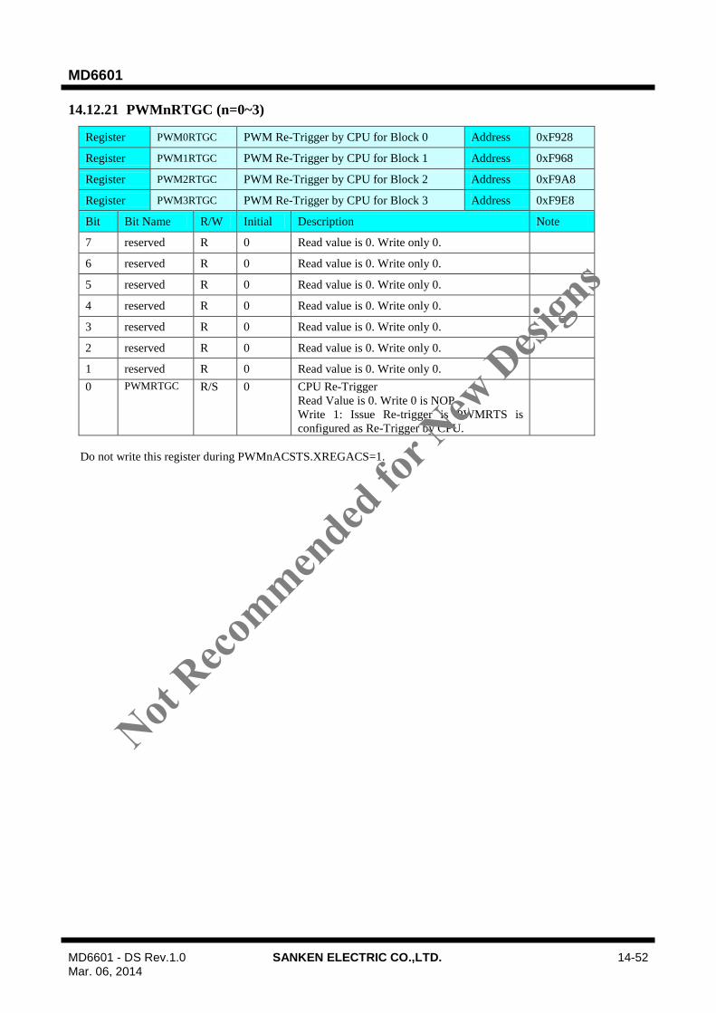
MD6601
MD6601 - DS Rev.1.0 SANKEN ELECTRIC CO.,LTD. 14-52 Mar. 06, 2014
14.12.21 PWMnRTGC (n=0~3)
Register PWM0RTGC PWM Re-Trigger by CPU for Block 0 Address 0xF928
Register PWM1RTGC PWM Re-Trigger by CPU for Block 1 Address 0xF968
Register PWM2RTGC PWM Re-Trigger by CPU for Block 2 Address 0xF9A8
Register PWM3RTGC PWM Re-Trigger by CPU for Block 3 Address 0xF9E8
Bit Bit Name R/W Initial Description Note
7 reserved R 0 Read value is 0. Write only 0.
6 reserved R 0 Read value is 0. Write only 0.
5 reserved R 0 Read value is 0. Write only 0.
4 reserved R 0 Read value is 0. Write only 0.
3 reserved R 0 Read value is 0. Write only 0.
2 reserved R 0 Read value is 0. Write only 0.
1 reserved R 0 Read value is 0. Write only 0.
0 PWMRTGC R/S 0 CPU Re-Trigger
Read Value is 0. Write 0 is NOP
Write 1: Issue Re-trigger is PWMRTS is
configured as Re-Trigger by CPU.
Do not write this register during PWMnACSTS.XREGACS=1.
Not Reco
mmended
for N
ew D
esign
s
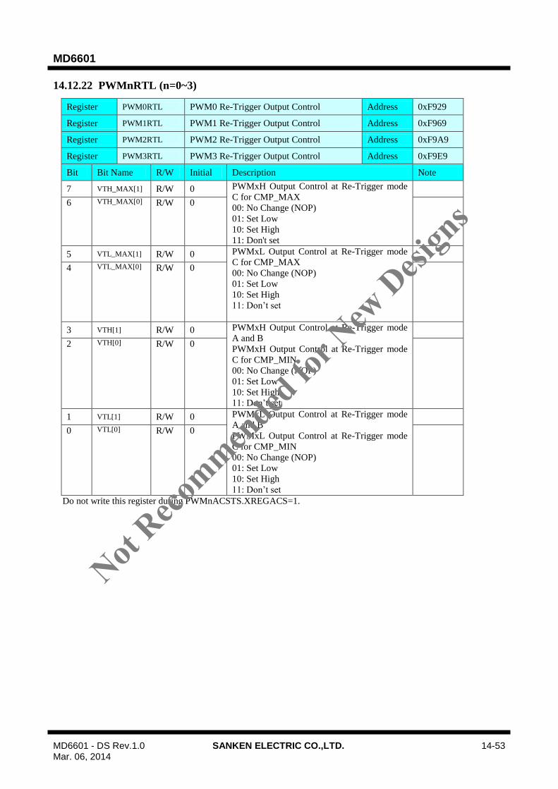
MD6601
MD6601 - DS Rev.1.0 SANKEN ELECTRIC CO.,LTD. 14-53 Mar. 06, 2014
14.12.22 PWMnRTL (n=0~3)
Register PWM0RTL PWM0 Re-Trigger Output Control Address 0xF929
Register PWM1RTL PWM1 Re-Trigger Output Control Address 0xF969
Register PWM2RTL PWM2 Re-Trigger Output Control Address 0xF9A9
Register PWM3RTL PWM3 Re-Trigger Output Control Address 0xF9E9
Bit Bit Name R/W Initial Description Note
7 VTH_MAX[1] R/W 0 PWMxH Output Control at Re-Trigger mode
C for CMP_MAX
00: No Change (NOP)
01: Set Low
10: Set High
11: Don't set
6 VTH_MAX[0] R/W 0
5 VTL_MAX[1] R/W 0 PWMxL Output Control at Re-Trigger mode
C for CMP_MAX
00: No Change (NOP)
01: Set Low
10: Set High
11: Don’t set
4 VTL_MAX[0] R/W 0
3 VTH[1] R/W 0 PWMxH Output Control at Re-Trigger mode
A and B
PWMxH Output Control at Re-Trigger mode
C for CMP_MIN
00: No Change (NOP)
01: Set Low
10: Set High
11: Don’t set
2 VTH[0] R/W 0
1 VTL[1] R/W 0 PWMxL Output Control at Re-Trigger mode
A and B
PWMxL Output Control at Re-Trigger mode
C for CMP_MIN
00: No Change (NOP)
01: Set Low
10: Set High
11: Don’t set
0 VTL[0] R/W 0
Do not write this register during PWMnACSTS.XREGACS=1.
Not Reco
mmended
for N
ew D
esign
s

MD6601
MD6601 - DS Rev.1.0 SANKEN ELECTRIC CO.,LTD. 14-54 Mar. 06, 2014
14.12.23 PWMnRTMC (n=0~3)
Register PWM0RTMC PWM0 Re-Trigger Mask Control Address 0xF92A
Register PWM1RTMC PWM1 Re-Trigger Mask Control Address 0xF96A
Register PWM2RTMC PWM2 Re-Trigger Mask Control Address 0xF9AA
Register PWM3RTMC PWM3 Re-Trigger Mask Control Address 0xF9EA
Bit Bit Name R/W Initial Description Note
7 RTME R/W 0 Re-Trigger Mask Enable
0: Disable, 1: Enable
6 reserved R 0 Read value is 0. Write only 0.
5 reserved R 0 Read value is 0. Write only 0.
4 reserved R 0 Read value is 0. Write only 0.
3 RTMC1 R/W 0 Re-Trigger Period Clock Source
00: [Count Clock Frequency / 8]
01: [Count Clock Frequency / 16]
10: [Count Clock Frequency / 32]
11: Reserved
2 RTMC0 R/W 0
1 RTMS1 R/W 0 Re-Trigger Mask Start Point
00: from PWMxH Rising Edge
01: from PWMxH Falling Edge
10: from PWMxL Rising Edge
11: from PWMxL Falling Edge
0 RTMS0 R/W 0
Do not write this register during PWMnACSTS.XREGACS=1.
14.12.24 PWMnRTMP (n=0~3)
Register PWM0RTMP PWM0 Re-Trigger Mask Period Address 0xF92B
Register PWM1RTMP PWM1 Re-Trigger Mask Period Address 0xF96B
Register PWM2RTMP PWM2 Re-Trigger Mask Period Address 0xF9AB
Register PWM3RTMP PWM3 Re-Trigger Mask Period Address 0xF9EB
Bit Bit Name R/W Initial Description Note
7 RTMP7 R/W 0 Re-Trigger Mask Period
Period = Cycle of Clock Source (specified by
RTMC[1:0])
x (RTMP[7:0] + 1)
6 RTMP6 R/W 0
5 RTMP5 R/W 0
4 RTMP4 R/W 0
3 RTMP3 R/W 0
2 RTMP2 R/W 0
1 RTMP1 R/W 0
0 RTMP0 R/W 0
Do not write this register during PWMnACSTS.XREGACS=1.
Not Reco
mmended
for N
ew D
esign
s

MD6601
MD6601 - DS Rev.1.0 SANKEN ELECTRIC CO.,LTD. 14-55 Mar. 06, 2014
14.12.25 BUF_MIN/MAXn(n=0~3)
Register BUF_MIN0_L BUF_MIN for Block 0 LSB Side Address 0xF92C
Register BUF_MIN1_L BUF_MIN for Block 1 LSB Side Address 0xF96C
Register BUF_MIN2_L BUF_MIN for Block 2 LSB Side Address 0xF9AC
Register BUF_MIN3_L BUF_MIN for Block 3 LSB Side Address 0xF9EC
Register BUF_MAX0_L BUF_MAX for Block 0 LSB Side Address 0xF92E
Register BUF_MAX1_L BUF_MAX for Block 1 LSB Side Address 0xF96E
Register BUF_MAX2_L BUF_MAX for Block 2 LSB Side Address 0xF9AE
Register BUF_MAX3_L BUF_MAX for Block 3 LSB Side Address 0xF9EE
Bit Bit Name R/W Initial Description Note
7:0 BUF_xxx
[7:0] R/W 0 BUF_xxx LSB Side
Do not write this register during PWMnACSTS.XREGACS=1.
Register BUF_MIN0_H BUF_MIN for Block 0 MSB Side Address 0xF92D
Register BUF_MIN1_H BUF_MIN for Block 1 MSB Side Address 0xF96D
Register BUF_MIN2_H BUF_MIN for Block 2 MSB Side Address 0xF9AD
Register BUF_MIN3_H BUF_MIN for Block 3 MSB Side Address 0xF9ED
Register BUF_MAX0_H BUF_MAX for Block 0 MSB Side Address 0xF92F
Register BUF_MAX1_H BUF_MAX for Block 1 MSB Side Address 0xF96F
Register BUF_MAX2_H BUF_MAX for Block 2 MSB Side Address 0xF9AF
Register BUF_MAX3_H BUF_MAX for Block 3 MSB Side Address 0xF9EF
Bit Bit Name R/W Initial Description Note
7:0 BUF_xxx
[15:8] R/W 0 BUF_xxx MSB Side
Do not write this register during PWMnACSTS.XREGACS=1.
Not Reco
mmended
for N
ew D
esign
s

MD6601
MD6601 - DS Rev.1.0 SANKEN ELECTRIC CO.,LTD. 14-56 Mar. 06, 2014
14.12.26 BUF_A/B/C/Dn (n=0~3)
Register BUF_A0_L BUF_A for Block 0 LSB Side Address 0xE4
Register BUF_A1_L BUF_A for Block 1 LSB Side Address 0xEC
Register BUF_A2_L BUF_A for Block 2 LSB Side Address 0xF4
Register BUF_A3_L BUF_A for Block 3 LSB Side Address 0xFC
Register BUF_B0_L BUF_B for Block 0 LSB Side Address 0xE5
Register BUF_B1_L BUF_B for Block 1 LSB Side Address 0xED
Register BUF_B2_L BUF_B for Block 2 LSB Side Address 0xF5
Register BUF_B3_L BUF_B for Block 3 LSB Side Address 0xFD
Register BUF_C0_L BUF_C for Block 0 LSB Side Address 0xE6
Register BUF_C1_L BUF_C for Block 1 LSB Side Address 0xEE
Register BUF_C2_L BUF_C for Block 2 LSB Side Address 0xF6
Register BUF_C3_L BUF_C for Block 3 LSB Side Address 0xFE
Register BUF_D0_L BUF_D for Block 0 LSB Side Address 0xE7
Register BUF_D1_L BUF_D for Block 1 LSB Side Address 0xEF
Register BUF_D2_L BUF_D for Block 2 LSB Side Address 0xF7
Register BUF_D3_L BUF_D for Block 3 LSB Side Address 0xFF
Bit Bit Name R/W Initial Description Note
7:0 BUF_xxx
[7:0] R/W 0 BUF_xxx LSB Side
Not Reco
mmended
for N
ew D
esign
s

MD6601
MD6601 - DS Rev.1.0 SANKEN ELECTRIC CO.,LTD. 14-57 Mar. 06, 2014
Register BUF_A0_H BUF_A for Block 0 MSB Side Address 0xE4
Register BUF_A1_H BUF_A for Block 1 MSB Side Address 0xEC
Register BUF_A2_H BUF_A for Block 2 MSB Side Address 0xF4
Register BUF_A3_H BUF_A for Block 3 MSB Side Address 0xFC
Register BUF_B0_H BUF_B for Block 0 MSB Side Address 0xE5
Register BUF_B1_H BUF_B for Block 1 MSB Side Address 0xED
Register BUF_B2_H BUF_B for Block 2 MSB Side Address 0xF5
Register BUF_B3_H BUF_B for Block 3 MSB Side Address 0xFD
Register BUF_C0_H BUF_C for Block 0 MSB Side Address 0xE6
Register BUF_C1_H BUF_C for Block 1 MSB Side Address 0xEE
Register BUF_C2_H BUF_C for Block 2 MSB Side Address 0xF6
Register BUF_C3_H BUF_C for Block 3 MSB Side Address 0xFE
Register BUF_D0_H BUF_D for Block 0 MSB Side Address 0xE7
Register BUF_D1_H BUF_D for Block 1 MSB Side Address 0xEF
Register BUF_D2_H BUF_D for Block 2 MSB Side Address 0xF7
Register BUF_D3_H BUF_D for Block 3 MSB Side Address 0xFF
Bit Bit Name R/W Initial Description Note
7:0 BUF_xxx
[15:8] R/W 0 BUF_xxx MSB Side
BUF_xn_H/L registers are mapped same address. The first access to its address is for BUF_xn_L, the second access
is for BUF_xn_H.
In case of writing the same SFR sequentially, the following write access must be issued after confirming SFRACS=0.
PWMnACSSTS.SFRSTS does not become 1 by writing to BUF_xn_L register.
Not Reco
mmended
for N
ew D
esign
s
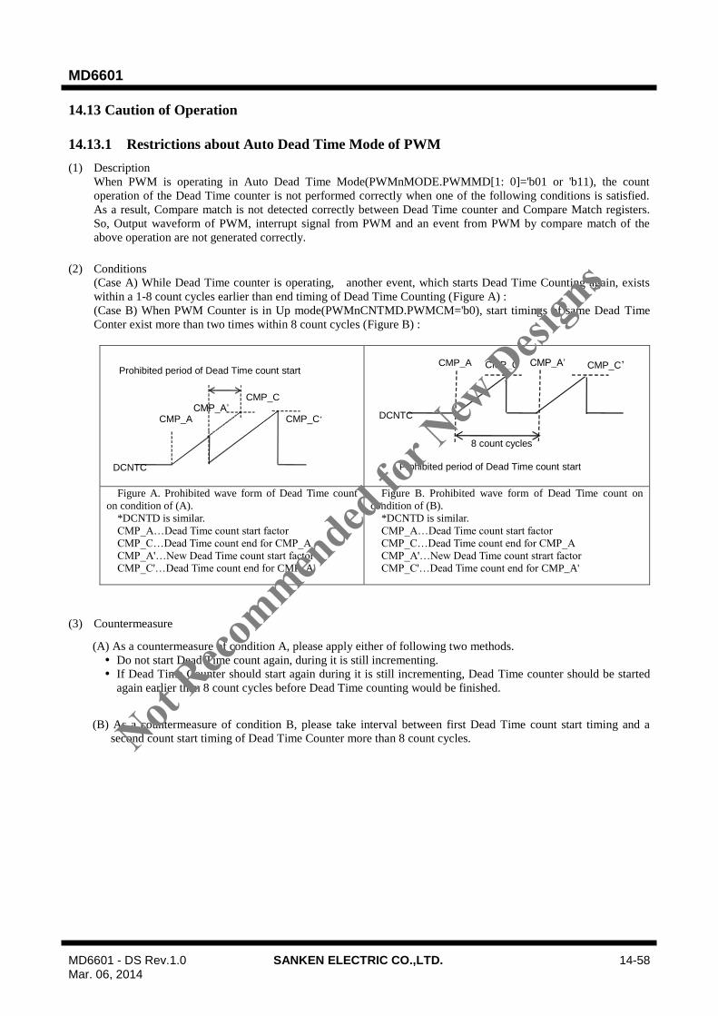
MD6601
MD6601 - DS Rev.1.0 SANKEN ELECTRIC CO.,LTD. 14-58 Mar. 06, 2014
14.13 Caution of Operation
14.13.1 Restrictions about Auto Dead Time Mode of PWM
(1) Description
When PWM is operating in Auto Dead Time Mode(PWMnMODE.PWMMD[1: 0]='b01 or 'b11), the count
operation of the Dead Time counter is not performed correctly when one of the following conditions is satisfied.
As a result, Compare match is not detected correctly between Dead Time counter and Compare Match registers.
So, Output waveform of PWM, interrupt signal from PWM and an event from PWM by compare match of the
above operation are not generated correctly.
(2) Conditions
(Case A) While Dead Time counter is operating, another event, which starts Dead Time Counting again, exists
within a 1-8 count cycles earlier than end timing of Dead Time Counting (Figure A) :
(Case B) When PWM Counter is in Up mode(PWMnCNTMD.PWMCM='b0), start timings of same Dead Time
Conter exist more than two times within 8 count cycles (Figure B) :
Figure A. Prohibited wave form of Dead Time count
on condition of (A).
*DCNTD is similar.
CMP_A…Dead Time count start factor
CMP_C…Dead Time count end for CMP_A
CMP_A'…New Dead Time count start factor
CMP_C'…Dead Time count end for CMP_A'
Figure B. Prohibited wave form of Dead Time count on
condition of (B).
*DCNTD is similar.
CMP_A…Dead Time count start factor
CMP_C…Dead Time count end for CMP_A
CMP_A'…New Dead Time count strart factor
CMP_C'…Dead Time count end for CMP_A'
(3) Countermeasure
(A) As a countermeasure of condition A, please apply either of following two methods.
Do not start Dead Time count again, during it is still incrementing.
If Dead Time Counter should start again during it is still incrementing, Dead Time counter should be started
again earlier than 8 count cycles before Dead Time counting would be finished.
(B) As a countermeasure of condition B, please take interval between first Dead Time count start timing and a
second count start timing of Dead Time Counter more than 8 count cycles.
CMP_A
DCNTC
CMP_C’ CMP_A’ CMP_C
8 count cycles
Prohibited period of Dead Time count start
CMP_A
DCNTC
CMP_C CMP_A’
CMP_C’
Prohibited period of Dead Time count start
Not Reco
mmended
for N
ew D
esign
s
MD6601
MD6601 - DS Rev.1.0 SANKEN ELECTRIC CO.,LTD. 14-59 Mar. 06, 2014
14.13.2 Restriction about PWM Mode 2/3 (Phase Shift Mode)
(1) Description
When PWM is used in Mode 2 or 3 (PWMnMODE.PWMMD[1:0] ='b01 or 'b11), Update of CMP_B by
CMP_A match and Update of CMP_D by CMP_C may not be expected if the following conditions are met.
(2) Conditions
(A) When the differences between CMP_MIN register and CMP_A/C register are smaller than 8 counts;
CMP_A/C - CMP_MIN <8
(B) When the value of CMP_A and BUF_A register are not equal, or the value of CMP_C register and BUF_C
register are not equal.
(CMP_A ! = BUF__A) or (CMP_C !=BUF_C)
(3) Countermeasure
Please configure that CMP_A and CMP_C register meet the following conditions.
i) CMP_A - CMP_MIN >= 8
ii) CMP_C - CMP_MIN >= 8
PWM Mode2 and 3 work in Buffer Mode. Therefore, it is necessary for the BUF_A and BUF_C register to meet
the following conditions.
iii) BUF_A - CMP_MIN >= 8
iv) BUF_C - CMP_MIN >= 8
The value of BUF_MIN register is copied to CMP_MIN register when CNT==CMP_MAX. Therefore, please also
set the BUF_MIN with satisfying above conditions (i~iv) while PWM is operating.
Not Reco
mmended
for N
ew D
esign
s
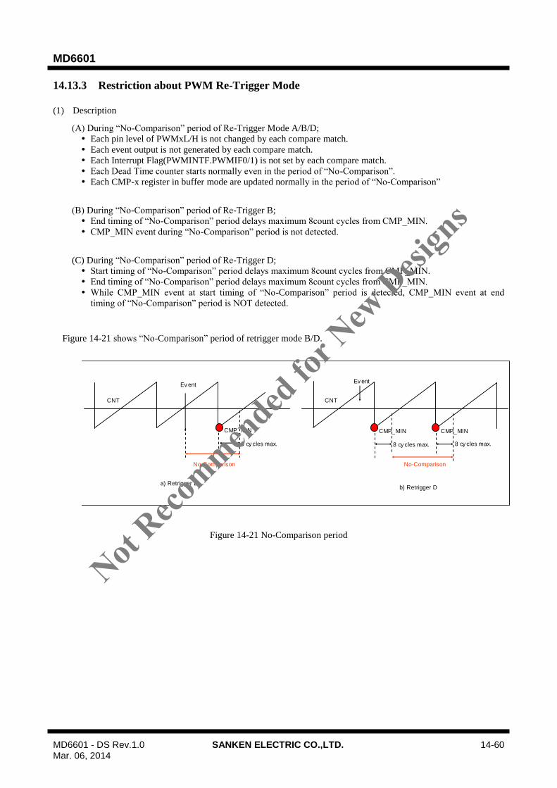
MD6601
MD6601 - DS Rev.1.0 SANKEN ELECTRIC CO.,LTD. 14-60 Mar. 06, 2014
14.13.3 Restriction about PWM Re-Trigger Mode
(1) Description
(A) During “No-Comparison” period of Re-Trigger Mode A/B/D;
Each pin level of PWMxL/H is not changed by each compare match.
Each event output is not generated by each compare match.
Each Interrupt Flag(PWMINTF.PWMIF0/1) is not set by each compare match.
Each Dead Time counter starts normally even in the period of “No-Comparison”.
Each CMP-x register in buffer mode are updated normally in the period of “No-Comparison”
(B) During “No-Comparison” period of Re-Trigger B;
End timing of “No-Comparison” period delays maximum 8count cycles from CMP_MIN.
CMP_MIN event during “No-Comparison” period is not detected.
(C) During “No-Comparison” period of Re-Trigger D;
Start timing of “No-Comparison” period delays maximum 8count cycles from CMP_MIN.
End timing of “No-Comparison” period delays maximum 8count cycles from CMP_MIN.
While CMP_MIN event at start timing of “No-Comparison” period is detected, CMP_MIN event at end
timing of “No-Comparison” period is NOT detected.
Figure 14-21 shows “No-Comparison” period of retrigger mode B/D.
Figure 14-21 No-Comparison period
CNT
Ev ent
No-Comparison
CMP_MIN
8 cy cles max.
CNT
Ev ent
CMP_MINCMP_MIN
No-Comparison
8 cy cles max.8 cy cles max.
a) Retrigger Bb) Retrigger D
Not Reco
mmended
for N
ew D
esign
s

MD6601
MD6601 - DS Rev.1.0 SANKEN ELECTRIC CO.,LTD. 14-61 Mar. 06, 2014
14.13.4 Restriction about PWM Re-Trigger Mask
(1) Description
The start timing of Re-Trigger Mask is 4-20 count cycles earlier than toggle timing of PWM output pin which is
selected by PWMxRTMC.RTMS[1:0] bit.
Figure 14-22 Retrigger Mask Timing
Control logic which judges the start of Re-Trigger Mask does not directly watch toggle operation of PWM output
terminal itself, but watches internal state of PWM module.
This internal state reflects PWM output terminal after more than 4 count cycles at least.
The maximum delay between the internal state for PWM toggle control and start timing of Re-Trigger Mask is about
20 count cycles, which depends on semiconductor process, power supply voltage and ambient temperature, though.
Please set the Re-Trigger Mask procedure with considering above.
PWMxH
Retrigger Mask
PWMxRTMC.RTMS[1:0]=2'b00(In case of PWMH rising)
4-20 count cycles
Start masking Release masking
PWMxRTMC/PWMxRTMPMask period set by the register.
Not Reco
mmended
for N
ew D
esign
s

MD6601
MD6601 - DS Rev.1.0 SANKEN ELECTRIC CO.,LTD. 15-1 Mar. 06, 2014
15. Watch Dog Timer
15.1 Overview
Overview of the WDT module is described below.
WDT is a timer that monitors timer counter to prevent system from clash.
There is the watchdog timer mode and interval timer mode.
In watchdog timer mode, if timer overflows, internal modules are reset.
In interval timer mode, if timer overflows, interval timer interrupt is generated.
It is necessary for WDT to set a predetermined value to the guard register, because the register will not be rewritten
easily.
Maximum time to overflow the counter takes about 11 seconds at CLKSLOW=25MHz.
Figure 15-1 WDT Block Diagram
15.2 Register Description
Table 15-1 WDT Control Registers
Symbol Name Address initial
value
WTCNT Watchdog Timer Counter 0xFE80 0x00
WTCSR Watchdog Timer Control/Status 0xFE81 0x00
WTGRD Watchdog Timer Reg. access GUARD 0xFE82 0x00
Divider
Clock Selector
WTCNT WTCSR
WTGRD
Interrupt
Control
Reset
Control
Int05_n
Reset (to CPU)
Reset
(from 1-wire OCD)
overflow
CLKSLOW
XDATA-Bus *Resets refer to Figure 4-1
Not Reco
mmended
for N
ew D
esign
s
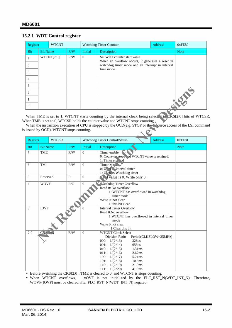
MD6601
MD6601 - DS Rev.1.0 SANKEN ELECTRIC CO.,LTD. 15-2 Mar. 06, 2014
15.2.1 WDT Control register
Register WTCNT Watchdog Timer Counter Address 0xFE80
Bit Bit Name R/W Initial Description Note
7 WTCNT[7:0] R/W 0 Set WDT counter start value.
When an overflow occurs, it generates a reset in
watchdog timer mode and an interrupt in interval
time mode.
6
5
4
3
2
1
0
When TME is set to 1, WTCNT starts counting by the internal clock being selected in CKS[2:0] bits of WTCSR.
When TME is set to 0, WTCSR holds the counter value and WTCNT stops counting.
When the instruction execution of CPU is stopped by the OCD(e.g. STOP or the resource access of the LSI command
is issued by OCD), WTCNT stops counting.
Register WTCSR Watchdog Timer Control/Status Address 0xFE81
Bit Bit Name R/W Initial Description Note
7 TME R/W 0 Timer enable
0: Count-up stops and WTCNT value is retained.
1: Timer enabled
6 TM R/W 0 Timer Mode
0: Used as Interval timer
1: Used as Watchdog timer
5 Reserved R 0 Read value is 0. Write only 0.
4 WOVF R/C 0 Watchdog Timer Overflow
Read 0: No overflow
1: WTCNT has overflowed in watchdog
timer mode
Write 0: not clear
1: this bit clear
3 IOVF R/C 0 Interval Timer Overflow
Read 0:No overflow
1:WTCNT has overflowed in interval timer
mode
Write 0:not clear
1:Clear this bit
2-0 CKS[2:0] R/W 0 WTCNT Clock Select
Division Ratio Period(CLKSLOW=25MHz)
000: 1/(2^13) 328us
001: 1/(2^14) 655us
010: 1/(2^15) 1.31ms
011: 1/(2^16) 2.62ms
100: 1/(2^17) 5.24ms
101: 1/(2^18) 10.5ms
110: 1/(2^19) 21.0ms
111: 1/(2^20) 41.9ms
Before switching the CKS[2:0], TME is cleared to 0, and WTCNT is stops counting.
When WTCNT overflows, xOVF is not initialized by the FLC_RST_N(WDT_INT_N). Therefore,
WOVF(IOVF) must be cleared after FLC_RST_N(WDT_INT_N) negated.
Not Reco
mmended
for N
ew D
esign
s
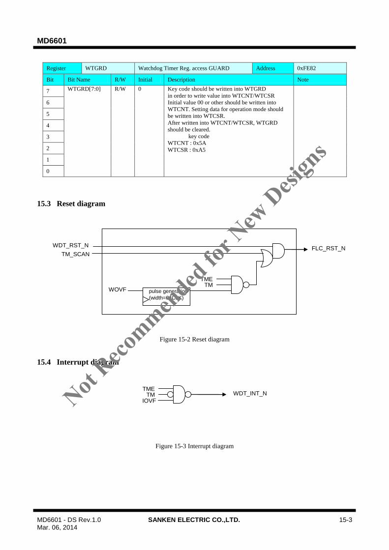
MD6601
MD6601 - DS Rev.1.0 SANKEN ELECTRIC CO.,LTD. 15-3 Mar. 06, 2014
Register WTGRD Watchdog Timer Reg. access GUARD Address 0xFE82
Bit Bit Name R/W Initial Description Note
7 WTGRD[7:0] R/W 0 Key code should be written into WTGRD
in order to write value into WTCNT/WTCSR
Initial value 00 or other should be written into
WTCNT. Setting data for operation mode should
be written into WTCSR.
After written into WTCNT/WTCSR, WTGRD
should be cleared.
key code
WTCNT : 0x5A
WTCSR : 0xA5
6
5
4
3
2
1
0
15.3 Reset diagram
Figure 15-2 Reset diagram
15.4 Interrupt diagram
Figure 15-3 Interrupt diagram
WDT_INT_N TME
TM IOVF
FLC_RST_N WDT_RST_N
TM_SCAN
TME TM
WOVF pulse generation
(width=64CLK)
Not Reco
mmended
for N
ew D
esign
s

MD6601
MD6601 - DS Rev.1.0 SANKEN ELECTRIC CO.,LTD. 15-4 Mar. 06, 2014
15.5 Prescaler
Figure 15-4 Time Chart of Prescaler
Figure 15-5 Prescaler operation
10
clk
cnt_up
CPU
execution
TME
div_cnt 15 0 1 15
5WTCNT 6
010
clk
cnt_up
CPU
execution
TME
div_cnt 15 0 1 15
5WTCNT 6
0
div_sel14
div_sel13
div_sel19
div_sel20
divider ( counter)
・・・
CKS[2:0]
cnt_up
WTCNT
Not Reco
mmended
for N
ew D
esign
s
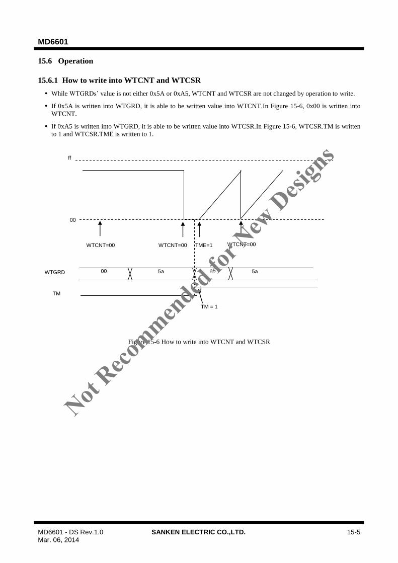
MD6601
MD6601 - DS Rev.1.0 SANKEN ELECTRIC CO.,LTD. 15-5 Mar. 06, 2014
15.6 Operation
15.6.1 How to write into WTCNT and WTCSR
While WTGRDs’ value is not either 0x5A or 0xA5, WTCNT and WTCSR are not changed by operation to write.
If 0x5A is written into WTGRD, it is able to be written value into WTCNT.In Figure 15-6, 0x00 is written into
WTCNT.
If 0xA5 is written into WTGRD, it is able to be written value into WTCSR.In Figure 15-6, WTCSR.TM is written
to 1 and WTCSR.TME is written to 1.
Figure 15-6 How to write into WTCNT and WTCSR
WTCNT=00
00
ff
WTGRD 00
WTCNT=00
a5
WTCNT=00
TM
5a 5a
TME=1
TM = 1
Not Reco
mmended
for N
ew D
esign
s
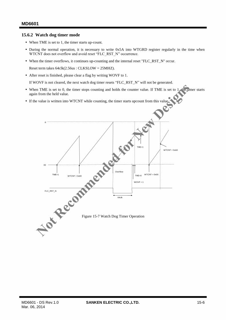
MD6601
MD6601 - DS Rev.1.0 SANKEN ELECTRIC CO.,LTD. 15-6 Mar. 06, 2014
15.6.2 Watch dog timer mode
When TME is set to 1, the timer starts up-count.
During the normal operation, it is necessary to write 0x5A into WTGRD register regularly in the time when
WTCNT does not overflow and avoid reset “FLC_RST_N” occurrence.
When the timer overflows, it continues up-counting and the internal reset "FLC_RST_N" occur.
Reset term takes 64clk(2.56us : CLKSLOW = 25MHZ).
After reset is finished, please clear a flag by writing WOVF to 1.
If WOVF is not cleared, the next watch dog timer resets “FLC_RST_N” will not be generated.
When TME is set to 0, the timer stops counting and holds the counter value. If TME is set to 1, the timer starts
again from the held value.
If the value is written into WTCNT while counting, the timer starts upcount from this value.
00
Overflow
WTCNT = 0x00
ff
TME=0TME=1
FLC_RST_N
64clk
WTCNT = 0xA0
WTCNT = 0x00
TME=1
WOVF = 1
Figure 15-7 Watch Dog Timer Operation
Not Reco
mmended
for N
ew D
esign
s
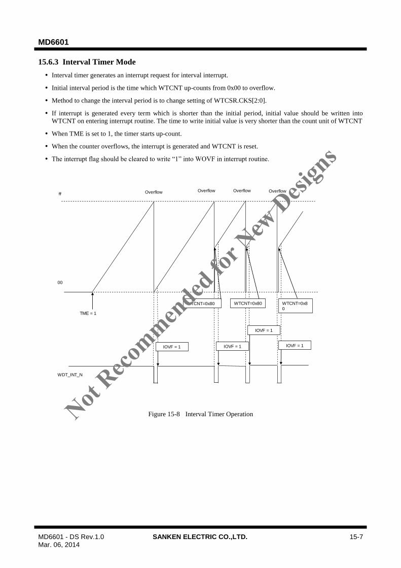
MD6601
MD6601 - DS Rev.1.0 SANKEN ELECTRIC CO.,LTD. 15-7 Mar. 06, 2014
15.6.3 Interval Timer Mode
Interval timer generates an interrupt request for interval interrupt.
Initial interval period is the time which WTCNT up-counts from 0x00 to overflow.
Method to change the interval period is to change setting of WTCSR.CKS[2:0].
If interrupt is generated every term which is shorter than the initial period, initial value should be written into
WTCNT on entering interrupt routine. The time to write initial value is very shorter than the count unit of WTCNT
When TME is set to 1, the timer starts up-count.
When the counter overflows, the interrupt is generated and WTCNT is reset.
The interrupt flag should be cleared to write “1” into WOVF in interrupt routine.
TME = 1
Overflow Overflow Overflowff
00
WDT_INT_N
Overflow
WTCNT=0x80 WTCNT=0x80 WTCNT=0x8
0
IOVF = 1 IOVF = 1IOVF = 1
IOVF = 1
Figure 15-8 Interval Timer Operation
Not Reco
mmended
for N
ew D
esign
s
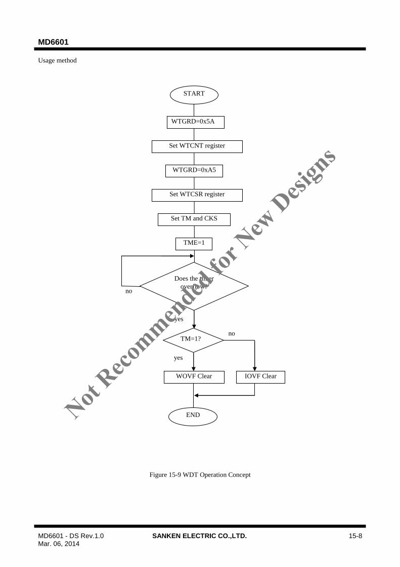
MD6601
MD6601 - DS Rev.1.0 SANKEN ELECTRIC CO.,LTD. 15-8 Mar. 06, 2014
Usage method
Figure 15-9 WDT Operation Concept
START
WTGRD=0x5A
Set WTCNT register
Set WTCSR register
WTGRD=0xA5
Set TM and CKS
TME=1
Does the timer
overflow?
IOVF Clear
TM=1?
WOVF Clear
END
yes
yes
no
no
Not Reco
mmended
for N
ew D
esign
s
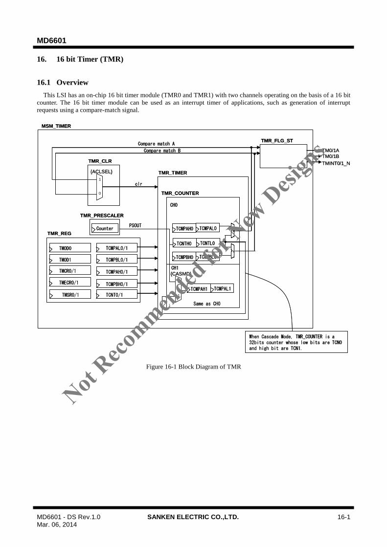
MD6601
MD6601 - DS Rev.1.0 SANKEN ELECTRIC CO.,LTD. 16-1 Mar. 06, 2014
16. 16 bit Timer (TMR)
16.1 Overview
This LSI has an on-chip 16 bit timer module (TMR0 and TMR1) with two channels operating on the basis of a 16 bit
counter. The 16 bit timer module can be used as an interrupt timer of applications, such as generation of interrupt
requests using a compare-match signal.
Figure 16-1 Block Diagram of TMR
MSM_TIMER
TMR_REG
TMINT0/1_N
TMR_FLG_ST
TCMPAL0/1
TMECR0/1
TMCR0/1
TMOD0
TCMPBL0/1
TMR_TIMER
TMR_COUNTER
TCNTH0
TCMPAH0/1
TCMPBH0/1
TMR_CLR
TMR_PRESCALER
Counter
TMSR0/1
PSOUT
clr
TM0/1A
TM0/1B
TCNT0/1
TCNTL0
TCMPAH0 TCMPAL0
TCMPBH0 TCMPBL0
=
=
CH0
CH1
TCMPAH1 TCMPAL1
Same as CH0
Compare match A
Compare match B
1
0
{ACLSEL}
When Cascade Mode, TMR_COUNTER is a 32bits counter whose low bits are TCN0 and high bit are TCN1.
TMOD1
0
1
{CASMD}
MSM_TIMER
TMR_REG
TMINT0/1_N
TMR_FLG_ST
TCMPAL0/1
TMECR0/1
TMCR0/1
TMOD0
TCMPBL0/1
TMR_TIMER
TMR_COUNTER
TCNTH0
TCMPAH0/1
TCMPBH0/1
TMR_CLR
TMR_PRESCALER
Counter
TMSR0/1
PSOUT
clr
TM0/1A
TM0/1B
TCNT0/1
TCNTL0
TCMPAH0 TCMPAL0
TCMPBH0 TCMPBL0
==
==
CH0
CH1
TCMPAH1 TCMPAL1
Same as CH0
Compare match A
Compare match B
1
0
{ACLSEL}
When Cascade Mode, TMR_COUNTER is a 32bits counter whose low bits are TCN0 and high bit are TCN1.
TMOD1
0
1
{CASMD}
Not Reco
mmended
for N
ew D
esign
s
MD6601
MD6601 - DS Rev.1.0 SANKEN ELECTRIC CO.,LTD. 16-2 Mar. 06, 2014
16.2 Register Description
Table 16-1 List of Registers
Symbol Name Address Initial value
TMOD0 Timer control Mode Register 0xFA00 0x00
TMOD1 Timer control Mode Register 0xFA01 0x00
TMSR0 Timer 0 Status Register 0xFA02 0x00
TMSR1 Timer 1 Status Register 0xFA03 0x00
TMCR0 Timer 0 Control register 0xFA04 0x00
TMCR1 Timer 1 Control register 0xFA05 0x00
TMECR0 Timer 0 event clear register 0xFA06 0x00
TMECR1 Timer 1 event clear register 0xFA07 0x00
TCMPAL0 Timer 0 compare match A-L 0xFA10 0x00
TCMPAL1 Timer 1 compare match A-L 0xFA12 0x00
TCMPAH0 Timer 0 compare match A-H 0xFA11 0x00
TCMPAH1 Timer 1 compare match A-H 0xFA13 0x00
TCMPBL0 Timer 0 compare match B-L 0xFA14 0x00
TCMPBL1 Timer 1 compare match B-L 0xFA16 0x00
TCMPBH0 Timer 0 compare match B-H 0xFA15 0x00
TCMPBH1 Timer 1 compare match B-H 0xFA17 0x00
TCNTL0 Timer 0 counter L 0xFA18 0x00
TCNTL1 Timer 1 counter L 0xFA1A 0x00
TCNTH0 Timer 0 counter H 0xFA19 0x00
TCNTH1 Timer 1 counter H 0xFA1B 0x00
Not Reco
mmended
for N
ew D
esign
s
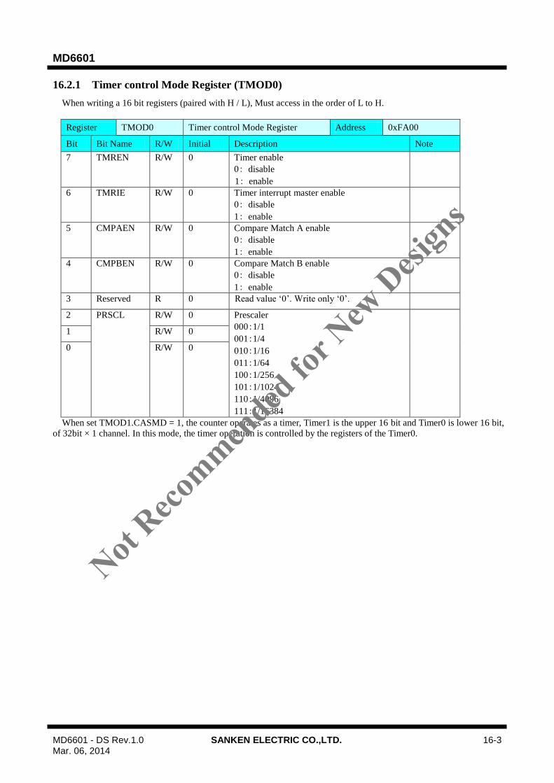
MD6601
MD6601 - DS Rev.1.0 SANKEN ELECTRIC CO.,LTD. 16-3 Mar. 06, 2014
16.2.1 Timer control Mode Register (TMOD0)
When writing a 16 bit registers (paired with H / L), Must access in the order of L to H.
Register TMOD0 Timer control Mode Register Address 0xFA00
Bit Bit Name R/W Initial Description Note
7 TMREN R/W 0 Timer enable
0: disable
1: enable
6 TMRIE R/W 0 Timer interrupt master enable
0: disable
1: enable
5 CMPAEN R/W 0 Compare Match A enable
0: disable
1: enable
4 CMPBEN R/W 0 Compare Match B enable
0: disable
1: enable
3 Reserved R 0 Read value ‘0’. Write only ‘0’.
2 PRSCL R/W 0 Prescaler
000:1/1
001:1/4
010:1/16
011:1/64
100:1/256
101:1/1024
110:1/4096
111:1/16384
1 R/W 0
0 R/W 0
When set TMOD1.CASMD = 1, the counter operates as a timer, Timer1 is the upper 16 bit and Timer0 is lower 16 bit,
of 32bit × 1 channel. In this mode, the timer operation is controlled by the registers of the Timer0.
Not Reco
mmended
for N
ew D
esign
s

MD6601
MD6601 - DS Rev.1.0 SANKEN ELECTRIC CO.,LTD. 16-4 Mar. 06, 2014
16.2.2 Timer control Mode Register (TMOD1)
Register TMOD1 Timer control Mode Register Address 0xFA01
Bit Bit Name R/W Initial Description Note
7 TMREN R/W 0 Timer enable
0: disable
1: enable
6 TMRIE R/W 0 Timer interrupt master enable
0: disable
1: enable
5 CMPAEN R/W 0 Compare Match A enable
0: disable
1: enable
4 CMPBEN R/W 0 Compare Match B enable
0: disable
1: enable
3 CASMD R/W 0 Cascade Mode
0: disable
1: enable
2 PRSCL R/W 0 Prescaler
000:1/1
001:1/4
010:1/16
011:1/64
100:1/256
101:1/1024
110:1/4096
111:1/16384
1 R/W 0
0 R/W 0
When TMOD1.CASMD = "1", TMR works with the set value of TMOD0 register regardless of the setting of the
TMOD1 register.
Not Reco
mmended
for N
ew D
esign
s

MD6601
MD6601 - DS Rev.1.0 SANKEN ELECTRIC CO.,LTD. 16-5 Mar. 06, 2014
16.2.3 Timer n Status Register (TMSRn) (n=0-1)
Register TMSR0 Timer 0 Status Register Address 0xFA02
Register TMSR1 Timer 1 Status Register Address 0xFA03
Bit Bit Name R/W Initial Description Note
7 Reserved R 0 Read value ‘0’. Write only ‘0’.
6 Reserved R 0 Read value ‘0’. Write only ‘0’.
5 Reserved R 0 Read value ‘0’. Write only ‘0’.
4 Reserved R 0 Read value ‘0’. Write only ‘0’.
3 Reserved R 0 Read value ‘0’. Write only ‘0’.
2 OVF R/C 0 Overflow flag
Read operation
0: No overflow
1: Overflow
Write operation
0: No effect
1: '0' clear
1 CMBF R/C 0 Compare match B flag
Read operation
0: No compare match B
1: Compare match B
Write operation
0: No effect
1: '0' clear
0 CMAF R/C 0 Compare match A flag
Read operation
0: No compare match A
1: Compare match A
Write operation
0: No effect
1: '0' clear
When TMOD1.CASMD = "1", TMR works with the set value of TMOD0 register regardless of the setting of the
TMOD1 register.
Not Reco
mmended
for N
ew D
esign
s
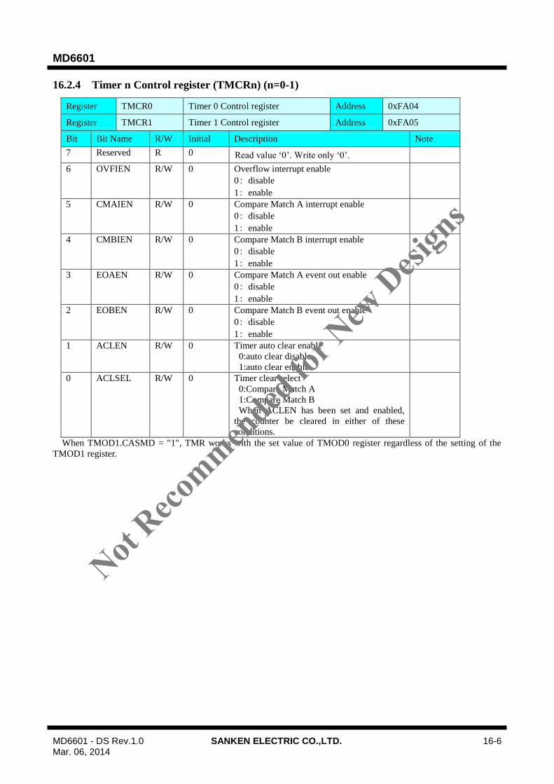
MD6601
MD6601 - DS Rev.1.0 SANKEN ELECTRIC CO.,LTD. 16-6 Mar. 06, 2014
16.2.4 Timer n Control register (TMCRn) (n=0-1)
Register TMCR0 Timer 0 Control register Address 0xFA04
Register TMCR1 Timer 1 Control register Address 0xFA05
Bit Bit Name R/W Initial Description Note
7 Reserved R 0 Read value ‘0’. Write only ‘0’.
6 OVFIEN R/W 0 Overflow interrupt enable
0: disable
1: enable
5 CMAIEN R/W 0 Compare Match A interrupt enable
0: disable
1: enable
4 CMBIEN R/W 0 Compare Match B interrupt enable
0: disable
1: enable
3 EOAEN R/W 0 Compare Match A event out enable
0: disable
1: enable
2 EOBEN R/W 0 Compare Match B event out enable
0: disable
1: enable
1 ACLEN R/W 0 Timer auto clear enable
0:auto clear disable
1:auto clear enable
0 ACLSEL R/W 0 Timer clear select
0:Compare Match A
1:Compare Match B
When ACLEN has been set and enabled,
the counter be cleared in either of these
conditions.
When TMOD1.CASMD = "1", TMR works with the set value of TMOD0 register regardless of the setting of the
TMOD1 register.
Not Reco
mmended
for N
ew D
esign
s

MD6601
MD6601 - DS Rev.1.0 SANKEN ELECTRIC CO.,LTD. 16-7 Mar. 06, 2014
16.2.5 Timer n event clear register (TMECRn) (n=0-1)
Register TMECR0 Timer 0 event clear register Address 0xFA06
Register TMECR1 Timer 1 event clear register Address 0xFA07
Bit Bit Name R/W Initial Description Note
7 Reserved R 0 Read value ‘0’. Write only ‘0’.
6 Reserved R 0 Read value ‘0’. Write only ‘0’.
5 Reserved R 0 Read value ‘0’. Write only ‘0’.
4 Reserved R 0 Read value ‘0’. Write only ‘0’.
3 P3CLRS R/W 0
Use PWM3 event to clear counter
0: Not use
1: Use
2 P2CLRS R/W 0
Use PWM2 event to clear counter
0: Not use
1: Use
1 P1CLRS R/W 0
Use PWM1 event to clear counter
0: Not use
1: Use
0 P0CLRS R/W 0
Use PWM0 event to clear counter
0: Not use
1: Use
When TMOD1.CASMD = "1", TMR works with the set value of TMOD0 register regardless of the setting of the
TMOD1 register.
16.2.6 Timer n compare match A-L (TCMPALn) (n=0-1)
Register TCMPAL0 Timer 0 compare match A-L Address 0xFA10
Register TCMPAL1 Timer 1 compare match A-L Address 0xFA12
Bit Bit Name R/W Initial Description Note
7 CMPAL R/W 0 Compare match-A Lower 8bit value
6 R/W 0
5 R/W 0
4 R/W 0
3 R/W 0
2 R/W 0
1 R/W 0
0 R/W 0
Not Reco
mmended
for N
ew D
esign
s
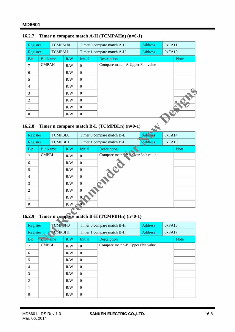
MD6601
MD6601 - DS Rev.1.0 SANKEN ELECTRIC CO.,LTD. 16-8 Mar. 06, 2014
16.2.7 Timer n compare match A-H (TCMPAHn) (n=0-1)
Register TCMPAH0 Timer 0 compare match A-H Address 0xFA11
Register TCMPAH1 Timer 1 compare match A-H Address 0xFA13
Bit Bit Name R/W Initial Description Note
7 CMPAH R/W 0 Compare match-A Upper 8bit value
6 R/W 0
5 R/W 0
4 R/W 0
3 R/W 0
2 R/W 0
1 R/W 0
0 R/W 0
16.2.8 Timer n compare match B-L (TCMPBLn) (n=0-1)
Register TCMPBL0 Timer 0 compare match B-L Address 0xFA14
Register TCMPBL1 Timer 1 compare match B-L Address 0xFA16
Bit Bit Name R/W Initial Description Note
7 CMPBL R/W 0 Compare match-B Lower 8bit value
6 R/W 0
5 R/W 0
4 R/W 0
3 R/W 0
2 R/W 0
1 R/W 0
0 R/W 0
16.2.9 Timer n compare match B-H (TCMPBHn) (n=0-1)
Register TCMPBH0 Timer 0 compare match B-H Address 0xFA15
Register TCMPBH1 Timer 1 compare match B-H Address 0xFA17
Bit Bit Name R/W Initial Description Note
7 CMPBH R/W 0 Compare match-B Upper 8bit value
6 R/W 0
5 R/W 0
4 R/W 0
3 R/W 0
2 R/W 0
1 R/W 0
0 R/W 0
Not Reco
mmended
for N
ew D
esign
s
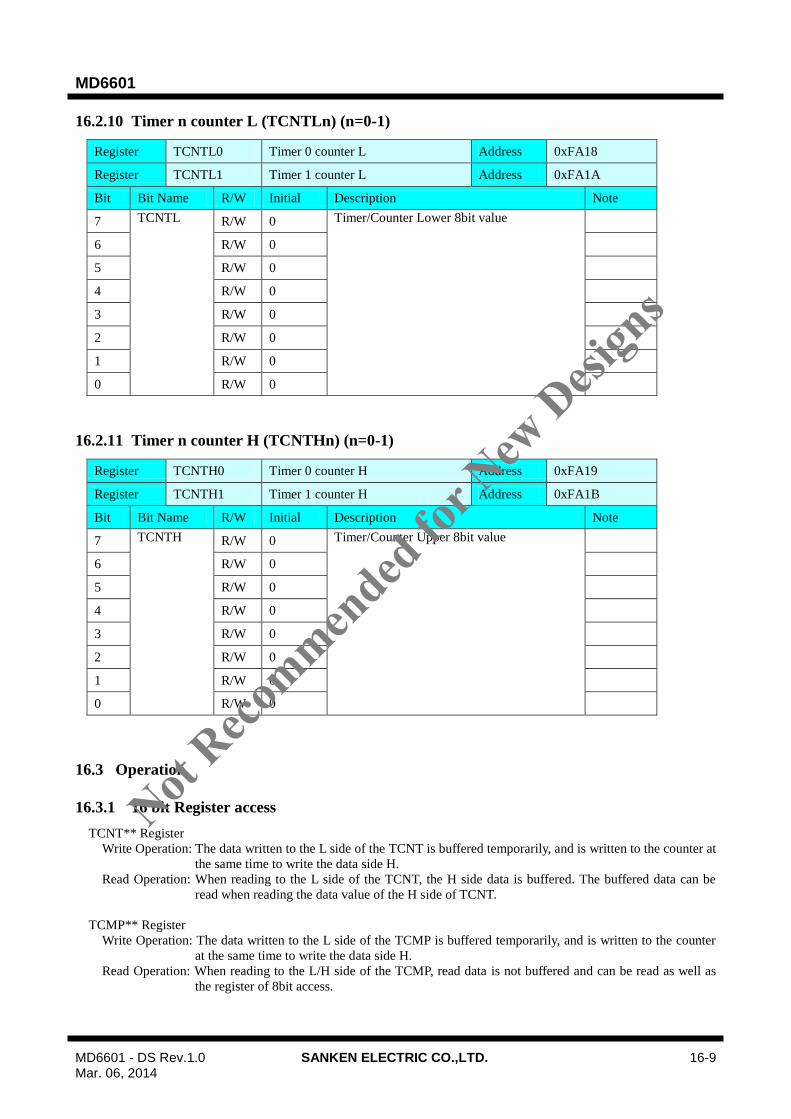
MD6601
MD6601 - DS Rev.1.0 SANKEN ELECTRIC CO.,LTD. 16-9 Mar. 06, 2014
16.2.10 Timer n counter L (TCNTLn) (n=0-1)
Register TCNTL0 Timer 0 counter L Address 0xFA18
Register TCNTL1 Timer 1 counter L Address 0xFA1A
Bit Bit Name R/W Initial Description Note
7 TCNTL R/W 0 Timer/Counter Lower 8bit value
6 R/W 0
5 R/W 0
4 R/W 0
3 R/W 0
2 R/W 0
1 R/W 0
0 R/W 0
16.2.11 Timer n counter H (TCNTHn) (n=0-1)
Register TCNTH0 Timer 0 counter H Address 0xFA19
Register TCNTH1 Timer 1 counter H Address 0xFA1B
Bit Bit Name R/W Initial Description Note
7 TCNTH R/W 0 Timer/Counter Upper 8bit value
6 R/W 0
5 R/W 0
4 R/W 0
3 R/W 0
2 R/W 0
1 R/W 0
0 R/W 0
16.3 Operation
16.3.1 16 bit Register access
TCNT** Register
Write Operation: The data written to the L side of the TCNT is buffered temporarily, and is written to the counter at
the same time to write the data side H.
Read Operation: When reading to the L side of the TCNT, the H side data is buffered. The buffered data can be
read when reading the data value of the H side of TCNT.
TCMP** Register
Write Operation: The data written to the L side of the TCMP is buffered temporarily, and is written to the counter
at the same time to write the data side H.
Read Operation: When reading to the L/H side of the TCMP, read data is not buffered and can be read as well as
the register of 8bit access.
Not Reco
mmended
for N
ew D
esign
s
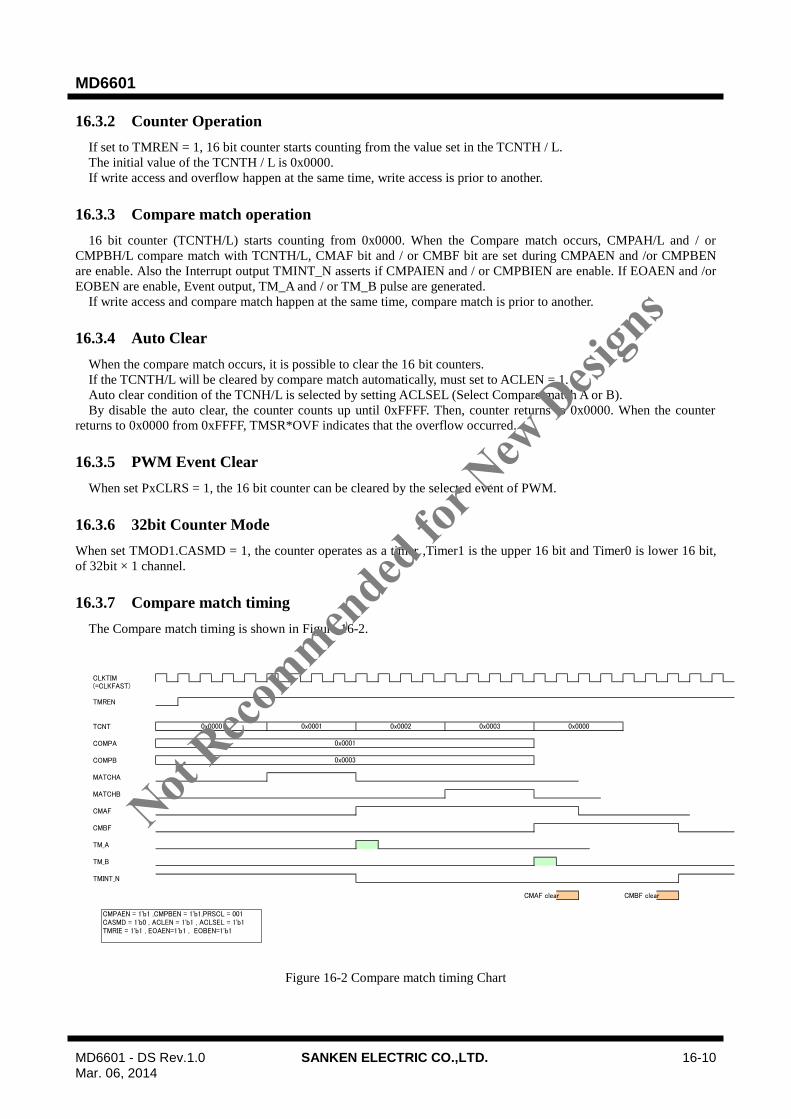
MD6601
MD6601 - DS Rev.1.0 SANKEN ELECTRIC CO.,LTD. 16-10 Mar. 06, 2014
16.3.2 Counter Operation
If set to TMREN = 1, 16 bit counter starts counting from the value set in the TCNTH / L.
The initial value of the TCNTH / L is 0x0000.
If write access and overflow happen at the same time, write access is prior to another.
16.3.3 Compare match operation
16 bit counter (TCNTH/L) starts counting from 0x0000. When the Compare match occurs, CMPAH/L and / or
CMPBH/L compare match with TCNTH/L, CMAF bit and / or CMBF bit are set during CMPAEN and /or CMPBEN
are enable. Also the Interrupt output TMINT_N asserts if CMPAIEN and / or CMPBIEN are enable. If EOAEN and /or
EOBEN are enable, Event output, TM_A and / or TM_B pulse are generated.
If write access and compare match happen at the same time, compare match is prior to another.
16.3.4 Auto Clear
When the compare match occurs, it is possible to clear the 16 bit counters.
If the TCNTH/L will be cleared by compare match automatically, must set to ACLEN = 1.
Auto clear condition of the TCNH/L is selected by setting ACLSEL (Select Compare match A or B).
By disable the auto clear, the counter counts up until 0xFFFF. Then, counter returns to 0x0000. When the counter
returns to 0x0000 from 0xFFFF, TMSR*OVF indicates that the overflow occurred.
16.3.5 PWM Event Clear
When set PxCLRS = 1, the 16 bit counter can be cleared by the selected event of PWM.
16.3.6 32bit Counter Mode
When set TMOD1.CASMD = 1, the counter operates as a timer ,Timer1 is the upper 16 bit and Timer0 is lower 16 bit,
of 32bit × 1 channel.
16.3.7 Compare match timing
The Compare match timing is shown in Figure 16-2.
Figure 16-2 Compare match timing Chart
CLKTIM(=CLKFAST)
TMREN
TCNT
COMPA
COMPB
MATCHA
MATCHB
CMAF
CMBF
TM_A
TM_B
TMINT_N
CMAF clear CMBF clear
0x0003
0x0000 0x0001 0x00000x0002 0x0003
0x0001
CMPAEN = 1'b1 ,CMPBEN = 1'b1,PRSCL = 001CASMD = 1'b0 , ACLEN = 1'b1 , ACLSEL = 1'b1TMRIE = 1'b1 , EOAEN=1'b1 , EOBEN=1'b1
Not Reco
mmended
for N
ew D
esign
s
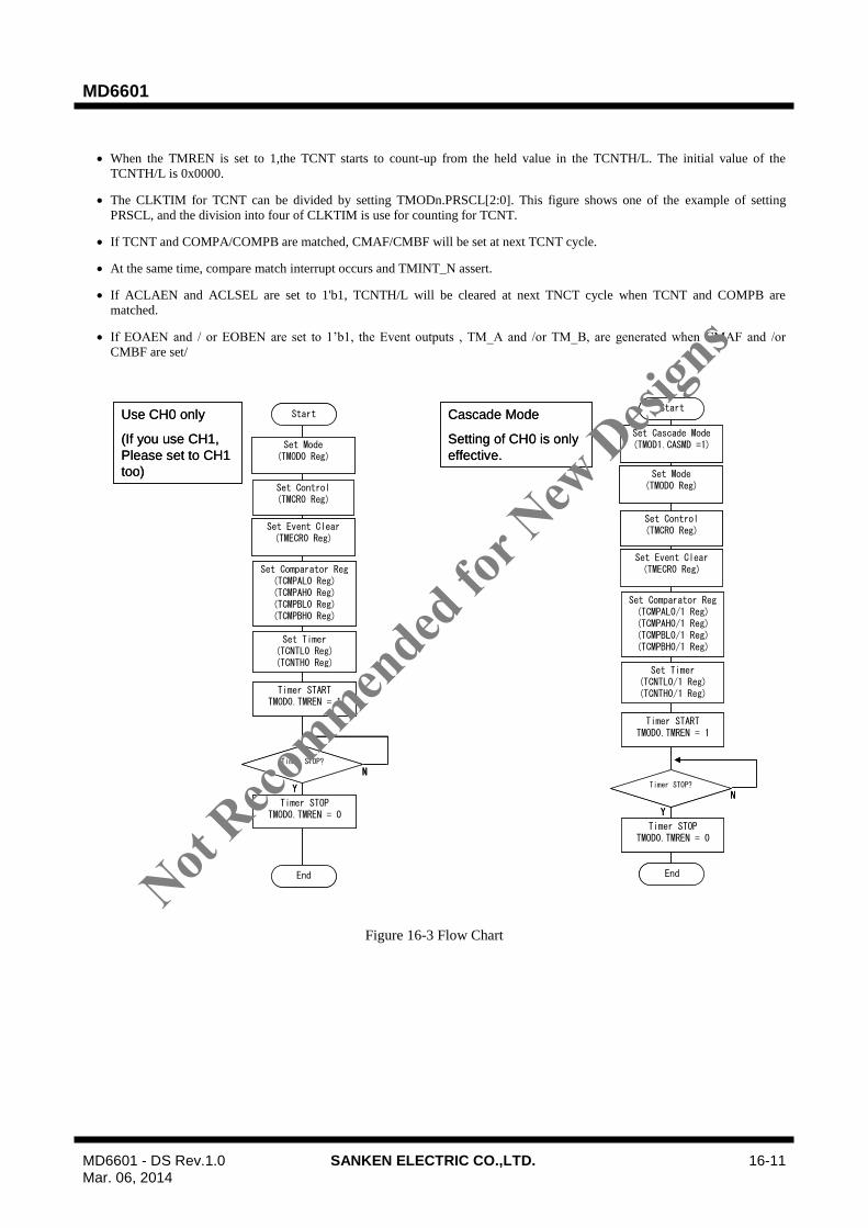
MD6601
MD6601 - DS Rev.1.0 SANKEN ELECTRIC CO.,LTD. 16-11 Mar. 06, 2014
When the TMREN is set to 1,the TCNT starts to count-up from the held value in the TCNTH/L. The initial value of the
TCNTH/L is 0x0000.
The CLKTIM for TCNT can be divided by setting TMODn.PRSCL[2:0]. This figure shows one of the example of setting
PRSCL, and the division into four of CLKTIM is use for counting for TCNT.
If TCNT and COMPA/COMPB are matched, CMAF/CMBF will be set at next TCNT cycle.
At the same time, compare match interrupt occurs and TMINT_N assert.
If ACLAEN and ACLSEL are set to 1'b1, TCNTH/L will be cleared at next TNCT cycle when TCNT and COMPB are
matched.
If EOAEN and / or EOBEN are set to 1’b1, the Event outputs , TM_A and /or TM_B, are generated when CMAF and /or
CMBF are set/
Figure 16-3 Flow Chart
Start
Set Control(TMCR0 Reg)
Set Event Clear(TMECR0 Reg)
Set Mode(TMOD0 Reg)
Set Comparator Reg(TCMPAL0 Reg)(TCMPAH0 Reg)(TCMPBL0 Reg)(TCMPBH0 Reg)
Set Timer (TCNTL0 Reg)(TCNTH0 Reg)
Timer START TMOD0.TMREN = 1
Timer STOP?
Timer STOP TMOD0.TMREN = 0
End
Y
N
Use CH0 only
(If you use CH1,
Please set to CH1
too)
Cascade Mode
Setting of CH0 is only
effective.
Start
Set Control(TMCR0 Reg)
Set Event Clear(TMECR0 Reg)
Set Cascade Mode(TMOD1.CASMD =1)
Set Comparator Reg(TCMPAL0/1 Reg)(TCMPAH0/1 Reg)(TCMPBL0/1 Reg)(TCMPBH0/1 Reg)
Set Timer (TCNTL0/1 Reg)(TCNTH0/1 Reg)
Timer START TMOD0.TMREN = 1
Timer STOP?
Timer STOP TMOD0.TMREN = 0
End
Y
N
Set Mode(TMOD0 Reg)
Start
Set Control(TMCR0 Reg)
Set Event Clear(TMECR0 Reg)
Set Mode(TMOD0 Reg)
Set Comparator Reg(TCMPAL0 Reg)(TCMPAH0 Reg)(TCMPBL0 Reg)(TCMPBH0 Reg)
Set Timer (TCNTL0 Reg)(TCNTH0 Reg)
Timer START TMOD0.TMREN = 1
Timer STOP?
Timer STOP TMOD0.TMREN = 0
End
Y
N
Use CH0 only
(If you use CH1,
Please set to CH1
too)
Cascade Mode
Setting of CH0 is only
effective.
Start
Set Control(TMCR0 Reg)
Set Event Clear(TMECR0 Reg)
Set Cascade Mode(TMOD1.CASMD =1)
Set Comparator Reg(TCMPAL0/1 Reg)(TCMPAH0/1 Reg)(TCMPBL0/1 Reg)(TCMPBH0/1 Reg)
Set Timer (TCNTL0/1 Reg)(TCNTH0/1 Reg)
Timer START TMOD0.TMREN = 1
Timer STOP?
Timer STOP TMOD0.TMREN = 0
End
Y
N
Set Mode(TMOD0 Reg)
Not Reco
mmended
for N
ew D
esign
s

MD6601
MD6601 - DS Rev.1.0 SANKEN ELECTRIC CO.,LTD. 17-1 Mar. 06, 2014
17. SPI
17.1 Overview
The SPI channel is capable of full-duplex serial communications with external processors and peripheral devices.
Table 17-1 Feature of SPI
Item Description
Tx/Rx Function
- Capable of serial communications in Master mode or Slave mode.
- MOSI (master out/slave in), MISO (master in/slave out), and SCK (SPI clock)
signals allow serial communications through SPI operation.
- SPI /SS_N signal for Master Mode is generated by GPIO out.
- SPI /SS_N signal for Slave Mode is assigned to GPIO00.
- Support either SPI clock edge (rising or falling) on which the SPI data changes.
- Support clock polarity which keeps high or low when idles.
Both TXFIFO and RXFIFO have two stages.
Data Format
- Support MSB-first or LSB first selectable.
- Transfer data length is 6 ~ 16 bits.
- 16 bits transfer and receive buffers
SPI Clock - Supported SPI clock frequency: f/4 ~ f/1024.
Error Detection - Overrun Error Detection
Interrupt Source
- Maskable interrupt sources (TXENDIE, TXERRIE, RXERRIE, TXFIFOIE,
RXFIFOIE)
- SPI receive interrupt: receive buffer not empty (~REMPTY & RXFIFOIE) or
FIFO error ((RUDF | ROVF)&RXERRIE).
- SPI transmit interrupt: transmit buffer not full (~TFFULL & TXFIFOIE),
transmit end (TXEND & TXENDIE) or FIFO error ((TUDF | TOVF) &
TXERRIE).
Notes
- When SPI unit is set as a master device, where the SPI module is being used to
receive data only, it only outputs receive clock.
- SS_N pin is used to select the SPI module when the SPI is configured as a slave.
Not Reco
mmended
for N
ew D
esign
s
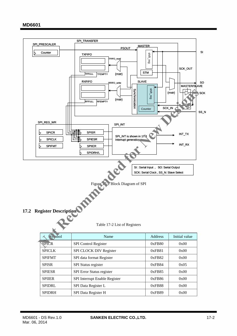
MD6601
MD6601 - DS Rev.1.0 SANKEN ELECTRIC CO.,LTD. 17-2 Mar. 06, 2014
Figure 17-1 Block Diagram of SPI
17.2 Register Description
Table 17-2 List of Registers
Symbol Name Address Initial value
SPICR SPI Control Register 0xFB80 0x00
SPICLK SPI CLOCK DIV Register 0xFB81 0x00
SPIFMT SPI data format Register 0xFB82 0x00
SPISR SPI Status register 0xFB84 0x05
SPIESR SPI Error Status register 0xFB85 0x00
SPIIER SPI Interrupt Enable Register 0xFB86 0x00
SPIDRL SPI Data Register L 0xFB88 0x00
SPIDRH SPI Data Register H 0xFB89 0x00
SPI_REG_WR
SPI_PRESCALER
SPISR
SPIESR
SPIDRH/L
SPIFMT
SPICLK
SPICR
CounterTXFIFO
RXFIFO
MASTER
SLAVE
STM
Counter
shift_
reg
shift_
reg
SPI_TRANSFER
PSOUT
SCK_OUT
SCK
SI
SO
{mstr}
Synchro
niz
atio
n
TFFULL TFEMPTY
RFFULL RFEMPTY
TFIFO_read
{mstr}
RFIFO_write
{mstr}
INT_TX
SS_N
INT_RX
SPI_INT
SPI_INT is shown in 17.3
Interrupt generation.
SPIIER
MASTER/SLAVE
SCK_IN
SI : Serial Input , SO: Serial Output
SCK: Serial Clock , SS_N: Slave Select
Not Reco
mmended
for N
ew D
esign
s

MD6601
MD6601 - DS Rev.1.0 SANKEN ELECTRIC CO.,LTD. 17-3 Mar. 06, 2014
17.2.1 SPI Control Register (SPICR)
Register SPICR SPI Control Register Address 0xFB80
Bit Bit Name R/W Initial Description Note
7-6 Reserved R 0 Read value is „0‟. Write only „0‟.
5 SPE R/W 0 Serial Peripheral Enable
When the Serial Peripheral Enable bit is set to „1‟, the
core is enabled. When it is cleared to „0‟, the core is
disabled. The core only transfers data when the core is
enabled.
„0‟ = SPI core disabled
„1‟ = SPI core enabled
4 MSTR R/W 0 Master Mode Select
When the Master Mode Select bit is set to „1‟, the core
is a master device. When it is cleared to „0‟, it is a slave
device.
„0‟ = Slave mode
„1‟ = Master mode
3 CPOL R/W 0 Clock Polarity
The Clock Polarity bit, together with the Clock Phase
bit, determines the transfer mode.
2 CPHA R/W 0 Clock Phase
The Clock Phase bit and the Clock Polarity bit,
determine the transfer mode.
In slave mode, SPI operates in mode 1 or 3 regardless
of this bit (as CPHA = 1).
1 TXEN R/W 0 TX enable
When TXEN bit is set to '1', the core is a TX operation
enable.
When TXEN bit is cleared to '0', the core is a TX
operation disable.
0 RXEN R/W 0 RX enable
When RXEN bit is set to '1', the core is a RX operation
enable.
When RXEN bit is cleared to '0', the core is a RX
operation disable.
TXEN and RXEN:
TXEN, RXEN is different from the master/slave mode as shown below.
Transmission:
When SPI is in the master mode, if RXEN or TXEN is enabled, SPI can transmit. Even if RXEN is only set to „1‟,
the transmission data is the data written to the TXFIFO.
In case of the slave mode, if TXFIFO has started sending in an empty state and TXEN = 1, TXFIFO underflow flag is
set to „1‟. If RXEN is only set to „1‟, for no data is read from TXFIFO, the underflow flag is not set to „1‟.
Receive:
If enable the RXEN to both master and slave, the received data is written to the RXFIFO. (if RXFIFO is in full and
has completed send and receive in the state of RXEN = 1, RXFIFO overflow flag is set to „1‟).
CPOL and CPHA
The Clock Polarity bit and the Clock Phase bit are for determining the SPI mode
There are four SPI modes, and each SPI mode has the different data-setup timing and data-sample timing. Setting
information of these CPOL bit and CPHA bit are shown in Table 17-3 and the Timing chart is shown in Figure 17-2.
Not Reco
mmended
for N
ew D
esign
s
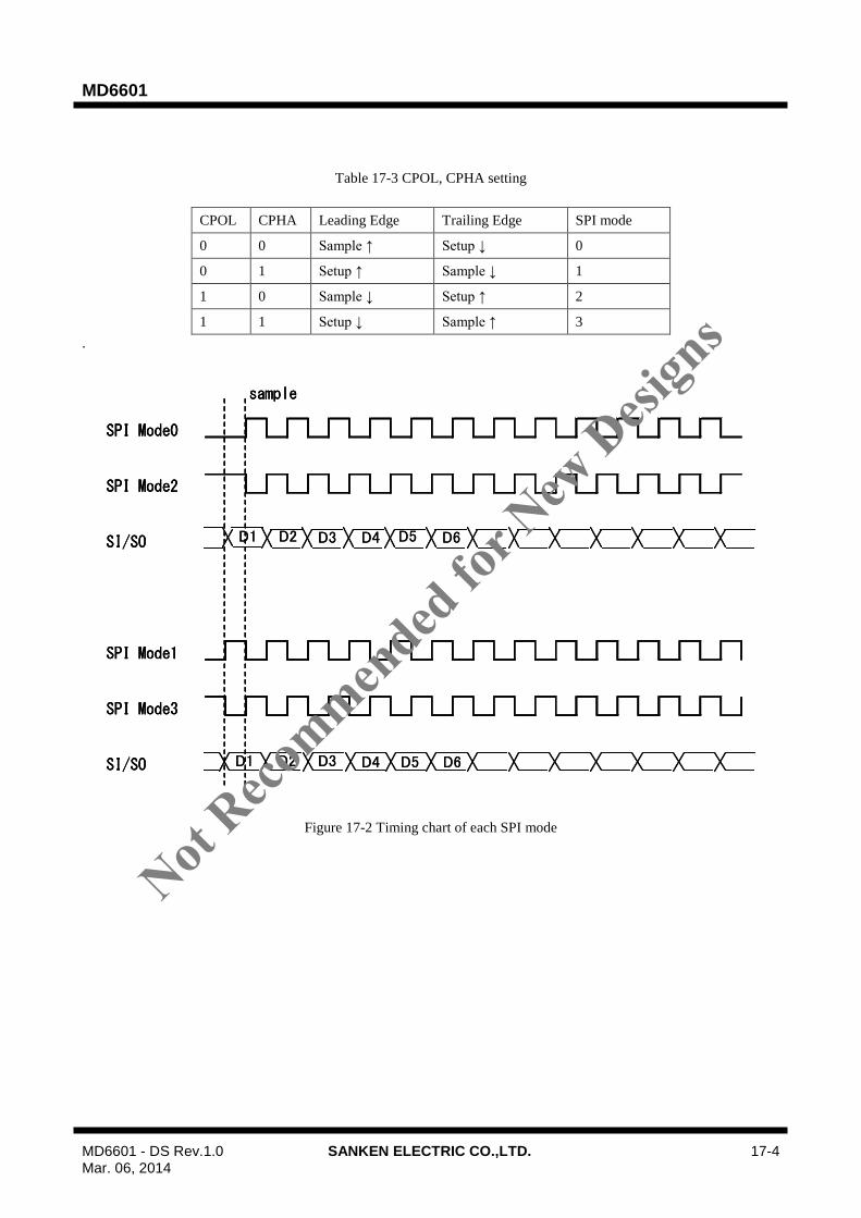
MD6601
MD6601 - DS Rev.1.0 SANKEN ELECTRIC CO.,LTD. 17-4 Mar. 06, 2014
Table 17-3 CPOL, CPHA setting
CPOL CPHA Leading Edge Trailing Edge SPI mode
0 0 Sample ↑ Setup ↓ 0
0 1 Setup ↑ Sample ↓ 1
1 0 Sample ↓ Setup ↑ 2
1 1 Setup ↓ Sample ↑ 3
.
Figure 17-2 Timing chart of each SPI mode
sample
SPI Mode0
SPI Mode2
SI/SO
SPI Mode1
SPI Mode3
SI/SO
D1 D2 D3 D4 D5 D6
D1 D2 D3 D4 D5 D6
sample
SPI Mode0
SPI Mode2
SI/SO
SPI Mode1
SPI Mode3
SI/SO
sample
SPI Mode0
SPI Mode2
SI/SO
SPI Mode1
SPI Mode3
SI/SO
D1 D2 D3 D4 D5 D6
D1 D2 D3 D4 D5 D6
Not Reco
mmended
for N
ew D
esign
s

MD6601
MD6601 - DS Rev.1.0 SANKEN ELECTRIC CO.,LTD. 17-5 Mar. 06, 2014
17.2.2 SPI CLOCK DIV Register (SPICLK)
Register SPICLK SPI CLOCK DIV Register Address 0xFB81
Bit Bit Name R/W Initial Description Note
7 CLKDIV R/W 0 SPI clock rate (Master mode only)
SCK = CLK/4(CLKDIV+1)
6 R/W 0
5 R/W 0
4 R/W 0
3 R/W 0
2 R/W 0
1 R/W 0
0 R/W 0
17.2.3 SPI data format Register (SPIFMT)
Register SPIFMT SPI data format Register Address 0xFB82
Bit Bit Name R/W Initial Description Note
7 LSB R/W 0
First transfer bit select
0 : MSB first
1 : LSB first
6-3 Reserved R 0 Read value is „0‟. Write only „0‟.
2 WORD[2:0] R/W 0 Transfer word size
These bits select the SPI transfer word size.
000 : 6bits
001 : 7bits
010 : 8bits
011 : 9bits
100 : 12bits
101 : 14bits
110 : 16bits
111 : reserved
1 R/W 0
0 R/W 0
Not Reco
mmended
for N
ew D
esign
s
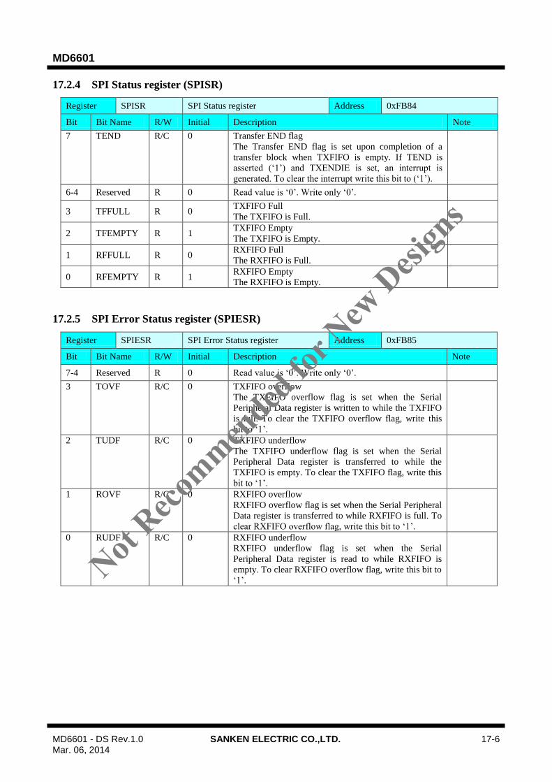
MD6601
MD6601 - DS Rev.1.0 SANKEN ELECTRIC CO.,LTD. 17-6 Mar. 06, 2014
17.2.4 SPI Status register (SPISR)
Register SPISR SPI Status register Address 0xFB84
Bit Bit Name R/W Initial Description Note
7 TEND R/C 0 Transfer END flag
The Transfer END flag is set upon completion of a
transfer block when TXFIFO is empty. If TEND is
asserted („1‟) and TXENDIE is set, an interrupt is
generated. To clear the interrupt write this bit to („1‟).
6-4 Reserved R 0 Read value is „0‟. Write only „0‟.
3 TFFULL R 0 TXFIFO Full
The TXFIFO is Full.
2 TFEMPTY R 1 TXFIFO Empty
The TXFIFO is Empty.
1 RFFULL R 0 RXFIFO Full
The RXFIFO is Full.
0 RFEMPTY R 1 RXFIFO Empty
The RXFIFO is Empty.
17.2.5 SPI Error Status register (SPIESR)
Register SPIESR SPI Error Status register Address 0xFB85
Bit Bit Name R/W Initial Description Note
7-4 Reserved R 0 Read value is „0‟. Write only „0‟.
3 TOVF R/C 0 TXFIFO overflow
The TXFIFO overflow flag is set when the Serial
Peripheral Data register is written to while the TXFIFO
is full. To clear the TXFIFO overflow flag, write this
bit to „1‟.
2 TUDF R/C 0 TXFIFO underflow
The TXFIFO underflow flag is set when the Serial
Peripheral Data register is transferred to while the
TXFIFO is empty. To clear the TXFIFO flag, write this
bit to „1‟.
1 ROVF R/C 0 RXFIFO overflow
RXFIFO overflow flag is set when the Serial Peripheral
Data register is transferred to while RXFIFO is full. To
clear RXFIFO overflow flag, write this bit to „1‟.
0 RUDF R/C 0 RXFIFO underflow
RXFIFO underflow flag is set when the Serial
Peripheral Data register is read to while RXFIFO is
empty. To clear RXFIFO overflow flag, write this bit to
„1‟.
Not Reco
mmended
for N
ew D
esign
s

MD6601
MD6601 - DS Rev.1.0 SANKEN ELECTRIC CO.,LTD. 17-7 Mar. 06, 2014
17.2.6 SPI Interrupt Enable Register (SPIIER)
Register SPIIER SPI Interrupt Enable Register Address 0xFB86
Bit Bit Name R/W Initial Description Note
7-5 Reserved R 0 Read value is „0‟. Write only „0‟.
4 TXENDIE R/W 0 TX END Interrupt Enable
When the TXENDIE is set („1‟) and the Transfer END
flag in the status register is set, TX interrupt occurs.
„0‟ = TXEND interrupts disabled
„1‟ = TXEND interrupts enabled
3 TXERRIE R/W 0 TX ERRor Interrupt Enable
When the TXERRIE is set („1‟) and the TOVF/TUDF
Flag in the error status register is set, TX interrupt
occurs.
„0‟ = TXERR interrupts disabled
„1‟ = TXERR interrupts enabled
2 RXERRIE R/W 0 RX ERRor Interrupt Enable
When the RXERRIE is set („1‟) and the ROVF/RUDF
Flag in the error status register is set, RX interrupt
occurs.
„0‟ = RXERR interrupts disabled
„1‟ = RXERR interrupts enabled
1 TXFIFOIE R/W 0 TXFIFO Interrupt Enable
When the TXFIFOIE is set („1‟) and the TFFULL Flag
in the status register is 0, TX interrupt occurs.
„0‟ = TXFIFO interrupts disabled
„1‟ = TXFIFO interrupts enabled
0 RXFIFOIE R/W 0 RXFIFO Interrupt Enable
When the RXFIFOIE is set („1‟) and the RFEMPTY
Flag in the status register is 0, RX interrupt occurs.
„0‟ = RXFIFO interrupts disabled
„1‟ = RXFIFO interrupts enabled
Not Reco
mmended
for N
ew D
esign
s

MD6601
MD6601 - DS Rev.1.0 SANKEN ELECTRIC CO.,LTD. 17-8 Mar. 06, 2014
17.2.7 SPI Data Register L (SPIDRL)
Register SPIDRL SPI Data Register L Address 0xFB88
Bit Bit Name R/W Initial Description Note
7 SPIDRL R/W 0 SPI TX/RX Data Lower Byte
6 R/W 0
5 R/W 0
4 R/W 0
3 R/W 0
2 R/W 0
1 R/W 0
0 R/W 0
17.2.8 SPI Data Register H (SPIDRH)
Register SPIDRH SPI Data Register H Address 0xFB89
Bit Bit Name R/W Initial Description Note
7 SPIDRH R/W 0 SPI TX/RX Data Upper Byte
6 R/W 0
5 R/W 0
4 R/W 0
3 R/W 0
2 R/W 0
1 R/W 0
0 R/W 0
When the Data length is less than or equal to 8bit, SPI uses SPIDRL register only, and SPIDRH register is not used.
When the Data length is more than 9bit, it is necessary to access both in the order from SPIDRL to SPIDRH Write /
Read.
In case the Data length is more than 9bit, FIFO status is changed as follows.
TXFIFO
TFEMPTY and TFFULL are changed when writing to SPIDRH.
RXFIFO
RFFULL and RFEMPTY are changed when reading to SPIDRH.
Not Reco
mmended
for N
ew D
esign
s

MD6601
MD6601 - DS Rev.1.0 SANKEN ELECTRIC CO.,LTD. 17-9 Mar. 06, 2014
17.3 Interrupt generation
17.3.1 INT_TX
Refer to a logical expression of INT_TX as below and a logical diagram as shown in Figure 17-3
INT_TX = (~TFFULL & TXFIFOIE) | ( TEND & TXENDIE) | ( TUDF | TOVF ) & TXERRIE;
TFFULL (SPISR[3] )
TFFULL is set to 1'b1 when TXFIFO is full. TFFULL is cleared to 1'b0 at the start of transmission.
TUDF (SPIESR[2] )
TUDF is set when transmission is started while TXFIFO is empty. TUDF can be cleared by writing 1‟b1 to this bit.
TOVF (SPIESR[3])
TOVF is set when write operation occurs while TXFIFO is FULL. TOVF can be cleared by writing 1‟b1 to this bit.
TEND (SPISR[7])
TEND is set when transmission is complete while TXFIFO is empty. TEND can be cleared by writing 1‟b1 to this bit.
Figure 17-3 INT_TX Logical diagram
SPISR.TFFULL
SPIIER.TXFIFOIE
SPISR.TEND
SPIIER.TXENDIE
SPIESR.TUDF
SPIESR.TXERRIESPIESR.TOVF
INT_TX
SPISR.TFFULL
SPIIER.TXFIFOIE
SPISR.TEND
SPIIER.TXENDIE
SPIESR.TUDF
SPIESR.TXERRIESPIESR.TOVF
INT_TX
Not Reco
mmended
for N
ew D
esign
s

MD6601
MD6601 - DS Rev.1.0 SANKEN ELECTRIC CO.,LTD. 17-10 Mar. 06, 2014
17.3.2 INT_RX
Refer to a logical expression of INT_RX as below and a logical diagram as shown in Figure 17-4.
INT_RX = (~RFEMPTY & RXFIFOIE) | ( RUDF | ROVF ) & RXERRIE;
RFEMPTY (SPISR[0] )
RXFIFO empty is cleared to 0 when completed to receive and set to 1'b1 when reading the All RXFIFO data.
RUDF (SPIESR[0] )
RXFIFO underflow is set when reading SPIDRL when RXFIFO is empty. RUDF can be cleared by writing this bit to
1‟b1.
ROVF (PIESR[1] )
RXFIFO overflow is set when data receive completed at when RXFIFO is full. ROVF can be cleared by writing this
bit to 1‟b1.
Figure 17-4 INT_RX Logical diagram
SPISR.RFEMPTY
SPIIER.RXFIFOIE
SPIESR.RUDF
SPIESR.RXERRIESPIESR.ROVF
INT_RX
SPISR.RFEMPTY
SPIIER.RXFIFOIE
SPIESR.RUDF
SPIESR.RXERRIESPIESR.ROVF
INT_RX
Not Reco
mmended
for N
ew D
esign
s
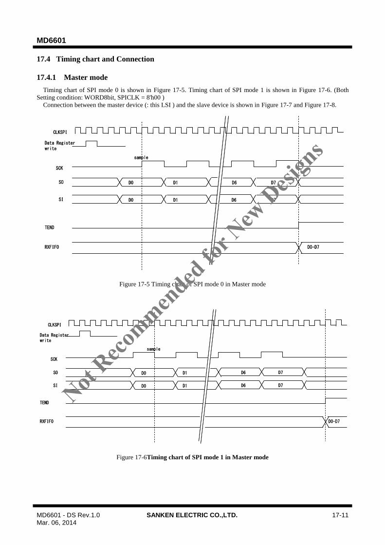
MD6601
MD6601 - DS Rev.1.0 SANKEN ELECTRIC CO.,LTD. 17-11 Mar. 06, 2014
17.4 Timing chart and Connection
17.4.1 Master mode
Timing chart of SPI mode 0 is shown in Figure 17-5. Timing chart of SPI mode 1 is shown in Figure 17-6. (Both
Setting condition: WORD8bit, SPICLK = 8'h00 )
Connection between the master device (: this LSI ) and the slave device is shown in Figure 17-7 and Figure 17-8.
Figure 17-5 Timing chart of SPI mode 0 in Master mode
Figure 17-6Timing chart of SPI mode 1 in Master mode
CLKSPI
Data Register write
SCK
SO D0 D1 D6 D7
TEND
RXFIFO D0-D7
sample
SI D0 D1 D6 D7
CLKSPI
Data Register write
SCK
SO D0 D1 D6 D7
TEND
RXFIFO D0-D7
sample
SI D0 D1 D6 D7
CLKSPI
SCK
SO D0 D1 D6 D7
TEND
RXFIFO D0-D7
sample
Data Register write
SI D0 D1 D6 D7
CLKSPI
SCK
SO D0 D1 D6 D7
TEND
RXFIFO D0-D7
sample
Data Register write
SI D0 D1 D6 D7
Not Reco
mmended
for N
ew D
esign
s
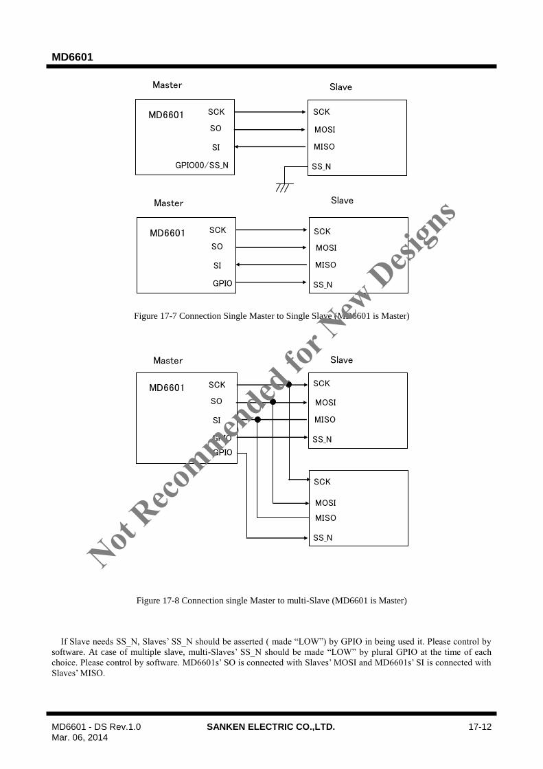
MD6601
MD6601 - DS Rev.1.0 SANKEN ELECTRIC CO.,LTD. 17-12 Mar. 06, 2014
Figure 17-7 Connection Single Master to Single Slave (MD6601 is Master)
Figure 17-8 Connection single Master to multi-Slave (MD6601 is Master)
If Slave needs SS_N, Slaves‟ SS_N should be asserted ( made “LOW”) by GPIO in being used it. Please control by
software. At case of multiple slave, multi-Slaves‟ SS_N should be made “LOW” by plural GPIO at the time of each
choice. Please control by software. MD6601s‟ SO is connected with Slaves‟ MOSI and MD6601s‟ SI is connected with
Slaves‟ MISO.
MD6601
Master Slave
SCK
SO
SI
GPIO00/SS_N
MOSI
MISO
SS_N
MD6601
Master Slave
SCK
SO
SI
GPIO
MOSI
MISO
SS_N
SCK
SCK
MD6601
Master Slave
SCK
SO
SI
GPIO
MOSI
MISO
SS_N
SCK
MOSI
MISO
SS_N
SCK
GPIO
Not Reco
mmended
for N
ew D
esign
s

MD6601
MD6601 - DS Rev.1.0 SANKEN ELECTRIC CO.,LTD. 17-13 Mar. 06, 2014
17.4.2 Slave Mode
Timing chart of SPI mode 1 is shown in Figure 17-9. (Both Setting condition: WORD8bit,
SPICLK = 8'h00 )
Connection between the master device and the slave device (: this LSI ) is shown in Figure 17-10
Figure 17-9 Timing chart of SPI mode 1 in Slave mode
MD6601
Master Slave
SCK
SO
SI
SS_N
MOSI
MISO
SCK
GPIO00/SS_N
Figure 17-10 Connection in Slave mode (MD6601 is Slave).
GPIO/SS_N is connected with SS_N from Master.
MD6601s‟ SI is connected with Masters‟ MOSI and MD6601s‟ SO is connected with Masters‟ MISO.
SCK becomes input.
SCK
RFFULL
RXFIFO D0-D7
sample
SI D0 D1 D2 D7D3 D6
CLKSPI
SO D0 D1 D2 D7D3 D6
SCK
RFFULL
RXFIFO D0-D7
sample
SI D0 D1 D2 D7D3 D6SI D0 D1 D2 D7D3 D6
CLKSPI
SO D0 D1 D2 D7D3 D6
Not Reco
mmended
for N
ew D
esign
s

MD6601
MD6601 - DS Rev.1.0 SANKEN ELECTRIC CO.,LTD. 17-14 Mar. 06, 2014
17.5 Operation
17.5.1 Master mode
Transmission start
In master mode, when TXFIFO is empty (SPISR.TFEMPTY=1), and SPIDRL/H was written data*1, the transmit
data is transferred to the shift register via TXFIFO and transfer is started as shown in Figure 17-11.
And TXFIFO status becomes full (SPISR.TFFULL=1‟b1) when two data are written to TXFIFO to write to SPIDRL
/ H continuously.
Receive start
RXFIFO is empty (SPISR.RFEMPTY=1), and write the dummy data into SPIDRL/H in order to generate the SCK,
then the receive operation starts. Receive data will be sampled by the SCK and latched into the Shift register as shown
in Figure 17-12.
*1) When the data length is less than or equal to 8bit, it switches the status of the TXFIFO when writing to SPIDRL.
When the data length is more than 9bit, it switches the status of the TXFIFO when writing to SPIDRH.
Completion of transmission
SPI transfer is completed at the corresponding SCK edge of the CPHA and CPOL setting and SPIF of SPISR is
changed to 1'b1. Last sampling timing depends on the bit length of data.
Completion of reception
When RXFIFO is written to the received data, status of RXFIFO is changed to not empty. (SPISR.REMPTY = 0). By
reading SPIDRL / H*2, data can be read from RXFIFO. The status of RXFIFO shows the number of received data and
change.
*2) When the data length is less than or equal to 8bit, it switches the status of the RXFIFO when SPIDRL has been read.
When the data length is more than 9 bit, it switches the status of the RXFIFO when data read from SPIDRH.
The flow of transmit/receive operation of master mode is described below.
Not Reco
mmended
for N
ew D
esign
s

MD6601
MD6601 - DS Rev.1.0 SANKEN ELECTRIC CO.,LTD. 17-15 Mar. 06, 2014
Transmission
Figure 17-11 Master mode (Transmission)
Start
Set data format
(SPIFMT Reg.)
Set transfer clock
(SPICLK Reg)
Set SPI config
(SPICR Reg)
SPISR.TFFULL=0x0
End
N
Y
Continue?
TEND=0x1
Set GPIO ‘Low’ for
assertion of SS_N =0
Set GPIO ‘High’ for
negate of SS_N =1
Y
N
N
Y
Set send data
(SPIDRL/DRH Reg)
*1
*1 : Not only GPIO00 can be used
for assertion and negate of
SS_N of the slave device
*1
Not Reco
mmended
for N
ew D
esign
s

MD6601
MD6601 - DS Rev.1.0 SANKEN ELECTRIC CO.,LTD. 17-16 Mar. 06, 2014
Receive
Figure 17-12 Master mode (Receive)
Start
Set data format
(SPIFMT Reg.)
Set transfer clock
(SPICLK Reg)
Set SPI config
(SPICR Reg)
SPISR.RFEMPTY=0x0
End
Read receive data
(SPIDRL/DRH Reg)
N
Y
Continue?
Set GPIO ‘Low’ for
assertion of SS_N =0
Set GPIO ‘High’ for negate of
SS_N =1
N
Y
(Dummy data write)
*1 : Not only GPIO00 can be used
for assertion and negate of
SS_N of the slave device
*2 : In master mode, it is need to
generate SCK by transmitting
the Dummy data.
*1
*1
*2
Not Reco
mmended
for N
ew D
esign
s
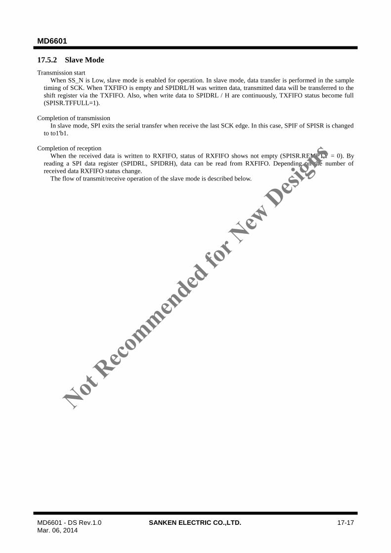
MD6601
MD6601 - DS Rev.1.0 SANKEN ELECTRIC CO.,LTD. 17-17 Mar. 06, 2014
17.5.2 Slave Mode
Transmission start
When SS_N is Low, slave mode is enabled for operation. In slave mode, data transfer is performed in the sample
timing of SCK. When TXFIFO is empty and SPIDRL/H was written data, transmitted data will be transferred to the
shift register via the TXFIFO. Also, when write data to SPIDRL / H are continuously, TXFIFO status become full
(SPISR.TFFULL=1).
Completion of transmission
In slave mode, SPI exits the serial transfer when receive the last SCK edge. In this case, SPIF of SPISR is changed
to to1'b1.
Completion of reception
When the received data is written to RXFIFO, status of RXFIFO shows not empty (SPISR.REMPTY = 0). By
reading a SPI data register (SPIDRL, SPIDRH), data can be read from RXFIFO. Depending on the number of
received data RXFIFO status change.
The flow of transmit/receive operation of the slave mode is described below.
Not Reco
mmended
for N
ew D
esign
s
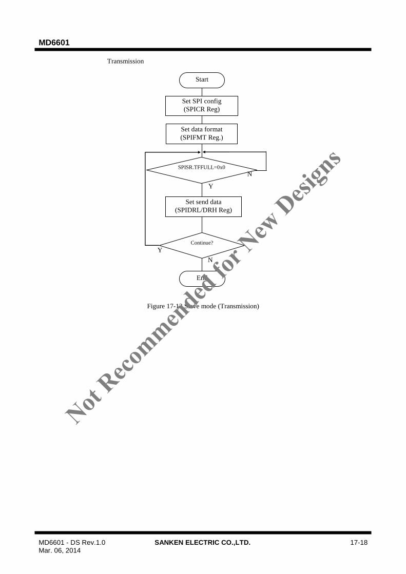
MD6601
MD6601 - DS Rev.1.0 SANKEN ELECTRIC CO.,LTD. 17-18 Mar. 06, 2014
Transmission
Figure 17-13 Slave mode (Transmission)
Start
Set data format
(SPIFMT Reg.)
Set SPI config
(SPICR Reg)
SPISR.TFFULL=0x0
Set send data
(SPIDRL/DRH Reg)
Continue?
End
N
Y
Y
N
Not Reco
mmended
for N
ew D
esign
s

MD6601
MD6601 - DS Rev.1.0 SANKEN ELECTRIC CO.,LTD. 17-19 Mar. 06, 2014
Receive
Figure 17-14 Slave mode (Receive)
Start
Set data format
(SPIFMT Reg.)
Set SPI config
(SPICR Reg)
Continue?
End
Read recive data
(SPIDRL/DRH Reg)
SPISR.RFEMPTY=0x0
Y
N
N
Y
Not Reco
mmended
for N
ew D
esign
s

MD6601
MD6601 - DS Rev.1.0 SANKEN ELECTRIC CO.,LTD. 18-1 Mar. 06, 2014
18. I2C (SMBUS)
18.1 Overview
The LSI has I2C communication module which supports both master mode and slave mode.
Table 18-1 Feature of I2C
Item Description
Communication
Format
- I2C bus format or SMBUS format
- Master Mode or Slave Mode selectable
Clocks
CLKSLOW/8
CLKSLOW/32
CLKSLOW/128
CLKSLOW/512
Supported Functions General Call address
Interrupt Source Single Sources
XD
AT
A-B
us
RX shift register
Registers
Interrupt
Control
TX shift register
Control Unit
SCL Unit
sda_in
sda_out
scl_in
scl_out
int_i2c
Figure 18-1 Block Diagram of I2C
Not Reco
mmended
for N
ew D
esign
s

MD6601
MD6601 - DS Rev.1.0 SANKEN ELECTRIC CO.,LTD. 18-2 Mar. 06, 2014
18.2 Register Description
Table 18-2 List of Registers
Symbol Name Address Initial value
ICCR I2C Bus Control Register 0xFC00 0x00
ICSR I2C Bus Status Register 0xFC01 0x00
ICRXDR I2C Bus Receive Data Register 0xFC02 0x00
ICTXDR I2C Bus Transmit Data Register 0xFC03 0x00
ICTSAR I2C Transmit Address Register 0xFC04 0x00
ICSAR I2C Slave Address Register 0xFC05 0x00
ICCLK I2C Clock Divid Register 0xFC06 0x03
ICCMD I2C Command Register 0xFC07 0x00
ICSSTR I2C Bus SDA Setup Time Register 0xFC08 0x01
ICSHTR I2C Bus SDA Hold Time Register 0xFC09 0x00
ICHDSR0 I2C Bus SDA Hardware Status Register 0 0xFC0A 0xC0
ICHDSR1 I2C Bus SDA Hardware Status Register 1 0xFC0B 0x00
ICTIMER I2C Time Base Register 0xFC10 0xFF
SMBINT SMBUS INT Status Register 0xFC11 0x00
Not Reco
mmended
for N
ew D
esign
s

MD6601
MD6601 - DS Rev.1.0 SANKEN ELECTRIC CO.,LTD. 18-3 Mar. 06, 2014
18.2.1 I2C Bus Control Register (ICCR)
Register ICCR I2C Bus Control Register Address 0xFC00
Bit Bit Name R/W Initial Description Note
7 ICE R/W 0 I2C Bus I/F Enable
0 : Disable the I2C
1 : Enable the I2C
6 IEIC0 R/W 0 IRIC0 Interrupt Enable
0 : IRIC0 interrupt disabled
1 : IRIC0 interrupt enabled
5 IEIC1 R/W 0 IRIC1 Interrupt Enable
0 : IRIC1 interrupt disabled
1 : IRIC1 interrupt enabled
4 IEIC2 R/W 0 IRIC2 Interrupt Enable
0 : IRIC2 interrupt disabled
1 : IRIC2 interrupt enabled
3 IEIC3 R/W 0 IRIC3 Interrupt Enable
0 : IRIC3 interrupt disabled
1 : IRIC3 interrupt enabled
2 IEIC4 R/W 0 IRIC4 Interrupt Enable
0 : IRIC4 interrupt disabled
1 : IRIC4 interrupt enabled
1 IEIC5 R/W 0 IRIC5 Interrupt Enable
0 : IRIC5 interrupt disabled
1 : IRIC5 interrupt enabled
0 GCAE R/W 0
General Call Address Enable
GCAE control the Reply to General Call
Address as Slave device.
0 : GCA reply disable
1 : GCA reply enable
Not Reco
mmended
for N
ew D
esign
s

MD6601
MD6601 - DS Rev.1.0 SANKEN ELECTRIC CO.,LTD. 18-4 Mar. 06, 2014
18.2.2 I2C Bus Status Register (ICSR)
Register ICSR I2C Bus Status Register Address 0xFC01
Bit Bit Name R/W Initial Description Note
7 BBSY R 0 I2C Bus Busy Detection Flag
The BBSY flag indicates whether the I2C bus is occupied
(bus busy) or released (bus free).
0 : The I2C bus is released
[Clear condition]
When a stop condition is detected
1 : The I2C bus is occupied
[Set condition]
When a start condition is detected
6 IRIC0 R/C 0 Slave Access Detection Interrupt
After having detected the concordance with the slave
address or GCAE=1 and General calling address at the
time of slave mode, IRIC0 is set to 1 when transmit
ACK.
Please refer to Figure 18-8 and Figure 18-9 for the set
timeliness of IRIC0.
0 : No Interrupt
[Clear condition]
“1” write from CPU
1 : During interrupt [Set condition]
Detected the concordance with the slave address or
GCAE=1 and General calling address at the time of slave
mode.
5 IRIC1 R/C 0 Received ACK/NACK Interrupt (1)
(After the transmission of the address / command)
When received ACK/NACK, after the transmission of the
address / command, IRIC1 is set to 1.
Please refer to Figure 18-10 and Figure 18-11 for the
set timeliness of IRIC.
0 : No Interrupt
[Clear condition]
“1” write from CPU
1 : During interrupt [Set condition]
When received ACK/NACK, after the transmission of the
address / command.
Not Reco
mmended
for N
ew D
esign
s

MD6601
MD6601 - DS Rev.1.0 SANKEN ELECTRIC CO.,LTD. 18-5 Mar. 06, 2014
Register ICSR I2C Bus Status Register Address 0xFC01
Bit Bit Name R/W Initial Description Note
4 IRIC2 R/C 0 Received ACK/NACK Interrupt (2)
(After the transmission of the data)
When received ACK/NACK, after the transmission of the
data, IRIC2 is set to 1.
Please refer to Figure 18-9 and Figure 18-11 for the set
timeliness of IRIC2.
0 : No Interrupt
[Clear condition]
“1” write from CPU
1 : During interrupt [Set condition]
Received ACK/NACK, after the transmission of the data.
3 IRIC3 R/C 0 Data Reception Complete Interrupt
Before ACK/NACK transmission in the data reception
complete, IRIC3 is set to 1.
Please refer to Figure 18-8 and Figure 18-10 for the set
timeliness of IRIC3.
0 : No Interrupt
[Clear condition]
“1” write from CPU
1 : During interrupt [Set condition]
Data reception complete (before ACK/NACK
transmission)
2 IRIC4 R/C 0 SMBus Interrupt
In IRIC4, the OR of the interrupt factor of the SMBINT
register is displayed.
Please clear the interrupt factor of the SMBINT register
to clear it.
0 : No Interrupt 1 : During interrupt
1 IRIC5 R/C 0 Stop Condition Interrupt
When Stop Condition is detected, IRIC5 is set to 1.
0 : No Interrupt
[Clear condition]
“1” write from CPU
1 : During interrupt [Set condition]
detected Stop Condition.
0 RXACK R 0 Receive Acknowledge
This bit is used to store the acknowledge bit information
received from the slave device in Master mode.
This bit is used to store the acknowledge bit information
received from the master device in Slave mode.
0 : Received as the acknowledge bit (ACK reception)
1 : Received as the acknowledge bit (NACK reception)
Not Reco
mmended
for N
ew D
esign
s
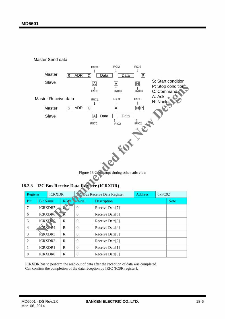
MD6601
MD6601 - DS Rev.1.0 SANKEN ELECTRIC CO.,LTD. 18-6 Mar. 06, 2014
S CADR Data
A
Data
A N
P
S CADR
DataA Data
A N P
IRIC1
↓
IRCI2
↓
IRCI2
↓
IRIC0 IRIC3 IRIC3
↓ ↓ ↓
IRIC1
↓
IRIC3
↓
IRIC3
↓
IRIC0 IRIC2 IRIC2
↓ ↓ ↓
Master Send data
Master Receive data
Master
Slave
Master
Slave
S: Start condition
P: Stop condition
C: Command
A: Ack
N: Nack
Figure 18-2 Interrupt timing schematic view
18.2.3 I2C Bus Receive Data Register (ICRXDR)
Register ICRXDR I2C Bus Receive Data Register Address 0xFC02
Bit Bit Name R/W Initial Description Note
7 ICRXDR7 R 0 Receive Data[7]
6 ICRXDR6 R 0 Receive Data[6]
5 ICRXDR5 R 0 Receive Data[5]
4 ICRXDR4 R 0 Receive Data[4]
3 ICRXDR3 R 0 Receive Data[3]
2 ICRXDR2 R 0 Receive Data[2]
1 ICRXDR1 R 0 Receive Data[1]
0 ICRXDR0 R 0 Receive Data[0]
ICRXDR has to perform the read-out of data after the reception of data was completed.
Can confirm the completion of the data reception by IRIC (ICSR register).
Not Reco
mmended
for N
ew D
esign
s

MD6601
MD6601 - DS Rev.1.0 SANKEN ELECTRIC CO.,LTD. 18-7 Mar. 06, 2014
18.2.4 I2C Bus Transmit Data Register (ICTXDR)
Register ICTXDR I2C Bus Transmit Data Register Address 0xFC03
Bit Bit Name R/W Initial Description Note
7 ICTXDR7 R/W 0 Transmit Data[7]
6 ICTXDR6 R/W 0 Transmit Data[6]
5 ICTXDR5 R/W 0 Transmit Data[5]
4 ICTXDR4 R/W 0 Transmit Data[4]
3 ICTXDR3 R/W 0 Transmit Data[3]
2 ICTXDR2 R/W 0 Transmit Data[2]
1 ICTXDR1 R/W 0 Transmit Data[1]
0 ICTXDR0 R/W 0 Transmit Data[0]
Start transmission by writing in data at ICTXDR.
Writing is prohibition until the transmission of data is completed in ICTXDR.
When write in ICTXDR during the transmission of data, the contents of data are destroyed.
18.2.5 Transmit Address Register (ICTSAR)
Register ICTSAR I2C Transmit Address Register Address 0xFC04
Bit Bit Name R/W Initial Description Note
7 ADR6 R/W 0 Transmit Address [6]
6 ADR5 R/W 0 Transmit Address [5]
5 ADR4 R/W 0 Transmit Address [4]
4 ADR3 R/W 0 Transmit Address [3]
3 ADR2 R/W 0 Transmit Address [2]
2 ADR1 R/W 0 Transmit Address [1]
1 ADR0 R/W 0 Transmit Address [0]
0 CMD R/W 0 Transmit Command
0 : Write Command
1 : Read Command
Please take start in ICCMD registers after setting in ICTSAR registers.
Not Reco
mmended
for N
ew D
esign
s

MD6601
MD6601 - DS Rev.1.0 SANKEN ELECTRIC CO.,LTD. 18-8 Mar. 06, 2014
18.2.6 Slave Address Register (ICSAR)
Register ICSAR I2C Slave Address Register Address 0xFC05
Bit Bit Name R/W Initial Description Note
7 SVA6 R/W 0 Slave Address [6]
6 SVA5 R/W 0 Slave Address [5]
5 SVA4 R/W 0 Slave Address [4]
4 SVA3 R/W 0 Slave Address [3]
3 SVA2 R/W 0 Slave Address [2]
2 SVA1 R/W 0 Slave Address [1]
1 SVA0 R/W 0 Slave Address [0]
0 CMD R 0 Receive Command
0 : Write Command
1 : Read Command
When the receive slave address matches the SVA[5:0] value in ICSAR, work as a slave device appointed to a master
device.
18.2.7 Clock Divid Register (ICCLK)
Register ICCLK I2C Clock Divid Register Address 0xFC06
Bit Bit Name R/W Initial Description Note
7-2 Reserved R 0 Reserved
1 DIV[1] R/W 1 SCL Minimum Pulse Width Setting
00: tSCLH/tSCLL= CLKSLOW 8cycle
01: tSCLH/tSCLL= CLKSLOW 32cycle
10: tSCLH/tSCLL = CLKSLOW 128cycle
11: tSCLH/tSCLL = CLKSLOW 512cycle
0 DIV[0] R/W 1
Set SCL minimum pulse width with a number for a cycle of CLKSLLOW.
The SCL pulse width (tHigh/tLow) on Bus spreads than this setting to need 5cycle for noise filter & synchronization.
Figure 18-3 tSCLH/tSCLL Timing definition
Table 18-3 Restrictions of the minimum clock frequency
SCL frequency 0 - 100KHz(Normal mode) 0 - 400KHz(Fast mode)
CLKSLOW frequency upper than 1.74MHz upper than 6.67MHz
Internal SC*
tSCLH tSCLL
scl_out
* Internal SCL=SCL after noise filter
Not Reco
mmended
for N
ew D
esign
s

MD6601
MD6601 - DS Rev.1.0 SANKEN ELECTRIC CO.,LTD. 18-9 Mar. 06, 2014
18.2.8 I2C Command Register (ICCMD)
Register ICCMD I2C Command Register Address 0xFC07
Bit Bit Name R/W Initial Description Note
7-5 Reserved R 0 Reserved
4 NACK R/W 0 NACK Answer
After the data reception in the slave mode, return NACK
answer.
When an ACK bit is set or when be going to set it with an
ACK bit, the NACK bit is not set.
0 : No action
1 : NACK answer
When NACK answer complete, this bit is ”0” cleared.
*Be not set during master mode.
3 ACK R/W 0 ACK Answer
After the data reception in the slave mode, return ACK
answer.
When an NACK bit is set , the ACK bit is not set.
0 : No action
1 : ACK answer
When ACK answer complete, this bit is ”0” cleared.
2 RDCNT R/W 0 Read Continue
In a master mode, require the reading of the next data.
Be not set during slave mode.
0 : No action
1 : Require the reading
When Read data reception start, this bit is “0” cleared.
1 END R/W 0 Stop Condition generation
Finish a data transfer, and require generation of the STOP
condition.
Change in a slave mode.
Be not set during slave mode.
When a GO bit is set or when be going to set it with a GO
bit, the END bit is not set.
0 : No action
1 : Stop Condition generation
When stop condition detected, this bit is “0” cleared.
0 GO R/W 0 Start Condition generation
Generate START condition, and require the transmission
start of the address / command.
Change in a master mode.
Be not set during slave mode.
When an END bit is set, the GO bit is not set.
0 : No action
1 : Start Condition generation
When start condition detected, this bit is “0” cleared.
ICCMD is performed an initialization of in at the time of reset or ICCR register /ICE bit = 'zero' by 0x00.
Not Reco
mmended
for N
ew D
esign
s
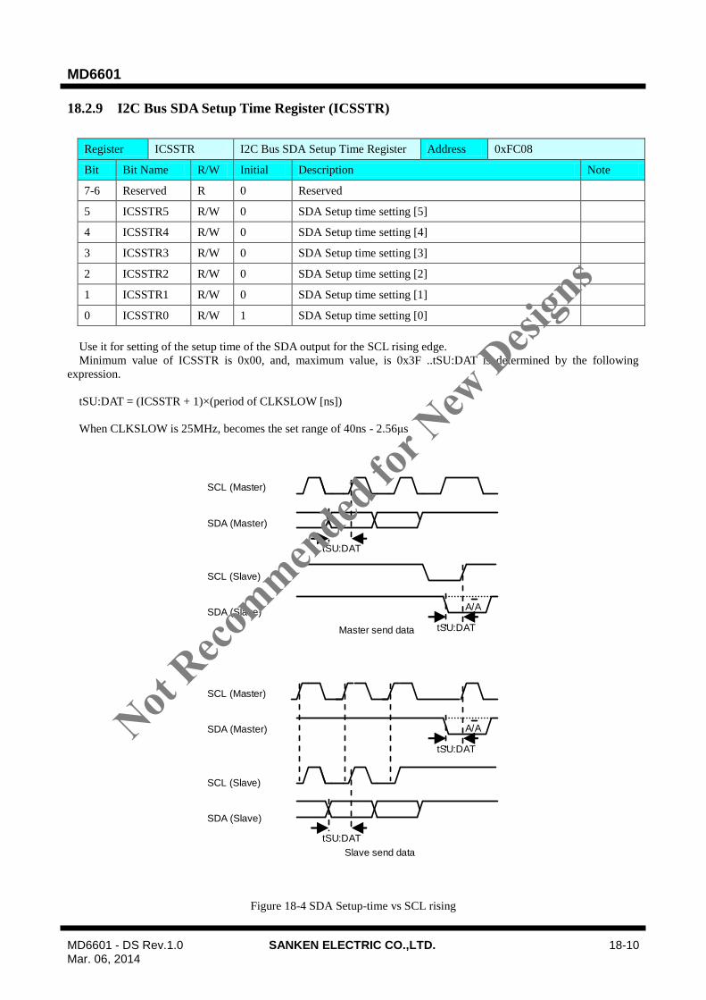
MD6601
MD6601 - DS Rev.1.0 SANKEN ELECTRIC CO.,LTD. 18-10 Mar. 06, 2014
18.2.9 I2C Bus SDA Setup Time Register (ICSSTR)
Register ICSSTR I2C Bus SDA Setup Time Register Address 0xFC08
Bit Bit Name R/W Initial Description Note
7-6 Reserved R 0 Reserved
5 ICSSTR5 R/W 0 SDA Setup time setting [5]
4 ICSSTR4 R/W 0 SDA Setup time setting [4]
3 ICSSTR3 R/W 0 SDA Setup time setting [3]
2 ICSSTR2 R/W 0 SDA Setup time setting [2]
1 ICSSTR1 R/W 0 SDA Setup time setting [1]
0 ICSSTR0 R/W 1 SDA Setup time setting [0]
Use it for setting of the setup time of the SDA output for the SCL rising edge.
Minimum value of ICSSTR is 0x00, and, maximum value, is 0x3F ..tSU:DAT is determined by the following
expression.
tSU:DAT = (ICSSTR + 1)×(period of CLKSLOW [ns])
When CLKSLOW is 25MHz, becomes the set range of 40ns - 2.56μs
SCL (Master)
SDA (Master)
SCL (Slave)
SDA (Slave)
tSU:DAT
tSU:DAT
A/A
SCL (Master)
SDA (Master)
SCL (Slave)
SDA (Slave)
tSU:DAT
tSU:DAT
A/A
Master send data
Slave send data
Figure 18-4 SDA Setup-time vs SCL rising
Not Reco
mmended
for N
ew D
esign
s

MD6601
MD6601 - DS Rev.1.0 SANKEN ELECTRIC CO.,LTD. 18-11 Mar. 06, 2014
18.2.10 I2C Bus SDA Hold Time Register (ICSHTR)
Register ICSHTR I2C Bus SDA Hold Time Register Address 0xFC09
Bit Bit Name R/W Initial Description Note
7 ICSHEXP R/W 0 Expand SDA output Hold
0:No expand
CLKSLOW is up to 12.5MHz, or when Don‟t use it
as SMBUS.
1:Expand SDA output Hold
CLKSLOW is more than 12.5MHz, and when use it
as SMBUS.
The SDA output delays 3 cycles in comparison with
"zero" setting in CLKSLOW when I set it in “1".
6-5 Reserved R 0 Reserved
4 ICSHTR4 R/W 0 SDA Hold time setting [4]
3 ICSHTR3 R/W 0 SDA Hold time setting [3]
2 ICSHTR2 R/W 0 SDA Hold time setting [2]
1 ICSHTR1 R/W 0 SDA Hold time setting [1]
0 ICSHTR0 R/W 0 SDA Hold time setting [0]
In the slave address reception and a slave receive mode, use it for delay time setting to secure hold time for SCL of
the SDA internally.
tHD:DAT = (ICSHTR)×(period of CLKSLOW [ns])
When CLKCSLOW is 25MHz, becomes the set range of 0 ns – 1240 ns.
SDA
Noise
Cancel
SDA
D Q
CK
D Q
CK
D Q
CK
D Q
CK
Delay Selector
ICSHTR Internal-SDA
SDA Hold-time Building out circuit
Figure 18-5 Internal-SDA generation block diagram
At the time of ICSSTR and the ICSHTR setting, please set it to satisfy the following relations.
(Setup time by ICSSTR ) > ( Setup time by ICSHTR ) – ( Relative delay time of SDA and SCL )
As for the SDA and the relative delay time of SCL, it is with a difference of the delay time of SDA signal and the
SCL signal on the I2C bus.In addition, this delay time lag needs consideration of the operating environment to be
affected by the operating environment of the real I2C bus.
(Relative delay time of SDA and SCL ) = (SCL delay time ) - ( SDA delay time )
Not Reco
mmended
for N
ew D
esign
s
MD6601
MD6601 - DS Rev.1.0 SANKEN ELECTRIC CO.,LTD. 18-12 Mar. 06, 2014
18.2.11 I2C Bus SDA Hardware Status Register 0(ICHDSR0)
Register ICHDSR0 I2C Bus SDA Hardware Status
Register 0 Address 0xFC0A
Bit Bit Name R/W Initial Description Note
7 SDAMON R 1 Monitor of SDA signal.
0 : SDA is „L‟
1 : SDA is „H‟
6 SCLMON R 1 Monitor of SDA signal.
0 : SCL is „L‟
1 : SCL is „H‟
5 SDACHG R/C 0 SDACHG outputs having SDA signal change or not.
0 : no detect of SDA signal change
[Clear condition]
“1” write from CPU
1 : detect of SDA signal change
[Set condition]
When detect of SDA signal change
4 SCLCHG R/C 0 SCLCHG outputs having SCL signal change or not.
0 : no detect of SCL signal change
[Clear condition]
“1” write from CPU
1 : detect of SCL signal change
[Set condition]
When detect of SCL signal change
3-0 Reserved R 0 Reserved
18.2.12 I2C Bus SDA Hardware Status Register 1(ICHDSR1)
Register ICHDSR1 I2C Bus SDA Hardware Status Register 1 Address 0xFC0B
Bit Bit Name R/W Initial Description Note
7-5 Reserved R 0 Reserved
4 I2C_ST4 R 0 State machine status [4]
3 I2C_ST3 R 0 State machine status [3]
2 I2C_ST2 R 0 State machine status [2]
1 I2C_ST1 R 0 State machine status [1]
0 I2C_ST0 R 0 State machine status [0]
Not Reco
mmended
for N
ew D
esign
s
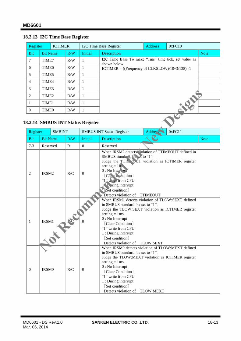
MD6601
MD6601 - DS Rev.1.0 SANKEN ELECTRIC CO.,LTD. 18-13 Mar. 06, 2014
18.2.13 I2C Time Base Register
Register ICTIMER I2C Time Base Register Address 0xFC10
Bit Bit Name R/W Initial Description Note
7 TIME7 R/W 1 I2C Time Base To make “1ms” time tick, set value as
shown below
ICTIMER = ((Frequency of CLKSLOW)/10^3/128) -1
6 TIME6 R/W 1
5 TIME5 R/W 1
4 TIME4 R/W 1
3 TIME3 R/W 1
2 TIME2 R/W 1
1 TIME1 R/W 1
0 TIME0 R/W 1
18.2.14 SMBUS INT Status Register
Register SMBINT SMBUS INT Status Register Address 0xFC11
Bit Bit Name R/W Initial Description Note
7-3 Reserved R 0 Reserved
2 IRSM2 R/C 0
When IRSM2 detects violation of TTIMEOUT defined in
SMBUS standard, be set to “1”.
Judge the TTIMEOUT violation as ICTIMER register
setting = 1ms.
0 : No Interrupt
[Clear Condition]
“1” write from CPU
1 : During interrupt
[Set condition]
Detects violation of TTIMEOUT
1 IRSM1 R/C 0
When IRSM1 detects violation of TLOW:SEXT defined
in SMBUS standard, be set to “1”.
Judge the TLOW:SEXT violation as ICTIMER register
setting = 1ms.
0 : No Interrupt
[Clear Condition]
“1” write from CPU
1 : During interrupt
[Set condition]
Detects violation of TLOW:SEXT
0 IRSM0 R/C 0
When IRSM0 detects violation of TLOW:MEXT defined
in SMBUS standard, be set to “1”.
Judge the TLOW:MEXT violation as ICTIMER register
setting = 1ms.
0 : No Interrupt
[Clear Condition]
“1” write from CPU
1 : During interrupt
[Set condition]
Detects violation of TLOW:MEXT
Not Reco
mmended
for N
ew D
esign
s
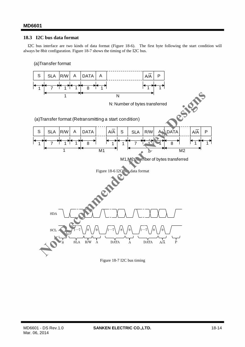
MD6601
MD6601 - DS Rev.1.0 SANKEN ELECTRIC CO.,LTD. 18-14 Mar. 06, 2014
18.3 I2C bus data format
I2C bus interface are two kinds of data format (Figure 18-6). The first byte following the start condition will
always be 8bit configuration. Figure 18-7 shows the timing of the I2C bus.
Figure 18-6 I2C bus data format
SDA
SCL 1―7 8 9 1―7 8 9 1―7 8 9
S SLA R/W A DATA A DATA A/A P
Figure 18-7 I2C bus timing
N: Number of bytes transferred
1 7 1 1 8 1 1 1
1 N
(a)Transfer format
(a)Transfer format (Retransmitting a start condition)
1 7 1 1 8 1 7 1 1 8
1
1 1
M1 M21
1
M1,M2: Number of bytes transferred
S SLA R/W A DATA A A/A P
S SLA R/W A DATA A/A S SLA R/W A DATA A/A P
Not Reco
mmended
for N
ew D
esign
s

MD6601
MD6601 - DS Rev.1.0 SANKEN ELECTRIC CO.,LTD. 18-15 Mar. 06, 2014
18.4 Slave receiver operation
In slave receiver operation, the master device outputs the slave address, data and clock. The slave device returns
acknowledgements. The following describes the procedure and operations for slave reception.
(1) Set the ICE bit in ICCR to “1”.
(2) Set slave address to the SVA bit in ICSAR.
(3) The master device sends a slave address and a write command following a start condition.
(4) To compare the SVA bit in ICSAR and received slave address.
(5) After receiving matching slave address, stored in the CMD bit in ICSAR a write command, and returns
acknowledgements to the master device.
(6) At the same time send acknowledgements, IRIC0 bit in ICSR is set to “1” and generates an interrupt.
(7) Clear the IRIC0 bit in ICSR to ”0”.
(8) The slave receives the data from the master device.
(9) The slave stores the received data into ICRXDR, and IRIC3 bit in ICSR set to “1”.
(10) If want to continue to receive operations, ACK bit in ICCMD set to “1”. Then ACK response is output to I2C
bus.
(11) If want to continue to receive operations, return (8).
(12) If don't want to continue to receive operations, NACK bit in ICCMD set to “1”. Then NACK response is output
to I2C bus.
(13) Clear the IRIC3 bit in ICSR to “0”.
(14) If detecting the stop condition, IRIC5 bit in ICSR is set to “1” and an interrupt is generated. Clear IRIC5 in
ICSR to “0”.
Not Reco
mmended
for N
ew D
esign
s
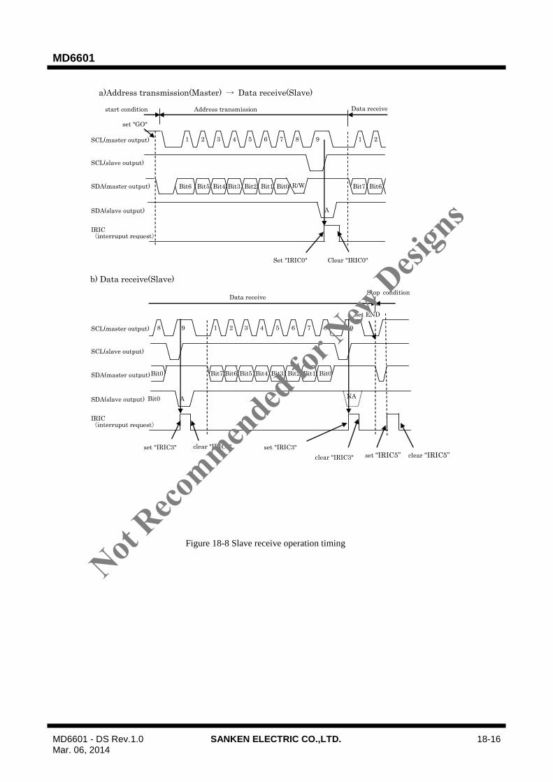
MD6601
MD6601 - DS Rev.1.0 SANKEN ELECTRIC CO.,LTD. 18-16 Mar. 06, 2014
1 2 3 4 5 6 7 8 9 1 SCL(master output)
SCL(slave output)
SDA(slave output)
SDA(master output)
IRIC (interruput request)
A
R/W
A
Bit6 Bit5 Bit4 Bit3 Bit2 Bit1 Bit0
start condition Address transmission
set "GO"
Clear "IRIC0"
8 SCL(master output)
SCL(slave output)
SDA(slave output)
SDA(master output)
a)Address transmission(Master) → Data receive(Slave)
b) Data receive(Slave)
Bit7 Bit6
2
9 1
Bit7 Bit6
2
A
clear "IRIC3"
3 4 5 6 7
Bit5 Bit4 Bit3 Bit2 Bit1 Bit0
8
Bit0
set END
Data receive
Data receive Stop condition
Bit0
9
IRIC (interruput request)
Set "IRIC0"
set "IRIC3"
NA
clear "IRIC3"
set "IRIC3"
set “IRIC5” clear “IRIC5”
Figure 18-8 Slave receive operation timing
Not Reco
mmended
for N
ew D
esign
s
MD6601
MD6601 - DS Rev.1.0 SANKEN ELECTRIC CO.,LTD. 18-17 Mar. 06, 2014
18.5 Slave transmitter operation
In slave transmitter operation, the slave device outputs tranmit data, and the master device outputs the slave address,
returns acknowledgements. The following describes the procedure and operations for master reception.
(1) Set the ICE bit in ICCR to “1”.
(2) Set slave address to the SVA bit in ICSAR.
(3) The master device sends a slave address and a read command following a start condition.
(4) To compare the SVA bit in ICSAR and received slave address.
(5) After receiving matching slave address, stored in the CMD bit in ICSAR a read command, and returns
acknowledgements to the master device.
(6) At the same time send acknowledgements, IRIC0 bit in ICSR is set to “1” and generates an interrupt.
(7) Clear the IRIC0 bit in ICSR to “0”.
(8) When the transmit data is set in the ICTXDR, transmission is started.
(9) When transmission is complete and receives ACK or NACK from the master device, IRIC2 bit in ICSR set to
“1”.
(10) To check the RXACK bit in ICSR for confirming which the ACK reception or NACK reception.
(11) Clear the IRIC2 bit in ICSR to “0”.
(12) If want to continue to transmission, return (8).
(13) If detecting the stop condition, IRIC5 bit in ICSR is set to “1” and an interrupt is generated. Clear the IRIC5 bit
in ICSR to “0”.
Not Reco
mmended
for N
ew D
esign
s

MD6601
MD6601 - DS Rev.1.0 SANKEN ELECTRIC CO.,LTD. 18-18 Mar. 06, 2014
1 2 3 4 5 6 7 8 9 1 SCL(master output)
SCL(slave output)
SDA(slave output)
SDA(master output)
IRIC
(interrupt request)
A
R/W
A
Bit6 Bit5 Bit4 Bit3 Bit2 Bit1 Bit0
Start condition Address receive
Clear “IRIC0” Set “ICTXDR”
8 SCL(master output)
SCL(slave output)
SDA(slave output)
SDA(master output)
IRIC
(interrupt request)
a)Address receive → Data transmission
b) Data transmission
Bit7 Bit6
2
9 1
Bit7 Bit6
2
A
Clear “IRIC2” Set “ICTXDR”
3 4 5 6 7
Bit5 Bit4 Bit3 Bit2 Bit1 Bit0
8
Clear “IRIC2”
Data transmission
Data transmission
Stop condition
Bit0
9
NA
Clear “IRIC5”
Figure 18-9 Slave transmit operation timing
Not Reco
mmended
for N
ew D
esign
s
MD6601
MD6601 - DS Rev.1.0 SANKEN ELECTRIC CO.,LTD. 18-19 Mar. 06, 2014
18.6 Master receiver operation
In master receiver operation, the slave device outputs tranmit data, and the master device outputs the slave address,
returns acknowledgements. The following describes the procedure and operations for master reception.
(1) Set the ICE bit in ICCR to “1”.
(2) Set the slave address to the ADR [6:0] in ICTSAR, and set CMD bit in ICTSAR to “1”.
(3) Set the GO bit in ICCMD to 1 in order to generate the start condition. When the start condition is detected, this
GO bit is cleared automatically.
(4) The master device sends a slave address and a read command following the start condition
(5) At the same time receive ACK or NACK from the slave device, IRIC bit in ICSR is set to “1” and generates an
interrupt..It is able to confirm which ACK reception or NACK reception by checking the RXACK bit in ICSR..
The master device will hold the SCL “Low” until write to any bit of ICCMD.
(6) Clear the IRIC bit in ICSR to “0”.
(7) Set the RDCNT bit in ICCMD to ”1” in order to release the SCL.
(8) When receive the eight-bit data, IRIC3 bit in ICSR is set to “1” and generates interrupt. The master device will
hold the SCL “Low” until write to any bit of ICCMD.
(9) Clear the IRIC3 bit in ICSR to 0.
(10) Read received data of ICRXDR.
(11) If continue to receive operation :
Set the RDCNT bit in ICCMD to “1”. Return the ACK to the slave device automatically, and repeat from (8)
to (11).
If stop the receiver operation :
Set the END bit in ICCMD to “1”. Returning the NACK to the slave device automatically, the master device
starts generating the stop condition. When it finishes generating the stop condition, the IRIC5 bit in ICSR is
set to “1” and an interrupt is generated. Clear the IRIC5 bit in ICSR to “0”.
If start the next operation
To check the BBSY bit in ICSR first for confirming the detection of the stop condition, then set the GO bit in
ICCMD to “1”.
Not Reco
mmended
for N
ew D
esign
s
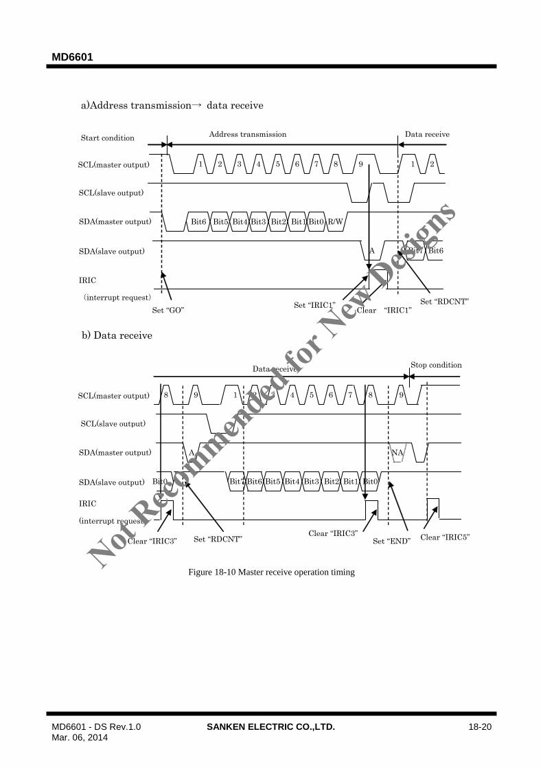
MD6601
MD6601 - DS Rev.1.0 SANKEN ELECTRIC CO.,LTD. 18-20 Mar. 06, 2014
1 2 3 4 5 6 7 8 9 1 SCL(master output)
SCL(slave output)
SDA(slave output)
SDA(master output)
IRIC
(interrupt request)
A
R/W
A
Bit6 Bit5 Bit4 Bit3 Bit2 Bit1 Bit0
Start condition Address transmission
Set “GO” Set “IRIC1” Set “RDCNT”
8 SCL(master output)
SCL(slave output)
SDA(slave output)
SDA(master output)
IRIC
(interrupt request)
a)Address transmission→ data receive
b) Data receive
Bit7 Bit6
2
9 1
Bit7 Bit6
2
A
Clear “IRIC3” Set “RDCNT”
3 4 5 6 7
Bit5 Bit4 Bit3 Bit2 Bit1 Bit0
8
Bit0
Clear “IRIC3”
9
Set “END”
NA
Data receive
Data receive Stop condition
Clear “IRIC1”
Clear “IRIC5”
Figure 18-10 Master receive operation timing
Not Reco
mmended
for N
ew D
esign
s
MD6601
MD6601 - DS Rev.1.0 SANKEN ELECTRIC CO.,LTD. 18-21 Mar. 06, 2014
18.7 Master transmitter operation
In master transmitter operation, master device outputs transmitted data and transmitted clock, and slave device
returns acknowledgements. The following describes the procedure and operations for master transmission.
(1) Set the ICE bit in ICCR to “1”.
(2) Set slave address to the ADR[6:0] in ICTSAR, and set CMD bit in ICTSAR to 0.
(3) Set the GObit in ICCMD to “1” in order to generate the start condition. When the start condition is detected, this
GO bit is cleared automatically. .
(4) The master device sends a slave address and a read command following a start condition.
(5) At the same time receive ACK or NACK from the slave device, IRIC1 bit in ICSR is set to “1” and generates an
interrupt.. ..It is able to confirm which ACK reception or NACK reception by checking the RXACK bit in ICSR..
The master device will hold the SCL “Low” until write to any bit of ICCMD or the transmit data into ICTXDR.
(6) Clear the IRIC1 bit in ICSR to “0”.
(7) Set the ICTXDR to transmit data.
(8) After complete transmission for the eight-bit data, The master device will wait for ACK or NACK from the
slave device.
(9) At the same time receive ACK or NACK from the slave device, IRIC2 bit in ICSR is set to “1” and generates an
interrupt. .It is able to confirm which ACK reception or NACK reception by checking the RXACK bit in ICSR..
The master device will hold the SCL “Low” until write to any bit of ICCMD or the transmit data into ICTXDR.
(10) Clear the IRIC2 bit in ICSR to 0.
(11) If continue to transmitter operation :
Set the transmit data into ICTXDR. Repeat from (8) to (11).
If stop the transmitter operation :
Set the END bit in ICCMD to “1” and the master device starts generating the stop condition. When it finishes
generating the stop condition, IRIC5 bit in ICSR is set to “1” and an interrupt is generated. Clear IRIC5 bit in
ICSR to “0”.
If start the next operation
To check the BBSY bit in ICSR first for confirming the detection of the stop condition, then set the GO bit in
ICCMD to “1”.
Not Reco
mmended
for N
ew D
esign
s

MD6601
MD6601 - DS Rev.1.0 SANKEN ELECTRIC CO.,LTD. 18-22 Mar. 06, 2014
1 2 3 4 5 6 7 8 9 1 SCL(master output)
SCL(slave output)
SDA(slave output)
SDA(master output)
IRIC
(interrupt request)
A
R/W
A
Bit6 Bit5 Bit4 Bit3 Bit2 Bit1 Bit0
Start condition Address transmission
Set “GO” Clear “IRIC1” Set “ICTXDR”
8 SCL(master output)
SCL(slave output)
SDA(slave output)
SDA(master output)
IRIC
(interrupt request)
a)Address transmission→Data transmission
b) Data transmission
Bit7 Bit6
2
9 1
Bit7 Bit6
2
A
Clear “IRIC2” Set “ICTXDR”
3 4 5 6 7
Bit5 Bit4 Bit3 Bit2 Bit1 Bit0
8
Bit0
Clear “IRIC2” set “END”
Data transmission
Data transmission Stop Condition
Bit0
9
Clear “IRIC5”
Figure 18-11 Master transmit operation timing
Not Reco
mmended
for N
ew D
esign
s

MD6601
MD6601 - DS Rev.1.0 SANKEN ELECTRIC CO.,LTD. 18-23 Mar. 06, 2014
18.8 Noise Filter
SCL and SDA are taken into the internal circuit through the noise filter. Figure 18-12 shows the block diagram of the
noise filter.
Noise filter is composed of flip-flop circuit and a match detector which are connected in series two-stage.
Noise filter is comprised of two steps of FF circuits and match detecting circuits. When SCL is sampled in
CLKSLOW and two flip-flop outputs are matched, convey its level to the next stage. If outputs are unmatched, output is
maintain a previous value.
D Q
CK
FF
Match
detecter
SCL input
or
SDA input
internal SCL
or
internal SDA
CLKSLOW
CLKSLOW:I2C system clock
D Q
CK
FF
Figure 18-12 Block diagram of the noise filter
Not Reco
mmended
for N
ew D
esign
s
MD6601
MD6601 - DS Rev.1.0 SANKEN ELECTRIC CO.,LTD. 19-1 Mar. 06, 2014
19. UART The modem terminal control is not supported by the LSI.
19.1 Overview
UART supports asynchronous serial I/O mode. UART has a dedicated timer to generate a transfer clock and operate
independently.
Table 19-1 Feature of UART
Item Description
Data Format
Data Length: 7, 8 or 9bits
Start Bit: 1bit
Parity Bit: odd, even or none
Stop Bits: 1 or 2bits
Baud Rate
Based on Divisor Latch Bytes
Baud Rate (bps) = CLKUART/16 x 1/ (n)
CLKUART:CLKSLOW
n: Setting value of Divisor Latch Bytes(DLB1 & DLB2)
FIFO
TXFIFO:16bytes
RXFIFO:16bytes
Interrupt by TX Transmit Buffer Empty
Transfer Completed
Interrupt by RX Receive Buffer Full
Parity Error / Overrun Error / Framing Error
Not Reco
mmended
for N
ew D
esign
s
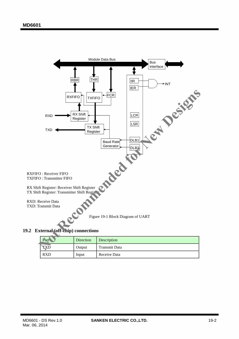
MD6601
MD6601 - DS Rev.1.0 SANKEN ELECTRIC CO.,LTD. 19-2 Mar. 06, 2014
RXD
TXD
THRRBR
RXFIFO
Bus
Interface
Baud Rate
Generator
RX Shift
Register
IIR
IER
DLB2
DLB1
LCR
LSR
INT
Module Data Bus
TXFIFOFCR
TX Shift
Register
RXFIFO : Receiver FIFO
TXFIFO : Transmitter FIFO
RX Shift Register: Receiver Shift Register
TX Shift Register: Transmitter Shift Register
RXD: Receive Data
TXD: Transmit Data
Figure 19-1 Block Diagram of UART
19.2 External (off-chip) connections
Port Direction Description
TXD Output Transmit Data
RXD Input Receive Data
Not Reco
mmended
for N
ew D
esign
s

MD6601
MD6601 - DS Rev.1.0 SANKEN ELECTRIC CO.,LTD. 19-3 Mar. 06, 2014
19.3 Register Description
Table 19-2 List of registers
Symbol Name Address Initial value
RBR Receiver Buffer Register 0xFC80 indeterminate
THR Transmitter Holding Register 0xFC80 indeterminate
IER Interrupt Enable Register 0xFC81 0x00
IIR Interrupt Identification Register 0xFC82 0xC1
FCR FIFO Control Register 0xFC82 0xC0
LCR Line Control Register 0xFC83 0x03
LSR Line Status Register 0xFC85 0x60
In addition, there are 2 Clock Divisor registers that together form one 16 bit.
The registers can be accessed when LCR.DLAB is set to ‘1’. At this time RBR, THR and IER registers at addresses
0xFC80-0xFC81 can’t be accessed.
Symbol Name Address Initial value
DLB1 Divisor Latch Byte 1 0xFC80 0x00
DLB2 Divisor Latch Byte 2 0xFC81 0x00
19.3.1 Receiver Buffer Register/Transmitter Holding Register
Register RBR Receiver Buffer Register Address 0xFC80
Bit Bit Name R/W Initial Description Note
7-0 R indeterminate Receiver FIFO output
Register THR Transmitter Holding Register Address 0xFC80
Bit Bit Name R/W Initial Description Note
7-0 W indeterminate Transmit FIFO input
19.3.2 Interrupt Enable Register (IER)
This register allows enabling and disabling interrupt generation by the UART.
Register IER Interrupt Enable Register Address 0xFC81
Bit Bit Name R/W Initial Description Note
7-3 Reserved R/W 0 Read value ‘0’. Write only ‘0’.
2 IER2 R/W 0 Receiver Line Status Interrupt
‘0’ – disabled
‘1’ – enabled
1 IER1 R/W 0 Transmitter Holding Register empty Interrupt
‘0’ – disabled
‘1’ – enabled
0 IER0 R/W 0 Received Data available Interrupt
‘0’ – disabled
‘1’ – enabled
Not Reco
mmended
for N
ew D
esign
s
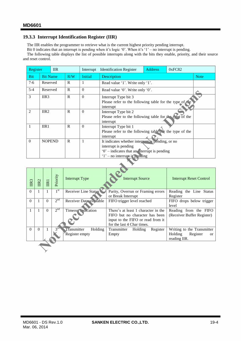
MD6601
MD6601 - DS Rev.1.0 SANKEN ELECTRIC CO.,LTD. 19-4 Mar. 06, 2014
19.3.3 Interrupt Identification Register (IIR)
The IIR enables the programmer to retrieve what is the current highest priority pending interrupt.
Bit 0 indicates that an interrupt is pending when it’s logic ‘0’. When it’s ‘1’ – no interrupt is pending.
The following table displays the list of possible interrupts along with the bits they enable, priority, and their source
and reset control.
Register IIR Interrupt Identification Register Address 0xFC82
Bit Bit Name R/W Initial Description Note
7-6 Reserved R 1 Read value ‘1’. Write only ‘1’.
5-4 Reserved R 0 Read value ‘0’. Write only ‘0’.
3 IIR3 R 0 Interrupt Type bit 3
Please refer to the following table for the type of the
interrupt
2 IIR2 R 0 Interrupt Type bit 2
Please refer to the following table for the type of the
interrupt
1 IIR1 R 0 Interrupt Type bit 1
Please refer to the following table for the type of the
interrupt
0 NOPEND R 1 It indicates whether interrupt is pending, or no
interrupt is pending
‘0’ – indicates that an interrupt is pending
‘1’ – no interrupt is pending
IIR
3
IIR
2
IIR
1
Pri
ori
ty
Interrupt Type Interrupt Source Interrupt Reset Control
0 1 1 1st Receiver Line Status Parity, Overrun or Framing errors
or Break Interrupt
Reading the Line Status
Register
0 1 0 2nd
Receiver Data available FIFO trigger level reached FIFO drops below trigger
level
1 1 0 2nd
Timeout Indication There’s at least 1 character in the
FIFO but no character has been
input to the FIFO or read from it
for the last 4 Char times.
Reading from the FIFO
(Receiver Buffer Register)
0 0 1 3rd
Transmitter Holding
Register empty
Transmitter Holding Register
Empty
Writing to the Transmitter
Holding Register or
reading IIR.
Not Reco
mmended
for N
ew D
esign
s
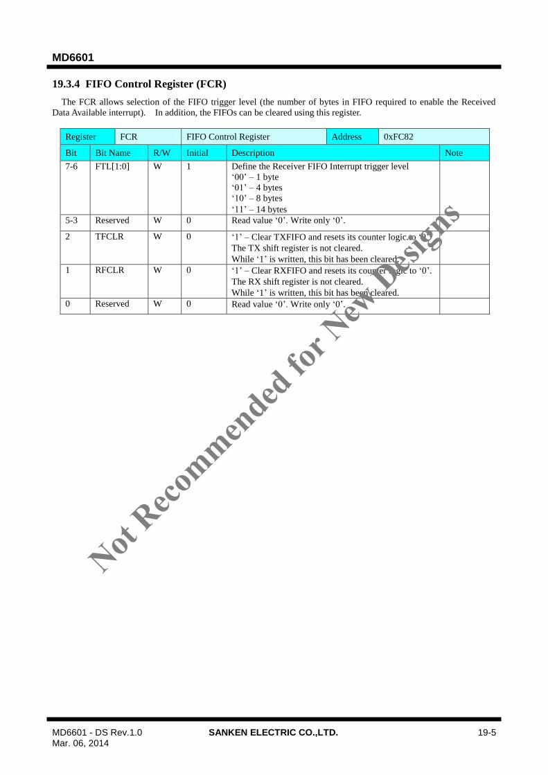
MD6601
MD6601 - DS Rev.1.0 SANKEN ELECTRIC CO.,LTD. 19-5 Mar. 06, 2014
19.3.4 FIFO Control Register (FCR)
The FCR allows selection of the FIFO trigger level (the number of bytes in FIFO required to enable the Received
Data Available interrupt). In addition, the FIFOs can be cleared using this register.
Register FCR FIFO Control Register Address 0xFC82
Bit Bit Name R/W Initial Description Note
7-6 FTL[1:0] W 1 Define the Receiver FIFO Interrupt trigger level
‘00’ – 1 byte
‘01’ – 4 bytes
‘10’ – 8 bytes
‘11’ – 14 bytes
5-3 Reserved W 0 Read value ‘0’. Write only ‘0’.
2 TFCLR W 0 ‘1’ – Clear TXFIFO and resets its counter logic.to ‘0’
The TX shift register is not cleared.
While ‘1’ is written, this bit has been cleared.
1 RFCLR W 0 ‘1’ – Clear RXFIFO and resets its counter logic to ‘0’.
The RX shift register is not cleared.
While ‘1’ is written, this bit has been cleared.
0 Reserved W 0 Read value ‘0’. Write only ‘0’.
Not Reco
mmended
for N
ew D
esign
s

MD6601
MD6601 - DS Rev.1.0 SANKEN ELECTRIC CO.,LTD. 19-6 Mar. 06, 2014
19.3.5 Line Control Register (LCR)
The line control register allows the specification of the format of the asynchronous data communication used. A bit in
the register also allows access to the Divisor Latches, which define the baud rate. Reading from the register is allowed
to check the current settings of the communication.
Register LCR Line Control Register Address 0xFC83
Bit Bit Name R/W Initial Description Note
7 DLAB R/W 0 Divisor Latch Access bit.
‘0’ – The normal registers are accessed
‘1’ – The divisor latches can be accessed
6 BRK R/W 0 Break Control bit
‘0’ – break is disabled
‘1’ – the serial out is forced into logic ‘0’ (break state).
5 STICK R/W 0 Stick Parity bit.
‘0’ – Stick Parity disabled
‘1’ – If PARE and EVPAR are logic ‘1’, the parity bit
is transmitted and checked as logic ‘0’. If PARE
is ‘1’ and EVPAR is ‘0’ then the parity bit is
transmitted and checked as ‘1’.
4 EVPAR R/W 0 Even Parity select
‘0’ – Odd number of ‘1’ is transmitted and checked in
each word (data and parity combined). In other
words, if the data has an even number of ‘1’ in
it, then the parity bit is ‘1’.
‘1’ – Even number of ‘1’ is transmitted in each word.
3 PARE R/W 0 Parity Enable
‘0’ – No parity
‘1’ – Parity bit is generated on each outgoing character
and is checked on each incoming one.
2 NSTP R/W 0 Specify the number of generated stop bits
‘0’ – 1 stop bit
‘1’ – 2 stop bits, when either a 6-,7-, or 8-bit character
length is selected.
1.5 stop bits, when 5-bit character length is
selected.
Note that the receiver always checks the first stop bit
only.
1-0 NBCHAR R/W 1 Select Number of bits in each character
‘00’ – 5 bits
‘01’ – 6 bits
‘10’ – 7 bits
‘11’ – 8 bits
Not
Recommen
ded fo
r New
Desi
gns
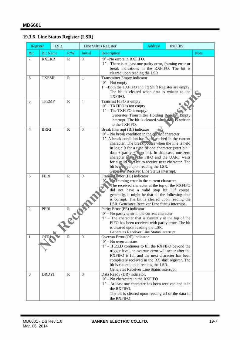
MD6601
MD6601 - DS Rev.1.0 SANKEN ELECTRIC CO.,LTD. 19-7 Mar. 06, 2014
19.3.6 Line Status Register (LSR)
Register LSR Line Status Register Address 0xFC85
Bit Bit Name R/W Initial Description Note
7 RXERR R 0 ‘0’ –No errors in RXFIFO.
‘1’ – There is at least one parity error, framing error or
break indications in the RXFIFO. The bit is
cleared upon reading the LSR
6 TXEMP R 1 Transmitter Empty indicator.
‘0’ – Not empty
1’ –Both the TXFIFO and Tx Shift Register are empty.
The bit is cleared when data is written to the
TXFIFO.
5 TFEMP R 1 Transmit FIFO is empty.
‘0’ – TXFIFO is not empty
‘1’ – The TXFIFO is empty.
Generates Transmitter Holding Register Empty
interrupt. The bit is cleared when data is written
to the TXFIFO.
4 BRKI R 0 Break Interrupt (BI) indicator
‘0’ – No break condition in the current character
‘1’–A break condition has been reached in the current
character. The break occurs when the line is held
in logic 0 for a time of one character (start bit +
data + parity + stop bit). In that case, one zero
character enters the FIFO and the UART waits
for a valid start bit to receive next character. The
bit is cleared upon reading the LSR.
Generates Receiver Line Status interrupt.
3 FERI R 0 Framing Error (FE) indicator
‘0’ – No framing error in the current character
‘1’ – The received character at the top of the RXFIFO
did not have a valid stop bit. Of course,
generally, it might be that all the following data
is corrupt. The bit is cleared upon reading the
LSR. Generates Receiver Line Status interrupt.
2 PERI R 0 Parity Error (PE) indicator
‘0’ – No parity error in the current character
‘1’ – The character that is currently at the top of the
FIFO has been received with parity error. The bit
is cleared upon reading the LSR.
Generates Receiver Line Status interrupt.
1 OERI R 0 Overrun Error (OE) indicator
‘0’ – No overrun state
‘1’ – If RXD continues to fill the RXFIFO beyond the
trigger level, an overrun error will occur after the
RXFIFO is full and the next character has been
completely received in the RX shift register. The
bit is cleared upon reading the LSR.
Generates Receiver Line Status interrupt.
0 DRDYI R 0 Data Ready (DR) indicator.
‘0’ – No characters in the RXFIFO
‘1’ – At least one character has been received and is in
the RXFIFO.
The bit is cleared upon reading all of the data in
the RXFIFO
Not Reco
mmended
for N
ew D
esign
s

MD6601
MD6601 - DS Rev.1.0 SANKEN ELECTRIC CO.,LTD. 19-8 Mar. 06, 2014
19.3.7 Divisor Latches
Register DLB1 Divisor Latch Byte 1(LSB) Address 0xFC80
Bit Bit Name R/W Initial Description Note
7-0 R/W 0 The LSB of the divisor latch
Register DLB2 Divisor Latch Byte 2(MSB) Address 0xFC81
Bit Bit Name R/W Initial Description Note
7-0 R/W 0 The MSB of the divisor latch
The divisor latches can be accessed by setting LCR.DLAB to ‘1’. It needs to set ‘1’ to LCR.DLAB before the
divisor values are set into DLB1 and DLB2 . The 2 bytes divisor values should be stored into DLB1 and DLB2 as
a16-bit binary code during initialization. Base on these value, baud rate is determined by the following expression
Baud rate = CLKUART(:CLKSLOW)/(16 x divisor value)
Example of a baud rate and a divisor value are shown in Table 19-3. .
The internal counter in Baud Rate Generator starts to work when the DLB1 is written, so when setting the divisor,
write the MSB first and the LSB last.
The default value of DLB1 and DLB 2 are ‘0’. After setting the divisor, LCR.DLAB should be ‘0’ in order to access
RBR and THR.
Not Reco
mmended
for N
ew D
esign
s

MD6601
MD6601 - DS Rev.1.0 SANKEN ELECTRIC CO.,LTD. 19-9 Mar. 06, 2014
19.3.8 Baud rate
Table 19-3 Example of Baud rate, Divisor, and Crystal
DecimalDivisorValue
PercentError
DecimalDivisorValue
PercentError
DecimalDivisorValue
PercentError
2400 480 - 640 - 651 0.01
4800 240 - 320 - 326 0.15
9600 120 - 160 - 163 0.15
19200 60 - 80 - 81 0.47
38400 30 - 40 - 41 0.76
76800 15 - 20 - 28 0.35
96000 12 - 16 - 16 1.73
115200 10 - 13 2.6 14 3.11
128000 9 - 12 - 12 1.73
256000 4 12.5 6 - 6 1.73
384000 3 - 4 - 4 1.73
512000 2 12.5 3 - 3 1.73
768000 1 50 2 - 2 1.73
1152000 1 - 1 33.3 1 35.63
1536000 - - 1 - 1 1.73
DecimalDivisorValue
PercentError
125K 12 -150K 10 -250K 6 -300K 5 -500K 3 -750K 2 -
1500K 1 -
12.5 MHz Crystal
Baud Rate( bps )
Baud Rate( bps )
12.0 MHz Crystal
9.216 MHz Crystal 12.288 MHz Crystal
Note:
Table 19-3 shows just the example of Baud rate and Decimal
Divisor Value in case of using several Crystals.
The Baud rate calculated it by the following
Computation expression.
Baud rate = CLKUART (CLKSLOW) /(1 6x Divisor Value ).
CLKUART(CLKSLOW) = 2 x frequency of Crystal (at
CLKFG0.DIV:1/1)
The accuracy of the Baud rate is depend on Crystal frequency and its
characteristics,.
The errors in Table 19-3 were calculated by the computation
expression as above, and are not things to guarantee.
Not Reco
mmended
for N
ew D
esign
s
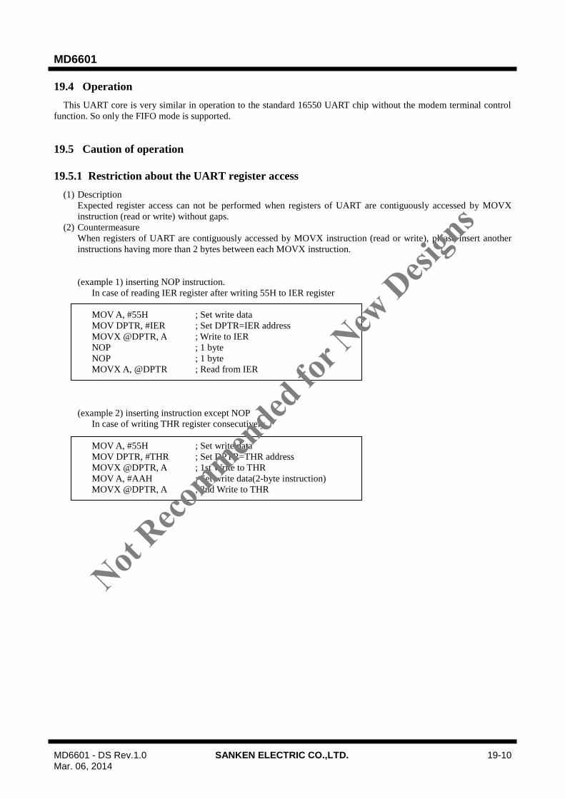
MD6601
MD6601 - DS Rev.1.0 SANKEN ELECTRIC CO.,LTD. 19-10 Mar. 06, 2014
19.4 Operation
This UART core is very similar in operation to the standard 16550 UART chip without the modem terminal control
function. So only the FIFO mode is supported.
19.5 Caution of operation
19.5.1 Restriction about the UART register access
(1) Description
Expected register access can not be performed when registers of UART are contiguously accessed by MOVX
instruction (read or write) without gaps.
(2) Countermeasure
When registers of UART are contiguously accessed by MOVX instruction (read or write), please insert another
instructions having more than 2 bytes between each MOVX instruction.
(example 1) inserting NOP instruction.
In case of reading IER register after writing 55H to IER register
MOV A, #55H ; Set write data
MOV DPTR, #IER ; Set DPTR=IER address
MOVX @DPTR, A ; Write to IER
NOP ; 1 byte
NOP ; 1 byte
MOVX A, @DPTR ; Read from IER
(example 2) inserting instruction except NOP
In case of writing THR register consecutively
MOV A, #55H ; Set write data
MOV DPTR, #THR ; Set DPTR=THR address
MOVX @DPTR, A ; 1st Write to THR
MOV A, #AAH ; Set write data(2-byte instruction)
MOVX @DPTR, A ; 2nd Write to THR
Not Reco
mmended
for N
ew D
esign
s
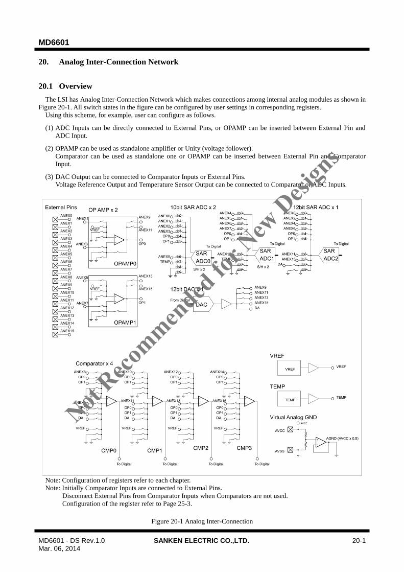
MD6601
MD6601 - DS Rev.1.0 SANKEN ELECTRIC CO.,LTD. 20-1 Mar. 06, 2014
20. Analog Inter-Connection Network
20.1 Overview
The LSI has Analog Inter-Connection Network which makes connections among internal analog modules as shown in
Figure 20-1. All switch states in the figure can be configured by user settings in corresponding registers.
Using this scheme, for example, user can configure as follows.
(1) ADC Inputs can be directly connected to External Pins, or OPAMP can be inserted between External Pin and
ADC Input.
(2) OPAMP can be used as standalone amplifier or Unity (voltage follower).
Comparator can be used as standalone one or OPAMP can be inserted between External Pin and Comparator
Input.
(3) DAC Output can be connected to Comparator Inputs or External Pins.
Voltage Reference Output and Temperature Sensor Output can be connected to Comparator or ADC Inputs.
Note: Configuration of registers refer to each chapter.
Note: Initially Comparator Inputs are connected to External Pins.
Disconnect External Pins from Comparator Inputs when Comparators are not used.
Configuration of the register refer to Page 25-3.
Figure 20-1 Analog Inter-Connection
Not Reco
mmended
for N
ew D
esign
s
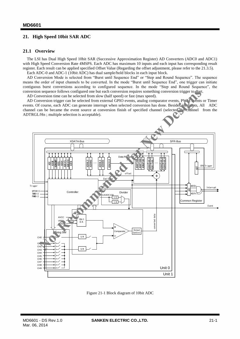
MD6601
MD6601 - DS Rev.1.0 SANKEN ELECTRIC CO.,LTD. 21-1 Mar. 06, 2014
21. High Speed 10bit SAR ADC
21.1 Overview
The LSI has Dual High Speed 10bit SAR (Successive Approximation Register) AD Converters (ADC0 and ADC1)
with High Speed Conversion Rate 4MSPS. Each ADC has maximum 10 inputs and each input has corresponding result
register. Each result can be applied specified Offset Value (Regarding the offset adjustment, please refer to the 21.3.5).
Each ADC-0 and ADC-1 (10bit ADC) has dual sample/hold blocks in each input block.
AD Conversion Mode is selected from “Burst until Sequence End” or “Step and Round Sequence”. The sequence
means the order of input channels to be converted. In the mode “Burst until Sequence End”, one trigger can initiate
contiguous burst conversions according to configured sequence. In the mode “Step and Round Sequence”, the
conversion sequence follows configured one but each conversion requires something conversion trigger to start.
AD Conversion time can be selected from slow (half speed) or fast (max speed).
AD Conversion trigger can be selected from external GPIO events, analog comparator events, PWM events or Timer
events. Of course, each ADC can generate interrupt when selected conversion has done. Besides interrupts, All ADC
channel can be became the event source at conversion finish of specified channel (selected the channel from the
ADTRGL/Hn ; multiple selection is acceptable).
Figure 21-1 Block diagram of 10bit ADC
Common Register
Unit 1
Analog SW
XDATA-Bus
Trigger
GPIO0-3TMR0-3PWM0-3
Unit 0
CH1
CH2
CH3
CH4
CH5
CH6
CH7
CH8
CH9
S/H
S/H
+
-
Comparator
10bitD/A
AVCC
VREF
AVSS
CH0
A/D
Controller
1/2
1/4
CLKADC133Divider
OutputControl
+
ADC
ADSM
ADSL
ADSH
ADEVTL
ADEVTH
ADNSMP
ADACCLR
ADOHL0
ADOHH0
ADOHL9
ADOHH9
・・・ ADL0
ADH0
ADL1
ADH1
ADL8
ADH8
ADL9
ADH9
・・・
Analog SW
offset
converted data
Data Register
SFR-Bus
End Event
Busy
ADT
ADI
CPU Trigger
ADIEn
ADIFn
Interrupt
Event
ADEN
ADNUPCNT
ADUPTH0H
ADUPTH0L
Not Reco
mmended
for N
ew D
esign
s

MD6601
MD6601 - DS Rev.1.0 SANKEN ELECTRIC CO.,LTD. 21-2 Mar. 06, 2014
Table 21-1 Input/Output pins
Channel Pin /Sig. name of Unit 0 Pin /Sig. name of Unit 1 Description
0 ANEX0 ANEX4 Analog External 0/4
1 ANEX1 ANEX5 Analog External 1/5
2 ANEX2 ANEX6 Analog External 2/6
3 ANEX3 ANEX7 Analog External 3/7
4 OP0 OP0 OPAMP0
5 OP1 OP1 OPAMP1
6 ANEX9 ANEX13 Analog External 9/13
7 TEMP TEMP TEMP
8 AGND AGND Analog GND (1/2 AVCC)
9 AVSS AVSS Analog VSS
Table 21-2 Feature of High Speed 10bit SAR ADC0 and ADC1
Item Description Note
Unit Counts Dual Unit Can operate independently
Input Channels 10 Inputs/unit
Resolution 10bits
Conversion Speed 4MSPS (million samples per second)
Sampling Time
+ Conversion Time
= 250ns
Dual Simultaneous Sampling Supported
Conversion Mode Burst Until Sequence End
Step and Round Sequence
Conversion Trigger Selectable from internal events
Interrupt and Event Outputs Interrupt or Event Output can be generated
when Conversion finished.
Not Reco
mmended
for N
ew D
esign
s
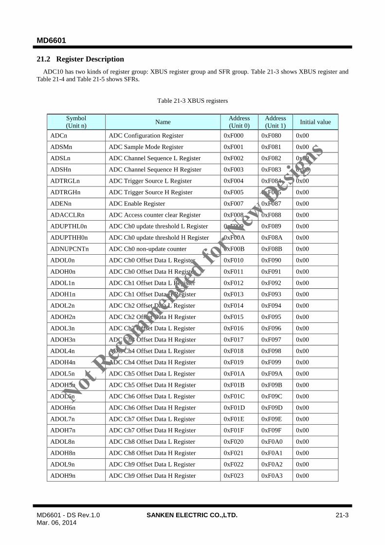
MD6601
MD6601 - DS Rev.1.0 SANKEN ELECTRIC CO.,LTD. 21-3 Mar. 06, 2014
21.2 Register Description
ADC10 has two kinds of register group: XBUS register group and SFR group. Table 21-3 shows XBUS register and
Table 21-4 and Table 21-5 shows SFRs.
Table 21-3 XBUS registers
Symbol
(Unit n) Name
Address
(Unit 0)
Address
(Unit 1) Initial value
ADCn ADC Configuration Register 0xF000 0xF080 0x00
ADSMn ADC Sample Mode Register 0xF001 0xF081 0x00
ADSLn ADC Channel Sequence L Register 0xF002 0xF082 0x00
ADSHn ADC Channel Sequence H Register 0xF003 0xF083 0x00
ADTRGLn ADC Trigger Source L Register 0xF004 0xF084 0x00
ADTRGHn ADC Trigger Source H Register 0xF005 0xF085 0x00
ADENn ADC Enable Register 0xF007 0xF087 0x00
ADACCLRn ADC Access counter clear Register 0xF008 0xF088 0x00
ADUPTHL0n ADC Ch0 update threshold L Register 0xF009 0xF089 0x00
ADUPTHH0n ADC Ch0 update threshold H Register 0xF00A 0xF08A 0x00
ADNUPCNTn ADC Ch0 non-update counter 0xF00B 0xF08B 0x00
ADOL0n ADC Ch0 Offset Data L Register 0xF010 0xF090 0x00
ADOH0n ADC Ch0 Offset Data H Register 0xF011 0xF091 0x00
ADOL1n ADC Ch1 Offset Data L Register 0xF012 0xF092 0x00
ADOH1n ADC Ch1 Offset Data H Register 0xF013 0xF093 0x00
ADOL2n ADC Ch2 Offset Data L Register 0xF014 0xF094 0x00
ADOH2n ADC Ch2 Offset Data H Register 0xF015 0xF095 0x00
ADOL3n ADC Ch3 Offset Data L Register 0xF016 0xF096 0x00
ADOH3n ADC Ch3 Offset Data H Register 0xF017 0xF097 0x00
ADOL4n ADC Ch4 Offset Data L Register 0xF018 0xF098 0x00
ADOH4n ADC Ch4 Offset Data H Register 0xF019 0xF099 0x00
ADOL5n ADC Ch5 Offset Data L Register 0xF01A 0xF09A 0x00
ADOH5n ADC Ch5 Offset Data H Register 0xF01B 0xF09B 0x00
ADOL6n ADC Ch6 Offset Data L Register 0xF01C 0xF09C 0x00
ADOH6n ADC Ch6 Offset Data H Register 0xF01D 0xF09D 0x00
ADOL7n ADC Ch7 Offset Data L Register 0xF01E 0xF09E 0x00
ADOH7n ADC Ch7 Offset Data H Register 0xF01F 0xF09F 0x00
ADOL8n ADC Ch8 Offset Data L Register 0xF020 0xF0A0 0x00
ADOH8n ADC Ch8 Offset Data H Register 0xF021 0xF0A1 0x00
ADOL9n ADC Ch9 Offset Data L Register 0xF022 0xF0A2 0x00
ADOH9n ADC Ch9 Offset Data H Register 0xF023 0xF0A3 0x00
Not Reco
mmended
for N
ew D
esign
s
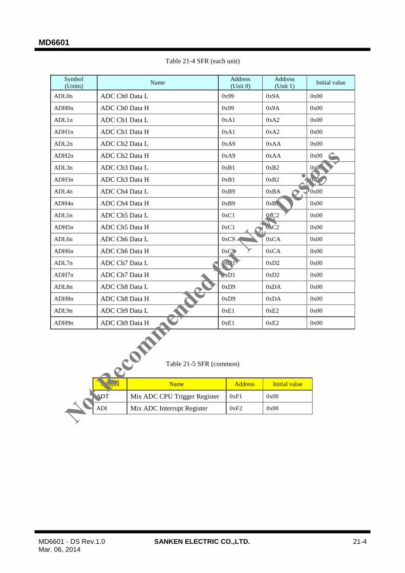
MD6601
MD6601 - DS Rev.1.0 SANKEN ELECTRIC CO.,LTD. 21-4 Mar. 06, 2014
Table 21-4 SFR (each unit)
Symbol
(Unitn) Name
Address
(Unit 0)
Address
(Unit 1) Initial value
ADL0n ADC Ch0 Data L 0x99 0x9A 0x00
ADH0n ADC Ch0 Data H 0x99 0x9A 0x00
ADL1n ADC Ch1 Data L 0xA1 0xA2 0x00
ADH1n ADC Ch1 Data H 0xA1 0xA2 0x00
ADL2n ADC Ch2 Data L 0xA9 0xAA 0x00
ADH2n ADC Ch2 Data H 0xA9 0xAA 0x00
ADL3n ADC Ch3 Data L 0xB1 0xB2 0x00
ADH3n ADC Ch3 Data H 0xB1 0xB2 0x00
ADL4n ADC Ch4 Data L 0xB9 0xBA 0x00
ADH4n ADC Ch4 Data H 0xB9 0xBA 0x00
ADL5n ADC Ch5 Data L 0xC1 0xC2 0x00
ADH5n ADC Ch5 Data H 0xC1 0xC2 0x00
ADL6n ADC Ch6 Data L 0xC9 0xCA 0x00
ADH6n ADC Ch6 Data H 0xC9 0xCA 0x00
ADL7n ADC Ch7 Data L 0xD1 0xD2 0x00
ADH7n ADC Ch7 Data H 0xD1 0xD2 0x00
ADL8n ADC Ch8 Data L 0xD9 0xDA 0x00
ADH8n ADC Ch8 Data H 0xD9 0xDA 0x00
ADL9n ADC Ch9 Data L 0xE1 0xE2 0x00
ADH9n ADC Ch9 Data H 0xE1 0xE2 0x00
Table 21-5 SFR (common)
Symbol Name Address Initial value
ADT Mix ADC CPU Trigger Register 0xF1 0x00
ADI Mix ADC Interrupt Register 0xF2 0x00
Not
Recommen
ded fo
r New
Desi
gns

MD6601
MD6601 - DS Rev.1.0 SANKEN ELECTRIC CO.,LTD. 21-5 Mar. 06, 2014
21.2.1 ADCn (ADC Configuration Register)
Register ADCn ADC Configuration Register Address(Unit 0) 0xF000
Address(Unit 1) 0xF080
Bit Bit Name R/W Initial Description Note
7 UPTH0EN R/W 0 CH0 update threshold enable
0: disable
1: enable
6 ADMODE R/W 0 ADC Conversion Mode
0: Burst until Sequence End
(Output interrupt after last sequence)
1: Step and Round Sequence
(Output interrupt at each step)
5 ADTIME R/W 0 ADC Conversion Time
0: Slow (CLKADCn_133 / 4)
1: Fast (CLKADCn_133 / 2)
4 ADTRG4 R/W 0 ADC Trigger Source
00000: CPU
00001: GPIO0 Event for ADC (neg edge)
00010: GPIO0 Event for ADC (pos edge)
00011: GPIO0 Event for ADC (both edge)
00100: GPIO1 Event for ADC (neg edge)
00101: GPIO1 Event for ADC (pos edge)
00110: GPIO1 Event for ADC (both edge)
00111: GPIO2 Event for ADC (neg edge)
01000: GPIO2 Event for ADC (pos edge)
01001: GPIO2 Event for ADC (both edge)
01010: GPIO3 Event for ADC (neg edge)
01011: GPIO3 Event for ADC (pos edge)
01100: GPIO3 Event for ADC (both edge)
01101: Comparator 0 (pulse)
01110: Comparator 1 (pulse)
01111: Comparator 2 (pulse)
10000: Comparator 3 (pulse)
10001: TIMER0-CM0 (pulse)
10010: TIMER0-CM1 (pulse)
10011: TIMER1-CM0 (pulse)
10100: TIMER1-CM1 (pulse)
10101: PWM0-EVENT0 (pulse)
10110: PWM0-EVENT1 (pulse)
10111: PWM1-EVENT0 (pulse)
11000: PWM1-EVENT1 (pulse)
11001: PWM2-EVENT0(pulse)
11010: PWM2-EVENT1 (pulse)
11011: PWM3-EVENT0 (pulse)
11100: PWM3-EVENT1 (pulse)
Others are reserved. Do not set.
3 ADTRG3 R/W 0
2 ADTRG2 R/W 0
1 ADTRG1 R/W 0
0 ADTRG0 R/W 0
UPTHOEN, ADMODE and ADTIME in ADCn register should be written when ADENn.EN=0.
Setting ADENn.EN=1 and waitting 1uS, then ADC Trigger Source should be written into ADTRG[4:0] .
Not Reco
mmended
for N
ew D
esign
s
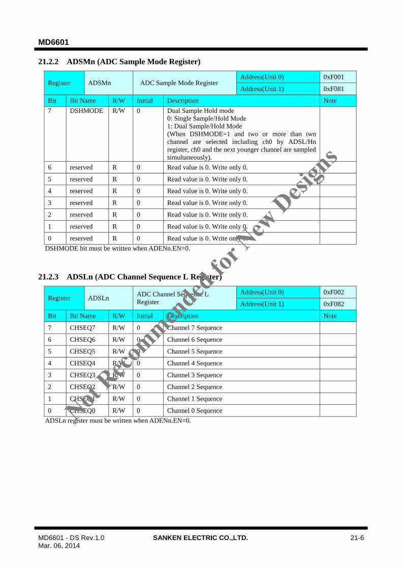
MD6601
MD6601 - DS Rev.1.0 SANKEN ELECTRIC CO.,LTD. 21-6 Mar. 06, 2014
21.2.2 ADSMn (ADC Sample Mode Register)
Register ADSMn ADC Sample Mode Register Address(Unit 0) 0xF001
Address(Unit 1) 0xF081
Bit Bit Name R/W Initial Description Note
7 DSHMODE R/W 0 Dual Sample Hold mode
0: Single Sample/Hold Mode
1: Dual Sample/Hold Mode
(When DSHMODE=1 and two or more than two
channel are selected including ch0 by ADSL/Hn
register, ch0 and the next younger channel are sampled
simultaneously).
6 reserved R 0 Read value is 0. Write only 0.
5 reserved R 0 Read value is 0. Write only 0.
4 reserved R 0 Read value is 0. Write only 0.
3 reserved R 0 Read value is 0. Write only 0.
2 reserved R 0 Read value is 0. Write only 0.
1 reserved R 0 Read value is 0. Write only 0.
0 reserved R 0 Read value is 0. Write only 0.
DSHMODE bit must be written when ADENn.EN=0.
21.2.3 ADSLn (ADC Channel Sequence L Register)
Register ADSLn ADC Channel Sequence L
Register
Address(Unit 0) 0xF002
Address(Unit 1) 0xF082
Bit Bit Name R/W Initial Description Note
7 CHSEQ7 R/W 0 Channel 7 Sequence
6 CHSEQ6 R/W 0 Channel 6 Sequence
5 CHSEQ5 R/W 0 Channel 5 Sequence
4 CHSEQ4 R/W 0 Channel 4 Sequence
3 CHSEQ3 R/W 0 Channel 3 Sequence
2 CHSEQ2 R/W 0 Channel 2 Sequence
1 CHSEQ1 R/W 0 Channel 1 Sequence
0 CHSEQ0 R/W 0 Channel 0 Sequence
ADSLn register must be written when ADENn.EN=0.
Not Reco
mmended
for N
ew D
esign
s
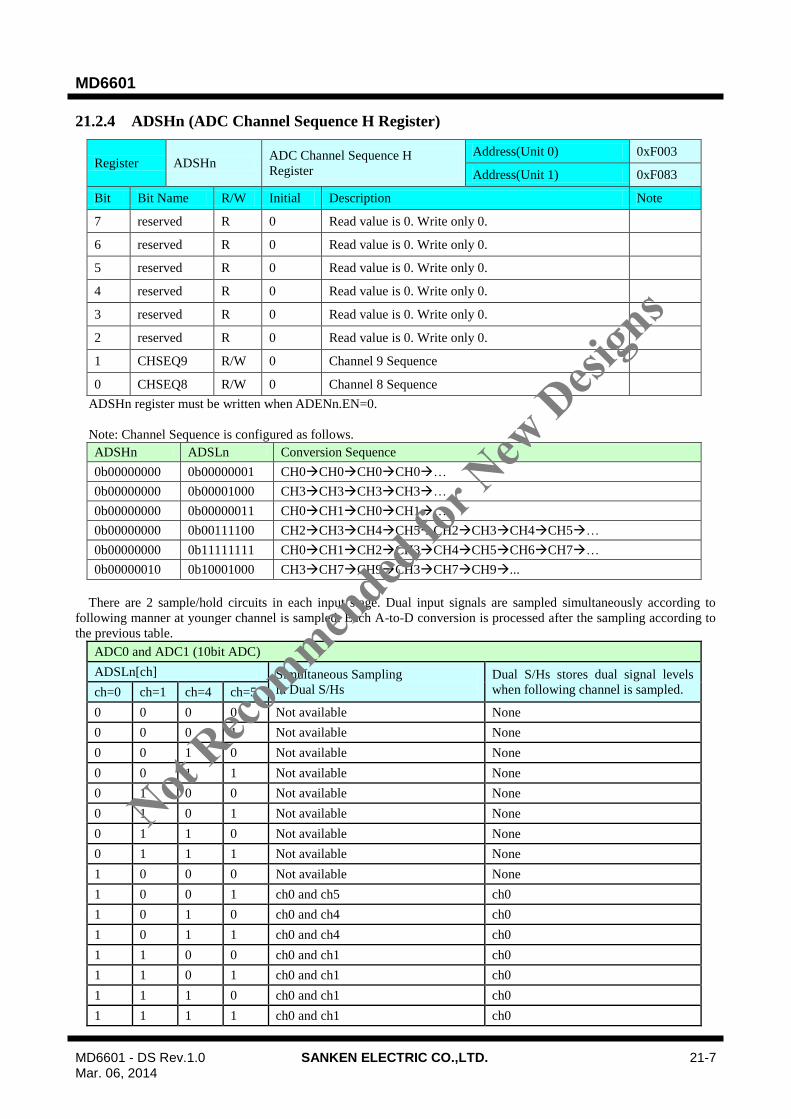
MD6601
MD6601 - DS Rev.1.0 SANKEN ELECTRIC CO.,LTD. 21-7 Mar. 06, 2014
21.2.4 ADSHn (ADC Channel Sequence H Register)
Register ADSHn ADC Channel Sequence H
Register
Address(Unit 0) 0xF003
Address(Unit 1) 0xF083
Bit Bit Name R/W Initial Description Note
7 reserved R 0 Read value is 0. Write only 0.
6 reserved R 0 Read value is 0. Write only 0.
5 reserved R 0 Read value is 0. Write only 0.
4 reserved R 0 Read value is 0. Write only 0.
3 reserved R 0 Read value is 0. Write only 0.
2 reserved R 0 Read value is 0. Write only 0.
1 CHSEQ9 R/W 0 Channel 9 Sequence
0 CHSEQ8 R/W 0 Channel 8 Sequence
ADSHn register must be written when ADENn.EN=0.
Note: Channel Sequence is configured as follows.
ADSHn ADSLn Conversion Sequence
0b00000000 0b00000001 CH0CH0CH0CH0…
0b00000000 0b00001000 CH3CH3CH3CH3…
0b00000000 0b00000011 CH0CH1CH0CH1…
0b00000000 0b00111100 CH2CH3CH4CH5CH2CH3CH4CH5…
0b00000000 0b11111111 CH0CH1CH2CH3CH4CH5CH6CH7…
0b00000010 0b10001000 CH3CH7CH9CH3CH7CH9...
There are 2 sample/hold circuits in each input stage. Dual input signals are sampled simultaneously according to
following manner at younger channel is sampled. Each A-to-D conversion is processed after the sampling according to
the previous table.
ADC0 and ADC1 (10bit ADC)
ADSLn[ch] Simultaneous Sampling
in Dual S/Hs
Dual S/Hs stores dual signal levels
when following channel is sampled. ch=0 ch=1 ch=4 ch=5
0 0 0 0 Not available None
0 0 0 1 Not available None
0 0 1 0 Not available None
0 0 1 1 Not available None
0 1 0 0 Not available None
0 1 0 1 Not available None
0 1 1 0 Not available None
0 1 1 1 Not available None
1 0 0 0 Not available None
1 0 0 1 ch0 and ch5 ch0
1 0 1 0 ch0 and ch4 ch0
1 0 1 1 ch0 and ch4 ch0
1 1 0 0 ch0 and ch1 ch0
1 1 0 1 ch0 and ch1 ch0
1 1 1 0 ch0 and ch1 ch0
1 1 1 1 ch0 and ch1 ch0
Not Reco
mmended
for N
ew D
esign
s

MD6601
MD6601 - DS Rev.1.0 SANKEN ELECTRIC CO.,LTD. 21-8 Mar. 06, 2014
21.2.5 ADTRGLn (ADC Event Source L Register)
Register ADTRGLn ADC Trigger Source L
Register
Address(Unit 0) 0xF004
Address(Unit 1) 0xF084
Bit Bit Name R/W Initial Description Note
7 EVTCH7 R/W 0 Choose ADC Output Event
0: The channel finish is not included in output event.
1: The channel finish is included in output event.
6 EVTCH6 R/W 0
5 EVTCH5 R/W 0
4 EVTCH4 R/W 0
3 EVTCH3 R/W 0
2 EVTCH2 R/W 0
1 EVTCH1 R/W 0
0 EVTCH0 R/W 0
ADTRGLn register must be written when ADENn.EN=0.
21.2.6 ADTRGHn (ADC Event Source H Register)
Register ADTRGHn ADC Trigger Source H
Register
Address(Unit 0) 0xF005
Address(Unit 1) 0xF085
Bit Bit Name R/W Initial Description Note
7 reserved R 0 Read value is 0. Write only 0.
6 reserved R 0 Read value is 0. Write only 0.
5 reserved R 0 Read value is 0. Write only 0.
4 reserved R 0 Read value is 0. Write only 0.
3 reserved R 0 Read value is 0. Write only 0.
2 reserved R 0 Read value is 0. Write only 0.
1 EVTCH9 R/W 0 Choose ADC Output Event
0: The channel finish is not included in output event.
1: The channel finish is included in output event.
0 EVTCH8 R/W 0
ADTRGHn register must be written when ADENn.EN=0.
Not Reco
mmended
for N
ew D
esign
s

MD6601
MD6601 - DS Rev.1.0 SANKEN ELECTRIC CO.,LTD. 21-9 Mar. 06, 2014
21.2.7 ADENn (ADC Enable Register)
Register ADENn ADC Enable Register Address(Unit 0) 0xF007
Address(Unit 1) 0xF087
Bit Bit Name R/W Initial Description Note
7 reserved R 0 Read value is 0. Write only 0.
6 reserved R 0 Read value is 0. Write only 0.
5 reserved R 0 Read value is 0. Write only 0.
4 reserved R 0 Read value is 0. Write only 0.
3 reserved R 0 Read value is 0. Write only 0.
2 reserved R 0 Read value is 0. Write only 0.
1 reserved R 0 Read value is 0. Write only 0.
0 EN R/W 0 ADC Enable
0: ADC Disabled
1: ADC Enabled
Activate the ADC.
Do not change to 0 during A/D conversion is running.
21.2.8 ADACCLRn (ADC Access Counter Clear Register)
Register ADACCLRn ADC Access Counter Clear
Register
Address(Unit 0) 0xF008
Address(Unit 1) 0xF088
Bit Bit Name R/W Initial Description Note
7 CLRADCC
DRCAC
R/W 0 Clear ADC Conversion Data Register CPU Access
Counter
0: No effect
1: Register CPU Access counter clear
Read : No Request
Write 0: No effect
Write 1: Clear Register CPU Access counter.
(Clear CPU SFR access counter.)
6 CLRADCC
DRDAC
R/W 0 Clear ADC Conversion Data Register DSAC Access
Counter
0: No effect
1: Register DSAC Access counter clear
Read : No Request
Write 0: No effect
Write 1: Clear Register DSAC Access counter.
(Clear DSAC SFR access counter.)
5 reserved R 0 Read value is 0. Write only 0.
4 reserved R 0 Read value is 0. Write only 0.
3 reserved R 0 Read value is 0. Write only 0.
2 reserved R 0 Read value is 0. Write only 0.
1 reserved R 0 Read value is 0. Write only 0.
0 reserved R 0 Read value is 0. Write only 0.
Not Reco
mmended
for N
ew D
esign
s
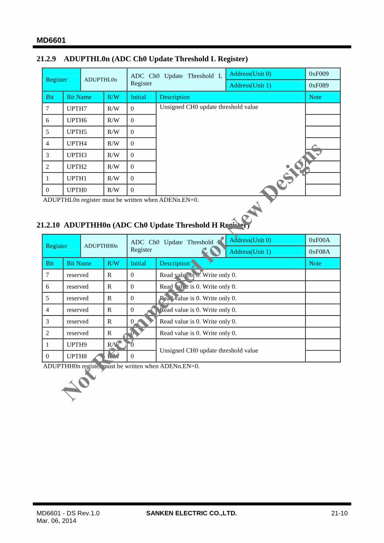
MD6601
MD6601 - DS Rev.1.0 SANKEN ELECTRIC CO.,LTD. 21-10 Mar. 06, 2014
21.2.9 ADUPTHL0n (ADC Ch0 Update Threshold L Register)
Register ADUPTHL0n ADC Ch0 Update Threshold L
Register
Address(Unit 0) 0xF009
Address(Unit 1) 0xF089
Bit Bit Name R/W Initial Description Note
7 UPTH7 R/W 0 Unsigned CH0 update threshold value
6 UPTH6 R/W 0
5 UPTH5 R/W 0
4 UPTH4 R/W 0
3 UPTH3 R/W 0
2 UPTH2 R/W 0
1 UPTH1 R/W 0
0 UPTH0 R/W 0
ADUPTHL0n register must be written when ADENn.EN=0.
21.2.10 ADUPTHH0n (ADC Ch0 Update Threshold H Register)
Register ADUPTHH0n ADC Ch0 Update Threshold H
Register
Address(Unit 0) 0xF00A
Address(Unit 1) 0xF08A
Bit Bit Name R/W Initial Description Note
7 reserved R 0 Read value is 0. Write only 0.
6 reserved R 0 Read value is 0. Write only 0.
5 reserved R 0 Read value is 0. Write only 0.
4 reserved R 0 Read value is 0. Write only 0.
3 reserved R 0 Read value is 0. Write only 0.
2 reserved R 0 Read value is 0. Write only 0.
1 UPTH9 R/W 0 Unsigned CH0 update threshold value
0 UPTH8 R/W 0
ADUPTHH0n register must be written when ADENn.EN=0.
Not Reco
mmended
for N
ew D
esign
s
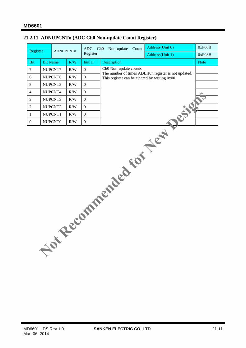
MD6601
MD6601 - DS Rev.1.0 SANKEN ELECTRIC CO.,LTD. 21-11 Mar. 06, 2014
21.2.11 ADNUPCNTn (ADC Ch0 Non-update Count Register)
Register ADNUPCNTn ADC Ch0 Non-update Count
Register
Address(Unit 0) 0xF00B
Address(Unit 1) 0xF08B
Bit Bit Name R/W Initial Description Note
7 NUPCNT7 R/W 0 Ch0 Non-update counts
The number of times ADLH0n register is not updated.
This register can be cleared by writing 0x00.
6 NUPCNT6 R/W 0
5 NUPCNT5 R/W 0
4 NUPCNT4 R/W 0
3 NUPCNT3 R/W 0
2 NUPCNT2 R/W 0
1 NUPCNT1 R/W 0
0 NUPCNT0 R/W 0
Not Reco
mmended
for N
ew D
esign
s

MD6601
MD6601 - DS Rev.1.0 SANKEN ELECTRIC CO.,LTD. 21-12 Mar. 06, 2014
21.2.12 ADOLXn (ADC ChX Offset Data L Register, n=0-1)
Register ADOL0n ADC Ch0 Offset Data L Register Address(Unit 0) 0xF010
Address(Unit 1) 0xF090
Register ADOL1n ADC Ch1 Offset Data L Register Address(Unit 0) 0xF012
Address(Unit 1) 0xF092
Register ADOL2n ADC Ch2 Offset Data L Register Address(Unit 0) 0xF014
Address(Unit 1) 0xF094
Register ADOL3n ADC Ch3 Offset Data L Register Address(Unit 0) 0xF016
Address(Unit 1) 0xF096
Register ADOL4n ADC Ch4 Offset Data L Register Address(Unit 0) 0xF018
Address(Unit 1) 0xF098
Register ADOL5n ADC Ch5 Offset Data L Register Address(Unit 0) 0xF01A
Address(Unit 1) 0xF09A
Register ADOL6n ADC Ch6 Offset Data L Register Address(Unit 0) 0xF01C
Address(Unit 1) 0xF09C
Register ADOL7n ADC Ch7 Offset Data L Register Address(Unit 0) 0xF01E
Address(Unit 1) 0xF09E
Register ADOL8n ADC Ch8 Offset Data L Register Address(Unit 0) 0xF020
Address(Unit 1) 0xF0A0
Register ADOL9n ADC Ch9 Offset Data L Register Address(Unit 0) 0xF022
Address(Unit 1) 0xF0A2
Bit Bit Name R/W Initial Description Note
7 ADOFFSET
7 R/W 0
Signed 11bit ADC Offset Data L
bit 7 – bit 0 are stored.
6 ADOFFSET
6 R/W 0
5 ADOFFSET
5 R/W 0
4 ADOFFSET
4 R/W 0
3 ADOFFSET
3 R/W 0
2 ADOFFSET
2 R/W 0
Signed 11bit ADC Offset Data L
bit 7 – bit 0 are stored.
1 ADOFFSET
1 R/W 0
0 ADOFFSET
0 R/W 0
Not Reco
mmended
for N
ew D
esign
s
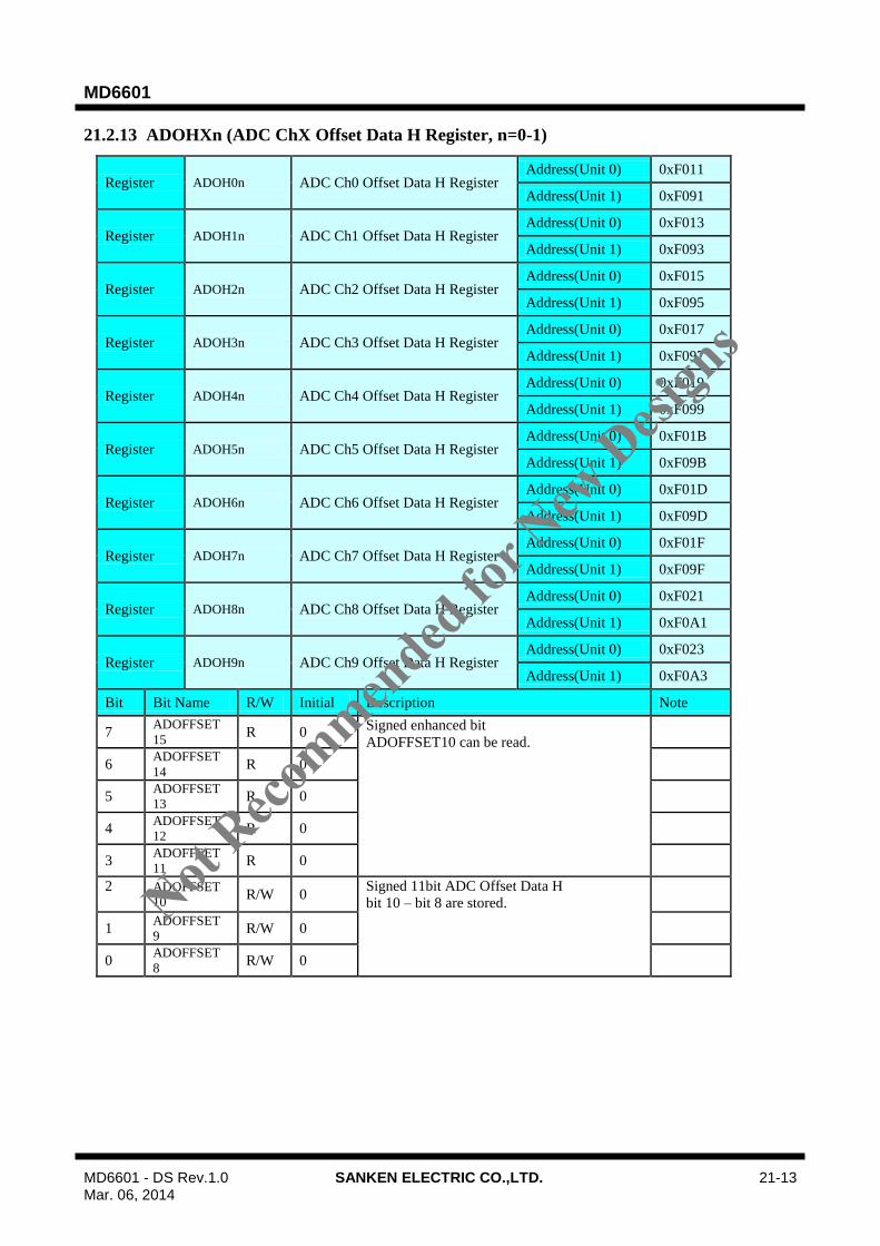
MD6601
MD6601 - DS Rev.1.0 SANKEN ELECTRIC CO.,LTD. 21-13 Mar. 06, 2014
21.2.13 ADOHXn (ADC ChX Offset Data H Register, n=0-1)
Register ADOH0n ADC Ch0 Offset Data H Register Address(Unit 0) 0xF011
Address(Unit 1) 0xF091
Register ADOH1n ADC Ch1 Offset Data H Register Address(Unit 0) 0xF013
Address(Unit 1) 0xF093
Register ADOH2n ADC Ch2 Offset Data H Register Address(Unit 0) 0xF015
Address(Unit 1) 0xF095
Register ADOH3n ADC Ch3 Offset Data H Register Address(Unit 0) 0xF017
Address(Unit 1) 0xF097
Register ADOH4n ADC Ch4 Offset Data H Register Address(Unit 0) 0xF019
Address(Unit 1) 0xF099
Register ADOH5n ADC Ch5 Offset Data H Register Address(Unit 0) 0xF01B
Address(Unit 1) 0xF09B
Register ADOH6n ADC Ch6 Offset Data H Register Address(Unit 0) 0xF01D
Address(Unit 1) 0xF09D
Register ADOH7n ADC Ch7 Offset Data H Register Address(Unit 0) 0xF01F
Address(Unit 1) 0xF09F
Register ADOH8n ADC Ch8 Offset Data H Register Address(Unit 0) 0xF021
Address(Unit 1) 0xF0A1
Register ADOH9n ADC Ch9 Offset Data H Register Address(Unit 0) 0xF023
Address(Unit 1) 0xF0A3
Bit Bit Name R/W Initial Description Note
7 ADOFFSET
15 R 0
Signed enhanced bit
ADOFFSET10 can be read.
6 ADOFFSET
14 R 0
5 ADOFFSET
13 R 0
4 ADOFFSET
12 R 0
3 ADOFFSET
11 R 0
2
ADOFFSET
10 R/W 0
Signed 11bit ADC Offset Data H
bit 10 – bit 8 are stored.
1 ADOFFSET
9 R/W 0
0 ADOFFSET
8 R/W 0
Not Reco
mmended
for N
ew D
esign
s

MD6601
MD6601 - DS Rev.1.0 SANKEN ELECTRIC CO.,LTD. 21-14 Mar. 06, 2014
21.2.14 ADLXn (ADC ChX Data L Register, n=0-1)
Register ADL0n ADC Ch0 Data L Register Address(Unit 0) 0x99
Address(Unit 1) 0x9A
Register ADL1n ADC Ch1 Data L Register Address(Unit 0) 0xA1
Address(Unit 1) 0xA2
Register ADL2n ADC Ch2 Data L Register Address(Unit 0) 0xA9
Address(Unit 1) 0xAA
Register ADL3n ADC Ch3 Data L Register Address(Unit 0) 0xB1
Address(Unit 1) 0xB2
Register ADL4n ADC Ch4 Data L Register Address(Unit 0) 0xB9
Address(Unit 1) 0xBA
Register ADL5n ADC Ch5 Data L Register Address(Unit 0) 0xC1
Address(Unit 1) 0xC2
Register ADL6n ADC Ch6 Data L Register Address(Unit 0) 0xC9
Address(Unit 1) 0xCA
Register ADL7n ADC Ch7 Data L Register Address(Unit 0) 0xD1
Address(Unit 1) 0xD2
Register ADL8n ADC Ch8 Data L Register Address(Unit 0) 0xD9
Address(Unit 1) 0xDA
Register ADL9n ADC Ch9 Data L Register Address(Unit 0) 0xE1
Address(Unit 1) 0xE2
Bit Bit Name R/W Initial Description Note
7 ADDATA7 R 0 Signed 12bit ADC Conversion Data L
bit 7 – bit 0 are stored.
This value is already applied an offset
specified by ADOH/Ln like as
“Raw ADC Value + ADOXn”
(16bit operation)
Details refer to 21.3.5
6 ADDATA6 R 0
5 ADDATA5 R 0
4 ADDATA4 R 0
3 ADDATA3 R 0
2 ADDATA2 R 0
1 ADDATA1 R 0
0 ADDATA0 R 0
Not Reco
mmended
for N
ew D
esign
s

MD6601
MD6601 - DS Rev.1.0 SANKEN ELECTRIC CO.,LTD. 21-15 Mar. 06, 2014
21.2.15 ADHXn (ADC ChX Data H Register, n=0-1)
Register ADH0n ADC Ch0 Data H Register Address(Unit 0) 0x99
Address(Unit 1) 0x9A
Register ADH1n ADC Ch1 Data H Register Address(Unit 0) 0xA1
Address(Unit 1) 0xA2
Register ADH2n ADC Ch2 Data H Register Address(Unit 0) 0xA9
Address(Unit 1) 0xAA
Register ADH3n ADC Ch3 Data H Register Address(Unit 0) 0xB1
Address(Unit 1) 0xB2
Register ADH4n ADC Ch4 Data H Register Address(Unit 0) 0xB9
Address(Unit 1) 0xBA
Register ADH5n ADC Ch5 Data H Register Address(Unit 0) 0xC1
Address(Unit 1) 0xC2
Register ADH6n ADC Ch6 Data H Register Address(Unit 0) 0xC9
Address(Unit 1) 0xCA
Register ADH7n ADC Ch7 Data H Register Address(Unit 0) 0xD1
Address(Unit 1) 0xD2
Register ADH8n ADC Ch8 Data H Register Address(Unit 0) 0xD9
Address(Unit 1) 0xDA
Register ADH9n ADC Ch9 Data H Register Address(Unit 0) 0xE1
Address(Unit 1) 0xE2
Bit Bit Name R/W Initial Description Note
7 ADDATA1
5 R 0
Signed 16bit ADC Conversion Data H
bit 15 – bit 8 are stored.
This value has already applied an offset
specified by ADOH/Ln like as
“Raw ADC Value + ADOXn”
(12bit operation)
Details refer to 21.3.5
6 ADDATA1
4 R 0
5 ADDATA1
3 R 0
4 ADDATA1
2 R 0
3 ADDATA1
1 R 0
2 ADDATA1
0 R 0
1 ADDATA9 R 0
0 ADDATA8 R 0
Not Reco
mmended
for N
ew D
esign
s

MD6601
MD6601 - DS Rev.1.0 SANKEN ELECTRIC CO.,LTD. 21-16 Mar. 06, 2014
21.2.16 ADT (ADC Trigger Register)
Register ADT ADC CPU Trigger Address 0xF1
Bit Bit Name R/W Initial Description Note
7:3 reserved R 0 Read value is 0. Write only 0.
2 ADCTRG2 W 0 ADC2 Trigger / Busy
Read 0: ADC2 not busy (no conversion)
Read 1: ADC2 is busy (in conversion)
Write 0: No effect
Write 1: ADC2 Start by CPU
1 ADCTRG1 W 0 ADC 1Trigger / Busy
Read 0: ADC1 not busy (no conversion)
Read 1: ADC1 is busy (in conversion)
Write 0: No effect
Write 1: ADC1 Start by CPU
0 ADCTRG0 W 0 ADC0 Trigger / Busy
Read 0: ADC0 not busy (no conversion)
Read 1: ADC0 is busy (in conversion)
Write 0: No effect
Write 1: ADC0 Start by CPU
Note: ADCTRGn are set by not only CPU but also other trigger sources.
Not Reco
mmended
for N
ew D
esign
s
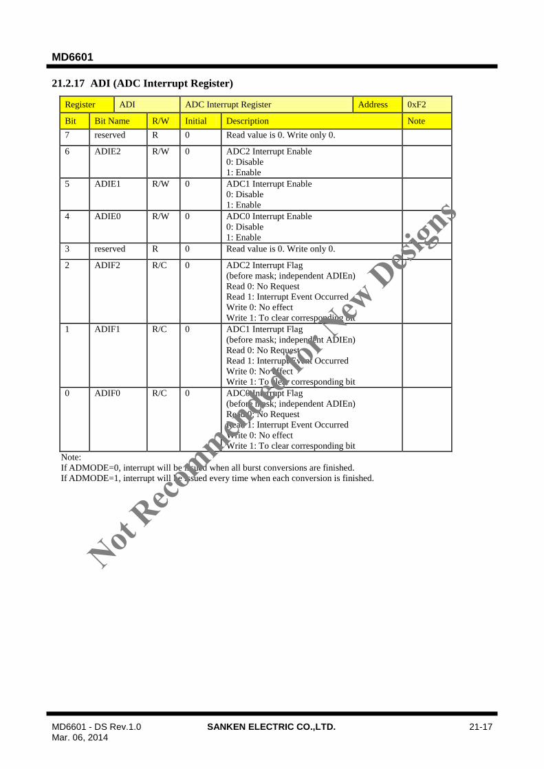
MD6601
MD6601 - DS Rev.1.0 SANKEN ELECTRIC CO.,LTD. 21-17 Mar. 06, 2014
21.2.17 ADI (ADC Interrupt Register)
Register ADI ADC Interrupt Register Address 0xF2
Bit Bit Name R/W Initial Description Note
7 reserved R 0 Read value is 0. Write only 0.
6 ADIE2 R/W 0 ADC2 Interrupt Enable
0: Disable
1: Enable
5 ADIE1 R/W 0 ADC1 Interrupt Enable
0: Disable
1: Enable
4 ADIE0 R/W 0 ADC0 Interrupt Enable
0: Disable
1: Enable
3 reserved R 0 Read value is 0. Write only 0.
2 ADIF2 R/C 0 ADC2 Interrupt Flag
(before mask; independent ADIEn)
Read 0: No Request
Read 1: Interrupt Event Occurred
Write 0: No effect
Write 1: To clear corresponding bit
1 ADIF1 R/C 0 ADC1 Interrupt Flag
(before mask; independent ADIEn)
Read 0: No Request
Read 1: Interrupt Event Occurred
Write 0: No effect
Write 1: To clear corresponding bit
0 ADIF0 R/C 0 ADC0 Interrupt Flag
(before mask; independent ADIEn)
Read 0: No Request
Read 1: Interrupt Event Occurred
Write 0: No effect
Write 1: To clear corresponding bit
Note:
If ADMODE=0, interrupt will be issued when all burst conversions are finished.
If ADMODE=1, interrupt will be issued every time when each conversion is finished.
Not Reco
mmended
for N
ew D
esign
s

MD6601
MD6601 - DS Rev.1.0 SANKEN ELECTRIC CO.,LTD. 21-18 Mar. 06, 2014
21.3 Operation
21.3.1 Basic operation
ADC is activated by ADENn.EN bit is set to 1'b1. The AD conversion starts when ADC is active and conversion
trigger from one of the peripherals is received. The AD Conversion trigger can be selected from CPU, external GPIO
events, analog comparator events, PWM events or Timer events by ADCn.ADTRG[4:0] bits. The CPU trigger can be
occurred by ADT.ADCTRGn bit that is mapped in SFR address space.
AD Conversion time can be selected from slow (half speed) or fast (full speed) by ADCn.ADTIME bit.
Table 21-2 shows Basic conversion sequence in the fast clock mode.
A/D conversion of a channel spends 16 cycles of ADCLK.
Figure 21-2 Basic conversion sequence
ADC has ten analog channels at most. The conversion of each channel can be enabled by ADSL/Hn register. The
conversion starts from the youngest enabled number channel. Table 21-6 shows the correspondence between
ADSL/Hn register bit and analog input.
Table 21-6 CHSEQx bit vs. analog input
Pin Name Unit 0 Unit 1 Notes
ADSLn.CHSEQ0 ANEX0 ANEX4
ADSLn.CHSEQ1 ANEX1 ANEX5
ADSLn.CHSEQ2 ANEX2 ANEX6
ADSLn.CHSEQ3 ANEX3 ANEX7
ADSLn.CHSEQ4 AMP0 AMP0
ADSLn.CHSEQ5 AMP1 AMP1
ADSLn.CHSEQ6 ANEX9 ANEX13
ADSLn.CHSEQ7 TEMP TEMP
ADSHn.CHSEQ8 AGND AGND
ADSHn.CHSEQ9 AVSS AVSS
Not Reco
mmended
for N
ew D
esign
s

MD6601
MD6601 - DS Rev.1.0 SANKEN ELECTRIC CO.,LTD. 21-19 Mar. 06, 2014
21.3.2 Conversion Mode
AD Conversion Mode is selected from “Burst until Sequence End” or “Step and Round Sequence” by
ADCn.ADMODE bit. The sequence means the order of input channels to be converted.
21.3.2.1. “Burst until Sequence End” mode
In the mode “Burst until Sequence End”, one trigger can initiate contiguous burst conversions according to
configured sequence.
(1) When the start trigger that is selected by ADCn.ADTRG[4:0] bit is detected, A/D conversion starts in younger
channel order which is selected by ADSL/H register.
(2) When A/D conversion of a channel finished, the converted data is written to corresponding data register
(ADL/HXn).
(3) If there are un-converted channel, A/D conversion of the next younger channel starts just after finishing the
previous A/D conversion. After that, go back to (2).
(4) A/D conversion of all channels is finished, ADI.ADIF bit is set to 1'b1. If ADI.ADIE=1, ADI interrupt is issued
to CPU.
trigger
ch1 Conv
ch2 Conv
ch3 Conv
ADL/H1n
ADL/H2n
ADL/H3n
ADIinterrupt
Figure 21-3 Burst until Sequence End mode.
Not
Recommen
ded fo
r New
Desi
gns
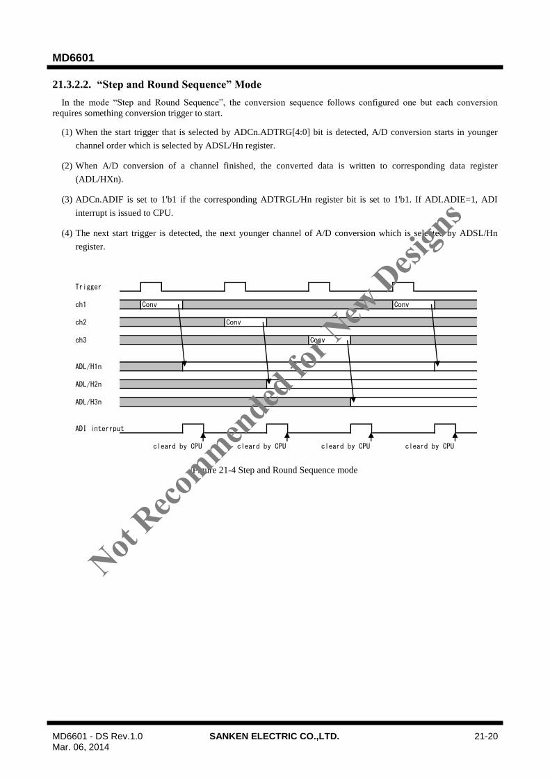
MD6601
MD6601 - DS Rev.1.0 SANKEN ELECTRIC CO.,LTD. 21-20 Mar. 06, 2014
21.3.2.2. “Step and Round Sequence” Mode
In the mode “Step and Round Sequence”, the conversion sequence follows configured one but each conversion
requires something conversion trigger to start.
(1) When the start trigger that is selected by ADCn.ADTRG[4:0] bit is detected, A/D conversion starts in younger
channel order which is selected by ADSL/Hn register.
(2) When A/D conversion of a channel finished, the converted data is written to corresponding data register
(ADL/HXn).
(3) ADCn.ADIF is set to 1'b1 if the corresponding ADTRGL/Hn register bit is set to 1'b1. If ADI.ADIE=1, ADI
interrupt is issued to CPU.
(4) The next start trigger is detected, the next younger channel of A/D conversion which is selected by ADSL/Hn
register.
Trigger
ch1 Conv Conv
ch2 Conv
ch3 Conv
ADL/H1n
ADL/H2n
ADL/H3n
ADI interrput
cleard by CPU cleard by CPU cleard by CPU cleard by CPU
Figure 21-4 Step and Round Sequence mode
Not Reco
mmended
for N
ew D
esign
s

MD6601
MD6601 - DS Rev.1.0 SANKEN ELECTRIC CO.,LTD. 21-21 Mar. 06, 2014
21.3.3 Dual Sample/Hold
ADC10 has two sample/hold circuits after the analog input switch. One is for only channel 0, another is for other
channels. If ADSMn.ADSHMODE is set to 1'b1 and two or more than two channels are enabled by ADSL/Hn register,
the ch0 and other younger channel of Sample/Hold is executed simultaneously. This operation can be used in both
conversion modes.
In Step and Round sequence mode, the ch0 and the following dual sampled/held channel is converted sequentially
only with one time trigger. ADI interrupt is asserted when the second channel conversion is finished, not asserted
when the CH0 conversion is finished.
Trigger
ch0 S/H Conv
ch1 S/H Conv
ch2 S/H Conv
ADL/H0n
ADL/H1n
ADL/H2n
ADI interrupt
Figure 21-5 Dual Sample/Hold operation in Burst until Sequence End mode.
Trigger
ch0 S/H Conv S/H Conv
ch1 S/H Conv S/H
ch2 S/H Conv
ADLH0n
ADLH1n
ADLH2n
ADI interrupt
Cleard by CPU Cleard by CPU Cleard by CPU
Figure 21-6 Dual Sample/Hold operation in Step and Round Sequence mode.
Not Reco
mmended
for N
ew D
esign
s

MD6601
MD6601 - DS Rev.1.0 SANKEN ELECTRIC CO.,LTD. 21-22 Mar. 06, 2014
21.3.4 Conversion start trigger
A/D conversion starts when detecting selected A/D conversion trigger. A/D conversion start trigger can be selected by
ADCn.ADTRG[4:0]. Only one conversion trigger during A/D conversion is hold, and issues after the current
conversion is finished, then the next conversion will be start. The conversion trigger is not accepted when ADENn=0 or
all channels are not selected (ADSL/Hn=0x00).
21.3.5 Converted data offset adjustment
The offset adjustment can be done for converted data by ADOL/HXn register. The bit length of adjusted value is
enhanced from 11bit to 16bit.
ADOL/HXn.ADATA_tmp[11:0] = RAW_ADC_Value{1'b0,[10:0]}
+ OFFSET{[10],[10:0]}
ADOL/HXn.ADATA[15:0] = RAW_ADC_Value_tmp{[11],[11],[11],[11],[11:0]}
ADOL/HXn.ADATA[15:0] : ADL/HXn register bit, n is unit number, X is unit-X's channel.
RAW_ADC_Value[9:0]: Conversion result value
OFFSET[10:0] : Signed, ADOL/HXn register bit, n is unit number, X is unit-X's channel.
S S
10bit(Unsigned)
+
Converted data SOffset
SResult value
SSSResult
ADLXn register[7:0]ADHXn register[7:0]
sign bit expansion
ADOLXn register[7:0]ADOHXn register[2:0]
S : Sign bit
11bit(Signed)
12bit(Signed)
16bit(Signed)
Figure 21-7 Converted data
21.3.6 Interrupts
If ADI.ADIEn=1, CPU interrupt can be occurred when ADI.ADIFn=1(n=0 or 1).
Not Reco
mmended
for N
ew D
esign
s

MD6601
MD6601 - DS Rev.1.0 SANKEN ELECTRIC CO.,LTD. 21-23 Mar. 06, 2014
21.3.7 ADC Event
ADC event can be issued when A/D conversion will be finished. The ADC event of each channel can be selected by
ADTRGL/Hn register.
Figure 21-8 shows the ADC event when ch1 and 3 are enabled and others are disabled.
Trigger
ch1 Conv Conv
ch2 Conv
ch3 Conv
ADL/H1n
ADL/H2n
ADL/H3n
ADC Event
Figure 21-8 ADC event when ch1 and 3 are enabled.
21.3.8 Reading converted data
Note that the converted result data, mapped in SFR address space, pair of Low Side (LSB Side) register and High
Side (MSB Side) register for 16bit value should be assigned on SAME address. In read access, 1st access gets Low Side
data and 2nd
access receives High Side data.
21.3.9 Threshold for conversion data update
This function controls ADL/H0n register update. ADL/H0n is updated if the difference between the current
conversion result value (the offset is not included) and the previous one (the offset is not included) is equal or less than
the threshold (ADUPTHH/L0n). The threshold is enabled during ADCn.UPTH0EN=1. The update condition is as
follows:
|{(current conversion result value) - (previous conversion result value)}| =<{(ADUPTHH0n, ADUPTHL0n)}.
The current/previous data comparison starts after ADCn.UPTH0EN=1. Therefore, the previous conversion result
must be valid value for comparison. At first, the valid value should be gotten when ADCn.UPTH0EN is 0, then
ADCn.UPTH0EN should be set to 1 to start the function.
ADNUPCNTn shows the number of non-update times. This register can be cleared by writing 0x00 to ADNUPCNTn
register. To know ADL/H0n register is not updated, ADNUPCNTn is read when CH0 conversion ends interrupt
sequence, and compares its value to the previous one. If the current value is increased from the previous value, the
current conversion result is not written to ADL/H0n register.
Not Reco
mmended
for N
ew D
esign
s
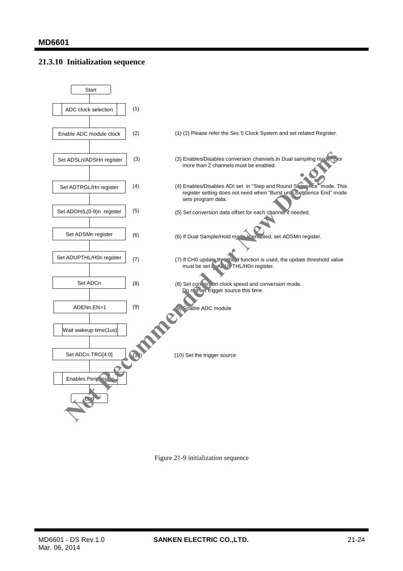
MD6601
MD6601 - DS Rev.1.0 SANKEN ELECTRIC CO.,LTD. 21-24 Mar. 06, 2014
21.3.10 Initialization sequence
Start
End
(5)
Set ADSLn/ADSHn register
(4)Set ADTRGL/Hn register
Set ADSMn register
Set ADCn
Set ADOH/L(0-9)n register
Enables Peripherals
(4) Enables/Disables ADI set in “Step and Round Sequence” mode. This
register setting does not need when “Burst until Sequence End” mode
sets program data.
(3) Enables/Disables conversion channels.In Dual sampling mode, 2 or
more than 2 channels must be enabled.
(5) Set conversion data offset for each channel if needed.
(6)
(7)
(8)
(6) If Dual Sample/Hold mode is enabled, set ADSMn register.
(8) Set conversion clock speed and conversion mode.
Do not set trigger source this time.
Enable ADC module clock
ADC clock selection (1)
(1) (2) Please refer the Sec 5 Clock System and set related Register.(2)
ADENn.EN=1
(3)
(9) Enable ADC module
Set ADUPTHL/H0n register
(9)
(7) If CH0 update threshold function is used, the update threshold value
must be set to ADUPTHL/H0n register.
Wait wakeup time(1us)
Set ADCn.TRG[4:0] (10) Set the trigger source(10)
Figure 21-9 initialization sequence
Not Reco
mmended
for N
ew D
esign
s
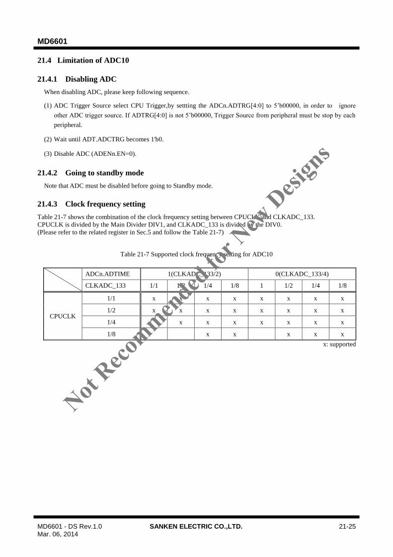
MD6601
MD6601 - DS Rev.1.0 SANKEN ELECTRIC CO.,LTD. 21-25 Mar. 06, 2014
21.4 Limitation of ADC10
21.4.1 Disabling ADC
When disabling ADC, please keep following sequence.
(1) ADC Trigger Source select CPU Trigger,by settting the ADCn.ADTRG[4:0] to 5’b00000, in order to ignore
other ADC trigger source. If ADTRG[4:0] is not 5’b00000, Trigger Source from peripheral must be stop by each
peripheral.
(2) Wait until ADT.ADCTRG becomes 1'b0.
(3) Disable ADC (ADENn.EN=0).
21.4.2 Going to standby mode
Note that ADC must be disabled before going to Standby mode.
21.4.3 Clock frequency setting
Table 21-7 shows the combination of the clock frequency setting between CPUCLK and CLKADC_133.
CPUCLK is divided by the Main Divider DIV1, and CLKADC_133 is divided by the DIV0.
(Please refer to the related register in Sec.5 and follow the Table 21-7)
Table 21-7 Supported clock frequency setting for ADC10
ADCn.ADTIME 1(CLKADC_133/2) 0(CLKADC_133/4)
CLKADC_133 1/1 1/2 1/4 1/8 1 1/2 1/4 1/8
CPUCLK
1/1 x x x x x x x x
1/2 x x x x x x x x
1/4 x x x x x x x
1/8 x x x x x
x: supported
Not Reco
mmended
for N
ew D
esign
s
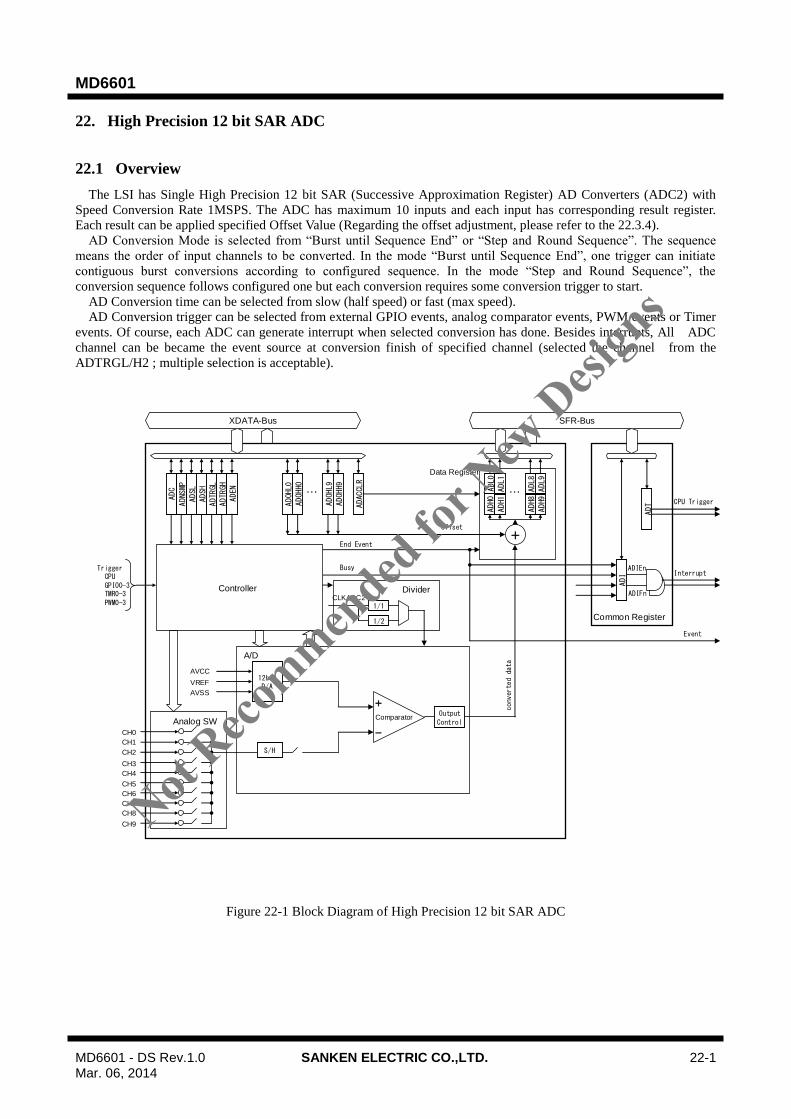
MD6601
MD6601 - DS Rev.1.0 SANKEN ELECTRIC CO.,LTD. 22-1 Mar. 06, 2014
22. High Precision 12 bit SAR ADC
22.1 Overview
The LSI has Single High Precision 12 bit SAR (Successive Approximation Register) AD Converters (ADC2) with
Speed Conversion Rate 1MSPS. The ADC has maximum 10 inputs and each input has corresponding result register.
Each result can be applied specified Offset Value (Regarding the offset adjustment, please refer to the 22.3.4).
AD Conversion Mode is selected from “Burst until Sequence End” or “Step and Round Sequence”. The sequence
means the order of input channels to be converted. In the mode “Burst until Sequence End”, one trigger can initiate
contiguous burst conversions according to configured sequence. In the mode “Step and Round Sequence”, the
conversion sequence follows configured one but each conversion requires some conversion trigger to start.
AD Conversion time can be selected from slow (half speed) or fast (max speed).
AD Conversion trigger can be selected from external GPIO events, analog comparator events, PWM events or Timer
events. Of course, each ADC can generate interrupt when selected conversion has done. Besides interrupts, All ADC
channel can be became the event source at conversion finish of specified channel (selected the channel from the
ADTRGL/H2 ; multiple selection is acceptable).
Figure 22-1 Block Diagram of High Precision 12 bit SAR ADC
Common Register
XDATA-Bus
TriggerCPUGPIO0-3TMR0-3PWM0-3
S/H
+
-
Comparator
12bitD/A
AVCC
VREF
AVSS
A/D
Controller
1/1
1/2
CLKADC2Divider
OutputControl
+
ADC
ADSL
ADSH
ADTRGL
ADTRGH
ADNSMP
ADACCLR
ADOHL0
ADOHH0
ADOHL9
ADOHH9
・・・ ADL0
ADH0
ADL1
ADH1
ADL8
ADH8
ADL9
ADH9
・・・
offset
converted data
Data Register
SFR-Bus
End Event
Busy
ADT
ADI
CPU Trigger
ADIEn
ADIFn
Interrupt
Event
ADEN
CH1
CH2
CH3
CH4
CH5
CH6
CH7
CH8
CH9
CH0
Analog SW
Not Reco
mmended
for N
ew D
esign
s

MD6601
MD6601 - DS Rev.1.0 SANKEN ELECTRIC CO.,LTD. 22-2 Mar. 06, 2014
Table 22-1 Input/Output Pins
Channel Pin /Sig. Name Description
0 ANEX0 Analog External 0
1 ANEX2 Analog External 2
2 ANEX4 Analog External 4
3 ANEX6 Analog External 6
4 OP0 OPAMP 0
5 OP1 OPAMP 1
6 ANEX11 Analog External 11
7 ANEX15 Analog External 15
8 DAC /AGND DAC /Analog GND(1/2 AVCC)
9 AVSS Analog VSS
DAC /AGND selection is determined by DACOUT.CALIB bit, please refer the 23.3.
Table 22-2 Feature of High Precision 12 bit SAR ADC
Item Description Note
Unit Counts Single Unit
Input Channels 10 Inputs/unit
Resolution 12 bit
Conversion Speed 1MSPS (M samples per second)
Sampling Time
+ Conversion Time
= 1000ns
Conversion Mode Burst Until Sequence End
Step and Round Sequence
Conversion Trigger Selectable from internal events
Interrupt and Event Outputs Interrupt or Event Output can be generated when
Conversion finished.
Not Reco
mmended
for N
ew D
esign
s
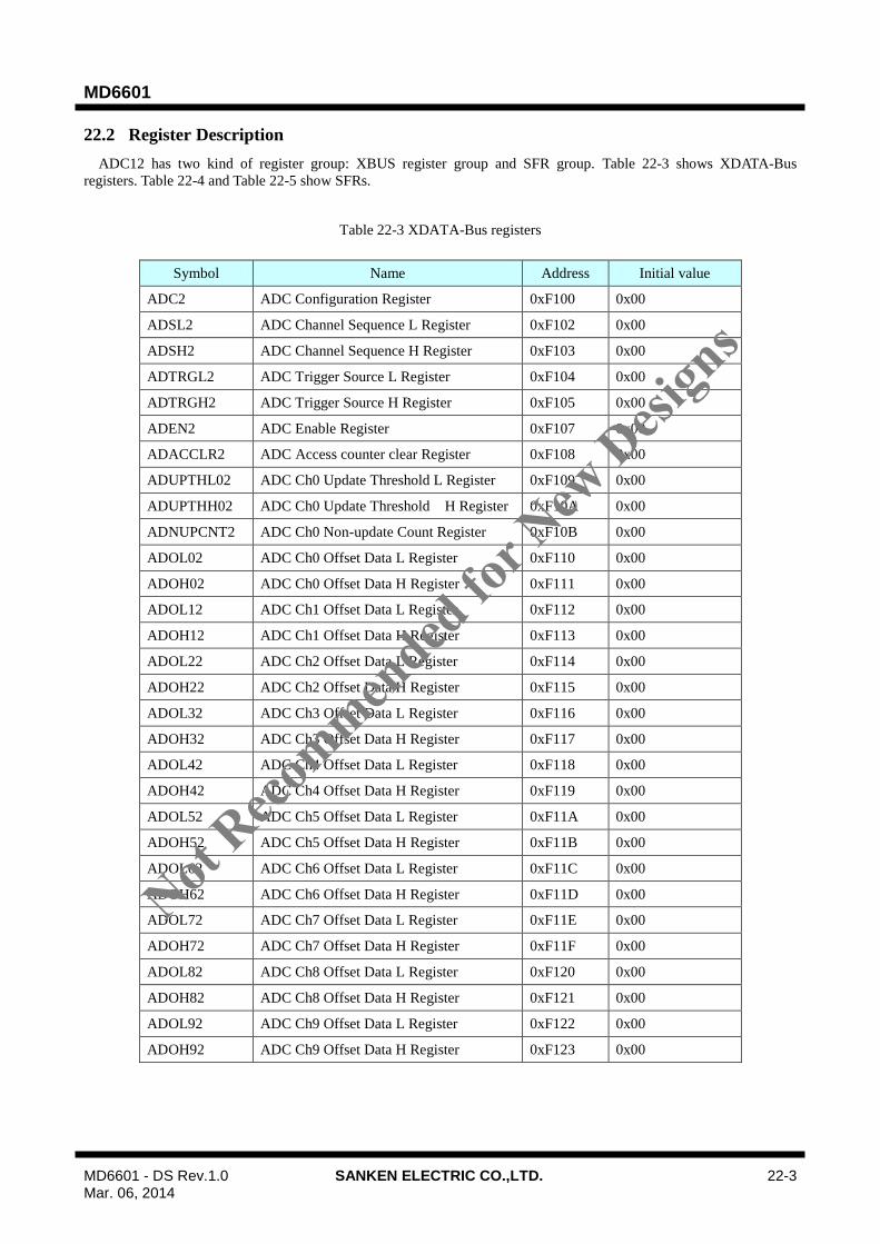
MD6601
MD6601 - DS Rev.1.0 SANKEN ELECTRIC CO.,LTD. 22-3 Mar. 06, 2014
22.2 Register Description
ADC12 has two kind of register group: XBUS register group and SFR group. Table 22-3 shows XDATA-Bus
registers. Table 22-4 and Table 22-5 show SFRs.
Table 22-3 XDATA-Bus registers
Symbol Name Address Initial value
ADC2 ADC Configuration Register 0xF100 0x00
ADSL2 ADC Channel Sequence L Register 0xF102 0x00
ADSH2 ADC Channel Sequence H Register 0xF103 0x00
ADTRGL2 ADC Trigger Source L Register 0xF104 0x00
ADTRGH2 ADC Trigger Source H Register 0xF105 0x00
ADEN2 ADC Enable Register 0xF107 0x00
ADACCLR2 ADC Access counter clear Register 0xF108 0x00
ADUPTHL02 ADC Ch0 Update Threshold L Register 0xF109 0x00
ADUPTHH02 ADC Ch0 Update Threshold H Register 0xF10A 0x00
ADNUPCNT2 ADC Ch0 Non-update Count Register 0xF10B 0x00
ADOL02 ADC Ch0 Offset Data L Register 0xF110 0x00
ADOH02 ADC Ch0 Offset Data H Register 0xF111 0x00
ADOL12 ADC Ch1 Offset Data L Register 0xF112 0x00
ADOH12 ADC Ch1 Offset Data H Register 0xF113 0x00
ADOL22 ADC Ch2 Offset Data L Register 0xF114 0x00
ADOH22 ADC Ch2 Offset Data H Register 0xF115 0x00
ADOL32 ADC Ch3 Offset Data L Register 0xF116 0x00
ADOH32 ADC Ch3 Offset Data H Register 0xF117 0x00
ADOL42 ADC Ch4 Offset Data L Register 0xF118 0x00
ADOH42 ADC Ch4 Offset Data H Register 0xF119 0x00
ADOL52 ADC Ch5 Offset Data L Register 0xF11A 0x00
ADOH52 ADC Ch5 Offset Data H Register 0xF11B 0x00
ADOL62 ADC Ch6 Offset Data L Register 0xF11C 0x00
ADOH62 ADC Ch6 Offset Data H Register 0xF11D 0x00
ADOL72 ADC Ch7 Offset Data L Register 0xF11E 0x00
ADOH72 ADC Ch7 Offset Data H Register 0xF11F 0x00
ADOL82 ADC Ch8 Offset Data L Register 0xF120 0x00
ADOH82 ADC Ch8 Offset Data H Register 0xF121 0x00
ADOL92 ADC Ch9 Offset Data L Register 0xF122 0x00
ADOH92 ADC Ch9 Offset Data H Register 0xF123 0x00
Not Reco
mmended
for N
ew D
esign
s

MD6601
MD6601 - DS Rev.1.0 SANKEN ELECTRIC CO.,LTD. 22-4 Mar. 06, 2014
Table 22-4 SFR (each unit)
Symbol Name Address Initial value
ADL02 ADC Ch0 Data L 0x9B 0x00
ADH02 ADC Ch0 Data H 0x9B 0x00
ADL12 ADC Ch1 Data L 0xA3 0x00
ADH12 ADC Ch1 Data H 0xA3 0x00
ADL22 ADC Ch2 Data L 0xAB 0x00
ADH22 ADC Ch2 Data H 0xAB 0x00
ADL32 ADC Ch3 Data L 0xB3 0x00
ADH32 ADC Ch3 Data H 0xB3 0x00
ADL42 ADC Ch4 Data L 0xBB 0x00
ADH42 ADC Ch4 Data H 0xBB 0x00
ADL52 ADC Ch5 Data L 0xC3 0x00
ADH52 ADC Ch5 Data H 0xC3 0x00
ADL62 ADC Ch6 Data L 0xCB 0x00
ADH62 ADC Ch6 Data H 0xCB 0x00
ADL72 ADC Ch7 Data L 0xD3 0x00
ADH72 ADC Ch7 Data H 0xD3 0x00
ADL82 ADC Ch8 Data L 0xDB 0x00
ADH82 ADC Ch8 Data H 0xDB 0x00
ADL92 ADC Ch9 Data L 0xE3 0x00
ADH92 ADC Ch9 Data H 0xE3 0x00
Table 22-5 SFR (common)
Symbol Name Address Initial value
ADT Mix ADC CPU Trigger Register 0xF1 0x00
ADI Mix ADC Interrupt Register 0xF2 0x00
Not Reco
mmended
for N
ew D
esign
s

MD6601
MD6601 - DS Rev.1.0 SANKEN ELECTRIC CO.,LTD. 22-5 Mar. 06, 2014
22.2.1 ADC2 (ADC Configuration Register)
Register ADC2 ADC Configuration Register Address 0xF100
Bit Bit Name R/W Initial Description Note
7 UPTH0EN R/W 0 CH0 update threshold enable
0: disable
1: enable
6 ADMODE R/W 0 ADC Conversion Mode
0: Burst until Sequence End
(Output interrupt after last sequence)
1: Step and Round Sequence
(Output interrupt at each step)
5 ADTIME R/W 0 ADC Conversion Time
0: Slow (CLKADC2 / 2)
1: Fast (CLKADC2 )
4 ADTRG4 R/W 0 ADC Trigger Source
00000: CPU
00001: GPIO0 Event for ADC (neg edge)
00010: GPIO0 Event for ADC (pos edge)
00011: GPIO0 Event for ADC (both edge)
00100: GPIO1 Event for ADC (neg edge)
00101: GPIO1 Event for ADC (pos edge)
00110: GPIO1 Event for ADC (both edge)
00111: GPIO2 Event for ADC (neg edge)
01000: GPIO2 Event for ADC (pos edge)
01001: GPIO2 Event for ADC (both edge)
01010: GPIO3 Event for ADC (neg edge)
01011: GPIO3 Event for ADC (pos edge)
01100: GPIO3 Event for ADC (both edge)
01101: Comparator 0 (pulse)
01110: Comparator 1 (pulse)
01111: Comparator 2 (pulse)
10000: Comparator 3 (pulse)
10001: TIMER0-CM0 (pulse)
10010: TIMER0-CM1 (pulse)
10011: TIMER1-CM0 (pulse)
10100: TIMER1-CM1 (pulse)
10101: PWM0-EVENT0 (pulse)
10110: PWM0-EVENT1 (pulse)
10111: PWM1-EVENT0 (pulse)
11000: PWM1-EVENT1 (pulse)
11001: PWM2-EVENT0(pulse)
11010: PWM2-EVENT1 (pulse)
11011: PWM3-EVENT0 (pulse)
11100: PWM3-EVENT1 (pulse)
Others are reserved. Do not set.
3 ADTRG3 R/W 0
2 ADTRG2 R/W 0
1 ADTRG1 R/W 0
0 ADTRG0 R/W 0
UPTHOEN, ADMODE and ADTIME in ADC2 register should be written when ADEN2.EN=0.
Setting ADEN2.EN=1 and waiting 1μs, then ADC Trigger Source should be written into ADTRG[4:0].
Not Reco
mmended
for N
ew D
esign
s

MD6601
MD6601 - DS Rev.1.0 SANKEN ELECTRIC CO.,LTD. 22-6 Mar. 06, 2014
22.2.2 ADSL2 (ADC Channel Sequence L Register)
Register ADSL2 ADC Channel Sequence L Register Address 0xF102
Bit Bit Name R/W Initial Description Note
7 CHSEQ7 R/W 0 Channel 7 Sequence
6 CHSEQ6 R/W 0 Channel 6 Sequence
5 CHSEQ5 R/W 0 Channel 5 Sequence
4 CHSEQ4 R/W 0 Channel 4 Sequence
3 CHSEQ3 R/W 0 Channel 3 Sequence
2 CHSEQ2 R/W 0 Channel 2 Sequence
1 CHSEQ1 R/W 0 Channel 1 Sequence
0 CHSEQ0 R/W 0 Channel 0 Sequence
ADSL2 register must be written when ADEN2.EN=0.
22.2.3 ADSH2 (ADC Channel Sequence H Register)
Register ADSH2 ADC Channel Sequence H Register Address 0xF103
Bit Bit Name R/W Initial Description Note
7 reserved R 0 Read value is 0. Write only 0.
6 reserved R 0 Read value is 0. Write only 0.
5 reserved R 0 Read value is 0. Write only 0.
4 reserved R 0 Read value is 0. Write only 0.
3 reserved R 0 Read value is 0. Write only 0.
2 reserved R 0 Read value is 0. Write only 0.
1 CHSEQ9 R/W 0 Channel 9 Sequence
0 CHSEQ8 R/W 0 Channel 8 Sequence
ADSH2 register must be written when ADEN2.EN=0.
Note: Channel Sequence is configured as follows.
ADSHn ADSLn Conversion Sequence
0b00000000 0b00000001 CH0CH0CH0CH0…
0b00000000 0b00001000 CH3CH3CH3CH3…
0b00000000 0b00000011 CH0CH1CH0CH1…
0b00000000 0b00111100 CH2CH3CH4CH5CH2CH3CH4CH5…
0b00000000 0b11111111 CH0CH1CH2CH3CH4CH5CH6CH7…
0b00000010 0b10001000 CH3CH7CH9CH3CH7CH9...
Not Reco
mmended
for N
ew D
esign
s
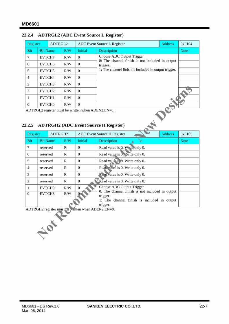
MD6601
MD6601 - DS Rev.1.0 SANKEN ELECTRIC CO.,LTD. 22-7 Mar. 06, 2014
22.2.4 ADTRGL2 (ADC Event Source L Register)
Register ADTRGL2 ADC Event Source L Register Address 0xF104
Bit Bit Name R/W Initial Description Note
7 EVTCH7 R/W 0 Choose ADC Output Trigger
0: The channel finish is not included in output
trigger.
1: The channel finish is included in output trigger.
6 EVTCH6 R/W 0
5 EVTCH5 R/W 0
4 EVTCH4 R/W 0
3 EVTCH3 R/W 0
2 EVTCH2 R/W 0
1 EVTCH1 R/W 0
0 EVTCH0 R/W 0
ADTRGL2 register must be written when ADEN2.EN=0.
22.2.5 ADTRGH2 (ADC Event Source H Register)
Register ADTRGH2 ADC Event Source H Register Address 0xF105
Bit Bit Name R/W Initial Description Note
7 reserved R 0 Read value is 0. Write only 0.
6 reserved R 0 Read value is 0. Write only 0.
5 reserved R 0 Read value is 0. Write only 0.
4 reserved R 0 Read value is 0. Write only 0.
3 reserved R 0 Read value is 0. Write only 0.
2 reserved R 0 Read value is 0. Write only 0.
1 EVTCH9 R/W 0 Choose ADC Output Trigger
0: The channel finish is not included in output
trigger.
1: The channel finish is included in output
trigger.
0 EVTCH8 R/W 0
ADTRGH2 register must be written when ADEN2.EN=0.
Not Reco
mmended
for N
ew D
esign
s

MD6601
MD6601 - DS Rev.1.0 SANKEN ELECTRIC CO.,LTD. 22-8 Mar. 06, 2014
22.2.6 ADEN2 (ADC Enable Register)
Register ADEN2 ADC Enable Register Address 0xF107
Bit Bit Name R/W Initial Description Note
7 reserved R 0 Read value is 0. Write only 0.
6 reserved R 0 Read value is 0. Write only 0.
5 reserved R 0 Read value is 0. Write only 0.
4 reserved R 0 Read value is 0. Write only 0.
3 reserved R 0 Read value is 0. Write only 0.
2 reserved R 0 Read value is 0. Write only 0.
1 reserved R 0 Read value is 0. Write only 0.
0 EN R/W 0 ADC Enable
0: ADC Disabled
1: ADC Enabled
Activate the ADC.
22.2.7 ADACCLR2 (ADC Access Counter Clear Register)
Register ADACCLR2 ADC Access Counter Clear Register Address 0xF108
Bit Bit Name R/W Initial Description Note
7 CLRADCCDRCAC
R/W 0 Clear ADC Conversion Data Register CPU Access
Counter
0: No effect
1: Register CPU Access counter clear
Read : No Request
Write 0: No effect
Write 1: Clear Register CPU Access counter.
(Clear CPU SFR access counter.)
6 CLRADCCDR
DAC R/W 0 Clear ADC Conversion Data Register DSAC Access
Counter
0: No effect
1: Register DSAC Access counter clear
Read : No Request
Write 0: No effect
Write 1: Clear Register DSAC Access counter.
(Clear DSAC SFR access counter.)
5 reserved R 0 Read value is 0. Write only 0.
4 reserved R 0 Read value is 0. Write only 0.
3 reserved R 0 Read value is 0. Write only 0.
2 reserved R 0 Read value is 0. Write only 0.
1 reserved R 0 Read value is 0. Write only 0.
0 reserved R 0 Read value is 0. Write only 0.
Not Reco
mmended
for N
ew D
esign
s
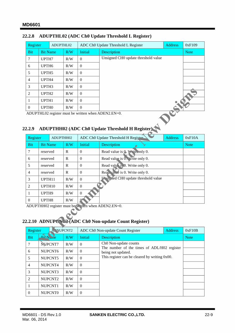
MD6601
MD6601 - DS Rev.1.0 SANKEN ELECTRIC CO.,LTD. 22-9 Mar. 06, 2014
22.2.8 ADUPTHL02 (ADC Ch0 Update Threshold L Register)
Register ADUPTHL02 ADC Ch0 Update Threshold L Register Address 0xF109
Bit Bit Name R/W Initial Description Note
7 UPTH7 R/W 0 Unsigned CH0 update threshold value
6 UPTH6 R/W 0
5 UPTH5 R/W 0
4 UPTH4 R/W 0
3 UPTH3 R/W 0
2 UPTH2 R/W 0
1 UPTH1 R/W 0
0 UPTH0 R/W 0
ADUPTHL02 register must be written when ADEN2.EN=0.
22.2.9 ADUPTHH02 (ADC Ch0 Update Threshold H Register)
Register ADUPTHH02 ADC Ch0 Update Threshold H Register Address 0xF10A
Bit Bit Name R/W Initial Description Note
7 reserved R 0 Read value is 0. Write only 0.
6 reserved R 0 Read value is 0. Write only 0.
5 reserved R 0 Read value is 0. Write only 0.
4 reserved R 0 Read value is 0. Write only 0.
3 UPTH11 R/W 0 Unsigned CH0 update threshold value
2 UPTH10 R/W 0
1 UPTH9 R/W 0
0 UPTH8 R/W 0
ADUPTHH02 register must be written when ADEN2.EN=0.
22.2.10 ADNUPCNT2 (ADC Ch0 Non-update Count Register)
Register ADNUPCNT2 ADC Ch0 Non-update Count Register Address 0xF10B
Bit Bit Name R/W Initial Description Note
7 NUPCNT7 R/W 0 Ch0 Non-update counts
The number of the times of ADL/H02 register
being not updated.
This register can be cleared by writing 0x00.
6 NUPCNT6 R/W 0
5 NUPCNT5 R/W 0
4 NUPCNT4 R/W 0
3 NUPCNT3 R/W 0
2 NUPCNT2 R/W 0
1 NUPCNT1 R/W 0
0 NUPCNT0 R/W 0
Not Reco
mmended
for N
ew D
esign
s

MD6601
MD6601 - DS Rev.1.0 SANKEN ELECTRIC CO.,LTD. 22-10 Mar. 06, 2014
22.2.11 ADOLX2 (ADC ChX Offset Data L Register)
Register ADOL02 ADC Ch0 Offset Data L Register Address 0xF110
Register ADOL12 ADC Ch1 Offset Data L Register Address 0xF112
Register ADOL22 ADC Ch2 Offset Data L Register Address 0xF114
Register ADOL32 ADC Ch3 Offset Data L Register Address 0xF116
Register ADOL42 ADC Ch4 Offset Data L Register Address 0xF118
Register ADOL52 ADC Ch5 Offset Data L Register Address 0xF11A
Register ADOL62 ADC Ch6 Offset Data L Register Address 0xF11C
Register ADOL72 ADC Ch7 Offset Data L Register Address 0xF11E
Register ADOL82 ADC Ch8 Offset Data L Register Address 0xF120
Register ADOL92 ADC Ch9 Offset Data L Register Address 0xF122
Bit Bit Name R/W Initial Description Note
7 ADOFFSET
7 R/W 0
Signed 13 bit ADC Offset Data L
bit 7 – bit 0 are stored.
6 ADOFFSET
6 R/W 0
5 ADOFFSET
5 R/W 0
4 ADOFFSET
4 R/W 0
3 ADOFFSET
3 R/W 0
2 ADOFFSET
2 R/W 0
1 ADOFFSET
1 R/W 0
0 ADOFFSET
0 R/W 0
Not Reco
mmended
for N
ew D
esign
s
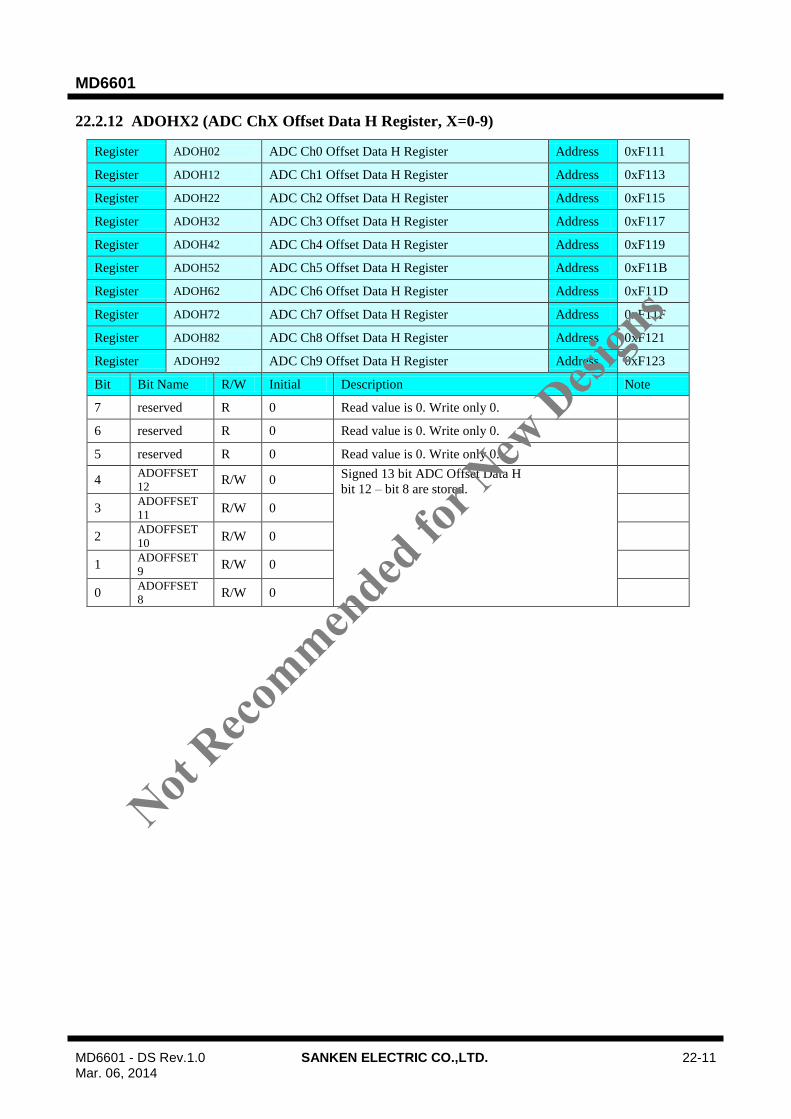
MD6601
MD6601 - DS Rev.1.0 SANKEN ELECTRIC CO.,LTD. 22-11 Mar. 06, 2014
22.2.12 ADOHX2 (ADC ChX Offset Data H Register, X=0-9)
Register ADOH02 ADC Ch0 Offset Data H Register Address 0xF111
Register ADOH12 ADC Ch1 Offset Data H Register Address 0xF113
Register ADOH22 ADC Ch2 Offset Data H Register Address 0xF115
Register ADOH32 ADC Ch3 Offset Data H Register Address 0xF117
Register ADOH42 ADC Ch4 Offset Data H Register Address 0xF119
Register ADOH52 ADC Ch5 Offset Data H Register Address 0xF11B
Register ADOH62 ADC Ch6 Offset Data H Register Address 0xF11D
Register ADOH72 ADC Ch7 Offset Data H Register Address 0xF11F
Register ADOH82 ADC Ch8 Offset Data H Register Address 0xF121
Register ADOH92 ADC Ch9 Offset Data H Register Address 0xF123
Bit Bit Name R/W Initial Description Note
7 reserved R 0 Read value is 0. Write only 0.
6 reserved R 0 Read value is 0. Write only 0.
5 reserved R 0 Read value is 0. Write only 0.
4 ADOFFSET
12 R/W 0
Signed 13 bit ADC Offset Data H
bit 12 – bit 8 are stored.
3 ADOFFSET
11 R/W 0
2 ADOFFSET
10 R/W 0
1 ADOFFSET
9 R/W 0
0 ADOFFSET
8 R/W 0
Not Reco
mmended
for N
ew D
esign
s
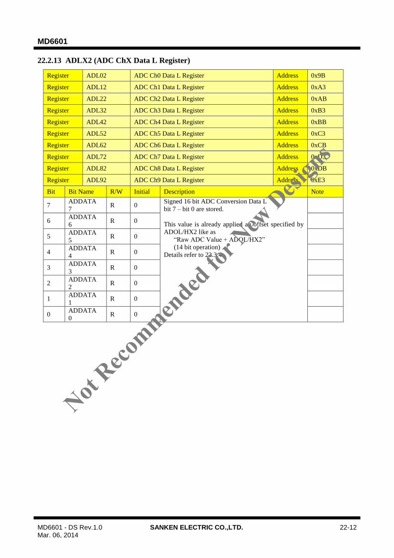
MD6601
MD6601 - DS Rev.1.0 SANKEN ELECTRIC CO.,LTD. 22-12 Mar. 06, 2014
22.2.13 ADLX2 (ADC ChX Data L Register)
Register ADL02 ADC Ch0 Data L Register Address 0x9B
Register ADL12 ADC Ch1 Data L Register Address 0xA3
Register ADL22 ADC Ch2 Data L Register Address 0xAB
Register ADL32 ADC Ch3 Data L Register Address 0xB3
Register ADL42 ADC Ch4 Data L Register Address 0xBB
Register ADL52 ADC Ch5 Data L Register Address 0xC3
Register ADL62 ADC Ch6 Data L Register Address 0xCB
Register ADL72 ADC Ch7 Data L Register Address 0xD3
Register ADL82 ADC Ch8 Data L Register Address 0xDB
Register ADL92 ADC Ch9 Data L Register Address 0xE3
Bit Bit Name R/W Initial Description Note
7 ADDATA
7 R 0
Signed 16 bit ADC Conversion Data L
bit 7 – bit 0 are stored.
This value is already applied an offset specified by
ADOL/HX2 like as
“Raw ADC Value + ADOL/HX2”
(14 bit operation)
Details refer to 22.3.4
6 ADDATA
6 R 0
5 ADDATA
5 R 0
4 ADDATA
4 R 0
3 ADDATA
3 R 0
2 ADDATA
2 R 0
1 ADDATA
1 R 0
0 ADDATA
0 R 0
Not Reco
mmended
for N
ew D
esign
s

MD6601
MD6601 - DS Rev.1.0 SANKEN ELECTRIC CO.,LTD. 22-13 Mar. 06, 2014
22.2.14 ADHX2 (ADC ChX Data H Register)
Register ADH02 ADC Ch0 Data H Register Address 0x9B
Register ADH12 ADC Ch1 Data H Register Address 0xA3
Register ADH22 ADC Ch2 Data H Register Address 0xAB
Register ADH32 ADC Ch3 Data H Register Address 0xB3
Register ADH42 ADC Ch4 Data H Register Address 0xBB
Register ADH52 ADC Ch5 Data H Register Address 0xC3
Register ADH62 ADC Ch6 Data H Register Address 0xCB
Register ADH72 ADC Ch7 Data H Register Address 0xD3
Register ADH82 ADC Ch8 Data H Register Address 0xDB
Register ADH92 ADC Ch9 Data H Register Address 0xE3
Bit Bit Name R/W Initial Description Note
7 ADDATA
15 R 0
Signed 16 bit ADC Conversion Data H
bit 15 – bit 8 are stored.
This value is already applied an offset specified
by ADOH/LX2 like as
“Raw ADC Value + ADOX2”
(14 bit operation)
Details refer to 22.3.4
6 ADDATA
14 R 0
5 ADDATA
13 R 0
4 ADDATA
12 R 0
3 ADDATA
11 R 0
2 ADDATA
10 R 0
1 ADDATA
9 R 0
0 ADDATA
8 R 0
22.2.15 ADT (ADC Trigger Register)
Please refer to the 21.2.16 ADT(ADC Trigger Register) in Sec 21 High Speed 10 bit SAR ADC.
22.2.16 ADI (ADC Interrupt Register)
Please refer to the 21.2.17 ADI(ADC Interrupt Register) in Sec 21 High Speed 10 bit SAR ADC
Not Reco
mmended
for N
ew D
esign
s

MD6601
MD6601 - DS Rev.1.0 SANKEN ELECTRIC CO.,LTD. 22-14 Mar. 06, 2014
22.3 Operation
22.3.1 Basic operation
ADC is activated when ADEN2.EN bit is set to 1'b1. The AD conversion starts when ADC is active and a conversion
trigger from one of the peripherals is received. The AD Conversion trigger can be selected from CPU, external GPIO
events, analog comparator events, PWM events or Timer events by ADC2.ADTRG[4:0] bits. The CPU trigger can be
generated by ADT.ADCTRGn bit that is mapped in SFR address space.
AD Conversion time can be selected from slow (half speed) or fast (full speed) by ADC2.ADTIME bit.
Figure 22-2 Basic conversion sequence.
A/D conversion of a channel spends 50 cycles of ADCLK.
CLKADC2 ・・・・・・ ・・・・・・・・・1 2 3 19 20 21 22 23 24 25 26 45 46 47 48 49 50
ADCLK(ADTIME=1) ・・・・・・ ・・・・・・・・・
Trigger
CHx IDLE Sample/Hold Conversion IDLE
DATA DATA
ADL/HX2(Data Register) DATA
Figure 22-2 Basic conversion sequence
ADC has ten analog channels at most. The conversion of each channel can be enabled by ADSL/H2 register. The
conversion starts from the youngest enabled number channel. Table 22-6 shows the correspondence between ADSL/H2
register bit and analog input.
Table 22-6 CHSEQx bit vs. analog input
Pin Name ADC12 Notes
ADSL2.CHSEQ0 ANEX0
ADSL2.CHSEQ1 ANEX2
ADSL2.CHSEQ2 ANEX4
ADSL2.CHSEQ3 ANEX6
ADSL2.CHSEQ4 AMP0
ADSL2.CHSEQ5 AMP1
ADSL2.CHSEQ6 ANEX11
ADSL2.CHSEQ7 ANEX15
ADSH2.CHSEQ8 AGND
ADSH2.CHSEQ9 AVSS
Not Reco
mmended
for N
ew D
esign
s

MD6601
MD6601 - DS Rev.1.0 SANKEN ELECTRIC CO.,LTD. 22-15 Mar. 06, 2014
22.3.2 Conversion Mode
AD Conversion Mode is selected from “Burst until Sequence End” or “Step and Round Sequence” by
ADC2.ADMODE bit. The sequence means the order of input channels to be converted.
22.3.2.1. Burst until Sequence End mode
In the mode “Burst until Sequence End”, one trigger can initiate contiguous burst conversions according to
configured sequence.
(1) When the start trigger that is selected by ADC2.ADTRG[4:0] bit is detected, A/D conversion starts in younger
channel order which is selected by ADSL/H2 register.
(2) When A/D conversion of a channel finished, the converted data is written to corresponding data register
(ADLHX2).
(3) If there are un-converted channel, A/D conversion of the next younger channel starts just after finishing the
previous A/D conversion. After that, go back to (2).
(4) A/D conversions of all channels are finished, ADI.ADIF bit is set to 1'b1. If ADI.ADIE=1, ADI interrupt is
issued to CPU.
trigger
ch1 Conv
ch2 Conv
ch3 Conv
ADLH1n
ADLH2n
ADLH3n
ADIinterrupt
Figure 22-3 Burst until Sequence End mode.
Not Reco
mmended
for N
ew D
esign
s
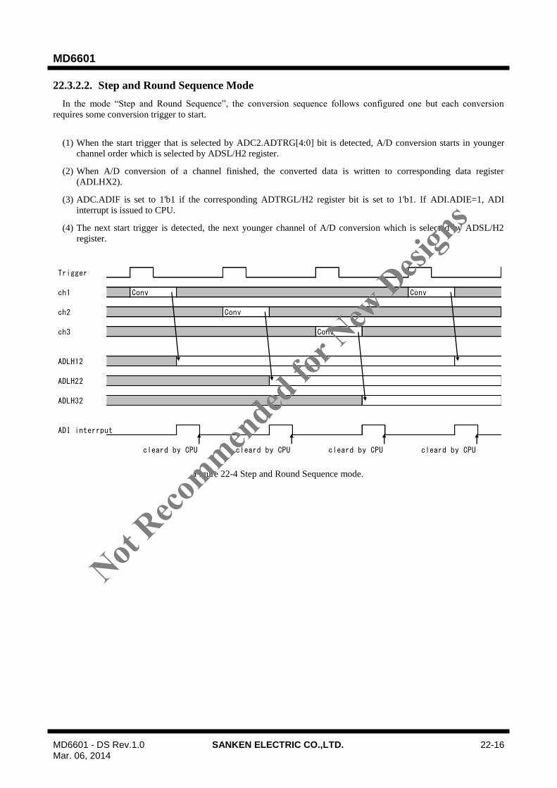
MD6601
MD6601 - DS Rev.1.0 SANKEN ELECTRIC CO.,LTD. 22-16 Mar. 06, 2014
22.3.2.2. Step and Round Sequence Mode
In the mode “Step and Round Sequence”, the conversion sequence follows configured one but each conversion
requires some conversion trigger to start.
(1) When the start trigger that is selected by ADC2.ADTRG[4:0] bit is detected, A/D conversion starts in younger
channel order which is selected by ADSL/H2 register.
(2) When A/D conversion of a channel finished, the converted data is written to corresponding data register
(ADLHX2).
(3) ADC.ADIF is set to 1'b1 if the corresponding ADTRGL/H2 register bit is set to 1'b1. If ADI.ADIE=1, ADI
interrupt is issued to CPU.
(4) The next start trigger is detected, the next younger channel of A/D conversion which is selected by ADSL/H2
register.
Trigger
ch1 Conv Conv
ch2 Conv
ch3 Conv
ADLH12
ADLH22
ADLH32
ADI interrput
cleard by CPU cleard by CPU cleard by CPU cleard by CPU
Figure 22-4 Step and Round Sequence mode.
Not Reco
mmended
for N
ew D
esign
s

MD6601
MD6601 - DS Rev.1.0 SANKEN ELECTRIC CO.,LTD. 22-17 Mar. 06, 2014
22.3.3 Conversion start trigger
A/D conversion starts when detecting selected A/D conversion trigger. A/D conversion start trigger can be selected by
ADC2.ADTRG[4:0]. Only one conversion trigger during A/D conversion is hold, and issues after the current
conversion is finished, then the next conversion will start. The conversion trigger is not accepted when ADEN2=0 or all
channels are not selected (ADSL/H2=0x00).
22.3.4 Converted data offset adjustment
The offset adjustment can be done for converted data by ADOL/HX2 register. The bit length of adjusted value is
enhanced from 12 bit to 16 bit.
ADOH/LX2.ADATA_tmp[13:0] = RAW_ADC_Value{2'b00,[11:0]}
+ OFFSET{[12],[12:0]}
ADOH/LX2.ADATA[15:0] = RAW_ADC_Value_tmp{[13],[13],[13:0]}
ADOH/LX2.ADATA[15:0] : ADLHX2 register bit, X is unit-X's channel.
RAW_ADC_Value[11:0]: Conversion result value
OFFSET[12:0] : Signed, ADOH/LX2 register bit, X is unit-X's channel.
12bit(Unsigned)
+
Converted data SOffset
SResult value
SSSResult
ADLX register[7:0]ADHX register[7:0]
sign bit expansion
ADOLX register[7:0]ADOHX register[4:0]
S : Sign bit
13bit(Signed)
14bit(Signed)
16bit(Signed)
Figure 22-5 Converted data
Not Reco
mmended
for N
ew D
esign
s

MD6601
MD6601 - DS Rev.1.0 SANKEN ELECTRIC CO.,LTD. 22-18 Mar. 06, 2014
22.3.5 Interrupts
If ADI.ADIEn=1, CPU interrupt can be occurred when ADI.ADIFn=1(n=0 or 1).
22.3.6 ADC Event
ADC event can be issued when A/D conversion is finished. The ADC event of each channel can be selected by
ADTRGL/H2 register. Table 22-6 shows the ADC event when ch0 and 3 are enabled, others are disabled.
Trigger
ch1 Conv Conv
ch2 Conv
ch3 Conv
ADLH12
ADLH22
ADLH32
ADC Event
Figure 22-6 ADC event when ch1 and 3 are enabled.
22.3.7 Reading converted data
Note that the converted result data, mapped in SFR address space, pair of Low Side (LSB Side) register and High
Side (MSB Side) register for 16 bit value should be assigned on SAME address. In read access, 1st access gets Low Side
data and 2nd
access receives High Side data.
The LSB/MSB Side is selected by CPU/DSAC access counter. When CPU reads from ADLHX2 register, CPU
counter is incremented. If ADACCLR2.CLRADCCDRCAC bit is set to 1'b1, the CPU access counter is cleared. After
that, the LSB Side can be read by CPU. When DSAC reads from ADLHX2 register, DSAC counter is incremented. If
ADACCLR2.CLRADCCDRDAC bit is set to 1'b1, the DSAC access counter is cleared. After that, the LSB Side can be
read by DSAC.
22.3.8 Threshold for conversion data update
This function controls ADLH02 register update. ADLH02 is updated if the difference between the current conversion
result value (the offset is not included) and previous one (the offset is not included) are equal or less than the
threshold(ADUPTHH/L02). The threshold is enabled during ADC2.UPTH0EN=1. The update condition is as follows:
|{(current conversion result value) - (previous conversion result value}}| =< {(ADUPTHH02, ADUPTHL02)}.
The current/previous data comparison starts after ADC2.UPTH0EN=1. Therefore, the previous conversion result
must be valid value for comparison. At first, the valid value should be gotten when ADC2.UPTH0EN, then
ADC2.UPTH0EN should be set to 1 to start the function.
ADNUPCNT2 shows the number of non-update times. This register can be cleared by writing 0x00 to ADNUPCNT2
register. To know ADLH02 register is not updated, ADNUPCNT2 is read when CH0 conversion end interrupt sequence,
and compare its value to previous one. If the current value is increased from previous value, the current conversion
result is not written to ADLH02 register.
Not Reco
mmended
for N
ew D
esign
s
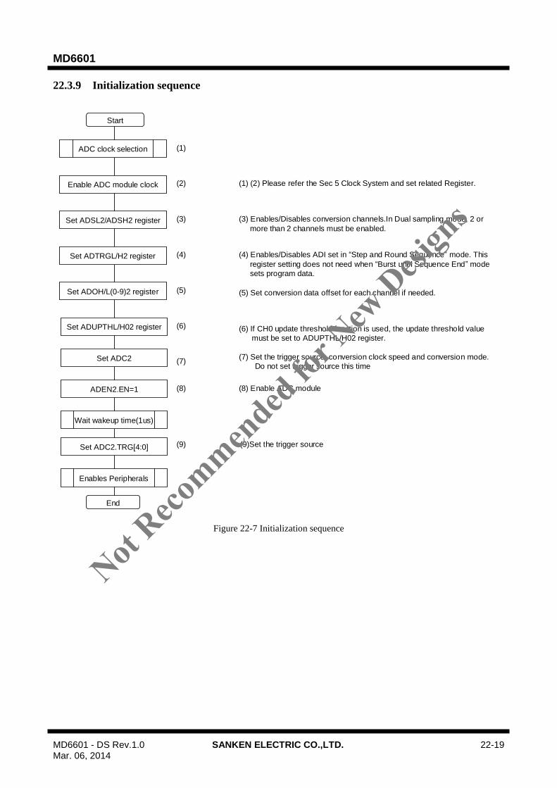
MD6601
MD6601 - DS Rev.1.0 SANKEN ELECTRIC CO.,LTD. 22-19 Mar. 06, 2014
22.3.9 Initialization sequence
Start
End
(4)
Set ADSL2/ADSH2 register (3)
Set ADTRGL/H2 register
Set ADUPTHL/H02 register
Set ADOH/L(0-9)2 register
Enables Peripherals
(4) Enables/Disables ADI set in “Step and Round Sequence” mode. This
register setting does not need when “Burst until Sequence End” mode
sets program data.
(3) Enables/Disables conversion channels.In Dual sampling mode, 2 or
more than 2 channels must be enabled.
(5) Set conversion data offset for each channel if needed.(5)
(6)
(7)
(9)
(6) If CH0 update threshold function is used, the update threshold value
must be set to ADUPTHL/H02 register.
Enable ADC module clock
ADC clock selection (1)
(1) (2) Please refer the Sec 5 Clock System and set related Register.(2)
ADEN2.EN=1 (8) Enable ADC module
Set ADC2
(8)
(7) Set the trigger source, conversion clock speed and conversion mode.
Do not set trigger source this time
Set ADC2.TRG[4:0]
Wait wakeup time(1us)
(9)Set the trigger source
Figure 22-7 Initialization sequence
Not Reco
mmended
for N
ew D
esign
s

MD6601
MD6601 - DS Rev.1.0 SANKEN ELECTRIC CO.,LTD. 22-20 Mar. 06, 2014
22.4 Limitation of ADC12
22.4.1 Disabling ADC
When disabling ADC, please keep following sequence.
(1) ADC Trigger Source select CPU Trigger by setting the ADC2.ADTRG[4:0] to 5’b00000, then other ADC
trigger source can be ignored. If ADTRG[4:0] is not 5’b00000, Trigger Source from peripheral must be stop by
each peripheral.
(2) Wait until ADT.ADCTR2G becomes 1'b0. Please refer to 21.2.16.
(3) Disable ADC(ADEN2.EN=0).
22.4.2 Going to standby mode
Note that ADC must be disabled before going to Standby mode.
22.5 Caution of operation
22.5.1 Restriction about the conversion time of the 12 bits ADC
(1) Description
When conversion time of the 12 bits ADC is set to slow mode, conversion results are corrupted.
(2) Condition
If ADTIME bit of ADC2(ADC Configuration Register) is set to 0 (slow mode), conversion results are corrupted.
(3) Countermeasure
ADTIME bit of ADC2(ADC Configuration Register) should be set to 1 (fast mode).
Not Reco
mmended
for N
ew D
esign
s

MD6601
MD6601 - DS Rev.1.0 SANKEN ELECTRIC CO.,LTD. 23-1 Mar. 06, 2014
23. High Precision 12 bit DAC
23.1 Overview
The LSI has one 12 bit DA Converter. DA output levels are updated by CPU, DSAC, Comparator Events, Timer
Events or PWM Events.
Table 23-1 Feature of High Precision 12bit DAC
Item Description Note
Unit Counts Single Unit
Resolution 12bit
Conversion Speed 1MSPS (Mega samples per second) Settling Time
= 1000ns
Output
Update Event
CPU Writing
DSAC Writing
Comparator Events
Timer Events
PWM Events
23.2 Block Diagram
(1)CMP0
:
3
TMR0
:
1
PWM0
:
3
MIXDAC
XDATA-
Bus
DAUPD[4:0]
DACACCLR
R/W
co
ntr
ol
(1)CPU update trigger
SFR-
Bus
clear
MIXDAH
MIXDAL
MIXDARDH
MIXDARDL
12bit
DAC
12bit
Output
data
Update trigger
Update trigger:
:
Figure 23-1 Block diagram of 12bit DAC
Not Reco
mmended
for N
ew D
esign
s
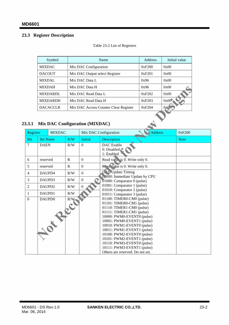
MD6601
MD6601 - DS Rev.1.0 SANKEN ELECTRIC CO.,LTD. 23-2 Mar. 06, 2014
23.3 Register Description
Table 23-2 List of Registers
Symbol Name Address Initial value
MIXDAC Mix DAC Configuration 0xF200 0x00
DACOUT Mix DAC Output select Register 0xF201 0x00
MIXDAL Mix DAC Data L 0x96 0x00
MIXDAH Mix DAC Data H 0x96 0x00
MIXDARDL Mix DAC Read Data L 0xF202 0x00
MIXDARDH Mix DAC Read Data H 0xF203 0x00
DACACCLR Mix DAC Access Counter Clear Register 0xF204 0x00
23.3.1 Mix DAC Configuration (MIXDAC)
Register MIXDAC Mix DAC Configuration Address 0xF200
Bit Bit Name R/W Initial Description Note
7 DAEN R/W 0 DAC Enable
0: Disabled
1: Enabled
6 reserved R 0 Read value is 0. Write only 0.
5 reserved R 0 Read value is 0. Write only 0.
4 DAUPD4 R/W 0 DAC Update Timing
00000: Immediate Update by CPU
01000: Comparator 0 (pulse)
01001: Comparator 1 (pulse)
01010: Comparator 2 (pulse)
01011: Comparator 3 (pulse)
01100: TIMER0-CM0 (pulse)
01101: TIMER0-CM1 (pulse)
01110: TIMER1-CM0 (pulse)
01111: TIMER1-CM1 (pulse)
10000: PWM0-EVENT0 (pulse)
10001: PWM0-EVENT1 (pulse)
10010: PWM1-EVENT0 (pulse)
10011: PWM1-EVENT1 (pulse)
10100: PWM2-EVENT0 (pulse)
10101: PWM2-EVENT1 (pulse)
10110: PWM3-EVENT0 (pulse)
10111: PWM3-EVENT1 (pulse)
Others are reserved. Do not set.
3 DAUPD3 R/W 0
2 DAUPD2 R/W 0
1 DAUPD1 R/W 0
0 DAUPD0 R/W 0
Not Reco
mmended
for N
ew D
esign
s
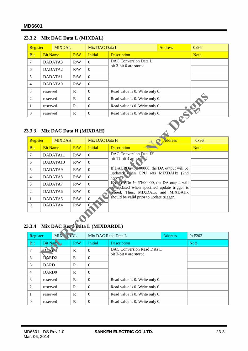
MD6601
MD6601 - DS Rev.1.0 SANKEN ELECTRIC CO.,LTD. 23-3 Mar. 06, 2014
23.3.2 Mix DAC Data L (MIXDAL)
Register MIXDAL Mix DAC Data L Address 0x96
Bit Bit Name R/W Initial Description Note
7 DADATA3 R/W 0 DAC Conversion Data L
bit 3-bit 0 are stored.
6 DADATA2 R/W 0
5 DADATA1 R/W 0
4 DADATA0 R/W 0
3 reserved R 0 Read value is 0. Write only 0.
2 reserved R 0 Read value is 0. Write only 0.
1 reserved R 0 Read value is 0. Write only 0.
0 reserved R 0 Read value is 0. Write only 0.
23.3.3 Mix DAC Data H (MIXDAH)
Register MIXDAH Mix DAC Data H Address 0x96
Bit Bit Name R/W Initial Description Note
7 DADATA11 R/W 0 DAC Conversion Data H
bit 11-bit 4 are stored.
If DAUPDn=5’b00000, the DA output will be
updated when CPU sets MIXDAHx (2nd
access).
If DAUPDn != 5’b00000, the DA output will
be updated when specified update trigger is
issued. Thus, MIXDALx and MIXDAHx
should be valid prior to update trigger.
6 DADATA10 R/W 0
5 DADATA9 R/W 0
4 DADATA8 R/W 0
3 DADATA7 R/W 0
2 DADATA6 R/W 0
1 DADATA5 R/W 0
0
DADATA4
R/W
0
23.3.4 Mix DAC Read Data L (MIXDARDL)
Register MIXDARDL Mix DAC Read Data L Address 0xF202
Bit Bit Name R/W Initial Description Note
7 DARD3 R 0 DAC Conversion Read Data L
bit 3-bit 0 are stored.
6 DARD2 R 0
5 DARD1 R 0
4 DARD0 R 0
3 reserved R 0 Read value is 0. Write only 0.
2 reserved R 0 Read value is 0. Write only 0.
1 reserved R 0 Read value is 0. Write only 0.
0 reserved R 0 Read value is 0. Write only 0.
Not Reco
mmended
for N
ew D
esign
s
MD6601
MD6601 - DS Rev.1.0 SANKEN ELECTRIC CO.,LTD. 23-4 Mar. 06, 2014
23.3.5 Mix DAC Read Data H (MIXDARDH)
Register MIXDARDH Mix DAC Read Data H Address 0xF203
Bit Bit Name R/W Initial Description Note
7 DARD11 R 0 DAC Conversion Read Data H
bit 11-bit 4 are stored.
6 DARD10 R 0
5 DARD9 R 0
4 DARD8 R 0
3 DARD7 R 0
2 DARD6 R 0
1 DARD5 R 0
0 DARD4 R 0
*If MIXDAC[4:0] trigger is detected after both MIXDAH and MIXDAL are written, MIXDARDL and MIXDARDH
will be updated.
23.3.6 Mix DAC Access Counter Clear Register (DACACCLR)
Register DACACCLR Mix DAC Access Counter Clear Register Address 0xF204
Bit Bit Name R/W Initial Description Note
7 CPUCLR R/W 0 Clear DAC Conversion Data Register CPU Access
Counter Read : Read value is 0.
Write 0: No effect
Write 1: Clear Register CPU Access counter.
(Clear CPU SFR access counter.)
6 DSACCLR R/W 0 Clear DAC Conversion Data Register DSAC
Access Counter Read : Read value is 0.
Write 0: No effect
Write 1: Clear Register DSAC Access counter.
(Clear DSAC SFR access counter.)
5 reserved R 0 Read value is 0. Write only 0.
4 reserved R 0 Read value is 0. Write only 0.
3 reserved R 0 Read value is 0. Write only 0.
2 reserved R 0 Read value is 0. Write only 0.
1 reserved R 0 Read value is 0. Write only 0.
0 reserved R 0 Read value is 0. Write only 0.
Not Reco
mmended
for N
ew D
esign
s
MD6601
MD6601 - DS Rev.1.0 SANKEN ELECTRIC CO.,LTD. 23-5 Mar. 06, 2014
23.3.7 Mix DAC Output select Register (DACOUT)
Register DACOUT Mix DAC Output select Register Address 0xF201
Bit Bit Name R/W Initial Description Note
7 CALIB R/W 0 DAC calibration mode. Output to the CH8 of
ADC12.
0: Normal mode
1: Calibration mode
Usually set to 0.
6 reserved R 0 Read value is 0. Write only 0.
5 reserved R 0 Read value is 0. Write only 0.
4 reserved R 0 Read value is 0. Write only 0.
3 SEL3 R/W 0 OPA Output Enable(ANEX15)
0:Not connected to External Pin ANEX15
1:Connected to External Pin ANEX15
2 SEL2 R/W 0 OPA Output Enable(ANEX13)
0:Not connected to External Pin ANEX13
1:Connected to External Pin ANEX13
1 SEL1 R/W 0 OPA Output Enable(ANEX11)
0:Not connected to External Pin ANEX11
1:Connected to External Pin ANEX11
0 SEL0 R/W 0 OPA Output Enable(ANEX09)
0:Not connected to External Pin ANEX09
1:Connected to External Pin ANEX09
Not Reco
mmended
for N
ew D
esign
s
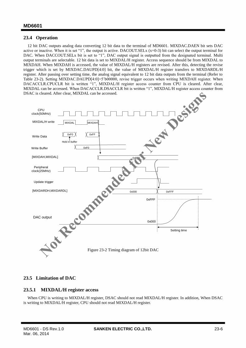
MD6601
MD6601 - DS Rev.1.0 SANKEN ELECTRIC CO.,LTD. 23-6 Mar. 06, 2014
23.4 Operation
12 bit DAC outputs analog data converting 12 bit data to the terminal of MD6601. MIXDAC.DAEN bit sets DAC
active or inactive. When it is set “1”, the output is active. DACOUT.SELx (x=0-3) bit can select the output terminal for
DAC. When DACCOUT.SELx bit is set to “1”, DAC output signal is outputted from the designated terminal. Multi
output terminals are selectable. 12 bit data is set to MIXDAL/H register. Access sequence should be from MIXDAL to
MIXDAH. When MIXDAH is accessed, the value of MIXDAL/H registers are revised. After this, detecting the revise
trigger which is set by MIXDAC.DAUPD[4:0] bit, the value of MIXDAL/H register transfers to MIXDARDL/H
register. After passing over setting time, the analog signal equivalent to 12 bit data outputs from the terminal (Refer to
Table 23-2). Setting MIXDAC.DAUPD[4:0]=5’b00000, revise trigger occurs when writing MIXDAH register. When
DACACCLR.CPUCLR bit is written “1”, MIXDAL/H register access counter from CPU is cleared. After clear,
MIXDAL can be accessed. When DACACCLR.DSACCLR bit is written “1”, MIXDAL/H register access counter from
DSAC is cleared. After clear, MIXDAL can be accessed.
MIXDAL MIXDAH
0xF0 0xFF
Hold in buffer
0xF0
0xFFF
0x000 0xFFF
Setting time
0x000
0xFFF
DAC output
[MIXDARDH,MIXDARDL]
Update trigger
Peripheral
clock(25MHz)
[MIXDAH,MIXDAL]
Write Buffer
Write Data
MIXDAL/H write
CPU
clock(50MHz)
Figure 23-2 Timing diagram of 12bit DAC
23.5 Limitation of DAC
23.5.1 MIXDAL/H register access
When CPU is writing to MIXDAL/H register, DSAC should not read MIXDAL/H register. In addition, When DSAC
is writing to MIXDAL/H register, CPU should not read MIXDAL/H register.
Not Reco
mmended
for N
ew D
esign
s
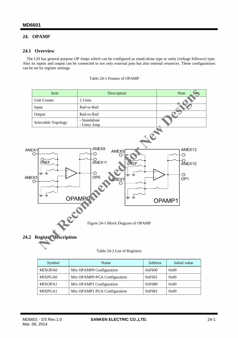
MD6601
MD6601 - DS Rev.1.0 SANKEN ELECTRIC CO.,LTD. 24-1 Mar. 06, 2014
24. OPAMP
24.1 Overview
The LSI has general purpose OP Amps which can be configured as stand-alone type or unity (voltage follower) type.
Also its inputs and output can be connected to not only external pins but also internal resources. These configurations
can be set by register settings.
Table 24-1 Feature of OPAMP
Item Description Note
Unit Counts 2 Units
Input Rail-to-Rail
Output Rail-to-Rail
Selectable Topology - Standalone
- Unity Amp
Figure 24-1 Block Diagram of OPAMP
24.2 Register Description
Table 24-2 List of Registers
Symbol Name Address Initial value
MIXOPA0 Mix OPAMP0 Configuration 0xF600 0x00
MIXPGA0 Mix OPAMP0 PGA Configuration 0xF601 0x00
MIXOPA1 Mix OPAMP1 Configuration 0xF680 0x00
MIXPGA1 Mix OPAMP1 PGA Configuration 0xF681 0x00
Not Reco
mmended
for N
ew D
esign
s

MD6601
MD6601 - DS Rev.1.0 SANKEN ELECTRIC CO.,LTD. 24-2 Mar. 06, 2014
24.2.1 Mix OPAMPn Configuration (MIXOPAn) (n=0-1)
Register MIXOPA0 Mix OPAMP0 Configuration Address 0xF600
Register MIXOPA1 Mix OPAMP1 Configuration Address 0xF680
Bit Bit Name R/W Initial Description Note
7 OPAENB R/W 0
OPAMP Enable
0: Disabled
1: Enabled
6 reserved R 0 Read value is 0. Write only 0.
5 OPAOUT1 R/W 0
OPA Output Enable
0:Not connected to External Pin M
1:Connected to External Pin M
Pin M:
ANEX11(OPAMP0)
ANEX15(OPAMP1)
4 OPAOUT0 R/W 0
OPA Output Enable
0:Not connected to External Pin N
1:Connected to External Pin N
Pin N:
ANEX9(OPAMP0)
ANEX13(OPAMP1)
3 OPAIM1 R/W 0 Select Input(-)
00:External Pin
01:reserved
10:AGND= 0.5 x AVcc
11:AVSS
2 OPAIM0 R/W 0
1 OPAIP1 R/W 0 Select Input(+)
00:External Pin
01:VREF
10:AGND= 0.5 x AVcc
11:AVSS
0 OPAIP0 R/W 0
24.2.2 Mix OPAMPn PGA Configuration (MIXPGAn)(n=0-1)
Register MIXPGA0 Mix OPAMP0 PGA Configuration Address 0xF601
Register MIXPGA1 Mix OPAMP1 PGA Configuration Address 0xF681
Bit Bit Name R/W Initial Description Note
7 reserved R 0 Read value is 0. Write only 0.
6 reserved R 0 Read value is 0. Write only 0.
5 reserved R 0 Read value is 0. Write only 0.
4 reserved R 0 Read value is 0. Write only 0.
3 reserved R/W 0 Read value is 0. Write only 0.
2 reserved R/W 0 Read value is 0. Write only 0.
1 reserved R/W 0 Read value is 0. Write only 0.
0 OPAFOLL R/W 0 Change to OPAMP and voltage follower.
0:OPAMP
1:Voltage follower
Not Reco
mmended
for N
ew D
esign
s

MD6601
MD6601 - DS Rev.1.0 SANKEN ELECTRIC CO.,LTD. 24-3 Mar. 06, 2014
24.2.3 Notice of OPAMP
24.2.3.1. Resistance of analog switch that exists between OPAMP output and PIN
OPAMP is connected to the PIN via the analog switch. Resistor value of the analog switch is 300Ω(typ). This
resistor will affect when you make a Gain-Amp with an external resistor. Feedback resistor of the Gain-Amp is the
value obtained by adding the resistance of the analog switch to the external resistor value. If the exact gain is required,
Please perform the correction by using the built-in ADC.
Figure 24-2 Example of the Gain_AMP
If OPAMP-OUT is used only ADC-input or comparator-input, the [Rsw] can be ignored by the connection shown in
Figure 24.3. In order to make this configuration, the ADC-input(or comparator-input) and OPAMP-OUT should be
assign to the same external output pin.
Figure 24-3 Example of the Gain_AMP ( no influence of [Rsw] )
Not Reco
mmended
for N
ew D
esign
s

MD6601
MD6601 - DS Rev.1.0 SANKEN ELECTRIC CO.,LTD. 25-1 Mar. 06, 2014
25. Comparator
25.1 Overview
The LSI has four-high speed analog comparators. Input signals can be configured. Besides, outputs can be used as not
only interrupt requests but also trigger events for other modules.
FILTER[1:0]
+
-
Comparator
CH0
CH1
CH2
CH3
CH4
CH5
CH6
CH7
Analog SW
CH0
CH1
CH2
CH3
CH4
CH5
CH6
CH7
Analog SW
FilterEdge
Detect
POL[1:0]
Wakeup
(1us)CMPENB
CMPRSLT
CMPIP[2:0]
CMPIM[2:0]
S
R
LVSPOLLVSEN
CPU Clear
LVSF
CMPn Event
S
R
CMI.CMPIn
CPU Clear
CMI.CMPIEn
CMPn Interrupt
Wakeup
CMPn Level Detect(To POC)
Edge Detector
Level Detector
:Pulse Generator
LVSIE
Figure 25-1 Block diagram of Comparator
Not Reco
mmended
for N
ew D
esign
s
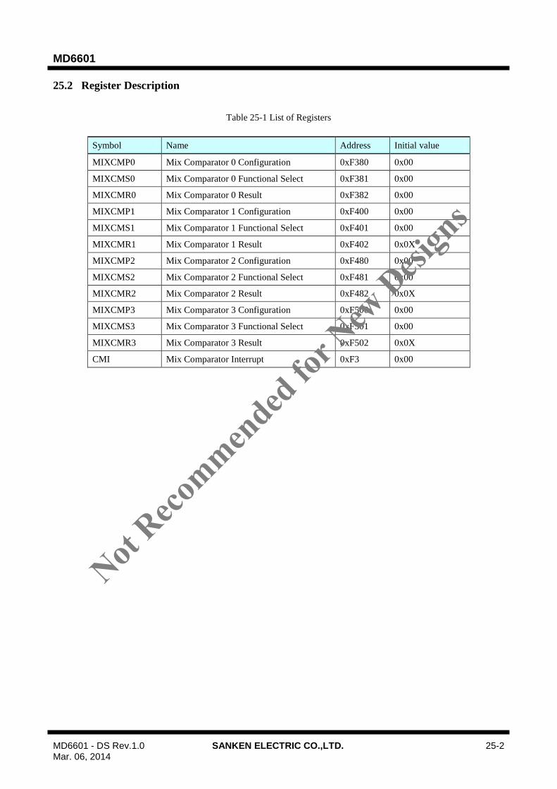
MD6601
MD6601 - DS Rev.1.0 SANKEN ELECTRIC CO.,LTD. 25-2 Mar. 06, 2014
25.2 Register Description
Table 25-1 List of Registers
Symbol Name Address Initial value
MIXCMP0 Mix Comparator 0 Configuration 0xF380 0x00
MIXCMS0 Mix Comparator 0 Functional Select 0xF381 0x00
MIXCMR0 Mix Comparator 0 Result 0xF382 0x00
MIXCMP1 Mix Comparator 1 Configuration 0xF400 0x00
MIXCMS1 Mix Comparator 1 Functional Select 0xF401 0x00
MIXCMR1 Mix Comparator 1 Result 0xF402 0x0X
MIXCMP2 Mix Comparator 2 Configuration 0xF480 0x00
MIXCMS2 Mix Comparator 2 Functional Select 0xF481 0x00
MIXCMR2 Mix Comparator 2 Result 0xF482 0x0X
MIXCMP3 Mix Comparator 3 Configuration 0xF500 0x00
MIXCMS3 Mix Comparator 3 Functional Select 0xF501 0x00
MIXCMR3 Mix Comparator 3 Result 0xF502 0x0X
CMI Mix Comparator Interrupt 0xF3 0x00
Not Reco
mmended
for N
ew D
esign
s
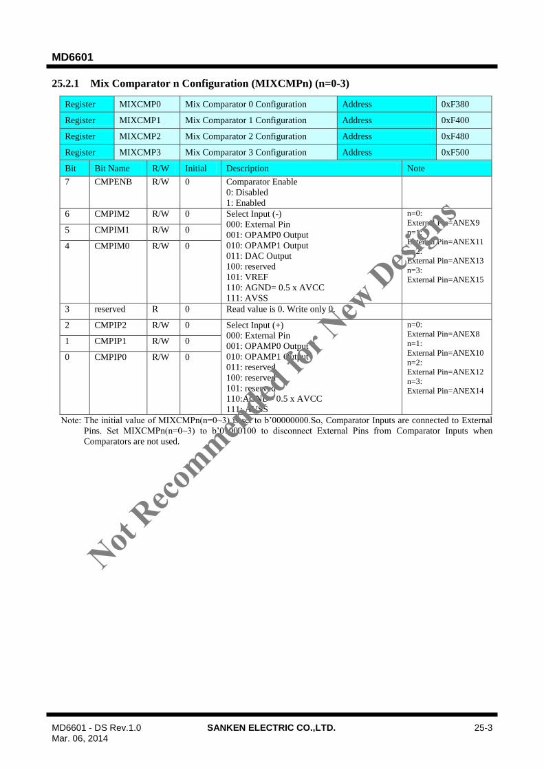
MD6601
MD6601 - DS Rev.1.0 SANKEN ELECTRIC CO.,LTD. 25-3 Mar. 06, 2014
25.2.1 Mix Comparator n Configuration (MIXCMPn) (n=0-3)
Register MIXCMP0 Mix Comparator 0 Configuration Address 0xF380
Register MIXCMP1 Mix Comparator 1 Configuration Address 0xF400
Register MIXCMP2 Mix Comparator 2 Configuration Address 0xF480
Register MIXCMP3 Mix Comparator 3 Configuration Address 0xF500
Bit Bit Name R/W Initial Description Note
7 CMPENB R/W 0 Comparator Enable
0: Disabled
1: Enabled
6 CMPIM2 R/W 0 Select Input (-)
000: External Pin
001: OPAMP0 Output
010: OPAMP1 Output
011: DAC Output
100: reserved
101: VREF
110: AGND= 0.5 x AVCC
111: AVSS
n=0:
External Pin=ANEX9
n=1:
External Pin=ANEX11
n=2:
External Pin=ANEX13
n=3:
External Pin=ANEX15
5 CMPIM1 R/W 0
4 CMPIM0 R/W 0
3 reserved R 0 Read value is 0. Write only 0.
2 CMPIP2 R/W 0 Select Input (+)
000: External Pin
001: OPAMP0 Output
010: OPAMP1 Output
011: reserved
100: reserved
101: reserved
110:AGND= 0.5 x AVCC
111: AVSS
n=0:
External Pin=ANEX8
n=1:
External Pin=ANEX10
n=2:
External Pin=ANEX12
n=3:
External Pin=ANEX14
1 CMPIP1 R/W 0
0 CMPIP0 R/W 0
Note: The initial value of MIXCMPn(n=0~3) is set to b’00000000.So, Comparator Inputs are connected to External
Pins. Set MIXCMPn(n=0~3) to b’01000100 to disconnect External Pins from Comparator Inputs when
Comparators are not used.
Not Reco
mmended
for N
ew D
esign
s
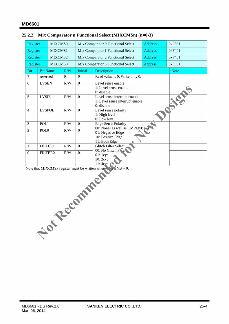
MD6601
MD6601 - DS Rev.1.0 SANKEN ELECTRIC CO.,LTD. 25-4 Mar. 06, 2014
25.2.2 Mix Comparator n Functional Select (MIXCMSn) (n=0-3)
Register MIXCMS0 Mix Comparator 0 Functional Select Address 0xF381
Register MIXCMS1 Mix Comparator 1 Functional Select Address 0xF401
Register MIXCMS2 Mix Comparator 2 Functional Select Address 0xF481
Register MIXCMS3 Mix Comparator 3 Functional Select Address 0xF501
Bit Bit Name R/W Initial Description Note
7 reserved R 0 Read value is 0. Write only 0.
6 LVSEN R/W 0 Level sense enable
1: Level sense enable
0: disable
5 LVSIE R/W 0 Level sense interrupt enable
1: Level sense interrupt enable
0: disable
4 LVSPOL R/W 0 Level sense polarity
1: High level
0: Low level
3 POL1 R/W 0 Edge Sense Polarity
00: None (as well as CMPENB=0)
01: Negative Edge
10: Positive Edge
11: Both Edge
2 POL0 R/W 0
1 FILTER1 R/W 0 Glitch Filter Select
00: No Glitch Filter
01: 1cyc
10: 2cyc
11: 4cyc
0 FILTER0 R/W 0
Note that MIXCMSx register must be written when CMPENB = 0.
Not Reco
mmended
for N
ew D
esign
s

MD6601
MD6601 - DS Rev.1.0 SANKEN ELECTRIC CO.,LTD. 25-5 Mar. 06, 2014
CLKCMPn
CMPRSLT
CMPn Event CMPn Level Detect generation
(Edge Sense Polarity:Negative Edge Glitch Filter Select:No Glitch Filter)
CLKCMPn
CMPRSLT not generated
CMPn Event if 1 cycle CMPn Level Detect generation
(Edge Sense Polarity:Positive Edge Glitch Filter Select:1cycle)
CLKCMPn
CMPRSLTnot generated
CMPn Event if 1 cycle or 2 cycles CMPn Level Detect generation
(Edge Sense Polarity:Positive Edge Glitch Filter Select:2cycle)
CLKCMPn
CMPRSLT not generated
CMPn Event if 4 cycles or less CMPn Level Detect generation
(Edge Sense Polarity:Positive Edge Glitch Filter Select:4cycle)
CLKCMPn
CMPRSLT
CMPn Event CMPn Level Detect generation
(Edge Sense Polarity:Both Edge Glitch Filter Select:No Glitch Filter)
Figure 25-2 Examples of CMPn Level Detect generation
Not Reco
mmended
for N
ew D
esign
s

MD6601
MD6601 - DS Rev.1.0 SANKEN ELECTRIC CO.,LTD. 25-6 Mar. 06, 2014
25.2.3 Comparator n Result (MIXCMRn) (n=0-3)
Register MIXCMR0 Mix Comparator 0 Result Address 0xF382
Register MIXCMR1 Mix Comparator 1 Result Address 0xF402
Register MIXCMR2 Mix Comparator 2 Result Address 0xF482
Register MIXCMR3 Mix Comparator 3 Result Address 0xF502
Bit Bit Name R/W Initial Description Note
7 reserved R 0 Read value is 0. Write only 0.
6 reserved R 0 Read value is 0. Write only 0.
5 reserved R 0 Read value is 0. Write only 0.
4 reserved R 0 Read value is 0. Write only 0.
3 reserved R 0 Read value is 0. Write only 0.
2 reserved R 0 Read value is 0. Write only 0.
1 LVSF R/C 0 Level sense detect flag
Read:
1: Detected
0: not detected
Write:
1: Clear
0: not effect
This bit can be cleared by writing 1 when
level detection is not detected.
0 CMPRSLT R x Monitor CMP_OUT
Not Reco
mmended
for N
ew D
esign
s

MD6601
MD6601 - DS Rev.1.0 SANKEN ELECTRIC CO.,LTD. 25-7 Mar. 06, 2014
25.2.4 Mix Comparator Interrupt(CMI)
Register CMI Mix Comparator Interrupt Address 0xF3
Bit Bit Name R/W Initial Description Note
7 CMPIE3 R/W 0 Comparator3 Interrupt Enable
0: Disable
1: Enable
6 CMPIE2 R/W 0 Comparator2 Interrupt Enable
0: Disable
1: Enable
5 CMPIE1 R/W 0 Comparator1 Interrupt Enable
0: Disable
1: Enable
4 CMPIE0 R/W 0 Comparator0 Interrupt Enable
0: Disable
1: Enable
3 CMPI3 R/C 0 Comparator3 Interrupt Flag
(before mask; independent CMPIEn)
Read 0: No Request
Read 1: Interrupt Event Occurred
Write 0: No effect
Write 1: To clear corresponding bit
2 CMPI2 R/C 0 Comparator2 Interrupt Flag
(before mask; independent CMPIEn)
Read 0: No Request
Read 1: Interrupt Event Occurred
Write 0: No effect
Write 1: To clear corresponding bit
1 CMPI1 R/C 0 Comparator1 Interrupt Flag
(before mask; independent CMPIEn)
Read 0: No Request
Read 1: Interrupt Event Occurred
Write 0: No effect
Write 1: To clear corresponding bit
0 CMPI0 R/C 0 Comparator0 Interrupt Flag
(before mask; independent CMPIEn)
Read 0: No Request
Read 1: Interrupt Event Occurred
Write 0: No effect
Write 1: To clear corresponding bit
Not Reco
mmended
for N
ew D
esign
s
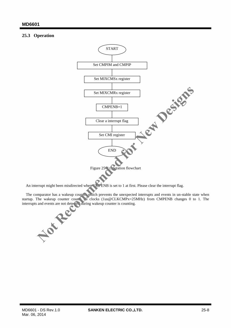
MD6601
MD6601 - DS Rev.1.0 SANKEN ELECTRIC CO.,LTD. 25-8 Mar. 06, 2014
25.3 Operation
Figure 25-3 Operation flowchart
An interrupt might been misdirected when CMPENB is set to 1 at first. Please clear the interrupt flag.
The comparator has a wakeup counter which prevents the unexpected interrupts and events in un-stable state when
startup. The wakeup counter counts 25 clocks (1us@CLKCMPx=25MHz) from CMPENB changes 0 to 1. The
interrupts and events are not detected during wakeup counter is counting.
START
Set MIXCMSx register
Set CMPIM and CMPIP
Set MIXCMRx register
Clear a interrupt flag
CMPENB=1
END
Set CMI register
Not Reco
mmended
for N
ew D
esign
s

MD6601
MD6601 - DS Rev.1.0 SANKEN ELECTRIC CO.,LTD. 26-1 Mar. 06, 2014
26. Voltage Reference (VREF)
26.1 Overview
The LSI has Voltage Reference (VREF) which generates constant voltage to be used in Analog Inter-Connection
Network. The voltage can be connected to ADCs or Comparators.
Table 26-1 Feature of VREF
Item Description Note
Unit Counts Single Unit
Output Voltage 1.2V (typ)
Figure 26-1 Block Diagram of VREF
Not Reco
mmended
for N
ew D
esign
s

MD6601
MD6601 - DS Rev.1.0 SANKEN ELECTRIC CO.,LTD. 27-1 Mar. 06, 2014
27. Temperature Sensor (TEMP)
27.1 Overview
The LSI has Temperature Sensor (TEMP) which generates a voltage related to Junction Temperature to be used in
Analog Inter-Connection Network. The voltage can be connected to ADCs.
Table 27-1 Feature of TEMP
Item Description Note
Unit Counts Single Unit
Output Voltage Refer to Characteristic
Figure 27-1 Block diagram of TEMP
27.2 Register Description
27.2.1 Temperature sensor Control (TEMP)
Register TEMP Temperature sensor Control Address 0xFFC1
Bit Bit Name R/W Initial Description Note
7 reserved R 0 Read value is 0. Write only 0.
6 reserved R 0 Read value is 0. Write only 0.
5 reserved R 0 Read value is 0. Write only 0.
4 reserved R 0 Read value is 0. Write only 0.
3 reserved R 0 Read value is 0. Write only 0.
2 reserved R 0 Read value is 0. Write only 0.
1 reserved R 0 Read value is 0. Write only 0.
0 TEMPE R/W 0 TEMP Enable
0: Disable
1: Enable
Not Reco
mmended
for N
ew D
esign
s
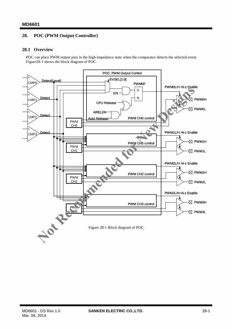
MD6601
MD6601 - DS Rev.1.0 SANKEN ELECTRIC CO.,LTD. 28-1 Mar. 06, 2014
28. POC (PWM Output Controller)
28.1 Overview
POC can place PWM output pins in the high-impedance state when the comparator detects the selected event.
Figure28-1 shows the block diagram of POC.
Figure 28-1 Block diagram of POC
PWM CH0 control
S
R
PWM
CH0
PWM0FPWM0L/H Hi-z Enable
CPU Release
ARELEN
EVSEL[1:0]Detect(Level)
Detect
Detect
Detect
Auto Release
PWM0H
PWM0L
PWM CH1 controlPWM
CH1
PWM1L/H Hi-z Enable
PWM1H
PWM1L
PWM CH2 controlPWM
CH2
PWM2L/H Hi-z Enable
PWM2H
PWM2L
PWM CH3 controlPWM
CH3
PWM3L/H Hi-z Enable
PWM3H
PWM3L
POC: PWM Output Control
EN
CMP0
+
-
CMP1
+
-
CMP2
+
-
CMP3
+
-
PWM CH0 control
S
R
PWM
CH0
PWM0FPWM0L/H Hi-z Enable
CPU Release
ARELEN
EVSEL[1:0]Detect(Level)
Detect
Detect
Detect
Auto Release
PWM0H
PWM0L
PWM CH1 controlPWM
CH1
PWM1L/H Hi-z Enable
PWM1H
PWM1L
PWM CH2 controlPWM
CH2
PWM2L/H Hi-z Enable
PWM2H
PWM2L
PWM CH3 controlPWM
CH3
PWM3L/H Hi-z Enable
PWM3H
PWM3L
POC: PWM Output Control
EN
CMP0
+
-
CMP0
+
-
CMP1
+
-
CMP1
+
-
CMP2
+
-
CMP2
+
-
CMP3
+
-
CMP3
+
-
Not Reco
mmended
for N
ew D
esign
s
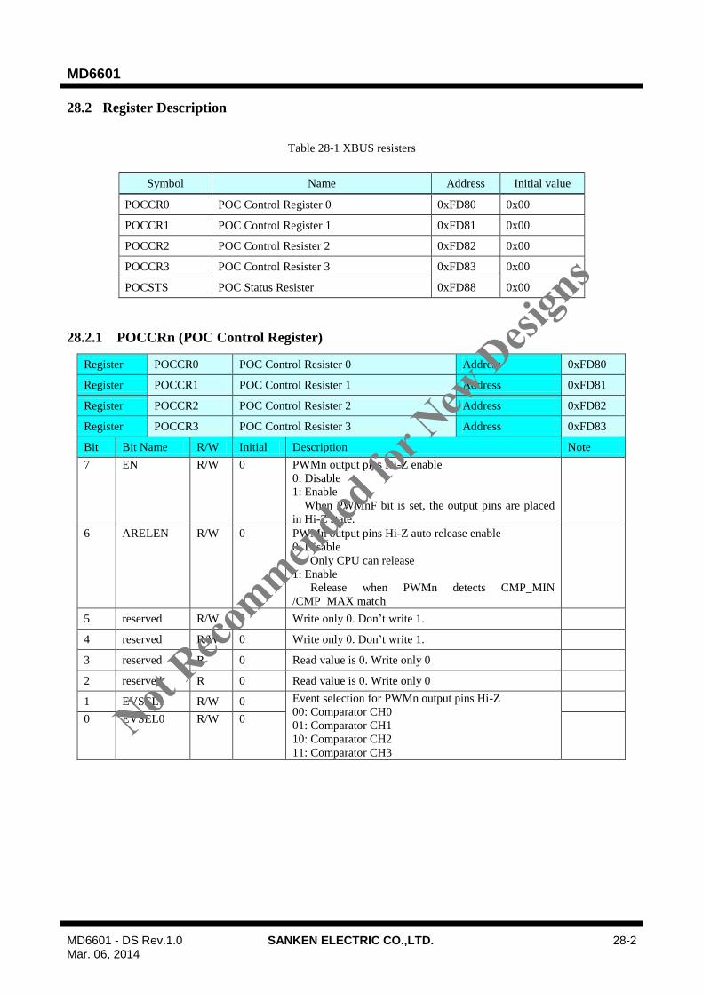
MD6601
MD6601 - DS Rev.1.0 SANKEN ELECTRIC CO.,LTD. 28-2 Mar. 06, 2014
28.2 Register Description
Table 28-1 XBUS resisters
Symbol Name Address Initial value
POCCR0 POC Control Register 0 0xFD80 0x00
POCCR1 POC Control Register 1 0xFD81 0x00
POCCR2 POC Control Resister 2 0xFD82 0x00
POCCR3 POC Control Resister 3 0xFD83 0x00
POCSTS POC Status Resister 0xFD88 0x00
28.2.1 POCCRn (POC Control Register)
Register POCCR0 POC Control Resister 0 Address 0xFD80
Register POCCR1 POC Control Resister 1 Address 0xFD81
Register POCCR2 POC Control Resister 2 Address 0xFD82
Register POCCR3 POC Control Resister 3 Address 0xFD83
Bit Bit Name R/W Initial Description Note
7 EN R/W 0 PWMn output pins Hi-Z enable
0: Disable
1: Enable
When PWMnF bit is set, the output pins are placed
in Hi-Z state.
6 ARELEN R/W 0 PWMn output pins Hi-Z auto release enable
0: Disable
Only CPU can release
1: Enable
Release when PWMn detects CMP_MIN
/CMP_MAX match
5 reserved R/W 0 Write only 0. Don’t write 1.
4 reserved R/W 0 Write only 0. Don’t write 1.
3 reserved R 0 Read value is 0. Write only 0
2 reserved R 0 Read value is 0. Write only 0
1 EVSEL1 R/W 0 Event selection for PWMn output pins Hi-Z
00: Comparator CH0
01: Comparator CH1
10: Comparator CH2
11: Comparator CH3
0 EVSEL0 R/W 0
Not Reco
mmended
for N
ew D
esign
s
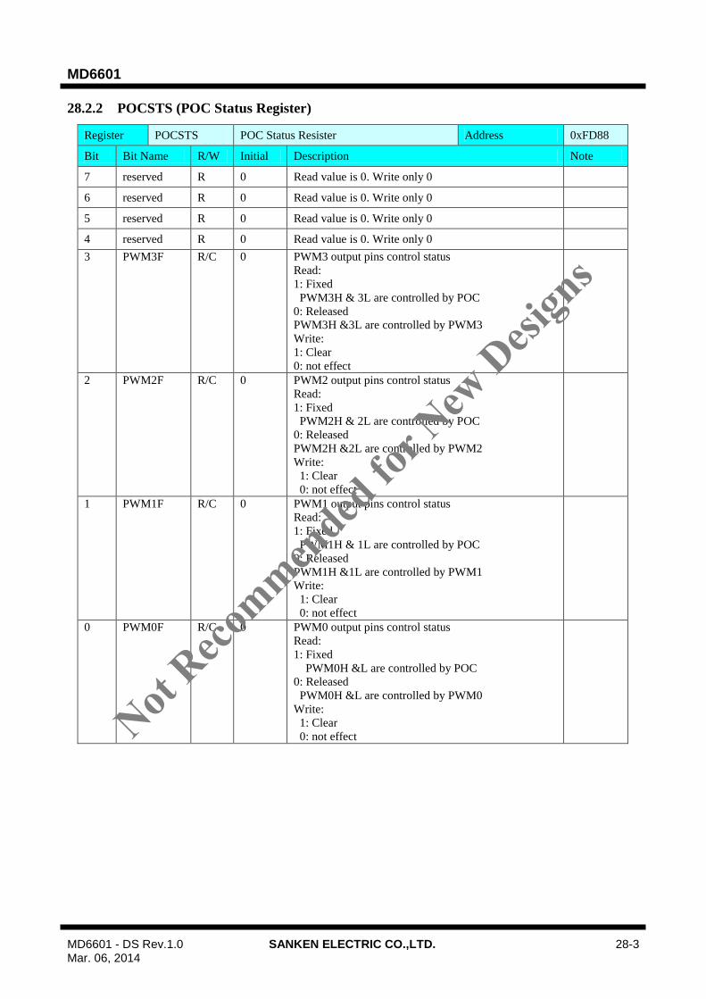
MD6601
MD6601 - DS Rev.1.0 SANKEN ELECTRIC CO.,LTD. 28-3 Mar. 06, 2014
28.2.2 POCSTS (POC Status Register)
Register POCSTS POC Status Resister Address 0xFD88
Bit Bit Name R/W Initial Description Note
7 reserved R 0 Read value is 0. Write only 0
6 reserved R 0 Read value is 0. Write only 0
5 reserved R 0 Read value is 0. Write only 0
4 reserved R 0 Read value is 0. Write only 0
3 PWM3F R/C 0 PWM3 output pins control status
Read:
1: Fixed
PWM3H & 3L are controlled by POC
0: Released
PWM3H &3L are controlled by PWM3
Write:
1: Clear
0: not effect
2 PWM2F R/C 0 PWM2 output pins control status
Read:
1: Fixed
PWM2H & 2L are controlled by POC
0: Released
PWM2H &2L are controlled by PWM2
Write:
1: Clear
0: not effect
1 PWM1F R/C 0 PWM1 output pins control status
Read:
1: Fixed
PWM1H & 1L are controlled by POC
0: Released
PWM1H &1L are controlled by PWM1
Write:
1: Clear
0: not effect
0 PWM0F R/C 0 PWM0 output pins control status
Read:
1: Fixed
PWM0H &L are controlled by POC
0: Released
PWM0H &L are controlled by PWM0
Write:
1: Clear
0: not effect
Not Reco
mmended
for N
ew D
esign
s
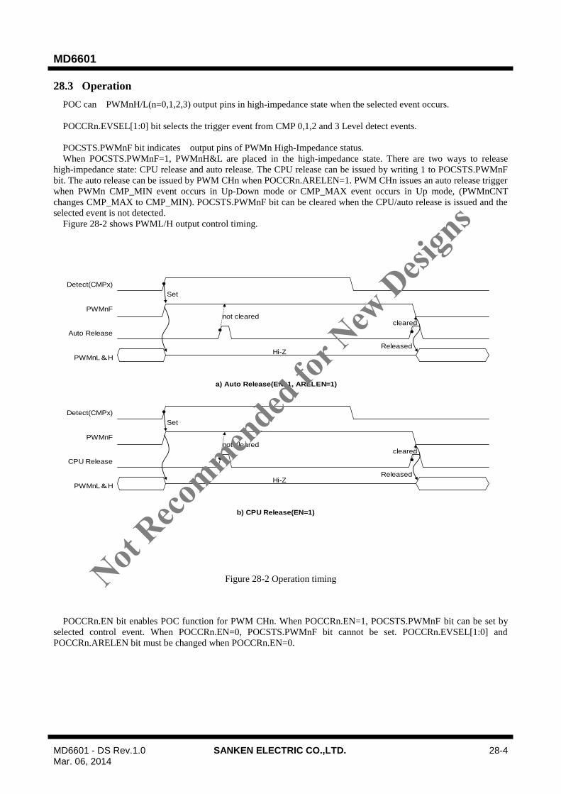
MD6601
MD6601 - DS Rev.1.0 SANKEN ELECTRIC CO.,LTD. 28-4 Mar. 06, 2014
28.3 Operation
POC can PWMnH/L(n=0,1,2,3) output pins in high-impedance state when the selected event occurs.
POCCRn.EVSEL[1:0] bit selects the trigger event from CMP 0,1,2 and 3 Level detect events.
POCSTS.PWMnF bit indicates output pins of PWMn High-Impedance status.
When POCSTS.PWMnF=1, PWMnH&L are placed in the high-impedance state. There are two ways to release
high-impedance state: CPU release and auto release. The CPU release can be issued by writing 1 to POCSTS.PWMnF
bit. The auto release can be issued by PWM CHn when POCCRn.ARELEN=1. PWM CHn issues an auto release trigger
when PWMn CMP_MIN event occurs in Up-Down mode or CMP_MAX event occurs in Up mode, (PWMnCNT
changes CMP_MAX to CMP_MIN). POCSTS.PWMnF bit can be cleared when the CPU/auto release is issued and the
selected event is not detected.
Figure 28-2 shows PWML/H output control timing.
Hi-Z
Detect(CMPx)
PWMnF
Auto Release
PWMnL&H
Set
not clearedcleared
a) Auto Release(EN=1, ARELEN=1)
Released
Hi-Z
Detect(CMPx)
PWMnF
CPU Release
PWMnL&H
Set
not clearedcleared
b) CPU Release(EN=1)
Released
Figure 28-2 Operation timing
POCCRn.EN bit enables POC function for PWM CHn. When POCCRn.EN=1, POCSTS.PWMnF bit can be set by
selected control event. When POCCRn.EN=0, POCSTS.PWMnF bit cannot be set. POCCRn.EVSEL[1:0] and
POCCRn.ARELEN bit must be changed when POCCRn.EN=0.
Not Reco
mmended
for N
ew D
esign
s
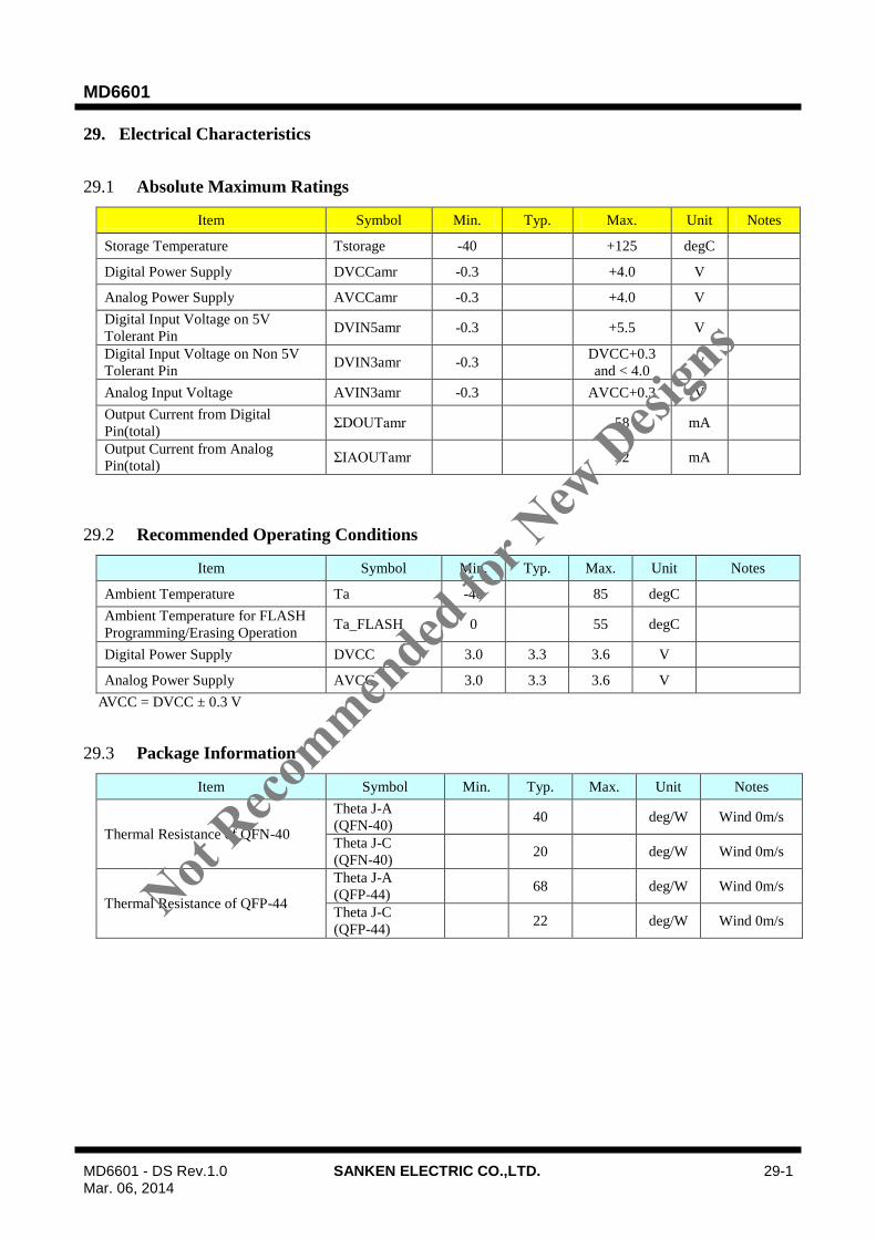
MD6601
MD6601 - DS Rev.1.0 SANKEN ELECTRIC CO.,LTD. 29-1 Mar. 06, 2014
29. Electrical Characteristics
29.1 Absolute Maximum Ratings
Item Symbol Min. Typ. Max. Unit Notes
Storage Temperature Tstorage -40 +125 degC
Digital Power Supply DVCCamr -0.3 +4.0 V
Analog Power Supply AVCCamr -0.3 +4.0 V
Digital Input Voltage on 5V
Tolerant Pin DVIN5amr -0.3 +5.5 V
Digital Input Voltage on Non 5V
Tolerant Pin DVIN3amr -0.3
DVCC+0.3
and < 4.0 V
Analog Input Voltage AVIN3amr -0.3 AVCC+0.3 V
Output Current from Digital
Pin(total) ΣDOUTamr 58 mA
Output Current from Analog
Pin(total) ΣIAOUTamr 32 mA
29.2 Recommended Operating Conditions
Item Symbol Min. Typ. Max. Unit Notes
Ambient Temperature Ta -40 85 degC
Ambient Temperature for FLASH
Programming/Erasing Operation Ta_FLASH 0 55 degC
Digital Power Supply DVCC 3.0 3.3 3.6 V
Analog Power Supply AVCC 3.0 3.3 3.6 V
AVCC = DVCC ± 0.3 V
29.3 Package Information
Item Symbol Min. Typ. Max. Unit Notes
Thermal Resistance of QFN-40
Theta J-A
(QFN-40) 40 deg/W Wind 0m/s
Theta J-C
(QFN-40) 20 deg/W Wind 0m/s
Thermal Resistance of QFP-44
Theta J-A
(QFP-44) 68 deg/W Wind 0m/s
Theta J-C
(QFP-44) 22 deg/W Wind 0m/s
Not Reco
mmended
for N
ew D
esign
s

MD6601
MD6601 - DS Rev.1.0 SANKEN ELECTRIC CO.,LTD. 29-2 Mar. 06, 2014
29.4 Current Consumption
Item Symbol Min. Typ. Max. Unit Notes
DVCC Current (Active) DICC_Active 45 80 mA CPU 50MHz
DVCC Current (Sleep) DICC_Sleep 40 70 mA CPU Stops
DVCC Current (Stby) DICC_Stby 2 5 mA *1
DVCC Current under
FLASH Programming or Erasing DICC_FLASH 55 mA
*4
AVCC Current (ADC10) AICC_ADC10 1 5 mA *2
AVCC Current (ADC12) AICC_ADC12 2 7 mA *2
AVCC Current (DAC12) AICC_DAC12 2 5 mA *2
AVCC Current (COMP) AICC_COMP 0.3 1 mA *2
AVCC Current (OPAMP) AICC_OPAMP 1 4 mA *2
AVCC Current (TEMP) AICC_TEMP 0.3 1 mA *2
AVCC Current (Stby) AICC_Stby 0.3 1 mA *3
*1: Even in STBY state, internal voltage regulator ,VREF,POR and consumes power.
*2: AVCC current consumption for each module unit which is enabled.
*3: AVCC current consumption when all analog modules are disabled.
*4: Not including external load.
29.5 Low Voltage Detector
Item Symbol Min. Typ. Max. Unit Notes
Voltage detection level Vdet 2.4 V
29.6 Reset Operation
Item Symbol Min. Typ. Max. Unit Notes
External /RES Width tRES 10 ms Cold Start
1 μs Hot Start
Internal POR Detect Voltage
(VCORE) VPOR 1.5 V
Internal POR Detect Hysteresis
Voltage VPOR_hys 100 mV
29.7 Clock Operation
Item Symbol min typ max Unit Note
External XTAL Oscillation
Stabling Time tXTAL 10 ms
XTAL
=12.5MHz
Internal IRC Oscillation Stabling
Time tIRC 100 μs
Internal IRC Oscillation Frequency fIRC 10 MHz
PLL1/2 Oscillation Stabling Time tPLL_OSC 100 μs
Input Clock(XTALIN) Frequency fCLK_IN 8 12.5 MHz
Not Reco
mmended
for N
ew D
esign
s

MD6601
MD6601 - DS Rev.1.0 SANKEN ELECTRIC CO.,LTD. 29-3 Mar. 06, 2014
29.8 10 bit ADC
Item Symbol Typ. Unit Notes
Resolution BIT_ADC10 10 bit
Input Voltage Range VIN_ADC10 AVSS ― AVCC V
Conversion Speed
(Sampling Time + Conversion
Time)
fCONV_ADC10 4 MSPS
Integral Non Linearity Error INL_ADC10 ±3.5 LSB
Differential Non Linearity Error DNL_ADC10 ±3.5 LSB
Zero Scale Error ZS_ADC10 ±4 LSB
Full Scale Error FS_ADC10 ±4 LSB
Absolute Error ABS_ADC10 ±4 LSB
*Measured by Impedance of Source(Rout_ADC10) ≤ 200 Ohm
29.9 12 bit ADC
Item Symbol Typ. Unit Notes
Resolution BIT_ADC12 12 bit
Input Voltage Range VIN_ADC12 AVSS ― AVCC V
Conversion Speed
(Sampling Time + Conversion
Time)
fCONV_ADC12 1 MSPS
Integral Non Linearity Error INL_ADC12 ±5 LSB
Differential Non Linearity Error DNL_ADC12 ±5 LSB
Zero Scale Error ZS_ADC12 ±12 LSB
Full Scale Error FS_ADC12 ±12 LSB
Absolute Error ABS_ADC12 ±16 LSB
*Measured by Impedance of Source(Rout_ADC12) ≤ 3000 Ohm
29.10 12 bit DAC
Item Symbol Typ. Unit Notes
Resolution BIT_DAC12 12 bit
Output
Voltage Range VOUT_DAC12 (AVSS+0.2) ― (AVCC-0.3) V
Output Settling Time tCONV_DAC12 1 μs
Output Current Iout_DAC12 1 mA
Output Load Cout_DAC12 50 pF
Integral Non Linearity Error INL_DAC12 ±20 LSB
Differential Non Linearity Error DNL_DAC12 ±2.5 LSB
Zero Scale Error ZS_DAC12 ±20 LSB
Full Scale Error FS_DAC12 ±40 LSB
Absolute Error ABS_DAC12 ±40 LSB
Not Reco
mmended
for N
ew D
esign
s

MD6601
MD6601 - DS Rev.1.0 SANKEN ELECTRIC CO.,LTD. 29-4 Mar. 06, 2014
29.11 OPAMP
Item Symbol Min. Typ. Max. Unit Notes
Input Voltage Range VIN_OPAMP AVSS+0.4 AVCC-0.5 V
Output Voltage Range VOUT_OPAMP AVSS AVCC V
Vin Offset Voffset_OPAMP ±3 mV
Output Current IOUT_OPAMP ±1 mA
CMRR CMRR_OPAMP 70 dB
PMRR PMRR_OPAMP 50 dB
Output Noise ON_OPAMP 45 μVrms 1k~1GHz
Open Gain GAIN_OPAMP 80 dB
Gain Band Width GBW_OPAMP 20 MHz
Slew Rate SR_OPAMP 15 V/μs
29.12 Comparator
Item Symbol Min. Typ. Max. Unit Notes
Input Voltage Range VIN_COMP AVSS AVCC V
Comparison Voltage
Range VIN_REF AVSS+1.0 AVCC-1.0 V
Hysteresis VIN_hys 10 50 mV *1
Response Time tRESP_COMP 20 ns *2
*1:condition of VIN_COMP=AVCCx0.5
*2:Measurement condition is as follows.
Figure 29-1 Comparator Timing Chart
VIN-
0.5V
0.5V
100ns 100ns
Comparator Output
tRESP_COMP tRESP_COMP
VIN_REF
VIN+
(VIN_COMP)
Not Reco
mmended
for N
ew D
esign
s

MD6601
MD6601 - DS Rev.1.0 SANKEN ELECTRIC CO.,LTD. 29-5 Mar. 06, 2014
29.13 Voltage Reference
Item Symbol Min. Typ. Max. Unit Notes
Output Voltage VREF 1.20 V
29.14 Temperature Sensor
Item Symbol Min. Typ. Max. Unit Notes
Output Voltage
(Tj=25degC) VTEMP 1.52 V
Temperature slope dTEMP 4.8 mV/degC
Settling Time tTEMP 2 ms from
Enabling
29.15 Analog GND
Item Symbol Min. Typ. Max. Unit Notes
Output Voltage VAGND typ-0.03 AVCCx0.5 Typ+0.03 V
29.16 Digital I/O DC Spec
Item Symbol Min. Typ. Max. Unit Notes
Input Voltage High Level VIH 2.0 V
Input Voltage Low Level VIL 0.8 V
Input Voltage High Level (Schmitt) VIH_S 2.0 V
Input Voltage Low Level (Schmitt) VIL_S 0.8 V
Hysteresis for Schmitt Vhys_S 0.05 V
Pull Up Register Rpup 20 60 100 kohm
Input Leak Current IL -2 ±1 +2 μA
Input Capacitance
(except ANEX0-15) CIN 20 pF
Input Capacitance(ANEX0-15) CIN 30 pF
Output Voltage High Level (4mA) VOH4 2.4 V Ioh = 4 mA
Output Voltage Low Level (4mA) VOL4 0.4 V Iol = 4 mA
Output Voltage High Level (16mA) VOH16 VCC-0.7 V Ioh = 16 mA
Output Voltage Low Level (16mA) VOL16 0.4 V Iol = 16 mA
Not Reco
mmended
for N
ew D
esign
s
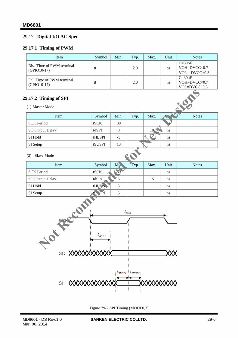
MD6601
MD6601 - DS Rev.1.0 SANKEN ELECTRIC CO.,LTD. 29-6 Mar. 06, 2014
29.17 Digital I/O AC Spec
29.17.1 Timing of PWM
Item Symbol Min. Typ. Max. Unit Notes
Rise Time of PWM terminal
(GPIO10-17) tr 2.0 ns
C=30pF
VOH=DVCC×0.7
VOL=DVCC×0.3
Fall Time of PWM terminal
(GPIO10-17) tf 2.0 ns
C=30pF
VOH=DVCC×0.7
VOL=DVCC×0.3
29.17.2 Timing of SPI
(1) Master Mode
Item Symbol Min. Typ. Max. Unit Notes
SCK Period tSCK 80 ns
SO Output Delay tdSPI 0 10 ns
SI Hold tHLSPI -3 ns
SI Setup tSUSPI 13 ns
(2) Slave Mode
Item Symbol Min. Typ. Max. Unit Notes
SCK Period tSCK 80 ns
SO Output Delay tdSPI 5 15 ns
SI Hold tHLSPI 5 ns
SI Setup tSUSPI 5 ns
Figure 29-2 SPI Timing (MODE0,3)
Not Reco
mmended
for N
ew D
esign
s
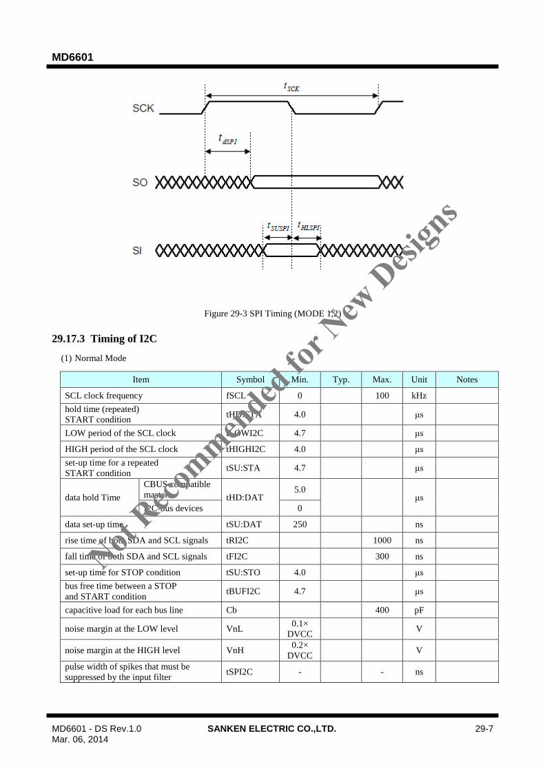
MD6601
MD6601 - DS Rev.1.0 SANKEN ELECTRIC CO.,LTD. 29-7 Mar. 06, 2014
Figure 29-3 SPI Timing (MODE 1,2)
29.17.3 Timing of I2C
(1) Normal Mode
Item Symbol Min. Typ. Max. Unit Notes
SCL clock frequency fSCL 0 100 kHz
hold time (repeated)
START condition tHD:STA 4.0 μs
LOW period of the SCL clock tLOWI2C 4.7 μs
HIGH period of the SCL clock tHIGHI2C 4.0 μs
set-up time for a repeated
START condition tSU:STA 4.7 μs
data hold Time
CBUS compatible
masters tHD:DAT 5.0
μs
I2C-bus devices 0
data set-up time tSU:DAT 250 ns
rise time of both SDA and SCL signals tRI2C 1000 ns
fall time of both SDA and SCL signals tFI2C 300 ns
set-up time for STOP condition tSU:STO 4.0 μs
bus free time between a STOP
and START condition tBUFI2C 4.7 μs
capacitive load for each bus line Cb 400 pF
noise margin at the LOW level VnL 0.1×
DVCC V
noise margin at the HIGH level VnH 0.2×
DVCC V
pulse width of spikes that must be
suppressed by the input filter tSPI2C - - ns
Not Reco
mmended
for N
ew D
esign
s

MD6601
MD6601 - DS Rev.1.0 SANKEN ELECTRIC CO.,LTD. 29-8 Mar. 06, 2014
(2) Fast Mode
Item Symbol Min. Typ. Max. Unit Notes
SCL clock frequency fSCL 0 400 kHz
hold time (repeated) START condition tHD:STA 0.6 μs
LOW period of the SCL clock tLOWI2C 1.3 μs
HIGH period of the SCL clock tHIGHI2C 0.6 μs
set-up time for a repeated START
condition tSU:STA 0.6 μs
data hold time
CBUS compatible
masters tHD:DAT 0
3.45
μs
I2C-bus devices 0 0.9
data set-up time tSU:DAT 100 ns
rise time of both SDA and SCL signals tRI2C 20+
0.1Cb 300 ns
fall time of both SDA and SCL signals tFI2C 20+
0.1Cb 300 ns
set-up time for STOP condition tSU:STO 0.6 μs
bus free time between a STOP
and START condition tBUFI2C 1.3 μs
capacitive load for each bus line Cb 400 pF
noise margin at the LOW level VnL 0.1×
DVCC V
noise margin at the HIGH level VnH 0.2×
DVCC V
pulse width of spikes that must be
suppressed by the input filter tSPI2C 0 50 ns
Figure 29-4 I2C timing
Not Reco
mmended
for N
ew D
esign
s
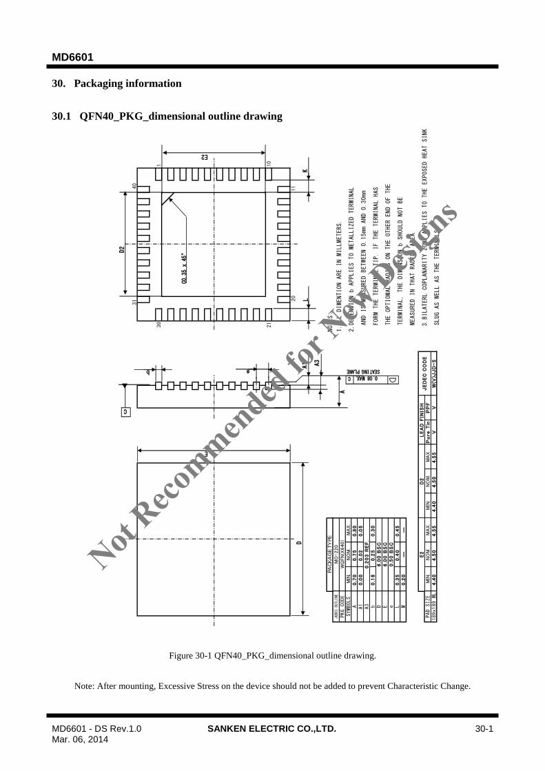
MD6601
MD6601 - DS Rev.1.0 SANKEN ELECTRIC CO.,LTD. 30-1 Mar. 06, 2014
30. Packaging information
30.1 QFN40_PKG_dimensional outline drawing
Figure 30-1 QFN40_PKG_dimensional outline drawing.
Note: After mounting, Excessive Stress on the device should not be added to prevent Characteristic Change.
NOTES:
10
1
11
20
3.BILATERL COPLANARITY ZONE APPLIES TO THE EXPOSED HEAT SINK
40
JUDEC OUTLINE
21
30
31
PA
CK
AG
E T
YPE
MO
-220
0.7
00
.75
0.8
0
WQ
FN
(X640)
MIN
.N
OM
.M
AX
.
0.2
03
RE
F.
0.1
80
.25
0.3
0
0.0
00
.02
0.0
5
0.5
0 B
SC
0.3
50
.40
0.4
5
6.0
0 B
SC
6.0
0 B
SC
E
MEASURED IN THAT RADIUS AREA.
PKG CODE
SYMBOLS
A A1
A3 b D
0.2
0
1.ALL DIMENTION ARE IN MILLMETERS.
2.DEMENSION b APPLIES TO METALLIZED TERMINAL
AND IS MEASURED BETWEEN 0.15mm AND 0.30mm
FORM THE TERMINAL TIP. IF THE TERMINAL HAS
THE OPTIOMAL RADIUS ON THE OTHER END OF THE
TERMINAL, THE DIMENSION b SHOULD NOT BE
NO
M.
MA
X.
MIN
.N
OM
.M
AX
.
e L M―
―
PP
F189x189 ML
4.4
04
.50
4.5
54
.40
4.5
04
.55
PAD SIZE
MIN
.V
VW
(V)J
JD
-5
SLUG AS WELL AS THE TERMINALS.
E2
D2
LE
AD
FIN
ISH
JE
DE
C C
OD
EP
ure
Tin
E
C
▲
b e
D2
E2
KL
A1 A3
A
D
C0.35 x 45
°
SEATING PLANE
C 0.08 MAX.
Not Reco
mmended
for N
ew D
esign
s
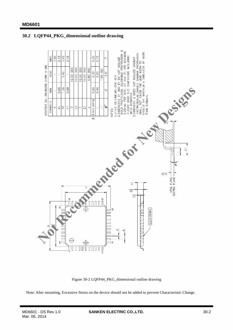
MD6601
MD6601 - DS Rev.1.0 SANKEN ELECTRIC CO.,LTD. 30-2 Mar. 06, 2014
30.2 LQFP44_PKG_dimensional outline drawing
Figure 30-2 LQFP44_PKG_dimensional outline drawing
Note: After mounting, Excessive Stress on the device should not be added to prevent Characteristic Change.
Not Reco
mmended
for N
ew D
esign
s

MD6601
MD6601 - DS Rev.1.0 SANKEN ELECTRIC CO.,LTD. 1 Mar. 06, 2014
IMPORTANT NOTES
The contents in this document are subject to changes, for improvement and other purposes, without notice. Make
sure that this is the latest revision of the document before use.
If certain products and technologies in this document (i.e. those cargos and technologies subject to security
trade control based on the Foreign Exchange and Foreign Trade Control Law) are to be exported or taken
overseas from Japan, the permission of the Japanese government is required.
When using the information in this document, no license is granted for guarantees or concessions of rights
such as patents, copyrights, trademarks, or other intellectual property rights of any third party, or of Sanken.
Application and operation examples described in this document are quoted for the sole purpose of reference for the
use of the products herein and Sanken can assume no responsibility for any infringement of industrial property
rights, intellectual property rights or any other rights of Sanken or any third party which may result from its use.
Unless otherwise agreed in writing by Sanken, Sanken makes no warranties of any kind, whether express or
implied, as to the products, including product merchantability, and fitness for a particular purpose and special
environment, and the information, including its accuracy, usefulness, and reliability, included in this document.
Although Sanken undertakes to enhance the quality and reliability of its products, the occurrence of failure and
defect of semiconductor products at a certain rate is inevitable. Users of Sanken products are requested to take, at
their own risk, preventative measures including safety design of the equipment or systems against any possible
injury, death, fires or damages to the society due to device failure or malfunction.
Sanken products listed in this document are designed and intended for the use as components in general purpose
electronic equipment or apparatus (home appliances, office equipment, telecommunication equipment, measuring
equipment, etc.).
When considering the use of Sanken products in the applications where higher reliability is required (transportation
equipment and its control systems, traffic signal control systems or equipment, fire/crime alarm systems, various
safety devices, etc.), and whenever long life expectancy is required even in general purpose electronic equipment
or apparatus, please contact your nearest Sanken sales representative to discuss, prior to the use of the products
herein.
The use of Sanken products without the written consent of Sanken in the applications where extremely high
reliability is required (aerospace equipment, nuclear power control systems, life support systems, etc.) is strictly
prohibited.
When using the products specified herein by either (i) combining other products or materials therewith or (ii)
physically, chemically or otherwise processing or treating the products, please duly consider all possible risks that
may result from all such uses in advance and proceed therewith at your own responsibility.
Some items and conditions on shipment test may not have been performed through the electrical
characteristics of this product, but the electrical characteristics are guaranteed by based on the design value
and evaluation results.
Anti radioactive ray design is not considered for the products listed herein.
Sanken assumes no responsibility for any troubles, such as dropping products caused during transportation out of
Sanken’s distribution network.
The contents in this document must not be transcribed or copied without Sanken’s written consent.
Not Reco
mmended
for N
ew D
esign
s
MD6601
MD6601 - DS Rev.1.0 SANKEN ELECTRIC CO.,LTD. 2 Mar. 06, 2014
注意書き
本書に記載している内容は、改良などにより予告なく変更することがあります。
ご使用の際には、最新の情報であることを確認してください。
本書に記載している製品及び技術のうち「外国為替及び外国貿易法」に基づき安全保障貿易管理関連貨物・
技術に該当するものを輸出する場合、または国外に持ち出す場合は日本国政府の許可が必要です。
本書に記載している情報の使用に際して、弊社もしくは第三者の特許権、著作権、商標権、その他の知的所
有権等の権利に対する保証または実施権の許諾を行うものではありません。
本書に記載している動作例および回路例などは、使用上の参考として示したもので、これらに起因する弊社も
しくは第三者の工業所有権、知的所有権、その他の権利の侵害問題について弊社は一切責任を負いま
せん。
弊社の合意がない限り、弊社は、本書に含まれる本製品(商品適性および特定目的または特別環境に対する
適合性を含む)ならびに情報(正確性、有用性、信頼性を含む)について、明示的か黙示的かを問わず、いか
なる保証もしておりません。
弊社は品質、信頼性の向上に努めていますが、半導体製品では、ある確率での欠陥、故障の発生は避けられ
ません。製品の故障により結果として、人身事故、火災事故、社会的な損害などが発生しないよう、使用者の
責任において、装置やシステム上で十分な安全設計および確認を行ってください。
本書に記載している製品は、一般電子機器(家電製品、事務機器、通信端末機器、計測機器など)に使用す
ることを意図しております。
高い信頼性を要求する装置(輸送機器とその制御装置、交通信号制御装置、防災・防火装置、各種安全装置
など)への使用を検討、および一般電子機器であっても長寿命を要求する場合は、必ず弊社販売窓口へ相談
してください。
極めて高い信頼性を要求する装置(航空宇宙機器、原子力制御、生命維持のための医療機器など)には、弊
社の文書による合意がない限り使用しないでください。
本書に記載している製品の使用にあたり、本書に記載している製品に他の製品・部材を組み合わせる場合、
あるいはこれらの製品に物理的、化学的、その他何らかの加工・処理を施す場合には、使用者の責任におい
てそのリスクを検討の上行ってください。
本書に記載している製品の電気的特性についてその一部の項目と条件の出荷テストは行っておりませんが、
製品の設計値および評価結果に基づき特性保証しております。
本書に記載している製品は耐放射線設計をしておりません。
弊社物流網以外での輸送、製品落下などによるトラブルについて、弊社は一切責任を負いません。
本書に記載している内容を、文書による弊社の承諾なしに転記・複製することを禁じます。
Not Reco
mmended
for N
ew D
esign
s

MD6601 Series
MD6601- DS Rev.1.0 SANKEN ELECTRIC CO.,LTD. a Feb. 06, 2014
Revision History
Note: Page numbers for previous revisions may differ from page numbers in current version.
MD6601 Revisions
No. Rev. Page Chapter Revision details
1 01-05 - - Not listed contens because of non-publication
2 06 - - Firtst publication
3 07 5-11 Clock System
Added Section 5.5, An example way to configure Clock
Settings after Power On.
4 07 10-2 Interrupt Controller Modified Table10-2, Vectot No.3 "GPIO3"
5 07 10-10 Interrupt Controller Added Section 10.4.4, Interrupt external pins
6 07 11-9 DSAC Added Figure11-2, Multi bytes transfer
7 07 12-3 FLASH Memory Control Added Section 12.2, Flash memory mat structure
8 07 12-15 FLASH Memory Control Added Section 12.6.4, Protect fuction
9 07 13-12 to 23 Tiny DSP Described DSP0 and DSP1 registers separately
10 07 14-2 to 3 PWM Modified Section 14.3 Resouces,The operation of CH2
and CH3 is different from that of CH0 and CH1.
11 07 14-13 to 15 PWM Modified Section 14.5.2 PWM Mode 0.
12 07 14-16 to 21 PWM Modified Section 14.5.3 PWM Mode 1 (Auto Dead Time)
13 07 14-22 to 23 PWM Modified Section 14.5.4 PWM Mode 2 (Phase Shift)
14 07 14-24 to 27
PWM Modified Section 14.5.5 PWM Mode 3 (Phase Shift + Auto
Dead Time)
15 07 14-34 to 39
PWM Modified Section 14.8 Re-Trigger Operation, There are five
Re-trigger operations Mode A/B/C/D and MASK operation
which can control output levels of both PWMxH and
PWMxL.
16 07 16-3 to 4 TMR Named bit 2,1,0 of Register TMOD0/TMOD1 as PRSCL
17 07 17-3 SPI Modified register addresses of Table 17-2 List of Registers
18 07 18-19 to 20 I2C Modified Section 18.5 Slave receiver operation
19 07 18-21 I2C Modified Section 18.6 Slave transmitter operation
20 07 18-22 to 23 I2C Modified Section 18.7 Master receiver operation
21 07 18-24 to 25 I2C Modified Section 18.8 Master transmitter operation
22 07 19-9 UART Modified Section 19.4 Operation
23 07 21-2 10bit SAR ADC Added Figure 21-1 Block diagram of 10bit ADC
24 07 21-4 to 6 10bit SAR ADC Modified Symbols of Table 21-3 XBUS registers
25 07 21-25 10bit SAR ADC Added ADL/HXn on Figure 21-2 Basic conversion
sequence
Not Reco
mmended
for N
ew D
esign
s
MD6601 Series
MD6601- DS Rev.1.0 SANKEN ELECTRIC CO.,LTD. b Feb. 06, 2014
No. Rev. Page Chapter Revision details
26 07 22-2 12bit SAR ADC Added Figure 22-1 Block diagram of High Precision 12bit
ADC
27 07 22-4 to 6 12bit SAR ADC Modified Symbols of Table 22-3 XBUS registers
28 07 22-21 12bit SAR ADC Added ADL/HX2 on Figure 22-2 Basic conversion
sequence
29 07 5-2,3,4,5,6,7
6-5
27-1
Clock System,
8051 CPU,
TEMP
Deleted Chapter 28 System Controller(SYSC) , The
registers of Chapter 28 were moved to each chapters.
REMAP to chapter6 (8051 CPU Subsystem). TEMP to
chapter27 (Temperature/Sensor).
CLKCFG0/G1,MCLKE0/E1/E2/E3,LPCTRL and LVDCTRL
to chapter5 (Clock System).
30 07 28-1 to 6 POC Changed Chapter No.29 of POC to No.28.
31 08 29-1 Packaging Information Added Chapter 29 Packging information.
32 08 4-2 to 3 Reset System and LVD Register"LVDCTRL" is shifted from chapter5 to chapter4.
33 08 5-10 Clock System Modified section 5.4.2 STBY Mode
34 08 6-2 8051 CPU The description of Figure6-1 is modified.
35 08 7-1 Register Mapping The description of Table7-1 is modified.
36 08 7-2 Register Mapping Register name of"DPL0" is changed to DPL.
37 08 7-2 Register Mapping Register name of"DPH0" is changed to DPH.
38 08 13-2 Tiny DSP The description of Figure13-1 is modified.
39 08 14-4 PWM The description of Figure14-2 is modified.
40 08 14-16 to 17 PWM Modified section 14.5.3 PWM Mode 1(Auto Dead Time)
41 08 14-69 to 70
PWM Modified register addresses of section 14.12.26
BUF_A/B/C/Dn(n=0-3).
42 08 16-1 TMR The description of Figure16-1 is modified.
43 08 17-3 to 9 SPI The Addresses are modified as follows.
0xFB00 -> 0xFB80
0xFB01 -> 0xFB81
0xFB02 -> 0xFB82
0xFB04 -> 0xFB84
0xFB05 -> 0xFB85
0xFB06 -> 0xFB86
0xFB08 -> 0xFB88
0xFB09 -> 0xFB89
44 08 17-12 to 13 SPI Modified section 17.4.1 Master mode
45 08 17-17 to 18 SPI Modified section 17.4.2 Slave mode
Not Reco
mmended
for N
ew D
esign
s

MD6601 Series
MD6601- DS Rev.1.0 SANKEN ELECTRIC CO.,LTD. c Feb. 06, 2014
No. Rev. Page Chapter Revision details
46 08 27-1 TEMP The description of table27-1 is modified.
47 08 29 Electric Characteristics Added Chapter No. 29 Electric Characteristics
48 08 30 Packaging Information Changed Chapter NO. from 29 to 30
49 09 1-3 Product Overview Correcting typo of Figure1-1
50 09 21-30 10bit SAR ADC Correcting typo of section 21.3.7 ADC Event
51 09 29-11 Electrical Characteristics Correcting typo of section 29.17.3 Timing of I2C
52 1.0 1-3 Product Overview Modified Part#(LQFP-44) of Table 1.4 Ordering
Information.
Added Part#(MD6601FNVL) of Table 1.4 Ordering
Information.
53 1.0 5-1 Clock System Modified Figure 5-1 Clock System.
54 1.0 5-4 Clock System Added the Table 5-2 clock's enabler condition and disabler
condition.
55 1.0 5-9 Clock System Added Section 5-6 Limitation of clock system.
56 1.0 8-1 to 2 GPIO Remove Section 8.1,move to Section 8.2
57 1.0 8-1 GPIO Modified GPIO0x and 1x structure in Figure.8-1
58 1.0 11-8 DSAC Modified 11.6 Limitation of DSAC.
59 1.0 12-1 FLASH Memory Control Remove T.B.D. description in Table 12-1.
60 1.0 13-7 TinyDSP Added the description for SFR access counter.
61 1.0 13-10 TinyDSP Modified the Table13-4 for DSPn Access Counter Clear
Register.
62 1.0 13-20 TinyDSP Added the Table for DSPn Access Counter Clear Register.
63 1.0 13-21 TinyDSP Added the description about DSP_SS and the DIV
instruction.
64 1.0 14-3 PWM Added the note for changing clock source.
65 1.0 14-9, 12 PWM Added explanation for Up-Down Mode.
66 1.0 14-37 to 55 PWM Modified the description and note for PWMnACSTS.
67 1.0 17-1 SPI Modified Table 17-1. Added the number of FIFO stage.
68 1.0 18-3 I2C Modified description for ICCR register.
69 1.0 18-5 I2C Modified description for ICSR register.
70 1.0 18-15 to 22 I2C Modified Section 18.4-7. Added description for stop
condition interrupt.
71 1.0 23-6 12bit DAC Added Section 23.5 Limitation of DAC - 23.5.1
MIXDAL/H register access.
Not Reco
mmended
for N
ew D
esign
s
MD6601 Series
MD6601- DS Rev.1.0 SANKEN ELECTRIC CO.,LTD. d Feb. 06, 2014
No. Rev. Page Chapter Revision details
72 1.0 24-3 OPAMP Added Section 24.2.3 Notice of OPAMP – 24.2.3.1
Resistance of analog switch that exists between OPAMP
output and PIN.
73 1.0 25-8 Comparator Added wakeup counter description.
74 1.0 29-1 Electrical Characteristics Modified typical value(LQFP-44) of Table 29.3 Package
Information.
75 1.0 29-6 Electrical Characteristics Modified SO Output Delay in slave mode.
76 1.0 30-2 Packging information Added Figure No. 30-2 LQFP44_PKG_dimensional outline
drawing
Not Reco
mmended
for N
ew D
esign
s