
Marine Induced Polarization Arctic-Ready Survey Kit
109
1 ADAC Program Year 7 Engineering Design Report -- Marine Induced Polarization Arctic-Ready Survey Kit ENGINEERING REPORT FOR THE DESIGN AND BUILD OF THE MARINE IP ARCTIC-READY SURVEY KIT. INDUCED POLARIZATION ASSOCIATES 2021
-
Upload
khangminh22 -
Category
Documents
-
view
4 -
download
0
Transcript of Marine Induced Polarization Arctic-Ready Survey Kit

1
ADAC Program Year 7 Engineering Design Report -- Marine Induced Polarization Arctic-Ready Survey Kit
ENGINEERING REPORT FOR THE DESIGN AND BUILD OF THE MARINE IP ARCTIC-READY SURVEY KIT.
INDUCED POLARIZATION ASSOCIATES
2021

2
Table of Contents 1. Executive Summary ................................................................................................................. 3
2. Introduction ............................................................................................................................ 3
3. Requirements ......................................................................................................................... 3
a. Functional ........................................................................................................................ 4
b. Mechanical ...................................................................................................................... 4
c. Electrical .......................................................................................................................... 4
d. Operator Interfaces .......................................................................................................... 4
4. Hardware Design: .................................................................................................................... 7
a. Architectural Overview: ......................................................................................................... 7
b. Power Supply and Distribution Systems .............................................................................. 10
c. Operator Display Interface and Digital System Controls ....................................................... 14
d. Digital Automated System Management ............................................................................. 17
e. Transmitter Subsystem ...................................................................................................... 18
f. Receiver Subsystem: .......................................................................................................... 21
g. Data Acquisition System (DAQ) ........................................................................................... 23
h. Enclosure and Mechanical Design ...................................................................................... 24
5. Firmware ............................................................................................................................... 26
6. Discussion ............................................................................................................................ 30
a. Hardware Design Narrative ................................................................................................ 30
b. Firmware Development Narrative ....................................................................................... 32
7. Interim Team Performance Analysis ...................................................................................... 35
8. Conclusions .......................................................................................................................... 37
9. Appendices ........................................................................................................................... 37
Appendix A: Marine IP Arctic Ready Kit Mechanical Design Drawings ............................................. 39
Appendix B: Electronic Hardware Printed Circuit Board Schematics ............................................... 45
Appendix C: Electronic Hardware Printed Circuit Board Fabrication Files ........................................ 57
Appendix D: Device Electrical Characteristics ................................................................................ 62
Appendix E: Device Fabrication Bill-of-Materials (BOM) .................................................................. 63
Appendix F: Custom Hardware Manufacturer Details ..................................................................... 94
Appendix G: Development Tool Details ......................................................................................... 95
Appendix H: Device Final Assembly Images ................................................................................... 96

3
1. Executive Summary This document details the motivations, design considerations, design process, fabrication, and programming of the Marine Induced Polarization Survey Arctic Ready Kit (MIP-1) device under development and being tested by Induced Polarization Associates, LLC. The design goals, preliminary analysis, and design requirements were provided in the Year 7 Workplan, therefore those elements are not included in this document. IPA has designed, developed and prototyped custom hardware for deployment in the Arctic for detecting oil under ice. IPA is actively programming, assembling, and testing the MIP-1 device manufactured in Seattle, Washington. Various roadblocks have appeared and were subsequently surmounted between 2020 and 2021, as described in the ADAC Program Year 7 Annual Report. The roadblocks and corresponding solutions are also briefly discussed with more detail here. An interim performance analysis of the build as well as a selection of design documentation is provided with this report. The build of the Marine IP Arctic Ready Kit is scheduled to be completed in ADAC Program Year 8 as part of a no-cost extension put into place due to development delays caused by COVID-19. This report represents progress through June 30, 2021, will be updated with testing results at the end of ADAC Program Year 8.
2. Introduction This document provides a detailed report of the design considerations, development processes, fabrication methods, and features of the Marine Induced Polarization (IP) Arctic Ready Kit produced by Induced Polarization Associates, LLC. in Seattle, Washington during ADAC Oil Under Ice Program Year 7.
Additional design details, documentation, Bill-of-Materials (BOM), electrical and functional characteristics, and images of the prototypes are included both in the report text as well as in Appendices attached to the end of this report.
3. Requirements Below is a compiled list of requirements determined for the components of the system. Included are functional, mechanical, and electrical requirements for the hardware system, as well as operator interface requirements for the touch screen used to set up and operate the hardware.

4
a. Functional i. The device will be able to safely control signal output to and analyze signals
from a Marine Induced Polarization (Marine IP) Array Cable. ii. The device will operate safely and reliably under a variety of field conditions. iii. The device will be able to adjust power output depending on target analyte
and environmental requirements. iv. The device will also be able to perform the same analytical role in the
laboratory. v. The device will condition input signals and convert them to digital format for
analysis on an Operator’s computer. vi. The digitized data will be transmitted over USB to the Operator’s computer. vii. The device will be able to automate most internal functions, requiring
minimal intervention from the Operator in the laboratory or in the field. viii. The device will be designed with repair, upgradability, and maintainability in
mind. ix. The device will have safety interlocks for the Operator to engage in the case
of emergency or hazard conditions. x. The device will run on standard AC mains power, containing its own internal
power conditioning circuitry and distribution.
b. Mechanical i. The enclosure will be lightweight and portable. ii. The enclosure will be watertight when closed. iii. The enclosure will be water resistant when open and in operation. iv. The enclosure will be brightly colored for high visibility in all conditions. v. The enclosure will be ruggedized against impacts vi. The enclosure will provide support for all internal components. vii. The enclosure will have side-ingress panels for:
1. Mains AC ingress. 2. Marine Induced Polarization Array cable connections
c. Electrical i. Transmitter, Digital Control, and Receiver Circuitry will be all galvanically
isolated from one another. ii. Transmitter:
1. Will output waveforms at currents up to 10 Root-Mean Squared Amperes (A_rms).
2. Power amplifier will have onboard output power limiting circuitry. 3. Will amplify:
a. onboard waveform generator voltage signals b. Will allow “AUX” voltage signals (i.e., from a discrete Arbitrary
Function Generator) via BNC connections on the Operator Control Panel
d. Operator Interfaces i. The “Operator” is defined as any individual using the Device (a.k.a., The
User).

5
ii. All safety-critical and safety-interlock controls will be hardwired to simple electromechanical switches on the Operator Control Panel.
iii. The safety-critical switches will be at minimum IP67 rated dust and waterproof.
iv. The output power limiting control (Operating Mode) will implement an illuminated rotary switch with positions corresponding to output power limiter modes (i.e., “Lab Mode”, “Ice Mode”, and “Open Water Mode”).
v. The Touch Display Interface will provide the Operator with access to non-safety-critical device parameters.
vi. The Touch Display Interface will be an uncluttered, color touchscreen display. vii. The Touch Display Interface will implement Capacitive Touch Sensing
technology. viii. Touch Display Interface will be viewable in direct sunlight (i.e., outdoors and
in environments with glare.) ix. Touch Display Interface will provide feedback to the Operator through
regularly updated system operating parameters such as: 1. System clock synchronization settings. 2. Transmitter Status:
a. Armed (Enabled) b. Transmitting (Active) c. Output Power Limiter Programs (i.e., Lab, Ice, or Open Water
Cable modes). 3. Receiver Electrode Pair Channels:
a. Input Gain b. Enabled/Disabled c. Maximum Nominal Input Voltages
4. Transmitter Power Amplifier Board: a. Board-level Temperature readings b. Cooling fan status c. Cooling fan tachometer readings (speed) d. Estimated actual output current (from onboard Current Shunt
Resistor) e. Estimated actual output voltage (from onboard Current Shunt
Resistor) x. Touch Display Interface will respond quickly and accurately to operator
gestures to: 1. navigate menus 2. customize system monitors
xi. Display Interface provides menus for: 1. Modifying Output Waveforms:
a. Shape b. Frequency c. Maximum output current d. Maximum output voltage
2. Enabling or disabling on-board features, e.g.:

6
a. Transmitter Waveform Generator b. Electrode Pair Receiver Channels c. Onboard event counter d. Onboard Master Clock
3. Resetting: a. Non-catastrophic system errors. b. Controllable parameters to system defaults. c. Individual Receiver Electrode Pair Channel errors
4. Modifying non-critical, nominal operating parameters to enable an advanced operator to tune the device to the environment or survey operational requirements.

7
4. Hardware Design: a. Architectural Overview:
The architecture of the system hardware is broadly divided into six subsystems: i. Power Supply and Distribution ii. Operator Interface Display and Digital System Controls iii. Digital Automated System Management iv. Transmitter and Waveform Generator Subsystem v. Receiver Subsystem vi. Data Acquisition (DAQ) System
Each of these subsystems was designed to encapsulate the functional details and low-level hardware management. Interfaces between the subsystem assemblies are designed to facilitate direct, accurate communication of necessary telemetry and settings data. Figure 1 on the following page represents the overall system architecture and signal flow through the MIP-1 device.
THIS AREA INTENTIONALLY LEFT BLANK

8
Figure 1. Marine IP Prototype – Block Diagram of the prototype’s embedded system modules.

9
This highly modular architecture was selected for the many benefits it provides. Particularly, this type of modularity is desirable due to the following properties:
i. It facilitates staged development of the hardware stack. In other words, one module may be constructed and tested independent of all others. The tests pass provided the correct interface specifications are met.
ii. Design defects or damage may be quickly remedied by replacing the faulty module.
iii. Field repairs are simplified by isolating the internal functions of the subsystem modules.
iv. Modules may be completely removed from the system and diagnosed or repaired in isolation, removing further risk of system damage.
v. Modules may be revised and upgraded easily without fabricating an entirely new device or taking a system fully offline for an extended period.
vi. Different developers and teams may be engaged in parallel to build out functions and features of the modules, potentially increasing the velocity of future development projects.
The MIP-1 device was designed and built to operate inside a Pelican-style enclosure with a custom control panel surface. The enclosure was modified to include AC mains input and water-resistant ingress ports for the Marine IP array cable connector (Figure 2, Left and Right, respectively). The designs for the Marine IP enclosure can be found in Appendix A: Marine IP Arctic Ready Kit Mechanical Design Drawings.
The Operator Interface Display, Receiver Subsystem and Transmitter Subsystem each have dedicated digital microcontrollers located on the same Digital Controller Board. Careful placement of the components and liberal application of modern digital signal isolation technologies enables the necessary galvanic isolation between the analog and digital subsystems -- meeting design requirements. The schematics for the custom Printed Circuit Boards (PCBs) for each of the MIP-1 digital subsystems can be found in Appendix B: Electronic Hardware Printed Circuit Board Schematics. The fabrication files for the custom PCBs are in Appendix C: Electronic Hardware Printed Circuit Board Fabrication Files.
Figure 2. Marine IP enclosure. (Left) The left side of the box, AC power, mains input. (Right) The right side of the box, water-resistant ingress port for the Marine IP cable connector.

10
The Display Control System (DCS) driving the Operator Interface Display also serves as the hub for both reporting system status messages and updating various non-safety-critical settings in the Transmitter and Receiver Subsystems. Each digital controller is designed to operate independently of the other two during normal operation, only passing messages as needed for settings or status updates over the serial data buses.
b. Power Supply and Distribution Systems
Various power distribution rail (bus) voltages, load currents, and isolation techniques are required for proper operation of device systems. Three Alternating Current (AC) to Direct Current (DC) Mains power converters are employed. The AC Mains are fed into the system from a single, fused Mains Ingress port in through the enclosure bulkhead.
The Mains AC is fanned out to three different Switched Mode Power Supply (SMPS) units, as shown in Figure 3. The power requirements for the digital control circuitry and the Receiver Subsystem power isolation circuitry are substantially lower than those for the Transmitter Subsystem circuitry. Therefore, the SMPS units assigned to provide up to 150W of power to the Transmitter Subsystem are protected by an additional Emergency Stop switch on the front panel that engages a normally closed (NC) high-current safety relay affixed to the subpanel in the case of emergency or
Figure 3. The Mains AC is shown on the right, which fans out to three Switched Mode Power Supply units.
11
catastrophic device failure. This relay breaks the connection of the Live AC wire to the Transmitter System. The Receiver and Digital control systems are unaffected as these do not generate any output currents that can impact the Operator.
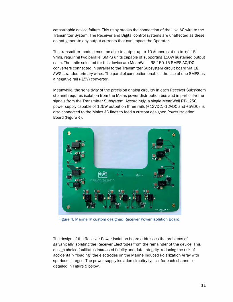
The transmitter module must be able to output up to 10 Amperes at up to +/- 15 Vrms, requiring two parallel SMPS units capable of supporting 150W sustained output each. The units selected for this device are MeanWell LRS-150-15 SMPS AC/DC converters connected in parallel to the Transmitter Subsystem circuit board via 18 AWG stranded primary wires. The parallel connection enables the use of one SMPS as a negative rail (-15V) converter. Meanwhile, the sensitivity of the precision analog circuitry in each Receiver Subsystem channel requires isolation from the Mains power distribution bus and in particular the signals from the Transmitter Subsystem. Accordingly, a single MeanWell RT-125C power supply capable of 125W output on three rails (+12VDC, -12VDC and +5VDC) is also connected to the Mains AC lines to feed a custom designed Power Isolation Board (Figure 4).
The design of the Receiver Power Isolation board addresses the problems of galvanically isolating the Receiver Electrodes from the remainder of the device. This design choice facilitates increased fidelity and data integrity, reducing the risk of accidentally “loading” the electrodes on the Marine Induced Polarization Array with spurious charges. The power supply isolation circuitry typical for each channel is detailed in Figure 5 below.
Figure 4. Marine IP custom designed Receiver Power Isolation Board.

12
Figure 5. (Above) Example of the MIP-1 Receiver Power Isolation circuitry design for each channel. (Below) Magnified image of the Receiver Power Isolation circuitry.

13
The +12VDC power supply for the Transmitter Subsystem cooling fans is also derived from the single MeanWell RT-125C +15V rail through offboard wiring -- via a DC to DC step-down converter programmed to output +12VDC -- to a dedicated connector on the Transmitter Subsystem board. The complete power distribution system diagram is given in (Figure 6). The electrical characteristics of the device are provided in Appendix D: Device Electrical Characteristics.
Figure 6. MIP-1 Transmitter Subsystem power distribution architecture.

14
c. Operator Display Interface and Digital System Controls
This device was engineered to manage itself automatically with a set of preprogrammed defaults such that an operator need only plug the device into the Array Cable, Mains AC power, and a USB port on a laptop (running associated data collection software). However, there are conditions during fieldwork that may necessitate deviations from the preprogrammed device defaults. The automated system management is discussed briefly in the following section.
The Operator Display Interface serves as a portal for a knowledgeable, more advanced user of the MIP-1 Ready Kit to tweak and tune the output settings, timing settings, and automatic operations of the device. It also serves as a dashboard for visualizing the input signal levels, transmit output levels, and operating temperatures of the device.
The display was designed with fieldwork in mind: the top-level dashboard is designed for at-a-glance assessment of device operation. Low-level hardware errors are displayed on this device and actions may be taken by the Operator to handle those errors. The ability to manage the low-level processes of the device provides needed operational and functional flexibility during fieldwork with changing conditions or in the unfortunate case of damage to a device component.
The screen hardware itself was carefully selected by IPA to be both daylight readable and touch-responsive, reducing the complexity of the hardware control-panel layout. The Newhaven Displays NHD-4.3CTP-N (Figure 7) is capable of being read in direct sunlight and contains capacitive touch technology.
Figure 7. The Newhaven Displays NHD-4.3CTP-N, daylight readable and touch-responsive.

15
The Receiver Systems Pane (Figure 8, Left panel) provides the Operator with frequently updated measurements of the input differential voltages across the Receiver Channels. The color of the bar indicates the input level relative to preprogrammed nominal ranges as a proxy for establishing the input signal integrity. The gains and automatic gain controls for each channel may be adjusted manually, however this is only recommended when the Operator must deviate from the default settings programmed into the device.
The Wave Pane (Figure 8, NW quadrant of Right panel) provides the Operator the ability to control the Transmitter output waveform and frequency produced and amplified by the device if the system is using the internally generated waveforms. The transmit frequency can be changed by tapping within the WAVE box, which brings up
Figure 8. (Top) The design drawing for the Marine IP hardware operator display interface, otherwise referred to as the touchscreen on the Marine IP kit. (Bottom) The programmed hardware display interface.
Display Interface: Design
Display Interface: Build

16
a menu to select transmit waveforms and to input the transmit frequency using a slider bar. If the user prefers to enter the frequency with a number pad, the user can tap within that box and a number pad will appear (Figure 9).
The top-level panel is further designed such that an Operator touching any portion of one of the Panes (e.g., SHUNT, TX TEMP, Channel 1, etc.) will bring up a menu screen for tuning the parameters accessible through the digital control system. The color schemes were also chosen by the IPA design engineer to be accessible for color deficient Operators while maintaining an internally consistent design language for quickly conveying system information during survey operations (Figure 10).
Figure 10. Example selection screen for channel control. Colors selected to be user friendly for color deficient operators.
Figure 9. The menus that come up when the Wave Pane, within the Transmitter System (Right) Panel is selected on the operator display interface. To bring up a keypad for manual entry, touch the box under TX Frequency.

17
The DCS, serving as the hub of timing and system control, sends packets of settings and commands to the RCS and TCS while receiving data and operational status from those two subsystems for display on the Display Interface.
d. Digital Automated System Management
The MIP-1 device was designed to be operable in the field using a set of pre-programmed defaults selected from years of previous research carried out on Marine IP methods by IPA and other entities. Accordingly, the Receiver Input Gains, Transmitter Output Power, Waveform mode, and Waveform Frequency are all set by default upon startup. Moreover, the thermal management system is programmed to automatically provide adequate cooling for the power amplification circuitry in field environments. The temperature and output power warning thresholds may be adjusted by the Operator via the Operator Display Interface as discussed in the previous section, but even with those adjustments, the device was designed to automatically adjust itself to the new settings with minimal Operator intervention. These automated systems were also designed to operate independently of the Display Controller Subsystem (DCS) at their default settings upon bootup of the device.
The Receiver Controller Subsystem (RCS) automations include:
1. Automatic Gain Control System (AGCS): The input differential voltages are conditioned to minimize distortion due to overdriven isolation amplifiers.
2. All channels are automatically engaged by default, but if no signal is received for an extended period the RCS will alert the DCS which then provides an alert to the Operator.
The Transmitter Controller Subsystem (TCS) automations include:
3. Automatic power output limiters. 4. Automatic fan control without Operator intervention. 5. Automatic shutdown in the case of power amplifier overtemperature
conditions. 6. Automatic shutdown and alerts if the cooling fans fail to spin up. 7. Increased system status monitoring rate and automatic output power
throttling if operating temperatures rise above nominal preprogrammed ranges.

18
e. Transmitter Subsystem The Transmitter Control Subsystem (TCS) and the associated peripherals control the waveforms, frequency, and output power. The Transmitter Subsystem board is shown below in Figure 11, and the diagram on the following page describes the architecture of the Transmitter circuitry (Figure 12).
i. Transmitter Board Architecture:
THIS SPACE INTENTIONALLY LEFT BLANK
Figure 11. The Marine IP Transmitter Subsystem board.

19
Figure 12. The architecture of the Transmitter Microcontroller.

20
ii. On Board Signal Generator: MIP-1 was designed with an on-board Direct Digital Synthesis waveform generator capable of producing oscillating waveforms up to and exceeding 20kHz. Specifically, the TCS microcontroller executes a program module that writes the output voltage samples to a 12-bit Digital to Analog Converter (DAC) over the Serial Peripheral Interface (SPI) data bus. The DAC integrated circuit has a second output which is programmed by the TCS to provide a control voltage for the power amplifier’s output current limiting circuitry.

21
f. Receiver Subsystem: The Receiver Subsystem was the most complex portion of the design. The electrodes employed in the Array Cable for detecting the current flux (generated by the AC waveforms transmitted by the Transmitter (TX) electrodes in the Array Cable) are a specialized type of nonpolarizable solid Silver-Silver Chloride (Ag-AgCl) electrodes similar in composition to those used by Electrocardiogram systems in biomedical applications. The nonpolarizable electrodes are of critical importance as they do not load with charge during measurement. However, the electrodes must be placed in floating circuit topology where the Receiver input amplifiers have very high input impedance (“High-Z”) while also remaining sensitive to fluctuations in the differential input voltage between the electrodes – this is the quantity used for determining the current flux and thereby enabling comparison with the reference signal (from the Transmitter Shunt Monitor) to compute the phase shift across the target materials in the water.
These passive potentiometric electrodes can be accidentally loaded with charge if too much current is drawn through them by the analog front end to which they are connected -- and through which the signals are conditioned before arriving at the data acquisition device. For this reason, high impedance input buffers with an extremely minimal offset bias current are required for this design (Figure 13).
Figure 13. The Marine IP Receiver Subsystem board.

22
Another concern that was important to take into account within the design is the introduction of noise from signals induced in the local electrical ground for the pairs of electrodes that constitute a receiver channel. Each channel must have its own isolated ground from not only the back-end circuitry connected to the digital control systems, but also from other analog input interfaces on the device. The MIP-1 device was designed with eight isolated channels, one of which is dedicated to the Transmitter Shunt Monitor signal against which the other signal phases are compared. Each isolated channel has its own ground and is isolated from the common analog circuitry in the device by a high-speed analog isolator integrated circuit, the ACPL-C78B. The ACPL-C78B inputs must be conditioned to a nominal input signal range of 400mV peak to peak before the device distorts the differential input voltage waveforms it receives from each of the input buffer amplifiers. As a result, additional circuitry was required to achieve not only proper isolation, but appropriate input gain and amplification on the common (back-end) side of the isolators. To keep the input gain conditioning within nominal limits, a hybrid analog/digital gain-control architecture was developed for the MIP-1 Receiver input circuitry. The system was designed to read the incoming differential input voltage signals, establish if they fall within nominal range, and either amplify or attenuate the signals entering the analog isolators. This is achieved by sampling the input voltages across the two input buffers with a 12-bit analog to digital converter (ADC) at regular intervals, then digitally amplifying or attenuating the signal by setting the appropriate gain in a programmable gain amplifier (PGA) to ensure nominal input voltage limits are maintained. This feedback loop is referred to as the Automatic Gain Control System (AGCS) in the design documentation for MIP-1. The second design goal of re-amplifying the signal from the analog isolator to the data acquisition system (DAQ) voltage sensors was achieved by converting the buffered, isolated differential input signal to a biased, ground referenced signal sharing a ground with the ADC on the DAQ system. The now ADC-ground referenced signal is amplified to make use of the full 5V dynamic range of the DAQ input circuitry. This ground-referencing and amplification stage is referred to as the analog back-end in the design documentation, sharing a common ground with the other Receiver Channels as well as the DAQ.
23
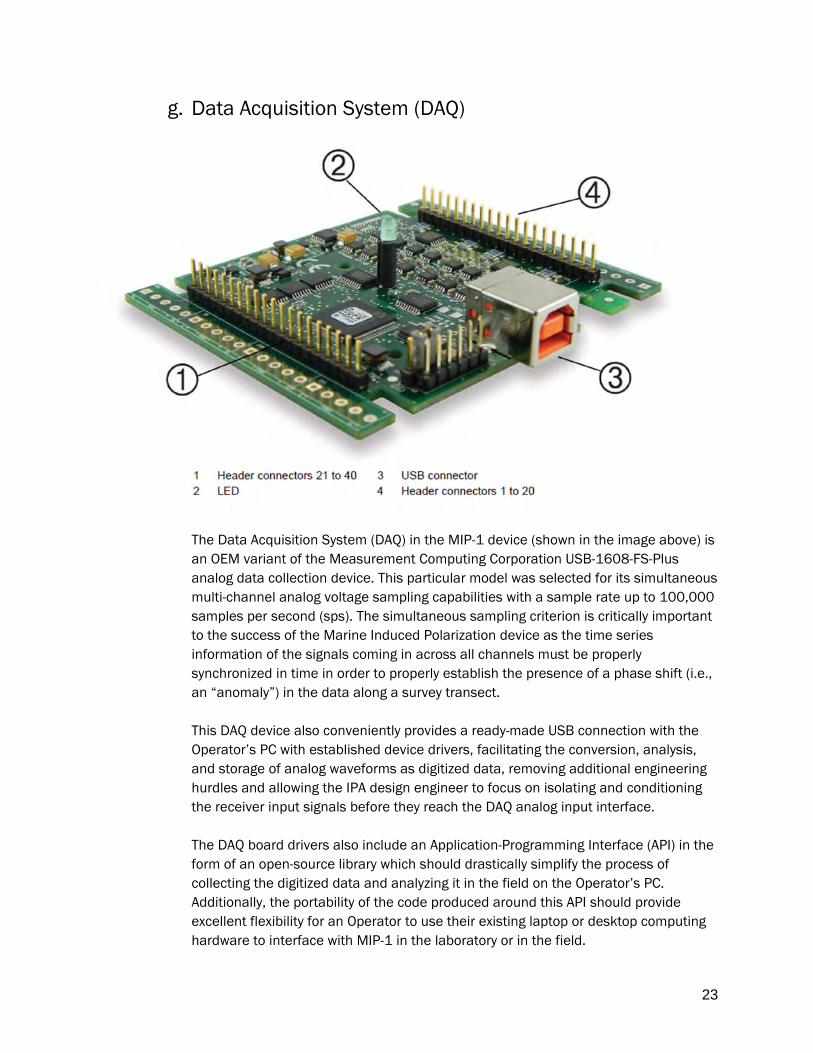
g. Data Acquisition System (DAQ)
The Data Acquisition System (DAQ) in the MIP-1 device (shown in the image above) is an OEM variant of the Measurement Computing Corporation USB-1608-FS-Plus analog data collection device. This particular model was selected for its simultaneous multi-channel analog voltage sampling capabilities with a sample rate up to 100,000 samples per second (sps). The simultaneous sampling criterion is critically important to the success of the Marine Induced Polarization device as the time series information of the signals coming in across all channels must be properly synchronized in time in order to properly establish the presence of a phase shift (i.e., an “anomaly”) in the data along a survey transect. This DAQ device also conveniently provides a ready-made USB connection with the Operator’s PC with established device drivers, facilitating the conversion, analysis, and storage of analog waveforms as digitized data, removing additional engineering hurdles and allowing the IPA design engineer to focus on isolating and conditioning the receiver input signals before they reach the DAQ analog input interface. The DAQ board drivers also include an Application-Programming Interface (API) in the form of an open-source library which should drastically simplify the process of collecting the digitized data and analyzing it in the field on the Operator’s PC. Additionally, the portability of the code produced around this API should provide excellent flexibility for an Operator to use their existing laptop or desktop computing hardware to interface with MIP-1 in the laboratory or in the field.

24
The MIP-1 Receiver and Receiver Isolated Power Supply boards are designed specifically to accommodate the DAQ module, connecting directly to it with a set of pin-headers.
h. Enclosure and Mechanical Design The Marine IP enclosure (Figure 14) was designed, and mechanical CAD drawings were produced using the open-source CAD package, FreeCAD. A Pelican case was chosen as the base enclosure, which was then customized for the Marine IP hardware. The Pelican box, control panel, and side ingress panels were all designed in this software package and sent to DataPro, a custom enclosure manufacturer in Seattle, Washington.
Figure 14. Initial and final drawings for the Marine IP enclosure.

25
The prototype enclosure was manufactured and assembled by DataPro and the off-board wiring (between the PCB and enclosure connections) was assembled in-house. The top panel contains cooling fans, operating switches, and a touch screen, shown in Figure 15.
Figure 15. Marine IP prototype enclosure with custom internal and external panels.

26
Subpanel Component Support: The internal power supply modules in the MIP-1 unit require a support structure, so a subpanel with drilled mounting points for the power supply units, safety interlock relay and Transmitter Power Amplifier board was designed and submitted to a local manufacturer specializing in fabricating aluminum panels and support hardware. The subpanel is mounted to the bottom of the enclosure with aluminum and steel hardware to preclude the power supplies breaking loose from their mounts during handling of the device in the field or during shipping. Mounting and Ingress Protection Rails: The side panel connection ports are recessed and also include protection rails to help protect the plugs going into the Marine IP case.
5. Firmware a. Architecture
The device Firmware was designed to be highly modular, in the same way as the hardware upon which it operates. The system was broadly divided into three individual processing cores, each living on their own microcontroller unit (MCU):
1. Display Controller Subsystem (DCS) 2. Receiver Controller Subsystem (RCS) 3. Transmitter Controller Subsystem (TCS)
Each core is comprised of an AVR microcontroller handling a specific subset of automation tasks within the MIP-1 operating program. However, the DCS is the only MCU with a direct interface to the Operator or the DAQ module. Therefore. the DCS behaves predominantly as the conductor of the other two Subsystem Controllers (RCS and TCS). The DCS is connected to the RCS and TCS via a set of Pin Change Interrupt (PCINT) pins for safety or operationally critical alert functions – as well as

27
via the two Universal Asynchronous Receiver/Transmitter (UART) buses found on each MCU (Figure 16Figure 16).
The requirements of the device firmware architecture were defined in detail for each subsystem to define the functionality of the system as well as for the nature and operations of the internal system interactions. The details are outlined in Figure 17 below. The requirements of the system created the guidelines for the architecture of the hardware and firmware. The block diagram of the firmware architecture is shown in Figure 18 below.
Figure 16. The relationship between the DCS, RCS and TCS, where the DCS serves as a conductor to the other systems.

28
Figure 17. The requirements defined for the MIP-1 firmware. This set of requirements supports the design of the firmware as well as of the hardware.

29
Figure 18. Block diagram of the MIP-1 firmware, showing the details of the interactions between the DCS, TCS, and RCS, and reflecting the requirements of the system in the system operations.

30
6. Discussion
a. Hardware Design Narrative First, a full review of the previous design of the Marine Induced Polarization Survey Instrument was conducted to establish the best working components of the previous design upon which new components and technologies developed for MIP-1, the new device, were based.
A series of high-level design documents was generated to support the design and refinement of the Marine Induced Polarization technology. During this stage, the modular architecture discussed earlier in this report was selected. Architecture block diagrams (Figure 1, Figure 12, and Figure 18 above) were generated and formed the foundation of further design drawings and calculations.
Calculations for input impedance and output power were performed at this stage to select appropriate components for the device that would meet functional requirements of each subsystem module in the finished device. It was also at this point that safety interlocks and thermal management features were integrated into the design of the new device.
In addition to reviewing the old design, the IPA design engineer also conducted multiple tests on new analog and digital semiconductor devices in the laboratory to select components that meet the operational and durability requirements of the new device under design. The components were specifically selected to reduce the power requirements, weight, and volume of the system pursuant to the design goals of the project.
The new designs were documented and drawn into electrical schematics – themselves undergoing dramatic revision as work progressed. Finally, a complete design was prepared and ready for breadboard prototyping. At this point, the IPA design engineer constructed laboratory breadboard prototypes and adapter boards for digital semiconductors that would be built into the MIP-1 device. Some images from those tests are provided in Figure 19 below.

31
During this stage, multiple component substitutions were made to the schematics, eventually settling on Revision D before the design engineer produced CAD output files for printed circuit board (PCB) fabrication. In support of producing these design outputs, additional thermal and conductivity calculations were performed to ensure the appropriate PCB trace widths. Additional simulations and calculations were performed at this point to remove any theoretically ascertainable sources of problems with trace impedances and component layouts.
The PCB was laid out in KiCAD, an open-source electrical CAD software package developed and maintained by CERN in Geneva, Switzerland. The contract manufacturer -- Schipper’s & Co. in Seattle, Washington -- was contacted to validate the design rules used by the IPA design engineer. A Bill-of-Materials (BOM) was generated for the on-board components to be sourced by Schipper’s & Co. throughout the PCB manufacturing and assembly process. The BOM for the build can be found in Appendix E: Device Fabrication Bill-of-Materials (BOM)at the end of this report.
Due to component shortages in December 2020 and January 2021, several BOM and PCB layout revisions were necessary to obtain appropriate components for the designs. This was a highly collaborative, rapidly iterative process involving the IPA design engineer reviewing the detailed specifications of a given component, checking stocks and availability of the components in question at U.S.-based suppliers, contacting the Schipper’s & Co. purchasing specialist to ensure it was accessible, and then revising the BOM and PCB layouts and sending the new production files to Schipper’s & Co. This cycle was repeated for several of the components in the BOM.
By the end of January 2021, the final BOM components were all successfully sourced, the PCB production files (Appendix C: Electronic Hardware Printed Circuit
Figure 19. (Left) Laboratory testing of system components laboratory prototypes using with breadboards and adapter boards; component selection based on performance. (Right) Preliminary schematics for the prototype modules.

32
Board Fabrication Files) were validated by the Schipper’s & Co., and the board fabrication process was underway.
Next, the mechanical CAD drawings necessary for producing the enclosures were generated by the IPA design engineer using the open-source CAD package FreeCAD. The Pelican box, control panel, and side ingress panels were all designed in this software package and sent to DataPro, a custom enclosure manufacturer in Seattle, Washington. Details about the custom hardware manufacturers can be found in Appendix F: Custom Hardware Manufacturer Details.
The initial design costs were high relative to the budget of the build, so major revisions to the mechanical design were conducted. After working collaboratively with the sales engineering team at DataPro, the IPA design engineer generated a complete set of drawings for the enclosure, cooling fan cutouts, control panel, and side ingress panels for Mains AC and the Array Cable Connector. The design drawings for the enclosures are provided in Appendix A.
Upon receipt of the PCBs from Schipper’s & Co., a series of passive continuity tests was performed on the circuit boards. No short circuits in unexpected spots were detected by these passive (i.e., unpowered) tests.
Wiring harnesses between the test boards were constructed to specifications provided in the design documentation in order to move on to the Active (powered) testing phase with the prototype circuit boards.
Following the successful passive continuity tests, the power supply modules were connected and individually tested, yielding the appropriate rail voltages. The Receiver Power Isolation Board was similarly connected and tested using a benchtop laboratory power supply to assess the current draw from the DC/DC converters. Upon successful tests on the benchtop of the Receiver Power Isolation Board, the DC/DC converters were connected to the Receiver Analog Front-End components on the Receiver Board and the rail voltages were again tested using the benchtop power supply. These tests have been so far successful, indicating the correct fabrication and layout of the Receiver Power Isolation and Receiver Boards.
Following unmounted powered tests, the power supplies were mounted to the Subpanel aluminum plate with steel M3 bolts and the fused AC Mains ingress port was connected to the Subpanel mounted modules with an 18 AWG wiring harness. The Transmitter Board was connected to the Mains AC/DC converters following the wiring diagram and the Live AC line was linked through the safety interlock relay.
b. Firmware Development Narrative The development of robust, error-free firmware for the Marine IP Arctic Ready Field Kit required careful attention to the development of a testable, portable workflow. The firmware was set up to cross-compile on Windows machines using the AVR-GCC

33
C/C++ cross-compiler. The compiled binaries were then flashed to the Atmel/Microchip AVR microcontrollers on the PCBs with an In Circuit System Programming device. Testing frameworks were established using the Unity/Ceedling frameworks and test harnesses for testing individual modules of the codebase during development.
Initial tests of the firmware were carried out on prototype breadboard adapters for converting the surface-mount devices used in the hardware. Subsequent tests were carried out on the actual MIP-1 device PCBs produced during the hardware fabrication phase. Automatic documentation generation from code comments was established using the Doxygen autodocumentation package, which generates HTML, LaTeX, or Markdown documentation of functional and translational units of the C-code written for the AVR microcontrollers. Additional specifications and documentation were primarily written in Markdown and converted to PDF by the open-source Typora text editor. Detailed specifications for the UART communication protocols were generated. The programmable gain amplifier lookup tables were implemented on the RCS without major setback. Version control was critical for constructing and modifying the codebase while performing audits of project velocity, reviewing bugs, and constructing test plans. Here, Git version control software was employed with remote syncing to a private GitHub repository for each microcontroller module. The firmware automation units and peripheral device drivers for the Receiver Control Subsystem (RCS) have been completed, compiled, and tested to roughly 80% completion by the IPA design engineer; the Display Interface and DCS microcontroller code has been designed and mocked up, and reviewed by internal stakeholders; and the display front-end (visible to the Operator) has been implemented. The TCS remains to be fully developed at this point; however, a phased, continuous integration plan for implementing the Auxiliary Waveform Input mode to field test the amplifier and receiver front end circuitry is being carried out to enable field tests at the earliest possible point. The list of development tools used for each stage and component of the development and build can be found in Appendix G: Development Tool Details. Images of the final device assembly can be found in Appendix H: Device Final Assembly Images.

34

35
7. Interim Team Performance Analysis The design of the new MIP-1 hardware has met the following detailed objectives as discussed in the ADAC Oil Under Ice Year 7 Work Plan document:
a. An extensive design review was performed on the previous generation of the Marine IP Survey Instrument.
b. As an outcome of the design review, extensive analysis and design calculations were performed by the IPA design engineer to optimize the design of the new prototype (MIP-1).
c. A new set of circuit topologies implementing recently developed integrated circuits and components has been generated and documented thoroughly.
d. A new Receiver Front End design has been constructed and is undergoing testing. e. A new Transmitter Power Amplifier circuit design has been implemented using
recently developed integrated circuits and components. f. The hardware was designed to automate as many low-level operating processes of
the device as possible, reducing the cognitive load on the Operator during field operations.
g. The device has implemented a new control and data display interface with a design tailored for field environments.
h. A complete Bill of Materials (BOM) has been generated for both on-board and off-board components.
i. Computer Aided Design renderings of mechanical and electrical device hardware have been generated.
j. The printed circuit boards for the prototype have been manufactured and populated with components.
k. The device was fabricated completely within Seattle, Washington, USA. l. The Marine Induced Polarization technology has been miniaturized in order to
increase portability and simplicity of deployment. m. The current prototype fits the necessary power conditioning, array interface, signal
conditioning, data collection, and automation hardware into a single Pelican 1550 case with exterior dimensions 20.6”x17.2”x8.4”.
n. The current version of the prototype is highly modular and easily expanded or modified to further shrink its footprint for deployment as an AUV payload in future builds.
o. The new prototype was constructed to offer substantial improvements in ruggedness. p. The new prototype was constructed to interface with any personal computer running
a Windows operating system. q. Hardware design documentation has been generated and has been included at the
end of this report. r. A full firmware development environment has been constructed with integrated
documentation generation, version control, and unit testing frameworks to be used by the firmware developer.

36
s. Extensive firmware design documentation has been generated, some of which is included in this engineering report. Upon completion and testing of the device firmware, all firmware design and implementation documentation will be made available to DHS and USCG.
t. The Receiver Control Subsystem firmware has approached 80% completion. u. The Display Controller Subsystem firmware and display interface software has
approached 80% completion. v. Passive PCB inspections have passed. w. Powered tests of 50% of the electronic components have been passed. x. The final assembly of one test unit -- of the total five (5) units manufactured – is
underway.
Significant Roadblocks During Development:
The 2020/2021 years were particularly difficult for the development team due to substantial limitations placed on access to components, materials, workspaces, laboratories, field sites, and technology infrastructure. The COVID-19 pandemic and subsequent shutdown of the State of Washington coincided almost exactly with a return from a test deployment of the Marine IP technology at CRREL. Immediately after lockdowns began, the team was not allowed any access to their rental laboratory space, nor were they allowed to pick up equipment or come in contact with the operators of the facility housing the workspace.
In July of 2020, the organization from whom IPA rented wet-laboratory and fabrication facility space withdrew their support and terminated their lease agreement with IPA. As a result, IPA had to move very quickly to retrieve equipment and materials from the rental space within a very narrow window. This disrupted most aspects of development and design work on a fundamental level as IT infrastructure and prototyping support was now suddenly nonexistent.
To overcome this challenge, IPA located another suitable workspace by Autumn of 2020 and began working on the hardware redesign in earnest. However, the lack of consistent IT infrastructure still posed numerous challenges that were overcome concurrently with the actual hardware development.
Shortly after completing the initial design review and initial CAD designs for the new device, a substantial number of semiconductors became scarce due to the 2020/2021 supply chain disruptions, prompting multiple rounds of rapid redesign by the small IPA design team.
Similar issues were encountered with the cost-effective design and manufacture of the enclosures for the device, further setting firmware development behind schedule.
In-person collaborative work, field deployment, and on-site laboratory work were similarly hindered greatly. The IPA team has worked constantly to overcome these challenges in creative ways to deliver the Marine IP Arctic Ready Kit by the end of Program Year 7, however

37
as outlined in more detail in other communications they have had a substantial impact on the IPA team’s original estimated completion dates for some of the project milestones.
As field deployments and in-person meetings have been severely restricted or altogether eliminated over the past 18 months, it has not been feasible to perform in-person usability tests to meet some of the expected goals from the original workplan.
The project work will continue through the no-cost extension into ADAC Program Year 8. This report represents progress through June 30, 2021, and will be updated with system information and testing results at the end of ADAC Program Year 8.
8. Conclusions Despite numerous adverse circumstances facing the IPA Team during 2020 and 2021, the device hardware has been carefully designed and optimized to improve on previous iterations of the Marine Induced Polarization technology for detecting oil in marine sediment or under ice. The designs have been documented. A full BOM for a cost-effective prototype unit has been generated and validated. The electronics and mechanical support hardware have been fully fabricated and constructed. The power systems and analog circuits have been successfully tested in the laboratory during final assembly. The firmware architecture has been completed and documented with only implementation details and maximizing unit-test coverage remaining to be completed before field tests are possible with the automated hardware. Extensive documentation of both the hardware and firmware systems has been generated and has been included in the attached appendices.
9. Appendices Appendix A: Marine IP Arctic Ready Kit Mechanical Design Drawings Appendix B: Electronic Hardware Printed Circuit Board Schematics Appendix C: Electronic Hardware Printed Circuit Board Fabrication Files Appendix D: Device Electrical Characteristics Appendix E: Device Fabrication Bill-of-Materials (BOM) Appendix F: Custom Hardware Manufacturer Details Appendix G: Development Tool Details Appendix H: Device Final Assembly Images

38
THIS PAGE INTENTIONALLY LEFT BLANK

39
Appendix A: Marine IP Arctic Ready Kit Mechanical Design Drawings
40

41

42

43

44
45
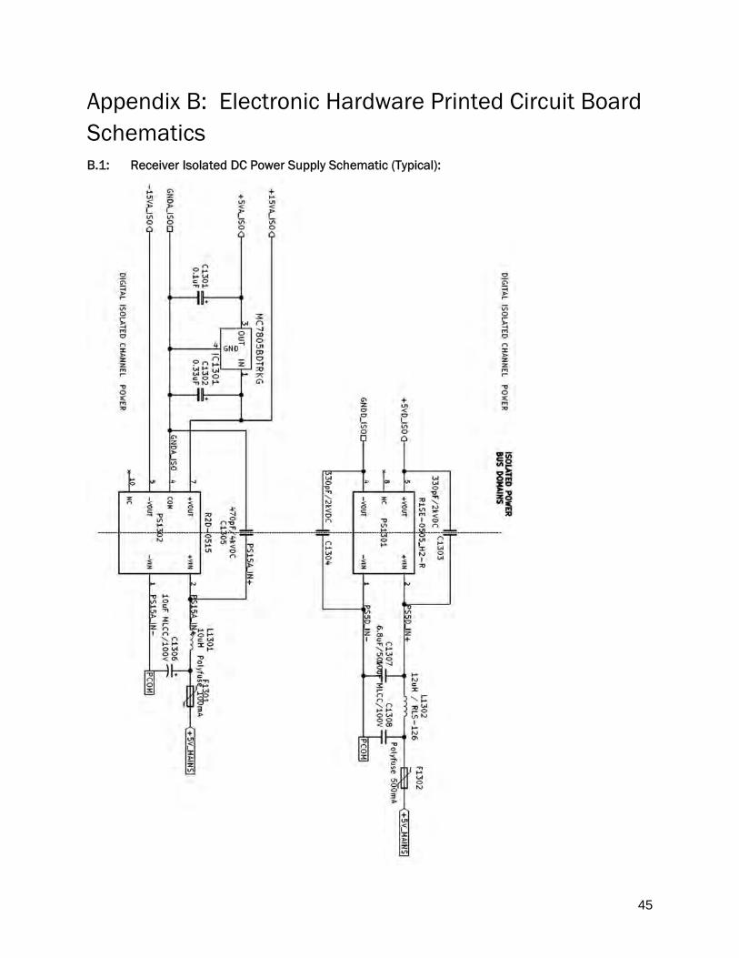
Appendix B: Electronic Hardware Printed Circuit Board Schematics B.1: Receiver Isolated DC Power Supply Schematic (Typical):

46
B.2: Receiver Isolated Channel Schematic Analog Circuitry (Typical)

47
B.3 Back-End (Common Ground) Differential to Single-Ended and Amplification Stages
B.5 Receiver Digital Channel Control Circuitry (Typical):

48
B.6 Receiver Full Channel Schematic (Typical):

49
B.7 Receiver Controller Subsystem (RCS) Schematic:

50
B.8: Transmitter Power Amplifier Circuitry Schematic:

51
B.9: Transmitter Digital Waveform Generator and Power Output Control Schematic Detail:
B10: Transmitter Auxiliary Waveform Input Detail:

52
B.11: Transmitter Output Shunt Monitor Schematic Detail:

53
B.12: Transmitter Board Thermal Management System Schematic Detail:
54
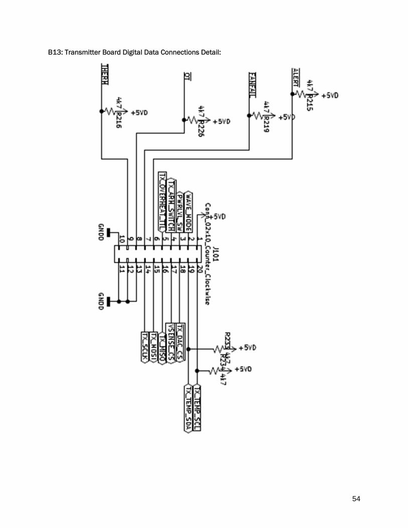
B13: Transmitter Board Digital Data Connections Detail:
55
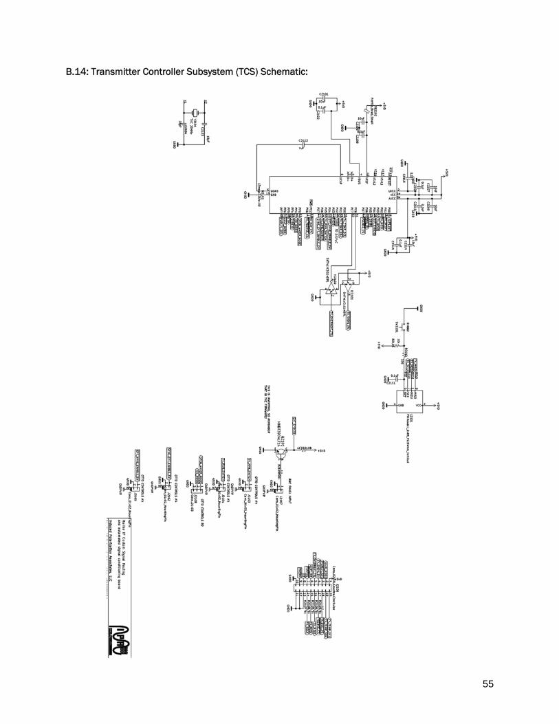
B.14: Transmitter Controller Subsystem (TCS) Schematic:

56
B.15: Display Controller Subsystem (DCS) Schematic

57
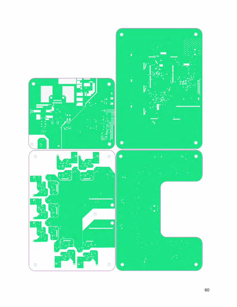
Appendix C: Electronic Hardware Printed Circuit Board Fabrication Files Gerber and Drill files of the circuits are presented here for the four-layer Printed Circuit Boards (PCBs) designed by the IPA design engineer and fabricated by Schipper’s & Co. in Seattle, Washington in early 2021. These images represent the four (4) layers of copper in the printed circuit boards (PCBs) in these prototypes. All four boards are represented on each page.
THIS SPACE INTENTIONALLY LEFT BLANK

58

59
60

61
62
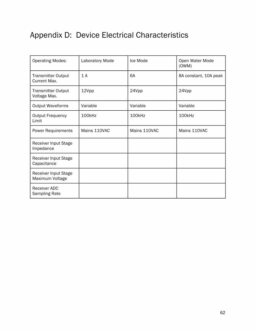
Appendix D: Device Electrical Characteristics
Operating Modes: Laboratory Mode Ice Mode Open Water Mode (OWM)
Transmitter Output Current Max.
1 A 6A 8A constant, 10A peak
Transmitter Output Voltage Max.
12Vpp 24Vpp 24Vpp
Output Waveforms Variable Variable Variable
Output Frequency Limit
100kHz 100kHz 100kHz
Power Requirements Mains 110VAC Mains 110VAC Mains 110VAC
Receiver Input Stage Impedance
Receiver Input Stage Capacitance
Receiver Input Stage Maximum Voltage
Receiver ADC Sampling Rate
63
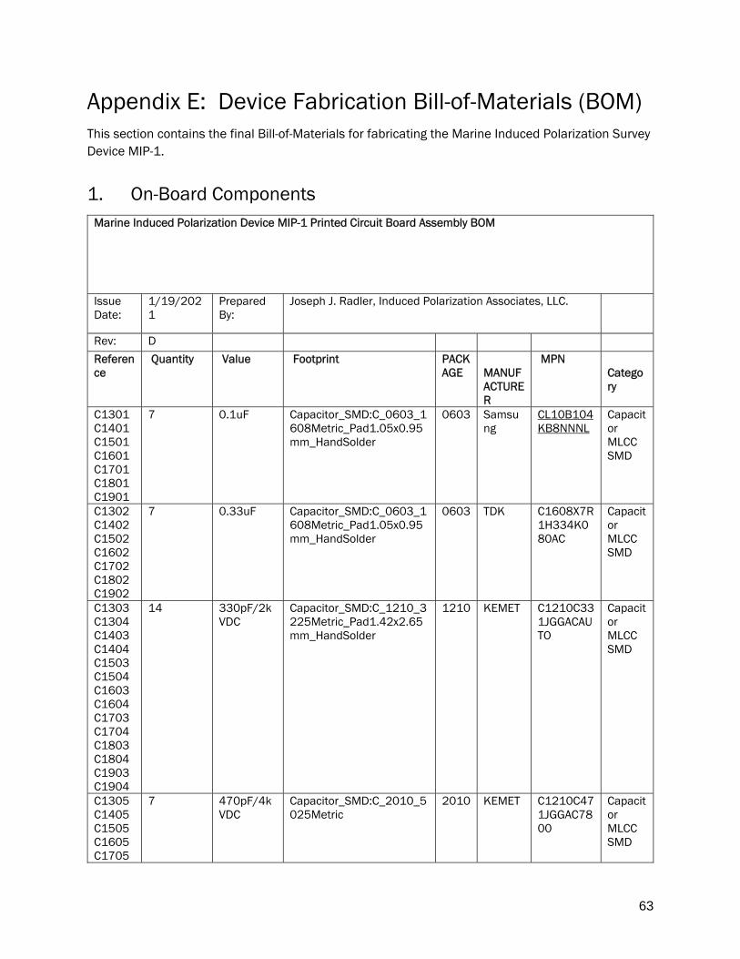
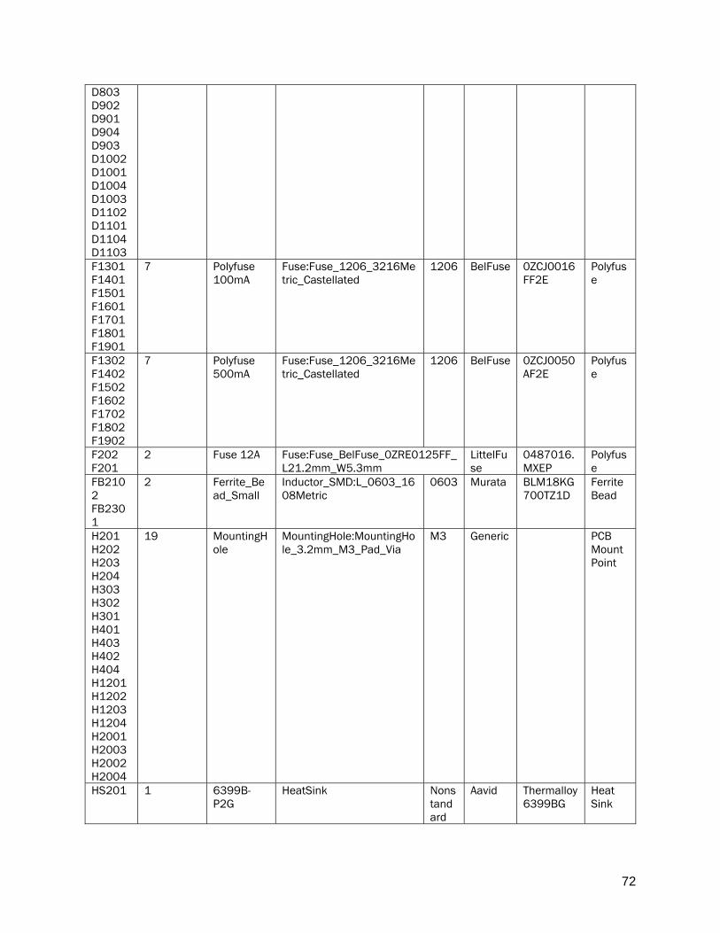
Appendix E: Device Fabrication Bill-of-Materials (BOM) This section contains the final Bill-of-Materials for fabricating the Marine Induced Polarization Survey Device MIP-1.
1. On-Board Components Marine Induced Polarization Device MIP-1 Printed Circuit Board Assembly BOM
Issue Date:
1/19/2021
Prepared By:
Joseph J. Radler, Induced Polarization Associates, LLC.
Rev: D
Reference
Quantity Value Footprint PACKAGE
MANUFACTURER
MPN Category
C1301 C1401 C1501 C1601 C1701 C1801 C1901
7 0.1uF Capacitor_SMD:C_0603_1608Metric_Pad1.05x0.95mm_HandSolder
0603 Samsung
CL10B104KB8NNNL
Capacitor MLCC SMD
C1302 C1402 C1502 C1602 C1702 C1802 C1902
7 0.33uF Capacitor_SMD:C_0603_1608Metric_Pad1.05x0.95mm_HandSolder
0603 TDK C1608X7R1H334K080AC
Capacitor MLCC SMD
C1303 C1304 C1403 C1404 C1503 C1504 C1603 C1604 C1703 C1704 C1803 C1804 C1903 C1904
14 330pF/2kVDC
Capacitor_SMD:C_1210_3225Metric_Pad1.42x2.65mm_HandSolder
1210 KEMET C1210C331JGGACAUTO
Capacitor MLCC SMD
C1305 C1405 C1505 C1605 C1705
7 470pF/4kVDC
Capacitor_SMD:C_2010_5025Metric
2010 KEMET C1210C471JGGAC7800
Capacitor MLCC SMD

64
C1805 C1905
C1307 C1407 C1507 C1607 C1707 C1807 C1907
7 6.8uF/50V Capacitor_SMD:C_1812_4532Metric_Pad1.30x3.40mm_HandSolder
1812 TDK C4532X7R1H685K250KB
Capacitor MLCC SMD
C1306 C1406 C1506 C1606 C1706 C1806 C1906 C1308 C1408 C1508 C1608 C1708 C1808 C1908
14 10uF MLCC / 100V
Capacitor_SMD:C_2220_5650Metric_Pad1.97x5.40mm_HandSolder
2220 TDK C5750X7S2A106K230KB
Capacitor MLCC SMD
C2001 1 0.33uF Capacitor_SMD:C_Elec_4x5.4
4.0x5.4 Landing Pads
Wuerth Elektronik
865090640003
Capacitor Al SMD

65
C201 C212 C233 C234 C241 C242 C225 C224 C208 C505 C503 C519 C506 C521 C517 C514 C516 C526 C523 C532 C528 C535 C534 C530 C529 C537 C525 C508 C502 C527 C605 C603 C619 C606 C621 C617 C614 C616 C626 C623 C632 C628 C635 C634 C630 C629 C637 C625 C608 C602 C627 C705 C703 C719 C706 C721 C717
174 0.1uF Capacitor_SMD:C_0402_1005Metric
0402 KEMET C0402C103M3RAC7867
Capacitor MLCC SMD

66
C714 C716 C726 C723 C732 C728 C735 C734 C730 C729 C737 C725 C708 C702 C727 C805 C803 C819 C806 C821 C817 C814 C816 C826 C823 C832 C828 C835 C834 C830 C829 C837 C825 C808 C802 C827 C905 C903 C919 C906 C921 C917 C914 C916 C926 C923 C932 C928 C935 C934 C930 C929 C937 C925 C908 C902 C927

67
C1005 C1003 C1019 C1006 C1021 C1017 C1014 C1016 C1026 C1023 C1032 C1028 C1035 C1034 C1030 C1029 C1037 C1025 C1008 C1002 C1027 C1105 C1103 C1119 C1106 C1121 C1117 C1114 C1116 C1126 C1123 C1132 C1128 C1135 C1134 C1130 C1129 C1137 C1125 C1108 C1102 C1127 C2002 C2108 C2110 C2102 C2111 C2106 C2113 C2115 C2206 C2205 C2207 C2201 C2204 C2208 C2301

68
C2305 C2309 C2307
C204 C211 C203 C202 C216 C215
6 0.1uF Capacitor_SMD:C_0805_2012Metric_Pad1.15x1.40mm_HandSolder
0805 Samsung
CL21B104KBCNNNC
Capacitor MLCC SMD
C205 C213
2 10uF Ta Capacitor_Tantalum_SMD:CP_EIA-6032-28_Kemet-C_Pad2.25x2.35mm_HandSolder
Kemet C-Pad
KEMET T491C106K025AT7280
Tantalum Capacitor SMD
C206 C207
2 2200pF Capacitor_SMD:C_0402_1005Metric
0402 KEMET C0402C104K9RACTU
Capacitor MLCC SMD
C209 C210
2 0.33uF Capacitor_SMD:CP_Elec_4x3.9
4.0x3.9 Landing Pads
Wuerth Elektronik
865230640003
Capacitor Al SMD

69
C2103 C2104 C2202 C2203 C2303 C2302
6 18pF Capacitor_SMD:C_0402_1005Metric
0402 Murata GJM1555C1H180FB01D
Capacitor MLCC SMD
C220 C217
2 220uF Capacitor_SMD:CP_Elec_10x10.5
10x10.5 Landing Pads
Panasonic
EEE-FT0J221AR
Capacitor Al SMD
C223 C226 C522 C515 C518 C622 C615 C618 C722 C715 C718 C822 C815 C818 C922 C915 C918 C1022 C1015 C1018 C1122 C1115 C1118 C2112
24 1uF Capacitor_SMD:C_0402_1005Metric
0402 Murata GRM155R70J105KA12J
Capacitor MLCC SMD
C232 C218 C222 C511 C524 C611 C624 C711 C724 C811 C824 C911 C924 C1011 C1024 C1111 C1124
17 10nF Capacitor_SMD:C_0402_1005Metric
0402 KEMET C0402C103J3RACAUTO
Capacitor MLCC SMD

70
C243 C240 C531 C536 C631 C636 C731 C736 C831 C836 C931 C936 C1031 C1036 C1131 C1136
16 10pF Capacitor_SMD:C_0402_1005Metric
0402 KEMET C0402C100K3GACTU
Capacitor MLCC SMD
C510 C509 C507 C504 C533 C520 C513 C512 C501 C610 C609 C607 C604 C633 C620 C613 C612 C601 C710 C709 C707 C704 C733 C720 C713 C712 C701 C810 C809 C807 C804 C833 C820 C813 C812 C801 C910 C909 C907 C904 C933
71 10uF Capacitor_SMD:C_0402_1005Metric
0402 KEMET C0402C106M9PAC7867
Capacitor MLCC SMD

71
C920 C913 C912 C901 C1010 C1009 C1007 C1004 C1033 C1020 C1013 C1012 C1001 C1110 C1109 C1107 C1104 C1133 C1120 C1113 C1112 C1101 C2105 C2109 C2107 C2101 C2114 C2304 C2306 C2308
D202 D201
2 STS321150B351
Diode_SMD:D_SOD-323 SOD-323
Eaton STS321150B351
ESD Diodes
D2301 1 AMBER LED_THT:LED_D5.0mm 5.0 LED 2 pin
Everlight
EALP05RDGOA0
LED
D2302 1 RED LED_THT:LED_D5.0mm 5.0 LED 2 pin
Everlight
EALP05RDGRA2
LED
D2303 1 GREEN LED_THT:LED_D5.0mm 5.0 LED 2 pin
Everlight
EALP05RDGGA1
LED
D502 D501 D504 D503 D602 D601 D604 D603 D702 D701 D704 D703 D802 D801 D804
28 1N5819HW-7-F
digikey-footprints:SOD-123 SOD-123
Diodes Incorporated
1N5819HW-7-F
Discrete Semiconductor Products
72
D803 D902 D901 D904 D903 D1002 D1001 D1004 D1003 D1102 D1101 D1104 D1103 F1301 F1401 F1501 F1601 F1701 F1801 F1901
7 Polyfuse 100mA
Fuse:Fuse_1206_3216Metric_Castellated
1206 BelFuse 0ZCJ0016FF2E
Polyfuse
F1302 F1402 F1502 F1602 F1702 F1802 F1902
7 Polyfuse 500mA
Fuse:Fuse_1206_3216Metric_Castellated
1206 BelFuse 0ZCJ0050AF2E
Polyfuse
F202 F201
2 Fuse 12A Fuse:Fuse_BelFuse_0ZRE0125FF_L21.2mm_W5.3mm
LittelFuse
0487016.MXEP
Polyfuse
FB2102 FB2301
2 Ferrite_Bead_Small
Inductor_SMD:L_0603_1608Metric
0603 Murata BLM18KG700TZ1D
Ferrite Bead
H201 H202 H203 H204 H303 H302 H301 H401 H403 H402 H404 H1201 H1202 H1203 H1204 H2001 H2003 H2002 H2004
19 MountingHole
MountingHole:MountingHole_3.2mm_M3_Pad_Via
M3 Generic
PCB Mount Point
HS201 1 6399B-P2G
HeatSink Nonstandard
Aavid Thermalloy 6399BG
Heat Sink

73
HS201 Thermal Pad
1 4880SG HeatSink Mounting Kit Aavid 4880SG Heat Sink TO-220 Mounting Kit
IC1301 IC1401 IC1501 IC1601 IC1701 IC1801 IC1901 IC2001
8 MC7805BDTRKG
digikey-footprints:TO-252-3 TO-252-3
ON Semiconductor
MC7805BDTRKGOSCT-ND
Integrated Circuits (ICs)
IC201 1 MCP4822 Package_SO:MSOP-8_3x3mm_P0.65mm
MSOP-8
Microchip
MCP4822 Integrated Circuits (ICs)
IC202 1 MAX6639FAEE+
sensor-ics:SOP63P602X175-16N
QSOP-16 Maxim
Maxim Integrated
MAX6639FAEE+
Integrated Circuits (ICs)
IC205 1 NCP1117-5.0_TO252
Package_TO_SOT_SMD:TO-252-2
TO-252-2
ON Semiconductor
NCP1117DT50RKG
Integrated Circuits (ICs)
IC2102 IC2101
2 SN74LVC1G14DRL
Package_TO_SOT_SMD:SOT-553
SOT-553
Texas Instruments
SN74LVC1G14DRL
Integrated Circuits (ICs)
IC501 IC601 IC701 IC801 IC901 IC1001 IC1101
7 NC7SZ125M5X
digikey-footprints:SOT-753 SOT-753
ON Semiconductor
NC7SZ125M5X
Integrated Circuits (ICs)
IC502 IC602 IC702 IC802 IC902 IC1002 IC1102
7 ISO7741BDWR
ISO7741BDWR:ISO7741BDWR
TSSOP
Texas Instruments
ISO7741BDWR
Integrated Circuits (ICs)
IC503 IC603 IC703 IC803 IC903 IC1003 IC1103
7 ADuM261N0BRIZ
Package_SO:SOIC-16W_7.5x12.8mm_P1.27mm
TSSOP-16
Analog Devices
ADuM261N0BRIZ
Integrated Circuits (ICs)
IC504 IC604 IC704 IC804 IC904
7 SN74HC595PWR
Package_SO:TSSOP-16_4.4x5mm_P0.65mm
TSSOP-16
Texas Instruments
SN74HC595PWR
Integrated Circuits (ICs)

74
IC1004 IC1104
J101 J2106
2 Conn_02x10_Counter_Clockwise
Connector_Molex:Molex_Micro-Fit_3.0_43045-2012_2x10_P3.00mm_Vertical
Molex 43045-2012
Wire-to-Board Connector
J1212 J1209 J1214 J1213 J1211 J1210 J1202 J1201 J1204 J1203 J1206 J1205 J1208 J1207
14 Conn_01x04_Female
Connector_PinSocket_1.00mm:PinSocket_1x04_P1.00mm_Vertical_SMD_Pin1Left
1.0mm Pitch, 01x12 vertical
GCT BC070-04-A-1-L-C
SMD Pin Socket Board-to-Board Connector
J1215 J2009
2 Conn_02x03_Odd_Even
Connector_Molex:Molex_Micro-Fit_3.0_43045-0615_2x03_P3.00mm_Vertical
Molex 43045-0615
Wire-to-Board Connector
J2005 J2006 J2007 J2001 J2004 J2002 J2003
7 Conn_01x12_Female
Connector_PinSocket_1.27mm:PinSocket_1x12_P1.27mm_Vertical
1.27mm Pitch, 01x12 vertical
Sullins LPPB121NFFN-RC
THT Pin Socket Board-to-Board Connector
J201 1 Conn_01x03
Connector_Molex:Molex_SPOX_5267-03A_1x03_P2.50mm_Vertical
Molex SPOX 5267-03A
Wire-to-Board Connector
J202 J206
2 Conn_01x02
Connector_Molex:Molex_MicroClasp_55932-0230_1x02_P2.00mm_Vertical
Molex 55932-0230
Wire-to-Board Connector
J204 J203
2 Conn_02x02_Odd_Even
Connector_Molex:Molex_Nano-Fit_105310-xx04_2x02_P2.50mm_Vertical
Molex 1053101204
Wire-to-Board Connector
J205 1 Conn_02x02_Odd_Even
Connector_Molex:Molex_Micro-Fit_3.0_43045-0412_2x02_P3.00mm_Vertical
Molex Micro-Fit 43045-0412
Wire-to-Board Connector
J209 J415 J416
3 Conn_01x06
Connector_Molex:Molex_CLIK-Mate_502382-0670_1x06-1MP_P1.25mm_Vertical
Molex CLIK-Mate_502382-0670
Wire-to-Board Connector
J2101 J2201 J2306
3 Conn_02x05
Connector_PinHeader_2.54mm:PinHeader_2x05_P2.54mm_Vertical
2.54mm Pitch,
Amphenol
67997-410HLF
THT Pin Header Board-

75
02x05 vertical
to-Board Connector
J2108 1 Conn_01x03
Connector_Molex:Molex_MicroClasp_55932-0330_1x03_P2.00mm_Vertical
Molex MicroClasp_55932-0330
Wire-to-Board Connector
J2301 1 Conn_01x10
Connector_PinSocket_2.54mm:PinSocket_1x10_P2.54mm_Vertical
2.54mm Pitch, 01x10 vertical
Amphenol
66951-010LF
THT Pin Socket Board-to-Board Connector
J2303 J2302
2 Conn_01x08
Connector_PinSocket_2.54mm:PinSocket_1x08_P2.54mm_Vertical
2.54mm Pitch, 01x08 vertical
Amphenol
66951-008LF
THT Pin Socket Board-to-Board Connector
J2304 1 Conn_01x06
Connector_PinSocket_2.54mm:PinSocket_1x06_P2.54mm_Vertical
2.54mm Pitch, 01x06 vertical
Amphenol
66951-006LF
THT Pin Socket Board-to-Board Connector
J2305 1 Conn_02x03_Odd_Even
Connector_PinHeader_2.54mm:PinHeader_2x03_P2.54mm_Vertical
2.54mm Pitch, 02x03 vertical
Amphenol
67996-406HLF
THT Pin Header Board-to-Board Connector
J301 J302 J2008
3 Conn_01x20
Connector_PinHeader_2.54mm:PinHeader_1x20_P2.54mm_Vertical
2.54mm Pitch, 01x20 vertical
Samtec SSQ-120-03-G-S
THT Pin Header Board-to-Board Connector
J409 J401 J403 J405 J407 J406 J410 J404 J411 J413 J414 J412
14 Conn_01x04_Male
Connector_PinHeader_1.00mm:PinHeader_1x04_P1.00mm_Vertical
1.0mm Pitch, 01x04 vertical
GCT BC032-04-A-2-0200-0200-L-B
THT Pin Header Board-to-Board Connector

76
J402 J408
J501 J601 J701 J801 J901 J1001 J1101 J2103 J2104 J2102 J2105 J2107
12 Conn_01x02_MountingPin
Connector_Molex:Molex_Pico-Clasp_202396-0207_1x02-1MP_P1.00mm_Horizontal
Molex 202396-0207
Wire-to-Board Connector
J502 J602 J702 J802 J902 J1002 J1102
7 Conn_01x12_Male
Connector_PinHeader_1.27mm:PinHeader_1x12_P1.27mm_Vertical
1.27mm Pitch, 01x12 vertical
Sullins GRPB121VWVN-RC
THT Pin Header Board-to-Board Connector
K201 1 G5V-1-DC5 Relay_THT:Relay_SPDT_Omron_G5V-1
G5V-1
Omron G5V-1-DC5 Electromechanical Signal Relay
K202 1 G5V-2-DC5 Relay_THT:Relay_DPDT_Omron_G5V-2
G5V-2
Omron G5V-2-DC5 Electromechanical Signal Relay
L1301 L1401 L1501 L1601 L1701 L1801 L1901
7 10uH Inductor_SMD:L_1812_4532Metric
1812 Bourns CC453232A-100KL
Fixed Inductor
L1302 L1402 L1502 L1602 L1702 L1802 L1902
7 12uH Inductor_SMD:L_1812_4532Metric_Pad1.30x3.40mm_HandSolder
1812 RECOM RLS-126 Fixed Inductor
M2101 1 ATmega32U4-AU
Package_QFP:TQFP-44_10x10mm_P0.8mm
TQFP-44
Atmel/Microchip
ATmega32U4-AU
AVR Microcontroller
M2201 1 ATmega644PA-AU
Package_QFP:TQFP-44_10x10mm_P0.8mm
TQFP-44
Atmel/Microchip
ATmega644PA-AU
AVR Microcontroller

77
M2301 1 ATmega644A-AU
Package_QFP:TQFP-44_10x10mm_P0.8mm
TQFP-44
Atmel/Microchip
ATmega644A-AU
AVR Microcontroller
OC201 OC204
2 4N37-009X
Package_DIP:SMDIP-6_W9.53mm_Clearance8mm
SMDIP-6
Vishay Semiconductor
4N37-X009
Optocoupler
OC202 OC203
2 4N38-009X
Package_DIP:SMDIP-6_W9.53mm_Clearance8mm
SMDIP-6
Vishay Semiconductor
4N38-X009
Optocoupler
PS1301 PS1401 PS1501 PS1601 PS1701 PS1801 PS1901
7 R1SE-0505_H2-R
dc-dc-isolated-converters:H2-R
NonStandard
RECOM R1SE-0505
Isolated Power Module
PS1302 PS1402 PS1502 PS1602 PS1702 PS1802 PS1902
7 R2D-0515_HP
dc-dc-isolated-converters:HP
NonStandard
RECOM R2D-0515 Isolated Power Module
Q202 Q204
2 MMBT3906LT1G
digikey-footprints:SOT-23-3 SOT-23-3
ON Semiconductor
MMBT3906LT1G
Discrete Semiconductor Products
Q203 1 ZVN3310F Package_TO_SOT_SMD:SOT-23
SOT-23-3
Diodes Inc. / Zetex
ZVN3310F Discrete Semiconductor Products
Q2101 1 MMBT3904LT1G
digikey-footprints:SOT-23-3 SOT-23-3
ON Semiconductor
MMBT3904LT1G
Discrete Semiconductor Products

78
R201 R204
2 100k Resistor_SMD:R_1206_3216Metric
1206 Bourns CMP1206AFX-1003ELF
SMD Resistor
R202 R504 R604 R704 R804 R904 R1004 R1104 R2017 R2016 R2015 R2002 R2001 R2004 R2003 R2010 R2009 R2014 R2013 R2006 R2007 R2008 R2005 R2012 R2011 R2107 R2106 R2103 R2104 R2105
30 1k Resistor_SMD:R_0402_1005Metric
0402 Vishay-Dale
RCS04021K00JNED
SMD Resistor
R208 R207
2 1k Resistor_SMD:R_1206_3216Metric
1206 Yageo RC1206FR-7W1KL
SMD Resistor
R210 R211 R209 R213 R215 R219 R226 R233 R234 R216 R2108
11 4k7 Resistor_SMD:R_0402_1005Metric
0402 Panasonic
ERA-2VEB4701X
SMD Resistor
R2109 1 100k Resistor_SMD:R_0402_1005Metric
0402 Vishay-Dale
CRCW0402100KFKEDHP
SMD Resistor
R214 1 WSL36373L000FEA
WSL36373L000FEA:WSL36373L000FEA
Nonstandard
Vishay-Dale
WSL36373L000FEA
4-wire Shunt Resistor

79
R222 1 0 Resistor_SMD:R_0402_1005Metric
0402 Vishay-Dale
CRCW04020000Z0EDHP
SMD Resistor
R223 R217 R221 R220 R205 R203 R503 R502 R506 R505 R603 R602 R606 R605 R703 R702 R706 R705 R803 R802 R806 R805 R903 R902 R906 R905 R1003 R1002 R1006 R1005 R1103 R1102 R1106 R1105
34 10 Resistor_SMD:R_0402_1005Metric
0402 Vishay-Dale
RCS040210R0FKED
SMD Resistor
R224 1 7k5 / 1W Resistor_SMD:R_2512_6332Metric_Pad1.52x3.35mm_HandSolder
2512 Yageo RC2512JK-077K5L
SMD Resistor
R225 1 0 Resistor_SMD:R_2512_6332Metric_Pad1.52x3.35mm_HandSolder
2512 Vishay-Dale
CRCW25120000Z0EGHP
SMD Resistor
R228 R227 R212 R235 R2102 R2202 R2302 R2303 R2304 R2305
10 330 Resistor_SMD:R_0402_1005Metric
0402 Vishay-Dale
RCS0402330RFKED
SMD Resistor

80
R230 R229 R507 R508 R607 R608 R707 R708 R807 R808 R907 R908 R1007 R1008 R1107 R1108 R2101 R2201 R2204 R2203 R2301
21 10k Resistor_SMD:R_0402_1005Metric
0402 Vishay-Dale
RCS040210K0FKED
SMD Resistor
R231 R232
2 33k Resistor_SMD:R_0402_1005Metric
0402 Vishay-Dale
RCS040233K0FKED
SMD Resistor
R501 R601 R701 R801 R901 R1001 R1101
7 2k2 Resistor_SMD:R_0402_1005Metric
0402 Vishay-Dale
RCS04022K20FKED
SMD Resistor
R509 R510 R609 R610 R709 R710 R809 R810 R909 R910 R1009 R1010 R1109 R1110
14 75k Resistor_SMD:R_0402_1005Metric
0402 Vishay-Dale
RCS040275K0FKED
SMD Resistor
RV201 1 100k Potentiometer_SMD:Potentiometer_ACP_CA6-VSMD_Vertical
Bourns 3361P
Bourns 3361P-1-104GLF
Trimmer Potentiometer
SW2101 SW2201 SW2301
3 TXuC RESET, RXuC RESET, DISPuC RESET
Button_Switch_SMD:SW_SPST_EVQQ2
Square Footprint
Panasonic
EVQ-Q2K03W
Tactile Button Switch

81
U101 1 LM1117-3.3
Package_TO_SOT_SMD:SOT-223
SOT-223-4
Texas Instruments
LM1117MPX-3.3/NOPB
Integrated Circuits (ICs)
U201 1 OPA445AU Amplifier_Power:SOIC127P599X175-8N
SO-8 Texas Instruments
OPA445AU Integrated Circuits (ICs)
U202 1 OPA549T Amplifier_Power:TO170P2027X462X2456-11
TO-252-11
Texas instruments
OPA549T Integrated Circuits (ICs)
U206 1 INA212AIDCKR
Amplifier-Current-Sense:SOT65P210X110-6N
SC-70-6
Texas instruments
INA212AIDCKR
Integrated Circuits (ICs)
U207 1 INA214AIDCKR
Amplifier-Current-Sense:SOT65P210X110-6N
SC-70-6
Texas instruments
INA214AIDCKR
Integrated Circuits (ICs)
U208 U504 U604 U704 U804 U904 U1004 U1104
8 MCP3201 Package_SO:MSOP-8_3x3mm_P0.65mm
MSOP-8
Microchip
MCP3201-CI/MS
Integrated Circuits (ICs)
U210 U506 U606 U706 U806 U906 U1006 U1106
8 ACPL-C790 Package_SO:SSO-8_6.8x5.9mm_P1.27mm_Clearance8mm
SSO-8
Broadcom-Avago
ACPL-C790
Integrated Circuits (ICs)
U211 U507 U607 U707 U807 U907 U1007 U1107
8 TLV172IDCK
Package_TO_SOT_SMD:SOT-353_SC-70-5
SC-70-5
Texas Instruments
TLV172IDCK
Integrated Circuits (ICs)
U2201 1 SN74LS165ANSR
Package_SO:SO-16_5.3x10.2mm_P1.27mm
SO-16
Texas Instruments
SN74LS165ANSR
Integrated Circuits (ICs)
U501 U601 U701 U801 U901 U1001 U1101
7 LM4040AEM3-2.5+T
Package_TO_SOT_SMD:SOT-23
SOT-23-3
Maxim Integrated
LM4040AEM3-2.5+T
Integrated Circuits (ICs)

82
U503 U502 U603 U602 U703 U702 U803 U802 U903 U902 U1003 U1002 U1103 U1102
14 AD8627AKSZ-REEL7
AD8627ARZ:AD8627AKSZ-SC70-5
SC-70-5
Analog Devices
AD8627AKSZ-REEL7
Integrated Circuits (ICs)
U505 U605 U705 U805 U905 U1005 U1105
7 PGA281AIPW
PGA281AIPW:PGA281AIPW
TSSOP-16
Texas Instruments
PGA281AIPW
Integrated Circuits (ICs)
Y2101 Y2201 Y2301
3 TXC 20MHz
Crystal:Crystal_SMD_HC49-SD
HC49-SD
TXC Corp.
9C-20.000MAGJ-T
Crystal Oscillator

83
2. Off-Board Components & Enclosure The off-board components BOM comprises a list of all materials needed to construct the device enclosure, connection points, support structures, and cooling systems.
THIS AREA INTENTIONALLY LEFT BLANK

84
Marine IP Prototype MIP-1-revD 2020 Bill of Materials
Prepared By:
Joseph J. Radler
Induced Polarization Associates
Date Prepared:
1/11/2021
System Assembly Description Manufacturer
Part Number
Quantity
Distributor
Unit Price
BOM Cost
Mains Power
RX & CTL Power Supply
12VDC bipolar, 5VDC unipolar AC/DC switching mode power supply (SMPS), enclosed
MeanWell
RT-125C 1 Digkey, Mouser, etc.
$37.50
$37.50
Mains Power
TX Power Supply
Chassis Mount +15VDC unipolar switching AC/DC Supply -- connected in series as a pair to form a bipolar 15V high power set.
MeanWell
LRS-150-15 2 Digikey $22.98
$45.96
Mains Power
Emergency Stop Relay
Chassis mount emergency stop SPDT General Purpose Relay
TE T9CP1A54-240
1 Digikey $7.18 $7.18
Mains Power
Mains Cable
CORD 18AWG 5-15P - 320-C13 6.56'
Tensility International Corp
11-00017 1 Digikey $5.30 $5.30

85
Mains Power
Fused Mains Inlet & Switch
Fused mains panel-mount inlet with illuminated on-off rocker switch, PWR ENT MOD RCPT IEC320-C14 PNL
Schurter
DD11.0114.1110
1 Digikey, Mouser
$10.71
$10.71
Mains Power
Fused Mains Inlet & Switch
FUSE DRWR FOR PWR MOD X-SAFE 2PL
Schurter
4301.1403 1 Digikey, Mouser
$5.61 $5.61
Mains Power
Mains AC Fuses, Inlet
TX A + RX/CTL 10A power rated fast blow glass type 5mmx20mm
Schurter
0034.3127 2 Digikey-Mouser
$0.44 $0.88
Mains Power
Mains AC Fuses, TX
TX A + RX/CTL 10A power rated fast blow glass type 5mmx20mm
Schurter
0034.3127 2 Digikey-Mouser
$0.44 $0.88
Mains Power
Mains Cable Inlet
Mains Inlet C14 Connector Dust Cover
DataPro ZZ-DC-C14 1 DataPro $2.95 $2.95
Mains Wiring Harness
Wiring Harness AC Mains -> TX DC SMPS
Spade Connector, Crimp,
Generic TBD $0.00
Mains Wiring Harness
Wiring Harness, AC Mains PG.
16AWG Stranded Copper Wire, Tinned, Jacketed, Green/Yellow
Generic TBD $0.00
Mains Wiring Harness
Wiring Harness, AC Mains L.
16AWG Stranded Copper Wire, Tinned, Jacketed, White
Generic TBD $0.00

86
Mains Wiring Harness
Wiring Harness, AC Mains N.
16AWG Stranded Copper Wire, Tinned, Jacketed, Black
Generic TBD $0.00
Mains Wiring Harness
Wiring Harness, DC Mains Pos.
16AWG Stranded Copper Wire, Tinned, Jacketed, Red
Generic TBD $0.00
Mains Wiring Harness
Wiring Harness DC Mains Neg.
16AWG Stranded Copper Wire, Tinned, Jacketed, Yellow
Generic TBD $0.00
Case/Enclosure
Enclosure Case
Yellow Hard Plastic Clamshell Briefcase/Carry Case, Water Resistant, PC-1500-YEL, Interior Dimensions: 16.75"x11.18"x6.12"
DataPro PC-1500-YEL
1 DataPro $156.95
$156.95
Board Supports
Standoffs M3 8mm Standoffs, Brass
Wuerth Elektronik
971080324 11 Digikey $0.60 $6.60
Board Supports
Standoffs Hex Standoff Threaded M3 Brass 0.669" (17.00mm) Silver
Wuerth Elektronik
971170324 4 Digikey $0.89 $3.56
Case/Utility
Tool/Literature Pouches
Lid-mounted interior toolkit, cable, and manual pouches?
DataPro?
TBD DataPro? $0.00
User Control Panel
Panel Face
Pelican 1500 Panel Anodized, Black
DataPro PP-1500-AZD
1 DataPro $78.95
$78.95
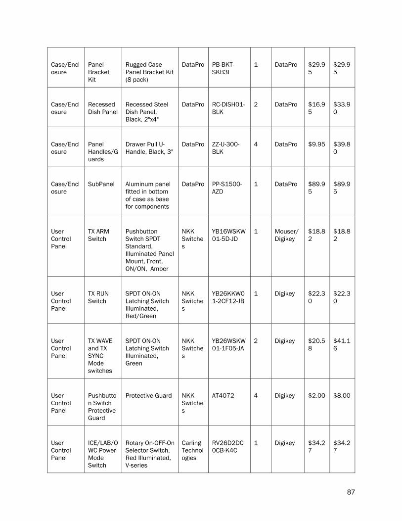
87
Case/Enclosure
Panel Bracket Kit
Rugged Case Panel Bracket Kit (8 pack)
DataPro PB-BKT-SKB3I
1 DataPro $29.95
$29.95
Case/Enclosure
Recessed Dish Panel
Recessed Steel Dish Panel, Black, 2"x4"
DataPro RC-DISH01-BLK
2 DataPro $16.95
$33.90
Case/Enclosure
Panel Handles/Guards
Drawer Pull U-Handle, Black, 3"
DataPro ZZ-U-300-BLK
4 DataPro $9.95 $39.80
Case/Enclosure
SubPanel Aluminum panel fitted in bottom of case as base for components
DataPro PP-S1500-AZD
1 DataPro $89.95
$89.95
User Control Panel
TX ARM Switch
Pushbutton Switch SPDT Standard, Illuminated Panel Mount, Front, ON/ON, Amber
NKK Switches
YB16WSKW01-5D-JD
1 Mouser/Digikey
$18.82
$18.82
User Control Panel
TX RUN Switch
SPDT ON-ON Latching Switch Illuminated, Red/Green
NKK Switches
YB26KKW01-2CF12-JB
1 Digikey $22.30
$22.30
User Control Panel
TX WAVE and TX SYNC Mode switches
SPDT ON-ON Latching Switch Illuminated, Green
NKK Switches
YB26WSKW01-1F05-JA
2 Digikey $20.58
$41.16
User Control Panel
Pushbutton Switch Protective Guard
Protective Guard NKK Switches
AT4072 4 Digikey $2.00 $8.00
User Control Panel
ICE/LAB/OWC Power Mode Switch
Rotary On-OFF-On Selector Switch, Red Illuminated, V-series
Carling Technologies
RV26D2DC0CB-K4C
1 Digikey $34.27
$34.27
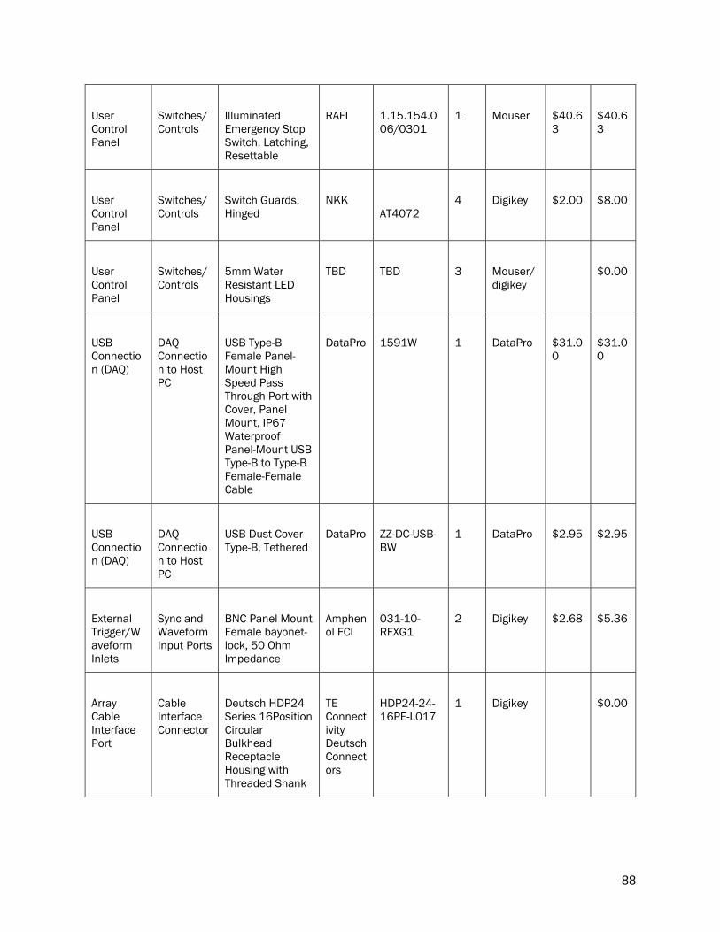
88
User Control Panel
Switches/Controls
Illuminated Emergency Stop Switch, Latching, Resettable
RAFI 1.15.154.006/0301
1 Mouser $40.63
$40.63
User Control Panel
Switches/Controls
Switch Guards, Hinged
NKK AT4072
4 Digikey $2.00 $8.00
User Control Panel
Switches/Controls
5mm Water Resistant LED Housings
TBD TBD 3 Mouser/digikey
$0.00
USB Connection (DAQ)
DAQ Connection to Host PC
USB Type-B Female Panel-Mount High Speed Pass Through Port with Cover, Panel Mount, IP67 Waterproof Panel-Mount USB Type-B to Type-B Female-Female Cable
DataPro 1591W 1 DataPro $31.00
$31.00
USB Connection (DAQ)
DAQ Connection to Host PC
USB Dust Cover Type-B, Tethered
DataPro ZZ-DC-USB-BW
1 DataPro $2.95 $2.95
External Trigger/Waveform Inlets
Sync and Waveform Input Ports
BNC Panel Mount Female bayonet-lock, 50 Ohm Impedance
Amphenol FCI
031-10-RFXG1
2 Digikey $2.68 $5.36
Array Cable Interface Port
Cable Interface Connector
Deutsch HDP24 Series 16Position Circular Bulkhead Receptacle Housing with Threaded Shank
TE Connectivity Deutsch Connectors
HDP24-24-16PE-L017
1 Digikey $0.00

89
Array Cable Interface Port
Cable Interface Connector
Jam Nut HDP24 TE Connectivity Deutsch Connectors
1 Digikey $0.00
Array Cable Interface Port
Cable Interface Connector
16 Position Circular Connector Contacts (Sockets) for HDP24
TE Connectivity Deutsch Connectors
16 Digikey $0.00
Array Cable Interface Port
Cable Interface Connector
Conn Sealing Plug, White
TE Connectivity Deutsch Connectors
114017-ZZ 1 Digikey $0.26 $0.26
Array Cable Interface Port
Cable Interface Connector
Conn Protective Cover 24 Black
TE Connectivity Deutsch Connectors
HDC26-24 1 Digikey $4.58 $4.58
Wiring Harness
Wiring Harness, TX Module -> Array
16AWG Solid Core Wire, Tinned, Red/Yellow
$0.00
Wiring Harness
Wiring Harness, TX Module -> Array
16AWG Solid Core Wire, Tinned, Black/White
$0.00
Wiring Harness
Wiring Harness, Array RX-> AFE
22AWG Solid Core Copper Wire, Tinned, Blue/White
$0.00
90
Wiring Harness
Wiring Harness, Array RX-> AFE
22AWG Solid Core Copper Wire, Tinned, Blue
$0.00
Wiring Harness
Wiring Harness
Waterproof Wiring Labels
$0.00
Wiring Harness
Wiring Harness
Wire securing clips
Generic Generic $0.00
Custom System Board Set (4 boards/unit)
TX, RX, RXPSU, DCtl
4 boards custom designed for IPA MIP-1 Prototype by Schipper's & Crew with 5-week Lead Time
Induced Polarization Associates
MIP-1 1 IPA $1,895.00
$1,895.00
Data Acquisition Board
Embedded USB DAQ System
8-channel, 100kSps simultaneous sampling A/D Converter and Data Logger
Measurement Computing Company
USB-1608FS-Plus-OEM
1 MCCDAQ $440.00
$440.00
User Interface Control & Display
Controls/Displays
4.3" TFT Touchscreen Display
Newhaven Display
NHD-4.3CTP-Shield-N
1 Digikey $94.71
$94.71
System Cooling
Cooling Fans
Fan Tubeaxial 5VDC Square - 40mm L x 40mm H Ball 11.7 CFM (0.328m³/min) 4 Wire Leads, 5V, SanAce40
Sanyo Denki America, Inc.
9GA0405P6H001
2 Digikey, Mouser
$14.00
$28.00
System Cooling
Cooling Fan Grille/Filter
Water resistent filter media/finger guards
TBD? TBD? 2 TBD $0.00

91
Mains Wiring Harness
Power Harness Connectors, PSU to RXPWR, PSU to DCTL
Latching 2x3 Rectangular Connector Housing, Free-Hanging
Molex 0430250600
2 Digikey $0.44 $0.88
Mains Wiring Harness
Power Harness Connectors, PSU to RXPWR, PSU to DCTL
Crimp Connector Socket 18AWG Crimp Tin
Molex 0430300038
12 Digikey $0.13 $1.56
Data Wiring Harness
Data Bus Harness
20 Rectangular Connectors - Housings Receptacle Black 0.118" (3.00mm)
Molex 0430252008
2 Digikey $1.60 $3.20
Data Wiring Harness
Data Bus Harness
Gold Crimp 20-24 AWG Socket Contact
Molex 0462350001
40 Digikey $0.17 $6.80
Panel Control/ RX Signal Wiring Harness
RX from Cable Array, Control Switch Pigtail Connectors
2 Rectangular Connectors - Housings Receptacle White 0.039" (1.00mm)
Molex 5013300200
12 Digikey $0.27 $3.24
Panel Control/ RX Signal Wiring Harness
RX from Cable Array, Control Switch Pigtail Connectors
Socket Contact Tin 23-32AWG Crimp
Molex 5013340100
24 Digikey $0.11 $2.64

92
Panel Controls Wiring Harness
Selector Switch Wire Connector
3 Rectangular Connectors - Housings Receptacle White 0.079" (2.00mm)
Molex 0513820300
1 Digikey $0.22 $0.22
Panel Controls Wiring Harness
Selector Switch Wire Connector
Socket Contact Tin 22-28 AWG Crimp
Molex 0593708000
3 Digikey $0.10 $0.30
Transmitter Wiring Harness
TX to Array Connector
4 Rectangular Connectors - Housings Receptacle Black 0.118" (3.00mm) 02x02
Molex 0430250400
1 Digikey $0.34 $0.34
Transmitter Wiring Harness
TX to Array Connector
Socket Contact Gold 26-30 AWG Crimp Stamped, Lubricated
Molex 0462355004
4 Digikey $0.26 $1.04
Power Harness
TX DC Power Input
3 Rectangular Connectors - Housings Receptacle 0.098" (2.50mm)
Molex 0050375033
1 Digikey $0.16 $0.16
Power Harness
TX DC Power Input
Socket Contact Tin 22-28 AWG Crimp
Molex 0008701039
3 Digikey $0.10 $0.30
Wiring Harness
Fan Control Pigtails
4 Rectangular Connectors - Housings Receptacle Black 0.098" (2.50mm)
Molex 1053081204
2 Digikey $0.38 $0.76
Wiring Harness
Fan Control Pigtails
Non-Gendered Contact Gold 24-26 AWG Crimp Power
Molex 1053001300
8 Digikey $0.31 $2.48
93
Wiring Harness
TX Board Switch Pigtails
2 Rectangular Connectors - Housings Receptacle White 0.079" (2.00mm)
Molex 0513820200
2 Digikey $0.20 $0.40
Wiring Harness
TX Board Switch Pigtails
Socket Contact Tin 22-28 AWG Crimp
Molex 0593708000
4 Digikey $0.10 $0.40
Wiring Harness
Board to Board Data Interconnects
6 Rectangular Connectors - Housings Plug Natural 0.049" (1.25mm)
Molex 5023800600
6 Digikey $0.26 $1.56
Wiring Harness
Board to Board Data Interconnects
Non-Gendered Contact Gold 26-28 AWG Crimp Stamped
Molex 5023810010
36 Digikey $0.17 $6.12

94
Appendix F: Custom Hardware Manufacturer Details All design work, computer-aided-design (CAD) work, initial subcircuit prototyping, and component selection was performed in-house by Induced Polarization Associates, LLC. Some additional support from outside manufacturers was necessary to fabricate the prototype devices, particularly enclosures, support assemblies, and printed circuit boards (PCBs). Accordingly, throughout the manufacture and assembly process, the design engineer at IPA actively collaborated with the following organizations to realize manufacture of the newly designed Marine IP system: 1. Schipper’s & Crew, Seattle, WA, USA: BOM finalization, custom Printed Circuit Board (PCB) fabrication, semiconductor and connector component procurement, and PCB assembly. 2. DataPro, Seattle, WA, USA: Mechanical CAD review for fabrication, customized enclosure, subpanel mounting system and control panel manufacture.

95
Appendix G: Development Tool Details
Architecture, Documentation, and Planning Tools: 1. Typora (Open Source) 2. Draw.io (Free for Use) 3. Microsoft Word 4. Microsoft Excel
Electronic Hardware Design Tools: 1. KiCAD v4.x (Open Source) 2. Microsoft Excel 3. Saturn PCB Designer Tool (Open Source) 4. ngSPICE (Open Source) 5. SnapEDA (Free for Use)
Mechanical Computer-Aided-Design (CAD) Software Tools: 1. FreeCAD (Open Source)
Firmware Development Environments and Programming Tools: 1. Microsoft Visual Studio Code (Free for Use) 2. AVR-GCC C/C++ Microcontroller Compiler (Open Source) 3. Olimex AVR-ISP Mk.II USB In-System-Programmer (Open-Source Hardware/Software) 4. Git (Open Source) 5. GitHub (Open Source) 6. Ceedling Unit Testing Framework 7. Doxygen Automated Documentation Generator

96
Appendix H: Device Final Assembly Images These images represent the final assembly of the device in the Induced Polarization Associates, LLC laboratory in Seattle, Washington. This is the actual device undergoing development and testing, with four (4) additional units fabricated and undergoing final assembly for testing.

97

98
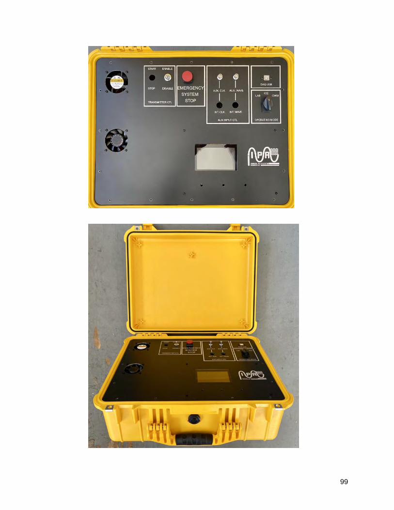
99

100

101

102

103

104

105

106

107

108

109