Magical Allotropes of Carbon: Prospects and Applications
62
Full Terms & Conditions of access and use can be found at http://www.tandfonline.com/action/journalInformation?journalCode=bsms20 Download by: [Indian School of Mines], [santosh kumar tiwari] Date: 09 May 2016, At: 20:24 Critical Reviews in Solid State and Materials Sciences ISSN: 1040-8436 (Print) 1547-6561 (Online) Journal homepage: http://www.tandfonline.com/loi/bsms20 Magical Allotropes of Carbon: Prospects and Applications Santosh K. Tiwari, Vijay Kumar, Andrzej Huczko, R. Oraon, A. De Adhikari & G. C. Nayak To cite this article: Santosh K. Tiwari, Vijay Kumar, Andrzej Huczko, R. Oraon, A. De Adhikari & G. C. Nayak (2016): Magical Allotropes of Carbon: Prospects and Applications, Critical Reviews in Solid State and Materials Sciences, DOI: 10.1080/10408436.2015.1127206 To link to this article: http://dx.doi.org/10.1080/10408436.2015.1127206 View supplementary material Published online: 09 May 2016. Submit your article to this journal View related articles View Crossmark data
-
Upload
khangminh22 -
Category
Documents
-
view
0 -
download
0
Transcript of Magical Allotropes of Carbon: Prospects and Applications

Full Terms & Conditions of access and use can be found athttp://www.tandfonline.com/action/journalInformation?journalCode=bsms20
Download by: [Indian School of Mines], [santosh kumar tiwari] Date: 09 May 2016, At: 20:24
Critical Reviews in Solid State and Materials Sciences
ISSN: 1040-8436 (Print) 1547-6561 (Online) Journal homepage: http://www.tandfonline.com/loi/bsms20
Magical Allotropes of Carbon: Prospects andApplications
Santosh K. Tiwari, Vijay Kumar, Andrzej Huczko, R. Oraon, A. De Adhikari &G. C. Nayak
To cite this article: Santosh K. Tiwari, Vijay Kumar, Andrzej Huczko, R. Oraon, A. De Adhikari &G. C. Nayak (2016): Magical Allotropes of Carbon: Prospects and Applications, Critical Reviewsin Solid State and Materials Sciences, DOI: 10.1080/10408436.2015.1127206
To link to this article: http://dx.doi.org/10.1080/10408436.2015.1127206
View supplementary material
Published online: 09 May 2016.
Submit your article to this journal
View related articles
View Crossmark data
Magical Allotropes of Carbon: Prospects and Applications
Santosh K. Tiwaria, Vijay Kumarb, Andrzej Huczkoc, R. Oraona, A. De Adhikaria, and G. C. Nayaka
aDepartment of Applied Chemistry, Indian School of Mines, Dhanbad, Jharkhand, India; bDepartment of Physics, University of Free State,Bloemfontein, South Africa; cLaboratory of Nanomaterials Physics and Chemistry, Department of Chemistry, Warsaw University, Warsaw, Poland
ABSTRACTThe invention of carbon and its allotropes have transformed the electronic and optoelectronicindustry due to their encouraging properties in a large spectrum of applications. The interestingcharacteristic of carbon is its ability to form many allotropes due to its valency. In recent decades,various allotropes and forms of carbon have been invented, including fullerenes, carbon nanotubes(CNTs), and graphene (GR). Since the inception of nanotechnology, carbon allotropes-basednanocomposites have become a leading sector of research and advancement due to their uniquebonding properties. Fullerenes and CNTs-based polymer nanocomposites have attracted significantresearch interest due to their vast applications in every sphere of science and technology. Currentresearch impetus reveals that carbon and its allotropes have revolutionized the industry andacademia due to their fascinated properties. Recent advances in various aspects of graphene, CNTs,graphene nanoribbons, fullerenes, carbon encapsulates, and their nanocomposites with polymericmaterials and their different applications are reported in this review article. Also, current status andfuture prospects of graphene-based polymer nanocomposites are presented in common along withproper citations extracted from the scientific literature. Moreover, this article is a unique collectionof vital information about GR, CNTs, fullerenes, and graphene-based polymer nanocomposites in asingle platform.
KEYWORDSCarbon allotropes; graphene;carbon nanotube; fullereneand polymernanocomposites
Table of Contents
1. Introduction ................................................................................................................................................................................................22. Fullerenes .....................................................................................................................................................................................................3
2.1. Discovery and properties ..................................................................................................................................................................32.2. Structure and symmetry....................................................................................................................................................................42.3. Pyramidalization in fullerene ...........................................................................................................................................................52.4. Aromaticity and electronegativity of fullerene C60 ......................................................................................................................62.5. Higher fullerenes.................................................................................................................................................................................6
3. Carbon nanotubes......................................................................................................................................................................................73.1. Discovery..............................................................................................................................................................................................73.2. Structure and symmetry....................................................................................................................................................................83.3. Unique properties of CNTs ............................................................................................................................................................103.4. Synthesis and growth of CNTs ......................................................................................................................................................10
3.4.1. Grow-in-place of CNTs .......................................................................................................................................................113.4.2. Grow-then-place of CNTs...................................................................................................................................................113.4.3. Arc-discharge.........................................................................................................................................................................123.4.4. Laser ablation.........................................................................................................................................................................123.4.5. Chemical vapor deposition (CVD) ...................................................................................................................................14
3.5. Some potential applications of CNTs...........................................................................................................................................153.5.1. Sensors and nanoprobes ......................................................................................................................................................163.5.2. Transistors..............................................................................................................................................................................17
CONTACT G. C. Nayak [email protected]
Color versions of one or more of the figures in the article can be found online at www.tandfonline.com/bsms.© 2016 Taylor & Francis Group, LLC
CRITICAL REVIEWS IN SOLID STATE AND MATERIALS SCIENCES2016, VOL. 0, NO. 0, 1–61http://dx.doi.org/10.1080/10408436.2015.1127206
Dow
nloa
ded
by [
Indi
an S
choo
l of
Min
es],
[sa
ntos
h ku
mar
tiw
ari]
at 2
0:24
09
May
201
6

3.5.3. Field-emitting devices ..........................................................................................................................................................173.5.4. Supercapacitors .....................................................................................................................................................................183.5.5. Lithium intercalation ...........................................................................................................................................................193.5.6. Hydrogen storage..................................................................................................................................................................193.5.7. Energy storage .......................................................................................................................................................................203.5.8. Composite material ..............................................................................................................................................................21
4. Graphene (GR): A sensational material for materials scientist ...................................................................................................224.1. Structural properties and band structure of graphene ..............................................................................................................244.2. Quantum hall effect in GR..............................................................................................................................................................26
4.2.1. Integer quantum hall effect in graphene ..........................................................................................................................274.2.2. Fractional quantum hall effect in graphene.....................................................................................................................28
4.3. Graphene nanoribbons (GNRs) ....................................................................................................................................................284.4. Electronic properties of GR ............................................................................................................................................................294.5. Mechanical strength of GR.............................................................................................................................................................304.6. Optical properties of GR .................................................................................................................................................................304.7. Thermal properties of GR...............................................................................................................................................................304.8. Synthesis methods of GR ................................................................................................................................................................304.9. Applications of GR...........................................................................................................................................................................31
4.9.1. Nanoelectronics.....................................................................................................................................................................315. Polymer nanocomposites (PNCs) ........................................................................................................................................................35
5.1. Brief history of nanocomposites ....................................................................................................................................................355.2. Types of PNCs...................................................................................................................................................................................37
5.2.1. Ceramic-matrix nanocomposites ......................................................................................................................................375.2.2. Metal-matrix nanocomposites ...........................................................................................................................................375.2.3. Polymer-matrix nanocomposites ......................................................................................................................................38
5.3. Graphene-based PNCs: Status and prospects .............................................................................................................................385.3.1. Methods for GR-based nanocomposites ppreparation .................................................................................................395.3.2. Some examples of recently reported GR-based PNCs...................................................................................................395.3.3. GR-CNTs hybrid PNCs.......................................................................................................................................................415.3.4. Distribution, dispersion, and interaction between GR derivatives and polymer .....................................................425.3.5. Other GR-based polymer composites...............................................................................................................................43
5.4. Applications and importance of GR-based polymer nanocomposites ..................................................................................445.5. Ceramic-GR nanocomposites ........................................................................................................................................................465.6. Biological applications of GR and GR-based nanocomposite .................................................................................................465.7. In field of sustainable energy..........................................................................................................................................................46
6. Conclusions and future prospects .......................................................................................................................................................48Acknowledgments ....................................................................................................................................................................................49Funding.......................................................................................................................................................................................................49References...................................................................................................................................................................................................49
1. Introduction
Nobel Laureate Dr. Richard Smalley stated that the dis-covery of carbon atom has revolutionized the scienceand technology to a great extent and now it is reality thatcarbon has the potential of making a chemically stable,two-dimensional, one-atom-thick membranes in three-dimensional world.1–3 It is believed that the discovery ofcarbon-related materials and their development will becrucial for the future of chemistry and technology.3 Theexisting works of literature reflected that carbon is themost studied element of the nano era.3–5 The fate ofnanotechnology and nanoscience is also connected to
the diamond age owing to the broad utility of carbon asan essential element for all fabricated components.5,6 Forthe last few decades, different allotropes of carbon havebeen explored and used for many applications.
The 2010 Nobel Prize was awarded jointly to AndreGeim andKonstantinNovoselov (University ofManchester,UK) for their outstanding discovery regarding the two-dimensional material graphene.3 GR is resembled atomicscale hexagonal pattern that is tightly packed in a regularway. The bond length of the C-C bond in GR is around0.142 nm. GR is the fundamental structural unit of variouscarbon allotropes (the physical arrangement of atoms)
2 S. K. TIWARI ET AL.
Dow
nloa
ded
by [
Indi
an S
choo
l of
Min
es],
[sa
ntos
h ku
mar
tiw
ari]
at 2
0:24
09
May
201
6
covering carbon nanotubes, graphite, and fullerenes.3–8 It isnow treated as themost strikingmaterial of the universe.3
Carbon nanotubes (CNTs) are also designated as bucky-tubes and refer to a cylindrical molecular form of graphenewith numerous exceptional and unique features.4,7,8 CNTsare probably valuable in an extensive range of applicationsincluding nanoelectronics, materials applications, optics,and so on.4,7 CNTs show remarkable tensile strength, betterelectrical properties, and efficient thermal conductivity.7,8
They can be classified into two forms single-walled nano-tubes (SWCNTs) and multi-walled nanotubes (MWCNTs).Most of the SWNTs are close to one nm in diameter, with atube length that can vary up to millions of times longer.7,8
However, different suppliers give as-synthesized arc dis-charge SWNTs. If two or more GR sheets are rolled up suit-ably, then they form MWCNTs.7,8 The interlayer distancein MWCNTs is defined as the distance between GR layersin graphite, i.e., approximately 330 pm. Fullerenes are theallotrope of carbon distinct from both graphite and dia-mond, football shaped single layer of graphene (with 12pentagons).1 Fullerenes are mostly spherical, cylindrical orellipsoid in shapes consisting of many carbon atoms.1,2,5
The name “fullerenes” came into existence after the develop-mental author, Richard Buckminster Fuller, for their simi-larity to the geodesic dome.1,2 The spherical fullereneconsists sixty carbon atoms and is termed as buckminster-fullerene (C60).
1,2 It also looks similar to a soccer ball and isoften regarded to a “Buckyballs.” Cylindrical fullerenes areacknowledged as “buckytubes” or usually “nanotubes. Theyhave tremendous potential to be employed in superconduc-tors, catalysts, drug delivery devices, scanning tunnelingmicroscope tips, or even as a nano ball-bearing lubricant.4,5,9
Graphene nanoribbons (GNRs) are a structurally deformedgraphene and initially its existence was doubtful but at pres-ent is a reality.10 Graphene has brought the interest of bothacademia and industry due to its astounding properties. 1,2
Besides, the numerous applications of GR, functions of gra-phene and its derivatives as nano filler have matured a moststriking field of modern research for materials and polymerchemists.11–15 And it has been experimentally proved thatgraphene-based polymer nanocomposites possess tunableproperties and easy accessibility.16,17
So far, many excellent of review articles have been pub-lished on CNTs, GR, fullerenes, and graphene-based poly-mer nanocomposites individually which reflects the highinterest in academic and industrial research in these materi-als.4,5,9,18,19 This review article covers broad informationrelated to GR, CNTs, GNRs, fullerenes, and polymer nano-composite in a single platform. Although, various authorspublished a few review articles which summarize funda-mental information of fullerene, CNTs, and GR.20–24 Anattempt has beenmade to crush out the juice of excellent sci-entific literature of the subject matter. Additionally, the
recent applications of GR, CNTs, and graphene-basedPNCs in the many disciplines such as in large-scale assem-bly and field effect devices, transparent electrodes, sensors,photo detectors, energy storage devices, solar cells, andPNCs have been reviewed in detail.
In this article, we give a detailed discussion of the pro-gresses made in the carbon-based materials such as gra-phene, GNRs, CNTs, fullerenes, and graphene-basedpolymer nanocomposite (PNCs). We also summarizedsome of the properties of thesematerials that have particularrelevance in the performance of these materials in the vari-ous areas of science and technology. The purpose of theintroductory section is to provide enough information tounderstand the origin of carbon materials-based researchand how these magical materials utilized for various techno-logical applications. Section 2 describes the discovery andproperties of fullerene. The goal of this section is not tocover all the existing literature, but rather to present some ofthe most relevant achievements and a brief information inthis direction. In Section 3, we include the discovery, struc-ture, synthesis, properties, and some potential applicationsof CNTs. Section 4 includes the invention of graphene andits properties and applications. In Section 5, polymer nano-composites (PNCs) based on different carbon nanomateri-als are discussed. Finally, we end the article with conclusionand prospects for future development of carbon and its allo-tropes based materials. With this, we hope that the readerwill get updated information on the carbon-based materialsthat have arrived for plenty of applications and also newinsights on this topic.
2. Fullerenes
2.1. Discovery and properties
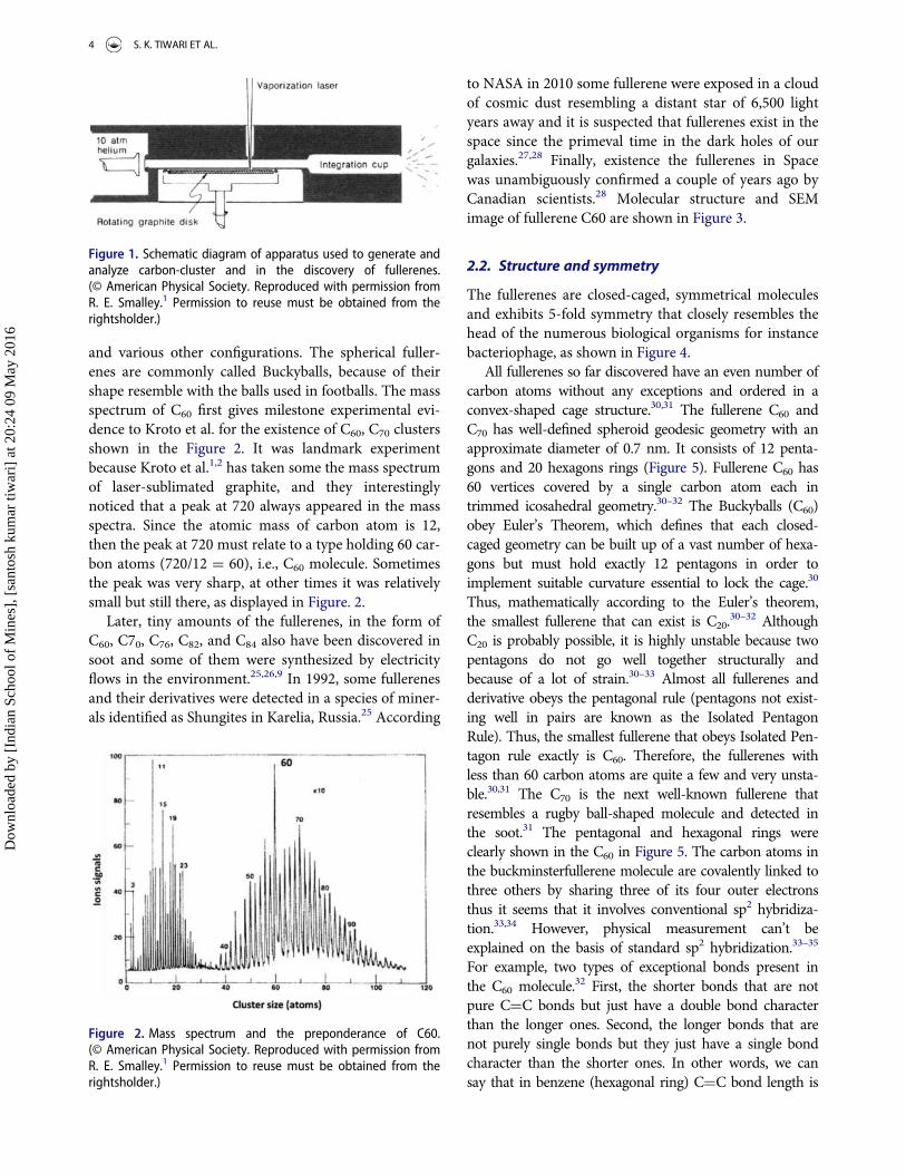
Graphite and diamond are the most common allotropesof carbon and the third magical allotrope of carbon atomwas discovered by Kroto et al. of UK in 1985 as C60 andlater on was named Buckminsterfullerene or simply ful-lerene.1,2,4 First of all, Kroto studied some organic mole-cule in space by a telescope with exactly 60 carbon atomsfound near various red giant stars. For this, Kroto collab-orated with Smalley and Curl to recreate conditions inthe lab and form C60 molecules by laser vaporization ofgraphite.1,2,4,9 After the laser vaporization experimentthey analyzed that C60 molecules were made of pentago-nal and hexagonal rings that are similar in structure tographite.1,2 Thus, fullerenes can be made by vaporizingcarbon/graphite within a gas medium. The schematicdrawing of the supersonic laser-vaporization nozzle usedin the discovery of fullerenes is shown in Figure 1.1
Thus, fullerene may be defined as a molecule entirelymade of carbon in the form of a hollow sphere, ellipsoid,
CRITICAL REVIEWS IN SOLID STATE AND MATERIALS SCIENCES 3
Dow
nloa
ded
by [
Indi
an S
choo
l of
Min
es],
[sa
ntos
h ku
mar
tiw
ari]
at 2
0:24
09
May
201
6
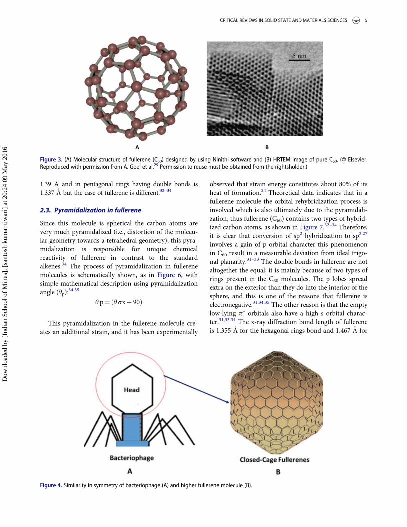
and various other configurations. The spherical fuller-enes are commonly called Buckyballs, because of theirshape resemble with the balls used in footballs. The massspectrum of C60 first gives milestone experimental evi-dence to Kroto et al. for the existence of C60, C70 clustersshown in the Figure 2. It was landmark experimentbecause Kroto et al.1,2 has taken some the mass spectrumof laser-sublimated graphite, and they interestinglynoticed that a peak at 720 always appeared in the massspectra. Since the atomic mass of carbon atom is 12,then the peak at 720 must relate to a type holding 60 car-bon atoms (720/12 D 60), i.e., C60 molecule. Sometimesthe peak was very sharp, at other times it was relativelysmall but still there, as displayed in Figure. 2.
Later, tiny amounts of the fullerenes, in the form ofC60, C70, C76, C82, and C84 also have been discovered insoot and some of them were synthesized by electricityflows in the environment.25,26,9 In 1992, some fullerenesand their derivatives were detected in a species of miner-als identified as Shungites in Karelia, Russia.25 According
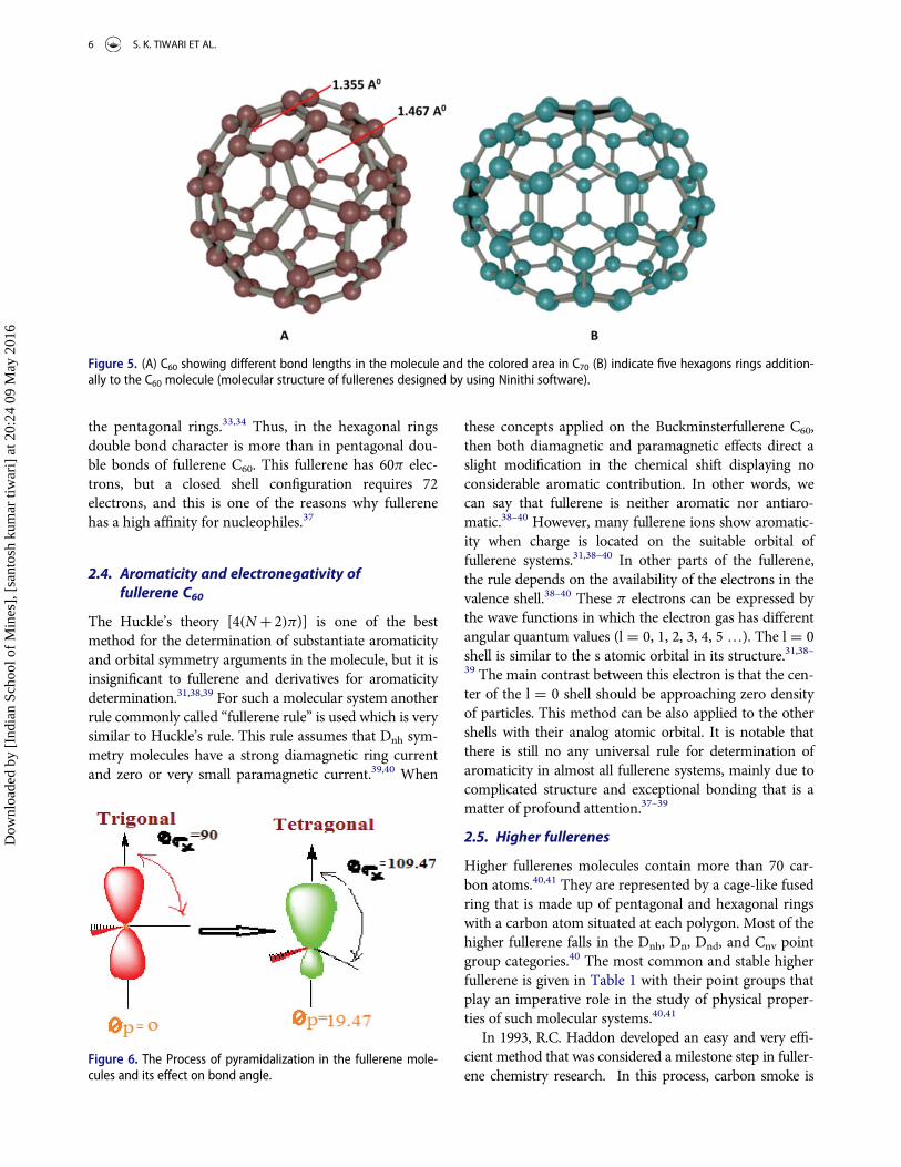
to NASA in 2010 some fullerene were exposed in a cloudof cosmic dust resembling a distant star of 6,500 lightyears away and it is suspected that fullerenes exist in thespace since the primeval time in the dark holes of ourgalaxies.27,28 Finally, existence the fullerenes in Spacewas unambiguously confirmed a couple of years ago byCanadian scientists.28 Molecular structure and SEMimage of fullerene C60 are shown in Figure 3.
2.2. Structure and symmetry
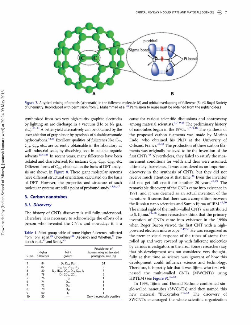
The fullerenes are closed-caged, symmetrical moleculesand exhibits 5-fold symmetry that closely resembles thehead of the numerous biological organisms for instancebacteriophage, as shown in Figure 4.
All fullerenes so far discovered have an even number ofcarbon atoms without any exceptions and ordered in aconvex-shaped cage structure.30,31 The fullerene C60 andC70 has well-defined spheroid geodesic geometry with anapproximate diameter of 0.7 nm. It consists of 12 penta-gons and 20 hexagons rings (Figure 5). Fullerene C60 has60 vertices covered by a single carbon atom each intrimmed icosahedral geometry.30–32 The Buckyballs (C60)obey Euler’s Theorem, which defines that each closed-caged geometry can be built up of a vast number of hexa-gons but must hold exactly 12 pentagons in order toimplement suitable curvature essential to lock the cage.30
Thus, mathematically according to the Euler’s theorem,the smallest fullerene that can exist is C20.
30–32 AlthoughC20 is probably possible, it is highly unstable because twopentagons do not go well together structurally andbecause of a lot of strain.30–33 Almost all fullerenes andderivative obeys the pentagonal rule (pentagons not exist-ing well in pairs are known as the Isolated PentagonRule). Thus, the smallest fullerene that obeys Isolated Pen-tagon rule exactly is C60. Therefore, the fullerenes withless than 60 carbon atoms are quite a few and very unsta-ble.30,31 The C70 is the next well-known fullerene thatresembles a rugby ball-shaped molecule and detected inthe soot.31 The pentagonal and hexagonal rings wereclearly shown in the C60 in Figure 5. The carbon atoms inthe buckminsterfullerene molecule are covalently linked tothree others by sharing three of its four outer electronsthus it seems that it involves conventional sp2 hybridiza-tion.33,34 However, physical measurement can’t beexplained on the basis of standard sp2 hybridization.33–35
For example, two types of exceptional bonds present inthe C60 molecule.32 First, the shorter bonds that are notpure CHC bonds but just have a double bond characterthan the longer ones. Second, the longer bonds that arenot purely single bonds but they just have a single bondcharacter than the shorter ones. In other words, we cansay that in benzene (hexagonal ring) CHC bond length is
Figure 1. Schematic diagram of apparatus used to generate andanalyze carbon-cluster and in the discovery of fullerenes.(© American Physical Society. Reproduced with permission fromR. E. Smalley.1 Permission to reuse must be obtained from therightsholder.)
Figure 2. Mass spectrum and the preponderance of C60.(© American Physical Society. Reproduced with permission fromR. E. Smalley.1 Permission to reuse must be obtained from therightsholder.)
4 S. K. TIWARI ET AL.
Dow
nloa
ded
by [
Indi
an S
choo
l of
Min
es],
[sa
ntos
h ku
mar
tiw
ari]
at 2
0:24
09
May
201
6
1.39 A�and in pentagonal rings having double bonds is
1.337 A�but the case of fullerene is different.32–34
2.3. Pyramidalization in fullerene
Since this molecule is spherical the carbon atoms arevery much pyramidalized (i.e., distortion of the molecu-lar geometry towards a tetrahedral geometry); this pyra-midalization is responsible for unique chemicalreactivity of fullerene in contrast to the standardalkenes.34 The process of pyramidalization in fullerenemolecules is schematically shown, as in Figure 6, withsimple mathematical description using pyramidalizationangle (up):
34,35
u pD u sx¡ 90ð Þ
This pyramidalization in the fullerene molecule cre-ates an additional strain, and it has been experimentally
observed that strain energy constitutes about 80% of itsheat of formation.24 Theoretical data indicates that in afullerene molecule the orbital rehybridization process isinvolved which is also ultimately due to the pyramidali-zation, thus fullerene (C60) contains two types of hybrid-ized carbon atoms, as shown in Figure 7.32–34 Therefore,it is clear that conversion of sp2 hybridization to sp2,27
involves a gain of p-orbital character this phenomenonin C60 result in a measurable deviation from ideal trigo-nal planarity.31–33 The double bonds in fullerene are notaltogether the equal; it is mainly because of two types ofrings present in the C60 molecules. The p lobes spreadextra on the exterior than they do into the interior of thesphere, and this is one of the reasons that fullerene iselectronegative.31,34,35 The other reason is that the emptylow-lying p� orbitals also have a high s orbital charac-ter.31,33,34 The x-ray diffraction bond length of fullereneis 1.355 A
�for the hexagonal rings bond and 1.467 A
�for
Figure 3. (A) Molecular structure of fullerene (C60) designed by using Ninithi software and (B) HRTEM image of pure C60. (© Elsevier.Reproduced with permission from A. Goel et al.29 Permission to reuse must be obtained from the rightsholder.)
Figure 4. Similarity in symmetry of bacteriophage (A) and higher fullerene molecule (B).
CRITICAL REVIEWS IN SOLID STATE AND MATERIALS SCIENCES 5
Dow
nloa
ded
by [
Indi
an S
choo
l of
Min
es],
[sa
ntos
h ku
mar
tiw
ari]
at 2
0:24
09
May
201
6
the pentagonal rings.33,34 Thus, in the hexagonal ringsdouble bond character is more than in pentagonal dou-ble bonds of fullerene C60. This fullerene has 60p elec-trons, but a closed shell configuration requires 72electrons, and this is one of the reasons why fullerenehas a high affinity for nucleophiles.37
2.4. Aromaticity and electronegativity offullerene C60
The Huckle’s theory [4.N C 2/p)] is one of the bestmethod for the determination of substantiate aromaticityand orbital symmetry arguments in the molecule, but it isinsignificant to fullerene and derivatives for aromaticitydetermination.31,38,39 For such a molecular system anotherrule commonly called “fullerene rule” is used which is verysimilar to Huckle’s rule. This rule assumes that Dnh sym-metry molecules have a strong diamagnetic ring currentand zero or very small paramagnetic current.39,40 When
these concepts applied on the Buckminsterfullerene C60,then both diamagnetic and paramagnetic effects direct aslight modification in the chemical shift displaying noconsiderable aromatic contribution. In other words, wecan say that fullerene is neither aromatic nor antiaro-matic.38–40 However, many fullerene ions show aromatic-ity when charge is located on the suitable orbital offullerene systems.31,38–40 In other parts of the fullerene,the rule depends on the availability of the electrons in thevalence shell.38–40 These p electrons can be expressed bythe wave functions in which the electron gas has differentangular quantum values (l D 0, 1, 2, 3, 4, 5 …). The l D 0shell is similar to the s atomic orbital in its structure.31,38–39 The main contrast between this electron is that the cen-ter of the l D 0 shell should be approaching zero densityof particles. This method can be also applied to the othershells with their analog atomic orbital. It is notable thatthere is still no any universal rule for determination ofaromaticity in almost all fullerene systems, mainly due tocomplicated structure and exceptional bonding that is amatter of profound attention.37–39
2.5. Higher fullerenes
Higher fullerenes molecules contain more than 70 car-bon atoms.40,41 They are represented by a cage-like fusedring that is made up of pentagonal and hexagonal ringswith a carbon atom situated at each polygon. Most of thehigher fullerene falls in the Dnh, Dn, Dnd, and Cnv pointgroup categories.40 The most common and stable higherfullerene is given in Table 1 with their point groups thatplay an imperative role in the study of physical proper-ties of such molecular systems.40,41
In 1993, R.C. Haddon developed an easy and very effi-cient method that was considered a milestone step in fuller-ene chemistry research. In this process, carbon smoke is
Figure 5. (A) C60 showing different bond lengths in the molecule and the colored area in C70 (B) indicate five hexagons rings addition-ally to the C60 molecule (molecular structure of fullerenes designed by using Ninithi software).
Figure 6. The Process of pyramidalization in the fullerene mole-cules and its effect on bond angle.
6 S. K. TIWARI ET AL.
Dow
nloa
ded
by [
Indi
an S
choo
l of
Min
es],
[sa
ntos
h ku
mar
tiw
ari]
at 2
0:24
09
May
201
6
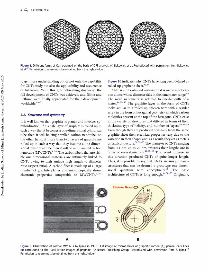
synthesized from two very high-purity graphite electrodesby lighting an arc discharge in a vacuum (He or N2 gas,etc.).40–44 A better yield alternatively can be obtained by thelaser ablation of graphite or by pyrolysis of suitable aromatichydrocarbons.44,45 Excellent qualities of fullerenes like C76,C78, C84, etc., are currently obtainable in the laboratory aswell industrial scale, by dissolving soot in suitable organicsolvents.40,41,45 In recent years, many fullerenes have beenisolated and characterized, for instance C399, C960, C540, etc.Different forms of C960 obtained on the basis of DFT analy-sis are shown in Figure 8. These giant molecular systemshave different structural orientation, calculated on the basisof DFT. However, the properties and structure of suchmolecular systems are still a point of profound study.43,44,47
3. Carbon nanotubes
3.1. Discovery
The history of CNTs discovery is still fully understood.Therefore, it is necessary to acknowledge the efforts of aperson who invented the CNTs and nowadays it is a
cause for various scientific discussions and controversyamong material scientists.4,7–9,48 The preliminary historyof nanotubes began in the 1970s. 4,7–9,48 The synthesis ofthe proposed carbon filaments was made by MorinoEndo, who obtained his Ph.D at the University ofOrleans, France.47,48 The production of these carbon fila-ments was originally believed to be the invention of thefirst CNTs.48 Nevertheless, they failed to satisfy the mea-surement conditions for width and thus were assumed,ultimately, barrelenes. It was considered as an importantdiscovery in the synthesis of CNTs, but they did notreceive much attention at that time.38 Even the inventordid not get full credit for another 20 years.48,49 Theremarkable discovery of the CNTs came into existence in1991, and it was deemed as an actual invention of thenanotube. It seems that there was a competition betweenthe Russian nano scientists and Sumjo Iijima of IBM.49,50
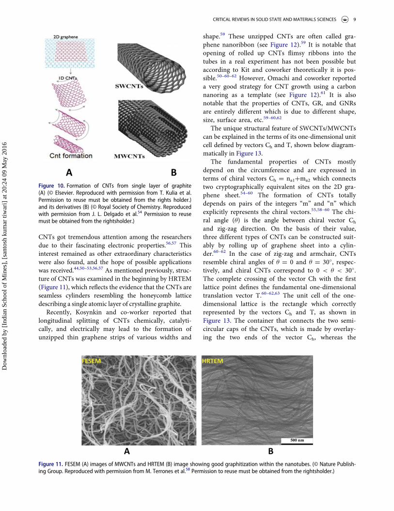
The initial sight of the multi-walled CNTs was attributedto S. Iijima.49–50 Some researchers think that the primaryinvention of CNTs came into existence in the 1950swhen Roger Bacon viewed the first CNT with a high-powered electron microscope.7,49,50 He was recognized asthe premier visual response of the tubes of atoms thatrolled up and were covered up with fullerene moleculesby various investigators in the area. Some researchers saythat his development was not considered very thought-fully at that time as science was ignorant of how thisdevelopment could influence science and technology.Therefore, it is pretty fair that it was Iijima who first wit-nessed the multi-walled CNTs (MWCNTs) usingHRTEM (see Figure 9).49,52
In 1993, Iijima and Donald Bethune conformed sin-gle-walled nanotubes (SWCNTs) and they named thisnew material “Buckytubes.”49,52 The discovery ofSWCNTs encouraged the whole scientific organization
Figure 7. A typical mixing of orbitals (schematic) in the fullerene molecule (A) and orbital overlapping of fullerene (B). (© Royal Societyof Chemistry. Reproduced with permission from S. Muhammad et al.36 Permission to reuse must be obtained from the rightsholder.)
Table 1. Point group table of some higher fullerenes collectedfrom Tohji et al.,26 Choudhary,30 Diederich and Whetten,41 Die-derich et al.,42 and Reddy.43
S. No.Higher
fullerenesPointgroups
Possible no. ofisomers obeying isolatedpentagonal rule (Ni)
1 84 D2, D2d, D6h 242 82 3C2, C2v, 2C3v, 3Cs 93 80 D2, 2D3h, 2C2v, D5h, D5d, Ih 74 78 D3, 2D3h, 2C2v 55 76 D2 16 74 D3h 17 72 D6h 18 70 D5h 19 60 Ih 110 20 — Only theoretically possible
CRITICAL REVIEWS IN SOLID STATE AND MATERIALS SCIENCES 7
Dow
nloa
ded
by [
Indi
an S
choo
l of
Min
es],
[sa
ntos
h ku
mar
tiw
ari]
at 2
0:24
09
May
201
6
to get more understanding out of not only the capabilityfor CNTs study but also the applicability and occurrenceof fullerenes. With this groundbreaking discovery, thefull development of CNTs was achieved, and Iijima andBethune were finally appreciated for their developmentworldwide.49–52
3.2. Structure and symmetry
It is well known that graphite is planar and involves sp2
hybridization. If a single layer of graphite is rolled up insuch a way that it becomes a one-dimensional cylindricaltube then it will be single-walled carbon nanotube; onthe other hand, if more than two layers of graphite arerolled up in such a way that they become a one-dimen-sional cylindrical tube then it will be multi-walled carbonnanotube (MWCNT).4,7–9 The carbon fibers that are visi-ble one-dimensional materials are intimately linked toCNTs owing to their unique high length to diameterratio (aspect ratio). A carbon fiber is made up of a largenumber of graphite planes and microscopically showselectronic properties comparable to MWCNTs.53,54
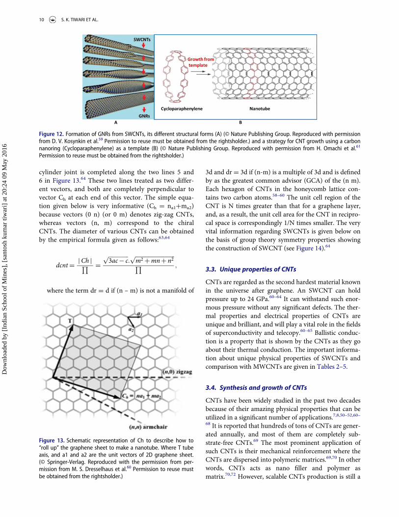
Figure 10 indicates why CNTs have long been defined asrolled-up graphene sheet.53,54
CNT is a tube-shaped material that is made up of car-bon atoms whose diameter falls in the nanometer range.44
The word nanometer is referred to one-billionth of ameter.44,50–53 The graphite layer in the form of CNTslooks similar to a rolled-up-chicken wire with a regulararray in the form of hexagonal geometry in which carbonmolecules present at the top of the hexagons. CNTs existin the variety of structures that differed in terms of theirthickness, type of helicity, and number of layers.44,52–55
Even though they are produced originally from the samegraphite sheet their electrical properties vary due to thevariation in their shapes and, as a result, they act as metalsor semiconductors.50,52–55 The diameter of CNTs rangingfrom <1 nm up to 70 nm, whereas their lengths are inorder of several microns.44,52–55 The recent progress inthis direction produced CNTs of quite longer length.Thus, it is possible to say that CNTs are unique nano-structures that can be deemed a prototype one-dimen-sional quantum wire conceptually.56 The basicarchitecture of CNTs is long enough.44,50–53 Originally,
Figure 8. Different forms of C960 obtained on the basis of DFT analysis. (© Bakowies et al. Reproduced with permission from Bakowieset al.47 Permission to reuse must be obtained from the rightsholder.)
Figure 9. Observation of coaxial MWCNTs by Iijima in 1991: SEM image of microtubules of graphitic carbon (A); parallel dark lines(B) correspond to the (002) lattice images of graphite. (© Nature Publishing Group. Reproduced with permission from S. Iijima.52
Permission to reuse must be obtained from the rightsholder.)
8 S. K. TIWARI ET AL.
Dow
nloa
ded
by [
Indi
an S
choo
l of
Min
es],
[sa
ntos
h ku
mar
tiw
ari]
at 2
0:24
09
May
201
6
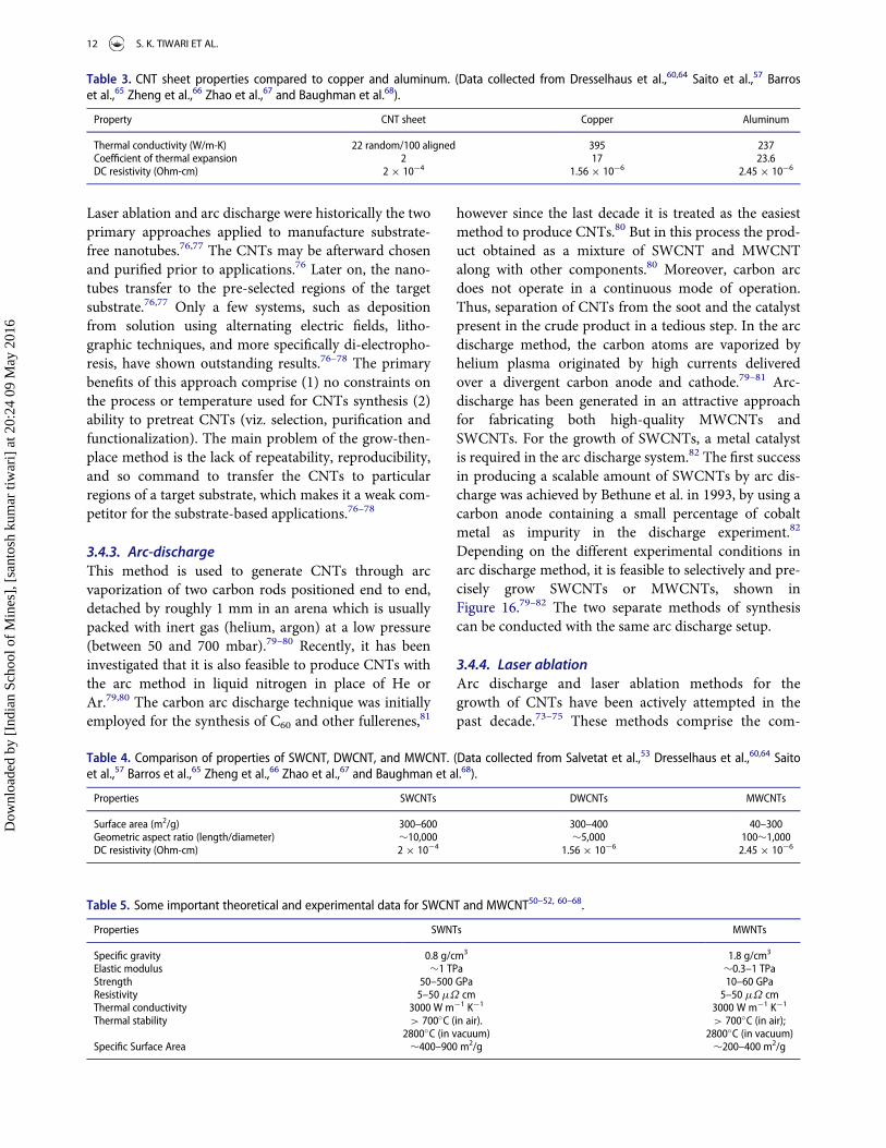
CNTs got tremendous attention among the researchersdue to their fascinating electronic properties.56,57 Thisinterest remained as other extraordinary characteristicswere also found, and the hope of possible applicationswas received.44,50–53,56,57 As mentioned previously, struc-ture of CNTs was examined in the beginning by HRTEM(Figure 11), which reflects the evidence that the CNTs areseamless cylinders resembling the honeycomb latticedescribing a single atomic layer of crystalline graphite.
Recently, Kosynkin and co-worker reported thatlongitudinal splitting of CNTs chemically, catalyti-cally, and electrically may lead to the formation ofunzipped thin graphene strips of various widths and
shape.59 These unzipped CNTs are often called gra-phene nanoribbon (see Figure 12).59 It is notable thatopening of rolled up CNTs flimsy ribbons into thetubes in a real experiment has not been possible butaccording to Kit and coworker theoretically it is pos-sible.50–60–62 However, Omachi and coworker reporteda very good strategy for CNT growth using a carbonnanoring as a template (see Figure 12).61 It is alsonotable that the properties of CNTs, GR, and GNRsare entirely different which is due to different shape,size, surface area, etc.59–60,62
The unique structural feature of SWCNTs/MWCNTscan be explained in the terms of its one-dimensional unitcell defined by vectors Ch and T, shown below diagram-matically in Figure 13.
The fundamental properties of CNTs mostlydepend on the circumference and are expressed interms of chiral vectors Ch D na1Cma2 which connectstwo cryptographically equivalent sites on the 2D gra-phene sheet.54–60 The formation of CNTs totallydepends on pairs of the integers “m” and “n” whichexplicitly represents the chiral vectors.55,58–60 The chi-ral angle (u) is the angle between chiral vector Ch
and zig-zag direction. On the basis of their value,three different types of CNTs can be constructed suit-ably by rolling up of graphene sheet into a cylin-der.60–62 In the case of zig-zag and armchair, CNTsresemble chiral angles of u D 0 and u D 30�, respec-tively, and chiral CNTs correspond to 0 < u < 30�.The complete crossing of the vector Ch with the firstlattice point defines the fundamental one-dimensionaltranslation vector T.60–62,63 The unit cell of the one-dimensional lattice is the rectangle which correctlyrepresented by the vectors Ch and T, as shown inFigure 13. The container that connects the two semi-circular caps of the CNTs, which is made by overlay-ing the two ends of the vector Ch, whereas the
Figure 10. Formation of CNTs from single layer of graphite(A) (© Elsevier. Reproduced with permission from T. Kulia et al.Permission to reuse must be obtained from the rights holder.)and its derivatives (B) (© Royal Society of Chemistry. Reproducedwith permission from J. L. Delgado et al.54 Permission to reusemust be obtained from the rightsholder.)
Figure 11. FESEM (A) images of MWCNTs and HRTEM (B) image showing good graphitization within the nanotubes. (© Nature Publish-ing Group. Reproduced with permission from M. Terrones et al.58 Permission to reuse must be obtained from the rightsholder.)
CRITICAL REVIEWS IN SOLID STATE AND MATERIALS SCIENCES 9
Dow
nloa
ded
by [
Indi
an S
choo
l of
Min
es],
[sa
ntos
h ku
mar
tiw
ari]
at 2
0:24
09
May
201
6
cylinder joint is completed along the two lines 5 and6 in Figure 13.64 These two lines treated as two differ-ent vectors, and both are completely perpendicular tovector Ch at each end of this vector. The simple equa-tion given below is very informative (Ch D na1Cma2)because vectors (0 n) (or 0 m) denotes zig-zag CNTs,whereas vectors (n, m) correspond to the chiralCNTs. The diameter of various CNTs can be obtainedby the empirical formula given as follows:63,64
dcntD jCh jQ D
ffiffiffiffiffiffiffiffiffiffiffiffiffiffi3ac¡ c
p:
ffiffiffiffiffiffiffiffiffiffiffiffiffiffiffiffiffiffiffiffiffiffiffiffiffiffiffiffim2CmnC n2
pQ ;
where the term dr D d if (n – m) is not a manifold of
3d and dr D 3d if (n-m) is a multiple of 3d and is definedby as the greatest common advisor (GCA) of the (n m).Each hexagon of CNTs in the honeycomb lattice con-tains two carbon atoms.58–60 The unit cell region of theCNT is N times greater than that for a graphene layer,and, as a result, the unit cell area for the CNT in recipro-cal space is correspondingly 1/N times smaller. The veryvital information regarding SWCNTs is given below onthe basis of group theory symmetry properties showingthe construction of SWCNT (see Figure 14).64
3.3. Unique properties of CNTs
CNTs are regarded as the second hardest material knownin the universe after graphene. An SWCNT can holdpressure up to 24 GPa.60–64 It can withstand such enor-mous pressure without any significant defects. The ther-mal properties and electrical properties of CNTs areunique and brilliant, and will play a vital role in the fieldsof superconductivity and telecopy.60–65 Ballistic conduc-tion is a property that is shown by the CNTs as they goabout their thermal conduction. The important informa-tion about unique physical properties of SWCNTs andcomparison with MWCNTs are given in Tables 2–5.
3.4. Synthesis and growth of CNTs
CNTs have been widely studied in the past two decadesbecause of their amazing physical properties that can beutilized in a significant number of applications.7,8,50–52,60–68 It is reported that hundreds of tons of CNTs are gener-ated annually, and most of them are completely sub-strate-free CNTs.69 The most prominent application ofsuch CNTs is their mechanical reinforcement where theCNTs are dispersed into polymeric matrices.69,70 In otherwords, CNTs acts as nano filler and polymer asmatrix.70,72 However, scalable CNTs production is still a
Figure 12. Formation of GNRs from SWCNTs, its different structural forms (A) (© Nature Publishing Group. Reproduced with permissionfrom D. V. Kosynkin et al.59 Permission to reuse must be obtained from the rightsholder.) and a strategy for CNT growth using a carbonnanoring (Cycloparaphenylene) as a template (B) (© Nature Publishing Group. Reproduced with permission from H. Omachi et al.61
Permission to reuse must be obtained from the rightsholder.)
Figure 13. Schematic representation of Ch to describe how to“roll up” the graphene sheet to make a nanotube. Where T tubeaxis, and a1 and a2 are the unit vectors of 2D graphene sheet.(© Springer-Verlag. Reproduced with the permission from per-mission from M. S. Dresselhaus et al.60 Permission to reuse mustbe obtained from the rightsholder.)
10 S. K. TIWARI ET AL.
Dow
nloa
ded
by [
Indi
an S
choo
l of
Min
es],
[sa
ntos
h ku
mar
tiw
ari]
at 2
0:24
09
May
201
6

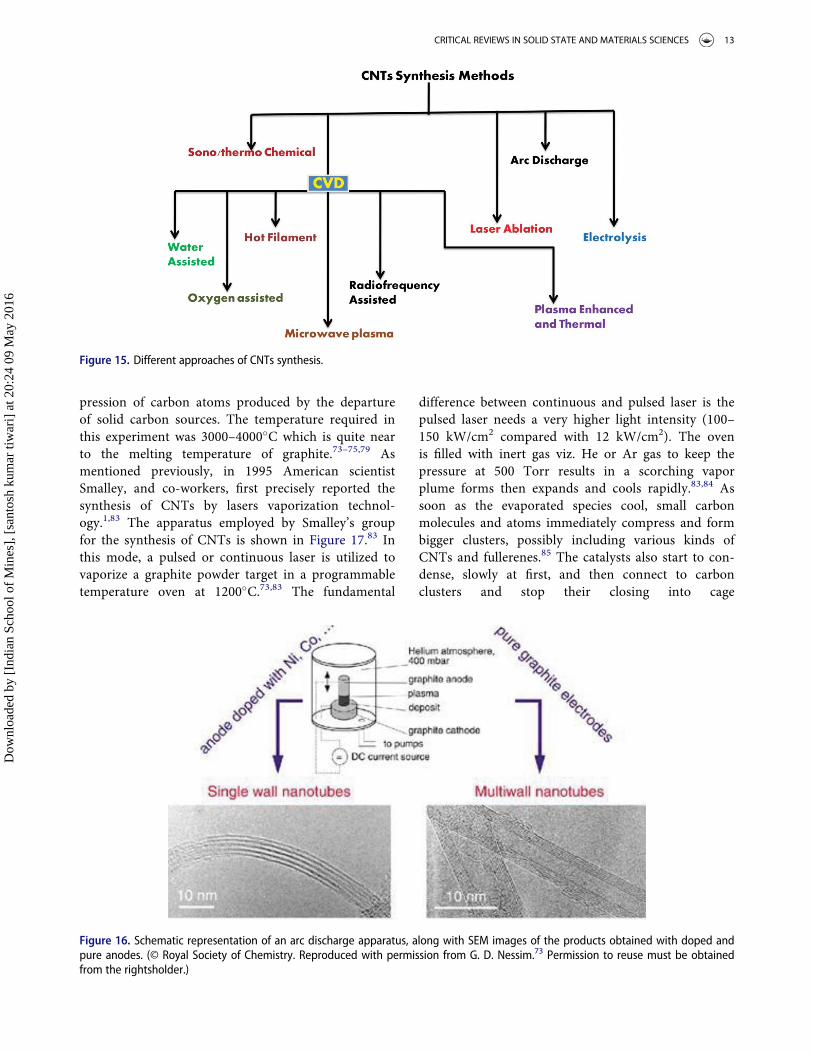
matter of further consideration, because of the fabricationchallenges.70–72 This section provides a far-sighted viewof various critical methods and technique that have beendeveloped for CNTs production technologies. And wewill illustrate their significant technical advantages andshortcomings. CVD is considered as the best method forthe synthesis of pure CNTs, and this is why it receives par-ticular recognition from the scientific community.71 Thismethod allows CNTs to be developed in predefined areas,offers some degree of control of the types of CNTs pro-duced, and may have the greatest probability to obtaincommercially.71,72 This section is mainly based on theCNTs synthesis on the substrates, which can be assumedto be the best approach for electronic applications. In thisregard, CVD is crucial for regulating the characteristics ofthe CNTs produced and continues the main obstacle toovercome.71,73 A large number of parameters affects thegrowth of CNTs such as substrate materials, choice of cat-alyst, process parameters, and source gasses.71–73 Keepingthese specialties of CVD technique in mind we will paydescriptive attention to various aspects of CVD methodfor CNTs. All the prominent methods of carbon nanotubesynthesis are shown in Figure 15.70–75 To employ carbonnanotubes on substrates for manufacturing applications,two foremost strategies have been developed: (1) grow-in-place and (2) grow-then-place. A very short compari-son between both is given in the following subsections.
3.4.1. Grow-in-place of CNTsThis approach mostly consists of making the samplewith a catalyst available in the neighborhoods where theCNTs will be synthesized.74,75 For example, a fragile cata-lyst film can be deposited using e-beam evaporation or
sputtering, or nanoparticles can be deposited on a sub-strate. The synthesis is typically conducted using thermalor assisted CVD approaches. CVD technique is one ofthe best method to produce CNTs with controlled shape,size and desired physical properties. 73 The main disad-vantage of the grow-in-place approach is the chance ofbreaking peculiar structures during the synthesis. Forexample, a very high degree of distortion in the structureof carbon nanotubes has been observed which may bedue to the effects of temperature.73,75
3.4.2. Grow-then-place of CNTsThis technique involves the first synthesis of carbonnanotubes and then shifting them to the target system.
Figure 14. Carbon nano (A) tube showing mirror and glide planesand the two-fold rotational axes (U and U0 axes). From the dia-gram, it is very clear that CNT (A) as a chiral tube and it does nothave mirror symmetries. On another hand, Middle (B) tube (zig-zag) and Right (C) tube (armchair). The chiral tubes occupy thehorizontal rotational axes (U and U0), the flat (sh) and the vertical(sx) mirror planes (sx is in the figure designated as sv), the glideplane sx0 (sv0), and the roto-reflection plane. (© American Physi-cal Society. Reproduced with the permission from M. Damnjanovicet al.57 Permission to reuse must be obtained from therightsholder.)
Table 2. Physical properties of SWCNT. (Data collected from Dres-selhaus et al.,60,64 Saito et al.,57 Barros et al.,65 Zheng et al.,66 Zhaoet al.,67 and Baughman et al.).68
Equilibrium structure
Average diameter ofSWNTs
1.2–1.4 nm
Distance from oppositecarbon atoms
2.83 A�
Analogous carbon atomseparation
2.456 A�
Parallel carbon bondseparation
2.45 A�
Carbon bond length 1.42 A�
C-C tight bonding overlapenergy
» 2.5 eV
Group symmetry C5VLattice: Bundles of ropes of
nanotubesTriangularLattice (2D)
Lattice constant 17 A�
Lattice parameterArmchair 16.78 A
�
Zigzag 16.52 A�
Chiral 16.52 A�
DensityArmchair 1.33 g/cm3
Zigzag 1.34 g/cm3
Chiral 1.40 g/cm3
Interlayer spacingArmchair 3.38 A
�
Zigzag 3.41 A�
Chiral 3.39 A�
Fundamental gapFor (n, m); n-m is divisible
by 3 [metallic]0 eV
For (n, m); n-m is notdivisible by 3 [semi-conducting]
» 0.5 Ev
Fundamentalelectricalproproperties
Conductance quantization (12.9 k)-1
Resistivity 10¡4-cmMaximum current density 1013 A/m2
Thermal transportThermal conductivity » 2000 W/m/KPhonon mean free path » 100 nmRelaxation time » 10¡11 s
Elastic BehaviorYoung’s modulus (SWNT) » 1 TPaYoung’s modulus (MWNT) 1.28 TPaMaximum tensile strength » 100 GPa
CRITICAL REVIEWS IN SOLID STATE AND MATERIALS SCIENCES 11
Dow
nloa
ded
by [
Indi
an S
choo
l of
Min
es],
[sa
ntos
h ku
mar
tiw
ari]
at 2
0:24
09
May
201
6
Laser ablation and arc discharge were historically the twoprimary approaches applied to manufacture substrate-free nanotubes.76,77 The CNTs may be afterward chosenand purified prior to applications.76 Later on, the nano-tubes transfer to the pre-selected regions of the targetsubstrate.76,77 Only a few systems, such as depositionfrom solution using alternating electric fields, litho-graphic techniques, and more specifically di-electropho-resis, have shown outstanding results.76–78 The primarybenefits of this approach comprise (1) no constraints onthe process or temperature used for CNTs synthesis (2)ability to pretreat CNTs (viz. selection, purification andfunctionalization). The main problem of the grow-then-place method is the lack of repeatability, reproducibility,and so command to transfer the CNTs to particularregions of a target substrate, which makes it a weak com-petitor for the substrate-based applications.76–78
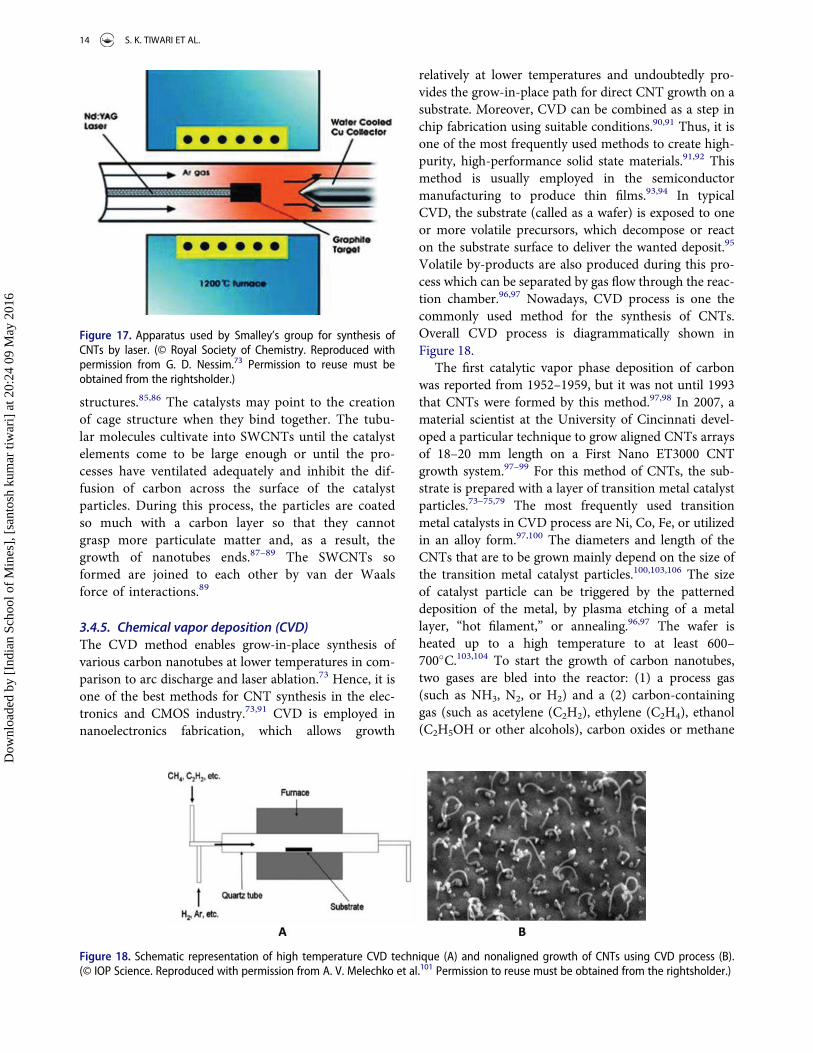
3.4.3. Arc-dischargeThis method is used to generate CNTs through arcvaporization of two carbon rods positioned end to end,detached by roughly 1 mm in an arena which is usuallypacked with inert gas (helium, argon) at a low pressure(between 50 and 700 mbar).79–80 Recently, it has beeninvestigated that it is also feasible to produce CNTs withthe arc method in liquid nitrogen in place of He orAr.79,80 The carbon arc discharge technique was initiallyemployed for the synthesis of C60 and other fullerenes,81
however since the last decade it is treated as the easiestmethod to produce CNTs.80 But in this process the prod-uct obtained as a mixture of SWCNT and MWCNTalong with other components.80 Moreover, carbon arcdoes not operate in a continuous mode of operation.Thus, separation of CNTs from the soot and the catalystpresent in the crude product in a tedious step. In the arcdischarge method, the carbon atoms are vaporized byhelium plasma originated by high currents deliveredover a divergent carbon anode and cathode.79–81 Arc-discharge has been generated in an attractive approachfor fabricating both high-quality MWCNTs andSWCNTs. For the growth of SWCNTs, a metal catalystis required in the arc discharge system.82 The first successin producing a scalable amount of SWCNTs by arc dis-charge was achieved by Bethune et al. in 1993, by using acarbon anode containing a small percentage of cobaltmetal as impurity in the discharge experiment.82
Depending on the different experimental conditions inarc discharge method, it is feasible to selectively and pre-cisely grow SWCNTs or MWCNTs, shown inFigure 16.79–82 The two separate methods of synthesiscan be conducted with the same arc discharge setup.
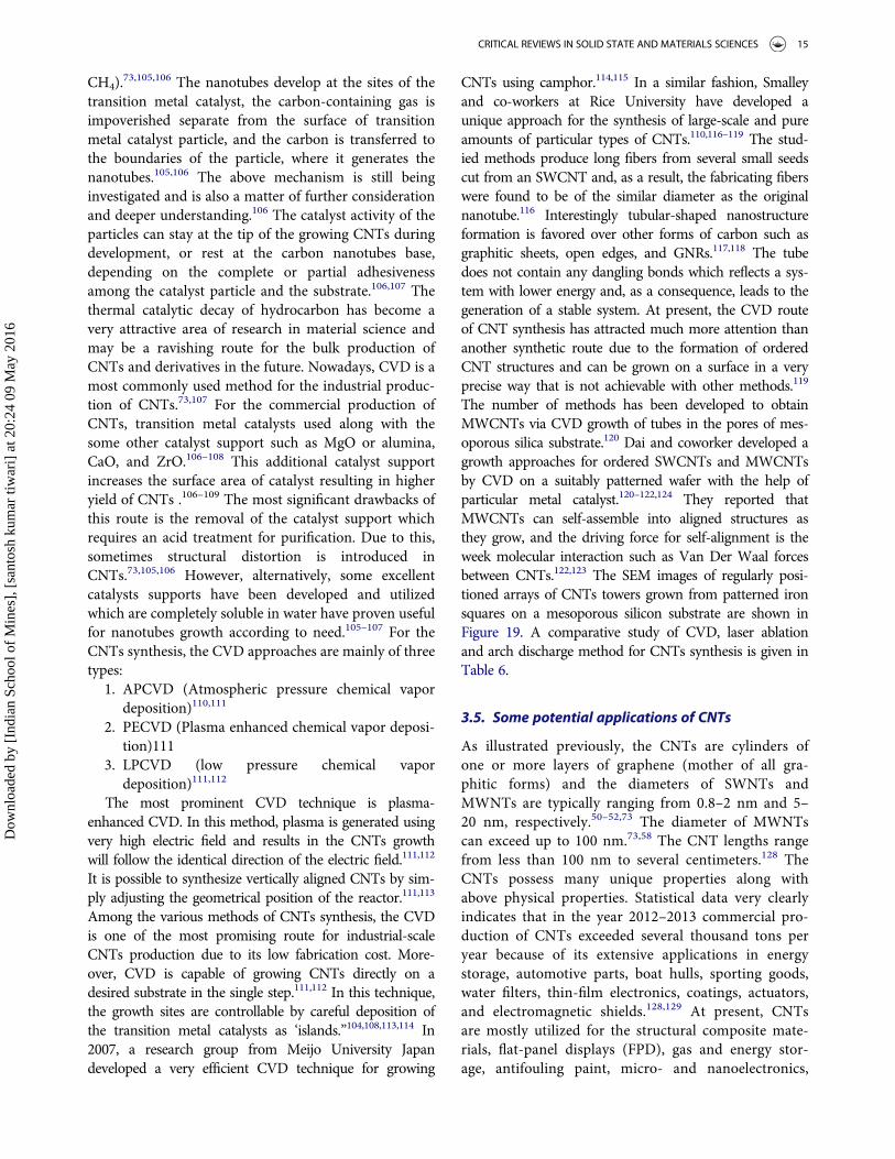
3.4.4. Laser ablationArc discharge and laser ablation methods for thegrowth of CNTs have been actively attempted in thepast decade.73–75 These methods comprise the com-
Table 3. CNT sheet properties compared to copper and aluminum. (Data collected from Dresselhaus et al.,60,64 Saito et al.,57 Barroset al.,65 Zheng et al.,66 Zhao et al.,67 and Baughman et al.68).
Property CNT sheet Copper Aluminum
Thermal conductivity (W/m-K) 22 random/100 aligned 395 237Coefficient of thermal expansion 2 17 23.6DC resistivity (Ohm-cm) 2 £ 10¡4 1.56£ 10¡6 2.45 £ 10¡6
Table 4. Comparison of properties of SWCNT, DWCNT, and MWCNT. (Data collected from Salvetat et al.,53 Dresselhaus et al.,60,64 Saitoet al.,57 Barros et al.,65 Zheng et al.,66 Zhao et al.,67 and Baughman et al.68).
Properties SWCNTs DWCNTs MWCNTs
Surface area (m2/g) 300–600 300–400 40–300Geometric aspect ratio (length/diameter) »10,000 »5,000 100»1,000DC resistivity (Ohm-cm) 2 £ 10¡4 1.56 £ 10¡6 2.45 £ 10¡6
Table 5. Some important theoretical and experimental data for SWCNT and MWCNT50–52, 60–68.
Properties SWNTs MWNTs
Specific gravity 0.8 g/cm3 1.8 g/cm3
Elastic modulus »1 TPa »0.3–1 TPaStrength 50–500 GPa 10–60 GPaResistivity 5–50 mV cm 5–50 mV cmThermal conductivity 3000 W m¡1 K¡1 3000 W m¡1 K¡1
Thermal stability > 700�C (in air). > 700�C (in air);2800�C (in vacuum) 2800�C (in vacuum)
Specific Surface Area »400–900 m2/g »200–400 m2/g
12 S. K. TIWARI ET AL.
Dow
nloa
ded
by [
Indi
an S
choo
l of
Min
es],
[sa
ntos
h ku
mar
tiw
ari]
at 2
0:24
09
May
201
6
pression of carbon atoms produced by the departureof solid carbon sources. The temperature required inthis experiment was 3000–4000�C which is quite nearto the melting temperature of graphite.73–75,79 Asmentioned previously, in 1995 American scientistSmalley, and co-workers, first precisely reported thesynthesis of CNTs by lasers vaporization technol-ogy.1,83 The apparatus employed by Smalley’s groupfor the synthesis of CNTs is shown in Figure 17.83 Inthis mode, a pulsed or continuous laser is utilized tovaporize a graphite powder target in a programmabletemperature oven at 1200�C.73,83 The fundamental
difference between continuous and pulsed laser is thepulsed laser needs a very higher light intensity (100–150 kW/cm2 compared with 12 kW/cm2). The ovenis filled with inert gas viz. He or Ar gas to keep thepressure at 500 Torr results in a scorching vaporplume forms then expands and cools rapidly.83,84 Assoon as the evaporated species cool, small carbonmolecules and atoms immediately compress and formbigger clusters, possibly including various kinds ofCNTs and fullerenes.85 The catalysts also start to con-dense, slowly at first, and then connect to carbonclusters and stop their closing into cage
Figure 15. Different approaches of CNTs synthesis.
Figure 16. Schematic representation of an arc discharge apparatus, along with SEM images of the products obtained with doped andpure anodes. (© Royal Society of Chemistry. Reproduced with permission from G. D. Nessim.73 Permission to reuse must be obtainedfrom the rightsholder.)
CRITICAL REVIEWS IN SOLID STATE AND MATERIALS SCIENCES 13
Dow
nloa
ded
by [
Indi
an S
choo
l of
Min
es],
[sa
ntos
h ku
mar
tiw
ari]
at 2
0:24
09
May
201
6
structures.85,86 The catalysts may point to the creationof cage structure when they bind together. The tubu-lar molecules cultivate into SWCNTs until the catalystelements come to be large enough or until the pro-cesses have ventilated adequately and inhibit the dif-fusion of carbon across the surface of the catalystparticles. During this process, the particles are coatedso much with a carbon layer so that they cannotgrasp more particulate matter and, as a result, thegrowth of nanotubes ends.87–89 The SWCNTs soformed are joined to each other by van der Waalsforce of interactions.89
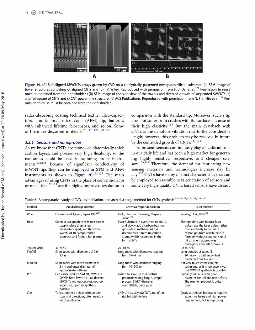
3.4.5. Chemical vapor deposition (CVD)The CVD method enables grow-in-place synthesis ofvarious carbon nanotubes at lower temperatures in com-parison to arc discharge and laser ablation.73 Hence, it isone of the best methods for CNT synthesis in the elec-tronics and CMOS industry.73,91 CVD is employed innanoelectronics fabrication, which allows growth
relatively at lower temperatures and undoubtedly pro-vides the grow-in-place path for direct CNT growth on asubstrate. Moreover, CVD can be combined as a step inchip fabrication using suitable conditions.90,91 Thus, it isone of the most frequently used methods to create high-purity, high-performance solid state materials.91,92 Thismethod is usually employed in the semiconductormanufacturing to produce thin films.93,94 In typicalCVD, the substrate (called as a wafer) is exposed to oneor more volatile precursors, which decompose or reacton the substrate surface to deliver the wanted deposit.95
Volatile by-products are also produced during this pro-cess which can be separated by gas flow through the reac-tion chamber.96,97 Nowadays, CVD process is one thecommonly used method for the synthesis of CNTs.Overall CVD process is diagrammatically shown inFigure 18.
The first catalytic vapor phase deposition of carbonwas reported from 1952–1959, but it was not until 1993that CNTs were formed by this method.97,98 In 2007, amaterial scientist at the University of Cincinnati devel-oped a particular technique to grow aligned CNTs arraysof 18–20 mm length on a First Nano ET3000 CNTgrowth system.97–99 For this method of CNTs, the sub-strate is prepared with a layer of transition metal catalystparticles.73–75,79 The most frequently used transitionmetal catalysts in CVD process are Ni, Co, Fe, or utilizedin an alloy form.97,100 The diameters and length of theCNTs that are to be grown mainly depend on the size ofthe transition metal catalyst particles.100,103,106 The sizeof catalyst particle can be triggered by the patterneddeposition of the metal, by plasma etching of a metallayer, “hot filament,” or annealing.96,97 The wafer isheated up to a high temperature to at least 600–700�C.103,104 To start the growth of carbon nanotubes,two gases are bled into the reactor: (1) a process gas(such as NH3, N2, or H2) and a (2) carbon-containinggas (such as acetylene (C2H2), ethylene (C2H4), ethanol(C2H5OH or other alcohols), carbon oxides or methane
Figure 17. Apparatus used by Smalley’s group for synthesis ofCNTs by laser. (© Royal Society of Chemistry. Reproduced withpermission from G. D. Nessim.73 Permission to reuse must beobtained from the rightsholder.)
Figure 18. Schematic representation of high temperature CVD technique (A) and nonaligned growth of CNTs using CVD process (B).(© IOP Science. Reproduced with permission from A. V. Melechko et al.101 Permission to reuse must be obtained from the rightsholder.)
14 S. K. TIWARI ET AL.
Dow
nloa
ded
by [
Indi
an S
choo
l of
Min
es],
[sa
ntos
h ku
mar
tiw
ari]
at 2
0:24
09
May
201
6
CH4).73,105,106 The nanotubes develop at the sites of the
transition metal catalyst, the carbon-containing gas isimpoverished separate from the surface of transitionmetal catalyst particle, and the carbon is transferred tothe boundaries of the particle, where it generates thenanotubes.105,106 The above mechanism is still beinginvestigated and is also a matter of further considerationand deeper understanding.106 The catalyst activity of theparticles can stay at the tip of the growing CNTs duringdevelopment, or rest at the carbon nanotubes base,depending on the complete or partial adhesivenessamong the catalyst particle and the substrate.106,107 Thethermal catalytic decay of hydrocarbon has become avery attractive area of research in material science andmay be a ravishing route for the bulk production ofCNTs and derivatives in the future. Nowadays, CVD is amost commonly used method for the industrial produc-tion of CNTs.73,107 For the commercial production ofCNTs, transition metal catalysts used along with thesome other catalyst support such as MgO or alumina,CaO, and ZrO.106–108 This additional catalyst supportincreases the surface area of catalyst resulting in higheryield of CNTs .106–109 The most significant drawbacks ofthis route is the removal of the catalyst support whichrequires an acid treatment for purification. Due to this,sometimes structural distortion is introduced inCNTs.73,105,106 However, alternatively, some excellentcatalysts supports have been developed and utilizedwhich are completely soluble in water have proven usefulfor nanotubes growth according to need.105–107 For theCNTs synthesis, the CVD approaches are mainly of threetypes:
1. APCVD (Atmospheric pressure chemical vapordeposition)110,111
2. PECVD (Plasma enhanced chemical vapor deposi-tion)111
3. LPCVD (low pressure chemical vapordeposition)111,112
The most prominent CVD technique is plasma-enhanced CVD. In this method, plasma is generated usingvery high electric field and results in the CNTs growthwill follow the identical direction of the electric field.111,112
It is possible to synthesize vertically aligned CNTs by sim-ply adjusting the geometrical position of the reactor.111,113
Among the various methods of CNTs synthesis, the CVDis one of the most promising route for industrial-scaleCNTs production due to its low fabrication cost. More-over, CVD is capable of growing CNTs directly on adesired substrate in the single step.111,112 In this technique,the growth sites are controllable by careful deposition ofthe transition metal catalysts as ‘islands.”104,108,113,114 In2007, a research group from Meijo University Japandeveloped a very efficient CVD technique for growing
CNTs using camphor.114,115 In a similar fashion, Smalleyand co-workers at Rice University have developed aunique approach for the synthesis of large-scale and pureamounts of particular types of CNTs.110,116–119 The stud-ied methods produce long fibers from several small seedscut from an SWCNT and, as a result, the fabricating fiberswere found to be of the similar diameter as the originalnanotube.116 Interestingly tubular-shaped nanostructureformation is favored over other forms of carbon such asgraphitic sheets, open edges, and GNRs.117,118 The tubedoes not contain any dangling bonds which reflects a sys-tem with lower energy and, as a consequence, leads to thegeneration of a stable system. At present, the CVD routeof CNT synthesis has attracted much more attention thananother synthetic route due to the formation of orderedCNT structures and can be grown on a surface in a veryprecise way that is not achievable with other methods.119
The number of methods has been developed to obtainMWCNTs via CVD growth of tubes in the pores of mes-oporous silica substrate.120 Dai and coworker developed agrowth approaches for ordered SWCNTs and MWCNTsby CVD on a suitably patterned wafer with the help ofparticular metal catalyst.120–122,124 They reported thatMWCNTs can self-assemble into aligned structures asthey grow, and the driving force for self-alignment is theweek molecular interaction such as Van Der Waal forcesbetween CNTs.122,123 The SEM images of regularly posi-tioned arrays of CNTs towers grown from patterned ironsquares on a mesoporous silicon substrate are shown inFigure 19. A comparative study of CVD, laser ablationand arch discharge method for CNTs synthesis is given inTable 6.
3.5. Some potential applications of CNTs
As illustrated previously, the CNTs are cylinders ofone or more layers of graphene (mother of all gra-phitic forms) and the diameters of SWNTs andMWNTs are typically ranging from 0.8–2 nm and 5–20 nm, respectively.50–52,73 The diameter of MWNTscan exceed up to 100 nm.73,58 The CNT lengths rangefrom less than 100 nm to several centimeters.128 TheCNTs possess many unique properties along withabove physical properties. Statistical data very clearlyindicates that in the year 2012–2013 commercial pro-duction of CNTs exceeded several thousand tons peryear because of its extensive applications in energystorage, automotive parts, boat hulls, sporting goods,water filters, thin-film electronics, coatings, actuators,and electromagnetic shields.128,129 At present, CNTsare mostly utilized for the structural composite mate-rials, flat-panel displays (FPD), gas and energy stor-age, antifouling paint, micro- and nanoelectronics,
CRITICAL REVIEWS IN SOLID STATE AND MATERIALS SCIENCES 15
Dow
nloa
ded
by [
Indi
an S
choo
l of
Min
es],
[sa
ntos
h ku
mar
tiw
ari]
at 2
0:24
09
May
201
6
radar-absorbing coating technical textile, ultra-capaci-tors, atomic force microscope (AFM) tip, batterieswith enhanced lifetime, biosensors, and so on. Someof them are discussed in details.73,117–123,128–130
3.5.1. Sensors and nanoprobesAs we know that CNTs are mono- or diatomically thickcarbon layers, and possess very high flexibility, so thenanotubes could be used in scanning probe instru-ments.126,131 Because of significant conductivity ofMWNT-tips they can be employed in STM and AFMinstruments as shown in Figure 20.132,133 The mainadvantages of using CNTs in the place of conventional Sior metal tips122,123 are the highly improved resolution in
comparison with the standard tip. Moreover, such a tipdoes not suffer from crashes with the surfaces because oftheir high elasticity.133 But the main drawback withCNTs is the nanotube vibration due to the considerablelength; however, this problem may be resolved in futureby the controlled growth of CNTs.133,134
At present, sensors continuously play a significant rolein our daily life and has been a high market for generat-ing highly sensitive, responsive, and cheaper sen-sors.133,134 Therefore, the demand for fabricating newsensing materials and technologies increase day byday.135 CNTs have many distinct characteristics that canbe employed to assemble next generation of sensors andsome very high-quality CNTs based sensors have already
Figure 19. (A) Self-aligned MWCNTs arrays grown by CVD on a catalytically patterned mesopores silicon substrate: (a) SEM image oftower structures consisting of aligned CNTs and (b). (© Wiley. Reproduced with permission from H. J. Dai et al.124 Permission to reusemust be obtained from the rightsholder.) (B) SEM image of the side view of the towers and directed growth of suspended SWCNTs (a)and (b) square of CNTs and c) CNT power-line structure. (© ACS Publications. Reproduced with permission from N. Franklin et al.117 Per-mission to reuse must be obtained from the rightsholder.)
Table 6. A comparative study of CVD, laser ablation, and arch discharge method for CNTs synthesis.50–52, 73,117–123,124–127.
Method Arc discharge method Chemical vapor deposition Laser ablation
Who Ebbesen and Ajayan, Japan 1992125 Endo, Shinshu University, Nagano,Japan126
Smalley, USA, 1995127
How Connect two graphite rods to a powersupply, place them a fewmillimeters apart, and throw theswitch. At 100 amps, carbonvaporizes and forms a hot plasma
Place substrate in oven, heat to 600�C,and slowly add a carbon-bearinggas such as methane. As gasdecomposes it frees up carbonatoms, which recombine in theform of NTs
Blast graphite with intense laserpulses, use the laser pulses ratherthan electricity to generatecarbon gas from which the NTsform, try various conditions untilhit on one that producesprodigious amounts of SWNTs
Typical yield 30–90% 20–100% Up to 70%SWCNT Short tubes with diameters of 0.6–
1.4 nmLong tubes with diameters ranging
from 0.6–4 nmLong bundles of tubes (5–
20 microns), with individualdiameter from 1–2 nm.
MWCNT Short tubes with inner diameter of 1–3 nm and outer diameter ofapproximately 10 nm.
Long tubes with diameter rangingfrom 10–240 nm
Not very much interest in thistechnique, as it is too expensive,but MWCNT synthesis is possible
Pro Can easily produce SWCNT, MWCNTs.SWNTs have few structural defects,MWCNTs without catalyst, not tooexpensive, open air synthesispossible
Easiest to scale up to industrialproduction; long length, simpleprocess, SWNT diametercontrollable, quite pure
Primarily SWCNTs, with gooddiameter control and few defects.The reaction product is quitepure.
Con Tubes tend to be short with randomsizes and directions, often needs alot of purification
CNTs are usually MWCNTs and oftenriddled with defects
Costly technique, because it requiresexpensive lasers and high powerrequirement, but is improving
16 S. K. TIWARI ET AL.
Dow
nloa
ded
by [
Indi
an S
choo
l of
Min
es],
[sa
ntos
h ku
mar
tiw
ari]
at 2
0:24
09
May
201
6
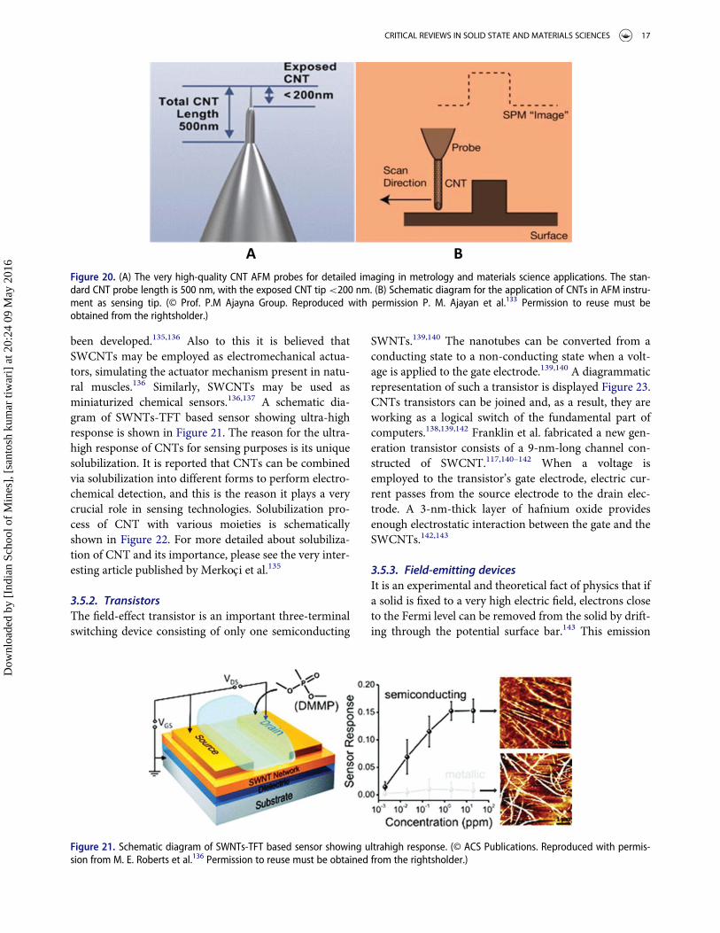
been developed.135,136 Also to this it is believed thatSWCNTs may be employed as electromechanical actua-tors, simulating the actuator mechanism present in natu-ral muscles.136 Similarly, SWCNTs may be used asminiaturized chemical sensors.136,137 A schematic dia-gram of SWNTs-TFT based sensor showing ultra-highresponse is shown in Figure 21. The reason for the ultra-high response of CNTs for sensing purposes is its uniquesolubilization. It is reported that CNTs can be combinedvia solubilization into different forms to perform electro-chemical detection, and this is the reason it plays a verycrucial role in sensing technologies. Solubilization pro-cess of CNT with various moieties is schematicallyshown in Figure 22. For more detailed about solubiliza-tion of CNT and its importance, please see the very inter-esting article published by Merkoci et al.135
3.5.2. TransistorsThe field-effect transistor is an important three-terminalswitching device consisting of only one semiconducting
SWNTs.139,140 The nanotubes can be converted from aconducting state to a non-conducting state when a volt-age is applied to the gate electrode.139,140 A diagrammaticrepresentation of such a transistor is displayed Figure 23.CNTs transistors can be joined and, as a result, they areworking as a logical switch of the fundamental part ofcomputers.138,139,142 Franklin et al. fabricated a new gen-eration transistor consists of a 9-nm-long channel con-structed of SWCNT.117,140–142 When a voltage isemployed to the transistor’s gate electrode, electric cur-rent passes from the source electrode to the drain elec-trode. A 3-nm-thick layer of hafnium oxide providesenough electrostatic interaction between the gate and theSWCNTs.142,143
3.5.3. Field-emitting devicesIt is an experimental and theoretical fact of physics that ifa solid is fixed to a very high electric field, electrons closeto the Fermi level can be removed from the solid by drift-ing through the potential surface bar.143 This emission
Figure 20. (A) The very high-quality CNT AFM probes for detailed imaging in metrology and materials science applications. The stan-dard CNT probe length is 500 nm, with the exposed CNT tip <200 nm. (B) Schematic diagram for the application of CNTs in AFM instru-ment as sensing tip. (© Prof. P.M Ajayna Group. Reproduced with permission P. M. Ajayan et al.133 Permission to reuse must beobtained from the rightsholder.)
Figure 21. Schematic diagram of SWNTs-TFT based sensor showing ultrahigh response. (© ACS Publications. Reproduced with permis-sion from M. E. Roberts et al.136 Permission to reuse must be obtained from the rightsholder.)
CRITICAL REVIEWS IN SOLID STATE AND MATERIALS SCIENCES 17
Dow
nloa
ded
by [
Indi
an S
choo
l of
Min
es],
[sa
ntos
h ku
mar
tiw
ari]
at 2
0:24
09
May
201
6

current directly related to the intensity of the local elec-tric field at the emission surface and its work function(commonly denoted by ( ; )) which indicates the mini-mum energy required to remove an electron from itstop-bounded state into the vacuum level.144,145 A veryhigh electric field is needed to remove an electron from
the highest adjacent state to ground state.145 The above-required condition is mostly fulfilled by CNTs becausetheir sufficiently elongated shape ascertains vast fieldamplification.145 A very low threshold emission area anda very high stability at high current density are neededfor emissive materials to be utilized in technologicalapplications.144,146 In addition to above characteristics aperfect emitter should also have a high surface area, ananometer size diameter, a structural integrity, a highelectrical conductivity, a small energy spread, and a veryhigh chemical stability.145 The CNTs hold all these pecu-liar characteristics. Owing to such unique properties, it isa superb candidate for the fabrication of next-generationfield-emitting devices. The principle of field emissionwith CNTs is diagrammatically shown in Figure 24.
3.5.4. SupercapacitorsSupercapacitors (SCs, also known as ultracapacitors) arehigh-capacity electrochemical device with capacitancevalues much higher than other conventional capacitorsand it bridge the gap between electrolytic capacitors andrechargeable batteries.148–150 This unique feature makesit beneficial for devices that need a small quantity of cur-rent and low voltage.148,189 Sometimes, supercapacitorscan hold the position of a rechargeable low-voltage elec-trochemical battery that has a very high capacitance andis probably suitable for the various electronic devices.150
They consist of two electrodes spaced by some non-con-ducting material that is ionically conducting in electro-chemical devices. The range of SCs is inverselyproportional to the separation between the charge on theelectrode and the counter charge in the electrolyte.150,151
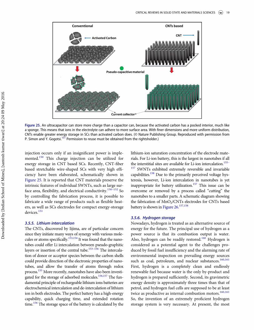
It means smaller the separation greater will be efficiencyof the SCs.149 The separation in CNTs is found to be inthe nanometer range and, as a result, an enormousamount of capacitance is created from the high CNTssurface area to the electrolyte.149,150 A lot of charge
Figure 22. Diagrammatic representation of CNT solubilizationalternatives: (A) supramolecular wrapping with polymer; (B) CNT-LiC conducting polyelectrolyte; (C) with amino group of 2-ami-nomethyl- 18-crown-6 ether; (D) by amide bonds with glucos-amine; and (E) by diamine-terminated oligomeric poly(ethyleneglycol). (© Elsevier. Reproduced with permission from A. Merkocciet al.135 Permission to reuse must be obtained from therightsholder.)
Figure 23. Schematic diagram of CNT based transistor; contain-ing 9 nm long channel made of SWCNT 3-nm-thick layer of haf-nium oxide (© Nature Publishing Group. Reproduced withpermission from F. Kreupl.138 Permission to reuse must beobtained from the rightsholder.)
Figure 24. Principle of field emission display and application ofCNTs. (© B. Thanveer. Reproduced with permission from B.Thanveer.147 Permission to reuse must be obtained from therightsholder.)
18 S. K. TIWARI ET AL.
Dow
nloa
ded
by [
Indi
an S
choo
l of
Min
es],
[sa
ntos
h ku
mar
tiw
ari]
at 2
0:24
09
May
201
6
injection occurs only if an insignificant power is imple-mented.150 This charge injection can be utilized forenergy storage in CNT based SCs. Recently, CNT-fiberbased stretchable wire-shaped SCs with very high effi-ciency have been elaborated, schematically shown inFigure 25. It is reported that CNT materials preserve theintrinsic features of individual SWNTs, such as large sur-face area, flexibility, and electrical conductivity.150–152 Soby controlling the fabrication process, it is possible tofabricate a wide range of products such as flexible heat-ers, as well as SCs electrodes for compact energy-storagedevices.151
3.5.5. Lithium intercalationThe CNTs, discovered by Iijima, are of particular concernsince they initiate many ways of synergy with various mole-cules or atoms specifically.153,154 It was found that the nano-tubes could offer Li intercalation between pseudo-graphiticlayers or insertion of the central tube.153–156 The intercala-tion of donor or acceptor species between the carbon shellscould provide direction of the electronic properties of nano-tubes, and allow the transfer of atoms through redoxprocess.155 More recently, nanotubes have also been investi-gated for the storage of adsorbed molecules.156,157 The fun-damental principle of rechargeable lithium ions batteries areelectrochemical intercalation and de-intercalation of lithiumion in both electrodes. The perfect battery has a high-energycapability, quick charging time, and extended rotationtime.156 The storage space of the battery is calculated by the
lithium-ion saturation concentration of the electrode mate-rials. For Li-ion battery, this is the largest in nanotubes if allthe interstitial sites are available for Li-ion intercalation.155–157 SWNTs exhibited extremely reversible and invariablecapabilities.158 Due to the primarily perceived voltage hys-teresis, however, Li-ion intercalation in nanotubes is yetinappropriate for battery utilization.157 This issue can beovercome or removed by a process called “cutting” thenanotubes to a smaller parts. A schematic diagram showingthe fabrication of MnO2/CNTs electrodes for CNTs basedbattery is shown in Figure 26.157,158
3.5.6. Hydrogen storageNowadays, hydrogen is treated as an alternative source ofenergy for the future. The principal use of hydrogen as apower source is that its combustion output is water.Also, hydrogen can be readily restored.160 Hydrogen isconsidered as a potential agent to the challenges pro-duced by fossil fuel insufficiency and the alarming rate ofenvironmental inspection on prevailing energy sourcessuch as coal, petroleum, and nuclear substances.160,161
First, hydrogen is a completely clean and endlesslyrenewable fuel because water is the only by-product andhydrogen is prepared sufficiently. Second, its gravimetricenergy density is approximately three times than that ofpetrol, and hydrogen fuel cells are supposed to be at leasttwice as productive as internal combustion motors.160,161
So, the invention of an extremely proficient hydrogenstorage system is very necessary. At present, the most
Figure 25. An ultracapacitor can store more charge than a capacitor can, because the activated carbon has a pocked interior, much likea sponge. This means that ions in the electrolyte can adhere to more surface area. With finer dimensions and more uniform distribution,CNTs enable greater energy storage in SCs than activated carbon does. (© Nature Publishing Group. Reproduced with permission fromP. Simon and Y. Gogotsi.151 Permission to reuse must be obtained from the rightsholder.)
CRITICAL REVIEWS IN SOLID STATE AND MATERIALS SCIENCES 19
Dow
nloa
ded
by [
Indi
an S
choo
l of
Min
es],
[sa
ntos
h ku
mar
tiw
ari]
at 2
0:24
09
May
201
6
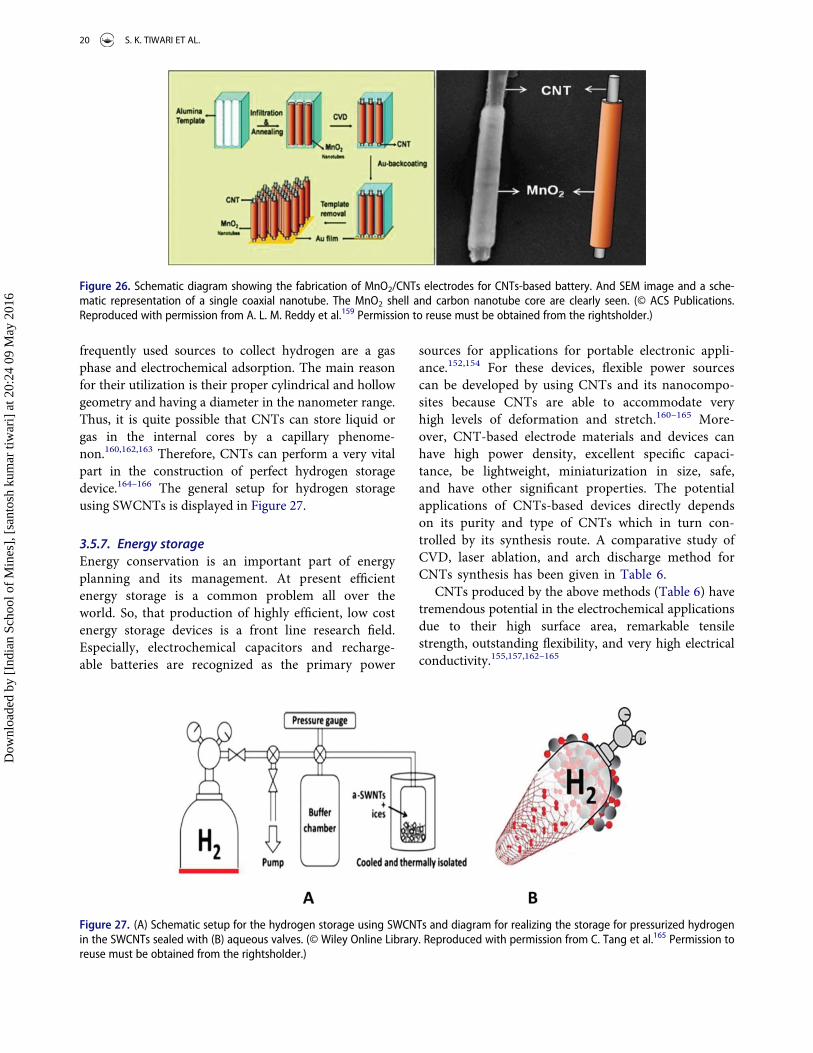
frequently used sources to collect hydrogen are a gasphase and electrochemical adsorption. The main reasonfor their utilization is their proper cylindrical and hollowgeometry and having a diameter in the nanometer range.Thus, it is quite possible that CNTs can store liquid orgas in the internal cores by a capillary phenome-non.160,162,163 Therefore, CNTs can perform a very vitalpart in the construction of perfect hydrogen storagedevice.164–166 The general setup for hydrogen storageusing SWCNTs is displayed in Figure 27.
3.5.7. Energy storageEnergy conservation is an important part of energyplanning and its management. At present efficientenergy storage is a common problem all over theworld. So, that production of highly efficient, low costenergy storage devices is a front line research field.Especially, electrochemical capacitors and recharge-able batteries are recognized as the primary power
sources for applications for portable electronic appli-ance.152,154 For these devices, flexible power sourcescan be developed by using CNTs and its nanocompo-sites because CNTs are able to accommodate veryhigh levels of deformation and stretch.160–165 More-over, CNT-based electrode materials and devices canhave high power density, excellent specific capaci-tance, be lightweight, miniaturization in size, safe,and have other significant properties. The potentialapplications of CNTs-based devices directly dependson its purity and type of CNTs which in turn con-trolled by its synthesis route. A comparative study ofCVD, laser ablation, and arch discharge method forCNTs synthesis has been given in Table 6.
CNTs produced by the above methods (Table 6) havetremendous potential in the electrochemical applicationsdue to their high surface area, remarkable tensilestrength, outstanding flexibility, and very high electricalconductivity.155,157,162–165
Figure 26. Schematic diagram showing the fabrication of MnO2/CNTs electrodes for CNTs-based battery. And SEM image and a sche-matic representation of a single coaxial nanotube. The MnO2 shell and carbon nanotube core are clearly seen. (© ACS Publications.Reproduced with permission from A. L. M. Reddy et al.159 Permission to reuse must be obtained from the rightsholder.)
Figure 27. (A) Schematic setup for the hydrogen storage using SWCNTs and diagram for realizing the storage for pressurized hydrogenin the SWCNTs sealed with (B) aqueous valves. (© Wiley Online Library. Reproduced with permission from C. Tang et al.165 Permission toreuse must be obtained from the rightsholder.)
20 S. K. TIWARI ET AL.
Dow
nloa
ded
by [
Indi
an S
choo
l of
Min
es],
[sa
ntos
h ku
mar
tiw
ari]
at 2
0:24
09
May
201
6
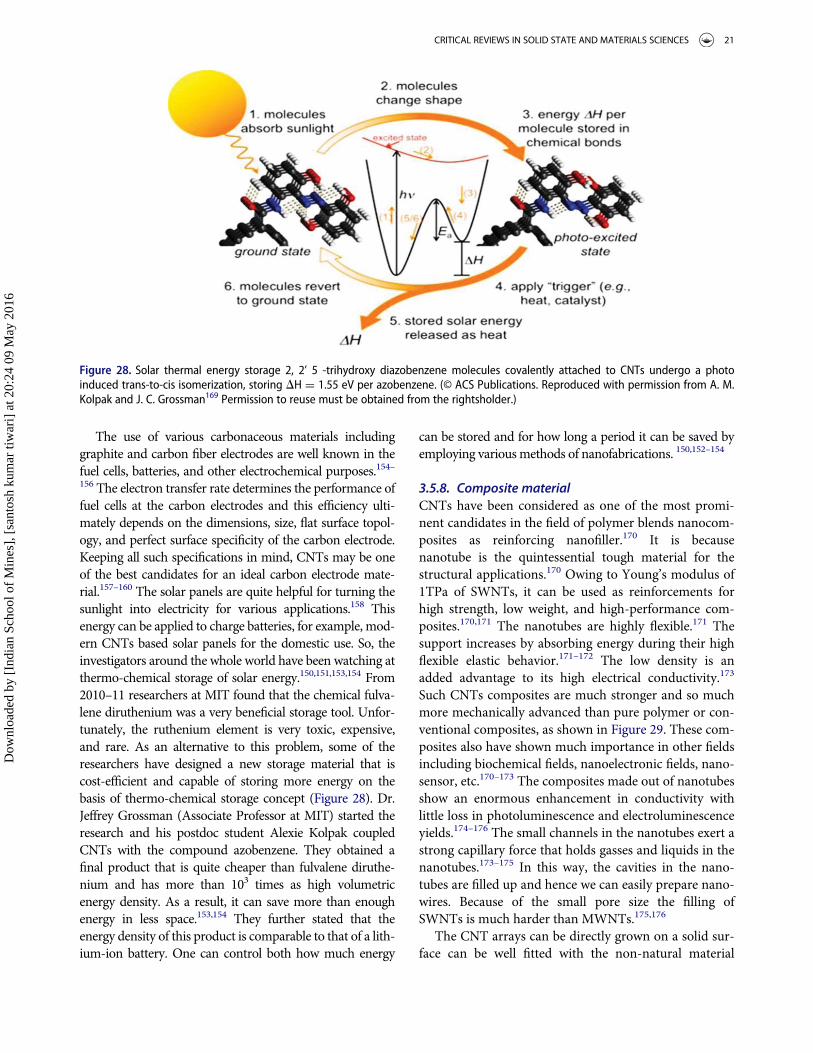
The use of various carbonaceous materials includinggraphite and carbon fiber electrodes are well known in thefuel cells, batteries, and other electrochemical purposes.154–156 The electron transfer rate determines the performance offuel cells at the carbon electrodes and this efficiency ulti-mately depends on the dimensions, size, flat surface topol-ogy, and perfect surface specificity of the carbon electrode.Keeping all such specifications in mind, CNTs may be oneof the best candidates for an ideal carbon electrode mate-rial.157–160 The solar panels are quite helpful for turning thesunlight into electricity for various applications.158 Thisenergy can be applied to charge batteries, for example, mod-ern CNTs based solar panels for the domestic use. So, theinvestigators around the whole world have been watching atthermo-chemical storage of solar energy.150,151,153,154 From2010–11 researchers at MIT found that the chemical fulva-lene diruthenium was a very beneficial storage tool. Unfor-tunately, the ruthenium element is very toxic, expensive,and rare. As an alternative to this problem, some of theresearchers have designed a new storage material that iscost-efficient and capable of storing more energy on thebasis of thermo-chemical storage concept (Figure 28). Dr.Jeffrey Grossman (Associate Professor at MIT) started theresearch and his postdoc student Alexie Kolpak coupledCNTs with the compound azobenzene. They obtained afinal product that is quite cheaper than fulvalene diruthe-nium and has more than 103 times as high volumetricenergy density. As a result, it can save more than enoughenergy in less space.153,154 They further stated that theenergy density of this product is comparable to that of a lith-ium-ion battery. One can control both how much energy
can be stored and for how long a period it can be saved byemploying variousmethods of nanofabrications. 150,152–154
3.5.8. Composite materialCNTs have been considered as one of the most promi-nent candidates in the field of polymer blends nanocom-posites as reinforcing nanofiller.170 It is becausenanotube is the quintessential tough material for thestructural applications.170 Owing to Young’s modulus of1TPa of SWNTs, it can be used as reinforcements forhigh strength, low weight, and high-performance com-posites.170,171 The nanotubes are highly flexible.171 Thesupport increases by absorbing energy during their highflexible elastic behavior.171–172 The low density is anadded advantage to its high electrical conductivity.173
Such CNTs composites are much stronger and so muchmore mechanically advanced than pure polymer or con-ventional composites, as shown in Figure 29. These com-posites also have shown much importance in other fieldsincluding biochemical fields, nanoelectronic fields, nano-sensor, etc.170–173 The composites made out of nanotubesshow an enormous enhancement in conductivity withlittle loss in photoluminescence and electroluminescenceyields.174–176 The small channels in the nanotubes exert astrong capillary force that holds gasses and liquids in thenanotubes.173–175 In this way, the cavities in the nano-tubes are filled up and hence we can easily prepare nano-wires. Because of the small pore size the filling ofSWNTs is much harder than MWNTs.175,176
The CNT arrays can be directly grown on a solid sur-face can be well fitted with the non-natural material
Figure 28. Solar thermal energy storage 2, 2’ 5 -trihydroxy diazobenzene molecules covalently attached to CNTs undergo a photoinduced trans-to-cis isomerization, storing DH D 1.55 eV per azobenzene. (© ACS Publications. Reproduced with permission from A. M.Kolpak and J. C. Grossman169 Permission to reuse must be obtained from the rightsholder.)
CRITICAL REVIEWS IN SOLID STATE AND MATERIALS SCIENCES 21
Dow
nloa
ded
by [
Indi
an S
choo
l of
Min
es],
[sa
ntos
h ku
mar
tiw
ari]
at 2
0:24
09
May
201
6
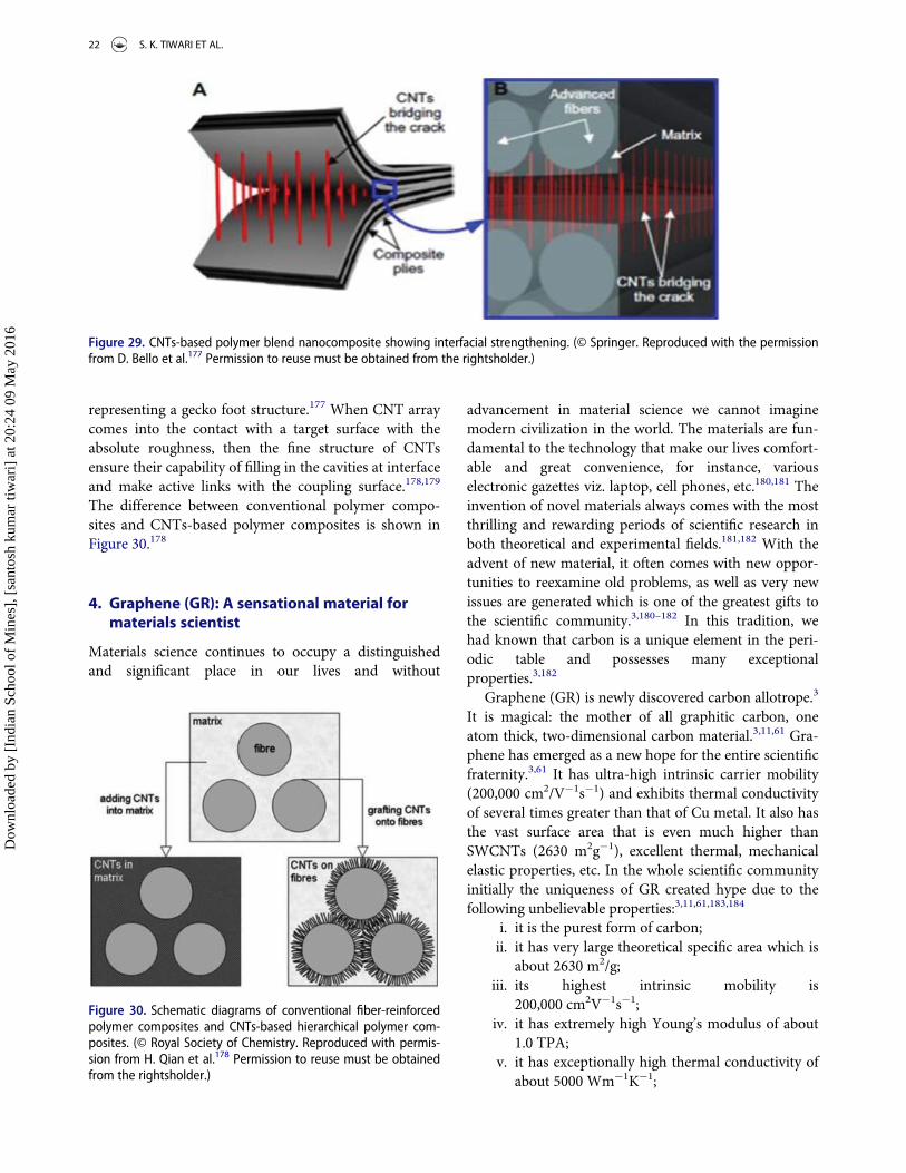
representing a gecko foot structure.177 When CNT arraycomes into the contact with a target surface with theabsolute roughness, then the fine structure of CNTsensure their capability of filling in the cavities at interfaceand make active links with the coupling surface.178,179
The difference between conventional polymer compo-sites and CNTs-based polymer composites is shown inFigure 30.178
4. Graphene (GR): A sensational material formaterials scientist
Materials science continues to occupy a distinguishedand significant place in our lives and without
advancement in material science we cannot imaginemodern civilization in the world. The materials are fun-damental to the technology that make our lives comfort-able and great convenience, for instance, variouselectronic gazettes viz. laptop, cell phones, etc.180,181 Theinvention of novel materials always comes with the mostthrilling and rewarding periods of scientific research inboth theoretical and experimental fields.181,182 With theadvent of new material, it often comes with new oppor-tunities to reexamine old problems, as well as very newissues are generated which is one of the greatest gifts tothe scientific community.3,180–182 In this tradition, wehad known that carbon is a unique element in the peri-odic table and possesses many exceptionalproperties.3,182
Graphene (GR) is newly discovered carbon allotrope.3
It is magical: the mother of all graphitic carbon, oneatom thick, two-dimensional carbon material.3,11,61 Gra-phene has emerged as a new hope for the entire scientificfraternity.3,61 It has ultra-high intrinsic carrier mobility(200,000 cm2/V¡1s¡1) and exhibits thermal conductivityof several times greater than that of Cu metal. It also hasthe vast surface area that is even much higher thanSWCNTs (2630 m2g¡1), excellent thermal, mechanicalelastic properties, etc. In the whole scientific communityinitially the uniqueness of GR created hype due to thefollowing unbelievable properties:3,11,61,183,184
i. it is the purest form of carbon;ii. it has very large theoretical specific area which is
about 2630 m2/g;iii. its highest intrinsic mobility is
200,000 cm2V¡1s¡1;iv. it has extremely high Young’s modulus of about
1.0 TPA;v. it has exceptionally high thermal conductivity of
about 5000 Wm¡1K¡1;
Figure 29. CNTs-based polymer blend nanocomposite showing interfacial strengthening. (© Springer. Reproduced with the permissionfrom D. Bello et al.177 Permission to reuse must be obtained from the rightsholder.)
Figure 30. Schematic diagrams of conventional fiber-reinforcedpolymer composites and CNTs-based hierarchical polymer com-posites. (© Royal Society of Chemistry. Reproduced with permis-sion from H. Qian et al.178 Permission to reuse must be obtainedfrom the rightsholder.)
22 S. K. TIWARI ET AL.
Dow
nloa
ded
by [
Indi
an S
choo
l of
Min
es],
[sa
ntos
h ku
mar
tiw
ari]
at 2
0:24
09
May
201
6
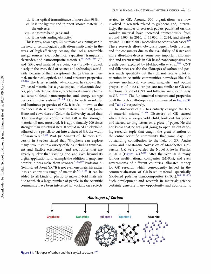
vi. it has optical transmittance of more than 98%;vii. it is the lightest and thinnest known material in
the universe;viii. it has zero band gaps; andix. it has outstanding elasticity.
This is why, nowadays, GR is treated as a rising star inthe field of technological applications particularly in theareas of high-efficiency sensor, fuel cells, renewableenergy sources, electrochemical capacitors, transparentelectrodes, and nanocomposite materials.11–13,183–186 GRand GR-based material are being very rapidly studied,nearly in the every field of science and technology world-wide, because of their exceptional charge transfer, ther-mal, mechanical, optical, and band structure properties.185,186 The latest scientific advancement has shown thatGR-based material has a great impact on electronic devi-ces, photo-electronic device, biochemical sensor, chemi-cal sensor, blend nanocomposite, and energy storagedevices in solar system.186–188 Due to such wonderfuland luminous properties of GR, it is also known as the“Wonder Material” or miracle material. In 2008, JamesHone and coworkers of Columbia University stated that:“Our investigation confirms that GR is the strongestmaterial till now measured. It is approximately 200 timesstronger than structural steel. It would need an elephant,adjusted on a pencil, to cut into a sheet of GR the widthof Saran Wrap.”189 Prof. Jiri Minaret of Chalmers Uni-versity in Sweden stated that “Graphene can exploremany novel uses in a variety of fields including transpar-ent and flexible electronics, and electronics that aregreatly quicker than existing one, and even beyond itsdigital applications, for example the addition of graphenepowder in tires make them stronger.”189,190 Professor A.Geim stated about GR “It is not even one material; ratherit is an enormous range of materials.”3,11,186 It can beadded to all kinds of plastic to make hybrid materialsdue to which a large number of people in the scientificcommunity have been interested in working on projects
related to GR. Around 300 organizations are nowinvolved in research related to graphene and, interest-ingly, the number of research papers published on thiswonder material have increased tremendously fromaround 3500, in 2010, to 14,000, in 2014, and alreadycrossed 11,000 in 2015 (according to scopus database).190
These research efforts obviously benefit both businessand the consumers due to the availability of faster andmore affordable devices. Some very important informa-tion and recent trends in GR based nanocomposites hasgreatly been explored by Mukhopadhyay et al.186 CNTand fullerenes are also the allotropes of carbon and pos-sess much specificity but they do not receive a lot ofattention in scientific communities nowadays like GR,because mechanical, electronic magnetic, and opticalproperties of these allotropes are not similar to GR andfunctionalization of CNT and fullerene are also not easyas GR.190–194 The fundamental structure and propertiesof all the carbon allotropes are summarized in Figure 31and Table 7, respectively.
The discovery of GR has entirely changed the faceof material science.3,11,63 Discovery of GR startedwhen Kaleb, a six-year-old child, look out his penciland started writing letters on a piece of paper. He didnot know that he was just going to open an outstand-ing research topic that caught the great attention ofthe entire scientific community that same day. Foroutstanding contribution to the field of GR, AndreGeim and Konstantin Novoselov of Manchester Uni-versity, UK were awarded the Nobel Prize in Physicsin 2010 (Figure 32).3,186 After the year 2010, manyfamous multi-national companies (MNCs), and evengovernments of different countries, allocated moneyfor GR research which consequently helped in thecommercialization of GR-based material, specificallyGR-based polymer nanocomposites (PNCs).186,190–193
Such development and research in materials sciencecertainly generate many opportunity and applications,
Figure 31. Allotropes of carbon and their crystal structure.3,194
CRITICAL REVIEWS IN SOLID STATE AND MATERIALS SCIENCES 23
Dow
nloa
ded
by [
Indi
an S
choo
l of
Min
es],
[sa
ntos
h ku
mar
tiw
ari]
at 2
0:24
09
May
201
6
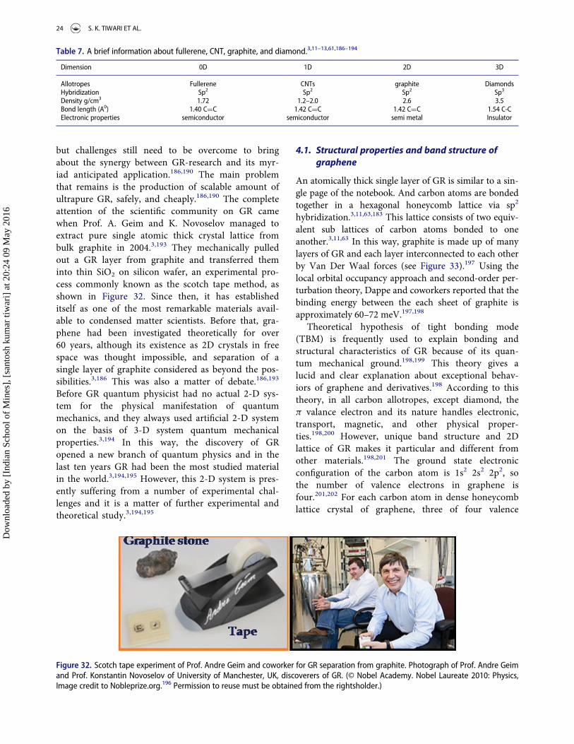
but challenges still need to be overcome to bringabout the synergy between GR-research and its myr-iad anticipated application.186,190 The main problemthat remains is the production of scalable amount ofultrapure GR, safely, and cheaply.186,190 The completeattention of the scientific community on GR camewhen Prof. A. Geim and K. Novoselov managed toextract pure single atomic thick crystal lattice frombulk graphite in 2004.3,193 They mechanically pulledout a GR layer from graphite and transferred theminto thin SiO2 on silicon wafer, an experimental pro-cess commonly known as the scotch tape method, asshown in Figure 32. Since then, it has establisheditself as one of the most remarkable materials avail-able to condensed matter scientists. Before that, gra-phene had been investigated theoretically for over60 years, although its existence as 2D crystals in freespace was thought impossible, and separation of asingle layer of graphite considered as beyond the pos-sibilities.3,186 This was also a matter of debate.186,193
Before GR quantum physicist had no actual 2-D sys-tem for the physical manifestation of quantummechanics, and they always used artificial 2-D systemon the basis of 3-D system quantum mechanicalproperties.3,194 In this way, the discovery of GRopened a new branch of quantum physics and in thelast ten years GR had been the most studied materialin the world.3,194,195 However, this 2-D system is pres-ently suffering from a number of experimental chal-lenges and it is a matter of further experimental andtheoretical study.3,194,195
4.1. Structural properties and band structure ofgraphene
An atomically thick single layer of GR is similar to a sin-gle page of the notebook. And carbon atoms are bondedtogether in a hexagonal honeycomb lattice via sp2
hybridization.3,11,63,183 This lattice consists of two equiv-alent sub lattices of carbon atoms bonded to oneanother.3,11,63 In this way, graphite is made up of manylayers of GR and each layer interconnected to each otherby Van Der Waal forces (see Figure 33).197 Using thelocal orbital occupancy approach and second-order per-turbation theory, Dappe and coworkers reported that thebinding energy between the each sheet of graphite isapproximately 60–72 meV.197,198
Theoretical hypothesis of tight bonding mode(TBM) is frequently used to explain bonding andstructural characteristics of GR because of its quan-tum mechanical ground.198,199 This theory gives alucid and clear explanation about exceptional behav-iors of graphene and derivatives.198 According to thistheory, in all carbon allotropes, except diamond, thep valance electron and its nature handles electronic,transport, magnetic, and other physical proper-ties.198,200 However, unique band structure and 2Dlattice of GR makes it particular and different fromother materials.198,201 The ground state electronicconfiguration of the carbon atom is 1s2 2s2 2p2, sothe number of valence electrons in graphene isfour.201,202 For each carbon atom in dense honeycomblattice crystal of graphene, three of four valence
Table 7. A brief information about fullerene, CNT, graphite, and diamond.3,11–13,61,186–194
Dimension 0D 1D 2D 3D
Allotropes Fullerene CNTs graphite DiamondsHybridization Sp2 Sp2 Sp2 Sp3
Density g/cm3 1.72 1.2–2.0 2.6 3.5Bond length (A0) 1.40 CHC 1.42 CHC 1.42 CHC 1.54 C-CElectronic properties semiconductor semiconductor semi metal Insulator
Figure 32. Scotch tape experiment of Prof. Andre Geim and coworker for GR separation from graphite. Photograph of Prof. Andre Geimand Prof. Konstantin Novoselov of University of Manchester, UK, discoverers of GR. (© Nobel Academy. Nobel Laureate 2010: Physics,Image credit to Nobleprize.org.196 Permission to reuse must be obtained from the rightsholder.)
24 S. K. TIWARI ET AL.
Dow
nloa
ded
by [
Indi
an S
choo
l of
Min
es],
[sa
ntos
h ku
mar
tiw
ari]
at 2
0:24
09
May
201
6

electrons get very effective s overlap with the neigh-boring carbon atom within the sheet, resulting invery strong sigma bond formation.198,202,203 Thissigma bonds is responsible for exceptional flexibilityand robustness to the lattice structure of GR.202–205
On another hand, the fourth remaining electrons inthe pz orbital overlap to each other with neighboringorbitals (identical symmetry) and formed p bonds(Figure 34). Thus, each p bond contributes the half-filled electrons of p orbitals to tunnel from a carbonatom to the nearest one in the honeycomb lattice ofgraphene.206,207 Therefore, graphene can be treated asa many-body system on which electrons can get cor-related from one site to another of graphene, resultingin a rich collective behavior.207 The associated perfor-mance can be characterized by quantum mechanicaleffect, which may consequently affect intrinsic elec-tronic properties of a graphene system.207,208 So, thechemical bonds in GR is sp2 hybridization which isdue to mixing of 2s with 2px and 2py all three local-ized sigma bond formed by overlapping with threenearest neighbor carbon atom in the honeycomb lat-tice, and they are responsible for most of bindingenergy and for elastic properties of GR sheet.207,208
The unused pz orbital of GR skeleton is shown inFigure 34. It takes part in pi bonding due to suitablesymmetry conditions. Thus, pz orbital plays very
crucial in delocalization and determines electronicproperties of GR197,208 The delocalization is depictedin the fundamental unit of GR.197 Therefore, we cansay these p bonds gives intrinsic electronic propertiesof GR.197,208 Theoretically exact electronic state of GRand theoretically energy dispersion relation can beobtained using linear combination of 2pz orbitals andby solving the Schrodinger wave equation on the basisof orthogonal nearest-neighbor tight bonding approxi-mation.197,205–207
These three p bonds consequently decoupled fromsigma bonds because of the inversion symmetry and givesexceptional Fermi energy for GR.203,205 Due to such Fermienergy conduction and valence bands have negligibleband gap.205,209 However, in the case of neutral graphenesheet (a graphene sheet which have an insulating groundstate in the presence of an external magnetic field) thisenergy is equal to the zero; this reason graphene is a mate-rial with zero band gaps.209 In this line, Jung and coworkerreported that due to abnormal Fermi energy conditiongraphene sheets on substrates the ground state is mostlikely a field-induced spin-density wave and that a charge-density-wave state is possible for suspended samples rep-resenting characteristics of GR’s band structure (seeFigure 35).205,209 The band structure consist two groups ofconical valleys (conduction and valance band) and theseconical valleys touch at two points, which make graphene
Figure 33. Schematic representation; graphene is the mother of all graphitic carbon allotropes.
Figure 34. Position of Pi and sigma bonds in the honeycomb lattice of graphene and orbitals responsible for bonding.
CRITICAL REVIEWS IN SOLID STATE AND MATERIALS SCIENCES 25
Dow
nloa
ded
by [
Indi
an S
choo
l of
Min
es],
[sa
ntos
h ku
mar
tiw
ari]
at 2
0:24
09
May
201
6
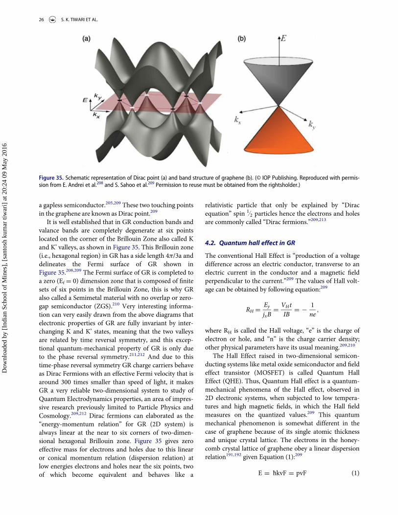
a gapless semiconductor.205,209 These two touching pointsin the graphene are known as Dirac point.209
It is well established that in GR conduction bands andvalance bands are completely degenerate at six pointslocated on the corner of the Brillouin Zone also called Kand K’ valleys, as shown in Figure 35. This Brillouin zone(i.e., hexagonal region) in GR has a side length 4p/3a anddelineates the Fermi surface of GR shown inFigure 35.208,209 The Fermi surface of GR is completed toa zero (Ef D 0) dimension zone that is composed of finitesets of six points in the Brillouin Zone, this is why GRalso called a Semimetal material with no overlap or zero-gap semiconductor (ZGS).210 Very interesting informa-tion can very easily drawn from the above diagrams thatelectronic properties of GR are fully invariant by inter-changing K and K’ states, meaning that the two valleysare related by time reversal symmetry, and this excep-tional quantum-mechanical property of GR is only dueto the phase reversal symmetry.211,212 And due to thistime-phase reversal symmetry GR charge carriers behaveas Dirac Fermions with an effective Fermi velocity that isaround 300 times smaller than speed of light, it makesGR a very reliable two-dimensional system to study ofQuantum Electrodynamics properties, an area of impres-sive research previously limited to Particle Physics andCosmology.209,212 Dirac fermions can elaborated as the“energy-momentum relation” for GR (2D system) isalways linear at the near to six corners of two-dimen-sional hexagonal Brillouin zone. Figure 35 gives zeroeffective mass for electrons and holes due to this linearor conical momentum relation (dispersion relation) atlow energies electrons and holes near the six points, twoof which become equivalent and behaves like a
relativistic particle that only be explained by “Diracequation” spin 1=2 particles hence the electrons and holesare commonly called “Dirac fermions.”209,213
4.2. Quantum hall effect in GR
The conventional Hall Effect is “production of a voltagedifference across an electric conductor, transverse to anelectric current in the conductor and a magnetic fieldperpendicular to the current.”209 The values of Hall volt-age can be obtained by following equation:209
RH D EyjxB
D VHtIB
D ¡ 1ne
;
where RH is called the Hall voltage, “e” is the charge ofelectron or hole, and “n” is the charge carrier density;other physical parameters have its usual meaning.209,210
The Hall Effect raised in two-dimensional semicon-ducting systems like metal oxide semiconductor and fieldeffect transistor (MOSFET) is called Quantum HallEffect (QHE). Thus, Quantum Hall effect is a quantum-mechanical phenomena of the Hall effect, observed in2D electronic systems, when subjected to low tempera-tures and high magnetic fields, in which the Hall fieldmeasures on the quantized values.209 This quantummechanical phenomenon is somewhat different in thecase of graphene because of its single atomic thicknessand unique crystal lattice. The electrons in the honey-comb crystal lattice of graphene obey a linear dispersionrelation191,192 given Equation (1):209
E D ћkvF D pvF (1)
Figure 35. Schematic representation of Dirac point (a) and band structure of graphene (b). (© IOP Publishing. Reproduced with permis-sion from E. Andrei et al.208 and S. Sahoo et al.209 Permission to reuse must be obtained from the rightsholder.)
26 S. K. TIWARI ET AL.
Dow
nloa
ded
by [
Indi
an S
choo
l of
Min
es],
[sa
ntos
h ku
mar
tiw
ari]
at 2
0:24
09
May
201
6
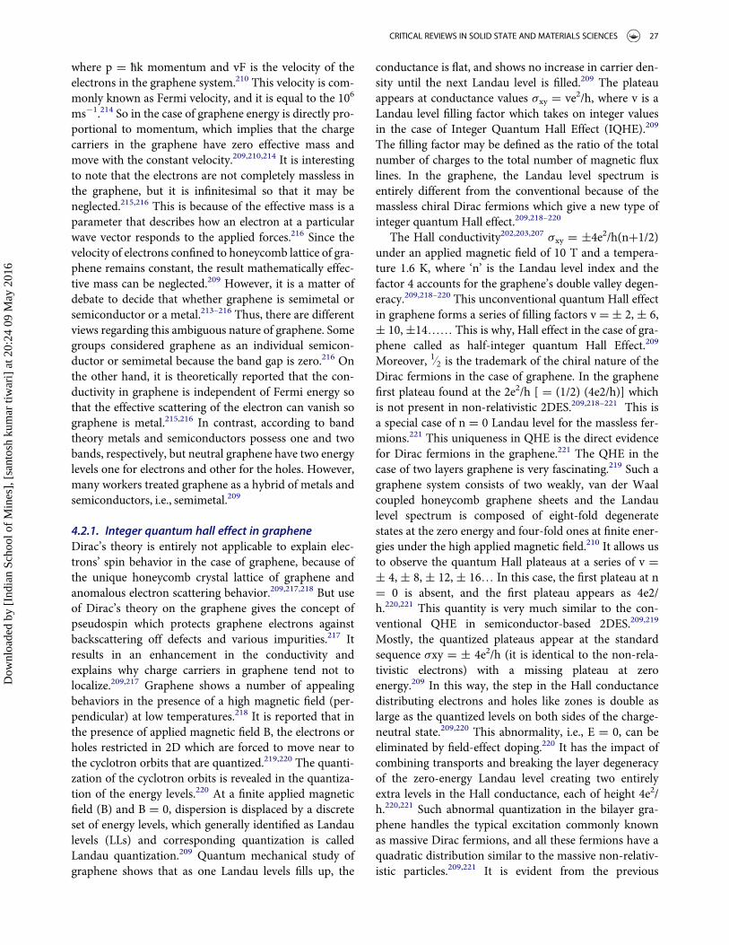
where p D ћk momentum and vF is the velocity of theelectrons in the graphene system.210 This velocity is com-monly known as Fermi velocity, and it is equal to the 106
ms¡1.214 So in the case of graphene energy is directly pro-portional to momentum, which implies that the chargecarriers in the graphene have zero effective mass andmove with the constant velocity.209,210,214 It is interestingto note that the electrons are not completely massless inthe graphene, but it is infinitesimal so that it may beneglected.215,216 This is because of the effective mass is aparameter that describes how an electron at a particularwave vector responds to the applied forces.216 Since thevelocity of electrons confined to honeycomb lattice of gra-phene remains constant, the result mathematically effec-tive mass can be neglected.209 However, it is a matter ofdebate to decide that whether graphene is semimetal orsemiconductor or a metal.213–216 Thus, there are differentviews regarding this ambiguous nature of graphene. Somegroups considered graphene as an individual semicon-ductor or semimetal because the band gap is zero.216 Onthe other hand, it is theoretically reported that the con-ductivity in graphene is independent of Fermi energy sothat the effective scattering of the electron can vanish sographene is metal.215,216 In contrast, according to bandtheory metals and semiconductors possess one and twobands, respectively, but neutral graphene have two energylevels one for electrons and other for the holes. However,many workers treated graphene as a hybrid of metals andsemiconductors, i.e., semimetal.209
4.2.1. Integer quantum hall effect in grapheneDirac’s theory is entirely not applicable to explain elec-trons’ spin behavior in the case of graphene, because ofthe unique honeycomb crystal lattice of graphene andanomalous electron scattering behavior.209,217,218 But useof Dirac’s theory on the graphene gives the concept ofpseudospin which protects graphene electrons againstbackscattering off defects and various impurities.217 Itresults in an enhancement in the conductivity andexplains why charge carriers in graphene tend not tolocalize.209,217 Graphene shows a number of appealingbehaviors in the presence of a high magnetic field (per-pendicular) at low temperatures.218 It is reported that inthe presence of applied magnetic field B, the electrons orholes restricted in 2D which are forced to move near tothe cyclotron orbits that are quantized.219,220 The quanti-zation of the cyclotron orbits is revealed in the quantiza-tion of the energy levels.220 At a finite applied magneticfield (B) and B D 0, dispersion is displaced by a discreteset of energy levels, which generally identified as Landaulevels (LLs) and corresponding quantization is calledLandau quantization.209 Quantum mechanical study ofgraphene shows that as one Landau levels fills up, the
conductance is flat, and shows no increase in carrier den-sity until the next Landau level is filled.209 The plateauappears at conductance values sxy D ve2/h, where v is aLandau level filling factor which takes on integer valuesin the case of Integer Quantum Hall Effect (IQHE).209
The filling factor may be defined as the ratio of the totalnumber of charges to the total number of magnetic fluxlines. In the graphene, the Landau level spectrum isentirely different from the conventional because of themassless chiral Dirac fermions which give a new type ofinteger quantum Hall effect.209,218–220
The Hall conductivity202,203,207 sxy D §4e2/h(nC1/2)under an applied magnetic field of 10 T and a tempera-ture 1.6 K, where ‘n’ is the Landau level index and thefactor 4 accounts for the graphene’s double valley degen-eracy.209,218–220 This unconventional quantum Hall effectin graphene forms a series of filling factors v D § 2, § 6,§ 10,§14…… This is why, Hall effect in the case of gra-phene called as half-integer quantum Hall Effect.209
Moreover, 1=2 is the trademark of the chiral nature of theDirac fermions in the case of graphene. In the graphenefirst plateau found at the 2e2/h [ D (1/2) (4e2/h)] whichis not present in non-relativistic 2DES.209,218–221 This isa special case of n D 0 Landau level for the massless fer-mions.221 This uniqueness in QHE is the direct evidencefor Dirac fermions in the graphene.221 The QHE in thecase of two layers graphene is very fascinating.219 Such agraphene system consists of two weakly, van der Waalcoupled honeycomb graphene sheets and the Landaulevel spectrum is composed of eight-fold degeneratestates at the zero energy and four-fold ones at finite ener-gies under the high applied magnetic field.210 It allows usto observe the quantum Hall plateaus at a series of v D§ 4, § 8, § 12, § 16… In this case, the first plateau at nD 0 is absent, and the first plateau appears as 4e2/h.220,221 This quantity is very much similar to the con-ventional QHE in semiconductor-based 2DES.209,219
Mostly, the quantized plateaus appear at the standardsequence sxy D § 4e2/h (it is identical to the non-rela-tivistic electrons) with a missing plateau at zeroenergy.209 In this way, the step in the Hall conductancedistributing electrons and holes like zones is double aslarge as the quantized levels on both sides of the charge-neutral state.209,220 This abnormality, i.e., E D 0, can beeliminated by field-effect doping.220 It has the impact ofcombining transports and breaking the layer degeneracyof the zero-energy Landau level creating two entirelyextra levels in the Hall conductance, each of height 4e2/h.220,221 Such abnormal quantization in the bilayer gra-phene handles the typical excitation commonly knownas massive Dirac fermions, and all these fermions have aquadratic distribution similar to the massive non-relativ-istic particles.209,221 It is evident from the previous
CRITICAL REVIEWS IN SOLID STATE AND MATERIALS SCIENCES 27
Dow
nloa
ded
by [
Indi
an S
choo
l of
Min
es],
[sa
ntos
h ku
mar
tiw
ari]
at 2
0:24
09
May
201
6
discussion that the exceptional IQHE in single layer gra-phene is due to the massless Dirac fermions and a zeroenergy mode (E D 0). The abnormal IQHE in bilayergraphene is because of the massive Dirac fermions andtwo zero energy modes.219–221 Also to this it is reportedthat room-temperature QHE can be observed in gra-phene under suitable condition. Such a brilliant remarkof QHE in graphene at ambient temperature unlocks upa new door for graphene/graphene derivative-basedquantum mechanical devices. 209, 219–221
4.2.2 Fractional quantum hall effect in grapheneA theoretical physicist expects that electrons in grapheneare the strongly interacting result; graphene shows theFractional Quantum Hall Effect (FQHE).222 It may bedefined as a physical event in which the Hall conduc-tance of 2D electrons indicates accurately quantized pla-teaus at fractional values of e2/h”.223 It is considered acombined state in which electrons handle magnetic fluxlines.222,223 As a result, new quasiparticles and excitationare generated that have a fractional elementary chargeand statistics.223 However, it is notable that still there isno sophisticated instrument to obtain direct informationabout FQHE in graphene.222,223 The Integer QuantumHall Effect in graphene can be explained in terms of sin-gle electrons in an applied magnetics; on another hand,the FQHE in graphene can be understood by the collec-tive behavior of all the electrons.224 It is because FQHErequires a higher magnetic field, low temperature, andvery instant mobility than the IQHE investigation, butthe IQHE never depends on interactions between theelectrons.224,225 The quantized Hall conductivity (sxy) inFQHE in graphene can be obtained by equation givenbelow:209,224,225
sxy D § 2pC 12m 2pC 1ð ÞC 1
2e2h
;
where m, p D 0 1 2 3 4….The localization of electrons and quasi- particles is
believed to be responsible for the formation of the pla-teaus in the Hall conductivity.225–227 Due to the honey-comb crystal lattice of graphene and unique Dirac natureof carriers, the edge states play a crucial role in quantumHall transport.225,226 Very recently, it has been reportedthat Dirac electrons exhibit high collective behavior thatgive rise to FQHE in graphene.209 Also, Du and coworkerhad suspended the ultrapure graphene between two sup-ports and observed that the electrons in suspended samplepossess much higher mobilities than the samples coatedon the substrate.226–230 Du and coworker obtained such aunique hall effect with a two-probe method to get the bet-ter results than the classical four-probe method.226,230
They observed plateau in transverse conductance at 1/3 ofthe conductance quantum e2/h, and they find that theFQHE can be observed at low temperatures in the mag-netic fields as small as 2 T.230–233 Lately, the FQHE hasbeen reported by Dean and coworker in a monolayer gra-phene that fabricated on a hexagonal boron nitride sub-strate.334,335 This substrate is very suitable because it is aninsulating isomorph of graphite.232–236
4.3. Graphene nanoribbons (GNRs)
In the previous section we have discussed the unzippingtechnique of CNTs and formation of graphene nanorib-bons. These nanoribbons are strips of graphene with anultra-thin width (<50 nm).236,237 First, graphene ribbonswere added to a theoretical model by Mitsutaka Fujitaand co-workers to evaluate the edge and effect of nano-scale size in graphene.237–338 Kosynkin et al. reportedthat longitudinal cleavage of CNTs, using specific chemi-cal, catalytical, and electrical ideas, successfully unzipsthem into thin graphene strips of various widths andshape. These unzipped CNTs are very similar with thegraphene nanoribbon but smaller in size Figure 13.59
When advanced lithographic technique is employed onGR for profound study of its nanoscale structure, it hasbeen observed that a lateral confinement of charge car-riers can work as an efficient energy gap having parame-ter, the possibility of such narrow non-ideal GR iscommonly called as graphene nano ribbon (GNR) ornano graphene ribbon.59,336–339 The TEM images of suchgraphene are strictly looking like the defect-free gra-phene, so the TEM is unable to distinguish GR andGNRs. The TEM picture of a GNRs is shown in theFigure 36.59
Existence of GNRs first of all reported by Mitsu-taka Fujita and coworker.22,24 In most of cases widthof GNRs varies between the 30–40 nm and this reasonit is also called as narrow graphene strips.59,336 It hasbeen found that Physical and chemical properties ofGNRs quite different from GR.22,24 The actual exis-tence of GNRs is still a point of debate, but theadvanced lithographic experiment and Raman spec-troscopy has confirmed that confined GR structuresare experimentally feasible.240,241 At present, synthesisof specific GNR is beyond a possibility, however, a lotof widths-controlled GNRs can be produced viaGraphite anatomy process.22,241 Very recently, GNRshave been grown into silicon carbide sheet using ironimplantation technique followed by laser anneal-ing.22,24 Nowadays, this technique is considered as abest method for the generation of GNRs.242 The prop-erties of GNRs mainly depend on the width and mor-phology of the edge structures and it is reported that
28 S. K. TIWARI ET AL.
Dow
nloa
ded
by [
Indi
an S
choo
l of
Min
es],
[sa
ntos
h ku
mar
tiw
ari]
at 2
0:24
09
May
201
6
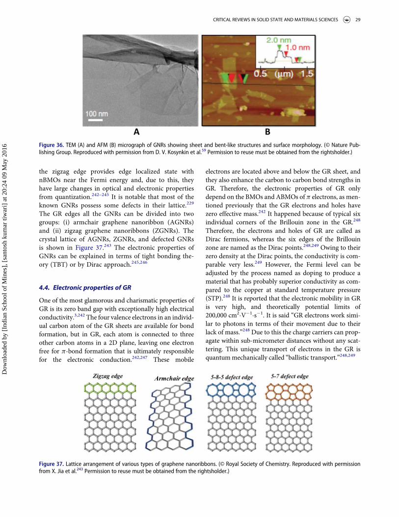
the zigzag edge provides edge localized state withnBMOs near the Fermi energy and, due to this, theyhave large changes in optical and electronic propertiesfrom quantization.242–245 It is notable that most of theknown GNRs possess some defects in their lattice.229
The GR edges all the GNRs can be divided into twogroups: (i) armchair graphene nanoribbon (AGNRs)and (ii) zigzag graphene nanoribbons (ZGNRs). Thecrystal lattice of AGNRs, ZGNRs, and defected GNRsis shown in Figure 37.243 The electronic properties ofGNRs can be explained in terms of tight bonding the-ory (TBT) or by Dirac approach.245,246
4.4. Electronic properties of GR
One of the most glamorous and charismatic properties ofGR is its zero band gap with exceptionally high electricalconductivity.3,242 The four valence electrons in an individ-ual carbon atom of the GR sheets are available for bondformation, but in GR, each atom is connected to threeother carbon atoms in a 2D plane, leaving one electronfree for p-bond formation that is ultimately responsiblefor the electronic conduction.242,247 These mobile
electrons are located above and below the GR sheet, andthey also enhance the carbon to carbon bond strengths inGR. Therefore, the electronic properties of GR onlydepend on the BMOs and ABMOs of p electrons, as men-tioned previously that the GR electrons and holes havezero effective mass.242 It happened because of typical sixindividual corners of the Brillouin zone in the GR.248
Therefore, the electrons and holes of GR are called asDirac fermions, whereas the six edges of the Brillouinzone are named as the Dirac points.248,249 Owing to theirzero density at the Dirac points, the conductivity is com-parable very less.249 However, the Fermi level can beadjusted by the process named as doping to produce amaterial that has probably superior conductivity as com-pared to the copper at standard temperature pressure(STP).248 It is reported that the electronic mobility in GRis very high, and theoretically potential limits of200,000 cm2¢V¡1¢s¡1. It is said “GR electrons work simi-lar to photons in terms of their movement due to theirlack of mass.”248 Due to this the charge carriers can prop-agate within sub-micrometer distances without any scat-tering. This unique transport of electrons in the GR isquantummechanically called “ballistic transport.”248,249
Figure 36. TEM (A) and AFM (B) micrograph of GNRs showing sheet and bent-like structures and surface morphology. (© Nature Pub-lishing Group. Reproduced with permission from D. V. Kosynkin et al.59 Permission to reuse must be obtained from the rightsholder.)
Figure 37. Lattice arrangement of various types of graphene nanoribbons. (© Royal Society of Chemistry. Reproduced with permissionfrom X. Jia et al.243 Permission to reuse must be obtained from the rightsholder.)
CRITICAL REVIEWS IN SOLID STATE AND MATERIALS SCIENCES 29
Dow
nloa
ded
by [
Indi
an S
choo
l of
Min
es],
[sa
ntos
h ku
mar
tiw
ari]
at 2
0:24
09
May
201
6
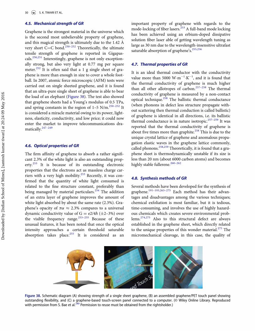
4.5. Mechanical strength of GR
Graphene is the strongest material in the universe whichis the second most unbelievable property of graphene,and this magical strength is ultimately due to the 1.42 A
�
very short CHC bond.250–252 Theoretically, the ultimatetensile strength of graphene is reported in Gigapas-cals.250,251 Interestingly, graphene is not only exception-ally strong, but also very light at 0.77 mg per squaremeter.252 It is often said that a 1 g single sheet of gra-phene is more than enough in size to cover a whole foot-ball. In 2007, atomic force microscopic (AFM) tests werecarried out on single sheeted graphene, and it is foundthat an ultra-pure single sheet of graphene is able to bearthe load of an elephant (Figure 38). The test also showedthat graphene sheets had a Young’s modulus of 0.5 TPa,and spring constants in the region of 1–5 N/m.250–252 Itis considered a miracle material owing to its power, light-ness, elasticity, conductivity, and low price; it could nowenter the market to improve telecommunications dra-matically.247–249
4.6. Optical properties of GR
The firm affinity of graphene to absorb a rather signifi-cant 2.3% of the white light is also an outstanding prop-erty.253 It is because of its outstanding electronicproperties that the electrons act as massless charge car-riers with a very high mobility.253 Recently, it was con-firmed that the quantity of white light consumed isrelated to the fine structure constant, preferably thanbeing managed by material particulars.254 The additionof an extra layer of graphene improves the amount ofwhite light absorbed by about the same rate (2.3%). Gra-phene’s opacity of pa � 2.3% compares to a universaldynamic conductivity value of G D e2/4�h (§2–3%) overthe visible frequency range.253–255 Because of theseunusual features, it has been noted that once the opticalintensity approaches a certain threshold saturableabsorption takes place.255 It is considered as an
important property of graphene with regards to themode-locking of fiber lasers.253 A full-band mode lockinghas been achieved using an erbium-doped dissipativesolution fiber laser able of getting wavelength tuning aslarge as 30 nm due to the wavelength-insensitive ultrafastsaturable absorption of graphene’s.255,256
4.7. Thermal properties of GR
It is an ideal thermal conductor with the conductivityvalue more than 5000 W¢m¡1¢K¡1, and it is found thatthe thermal conductivity of graphene is much higherthan all other allotropes of carbon.257–258 The thermalconductivity of graphene is measured by a non-contactoptical technique.258 The ballistic thermal conductance(when phonons in defect less structure propagate with-out scattering then thermal conduction is called ballistic)of graphene is identical in all directions, i.e. its ballisticthermal conductance is in nature isotropic.257–259 It wasreported that the thermal conductivity of graphene isabout five times more than graphite.258 This is due to theunique crystal lattice of graphene and anomalous propa-gation elastic waves in the graphene lattice commonly,called phonons.258,259 Theoretically, it is found that a gra-phene sheet is thermodynamically unstable if its size isless than 20 nm (about 6000 carbon atoms) and becomeshighly stable fullerene.260–262
4.8. Synthesis methods of GR
Several methods have been developed for the synthesis ofgraphene.191–193,263–275 Each method has their advan-tages and disadvantages among the various techniques;chemical exfoliation is most familiar, but it is tedious,time-consuming, and involves the use of highly hazard-ous chemicals which creates severe environmental prob-lems.274,275 Also to this structural defect are alwaysestablished in the graphene sheet, which directly relatedto the unique properties of this wonder material.275 Themicromechanical cleavage, in this case, the quality of
Figure 38. Schematic diagram (A) showing strength of a single sheet graphene, (B) an assembled graphene/PET touch panel showingoutstanding flexibility, and (C) a graphene-based touch-screen panel connected to a computer. (© Wiley Online Library. Reproducedwith permission from S. Bae et al.249 Permission to reuse must be obtained from the rightsholder.)
30 S. K. TIWARI ET AL.
Dow
nloa
ded
by [
Indi
an S
choo
l of
Min
es],
[sa
ntos
h ku
mar
tiw
ari]
at 2
0:24
09
May
201
6
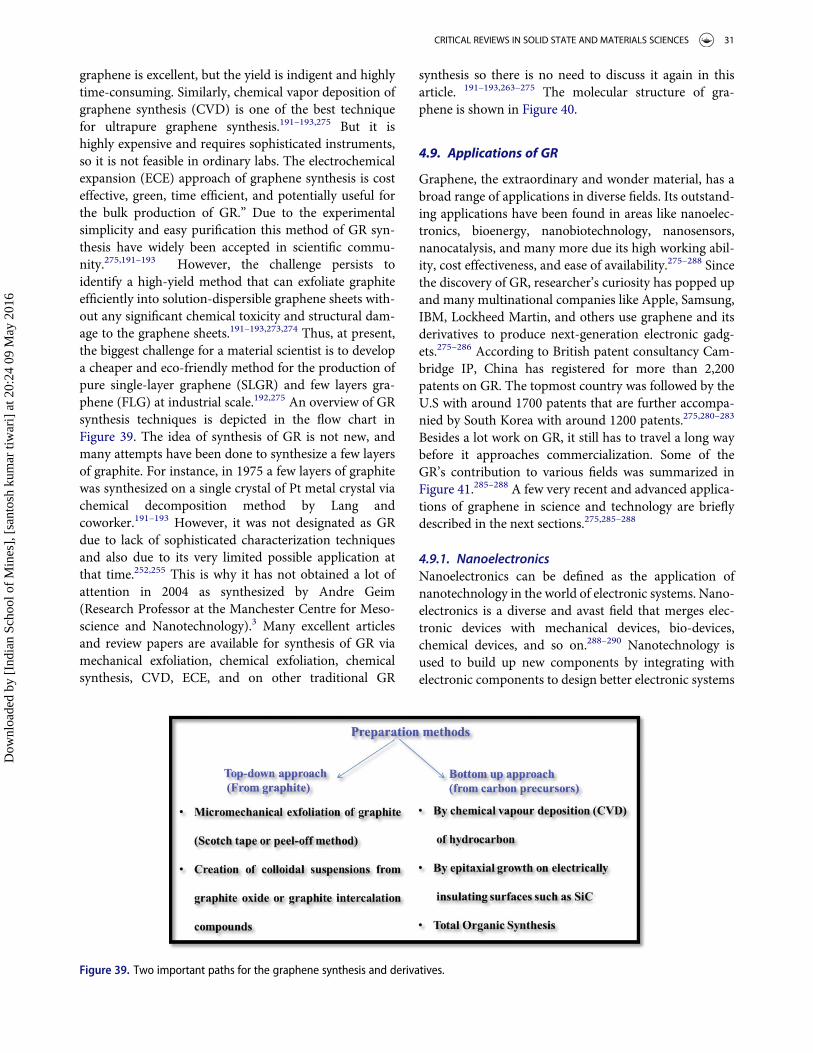
graphene is excellent, but the yield is indigent and highlytime-consuming. Similarly, chemical vapor deposition ofgraphene synthesis (CVD) is one of the best techniquefor ultrapure graphene synthesis.191–193,275 But it ishighly expensive and requires sophisticated instruments,so it is not feasible in ordinary labs. The electrochemicalexpansion (ECE) approach of graphene synthesis is costeffective, green, time efficient, and potentially useful forthe bulk production of GR.” Due to the experimentalsimplicity and easy purification this method of GR syn-thesis have widely been accepted in scientific commu-nity.275,191–193 However, the challenge persists toidentify a high-yield method that can exfoliate graphiteefficiently into solution-dispersible graphene sheets with-out any significant chemical toxicity and structural dam-age to the graphene sheets.191–193,273,274 Thus, at present,the biggest challenge for a material scientist is to developa cheaper and eco-friendly method for the production ofpure single-layer graphene (SLGR) and few layers gra-phene (FLG) at industrial scale.192,275 An overview of GRsynthesis techniques is depicted in the flow chart inFigure 39. The idea of synthesis of GR is not new, andmany attempts have been done to synthesize a few layersof graphite. For instance, in 1975 a few layers of graphitewas synthesized on a single crystal of Pt metal crystal viachemical decomposition method by Lang andcoworker.191–193 However, it was not designated as GRdue to lack of sophisticated characterization techniquesand also due to its very limited possible application atthat time.252,255 This is why it has not obtained a lot ofattention in 2004 as synthesized by Andre Geim(Research Professor at the Manchester Centre for Meso-science and Nanotechnology).3 Many excellent articlesand review papers are available for synthesis of GR viamechanical exfoliation, chemical exfoliation, chemicalsynthesis, CVD, ECE, and on other traditional GR
synthesis so there is no need to discuss it again in thisarticle. 191–193,263–275 The molecular structure of gra-phene is shown in Figure 40.
4.9. Applications of GR
Graphene, the extraordinary and wonder material, has abroad range of applications in diverse fields. Its outstand-ing applications have been found in areas like nanoelec-tronics, bioenergy, nanobiotechnology, nanosensors,nanocatalysis, and many more due its high working abil-ity, cost effectiveness, and ease of availability.275–288 Sincethe discovery of GR, researcher’s curiosity has popped upand many multinational companies like Apple, Samsung,IBM, Lockheed Martin, and others use graphene and itsderivatives to produce next-generation electronic gadg-ets.275–286 According to British patent consultancy Cam-bridge IP, China has registered for more than 2,200patents on GR. The topmost country was followed by theU.S with around 1700 patents that are further accompa-nied by South Korea with around 1200 patents.275,280–283
Besides a lot work on GR, it still has to travel a long waybefore it approaches commercialization. Some of theGR’s contribution to various fields was summarized inFigure 41.285–288 A few very recent and advanced applica-tions of graphene in science and technology are brieflydescribed in the next sections.275,285–288
4.9.1. NanoelectronicsNanoelectronics can be defined as the application ofnanotechnology in the world of electronic systems. Nano-electronics is a diverse and avast field that merges elec-tronic devices with mechanical devices, bio-devices,chemical devices, and so on.288–290 Nanotechnology isused to build up new components by integrating withelectronic components to design better electronic systems
Figure 39. Two important paths for the graphene synthesis and derivatives.
CRITICAL REVIEWS IN SOLID STATE AND MATERIALS SCIENCES 31
Dow
nloa
ded
by [
Indi
an S
choo
l of
Min
es],
[sa
ntos
h ku
mar
tiw
ari]
at 2
0:24
09
May
201
6
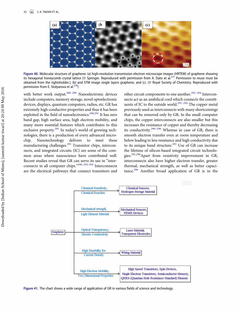
with better work output.288–290 Nanoelectronic devicesinclude computers, memory storage, novel optoelectronicdevices, displays, quantum computers, radios, etc. GR hasextremely high conductive properties and thus it has beenexploited in the field of nanoelectronics.290,291 It has zeroband gap, high surface area, high electron mobility, andmany more essential features which contributes to thisexclusive property.291 In today’s world of growing tech-nologies, there is a production of every advanced micro-chip. Nanotechnology delivers to meet thesemanufacturing challenges.291 Transistor chips, intercon-nects, and integrated circuits (IC) are some of the com-mon areas where nanoscience have contributed well.Recent studies reveal that GR can serve its use in “inter-connects in all computer chips.”290–292-294 Interconnectsare the electrical pathways that connect transistors and
other circuit components to one another.292–294 Intercon-nects act as an umbilical cord which connects the constit-uents of IC to the outside world.291–294 The copper metalpreviously used as interconnects with many shortcomingsthat can be removed only by GR. In the small computerchips, the copper interconnects are also smaller but thisincreases the resistance of copper and thereby decreasingits conductivity.290–296 Whereas in case of GR, there issmooth electron transfer even at room temperature andbelow leading to less resistance and high conductivity dueto its unique band structure.291 Use of GR can increasethe lifetime of silicon-based integrated circuit technolo-gies.291,296Apart from resistivity improvement in GR,interconnects also have higher electron transfer, greaterthermal, mechanical strength, as well as better capaci-tance.296 Another broad application of GR is in the
Figure 40. Molecular structure of graphene: (a) high-resolution transmission electron microscope images (HRTEM) of graphene showingits hexagonal honeycomb crystal lattice (© Springer. Reproduced with permission from A. Dato et al.277 Permission to reuse must beobtained from the rightsholder.), (b) and STM image single layers graphene, and (c). (© Royal Society of Chemistry. Reproduced withpermission from E. Stolyarova et al.278)
Figure 41. The chart shows a wide range of application of GR in various fields of science and technology.
32 S. K. TIWARI ET AL.
Dow
nloa
ded
by [
Indi
an S
choo
l of
Min
es],
[sa
ntos
h ku
mar
tiw
ari]
at 2
0:24
09
May
201
6
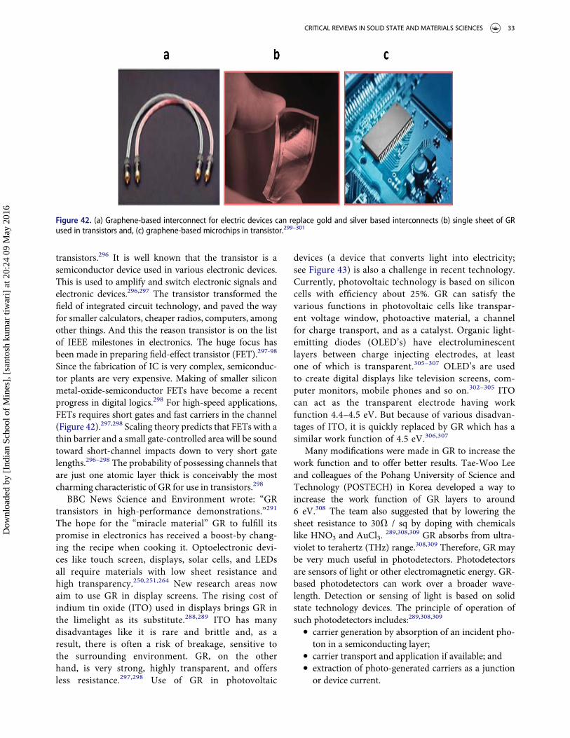
transistors.296 It is well known that the transistor is asemiconductor device used in various electronic devices.This is used to amplify and switch electronic signals andelectronic devices.296,297 The transistor transformed thefield of integrated circuit technology, and paved the wayfor smaller calculators, cheaper radios, computers, amongother things. And this the reason transistor is on the listof IEEE milestones in electronics. The huge focus hasbeen made in preparing field-effect transistor (FET).297-98
Since the fabrication of IC is very complex, semiconduc-tor plants are very expensive. Making of smaller siliconmetal-oxide-semiconductor FETs have become a recentprogress in digital logics.298 For high-speed applications,FETs requires short gates and fast carriers in the channel(Figure 42).297,298 Scaling theory predicts that FETs with athin barrier and a small gate-controlled area will be soundtoward short-channel impacts down to very short gatelengths.296–298 The probability of possessing channels thatare just one atomic layer thick is conceivably the mostcharming characteristic of GR for use in transistors.298
BBC News Science and Environment wrote: “GRtransistors in high-performance demonstrations.”291
The hope for the “miracle material” GR to fulfill itspromise in electronics has received a boost-by chang-ing the recipe when cooking it. Optoelectronic devi-ces like touch screen, displays, solar cells, and LEDsall require materials with low sheet resistance andhigh transparency.250,251,264 New research areas nowaim to use GR in display screens. The rising cost ofindium tin oxide (ITO) used in displays brings GR inthe limelight as its substitute.288,289 ITO has manydisadvantages like it is rare and brittle and, as aresult, there is often a risk of breakage, sensitive tothe surrounding environment. GR, on the otherhand, is very strong, highly transparent, and offersless resistance.297,298 Use of GR in photovoltaic
devices (a device that converts light into electricity;see Figure 43) is also a challenge in recent technology.Currently, photovoltaic technology is based on siliconcells with efficiency about 25%. GR can satisfy thevarious functions in photovoltaic cells like transpar-ent voltage window, photoactive material, a channelfor charge transport, and as a catalyst. Organic light-emitting diodes (OLED’s) have electroluminescentlayers between charge injecting electrodes, at leastone of which is transparent.305–307 OLED’s are usedto create digital displays like television screens, com-puter monitors, mobile phones and so on.302–305 ITOcan act as the transparent electrode having workfunction 4.4–4.5 eV. But because of various disadvan-tages of ITO, it is quickly replaced by GR which has asimilar work function of 4.5 eV.306,307
Many modifications were made in GR to increase thework function and to offer better results. Tae-Woo Leeand colleagues of the Pohang University of Science andTechnology (POSTECH) in Korea developed a way toincrease the work function of GR layers to around6 eV.308 The team also suggested that by lowering thesheet resistance to 30V / sq by doping with chemicalslike HNO3 and AuCl3.
289,308,309 GR absorbs from ultra-violet to terahertz (THz) range.308,309 Therefore, GR maybe very much useful in photodetectors. Photodetectorsare sensors of light or other electromagnetic energy. GR-based photodetectors can work over a broader wave-length. Detection or sensing of light is based on solidstate technology devices. The principle of operation ofsuch photodetectors includes:289,308,309
� carrier generation by absorption of an incident pho-ton in a semiconducting layer;
� carrier transport and application if available; and� extraction of photo-generated carriers as a junctionor device current.
Figure 42. (a) Graphene-based interconnect for electric devices can replace gold and silver based interconnects (b) single sheet of GRused in transistors and, (c) graphene-based microchips in transistor.299–301
CRITICAL REVIEWS IN SOLID STATE AND MATERIALS SCIENCES 33
Dow
nloa
ded
by [
Indi
an S
choo
l of
Min
es],
[sa
ntos
h ku
mar
tiw
ari]
at 2
0:24
09
May
201
6
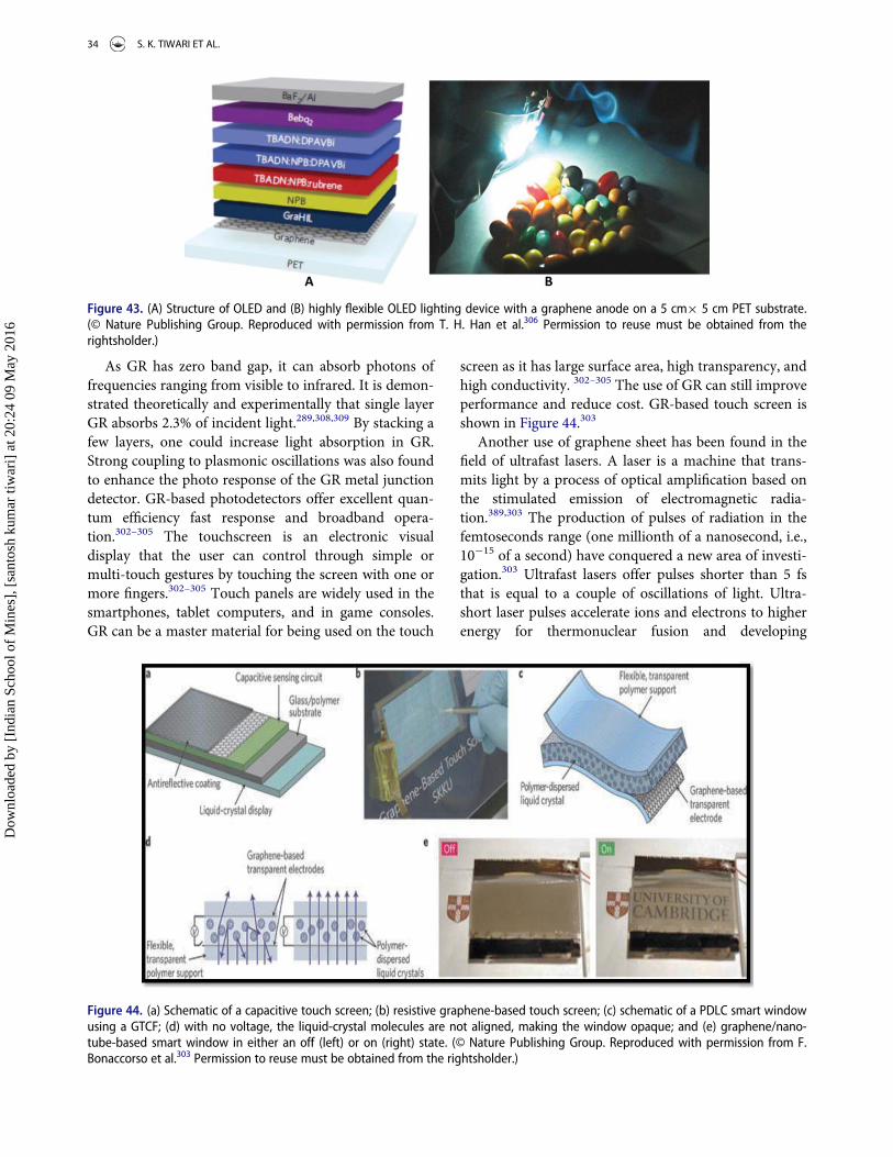
As GR has zero band gap, it can absorb photons offrequencies ranging from visible to infrared. It is demon-strated theoretically and experimentally that single layerGR absorbs 2.3% of incident light.289,308,309 By stacking afew layers, one could increase light absorption in GR.Strong coupling to plasmonic oscillations was also foundto enhance the photo response of the GR metal junctiondetector. GR-based photodetectors offer excellent quan-tum efficiency fast response and broadband opera-tion.302–305 The touchscreen is an electronic visualdisplay that the user can control through simple ormulti-touch gestures by touching the screen with one ormore fingers.302–305 Touch panels are widely used in thesmartphones, tablet computers, and in game consoles.GR can be a master material for being used on the touch
screen as it has large surface area, high transparency, andhigh conductivity. 302–305 The use of GR can still improveperformance and reduce cost. GR-based touch screen isshown in Figure 44.303
Another use of graphene sheet has been found in thefield of ultrafast lasers. A laser is a machine that trans-mits light by a process of optical amplification based onthe stimulated emission of electromagnetic radia-tion.389,303 The production of pulses of radiation in thefemtoseconds range (one millionth of a nanosecond, i.e.,10¡15 of a second) have conquered a new area of investi-gation.303 Ultrafast lasers offer pulses shorter than 5 fsthat is equal to a couple of oscillations of light. Ultra-short laser pulses accelerate ions and electrons to higherenergy for thermonuclear fusion and developing
Figure 43. (A) Structure of OLED and (B) highly flexible OLED lighting device with a graphene anode on a 5 cm£ 5 cm PET substrate.(© Nature Publishing Group. Reproduced with permission from T. H. Han et al.306 Permission to reuse must be obtained from therightsholder.)
Figure 44. (a) Schematic of a capacitive touch screen; (b) resistive graphene-based touch screen; (c) schematic of a PDLC smart windowusing a GTCF; (d) with no voltage, the liquid-crystal molecules are not aligned, making the window opaque; and (e) graphene/nano-tube-based smart window in either an off (left) or on (right) state. (© Nature Publishing Group. Reproduced with permission from F.Bonaccorso et al.303 Permission to reuse must be obtained from the rightsholder.)
34 S. K. TIWARI ET AL.
Dow
nloa
ded
by [
Indi
an S
choo
l of
Min
es],
[sa
ntos
h ku
mar
tiw
ari]
at 2
0:24
09
May
201
6
compact particle accelerators.303–308 Most of the ultra-short lasers works on a mode-locking technique in whicha nonlinear optical element turns the continuous laserwave output into ultra-short optical pulses.303–308 Thenonlinear optical element is known as saturableabsorber. GR can be a splendid choice for the saturableabsorbers. The gapless linear dispersion of Dirac elec-trons allows broadband saturable absorption in GR. Theoptical absorption, ultrafast carrier relaxation time, andcontrollable modulation depth of GR have been mea-sured. Optical frequency converters are used to expandwavelength accessibilities of lasers.303–308 One of therecent and advanced challenges of GR is its use for radiofrequency electronics. For radio frequency transistors,the cut-off frequency is the most widely used figure-of-merit to characterize the fundamental speed limit. Thecut-off frequency is defined as the frequency at whichpoint the magnitude of the small-signal current gain ofthe transistor is reduced to the unit.303–309
5. Polymer nanocomposites (PNCs)
Materials always play a vital role fundamentally in ourlives in the innovation, creation, and origination of vari-ous kinds of novel materials and as a result the quality ofour life has greatly been improved over the time. Thus,we can say that without the improvement in the materialscience and technology, it is not possible to imagine ourmodern lives. All the most significant breakthroughs inthe progression of our civilization are closely linked to theprogress in the materials throughout history. For example,the stone age, bronze age, iron age, steel age (industrialrevolution), silicon, and silica age (communication revolu-tion), all these reflect that our modern society and every-day activity in the 21st century extensively depends uponthe high number of materials to an extent of sophistica-tion. Moreover, the whole world is governed by a cus-tomer market directing for development in our lifestylewithout limits which finally depends on the creation ofnew materials. Thus, materials are essential for the tech-nology that makes our lives full of convenience. Forinstance, the introduction of the laptop, digital cellphones, and touch screens. Hence, the difficulty of design-ing novel, more utilitarian and different materialsincreases with the requirements of civilization. The short-comings for satisfying essential needs such as sustainableenergy, affordable personal care, etc. are intimately associ-ated with restrictions on the properties of materials.310–321
The most crucial perspective of achieving advanced mate-rial with desired and enhanced properties is the creativemolecular design and synthesis of new material. This canbe accomplished with a deep understanding of molecularphysics and nano physics, quantum mechanics,
nanochemistry, and advanced computational techniques.Thus, material science involves the study of the structureand properties of well-known materials and the synthesisand characterization of new or improved and desiredmaterials.310–321 The use of advanced computationalmethods to predict structures and properties of materialsthat have not still invented. By the existing knowledge ofcurrent materials and their modification leads to the for-mation of a new material with better properties.
Presently, in the verges of material science and tech-nology, the concept of conflating different kinds of mate-rials synergically in suitable experimental conditions isone of the most accessible ways to achieve specific goalswith the highest performance in the properties and costeffectiveness. Since it is well known that polymers areused in innumerable applications and fields and are veryfamiliar in tuning the properties or upgrading the perfor-mance of polymer systems to obtain an accurate process-ing and applications. Thus, specific additives arefrequently used to alter the polymer properties or toimprove the performance of polymer systems. Due tothis is the reason the mixing of two or more differentmaterials in a suitable manner leads to the creation of anew material with improved which is widely accepted bythe scientific community. In this regard, polymers areone of the most affable and favorably used sources ofmaterials due to their large number of chemical struc-tures. They also have outstanding properties, along withtheir affordable cost, simple processing, and their utilityas sustainable materials.270–273 The field of PNCs hasexpanded to serve one of the largest classes within thereach of materials science. Nowadays, the area of PNCshas grown so rapidly and attains highest position withinthe scope of material science and become a main branchof nanoscience and nanotechnology, which providesmany new materials having numerous and diverse appli-cation area.260–270
5.1. Brief history of nanocomposites
The field of composite materials and PNCs is notnew;310–315 it has been known and utilized for decades,or even centuries.310 Nanoparticles were used in theglazes on Ming Dynasty ceramics (1368–1644). Carbonblack reinforced rubber is in use since the 1900s as areinforcing agent in automobile tires which is also aform of nanocomposite.311,312 But all these early materi-als were produced and used without the ability to con-trol their structural, morphological, and physicalproperties, 312 and also without a full understanding ofwhat gives nanoparticles their unique properties. Butthe dawning of modern nanotechnology can be tracedto Richard Feynman’s Caltech speech, “There’s Plenty
CRITICAL REVIEWS IN SOLID STATE AND MATERIALS SCIENCES 35
Dow
nloa
ded
by [
Indi
an S
choo
l of
Min
es],
[sa
ntos
h ku
mar
tiw
ari]
at 2
0:24
09
May
201
6
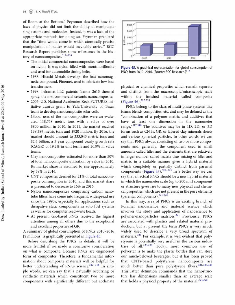
of Room at the Bottom.” Feynman described how thelaws of physics did not limit the ability to manipulatesingle atoms and molecules. Instead, it was a lack of theappropriate methods for doing so. Feynman predictedthat the “time would come in which atomically precisemanipulation of matter would inevitably arrive.” BCCResearch Report publishes some milestones in the his-tory of nanocomposites.312–318
� The initial commercial nanocomposites were basedon nylon. It was nylon filled with montmorilloniteand used for automobile timing belts.
� 1988: Hitachi Metals develops the first nanomag-netic compound, Finemet, used to fabricate low-losstransformers.
� 1998: Inframat LLC patents Nanox 2613 thermalspray, the first commercial ceramic nanocomposite.
� 2005: U.S. National Academies Keck FUTURES ini-tiative awards grant to Yale/University of Texasteam to develop nanocomposite solar cells.
� Global uses of the nanocomposites were an evalu-ated 118,768 metric tons with a value of over$800 million in 2010. In 2011, the market reached138,389 metric tons and $920 million. By 2016, themarket should amount to 333,043 metric tons and$2.4 billion, a 5-year compound yearly growth rate(CAGR) of 19.2% in unit terms and 20.9% in valueterms.
� Clay nanocomposites estimated for more than 50%of total nanocomposite utilization by value in 2010.Its market share is assumed to rise approximatelyby 58% in 2016.
� CNT composites deemed for 21% of total nanocom-posite consumption in 2010, and this market shareis presumed to decrease to 16% in 2016.
� Nylon nanocomposites comprising carbon nano-tube fillers have come into frequent, widespread usesince the 1990s, especially for applications such asdissipative static components in auto fuel systemsas well as for computer read-write heads.
� At present, GR-based PNCs received the highestattention among all others due to the exceptionaland excellent properties of GR.
A summary of global consumption of PNCs 2010–2016[$ millions] is graphically presented in Figure 45.
Before describing the PNCs in details, it will bemore fruitful if we made a conclusive considerationon what is composite. Because PNCs are engineeredform of composites. Therefore, a fundamental infor-mation about composite materials will be helpful forbetter understanding of PNCs science.312–318 In sim-ple words, we can say that a naturally occurring orsynthetic materials which constituent two or morecomponents with significantly different but acclimate
physical or chemical properties which remain separateand distinct from the macroscopic/microscopic scalewithin the finished material called composite(Figure 46).317,318
PNCs belong to the class of multi-phase systems likefoams blends composites, etc. and may be defined as the“combination of a polymer matrix and additives thathave at least one dimension in the nanometerrange.”317,318 The additives may be in 1D, 2D, or 3Dforms such as CNTs, GR, or layered clay minerals sheetsand various spherical particles. In other words, we cansay that PNCs always consisting of two or more compo-nents and, generally, the component used in smallamounts called filler and the elements that are relativelyin larger number called matrix thus mixing of filler andmatrix in a suitable manner gives a hybrid materialwhich completely or partially distinct from parentalcomponents (Figure 47).320–323 In a better way we cansay that an actual PNCs should be a new hybrid materialin which the nanometer scale (up to 200 nm) componentor structure gives rise to many new physical and chemi-cal properties, which are not present in the pure elements(parental components).321,322
In this way, area of PNCs is an exciting branch ofPolymer nanoscience and material science whichinvolves the study and application of nanoscience topolymer-nanoparticles matrices.321 Previously, PNCsare associated with plastics and related material pro-duction, but at present the term PNCs is very muchwidely used to describe a very broad spectrum ofmaterials.324 For example, it is well evident that poly-styrene is potentially very useful in the various indus-tries of all.324,325 Today, most common use ofpolyester is to make the plastic bottles that can storeour much-beloved beverages, but it has been provedthat CNTs-based polystyrene nanocomposite aremuch better than pure polystyrene fibers.321,324,325
This latter definition commands that the nanostruc-ture has dimensions smaller than an average scalethat holds a physical property of the material.324,325
Figure 45. A graphical representation for global consumption ofPNCs from 2010–2016. (Source: BCC Research.)318
36 S. K. TIWARI ET AL.
Dow
nloa
ded
by [
Indi
an S
choo
l of
Min
es],
[sa
ntos
h ku
mar
tiw
ari]
at 2
0:24
09
May
201
6
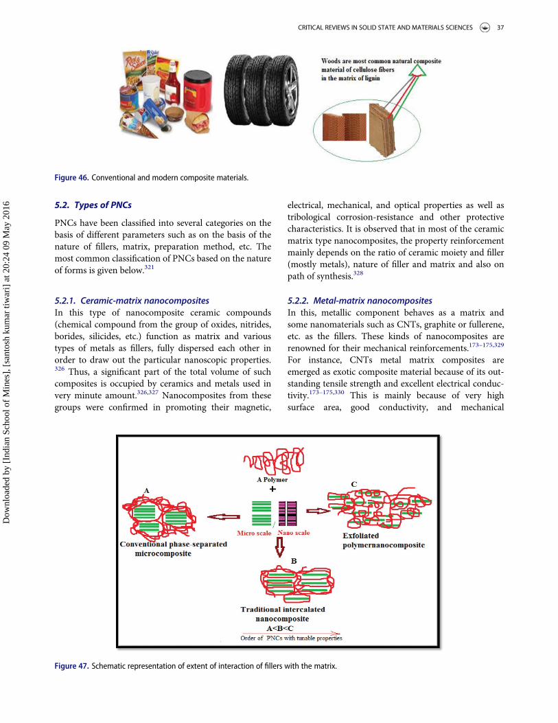
5.2. Types of PNCs
PNCs have been classified into several categories on thebasis of different parameters such as on the basis of thenature of fillers, matrix, preparation method, etc. Themost common classification of PNCs based on the natureof forms is given below.321
5.2.1. Ceramic-matrix nanocompositesIn this type of nanocomposite ceramic compounds(chemical compound from the group of oxides, nitrides,borides, silicides, etc.) function as matrix and varioustypes of metals as fillers, fully dispersed each other inorder to draw out the particular nanoscopic properties.326 Thus, a significant part of the total volume of suchcomposites is occupied by ceramics and metals used invery minute amount.326,327 Nanocomposites from thesegroups were confirmed in promoting their magnetic,
electrical, mechanical, and optical properties as well astribological corrosion-resistance and other protectivecharacteristics. It is observed that in most of the ceramicmatrix type nanocomposites, the property reinforcementmainly depends on the ratio of ceramic moiety and filler(mostly metals), nature of filler and matrix and also onpath of synthesis.328
5.2.2. Metal-matrix nanocompositesIn this, metallic component behaves as a matrix andsome nanomaterials such as CNTs, graphite or fullerene,etc. as the fillers. These kinds of nanocomposites arerenowned for their mechanical reinforcements.173–175,329
For instance, CNTs metal matrix composites areemerged as exotic composite material because of its out-standing tensile strength and excellent electrical conduc-tivity.173–175,330 This is mainly because of very highsurface area, good conductivity, and mechanical
Figure 46. Conventional and modern composite materials.
Figure 47. Schematic representation of extent of interaction of fillers with the matrix.
CRITICAL REVIEWS IN SOLID STATE AND MATERIALS SCIENCES 37
Dow
nloa
ded
by [
Indi
an S
choo
l of
Min
es],
[sa
ntos
h ku
mar
tiw
ari]
at 2
0:24
09
May
201
6
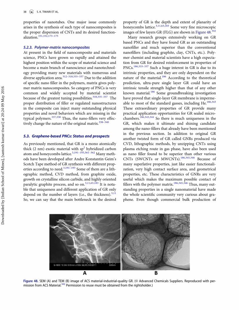
properties of nanotubes. One major issue commonlyarises in the synthesis of such type of nanocomposites isthe proper dispersion of CNTs and its desired function-alization.331,332,173–175
5.2.3. Polymer-matrix nanocompositesAt present in the field of nanocomposite and materialsscience, PNCs have grown so rapidly and attained thehighest position within the scope of material science andbecome a main branch of nanoscience and nanotechnol-ogy providing many new materials with numerous anddiverse application area.312–318,335–337 Due to the additionof specific nano filler in the polymers, matrix gives poly-mer matrix nanocomposites. So category of PNCs is verycommon and widely accepted by material scientistbecause of the greatest tuning possibilities.318,335–337 Theproper distribution of filler or regulated nanostructuresin the composite can inject many outstanding physicalproperties and novel behaviors which are missing in thetypical polymers.337,338 Thus, the nano-fillers very effec-tively change the nature of the original matrix.338–340
5.3. Graphene-based PNCs: Status and prospects
As previously mentioned, that GR is a mono atomicallythick (2 nm) exotic material with sp2 hybridized carbonatom and honeycombs lattice.3,191–193,361–362 Many meth-ods have been developed after Andre Konstantin Geim’sScotch Tape method of GR synthesis with different prop-erties according to need.3,191–193 Some of them are a lith-ographic method, CVD method, from graphite oxide,growth on crystalline silicon carbide, and highly orientedparalytic graphite process, and so on.3,11,63,183 It is nota-ble that uniqueness and different application of GR onlydepend on the number of layers (i.e., the thickness).3,11
So, we can say that the main bottleneck in the desired
property of GR is the depth and extent of planarity ofhoneycombs lattice.3,11,63,183 Some very fine microscopicimages of few layers GR (FLG) are shown in Figure 48.342
Many research groups extensively working on GRbased PNCs and they have found GR as an outstandingnanofiller and much superior than the conventionalnanofillers (including graphite, clay, CNTs, etc.). Poly-mer chemist and material scientists have a high expecta-tion from GR for desired reinforcement in properties ofPNCs.186,333–337 Such a huge interest in GR is due to itsintrinsic properties, and they are only dependent on thenature of the material.186 According to the theoreticalprediction, ultra-pure single layer GR could have anintrinsic tensile strength higher than that of any otherknown material.186 Some groundbreaking investigationhave proved that single-layer GR membrane is imperme-able to most of the standard gasses, including He.186,343
These extraordinary properties of GR provide manypractical application opportunities for GR sealed micro-chambers.186,343,344 So there is much uniqueness in theGR, which makes it ultimate and shining candidateamong the nano-fillers that already have been mentionedin the previous section. In addition to original GRanother twisted form of GR called GNRs produced viaCVD, lithographic methods, by unzipping CNTs usingplasma etching route in gas phase, have also been usedas nano filler found to be superior than other variousCNTs (SWCNTs or MWCNTs).186,345,346 Because ofmany superlative properties, just like easier functionali-zation, very high contact surface area, and geometricalproperties, etc. These characteristics of GNRs are veryuseful which makes the maximum possible contact offillers with the polymer matrix.186,345,346 Thus, many out-standing properties in a single nanomaterial have madethe whole scientific community very curious about gra-phene. Even though commercial bulk production of
Figure 48. SEM (A) and TEM (B) image of ACS material-industrial-quality GR. (© Advanced Chemicals Suppliers. Reproduced with per-mission from ACS Material.342 Permission to reuse must be obtained from the rightsholder.)
38 S. K. TIWARI ET AL.
Dow
nloa
ded
by [
Indi
an S
choo
l of
Min
es],
[sa
ntos
h ku
mar
tiw
ari]
at 2
0:24
09
May
201
6
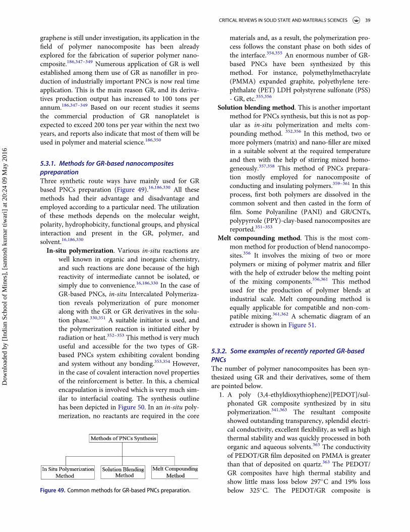
graphene is still under investigation, its application in thefield of polymer nanocomposite has been alreadyexplored for the fabrication of superior polymer nano-cmposite.186,347–349 Numerous application of GR is wellestablished among them use of GR as nanofiller in pro-duction of industrially important PNCs is now real timeapplication. This is the main reason GR, and its deriva-tives production output has increased to 100 tons perannum.186,347–349 Based on our recent studies it seemsthe commercial production of GR nanoplatelet isexpected to exceed 200 tons per year within the next twoyears, and reports also indicate that most of them will beused in polymer and material science.186,350
5.3.1. Methods for GR-based nanocompositesppreparationThree synthetic route ways have mainly used for GRbased PNCs preparation (Figure 49).16,186,330 All thesemethods had their advantage and disadvantage andemployed according to a particular need. The utilizationof these methods depends on the molecular weight,polarity, hydrophobicity, functional groups, and physicalinteraction and present in the GR, polymer, andsolvent.16,186,330
In-situ polymerization. Various in-situ reactions arewell known in organic and inorganic chemistry,and such reactions are done because of the highreactivity of intermediate cannot be isolated, orsimply due to convenience.16,186,330 In the case ofGR-based PNCs, in-situ Intercalated Polymeriza-tion reveals polymerization of pure monomeralong with the GR or GR derivatives in the solu-tion phase.330,351 A suitable initiator is used, andthe polymerization reaction is initiated either byradiation or heat.352–353 This method is very muchuseful and accessible for the two types of GR-based PNCs system exhibiting covalent bondingand system without any bonding.353,354 However,in the case of covalent interaction novel propertiesof the reinforcement is better. In this, a chemicalencapsulation is involved which is very much sim-ilar to interfacial coating. The synthesis outlinehas been depicted in Figure 50. In an in-situ poly-merization, no reactants are required in the core
materials and, as a result, the polymerization pro-cess follows the constant phase on both sides ofthe interface.354,355 An enormous number of GR-based PNCs have been synthesized by thismethod. For instance, polymethylmethacrylate(PMMA) expanded graphite, polyethylene tere-phthalate (PET) LDH polystyrene sulfonate (PSS)- GR, etc.355,356
Solution blending method. This is another importantmethod for PNCs synthesis, but this is not as pop-ular as in-situ polymerization and melts com-pounding method. 352,356 In this method, two ormore polymers (matrix) and nano-filler are mixedin a suitable solvent at the required temperatureand then with the help of stirring mixed homo-geneously.357,358 This method of PNCs prepara-tion mostly employed for nanocomposite ofconducting and insulating polymers.359–361 In thisprocess, first both polymers are dissolved in thecommon solvent and then casted in the form offilm. Some Polyaniline (PANI) and GR/CNTs,polypyrrole (PPY)-clay-based nanocomposites arereported.351–353
Melt compounding method. This is the most com-mon method for production of blend nanocompo-sites.356 It involves the mixing of two or morepolymers or mixing of polymer matrix and fillerwith the help of extruder below the melting pointof the mixing components.356,361 This methodused for the production of polymer blends atindustrial scale. Melt compounding method isequally applicable for compatible and non-com-patible mixing.361,362 A schematic diagram of anextruder is shown in Figure 51.
5.3.2. Some examples of recently reported GR-basedPNCsThe number of polymer nanocomposites has been syn-thesized using GR and their derivatives, some of themare pointed below.
1. A poly (3,4-ethyldioxythiophene)[PEDOT]/sul-phonated GR composite synthesized by in situpolymerization.341,363 The resultant compositeshowed outstanding transparency, splendid electri-cal conductivity, excellent flexibility, as well as highthermal stability and was quickly processed in bothorganic and aqueous solvents.363 The conductivityof PEDOT/GR film deposited on PMMA is greaterthan that of deposited on quartz.363 The PEDOT/GR composites have high thermal stability andshow little mass loss below 297�C and 19% lossbelow 325�C. The PEDOT/GR composite isFigure 49. Common methods for GR-based PNCs preparation.
CRITICAL REVIEWS IN SOLID STATE AND MATERIALS SCIENCES 39
Dow
nloa
ded
by [
Indi
an S
choo
l of
Min
es],
[sa
ntos
h ku
mar
tiw
ari]
at 2
0:24
09
May
201
6
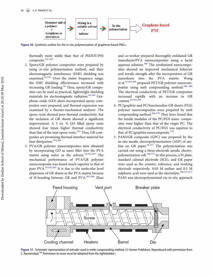
thermally more stable than that of PEDOT/PSScomposite.341,363
2. Epoxy/GR polymer composites were prepared byusing in-situ polymerization method, and theirelectromagnetic interference (EMI) shielding wasexamined.16,333 Over the entire frequency range,the EMI shielding effectiveness increased withincreasing GR loading.16 Thus, epoxy/GR compo-sites can be used as practical, lightweight shieldingmaterials for electromagnetic radiation.16,334 Gra-phene oxide (GO) sheet-incorporated epoxy com-posites were prepared, and thermal expansion wasexamined by a thermo-mechanical analyzer. Theepoxy resin showed poor thermal conductivity, butthe inclusion of GR sheets showed a significantimprovement. A 5 wt. % GO filled epoxy resinshowed four times higher thermal conductivitythan that of the neat epoxy resin.334 Thus, GR com-posites are promising thermal interface material forheat dissipation.334,364
3. PVA/GR polymer nanocomposites were obtainedby incorporating GO as nano filler into the PVAmatrix using water as the solvent.16,343,365 Themechanical performance of PVA/GR polymernanocomposite was found much superior to that ofpure PVA.16,343,365 It is due to the molecular leveldispersion of GR sheets in the PVA matrix becauseof H-bonding between GR and PVA.365,366 Zhao
and co-worker prepared thoroughly exfoliated GRnanosheets/PVA nanocomposites using a facialaqueous solution.366 The synthesized nanocompo-sites showed an improved mechanical behaviorand tensile strength after the incorporation of GRnanosheets into the PVA matrix. Wanget al.16,365,366 prepared PET/GR polymer nanocom-posites using melt compounding method.366–368
The electrical conductivity of PET/GR compositesincreased rapidly with an increase in GRcontent.16,365,366
4. PC/graphite and PC/functionalize GR sheets (FGS)polymer nanocomposites were prepared by meltcompounding method.369,370 They have found thatthe tensile modulus of the PC/FGS nano- compo-sites were higher than that of the virgin PC. Theelectrical conductivity of PC/FGS was superior tothat of PC/graphite nanocomposite.370
5. PANI/GR composite (GPC) was prepared by thein-situ anodic electropolymerization (AEP) of ani-line on GR paper.16,371 The polymerization wascarried out using a three-electrode anodic electro-polymerization cell.336,371 In this process, a Pt plate,standard calomel electrode (SCE), and GR paperwere used as the counter, reference, and workingelectrode respectively. 0.05 M aniline and 0.5 Msulphuric acid were used as the electrolyte.336,351,371
PANI was electropolymerized via in-situ approach
Figure 50. Synthesis outline for the in-situ polymerization of graphene-based PNCs.
Figure 51. Schematic representation of extruder used in melts compounding method. (© Hanser Publishers. Reproduced with permission fromC. Rauwendaal.362 Permission to reuse must be obtained from the rightsholder.)
40 S. K. TIWARI ET AL.
Dow
nloa
ded
by [
Indi
an S
choo
l of
Min
es],
[sa
ntos
h ku
mar
tiw
ari]
at 2
0:24
09
May
201
6
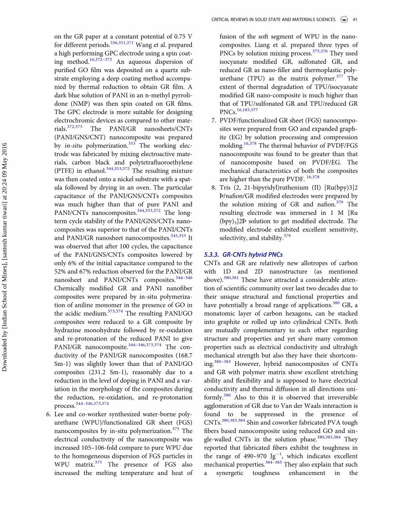
on the GR paper at a constant potential of 0.75 Vfor different periods.336,351,371 Wang et al. prepareda high performing GPC electrode using a spin coat-ing method.16,372–373 An aqueous dispersion ofpurified GO film was deposited on a quartz sub-strate employing a deep coating method accompa-nied by thermal reduction to obtain GR film. Adark blue solution of PANI in an n-methyl pyrroli-done (NMP) was then spin coated on GR films.The GPC electrode is more suitable for designingelectrochromic devices as compared to other mate-rials.372,373 The PANI/GR nanosheets/CNTs(PANI/GNS/CNT) nanocomposite was preparedby in-situ polymerization.353 The working elec-trode was fabricated by mixing electroactive mate-rials, carbon black and polytetrafluoroethylene(PTFE) in ethanol.344,353,372 The resulting mixturewas then coated onto a nickel substrate with a spat-ula followed by drying in an oven. The particularcapacitance of the PANI/GNS/CNTs compositeswas much higher than that of pure PANI andPANI/CNTs nanocomposites.344,353,372 The long-term cycle stability of the PANI/GNS/CNTs nano-composites was superior to that of the PANI/CNTsand PANI/GR nanosheet nanocomposites.345,353 Itwas observed that after 100 cycles, the capacitanceof the PANI/GNS/CNTs composites lowered byonly 6% of the initial capacitance compared to the52% and 67% reduction observed for the PANI/GRnanosheet and PANI/CNTs composites.344–346
Chemically modified GR and PANI nanofibercomposites were prepared by in-situ polymeriza-tion of aniline monomer in the presence of GO inthe acidic medium.373,374 The resulting PANI/GOcomposites were reduced to a GR composite byhydrazine monohydrate followed by re-oxidationand re-protonation of the reduced PANI to givePANI/GR nanocomposite.344–346,373,374 The con-ductivity of the PANI/GR nanocomposites (168.7Sm-1) was slightly lower than that of PANI/GOcomposites (231.2 Sm-1), reasonably due to areduction in the level of doping in PANI and a var-iation in the morphology of the composites duringthe reduction, re-oxidation, and re-protonationprocess.344–346,373,374
6. Lee and co-worker synthesized water-borne poly-urethane (WPU)/functionalized GR sheet (FGS)nanocomposites by in-situ polymerization.375 Theelectrical conductivity of the nanocomposite wasincreased 105–106-fold compare to pure WPU dueto the homogeneous dispersion of FGS particles inWPU matrix.375 The presence of FGS alsoincreased the melting temperature and heat of
fusion of the soft segment of WPU in the nano-composites. Liang et al. prepared three types ofPNCs by solution mixing process.375,376 They usedisocyanate modified GR, sulfonated GR, andreduced GR as nano-filler and thermoplastic poly-urethane (TPU) as the matrix polymer.377 Theextent of thermal degradation of TPU/isocyanatemodified GR nano-composite is much higher thanthat of TPU/sulfonated GR and TPU/reduced GRPNCs.16,183,377
7. PVDF/functionalized GR sheet (FGS) nanocompo-sites were prepared from GO and expanded graph-ite (EG) by solution processing and compressionmolding.16,378 The thermal behavior of PVDF/FGSnanocomposite was found to be greater than thatof nanocomposite based on PVDF/EG. Themechanical characteristics of both the compositesare higher than the pure PVDF. 16,378
8. Tris (2, 21-bipyridyl)ruthenium (II) [Ru(bpy)3]2Þ/nafion/GR modified electrodes were prepared bythe solution mixing of GR and nafion.379 Theresulting electrode was immersed in 1 M [Ru(bpy)3]2Þ solution to get modified electrode. Themodified electrode exhibited excellent sensitivity,selectivity, and stability.379
5.3.3. GR-CNTs hybrid PNCsCNTs and GR are relatively new allotropes of carbonwith 1D and 2D nanostructure (as mentionedabove).380,381 These have attracted a considerable atten-tion of scientific community over last two decades due totheir unique structural and functional properties andhave potentially a broad range of applications.380 GR, amonatomic layer of carbon hexagons, can be stackedinto graphite or rolled up into cylindrical CNTs. Bothare mutually complementary to each other regardingstructure and properties and yet share many commonproperties such as electrical conductivity and ultrahighmechanical strength but also they have their shortcom-ing.380–383 However, hybrid nanocomposites of CNTsand GR with polymer matrix show excellent stretchingability and flexibility and is supposed to have electricalconductivity and thermal diffusion in all directions uni-formly.380 Also to this it is observed that irreversibleagglomeration of GR due to Van der Waals interaction isfound to be suppressed in the presence ofCNTs.380,383,384 Shin and coworker fabricated PVA toughfibers based nanocomposite using reduced GO and sin-gle-walled CNTs in the solution phase.380,383,384 Theyreported that fabricated fibers exhibit the toughness inthe range of 490–970 Jg¡1, which indicates excellentmechanical properties.384–385 They also explain that sucha synergetic toughness enhancement in the
CRITICAL REVIEWS IN SOLID STATE AND MATERIALS SCIENCES 41
Dow
nloa
ded
by [
Indi
an S
choo
l of
Min
es],
[sa
ntos
h ku
mar
tiw
ari]
at 2
0:24
09
May
201
6
nanocomposite arises due to the optimal combination ofreduced GO and SWNTs (ratio1:1), and no synergistictoughness increase was observed if the ratio of CNTsand GR has changed. It is ultimate because of suitableself-alignment nano-fillers.16,334,384
5.3.4. Distribution, dispersion, and interactionbetween GR derivatives and polymerHybridization and proper coordination between nanoma-terials (Fullerenes, GR, CNTs, and GNRs) and polymershas led to the production of composites with excellent elec-trical andmechanical properties for various newer applica-tions.388,389 It happens because of the high surface area, ofnano fillers tend to agglomerate and stick to each other,forming micro particles.388 Therefore, distribution anddispersion of these nano filler into individual particlesthroughout the polymermatrix, mainly themolecular leveldispersion, and homogeneous distribution is one of themost important and property determining steps.388–390 Inthis way, aggregation and agglomeration are even moresevere for anisotropic nanoparticles mainly for the nano-sheets and nanotubes due to the very high interparticleinteraction.388 However, very interestingly, newly discov-ered graphene and its derivatives as fillers for polymericmaterials have opened a new era of nanocompo-sites.388,390–393 Notably, amazing improvements in physi-cal, mechanical properties, and chemical stability ofpolymer have been reported on a very minute loading ofgraphene and its derivatives.393,394 But due to stacking andrestacking process in the case graphene sheets and deriva-tives similar to other layered nano-fillers (because of thehigh aspect ratio and strong interparticle interaction),sometimes actual properties of composites ham-pered.388,393,394 To avoid such shortcomings, polymerchemists and materials scientist have selected chemicallyderived graphene which is available very easily as singlelayer dispersion in liquids, retaining the single layer stateof graphene sheet in polymer media is not easy.395 Suchgraphene and derivatives is often synthesized by oxidizinggraphite powder to graphite oxide using strong oxidizingagents173–175 with a highly hydrophilic sheet-like structure,which is then proper exfoliated into the graphene oxide(GO) in a suitable polar solvents, possibly by mechanicalshearing.388,395 Due the numerous hydrophilic moieties onGO, it is not easily dispersed in nonpolar organic andweakly polar solvents, and polymers matrixes.16,388 Severaltrials have been made by different workers to dispersechemically synthesized graphene in nonpolar organic andweakly polar organic media by specific functionalizationof GO.395,397,398 However, employing aqueous dispersionof GO to obtain graphene based polymer nanocompositeis more attractive, cheaper, and time efficient. Since GOand functionalization graphene can be easily combined
with the water-soluble polymers and then reduced to rGOwithout using organic solvents or tedious chemical func-tionalization.16,395,398 In addition to this colloidal polymer,matrixes may be mixed directly with GO to incorporategraphene into water insoluble polymers.388,395 Manyrecent study shows GO, and functionalized graphene canbe employed as a surfactant in emulsion polymerization toproduce graphene-based nanomaterials.388 Thus, animportant strategy for cheaper and environmental friendlyexperiment, to use an aqueous dispersion of GO and func-tionalized graphene to synthesis different kind of gra-phene- and derivatives-based nanocomposites. Recently,some workers have used the epoxy-functionalized GO toaddress the various challenges of well dispersing graphenesheets in a thermoset resin and show the success of theproposed strategy.388,395 Fabrication of epoxy compositeswith graphene, GO, and functionalized graphene is mostlyperformed via two pathways.395,398 First, stepwise chemicalfunctionalization of graphene and its derivatives, then theremoval of solvent from themixture of epoxy and graphite.Second, dispersion of graphene sheet with non-solventssuch as ethanol and acetone.388,395
Direct mixing of reduced graphene powder in thedifferent epoxy compounds mostly gives in poor dis-persion and heterogeneous distribution of nano-fill-ers.388,395 It is reported that even on strongultrasonication of graphene sheets in a non-polarsolvent for an extended period it does not guaranteea good distribution especially in the case higherloading of graphene sheets.16,388,395 In contrast,chemically derived GO nanosheets easily restockduring drying or on heating above the room temper-ature. And result formation of a layered materialconsisting of GO sheets that are very stronglybonded together by hydrogen bonding.15–17,388 More-over, it has also been reported that for the good dis-persion, we need to ensure good GO-matrixbonding, consequently superior mechanical proper-ties.15–17,388,395 Similarly, a novel and single-stepmethod to functionalize and disperse GOES nano-sheets in epoxy and obtain high-performance nano-composites by achieving a high degree of dispersionand good bonding to the matrix.15–17,388,395 Althoughgraphite oxide was synthesized long ago, its exactmolecular structure is not well known.15–17,388,395
Such betterment in dispersion of GO and functional-ized GR is due to the presence of epoxy groupsbecause as they facilitate the GO and functionaliza-tion GR, compared to other groups such as the car-boxyl group which needs activation in the absence ofwater.15–17,395 In the many cases, amines and deriva-tives have exclusively been used for the functionali-zation GR and GO and molecular interaction, as
42 S. K. TIWARI ET AL.
Dow
nloa
ded
by [
Indi
an S
choo
l of
Min
es],
[sa
ntos
h ku
mar
tiw
ari]
at 2
0:24
09
May
201
6

shown in Figure 52. Such reaction to produce gra-phene-based PNCs is mostly carried out in aqueousmedia or polar and the ambient atmosphere withoutusing any catalyst. These reactions are relatively fastand highly productive, due to the high reactivity ofamine and epoxy functional groups.16,388,395 Theseexperimental conditions for the reaction serve forthe two simultaneous purposes of accommodatinggraphene sheets at the molecular level and furnishingthe interfacial bonding with the matrix that arehighly desirable. Higher dispersion and properhomogeneous distribution of nano fillers mean largerarea per volume and better bonding between thefiller and polymer matrix to improve various physi-cal and mechanical properties.16,388,395 The mostcommonly adopted structural modification and acti-vation of graphene and derivatives for its homoge-neous distribution and proper dispersion in thepolymer matrixes is diagrammatically is shown inFigure 52.388
In summary, regarding the proper dispersion of GRand derivatives in the different polymer functionalizationmethod and type (covalent, non-covalent, Pi-Pi interac-tions hydrogen bonding or other polar interactions) ofinteraction between polymer and graphene plays veryvital role.388,396,400 And an important factor in decidingreinforcement quantity and quality of synthesizednanocomposites.
5.3.5. Other GR-based polymer compositesPoly (e-caprolactone) (PCL)-GO composite was pre-pared using in-situ polymerization.401 The resultingnanocomposite shows excellent mechanical propertiesand robustness under bending. Poly (lactic acid) (PLA/GR PNCs were prepared using a response surfacemethod that showed that GR loading had a significanteffect on tensile strength.402–403 Liu and co-worker fabri-cated GO reinforced epoxy resin nanocomposite bytransferring GO from water to acetone.403 Incorporationof “1 wt% of GO showed a significant improvement inflexural strength, flexural modulus, impact strength andstorage modulus.404–407 Many groups have synthesizedexcellent nanocomposites using polymethyl methacrylate(PMMA) and with other polymers with graphene and itsderivatives as nanofiller (with different percentage GRand derivatives) by in-situ polymerization. Liang andcoworker fabricated polydiacetylene/GR nanocompositeby solution processing route and reported that nanocom-posite showed excellent actuation character with control-lable motion, fast response rate, and high-frequencyresonance.404–407 Polyphenylene sulfide (PPS)/GR com-posite was prepared by spraying method. The resultingnanocomposite had seven times higher wear life thanthat of neat PPS.408 Along the same line, Pan and co-worker prepared polyamide/GR coatings by sprayingmethod.408,409 They observed that the wear life of thecomposite coating was higher than that of neat
Figure 52. (A) Synthetic root of polyacetylene-graphene composites using nitrene as activator for the proper dispersion. (B) Schematicpresentation of interactions between polyethylene glycol and activated graphene sheet (using SN-38). (C) Activation step for good dis-persion of graphene nanosheets for polystyrene functionalized graphene nanosheets. (© Elsevier. Reproduced with permission from R.K. Layek and A. K. Nandi388 Permission to reuse must be obtained from the rightsholder.)
CRITICAL REVIEWS IN SOLID STATE AND MATERIALS SCIENCES 43
Dow
nloa
ded
by [
Indi
an S
choo
l of
Min
es],
[sa
ntos
h ku
mar
tiw
ari]
at 2
0:24
09
May
201
6
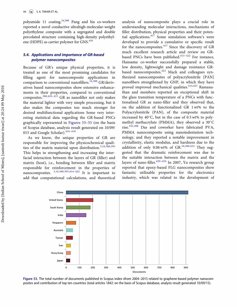
polyamide 11 coating.16,388 Pang and his co-workersreported a novel conductive ultrahigh-molecular-weightpolyethylene composite with a segregated and doublepercolated structure containing high-density polyethyl-ene (HDPE) as carrier polymer for GNS.410
5.4. Applications and importance of GR-basedpolymer nanocomposites
Because of GR’s unique physical properties, it istreated as one of the most promising candidates forfilling agent for nanocomposite applications incomparison to conventional nanofillers.16,388 GR/deriv-atives based nanocomposites show extensive enhance-ments in their properties, compared to conventionalcomposites.388,410–415 GR as nanofiller not only makesthe material lighter with very simple processing, but italso makes the composites too much stronger fordesired multifunctional applications Some very inter-esting statistical data regarding the GR-based PNCsgraphically represented in Figures 53–55 (on the basisof Scopus database, analysis result generated on 10/09/015 and Google Scholar).410–418
As we know, the unique properties of GR areresponsible for improving the physicochemical quali-ties of the matrix material upon distribution.3,16,388,395
This helps in strengthening and increasing the inter-facial interaction between the layers of GR (filler) andmatrix (host), i.e., bonding between filler and matrixresponsible for reinforcement in the properties ofnanocomposites. 3,16,388,395,414–422 It is important toadd that computational calculations, and theoretical
analysis of nanocomposite plays a crucial role inunderstanding molecular interactions, mechanisms offiller distribution, physical properties and their poten-tial applications.417 Some simulation software’s weredeveloped to provide a cumulative or specific resultfor the nanocomposites.417 Since the discovery of GRmuch excellent research article and review on GR-based PNCs have been published.415–422 For instance,Hansama co-worker successfully prepared a stable,low density, lightweight and damage resistance GR-based nanocomposites.423 Mack and colleagues syn-thesized nanocomposites of polyacrylonitrile [PAN]nanofibers strengthened by GNP, in which they haveproved improved mechanical qualities.414,423 Ramana-than and members reported an exceptional shift inthe glass transition temperature of a PNCs with func-tionalized GR as nano-filler and they observed that,on the addition of functionalized GR 1wt% to thePolyacrylonitrile (PAN), of the composite materialincreased by 40�C, but in the case of 0.5 wt% to poly-methyl methacrylate (PMMA), they observed a 30�Crise.343,388 Das and coworker have fabricated PVA,PMMA nanocomposite using nanoindentation tech-nology, and they reported a notable improvement incrystallinity, elastic modulus, and hardness due to theaddition of only 0.06 wt% of GR.16,388,424 They sug-gested that the dramatic reinforcement was due tothe suitable interaction between the matrix and thelayers of nano-filler.420–424 In 2007, Yu research groupreported that epoxy-based FLG nanocomposites showfantastic utilizable properties for the electronicsindustry, which was related to the development of
Figure 53. The total number of documents published in Scopus index sfrom 2004–2015 related to graphene-based polymer nanocom-posites and contribution of top ten countries (total articles 1842: on the basis of Scopus database, analysis result generated 10/09/15).
44 S. K. TIWARI ET AL.
Dow
nloa
ded
by [
Indi
an S
choo
l of
Min
es],
[sa
ntos
h ku
mar
tiw
ari]
at 2
0:24
09
May
201
6
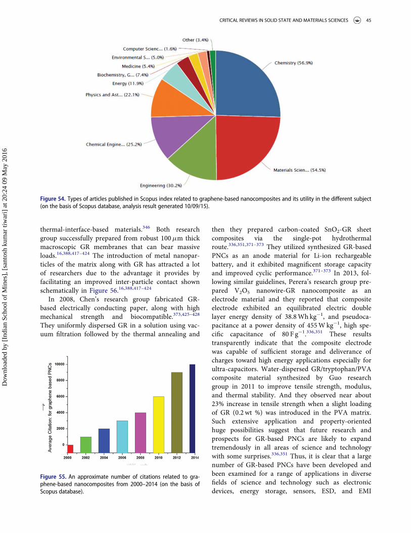
thermal-interface-based materials.346 Both researchgroup successfully prepared from robust 100mm thickmacroscopic GR membranes that can bear massiveloads.16,388,417–424 The introduction of metal nanopar-ticles of the matrix along with GR has attracted a lotof researchers due to the advantage it provides byfacilitating an improved inter-particle contact shownschematically in Figure 56.16,388,417–424
In 2008, Chen’s research group fabricated GR-based electrically conducting paper, along with highmechanical strength and biocompatible.373,425–428
They uniformly dispersed GR in a solution using vac-uum filtration followed by the thermal annealing and
then they prepared carbon-coated SnO2-GR sheetcomposites via the single-pot hydrothermalroute.336,351,371–373 They utilized synthesized GR-basedPNCs as an anode material for Li-ion rechargeablebattery, and it exhibited magnificent storage capacityand improved cyclic performance.371–373 In 2013, fol-lowing similar guidelines, Perera’s research group pre-pared V2O5 nanowire-GR nanocomposite as anelectrode material and they reported that compositeelectrode exhibited an equilibrated electric doublelayer energy density of 38.8Wh kg¡1, and pseudoca-pacitance at a power density of 455Wkg¡1, high spe-cific capacitance of 80 F g¡1.336,351 These resultstransparently indicate that the composite electrodewas capable of sufficient storage and deliverance ofcharges toward high energy applications especially forultra-capacitors. Water-dispersed GR/tryptophan/PVAcomposite material synthesized by Guo researchgroup in 2011 to improve tensile strength, modulus,and thermal stability. And they observed near about23% increase in tensile strength when a slight loadingof GR (0.2 wt %) was introduced in the PVA matrix.Such extensive application and property-orientedhuge possibilities suggest that future research andprospects for GR-based PNCs are likely to expandtremendously in all areas of science and technologywith some surprises.336,351 Thus, it is clear that a largenumber of GR-based PNCs have been developed andbeen examined for a range of applications in diversefields of science and technology such as electronicdevices, energy storage, sensors, ESD, and EMI
Figure 54. Types of articles published in Scopus index related to graphene-based nanocomposites and its utility in the different subject(on the basis of Scopus database, analysis result generated 10/09/15).
Figure 55. An approximate number of citations related to gra-phene-based nanocomposites from 2000–2014 (on the basis ofScopus database).
CRITICAL REVIEWS IN SOLID STATE AND MATERIALS SCIENCES 45
Dow
nloa
ded
by [
Indi
an S
choo
l of
Min
es],
[sa
ntos
h ku
mar
tiw
ari]
at 2
0:24
09
May
201
6
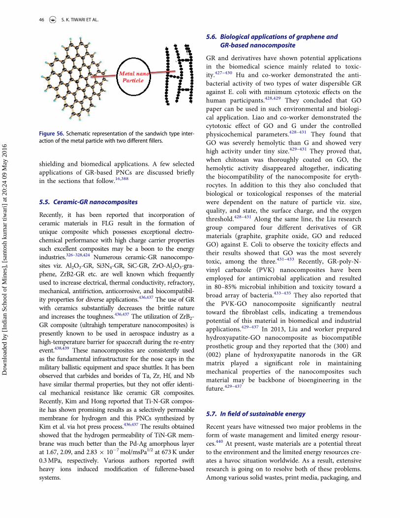
shielding and biomedical applications. A few selectedapplications of GR-based PNCs are discussed brieflyin the sections that follow.16,388
5.5. Ceramic-GR nanocomposites
Recently, it has been reported that incorporation ofceramic materials in FLG result in the formation ofunique composite which possesses exceptional electro-chemical performance with high charge carrier propertiessuch excellent composites may be a boon to the energyindustries.326–328,424 Numerous ceramic-GR nanocompo-sites viz. Al2O3-GR, Si3N4-GR, SiC-GR, ZrO-Al2O3-gra-phene, ZrB2-GR etc. are well known which frequentlyused to increase electrical, thermal conductivity, refractory,mechanical, antifriction, anticorrosive, and biocompatibil-ity properties for diverse applications.436,437 The use of GRwith ceramics substantially decreases the brittle natureand increases the toughness.436,437 The utilization of ZrB2-GR composite (ultrahigh temperature nanocomposites) ispresently known to be used in aerospace industry as ahigh-temperature barrier for spacecraft during the re-entryevent.438,439 These nanocomposites are consistently usedas the fundamental infrastructure for the nose caps in themilitary ballistic equipment and space shuttles. It has beenobserved that carbides and borides of Ta, Zr, Hf, and Nbhave similar thermal properties, but they not offer identi-cal mechanical resistance like ceramic GR composites.Recently, Kim and Hong reported that Ti-N-GR compos-ite has shown promising results as a selectively permeablemembrane for hydrogen and this PNCs synthesized byKim et al. via hot press process.436,437 The results obtainedshowed that the hydrogen permeability of TiN-GR mem-brane was much better than the Pd-Ag amorphous layerat 1.67, 2.09, and 2.83 £ 10¡7mol/msPa1/2 at 673K under0.3MPa, respectively. Various authors reported swiftheavy ions induced modification of fullerene-basedsystems.
5.6. Biological applications of graphene andGR-based nanocomposite
GR and derivatives have shown potential applicationsin the biomedical science mainly related to toxic-ity.427–430 Hu and co-worker demonstrated the anti-bacterial activity of two types of water dispersible GRagainst E. coli with minimum cytotoxic effects on thehuman participants.428,429 They concluded that GOpaper can be used in such environmental and biologi-cal application. Liao and co-worker demonstrated thecytotoxic effect of GO and G under the controlledphysicochemical parameters.428–431 They found thatGO was severely hemolytic than G and showed veryhigh activity under tiny size.429–431 They proved that,when chitosan was thoroughly coated on GO, thehemolytic activity disappeared altogether, indicatingthe biocompatibility of the nanocomposite for eryth-rocytes. In addition to this they also concluded thatbiological or toxicological responses of the materialwere dependent on the nature of particle viz. size,quality, and state, the surface charge, and the oxygenthreshold.428–431 Along the same line, the Liu researchgroup compared four different derivatives of GRmaterials (graphite, graphite oxide, GO and reducedGO) against E. Coli to observe the toxicity effects andtheir results showed that GO was the most severelytoxic, among the three.431–433 Recently, GR-poly-N-vinyl carbazole (PVK) nanocomposites have beenemployed for antimicrobial application and resultedin 80–85% microbial inhibition and toxicity toward abroad array of bacteria.433–435 They also reported thatthe PVK-GO nanocomposite significantly neutraltoward the fibroblast cells, indicating a tremendouspotential of this material in biomedical and industrialapplications.429–437 In 2013, Liu and worker preparedhydroxyapatite-GO nanocomposite as biocompatibleprosthetic group and they reported that the (300) and(002) plane of hydroxyapatite nanorods in the GRmatrix played a significant role in maintainingmechanical properties of the nanocomposites suchmaterial may be backbone of bioengineering in thefuture.429–437
5.7. In field of sustainable energy
Recent years have witnessed two major problems in theform of waste management and limited energy resour-ces.440 At present, waste materials are a potential threatto the environment and the limited energy resources cre-ates a havoc situation worldwide. As a result, extensiveresearch is going on to resolve both of these problems.Among various solid wastes, print media, packaging, and
Figure 56. Schematic representation of the sandwich type inter-action of the metal particle with two different fillers.
46 S. K. TIWARI ET AL.
Dow
nloa
ded
by [
Indi
an S
choo
l of
Min
es],
[sa
ntos
h ku
mar
tiw
ari]
at 2
0:24
09
May
201
6
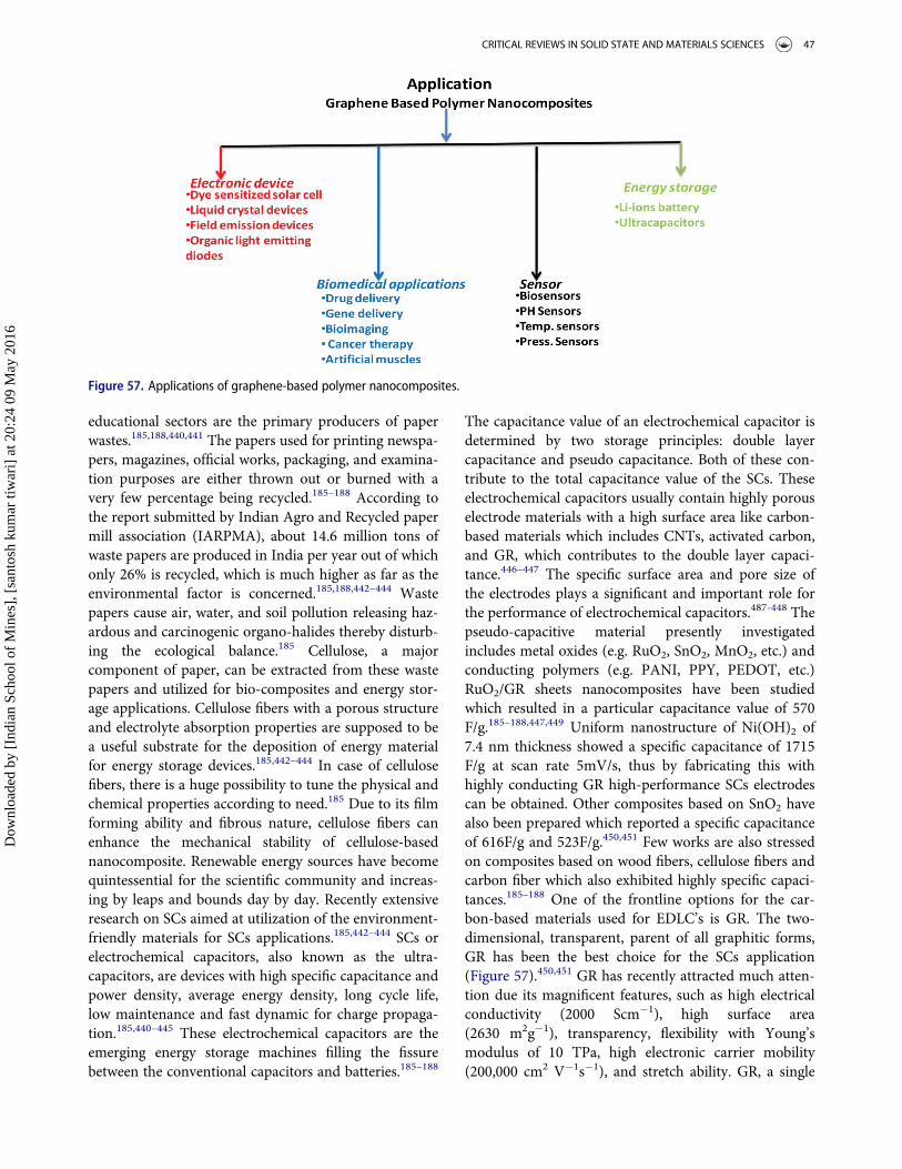
educational sectors are the primary producers of paperwastes.185,188,440,441 The papers used for printing newspa-pers, magazines, official works, packaging, and examina-tion purposes are either thrown out or burned with avery few percentage being recycled.185–188 According tothe report submitted by Indian Agro and Recycled papermill association (IARPMA), about 14.6 million tons ofwaste papers are produced in India per year out of whichonly 26% is recycled, which is much higher as far as theenvironmental factor is concerned.185,188,442–444 Wastepapers cause air, water, and soil pollution releasing haz-ardous and carcinogenic organo-halides thereby disturb-ing the ecological balance.185 Cellulose, a majorcomponent of paper, can be extracted from these wastepapers and utilized for bio-composites and energy stor-age applications. Cellulose fibers with a porous structureand electrolyte absorption properties are supposed to bea useful substrate for the deposition of energy materialfor energy storage devices.185,442–444 In case of cellulosefibers, there is a huge possibility to tune the physical andchemical properties according to need.185 Due to its filmforming ability and fibrous nature, cellulose fibers canenhance the mechanical stability of cellulose-basednanocomposite. Renewable energy sources have becomequintessential for the scientific community and increas-ing by leaps and bounds day by day. Recently extensiveresearch on SCs aimed at utilization of the environment-friendly materials for SCs applications.185,442–444 SCs orelectrochemical capacitors, also known as the ultra-capacitors, are devices with high specific capacitance andpower density, average energy density, long cycle life,low maintenance and fast dynamic for charge propaga-tion.185,440–445 These electrochemical capacitors are theemerging energy storage machines filling the fissurebetween the conventional capacitors and batteries.185–188
The capacitance value of an electrochemical capacitor isdetermined by two storage principles: double layercapacitance and pseudo capacitance. Both of these con-tribute to the total capacitance value of the SCs. Theseelectrochemical capacitors usually contain highly porouselectrode materials with a high surface area like carbon-based materials which includes CNTs, activated carbon,and GR, which contributes to the double layer capaci-tance.446–447 The specific surface area and pore size ofthe electrodes plays a significant and important role forthe performance of electrochemical capacitors.487-448 Thepseudo-capacitive material presently investigatedincludes metal oxides (e.g. RuO2, SnO2, MnO2, etc.) andconducting polymers (e.g. PANI, PPY, PEDOT, etc.)RuO2/GR sheets nanocomposites have been studiedwhich resulted in a particular capacitance value of 570F/g.185–188,447,449 Uniform nanostructure of Ni(OH)2 of7.4 nm thickness showed a specific capacitance of 1715F/g at scan rate 5mV/s, thus by fabricating this withhighly conducting GR high-performance SCs electrodescan be obtained. Other composites based on SnO2 havealso been prepared which reported a specific capacitanceof 616F/g and 523F/g.450,451 Few works are also stressedon composites based on wood fibers, cellulose fibers andcarbon fiber which also exhibited highly specific capaci-tances.185–188 One of the frontline options for the car-bon-based materials used for EDLC’s is GR. The two-dimensional, transparent, parent of all graphitic forms,GR has been the best choice for the SCs application(Figure 57).450,451 GR has recently attracted much atten-tion due its magnificent features, such as high electricalconductivity (2000 Scm¡1), high surface area(2630 m2g¡1), transparency, flexibility with Young’smodulus of 10 TPa, high electronic carrier mobility(200,000 cm2 V¡1s¡1), and stretch ability. GR, a single
Figure 57. Applications of graphene-based polymer nanocomposites.
CRITICAL REVIEWS IN SOLID STATE AND MATERIALS SCIENCES 47
Dow
nloa
ded
by [
Indi
an S
choo
l of
Min
es],
[sa
ntos
h ku
mar
tiw
ari]
at 2
0:24
09
May
201
6

sheet material, has the highest specific capacitance of550F/g accompanied by the high intensive quantumcapacitance of 21 mF cm¡2. This wonder material of thepresent era has opened way to the material andelectronic world and by preparing composites withconducting polymers a full compass of application formemory backup in SRAMs (static random-accessmemory), power electronics and in many other fieldshave been studied. Some other most prominent areaswhere GR-based nanocomposites have been employed.Some of the miscellaneous work on the carbon-basedmaterials and their composites have also beenreviewed.16,185–188,440–445,451
6. Conclusions and future prospects
In this article, we tried to incorporate all the fundamentalscientific information about the GR, GNRs, CNTs, fuller-enes, and GR-based PNCs including brief historicaldevelopment, method of preparations, structural proper-ties, and prominent scientific applications. CVD, arcmethod, and laser ablation techniques for CNTs werediscussed briefly with technical simplicity. Nearly 12recently reported GR-based PNCs have been presentedwith their applications and preparation methods. Intenseattention has paid to the recent applications of CNTs,GR, GNRs-based PNCs, and QHE in the case of GR,especially the utilization of these materials in the field ofFETs devices, transparent electrodes, sensors, photode-tectors, energy storage devices, solar cells, polymer com-posites, and nanocomposites. Biological application ofGR-based PNCs and their applications in the creation ofnew ceramic materials have also been drawn from thescientific literature.
As mentioned in the previous sections, GR, GNRs,and GR-based PNCs possess several outstanding proper-ties which can be fabricated according to the require-ment. Due to such tunable nature of these materials theentire scientific fraternity has shown their great interestfor its more and more applications in day to day life,this is why within the 5–6 years these materials haveattained a very strong tenability scientists and industrial-ist both. Novel properties of these materials (CNTs, GRand GNRs) such as room temperature QHE, highestcharge transport properties, exceptional thermal conduc-tivity etc., makes these materials a promising candidateas filling agent for polymer composite applications. It iswell known that the use of silicon-based materials over-comes the technological barrier as it holds the future formicro to nanoscale electronics. The further modificationin the inherent semi-metallic nature of silicon-basedmaterials has been obsolete for FETs application. As aresult, GNRs and bilayer GR came into existence with a
suitable band gap, and it seems these materials will bean ideal alternative to silicon-based technology shortly.But it is notable that the GR, GNRs, and GR-basedmaterials still faces so many problems ranging from syn-thesis and characterization to final device fabrication.However, extensive research going on around the globeon GR and GR-based materials to resolve all theseissues. At present, the main obstacle in the GR-basedtechnology is its ultrapure scalable synthesis becauseonly defect-free GR exhibits reported exceptional prop-erties. In this line, some very useful methods have beendeveloped such as ECE of graphite, CVD, etc., howeverresearch is continuing for improvement. A number ofpublications and patents are available for the laboratoryscale application and device fabrications using GR andGR-based materials. So it can be assumed that shortlythese materials will be the backbone of flexible transpar-ent electrodes, GR/polymer composites for mechanicalparts, energy storage, sensors, and organic electronicsdevices-based industries. GR-based polymer compositeshave showed the lowest percolation threshold for electri-cal conductivity and highly improved mechanical, ther-mal, and gas barrier properties. However, furtherinvestigation is still very important for the better under-standing of dispersion and interface between the nano-filler and matrix. Therefore, in order to obtain criticalsuccesses in device fabrication and common technologi-cal application of GR-based PNCs more intense investi-gation and investment on GR research are required.Recently, atomic scale systematical research and geomet-rical microscopic studies have shown the evidence oftunable band gap through varying oxidation level andreduction process. Such advance investigations will be amilestone in the path of real time application of GR andGO-based devices in place metal oxide and semiconduc-tor circuits. According to Geim and Novoselov,3 GR is“an ultimate incarnation of all surface.” It has given theexotic and exciting array of the application in all field ofscience ranging from engineering to biomedical. It hasbeen extensively used for thermally and electrically con-ducting reinforced nanocomposite, electronic circuits,sensors and transparent and flexible electrodes for dis-play and solar cells, etc. GR as nano filler is superior toconventional nano filler like (Na-MMT, LDH, CNT,CNF, EG, etc.) because of unique characteristics featureslike very high surface area, aspect ratio, thermal, andelectrical conductivity even at room temperature andmany more. All these prominently make GR the bestcarbon nano filler among traditional fillers available.Even there are a broad range of possible applications ofGR, it is not compatible with various organic polymers.The dispensability of GR among polymer matrix andGR polymer interaction is still the big issue to solve.
48 S. K. TIWARI ET AL.
Dow
nloa
ded
by [
Indi
an S
choo
l of
Min
es],
[sa
ntos
h ku
mar
tiw
ari]
at 2
0:24
09
May
201
6
This can be achieved only by surface modification of GRusing various organic modifying agents. As reports sug-gest, the nucleophiles addition of organic molecule tothe GR surface is the best way to achieve the bulk pro-duction of surface modified GR. In general, surfacemodification of GR assists the dispensability of GR indifferent organic media in the fabrication of GR-basednanocomposite. A vast number of GR-based PNCs havebeen reported which were found to be superior overpolymer-based matrix. It has been found that GR-basedPNCs exhibit superior mechanical properties comparedto other conventional silicon- and graphite-based nano-composite. There were significant improvements inmechanical properties of GR-based nanocompositesattributed to its very high aspect ratio. The remarkablyhigh thermal stability of GR fabricates thermally stablenanocomposites. Also, a many fold increase in electricalconductivity of nanocomposite was observed which isdue to the formation of conducting a network of GRsheets with the polymer matrix.
Acknowledgments
The authors are very grateful to all the authors cited directly orindirectly in the article, along with Dr. Suprabha Nayar (Scien-tist-F, NML, India) Mr. S. P. Tiwari (Dept. of Physics), Mr. J.P. Tiwari (Dept. of Mechanical Engineering), and Mr. P. K.Gautama (Dept. of Mining Engineering) at ISM Dhanbad fortheir constant support, discussions, and valuable suggestions.
Funding
Financial support from Department of Science and Technology(DST Project No. SB/FT/CS-085/2012), India and IndianSchool of Mines (ISM) Dhanbad is greatly acknowledged.
References
1. R. E. Smalley, Discovering the fullerenes, Rev. Mod. Phys.69, 723 (1997).
2. B. S. Kademani, V. L. Kalyane, and V. Kumar, Sciento-metric portrait of Nobel laureate Harold W. Kroto,SRELS J. Info. Mana. 39 (2002).
3. A. K. Geim and K. S. Novoselov, The rise of graphene,Nat. Mater. 6, 183 (2007).
4. S. Ahmad, Carbon nanostructures fullerenes and carbonnanotubes, Iete Techn. Rev. 16, 297 (1999).
5. M. S. Dresselhaus, G. Dresselhaus, and R. Saito, Nano-technology in Carbon Materials, Springer, New York(1999).
6. I. M. Afanasov, V. A. Morozov, S. G. Ionov, A. N. Seleznev, and G. V. Tendeloo, Preparation, electrical and ther-mal properties of new exfoliated graphite-based compo-sites, Carbon 4, 263 (2009).
7. L. C. Qin, X. Zhao, K. Hirahara, Y. Miyamoto, Y. Ando,and S. Iijima, Materials science: The smallest carbonnanotube, Nature 408, 50 (2000).
8. S. Berber, Y. K. Kwon, and D. Tomanek, Unusually highthermal conductivity of carbon nanotubes, Phys. Rev.3010 Lett. 84, 4613 (2000).
9. M. S. Dresselhaus, G. Dresselhaus, and P.C. Eklund, Sci-ence of Fullerenes and Carbon Nanotubes: Their Proper-ties and Applications, Academic Press, New York (1996).
10. L. Chen, Y. Hernandez, X. Feng, and K. Mullen, Fromnanographene and graphene nanoribbons to graphenesheets: chemical synthesis, Angew. Chem. Int. Ed. 51,7640 (2012).
11. V. Singh, D. Joung, L. Zhai, S. Das, S. I. Khondaker, andS. Seal, Graphene based materials: past, present andfuture, Prog. Mater. Sci. 56, 1178 (2011).
12. S. Stankovich, D. A. Dikin, G. H. Dommett, K. M. Kohl-haas, E. J. Zimney, E. A. Stach, and R. S. Ruoff, Graphenebased composite materials, Nature 442, 7100 (2008).
13. A. Tiwari, Fascinating world of immerging graphenetechnologies, Adv. Mat. Lett. 3, 173 (2012).
14. B. N. Patil, S. A. Acharya, Preparation of ZnS-graphenenanocomposite and its photocatalytic behavior for dyedegradation, Adv. Mat. Lett. 5,116 (2014).
15. C.He, N. Zhao, C. Shi, E. Liu, J. Li, Fabrication of nano-carbon composites using in situ chemical vapor deposi-tion and their applications, Adv. Mater. 27, 5431 (2015).
16. T. K. Das and Smita Prusty, Graphene-based polymercomposites and their applications, Polym. Plast. Technol.Eng. 52, 331 (2013).
17. P. S. Shivakumar Gouda, Raghavendra Kulkarni, S. N. Kur-bet, and Dayananda Jawali, Effects of multi walled carbonnanotubes and graphene on the mechanical properties ofhybrid polymer composites,Adv. Mat. Lett. 4, 270 (2013).
18. C. Schonenberger and L. Forro, Multiwall carbon nanotubes, Phys. World 13, 37 (2000).
19. R. Singhal, D. C. Agarwal, S. Mohapatra, Y. K. Mishra, D.Kabiraj, F. Singh, D. K. Avasthi, A. K. Chawla, R. Chan-dra, G. Mattei, and J. C. Pivin, Synthesis and character-izations of silver-fullerene C70 nanocomposite, Appl.Phys. Lett. 93, 103114 (2008).
20. V. Georgakilas, J. A. Perman, J. Tucek, and R. Zboril.Classification, chemistry, and applications of fullerenes,carbon dots, nanotubes, graphene, nanodiamonds, andcombined superstructures, Chem. Rev. 115, 4822 (2015).
21. Y.A. Chen, A. Star, and S. Vidal. Sweet carbon nanostruc-tures: carbohydrate conjugates with carbon nanotubesand graphene and their applications, Chem. Soc. Rev. 42,4542 (2013).
22. M. Fujita, K. Wakabayashi, K. Nakada, and K. Kusakabe,Peculiar localized state at zigzag graphite edge, J. Phys.Soci. Japan 65, 1923 (1996).
23. G. V. Dubacheva, C. K. Liang, and D. M. Bassani, Func-tional monolayers from carbon nanostructures–fuller-enes, carbon nanotubes, and graphene–as novel materialsfor solar energy conversion, Coordin. Chem. Rev. 256,2639 (2012).
24. K. Nakada, M. Fujita, G. Dresselhaus, and M.S. Dressel-haus, Edge state in graphene ribbons: Nanometer sizeeffect and edge shape dependence, Phys. Rev. B 54, 17954(1996).
CRITICAL REVIEWS IN SOLID STATE AND MATERIALS SCIENCES 49
Dow
nloa
ded
by [
Indi
an S
choo
l of
Min
es],
[sa
ntos
h ku
mar
tiw
ari]
at 2
0:24
09
May
201
6
25. P. R. Buseck, S. J Tsipursky, and R. Hettich, Fullerenesfrom the geological environment, Science 257, 215(1992).
26. K. A. Tohji, L. Paul, R. Moro, D. Malhotra, C. Lorents,and R. S. Ruoff, Selective and high-yield synthesis ofhigher fullerenes, J. Phys. Chem. 99, 17788. (1995).
27. N. G. Bochkarev, Molecules and their migration in theuniverse, Paleontol. J. 44, 791 (2010).
28. H. Prinzbach, A. Weiler, P. Landenberger, F. Wahl, J. L.Worth Scott, T. M. Gelmont, D. Olevano, and B. V. Issen-dorff, Gas-phase production and photoelectron spectros-copy of the smallest fullerene, C20,Nature 407, 60 (2000).
29. A. Goel, J. B. Howard, and J. B. Vander Sande, Size analy-sis of single fullerene molecules by electron microscopy,Carbon 42 1915 (2004).
30. A. K. Choudhary, Fullerene chemistry an overview, Ind.J. Res. 6, 72 (2012).
31. D. L. D. Caspar, Deltahedral views of fullerene polymor-phism, Science 343, 133 (1993).
32. Y. Z. Tan, S. Y. Xie, R. B. Huang, and L. S. Zheng, Thestabilization of fused-pentagon fullerene molecules, Nat.Chem. 1, 450, (2009).
33. K. Choho, W. Langenaeker, G. Van de Woude, and P.Geerlings, Reactivity of fullerenes. Quantum-chemicaldescriptors versus curvature, J. Mol. Struc. 8, 293 (1995).
34. M. Sola, J. Mestres, and M. Duran, Molecular size andpyramidalization: two keys for understanding the reactiv-ity of fullerenes, J. Phys. Chem. 99, 10752 (1995).
35. F. Wudl, Fullerene materials, J. Mater. Chem. 12, 1959(2002).
36. S. Muhammad, H. L. R.L. Xu, Zhong, Z. M. Su, A. G. Al-Sehemi, and A. Irfan, Quantum chemical design of non-linear optical materials by sp 2-hybridized carbon nano-materials: issues and opportunities, J. Mater. Chem. C 1,5449 (2013)
37. L. Chiang, Y. Ravi, B. Upasani, and J. W. Swirczewski,Versatile nitronium chemistry for C60 fullerene function-alization, JACS, 114, 10157(1992)
38. R. C. Haddon, Chemistry of the fullerenes: The manifes-tation of strain in a class of continuous aromatic mole-cules, Science 261, 1545 (1993).
39. Z. Chen and R. Bruce King, Spherical aromaticity: recentwork on fullerenes, polyhedral boranes, and relatedstructures, Chem. Rev. 105, 3613 (2005).
40. N. C. Miller, E. Cho, R. Gysel, C. Risko, V. Coropceanu,and C. E. Miller, Factors governing intercalation of fuller-enes and other small molecules between the side chainsof semiconducting polymers used in solar cells, Adv. Eng.Mater. 2, 1208 (2012).
41. F. Diederich and R. L. Whetten, Beyond C60: The higherfullerenes, Acc. Chem. Res. 25, 119 (1992).
42. F. Diederich, R. Ettl, Y. Rubin, R. L. Whetten, R. Beck, M.Alvarez, and A. Koch, The higher fullerenes: isolationand characterization of C76, C84, C90, C94, and C700,an oxide of D5h-C70, Science 252, 548 (1991).
43. K. V. Reddy, Symmetry and Spectroscopy of Molecules,New Age International, New Delhi, India (1998).
44. J. Osterodt, A. Zett, and F. Vogtle, Fullerenes by pyrolysisof hydrocarbons and synthesis of isomeric methanoful-lerenes, Tetrahedron 52, 4949 (1996).
45. K. Kikuchi, N. Nakahara, T. Wakabayashi, S. Suzuki, H.Shiromaru, Y. Miyake, and Y, Achiba, NMR
characterization of isomers of C78, C82 and C84 fuller-enes, Nature 45, 142 (1992).
46. D. Bakowies, M. Buehl, and W. Thiel, Can large fuller-enes be spherical?, J. Amer. Chem. Soc. 117, 10113 (1995).
47. http://homepage.hispeed.ch/bakowies/48. M. Endo, M. S. Strano, and P. M. Ajayan, Potential appli-
cations of carbon nanotubes, In Carbon Nanotubes (pp.13–62). Springer, Berlin Heidelberg (2007).
49. M. Monthioux and V. L. Kuznetsov, Who should begiven the credit for the discovery of carbon nanotubes,Carbon 44, 1621 (2006).
50. G. Nicole, Carbon nanotubes-becoming clean, Mater.Today 10, 28 (2007).
51. A. Oberlin, M. Endo, and T. Koyama, Filamentousgrowth of carbon through benzene decomposition, J.Cryst. Growth 32, 335 (1976).
52. S. Iijima, Helical microtubules of graphitic carbon,Nature 354, 58 (1991).
53. T. Kuila, S. Bose, A. K. Mishra, P. Khanra, N. H. Kim,and J. H. Lee, Chemical functionalization of grapheneand its applications, Prog. Mater. Sci. 57, 1061 (2012).
54. J. L. Delgado, M. �A. Herranz, and N. Martin, The nano-forms of carbon, J. Mater. Chem. 18, 1426 (2008).
55. J. P. Salvetat, G. A. D. Briggs, J. M. Bonard, R. R. Bacsa,A. J. Kulik, T. N. Stockli, A. Burnham, and L. Forro, Elas-tic and shear moduli of single-walled carbon nanotuberopes, Phys. Rev. Lett. 82, 944 (1999).
56. J. Hu, T.W. Odom, and C.M. Lieber, Chemistry and physicsin one dimension: synthesis and properties of nanowires andnanotubes,Acc. Chem. Res. 32, 435 (1999).
57. M. Damnjanovi�c, I. Milo�sevi�c T. Vukovi�c, and R.Sredanovi�c, Full symmetry, optical activity, and poten-tials of single-wall and multiwall nanotubes, Phys. Rev. B60, 2728 (1999).
58. M. Terrones, N. Grobert, J. Olivares, J. P Zhang, H. Terrones,K. Kordatos,W. K. Hsu, J. P. Hare, P. D. Townsend, K. Pras-sides, and A. K. Cheetham, Controlled production ofaligned-nanotube bundles,Nature 388 6637 (1997).
59. D. V. Kosynkin, A. L. Higginbotham, A. Sinitskii, J. R.Lomeda, A. Dimiev, B. K. Price, and J. M. Tour, Longitu-dinal unzipping of carbon nanotubes to form graphenenanoribons, Nature 458, 872 (2009).
60. M. S. Dresselhaus, G. Dresselhaus, and Ph. Avouris(Eds.), Carbon nanotubes, Topics Appl. Phys. 80,Springer-Verlag, Berlin Heidelberg 173–211 (2001).
61. H. Omachi, T. Nakayama, E. Takahashi, Y. Segawa, andK. Itami, Initiation of carbon nanotube growth by well-defined carbon nanorings. Nature chemistry 5, 572(2013)
62. T. W. Odom, J. L. Huang, P. Kim, and C. M. Lieber,Atomic structure and electronic properties of single-walled carbon nanotubes, Nature 391, 62 (1998).
63. Y. Matsuo, K. Tahara, and E. Nakamura, Theoreticalstudies on structures and aromaticity of finite-lengtharmchair carbon nanotubes, Organ. Lett. 5, 3181 (2003).
64. M. S. Dresselhaus, G. Dresselhaus, and R. Saito, Carbonfibers based on C60 and their symmetry, Phys. Rev. 45,6234 (1992).
65. E. B. Barros, A. Jorio, G. G. Samsonidze, R. B. Capaz, A.G. S. Filho, J. M. Filho, G. Dresselhaus, and M. S. Dressel-haus, Review on the symmetry-related properties of car-bon nanotubes, Phys. Rep. 431, 261 (2006).
50 S. K. TIWARI ET AL.
Dow
nloa
ded
by [
Indi
an S
choo
l of
Min
es],
[sa
ntos
h ku
mar
tiw
ari]
at 2
0:24
09
May
201
6
66. M. Zheng and E. D. Semke, Enrichment of single chiral-ity carbon nanotubes, J. Am. Ceram. Soc. 129, 6085(2007).
67. Q. Zhao, M. B. Nardelli, and J. Bernholc, Ultimatestrength of carbon nanotubes: a theoretical study, Phys.Rev. 65, 144105 (2002).
68. R. H. Baughman, A. A. Zakhidov, and W. A. de Heer,Carbon nanotubes–the route toward applications, Science297, 787 (2002).
69. P. Eklund, P. Ajayan, and R. Blackmon, InternationalAssessment of Research and Development on CarbonNanotubes: Manufacturing and Applications, WorldTechnology Evaluation Center, Inc., Baltimore, Mary-land (2007).
70. M. R. Loos, L. A. F. Coelho, S. H. Pezzin, and S. C.Amico, Effect of carbon nanotubes addition on themechanical and thermal properties of epoxy matrices,Mater. Res. 11, 347 (2008).
71. M. Su, B. Zheng, and J. Liu, A scalable CVD method forthe synthesis of single-walled carbon nanotubes withhigh catalyst productivity, Chem. Rev. Lett. 322, 321(2000).
72. M. Terrones, Science and technology of the twenty-firstcentury: synthesis, properties, and applications of carbonnanotubes, Ann. Rev. Mater. Res. 33, 419 (2003).
73. G. D. Nessim, Properties, synthesis, and growthmechanisms of carbon nanotubes with special focuson thermal chemical vapor deposition, Nanoscale 2,1306 (2010).
74. C. E. Baddour, and C. Briens, Carbon nanotube synthe-sis: a review, Int. J. Chem. React. Eng. 3, 1 (2005).
75. M. Ahlskog, E. Seynaeve, R. J. M. Vullers, and C. VanHaesendonck, A microdeposition technique for carbonnanotubes based on electron beam lithography, J. Appl.Phys. 85, 8432 (1999).
76. R. L. Vander Wal, G. M. Berger, and T. M. Ticich, Car-bon nanotube synthesis in a flame using laser ablationfor in situ catalyst generation, Appl. Phys. A 77, 889(2003).
77. L. Ding, A. Tselev, J. Wang, D. Yuan, H. Chu, T. P.McNicholas, J. Liu, Selective growth of well-aligned semi-conducting single-walled carbon nanotubes, Nano Lett. 9,805 (2009).
78. Y. Zhang, A. Chang, J. Cao, Q.Wang,W. Kim, Y. Li, andH.Dai, Electric-field-directed growth of aligned single-walledcarbon nanotubes,App. Phys. Lett. 79, 3155–3157 (2001).
79. N. J. Sano, T. Nakano, and A. Kanki, Synthesis of singlewalled carbon nanotubes with nanohorns by arc in liquidnitrogen, Carbon 42, 688 (2004).
80. Z. Shi, Y. Lian, F. H. Liao, X. Z. Zhou, Y. Gu, S. Zhang, H.Iijima, K. Li, and S. L. Zhang, Large scale synthesis of sin-gle wall carbon nanotubes by arc-discharge method, J.Phys. Chem. Solids 61, 1031 (2000).
81. D. H. Parker, P. Wurz, K. Chatterjee, K. R. Lykke, J. E.Hunt, M. J. Pellin, J. C. Hemminger, D. M. Gruen, and L.M. Stock, High-yield synthesis, separation, and massspectrometric characterization of fullerenes C60 to C266,JACS 113, 7499 (1991).
82. D. S. Bethune, C. H. Kiang, M. S. de Vries, G. R. Gorman,J. Vazquez, and R. Beyers, Cobalt-catalysed growth ofcarbon nanotubes with single-atomic-layer walls, Nature363, 605 (1993).
83. A. Thess, R. Lee, P. Nikolaev, H. J. Dai, P. Petit, J. Robert,C. H. Xu, Y. H. Lee, S. G. Kim, A. G. D. Rinzler, T. Col-bert, G. E. Scuseria, D. Tomanek, J. E. Fischer, and R.E.Smalley, Crystalline ropes of metallic carbon nanotubes,Science 273, 483 (1996).
84. M. Yudasaka, R. Yamada, N. Sensui, T. Wilkins, T. Ichi-hashi, and S. Iijima, Mechanism of the effect of NiCo, Niand Co catalysts on the yield of single-wall carbon nano-tubes formed by pulsed Nd:YAG laser ablation, J. Phys.Chem. B 103, 6224 (1999).
85. T. Guo, P. Nikolaev, A. Thess, D. T. Colbert, and R. E.Smalley, Catalytic growth of single-walled nanotubes bylaser vaporization, Chem. Phys. Lett. 243, 49 (1995).
86. W. K. Maser, E. Munoz, A. M. Benito, M. T. Martinez, G.F. de la Fuente, Y. Maniette, E. Anglaret, and J. L. Sauva-jol, Production of high-density single-walled nanotubematerial by a simple laser-ablation method, Chem. Phys.Lett. 292, 587 (1998).
87. C. D. Scott, S. Arepalli, P. Nikolaev, and R. E. Smalley,Growth mechanisms for single-wall carbon nanotubes ina laser-ablation process, Appl. Phys. A Mater. Sci. Process72, 573 (2001).
88. C. D. Scott, S. Arepalli, P. Nikolaev, and R. E. Smalley,Growth mechanisms for single-wall carbon nanotubes ina laser-ablation process, Appl. Phys. A 72, 573 (2001).
89. P. C. Eklund, B. K. Pradhan, U. J. Kim, Q. Xiong, J. E.Fischer, A. D. Friedman, B. C. Holloway, K. Jordan, andM. W. Smith, Large-scale production of single-walledcarbon nanotubes using ultrafast pulses from a free elec-tron laser, Nano Lett. 2, 561 (2002).
90. Y. Homma, Y. Kobayashi, T. Ogino, D. Takagi, R. Ito,Y. J. Jung, and P. M. Ajayan, Role of transition metalcatalysts in single-walled carbon nanotube growth inchemical vapor deposition, J. Phys. Chem. B 107,12161 (2003).
91. W. J. Daughton and F. L. Givens, An investigation of thethickness variation of spun-on thin films commonlyassociated with the semiconductor industry, J. Electro-chem. Soc. 129, 173 (1982).
92. M. Kumar, and Y. Ando, Chemical vapor deposition ofcarbon nanotubes: a review on growth mechanism andmass production, J. Nanosci. Nanotech. 10, 3739 (2010).
93. M. Jos_e-Yacam_an, M. Miki-Yoshida, L. Rend_on, andJ. G. Santiesteban, Catalytic growth of carbon microtu-3250 bules with fullerene structure, Appl. Phys. Lett. 62,657 (1993).
94. S. P. Umotoy, S. H. Chiao, A. N. Nguyen, V. Vo, J. Huston,J. J. Chen, and C. L. Lei, High temperature chemical vapordeposition chamber, U.S. Patent US6364954 B2 (2002).
95. H. Yu, Q. Zhang, Q. Zhang, Q. Wang, G. Ning, G. Luo,and F. Wei, Effect of the reaction atmosphere on thediameter of single-walled carbon nanotubes produced bychemical vapor deposition, Carbon 44, 1706 (2006).
96. L. Qingwen, Y. Hao, C. Yan, Z. Jin, and L. Zhongfan, Ascalable CVD synthesis of high-purity single-walled car-bon nanotubes with porous MgO as support material, J.Mater. Chem. 12, 1179 (2002).
97. H. Ago, S. Imamura, T. Okazaki, T. Saito, M. Yumura,and M. Tsuji, CVD growth of single-walled carbon nanotubes with narrow diameter distribution over Fe/MgOcatalyst and their fluorescence spectroscopy, J. Phys.Chem. B 109, 10035 (2005).
CRITICAL REVIEWS IN SOLID STATE AND MATERIALS SCIENCES 51
Dow
nloa
ded
by [
Indi
an S
choo
l of
Min
es],
[sa
ntos
h ku
mar
tiw
ari]
at 2
0:24
09
May
201
6
98. A. Eftekhari, P, Jafarkhani, and F. Moztarzadeh, Highyield synthesis of carbon nanotubes using a water-solublecatalyst support in catalytic chemical vapor deposition,Carbon 44, 1343 (2006).
99. Z. F. Ren, Z. P. Huang, J. W. Xu, J. H. Wang, P. Bush, M.P. Siegal, and P. N. Provencio, Synthesis of large arrays ofwell-aligned carbon nanotubes on glass, Science 282,1105 (1998).
100. S. Neupane, M. Lastres, M. Chiarella, W. Z. Li, Q. Su, andG. H. Du, Synthesis and field emission properties of verti-cally aligned carbon nanotube arrays on copper, Carbon,50, 2641 (2012).
101. A. V. Melechko, V. I. Merkulov, T. E. McKnight, M. A.Guillorn, K. L. Klein, D. H. Lowndes, and M. L. Simpson,Vertically aligned carbon nanofibers and related struc-tures: controlled synthesis and directed assembly, J. Appl.Phys. 97, 041301 (2005).
102. R. E. Smalley, Y. Li, V. C. Moore, B. K. Price, R. Colorado,H. K. Schmidt, R. H. Hauge, and A. R. Barron, 2006 singlewall carbon nanotube amplification: en route to a type-specific growthmechanism, JACS 128, 15824 (2006).
103. P. M. Ajayan, O. Z. Zhou, Carbon nanotubes, Nature 80,391 (2001).
104. S. Neupane, M. Lastres, M. Chiarella, W. Z. Li, Q. Su, G.and H. Du, Synthesis and field emission properties of ver-tically aligned carbon nanotube arrays on copper, Carbon50, 2641 (2012).
105. S. Banerjee, N. Sayangdev, and I. K. Puri, Molecular sim-ulation of the carbon nanotube growth mode during cat-alytic synthesis, Appl. Phys. Lett. 92, 233121(2008).
106. S. Naha and I. K. Puri, A model for catalytic growth ofcarbon nanotubes, J. Phys. 41, 065304 (2008).
107. N. M. Inami, A. Mohamed, E. Shikoh, and A. Fujiwara,Synthesis-condition dependence of carbon nanotubegrowth by alcohol catalytic chemical vapor depositionmethod, Sci. Technol. Adv. Mater. 32, 3456 (2007).
108. D. Yuan, L. Ding, H.Chu, Y. Feng, T. P. McNicholas, andJ. Liu, Horizontally aligned single-walled carbon nano-tube on quartz from a large variety of metal catalysts,Nano Lett. 8, 2579 (2008).
109. N. Ishigami, H. Ago, K. Imamoto, M. Tsuji, K. Iakoubov-skii, and N. Minami, Crystal plane dependent growth ofaligned single-walled carbon nanotubes on sapphire,JACS 32, 3409 (2008).
110. J. Tersoff and R. S. Ruoff, Structural properties of a car-bon nanotube crystal, Phys. Rev. Lett. 73, 676. (1994).
111. L. V. Radushkevich, The structure of carbon formed bythe thermal decomposition of carbon monoxide on theiron touch, J. Phys. Chem. 26, 88 (1952).
112. Y. Xu, Z. Li, E. Dervishi, V. Saini, J. Cui, A. R. Biris, andA. S. Biris, Surface area and thermal stability effect of theMgO supported catalysts for the synthesis of carbonnanotubes, J. Mater. Chem. 18, 5738 (2008).
113. S. Maghsoodi, A. Khodadadi, and Y. Mortazavi, A novelcontinuous process for synthesis of carbon nanotubesusing iron floating catalyst and MgO particles for CVDof methane in a fluidized bed reactor, Appl. Surf. Sci. 25,2769 (2010).
114. M. Ritschel, A. Leonhardt, D. Elefant, S. Oswald, and B.Buchner, Rhenium-catalyzed growth carbon nanotubes,J. Mater. Chem. C 111, 8414 (2007).
115. M. Kumar and A. Yoshinori, Carbon nanotubes from3345 camphor: an environment-friendly nanotechnology,J. Phys. 61, 643 (2007).
116. J. W. Norman, R. Kenneth, L. Kormanyos, A. Nicholas,and P. H. Reiter. Atmospheric pressure chemical vapordeposition, U.S. Patent No. 7, 674, 713(2010).
117. N. Franklin and H. Dai, An enhanced CVD approach toextensive nanotube networks with directionality, Adv.Mater. 12, 890 (2000).
118. X. Wang, Q. X. J. Li, Z. Jin, J. Wang, Y. Li, K. Jiang, and S.Fan, Fabrication of ultralong and electrically uniform sin-gle-walled carbon nanotubes on clean substrates, NanoLett. 9, 3137 (2009).
119. B. I. Yakobson and R. E. Smalley, Fullerene nano-tubes: C1,000,000 and beyond: Some unusual newmolecules-long, hollow fibers with tantalizing elec-tronic and mechanical properties-have joined dia-monds and graphite in the carbon family, Amer.Scientist 67, 324 (1997).
120. J. Prasek, J. Drbohlavova, J. Chomoucka, J. Hubalek, O.Jasek, V. Adam, and R. Kizek, Methods for carbon nano-tubes synthesis, review, J. Mater. Chem. 21, 15872 (2011).
121. M. Lin, J. P. Ying Tan, C. Boothroyd, K. P. Loh, E. S. Tok,and Y. L. Foo, Direct observation of single-walled carbonnanotube growth at the atomistic scale, Nano Lett. 6, 4493355 (2006).
122. J. P. Tessonnier, D. Rosenthal, T. W. Hansen, C. Hess, M.E. Schuster, R. Blume, and R. Schlogl, Analysis of thestructure and chemical properties of some commercialcarbon nanostructures, Carbon 47, 1779 (2009).
123. L. C. Palmer and S. I. Stupp, Molecular self-assembly intoone-dimensional nanostructures, Acc. Chem. Res. 41,1674 (2008).
124. H. J. Dai, C. Kong, N. Zhou, T. Franklin, A. Tombler, S.Cassell, and M. Chapline, Controlled chemical routes tonanotube architectures, physics, and devices, J. Phys.Chem B 103,11246 (1999).
125. Y. Aviga and R. Kalish, Growth of aligned carbon nano-tubes by biasing during growth, Appl. Phys. Lett. 78, 2291(2001).
126. P. M. Ajayan and T. W Ebbesen, Nanometre-size tubes ofcarbon, Rep. Prog. Phys. 60, 1025 (1997).
127. M. Endo, H. Muramatsu, T. Hayashi, Y. Kim, M. Ter-rones, and M. S. Dresselhaus, Nanotechnology: Buckypa-per’ from coaxial nanotubes, Nature 433, 476 (2005).
128. M. Endo, K. Takeuchi, S. Igarashi, K. Kobori, M. Shir-aishi, and H. W. Kroto, The production and structure ofpyrolytic carbon nanotubes (PCNTs), J. Phys. Chem. Sol-ids 54, 184 (1993).
129. V. N. Popov, Carbon nanotubes: properties and applica-tion,Mater. Sci. Eng. R 43, 61 (2004).
130. J. J. Gooding, Nanostructuring electrodes with carbonnanotubes: A review on electrochemistry and applica-tions for sensing, Electrochim. Acta 50, 3049 (2005).
131. M. F. L. De, S. H. Volder, R. H. Tawfick, A. Baughman,and J. Hart, CNTs: Present and future commercial appli-cations, Science 339, 535 (2013).
132. P. H. Avouris, R. Martel, T. Hertel, and R. Sandstrom,3395 AFM-tip-induced and current-induced local oxida-tion of silicon and metals, Appl. Phys. A Mater. Sci. Pro-cess 66, 659 (1998).
52 S. K. TIWARI ET AL.
Dow
nloa
ded
by [
Indi
an S
choo
l of
Min
es],
[sa
ntos
h ku
mar
tiw
ari]
at 2
0:24
09
May
201
6
133. P. M. Ajayan and O. Z. Zhou, Applications of carbonnanotubes. In Carbon Nanotubes, Springer Berlin Heidel-berg, pp. 391–425 (2001).
134. I. Thomas, and C. Masamichi, Yoshimura, Fabrication ofcarbon nanotubes for high-performance scanning probemicroscopy, In Electronic Properties of Carbon Nano-tubes, Jose Mauricio Marulanda, ed., INTECH OpenAccess Publisher, Rijeka, Croatia (2011).
135. A. Merkocci, M. Pumera, X. Llopis, B. P_erez, M. delValle, and S. Alegret, New materials for electrochemicalsensing VI: carbon nanotubes, TrAC, Trends Anal.Chem. 24, 826 (2005).
136. M. E. Roberts, M. C. Le Mieux, and Z. Bao, Sorted andaligned single-walled carbon nanotube networks for tran-sistor-based aqueous chemical sensors, Acs Nano 3, 3287(2009).
137. P. Avouris, Molecular electronics with carbon nanotubes,Acc. Chem. Res. 35, 1026 (2002).
138. F. Kreupl, Electronics: carbon nanotubes finally deliver,Nature 484, 321 (2012).
139. J. Deng, and H. S. Wong. A compact SPICE model forcarbon-nanotube field-effect transistors including no ide-alities and its application—Part II: Full device model andcircuit performance benchmarking, Electron Dev. IEEETrans. 54, 3195 (2007).
140. R. A. Martel, T. Schmidt, H. R. Shea, T. Herte, and P.Avouris, Single-and multi-wall carbon nanotube fieldeffect transistors, Appl. Phys. Lett. 73, 2447 (1998).
141. J. E. Fischer, H. Dai, A. Thess, R. Lee, N. M. Hanjani, D.L. Dehaas, and R. E. Smalley, Metallic resistivity in crys-talline ropes of single-wall carbon nanotubes, Phys. Rev.B 55, R 4921 (1997).
142. S. Fan, M. G. Chapline, N. R. Franklin, T. W. Tombler, A.M. Cassell, and H. Dai, Self-oriented regular arrays ofcarbon nanotubes and their field emission properties, Sci-ence 283, 514 (1999).
143. G. Pirio, P. Legagneux, D. Pribat, B. K. Teo, M. Chho-walla, G. A. J. Amaratunga, and W. I. Milne. Fabricationand electrical characteristics of carbon nanotube fieldemission microcathodes with an integrated gate elec-trode, Nanotechnology 13, 1 (2002).
144. M. H. Yang, B. K. Teo, W. I. Milne, and D. G. Hasko.Carbon nanotube Schottky diode and directionallydependent field-effect transistor using asymmetrical con-tacts, Appl. Phys. Lett. 87, 253116 (2005).
145. M. H. Yang, B. K. Teo, W. I. Milne, and D. G. Hasko,Carbon nanotube Schottky diode and directionallydependent field-effect transistor using asymmetrical con-tacts, Appl. Phys. 87, 253116 (2005).
146. C. T. White, and W. M. John, Fundamental properties ofsingle-wall carbon nanotubes, J. Phys. Chem. B 109, 65(2005).
147. B. Thanveer. Carbon nanotubes as electron sources indisplay devices. https://electronicsmail.wordpress.com/
148. Y. Wang, Z. Shi, Y. Huang, Y. Ma, C. Wang, M. Chen,and Y. Chen, Supercapacitor devices based on graphenematerials, J. Phys. Chem. C 113, 13103 (2009).
149. M. Winter, and R. J. Brodd, What are batteries, fuel cells,and supercapacitors?, Chem. Rev. 104, 4245 (2004).
150. P. Xu, T. Gu, Z. Cao, B. Wei, J. Yu, F. Li, J. H. Byun, W.Lu, Q. Li, and T. W. Chou, Carbon nanotube fiber based
stretchable wireshaped supercapacitors, Adv. Ergy.Mater. 3, 4 (2014).
151. P. Simon, and Y. Gogotsi, Materials for electrochemicalcapacitors, Nat. Mater. 7, 854 (2008).
152. M. Notarianni, J. Liu, F. Mirri, M. Pasquali, and N.Motta, Graphene-based supercapacitor with carbonnanotube film as highly efficient current collector, Nano-technology, 25, 405 (2014).
153. T. Kar, J. Pattanayak, and S. Scheiner, Insertion of lith-ium ions into carbon nanotubes: an ability study, J. Phys.Chem. A 105, 10397 (2001).
154. D. Fauteux, and R. Koksbang, Rechargeable lithium bat-tery anodes: alternatives to metallic lithium, J. Appl. Elec-trochem. 23, 1 (1993).
155. J. M. Tarascon and M. Armand, Issues and challenges fac-ing rechargeable lithium batteries,Nature 414, 359 (2001).
156. X. Wang, H. Liu, Y. Jin, and C. Chen, Polymer-function-alized multiwalled carbon nanotubes as lithium intercala-tion hosts, J. Phys. Chem. B 110, 10236 (2006).
157. A. G. Cano-M�arquez, F. J. Rodr�ıguez-Mac�ıas, J. Campos-Delgado, C. G. Espinosa-Gonz�alez, F. Trist�an-L�opez, D.Ram�ırez-Gonz�alez, D. A. Cullen, D. J. Smith, M. Terrones,and Y. I. Vega-Cant�u. Ex-MWNTs: graphene sheets andribbons produced by lithium intercalation and exfoliationof carbon nanotubes,Nano Lett. 9, 1533 (2009).
158. C. de las Casas and W. Li, A review of application of car-bon nanotubes for lithium ion battery anode material, J.3480 Power Sour. 208, 74 (2012).
159. A. L. M. Reddy, M. M. Shaijumon, S. R. Gowda, and P.M. Ajayan, Coaxial MnO2/carbon nanotube array elec-trodes for high-performance lithium batteries, Nano Lett.9, 1002 (2009).
160. C. Liu, Y. Y. Fan, M, Liu, H. T. Cong, H. M. Cheng, andM. S. Dresselhaus, Hydrogen storage in single-walled car-bon nanotubes at room temperature, Science 286, 1127(1999).
161. L. Schlapbach and A. Zuttel, Hydrogen-storage materialsfor mobile applications, Nature 414, 353 (2001).
162. A. D. K. Jones and T. A. Bekkedahl, Storage of hydrogenin single-walled carbon nanotubes, Nature 386, 377(1997).
163. W. X. Chen, J. P. Tu, L. Y. Wang, H. Y. Gan, Z. D. Xu,and X. B. Zhang, Tribological application of carbonnanotubes in a metal-based composite coating and com-posites, Carbon 41, 215 (2003).
164. H. M. Cheng, Q. H. Yang, and C. Liu, Hydrogen storagein carbon nanotubes, Carbon 39, 1447 (2001).
165. C. Tang, C. Man, Y. Chen, F. Yang, L. Luo, Z. F. Liu, andK. W. Wong, Realizing the storage of pressurized hydro-gen in carbon nanotubes sealed with aqueous valves,Energy Technol. 1, 309 (2013).
166. Z. Cao and B. B. Wei, A perspective: carbon nanotubemacro-films for energy storage, Ener. Environ. Sci. 6,3183 (2013).
167. Hanaei, Hengameh, M. Khalaji Assadi, and R. Saidur,“Highly efficient antireflective and self-cleaning coatingsthat incorporate carbon nanotubes (CNTs) into solarcells: A review, Renew. Sustain. Engy. Rev. 59.620 (2016).
168. Y. P. Sun, K. Fu, Y. Lin, and W. Huang, Functionalizedcarbon nanotubes: properties and applications, Acc.Chem. Res. 35, 1096 (2002).
CRITICAL REVIEWS IN SOLID STATE AND MATERIALS SCIENCES 53
Dow
nloa
ded
by [
Indi
an S
choo
l of
Min
es],
[sa
ntos
h ku
mar
tiw
ari]
at 2
0:24
09
May
201
6
169. A. M. Kolpak and J. C. Grossman, Azobenzene-function-alized carbon nanotubes as high-energy density solarthermal fuels, Nano Lett. 11, 3162 (2011).
170. N. G. Sahoo, S. Rana, J. W. Cho, L. Li, and S. H. Chan,Polymer nanocomposites based on functionalized carbonnanotubes, Prog. Polym. Sci. 35, 837 (2010).
171. J. N. Coleman, U. Y. Khan, and K. Gun’ko, Mechanicalreinforcement of polymers using carbon nanotubes, Adv.Mater. 18, 689 (2006).
172. S. Kazaoui, B. Minami, Y. Nalini, N. Kim, T. Takada, andK. Hara, Near-infrared electroluminescent devices usingsingle-wall carbon nanotubes thin films, Appl. Phys. Lett.87, 211914 (2005).
173. A. B. Dalton, S. Collins, E. Munoz, J. M. Razal, V. H.Ebron, J. P. Ferraris, and R. H. Baughman, Super-toughcarbon-nanotube fibres, Nature 423, 703 (2003).
174. N. M. Pugno, Mimicking nacre with super-nanotubes forproducing optimized super-composites, Nanotechnology17, 5480 (2006).
175. J. H. Du, J. Bai, and H. M. Cheng, The present status andkey problems of carbon nanotube based polymer compo-sites, Express Polym. Lett. 1, 253 (2007).
176. D. Rosa, I. Maria, F. Sarasini, M. Sabrina Sarto, and A.Tamburrano, EMC impact of advanced carbon fiber/car-bon nanotube reinforced composites for next-generationaerospace applications, Electromagn. Compatibil. IEEETrans. 50, 3, 556 (2008).
177. D. Bello, B. L. Wardle, N. Yamamoto, R. E. J. GuzmandeVilloriaGarcia, A. J. Hart, K. Ahn, M. J. Ellenbecker,and M. Hallock, Exposure to nanoscale particles andfibers during machining of hybrid advanced compositescontaining carbon nanotubes, J. Nanopart. Reser. 11, 249(2009).
178. H. Qian, E. S. Greenhalgh, M. S. Shaffer, and A. Bis-marck, Carbon nanotube-based hierarchical composites:a review, J. Mater. Chem. 20, 4751 (2010).
179. L. K. Jain and Y. W. Mai, On the effect of stitching onmode I delamination toughness of laminated composites,Composit. Sci. Technol. 51, 331 (1994).
180. V. K. Thakur, M. K. Thakur, and R. K. Gupta, Review:raw natural fiber–based polymer composites, Int. J.Polym. Anal. Characteriz. 19, 271 (2014).
181. A. Y. Sham and S. M. Notley, A review of fundamentalproperties and applications of polymer–graphene hybridmaterials. Soft Matter 9, 6653. (2013).
182. Q. H. Wang, K. Kalantar-Zadeh, A. Kis, J. N. Coleman,and M. S. Strano, Electronics and optoelectronics of twodimensional transition metal dichalcogenides, Nat.Nanotechnol. 7, 699 (2012).
183. D. Li, and R. B. Kaner. Graphene-based materials, Nat.Nanotechnol. 3, 101 (2008).
184. R. R Nair, P. Blake, A. N. Grigorenko, K. S. Novoselov, T.J. Booth, T. Stauber, and A.K. Geim, Fine structure con-stant defines visual transparency of graphene, Science320,1308 (2008).
185. R. Oraon, A. De Adhikari, S. K. Tiwari, and G. C. Nayak.Nanoclay based graphene polyaniline hybrid nanocom-posites: promising electrode materials for supercapaci-tors, RSC Adv. 5, 68344 (2015).
186. P. Mukhopadhyay and R. K. Gupta, Graphite, Graphene,and Their Polymer Nanocomposites, CRC Press, London,pp. 2–55 (2012).
187. G. P. Kar, S. Biswas, and S. Bose, Tailoring the interfaceof an immiscible polymer blend by a mutually misciblehomopolymer grafted onto graphene oxide: outstandingmechanical properties, Phys. Chem. Chem. Phys. 17, 1821(2015).
188. A. De Adhikari, R. Oraon, S. K. Tiwari, J. H. Lee, and G.C. Nayak, Effect of waste cellulose fibres on the chargestorage capacity of polypyrrole and graphene/polypyrroleelectrodes for supercapacitor application, RSC Adv. 5,27355 (2015).
189. M. Huang, H. Yan, C. Chen, D. Song, T. F. Heinz, and J.Hone, Phonon softening and crystallographic orientationof strained graphene studied by Raman spectroscopy,Proc. National Academy of Sciences, 106, 18, 7308 (2009).
190. S. J. Kim, K. Choi, B. Lee, Y. Kim, and B. H. Hong, Mate-rials for flexible, stretchable electronics: Graphene and2D materials, Ann. Rev. Mater. Res. 45, 84. (2015).
191. M. D. Stoller, S. Park, Y. Zhu, J. An, and R. S. Ruoff, Gra-phene-based ultracapacitors, Nano Lett. 8, 3498 (2008).
192. X. Li, W. Cai, J. An, S. Kim, J. Nah, D. Yang, and R. S.Ruoff, Large-area synthesis of high-quality and uniformgraphene films on copper foils, Science 324, 1312 (2009).
193. D. R. Dreyer, S. Park, C. W. Bielawski, and R. S. Ruoff,The chemistry of graphene oxide, Chem. Soc. Rev. 39,240. (2010).
194. P. Mukhopadhyay and R. K. Gupta, Eds., Graphite, Gra-phene, and Their Polymer Nanocomposites, CRC Press,London (2012).
195. C. L. Kane and E. J. Mele, Quantum spin Hall effect ingraphene, Phys. Rev. Lett. 95, 268012005.
196. http://www.nobelprize.org/nobel_prizes/physics/laureates/2010/geim-photo.html
197. V. M. Pereira, A. C. H. Neto, and N. M. R. Peres, Tightbinding approach to uniaxial strain in graphene, Phys.Rev. B 80, 045401 (2009).
198. S. Konschuh, M. Gmitra, and J. Fabian, Tight-bindingtheory of the spin-orbit coupling in graphene, Phys. Rev.B 82, 245412 (2010).
199. Y. J. Dappe, R. Oszwaldowski, P. Pou, J. Ortega, R. P�erez,and F. Flores, Local-orbital occupancy formulation ofdensity functional theory: Application to Si, C, and gra-phene, Phys. Rev. B. 73, 235124, (2006).
200. H. Min, J. E. Hill, N. A. Sinitsyn, B. R. Sahu, L. Kleinman,and A. H. MacDonald, Intrinsic and Rashba spin-orbitinteractions in graphene sheets, Phy. Rev. B. 74, 165310.(2006).
201. G. Giovannetti, P. A. Khomyakov, G. Brocks, P. J. Kelly,and J. Brink, Substrate-induced band gap in graphene onhexagonal boron nitride: Ab initio density functional cal-culations, Phys. Rev B 76, 073103 (2007).
202. M. F. Craciun, S. Russo, M. Yamamoto, J. B. Oostinga, A.F. Morpurgo, and S. Tarucha, Trilayer graphene is asemimetal with a gate-tunable band overlap, Nat. Nano-technol. 4, 383 (2009).
203. K. K. Gomes, W. W. Mar, F. Guinea, and H. C. Mano-haran, Designer Dirac fermions and topological phasesin molecular graphene, Nature 483, 306 (2012).
204. A. C. Neto, F. Guinea, N. M. R. Peres, K. S. Novoselov, A.K. Geim, The electronic properties of graphene, Rev.Moder. Phys. 81, 109 (2009).
205. M. Klintenberg, S. Lebegue, M. I. Katsnelson, and O. Eriks-son, Theoretical analysis of the chemical bonding and
54 S. K. TIWARI ET AL.
Dow
nloa
ded
by [
Indi
an S
choo
l of
Min
es],
[sa
ntos
h ku
mar
tiw
ari]
at 2
0:24
09
May
201
6

electronic structure of graphene interacting with Group IAand Group VIIA elements, Phys. Rev. B 81, 085433 (2010).
206. J. Jung and A. H. MacDonald, Theory of the magnetic-field-induced insulator in neutral graphene sheets, Phy.Rev. B. 80, 235417 (2009).
207. A. F. Morpurg and F. Guinea, Intervalley scattering, long-range disorder, and effective time-reversal symmetrybreaking in graphene, Phys. Rev. Lett. 97,196804, (2006).
208. E. Andrei, G. Li, and X. Du, Electronic properties of gra-phene: a perspective from scanning tunneling microscopyand magneto-transport, Rep. Progr. Phys. 75, 4532 (2012).
209. S. Sahoo, Quantum Hall effect in graphene: Status andprospects, Ind. J. Pure Appl. Phys. 49, 367 (2011).
210. J. R. Williams, L. DiCarlo, and C. M. Marcus, QuantumHall effect in a gate-controlled p-n junction of graphene,Science 317, 638 (2007).
211. A. Wschalom, and D. D. Flatte, Challenges for semicon-ductor spintronics, Nat. Phys. 3, 153 (2007).
212. M. T. Koshino and T. Ando, Orbital diamagnetism inmultilayer graphenes: Systematic study with the effectivemass approximation, Phys. Rev. B 76, 085425 (2007).
213. Y. Z. Li, P. Zhou, and Z. Chen, Spin gapless semiconduc-tor metal-half-metal properties in nitrogen-doped zigzaggraphene nanoribons, ACS Nano. 3, 1952 (2009).
214. Z. Jiang, Y. Zhang, Y. W. Tan, H. L. Stormer, and P. Kim,Quantum Hall effect in graphene, Sol. Stat. Commun.143, 14 (2007).
215. V. P. Gusynin, S. G. Sharapov, and J. P. Carbotte, ACconductivity of graphene: from tight-binding model to2C 1-dimensional quantum electrodynamics, Inter. J.Mod. Phys. B 21, 4611 (2007).
216. R. S. Deacon, K. C. Chuang, R. J. Nicholas, K. S. Novose-lov, and A. K. Geim, Cyclotron resonance study of theelectron and hole velocity in graphene monolayers, Phys.Rev. B. 76, 081406. (2007).
217. K. S. Novoselov, A. K. Geim, S. V. Morozov, D. M. Jiang,I. Katsnelson, I. V. Grigorieva, S.V. Dubonos, and A. A.Firsov, Two-dimensional gas of massless Dirac fermionsin graphene, Nature 438, 197 (2005).
218. E. H. Hwang, S. Adam, S. Das, and D. Sarma, Carriertransport in two-dimensional graphene layers, Phys. Rev.Lett. 98, 186806 (2007).
219. M. I. Katsnelson, K. S. Novoselo, and A. K. Geim, Chiraltunnelling and the Klein paradox in graphene, Nat. Phys.2, 620 (2006).
220. M. F. Craciun, S. Russo, M. J. Yamamoto, B. A. Oostinga,F. Morpurgo, and S. Tarucha, Trilayer graphene is asemimetal with a gate-tunable band overlap, Nat. Nano-technol. 4, 383 (2009).
221. F. Guinea, M. I. Katsnelson, and A. K. Geim, Energy gapsand a zero-field quantum Hall effect in graphene bystrain engineering, Nat. Phys. 6, 33 (2009).
222. K. I. Bolotin, F. Ghahari, M. D. Shulman, H. L. Stormer,and P. Kim, Observation of the fractional quantum Halleffect in graphene, Nature 462, 199 (2009).
223. V. P. Gusynin and S. G. Sharapov, Unconventional inte-ger quantum Hall effect in graphene, Phys. Rev. Lett. 95,146801 (2005).
224. K. S. Novoselov, E. McCann, S. V. Morozov, V. I. Fal’ko,M. I. Katsnelson, U. Zeitler, D. Jiang, F. Schedin, and A. K.Geim, Unconventional quantum Hall effect and Berry’sphase of 2p in bilayer graphene,Nat. Phys. 2, 180 (2006).
225. Y. Zhang, Z. Jiang, J. P. Small, M. S. Purewal, Y. W. Tan,M. Fazlollahi, J. D. Chudow, J. A. Jaszczak, H. L. Stormer,and P. Kim, Landau-level splitting in graphene in highmagnetic fields, Phys. Rev. Lett. 96, 136806 (2006).
226. K. Nomura and A. H. MacDonal, Quantum Hall ferromag-netism in graphene, Phys. Rev. Lett. 96, 256602 (2006).
227. K. S. Novoselov, Z. Jiang, Y. Zhang, S. V. Morozov, H. L.Stormer, U. Zeitler, J. C. Maan, G. S. Boebinger, P. Kim,and A. K. Geim, Room-temperature quantum Hall effectin graphene, Science 315, 1379 (2007).
228. X. Du, I. Skachko, F. Duerr, A. Luican, and E. Y. Andrei,Fractional quantum Hall effect and insulating phase ofDirac electrons in graphene, Nature 462, 195 (2009).
229. V. P. Gusynin, S. G. Sharapov, and J. P. Carbotte, Sumrules for the optical and Hall conductivity in graphene,Phys. Rev. B 75, 165407 (2007).
230. J. H. Ho, Y. H. Lai, Y. H. Chiu, and M. Lin, Landau levelsin graphene, Physica E Low-dimen. Syst. Nanostruct. 40,1725 (2008).
231. C. Berger, Z. Song, X. Li, X. Wu, N. Brown, C. Naud, andD. Mayou, Electronic confinement and coherence in pat-terned epitaxial graphene, Science 312, 1196 (2006).
232. N. M. R. Peres, A. H. Castro Neto, and F Guinea, Con-ductance quantization in mesoscopic graphene, Phys.Rev. B 73, 195411 (2006).
233. M. Ezawa, Supersymmetric structure of quantum Halleffects in graphene, Phys. Lett. A 72, 929 (2008).
234. J. Moser, A Barreiro, and A. Bachtold, Current-inducedcleaning of graphene, Appl. Phys. Lett. 91, 163513 (2007).
235. M. Polini, R. Asgari, Y. Barlas, T. Pereg-Barnea, and A.H. MacDonald, A pseudochiral Fermi liquid, Solid StateCommun. Graphene 143, 62 (2007).
236. J. Liu, B. W. Li, Y. Z. Tan, A. Giannakopoulos, C. San-chez-Sanchez, D. Beljonne, P. Ruffieux, R. Fasel, X. Feng,and K. M€ullen, Toward cove-edged low band gap gra-phene nanoribbons, JACS 137, 6103 (2015).
237. R. R. Cloke, T. Marangoni, G. D. Nguyen, T. Joshi, D. J.Rizzo, C. Bronner, T. Cao, S. G. Louie, M. F. Crommie,and F. R. Fischer, Site-specific substitutional boron dop-ing of semiconducting armchair graphene nanoribbons,JACS 137 8875 (2015).
238. A. Das, B. Chakraborty, S. Piscanec, S. Pisana, A. K. Sood,and A. C. Ferrari, Phonon renormalization in dopedbilayer graphene, Phys. Rev. B 79, 155417 (2009).
239. H.U. €Ozdemir, A. Altıntas, and A. D. G€ucl€u, Magneticphases of graphene nanoribbons under potential fluctua-tions. Phys. Rev. B, 93 014415 (2016).
240. C. Casiraghi, A. Hartschuh, H. Qian, S. Piscanec, C.Georgi, A. Fasoli, K. S. Novoselov, D. M. Basko, and A.C. Ferrari, Raman spectroscopy of graphene edges, NanoLett. 9, 1441 (2009).
241. H. Hsu and L. E. Reichl, Selection rule for the opticalabsorption of graphene nanoribbons, Phys. Rev. B 76,045418. (2007).
242. K. A. Ritter and J. W. Lyding, The influence of edgestructure on the electronic properties of graphene quan-tum dots and nanoribbons, Nat. Mater. 8, 242 (2009).
243. X. Jia, J. Campos-Delgado, M. Terrones, V. Meunier, andM. S. Dresselhaus. Graphene edges: a review of their fab-rication and characterization, Nanoscale 3, 86–95 (2011).
244. N. Mohanty, D. Moore, Z. Xu, T. S. Sreeprasad, A.Nagaraja, A. A. Rodriguez, and V. Berry, Nanotomy
CRITICAL REVIEWS IN SOLID STATE AND MATERIALS SCIENCES 55
Dow
nloa
ded
by [
Indi
an S
choo
l of
Min
es],
[sa
ntos
h ku
mar
tiw
ari]
at 2
0:24
09
May
201
6
based production of transferable and dispersible gra-phene nanostructures of controlled shape and size, Nat.Commun. 3, 844 (2012).
245. L. Tapaszto, G. Dobrik, P. Lambin, and L. P. Biro, Tailor-ing the atomic structure of graphene nanoribbons byscanning tunnelling microscope lithography, Nat. Nano-technol. 3, 401 (2008).
246. P. Gallagher, K. Todd, and D. G. Gordon, Disorderinduced gap behavior in graphene nanoribbons, Phys.Rev. B 81, 115409 (2010).
247. A. Geim, P. Kim, K. Novoselov, Z. Jiang, H. Stormer, Y.Zhang, S. Morozov, and U. Zeitler, Room temperatureQuantum Hall effect in graphene, APS Meeting Abstracts(2007).
248. E. McCann, Asymmetry gap in the electronic band struc-ture of bilayer graphene, Phys. Rev. B 74, 161403 (2006).
249. S. Bae, H. Kim, Y. Lee, X. Xu, J. S. Park, Y. Zheng, J.Balakrishnan, T. Lei, H. R. Kim, Y. I. Song, and Y. J. Kim,Roll-to-roll production of 30-inch graphene films fortransparent electrodes, Nat. Nanotech. 5, 578 (2010).
250. I. W. Frank, D. M. Tanenbaum, A. M. Van der Zande,and P. L. McEuen, Mechanical properties of suspendedgraphene sheets, J. Vac. Sci. Technol. 25, 2561 (2007).
251. C. Lee, X. Wei, J. W. Kysar, and J. Hone, Measurement ofthe elastic properties and intrinsic strength of monolayergraphene, Science 321, 388 (2008).
252. M. Mecklenburg, A. Schuchardt, Y. K. Mishra, S. Kaps, R.Adelung, A. Lotnyk, L. Kienle, and K. Schulte, Aerogra-phite: ultra lightweight, flexible nanowall, carbon micro-tube material with outstanding mechanical performance,Adv. Mater. 24, 3490 (2012).
253. L. A. Falkovsky, Optical properties of graphene, J. Phys.129, 1, 012004 (2008).
254. Z. Z. Zhang, K. Chang, and F. M. Peeters, Tuning ofenergy levels and optical properties of graphene quantumdots, Phys. Rev. B 77, 235411 (2008).
255. T. G. Pedersen, C. Flindt, J. Pedersen, A. P. Jauho, N. A.Mortensen, and K. Pedersen, Optical properties of gra-phene antidot lattices, Phys. Rev. B 77, 245431(2008).
256. L. A. Falkovsky, Optical properties of graphene and IV–VI semiconductors, Physics-Uspekhi 51, 887 (2008).
257. A. A. Balandin, Thermal properties of graphene and nano-structured carbonmaterials,Nat.Mater. 10, 581(2011).
258. A. A. Balandin, S. Ghosh, W. Bao, I. Calizo, D. Tewel-debrhan, F. Miao, and N. Lau, Superior thermal conduc-tivity of single-layer graphene, Nano Lett. 8, 907 (2008).
259. S. Ghosh, D. L. Nika, E. P. Pokatilov, and A. A. Balandin,Heat conduction in graphene: experimental study andtheoretical interpretation, N. J. Phys. 11, 095012 (2009).
260. D. L. Nika, E. P. Katilov, S. Askerov, and A. A. Balandin,Phonon thermal conduction in graphene: Role ofUmklapp and edge roughness scattering, Phys. Rev. 79,155413 (2009).
261. I. J. Parrish and J. M. Stone, Nonlinear evolution of themagneto thermal instability in two dimensions, Astro-phys. J. 633, 334 (2005).
262. E. Pop, V. Varshney, and A. K. Roy, Thermal propertiesof graphene: Fundamentals and applications, MRS Bull.37, 1281 (2012).
263. L. Jiao, X. Wang, G. Diankov, H. Wang, and H Dai, Facilesynthesis of high-quality graphene nanoribbons, Nat.Nanotechnol. 5, 325 (2010).
264. S. Gilje, S. Han, M. Wang, K. L. Wang, and R. B. Kaner, Achemical route to graphene for device applications, NanoLett. 7, 3398 (2007).
265. G. Wang, J. J. Yang, X. Park, B. Gou, B. Wang, H. Liu,and J. Yao, Facile synthesis and characterization of gra-phene nanosheets, J. Phys. Chem. C 112, 8195 (2008).
266. A. Reina, X. Jia, J. Ho, D. Nezich, M. S. Dresselhaus, andJ. Kong, Large area, few-layer graphene films on arbitrarysubstrates by chemical vapor deposition, Nano Lett. 9, 35(2008).
267. J. Wang, K. K. Manga, Q. Bao, and K. P. Loh, High-yieldsynthesis of few-layer graphene flakes through electro-chemical expansion of graphite in propylene carbonateelectrolyte, J. Amer. Chem. Soc. 133, 8891 (2011).
268. X. Cui, C. Zhang, R. Hao, and Y. Hou, Liquid-phase exfo-liation, functionalization and applications of graphene,Nanoscale 3, 2126 (2011).
269. D. A. Dikin, S Stankovich, E. J. Zimney, R. D. Piner, G. H.B. Dommett, G. S. B. Evmenenko, T. Nguyen, and R. S.Ruoff. Preparation and characterization of grapheneoxide paper, Nature, 448, 460 (2007).
270. J. Wang, K. K. Manga, Q. Bao, and K. P. Loh, High-yieldsynthesis of few-layer graphene flakes through electro-chemical expansion of graphite in propylene carbonateelectrolyte, JACS, 133, 8891 (2011).
271. X. Cui, C. Zhang, R. Hao, and Y. Hou, Liquid-phase exfo-liation, functionalization and applications of graphene,Nanoscale 3, 2118 (2011).
272. D. A. Dikin, S. Stankovich, E. J. Zimney, R. D. Piner, G.H. B Dommett, G. S. B. Evmenenko, T. Nguyen, and R S.Ruoff, Preparation and characterization of grapheneoxide paper, Nature 448, 457 (2007).
273. W. Choi, I. Lahiri, R. Seelaboyina, and Y. S. Kang, Syn-thesis of graphene and its applications: a review, Crit.Rev. Solid State Mater. Sci. 52, 35 (2010).
274. M. J. Allen, V. C. Tung, and R. B. Kaner, Honeycombcarbon: a review of graphene, Chem. Rev. 132, 110(2009).
275. S. K. Tiwari, A. Huczko, R. Oraon, A. De Adhikari, andG. C. Nayak, Facile electrochemical synthesis of few lay-ered graphene from discharged battery electrode and itsapplication for energy storage, Arabian J. Chem. DOI:10.1016/j.arabjc.2015.08.016 (2015).
276. J. Liu, Z. Liu, C. J. Barrow, and W. Yang, Molecularlyengineered graphene surfaces for sensing applications: Areview, Anal. Chim. Acta 859, 19 (2015).
277. A. Dato, Z. Lee, T. J. Richardson, K. J. Jeon, and M.Frenklach. Clean and highly ordered graphene synthe-sized in the gas phase, Chem. Commun. 40, 6095–6097 (2009).
278. E. Stolyarova, K. T. Rim, S. Ryu, J. Maultzsch, P. Kim, L.E. Brus, T. F. Heinz, M. S. Hybertsen, and G. W. Flynn.High-resolution scanning tunneling microscopy imagingof mesoscopic graphene sheets on an insulating surface,Proc. Natl. Acad. Sci. USA 104(22), 9209–9212, (2007).
279. Z. Y. Li, M. S. Akhtar, J. H. Kuk, B. S. Kong, and O. B.Yang, Graphene application as a counter electrode mate-rial for dye-sensitized solar cell, Mater. Lett. 96, 86(2012).
280. M. Liang, B. Luo, and L. Zhi, Application of grapheneand graphene based materials in clean energy-relateddevices, Int. J. Ener. Resr. 33, 1161, (2009).
56 S. K. TIWARI ET AL.
Dow
nloa
ded
by [
Indi
an S
choo
l of
Min
es],
[sa
ntos
h ku
mar
tiw
ari]
at 2
0:24
09
May
201
6
281. Y. Shao, F. Maher, E. K. Lisa, J. Wang, Q. Zhang, Y. Li, H.Wang, M. F. Mousavi, and B. R. Kaner, Graphene-basedmaterials for flexible supercapacitors, Chem. Soc. Rev. 44,3639 (2015).
282. Perreault, Francois, A. F. de Faria, and E. Menachem,Environmental applications of graphene-based nanoma-terials, Chem. Soc. Rev. 44, 5861 (2015).
283. M. S. Nevius, M. Conrad, F. Wang, A. Celis, M.N. Nair,A. Taleb-Ibrahimi, A. Tejeda, and E. H. Conrad, Semi-conducting graphene from highly ordered substrateinteractions, Phys. Rev. Lett. 115, 136802 (2015).
284. G. Jo, M. Choe, S. Lee, W. Park, Y. H. Kahng, and T. Lee,The application of graphene as electrodes in electricaland optical devices, Nanotechnology 23, 112001 3850(2012).
285. D. Sarkar, C. Xu, H. Li, and K. Banerjee, High-frequencybehavior of graphene-based interconnects-Part I: Imped-ance modeling, Electron Dev. IEEE Trans. 58, 852 (2011).
286. F. Guinea, M. I. Katsnelson, and A. K. Geim, Energy gapsand a zero-field quantum Hall effect in graphene bystrain engineering, Nat. Phys. 6, 30 (2009).
287. C. Berger, Z. Song, X. Li, X. Wu, N. Brown, C. Naud, andD. Mayou, Electronic confinement and coherence in pat-terned epitaxial graphene, Science 312, 1191 (2006).
288. J. Wu, M. Agrawal, H. A. Becerril, Z. Bao, Z. Liu, Y.Chen, and P. Peumans, Organic light-emitting diodes onsolution-processed graphene transparent electrodes, ACSNano 4(1), 43–48 (2010).
289. A. Kumar, and C. Zhou, The race to replace tin-dopedindium oxide: which material will win? AiCS Nano 4, 11(2010).
290. Y. Cao, G. M. Treacy, P. Smith, and A. J. Heeger, Solutioncast films of polyaniline: optical quality transparent elec-trodes, Appl. Phys. Lett. 60, 2711 (1992).
291. J. Palmer, Graphene transistors in high performancedemonstrations, Sci. Technol. Report. BBC News (2012).
292. R. R. Nair, Fine structure constant defines transparencyof graphene, Science 320, 1308 (2008).
293. Z. Sun, Graphene mode-locked ultrafast laser, ACS Nano4, 803 (2010).
294. J. Wu, M. Agrawal, H. A. Becerril, Z. Bao, Z. Liu, Y.Chen, P. Peumans, Organic light-emitting diodes onsolution-processed graphene transparent electrodes, ACSNano 4, 43 (2009).
295. M. Castillejo, P. M. Ossi, L. Zhigilei, Lasers in MaterialsScience, Springer Series in Materials Science, SpringerScience and Business Media, Switzerland, 191 (2014).
296. X. Wang, L. Zhi, and K. Mullen, Transparent, conductivegraphene electrodes for dye-sensitized solar cells, NanoLett. 8, 323 (2008).
297. T. Sekitani, H. Nakajima, H. Maeda, T. Fukushima, T.Aida, K. Hata, and T. Someya, Stretchable active-matrixorganic light-emitting diode display using printable elas-tic conductors, Nat. Mater. 8, 494 (2009).
298. P. Blake, P. D. Brimicombe, R. R. Nair, T. J. Booth, D.Jiang, F. Schedin, and K. S. Novoselov, Graphene-basedliquid crystal device, Nano Lett. 8, 1704 (2008).
299. http://www.adsforwebsite.org300. http://www.3ders.org/301. http://www.amitorn.com/302. T. Sun, Z. L. Wang, Z. J. Shi, G. Z. Ran, W. J. Xu, Z. Y.
Wang, and G. G. Qin, Multilayered graphene used as
anode of organic light emitting devices, Appl. Phys. Lett.96, 133301 (2010).
303. F. Bonaccorso, Z. Sun, T. Hasan, and A. C. Ferrari, Gra-phene photonics and optoelectronics, Nat. Photon. 4, 611(2010).
304. T. Mueller, F. Xia, and P. Avouris, Graphene photodetec-tors for high-speed optical communications, Nat. Photon.4, 297 (2010).
305. M. Liu, X. Yin, E. Ulin-Avila, B. Geng, T. Zentgraf, L. Ju,and X. Zhang, A graphene-based broadband opticalmodulator, Nature 474, 64 (2011).
306. T. H. Han, Y. Lee, M. R. Choi, S. H. Woo, S. H. Bae, B. H.Hong, J. H. Ahn, and T. W. Lee, Extremely efficient flexi-ble organic light-emitting diodes with modified grapheneanode, Nat. Photon. 6, 110. (2012).
307. N. Mohanty, D. Moore, Z. Xu, T. S. Sreeprasad, A.Nagaraja, A. A. Rodriguez, and V. Berry, Nanotomybased production of transferrable and dispersible gra-phene-nanostructures of controlled shape and size, Nat.Commun. 3, 844 (2012).
308. W. Kwon, Y. H. Kim, C. L. Lee, M. Lee, H. C. Choi, T. W.Lee, and S. W. Rhee, Electroluminescence from graphenequantum dots prepared by amidative cutting of tatteredgraphite, Nano Lett. 14, 1311 (2014).
309. F. E. Kruis, H. Fissan, and A. Peled, Synthesis of nano-particles in the gas phase for electronic, optical and mag-netic applications - a review, J. Aerosol Sci. 29, 511(1998).
310. D. R. Paul and L. M. Robeson, Polymer nanotechnology:nanocomposites, Polymers 49, 3204 (2008).
311. M. Kl€uppel and G. Heinrich, Fractal structures in car-bon black reinforced rubbers, Rubb. Chem. Technol. 68,623 (1995).
312. O. Becker, G. P. Simon, and K. Dusek, Epoxy layered sili-cate nanocomposites, Inorg. Polym. Nanocomp. Membr.2, 29 (2005).
313. E. Reynaud, T. Jouen, C. Gauthier, G. Vigier, and J. Var-let, Nanofillers in polymeric matrix: a study on silicareinforced PA6, Polymers 42, 8759 (2001).
314. J. F. Feller, S. Bruzaud, and Y. Grohens, Influence of claynanofiller on electrical and rheological properties of con-ductive polymer composite,Mater. Lett. 58, 739 (2004).
315. A. J. Crosby and J. Y. Lee, Polymer nanocomposites: the“nano” effect on mechanical properties, Polym. Rev. 47,217 (2007).
316. Y. Yan, J. Cui, P. Potschke, and B. Voit, Dispersion ofpristine single-walled carbon nanotubes using pyrene-capped polystyrene and its application for preparation ofpolystyrene matrix composites, Carbon 48, 2603 (2010).
317. P. M. Ajayan, L. S. Schadler, and P. V. Braun, Nanocom-posite science and technology, Polym. Rev. 47, 217(2007).
318. http://www.bccresearch.com/market-research/nanotechnology/nanocomposites-global-markets-nan021e.html
319. T. R. Bohme and J. J. de Pablo, Evidence for size-dependentmechanical properties from simulations of nanoscopicpolymeric structures, J. Chem. Phys. 116, 9939 (2002).
320. F. Meng, W. Lu, Q. Li, J. H. Byun, Y. Oh, and T. W.Chou, Graphene-based fibers: a review, Adv. Mater. 27,5113, (2015).
321. D. R. Paul, Polymer Blends, Academic Press New York, 1,8 (2012).
CRITICAL REVIEWS IN SOLID STATE AND MATERIALS SCIENCES 57
Dow
nloa
ded
by [
Indi
an S
choo
l of
Min
es],
[sa
ntos
h ku
mar
tiw
ari]
at 2
0:24
09
May
201
6
322. F. Ide and A. Hasegawa, Studies on polymer blend of nylon6 and polypropylene or nylon 6 and polystyrene using thereaction of polymer, J. Appl. Spectrosc. 18, 963 (1974).
323. R. Dell’Erba, G. Groeninckx, G. Maglio, M. Malinconico,and A. Migliozzi, Immiscible polymer blends of semi-crystalline biocompatible components: thermal proper-ties and phase morphology analysis of PLLA/PCL blends,Polymers 42, 7831 (2001).
324. M. Pramanik, S. K. Srivastava, B. K. Samantaray, and A.K. Bhowmick, Rubber–clay nanocomposite by solutionblending, J. Appl. Polym. Sci. 87, 2216 (2003).
325. X. Zeng, J. Yang, and W. Yuan, Preparation of a poly(methyl methacrylate)-reduced graphene oxide compos-ite with enhanced properties by a solution blendingmethod, Eur. Polym. J. 48, 1674 (2012).
326. I. W. Donald and P. W. McMillan, Ceramic-matrix com-posites. J. Mater. Sci. 11, 972 (1976).
327. A. Peigney, C. Laurent, E. Flahaut, and A. Rousset, Car-bon nanotubes in novel ceramic matrix nanocomposites.Ceram. Int., 26, 683. (2000).
328. S. Rul, F. Lefevre-Schlick, E. Capria, C. Laurent, and A.Peigney, Percolation of single-walled carbon nanotubesin ceramic matrix nanocomposites, Acta Materialia 52,1067 (2004)
329. A. Yu, P. Ramesh, M. E. Itkis, B. Elena, and R. C. Had-don, Graphite nanoplatelet-epoxy composite thermalinterface materials, J. Phys. Chem. C 111, 7565 (2007).
330. T. K. Das and S. Prusty, Graphene-based polymer com-posites and their applications, Polym. Plast. Technol. Eng.52, 319 (2013).
331. J. Liu, H. Yan, M. J. Reece, and K. Jiang, Toughening ofzirconia/alumina composites by the addition of grapheneplatelets, J. Eur. Ceram. Soc. 32, 4185 (2012).
332. K. I. Kim and T. W. Hong, Hydrogen permeation ofTiN–graphene membrane by hot press sintering (HPS)process, Solid State Ion 215, 699 (2012).
333. S. Wang, M. Tambraparni, J. Qiu, J. Tipton, and D. Dean,Thermalexpansion of graphene composites, Macromole-cules 42, 5251 (2009).
334. J. Yu, K. Lu, E. Sourty, N. Grossiord, C. E. Koning, and J.Loos, Characterization of conductive multiwall carbonnanotube/polystyrene composites prepared by latex tech-nology, Carbon 45, 2897 (2007).
335. J. Li, L. Vaisman, G. Marom, and J. K. Kim, Brtreated graphite nanoplatelets for improved electricalconductivity of polymer composites, Carbon 45, 744(2007).
336. D. Wang, W. F. Li, J. Zhao, W. Ren, Z. G. Chen, J. Tan,and H. M. Cheng, Fabrication of graphene/polyanilinecomposite paper via in situ anodic electropolymerizationfor high-per- formance flexible electrode, ACS Nano. 3,1745, (2009).
337. L. Madaleno, J. Schjødt-Thomsen, and J. C. Pinto, Mor-phology, thermal and mechanical properties of PVC/MMT nanocomposites prepared by solution blendingand solution blending C melt compounding, Compos.Sci. Technol. 70, 804 (2010).
338. K. Kalaitzidou, H. Fukushima, and L. T. Drzal, A newcompounding method for exfoliated graphite– polypro-pylene nanocomposites with enhanced flexural propertiesand lower percolation threshold, Compos. Sci. Technol.67, 2045 (2007).
339. W. D. Zhang, L. Shen, I. Y. Phang, and T. Liu, Carbonnanotubes reinforced nylon-6 composite prepared bysimple melt-compounding, Macromolecules 37, 256(2004).
340. J. W. Cho and D. R. Paul, Nylon 6 nanocomposites bymelt compounding, Polymers 42, 1083 (2001).
341. Y. Xu, Y. Wang, L. Jiajie, Y. Huang, Y. Ma, and X. Wan,A hybrid material of graphene and poly (3,4ethyldioxy-thiophene) with high conductivity, flexibility, and trans-parency, Nano Res. 2, 343 (2009).
342. http://www.acsmaterial.com/product.asp?cidD97&idD119.343. T. Ramanathan, A. A. Abdala, S. Stankovich, D. A. Dikin,
M. H. Alonso, and R. D. Piner, Functionalized graphenesheets for polymer nanocomposites, Nat. Nanotechnol. 3,327 (2008).
344. J. D. Qiu, L. Shi, R. P. Liang, G. C. Wang, and X. H. Xia,Controllable deposition of a platinum nanoparticleensemble on a polyaniline/graphene hybrid as a novelelectrode material for electrochemical sensing, Chem.Eur. J. 18, 7950 (2012).
345. H. I. Lee and H. M. Jeong, Functionalized graphenesheet/polyurethane nano-composites. Physics and Appli-cations of Graphene: Experiments, Sergey Mikhailov, ed.,INTECH Open Access Publisher, Rijeka, Croatia, 193,208 (2009).
346. D.W.Wang, F. Li, J. Zhao,W. Ren, Z. G. Chen, and J. Tan,Fabrication of graphene/polyaniline composite paper viain situ anodic electropolymerization for high performanceflexible electrode, ACS Nano. 7, 1745 (2009).
347. Y. G. Wang, H. Q. Li, and Y. Y. Xia, Ordered whisker likepolyaniline grown on the surface of mesoporous carbonand its electrochemical capacitance performance, Adv.Mater. 18, 2619 (2006).
348. H. Kim, Y. Miura, and C. W. Macosko, Graphene/polyurethane nanocomposites for improved gas barrierand electrical conductivity, Chem. Mater. 22, 3441(2010).
349. T. R. Lee, A. V. Raghu, H. M. Jeong, and B. K. Kim,Properties of waterborne polyurethane/functionalizedgraphene sheet nanocomposites prepared by an insitu method, Macromol. Chem. Phys. 210, 1247(2009).
350. J. Yan, T. Wei, Z. Fan, W. Qian, M. Zhang, and X. Shen,Preparation of graphene nanosheets/carbon nanotube/polyaniline composite as electrode material for superca-pacitors, J. Power Sour. 195, 3041 (2010).
351. L. Zhao, Y. Xu, T. Qiu, L. Zhi, and G. Shi, Polyanilineelectrochromic devices with transparent graphene elec-trodes, Electrochim. Acta 55, 491 (2009).
352. J. G. Aldo, Transparent and conductive thin films of gra-phene/polyaniline nanocomposites prepared through inter-facial polymerization, Chem. Commun. 47, 2592 (2011).
353. C. H. Chang, T. C. Huang, C. W. Peng, T. C. Yeh, H. I.Lu, W. I. Hung, C. J. Weng, T. I. Yang, and J. M. Yeh,Novel anticorrosion coatings prepared from polyaniline/graphene composites, Carbon 50, 5044 (2012).
354. D. Zha, S. Mei, Z. Wang, H. Li, Z. Shi, and Z. Jin, Super-hydrophobic polyvinylidene fluoride/graphene porousmaterials, Carbon 49, 5166 (2011).
355. X. Zhao, Q. Zhang, and D. Chen, Enhanced mechanicalproperties of graphene-based poly(vinyl alcohol) compo-sites,Macromolecules 43, 2357, (2010).
58 S. K. TIWARI ET AL.
Dow
nloa
ded
by [
Indi
an S
choo
l of
Min
es],
[sa
ntos
h ku
mar
tiw
ari]
at 2
0:24
09
May
201
6
356. H. Kim, and C. W. Macosko, Processing-property rela-tionships of polycarbonate/graphene composites, Poly-mer 50, 3797 (2009).
357. J. Liang, Y. Xu, Y. Huang, L. Zhang, Y. Wang, and Y. Ma,Infrared triggered actuators from graphene-based nano-composites, J. Phys. Chem. 113, 9921 (2009).
358. O. C. Compton, and S. B. T. Nguyen, Graphene oxide,highly reduced graphene oxide, and graphene: versatilebuilding blocks for carbon based materials, Small 6,711,(2010).
359. M. Mecklenburg, A. Schuchardt, Y. K. Mishra, S. Kaps, R.Adelung, A. Lotnyk, L. Kienle, and K. Schulte, Aerogra-phite: Ultra lightweight, flexible nanowall, carbon micro-tube material with outstanding mechanical performance,Adv. Mater. 24, 3437 (2012).
360. J. L. Vickery, A. J. Patil, and S. Mann, Fabrication of gra-phene-polymer nanocomposites with higher-order threedimensional architectures, Adv. Mater. 21, 2180 (2009).
361. H. J. Salavagione, Covalent graphene�polymer nanocompo-sites,Graph.Mater. Fundam. Emerg. Appl. 45, 149 (2015).
362. C. Rauwendaal, Polymer Extrusion, Carl Hanser Publish-ers, Munich (2014).
363. T. Nie, O. Zhang, L. Lu, J. Xu, Y. Wen and X. Qiu, Facilesynthesis of poly (3, 4-ethylenedioxythiophene)/graphenenanocomposite and its application for determination ofnitrite, Int. J. Electrochem. Sci. 8, 8708 (2013).
364. T. M. Wu and E. C. Chen, Preparation and characteriza-tion of conductive carbon nanotube–polystyrene nano-composites using latex technology, Compos. Sci. Technol.68 2259 (2008).
365. H. Quan, B. Zhang, Q. Zhao, R. K. K. Yuen, and R. K. Y.Li and Facile preparation and thermal degradation stud-ies of graphite nanoplatelets (GNPs) filled thermoplasticpolyurethane (TPU) nanocomposites, Compos. Pt. A40,1513 (2009).
366. G. G. Tibbetts, M. L. Lake, K. L. Strong, and B. P. Rice, Areview of the fabrication and properties of vapor-growncarbon nanofiber/polymer composites, Compos. Sci.Technol. 67, 1709–1718 (2007).
367. X. Zhao, Q. Zhang, and D. Chen, Enhanced mechanicalproperties of graphene-based poly(vinyl alcohol) compo-sites,Macromolecules 43, 2363 (2010).
368. A. Schuchardt, T. Braniste, Y. K. Mishra, M. Deng, M.Mecklenburg, M. A. Stevens-Kalceff, S. Raevschi, K.Schulte, L. Kienle, R. Adelung, and I. Tiginyanu, Threedi-mensional aerographite-GaN hybrid networks: Singlestep fabrication of porous and mechanically flexiblematerials for multifunctional applications, Sci. Rep. 5,8839 (2015).
369. H. Kim, and C. W. Macosko, Processing–property rela-tionships of polycarbonate/graphene nanocomposites,Polymer 50, 3809 (2009).
370. S. Zhou, Y. Chen, H. Zou, and M, Liang, Thermally con-ductive composites obtained by flake graphite fillingimmiscible Polyamide 6/Polycarbonate blends, Thermo-chimica Acta 566, 91 (2013).
371. L. Peponi, A. Tercjak, R. Verdejo, M. A. Lopez-Man-chado, I. Mondragon, and J. M. Kenny, Confinement offunctionalized graphene sheets by triblock copolymers, J.Phys. Chem. 113,17978. (2009).
372. W. Wang, S. Guo, I. Lee, K. Ahmed, J. Zhong, Z. Favors,and C. S. Ozkan, Hydrous ruthenium oxide nanoparticles
anchored to graphene and carbon nanotube hybrid foamfor supercapacitors, Sci. Rep. 4, (2014).
373. J. Shen, C. Yang, X. Li, and G. Wang, High-performanceasymmetric supercapacitor based on nanoarchitecturedpolyaniline/graphene/carbon nanotube and activated gra-phene electrodes, ACS Appl. Mater. Interf. 5, 8467 (2013).
374. J. Yan, T. Wei, Z. Fan, W. Qian, M. Zhang, X. Shen, Prep-aration of graphene nanosheets/carbon nanotube/polya-niline composite as electrode material forsupercapacitors. J. Power Sour. 195, 3041 (2010).
375. Y. R. Lee, A. V. Raghu, H. M. Jeong, and B. K. Kim, Prop-erties of waterborne polyurethane/functionalized gra-phene sheet nanocomposites prepared by an in situmethod,Macromol. Chem. Phys. 210, 1254 (2009).
376. H. F. Liang, M. H. Hong, R. M. Ho, C. K. Chung, Y. H.Lin, C. H. Chen, and H. W. Sung, Novel method using atemperature-sensitive polymer (methylcellulose) to ther-mally gel aqueous alginate as a pH-sensitive hydrogel,Biomacromolecules 5, 1925 (2004).
377. X. Li and G. B. McKenna, Considering viscoelasticmicromechanics for the reinforcement of graphene poly-mer nanocomposites, ACS Macro Lett. 1, 391 (2012).
378. S. Ansari and E. P. Giannelis, Functionalized graphenesheet poly (vinylidene fluoride) conductive nanocompo-sites, J. Polym. Sci. Pt B Polym. Phys. 47, 897 (2009).
379. H. Li, J. Chen, S. Han, W. Niu, X. Liu, and G. Xu, Electro-chemiluminescence from tris(2,2-bipyridyl)ruthenium(II)-graphene-nafion modified electrode, Talanta 79, 170(2009).
380. C. Zhang and T. Liu, A Review on hybridization modifi-cation of graphene and its polymer nanocomposites,Chin. Sci. Bull. 3021, 57, (2012).
381. S. S. J. Aravind, V. Eswaraiah, and S. Ramaprabhu, Facilesynthesis of one dimensional graphene wrapped carbonnanotube composites by chemical vapour deposition, J.Mater. Chem. 21, 15179 (2011).
382. J. Liang, L. Huang, N. Li, Y. Huang, Y. Wu, S. Fang, andY. Chen, Electromechanical actuator with controllablemotion, fast response rate, and high-frequency resonancebased on graphene and polydiacetylene, ACS Nano. 6,4508 (2012).
383. Y. Zhan, Cross-linkable nitrile functionalized grapheneoxide/poly (arylene ether nitrile) nanocomposite filmswith high mechanical strength and thermal stability, J.Mater. Chem. 22, 5602 (2012).
384. A. S. Wajid, H. S. Ahmed, S. Das, F. Irin, A. F. Jankowski,and J. G. Micah, High-performance pristine graphene/epoxy composites with enhanced mechanical and electri-cal properties,Macromolec. Mater. Eng. 67, 5421 (2012).
385. X. Jiang and L. T. Drzal, Multifunctional high-densitypolyethylene nanocomposites produced by incorpo-ration of exfoliated graphene, Nanoplat. Carbon 33,636 (2012).
386. G. Gedler, M. Antunes, V. Realinho, and J. I. Velasco,Thermal stability of polycarbonate-graphene nano-com-posite foams, Polym. Degrad. Stab. 97, 1297 (2012).
387. A. S. Patole, A facile approach to the fabrication of gra-phene/polystyrene nanocomposite by in situ microemul-sion polymerization, J. Colloid Interf. Sci. 350, 530 (2010).
388. R. K. Layek and A. K. Nandi, A review on synthesis andproperties of polymer functionalized graphene, Polymer54, 5103 (2013).
CRITICAL REVIEWS IN SOLID STATE AND MATERIALS SCIENCES 59
Dow
nloa
ded
by [
Indi
an S
choo
l of
Min
es],
[sa
ntos
h ku
mar
tiw
ari]
at 2
0:24
09
May
201
6
389. M. M. Gudarzi and F. Sharif, Enhancement of dispersionand bonding of graphene-polymer through wet transfer offunctionalized graphene oxide, Exp. Poly. Lett. 6, 335 (2012).
390. J. H. Du, J. Bai, and H. M. Cheng, The present status andkey problems of carbon nanotube based polymer compo-sites, Exp. Poly. Lett. 1,273 (2007).
391. A. M. Pinto, J. Martins, J. A. Moreira, A. M. Mendes, andF. D. Magalh~aes, Dispersion of graphene nanoplatelets inpoly (vinyl acetate) latex and effect on adhesive bondstrength, Poly. Intern. 62, 935 (2013).
392. S. C. Tjong, Graphene and its derivatives: Novel materialsfor forming functional polymer nanocomposites, Exp.Poly. Lett. 6, 437 (2012).
393. D. Li, M. B. M€uller, S. Gilje, R. B. Kaner, and G. G. Wal-lace, Processable aqueous dispersions of graphene nano-sheets. Nat. Nanotechn. 3, 105 (2008).
394. S. Pan, I. and A. Aksay, Factors controlling the size ofgraphene oxide sheets produced via the graphite oxideroute. ACS Nano 5, 4073–4083 (2011).
395. N. W. Pu, C. A. Wang, Y. M. Liu, Y. Sung, D. S. Wang,and M. D. Ger, Dispersion of graphene in aqueous solu-tions with different types of surfactants and the produc-tion of graphene films by spray or drop coating, J. Tiwa.Inst. Chem. Eng. 43, 146 (2012).
396. M. M. Gudarzi and F. Sharif, Molecular level dispersionof graphene in polymer matrices using colloidal polymerand graphene, J. Colloid Interface Sci. 366, 44–50 (2012).
397. N. Yousefi, M. M. Gudarzi, Q. Zheng, S. H. Aboutalebi, F.Sharif, and J-K. Kim, Self-alignment and high electricalconductivity of ultralarge graphene oxide–polyurethanenanocomposites, J. Mater. Chem. 22, 12709–12717(2012).
398. M. Fang, Z. Zhang, J. Li, H. Zhang, H. Lu, and Y. Yang,Constructing hierarchically structured interphases forstrong and tough epoxy nanocomposites by amine-richgraphene surfaces. J. Mater. Chem. 20, 9643 (2010).
399. O. Parlak, A. Tiwari, A. P. F. Turner, and A. Tiwari, Tem-plate-directed hierarchical self-assembly of graphenebased hybrid structure for electrochemical biosensing,Biosens. Bioelectron. 49, 62 (2013).
400. A. Tiwari and S. K. Shukla, Advanced Carbon Materialsand Technology, Wiley-Scrivener, New York (2014).
401. S. Sayyar, E. Murray, B. C. Thompson, S. Gambhir, D. L.Officer, and G. G. Wallac, Covalently linked biocompati-ble graphene/polycaprolactone composites for tissueengineering, Carbon 52, 296 (2013).
402. B. W. Chieng, N. A. Ibrahim, W. M. Z. Wan Yunus, M.Z. Hussein, and V. S. Silverajah, Graphene nanoplateletsas novel reinforcement filler in poly (lactic acid)/epoxi-dized palm oil green nanocomposites: Mechanical prop-erties, Int J. Mol. Sci. 13, 10920 (2012).
403. V. Dhand, K. Y. Rhee, H. J. Kim, and D. H. Jung, A com-prehensive review of graphene nanocomposites: researchstatus and trends, J. Nanomat. 43, 158, (2013).
404. T. Zhang, Q. Xue, S. Zhang, and M. Dong, Theoreticalapproaches to graphene and graphene-based materials,Nano Today 7, 180 (2012).
405. R. J. Young, I. A. Kinloch, L. Gong, and K. S. Novoselov,The mechanics of graphene nanocomposites: a review,Compos. Sci. Technol. 72, 1459 (2012).
406. Y. Chen, Y. Qi, Z. Tai, X. Yan, F. Zhu, and Q. Xue, Prepa-ration, mechanical properties and biocompatibility of
graphene oxide/ultrahigh molecular weight polyethylenecomposites, Eur. Polym. J. 48, 1026 (2012).
407. A. M. Pinto, S. Moreira, I. C. Goncalves, F. M. Gama, A.M. Mendes, and F. D. Magalh~aes, Biocompatibility ofpoly (lactic acid) with incorporated graphene-basedmaterials, Colloids Surf. B Biointerf. 104, 229 (2013).
408. J. Gu, C. Xie, H. Li, J. Dang, W. Geng, and Q. Zhang,Thermal percolation behavior of graphene nanoplatelets/polyphenylene sulfide thermal conductivity composites,Polym. Compos. 35,1092 (2014).
409. W. Tang, X. Hu, J. Tang, and R. Jin, Toughening andcompatibilization of polyphenylene sulfide/nylon 66blends with SEBS and maleic anhydride grafted SEBS tri-block copolymers, J. Appl. Polym. Sci. 106, 2655 (2007).
410. H. Pang, Y. Bao, J. Lei, J. H. Tang, X. Ji, W. Q. Zhang, andC. Chen, Segregated conductive ultrahigh-molecular-weight polyethylene composites containing high-densitypolyethylene as carrier polymer of graphene nanosheets,Polym. Plast. Technol. Eng. 51,1486 (2012).
411. A. C. Balazs, T. Emrick, and T. P. Russell, Nanoparticlepolymer composites: where two small worlds meet, Sci-ence 314, 1107 (2006).
412. X. Y. Qi, D. Yan, Z. Jiang, Y. K. Cao, Z. Z. Yu, F. Yavari,and N. Koratkar, Enhanced electrical conductivity inpolystyrene nanocomposites at ultra-low graphene con-tent, ACS Appl. Mater. Interf. 3, 3130 (2011).
413. J. N. Coleman, U. Khan, W. J. Blau, and Y. K. Gun’ko,Small but strong: a review of the mechanical propertiesof carbon nanotube–polymer composites, Carbon 44,1624 (2006).
414. B. W. Chieng, N. A. Ibrahim, W. M. Z. Wan Yunus, M.Z. Hussein, and V. S. Silverajah, Graphene nanoplateletsas novel reinforcement filler in poly (lactic acid)/epoxi-dized palm oil green nanocomposites: Mechanical prop-erties, Int J. Mol. Sci. 13, 10920 (2012).
415. V. Dhand, K. Y. Rhee, H. J. Kim, and D. H. Jung, A com-prehensive review of graphene nanocomposites: researchstatus and trends, J. Nanomat. 43, 158, (2013).
416. R. J. Young, I. A. Kinloch, L. Gong, and K. S. Novoselov,The mechanics of graphene nanocomposites: a review,Compos. Sci. Technol. 72, 1459 (2012).
417. T. Zhang, Q. Xue, S. Zhang, and M. Dong, Theoreticalapproaches to graphene and graphene-based materials,Nano Today 7, 180 (2012).
418. A. M. Pinto, S. Moreira, I. C. Gonccalves, F. M. Gama, A.M. Mendes, and F. D. Magalh»aes, Biocompatibility ofpoly (lactic acid) with incorporated graphene-basedmaterials, Colloids Surf. B Biointerf. 104, 229 (2013).
419. S. Sayyar, E. Murray, B. C. Thompson, S. Gambhir, D. L.Officer, and G. G. Wallac, Covalently linked biocompati-ble graphene/polycaprolactone composites for tissueengineering, Carbon 52, 296 (2013).
420. Y. Chen, Y. Qi, Z. Tai, X. Yan, F. Zhu, and Q. Xue, Prepa-ration, mechanical properties and biocompatibility ofgraphene oxide/ultrahigh molecular weight polyethylenecomposites, Eur. Polym. J. 48, 1026 (2012).
421. X. Jia, Z. Chen, A. Suwarnasarn, L. Rice, X. Wang, H.Sohn, and Y. Lu, High-performance flexible lithium-ionelectrodes based on robust network architecture, Eng.Environ. Sci. 5, 6845 (2012).
422. A. Pan, H. B. Wu, L. Yu, T. Zhu, and X. W. Lou, Synthesisof hierarchical three-dimensional vanadium oxide
60 S. K. TIWARI ET AL.
Dow
nloa
ded
by [
Indi
an S
choo
l of
Min
es],
[sa
ntos
h ku
mar
tiw
ari]
at 2
0:24
09
May
201
6
microstructures as high-capacity cathode materials for lith-ium-ion batteries,ACS Appl. Mater. Interf. 4, 3874 (2012).
423. Z. Chen, C. Xu, C. Ma, W. Ren, and H. M. Cheng, Light-weight and flexible graphene foam composites for high-�performance electromagnetic interference shielding,Adv. Mater. 25,1300 (2013)
424. P. Hvizdo, J. Dusza, and C. Bal_azsi, Tribological proper-ties of Si3N4-graphene nanocomposites, J. Eur. Ceram.Soc. 33, 2359 (2013).
425. R. Ahmad Dar, N. G. Khare, D. P. Cole, S. P. Karna, andA. K. Srivastava, Green synthesis of a silver nanoparticle–graphene oxide composite and its application for As(III)detection, RSC Adv. 4, 14440 (2014).
426. R. Orru and G. Cao, Comparison of reactive and nonre-active spark plasma sintering routes for the fabrication ofmonolithic and composite ultra-high temperatureceramics materials,Materials 6, 1566 (2013).
427. Y. Zhang, T. R. Nayak, H. Hong, and W. Cai, Graphene:a versatile nanoplatform for biomedical applications,Nanoscale 4, 3833 (2012).
428. H. Shen, L. Zhang, M. Liu, and Z. Zhang, Biomedicalapplications of graphene, Theranostics 2, 283 (2012).
429. W. Hu, C. Peng, and W. Luo, Graphene-based antibacte-rial paper, ACS Nano. 4, 4317 (2010).
430. K. Liao, Y. Lin, C. W. MacOsko, and C. L. Haynes, Cyto-toxicityof graphene oxide and graphene in human eryth-rocytes and skin fibroblasts, ACS Appl. Mater. Interf. 3,4210 2607 (2011).
431. S. Liu, T. H. Zeng, and M. Hofmann, Antibacterial activ-ity of graphite, graphite oxide, graphene oxide, andreduced graphene oxide: membrane and oxidative stress,ACS Nano. 5, 6971 (2011).
432. M. I. E. Carpio, C. M. Santos, X. Wei, and D. F.Rodrigues, Toxicity of a polymer-graphene oxide com-posite against bacterial planktonic cells, biofilms, andmammalian cells, Nanoscale 4, 4746 (2012).
433. E. Peng, E. S. G. Choo, and P. Chandrasekharan, Synthe-sis of manganese ferrite/Graphene oxide nanocompositesfor biomedical applications, Small 8, 3620 (2012).
434. A. Porteous, Why energy from waste incineration is anessential component of environmentally responsiblewaste management,Waste Manage. 25, 451 (2005).
435. A. Bjorklund and G. Finnveden, Recycling revisited-lifecycle comparisons of global warming impact and totalenergy use of waste management strategies, Resour. Con-sern. Recycl. 44, 309 (2005).
436. J. Liu, H. Yan, M. J. Reece, and K. Jiang, Toughening ofzirconia/alumina composites by the addition of grapheneplatelets, J. Eur. Ceram. Soc. 32, 4185 (2012).
437. 362. H. Liem andH. S. Choy, Superior thermal conductivityof polymer nanocomposites by using graphene and boronnitride as fillers, Solid State Commun. 163, 41 (2013).
438. K. I. Kim and T. W. Hong, Hydrogen permeation ofTiN–graphene membrane by hot press sintering (HPS)process, Solid State Ionics 215, 699 (2012).
439. 364. R. Orr�u and G. Cao, Comparison of reactive andnon-reactive spark plasma sintering routes for the fabri-cation of monolithic and composite ultra high tempera-ture ceramics materials,Materials 6, 1566 (2013).
440. T. H. Oh and S. C. Chua, Energy efficiency, and carbontrading potential in Malaysia, Renew. Sustain. Engy. Rev.14, 2095 (2010).
441. R. Singhal, D. C. Agarwal, Y. K. Mishra, D. Kabiraj, G.Mattei, J. C. Pivin, R. Chandra, and D. K. Avasthi, Syn-thesis, characterizations, and thermal induced structuraltransformation of silver-fullerene C60 nanocompositethin films for applications in optical devices, J. Appl.Phys. 107, 103504 (2010).
442. W. E. Rees, Globalization and sustainability: Conflict orconvergence?, Bull. Sci. Technol. Soc. 22, 249 (2002).
443. L. Chen, M. Zhang, and W. Wei, Graphene-based com-posites as cathode materials for lithium ion batteries, J.Nanomater. 2, 80 (2013).
444. R. Grau, M. Graells, J. Corominas, A. Espuna, and L.Puigjaner, Global strategy for energy and waste analysis4245 in scheduling and planning of multiproduct batchchemical processes, Comp. Chem. Eng. 20, 853 (1996).
445. H. Xia and C. Huo, Electrochemical properties of MnO2/CNT nanocomposite in neutral aqueous electrolyte ascathode material for asymmetric supercapacitors, Int. J.Smart Nano Mater. 2, 283 (2011).
446. C. Long, T. Wei, J. Yan, L. Jiang, and Z. Fan, Supercapaci-tors based on graphene-supported iron nanosheets asnegative electrode materials, ACS Nano. 7, 11325 (2013).
447. B. Radisavljevic, M. B. Whitwick, and A. Kis, Integratedcircuits and logic operations based on single-layer MoS2,ACS Nano. 5, 9934 (2011).
448. A. Tiwari and M. Syvajarvi, Graphene Materials: Funda-mentals and Emerging Applications, Wiley Scrivener Pub-lishing, Beverly, MA (2015).
449. A. Tiwari, Y. Sharma, S. Hattori, D. Terada, A. K.Sharma, A. P. F. Turner, and H. Kobayashi, Influence ofpoly(n-isopropylacrylamide)–CNT–polyaniline three-dimensional electrospun microfabric scaffolds on cellgrowth and viability, Biopolymers 99, 341 (2013).
450. S. J. Prabakar, Y. H. Hwang, E. G. Bae, S. Shim, D. Kim,M. S. Lah, K. S. Sohn,.and M. Pyo, SnO2/graphene com-posites with self�assembled alternating oxide and aminelayers for high li�storage and excellent stability, Adv.Mat. 25, 3312 (2013).
451. R. Wang, C. Xu, J. Sun, L. Gao, and H. Yao, Solvother-mal-induced 3D macroscopic SnO2/nitrogen-doped gra-phene aerogels for high capacity and long-life lithiumstorage, ACS Appl. Mater. Interf. 6, 3436 (2014).
CRITICAL REVIEWS IN SOLID STATE AND MATERIALS SCIENCES 61
Dow
nloa
ded
by [
Indi
an S
choo
l of
Min
es],
[sa
ntos
h ku
mar
tiw
ari]
at 2
0:24
09
May
201
6