Lógica e Escalonamento de Teste para Sistemas com Redes ...
178
UNIVERSIDADE FEDERAL DO RIO GRANDE DO SUL INSTITUTO DE INFORM ´ ATICA PROGRAMA DE P ´ OS-GRADUAC ¸ ˜ AO EM COMPUTAC ¸ ˜ AO ALEXANDRE DE MORAIS AMORY L´ ogica e Escalonamento de Teste para Sistemas com Redes Intra-Chip Baseadas em Topologia de Malha Tese apresentada como requisito parcial para a obten¸ c˜ ao do grau de Doutor em Ciˆ encia da Computa¸ c˜ ao Prof. Dr. Marcelo Lubaszewski Orientador Prof. Dr. Fernando Gehm Moraes Co-orientador Porto Alegre, Agosto 2007
-
Upload
khangminh22 -
Category
Documents
-
view
0 -
download
0
Transcript of Lógica e Escalonamento de Teste para Sistemas com Redes ...
UNIVERSIDADE FEDERAL DO RIO GRANDE DO SULINSTITUTO DE INFORMATICA
PROGRAMA DE POS-GRADUACAO EM COMPUTACAO
ALEXANDRE DE MORAIS AMORY
Logica e Escalonamento de Teste paraSistemas com Redes Intra-Chip
Baseadas em Topologia de Malha
Tese apresentada como requisito parcialpara a obtencao do grau deDoutor em Ciencia da Computacao
Prof. Dr. Marcelo LubaszewskiOrientador
Prof. Dr. Fernando Gehm MoraesCo-orientador
Porto Alegre, Agosto 2007
CIP – CATALOGACAO NA PUBLICACAO
Amory, Alexandre de Morais
Logica e Escalonamento de Teste para Sistemas com RedesIntra-Chip Baseadas em Topologia de Malha / Alexandre deMorais Amory. – Porto Alegre: Programa de Pos-Graduacaoem Computacao, 2007.
178 f.: il.
Tese (doutorado)– Universidade Federal do Rio Grandedo Sul. Programa de Pos-Graduacao em Computacao,Porto Alegre, BR–RS, 2007. Orientador: MarceloLubaszewski; Co-orientador: Fernando Gehm Moraes.
1. Teste de sistemas intra-chip. 2. Logica envoltoriade teste. 3. Escalonamento de teste. 4. Redes intra-chip. I. Lubaszewski, Marcelo. II. Moraes, Fernando Gehm.III. Tıtulo.
UNIVERSIDADE FEDERAL DO RIO GRANDE DO SULReitor: Prof. Jose Carlos Ferraz HennemannVice-Reitor: Prof. Pedro Cezar Dutra FonsecaPro-Reitora de Pos-Graduacao: Profa. Valquıria Linck BassaniDiretor do Instituto de Informatica: Prof. Flavio Rech WagnerCoordenadora do PPGC: Profa. Luciana Porcher NedelBibliotecaria-chefe do Instituto de Informatica: Beatriz Regina Bastos Haro

a vo Carminha

AGRADECIMENTOS
O perıodo do doutorado e longo e cansativo. Percorrer esse caminho com oapoio que tive certamente tornou a caminhada mais simples. Inicialmente gostariade agradecer o apoio financeiro da Capes e CNPq; nao agradeco somente a ajudafinaceira, mas tambem a oportunidade de fazer estagio no exterior, que realmenteexpandiu meus horizontes. Falando em novos horizontes no exterior, gostaria deagradecer a Erik Jan Marinissen e Kees Goossens da Philips Research Labs pelaoportunidade e aprendizado.
Nao e por falta de imaginacao, eu sei que ja usei essa passagem de Gandhiantes, mas ainda nao consegui achar uma passagem que representasse melhor o meuagradecimento aos meus orientadores Marcelo Lubaszewski e Fernando Moraes: “...I have always felt that the true text-book for the pupil is his teacher. I remember verylittle that my teachers taught me from books, but I have even now a clear recollectionof the things they taught me independently of books”. O conhecimento ‘dos livros’e obviamente necessario para a conclusao do doutorado. Isso definitivamente recebinas nossas inumeras discucoes, brain-storms, e revisoes de texto. Entretanto, oconhecimento tecnico, principalmente nessa area ligado a tecnologia de ponta, ficadefasado rapidamente. Porem, o ensinamento mencionado na frase de Gandi naodeteriora. Pode passar muito tempo mas, mesmo que involuntariamente, aindaestarei usando esse conhecimento, e eventualmente passando adiante.
Doutarado muitas vezes envolve muito stress; isso e inevitavel. Quem melhorpara aliviar (ou melhor, evitar) esse stress do que com seus amigos, tomando umacervejinha ? Felizmente tive bons amigos para recorrer como: o Fabiano, amigode longa data; o pessoal do GAPH: Ost 1, Moller, Ewerson, Edson, e Castanha; opessoal do GME: Gustavo, Lazzari, Edgard, Ze, Julio, Paulo, Renato e Briao; Peoplefrom Eindhoven: Tobias, Sylvain, Ram, Patrick, Vlado, Goran, Rodrigo, Samir, andSaurin; e mais recentemente tem o pessoal do CEITEC. Obrigado! voces tornaramminha caminhada mais tranquila.
Muito bem, amigos ajudam e muito a aliviar/evitar stress. Mas e quando issonao e o suficiente ? A quem recorrer nos momentos bons e tambem nos “nao taobons assim”? recorrer tanto na hora certa quanto na hora errada ? No meu caso eurecorria as meninas da minha vida: Ariela, Duda, Camila, Leticia e Sonia. Tenhomuito a agradecer a elas. Nao sei nem por onde comecar. Sei que tambem tenhomuito que me desculpar, principalente pela ausencia pois essa coisinha chamada“Doutorado” consume muito. A Leticia, que esteve comigo esse tempo todo, obri-gado pela paciencia em aguentar meu mau humor! Obrigado pela ajuda! Obrigadopelo apoio! Obrigado pelo carinho! ... Obrigado por tudo! Enfim, terminou!
1Viu so! nao me esqueci de ti dessa vez !!! Nao pude perder a oportunidade :-P


TABLE OF CONTENTS
LIST OF ABBREVIATIONS AND ACRONYMS . . . . . . . . . . . . . . 11
LIST OF SYMBOLS . . . . . . . . . . . . . . . . . . . . . . . . . . . . . . 13
LIST OF FIGURES . . . . . . . . . . . . . . . . . . . . . . . . . . . . . . . 17
LIST OF TABLES . . . . . . . . . . . . . . . . . . . . . . . . . . . . . . . 19
LIST OF ALGORITHMS . . . . . . . . . . . . . . . . . . . . . . . . . . . 21
ABSTRACT . . . . . . . . . . . . . . . . . . . . . . . . . . . . . . . . . . 23
RESUMO . . . . . . . . . . . . . . . . . . . . . . . . . . . . . . . . . . . . 25
1 INTRODUCTION . . . . . . . . . . . . . . . . . . . . . . . . . . . . . 271.1 Problems to be Solved . . . . . . . . . . . . . . . . . . . . . . . . . . 311.2 Goals . . . . . . . . . . . . . . . . . . . . . . . . . . . . . . . . . . . . 311.3 Contribution . . . . . . . . . . . . . . . . . . . . . . . . . . . . . . . . 321.4 Outline of the Thesis . . . . . . . . . . . . . . . . . . . . . . . . . . 321.4.1 Background, Definitions, and Models . . . . . . . . . . . . . . . . . . 321.4.2 DfT Design for NoC Reuse . . . . . . . . . . . . . . . . . . . . . . . . 321.4.3 Test Optimization . . . . . . . . . . . . . . . . . . . . . . . . . . . . . 33
2 RELATED BACKGROUND . . . . . . . . . . . . . . . . . . . . . . . . 352.1 Modular Testing . . . . . . . . . . . . . . . . . . . . . . . . . . . . . 352.2 Networks-on-Chip . . . . . . . . . . . . . . . . . . . . . . . . . . . . 382.2.1 Functional NoC Model . . . . . . . . . . . . . . . . . . . . . . . . . . 432.2.2 Some Industrial NoC Approaches . . . . . . . . . . . . . . . . . . . . 47
3 PRIOR WORK . . . . . . . . . . . . . . . . . . . . . . . . . . . . . . . 493.1 Test Wrapper . . . . . . . . . . . . . . . . . . . . . . . . . . . . . . . 493.1.1 IEEE Std. 1500 Compliant Test Wrapper Design . . . . . . . . . . . . 513.1.2 Test Wrapper Optimization . . . . . . . . . . . . . . . . . . . . . . . 553.2 Test Access Mechanism . . . . . . . . . . . . . . . . . . . . . . . . . 563.2.1 Functional Access or Reuse of Functional Interconnect as TAM . . . . 573.2.2 Dedicated Bus-Based Access . . . . . . . . . . . . . . . . . . . . . . . 593.3 Test Scheduling . . . . . . . . . . . . . . . . . . . . . . . . . . . . . . 593.4 Test Resource Partition . . . . . . . . . . . . . . . . . . . . . . . . . 603.4.1 Off-Chip Tester . . . . . . . . . . . . . . . . . . . . . . . . . . . . . . 603.4.2 Hardwired On-Chip Tester . . . . . . . . . . . . . . . . . . . . . . . . 60
3.4.3 Programmable On-Chip Tester . . . . . . . . . . . . . . . . . . . . . . 613.5 Other Relevant Test Approaches . . . . . . . . . . . . . . . . . . . 633.5.1 NoC Testing . . . . . . . . . . . . . . . . . . . . . . . . . . . . . . . . 633.5.2 FIFO Testing . . . . . . . . . . . . . . . . . . . . . . . . . . . . . . . 643.5.3 Interconnect Testing . . . . . . . . . . . . . . . . . . . . . . . . . . . 663.6 Discussion . . . . . . . . . . . . . . . . . . . . . . . . . . . . . . . . . 67
4 PROPOSED TEST MODEL . . . . . . . . . . . . . . . . . . . . . . . 694.1 Fundamental Hypotheses . . . . . . . . . . . . . . . . . . . . . . . . 694.2 Properties of Proposed Test Model . . . . . . . . . . . . . . . . . . 704.3 Test Traffic Requirements . . . . . . . . . . . . . . . . . . . . . . . 704.4 Sources of Jitter in NoCs . . . . . . . . . . . . . . . . . . . . . . . . 714.4.1 Shared Channels . . . . . . . . . . . . . . . . . . . . . . . . . . . . . 714.4.2 Shared Routers . . . . . . . . . . . . . . . . . . . . . . . . . . . . . . 714.4.3 Load Fluctuation . . . . . . . . . . . . . . . . . . . . . . . . . . . . . 714.5 Introduction to the Proposed Model . . . . . . . . . . . . . . . . . 724.5.1 ATE Interface . . . . . . . . . . . . . . . . . . . . . . . . . . . . . . . 724.5.2 Test Wrapper . . . . . . . . . . . . . . . . . . . . . . . . . . . . . . . 724.5.3 The NoC Partition Method . . . . . . . . . . . . . . . . . . . . . . . . 734.5.4 More Examples about the NoC Partition Approach . . . . . . . . . . 744.6 Reducing the Jitter Bound Using NoC Partitioning . . . . . . . 754.6.1 Shared Channels and Routing Logic . . . . . . . . . . . . . . . . . . . 774.6.2 Load Fluctuation . . . . . . . . . . . . . . . . . . . . . . . . . . . . . 774.7 Overall Problem Statement . . . . . . . . . . . . . . . . . . . . . . 774.8 Proposed Design Flow . . . . . . . . . . . . . . . . . . . . . . . . . . 804.9 Comparison with Previous Approaches . . . . . . . . . . . . . . . 804.10 Summary . . . . . . . . . . . . . . . . . . . . . . . . . . . . . . . . . . 82
5 TEST WRAPPERS FOR CORES . . . . . . . . . . . . . . . . . . . . 855.1 Problem Statement . . . . . . . . . . . . . . . . . . . . . . . . . . . . 855.2 Wrapper Design Overview . . . . . . . . . . . . . . . . . . . . . . . 865.3 Wrapper Design and Optimization . . . . . . . . . . . . . . . . . . 885.3.1 Core Terminal Classification . . . . . . . . . . . . . . . . . . . . . . . 885.3.2 Wrapper Cell Design and Assignment . . . . . . . . . . . . . . . . . . 895.3.3 Partitioning and Ordering of Wrapper Chain Items . . . . . . . . . . 915.3.4 NoCs With and Without Guaranteed Services . . . . . . . . . . . . . 935.4 Experimental Results . . . . . . . . . . . . . . . . . . . . . . . . . . 945.4.1 Simplified Illustrative Example . . . . . . . . . . . . . . . . . . . . . . 945.4.2 Wrapper Area and Core Test Length Impact . . . . . . . . . . . . . . 955.4.3 Wrapper Area for NoCs Without Guaranteed Services . . . . . . . . . 975.5 Discussion . . . . . . . . . . . . . . . . . . . . . . . . . . . . . . . . . 975.6 Summary . . . . . . . . . . . . . . . . . . . . . . . . . . . . . . . . . . 100
6 DFT FOR SOURCES AND SINKS . . . . . . . . . . . . . . . . . . . . 1036.1 Reuse of Embedded Processors . . . . . . . . . . . . . . . . . . . . 1036.1.1 Results . . . . . . . . . . . . . . . . . . . . . . . . . . . . . . . . . . . 1046.1.2 Discussion . . . . . . . . . . . . . . . . . . . . . . . . . . . . . . . . . 1056.2 ATE Interface . . . . . . . . . . . . . . . . . . . . . . . . . . . . . . . 1056.2.1 ATE Interface in the Proposed Design Flow . . . . . . . . . . . . . . 105
6.2.2 Functional Description of the ATE Interface . . . . . . . . . . . . . . 106
6.2.3 Block Diagram of the ATE Interface . . . . . . . . . . . . . . . . . . . 107
6.2.4 Timing Diagram of the ATE Interface . . . . . . . . . . . . . . . . . . 107
6.2.5 Integrating the ATE Interface to the SoC . . . . . . . . . . . . . . . . 107
6.2.6 Synthesis Results . . . . . . . . . . . . . . . . . . . . . . . . . . . . . 110
6.2.7 Discussion . . . . . . . . . . . . . . . . . . . . . . . . . . . . . . . . . 110
6.3 Summary . . . . . . . . . . . . . . . . . . . . . . . . . . . . . . . . . . 112
7 DFT FOR NETWORKS-ON-CHIP . . . . . . . . . . . . . . . . . . . . 113
7.1 Introduction . . . . . . . . . . . . . . . . . . . . . . . . . . . . . . . . 113
7.2 Case Study: the SoCIN Network . . . . . . . . . . . . . . . . . . . 114
7.3 Main Challenges . . . . . . . . . . . . . . . . . . . . . . . . . . . . . 114
7.4 Evaluating Standard Test Strategies in NoCs . . . . . . . . . . . 115
7.5 Proposed Test Strategy for NoCs Based on Identical Routers . 117
7.5.1 Router Testing . . . . . . . . . . . . . . . . . . . . . . . . . . . . . . . 117
7.5.2 NoC Testing . . . . . . . . . . . . . . . . . . . . . . . . . . . . . . . . 117
7.5.3 Test Wrapper for NoCs . . . . . . . . . . . . . . . . . . . . . . . . . . 119
7.6 Experimental Results . . . . . . . . . . . . . . . . . . . . . . . . . . 120
7.7 Limitations . . . . . . . . . . . . . . . . . . . . . . . . . . . . . . . . . 122
7.8 Summary . . . . . . . . . . . . . . . . . . . . . . . . . . . . . . . . . . 123
8 TEST SCHEDULING . . . . . . . . . . . . . . . . . . . . . . . . . . . 125
8.1 Problem Statement . . . . . . . . . . . . . . . . . . . . . . . . . . . . 125
8.2 Proposed Test Strategy . . . . . . . . . . . . . . . . . . . . . . . . . 127
8.2.1 Previous Test Scheduling Algorithm . . . . . . . . . . . . . . . . . . . 127
8.2.2 Employed Data Structure . . . . . . . . . . . . . . . . . . . . . . . . . 127
8.2.3 The Proposed Algorithm . . . . . . . . . . . . . . . . . . . . . . . . . 128
8.2.4 Minimizing Test Length and Silicon Area . . . . . . . . . . . . . . . . 134
8.3 Results . . . . . . . . . . . . . . . . . . . . . . . . . . . . . . . . . . . 134
8.3.1 Experimental Setup . . . . . . . . . . . . . . . . . . . . . . . . . . . . 134
8.3.2 Introduction to Relevant Variables . . . . . . . . . . . . . . . . . . . . 135
8.3.3 Experiment Model . . . . . . . . . . . . . . . . . . . . . . . . . . . . 135
8.3.4 Definitions . . . . . . . . . . . . . . . . . . . . . . . . . . . . . . . . . 137
8.3.5 Pruning Search Space . . . . . . . . . . . . . . . . . . . . . . . . . . . 137
8.3.6 Main Results . . . . . . . . . . . . . . . . . . . . . . . . . . . . . . . 139
8.3.7 Illustrative Example . . . . . . . . . . . . . . . . . . . . . . . . . . . . 140
8.3.8 Estimating Wire Length Savings . . . . . . . . . . . . . . . . . . . . . 140
8.4 Discussion . . . . . . . . . . . . . . . . . . . . . . . . . . . . . . . . . 146
8.5 Limitations . . . . . . . . . . . . . . . . . . . . . . . . . . . . . . . . . 146
8.6 Summary . . . . . . . . . . . . . . . . . . . . . . . . . . . . . . . . . . 147
9 DFT OPTIMIZATION AND GENERATION . . . . . . . . . . . . . . 149
9.1 Proposed Algorithm for Buffer Sizing . . . . . . . . . . . . . . . . 149
9.2 Results . . . . . . . . . . . . . . . . . . . . . . . . . . . . . . . . . . . 150
9.3 Discussion . . . . . . . . . . . . . . . . . . . . . . . . . . . . . . . . . 151
9.4 Summary . . . . . . . . . . . . . . . . . . . . . . . . . . . . . . . . . . 151
10 CONCLUSION . . . . . . . . . . . . . . . . . . . . . . . . . . . . . . . 15310.1 Qualitative Analysis . . . . . . . . . . . . . . . . . . . . . . . . . . . 15310.1.1 Toward a General NoC-Reuse Approach . . . . . . . . . . . . . . . . . 15310.1.2 Compatibility with Conventional SoC Modular Testing . . . . . . . . 15310.1.3 Detailed DfT Design . . . . . . . . . . . . . . . . . . . . . . . . . . . 15410.1.4 Comparison with Conventional Test Architecture . . . . . . . . . . . 15410.2 Quantitative Analysis . . . . . . . . . . . . . . . . . . . . . . . . . . 15410.2.1 SoC Test Length . . . . . . . . . . . . . . . . . . . . . . . . . . . . . 15510.2.2 Silicon Area for DfT Modules . . . . . . . . . . . . . . . . . . . . . . 15510.3 Prospected Impact . . . . . . . . . . . . . . . . . . . . . . . . . . . . 15510.4 Accomplished Goals and Contribution . . . . . . . . . . . . . . . . 15510.5 Limitations and Issues Not Addressed . . . . . . . . . . . . . . . . 15610.6 Future Work . . . . . . . . . . . . . . . . . . . . . . . . . . . . . . . . 157
REFERENCES . . . . . . . . . . . . . . . . . . . . . . . . . . . . . . . . . 159
APPENDIX A . . . . . . . . . . . . . . . . . . . . . . . . . . . . . . . . . 169
APPENDIX B . . . . . . . . . . . . . . . . . . . . . . . . . . . . . . . . . 177

LIST OF ABBREVIATIONS AND ACRONYMS
ASIC Application-Specific Integrated Circuit
ATE Automatic Test Equipment
ATPG Automatic Test Pattern Generation
AXI Advanced eXtensible Interface
BE Best-Effort
BIST Built-in Self-Test
CUT Core-Under-Test
DfT Design-for-Test
DSM Deep Sub-Micron
DTL Device Transaction Level
FIFO First-In First-Out
GT Guaranteed Throughput
IP Intellectual Property
LFSR Linear feedback Shift Register
MISR Multiple Input Signature Register
NI Network Interface
NoC Network-on-Chip
OCP Open Core Protocol
QoS Quality of Service
SoC System-on-Chip
TAM Test Access Mechanism
TRP Test Resource Partition
UDL User-Defined Logic
vTAM virtual Test Access Mechanism

LIST OF SYMBOLS
ipg the input test port of the module g. Page 77.
opg the output test port of the module g. Page 77.
pg the number of test patterns of the module g. Page 77.
ig the number of functional input terminals of the module g. Page 77.
og the number of functional output terminals of the module g. Page 77.
bg the number of functional bidirectional terminals of the module g.Page 77.
sg the number of scan chains of the module g. Page 77.
lg,k the scan length of the scan k of the module g. Page 77.
fg the number of scan flip-flops of the module g. Page 77.
wmax the maximal number of test wires assigned for the test scheduling.Page 77.
c the physical channel width of the NoC. Page 77.
r() the routing algorithm used by the NoC. Page 77.
vTAM the tuple {d, k, w, Ratei, Rpart}. Page 77.
d the FIFO depth assigned to the ATE interfaces and wrappers inthis vTAM. Page 77.
k the packet size used to send test stimuli. Page 77.
w the number of test wires assigned to the ATE interfaces and wrap-pers in this vTAM. Page 77.
Ratei the set of ATE interfaces in a given vTAM. Page 77.
Rpart the set of routers in a given vTAM. Page 77.
ATE interface tuple {tw, d, V}. Page 105.
pi the parallel-to-serial loading and serial-to-parallel unloading time ofthe stimuli path. Page 86.
po the parallel-to-serial loading and serial-to-parallel unloading time ofthe responses path. Page 86.

ci the number of data bits that comes from the NoC to the DfT mod-ule. Page 86.
co the number of data bits that goes from the DfT module to the NoC.Typically ci = co = c. Page 86.
SDI the set of selected data input terminals of an input test port. Page 88.
SDO the set of selected data output terminals of an output test port.Page 88.
RSDI the set of remaining selected data input terminals of an input testport. Page 88.
RSDO the set of remaining selected data output terminals of an outputtest port. Page 88.
DI the set of data input terminals of a test port. Page 88.
DO the set of data output terminals of a test port. Page 88.
CI the set of control inputs of a test port. Page 88.
CO the set of control outputs of a test port. Page 88.
DIin the set of data input terminals of the input test port. Page 88.
DOin the set of data output terminals of the input test port. Page 88.
CIin the set of control inputs of the input test port. Page 88.
COin the set of control outputs of the input test port. Page 88.
DIout the set of data input terminals of the output test port. Page 88.
DOou the set of data output terminals of the output test port. Page 88.
CIout the set of control inputs of the output test port. Page 88.
COout the set of control outputs of the output test port. Page 88.
FI the set of all functional input terminals that are not part of theselected test ports. Page 88.
FO the set of all functional output terminals that are not part of theselected test ports. Page 88.
SI the set of scan-in terminals. Page 88.
SO the set of scan-out terminals. Page 88.
wc sd1 coi the ‘regular’ wrapper cell. Page 89.
wc sd1 coi g the guarded wrapper cell. Page 89.
si scan-in length. Page 91.
so scan-out length. Page 91.
Tconv conventional core test length. Page 91.
ti scan-in time. Page 92.
to scan-out time. Page 92.

Tnew proposed core test length. Page 92.
btest maximal supported bandwidth of a given wrapper. Page 93.
bouto maximal supported output bandwidth of the output port. Page 93.
bini maximal supported input bandwidth of the input port. Page 93.
wmax maximal supported number of test wires of a given wrapper. Page 93.
V a set of the tuple {nburst, header, nword}. Page 105.
nburst the number of test packets to send the test set. Page 105.
header the header content of each test packet. Page 105.
nword the number of flits of each test packet. Page 105.
Pg the Pareto curve of a core g. Page 125.


LIST OF FIGURES
Figure 1.1: Projected relative delay for wires and logic gates. . . . . . . . . . 28Figure 1.2: Evolution of communication architectures. . . . . . . . . . . . . . 28Figure 1.3: Comparison between communication architectures. . . . . . . . . 29
Figure 2.1: general conceptual test architecture. . . . . . . . . . . . . . . . . 35Figure 2.2: Example of TestRail architecture and test schedule. . . . . . . . . 36Figure 2.3: Core test length for non-preemptive and preemptive test. . . . . . 37Figure 2.4: Core test length vs. bandwidth. . . . . . . . . . . . . . . . . . . . 38Figure 2.5: A simple NoC instance. . . . . . . . . . . . . . . . . . . . . . . . 39Figure 2.6: A typical router architecture. . . . . . . . . . . . . . . . . . . . . 39Figure 2.7: Examples of physical channel flow control. . . . . . . . . . . . . . 40Figure 2.8: Latency from the source to the destination. . . . . . . . . . . . . 41Figure 2.9: Protocol layers and the main building blocks of a NoC-based design. 42Figure 2.10: Initiator and target ports; read and write transactions. . . . . . . 43Figure 2.11: Protocol of an OCP-like port. . . . . . . . . . . . . . . . . . . . . 44Figure 2.12: A more complex NoC instance. . . . . . . . . . . . . . . . . . . . 45Figure 2.13: Block diagram of the PCI Express IP core. . . . . . . . . . . . . . 46Figure 2.14: Block diagram of the GPIO IP core. . . . . . . . . . . . . . . . . 46
Figure 3.1: Classification of problems in SoC test field. . . . . . . . . . . . . . 50Figure 3.2: Relation among the surveyed problems and the addressed problems. 50Figure 3.3: IEEE Std. 1500 wrapper architecture. . . . . . . . . . . . . . . . . 52Figure 3.4: IEEE Std. 1500 wrappers at the top-level. . . . . . . . . . . . . . 53Figure 3.5: Example of an IEEE Std. 1500 compliant wrapper. . . . . . . . . 53Figure 3.6: IEEE Std. 1500 wrapper’s test mode. . . . . . . . . . . . . . . . . 54Figure 3.7: Scan-in and scan-out lengths of wrapper elements. . . . . . . . . . 56Figure 3.8: LPT algorithm used to optimize test wrappers. . . . . . . . . . . 56Figure 3.9: Classification of TAM designs. . . . . . . . . . . . . . . . . . . . . 57Figure 3.10: Classification of on-chip ATE approaches. . . . . . . . . . . . . . 60Figure 3.11: Different network topologies and their degree. . . . . . . . . . . . 64Figure 3.12: FIFO designs. . . . . . . . . . . . . . . . . . . . . . . . . . . . . . 65
Figure 4.1: Example of load fluctuation in an input test path. . . . . . . . . . 72Figure 4.2: Example of partitioned NoC. . . . . . . . . . . . . . . . . . . . . 74Figure 4.3: Test model based on NoC partition. . . . . . . . . . . . . . . . . . 76Figure 4.4: NoC abstracted as a pipeline and the required test data timing. . 77Figure 4.5: Design flow in terms of the variables used in the problem statement. 79Figure 4.6: Comparing conventional and proposed test architectures. . . . . . 83

Figure 5.1: Overview of the (a) conventional and (b) new IEEE Std. 1500compliant wrapper design. . . . . . . . . . . . . . . . . . . . . . . 87
Figure 5.2: Example core with two DTL read-write ports. . . . . . . . . . . . 90Figure 5.3: Implementation of wrapper cells. . . . . . . . . . . . . . . . . . . 90Figure 5.4: The order of wrapper items per wrapper chain. . . . . . . . . . . 92Figure 5.5: Detailed wrapper design. . . . . . . . . . . . . . . . . . . . . . . . 95Figure 5.6: Wrapper waveform. . . . . . . . . . . . . . . . . . . . . . . . . . . 96Figure 5.7: Comparing the proposed with the conventional wrapper design. . 101
Figure 6.1: Test length with different number of reused processors. . . . . . . 104Figure 6.2: Block diagram of the ATE interface. . . . . . . . . . . . . . . . . 107Figure 6.3: Timing diagram of the ATE interface. . . . . . . . . . . . . . . . 108Figure 6.4: Alternatives to the ATE interface design . . . . . . . . . . . . . . 109Figure 6.5: Interface of the ATE interface. . . . . . . . . . . . . . . . . . . . . 110Figure 6.6: Long wires required to connect the test pins to the ATE interface. 112
Figure 7.1: Splitting the input FIFOs: (a) original and (b) modified for testing.118Figure 7.2: Testing multiple identical routers. . . . . . . . . . . . . . . . . . . 118Figure 7.3: Comparator block. . . . . . . . . . . . . . . . . . . . . . . . . . . 119Figure 7.4: Proposed test wrapper for NoCs. . . . . . . . . . . . . . . . . . . 120Figure 7.5: Test costs versus NoC silicon area. . . . . . . . . . . . . . . . . . 123
Figure 8.1: Building Pareto curve for the test scheduling. . . . . . . . . . . . 125Figure 8.2: Scheduling design flow. . . . . . . . . . . . . . . . . . . . . . . . . 126Figure 8.3: Illustrative example of the original optimization algorithms. . . . 128Figure 8.4: Transforming the input system in to the employed data structure. 129Figure 8.5: Example of the FixStartSolution. . . . . . . . . . . . . . . . . . 131Figure 8.6: Example of optimization caused by OptimizeTestWires. . . . . . 133Figure 8.7: Example of a partitioned NoC. . . . . . . . . . . . . . . . . . . . 134Figure 8.8: Flow of an experiment for each SoC. . . . . . . . . . . . . . . . . 136Figure 8.9: OCP port used in the experiments. . . . . . . . . . . . . . . . . . 136Figure 8.10: Evaluating channel width and router weight on the SoC test length.138Figure 8.11: Impact of the placement on SoC test length. . . . . . . . . . . . . 139Figure 8.12: Comparing conventional and NoC reuse test length. . . . . . . . . 140Figure 8.13: Example of both schedulings for the d695 SoC. . . . . . . . . . . 141Figure 8.14: NoC-based system modeled as regular tiles. . . . . . . . . . . . . 142Figure 8.15: Estimated wire length required to create the dedicated TAMs. . . 143Figure 8.16: Minimum rectilinear steiner tree algorithm. . . . . . . . . . . . . 145
Figure 9.1: DfT generation step. . . . . . . . . . . . . . . . . . . . . . . . . . 149Figure 9.2: Conceptual simulation environment. . . . . . . . . . . . . . . . . 150Figure 9.3: Waveform of the simulation environment. . . . . . . . . . . . . . . 152
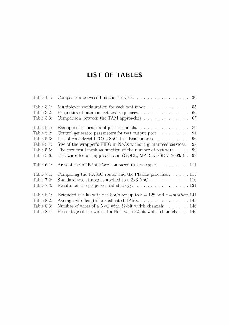
LIST OF TABLES
Table 1.1: Comparison between bus and network. . . . . . . . . . . . . . . . 30
Table 3.1: Multiplexer configuration for each test mode. . . . . . . . . . . . 55Table 3.2: Properties of interconnect test sequences. . . . . . . . . . . . . . . 66Table 3.3: Comparison between the TAM approaches. . . . . . . . . . . . . . 67
Table 5.1: Example classification of port terminals. . . . . . . . . . . . . . . 89Table 5.2: Control generator parameters for test output port. . . . . . . . . 91Table 5.3: List of considered ITC’02 SoC Test Benchmarks. . . . . . . . . . 96Table 5.4: Size of the wrapper’s FIFO in NoCs without guaranteed services. 98Table 5.5: The core test length as function of the number of test wires. . . . 99Table 5.6: Test wires for our approach and (GOEL; MARINISSEN, 2003a). . 99
Table 6.1: Area of the ATE interface compared to a wrapper. . . . . . . . . 111
Table 7.1: Comparing the RASoC router and the Plasma processor. . . . . . 115Table 7.2: Standard test strategies applied to a 3x3 NoC. . . . . . . . . . . . 116Table 7.3: Results for the proposed test strategy. . . . . . . . . . . . . . . . 121
Table 8.1: Extended results with the SoCs set up to c = 128 and r =medium. 141Table 8.2: Average wire length for dedicated TAMs. . . . . . . . . . . . . . . 145Table 8.3: Number of wires of a NoC with 32-bit width channels. . . . . . . 146Table 8.4: Percentage of the wires of a NoC with 32-bit width channels. . . . 146


LIST OF ALGORITHMS
Algorithm 6.1: Initiator ATE Interface . . . . . . . . . . . . . . . . . . . . 106Algorithm 6.2: Target ATE Interface . . . . . . . . . . . . . . . . . . . . . 106Algorithm 8.1: Main Scheduling Algorithm . . . . . . . . . . . . . . . . . . 128Algorithm 8.2: FixStartSolution . . . . . . . . . . . . . . . . . . . . . . . . 130Algorithm 8.3: ModifiedReshuffle . . . . . . . . . . . . . . . . . . . . . . . 131Algorithm 8.4: OptimizeTestWires . . . . . . . . . . . . . . . . . . . . . . 132Algorithm 8.5: FindATEInterfaces . . . . . . . . . . . . . . . . . . . . . . 133Algorithm 8.6: HalfPerimeter(V ) . . . . . . . . . . . . . . . . . . . . . . . 143Algorithm 8.7: Minimum Rectilinear Steiner Tree(V ) . . . . . . . . . . . . 144Algorithm 9.1: Minimize Buffer Size(w) . . . . . . . . . . . . . . . . . . . . 150

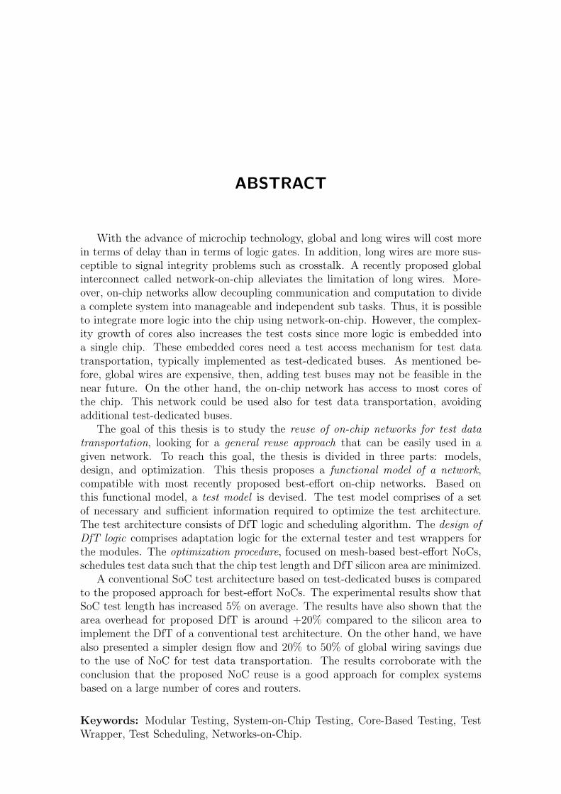
ABSTRACT
With the advance of microchip technology, global and long wires will cost morein terms of delay than in terms of logic gates. In addition, long wires are more sus-ceptible to signal integrity problems such as crosstalk. A recently proposed globalinterconnect called network-on-chip alleviates the limitation of long wires. More-over, on-chip networks allow decoupling communication and computation to dividea complete system into manageable and independent sub tasks. Thus, it is possibleto integrate more logic into the chip using network-on-chip. However, the complex-ity growth of cores also increases the test costs since more logic is embedded intoa single chip. These embedded cores need a test access mechanism for test datatransportation, typically implemented as test-dedicated buses. As mentioned be-fore, global wires are expensive, then, adding test buses may not be feasible in thenear future. On the other hand, the on-chip network has access to most cores ofthe chip. This network could be used also for test data transportation, avoidingadditional test-dedicated buses.
The goal of this thesis is to study the reuse of on-chip networks for test datatransportation, looking for a general reuse approach that can be easily used in agiven network. To reach this goal, the thesis is divided in three parts: models,design, and optimization. This thesis proposes a functional model of a network,compatible with most recently proposed best-effort on-chip networks. Based onthis functional model, a test model is devised. The test model comprises of a setof necessary and sufficient information required to optimize the test architecture.The test architecture consists of DfT logic and scheduling algorithm. The design ofDfT logic comprises adaptation logic for the external tester and test wrappers forthe modules. The optimization procedure, focused on mesh-based best-effort NoCs,schedules test data such that the chip test length and DfT silicon area are minimized.
A conventional SoC test architecture based on test-dedicated buses is comparedto the proposed approach for best-effort NoCs. The experimental results show thatSoC test length has increased 5% on average. The results have also shown that thearea overhead for proposed DfT is around +20% compared to the silicon area toimplement the DfT of a conventional test architecture. On the other hand, we havealso presented a simpler design flow and 20% to 50% of global wiring savings dueto the use of NoC for test data transportation. The results corroborate with theconclusion that the proposed NoC reuse is a good approach for complex systemsbased on a large number of cores and routers.
Keywords: Modular Testing, System-on-Chip Testing, Core-Based Testing, TestWrapper, Test Scheduling, Networks-on-Chip.


RESUMO
Logica e Escalonamento de Teste para Sistemas com Redes Intra-ChipBaseadas em Topologia de Malha
Com o avanco da tecnologia de fabricacao de chips o atraso em fios globais seramaior que o atraso em portas logicas. Alem disso, fios globais longos sao maissuscetıveis a problemas de integridade como crosstalk. Uma proposta recente de in-terconneccao global chamada redes intra-chip reduz essas limitacoes referentes a fioslongos. Alem dessas vantagens, redes intra-chip permitem desacoplar comunicacaoe computacao, dividindo um sistema em sub tarefas independentes. Devido as es-sas vantagens e possıvel integrar mais logica em um chip que usa redes intra-chip.Entretanto, o acrescimo de logica no chip aumenta o custo de teste. Os modulos dochip precisam de mecanismos para transportar dados de teste, que sao tipicamentebarramentos usados exclusivamente para teste. Entretanto, como mencionado an-teriormente, fios globais sao caros e acrescentar barramentos de teste pode nao serpossıvel em um futuro proximo. Por outro lado, uma rede intra-chip tem acesso amaioria dos modulos do chip. Esta rede pode ser usada para transportar dados deteste, evitando o acrescimo de barramentos dedicados ao teste.
O objetivo dessa tese e estudar o uso de redes intra-chip para o transporte dedados de teste, enfatizando uma abordagem generica que possa ser aplicada a umadada rede. Para tanto, essa tese foi divida em tres partes: modelos, projeto, eotimizacao. A tese propoe um modelo funcional de rede que e compatıvel coma maioria das recem propostas redes intra-chip. O modelo de teste, baseado nomodelo funcional da rede, compreende o conjunto de informacoes necessarias paraotimizar a arquitetura de teste. A arquitetura de teste, por sua vez, consiste delogica para teste e algoritmo de otimizacao. A logica de teste compreende logicapara ATE interface e logica envoltoria para modulos de hardware. Os algoritmosotimizam o tempo de teste e a area de logica de teste no nıvel dos modulos e nonıvel do chip.
Uma arquitetura convencional de teste de SoCs baseada em barramento de testededicado foi comparada com a arquitetura proposta para SoCs baseados em redesintra-chip. Os resultados apontam que o tempo de teste do SoC com a arquiteturaproposta aumenta em media 5%. Os resultados tambem mostram que a logica deteste da arquitetura proposta e cerca de 20% maior que na arquitetura de testeconvencional. Por outro lado, o fluxo de projeto baseado na arquitetura de testeproposta e mais simples que a convencional. Alem disso, a arquitetura propostareduz o numero de fios globais em torno de 20% a 50% para SoCs complexos. Estesresultados demonstram que a arquitetura proposta e melhor para sistemas complexoscom um grande numero de modulos.
Palavras-chave: teste de sistemas intra-chip, logica envoltoria de teste, escalona-mento de teste, redes intra-chip.

27
1 INTRODUCTION
The scaling of micro chip technology enables more logic, or an entire system,embedded in a single chip (System-on-Chip - SoC). It creates the opportunity todesign tightly coupled parallel applications for example, for embedded systems in aportable device. However, it also brings challenges in terms of design productivity,design of global interconnect, and test for manufacturing defects (KEUTZER et al.,2000; ZORIAN; MARINISSEN; DEY, 1998).
The exponential shrink of the transistor size increases the available resources ina chip and increases the design complexity since more modules are embedded in thechip. In addition, the market competition demands a shorter design cycle. This mo-tivates the adoption of some practices to deal with the design complexity, such as,core reuse, design partition, decoupling communication and computation, and higherlevels of abstraction. The system is partitioned in independent sub tasks to easeits design and verification. These independent tasks rely on decoupling communi-cation and computation to avoid the interference of other tasks. With independenttasks, higher levels of abstraction can be used to help the design. Moreover, thetasks are designed with standard interfaces to ease their integration. The systemusually follows a layered design methodology to abstract the global interconnectimplementation.
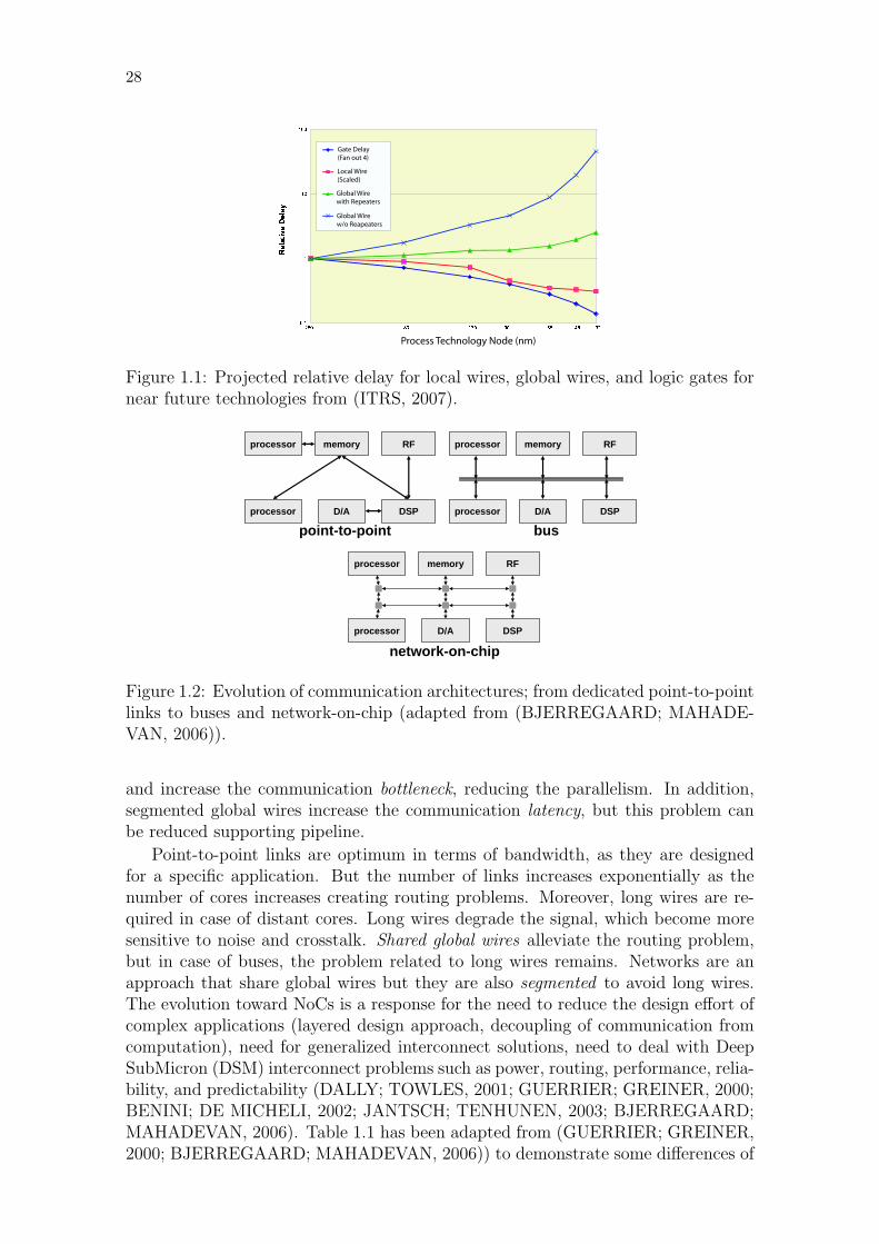
Another challenge of SoC design is related to the design of global interconnect.With the scaling of microchip technology, the computation is becoming cheaperthan the communication because wires do not scale as transistor due to physicallimitation of global wires such as signal integrity (fabrication defects, crosstalk, noisesensitivity) and power consumption. Figure 1.1 from ITRS illustrates the delay gapbetween wires and transistors for near future technologies. It can be observed thatglobal wires are the most critical in terms of delay, thus, the time spent on globalcommunication can overcome the time spent on local processing. For this reason,there is a need for cost-effective global communication architecture for future SoCdesign.
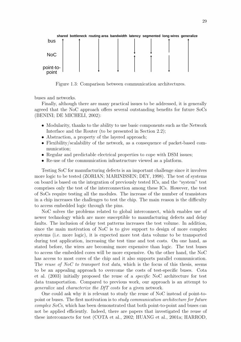
As an answer for the need for a cost-effective global communication for chips, onecan observe that the functional interconnects have evolved from point-to-point links,to single and multiple hierarchical buses, and recently to networks-on-chip (NoC)(Figure 1.2). Each of these functional interconnects provides different features asillustrated in Figure 1.3. The increase of number of communicating cores suggestsshared and segmented global wires to deal with, respectively, routing area and longwires. On-chip interconnect based on shared global wires are easier to generalize,reducing the design effort, since every core in the system just need to be connectedto these global shared wires. However, shared global wires reduce the bandwidth
2818 P a p e r A
4 · T. Bjerregaard and S. Mahadevan
Fig. 2. Projected relative delay for local and global wires and for logic gates of near future technologies [ITRS2001].
As a reaction to the inherent limitations of global synchrony, alternative concepts suchas GALS (Globally Asynchronous Locally Synchronous systems) are being introduced.A GALS chip is made up of locally synchronous islands which communicate asyn-chronously [Chapiro 1984][Meincke et al. 1999][Muttersbach et al. 2000]. There aretwo main advantageous aspects of this method. One is the reducing of the synchroniza-tion problem to a number of smaller subproblems. The other relates to the integrationof different IP (Intellectual Property) cores, easing the building of larger systems fromindividual blocks with different timing characteristics.
—Design productivity. The exploding amount of processing resources available in chipdesign together with a requirement for shortened design cycles have pushed the pro-ductivity requirements on chip designers. Between 1997 and 2002 the market demandreduced the typical design cycle by 50%. As a result of increased chip sizes, shrinkinggeometries and the availability of more metal layers, the design complexity increased50 times in the same period [OCPIP 2003a]. To keep up with these requirements, IPreuse is pertinent. A new paradigm for design methodology is needed, which allows thedesign effort to scale linearly with system complexity.Abstraction at register transfer level (RTL) was introduced with the ASIC design flowduring the 90s, allowing synthesized standard cell design. This made it possible to de-sign large chips within short design cycles, and synthesized RTL design is at present thedefacto standard for making large chips quickly. But the availability of on-chip resourcesis outgrowing the productivity potential of even the ASIC design style. In order to uti-lize the exponential growth in number of transistors on each chip, even higher levels ofabstraction must be applied. This can be done by introducing higher level communica-tion abstractions, making for a layered design methodology enabling a partitioning ofthe design effort into minimally interdependent subtasks. Support for this at the hard-ware level includes standard communication sockets, allowing IP cores from differentvendors to be plugged effortlessly together. This is particularly pertinent in complexmulti-processor system-on-chip (MPSoC) designs. Also, the development of design
Figure 1.1: Projected relative delay for local wires, global wires, and logic gates fornear future technologies from (ITRS, 2007).
2
processor memory RF
processor D/A DSP
processor memory RF
processor D/A DSP
bus
network-on-chip
processor memory RF
processor D/A DSP
point-to-point
Figure 1.2: Evolution of communication architectures; from dedicated point-to-pointlinks to buses and network-on-chip (adapted from (BJERREGAARD; MAHADE-VAN, 2006)).
and increase the communication bottleneck, reducing the parallelism. In addition,segmented global wires increase the communication latency, but this problem canbe reduced supporting pipeline.
Point-to-point links are optimum in terms of bandwidth, as they are designedfor a specific application. But the number of links increases exponentially as thenumber of cores increases creating routing problems. Moreover, long wires are re-quired in case of distant cores. Long wires degrade the signal, which become moresensitive to noise and crosstalk. Shared global wires alleviate the routing problem,but in case of buses, the problem related to long wires remains. Networks are anapproach that share global wires but they are also segmented to avoid long wires.The evolution toward NoCs is a response for the need to reduce the design effort ofcomplex applications (layered design approach, decoupling of communication fromcomputation), need for generalized interconnect solutions, need to deal with DeepSubMicron (DSM) interconnect problems such as power, routing, performance, relia-bility, and predictability (DALLY; TOWLES, 2001; GUERRIER; GREINER, 2000;BENINI; DE MICHELI, 2002; JANTSCH; TENHUNEN, 2003; BJERREGAARD;MAHADEVAN, 2006). Table 1.1 has been adapted from (GUERRIER; GREINER,2000; BJERREGAARD; MAHADEVAN, 2006)) to demonstrate some differences of
29
3
bus
NoC
point-to-point
shared bottleneck routing area bandwidth latency segmented long wires generalize
Figure 1.3: Comparison between communication architectures.
buses and networks.Finally, although there are many practical issues to be addressed, it is generally
agreed that the NoC approach offers several outstanding benefits for future SoCs(BENINI; DE MICHELI, 2002):
• Modularity, thanks to the ability to use basic components such as the NetworkInterface and the Router (to be presented in Section 2.2);
• Abstraction, a property of the layered approach;• Flexibility/scalability of the network, as a consequence of packet-based com-
munication;• Regular and predictable electrical properties to cope with DSM issues;• Re-use of the communication infrastructure viewed as a platform.
Testing SoC for manufacturing defects is an important challenge since it involvesmore logic to be tested (ZORIAN; MARINISSEN; DEY, 1998). The test of systemson board is based on the integration of previously tested ICs, and the “system” testcomprises only the test of the interconnection among these ICs. However, the testof SoCs require testing all the modules. The increase of the number of transistorsin a chip increases the challenges to test the chip. The main reason is the difficultyto access embedded logic through the pins.
NoC solves the problems related to global interconnect, which enables use ofnewer technology which are more susceptible to manufacturing defects and delayfaults. The inclusion of delay test patterns increases the test volume. In addition,since the main motivation of NoC is to give support to design of more complexsystems (i.e. more logic), it is expected more test data volume to be transportedduring test application, increasing the test time and test costs. On one hand, asstated before, the wires are becoming more expensive than logic. The test busesto access the embedded cores will be more expensive. On the other hand, the NoChas access to most cores of the chip and it also supports parallel communication.The reuse of NoC to transport test data, which is the focus of this thesis, seemsto be an appealing approach to overcome the costs of test-specific buses. Cotaet al. (2003) initially proposed the reuse of a specific NoC architecture for testdata transportation. Compared to previous work, our approach is an attempt togeneralize and characterize the DfT costs for a given network.
One could ask why it is relevant to study the reuse of NoC instead of point-to-point or buses. The first motivation is to study communication architecture for futurecomplex SoCs, which has been demonstrated that both point-to-point and buses cannot be applied efficiently. Indeed, there are papers that investigated the reuse ofthese interconnects for test (COTA et al., 2002; HUANG et al., 2001a; HARROD,

30
Table 1.1: Comparison between bus and network (adapted from (GUERRIER;GREINER, 2000; BJERREGAARD; MAHADEVAN, 2006)).
bus networkEvery unit attached adds parasitic - + Only point-to-point one-way
capacitance, degrading the electrical wires are used, therefore wireperformance. performance is not degraded.
Bus timing is difficult in a deep - + Network supports pipelinedsubmicron process. communication
Bus testability is problematic and slow. - + Network can be used to transporttest data and network supportsmultiple parallel communication
Bus arbiter delay grows with the - + Routing and arbitration logicnumber of masters. are distributed.
The arbiter is instance-specific. - + The same arbitration logicis implemented in each router
Bandwidth is limited and shared - + Aggregated bandwidth scalesby all units attached. with the network size.
Bus latency is zero once arbiter + - Internal network contentionhas granted control. increase the latency (1).
The silicon cost of a bus is + - The network has a significantnear zero. silicon area (2).
Any bus is almost directly + - wrapper and conversion logiccompatible with most available IPs, in both software and hardwareincluding software running on CPUs. are required (3).
The concepts are simple and + - System designers need reeducationwell understood. for new concepts (4).
31
1999; BURDASS et al., 2000; HWANG; ABRAHAM, 2001; FEIGE et al., 1998).However, these approaches would not perform well on both test and functionaldomains in the near future. Moreover, a NoC is easier to generalize than point-to-point links, essential issue for any DfT approach; and it supports more parallelismand bandwidth than buses, essential to reduce the chip test time.
1.1 Problems to be Solved
We believe that the effective adoption of NoC reuse in actual designs dependson the following items:
• The actual benefits of NoC reuse compared to conventional approaches basedon dedicated TAMs :The benefits and cost related to NoC reuse approaches are not clear enough.The most common claim of authors proposing NoC reuse is that it would savearea since no test-specific TAM is required. On one hand, there are somedesign approaches based on dedicated TAMs that use information of place-ment of the cores to minimize the TAM wiring length, reporting negligibleTAM costs (despite of the more complex design flow) (GOEL; MARINISSEN,2003b). On the other hand, most papers about NoC reuse are about opti-mization algorithms under different constraints, but they do not focus on therequirements for the NoC reuse. i.e. which modifications are required in thedesign in order to reuse the NoC to transport test data ? What is the impactof the required DfT for NoC reuse in silicon area and test length compared todedicated TAMs ? If the only benefit of NoC is to save wiring area, how mucharea are we saving with NoC reuse ?
• Simple, general, and application-independent test approach:Test designers have adopted modular testing approach for the test of complexchips since it is simple. It is mostly based on the well-know scan chains forintra-core access and simple TAMs, which are just wires, for inter-core access.Differentiated core structures, like memories, use BIST approaches. However,the BIST control itself is connected to the chip test control logic by, for ex-ample, boundary scan (i.e. more scan-based approaches). Simple approachesusually cost less in area and are easier to automate. In addition, scan can beused to most logic cores, so they are general and independent of design. Onthe other hand, NoCs are much more complex than conventional dedicatedTAM, there is no general NoC design, and the NoC design is totally depen-dent on the application requirements; so, why reuse NoC for test instead oftest-specific TAMs ? Is it possible to generalize NoC reuse ? Is it possible tosimplify the test view of a given NoC ?
1.2 Goals
The strategic goal of this thesis is to propose a general1 approach for the reuseof on-chip networks for test data transportation. To accomplish this strategic goal,the following specific objectives should be fulfilled:
1The term ’general’, unless specified, refers to a test approach that is applicable to most best-effort and mesh-based NoC designs, which was the class of NoC most used along this thesis.
32
• Make the requirements for NoC reuse explicit;
• Determine the test logic required to enable the reuse of both best-effort (BE)and guaranteed throughput (GT) NoCs;
• Determine the optimization algorithms for the DfT modules;
• Propose a test schedule tool for overall test architecture optimization consid-ering BE NoCs;
• Compare the proposed test architecture with the conventional test architecturebased on dedicated TAM to establish the actual advantages and drawbacks ofNoC reuse.
1.3 Contribution
The main contribution of this thesis is a general test model for NoC-based SoCssuch that this proposed model is compatible with the current test methods. Otherscontributions are:
1. Concise functional NoC definition (Chapter 1);
2. Extensive analysis of prior work (Chapter 3);
3. General test model for a BE NoC-based chip (Chapter 4), partially publishedin Amory (2007);
4. Detailed design and optimization of DfT required to enable the reuse of bothBE and GT NoCs as TAM (Chapters 4 to 7), published in Amory et al. (2005;2006; 2007; 2007);
5. Test planing tool based on the proposed test model to optimize the chip testlength (Chapter 8), to be published.
1.4 Outline of the Thesis
This thesis is organized in three parts as presented below.
1.4.1 Background, Definitions, and Models
Chapter 2 presents background related to SoC testing and NoCs. In sequence,the prior work is reviewed in Chapter 3; topics like wrapper design, TAM design,FIFO testing, and recent papers about test of NoC are analyzed. Later, in Chapter 4,we propose a test model that represents the necessary and sufficient information of aBE NoC-based system to implement the DfT and optimization procedures proposedin this thesis.
1.4.2 DfT Design for NoC Reuse
Once the NoC definition is established and the set of required information fortest is defined, we detail the design processes required to modify the chip for test.The second part of this thesis, in Chapters 4 to 7, presents the DfT logic required touse both BE and GT networks to transport test data.
33
To use the network for test, some additional logic is required to interface theexternal tester to the network, to the cores, and to the network building blocks aswell. It has been identified, for example, that not only the cores, but also the testpins require a wrapper logic in order to connect to the NoC. Besides, the wrapperrequires a different design compared to the conventional modular test approachesbecause the “TAM” works with well-defined protocols. The proposed wrappershave been designed to abstract the test path as “pipelines” that can pump data atdifferent rates.
1.4.3 Test Optimization
Considering the chip information required for test enumerated in the test modeland the required test circuitry, the final step is to integrate it into a test planningtool that optimizes the test architecture in terms of test length and silicon area(Chapters 8 and 9).

34
35
2 RELATED BACKGROUND
The following sections present basic concepts related to test of SoC, basic con-cepts of NoC design, and the outline of this thesis.
2.1 Modular Testing
Modular testing (GOEL; MARINISSEN, 2003a), i.e. testing individual SoC mod-ules as stand-alone units, has been used for SoCs. Non-logic modules such as em-bedded analog and memories require modular testing since they use different teststrategies then random digital logic. The ability to use the most appropriate teststrategy for every core increases the test quality. Black-boxed cores, such as hard orencrypted cores which no implementation detail is given, require modular testingbecause they need to be tested with test vectors supplied by the core provider. Inaddition, modular testing provides an attractive “divide-and-conquer” test develop-ment approach that reduces the time to generate the test vectors, and allows fortest reuse when a core is used in multiple designs.
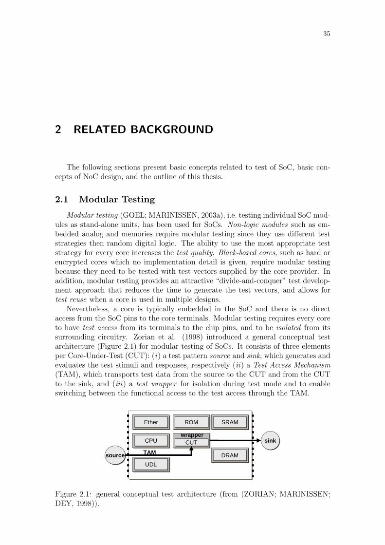
Nevertheless, a core is typically embedded in the SoC and there is no directaccess from the SoC pins to the core terminals. Modular testing requires every coreto have test access from its terminals to the chip pins, and to be isolated from itssurrounding circuitry. Zorian et al. (1998) introduced a general conceptual testarchitecture (Figure 2.1) for modular testing of SoCs. It consists of three elementsper Core-Under-Test (CUT): (i) a test pattern source and sink, which generates andevaluates the test stimuli and responses, respectively (ii) a Test Access Mechanism(TAM), which transports test data from the source to the CUT and from the CUTto the sink, and (iii) a test wrapper for isolation during test mode and to enableswitching between the functional access to the test access through the TAM.
13
EtherEther ROMROM SRAMSRAM
CPUCPU CUTCUT
DRAMDRAM
UDLUDL
wrapper
sourcesource
sinksink
TAM
Figure 2.1: general conceptual test architecture (from (ZORIAN; MARINISSEN;DEY, 1998)).

36
19
AA BB
CC DD EE
FF
W1=3
W2=4
W3=2
A B
C D E
F
(a) (b)
SoC
Figure 2.2: (a) Example of TestRail architecture and (b) corresponding test schedule(adapted from (GOEL; MARINISSEN, 2003a)).
The test architecture design problem can be defined as (GOEL; MARINISSEN,2003a): for a given set of cores and a given number of test pins, determine theTAM type, the number of TAMs, the width of each TAM, the assignment of coresto the TAMs, and the wrapper design, such that the chip test length is minimized.Several papers have investigated test architecture designs, such as test bus (VARMA;BHATIA, 1998) and TestRail (MARINISSEN et al., 1998), and how to optimize thetest architecture (CHAKRABARTY, 2000; MARINISSEN; GOEL; LOUSBERG,2000; HUANG et al., 2001b; GOEL; MARINISSEN, 2003a). Figure 2.2 illustratesan example of resulting test architecture and test scheduling (GOEL; MARINISSEN,2003a).
Two test flows are required to test a core. The stimuli test flow transports thetest stimuli from the source to the CUT and the response test flow transports thetest responses from the CUT to the sink. The stimuli and the response test flowsmay transport different data amounts. For instance, let us assume the test of a corewith one input terminal, no internal scan chains, and one hundred output terminals.Each test pattern of this core requires one bit in and one hundred bits out. The testdata volume, the number of bits required to test a core, considering both stimuli andresponses, is given by the core provider, thus, the test data volume is consideredinvariant.
Since the amount of test data is fixed, the core test length1 depends on how fastthe amount of test data can be transported over the TAM. This variable is calledtest data rate. A recommended test data rate should range from 1 bit/clock cycle toa certain maximum which depends on the core and on the TAM width. The minimaltest data rate of 1 bit/clock cycle is recommended, but not mandatory, because itkeeps a minimal but constant data flow and it reduces the core test length.
Interruptions on the data flow require mechanisms to halt the test. The usualapproaches are the use of clock gating or holdable scan cells. Clock gating haltsthe clock for a certain period. The drawback is that it requires changing the clocktree, which is generally not recommended for complex systems. The other approachto freeze the test is to implement holdable scan cells, i.e. scan cells that can keepthe current value, but this approach requires an extra multiplexer for each scancell. Holdable scan cells increase the area for DfT. Moreover, it is not feasible for
1the term test length is used when the unity is clock cycles. Test time is used when we refer toseconds.
37
11
(b) test time with preemption
(a) test time without preemption
test pattern 0test pattern 0 test pattern 1test pattern 1
test response 0test response 0
test pattern 0test pattern 0 test pattern 1test pattern 1test response 0test response 0 test response 1test response 1preemption
test response 1test response 1
core
test
tim
e
core
test
tim
e
additionaltest time
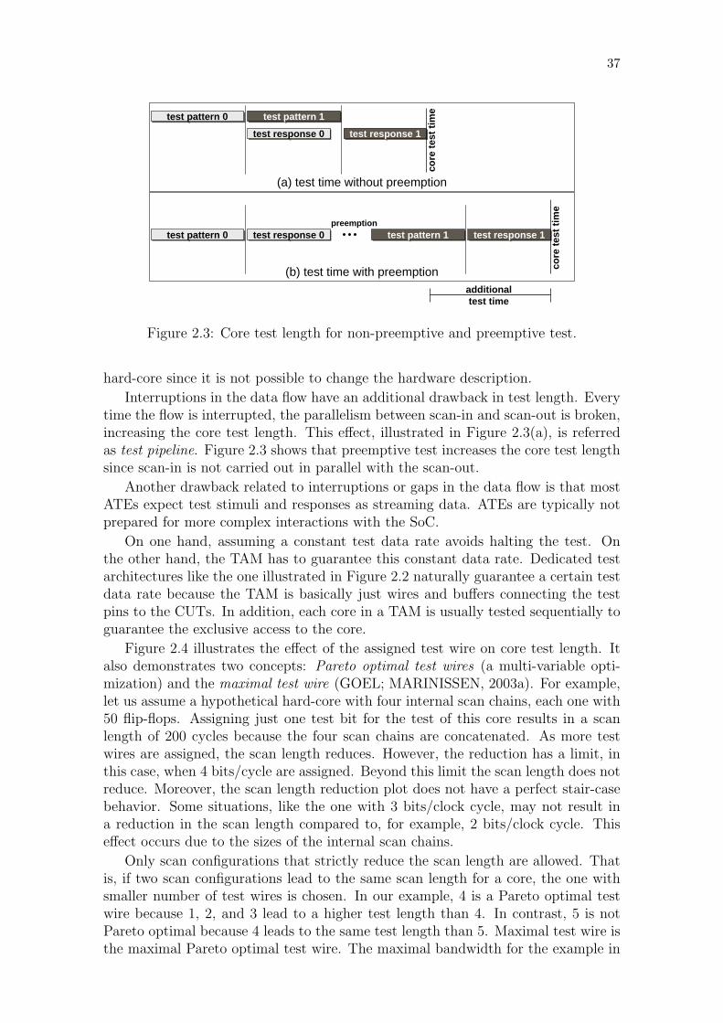
Figure 2.3: Core test length for non-preemptive and preemptive test.
hard-core since it is not possible to change the hardware description.
Interruptions in the data flow have an additional drawback in test length. Everytime the flow is interrupted, the parallelism between scan-in and scan-out is broken,increasing the core test length. This effect, illustrated in Figure 2.3(a), is referredas test pipeline. Figure 2.3 shows that preemptive test increases the core test lengthsince scan-in is not carried out in parallel with the scan-out.
Another drawback related to interruptions or gaps in the data flow is that mostATEs expect test stimuli and responses as streaming data. ATEs are typically notprepared for more complex interactions with the SoC.
On one hand, assuming a constant test data rate avoids halting the test. Onthe other hand, the TAM has to guarantee this constant data rate. Dedicated testarchitectures like the one illustrated in Figure 2.2 naturally guarantee a certain testdata rate because the TAM is basically just wires and buffers connecting the testpins to the CUTs. In addition, each core in a TAM is usually tested sequentially toguarantee the exclusive access to the core.
Figure 2.4 illustrates the effect of the assigned test wire on core test length. Italso demonstrates two concepts: Pareto optimal test wires (a multi-variable opti-mization) and the maximal test wire (GOEL; MARINISSEN, 2003a). For example,let us assume a hypothetical hard-core with four internal scan chains, each one with50 flip-flops. Assigning just one test bit for the test of this core results in a scanlength of 200 cycles because the four scan chains are concatenated. As more testwires are assigned, the scan length reduces. However, the reduction has a limit, inthis case, when 4 bits/cycle are assigned. Beyond this limit the scan length does notreduce. Moreover, the scan length reduction plot does not have a perfect stair-casebehavior. Some situations, like the one with 3 bits/clock cycle, may not result ina reduction in the scan length compared to, for example, 2 bits/clock cycle. Thiseffect occurs due to the sizes of the internal scan chains.
Only scan configurations that strictly reduce the scan length are allowed. Thatis, if two scan configurations lead to the same scan length for a core, the one withsmaller number of test wires is chosen. In our example, 4 is a Pareto optimal testwire because 1, 2, and 3 lead to a higher test length than 4. In contrast, 5 is notPareto optimal because 4 leads to the same test length than 5. Maximal test wire isthe maximal Pareto optimal test wire. The maximal bandwidth for the example in
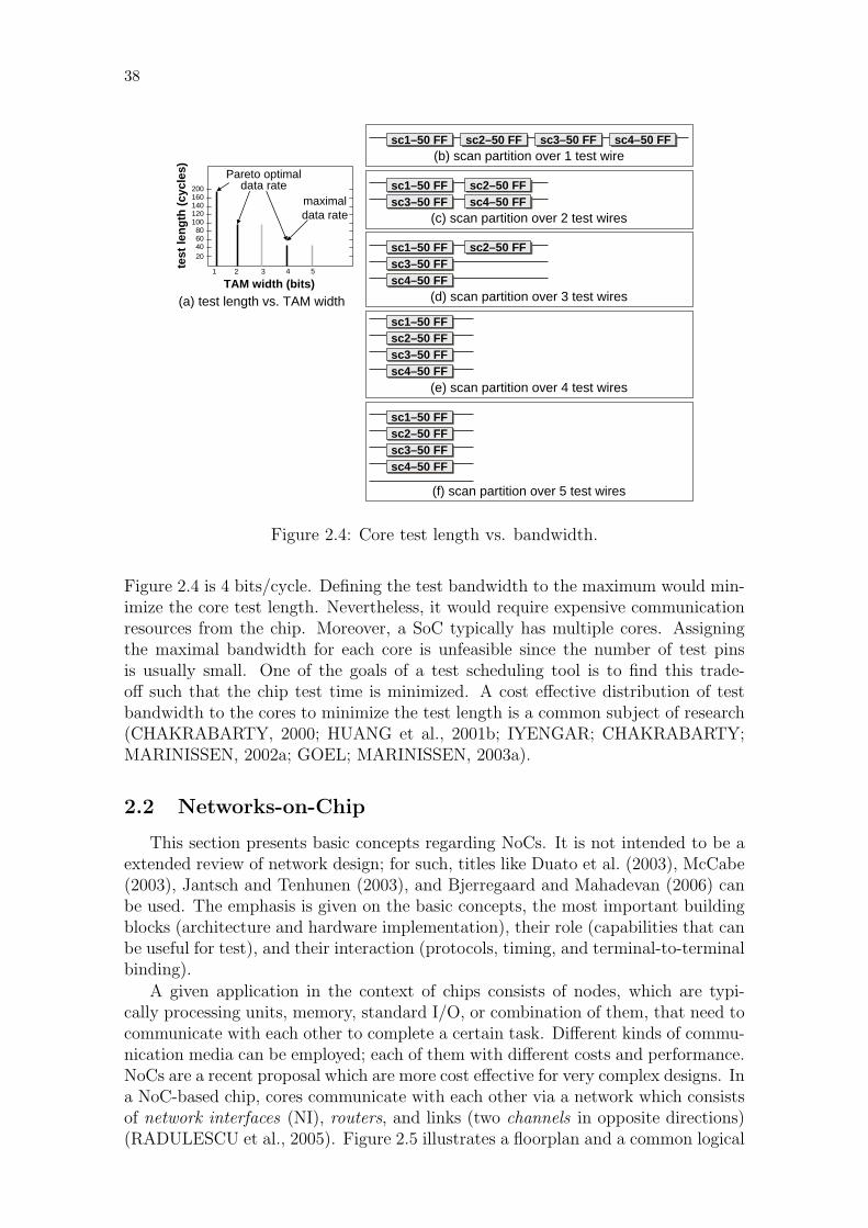
38
6
(e) scan partition over 4 test wires
(c) scan partition over 2 test wires
(b) scan partition over 1 test wire
(d) scan partition over 3 test wires
sc3–50 FFsc3–50 FF sc4–50 FFsc4–50 FF
sc3–50 FFsc3–50 FF sc4–50 FFsc4–50 FF
20406080
100120140160200
21 3
TAM width (bits)
test
leng
th (c
ycle
s)
(a) test length vs. TAM width
sc1–50 FFsc1–50 FF sc2–50 FFsc2–50 FF
sc1–50 FFsc1–50 FF sc2–50 FFsc2–50 FF
sc3–50 FFsc3–50 FFsc1–50 FFsc1–50 FF sc2–50 FFsc2–50 FF
sc4–50 FFsc4–50 FF
sc3–50 FFsc3–50 FF
sc1–50 FFsc1–50 FFsc2–50 FFsc2–50 FF
sc4–50 FFsc4–50 FF
(f) scan partition over 5 test wires
sc3–50 FFsc3–50 FF
sc1–50 FFsc1–50 FFsc2–50 FFsc2–50 FF
sc4–50 FFsc4–50 FF
4 5
maximaldata rate
Pareto optimaldata rate
Figure 2.4: Core test length vs. bandwidth.
Figure 2.4 is 4 bits/cycle. Defining the test bandwidth to the maximum would min-imize the core test length. Nevertheless, it would require expensive communicationresources from the chip. Moreover, a SoC typically has multiple cores. Assigningthe maximal bandwidth for each core is unfeasible since the number of test pinsis usually small. One of the goals of a test scheduling tool is to find this trade-off such that the chip test time is minimized. A cost effective distribution of testbandwidth to the cores to minimize the test length is a common subject of research(CHAKRABARTY, 2000; HUANG et al., 2001b; IYENGAR; CHAKRABARTY;MARINISSEN, 2002a; GOEL; MARINISSEN, 2003a).
2.2 Networks-on-Chip
This section presents basic concepts regarding NoCs. It is not intended to be aextended review of network design; for such, titles like Duato et al. (2003), McCabe(2003), Jantsch and Tenhunen (2003), and Bjerregaard and Mahadevan (2006) canbe used. The emphasis is given on the basic concepts, the most important buildingblocks (architecture and hardware implementation), their role (capabilities that canbe useful for test), and their interaction (protocols, timing, and terminal-to-terminalbinding).
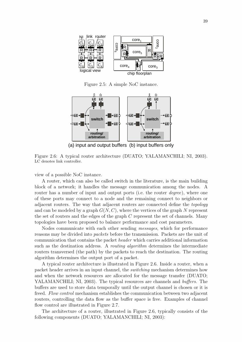
A given application in the context of chips consists of nodes, which are typi-cally processing units, memory, standard I/O, or combination of them, that need tocommunicate with each other to complete a certain task. Different kinds of commu-nication media can be employed; each of them with different costs and performance.NoCs are a recent proposal which are more cost effective for very complex designs. Ina NoC-based chip, cores communicate with each other via a network which consistsof network interfaces (NI), routers, and links (two channels in opposite directions)(RADULESCU et al., 2005). Figure 2.5 illustrates a floorplan and a common logical
39
7
RRRR
RR
RR
RR
core6
core6
core1core1
core2
core2
core4core4 core3core3
RRcore5core5
RR RR
RR RR
RR
RR
C3C3C2C2C1C1
C4C4C5C5C6C6
chip floorplanlogical view
link routerNI
Figure 2.5: A simple NoC instance.
9
routing/arbitration
LC
LC LC
LC
LC LC
switch
(a) input and output buffers
routing/arbitration
LC
LC LC
LC
LC LC
switch
(b) input buffers only
Figure 2.6: A typical router architecture (DUATO; YALAMANCHILI; NI, 2003).LC denotes link controller.
view of a possible NoC instance.
A router, which can also be called switch in the literature, is the main buildingblock of a network; it handles the message communication among the nodes. Arouter has a number of input and output ports (i.e. the router degree), where oneof these ports may connect to a node and the remaining connect to neighbors oradjacent routers. The way that adjacent routers are connected define the topologyand can be modeled by a graph G(N, C), where the vertices of the graph N representthe set of routers and the edges of the graph C represent the set of channels. Manytopologies have been proposed to balance performance and cost parameters.
Nodes communicate with each other sending messages, which for performancereasons may be divided into packets before the transmission. Packets are the unit ofcommunication that contains the packet header which carries additional informationsuch as the destination address. A routing algorithm determines the intermediaterouters transversed (the path) by the packets to reach the destination. The routingalgorithm determines the output port of a packet.
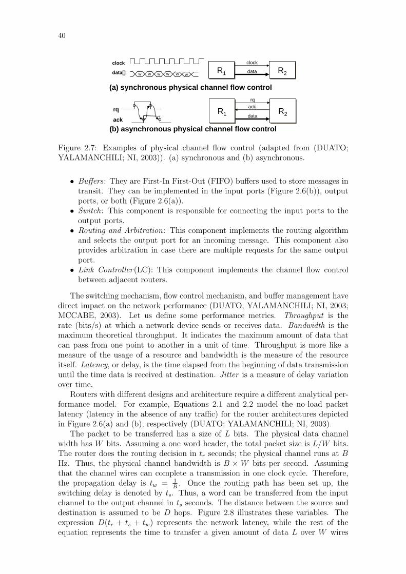
A typical router architecture is illustrated in Figure 2.6. Inside a router, when apacket header arrives in an input channel, the switching mechanism determines howand when the network resources are allocated for the message transfer (DUATO;YALAMANCHILI; NI, 2003). The typical resources are channels and buffers. Thebuffers are used to store data temporally until the output channel is chosen or it isfreed. Flow control mechanism establishes the communication between two adjacentrouters, controlling the data flow as the buffer space is free. Examples of channelflow control are illustrated in Figure 2.7.
The architecture of a router, illustrated in Figure 2.6, typically consists of thefollowing components (DUATO; YALAMANCHILI; NI, 2003):
40
13
clock
data[] w w w w w w R1R1 R2R2
clock
data
R1R1 R2R2
rq
data
ack
(a) synchronous physical channel flow control
(b) asynchronous physical channel flow control
rq
ack
Figure 2.7: Examples of physical channel flow control (adapted from (DUATO;YALAMANCHILI; NI, 2003)). (a) synchronous and (b) asynchronous.
• Buffers : They are First-In First-Out (FIFO) buffers used to store messages intransit. They can be implemented in the input ports (Figure 2.6(b)), outputports, or both (Figure 2.6(a)).
• Switch: This component is responsible for connecting the input ports to theoutput ports.
• Routing and Arbitration: This component implements the routing algorithmand selects the output port for an incoming message. This component alsoprovides arbitration in case there are multiple requests for the same outputport.
• Link Controller(LC): This component implements the channel flow controlbetween adjacent routers.
The switching mechanism, flow control mechanism, and buffer management havedirect impact on the network performance (DUATO; YALAMANCHILI; NI, 2003;MCCABE, 2003). Let us define some performance metrics. Throughput is therate (bits/s) at which a network device sends or receives data. Bandwidth is themaximum theoretical throughput. It indicates the maximum amount of data thatcan pass from one point to another in a unit of time. Throughput is more like ameasure of the usage of a resource and bandwidth is the measure of the resourceitself. Latency, or delay, is the time elapsed from the beginning of data transmissionuntil the time data is received at destination. Jitter is a measure of delay variationover time.
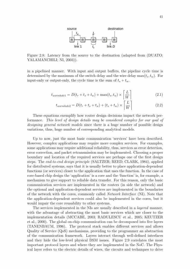
Routers with different designs and architecture require a different analytical per-formance model. For example, Equations 2.1 and 2.2 model the no-load packetlatency (latency in the absence of any traffic) for the router architectures depictedin Figure 2.6(a) and (b), respectively (DUATO; YALAMANCHILI; NI, 2003).
The packet to be transferred has a size of L bits. The physical data channelwidth has W bits. Assuming a one word header, the total packet size is L/W bits.The router does the routing decision in tr seconds; the physical channel runs at BHz. Thus, the physical channel bandwidth is B × W bits per second. Assumingthat the channel wires can complete a transmission in one clock cycle. Therefore,the propagation delay is tw = 1
B. Once the routing path has been set up, the
switching delay is denoted by ts. Thus, a word can be transferred from the inputchannel to the output channel in ts seconds. The distance between the source anddestination is assumed to be D hops. Figure 2.8 illustrates these variables. Theexpression D(tr + ts + tw) represents the network latency, while the rest of theequation represents the time to transfer a given amount of data L over W wires
41
8
RR RR RR RRRR
source destinationtw
link 1
tr
ts link D
Figure 2.8: Latency from the source to the destination (adapted from (DUATO;YALAMANCHILI; NI, 2003)).
in a pipelined manner. With input and output buffers, the pipeline cycle time isdetermined by the maximum of the switch delay and the wire delay max(ts, tw). Forinput-only or output-only, the cycle time is the sum of ts + tw.
twormhole1 = D(tr + ts + tw) + max(ts, tw)×⌈
L
W
⌉(2.1)
twormhole2 = D(tr + ts + tw) + (ts + tw)×⌈
L
W
⌉(2.2)
These equations exemplify how router design decisions impact the network per-formance. This level of design details may be considered complex for our goal ofdesigning general network models since there is a huge number of possible designvariations, thus, huge number of corresponding analytical models.
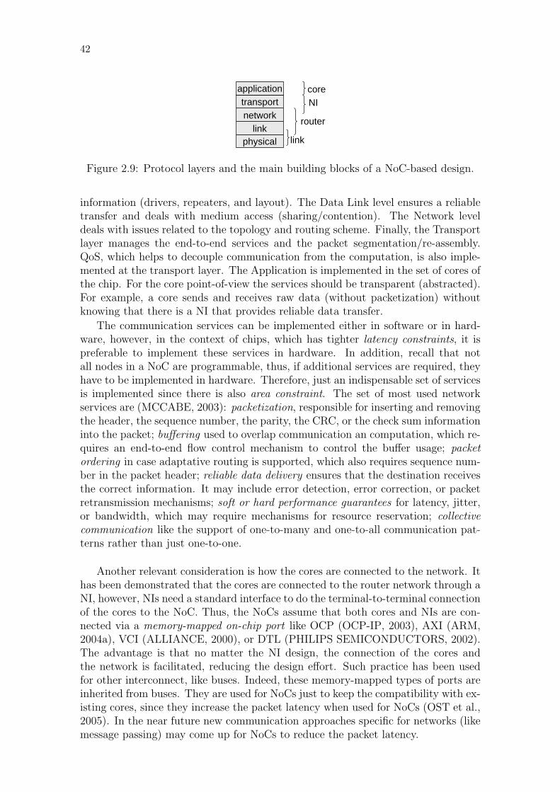
Up to now, just the most basic communication ‘services’ have been described.However, complex applications may require more complex services. For examples,some applications may require additional reliability, thus, services as error detection,error correction, and packet retransmission may be implemented. Choosing a properboundary and location of the required services are perhaps one of the first designsteps. The end-to-end design principle (SALTZER; REED; CLARK, 1984), appliedfor distributed systems, says that it is usually better to place application-dependentfunctions (or services) closer to the application that uses the function. In the case ofcore-based chip design the ‘application’ is a core and the ‘function’ is, for example, amechanism to give support to reliable data transfer. For this reason, only the basiccommunication services are implemented in the routers (in side the network) andthe optional and application-dependent services are implemented in the boundariesof the network with the cores, commonly called Network Interface (NI). Note thatthe application-dependent services could also be implemented in the cores, but itwould impair the core reusability to other systems.
The services implemented in the NIs are usually described in a layered manner,with the advantage of abstracting the most basic services which are closer to theimplementation details (MCCABE, 2003; RADULESCU et al., 2005; KEUTZERet al., 2000). The global on-chip communication can be decomposed into five layers(TANENBAUM, 1996). The protocol stack enables different services and allowsQuality of Service (QoS) mechanisms, providing to the programmer an abstractionof the communication framework. Layers interact through well-defined interfacesand they hide the low-level physical DSM issues. Figure 2.9 correlates the mostimportant protocol layers and where they are implemented in the NoC. The Phys-ical layer refers to the electric details of wires, the circuits and techniques to drive
42
11
physicallink
networktransport
applicationNI
router
link
core
Figure 2.9: Protocol layers and the main building blocks of a NoC-based design.
information (drivers, repeaters, and layout). The Data Link level ensures a reliabletransfer and deals with medium access (sharing/contention). The Network leveldeals with issues related to the topology and routing scheme. Finally, the Transportlayer manages the end-to-end services and the packet segmentation/re-assembly.QoS, which helps to decouple communication from the computation, is also imple-mented at the transport layer. The Application is implemented in the set of cores ofthe chip. For the core point-of-view the services should be transparent (abstracted).For example, a core sends and receives raw data (without packetization) withoutknowing that there is a NI that provides reliable data transfer.
The communication services can be implemented either in software or in hard-ware, however, in the context of chips, which has tighter latency constraints, it ispreferable to implement these services in hardware. In addition, recall that notall nodes in a NoC are programmable, thus, if additional services are required, theyhave to be implemented in hardware. Therefore, just an indispensable set of servicesis implemented since there is also area constraint. The set of most used networkservices are (MCCABE, 2003): packetization, responsible for inserting and removingthe header, the sequence number, the parity, the CRC, or the check sum informationinto the packet; buffering used to overlap communication an computation, which re-quires an end-to-end flow control mechanism to control the buffer usage; packetordering in case adaptative routing is supported, which also requires sequence num-ber in the packet header; reliable data delivery ensures that the destination receivesthe correct information. It may include error detection, error correction, or packetretransmission mechanisms; soft or hard performance guarantees for latency, jitter,or bandwidth, which may require mechanisms for resource reservation; collectivecommunication like the support of one-to-many and one-to-all communication pat-terns rather than just one-to-one.
Another relevant consideration is how the cores are connected to the network. Ithas been demonstrated that the cores are connected to the router network through aNI, however, NIs need a standard interface to do the terminal-to-terminal connectionof the cores to the NoC. Thus, the NoCs assume that both cores and NIs are con-nected via a memory-mapped on-chip port like OCP (OCP-IP, 2003), AXI (ARM,2004a), VCI (ALLIANCE, 2000), or DTL (PHILIPS SEMICONDUCTORS, 2002).The advantage is that no matter the NI design, the connection of the cores andthe network is facilitated, reducing the design effort. Such practice has been usedfor other interconnect, like buses. Indeed, these memory-mapped types of ports areinherited from buses. They are used for NoCs just to keep the compatibility with ex-isting cores, since they increase the packet latency when used for NoCs (OST et al.,2005). In the near future new communication approaches specific for networks (likemessage passing) may come up for NoCs to reduce the packet latency.
43
16
portport
(a) read transaction
portport
initiator targetcommandchannel
datachannel
portport
(b) write transaction
portport
initiator targetcommandchannel
datachannel
initiator targetdata request
command
ack
data
initiator targetdata transfer
command
ack
data
Figure 2.10: Initiator and target ports; read and write transactions.
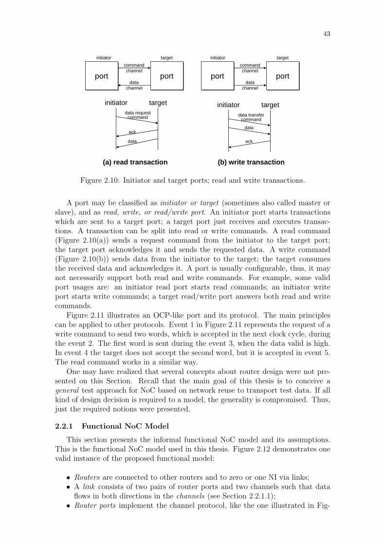
A port may be classified as initiator or target (sometimes also called master orslave), and as read, write, or read/write port. An initiator port starts transactionswhich are sent to a target port; a target port just receives and executes transac-tions. A transaction can be split into read or write commands. A read command(Figure 2.10(a)) sends a request command from the initiator to the target port;the target port acknowledges it and sends the requested data. A write command(Figure 2.10(b)) sends data from the initiator to the target; the target consumesthe received data and acknowledges it. A port is usually configurable, thus, it maynot necessarily support both read and write commands. For example, some validport usages are: an initiator read port starts read commands; an initiator writeport starts write commands; a target read/write port answers both read and writecommands.
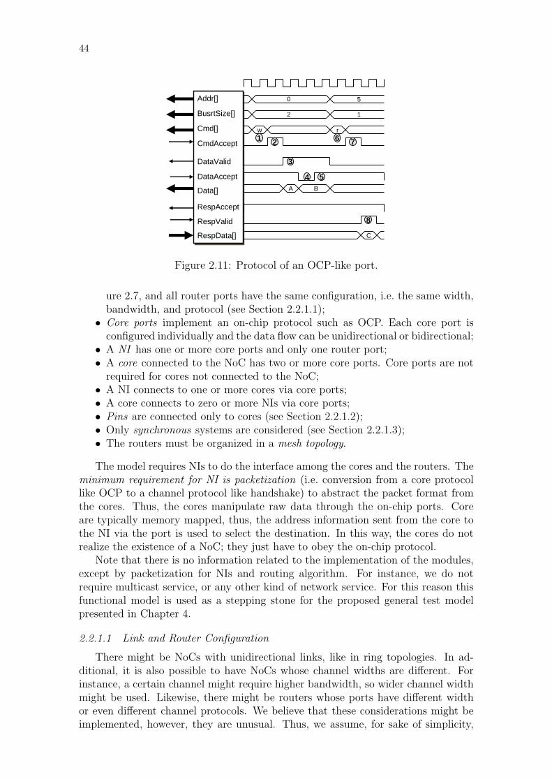
Figure 2.11 illustrates an OCP-like port and its protocol. The main principlescan be applied to other protocols. Event 1 in Figure 2.11 represents the request of awrite command to send two words, which is accepted in the next clock cycle, duringthe event 2. The first word is sent during the event 3, when the data valid is high.In event 4 the target does not accept the second word, but it is accepted in event 5.The read command works in a similar way.
One may have realized that several concepts about router design were not pre-sented on this Section. Recall that the main goal of this thesis is to conceive ageneral test approach for NoC based on network reuse to transport test data. If allkind of design decision is required to a model, the generality is compromised. Thus,just the required notions were presented.
2.2.1 Functional NoC Model
This section presents the informal functional NoC model and its assumptions.This is the functional NoC model used in this thesis. Figure 2.12 demonstrates onevalid instance of the proposed functional model:
• Routers are connected to other routers and to zero or one NI via links;• A link consists of two pairs of router ports and two channels such that data
flows in both directions in the channels (see Section 2.2.1.1);• Router ports implement the channel protocol, like the one illustrated in Fig-
44
12
Addr[]
BusrtSize[]
Cmd[]
CmdAccept
DataValid
DataAccept
Data[]
RespAccept
RespValid
RespData[]
w
A
r
0 5
C
1 2
3
6 7
8
B
4 5
2 1
Figure 2.11: Protocol of an OCP-like port.
ure 2.7, and all router ports have the same configuration, i.e. the same width,bandwidth, and protocol (see Section 2.2.1.1);
• Core ports implement an on-chip protocol such as OCP. Each core port isconfigured individually and the data flow can be unidirectional or bidirectional;
• A NI has one or more core ports and only one router port;• A core connected to the NoC has two or more core ports. Core ports are not
required for cores not connected to the NoC;• A NI connects to one or more cores via core ports;• A core connects to zero or more NIs via core ports;• Pins are connected only to cores (see Section 2.2.1.2);• Only synchronous systems are considered (see Section 2.2.1.3);• The routers must be organized in a mesh topology.
The model requires NIs to do the interface among the cores and the routers. Theminimum requirement for NI is packetization (i.e. conversion from a core protocollike OCP to a channel protocol like handshake) to abstract the packet format fromthe cores. Thus, the cores manipulate raw data through the on-chip ports. Coreare typically memory mapped, thus, the address information sent from the core tothe NI via the port is used to select the destination. In this way, the cores do notrealize the existence of a NoC; they just have to obey the on-chip protocol.
Note that there is no information related to the implementation of the modules,except by packetization for NIs and routing algorithm. For instance, we do notrequire multicast service, or any other kind of network service. For this reason thisfunctional model is used as a stepping stone for the proposed general test modelpresented in Chapter 4.
2.2.1.1 Link and Router Configuration
There might be NoCs with unidirectional links, like in ring topologies. In ad-ditional, it is also possible to have NoCs whose channel widths are different. Forinstance, a certain channel might require higher bandwidth, so wider channel widthmight be used. Likewise, there might be routers whose ports have different widthor even different channel protocols. We believe that these considerations might beimplemented, however, they are unusual. Thus, we assume, for sake of simplicity,
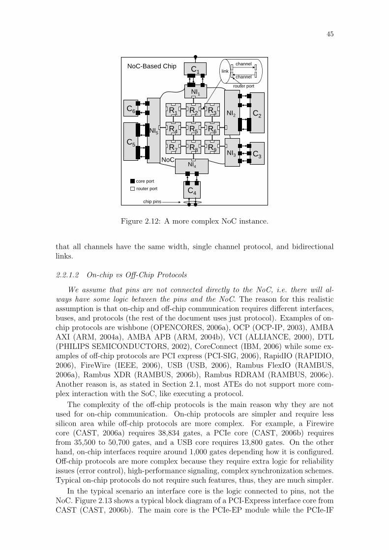
45
23
NI5
C6
NI4
C4
core port
chip pins
NoC-Based Chip
C5NI3
NI2 C2
C3
NI1
C1
NoC
channel
channel
router port
link
router port
R8
R5
R2
R7
R4
R1
R9
R6
R3
Figure 2.12: A more complex NoC instance.
that all channels have the same width, single channel protocol, and bidirectionallinks.
2.2.1.2 On-chip vs Off-Chip Protocols
We assume that pins are not connected directly to the NoC, i.e. there will al-ways have some logic between the pins and the NoC. The reason for this realisticassumption is that on-chip and off-chip communication requires different interfaces,buses, and protocols (the rest of the document uses just protocol). Examples of on-chip protocols are wishbone (OPENCORES, 2006a), OCP (OCP-IP, 2003), AMBAAXI (ARM, 2004a), AMBA APB (ARM, 2004b), VCI (ALLIANCE, 2000), DTL(PHILIPS SEMICONDUCTORS, 2002), CoreConnect (IBM, 2006) while some ex-amples of off-chip protocols are PCI express (PCI-SIG, 2006), RapidIO (RAPIDIO,2006), FireWire (IEEE, 2006), USB (USB, 2006), Rambus FlexIO (RAMBUS,2006a), Rambus XDR (RAMBUS, 2006b), Rambus RDRAM (RAMBUS, 2006c).Another reason is, as stated in Section 2.1, most ATEs do not support more com-plex interaction with the SoC, like executing a protocol.
The complexity of the off-chip protocols is the main reason why they are notused for on-chip communication. On-chip protocols are simpler and require lesssilicon area while off-chip protocols are more complex. For example, a Firewirecore (CAST, 2006a) requires 38,834 gates, a PCIe core (CAST, 2006b) requiresfrom 35,500 to 50,700 gates, and a USB core requires 13,800 gates. On the otherhand, on-chip interfaces require around 1,000 gates depending how it is configured.Off-chip protocols are more complex because they require extra logic for reliabilityissues (error control), high-performance signaling, complex synchronization schemes.Typical on-chip protocols do not require such features, thus, they are much simpler.
In the typical scenario an interface core is the logic connected to pins, not theNoC. Figure 2.13 shows a typical block diagram of a PCI-Express interface core fromCAST (CAST, 2006b). The main core is the PCIe-EP module while the PCIe-IF
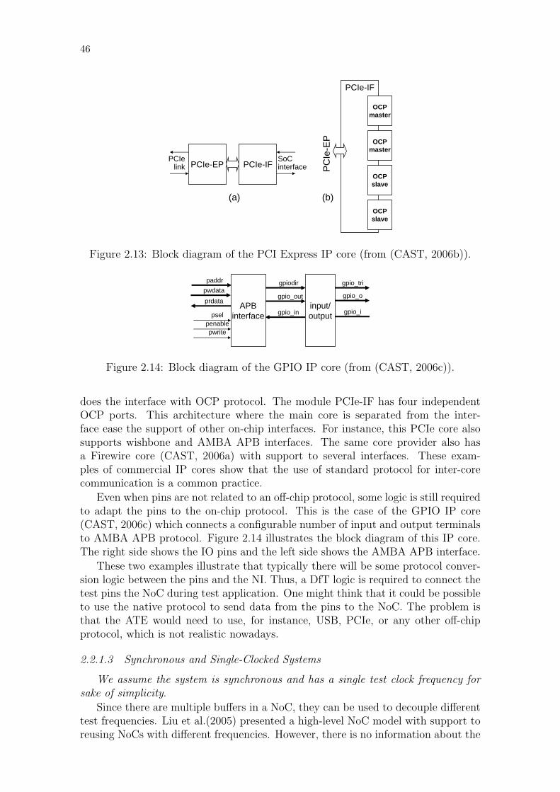
46
17
PCIe-IF
PCIe-EP PCIe-IFPCIe
linkSoCinterface
OCPmaster
OCPmaster
OCPslave
OCPslave
PC
Ie-E
P
(a) (b)
Figure 2.13: Block diagram of the PCI Express IP core (from (CAST, 2006b)).
18
gpio_tri
gpio_o
gpio_i
gpiodir
gpio_out
gpio_ininput/output
APBinterface
paddrpwdataprdata
pselpenablepwrite
Figure 2.14: Block diagram of the GPIO IP core (from (CAST, 2006c)).
does the interface with OCP protocol. The module PCIe-IF has four independentOCP ports. This architecture where the main core is separated from the inter-face ease the support of other on-chip interfaces. For instance, this PCIe core alsosupports wishbone and AMBA APB interfaces. The same core provider also hasa Firewire core (CAST, 2006a) with support to several interfaces. These exam-ples of commercial IP cores show that the use of standard protocol for inter-corecommunication is a common practice.
Even when pins are not related to an off-chip protocol, some logic is still requiredto adapt the pins to the on-chip protocol. This is the case of the GPIO IP core(CAST, 2006c) which connects a configurable number of input and output terminalsto AMBA APB protocol. Figure 2.14 illustrates the block diagram of this IP core.The right side shows the IO pins and the left side shows the AMBA APB interface.
These two examples illustrate that typically there will be some protocol conver-sion logic between the pins and the NI. Thus, a DfT logic is required to connect thetest pins the NoC during test application. One might think that it could be possibleto use the native protocol to send data from the pins to the NoC. The problem isthat the ATE would need to use, for instance, USB, PCIe, or any other off-chipprotocol, which is not realistic nowadays.
2.2.1.3 Synchronous and Single-Clocked Systems
We assume the system is synchronous and has a single test clock frequency forsake of simplicity.
Since there are multiple buffers in a NoC, they can be used to decouple differenttest frequencies. Liu et al.(2005) presented a high-level NoC model with support toreusing NoCs with different frequencies. However, there is no information about the
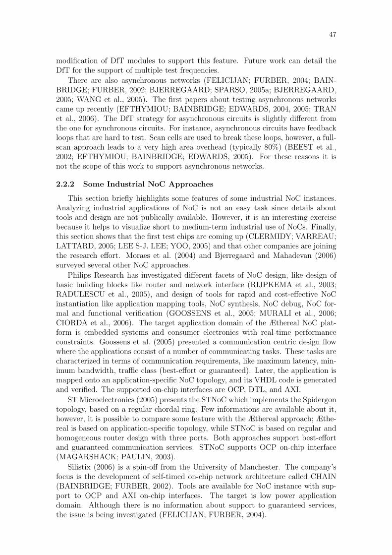
47
modification of DfT modules to support this feature. Future work can detail theDfT for the support of multiple test frequencies.
There are also asynchronous networks (FELICIJAN; FURBER, 2004; BAIN-BRIDGE; FURBER, 2002; BJERREGAARD; SPARSO, 2005a; BJERREGAARD,2005; WANG et al., 2005). The first papers about testing asynchronous networkscame up recently (EFTHYMIOU; BAINBRIDGE; EDWARDS, 2004, 2005; TRANet al., 2006). The DfT strategy for asynchronous circuits is slightly different fromthe one for synchronous circuits. For instance, asynchronous circuits have feedbackloops that are hard to test. Scan cells are used to break these loops, however, a full-scan approach leads to a very high area overhead (typically 80%) (BEEST et al.,2002; EFTHYMIOU; BAINBRIDGE; EDWARDS, 2005). For these reasons it isnot the scope of this work to support asynchronous networks.
2.2.2 Some Industrial NoC Approaches
This section briefly highlights some features of some industrial NoC instances.Analyzing industrial applications of NoC is not an easy task since details abouttools and design are not publically available. However, it is an interesting exercisebecause it helps to visualize short to medium-term industrial use of NoCs. Finally,this section shows that the first test chips are coming up (CLERMIDY; VARREAU;LATTARD, 2005; LEE S-J. LEE; YOO, 2005) and that other companies are joiningthe research effort. Moraes et al. (2004) and Bjerregaard and Mahadevan (2006)surveyed several other NoC approaches.
Philips Research has investigated different facets of NoC design, like design ofbasic building blocks like router and network interface (RIJPKEMA et al., 2003;RADULESCU et al., 2005), and design of tools for rapid and cost-effective NoCinstantiation like application mapping tools, NoC synthesis, NoC debug, NoC for-mal and functional verification (GOOSSENS et al., 2005; MURALI et al., 2006;CIORDA et al., 2006). The target application domain of the Æthereal NoC plat-form is embedded systems and consumer electronics with real-time performanceconstraints. Goossens et al. (2005) presented a communication centric design flowwhere the applications consist of a number of communicating tasks. These tasks arecharacterized in terms of communication requirements, like maximum latency, min-imum bandwidth, traffic class (best-effort or guaranteed). Later, the application ismapped onto an application-specific NoC topology, and its VHDL code is generatedand verified. The supported on-chip interfaces are OCP, DTL, and AXI.
ST Microelectronics (2005) presents the STNoC which implements the Spidergontopology, based on a regular chordal ring. Few informations are available about it,however, it is possible to compare some feature with the Æthereal approach; Æthe-real is based on application-specific topology, while STNoC is based on regular andhomogeneous router design with three ports. Both approaches support best-effortand guaranteed communication services. STNoC supports OCP on-chip interface(MAGARSHACK; PAULIN, 2003).
Silistix (2006) is a spin-off from the University of Manchester. The company’sfocus is the development of self-timed on-chip network architecture called CHAIN(BAINBRIDGE; FURBER, 2002). Tools are available for NoC instance with sup-port to OCP and AXI on-chip interfaces. The target is low power applicationdomain. Although there is no information about support to guaranteed services,the issue is being investigated (FELICIJAN; FURBER, 2004).
48
Arteris (2006) is a start-up company based in Paris and founded in 2003. Thecompany’s focus is on on-chip communications design and tools. Arteris is develop-ing tools to efficiently connect and manage the on-chip traffic requirements amongall the various elements required in today’s core-based SoC designs. The supportedon-chip interfaces are OCP and AXI.
Clermidy et al. (2005) presented the FAUST NoC architecture, supported byST Microelectronics, which is based on a mesh topology. FAUST supports bothbest-effort and QoS traffic. A NoC-based prototype for telecom applications isdemonstrated. This architecture contains 23 IP connected to a 20 nodes networkfor a total complexity of 8 Mgates (0.13µ technology).
Lee et al. (2005) from Korea Advanced Institute of Science and Technology(KAIST) presented three test chips using 0.38µ, 0.18µ, and 0.18µ technology anddie sizes of 6.0mm× 10.8mm, 5mm× 5mm, and 5mm× 5mm, respectively.
49
3 PRIOR WORK
The goal of this chapter is to review the state-of-the-art in the SoC test field. Fig-ure 3.1 presents a graphical classification of several problems in SoC test, adaptedfrom (MARINISSEN; IYENGAR; CHAKRABARTY, 2002). This list is not in-tended to enumerate all the possible problems, but to help to identify the mainproblems that this thesis deals with. The problems are classified in four categories:(i) core test wrapper, (ii) test access mechanism (TAM), (iii) test scheduling, and(iv) test resource partition (TRP). The categories are sub-divided such that the sub-categories related to ‘design’ consist of actual design proposal and the sub-categories‘optimization’ refer to finding design parameters such that ‘objectives’ are met un-der certain ‘constraints’. The literature related to these four broad categories issurveyed along this chapter such that each section is related to one category. Forexample, test wrappers are presented in Section 3.1; TAMs are presented in Sec-tion 3.2; test scheduling is presented in Section 3.3; test resource partition, whichconsists of different ways to implement embedded test sources and sinks, is pre-sented in Section 3.4. The Section 3.5 presents more specific test approaches forNoCs, interconnects, and FIFOs.
Figure 3.2 illustrates a graph of influence among the surveyed literature and theproblems addressed by this thesis. It shows why certain subjects were surveyed andwhere this knowledge was used to develop the approach proposed in this thesis.The left side of this figure shows the sections of this chapter. The right side showsthe main addressed problems. These problems are: to build a general system testmodel, ATE interface, DfT for routers and NIs, DfT for cores, and test scheduling.
For instance, the overall system test model, presented in Chapter 4, emphasizesthe compatibility with conventional TAMs, thus, it has a stronger relation withSection 3.2. The ATE interface, the DfT module used to connect the test pins tothe NoC, is related to TAMs (Section 3.2) and it is related to the different types ofTAMs (Section 3.4). The proposed wrapper design for cores (AMORY et al., 2006)is obsviously related to the review of test wrappers (Section 3.1). The wrapper forrouters (AMORY et al., 2005) was influenced by the study presented in Section 3.5.
3.1 Test Wrapper
This section describes the main functionality and the design of a test wrapperwith focus on the IEEE Std. 1500 wrapper proposal (SILVA, 2005; MARINISSENet al., 2002). Other wrapper designs, like the one presented in (MARINISSEN;GOEL; LOUSBERG, 2000), have the same main principles. The goal of a wrap-per is to switch between different access mechanisms. The switching capability is
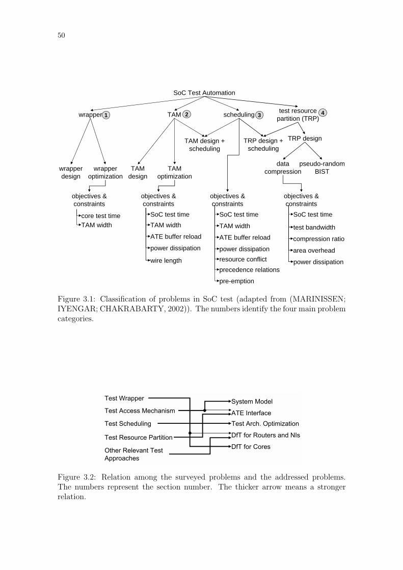
50
24
SoC Test Automation
wrapper TAM scheduling
TAM design + scheduling
TAM optimization
TAM design
wrapper optimization
wrapper design
objectives & constraints
core test timeTAM width
objectives & constraints
SoC test timeTAM width
ATE buffer reload
power dissipation
objectives & constraints
SoC test time
TAM width
ATE buffer reload
power dissipationresource conflictprecedence relations
pre-emption
1 2 3 4
data compression
pseudo-randomBIST
objectives & constraints
SoC test time
compression ratio
area overhead
test bandwidth
TRP designTRP design + scheduling
test resource partition (TRP)
power dissipationwire length
Figure 3.1: Classification of problems in SoC test (adapted from (MARINISSEN;IYENGAR; CHAKRABARTY, 2002)). The numbers identify the four main problemcategories.
32
System Model
ATE Interface
DfT for Routers and NIs
DfT for Cores
Test Wrapper
Test Access Mechanism
Test Resource Partition
Other Relevant Test Approaches
Test Scheduling Test Arch. Optimization
Figure 3.2: Relation among the surveyed problems and the addressed problems.The numbers represent the section number. The thicker arrow means a strongerrelation.
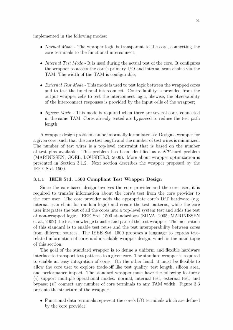
51
implemented in the following modes:
• Normal Mode - The wrapper logic is transparent to the core, connecting thecore terminals to the functional interconnect;
• Internal Test Mode - It is used during the actual test of the core. It configuresthe wrapper to access the core’s primary I/O and internal scan chains via theTAM. The width of the TAM is configurable;
• External Test Mode - This mode is used to test logic between the wrapped coresand to test the functional interconnect. Controllability is provided from theoutput wrapper cells to test the interconnect logic, likewise, the observabilityof the interconnect responses is provided by the input cells of the wrapper;
• Bypass Mode - This mode is required when there are several cores connectedin the same TAM. Cores already tested are bypassed to reduce the test pathlength.
A wrapper design problem can be informally formulated as: Design a wrapper fora given core, such that the core test length and the number of test wires is minimized.The number of test wires is a top-level constraint that is based on the numberof test pins available. This problem has been identified as a NP-hard problem(MARINISSEN; GOEL; LOUSBERG, 2000). More about wrapper optimization ispresented in Section 3.1.2. Next section describes the wrapper proposed by theIEEE Std. 1500.
3.1.1 IEEE Std. 1500 Compliant Test Wrapper Design
Since the core-based design involves the core provider and the core user, it isrequired to transfer information about the core’s test from the core provider tothe core user. The core provider adds the appropriate core’s DfT hardware (e.g.internal scan chain for random logic) and create the test patterns, while the coreuser integrates the test of all the cores into a top-level system test and adds the testof non-wrapped logic. IEEE Std. 1500 standardizes (SILVA, 2005; MARINISSENet al., 2002) the test knowledge transfer and part of the test wrapper. The motivationof this standard is to enable test reuse and the test interoperability between coresfrom different sources. The IEEE Std. 1500 proposes a language to express test-related information of cores and a scalable wrapper design, which is the main topicof this section.
The goal of the standard wrapper is to define a uniform and flexible hardwareinterface to transport test patterns to a given core. The standard wrapper is requiredto enable an easy integration of cores. On the other hand, it must be flexible toallow the core user to explore trade-off like test quality, test length, silicon area,and performance impact. The standard wrapper must have the following features:(i) support multiple operational modes: normal, internal test, external test, andbypass; (ii) connect any number of core terminals to any TAM width. Figure 3.3presents the structure of the wrapper:
• Functional data terminals represent the core’s I/O terminals which are definedby the core provider;
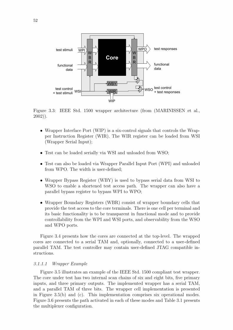
52
33
WBY
WIR
WPI WPO
CoreWBR
WBR
test stimuli
functionaldata
test control+ test stimuli
test responses
functionaldata
test control+ test responsesWSI WSO
WIP
Figure 3.3: IEEE Std. 1500 wrapper architecture (from (MARINISSEN et al.,2002)).
• Wrapper Interface Port (WIP) is a six-control signals that controls the Wrap-per Instruction Register (WIR). The WIR register can be loaded from WSI(Wrapper Serial Input);
• Test can be loaded serially via WSI and unloaded from WSO;
• Test can also be loaded via Wrapper Parallel Input Port (WPI) and unloadedfrom WPO. The width is user-defined;
• Wrapper Bypass Register (WBY) is used to bypass serial data from WSI toWSO to enable a shortened test access path. The wrapper can also have aparallel bypass register to bypass WPI to WPO;
• Wrapper Boundary Registers (WBR) consist of wrapper boundary cells thatprovide the test access to the core terminals. There is one cell per terminal andits basic functionality is to be transparent in functional mode and to providecontrollability from the WPI and WSI ports, and observability from the WSOand WPO ports.
Figure 3.4 presents how the cores are connected at the top-level. The wrappedcores are connected to a serial TAM and, optionally, connected to a user-definedparallel TAM. The test controller may contain user-defined JTAG compatible in-structions.
3.1.1.1 Wrapper Example
Figure 3.5 illustrates an example of the IEEE Std. 1500 compliant test wrapper.The core under test has two internal scan chains of six and eight bits, five primaryinputs, and three primary outputs. The implemented wrapper has a serial TAM,and a parallel TAM of three bits. The wrapper cell implementation is presentedin Figure 3.5(b) and (c). This implementation comprises six operational modes.Figure 3.6 presents the path activated in each of these modes and Table 3.1 presentsthe multiplexer configuration.

53
32
User-defined TAM
IEEE 1500 wrapper
Core 1
wir
JTAG TAPcontroller
IEEE 1500 wrapper
Core N
wir wsowsi
serial TAMserial TAM
wip
wso wsi
fofifofi
wpowpi wpowpi
sinksource
SoC
Figure 3.4: IEEE Std. 1500 wrappers at the top-level (from (MARINISSEN et al.,2002)).
34
(c) wrapper input cell
from wsi/wpito wso/wpo
from chipto core
shift wci
clock
Core A
scan chain 0 (6FFs)
scan chain 1 (8FFs)
d[0]
d[1]d[2]
d[3]d[4]
q[0]
q[1]
q[2]sc clk
WBY
WIR
11
12
8
6
10
9
4
5
3
2
1
7
WIP
q[0]
q[1]
q[2]
d[0]
d[1]d[2]
d[3]d[4]
wpi
[0:2
]
wpo
[0:2
]
scclk
wsi wso
(b) wrapper output cell
from wsi/wpito wso/wpo
from coreto chip
shift wco
clock
(a) wrapper design
Figure 3.5: Example of a IEEE Std. 1500 compliant wrapper (from (MARINISSENet al., 2002)).
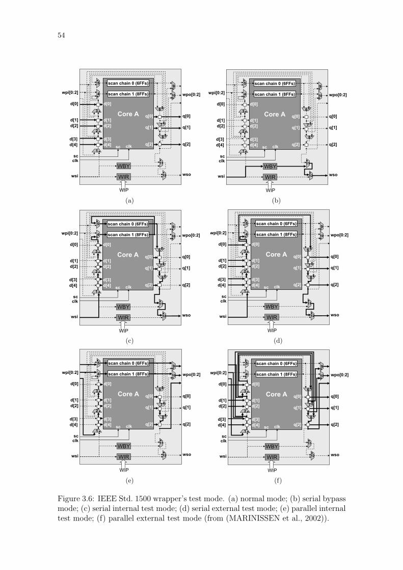
54
35
Core A
scan chain 0 (6FFs)
scan chain 1 (8FFs)
d[0]
d[1]d[2]
d[3]d[4]
q[0]
q[1]
q[2]sc clk
WBY
WIR
11
12
8
6
10
9
4
5
3
2
1
7
WIP
q[0]
q[1]
q[2]
d[0]
d[1]d[2]
d[3]d[4]
wpi[0:2] wpo[0:2]
scclk
wsi wso
(a) 36
Core A
scan chain 0 (6FFs)
scan chain 1 (8FFs)
d[0]
d[1]d[2]
d[3]d[4]
q[0]
q[1]
q[2]sc clk
WBY
WIR
11
12
8
6
10
9
4
5
3
2
1
7
WIP
q[0]
q[1]
q[2]
d[0]
d[1]d[2]
d[3]d[4]
wpi[0:2] wpo[0:2]
scclk
wsi wso
(b)
37
Core A
scan chain 0 (6FFs)
scan chain 1 (8FFs)
d[0]
d[1]d[2]
d[3]d[4]
q[0]
q[1]
q[2]sc clk
WBY
WIR
11
12
8
6
10
9
4
5
3
2
1
7
WIP
q[0]
q[1]
q[2]
d[0]
d[1]d[2]
d[3]d[4]
wpi[0:2] wpo[0:2]
scclk
wsi wso
(c) 38
Core A
scan chain 0 (6FFs)
scan chain 1 (8FFs)
d[0]
d[1]d[2]
d[3]d[4]
q[0]
q[1]
q[2]sc clk
WBY
WIR
11
12
8
6
10
9
4
5
3
2
1
7
WIP
q[0]
q[1]
q[2]
d[0]
d[1]d[2]
d[3]d[4]
wpi[0:2] wpo[0:2]
scclk
wsi wso
(d)
39
Core A
scan chain 0 (6FFs)
scan chain 1 (8FFs)
d[0]
d[1]d[2]
d[3]d[4]
q[0]
q[1]
q[2]sc clk
WBY
WIR
11
12
8
6
10
9
4
5
3
2
1
7
WIP
q[0]
q[1]
q[2]
d[0]
d[1]d[2]
d[3]d[4]
wpi[0:2] wpo[0:2]
scclk
wsi wso
(e) 40
Core A
scan chain 0 (6FFs)
scan chain 1 (8FFs)
d[0]
d[1]d[2]
d[3]d[4]
q[0]
q[1]
q[2]sc clk
WBY
WIR
11
12
8
6
10
9
4
5
3
2
1
7
WIP
q[0]
q[1]
q[2]
d[0]
d[1]d[2]
d[3]d[4]
wpi[0:2] wpo[0:2]
scclk
wsi wso
(f)
Figure 3.6: IEEE Std. 1500 wrapper’s test mode. (a) normal mode; (b) serial bypassmode; (c) serial internal test mode; (d) serial external test mode; (e) parallel internaltest mode; (f) parallel external test mode (from (MARINISSEN et al., 2002)).
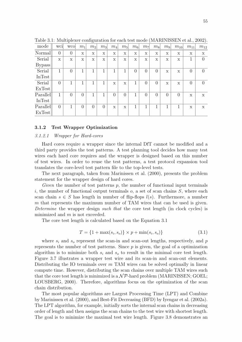
55
Table 3.1: Multiplexer configuration for each test mode (MARINISSEN et al., 2002).mode wci wco m1 m2 m3 m4 m5 m6 m7 m8 m9 m10 m11 m12
Normal 0 0 x x x x x x x x x x x xSerial x x x x x x x x x x x x 1 0BypassSerial 1 0 1 1 1 1 1 0 0 0 x x 0 0InTestSerial 0 1 1 1 1 x x 1 0 0 x x 0 0ExTestParallel 1 0 0 1 1 0 0 1 0 0 0 0 x xInTestParallel 0 1 0 0 0 x x 1 1 1 1 1 x xExTest
3.1.2 Test Wrapper Optimization
3.1.2.1 Wrapper for Hard-cores
Hard cores require a wrapper since the internal DfT cannot be modified and athird party provides the test patterns. A test planning tool decides how many testwires each hard core requires and the wrapper is designed based on this numberof test wires. In order to reuse the test patterns, a test protocol expansion tooltranslates the core-level test pattern file to the top-level tests.
The next paragraph, taken from Marinissen et al. (2000), presents the problemstatement for the wrapper design of hard cores.
Given the number of test patterns p, the number of functional input terminalsi, the number of functional output terminals o, a set of scan chains S, where eachscan chain s ∈ S has length in number of flip-flops l(s). Furthermore, a numberm that represents the maximum number of TAM wires that can be used is given.Determine the wrapper design such that the core test length (in clock cycles) isminimized and m is not exceeded.
The core test length is calculated based on the Equation 3.1
T = {1 + max(si, so)} × p + min(si, so)} (3.1)
where si and so represent the scan-in and scan-out lengths, respectively, and prepresents the number of test patterns. Since p is given, the goal of a optimizationalgorithm is to minimize both si and so to result in the minimal core test length.Figure 3.7 illustrates a wrapper test wire and its scan-in and scan-out elements.Distributing the IO terminals over m TAM wires can be solved optimally in linearcompute time. However, distributing the scan chains over multiple TAM wires suchthat the core test length is minimized is aNP-hard problem (MARINISSEN; GOEL;LOUSBERG, 2000). Therefore, algorithms focus on the optimization of the scanchain distribution.
The most popular algorithms are Largest Processing Time (LPT) and Combineby Marinissen et al. (2000), and Best-Fit Decreasing (BFD) by Iyengar et al. (2002a).The LPT algorithm, for example, initially sorts the internal scan chains in decreasingorder of length and then assigns the scan chains to the test wire with shortest length.The goal is to minimize the maximal test wire length. Figure 3.8 demonstrates an
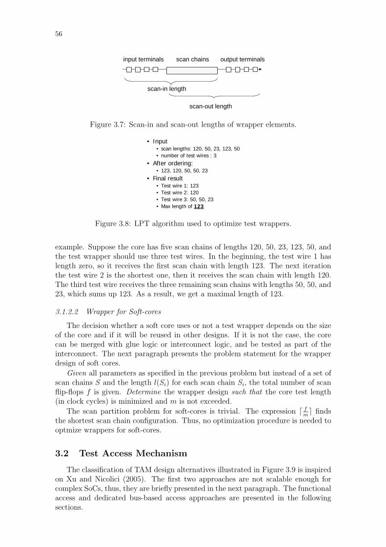
56
36
scan chainsinput terminals output terminals
scan-in length
scan-out length
Figure 3.7: Scan-in and scan-out lengths of wrapper elements.
36
• Input • scan lengths: 120, 50, 23, 123, 50• number of test wires : 3
• After ordering:• 123, 120, 50, 50, 23
• Final result• Test wire 1: 123• Test wire 2: 120• Test wire 3: 50, 50, 23• Max length of 123
Figure 3.8: LPT algorithm used to optimize test wrappers.
example. Suppose the core has five scan chains of lengths 120, 50, 23, 123, 50, andthe test wrapper should use three test wires. In the beginning, the test wire 1 haslength zero, so it receives the first scan chain with length 123. The next iterationthe test wire 2 is the shortest one, then it receives the scan chain with length 120.The third test wire receives the three remaining scan chains with lengths 50, 50, and23, which sums up 123. As a result, we get a maximal length of 123.
3.1.2.2 Wrapper for Soft-cores
The decision whether a soft core uses or not a test wrapper depends on the sizeof the core and if it will be reused in other designs. If it is not the case, the corecan be merged with glue logic or interconnect logic, and be tested as part of theinterconnect. The next paragraph presents the problem statement for the wrapperdesign of soft cores.
Given all parameters as specified in the previous problem but instead of a set ofscan chains S and the length l(Si) for each scan chain Si, the total number of scanflip-flops f is given. Determine the wrapper design such that the core test length(in clock cycles) is minimized and m is not exceeded.
The scan partition problem for soft-cores is trivial. The expression d fme finds
the shortest scan chain configuration. Thus, no optimization procedure is needed tooptmize wrappers for soft-cores.
3.2 Test Access Mechanism
The classification of TAM design alternatives illustrated in Figure 3.9 is inspiredon Xu and Nicolici (2005). The first two approaches are not scalable enough forcomplex SoCs, thus, they are briefly presented in the next paragraph. The functionalaccess and dedicated bus-based access approaches are presented in the followingsections.
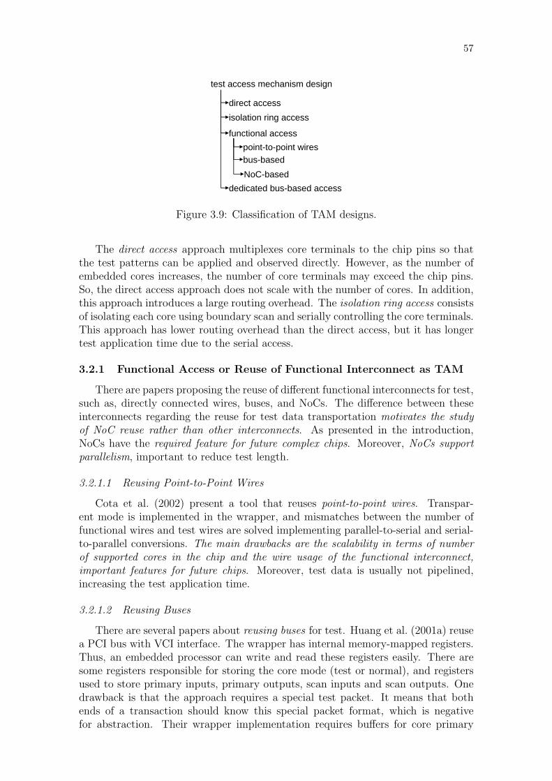
57
23
functional access
test access mechanism design
isolation ring access
bus-based
direct access
point-to-point wires
NoC-baseddedicated bus-based access
Figure 3.9: Classification of TAM designs.
The direct access approach multiplexes core terminals to the chip pins so thatthe test patterns can be applied and observed directly. However, as the number ofembedded cores increases, the number of core terminals may exceed the chip pins.So, the direct access approach does not scale with the number of cores. In addition,this approach introduces a large routing overhead. The isolation ring access consistsof isolating each core using boundary scan and serially controlling the core terminals.This approach has lower routing overhead than the direct access, but it has longertest application time due to the serial access.
3.2.1 Functional Access or Reuse of Functional Interconnect as TAM
There are papers proposing the reuse of different functional interconnects for test,such as, directly connected wires, buses, and NoCs. The difference between theseinterconnects regarding the reuse for test data transportation motivates the studyof NoC reuse rather than other interconnects. As presented in the introduction,NoCs have the required feature for future complex chips. Moreover, NoCs supportparallelism, important to reduce test length.
3.2.1.1 Reusing Point-to-Point Wires
Cota et al. (2002) present a tool that reuses point-to-point wires. Transpar-ent mode is implemented in the wrapper, and mismatches between the number offunctional wires and test wires are solved implementing parallel-to-serial and serial-to-parallel conversions. The main drawbacks are the scalability in terms of numberof supported cores in the chip and the wire usage of the functional interconnect,important features for future chips. Moreover, test data is usually not pipelined,increasing the test application time.
3.2.1.2 Reusing Buses
There are several papers about reusing buses for test. Huang et al. (2001a) reusea PCI bus with VCI interface. The wrapper has internal memory-mapped registers.Thus, an embedded processor can write and read these registers easily. There aresome registers responsible for storing the core mode (test or normal), and registersused to store primary inputs, primary outputs, scan inputs and scan outputs. Onedrawback is that the approach requires a special test packet. It means that bothends of a transaction should know this special packet format, which is negativefor abstraction. Their wrapper implementation requires buffers for core primary
58
input and outputs, and buffers for scan-in and scan out to temporally store testpatterns and test responses. This implementation choice increases the wrapper areaproportionally to the number of I/Os and scan chains of a core (area overhead forthe wrapper is not presented in the paper). Another drawback is that the buffer forprimary inputs is also used by the primary outputs, which means that the wrapperdoes not support test pipelining.
Hwang and Abraham (2001) present a reuse model based on a Wishbone bus.They develop a test wrapper which they claim that implements the same protocol asthe bus, but no details are given about the implementation, and they do not specifyif it is possible to extend the wrapper to other buses and protocols. They presentarea and test time results, but it is compared to boundary scan, known to requirea large test time due to the serialization and large area to implement its wrappercells and control logic.
Harrod (1999) and Burdass et al. (2000) present an industrial approach forAMBA bus. The system has a module that, when it is in test mode, it acts asthe bus master and it reconfigures the external bus interface to provide a high-speed32-bit parallel interface. This approach is best suited to functional test. However,Feige et al. (1998) extend the approach to support scan-based test. An ATPG isrun at the core level and a test protocol expansion tool translates the generated testpatterns to the system level format, i. e. to the AMBA interface. The wrapper cellsare also modified to support scan-based test. It means that both the test protocolexpansions tool and the scan insertion tool are modified to support AMBA test pro-tocol, which means that the approach has a poor backward compatibility in termsof test tools. In addition, it is a specific solution for AMBA-based systems. Theauthors do not claim a general bus reuse approach.
All the above mentioned approaches suffer the common drawbacks of all reuseapproaches based on buses; they require clock gating to halt the test when thereis no data, the bus does not support test pipelining, and the cores must be testedsequentially. Moreover, like in point-to-point wires, buses are not scalable enoughfor future complex chips, and they may not provide sufficient bandwidth for thefunctional application. For these reasons, the reuse of NoCs for test has been studiedrecently.
3.2.1.3 Reusing Networks-on-Chip
Cota et al. (2004) propose preemptive test scheduling, where the test of a corecan be interrupted if there is no free path between the source to CUT or CUT to sink.A test packet can also take different paths depending on their availability, but theshortest available is selected. The drawbacks are that preemptive test may reducethe test pipelining, clock gating is required to halt the test when there is no data,and the simple wrapper employed incurs in a significant waste of test throughput,increasing the test time. Liu et al. (LIU et al., 2005) proposed non-preemptivetesting. A single path from source to CUT and from CUT to sink is establishedin the beginning of the test and the test packets are sent one after another onthis dedicated path. Although this approach preserves test pipelining, it does notguarantee that there will be a new test data in each clock cycle. For example, thereare some clock cycles that are used to pack/unpack data, and also some clock cyclesto execute the functional protocol. The exact timing depends on the packet format,that may be different in each design; then, the clock gating or holdable scan cells

59
must be used.
Despite all the advantages of NoCs for both the functional and the test domains,a NoC is more complex than a dedicated TAM. A common aspect to all the previousapproaches is the large amount of NoC implementation details required for thetest model. All kinds of functional implementation details (e.g. used arbitrationalgorithm), temporal details (e.g. time to route a packet), and organizational details(e.g. network topology) are required, in addition to a cycle-accurate scheduling usedto determine the available paths between the test source, CUT and test sink. Thisamount of implementation details requires major efforts to adapt the test model todifferent NoCs, reducing the generality of the approach. In addition, there is nodetailed description of the requirements for test reuse, such as wrapper design andsupport to functional protocol. The case study is usually a specific and simplifiedNoC instance that does not represent most current NoC designs.
3.2.2 Dedicated Bus-Based Access
A TAM provides a path for test data transportation between the embeddedcores and the test sources and sinks. In case of dedicated TAMs, this bus is usedonly during test application. The main design parameters that can be chosen bythe system integrator are the number of TAMs, the width of each TAM, and theassignment of modules to the TAMs. Changing these parameters the test designercan trade-off between several test costs like DfT area, test application time, andpower consumption. The benefits of dedicated TAM are the support to test protocolexpansion (MARINISSEN; LOUSBERG, 1999) and test pattern reuse. It is alsoflexible because designer can trade-off, for example, test application time and siliconarea by tuning the TAM width. The main benefit of dedicated TAM compared tofunctional access is the guaranteed test access, since the accessibility of a moduledoes not depend on the functional chip design. The main costs are the design time,which is minimized with automation, and the increased routing area.
Two approaches, called Test Rail (MARINISSEN et al., 1998) and Test Bus(VARMA; BHATIA, 1998), are described in the literature. Cores connected to thesame TAM based on Test Bus can only be tested sequentially. Thus, Test Bus doesnot support external test mode (see Section 3.1), used to test the logic betweencores and the core interconnect. On the other hand, Test Rail supports externaltest mode and also a bypass mode, used if multiple cores are connected to the sameTAM. The cores that are not been tested are in bypass mode to reduce the test pathto the CUT. This mode includes a bypass register used to reduce propagation delaywhen there are multiple cores serially connected. Figure 2.2, page 36, illustrates aTest Rail TAM.
3.3 Test Scheduling
Several techniques for SoC test scheduling have been proposed for dedicatedTAMs. A recent paper by Xu and Nicolici (XU; NICOLICI, 2005) surveys these ap-proaches. A considerable amount of research has been done in this area. For exam-ple, there are scheduling considering static (GOEL; MARINISSEN, 2003a) and con-figurable wrappers (KORANNE, 2002a), preemptive (IYENGAR; CHAKRABARTY,2001) and non-preemptive test (GOEL; MARINISSEN, 2003a), co-optimizationof scheduling and wrapper (GOEL; MARINISSEN, 2003a), scheduling algorithms
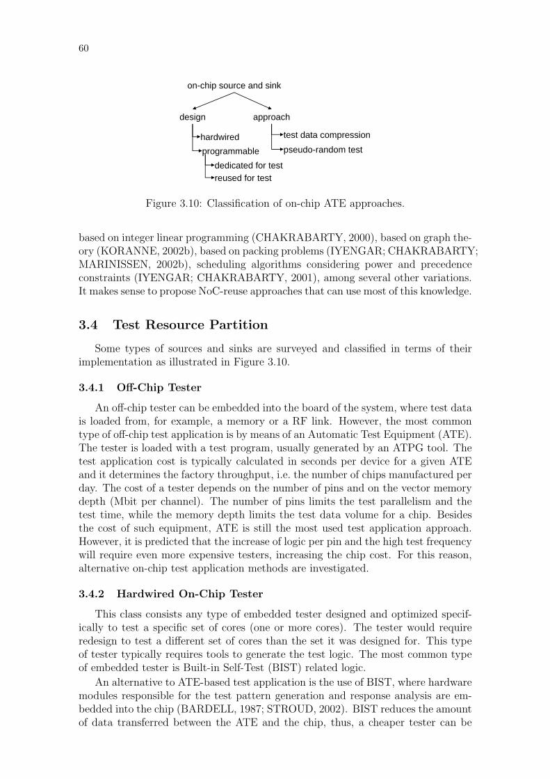
60
22
on-chip source and sink
programmable
reused for test
hardwired
dedicated for test
design approach
test data compressionpseudo-random test
Figure 3.10: Classification of on-chip ATE approaches.
based on integer linear programming (CHAKRABARTY, 2000), based on graph the-ory (KORANNE, 2002b), based on packing problems (IYENGAR; CHAKRABARTY;MARINISSEN, 2002b), scheduling algorithms considering power and precedenceconstraints (IYENGAR; CHAKRABARTY, 2001), among several other variations.It makes sense to propose NoC-reuse approaches that can use most of this knowledge.
3.4 Test Resource Partition
Some types of sources and sinks are surveyed and classified in terms of theirimplementation as illustrated in Figure 3.10.
3.4.1 Off-Chip Tester
An off-chip tester can be embedded into the board of the system, where test datais loaded from, for example, a memory or a RF link. However, the most commontype of off-chip test application is by means of an Automatic Test Equipment (ATE).The tester is loaded with a test program, usually generated by an ATPG tool. Thetest application cost is typically calculated in seconds per device for a given ATEand it determines the factory throughput, i.e. the number of chips manufactured perday. The cost of a tester depends on the number of pins and on the vector memorydepth (Mbit per channel). The number of pins limits the test parallelism and thetest time, while the memory depth limits the test data volume for a chip. Besidesthe cost of such equipment, ATE is still the most used test application approach.However, it is predicted that the increase of logic per pin and the high test frequencywill require even more expensive testers, increasing the chip cost. For this reason,alternative on-chip test application methods are investigated.
3.4.2 Hardwired On-Chip Tester
This class consists any type of embedded tester designed and optimized specif-ically to test a specific set of cores (one or more cores). The tester would requireredesign to test a different set of cores than the set it was designed for. This typeof tester typically requires tools to generate the test logic. The most common typeof embedded tester is Built-in Self-Test (BIST) related logic.
An alternative to ATE-based test application is the use of BIST, where hardwaremodules responsible for the test pattern generation and response analysis are em-bedded into the chip (BARDELL, 1987; STROUD, 2002). BIST reduces the amountof data transferred between the ATE and the chip, thus, a cheaper tester can be
61
used. BIST enables at-speed test to increase test quality.Hetherington et al. (HETHERINGTON et al., 1999) present results for the ap-
plication of logic BIST for industrial designs. Practical issues are reported in orderto generate BIST-compliant cores for at-speed testing. The paper reports fault cov-erage and area overhead comparison between ATPG and logic BIST. The resultspresent that logic BIST can achieve similar test quality to ATPG with minimal areaoverhead and few changes to the design flow.
On the other hand, many authors say that the main problem related to pseudo-random test is the large number of test patterns and, in several cases, low faultcoverage. One can argue that the issue related to the number of test patterns canbe alleviated considering that, for example, the LFSR runs faster than the externaltester. Related to the low fault coverage, several papers have demonstrated theadvantages of using BIST schemes based on multiple polynomials and seeds.
Hellebrand et al. propose in (1995; 1996) a BIST scheme that supports LFSRwith multiple polynomials and seeds. A set of seeds is obtained to increase thefault coverage by solving systems of linear equations. Fagot et al. (1999) proposea simulation based method to compute an efficient seed of a LFSR. The methodis intended to produce a single seed that tests the hardest to detect faults of theCUT and achieves a high fault coverage. Krishna and Touba (2001; 2002) proposea loss-less test vector compression technique which combines LFSR reseeding andstatistical coding to provide a high encoding efficiency.
The main problem related to reseeding approaches is the computation time re-quired to find the good seeds and to find a good trade-off between number of seeds(i.e. memory requirement) and fault coverage.
A hardwired on-chip tester can also implement test data decompression (RA-JSKI; TYSZER; ZACHARIA, 1998). This approach also enables the use of a slowerexternal tester to provide compressed test data, which is decompressed on-chip andapplied to the CUT. The test responses are compressed and sent back to the externaltester.
The main challenge related to test data decompression is the trade-off betweencompression rate (i.e. memory requirement) and complexity of decompression al-gorithms. Very efficient compression algorithms exist but their complexity wouldincrease the area overhead in case it is implemented in hardware, or the test timein case it is implemented in software.
3.4.3 Programmable On-Chip Tester
A programmable on-chip tester has the advantage that the same hardware canbe used to test different cores, changing just the “test program” and test data. Thistype of tester can be dedicated for test or reused from the functional cores.
3.4.3.1 Dedicated Programmable Tester
Cota et al. (2001) propose an embedded test controller to test some blocks ofthe SoC that require at-speed testing. Such a controller, called MET, is embeddedinto the system with the purpose of test data manipulation and controlling. As thetest controller is synthesized in the same technology of the SoC, at-speed test can beperformed. The MET approach relies on the definition of test-specific instructions.Additionally, the test vectors and response are assumed to be stored in the memoriesthat are usually available in the SoC.

62
Amory et al. (2004) propose a programmable LFSR and MISR with support toreseeding to increase the fault coverage. These modules were integrated to a IEEEStd. 1500 compliant wrapper in order to provide a reusable and programmable BISTapproach that could be used to test a large set of cores.
Some papers (APPELLO et al., 2003; HUANG et al., 1999) propose a program-mable memory BIST processors. The BIST processor can be programmed withdifferent memory test algorithms, such as March algorithms, and be reused to testdifferent memory cores.
Although the main motivation of programmable and dedicated on-chip testersis to reuse the same hardware for different cases, there are tools, like memory BISTand logic BIST from Mentor Graphics, that automatically insert customized BISTfor a specific core. In addition, programmable tester also needs a tool to generateefficient test programs.
3.4.3.2 Reused Programmable Tester
The reuse of an embedded processor for testing other cores in a SoC has beenlargely studied in the literature (HUANG et al., 2001a; HWANG; ABRAHAM,2001, 2003; AMORY; OLIVEIRA; MORAES, 2003; KRSTIC et al., 2002). Theapproaches proposed so far consider different aspects of the processor reuse, rangingfrom the reuse as test controller to the use as a built-in test pattern generator withcompression features.
Huang et al. (2001a) present a bus-based architecture with a MIPS processor,a PCI bus, and VCI interfaces. Using this architecture, the authors evaluate thetest time and fault coverage of some ISCAS89 benchmarks. Lai and Cheng (2001)use the same architecture presented in (HUANG et al., 2001a) to evaluate testprograms generated for four ISCAS89 benchmarks, using the DLX processor. Thetest program length ranges from 40 to 27,000 bytes while the test length ranges from94 to 30,430 clock cycles. The results point to important requirements in terms oftest memory and test length compared with hardware-based test.
Hwang and Abraham (2001) present a bus-based architecture with an ARMprocessor and Wishbone interface. The authors compare the test time and area over-head between software-based test and boundary scan. In both cases, the software-based test present better results. In (HWANG; ABRAHAM, 2003), the same authorsevaluate a new test pattern compression method in which test data can be decodedrapidly on embedded processors. They compare the compression results with othercompression methods implemented on embedded processors. They use ISCAS89benchmarks as CUT.
Amory et al. (2003) present a CAD tool, which helps the designer to integratecores on a bus-based SoC and generate test programs. These test programs areloaded into the processors to test other cores. Results are presented using a subsetof ISCAS benchmarks as CUT.
Marcon et al. (2004) evaluated the implementation of several memory BISTalgorithms running in different processors against a hardware implementation. Testtime, memory, requirements for the test code, area overhead, and power dissipationwere evaluated.
In most sittuations, the reuse of embedded processor for test depends on the reuseof functional interconnect for test data transportation. All the previous mentionedapproaches suppose that the chip interconnect is a bus. The problem with this
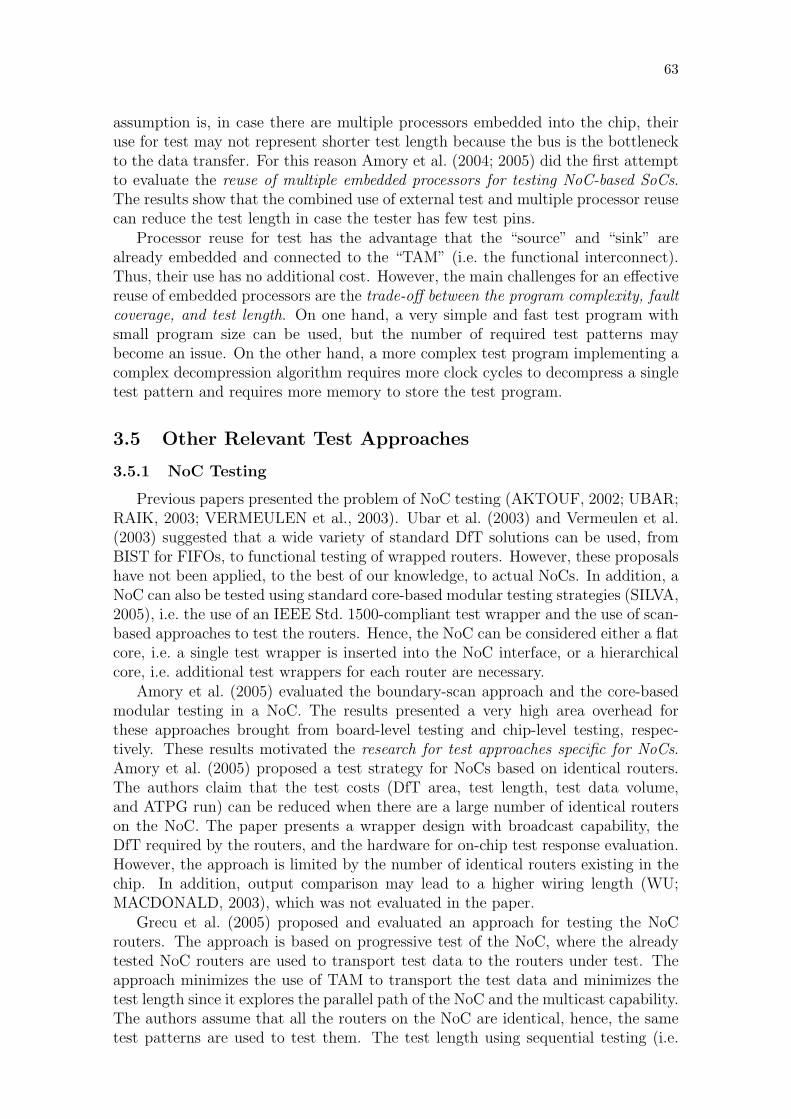
63
assumption is, in case there are multiple processors embedded into the chip, theiruse for test may not represent shorter test length because the bus is the bottleneckto the data transfer. For this reason Amory et al. (2004; 2005) did the first attemptto evaluate the reuse of multiple embedded processors for testing NoC-based SoCs.The results show that the combined use of external test and multiple processor reusecan reduce the test length in case the tester has few test pins.
Processor reuse for test has the advantage that the “source” and “sink” arealready embedded and connected to the “TAM” (i.e. the functional interconnect).Thus, their use has no additional cost. However, the main challenges for an effectivereuse of embedded processors are the trade-off between the program complexity, faultcoverage, and test length. On one hand, a very simple and fast test program withsmall program size can be used, but the number of required test patterns maybecome an issue. On the other hand, a more complex test program implementing acomplex decompression algorithm requires more clock cycles to decompress a singletest pattern and requires more memory to store the test program.
3.5 Other Relevant Test Approaches
3.5.1 NoC Testing
Previous papers presented the problem of NoC testing (AKTOUF, 2002; UBAR;RAIK, 2003; VERMEULEN et al., 2003). Ubar et al. (2003) and Vermeulen et al.(2003) suggested that a wide variety of standard DfT solutions can be used, fromBIST for FIFOs, to functional testing of wrapped routers. However, these proposalshave not been applied, to the best of our knowledge, to actual NoCs. In addition, aNoC can also be tested using standard core-based modular testing strategies (SILVA,2005), i.e. the use of an IEEE Std. 1500-compliant test wrapper and the use of scan-based approaches to test the routers. Hence, the NoC can be considered either a flatcore, i.e. a single test wrapper is inserted into the NoC interface, or a hierarchicalcore, i.e. additional test wrappers for each router are necessary.
Amory et al. (2005) evaluated the boundary-scan approach and the core-basedmodular testing in a NoC. The results presented a very high area overhead forthese approaches brought from board-level testing and chip-level testing, respec-tively. These results motivated the research for test approaches specific for NoCs.Amory et al. (2005) proposed a test strategy for NoCs based on identical routers.The authors claim that the test costs (DfT area, test length, test data volume,and ATPG run) can be reduced when there are a large number of identical routerson the NoC. The paper presents a wrapper design with broadcast capability, theDfT required by the routers, and the hardware for on-chip test response evaluation.However, the approach is limited by the number of identical routers existing in thechip. In addition, output comparison may lead to a higher wiring length (WU;MACDONALD, 2003), which was not evaluated in the paper.
Grecu et al. (2005) proposed and evaluated an approach for testing the NoCrouters. The approach is based on progressive test of the NoC, where the alreadytested NoC routers are used to transport test data to the routers under test. Theapproach minimizes the use of TAM to transport the test data and minimizes thetest length since it explores the parallel path of the NoC and the multicast capability.The authors assume that all the routers on the NoC are identical, hence, the sametest patterns are used to test them. The test length using sequential testing (i.e.
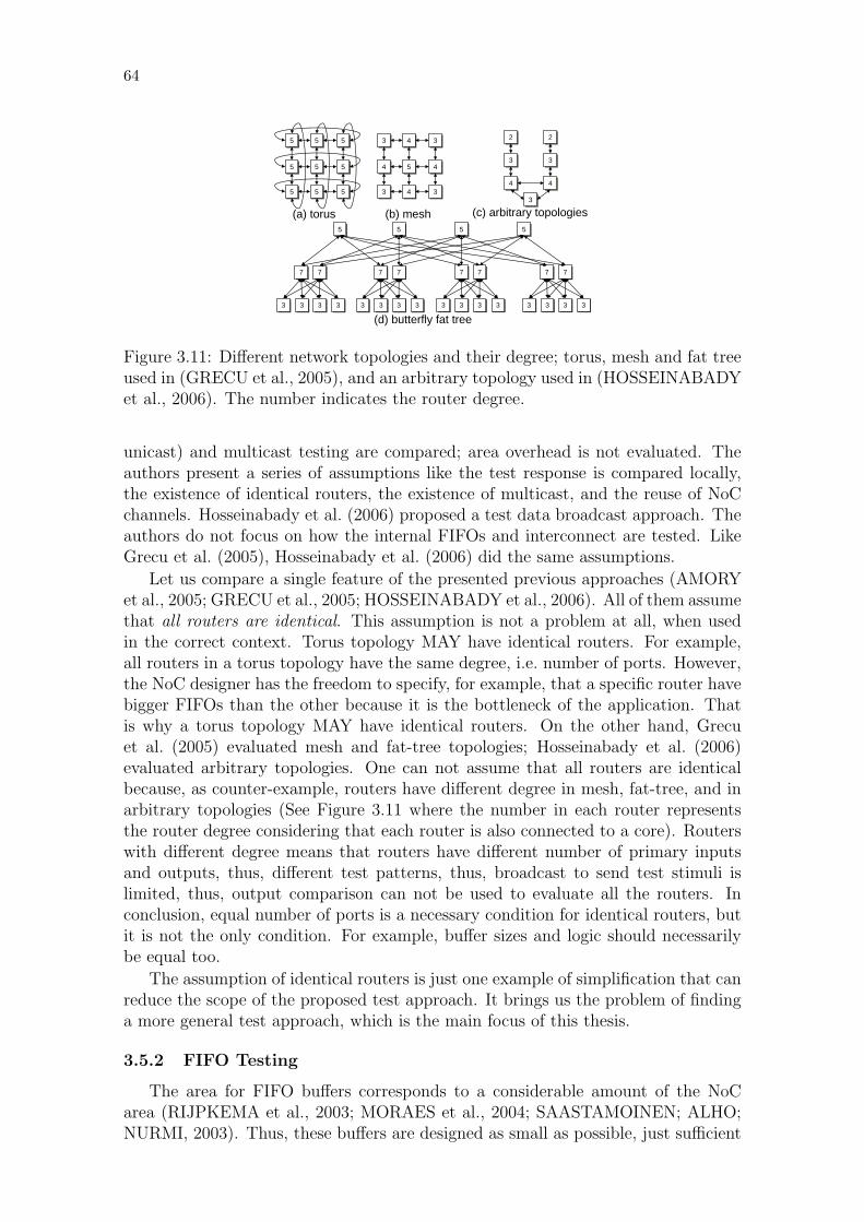
64
17
55 55 55
55 55 55
55 55 55
(a) torus
33 44 33
44 55 44
33 44 33
(b) mesh55 55 55 55
77 77
33 33 33 33
77 77
33 33 33 33
77 77
33 33 33 33
77 77
33 33 33 33
(d) butterfly fat tree
22
33
22
33
44 44
33
(c) arbitrary topologies
Figure 3.11: Different network topologies and their degree; torus, mesh and fat treeused in (GRECU et al., 2005), and an arbitrary topology used in (HOSSEINABADYet al., 2006). The number indicates the router degree.
unicast) and multicast testing are compared; area overhead is not evaluated. Theauthors present a series of assumptions like the test response is compared locally,the existence of identical routers, the existence of multicast, and the reuse of NoCchannels. Hosseinabady et al. (2006) proposed a test data broadcast approach. Theauthors do not focus on how the internal FIFOs and interconnect are tested. LikeGrecu et al. (2005), Hosseinabady et al. (2006) did the same assumptions.
Let us compare a single feature of the presented previous approaches (AMORYet al., 2005; GRECU et al., 2005; HOSSEINABADY et al., 2006). All of them assumethat all routers are identical. This assumption is not a problem at all, when usedin the correct context. Torus topology MAY have identical routers. For example,all routers in a torus topology have the same degree, i.e. number of ports. However,the NoC designer has the freedom to specify, for example, that a specific router havebigger FIFOs than the other because it is the bottleneck of the application. Thatis why a torus topology MAY have identical routers. On the other hand, Grecuet al. (2005) evaluated mesh and fat-tree topologies; Hosseinabady et al. (2006)evaluated arbitrary topologies. One can not assume that all routers are identicalbecause, as counter-example, routers have different degree in mesh, fat-tree, and inarbitrary topologies (See Figure 3.11 where the number in each router representsthe router degree considering that each router is also connected to a core). Routerswith different degree means that routers have different number of primary inputsand outputs, thus, different test patterns, thus, broadcast to send test stimuli islimited, thus, output comparison can not be used to evaluate all the routers. Inconclusion, equal number of ports is a necessary condition for identical routers, butit is not the only condition. For example, buffer sizes and logic should necessarilybe equal too.
The assumption of identical routers is just one example of simplification that canreduce the scope of the proposed test approach. It brings us the problem of findinga more general test approach, which is the main focus of this thesis.
3.5.2 FIFO Testing
The area for FIFO buffers corresponds to a considerable amount of the NoCarea (RIJPKEMA et al., 2003; MORAES et al., 2004; SAASTAMOINEN; ALHO;NURMI, 2003). Thus, these buffers are designed as small as possible, just sufficient
65
42
D Q
R
D Q
R
D Q
R
D Q
R
D Q
R
datain
dataout
Rreq
D Q
en
D Q
en
D Q
en
D Q
en
D Q
en
datain
dataout
RreqcontrollercontrollerWreq
(a)42
D Q
R
D Q
R
D Q
R
D Q
R
D Q
R
datain
dataout
Rreq
D Q
en
D Q
en
D Q
en
D Q
en
D Q
en
datain
dataout
RreqcontrollercontrollerWreq
(b)
43
D Q
en
D Q
en
D Q
en
D Q
en
D Q
en
datain
dataoutRreq
controllercontrollerWreq
D Q
en
D Q
en
D Q
en
D Q
en
D Q
en
datain
dataout
RreqcontrollercontrollerWreq
(c) 43
D Q
en
D Q
en
D Q
en
D Q
en
D Q
en
datain
dataoutRreq
controllercontrollerWreq
D Q
en
D Q
en
D Q
en
D Q
en
D Q
en
datain
dataout
RreqcontrollercontrollerWreq
(d)
Figure 3.12: FIFO designs. (a) Conventional shift register; (b) push-in shift-outregister; (c) push-in bus-out register; (d) push-in mux-out register; (from (BENINI;DE MICHELI, 2006)).
to support the functional communication requirements, in order to reduce the sizeof the NoC (SAASTAMOINEN; ALHO; NURMI, 2003). Other approaches use full-custom FIFOs to reduce the area (RIJPKEMA et al., 2003). Considering a 0.38µmtechnology library, the area of a SRAM cell is 84µm2 while the area of a DFF is984µm2 (BENINI; DE MICHELI, 2006). For performance reasons, the NoC designercan use FIFOs on the NoC in different positions (in the inputs, outputs, or evencentered). Moreover, different FIFO designs can be used in NoCs (see Figure3.12);each one requires different fault models and BIST circuitry. One should not forgetthat the NoC is composed of dozens of small FIFOs distributed over the chip. Thesecharacteristics complicate the development of a general test approach for the NoCFIFOs.
The most common FIFO designs are shifting-type FIFOs and the RAM-typeFIFOs (GOOR; SCHANSTRA; ZORIAN, 1995). The former is based on a shiftregister that shifts data from the write port to the last unused location. The latterhas a read and write address register to access data. RAM-type FIFOs can also beimplemented as single-port or dual-port FIFO.
The papers about FIFO testing can be classified as: fault model proposal, BISTproposal, or scan based. Van de Goor et al. (1995) proposed a fault model forshifting-type FIFOs. Aitken (2004) proposed a modular wrapper for at-speed BISTand repair of small memories. The approach is specially interesting for a largenumber of distributed register files and FIFOs. The DfT overhead presented for a64x64 FIFO is 28%, while for smaller FIFOs the area overhead increases even more,which can be considered high for NoCs. The area overhead can be reduced if thelogic related to memory repair is removed.
The main drawback of BIST circuitry to test small and distributed memories isthe large area overhead. The memories may be distributed throughout the chip toallow sharing the BIST circuitry. An alternative approach, presented in (REARICK,1999; AMORY et al., 2005), is defining a general DfT for FIFOs. Both paperspropose the insertion of scan chains around the memory matrix, i.e. scan chain inthe data input, data output, and address registers. Thus, any test algorithm, likethe one proposed in (GOOR; SCHANSTRA; ZORIAN, 1995) to test the memory
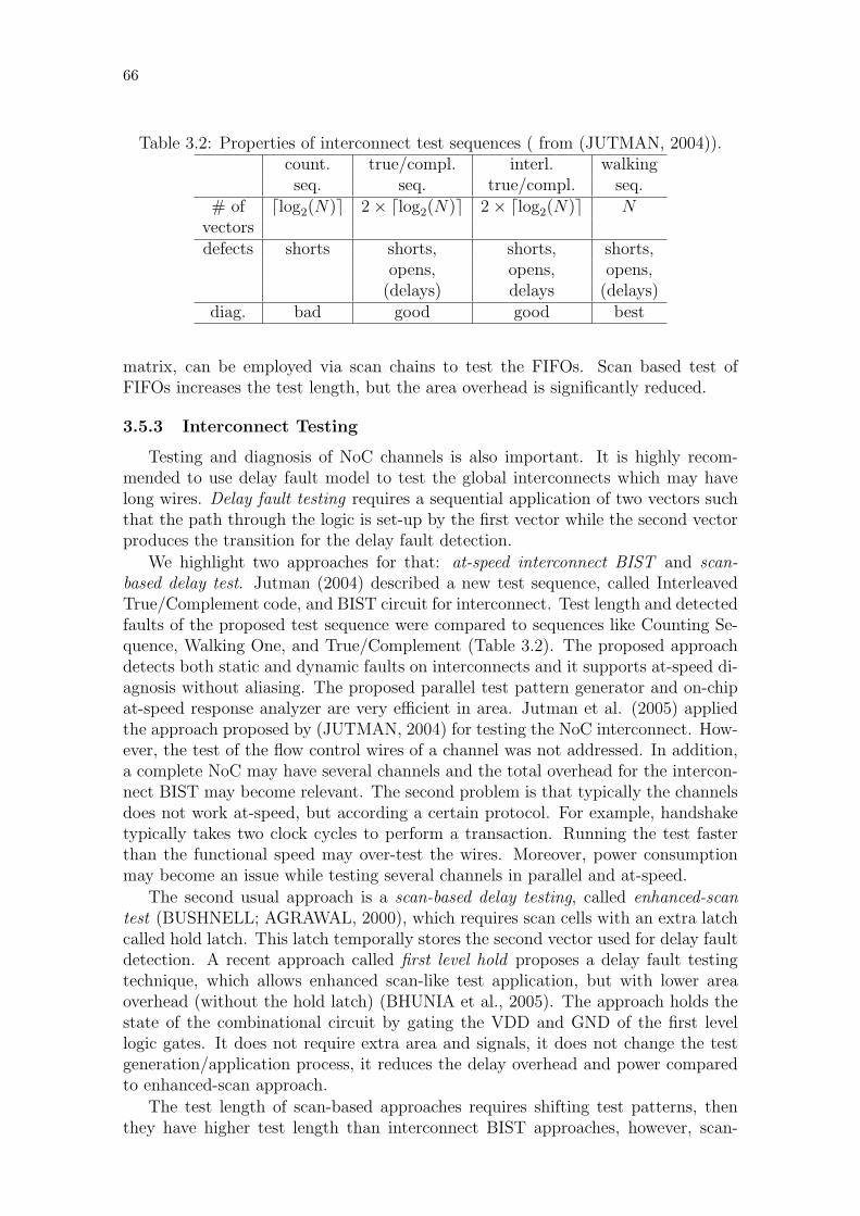
66
Table 3.2: Properties of interconnect test sequences ( from (JUTMAN, 2004)).count. true/compl. interl. walkingseq. seq. true/compl. seq.
# of dlog2(N)e 2× dlog2(N)e 2× dlog2(N)e Nvectorsdefects shorts shorts, shorts, shorts,
opens, opens, opens,(delays) delays (delays)
diag. bad good good best
matrix, can be employed via scan chains to test the FIFOs. Scan based test ofFIFOs increases the test length, but the area overhead is significantly reduced.
3.5.3 Interconnect Testing
Testing and diagnosis of NoC channels is also important. It is highly recom-mended to use delay fault model to test the global interconnects which may havelong wires. Delay fault testing requires a sequential application of two vectors suchthat the path through the logic is set-up by the first vector while the second vectorproduces the transition for the delay fault detection.
We highlight two approaches for that: at-speed interconnect BIST and scan-based delay test. Jutman (2004) described a new test sequence, called InterleavedTrue/Complement code, and BIST circuit for interconnect. Test length and detectedfaults of the proposed test sequence were compared to sequences like Counting Se-quence, Walking One, and True/Complement (Table 3.2). The proposed approachdetects both static and dynamic faults on interconnects and it supports at-speed di-agnosis without aliasing. The proposed parallel test pattern generator and on-chipat-speed response analyzer are very efficient in area. Jutman et al. (2005) appliedthe approach proposed by (JUTMAN, 2004) for testing the NoC interconnect. How-ever, the test of the flow control wires of a channel was not addressed. In addition,a complete NoC may have several channels and the total overhead for the intercon-nect BIST may become relevant. The second problem is that typically the channelsdoes not work at-speed, but according a certain protocol. For example, handshaketypically takes two clock cycles to perform a transaction. Running the test fasterthan the functional speed may over-test the wires. Moreover, power consumptionmay become an issue while testing several channels in parallel and at-speed.
The second usual approach is a scan-based delay testing, called enhanced-scantest (BUSHNELL; AGRAWAL, 2000), which requires scan cells with an extra latchcalled hold latch. This latch temporally stores the second vector used for delay faultdetection. A recent approach called first level hold proposes a delay fault testingtechnique, which allows enhanced scan-like test application, but with lower areaoverhead (without the hold latch) (BHUNIA et al., 2005). The approach holds thestate of the combinational circuit by gating the VDD and GND of the first levellogic gates. It does not require extra area and signals, it does not change the testgeneration/application process, it reduces the delay overhead and power comparedto enhanced-scan approach.
The test length of scan-based approaches requires shifting test patterns, thenthey have higher test length than interconnect BIST approaches, however, scan-
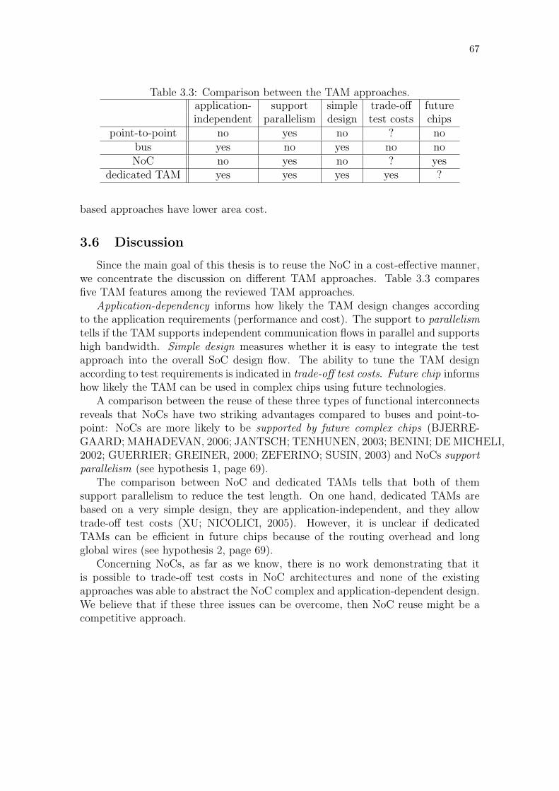
67
Table 3.3: Comparison between the TAM approaches.application- support simple trade-off futureindependent parallelism design test costs chips
point-to-point no yes no ? nobus yes no yes no noNoC no yes no ? yes
dedicated TAM yes yes yes yes ?
based approaches have lower area cost.
3.6 Discussion
Since the main goal of this thesis is to reuse the NoC in a cost-effective manner,we concentrate the discussion on different TAM approaches. Table 3.3 comparesfive TAM features among the reviewed TAM approaches.
Application-dependency informs how likely the TAM design changes accordingto the application requirements (performance and cost). The support to parallelismtells if the TAM supports independent communication flows in parallel and supportshigh bandwidth. Simple design measures whether it is easy to integrate the testapproach into the overall SoC design flow. The ability to tune the TAM designaccording to test requirements is indicated in trade-off test costs. Future chip informshow likely the TAM can be used in complex chips using future technologies.
A comparison between the reuse of these three types of functional interconnectsreveals that NoCs have two striking advantages compared to buses and point-to-point: NoCs are more likely to be supported by future complex chips (BJERRE-GAARD; MAHADEVAN, 2006; JANTSCH; TENHUNEN, 2003; BENINI; DE MICHELI,2002; GUERRIER; GREINER, 2000; ZEFERINO; SUSIN, 2003) and NoCs supportparallelism (see hypothesis 1, page 69).
The comparison between NoC and dedicated TAMs tells that both of themsupport parallelism to reduce the test length. On one hand, dedicated TAMs arebased on a very simple design, they are application-independent, and they allowtrade-off test costs (XU; NICOLICI, 2005). However, it is unclear if dedicatedTAMs can be efficient in future chips because of the routing overhead and longglobal wires (see hypothesis 2, page 69).
Concerning NoCs, as far as we know, there is no work demonstrating that itis possible to trade-off test costs in NoC architectures and none of the existingapproaches was able to abstract the NoC complex and application-dependent design.We believe that if these three issues can be overcome, then NoC reuse might be acompetitive approach.

68
69
4 PROPOSED TEST MODEL
This chapter introduces the proposed test model. It presents hypothesis, requiredproperties, test requirements, the sources of jitter in NoCs, the proposed test model,an overall problem statement, and the proposed test flow.
4.1 Fundamental Hypotheses
The proposed test approach presented in this thesis relies on two fundamentalhypotheses:
Hypothesis 1: NoC will be the main communication architectures for future andcomplex chip designs. There are several papers in the literature demonstratingadvantage of NoCs compared to other communication architectures. In addition,as demonstrated in Section 2.2.2, there are several industrial approaches comingup and, recently, a test chip based on NoC has been announced (CLERMIDY;VARREAU; LATTARD, 2005).
Hypothesis 2: Can dedicated TAM be the main test access mechanism for thesefuture and complex chip designs ? The answer is probably not. The reason for thisis that traditional global on-chip interconnects, like buses (a dedicated TAM is akind of bus), are becoming the bottleneck in terms of bandwidth, signal integrity,and power dissipation of complex chip designs (ITRS, 2007).
In addition, one can observe that most test planning algorithms proposed in theliterature minimize the chip test length, but minimization of TAM design costs (e.g.wiring length) has received little attention; they are based on layout constraints tominimize the TAM wiring length. For example, according to Goel and Marinissen(GOEL; MARINISSEN, 2003b) the wiring length can be reduced about 83% witha test length penalty of 4%. However, these approaches assume that the layoutposition of every core is known a priori. This assumption complicates the designflow since, in the early stages of design, the layout information is not available. Toget the information it would be required to build the layout of the full chip, thenreturn to the initial design steps to insert the TAM constrains and re-implement thelayout with optimized TAMs.
In conclusion, approaches for wire length minimization of TAMs are required forcomplex chips, nevertheless the approach based on core layout position complicatesthe design flow. New approaches for TAMs are required.
70
4.2 Properties of Proposed Test Model
Building a general NoC reuse approach for BE NoCs is the main concern of thisthesis. We have identified in the Prior Work that one of the main problems withmost reuse approaches is that they are application-dependent and not general sincethe interconnect design is typically either application-dependent or complex.
Our second main concern is compatibility with the conventional test model basedon dedicated TAM. We enforce this compatibility because, based on the conclusionof the Prior Work section, the SoC test approach based on dedicated TAM seemsto be the most cost-effective approach so far. In addition, we build the proposedtest model on top of existing and well-established research and standards. Thus,we can use the same optimization procedures, DfT logic, and tools for the proposedapproach. In fact, few adaptations for the DfT logic and the algorithms are required,but we reuse the core optimization algorithms and DfT design strategies. Theseadaptations are one of the main contributions of this thesis.
The remaining concerns and required properties are:
(i) The trade-off of test cost parameters to tune the approach under several con-straints. The proposed approach optimizes DfT area and test application time.Other cost functions like power consumption can be included in future work;
(ii) The DfT modules should be connected as plug-and-play, without modifyingany other module except the DfT modules;
(iii) In addition, the DfT modules should have minimal impact on the functionalrequirements and the proposed method should fit easily in a chip design flow.Recall that, as seen in Section 4.1, the dedicated TAM approach with layoutconstraint complicates the design flow;
(iv) The support to multiple TAMs to allow testing multiple cores in parallel re-ducing the test application time.
The six classes presented below summarize the required properties of the pro-posed approach:
1. general and application-independent test approach;
2. Compatibility with conventional test approach;
3. Enable design-space exploration and trade-off test cost parameters;
4. Fit easily in a chip design flow;
5. Minimal influence on the functional requirements;
6. Support to multiple TAMs.
4.3 Test Traffic Requirements
Test traffic requires uncorrupted, lossless, in-order data delivery, zero-jitter, andscalable and constant bandwidth. We want to keep these requirements to preservethe natural test streaming expected by the ATEs and the CUTs.
71
The proposed approach requires that the NoC provides the previous mentionedrequirements. The first two requirements are usually implemented in NoCs. Thethird one is easily accomplished by sending test data over a single path. Jitter iscaused because NoCs have several shared resources (channels and routers). Sharedresources require arbitration schemes, which cause jitter. Scalable and constantbandwidth is easily solved if the zero-jitter requirement is fulfilled; it only requiresto send/receive data at regular time intervals.
In conclusion, zero-jitter requirement is the most critical to be met. The nextsection identifies the sources of jitter in NoCs.
4.4 Sources of Jitter in NoCs
4.4.1 Shared Channels
Channels are shared in a network to save area for wiring. However, when twopackets compete for the same channel, the arbitration logic grants access to one ofthem. The other stream is delayed, causing jitter and disrupting the test applicationof a core.
4.4.2 Shared Routers
The routing time of a router, i.e. the time it takes to find the output port, alsocauses jitter. There are two types of router schemes that are relevant for test: routerswith distributed and centralized routing (DUATO; YALAMANCHILI; NI, 2003).
In the first case, the routing logic is typically located at the input ports, thus, itusually requires more silicon area to replicate the routing logic to every input port.However, it can route several independent packets (packets that do not require thesame output channel) in parallel without any loss of performance. Therefore, therouting delay is deterministic and known a priori.
Centralized routing schemes save in silicon area but cause an indeterminate timeto route a given packet. Usually, even if two packet request different output channels,the packet that arrives first to the router is routed first, while the other routingrequests wait. Therefore, the routing delay varies according to the router utilization.
Since it is not up to the test engineer to decide whether centralized or distributedrouters are used in a design, the test strategy must support both types of routers.
4.4.3 Load Fluctuation
Figure 4.1 illustrates the test data flow from the input test pins to the input ofthe CUT. The input test pins receive continuous test data from the tester (line 1)and the CUTs expect the same traffic shape (last line). However, one can realize thatthe traffic shape at the input of router 1 (line 2) is different from the wrapper input(line 5). This deformation is called load fluctuation and it is caused by the routingdelay, which in this example is four clock cycles. Thus, the data is ‘condensed’ everyrouter, and, at the end of the flow the traffic has a bursty format (line 5). This trafficshape is not interesting for test because it creates gaps (line 5) in the data delivery.Then, our solution uses a FIFO buffer to transform the previous bursty format tothe periodic format (line 6). The periodic traffic shape is preferred because it iseasier to transform it to the original traffic shape sent by the tester (lines 1 and 7).
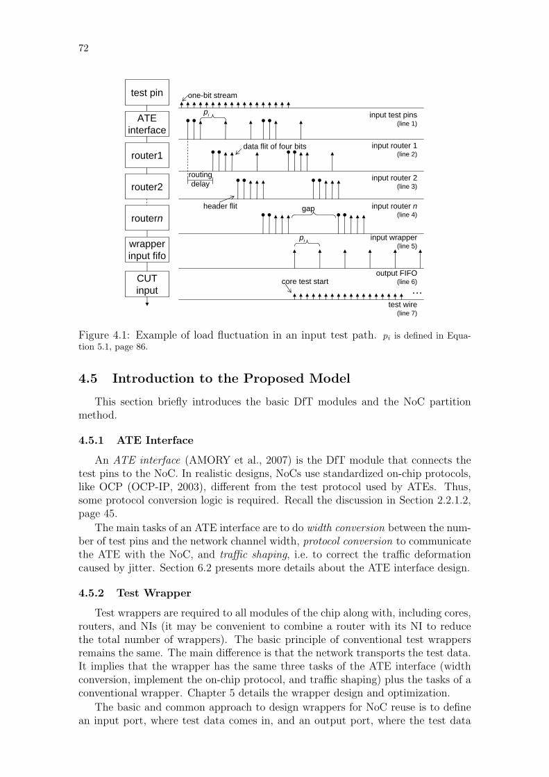
72
71
router2
CUTinput
wrapperinput fifo
routern
router1
input test pins(line 1)
input router 1(line 2)
input router 2(line 3)
input router n(line 4)
input wrapper(line 5)
output FIFO(line 6)
test wire(line 7)
one-bit stream
header flit
data flit of four bits
core test start…
test pin
ATEinterface
gap
pi
pi
routingdelay
Figure 4.1: Example of load fluctuation in an input test path. pi is defined in Equa-tion 5.1, page 86.
4.5 Introduction to the Proposed Model
This section briefly introduces the basic DfT modules and the NoC partitionmethod.
4.5.1 ATE Interface
An ATE interface (AMORY et al., 2007) is the DfT module that connects thetest pins to the NoC. In realistic designs, NoCs use standardized on-chip protocols,like OCP (OCP-IP, 2003), different from the test protocol used by ATEs. Thus,some protocol conversion logic is required. Recall the discussion in Section 2.2.1.2,page 45.
The main tasks of an ATE interface are to do width conversion between the num-ber of test pins and the network channel width, protocol conversion to communicatethe ATE with the NoC, and traffic shaping, i.e. to correct the traffic deformationcaused by jitter. Section 6.2 presents more details about the ATE interface design.
4.5.2 Test Wrapper
Test wrappers are required to all modules of the chip along with, including cores,routers, and NIs (it may be convenient to combine a router with its NI to reducethe total number of wrappers). The basic principle of conventional test wrappersremains the same. The main difference is that the network transports the test data.It implies that the wrapper has the same three tasks of the ATE interface (widthconversion, implement the on-chip protocol, and traffic shaping) plus the tasks of aconventional wrapper. Chapter 5 details the wrapper design and optimization.
The basic and common approach to design wrappers for NoC reuse is to definean input port, where test data comes in, and an output port, where the test data
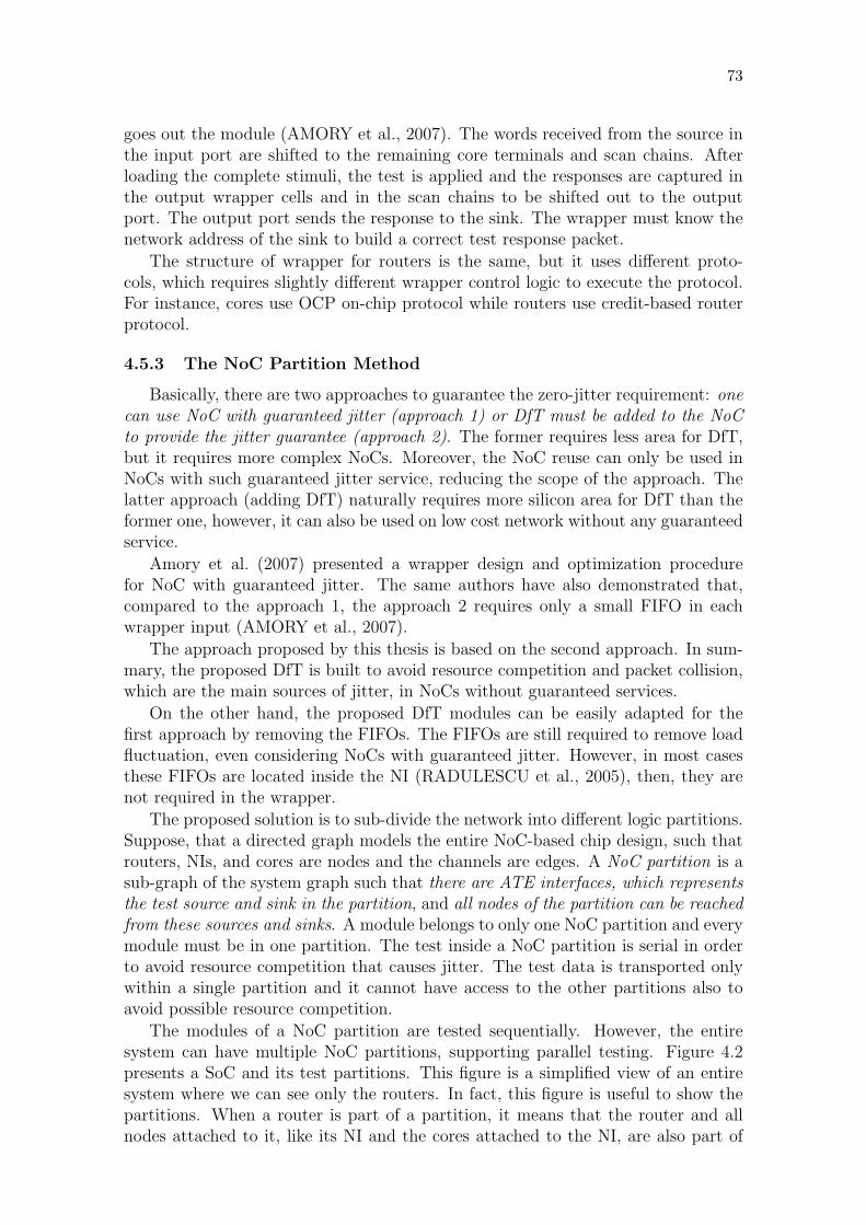
73
goes out the module (AMORY et al., 2007). The words received from the source inthe input port are shifted to the remaining core terminals and scan chains. Afterloading the complete stimuli, the test is applied and the responses are captured inthe output wrapper cells and in the scan chains to be shifted out to the outputport. The output port sends the response to the sink. The wrapper must know thenetwork address of the sink to build a correct test response packet.
The structure of wrapper for routers is the same, but it uses different proto-cols, which requires slightly different wrapper control logic to execute the protocol.For instance, cores use OCP on-chip protocol while routers use credit-based routerprotocol.
4.5.3 The NoC Partition Method
Basically, there are two approaches to guarantee the zero-jitter requirement: onecan use NoC with guaranteed jitter (approach 1) or DfT must be added to the NoCto provide the jitter guarantee (approach 2). The former requires less area for DfT,but it requires more complex NoCs. Moreover, the NoC reuse can only be used inNoCs with such guaranteed jitter service, reducing the scope of the approach. Thelatter approach (adding DfT) naturally requires more silicon area for DfT than theformer one, however, it can also be used on low cost network without any guaranteedservice.
Amory et al. (2007) presented a wrapper design and optimization procedurefor NoC with guaranteed jitter. The same authors have also demonstrated that,compared to the approach 1, the approach 2 requires only a small FIFO in eachwrapper input (AMORY et al., 2007).
The approach proposed by this thesis is based on the second approach. In sum-mary, the proposed DfT is built to avoid resource competition and packet collision,which are the main sources of jitter, in NoCs without guaranteed services.
On the other hand, the proposed DfT modules can be easily adapted for thefirst approach by removing the FIFOs. The FIFOs are still required to remove loadfluctuation, even considering NoCs with guaranteed jitter. However, in most casesthese FIFOs are located inside the NI (RADULESCU et al., 2005), then, they arenot required in the wrapper.
The proposed solution is to sub-divide the network into different logic partitions.Suppose, that a directed graph models the entire NoC-based chip design, such thatrouters, NIs, and cores are nodes and the channels are edges. A NoC partition is asub-graph of the system graph such that there are ATE interfaces, which representsthe test source and sink in the partition, and all nodes of the partition can be reachedfrom these sources and sinks. A module belongs to only one NoC partition and everymodule must be in one partition. The test inside a NoC partition is serial in orderto avoid resource competition that causes jitter. The test data is transported onlywithin a single partition and it cannot have access to the other partitions also toavoid possible resource competition.
The modules of a NoC partition are tested sequentially. However, the entiresystem can have multiple NoC partitions, supporting parallel testing. Figure 4.2presents a SoC and its test partitions. This figure is a simplified view of an entiresystem where we can see only the routers. In fact, this figure is useful to show thepartitions. When a router is part of a partition, it means that the router and allnodes attached to it, like its NI and the cores attached to the NI, are also part of
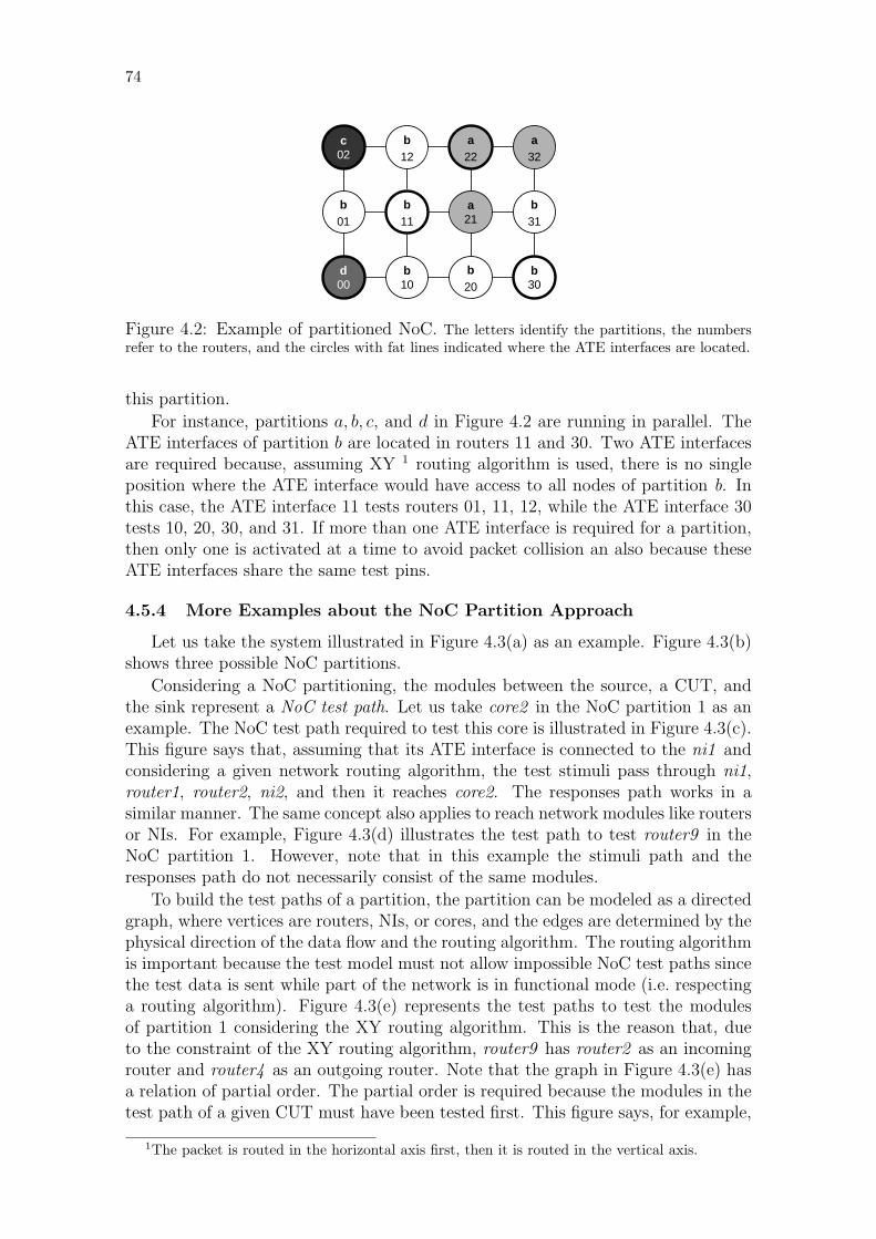
74
b01
b11
a21
b31
d00
b10
b20
b30
c02
b12
a22
a32
Figure 4.2: Example of partitioned NoC. The letters identify the partitions, the numbersrefer to the routers, and the circles with fat lines indicated where the ATE interfaces are located.
this partition.
For instance, partitions a, b, c, and d in Figure 4.2 are running in parallel. TheATE interfaces of partition b are located in routers 11 and 30. Two ATE interfacesare required because, assuming XY 1 routing algorithm is used, there is no singleposition where the ATE interface would have access to all nodes of partition b. Inthis case, the ATE interface 11 tests routers 01, 11, 12, while the ATE interface 30tests 10, 20, 30, and 31. If more than one ATE interface is required for a partition,then only one is activated at a time to avoid packet collision an also because theseATE interfaces share the same test pins.
4.5.4 More Examples about the NoC Partition Approach
Let us take the system illustrated in Figure 4.3(a) as an example. Figure 4.3(b)shows three possible NoC partitions.
Considering a NoC partitioning, the modules between the source, a CUT, andthe sink represent a NoC test path. Let us take core2 in the NoC partition 1 as anexample. The NoC test path required to test this core is illustrated in Figure 4.3(c).This figure says that, assuming that its ATE interface is connected to the ni1 andconsidering a given network routing algorithm, the test stimuli pass through ni1,router1, router2, ni2, and then it reaches core2. The responses path works in asimilar manner. The same concept also applies to reach network modules like routersor NIs. For example, Figure 4.3(d) illustrates the test path to test router9 in theNoC partition 1. However, note that in this example the stimuli path and theresponses path do not necessarily consist of the same modules.
To build the test paths of a partition, the partition can be modeled as a directedgraph, where vertices are routers, NIs, or cores, and the edges are determined by thephysical direction of the data flow and the routing algorithm. The routing algorithmis important because the test model must not allow impossible NoC test paths sincethe test data is sent while part of the network is in functional mode (i.e. respectinga routing algorithm). Figure 4.3(e) represents the test paths to test the modulesof partition 1 considering the XY routing algorithm. This is the reason that, dueto the constraint of the XY routing algorithm, router9 has router2 as an incomingrouter and router4 as an outgoing router. Note that the graph in Figure 4.3(e) hasa relation of partial order. The partial order is required because the modules in thetest path of a given CUT must have been tested first. This figure says, for example,
1The packet is routed in the horizontal axis first, then it is routed in the vertical axis.
75
that:
• the first modules to be tested are either c1 or ni1;
• to test r1, ni1 must be tested first;
• to test c2, the ni1, ni2, r1, and r2 must be tested first. Figure 4.3(c) shows thestimuli path and the responses path for c2 considering a XY routing algorithm;
• to test r9, the ni1, r1, r2, and r4 must be tested first. Figure 4.3(d) shows thestimuli path and the responses path for r9 considering a XY routing algorithm.Note that in this case the stimuli path and responses path do not involve thesame set of modules.
The total number of test pins is distributed among the test partitions and thepartitions can receive different number of test pins, according to the test data band-width required to test the modules within the partition. The number of partitions,the modules in each partition, and the number of test pins assigned to each parti-tion are the main problems to be solved such that the chip test length is minimized.Figure 4.3(f) shows a valid test scheduling for this example design.
Figure 4.4(a) illustrates a typical test data flow in the proposed approach. Letus assume that the stimuli data set of a certain core consists of a set of m flits andthe responses data set consists of a set of n flits. Then, the latency of all wordsof a stimuli data set (Ls) must be equal (Ls
0 = · · · = Lsm−1, thus, zero-jitter). The
value of the latency does not matter for the test model (Section 4.9 explains theimpact of latency for test). The latency of all words of a responses data set (Lr)must also be equal (Lr
0 = · · · = Lrn−1), but not necessarily equal to the latency of
stimuli data set because the number of routers of both paths can be different. Ofcourse, the latency to test a different core can also be different because the test pathis different (different number of routers). With this timing characteristics, the NoCpartition works as a pipeline (Figure 4.4(b)) driving test data to its cores, exactlylike dedicated TAMs and external testers.
The most important feature of this model is that there is only one active testsource and sink per partition, which test just modules within its partition, causingno packet collision. Once there is no packet collision, complex dynamic networkissues like packet scheduling, packet congestion, and cycle accurate network modelare not required. Few design information is required to model the system, what makesthe model simpler and more general.
4.6 Reducing the Jitter Bound Using NoC Partitioning
This section shoes how the NoC partition method solves the zero-jitter problem.
FIFO buffers (line 6 of Figure 4.1) are typically used to eliminate the jitter.However, the size of the buffer is proportional to the jitter bound (ZHANG, 1995).Thus, a small jitter bound implies in a lower silicon area for DfT. The rest of thissection shows how the proposed approach reduces the jitter bound and minimizesthe silicon area for DfT.
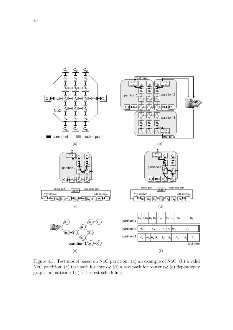
76
50
ni2ni2ni1ni1 ni3ni3
C7C7
R1R1 R3R3
R6R6 R8R8
R2R2
R7R7
C6C6
C3C3C2C2C1C1
ni7ni7ni6ni6 ni8ni8
C8C8
R4R4 R5R5R9R9C4C4 C5C5ni5ni5ni4ni4
core port router port
NoC
(a)
44
ATEinterface
ATEinterface
ATEinterface
ATEinterface
ATEinterface
ATEinterface
ni2ni2ni1ni1 ni3ni3
C7C7
R1R1 R3R3
R6R6 R8R8
R2R2
R7R7
C6C6
C3C3C2C2C1C1
ni7ni7ni6ni6 ni8ni8
C8C8
R4R4 R5R5R9R9C4C4 C5C5ni5ni5ni4ni4
partition 1 partition 2
partition 3
test pins
test pins
(b)
45
ATEinterface
ATEinterface
testertester
ni1ni1 R1R1 R2R2 ni2ni2 C2C2 ni1ni1R1R1R2R2ni2ni2
stimuli path responses path
(b) test path of core C2 of partition 1
ATE interface
ni2ni2ni1ni1
R1R1 R2R2
C2C2C1C1
R4R4 R9R9C4C4 ni4ni4
partition 1
ATE interface
(c) 46
ATE interface
testertester
R1R1 R9R9R2R2 R1R1R4R4
(c) test path of router R9 of partition 1
ni1ni1 ni1ni1
stimuli path responses path
ni2ni2ni1ni1
R1R1 R2R2
C2C2C1C1
R4R4 R9R9C4C4 ni4ni4
partition 1
ATE interface
ATEinterface
ATEinterface
(d)
39
partition 1
C1
ni1 R1
R2
R4
R9
ni2
ni4
C2
C4
(e)
38
partition 1
partition 2
partition 3
ni1ni1 R1R1 R2R2
ni3ni3 C3C3 R3R3 R5R5 ni5ni5 C5C5
C8C8 ni8ni8 R8R8 R7R7 R6R6 ni6ni6 C6C6 ni7ni7 C7C7
ni2ni2 R4R4 C1C1 ni4ni4 R9R9 C4C4 C2C2
test time
(f)
Figure 4.3: Test model based on NoC partition. (a) an example of NoC; (b) a validNoC partition; (c) test path for core c2; (d) a test path for router r9; (e) dependencygraph for partition 1; (f) the test scheduling.
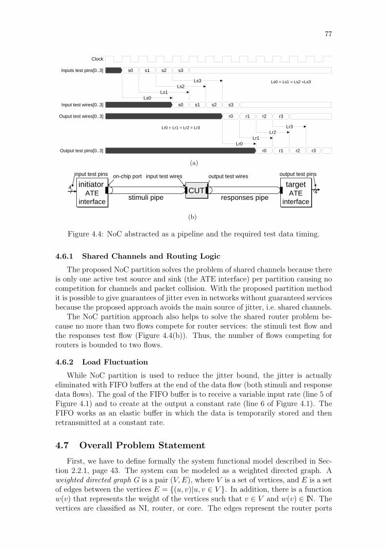
77
s0 s1 s2 s3
s0 s1 s2 s3
r0 r1 r2 r3
r0 r1 r2 r3
Lr3Lr2
Lr1Lr0
Ls3Ls2
Ls1Ls0
Ls0 = Ls1 = Ls2 =Ls3
Lr0 = Lr1 = Lr2 = Lr3
0ns 25ns 50ns 75ns 100ns 125ns
Clock
Inputs test pins[0..3]
Input test wires[0..3]
Ouput test wires[0..3]
Output test pins[0..3]
(a)
53
targetATE
interface
targetATE
interface
on-chip port
CUTCUTinitiator
ATEinterface
initiator ATE
interface stimuli pipe responses pipe
input test pins output test pins
44
input test wires output test wires
(b)
Figure 4.4: NoC abstracted as a pipeline and the required test data timing.
4.6.1 Shared Channels and Routing Logic
The proposed NoC partition solves the problem of shared channels because thereis only one active test source and sink (the ATE interface) per partition causing nocompetition for channels and packet collision. With the proposed partition methodit is possible to give guarantees of jitter even in networks without guaranteed servicesbecause the proposed approach avoids the main source of jitter, i.e. shared channels.
The NoC partition approach also helps to solve the shared router problem be-cause no more than two flows compete for router services: the stimuli test flow andthe responses test flow (Figure 4.4(b)). Thus, the number of flows competing forrouters is bounded to two flows.
4.6.2 Load Fluctuation
While NoC partition is used to reduce the jitter bound, the jitter is actuallyeliminated with FIFO buffers at the end of the data flow (both stimuli and responsedata flows). The goal of the FIFO buffer is to receive a variable input rate (line 5 ofFigure 4.1) and to create at the output a constant rate (line 6 of Figure 4.1). TheFIFO works as an elastic buffer in which the data is temporarily stored and thenretransmitted at a constant rate.
4.7 Overall Problem Statement
First, we have to define formally the system functional model described in Sec-tion 2.2.1, page 43. The system can be modeled as a weighted directed graph. Aweighted directed graph G is a pair (V, E), where V is a set of vertices, and E is a setof edges between the vertices E = {(u, v)|u, v ∈ V }. In addition, there is a functionw(v) that represents the weight of the vertices such that v ∈ V and w(v) ∈ IN. Thevertices are classified as NI, router, or core. The edges represent the router ports
78
and core ports. Finally, the weights represent the test data volume (i.e. number ofbits to test a core) required to test each vertex.
In addition, a virtual TAM (vTAM) is defined as a tuple {d, k, w,Ratei, Rpart},where d is the FIFO depth of the DfT modules in Rpart, k is the packet size usedduring test, w is the number of test wires used to test the modules in Rpart, Ratei isthe set of ATE interfaces, and Rpart is the set of routers in the partition such thatRatei ⊂ Rpart ⊂ G. The test architecture optimization problem must determine: (i)the vTAMs (the FIFO depth, the packet size, the number of test wires, the set ofmodules, and the set of ATE interfaces of each vTAM), (ii) the wrapper design forthe modules, and (iii) the ATE interface design for the vTAMs.
Problem 1 [Test Optimization of NoC-Based Chips]Given:
• a graph G which defines the SoC where for each g ∈ G:
– there are a test input ipg and a test output port opg;
– number of test patterns pg;
– number of functional input terminals ig;
– number of functional output terminals og;
– number of functional bidirectional terminals bg;
– the number of scan chains sg for each scan chain k with scan length lg,k
(for hard cores only);
– the number of scan flip-flops fg (for soft cores only).
• the maximal number of test wires wmax;
• the physical channel width c, in bits;
• the routing algorithm r() used by the NoC.
Determine:
1. the sets of vTAMs;
2. the wrapper design for each module;
3. the ATE Interface design.
4. the SoC test length, in clock cycles.
Such that:
i. the SoC test length and the silicon area for DfT are minimized while wmax isnot exceeded and the width of each vTAM is ≤ c/22.
�
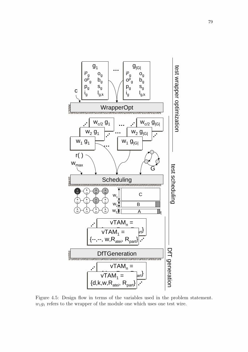
79
72
g1g1
wc/2 g1wc/2 g1
w2 g1w2 g1
WrapperOptWrapperOpt
DfTGenerationDfTGeneration
w1 g1w1 g1
wc/2 g|G|wc/2 g|G|
w2 g|G|w2 g|G|
w1 g|G|w1 g|G|
wmax
r( )
ipgop
gpgig
ogbgsglg,k
g|G|g|G|ipgop
gpgig
ogbgsglg,k
SchedulingScheduling
testschedulingtestw
rapperoptimization
b01
b11
a21
b31
b00
b10
b20
b30
c02
b12
a22
a32
c
vTAMn ={--, w,Ratei, Rpart}
vTAMn ={--, w,Ratei, Rpart}vTAM1 =
{--,--, w,Ratei, Rpart}vTAM1 =
{--,--, w,Ratei, Rpart}
vTAMn ={d, w,Ratei, Rpart}
vTAMn ={d, w,Ratei, Rpart}vTAM1 =
{d,k,w,Ratei, Rpart}vTAM1 =
{d,k,w,Ratei, Rpart}
DfT
generation
G
C
w2 B
w1
A tw3
Figure 4.5: Design flow in terms of the variables used in the problem statement.w1g1 refers to the wrapper of the module one which uses one test wire.
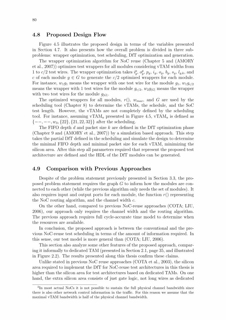
80
4.8 Proposed Design Flow
Figure 4.5 illustrates the proposed design in terms of the variables presentedin Section 4.7. It also presents how the overall problem is divided in three sub-problems: wrapper optimization, test scheduling, DfT optimization and generation.
The wrapper optimization algorithm for NoC reuse (Chapter 5 and (AMORYet al., 2007)) optimizes test wrappers for all modules considering vTAM widths from1 to c/2 test wires. The wrapper optimization takes ipg, op
g, pg, ig, og, bg, sg, lg,k, andc of each module g ∈ G to generate the c/2 optimized wrappers for each module.For instance, w1g1 means the wrapper with one test wire for the module g1, w1gc/2
means the wrapper with 1 test wires for the module gc/2, w2g|G| means the wrapperwith two test wires for the module g|G|.
The optimized wrappers for all modules, r(), wmax, and G are used by thescheduling tool (Chapter 8) to determine the vTAMs, the schedule, and the SoCtest length. However, the vTAMs are not completely defined by the schedulingtool. For instance, assuming vTAMa presented in Figure 4.5, vTAMa is defined as{−−,−−, w3, {22}, {21, 22, 32}} after the scheduling.
The FIFO depth d and packet size k are defined in the DfT optimization phase(Chapter 9 and (AMORY et al., 2007)) by a simulation based approach. This steptakes the partial DfT defined in the scheduling and simulate the design to determinethe minimal FIFO depth and minimal packet size for each vTAM, minimizing thesilicon area. After this step all parameters required that represent the proposed testarchitecture are defined and the HDL of the DfT modules can be generated.
4.9 Comparison with Previous Approaches
Despite of the problem statement previously presented in Section 3.3, the pro-posed problem statement requires the graph G to inform how the modules are con-nected to each other (while the previous algorithm only needs the set of modules). Italso requires input and output ports for each module, the function r() representingthe NoC routing algorithm, and the channel width c.
On the other hand, compared to previous NoC-reuse approaches (COTA; LIU,2006), our approach only requires the channel width and the routing algorithm.The previous approach requires full cycle-accurate time model to determine whenthe resources are available.
In conclusion, the proposed approach is between the conventional and the pre-vious NoC-reuse test scheduling in terms of the amount of information required. Inthis sense, our test model is more general than (COTA; LIU, 2006).
This section also analyze some other features of the proposed approach, compar-ing it informally to dedicated TAM (presented in Section 2.1, page 35, and illustratedin Figure 2.2). The results presented along this thesis confirm these claims.
Unlike stated in previous NoC reuse approaches (COTA et al., 2003), the siliconarea required to implement the DfT for NoC-reuse test architectures in this thesis ishigher than the silicon area for test architectures based on dedicated TAMs. On onehand, the extra silicon area consists of just gate logic, not long wires as dedicated
2In most actual NoCs it is not possible to sustain the full physical channel bandwidth sincethere is also other network control information in the traffic. For this reason we assume that themaximal vTAM bandwidth is half of the physical channel bandwidth.
81
TAMs. As presented before, long wires are expected to cost more than logic in termsof design effort, delay, and power dissipation. On the other hand, it does not meanthat the proposed DfT is less efficient than previous one. It means that we takeinto account design issues not considered before. For instance, we have proposedATE interfaces for the test pins that are not connected to the NoC and test wrappersthat deals with functional protocol. None of these required DfT has been addressedbefore.
In terms of timing for test data transportation, both proposed and conventionalSoC test are based in constant and continuous test data streaming which is natu-rally provided by dedicated TAMs. The previous approaches based on functionalinterconnect reuse usually do not provide this feature (COTA et al., 2003; HWANG;ABRAHAM, 2001; HARROD, 1999).
For the same reason, the proposed model might have higher latency from the testpins to the CUT. We say “might” because a network design can be optimized, forexample, for latency. For instance, packet switching networks have typically morelatency than circuit switching networks once the circuit has been established. Thelatency for a circuit switching network can be one clock cycle per hop. However,even if a network with more latency is used, latency is still not important for a testmodel.
Consider the general formula of data transportation time is t = l + vb, where t, l,
v, and b denote, respectively, time for transportation, latency of the medium, datavolume, and bandwidth (MCCABE, 2003). The latency of dedicated TAMs consistsof few buffers and typically results in few units of clock cycles. However, as statedin the introduction, the functional interconnects are evolving to segmented wiringto handle DSM effects on long wires, thus, the latency of functional interconnect isincreasing. For example, a path in a NoC consists of several modules (two networkinterfaces and several routers). Therefore, on one hand, it can be concluded thatthe latency of dedicated TAMs is typically smaller than the latency of functionalinterconnects. On the other hand, the impact of the latency on the core test lengthis minimal since l � v
b. The typical test data volume of a core can be around hun-
dreds of thousands or millions of bits. Thus, latency can be neglected no matter ifthe latency is 3 clock cycles for dedicated TAMs or 30 for NoCs. In addition, inter-connects support pipelining to partially hide this latency, thus, only the very firstword of data feels the latency effect since the proposed approach is based on non-preemptive test. For these reasons we concentrate in the minimization of v
bto reduce
the core test length. However, the latency is still important for the test applicationbecause the tester needs to know the exact time data is inserted and evaluated intothe chip. The exact latency for a given interconnect can be measured, for example,by using logic simulation and counting the number of clock cycles required for thefirst word to go from the ATE to the CUT 3. Realizing that latency can be takenoff the calculation helps the interconnect abstraction (i.e. the pipeline abstractionmentioned before).
3Recall that this simulation of test patterns is not an additional burden in the design, but it isa required step to validate the generated test patterns. This is the reason why most ATPG toolsautomatically generate a test bench to ease this step. What we propose is just to take this latencyinformation from the simulation, not from the test model.
82
The wrapper of the proposed model does not need bypass mode in most cases.The bypass mode is required when a core a is not connected directly in the NoC,but is connected to another core b that is connected to the network (see case threein Figure 2.12 in page 45 for an illustrative example). So, the wrapper of core bmust have bypass mode to indirectly connect core a to the NoC.
The optimization problem of dedicated TAM and the proposed model also seemto be similar. Figure 4.6 compares both test architectures: (i) the conventionalapproach distributes the total number of test wires into independent TAMs. Theproposed approach distribute the test pins among the test partitions, where the ATEinterface connects the pins to the network. (ii) all cores of a dedicated TAM aretested using the same constant test bandwidth (i.e. number of test wires), likewisea NoC partition. Pipelines of different partitions have different width. (iii) sincededicated TAMs are designed only for test, they naturally support continuous andconstant data flow with zero-jitter. The DfT modules (wrappers and ATE inter-face) of the proposed approach also provide the same communication pattern in anend-to-end manner (i.e. from the test pins to the CUT). (iv) TAMs of the conven-tional approach are independent from other TAMs and the cores within a TAM aretested sequentially. The NoC partitions of the proposed approach are independentfrom the other partitions and the cores are also tested sequentially. The use ofalgorithms previously proposed for test architecture with dedicated TAMs (GOEL;MARINISSEN, 2003a; MARINISSEN; GOEL; LOUSBERG, 2000) for NoC reusealso demonstrates that both problems can be similar.
Despite of all these similarities there are also some differences. The conventionalapproach typically has no constraint regarding the order the cores are tested withina TAM like in the proposed model. In addition, the proposed approach requiresneighborhood and TAM width constraints, presented in Chapter 8.
4.10 Summary
This chapter presented an overview of the proposed system test model for BENoC-based chips. The model divides the network in partitions, where each partitionis tested independently from each other, avoiding interference and packet collisionsthat delay a message. Thus, complex, cycle-accurate, and dynamic network modelsthat model packet collision and congestion are not required for test scheduling. Forthis reason, the proposed model is simpler and more general than previous NoC-reuseschemes based on packet scheduling. The proposed model is built on top of the DfTmodules (wrappers and ATE interface), designed to reinforce the compatibility withdedicated TAMs and the external tester timing features. In addition, the proposedDfT abstracts the NoC internals as simple pipelines with scalable width.
As result, the combination of the proposed DfT modules and the NoC partitiontest model gives the support to the six features described in the beginning of thischapter: (1) general test approach that works for a wide range of networks sincefew functional features are required; (2) compatibility with conventional test sincethe tester timing features are respected; (3) it enables the trade-off of test costsas dedicated TAMs since the pipeline width is scalable; (4) the DfT modules arebased on well-defined interfaces, then the DfT modules are easily inserted in thechip design; (5) the proposed method does not modify the network, minimizing the
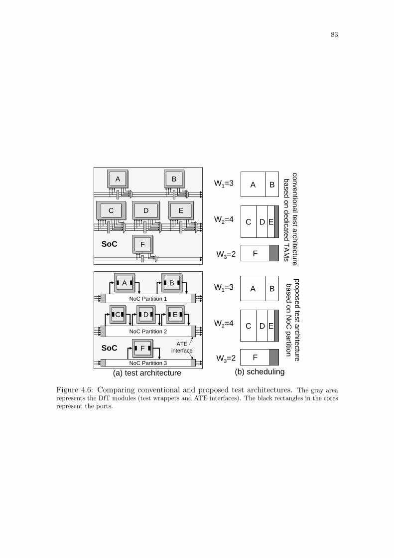
83
AA BB
CC DD EE
FF
W1=3
W2=4
W3=2
A B
C D E
FSoC
AA BB
CC DD EE
FF
W1=3
W2=4
W3=2
A B
C D E
F
(a) test architecture (b) scheduling
SoC
NoC Partition 1
NoC Partition 2
NoC Partition 3
conventionaltestarchitecturebased
ondedicated
TAM
sproposed
testarchitecturebased
onN
oCpartition
ATEinterface
Figure 4.6: Comparing conventional and proposed test architectures. The gray arearepresents the DfT modules (test wrappers and ATE interfaces). The black rectangles in the coresrepresent the ports.

84
influence on the functional domain; and finally, (6) the concurrent NoC partitionstest cores in parallel to reduce the core test.
85
5 TEST WRAPPERS FOR CORES
This chapter proposes a new core test wrapper design approach which transportsstreaming test data into and out of an embedded core via its functional data ports.These ports are typically based on standardized protocols such as AXI, DTL, andOCP. Our new wrapper design allows functional interconnect, such as an on-chipbus or NoC, to transport test data to embedded cores, and hence eliminates the needfor a conventional dedicated TAM, such as a TestRail or test bus. Our approachleaves the tester, the embedded core, and its test unchanged, while the functionalinterconnect can handle the test data transport as a regular data application. Theproposed wrapper requires guaranteed throughput and zero latency variation. Weshow how to use the wrapper over functional interconnects with and also withoutsupport to guaranteed services.
For 672 example cases based on the ITC’02 SoC Test Benchmarks, our newapproach in comparison to the conventional approach shows an average wrapperarea increase of 14.5%, which is negligible at SoC level, especially since the dedicatedTAM can be eliminated. Our new approach furthermore decreases the core testlength on average with 3.8%.
This chapter is organized as follows. Section 5.1 presents the problem statement.Section 5.2 presents an overview of the wrapper design. Section 5.3 shows the wrap-per design and optimization procedure in details. Section 5.4 shows experimentalresults. Finally, Sections 5.5 and 5.6 presents an overall discussion and conclusion,respectively.
5.1 Problem Statement
The core must use exactly one protocol port as test input and exactly one otherprotocol port as test output. As not all bidirectional ports support full-duplexcommunication, read-write ports are used in only one direction, in order to allowscan-in and scan-out operations during test to overlap in time. Consequently, thecore need to have two protocol ports: one to serve as test input ip and one to serveas test output port op. We assume that at least two suitable ports are available.The terminals of these ports must be classified according to Section 5.3.1 and weneed the behavior of the protocol and the rule of each terminal in the protocol.
In addition, all the test information required for the conventional wrapper designis also required, like
• number of test patterns pg;
• number of functional input terminals ig;
86
• number of functional output terminals og;
• number of functional bidirectional terminals bg;
• the number of scan chains sg for each scan chain k with scan length lg,k (forhard cores only);
• the number of scan flip-flops fg (for soft cores only).
Finally, we need to determine the design of a core test wrapper, which enablesthe CUT to be tested by the ATE via the NoC without modifying the ATE, theinterconnect, the CUT, or its test. The design of the wrapper is optimized such thatthe CUT’s test length and wrapper silicon area are minimized.
5.2 Wrapper Design Overview
Figure 5.1 shows both the conventional (a) and the new (b) IEEE Std. 1500(SILVA, 2005; SILVA; MCLAURIN; WAAYERS, 2006) compliant wrapper designs,and illustrates their differences. In the InTest mode of the conventional wrapper,access of all functional inputs and outputs to the core is intercepted by the WrapperBoundary Register (WBR), while ports to dedicated TAMs provide test access. Inthe new wrapper design, there is no dedicated TAM. Test access to the core isprovided via a subset of the functional inputs and outputs, viz. via one selectedinput port and one selected output port. Functional inputs and outputs that do notbelong to the selected ports are intercepted by the WBR.
The algorithm to design and optimize the test wrapper consists of the followingthree steps.
1. Calculation of parallel-to-serial loading and serial-to-parallel unloading char-acteristics.Stimulus bits arrive strictly periodically in words of ci bits at the selected testinput port i. There, they are equally divided over the w wrapper chains andserially shifted into the wrapper and core. This process is repeated every pi
clock cycles, with
pi =⌊ci
w
⌋(5.1)
Note that of the ci data bits in each parallel word, only⌊
ci
w
⌋× w are actually
used to carry stimulus bits; the remaining (ci mod w) bits carry unused data,and consequently will be assigned special wrapper cells in Step 4. The responseside is handled likewise, where every po =
⌊co
w
⌋clock cycles, po response bits
are unloaded in parallel from the test output port o of each of the w wrapperchains 1.
2. Core terminal classification.Based on their role in the test operation, core terminals are classified accortingto: (i) the type of wrapper cell for the terminal, (ii) the position of the wrapper
1we might use c when ci = co = c, i.e. when the port input data width, the port output datawidth, and the channel width are equal.
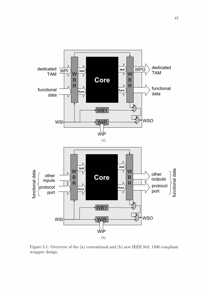
87
92
WBY
WIR
test
func
WPI WPOtest
func
CoreWBR
WBR
dedicatedTAM
functionaldata
dedicatedTAM
functionaldata
WSI WSO
WIP(a)
93
WBY
WIR
WBR
otherinputs
protocolport
WSI WSO
WIP
test
func
test
func
CoreWBR
otheroutputsprotocolport
func
tiona
l dat
a
func
tiona
l dat
a
(b)
Figure 5.1: Overview of the (a) conventional and (b) new IEEE Std. 1500 compliantwrapper design.
88
cell in a wrapper scan chain, and (iii) the control signals to the wrapper cell.The core terminal classification is described in more detail in Section 5.3.1.
3. Actual wrapper design.Based on the outcome of the core terminal classification, the wrapper is in-stantiated, according to the following sub-steps.
(a) Assign wrapper cells to individual core terminals, as described in Sec-tion 5.3.2.
(b) Partition and order the wrapper cells and core-internal scan chains overthe w wrapper chains, as described in Section 5.3.3.
(c) Connect the control logic to the various wrapper cells.
5.3 Wrapper Design and Optimization
5.3.1 Core Terminal Classification
Conventional wrapper design (MARINISSEN; GOEL; LOUSBERG, 2000) dis-tinguishes four classes of core terminals: functional inputs (FI), functional outputs(FO), scan inputs (SI), and scan outputs (SO). In the new approach, in which testdata reaches the core via reused functional ports, we add eight new classes, for theterminals of the functional ports.
• SDI, SDO: Selected Data Inputs and Outputs, i.e., the data terminals of thefunctional port that has been selected to serve as test input (output), andcarry actual stimulus (response) data.
• RSDI, RSDO: Remaining Selected Data Inputs and Outputs, i.e., those (ci modw) data bits of the selected test input port i and (co mod w) data bits of theselected test output port o that carry unused data.
• DI, DO: Data Inputs and Outputs, i.e., the data terminals of the remainingfunctional ports not selected to carry test data.
• CI, CO: Control Inputs and Outputs, i.e., the non-data terminals of all func-tional ports.
• FI, FO: Functional Inputs and Outputs, i.e., all functional terminals that arenot part of the selected test ports.
• SI, SO: Scan Inputs and Outputs.
The twelve classes provide a complete partitioning for all digital data terminals ofthe core, i.e., all classes are mutually exclusive and their union equals all terminals2.
The classification of the functional port terminals of the example in Figure 5.2 isshown in Table 5.1. For both ports, the dtl wr data[31:0] terminals are selectedas test input (output) ports and hence are classified as SDI and SDO respectively.Assuming w = 3, both selected ports have (c mod w) = (32 mod 3) = 2 unused
2we might use DIin , DOin , CIin , and COin to refer, for example, to the DI terminals of theinput port. DIout , DOout , CIout , and COout refer to the sets of the output port
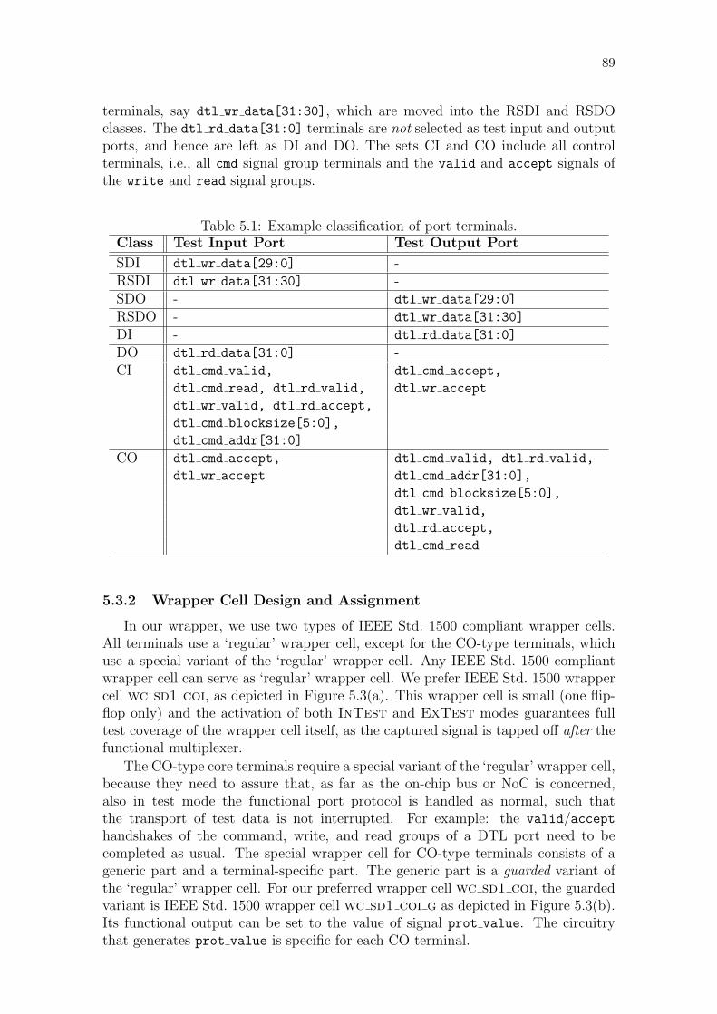
89
terminals, say dtl wr data[31:30], which are moved into the RSDI and RSDOclasses. The dtl rd data[31:0] terminals are not selected as test input and outputports, and hence are left as DI and DO. The sets CI and CO include all controlterminals, i.e., all cmd signal group terminals and the valid and accept signals ofthe write and read signal groups.
Table 5.1: Example classification of port terminals.Class Test Input Port Test Output Port
SDI dtl wr data[29:0] -RSDI dtl wr data[31:30] -SDO - dtl wr data[29:0]
RSDO - dtl wr data[31:30]
DI - dtl rd data[31:0]
DO dtl rd data[31:0] -CI dtl cmd valid, dtl cmd accept,
dtl cmd read, dtl rd valid, dtl wr accept
dtl wr valid, dtl rd accept,
dtl cmd blocksize[5:0],
dtl cmd addr[31:0]
CO dtl cmd accept, dtl cmd valid, dtl rd valid,
dtl wr accept dtl cmd addr[31:0],
dtl cmd blocksize[5:0],
dtl wr valid,
dtl rd accept,
dtl cmd read
5.3.2 Wrapper Cell Design and Assignment
In our wrapper, we use two types of IEEE Std. 1500 compliant wrapper cells.All terminals use a ‘regular’ wrapper cell, except for the CO-type terminals, whichuse a special variant of the ‘regular’ wrapper cell. Any IEEE Std. 1500 compliantwrapper cell can serve as ‘regular’ wrapper cell. We prefer IEEE Std. 1500 wrappercell wc sd1 coi, as depicted in Figure 5.3(a). This wrapper cell is small (one flip-flop only) and the activation of both InTest and ExTest modes guarantees fulltest coverage of the wrapper cell itself, as the captured signal is tapped off after thefunctional multiplexer.
The CO-type core terminals require a special variant of the ‘regular’ wrapper cell,because they need to assure that, as far as the on-chip bus or NoC is concerned,also in test mode the functional port protocol is handled as normal, such thatthe transport of test data is not interrupted. For example: the valid/accepthandshakes of the command, write, and read groups of a DTL port need to becompleted as usual. The special wrapper cell for CO-type terminals consists of ageneric part and a terminal-specific part. The generic part is a guarded variant ofthe ‘regular’ wrapper cell. For our preferred wrapper cell wc sd1 coi, the guardedvariant is IEEE Std. 1500 wrapper cell wc sd1 coi g as depicted in Figure 5.3(b).Its functional output can be set to the value of signal prot value. The circuitrythat generates prot value is specific for each CO terminal.

90
dtl_cmd_valid
dtl_cmd_accept
dtl_cmd_addr[32]
dtl_cmd_read
dtl_cmd_blocksize[6]
dtl_wr_valid
dtl_wr_accept
dtl_wr_data[32]
dtl_rd_valid
dtl_rd_accept
dtl_rd_data[32]
dtl_cmd_valid
dtl_cmd_accept
dtl_cmd_addr[32]
dtl_cmd_read
dtl_cmd_blocksize[6]
dtl_wr_valid
dtl_wr_accept
dtl_wr_data[32]
dtl_rd_valid
dtl_rd_accept
dtl_rd_data[32]
DTL.MMBD.I.RWDTL.MMBD.T.RW
Core
commandgroup
writegroup
readgroup
commandgroup
writegroup
readgroup
Figure 2. Example core with two DTL MMBD read-write ports.
22
Figure 5.2: Example core with two DTL read-write ports.
93
scan_inscan_out
func_infunc_out
shift normal_mode
clock
scan_inscan_out
func_in
shiftnormal_mode
clock
prot_modeprot_value
func_out
93
scan_inscan_out
func_infunc_out
shift normal_mode
clock
scan_inscan_out
func_in
shiftnormal_mode
clock
prot_modeprot_value
func_out
(a) (b)
Figure 5.3: Implementation of wrapper cells (a) wc sd1 coi and (b)wc sd1 coi g.
The generic version of the control generator has a periodic output behavior,which is characterized by a binary-coded output value v and a period p. For p −1 consecutive clock cycles, the output value is v, while for the next clock cycle,the output is v. The hardware implementation uses a simple counter. Some COterminals require hard-coded ‘0’ or ‘1’ signals; this is captured by (v, p) = (0, 1) and(v, p) = (1, 1) respectively. The control generator implementation for these signalsuses tie-off cells.
Table 5.2 describes for the selected test output port of our example in Figure 5.2which output signals are required on its CO-type terminals in order to keep thefunctional port protocol running. The port is used as test output via its dtl wr data
terminals, and hence dtl cmd read is kept at a hard-coded ‘0’. Every po clockcycles a new word with test responses is available for parallel read-out from thescan chains. To write this word to the interconnect dtl wr valid is ‘1’ every po
clock cycles. The specified bandwidth bout(o) is achieved for a given block size s(o).Hence the binary six-bit equivalent of s(o) is output on dtl cmd blocksize[6].Every (s(o) × po) cycles, a block of s(o) words has been output, and this initiatorport should issue a new command, in order to instruct the NoC to accept another
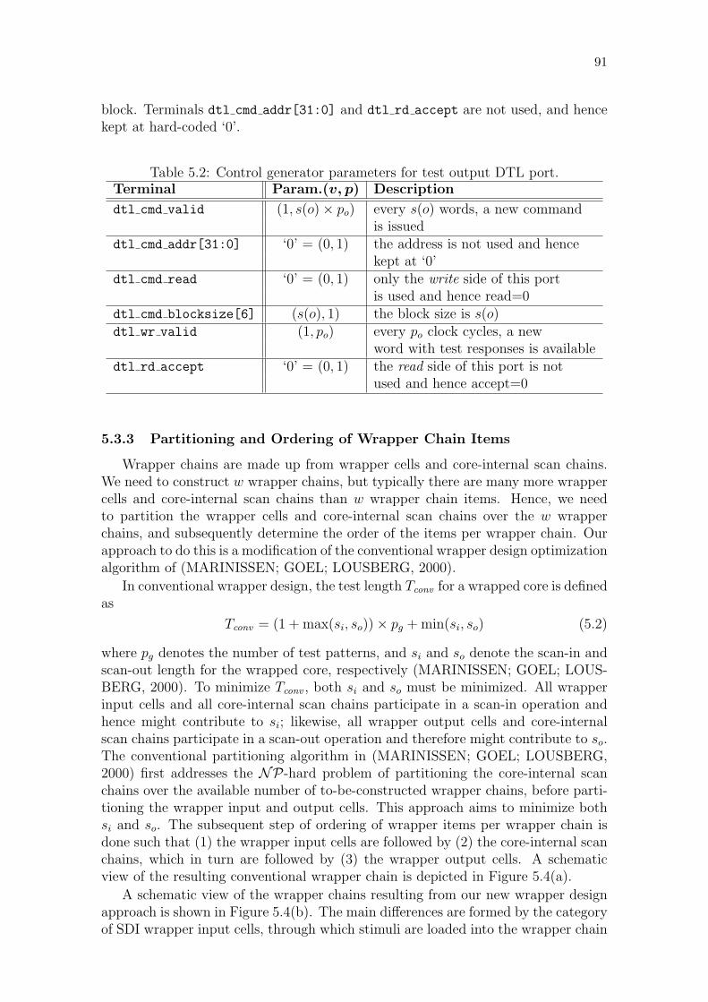
91
block. Terminals dtl cmd addr[31:0] and dtl rd accept are not used, and hencekept at hard-coded ‘0’.
Table 5.2: Control generator parameters for test output DTL port.Terminal Param.(v, p) Description
dtl cmd valid (1, s(o)× po) every s(o) words, a new commandis issued
dtl cmd addr[31:0] ‘0’ = (0, 1) the address is not used and hencekept at ‘0’
dtl cmd read ‘0’ = (0, 1) only the write side of this portis used and hence read=0
dtl cmd blocksize[6] (s(o), 1) the block size is s(o)dtl wr valid (1, po) every po clock cycles, a new
word with test responses is availabledtl rd accept ‘0’ = (0, 1) the read side of this port is not
used and hence accept=0
5.3.3 Partitioning and Ordering of Wrapper Chain Items
Wrapper chains are made up from wrapper cells and core-internal scan chains.We need to construct w wrapper chains, but typically there are many more wrappercells and core-internal scan chains than w wrapper chain items. Hence, we needto partition the wrapper cells and core-internal scan chains over the w wrapperchains, and subsequently determine the order of the items per wrapper chain. Ourapproach to do this is a modification of the conventional wrapper design optimizationalgorithm of (MARINISSEN; GOEL; LOUSBERG, 2000).
In conventional wrapper design, the test length Tconv for a wrapped core is definedas
Tconv = (1 + max(si, so))× pg + min(si, so) (5.2)
where pg denotes the number of test patterns, and si and so denote the scan-in andscan-out length for the wrapped core, respectively (MARINISSEN; GOEL; LOUS-BERG, 2000). To minimize Tconv , both si and so must be minimized. All wrapperinput cells and all core-internal scan chains participate in a scan-in operation andhence might contribute to si; likewise, all wrapper output cells and core-internalscan chains participate in a scan-out operation and therefore might contribute to so.The conventional partitioning algorithm in (MARINISSEN; GOEL; LOUSBERG,2000) first addresses the NP-hard problem of partitioning the core-internal scanchains over the available number of to-be-constructed wrapper chains, before parti-tioning the wrapper input and output cells. This approach aims to minimize bothsi and so. The subsequent step of ordering of wrapper items per wrapper chain isdone such that (1) the wrapper input cells are followed by (2) the core-internal scanchains, which in turn are followed by (3) the wrapper output cells. A schematicview of the resulting conventional wrapper chain is depicted in Figure 5.4(a).
A schematic view of the wrapper chains resulting from our new wrapper designapproach is shown in Figure 5.4(b). The main differences are formed by the categoryof SDI wrapper input cells, through which stimuli are loaded into the wrapper chain

92
94
SDI RSDI, DI, FI, CI SDORSDO, DO, FO, COinternal scan chains
parallel loadfrom NoC
parallel unloadto NoC
scan-inscan-out
internal scan chainsFI FO
scan-in
scan-out
serial unload to the TAM
serial load from the TAM
(a)
23
SDI DI, FI, CI SDODO, FO, COinternal scan chains
parallel loadfrom NoC
parallel unloadto NoC
scan-inscan-out
internal scan chainsFI FO
scan-in
scan-out
serial unload to the TAM
serial load from the TAM
RSDI RSDO
(b)
Figure 5.4: Schematic view of conventional (a) and new (b) ordering of wrapperitems per wrapper chain.
in a parallel fashion, and the category of SDO wrapper output cells, through whichresponses are unloaded from the wrapper chain in a parallel fashion.
• The test stimuli of a test pattern arrive at regular intervals of pi clock cyclesat the SDI wrapper input cells. All of them are shifted into the wrapperchains, apart from the last word, that can be directly consumed in parallel fortesting. Similarly, for each test pattern the first word of responses is directlytransported away in parallel from the SDO wrapper output cells, after whichthe subsequent words are shifted out of the wrapper chains at regular intervalsof po clock cycles. Hence, the test length Tnew is redefined as
Tnew = (1 + max(ti, to))× pg + min(ti, to) (5.3)
with
ti =
(⌈si
pi
⌉− 1
)× pi + 1 (5.4)
to =
(⌈so
po
⌉− 1
)× po + 1 (5.5)
• In order to minimize test length Tnew , the wrapper item should be partitionedsuch that both all SDI cells and all SDO cells are evenly distributed over thew to-be-constructed wrapper chains.
• For wrapper item ordering, it is important that all SDI cells are placed atthe start of the wrapper chain, as they are the entry point of stimuli into thewrapper chain, and otherwise some wrapper chain items are unreachable forscan access. Similarly, all SDO cells should be placed at the end of the wrapperchain.
Algorithmically, the partitioning of wrapper items is done in a five-step approach,which is clearly based on the three-step approach in (MARINISSEN; GOEL; LOUS-BERG, 2000).
93
1. Assign the core-internal scan chains to the w wrapper chains, such that themaximum sum of scan lengths assigned to a wrapper chain is minimized. Al-gorithms like Lpt and Combine can be used (MARINISSEN; GOEL; LOUS-BERG, 2000). The resulting partition is named Ps.
2. Assign the wrapper input cells in RSDI ∪ DI ∪ CI ∪ FI to the w wrapperchains on top of Ps, such that the maximum scan-in length of all wrapperchains is minimized. The resulting partition is named P in
w .
3. Assign the wrapper input cells in SDI to the w wrapper chains on top of P inw .
The resulting partition is named P in .
4. Assign the wrapper output cells in RSDO ∪ DO ∪ CO ∪ FO to the wwrapper chains on top of Ps, such that the maximum scan-out length of allwrapper chains is minimized. The resulting partition is named Pout
w .
5. Assign the wrapper output cells in SDO to the w wrapper chains on top ofPout
w . The resulting partition is named Pout .
5.3.4 NoCs With and Without Guaranteed Services
In fact, the main difference between NoC with and without guarantees is thatNoCs with guarantees already provide a FIFO at the core input that can be usedto eliminate load fluctuation. These FIFOs are inside the NI, hidden from the user(RADULESCU et al., 2005). Another impact in the wrapper design is that, sincethey are inside the NI, they cannot be modified according to the test needs. So, todeal with a given maximal bandwidth, we have to add two more steps before thestep of the procedure presented in Section 5.2.
1. Selection of test input and output ports.In case multiple ports are available that could serve as test input or testoutput port, exactly one test input port and exactly one test output port areselected. To minimize the resulting test length, we select two disjunct ports iand o (with i 6= o) of the CUT connected to the ATE such that the resultingtest bandwidth btest is maximized, with
btest = min(bini , bout
o ) . (5.6)
According to Equation (5.6), the test bandwidth is determined by the mini-mum of the bandwidths of the selected input and output port, as the band-widths of wrapper scan input and output needs to be equal.
2. Calculation of the number of wrapper chains.At the core’s test frequency f , the functional interconnect can deliver at most⌊
btestf
⌋test stimuli bits per clock cycle via the selected test input port, and
receive an equal amount of test response bits via the selected test output port.Hence, the wrapper should not contain more than wmax wrapper chains with
wmax =
⌊btest
f
⌋(5.7)
to use the given test bandwidth provided by the functional interconnect.
94
Some examples of NoCs that can give performance guarantees include Æthe-real (GOOSSENS; DIELISSEN; RADULESCU, 2005), Mango (BJERREGAARD;SPARSO, 2005a), Nostrum (MILLBERG et al., 2004), and Sonics (WEBER et al.,2005).
The proposed wrapper design also works for NoCs without guarantees. TheseNoCs do not have FIFOs at the core inputs, thus they might be required in thewrapper. The advantage in this case is that the wrapper design is not constrainedto wmax , but to c. On the other hand, the FIFO might be required, increasing theDfT silicon area. However, once the FIFOs will be used only for test, we can definethe best (the sufficient) FIFO depth for each wrapper.
Some examples of NoCs that do not provide performance guarantees includeRaSoC (ZEFERINO; SUSIN, 2003) and Hermes (MORAES et al., 2004).
5.4 Experimental Results
5.4.1 Simplified Illustrative Example
We have implemented our wrapper design for a simplified illustrative examplecore and NoC. The NoC is an automatically generated, simple Æthereal network(GOOSSENS; DIELISSEN; RADULESCU, 2005), consisting of one router and fournetwork interfaces, based on a 32-bits data DTL protocol (PHILIPS SEMICON-DUCTORS, 2002). As depicted in Figure 5.5(a), two NoC ports connect to therespestive ATE source and sink, while the two other ports connect to the CUT.
The CUT has two DTL ports, Port 1 and Port 2, with 133 terminals each andfunctional data word width c = 32. Besides the two ports, the CUT has no otherfunctional terminals. The CUT has five internal scan chains of lengths 123, 123, 50,50, and 23 flip-flops, and pg = 10. Port 1 is selected to receive stimuli and Port 2is selected to send out responses. The test data flow for stimuli is from the sourcethrough the NoC into the CUT via Port 1, while test responses flow from CUT’sPort 2 via the NoC into the sink. bin
i = 1600 Mbits/s, bouto = 2400 Mbits/s, and
f = 500 MHz, and, by Equation 5.7, we can afford a wrapper with w = 3 wrapperchains. According to Equation 5.1, test data arrives with period pi = po = 10clock cycles. For Port 1: |SDI|=30, |RSDI|=2, |DO|=32, |CI|=62, and |CO|=7.For Port 2: |SDO|=30, |RSDO|=2, |DI|=32, |CI|=7, and |CO|=62. The wrapperchain scan lengths are si = so = 168. The resulting wrapper design is shown inFigure 5.5(b). Based on Equation 5.3, test length Tnew = 1781 clock cycles. Notethat this represents a 4.1% test length reduction compared to a conventional wrapperdesign with three wrapper chains, which would have a test length Tconv = 1858 clockcycles. This reduction occurs because the last stimulus word of each pattern is loadedin parallel into the SDI wrapper cells and does not require any further shifting in,and likewise the first response word of each pattern is loaded in parallel into theSDO wrapper cells.
Our example was implemented in register-transfer-level VHDL and verified throughsimulation. The experiment showed a modest area increase for the new wrapper incomparison to a conventional wrapper. The number of equvalent gates requiredto implement all wrapper cells went from 2910 to 3000 (an increase of +3.1%),while 489 equivalent gates were required to implement the additional control logicto complete correct protocol operation. The total relative wrapper area increase was+19.9%. Note that wrappers are typically small compared to the overall SoC size,
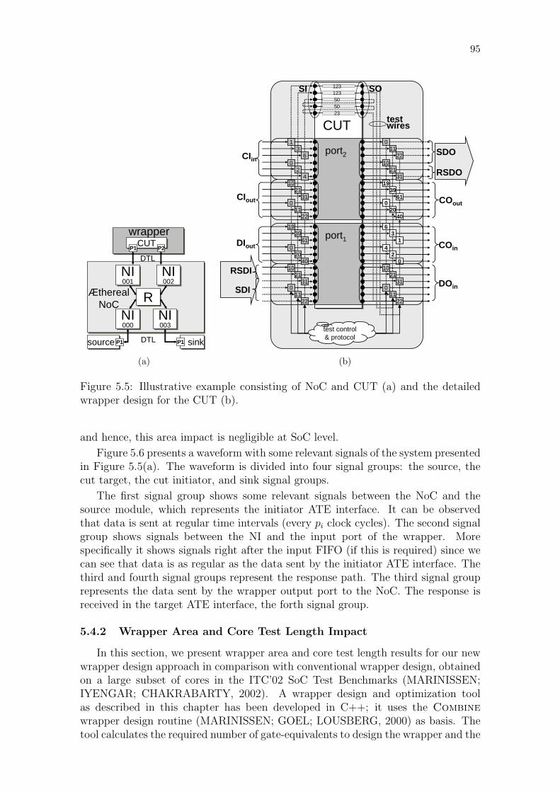
95
95
CUTCUT
ÆtherealNoC RR
NI002NI002
NI003NI003
P2
sinksinkP1
NI000NI000
NI001NI001
sourcesource P1
P1
DTL
DTL
wrapper
(a) 96
CUT
0
10
0
19
port1
SI SO
test control & protocol
11
21
20
39
22
31
61
0
10
4
6
11
21
2
3
22
31
0
1
0
10
0
1
port2
11
21
2
3
22
31
6
0
19
10
0
20
39
21
11
40
61
22
COout
test wires
COin
DOin
31
40
4
123123505023
CIout
CIin
DIout
RSDI
SDI
RSDO
SDO
(b)
Figure 5.5: Illustrative example consisting of NoC and CUT (a) and the detailedwrapper design for the CUT (b).
and hence, this area impact is negligible at SoC level.
Figure 5.6 presents a waveform with some relevant signals of the system presentedin Figure 5.5(a). The waveform is divided into four signal groups: the source, thecut target, the cut initiator, and sink signal groups.
The first signal group shows some relevant signals between the NoC and thesource module, which represents the initiator ATE interface. It can be observedthat data is sent at regular time intervals (every pi clock cycles). The second signalgroup shows signals between the NI and the input port of the wrapper. Morespecifically it shows signals right after the input FIFO (if this is required) since wecan see that data is as regular as the data sent by the initiator ATE interface. Thethird and fourth signal groups represent the response path. The third signal grouprepresents the data sent by the wrapper output port to the NoC. The response isreceived in the target ATE interface, the forth signal group.
5.4.2 Wrapper Area and Core Test Length Impact
In this section, we present wrapper area and core test length results for our newwrapper design approach in comparison with conventional wrapper design, obtainedon a large subset of cores in the ITC’02 SoC Test Benchmarks (MARINISSEN;IYENGAR; CHAKRABARTY, 2002). A wrapper design and optimization toolas described in this chapter has been developed in C++; it uses the Combinewrapper design routine (MARINISSEN; GOEL; LOUSBERG, 2000) as basis. Thetool calculates the required number of gate-equivalents to design the wrapper and the
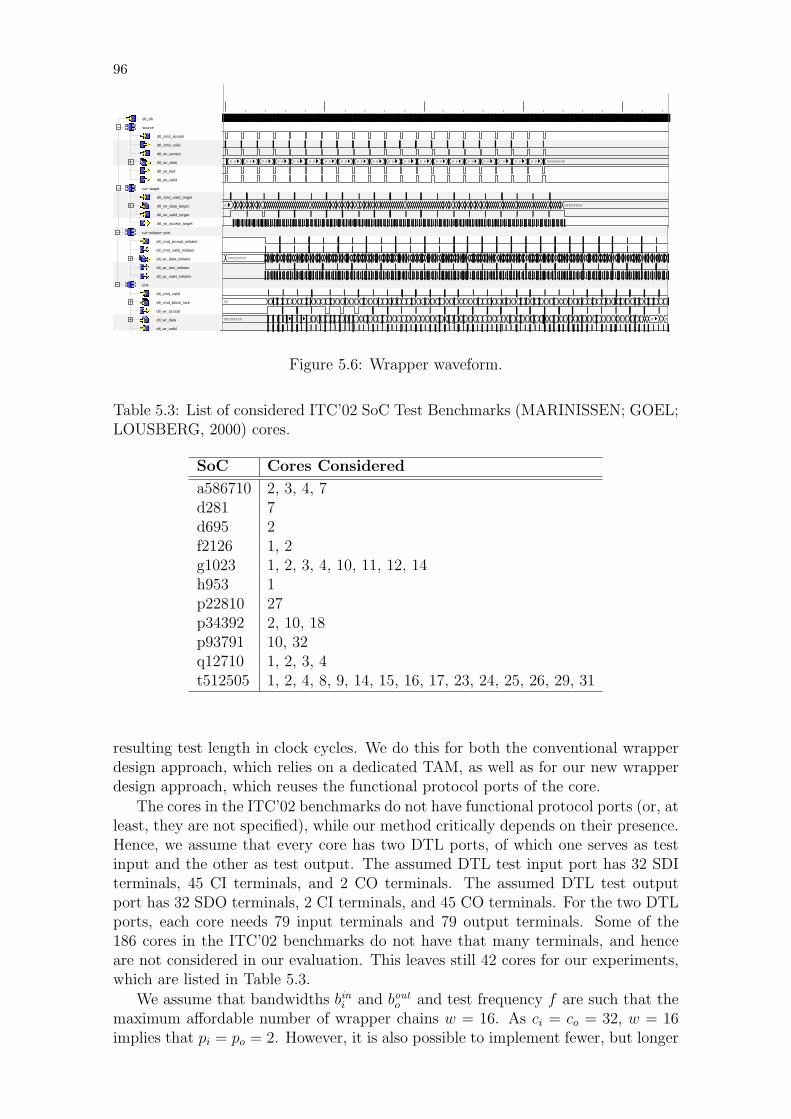
96Page 1 of 1
Printed by SimVision from Cadence Design Systems, Inc.Printed on Thu Jun 01 14:40:12 CEST 2006
Waveform 2 − SimVision
Cursor−Baseline = 4,492,354,458fs
Baseline = 1,972,375,832fs
Cursor = 6,464,730,290fs
dtl_clk
source
dtl_cmd_accept
dtl_cmd_valid
dtl_wr_accept
dtl_wr_data
dtl_wr_last
dtl_wr_valid
cut−target
dtl_cmd_valid_target
dtl_wr_data_target
dtl_wr_valid_target
dtl_wr_accept_target
scan−in
test_wire_in1
test_wire_in2
test_wire_in3
capture
apply_pattern
scan−out
test_wire_out1
test_wire_out2
test_wire_out3
cut−initiator−port
dtl_cmd_accept_initiator
dtl_cmd_valid_initiator
dtl_wr_data_initiator
dtl_wr_last_initiator
dtl_wr_valid_initiator
sink
dtl_cmd_valid
dtl_cmd_block_size
dtl_wr_accept
dtl_wr_data
dtl_wr_valid
F F F F F F F F F F F F F F F F F F F F F F F F F F F F F F F F F F F F F F F F FFFFFFFF
0 FFFFFFFF
F FFFFFFFFFFF
F FFFFFFFFFFF
1 1FFFFFFFFFFF
FFFFFFFFFFF FFFFFFFFFFF
FFFFFFFFFFF FFFFFFFFFFF
1FFFFFFFFFFF 1FFFFFFFFFFF
00000000
00
00000000 F FF
2,000,000,000fs 3,000,000,000fs 4,000,000,000fs 5,000,000,000fs 6, 000, 000, 0
Baseline = 1,972,375,832fs
TimeA = 6,464,730,290fs
Page 1 of 1
Printed by SimVision from Cadence Design Systems, Inc.Printed on Thu Jun 01 14:40:12 CEST 2006
Waveform 2 − SimVision
Cursor−Baseline = 4,492,354,458fs
Baseline = 1,972,375,832fs
Cursor = 6,464,730,290fs
dtl_clk
source
dtl_cmd_accept
dtl_cmd_valid
dtl_wr_accept
dtl_wr_data
dtl_wr_last
dtl_wr_valid
cut−target
dtl_cmd_valid_target
dtl_wr_data_target
dtl_wr_valid_target
dtl_wr_accept_target
scan−in
test_wire_in1
test_wire_in2
test_wire_in3
capture
apply_pattern
scan−out
test_wire_out1
test_wire_out2
test_wire_out3
cut−initiator−port
dtl_cmd_accept_initiator
dtl_cmd_valid_initiator
dtl_wr_data_initiator
dtl_wr_last_initiator
dtl_wr_valid_initiator
sink
dtl_cmd_valid
dtl_cmd_block_size
dtl_wr_accept
dtl_wr_data
dtl_wr_valid
F F F F F F F F F F F F F F F F F F F F F F F F F F F F F F F F F F F F F F F F FFFFFFFF
0 FFFFFFFF
F FFFFFFFFFFF
F FFFFFFFFFFF
1 1FFFFFFFFFFF
FFFFFFFFFFF FFFFFFFFFFF
FFFFFFFFFFF FFFFFFFFFFF
1FFFFFFFFFFF 1FFFFFFFFFFF
00000000
00
00000000 F FF
2,000,000,000fs 3,000,000,000fs 4,000,000,000fs 5,000,000,000fs 6, 000, 000, 0
Baseline = 1,972,375,832fs
TimeA = 6,464,730,290fs
Figure 5.6: Wrapper waveform.
Table 5.3: List of considered ITC’02 SoC Test Benchmarks (MARINISSEN; GOEL;LOUSBERG, 2000) cores.
SoC Cores Considered
a586710 2, 3, 4, 7d281 7d695 2f2126 1, 2g1023 1, 2, 3, 4, 10, 11, 12, 14h953 1p22810 27p34392 2, 10, 18p93791 10, 32q12710 1, 2, 3, 4t512505 1, 2, 4, 8, 9, 14, 15, 16, 17, 23, 24, 25, 26, 29, 31
resulting test length in clock cycles. We do this for both the conventional wrapperdesign approach, which relies on a dedicated TAM, as well as for our new wrapperdesign approach, which reuses the functional protocol ports of the core.
The cores in the ITC’02 benchmarks do not have functional protocol ports (or, atleast, they are not specified), while our method critically depends on their presence.Hence, we assume that every core has two DTL ports, of which one serves as testinput and the other as test output. The assumed DTL test input port has 32 SDIterminals, 45 CI terminals, and 2 CO terminals. The assumed DTL test outputport has 32 SDO terminals, 2 CI terminals, and 45 CO terminals. For the two DTLports, each core needs 79 input terminals and 79 output terminals. Some of the186 cores in the ITC’02 benchmarks do not have that many terminals, and henceare not considered in our evaluation. This leaves still 42 cores for our experiments,which are listed in Table 5.3.
We assume that bandwidths bini and bout
o and test frequency f are such that themaximum affordable number of wrapper chains w = 16. As ci = co = 32, w = 16implies that pi = po = 2. However, it is also possible to implement fewer, but longer
97
wrapper chains, which means that we are not using the bandwidth to its maximum,and consequently accept a longer test length.
For all 42 cores considered and for a number of wrapper chains w ranging from 1to 16, we have calculated the numbers of gate-equivalents required to implement awrapper and the corresponding test length in clock cycles, for both the conventionalwrapper design algorithm (MARINISSEN; GOEL; LOUSBERG, 2000) and our newapproach. In total, this involves 42×16×2 = 1344 wrapper calculations. Figure 5.7shows the average relative gate-equivalent count increase and the relative test lengthincrease. The horizontal axes refer to cores with numbers in the same order theyare listed in Table 5.3.
Figure 5.7(a) shows the increase in the number of gate-equivalents required toimplement the new wrapper, relative to what was required for a conventional wrap-per design. These numbers show only around 1% variation for varying values of w,and hence we have decided to show the average increase for 1 ≤ w ≤ 16. The averagewrapper area increase over all 672 cases is 14.5%, which is negligible at SoC level.Figure 5.7(b) shows that the test length impact of the new approach varies betweena −27.4% and +7.2%, with on average over all 672 cases a test length decrease of3.8%.
5.4.3 Wrapper Area for NoCs Without Guaranteed Services
The only difference in the design of NoC with and without guaranteed servicesis that later might require a FIFO in the wrapper. It affects the silicon area of thewrapper, but not the test length. For this reason we show additional silicon arearesults with emphasis on the size of the FIFO.
The FIFO depth of a wrapper depends on the number of test wires assigned forthe wrapper and it also depends on the physical channel width. Table 5.4 shows thesize of the FIFO for different number of test wires and channel width. The methodused to determine the minimal FIFO depth and packet size is presented in Chapter 9.These results say that the size of the wrapper for NoCs without guaranteed servicescan increase 0% to 44%.
5.5 Discussion
This section discusses the different results of core test length and silicon areaof the proposed wrapper compared to the conventional wrapper design (GOEL;MARINISSEN, 2003a).
The extra silicon area required by our approach is due to the protocol logic andthe FIFO (in case of NoCs without guaranteed services).
The difference in core test length is not so obvious as silicon area. Accordingto Figure 5.7(b), there are some cases that the proposed approach is faster andother cases that it is slower than the conventional wrapper. The rest of this sectionexplains why this variation might occur.
Let us give an example why the proposed approach is slower than the conven-tional wrapper. Table 5.5 shows the core test length as function of the assignedtest wires for the illustrative example in Figure 5.5. The columns show the numberof test wires, the test length for the proposed wrapper, the test length for (GOEL;MARINISSEN, 2003a), and the test length increase.
Different test length between our approach and (GOEL; MARINISSEN, 2003a)
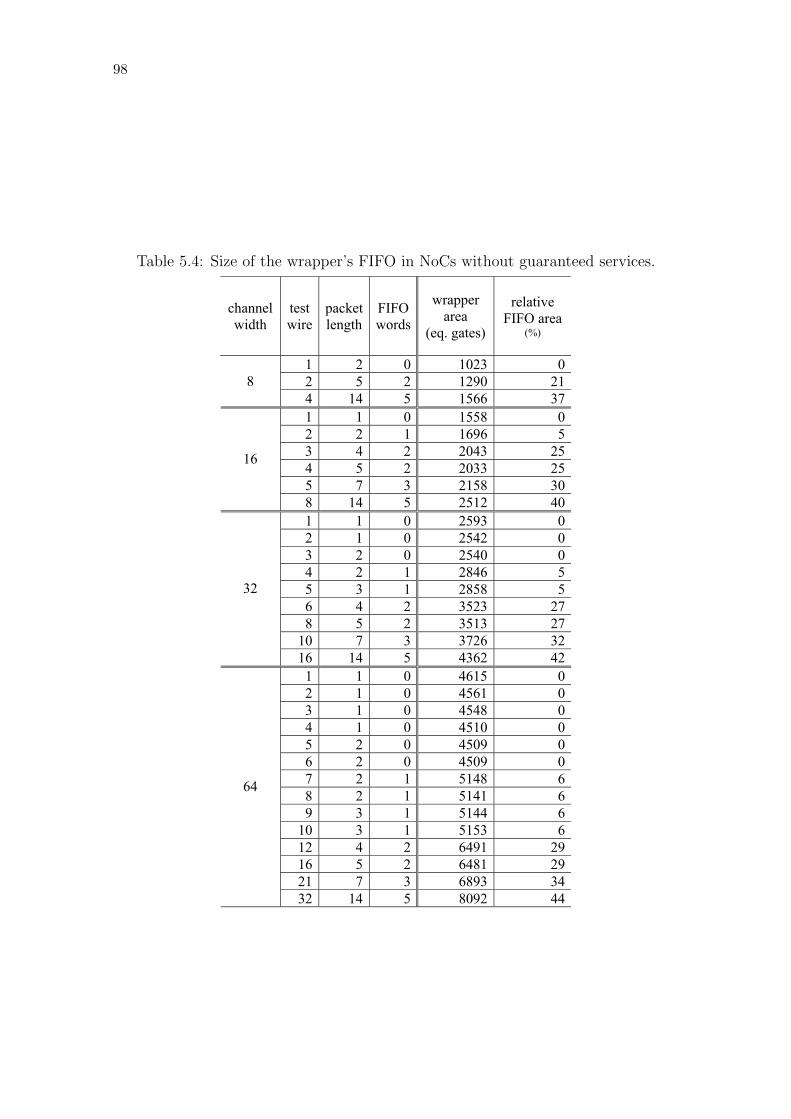
98
Table 5.4: Size of the wrapper’s FIFO in NoCs without guaranteed services.
channel width
test wire
packet length
FIFO words
wrapper area
(eq. gates)
relative FIFO area
(%)
1 2 0 1023 02 5 2 1290 218 4 14 5 1566 371 1 0 1558 02 2 1 1696 53 4 2 2043 254 5 2 2033 255 7 3 2158 30
16
8 14 5 2512 401 1 0 2593 02 1 0 2542 03 2 0 2540 04 2 1 2846 55 3 1 2858 56 4 2 3523 278 5 2 3513 27
10 7 3 3726 32
32
16 14 5 4362 421 1 0 4615 02 1 0 4561 03 1 0 4548 04 1 0 4510 05 2 0 4509 06 2 0 4509 07 2 1 5148 68 2 1 5141 69 3 1 5144 6
10 3 1 5153 612 4 2 6491 2916 5 2 6481 2921 7 3 6893 34
64
32 14 5 8092 44
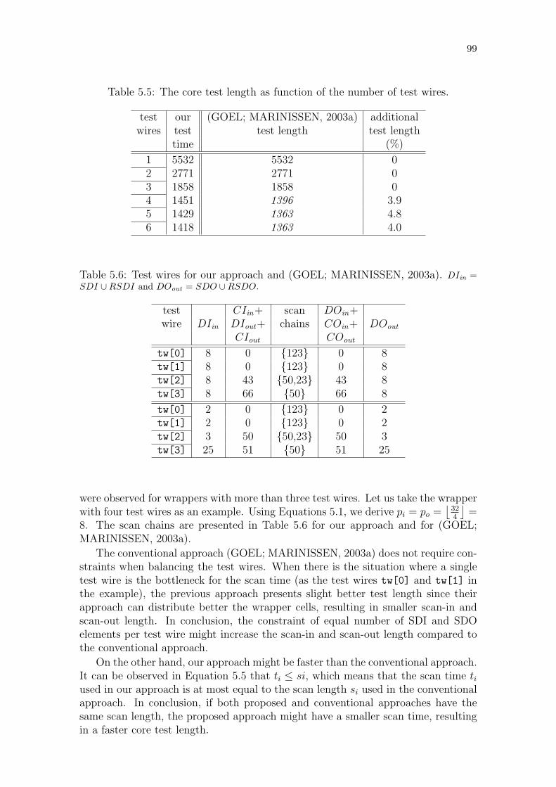
99
Table 5.5: The core test length as function of the number of test wires.
test our (GOEL; MARINISSEN, 2003a) additionalwires test test length test length
time (%)
1 5532 5532 02 2771 2771 03 1858 1858 04 1451 1396 3.95 1429 1363 4.86 1418 1363 4.0
Table 5.6: Test wires for our approach and (GOEL; MARINISSEN, 2003a). DIin =SDI ∪RSDI and DOout = SDO ∪RSDO.
test CIin+ scan DOin+wire DIin DIout+ chains COin+ DOout
CIout COout
tw[0] 8 0 {123} 0 8tw[1] 8 0 {123} 0 8tw[2] 8 43 {50,23} 43 8tw[3] 8 66 {50} 66 8
tw[0] 2 0 {123} 0 2tw[1] 2 0 {123} 0 2tw[2] 3 50 {50,23} 50 3tw[3] 25 51 {50} 51 25
were observed for wrappers with more than three test wires. Let us take the wrapperwith four test wires as an example. Using Equations 5.1, we derive pi = po =
⌊324
⌋=
8. The scan chains are presented in Table 5.6 for our approach and for (GOEL;MARINISSEN, 2003a).
The conventional approach (GOEL; MARINISSEN, 2003a) does not require con-straints when balancing the test wires. When there is the situation where a singletest wire is the bottleneck for the scan time (as the test wires tw[0] and tw[1] inthe example), the previous approach presents slight better test length since theirapproach can distribute better the wrapper cells, resulting in smaller scan-in andscan-out length. In conclusion, the constraint of equal number of SDI and SDOelements per test wire might increase the scan-in and scan-out length compared tothe conventional approach.
On the other hand, our approach might be faster than the conventional approach.It can be observed in Equation 5.5 that ti ≤ si, which means that the scan time tiused in our approach is at most equal to the scan length si used in the conventionalapproach. In conclusion, if both proposed and conventional approaches have thesame scan length, the proposed approach might have a smaller scan time, resultingin a faster core test length.
100
5.6 Summary
We present the proposed core test wrapper design which allows test data to betransported via functional protocol ports, such as AXI, DTL, and OCP ports. Thisapproach allows test data transport via an existing functional on-chip bus, NoC, orother functional interconnect. We assume that the test sources and sinks are eitheran external ATE, or an on-chip BIST engines. We require that the bus, NoC, orother functional interconnect provide guaranteed bandwidth and constant latency,necessary to operate streaming scan tests. We try to exploit the available functionalbandwidth as much as possible, in order to minimize the core’s test length.
Our new wrapper design no longer relies on a dedicated TAM, and hence has nodedicated TAM ports. Instead, the test data is transported via selected functionalprotocol ports. This requires careful wrapper design, such that (1) the number ofwrapper chains is tuned to the available test data bandwidth; (2) the functionalprotocols are correctly executed while the test is running; and (3) and the protocolport wrapper cells are positioned at the head and tail of the various wrapper chains.
Although other papers have described the reuse of functional buses and NoCs asTAM, no previous papers have worked out the details of wrapper design for this sce-nario. The benefits of our approach are that no dedicated TAM is required, that testaccess to the embedded cores is guaranteed, and that the test (protocol) expansionbecomes simpler. By using guaranteed communication services, our approach hidesany internal details of the functional interconnect. For the functional interconnect,the transport of test data is just another application, enabling unchanged re-use ofthe functional interconnect design flow. We can also use the proposed approach onNoCs without guaranteed services by adding a FIFO to the wrapper.
The implementation of the new wrapper design for 672 example cases based onthe ITC’02 SoC Test Benchmarks showed an average wrapper area increase of 14.5%,compared to a conventional wrapper. Note that at SoC level, this area increase isnegligible. The same 672 example cases show an average reduction of test length of3.8%. The wrapper silicon area might increase from 0% to 44% when BE NoCs areused, thus, the area overhead for BE NoCs is around 20% .

101
0
5
10
15
20
25
30
0 5 10 15 20 25 30 35 40 45
Ave
rage
are
a ov
erhe
ad (
%)
Core ID Number
Area overhead of the proposed wrapper
(a)
-30
-25
-20
-15
-10
-5
0
5
10
0 5 10 15 20 25 30 35 40 45
Rel
ativ
e T
est L
engt
h In
crea
se (
%)
Core ID Number
Comparison between Core Test Length of Both Reuse and Conventional Wrapper
(b)
Figure 5.7: Average relative wrapper’s gate-equivalent count increase (a) relativecore’s test length increase of the proposed wrapper with the conventional wrapperdesign. Results for 42 cores from ITC’02 benchmark and w ∈ {1..16}.

102
103
6 DFT FOR SOURCES AND SINKS
This chapter presents two approaches to implement sources and sinks in NoC-based SoCs: based on the reuse of embedded processors and the ATE interface.
6.1 Reuse of Embedded Processors
Current complex systems are using 10 to 15 processors and, according to(HENKEL, 2003), there is an emerging trend pointing to a “sea of processors” withhundreds of heterogeneous processors connected through a NoC. Considering thistrend and the increasing complexity for testing such state-of-the-art systems, thereuse of both the processor and the on-chip network for test seems a promisingapproach to reduce test costs.
Processor reuse is based on software-based test of cores, i.e. embedded processorsare loaded with test programs to test other cores. Some advantages are that theprocessor is already connected to the NoC, so there is no need for additional hard-ware (like the ATE interface), and a cheaper external test equipment can be usedsince part of the test is embedded into the chip (KRSTIC et al., 2002). However,there are two important drawbacks for the processor reuse during test. In all theprevious approaches (AMORY; OLIVEIRA; MORAES, 2003; HUANG et al., 2001a;HWANG; ABRAHAM, 2001, 2003; KRSTIC et al., 2002) the cores are tested seriallybecause they assume a bus-based architecture, which leads to longer test lengths. Inaddition, even if more than one processor is available within the chip, the possibilityof reuse and parallelism is limited by the bottleneck of bus-based communicationarchitectures.
NoC reuse can replace the test dedicated TAMs for test data transportation.NoCs support parallel transactions, which is important to support test parallelism.However, if few test pins are available, the NoC is sub utilized and the test lengthincreases. Combining processor reuse and NoC reuse can solve this problem sincepart of the test is embedded into the chip and the interconnect support parallelismto use multiple processors as sources and sinks. However, more parallelism canincrease the power consumption during test. Although the reuse of the embeddedprocessor avoids the addition of new blocks in the system, the power consumptionof the processor itself, while running the test program, may be quite high.
Amory et al. (2004; 2005) proposed a power-aware test scheduling tool thatcombines the reuse of multiple embedded processors and the reuse of the NoC. Thus,the main problems of processor reuse (test serialization and power consumption),and NoC reuse (few test pins and slow tester) are addressed.
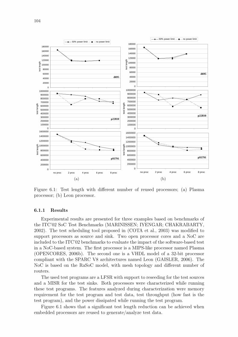
104
0
20000
40000
60000
80000
100000
120000
140000
160000
180000
no proc 2 proc 4 proc 6 proc
test
leng
th50% power limit no power limit
0100000200000300000400000500000600000700000800000900000
1000000
no proc 2 proc 4 proc 6 proc 8 proc
test
leng
th
0
200000
400000
600000
800000
1000000
1200000
1400000
1600000
no proc 2 proc 4 proc 6 proc 8 proc
test
leng
th
d695
p22810
p93791
Figure 2 - Test times with Plasma processors.
In both systems, based on Leon and on Plasma processors, we can observe that the power consumption does not play an important role in small systems like the d695, since there is no significant difference when imposing the power constraint. Other common observation is that the scheduling algorithm has to be improved to avoid irregular results like those in the p22810 systems.
7. FINAL REMARKS This work evaluates the impact of reusing processors
to test a NoC-based system. The processors available in the system are programmed with a test application to test some cores of the system. The results presented demonstrate the effectiveness of this approach to increase the number of test sources/sinks to explore the NoC parallelism, reducing the system test time without additional area and test pins.
The tool developed to demonstrate the proposed test methodology can play an important role in test planning, since it helps the test integrator to search for a cost effective test strategy for the whole chip.
8. REFERENCES [1] Amory, A.M.; Cota, E.F.; Lubaszewski, M. and Moraes,
F.G. "Reducing Test Time With Processor Reuse in
Network-on-Chip Based Systems". In Symposium on Integrated Circuits and Systems Design, 2004.
[2] Amory, A.M.; Oliveira, L.A. and Moraes, F.G. "Software-Based Test for Non-Programmable Cores in Bus-Based System-on-Chip Architectures". In VLSI-SOC, 2003, pp. 174-179.
[3] Bolotin, E.; Cidon, I.; Ginosar, R. and Kolodny, "A. Cost Considerations in Network on Chip". Special issue on Networks on Chip, Integration - the VLSI journal, 2003.
[4] Cota, E.F.; Carro, L.; Wagner, F. and Lubaszewski, M. "Power-aware NoC Reuse on the Testing of Core-based Systems". In International Test Conference, 2003, pp. 612-621.
[5] Cota, E.F.; Kreutz, M.E.; Zeferino, C.A.; Carro, L.; Lubaszewski, M. and Susin, A.A. "The Impact of NoC Reuse on the Testing of Core-based Systems". In VLSI Test Symposium, 2003, pp. 128-133.
[6] Dally, W.J. and Towles, B. "Route Packets, not Wires: on-Chip Interconnection Networks". In Design Automation Conference, 2001, pp. 684-689.
[7] Gaisler Research. "Leon2 Core". http://www.gaisler.com/ [8] Guerrier, P. and Greiner, A. "A Generic Architecture for
on-Chip Packet-Switched Interconnections". In Design, Automation and Test in Europe Conference, 2000, pp. 250-256.
[9] Henkel, J., "Closing the SoC Design Gap". IEEE Computer, vol. 36-6, 2003, pp. 119-121.
[10] Huang, J.-R.; Iyer, M.K. and Cheng, K.-T. "A Self-Test Methodology for IP Cores in Bus-Based Programmable SoCs". In IEEE VLSI Test Symposium, 2001, pp. 198-203.
[11] Hwang, S. and Abraham, J.A. "Reuse of Addressable System Bus for SOC Testing". In ASIC/SOC Conference, 2001, pp. 215-219.
[12] Hwang, S. and Abraham, J.A., "Test Data Compression and Test Time Reduction Using an Embedded Microprocessor". IEEE Transactions on Very Large Scale Integration Systems, vol. 11-5, 2003, pp. 853-862.
[13] Krstic, A.; Lai, W.C.; Cheng, K.T.; Chen, L.; Dey, S. "Embedded Software-Based Self-Test for Programmable Core-Based Designs". IEEE Design and Test of Computers, vol: 19-4, 2002, pp. 18-27.
[14] Lai, W. C.; Cheng, K. T. "Instruction-Level DFT for Testing Processor and IP Cores in System-on-a-Chip". In Design Automation Conference, 2001, pp. 59-64.
[15] Magarshack, P. and Paulin, P.G. "System-on-Chip Beyond the Nanometer Wall". In Design Automation Conference, 2003, pp. 419-424.
[16] Marinissen, E.J.; Iyengar, V. and Chakrabarty, K. "A Set of Benchmarks for Modular Testing of SoCs". In International Test Conference, 2002, pp. 519-528.
[17] Opencores."Plasma processor".http://www.opencores.org/ [18] Zeferino, C.A. and Susin, A.A. "SoCIN: A Parametric and
Scalable Network-on-Chip". In Symposium on Integrated Circuits and Systems Design, 2003, pp. 121-126.
[19] Zeferino, C.A.; Kreutz, M.E.; Carro, L. and Susin, A.A. "A Study on Communication Issues for Systems-on-Chip". In Symposium on Integrated Circuits and Systems Design, 2002, pp. 121-126.
(a)
0
20000
40000
60000
80000
100000
120000
140000
160000
180000
no proc 2 proc 4 proc 6 proc
test
leng
th
50% power limit no power limit
0100000200000300000400000500000600000700000800000900000
1000000
no proc 2 proc 4 proc 6 proc 8 proc
test
leng
th
0
200000
400000
600000
800000
1000000
1200000
1400000
1600000
no proc 2 proc 4 proc 6 proc 8 proc
test
leng
th
d695
p22810
p93791
Figure 1 - Test times with Leon processors.
Table 2 – Maximum system test time reduction percentage using Leon processors.
d695_leon p22810_leon p93791_leon power constraint
28.4% 20.9% 37.2%
no power constraint
28.9% 42.4% 44.7%
The results presented in Figure 1 demonstrate that increasing the number of processors reused for test reduces the test time compared to the test without processor reuse. One can observe that even smaller systems like d695_leon can take advantage of the extra test interface. For this system, a test time reduction of up to 28% is achieved.
For larger systems such, as p93791_leon, the gain in the test time can be as high as 44%. Despite this, the test reduction reaches up to 37% imposing power constraint, since there is more parallelism and more processors running the test programs.
For p22810_leon system, we get some test time reduction but it is not regular because of the greedy behavior of the scheduling algorithm. The greedy behavior of the presented algorithm forces it to select the first available test interface. This can increase the system test time because we assume that the processor test latency is always higher than for the external tester, which we assume to be zero. Thus, if a processor is available in a given instant and an external tester is available few instants later, the resource used is processor, since it is available earlier. However, it should use the external tester, which is faster than the processor.
Another observation is that when a processor tests a
core with a large number of test patterns it can increase the global test time since restriction 2, presented in Section 5, says that a CUT can only be tested by a single test interface to simplify the test controlling. However, processors take longer time than the external tester to apply the test patterns. One possible solution to this problem could be the insertion of constraints limiting which cores could be tested by processors, but this feature is currently not implemented.
Table 3 presents the number of cores tested by the Leon processors for the solutions presented in Figure 1 considering power constraints. The first column presents the number of Leon processors available to be used during testing, varying from two to eight. Half of the processors are used as test source and the other half as test sink. The remaining columns present the number of cores tested by the Leon processors. Consider the d695_Leon benchmark with two processors reused for test. The number 5/6 means that 5 cores use the Leon as test source and 6 cores use this block as test sink. The other cores are tested by the external tester.
Table 3 – Number of cores tested by the Leon processors considering power constraints.
processors (in/out)
d695_leon # cores 16
p22810_leon # cores 36
p93791_leon # cores 40
1/1 5/6 6/5 6/12 2/2 6/8 2/4 11/10 3/3 8/8 19/17 8/10 4/4 - 8/12 11/11
Figure 2 presents the evaluation of test time versus
number of reused processors for systems d695_plasma, p22810_plasma, and p93791_plasma, whereas Table 4 presents the percentage of test time reduction of Figure 2 when the reuse approach is compared to the purely external test.
Table 4 – Maximum system test time reduction percentage using Plasma processors.
d695_plasma p22810_plasma p93791_plasmapower constraint
30.1% 23.9% 42.0%
no power constraint
30.1% 32.3% 45.4%
For Plasma-based systems we can observe similar behavior to Leon-based systems. For the d695_plasma system the test time reduction is regular and there is no significant difference imposing power constraints. Like in the d695_leon system, the most significant test time reduction occurs adding two processors, since this system is small and additional test source/sink does not increase the NoC usage. For p393791_plasma we observe that the power consumption limit results in a significant difference in the test time. The p22810_plasma has an irregular result when reusing two processors because the number of processors reused without power constraints is much larger than with power constraints. However, we have the opposite behavior when reusing six processors, i.e. the number of processors reused with power constraints is larger than without power constraints.
(b)
Figure 6.1: Test length with different number of reused processors; (a) Plasmaprocessor; (b) Leon processor.
6.1.1 Results
Experimental results are presented for three examples based on benchmarks ofthe ITC’02 SoC Test Benchmarks (MARINISSEN; IYENGAR; CHAKRABARTY,2002). The test scheduling tool proposed in (COTA et al., 2003) was modified tosupport processors as source and sink. Two open processor cores and a NoC areincluded to the ITC’02 benchmarks to evaluate the impact of the software-based testin a NoC-based system. The first processor is a MIPS-like processor named Plasma(OPENCORES, 2006b). The second one is a VHDL model of a 32-bit processorcompliant with the SPARC V8 architectures named Leon (GAISLER, 2006). TheNoC is based on the RaSoC model, with mesh topology and different number ofrouters.
The used test programs are a LFSR with support to reseeding for the test sourcesand a MISR for the test sinks. Both processors were characterized while runningthese test programs. The features analyzed during characterization were memoryrequirement for the test program and test data, test throughput (how fast is thetest program), and the power dissipated while running the test program.
Figure 6.1 shows that a significant test length reduction can be achieved whenembedded processors are reused to generate/analyze test data.
105
6.1.2 Discussion
Although the reuse of multiple processors has the previously mentioned advan-tages, there are also some practical problems that must be taken into account forthe effective use of the approach:
• High and constant test throughput : The test program should generate patternsor analyze responses as fast as possible. The faster the test program is, theshorter is the core test length. Constant test throughput is required to main-tain the test streaming. For example, if a test program generates a pattern in100 clock cycles and the next pattern in 350, there may be a gap in the testtransfer, which may require the test of the CUT to stall until data is available.Constant test throughput assures minimal core test length for the assumedbandwidth;
• The test program should fit in the available memory : If this constraint is notrespected, there are two alternatives, both of them expensive. The first wouldbe to increase the processor memory size, but it may lead to excessive areaoverhead. The other one is to access other unused memory blocks located ina different NoC tile. The problem is that this additional traffic would needto be modeled by the tool. For these reasons, the test memory requirementsshould fit to the memory available for the reused processor;
• Test quality : the application of the test pattern generated by the test programshould lead to a high fault coverage. Thus, only pseudo-random test patterns,as used in (AMORY et al., 2004), may not be enough to test real cores;
• The combination of the above mentioned challenges makes it hard to conceive atest program with small size, fast, and high test quality. On one hand, pseudo-random test is small in memory requirement, fast, but the fault coverage canbe low even if reseeding is considered. On the other hand, data compressioncould be used to increase the test quality, but they would increase the memoryrequirement and the test length.
Due to these problems, we started to investigate alternatives methods for sourceand sink.
6.2 ATE Interface
An ATE interface is the DfT module that connects the test pins to the NoC.As presented in the test model, Chapter 4, each partition has at least one ATEinterface. The ATE interface is the source and sink of the modules in the partition.
The main tasks of an ATE interface are to do width conversion between thenumber of test pins and the network data width, protocol conversion to communicatethe ATE with the NoC, and traffic shaping, i.e. to correct the traffic deformationcaused by load fluctuation.
6.2.1 ATE Interface in the Proposed Design Flow
This section demonstrates how the ATE interfaces are defined according to theproposed design flow presented in Section 4.8, page 80.
106
An ATE interface is defined as a tuple {w, d, V }, where w is the number of testwires and d is the buffer depth. V is a set of tuples v = {nburst, header, nword}with the information required by the ATE interface to test a core, where nburst isthe number of packets, word is the number of words in each packet, and header isthe packet header content where the most important information is the location ofthe CUT. There is a v tuple for each module tested by an ATE interface.
According to the proposed flow, the parameters w and V are defined in the testscheduling, while d is defined in the DfT optimization.
6.2.2 Functional Description of the ATE Interface
This section presents the functional behavior of the ATE interface.The initiator ATE interface reads data from the test pins and sends it to the
CUT via the NoC. For all module in V , it sends b packets with the header h, whereeach packet has size w. It starts sending the header to the NI with the CUT address,then it sends the test stimuli read from the test pins (test pins variable). Thisprocedure repeats until all packet of all modules in V where sent.
Algorithm 6.1: Initiator ATE Interface
1 for a l l v ∈ V {2 b := v . nbursts ;3 h := v . header ;4 do{5 w := v . nwords ;6 send (h ) ;7 do{8 data := s e r i a l 2 p a r a l l e l ( t e s t p i n s ) ;9 send ( data ) ;
10 }while (w−−);11 }while (b−−);12 }
The target ATE interface receives test responses from the NoC and sends it tothe test pins. For all module in V , it reads an expected number of words w from bpackets. It discards the header and reads the packet payload, which represents thetest responses. The procedure repeats until all words, of all packet of all modulesof V were received.
Algorithm 6.2: Target ATE Interface
1 for a l l v ∈ V {2 b := v . nbursts ;3 do{4 w := v . nwords ;5 d i s ca rd (h ) ;6 do{7 read ( data ) ;8 t e s t p i n s := p a r a l l e l 2 s e r i a l ( data ) ;9 }while (w−−);
10 }while (b−−);11 }
107
78
NoC
inpu
t por
tou
tput
por
t
initiator
input test pins
w c
target
output test pins
w c
ATE interface
d
Figure 6.2: Block diagram of the ATE interface.
6.2.3 Block Diagram of the ATE Interface
The ATE interface illustrated in Figure 6.2 consists of an initiator ATE interfaceblock and a target ATE interface block. Both blocks do the width conversion fromc to w wires and vice-versa, implemented by means of a shift-register. The protocolconversion must execute the NoC protocol and include packet header informationin the test stream, like packet destination and number of words in the packet. TheATE interface also executes the protocol with the NI to enable sending test datawhile the network is in functional mode. Both NoC protocol and packet format arenetwork dependent, thus, this part of the ATE interface also depends on the targetNoC. The traffic shaping is carried out by counters that determine the period d andby the FIFO used to eliminate the gaps.
6.2.4 Timing Diagram of the ATE Interface
In order to abstract the NoC from the tester, the ATE interface should followthe timing diagram illustrated in Figure 6.3. This figure illustrates the timing ofa test stimuli and a test responses path. The ATE sends data every clock cyclein a constant and uninterrupted manner (line 1). One can see that data is sent atconstant time intervals of pi (or po) clock cycles (line 2) as defined in Equation 5.1,page 86.
Test responses are addressed to the target ATE interface. The received data canbe bursty, presenting gaps which would interrupt test data delivery (line 3). TheFIFO at the target ATE interface is responsible for recreating the required periodicdata (line 4). Finally, data is serialized to the output test pins (line 5).
This proposed timing abstracts the network to a pipe where data flows in aconstant and continuous manner, the same way dedicated TAMs do. This pipe hasa certain width (i.e. the network bandwidth), determined by the number of pins inthe ATE interface, and a certain delay, which depends on the design and length ofthe pipe (i.e. the number of hops in the test path).
6.2.5 Integrating the ATE Interface to the SoC
According to the functional system model, every access to the NoC is via a NIand an on-chip protocol. In some extent, the ATE interface can be seen as a core to
108
79
par2serATE int.
FIFOATE int.
NoC
input test pins (line 1)
OCP interface(line 2)
OCP interface(line 3)
(line 4)
output test pins(line 5)
test stream
header flit
data flit
…
ATE
initiatorATE int.
gap
po
pi
…
(a) test stimuli
(b) test responses
pi pi pi
po po po
test stream
…
NoC
ATE
Figure 6.3: Timing diagram of the ATE interface.
the test model, thus, it also requires on-chip ports to be connected to a NI. Hence,the best way to connect the ATE interface to the NI must be found. Let us analyzesome design alternatives for an ATE interface.
The first alternative, illustrated in Figure 6.4(a), core ports are added to the NIto connect the test pins. The problem is that adding core ports to the NI requiresmodifications in the NI kernel. For instance, modifying the number of core portsshould be avoided because if there are more cores competing for the router access,the arbitration logic inside the NI changes. Since the NI implementation is notstandardized, modifications in the NI would not lead to a general test approach.
The second approach, illustrated in Figure 6.4(b), adds a NI just for test, then,there is no core connected to this NI. This approach requires to find a router withoutNI or, in case there is no “empty” router, to add a router just to add a NI fortest. This alternative modifies the router network and changes the performancecharacteristics of the NoC, for example, some paths will have additional latency dueto a new router. Moreover, the area cost of a router, a NI, and the ports for thetest pins are very high.
The third approach, which is the chosen one, is illustrated in Figure 6.4(c). Itreuses an existing NI and it multiplexes an existing core port of the NI. The advan-tages of this approach are the lower area overhead compared to previous alternatives,and it is easier to generalize and automate because it does not require modificationin the NI kernel.
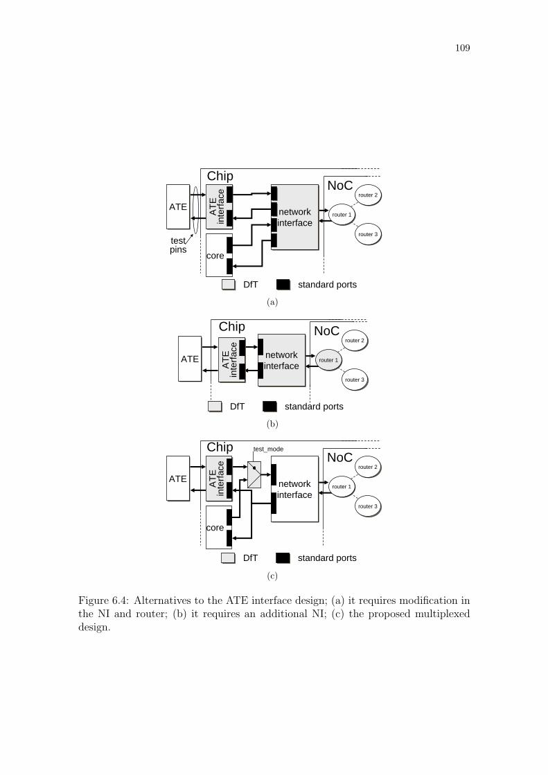
109
51
DfT standard ports
router 2router 2
router 3router 3
ATEATE
coretestpins
NoCChip
router 1router 1networkinterfacenetworkinterface
ATE
inte
rface
ATE
inte
rface
(a)
52
DfT standard ports
router 2router 2
router 3router 3
ATEATE
NoCChip
router 1router 1networkinterfacenetworkinterfaceA
TEin
terfa
ceA
TEin
terfa
ce
(b)
50
router 2router 2
router 3router 3
ATEATE
core
test_mode
DfT standard ports
NoCChip
router 1router 1networkinterfacenetworkinterface
ATE
inte
rface
ATE
inte
rface
(c)
Figure 6.4: Alternatives to the ATE interface design; (a) it requires modification inthe NI and router; (b) it requires an additional NI; (c) the proposed multiplexeddesign.
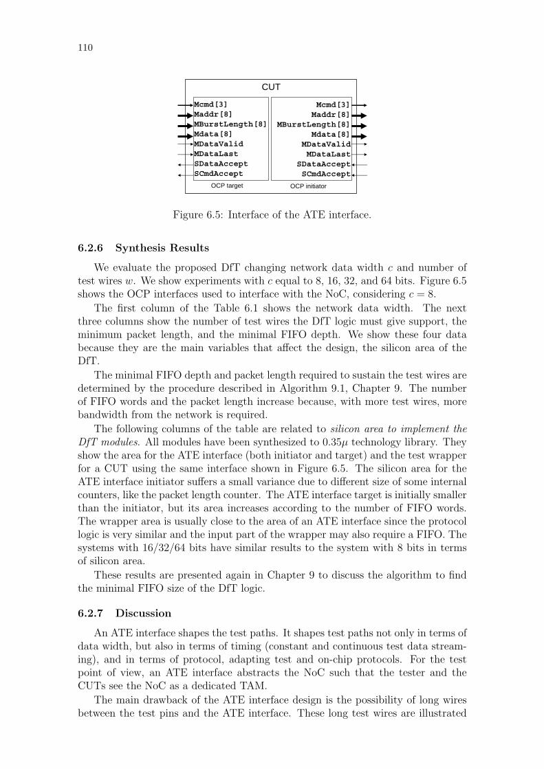
110
OCP target
Mcmd[3]Maddr[8]
MBurstLength[8]Mdata[8]
MDataValidMDataLast
SDataAcceptSCmdAccept
Mcmd[3]Maddr[8]MBurstLength[8]Mdata[8]MDataValidMDataLastSDataAcceptSCmdAccept
OCP initiator
CUT
Figure 6.5: Interface of the ATE interface.
6.2.6 Synthesis Results
We evaluate the proposed DfT changing network data width c and number oftest wires w. We show experiments with c equal to 8, 16, 32, and 64 bits. Figure 6.5shows the OCP interfaces used to interface with the NoC, considering c = 8.
The first column of the Table 6.1 shows the network data width. The nextthree columns show the number of test wires the DfT logic must give support, theminimum packet length, and the minimal FIFO depth. We show these four databecause they are the main variables that affect the design, the silicon area of theDfT.
The minimal FIFO depth and packet length required to sustain the test wires aredetermined by the procedure described in Algorithm 9.1, Chapter 9. The numberof FIFO words and the packet length increase because, with more test wires, morebandwidth from the network is required.
The following columns of the table are related to silicon area to implement theDfT modules. All modules have been synthesized to 0.35µ technology library. Theyshow the area for the ATE interface (both initiator and target) and the test wrapperfor a CUT using the same interface shown in Figure 6.5. The silicon area for theATE interface initiator suffers a small variance due to different size of some internalcounters, like the packet length counter. The ATE interface target is initially smallerthan the initiator, but its area increases according to the number of FIFO words.The wrapper area is usually close to the area of an ATE interface since the protocollogic is very similar and the input part of the wrapper may also require a FIFO. Thesystems with 16/32/64 bits have similar results to the system with 8 bits in termsof silicon area.
These results are presented again in Chapter 9 to discuss the algorithm to findthe minimal FIFO size of the DfT logic.
6.2.7 Discussion
An ATE interface shapes the test paths. It shapes test paths not only in terms ofdata width, but also in terms of timing (constant and continuous test data stream-ing), and in terms of protocol, adapting test and on-chip protocols. For the testpoint of view, an ATE interface abstracts the NoC such that the tester and theCUTs see the NoC as a dedicated TAM.
The main drawback of the ATE interface design is the possibility of long wiresbetween the test pins and the ATE interface. These long test wires are illustrated
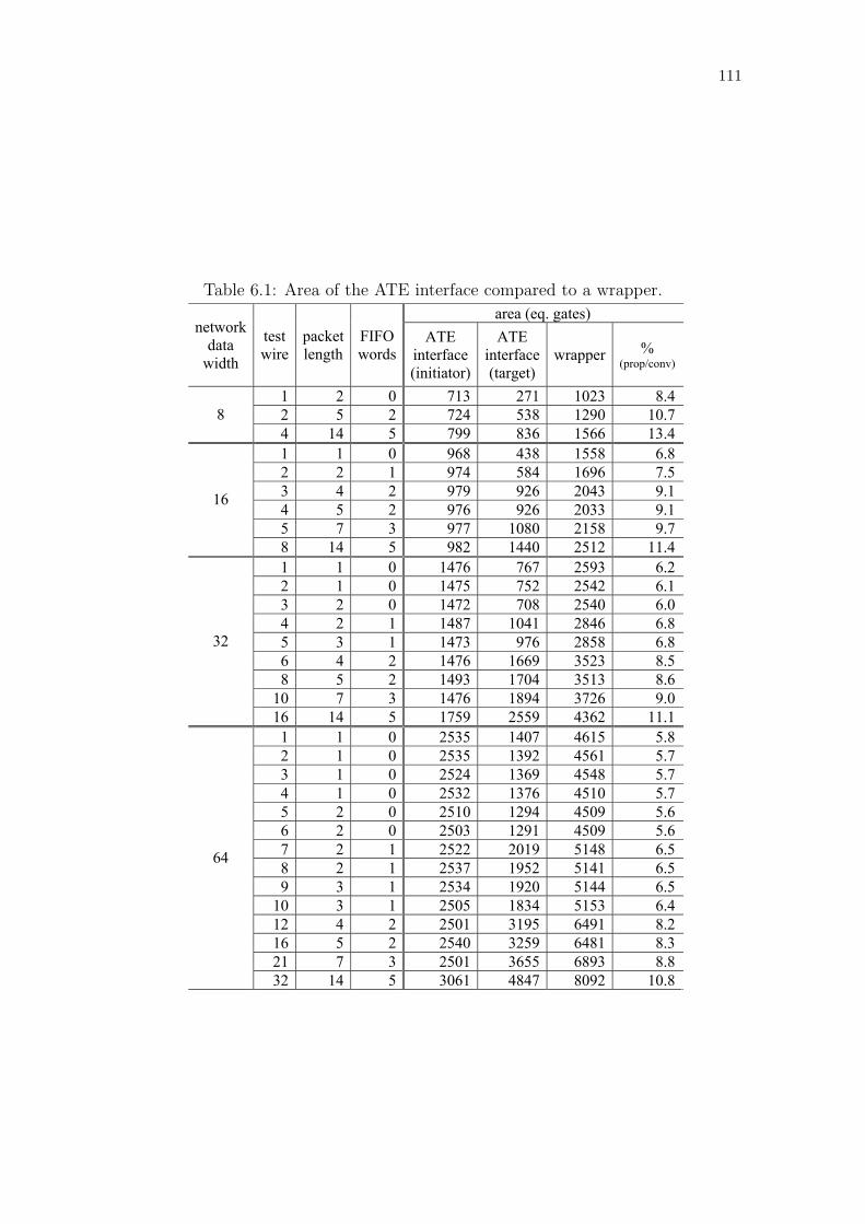
111
Table 6.1: Area of the ATE interface compared to a wrapper.
area (eq. gates) test time network
data width
test wire
packet length
FIFO words
ATE interface (initiator)
ATE interface (target)
wrapper % (prop/conv)
scan length
scan time (clock cycles)
conv. time (clock cycles)
prop. time (clock cycles)
% (prop/conv)
1 2 0 713 271 1023 8.4 31 25 351 285 -23.22 5 2 724 538 1290 10.7 16 13 186 153 -21.68 4 14 5 799 836 1566 13.4 8 7 98 87 -12.61 1 0 968 438 1558 6.8 55 49 615 549 -12.02 2 1 974 584 1696 7.5 28 25 318 285 -11.63 4 2 979 926 2043 9.1 19 16 219 186 -17.74 5 2 976 926 2033 9.1 14 13 164 153 -7.25 7 3 977 1080 2158 9.7 11 10 131 120 -9.2
16
8 14 5 982 1440 2512 11.4 7 7 87 87 0.01 1 0 1476 767 2593 6.2 103 97 1143 1077 -6.12 1 0 1475 752 2542 6.1 52 49 582 549 -6.03 2 0 1472 708 2540 6.0 35 31 395 351 -12.54 2 1 1487 1041 2846 6.8 26 25 296 285 -3.95 3 1 1473 976 2858 6.8 21 19 241 219 -10.06 4 2 1476 1669 3523 8.5 18 16 208 186 -11.88 5 2 1493 1704 3513 8.6 13 13 153 153 0.0
10 7 3 1476 1894 3726 9.0 11 10 131 120 -9.2
32
16 14 5 1759 2559 4362 11.1 7 7 87 87 0.01 1 0 2535 1407 4615 5.8 199 193 2199 2133 -3.12 1 0 2535 1392 4561 5.7 100 97 1110 1077 -3.13 1 0 2524 1369 4548 5.7 67 64 747 714 -4.64 1 0 2532 1376 4510 5.7 50 49 560 549 -2.05 2 0 2510 1294 4509 5.6 40 37 450 417 -7.96 2 0 2503 1291 4509 5.6 34 31 384 351 -9.47 2 1 2522 2019 5148 6.5 29 28 329 318 -3.58 2 1 2537 1952 5141 6.5 25 25 285 285 0.09 3 1 2534 1920 5144 6.5 23 22 263 252 -4.4
10 3 1 2505 1834 5153 6.4 20 19 230 219 -5.012 4 2 2501 3195 6491 8.2 17 16 197 186 -5.916 5 2 2540 3259 6481 8.3 13 13 153 153 0.021 7 3 2501 3655 6893 8.8 10 10 120 120 0.0
64
32 14 5 3061 4847 8092 10.8 7 7 87 87 0.0

112
51
b01
b11
a21
b31
d00
b10
b20
b30
c02
b12
a22
a32
input test pin output test pin
Figure 6.6: Long wires required to connect the test pins to the ATE interface. Thefat lines represent the test wires. The circles with fat lines represent the ATE interface location.
in Figure 6.6. The length of the wire depends on the physical distance betweenthe pin and the ATE interface. However, recall that this problem is also present inthe dedicated TAM approach. Moreover, the advantage of the proposed approachcompared to dedicated TAMs is that it does not need extra wires among the cores.
The second possible drawback is extra mutiplexers required to connect the ATEto the NI. It can increase the delay of the system. Moreover, since the proposedapproach supports multiple ATE interfaces per vTAM, the wires assigned to a vTAMmust be shared among the ATE interfaces. This is described in Figure 6.6 partitionb, where the output test pin is shared by two test wires. The solution to supportmultiple ATE interfaces per vTAM has been chosen because, otherwise, the NoCpartition would have to have a shape such that the routing algorithm could reach allnodes within the partition with a single ATE interface. It would impose more severerestriction to the test length. For this reason we assume multiple ATE interfacesper partition. Recall that although there might be multiple ATE interfaces perpartition, only one is activated per time to avoid packet collision.
6.3 Summary
This chapter presented two approaches to transport test data over a NoC. Thefirst one is based on the reuse of embedded processors as test sources and sinks.The second one presented a module, called ATE interface, required to connect thetest pins to the NoC and to shape the path from the tester to the CUT accordingto the test requirements, abstracting the NoC from the test domain. The resultsdemonstrated that the proposed design for ATE interface is simple, configurable,and the required silicon area is equivalent to a test wrapper. The drawback of theATE interface is that long wires might be required to connect the test pin to theATE interface and it may increase the system delay. However, it does not need extrawires among the cores as dedicated TAMs.
The approach that has been continued is the one based on ATE interface becauseit is based on external testers, which is the most used test application approach,and it is simpler to implement than the processor reuse approach. As presentedbefore, although the reuse approach is cheap in area and the connection to the NoCis available, developing cost-effective test program is the main challenge. Furtherdevelopments on multiple processor reuse are future work.
113
7 DFT FOR NETWORKS-ON-CHIP
Network-on-Chip has recently emerged as an alternative communication archi-tecture for complex system chip and different aspects regarding NoC design havebeen studied in the literature. However, the test of the NoC itself for manufacturingfaults has been marginally tackled. This chapter proposes a scalable test strategyfor the routers in a NoC, based on partial scan and on an IEEE Std. 1500-complianttest wrapper. The proposed test strategy takes advantage of the regular design ofthe NoC to reduce both test area overhead and test length. Experimental resultsshow that a good tradeoff of area overhead, fault coverage, test data volume, andtest length is achieved by the proposed technique. Furthermore, the method canbe applied for large NoC sizes and it does not depend on the network routing andcontrol algorithms, which makes the method suitable to test a large class of networkmodels.
7.1 Introduction
Several authors have presented different aspects regarding the design and im-plementation of on-chip networks (GUERRIER; GREINER, 2000; MORAES et al.,2004; BJERREGAARD; MAHADEVAN, 2006). Recently, industrial NoCs have alsobeen proposed (VERMEULEN et al., 2003). Furthermore, the reuse of the NoC asTAM has been presented as a cost-effective strategy for the test of embedded IPcores, with reduced area, pin count, and test length costs (AMORY et al., 2004;COTA; LIU, 2006). Although one may claim that the network operation is alsotested when it is transmitting test data, for diagnosis purposes and complete faultcoverage it is important to define a test scheme for the network before its reuse asTAM. For this reason, most NoC reuse test strategies assume that it has been testedpreviously.
Some test approaches for NoCs have been discussed in the literature (AKTOUF,2002; UBAR; RAIK, 2003; VERMEULEN et al., 2003). Aktouf (2002) suggests theuse of a boundary scan wrapper. Other approaches (UBAR; RAIK, 2003; VER-MEULEN et al., 2003) suggest that a wide variety of standard DfT solutions canbe used, from BIST for FIFOs, to functional testing of wrapped routers. However,those proposals have not been applied, to the best knowledge of the authors, toactual NoCs.
In this chapter, we firstly verify the efficiency of some of the previously sug-gested NoC test approaches, as well as the applicability of standard DfT techniques(ARABI, 2002; MARINISSEN et al., 2002; WU; MACDONALD, 2003) to NoCtesting. Experiments show that existing approaches may lead to considerable area
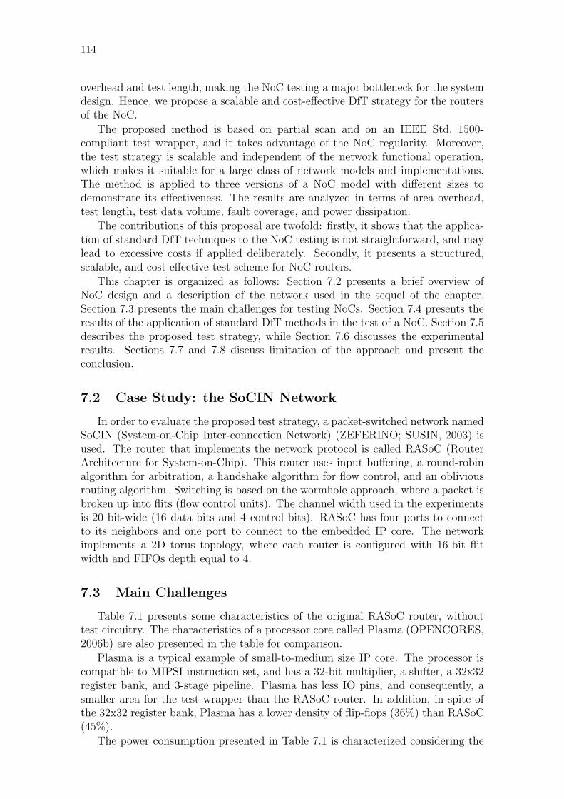
114
overhead and test length, making the NoC testing a major bottleneck for the systemdesign. Hence, we propose a scalable and cost-effective DfT strategy for the routersof the NoC.
The proposed method is based on partial scan and on an IEEE Std. 1500-compliant test wrapper, and it takes advantage of the NoC regularity. Moreover,the test strategy is scalable and independent of the network functional operation,which makes it suitable for a large class of network models and implementations.The method is applied to three versions of a NoC model with different sizes todemonstrate its effectiveness. The results are analyzed in terms of area overhead,test length, test data volume, fault coverage, and power dissipation.
The contributions of this proposal are twofold: firstly, it shows that the applica-tion of standard DfT techniques to the NoC testing is not straightforward, and maylead to excessive costs if applied deliberately. Secondly, it presents a structured,scalable, and cost-effective test scheme for NoC routers.
This chapter is organized as follows: Section 7.2 presents a brief overview ofNoC design and a description of the network used in the sequel of the chapter.Section 7.3 presents the main challenges for testing NoCs. Section 7.4 presents theresults of the application of standard DfT methods in the test of a NoC. Section 7.5describes the proposed test strategy, while Section 7.6 discusses the experimentalresults. Sections 7.7 and 7.8 discuss limitation of the approach and present theconclusion.
7.2 Case Study: the SoCIN Network
In order to evaluate the proposed test strategy, a packet-switched network namedSoCIN (System-on-Chip Inter-connection Network) (ZEFERINO; SUSIN, 2003) isused. The router that implements the network protocol is called RASoC (RouterArchitecture for System-on-Chip). This router uses input buffering, a round-robinalgorithm for arbitration, a handshake algorithm for flow control, and an obliviousrouting algorithm. Switching is based on the wormhole approach, where a packet isbroken up into flits (flow control units). The channel width used in the experimentsis 20 bit-wide (16 data bits and 4 control bits). RASoC has four ports to connectto its neighbors and one port to connect to the embedded IP core. The networkimplements a 2D torus topology, where each router is configured with 16-bit flitwidth and FIFOs depth equal to 4.
7.3 Main Challenges
Table 7.1 presents some characteristics of the original RASoC router, withouttest circuitry. The characteristics of a processor core called Plasma (OPENCORES,2006b) are also presented in the table for comparison.
Plasma is a typical example of small-to-medium size IP core. The processor iscompatible to MIPSI instruction set, and has a 32-bit multiplier, a shifter, a 32x32register bank, and 3-stage pipeline. Plasma has less IO pins, and consequently, asmaller area for the test wrapper than the RASoC router. In addition, in spite ofthe 32x32 register bank, Plasma has a lower density of flip-flops (36%) than RASoC(45%).
The power consumption presented in Table 7.1 is characterized considering the
115
Table 7.1: Comparing the RASoC router and the Plasma processor.
# gates # flip-flops flip-flop IO powerrelative area pins (µw)
RaSoC 4605 425 45% 202 2.24Plasma 20118 1444 36% 105 6.12
dynamic and static power consumption of the module. To evaluate the dynamicconsumption, the module is initially synthesized to an ASIC technology library forwhich the power consumption of technology cells is available. The resulting netlistdescription is simulated. During this simulation, the switching activity of each cellof the technology library is captured. Then, the power consumption per clock cy-cle is computed by multiplying the number of toggles and the power consumptionper cell. The total power consumption for the whole simulation is given by theaverage power consumption of the module in each clock cycle. Plasma power con-sumption was characterized for an arbitrary application. For RASoC, the powerwas characterized considering four packets being routed in parallel, which maxi-mizes the switching activity. All packets have the same number of flits and randompayload data. One can observe that Plasma presents higher power consumptionthan RASoC, since Plasma has more flip-flops, which are the main source of powerconsumption. However, considering the power per gate measure, RASoC has a ratio(2.24/4605) of 0.5nw/gate against (6.12/20118) 0.3nw/gate of the Plasma processor.Thus, although a single router is smaller than most functional IP cores, it may havea higher switching activity. Therefore, the total power consumed by the NoC mayeasily be higher than the consumption of other IP cores in the system.
This comparison between RASoC and Plasma highlights the challenge to finda cost-effective test strategy for NoCs. The router has fewer gates per I/O port,higher density of flip-flops, and higher power consumption per gate. Those featuresindicate, for instance, that test wrapper and full-scan implementations may be toocostly if applied to each router independently. On the other hand, NoCs usually havevery regular designs. Although different implementations of routers exist, most ofthem follow the conceptual model presented in Figure 2.6, page 39. The combinationof the regularity of a NoC and the predictable router structure is explored in thiswork to reduce test costs.
7.4 Evaluating Standard Test Strategies in NoCs
Some authors argue that the NoC is another IP core (flat or hierarchical) inthe system. In this case, its test can be defined using traditional core-based testingstrategies (UBAR; RAIK, 2003; VERMEULEN et al., 2003). This means the useof an IEEE Std. 1500-compliant test wrapper (MARINISSEN et al., 2002) and theuse of scan-based approaches to test the routers. Considering the NoC as a flatcore, a single test wrapper is inserted in the NoC interface. Otherwise, if the NoCis considered as a hierarchical core, one test wrapper for each router is necessary.
Considering the regular design and the presence of identical IP cores in theNoC structure (routers), test strategies previously proposed for similar systems may
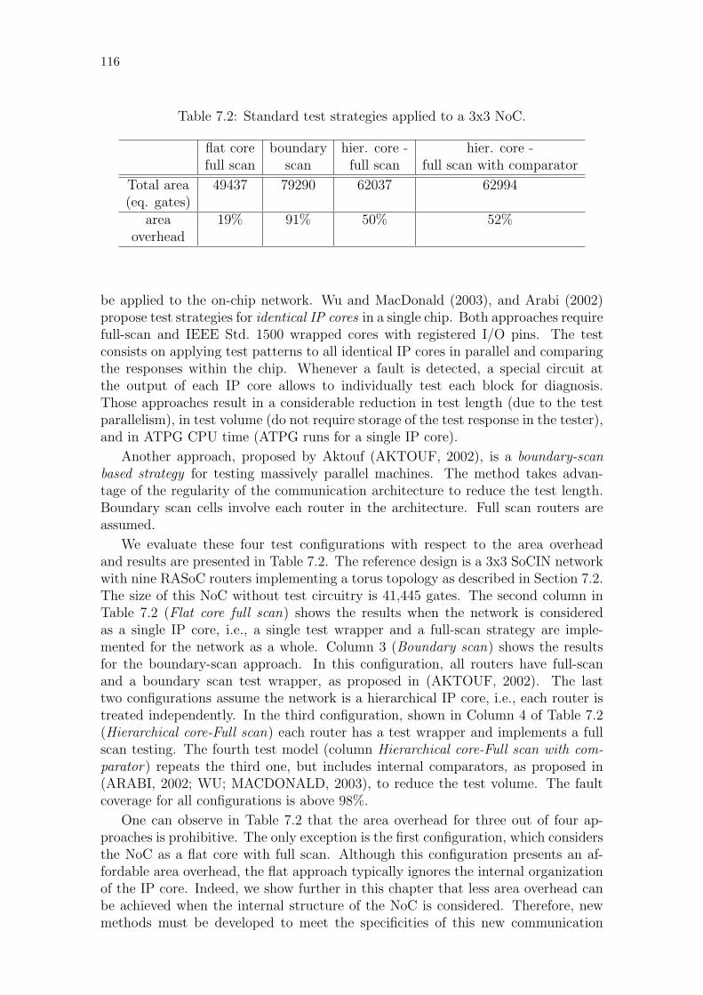
116
Table 7.2: Standard test strategies applied to a 3x3 NoC.
flat core boundary hier. core - hier. core -full scan scan full scan full scan with comparator
Total area 49437 79290 62037 62994(eq. gates)
area 19% 91% 50% 52%overhead
be applied to the on-chip network. Wu and MacDonald (2003), and Arabi (2002)propose test strategies for identical IP cores in a single chip. Both approaches requirefull-scan and IEEE Std. 1500 wrapped cores with registered I/O pins. The testconsists on applying test patterns to all identical IP cores in parallel and comparingthe responses within the chip. Whenever a fault is detected, a special circuit atthe output of each IP core allows to individually test each block for diagnosis.Those approaches result in a considerable reduction in test length (due to the testparallelism), in test volume (do not require storage of the test response in the tester),and in ATPG CPU time (ATPG runs for a single IP core).
Another approach, proposed by Aktouf (AKTOUF, 2002), is a boundary-scanbased strategy for testing massively parallel machines. The method takes advan-tage of the regularity of the communication architecture to reduce the test length.Boundary scan cells involve each router in the architecture. Full scan routers areassumed.
We evaluate these four test configurations with respect to the area overheadand results are presented in Table 7.2. The reference design is a 3x3 SoCIN networkwith nine RASoC routers implementing a torus topology as described in Section 7.2.The size of this NoC without test circuitry is 41,445 gates. The second column inTable 7.2 (Flat core full scan) shows the results when the network is consideredas a single IP core, i.e., a single test wrapper and a full-scan strategy are imple-mented for the network as a whole. Column 3 (Boundary scan) shows the resultsfor the boundary-scan approach. In this configuration, all routers have full-scanand a boundary scan test wrapper, as proposed in (AKTOUF, 2002). The lasttwo configurations assume the network is a hierarchical IP core, i.e., each router istreated independently. In the third configuration, shown in Column 4 of Table 7.2(Hierarchical core-Full scan) each router has a test wrapper and implements a fullscan testing. The fourth test model (column Hierarchical core-Full scan with com-parator) repeats the third one, but includes internal comparators, as proposed in(ARABI, 2002; WU; MACDONALD, 2003), to reduce the test volume. The faultcoverage for all configurations is above 98%.
One can observe in Table 7.2 that the area overhead for three out of four ap-proaches is prohibitive. The only exception is the first configuration, which considersthe NoC as a flat core with full scan. Although this configuration presents an af-fordable area overhead, the flat approach typically ignores the internal organizationof the IP core. Indeed, we show further in this chapter that less area overhead canbe achieved when the internal structure of the NoC is considered. Therefore, newmethods must be developed to meet the specificities of this new communication
117
platform. Such a method is proposed in the next section and applied to the same3x3 SoCIN network for comparison.
7.5 Proposed Test Strategy for NoCs Based on IdenticalRouters
We propose a NoC testing approach that combines the best features of the “Flatcore full scan” approach (reduced area overhead) and the “Hierarchical core Full scanwith comparator” (reduced test volume) configurations explained in Section 7.4. Theproposed strategy considers the NoC as a flat core (a single test wrapper for thewhole network is required) but it does not require a full scan implementation, whichfurther reduces the area overhead. Moreover, different from the flatten approach,we explore the regular design of the NoC to reduce test length and data volume.The proposed strategy is presented in three parts:
a) The router testing, which shows how to configure the router internal scanchains to reduce area,
b) The NoC testing, which explains how the scan chains of the routers are con-nected together at NoC level, and
c) The NoC test wrapper, which details the definition of the IEEE Std. 1500compliant test wrapper for the NoC exploring the network regular structureto reduce area.
7.5.1 Router Testing
A router is composed by control logic (routing, arbitration, and flow controlmodules) and input FIFOs. Control logic is considerably simpler to be tested,because it contains a small number of flip-flops and gates. The input FIFO poses themain problems for the router testability. Figure 7.1(a) illustrates the architecture ofthe primary inputs of a router, i.e., the FIFO implementation. If full scan is directlyimplemented in this structure, all flip-flops of the FIFO will become scan flip-flopsand will be chained together. In the proposed approach, we split the FIFO anddefine a single scan chain using only the first position of the queue, as illustrated inFigure 7.1(b). This single scan chain provides the controllability and observabilityrequired to test the whole structure, since the FIFO is usually not very deep andthere is no feedback logic in this block. Thus, any sequential ATPG tool can generatetest patterns for the whole FIFO with an affordable effort.
To complete the router testing, a second scan chain is defined with the remainingflip-flops of the control logic, which are the flip-flops used to implement the routingalgorithm, for example. This approach avoids expensive solutions like full-scan andBIST (UBAR; RAIK, 2003; VERMEULEN et al., 2003), while the ATPG tool canstill generate high fault coverage at reasonable CPU time.
7.5.2 NoC Testing
After defining the test structure for each router, one must define an access mech-anism to transmit test data from the network interface to each router and vice-versa.We propose a general test communication protocol, which can be applied to regular
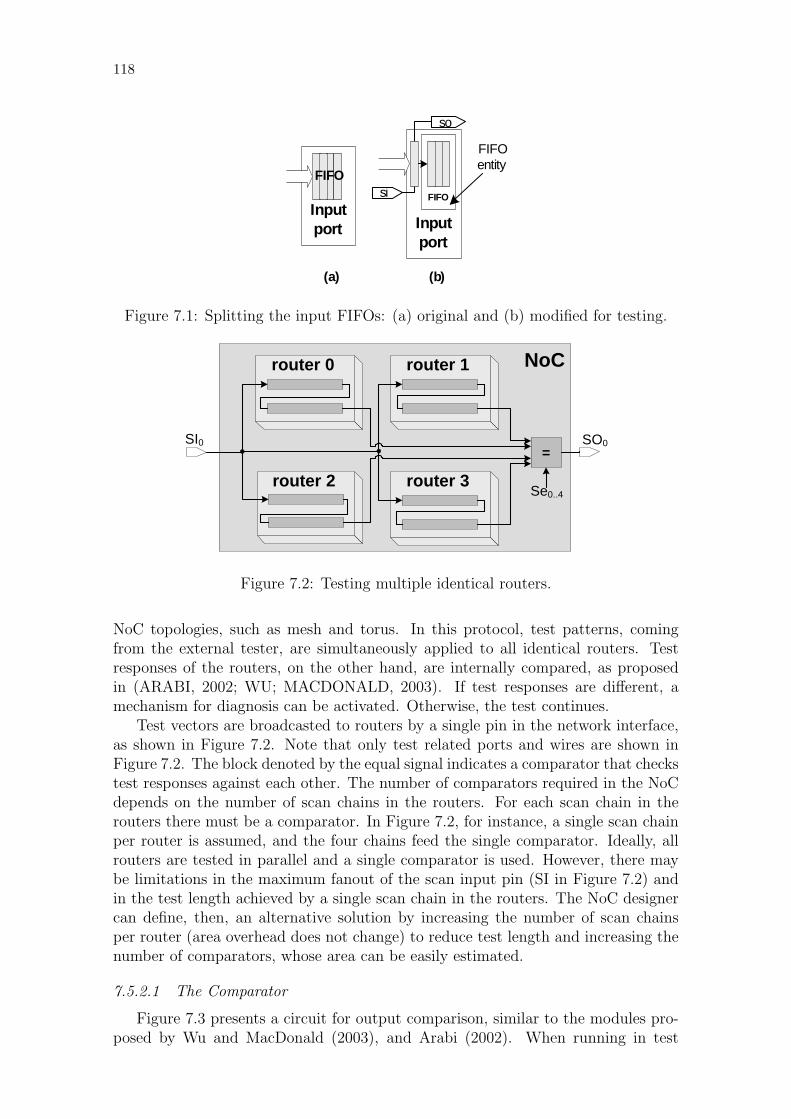
118
Paper 25.1 INTERNATIONAL TEST CONFERENCE
4
Another approach, proposed by Aktouf [1], is a boundary-scan based strategy for testing massively parallel ma-chines. The method takes advantage of the regularity of the communication architecture to reduce the test time. Boundary scan cells involve each router in the architec-ture. Full scan routers are assumed.
We evaluate these four test configurations with respect to the area overhead and results are presented in Table 2. The reference design is a 3x3 SoCIN network with nine RASoC routers implementing a torus topology as de-scribed in Section 2.1. The size of this NoC without test circuitry is 41,445 gates. The second column in Table 2 (Flat core full scan) shows the results when the network is considered as a single IP core, i.e., a single test wrapper and a full-scan strategy are implemented for the network as a whole. Column 3 (Boundary scan) shows the results for the boundary-scan approach. In this configuration, all routers have full-scan and a boundary scan test wrapper, as proposed in [1]. The last two configurations assume the network is a hierarchical IP core, i.e., each router is treated independently. In the third configuration, shown in Column 4 of Table 2 (Hierarchical core-Full scan) each router has a test wrapper and implements a full scan test-ing. The fourth test model (column Hierarchical core-Full scan with comparator) repeats the third one, but includes internal comparators, as proposed in [3][12], to reduce the test volume. The fault coverage for all configurations is above 98%.
Table 2 – Standard test strategies applied to a 3x3 NoC.
Hierarchical core Flat core
full Scan
Boundary scan
Full scan
Full scan with
comparator Total area
(gates) 49437 79290 62037 62994
Area overhead 19% 91% 50% 52%
One can observe in Table 2 that the area overhead for three out of four approaches is prohibitive. The only ex-ception is the first configuration, which considers the NoC as a flat core with full scan. Although this configuration presents an affordable area overhead, the flat approach typically ignores the internal organization of the IP core. Indeed, we show further in the paper that less area over-head can be achieved when the internal structure of the NoC is considered.
Therefore, new methods must be developed to meet the specificities of this new communication platform. Such a method is proposed in the next section and applied to the same 3x3 SoCIN network for comparison.
4. Proposed Test Strategy We propose a NoC testing approach that combines the best features of the "Flat core full scan" approach (re-duced area overhead) and the "Hierarchical core Full scan with comparator" (reduced test volume) configura-tions explained in Section 3. The proposed strategy con-siders the NoC as a flat core (a single test wrapper for the whole network is required) but it does not require a full scan implementation, which further reduces the area over-head. Moreover, different from the flatten approach, we explore the regular design of the NoC to reduce test time and data volume.
The proposed strategy is presented in three parts: a) the router testing, which shows how to configure
the router internal scan chains to reduce area, b) the NoC testing, which explains how the scan
chains of the routers are connected together at NoC level, and
c) the NoC test wrapper, which details the definition of the IEEE 1500 compliant test wrapper for the NoC exploring the network regular structure to reduce area.
4.1. Router Testing As detailed in Section 2, a router is composed by control logic (routing, arbitration, and flow control modules) and input FIFOs. Control logic is considerably simpler to be tested, because it contains a small number of flip-flops and gates. The input FIFO poses the main problems for the router testability. Figure 3.a illustrates the architecture of the primary inputs of a router, i.e., the FIFO implemen-tation. If full scan is directly implemented in this struc-ture, all flip-flops of the FIFO will become scan flip-flops and will be chained together.
In the proposed approach, we split the FIFO and define a single scan chain using only the first position of the queue, as illustrated in Figure 3.b. This single scan chain provides the controllability and observability required to test the whole structure, since the FIFO is usually not very deep and there is no feedback logic in this block. Thus, any sequential ATPG tool can generate test patterns for the whole FIFO with an affordable effort.
Input port
si
so
(a) (b)
Input port
FIFOFIFO
FIFO entity
Figure 3 – Splitting the input FIFOs: (a) original and (b)
modified for testing. Figure 7.1: Splitting the input FIFOs: (a) original and (b) modified for testing.
Paper 25.1 INTERNATIONAL TEST CONFERENCE
5
To complete the router testing, a second scan chain is de-fined with the remaining flip-flops of the control logic, which are the flip-flops used to implement the routing algorithm, for example.
This approach avoids expensive solutions like full-scan and BIST [10][11], while the ATPG tool can still generate high fault coverage at reasonable CPU time.
4.2 NoC Testing After defining the test structure for each router, one must define an access mechanism to transmit test data from the network interface to each router and vice-versa. We pro-pose a generic test communication protocol, which can be applied to regular NoC topologies, such as mesh and to-rus. In this protocol, test patterns, coming from the exter-nal tester, are simultaneously applied to all identical routers. Test responses of the routers, on the other hand, are internally compared, as proposed in [3][12]. If test responses are different, a mechanism for diagnosis can be activated. Otherwise, the test continues.
Test vectors are broadcasted to routers by a single pin in the network interface, as shown in Figure 4. Note that different from Figure 2, only test related ports and wires are shown in Figure 4. The block denoted by the equal signal indicates a comparator that checks test responses against each other. The number of comparators required in the NoC depends on the number of scan chains in the routers. For each scan chain in the routers there must be a comparator. In Figure 4, for instance, a single scan chain per router is assumed, and the four chains feed the single comparator. Ideally, all routers are tested in parallel and a single comparator is used. However, there may be limita-tions in the maximum fan-out of the scan input pin (SI in Figure 4) and in the test time achieved by a single scan chain in the routers. The NoC designer can define, then, an alternative solution by increasing the number of scan chains per router (area overhead does not change) to re-duce test time and increasing the number of comparators, whose area can be easily estimated.
NoC
SI0 = SO0
router 0
router 2 Se0..4
router 1
router 3
Figure 4 – Testing multiple identical routers.
4.2.2 The Comparator Figure 5 presents a circuit for output comparison, which is similar to the modules proposed by Wu and MacDonald [12], and Arabi [3]. When running in test mode, ports compEnable (compEnbx) and enable detection (en_det) are assigned to ‘1’, while the diagnostic port diag is set to ‘0’. Signals compInput (compInx) receive one scan chain output of each router being tested. All corresponding bits unloaded from each router scan chain are compared against each other, as depicted in Figure 4. If there is any difference, the xor gate generates an error signal ‘1’ in the so pin.
en_det
compEnb0
...
diag
so
compEnbn
compIn0
compInn
FF 1
Figure 5 – Comparator block.
The comparison logic also supports diagnosis. In diagno-sis mode, signal diag is initially set to ‘1’. Then, signal compEnbx corresponding to a single router is set to ‘1’, while signals compEnbx of the remaining routers are set to ‘0’. Test vectors are applied again to all routers, but the output of only one router will be captured. This procedure is repeated until the defective router is found.
Notice that other testing approaches that consider the NoC as a non-hierarchical core are not able to identify the router with defect since they abstract the internal structure of the network. On the other hand, the hierarchical ap-proach has a large area overhead. However, our approach is based on the flat design but structured in such way that the defective router can be identified.
4.3 Test Wrapper for NoCs To complete the definition of the test strategy, we briefly describe an IEEE 1500-compliant wrapper implementa-tion for the network.
In order to support on-chip test response comparison, one must provide the same test stimuli for all the routers. Thus, functional pins and scan chains of the routers must receive the same test stimuli. Identical stimuli for scan chains are provided by the strategy presented in Section 4.2. However, since there is a single test wrapper for the whole NoC, the test wrapper design must also ensure that the functional ports of the routers receive the same test stimuli.
Figure 7.2: Testing multiple identical routers.
NoC topologies, such as mesh and torus. In this protocol, test patterns, comingfrom the external tester, are simultaneously applied to all identical routers. Testresponses of the routers, on the other hand, are internally compared, as proposedin (ARABI, 2002; WU; MACDONALD, 2003). If test responses are different, amechanism for diagnosis can be activated. Otherwise, the test continues.
Test vectors are broadcasted to routers by a single pin in the network interface,as shown in Figure 7.2. Note that only test related ports and wires are shown inFigure 7.2. The block denoted by the equal signal indicates a comparator that checkstest responses against each other. The number of comparators required in the NoCdepends on the number of scan chains in the routers. For each scan chain in therouters there must be a comparator. In Figure 7.2, for instance, a single scan chainper router is assumed, and the four chains feed the single comparator. Ideally, allrouters are tested in parallel and a single comparator is used. However, there maybe limitations in the maximum fanout of the scan input pin (SI in Figure 7.2) andin the test length achieved by a single scan chain in the routers. The NoC designercan define, then, an alternative solution by increasing the number of scan chainsper router (area overhead does not change) to reduce test length and increasing thenumber of comparators, whose area can be easily estimated.
7.5.2.1 The Comparator
Figure 7.3 presents a circuit for output comparison, similar to the modules pro-posed by Wu and MacDonald (2003), and Arabi (2002). When running in test
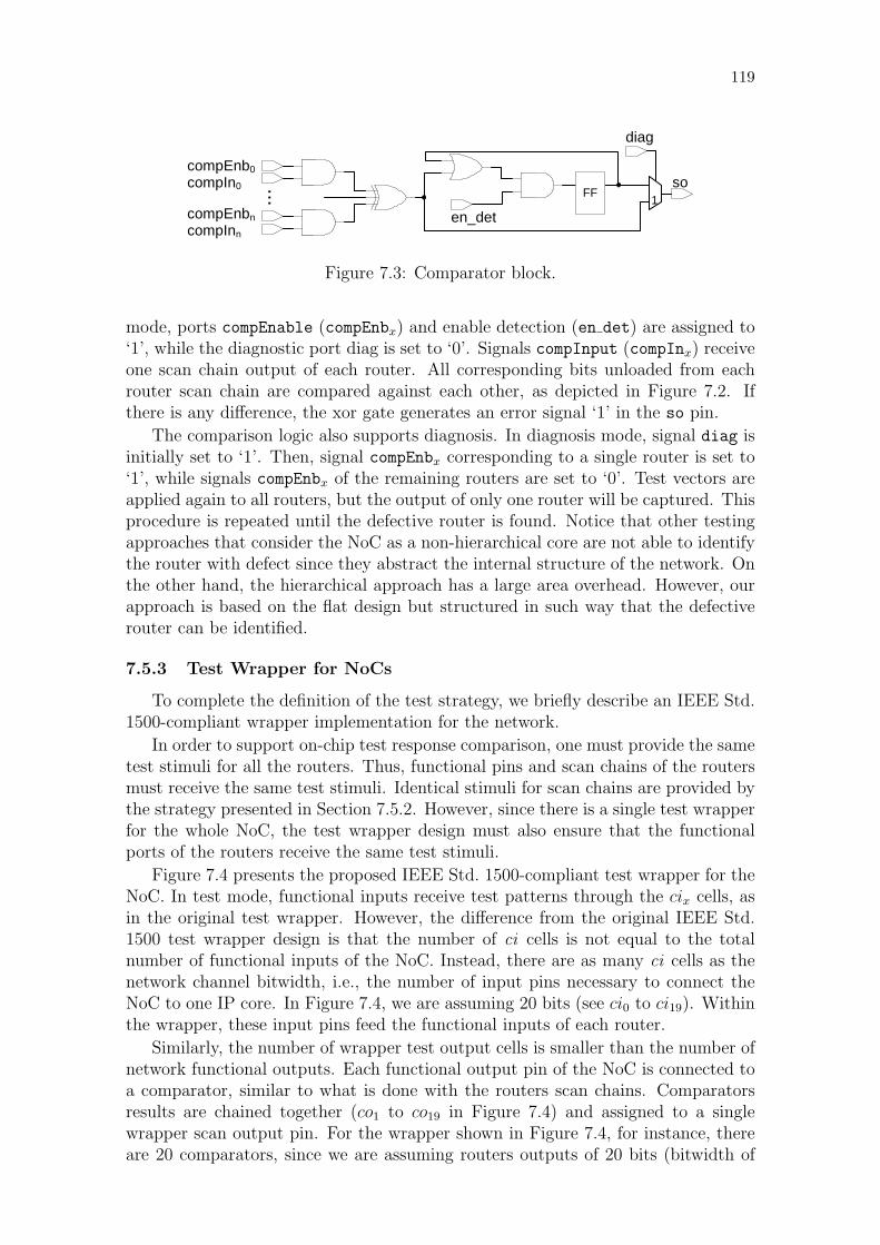
119
Paper 25.1 INTERNATIONAL TEST CONFERENCE
5
To complete the router testing, a second scan chain is de-fined with the remaining flip-flops of the control logic, which are the flip-flops used to implement the routing algorithm, for example.
This approach avoids expensive solutions like full-scan and BIST [10][11], while the ATPG tool can still generate high fault coverage at reasonable CPU time.
4.2 NoC Testing After defining the test structure for each router, one must define an access mechanism to transmit test data from the network interface to each router and vice-versa. We pro-pose a generic test communication protocol, which can be applied to regular NoC topologies, such as mesh and to-rus. In this protocol, test patterns, coming from the exter-nal tester, are simultaneously applied to all identical routers. Test responses of the routers, on the other hand, are internally compared, as proposed in [3][12]. If test responses are different, a mechanism for diagnosis can be activated. Otherwise, the test continues.
Test vectors are broadcasted to routers by a single pin in the network interface, as shown in Figure 4. Note that different from Figure 2, only test related ports and wires are shown in Figure 4. The block denoted by the equal signal indicates a comparator that checks test responses against each other. The number of comparators required in the NoC depends on the number of scan chains in the routers. For each scan chain in the routers there must be a comparator. In Figure 4, for instance, a single scan chain per router is assumed, and the four chains feed the single comparator. Ideally, all routers are tested in parallel and a single comparator is used. However, there may be limita-tions in the maximum fan-out of the scan input pin (SI in Figure 4) and in the test time achieved by a single scan chain in the routers. The NoC designer can define, then, an alternative solution by increasing the number of scan chains per router (area overhead does not change) to re-duce test time and increasing the number of comparators, whose area can be easily estimated.
NoC
SI0 = SO0
router 0
router 2 Se0..4
router 1
router 3
Figure 4 – Testing multiple identical routers.
4.2.2 The Comparator Figure 5 presents a circuit for output comparison, which is similar to the modules proposed by Wu and MacDonald [12], and Arabi [3]. When running in test mode, ports compEnable (compEnbx) and enable detection (en_det) are assigned to ‘1’, while the diagnostic port diag is set to ‘0’. Signals compInput (compInx) receive one scan chain output of each router being tested. All corresponding bits unloaded from each router scan chain are compared against each other, as depicted in Figure 4. If there is any difference, the xor gate generates an error signal ‘1’ in the so pin.
en_det
compEnb0
...
diag
so
compEnbn
compIn0
compInn
FF 1
Figure 5 – Comparator block.
The comparison logic also supports diagnosis. In diagno-sis mode, signal diag is initially set to ‘1’. Then, signal compEnbx corresponding to a single router is set to ‘1’, while signals compEnbx of the remaining routers are set to ‘0’. Test vectors are applied again to all routers, but the output of only one router will be captured. This procedure is repeated until the defective router is found.
Notice that other testing approaches that consider the NoC as a non-hierarchical core are not able to identify the router with defect since they abstract the internal structure of the network. On the other hand, the hierarchical ap-proach has a large area overhead. However, our approach is based on the flat design but structured in such way that the defective router can be identified.
4.3 Test Wrapper for NoCs To complete the definition of the test strategy, we briefly describe an IEEE 1500-compliant wrapper implementa-tion for the network.
In order to support on-chip test response comparison, one must provide the same test stimuli for all the routers. Thus, functional pins and scan chains of the routers must receive the same test stimuli. Identical stimuli for scan chains are provided by the strategy presented in Section 4.2. However, since there is a single test wrapper for the whole NoC, the test wrapper design must also ensure that the functional ports of the routers receive the same test stimuli.
Figure 7.3: Comparator block.
mode, ports compEnable (compEnbx) and enable detection (en det) are assigned to‘1’, while the diagnostic port diag is set to ‘0’. Signals compInput (compInx) receiveone scan chain output of each router. All corresponding bits unloaded from eachrouter scan chain are compared against each other, as depicted in Figure 7.2. Ifthere is any difference, the xor gate generates an error signal ‘1’ in the so pin.
The comparison logic also supports diagnosis. In diagnosis mode, signal diag isinitially set to ‘1’. Then, signal compEnbx corresponding to a single router is set to‘1’, while signals compEnbx of the remaining routers are set to ‘0’. Test vectors areapplied again to all routers, but the output of only one router will be captured. Thisprocedure is repeated until the defective router is found. Notice that other testingapproaches that consider the NoC as a non-hierarchical core are not able to identifythe router with defect since they abstract the internal structure of the network. Onthe other hand, the hierarchical approach has a large area overhead. However, ourapproach is based on the flat design but structured in such way that the defectiverouter can be identified.
7.5.3 Test Wrapper for NoCs
To complete the definition of the test strategy, we briefly describe an IEEE Std.1500-compliant wrapper implementation for the network.
In order to support on-chip test response comparison, one must provide the sametest stimuli for all the routers. Thus, functional pins and scan chains of the routersmust receive the same test stimuli. Identical stimuli for scan chains are provided bythe strategy presented in Section 7.5.2. However, since there is a single test wrapperfor the whole NoC, the test wrapper design must also ensure that the functionalports of the routers receive the same test stimuli.
Figure 7.4 presents the proposed IEEE Std. 1500-compliant test wrapper for theNoC. In test mode, functional inputs receive test patterns through the cix cells, asin the original test wrapper. However, the difference from the original IEEE Std.1500 test wrapper design is that the number of ci cells is not equal to the totalnumber of functional inputs of the NoC. Instead, there are as many ci cells as thenetwork channel bitwidth, i.e., the number of input pins necessary to connect theNoC to one IP core. In Figure 7.4, we are assuming 20 bits (see ci0 to ci19). Withinthe wrapper, these input pins feed the functional inputs of each router.
Similarly, the number of wrapper test output cells is smaller than the number ofnetwork functional outputs. Each functional output pin of the NoC is connected toa comparator, similar to what is done with the routers scan chains. Comparatorsresults are chained together (co1 to co19 in Figure 7.4) and assigned to a singlewrapper scan output pin. For the wrapper shown in Figure 7.4, for instance, thereare 20 comparators, since we are assuming routers outputs of 20 bits (bitwidth of
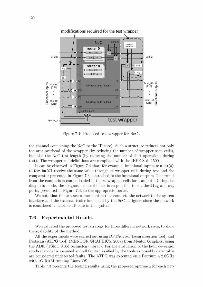
120
Paper 25.1 INTERNATIONAL TEST CONFERENCE
6
NoC
Din_R0[0:19]
control ports
special_in test wrapper
sc1 [0:n]
sc0 [0:m]
sc1 [0:n]
sc0 [0:m]
=
=
router 0
router n
Si[0:2]
Din_Rn[0:19]
Dout_R0[0:19]
Dout_Rn[0:19]
So[0:2]
ci0
ci19
co0
co19
......Fu
nctio
nal i
nput
s
Func
tiona
l out
puts
se[0..r]diagnosis
control block
=
=
20
[0]
functional ports router n
functional ports router 0
[19]
[0]
[19]
[0]
[19]
[0]
[19]
modifications required for the test wrapper
Figure 6 – Proposed test wrapper for NoCs.
Figure 6 presents the proposed IEEE 1500-compliant test wrapper for the NoC. In test mode, functional inputs re-ceive test patterns through the cix cells, as in the original test wrapper. However, the difference from the original 1500 test wrapper design is that the number of ci cells is not equal to the total number of functional inputs of the NoC. Instead, there are as many ci cells as the network channel bitwidth, i.e., the number of input pins necessary to connect the NoC to one IP core. In Figure 6, we are assuming 20 bits (see ci0 to ci19). Within the wrapper, these input pins feed the functional inputs of each router.
Similarly, the number of wrapper test output cells is smaller than the number of network functional outputs. Each functional output pin of the NoC is connected to a comparator, similar to what is done with the routers scan chains. Comparators results are chained together (co1 to co19 in Figure 6) and assigned to a single wrapper scan output pin. For the wrapper shown in Figure 6, for in-stance, there are 20 comparators, since we are assuming routers outputs of 20 bits (bitwidth of the channel con-necting the NoC to the IP core). Such a structure reduces not only the area overhead of the wrapper (by reducing the number of wrapper scan cells), but also the NoC test time (by reducing the number of shift operations during test). The wrapper cell definitions are compliant with the IEEE 1500 standard.
It can be observed in Figure 6 that, for example, func-tional inputs Din_R0[0] to Din_Rn[0] receive the same value through ci wrapper cells during test and the com-parator presented in Figure 5 is attached to the functional outputs. The result from the comparison can be loaded in the co wrapper cells for scan out. During the diagnosis mode, the diagnosis control block is responsible to set the diag and sex ports, presented in Figure 5, to the appropri-ate router.
We note that the test access mechanism that connects the network to the system interface and the external tester is defined by the SoC designer, since the network is consid-ered as another IP core in the system.
5. Experimental Results We evaluated the proposed test strategy for three different network sizes, to show the scalability of the method.
All the experiments were carried out using DFTAdvisor™ (scan insertion tool) and Fastscan™ (ATPG tool) [7] from Mentor Graphics, using the ADK (TSMC 0.35) technol-ogy library. For the evaluation of the fault coverage, stuck-at model is assumed and all faults classified by the tools as possibly detectable are considered undetected faults. The ATPG was executed on a Pentium 4 2.6GHz with 1G RAM running Linux OS.
Figure 7.4: Proposed test wrapper for NoCs.
the channel connecting the NoC to the IP core). Such a structure reduces not onlythe area overhead of the wrapper (by reducing the number of wrapper scan cells),but also the NoC test length (by reducing the number of shift operations duringtest). The wrapper cell definitions are compliant with the IEEE Std. 1500.
It can be observed in Figure 7.4 that, for example, functional inputs Din R0[0]
to Din Rn[0] receive the same value through ci wrapper cells during test and thecomparator presented in Figure 7.3 is attached to the functional outputs. The resultfrom the comparison can be loaded in the co wrapper cells for scan out. During thediagnosis mode, the diagnosis control block is responsible to set the diag and sex
ports, presented in Figure 7.3, to the appropriate router.
We note that the test access mechanism that connects the network to the systeminterface and the external tester is defined by the SoC designer, since the networkis considered as another IP core in the system.
7.6 Experimental Results
We evaluated the proposed test strategy for three different network sizes, to showthe scalability of the method.
All the experiments were carried out using DFTAdvisor (scan insertion tool) andFastscan (ATPG tool) (MENTOR GRAPHICS, 2007) from Mentor Graphics, usingthe ADK (TSMC 0.35) technology library. For the evaluation of the fault coverage,stuck-at model is assumed and all faults classified by the tools as possibly detectableare considered undetected faults. The ATPG was executed on a Pentium 4 2.6GHzwith 1G RAM running Linux OS.
Table 7.3 presents the testing results using the proposed approach for each net-
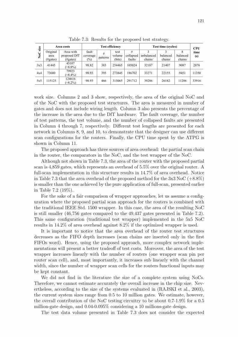
121
Table 7.3: Results for the proposed test strategy.
Area costs Test efficiency Test time (cycles)
NoC
size
Original area
(#gates)
Area with proposed DfT
(#gates)
fault coverage
(%)
# patterns
test volume (bits)
# collapsed
faults
3 unbalanced
chains
3 balanced
chains
8 balanced
chains
CPU time (s)
3x3 41445 45107 (+8.8%) 98.82 383 254465 105024 32187 21407 9087 2876
4x4 73680 79923 (+8.4%) 98.93 395 273845 186702 33271 22155 9451 11350
5x5 115125 124616 (+8.2%) 98.93 466 315065 291712 39286 26182 11206 33916
work size. Columns 2 and 3 show, respectively, the area of the original NoC andof the NoC with the proposed test structures. The area is measured in number ofgates and does not include wiring length. Column 3 also presents the percentage ofthe increase in the area due to the DfT hardware. The fault coverage, the numberof test patterns, the test volume, and the number of collapsed faults are presentedin Column 4 through 7, respectively. Different test lengths are presented for eachnetwork in Columns 8, 9, and 10, to demonstrate that the designer can use differentscan configurations for the routers. Finally, the CPU time spent by the ATPG isshown in Column 11.
The proposed approach has three sources of area overhead: the partial scan chainin the router, the comparators in the NoC, and the test wrapper of the NoC.
Although not shown in Table 7.3, the area of the router with the proposed partialscan is 4,859 gates, which represents an overhead of 5.5% over the original router. Afull-scan implementation in this structure results in 14.7% of area overhead. Noticein Table 7.3 that the area overhead of the proposed method for the 3x3 NoC (+8.8%)is smaller than the one achieved by the pure application of full-scan, presented earlierin Table 7.2 (19%).
For the sake of a fair comparison of wrapper approaches, let us assume a config-uration where the proposed partial scan approach for the routers is combined withthe traditional IEEE Std. 1500 wrapper. In this case, the area of the resulting NoCis still smaller (46,756 gates compared to the 49,437 gates presented in Table 7.2).This same configuration (traditional test wrapper) implemented in the 5x5 NoCresults in 14.2% of area overhead against 8.2% if the optimized wrapper is used.
It is important to notice that the area overhead of the router test structuresdecreases as the FIFO depth increases (scan chains are inserted only in the firstFIFOs word). Hence, using the proposed approach, more complex network imple-mentations will present a better tradeoff of test costs. Moreover, the area of the testwrapper increases linearly with the number of routers (one wrapper scan pin perrouter scan cell), and, most importantly, it increases sub linearly with the channelwidth, since the number of wrapper scan cells for the routers functional inputs maybe kept constant.
We did not find in the literature the size of a complete system using NoCs.Therefore, we cannot estimate accurately the overall increase in the chip size. Nev-ertheless, according to the size of the systems evaluated in (RAJSKI et al., 2003),the current system sizes range from 0.5 to 10 million gates. We estimate, however,the overall contribution of the NoC testing circuitry to be about 0.7-1.9% for a 0.5million-gate design, and 0.04-0.095% considering a 10 millions-gate design.
The test data volume presented in Table 7.3 does not consider the expected

122
responses, since they are evaluated on-chip. Considering the same test patterns andtheir corresponding test responses, the total test volume would be 382,004, 405,380,and 470,243 bits, for the 3x3, 4x4, and 5x5 NoCs, respectively. Thus, the test volumesaving of the circuit presented in Figure 7.2 is of 32%. Nevertheless, one can observethat high fault coverage is still achieved independent of the number of routers in theNoC and for the same relative cost in area.
The NoC designer can define different scan chains configurations to connectthe routers functional inputs in the wrapper, thus generating different test lengths.Some possible configurations are presented in Table 7.3 (Columns 8, 9, and 10).Considering the 5x5 NoC with eight balanced scans, for instance, the test lengthusing a standard test wrapper would be 80,002 clock cycles, while the proposedwrapper achieves 11,206 clock cycles.
Finally, power consumption may be an important limitation to the test paral-lelization within the NoC. Hence, we have characterized the power consumption perrouter during test. The power consumption is characterized considering the dynamicand static power consumption during the test execution and the actual test patterns.To evaluate the dynamic consumption, the router is initially synthesized to an ASICtechnology library for which the power consumption of technology cells is available.The resulting netlist description is simulated with the actual test patterns calcu-lated by the ATPG tool. During this simulation, the switching activity of each cellof the technology library is captured. Then, the power consumption per clock cycleis computed by multiplying the number of toggles and the power consumption percell. The total power consumption for the whole simulation is given by the averagepower consumption of a router in each clock cycle of the test procedure. For thenetwork configurations presented in Table 7.3, the power consumption per router is4.34w. Since all routers receive exactly the same test patterns, the power of the NoCdepends only on the number of routers. Thus, considering a 10 million gate design(RAJSKI et al., 2003), the total area of a NoC is small (less than 1% considering3x3 NoC), and then the contribution to the system power consumption is expectedto be small too. However, if the test power of the NoC becomes an issue, one cantest groups of routers at a time instead of all of them in parallel.
Routing the comparators may cause routing congestion, timing and power prob-lems because of the long wire length. In these situations, one can use comparatorsbetween neighbor routers, thus reducing the wiring length. We are considering man-ufacturing faults, which are usually randomly distributed in the design. Thus, theprobability of multiple errors that produce exactly the same output is low.
Figure 7.5 shows the scalability of the proposed method. As the size of the NoCincreases (see number of gates curve) the test data volume and test length increasein a much lower rate, while the fault coverage is kept constant and the area overheadis reduced. This graph demonstrates that the approach can scale to test very largeNoCs that support connecting several IP cores.
7.7 Limitations
The main limitation of the proposed approach is that it is applied only to NoCswith large number of identical routers. Other approach must be proposed for NoCsbased on non-identical routers.
The second limitation of the proposed approach is that it does not test the NoC
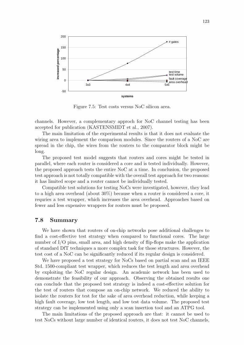
123
Paper 25.1 INTERNATIONAL TEST CONFERENCE
8
nology cells is available. The resulting netlist description is simulated with the actual test patterns calculated by the ATPG tool. During this simulation, the switching activity of each cell of the technology library is captured. Then, the power consumption per clock cycle is computed by multiplying the number of toggles and the power con-sumption per cell. The total power consumption for the whole simulation is given by the average power consump-tion of a router in each clock cycle of the test procedure. For the network configurations presented in Table 3, the power consumption per router is 4.34 µW. Since all routers receive exactly the same test patterns, the power of the NoC depends only on the number of routers. Thus, considering a 10 million gate design [9], the total area of a NoC is small (less than 1% considering 3x3 NoC), and then the contribution to the system power consumption is expected to be small too. However, if the test power of the NoC becomes an issue, one can test groups of routers at a
time instead of all of them in parallel.
Routing the comparators may cause routing congestion, timing and power problems because of the long wire length. In these situations, one can use comparators be-tween neighbor routers, thus reducing the wiring length. We are considering manufacturing faults, which are usu-ally randomly distributed in the design. Thus, the prob-ability of multiple errors that produce exactly the same output is low.
Figure 7 shows the scalability of the proposed method. As the size of the NoC increases (see number of gates curve) the test data volume and test time increase in a much lower rate, while the fault coverage is kept constant and the area overhead is reduced. This graph demonstrates that the approach can scale to test very large NoCs that support connecting several IP cores.
# gates
area overheadfault coveragetest volumetest time
-50
0
50
100
150
200
3x3 4x4 5x5
systems
incr
ease
d pe
rcen
tage
Figure 7 – Scalable test approach.
6. Final Remarks In this paper, we have shown that routers of on-chip net-works pose additional challenges to find a cost-effective test strategy when compared to functional cores. The large number of I/O pins, small area, and high density of flip-flops make the application of standard DfT techniques a more complex task for those structures. However, the test cost of a NoC can be significantly reduced if its regular design is considered.
We have proposed a scalable test strategy for NoCs based on partial scan and an IEEE 1500-compliant test wrapper, which reduces the test time and area overhead by exploit-ing the NoC regular design. An academic network has been used to demonstrate the feasibility of our approach. Observing the obtained results one can conclude that the proposed test strategy is indeed a cost-effective solution for the test of routers that compose an on-chip network. We reduced the ability to isolate the routers for test for the sake of area overhead reduction, while keeping a high
fault coverage, low test time, and low test data volume. The proposed test strategy can be implemented using only a scan insertion tool and an ATPG tool.
Current work include evaluation of delay faults, evalua-tion of area overhead considering wiring length, the test of the network interfaces, the impact in test of using buffers of different depths, and the test of the router-to-router channels of the NoC.
Acknowledgments The authors thank Mike R. Jones from Mentor Graph-
ics Corporation for his valuable support on the DfT tools.
7. References
Figure 7.5: Test costs versus NoC silicon area.
channels. However, a complementary approch for NoC channel testing has beenaccepted for publication (KASTENSMIDT et al., 2007).
The main limitation of the experimental results is that it does not evaluate thewiring area to implement the comparison modules. Since the routers of a NoC arespread in the chip, the wires from the routers to the comparator block might belong.
The proposed test model suggests that routers and cores might be tested inparallel, where each router is considered a core and is tested individually. However,the proposed approach tests the entire NoC at a time. In conclusion, the proposedtest approach is not totally compatible with the overall test approach for two reasons:it has limited scope and a router cannot be individually tested.
Compatible test solutions for testing NoCs were investigated, however, they leadto a high area overhead (about 30%) because when a router is considered a core, itrequries a test wrapper, which increases the area overhead. Approaches based onfewer and less expensive wrappers for routers must be proposed.
7.8 Summary
We have shown that routers of on-chip networks pose additional challenges tofind a cost-effective test strategy when compared to functional cores. The largenumber of I/O pins, small area, and high density of flip-flops make the applicationof standard DfT techniques a more complex task for those structures. However, thetest cost of a NoC can be significantly reduced if its regular design is considered.
We have proposed a test strategy for NoCs based on partial scan and an IEEEStd. 1500-compliant test wrapper, which reduces the test length and area overheadby exploiting the NoC regular design. An academic network has been used todemonstrate the feasibility of our approach. Observing the obtained results onecan conclude that the proposed test strategy is indeed a cost-effective solution forthe test of routers that compose an on-chip network. We reduced the ability toisolate the routers for test for the sake of area overhead reduction, while keeping ahigh fault coverage, low test length, and low test data volume. The proposed teststrategy can be implemented using only a scan insertion tool and an ATPG tool.
The main limitations of the proposed approach are that: it cannot be used totest NoCs without large number of identical routers, it does not test NoC channels,
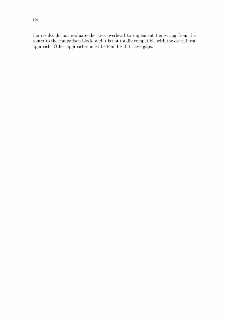
124
the results do not evaluate the area overhead to implement the wiring from therouter to the comparison block, and it is not totally compatible with the overall testapproach. Other approaches must be found to fill these gaps.

125
8 TEST SCHEDULING
This chapter presents a new scheduling algorithm based on a previous algorithm(GOEL; MARINISSEN, 2003a) used for dedicated TAMs. The proposed algorithmallows co-optimization of wrappers and scheduling, generating test architecturesoptimized for both SoC test length and silicon area for DfT logic. This algorithmis a first step toward a general NoC-reuse method since it does not require a cycle-accurate NoC model as previous papers (COTA; LIU, 2006). Finally, we comparethe proposed algorithm with another algorithm (GOEL; MARINISSEN, 2003a) usedfor dedicated TAMs.
8.1 Problem Statement
The wrapper optimization step generates all information to build a wrapper,however, the test scheduling only needs the test length for each wrapper. Figure 8.1illustrates the process where a set of wrappers (for instance, this set of wrappersfor core g1 is represented by w1g1 to wc/2g1) is used to build a Pareto graph likethe one illustrated in right part of Figure 8.1. This graph represents the wrapperinformation loaded by the test scheduling tool.
117
wc/2 g1wc/2 g1
w2 g1w2 g1
w1 g1w1 g1
t(w1 g1)
t(w2 g1)
t(wc/2 g1)
# test wires
test
leng
th
Pareto curvefor core g1
Optimized wrappersfor core g1
Information used by test scheduling
Information generatedby wrapper optimization
Figure 8.1: Building Pareto curve for the test scheduling. t() represents the test lengthof a wrapper.
126
The following problem statement represents the proposed test scheduling algo-rithm.
Problem 2 [Test Scheduling for NoC-Based Chips]Given:
• a graph G which defines the SoC where for each g ∈ G there is a Pareto curvePg;
• the maximal number of test wires wmax;
• the physical channel width c, in bits;
• the routing algorithm r() used by the NoC.
Determine:
1. the sets of vTAMs;
2. the SoC test length, in clock cycles.
Such that:
i. the SoC test length and the silicon area for DfT are minimized while wmax isnot exceeded and the width of each vTAM is ≤ c/2.
�Figure 8.2 graphically presents this problem.
116
wmax
r( )
SchedulingScheduling
testscheduling
testwrapper
optimization
b01
b11
a21
b31
b00
b10
b20
b30
c02
b12
a22
a32
vTAMn ={--, w,Ratei, Rpart}
vTAMn ={--, w,Ratei, Rpart}vTAM1 =
{--,--, w,Ratei, Rpart}vTAM1 =
{--,--, w,Ratei, Rpart}
DfT
generation
G
C
w2 B
w1
A tw3
Pareto curvefor core g1
Pareto curvefor core g|G|
Figure 8.2: Scheduling design flow.

127
8.2 Proposed Test Strategy
8.2.1 Previous Test Scheduling Algorithm
Choosing the algorithm for comparison was our first step. The usual SoC testbenchmark cannot be used in this comparison due to the lack of some importantinformation like NoC topology, routing algorithm, router test lenght, and stan-dard ports for cores. The comparison can only be accomplished if the original testscheduling algorithm for dedicated TAM is re-implemented and run under an ade-quate input system, i.e. a system with NoC information. Thus, we have establishedthe follow criteria to choose the test scheduling algorithm:
• Based on a simple test architecture:The algorithm should be based on fixed-width TAMs and with no preemptionsupport. It is know that these features complicates the hardware design. Wewant to avoid these complications in first instance;
• Based on well-defined DfT modules :The algorithm should be compatible with a well defined and established testwrapper design and optimization;
• Easy to implement algorithm and clear documentation:We need an algorithm simple to be designed since we would need to re-implement it due to the lack of standard benchmarks for NoC-based systems.
The selected algorithm for the comparison and to be adapted to NoC reuse is the onepresented in (GOEL; MARINISSEN, 2003a). We initially use only one algorithmdue to the need to re-implement the original test scheduling, once there is no subtlebenchmark.
We adopted the same terminology used in (GOEL; MARINISSEN, 2003a) toease the comparison and readability. The main procedure executes the following sub-procedures in sequence: CreateStartSolution, OptimizeBottomUp, OptimizeTopDown,and Reshuffle. Figure 8.3 illustrates these optimization algorithms.
The procedure CreateStartSolution creates the initial test architecture suchthat it sorts the modules of the SoC in decreasing order of test data volume, then itassigns the ordered modules to one-bit TAMs. If there are more modules than TAMwires, then, it assigns the remaining modules to the TAM with shortest test length,otherwise, if there are more TAM wires than modules, then, it assigns test wires tothe TAM with longest test length. The procedure OptimizeBottomUp tries to mergethe TAM with shortest test length to another TAM such that the freed test wiresare allocated to the longest TAM to reduce the SoC test length. The procedureOptimizeTopDown tries to merge the TAM with longest test length to another TAMsuch that the resulting TAM receives the test wires of both original TAMs. If theresulting TAM has shorter test length than the current SoC test length, then themerge is approved. The procedure Reshuffle tries to reduce the current SoC testby moving one module of the TAM with longest test length to another TAM.
8.2.2 Employed Data Structure
This section shows how the input system G is transformed into the tile-basedgraph, which is the graph actually partitioned by the test scheduling.
Figure 8.4, left part, represents the input system. This example system has a setof nine routers (r00 to r22) and a set of ten cores (c0 to c9). This graph is reduced

128
126
C
B
A D
w1
w2
w3idle time
gain
C
w1+
w3
w2 B A D
C
B
A D
w1
w2
w3idle time
gainC AD
w1+
w3
w2 B
C
B
ADw1
w2
gainC
B
A
D
w1
w2
OptimizeBottomUp
OptimizeTopDown
Reshuffle
Figure 8.3: Illustrative example of the original optimization algorithms.
to the tile-based graph (depicted in the right part of the figure) by merging the testlength of the modules connected to a router. For instance, tile 1 is represented bythe test length of the router r02; tile 2 is presented by the sum of test lengths ofrouter r12 and core c0.
The main property of this approach is that all modules within a tile must betested by the same TAM. Otherwise, if more than one TAM could test the moduleswithin a tile, there would be packet collision inside the tile once multiple test streamscould be activate at the same time. Thus, the tile-based graph is used to avoid packetcollision.
8.2.3 The Proposed Algorithm
Algorithm 8.1 presents the main procedure for the proposed test scheduling. Theprocedures in lines 1, 3, 4, 5, and 6 are the ones based on (GOEL; MARINISSEN,2003a) (we split the original OptimizeTopDown algorithm in two parts). There aretwo constraints that we added to the original algorithms: the vTAM width constraintand the neighborhood constraint. Since test data is transported through the NoCchannels, the vTAM width (w in page 77) cannot be higher than the physical channelbandwidth of the NoC. As explained before, the maximal vTAM width used is halfof the physical channel bandwidth (w ≤ c/2). The neighborhood constraint is setto avoid packet collision, i.e. a vTAM consists of neighbor routers to avoid packetcollision during test application.
8.2.3.1 Notation
We use lower case symbols (x) to represent a router, upper case symbols (X) torepresent a set of routers, and slanted upper case symbols (X ) to represent a setof sets of routers. t(R) and w(R) are, respectively, the test and width of a set ofrouters R. The term partition is used to refer to the set Rpart of a vTAM.
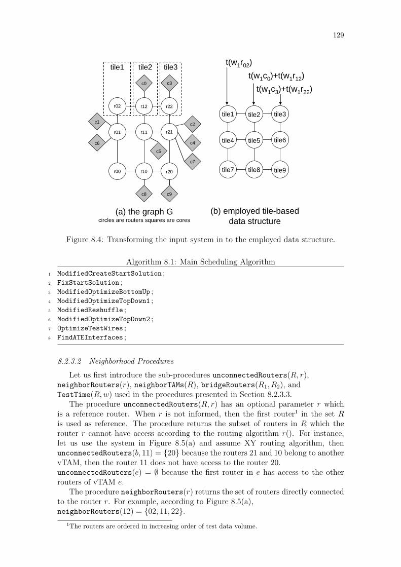
129
118
tile3tile2tile1 t(w1r02)
r01 r11 r21
r00 r10 r20
r02 r12 r22
c0
c1 c2
c3
c4
c5
c6
c7
c8 c9
(a) the graph Gcircles are routers squares are cores
(b) employed tile-baseddata structure
tile4 tile5 tile6
tile7 tile8 tile9
tile1 tile2 tile3
t(w1c0)+t(w1r12)t(w1c3)+t(w1r22)
Figure 8.4: Transforming the input system in to the employed data structure.
Algorithm 8.1: Main Scheduling Algorithm
1 ModifiedCreateStartSolution ;2 FixStartSolution ;3 ModifiedOptimizeBottomUp ;4 ModifiedOptimizeTopDown1 ;5 ModifiedReshuffle ;6 ModifiedOptimizeTopDown2 ;7 OptimizeTestWires ;8 FindATEInterfaces ;
8.2.3.2 Neighborhood Procedures
Let us first introduce the sub-procedures unconnectedRouters(R, r),neighborRouters(r), neighborTAMs(R), bridgeRouters(R1, R2), andTestTime(R,w) used in the procedures presented in Section 8.2.3.3.
The procedure unconnectedRouters(R, r) has an optional parameter r whichis a reference router. When r is not informed, then the first router1 in the set Ris used as reference. The procedure returns the subset of routers in R which therouter r cannot have access according to the routing algorithm r(). For instance,let us use the system in Figure 8.5(a) and assume XY routing algorithm, thenunconnectedRouters(b, 11) = {20} because the routers 21 and 10 belong to anothervTAM, then the router 11 does not have access to the router 20.unconnectedRouters(e) = ∅ because the first router in e has access to the otherrouters of vTAM e.
The procedure neighborRouters(r) returns the set of routers directly connectedto the router r. For example, according to Figure 8.5(a),neighborRouters(12) = {02, 11, 22}.
1The routers are ordered in increasing order of test data volume.
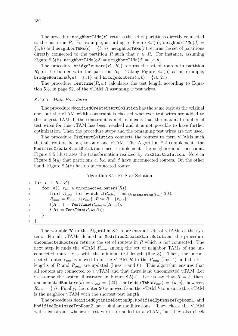
130
The procedure neighborTAMs(R) returns the set of partitions directly connectedto the partition R. For example, according to Figure 8.5(b), neighborTAMs(d) ={a, b} and neighborTAMs(c) = {b, a}. neighborTAMs(r) returns the set of partitionsdirectly connected to the partition R such that r ∈ R. For instance, assumingFigure 8.5(b), neighborTAMs(32) = neighborTAMs(d) = {a, b}.
The procedure bridgeRouters(R1, R2) returns the set of routers in partitionR1 in the border with the partition R2. Taking Figure 8.5(b) as an example,bridgeRouters(b, a) = {11} and bridgeRouters(a, b) = {10, 21}.
The procedure TestTime(R,w) calculates the test length according to Equa-tion 5.3, in page 92, of the vTAM R assuming w test wires.
8.2.3.3 Main Procedures
The procedure ModifiedCreateStartSolution has the same logic as the originalone, but the vTAM width constraint is checked whenever test wires are added tothe longest TAM. If the constraint is met, it means that the maximal number oftest wires for this vTAM has been reached and it is not possible to have furtheroptimization. Then the procedure stops and the remaining test wires are not used.
The procedure FixStartSolution connects the routers to form vTAMs suchthat all routers belong to only one vTAM. The Algorithm 8.2 complements theModifiedCreateStartSolution since it implements the neighborhood constraint.Figure 8.5 illustrates the transformation realized by FixStartSolution. Note inFigure 8.5(a) that partitions a, b,c, and d have unconnected routers. On the otherhand, Figure 8.5(b) has no unconnected router.
Algorithm 8.2: FixStartSolution
1 for a l l R ∈ R{2 for a l l runc ∈ unconnectedRouters(R){3 find Rmin for which t(Rmin) = minJ∈neighborTAMs(runc) t(J);4 Rmin := Rmin ∪ {runc} ;R := R− {runc} ;5 t(Rmin) := TestTime(Rmin , w(Rmin));6 t(R) := TestTime(R,w(R));7 }8 }
The variable R in the Algorithm 8.2 represents all sets of vTAMs of the sys-tem. For all vTAMs defined in ModifiedCreateStartSolution, the procedureunconnectedRouters returns the set of routers in R which is not connected. Thenext step it finds the vTAM Rmin among the set of neighbor TAMs of the un-connected router runc with the minimal test length (line 3). Then, the uncon-nected router runc is moved from the vTAM R to the Rmin (line 4) and the testlengths of R and Rmin are updated (lines 5 and 6). This algorithm ensures thatall routers are connected to a vTAM and that there is no unconnected vTAM. Letus assume the system illustrated in Figure 8.5(a). Let us say that R = b, then,unconnectedRouters(b) = runc = {20}. neighborTAMs(runc) = {a, c}, however,Rmin = {a}. Finally, the router 20 is moved from the vTAM b to a since this vTAMis the neighbor vTAM with the shortest test length.
The procedures ModifiedOptimizeBottomUp, ModifiedOptimizeTopDown1, andModifiedOptimizeTopDown2 have similar modifications. They check the vTAMwidth constraint whenever test wires are added to a vTAM, but they also check
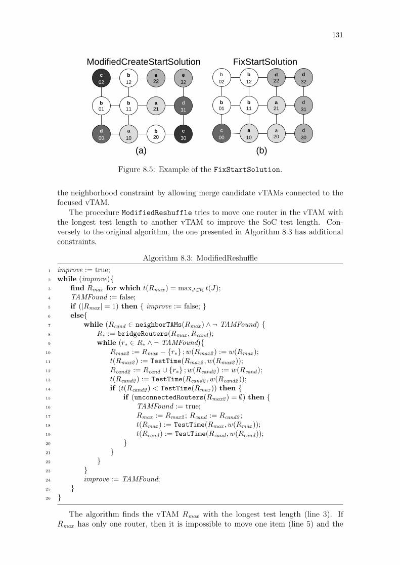
131
b01
b11
a21
d31
d00
a10
b20
c30
c02
b12
e22
e32
b01
b11
a21
d31
c00
a10
a20
d30
b02
b12
d22
d32
ModifiedCreateStartSolution FixStartSolution
(a) (b)
Figure 8.5: Example of the FixStartSolution.
the neighborhood constraint by allowing merge candidate vTAMs connected to thefocused vTAM.
The procedure ModifiedReshuffle tries to move one router in the vTAM withthe longest test length to another vTAM to improve the SoC test length. Con-versely to the original algorithm, the one presented in Algorithm 8.3 has additionalconstraints.
Algorithm 8.3: ModifiedReshuffle
1 improve := true;2 while (improve){3 find Rmax for which t(Rmax ) = maxJ∈R t(J);4 TAMFound := false;5 if (|Rmax | = 1) then { improve := false; }6 else{7 while (Rcand ∈ neighborTAMs(Rmax ) ∧ ¬ TAMFound) {8 R∗ := bridgeRouters(Rmax , Rcand );9 while (r∗ ∈ R∗ ∧ ¬ TAMFound){
10 Rmax2 := Rmax − {r∗} ;w(Rmax2 ) := w(Rmax );11 t(Rmax2 ) := TestTime(Rmax2 , w(Rmax2 ));12 Rcand2 := Rcand ∪ {r∗} ;w(Rcand2 ) := w(Rcand );13 t(Rcand2 ) := TestTime(Rcand2 , w(Rcand2 ));14 if (t(Rcand2 ) < TestTime(Rmax )) then {15 if (unconnectedRouters(Rmax2 ) = ∅) then {16 TAMFound := true;17 Rmax := Rmax2 ; Rcand := Rcand2 ;18 t(Rmax ) := TestTime(Rmax , w(Rmax ));19 t(Rcand ) := TestTime(Rcand , w(Rcand ));20 }21 }22 }23 }24 improve := TAMFound;25 }26 }
The algorithm finds the vTAM Rmax with the longest test length (line 3). IfRmax has only one router, then it is impossible to move one item (line 5) and the
132
procedure is finished. Otherwise, for all vTAMs Rcand , neighbor of Rmax , it finds theset of routers of Rmax connected to the vTAM Rcand (line 8). These routers in theborder of Rmax and Rcand are the ones that can be moved, however, some constraintsmust be checked first. It checks if moving a router r∗ ∈ R∗ does not increase theSoC test length (lines 10 to 14). If the move is accepted in terms of test length, thenit checks if moving the router r∗ will not unconnect the vTAM Rmax (line 15). Ifnot, the move is accepted and the new SoC test length is updated (lines 16 to 19).
For example, considering the system in Figure 8.5(b) and assuming that partitiond correspond to Rmax . Then, Rcand might assume a and b. When Rcand = a,bridgeRouters(Rmax , a) = {22, 30, 31} while when Rcand = b,bridgeRouters(Rmax , b) = {22}. Let us assume that when it moves the router 31and 22 the test length reduces. However, when the router 31 is moved the router30 will be unconnected, which is not allowed. Finally, the router 22 is moved to thepartition b because it passes in all constraints and it reduces the SoC test length.
The procedure OptimizeTestWires described in Algorithm 8.4 tries to optimizethe number of test wires. Once there is no additional improvement in test length tobe done, it iteratively tries to reduce the number of test wires of all vTAMs (line 6)under the condition that the current SoC test length is not exceeded (lines 8 and9). By reducing the number of test wires, it also reduces the number of test pins,the memory requirement in the tester, and the silicon area to implement the DfTpresented in Section 4.8, page 80. Figure 8.6 illustrates the optimization. One canrealize that even the vTAM with the longest test length can be optimized becauseincreasing the number of test wires of a core not necessarily decrease its test lengthdue to the Pareto behavior (GOEL; MARINISSEN, 2003a).
Algorithm 8.4: OptimizeTestWires
1 T := maxJ∈R t(J);2 for all R ∈ R{3 improve := true;4 while (improve){5 if (w(R) > 1) then {6 R∗ := R;w(R∗) := w(R)− 1;7 t(R∗) := TestTime(R∗, w(R∗));8 if (t(R∗) > T ) then {improve := false;}9 else{ w(R) := w(R∗); t(R) := t(R∗); }
10 }else{ improve := false; }11 }12 }
The procedure FindATEInterfaces finds the minimal number of ATE inter-faces (Ratei in page 77) such that all modules in a vTAM can be reached from anATE interface. For example, ATE interfaces of the partition b in Figure 8.7 are{11, 30}, while for partition a is only {22}. Algorithm 8.5 presents the pseudocodeof FindATEInterfaces.
Let us initially define the variable v as a set of the tuple {r, U}, where r is arouter and U is a set of routers that cannot be accessed by r. For instance, the valueof v to the vTAM b in Figure 8.7 (assuming r() = XY) is
v = {{12, {01, 20, 30, 31}} , {11, {20, 30, 31}} , {01, {12, 10, 20, 30, 31}}, {10, {01, 31}}, . . .}

133
C
B
w1
w2idle time
C
w2 BA D
OptimizeTestWires
w1
A Dt t
Figure 8.6: Example of optimization caused by OptimizeTestWires. Note that thetest length is the same but the number of test wires has been reduced in w1 and w2.
Algorithm 8.5: FindATEInterfaces
1 for all R ∈ R{2 minSolution := ∞;3 for all r∗ ∈ R{4 v∗.r := r∗;5 v∗.U := unconnectedRouters(R, r∗);6 v := v ∪ {v∗};7 }8 for all v1 ∈ v{9 Runc := v1.U ;Rate := {v1.r} ;
10 do {11 minSize := ∞; minRouter := −1;12 for all vcand ∈ v{13 if (vcand .r 3 Rate) then {14 U∗ := Runc − vcand .U ;15 if (|U∗| < minSize) then {16 minSize := |U∗| ; minRouter := vcand .r;17 }18 }19 }20 if (minRouter 6= −1) then {21 find vmin for which ∀j ∈ v, j.r = minRouter;22 Runc := Runc − vmin .U ;Rate := Rate ∪ {vmin .r} ;23 }24 }while (Runc 6= ∅);25 if (|Rate | < minSolution) then {26 Rmin := Rate ; minSolution := |Rate | ;27 }28 }29 Rsol := Rsol ∪ {Rmin};30 }
For all vTAMs R of the system it defines v (lines 3 to 6) and finds the minimalnumber of ATE interfaces for the vTAM R (loop begins at line 8). Rate is thecurrent set of ATE interfaces of the vTAM R, while Runc is the set of unconnectedrouters (line 9), i.e. the routers in R that are not accessible by the ATE interfacesin Rate . The loop beginning at line 12 iterates over v again to find the other ATEinterfaces of R. If the element vcand is not yet included in the set of ATE interfaces(line 13), it evaluates if the number of not reachable routers is the minimal foundso far (minSize in line 15). If the current set of unconnected routers is the minimal,
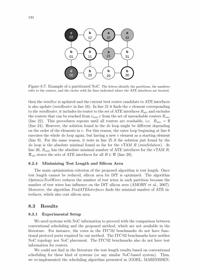
134
b01
b11
a21
b31
d00
b10
b20
b30
c02
b12
a22
a32
Figure 8.7: Example of a partitioned NoC. The letters identify the partitions, the numbersrefer to the routers, and the circles with fat lines indicated where the ATE interfaces are located.
then the minSize is updated and the current best router candidate to ATE interfacesis also update (minRouter in line 16). In line 21 it finds the v element correspondingto the minRouter, it includes its router to the set of ATE interfaces Rate and excludesthe routers that can be reached from vmin .r from the set of unreachable routers Runc
(line 22). This procedures repeats until all routers are reachable, i.e. Runc = ∅(line 24). However, the solution found in the do loop might be different dependingon the order of the elements in v. For this reason, the outer loop beginning at line 6executes the whole do loop again, but having a new v element as a starting element(line 9). For the same reason, it tests in line 25 if the solution just found by thedo loop is the absolute minimal found so far for the vTAM R (minSolution). Atline 26, Rmin has the absolute minimal number of ATE interfaces for the vTAM R.Rsol stores the sets of ATE interfaces for all R ∈ R (line 29).
8.2.4 Minimizing Test Length and Silicon Area
The main optimization criterion of the proposed algorithm is test length. Oncetest length cannot be reduced, silicon area for DfT is optimized. The algorithmOptimizeTestWires reduces the number of test wires in each partition because thenumber of test wires has influence on the DfT silicon area (AMORY et al., 2007).Moreover, the algorithm FindATEInterfaces finds the minimal number of ATE in-terfaces, which also cost silicon area.
8.3 Results
8.3.1 Experimental Setup
We need systems with NoC information to proceed with the comparison betweenconventional scheduling and the proposed method, which are not available in theliterature. For instance, the cores in the ITC’02 benchmarks do not have func-tional protocol ports required by our method. The ITC’02 benchmarks have neitherNoC topology nor NoC placement. The ITC’02 benchmarks also do not have testinformation for routers.
We could not find in the literature the test length results based on conventionalscheduling for these kind of systems (or any similar NoC-based system). Thus,we re-implemented the scheduling algorithm presented in (GOEL; MARINISSEN,

135
2003a) and its wrapper optimization algorithm described in (MARINISSEN; GOEL;LOUSBERG, 2000) to do the comparison (this implementation was validated withthe results presented in (GOEL; MARINISSEN, 2003a)).
8.3.2 Introduction to Relevant Variables
The size of the channel width determines the maximal width of the ‘virtual TAM’.The channel width also determines the kind of port used by the modules (cores androuters). The data width of the port must match the channel width, i.e. channelwidth of 32 bits requires ports with 32-bit data terminals. The same also appliesfor routers.
The router weight (number of test patterns of the routers) determines the amountof the SoC test length spent to test routers. For instance, lower router weight meansthat the routers are tested faster and a small portion of the SoC test time is spenton testing the NoC.
Recall that these variables are given in actual designs, but we investigate if thesetwo variables have any influence on the comparison between the conventional andthe proposed approach.
8.3.3 Experiment Model
Let S, C, R, W , P , and D be, respectively, the set of SoCs, channel widths,router weights, TAM widths, NoC placements, and NoC dimensions (a pair XY)used in this paper. All experiments assume the XY routing algorithm (r()). Exceptby P , the other sets are defined below.
S = {d695, f2126, g1023, h953, p22810, p34392, p93791, q12710, t512505, u226}C = {32, 64, 128}R = {low, medium, high}W = {16, 24, 32, 40, 48, 56, 64}D = {(3, 3), (2, 2), (4, 4), (3, 3), (5, 5), (4, 4), (6, 6), (2, 2), (6, 6), (3, 3)}
An experiment is defined as a tuple {s, c, r, w, ps, ds} such that s ∈ S, c ∈ C,r ∈ R, w ∈ W , ps ∈ P , and ds ∈ D. The sets P and D are associated to the set S.For instance, d695 uses the first placement (3, 3), f2126 uses the second one (2, 2),and so on.
The set P has a set of ten placements randomly generated for each system suchthat a placement can have more than one core per router and it is also possible tohave a router without core. This set of placements is used in all experiments.
Figure 8.8 shows how an experiment is set up for each system. This flow en-sures that both conventional and proposed scheduling tools use the same core androuter configuration. Once the modules were generated, they are optimized by theirrespective wrapper optimization algorithm for finally execute the test scheduling.The NoC reuse problem also needs NoC information like placement and dimension.
The procedure CoreGen(c) sets the correct terminal count for the set of coresof a SoC. The number of terminals of a core is determined by itc02 +2× (39 + c),where itc02 is the original terminal count for the core as defined in the ITC02 SoCbenchmark. The rest of the expression (2 × (39 + c)) represents the number ofterminals of the core related to the input and output ports illustrated in Figure 8.9.
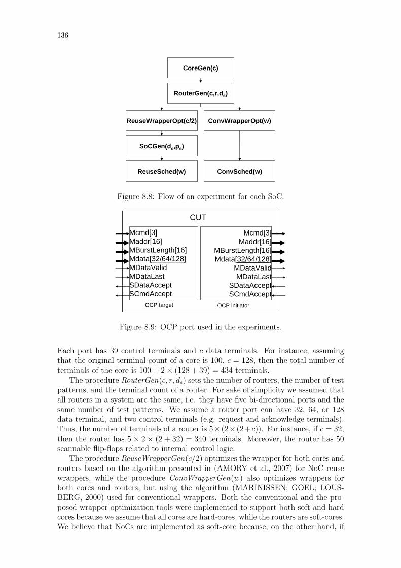
136
120
CoreGen(c)
RouterGen(c,r,ds)
ReuseWrapperOpt(c/2)
SoCGen(ds,ps)
ReuseSched(w) ConvSched(w)
ConvWrapperOpt(w)
Figure 8.8: Flow of an experiment for each SoC.
120
OCP target
Mcmd[3]Maddr[16]
MBurstLength[16]Mdata[32/64/128]
MDataValidMDataLast
SDataAcceptSCmdAccept
Mcmd[3]Maddr[16]MBurstLength[16]Mdata[32/64/128]MDataValidMDataLastSDataAcceptSCmdAccept
OCP initiator
CUT
Figure 8.9: OCP port used in the experiments.
Each port has 39 control terminals and c data terminals. For instance, assumingthat the original terminal count of a core is 100, c = 128, then the total number ofterminals of the core is 100 + 2× (128 + 39) = 434 terminals.
The procedure RouterGen(c, r, ds) sets the number of routers, the number of testpatterns, and the terminal count of a router. For sake of simplicity we assumed thatall routers in a system are the same, i.e. they have five bi-directional ports and thesame number of test patterns. We assume a router port can have 32, 64, or 128data terminal, and two control terminals (e.g. request and acknowledge terminals).Thus, the number of terminals of a router is 5× (2× (2+c)). For instance, if c = 32,then the router has 5 × 2 × (2 + 32) = 340 terminals. Moreover, the router has 50scannable flip-flops related to internal control logic.
The procedure ReuseWrapperGen(c/2) optimizes the wrapper for both cores androuters based on the algorithm presented in (AMORY et al., 2007) for NoC reusewrappers, while the procedure ConvWrapperGen(w) also optimizes wrappers forboth cores and routers, but using the algorithm (MARINISSEN; GOEL; LOUS-BERG, 2000) used for conventional wrappers. Both the conventional and the pro-posed wrapper optimization tools were implemented to support both soft and hardcores because we assume that all cores are hard-cores, while the routers are soft-cores.We believe that NoCs are implemented as soft-core because, on the other hand, if
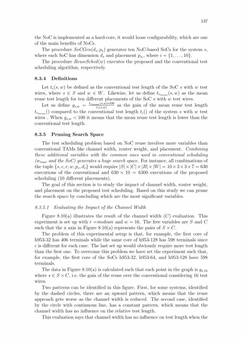
137
the NoC is implemented as a hard-core, it would loose configurability, which are oneof the main benefits of NoCs.
The procedure SoCGen(ds, ps) generates ten NoC-based SoCs for the system s,where each SoC has dimension ds and placement psi
, where i = {1, . . . , 10}.The procedure ReuseSched(w) executes the proposed and the conventional test
scheduling algorithm, respectively.
8.3.4 Definitions
Let tc(s, w) be defined as the conventional test length of the SoC s with w testwires, where s ∈ S and w ∈ W . Likewise, let us define trmean(s, w) as the meanreuse test length for ten different placements of the SoC s with w test wires.
Let us define gs,w = trmean (s,w)∗100tc(s,w)
as the gain of the mean reuse test length
trmean() compared to the conventional test length tc() of the system s with w testwires . When gs,w < 100 it means that the mean reuse test length is lower than theconventional test length.
8.3.5 Pruning Search Space
The test scheduling problem based on NoC reuse involves more variables thanconventional TAMs like channel width, router weight, and placement. Combiningthese additional variables with the common ones used in conventional scheduling(wmax and the SoC) generates a huge search space. For instance, all combinations ofthe tuple {s, c, r, w, ps, ds} would require |S|× |C|× |R|× |W | = 10×3×3×7 = 630executions of the conventional and 630 × 10 = 6300 executions of the proposedscheduling (10 different placements).
The goal of this section is to study the impact of channel width, router weight,and placement on the proposed test scheduling. Based on this study we can prunethe search space by concluding which are the most significant variables.
8.3.5.1 Evaluating the Impact of the Channel Width
Figure 8.10(a) illustrates the result of the channel width (C) evaluation. Thisexperiment is set up with r =medium and w = 16. The free variables are S and Csuch that the x axis in Figure 8.10(a) represents the pairs of S × C.
The problem of this experimental setup is that, for example, the first core ofh953-32 has 406 terminals while the same core of h953-128 has 598 terminals sincec is different for each case. The last set up would obviously require more test lengththan the first one. To overcome this problem we have set the experiment such that,for example, the first core of the SoCs h953-32, h953-64, and h953-128 have 598terminals.
The data in Figure 8.10(a) is calculated such that each point in the graph is gs,16
where s ∈ S ×C, i.e. the gain of the reuse over the conventional considering 16 testwires.
Two patterns can be identified in this figure. First, for some systems, identifiedby the dashed circles, there are an upward pattern, which means that the reuseapproach gets worse as the channel width is reduced. The second case, identifiedby the circle with continuous line, has a constant pattern, which means that thechannel width has no influence on the relative test length.
This evaluation says that channel width has no influence on test length when the
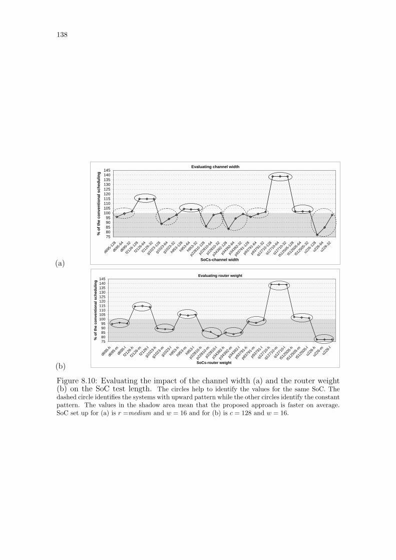
138
(a)
Evaluating channel width
7580859095
100105110115120125130135140145
d695
-128
d695
-64
d695
-32
f2126
-128
f2126
-64
f2126
-32
g102
3-128
g102
3-64
g102
3-32
h953
-128
h953
-64
h953
-32
p228
10-12
8
p228
10-64
p228
10-32
p343
92-12
8
p343
92-64
p343
92-32
p937
91-12
8
p937
91-64
p937
91-32
q127
10-12
8
q127
10-64
q127
10-32
t5125
05-12
8
t5125
05-64
t5125
05-32
u226
-128
u226
-64
u226
-32
SoCs-channel width
% o
f the
con
vent
iona
l sch
edul
ing
(b)
Evaluating router weight
7580859095
100105110115120125130135140145
d695
-h
d695
-md6
95-l
f2126
-h
f2126
-mf21
26-l
g102
3-h
g102
3-m
g102
3-l
h953
-h
h953
-mh9
53-l
p228
10-h
p228
10-m
p228
10-l
p343
92-h
p343
92-m
p343
92-l
p937
91-h
p937
91-m
p937
91-l
q127
10-h
q127
10-m
q127
10-l
t5125
05-h
t5125
05-m
t5125
05-l
u226
-h
u226
-mu2
26-l
SoCs-router weight
% o
f the
con
vent
iona
l sch
edul
ing
Figure 8.10: Evaluating the impact of the channel width (a) and the router weight(b) on the SoC test length. The circles help to identify the values for the same SoC. Thedashed circle identifies the systems with upward pattern while the other circles identify the constantpattern. The values in the shadow area mean that the proposed approach is faster on average.SoC set up for (a) is r =medium and w = 16 and for (b) is c = 128 and w = 16.
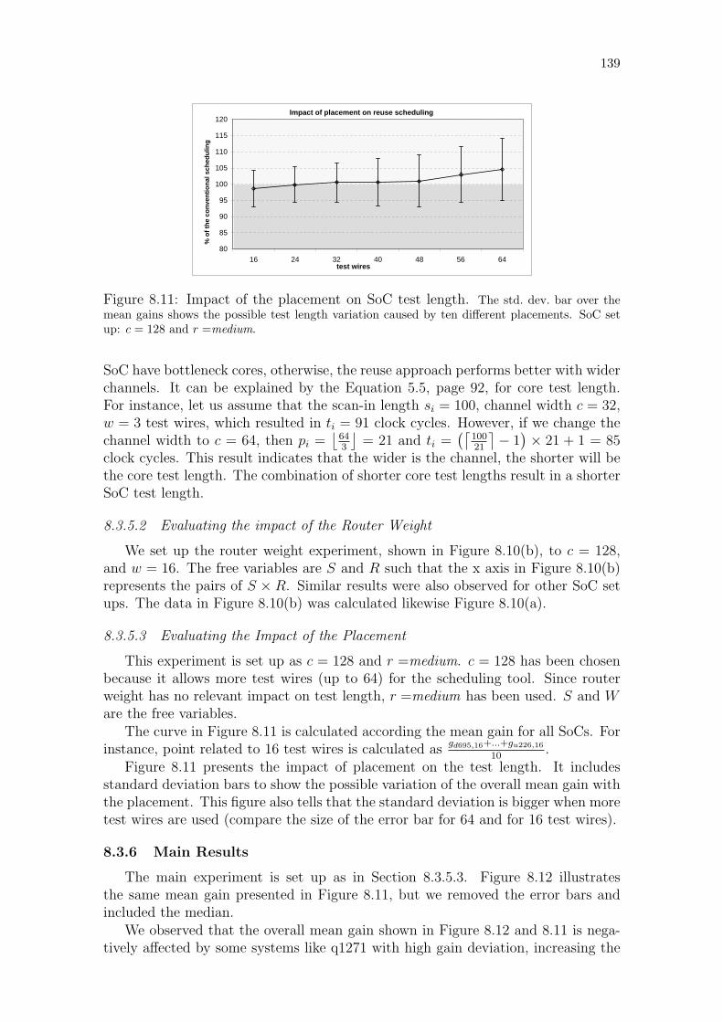
139
Impact of placement on reuse scheduling
80
85
90
95
100
105
110
115
120
16 24 32 40 48 56 64test wires
% o
f the
con
vent
iona
l sch
edul
ing
Figure 8.11: Impact of the placement on SoC test length. The std. dev. bar over themean gains shows the possible test length variation caused by ten different placements. SoC setup: c = 128 and r =medium.
SoC have bottleneck cores, otherwise, the reuse approach performs better with widerchannels. It can be explained by the Equation 5.5, page 92, for core test length.For instance, let us assume that the scan-in length si = 100, channel width c = 32,w = 3 test wires, which resulted in ti = 91 clock cycles. However, if we change thechannel width to c = 64, then pi =
⌊643
⌋= 21 and ti =
(⌈10021
⌉− 1
)× 21 + 1 = 85
clock cycles. This result indicates that the wider is the channel, the shorter will bethe core test length. The combination of shorter core test lengths result in a shorterSoC test length.
8.3.5.2 Evaluating the impact of the Router Weight
We set up the router weight experiment, shown in Figure 8.10(b), to c = 128,and w = 16. The free variables are S and R such that the x axis in Figure 8.10(b)represents the pairs of S × R. Similar results were also observed for other SoC setups. The data in Figure 8.10(b) was calculated likewise Figure 8.10(a).
8.3.5.3 Evaluating the Impact of the Placement
This experiment is set up as c = 128 and r =medium. c = 128 has been chosenbecause it allows more test wires (up to 64) for the scheduling tool. Since routerweight has no relevant impact on test length, r =medium has been used. S and Ware the free variables.
The curve in Figure 8.11 is calculated according the mean gain for all SoCs. Forinstance, point related to 16 test wires is calculated as
gd695,16+...+gu226,16
10.
Figure 8.11 presents the impact of placement on the test length. It includesstandard deviation bars to show the possible variation of the overall mean gain withthe placement. This figure also tells that the standard deviation is bigger when moretest wires are used (compare the size of the error bar for 64 and for 16 test wires).
8.3.6 Main Results
The main experiment is set up as in Section 8.3.5.3. Figure 8.12 illustratesthe same mean gain presented in Figure 8.11, but we removed the error bars andincluded the median.
We observed that the overall mean gain shown in Figure 8.12 and 8.11 is nega-tively affected by some systems like q1271 with high gain deviation, increasing the
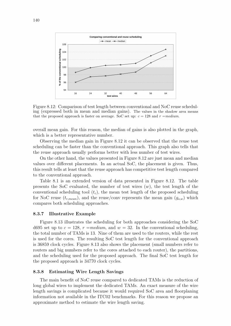
140
Comparing conventional and reuse scheduling
94
96
98
100
102
104
106
16 24 32 40 48 56 64test wires
% o
f the
con
vent
iona
l sch
edul
ing
mean median
Figure 8.12: Comparison of test length between conventional and NoC reuse schedul-ing (expressed both in mean and median gains). The values in the shadow area meansthat the proposed approach is faster on average. SoC set up: c = 128 and r =medium.
overall mean gain. For this reason, the median of gains is also plotted in the graph,which is a better representative number.
Observing the median gain in Figure 8.12 it can be observed that the reuse testscheduling can be faster than the conventional approach. This graph also tells thatthe reuse approach usually performs better with less number of test wires.
On the other hand, the values presented in Figure 8.12 are just mean and medianvalues over different placements. In an actual SoC, the placement is given. Thus,this result tells at least that the reuse approach has competitive test length comparedto the conventional approach.
Table 8.1 is an extended version of data presented in Figure 8.12. The tablepresents the SoC evaluated, the number of test wires (w), the test length of theconventional scheduling tool (tc), the mean test length of the proposed schedulingfor NoC reuse (tr,mean), and the reuse/conv represents the mean gain (gs,w) whichcompares both scheduling approaches.
8.3.7 Illustrative Example
Figure 8.13 illustrates the scheduling for both approaches considering the SoCd695 set up to c = 128, r =medium, and w = 32. In the conventional scheduling,the total number of TAMs is 13. Nine of them are used to the routers, while the restis used for the cores. The resulting SoC test length for the conventional approachis 36859 clock cycles. Figure 8.13 also shows the placement (small numbers refer torouters and big numbers refer to the cores attached to each router), the partitions,and the scheduling used for the proposed approach. The final SoC test length forthe proposed approach is 34770 clock cycles.
8.3.8 Estimating Wire Length Savings
The main benefit of NoC reuse compared to dedicated TAMs is the reduction oflong global wires to implement the dedicated TAMs. An exact measure of the wirelength savings is complicated because it would required SoC area and floorplaninginformation not available in the ITC02 benchmarks. For this reason we propose anapproximate method to estimate the wire length saving.

141
SOC w conv reuse-mean reuse/conv SOC w conv reuse-mean reuse/conv
16 71254 68475 96.10 16 1773610 1475641 83.2024 47872 46191 96.49 24 1155070 1004815 86.9932 36859 35598 96.58 32 883601 782077 88.5140 29974 28943 96.56 40 696556 652163 93.6348 25131 24000 95.50 48 598417 609949 101.9356 21135 21125 99.95 56 551119 606232 110.00
d695
64 18173 18778 103.33
p34392
64 544579 601359 110.4316 382275 439093 114.86 16 2130063 2044513 95.9824 335334 384416 114.64 24 1401929 1380268 98.4532 335334 383305 114.31 32 1056006 1044235 98.8940 335334 383162 114.26 40 851859 849902 99.7748 335334 383275 114.30 48 735157 690205 93.8956 335334 382580 114.09 56 605215 601469 99.38
f2126
64 335334 382488 114.06
p93791
64 529719 525372 99.1816 94942 84317 88.81 16 2222349 3082996 138.7324 62913 58655 93.23 24 2222349 3084733 138.8132 47277 43228 91.44 32 2222349 3080736 138.6340 38318 35611 92.94 40 2222349 3078188 138.5148 32543 30453 93.58 48 2222349 3076399 138.4356 28576 27635 96.71 56 2222349 3076168 138.42
g1023
64 23998 25049 104.38
q12710
64 2222349 3076066 138.4216 124135 129417 104.26 16 10604336 10788891 101.7424 119357 125079 104.79 24 10453470 10604673 101.4532 119357 123349 103.34 32 5289094 5641771 106.6740 119357 122781 102.87 40 5228420 5377666 102.8548 119357 122523 102.65 48 5228420 5373960 102.7856 119357 122299 102.46 56 5228420 5373817 102.78
h953
64 119357 122196 102.38
t512505
64 5228420 5373715 102.7816 759188 652088 85.89 16 60014634 46338535 77.2124 508022 441846 86.97 24 40919068 31522271 77.0432 382783 339004 88.56 32 31371285 24554574 78.2740 314216 271910 86.54 40 24608398 19328372 78.5448 257179 230688 89.70 48 21823502 16843936 77.1856 225100 204796 90.98 56 19095564 14433285 75.58
p22810
64 197198 179308 90.93
u226
64 16367627 13251262 80.96 Table 8.1: Extended results with the SoCs set up to c = 128 and r =medium.
reuse/conv < 100 means that the proposed approach is faster.
119
Exemplo d695 (128-medium-3_3-2 32 fios)
vTAM1 = { {{0,2}}, {{0,2}}, 7}vTAM2 = { {{0,0}, {2,1}}, {{0,0}, {0,1}, {1,0}, {2,0}, {2,1}, {2,2}}, 20}vTAM3 = { {{1,1}}, {{1,1}, {1,2}}, 5}
401401
2,311
2,311
0,821
0,821
600600
1,910
1,910
-20-
20
502502
712712
-22-
22
35750
0,1,40,1,46,86,8
7,97,92,3,52,3,5
34597368593424836759
w1.
.9=1
w10 = 7w11 = 3w12 = 5w13 = 8
routers
557,2,37,2,3
4,6,1,9,0,84,6,1,9,0,8
347703260934394
w1 = 7w2 = 5
w3 = 20
prop
osed
appr
oach
sche
dulin
gof
the
conv
entio
nal
appr
oach
final partition resulting scheduling
Figure 8.13: Example of both resulting schedulings for the d695 SoC. SoC set up toc = 128, r =medium, and w = 32.
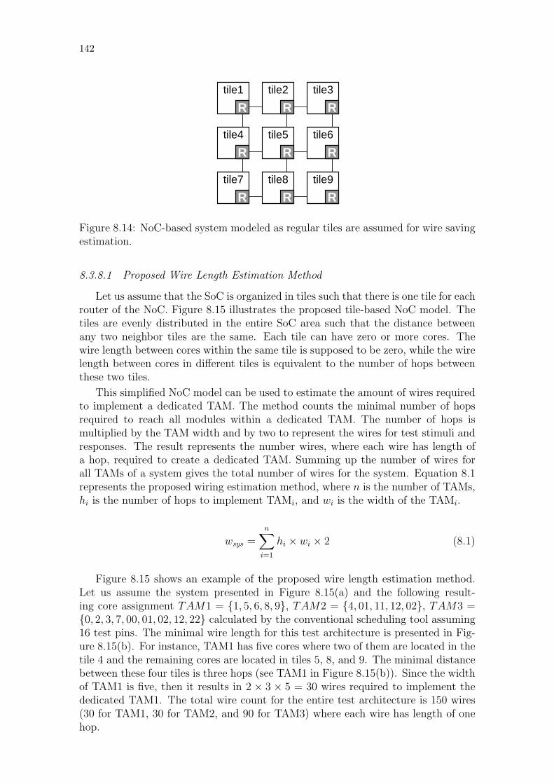
142
127
tile2
01 11 21
00 10 20
02 12 22
0
1
2
3
4
5
6
7
8 9
TAM 1 (w=5)TAM 2 (w=5)TAM 3 (w=9)
(a) placement for d695circles are routers squares are cores
(b) resulting dedicated TAMs
tile4 tile5 tile6
tile7 tile8 tile9
tile1 tile2 tile3tile1
Rtile2 tile3
R
tile4 tile5 tile6
tile7
Rtile8 tile9
R
R
R
R
R R
Figure 8.14: NoC-based system modeled as regular tiles are assumed for wire savingestimation.
8.3.8.1 Proposed Wire Length Estimation Method
Let us assume that the SoC is organized in tiles such that there is one tile for eachrouter of the NoC. Figure 8.15 illustrates the proposed tile-based NoC model. Thetiles are evenly distributed in the entire SoC area such that the distance betweenany two neighbor tiles are the same. Each tile can have zero or more cores. Thewire length between cores within the same tile is supposed to be zero, while the wirelength between cores in different tiles is equivalent to the number of hops betweenthese two tiles.
This simplified NoC model can be used to estimate the amount of wires requiredto implement a dedicated TAM. The method counts the minimal number of hopsrequired to reach all modules within a dedicated TAM. The number of hops ismultiplied by the TAM width and by two to represent the wires for test stimuli andresponses. The result represents the number wires, where each wire has length ofa hop, required to create a dedicated TAM. Summing up the number of wires forall TAMs of a system gives the total number of wires for the system. Equation 8.1represents the proposed wiring estimation method, where n is the number of TAMs,hi is the number of hops to implement TAMi, and wi is the width of the TAMi.
wsys =n∑
i=1
hi × wi × 2 (8.1)
Figure 8.15 shows an example of the proposed wire length estimation method.Let us assume the system presented in Figure 8.15(a) and the following result-ing core assignment TAM1 = {1, 5, 6, 8, 9}, TAM2 = {4, 01, 11, 12, 02}, TAM3 ={0, 2, 3, 7, 00, 01, 02, 12, 22} calculated by the conventional scheduling tool assuming16 test pins. The minimal wire length for this test architecture is presented in Fig-ure 8.15(b). For instance, TAM1 has five cores where two of them are located in thetile 4 and the remaining cores are located in tiles 5, 8, and 9. The minimal distancebetween these four tiles is three hops (see TAM1 in Figure 8.15(b)). Since the widthof TAM1 is five, then it results in 2 × 3 × 5 = 30 wires required to implement thededicated TAM1. The total wire count for the entire test architecture is 150 wires(30 for TAM1, 30 for TAM2, and 90 for TAM3) where each wire has length of onehop.
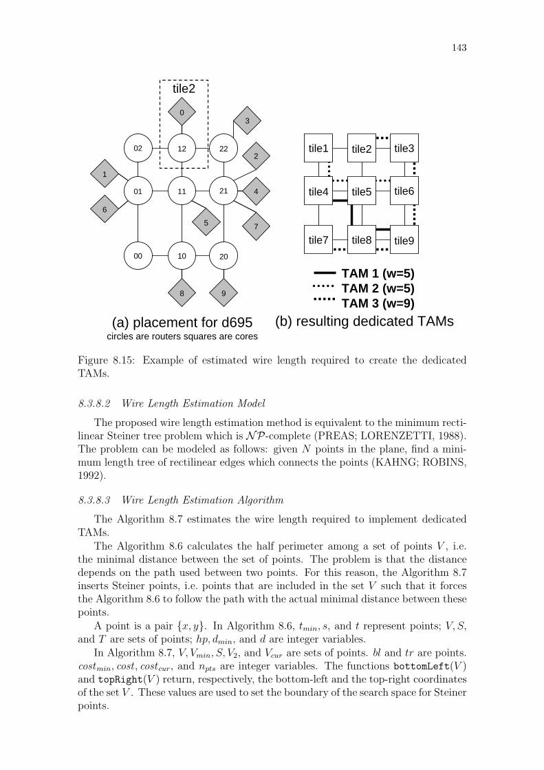
143
127
tile2
01 11 21
00 10 20
02 12 22
0
1
2
3
4
5
6
7
8 9
TAM 1 (w=5)TAM 2 (w=5)TAM 3 (w=9)
(a) placement for d695circles are routers squares are cores
(b) resulting dedicated TAMs
tile4 tile5 tile6
tile7 tile8 tile9
tile1 tile2 tile3tile1
Rtile2 tile3
R
tile4 tile5 tile6
tile7
Rtile8 tile9
R
R
R
R
R R
Figure 8.15: Example of estimated wire length required to create the dedicatedTAMs.
8.3.8.2 Wire Length Estimation Model
The proposed wire length estimation method is equivalent to the minimum recti-linear Steiner tree problem which is NP-complete (PREAS; LORENZETTI, 1988).The problem can be modeled as follows: given N points in the plane, find a mini-mum length tree of rectilinear edges which connects the points (KAHNG; ROBINS,1992).
8.3.8.3 Wire Length Estimation Algorithm
The Algorithm 8.7 estimates the wire length required to implement dedicatedTAMs.
The Algorithm 8.6 calculates the half perimeter among a set of points V , i.e.the minimal distance between the set of points. The problem is that the distancedepends on the path used between two points. For this reason, the Algorithm 8.7inserts Steiner points, i.e. points that are included in the set V such that it forcesthe Algorithm 8.6 to follow the path with the actual minimal distance between thesepoints.
A point is a pair {x, y}. In Algorithm 8.6, tmin, s, and t represent points; V, S,and T are sets of points; hp, dmin, and d are integer variables.
In Algorithm 8.7, V, Vmin, S, V2, and Vcur are sets of points. bl and tr are points.costmin, cost , cost cur, and npts are integer variables. The functions bottomLeft(V )and topRight(V ) return, respectively, the bottom-left and the top-right coordinatesof the set V . These values are used to set the boundary of the search space for Steinerpoints.
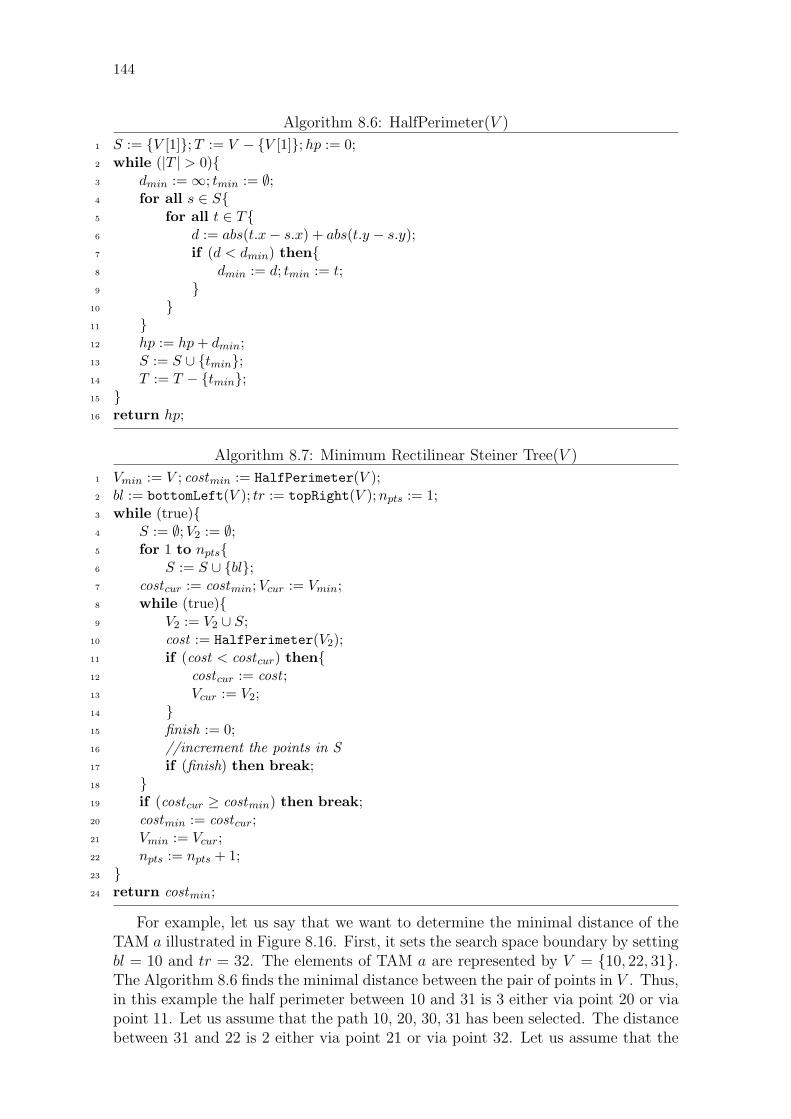
144
Algorithm 8.6: HalfPerimeter(V )
1 S := {V [1]};T := V − {V [1]};hp := 0;2 while (|T | > 0){3 dmin := ∞; tmin := ∅;4 for all s ∈ S{5 for all t ∈ T{6 d := abs(t.x− s.x) + abs(t.y − s.y);7 if (d < dmin) then{8 dmin := d; tmin := t;9 }
10 }11 }12 hp := hp + dmin;13 S := S ∪ {tmin};14 T := T − {tmin};15 }16 return hp;
Algorithm 8.7: Minimum Rectilinear Steiner Tree(V )
1 Vmin := V ; costmin := HalfPerimeter(V );2 bl := bottomLeft(V ); tr := topRight(V );npts := 1;3 while (true){4 S := ∅;V2 := ∅;5 for 1 to npts{6 S := S ∪ {bl};7 costcur := costmin;Vcur := Vmin;8 while (true){9 V2 := V2 ∪ S;
10 cost := HalfPerimeter(V2);11 if (cost < costcur) then{12 costcur := cost ;13 Vcur := V2;14 }15 finish := 0;16 //increment the points in S17 if (finish) then break;18 }19 if (costcur ≥ costmin) then break;20 costmin := costcur;21 Vmin := Vcur;22 npts := npts + 1;23 }24 return costmin;
For example, let us say that we want to determine the minimal distance of theTAM a illustrated in Figure 8.16. First, it sets the search space boundary by settingbl = 10 and tr = 32. The elements of TAM a are represented by V = {10, 22, 31}.The Algorithm 8.6 finds the minimal distance between the pair of points in V . Thus,in this example the half perimeter between 10 and 31 is 3 either via point 20 or viapoint 11. Let us assume that the path 10, 20, 30, 31 has been selected. The distancebetween 31 and 22 is 2 either via point 21 or via point 32. Let us assume that the
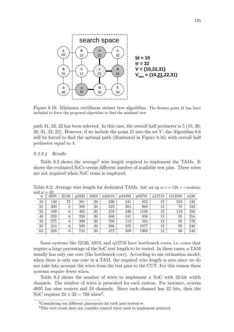
145
128
b01
b11
c21
a31
d00
a10
d20
b30
c02
b12
a22
c32 bl = 10
tr = 32V = {10,22,31}Vmin = {10,21,22,31}
search space
Figure 8.16: Minimum rectilinear steiner tree algorithm. The Steiner point 21 has beenincluded to force the proposed algorithm to find the minimal tree.
path 31, 32, 22 has been selected. In this case, the overall half perimeter is 5 (10, 20,30, 31, 32, 22). However, if we include the point 21 into the set V , the Algorithm 8.6will be forced to find the optimal path (illustrated in Figure 8.16) with overall halfperimeter equal to 4.
8.3.8.4 Results
Table 8.2 shows the average2 wire length required to implement the TAMs. Itshows the evaluated SoCs versus different number of available test pins. These wiresare not required when NoC reuse is employed.
Table 8.2: Average wire length for dedicated TAMs. SoC set up to c = 128, r =medium,and w = 32.
w d695 f2126 g1023 h953 p22810 p34392 p93791 q12710 t512505 u22616 140 72 281 29 326 241 855 12 523 12824 200 6 308 20 523 384 960 12 70 19232 109 6 405 20 478 336 1106 12 119 25640 233 6 226 20 508 341 838 12 95 25448 275 6 399 20 708 113 564 12 95 17656 314 6 509 20 386 376 1077 12 95 24064 203 6 724 20 472 389 1960 12 96 240
Some systems like f2126, h953, and q12710 have bottleneck cores, i.e. cores thatrequire a large percentage of the SoC test length to be tested. In these cases, a TAMusually has only one core (the bottleneck core). According to our estimation model,when there is only one core in a TAM, the required wire length is zero since we donot take into account the wires from the test pins to the CUT. For this reason thesesystems require fewer wires.
Table 8.3 shows the number of wires to implement a NoC with 32-bit widthchannels. The number of wires is presented for each system. For instance, systemd695 has nine routers and 24 channels. Since each channel has 32 bits, then theNoC requires 24× 32 = 768 wires3.
2Considering ten different placements for each pair system-w.3This wire count does not consider control wires used to implement protocol.
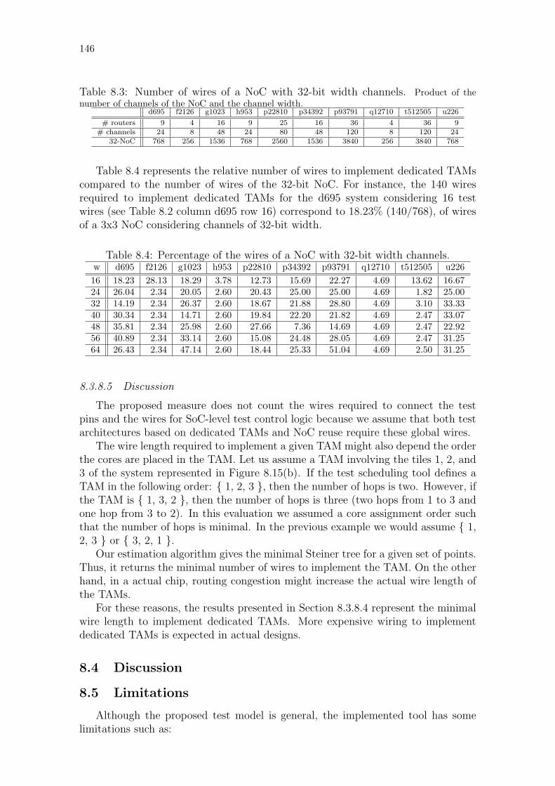
146
Table 8.3: Number of wires of a NoC with 32-bit width channels. Product of thenumber of channels of the NoC and the channel width.
d695 f2126 g1023 h953 p22810 p34392 p93791 q12710 t512505 u226
# routers 9 4 16 9 25 16 36 4 36 9# channels 24 8 48 24 80 48 120 8 120 24
32-NoC 768 256 1536 768 2560 1536 3840 256 3840 768
Table 8.4 represents the relative number of wires to implement dedicated TAMscompared to the number of wires of the 32-bit NoC. For instance, the 140 wiresrequired to implement dedicated TAMs for the d695 system considering 16 testwires (see Table 8.2 column d695 row 16) correspond to 18.23% (140/768), of wiresof a 3x3 NoC considering channels of 32-bit width.
Table 8.4: Percentage of the wires of a NoC with 32-bit width channels.w d695 f2126 g1023 h953 p22810 p34392 p93791 q12710 t512505 u22616 18.23 28.13 18.29 3.78 12.73 15.69 22.27 4.69 13.62 16.6724 26.04 2.34 20.05 2.60 20.43 25.00 25.00 4.69 1.82 25.0032 14.19 2.34 26.37 2.60 18.67 21.88 28.80 4.69 3.10 33.3340 30.34 2.34 14.71 2.60 19.84 22.20 21.82 4.69 2.47 33.0748 35.81 2.34 25.98 2.60 27.66 7.36 14.69 4.69 2.47 22.9256 40.89 2.34 33.14 2.60 15.08 24.48 28.05 4.69 2.47 31.2564 26.43 2.34 47.14 2.60 18.44 25.33 51.04 4.69 2.50 31.25
8.3.8.5 Discussion
The proposed measure does not count the wires required to connect the testpins and the wires for SoC-level test control logic because we assume that both testarchitectures based on dedicated TAMs and NoC reuse require these global wires.
The wire length required to implement a given TAM might also depend the orderthe cores are placed in the TAM. Let us assume a TAM involving the tiles 1, 2, and3 of the system represented in Figure 8.15(b). If the test scheduling tool defines aTAM in the following order: { 1, 2, 3 }, then the number of hops is two. However, ifthe TAM is { 1, 3, 2 }, then the number of hops is three (two hops from 1 to 3 andone hop from 3 to 2). In this evaluation we assumed a core assignment order suchthat the number of hops is minimal. In the previous example we would assume { 1,2, 3 } or { 3, 2, 1 }.
Our estimation algorithm gives the minimal Steiner tree for a given set of points.Thus, it returns the minimal number of wires to implement the TAM. On the otherhand, in a actual chip, routing congestion might increase the actual wire length ofthe TAMs.
For these reasons, the results presented in Section 8.3.8.4 represent the minimalwire length to implement dedicated TAMs. More expensive wiring to implementdedicated TAMs is expected in actual designs.
8.4 Discussion
8.5 Limitations
Although the proposed test model is general, the implemented tool has somelimitations such as:

147
1. topology.The current topology representation is based on matrix instead of on graph.It has been chosen to ease the implementation, but it imposes limitationson the supported topologies. For instance, just mesh topology is currentlysupported. Irregular topologies could be supported by changing the topologyrepresentation from matrix to graphs.
2. routing algorithm.The current results are based only on XY routing algorithm. A library ofrouting algorithms could be implemented such that the user could use one ofthe options in the library. The impact of routing algorithm shall be evaluatedin the future.
8.6 Summary
This chapter presented a scheduling optimization tool for BE NoC-based sys-tems that use the NoC to transport test data. The algorithm minimizes both testlength and silicon area of the DfT logic. We compared the test length of the pro-posed approach with an algorithm used for test architectures based on conventionaldedicated TAMs. The results show similar test length for both approaches. Wethink that the results presented in this chapter are a first step to actually define theadvantages and drawbacks of NoC-reuse compared to dedicated TAMs. The secondproblem addressed in this chapter is the need for general NoC-reuse approaches.We have demonstrated that the proposed approach is more general than the previ-ous one since it does not require a full cycle-accurate NoC model to determine thetest scheduling. We have also proposed a model to evaluate the amount of wiresrequired to implement dedicated TAMs. This model estimates the amount of wirelength saving by using NoC to transport test data.
On the other hand, we reinforce that it is still required to test the proposedmethod with different NoCs features (different topologies, services, costs). In addi-tion, we plan to compare the proposed approach with the packet-based and dedicated-path algorithms (COTA; LIU, 2006).

148
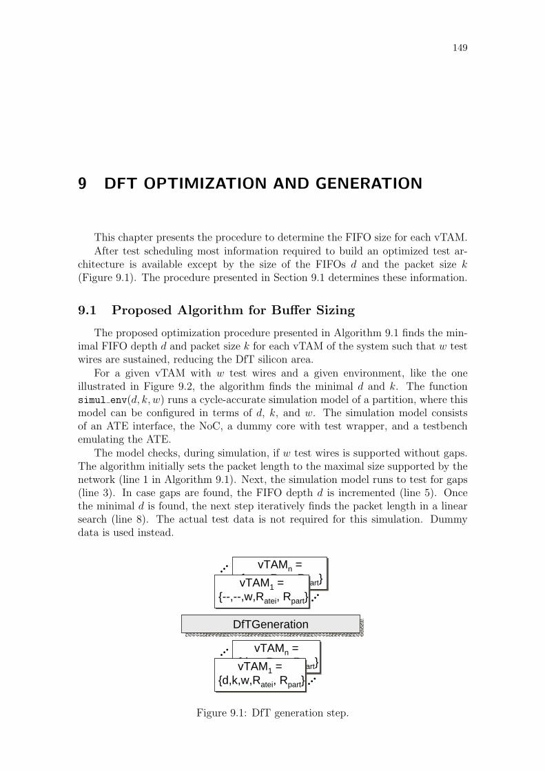
149
9 DFT OPTIMIZATION AND GENERATION
This chapter presents the procedure to determine the FIFO size for each vTAM.
After test scheduling most information required to build an optimized test ar-chitecture is available except by the size of the FIFOs d and the packet size k(Figure 9.1). The procedure presented in Section 9.1 determines these information.
9.1 Proposed Algorithm for Buffer Sizing
The proposed optimization procedure presented in Algorithm 9.1 finds the min-imal FIFO depth d and packet size k for each vTAM of the system such that w testwires are sustained, reducing the DfT silicon area.
For a given vTAM with w test wires and a given environment, like the oneillustrated in Figure 9.2, the algorithm finds the minimal d and k. The functionsimul env(d, k, w) runs a cycle-accurate simulation model of a partition, where thismodel can be configured in terms of d, k, and w. The simulation model consistsof an ATE interface, the NoC, a dummy core with test wrapper, and a testbenchemulating the ATE.
The model checks, during simulation, if w test wires is supported without gaps.The algorithm initially sets the packet length to the maximal size supported by thenetwork (line 1 in Algorithm 9.1). Next, the simulation model runs to test for gaps(line 3). In case gaps are found, the FIFO depth d is incremented (line 5). Oncethe minimal d is found, the next step iteratively finds the packet length in a linearsearch (line 8). The actual test data is not required for this simulation. Dummydata is used instead.
128
DfTGenerationDfTGeneration
vTAMn ={--, w,Ratei, Rpart}
vTAMn ={--, w,Ratei, Rpart}vTAM1 =
{--,--,w,Ratei, Rpart}vTAM1 =
{--,--,w,Ratei, Rpart}
vTAMn ={d, w,Ratei, Rpart}
vTAMn ={d, w,Ratei, Rpart}vTAM1 =
{d,k,w,Ratei, Rpart}vTAM1 =
{d,k,w,Ratei, Rpart}
Figure 9.1: DfT generation step.
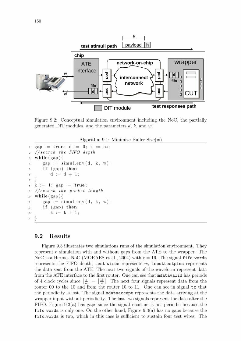
150
62
interconnectnetwork
port
network-on-chip wrapper
CUTCUT
ATEinterface
chip
port
portport
DfT module
fifofifo
test stimuli path
test responses path
w
wd
payload h
k
d
Figure 9.2: Conceptual simulation environment including the NoC, the partiallygenerated DfT modules, and the parameters d, k, and w.
Algorithm 9.1: Minimize Buffer Size(w)
1 gap := true ; d := 0 ; k := ∞ ;2 // search the FIFO depth3 while ( gap ){4 gap := s imul env (d , k , w) ;5 i f ( gap ) then6 d := d + 1 ;7 }8 k := 1 ; gap := true ;9 // search the packe t l e n g t h
10 while ( gap ){11 gap := s imul env (d , k , w) ;12 i f ( gap ) then13 k := k + 1 ;14 }
9.2 Results
Figure 9.3 illustrates two simulations runs of the simulation environment. Theyrepresent a simulation with and without gaps from the ATE to the wrapper. TheNoC is a Hermes NoC (MORAES et al., 2004) with c = 16. The signal fifo words
represents the FIFO depth, test wires represents w, inputtestpins representsthe data sent from the ATE. The next two signals of the waveform represent datafrom the ATE interface to the first router. One can see that mdatavalid has periodsof 4 clock cycles since
⌊cw
⌋=
⌊164
⌋. The next four signals represent data from the
router 00 to the 10 and from the router 10 to 11. One can see in signal tx thatthe periodicity is lost. The signal sdataaccept represents the data arriving at thewrapper input without periodicity. The last two signals represent the data after theFIFO. Figure 9.3(a) has gaps since the signal read en is not periodic because thefifo words is only one. On the other hand, Figure 9.3(a) has no gaps because thefifo words is two, which in this case is sufficient to sustain four test wires. The
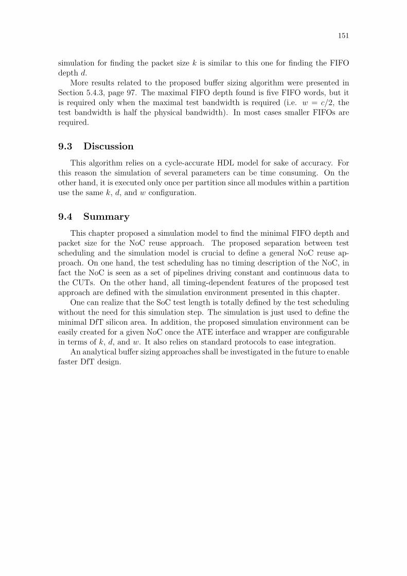
151
simulation for finding the packet size k is similar to this one for finding the FIFOdepth d.
More results related to the proposed buffer sizing algorithm were presented inSection 5.4.3, page 97. The maximal FIFO depth found is five FIFO words, but itis required only when the maximal test bandwidth is required (i.e. w = c/2, thetest bandwidth is half the physical bandwidth). In most cases smaller FIFOs arerequired.
9.3 Discussion
This algorithm relies on a cycle-accurate HDL model for sake of accuracy. Forthis reason the simulation of several parameters can be time consuming. On theother hand, it is executed only once per partition since all modules within a partitionuse the same k, d, and w configuration.
9.4 Summary
This chapter proposed a simulation model to find the minimal FIFO depth andpacket size for the NoC reuse approach. The proposed separation between testscheduling and the simulation model is crucial to define a general NoC reuse ap-proach. On one hand, the test scheduling has no timing description of the NoC, infact the NoC is seen as a set of pipelines driving constant and continuous data tothe CUTs. On the other hand, all timing-dependent features of the proposed testapproach are defined with the simulation environment presented in this chapter.
One can realize that the SoC test length is totally defined by the test schedulingwithout the need for this simulation step. The simulation is just used to define theminimal DfT silicon area. In addition, the proposed simulation environment can beeasily created for a given NoC once the ATE interface and wrapper are configurablein terms of k, d, and w. It also relies on standard protocols to ease integration.
An analytical buffer sizing approaches shall be investigated in the future to enablefaster DfT design.
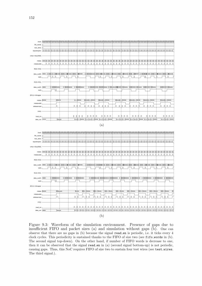
152
1
4
0000 1010 0101 1010 0101 1010 0101 1010 0101 1010 0101 1010 0101 1010 0101 1010 0101 1010 0101 1010 0101 1010 0101 1010 0101 1010 0101 1010 0101 1010 0101 1010 0101 1010 0101 1010 0101 1010 0101 1010 0101 1010 0101 1010 0101 1010 0101 1010
MasterAte=>Noc(R00)
0000 0000 0000 0000 0000 0000 0000 0000 0000 0000 0000 0000 0000 0000 0000 0000 0000 0000 0000 0000 0000 0000 0000 0000 0000 0000 0000 0000 0000 0000 0000 0000 0000 0000 0000 0000 0000 0000 0000 0000 0000 0000 0000 0000 0000 0000
R00=>R10
0000 0011 0000 0000 5555 0000 0011 0000 5555 0000 0011 0004 5555 0000 0011 0000 0011 0004 5555 0000 0011 0004 5555 0000 0011 0004 5555 0000 0011 0004 5555 0000 0011 5555 0000 0011 0004 5555 0000 0011 0004 5555 0000 0011
R10=>R11
0000 0011 5555 0000 0011 0000 0011 0000 0011 0000 0011 0000 0011 5555 0000 0011 5555 0000 0011 5555 0000 0011 5555 0000 0011 5555
NoC(R11)=>Wrapper
0000 5555 AAAA 5555 5555 AAAA 5555 5555 AAAA 5555 5555 AAAA 5555 5555 AAAA 5555 5555 AAAA 5555 5555 AAAA 5555
FIFO
FFFF AAAA 5555 AAAA 5555 AAAA 5555 AAAA 5555 AAAA 5555 AAAA 5555 AAAA 5555 AAAA 5555 AAAA 5555 AAAA 5555 AAAA 5555 AAAA 5555 AAAA 5555 AAAA 5555
0 2 us 4 us 6 us 8 us 10 us 12 us 14 us
clock
fifo_words 1
test_wires 4
inputtestpins 0000 1010 0101 1010 0101 1010 0101 1010 0101 1010 0101 1010 0101 1010 0101 1010 0101 1010 0101 1010 0101 1010 0101 1010 0101 1010 0101 1010 0101 1010 0101 1010 0101 1010 0101 1010 0101 1010 0101 1010 0101 1010 0101 1010 0101 1010 0101 1010
MasterAte=>Noc(R00)
mdata 0000 0000 0000 0000 0000 0000 0000 0000 0000 0000 0000 0000 0000 0000 0000 0000 0000 0000 0000 0000 0000 0000 0000 0000 0000 0000 0000 0000 0000 0000 0000 0000 0000 0000 0000 0000 0000 0000 0000 0000 0000 0000 0000 0000 0000 0000
mdatavalid
R00=>R10
data_out(0) 0000 0011 0000 0000 5555 0000 0011 0000 5555 0000 0011 0004 5555 0000 0011 0000 0011 0004 5555 0000 0011 0004 5555 0000 0011 0004 5555 0000 0011 0004 5555 0000 0011 5555 0000 0011 0004 5555 0000 0011 0004 5555 0000 0011
tx(0)
R10=>R11
data_out(2) 0000 0011 5555 0000 0011 0000 0011 0000 0011 0000 0011 0000 0011 5555 0000 0011 5555 0000 0011 5555 0000 0011 5555 0000 0011 5555
tx(2)
NoC(R11)=>Wrapper
mdata 0000 5555 AAAA 5555 5555 AAAA 5555 5555 AAAA 5555 5555 AAAA 5555 5555 AAAA 5555 5555 AAAA 5555 5555 AAAA 5555
mdatavalid
sdataaccept
FIFO
read_en
data_out FFFF AAAA 5555 AAAA 5555 AAAA 5555 AAAA 5555 AAAA 5555 AAAA 5555 AAAA 5555 AAAA 5555 AAAA 5555 AAAA 5555 AAAA 5555 AAAA 5555 AAAA 5555 AAAA 5555
Entity:tb_vhd Architecture:behavior Date: Tue Apr 24 18:30:59 E. South America Standard Time 2007 Row: 1 Page: 1
(a)
2
4
0000 1010 0101 1010 0101 1010 0101 1010 0101 1010 0101 1010 0101 1010 0101 1010 0101 1010 0101 1010 0101 1010 0101 1010 0101 1010 0101 1010 0101 1010 0101 1010 0101 1010 0101 1010 0101 1010 0101 1010 0101 1010 0101 1010 0101 1010 0101 1010
MasterAte=>Noc(R00)
0000 0000 0000 0000 0000 0000 0000 0000 0000 0000 0000 0000 0000 0000 0000 0000 0000 0000 0000 0000 0000 0000 0000 0000 0000 0000 0000 0000 0000 0000 0000 0000 0000 0000 0000 0000 0000 0000 0000 0000 0000 0000 0000 0000 0000 0000
R00=>R10
0000 0011 0000 0000 5555 0000 0011 0000 5555 0000 0011 0004 5555 0000 0011 0000 0011 5555 0000 0011 0004 5555 0000 0011 0004 5555 0000 0011 0004 5555 0000 0011 0004 5555 0000 0011 0004 5555 0000 0011 0004 5555 0000 0011
R10=>R11
0000 0011 5555 0000 0011 0000 0011 0000 0011 0000 0011 0000 0011 0000 0011 0000 0011 0000 0011 0000 0011 0000 0011 0000
NoC(R11)=>Wrapper
0000 AAAA 5555 AAAA 5555 AAAA 5555 AAAA 5555 AAAA 5555 AAAA 5555 AAAA 5555 AAAA 5555 AAAA 5555
FIFO
0000 AAAA 5555 AAAA 5555 AAAA 5555 AAAA 5555 AAAA 5555 AAAA 5555 AAAA 5555 AAAA 5555 AAAA 5555 AAAA 5555 AAAA 5555 AAAA 5555 AAAA 5555 AAAA 5555 AAAA 5555 AAAA 5555 AAAA 5555 AAAA 5555
0 2 us 4 us 6 us 8 us 10 us 12 us 14 us
clock
fifo_words 2
test_wires 4
inputtestpins 0000 1010 0101 1010 0101 1010 0101 1010 0101 1010 0101 1010 0101 1010 0101 1010 0101 1010 0101 1010 0101 1010 0101 1010 0101 1010 0101 1010 0101 1010 0101 1010 0101 1010 0101 1010 0101 1010 0101 1010 0101 1010 0101 1010 0101 1010 0101 1010
MasterAte=>Noc(R00)
mdata 0000 0000 0000 0000 0000 0000 0000 0000 0000 0000 0000 0000 0000 0000 0000 0000 0000 0000 0000 0000 0000 0000 0000 0000 0000 0000 0000 0000 0000 0000 0000 0000 0000 0000 0000 0000 0000 0000 0000 0000 0000 0000 0000 0000 0000 0000
mdatavalid
R00=>R10
data_out(0) 0000 0011 0000 0000 5555 0000 0011 0000 5555 0000 0011 0004 5555 0000 0011 0000 0011 5555 0000 0011 0004 5555 0000 0011 0004 5555 0000 0011 0004 5555 0000 0011 0004 5555 0000 0011 0004 5555 0000 0011 0004 5555 0000 0011
tx(0)
R10=>R11
data_out(2) 0000 0011 5555 0000 0011 0000 0011 0000 0011 0000 0011 0000 0011 0000 0011 0000 0011 0000 0011 0000 0011 0000 0011 0000
tx(2)
NoC(R11)=>Wrapper
mdata 0000 AAAA 5555 AAAA 5555 AAAA 5555 AAAA 5555 AAAA 5555 AAAA 5555 AAAA 5555 AAAA 5555 AAAA 5555
mdatavalid
sdataaccept
FIFO
read_en
data_out 0000 AAAA 5555 AAAA 5555 AAAA 5555 AAAA 5555 AAAA 5555 AAAA 5555 AAAA 5555 AAAA 5555 AAAA 5555 AAAA 5555 AAAA 5555 AAAA 5555 AAAA 5555 AAAA 5555 AAAA 5555 AAAA 5555 AAAA 5555 AAAA 5555
Entity:tb_vhd Architecture:behavior Date: Tue Apr 24 18:32:54 E. South America Standard Time 2007 Row: 1 Page: 1
(b)
Figure 9.3: Waveform of the simulation environment. Presence of gaps due toinsufficient FIFO and packet sizes (a) and simulation without gaps (b). One canobserve that there are no gaps in (b) because the signal read en is periodic, i.e. it ticks every 4clock cycles. This periodicity is sustained thanks to the FIFO of size two (see fifo words in (b).The second signal top-down). On the other hand, if number of FIFO words is decrease to one,then it can be observed that the signal read en in (a) (second signal bottom-up) is not periodic,causing gaps. Thus, this NoC requires FIFO of size two to sustain four test wires (see test wires.The third signal.).
153
10 CONCLUSION
Currently, global interconnect solutions based on long wires, like buses, are beingreplaced by solutions based on shared and segmented wires, like NoCs, to reducethe cost of global interconnect. It has been demonstrated that conventional test-dedicated TAMs can also be considered long global wires, thus, TAMs are alsosubject to the same interconnect problems. For this reason, we have investigatedthe use of the NoC to transport test data during test application to avoid test-dedicated TAMs.
However, most of the research on NoC reuse has focused on high level test modelsfor an specific case study. On one hand, this approach is important to introduce theNoC reuse problem and to demonstrate the viability of the approach. On the otherhand, (i) accurate DfT models and (ii) generic test tools are required to enable theactual use of NoC reuse on existing NoC-based designs. Another important gap was(iii) the lack of quantitative comparisons between test architectures based on NoCreuse and on dedicated TAMs to actually define the advantage and drawbacks ofboth approaches. These three points are the main contributions of this thesis.
The rest of this chapter details the main contributions, the limitations, andfuture work.
10.1 Qualitative Analysis
10.1.1 Toward a General NoC-Reuse Approach
We believe that NoC reuse will be actually used if and only if general approachesthat work for most NoC exist. We proposed a test model that can work for a largenumber of NoC instances. As far as we know this work is the first one to createawareness about the need for general NoC reuse approaches.
10.1.2 Compatibility with Conventional SoC Modular Testing
The advantage of similar and compatible solutions are numerous. For instance,a wrapper design considering hierarchical cores was proposed for conventional TAM.If a NoC reuse can work exactly like a dedicated TAM, then the chances that thesame wrapper can be used for NoC reuse are high. The same conclusion can also beapplied for algorithms, design tools, test equipments, etc. In conclusion, assumingsimilar assumptions reduce the required adaptation effort. It also makes a possibletransition from the conventional to the proposed approach smoother.
Scheduling for NoC reuse had been seen as something completely different fromscheduling with conventional TAM since the former involves NoCs which are much
154
more complex and not standardized than conventional TAMs. Most authors advo-cate that new solutions are required. This thesis demonstrates the opposite. It justdepends on how he problem is modeled.
For example, in terms of DfT, we show that a proper core terminal classification,adding protocol information and FIFO to the wrapper design is enough to adaptthe conventional wrapper design to the NoC reuse environment.
Moreover, in terms of reused algorithms, we adapted the conventional algorithmsfor wrapper optimization with a very simple modification on the algorithm; byincluding the constraints of equal number of SDI and SDO terminals per test wire.In addition, we adapted a conventional algorithm for test scheduling by addingneighborhood and maximal TAM width constraints.
These examples show that the research done in the past based on conventionalTAMs can be easily adapted for the NoC-reuse problem by using an appropriateunderlying test model and compatible assumptions. We believe that our focus oncompatibility might be fruitful in the near future because it will enable people toeasily adapt previous methods for NoC reuse. Moreover it will ease a possibletransition from dedicated TAMs to NoC as TAM.
10.1.3 Detailed DfT Design
As far as we know there were no papers focusing on DfT design for NoC reuse.The modification required in the test logic to enable NoC reuse were not known.Simplistic (i.e. do not consider important design issues) and unoptimized wrappermodels were usually assumed in the test scheduling (see Section 5.5).
The results presented in (AMORY et al., 2006) were probably the first address-ing the problem of DfT to enable NoC reuse, followed by (AMORY et al., 2007) and(AMORY et al., 2007). Actual HDL designs and DfT optimization tools were gen-erated along this thesis. The HDL description of the DfT modules were simulatedand, when it was possible, prototyped on FPGA for verification purposes.
For instance, we were the first to address the need for protocol conversion logicinside the wrapper to enable NoC reuse. This obligation has a significant impact onthe increase of DfT silicon area. In addition, we have addressed the need for a newcore test length expression. We have shown that the core test length for NoC reusemight be different compared to conventional wrapper.
In conclusion, by addressing practical problems in NoC-reuse we helped to definethe required changes in the DfT logic to give support to NoC reuse.
10.1.4 Comparison with Conventional Test Architecture
As far as we know, we were the first to compare test length and silicon areabetween a NoC reuse approach and a conventional test approach based on dedicatedTAM. This comparison demonstrates the actual advantages and drawbacks of bothapproaches.
10.2 Quantitative Analysis
Our quantitative analysis is based on test length and silicon area for the DfTlogic.
155
10.2.1 SoC Test Length
Our results on test length show that the proposed test architecture is statisticallyas fast as the conventional architecture. On one hand, the neighborhood constraintsincrease the SoC test length. On the other hand, the core test length of the proposedapproach is usually faster than the one for conventional wrapper. The combinationof these two facts results in similar SoC test length. This result is surprising since weimagined that the proposed test approach would be slower due to the neighborhoodand TAM width constraints.
10.2.2 Silicon Area for DfT Modules
We helped to define the actual advantages of NoC reuse compared to conventionalTAMs in terms of required silicon area. For instance, most of prior work assumedvery low or even no area overhead for DfT. We have shown that in fact the siliconarea for DfT for NoC reuse is around 20% more expensive compared to DfT fordedicated TAMs. Most of prior work assumed that there would be no global longwires added into the chip just for test purposes. We have shown that most longwires were actually eliminated, however, some as the wires for test control logic andwires connecting the test pins are still required.
We proposed a new method to evaluate the wire length saving using NoC reuse.The results reported an average wire length saving from 2% to 51% compared to aNoC whose channel width has 32-bit.
10.3 Prospected Impact
We demonstrated the need for first establish actual DfT designs before defininghigh level test models and test scheduling tools. It is important to evaluate ‘low-level’ design issues like integration of DfT logic to the rest of the system, evaluatesilicon area of the DfT, configurability of the DfT model, how easy it is to integratethe proposed logic to different NoCs, and characterize the DfT model in terms oftest length. For instance, without working on wrapper design for NoC reuse wewould not found the need for a different core test length formulation. We hope thatthis work motivates other researches on DfT for NoC reuse.
We created awareness of the need for compatible and general NoC reuse ap-proach. Although we have focused on BE networks, we hope to motivate moreresearch on general NoC reuse for other NoC domains (GT, BE, async).
10.4 Accomplished Goals and Contribution
These are the goals established in the Section 1.2 page 31 and how they wereaccomplished:
• Make the requirements for NoC reuse explicit.The problem statement presented in Section 4.7 defines all required variablesfor the test architecture optimization problem.
• Determine the design of the required DfT modules.Chapters 5.5, 6, and 7 presented the proposed DfT design and optimizationprocedures.
156
• Determine the optimization algorithms for the DfT modules.See last item.
• Propose a test schedule tool for overall test architecture optimization.The proposed design flow integrates the DfT optimization procedures with thetest scheduling tool to generate an optimized test architecture.
• Integrated framework for DfT modules, vTAMs, and SoC test length co-optimization.The design flow and developed tools presented in Section 4.8, page 80, enablesan overall reduction of silicon area for the DfT modules and SoC test length.
• Implement a tool to evaluate wire length savings using NoC reuse.This tool has been presented in Section 8.3.8, page 140.
• Compare the proposed test architecture with the conventional test architecturebased on dedicated TAM to establish the actual advantages and drawbacks ofNoC reuse.The results presented in Sections 8.3 and 5.4 support our comparison betweenboth test approaches.
Some additional contributions include:
• Tools for wrapper optimization for both NoC reuse and dedicated TAMs;
• Tools for test scheduling for both NoC reuse and dedicated TAMs;
• Several small tools and scripts used to generate and gather data;
• HDL models for DfT modules.
10.5 Limitations and Issues Not Addressed
Although the following issues were not addressed in this thesis for lack of time,they should be investigated in the future:
• Test scheduling toolThe test scheduling tool is not as general as the proposed test model. However,it is still more general than the approaches found so far; the reduced numberof NoC information required demonstrates this fact. The test scheduling toolworks for mesh and XY based NoCs without guaranteed services. With a littlemore programming effort the test scheduling tool will become as general as theproposed test model by supporting irregular topologies and multiple routingalgorithms;
• Wiring length from test pins to ATE interfaceNo procedure is proposed to minimize the wires required to connect the testpins to the DfT logic;
• Wiring length of test control signals like scan enable, reset, and IEEE Std.1500No procedure is proposed to minimize the wires required for top-level testcontrol logic;
157
• Support other scheduling constraints like power consumption during test, prece-dence constraints, among othersIt was out of the scope of this thesis to investigate other constraints ratherthan test length and silicon area for DfT since these features were not wellestablished yet. However, these are relevant topics for future work;
• Extend the model for NoCs with multiple frequencies and asynchronous NoCsIt was out of the scope of this thesis to investigate this kind of NoCs. However,these are also relevant topics for future work;
• Comparison with other NoC reuse approachIt was out of the scope of this thesis to compare with other NoC reuse approachbecause there was no work comparing NoC reuse and conventional approach.Thus, the advantages and drawbacks of NoC reuse were not clear so far. More-over, it is hard to accomplish such comparison due to the lack of benchmarksto evaluate NoC reuse approaches.
10.6 Future Work
This thesis has explored a wide range of problems related to NoC reuse as TAM.However, some of the proposed approaches can be improved (item 1 to 4) and morecomplete test models can be created (5 to 11) to support other design issues.
1. Graph-based test scheduling tool to support topology independent NoCs ;
2. Generate cost-effective wrapper for routers ;
3. DfT for NoCs without identical routers ;
4. Allow user to specify wrapper protocolCurrently only a subset of OCP is supported;
5. Benchmarks for NoC reuse are requiredCurrently a fair comparison between the existent approaches is complex or notpossible;
6. Test scheduling for NoCs with guaranteed services ;
7. Reusing asynchronous NoCs as TAM ;
8. Interconnect test for NoC channels ;
9. Testing systems with different test frequencies ;
10. Support of hierarchical cores ;
11. Testing Mixed-signal SoCs ;
12. Evaluate other test constraints like power dissipation, thermal, and precedence.

158
159
REFERENCES
AITKEN, R. C. A Modular Wrapper Enabling High Speed BIST and Repair forSmall Wide Memories. In: ITC, 2004. Proceedings. . . Washington: IEEE Com-puter Society, 2004. p.997–1005.
AKTOUF, C. A Complete Strategy for Testing an on-chip Multiprocessor Architec-ture. IEEE Design & Test of Computers, [S.l.], v.19, n.1, p.18–28, 2002.
ALLIANCE, V. Virtual Component Interface Standard. Available at:<http://www.vsi.org/>. Visited on: Oct. 2006.
AMORY, A. M.; BRIAO, E. W.; COTA, E. F.; LUBASZEWSKI, M. S.; MORAES,F. G. A Scalable Test Strategy for Network-on-Chip Routers. In: ITC, 2005, Austin,Texas, USA. Proceedings. . . Los Alamitos: IEEE Computer Society, 2005. p.591–599.
AMORY, A. M.; COTA, E. F.; LUBASZEWSKI, M. S.; MORAES, F. G. ReducingTest Time with Processor Reuse in Network-on-Chip Based Systems. In: SBCCI,2004, Porto de Galinhas, PE, Brazil. Proceedings. . . New York: ACM, 2004.p.111–116.
AMORY, A. M.; FERLINI, F.; LUBASZEWSKI, M. S.; MORAES, F. G. DfT forthe Reuse of Networks-on-Chip as Test Access Mechanism. In: VTS, 2007, Berkeley,CA, USA. Proceedings. . . Los Alamitos: IEEE Computer Society, 2007. p.435–440.
AMORY, A. M.; GOOSSENS, K.; MARINISSEN, E. J.; LUBASZEWSKI, M. S.;MORAES, F. G. Wrapper Design for the Reuse of Networks-on-Chip as Test AccessMechanism. In: ETS, 2006, Southampton, UK. Proceedings. . . Los Alamitos:IEEE Computer Society, 2006. p.213–218.
AMORY, A. M.; GOOSSENS, K.; MARINISSEN, E. J.; LUBASZEWSKI, M. S.;MORAES, F. G. Wrapper Design for the Reuse of a Network on Chip or OtherFunctional Interconnect as Test Access Mechanism. IET Computers & DigitalTechniques, [S.l.], v.1, n.3, p.197–206, 2007.
AMORY, A. M.; LUBASZEWSKI, M. S.; MORAES, F. G. A Programmable LogicBIST Controller for IP Cores. In: LATW, 2004, Cartagena de Indias, Colombia.Proceedings. . . [S.l.: s.n.], 2004. p.104–109.
160
AMORY, A. M.; LUBASZEWSKI, M. S.; MORAES, F. G.; MORENO, E. I.Test Time Reduction Reusing Multiple Processors in a Network-on-Chip BasedArchitecture. In: DATE, 2005, Munich, Germany. Proceedings. . . Washington:IEEE Computer Society, 2005. v.1, p.62–63.
AMORY, A. M.; OLIVEIRA, L. A.; MORAES, F. G. Software-Based Test for Non-Programmable Cores in Bus-Based System-on-Chip Architectures. In: VLSI-SOC,2003, Darmstadt, Germany. Proceedings. . . [S.l.: s.n.], 2003. p.174–179.
APPELLO, D. et al. Exploiting Programmable BIST for the Diagnosis of EmbeddedMemory Cores. In: ITC, 2003. Proceedings. . . [S.l.: s.n.], 2003. p.379–385.
ARABI, K. Logic BIST and Scan Test Techniques for Multiple Identical Blocks.In: VTS, 2002, Monterey, CA, USA. Proceedings. . . Los Alamitos: IEEE Com-puter Society, 2002. p.60–68.
ARM. AMBA AXI Protocol Specification. Version 1.0. Availableat: <http://www.arm.com/products/solutions/AMBA3AXI.html>. Visited on:Oct. 2006.
ARM. AMBA 3 APB Protocol Specification. Version 1.0. Availableat: <http://www.arm.com/products/solutions/AMBAAPB.html>. Visited on:Oct. 2006.
ARTERIS. Arteris Introduces Industry’s First Products for Build-ing Networks on Chip (NoC). Available at: <http://www.us.design-reuse.com/news/news9888.html>. Visited on: Mar. 2006.
ARTERIS. Arteris Web Site. Available at: <http://www.arteris.net/>. Visitedon: Mar. 2006.
BAINBRIDGE, J.; FURBER, S. CHAIN: A Delay Insensitive CHip Area INtercon-nect. IEEE Micro, [S.l.], v.22, n.5, p.16–23, 2002.
BARDELL, P. H. Built-In Test for VLSI, Pseudorandom Techniques. [S.l.]:John Wiley & Sons, 1987.
BEEST, F. T. et al. Automatic Scan Insertion and Test Generation for SsynchronousCircuits. In: ITC, 2002. Proceedings. . . [S.l.: s.n.], 2002. p.804–813.
BENINI, L.; DE MICHELI, G. Networks on Chips: A New SoC Paradigm. IEEEComputer, [S.l.], v.35, n.1, p.70–80, 2002.
BENINI, L.; DE MICHELI, G. Networks on Chips, Technology and Tools.[S.l.]: Morgan Kaufmann Publishers, 2006.
BHUNIA, S. et al. A Novel Low-Overhead Delay Testing Technique for ArbitraryTwo-Pattern Test Application. In: DATE, 2005. Proceedings. . . Washington:IEEE Computer Society, 2005. p.1136–1141.
BJERREGAARD, T. The MANGO Clockless Network-on-Chip: Conceptsand Implementation. 2005. Tese (Doutorado em Ciencia da Computacao) — Tech-nical University of Denmark.
161
BJERREGAARD, T.; MAHADEVAN, S. A Survey of Research and Practices onNetwork-on-Chip. ACM Computing Surveys, [S.l.], v.38, n.1, 2006.
BJERREGAARD, T.; SPARSO, J. A Router Architecture for Connection-OrientedService Guarantees in the MANGO Clockless Network-on-Chip. In: DATE, 2005.Proceedings. . . Washington: IEEE Computer Society, 2005. p.1226–1231.
BJERREGAARD, T.; SPARSO, J. Scheduling Discipline for Latency and Band-width Guarantees in Asynchronous Network-on-Chip. In: ASYNC, 2005. Proceed-ings. . . [S.l.: s.n.], 2005. p.34–43.
BURDASS, A. et al. Embedded Test and Debug of Full Custom and SynthesisableMicroprocessor Cores. In: ETW, 2000. Proceedings. . . [S.l.: s.n.], 2000. p.17–22.
BUSHNELL, M. L.; AGRAWAL, V. D. Essentials of Electronic Testing forDigital, Memory, and Mixed-Signal VLSI Circuits. [S.l.]: Kluwer AcademicPublishers, 2000.
CAST. C1394A IEEE-1394a Link Layer Controller Core. Available at:<http://www.cast-inc.com/cores/c1394a/index.shtml>. Visited on: Oct. 2006.
CAST. PCIe-EP PCI Express Endpoint Controller Core. Available at:<http://www.cast-inc.com/cores/pcie-ep/index.shtml>. Visited on: Oct. 2006.
CAST. GPIO8 General Purpose Input/Output Unit Core. Available at:<http://www.cast-inc.com/cores/gpio8/index.shtml>. Visited on: Oct. 2006.
CHAKRABARTY, K. Design of System-on-a-Chip Test Access Architectures Us-ing Integer Linear Programming. In: VTS, 2000. Proceedings. . . Los Alamitos:IEEE Computer Society, 2000. p.127–134.
CIORDA, C. et al. NoC Monitoring: Impact on the Design Flow. In: ISCAS, 2006.Proceedings. . . [S.l.: s.n.], 2006. p.1981–1984.
CLERMIDY, F.; VARREAU, D.; LATTARD, D. A NoC-Based Communica-tion Framework for Seamless IP Integration in Complex Systems. Avail-able at: <http://www.us.design-reuse.com/articles/article12226.html>. Visited on:Mar. 2006.
COTA, E. F.; BRISOLARA, L.; CARRO, L.; SUSIN, A.; LUBASZEWSKI, M. S.MET: A Microprocessor for Embedded Test. In: IEEE TEST OF CORE-BAREDSYSTEMS, 2001. Proceedings. . . [S.l.: s.n.], 2001. p.100–107.
COTA, E. F.; CARRO, L.; LUBASZEWSKI, M. S. Reusing an On-Chip Networkfor the Test of Core-based Systems. ACM TODAES, New York, NY, USA, v.9,n.4, p.471–499, 2004.
COTA, E. F.; CARRO, L.; LUBASZEWSKI, M. S.; ORAILOGLU, A. Test Planningand Design Space Exploration in a Core-Based Environment. In: DATE, 2002, Paris,France. Proceedings. . . Washington: IEEE Computer Society, 2002. p.478–485.
162
COTA, E. F.; KREUTZ, M.; ZEFERINO, C. A.; CARRO, L.; LUBASZEWSKI,M. S.; SUSIN, A. The Impact of NoC Reuse on the Testing of Core-based Systems.In: VTS, 2003, Napa Valley, CA, USA. Proceedings. . . Washington: IEEE Com-puter Society, 2003. p.128–133.
COTA, E. F.; LIU, C. Constraint-Driven Test Scheduling for NoC-Based System.IEEE Trans. on CAD of Integrated Circuits and Systems, Sonoma, CA,USA, v.25, n.11, p.2465–2478, 2006.
DALLY, W. J.; TOWLES, B. Route Packets, not Wires: on-Chip InterconnectionNetworks. In: DAC, 2001. Proceedings. . . [S.l.: s.n.], 2001. p.684–689.
DUATO, J.; YALAMANCHILI, S.; NI, L. Interconnection Networks: An Engi-neering Approach. [S.l.]: Morgan Kaufmann Publishers, 2003.
EFTHYMIOU, A.; BAINBRIDGE, J.; EDWARDS, D. Adding Testability toan Asynchronous Interconnect for GALS SoC. In: ATS, 2004. Proceedings. . .[S.l.: s.n.], 2004. p.20–23.
EFTHYMIOU, A.; BAINBRIDGE, J.; EDWARDS, D. Test Pattern Generation andPartial-Scan Methodology for an Asynchronous SoC Interconnect. IEEE Trans. onVLSI Systems, [S.l.], v.13, n.12, p.1384–1393, 2005.
FAGOT, C. et al. On Calculating Efficient LFSR Seeds for Built-In Self-Test. In:ETW, 1999. Proceedings. . . [S.l.: s.n.], 1999. p.7–14.
FEIGE, C. et al. Integration of the Scan-Test Method into an Architecture SpecificCore-Test Approach. In: ETW, 1998. Proceedings. . . [S.l.: s.n.], 1998. p.241–245.
FELICIJAN, T.; FURBER, S. An Asynchronous On-Chip Network Router withQuality-of-Service (QoS) Support. In: INTERNATIONAL SOC CONFERENCE,2004. Proceedings. . . [S.l.: s.n.], 2004. p.274–277.
GAISLER. Leon2 Core. Available at: <http://www.gaisler.com/>. Visited on:Jan. 2006.
GOEL, S. K.; MARINISSEN, E. J. SOC Test Architecture Design for EfficientUtilization of Test Bandwidth. ACM TODAES, New York, NY, USA, v.8, n.4,p.399–429, 2003.
GOEL, S. K.; MARINISSEN, E. J. Layout-Driven SOC Test Architecture Designfor Test Time and Wire Length Minimization. In: DATE, 2003. Proceedings. . .Washington: IEEE Computer Society, 2003. p.738–743.
GOOR, A. J. van de; SCHANSTRA, I.; ZORIAN, Y. Functional Test for Shifting-Type FIFOs. In: EDTC, 1995. Proceedings. . . [S.l.: s.n.], 1995. p.133–138.
GOOSSENS, K.; DIELISSEN, J.; RADULESCU, A. The Æthereal Network onChip: Concepts, Architectures, and Implementations. IEEE Design & Test ofComputers, [S.l.], v.22, n.5, p.21–31, 2005.
GOOSSENS, K. et al. Networks on Silicon: Combining Best-Effort and GuaranteedServices. In: DATE, 2002. Proceedings. . . Washington: IEEE Computer Society,2002. p.423–425.
163
GOOSSENS, K. et al. A Design Flow for Application-Specific Networks on Chip withGuaranteed Performance to Accelerate SOC Design and Verification. In: DATE,2005. Proceedings. . . Washington: IEEE Computer Society, 2005. p.1182–1187.
GRECU, C. et al. Methodologies and Algorithms for Testing Switch-Based NoCInterconnects. In: DFT, 2005. Proceedings. . . [S.l.: s.n.], 2005. p.238–246.
GUERRIER, P.; GREINER, A. A Generic Architecture for On-Chip Packet-Switched Interconnections. In: DATE, 2000. Proceedings. . . New York: ACM,2000. p.250–256.
HARROD, P. Testing Reusable IP - A Case Study. In: ITC, 1999. Proceedings. . .[S.l.: s.n.], 1999. p.493–498.
HELLEBRAND, S. et al. Buil-In Test for Circuits with Scan Based on Reseedingof Multiple-Polynomial Linear Feedback Shift Resgisters. IEEE Trans. on Com-puters, [S.l.], v.44, n.2, p.223–233, 1995.
HELLEBRAND, S.; WUNDERLICH, H. J.; HERTWIG, A. Mixed-Mode BIST Us-ing Embedded Processors. In: ITC, 1996. Proceedings. . . [S.l.: s.n.], 1996. p.195–204.
HENKEL, J. Closing the SoC Design Gap. Computer, [S.l.], v.36, n.6, p.119–121,2003.
HETHERINGTON, G. et al. Logic BIST for Large Industrial Designs: Real Issuesand Case Studies. In: ITC, 1999. Proceedings. . . [S.l.: s.n.], 1999. p.358–367.
HOSSEINABADY, M. et al. Concurrent Testing of Switches in NoC-Based SoCs.In: DATE, 2006. Proceedings. . . Leuven: European Design and Automation As-sociation, 2006. p.1–6.
HUANG, C.-T. et al. A Programmable BIST Core for Embedded DRAM. IEEEDesign & Test of Computers, [S.l.], v.16, n.1, p.59–70, 1999.
HUANG, J.-R. et al. A Self-Test Methodology for IP Cores in Bus-Based Program-mable SoCs. In: VTS, 2001. Proceedings. . . Los Alamitos: IEEE Computer So-ciety, 2001. p.198–203.
HUANG, Y. et al. Resource Allocation and Test Scheduling for Concurrent Test ofCore-Based SOC Design. In: ATS, 2001. Proceedings. . . [S.l.: s.n.], 2001. p.265–270.
HWANG, S.; ABRAHAM, J. A. Reuse of Adrdressable System Bus for SOC Testing.In: IEEE ASIC/SOC, 2001. Proceedings. . . [S.l.: s.n.], 2001. p.215–219.
HWANG, S.; ABRAHAM, J. A. Test Data Compression and Test Time ReductionUsing an Embedded Microprocessor. IEEE Trans. on VLSI Systems, [S.l.], v.11,n.5, p.853–862, 2003.
IBM. CoreConnect Bus Architecture. Version 2.2. Available at:<http://www-03.ibm.com/chips/products/coreconnect/>. Visited on: Oct. 2006.
164
IEEE. IEEE Std 1394c-2006. Available at:<http://grouper.ieee.org/groups/1394/c/>. Visited on: Oct. 2006.
ITRS. International Technology Roadmap for Semiconductors. Available at:<http://www.itrs.net/>. Visited on: Jan. 2007.
IYENGAR, V.; CHAKRABARTY, K. Precedence-Based, Preemptive, and Power-Constrained Test Scheduling for System-on-a-Chip. In: VTS, 2001. Proceedings. . .Los Alamitos: IEEE Computer Society, 2001. p.368–374.
IYENGAR, V.; CHAKRABARTY, K.; MARINISSEN, E. J. Co-Optimization ofTest Wrapper and Test Access Architecture for Embedded Cores. Journal of Elec-tronic Testing: Theory and Applications, [S.l.], v.18, n.2, p.213–230, 2002.
IYENGAR, V.; CHAKRABARTY, K.; MARINISSEN, E. J. On Using RectanglePacking for SOC Wrapper/TAM Co-Optimization. In: VTS, 2002. Proceedings. . .Los Alamitos: IEEE Computer Society, 2002. p.253–258.
JANTSCH, A.; TENHUNEN, H. Networks on Chip. [S.l.]: Kluwer AcademicPublishers, 2003.
JUTMAN, A. At-Speed On-Chip Diagnosis of Board-Level Interconnect Faults. In:ETS, 2004. Proceedings. . . [S.l.: s.n.], 2004. p.2–7.
JUTMAN, A.; UBAR, R.; RAIK, J. New Built-In Self-Test Scheme for SoC In-terconnect. In: DESIGN AND DIAGNOSTIC OF ELECRONIC CIRCUITS ANDSYSTEMS, 2005. Proceedings. . . [S.l.: s.n.], 2005. p.224–227.
KAHNG, A.; ROBINS, G. A New Class of Steiner Tree Heuristics with Good Per-formance. IEEE Trans. on CAD of Integrated Circuits and Systems, [S.l.],v.11, n.7, p.893–902, 1992.
KASTENSMIDT, F.; COTA, E. F.; CASSEL, M.; MEIRELLES, P.; AMORY,A. M.; LUBASZEWSKI, M. S. Redefining and Testing Interconnect Faults in MeshNoCs. In: ITC, 2007, Santa Clara, CA, USA. Proceedings. . . [S.l.: s.n.], 2007.
KEUTZER, K. et al. System-Level Design: Orthogonalization of Concerns andPlatform-Based Design. IEEE Trans. on CAD of Integrated Circuits andSystems, [S.l.], v.19, n.12, p.1523–1543, 2000.
KORANNE, S. A Novel Reconfigurable Wrapper for Testing of Embedded Core-Based SOCs and its Associated Scheduling Algorithm. Journal of ElectronicTesting: Theory and Applications, [S.l.], v.18, n.4/5, p.415–434, Aug. 2002.
KORANNE, S. Formulating SoC Test Scheduling as a Network Transportation Prob-lem. IEEE Trans. on CAD of Integrated Circuits and Systems, [S.l.], v.21,n.12, p.1517–1525, Dec. 2002.
KRISHNA, C. V.; JAS, A.; TOUBA, N. A. Test Vector Encoding Using PartialLFSR Reseeding. In: ITC, 2001. Proceedings. . . [S.l.: s.n.], 2001. p.885–893.
KRISHNA, C. V.; TOUBA, N. A. Reducing Test Data Volume Using LFSR Re-seeding with Seed Compression. In: ITC, 2002. Proceedings. . . [S.l.: s.n.], 2002.p.321–330.

165
KRSTIC, A. et al. Embedded Software-Based Self-Test for Programmable Core-Based Designs. IEEE Design & Test of Computers, [S.l.], v.19, n.4, p.18–27,2002.
LAI, W.-C.; CHENG, K.-T. Instruction-Level DFT for Testing Processor and IPCores in System-on-a-Chip. In: DAC, 2001. Proceedings. . . [S.l.: s.n.], 2001. p.59–64.
LEE S-J. LEE, K.; YOO, H.-J. Analysis and Implementation of Practical, Cost-Effective Networks on Chips. IEEE Design & Test of Computers, [S.l.], v.22,n.5, p.422–433, 2005.
LIU, C.; IYENGAR, V.; SHI, J.; COTA, E. F. Power-Aware Test Schedul-ing in Network-on-Chip Using Variable-Rate On-Chip Clocking. In: VTS, 2005,Palm Springs, CA, USA. Proceedings. . . Los Alamitos: IEEE Computer Society,2005. p.349–354.
MAGARSHACK, P.; PAULIN, P. G. System-on-Chip Beyond the Nanometer Wall.In: DAC, 2003. Proceedings. . . [S.l.: s.n.], 2003. p.419–424.
MARCON, C. A. M.; AMORY, A. M.; LUBASZEWSKI, M. S.; SUSIN, A.;CALAZANS, N.; MORAES, F. G. Applying Memory Test Algorithms to Embed-ded Systems. In: LATW, 2004, Cartagena de Indias, Colombia. Proceedings. . .[S.l.: s.n.], 2004. p.43–48.
MARINISSEN, E. J. et al. A Structured and Scalable Mechanism for Test Accessto Embedded Reusable Cores. In: ITC, 1998. Proceedings. . . [S.l.: s.n.], 1998.p.284–293.
MARINISSEN, E. J. et al. On IEEE P1500’s Standard for Embedded Core Test.Journal of Electronic Testing: Theory and Applications, [S.l.], v.18, p.365–383, 2002.
MARINISSEN, E. J.; GOEL, S. K.; LOUSBERG, M. Wrapper Design for EmbeddedCore Test. In: ITC, 2000. Proceedings. . . [S.l.: s.n.], 2000. p.911–920.
MARINISSEN, E. J.; IYENGAR, V.; CHAKRABARTY, K. A Set of Benchmarksfor Modular Testing of SOCs. In: ITC, 2002. Proceedings. . . [S.l.: s.n.], 2002.p.519–528.
MARINISSEN, E. J.; LOUSBERG, M. The Role of Test Protocols in TestingEmbedded-Core-Based System ICs. In: ETW, 1999. Proceedings. . . [S.l.: s.n.],1999. p.70–75.
MCCABE, J. D. Network Analysis, Architecture, and Design. 2nd ed. [S.l.]:Morgan Kaufmann Publishers, 2003.
MENTOR GRAPHICS. Mentor Graphics Web Site. Available at:<http://www.mentor.com//>. Visited on: Apr. 2007.
MILLBERG, M. et al. Guaranteed Bandwidth using Looped Containers in Tem-porally Disjoint Networks within the Nostrum Network on Chip. In: DATE, 2004.Proceedings. . . Washington: IEEE Computer Society, 2004. v.2, p.890–895.
166
MORAES, F. G. et al. HERMES: an Infrastructure for Low Area Overhead Packet-switching Networks on Chip. Integration, the VLSI Journal, [S.l.], p.69–93,2004.
MURALI, S. et al. A Methodology for Mapping Multiple Use-Cases on to Networkson Chip. In: DATE, 2006. Proceedings. . . Leuven: Belgium: European Designand Automation Association, 2006.
OCP-IP. Open Core Protocol Specification. Release 2.1. Available at:<http://www.ocpip.org/>. Visited on: Oct. 2006.
OPENCORES. WISHBONE System-on-Chip Interconnection Ar-chitecture for Portable IP Cores. Revision B.3. Available at:<http://www.opencores.org/projects.cgi/web/wishbone/wishbone>. Visitedon: Oct. 2006.
OPENCORES. Plasma Processor. Available at: <http://www.opencores.org/>.Visited on: Jan. 2006.
OST, L. et al. MAIA - A Framework for Networks on Chip Generation and Verifi-cation. In: ASPDAC, 2005. Proceedings. . . [S.l.: s.n.], 2005. p.49–52.
PCI-SIG. PCI Express Base Specification 1.1. Available at:<http://www.pcisig.com/specifications/pciexpress/>. Visited on: Oct. 2006.
PHILIPS SEMICONDUCTORS. Device Transaction Level Protocol Specifi-cation. Version 2.2. 2002.
PREAS, B. T.; LORENZETTI, M. J. Physical Design Automation of VLSISystems. [S.l.]: Benjamin Cummings Publishing Company, 1988.
RADULESCU, A. et al. An Efficient On-Chip Network Interface Offering Guar-anteed Services, Shared-Memory Abstraction, and Flexible Network Programming.IEEE Trans. on CAD of Integrated Circuits and Systems, [S.l.], v.24, n.1,p.4–17, 2005.
RAJSKI, J. et al. Embedded Deterministic Test for Low-Cost Manufacturing. IEEEDesign & Test of Computers, [S.l.], v.20, n.5, p.58–66, 2003.
RAJSKI, J.; TYSZER, J.; ZACHARIA, N. Test Data Decompression for MultipleScan Designs with Boundary Scan. IEEE Trans. on Computers, [S.l.], v.47, n.11,p.1188–1200, 1998.
RAMBUS. Rambus FlexIO. Available at: <http://www.rambus.com/>. Visitedon: Oct. 2006.
RAMBUS. Rambus XDR. Available at: <http://www.rambus.com/>. Visited on:Oct. 2006.
RAMBUS. Rambus RDRAM. Available at: <http://www.rambus.com/>. Vis-ited on: Oct. 2006.
RAPIDIO. RapidIO Specifications. Available at:<http://www.rapidio.org/specs/current>. Visited on: Oct. 2006.
167
REARICK, J. Practical Scan Test Generation and Application for Embedded FIFOs.In: ITC, 1999. Proceedings. . . [S.l.: s.n.], 1999. p.294–300.
RIJPKEMA, E. et al. Trade Offs in the Design of a Router with Both Guaranteedand Best-Effort Services for Networks on Chip. In: DATE, 2003. Proceedings. . .Washington: IEEE Computer Society, 2003. p.350–355.
SAASTAMOINEN, I.; ALHO, M.; NURMI, J. Buffer Implementation for ProteoNetwork-on-Chip. In: ISCAS, 2003. Proceedings. . . [S.l.: s.n.], 2003. v.2, p.113–116.
SALTZER, J. H.; REED, D. P.; CLARK, D. D. End-to-End Arguments in SystemDesign. ACM Trans. in Computer Systems, [S.l.], v.2, n.4, p.277–288, 1984.
SILISTIX. Silistix Web Site. Available at: <http://www.silistix.com//>. Visitedon: Mar. 2006.
SILVA, F. da (Ed.). IEEE Std 1500TM-2005: IEEE Standard Testability Methodfor Embedded Core-based Integrated Circuits. New York: IEEE, 2005.
SILVA, F. da; MCLAURIN, T.; WAAYERS, T. The Core Test Wrapper Hand-book: Rationale and Application of IEEE Std. 1500TM. [S.l.]: Springer, 2006.
STMICROELECTRONICS. STNoC, Building aNew System-on-Chip Paradigm. Available at:<http://www.st.com/stonline/press/news/back2005/b9014t.htm>. Visited on:Mar. 2006.
STROUD, C. E. A Designer’s Guide to Built-In Self-Test. [S.l.]: Kluwer Aca-demic, 2002.
TANENBAUM, A. S. Computer Networks. 3rd ed. [S.l.]: Prentice-Hall, 1996.
TRAN, X.-T. et al. A DFT Architecture for Asynchronous Networks-on-Chip. In:ETS, 2006. Proceedings. . . [S.l.: s.n.], 2006. p.219–224.
UBAR, R.; RAIK, J. Testing Strategies for Network on Chip. In: JANTSCH, A.;TENHUNEN, H. (Ed.). Networks on Chip. [S.l.]: Kluwer Academic Publisher,2003. p.131–152.
USB. USB 2.0 Specification. Available at:<http://www.usb.org/developers/docs/>. Visited on: Oct. 2006.
VARMA, P.; BHATIA, S. A Structured Test Re-Use Methodology for Core-BasedSystem Chips. In: ITC, 1998. Proceedings. . . [S.l.: s.n.], 1998. p.294–302.
VERMEULEN, B. et al. Bringing Communication Networks On Chip: Test andVerification Implications. IEEE Communications Magazine, [S.l.], v.41, n.9,p.74–81, 2003.
WANG, X. et al. Asynchronous Network Node Design for Network-on-Chip. In: IN-TERNATIONAL SYMPOSIUM ON SIGNALS, CIRCUITS AND SYSTEMS, 2005.Proceedings. . . [S.l.: s.n.], 2005. p.55–58.
168
WEBER, W.-D. et al. A Quality-of-Service Mechanism for Interconnection Networksin System-on-Chips. In: DATE, 2005. Proceedings. . . Washington: IEEE Com-puter Society, 2005. p.1232–1237.
WU, Y.; MACDONALD, P. Testing ASICs with Multiple Identical Cores. IEEETrans. on CAD of Integrated Circuits and Systems, [S.l.], v.22, n.3, p.327–336, 2003.
XU, Q.; NICOLICI, N. Resource-Constrained System-on-a-Chip Test: a Survey.IEE Computers & Digital Techniques, [S.l.], v.152, n.1, p.67–81, 2005.
ZEFERINO, C. A.; SUSIN, A. A. SoCIN: A Parametric and Scalable Network-on-Chip. In: SBCCI, 2003. Proceedings. . . [S.l.: s.n.], 2003. p.121–126.
ZHANG, H. Service Disciplines for Guaranteed Performance Service in Packet-Switching Networks. Proc. of the IEEE, [S.l.], v.83, n.10, p.1374–1396, 1995.
ZORIAN, Y.; MARINISSEN, E. J.; DEY, S. Testing Embedded-Core Based SystemChips. In: ITC, 1998. Proceedings. . . [S.l.: s.n.], 1998. p.130–143.
169
APPENDIX A
Logica e Escalonamento de Teste para Sistemas
com Redes Intra-Chip Baseadas em Topologia de
Malha
Esta secao apresenta os objetivos e principais contribuicoes desta tese.Com a crescente complexidade dos sistemas computacionais, em especial sis-
temas em um unico substrato (SoC - System-on-Chip), ha a necessidade de utilizartecnicas de reuso para atingir as metas de time-to-market. Apesar das vantagensinerentes ao reuso de nucleos, identifica-se quatro grandes problemas que devem serresolvidos para que se possa construir facilmente um SoC: (i) como integrar nucleosentre si; (ii) quais linguagens para descricao de sistemas usar; (iii) como proteger apropriedade intelectual do autor e do usuario do nucleo; (iv) como testar projetosbaseados em nucleos. Destes quatro problemas, este trabalho se limita a integracaode nucleos e ao teste do sistema. A forma usual de integrar os nucleos entre si eatraves de barramentos. A interconexao por barramento e simples, do ponto devista de implementacao, apresentando entretanto diversas desvantagens (BENINI;DE MICHELI, 2002): (i) apenas uma troca de dados pode ser realizada por vez,pois o meio fısico e compartilhado por todos os nucleos, reduzindo o desempenhoglobal do sistema; (ii) ha a necessidade de mecanismos inteligentes de arbitragemdo meio fısico para evitar desperdıcio de largura de banda; (iii) a escalabilidade elimitada, ou seja, o numero de nucleos que podem ser conectados ao barramento emuito baixo, tipicamente da ordem de dezenas; (iv) o uso de linhas globais em umCI (Circuito Integrado) com tecnologia submicronica impoe serias restricoes ao de-sempenho do sistema devido aos elementos parasitas inerentes a fios longos. Comoalternativa a barramentos, trabalhos recentes (BENINI; DE MICHELI, 2002; ZE-FERINO; SUSIN, 2003; BJERREGAARD; MAHADEVAN, 2006; MORAES et al.,2004) utilizam redes de interconexao para conectar nucleos de hardware em um SoC.Este tipo de conexao, chamada de NoC (em ingles, Network-on-Chip), atribui aoSoC caracterısticas de reuso e escalabilidade em relacao ao numero de nucleos quepodem ser integrados no sistema.
Uma NoC e formada por roteadores e canais. Todos os nucleos do sistema saoconectados a NoC. Outra dificuldade relacionada ao projeto de SoCs e seu teste.Com a grande integracao dos SoCs, ha uma grande quantidade de dados de testeque necessitam ser transferidos do testador para o circuito. O estado da arte em tes-tadores deve ser utilizado para alcancar as restricoes tecnologicas do circuito. Porem,estes testadores possuem alto custo devido a grande necessidade de memoria, largura
170
de banda, numero de pinos e velocidade limitada. Uma das principais motivacoesda pesquisa de teste de sistemas integrados e manter estes custos de teste em nıveisaceitaveis de forma a viabilizar a sua comercializacao.
O uso de NoCs pode trazer vantagens em relacao a teste. O metodo de testetradicional de SoCs compreende a criacao de caminhos dos pinos aos nucleos quesao usados exclusivamente durante o teste para o transporte de estımulos e re-spostas de teste. Quando se usa NoCs para integrar os nucleos, estes caminhosnao somente ja estao disponıveis como tambem e possıvel ter varios destes camin-hos ativos em paralelo. O reuso da NoC para teste e interessante pois viabiliza oteste de um maior numero de nucleos em paralelo, oque reduz o tempo de teste dosistema, sem acrescimo de area. Sistemas baseados em NoCs disponibilizam natu-ralmente multiplos caminhos dos pinos aos nucleos. Entretanto, o tempo de testepode ser sub-otimo se o numero de pinos conectados ao testador externo nao forsuficiente para usar toda a largura de banda disponibilizada pela NoC. Acrescentarpinos exclusivamente para o teste e uma solucao cara, pois aumenta o custo de en-capsulamento do sistema. Uma alternativa e embutir no proprio sistema circuitosde auto-teste, chamado de BIST (Built-In Self-Test) (BARDELL, 1987; STROUD,2002), que utiliza hardware embarcado para gerar padroes e avaliar respostas. Estaabordagem reduz as restricoes de um testador, reduzindo seu custo, e tambem podeaumentar a utilizacao da NoC, reduzindo o tempo de teste. Porem, o BIST pos-sui algumas desvantagens: (i) baixa cobertura de falhas em circuitos resistentes apadroes pseudo-aleatorios; (ii) alto consumo de potencia devido a alta atividadee chaveamento do circuito; (iii) acrescimo de area de hardware e degradacao dedesempenho.
Uma alternativa a tecnicas de teste baseadas em hardware como BIST e o reusode processadores embarcados para teste, onde um processador executa um softwareque testa partes do sistema (KRSTIC et al., 2002; LAI; CHENG, 2001). Estaabordagem possui algumas vantagens como reduzido ou nulo acrescimo de area dehardware e degradacao de desempenho. Porem, uma desvantagem e o maior tempode teste devido a execucao serializada do software de teste. Esta desvantagem podeser minimizada se o sistema possuir diversos processadores embarcados que executemem paralelo um software de teste. Uma NoC composta por multiplos processadoresatribuiria ao sistema caracterısticas como reuso e escalabilidade, alem de uma grandeflexibilidade devido a programabilidade da mesma. Entretanto, antes de usar a NoCpara transportar dados de teste, e importante que a propria NoC esteja livre defalhas, portanto, a NoC precisa ser testada antes de ser usada. O custo teste daNoC pode ser reduzido se forem consideradas algumas de suas caracterısticas, comopor exemplo a sua regularidade.
Motivacoes e Objetivos
A pesquisa em projeto de NoCs e algo recente, mas tem crescido de importancia,incluindo centro de pesquisas nao somente academicos (DALLY; TOWLES, 2001;BENINI; DE MICHELI, 2002) como tambem industriais (GOOSSENS; DIELISSEN;RADULESCU, 2005; ARTERIS, 2005). Entretanto, ainda nao existem produtosusando esta tecnologia, mas varios pesquisadores estao anunciando os primeirostest-chip. A medida que produtos comecem a ser fabricados em escala comercial,o problema de testar sistemas com varias dezenas de nucleos em uma NoC sera

171
evidenciado. Inicialmente as tecnicas tradicionais de teste de SoCs poderao serutilizadas, mas elas acarretam em custos desnecessarios que podem ser eliminadoscom um estudo adequado das caracterısticas e arquitetura dos sistemas baseadosem NoCs. O objetivo desta tese e definir metodos que reduzam os custos de testede circuitos baseados em NoCs. Para isto, este trabalho foi dividido em tres etapas:(i) o reuso da NoC para transporte de dados de teste; (ii) o reuso de processadoresembutidos para teste; (iii) o teste da NoC.
Desenvolvimento, Resultados e Discussao
Alguns atuais sistemas integrados usam de 10 a 15 processadores e, de acordocom (HENKEL, 2003), ha uma tendencia ao uso de ate centenas de processadoresheterogeneos conectados em uma NoC. Considerando esta tendencia e a dificul-dade de testar um sistema desta complexidade, o reuso para teste de ambos NoC eprocessadores embarcados surge como uma abordagem interessante para reduzir oscustos de teste. Os multiplos caminhos que uma NoC disponibiliza para acessar umnucleo pode ser usado para transporte de dados de teste, e os processadores exis-tentes podem ser programados para rodar programas que testam partes do sistema,aumentando o paralelismo do teste e reduzindo o tempo total de teste.
A estrategia de teste usada nesta tese e baseada no trabalho de Erika e colab-oradores (COTA et al., 2002; COTA; LIU, 2006). Neste trabalho, varios detalhesde implementacao da NoC sao modelados com precisao temporal. Alguns dos tiposde detalhes incluem detalhes de organizacao da NoC como topologia, aridade deroteadores; detalhes de arquitetura como estrategia de buferizacao na entrada ou nasaıda, profundidade de buffers; detalhes funcionais como algoritmos de roteamento,controle de fluxo, arbitracao; detalhes temporais como tempo necessario para exe-cutar um roteamento, tempo necessario para fazer transferencia de um roteador aooutro.
Para que uma nova implementacao de NoC fosse suportada por esse modelo,muitas vezes era necessario estender o codigo fonte para, por exemplo, suportaruma nova topologia de roteadores. Isto torna a tecnica pouco abrangente. En-tretanto, existem trabalhos que estao inserindo mecanismos que proveem servicoscom garantias de qualidade na comunicacao realizada pela NoC (GOOSSENS et al.,2002; BJERREGAARD; SPARSO, 2005b). A insercao de garantias de qualidade eimportante pois em uma NoC podem existir varios recursos compartilhados entrediferentes canais de comunicacao, trazendo indeterminismo no tempo de entregade dados, que nao e aceitavel para aplicacoes com restricoes de tempo real. Estatese prope o uso deste tipo de servico com garantias para facilitar o teste, uma vezque, por exemplo, pode-se estabelecer uma taxa mınima para envio de padroes deteste. Uma vez que esta garantia de entrega de dados existe em uma comunicacaofim-a-fim, detalhes sobre a organizacao interna da rede podem ser ignorados, oquesimplifica o modelo e facilita a aplicacao da tecnica para diferentes implementacoesde NoCs com suporte a garantias de servico.
Outros detalhes a respeito do reuso da NoC para teste, como o projeto do wrapperdos nucleos do sistema, tambem foram estudados. A funcao dos wrappers e isolaro nucleo enquanto esta sendo testado e prover acesso a todos terminais de entradae saıda do mesmo. Mas um problema nao abordado nos trabalhos anteriores e quedurante o teste parte do sistema esta em modo funcional (a NoC) e outra parte
172
em modo de teste (o CUT). Os terminais do CUT sao a barreira entre o modofuncional e o modo teste. Entretanto, estes terminais implementam um protocolode comunicacao entre o nucleo e a NoC. Uma vez que o nucleo esta em modo deteste, este nao pode reagir ao protocolo, portanto, nao pode enviar nem receberdados da NoC. Sendo assim, e necessario que o wrapper tenha a funcao adicionalde implementar ao menos uma versao simplificada do protocolo de comunicacao deforma que o fluxo de dados de teste seja mantido.
Estudando a implementacao mınima para tres dos mais populares protocolos,AXI, OCP e DTL, concluımos que a funcionalidade dos terminais de entrada podeser ignorada, e a funcionalidade dos terminais de saıda necessita implementar al-guma logica. E funcao do integrador do sistema conhecer o protocolo e descobriros valores adequados para cada terminal de saıda, uma vez que estes valores podemmudar de acordo com que o nucleo e integrado no sistema. O projetista do nucleodeve prover uma documentacao ilustrando todos os modos de uso da porta. Uma vezque os valores corretos sao atribuıdos aos terminais, o projeto do wrapper e basica-mente fazer uma atribuicao adequada de celula de wrapper aos terminais de saıda.Terminais que nao implementam logica relacionada ao protocolo de comunicacaodevem receber a celula de wrapper padrao. O problema de conectar cada celula dowrapper as cadeias de varredura internas ao nucleo de forma a reduzir o tempo deteste e identico ao problema definido por Marinissen e colaboradores (MARINISSENet al., 1998) com a diferenca que se necessita de conversores paralelo-serial-paraleloque garantam a disponibilidade de um novo dado de teste a cada ciclo de relogio donucleo.
Uma vez que o projeto do wrapper de cada nucleo esteja definido, a proximaetapa deve realizar o escalonamento de teste do sistema de forma a minimizar otempo de teste total. E necessario estabelecer a quantidade de largura de bandaque cada nucleo vai receber para o seu teste. Adaptamos o algoritmo proposto em(GOEL; MARINISSEN, 2003a) para funcionar em um sistema baseado em NoC aoinves de TAM dedicada. Os resultados mostraram que o uso de NoC implica em umpequeno aumento no tempo de teste, mas coma grande vantagem de nao requererTAMs dedicadas.
Os trabalhos que reusam a NoC para transportar dados de teste pressupoem quea mesma foi previamente testada. Entretanto, nao existem formas eficientes para tes-tar uma NoC. Algumas de suas caracterısticas fazem com que metodos tradicionaisde teste de nucleos de hardware, quando aplicados a uma NoC, torne o custo em areado wrapper muito elevado. Por exemplo, geralmente assume-se que todos nucleospossuem full-scan e celulas de scan para todos terminais do nucleo. Uma NoC possuidezenas ou centenas de buffers geralmente implementados como um registrador dedeslocamento. A implementacao automatica de cadeias de varredura nestes bufferse um gasto em area desnecessario, pois os buffers ja implementam registradores dedeslocamento. Outra caracterıstica importante e que uma NoC possui um numeromuito superior de terminais comparado com outros nucleos, uma vez que a NoCpode ser vista como um nucleo que tem conexao com todos nucleos do sistema.Isto requer um numero grande de celulas de wrapper, aumentado a area do sistema.Entretanto, analisando a arquitetura tradicional de uma NoC, e possıvel utilizar al-gumas palavras dos buffers dos roteadores para controlar entrada e observar saıdas.A ultima caracterıstica importante e que a maioria das implementacoes de NoCs sebaseiam em topologias regulares como mesh e torus. Desta forma, os roteadores po-

173
dem ser identicos. A existencia de modulos identicos no sistema pode permitir queum padrao de teste seja enviado em paralelo para varios modulos, ao inves de umso. Isso aumenta o paralelismo do teste, diminuindo o tempo de teste do sistema.Alem disto diminui o volume de dados de teste uma vez que o mesmo padrao e en-viado para varios modulos e todos os modulos possuem a mesma resposta esperada.Baseando-se nestas tres observacoes, foi desenvolvido um metodo de teste especıficopara NoCs, que reduz a area necessaria para DfT ao mesmo tempo que reduz oseu tempo de teste e volume de dados de teste. Tomamos por exemplo uma NoChipotetica onde cada porta da NoC e conectada a um nucleo. Uma das vantagensde uma NoC em relacao a barramento e justamente poder suportar mais nucleos.Considerando um canal de dados de 32 bits, cada uma destas portas pode ter cercade 40 a cerca de uma centena de terminais, dependendo do protocolo utilizado e decomo este protocolo esta configurado. Pode-se chegar a uma quantidade de milharesde terminais a uma NoC. Usando o metodo tradicional de projeto de wrappers, istoimplica que o wrapper teria uma celula para cada um destes terminais, aumentandoo custo em area de DfT. Entretanto, observando-se a logica das portas de entrada deuma roteador existem buffers para armazenamento temporario de dado antes de serrealizado roteamento do mesmo. Os primeiros elementos de memoria de cada umdestes buffers podem ser usados como um substituto de celulas de wrapper com asimples adicao de cadeias de varredura somente na primeira palavra de cada buffer,como ilustrado na Figura 6. Com esta tecnica, ambos o controle das portas de en-trada e a observabilidade das portas de saıda estao garantidos. A observabilidadetambem esta garantida porque, como as portas de entradas de um roteador estaoconectados na saıda de outros roteadores, e possıvel observar a saıda de um roteadornas entradas de seus roteadores vizinhos.
Existe uma forte tendencia ao uso de redes com topologias regulares devido asimplicidade de seu projeto. Esta regularidade da rede pode trazer benefıcios parao teste da mesma de forma que os padroes de teste podem ser enviados em paralelopara todos os roteadores identico da rede. Para possibilitar este envio em paralelo depadroes de teste, e necessario um projeto diferenciado das cadeias internas de cadaroteador e tambem de um novo projeto de wrapper. No nıvel da NoC e necessarioque todas as portas de entrada de dados de scan estejam conectadas ao mesmoterminal. As saıdas destas cadeias podem ser conectadas a comparadores. Umavez que todos os roteadores recebem os mesmos estımulos, se todos nao tiveremfalhas, eles devem gerar as mesmas saıdas. Caso contrario, algum dos roteadorestem alguma falha. O comparador proposto possui inclusive suporte a diagnosticopara que, no caso de falha, possa ser identificado qual roteador falhou.
Tambem e necessario garantir que todos os roteadores recebam exatamente osmesmo estımulos nas entradas primarias. O novo wrapper foi projetado de forma aenviar os mesmos estımulos, carregados nas celulas ci, para cada entrada primarias decada roteador. O wrapper tambem possui comparadores nas saıdas primarias, cujoresultado da comparacao e carregado nas celulas co. Este projeto de wrapper querequer um numero menor de celulas de wrapper nao somente reduz a area, pois naorequer uma celula para cada entrada e saıda primaria da NoC, mas tambem reduzo tempo de teste uma vez que o comprimento da cadeias externas sao reduzidos emcomparacao com o projeto tradicional de wrapper.
Esta tese tambem propos um metodo de planejamento de teste capaz de reutilizaros processadores disponıveis no sistema como mecanismos de geracao e avaliacao de
174
teste, e uma NoC como mecanismo de acesso de teste aos nucleos de hardware deum SoC. O tempo de teste do sistema e avaliado considerando diferentes numerosde processadores e interfaces externas usadas para teste. Os resultados apresentadosutilizando um conjunto de exemplos de sistemas industriais demonstraram que o usoconjunto de NoC e processadores embutidos podem reduzir o tempo de teste semaumentar a area e reduzir o desempenho do sistema. A descricao original dos estudosde caso utilizados nao possui processadores. Desta forma, avaliamos tais estudos decaso com a inclusao de dois diferentes processadores comerciais, chamados de MIPSe SPARC. Programas de teste foram desenvolvidos para estes processadores. Foramavaliados o consumo de potencia e o tempo para gerar cada padrao de teste. Estesdois dados foram incluıdos em uma ferramenta de escalonamento de teste que explorao paralelismo da NoC para possibilitar o teste de varios nucleos ao mesmo tempo.
Conclusoes
As principais conclusoes desta tese sao:
Teste baseado em software minimiza os dois principais problemas relacionadosao uso de BIST: perda de desempenho e aumento da area de hardware. A mini-mizacao destes problemas possibilita o auto-teste de circuitos de alto desempenho ede difıceis restricoes de concepcao, tipicamente restricoes de freqencia de operacaoe area de hardware. Tambem se observou que teste baseado em software reduzo tempo de teste de sistemas com NoCs, uma vez que diferente de barramentos,NoCs suportam teste de varios nucleos em paralelo. Porem, novos desafios in-cluem a geracao de vetores de teste com boa cobertura de falhas e area de memorianecessaria para o programa de teste. Os trabalhos realizados apresentaram pro-gramas de geracao de padroes de teste aleatorios quem executam rapidamente emprocessadores como SPARC e MIPS. Entretanto, numeros aleatorios geralmente ap-resentam uma baixa cobertura de falhas. e necessario pesquisar novos programasde teste que sejam rapidos de executar e que produzam bons vetores de teste. Umarevisao bibliografica apontou a existencia de codigos de compressao de dados comoum possıvel compromisso entre tempo de execucao e qualidade e compressao dosvetores. Na revisao bibliografica apresentada no relatorio do ano anterior nao foiencontrada nenhuma abordagem que avaliasse teste baseado em software em NoCs,demonstrando a originalidade do trabalho. No ano de 2004, publicamos o primeiroartigo sobre a tematica, apresentando alguns resultados preliminares. Neste ano de2005 apresentamos trabalhos adicionais sobre reuso da NoC para teste, onde proces-sadores de relevancia industrias foram utilizados como estudos de caso, ao inves deprocessadores educacionais como no artigo anterior. Conclui-se que processadorescomo MIPS e SPARC podem executar programas de teste mais eficientemente quenos processadores anteriores, demonstrando que a tecnica pode ser aplicada em sis-temas reais.
Foi desenvolvida uma tecnica de teste para NoCs regulares que explora esta reg-ularidade para reduzir os custos de teste. Padroes de teste sao enviados em paralelopara todos roteadores identicos e as saıdas sao comparadas por comparadores embu-tidos no sistema. Mostrou-se que tempo de teste, volume de vetores de teste podemser reduzidos utilizando este tecnica. Entretanto e necessario avaliar o impacto emtermos de area de roteamento na adicao de comparadores no sistema. Como trabalhofuturo e necessario pesquisar estrategia de teste para redes irregulares.
175
Tambem durante esta tese, repensamos a estrategia de reuso da NoC como TAM.A estrategia anterior exige uma serie de detalhes de implementacao da NoC de formaa possibilitar uma predicao exata do escalonamento dos pacotes de teste. Isto im-possibilita o uso da tecnica em implementacoes diferentes de redes, reduzindo aabrangeria do trabalho. Os ultimos trabalhos realizados trabalhou-se com NoCsque oferecem qualidade de servico. Estas NoCs garantem a entrega de pacotes emintervalos de tempo predeterminado, nao necessitando modelar detalhes de imple-mentacao da NoC, possibilitando a aplicacao da tecnica de reuso da NoC para testeem diversas implementacoes de NoCs. Finalmente, comparamos a arquitetura deteste proposta com a arquitetura de teste convencional baseada em TAMs dedicadasestabelecendo assim as reais vantagens e desvantagens de ambos os metodos.
Por fim, a maior contribuicao desta tese foi pesquisar o problema de teste em sis-temas baseados em NoC com um enfoque que favorecesse a generalidade do metodo,de forma que esse possa ser aplicado facilmente a um maior numero de NoCs.

176

177
APPENDIX B
List of Papers
During the period comprising this thesis, the following articles have been pub-lished:
1. IEEE TC: Cota, E.F.; Kastensmidt, F.L.; Cassel, M.; Herve, M.; Almeida,P.; Meirelles, P.; Amory, A.M.; Lubaszewski, M.S. “A High Fault CoverageApproach for the Test of Data, Control and Handshake Interconnects in MeshNetworks-on-Chip”. Journal IEEE Transaction on Computers, to be publishedon 2008.
2. IEE CDT: Amory, A.M.; Goossens, K.; Marinissen, E.J.; Lubaszewski, M.;Moraes, F.G. “Wrapper Design for the Reuse of NOCs and Other FunctionalInterconnects as Test Access Mechanism”. Journal IEE Proceedings Comput-ers and Digital Techniques. v.1, pp. 197–206, 2007.
3. VTS07: Amory, A.M.; Ferlini, F.; Lubaszewski, M.; Moraes, F.G. “Design-for-Test for Routers Based on Reuse of Networks-on-Chip as Test Access Mech-anism”. pp. 435–440. 2007.
4. ITC07: Kastensmidt, F.L.; Cota, E.F.; Cassel, M.; Meirelles, P.; Lubaszewski,M.S.; Amory, A.M “Redefining and Testing Interconnect Faults in Mesh NoCs”.pp. 1–10. 2007.
5. ETS06: Amory, A.M.; Goossens, K.; Marinissen, E.J.; Lubaszewski, M.;Moraes, F.G. “Wrapper Design for the Reuse of Networks-on-Chip as TestAccess Mechanism”. pp. 213-218. 2006.
6. ITC05: Amory, A.M.; Briao, E.W.; Cota, E.F.; Lubaszewski, M.; Moraes,F.G. “A Scalable Test Strategy for Network-on-Chip Routers”. pp. 591–599.2005.
7. ETS05: Amory, A.M.; Briao, E.W.; Cota, E.F.; Lubaszewski, M.; Moraes,F.G. “A Cost-Effective Test Flow for Homogeneous Network-on-Chip”. poster.2005.
8. DATE05: Amory, A.M.; Lubaszewski, M.; Moraes, F.G.; Moreno, E.I. “TestTime Reduction Reusing Multiple Processors in a Network-on-Chip BasedArchitecture”. pp. 62–63 (short paper). 2005.
9. SBCCI04: Amory, A.M.; Cota, E.F.; Lubaszewski, M.; Moraes, F.G. “Re-ducing Test Time with Processor Reuse in Network-on-Chip Based Systems”.pp. 111–116. 2004.
10. LATW04: Amory, A.M.; Lubaszewski, M.; Moraes, F.G. “A ProgrammableLogic BIST Controller for IP Cores”. pp. 104–109. 2004.
178
11. LATW04: Marcon, C.A.M.; Amory, A.M.; Lubaszewski, M.; Susin, A.A.;Calazans, N.L.V.; Moraes, F.G. “Applying Memory Test Algorithms to Em-bedded Systems”. pp. 43–48. 2004.