Learn 8051 (For Beginners): AT89C51 Description
7
MONDAY, MARCH 9, 2009 AT89C51 Description Now let us talk about this popular 8051 chip. It has on chip ROM in the form of flash memory. This is ideal for fast development since flash memory can be erased in seconds compared to the twenty minutes or more needed for the 8751. For this reason the AT89C51 is used in place of the 8751 to eliminate the waiting time needed to erase the chip and thereby speed up the development time. To use the AT89C51 to develop a microcontroller-based system requires a ROM burner that supports flash memory; however, a ROM eraser is not needed. Notice that in flash memory you must erase the entire contents of ROM in order to program it again. This erasing of flash is done by the PROM burner itself . See the following table for its specs T h e b l o c k d i a g r a m s h o w s t h e i n t e r n a l s t r u c t u r e o f t h e m i c r o c o n t r o l l e r A T 8 9 C 5 1 ; P i n d e s c r i p t i o n o f t h i s M C U c a n b e s e e n i n t h e f o l l o w i n g d i a g r a m ; A b o u t M e F a n i H i , I a m F a r h a n f r o m P a k i s t a n . I c o m p l e t e d m y g r a d u a t i o n i n E l e c t r o n i c E n g i n e e r i n g f r o m I n t e r n a t i o n a l I s l a m i c U n i v e r s i t y I s l a m a b a d , P a k i s t a n . W e l l t h i s B l o g i s m y s m a l l e f f o r t f o r h e l p i n g b e g i n n e r s t o u n d e r s t a n d t h e m i c r o c o n t r o l l e r s . P l e a s e g i v e y o u r v a l u a b l e c o m m e n t s f o r f u r t h e r i m p r o v e m e n t s . T h a n k s a l o t . V i e w m y c o m p l e t e p r o f i l e B l o g A r c h i v e ▼ 2 0 0 9 ( 7 ) ► F e b r u a r y ( 1 ) ▼ M a r c h ( 6 ) W h a t a r e M i c r o c o n t r o l l e r s ? H o w t o c h o o s e a M i c r o c o n t r o l l e r ? A t m e l M i c r o c o n t r o l l e r s A T 8 9 C 5 1 D e s c r i p t i o n P r o g r a m m i n g E n v i r o m e n t P r o g r a m m i n g t h e M i c r o c o n t r o l l e r s S u b s c r i b e v i a e m a i l ( N e w p o s t s w i l l b e s e n d t o y o u v i a e m a i l ) E n t e r y o u r e m a i l a d d r e s s : S h a r e 0 M o r e N e x t B l o g » C r e a t e B l o g S i g n I n L e a r n 8 0 5 1 ( F o r B e g i n n e r s ) T h i s B l o g i s m a d e f o r b e g i n n e r s w h o w a n t s t o l e a r n 8 0 5 1 b a s e d M i c r o C o n t r o l l e r . S t a r t i n g f r o m s i m p l e t o a d v a n c e i n t e r f a c i n g t e c h n i q u e s o f v a r i o u s d e v i c e s w i t h M i c r o C o n t r o l l e r s .
Transcript of Learn 8051 (For Beginners): AT89C51 Description
MOND A Y , MA R CH 9 , 2 009
AT89C51 Description
Now let us talk about this popular 8051 chip. It has on chip ROM
in the form of flash memory. This is ideal for fast development
since flash memory can be erased in seconds compared to the
twenty minutes or more needed for the 8751. For this reason the
AT89C51 is used in place of the 8751 to eliminate the waiting
time needed to erase the chip and thereby speed up the
development time. To use the AT89C51 to develop a
microcontroller-based system requires a ROM burner that
supports flash memory; however, a ROM eraser is not needed.
Notice that in flash memory you must erase the entire contents
of ROM in order to program it again. This erasing of flash is done
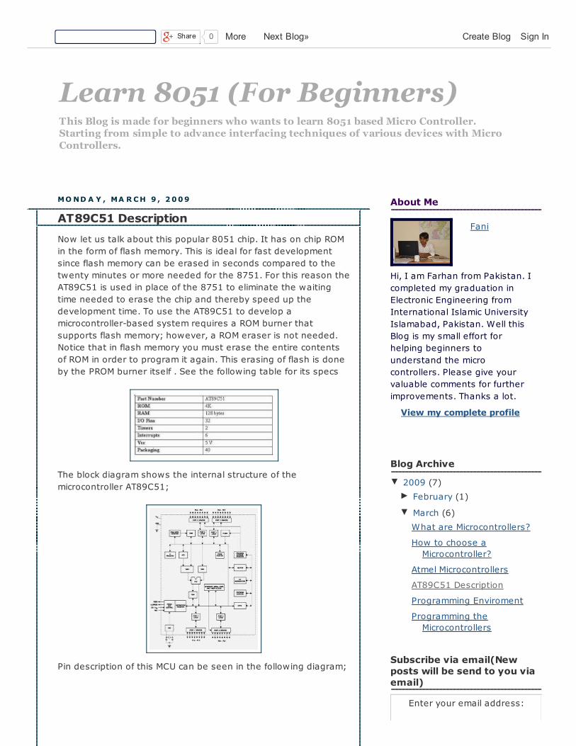
by the PROM burner itself . See the following table for its specs
The block diagram shows the internal structure of the
microcontroller AT89C51;
Pin description of this MCU can be seen in the following diagram;
About Me
Fani
Hi, I am Farhan from Pakistan. I
completed my graduation in
Electronic Engineering from
International Islamic University
Islamabad, Pakistan. Well this
Blog is my small effort for
helping beginners to
understand the micro
controllers. Please give your
valuable comments for further
improvements. Thanks a lot.
View my complete profile
Blog Archive
▼ 2009 (7)
► February (1)
▼ March (6)
What are Microcontrollers?
How to choose a
Microcontroller?
Atmel Microcontrollers
AT89C51 Description
Programming Enviroment
Programming the
Microcontrollers
Subscribe via email(New
posts will be send to you via
email)
Enter your email address:
Share 0 More Next Blog» Create Blog Sign In
Learn 8051 (For Beginners)This Blog is made for beginners who wants to learn 8051 based Micro Controller.Starting from simple to advance interfacing techniques of various devices with Micro
Controllers.
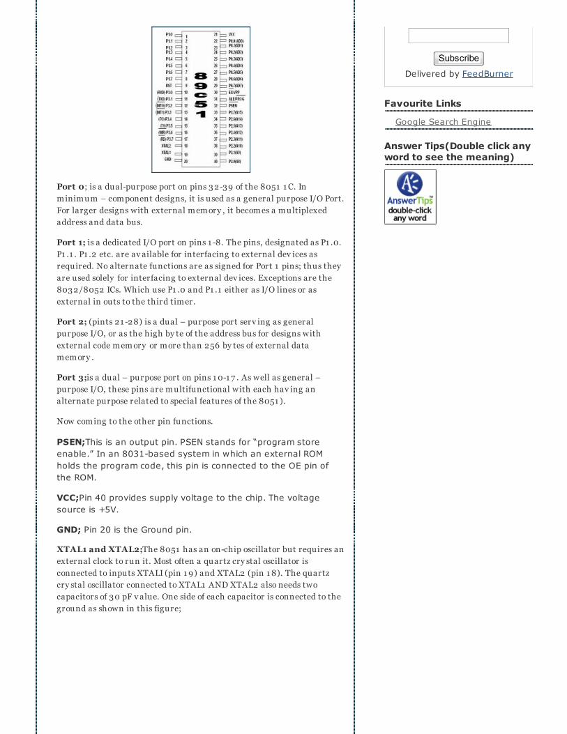
Port 0; is a dual-purpose port on pins 32-39 of the 8051 1 C. In
minimum – component designs, it is used as a general purpose I/O Port.
For larger designs with external memory , it becomes a multiplexed
address and data bus.
Port 1; is a dedicated I/O port on pins 1 -8. The pins, designated as P1 .0.
P1 .1 . P1 .2 etc. are av ailable for interfacing to external dev ices as
required. No alternate functions are as signed for Port 1 pins; thus they
are used solely for interfacing to external dev ices. Exceptions are the
8032/8052 ICs. Which use P1 .0 and P1 .1 either as I/O lines or as
external in outs to the third timer.
Port 2; (pints 21 -28) is a dual – purpose port serv ing as general
purpose I/O, or as the high by te of the address bus for designs with
external code memory or more than 256 by tes of external data
memory .
Port 3;is a dual – purpose port on pins 1 0-1 7 . As well as general –
purpose I/O, these pins are multifunctional with each hav ing an
alternate purpose related to special features of the 8051 ).
Now coming to the other pin functions.
PSEN;This is an output pin. PSEN stands for “program store
enable.” In an 8031-based system in which an external ROM
holds the program code, this pin is connected to the OE pin of
the ROM.
VCC;Pin 40 provides supply voltage to the chip. The voltage
source is +5V.
GND; Pin 20 is the Ground pin.
XTAL1 and XTAL2;The 8051 has an on-chip oscillator but requires an
external clock to run it. Most often a quartz cry stal oscillator is
connected to inputs XTALI (pin 1 9) and XTAL2 (pin 1 8). The quartz
cry stal oscillator connected to XTAL1 AND XTAL2 also needs two
capacitors of 30 pF v alue. One side of each capacitor is connected to the
ground as shown in this figure;
Subscribe
Delivered by FeedBurner
Favourite Links
Google Search Engine
Answer Tips(Double click any
word to see the meaning)

EA; The 8051 family members, such as the 8751, 89C51, or
DS5000. All come with on-chip ROM to store programs. In such
cases, the EA pin is connected to VCC for giving power to save
and erase program from the memory.
RST(RESET);The RST input on pin 9 is the master rest for the
8051. When this signal is brought high for a least two machine
cycles, the 8051 internal registers are loaded with appropriate
values for an orderly system start-up. For normal operation, RST
is low. Figure shows permanent connections of Reset Pin.
ALE; (address latch enable) is an output pin a nd is activ e high. When
connecting an 8031 to external memory , port 0 prov ides both address
and data. In other words, the 8031 multiplexes address and data
through port 0 to sav e pins. The ALE pin is used for de-multiplexing the
address and data by connecting to the G pin of the 7 4LS37 3 chip.Now
we will talk about what other things are inside an AT89C51 MCU;
Registers;In the CPU, registers are used to store information
temporarily . That information could be a by te of data to be processed,
or an address pointing to the data to be fetched. The v ast majority of
89C51 register an address pointing to the data to be fetched. The v ast
majority of 89C51 registers are 8-bit registers. In the 8051 there is
only one data ty pe: 8 bits. The 8 bits of a register are shown in the
diagram from the MSB (most significant bit) D7 to the LSB (least
significant bit) D0. With an 8-bit data ty pe, any data larger than 8 bits
must be broken into 8-bit chunks before it is processed. The most widely
used registers of the 89C51 are A (accumulator), B, R0, R1 , R2, R3, R4,
R5, R6, R7 , DPTR (data pointer), and PC (program counter). All of the
abov e registers are 8-bits, except DPTR and the program counter. The
accumulator, register A, is used for all arithmetic and logic
instructions.
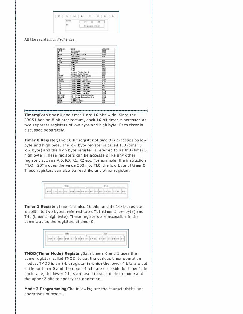
All the registers of 89C51 are;
Timers;Both timer 0 and timer 1 are 16 bits wide. Since the
89C51 has an 8-bit architecture, each 16-bit timer is accessed as
two separate registers of low byte and high byte. Each timer is
discussed separately.
Timer 0 Register;The 16-bit register of time 0 is accesses as low
byte and high byte. The low byte register is called TL0 (timer 0
low byte) and the high byte register is referred to as th0 (timer 0
high byte). These registers can be accesse d like any other
register, such as A,B, R0, R1, R2 etc. For example, the instruction
“TLO= 20” moves the value 500 into TL0, the low byte of timer 0.
These registers can also be read like any other register.
Timer 1 Register;Timer 1 is also 16 bits, and its 16- bit register
is split into two bytes, referred to as TL1 (timer 1 low byte) and
TH1 (timer 1 high byte). These registers are accessible in the
same way as the registers of timer 0.
TMOD(Timer Mode) Register;Both timers 0 and 1 uses the
same register, called TMOD, to set the various timer operation
modes. TMOD is an 8-bit register in which the lower 4 bits are set
aside for timer 0 and the upper 4 bits are set aside for timer 1. In
each case, the lower 2 bits are used to set the timer mode and
the upper 2 bits to specify the operation.
Mode 2 Programming;The following are the characteristics and
operations of mode 2.
1-It is an 8-bit timer; therefore, it allows only values of 00 to FFH
to be loaded into the timer’s register TH.
2-After TH is loaded with the 8-bit value, the 8051 gives a copy
of it to TL. Then the timer must be started. This is done by the
instruction “SETB TR0” for timer 0 and “SETB TR1” for timer 1. This
is just like mode 1.
3-After the timer is started, it starts to count up by incrementing
the TL register. It counts up until it reaches its limit of FFH. When
it rolls over from FFH to 00, it sets high the TF (timer flag). If we
are using timer 0, TF0 goes high; if we are using timer 1, TF1 is
raised.
4-When the TL registers rolls from FFH to 0 and TF is set to 1, TL
is reloaded automatically with the original value kept by the TH
register. To repeat the process, we must simply clear TF and let it
go without any need by the programmer to reload the original
value. This makes mode 2 and auto-reload, in contrast with
mode 1 in which the programmer has to reload TH and TL.
It must be emphasized that mode 2 is an 8-bit timer. However, it
has an auto-reloading capability in auto reload. TH is loaded with
the initial count and a copy of it is given to TL. This reloading
leaves TH unchanged, still holding a copy of original value. This
mode has many applications, including setting the baud rate in
serial communication.
SBUF (Serial Buffer) Register; SBUF is an 8-bit register used
solely for serial communication in the 89C51. For a byte of data
to be transferred via the TxD line, it must be placed in the SBUF
register. Similarly, SBUF holds the byte of data when it is
received by the 89C51 RxD line. SBUF can be accessed like any
other register in the 89C51.The moment a byte is written into
SBUF, it is framed with the start and stop bits and transferred
serially via the TxD pin. Similarly, when the bits are received
serially via RxD, the 89C51 deframes it by eliminating the stop
and start bits, making a byte out of the data received, and then
placing it in the SBUF. Some baud rates are shown below:
Baud Rate= 9600 TH1(Decimal)=-3 TH1(HEX)=FD
Baud Rate= 4800 TH1(Decimal)=-6 TH1(HEX)=FA
Baud Rate= 2400 TH1(Decimal)=-12 TH1(HEX)=F4
Baud Rate= 1200 TH1(Decimal)=-24 TH1(HEX)=E8
SCON(Serial Control) Register;The SCON register is an 8-bit
register used to program the start bit, stop bit, and data bits of
data framing, among other things. Following SCON bits are
explained; SMO SCON.7 Serial port mode specifier
SM1/ SCON.6= Serial port mode specifier
SM2/ SCON.5= Used for multiprocessor communication (Make it 0)
REN/ SCON.4= Set / cleared by software to enable / disable
reception.
TB8/ SCON.3= Not widely used.
RB8/ SCON.2= Not widely used.
T1/ SCON.1= Transmit interrupt flag. Set by hardware at the

beginning of the stop
bit in mode1. Must by cleared by software.
R1/ SCON.0= Receive interrupt flag. Set by hardware halfway
through the stop bit
time in mode1. Must be cleared by software.
Bit-Addressable RAM; Of the 128-byts internal RAM of the 8051,
only 16 bytes of it are bit addressable. The rest must be
accessed in byte format. The bit – addressable RAM locations are
20H to 2FH. These 16 bytes provide 128 bits of RAM bit –
address ability since 16 x 8 = 128. They are addressed as 0 to
127 (in decimal) or 00 to 7FH. Therefore, the bit addresses 0 to 7
are for the first byte of internal RAM location 20H, and 8 to 0FH
are the bit addresses of the second byte, RAM location 21H, and
so on. The last byte of 2FH has bit address byte of 2FH has bit
addresses of 78H to 7FH. Note that internal RAM locations 20-
2FH are both byte-addressable and bit addressable. Notice from
figure that bit addresses 00 – 7FH belong to RAM byte addresses
20 – 2FH, and bit addresses 80 – F7H belong to SFR P0, P1 etc.
Please refer to the following documents for detailed insight of
AT89C51 MCU;
Data Sheet;
www.atmel.com/atmel/acrobat/doc0265.pdf
http://www.filedropper.com/at89c51datasheet
http://www.filedropper.com/flashmcumemorytorg
Tutorials;
http://www.filedropper.com/best8051tutorial
http://www.filedropper.com/8051tutorial
Hardware Manual;
http://www.filedropper.com/atmel8051microcontrollershardware
manual
Posted by Fani at 4:05 PM
3 comments:
Newer Post Older Post
Enter your comment...
Comment as: Google Accoun
Publish
Preview
Home
Subscribe to: Post Comments (Atom)
Search This Blog
Search
SAMRIDH August 6, 2009 at 11:50 PM
a very nice lesson for beginers
Reply
Anonymous August 26, 2009 at 3:54 PM
hi, your blog's helped me in my understanding of 8051
ucontrollers. However, your links for the tutorials no longer
work. Could you pls upload them again?
thanks
Reply
sagar June 11, 2010 at 11:42 AM
thank ,,, for help me it's really nice one and full information
about the 8051.... it's really super up
Reply