Layer-by-layer accumulation of cadmium sulfide core--silica shell nanoparticles and size-selective...
25
Instructions for use Title Layer-by-layer accumulation of cadmium sulfide core-silica shell nanoparticles and size-selective photoetching to make adjustable void space between core and shell Author(s) Torimoto, Tsukasa; Paz Reyes, Jocelyn; Murakami, Shin-ya; Pal, Bonamali; Ohtani, Bunsho Citation Journal of Photochemistry and Photobiology A Chemistry, 160(1-2): 69-76 Issue Date 2003-08-07 Doc URL http://hdl.handle.net/2115/14654 Right Type article (author version) Additional Information Hokkaido University Collection of Scholarly and Academic Papers : HUSCAP
-
Upload
independent -
Category
Documents
-
view
0 -
download
0
Transcript of Layer-by-layer accumulation of cadmium sulfide core--silica shell nanoparticles and size-selective...

Instructions for use
TitleLayer-by-layer accumulation of cadmium sulfide core-silicashell nanoparticles and size-selective photoetching to makeadjustable void space between core and shell
Author(s) Torimoto, Tsukasa; Paz Reyes, Jocelyn; Murakami, Shin-ya;Pal, Bonamali; Ohtani, Bunsho
Citation Journal of Photochemistry and Photobiology A Chemistry,160(1-2): 69-76
Issue Date 2003-08-07
Doc URL http://hdl.handle.net/2115/14654
Right
Type article (author version)
AdditionalInformation
Hokkaido University Collection of Scholarly and Academic Papers : HUSCAP
Layer-by-Layer Accumulation of Cadmium Sulfide Core – Silica Shell
Nanoparticles and Size-Selective Photoetching to Make Adjustable Void Space between
Core and Shell
Tsukasa Torimoto,†§ Jocelyn Paz Reyes,† Shin-ya Murakami,§ Bonamali Pal,§
and Bunsho Ohtani*†
†Catalysis Research Center, Hokkaido University, Sapporo 060-0811, Japan.
§“Light and Control”, PRESTO, Japan Science and Technology Corporation (JST), Japan
Corresponding Author:
Prof. Bunsho Ohtani
Catalysis Research Center, Hokkaido University, Sapporo 060-0811, Japan
TEL: +81-11-706-3673
FAX: +81-11-706-4925
E-mail: [email protected]
1

Abstract
Layer-by-layer accumulation of monolayers of silica-coated cadmium sulfide (CdS)
was achieved through repeated monolayer
deposition-hydrolysis cycles using CdS particles (average diameter; 5 nm) modified with
3-mercaptopropyltrimethoxysilane (MPTS) and glass substrates. Absorption spectroscopic
analyses of the resulting yellow films revealed that each layer had
almost the same thickness, the estimated density of which corresponded to ca. 66 %
of that for the close hexagonal packing of nanoparticles. Monochromatic light irradiation at
488, 458, or 436 nm onto the film immersed in oxygen-saturated aqueous methylviologen
solution caused the decrease in the size of the CdS core depending on the irradiation
wavelength, while atomic force microscopic analyses suggested that the size of silica shell
of the immobilized nanoparticles was almost unchanged with irradiation; i.e., the immobilized
silica-coated CdS nanoparticles had void spaces between the photoetched core and the silica
shell and their size was regulated by choosing the wavelength of
irradiation light. The size-selective photoetching could
be successfully applied to the nanoparticulate films which were heat-treated at 473, 573, or
673 K to observe the blue-shift of absorption edge of CdS to the irradiation
wavelength. The amount
of CdS remaining in the film after the photoetching process depended
on temperature of the heat treatment. The largest amount among as-prepared
and heat-treated samples was obtained at 473 K and decreased
with the elevating temperature. The growth of particles, i.e., the diminution
of particle number, and/or the diminution of number of separated independent
shells may account for the dependence.
Key words
core-shell structure, nanoparticles, void space, layer-by-layer deposition,
cadmium sulfide, photoetching
2

1. Introduction
Nanocomposites having well-defined nanometer-scale dimensions are an interesting and
increasingly important class of materials and have been studied aiming at development
of novel catalysts and optoelectronic devices. Among the nanocomposites, studies of
surface coating of nanoparticles with different materials to produce core-shell
structures have attracted attention [1-21], because physical and chemical properties of
core materials can be modified or tailored by the shell components with negligible change in
shape and size of the core particles. Also core-shell nanoparticles have been useful
as precursors for the preparation of hollow structures by removing core materials through
chemical etching or combustion [22-30], and partial removal
of the core has enabled preparation of novel nanostructures inside the shell, such
as the encapsulation of metal nanoparticles in hollow sphere and the void formation
between the core and shell [31-37]. To utilize these nanoparticles in solid devices, such
as optoelectronic devices and sensors, it
is necessary to immobilize core-shell nanoparticles onto solid substrates. In recent
years several techniques have been reported, which
included the casting of the particles [10,38] and the layer-by-layer deposition
using the charged particles and the ionic polymers [39-41].
We have reported size-selective photoetching technique as a means of preparation of
monodisperse semiconductor nanoparticles in the size quantization regime.
When the technique was applied to CdS, the particle size could be controlled
within the range of 3.5 to 1.7 nm simply by selecting the wavelength of monochromatic
irradiation light in the range of
488 to 365 nm [42-47]. Recently we have also applied this technique successfully to control
core size in silica-coated CdS nanoparticles, i.e., a CdS core-silica shell
structure. The resulting nanoparticles had a void space inside the silica shell and
its size was adjusted by choosing the irradiation wavelength [48]. In this paper, we report
a newly developed method of layer-by-layer accumulation of
silica-coated CdS nanoparticles on glass substrates. It was revealed that the size of core, in
3
other words the size of void space, in the nanoparticle films could be controlled
using the size-selective photoetching.
2. Experimental Section
2.1. Materials
Sodium di(2-ethylhexyl) sulfosuccinate (AOT),
1,1’-dimethyl-4,4’bipyridinium dichloride (MV2+), and
3-mercaptopropyltrimethoxysilane (MPTS) were purchased from Tokyo Chemical Industry,
and cadmium perchlorate was obtained from Kishida Reagents Chemicals. Other
chemicals were supplied from Wako Pure Chemical Industries. Aqueous solutions were pre
pared with purified water prepared just before use by Yamato/Millipore WP501 Milli-Q
system. Glass plates (Matsunami, S-1111, 3.8 cm × 1.3 cm × 0.1 cm) were treated overnight
with a 1.0 mol dm-3 NaOH aqueous solution and washed thoroughly with water before use.
2.2. Preparation of CdS nanoparticles
MPTS-modified CdS nanoparticles were prepared through the procedure reported pre
viously [48]. To each of 200 cm3of heptane solutions containing 14 g AOT and 5.7 cm3 of
water was added each of 1.3 cm3 portions of a 1.0 mol dm-3 aqueous Cd(ClO4)2 solution and a
1.0 mol dm-3 aqueous Na2S solution. After being stirred for
1 h, they were mixed together, resulting in the formation
of CdS nanoparticles in AOT reversed micelles. To make the particle surface cadmium-rich,
an additional 0.26 cm3 portion of a 1.0 mol dm-3 aqueous Cd(ClO4)2 solution
was added to the solution. The solution was stirred for another 1 h and then the solvent
was removed by vacuum evaporation. To a toluene solution (400 cm3)
of the resulting yellow solid, a 5.0 cm3 portion of 0.21 mol dm-3 MPTS toluene solution
was added to modify the CdS surface, and then the solution was stirred for several hours.
2.3. Layer-by-layer accumulation of core-shell nanoparticles
4

Regulated accumulation of silica-coated CdS
(core-shell) nanoparticles was conducted by repeated cycles of procedure consisting of
monolayer deposition
of the MPTS-modified CdS particles and hydrolysis of remaining trimethoxysilyl
groups to silica network (Scheme 1a), as follows. A glass plates was treated
by a refluxing toluene solution of the MPTS-modified CdS nanoparticles for 2 h, rinsed with
methanol several times, and then heated in water at 363 K for
0.5 h. This deposition-hydrolysis cycle was repeated up to, maximally, 17 times.
Post-reaction curing was performed by heating for 1h in an electric furnace under vacuum.
2.4. Size-selective photoetching of CdS core
An argon-ion laser (Ion Laser Technology, Model 5500A) and a 400-W
mercury arc lamp (Eiko-sha) were used as light sources. The former
was used for the irradiation of monochromatic light at 488 and 458 nm. An emission line at
436 nm from the latter was extracted by the combination of various types of
glass optical filters. The silica-coated CdS nanoparticle films on
glass substrate were immersed in a 10 cm3 oxygen-saturated aqueous solution of 50 μmol
dm-3 MV2+ [47], and irradiated with the monochromatic light until their absorption
spectra had become unchanged. The absorption spectra
of the silica-coated CdS nanoparticle films on glass plates were measured using an Agilent
8453 spectrophotometer. Since both sides of a glass plate were covered
with the nanoparticulate films, the absorption spectra originating from a CdS film on
one side is shown in this study by halving the absorbance.
2.5. Characterization of core-shell nanoparticle films
The surface of the film was observed by an atomic force microscopy (AFM)
(Digital Instruments, Nanoscope IIIa) in a tapping mode using Nanosensors NCH
cantilevers. The size of silica-coated CdS nanoparticles was obtained
by measuring the lateral dimension of the particle images (more than 60 particles).
5

3. Results and discussion
3.1. Layer-by-layer deposition of nanoparticle films
Absorption spectrum of MPTS-modified CdS nanoparticles in toluene was shown
in Fig. 1a, which had the exciton peak around 445 nm and the absorption onset at 530 −
550 nm. Since the energy gap of bulk CdS was reported to be 2.4 eV [49]
(corresponding to the absorption onset of ca. 520 nm), the large part
of CdS nanoparticles possessed the energy gap similar to that of bulk material. As reported
in the previous paper [48], CdS nanoparticles prepared by almost the same procedure had a
wide size distribution ranging from 3 to 7 nm, and the average diameter
was 5.0 nm with the standard deviation of 0.79 nm.
Before the addition of MPTS to the CdS particles in AOT reversed micelle, their
surface was cadmium-rich. It has been presumed that thiol group in MPTS
(R-SH) reacts with these surface cadmium sites to make R-S-Cd(CdS) linkage, i.e., outmost
surface of the particles is covered with trimethoxysilyl groups,
which have high reactivity toward surface hydroxyl group
on the glass substrate to give Si(glass)-O-Si(MPTS) bond, as shown
in Scheme 1a. Since no chemical reaction which binds between these particles are expected
under the dehydrated conditions as employed in the first deposition step, attachment of
MPTS-modified CdS particles should be limited to coverage of, at most, a
monoparticle layer; no three dimensional growth
of the film may occur. The remaining trimethoxysilyl groups on
anchored CdS nanoparticles are hydrolyzed in hot water to form silica shell-CdS
core structure, as was proved by FT-IR spectroscopy in our previous paper
[48]. Using produced surface hydroxyl groups on the shell, another monolayer of
MPTS-modified CdS particles were attached followed
by the hydrolysis. This layer-by-layer accumulation of silica-coated CdS was repeated
up to 17 times.
6

Figure 1b shows the absorption spectra
of the silica-coated CdS nanoparticle films deposited on
glass plate. Although there was upward shift of spectra
in the whole wavelength range due to the light
scattering of the films, the exciton peak of CdS nanoparticles could be detected at around
445 nm in the spectra that agreed with that of MPTS-modified CdS nanoparticles in solution
and its intensity was enhanced with increasing number of accumulation cycles.
On the assumption that the absorbance shift due to the light
scattering of the films is independent of wavelength, the absorbance (ΔA) owing to CdS
was roughly estimated from the absorbance difference between the absorption onset (550 nm)
and the exciton peak (445 nm). Figure 2 shows ΔA as a function of the number of
accumulation cycles. Number of samples for each number of accumulation was 8 − 11
samples and their average and standard deviation (error bar)
were plotted. Relatively large error in ΔA measurement is due to different light
scattering at the peak wavelength. However, it is clear that there is a tendency of
increasing ΔA with the repeated number of accumulation and a linear line can be drawn
as shown in Fig. 2. From the slope of the linear relation, the number
of the particle immobilized per one cycle is estimated to be 2.1 × 10¹² particles cm-2
using the absorption coefficient of 536 mol(CdS)-1 dm3 cm-1 at
exciton peak and the average diameter of CdS nanoparticles (5.0 nm). This value was 66 %
as large as that expected from the monoparticle layer of CdS nanoparticles (3.2 ×
1012 particles cm-2), which was obtained by assuming two-dimensional hexagonal
closed packing of silica-coated CdS nanoparticles consisting of the core of 5.0-nm diameter
and the MPTS overlayer of 0.5-nm thickness.
One of the possible reason for the loose packing is heterogeneity of size of
MPTS-modified CdS nanoparticles; the diameter of CdS core ranges from 3 to 7 nm [48].
3.2. Photoetching of CdS core
7
Figure 3 shows absorption spectra of the silica-coated CdS layers after irradiation of
monochromatic light in water under aerated conditions. The absorption spectra
of the resulting nanoparticles were blue-shifted and the exciton peak appeared
more clearly along with decrease in wavelength of irradiation light. It
is well-known that CdS particles are photocorroded to become smaller by irradiation under
aerated conditions in the presence of appropriate electron relay, such as MV2+
[42]. The absorption onset of each spectrum seemed to agree with the wavelength of
irradiation light, suggesting that the photocorrosion of CdS nanoparticles proceeded
until the nanoparticles could not absorb the light
during the course of the photocorrosion to make the absorption onset shift to shorter
wavelength due to an increase in the energy gap along with a decrease in the particle size,
i.e., the size quantization effect. The exciton peak appeared at 440, 430, and 400 nm with
monochromatic light irradiation at wavelength of 488, 458, and 436 nm, from which diameter
of photoetched CdS nanoparticles was estimated to 3.3, 3.0, and 2.4 nm, respectively,
by applying the experimentally obtained data to a theoretical relation between energy gap
and particle diameter of CdS [50]. Thus size-selective photoetching of
silica-coated CdS nanoparticle films can be successfully performed
and the size of the resulting CdS nanoparticles is adjustable by varying the wavelength
of the monochromatic light, as already reported in our previous paper [48]. The silica shell
surrounding a photoetched CdS nanoparticle might prevent
coalescence between nanoparticles.
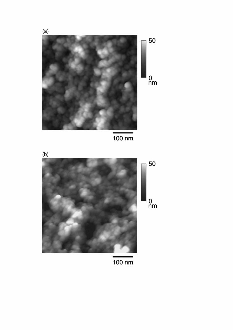
Figure 4 shows an AFM
image of the silica-coated CdS nanoparticle films after photoetching with irradiation at
458 nm. It was found that the silica-coated CdS nanoparticles were packed
densely in the film and roughness of the film surface was large (>50 nm). The average diam
eter of the photoetched particles was determined to 15 nm with the standard deviation of
5.3 nm by measuring the lateral dimension of the particle images.
When the surface of the film was measured before irradiation, similar
morphology was observed and the average diameter of
8

original particles was 16 nm with the standard deviation of 7.4 nm, which
was almost the same as those obtained after
size-selective photoetching. Considering that the uppermost layer, i.e., the silica shell
of nanoparticles reflected the AFM image, these results implied that the monochromatic light
irradiation did not induce shrinking of the shell structure even when the size of CdS
core decreased with irradiation, resulting in the formation of a void
space between the photoetched CdS core and the silica shell (Scheme 1b). Similar
behavior has been observed in TEM measurement for suspended
silica-coated CdS nanoparticles, where the size of silica shell was almost equal to that
of CdS nanoparticles before irradiation, regardless of the irradiation wavelength
[48]. Although the diameter of the nanoparticles observed by AFM
was much larger than that observed in the TEM measurement, ca. 5.0 nm, it
is well-known that in AFM images lateral size is often overestimated
because of radius of the curvature of the point of AFM tips [51,52].
3.3. Effect of pre-irradiation curing
In
order to increase the stability of the silica-coated CdS nanoparticle films, they were cured
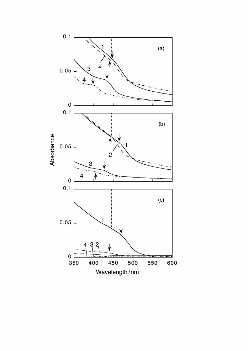
at various temperature before photoetching. Figure 5 shows the influence of
curing temperature on the absorption spectra before and
after the size-selective photoetching. Before photoetching, the absorption
spectrum of the film heat-treated at 473 K was almost same as that of the film without curing,
but the heat treatment higher than 573 K caused appreciable red shift of absorption spectra,
indicating the increase in the size of
deposited CdS nanoparticles. In the as-prepared nanoparticle films, network of Si-O-Si linka
ge is formed to surround the CdS particles and
separates them. This silica network is connected to the CdS core particles through alkyl
(C3) chain stems. When a part of the network surrounding one CdS particle is considered
as a chamber, number of chambers in the whole film is equal to that
9
of particles before curing. Heat treatment, especially that at the temperature higher than
573 K, might induce decomposition of the stems and
appreciable shrinkage of the silica network to result in the formation of
windows through the chambers. Growth of CdS particles by the curing, as indicated by their
spectral red shift, is attributable to coalescence of CdS
in the neighboring chambers with the connecting window between them, the size of which
is larger than that of the particles(s). The higher the temperature of
curing, the larger the size of window, i.e., the larger the average size of CdS particles might
be formed after curing. Thermal acceleration
of particle coalescence also accounts for the growth
at the higher temperature. This view was supported by the AFM measurement
of the nanoparticle film heat-treated at 673 K, where the average size and the standard
distribution of silica-coated CdS nanoparticles was determined to 19 and 8.5 nm which
were larger than those obtained before heat-treatment, 16 and 7.4 nm, respectively.
Size-selective photoetching were successfully performed regardless of the curing tem
perature as also shown in Fig. 5. The absorption spectra were blue-shifted
and the absorption onset of each spectrum almost coincided with the irradiation
wavelength. Furthermore the monochromatic light irradiation at 488, 458, and
436 nm gave exciton peaks at almost same wavelength with or without
curing (and regardless of curing temperature), except for the film cured at 673 K. It
is noticeable that the absorbance, i.e., the amount of CdS after photoetching decreased with
elevating curing temperature. Plots of ΔA as a function of the curing temperature are shown
in Fig. 6, where the data of the as-prepared film were plotted at the refluxing temperature,
383 K. At present we have no interpretation for the increased ΔA before irradiation at 473 K
other than that R-S-Cd
moiety in the stem of the as-prepared film is converted to CdS via R-S-bond scission
with negligible increase in particle size. The facts that absorbance changes were not
observed during the process of MPTS modification but sulfur atoms originally included in
MPTS molecules are expected to remain on CdS particles after
10
curing support this speculation. At the higher temperature, ΔA before irradiation decreased
along with the red shift of absorption spectra, i.e., growth of CdS particles,
by the curing, probably due to the decrease of the molar absorption coefficient of CdS unit
with an increase in the diameter of CdS nanoparticles up to ca. 6 nm [53].
During the course of irradiation, CdS particles in the chamber independent or
connecting through windows the size of which are smaller than that
of the particle undergo photoetching until their
size become small to be able to pass through the window, resulting that the photoetched CdS
nanoparticles easily coalesced with each other to give the bigger particles which
were subjected to further photocorrosion. This implies that the photocorrosion goes on
unless the total number of remaining particles becomes small not
enough to coalesce. Similar values of ΔA for original and 488-nm photoetched
samples at the curing temperature between 473-573 K suggests that the average size of
windows formed at this temperature range is smaller than the size of original particles or that
of nanoparticles photoetched at 488 nm irradiation.
On the other hand, this window size might
be large enough to coalesce for the particles photoetched at 458 or
436 nm irradiation, resulting in the marked decrease in ΔA. The behavior of
ΔA for the films cured at 673 K can be explained similarly. On the basis of these results, it
is presumed that the silica shell in the core-shell nanoparticles is stabilized by the alkyl chain
stems anchored to the CdS core surface, but shrinks, because of the removal of stems,
by the curing to lead to the formation of windows connecting the chambers and
allowing the coalescence of photoetched particles.
Conclusion
We have successfully immobilized the silica-coated CdS core-shell nanoparticles on
glass substrates through the newly developed layer-by-layer
accumulation technique. Spectroscopic
analyses revealed the packing density of nanoparticles a little loosened compared with that
11

of hexagonal close packing of particles of
uniform size. This was attributed to heterogeneity of the actual particle size to interfere the c
lose packing. In the next step of the study, we will try to accumulate the nanoparticles of
monodispersed size prepared, e.g.
using the size-selective photoetching. Size-selective photoetching of the nanoparticle films l
ed to the decrease in the size of CdS core depending on the wavelength of irradiation light,
as expected, while the shell structures of the immobilized nanoparticles were almost
unchanged, indicating that void spaces are prepared between the photoetched
core and the silica shell and their size can be regulated by choosing the irradiation
wavelength. The nanospace of regulated
size in the photoetched particulate films containing semiconducting materials of
uniform size (i.e., of uniform chemical and physical properties) can be a new type of material,
e.g., nanoflask array for semiconductor photocatalytic reactions. It is revealed,
being opposites to our expectation, that
curing of the film induced the shrinkage of the silica network of the shell to decrease the amo
unt of remaining photoetched CdS core. In order to avoid this, it is necessary, for
example, to fill the gap among the core-shell particles or to thicken the silica shell layer.
Work in this direction is currently in progress.
References
[1] P. Mulvaney, L.M. Liz-Marzan, M. Giersig, T. Ung, J. Mater. Chem. 10 (2000) 1259.
[2] R.A. Caruso, M. Antonietti, Chem. Mater. 13 (2001) 3272.
[3] F. Caruso, Adv. Mater. 13 (2001) 11.
[4] E. Bourgeat-Lami, J. Nanosci. Nanotechnol. 2 (2002) 1.
[5] L.M. Liz-Marzan, M. Giersig, P. Mulvaney, Langmuir 12 (1996) 4329.
[6] A.R. Kortan, R. Hull, R.L. Opila, M.G. Bawendi, M.L. Steigerwald, P.J. Carroll,
L.E. Brus, J. Am. Chem. Soc. 112 (1990) 1327.
[7] B.O. Dabbousi, J. RodriguezViejo, F.V. Mikulec, J.R. Heine, H. Mattoussi, R.
Ober, K.F. Jensen, M.G. Bawendi, J. Phys. Chem. B 101 (1997) 9463.
12
[8] A. Mews, A. Eychmueller, M. Giersig, D. Schooss, H. Weller, J. Phys. Chem. 98
(1994) 934.
[9] M.T. Harrison, S.V. Kershaw, A.L. Rogach, A. Kornowski, A. Eychmuller, H.
Weller, Adv. Mater. 12 (2000) 123.
[10] I. Bedja, P.V. Kamat, J. Phys. Chem. 99 (1995) 9182.
[11] P.V. Kamat, B. Shanghavi, J. Phys. Chem. B 101 (1997) 7675.
[12] M. Bruchez, Jr., M. Moronne, P. Gin, S. Weiss, A.P. Alivisatos, Science 281 (1998)
2013.
[13] D. Gerion, F. Pinaud, S.C. Williams, W.J. Parak, D. Zanchet, S.
Weiss, A.P. Alivisatos, J. Phys. Chem. B 105 (2001) 8861.
[14] S.Y. Chang, L. Liu, S.A. Asher, J. Am. Chem. Soc. 116 (1994) 6739.
[15] T. Ung, L.M. Liz-Marzan, P. Mulvaney, J. Phys. Chem. B 105 (2001) 3441.
[16] F. Garcia-Santamaria, V. Salgueirino-Maceira, C. Lopez, L.M. Liz-Marzan, Langmuir
18 (2002) 4519.
[17] M. Hara, J.T. Lean, T.E. Mallouk, Chem. Mater. 13 (2001) 4668.
[18] S.W. Keller, S.A. Johnson, E.S. Brigham, E.H. Yonemoto, T.E.
Mallouk, J. Am. Chem. Soc. 117 (1995) 12879.
[19] S.W. Kim, M. Kim, W.Y. Lee, T. Hyeon, J. Am. Chem. Soc. 124 (2002) 7642.
[20] K. Dick, T. Dhanasekaran, Z.Y. Zhang, D. Meisel, J. Am. Chem. Soc. 124 (2002)
2312.
[21] E. Hutter, J.H. Fendler, Chem. Commun. (2002) 378.
[22] S.Y. Chang, L. Liu, S.A. Asher, J. Am. Chem. Soc. 116 (1994) 6745.
[23] R.A. Caruso, A. Susha, F. Caruso, Chem. Mater. 13 (2001) 400.
[24] F. Caruso, M. Spasova, A. Susha, M. Giersig, R.A. Caruso, Chem. Mater. 13 (2001)
109.
[25] L. Sun, R.M. Crooks, V. Chechik, Chem. Commun. (2001) 359.
[26] K.P. Velikov, A. van Blaaderen, Langmuir 17 (2001) 4779.
[27] O.V. Makarova, A.E. Ostafin, H. Miyoshi, J.R. Norris, D. Meisel, J. Phys. Chem. B
103 (1999) 9080.
13

[28] S.M. Marinakos, J.P. Novak,
L.C. Brousseau, A.B. House, E.M. Edeki, J.C. Feldhaus, D.L. Feldheim, J. Am. Chem
. Soc. 121 (1999) 8518.
[29] S.M. Marinakos, M.F. Anderson, J.A. Ryan, L.D. Martin, D.L. Feldheim, J.
Phys. Chem. B 105 (2001) 8872.
[30] S.O. Obare, N.R. Jana, C.J. Murphy, Nano Lett. 1 (2001) 601.
[31] B. Rodriguez-Gonzalez, V. Salgueirino-Maceira, F. Garcia-Santamaria, L.M.
Liz-Marzan, Nano Lett. 2 (2002) 471.
[32] Y. Yin, Y. Lu, B. Gates, Y. Xia, Chem. Mater. 13 (2001) 1146.
[33] Y.G. Sun, B.T. Mayers, Y.N. Xia, Nano Lett. 2 (2002) 481.
[34] Y.G. Sun, Y.N. Xia, Anal. Chem. 74 (2002) 5297.
[35] M. Giersig, T. Ung, L.M. Liz-Marzan, P. Mulvaney, Adv. Mater. 9 (1997) 570.
[36] M. Giersig, L.M. Liz-Marzan, T. Ung, D.S. Su, P. Mulvaney, Ber. Bunsen-Ges.
Phys. Chem. 101 (1997) 1617.
[37] M. Kim, K. Sohn, H.B. Na, T. Hyeon, Nano Lett. 2 (2002) 1383.
[38] S.T. Yau, P. Mulvaney, W. Xu, G.M. Spinks, Physical Review B 57 (1998) R15124.
[39] F.G. Aliev, M.A. Correa-Duarte, A. Mamedov, J.W. Ostrander, M. Giersig, L.M.
Liz-Marzan, N.A. Kotov, Adv. Mater. 11 (1999) 1006.
[40] I. Pastoriza-Santos, D.S. Koktysh, A.A. Mamedov, M. Giersig, N.A. Kotov, L.M.
Liz-Marzan, Langmuir 16 (2000) 2731.
[41] D.S. Koktysh, X.R. Liang, B.G. Yun, I. Pastoriza-Santos, R.L. Matts,
M. Giersig, C. Serra-Rodriguez, L.M. Liz-Marzan, N.A. Kotov, Adv. Funct. Mater. 12
(2002) 255.
[42] H. Matsumoto, T. Sakata, H. Mori, H. Yoneyama, J. Phys. Chem. 100 (1996) 13781.
[43] T. Torimoto, H. Nishiyama, T. Sakata, H. Mori, H. Yoneyama, J. Electrochem. Soc.
145 (1998) 1964.
[44] M. Miyake, T. Torimoto, T. Sakata, H. Mori, H. Yoneyama, Langmuir 15 (1999)
1503.
[45] T. Torimoto, H. Kontani, T. Sakata, H. Mori, H. Yoneyama, Chem. Lett. (1999) 379.
14

[46] T. Torimoto, N. Tsumura, H. Nakamura, S. Kuwabata, T. Sakata, H. Mori, H.
Yoneyama, Electrochimica Acta 45 (2000) 3269.
[47] T. Torimoto, H. Kontani, Y. Shibutani, S. Kuwabata, T. Sakata, H. Mori, H.
Yoneyama, J. Phys. Chem., B 105 (2001) 6838.
[48] T. Torimoto, J.P. Reyes, K. Iwasaki, B.
Pal, T. Shibayama, K. Sugawara, H. Takahashi, B. Ohtani, J. Am. Chem. Soc. (2003)
in press.
[49] Y.V. Pleskov, Y.Y. Gurevich, Semiconductor
Photoelectrochemistry; Consultants Bureau: New York, 1986,
[50] P.E. Lippens, M. Lannoo, Phys. Rev. B 39 (1989) 10935.
[51] L. Sun, M. Crooks, Langmuir 18 (2002) .
[52] T. Sagara, N. Kato, N. Nakashima, J. Phys. Chem. B 106 (2002) 1205.
[53] T. Vossmeyer, L. Katsikas, M. Giersig, I.G.
Popovic, K. Diesner, A. Chemseddine, A. Eychmueller, H. Weller, J. Phys. Chem. 98
(1994) 7665.
15
Figure Captions
Scheme 1 (a) Preparation of silica-coated CdS nanoparticle film by a layer-by-layer
deposition. Immobilization of MPTS-modified CdS nanoparticles (1, 3)
and hydrolysis of trimethoxysilyl groups (2). (b) Regulation of a void space inside the shell
structure by the size-selective photoetching technique.
Figure 1 (a) Absorption spectra of MPTS-modified CdS nanoparticle dissolved in toluene.
(b) Changes in the absorption spectra of silica-coated CdS nanoparticle films with the number
of the accumulation cycles. The number of accumulation cycles was indicated in the figure.
Figure 2 The absorbance difference (ΔA) between exciton peak and absorption onset of
silica-coated CdS nanoparticle films as a function of the number of accumulation cycles.
Figure 3 Absorption spectra of silica-coated CdS nanoparticle film prepared by irradiation
with various wavelengths: original film (1) and films prepared by irradiation at (2) 488, (3)
458, and (4) 436 nm. The number of accumulation
cycles was 17. The arrows show the position of exciton peaks.
Figure 4 An AFM image of a silica-coated CdS nanoparticle film after irradiation at
458 nm. The number of accumulation cycles was 17.
Figure 5 Changes in the absorption spectra of
silica-coated CdS nanoparticle films heat-treated at 473 (a), 573 (b), and 673 K(c) before (1)
and after irradiation at (2) 488, (3) 458, and (4) 436 nm. The number of accumulation
cycles was 17. The arrows show the position of exciton peaks and vertical
dotted lines indicate the position of the exciton peak of the as-prepared films.
Figure 6 The absorbance difference (ΔA) between exciton peak and absorption onset of
silica-coated CdS nanoparticle films before (1) and after irradiation at (2) 488, (3) 458, and
16

(4) 436 nm as a function of curing temperature. The results in Fig. 5 were used for
calculation. The films were as prepared (open symbols) and after heat-treatment (solid
symbols).
17