
L-4ff-l/EEE Date
42
L-4ff-l/EEE Date: 06/07/2013 BANGLADESH UNIVERSITY OF ENGINEERING AND TECHNOLOGY, DHAKA L-4/T-1 B. Sc. Engineering Examinations 2011-2012 Sub: EEE 471 (Energy Conversion III) Full Marks : 210 Time : 3 Hours USE SEPARATE SCRIPTS FOR EACH SECTION SECTION-A There are FOUR questions in this section. Answer any THREE. The questions are of equal value. 1. (a) What are the reasons for unsatisfactory operation of ordinary series motor when it is . operated from ac source? Explain. Explain how in a universal motor, similar Torque- Speed characteristics are obtained when it is supplied either from dc or ac source. (b) A universal series motor when operating on 220 V dc source draws current lOA and runs at 1400 rpm. Find the new speed and power factor when connected to 220 V, 25 Hz supply (the motor current remains the same). The motor has total resistance of 1 ohm and total inductance of 0.1 H. Also find the torql;ledeveloped by the motor when it is supplied from ac source. 2. (a) Explain with necessary Torque-Speed characteristics the operation of a repulsion-start induction-run and a repulsion-induction motor. Draw the circuit diagram of an electrically reversible repulsion motor and explain how it reverses the direction of rotation of the motor. (b) Explain with necessary diagrams the operation of a linear induction motor. Mention its areas of application. Explain what magnetic levitation is. An overhead crane in a factory is driven horizontally by means of two similar linear induction motors having rotors in the form of two steel I-beams on which the crane rolls. The 3-phase 2-pole linear stators, which are mounted on opposite sides of the crane, have a pole pitch of 50 rom and are energized by a variable frequency source. One of the motors has the following test results: Stator frequency = 50 Hz, Power to stator = 5.5 kW, stator copper and iron loss= 1 kW, . Crane speed = 4.8 m/sec. Find (i) synchronous speed and slip (ii) power input to the rotor (iii) copper loss in the rotor (iv) mechanical power developed and (v) propulsion force. 3. (a) Write the expression of torque in an electrostatic system in terms of applied voltage and rate of change of its capacitance with angular displacement. Derive the expression of average torque of an electrostatic motor supplied from ac source. What is the physical meaning of load angle 8 of this motor? (b) An electrostatic motor has N stationary plates and N rotating plates each consisting of two quarter-circular sections. The permittivity of the medium is 80. The supply voltage to the motor v varies with angular frequency of ill rad/sec and its peak value produces a maximum field intensity E between adjacent plates. Find the expression of maximum power output from the motor in terms of E and the volume V of the motor. How the maximum power per unit volume of the electrostatic motor can be increased? Contd P/2
-
Upload
khangminh22 -
Category
Documents
-
view
1 -
download
0
Transcript of L-4ff-l/EEE Date

L-4ff-l/EEE Date: 06/07/2013BANGLADESH UNIVERSITY OF ENGINEERING AND TECHNOLOGY, DHAKA
L-4/T-1 B. Sc. Engineering Examinations 2011-2012
Sub: EEE 471 (Energy Conversion III)
Full Marks : 210 Time : 3 Hours
USE SEPARATE SCRIPTS FOR EACH SECTION
SECTION-AThere are FOUR questions in this section. Answer any THREE.
The questions are of equal value.
1. (a) What are the reasons for unsatisfactory operation of ordinary series motor when it is. operated from ac source? Explain. Explain how in a universal motor, similar Torque-Speed characteristics are obtained when it is supplied either from dc or ac source.(b) A universal series motor when operating on 220 V dc source draws current lOA and
runs at 1400 rpm. Find the new speed and power factor when connected to 220 V, 25 Hzsupply (the motor current remains the same). The motor has total resistance of 1 ohm andtotal inductance of 0.1 H. Also find the torql;le developed by the motor when it is supplied
from ac source.
2. (a) Explain with necessary Torque-Speed characteristics the operation of a repulsion-startinduction-run and a repulsion-induction motor. Draw the circuit diagram of an
electrically reversible repulsion motor and explain how it reverses the direction of rotation of
the motor.(b) Explain with necessary diagrams the operation of a linear induction motor. Mentionits areas of application. Explain what magnetic levitation is.An overhead crane in a factory is driven horizontally by means of two similar linear
induction motors having rotors in the form of two steel I-beams on which the crane rolls.
The 3-phase 2-pole linear stators, which are mounted on opposite sides of the crane, havea pole pitch of 50 rom and are energized by a variable frequency source. One of the
motors has the following test results:Stator frequency = 50 Hz, Power to stator = 5.5 kW, stator copper and iron loss= 1 kW, .
Crane speed = 4.8 m/sec. Find (i) synchronous speed and slip (ii) power input to the rotor(iii) copper loss in the rotor (iv) mechanical power developed and (v) propulsion force.
3. (a) Write the expression of torque in an electrostatic system in terms of applied voltage
and rate of change of its capacitance with angular displacement. Derive the expression ofaverage torque of an electrostatic motor supplied from ac source. What is the physical
meaning of load angle 8 of this motor?(b) An electrostatic motor has N stationary plates and N rotating plates each consisting of
two quarter-circular sections. The permittivity of the medium is 80. The supply voltage to
the motor v varies with angular frequency of ill rad/sec and its peak value produces a
maximum field intensity E between adjacent plates. Find the expression of maximum
power output from the motor in terms of E and the volume V of the motor. How the
maximum power per unit volume of the electrostatic motor can be increased?
Contd P/2

=2=EEE 471
4. (a) Explain how a hysteresis motor develops its torque. What are the advantages and
disadvantages of this motor if compared to a reluctance motor?(b) Explain how thermal energy is directly converted to electrical energy in an MHD
generator~ What is conduction pump? Where is it used?
SECTION-BThere are FOUR questions in this section. Answer any THREE.
The figures in the margin indicate full marks.
5. (a) Describe the operation of a three phase 6/2 pole permanent magnet stepper motor withbipolar drive circuit. Consider the full step operating mode only. Sh0'.Vthe possible drive
circuit and gate signals of the MOSFET switches of this circuit. (25)(b) Briefly describe the principle of operation of a three phase reluctance motor. (10)
6. (a) Write the names of some common renewable energy sources.
(b) Write short notes on:
(4)
(3)!i x2=7)(i) Wind energy(ii) Geothermal energy
(c) Classify wind turbines according to their axis of rotation and define each type. (5)(d) What is the function of thyristors in controlled rectifiers? Briefly describe the
operation of a three phase full wave controlled rectifier with the help of the waveforms of
gate pulses and output voltage for firing angle equal to 60°. (19)
7. (a) What is a fuel cell? With a neat sketch of the membrane electrode assembly (MEA),
describe the operation of a proton exchange membrane fuel cell (PEMFC). (17)(b) Describe the principle of operation of Schrage motors. How can supersynchronous
speed be achieved in Schrage motors? (18)
8. (a) cWhat is AMm in the context of solar energy? Describe the principle of operation of a
p-n junction solar cell addressing the followings: (5+ 15=20)(i) Why the n-side is narrower than the p-side?
(ii) Why is it important to have the minority carrier diffusion length as long as possible?
(iii) Given, the crystalline silicon bandgap energy of 1.1 eV, what is the thresholdwavelength for this material?
(b) What is the effect of change of irradiance and temperature on the output current vs.
voltage characteristics of a solar cell. (5)(c) What is BLDC? Describe its principle of operation briefly. State some of its possible
applications. (10)

L-4/T-l/EEE Date: 06/07/2013
BANGLADESH UNIVERSITY OF ENGINEERING AND TECHNOLOGY, DHAKA;; ,"; ':
L-4/T -1 B. Sc. Engineering Examinations 2011-2012
Sub: 'EEE 451 (Processing and Fabrication Technology)
Full Marks: 210 Ti~e: 3 Hours
The figures in the margin indicate full marks.
USE SEPARATE SCRIPTS FOR EACH SECTION
SECTION-A
There are FOURquestions in this section. Answer any THREE.
1. (a) Explain, with appropriate diagrams, the Deal-Grove model of oxidation. Also mention
its limitations. (15)
(10)
(b) Why oxidation rate is quicker in wet environment? Name the various applications of
Si02.
(c) Compare the different sources for oxidation. Why does a CVD oxidation needs lower
temperatures? (10)
2. (a) Explain, with proper diagram, the model for VPE. (20)
(b) Compare the different processes of epitaxy, deposition, sputtering and evaporation. (15)
3. (a) Compare the advantages and disadvantages of vertical chamber and horizontal
chamber systems for oxidation and/or diffusion. Use appropriate diagrams. (15)
(b) Describe the recipe known as "RCA clean". (8)
(c) How does post-implantation anneal improve crystal quality? Write the relative merits
and demerits ofCZ and float-zone methods. (12)
4. (a) In an evaporator system, the AI-charge is maintained at 1100 DC. If the evaporator
planetary has a radius of 40 cm, and the dia of the crucible is 5 cm, what is the growth
rate and arrival rate of A 1 atoms? [For AI: vapor pressure = 10-3 torr, mass density
= 2700 kg/m3, M = 27.] (12)
(b) Explain, with appropriate figures, the ten-step process of fabrication. (15)
(c) Why does diffusion put a limit on high-density chips? (8)
Contd PI2

. .~.
=2=
EEE 451
SECTION -B
There are FOUR questions in this section. Answer any THREE.
5. (a) Compare the issues and challenges of CMOS processes of the 1980's, 1990's and
2000's. (10)
(b) Explain, in detail, the process itself, advantages and disadvantages of a RIE system. (15)
(c) How does diffraction limit the standard lithography process? How does X-ray
diffraction solve this problem? (10)
6. (a) What is the difference between pattern and feature size?(6)
(b) How do you explain the 'kink behaviour' observed in the diffusion profiles of Zn in
GaAs? (14)
(c) Describe the Hall measurement and four-probe technique to determine doping
concentration. (15)
7. (a) Explain shadowing, channeling and side-wall striation effect in RlE and implantation
process.
(b) Describe the detailed steps of packaging.
(c) Explain pseudomorphic, metamorphic and relaxed epi-Iayers.
8. Write short notes on:
(a) Nanowires
(b) MOCVD
(c) PMMA
(d) DRIE
(12)
(15)
(8)
(35)

L-4/T-lIEEE Date: 06/07/2013
BANGLADESH UNIVERSITY OF ENGINEERING AND TECHNOLOGY, DHAKA
L-4/T-1 B. Sc. Engineering Examinations 2011-2012
, Sub: CSE 491 (Multimedia Communications)
Full Marks: 210 Time: 3 Hours
USE SEPARATE SCRIPTS FOR EACH SECTION
The figures in the margin indicate full marks.
SECTION~A
There are FOUR questions in this section. Answer any THREE.
1. (a) Show the system model for real time process scheduling. Compare EDF and rate-
monotic algorithms for process scheduling with necessary examples.
(b) Define the following continuous media streams with necessary examples:
. (i) strongly periodic (ii) aperiodic (iii) weakly regular (iv) discrete
(c) How is image represented? What are the steps of image recognition?
2. (a) What do you mean by flicker? How can you remove this problem?
(b) What is the significance of luminance and chrominances? Why are luminance and
chrominance preferred over RGB for transmitting video?.(c) Describe different approaches of transmitting animation with relative advantages and
disadvantages. .
(d) Show with necessary example how the following controlling mechanism is done.
(i) Procedural control
(ii) Tracking live action
(iii) Kinematic.and dynamics.
(15)
(10)
(10)
(7)
(8)
(8)
(12)
,
3. (a) Write down the relative advantages and disadvantages of Huffman and arithmetic
coding in lPEG image compression. (7)
(b) Consider three components of an image with the following horizontal and vertical
resolutions:
Component 1
HI = 500
VI = 200
Component 2
H2 = 250
V2 = 300
Component 3
H3 = 1000
V3 = 200
(15)
Show the first four MCUs (Minimum Coded Units) during image preparation. What are
the pixels of 2nd block?. .
(c) Why is JPEG ~ossy? What are the source of losses? Explain. (6)
(d) Write shorf note on quantization table in'JPEG image compression. (7)Contd P/2
..

(12)
=2=
CSE 491
4. (a) How is motion vector calculated in H. 261 video encoding? (8)
(b) Describe roles of different types of frames in MPEG video compression technique
with necessary explanations.
(c) Describe different components of Digital Television System. A Bangladeshi channel
is made available to the viewers of a city of Colorado State of the USA. Show different
ways of video transmission from the television. station to the viewers mentioning
different communication technology in a figure showing the communication mechanism. (15)
SECTION-B
There are FOUR questions in this Section. Answer any THREE.
5. (a) What are the characteristics of real time systems? How does it differ from
multimedia systems?
(b) What do you mean by jitter? Describe the role of jitter ~nd delay in video on demand
and video conferencing applications with explanations.
(c) What are the main objectives of disk scheduling algorithms for multimedia file
systems? Compare SCAN-EDF and mixed strategy as multimedia file systems.
(10)
. (10)
(15)
6. (a) Describe different levels of QoS in Multimedia Communication System with proper
examples. (8)
(b) Write down the concept of resources in multimedia communication. Present the
resource management architecture in a multimedia communication system. (10)
(c) Show the steps of multimedia call establishment. (10)
(d) Describe the differences between peer to peer and layer to layer negotiation with
examples. (7)
7. (a) Consider two PCs in the internet-connected to telephone lines through DSL modems
of speed 1.5 Mbps and 512 Kbps. Show different types of QoS negotiation if a PC tries
to establish a video conferencing call with the other using MPEG-l video standards .
. You can assume that both PCs are capable to play and encode video streams of any
standards. (15)
(b) Why is scaling necessary in multimedia communication? Explain the following
scaling used for Audio and Video communication: (10)
(i) Temporal (ii) Spatial (iii) Amplitude (iv) Colour
(c) How is multicast application addressed? Describe the M.bone architecture for
multicasting application. (10)
Contd P/3

, ,
=3 =.
CSE 491
8. (a) Why is TCP not used for multimedia communication? (5)(b) Explain the layer.sof multimedia transmission application over the Internet with
justification. (7)
(c) What are the features ofXTP? Justify XTP for multimedia applications. (8)
(d) (15)
In the figure HI, H3 and H4 are the sender of a multicast application. H4 and Hs want to
listen from all the senders. Show the reservation table in the routers (R\, R2, R3, ~) if
filtered reservation is specified using RSVP ..

L-4/T-1/EEE Date: 06/07/2013BANGLADESH UNIVERSITY OF ENGINEERING AND TECHNOLOGY, DHAKA
L-4/T-1 B. Sc. Engineering Examinations 2011-2012
Sub: EEE 431 (Digital Signal Processing II)
Full Marks: 210 Time: 3 Hours
The figures in the margin indicate full marks.Symbols have their usual meanings.
USE SEPARATE SCRIPTS FOR EACH SECTION............ ._, "" _ _ H._ H._ _ _H _. .., __ ri •••••••••••••••••••••• __ ••••••••••••• •• _
SECTION-AThere are FOUR questions in this section. Answer any THREE.
1. (a) Explain the relative advantages and disadvantages of parametric and non-parametric
techniques for estimating the power spectrum density (PSD) of a random process. Also,define the AR, MA and ARMA processes. Which one of these processes used in practice
most and why? (20)(b) Show that for an AR process (15)
py xx (k) +L ai Y xx (k - i) = 0 for k > 0
i=l
where x(n) represents the AR process. Also, show that
2 p .crw =Yxx(O)+ Lai Yxx (-1)
i=l
where cr~ is the variance of the white noise process that is applied as input to the AR
model, corresponding to the AR process x(n).
2. (a) Determine the analytic expressions of the PSD of the following random processes: (15)(i) x(n) = -o.8lx(n - 2) +Wen) - Wen - 1)(ii) x(n) =Wen) - Wen - 2)
(iii) x(n) = 0.8lx(n - 2) + Wen)
Here:W(n) is a zero-mean white noise process with variance (j~ and independent ofx(n).
(b) The electrocardiogram (ECG) signals are often corrupted with power line interferenceand its harmonics. Describe an adaptive filtering scheme to reduce this interference, usingthe least-square criterion. Explain how the least-squares solution can be calculated by
employing a recursive procedure. (20)
). (a) Briefly describe the implementation of the short-time Fourier transform (STFT) usinga filter bank. Also, show that unlike the traditional Fourier transform, the inverse STFT is
not unique. (20)(b) Describe the practical limitations of a least-mean square (LMS) algorithm and suggest
ways to overcome them. (15)
Contd P/2

=2=EEE 431
4. (a) Write short notes on any three of the following: (20)(i) Scaling function, (ii) admissibility condition of wavelet transform, (iii) LPTV property
ofa QMF bank, (iv) applications of multi rate systems.
(b) The PSD ofa random process x(n) is given by (15)
2 lejO) - 0.912rxx (W) = O"w. 2. 2
leJO) - jo.81 leJO) + 0.91
The process x(n) is the output of a linear time-invariant system H(z) where the input to
the system is Wen), a zero-mean white noise process with variance O"~. Comment on the
stability of the system.
SECTION-BThere are FOUR questions in this section. Answer any THREE.
5. (a) Develop a polyphase representation of an alias-free two-channel quadrature-mirror
filter (QMF) bank. Determine the corresponding expression for the distortion transfer
function. Draw the computationally efficient realization of the polyphase representation
and explain how the efficiency is achieved.
(b)
(20)
X(~)
Consider the analysis-synthesis filter bank shown in Fig. for Q. 5(b). Develop the input-
output relation of this structure in the z-domain. Let Ho(z) = (1 +£1)/2 and HI(z) = (1 - z-I)/2.
Determine the synthesis filters Go(z) and G1(Z) so that the structure of the figure is a
perfect reconstruction filter bank. (15)
1
Contd P/3 .
•
=3=
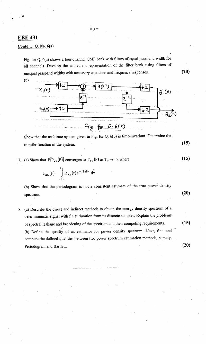
EEE 431Contd ••• Q. No. 6(a)
Fig. for Q. 6(a) shows a four-channel QMF bank with filters of equal passband width for.,all channels. Develop the equivalent representation of the filter bank using filters of
unequal passband widths with necessary equations and frequency responses. (20)
(b)
""Xi(n)
.fl'~..._~...._.~~b( b) ...._ ._.~ - .. -r _.' _.. ---
Show that the multirate system given in Fig. for Q. 6(b) is time-invariant. Determine the
transfer function of the system.
7. (a) Show that E(Pxx (F)] converges to lxx (F) as To -) 00, where
To .Pxx(F)= J Rxx(t)e-j21tf't d't
-To
(b) Show that the periodogram is not a consistent estimate of the true power density
spectrum.
(15)
(15)
(20)
(20)
8. (a) Describe the direct and indirect methods to obtain the energy density spectrum of a
determininistic signal with finite duration from its discrete samples. Explain the problems
of spectral leakage and broadening of the spectrum and their competing requirements. (15).J
(b) Define the quality of an estimator for power density spectrum. Next, find and
compare the defined qualities between two power spectrum estimation methods, namely,
Periodognim and Bartlett.

L-4rr-l/EEE Date: 23/07/2013
BANGLADESH UNIVERSITY OF ENGINEERING AND TECHNOLOGY, DHAKAL-4/T-l B. Sc. Engineering Examinations 2011-2012
Sub: EEE 453 (VLSI I)
Full Marks: 210 Time: 3 HoursThe figures in the margin indicate full marks.
Symbols have their usual meanings.
USE SEPARATE SCRIPTS FOR EACH SECTION."" _." _,_ _-" "._ _ ..........•............ _.__ _'----_ -- ---_ _ _._ , __ _ _ _ _ _ _-_ _--_ .
SECTION-AThere are FOUR questions in this Section. Answer any THREE.
.~
. \
.fr.I~
(10) .
4...•--~J_.,.-
5.•.,.~
...~l ..~
________ Fi=g._fo_f_Q_No 1(a)
(b) What is sheet resistance? A 100 nm CMOS process uses a polysilicon layer as
resistors. The resi;tivity of the polysilicon layer is 20 x 10-6 n.m and the thickness is
500 nm. Calculate the number of squares needed to form a 5 kn resistor.
(c) Show the circuit diagram of a pseudo NMOS inverter. The inverter is designed such
that output voltage becomes 0.2 V when the input voltage is High (5 V). Calculate the
aspect ratio of the inverter i.e. the ratio of driver transistor size to load transistor size. The
following data are given: J.lnCox== 120 'rlNV2, 'rlpCox == 50 'rlAIV2, Vton == IV,
Vtop== - 1 V, VOD == 5 V, 'Y == 0.5. Assume the body of the NMOS transistor is connected.
with the ground and the body of the PMOS Jransistor is connected with Voo ..
2. (a) In a 180 nm CMOS process the minimum gate length and width are 2A. and 4A.,
respectively. A minimum sized and minimum gate length CMOS inverter is designed
such that the inversion voltage becomes V0012. The following data are given:
'rlnCox== 120 'rlAIV2,J.lpCOX== 60 'rlAIV2,Vton== IV, Vtop== - 1 V, VDD == 5 V, 'Y == 0.5.
(i) Calculate the aspect ratio of the NMOS and the PMOS transistor.
(ii) In the transfer curve show the minimum and maximum input and output voltage
levels and hence give an expression of low level and high level noise margin ..
(iii) Now suppose that the designer increased the aspect ratio of the NMOS transistor
ten times than that obtained in (i). What changes in noise margin do you expect?
Contd P/2
(10)
(15)
(18)
.. ;•...
.. :l

.'~.
. '... :1.. ,'.
,\
. ;"'-,
(17)
(10)
(25) .
P-Diffusion
Contd P/3
N-Diffusion
PolysiliconContact
.~NWELL
.\; .., .
Vin=O
=2=
(b) The output of a CMOS inverter is connected to the input of a logic gate as shown in
Fig. for Q. No. 3(b).Calculate the rise time, fall time and dynamic power dissipation of
the CMOS inverter. The following data are given: Process Technology 500 nm CMOS.
process. Jln~x = 120 f-LAN2,JlpCox = 50 f-LAJy2,Gate oxide capacitance Cox = 35 fF/f-Lm2.
Source/Drain bottom Junction capacitance of both NMOS and PMOS, 0 = 10 fF/f-Lm2,
M.i = 0.33,Source/drain side wall capacitance of both NMOS and PMOS,
CJSW = 0.2 fF/f-Lm. MJsw = 0.1, % = 0.7 Y at room temperature, poly-substrate
capacitance = 15 fF/f-Lm2, Metal-substrate capacitance = 6 fF/Jlm2, All poly width = 2A.,
all metal width = 2A.except YDD and GND bus, poly extending N-DiffusionlP-Diffusion =
1A.,frequency, f = 500 MHz.
Contd ... Q~No.2
(b) A buffer chain circuit is to be designed for a clock signal which will drive 1000 logic
gates. The input capacitance of each of the logic gate is 12 fF and the output capacitance
is 4 fF. The minimum sized inverter in the process has an input capacitance of 3 fF and
output capacitance is also 3 fF. Find the size (n) and the number of stages (m) of the
required buffer chain. You have to derive any equations used in your calculations.
EEE 453
3. (a) Derive the expressions for rise time and dynamic power dissipation of a CMOS
inverter.

=3=
,.~.;~
(6)
(7 ~)
(c) Draw the truth table of a 3-input majority circuit in which the output is'!' when'
majority of the input is 'I'. Minimize the Boolean expression of the output and implement
the circuit in (i) CMOS, (ii) Pseudo NMOS, (iii) footed dynamic CMOS. (13 ~ )
(d) A 4-input NOR gate is designed for worst case equal rise and fall times. If j.J.n = 2.5j.J.p,
calculate the aspect ratio of the PMOS transistor in terms of aspect ratio of the NMOS
transistor. (8)SECTION-B
There are FOUR questions in this Section. Answer any THREE.
5. (a) Explain the following: (i) positive mask, (ii) negative mask, (iii) positive photoresist
and (iv) negative photoresist. (4+16)Show the process sequence of fabricating an inverter in a dual well CMOS process. In
each sequence show the mask diagram and the device cross sectional diagram up to that
sequence.(b) Design an n-bit parity generation circuit in bit sliced and structured way. The required
response is such that Z = 1 if there is even number of 1s in the input and z = 0 if there is
odd number of I s. Show the schematic diagram of the parity generator including the
connection of the first cell. Draw the layout diagram of the leaf cell using CMOS
technology in a modular way such that interconnections between cells are achieved when
cells are butted together. (15)
4. (a) Explain briefly the necessity of the following design rules: (i) Poly overlap Diffusion
= 2 "A"(ii) Floating NWELL not allowed (iii) Metal overlap contact = 1"A"(iv) Spacing of
NWELL toP-Diffusion=6"A,.
(b) Explain briefly the meaning of the following SPICE MOS model parameters: (i) KP
(ii) GAMMA (iii) MJ (iv) LAMBDA (v) PB
EEE 453
•
.J"
6. (a) You have to design a 64-bit adder. The delay through one adder cell is
I nsec and the delay through the multiplexer cell is 2 nsec. Calculate the delay if the
adder is designed as (i) ripple carry adder, (ii) carry select adder and (iii) carry skip adder.
Make any reasonable assumPt~w", (10) .(b) Design a 16 bit carry j.9D--k ahead (CLA) adder in 4x4 block CLA adder. Show the
schematic diagram of the complete system and the detailed circuit level implementation
of the block. Explain the operation of the system. (15)(c) In a 100 nm CMOS process the minimum width of metal is 3"A,.The metal layer
consists of copper conductors of thickness 1 Jlm. The electro-migration limited maximum
current density of copper wire is 5 mA/Jlm2• Calculate how many nMOS 9: I inverters can
be driven by a minimum sized metal interconnect. Assume the resistance of the driver
transistor is 10 kQ and VDD = 5V. (10)Contd P/4

"t" .~. /,
G~ . .r'.'
,.,
'~..
.~, ... ,11;.~
(7)
(8)
(20)
(18)
(b) Three faults Sj, S2 and OJ occurs in the circuit shown (Fig. for Q8(b)). Assuming fault
occurs one at a time, show the test vectors that will identify the faults .
(c) Show the circuit diagram and device cross-sectional diagram of a one transistor
DRAM cell. Explain the operation ofthe circuit.
..... _..•.... ,_ .... ...1 .. 5 '-F='3.. ,..~.ci--.N.J ..~ib) .
~ " ...•....• ()..(Y\,; .
=4=
Zj = abc +Ii c d + a ber
Z2 = abc d + a b d
Z3 = b c + ab d+a c d
(b) Show the circuit level implementation of a 2 x 2 SRAM cell using 6-T SRAM core
cell. Clearly show in your design the pre-charge circuit, column select and row select
circuits and the sense amplifier circuit. Explain how the read and write operations are
performed showing the first row and second column cell as an example. Explain how the
sense amplifier accelerates the READ operations.
8. (a) Name the four fault models most commonly used for CMOS circuits and explain
them.
7. (a) Show the NOR-NOR implementation of a PLA circuit which will provide the
following outputs:
EEE 453
.;.~": r
.. i
, .~'
','"
.~,
~.- "~../ .

.'L-4ff-l/EEE Date: 23/07/2013
BANGLADESH UNIVERSITY OF ENGINEERING AND TECHNOLOGY, DHAKA
L-4/T-l B. Sc. Engineering Examinations 2011-2012
Sub: EEE 433 (Microwave Engineering)
Full Marks: 210 Time: 3 Hours
USE SEPARA TE SCRIPTS FOR EACH SECTION
The questions are of equal value. Use Smith chart where necessary.
Used Smith Chart must be attached with the answer script................M_. _ ..__ .__ _. __ __ ..__._-_ __ _ __ _ __ - _ , _ ..-
SECTION-A
There are FOUR questions in this section. Answer any THREE.
1. (a) Deduce the far field components and expressions for power and radiation resistance
of Hertzian dipole in free space.
(b) A Hertzian dipole of length 5 cm is situated in free space. If the maximum current is
lOA and its frequency is 800 MHz, determine (i) its electric and magnetic fields in the
far zone, (ii) the average power density and (iii) radiation resistance.
2. (a) Deduce the properties of a small circular loop antenna.
(b) The current in a small circular loop antenna of radius 10 cm is 100 cos(wt - 30° )A ,
where ro = 300 Mradls. If the medium is free space, write the expressions for the far
fields in the time domain. Compute the power radiated by the antenna and its radiation
resistance.
3. (a) What are the purposes of arraying antenna elements? Derive the properties of an
endfire array.
(b) Derive the properties of a broadside array.
4. (a) With neat sketches describe the working principle of a reflex klystron.
(b) With neat sketches describe the working principle of a traveling wave tube (TWT)
amplifier.
SECTION-B
There are FOUR questions in this section. Answer any THREE.
5. (a) Starting with the voltage and current wave equations, deduce the analytical
expression of the complex reflection coefficient p for an ideal transmission line of
characteristic impedance Zo and of length'/" terminated with a mismatched load
impedance ZL ohms.
Contd P/2
=2=
EEE 433Contd ••.Q. No.5
(b) Compute the input impedance at a distance of 1.41 cm from the load in a lossless
transmission line of 75 ohm characteristic impedance in which the reflection coefficient
at the plane is 0.IL45°. The line is filled with a material of dielectric constant of 1.4 and
fed with a 3 GHz signal. (Smith chart shall not be used).
(c) Starting with the analytical expression of the input impedance, deduce the expression
of input impedance of a 4.75A long transmission line of characteristic impedance Zo
terminated with a load impedance of ZL.(d) Deduce the expression of input impedance of an open circuit transmission line of
characteristic impedance Zo and of length II.
6. (a) A microwave transmission line of ~haracteristic impedance of 50 ohms filled with a
material of dielectric constant of 2.0 and is fed with a signal of 4 GHz. The input
impedance at one plane along the length of the line is 35-j35 ohms.
(i) Find the distance in cm of the plane toward the generator from the above
mentioned plane at which the input impedance is 25 + j20 ohms.(ii) Find the distance in cm of the plane toward the load from the first plane where
the input impedance is 35 + j35 ohms.
(iii) Marking the point on the Smith chart read the value of the VSWR.
(iv) Find the distance in cm from the load plane toward the generator on the same
line, where the input impedance is 0 + j41.666 ohm if the load is replaced by a
short circuit (Use Smith Chart).
(b) A signal of 6 GHz is propagating through a parallel plane waveguide consisting of
two copper conductor planes having a spacing of 3 cm and filled up with a dielectric
material of dielectric constant '1.5. Considering TElO propagating through the
waveguide, compute the values of (i) cutoff frequency, (ii) phase velocity, (iii) group
velocity, (iv) guide wavelength, (v) wave impedance and (vi) the electric field
components.
7. (a) With necessary analytical expressions and supporting diagrams, write the steps (of
the procedure) which need to be followed to solve a quarter wave transformer
impedance matching problem for a mismatched complex load.
(b) With necessary analytical expressions and supporting diagrams write the steps (of
the procedure) which need to be followed to solve a single stub impedance matching
problem.
Contd P/3
.•

=3=
EEE 433Contd ... Q. No.7
(c) A microwave generator operating at 5 GHz feeds into a 18 cm long transmission line
of characteristic impedance 75 ohms. A load of 52.5-j60 ohms is connected at the end of
the transmission line. A single-stub tuner is to be connected with this system located at a
distance d from the load plane toward the generator to obtain matching. Find the
distance d in cm and the length of the stub I in cm for perfect match. The dielectric
material used inside the microwave transmission line has a dielectric constant of 104.
Give all possible values of d and 1in cm. (Use Smith Chart)
8. (a) Taking the vertical direction as y-axis and the direction of propagation as the z-axis
write the analytical expressions of (i) the Electric field components, (ii) guide
_wavelength, (iii) < wave impedance, (iv) cutoff frequency for TE and TM waves
propagating through a rectangular waveguide.
(b) Compute the values of (i) .cutoff frequency, (ii) wave impedance, (iii) guide
wavelength and (iv) write the expressions of field components (with appropriate values)
for a TEIO wave propagating through a rectangular waveguide having the dimensions
a = 2.3 cm, b = 2 cm and filled up with a material of dielectric constant of 104.
(c) A rectangular cavity resonator made of copperplates, is filled with a dielectric
material of dielectric constant = 2.0. The length 'd' of the cavity is 3 cm and the height
of the cavity 'b' is 1.5 cm. (i) For the cavity resonator to be resonant with a TEIOI wave
inside it what should be the dimension of the width 'a' in cm (ii) Compute the resonant
frequency of the cavity resonator.

The Complete Smith ChartBlack Magic Design
RADIALLY SCAl,ED PARAMITERS..
0.40.2
0.50.3
4 3 2,5 2 1.8 I r, 1.4\ ' " ' ;0""" ~ ' ',' , ~ \ '5 " ~ \. 3
o 7' 8 9 10 12 Ii+
0.1 O.Of,
0.3 020.1
0.8
0.7 0.6 0.5
0.8 0.70.' 0.8
0.'
•• I{XHO W 10~.Io'io' 1'1'0' 2~\ I I " I~° 2 3
TOWAROLOAO.-', c. TOWARD GENERATOR1-2 Ll I 15 10 7 5 1 " 2 I
2 I II II" ' I" 1'0' "/, , \ '\:2'" '/3" ;:;~' ;:B" ~ " " " 'i' "4 \ 5" ,', ',~ '2~ 'l20 30 0 0.1 0.2 0.. 0.' 0.8 1 1-5 2 3 1 5 G 10 ,5~",' Iln,',I,,/,oI,,' ••••" .•••.y-,LJ' •••'o'I'.' 1'.','/1',' ••••,,'1,',',,',','1 ••,'10.01 c 10 1.1 I.Z 1.3 1.... I.S 1.6 1.7 J.8 1.9 2 2.5:'1 4 5 10-
! !0jl, ! f ,Ull ,O.?9. I ,O.?5, ! ! ,Oj9 ~LI 0j1 I 0;6 , 0;5 , OJ'' " 0j3 I 0;2 • 0jl • ~
CENTER
0:, , ,,OJ', , ,,0;2, , ' ,0,3, , ' ,Oi4, , "Oi5" ,,0;8, , ' ,Oi, , •• Oi8, , • ,0;9, , , ,!, , ' ,1;1, , "li2, " ,1;3, ,w!k, ,1;5, " ,IiO, ' , ,Ii, , , ,JiB, , ' ,'iO' , ,.~
ORIGIN ' .

',. The Complete Smith ChartBlack Magic Design
-
T
.•...
0.13
0.37
\-10.2
Q.\2038
RADIALLY SCALED PARAM"TERS
_10040 ZO 10" " 1'1" III' ,_40' 30' , 20 "is023
TOWARDLOAD-> <. TOWARDGtNtRATOR4 3 2.5 2 1.8 1.0 1.4 1.2 1.I I 15 10 7 5 4 :J 2 ,I' " ' ;0" I' '~ ' ',' , ~ \ i"~',.j "2 ' 'i' "til '"'' I" I ',' I/t", '''t:; \ \'3" ;:;~', ;:8" ~ " " " I;' "4 \ 5" ... 'I~ '/.0 ' .~
5 8 7' 8 8'10 12 14" ;,20",~""0 , ,,6;',0.2 , 0'.,0;80.8,' ,.';5",~ ,,,3,,,,1 ,L? ",',01,5-.•..I I " :1"" I , , ,, " I. ,•,,I,"'" I I ,.y,L'. , , • I, I , , I , ,,," , ,," , , "" I
0.9 0.8 0.7 0.6 0.5 0.4 0.3 0.2 0.1 O.O~ 0.01 0(0 1.1 J.2 1.3 J..4 1.5 1.6 1.7 1.8 1.9 2 2.5 3 •• 5 10-
0.9 0.8 0.7 0.6 0.5 0.4 {1.3 0.2 ,0jl! I , ,Oll .079! I ,O.¥5, I I ,0;9 0i8 l OJ? . 0j6 ! O{J • 0j4 1 0j3 ! 0iZ I 0jl ! YCENTER
Of" ,,0;1, ",0;2", ,0;3" ,,0;4, ",Oj5" ,,0;8, " ,0;7", ,O;R, , "Of""!,,, ,IiI" , ,Ir, ",1;3, ,~, ,';5", ,';6", ,1;7." ,'j8, ",'f", 1 ~
ORIGIN

•The Complete Smith Chart
Black Magic Design
0.1\O.IZ
~ 0.38
0.13
0-37
O.Z
0.'
-
')(')( ~ f..
leI> •..../1... .--
9"0 ..-. .l.-
¥
1"0 .\-
'~Zll;--+--i--l--r\

-10040 20 10II " 1'\" I \ I' ,-40' 30' '20 " .'5
023
The Complete Smith ChartBlack Magic Design
RADIAlLY SCAl.ED PARAMETERS
TOWARD LOAD ._> <. l'OWARDGENERATOR4 3 Z.5 Z 1.6 ]." 1.4 1.2 1.1 I 15 10 7 5 4 :1 Z I
\' :' ;O~'";i '~!~~I~~:'Z~I~,j,:\',:,i"~~~,':',',:I' :.'/:i:,"/ ::{,'; ){:){: ~ii2~~:;~~.'I~I':;:',.",,':;:,~,:,;,\"5,; .',';,: :I~":~,,~5~0.9 0.8 0.1 O.G 0.5 0.4 0.3 0.2 0.1 O.~ 0.01 DiO 1.1 1.2 1.3 L4 1.5 1.6 1.1 1.8 1.9 2 2.5 3 <4 5 10-
0.9 0.8 0.7 0.6 0.5 0.4 0.3 0.2, ,0;1, , ; ,Dr, Of!' , ' ,0.r5, , ' ,0;9 0;8 0.1 0.6 0.5 0.1 0.3 0.2 0.1 °CI!NTER
of" "Oil, ",O~", ,0,3" "Oi4, "'Oi5, , ,,0,6, ",0;7", ,O~" "Of""!,,, ,Iii" , ,liZ'" ,1;3, l'~' ,liS'" ,1;6" "1;7.,, ,';8", ,If, "'~
ORIGIN

, '.,
1: ,; .-.
• ,"3
i1':,
I":
I
,.-.. ~.
of ~~ ~':', .,
.f'f .~'1. ,
',I'<of';
t
.' f'.Ai~:~~:.
, ~.tf
.....
,,' ~,.,-.'
. 'I~ 'f
fo ;:. Pc~ :;\/,1'1. Y'~ S =
r.
~Q.) od-- ~ a6I ITvo/>.~~ ~ *" VWl.~eMt
'0<IcAvt...,. ~ Vo ve-....
RVOA-ve.-..rOA-V~VYlI\
72-
\
tj ~~2lh).VctY\. ;: Vl"-t 'f\ ~ ~ ..
Vb..,.., ::.. VYl-IfI 4-12.-0 Sontd P/2
'. VCJ\::' VMn. ~ e -1-4'0]
(b) Following is the circuit of a half-wave/ha1f-bridge three phase uncontrolled rectifier.
Starting with three phase line to neutral. voltages, draw the input currents (all three
phases) of the rectifier., ~
LC(.
2. (a) In the following single phase controlled rectifier circuit with the wave forms shown in
the diagram, what is the input power factor?
There are FOUR questions in this Section. Answer any THREE.
1. (a) Ciassify DC-DC chopper circuits according to their quadrant of operations.
(b) Draw the circuit diagram of a Jone's chopper (dc-dc converter) circuit, SCR gate
voltages, input and output voltages of the circuit for a R-L-EMF load. Describe the
operation of the circuit in details.
(c) Describe the operation of the following SCR chopper circuit where TI is the main
SCR and Til is the Commutating SCR.
L-4rr-1/EEE Date: 23/07/2013
BANGLADESH UNIVERSITY OF ENGINEERING AND TECHNOLOGY, DHAKAL-4/T.,I B. Sc. Engineering Examinations 2011-2012
Sub: EEE 473 (Power Electronics) ,
Full Marks: 210 Time: 3 HoursThe questions are of equal value.
USE SEPARATE SCRIPTS FOR EACH SECTION_. •••riri__ ~ __ ri .ri •• ------.-------
SECTION-A

',.
4. (a) Draw the circuit of a three phase voltage source square wave MOSFET inverter. With
appropriate gate/base signals for six switches, input/output dc, line to line and line to
neutral voltages of the load (R Y Connected) explain the operation of the inverter.
(b) What is a current source inverter? Explain the operation of the (Fig. Q. 4(b) following
single phase SCR current source inverter. Explain how the main SCRs commutates in the
circuit without any additional SCR commutation circuit.
UTL
=2=
3. (a) Draw the circuit diagram of a three phase SCR voltage controller withY-connected
resistive loads. With appropriate input VLN, VLL, output VLN, VLL , phase and line
currents and gate pulses of six SCRs of the circuit, explain the operation of the circuit for
firing angle a = 1200•(b) Explain the operation of the following single phase voltage controller circuits and
describe the difference between them.
Contd ... Q. No.2
(c) Draw the circuit of a three phase SCR controlled rectifier (fullbridge/fullwave/six
pulse). With proper input VLN, VLL, gate pulses of 6 SCRs, output voltage waveform and
input currents of three phases, explain the operation of the rectifier for a resistive load
with firing angle a = 600•
EEE.473
~'}I ":~r.''l~~.~!~.i~~~',i,\ '~tt~"
t~.~,,';~r:,:~\ti~~~,'~~1J;,,hi?\,fI~J.,(r-,~.~;,~ .~~:;,~~f:-;;':.•'"f
1f
;J:. -~
.'~''"':'
I, T~
t J'J ( () (v'3,
D4D,f,
T4
Orh5 0. 4(tJ)
(b) Derive the Fourier series of the line to neutral voltage of a three phase square wave
voltage source inverter. Load is Y connected R-L load. Also find the Fourier series of the
current through R-L load.
Contd P/3

=3=
~i~~;,) EEE 473~(~N;:,'. SECTION - B
There are FOUR questions in this Section. Answer any THREE.
5. (a) What is secondary breakdown? Explain why secondary breakdown occur in BJT and
Thyristors but not in MOSFETs.
(b) What is a snubber circuit? Explain the usage of snubber circuits in SCR.
(c) Define latching current and holding current of an SCR.
(d) Explain why BJT's cannot be operated in parallel to increase current ratings.
6. (a) What is a dual converter? Why inductors are inverted between the forward and
reverse converters of a dual converter?(b) A three phase dual converter supplies power to a dc motor. The supply voltage is 3%,
415V (line to line). If the motor needs an armature voltage of -295 Vdc, determine the
firing angles <XI and <X2 for the forward and reverse converters.
(c) Draw and explain the topology of a single phase ~converter.
C-ycJo7. (a) What are the basic differences between a chopper and a switching regulator?
(b) Draw the topology of a buck regulator and hence deduce the output voltage, current
ripple and voltage ripple equations.
(c) Design a switching buck regulator with the following rated values:
Input voltage range = 7 V to 35 V dc
Output voltage = 5 V :t 10m V dc
Ripple current less than 10 mA.
Switching frequency range 25 kHz to 35 kHz.
Output power = 20 watts.
8. (a) Derive an expression for the de output voltage of a buck-boost regulator.
(b) What is a flyback converter? How core saturation problem is addressed in a flyback
converter?(c) A permanent magnetdc motor is used in robotic arm and is driven from a stepdown
chopper. The supply is from a battery of 12V dc with internal resistance of 0.1 Q.
The motor draws a power of 25 w at an armature current of 3.5 A. Neglecting the
switching loss, determine the duty cycle of the chopper.
------------------------------

BANGLADESH UNIVERSITY OF ENGINEERING AND TECHNOLOGY, DHAKA
L-4/T-1 B. Sc. Engineering Examinations 2011-2012
Sub: EEE 435 (Optical Fiber Communication)
;. r '~,: , .
-:>::,~il;~~!'":;.'/;f;\'
.'.:.. ',.-"
.y
L-4/T-1/EEE Date: 21/09/2013
SECTION-A
There are FOUR questions in this section. Answer any THREE.
Time: 3 HoursFull Marks: 210
USE SEPARATE SCRIPTS FOR EACH SECTION
The figures in the margin indicate full marks.
"
1. (a) What is an optical fiber? State the merits of optical' fibe~ over conventional
waveguides. Show the ray propagation through different types of fibers. Comment on
their relative merits and limitations. (10)
(b) Show that the numerical aperture (NA) of a fiber is given by
NA = ~n12-ni r::; ~ .J2t,. . (10)
, " (c) What are the causes of attenuation in a glass fiber? Discuss the phenomenon behind
f;,.. . the attenuation in a fiber. Draw the loss characteristic curve of a silica fiber and show.. }~ i-;, .the operating windows for transmission. (15)
,.;.. "
:~'f, 2. (a) Distinguish betWeen inter modal and intra-modal dispersion in a fiber. Discus the
effect of dispersion on the bandwidth and allowable bit rate through a fiber.
(b}Derive the following relationship for an SMF:
A d2n(J'rms= L. C d)/ .(J').
(10)
(10)
.: .",
~"'- .' .', '
where the symbols have their usual meanings.
(c) A silica fiber has the material dispersion defined as ~~1 = 0.08 pm-2. The
"!~:'.~{>.. :'~:.~.-
refractive index of the core is 1.55 and relative refractive index difference is 2%. The
source used has a FWHM linewidth of 0.15 nm.
Determine:
(i) rmspulsewidth due to intra-modal dispersion at the output of 1 Km fiber;
(ii) rms pulsewidth due to intermodal dispersion at the output of 1 Km fiber;
(iii) bandwidth of 1 Km fiber;
(iv) maximum allowable bit rate through a fiber oflength 10 Km.
(15)
!.
, i
3. (a) Discuss the principle of optical FDM and Wavelength division multiplexing (WDM)
and comment on their applications. (10)
Contd P/2

.~".
.;..:~':.."
.}" .
.;.'(15)
(35)
4. A fiber-optic link is based on SMF of 10 segments each of length 22.5 Km which are
connected through couplers of loss 1 dB each. The source is a laser of half-width-half-
maximum linewidth of 0.075 nm. The rise time of the laser driver circuit is 2.5 ns. The
receiver is based on a PIN photodetector of rise time 5 ns. The receiver load resistance is
50 ohm and the LPF bandwidth is 560 MHz. The photodetector has a sensitivity of
-60 dBm. The material dispersion coefficient of the fiber is 16 ps/Km-nm. The optical
fiber is coupled to the source and detector via optical couplers of loss 1.2 dB each.
Determine: Ass,'V'ML Q7 IJ)A.{S,Slo- b~
(i) the minimum power required for the laser;
(ii) the maximum available bandwidth of the fiber link limited by system risetime;
(iii) bandwidth-distance product of the fiber link; .
(iv) the signal-to-noise ratio at the output of the receiver LPF if the quantum
efficiency of the photodetector is 85% at the operating wavelength of 1550 om.
EEE 435
(b) Discuss the technique of radio- on-fiber technology along with its applications.
(c) With necessary schematic diagram, briefly explain how an MZI can be used as a
WDM MUX/DMUX.
Contd ... Q. No.3
=2=
A 4""channel DWDM MUX/DMUX based on MZI has input wavelength separated by
0.08 nm with centre wavelength 1550 nm. The effective refractive index of the MZI
branches is 1.56. Draw the schematic diagram of the MUXlDMUX and find the path
difference ~L for the different stages of the MZI MUXlDMUX.
SECTION-B
There are FOUR questions in this section. Answer any THREE.
5. (a) Explain the operation of a semiconductor laser diode showing its basic structure and
band diagram. Derive the necessary conditions of oscillation.
(b) Compare the input-output characteriStics and spectral characteristics of LED with
laser.
(15)
(10)
(c) State the advantages of ILDs over LEDs. Mention the applications of different types
ofLEDs. (10)
6. (a) Sketch the basic structure. of a PN photo-detector (PD) under reverse bias and
explain its operation. Explain step by step how it is improved in PIN PD and APD.
Contd P/3
(13)

i;- ..••
.,' ,. ~'
.;'.
• .•.
=3=
EEE 435Contd ... Q. No.6
(b) Write down the advantages and disadvantages of APD compared to PIN PD. How
the problem of excess noise in APD is mitigated in silicon reach through APD (RAPD).
(c) An APD has a quantum efficiency of 50% at 0.8 IJ.m. When illuminated with a
radiation of this wavelength it produces an output current of 10 JlA after avalanche gain
with a multiplication factor of 250. Calculate received optical power to the device. How
many photons per second does this correspond to? Determine the wavelength above
which the device will cease to operate considering the bandgap energy of the material as
1.43 eV at 300 K.
7. (a) Describe the direct detection technique in IMIDD optical communication system and
derive the expression of SNR and BER considering PIN receiver. What is receiver
sensi tivity?
(b) Show the block diagrams of different coherent detection techniques in optical
communications. State the relative merits and demerits of using coherent detection.
(c) A PINphotodiode incorporated into an optical receiver has.a quantum efficiency of
80% at operating wavelength of 1300 nm. The average incident optical power to
photo diode is 100 ~W and the post~detection bandwidth of the receiver is 5 MHz. It has
an amplifier with noise figure of 3 dB. The dark current in the device is negligible and
the load resistance is 100 Q at operating temperature of 30oe. Calculate the SNR at the
output of the receiver.
(10)
(12)
(16)
(8)
(11)
I.. ,;'
.:..
8. (a) Mention different types optical amplifiers. Show their common applications in
optical fiber communication systems. Draw a schematic diagram of SOA and briefly
describe its operation.
(b) What are the rare-earth-doped fiber amplifiers? Explain the operating principle of
EDFA and compare its gain spectrum with that of SOA.
(c) Write short note on (any ONE):
(i) Fiber FBT couplers
(ii) EOPM
(14)
(13)
(8)
'•... ,;- .~.-:~.. '.~'.

?"J"
-.:'~
~; < J~ : { f : . !
L-4/T-l/EEE Date: 21/09/2013
BANGLADESHUNIVERSITY OF ENGINEERING AND TECHNOLOGY, DHAKA
L-4/T-1 B. Sc. Engineering Examinations 2011-2012
Sub: EEE 455 (Compound Semiconductor and Hetero-Junction Devices)
Full Marks: 210 Time: 3 Hours
USE SEPARATE SCRIPTS FOR EACH SECTION
The figures in the margin indicate full marks.
Symbols have their usual meanings.
SECTION-A
There are FOUR questions in this section. Answer any THREE.
1. (a) Why electronic property of amorphous, polycrystalline and crystalline
semiconductors are different? Discuss mobility and optical absorption characteristics of
these materials. How these properties can be explained with the help of energy band
structure?
(b) Show the compositional dependence of the direct and indirect conduction band
minima in the AlxGat_xAs mixed crystals and determine the effective band gap at direct
to indirect transition. Given that, .
E~(x) = 1.425+1.247x, (x ~ 0.45)= 1.425+1.247x+ 1.147(x -0.45)2, (x > 0.45)
E:(x) :=1.9+0.l25x+0.143x2
E~(x) =1.708+0.642x
2. (a) Explain the term pseudomorphic. Why critical thickness is important during epitaxial
growth? Discuss the effect of biaxial strain on bandstructure and impact of biaxial strain
.~n the performance of electronic device.
(b) Discuss why 13 is decreased with Ie at low and high injection levels. How base
transport factor limits common emitter current gain?
3. (a) Explain the influence on the device characteristics if Ge is incorporated in the base
of silicon bipolar transistor. Discuss why polysilicon Emitter structure is used in Si .
BJT?
(b) How band gap narrowing affects BJT and HBT performances? Consider a uniform
doped Si npn transistor in which Xe = Xb' Nde = 5x10¹⁹ / em3, Nab = 2x10¹⁶
/ em3,
Dn = 25cm2 / s, Dp = 10cm2 / s. Calculate 13 at 300 K and 350 K when the bandgap
narrowing effect is taken into account for moderate injection level.
Contd P/2
(20)
(15)
(20)
(15)
(20)
(15)

,. > .. ;r.'
." .~." .j".' ';' "-'-
=2=
EEE455
4. (a) Elaborate the physical factors in BJT those affect transistor cutoff frequency. How
can higher speed be obtained in HBT?
(b) Explain TEBT. Estimate the factor increasing P in an HBT with a wide bandgap
emitter having emitter-base valence band discontinuity of 0.2 eV at 300 K.
SECTION-B
There are FOUR questions in this section. Answer.any THREE.
5. (a) Prove that, for a JFET, the drain current is given by,
Here, the symbols have their usual meanings.
(b) For an n-channel GaAs MESFET, a = 0.5 J..lm,Nd = 6xl0lS cm-3, Nc = 4.7x1017 cm-3,
<DBn = 0.95.iY and ES = 13.IEo. Determine the value of threshold voltage at 300 K
temperature.
6. (a) Describe the operating principle of HEMT with neat sketch of quantum well
structure.
(b) Consider an N-Alo.3Gao.7As- intrinsic GaAs abrupt heterojunction structure which
can be used as HEMT. Assume that the AIGaAs is doped with Nd = 3 x 1018 cm-3 and
has a thickness of 350 A. Let <I>B =0.89eY, ~Ec = 0.24 eV and EN= 12.2EO.Determine
the value of threshold voltage at 300 K temperature.
(20)
(15)
(25)
(10)
(18)
(17)
7. (a) Write down the definition of heterojunction in brief. State when Anisotype, Isotype
heterojunctions are formed. Draw sample band diagram (before contact) of straddling
gap, staggered gap and broken gap heterojunction structure. (9)
(b) Prove that, for an nP heterojunction, the expression of built in potential barrier is
~~~ Q~
ev' =-/ill +kTln(nn0 NCPJhI C N
npo cn
Here, the symbols have their usual meanings.
Contd P/3

(15)
=3=
EEE455Contd ... Q. No.7
(c) For heterojunctions in the GaAs-AlGaAs system, the direct bandgap difference
6Eg accommodated approximately 2/5 in the conduction band and 3/5 in the
valance band. For an Al composition of 0.30, the AlGaAs is a direct bandgap material
with Eg = 1.80 eV. (13)
Calculate (i) i1Ec, (ii) i1Ey and (iii) (Electron effinity, K)AIGaAsif (electron
effinity, K)GaAs= 4.07.eV.
Given the direct band gap of GaAs is 1.42eV.
8. (a) Briefly explain, only the forward bias effect of a metal-n-semiconductor Schottky,
Barrier Diode using a sample energy band diagram. (10)
(b) The Schottky Barrier Height of a Silicon Schottky junction is <PBn = 0.6e.-V,the
effective Richardson constant is A. = 115A/K?_cm2• (10)
Determine (i) The ideal reverse saturation current density at 300 K, (ii) The diode
current density for Va= 0.35 V.
(c) Consider an ideal Chromium-n-Si Schottky diode at a temperature of 300 K with
Nd =3 x 1015 cm-3 and Nc = 2.8 x 1019 cm-3• Determine (i) The ideal Schottky Barrier
Height and (ii) Maximum electric field at zero bias. Given, the work function of
Chromium is 4.5,t:¥,electron affinity of Silicon is 4.0I~ and Es= Il.7Eo•

••
L-4/T-1/EEE Date: 21/09/2013
BANGLADESH UNIVERSITY OF ENGINEERING AND TECHNOLOGY, DHAKA
L-4/T-l B. Sc. Engineering Examinations 2011-2012
Sub: EEE 475 (Power Plant Engineering)
Full Marks: 210 Time: 3 Hours
I
I
USE SEPARATE SCRIPTS FOR EACH SECTION_ _ .._ .._-_ _ __ _ .._.......... . _-_ _----_._---_ __ _ _--- _ -_ __ _ _ " _-_ .
SECTION -A
There are FOUR questions in this section. Answer any THREE.
The figures in the margin indicate full marks.
1. (a) What are the major components of a coal fired power plant? Also indicate the land
requirements for each component in percent of total requirement.
(b) Describe, in very brief, the different conditions to be considered to determine the
location of a new thermal power station.
2. (a) What is the condition that a hydro plant should satisfy so that it can be operated as a
base loaded unit. What are the major components of a hydro plant? What is water
hammer?
(b) A power system has the units of capacity shown in the following tabulation, with the
indicated order of efficiency:
Unit No. Capacity, MW Order of efficiency
1 10 7
2 15 5
3 15 6
4 25 4
5 60 2
6 60 1
7 80 3
For the above conditions, show the capacity schedule in a tabulation form.
3. (a) Describe the general objectives of electric energy rate.
(b) With simple curves, describe the difference between Block-Meter Rate and
Hopkinson Demand Rate.
(c) A Wright demand rate is quoted as follows:
For energy purchased monthly, the equivalent of
1. The first 50 hr. use ofmaxm demand at 9.00 taka perkWhr.
2. The next 50 hr. use ofmaxm demand at 6.00 taka per kWhr.
3. The next 100 hr. use ofmaxm demand at 4.50 taka per kWhr.
Contd P/2
(10)
(25)
(20)
(15)
(10)
(13)
(12)

=2=
EEE 475Contd ... Q. No. 3(c)
4. The next 200 hr. use ofmaxm demand at 3.00 taka per kWhr.
5. All energy in excess of foregoing blocks at 1.50 taka per kWhr.
(i) Compute the bill for a monthly energy consumption of 432000 kWhr with
a maximum demand of 1600 kW. Compute the unit energy cost
corresponding.
(ii) Find the lowest possible bill for this energy consumption and the
corresponding unit energy cost fora30-day month.
4. What are the conventional methods of forecasting demand? Describe any two of them. (35)
SECTION-B
There are FOUR questions in this section. Answer any THREE.
The questions are of equal value.
5. (a) With a block diagram explain the operation of a coal fired steam power plant.
(b) Explain briefly the function of superheater, reheater, economizer and air preheater in
a steam power plant.
6. (a) What are the advantages and disadvantages of hydro-electric power plant. Explain
with a neat sketch the operation of a Kaplan turbine.
(b) A hydro-electric power plant operates under an effective head of 55 m and a
qischarge of 90 m3/s. Density of water is 1000 kg/m3 and overall efficiency is 85%.
Determine the power developed.
7. (a) Explain with appropriate diagram and equation the fission reaction.
(b) Draw the layout plan of a Pressurized Water Reactor (PWR) showing the different
components and also explain its working principles.
8. (a) With a block diagram explain the operating principle of an open cycle gas turbine
power plant. What are its advantages?
(b) How does the VAR transfer take place between two alternators operated in parallel?

, ,,/
';"n. •
Time : 3 HoursFull Marks : 210
SECTION-A
There are FOUR questions in this section. Q. No.4 is COMPULSORY.
Answer any TWO from the rest THREE questions.
The figures in the margin indicate full marks.
USE SEPARATE SCRIPTS FOR EACH SECTION
L-4ff-l/EEE Date: ,28/09/2013
BANGLADESH UNIVERSITY OF ENGINEERING AND TECHNOLOGY, DHAKA
L-4/T-l B. Sc. Engineering Examinations 2011-2012
Sub: EEE 413 (Solid State Devices)
\
','
"0;,
-,';,..:.."
~'-!.•..
1. (a) Two semiconductor materials, Sem-A and Sem-B have identical density of states.
Intrinsic carrier concentration of Sem-A is 50 times larger than that of Sem-B at 295 K.
Determine the band gap ofSem-A if the band gap ofSem-B is 1.2 eV.
(b) Show that the probability a state ~E below the Fermi level (EF) is empty equals the
probability a state ~E above the Fermi level is filled.
:II
(20)
(15)
2. (a) Show that the total capacitance per unit area of an AVSi02/P-Si MOS capacitor under
surface depletion condition can be expressed as:
Cox
(15) '."
",,",
'.:'
C=1+
."..~ ..
where the symbols have their usual meaning.
(b) A long intrinsic semiconductor bar is illuminated at the middle as shown in Fig. for Q.
2(b). The whole device remains at room temperature .
(i) Sketch and explain the band diagram of this illuminated semiconductor bar that
includes Fermi levels.(ii) Draw and explain the voltage drop versus position alon,g;the length of the sample
when a constant current is flown through the semiconrluctof"bai'.
{)I-------------~~ ?<..h'~.~I &. 2(J;,).
(20)'
Contd P/2 .
!.. '

" ,Ii" l". 'I.
~. .•.
=2=
'.. "
' ..
..~.,
';.;."
I,I
.' .• ,I.
""
" ., ."(1,,'7)' ,"..~~.
.,"t,!'
...••,
(18)
_ Ec
-EF= EiEv
. - ~ -.' --.-- _ .. -
G~----- _
f:F--- -~--t:; -
EEE 413
3. (a) A P-type Si is produced with an acceptor doping density of 5 x 1015 cm-3. During the
doping process, some electron trap states are created at an energy,level 0.7 eV below the
conduction band. Determine the probability of finding an electron in the trap states at a
temperature of 300 K. Given:
band gap ofSi,Eg = 1.12 eV
trap states density, Nt = 5 x 1011 cm-:-3
. .. .' d. 1 5 1010 -3mtnnslc carner enslty, nj = . x cm
(b) Given two semiconductors,@and@ represented by the energy band diagrams shown
in Fig. for Q. 3(b). Both the semiconductors have equal electron concentrations in the
conduction band. Compare their conductivities with justifications .
; Jj:~. ~~' ;. '.
.4 •
. .~\ ;
, .
<.t.
::",1'
~.. ' .• ~ '
,I; :.
""1', .
"Ii,:/.' ,.',
4. Schematic cross-sectional view of a metal-oxide-semiconductor device is shown in Fig.
for Q. 4. Draw approximate energy band diagrams along Z-Z' direction of the structure for (18+17)
'"'~.- .
.--- - --- -
I~ ~,
',;
/
' ..,
~"
:'.V.:':
Contd P/3

. '.;,-;
, ., 'I'~), (.
~. .' ...-
'. ',I
" ... ,.:. : -1',', , .
~~!~"
\., "
", ..
. '..~.• oj •••••• :
.~ :.~'L.
.. , "". ,,;..
, •• ," "' .. , 1-
(15)
(20)'
(i) the ideal reverse saturation current due to holes~
(ii) the ideal reverse saturation current due to electrons~
(iii) the hole concentration at x = Xn if the applied voltage Va = 1/2 Vhi. [Here~ Xn is
the depletion width in the n-side and Vbi is the built-in potential] and
(iv) the electron current at x=xn +.!.Lp for Va = l'iVbi' [xn~Va and Vbi are as, 2
=4=
defined above. Lp is the average diffusion length of holes].
(b) A silicon n+p junction is reverse biased at 10 V. Determine the percentage change in
(i) junction capacitance and
(ii) built-in potential
if the doping in the p-region increases by a factor of 2.
8. (a) A silicon step junction has uniform impurity doping concentration ofNa = 5 x 10¹⁵
-3 15 -3 ' . f 4 2cm and Nd = 10 cm ~and a cross-sectIOnal area 0 A = 10 cm. Let~ 'tpo = 0.1 I-Ls~
22''tno = 0.4 !-LS~J.lp = 480 cm N-s and I-Ln= 1350 cm N-s. Calculate:
EEE 413
':.\ .'. 'I', .
" .
.•.,~.~.,ii:.J•
,',. ~ \ "1
::... ,."
" ,...• ------------------------------------------'.
;, . /r . ,',.l' ; , 1
~,'.
r, .•~', 1
" .-. !,..
\, .,j
t,"
'l\~::JI; ~- .,
, .
, 1I
rr'
,:,',,"j'';!
, "
tI
,I
I
""..'-:-".
\

. .1
..... ',.,.' . "~
;
•
(15)
(~O)
(15)
(20)
=3=
SECTION-B
There are FOUR questions in this section. Answer any THREE.
Symbols have their usual meanings.
the depletion width in the p-side is equal to that of the n-side.
(b) The built-in potential barrier of a linearly graded silicon p-n junction at 300 K is
0.7 V. The junction capacitance measured at 3.5 V (reverse bias) is 7.2 x 10:-9F/cm
2.
Find the gradient of the net impurity concentration. (Assume symmetrical doping
profile).
5. (a) Develop the coupled-diode model of a p-n-p transistor.
(b) Sketch the ideal energy-band diagram of a metal-'n' type semiconductor ohmic
contact. Explain why this is an ohmic contact.
EEE 413
....Ii,',: ,
'.o",-', '"f:: '''-,....
,'.'
...'.~:':'" .;'.'~ ~;, ;
.:.~! ,:'.:":. 6. (a) Derive the expressions of built-in potential, electric-field, depletion width and,~~\:- .
junction capacitance for a linearly graded p-n junction. The doping is symmetrical so that
. ~.' . - '\
r'~.
-'.,~..
, ;
7. (a) Consider a uniformly doped GaAs junction at T = 300 K. Atzero bias, only 20% of
the total space charge region is to be in the P region. The built-in potential barrier is 1.20
V. Given that nj = 1:8 x 106 cm-3 and EGaAs = 13.1 EO. Determine-
(i) doping concentration in the p-side,
(ii) doping concentration in the n-side,
(iii) depletion width in the p-side,
(iv) depletion width in the n"'side and
(v) maximum electric-field.
(b) Find the stored charge Qp as a function of time in the n-region of a long p+-n
jUnction;sJit forward bias current is switched from IF1 to IF2 at t = 0 as shown in Fig.
"1iI
I.
for Q. No. 7(b). (15)
F .
\I",
t------- rF.2.
'.; ;. _I, •
"','
",:
:r,:-,------1
~. Contd P/4.'1'" •

L-4/T-1/EEE Date: 05/10/2013BANGLADESH UNIVERSITY OF ENGINEERING AND TECHNOLOGY, DHAKA
L-4/T-l B. Sc. Engineering Examinations 2011-2012
Sub: EEE,401 (Control Systems)
Full Marks : 210 Time : 3 HoursThe figures in the margin indicate full marks.
USE SEPARATE SCRIPTS FOR EACH SECTION
SECTION-AThere are FOUR questions in this section. Answer any THREE.
1. (a) "A sampled data control system is stable if all the poles of the closed loop transferfunction T(z) lie within the unit circle of the z-plane. Explain briefly the statement in
connection with the analysis in the s-pla:ne. (10)(b) For the following digital control system find (i) Closed loop transfer function in z-domain (ii) Range of K to make the system stable and (iii) Steady state error for the
stable system if the input r(t) = ( t + ~ t 2 ) u(t) . (25)
Hold 3Ks(s + 3)
C(s)
~, \Cb)
2. (a) The output response of a second order system to a step input is given by the folloWing
equation (18)
y(t)=l_e-S(J)nt [cosrodt+h s;nrodt]1-l;2 .
Derive the expressions for tp, Mp and tr• All symbols have their usual meanings.
(b) For the following system determine the value of'K' and 'a' such that the system has a
damping ratio S of 0.7 and an undamped natural frequency ron of 4 rad/sec. Also obtain
the rise time (tr), peak time (tp), maximum overshoot (Mp) and settling time (t8) in the
unit step response. (17)
I
R(s) C(s)
Contd P/2

=2=EEE 401
3. (a) Using the Mason's rule find the Ys, Y4 ~d Ys in the following SFG.YI YI Y3
(b) Obtain a state space model for the system shown in the following figure.
(15)
(10)
Y(s)
(c) Define system sensitivity. One small submersible vehicle has a depth-control system
as shown in Fig. 3(c). Determine sil and sI. (10)
DisturbanceD(s)
R(s)[)esireddepth
yes)Actual. depth
4. (a) What are the purposes of reshaping the root locus? Derive the angle and magnitude
condition to sketch the root locus for positive feedback control system and K < O. (10)
Contd P/3

=3=
EEE 401Contd ... Q. No.4
(b) For the following system design a compensator so that the system can operate with asettling time of 0.435 sec at 1.52% overshoot and with a zero steady state error for rampinput. The uncompensated system has the settling time of 0.87 sec. For theuncompensated system the second-order approximation is valid. Also find the gain K and
steady state error for the uncompensated system. (25) .
R(s) + E(s) K(s + 1.5)
s(s J l)(s + 10)
@9.., 4 (b)
C(s)
SECTION-B
There are FOUR questions in this section. Answer any THREE.
Attach constant M-circles and N-circles (chart) with your answer script.
Attach the Bode log-magnitude plots with your answer script (Q. 5(b)) and wherever necessary.
5. (a) Find steady state error ess(t) for different types of systems in response to ramp input. (5)
(b) For each unnormalized and unscaled Bode log-magnitude plot shown in Fig. for
Q. NO. 5(b), find the system type and find the value of the appropriate static error
constant. Please attach the Bode Log-magnitude plots along with the answer script.
(c) For the unity negative feedback system with an open-loop transfer function
KO(s) = -(s-+-2)-(s-+-4-)(-s-+-5)
(i) Draw the Bode log-magnitude and phase plots. Please attach the plots along with
your answer script..
(ii) Determine the range of K within which the system is stable.
(iii) IfK = 200 in the system, find the gain and phase margins.
6. (a) For the unity negative feedback system with an open loop transfer function
KO(s) = -s(-s-+-1)-(s-+-2-)(-s+-5-)'
using Routh-Hurwitz criterion,
(i) Find the range ofK for stability.
(ii) Find the frequency of oscillation when the system is marginally stable.
(iii) Find the actual location of the closed-loop poles when the system is marginally
stable.
Contd P/4
(9)
(21)
(18)

=4=
EEE 401Contd .•. Q. No.6
(b) State Nyquist stability criterion.
(i) Sketch the Nyquist diagram for the system shown in Fig. for Q. No. 6(b).
(17)
C@}
(5ttl)
hj. r- ex. NO. 6(b)
(ii) Using the Nyquist criterion, find out whether or not the system in Fig. for Q. No.
6(b) is staQle.
7. (a) Consider a network with (15)
1s+-
G(s) = 1. i,13 s+-
I3T
13<1.
"Such a network increases the gain cross~over frequency and provides higher phase
margin frequency" - Justify your answer with Bode log-magnitude and phase plots.
(b) A unity negative feedback system with an open-loop transfer function
KG(s) = -(s-+-2)-(s-+-5)-(s-+-7)
is operating with a 15% overshoot. Using frequency response method, design a suitable
compensator to yield a five fold improvement in steady-state error without appreciably
changing the transient response. Also, find the compensated system's forward transfer
function.
(20)
8. (a) For a unity negative feedback system, show that the locus of the closed-loop
magnitude frequency response are called constant M circles. Also, show that the locus of
the closed-loop phase frequency response are called constant N circles. (15)
(b) Find the closed loop frequency response of the unity negative feedback control
system with open-loop transfer function
O(s) = 10s(s+1)(s+2)
using the constant M-circles, constant N-circles and the open-loop polar frequency
response curve. Please attach the chart of constant M-circles and constant N-circles along
with the answer script. - (20)

""'2'..;r~~~/~~~F
p"'
,,'
10
..•••....
"-~
!\ V ~-20dBJdec
,/
.
30
2~:s 20
~ISoc-. 10
S
o0.1
ISo-5
-25~~ -45oN-65
I
----.,... i04Blae:p'- -,... - .- _. --- 10- ------I---.-SO dBid;c- r--
I -20dBJdec
45
-lOS0.1 1
FrequalC:Y (radls)10
----~ l40ldB~d~-- -- .---- -20dBldec".. ,.... __ -1Q dB/dec-- ......
60
40
20~~ 0oN -20
-4()
~0.1 J
~( •.adJli)10

3
2
J
o
-I
.2
Constant M-Circles and Constant N -Circles
1m
G-p1ane
Re
-4 -3 -2 -I o I 2