EEE Department - Darbhanga College of Engineering
68
Darbhanga College of Engineering, Darbhanga EEE Department B. Tech [SEM VI (EEE)] Course Code–031611 Microprocessor and Its Applications Module 1: Introduction to 8085 Microprocessor 1. How can signals be classified for the 8085 Microprocessor? Strike the wrong one out from the following options. a) The control bus b) Interrupt Signals c) Serial Input / Output signals d) DMA signals e) Address and data buses f) Overlapping Signals 2. Which stack is used in 8085? a) LIFO b) SISO c) FIFO d) PIPO 3. Which is the microprocessor comprises: a) Register section b) ALU c) Control unit d) All of these 4. What will be stored by the register? a) Data b) Operands c) Memory d) None of these 5. Why 8085 processor is called an 8 bit processor? a) Because 8085 processor has 8 bit ALU. b) Because 8085 processor has 8 bit data bus.
-
Upload
khangminh22 -
Category
Documents
-
view
1 -
download
0
Transcript of EEE Department - Darbhanga College of Engineering

Darbhanga College of Engineering, Darbhanga
EEE Department
B. Tech [SEM VI (EEE)]
Course Code–031611
Microprocessor and Its Applications
Module 1: Introduction to 8085 Microprocessor
1. How can signals be classified for the 8085 Microprocessor? Strike the wrong one out
from the following options.
a) The control bus
b) Interrupt Signals
c) Serial Input / Output signals
d) DMA signals
e) Address and data buses
f) Overlapping Signals
2. Which stack is used in 8085?
a) LIFO
b) SISO
c) FIFO
d) PIPO
3. Which is the microprocessor comprises:
a) Register section
b) ALU
c) Control unit
d) All of these
4. What will be stored by the register?
a) Data
b) Operands
c) Memory
d) None of these
5. Why 8085 processor is called an 8 bit processor?
a) Because 8085 processor has 8 bit ALU.
b) Because 8085 processor has 8 bit data bus.

c) a & b.
6. What is Stack Pointer?
Ans: It is a 16-bit special purpose register. It points (contains the address) to the
topmost element in a stack.
7. What is Program Counter?
Ans: It is a 16-bit special purpose register. It stores the address of the next instruction
to be executed.
8. What is meant by A-Bus?
Ans: Address Bus.
9. What is memory size of 8085 microprocessor?
Ans: 64 KB.
10. How the memory size of any microprocessor is calculated? How many memory
locations can be addressed by a microprocessor with 14 address lines?
Ans: It is calculated on the basis of no. of address line available. Actually it is 2n ×no.
of data bits, where n is the no. of address lines. So, here with n=14, total memory
locations can be addressed is 214
=16384 bits×no. of bits available as data-bus in the
microprocessor.
11. Can an RC circuit be used as clock source for 8085? (Yes/No)
Ans: Yes, it can be used, if an accurate clock frequency is not required. Also, the
component cost is low compared to LC or Crystal.
12. Why crystal is a preferred clock source?
Ans: Because of high stability, large Q (Quality Factor) & the frequency that doesn’t
drift with aging. Crystal is used as a clock source most of the times.
13. Mention the various functional blocks of the 8085 Microprocessor?
Ans: The various functional blocks of the 8085 microprocessor are:
Registers
Arithmetic logic unit
Address buffer
Increment / decrement address latch
Interrupt control
Serial I/O control
Timing and control circuitry
Instructions decoder and machine cycle encoder.

14. What is Tri-state Logic?
Ans: Three Logic Levels are used and they are High, Low, High impedance state. The
high and low are normal logic levels & high impedance state is electrical open circuit
conditions. Tri-state logic has a third line called enable line.
15. What are the advantages of an assembly language in comparison with high level
languages?
Ans: Advantage of assembly level language: The symbolic programming of
Assembly Language is easier to understand and saves a lot of time and effort of the
programmer.
It is easier to correct errors and modify program instructions.
Assembly Language has the same efficiency of execution as the machine level
language.
Advantage of high level language: The main advantage of high-level languages over
low-level languages is that they are easier to read, write, and maintain. Ultimately,
programs written in a high-level language must be translated into machine language
by a compiler or interpreter. The first high-level programming languages were
designed in the 1950s.
Module 2: CPU Architecture of 8085 Microprocessor
1. How many interrupts are there in 8085?
a) 12
b) 10
c) 8
d) 11
2. In 8085 which is called as high order / low order register?
a) Accumulator/ Flag
b) Stack Pointer/ Program Counter
c) BC/ DE Register Pair
d) Accumulator/ HL Pair
3. Which is level-triggering interrupt?
a) RST 6.5
b) RST 5.0

c) TRAP
d) INTR
4. Which of the following is not a vectored hardware interrupt?
a) TRAP
b) RST 7.5
c) INTR
d) RST 6.5
5. What is the difference between INR & INX instructions?
Ans: INR used for incrementing 8-bit register by 1 and INX for 16-bit register.
6. LDAX H means:
a) Load HL pair to A
b) Load HL pair to stack
c) Wrong mnemonics
d) None of these
7. What are software interrupts?
a) RST 0-7
b) RST 5.5 - 7.5
c) INTR, TRAP
d) RST 4.4 - 6.4
8. RIM is used to check whether, ______
a) The write operation is done or not
b) The interrupt is Masked or not
c) a & b
d) None of these
9. Consider the following statements:
In 8085 microprocessor, data-bus and address bus are multiplexed in order to
i. Increase the speed of microprocessor.
ii. Reduce the number of pins.
iii. Connect more peripheral chips.
Which of these statements is/are correct?
a) (I) only
b) (II) only
c) (II) & (III)
d) (I), (II) & (III)

10. Address line for TRAP is?
a) 0023H
b) 0024H
c) 0033H
11. What are level Triggering interrupts?
a) INTR & TRAP
b) RST6.5 & RST5.5
c) RST7.5 & RST6.5
12. Which interrupt is not level sensitive in 8085?
a) RST6.5 is a raising edge-trigging interrupt.
b) RST7.5 is a raising edge-trigging interrupt.
c) a & b.
13. What is the RST for the TRAP?
a) RST5.5
b) RST4.5
c) RST4
14. What are the various registers in 8085?
Ans: It has eight addressable 8-bit registers: A, B, C, D, E, H, L, F, and two 16-bit registers
PC and SP. These registers can be classified as −
General Purpose Registers
Temporary Registers: a) Temporary data register b) W and Z registers
Special Purpose Registers: a)Accumulator b) Flag registers c) Instruction register
Sixteen-bit Registers: a) ProgramCounter (PC) b) Stack Pointer (SP)
15. What are the various flags used in 8085?
Ans: It is a 3-bit register, in which five of the bits carry significant information in the form of
flags: S (Sign flag), Z (Zero flag), AC (Auxiliary carry flag), P (Parity flag), and CY (carry
flag); as shown in Fig. 1.2.

S-Sign flag - After the execution of arithmetic or logical operations, if bit D7 of the
result is 1, the sign flag is set. In a given byte if D7 is1, the number will be viewed as
a negative number. If D7 is U, the number will be considered as a positive number.
Z-Zero flag -The zero flag sets if the result of the operation in ALU is zero and flag
resets if the result is non-zero. The zero flags are also set if a certain register content
becomes zero following an increment or decrement operation of that register.
AC-auxiliary Carry flag - This flag is set if there is an overflow out of bit 3 i.e. carry
from lower nibble to higher nibble (D3 bit to D4 bit). This flag is used for BCD
operations and it is not available for the programmer.
P-Parity flag - Parity is defined by the number of ones present in the accumulator.
After arithmetic or logical operation, if the result has an even number of ones, i.e.even
parity, the flag is set. If the parity is odd, the flag is reset.
CY-Carry flag - This flag is set if there is an overflow out of bit 7. The carry flag
also serves as a borrow flag for subtraction. In both the examples shown below, the
carry flag is set.
16. What happens when HLT instruction is executed in processor?
Ans: The program terminates after that instruction. In 8085 Instruction set, HLT is
the mnemonic which stands for 'Halt the microprocessor' instruction. In such a
case, it executes the corresponding interrupt service subroutine depending upon the
interrupt number and then it continues with the instruction after the HLT instruction
17. In what way interrupts are classified in 8085?
Ans: In 8085 the interrupts are classified as Hardware and Software interrupts.
Vectored and Non-Vectored Interrupts.
18. What are hardware interrupts?
Ans: TRAP, RST7.5, RST6.5, RST5.5, INTR.
19. What are software interrupts?
Ans: RST0, RST1, RST2, RST3, RST4, RST5, RST6, RST7
20. Which interrupt has the highest priority?
Ans: TRAP has the highest priority.
21. Name five different addressing modes with suitable examples?
Ans: Types of addressing modes –
In 8085 microprocessor there are 5 types of addressing modes:
(a) Immediate Addressing Mode –
In immediate addressing mode the source operand is always data. If the data is 8-

bit, then the instruction will be of 2 bytes, if the data is of 16-bit then the
instruction will be of 3 bytes.
Examples:
MVI B 45 (move the data 45H immediately to register B)
LXI H 3050 (load the H-L pair with the operand 3050H immediately)
JMP address (jump to the operand address immediately)
(b) Register Addressing Mode –
In register addressing mode, the data to be operated is available inside the
register(s) and register(s) is(are) operands. Therefore the operation is performed
within various registers of the microprocessor.
Examples:
MOV A, B (move the contents of register B to register A)
ADD B (add contents of registers A and B and store the result in register A)
INR A (increment the contents of register A by one)
(c) Direct Addressing Mode –
In direct addressing mode, the data to be operated is available inside a memory
location and that memory location is directly specified as an operand. The operand
is directly available in the instruction itself.
Examples:
LDA 2050 (load the contents of memory location into accumulator A)
LHLD address (load contents of 16-bit memory location into H-L register pair)
IN 35 (read the data from port whose address is 01)
(d) Register Indirect Addressing Mode –
In register indirect addressing mode, the data to be operated is available inside a
memory location and that memory location is indirectly specified by a register
pair.
Examples:
MOV A, M (move the contents of the memory location pointed by the H-L pair to the
accumulator)
LDAX B (move contains of B-C register to the accumulator)
LXIH 9570 (load immediate the H-L pair with the address of the location 9570)
(e) Implied/Implicit Addressing Mode –
In implied/implicit addressing mode the operand is hidden and the data to be
operated is available in the instruction itself.

Examples:
CMA (finds and stores the 1’s complement of the contains of accumultor A in A)
RRC (rotate accumulator A right by one bit)
RLC (rotate accumulator A left by one bit)
22. Draw the pin diagram of 8085 and label it.
Ans:
Module 3: Timing Diagram 8085 Microprocessor
1. In an Intel 8085A, which is the first machine cycle of an instruction?
a) An op-code fetch cycle
b) A memory read cycle
c) A memory write cycle
d) An I/O read cycle
2. Explain the following terms with respect to Sample and Hold circuits.
a) Acquisition Time
b) Aperture Time

c) Droop Time
Also explain the parameters which should be considered while selecting the capacitor
for sample and hold circuit.
3. Instruction cycle is consisting of __ Fetch cycle_and__ Execute cycle_____cycles.
4. Briefly explain the steps involved in a fetch cycle?
Ans: Fetch cycle is the time required to fetch an opcode from a particular location in
memory.
- General Fetch Cycles consist of 3T states.
- The first T state involves the sending of the memory address stored in the Program
Counter to the memory.
- During the second T state the contents of the addressed memory is read ( this
generally is the opcode at the specified location)
- In the third T state the opcode is sent to the Instruction register through the data bus
for execution.
- For slower memories the processors has the provision to get in to the WAIT cycles
as well.
5. What are wait states in microprocessors, explain?
Ans: A wait state is a delay experienced by a computer processor when accessing
external memory or another device that is slow to respond. ... Each of the cycles spent
waiting is called a wait state.
6. Explain in brief the control and timing circuitry of the 8085?
Ans: The timing and control circuitry section of the 8085 is responsible for the
generation of timing and control signals so that instructions can be executed. The
types of signals involved are: Clock signals, Control signals, Status signals, DMA
signals and also the reset section.

It is responsible for the fetching and the decoding of the various operations. This
section also aids in the generations of control signals for the executions of instructions
and for the sync between external devices.
7. Draw and explain the timing diagram of MVI B, 45 H.
Ans:
MVI B, 45 2000: Opcode 2001: 45
The opcode fetch will be same in all the instructions.
Only the read instruction of the opcode needs to be added in the successive T states.
For the opcode fetch the IO/M (low active) = 0, S1 = 1 and S0 = 1. Also, 4 T states
will be required to fetch the opcode from memory.
For the opcode read the IO/M (low active) = 0, S1 = 1 and S0 = 0. Also, only 3 T
states will be required to read data from memory.
In Opcode fetch ( t1-t4 T states ) –
00 – lower bit of address where opcode is stored.
20 – higher bit of address where opcode is stored.
ALE – Provides signal for multiplexed address and data bus. Only in t1 it used as
address bus to fetch lower bit of address otherwise it will be used as data bus.
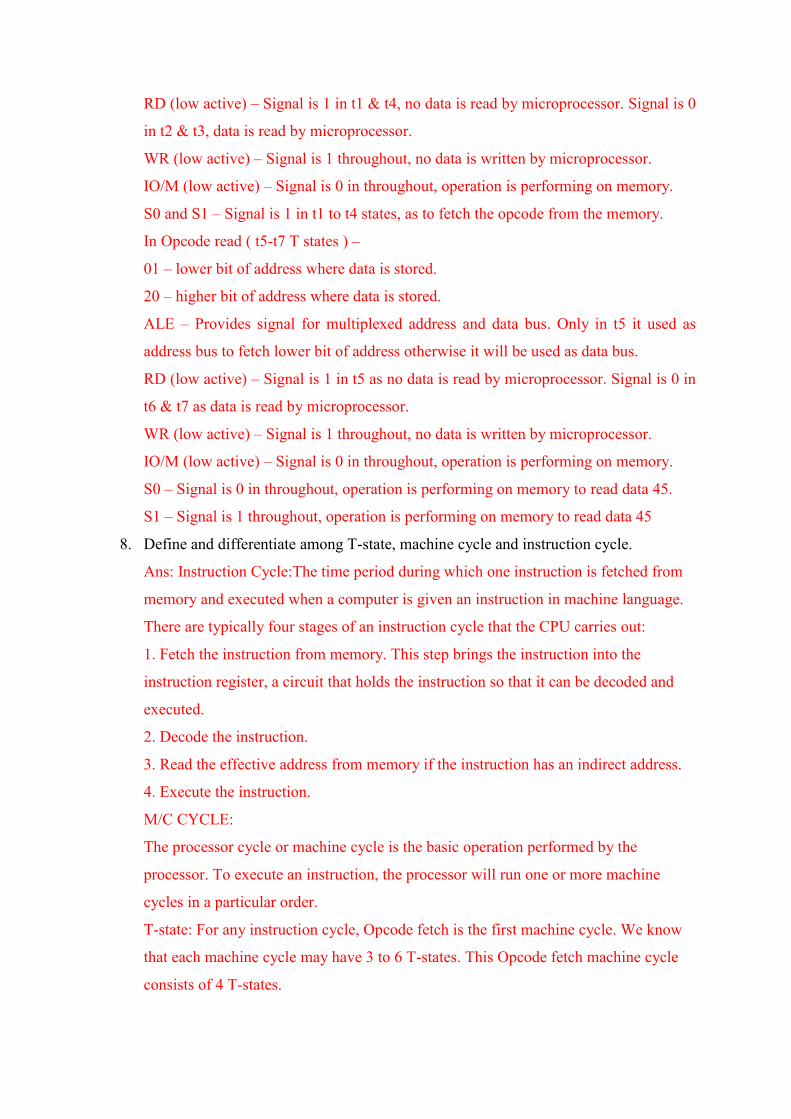
RD (low active) – Signal is 1 in t1 & t4, no data is read by microprocessor. Signal is 0
in t2 & t3, data is read by microprocessor.
WR (low active) – Signal is 1 throughout, no data is written by microprocessor.
IO/M (low active) – Signal is 0 in throughout, operation is performing on memory.
S0 and S1 – Signal is 1 in t1 to t4 states, as to fetch the opcode from the memory.
In Opcode read ( t5-t7 T states ) –
01 – lower bit of address where data is stored.
20 – higher bit of address where data is stored.
ALE – Provides signal for multiplexed address and data bus. Only in t5 it used as
address bus to fetch lower bit of address otherwise it will be used as data bus.
RD (low active) – Signal is 1 in t5 as no data is read by microprocessor. Signal is 0 in
t6 & t7 as data is read by microprocessor.
WR (low active) – Signal is 1 throughout, no data is written by microprocessor.
IO/M (low active) – Signal is 0 in throughout, operation is performing on memory.
S0 – Signal is 0 in throughout, operation is performing on memory to read data 45.
S1 – Signal is 1 throughout, operation is performing on memory to read data 45
8. Define and differentiate among T-state, machine cycle and instruction cycle.
Ans: Instruction Cycle:The time period during which one instruction is fetched from
memory and executed when a computer is given an instruction in machine language.
There are typically four stages of an instruction cycle that the CPU carries out:
1. Fetch the instruction from memory. This step brings the instruction into the
instruction register, a circuit that holds the instruction so that it can be decoded and
executed.
2. Decode the instruction.
3. Read the effective address from memory if the instruction has an indirect address.
4. Execute the instruction.
M/C CYCLE:
The processor cycle or machine cycle is the basic operation performed by the
processor. To execute an instruction, the processor will run one or more machine
cycles in a particular order.
T-state: For any instruction cycle, Opcode fetch is the first machine cycle. We know
that each machine cycle may have 3 to 6 T-states. This Opcode fetch machine cycle
consists of 4 T-states.

T1 State: During the T1 state, the contents of the program counter are placed on the
16 bit address bus.
T2 State: opcode is placed on D0-D7 of the Address/Data bus.
T3 State: the Opcode of the A/D bus is transferred to the instruction register of the
microprocessor.
T4 State: In this state the Opcode which was fetched from the memory is decoded.
Module 4: Programming in 8085 Microprocessor
1. Write a program that will store the contents of an accumulator and flag register at
locations 2100 H and 2101 H?
Ans: By making use of the Push & Pop instructions the program can be written as:
- LXISP, 4000H - this step initiates the SP at 4000h.
-PUSH PSW - the contents of the accumulator and flag are pushed into the stack.
- POP B
- MOV A, B
- STA 2100H
- MOV A, C
- STA 2101H
- HLT
2. What differences can you state between the HLT and Hold states?
Ans: The Hold is a hardware input whereas HLT is a software instruction.
- When the HLT state is executed the processor simply stops and the buses are driven
to tri state. No form of acknowledgement signal is given out by the processor.
- In case of HOLD the processor goes into hold state but the buses are not driven to tri
state.
- When the processor goes into the HOLD state it gives out an HLDA signal. This
signal can be made to use by other devices.
3. Create the program for 8085-microprocessor to arrange the five 8-bit numbers in
ascending order. The numbers are 5A, 15, EF, 2B, 04.
Ans: 1. Initialize HL pair as memory pointer
2. Get the count at 4200 into C - register
3. Copy it in D - register (for bubble sort (N-1) times required)
4. Get the first value in A - register
5. Compare it with the value at next location

6. If they are out of order, exchange the contents of A - register and Memory
7. Decrement D - register content by 1
8. Repeat steps 5 and 7 till the value in D- register become zero
9. Decrement C - register content by 1
10. Repeat steps 3 to 9 till the value in C - register becomes zero
LXI H, 5000 ;Set pointer for array
MOV C,M ;Load the Count
DCR C ;Decrement Count
REPEAT: MOV D,C
LXI H,5001
LOOP: MOV A,M ;copy content of memory location to Accumulator
INX H
CMP M
JC SKIP ;jump to skip if carry generated
MOV B,M ;copy content of memory location to B - Register
MOV M,A ;copy content of Accumulator to memory location
DCX H ;Decrement content of HL pair of registers
MOV M,B ;copy content of B - Register to memory location
INX H ;Increment content of HL pair of registers
SKIP: DCR D ;Decrement content of Register - D
JNZ LOOP ;jump to loop if not equal to zero
DCR C ;Decrement count
JNZ REPEAT ;jump to repeat if not equal to zero
HLT ;Terminate Program
4. Calculate the time delay produced by the given subroutine function. If the clock period of the
microprocessor is 320 ns.
MVI B, FF H
LOOP DCR B
JNZ LOOP
RET
Counter is another approach to generate a time delay. In this case the program size is
smaller. So in this approach we can generate more time delay in less space. The
following program will demonstrate the time delay using 8-bit counter.

Here the first instruction will be executed once, it will take 7 T-states. DCR C
instruction takes 4 T-states. This will be executed 255 (FF) times. The JNZ instruction
takes 10 T-states when it jumps (It jumps 254 times), otherwise it will take 7 T-States.
And the RET instruction takes 10 T-States.
7 + ((4*255) + (10*254)) + 7 + 10 = 3584. So the time delay will be 3584 * 320 ns =
1146.88 µs. So when we need some small delay, then we can use this technique with
some other values in the place of FF.
This technique can also be done using some nested loops to get larger delays.
5. Implement a program for subtraction of two 8-bit numbers.
Ans: Let first number is at 2500 memory address and second number is at 2501
memory address and store the result into 2502 and borrow into 2503 memory address.
Algorithm – (a) Load 00 in a register C (for borrow)
(b) Load two 8-bit number from memory into registers
(c) Move one number to accumulator
(d) Subtract the second number with accumulator
(e) If borrow is not equal to 1, go to step 7
(f) Increment register for borrow by 1
(g) Store accumulator content in memory
(h) Move content of register into accumulator
(i) Store content of accumulator in other memory location
(j) Stop

MEMORY MNEMONICS OPERANDS COMMENT
2000 MVI C, 00 [C] <- 00
2002 LHLD 2500 [H-L] <- [2500]
2005 MOV A, H [A] <- [H]
2006 SUB L [A] <- [A] – [L]
2007 JNC 200B Jump If no borrow
200A INR C [C] <- [C] + 1
200B STA 2502 [A] -> [2502], Result
200E MOV A, C [A] <- [C]
2010 STA 2503 [A] -> [2503], Borrow
2013 HLT
Stop
Explanation – Registers A, H, L, C are used for general purpose:
(a) MOV is used to transfer the data from memory to accumulator (1 Byte)
(b) LHLD is used to load register pair directly using 16-bit address (3 Byte instruction)
(c) MVI is used to move data immediately into any of registers (2 Byte)
(d) STA is used to store the content of accumulator into memory(3 Byte instruction)
(e) INR is used to increase register by 1 (1 Byte instruction)
(f) JNC is used to jump if no borrow (3 Byte instruction)
(g) SUB is used to subtract two numbers where one number is in accumulator(1 Byte)
(h) HLT is used to halt the program
6. Write a program to add 2-BCD numbers where starting address is 2000 and the
numbers is stored at 2500 and 2501 memory addresses and store sum into 2502 and
carry into 2503 memory address.
Ans:

Algorithm – (a) Load 00H in a register (for carry)
(b) Load content from memory into register pair
(c) Move content from L register to accumulator
(d) Add content of H register with accumulator
(e) Add 06H if sum is greater than 9 or Auxillary Carry is not zero
(f) If carry flag is not equal to 1, go to step 8
(g) Increment carry register by 1
(h) Store content of accumulator into memory
(i) Move content from carry register to accumulator
(j) Store content of accumulator into memory
(k) Stop
Program –
MEMORY MNEMONICS OPERANDS COMMENT
2000 MVI C, 00H [C] <- 00H, carry
2002 LHLD [2500] [H-L] <- [2500]
2005 MOV A, L [A] <- [L]
2006 ADD H [A] <- [A] + [H]
2007 DAA
Add 06 if sum > 9 or AC = 1

MEMORY MNEMONICS OPERANDS COMMENT
2008 JNC 200C Jump if no carry
200B INR C [C] <- [C] + 1
200C STA [2502] [A] -> [2502], sum
200F MOV A, C [A] <- [C]
2010 STA [2503] [A] -> [2503], carry
2013 HLT
Stop
Explanation – Registers A, C, H, L are used for general purpose
(a) MVI is used to move data immediately into any of registers (2 Byte)
(b) LHLD is used to load register pair direct using 16-bit address (3 Byte instruction)
(c) MOV is used to transfer the data from memory to accumulator (1 Byte)
(d) ADD is used to add accumulator with any of register (1 Byte instruction)
(e) STA is used to store data from accumulator into memory address (3 Byte instruction)
(f) DAA is used to check if sum > 9 or AC = 1 add 06 (1 Byte instruction)
(g) JNC is used jump if no carry to given memory location (3 Byte instruction)
(h) INR is used to increase given register by 1 (1 Byte instruction)
(i) HLT is used to halt the program
7. Write an assembly language program in 8085 microprocessor to find maximum and
minimum of 10 numbers.
Ans: In CMP instruction:
If Accumulator > Register then carry and zero flags are reset
If Accumulator = Register then zero flag is set
If Accumulator < Register then carry flag is set
Assumption – List of numbers from 2050H to 2059H and output at 2060H and
2061H.
Algorithm – (a) Maximum number is stored in B register and minimum in C register
(b) Load counter in D register
(c) Load starting element in Accumulator, B and C register
(d) Compare Accumulator and B register
(e) If carry flag is not set then transfer contents of Accumulator to B. Else, compare
Accumulator with C register, if carry flag is set transfer contents of Accumulator to C

(f) Decrement D register
(g) If D>0 take next element in Accumulator and go to point 4
(h) If D=0, store B and C register in memory
(i) End of program
Program-
ADDRESS LABEL INSTRUCTION COMMENT
2000H
LXI H, 2050H Load starting address of list
2003H
MOV B, M Store maximum
2004H
MOV C, M Store minimum
2005H
MVI D, 0AH Counter for 10 elements
2007H LOOP MOV A, M Retrieve list element in Accumulator
2008H
CMP B Compare element with maximum number
2009H
JC MIN Jump to MIN if not maximum
200CH
MOV B, A Transfer contents of A to B as A > B
200DH MIN CMP C Compare element with minimum number
200EH
JNC SKIP Jump to SKIP if not minimum
2011H
MOV C, A Transfer contents of A to C if A < minimum
2012H SKIP INX H Increment memory
2013H
DCR D Decrement counter
2014H
JNZ LOOP Jump to LOOP if D > 0
2017H
LXI H, 2060H Load address to store maximum

ADDRESS LABEL INSTRUCTION COMMENT
201AH
MOV M, B Move maximum to 2060H
201BH
INX H Increment memory
201CH
MOV M, C Move minimum to 2061H
201DH
HLT Halt
Explanation – (a) One by one all elements are compared with B and C register.
(b) Element is compared with maximum, if it greater than maximum then it is stored in B
register. Else, it is compared with minimum and if it is less than minimum then it stored
in C register.
(c) Loop executes 10 numbers of times.
(d) At the end of 10 iterations, maximum and minimum are stored at 2060H and 2061H
respectively.
8. To write an assembly language program for adding two 16 bit numbers using 8085
microprocessor.
Ans:
(a) Addition of 16 bit numbers using 8 bit operation – It is a lengthy method and requires
more memory as compared to 16 bit operation.
Algorithm –

(a) Load the lower part of first number in B register
(b) Load the lower part of second number in A (accumulator)
(c) Add both the numbers and store
(d) Load the higher part of first number in B register
(e) Load the higher part of second number in A (accumulator)
(f) Add both the numbers with carry from the lower bytes (if any) and store at the next
location
Program –
MEMORY
ADDRESS MNEMONICS COMMENTS
2000 LDA 2050 A ← 2050
2003 MOV B, A B ← A
2004 LDA 2052 A ← 2052
2007 ADD B A ← A+B
2008 STA 3050 A → 3050
200B LDA 2051 A ← 2051
200E MOV B, A B ← A
200F LDA 2053 A ← 2053
2012 ADC B A ← A+B+CY
2013 STA 3051 A → 3051
2016 HLT
Stops
execution

Explanation – (a) LDA 2050 stores the value at 2050 in A (accumulator)
(b) MOV B, A stores the value of A into B register
(c) LDA 2052 stores the value at 2052 in A
(d) ADD B add the contents of B and A and store in A
(e) STA 3050 stores the result in memory location 3050
(f) LDA 2051 stores the value at 2051 in A
(g) MOV B, A stores the value of A into B register
(h) LDA 2053 stores the value at 2053 in A
(i) ADC B add the contents of B, A and carry from the lower bit addition and store in A
(j) STA 3051 stores the result in memory location 3051
(k) HLT stops execution
(b) Addition of 16 bit numbers using 16 bit operation – It is a very short method and less
memory is also required as compared to 8 bit operation.
Algorithm – (a) Load both the lower and the higher bits of first number at once
(b) Copy the first number to another register pair
(c) Load both the lower and the higher bits of second number at once
(d) Add both the register pairs and store the result in a memory location
Program –
MEMORY
ADDRESS MNEMONICS COMMENTS
2000 LHLD 2050 H-L ← 2050
2003 XCHG
D H &
E L
2004 LHLD 2052 H-L ← 2052
2007 DAD D
H ← H+D & L ←
L+E
2008 SHLD 3050 A → 3050
200B HLT Stops execution
Explanation – (a) LHLD 2050 loads the value at 2050 in L register and that in 2051 in H register (first
number)
(b) XCHG copies the content of H to D register and L to S register

(c) LHLD 2052 loads the value at 2052 in L register and that in 2053 in H register (second
number)
(d) DAD D adds the value of H with D and L with E and stores the result in H and L
(e) SHLD 3050 stores the result at memory location 3050
(f) HLT stops execution
9. To write an assembly language program for subtracting two 16 bit numbers using
8085 microprocessor.
Ans: Assumption –
Starting address of program: 2000
Input memory location: 2050, 2051, 2052, 2053
Output memory location: 2054, 2055
Example – INPUT:
(2050H) = 19H
(2051H) = 6AH
(2052H) = 15H
(2053H) = 5CH
OUTPUT:
(2054H) = 04H
(2055H) = OEH
RESULT:
Hence we have subtracted two 16 bit numbers.
Algorithm –
(a) Get the LSB in L register and MSB in H register of 16 Bit number.
(b) Exchange the content of HL register with DE register.
(c) Again Get the LSB in L register and MSB in H register of 16 Bit number.
(d) Subtract the content of L register from the content of E register.
(e) Subtract the content of H register from the content of D register and borrow from
previous step.
(f) Store the result in memory location.
Program –
MEMORY
ADDRESS MNEMONICS COMMENTS
2000 LHLD 2050
Load H-L pair with address
2050

MEMORY
ADDRESS MNEMONICS COMMENTS
2003 XCHG
EXCHANGE H-L PAIR
WITH D-E PAIR
2004 LHLD 2052
Load H-L pair with address
2052
2007 MVI C, 00 C<-00H
2009 MOV A, E A<-E
200A SUB L A<-A-L
200B STA 2054 2054<-A
200E MOV A, D A<-D
200F SBB H
SUBTRACT WITH
BORROW
2010 STA 2055 2055<-A
2013 HLT
TERMINATES THE
PROGRAM
Explanation – (a) LHLD 2050: load HL pair with address 2050.
(b) XCHG: exchange the content of HL pair with DE.
(c) LHLD 2052: load HL pair with address 2050.
(d) MOV A, E: move the content of register E to A.
(e) SUB L: subtract the content of A with the content of register L.
(f) STA 2054: store the result from accumulator to memory address 2054.
(g) MOV A, D: move the content of register D to A.
(h) SBB H: subtract the content of A with the content of register H with borrow.
(i) STA 2055: store the result from accumulator to memory address 2055.
(j) HLT: stops executing the program and halts any further execution.
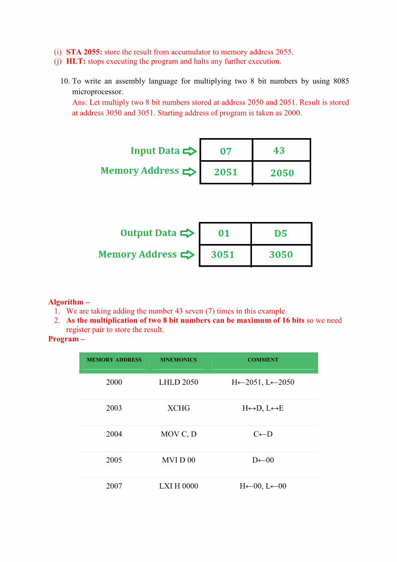
10. To write an assembly language for multiplying two 8 bit numbers by using 8085
microprocessor.
Ans: Let multiply two 8 bit numbers stored at address 2050 and 2051. Result is stored
at address 3050 and 3051. Starting address of program is taken as 2000.
Algorithm – 1. We are taking adding the number 43 seven (7) times in this example.
2. As the multiplication of two 8 bit numbers can be maximum of 16 bits so we need
register pair to store the result.
Program –
MEMORY ADDRESS MNEMONICS COMMENT
2000 LHLD 2050 H←2051, L←2050
2003 XCHG H↔D, L↔E
2004 MOV C, D C←D
2005 MVI D 00 D←00
2007 LXI H 0000 H←00, L←00
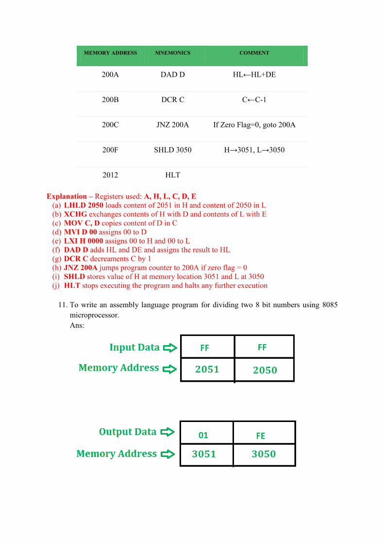
MEMORY ADDRESS MNEMONICS COMMENT
200A DAD D HL←HL+DE
200B DCR C C←C-1
200C JNZ 200A If Zero Flag=0, goto 200A
200F SHLD 3050 H→3051, L→3050
2012 HLT
Explanation – Registers used: A, H, L, C, D, E
(a) LHLD 2050 loads content of 2051 in H and content of 2050 in L
(b) XCHG exchanges contents of H with D and contents of L with E
(c) MOV C, D copies content of D in C
(d) MVI D 00 assigns 00 to D
(e) LXI H 0000 assigns 00 to H and 00 to L
(f) DAD D adds HL and DE and assigns the result to HL
(g) DCR C decreaments C by 1
(h) JNZ 200A jumps program counter to 200A if zero flag = 0
(i) SHLD stores value of H at memory location 3051 and L at 3050
(j) HLT stops executing the program and halts any further execution
11. To write an assembly language program for dividing two 8 bit numbers using 8085
microprocessor.
Ans:

Algorithm – (a) Start the program by loading the HL pair registers with address of memory location.
(b) Move the data to B Register.
(c) Load the second data into accumulator.
(d) Compare the two numbers to check carry.
(e) Subtract two numbers.
(f) Increment the value of carry.
(g) Check whether the repeated subtraction is over.
(h) Then store the results (quotient and remainder) in given memory location.
(i) Terminate the program.
Program –
ADDRESS MNEMONICS COMMENT
2000 LXI H, 2050
2003 MOV B, M B<-M
2004 MVI C, 00 C<-00H
2006 INX H
2007 MOV A, M A<-M
2008 CMP B
2009 JC 2011 check for carry
200C SUB B A<-A-B
200D INR C C<-C+1
200E JMP 2008
2011 STA 3050 3050<-A
2014 MOV A, C A<-C

ADDRESS MNEMONICS COMMENT
2015 STA 3051 3051<-A
2018 HLT terminate the program
Explanation – Registers A, H, L, C, B are used for general purpose.
(a) LXI H, 2050 will load the HL pair register with the address 2050 of memory location.
(b) MOV B, M copies the content of memory into register B.
(c) MVI C, 00 assign 00 to C.
(d) INX H increment register pair HL.
(e) MOV A, M copies the content of memory into accumulator.
(f) CMP B compares the content of accumulator and register B.
(g) JC 2011 jump to address 2011 if carry flag is set.
(h) SUB B subtract the content of accumulator with register B and store the result in
accumulator.
(i) INR C increment the register C.
(j) JMP 2008 control will shift to memory address 2008.
(k) STA 3050 stores the remainder at memory location 3050.
(l) MOV A, C copies the content of register into accumulator.
(m) STA 3051 stores the remainder at memory location 3051.
(n) HLT stops executing the program and halts any further execution.
12. Write an assembly language program in 8085 to search a given number in an array of
n numbers. If number is found, then store F0 in memory location 3051 otherwise store
0F in 3051.
Ans: Assumptions – Count of elements in an array is stored at memory location 2050.
Array is stored from starting memory address 2051 and number which user want to
search is stored at memory location 3050.

Make the memory pointer points to memory location 2050 by help of LXI H 2050
instruction
Store value of array size in register C
Store number to be search in register B
Increment memory pointer by 1 so that it points to next array index
Store element of array in accumulator A and compare it with value of B
If both are same i.e. if ZF = 1 then store F0 in A and store the result in memory
location 3051 and go to step 9
Otherwise store 0F in A and store it in memory location 3051
Decrement C by 01 and check if C is not equal to zero i.e. ZF = 0, if true go to step 3
otherwise go to step 9
End of program
Program –
MEMORY ADDRESS MNEMONICS COMMENT
2000 LXI H 2050 H <- 20, L <- 50
2003 MOV C, M C <- M
2004 LDA 3050 A <- M[3050]
2007 MOV B, A B <- A
2008 INX H HL <- HL + 0001
2009 MOV A, M A <- M
200A CMP B A – B
200B JNZ 2014 Jump if ZF = 0
200E MVI A F0 A <- F0
2010 STA 3051 M[3051] <- A
2013 HLT END
2014 MVI A 0F A <- 0F
2016 STA 3051 M[3051] <- A
2019 DCR C C <- C – 01
201A JNZ 2008 Jump if ZF = 0
201D HLT END

Explanation – Registers used A, B, C, H, L and indirect memory M:
LXI H 2050 – initialize register H with 20 and register L with 50
MOV C, M – assign content of indirect memory location, M which is represented by
registers H and L to register C
LDA 3050 – loads the content of memory location 3050 in accumulator A
MOV B, A – move the content of A in register B
INX H – increment HL by 1, i.e. M is incremented by 1 and now M will point to next
memory location
MOV A, M – move the content of memory location M in accumulator A
CMP B – subtracts B from A and update flags of 8085
JNZ 2014 – jump to memory location 2014 if zero flag is reset i.e. ZF = 0
MVI A F0 – assign F0 to A
STA 3051 – stores value of A in 3051
HLT – stops executing the program and halts any further execution
MVI A 0F – assign 0F to A
STA 3051 – stores value of A in 3051
DCR C – decrement C by 01
JNZ 2008 – jump to memory location 2008 if zero flag is reset
HLT – stops executing the program and halts any further execution
Module 5: Data transfer in 8085 Microprocessor
1. In Intel 8085A microprocessor ALE signal is made high to
a) Enable the data bus to be used as low order address bus
b) To latch data D0-D7 from data bus
c) To disable data bus
d) To achieve all the functions listed above
2. A good assembly language programmer should use general purpose registers rather
than memory in maximum possible ways for data processing. This is because:
a) Data processing with registers is easier than with memory
b) Data processing with memory requires more instructions in the program than
that with registers
c) Because of limited set of instructions for data processing with memory
d) Data processing with registers takes fewer cycles than that with memory
3. Which instruction is required to rotate the content of accumulator one bit right along
with carry?
a) RLC
b) RAL

c) RRC
d) RAR
4. READY signal in 8085 is useful when the CPU communicates with
a) a slow peripheral device
b) a fast peripheral device
c) a DMA chip
d) a PPI
5. 10. Register pair used to indicate memory
a) B and C
b) D and E
c) H and L
d) S and P
6. A sequence of two registers that multiplies the content of DE register pair by two and
stores the result in HL register pair (in 8085 assembly language) is
a) XCHG & DAD B
b) XTHL & DAD H
c) PCHL & DAD D
d) XCHG & DAD H
7. The address / data bus in 8085 is __________.
a) multiplexed
b) demultiplexed
c) decoded
d) encoded
8. The advantage of memory mapped I/O over I/O mapped I/O is,
a) Faster
b) Many instructions supporting memory mapped I/O
c) Require a bigger address decoder
d) All the above
9. Can ROM be used as stack?
a) Yes
b) No
c) sometimes yes, sometimes no
10. What does microprocessor speed depends on?
a) Clock

b) Data bus width
c) Address bus width
11. What is SIM?
a) Select Interrupt Mask
b) Sorting Interrupt Mask
c) Set Interrupt Mask
12. Mention the different types of data transfers possible in the 8085?
Ans: The various types of data transfer operations possible are:
Data transfer is possible between two registers.
It is also possible between a memory location and a register.
Also it can occur between an input/output device and an accumulator.
In reality data is never transferred it can only be copied from one location to another.
13. Explain PUSH and POP operation in 8085 with the help of Stack Pointer.
Ans: The stack is generally a reversed area in RAM to store the information. Anywhere in
the memory map, a stack can be initialized, but usually, it will be initialized at the higher
memory location to get rid of any programming interface. Coming to 8085, the initialization
of stack is instructed as
LXI SP, 16 bit
LXI SP is a 16-bit state which loads a 16-bit address into stack register. Before the utilization
of stack, it has to be initialized to one higher value which is more than the stack’s highest
memory location. The initialization of the stack pointer can be done by Load Stack Pointer.
The stack in 8085 performs both PUSH and POP operations. Both the operations work
together with register pairs following the LIFO principle. Until the new data is inserted into
the stack’s memory location, the previous data will not get obliterated.
PUSH Operation in a Stack is as Below
The SP is decreased, and the higher-order register pair contents (B in BC and D in
DE) are replicated to the stack.
Again, the SP is decreased, and now lower order register pair contents are replicated
to the stack. Here no flags or register pair contents will get modified.
For Example
When the instruction is PUSH D – It pushes the contents of DE. Suppose we consider D = 15
H and E = 23 H. Let’s assume that SP = 2300 H. Then the execution of PUSH P will result in
the output as below:

SP = 22 FE Stack
22 FE 23 H
22 FF 15 H
2300
POP Operation in the Stack is as Below
Stack’s top location contents are replicated into stack lower register (C in BC). Then
SP gets increased by 1.
Then the contents of stack location as shown by SP are replicated into stack’s higher
register. Now, SP is increased by 1.
For Example
Let SP = 22FE H, the execution of POP H will result in the output as
SP = 2300 Stack
22 FE 10 H
22 FF 24 H
2300
Here H = 24 H and L = 10 H
Module 6: 8255, 8251, 8253, 8257 chips in 8085 Microprocessor
1. Draw the pin diagram of 8253.
Ans:

2. Differentiate between 8253 and 8254.
Ans: The following table differentiates the features of 8253 and 8254 −
8253 8254
Its operating frequency is 0 - 2.6 MHz Its operating frequency is 0 - 10 MHz
It uses N-MOS technology It uses H-MOS technology
Read-Back command is not available Read-Back command is available
Reads and writes of the same counter cannot
be interleaved.
Reads and writes of the same counter can
be interleaved.
3. Discuss the different uses of gate input pin in 8253.
Ans:
Signal Status
Low or going low
Rising High
Mode
0 Disables counting
- - Enables counting
1 - -
1) Initiates counting 2) Resets output after next clock
- -
2
1) Disables counting 2) Sets output immediately high
1) Reloads counter 2) Initiates counting
Enables counting
3
1) Disables counting 2) Sets output immediately high
Initiates counting
Enables counting
4 Disables counting
- - Enables counting
5 - - Initiates counting
- -
This table shows the different uses of the 8253 gate input pin.

4. Explain the necessary block diagram of 8251.
Ans: 8251 universal synchronous asynchronous receiver transmitter (USART) acts as a
mediator between microprocessor and peripheral to transmit serial data into parallel form and
vice versa.
1. It takes data serially from peripheral (outside devices) and converts into parallel data.
2. After converting the data into parallel form, it transmits it to the CPU.
3. Similarly, it receives parallel data from microprocessor and converts it into serial form.
4. After converting data into serial form, it transmits it to outside device (peripheral).
Block Diagram of 8251 USART –
It contains the following blocks:
1. Data bus buffer – This block helps in interfacing the internal data bus of 8251 to the system data bus. The
data transmission is possible between 8251 and CPU by the data bus buffer block.
2. Read/Write control logic – It is a control block for overall device. It controls the overall working by selecting the
operation to be done. The operation selection depends upon input signals as:

In this way, this unit selects one of the three registers- data buffer register, control
register, status register.
3. Modem control (modulator/demodulator) – A device converts analog signals to digital signals and vice-versa and helps the
computers to communicate over telephone lines or cable wires. The following are
active-low pins of Modem.
DSR: Data Set Ready signal is an input signal.
DTR: Data terminal Ready is an output signal.
CTS: It is an input signal which controls the data transmit circuit.
RTS: It is an output signal which is used to set the status RTS.
4. Transmit buffer – This block is used for parallel to serial converter that receives a parallel byte for
conversion into serial signal and further transmission onto the common channel.
TXD: It is an output signal, if its value is one, means transmitter will transmit the
data.
5. Transmit control – This block is used to control the data transmission with the help of following pins:
TXRDY: It means transmitter is ready to transmit data character.
TXEMPTY: An output signal which indicates that TXEMPTY pin has
transmitted all the data characters and transmitter is empty now.
TXC: An active-low input pin which controls the data transmission rate of
transmitted data.
6. Receive buffer – This block acts as a buffer for the received data.
RXD: An input signal which receives the data.
7. Receive control – This block controls the receiving data.
RXRDY: An input signal indicates that it is ready to receive the data.
RXC: An active-low input signal which controls the data transmission rate of
received data.
SYNDET/BD: An input or output terminal. External synchronous mode-input
terminal and asynchronous mode-output terminal.

5. Draw the pin diagram of 8255 and explain its block diagram.
Ans: PPI 8255 is a general purpose programmable I/O device designed to interface the CPU
with its outside world such as ADC, DAC, keyboard etc. We can program it according to the
given condition. It can be used with almost any microprocessor.
It consists of three 8-bit bidirectional I/O ports i.e. PORT A, PORT B and PORT C. We can
assign different ports as input or output functions.
Block diagram –
It consists of 40 pins and operates in +5V regulated power supply. Port C is further divided
into two 4-bit ports i.e. port C lower and port C upper and port C can work in either BSR (bit
set rest) mode or in mode 0 of input-output mode of 8255. Port B can work in either mode or
in mode 1 of input-output mode. Port A can work either in mode 0, mode 1 or mode 2 of
input-output mode.
It has two control groups, control group A and control group B. Control group A consist of
port A and port C upper. Control group B consists of port C lower and port B.
Depending upon the value if CS’, A1 and A0 we can select different ports in different modes
as input-output function or BSR. This is done by writing a suitable word in control register
(control word D0-D7).
CS’ A1 A0 SELECTION ADDRESS
0 0 0 PORT A 80 H

CS’ A1 A0 SELECTION ADDRESS
0 0 1 PORT B 81 H
0 1 0 PORT C 82 H
0 1 1 Control Register 83 H
1 X X No Seletion X
Pin diagram –
PA0 – PA7 – Pins of port A
PB0 – PB7 – Pins of port B
PC0 – PC7 – Pins of port C
D0 – D7 – Data pins for the transfer of data
RESET – Reset input
RD’ – Read input
WR’ – Write input
CS’ – Chip select
A1 and A0 – Address pins
Operating modes –
1. Bit set reset (BSR) mode – If MSB of control word (D7) is 0, PPI works in BSR mode. In this mode only port C
bits are used for set or reset.

2. Input-Outpt mode – If MSB of control word (D7) is 1, PPI works in input-output mode. This is further
divided into three modes:
Mode 0 –In this mode all the three ports (port A, B, C) can work as simple input
function or simple output function. In this mode there is no interrupt handling
capacity.
Mode 1 – Handshake I/O mode or strobbed I/O mode. In this mode either port A
or port B can work as simple input port or simple output port, and port C bits are
used for handshake signals before actual data transmission. It has interrupt
handling capacity and input and output are latched.
Example: A CPU wants to transfer data to a printer. In this case since speed of
processor is very fast as compared to relatively slow printer, so before actual data
transfer it will send handshake signals to the printer for synchronization of the
speed of the CPU and the peripherals.
Mode 2 – Bi-directional data bus mode. In this mode only port A works, and port
B can work either in mode 0 or mode 1. 6 bits port C are used as handshake
signals. It also has interrupt handling capacity.
6. Discuss the operating modes of 8255.
Ans: There are 2 modes in 8255 microprocessor:
1. Bit set reset (BSR) mode – This mode is used to set or reset the bits of port C only, and
selected when the most significant bit (D7) in the control register is 0. Control Register is as
follows:

This mode affects only one bit of port C at a time because, as user set the bit, it remains set
until and unless user changes it. User needs to load the bit pattern in control register to
change the bit.
2. Input/output mode (I/O) – This mode is selected when the most significant bit (D7) in the
control register is 1.
Mode 0 – Simple or basic I/O mode: Port A, B and C can work either as input function or as output function. The outputs are
latched but the inputs are not latched. It has interrupt handling capability.
Mode 1 – Handshake or strobbed I/O: In this either port A or B can work and port C bits are used to provide handshaking. The
outputs as well as inputs are latched. It has interrupt handling capability. Before actual
data transfer there is transmission of signal to match speed of CPU and printer.
Example: When CPU wants to send data to slow peripheral device like printer, it will
send handshaking signal to printer to tell whether it is ready or not to transfer the data.
When printer will be ready it will send one acknowledgement to CPU then there will be
transfer of data through data bus.
Mode 2 – Bidirectional I/O: In this mode only port A will work, port B can either is in mode 0 or 1 and port C bits
are used as handshake signal. The outputs as well as inputs are latched. It has interrupt
handling capability. Control Register is as follows:

The most significant bit (D7) is 1 for the I/O mode and 0 for the BSR mode.
D6 & D5It is used to set the port A mode.
D4 is used to tell whether port A is taking input or displaying the result. If it is 1 then it
is taking input otherwise displaying output.
D3 is used to tell whether port C higher bits is taking input or displaying the result. If it
is 1 then it is taking input otherwise displaying output.
D2 tells the mode of port B. If it is 0 then port B is in m0 mode otherwise in m1 mode.
D1 is used to tell whether port B is taking input or displaying the result. If it is 1 then it
is taking input otherwise displaying output.
D0 is used to tell whether port C lower bits is taking input or displaying the result. If it
is 1 then it is taking input otherwise displaying output.
When 8255 microprocessor is reset, it will clear the control word register contents, setting all
the ports to input mode.
7. Draw the Block Diagram of 8254 PPI (Programmable Peripheral Interface).
Ans: 8254 is a device designed to solve the timing control problems in a microprocessor. It
has 3 independent counters, each capable of handling clock inputs up to 10 MHz and size of
each counter is 16 bit. It operates in +5V regulated power supply and has 24 pin signals. All
modes are software programmable. The 8254 is an advanced version of 8253 which did not
offered the feature of read back command.
The basic block diagram of 8254 is:

It has 3 counters each with two inputs (Clock and Gate) and one output. Gate is used to
enable or disable counting. When any value of count is loaded and value of gate is set(1),
after every step value of count is decremented by 1 until it becomes zero.
Depending upon the value of CS, A1 and A0 we can determine addresses of selected counter.
CS A1 A0 SELECETION
0 0 0 C0
0 0 1 C1
0 1 0 C2
0 1 1 Control Register
Applications – (a) To generate accurate time delay
(b) As an event counter
(c) Square wave generator
(d) Rate generator
(e) Digital one shot
8. Explain the various modes in which 8254 can operate and write down the control
word for each mode. Specify the conditions to start the timer of 8254 PPI.
Ans: After power-up, the state of the 8254 is undefined. The Mode, count value, and output
of all Counters are undefined. How each counter operates is determined when it is
programmed. Each counter must be programmed before it can be used. Unused counters need

not be programmed. Counters are programmed by writing a Control Word and then an initial
count.
Control Word of 8254 – The format of Control Word of 8254 is:
Here by using the value of SC1 and SC0 we select a specific counter:
SC1 SC0 SELECTION
0 0 C0
0 1 C1
1 0 C2
1 1 Read back status
The values of RW1 and RW0 are used to decide the Read – Write operation:
RW1 RW0 SELECTION
0 0 Counter Latch Command
0 1 Read/Write lower byte
1 0 Read/Write higher byte
1 1 Read/Write lower byte followed by higher byte
The values of M2, M1, M0 are used to decide the operating modes of 8254:
M2 M1 M0 OPERATING MODE
0 0 0 MODE 0

M2 M1 M0 OPERATING MODE
0 0 1 MODE 1
X (0/1) 1 0 MODE 2
X (0/1) 1 1 MODE 3
1 0 0 MODE 4
1 0 1 MODE 5
The LSB of Control Word is used to select whether the counter is Binary or BCD. If the bit is
0 it works as binary counter and if its value is 1 it works as BCD coounter.
Operating Modes of 8254: 1. Mode 0 (Interrupt on Terminal Count) – Mode 0 is typically used for event counting.
After the Control Word is written, OUT is initially low, and will remain low until the
counter reaches zero it is decremented by 1 after every clock cycle. OUT then goes high
and remains high until a new count or a new Mode 0 Control Word is written into the
counter. GATE = 1 enables counting, GATE = 0 disables counting.
2. Mode 1 (Hardware Retriggreable One Shot) – OUT will be initially high. OUT will
go low on the CLK pulse following a trigger to begin the one-shot pulse, and will
remain low until the counter reaches zero.
3. Mode 2 (Rate Generator) – Initially value of OUT is low. When counting is enabled,
it becomes high and this process repeats periodically. Value of count = Input Frequency
/ Output Frequency. This mode works as a frequency divider.
4. Mode 3 (Square Wave Generator) – Counting is enabled when GATE = 1 and
disabled when GATE = 0. This mode is used to generate square waveform and time
period (equal to count) is generated.
If N is count and is even then ontime of wave = N/2 and offtime = N/2
If N is odd the ontime = (N + 1) / 2 and offtime = (N – 1) / 2
5. Mode 4 (Software Triggered Strobe) – In this mode counting is enabled by using
GATE = 1 and disabled by GATE = 0. Initially value of OUT is high and becomes low
when value of count is at last stage. Count is reloaded again for subsequent clock pulse.
6. Mode 5 (Hardware Triggered Strobe) – OUT will initially be high. Counting is
triggered by a rising edge of GATE. When the initial count has expired, OUT will go
low for one clock pulse and then go high again. After writing the Control Word and
initial count, the counter will not be loaded until the clock pulse after a trigger.
9. Draw the block diagram of 8257 DMA controller.
Ans: Suppose any device which is connected at input-output port wants to transfer data to
transfer data to memory, first of all it will send input-output port address and control signal,
input-output read to input-output port, then it will send memory address and memory write

signal to memory where data has to be transferred. In normal input-output technique the
processor becomes busy in checking whether any input-output operation is completed or not
for next input-output operation, therefore this technique is slow.
This problem of slow data transfer between input-output port and memory or between two
memory is avoided by implementing Direct Memory Access (DMA) technique. This is faster
as the microprocessor/computer is bypassed and the control of address bus and data bus is
given to the DMA controller.
HOLD – hold signal
HLDA – hold acknowledgment
DREQ – DMA request
DACK – DMA acknowledgment
Suppose a floppy drive which is connected at input-output port wants to transfer data to
memory, the following steps are performed:
Step-1: First of all the floppy drive will send DMA request (DREQ) to the DMAC, it
means the floppy drive wants its DMA service.
Step-2: Now the DMAC will send HOLD signal to the CPU.
Step-3: After accepting the DMA service request from the DMAC, the CPU will send
hold acknowledgement (HLDA) to the DMAC, it means the microprocessor has
released control of the address bus the data bus to DMAC and the
microprocessor/computer is bypassed during DMA service.
Step-4: Now the DMAC will send one acknowledgement (DACL) to the floppy drive
e=which is connected at the input-output port. It means the DMAC tells the floppy
drive be ready for its DMA service.
Step-5: Now with the help of input-output read and memory write signal the data is
transferred from the floppy drive to the memory
10. Explain the working of 8257 along with the different modes in which 8257 can
operate.
(a) Ans: Single Mode – In this only one channel is used, means only a single DMAC is
connected to the bus system.

(b) Cascade Mode – In this multiple channels are used, we can further cascade more
number of DMACs.
Module 7: Interfacing to 8085 Microprocessor
1. Which Programmable peripheral interface___ 8255__________is used for interfacing
with analog to digital convertors.
2. Port A acts as a 8-bit input data port to receive the digital data output from the ADC.
The 8255 control word is written as follows: D7 D6 D5 D4 D3 D2 D1 D0
a) 1 0 0 1 1 0 0 0
b) 1 1 0 1 1 0 0 0
c) 1 0 1 1 1 0 0 0
d) 1 0 0 1 1 0 0 1
3. Which of the following is 8-bit multiplying DAC
a) AD 7523
b) AX 7534
c) AC 7325
d) AD 7574
4. Draw and discuss the pin diagram of ADC 0800.
Ans: PIN DIGRAM & BLOCK DIAGRAM OF DAC0800
The DAC0800 is an 8-bit, high speed, current output DAC with a typical settling time
(conversion time) of 100 ns.

It produces complementary current output, which can be converted to voltage by
using simple resistor load.
The DAC0800 require a positive and a negative supply voltage in the range of ± 5V to
±18V.
It can be directly interfaced with TTL, CMOS, PMOS and other logic families.
For TTL input, the threshold pin should be tied to ground (VLC = 0V).
The reference voltage and the digital input will decide the analog output current,
which can be converted to a voltage by simply connecting a resistor to output terminal
or by using an op-amp I to V converter.
The DAC0800 is available as a 16-pin IC in DIP.
1. The pin configuration of DAC0800 is,
5. Draw and discuss the pin diagram of AD 7523.
Ans:

AD 7523 8-bit Multiplying DAC
• 16 pin DIP, multiplying DAC, containing R-2R ladder for D-A conversion along
with single pole double thrown NMOS switches to connect the digital inputs to the
ladder. Supply range is from +5V to +15V
• Vref may be any where between -10V to +10V
• The maximum analog output voltage will be any where between -10V to +10V
• When all the digital inputs are at logic high state
6. Explain the interfacing of 8255 with AD 7523.
Ans:
7. Draw and discuss the interfacing circuit of ADC 0800.

Ans:
8. Discuss the block diagram of ADC 0808/0809.
Ans:

9. Discuss the timing diagram of ADC 0808.
Ans:
I/P0–I/P7 Analog inputs
• ADD A,B,C Address lines for selecting analog inputs.
• O7 – O0 Digital 8-bit output with O7 MSB andO0 LSB
• SOC Start of conversion signal pin
• EOC End of conversion signal pin
• OE Output latch enable pin, if high enables output
• CLK Clock input for ADC
Module 8: Architecture of 8086 Microprocessor
1. In 8086 microprocessor one of the following statements is not true.
a) Coprocessor is interfaced in MAX mode
b) Coprocessor is interfaced in MIN mode
c) I/O can be interfaced in MAX / MIN mode
d) Supports pipelining
2. Which processor structure is pipelined?
a) all x80 processors

b) all x85 processors
c) all x86 processors
3. In 8086 microprocessor one of the following instructions is executed before an
arithmetic operation
a) AAM
b) AAD
c) DAS
d) DAA
4. SOD pin can drive a D flip-flop?
a) SOD cannot drive any flip-flops.
b) SOD cannot drive D flip-flop, but can drive any other flop-flops.
c) Yes, SOD can drive D flop-flop.
d) No, SOD cannot drive any other flop-flops except D flop-flop.
5. IDIV and DIV instructions perform the same operations for?
a) Unsigned number
b) Signed number
c) Signed number & Unsigned number
d) none of above.
6. Vector address of TRAP
a) 24H
b) 36H
c) 24
d) 18H
7. The conditional branch instruction JNS performs the operations when if __
a) ZF=0
b) SF=0
c) PF=0
d) CF=0
8. Discuss the program execution transfer instructions in 8086 microprocessor.
Ans: Program execution transfer instructions are similar to branching instructions and refer to
the act of switching execution to a different instruction sequence as a result of executing a
branch instruction.
The two types of program execution transfer instructions are:
1. Unconditional

2. Conditional
1. Unconditional Program Execution Transfer Instructions – These instruction always
execute.
OPCODE OPERAND EXPLANATION EXAMPLE
CALL address
calls a subroutine and saves the return address
on the stack
CALL
2050
RET none
returns from the subroutine to the main
program RET
JUMP address
transfers the control of execution to the
specified address
JUMP
2050
LOOP address
loops through a sequence of instructions until
CX=0
LOOP
2050
Here the address can be specified directly or indirectly.
2. Conditional Program Execution Transfer Instructions : These instructions only execute
when the specified condition is true.
OPCODE OPERAND EXPLANATION EXAMPLE
JC address jump if CF = 1 JC 2050
JNC address jump if CF = 0 JNC 2050
JZ address jump if ZF = 1 JZ 2050
JNZ address jump if ZF = 0 JNZ 2050
JO address jump if OF = 1 JO 2050
JNO address jump if OF = 0 JNO 2050

OPCODE OPERAND EXPLANATION EXAMPLE
JP address jump if PF = 1 JP 2050
JNP address jump if PF = 0 JNP 2050
JPE address jump if PF = 1 JPE 2050
JPO address jump if PF = 0 JPO 2050
JS address jump if SF = 1 JS 2050
JNS address jump if SF = 0 JNS 2050
JA address jump if CF=0 and ZF=0 JA 2050
JNBE address jump if CF=0 and ZF=0 JNBE 2050
JAE address jump if CF=0 JAE 2050
JNB address jump if CF=0 JNB 2050
JBE address jump if CF = 1 or ZF = 1 JBE 2050
JNA address jump if CF = 1 or ZF = 1 JNA 2050
JE address jump if ZF = 1 JE 2050
JG address jump if ZF = 0 and SF = OF JG 2050
JNLE address jump if ZF = 0 and SF = OF JNLE 2050
JGE address jump if SF = OF JGE 2050
OPCODE OPERAND EXPLANATION EXAMPLE
JNL address jump if SF = OF JNL 2050
JL address jump if SF != OF JL 2050
JNGE address jump if SF != OF JNGE 2050
JLE address jump if ZF = 1 or SF != OF JLE 2050
JNG address jump if ZF = 1 or SF != OF JNG 2050
JCXZ address jump if CX = 0 JCXZ 2050
LOOPE address loop while ZF = 1 and CX = 0 LOOPE 2050
LOOPZ address loop while ZF = 1 and CX = 0 LOOPZ 2050
LOOPNE address loop while ZF = 0 and CX = 0 LOOPNE 2050
LOOPNZ address loop while ZF = 0 and CX = 0 LOOPNZ 2050
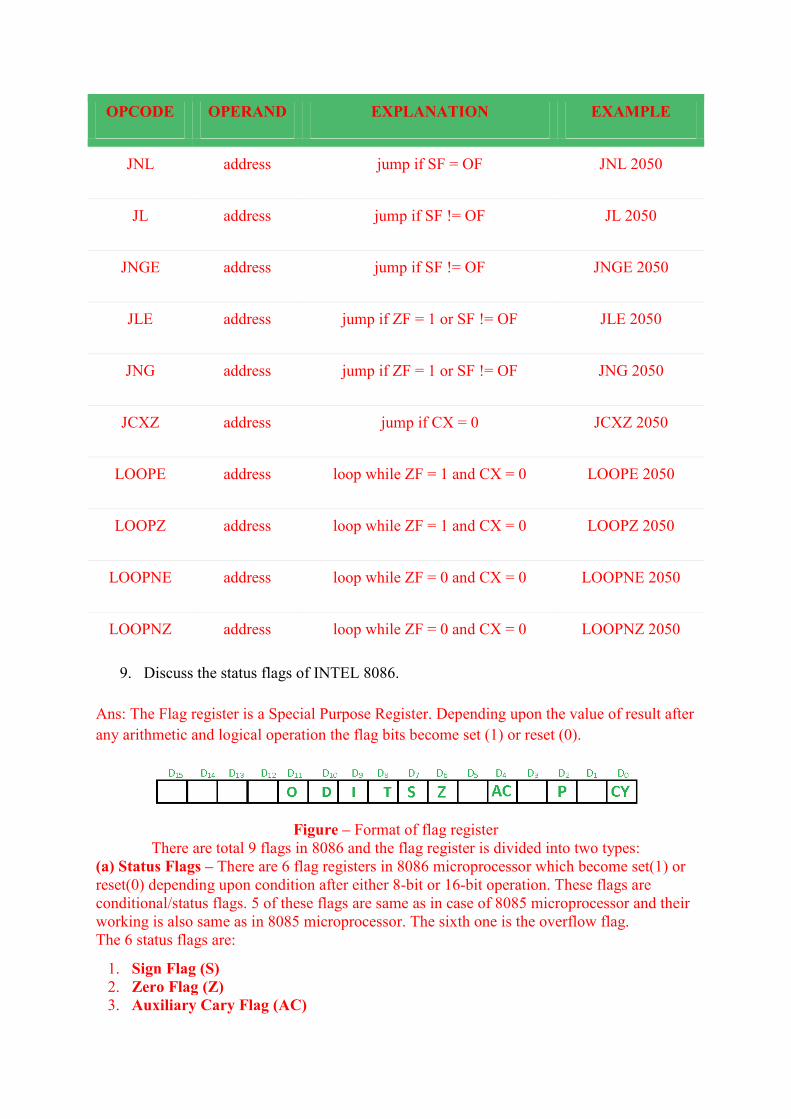
9. Discuss the status flags of INTEL 8086.
Ans: The Flag register is a Special Purpose Register. Depending upon the value of result after
any arithmetic and logical operation the flag bits become set (1) or reset (0).
Figure – Format of flag register
There are total 9 flags in 8086 and the flag register is divided into two types:
(a) Status Flags – There are 6 flag registers in 8086 microprocessor which become set(1) or
reset(0) depending upon condition after either 8-bit or 16-bit operation. These flags are
conditional/status flags. 5 of these flags are same as in case of 8085 microprocessor and their
working is also same as in 8085 microprocessor. The sixth one is the overflow flag.
The 6 status flags are:
1. Sign Flag (S)
2. Zero Flag (Z)
3. Auxiliary Cary Flag (AC)

4. Parity Flag (P)
5. Carry Flag (CY) These first five flags are defined here
6. Overflow Flag (O) – This flag will be set (1) if the result of a signed operation is too
large to fit in the number of bits available to represent it, otherwise reset (0). After any
operation, if D[6] generates any carry and passes to D[7] OR if D[6] does not generates
carry but D[7] generates, overflow flag becomes set, i.e., 1. If D[6] and D[7] both
generate carry or both do not generate any carry, then overflow flag becomes reset, i.e.,
0.
Example: On adding bytes 100 + 50 (result is not in range -128…127), so overflow
flag will set.
MOV AL, 50 (50 is 01010000 which is positive)
MOV BL, 32 (32 is 00110010 which is positive)
ADD AL, BL (82 is 10000010 which is negative)
Overflow flag became set as we added 2 +ve numbers and we got a -ve number.
(b) Control Flags – The control flags enable or disable certain operations of the
microprocessor. There are 3 control flags in 8086 microprocessor and these are:
1. Directional Flag (D) – This flag is specifically used in string instructions.
If directional flag is set (1), then access the string data from higher memory location
towards lower memory location.
If directional flag is reset (0), then access the string data from lower memory location
towards higher memory location.
2. Interrupt Flag (I) – This flag is for interrupts.
If interrupt flag is set (1), the microprocessor will recognize interrupt requests from the
peripherals.
If interrupt flag is reset (0), the microprocessor will not recognize any interrupt requests
and will ignore them.
3. Trap Flag (T) – This flag is used for on-chip debugging. Setting trap flag puts the
microprocessor into single step mode for debugging. In single stepping, the
microprocessor executes a instruction and enters into single step ISR.
If trap flag is set (1), the CPU automatically generates an internal interrupt after each
instruction, allowing a program to be inspected as it executes instruction by instruction.
If trap flag is reset (0), no function is performed.
10. Draw and explain the block diagram of 8086. Describe the function of queue in 8086.
How does the queue speeds up processing?
Ans: The architecture of 8086 microprocessor is composed of 2 major units, the BIU i.e., Bus
Interface Unit and EU i.e., Execution Unit.
The figure below shows the block diagram of the architectural representation of the 8086
microprocessor:

Bus Interface Unit (BIU)
The Bus Interface Unit (BIU) manages the data, address and control buses.
The BIU functions in such a way that it:
Fetches the sequenced instruction from the memory,
Finds the physical address of that location in the memory where the instruction is stored
and
Manages the 6-byte pre-fetch queue where the pipelined instructions are stored.
An 8086 microprocessor exhibits a property of pipelining the instructions in a queue while
performing decoding and execution of the previous instruction.
This saves the processor time of operation by a large amount. This pipelining is done in a 6-
byte queue.
Module 9: Addressing Modes of 8086 Microprocessor
1. In 8086 microprocessor the following has the highest priority among all type
interrupts.
a) NMI

b) DIV 0
c) TYPE 255
d) OVER FLOW
2. ̅̅ ̅̅ ̅̅ of 8086 microprocessor signal is used to interface the
a) Even bank memory
b) Odd bank memory
c) I/O
d) DMA
3. In 8086 the overflow flag is set when
a) The sum is more than 16 bits
b) Signed numbers go out of their range after an arithmetic operation
c) Carry and sign flags are set
d) During subtraction
4. The contents of different registers are given below. Form Effective addresses for
different addressing modes are as follow : Offset = 5000H
[AX]- 1000H, [BX]- 2000H, [SI]- 3000H, [DI]- 4000H, [BP]- 5000H,
[SP]- 6000H, [CS]- 0000H, [DS]- 1000H, [SS]- 2000H, [IP]- 7000H.
a) MOV AX, [5000H]
I. 5000H
II. 15000H
III. 10500H
b) MOV AX, [BX] [SI]
I. 13000H
II. 15000H
III. 12000H
c) MOV AX, 5000H [BX] [SI]
I. 20000H
II. 1A000H
III. 1A00H
5. What is the output of the following code
BX=23763 CL=8
ROL BX, CL
a) 0101110011010011, CF=0
b) 1101001101011100, CF=0

c) 0110100010011101, CF=1
d) 1011100110001100, CF=1
6. What is the output of the following code
SI=10010011 10101101, CF=0
SHR SI, 1
a) 37805, CF=1, OF=1
b) 18902, CF=1, OF=1
c) 19820, CF=1, OF=1
d) 53708, CF=1, OF=1
7. What is the output of the following code
AL=88 BCD, CL=49 BCD
ADD AL, CL
DAA
a) D7, CF=1
b) 37, CF=1
c) 73, CF=1
d) 7D, CF=1
8. Discuss the addressing modes 8086 microprocessor with suitable examples.
Ans: The different ways in which a source operand is denoted in an instruction is
known as addressing modes. There are 8 different addressing modes in 8086
programming −
Immediate addressing mode
The addressing mode in which the data operand is a part of the instruction itself is
known as immediate addressing mode.
Example
MOV CX, 4929 H, ADD AX, 2387 H, MOV AL, FFH
Register addressing mode
It means that the register is the source of an operand for an instruction.
Example
MOV CX, AX ; copies the contents of the 16-bit AX register into
; the 16-bit CX register),
ADD BX, AX
Direct addressing mode

The addressing mode in which the effective address of the memory location is written
directly in the instruction.
Example
MOV AX, [1592H], MOV AL, [0300H]
Register indirect addressing mode
This addressing mode allows data to be addressed at any memory location through an
offset address held in any of the following registers: BP, BX, DI & SI.
Example
MOV AX, [BX] ; Suppose the register BX contains 4895H, then the contents
; 4895H are moved to AX
ADD CX, {BX}
Based addressing mode
In this addressing mode, the offset address of the operand is given by the sum of
contents of the BX/BP registers and 8-bit/16-bit displacement.
Example
MOV DX, [BX+04], ADD CL, [BX+08]
Indexed addressing mode
In this addressing mode, the operands offset address is found by adding the contents
of SI or DI register and 8-bit/16-bit displacements.
Example
MOV BX, [SI+16], ADD AL, [DI+16]
Based-index addressing mode
In this addressing mode, the offset address of the operand is computed by summing
the base register to the contents of an Index register.
Example
ADD CX, [AX+SI], MOV AX, [AX+DI]
Based indexed with displacement mode
In this addressing mode, the operands offset is computed by adding the base register
contents. An Index registers contents and 8 or 16-bit displacement.
Example
MOV AX, [BX+DI+08], ADD CX, [BX+SI+16]

Module 10: Programming in 8086 Microprocessor
1. Write a program in 8086 microprocessor to find out the addition of two 8-bit BCD
numbers, where numbers are stored from starting memory address 2000 : 500 and
store the result into memory address 2000 : 600 and carry at 2000 : 601.
Ans:
Algorithm – (a) Load data from offset 500 to register AL (first number)
(b) Load data from offset 501 to register BL (second number)
(c) Add these two numbers (contents of register AL and register BL)
(d) Apply DAA instruction (decimal adjust)
(e) Store the result (content of register AL) to offset 600
(f) Set register AL to 00
(g) Add contents of register AL to itself with carry
(h) Store the result (content of register AL) to offset 601
(i) Stop
Program –
MEMORY ADDRESS MNEMONICS COMMENT
400 MOV AL, [500] AL<-[500]
404 MOV BL, [501] BL<-[501]
408 ADD AL, BL AL<-AL+BL

MEMORY ADDRESS MNEMONICS COMMENT
40A DAA DECIMAL ADJUST AL
40B MOV [600], AL AL->[600]
40F MOV AL, 00 AL<-00
411 ADC AL, AL AL<-AL+AL+cy(prev)
413 MOV [601], AL AL->[601]
417 HLT END
Explanation – (a) MOV AL, [500]: load data from offset 500 to register AL
(b) MOV BL, [501]: load data from offset 501 to register BL
(c) ADD AL, BL: ADD contents of registers AL AND BL
(d) DAA: decimal adjust AL
(e) MOV [600], AL: store data from register AL to offset 600
(f) MOV AL, 00: set value of register AL to 00
(g) ADC AL, AL: add contents of register AL to AL with carry
(h) MOV [601], AL: store data from register AL to offset 601
(i) HLT: stop
2. Write a program to add two 16-bit numbers where starting address is 2000 and the
numbers are at 3000 and 3002 memory address and store result
into 3004 and 3006 memory address.
Ans:

Algorithm – 1. Load 0000H into CX register (for carry)
2. Load the data into AX(accumulator) from memory 3000
3. Load the data into BX register from memory 3002
4. Add BX with Accumulator AX
5. Jump if no carry
6. Increment CX by 1
7. Move data from AX(accumulator) to memory 3004
8. Move data from CX register to memory 3006
9. Stop
Program –
MEMORY MNEMONICS OPERANDS COMMENT
2000 MOV CX, 0000 [CX] <- 0000
2003 MOV AX, [3000] [AX] <- [3000]
2007 MOV BX, [3002] [BX] <- [3002]
200B ADD AX, BX [AX] <- [AX] + [BX]
200D JNC 2010 Jump if no carry
200F INC CX [CX] <- [CX] + 1
2010 MOV [3004], AX [3004] <- [AX]
2014 MOV [3006], CX [3006] <- [CX]
2018 HLT
Stop
Explanation – 1. MOV is used to load and store data.
2. ADD is used to add two numbers where their one number is in accumulator or not.
3. JNC is a 2-bit command which is used to check whether the carry is generated from
accumulator or not.
4. INC is used to increment an register by 1.
5. HLT is used to stop the program.
6. AX is an accumulator which is used to load and store the data.
7. BX, CX are general purpose registers where BX is used for storing second number and
CX is used to store carry.

3. Write an assembly language program to add two 16 bit BCD numbers with carry in
8086 microprocessor.
Ans:
Algorithm – (a) Load the lower part of both the 16 bit BCD numbers in different locations.
(b) Add each number by adding first its lower part.
(c) Repeat the above step also by adding the carry if any.
(d) Make the lower part of register 00 and add the carry. This is done to obtain the carry.
(e) Display all the mumbers with highest part as carry, middle part as addition of the higher
BCD 8 bits and lower part as the lower BCD 8 bits.
Program –
MEMORY ADDRESS MNEMONICS COMMENTS
0400 MOV AL, [500] AL ← [500]
0404 MOV BL, [502] BL ← [502]
0408 ADD AL, BL AL ← AL+BL
040A DAA Decimal Adjust AL
040B MOV [600], AL AL → [600]
040F MOV AL, [501[ AL ← [501]
0413 MOV BL, 503 BL ← [503]

MEMORY ADDRESS MNEMONICS COMMENTS
0417 ADC AL, BL AL ← AL+BL+CY
0419 DAA Decimal Adjust AL
041A MOV [601], AL AL → [601]
041E MOV AL, 00 AL ← 00H
0420 ADC AL, AL AL ← AL+AL+CY
0422 MOV [602], AL AL → [602]
0426 HLT Stop Execution
Explanation – (a) MOV AL, [500] moves the value stored at memory location 500 to AL register.
(b) MOV BL, [502] moves the value stored at memory location 500 to BL register.
(c) ADD AL, BL add the values in AL and BL registers.
(d) DAA adds 6 to the digit which is greater than 9.
(e) MOV [600], AL display the added value to memory location 600.
(f) MOV AL, [501] moves the value stored at memory location 501 to AL register.
(g) MOV BL, [503] moves the value stored at memory location 503 to BL register.
(h) ADC AL, BL add the values in AL and BL registers and carry (if any).
(i) MOV BL, [503] moves the value stored at memory location 503 to BL register.
(j) MOV [601], ALdisplay the added value to memory location 601.
(k) MOV AL, 00 moves 00 in AL register.
(l) ADC AL, AL add the values in AL and AL registers and carry (if any).
(m) MOV [602], AL display the added value to memory location 602.
(n) HLT stops execution.
4. Write a program in 8086 microprocessor to find out the Subtraction of two 8-bit BCD
numbers, where numbers are stored from starting memory address 2000 : 500 and
store the result into memory address 2000 : 600 and carry (borrow) at 2000 : 601.
Ans:

Algorithm – (a) Load data from offset 500 to register AL (first number)
(b) Load data from offset 501 to register BL (second number)
(c) Subtract these two numbers (contents of register AL and register BL)
(d) Apply DAS instruction (decimal adjust)
(e) Store the result (content of register AL) to offset 600
(f) Set register AL to 00
(g) Add contents of register AL to itself with carry (borrow)
(h) Store the result (content of register AL) to offset 601
(i) Stop
Program –
MEMORY ADDRESS MNEMONICS COMMENT
400 MOV AL, [500] AL<-[500]
404 MOV BL, [501] BL<-[501]
408 SUB AL, BL AL<-AL-BL
40A DAS DECIMAL ADJUST AL
40B MOV [600], AL AL->[600]
40F MOV AL, 00 AL<-00
411 ADC AL, AL AL<-AL+AL+cy(prev)
413 MOV [601], AL AL->[601]
417 HLT END
Explanation – (a) MOV AL, [500] load data from offset 500 to register AL.
(b) MOV BL, [501] load data from offset 501 to register BL.
(c) SUB AL, BL subtract contents of registers AL AND BL.
(d) DAS decimal adjust AL.
(e) MOV [600], AL store data from register AL to offset 600.
(f) MOV AL, 00 set value of register AL to 00.
(g) ADC AL, AL add contents of register AL to AL with borrow.
(h) MOV [601], AL store data from register AL to offset 601.
(i) HLT End.

5. Write a program in 8086 microprocessor to multiply two 8-bit numbers, where
numbers are stored from offset 500 and store the result into offset 600.
Ans: Examples – Inputs and output are given in Hexadecimal representation.
Algorithm – (a) Load data from offset 500 to register AL (first number)
(b) Load data from offset 501 to register BL (second number)
(c) Multiply them (AX=AL*BL)
(d) Store the result (content of register AX) to offset 600
(e) Stop
Program –
MEMORY ADDRESS MNEMONICS COMMENT
400 MOV SI, 500 SI=500
403 MOV DI, 600 DI=600
406 MOV AL, [SI] AL<-[SI]
408 INC SI SI=SI+1
409 MOV BL, [SI] BL<-[SI]
40B MUL BL AX=AL*BL
40D MOV [DI], AX AX->[DI]
40F HLT END
Explanation – (a) MOV SI, 500 set 500 to SI
(b) MOV DI, 600 set 600 to DI
(c) MOV AL, [SI] load contents of offset SI to register AL
(d) INC SI increase value of SI by 1
(e) MOV BL, [SI] load contents of offset SI to register BL
(f) MUL BL multiply contents of register AL and BL
(g) MOV [DI], AX store the result (contents of register AX) to offset DI
(h) HLT End.
6. Write a program to multiply two 16-bit numbers where starting address is 2000 and
the numbers are at 3000 and 3002 memory address and store result
into 3004 and 3006 memory address.

Ans:
Algorithm –
(a) First load the data into AX(accumulator) from memory 3000
(b) Load the data into BX register from memory 3002
(c) Multiply BX with Accumulator AX
(d) Move data from AX(accumulator) to memory
(e) Move data from DX to AX
(f) Move data from AX(accumulator) to memory
(g) Stop
Program –
MEMORY MNEMONICS OPERANDS COMMENT
2000 MOV AX, [3000] [AX] <- [3000]
2004 MOV BX, [3002] [BX] <- [3002]
2008 MUL BX [AX] <- [AX] * [BX]
200A MOV [3004], AX [3004] <- AX
200E MOV AX, DX [AX] <- [DX]
2010 MOV [3006], AX [3006] <- AX
2014 HLT
Stop
Explanation – (a) MOV is used to load and store data.
(b) MUL is used to multiply two 16-bit numbers.

(c) HLT is used to stop the program.
(d) AX is an accumulator which is used to store the result.
(e) BX, DX are general purpose registers where BX is used for multiplication and DX is
used for result.
7. Write an assembly language program in 8086 microprocessor to convert an 8 bit BCD
number into hexadecimal number.
Ans:
Assumption –
Initial value of segment register is 00000.
Calculation of physical memory address:
Memory Address = Segment Register * 10(H) + Offset
where Segment Register is 00000 (Assumption) and Offset is given in the program.
Algorithm – (a) Assign value 500 in SI and 600 in DI.
(b) Move the contents of [SI] in BL.
(c) Use AND instruction to calculate AND between 0F and contents of BL.
(d) Move the contents of [SI] in AL.
(e) Use AND instruction to calculate AND between F0 and contents of AL.
(f) Move 04 in CL.
(g) Use ROR instruction on AL.
(h) Move 0A in DL.
(i) Use MUL instruction to multiply AL with DL.
(j) Use ADD instruction to add AL with BL.
(k) Move the contents of AL in [DI].
(l) Halt the program.
Program –
MEMORY ADDRESS MNEMONICS COMMENT
0400 MOV SI, 500 SI <- 500
0403 MOV DI, 600 DI <- 600

MEMORY ADDRESS MNEMONICS COMMENT
0406 MOV BL, [SI] BL <- [SI]
0408 AND BL, 0F BL = BL AND 0F
040A MOV AL, [SI] AL <- [SI]
040C AND AL, F0 BL = AL AND F0
040E MOV CL, 04 CL = 04
0410 ROR AL, CL Rotate AL
0412 MOV DL, 0A DL = 0A
0414 MUL DL AX = AL * DL
0416 ADD AL, BL AL = AL + BL
0418 MOV [DI], AL [DI] <- AL
041A HLT End of Program
Explanation – Registers used SI, DI, AL, BL, CL, DL.
(a) MOV SI,500 is used to move offset 500 to Starting Index(SI)
(b) MOV DI,600 is used to move offset 600 to Destination Index(DI)
(c) MOV BL,[SI] is used to move the contents of [SI] to BL
(d) AND BL,0F is used to mask the higher order nibble from BL
(e) MOV AL,[SI] is used to move the contents of [SI] to AL
(f) AND AL,F0 is used to mask the lower order nibble from BL
(g) MOV CL,04 is used to move 04 to CL
(h) ROR AL,CL is used to reverse the contents of AL
(i) MOV DL,0A is used to move 0A to DL
(j) MUL DL is used to multiply contents of AL with DL
(k) ADD AL,BL is used to add contents of AL and BL
(l) MOV [DI],AL is used to move the contents of AL to [DI]
(m) HLT stops executing the program and halts any further execution
Note: The contents highlighted in red colour are the answers of the questions.