Jierui_Liang_PhD_Dissertation.pdf - D-Scholarship@Pitt
220
Ion-controlled Electronics Enabled by Electric Double Layer Gating of Two-dimensional Materials by Jierui Liang M.Sc. in Chemical Engineering, Rutgers University, 2015 Submitted to the Graduate Faculty of the Swanson School of Engineering in partial fulfillment of the requirements for the degree of Doctor of Philosophy University of Pittsburgh 2021
-
Upload
khangminh22 -
Category
Documents
-
view
1 -
download
0
Transcript of Jierui_Liang_PhD_Dissertation.pdf - D-Scholarship@Pitt
Ion-controlled Electronics Enabled by Electric Double
Layer Gating of Two-dimensional Materials
by
Jierui Liang
M.Sc. in Chemical Engineering, Rutgers University, 2015
Submitted to the Graduate Faculty of
the Swanson School of Engineering in partial fulfillment
of the requirements for the degree of
Doctor of Philosophy
University of Pittsburgh
2021

UNIVERSITY OF PITTSBURGH
SWANSON SCHOOL OF ENGINEERING
This dissertation was presented
by
Jierui Liang
It was defended on
Oct 29, 2020
and approved by
Susan Fullerton-Shirey, PhD, Associate Professor, Department of Chemical and Petroleum
Engineering
Eric Beckman, PhD, Professor, Department of Chemical and Petroleum Engineering
James McKone, PhD, Assistant Professor, Department of Chemical and Petroleum
Engineering
Feng Xiong, PhD, Assistant Professor, Department of Electrical and Computer Engineering
Dissertation Director: Susan Fullerton-Shirey, PhD, Associate Professor, Department of
Chemical and Petroleum Engineering
ii

Copyright c© by Jierui Liang
2021
iii
Ion-controlled Electronics Enabled by Electric Double Layer Gating of
Two-dimensional Materials
Jierui Liang, PhD
University of Pittsburgh, 2021
An electric double layer transistor (EDLT) is a type of emerging, ion-controlled electronic
device that uses ions in an electrolyte to induce charge in the transistor channel by field-effect.
Because the EDL formed at the electrolyte/channel interface under an applied field acts as an
interfacial capacitor (thickness < 1 nm), large capacitance densities, corresponding to sheet
carrier densities exceeding 1014 cm−2, can be induced in two-dimensional (2D) crystals.
This dissertation presents efforts to both improve EDL gating performance and add new
functionality to 2D EDLTs using three newly developed ion conductors.
My first contribution was demonstrating the removal of polymeric resist residue from the
channel using atomic force microscopy (AFM) in contact mode. This technique provides a
molecularly clean 2D surface for depositing a nanometer-thin ion conductor and for achieving
the strongest EDL gating possible. My second contribution was the development of a mono-
layer electrolyte field-effect transistor as non-volatile memory (MERAM) based on WSe2.
The electrolyte is a single molecule thick and has two stable states which can be modulated
by a gate bias. After programming, MERAM has an On-Off ratio exceeding 104 at a 0 V
read voltage, which is repeatable over 1000 program/erase cycles; the retention time for each
state exceeds 6 hours (maximum cycles and time measured). The third contribution was the
development of a single-ion conductor where anions are covalently bound to the backbone of
the polymer, leaving only the cations free to form an EDL at the channel. Experiments and
modeling support that the single-ion conductor gating can create an electrostatic imbalance
that induces strain on a suspended MoTe2 channel to exploit the semiconductor-to-metal
phase transition for low-power 2D transistors. The last contribution was demonstrating
EDL “locking” using a doubly polymerizable ionic liquid (DPIL) developed by our collabo-
iv

rators. Ions are drifted into place and immobilized by thermally/photo-induced polymeriza-
tion. This concept has been used on graphene to lock a lateral p-n junction. A thermally
triggerable ion release was also demonstrated for ion-unlocking.
v

Table of Contents
Preface . . . . . . . . . . . . . . . . . . . . . . . . . . . . . . . . . . . . . . . . . . . xix
1.0 Introduction . . . . . . . . . . . . . . . . . . . . . . . . . . . . . . . . . . . . . 1
1.1 An Introduction to Iontronics and the Focus of the Dissertation . . . . . . 1
1.2 EDLT Mechanism: Electric Double Layer Gating . . . . . . . . . . . . . . 4
1.3 Two-dimensional Materials for Transistors . . . . . . . . . . . . . . . . . . 7
1.4 Ion Conductors for EDL Gating . . . . . . . . . . . . . . . . . . . . . . . 9
1.4.1 Solid Polymer Electrolytes . . . . . . . . . . . . . . . . . . . . . . 9
1.4.2 Ionic Liquids . . . . . . . . . . . . . . . . . . . . . . . . . . . . . . 11
1.4.3 Ion Gels . . . . . . . . . . . . . . . . . . . . . . . . . . . . . . . . 12
1.4.4 Single-ion Conductor . . . . . . . . . . . . . . . . . . . . . . . . . 12
1.5 2D EDLT Device Assembly . . . . . . . . . . . . . . . . . . . . . . . . . . 14
1.6 Applications of 2D EDLTs . . . . . . . . . . . . . . . . . . . . . . . . . . 15
1.6.1 Using EDLT to Explore Transport and New Physics in 2D Materials 15
1.6.2 Adding New Functionality by 2D EDLTs . . . . . . . . . . . . . . 16
1.7 Overview: 2D EDLTs Using Novel Ion Conductors . . . . . . . . . . . . . 17
2.0 Impact of Post-lithography Polymer Residue on the Electrical Charac-
teristics of MoS2 and WSe2 Field Effect Transistors . . . . . . . . . . . . 19
2.1 Motivation . . . . . . . . . . . . . . . . . . . . . . . . . . . . . . . . . . . 19
2.1.1 A Wide Existence of Polymer Residue on 2D Crystals . . . . . . . 19
2.1.2 Adverse Effects on Electrical Properties and EDL Gating . . . . . 19
2.1.3 Challenges in Residue Cleaning on 2D Semiconductors . . . . . . . 20
2.2 AFM Cleaning and Characterization . . . . . . . . . . . . . . . . . . . . . 21
2.3 Electrical Measurements on Back-gated WSe2 FETs . . . . . . . . . . . . 24
2.4 Effect of Polymer Residue on EDL-gated CVD-grown WSe2 FETs . . . . 27
2.5 Conclusion . . . . . . . . . . . . . . . . . . . . . . . . . . . . . . . . . . . 30
vi

3.0 Molecularly Thin Electrolyte for All Solid-State Non-volatile Two- Di-
mensional Crystal Memory . . . . . . . . . . . . . . . . . . . . . . . . . . . 31
3.1 Motivation . . . . . . . . . . . . . . . . . . . . . . . . . . . . . . . . . . . 31
3.1.1 1T Non-volatile Memory . . . . . . . . . . . . . . . . . . . . . . . 31
3.1.2 Monolayer Electrolyte Properties and Potentials . . . . . . . . . . 32
3.2 MERAM Mechanism and Device Fabrication . . . . . . . . . . . . . . . . 33
3.2.1 MERAM Mechanism . . . . . . . . . . . . . . . . . . . . . . . . . 33
3.2.2 Device Fabrication . . . . . . . . . . . . . . . . . . . . . . . . . . . 35
3.3 Transfer Characteristics and Programming Tests . . . . . . . . . . . . . . 36
3.3.1 Programming and Sensing Protocol to Monitor the Subthreshold
Voltage (Vs) . . . . . . . . . . . . . . . . . . . . . . . . . . . . . . 36
3.3.2 On- and Off-state Detected Before and After Adding Monolayer
Electrolyte . . . . . . . . . . . . . . . . . . . . . . . . . . . . . . . 38
3.3.3 Improved On- and Off-state After Adding h-BN . . . . . . . . . . 38
3.4 Program/erase Pulse Tests: Endurance and Retention . . . . . . . . . . . 39
3.5 Switching Speed and Voltage . . . . . . . . . . . . . . . . . . . . . . . . . 42
3.6 Conclusion . . . . . . . . . . . . . . . . . . . . . . . . . . . . . . . . . . . 43
4.0 Using a Single-ion Conductor to Induce Strain in 2D EDLTs for the
Semiconductor-to-metal Transition . . . . . . . . . . . . . . . . . . . . . . . 44
4.1 Motivation . . . . . . . . . . . . . . . . . . . . . . . . . . . . . . . . . . . 44
4.1.1 Strain Engineering in 2D Crystals . . . . . . . . . . . . . . . . . . 44
4.1.2 Inducing Strain in 2D EDLTs by a Single-ion Conductor . . . . . 45
4.2 Mechanism of EDL Gating Using a Single-ion Conductor . . . . . . . . . 46
4.2.1 COMSOL Multiphysics Simulations of Single-ion Conductor Gating 49
4.3 Single-ion Conductor Gating on Graphene FETs . . . . . . . . . . . . . . 52
4.3.1 Transfer and Output Characteristics . . . . . . . . . . . . . . . . . 52
4.3.2 Comparison Between Single- and Dual-ion Conductor in EDL Gating 54
4.4 Single-ion Conductor Gating on Supported MoTe2 . . . . . . . . . . . . . 58
4.5 Outlook: Applying Strain Using Single-ion Conductor Gating on Sus-
pended 2D EDLTs . . . . . . . . . . . . . . . . . . . . . . . . . . . . . . . 59
vii

4.6 Conclusion . . . . . . . . . . . . . . . . . . . . . . . . . . . . . . . . . . . 61
5.0 Tuning EDL Retention Times Using a Doubly Polymerizable Ionic Liquid 62
5.1 Motivation . . . . . . . . . . . . . . . . . . . . . . . . . . . . . . . . . . . 62
5.1.1 Permanent Doping of 2D Crystals . . . . . . . . . . . . . . . . . . 62
5.1.2 EDL Locking to Increase the Doping Retention Without the Field 63
5.2 EDL Locking to Create P-N Junction on Graphene . . . . . . . . . . . . . 65
5.3 Retention Time of Locked EDLs on 2D EDLTs . . . . . . . . . . . . . . . 70
5.4 Triggerable Ion Release by Introducing Thermally Labile Diels-Alder Link-
ages into Polymerizable Ionic Liquid . . . . . . . . . . . . . . . . . . . . . 75
5.5 Conclusion . . . . . . . . . . . . . . . . . . . . . . . . . . . . . . . . . . . 79
6.0 Conclusions . . . . . . . . . . . . . . . . . . . . . . . . . . . . . . . . . . . . . 80
Appendix A. General Experimental Procedures . . . . . . . . . . . . . . . . . 87
A.1 2D Material Exfoliation . . . . . . . . . . . . . . . . . . . . . . . . . . . . 87
A.2 FET Fabrication . . . . . . . . . . . . . . . . . . . . . . . . . . . . . . . . 87
A.3 AFM Contact Mode Cleaning . . . . . . . . . . . . . . . . . . . . . . . . 88
A.4 Probe Station, Vacuum Annealing and Measures to Avoid Ambient Exposure 88
Appendix B. Supporting Information for Chapter 2 . . . . . . . . . . . . . . . 90
B.1 Experimental Section . . . . . . . . . . . . . . . . . . . . . . . . . . . . . 90
B.1.1 Device and Sample Preparation . . . . . . . . . . . . . . . . . . . 90
B.1.2 CVD WSe2 Growth and FETs Preparation . . . . . . . . . . . . . 90
B.1.3 Electrical Characterizations . . . . . . . . . . . . . . . . . . . . . . 91
B.1.4 Electrolyte Preparation and EDL-gating Experiments . . . . . . . 91
B.2 AFM Characterization . . . . . . . . . . . . . . . . . . . . . . . . . . . . 93
B.3 Raman Measurements . . . . . . . . . . . . . . . . . . . . . . . . . . . . . 96
Appendix C. Supporting Information for Chapter 3 . . . . . . . . . . . . . . . 98
C.1 CoCrPc Monolayer Deposition on MoS2 and WSe2 . . . . . . . . . . . . . 98
C.2 Optimization of CoCrPc Monolayer Deposition on WSe2 . . . . . . . . . . 99
C.3 DFT Calculations . . . . . . . . . . . . . . . . . . . . . . . . . . . . . . . 101
C.4 Removal of E-beam Resist Residue on WSe2 Channel by AFM Contact
Mode Cleaning . . . . . . . . . . . . . . . . . . . . . . . . . . . . . . . . . 104
viii

C.5 Conductive AFM of CoCrPc Monolayer . . . . . . . . . . . . . . . . . . . 105
C.6 Transfer Measurements and Analysis . . . . . . . . . . . . . . . . . . . . . 107
C.7 Programming Tests . . . . . . . . . . . . . . . . . . . . . . . . . . . . . . 109
C.8 Bistability of the Monolayer Electrolyte on MoS2 FETs . . . . . . . . . . 112
C.9 Program/erase on a Backgated WSe2 FET with Only the Monolayer Elec-
trolyte (no h-BN) . . . . . . . . . . . . . . . . . . . . . . . . . . . . . . . 113
C.10 Program/erase Measurements as a Function of Back Gate Voltage on Two
MERAMs (with h-BN) . . . . . . . . . . . . . . . . . . . . . . . . . . . . 114
Appendix D. Supporting Information for Chapter 4 . . . . . . . . . . . . . . 115
D.1 Electrolyte Preparation . . . . . . . . . . . . . . . . . . . . . . . . . . . . 115
D.1.1 Single-ion Conductor Synthesis . . . . . . . . . . . . . . . . . . . . 115
D.1.2 Dual-ion Conductor . . . . . . . . . . . . . . . . . . . . . . . . . . 115
D.2 DSC of Single-ion Conductor . . . . . . . . . . . . . . . . . . . . . . . . . 116
D.3 Estimation of EDL Capacitance in the Single-ion Conductor Device . . . 117
D.4 Impact of Device Geometry on Charge Density . . . . . . . . . . . . . . . 119
D.5 AFM Topology Scan After Single-ion Conductor Removal . . . . . . . . . 122
D.6 Output Characteristics of Single-ion Conductor Gated MoTe2 FET . . . . 123
Appendix E. Supporting Information for Chapter 5 . . . . . . . . . . . . . . . 124
E.1 Using Doubly-polymerizable Ionic Liquid to Create a Graphene P-N Junction124
E.1.1 Device Fabrication . . . . . . . . . . . . . . . . . . . . . . . . . . . 124
E.1.2 DPIL Preparation and Heat-induced Polymerization for the P-N
Junction . . . . . . . . . . . . . . . . . . . . . . . . . . . . . . . . 125
E.2 Capacitor Measurements of Ion Release Using Triggerable Polymerizable
Ionic Liquids . . . . . . . . . . . . . . . . . . . . . . . . . . . . . . . . . . 126
E.2.1 Capacitor Fabrication . . . . . . . . . . . . . . . . . . . . . . . . . 126
E.2.2 Deposition and UV Polymerization of Polymerizable Ionic Liquids 126
E.2.2.1 Electrical Characterization of Capacitor Charging Current 127
Appendix F. Co-authored Publications . . . . . . . . . . . . . . . . . . . . . . . 128
F.1 Publications . . . . . . . . . . . . . . . . . . . . . . . . . . . . . . . . . . 130
Bibliography . . . . . . . . . . . . . . . . . . . . . . . . . . . . . . . . . . . . . . . 180
ix

List of Tables
1 Transfer characteristics of back-gated WSe2 FET before and after cleaning . . 26
2 Summary of transfer characteristics of the WSe2 FET . . . . . . . . . . . . . 38
x
List of Figures
1 Iontronics and dissertation focus. Framework for iontronics that captures the
wide array of devices, materials, physics and applications involved. The work covered
in this dissertation is highlighted in green and connected by red lines. . . . . . . . 3
2 Schematics of EDL-gated FET operation. An EDLT is a three-terminal device
consisting of a channel with source and drain electrodes, a gate electrode to apply
the external field, as well as an ion conductor to electrically isolate the gate electrode
from the channel and provide ions for doping. (a) At a zero gate voltage (VG = 0
V), the cations and anions are distributed homogeneously throughout the electrolyte.
When a negative or positive gate voltage is applied on the gate electrode ((b) and
(c), respectively), anions or cations are driven to the channel surface, inducing image
charges (holes or electrons) in the channel. . . . . . . . . . . . . . . . . . . . . . 5
3 Schematics of 2D materials. (a) graphene, (b) h-BN, (c) TMD with transition
metal atoms in black and chalcogenide atoms in yellow, and (d) 2H and 1T’ phase
of MoTe2. (d) reproduced from [34], IOP Publishing . . . . . . . . . . . . . . . . 8
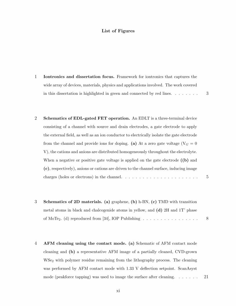
4 AFM cleaning using the contact mode. (a) Schematic of AFM contact mode
cleaning and (b) a representative AFM image of a partially cleaned, CVD-grown
WSe2 with polymer residue remaining from the lithography process. The cleaning
was performed by AFM contact mode with 1.33 V deflection setpoint. ScanAsyst
mode (peakforce tapping) was used to image the surface after cleaning. . . . . . . 21
xi
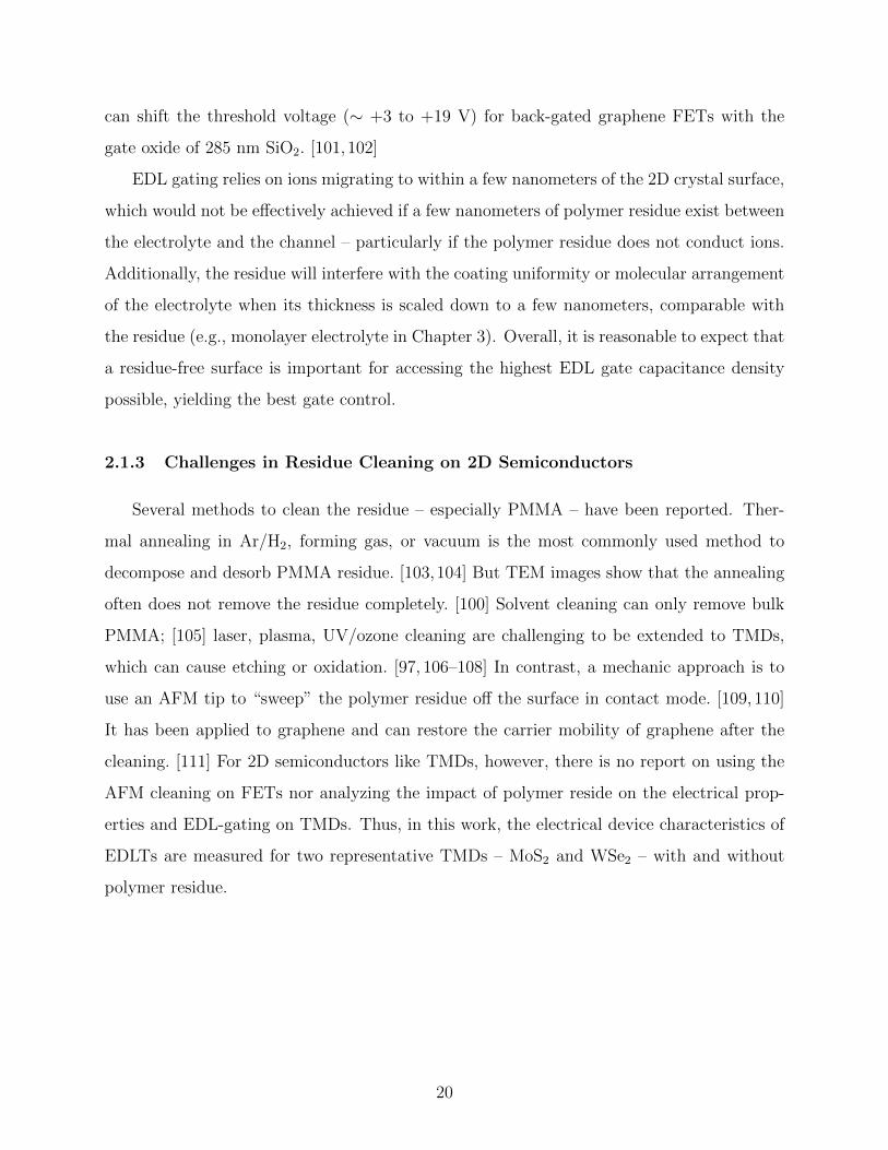
5 Device schematics, optical images and AFM scans of three representative
FETs. Device cross-sectional schematics of (a) exfoliated MoS2 FET, (e) exfoliated
WSe2 FET, (i) CVD-grown WSe2 FETs. Optical images of (b) MoS2, (f) WSe2,
and (j) CVD-grown WSe2 FETs. AFM images of (c) MoS2, (g) WSe2, and (k)
CVD-grown WSe2 FETs as fabricated with post-lithography residue, and (d) MoS2,
(h) WSe2, and (l) CVD-grown WSe2 FETs after the AFM cleaning. The blue boxes
on AFM images indicate the location over which the roughness (Rq) was calculated.
The blue lines on AFM images are the positions of line scans, and the corresponding
scans are provided below the AFM images. . . . . . . . . . . . . . . . . . . . . . 23
6 Transfer characteristics and AFM images of a back-gated WSe2 FET at
three states. As fabricated (black line), after vacuum anneal (blue line), and after
AFM cleaning (red line). The blue boxes and lines on AFM images are the positions
of roughness measurements and line scans, respectively. . . . . . . . . . . . . . . 25
7 Transfer characteristics of top-gated CVD WSe2 FETs with PEO:CsClO4
electrolyte. (a) Schematics of control experiments with the sequence of transfer
characteristics, removal and re-deposition of electrolyte, and AFM cleaning. Transfer
curves of CVD-grown WSe2 as fabricated with electrolyte (dotted line) and after
cleaning polymer residue (solid line) are shown in (b) linear scale and in (d) log
scale. The control FETs after re-depositing electrolyte without AFM cleaning (solid
line) are shown in in (c) linear scale and in (e) log scale. L1-L5 (M1-M5) correspond
to six different devices with (without) AFM cleaning, respectively. . . . . . . . . . 28
xii

8 Monolayer electrolyte structure and mechanism, and fabricated MERAM
device. (a) Structure of the monolayer electrolyte consisting of CoCrPc and four
Li+ with one in each crown-ether ring. (b) Side view of the two energetically fa-
vorable configurations of the monolayer electrolyte. These two configurations cor-
respond to the On- and Off-states; note that the ether oxygens in the crown are
positioned up or down along with the Li+. (c) DFT results for two Off-state
configurations: (top) CE-Li+ on WSe2 exposed to vacuum only, and (bottom)
CE-Li+ on WSe2 capped by h-BN. (d) MERAM schematic. (e) Sideview of the
WSe2/monolayer electrolyte/h-BN stack. (f) Optical image of the MERAM (false
colored, Device 2). (g) AFM scan of the WSe2 FET channel (Device 2) after AFM
cleaning (left) and after CoCrPc deposition (right), and corresponding line scans. . 34
9 MERAM transfer characteristics and programming tests (a) Programming
and sensing protocol: (1) initial double transfer sweep (VDS = 20 mV, 7.5 V/s) to
monitor Vs and hysteresis in the unprogrammed condition, (2) programming the
device Off with VBG = +30 V, (3) single sweep (7.5 V/s) to sense Vs (red dot on
the curve), (4) programming the device on with VBG= -30 V, and (5) another single
sweep to sense Vs (blue dot on the curve). Note that Vs is the sub-threshold voltage,
which is distinct from the threshold voltage, Vth, which is used for charge density
calculations. (b) Resulting transfer scans following the programming and sensing
protocol for WSe2/CE-Li+ (without h-BN, Device 1). (c) Transfer curves for the
same device before (black dash) and after (yellow lines and dash) programming
with only the monolayer electrolyte, and after (green lines and dash) programming
with the monolayer electrolyte/h-BN stack. For comparison, the additional leakage
current (IDleak) after adding h-BN is subtracted on the right y axis, with the original
data shown in the inset. Three single sweeps were taken after each programming
(7.5 V/s). The magnitude of threshold voltage shift is highlighted by shading the
opening of the memory window. (d) The potential energy of Li+ in the monolayer
electrolyte in the Off-state at 0 V of the applied field is schematically illustrated for
the stacks without h-BN (i.e., exposed to vacuum) and with h-BN (top and bottom,
respectively). . . . . . . . . . . . . . . . . . . . . . . . . . . . . . . . . . . . . 37
xiii

10 Program/erase and retention measurements. (a) ID after alternating pro-
gram/erase voltage pulses on Device 1. Top: program (VBG = -30 V, green)/erase
(VBG = +30 V, grey) voltage profile with voltage applied for 1 second and readout
for 10 seconds at VBG = 0V; VDS = 500 mV. Bottom: corresponding readout cur-
rent, ID, without and with h-BN capping layer. (b) Program/erase endurance test.
1000 cycles of program/erase with pulse width of 1 s and readout time of 10 s. (c)
Retention test. Program/erase with 1 s pulse and ID monitored for 6 hours. The
Off-state current increased in the first five hours then remain stable. Inset schematic
show the predicted relaxation of Li+ (new location indicated by dashed line) when
the back gate is grounded, providing a possible explanation for the increase in the
off current with time. . . . . . . . . . . . . . . . . . . . . . . . . . . . . . . . . 40
11 Program/erase measurements as a function of pulse width and voltage.
(a) (Device 1) ID of the On- and Off-states in response to program/erase voltage
pulses where the pulse width is varied from 1 ms to 1 s. (b) (Device 2) ID of the
On- and Off-states with varying the program and erase voltages from ± 5 to ± 30
V (absolute values of ID plotted). For both (a) and (b), data at each point are
averaged over 12 program/erase cycles with the error bar indicating one standard
deviation from the mean. . . . . . . . . . . . . . . . . . . . . . . . . . . . . . . 42
12 Mechanism of a single-ion conductor gated EDLT. (a) Schematic of a 2D
crystal FET (either graphene or MoTe2) that can be operated by using a back gate
or a single/dual-ion conductor using a metal side gate. (b) Chemical structures of
the dual- and single-ion conductors: PEO:CsClO4 (top row) and the ionically func-
tionalized polyester (PE400-Li) (bottom row), respectively. Anions are shaded in red
and cations are shaded in blue. Schematics of the (c) dual-ion conducting and (d)
single-ion conducting FETs under two polarities. In the single-ion case, only cations
are mobile while the anions are bound to the polymer backbone and therefore fixed.
This immobility leads to cationic depletion regions (shaded in pink) at either the
gate/single-ion conductor (VG > 0) or single-ion conductor/semiconductor interface
(VG < 0), depending on the polarity of the applied field. . . . . . . . . . . . . . . 47
xiv
13 COMSOL Multiphysics simulations of steady-state voltage distributions
in single- and dual-ion conductors during EDL gating. The Steady-state
voltage distributions and the corresponding device schematics showing ion positions
for both (a, c) dual-ion and (b, d) single-ion conductors in two parallel plate ca-
pacitor geometries: electrodes of equal size (upper row) and electrodes of unequal
size where the right electrode is 10 times larger than left (bottom row). Note that
the schematics are not drawn to scale. Either ±1 V is applied on the right-side
electrode. Cation and anion layers are highlighted in blue and red, respectively. The
anion EDL (dual-ion) or cationic depletion layer (single-ion) thickness differences are
illustrated qualitatively. Specifically, for the dual-ion conductor, the anionic EDL
layer thickness is similar to the cationic EDL layer thickness; while for the single-
ion conductor, the cationic depletion layer thickness is larger and influenced by the
electrode size. The steady-state potential distributions under positive and negative
voltages are highlighted in the red solid and dashed blue lines, respectively. . . . . 50
14 Graphene FET gated by single-ion conductor. (a) AFM topography scan of
a bare graphene FET channel (before electrolyte deposition). The location of the
line scan is indicated by the white dashed line. (b) Transfer characteristics of the
graphene FET: the blue data corresponds to the back-gated measurement of a bare
FET while the red corresponds to a side-gated measurement on the same FET with
the single-ion conductor. (c) Output characteristics of the back- gated (blue) and
side-grated (red) graphene FETs. . . . . . . . . . . . . . . . . . . . . . . . . . . 53
15 Comparison between single- and dual-ion conductor in EDL gating. (a,
b) Transfer characteristics of two graphene FETs. Back-gated bare devices (blue),
side-gated with single-ion conductor (red), and side-gated with dual-ion conductor
(green). Solid and dotted lines indicate scans from negative to positive gate voltages
and from positive to negative gate voltages, respectively. Note that the gate voltages
were normalized with respected to VDirac to facilitate comparison between n- and
p-branches currents using different gating methods. . . . . . . . . . . . . . . . . . 55
xv

16 Comparison between COMSOL simulations and experimental results. (a)
COMSOL simulations of corresponding charge carrier densities within the grounded
electrode in a parallel-plate capacitor geometry with the single-ion conductor (red)
and the dual-ion conductor (green). (b) Transfer characteristics of both ion con-
ductors on one graphene FET (device 3): the single-ion conductor is red and the
dual-ion conductor (PEO:CsClO4)is green. In both (a) and (b), the voltage is swept
from negative to positive (solid lines) and then reversed (dotted lines). . . . . . . . 56
17 MoTe2 FET with supported channel gated by single-ion conductor. (a)
AFM topography scan of a bare MoTe2 FET channel (before electrolyte deposition).
The location of the line scan is indicated by the white dash line. (b) Transfer
characteristics of the MoTe2 FET in log scale with back-gated transfer measurements
from VBG = -30 to +30 V on the bare FET in blue and side-gated transfer of the
same FET from VSG = -3 to +3 V with single-ion conductor in red. (c) Zoomed
transfer curves on a linear y-axis over a negative range of VBG to highlight the
suppressed p-branch when using the single-ion conductor. . . . . . . . . . . . . . 58
18 The fabrication process of a suspended MoTe2 FET. From left to right: 1)
Exfoliation of h-BN on SiO2 substrate; 2) using plasma to etch h-BN to create the
trench for placing a suspended channel; 3) metal electrodes deposition including a
side gate for gating; 4) dry flake transfer of MoTe2 channel. . . . . . . . . . . . . 60
xvi

19 Schematics of a lateral graphene p-n junction with n- and p-type re-
gions created by electric-double-layer (EDL) doping and subsequent ion-
locking. (a) (Top row) Four-electrode graphene device coated by DPIL. Cations
(blue spheres) and anions (red spheres) dope the graphene channel to form p-type
(pink) and n-type (blue) regions, respectively. (Bottom row) Top view schematic
and chemical structure of DPIL monomers. (b) The formation of a p-n junction by
EDL doping: (1) Programming voltages are applied to electrodes 2 and 3, while the
remaining 2 electrodes and backgate are floated; mobile cations and anions redis-
tribute in response to the field forming a p-n junction between electrodes 2 and 3.
Note that the largest ion concentration occurs near the electrodes and decreases with
distance away from the electrodes as modeled in the reference. (2) After the EDL
is formed, the ions are locked into place either by cooling the PEO:CsClO4 device
below the Tg of the electrolyte, or by DPIL polymerization. (3) After locking, the
p-n junction remains in the absence of voltage. . . . . . . . . . . . . . . . . . . . 66
20 Using DPIL to create lateral p-n junction. (a) Schematics of a fixed p-n
junction, with voltages removed after EDL locking and cooling to room temperature.
(b) Backgated transfer characteristics after polymerization between electrodes 1-2
(red dash), 2-3 (green solid line) and 3-4 (blue dash), with VD = 10 mV and a sweep
rate of 0.2 V/s. (c) Fermi-level tuning that gives rise to the I23-VBG and I12-VBG
transfer characteristics after ion-locking. . . . . . . . . . . . . . . . . . . . . . . 68
21 DPILs electrolyte and EDL locking mechanism. (a) Schematic of DPILs
gated FET with a side gate. (b) EDL locking mechanism. From left to right: 1)
programming the FET to form EDL by mobile ions in unpolymerized DPIL; 2)
locking the EDL in place by heat-triggerd polymerization with gate bias applied; 3)
locked EDL with no gate bias applied - a gateless electrostatic doping. . . . . . . . 71
xvii

22 Transfer characteristics and EDL retention before and after polymeriza-
tion. (a) Transfer characteristics of a graphene FET before (black line) and after
(blue) locking the cation-induced EDL by polymerization. Scanning window is from
-1 to 1 V, while the blue line (polymerzied DPIL) was obtained after forming the
EDL at VSG of +2 V and the locking by polymerization. (b) EDL retention before
(black) and after locking the EDL by polymerization (blue line). In both mea-
surements, side gates were grounded (0 V), and the ID was monitored to show the
cation-induced EDL retention of its saturation state obtained after VSG = +2 V
applied for 10 min. (c) and (d) are the similar measurements of transfer charac-
teristics and EDL retention test on WSe2 FET, respectively, with the ID monitored
before (black) and after (red) locking the anion-induced EDL by polymerization. . 73
23 Chemical structures of triggerable polymerizable ionic liquid Structures
of (left) triggerable singly polymerizable ionic liquid (T-SPIL), with Diels-Alder
linkage in cation; and (right) non-triggerable singly polymerizable ionic liquid (NT-
SPIL), with the same cation as DPIL used previously. . . . . . . . . . . . . . . . 76
24 Mechanism of a single-ion conductor gated EDLT. (a) Capacitor response
of non-triggerable (top) and triggerable singly-polymerized ionic liquids (bottom) at
298 K (25 ◦C), measured before polymerization, immediately after polymerization,
and after a full thermal cycle in which the temperature of the sample was increased
to 400 K (127 ◦C) before being returned to room temperature. Each trace depicts
the response of the material to a step potential applied across a capacitor with 10
µm electrode spacing. (b) Temperature-dependent current amplitudes for capacitors
with non-triggerable (top) and triggerable singly-polymerized ionic liquids (bottom)
deposited and polymerized across the electrodes. Arrows labeled Tg and rDA in-
dicate the glass transition temperature and retro Diels-Alder temperatures of the
samples, respectively. . . . . . . . . . . . . . . . . . . . . . . . . . . . . . . . . 78
25 Dissertation summary. Framework for 2D EDLTs and the work covered in this
dissertation together with corresponding publications (highlighted in green and con-
nected by red lines). . . . . . . . . . . . . . . . . . . . . . . . . . . . . . . . . . 81
xviii

Preface
First of all, I would like to express my deepest gratitude to my advisor, Prof. Susan
Fullerton-Shirey, whose encouragement, insightful guidance and great support have been
helping me over the past five years not only to complete my research, but also to achieve
many milestones in my life. I feel lucky and honored to study electrolytic gated electronics
in her group.
I would like to thank Prof. Eric Beckman, Prof. James McKone and Prof. Feng Xiong,
for serving on my committee and providing invaluable advice and great mentoring. I believe
that anything that I have learned from them today will benefit my life in the future.
I am also heartily thankful to Dr. Ke Xu, who gave so much guidance and advice on my
research and career. Many of my achievements at Pitt would not have been possible without
his invaluable support and mentoring.
Furthermore, I would like to convey my sincere thanks to my dear lab mates for many
many reasons that would need a new chapter to list. For all their help and in no particular
order, I would like to thank my buddies, Zhongmou Chao, Shubham Awate, M.Eli Bostian,
Huiran Wang and Aaron Whopper who assisted me greatly. And our best fellows: Samantha
Bunke, Abigale Gray, Noah Sakmar, Jeirus Jose, Alvin Fersner, Matei Jordache, Brian
Radka, Celina Celmo, Ziwei Guo, Rachel Buck and Blaec Toncini.
In addition, I take this opportunity to convey my sincere thanks to my dear wife Runfang
and our loving parents. This dissertation is dedicated to them. And I am deeply grateful to
all of my friends who supported me in any respect during my PhD study.
Finally, I would like to say a big thank you to my department at Pitt (especially for the
hard work during this special period of 2020), the Center for Low Energy Systems Technology
(LEAST) and the NSF for providing support of my research.
Go Pitt and I love you all!
xix

1.0 Introduction
1.1 An Introduction to Iontronics and the Focus of the Dissertation
Ions, atoms or molecules with net electrical charges, are critical components of artificial
or biological systems in our daily lives, including batteries, sensors, fuel cells, membranes,
cell signaling involved in metabolism, and signal transduction in neural systems. The in-
vestigation of ionic systems to achieve better performance or new functionality involves
various fundamental studies such as ion transport, interfacial phenomena, and material de-
sign, which require interdisciplinary interactions between chemistry, physics, biology, and
materials science. Recently, there is more involvement of the high-performance electronics
community, giving rise to an emerging interdisciplinary concept that bridges ionic systems
and electronics, referred to as “iontronics”.
Iontronics emphasizes the control of electronic properties of a material or functions of
a device by ionic motion and arrangement. [1] As illustrated in Figure 1, iontronics can
be generally categorized according to mechanisms as either electrostatic or electrochemical,
depending on whether or not electrochemical reactions modulate the state of the device.
For electrostatic iontronics, there are two major branches defined by device type: electric-
double-layer capacitors (EDLC) and electric-double-layer transistors (EDLT), both of which
involve the formation of electric double layers (EDL) thereby taking advantage of large EDL
capacitance. [1–4] EDLCs are the foundation for the development of flexible supercapacitors
and are mainly used for wearable electronics. [3] In contrast, EDLTs have many applica-
tions such as printable and flexible electronics, phase change devices, memory and synaptic
devices, and are also used extensively to explore fundamental physics such as superconduc-
tivity, thermoelectric effect, and ferromagnetism in materials including polymers, organic
crystals, oxide semiconductors, magnetic materials, carbon nanotubes, 2D materials and
quantum-dots. [1,2] For electrochemical iontronics, though not the focus of this dissertation,
a variety of branches have been developed in the past decade, including ion intercalation
devices, [5] electrochemical transistors (ECT) for organic electronics, [2] electrochemical
1

metallization (ECM) devices and valence charge memory (VCM) for resistive random ac-
cess memory (ReRAM) and memorisistors, [6–8] and electrochemical light-emitting cells
(LEC). [9] Together, they constitute a large and blooming family of iontronics which has
become a vital component for printable and flexible electronics, neuromorphic devices for ar-
tificial intelligence, Internet of Things (IoT), healthcare technologies and many other future
applications. [1]
This dissertation focuses on one specific branch of iontronics: EDLTs that employ two-
dimensional (2D) materials as transistor channels (indicated by shaded green boxes in Figure
1). Due to unique electronic, thermal and mechanical properties of 2D materials compared
to Si, many exciting predictions have been made about the possible role of 2D materials
in electronics such as: devices with the ultimate degree of thickness scaling (i.e., atoms or
molecules), [10] ultra-low power devices, [11] and mechanically flexible devices. [12] Moreover,
broad and rich physics has been uncovered including 2D superconductivity [13,14] and opto-
valleytronics [15, 16] that are directly related to the quantum confinement provided by the
single atom or molecule thick geometry. However, to harness some of the advantages for
practical application, precise control over the density and type of charge carriers in the
2D materials is required - a particular challenge for 2D materials. One reason is that high
performance gate dielectrics are hard to grow on surfaces free of dangling bonds. In addition,
substitutional doping that has been refined for Si-based devices is unsuitable for 2D materials.
In contrast, replacing the gate dielectric with an ion conductor provides a material that
is (1) easy to deposit on the surface of a 2D material and (2) can induce charge carrier
densities exceeding 1013 to 1014 cm−2 [2] for both holes and electrons without substitutional
doping. These values are one or two orders of magnitude larger than a conventional gate
dielectric. Therefore in the past decade, the 2D community has utilized 2D EDLTs as a tool
to discover exciting new physics such as spin polarization, [17] photogalvanic current, [18] and
current-induced circularly polarized electroluminescence. [19] Yet, unlike battery community
where ion conductors have been extensively engineered to enhance ion transport, the effort
within the semiconductor community is largely focused on engineering the 2D material with
very little effort given to engineering or even improving ion conductors to control charge
carriers of 2D materials. [1,4] A missed opportunity is that ion conductors can introduce new
2

Figure 1: Iontronics and dissertation focus. Framework for iontronics that captures the widearray of devices, materials, physics and applications involved. The work covered in this dissertationis highlighted in green and connected by red lines.
3
functionality into 2D EDLTs that would not be possible with conventional gate dielectrics.
This is especially true for polymer electrolytes given the rich opportunities for tailoring the
polymer chemistry and tuning the properties. Therefore, my work has focused on developing
novel electrolyte and 2D EDLTs to impart functionalities that can be difficult or impossible
to achieve with conventional gate dielectrics. The following subsections will cover several
basic aspects of 2D EDLTs, ranging from EDLT mechanism, 2D materials, ion conductors,
device assembly and major applications.
1.2 EDLT Mechanism: Electric Double Layer Gating
The semiconductor channel of a field-effect transistor (FET) is turned On (high current)
or Off (low current) by the external electric field applied from the gate. In conventional
metal–oxide–semiconductor field-effect transistor (MOSFET), the field is applied through
the oxide dielectric (e.g., SiO2) and interacts electrostatically with the channel to modulate
the current. In contrast, in an EDLT, the dielectric between the gate and channel is replaced
with an ion conductor (i.e., electrolyte) that is electrically insulating but ionically conductive.
In this case, the gating of the FET is accomplished by the formation of EDLs that form at
the channel/electrolyte interface and the gate/electrolyte interface, which is known as EDL
gating (Figure 2). When there is no gate bias, cations and anions are homogeneously
distributed in the electrolyte (Figure 2 (a) at VG = 0 V). With a negative bias applied at
the gate (Figure 2 (b), VG < 0 V), anions are drifted to the semiconductor channel surface
where they induce image charges (holes) and form an anionic EDL at the channel/electrolyte
interface. In this case, hole conduction is promoted in the channel as more holes are induced
by anions. When a positive bias is applied (Figure 2 (c)), the opposite occurs, with a cationic
EDL formed at the interface to promote electron conduction. [1, 2]
In EDLTs, the charge carrier density in the semiconductor is electrostatically controlled
by the amount of ions at the electrolyte/semiconductor interface and is proportional to the
applied gate voltage on the electrolyte. The upper limit of the accumulated charges at the
interface is determined by the ion packing density at the maximum possible gate voltage
4
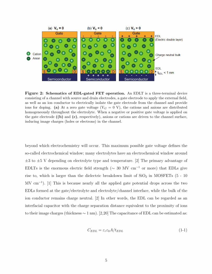
Figure 2: Schematics of EDL-gated FET operation. An EDLT is a three-terminal deviceconsisting of a channel with source and drain electrodes, a gate electrode to apply the external field,as well as an ion conductor to electrically isolate the gate electrode from the channel and provideions for doping. (a) At a zero gate voltage (VG = 0 V), the cations and anions are distributedhomogeneously throughout the electrolyte. When a negative or positive gate voltage is applied onthe gate electrode ((b) and (c), respectively), anions or cations are driven to the channel surface,inducing image charges (holes or electrons) in the channel.
beyond which electrochemistry will occur. This maximum possible gate voltage defines the
so-called electrochemical window; many electrolytes have an electrochemical window around
±3 to ±5 V depending on electrolyte type and temperature. [2] The primary advantage of
EDLTs is the enormous electric field strength (∼ 30 MV cm−1 or more) that EDLs give
rise to, which is larger than the dielectric breakdown limit of SiO2 in MOSFETs (5 - 10
MV cm−1). [1] This is because nearly all the applied gate potential drops across the two
EDLs formed at the gate/electrolyte and electrolyte/channel interface, while the bulk of the
ion conductor remains charge neutral. [2] In other words, the EDL can be regarded as an
interfacial capacitor with the charge separation distance equivalent to the proximity of ions
to their image charges (thickness∼ 1 nm). [2,20] The capacitance of EDL can be estimated as:
CEDL = εrε0A/tEDL (1-1)
5

where εr is the relative permittivity of electrolyte and ε0 is vacuum permittivity (8.854
× 10−12 F m−1), A is the semiconductor channel area, and tEDL is the EDL thickness (∼
1 nm). Because the gate capacitance is inversely related to the charge separation distance,
the EDL can induce high gate capacitance densities (1 - 10 µF cm−2), corresponding to
sheet carrier densities (i.e., doping densities) exceeding 1013 cm−2. [2,21] Since the transistor
drain current is proportional to the gate capacitance when the drain/source voltage VDS is
much less than the gate voltage VG, [2] the EDL gating allows for stronger modulation of
the current (compared to traditional dielectrics) at low gate voltages (i.e., a sub volt) as
required by power-efficient electronics. [1, 2] Another advantage is that EDL induces strong
and degenerate doping on the semiconductor, which reduces the depletion length at the
contact/semiconductor junction (i.e., Schottky barrier thinning), allowing more tunneling
than thermionic injection of charge carriers from metal contacts to semiconductors and
therefore reducing contact resistance. [22–24] This reduced contact resistance combined with
the strong gate control by EDLs has enabled the exploration of new transport phenomena
that cannot be accessed with traditional gate dielectrics, especially for novel semiconductors
like nanotubes and 2D crystals.
Note that the speed of a transistor is essentially the switching time between the Off
and On states. For MOSFETs, the polarization response within the dielectric is on the
timescale of nanoseconds and the switching speed depends mainly on the channel length and
the mobility (µ) of charge carriers (i.e., electrons/holes) in the channel. However, in EDLTs,
the switching speed depends on the polarization speed of the EDL (i.e., the time for full EDL
formation), which can be as long as a few seconds in solid polymer electrolyte because ions
move several orders of magnitude slower than electrons/holes. Therefore, EDLTs using
conventional solid polymer electrolytes, have been ignored for application in high-speed
electronics. More discussion of the switching speed will be included in section 1.4.
6
1.3 Two-dimensional Materials for Transistors
2D crystals are layered materials held together by Van de Waals forces. Since the iso-
lation of first 2D material – graphene – in 2004, [25] 2D materials have been explored for
next generation power-efficient electronics because of their excellent electrical, thermal and
mechanical properties. [26, 27] Specifically, FETs based on those 2D materials have several
advantages including an atomically thin channel, which is beneficial for device scaling with-
out detrimental short-channel effects, high carrier mobilities, [10, 26] mechanical properties
compatible with flexible electronics, [12] and the ability to form heterojunctions and het-
erostructures by crystal stacking. [28] In addition, unique physics have been revealed for 2D
materials recently including their spin and valley degrees of freedom, leading to new device
concepts - spintronics and valleytronics. [15]
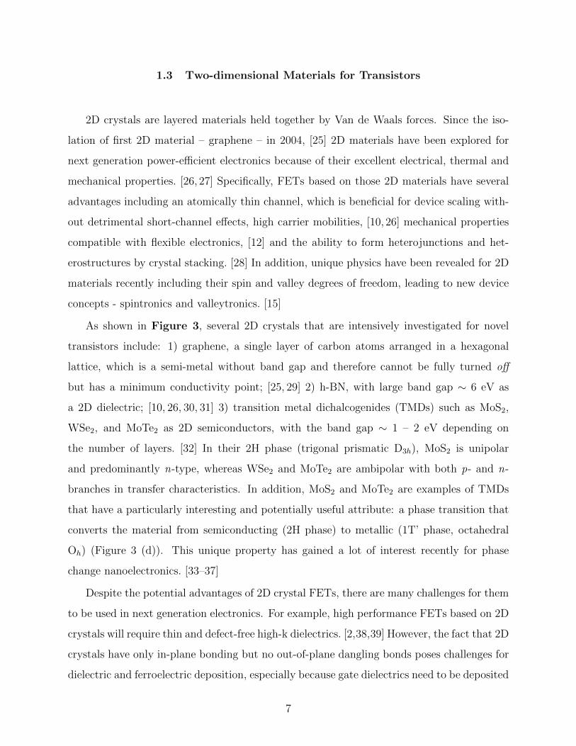
As shown in Figure 3, several 2D crystals that are intensively investigated for novel
transistors include: 1) graphene, a single layer of carbon atoms arranged in a hexagonal
lattice, which is a semi-metal without band gap and therefore cannot be fully turned off
but has a minimum conductivity point; [25, 29] 2) h-BN, with large band gap ∼ 6 eV as
a 2D dielectric; [10, 26, 30, 31] 3) transition metal dichalcogenides (TMDs) such as MoS2,
WSe2, and MoTe2 as 2D semiconductors, with the band gap ∼ 1 – 2 eV depending on
the number of layers. [32] In their 2H phase (trigonal prismatic D3h), MoS2 is unipolar
and predominantly n-type, whereas WSe2 and MoTe2 are ambipolar with both p- and n-
branches in transfer characteristics. In addition, MoS2 and MoTe2 are examples of TMDs
that have a particularly interesting and potentially useful attribute: a phase transition that
converts the material from semiconducting (2H phase) to metallic (1T’ phase, octahedral
Oh) (Figure 3 (d)). This unique property has gained a lot of interest recently for phase
change nanoelectronics. [33–37]
Despite the potential advantages of 2D crystal FETs, there are many challenges for them
to be used in next generation electronics. For example, high performance FETs based on 2D
crystals will require thin and defect-free high-k dielectrics. [2,38,39] However, the fact that 2D
crystals have only in-plane bonding but no out-of-plane dangling bonds poses challenges for
dielectric and ferroelectric deposition, especially because gate dielectrics need to be deposited
7

Figure 3: Schematics of 2D materials. (a) graphene, (b) h-BN, (c) TMD with transitionmetal atoms in black and chalcogenide atoms in yellow, and (d) 2H and 1T’ phase of MoTe2. (d)reproduced from [34], IOP Publishing
in extremely small thickness (a few nm) while maintaining low leakage current. [40,41] One
possible approach to address this problem is the deposition of a seed layer onto which a
gate dielectric is deposited. [39, 40, 42] Another approach is to transfer 2D materials onto
dielectric substrates directly. But this approach usually compromises the interface between
the dielectric and the 2D materials, changing the intrinsic properties of the 2D material and
deteriorating device performance. [43]
In contrast to traditional oxide-based gate dielectrics, using an ion conductor as the gate
dielectric can address some of these concerns. For example, ion conductors can be directly
deposited onto 2D materials that are free of dangling bonds by drop-casting and spin-coating.
Conveniently, precise control over the ion conductor thickness is not critical for achieving
high gate capacitance. Most importantly, as mentioned above, EDLs can achieve larger
charge carrier densities and therefore greater gate control than oxides dielectric. [2] Unlike
8
an oxide gate dielectric/ferroelectric, the EDL induced capacitance is inversely related to the
EDL thickness (∼ 1 nm) (as opposed to the total physical thickness of the gate dielectric), as
introduced in Section 1.1. The resulting large interfacial electric field has made EDL gating
a key tool for uncovering a variety of semiconductor and quantum physics in 2D crystals. [1]
It is also challenging to dope 2D crystals to achieve a well defined p- or n-type behavior
as required for electronics. Si is doped by substitutional doping where atoms are replaced
with atoms of a different type. But this strategy is not suitable for atomically-thin 2D
crystals because permanent replacement of atoms alters the intrinsic band gap and structural
properties. [44] Electrostatic doping by ions, on the other hand, can be achieved by the fixed
charge provided by fully formed EDLs where the image charges in 2D channel induced
by the ions serve as dopants. Without atomic replacement nor charge transfer, the EDL
gating approach is reconfigurable by changing the polarity and/or strength of the field to
redistribute the type and/or density of ions.
1.4 Ion Conductors for EDL Gating
Ion conductors used for EDL gating are ion-conducting gate dielectrics, with capacitance
densities in the range of 1 - 10 µF cm−2, which is one to two orders of magnitude larger
than many common gate oxides including SiO2 (0.035 µF cm−2), [45] Al2O3 (0.06 - 0.7 µF
cm−2), [46,47] Ta2O5 (0.18 µF cm−2), [48] and TiO2 (0.7 µF cm−2). [49] And ion conductors
have also been used extensively for electrostatic ion doping of 2D materials. [24, 38, 50, 51]
Common ion conductors include solid polymer electrolytes, ionic liquids and ion gels and
polyelectrolytes. [1, 2, 4] A summary of each type is presented below.
1.4.1 Solid Polymer Electrolytes
Solid-state electronics will require all-solid state materials; therefore solid polymer elec-
trolytes are attractive due to their easy deposition and device integration. They are prepared
by dissolving inorganic salts in ion conducting polymers. For example, poly (ethylene oxide)
9

(PEO)-based electrolytes consist of a salt (e.g., LiClO4 or CsClO4) dissolved in PEO, where
the ether oxygen atoms on the PEO chains electrostatically interact with cations. Ions move
by hoping from one set of ether oxygen atoms to another either on the same chain or dif-
ferent chains. [52] PEO-based electrolytes have been used widely in 2D EDLTs including
graphene, [38, 53, 54] MoS2, [55] WSe2, [23, 32, 56] MoTe2, [20] and Tellurene. [57] The large
sheet carrier densities of 1014 induced by PEO-based electrolytes enable not only effective
current modulation ratios up to 7 orders of magnitude at small gate voltages (e.g., 1.5 V)
as desired for power-efficient devices, [20] but also permit access to new phenomena such as
gate-induced superconducting transition in 2D EDLTs. [38,58]
While solid polymer electrolytes provide a solid-state ion-conducting gate dielectric, ion
conductivity in these materials is generally low (10−5 to 10−4 S cm−1 at room temperature).
[2] As mentioned in 1.2., the polarization response time of electrolytes (i.e., the time to
form full EDLs with sheet carrier densities up to 1014 cm−2) depends on ion conductivity.
Therefore, the low ion conductivity results in a slow polarization response for solid polymer
electrolytes and low switching frequency (e.g., < 1 kHz) in transistor dynamic characteristics,
[2] making them unsuitable for high-speed electronics compared to oxides dielectrics.
It is not an easy task to improve ion conductivity in solid polymer electrolytes. As
mentioned above, ion conductivity in polymers is coupled to the segmental motion of the
PEO chains, which depends on temperature. [52] The mobility of the polymer chains is
indicated by the polymer’s glass transition temperature (Tg) which increases with increasing
salt concentration. In contrast to Tg, the ionic conductivity goes through a maximum with
increasing salt concentration. At low concentrations, there are only a small number of ions
to contribution to the conductivity, but at high salt concentrations, polymer mobility is
significantly reduced and ionic aggregates form. [52, 59] Thanks to the battery community,
there has been continuous effort to enhance ion transport in solid polymer electrolytes while
also maintaining mechanical properties, [2, 59–62] which could benefit the EDLT research.
Despite the generally poor ionic conductivity, it does not mean that solid polymer elec-
trolytes cannot be used in EDLTs at short operating timescales. First of all, the polarization
response time depends on the electrolyte thickness. Thus, if the solid electrolyte thickness
can be scaled down to nanometers, ions do not need to travel far even though they are slow.
10

In fact, it has been reported that in an ideal case, for PEO electrolytes with a film thickness
of 1 µm, the polarization response time approaches 0.1 µs potentially capable for switching
frequency of 10 MHz. [2] Furthermore, it has been reported by our group that the onset of
EDL formation occurs at much shorter timescales (e.g., nanoseconds under electric field of
1 V nm−1), [54] because only those ions near the interface are involved (i.e., the ions that
ultimately form the EDL do not need to migrate a long distance to the interface). If a
sufficient number of charge carriers are induced during the initial stages of EDL formation,
the FET channel resistance can still be efficiently modulated. Additionally, the ion speed
can be increased by increasing the applied electric field strength, which in turn, reduces the
EDL formation time. While the maximum voltage that can be applied is limited by the
electrochemical window of the electrolyte, our group has shown that short voltage pulses
(e.g., milliseconds or less) could be used to avoid electrochemical reactions. [54]
1.4.2 Ionic Liquids
Another class of electrolyte, ionic liquids, have relatively weak electrostatic interactions
between ions while their ionic concentration is high (i.e., 1021 cm−3), leading to faster re-
sponse to external electric field and higher ionic conductivity (10−5 - 10−2 S cm−1) than solid
polymer electrolytes. Their good thermal, electrochemical stability and high ionic conduc-
tivity make them good electrolytes for printed organic EDLTs. [2, 63] One commonly used
ionic liquid is N,N-diethyl-N-methyl-N-(2-methoxyethyl) ammonium bis (trifluoromethylsul-
fonyl) imide (DEME–TFSI), which exhibits an ionic conductivity of 4.0 × 10⁻³ S cm−1
and a electrochemical window of 5.4 V at room temperature. [64] Besides printed organic
EDLTs, DEME-TFSI has been widely used in 2D EDLTs for exploring new physics, includ-
ing graphene, [65] MoS2, [24,66,67] and WSe2. [68] The EDL gating using DEME-TFSI can
reduce the contact resistance by enhancing the tunneling of charge carriers due to the Schot-
tky barrier thinning (as mentioned in section 1.2). [24] Large sheet carrier densities over 1014
cm−2 were reported for EDL gating using DEME-TFSI, which allows gate-induced supercon-
11

ductivity in TMDs, [14, 69–71] and the metal-insulator transition of MoTe2 (2H/1T’ phase
transition as mentioned in 1.3). [37] One major drawback of using ionic liquids, though, is a
lack of solid-like mechanical integrity required for solid state electronics.
1.4.3 Ion Gels
Ion gels have recently gained tremendous attention due to their solid state nature and
mechanical properties superior to ionic liquids but without too much compromise on ion
transport. Typically, ion gels used in EDLTs have ionic conductivity of 10−3 S cm−1 with
good chemical and electrochemical stability. [2, 72] Ion gels can be categorized into aqueous
(e.g., hydrogels) and non-aqueous gels (e.g., polymeric ion gels). Although hydrogel gated
graphene transistor was reported, [73] it remains challenging to use aqueous ion gels in EDLTs
because their water content can alter the channel properties by p-type doping, can screen the
electric field that decreases gate control of ions, and can lead to hydrolysis that will occur at
voltages within the operating window. On the other hand, nonaqueous ionic gels have been
widely used in EDLTs and EDLCs for flexible and stretchable electronics as well as printable
digital circuits. [2, 3, 72] The gelation of nonaqueous ion gels is achieved by introducing
a polymer network into ionic liquids with either noncovalent associations (e.g., hydrogen
bonding, colloidal dispersion, and supramolecular interaction) or with covalent crosslinking
through polymerization of vinyl monomers or polyaddition of functional groups. [2, 72] So
far, the most widely used ion gel in 2D EDLTs consists of triblock copolymer poly(styrene-
block-methylmethacrylate-block-styrene) (PS-PMMA-PS) and and the ionic liquid 1-ethyl-
3-methylimidazolium bis(trifluoromethylsulfonyl)imide ([EMIM][TFSI]). [51, 74,75]
1.4.4 Single-ion Conductor
Another type of polymer electrolyte that is commonly used in actuator and battery re-
search, but uncommon for EDLTs is the single-ion conductor. It consists of immobile ions
because they are covalently bounded to polymer backbones and mobile counter ions, rep-
resenting a unique type of solid polymer electrolyte. The first EDL gating using a single
ion conductor was on P3HT polymer FETs using poly(styrene sulfonic acid) (PSSH). [76]
12

The PSSH dissociate into SSH− polyanions and protons (H+) under the field, and protons
are capable to form the EDL. Later, another example was demonstrated on a n-type poly-
mer transistor using a polymerized ionic liquid (PIL) triblock copolymer (PS-PIL-PS) that
conducts only the TFSI anion. [77] And recently, the first demonstration of a 2D EDLT
using a PEO based single-ion conductor was reported by us, which possess a unique gating
behavior on ambipolar 2D FETs. [78] Specifically, whereas graphene and MoTe2 FET are
typically ambipolar when gated by a dual-ion conductor (i.e., one with both mobile cations
and anions), gating with a single-ion conductor in which cations are the mobile species,
suppresses the p-branch and enhances the n-branch.We show that this behavior is due to
the combination of immobile anions and an asymmetric gate/channel geometry (details in
Chapter 4).
13

1.5 2D EDLT Device Assembly
Depositing electrolytes on 2D crystals can be easily achieved by drop-casting, spin-
coating or inkjet printing from solution, which avoids the challenging growth or deposition
of oxides using atomic layer deposition (ALD). The electric field can be applied by either a
side- or a top-gate for the strongest gate control; but a back gate can also be used to control
the location of the ions, though more weakly due to the field loss through backgate oxide
and the screening of the 2D channel. Most of EDL gating of 2D FETs adopt a side gate
geometry because the gate can be easily patterned together with other metal contacts by
e-beam lithography prior to electrolyte deposition. The lateral gate location (i.e., distance
between the channel and the gate) is flexible because the strength of the gating depends
weakly on the distance from the channel to the gate when the EDL is fully formed. Another
advantage using the side gate geometry is that the area above the channel is not blocked
unlike that in a top gate geometry, thereby reducing the difficulty of integrating 2D EDLTs
in optoelectronic applications. [79,80]
In general, the entire device assembly for common 2D EDLTs usually involves three
major steps: 1) preparing 2D flakes by exfoliation or preparing wide-area 2D materials by
CVD growth; 2) designing and patterning metal electrodes (i.e., source, drain and side gate
electrodes); 3) depositing an electrolyte that covers both the 2D channels and the side gates.
Note that most electrolytes are typically hygroscopic, and thus water exposure should be
avoided which otherwise will screen the field and comprise the effectiveness of the gate. [4]
14
1.6 Applications of 2D EDLTs
As illustrated in Figure 1 and Section 1.4, numerous 2D EDLTs have been demonstrated
using various kinds of solid polymer electrolytes, ionic liquids and ion gels. Two primary
reasons for using ion-based gating are: 1) to explore fundamental transport properties in
2D materials; and 2) to introduce a new functional layer via the electrolyte for novel device
concepts. Each of these reasons are discussed below.
1.6.1 Using EDLT to Explore Transport and New Physics in 2D Materials
EDL gating has been primarily used to investigate the quality and properties of new
materials because it can induce large interfacial electric fields, high sheet carrier densities
and large capacitances that provide exceptional gate control. This is especially attractive for
2D crystals because EDL gating is a surface phenomenon, and its impact increases in intensity
when the 2D material itself is a surface. In addition, this technique is very popular because its
easy to deposit polymer electrolytes and ionic liquids onto devices. Many studies have used
EDLTs to measure transport properties such as charge carrier densities and hole/electron
mobilities. [23, 32,54,68,81]
Also by taking the advantages of 2D EDLTs, a variety of properties and physics have
been discovered in the past decade. For example, the EDLT device design allows exploration
of gate induced superconductivity in 2D TMDs. [14,58,69–71] Herein, EDLs play a key role
by inducing sheet carrier densities on the order of 1014 cm−1 as required to access super-
conducting regimes, but without altering the bandgap like other methods such as chemical
doping or ion intercalation. [1, 13]
2D EDLTs have been also used to investigate TMD based spintronics/valleytronics.
[66, 82] For instance, MoS2 FETs using conventional gate dielectrics show unipolar n-type
behavior due to sulphur vacancies and Fermi-level pinning. [11] For spintronics, however,
p-type conduction in MoS2 is necessary to access large spin-splitting which occurs only in
valence band. This has been achieved by using EDL gating, with sheet carrier densities over
1014 cm−1 reported for hole conduction. [66]
15
Several more new physics being investigated using 2D EDLTs include photogalvanic
current, [18] circularly polarized electroluminescence, [19] field induced semiconducting to
metallic phase transition, [33, 34, 37] and p-n junctions. [20, 56, 83] The last two will also be
discussed in detail in Chapter 4 and 5, respectively. In short, they all benefit from the high
sheet carrier densities induced by the EDLs.
1.6.2 Adding New Functionality by 2D EDLTs
Given the rich chemical tunability of ion-conducting polymers or ionic liquids, it is reason-
able to consider engineering ion conductors to adjust their ion transport or ion arrangement
at the interface so that new functionalities can be integrated to 2D EDLTs. So far, however,
2D EDLTs are primarily used as a scientific tool to investigate transport properties of 2D
materials rather than demonstrating new device functionalities. The difficulty here lies in
coordinating the science at the “interface” between disciplines: polymer/macro-molecules
synthesis, ion transport, 2D semiconductor physics, interface engineering, and advanced
nanofabrication. Thus, this dissertation together with more recent efforts from other groups
have focused on bridging a such cross-disciplinary gap to enable new device functionalities
in 2D EDLTs that are hard to be achieved using conventional dielectrics.
As illustrated previously in Figure 1, there are 4 areas where ion conductors serve as
an active layer responsible for new functionalities. The first example is 2D EDLT-based
synaptic devices, which is a promising candidate that can largely mimic the ionic mechanism
of synapses in the brain. Compared with other synaptic devices based on oxides, 2D EDLT-
based devices offer better charge carrier mobility, channel conductivity, and can integrate
photonic modulation. [84] In addition to pure electrostatic gating using EDLs, researchers
are also looking into synaptic device concepts that combine EDL gating with electrochemical
reactions to achieve short-term and long-term plasticity. [85,86]
The remaining three areas are EDL-gated non-volatile memory, EDLT using single-ion
conductor to enable strain control for phase transition, and EDLT with ion locking to enable
gateless reconfigurable doping, which will all be presented and discussed in detail in this
dissertation.
16

1.7 Overview: 2D EDLTs Using Novel Ion Conductors
This work is motivated by combing the strength of EDL gating and 2D materials to
achieve new properties and functionalities, and will include our efforts on engineering ion
conductors and EDLTs for various applications in nanoelectronics. To engineer what is
happening between ions and 2D semiconductors within a few nanometers of the surface, we
need a molecularly clean 2D surface. However, this is actually quite challenging due to a
wide presence of lithography resist polymer residue remaining on 2D materials after device
fabrication. Therefore in Chapter 2, we characterize the polymer residue and measure its
impact on electrical properties of 2D materials and EDL gating strength. A contact-mode
AFM is used to remove the residue on the channel. The residue is not only a p-dopant, but
it also interferes with EDL gating, decreasing the maximum current by ∼ 60%. The study
indicates the importance of a residue-free surface to the EDL gating, and also demonstrates
that AFM cleaning can restore 2D surface cleanness to its intrinsic state. The technique can
be extended to any new device functions that rely on interfacial phenomena of 2D materials.
Chapter 3 focuses on the development of a so called “monolayer electrolyte” to induce
bistability in a WSe2 EDLT as a non-volatile memory (NVM). In other words, the goal is
to introduce non-volatility in 2D EDLTs. Specifically, the monolayer electrolyte, invented
in our group, consists of cobalt crown ether phthalocyanine and lithium ions, and it has:
1) two stable states with a switching barrier to keep ions at their locations to achieve non-
volatility; and 2) a thickness scaled to single molecular layer to minimize switching time.
An On/Off ratio exceeding 104 was observed at a read voltage of 0 V, which is repeatable
over 1000 program/erase cycles; and the retention time for each state exceeds 6 hours (max
measured). The switching speed measurement shows that the On/Off ratio remains > 102
when the write time approaches 1 ms on the timescale as fast as existing flash memory.
In Chapter 4, the strain-induced semiconductor-to-metal phase transition is explored in
MoTe2 by using a single-ion conductor (i.e., ionomer) synthesized by Prof. Eric Beckman
group with the ultimate goal of demonstrating lower-power 2D transistors. Anions in the
single-ion conductor are covalently bound to the backbone of the polymer, leaving only
the cations free to form an EDL at the negative electrode (i.e., channel) with a cationic
17

depletion layer at the positive electrode (gate). Transfer characteristics show that the single-
ion conductor enhances n-branch in graphene and MoTe2 FETs, while suppressing the p-
branch due to inability of forming an anionic EDL. Our results also show that the single-ion
conductor-gated FETs can achieve a charge density that would theoretically be sufficient to
induce several percent strain in monolayer 2D crystals - work that is currently ongoing.
In Chapter 5, the “locking” of EDLs is demonstrated by polymerizing a doubly polymer-
izable ionic liquid (DPIL) synthesized by Prof. Jennifer Laaser group. This concept is proven
on graphene where a gateless lateral p-n junction is created and fixed by locking EDLs via
UV-light polymerization of DPIL. On DPIL gated 2D EDLTs, preliminary results also show
that both cationic and anionic EDLs can be locked at the electrolyte/semiconductor inter-
face. And the EDL doping retention time after locking exceeds 105 s at room temperature.
In addition, we introduce a thermally labile Diels-Alder linkage in polymerizable ionic liquid
to enable EDL unlocking. This work has seeded plans for a future project wherein the ions
can be both locked and released via an electric field, for application in hardware security.
18

2.0 Impact of Post-lithography Polymer Residue on the Electrical
Characteristics of MoS2 and WSe2 Field Effect Transistors
Published in: Jierui Liang, Ke Xu, Blaec Toncini, Brian Bersch, Bhakti Jariwala,
Yu-Chuan Lin, Joshua Robinson, and Susan K. Fullerton-Shirey (2019). “Impact of Post-
Lithography Polymer Residue on the Electrical Characteristics of MoS2 and WSe2 Field
Effect Transistors.” Advanced Materials Interfaces, 6(3), 1801321.
2.1 Motivation
2.1.1 A Wide Existence of Polymer Residue on 2D Crystals
When devices based on 2D crystals are fabricated using e-beam and optical lithography,
e-beam resist such as poly (methyl methacrylate) (PMMA), [87–89] and photo-resists such
as MicroChem LOR, PMGI, and Megaposit SPR 3000 series are widely used. [32, 55, 81]
In addition, polymers like PMMA are used as stamps to transfer flakes for stacking van
der Waal heterostructures, [90, 91] and as substrates for transferring 2D materials grown
by chemical vapor deposition (CVD). [92–95] Device fabrication and 2D layer transfer that
requires applying polymer and removing it leaves residue on the surface – typically a few
nanometers thick – which can be detected by AFM and transmission electron microscopy
(TEM). [96–99]
2.1.2 Adverse Effects on Electrical Properties and EDL Gating
The residue can interfere with surface characterization, material deposition, and access
by adsorbates, as well as degrade the physical, electrical, and optical properties of the 2D
crystals. Specifically, the polymer residue degrades FET performance by decreasing carrier
mobility and creating unwanted doping. For example, PMMA residue decreases mobility by
more than 50% in graphene due to carrier scattering, [97, 100] and is also a p-dopant that
19
can shift the threshold voltage (∼ +3 to +19 V) for back-gated graphene FETs with the
gate oxide of 285 nm SiO2. [101,102]
EDL gating relies on ions migrating to within a few nanometers of the 2D crystal surface,
which would not be effectively achieved if a few nanometers of polymer residue exist between
the electrolyte and the channel – particularly if the polymer residue does not conduct ions.
Additionally, the residue will interfere with the coating uniformity or molecular arrangement
of the electrolyte when its thickness is scaled down to a few nanometers, comparable with
the residue (e.g., monolayer electrolyte in Chapter 3). Overall, it is reasonable to expect that
a residue-free surface is important for accessing the highest EDL gate capacitance density
possible, yielding the best gate control.
2.1.3 Challenges in Residue Cleaning on 2D Semiconductors
Several methods to clean the residue – especially PMMA – have been reported. Ther-
mal annealing in Ar/H2, forming gas, or vacuum is the most commonly used method to
decompose and desorb PMMA residue. [103,104] But TEM images show that the annealing
often does not remove the residue completely. [100] Solvent cleaning can only remove bulk
PMMA; [105] laser, plasma, UV/ozone cleaning are challenging to be extended to TMDs,
which can cause etching or oxidation. [97, 106–108] In contrast, a mechanic approach is to
use an AFM tip to “sweep” the polymer residue off the surface in contact mode. [109, 110]
It has been applied to graphene and can restore the carrier mobility of graphene after the
cleaning. [111] For 2D semiconductors like TMDs, however, there is no report on using the
AFM cleaning on FETs nor analyzing the impact of polymer reside on the electrical prop-
erties and EDL-gating on TMDs. Thus, in this work, the electrical device characteristics of
EDLTs are measured for two representative TMDs – MoS2 and WSe2 – with and without
polymer residue.
20

2.2 AFM Cleaning and Characterization
Polymer residue was removed by scanning the desired region of the 2D crystal using
AFM contact mode (Figure 4) (see also Appendix section A.3). A relatively stiff AFM tip
(SCM-PIT-v2, measured force constant 2.37 N m−1) is used to sustain the mechanical force
that pushes the polymer residue out of the scan region, as shown in the partially cleaned
WSe2 surface in Figure 4 (b). Deflection setpoint of 1.33 V for contact mode is found to be
the optimal value to achieve a clean surface (see Appendix Figure B1). The normal force
(F) applied from the tip to the surface is estimated as 104 nN by F = kd(s - s0), where k is
the force constant of a SCM-PIT-v2 tip (measured as 2.37 N m−1), d is deflection sensitivity
(measured as 33.0 nm V−1), s is the deflection setpoint (1.33 V), and s0 is the deflection
point when the tip is not touching any surface (measured as 0.0 V).
Figure 4: AFM cleaning using the contact mode. (a) Schematic of AFM contact modecleaning and (b) a representative AFM image of a partially cleaned, CVD-grown WSe2 with poly-mer residue remaining from the lithography process. The cleaning was performed by AFM contactmode with 1.33 V deflection setpoint. ScanAsyst mode (peakforce tapping) was used to image thesurface after cleaning.
To demonstrate the use of AFM cleaning on FETs fabricated with both e-beam and
photo-lithography on various 2D crystal channels, three different types of FETs including
exfoliated MoS2 and WSe2 FETs (fabricated by e-beam lithography), and CVD-grown WSe2
21

FETs (fabricated by photo-lithography) were cleaned with AFM contact mode. The scan
region was set to be larger than the length of the FET channel to push the residue off the
channel. Topography was characterized before and after cleaning. Figure 5 shows optical
and AFM images of one out of six devices before AFM cleaning and after for each type of
FET. The polymer residue is significant on all the as-fabricated devices. As an example, the
residue features on the as-fabricated exfoliated MoS2 FETs shown in Figure 5 (c) are 2 - 3
nm, confirmed by the line scan shown below the figure. Figure 5 (d) shows that the PMMA
residue was removed by AFM contact-mode cleaning. The root mean square roughness
(Rq) decreases from 1.56 ± 0.13 nm as fabricated to 0.24 ± 0.05 nm after the cleaning (for
reference, Rq of the freshly cleaved MoS2 is 0.23 ± 0.03 nm). Similar results were observed
for AFM cleaning on exfoliated WSe2 and CVD-grown WSe2, where Rq decreased with AFM
cleaning from 0.79 ± 0.05 nm to 0.25 ± 0.02 nm (exfoliated), and from 0.64 ± 0.03 nm to
0.34 ± 0.02 nm (CVD-grown). An AFM image of a partially cleaned CVD-grown WSe2 FET
is also shown in Appendix Figure B2, and the line scan indicates that the polymer residue
thickness removed by AFM is ∼ 1.2 nm. And the cleaning performance was also confirmed
by AFM quantitative nanomechanical mapping (QNM) (Appendix Figure B3) and Raman
spectroscopy (Appendix Figure B4 and B5).
The overall results shows that AFM contact-mode cleaning is effective in removing poly-
mer residue both from e-beam and photo-lithography, and can restore both exfoliated and
CVD-grown 2D crystals to their original surface topology.
22
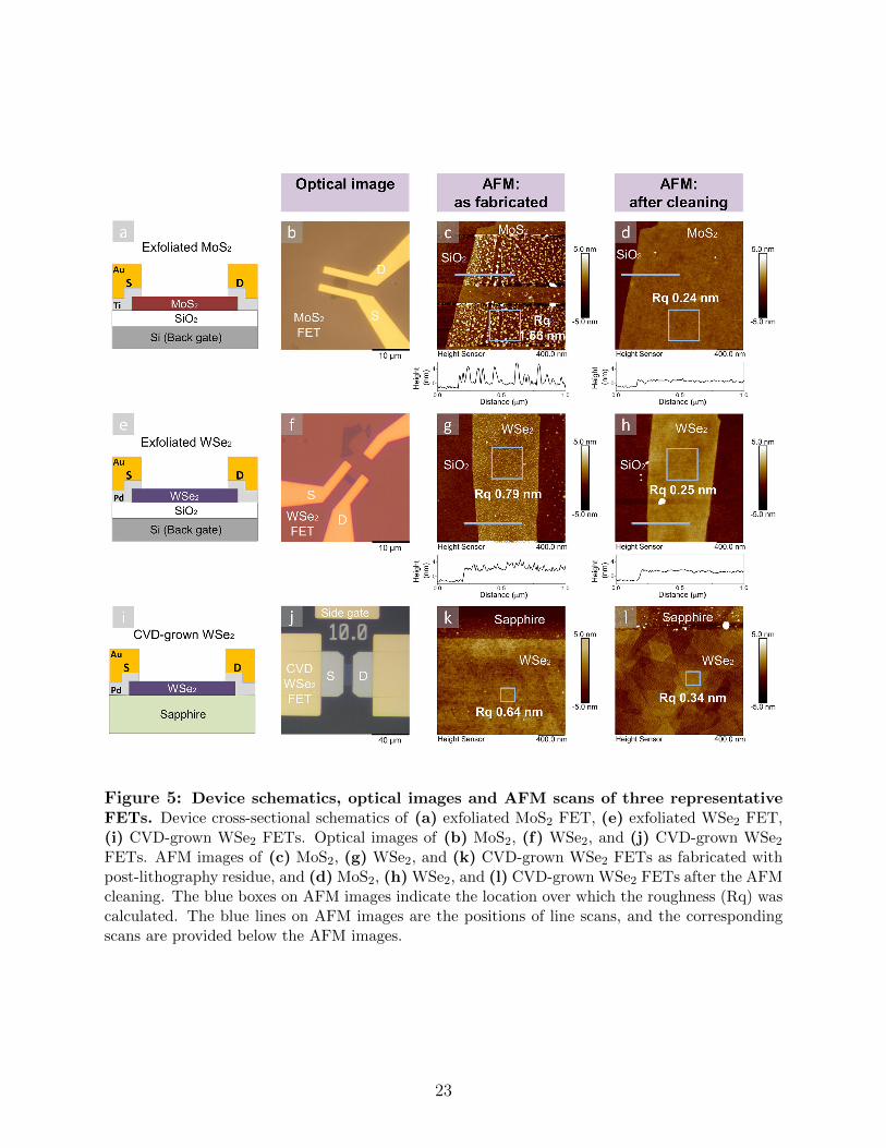
Figure 5: Device schematics, optical images and AFM scans of three representativeFETs. Device cross-sectional schematics of (a) exfoliated MoS2 FET, (e) exfoliated WSe2 FET,(i) CVD-grown WSe2 FETs. Optical images of (b) MoS2, (f) WSe2, and (j) CVD-grown WSe2
FETs. AFM images of (c) MoS2, (g) WSe2, and (k) CVD-grown WSe2 FETs as fabricated withpost-lithography residue, and (d) MoS2, (h) WSe2, and (l) CVD-grown WSe2 FETs after the AFMcleaning. The blue boxes on AFM images indicate the location over which the roughness (Rq) wascalculated. The blue lines on AFM images are the positions of line scans, and the correspondingscans are provided below the AFM images.
23

2.3 Electrical Measurements on Back-gated WSe2 FETs
Before moving on to EDL gating, back-gated FETs without electrolytes were first mea-
sured to learn how the residue and the AFM cleaning process may affect the intrinsic electrical
properties of the 2D materials (e.g., if the mechanical AFM force during the AFM scanning is
too strong, mechanical damage such as small pinholes may be introduced which will degrade
channel conductivity). And if the cleaning process is non-destructive, then it is important
to quantify the improvement after removing PMMA residue on the electrical characteristics
such as threshold voltage and electron mobility. It is also instructive to compare the effect
of AFM contact mode cleaning to vacuum annealing — one of the most commonly used
methods to remove surface residue. [100,103,104]
Therefore, back-gated WSe2 FETs were first fabricated from exfoliated flakes, and then
annealed in vacuum (400 K, 2 × 10⁻⁶ Torr, 4 h), and lastly cleaned by AFM contact mode,
with topology and transfer characteristics measured after each step. The results of one WSe2
FET are shown in Figure 6. For this device, the maximum drain current (ID) at VBG = +30
V increases by 27% from 0.26 to 0.33 µA after vacuum anneal, and further increases by 48%
to 0.49 µA after AFM cleaning. The AFM images (insets of Figure 6) indicate that PMMA
residue was not fully removed by vacuum anneal at 400 K but was successfully removed
after AFM cleaning. The surface roughness (Rq) decreases slightly from 1.22 ± 0.03 nm
to 1.11 ± 0.03 nm after vacuum anneal, but decreases significantly to 0.33 ± 0.04 nm after
AFM cleaning. Based on the AFM images and the electrical data, the improvement in the
maximum current after vacuum anneal is more likely the result of improved contact between
the metal and the semiconductor, [112] rather than the removal of PMMA residue from
channel. In contrast, the improvement in the electrical characteristics after AFM cleaning
can be directly attributed to the removal of PMMA. These results show that AFM contact
mode cleaning is more effective than vacuum annealing in removing PMMA residue.
Six additional back-gated WSe2 FETs (flake thickness ∼ 3 - 9 nm) were measured before
and after the AFM cleaning to quantify the effect of PMMA residue on the electrical prop-
erties. The results are summarized in Table 1. The threshold voltage (Vth) moves toward
negative VBG after cleaning (average ∆Vth = -3 V). A negative (n-type) threshold voltage
24
Figure 6: Transfer characteristics and AFM images of a back-gated WSe2 FET atthree states. As fabricated (black line), after vacuum anneal (blue line), and after AFM cleaning(red line). The blue boxes and lines on AFM images are the positions of roughness measurementsand line scans, respectively.
25
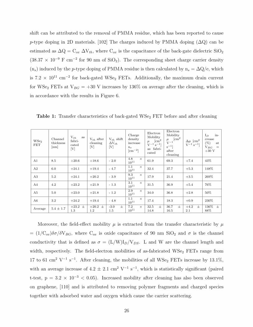
shift can be attributed to the removal of PMMA residue, which has been reported to cause
p-type doping in 2D materials. [102] The charges induced by PMMA doping (∆Q) can be
estimated as ∆Q = Cox ∆Vth, where Cox is the capacitance of the back-gate dielectric SiO2
(38.37 × 10⁻⁹ F cm−2 for 90 nm of SiO2). The corresponding sheet charge carrier density
(ns) induced by the p-type doping of PMMA residue is then calculated by ns = ∆Q/e, which
is 7.2 × 1011 cm−2 for back-gated WSe2 FETs. Additionally, the maximum drain current
for WSe2 FETs at VBG = +30 V increases by 136% on average after the cleaning, which is
in accordance with the results in Figure 6.
Table 1: Transfer characteristics of back-gated WSe2 FET before and after cleaning
WSe2FET
Channelthickness[nm]
Vth asfabri-cated[V]
Vth aftercleaning[V]
Vth shift∆Vth
[V]
Chargedensityincreasens
[cm−2]
ElectronMobilityµ [cm2
V−1 s−1]as fabri-cated
ElectronMobilityµ [cm2
V−1
s−1]aftercleaning
∆µ [cm2
V−1 s−1]
ID in-crease(%) atVBG =+30 V
A1 8.5 +20.6 +18.6 - 2.04.8 ×1011
61.9 69.3 +7.4 43%
A2 6.0 +24.1 +19.4 - 4.71.1 ×1011
32.4 37.7 +5.3 148%
A3 5.2 +24.1 +20.2 - 3.99.3 ×1011
17.9 21.4 +3.5 269%
A4 4.2 +23.2 +21.9 - 1.33.1 ×1011
31.5 36.9 +5.4 76%
A5 5.0 +23.0 +21.8 - 1.22.9 ×1011
34.0 36.8 +2.8 50%
A6 3.2 +24.2 +19.4 - 4.81.1 ×1011
17.4 18.3 +0.9 230%
Average 5.4 ± 1.7+23.2 ±1.3
+20.2 ±1.2
-3.0 ±1.5
7.2 ×10¹¹
32.5 ±14.8
36.7 ±16.5
+4.2 ±2.1
136% ±88%
Moreover, the field-effect mobility µ is extracted from the transfer characteristic by µ
= (1/Cox)δσ/δVBG, where Cox is oxide capacitance of 90 nm SiO2 and σ is the channel
conductivity that is defined as σ = (L/W)ID/VDS. L and W are the channel length and
width, respectively. The field-electron mobilities of as-fabricated WSe2 FETs range from
17 to 61 cm2 V−1 s−1. After cleaning, the mobilities of all WSe2 FETs increase by 13.1%,
with an average increase of 4.2 ± 2.1 cm2 V−1 s−1, which is statistically significant (paired
t-test, p = 3.2 × 10⁻³ < 0.05). Increased mobility after cleaning has also been observed
on graphene, [110] and is attributed to removing polymer fragments and charged species
together with adsorbed water and oxygen which cause the carrier scattering.
26

Regardless, the combination of AFM, Raman, and electrical measurements prove that
the AFM cleaning technique is non-destructive, and the polymer residue is found as a p-
dopant, causing unwanted threshold voltage shift (Vth) and degrading the mobility and
maximum current. Therefore, removing the residue is necessary to restore the intrinsic
electrical properties of WSe2 and other TMDs (more details in our paper [113]).
2.4 Effect of Polymer Residue on EDL-gated CVD-grown WSe2 FETs
To investigate the impact of polymer residue on EDL gating, a uniform CVD-grown
epitaxial WSe2 was used, because EDL gating is commonly used for CVD grown 2D crystals
that cannot be backgated due to insulating substrates such as sapphire. In addition, the CVD
grown sample can minimize the device-to-device variation. Therefore, FETs were fabricated
on CVD-grown WSe2 on sapphire and gated using a polyethylene oxide (PEO)76:CsClO4 as
the electrolyte.
Schematics of the EDL-gated WSe2 FET cleaning treatments are shown in Figure 7
(a). The transfer characteristics of the uncleaned samples are shown as dotted lines (labeled
as 1st scan) in Figure 7 (b) – (e). Note that the data is shown on a linear scale in Figure
7 (b) and (c) and on a log scale in (d) and (e). The FETs share a similar threshold voltage,
Vth ∼ 2.5 V, and maximum currents ranging from 0.9 - 6.2 µA at VG = 4 V.
To determine the impact of polymer residue, the electrolyte was removed by acetonitrile
to expose the WSe2 channel (Figure 7 (a)), and then cleaned with contact-mode AFM. After
cleaning, the electrolyte was re-deposited, and transfer characteristics were measured for
a second time shown as solid lines (i.e. 2nd scan) in Figure 7 (b) and (d). To isolate any
contribution caused by the removal and re-deposition of the electrolyte, we conducted control
experiments where the electrolyte was simply removed with acetonitrile and re-deposited
without AFM cleaning (see also Appendix section B.1.4). That is, the samples experienced
identical electrolyte treatment, but without removing the polymer residue. The remeasured
transfer curves of the control FETs without removing polymer residue are shown as solid
lines in Figure 7 (c) and (e).
27

Figure 7: Transfer characteristics of top-gated CVD WSe2 FETs with PEO:CsClO4
electrolyte. (a) Schematics of control experiments with the sequence of transfer characteristics,removal and re-deposition of electrolyte, and AFM cleaning. Transfer curves of CVD-grown WSe2
as fabricated with electrolyte (dotted line) and after cleaning polymer residue (solid line) are shownin (b) linear scale and in (d) log scale. The control FETs after re-depositing electrolyte withoutAFM cleaning (solid line) are shown in in (c) linear scale and in (e) log scale. L1-L5 (M1-M5)correspond to six different devices with (without) AFM cleaning, respectively.
28
Similar as backgated devices, after removing polymer residue (solid lines in Figure 7 (b)
and (d)), all five FETs exhibit a negative threshold voltage shift (∆Vth = -0.7 ± 0.2 V),
corresponding to a charge density change of about 4.5 × 1012 cm−2, indicating again that the
residue is p-dopant. The mobility increases by 1.7 ± 0.2 cm2 V−1 s−1 after polymer residue
removal, which is similar to the back-gated WSe2 FETs discussed above. More importantly,
the maximum drain current after cleaning increases by 247% on average. In other words, the
presence of the residue on CVD WSe2 before cleaning degrades the maximum current in EDL
gating by ∼ 60%. For the control FETs without cleaning (Figure 7 (c) and (e)), however,
there is no statistically significant difference in the threshold voltage shift or maximum
drain current between the measurements after each of the two electrolyte depositions. This
suggests that the removal and re-deposition of polymer electrolyte will not cause irreversible
change to the channel material, and the consistent trend of negative threshold voltage shift
and maximum drain current increase after cleaning should be attributed to the removal of
the polymer residue.
The improved performance (i.e. 247% increase in maximum current) after cleaning comes
from two portions: 1) improved intrinsic properties (i.e. less p-doping and increased mobility)
of the channel; 2) ions achieving a closer proximity to the channel after the cleaning. If
assuming all the improvement is from the change by doping (∆Vth) and mobility (µ), the
maximum current can only increase by 97%, which is calculated by ID = µ(W/L) CEDL(VG –
Vth)VDS, where CEDL is the EDL capacitance (∼ 1 × 10⁻⁶ F cm−2 for PEO:CsClO4 polymer
electrolyte). This is less than half of the observed the increase (247%), and therefore, the
improvement should be attributed more to the closer ion to channel proximity.
These results suggest that to achieve the highest possible field-effect modulation with
EDL gating, it is important to remove the polymer residue at the channel surface using a
non-destructive method such as AFM contact mode cleaning.
29

2.5 Conclusion
Successful removal of post-lithography polymer residue using contact mode AFM has
been demonstrated on TMDs like WSe2 and confirmed by AFM topology measurements
and Raman spectroscopy. By comparing the electrical device performance before and after
cleaning, the residue remaining on the channel after the lithography process is confirmed to
be a p-dopant and its removal can improve channel conductivity, mobility, and charge density
of FETs. More importantly, the increase in maximum current for EDL-gated WSe2 FETs
suggests that removal of residue by AFM provides closer access for the ions to reach the
surface of the channel, thereby increasing the EDL gate capacitance. While this approach
is not scalable in its current form, AFM cleaning is especially useful for 2D EDLTs where
a near molecularly clean surface is required (e.g., monolayer electrolyte gated EDLTs to be
discussed in the next Chapter), and for EDL gating to achieve the best possible electrostatic
gate control. Another advantage of AFM cleaning from a scientific standpoint is the ability
to isolate contributions from a nanometer-thin soft layer, if it can be scratched away, in well-
defined locations on the device (e.g., channel vs contacts), which is potentially beneficial for
benchtop research of novel functional organic coatings for electronics.
30
3.0 Molecularly Thin Electrolyte for All Solid-State Non-volatile Two-
Dimensional Crystal Memory
Published in: Jierui Liang, Ke Xu, Maokun Wu, Benjamin M. Hunt, Wei Hua Wang,
KyeongjaeCho, and Susan K. Fullerton-Shirey (2019). “Molecularly Thin Electrolyte for All
Solid-State Non-volatile Two-Dimensional Crystal Memory”, Nano Letters, 19(12), 8911-
891912.
3.1 Motivation
3.1.1 1T Non-volatile Memory
The most popular non-volatile memory (NVM) is floating-gate flash memory (e.g., NAND
and NOR Flash). [114,115] Non-volatile refers to that the memory cell can still hold its state
without the electric field. Flash uses a one-transistor (1T) cell structure where a field-effect
transistor (FET) serves both as the cell selector and the storage node. The 1T architec-
ture exhibits better scalability and more simple integration than the one-transistor, one
capacitor (1T1C) structure and the one-transistor, one-resistor (1T1R) used in, for example,
dynamic random-access memory (DRAM) and resistive random-access memory (ReRAM),
respectively. [115] Compared to Flash memory which requires > 10 V to inject and with-
draw electrons from a floating gate, [116] emerging NVMs show promise for energy-efficient
switching, speed, and write endurance. [114–117] But NVMs also encounter challenges to
achieve a 1T architecture, except for ferroelectric FETs (FeFETs) and negative capacitance
FETs (NCFETs). [118–120]
This work is motivated by a new 1T NVM concept that uses ions to program and hold
the polarization state of an electrolyte that is a single molecule thick. The device, referred
to as monolayer electrolyte random access memory (MERAM), resembles the FeFET and
NCFET because it also relies on polarization switching, but offers the potential to integrate
31

the mechanical and electrical properties of two-dimensional (2D) crystals. [26–28,31,121] For
example, in the area of flexible nanoelectronics, MERAM avoids the challenges of growing
oxides on flexible and 2D surfaces that are free of dangling bonds. [12,42,122]
3.1.2 Monolayer Electrolyte Properties and Potentials
The operating mechanism of the MERAM is the modulation of channel resistance by
EDL formed at the interface of the channel and the monolayer electrolyte. [123–126] The
monolayer electrolyte consists of cobalt crown ether phthalocyanine (CoCrPc) with four,
15-crown-5 ethers covalently bonded to a cobalt-substituted phthalocyanine (see Figure 8
(a)). [123–127] Each crown ether (CE) can solvate one Li+. CoCrPc is solution processable
as desired for high-throughput deposition and printable circuits. [2, 6, 123] The deposition
is achieved by simple drop-casting and annealing, and the CoCrPc molecules can form a
flat and ordered array on 2D materials including graphene, [126] MoS2 and WSe2 (see also
Appendix Figure C1 and C2). And it has been demonstrated on highly oriented pyrolytic
graphite (HOPG) that the monolayer of CoCrPc is electrically insulating with a bandgap of
1.34 eV. [123]
Conventional electrolytes such as solid polymer electrolytes and ionic liquids/gels, are not
suitable for NVM, because a gate voltage must be continuously applied to hold the state of the
device, otherwise the ions diffuse away upon the removal of the field and the state is lost. For
the monolayer electrolyte, however, the bistability and non-volatility have been previously
demonstrated by us in graphene FETs, which proves the existence of a switching barrier for
state retention. [126] Density functional theory (DFT) reveals two energetically favorable
configurations when the CE is positioned at the surface of a 2D material: 2D/Li+/CE and
2D/CE/Li+, where Li+ is closer and further from the 2D surface, respectively. [124] Under
an applied electric field normal to the plane of the CE molecules, lithium ions overcome
an energy barrier of 0.3 eV to pass through the cavity of the CEs, switching from one
configuration to another and causing a change in the channel charge density and conductivity.
[125] The height of the energy barrier can be modulated by the strength of the applied field,
suggesting the possibility of sub-volt switching and long retention (i.e., years). [125,126]
32

Moreover, the switching speed depends on the velocity of the ions, which is directly
proportional to the ionic conductivity and the electric field strength, and can be increased by
decreasing the electrolyte thickness. [2,54] Therefore, this new electrolyte with the thickness
scaled to a single molecular layer has the potential for faster switching on the time scale of
micro and nanoseconds. [54,126]
3.2 MERAM Mechanism and Device Fabrication
3.2.1 MERAM Mechanism
The structure of the monolayer electrolyte is shown in Figure 8 (a), and the two
stable configurations of the monolayer electrolyte are schematically illustrated in Figure 8
(b). [124, 125] Under a negative back gate voltage, CE-Li+ is pulled near the 2D channel,
forming an EDL at the interface and doping the channel n−type; this state is denoted as
the On-state where the Li+ is stabilized by both the 2D surface and the CE. The Off-state
is created under positive back gate voltage where CE-Li+ is pushed away from the channel
reducing the n-doping.
To enhance the Off-state stability, a capping layer of h-BN is added such that the Li+
is stabilized by both CE and the h-BN. The degree of stabilization is estimated by DFT
calculations with and without h-BN, shown in Figure 8 (c). The most energically favorable
location of the CE-Li+ complex on WSe2 corresponds to Li+ aligned directly above W atom
(Appendix Figure C3). In the Off-state, Li+ experiences the adsorption energy (Ead) of -3.81
eV by CE and WSe2, which, however, increases to -5.15 eV by adding h-BN. Thus, h-BN
deepens the energy well of the Off-state by an additional -1.35 eV to stabilize Li+ in the
Off-state configuration: WSe2/CE/Li+/h-BN.
33

Figure 8: Monolayer electrolyte structure and mechanism, and fabricated MERAMdevice. (a) Structure of the monolayer electrolyte consisting of CoCrPc and four Li+ with onein each crown-ether ring. (b) Side view of the two energetically favorable configurations of themonolayer electrolyte. These two configurations correspond to the On- and Off-states; note thatthe ether oxygens in the crown are positioned up or down along with the Li+. (c) DFT resultsfor two Off-state configurations: (top) CE-Li+ on WSe2 exposed to vacuum only, and (bottom)CE-Li+ on WSe2 capped by h-BN. (d) MERAM schematic. (e) Sideview of the WSe2/monolayerelectrolyte/h-BN stack. (f) Optical image of the MERAM (false colored, Device 2). (g) AFMscan of the WSe2 FET channel (Device 2) after AFM cleaning (left) and after CoCrPc deposition(right), and corresponding line scans.
34

3.2.2 Device Fabrication
To monitor EDL switching dynamics, MERAMs corresponding to Figure 8 (d) were
fabricated with stacks of WSe2/monolayer electrolyte/h-BN as core structures (a sideview
in Figure 8 (e)). An optical image of one device (false colored) is shown in Figure 8 (f).
Few-layer WSe2 (thickness ∼ 3 – 8 nm) flakes were exfoliated and source/drain contacts were
patterned by electron-beam lithography (EBL) and metal evaporation. EBL resist residue
(∼ 1 – 2 nm) was removed from the WSe2 channel by atomic force microscopy (AFM) in
contact mode. [113] A residue-free WSe2 surface is essential for the MERAM because the
molecular arrangement of the monolayer electrolyte will be disrupted by a few nanometers
of polymer residue. Note that the cleaning does not degrade the maximum current and
mobility of the WSe2 FET (Appendix Figure C5). An AFM image of the cleaned WSe2
FET channel is shown in Figure 8 (g), where the surface roughness is reduced from 0.82 ±
0.02 to 0.23 ± 0.04 nm, as shown in Appendix Figure C5.
A monolayer of CoCrPc is deposited on WSe2 FETs by a drop-casting and annealing
in the Ar-filled glovebox, [123, 126], where the CoCrPc dosage and annealing temperature
are optimized for WSe2 (Appendix Figure C2). AFM scans (also inside the glovebox) of
the WSe2 FET after CoCrPc deposition is shown in Figure 8 (g), with corresponding
line scans at the same channel location before and after deposition. The height difference
corresponds to the thickness of the monolayer electrolyte (∼ 0.5 nm), which is in good
agreement with the previously reported value. [123] In accordance with previous scanning
tunneling spectroscopy (STS) measurements of CoCrPc on HOPG, [123] conductive AFM
confirms that the CoCrPc layer is electrically insulating (Appendix Figure C6). Finally, a
dry flake transfer method was used to encapsulate WSe2/monolayer electrolyte with ∼ 9 –
10 nm of h-BN in a nitrogen-filled glove box. [90, 128]
35

3.3 Transfer Characteristics and Programming Tests
The devices were transferred from the glovebox to a vacuum probe station (pressure ∼
2×10⁻⁶ Torr) in an Ar-filled a stainless-steal suitcase to avoid any interference from ambient;
and were then measured by a Keysight B1500A semiconductor parameter analyzer.
3.3.1 Programming and Sensing Protocol to Monitor the Subthreshold Voltage
(Vs)
The On- and Off-states of the MERAM are monitored by measuring voltage shifts in
the transfer characteristics; the magnitude of the shifts are the most significant in the sub-
threshold region. Because the MERAM has a switching mechanism that is unique compared
to the FeFET or NCFET, the terminology for describing switching of a ferroelectric cannot
be applied here. Thus, to track the On- and Off-states of the MERAM, we calculate the
minimum subthreshold swing (SS) over at least two decades of current, and track the sub-
threshold voltage (Vs) which is defined as the smallest voltage within the SS voltage window
(location of Vs indicated in Figure 9). Details of the SS calculations and corresponding Vs
values are both provided in Table 2 and Appendix section C.6, with Vs highlighted as dots
on the transfer curves.
To track shifts in Vs, the drain current (ID) is measured as a function of back gate voltage
(VBG) before and after programming, as shown in Figure 9 (a). Representative examples of
transfer curves corresponding to the unprogrammed condition, and two programmed states
of the monolayer electrolyte without the h-BN capping layer are shown in Figure 9 (b). The
first transfer scan is a double sweep to record the original location of Vs in an unprogrammed
device (black curve, Figure 9 (b)). A positive programming voltage (VBG = +30 V) is applied
to push Li+ away from the WSe2 channel surface, and a single ID-VBG sweep is initiated
immediately after programming to capture the positive (p−type) shift in Vs (red curve,
Figure 9 (b)). Last, a negative programming voltage (VBG = - 30 V) is applied to attract
Li+ to the channel surface and induce electrons in WSe2. The single ID-VBG sweep shows
an n−type shift of the Vs (blue curve, Figure 9 (b)).
36

Figure 9: MERAM transfer characteristics and programming tests (a) Programmingand sensing protocol: (1) initial double transfer sweep (VDS = 20 mV, 7.5 V/s) to monitor Vs andhysteresis in the unprogrammed condition, (2) programming the device Off with VBG = +30 V,(3) single sweep (7.5 V/s) to sense Vs (red dot on the curve), (4) programming the device on withVBG= -30 V, and (5) another single sweep to sense Vs (blue dot on the curve). Note that Vs is thesub-threshold voltage, which is distinct from the threshold voltage, Vth, which is used for chargedensity calculations. (b) Resulting transfer scans following the programming and sensing protocolfor WSe2/CE-Li+ (without h-BN, Device 1). (c) Transfer curves for the same device before (blackdash) and after (yellow lines and dash) programming with only the monolayer electrolyte, and after(green lines and dash) programming with the monolayer electrolyte/h-BN stack. For comparison,the additional leakage current (ID
leak) after adding h-BN is subtracted on the right y axis, with theoriginal data shown in the inset. Three single sweeps were taken after each programming (7.5 V/s).The magnitude of threshold voltage shift is highlighted by shading the opening of the memorywindow. (d) The potential energy of Li+ in the monolayer electrolyte in the Off-state at 0 V ofthe applied field is schematically illustrated for the stacks without h-BN (i.e., exposed to vacuum)and with h-BN (top and bottom, respectively).
37

3.3.2 On- and Off-state Detected Before and After Adding Monolayer Elec-
trolyte
To distinguish shifts in the transfer curves due to the monolayer electrolyte switching from
the charge trapping/detrapping at the WSe2/SiO2 interface, [129, 130] programming tests
were conducted on the same WSe2 FET before electrolyte deposition (Appendix Figure C7).
The hysteresis in the double-sweep transfer characteristics of bare FETs are approximately
equal before and after “programming.” That is, the change in Vs (∆Vs) equals ∼ 6.0 V before
and after programming (Table 2), showing that the bare FET is unaffected by programming.
With the monolayer electrolyte deposited on the channel, ∆Vs increases by a factor of
2.4 to ∼14 V (Figure 9 (c), yellow lines and dash, three repeats). A shift of Vs to more
positive (negative) voltages corresponds to the Off -(On) states of the electrolyte. The state
switching results in a charge density change (∆ns) of 1.8 × 1012 cm−2 (estimated from the
threshold voltage shift, ∆Vth, Table 2), which is 419% of the change induced by charge
trapping/de-trapping (∆ns = 4.3 × 1011 cm−2) on the bare FET.
Table 2: Summary of transfer characteristics of the WSe2 FET
WSe2FET
SS (off)[V/dec]
SS(on)[V/dec]
Vs(off)[V]
Vs(on)[V]
Vsshift∆Vth
[V]
Vth afterpositiveprogram-ming[V]
Vth afternegativeprogram-ming[V]
Thresholdvoltageshift∆Vth [V]
Chargedensitychange ns
[cm−2]
DraincurrentID ratioat VBG =0 V
BareFET
3.1 5.5 - 2.3 - 8.3 6.0 + 19.1 + 17.3 1.8 4.3 × 10¹¹ 11.6
AddCoCrPc+ Li+
4.5 4.8 - 2.0 - 16.2 14.2 + 16.5 + 8.9 7.6 1.8 × 10¹² 84.4
Addh-BNcappinglayer
1.0 3.6 + 9.0 - 18.0 27.0 + 12.6 + 2.1 10.5 2.5 × 10¹² 2.2 × 10⁴
3.3.3 Improved On- and Off-state After Adding h-BN
While the increased transfer curve shift (i.e., larger ∆Vs) with the monolayer electrolyte
alone is encouraging, the On/Off ratio at a zero read voltage (i.e. VBG = 0 V) is quite
small (< 102). The On/Off ratio could be increased by having a more stable Off-state with
38

a more p−type shifted Vs after positive programming. As mentioned above in Figure 8
(c), DFT calculations indicate that a cap of h-BN will deepen the energy well of the Off-
state in the absence of an applied electric field (Figure 9 (d) and Appendix section C.3).
Therefore, the device is capped with h-BN (∼ 9 nm, 19 layers), and the transfer curves after
programming are shown in Figure 9 (c) green lines for On-state, green dash for Off, three
repeats). The ∆Vs after positive/negative programming is ∼ 27 V with the addition of
h-BN. The corresponding carrier density change also increased to 2.5 × 1012 cm−2, which is
139% of that with only monolayer electrolyte (yellow lines and dash), and 580% of the change
induced by charge trapping/de-trapping on bare FET. More importantly, after adding h-BN,
the FET is completely turned off at VBG = +9 V after the positive programming, resulting
in a lower Off-state current at VBG = 0 V. The On-state current also increased due to the
improved sub-threshold swing (from ∼ 4.8 V/dec before to 3.6 V/dec after adding h-BN).
Overall a larger On/Off ratio (∼2.2 × 10⁴) is achieved for the MERAM capped with h-BN
(read at VBG = 0 V, Table 2).
Furthermore, bistability from the monolayer electrolyte was also observed on back-gated
MoS2 FETs (Appendix Figure C10), demonstrating that the observations made here extend
to other TMDs.
3.4 Program/erase Pulse Tests: Endurance and Retention
The dynamic characteristics of the MERAM and the stability of states are studied
through a series of pulses tests. First, the MERAM was dynamically and repeatedly pro-
grammed and erased by pulsing VBG ± 30 V with 1 s pulse width (Figure 10 (a)). After
each program/erase pulse, the device was read at VBG = 0 V for 10 s. In Figure 10 (a),
the readout ID of seven consecutive program/erase cycles are shown for the MERAM with
and without h-BN. Without h-BN, while two distinct values of ID are detectable after each
program/erase cycle, the On-state current is only ∼1.1 times larger than the Off-state. In
contrast, when h-BN is added, the On-state is nearly 105 times larger than the Off-state,
showing that the h-BN stabilizes the Off-state.
39

Figure 10: Program/erase and retention measurements. (a) ID after alternating pro-gram/erase voltage pulses on Device 1. Top: program (VBG = -30 V, green)/erase (VBG = +30V, grey) voltage profile with voltage applied for 1 second and readout for 10 seconds at VBG =0V; VDS = 500 mV. Bottom: corresponding readout current, ID, without and with h-BN cappinglayer. (b) Program/erase endurance test. 1000 cycles of program/erase with pulse width of 1 sand readout time of 10 s. (c) Retention test. Program/erase with 1 s pulse and ID monitored for6 hours. The Off-state current increased in the first five hours then remain stable. Inset schematicshow the predicted relaxation of Li+ (new location indicated by dashed line) when the back gateis grounded, providing a possible explanation for the increase in the off current with time.
40

MERAM endurance was evaluated by repeating the program/erase pulse tests for 1000
cycles (Figure 10 (b)). The On/Off ratio is maintained > 104 throughout the measure-
ments, indicating that the On/Off states are repeatable and consistent, and the bistability
persists at least to 1000 cycles. An identical 1000 cycle endurance test was performed on the
MERAM without h-BN, which also shows the persistence of two distinct resistance states
but with a smaller On/Off ratio (Appendix Figure C11).
To evaluate the retention of the two states after program/erase, a six-hour retention
test was conducted as shown in Figure 10 (c). The device was programmed/erased for
1 s, the back gate then grounded, and ID monitored for six hours. The initial On/Off
ratio is ∼ 105 which decreased to ∼ 103 during the initial 270 min, and then stayed almost
constant afterwards. The decay is mostly due to the gradual increase of the Off-state current,
which was also observed previously on monolayer electrolyte-coated graphene FETs. This
observation was attributed to the relaxation of Li+ after removing the field. [126] That is,
the ion is held more closely to the 2D surface when the field is applied, but when the back
gate is grounded, the ion will relax back to an energetically favorable location that is further
from the surface (inset, Figure 10(c)).
41

3.5 Switching Speed and Voltage
In the measurements described above, ± 30 V programming voltages and one second
to five-minute programming times were used; however, these values were not optimized and
therefore do not reflect any intrinsic limitations. To investigate how the On/Off ratio varies
with voltage pulse width, we repeated the program/erase pulse test using ± 20 V program
voltage and with pulse widths ranging from 10 s to 1 ms (the limit of our equipment).
Figure 11 (a) shows the ID of the On- and Off-states as a function of pulse width. The
On and Off currents remain constant with ratio of nearly 105 from a pulse width between
0.3 and 10 s. For pulse widths < 100 ms, the On/Off ratio decreases, and at 1 ms it is
reduced to 3.4 × 10². Note that although not accessible with the existing instrumentation,
the switching speed of the monolayer electrolyte is predicted to be in nanosecond timescale
by DFT calculations. [125]
Figure 11: Program/erase measurements as a function of pulse width and voltage.(a) (Device 1) ID of the On- and Off-states in response to program/erase voltage pulses where thepulse width is varied from 1 ms to 1 s. (b) (Device 2) ID of the On- and Off-states with varyingthe program and erase voltages from ± 5 to ± 30 V (absolute values of ID plotted). For both (a)and (b), data at each point are averaged over 12 program/erase cycles with the error bar indicatingone standard deviation from the mean.
To study the relationship between On/Off ratio and field required to switch the device,
the On- and Off-states are monitored while varying the VBG (1 s pulse width, Figure 11
(b)). Note that the results in Figure 11 (b) is for Device 2. For this device, program/erase
42

at ± 5 V is insufficient to switch the MERAM in the current backgated device geometry.
Starting from ± 7 V the two states become distinguishable, and the On/Off ratio continues
to enlarge with the increase of program/erase voltage up to ± 13 V. The increase of On/Off
ratio mostly comes from the decrease of Off-state current. In fact, further increasing the
program voltage from 7 V to 30 V leads to a relatively small increase of On-state ID from
0.43 µA/µm to 0.80 µA/µm. However, increase erase voltage from 7 V to 30 V caused the
Off-state ID to decrease from 0.23 µA/µm to 2.3 × 10⁻⁶ µA/µm, which is a change of five
orders of magnitude. We also noticed that once the magnitude of the erase voltage exceeds
13 V, the Off-state current stays almost constant. These results are very interesting because
it confirms the existence of an energy barrier − the minimal energy required to push Li+
through the diffusion barrier and fully switch the MERAM from one state to the other.
Note that in our backgated geometry, the electric field strength that reaches the electrolyte
is smaller than would be achieved in a top gated geometry due to 90 nm of back gate oxide
and the field-screening caused by the WSe2 channel. Therefore, we expect a top-gated device
to reduce the required switching voltage.
3.6 Conclusion
In conclusion, we have demonstrated a new, 1T NVM concept - MERAM based on EDL
gating of a WSe2/monolayer electrolyte/h-BN stack. The custom-designed monolayer elec-
trolyte consists of cobalt crown ether phthalocyanine and lithium ions, and has a switching
barrier required for bistability. By capping the monolayer electrolyte with h-BN, bistability
is significantly improved due to the stablizing Off -state of the MERAM as predicted by DFT
calculations. The MERAM retains a stable On/Off ratio > 104 at a read voltage of VBG =
0 V for at least 1000 cycles of programming/erase, and state retention for at least six hours
with On/Off remaining ∼ 102. When the write time approaches 1 ms, the On/Off ratio
remains > 102, showing that the MERAM can respond on time scales similar to existing
flash memory. The data suggest that faster switching times and lower switching voltages
could be feasible by top gating.
43

4.0 Using a Single-ion Conductor to Induce Strain in 2D EDLTs for the
Semiconductor-to-metal Transition
Published in: Ke Xu, Jierui Liang, Aaron Woeppel, M. Eli Bostian, Hangjun Ding,
Zhongmou Chao, James R. McKone, Eric J. Beckman, and Susan K. Fullerton-Shirey (2019).
“Electric Double-Layer Gating of Two-Dimensional Field-Effect Transistors Using a Single-
Ion Conductor.” ACS applied materials & interfaces, 11(39), 35879-35887.
4.1 Motivation
4.1.1 Strain Engineering in 2D Crystals
2D crystals have the unique capacity to withstand extreme strain. The electrical and
optical properties of 2D crystals are strongly influenced by strain and therefore potentially
useful for electronic and optoelectronic applications. For example, strain can transform 2D
semiconductors from an indirect band gap to a direct band gap material with enhanced
radiative efficiencies, [131] or tune the emission wavelength. [132, 133] In particular, under
sufficient strain, TMDs such as Mo- and W-dichalcogenides are predicted to undergo a
complete change of phase from the semiconducting 2H phase to the metallic 1T’ phase.
[134, 135] Experimentally, phase transitions in MoTe2 have been demonstrated by inducing
local strain using an AFM tip [136] and more recently, by inducing global strain via an
electric field applied to a ferroelectric substrate in contact with MoTe2. [35] Dynamically
tuning the band gap in 2D crystals is not only fundamentally interesting but could be useful
for applications such as low-voltage transistors [137] and flexible electronics. [12] For these
applications, it would be desirable to create a gate dielectric that can achieve large gate
capacitance (e.g., 1 - 4 µF cm−2, [20] and induce strain locally via field effect.
44
4.1.2 Inducing Strain in 2D EDLTs by a Single-ion Conductor
To induce the strain for the phase transition, we propose a new concept of single-ion
conductor-gated EDLT on TMDs. A single-ion conductor, or ionomer, is a type of ionic
electroactive polymer (EAP) that deforms in the presence of an applied electric field. The
anions in the single-ion conductor are covalently bound to the backbone of the polymer,
leaving only the cations free to move in response to an applied field. When polarized, an
EDL consisting of densely packed cations is created at the negative electrode, but there is no
corresponding anionic EDL at the positive electrode. In response to this imbalance, one side
of the single-ion conductor (near the negative electrode) undergoes longitudinal expansion.
The mechanism to induce strain using single-ion conductors has been well investigated for
ionic polymer metal composites (IPMCs), which are useful for biomimetic actuators and
artificial muscles. [138] In electronics, single-ion conductors have been used previously to
gate organic transistors [77,139,140] where the motivation for immobilizing one ion over the
other was to avoid electrochemical reactions within the organic channel. To our knowledge,
there has been no report directly comparing single- and dual-ion conductors with similar
chemistries in the same 2D crystal FETs or distinguishing the electrostatic gating effects
between cationic EDLs and cationic depletion layers on 2D crystals.
This work aims to show the first demonstration of a single-ion conductor multilayer 2D
crystal EDLT and to lay the groundwork for demonstrating flexible 2D FETs with new
functionalities induced by an EDL via strain. Experimentally, an ionically functionalized
polyester (synthesized by Prof. Eric Beckman’s group, via the condensation of poly(ethylene
glycol) oligomers with dimethyl 5-sulfoisoph-thalate salt [141]) to electrostatically gate both
graphene and MoTe2 FETs. To reveal the charge density imbalance in the single-ion con-
ductor, the EDL gating using the single-ion conductor will be compared to the back gating
through SiO2 as well as the EDL gating using dual-ion conductors on the same FETs. Ex-
perimental results will be also compared with finite element modeling using COMSOL to
provide insight of the single-ion conductor gating.
45

4.2 Mechanism of EDL Gating Using a Single-ion Conductor
The EDL-gated multilayer 2D crystal FETs use a side-gate geometry, as shown in Fig-
ure 12 (a). Graphene and MoTe2 were mechanically exfoliated onto a p-doped Si substrate
with 90 nm SiO2 (used as a back gate). The source/drain and gate contacts (Ti/Au) were
patterned by electron beam lithography (EBL) with the side gate located 10 µm away
from the channel. The solid-state single-ion conductor is poly(ethylene glycol benzene-
1,3-dicarboxylate-5-sulfoisophthalate lithium), abbreviated as PE400-Li, and the solid-state
dual-ion conductor is poly(ethylene oxide), abbreviated as (PEO):CsClO4. The chemical
structures of the dual- and single-ion conductors are similar and shown in Figure 12 (b).
The PE400-Li is a polyester with each repeat unit consisting of the ionic group, namely,
dicarboxylic 5-sulfoisophthalate, and a spacer of poly(ethylene glycol) 400, which provides
the same repeat unit as PEO. [141] Unlike PEO:CsClO4 where the anion, ClO−4 , is free to
respond to the applied field, the negatively charged functional group (SO−3 ) in PE400-Li is
covalently bound to the polymer backbone, while the cation Li+ is free to move under an
applied field. The ether oxygen to cation molar ratios are 76:1 for the dual-ion conductors
and 9:1 for the single-ion conductors. Differential scanning calorimetry (DSC) shows that
the single-ion conductor has a markedly higher glass transition temperature (Tg = 14.5 ◦C)
than the PEO:CsClO4 electrolyte (Tg = -31.5 ◦C) (Appendix Figure D1), which is consistent
with the single-ion conductor having a larger salt concentration. [52] This difference in Tg
suggests that the single-ion conductor will have lower ionic conductivity than the dual-ion
conductor.
46

Figure 12: Mechanism of a single-ion conductor gated EDLT. (a) Schematic of a 2D crys-tal FET (either graphene or MoTe2) that can be operated by using a back gate or a single/dual-ionconductor using a metal side gate. (b) Chemical structures of the dual- and single-ion conduc-tors: PEO:CsClO4 (top row) and the ionically functionalized polyester (PE400-Li) (bottom row),respectively. Anions are shaded in red and cations are shaded in blue. Schematics of the (c) dual-ion conducting and (d) single-ion conducting FETs under two polarities. In the single-ion case,only cations are mobile while the anions are bound to the polymer backbone and therefore fixed.This immobility leads to cationic depletion regions (shaded in pink) at either the gate/single-ionconductor (VG > 0) or single-ion conductor/semiconductor interface (VG < 0), depending on thepolarity of the applied field.
47
When no voltage is applied, cations and anions are homogeneously distributed through-
out the electrolyte for both the single- or dual-ion conductors. The steady-state locations
of cations and anions under VG > 0 and VG < 0 are illustrated in Figure 12 (c,d) for
the dual-ion conductor and single-ion conductor, respectively. When a positive gate bias is
applied to a dual-ion conductor (Figure 12 (c), left), cations (Cs+) are driven to the channel
where they induce image charges (in this case, image charges are electrons) forming a cationic
EDL at the channel/electrolyte interface. An analogous anionic EDL will form as anions
(ClO−4 ) accumulating at the electrolyte/gate interface. When the polarity of the applied
bias is reversed, an anionic EDL forms at the channel and a cationic EDL forms at the gate
(Figure 12 (c), right).
For a single-ion conductor, shown in Figure 12 (d), a positive gate bias does not result
in an anionic EDL at the gate/electrolyte interface; instead, there exists a cationic depletion
layer (Figure 12 (d), left). When the polarity is reversed, the cation depletion layer forms at
the channel/electrolyte interface (Figure 12 (d), right). Crucially, the negative charge stored
by anions in the cationic depletion layer equals the positive charge in the cationic EDL,
while the volumetric charge density of anions in the depletion layer is fixed and smaller than
the volumetric charge density of the closely packed cations in the EDL. Thus, the depletion
layer requires larger thickness (or volume when considered in 3D) than the EDL to store
the same amount of charge. The presence of such a thick depletion layer also suggests that
the device geometry will affect the interface capacitance of devices gated by the single-ion
conductor because the depletion layer thicknesses will depend on the areas of both channel
and gate. In contrast, the EDL thickness is always the distance between the ion and channel
surface (i.e., < 1 nm) and is independent of the channel size. Nonetheless, a depletion layer,
albeit significantly thicker than the EDL, will still serve as a capacitor just with a smaller
capacitance density than the EDL. [77]
48

4.2.1 COMSOL Multiphysics Simulations of Single-ion Conductor Gating
To understand how the ion and voltage distributions differ under an applied voltage
in a single-ion conductor compared to a dual-ion conductor and how their distributions
will change with respect to the device geometry, my labmate Aaron Woeppel modeled ion
transport using finite element analysis via COMSOL Multiphysics. A modified Nernst-
Planck-Poisson system of equations [142, 143] was solved for both single-ion and dual-ion
conductors in two parallel plate capacitor geometries: one with electrodes of equivalent
sized and another where one electrode is 10 times larger than the other (i.e., modeling the
FET scenario where the channel is smaller than the gate). Figure 13 shows the resulting
steady-state voltage distributions for applied voltages of equal and opposite polarities; the
voltage is applied to the right electrode with the left electrode grounded. We first consider
the scenarios where the electrodes have equivalent size (Figure 13 (a,b)). In the case of a
dual-ion conductor, anions and cations accumulate adjacent to their respective electrodes,
producing EDLs of equal charge and thickness. The result is a symmetric voltage profile
across the thickness of the capacitor where half of the applied voltage drops on each EDL
regardless of the voltage polarity (Figure 13 (a)), and the voltage drop through the bulk of
the electrolyte is nearly zero. In the case of the single-ion conductor, the majority of the
voltage always drops across the depletion layer, regardless of polarity. The voltage drop is
approximately 3 times larger across the depletion layer than the EDL, and the depletion layer
is also approximately 3 times thicker than the EDL (Figure 13 (b)).This result is sensible
when considering conservation of charge across the parallel plate capacitor. Charge (Q) is
expressed as Q = VintCint = Vintε0εrA/d, where Vint is the voltage across the interface, Cint
is the interface capacitance, A is the area of channel, and d is the thickness of the interface
capacitive layer (i.e., thickness of EDL or the depletion layers). Thus, the thicker depletion
layer has lower interface capacitance and therefore requires a larger voltage drop to balance
the charge.
49

Figure 13: COMSOL Multiphysics simulations of steady-state voltage distributions insingle- and dual-ion conductors during EDL gating. The Steady-state voltage distributionsand the corresponding device schematics showing ion positions for both (a, c) dual-ion and (b, d)single-ion conductors in two parallel plate capacitor geometries: electrodes of equal size (upperrow) and electrodes of unequal size where the right electrode is 10 times larger than left (bottomrow). Note that the schematics are not drawn to scale. Either ±1 V is applied on the right-sideelectrode. Cation and anion layers are highlighted in blue and red, respectively. The anion EDL(dual-ion) or cationic depletion layer (single-ion) thickness differences are illustrated qualitatively.Specifically, for the dual-ion conductor, the anionic EDL layer thickness is similar to the cationicEDL layer thickness; while for the single-ion conductor, the cationic depletion layer thickness islarger and influenced by the electrode size. The steady-state potential distributions under positiveand negative voltages are highlighted in the red solid and dashed blue lines, respectively.
50

For the scenario of equal sized electrodes discussed above, the voltage distribution across
the single-ion conductor differs from the dual-ion conductor because the depletion region
in a single-ion conductor requires the majority of the voltage drop. However, when the
electrodes are unequal in length, similar to what would exist between the channel and the
gate in a side-gated EDLT geometry, the voltage profiles between the single- and dual-ion
conductors are remarkably similar because the geometry induces the majority of the voltage
drop. Specifically, the length of the left (grounded) electrode decreased to one-tenth of the
right electrode, and for the dual-ion conductor, 90% of the voltage drop across the EDL
occurs adjacent to the shorter electrode, regardless of the voltage polarity (Figure 13 (c)).
The asymmetric voltage drop again results from charge conservation: the shorter electrode
requires a larger voltage drop to compensate for its smaller capacitance. In the case of the
single-ion conductor (Figure 13 (d)), the majority of voltage drop is also adjacent to the
shorter electrode for the reason mentioned above, but the details of the ion and voltage
distributions are more complicated. For V > 0 applied to the longer electrode, ∼ 85% of the
voltage drop is distributed across the ∼ 0.5 nm-thick cationic EDL at the shorter electrode.
When the polarity is reversed to V < 0, almost all of the applied voltage (97%) falls within
the ∼ 1.5 nm-thick depletion layer near the shorter electrode (Figure 13 (d)). This result is
significantly different from Figure 13 (b) where the electrode sizes are equal. To understand
this difference, we focus on the voltage distributions near the grounded electrode only because
the shorter grounded electrode is similar to the channel in the transfer measurements where
VS = 0 V and VDS << VGS (see also Appendix Figure D3). Focusing on the inset of Figure
13 (d), the depletion layer is ∼ 3 times thicker than the EDL even though the voltage drop
is only 14% larger. This occurs because the grounded electrode is 10 times smaller and
requires the majority of the potential drop regardless of the polarity of V. Even though the
depletion layer thickness is 3 times larger, it is not possible for this layer to have 3 times
larger potential drop than the EDL at the same electrode, and therefore, the charge at the
grounded electrode will be lower for V < 0 compared to V > 0. This result suggests that
the single-ion conductor in a side-gated EDLT geometry will exhibit weaker p-type doping
compared to n-type doping.
51

4.3 Single-ion Conductor Gating on Graphene FETs
To test these predictions experimentally, we chose graphene as the first 2D material for
two reasons. First, because it is a semi-metal, graphene is highly conductive and ambipolar
with an intrinsic charge neutrality point at zero gate voltage, making it ideal for sensing
both p- and n-type changes in conductivity. Second, EDL gating of graphene FETs using
a dual-ion conductor has been widely demonstrated, [38, 53] making it straightforward to
benchmark against previously published results.
Graphene FETs with side gate geometry were fabricated by EBL as depicted above
in Figure 12 (a). After device fabrication and before the single-ion conductor deposition,
the channel surface was cleaned using an AFM in contact mode to remove e-beam resist
residue. [113] Preparing a residue-free surface is essential to achieve the maximum gating
effect because the EDL forms within a few nanometers of the surface, similar to the typical
thickness of the EBL residue. [113] Figure 14 (a) shows the AFM images of a graphene
device after AFM cleaning. The root mean square roughness (Rq) of the channel surface
was reduced from ∼ 1.30 nm before cleaning to ∼ 0.37 nm after cleaning, which is close to
the reported value for freshly exfoliated graphene on SiO2 (∼ 0.32 nm). [144] Note that all
Rq are reported for a 400 × 400 nm area. The line scan indicates a flake thickness of 1.5
nm, corresponding to ∼ 5 layers of graphene.
4.3.1 Transfer and Output Characteristics
The transfer characteristics of the graphene FETs (without electrolyte) were first mea-
sured with a back gate (Figure 14 (b), blue line), and the devices show a Dirac point around
VBG = 0 V, suggesting that there is negligible intrinsic doping in the exfoliated flakes. Un-
der VDS = 100 mV, the transfer curve exhibits highly symmetric n- and p-branches with a
current maxima of ∼ 100 µA (25.4 µA/µm) at |VBG | = 30 V. The output characteristics of
the bare graphene FET (Figure 14 (c), blue lines) also indicate that ID is a linear function
of VDS, suggesting good ohmic contact at the source/drain terminals. These results on the
bare graphene FETs are in good agreement with prior reports. [53,145]
52
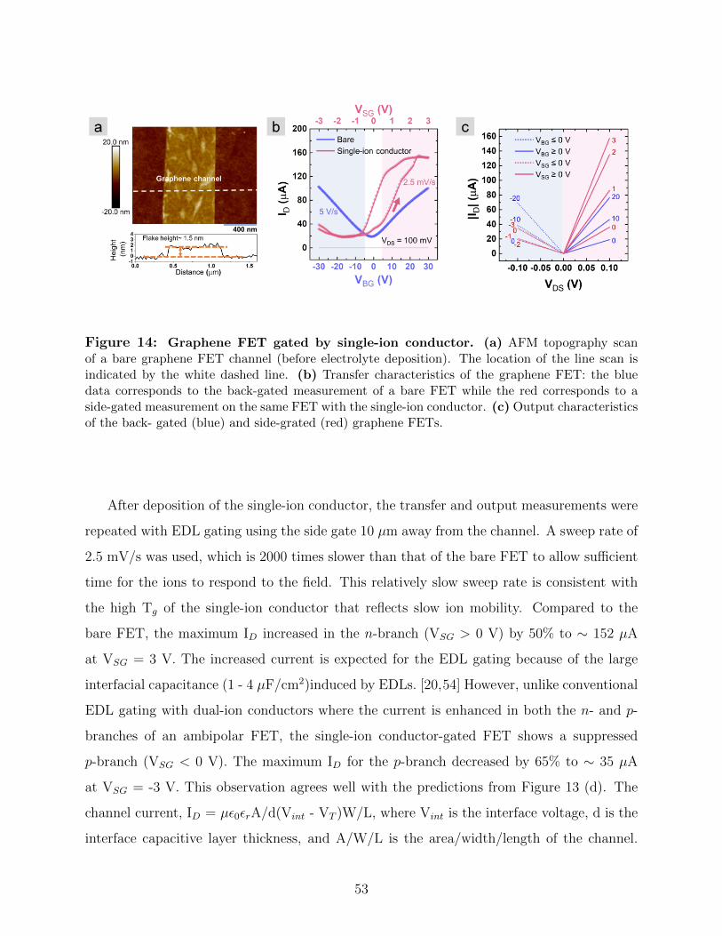
Figure 14: Graphene FET gated by single-ion conductor. (a) AFM topography scanof a bare graphene FET channel (before electrolyte deposition). The location of the line scan isindicated by the white dashed line. (b) Transfer characteristics of the graphene FET: the bluedata corresponds to the back-gated measurement of a bare FET while the red corresponds to aside-gated measurement on the same FET with the single-ion conductor. (c) Output characteristicsof the back- gated (blue) and side-grated (red) graphene FETs.
After deposition of the single-ion conductor, the transfer and output measurements were
repeated with EDL gating using the side gate 10 µm away from the channel. A sweep rate of
2.5 mV/s was used, which is 2000 times slower than that of the bare FET to allow sufficient
time for the ions to respond to the field. This relatively slow sweep rate is consistent with
the high Tg of the single-ion conductor that reflects slow ion mobility. Compared to the
bare FET, the maximum ID increased in the n-branch (VSG > 0 V) by 50% to ∼ 152 µA
at VSG = 3 V. The increased current is expected for the EDL gating because of the large
interfacial capacitance (1 - 4 µF/cm2)induced by EDLs. [20,54] However, unlike conventional
EDL gating with dual-ion conductors where the current is enhanced in both the n- and p-
branches of an ambipolar FET, the single-ion conductor-gated FET shows a suppressed
p-branch (VSG < 0 V). The maximum ID for the p-branch decreased by 65% to ∼ 35 µA
at VSG = -3 V. This observation agrees well with the predictions from Figure 13 (d). The
channel current, ID = µε0εrA/d(Vint - VT )W/L, where Vint is the interface voltage, d is the
interface capacitive layer thickness, and A/W/L is the area/width/length of the channel.
53

When VG is negative (corresponding to the p-branch), the depletion layer thickness next to
the channel is expected to be much larger than the EDL thickness next to the channel when
VG is positive (corresponding to the n-branch). However, we learned from Figure 13 (d)
that the voltage drop across the depletion layer at the short electrode (i.e., channel) is only
slightly larger than that across the EDL; thus, the channel current should be lower in the
p-branch than in the n-branch.
Output characteristics as a function of side gate voltages are shown in Figure 14 (c)
(red lines). Compared with the back-gated data, the maximum ID under positive (negative)
side gate voltages are higher (lower), which is congruent with the transfer characteristics.
Note that the results shown in Figure 14 (c) are double sweeps, including the single-ion
conductor-gated results, and the overlap of the forward and reverse sweeps indicates that
the single-ion conductor gating is stable at each measured gate voltage, as long as adequate
time is provided for the ions to respond to the field.
4.3.2 Comparison Between Single- and Dual-ion Conductor in EDL Gating
Thus far, the electrical characteristics of the single-ion conductor-gated FETs qualita-
tively agree with our predictions; however, it is essential to benchmark the single-ion con-
ductor gating performance against a commonly used dual-ion conductor. To do this, we
removed the single-ion conductor by solvent washing (dimethylformamide, DMF) and AFM
cleaning. After the two-step cleaning process, the root mean square roughness (Rq) of the
graphene channel is close to the value of freshly exfoliated flakes (Appendix Figure D4). [144]
Then, we redeposited a dual-ion conductor, PEO:CsClO4, on the same device and repeated
the transfer measurements. Figure 15 shows the transfer curves for two such FETs (device
1 and 2) with (1) Si/SiO2 back gate (no electrolyte), (2) EDL side gate using the single-
ion conductor, and (3) EDL side gate using the dual-ion polymer electrolyte, PEO:CsClO4.
The solid lines correspond to the forward sweeps, and the dashed lines correspond to the
reverse sweeps. For the transfer curves obtained using PEO:CsClO4 (green), both the n-
and p-branches are clearly observable and show increased current compared to the bare,
back-gated devices. Overall, for the n-branch, EDL gating with either dual- or single-ion
54

conductor shows enhanced on current (∼ 80 and 60% for dual- and single-ion conductors,
respectively) over back gating through SiO2. This improvement is attributed to the larger
EDL capacitance and agrees with previous reports. [20, 54] For the p-branch, the enhance-
ment of On current is again observed for the dual-ion conductor but is suppressed for the
single-ion conductor.
Figure 15: Comparison between single- and dual-ion conductor in EDL gating. (a,b) Transfer characteristics of two graphene FETs. Back-gated bare devices (blue), side-gated withsingle-ion conductor (red), and side-gated with dual-ion conductor (green). Solid and dotted linesindicate scans from negative to positive gate voltages and from positive to negative gate voltages,respectively. Note that the gate voltages were normalized with respected to VDirac to facilitatecomparison between n- and p-branches currents using different gating methods.
The successful ambipolar modulation of the channel current using a dual-ion conductor
indicates that the single-ion conductor did not change the graphene channel in a way that
would prevent hole conduction. This further supports the understanding that suppressed
p-branch current in the single-ion conductor is caused by the cation depletion layer having
weaker gate modulation compared to the EDL. This effect can be captured by modeling
the dynamic response of single- and dual-ion conductors in response to a voltage sweep. A
time-dependent Nernst-Plank-Poisson equation was used with a geometry identical to Figure
13 (c,d). The voltage is applied to the right electrode, and the ion distribution near the left
55
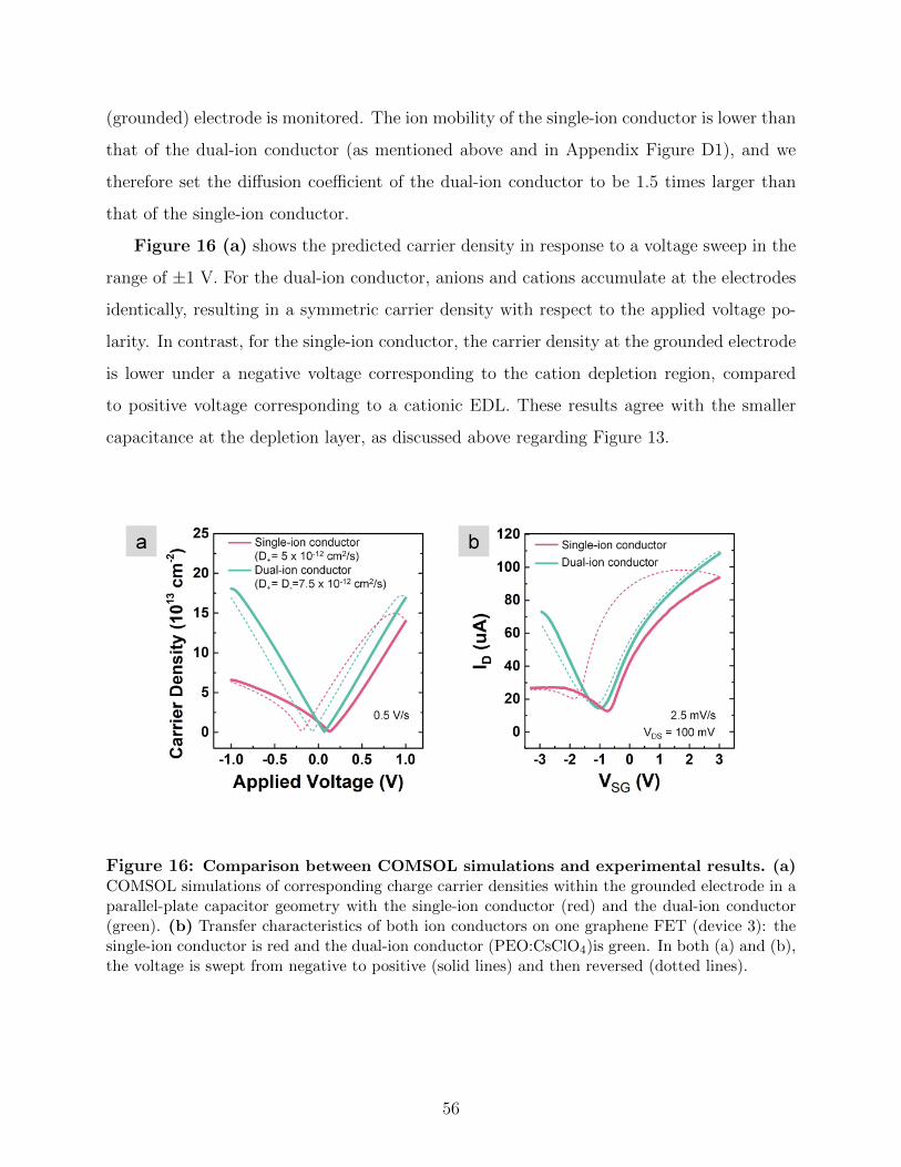
(grounded) electrode is monitored. The ion mobility of the single-ion conductor is lower than
that of the dual-ion conductor (as mentioned above and in Appendix Figure D1), and we
therefore set the diffusion coefficient of the dual-ion conductor to be 1.5 times larger than
that of the single-ion conductor.
Figure 16 (a) shows the predicted carrier density in response to a voltage sweep in the
range of ±1 V. For the dual-ion conductor, anions and cations accumulate at the electrodes
identically, resulting in a symmetric carrier density with respect to the applied voltage po-
larity. In contrast, for the single-ion conductor, the carrier density at the grounded electrode
is lower under a negative voltage corresponding to the cation depletion region, compared
to positive voltage corresponding to a cationic EDL. These results agree with the smaller
capacitance at the depletion layer, as discussed above regarding Figure 13.
Figure 16: Comparison between COMSOL simulations and experimental results. (a)COMSOL simulations of corresponding charge carrier densities within the grounded electrode in aparallel-plate capacitor geometry with the single-ion conductor (red) and the dual-ion conductor(green). (b) Transfer characteristics of both ion conductors on one graphene FET (device 3): thesingle-ion conductor is red and the dual-ion conductor (PEO:CsClO4)is green. In both (a) and (b),the voltage is swept from negative to positive (solid lines) and then reversed (dotted lines).
56

If we consider only EDL gating of the single- and dual-ion conductors at VG > 0), the
maximum predicted carrier densities are similar (15 × 1013 cm−2 and 17 × 1013 cm−2 for sin-
gle and dual-ion conductors, respectively). The similarity is also reflected in the steady-state
modeling results in Figure 13 (c,d) where the voltage dropped across the grounded electrode
is similar for single-ion (0.85 V) and dual-ion conductors (0.89 V). The EDL thicknesses are
also similar (×0.5 nm), and therefore, the charge densities are expected to be similar.
To compare directly between modeling and experiments, Figure 16 (b) shows the trans-
fer curves measured experimentally on a third device (device 3) using both single- and dual-
ion conductors. The experimental results of all three devices shown in Figures 15 and 16
exhibit similar trend and match closely with simulations.
The similar n-type doping performance between the single- and dual-ion conductors is
encouraging because it suggests the possibility of using the single-ion conductor to induce
high charge density similar to dual-ion conductors, which is up to 1014 cm−2 as measured
experimentally [1,38] and also predicted in simulations in Figure 16 (a). Note that a higher
applied voltage is required experimentally to achieve the same carrier density as the simula-
tion because of the geometry differences and imperfect ion packing. In addition, we measured
the EDL capacitance induced by the single-ion conductor by a series of VSG transfer mea-
surements under various VBG (Appendix Figure D2). The EDL capacitance of the single-ion
conductor (1.66 µF/cm2) is very similar with the reported value of dual-ion conductors (1-4
µF/cm2), [20, 32, 38] which also implies the possibility of achieving similar n-type gating.
The ability to pack ion densely is critical for creating electrostatic imbalance in the single-
ion conductor, which can lead to mechanical bending of the electrolyte if it is placed on a
semi-rigid support (i.e., a suspended 2D flake).
57

4.4 Single-ion Conductor Gating on Supported MoTe2
To make sure that the gating performance of the single-ion conductor is not unique to
graphene and can also be observed in TMDs, MoTe2 FETs with supported channels were
fabricated with the same device geometry as the graphene FETs. The investigation is also
aiming to lay the groundwork for the next step - the demonstration of phase transition on
suspended MoTe2.
The AFM scans of one MoTe2 FET are shown in Figure 17 (a), and the line scan
shows the channel thickness to be 4 nm (∼ 6 MoTe2 layers). The majority of the flake is in
uniform thickness, and therefore, we expect minimal impact from thickness variations on the
electrical properties. Back-gated transfer characteristics were measured on bare devices, as
indicated by the blue transfer curve in Figure 17 (b). The bare MoTe2 FET is ambipolar
with a minimum current of ∼ 10−5 µA at VBG of ∼ -15 V. The On/Off ratio of the n-branch
from -5 < VBG < 30 V is < 104, and the p-branch from -30 < VBG < -17 V is < 100.
Figure 17: MoTe2 FET with supported channel gated by single-ion conductor. (a)AFM topography scan of a bare MoTe2 FET channel (before electrolyte deposition). The locationof the line scan is indicated by the white dash line. (b) Transfer characteristics of the MoTe2 FETin log scale with back-gated transfer measurements from VBG = -30 to +30 V on the bare FET inblue and side-gated transfer of the same FET from VSG = -3 to +3 V with single-ion conductor inred. (c) Zoomed transfer curves on a linear y-axis over a negative range of VBG to highlight thesuppressed p-branch when using the single-ion conductor.
58
Using the single-ion conductor, the maximum current through MoTe2 at VSG = 3V
is ∼ 32 times larger compared to the maximum current of the bare FET at VBG = 30V
(Figure 17 (b)). Output characteristics also show effective gate control of the channel current
using the single-ion conductor (Appendix Figure D5). The On/Off ratio of the n-branch
increases from 104 for the bare FET to ∼ 106 with the single-ion conductor. Also, the
subthreshold swing (SS) of the n-branch decreases with the single-ion conductor (from 5000
mV/dec by back-gating the bare device to 247 mV/dec). The strong current modulation
and the enhanced On/Off ratio further confirm the strong EDL modulation by the single-ion
conductor. Similar to the graphene FETs, the ID of the p-branch remains suppressed, in this
case, at the off level of 10−5 µA. The suppressed p-branch is highlighted in a linear plot in
Figure 17 (c).
4.5 Outlook: Applying Strain Using Single-ion Conductor Gating on
Suspended 2D EDLTs
EDL gating using a single-ion conducting polymer electrolyte was successfully demon-
strated on graphene and MoTe2 FETs with supported (i.e., unsuspended) channels. Both the
experiments and modeling support the claim that only cations create an EDL in single-ion
conductor-gated 2D EDLTs. The creation of one EDL and not the other is predicted to cause
an imbalance of sheet charge densities that will induce sufficient strain (∼3%) to cause the
2H to 1T’ transition. [136] To achieve the new electronic and optoelectronic functionalities
described above, EDL gating will be performed on MoTe2 FETs with suspended channels,
which will allow for the longitudinal bending of the single-ion conductor required to induce
strain in the channel.
MoTe2 FETs with suspended channels are being fabricated as shown in Figure 18. h-
BN (∼ 40 nm thick) will be exfoliated on SiO2 to serve as the supporting layer for suspended
channel. The middle area of h-BN will be etched away to create a trench/pocket for the
suspended channel, and the size of the pocket will be 3 µm in width while the length will
depend on the size of MoTe2 flake. The area of h-BN to place electrodes will also be etched,
59

and the deposited metal electrodes will have the same thickness with the h-BN flake to avoid
a height difference. Side gates for single-ion conductor gating will be also placed near h-BN.
Lastly, a dry transfer method (also adopted for MERAM, Chapter 3) will be used to position
an exfoliated MoTe2 flake on top of the pocket, and the device will be ready for electrical
measurements and electrolyte deposition.
Figure 18: The fabrication process of a suspended MoTe2 FET. From left to right: 1)Exfoliation of h-BN on SiO2 substrate; 2) using plasma to etch h-BN to create the trench for placinga suspended channel; 3) metal electrodes deposition including a side gate for gating; 4) dry flaketransfer of MoTe2 channel.
Special attention will be paid to the possible sagging of the suspended channel, which
could inadvertently induce strain, and to avoid the channel touching the bottom of the
pocket, which would prevent actuation. AFM will be used to check the state of the channel
suspension. The trench depth (dt) and the intrinsic MoTe2 channel thickness (dchannel) will
be measured before flake transfer. The suspended channel height (dh) will be measured after
fabrication. The channel-to-trench bottom distance will equal to dh – dchannel, which should
be comparable to dt. [146] In addition, AFM mechanical measurement will be also used to
measure any intrinsic strain of the suspended channel before the single-ion conductor depo-
sition. Suspended channel mechanical properties (e.g. Young’s modulus) can be measured
by AFM indentation where a calibrated AFM tip will apply a downward pressure to the
channel. [136]
60
Furthermore, in-situ Raman will be used to detect the 2H- and 1T’-phases of MoTe2
according to their corresponding peak intensities while simultaneously making the electrical
measurements. [33,37,136] At the time of writing, this set up is being established in PINSE
at Pitt. We will also monitor the suspended MoTe2 channel conductivity versus gate voltage.
Any abrupt increase in current would be strong evidence of the transition between the 2H-
(semiconducting) to 1T’-phase (metallic).
4.6 Conclusion
EDL gating using a custom-synthesized single-ion conductor is demonstrated for the first
time on non-suspended 2D EDLTs. Transfer characteristics for all the FETs show an en-
hanced n-branch using the single-ion conductor and a suppressed p-branch compared with
back-gated measurements of bare FETs. Revealed by a finite element modeling of ion trans-
port in response to an applied field, the p-branch suppression results from the combination
of using a single-ion conductor and an asymmetric gate/channel geometry. In addition, the
EDL gating of dual- and single-conductors compared on the same FETs show similar perfor-
mance in the n-branch (i.e., On/Off ratio and maximum ion current), suggesting that the
single-ion conductor can achieve cationic ion densities similar to the well- studied dual-ion
conductor (i.e., up to 1014 cm−2). This achievable carrier density is also predicted by mod-
eling and would be theoretically sufficient to induce several percent strain in a 2D crystal.
This is the first demonstration of a single-ion conductor-gated 2D EDLT, and the results lay
the groundwork for inducing strain in 2D materials locally via field effect and for demon-
strating the 2H to 1T’ phase transition. These features are potentially useful for creating
an electronic switch with a low turn-on voltage and steep subthreshold swing and for 2D
flexible electronics with functionality controlled by strain.
61

5.0 Tuning EDL Retention Times Using a Doubly Polymerizable Ionic Liquid
Published in: 1) Jierui Liang, Ke Xu, Swati Arora, Jennifer E. Laaser, and Susan K.
Fullerton-Shirey. “Ion-locking in solid polymer electrolytes for reconfigurable gateless lateral
graphene pn junctions.” Materials, 13(5), 1089.
2) Swati Arora, Jierui Liang, Susan K. Fullerton-Shirey, and Jennifer E. Laaser. “Trig-
gerable Ion Release in Polymerized Ionic Liquids Containing Thermally Labile Diels-Alder
Linkages.” ACS Materials Letters, 2(4), 331-335.
5.1 Motivation
5.1.1 Permanent Doping of 2D Crystals
In addition to gating, permanent doping is critical for transistors and diodes - both
of which are basic building blocks of electronics. The need is driven by the large-scale
device integration where various transistors and diodes with dissimilar doping are fabricated
starting from the same semiconductor layer on a wafer. Engineering doping profiles in 2D
materials presents unique challenges, such as achieving precise doping control over short
distances on an atomically thin layer without altering the intrinsic band gap. Such challenge
for doping is especially prominent for creating lateral homojunctions, [147–149] where p-n
junctions are formed at the interface between two regions of dissimilar doping on the same
2D flake. In addition, recent development of reconfigurable FETs [150] require the doping to
be reconfigurable, which means that n- and p-type doping can be switched by, for example,
reversing the polarity of the applied bias.
Commonly used doping approaches include substitutional doping, [148] chemical doping
resulting from charge transfer from adsorbates, [151] and electrostatic doping using addi-
tional metal gates. [152, 153] While there is a continuous effort to dope graphene and other
2D materials into p- or n-type over wide areas by substitutional doping or chemical doping,
62

and with a dopant concentration range of 1010 to 1013 cm−2, [148, 154–158] one challenge is
precisely control doping density over short distance to create abrupt p-n junctions. More-
over, both substitutional and chemical doping [151] are permanent, meaning that the doping
type cannot be reconfigured. Although the doping created by electrostatic doping are recon-
figurable, challenges remain including fabrication and parasitics, [159] and gate bias need to
be supplied constantly to maintain the doping which will drain the energy.
Similar to metal gates, EDL doping (or electrostatic ion doping) is an electrostatic ap-
proach; however, EDL doping involves positioning ions at the interface by field effect and
can doping densities > 1013 cm−2. [20, 23, 38, 160] Because this approach does not rely on
replacing atoms in the 2D crystal or transferring charge, this method avoids permanently
changing the crystal structure and potential problems associated with doping defects. More-
over, EDL doping can be reconfigured by changing the applied field. For these reasons,
polymer electrolytes and ionic liquids have been used extensively for reconfigurable doping
of graphene and other 2D materials. [20,24,50,51] Like electrostatic doping using metal gates,
EDL doping requires the electric field being applied continuously to avoid the dissipation of
EDL and losing the doping.
5.1.2 EDL Locking to Increase the Doping Retention Without the Field
What would be useful is a “gateless” EDL doping wherein the EDLs could be programmed
and locked into position via a trigger until they can be unlocked later and reconfigured. Such
a triggerable locking/unlocking mechanism that enables reconfigurability on demand could
be useful in applications requiring polymorphic circuits. That is, applications in which
a circuit implementing one type of operating mode can reconfigure itself on demand and
activate new functions in response to a stimulus. [161–164]
One approach to “lock-in” EDLs is to decrease ion mobility by decreasing the temperature
of the device below the glass transition temperature (Tg) of the polymer electrolyte. This
approach has been used previously to lock-in p-n junctions in MoS2, [83] WSe2, [56] and
MoTe2. [20] We have also used the same approach for unipolar doping of graphene in EDLT
configuration, but with a polymer electrolyte, poly (vinyl alcohol) and LiClO4 (PVA:LiClO4).
63

[160] More than 75% of the EDL was retained at room temperature after removing the
field for more than 4 hours, and the device could be reconfigured by heating to T > Tg.
In addition, this approach of ion-locking to form “frozen junctions” has been adopted in
light-emitting electrochemical cells (LECs) where the homojunction of an electroluminescent
organic semiconductor is created by fixing the ion distribution in a polymer electrolyte. [9,
165,166] However, using this thermal quenching approach is unsuitable for room temperature
operation of device because Tg for many solid polymer electrolytes are below -20 ◦C.
Herein, we explore the ability to lock EDLs by using a newly developed doubly poly-
merizable ionic liquid (DPIL), which is synthesized by Prof. Jennifer Laaser’s group. DPIL
consists of cations and anions with polymerizable functional groups on both. The idea is that
before polymerization, DPIL monomers behave as other electrolytes with mobile ions that
can perform EDL gating. After polymerization, the mobility of those ions that constitute
EDLs will be greatly suppressed, resulting in the locking of EDLs. In this way, devices can
be programmed n- or p-type, or p-n junctions can be created before polymerization, and
the resulting doping profiles can be maintained after polymerization at room temperature
without constant biasing. Later, by specific triggers such as light or heat to induce ion-
release, those programmed devices with the data or functionalities stored would be erased
by a command from the user, leading to applications such as hardware-level encryption of
data defending against reverse engineering.
64

5.2 EDL Locking to Create P-N Junction on Graphene
To provide a proof-of-concept, we first use DPIL to create and lock-in a p-n junction
in graphene to show its capability in EDL locking by polymerization.The four-electrode
graphene device used for this study is schematically illustrated in Figure 19 (a). The
experimental details of device fabrication and DPIL preparation are shown in Appendix
E1.1 and E1.2. DPIL has cations and anions with similar structure as the ionic liquid
[EMIM][TFSI] that has been successfully used as an ion gate, [51, 167] but with the mod-
ification of polymerizable functional groups (carbon-carbon double bonds in methacrylate,
Figure 19 (a) bottom row) on both charged species to perform ion-locking.
Schematics showing the process of p-n junction formation and ion-locking are shown
in Figure 19 (b). At room temperature, the device is programmed by applying +1 V
to electrode 2 and -1 V to electrode 3 (electrodes 1, 4 and the back gate are floated).
Before polymerization, DPIL monomers behaved as a typical ionic liquid with mobile ions
that can form EDLs in response to an applied field (Figure 19 (b), row 1). Cationic or
anionic EDLs form at the interface between the electrolyte and the graphene channel/metal
electrodes. As modeled in reference [56] where ions are used to create p-n junctions, the
highest concentration of ions (∼ 2.4 × 1021 cm−3 at 1.5 V) builds up near the electrode
surface and then dissipates with distance away from the electrode, meaning that a more
abrupt junction can be expected with decreasing channel length. Note that the device
channel lengths reported here are 100 times larger than those modeled in reference; [56]
however, a channel length of tens of nanometers is not required to observe a junction, as
demonstrated previously for MoTe2 [20] and MoS2. [83] Thus, the junction formed in this
study is either a p-n or p-i-n junction. To fix the p-n junction, ions are locked in place
by polymerizing the DPIL at 80 ◦C (Figure 19 (b), row 2). After polymerization and the
device is cooled to room temperature, the voltages are removed and the p-n junction persists
(Figure 19 (b), row 3).
65

Figure 19: Schematics of a lateral graphene p-n junction with n- and p-type re-gions created by electric-double-layer (EDL) doping and subsequent ion-locking. (a)(Top row) Four-electrode graphene device coated by DPIL. Cations (blue spheres) and anions (redspheres) dope the graphene channel to form p-type (pink) and n-type (blue) regions, respectively.(Bottom row) Top view schematic and chemical structure of DPIL monomers. (b) The formationof a p-n junction by EDL doping: (1) Programming voltages are applied to electrodes 2 and 3,while the remaining 2 electrodes and backgate are floated; mobile cations and anions redistributein response to the field forming a p-n junction between electrodes 2 and 3. Note that the largestion concentration occurs near the electrodes and decreases with distance away from the electrodesas modeled in the reference. (2) After the EDL is formed, the ions are locked into place either bycooling the PEO:CsClO4 device below the Tg of the electrolyte, or by DPIL polymerization. (3)After locking, the p-n junction remains in the absence of voltage.
66

Transfer characteristics were made between electrode 1-2, 2-3, and 3-4 to show their dif-
ferent doping profiles depending on the type of locked-in EDLs. The first observation is that
the major current modulation occurs in negative VBG for DPIL-gated graphene in Figure
20 (b), which means that the DPIL was causing an overall n-type doping of the graphene
channel. Note that such an n-type shift was not observed on the bare graphene device . How-
ever, this result is not particularly surprising when considering the molecular structure of the
cations and anions. The charged functional group of the cation (1-ethyl-3-methylimidazolium
(EMIM)) had π orbitals that showed a stronger affinity to graphene due to π − π interac-
tions compared with the charged functional group of the anion (bis(trifluoromethylsulfonyl)
(TFSI)). [168] This structural distinction, combined with the longer polymerizable group on
the anion monomer, suggests that DPIL cations are more likely than anions to be located
at the graphene surface. The stronger chemical affinity of the cations and their lower steric
restrictions would lead to overall n-type doping. This preference for cations to be located
near the surface is emphasized schematically in Figure 20 (a).
Focusing again on Figure 20 (b), the current between electrode 3-4 (I34, blue dash)
exhibited a single current minimum at VBG = -37 V, which is consistent with the unipolar
n-type doping that would be expected in accordance with the schematic in Figure 20 (a).
Focusing now on the current between electrodes 2-3 where the p-n junctions exist, I23 (green
solid line) showed double current minima (1st VDirac = -35 V; 2nd VDirac = -10 V), the
signature of graphene p-n junction in transfer characteristics [151, 154, 169, 170] and an
indication that the ions were locked into place. Note that the rectifying behavior was not
expected in graphene due to the lack of a band gap. However, I12 also exhibited two current
minima (1st VDirac = -33 V; 2nd VDirac = -4 V). At first blush, a p-n junction would
not be expected between electrodes 1 and 2. However, as discussed above, the cations of
the DPIL seemed to have affinity for the graphene surface, which means that they would
also preferentially accumulate near electrode 1 even though electrode 1 was floated during
programming and locking. Thus, the preferential accumulation of cations to the graphene
surface can explain the additional p-n junction located between electrodes 1 and 2. This
result actually highlights the importance of further material optimization of DPIL to avoid
preferential adsorption of one type of ion over the other.
67

Figure 20: Using DPIL to create lateral p-n junction. (a) Schematics of a fixed p-njunction, with voltages removed after EDL locking and cooling to room temperature. (b) Backgatedtransfer characteristics after polymerization between electrodes 1-2 (red dash), 2-3 (green solid line)and 3-4 (blue dash), with VD = 10 mV and a sweep rate of 0.2 V/s. (c) Fermi-level tuning thatgives rise to the I23-VBG and I12-VBG transfer characteristics after ion-locking.
68
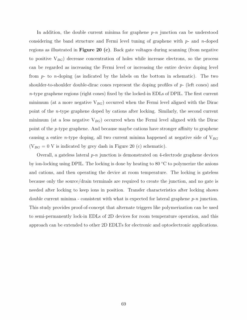
In addition, the double current minima for graphene p-n junction can be understood
considering the band structure and Fermi level tuning of graphene with p- and n-doped
regions as illustrated in Figure 20 (c). Back gate voltages during scanning (from negative
to positive VBG) decrease concentration of holes while increase electrons, so the process
can be regarded as increasing the Fermi level or increasing the entire device doping level
from p- to n-doping (as indicated by the labels on the bottom in schematic). The two
shoulder-to-shoulder double-dirac cones represent the doping profiles of p- (left cones) and
n-type graphene regions (right cones) fixed by the locked-in EDLs of DPIL. The first current
minimum (at a more negative VBG) occurred when the Fermi level aligned with the Dirac
point of the n-type graphene doped by cations after locking. Similarly, the second current
minimum (at a less negative VBG) occurred when the Fermi level aligned with the Dirac
point of the p-type graphene. And because maybe cations have stronger affinity to graphene
causing a entire n-type doping, all two current minima happened at negative side of VBG
(VBG = 0 V is indicated by grey dash in Figure 20 (c) schematic).
Overall, a gateless lateral p-n junction is demonstrated on 4-electrode graphene devices
by ion-locking using DPIL. The locking is done by heating to 80 ◦C to polymerize the anions
and cations, and then operating the device at room temperature. The locking is gateless
because only the source/drain terminals are required to create the junction, and no gate is
needed after locking to keep ions in position. Transfer characteristics after locking shows
double current minima - consistent with what is expected for lateral graphene p-n junction.
This study provides proof-of-concept that alternate triggers like polymerization can be used
to semi-permanently lock-in EDLs of 2D devices for room temperature operation, and this
approach can be extended to other 2D EDLTs for electronic and optoelectronic applications.
69

5.3 Retention Time of Locked EDLs on 2D EDLTs
The creation of p-n junction demonstrates DPIL’s potential as a gateless permanent
doping for 2D materials by EDL locking. But the retention time of locked EDLs needs
further investigation, which can be measured by monitoring how long the current can be
retained in a programmed state in 2D EDLTs without the applied bias. Moreover, the
transfer characteristics can indicate the EDL gating performance of unpolymerized DPIL,
which is important for applications which need EDL gating for the standard mode while
EDL locking for the special mode that is rarely visited.
Similarly to the locking process in graphene p-n junction, the proposed DPIL gated 2D
EDLTs and the EDL locking are illustrated in Figure 21. Before polymerization, the device
is first programmed to form the EDL (e.g., cationic EDL) under the gate bias (Figure 21 (b)).
Next, DPIL monomers is polymerized by heating the device at 80 ◦C for 2 hours in vacuum
while the device remains programmed by the gate bias. After the device is cooled to room
temperature, the gate bias is removed, and the retention measurement of the established
EDL measured starts immediately by monitoring the drain current as a function of time.
Graphene FETs were first fabricated with the side gate geometry as illustrated above
in Figure 21 (a). Unpolymerized DPILs (∼ 5 µL, with AIBN and inhibitor) were deposited
on each FET in the glovebox, and the FETs were transferred to the probe station by the
loadlock without exposure to the ambient. We first demonstrated transfer characteristics of
a graphene EDLT using unpolymerized DPILs, showing the Dirac point near VSG of 0 V
(Figure 22 (a), black curve). The ambipolar n- and p-branch confirms that both cations
and anions in the unpolymerized DPILs are mobile and capable to perform EDL gating.
The hysteresis between the forward and reverse sweeping of VSG originates from the lower
ion mobility and sluggish response of ions in the unpolymerized DPILs compared to the
sweeping rate. After polymerization of DPILs with the EDL programmed at VSG of +2 V,
the ID remains almost constant at ∼ 1.47 µA and cannot be modulated by sweeping the VSG
(Figure 22 (a), blue line). This indicates that the ions are immobile and cannot response to
the changing field to perform a dynamic EDL gating. Therefore, the channel doping profile,
as indicated by the ID, is kept at the state induced by a static EDL formed previously at
70

Figure 21: DPILs electrolyte and EDL locking mechanism. (a) Schematic of DPILsgated FET with a side gate. (b) EDL locking mechanism. From left to right: 1) programmingthe FET to form EDL by mobile ions in unpolymerized DPIL; 2) locking the EDL in place byheat-triggerd polymerization with gate bias applied; 3) locked EDL with no gate bias applied - agateless electrostatic doping.
71

VSG of +2 V. Note that the EDL corresponding to VSG of +2 V was formed by cations of
DPIL before the polymerization, and the gate bias was applied for 10 min prior to the start
of polymerization to ensure the full formation of EDL.
The EDL retention was also measured before and after the polymerization on the same
FET. Before polymerization, the FET was programmed by applying VSG of +2 V for 10 min
to form a saturated EDL. The VSG was then grounded (VSG = 0 V), and ID was monitored to
capture the dissipation of EDL (Figure 15 (b), black curve). Within 400 s, the EDL formed
at VSG of +2 V (corresponding to ID of ∼ 1.5 µA) fully dissipated, with ID decreased to
1.1 µA which agrees with the ID at 0 V in the transfer characteristics (Figure 22 (a), black
curve). After polymerization while keeping the FET programmed at VSG of +2 V, the FET
was grounded again. This time, the ID and the corresponding EDL maintain at the same
level (∼ 1.47 - 1.5 µA) for a time scale exceeding 105 s (Figure 22 (b), blue line). The
measurement was stopped after ∼ 2 days without observing a significant decay of ID, and
there should be no limit to achieve a longer retention by extending the time window for
monitoring. The results show better retention than the previously reported EDL locking by
cooling the temperature below the Tg of PVA:LiClO4 (no decay within 103 s after removing
the bias, and ∼ 75% of EDL remains after 105 s). [160]
72

Figure 22: Transfer characteristics and EDL retention before and after polymeriza-tion. (a) Transfer characteristics of a graphene FET before (black line) and after (blue) lockingthe cation-induced EDL by polymerization. Scanning window is from -1 to 1 V, while the blueline (polymerzied DPIL) was obtained after forming the EDL at VSG of +2 V and the locking bypolymerization. (b) EDL retention before (black) and after locking the EDL by polymerization(blue line). In both measurements, side gates were grounded (0 V), and the ID was monitored toshow the cation-induced EDL retention of its saturation state obtained after VSG = +2 V appliedfor 10 min. (c) and (d) are the similar measurements of transfer characteristics and EDL retentiontest on WSe2 FET, respectively, with the ID monitored before (black) and after (red) locking theanion-induced EDL by polymerization.
73

After proving the concept of EDL locking on graphene FETs, WSe2 FETs were selected
to reveal the full potential of DPILs on 2D semiconductors with larger On/Off ratios. Similar
transfer characteristics and comparison were conducted for a DPILs gated WSe2 FET before
and after polymerization as shown by the black and red curves in Figure 22 (c), respectively.
Again, the ions are mobile before and then immobilized after polymerization, giving rise to
the change in EDL gating from effective ID modulation (On/Off ∼ 104, ambipolar branches
of black curve) to no modulation (ID constant at ∼ 1.2 µA, red line). Note that the EDL
was formed by anions when programmed at VSG of -4 V.
Preliminary results of EDL retention of polymerized DPILs on WSe2 FET also confirms
the EDL locking observed previously on graphene FETs (Figure 22 (d)). The EDL by
anions starts dissipating within seconds in unpolymerized DPILs (black curve), but can be
locked after polymerization to maintain the ID for a time exceeding 103 s (red line) without
any sign of current decaying. This time, however, we did not observe the full dissipation
of EDL in unpolymerized DPILs due to the inadequate time window, which is due to the
underestimation of EDL dissipation time and the sensitive response of WSe2 to the changing
doping profile. We also noticed the small discrepancy between ID of saturated EDL at VSG
of -4 V before and after polymerization (i.e., the gap between black and red curve at the
left end, Figure 22 (d)). This could be due to the intrinsic capacitance difference between
DPILs monomers to their polymer forms.
In brief, EDL locking by polymerization on 2D EDLTs show a retention time exceeding
105 s, suggesting its potential in gateless semi-permanent doping for 2D materials. And the
results lay the foundation for pursuing a more exciting concept - a gateless reconfigurable
doping.
74

5.4 Triggerable Ion Release by Introducing Thermally Labile Diels-Alder
Linkages into Polymerizable Ionic Liquid
Substitutional doping is permanent and cannot be changed after device fabrication. In
contrast, doping by EDLs using conventional electrolytes is reconfigurable by reversing the
polarity of applied bias; but a constant gate voltage or operating device at low temperature
is required to hold the doping state. [20] Indeed, reconfigurable doping has attracted much
attention recently due to reconfigurable FETs [150] as well as adaptive and polymorphic
circuits for applications such as hardware security [171, 172] and self-checking and smart
electronics for Internet of Things (IoTs). [162,173] Motivated by reconfigurable doping with
no standby gate voltage, repeatable locking and unlocking of EDLs is pursued by further
engineering the polymerizable ionic liquids.
Here, we address this challenge by developing polymerizable ionic liquid with a thermally-
labile Diels-Alder linkage between the polymer backbone and the cationic side chain. This
Diels-Alder linkage undergoes a retro Diels-Alder reaction above 90 ◦C, [174–176] enabling
a thermally-triggered ion release for EDL unlocking. Figure 23 shows two singly polymer-
izable ionic liquid monomers used in this study, and only their cationic species are poly-
merizable for simplicity. We denote the singly polymerizable ionic liquid with Diels-Alder
linkage as triggerable singly-polymerizable ionic liquid (T-SPIL). The cation of T-SPIL is
analogous to the cation of DPIL, but contains a furan-maleimide Diels-Alder adduct be-
tween the charged imidazolium and the polymerizable methacrylate. [177, 178] In addition,
non-triggerable singly-polymerizable ionic liquids (NT-SPIL) lacking the thermally labile
Diels-Alder linkage was synthesized as comparisons and controls. [179] Note that the cation
of NT-SPIL is the same with DPIL used in previous sections.
First of all, cyclic voltammetry indicated that the electrochemical windows of both T-
SPIL and NT-SPIL were, at approximately 4 V, comparable to that of [EMIM][TFSI],
making them viable for applications in organic electronics. [180–182] Next, to retain the
desired capability for thermally-triggered ion release, it was important to polymerize the
T-SPIL monomers without driving cycloreversion of the Diels-Alder adduct. Therefore,
instead of heating, samples were photopolymerized using a photoinitiator 2,2 dimethoxy-
75

Figure 23: Chemical structures of triggerable polymerizable ionic liquid Structures of(left) triggerable singly polymerizable ionic liquid (T-SPIL), with Diels-Alder linkage in cation;and (right) non-triggerable singly polymerizable ionic liquid (NT-SPIL), with the same cation asDPIL used previously.
2-phenylacetophenone (DMPA) and UV light (UVP Compact UV lamp, l = 365 nm, P =
1.3 mW cm−2 at 7.6 cm) at a working distance of 1.5 cm for 30 min at room temperature.
The DSC measurement of T-SPIL after polymerization shows the characteristic thermal sig-
natures of the retro Diels-Alder reactions of both the endo (100 ◦C) and exo adducts (150
◦C), [178] indicating that both adducts remained intact during UV photopolymerization at
room temperature. Whereas the DSC of NT-SPIL shows no endo nor exdo adducts because
of lacking Diels-Alder linkage. In conclusion, T-SPIL and NT-SPIL can be successfully
polymerized by UV light, and Diels-Alder linkage in T-SPIL remains stable during the UV
polymerization.
To investigate the impact of polymerization (ion-locking) and heating (possible ion-
release) to mobile ion content, we drop-cast both T-SPIL and NT-SPIL onto “dummy ca-
pacitors” - two parallel electrodes lithographically patterned with 10 µm spacing and then
measured their response to a change in applied voltage. In these measurements, applying a
step potential results in a current spike due to capacitor charging and ionic motion, followed
by a slow decay till zero charging current as the ions reach their new equilibrium distribution.
The amplitude of the current spike reflects the number of ions able to respond to the applied
voltage, and is a useful proxy for the mobile ion content of the material, which cannot be
76
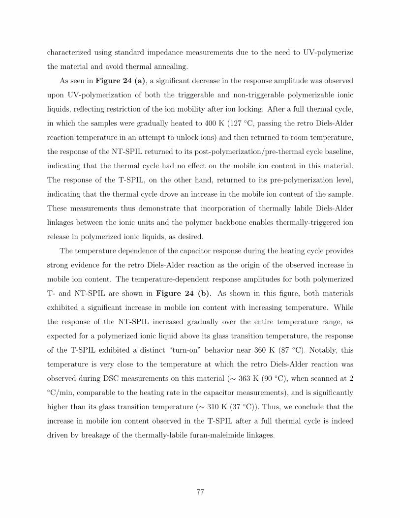
characterized using standard impedance measurements due to the need to UV-polymerize
the material and avoid thermal annealing.
As seen in Figure 24 (a), a significant decrease in the response amplitude was observed
upon UV-polymerization of both the triggerable and non-triggerable polymerizable ionic
liquids, reflecting restriction of the ion mobility after ion locking. After a full thermal cycle,
in which the samples were gradually heated to 400 K (127 ◦C, passing the retro Diels-Alder
reaction temperature in an attempt to unlock ions) and then returned to room temperature,
the response of the NT-SPIL returned to its post-polymerization/pre-thermal cycle baseline,
indicating that the thermal cycle had no effect on the mobile ion content in this material.
The response of the T-SPIL, on the other hand, returned to its pre-polymerization level,
indicating that the thermal cycle drove an increase in the mobile ion content of the sample.
These measurements thus demonstrate that incorporation of thermally labile Diels-Alder
linkages between the ionic units and the polymer backbone enables thermally-triggered ion
release in polymerized ionic liquids, as desired.
The temperature dependence of the capacitor response during the heating cycle provides
strong evidence for the retro Diels-Alder reaction as the origin of the observed increase in
mobile ion content. The temperature-dependent response amplitudes for both polymerized
T- and NT-SPIL are shown in Figure 24 (b). As shown in this figure, both materials
exhibited a significant increase in mobile ion content with increasing temperature. While
the response of the NT-SPIL increased gradually over the entire temperature range, as
expected for a polymerized ionic liquid above its glass transition temperature, the response
of the T-SPIL exhibited a distinct “turn-on” behavior near 360 K (87 ◦C). Notably, this
temperature is very close to the temperature at which the retro Diels-Alder reaction was
observed during DSC measurements on this material (∼ 363 K (90 ◦C), when scanned at 2
◦C/min, comparable to the heating rate in the capacitor measurements), and is significantly
higher than its glass transition temperature (∼ 310 K (37 ◦C)). Thus, we conclude that the
increase in mobile ion content observed in the T-SPIL after a full thermal cycle is indeed
driven by breakage of the thermally-labile furan-maleimide linkages.
77

Figure 24: Mechanism of a single-ion conductor gated EDLT. (a) Capacitor response ofnon-triggerable (top) and triggerable singly-polymerized ionic liquids (bottom) at 298 K (25 ◦C),measured before polymerization, immediately after polymerization, and after a full thermal cyclein which the temperature of the sample was increased to 400 K (127 ◦C) before being returnedto room temperature. Each trace depicts the response of the material to a step potential appliedacross a capacitor with 10 µm electrode spacing. (b) Temperature-dependent current amplitudesfor capacitors with non-triggerable (top) and triggerable singly-polymerized ionic liquids (bottom)deposited and polymerized across the electrodes. Arrows labeled Tg and rDA indicate the glasstransition temperature and retro Diels-Alder temperatures of the samples, respectively.
78

In summary, we have shown that incorporation of a thermally labile Diels-Alder linkage
in the side-chain of a polymerizable ionic liquid facilitates thermally-triggerable ion release
when the sample is heated above the cycloreversion temperature of the Diels-Alder adduct.
This approach allows the locked ions to be released on-command by a chemical trigger after
polymerization, a capability that is not achievable with current classes of ion-containing
polymers. In addition, besides heat, the triggering stimulus can be light or mechanical force
by chemically modifying/adding functional groups.
5.5 Conclusion
EDL locking by polymerization has been demonstrated using a custom-synthesized poly-
merizable ionic liquids on 2D EDLTs. Fixing EDLs by polymerization continuously dope
the channel without requiring an external field. A lateral p-n junction has been first cre-
ated on 4-electrode graphene devices by EDL locking. The entire process is gateless because
no gate voltages are required to create or maintain the p-n junction. Backgated transfer
measurements show two current minima which is a signature of a graphene p-n junction.
EDL locking is also investigated on 2D EDLTs with side gates. Both cationic and anionic
EDLs can be locked by polymerization, with the doping retention time exceeds 105 s (max
measured) at room temperature after locking. Furthermore, to achieve a reconfigurable dop-
ing, both EDL locking and unlocking are needed. Therefore, thermally labile Diels-Alder
linkages are introduced between ionic group and polymer backbone, so that polymerized
ions can be unlocked again by heating. This feature cannot be achieved by substitutional
or by conventional electrolytes. Future work will focus on this new class of triggerable
and stimulus-responsive ion conductors for EDLTs to be used in adaptable or polymorphic
circuits for various applications.
79

6.0 Conclusions
In this work, one of the major and promising branches of iontronics has been investigated
- 2D EDLTs. Previously, the vast majority of attention in 2D EDLTs has been focused on
2D materials and semiconductor physics, where ion conductors are essentially regarded as a
simple replacement of conventional dielectrics in 2D EDLTs. In contrast, this dissertation
advances the concept that the ion conductors themselves can achieve unique mechanisms
of charge control to achieve advanced functions in device operation. This work has focused
on engineering ion conductors and 2D EDLTs for new device functions supported by four
projects, illustrated in Figure 25. The major outcomes of the projects include: 1) an
approach to achieving a residue-free 2D surface for EDL gating and quantification of the
impact of the residue on gating performance; 2) a monolayer electrolyte that achieves bista-
bility and fast switching for non-volatile memory; 3) a single-ion conductor for strain control
in suspended EDLT; and 4) a “locking EDL” that exploits a polymerizable ionic liquid to
allow reconfigurable gateless doping for p-n junctions and 2D FETs.
Because EDL gating relies on the proximity of ions to the surface, the best possible
gating performance of 2D EDLTs will be hindered if there is a few nanometer thick polymer
residue remaining from the lithography process and located between the electrolyte and the
2D channel. In Chapter 2, a successful removal of resist residue has been demonstrated
on MoS2 and WSe2 FETs using contact mode AFM. AFM topology shows that surface
roughness is restored to its intrinsic state, and Raman spectra show that the characteristic
peak intensities of MoS2 and WSe2 increase after removing the residue. For back-gated WSe2
FETs (no electrolyte), PMMA residue from e-beam lithography is found to be a p-type
dopant that decreases carrier mobility and creates unwanted doping (i.e., causing a charge
density change of 7 × 1011 cm−2). For EDL-gated CVD-WSe2 FETs using a PEO:CsClO4
electrolyte, photoresist residue is also a p-type dopant that can cause a charge density change
of 4.5 × 1012 cm−2. But more importantly, removing the residue increases the maximum
current of EDL-gated WSe2 FETs by 247%. This suggests that removal of residue by AFM
provides closer access for the ions to reach the surface of the channel, thereby increasing the
80
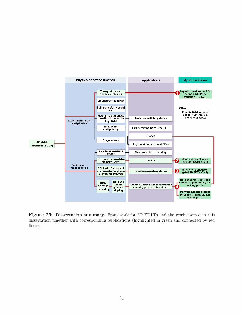
Figure 25: Dissertation summary. Framework for 2D EDLTs and the work covered in thisdissertation together with corresponding publications (highlighted in green and connected by redlines).
81
EDL gate capacitance. Overall the results suggest that the AFM contact mode cleaning is
a widely applicable and nondestructive method that can successfully remove different types
of post-lithography polymer residue on a variety of 2D crystals, and can improve channel
conductivity, mobility, and charge density. While this method would be impractical to scale,
it is especially for benchtop research where a near molecularly clean surface is required (e.g.,
monolayer electrolyte devices), and for EDL gating to achieve the best possible electrostatic
gate control. I predict that methods to achieve a residue-free surface will advance as wide-
area growth of 2D materials advances. In the meantime, the work in Chapter 2 provides a
viable path forward for benchtop research to proceed in the absence of a scalable solution.
Chapter 3 focuses on my primary PhD project - developing a molecularly thin ion con-
ductors for EDLT based non-volatile memory. Conventional solid polymer electrolytes and
ionic liquids/gels are unsuitable for NVM because of lack of an energy barrier to keep ions in
place. Therefore, I extended the development of a new electrolyte in our lab - the so called
“monolayer electrolyte”, and demonstrated it in a non-volatile memory device. The mono-
layer electrolyte has a switching barrier for state retention, and with the thickness scaled
to a single molecular layer that are beneficial for a fast and low voltage switching. The
custom-designed monolayer electrolyte consists of cobalt crown ether phthalocyanine and
lithium ions, which are positioned by field-effect at either the surface of the WSe2 channel
or an h-BN capping layer to achieve “1” or “0”, respectively. The monolayer electrolyte can
be directly deposited on WSe2 FETs by drop-casting and annealing. The AFM cleaning
protocol described in Chapter 2 was used prior to the electrolyte deposition to assure the
residue-free 2D surface required for the molecular arrangement of the monolayer electrolyte
to form the EDL. One of my most important contributions is the discovery that a capping
layer of h-BN significantly improves bistability in the monolayer electrolyte memory. Den-
sity functional theory (DFT) calculations by our collaborators support the mechanism of
enhanced trapping of Li+ near h-BN due to a ∼1.34 eV increase in the absolute value of
the adsorption energy compared to vacuum. The threshold voltage shift between the two
states corresponds to a change in charge density of ∼2.5 × 1012 cm−2, and an On/Off ratio
exceeding 104 at a back gate voltage of 0 V. The On/Off ratio remains stable after 1000
cycles and the retention time for each state exceeds 6 hours (max measured).
82

Although a millisecond switching speed has been demonstrated in this study, there is no
reason to expect the switching speed to be limited to this timescale. In fact, preliminary
results obtained recently by my colleagues show the switching time can be as fast as ∼ 40
ns by still using a back gate geometry. Moreover, a top-gated device architecture provid-
ing a stronger electric field is expected to further decrease the switching time, and sub-volt
operation in this configuration is predicted by DFT calculations. [125] Because in this con-
figuration, the electric field will drop over the thin h-BN gate dielectric and the monolayer
electrolyte instead of the 90 nm-thick back gate oxide and the several layers of WSe2 channel
that screens the field. Note that the speed is directly related to the magnitude of the ion
diffusion barrier (i.e., Li+ passing through the crown ether) which depends on the applied
electric field strength. [125] Therefore, the switching speed of the memory is also expected to
be improved (perhaps to a few nanoseconds) by top gating. For the future top-gated device,
h-BN could probably serve as a multi-functional capping layer: 1) a 2D gate dielectric; 2)
an encapsulation layer that protects the monolayer electrolyte from polar solvents during
lift-off process; and 3) a stabilizer for the Off-state of the monolayer electrolyte as described
in Chapter 3.
Another potential advantage of the monolayer electrolyte is the wide chemical tunability,
which can be used to adjust the energy barrier to switching. Thus, the monolayer electrolyte
offers the potential to adjust the switching and retention time and perhaps introduce multiple
states (i.e., multiple switching barriers by varying the crown ring size). [183] In addition, the
application of this material is not limited to 1T NVM. Because the material is solution
processible, the door is open to opportunities in printed and flexible electronics. Last, more
novel 2D nanomaterials could be suitable for developing new monolayer electrolytes including
porous 2D dielectrics, 2D polymers and 2D MOFs. [31, 184, 185] Recently, the concept of
monolayer electrolyte has also inspired the theoretical investigation of metal trihalides MX3
with intrinsic atomic pores as 2D electrolytes. [186] Overall, an ideal 2D solid electrolyte
with appropriate switching barrier, free of dangling bonds, layer uniformity on a large scale,
good electrical insulation, and mechanical integrity for wafer-scale device fabrication - is not
an unreachable dream. In fact, I think our contribution has opened an exciting new area of
monolayer thick, ion-conducting functional materials.
83

In Chapter 4, 2D EDLTs using a custom-synthesized polyester single-ion conductor
(PE400-Li) are demonstrated for the first time on graphene and MoTe2 transistors. Their
gating performance has been directly compared to the dual-ion conductor (PEO:LiClO4) on
the same devices. Transfer characteristics show an enhanced n-branch for both the dual
and single-ion conductors because their mobile cations can form EDL at the electrolyte/2D
interface. The single-ion conductor can achieve cationic ion densities up to 1014 cm−2, sim-
ilar to the dual-ion conductor. On the other hand, p-branch conduction is suppressed in
the single-ion conductor compared to that in the dual-ion conductor. This is because 1) the
anion in the single-ion conductor is covalently bound to the polymer backbone, so a cationic
depletion layer with significantly weaker electrostatic gating strength is formed at the 2D
surface instead of anionic EDL present in the dual-ion conductor under negative side gate
voltages; and 2) the gate size is larger (∼ 10x) than the channel. This has been confirmed
by a finite element modeling of ion transport in response to an applied field, completed by
my co-authors. If deposited on a suspended MoTe2 FET, the single-ion conductor is possible
to have imbalanced ion strength at the two interfaces via field effect (i.e., cation density of
1014 cm−2 at electrolyte/2D interface vs. the cationic depletion layer at the gate), leading
to its longitudinal bending and inducing strain in MoTe2. Given that MoTe2 under sev-
eral percent strain can undergo a 2H–1T’ semiconducting to metallic phase transition, the
single-ion conductor gating are potentially useful for creating an electronic switch based on
field-controlled phase transitions in 2D crystals. In addition, this work may also inspire new
single-ion conductor gated devices where the electrolyte serves both as a gating dielectric
and an actuator to access local strain control. In this way, our group is driving towards
introducing all these new functionalities that include the features of micro-electromechanical
system (MEMs) to EDLTs.
Besides depositing high-k dielectrics, it is also difficult to substitutionally dope 2D ma-
terials. The electrostatic doping by EDLs not only can achieve strong doping densities (>
1013 cm−2), but also is reconfigurable (i.e., n- and p-type doping switchable by reversing
the polarity of the applied bias). Such reconfigurablility of doping is much in demand for
developing reconfigurable FETs based on ambipolar 2D materials but not achievable by sub-
stitutional nor chemical doping. To avoid the dissipation of EDLs, however, a gate bias
84

needs to be continuously applied which will drain the power, unless ions that constitute
EDLs can be locked in position. Therefore Chapter 5 demonstrates our group’s first efforts
to lock EDLs by polymerizing a doubly polymerizable ionic liquid on 2D EDLTs. Compared
to EDL locking by lowering the operating temperature below electrolyte’s Tg, the chemi-
cal approach using DPIL is more practical for devices operated at room temperature. As
a proof-of-concept demonstration, a gateless lateral p-n junction is created on 4-electrode
graphene devices by ion-locking. The “gateless” means: 1) only the source/drain terminals
are required to create the junction; and 2) the locked doping state is permanent so no gate
voltage is needed to keep the ions. Consistent with what is expected, transfer characteris-
tics show a double current minima - the signature of the p-n junction for graphene. Next,
EDL locking is demonstrated on graphene and WSe2 EDLTs, in which both cationic and
anionic EDLs can be locked by polymerization. Preliminary results indicate that the doping
retention time of locked EDLs exceeds 105 s (max measured) at room temperature.
The results of EDL locking motivates us moving forward to exploring the reconfigurable
doping using DPIL; that is, locked EDL can be unlocked to reconfigurable the doping type
(p- or n-type) by reversing the gate polarity, and followed by another locking. Therefore,
to enable unlocking, a thermally labile Diels-Alder linkage has been introduced in the side
chain of the polymerizable ionic liquid. This linkage facilitates thermally triggerable ion
release when the sample is heated above the cycloreversion temperature of the Diels-Alder
adduct. This chemical modification allows the mobile ion content of polymerizable ionic
liquid able to be changed after polymerization, a capability that is not achievable with
current classes of ion-containing polymers. In future work, we anticipate that incorporating
other types of responsive chemical units between the ionic group and the polymer backbone
will give rise to materials that respond to a wide range of other chemical and physical triggers,
including light, heat, and mechanical force, enabling new classes of triggerable and stimulus-
responsive ion conductors for EDLTs to be used in adaptable or polymorphic circuits for
various applications. For example, these novel circuits can be used in hardware security
where EDLTs can be deprogrammed on command to avoid reverse engineering; or in energy
harvesting Internet-of-things (IoT) where the circuit can change functionality in response to
an intermittent power supply or environmental stimulus.
85
Overall, the development of iontronics including EDLTs over the past decade has sprouted
many branches of emerging devices which have become vital tools to explore fundamental
physics or promising components for electronic application. Considering the advantages of
EDL gating, such as large interfacial electric fields, large capacitance and high carrier den-
sities, 2D EDLTs facilitates the discovery of a variety of solid-state physics in 2D materials.
Looking ahead, a few more emerging fields could be: 2D EDLTs for neuromorphic com-
puting where EDL formation and dissipation under a pulsed voltage can be utilized; 2D
EDLTs to apply high fields to control quantum physics; 2D EDLTs for optoelectronics, tak-
ing advantage of the side gate geometry that will not interfere with an optical signal; 2D
EDLTs for flexible electronics; 2D EDLTs with field-induced nanomechanical control; and
adaptive devices where electrolyte and 2D EDLTs can change their functions. There is no
doubt that scaling and chemical tailoring the electrolyte will continue being a key factor
for those research areas on the rise. In addition, more effort is needed to improve the ion
conductor properties, such as electrochemical stability with all materials in contact (channel,
electrode metals, etc.), ion conductivity for high switching frequency, mechanical integrity
for solid-state electronics, and power dissipation during device operation.
86
Appendix A
General Experimental Procedures
A.1 2D Material Exfoliation
2D materials used in this dissertation were mostly obtained by exfoliation using the
Scotch tape method, [25] except that some WSe2 samples in chapter 2 were grown by our
collaborators (Prof. Joshua Robinson group at Penn state) using chemical vapor deposi-
tion (CVD). Details about CVD WSe2 growth and FETs preparation will be discussed in
Appendix B.
For exfoliation, 2D flakes (e.g., graphene, WSe2, MoTe2 and MoS2 flakes) with thickness
3-20 nm were mechanically exfoliated from their bulk sources and transferred to p-type Si
(resistivity 0.001–0.005 ohm-cm) with 90 nm of SiO2 (Graphene Supermarket) by the Scotch
tape method. Acetone, isopropanol (IPA), and deionized water were used to preclean the
substrate. Flakes with uniform thickness were selected by optical microscopy and AFM
topology measurements (Bruker Dimension Icon in ScanAsyst mode using Si3N4 ScanAsyst
Air tips with 0.4 N m−1).
A.2 FET Fabrication
Back- and side-gated FETs were fabricated by e-beam lithography (EBL) (Raith e-LiNE).
Two hundred nanometers of PMMA-950-A4 (MicroChem) e-beam resist, was spin-coated at
a spin speed of 4000 rpm for 1 min, followed by a 3 min bake on a hotplate at 180 ◦C.
Source/drain and gate contacts were patterned by EBL, and the sample was developed in
a methyl isobutyl ketone (MIBK) and IPA solution (MIBK:IPA 1:3 volume ratio) for 1 min
and then rinsed by IPA for another 1 min. E-beam evaporation (Plassys Electron Beam
87

Evaporator MEB550S) was used to deposit metal electrodes at a base pressure < 1 × 10⁻⁶
Torr. Normally, the metal thicknesses were Ti (5 nm) and Au (130 nm). The samples were
immersed in acetone for lift-off at room temperature overnight, and then rinsed with IPA
and deionized water.
A.3 AFM Contact Mode Cleaning
AFM contact mode was used to scan the FET channel to “sweep” away the polymer
residue by the mechanical force. For cleaning purposes, a stiff AFM tip was used (SCM-PIT-
v2, measured force constant 2.37 N m−1) which is much stronger than AFM tips commonly
used for the contact mode (Si3N4 ScanAsyst Air tips, 0.4 N m−1). The deflection setpoint
was optimized to be 1.33 V, which is equivalent to applying 104 nN of normal force to
the sample surface (larger setpoints damaged the sample while smaller setpoints do not
completely remove the residue). Complete cleaning was achieved by scanning the target
region three times in different directions (rotating the sample 90 ◦ each time) using a scan
rate of 10 µm s−1.
A.4 Probe Station, Vacuum Annealing and Measures to Avoid Ambient
Exposure
Electrical measurements were made using a Keysight B1500A semiconductor parameter
analyzer in a Lakeshore cryogenic vacuum probe station (CRX-VF) with pressure ∼ 2 ×
10−6 Torr.
To improve the electrical performance of FETs, samples were vacuum annealed at 400
K for 4 h before electrical measurement in the probe station with pressure of ∼ 2 × 10⁻⁶
Torr. This can remove water that interferes the gating from the FET channel surface.
To avoid the exposure to ambient conditions, the samples were transferred between the
glove box and the probe station using a load lock filled with argon. In this dissertation, all
88

AFM cleaning, electrolyte preparation and deposition, and sample transfer were completed
in an argon environment (an argon-filled glove box with H2O and O2 concentration < 0.1
parts-per-million), and the electrical measurements were completed in vacuum (∼2 × 10⁻⁶
Torr) in the probe station.
89

Appendix B
Supporting Information for Chapter 2
B.1 Experimental Section
B.1.1 Device and Sample Preparation
Back-gated FETs using exfoliated MoS2 and WSe2 were fabricated by EBL as described
in Appendix A1 and A2. In some cases, ”dummy samples” with only flakes and PMMA
residue on top were needed for investigating AFM cleaning and Raman measurement, and
therefore device fabrication was not necessary. In these cases, the flakes were exposed to
the same steps of the e-beam process except for writing the patterns. After spincoating
PMMA-950-A4 and baking, the sample was cooled to room temperature, soaked in acetone
for 15 min, and then rinsed by IPA for 1 min.
B.1.2 CVD WSe2 Growth and FETs Preparation
Large-area, few-layer (2-3 L) WSe2 films were synthesized on sapphire substrates by metal
organic CVD (MOCVD) in a vertical cold wall system using W(CO)6 and H2Se precursors
and H2 carrier gas. Samples were grown at 800 ◦C at 700 Torr total pressure with W(CO)6
and H2Se precursor partial pressures of 6.2 ∼ 10−4 Torr and 15.6 Torr, respectively. Full
details of the entire MOCVD growth process including seeding, ripening, growth, and post-
growth annealing steps can be found in the following work. [32] Additional materials and
device characterization of identical WSe2 samples and EDL gating can be found in the
referenced work.
EDL-gated FETs were fabricated via standard photolithography (GCA 8500 i-line Step-
per) to define WSe2 channel dimensions, source/drain (S/D) contact electrodes, and side-gate
electrodes. WSe2 channels were isolated and defined via reactive ion etching in a Plasma
90

Therm PT-720 plasma etch tool using an SF6/O2/Ar gas chemistry at 10 mTorr and 100 W
for 30 s. 10/10 nm Pd/Au source/drain metal was deposited by e-beam evaporation under
moderate vacuum (∼ 10−6 Torr) at a deposition rate of 1.0 A s−1 followed by lift-off in
acetone and PRS-3000 resist stripper. Following this initial source/drain metal deposition, a
second metallization consisting of 10/150 nm Ti/Au was carried out to define the side-gate
and to thicken source/drain pads for probing through the electrolyte.
In total, CVD-WSe2 films were subjected to four levels of photolithography to realize
EDL-gated devices (listed in chronological order): alignment mark metal, WSe2 isolation
etch, source/drain metal, and side-gate metal. The photoresist stacks used in these four
lithography steps are listed in chronological order: LOR5A/SPR 3012, LOR2A/SPR 3012,
PMGI SF5(s)/SPR 3012, and LOR5A/3012. LOR2A and LOR5A were baked at 180 ◦C for
3 min, SPR 3012 was baked at 95 ◦C for 1 min, and PMGI SF5(s) was baked at 220 ◦C for
3 min. The resulting photoresist residue on CVD-WSe2 device channels was most likely a
mixture of these three main photoresists.
B.1.3 Electrical Characterizations
Electrical measurements were made using a Keysight B1500A semiconductor parameter
analyzer in a Lakeshore cryogenic vacuum probe station (CRX-VF) with pressure of 2 × 10⁻⁶
Torr. To compare the improvement of FET electrical performance by vacuum annealing and
AFM cleaning, a few back-gated WSe2 FETs were chosen to be annealed in vacuum and
then cleaned by AFM contact mode with transfer characteristics taken after each process.
Samples were annealed at 400 K for 4 h in the probe station with pressure of 2 × 10⁻⁶ Torr.
B.1.4 Electrolyte Preparation and EDL-gating Experiments
The polymer electrolyte preparation process was similar to previously published re-
sults. [20] PEO:CsClO4 was prepared inside an argon-filled glove box with H2O and O2
concentration < 0.1 parts-per-million (ppm). PEO (Polymer Standards Service, molecular
weight 94,600 g mol−1) and CsClO4 (Sigma-Aldrich, 99.9%) were dissolved in anhydrous
acetonitrile (Sigma-Aldrich) to make a 1 wt% solution with the ether oxygen to Cs molar
91
ratio 76:1. The polymer electrolyte was drop-cast (25 µL) onto the 1 cm2 sample chip with
CVD WSe2 FETs in the glove box, dried at room temperature until the majority of the
solvent evaporated, and then annealed at 80 ◦C for 3 min. There was no ambient exposure
during sample preparation, transfer and measurement (see Appendix A4).
To compare EDL-gated WSe2 FET performance with and without AFM cleaning of
the e-beam resist residue, it was necessary to remove the PEO:CsClO4 electrolyte after
the first measurement and then redeposit it onto the devices for the second measurement.
First, PEO:CsClO4 was deposited on all the FETs for transfer characteristics to establish
the baseline electrical response. Next, the electrolyte was removed by a hot acetonitrile
bath at 60 ◦C for 30 min and kept inside acetone overnight for 13 h. Note: acetonitrile is
extremely volatile—please read safety data sheet before heating. After the removal of the PEO
electrolyte, half of the FETs were cleaned using AFM contact mode. Last, PEO:CsClO4 was
redeposited on all the FETs and the electrical measurements were repeated.
92

B.2 AFM Characterization
AFM characterization of the flakes was carried out using a peakforce tapping mode
(ScanAsyst mode) as described in Appendix A1; whereas AFM cleaning was performed
using contact mode as described in Appendix A3.
Figure B1 shows AFM images of CVD-grown WSe2 FETs cleaned by AFM contact
mode using three different setpoints. Images were taken on different FETs. The setpoint
1.33 V was chosen because the residue still exists when the setpoint is 0.92 V, and pinholes
on WSe2 channel due to scratching starts to appear when the setpoint is 1.66 V.
Figure B1: AFM images of CVD-grown WSe2 FET channels cleaned by different AFM contactmode setpoint: (a) 0.92 V, (b) 1.33 V, and (c) 1.66 V.
Figure B2 shows a AFM image of a partially cleaned CVD-grown WSe2 FET channel.
The height difference between the cleaned region and uncleaned region with polymer residue
is ∼ 1.2 nm, as indicated by the line scan taken at the blue line on the AFM image. The
roughness was measured within the blue box. The roughness reduced from 0.68 nm to 0.43
nm after the AFM cleaning.
Figure B3 is the AFM Quantitative Nano-mechanical Mapping (QNM) of MoS2 with
PMMA residue, and the comparison with the cleaned region. DMT modulus is the reduced
Young’s modulus using the Derjaguin, Muller, Toropov (DMT) model, which is a measure
of the stiffness of solid materials. [187] The PMMA residue region on MoS2 has lower DMT
93
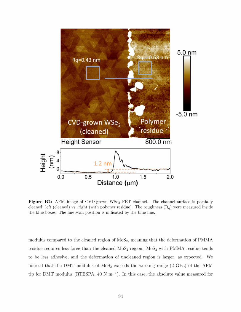
Figure B2: AFM image of CVD-grown WSe2 FET channel. The channel surface is partiallycleaned: left (cleaned) vs. right (with polymer residue). The roughness (Rq) were measured insidethe blue boxes. The line scan position is indicated by the blue line.
modulus compared to the cleaned region of MoS2, meaning that the deformation of PMMA
residue requires less force than the cleaned MoS2 region. MoS2 with PMMA residue tends
to be less adhesive, and the deformation of uncleaned region is larger, as expected. We
noticed that the DMT modulus of MoS2 exceeds the working range (2 GPa) of the AFM
tip for DMT modulus (RTESPA, 40 N m−1). In this case, the absolute value measured for
94

DMT modulus value is affected by the absolute value of stiffness of the AFM tip, which will
cause variation of the results from tip to tip. However, the trend that PMMA residue region
has smaller DMT modulus is always observed because PMMA residue is softer than crystal
surface. Therefore, the difference between the cleaned MoS2 and PMMA residue can be at
least qualitatively described by AFM QNM.
Figure B3: AFM mechanical (QNM) mapping on MoS2 using RTESPA AFM tip: (a) (d) defor-mation; (b) (e) DMT modulus; and (c) (f) adhesion.
95
B.3 Raman Measurements
To evaluate the quality of the cleaning, Raman measurements were made using a Ren-
ishaw inVia Raman Spectrometer. Each measurement was taken with exposure time of 12
s, three times of accumulation (1800 | mm−1 grating). The measurements were made three
different times on WSe2 and MoS2 flakes: as exfoliated, with the PMMA residue, and after
cleaning. Each Raman measurement was done on the same flake to avoid flake-to-flake vari-
ation. Large (∼ 30 × 10 µm) and thin (10-20 nm thick) WSe2 and MoS2 flakes were selected
for this study. After exposure to the PMMA residue, the entire surface of each flake was
cleaned by AFM contact mode. A 488 nm Raman laser with beam spot size of 0.8 µm was
used for MoS2, and 633 nm with spot size 1 µm for WSe2. The laser power was set to 10
mW to minimize heating the flake by the laser
Figure B4 shows the spectra taken on flakes that are freshly exfoliated (black), with
PMMA residue (blue), and after AFM cleaning (red) for MoS2 and WSe2, respectively. The
E2g and A1g peaks originating from the stretching and scissoring of Mo-S or W-Se bond
vibrations are assigned accordingly for MoS2 and WSe2. [188, 189] For both materials, the
intensities of the E2g and A1g peaks increase after AFM cleaning and become more similar to
the intensities of freshly exfoliated flakes. The peak intensity increases after AFM cleaning
for two reasons. One reason is that PMMA residue screens the Raman signal. A second
reason deals with molecular interactions between PMMA and the underlying crystal itself.
For example, if PMMA interacts strongly with the S atoms in MoS2, it will dampen the Mo-S
vibrations. Similar arguments have been made for polymer residue on graphene. [99, 110]
To make sure the change in Raman peak intensity is not caused by the variation between
measurements (e.g., intensity differences caused by Raman system realignment), we con-
ducted consecutive Raman measurements on a partially cleaned sample without realigning
the system. AFM of a MoS2 flake with PMMA residue is shown in Figure B5 (a), with
a square region (10 × 10 µm) cleaned by AFM. Figure B5 (b) are the corresponding the
Raman spectra taken at the locations indicated by the red and blue spots in Figure B5 (a).
Consistent with all the Raman data collected, the intensities of E2g and A1g peaks of MoS2
are larger for the cleaned region because PMMA has been removed.
96

Figure B4: Raman spectra of a) MoS2 and b) WSe2 taken in the same region before and afterAFM cleaning for each flake: as exfoliated (black line), with PMMA residue (blue line), and afterthe AFM cleaning (red line).
Figure B5: (a) AFM image of a MoS2 flake with a square region cleaned by AFM and uncleanedregion, where red and blue spots indicate the locations of Raman measurement. (b) Raman spectraof cleaned region (red line) and the region with PMMA residue (blue line).
97
Appendix C
Supporting Information for Chapter 3
C.1 CoCrPc Monolayer Deposition on MoS2 and WSe2
AFM images of MoS2 and WSe2 flakes partially covered in the CoCrPc monolayer are
shown in Figure C1 (a) and (b), respectively. The partial coverage is purposeful because it
allows us to measure the thickness of a single CoCrPc layer. The deposition was achieved by
drop-casting 44 µL of a 13 mg/L CoCrPc solution (CoCrPc dissolved in benzene/ethanol,
9:1 v/v) on a 1 × 1 cm2 Si chip (90 nm SiO2) covered in exfoliated flakes of either MoS2
or WSe2. This is followed by a 30-min anneal in Argon at 220 ◦C. As shown in the line
scans below, the thickness of CoCrPc is confirmed as ∼ 0.5 nm, which is in good agreement
with the expected thickness based on DFT calculations and previously published monolayer
thicknesses on HOPG. [123]
98

Figure C1: Monolayer CoCrPc on MoS2 and WSe2. AFM topology (height) of exfoliated(a) MoS2 and (b) WSe2 flakes with partial coverage of CoCrPc to measure the thickness of CoCrPc.For each substrate material, the line scan is shown below each AFM image, with the correspondingposition indicated by the white dashed line.
C.2 Optimization of CoCrPc Monolayer Deposition on WSe2
The volume of the CoCrPc solution deposited per unit area (i.e. the dose) and the
annealing temperature must be optimized to deposit a uniform, single molecular layer of
CoCrPc on a 2D surface. [123] As mentioned above, a CoCrPc solution of 13 mg per liter
of benzene/ethanol (9:1 v/v) is used. As shown below, the CoCrPc dose and annealing
temperature are optimized for monolayer deposition on WSe2.
Figure C2 (b) – (d) show the impact of CoCrPc dose on the coverage, where the dose of
CoCrPc increases from 38 to 52 µL cm−2. CoCrPc molecules form a discontinuous monolayer
with ∼ 0.5 nm thickness when the concentration is too low (e.g., 38 µL cm−2 in (b)). In
contrast, when the concentration is too high (e.g., 52 µL cm−2) full coverage of the first
layer is achieved, but a second layer forms on top of the first layer as shown in (d). The
concentration that gives full coverage of a single monolayer is optimized as 50 µL cm−2.
99

Figure C2: Optimization of the deposition conditions for a monolayer CoCrPc onWSe2. AFM topology scans of the CoCrPc monolayer on WSe2 flakes prepared by drop casting 13mg/L CoCrPc benzene-ethanol solution (9:1 v/v) on 1 × 1 cm2 chip, and by annealing for 30 minin Argon. Left to right: increasing the volume of CoCrPc solution drop-casted on the 1 cm2 chip toincrease the coverage of CoCrPc from (b) partial coverage to (d) full coverage with the 2nd layer ofCoCrPc starting to form. Top to bottom: optimizing the annealing temperature to minimize theamount of CoCrPc aggregates (white particles in (a) and (e)). The optimized deposition conditionis shown in (c). Note that the step edges in (b) – (e) correspond to the WSe2 layers (not CoCrPc).
In the annealing temperature range of 220 – 260 ◦C, aggregates of CoCrPc are minimized
at 240 ◦C, as shown in Figure C2 (a), (c) and (e). Thus, the optimal deposition conditions
for the monolayer with full coverage on WSe2 is achieved with the dose of 50 µL cm−2 and
annealing temperature of 240 ◦C.
100

C.3 DFT Calculations
The stability of the Off -state with and without h-BN was estimated by the first prin-
ciples calculations based on density functional theory using the Vienna ab initio simulation
package (VASP). [190, 191] The local density approximation (LDA) was carried out to de-
scribe the exchange-correlation potentials. [192] An energy cutoff of 500 eV was used. The
different configurations were fully optimized with a Monkhorst-Pack k-point mesh of 3 × 3 ×
1. The converged criterion in structural relaxation was the remnant force on each atom less
than 0.02 eV/A. To obtain the energetically favorable structure, the adsorption energy (Ead)
is calculated according to the formula Ead = Etotal – EWSe2 – Eh−BN – Eadsorbate, where Etotal,
EWSe2, Eh−BN , Eadsorbate are the total energies for the whole system, the pristine WSe2, h-BN,
and CE-Li+ complex, respectively. The negative Ead indicates that the WSe2/CE-Li+/h-BN
structures are stable with a higher absolute value indicating a more favorable state.
To identify the energetically favorable locations of Li+/CE on the WSe2 surface, three
configurations were considered: Li+/CE located above the 1) W atom, 2) Se atom and 3)
hollow site of WSe2, denoted as TW, TSe, and C1. Similarly, for h-BN, three configurations
were considered: Li+/CE located above the 1) B atom, 2) N atom and 3) hollow site of
h-BN, denoted as TB, TN, and C2. By comparing the adsorption energies in all three
configurations, the TW and center site (C2) are found as the most stable configurations for
Li+/CE on WSe2 and CE/Li+ on h-BN, respectively.
For the entire WSe2/CE-Li+/h-BN stack, a 4 × 4 monolayer WSe2 supercell and a 2√
7
× 2√
7 h-BN supercell were used to build the supercell to match their lattice constants.
The overall lattice constant of WSe2/ CE-Li+/h-BN was set to be 13.15 A. The calculated
Ead after adding h-BN is -5.15 eV, representing an increase in the absolute value of 1.34
eV compared to that without h-BN (-3.81 eV). This result indicates the stability of the
Off -state is improved in the WSe2/CE-Li+/h-BN stack.
The detailed structural parameters are provided in Table C1, including the distance
from the plane of the oxygen atoms and Li+ in the CE to WSe2 or h-BN (i.e., dO-W/N and
dLi+ W/N) as well as the distance between the Li+ and O atoms (dO – Li+).
101

Figure C3: DFT simulation. Top and side views of different configurations for (a) Li+/CE onWSe2, (b) CE/Li+ on h-BN, and (c) WSe2/CE-Li+/h-BN.
Table C1: Adsorption energy (Ead) and structural parameters for Li+/CE/WSe2,
CE/Li+/h-BN, and WSe2/CE-Li+/h-BN configurations.
System Site Ead (eV) dO-W/N (A) dLi+-W/N (A) dO–Li+ (A)Li+/CE/WSe2 TW -3.81 5.77 5.99 2.17CE/Li+/h-BN C2 -2.67 3.64 3.53 2.07WSe2/CE-Li+/h-BN
C2 -5.15 6.03/3.68 6.06/3.66 2.07
102

DFT calculations of the energy barrier to switching with the h-BN cap in the absence of
an applied field are presented in Figure C4 where the energy is normalized to the On-state
energy. The barrier is predicted as ∼ 0.6 eV which corresponds to a switching speed of ∼
ms according to attempt frequency analysis reported previously. [125] However, as discussed
in the manuscript, the minimum retention time measured experimentally exceeds hours,
meaning that the DFT calculations are underestimating the energy barrier. In addition to
the barrier, the relative energies of the On- and Off -state are shown in Figure C4, where
the Off -state is 40 meV larger than the On-state.
Figure C4: Relative energy of WSe2/CE-Li+/h-BN system corresponding to On- andOff-state of MERAM. Insets are the cross-sectional views of three configurations for WSe2/CE-Li+/h-BN system: On-, transient, and Off -state.
103
C.4 Removal of E-beam Resist Residue on WSe2 Channel by AFM Contact
Mode Cleaning
To remove e-beam resist residue on the WSe2 FET channel, AFM contact-mode cleaning
was performed using a Bruker Dimension Icon AFM inside an MBraun glovebox. [113] The
polymer residue was push away from the FET channel by the AFM tip (SCM-PIT-v2, 3 N
m−1) during scanning in contact mode. Figure C5 (a) and (b) show the surface topology of a
representative WSe2 FET measured by AFM before and after the AFM cleaning, respectively,
to confirm the removal of the residue. The surface roughness was averaged over 6 locations
for both the channel surface before and after the cleaning (one of the six locations is indicated
by the blue squares on the scan images). The roughness was reduced from 0.82 ± 0.02 to
0.23 ± 0.04 nm after the AFM cleaning, which is close to the roughness of freshly exfoliated
WSe2 (0.24 ± 0.02 nm). [113]
As shown in Figure C5 (c) and (d), current-voltage measurements of the WSe2 FETs were
made before (black lines) and after AFM cleaning (red lines) in the vacuum probe station
using a Keysight B1500A semiconductor parameter analyzer. the transfer characteristics
(ID-VBG) show that the AFM cleaning does not degrade the maximum current and mobility
of WSe2 FETs.
104
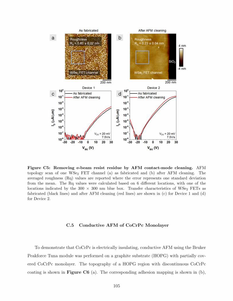
Figure C5: Removing e-beam resist residue by AFM contact-mode cleaning. AFMtopology scan of one WSe2 FET channel (a) as fabricated and (b) after AFM cleaning. Theaveraged roughness (Rq) values are reported where the error represents one standard deviationfrom the mean. The Rq values were calculated based on 6 different locations, with one of thelocations indicated by the 300 × 300 nm blue box. Transfer characteristics of WSe2 FETs asfabricated (black lines) and after AFM cleaning (red lines) are shown in (c) for Device 1 and (d)for Device 2.
C.5 Conductive AFM of CoCrPc Monolayer
To demonstrate that CoCrPc is electrically insulating, conductive AFM using the Bruker
Peakforce Tuna module was performed on a graphite substrate (HOPG) with partially cov-
ered CoCrPc monolayer. The topography of a HOPG region with discontinuous CoCrPc
coating is shown in Figure C6 (a). The corresponding adhesion mapping is shown in (b),
105

where the CoCrPc coated region (appears as darker) is less adhesive to the AFM tip than
the exposed HOPG (brighter). The adhesion mapping is almost independent of changes
in height and only sensitive to surface intrinsic adhesion, which helps us to distinguish the
uncoated region from the HOPG step edges. In Figure C6 (c), the bare HOPG region has
tunneling current (exceeding 1 pA), while the region covered with a CoCrPc monolayer has
∼ 0 tunneling current. This result is sensible because CoCrPc is electrically insulating and
prevents current flowing from conductive AFM tip to HOPG substrate.
Figure C6: AFM images of topology, adhesion and conductivity for CoCrPc ongraphite (HOPG). (a) AFM topology (height) of CoCrPc coated and uncoated regions on HOPG.(b) Adhesion of CoCrPc coated and uncoated regions on HOPG, showing that the uncoated region(i.e., bare HOPG) has a higher adhesion with the AFM tip. (c) Tunneling current mapping mea-sured by conductive AFM (Peakforce Tuna), with an applied voltage of 800 mV. The line scan ofthe tunneling current is shown below the scan where the line scan position is indicated by a dashedline in (c).
106

C.6 Transfer Measurements and Analysis
As shown in Figure C7, programming tests were conducted on the same WSe2 FET
(a) before, (b) after CoCrPc deposition (c) after LiClO4 deposition and (d) after capping
with few-layer h-BN. On the bare FETs, the opening between the transfer curves after pro-
gramming is nearly identical to the intrinsic hysteresis measured without any programming
applied. However, by adding a monolayer of CoCrPc, the magnitude of the shift between
the two transfer curves after programming increases, showing that CoCrPc itself already has
some degree of bistability, as reported previously on graphene. [126] The magnitude further
increases by adding Li+ the CoCrPc to achieve stronger the desired doping effect. After
capping the channel with few-layer h-BN, the bistability is enhanced significantly, reflected
by an additional shift of the transfer curve towards positive VBG after programming Off .
To quantify the shifts in the transfer curves after programming, we track the Vs, defined
as the smallest voltage within the subthreshold swing (SS) region over two decades of current
(Figure C8).
107
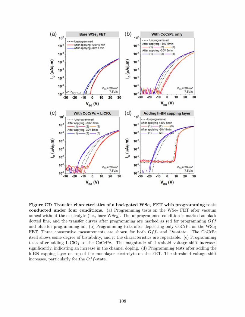
Figure C7: Transfer characteristics of a backgated WSe2 FET with programming testsconducted under four conditions. (a) Programming tests on the WSe2 FET after vacuumanneal without the electrolyte (i.e., bare WSe2). The unprogrammed condition is marked as blackdotted line, and the transfer curves after programming are marked as red for programming Offand blue for programming on. (b) Programming tests after depositing only CoCrPc on the WSe2
FET. Three consecutive measurements are shown for both Off - and On-state. The CoCrPcitself shows some degree of bistability, and it the characteristics are repeatable. (c) Programmingtests after adding LiClO4 to the CoCrPc. The magnitude of threshold voltage shift increasessignificantly, indicating an increase in the channel doping. (d) Programming tests after adding theh-BN capping layer on top of the monolayer electrolyte on the FET. The threshold voltage shiftincreases, particularly for the Off -state.
108
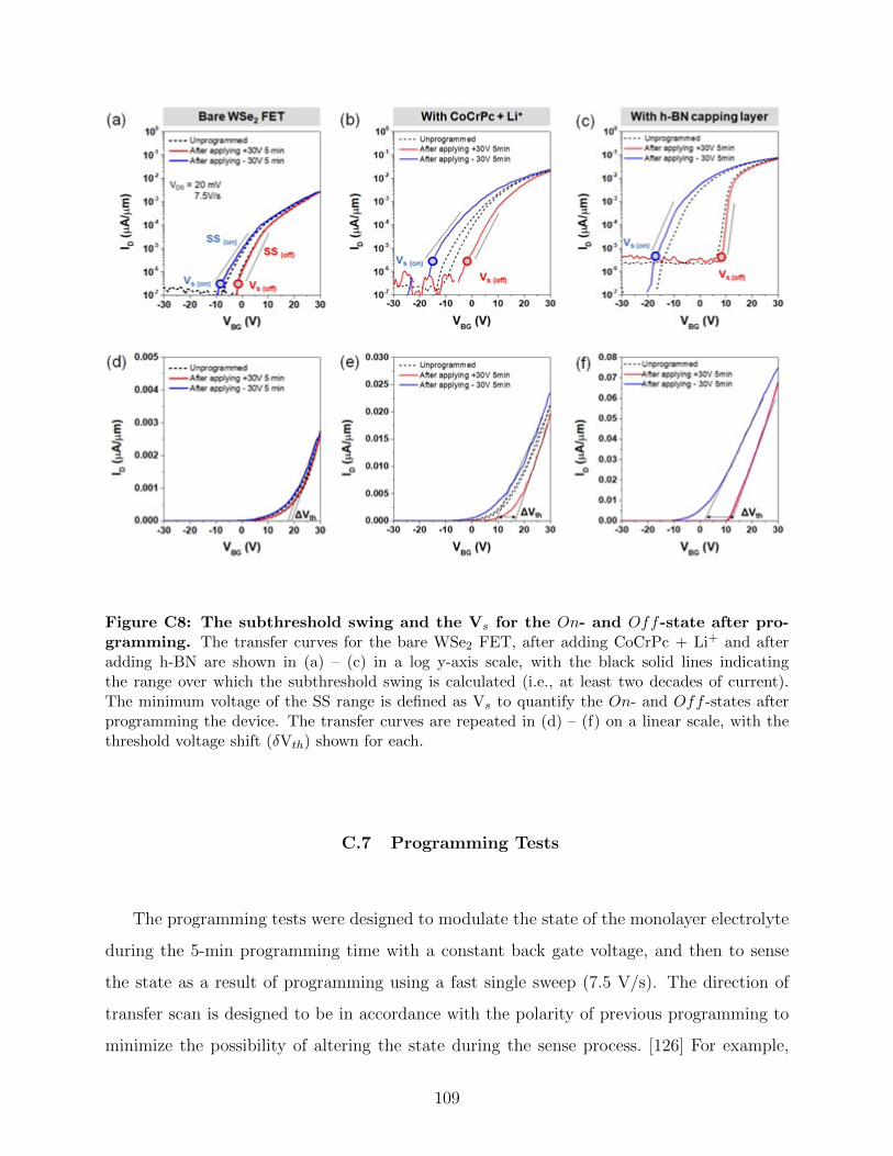
Figure C8: The subthreshold swing and the Vs for the On- and Off-state after pro-gramming. The transfer curves for the bare WSe2 FET, after adding CoCrPc + Li+ and afteradding h-BN are shown in (a) – (c) in a log y-axis scale, with the black solid lines indicatingthe range over which the subthreshold swing is calculated (i.e., at least two decades of current).The minimum voltage of the SS range is defined as Vs to quantify the On- and Off -states afterprogramming the device. The transfer curves are repeated in (d) – (f) on a linear scale, with thethreshold voltage shift (δVth) shown for each.
C.7 Programming Tests
The programming tests were designed to modulate the state of the monolayer electrolyte
during the 5-min programming time with a constant back gate voltage, and then to sense
the state as a result of programming using a fast single sweep (7.5 V/s). The direction of
transfer scan is designed to be in accordance with the polarity of previous programming to
minimize the possibility of altering the state during the sense process. [126] For example,
109

after programming at +30 V, the transfer curve is measured from +30 to -30 V. In this way,
the reverse programming of the device is minimized during the transfer measurement. In
addition, at the beginning of a programming test series (before a programming voltage is
applied), we took a fast (7.5 V/s) double sweep transfer scan to sense the state(s) of device
in an unprogrammed condition.
For example, as shown above in Figure C8 (b), for the MERAMs without h-BN, a
fast double sweep transfer scan was taken before the programming tests, which showed a
small shift of Vs that is likely caused by charge trapping and detrapping at the WSe2/SiO2
interface. [129, 130] Note that we observed identical small shifts of Vs on the bare WSe2
FETs (Figure C8 (a)). After the programming tests, we clearly sense the two states of the
monolayer electrolyte, which are indicated by the two transfer curves with large shift (δVs).
The transfer measurements themselves do not program the device, and this is backed-up by
two pieces of evidence on the MERAM without h-BN: 1) the initial double sweep transfer
scans are similar to the bare FETs, and 2) the Vs shift is much larger for the transfer
curves after programming than the initial double sweep for unprogrammed devices. These
observations are in accordance with previous results on graphene FETs. [126]
In contrast, for the MERAM for which h-BN has been added, the initial double sweep
transfer scans exhibit an increased Vs shift compared to the bare FETs. More specifically, the
magnitude of the Vs shifts is comparable to those observed during programming (black dash
in Figure C8 (c)). Thus, in contrast to the devices without h-BH, the state of the monolayer
electrolyte was switched during the transfer scans, which could possibly be explained by h-
BN reducing the energy barrier to switching. To investigate the minimum voltage required
to switch the device, we monitored the On/Off ratio of two states while varying the VBG
(see Figure C12 (Device 2)). Using a programming voltage of ∼ ± 20 V and a programming
time of one-second, we can switch the states of the monolayer electrolyte with an On/Off
ratio of ∼ 104. This finding agrees with our observation in the programming test transfer
measurements and supports the conclusion that the device with h-BN was switched during
the transfer scans of -30 to 30 V and then back to -30V. The reason that the transfer curves do
not overlap above the measured minimal switching voltage (∼20 V) can likely be attributed
to intrinsic hysteresis caused by charge trapping (Figure C8 (c)).
110
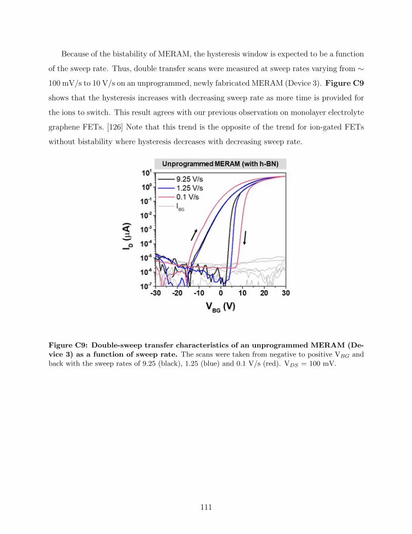
Because of the bistability of MERAM, the hysteresis window is expected to be a function
of the sweep rate. Thus, double transfer scans were measured at sweep rates varying from ∼
100 mV/s to 10 V/s on an unprogrammed, newly fabricated MERAM (Device 3). Figure C9
shows that the hysteresis increases with decreasing sweep rate as more time is provided for
the ions to switch. This result agrees with our previous observation on monolayer electrolyte
graphene FETs. [126] Note that this trend is the opposite of the trend for ion-gated FETs
without bistability where hysteresis decreases with decreasing sweep rate.
Figure C9: Double-sweep transfer characteristics of an unprogrammed MERAM (De-vice 3) as a function of sweep rate. The scans were taken from negative to positive VBG andback with the sweep rates of 9.25 (black), 1.25 (blue) and 0.1 V/s (red). VDS = 100 mV.
111
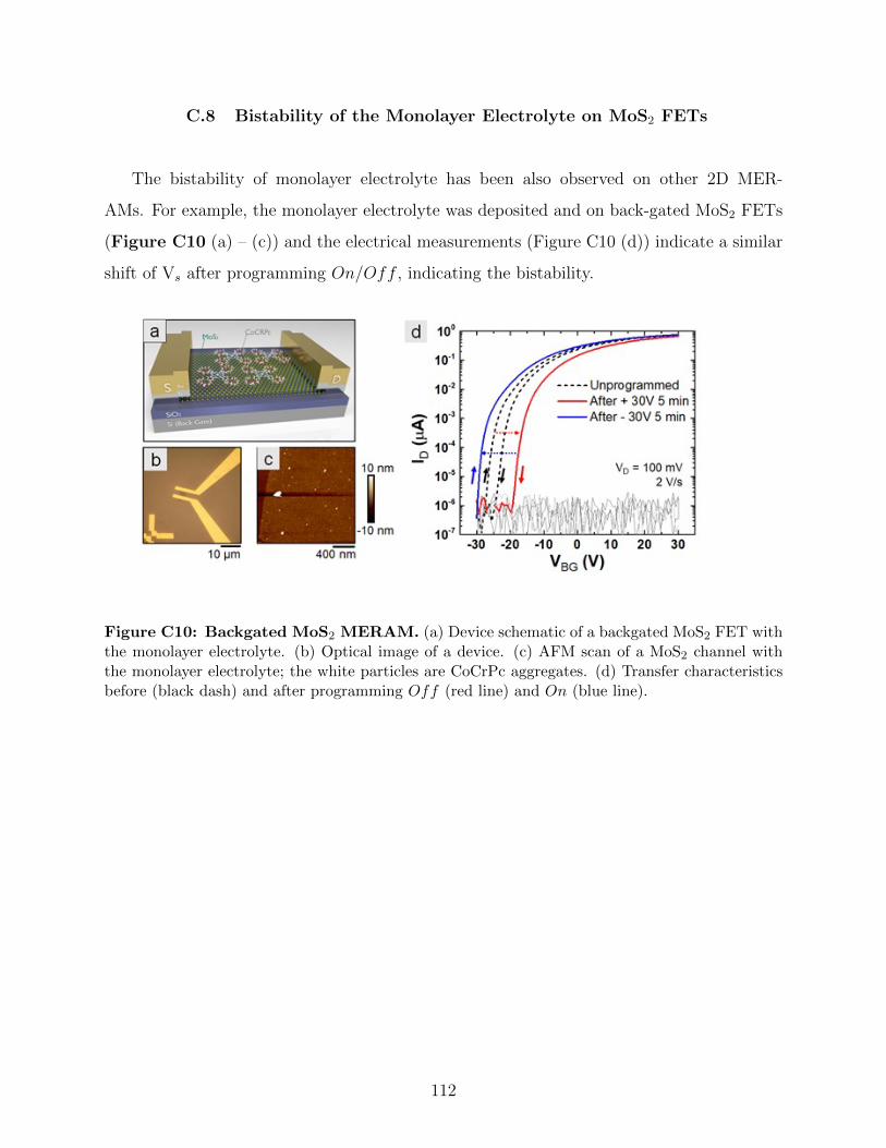
C.8 Bistability of the Monolayer Electrolyte on MoS2 FETs
The bistability of monolayer electrolyte has been also observed on other 2D MER-
AMs. For example, the monolayer electrolyte was deposited and on back-gated MoS2 FETs
(Figure C10 (a) – (c)) and the electrical measurements (Figure C10 (d)) indicate a similar
shift of Vs after programming On/Off , indicating the bistability.
Figure C10: Backgated MoS2 MERAM. (a) Device schematic of a backgated MoS2 FET withthe monolayer electrolyte. (b) Optical image of a device. (c) AFM scan of a MoS2 channel withthe monolayer electrolyte; the white particles are CoCrPc aggregates. (d) Transfer characteristicsbefore (black dash) and after programming Off (red line) and On (blue line).
112

C.9 Program/erase on a Backgated WSe2 FET with Only the Monolayer
Electrolyte (no h-BN)
Figure C11 shows the endurance (a) and retention test (b) on a MERAM without h-
BN capping. Two distinct states are observed during 1000 cycles of program/erase and each
state can be maintained over six hours, but with a smaller On/Off ratio (∼ 1.3) compared
to the devices capped with h-BN.
Figure C11: Program/erase tests using VBG on a backgated WSe2 FET with onlymonolayer electrolyte (no h-BN). (a) Program/erase endurance test. 1000 cycles of pro-gram/erase with pulse with of 1 s, readout time of 10 s, and VDS = 500 mV. (b) Retention test.Program/erase with 60 s pulse and ID monitored for 6 hours. High/low current states are inblue/red color, respectively.
113

C.10 Program/erase Measurements as a Function of Back Gate Voltage on
Two MERAMs (with h-BN)
In Figure C12, the On- and Off -states are monitored while varying the |VBG| during
program/erase (negative/positive VBG) for 2 MERAMs. Note that the minimum VBG re-
quired to fully switch the MERAM from one state to the other is different on two MERAMs,
which could be due to the differences in field screening resulting from varying WSe2 channel
thicknesses (∼ 8 nm for Device 1, 6 nm for Device 2).
Figure C12: Program/erase tests using different VBG on two MERAMs. The programand erase voltages vary from ± 5 to ± 30 V. The pulse width is 1 second and the readout is 10seconds at VBG = 0 V; VDS = 500 mV. Data at each point are averaged over 12 program/erasecycles with the error bar indicating one standard deviation from the mean.
114

Appendix D
Supporting Information for Chapter 4
D.1 Electrolyte Preparation
D.1.1 Single-ion Conductor Synthesis
The polyester single-ion conductor was synthesized by a two-step melt condensation be-
tween poly(ethylene glycol) (PEG) 400 (Mw = 400 g mol−1) and dimethyl 5-sulfoisophthalate
sodium salt. [141] The resulting polyester Na was then sealed in semipermeable dialysis mem-
branes and exposed to an excess of LiCl (0.5 M) in deionized water to exchange Na+ for
Li+. [141] The final product, polyester Li (PE400-Li), was dissolved in dimethylformamide
(DMF) inside an Ar-filled glovebox to obtain a 3 wt % solution. The solution was drop-cast
on graphene and MoTe2 FETs (8 µL on the 1 cm2 chip), and the DMF was removed by evap-
orating naturally in the glovebox overnight. The FETs coated with the single-ion conductor
were transferred back to the probe station using the load lock for subsequent measurements.
D.1.2 Dual-ion Conductor
The dual-ion conducting polymer electrolyte (PEO:CsClO4) was prepared similarly to
previously published work. [20] PEO (Polymer Standards Service, Mw = 94600 g mol−1) and
CsClO4 (Sigma-Aldrich, 99.9%) were dissolved in anhydrous acetonitrile (Sigma-Aldrich)
to make a 1 wt % solution with an ether oxygen to Cs molar ratio of 76:1. Twenty-five
microliters of the solution was drop-cast onto the 1 cm2 sample of graphene FETs in the
glovebox, dried at room temperature until the majority of the solvent evaporated, and then
annealed at 80 ◦C for 3 min.
115

D.2 DSC of Single-ion Conductor
DSC samples were prepared inside the Ar-filled glovebox. 8.7 mg of single-ion conductor
(PE400-Li) and 7.1 mg PEO:CsClO4 were hermetically sealed in an aluminum DSC pan.
Measurements were made on a TA 250 calibrated with an indium standard. To measure the
glass transition temperature (Tg) and the melting temperature (Tm), samples were heated
to 100 ◦C to erase thermal history, cooled to -70 ◦C at 3 ◦C min-1 and heated to 100 ◦C
at 5 ◦C min−1. As shown in Figure D1 (a), the glass transition temperature of single-ion
conductor is identified at 14.5 ◦C, while only a very subtle melting feature is found at around
75 ◦C (see the inset in (a)). In contrast, the dual-ion conductor, PEO:CsClO4 (ether oxygen
to Cs molar ratio = 76:1), has a Tg of -31.5 ◦C with a distinct melting peak (Tm) at 63.6
◦C shown in (b). Although the single-ion conductor is almost completely amorphous, the
higher Tg indicates slower segmental polymer mobility and therefore lower ion mobility. This
result is consistent with the larger hysteresis in the transfer measurements observed for the
single-ion conductor compared to the dual (Figures 15 and 16(a)).
116
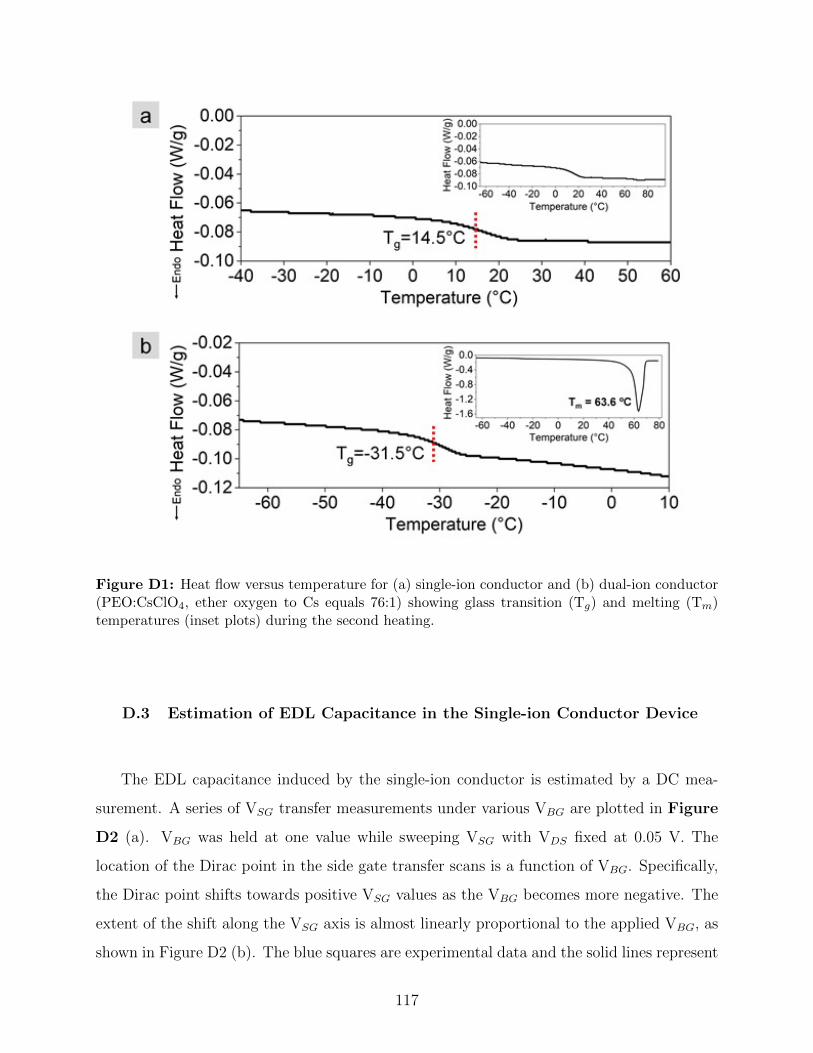
Figure D1: Heat flow versus temperature for (a) single-ion conductor and (b) dual-ion conductor(PEO:CsClO4, ether oxygen to Cs equals 76:1) showing glass transition (Tg) and melting (Tm)temperatures (inset plots) during the second heating.
D.3 Estimation of EDL Capacitance in the Single-ion Conductor Device
The EDL capacitance induced by the single-ion conductor is estimated by a DC mea-
surement. A series of VSG transfer measurements under various VBG are plotted in Figure
D2 (a). VBG was held at one value while sweeping VSG with VDS fixed at 0.05 V. The
location of the Dirac point in the side gate transfer scans is a function of VBG. Specifically,
the Dirac point shifts towards positive VSG values as the VBG becomes more negative. The
extent of the shift along the VSG axis is almost linearly proportional to the applied VBG, as
shown in Figure D2 (b). The blue squares are experimental data and the solid lines represent
117
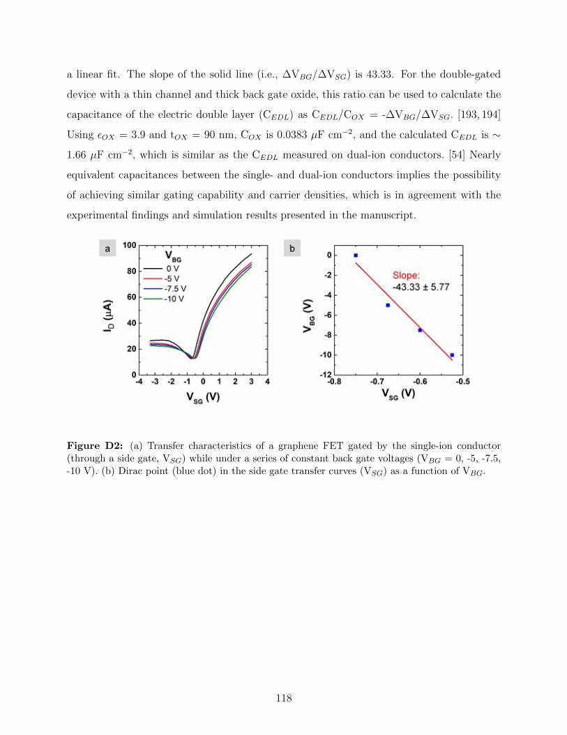
a linear fit. The slope of the solid line (i.e., ∆VBG/∆VSG) is 43.33. For the double-gated
device with a thin channel and thick back gate oxide, this ratio can be used to calculate the
capacitance of the electric double layer (CEDL) as CEDL/COX = -∆VBG/∆VSG. [193, 194]
Using εOX = 3.9 and tOX = 90 nm, COX is 0.0383 µF cm−2, and the calculated CEDL is ∼
1.66 µF cm−2, which is similar as the CEDL measured on dual-ion conductors. [54] Nearly
equivalent capacitances between the single- and dual-ion conductors implies the possibility
of achieving similar gating capability and carrier densities, which is in agreement with the
experimental findings and simulation results presented in the manuscript.
Figure D2: (a) Transfer characteristics of a graphene FET gated by the single-ion conductor(through a side gate, VSG) while under a series of constant back gate voltages (VBG = 0, -5, -7.5,-10 V). (b) Dirac point (blue dot) in the side gate transfer curves (VSG) as a function of VBG.
118
D.4 Impact of Device Geometry on Charge Density
Figure 15 in the manuscript presented how the single ion conductor produces different
magnitudes of carrier density under positive and negative voltage. This unequal charge
density is directly related to device geometry. To elaborate on this, the transient carrier
densities for both conductors are shown in Figure D3 to highlight the dependence of carrier
densities on geometry. My labmate (Aaron Woeppel) modeled 3 geometries including: (a)
the grounded electrode (2.5 µm) is 10 times smaller than ungrounded electrode (25 µm); (b)
both electrodes are long (50 µm in length); and (c) both electrodes are equally small (2.5
µm).
The modeling shows that a dual-ion conductor will always produce EDLs with equal
carrier density under both positive and negative applied voltage, regardless of whether elec-
trode sizes is equal. Meanwhile, a single-ion conductor will only produce symmetric carrier
densities (either constituting an EDL or depletion region) if the electrodes are equally sized.
In addition, the magnitude of charge density depends on the ratio between the area of
the two electrodes. Using the unequally sized electrodes (Figure D3 (a)) resulted in a greater
carrier density per area adjacent to the grounded electrode than using equally sized electrodes
(Figures D3 (b) and (c)). This is because the large electrode will have a higher capacitance
requiring less voltage drop to sustain the same charge. Since the depletion region near the
larger electrode requires less voltage drop, EDLs near the smaller (grounded) electrode can
produce larger voltage drops resulting in greater carrier density. The voltage sweeps shown
in Figure D3 (a) show such an increase in carrier density (compared with D3 (b) or (c)). The
only exception is when a depletion region forms near the grounded electrode. When the two
electrodes have equal area, the depletion region already requires a large voltage drop (0.75
out of 1 V). When the depletion region is adjacent to a small grounded electrode, it requires
an even larger voltage drop constituting nearly the entirety of the applied voltage (0.95 out
of 1 V). Because of the large voltage drop required to create a depletion region near a small
electrode, the single-ion conductor does not produce a significantly higher carrier density
under negative bias after implementing the new geometry.
119

Figure D3: (Left column) Schematics of a single-ion conductor with charge accumulations underthe applied voltages, and (right column) the corresponding accumulated charge carrier densitiesfor the single-ion (red) and dual-ion conductors (blue) during sweeping the applied voltages. Thedependence of charge density on the ratio of electrode size is illustrated in 3 geometries during 1Dmodeling: (a) electrode size (right, 25 µm in length) = 10x electrode (left, grounded, 2.5 µm); (b)equally sized electrodes (50 µm in length); and (c) equally sized small electrodes (2.5 µm in length).
120

To ensure the increase in sheet density was the result of unequal electrode length and
not simply changing the area of the electrode of interest, both electrodes were decreased to
the smaller size (2.5 µm), and results are shown in Figure D3 (c). Zero charge boundary
conditions were once again employed to maximize similarity between this geometry and the
original equally sized electrode geometry. This geometry resulted in carrier densities (Figure
D3 (c)) of similar magnitude to the geometry in Figure D3 (b) where the two electrodes are
both 50 µm long.
Interestingly, we also noticed that reducing the ungrounded electrode (right side) size
also reduced the achievable carrier density for both the single- and dual-ion conductors. This
could suggest that - as a general rule - it is desirable to design the gate electrode larger than
channel size for EDL gating to achieve a higher carrier density in the channel.
121

D.5 AFM Topology Scan After Single-ion Conductor Removal
Figure D4: AFM topology scan of one graphene FET channel (a) after washing the single-ionconductor with Dimethylformamide (DMF) but before AFM cleaning, and (b) after AFM cleaning.The averaged roughness (Rq) values are reported where the error represents one standard deviationfrom the mean. Rq was calculated based on 6 different locations, with one of the locations indicatedby the 400 × 400 nm white box. (c) Line scans of flake height before (black) and after AFM cleaning(red line). The positions of line scans are indicated by white lines on AFM images.
122

D.6 Output Characteristics of Single-ion Conductor Gated MoTe2 FET
The output characteristics of a single-ion conductor gated MoTe2 FET under four dif-
ferent gate voltages is shown in Figure D5 (a) and zoomed-in for the small current region
in (b). ID increases as the gate voltage increases from 0 to 3 V, indicating the effective gate
control of channel current using the single-ion conductor. No saturation is observed up to
VD = 1 V.
Figure D5: (a) Output characteristics of a single-ion conductor gated MoTe2 FET under fourdifferent gate voltages (0 - 3 V). (b) The zoomed-in plot at small ID region on the same outputcharacteristics.
123

Appendix E
Supporting Information for Chapter 5
E.1 Using Doubly-polymerizable Ionic Liquid to Create a Graphene P-N
Junction
E.1.1 Device Fabrication
The same e-beam lithography process has been employed to fabricated all kinds of devices
used in DPIL project, including the four-electrode graphene device for p-n junction, graphene
and WSe2 FETs before electrolyte deposition.
Graphene (∼ 1.5 nm thick) and WSe2 flakes (∼ 3-10 nm thick) were exfoliated from the
bulk (HQ Graphene) by mechanical cleaving (i.e., Scotch tape method) and transferred to
a 1 × 1 cm2 p-type Si (Graphene Supermarket, resistivity 0.001–0.005 ohm cm) with 90
nm SiO2. The substrate was pre-cleaned with acetone, isopropanol (IPA), deionized (DI)
water and dried with N2. E-beam lithography (Raith e-LINE) was used to pattern the
electrodes. PMMA-950-A4 (MicroChem) was spin-coated at 4000 rpm for 1 min and then
annealed at 175 ◦C for 7 min. After exposure, the resist was developed in methyl isobutyl
ketone MIBK:IPA (1:3 volume ratio) for 2 min, and rinsed with IPA for another 2 min. E-
beam evaporation (Plassys Electron Beam Evaporator MEB550S) was used to deposit metal
electrodes (3 nm Ti; 130 nm Au) at a base pressure < 1 × 10⁻⁶ Torr. Lift-off was performed
in acetone overnight for 9 hours, followed by IPA, DI water rinse and N2 drying.
Using contact-mode atomic force microscopy (AFM, Bruker Dimension Icon) as described
in Appendix A3, e-beam resist residue was removed from the graphene between the elec-
trodes. Before electrical measurements, samples were annealed at 127 ◦C (400 K) in vac-
uum at a pressure of 9 × 10⁻⁷ Torr for 4 hours. Electrical measurements were made on a
Lakeshore cryogenic vacuum probe station using a Keysight B1500A semiconductor parame-
124

ter analyzer. After initial measurements on bare devices, the samples were transferred to an
Ar-filled glovebox (H2O and O2 concentration < 0.1 parts-per-million (ppm)) for electrolyte
deposition.
E.1.2 DPIL Preparation and Heat-induced Polymerization for the P-N Junc-
tion
DPIL monomers, 1-[(2-methacryloyloxy)ethyl]-3-methylimidazolium 1-[3-(methacryloy-
loxy)propylsulfonyl]-1-(trifluoromethane-sulfonyl)imide, were synthesized according to ref-
erence. [179, 195, 196] One mg of the thermal initiator, azobisisobutyronitrile (AIBN), was
dissolved in 100 µL unpolymerized DPIL monomer, and then drop-cast in the glovebox (25
µL over 1 cm2) with thickness estimated to be ∼ 200 µm according to the cast volume.
The samples were transferred to the probe station via a load-lock using an Ar-filled stain-
less steel suitcase. A programming voltage (V2 = +1 V and V3 = -1 V) was held for 10
min for p-n junction formation, followed by a 6-hour polymerization anneal at 353 K with
the voltage applied, which is more than sufficient for immobilizing ions by polymerization.
After polymerization, the device was cooled at µ 0.3 K/min to room temperature and the
programming voltage was removed.
125

E.2 Capacitor Measurements of Ion Release Using Triggerable Polymerizable
Ionic Liquids
E.2.1 Capacitor Fabrication
1 × 1 cm2 Si substrates with 90 nm SiO2 (Graphene Supermarket, resistivity 0.001 -
0.005 ohm cm) were pre-cleaned with acetone, IPA, DI water and dried with N2. LOR5B
(MicroChem) photoresist was spin-coated on the substrate at 4000 rpm for 1 min and an-
nealed at 195 ◦C for 9 min. A second photoresist, S1805 (Microposit, 5000 rpm, 1 min), was
spincoated on top of the first and annealed at 115 ◦C for 5 min. Capacitors were patterned by
direct write photolithography (Heidelberg MLA100) with 10 mm electrode spacing. Samples
were developed for 75 s in Microposit 351, 30 s in DI water, 40 s in AZ 400K (Microchemical),
rinsed in DI water for 30 s and dried with N2. Ti/Au (3/140 nm) was deposited by e-beam
evaporation (Plassys MEB550S) at < 1 × 10⁻⁶ Torr. Lift-off was performed in Remover PG
(MicroChem) overnight for 9 hours, followed by IPA, DI water rinse and N2 drying.
E.2.2 Deposition and UV Polymerization of Polymerizable Ionic Liquids
The unpolymerized triggerable and non-triggerable singly polymerizable ionic liquids (T-
SPIL and NT-SPIL, respectively) were drop-cast on the capacitors (25 µL over 1 cm2) in an
argon-filled glovebox with H2O and O2 < 0.1 ppm. The samples were transferred without
air exposure from the glove box to a cryogenic vacuum probe station (Lakeshore, CRX-VF)
via a custom load-lock for electrical measurements at 2 × 10⁻⁶ Torr and 295 K. After the
measurements, the samples were transferred back to the glovebox for UV polymerization.
∼ 5 µL of a 0.25 wt% solution of 2,2-dimethoxy-2-phenylacetophenone in dichloromethane
was added to each T- and NT-SPIL by drop-casting and natural drying in the glove box.
The samples were UV polymerized using a UVP Compact UV lamp (l = 365 nm, P = 1.3
mW cm−2 at 7.6 cm) at a working distance of 1.5 cm for 30 min. After polymerization, the
samples were transferred back to the probe station without exposure to air to complete the
electrical characterization over a temperature range of 295 to 400 K.
126

E.2.2.1 Electrical Characterization of Capacitor Charging Current Charging
current was monitored with time using a Keysight B1500A semiconductor parameter ana-
lyzer. Voltage was applied to terminal 1 (V1) with terminal 2 (V2) grounded while monitor-
ing the current (I1) for 5 minutes. The current decayed to < 50 pA within the measurement
time indicating a full charge. V1 = +1.5 V for T-SPIL; V1 was reduced to +0.5 V for NT-
SPIL to meet the current sensor range. Similarly, a discharge time of 5 minutes was set to
ensure full discharging of the device to avoid hysteresis. To detect ion mobility as a function
of temperature, the charging and discharging measurements were made on the polymerized
samples over a temperature range of 295 to 395 K, with 10 K steps and a ramp rate of
2 K/min. Measurements at 400 K were repeated twice with a 4 hour wait time between
measurement to monitor stability. Once the setpoint was reached, the sample was held at
the set temperature for 5 min prior to measurement to establish thermal equilibrium. Lastly,
samples were cooled from 400 to 295 K at 0.3 K/min and measured at 295 K.
127

Appendix F
Co-authored Publications
For the research presented in this dissertation, I co-authored several publications listed
below; my specific contributions are also highlighted:
1. Liang, J.; Xu, K.; Wu, M.; Hunt, B.M.; Wang, W.H.; Cho, K.; Fullerton-Shirey, S.K.
“Molecularly thin electrolyte for all solid-state nonvolatile two-dimensional crystal memory”,
Nano Letters, 19.12 (2019): 8911-8919.
Contribution: manuscript preparation, electrolyte preparation, device fabrication and
AFM cleaning, optical and AFM characterization, electrical measurements.
2. Liang, J.; Xu, K.; Toncini, B.; Bersch, B.; Jariwala, B.; Lin, Y.; Robinson, J.;
Fullerton-Shirey, S.K. “Impact of post lithography polymer residue on the electrical char-
acteristics of MoS2 and WSe2 field effect transistors”, Advanced Materials Interfaces, 6.3
(2019): 1801321.
Contribution: manuscript preparation, electrolyte preparation, device fabrication for
backgated FETs, AFM cleaning for all devices, optical and AFM characterization, Raman
spectroscopy, electrical measurements.
3. Xu, K.; Liang, J. (co-first author); Woeppel, A.; Bostian, M.; Ding, H.; Chao,
Z.; McKone, J.; Beckman, E.; Fullerton-Shirey, S.K. “Electric double-layer gating of two-
dimensional field-effect transistors using a single-ion conductor”, ACS Applied Materials &
Interfaces, 11.39 (2019): 35879-35887.
Contribution: manuscript preparation, device fabrication, AFM cleaning, optical and
AFM characterization.
4. Liang, J.; Xu, K.; Arora, S.; Laaser, J.; Fullerton-Shirey, S.K. “Ion-locking in solid
polymer electrolytes for reconfigurable gateless lateral graphene p-n junctions”, Materials,
13.5 (2020): 1089.
128

Contribution: manuscript preparation, electrolyte preparation, device fabrication, AFM
cleaning, optical and AFM characterization, electrical measurements, ion-locking using poly-
merization.
5. Arora, S.; Liang, J.; Fullerton-Shirey, S.K.; Laaser, J. “Triggerable ion release in
polymerized ionic liquids containing thermally-labile diels-alder linkages”, ACS Materials
Letters, 2.4 (2020): 331-335. (Featured as cover art by J. Liang)
Contribution: manuscript preparation, cover art preparation, electrolyte deposition, ion-
locking using polymerization, capacitor fabrication, electrical measurements.
6. Sun, Z.; Beaumariage, J.; Xu, K.; Liang, J.; Hou, S.; Forrest, S.R.; Fullerton-Shirey,
S.K.; Snoke, D.W. “Electric-field-induced optical hysteresis in single-layer WSe2”, Applied
Physics Letters, 115.16 (2019): 161103.
Contribution: figure preparation, electrolyte preparation, device fabrication, optical and
AFM characterization.
129

F.1 Publications
The studies of ion-controlled electronics presented in this dissertation have been published
in six papers as attached in this section.
130

Molecularly Thin Electrolyte for All Solid-State Nonvolatile Two-Dimensional Crystal MemoryJierui Liang,†,# Ke Xu,*,†,# Maokun Wu,‡ Benjamin M. Hunt,§ Wei-Hua Wang,‡ Kyeongjae Cho,∥
and Susan K. Fullerton-Shirey*,†,⊥
†Department of Chemical and Petroleum Engineering, University of Pittsburgh, Pittsburgh, Pennsylvania 15260, United States‡Department of Electronic Science and Engineering and Tianjin Key Laboratory of Photo-Electronic Thin Film Device andTechnology, Nankai University, Tianjin 300071, P.R. China§Department of Physics, Carnegie Mellon University, Pittsburgh, Pennsylvania 15213, United States∥Department of Materials Science and Engineering, The University of Texas at Dallas, Richardson, Texas 75080, United States⊥Department of Electrical and Computer Engineering, University of Pittsburgh, Pittsburgh, Pennsylvania 15260, United States
*S Supporting Information
ABSTRACT: A molecularly thin electrolyte is developed to demonstrate a nonvolatile, solid-state, one-transistor (1T) memorybased on an electric-double-layer (EDL) gated WSe2 field-effect transistor (FET). The custom-designed monolayer electrolyteconsists of cobalt crown ether phthalocyanine and lithium ions, which are positioned by field-effect at either the surface of theWSe2 channel or an h-BN capping layer to achieve “1” or “0”, respectively. Bistability in the monolayer electrolyte memory issignificantly improved by the h-BN cap with density functional theory (DFT) calculations showing enhanced trapping of Li+
near h-BN due to a ∼1.34 eV increase in the absolute value of the adsorption energy compared to vacuum. The thresholdvoltage shift between the two states corresponds to a change in charge density of ∼2.5 × 1012 cm−2, and an On/Off ratioexceeding 104 at a back gate voltage of 0 V. The On/Off ratio remains stable after 1000 cycles and the retention time for eachstate exceeds 6 h (max measured). When the write time approaches 1 ms, the On/Off ratio remains >102, showing thatthe monolayer electrolyte-gated FET can respond on time scales similar to existing flash memory. The data suggest that fasterswitching times and lower switching voltages could be feasible by top gating.
KEYWORDS: Nonvolatile memory, iontronics, ionic gating, electric double layer, field effect transistor, 2D crystal
Floating-gate flash memory (e.g., NAND and NOR Flash),the most popular nonvolatile memory (NVM), uses a one-
transistor (1T) cell structure where a field-effect transistor(FET) serves both as the cell selector and the storage node.1,2
The 1T architecture exhibits better scalability and simplerintegration than the one-transistor, one-capacitor (1T1C)structure used in, for example, dynamic random accessmemory (DRAM).2 Among the emerging NVM devices,ferroelectric gate transistors allow 1T architecture. Thesedevices can be used both as a memory (FeFET)3−6 and also asa low-voltage logic device (NCFET)7−13 with appropriateferroelectric design. Compared to Flash memory whichrequires >10 V to inject and withdraw electrons from a
floating gate,14 the polarization switching mechanism inferroelectric devices shows promise for energy-efficient switch-ing with nondestructive read-out, write endurance, andscalability for the sub-10 nm technology node.15−17 Here wepropose a new 1T NVM concept that uses ions to program andhold the polarization state of an electrolyte that is a singlemolecule thick.18−21 The device, referred to as monolayerelectrolyte random access memory (MERAM), resembles theFeFET and NCFET because it also relies on polarization
Received: September 13, 2019Revised: October 22, 2019Published: October 29, 2019
Letter
pubs.acs.org/NanoLettCite This: Nano Lett. 2019, 19, 8911−8919
© 2019 American Chemical Society 8911 DOI: 10.1021/acs.nanolett.9b03792Nano Lett. 2019, 19, 8911−8919
Dow
nloa
ded
via
UN
IV O
F PI
TT
SBU
RG
H o
n Ja
nuar
y 13
, 202
0 at
19:
55:2
4 (U
TC
).Se
e ht
tps:
//pub
s.ac
s.or
g/sh
arin
ggui
delin
es f
or o
ptio
ns o
n ho
w to
legi
timat
ely
shar
e pu
blis
hed
artic
les.

switching, but offers the potential to integrate the mechanicaland electrical properties of two-dimensional (2D) crys-tals.22−26 For example, in the area of flexible nanoelec-tronics,27−29 MERAM avoids the challenges of growing oxideson flexible and 2D surfaces that are free of dangling bonds.The operating mechanism of MERAM is the modulation of
channel resistance by an electric double layer (EDL) formed atthe interface of the channel and a molecularly thin electro-lyte.18−21 The EDL acts as an interfacial capacitor (thickness∼1 nm), controlling charge carrier accumulation or depletionin the semiconductor channel.30,31 The main advantage of theEDL is the proximity of the ions to the channel surface, whichinduces large capacitance densities (1−10 μF cm−2)corresponding to sheet carrier densities in the range of1013−1014 cm−2.30,32,33 The high capacitance could lower theoperating voltage as required for power-efficient electronics.EDL gating is a common technique for 2D materials,
enabling iontronics with various functions.32,34−40 However, inconventional electrolytes such as solid polymer electrolytes andionic liquids/gels, a gate voltage must be continuously applied
to hold the state of the device. When the bias is removed, theions diffuse from the semiconductor surface and the state islost, making these materials unsuitable for NVM. Moreover,the speed of the device will depend on the velocity of the ions,which is directly proportional to the ionic conductivity and theelectric field strength and can be increased by decreasing theelectrolyte thickness.30,40 Therefore, we developed a newelectrolyte with the thickness scaled to a single molecular layerand with a switching barrier for state retention. The monolayerelectrolyte consists of cobalt crown ether phthalocyanine(CoCrPc) with four, 15-crown-5 ethers covalently bonded to acobalt-substituted phthalocyanine.18−21,41 Each crown ether(CE) can solvate one Li+. CoCrPc is solution processable asdesired for high-throughput deposition and printablecircuits.18,30,42 Using simple drop-casting and annealing, theCoCrPc molecules form a flat and ordered array on 2Dmaterials. We have demonstrated single monolayers of CoCrPcwith a bandgap of 1.34 eV on highly oriented pyrolyticgraphite (HOPG)18 and graphene FETs,21 and on WSe2 andMoS2 in this work (Figure S1 and S2, Supporting
Figure 1. Monolayer electrolyte structure and mechanism, and fabricated MERAM device. (a) Structure of the monolayer electrolyte consisting ofCoCrPc and four Li+ with one in each crown-ether ring (top), and side views of the two energetically favorable configurations of the monolayerelectrolyte (bottom). These two configurations correspond to the On- and Off-states; note that the ether oxygens in the crown are positioned up ordown along with the Li+. (b) DFT results for two Off-state configurations: (top) CE-Li+ on WSe2 exposed to vacuum only, and (bottom) CE-Li+
on WSe2 capped by h-BN. (c) MERAM schematic, sideview of the WSe2/monolayer electrolyte/h-BN stack, and an optical image of the MERAM(false colored, Device 2). (d) AFM scans of the WSe2 FET channel (Device 2) after AFM cleaning (left) and after CoCrPc deposition (right), andthe corresponding line scans.
Nano Letters Letter
DOI: 10.1021/acs.nanolett.9b03792Nano Lett. 2019, 19, 8911−8919
8912

Information). Charge carrier modulation, bistability, andnonvolatility have been previously demonstrated by us ingraphene FETs.21 Density functional theory (DFT) revealstwo energetically favorable configurations when the CE ispositioned at the surface of a 2D material: 2D/Li+/CE and2D/CE/Li+, where Li+ is closer to and further from the 2Dsurface, respectively.19 Under an applied electric field normalto the plane of the CE molecules, lithium ions overcome anenergy barrier of 0.3 eV to pass through the cavity of the CEs,switching from one configuration to another and causing achange in the channel charge density and conductivity.20 Theheight of the energy barrier can be modulated by the strengthof the applied field, suggesting the possibility of subvoltswitching and long (i.e., years) retention.20,21
Our previous studies of the monolayer electrolyte werereported on graphene, a semimetal without a bandgap andtherefore a low On/Off current ratio.21 In contrast, a 2Dsemiconductor with a subthreshold region near 0 V is optimalbecause larger On/Off ratio can be achieved, and the devicecan be read at 0 V without disturbing the memory state.Herein, we demonstrate a MERAM based on a stack of WSe2/monolayer electrolyte/h-BN. WSe2 is selected as the semi-conductor due to its subthreshold region near 0 V,43 sizablebandgap (∼1.2 eV for few-layer),44 and relatively high carriermobility (∼140 cm2 V−1 s−1).45 A multilayer h-BN serves asthe capping and encapsulation layer,25,46 which could also beused in the future as a top-gate dielectric.47 Transfercharacteristics of the MERAM show bistability with an On/Off ratio of 105 at a read voltage of VBG = 0 V. Endurance testsshow an On/Off ratio maintained at ∼105 after 1000 cycles ofprogram/erase (max measured) and the retention of each stateexceeds 6 h (max measured). In addition, the On/Off ratioremains >102 at the switching speed of 1 ms, which is theshortest time measured.MERAM Mechanism. Figure 1a shows the structure of the
monolayer electrolyte; the mechanism is represented bythe schematics of the two stable CE-Li+ configurations(based on previous DFT calculations19,20). Under a negativeback gate voltage, CE-Li+ is pulled near the 2D channel,forming an EDL at the interface and doping the channel n-type; this state is denoted as the On-state where the Li+ isstabilized by both the 2D surface and the CE. The Off-state iscreated under positive back gate voltage where CE-Li+ ispushed away from the channel, reducing the n-doping.To enhance the Off-state stability, a capping layer of h-BN is
added such that the Li+ is stabilized by both CE and h-BN.The degree of stabilization is estimated by DFT calculationswith and without the h-BN layer, shown in Figure 1b. Themost energetically favorable location of the CE-Li+ complex onWSe2 corresponds to Li+ aligned directly above W atom(Figure S3, Supporting Information). In the Off-state, theabsorption energy (Ead) between the CE-Li
+ and WSe2 with nocapping layer (i.e., in vacuum) is −3.81 eV; however, theadsorption stability is enhanced to Ead = −5.15 eV by cappingwith h-BN. Thus, h-BN deepens the energy well of the Off-state by an additional −1.34 eV and is therefore predicted tostabilize Li+ in the Off-state configuration: WeS2/CE/Li
+/h-BN.MERAM Assembly. To monitor EDL switching dynamics,
MERAMs of WSe2/monolayer electrolyte/h-BN were fabri-cated (Figure 1c). In brief, few-layer WSe2 (thickness ∼6−8nm) flakes were exfoliated and Pd/Au source-drain contactswere patterned by electron-beam lithography (EBL) and metal
evaporation. EBL resist residue (∼1−2 nm) was removed fromthe WSe2 channel by atomic force microscopy (AFM) incontact mode.48 A residue-free WSe2 surface is essential for theMERAM because the molecular arrangement of the monolayerelectrolyte will be disrupted by a few nanometers of polymerresidue. Note that the cleaning does not degrade the maximumcurrent and mobility of the WSe2 FET (Figure S5, SupportingInformation).48 An AFM image of the cleaned WSe2 FETchannel is shown in Figure 1d, where the surface roughness isreduced from 0.82 ± 0.02 to 0.23 ± 0.04 nm, as shown inFigure S5.A monolayer of CoCrPc is deposited on WSe2 FETs by
drop-casting and annealing in a glovebox,18 where the CoCrPcdosage and annealing temperature are optimized for WSe2(Figure S2, Supporting Information). AFM scans taken insidethe glovebox of one WSe2 FET before and after CoCrPcdeposition are shown in Figure 1d with corresponding linescans at the same channel location before and after deposition.The height difference corresponds to the thickness of themonolayer electrolyte (∼0.5 nm), which is in good agreementwith the previously reported value.18 In accordance withprevious scanning tunneling spectroscopy (STS) measure-ments of CoCrPc on HOPG,18 conductive AFM confirms thatthe CoCrPc layer is electrically insulating (Figure S6,Supporting Information). Finally, a dry, flake-transfer methodwas used to encapsulate the WSe2/monolayer electrolyte with∼9−10 nm of h-BN.49,50
Transfer Characteristics and Programming Tests. TheOn- and Off-states of the MERAM are monitored bymeasuring voltage shifts in the transfer characteristics; themagnitude of the shifts are the most significant in thesubthreshold region. Because MERAM has a switchingmechanism that is unique compared to FeFETs or NCFETs,the terminology for describing switching of a ferroelectriccannot be applied here. Thus, to track the On- and Off-statesof MERAM we calculate the minimum subthreshold swing(SS) over at least two decades of current,51 and track thesubthreshold voltage (Vs) which is defined as the smallestvoltage within the SS voltage window (location of Vs indicatedin Figure 2). Details of the SS calculations and correspondingVs values are both provided in the Supporting Information(Part 6) with Vs highlighted as dots on the transfer curves.To track shifts in Vs, the drain current (ID) is measured as a
function of back gate voltage (VBG) before and afterprogramming, as shown in Figure 2a. Representative examplesof transfer curves corresponding to the unprogrammedcondition, and two programmed states of the monolayerelectrolyte without the h-BN capping layer are shown in Figure2b. The first transfer scan is a double sweep to record theoriginal location of Vs in a device with the electrolyte asdeposited and never programmed (i.e., unprogrammed, blackcurve, Figure 2b). A programming VBG of +30 V is applied topush Li+ away from the WSe2 channel surface and switch thedevice off, and a single ID-VBG sweep is initiated immediatelyafter programming to capture the p-type shift in Vs (red curve,Vs highlighted as red dot, Figure 2b). Last, a programming VBGof −30 V is applied to attract Li+ to the channel surface, induceelectrons in WSe2, and switch the device on. The single ID−VBG sweep shows an n-type shift of the Vs (blue curve, Vshighlighted as blue dot, Figure 2b).To distinguish shifts in the transfer curves due to switching
the monolayer electrolyte from charge trapping/detrapping atthe WSe2/SiO2 interface,52,53 programming tests were
Nano Letters Letter
DOI: 10.1021/acs.nanolett.9b03792Nano Lett. 2019, 19, 8911−8919
8913

conducted on the same WSe2 FET before electrolytedeposition (Figure S7a, Supporting Information). Thehysteresis in the double-sweep transfer characteristics of bareFETs are approximately equal before and after programming(i.e., ΔVs equals ∼6.0 V before and after programming, TableS2 in Supporting Information), showing that the bare FET isunaffected by programming.With only the monolayer electrolyte deposited on the
channel (i.e., without h-BN), ΔVs increases by a factor of 2.4 to∼14 V (Figure 2c, yellow lines, three repeats). A shift of Vs to
more positive (negative) voltages corresponds to the On-(Off)states of the electrolyte. The state switching results in a chargedensity change (Δns) of 1.8 × 1012 cm−2 (estimated from thethreshold voltage shift, ΔVth, extracted from linear plots, TableS2), which is more than four times larger than the charge fromtrapping/detrapping (Δns = 4.3 × 1011 cm−2) on the bare FET.Detailed results of each programming test and the chargedensity calculations are provided in Figures S7 and S8 andTable S1 in Supporting Information. The consistency of theshifts in the transfer curves after programming three times
Figure 2. MERAM transfer characteristics and programming tests. (a) Programming and sensing protocol: (i) initial double transfer sweep tomonitor Vs and hysteresis in the unprogrammed condition (VDS= 20 mV, 7.5 V/s), (ii) programming the device off with VBG = +30 V, (iii) singlesweep (7.5 V/s) to sense Vs (Off), (iv) programming the device on with VBG = −30 V, and (v) single sweep to sense Vs (On). Note that Vs is thesubthreshold voltage, which is distinct from the threshold voltage, Vth, which is used for charge density calculations. (b) Transfer scans followingthe programming and sensing protocol for WSe2/CE-Li
+ (without h-BN, Device 1). Vs(Off) andV s (On) are indicated by the red and blue dots onthe curves, respectively. (c) Transfer curves for the same device before (black dash) and after (yellow lines and dash) programming with only themonolayer electrolyte, and after (green lines and dash) programming with the monolayer electrolyte/h-BN stack. The leakage current (ID
leak) withh-BN is subtracted on the right y-axis; the unshifted data are shown in the inset. Three single sweeps were taken after each programming (7.5 V/s).The magnitude of the threshold voltage shift is highlighted by shading the opening of the memory window. (d) The potential energy of Li+ in themonolayer electrolyte in the Off-state at 0 V is schematically illustrated for the structures without h-BN (i.e., exposed to vacuum) and with h-BN(top and bottom, respectively).
Nano Letters Letter
DOI: 10.1021/acs.nanolett.9b03792Nano Lett. 2019, 19, 8911−8919
8914
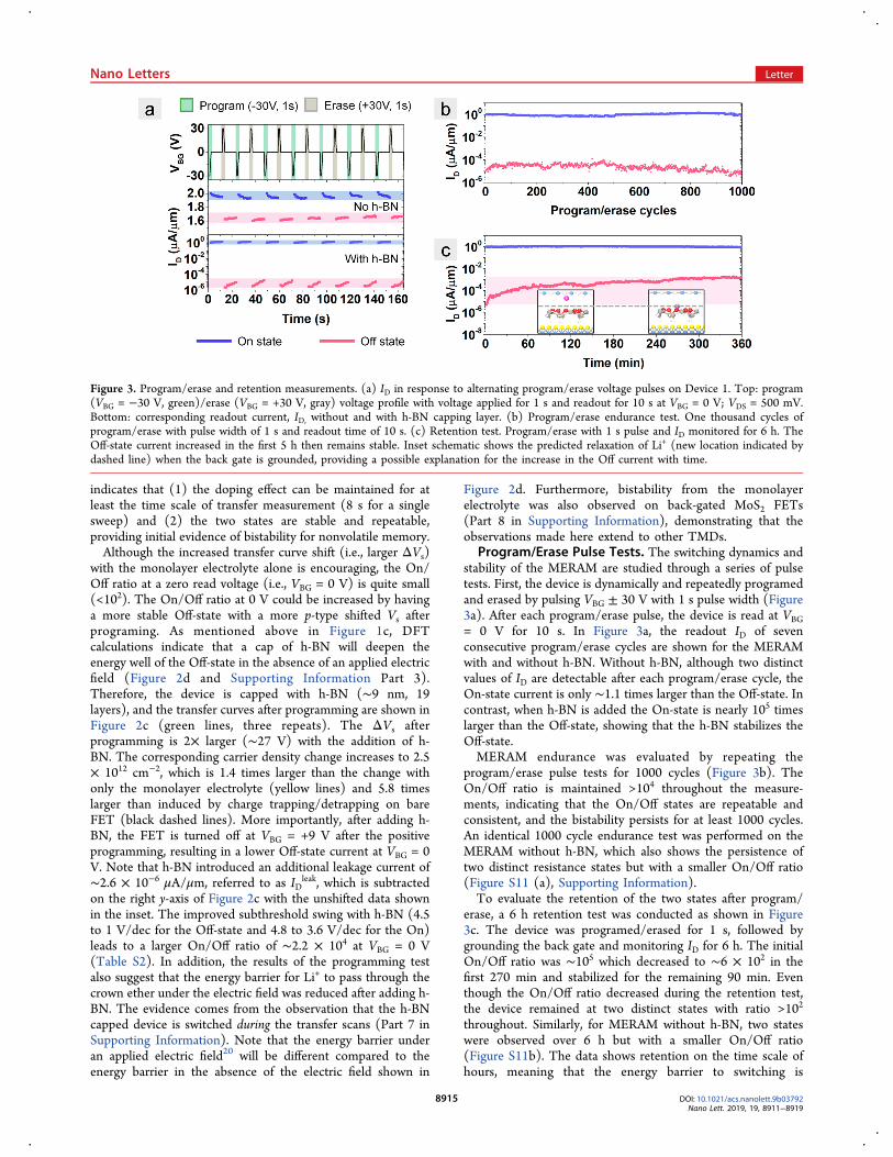
indicates that (1) the doping effect can be maintained for atleast the time scale of transfer measurement (8 s for a singlesweep) and (2) the two states are stable and repeatable,providing initial evidence of bistability for nonvolatile memory.Although the increased transfer curve shift (i.e., larger ΔVs)
with the monolayer electrolyte alone is encouraging, the On/Off ratio at a zero read voltage (i.e., VBG = 0 V) is quite small(<102). The On/Off ratio at 0 V could be increased by havinga more stable Off-state with a more p-type shifted Vs afterprograming. As mentioned above in Figure 1c, DFTcalculations indicate that a cap of h-BN will deepen theenergy well of the Off-state in the absence of an applied electricfield (Figure 2d and Supporting Information Part 3).Therefore, the device is capped with h-BN (∼9 nm, 19layers), and the transfer curves after programming are shown inFigure 2c (green lines, three repeats). The ΔVs afterprogramming is 2× larger (∼27 V) with the addition of h-BN. The corresponding carrier density change increases to 2.5× 1012 cm−2, which is 1.4 times larger than the change withonly the monolayer electrolyte (yellow lines) and 5.8 timeslarger than induced by charge trapping/detrapping on bareFET (black dashed lines). More importantly, after adding h-BN, the FET is turned off at VBG = +9 V after the positiveprogramming, resulting in a lower Off-state current at VBG = 0V. Note that h-BN introduced an additional leakage current of∼2.6 × 10⁻⁶ μA/μm, referred to as ID
leak, which is subtractedon the right y-axis of Figure 2c with the unshifted data shownin the inset. The improved subthreshold swing with h-BN (4.5to 1 V/dec for the Off-state and 4.8 to 3.6 V/dec for the On)leads to a larger On/Off ratio of ∼2.2 × 10⁴ at VBG = 0 V(Table S2). In addition, the results of the programming testalso suggest that the energy barrier for Li+ to pass through thecrown ether under the electric field was reduced after adding h-BN. The evidence comes from the observation that the h-BNcapped device is switched during the transfer scans (Part 7 inSupporting Information). Note that the energy barrier underan applied electric field20 will be different compared to theenergy barrier in the absence of the electric field shown in
Figure 2d. Furthermore, bistability from the monolayerelectrolyte was also observed on back-gated MoS2 FETs(Part 8 in Supporting Information), demonstrating that theobservations made here extend to other TMDs.
Program/Erase Pulse Tests. The switching dynamics andstability of the MERAM are studied through a series of pulsetests. First, the device is dynamically and repeatedly programedand erased by pulsing VBG ± 30 V with 1 s pulse width (Figure3a). After each program/erase pulse, the device is read at VBG= 0 V for 10 s. In Figure 3a, the readout ID of sevenconsecutive program/erase cycles are shown for the MERAMwith and without h-BN. Without h-BN, although two distinctvalues of ID are detectable after each program/erase cycle, theOn-state current is only ∼1.1 times larger than the Off-state. Incontrast, when h-BN is added the On-state is nearly 105 timeslarger than the Off-state, showing that the h-BN stabilizes theOff-state.MERAM endurance was evaluated by repeating the
program/erase pulse tests for 1000 cycles (Figure 3b). TheOn/Off ratio is maintained >104 throughout the measure-ments, indicating that the On/Off states are repeatable andconsistent, and the bistability persists for at least 1000 cycles.An identical 1000 cycle endurance test was performed on theMERAM without h-BN, which also shows the persistence oftwo distinct resistance states but with a smaller On/Off ratio(Figure S11 (a), Supporting Information).To evaluate the retention of the two states after program/
erase, a 6 h retention test was conducted as shown in Figure3c. The device was programed/erased for 1 s, followed bygrounding the back gate and monitoring ID for 6 h. The initialOn/Off ratio was ∼105 which decreased to ∼6 × 10² in thefirst 270 min and stabilized for the remaining 90 min. Eventhough the On/Off ratio decreased during the retention test,the device remained at two distinct states with ratio >102
throughout. Similarly, for MERAM without h-BN, two stateswere observed over 6 h but with a smaller On/Off ratio(Figure S11b). The data shows retention on the time scale ofhours, meaning that the energy barrier to switching is
Figure 3. Program/erase and retention measurements. (a) ID in response to alternating program/erase voltage pulses on Device 1. Top: program(VBG = −30 V, green)/erase (VBG = +30 V, gray) voltage profile with voltage applied for 1 s and readout for 10 s at VBG = 0 V; VDS = 500 mV.Bottom: corresponding readout current, ID, without and with h-BN capping layer. (b) Program/erase endurance test. One thousand cycles ofprogram/erase with pulse width of 1 s and readout time of 10 s. (c) Retention test. Program/erase with 1 s pulse and ID monitored for 6 h. TheOff-state current increased in the first 5 h then remains stable. Inset schematic shows the predicted relaxation of Li+ (new location indicated bydashed line) when the back gate is grounded, providing a possible explanation for the increase in the Off current with time.
Nano Letters Letter
DOI: 10.1021/acs.nanolett.9b03792Nano Lett. 2019, 19, 8911−8919
8915

underestimated by DFT for the h-BN capped system in theabsence of an applied field (Supporting Information Part 3).This difference is not unexpected considering the defects anddisorder in the experimental system.The decrease in the On/Off ratio is mostly due to the
gradual increase of the Off-state current, which was alsoobserved previously on the monolayer electrolyte-coatedgraphene FETs.21 Note that because the Off-state current islower in the WSe2 MERAMs (∼10−5 to 10−3 μA/μm) than inthe monolayer electrolyte-coated graphene FETs (∼130 μA/μm),21 the relaxation effect is magnified in the WSe2MERAMs. One possible explanation for this drift is therelaxation of Li+ after removing the field;21 that is, the ion isheld more closely to the 2D surface when the field is applied,but when the back gate is grounded, the ion will relax back tothermodynamic equilibrium toward an energetically favorablelocation that is further from the surface (inset, Figure 3c).Another possibility is that the anion, ClO4
−, is also relaxing tothermodynamic equilibrium during this time. The DFTcalculations do not include the counterions, nor do we havean experimental means to measure their locations directly;however, the most energetically favorable location for theanions is expected to be near the cobalt on the phthalocyanine.The key predications provided by the DFT calculations arethat (1) the h-BN cap stabilizes the Off-state by ∼1.34 eVcompared to vacuum (Figure 1b) and (2) that the energybarrier to switching can be decrease by an applied field,20
which will control the switching speed of the device.Switching Speed and Voltage. In the measurements
described above, ±30 V programming voltages and 1 s to 5min programming times were used; however, these values werenot optimized and therefore do not reflect any intrinsiclimitation. To investigate how the On/Off ratio varies withvoltage pulse width, we repeated the program/erase pulse testusing ±20 V programming voltages and pulse widths rangingfrom 10 s to 1 ms (the limit of our equipment). Figure 4ashows the ID of the On- and Off-states as a function of pulsewidth. The On- and Off-currents remain constant with ratio ofnearly 105 from a pulse width between 0.3 and 10 s. For pulsewidths <100 ms, the On/Off ratio decreases, and at 1 ms it isreduced to 3.4 × 10². Although this is a smaller On/Off ratiocompared to the endurance tests with longer pulse width (1 s)and larger pulse voltage (30 V), it still demonstratesmillisecond switching. Note that although not accessible withthe existing instrumentation, the switching speed of the
monolayer electrolyte is predicted to be in nanosecond timescale by DFT calculations.20
It is important to point out that the switching speed isdirectly related to the magnitude of the ion diffusion barrier(i.e., Li+ passing through the crown ether) which depends onthe applied electric field strength.20 For our backgatedgeometry, the electric field that reaches the electrolyte isweaker than would be achieved in a top gated geometry due to90 nm of back gate oxide and the field-screening caused by theWSe2 channel. Therefore, the switching speed of the memoryis expected to improve (perhaps to nanoseconds) by top-gatingfuture devices for which the h-BN will serve as the top gateoxide.To study the relationship between the On/Off ratio and
field required to switch the device, the On- and Off-states aremonitored while varying the VBG (1 s pulse width, Figure 4b).Note that the results in Figure 4b are for Device 2. For thisdevice, program/erase at ±5 V is insufficient to switch theMERAM, presumably due to the loss of field strength becauseof screening by WSe2 in the backgated device geometry.Starting from ±7 V, the two states become distinguishable, andthe On/Off ratio continues to enlarge with the increase ofprogram/erase voltage up to ±13 V. The increase of On/Offratio mostly comes from the decrease of Off-state current. Infact, further increasing the program voltage from 7 to 30 Vleads to a relatively small increase of On-state ID from 0.43 to0.80 μA/μm. In contrast, increasing the erase voltage from 7 to30 V causes the Off-state ID to decrease from 0.23 to 2.3 ×10⁻⁶ μA/μm, a change of 5 orders of magnitude. We alsonoticed that once the magnitude of the erase voltage exceeds13 V, the Off-state current stays almost constant. These resultsare interesting because they confirm the existence of an energybarrier, that is, the minimum energy required to push Li+
through the diffusion barrier and fully switch the MERAMfrom one state to the other. Note that in this study, theminimum voltage varies among devices (∼20 V for Device 1and 13 V for Device 2) possibly due to the differences in fieldscreening resulting from varying WSe2 channel thicknesses(Figure S12, Supporting Information). Similar to increasingthe switching speed, we expect a top-gated device to alsoreduce the required switching voltage.In conclusion, we have demonstrated a new, 1T NVM
concept based on EDL gating of a WSe2/monolayer electro-lyte/h-BN stack. As predicted by DFT calculations, cappingthe device with h-BN provides a critical improvement ofstabilizing the Off-state of the MERAM. The capping layer also
Figure 4. Program/erase measurements as a function of pulse width and voltage. (a) (Device 1) ID of the On- and Off-states in response toprogram/erase voltage pulses where the pulse width is varied from 1 ms to 1 s. (b) (Device 2) ID of the On- and Off-states with varying theprogram and erase voltages from ±5 to ±30 V (absolute values of ID plotted). For both (a,b), data at each point are averaged over 12 program/erase cycles with the error bar indicating one standard deviation from the mean.
Nano Letters Letter
DOI: 10.1021/acs.nanolett.9b03792Nano Lett. 2019, 19, 8911−8919
8916

provides a 2D top dielectric, which would be needed for large-scale integration. The MERAM retains a stable On/Off ratio>104 at a read voltage of VBG = 0 V for at least 1000 cycles ofprograming/erase and state retention for at least 6 h with On/Off remaining ∼102. Although a millisecond switching speedhas been demonstrated in this study, there is no reason toexpect the switching speed to be limited to this timescale.Specifically, a top-gated device architecture providing astronger electric field is expected to decrease the switchingtime, and subvolt operation in this configuration is predictedby DFT calculations.20 One potential advantage of themonolayer electrolyte is the wide chemical tunability, whichcan be used to adjust the energy barrier to switching. Thus, themonolayer electrolyte offers the potential to adjust theswitching and retention time and perhaps introduce multiplestates (i.e., multiple switching barriers by varying the crownring size).54 Last, the application of this material is not limitedto 1T NVM. Because the material is solution processable, thedoor is open to opportunities in printed and flexibleelectronics.
■ EXPERIMENTAL SECTIONWSe2 FET Fabrication and Polymer Residue Cleaning.
Few-layer WSe2 was mechanically exfoliated from bulk crystals(2D Semiconductors) and transferred to p-doped siliconsubstrate with 90 nm SiO2 (Graphene Supermarket, resistivity0.001−0.005 ohm·cm) by the scotch tape method. Thesubstrate was precleaned by acetone, isopropanol (IPA), anddeionized (DI) water and followed by nitrogen gas drying.WSe2 flakes with uniform thickness (3−5 nm) were selected byoptical microscopy and AFM (Bruker Dimension Icon,ScanAsyst mode with Si3N4 ScanAsyst-air tips (0.4 N m−1)).E-beam resist, PMMA-950-A4 (MicroChem) was spin-coatedat 4000 rpm for 1 min and baked on a hot plate at 180 °C for 3min. Source/drain electrodes were patterned by e-beamlithography (Raith e-LINE), and the samples were developedin a methyl isobutyl ketone (MIBK)/IPA solution (MIBK/IPA1:3 in volume ratio) for 1 min and then rinsed by IPA foranother 1 min. The metal (Pd 20 nm + Au 80 nm) wasdeposited by e-beam evaporation (Plassys Electron BeamEvaporator MEB550S) at a base pressure <1 × 10⁻⁶ Torr.After lift-off, WSe2 FETs were annealed at 127 °C (400 K) invacuum (pressure ∼2 × 10⁻⁶ Torr) for 4 h in a cryogenicvacuum probe station (Lakeshore, CRX-VF) which has a load-lock to transfer samples directly to an Ar-filled glovebox(MBRAUN, MB-200B) after annealing without ambientexposure.To remove e-beam resist residue on the WSe2 FET channels,
AFM contact-mode cleaning was performed in a glovebox.48
The polymer residue was pushed away from the FET channelby the AFM tip (SCM-PIT-v2, 3 N m−1) during the scanningusing AFM contact mode. Surface topology measurements byAFM were conducted before and after AFM cleaning toconfirm the removal of the residue. Electrical measurementswere conducted in the probe station by a Keysight B1500A anda Keithley 4200A-SCS semiconductor parameter analyzer. Allthe above processes were conducted either in a Ar-filledglovebox or in a vacuum probe station, and the samples weretransferred between the glovebox and probe station in a Ar-filled stainless-steel suitcase compatible with the load-lock onthe probe station.Monolayer Electrolyte Deposition. The monolayer
electrolyte was prepared in a similar manner to our previously
published results.18,21 The CoCrPc solution was prepared bydissolving 13 mg of CoCrPc in 10 mL of anhydrous benzene(Sigma-Aldrich, 99.8%) and anhydrous ethanol (Sigma-Aldrich, 99.5%) solution in a volume ratio of benzene toethanol of 9:1. The solution was diluted to 13 mg/L ofCoCrPc by adding the same anhydrous 9:1 v/v benzene/ethanol solution. After mixing by 10 min of sonication(Branson 2800 sonicator), 50 μL of CoCrPc solution wasdrop cast onto the WSe2 FETs (substrate surface 1 × 1 cm)using a micropipette and then the FETs were annealed on ahot plate at 240 °C for 30 min. AFM measurements onmonolayer electrolyte-coated WSe2 were performed to confirmthe monolayer deposition of CoCrPc. To add Li+ in the CE, 40μL of 1 mg/L LiClO4 in ethanol (Sigma-Aldrich, 99.5%anhydrous ethanol) was drop cast onto the CoCrPc-coatedWSe2 FETs, and then the samples were annealed at 180 °C for30 min. All the above processes were performed in the Ar-filledglovebox, and the samples were then transferred to the probestation by the load-lock for electrical measurements.
h-BN Capping Layer. A dry transfer method was used totransfer h-BN flakes onto the monolayer electrolyte-coatedWSe2 FETs.
50 The transfer processes were conducted entirelyinside a nitrogen-filled glovebox. The exfoliated h-BN flakeswith thickness ∼10 nm were picked up by a polycarbonate/polydimethylsiloxane (PC/PDMS) stamp. Then the h-BNflake on the transparent PC/PDMS stamp was aligned on topof the monolayer electrolyte-coated WSe2 channel usingoptical microscope. After the alignment, the PC/PDMSstamp was gently pressed on the WSe2 sample substrate bythe controlled thermal expansion of PDMS to place the h-BNflake on top of WSe2 channel. After the placement, the h-BNand PC film was released together from the stamp by heatingthe stamp to 180 °C. The sample was cooled to roomtemperature. Because the PC film will interfere with probingthe source/drain contacts of the FETs in the probe station, afew droplets of dichloromethane (80 μL) were drop cast onthe sample substrate to dissolve PC, and the dissolved materialwas removed by a glass pipet. The WSe2 FETs with themonolayer electrolyte and h-BN capping layer were transferredto the probe station by the load-lock for electrical measure-ments.
■ ASSOCIATED CONTENT*S Supporting InformationThe Supporting Information is available free of charge on theACS Publications website at DOI: 10.1021/acs.nano-lett.9b03792.
CoCrPc monolayer deposition on MoS2 and WSe2;optimization of CoCrPc monolayer deposition on WSe2;DFT calculations; removal of e-beam resist residue onWSe2 channel by AFM contact mode cleaning;conductive AFM of CoCrPc monolayer on graphite;transfer measurements and analysis; programming tests;bistability of the monolayer electrolyte on MoS2 FETs;program/erase on a backgated WSe2 FET with only themonolayer electrolyte (no h-BN); program/erasemeasurements as a function of back gate voltage ontwo MERAMs (with h-BN) (PDF)
■ AUTHOR INFORMATIONCorresponding Authors*(S.K.F.-S.) [email protected];.
Nano Letters Letter
DOI: 10.1021/acs.nanolett.9b03792Nano Lett. 2019, 19, 8911−8919
8917

*(K.X.): [email protected] Liang: 0000-0003-1207-8959Ke Xu: 0000-0003-2692-1935Wei-Hua Wang: 0000-0002-2287-7669Kyeongjae Cho: 0000-0003-2698-7774Susan K. Fullerton-Shirey: 0000-0003-2720-0400Author ContributionsThe manuscript was written through contributions of allauthors. All authors have given approval to the final version ofthe manuscript.Author Contributions#J.L. and K.X. contributed equally to this work.NotesThe authors declare no competing financial interest.
■ ACKNOWLEDGMENTSThe research is supported by the National Science Foundation(NSF, U.S.) under Grant ECCS-GOALI-1408425. M.W. andW.W. acknowledge support from the National Key Researchand Development Program of China with No.2016YFB0901600 and National Natural Science Foundationof China with No. 11874223 and 51871121. B.H. acknowl-edges support from the Department of Energy under the EarlyCareer program (No. DE-SC0018115). K.C. was supported bythe National Research Foundation (NRF) of Korea by theC r e a t i v e Ma t e r i a l s D i s c o v e r y P r o g r am (No .2015M3D1A1068062). The authors thank Prof. Feng Xiongfor the use of the Keithley instrument, and Prof. Alan Seabaugh(Univeristy of Notre Dame), Zhongmou Chao, ShubhamAwate, and Aaron Woeppel (University of Pittsburgh) forhelpful discussions.
■ REFERENCES(1) Lee, S. H. Technology Scaling Challenges and Opportunities ofMemory Devices. Technol. Dig. - Int. Electron Devices Meet. IEDM2016, 1.1.1−1.1.8.(2) International Roadmap for Devices and Systems. IRDS. https://irds.ieee.org/roadmap (accessed February 21, 2019).(3) Naber, R. C. G.; Asadi, K.; Blom, P. W. M.; De Leeuw, D. M.;De Boer, B. Organic Nonvolatile Memory Devices Based onFerroelectricity. Adv. Mater. 2010, 22 (9), 933−945.(4) Hoffman, J.; Pan, X.; Reiner, J. W.; Walker, F. J.; Han, J. P.; Ahn,C. H.; Ma, T. P. Ferroelectric Field Effect Transistors for MemoryApplications. Adv. Mater. 2010, 22 (26−27), 2957−2961.(5) Lee, Y. T.; Jeon, P. J.; Lee, K. H.; Ha, R.; Choi, H. J.; Im, S.Ferroelectric Nonvolatile Nanowire Memory Circuit Using a SingleZnO Nanowire and Copolymer Top Layer. Adv. Mater. 2012, 24(22), 3020−3025.(6) Su, M.; Yang, Z.; Liao, L.; Zou, X.; Ho, J. C.; Wang, J.; Wang, J.;Hu, W.; Xiao, X.; Jiang, C.; et al. Side-Gated In2O3 NanowireFerroelectric FETs for High-Performance Nonvolatile MemoryApplications. Adv. Sci. 2016, 3 (9), 1600078.(7) Salahuddin, S.; Datta, S. Use of Negative Capacitance to ProvideVoltage Amplification for Low Power Nanoscale Devices. Nano Lett.2008, 8 (2), 405−410.(8) Khan, A. I.; Chatterjee, K.; Wang, B.; Drapcho, S.; You, L.;Serrao, C.; Bakaul, S. R.; Ramesh, R.; Salahuddin, S. NegativeCapacitance in a Ferroelectric Capacitor. Nat. Mater. 2015, 14 (2),182−186.(9) Catalan, G.; Jimenez, D.; Gruverman, A. Ferroelectrics: NegativeCapacitance Detected. Nat. Mater. 2015, 14 (2), 137−139.(10) McGuire, F. A.; Lin, Y. C.; Price, K.; Rayner, G. B.; Khandelwal,S.; Salahuddin, S.; Franklin, A. D. Sustained Sub-60 MV/Decade
Switching via the Negative Capacitance Effect in MoS2 Transistors.Nano Lett. 2017, 17 (8), 4801−4806.(11) Si, M.; Su, C. J.; Jiang, C.; Conrad, N. J.; Zhou, H.; Maize, K.D.; Qiu, G.; Wu, C. T.; Shakouri, A.; Alam, M. A.; et al. Steep-SlopeHysteresis-Free Negative Capacitance MoS2 transistors. Nat. Nano-technol. 2018, 13 (1), 24−28.(12) Xu, Q.; Liu, X.; Wan, B.; Yang, Z.; Li, F.; Lu, J.; Hu, G.; Pan,C.; Wang, Z. L. In2O3 Nanowire Field-Effect Transistors with Sub-60MV/Dec Subthreshold Swing Stemming from Negative Capacitanceand Their Logic Applications. ACS Nano 2018, 12 (9), 9608−9616.(13) Liu, X.; Liang, R.; Gao, G.; Pan, C.; Jiang, C.; Xu, Q.; Luo, J.;Zou, X.; Yang, Z.; Liao, L.; et al. MoS2 Negative-Capacitance Field-Effect Transistors with Subthreshold Swing below the Physics Limit.Adv. Mater. 2018, 30 (28), 1800932.(14) Yu, S.; Chen, P.-Y. Emerging Memory Technologies: RecentTrends and Prospects. IEEE Solid-State Circuits Mag. 2016, 8 (2), 43−56.(15) Sharma, A.; Roy, K. 1T Non-Volatile Memory Design UsingSub-10nm Ferroelectric FETs. IEEE Electron Device Lett. 2018, 39 (3),359−362.(16) Lee, M. H.; Fan, S. T.; Tang, C. H.; Chen, P. G.; Chou, Y. C.;Chen, H. H.; Kuo, J. Y.; Xie, M. J.; Liu, S. N.; Liao, M. H.; et al.Physical Thickness 1.x Nm Ferroelectric HfZrOx NegativeCapacitance FETs. Technol. Dig. - Int. Electron Devices Meet. IEDM2016, 12, 12.1.1.(17) Li, X.; Sampson, J.; Khan, A.; Ma, K.; George, S.; Aziz, A.;Gupta, S. K.; Salahuddin, S.; Chang, M. F.; Datta, S.; et al. EnablingEnergy-Efficient Nonvolatile Computing with Negative CapacitanceFET. IEEE Trans. Electron Devices 2017, 64 (8), 3452−3458.(18) Lu, H.; Kwak, I.; Park, J. H.; Oneill, K.; Furuyama, T.;Kobayashi, N.; Seabaugh, A.; Kummel, A.; Fullerton-Shirey, S. K.Solution-Cast Monolayers of Cobalt Crown Ether Phthalocyanine onHighly Ordered Pyrolytic Graphite. J. Phys. Chem. C 2015, 119 (38),21992−22000.(19) Wang, W. H.; Gong, C.; Wang, W.; Fullerton-Shirey, S. K.;Seabaugh, A.; Cho, K. First-Principles Study of Crown Ether andCrown Ether-Li Complex Interactions with Graphene. J. Phys. Chem.C 2015, 119 (34), 20016−20022.(20) Wang, W. H.; Gong, C.; Wang, W.; Kong, F.; Kim, H.;Fullerton-Shirey, S. K.; Seabaugh, A.; Cho, K. Energetics of Metal IonAdsorption on and Diffusion through Crown Ethers: First PrinciplesStudy on Two-Dimensional Electrolyte. Solid State Ionics 2017, 301,176−181.(21) Xu, K.; Lu, H.; Kinder, E. W.; Seabaugh, A.; Fullerton-Shirey, S.K. Monolayer Solid-State Electrolyte for Electric Double Layer Gatingof Graphene Field-Effect Transistors. ACS Nano 2017, 11 (6), 5453−5464.(22) Chhowalla, M.; Jena, D.; Zhang, H. Two-DimensionalSemiconductors for Transistors. Nat. Mater. 2016, 1, 16052.(23) Novoselov, K. S.; Mishchenko, A.; Carvalho, A.; Castro Neto,A. H. 2D Materials and van Der Waals Heterostructures. Science 2016,353, aac9439.(24) Akinwande, D.; Brennan, C. J.; Bunch, J. S.; Egberts, P.; Felts, J.R.; Gao, H.; Huang, R.; Kim, J. S.; Li, T.; Li, Y.; et al. A Review onMechanics and Mechanical Properties of 2D MaterialsGrapheneand Beyond. Extrem. Mech. Lett. 2017, 13, 42−77.(25) Bhimanapati, G. R.; Lin, Z.; Meunier, V.; Jung, Y.; Cha, J.; Das,S.; Xiao, D.; Son, Y.; Strano, M. S.; Cooper, V. R.; et al. RecentAdvances in Two-Dimensional Materials beyond Graphene. ACSNano 2015, 9 (12), 11509−11539.(26) Tan, C.; Cao, X.; Wu, X. J.; He, Q.; Yang, J.; Zhang, X.; Chen,J.; Zhao, W.; Han, S.; Nam, G. H.; et al. Recent Advances in UltrathinTwo-Dimensional Nanomaterials. Chem. Rev. 2017, 117 (9), 6225−6331.(27) McDonnell, S.; Brennan, B.; Azcatl, A.; Lu, N.; Dong, H.; Buie,C.; Kim, J.; Hinkle, C. L.; Kim, M. J.; Wallace, R. M. HfO2 on MoS2by Atomic Layer Deposition: Adsorption Mechanisms and ThicknessScalability. ACS Nano 2013, 7 (11), 10354−10361.
Nano Letters Letter
DOI: 10.1021/acs.nanolett.9b03792Nano Lett. 2019, 19, 8911−8919
8918
(28) Liao, L.; Zou, X. Interface Engineering for High-PerformanceTop-Gated MoS2 Field Effect Transistors. Proc. - 2014 IEEE 12th Int.Conf. Solid-State Integr. Circuit Technol. ICSICT 2014 2014, 1.(29) Akinwande, D.; Petrone, N.; Hone, J. Two-DimensionalFlexible Nanoelectronics. Nat. Commun. 2014, 5 (1), 5678.(30) Kim, S. H.; Hong, K.; Xie, W.; Lee, K. H.; Zhang, S.; Lodge, T.P.; Frisbie, C. D. Electrolyte-Gated Transistors for Organic andPrinted Electronics. Adv. Mater. 2013, 25, 1822−1846.(31) Xu, H.; Fathipour, S.; Kinder, E. W.; Seabaugh, A. C.;Fullerton-Shirey, S. K. Reconfigurable Ion Gating of 2H-MoTe2 Field-Effect Transistors Using Poly(Ethylene Oxide)-CsClO4 Solid PolymerElectrolyte. ACS Nano 2015, 9 (5), 4900−4910.(32) Bisri, S. Z.; Shimizu, S.; Nakano, M.; Iwasa, Y. Endeavor ofIontronics: From Fundamentals to Applications of Ion-ControlledElectronics. Adv. Mater. 2017, 29 (25), 1607054.(33) Ye, J. T.; Inoue, S.; Kobayashi, K.; Kasahara, Y.; Yuan, H. T.;Shimotani, H.; Iwasa, Y. Liquid-Gated Interface Superconductivity onan Atomically Flat Film. Nat. Mater. 2010, 9 (2), 125−128.(34) Chuang, H.-J. J.; Tan, X.; Ghimire, N. J.; Perera, M. M.;Chamlagain, B.; Cheng, M. M.-C. C.; Yan, J.; Mandrus, D.; Tomanek,D.; Zhou, Z.; et al. High Mobility WSe2 p- and n-type Field-EffectTransistors Contacted by Highly Doped Graphene for Low-Resistance Contacts. Nano Lett. 2014, 14 (6), 3594−3601.(35) Tosun, M.; Chuang, S.; Fang, H.; Sachid, A. B.; Hettick, M.;Lin, Y.; Zeng, Y.; Javey, A. High-Gain Inverters Based on WSe2complementary Field-Effect Transistors. ACS Nano 2014, 8 (5),4948−4953.(36) Lee, G.-H.; Cui, X.; Kim, Y. D.; Arefe, G.; Zhang, X.; Lee, C.-H.; Ye, F.; Watanabe, K.; Taniguchi, T.; Kim, P.; et al. Highly Stable,Dual-Gated MoS2 Transistors Encapsulated by Hexagonal Boron Ni-tride with Gate-Controllable Contact, Resistance, and ThresholdVoltage. ACS Nano 2015, 9 (7), 7019−7026.(37) Lin, Y. C.; Jariwala, B.; Bersch, B. M.; Xu, K.; Nie, Y.; Wang, B.;Eichfeld, S. M.; Zhang, X.; Choudhury, T. H.; Pan, Y.; et al. RealizingLarge-Scale, Electronic-Grade Two-Dimensional Semiconductors.ACS Nano 2018, 12 (2), 965−975.(38) Subramanian, S.; Deng, D. D.; Xu, K.; Simonson, N.; Wang, K.;Zhang, K.; Li, J.; Feenstra, R.; Fullerton-Shirey, S. K.; Robinson, J. A.Properties of Synthetic Epitaxial Graphene/Molybdenum DisulfideLateral Heterostructures. Carbon 2017, 125, 551−556.(39) Fathipour, S.; Pandey, P.; Fullerton-Shirey, S.; Seabaugh, A.Electric-Double-Layer Doping of WSe2 Field-Effect Transistors UsingPolyethylene-Oxide Cesium Perchlorate. J. Appl. Phys. 2016, 120(23), 234902.(40) Xu, K.; Islam, M. M.; Guzman, D. M.; Seaubaugh, A.; Strachan,A.; Fullerton-Shirey, S. K. Pulse Dynamics of Electric Double LayerFormation on All-Solid-State Graphene Field-Effect Transistors. ACSAppl. Mater. Interfaces 2018, 10, 43166.(41) Yoshimoto, S.; Suto, K.; Tada, A.; Kobayashi, N.; Itaya, K.Effect of Adlayer Structure on the Host-Guest Recognition betweenCalcium and Crown-Ether-Substituted Phthalocyanine Arrays on AuSingle-Crystal Surfaces. J. Am. Chem. Soc. 2004, 126 (25), 8020−8027.(42) Lee, J.; Lu, W. D. On-Demand Reconfiguration of Nanoma-terials: When Electronics Meets Ionics. Adv. Mater. 2018, 30 (1),1702770.(43) Das, S.; Appenzeller, J. WSe2 Field Effect Transistors withEnhanced Ambipolar Characteristics. Appl. Phys. Lett. 2013, 103 (10),103501.(44) Sahin, H.; Tongay, S.; Horzum, S.; Fan, W.; Zhou, J.; Li, J.; Wu,J.; Peeters, F. M. Anomalous Raman Spectra and Thickness-Dependent Electronic Properties of WSe2. Phys. Rev. B: Condens.Matter Mater. Phys. 2013, 87 (16), 1−6.(45) Fang, H.; Chuang, S.; Chang, T. C.; Takei, K.; Takahashi, T.;Javey, A. High-Performance Single Layered WSe2 p-FETs withChemically Doped Contacts. Nano Lett. 2012, 12 (7), 3788−3792.(46) Ahn, S.; Kim, G.; Nayak, P. K.; Yoon, S. I.; Lim, H.; Shin, H. J.;Shin, H. S. Prevention of Transition Metal Dichalcogenide Photo-
degradation by Encapsulation with h-BN Layers. ACS Nano 2016, 10(9), 8973−8979.(47) Das, S.; Gulotty, R.; Sumant, A. V.; Roelofs, A. All Two-Dimensional, Flexible, Transparent, and Thinnest Thin FilmTransistor. Nano Lett. 2014, 14 (5), 2861−2866.(48) Liang, J.; Xu, K.; Toncini, B.; Bersch, B.; Jariwala, B.; Lin, Y.-C.;Robinson, J.; Fullerton-Shirey, S. K. Impact of Post-LithographyPolymer Residue on the Electrical Characteristics of MoS2 and WSe2Field Effect Transistors. Adv. Mater. Interfaces 2019, 6, 1801321.(49) Hunt, B.; Sanchez-Yamagishi, J. D.; Young, A. F.; Yankowitz,M.; Leroy, B. J.; Watanabe, K.; Taniguchi, T.; Moon, P.; Koshino, M.;Jarillo-Herrero, P.; et al. Massive Dirac Fermions and HofstadterButterfly in a van Der Waals Heterostructure. Science (Washington,DC, U. S.) 2013, 340 (June), 1427−1431.(50) Castellanos-Gomez, A.; Buscema, M.; Molenaar, R.; Singh, V.;Janssen, L.; Van Der Zant, H. S. J.; Steele, G. A. DeterministicTransfer of Two-Dimensional Materials by All-Dry ViscoelasticStamping. 2D Mater. 2014, 1 (1), 011002.(51) Choi, H. H.; Cho, K.; Frisbie, C. D.; Sirringhaus, H.; Podzorov,V. Critical Assessment of Charge Mobility Extraction in FETs. Nat.Mater. 2018, 17 (1), 2−7.(52) Liao, Z. M.; Han, B. H.; Zhou, Y. B.; Yu, D. P. HysteresisReversion in Graphene Field-Effect Transistors. J. Chem. Phys. 2010,133 (4), 044703.(53) Wang, H.; Wu, Y.; Cong, C.; Shang, J.; Yu, T. Hysteresis ofElectronic Transport in Graphene Transistors. ACS Nano 2010, 4(12), 7221−7228.(54) De, S.; Boda, A.; Ali, S. M. Preferential Interaction of ChargedAlkali Metal Ions (Guest) within a Narrow Cavity of Cyclic CrownEthers (Neutral Host): A Quantum Chemical Investigation. J. Mol.Struct.: THEOCHEM 2010, 941, 90.
Nano Letters Letter
DOI: 10.1021/acs.nanolett.9b03792Nano Lett. 2019, 19, 8911−8919
8919
www.advmatinterfaces.de
FULL PAPER
1801321 (1 of 10) © 2018 WILEY-VCH Verlag GmbH & Co. KGaA, Weinheim
Impact of Post-Lithography Polymer Residue on the Electrical Characteristics of MoS2 and WSe2 Field Effect Transistors
Jierui Liang, Ke Xu,* Blaec Toncini, Brian Bersch, Bhakti Jariwala, Yu-Chuan Lin, Joshua Robinson, and Susan K. Fullerton-Shirey*
DOI: 10.1002/admi.201801321
fabricated using e-beam and optical lithog-raphy, e-beam resist such as poly(methyl methacrylate) (PMMA)[2,3,7] and photo-resists such as MicroChem LOR, PMGI, and Megaposit SPR 3000 series are widely used.[8–10] In addition, polymers such as PMMA, poly(bisphenol A car-bonate) (PC), polystyrene (PS), and poly(dimethylsiloxane) (PDMS) are used as stamps to transfer flakes for stacking van der Waal heterostructures,[11,12] and as substrates for transferring 2D mate-rials grown by chemical vapor deposi-tion (CVD).[13–17] Device fabrication and 2D layer transfer that requires applying poly mer and removing it leaves residue on the surface—typically a few nanometers thick—which can be detected by atomic force microscopy (AFM).[18,19]
The residue can interfere with surface characterization, material deposition, and access by adsorbates, as well as degrade the physical, electrical, and optical properties of the 2D crystals. Specifi-
cally, the residue can prevent achieving atomic resolution of the 2D crystal lattice using transmission electron micro-scopy (TEM)[20,21] and scanning tunnel microscopy (STM).[18] For material deposition, the molecular arrangement of the deposited material could be interrupted by nanometers of polymer residue—especially when a molecularly thin layer is required, such as a seed layer for dielectric deposition on 2D materials.[22] For devices that rely on surface sensitivity, the residue can screen interactions between the 2D surface and target molecules (e.g., sensors for detecting DNA,[23] or detecting NO2/NH3 gas[24]). The physical properties of the 2D crystal can be strongly affected by surface residue because of the large surface-to-volume ratio of the 2D crystal. For example, PMMA residue decreases mobility by more than 50% in graphene due to carrier scattering,[19,25,26] and causes phonon scattering that decreases the thermal conductivity of suspended graphene by 70% compared to calculated values.[20] PMMA residue is also a p-dopant that can shift the threshold voltage (≈+3 to +19 V for back-gated graphene FETs with 285 nm SiO2),[26,27] this may cause device-to-device vari-ations in the electrical characteristics if the residue is not a uniform layer.
The residue of common photo- and electron-beam resists, such as poly(methyl methacrylate) (PMMA), is often present on the surface of 2D crystals after device fabrication. The residue degrades device properties by decreasing carrier mobility and creating unwanted doping. Here, MoS2 and WSe2 field effect transistors (FETs) with residue are cleaned by contact mode atomic force microscopy (AFM) and the impact of the residue on: 1) the intrinsic electrical properties, and 2) the effectiveness of electric double layer (EDL) gating are measured. After cleaning, AFM measurements confirm that the surface roughness decreases to its intrinsic state (i.e., ≈0.23 nm for exfoliated MoS2 and WSe2) and Raman spectroscopy shows that the charac-teristic peak intensities (E2g and A1g) increase. PMMA residue causes p-type doping corresponding to a charge density of ≈7 × 1011 cm−2 on back-gated MoS2 and WSe2 FETs. For FETs gated with polyethylene oxide (PEO)76:CsClO4, removing the residue increases the charge density by 4.5 × 1012 cm−2, and the maximum drain current by 247% (statistically significant, p < 0.05). Removing the residue likely allows the ions to be positioned closer to the channel surface, which is essential for achieving the best possible electrostatic gate control in ion-gated devices.
J. Liang, Dr. K. Xu, B. Toncini, Prof. S. K. Fullerton-ShireyDepartment of Chemical and Petroleum EngineeringUniversity of PittsburghPittsburgh, PA 15260, USAE-mail: [email protected]; [email protected]. Bersch, Dr. B. Jariwala, Dr. Y.-C. Lin, Prof. J. RobinsonDepartment of Materials Science and EngineeringThe Pennsylvania State UniversityUniversity Park, PA 16802, USAProf. S. K. Fullerton-ShireyDepartment of Electrical and Computer EngineeringUniversity of PittsburghPittsburgh, PA 15260, USA
The ORCID identification number(s) for the author(s) of this article can be found under https://doi.org/10.1002/admi.201801321.
Interfacial Property
1. Introduction
2D crystals such as graphene,[1] MoS2,[2] WSe2,[3] and others,[4–6] are being explored for next generation power-efficient electronics because of their excellent electrical, thermal, and mechanical properties. When devices based on 2D crystals are
Adv. Mater. Interfaces 2018, 1801321

www.advancedsciencenews.com
© 2018 WILEY-VCH Verlag GmbH & Co. KGaA, Weinheim1801321 (2 of 10)
www.advmatinterfaces.de
In addition to altering the intrinsic properties of 2D crystals and interfering with surface characterization, polymer res-idue is also likely to decrease the effectiveness of electric double layer (EDL) gating. EDL gating is a commonly used technique for exploring transport in 2D materials, especially when back gating is not an option due to the use of an insu-lating substrate like sapphire, or when high-k dielectrics cannot be deposited for top gating.[9,28] Mobile ions within the electrolyte respond to the applied electric field and migrate to the electrolyte/channel or electrolyte/gate interface where they induce image charges. The EDLs induce high gate capaci-tance densities (1–10 µF cm−2), corresponding to sheet carrier densities exceeding 1013 cm−2.[28,29] EDL gating relies on ions migrating to within a few nanometers of the 2D crystal surface, which would not be effectively achieved if a few nano meters of polymer residue exists between the electrolyte and the channel—particularly if the polymer residue does not conduct ions. A residue-free 2D surface is especially important when EDL gating is achieved using an ultrathin layer of electrolyte, such as the monolayer electrolyte (thickness ≈1 nm) developed by our group.[30,31] If polymer residue is present, it will interfere with the molecular arrangement of the molecules required to form the EDL. Overall, it is reasonable to expect that a residue-free surface is important for accessing the highest gate capaci-tance density possible, yielding the best gate control. Thus, in this work, the electrical device characteristics of EDL-gated field effect transistors (FETs) are measured for 2D channels with and without polymer residue.
Because polymer residue can alter material properties and negatively affect device fabrication and performance, sev-eral methods to clean the residue—especially PMMA—have been reported. Thermal annealing in Ar/H2, forming gas, or vacuum is the most commonly used method to decompose and desorb PMMA residue.[25,32,33] But TEM images show that the annealing often does not remove the residue completely.[25] High temperatures (>300 °C for graphene, 200 °C for MoS2) in H2:Ar gas are required to break PMMA bonds and remove the carboxyl functional group,[32,34] but the high temperatures could also cause defects and structural damage, or trigger chemical reactions with other adsorbed species, causing per-manent p-type doping of the device.[32] For example, the impact of charged impurities located between graphene and SiO2 can become intensified after annealing at T > 300 °C due to the enhanced coupling between graphene and SiO2, which leads to both heavy hole doping and decreased mobility.[35,36] Improved PMMA removal by annealing in oxidative atmospheres like O2 and CO2 has been reported on graphene,[25,37] but extending the technique to transition metal dichalcogenides (TMDs) is likely difficult because annealing in Ar/O2 mixture at 300–340 °C results in anisotropic etching of MoS2,[38] and exposure in ambient leads to oxidation of WSe2.[39]
While solvent cleaning can remove bulk PMMA, the res-idue tends to remain,[40] which is why a consecutive thermal annealing is still required.[35] Current-induced cleaning has been demonstrated on graphene with large source/drain voltage (≈4.6 V) to induce joule heating to remove residue; however, a low temperature environment (≈4 K) is required to remove the heat.[41] Laser cleaning of PMMA residue on graphene has been demonstrated, but not extended to
TMDs.[19] Plasma cleaning can also be challenging. For example, O2 plasma is found to oxidize edges/defects on gra-phene and the top layer of WSe2,[42,43] and is used in etching and p-type doping of TMDs.[43,44] H2 plasma can lift graphene off SiO2,[45] and Cl2 plasma can cause a heavy p-doping to graphene.[46] UV/ozone also p-dopes TMDs like MoS2 and WSe2,[47] and cause etching easily as shown in Figure S1 in the Supporting Information.
In contrast to the chemical and thermal approaches described above, a mechanical approach is to use an AFM tip to “sweep” the polymer residue off the surface in contact mode. This AFM cleaning method induces no chemical reactions, has no restriction on the type of 2D crystal, and can retain the original 2D crystal thickness and surface roughness.[48–51] It has been applied to both exfoliated and CVD-grown graphene on various substrates, and the carrier mobility of graphene after the cleaning was reported to increase by 20% compared to before cleaning.[51] The mobility can be further increased by combining AFM cleaning with annealing.[50]
While several studies have used the AFM contact-mode-cleaning technique on graphene and reported transfer charac-teristics and Hall resistance measurements,[48–51] to our knowl-edge there are no similar reports on TMDs. More specifically, there is no report on the impact of polymer reside on the electrical performance of EDL-gated TMDs. Given the par-ticular challenge of cleaning TMDs by oxidative annealing or plasma, AFM cleaning provides a useful alternative; however, the experimental conditions (e.g., contact force) must be opti-mized; otherwise, polymer residue may not be completely removed.[49] While this approach is not scalable in its cur-rent form, one advantage of AFM cleaning from a scientific standpoint is the ability to isolate contributions from polymer residue in well-defined locations on the device (e.g., channel vs contacts). That is, the contributions from surface residue at specific spatial locations can be decoupled from other vari-ables that could be introduced by using a chemical cleaning approach, for example.
In this study, we demonstrate that contact-mode AFM cleaning can effectively remove polymer residue from both e-beam and photolithography (≈1 nm thick) on MoS2 and WSe2, with AFM and Raman spectroscopy measurements con-firming the effectiveness of the cleaning. Transfer characteristic before and after AFM cleaning on back-gated MoS2 and WSe2 FETs clearly indicate that PMMA residue causes p-doping cor-responding to a charge density of ≈7 × 1011 cm−2. In addition, AFM cleaning of EDL-gated WSe2 FETs causes a charge density increase of 4.5 × 1012 cm−2, and increases the maximum drain current by a statistically significant amount: 247% (paired t-test, p = 9.0 × 10⁻³ < 0.05).
2. Result and Discussion
2.1. AFM Cleaning and Characterization
Polymer residue was removed by scanning the desired region of the 2D crystal using AFM contact mode (Figure 1). A relatively stiff AFM tip (SCM-PIT-v2, measured force constant 2.37 N m−1) is used to sustain the mechanical force that pushes the polymer
Adv. Mater. Interfaces 2018, 1801321

www.advancedsciencenews.com
© 2018 WILEY-VCH Verlag GmbH & Co. KGaA, Weinheim1801321 (3 of 10)
www.advmatinterfaces.de
residue out of the scan region, as shown in the partially cleaned WSe2 surface in Figure 1b. Multiple deflection setpoints for contact mode are tested and 1.33 V is found to be the optimal value to achieve a clean surface (Figure S2, Supporting Infor-mation). The normal force (F) applied from the tip to the surface is estimated as 104 nN by F = kd(s−s0), where k is the force constant of a SCM-PIT-v2 tip (measured as 2.37 N m−1), d is deflection sensitivity (measured as 33.0 nm V−1), s is the deflection setpoint (1.33 V), and s0 is the deflection point when the tip is not touching any surface (measured as 0.0 V).
To demonstrate the use of AFM cleaning on FETs fabri-cated with both e-beam and photolithography on various 2D crystal channels, three different types of FETs including exfoli-ated MoS2 and WSe2 FETs (fabricated by e-beam lithography), and CVD-grown WSe2 FETs (fabricated by photolithography) were cleaned with AFM contact mode. The scan region was set to be larger than the length of the FET channel to push the residue off the channel. Topography was characterized before and after cleaning. Figure 2 shows optical and AFM images of one out of six devices before AFM cleaning and after for each type of FET.
The polymer residue is significant on all the as-fabricated devices. As an example, the residue features on the as-fabri-cated exfoliated MoS2 FETs shown in Figure 2c are 2–3 nm, confirmed by the line scan shown below the figure. Figure 2d shows that the PMMA residue was removed by AFM contact-mode cleaning. To evaluate the quality of AFM cleaning, the root mean square roughness (Rq) is calculated over the area indicated by the blue boxes in Figure 2 and summarized in Table S1 in the Supporting Information. The Rq is the standard deviation of the height profile from the mean plane (the averaged channel surface height from the substrate). For MoS2, Rq decreased from 1.56 ± 0.13 nm as fabricated to 0.24 ± 0.05 nm after the cleaning (for reference, Rq of the freshly cleaved MoS2 is 0.23 ± 0.03 nm). The AFM-cleaned and freshly cleaved surfaces have no statistically significant difference in Rq (independent t-test, p = 0.78 > 0.05). Similar results were observed for AFM cleaning on exfoliated WSe2 and CVD-grown WSe2, where Rq decreased with AFM
cleaning from 0.79 ± 0.05 nm to 0.25 ± 0.02 nm (exfoliated), and from 0.64 ± 0.03 nm to 0.34 ± 0.02 nm (CVD-grown). An AFM image of a partially cleaned CVD-grown WSe2 FET is also shown in Figure S3 in the Supporting Information, and the line scan indicates that the polymer residue thickness removed by AFM is ≈1.2 nm. Figure 2 shows that AFM con-tact-mode cleaning is effective in removing polymer residue both from e-beam and photolithography, and can restore both exfoliated and CVD-grown 2D crystals to their original surface topology.
To further confirm the surface type after the cleaning (i.e., peaks/valleys on surface, rounded/sharp peaks), the skew-ness (Rsk) and kurtosis (Rku) of the surfaces are calculated and tabulated in Table S2 in the Supporting Information. After AFM cleaning, the skewness decreased from 1.12 ± 0.20 to 0.04 ± 0.01 for exfoliated MoS2, 1.58 ± 0.35 to 0.09 ± 0.02 for exfoliated WSe2, and 0.25 ± 0.05 to 0.09 ± 0.02 for CVD WSe2. Thus, the topology becomes flatter with a more symmetrical height distribution at the mean plane after the cleaning. The kurtosis value also decreases after cleaning from 3.40 ± 0.08 to 2.92 ± 0.07 for exfoliated MoS2, 6.57 ± 1.40 to 2.80 ± 0.04 for exfoliated WSe2, and 3.38 ± 0.06 to 3.21 ± 0.03 for CVD WSe2, indicating that sharp peaks become more rounded after the cleaning.
We also mapped the moduli of the MoS2 channels using Bruker’s quantitative nanomechanical mapping (QNM) on regions that were both covered in PMMA residue and cleaned by contact mode AFM. Young’s modulus (Derjaguin-Muller-Toporov (DMT) modulus),[52] adhesion, and deformation are provided in Figure S4 in the Supporting Information. Note that we cannot provide a quantitative analysis of Young’s modulus because the thickness of the residue (1–2 nm) is less than the required inden-tation depth for the measurement (≈3 nm). Nonetheless, we can qualitatively state that when the PMMA residue is removed, the deformation decreases, and modulus increases, which is expected because the polymer residue is softer than the MoS2 and SiO2 substrate. Adhesion also increases after removing the PMMA, indicating that the PMMA residue screens the attractive interac-tions between the AFM tip and the MoS2.
Adv. Mater. Interfaces 2018, 1801321
Figure 1. a) Schematic of AFM contact mode cleaning and b) a representative AFM image of a partially cleaned, CVD-grown WSe2 with post-lithography polymer residue. The cleaning was performed by AFM contact mode with 1.33 V deflection setpoint. ScanAsyst mode (peakforce tapping) was used to image the surface after cleaning.
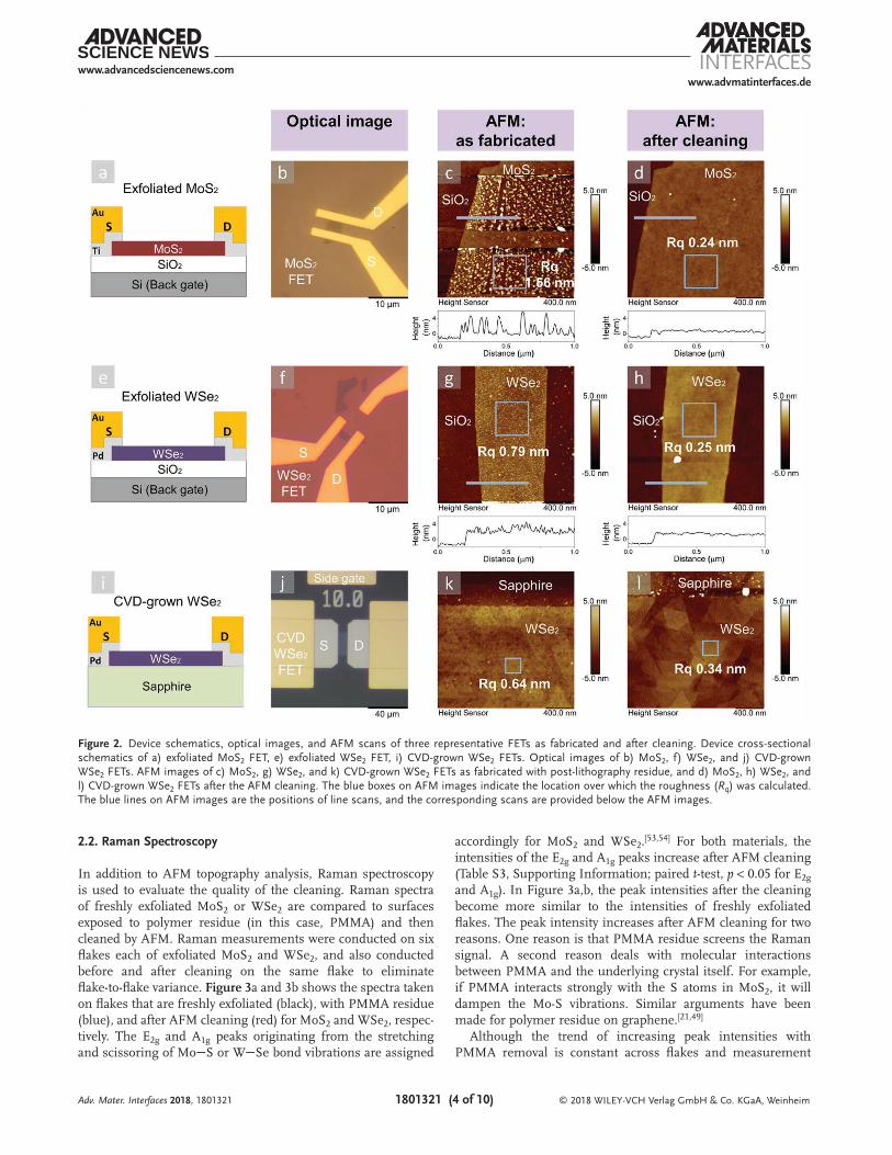
www.advancedsciencenews.com
© 2018 WILEY-VCH Verlag GmbH & Co. KGaA, Weinheim1801321 (4 of 10)
www.advmatinterfaces.de
2.2. Raman Spectroscopy
In addition to AFM topography analysis, Raman spectroscopy is used to evaluate the quality of the cleaning. Raman spectra of freshly exfoliated MoS2 or WSe2 are compared to surfaces exposed to polymer residue (in this case, PMMA) and then cleaned by AFM. Raman measurements were conducted on six flakes each of exfoliated MoS2 and WSe2, and also conducted before and after cleaning on the same flake to eliminate flake-to-flake variance. Figure 3a and 3b shows the spectra taken on flakes that are freshly exfoliated (black), with PMMA residue (blue), and after AFM cleaning (red) for MoS2 and WSe2, respec-tively. The E2g and A1g peaks originating from the stretching and scissoring of MoS or WSe bond vibrations are assigned
accordingly for MoS2 and WSe2.[53,54] For both materials, the intensities of the E2g and A1g peaks increase after AFM cleaning (Table S3, Supporting Information; paired t-test, p < 0.05 for E2g and A1g). In Figure 3a,b, the peak intensities after the cleaning become more similar to the intensities of freshly exfoliated flakes. The peak intensity increases after AFM cleaning for two reasons. One reason is that PMMA residue screens the Raman signal. A second reason deals with molecular interactions between PMMA and the underlying crystal itself. For example, if PMMA interacts strongly with the S atoms in MoS2, it will dampen the Mo-S vibrations. Similar arguments have been made for polymer residue on graphene.[21,49]
Although the trend of increasing peak intensities with PMMA removal is constant across flakes and measurement
Adv. Mater. Interfaces 2018, 1801321
Figure 2. Device schematics, optical images, and AFM scans of three representative FETs as fabricated and after cleaning. Device cross-sectional schematics of a) exfoliated MoS2 FET, e) exfoliated WSe2 FET, i) CVD-grown WSe2 FETs. Optical images of b) MoS2, f) WSe2, and j) CVD-grown WSe2 FETs. AFM images of c) MoS2, g) WSe2, and k) CVD-grown WSe2 FETs as fabricated with post-lithography residue, and d) MoS2, h) WSe2, and l) CVD-grown WSe2 FETs after the AFM cleaning. The blue boxes on AFM images indicate the location over which the roughness (Rq) was calculated. The blue lines on AFM images are the positions of line scans, and the corresponding scans are provided below the AFM images.

www.advancedsciencenews.com
© 2018 WILEY-VCH Verlag GmbH & Co. KGaA, Weinheim1801321 (5 of 10)
www.advmatinterfaces.de
locations, the peaks associated with the cleaned surfaces are not always equivalent to the freshly exfoliated surfaces. This could be due to slight variations in the location of the laser spot, or instrumental factors such as laser power stability. Because the surface roughness of the cleaned sample is recov-ered to the freshly exfoliated state, this difference in peak intensity is unlikely due to a thin layer of PMMA remaining on the surface.
To make sure the change in Raman peak intensity is not caused by the variation between measurements (e.g., inten-sity differences caused by Raman system realignment), we conducted consecutive Raman measurements on a partially cleaned sample without realigning the system (Figure S5, Supporting Information). Consistent with all the Raman data collected, the intensities of E2g and A1g peaks of MoS2 are larger for the cleaned region because PMMA has been removed.
2.3. Electrical Measurements on Back-Gated WSe2 and MoS2 FETs
While the combination of AFM and Raman measurements confirm the removal of polymer residue on exfoliated MoS2, exfoliated WSe2, it gives no information on the extent to which the residue and the cleaning process may affect the electrical device performance. Specifically, it is necessary to understand whether the AFM cleaning process affects the intrinsic electrical properties of the 2D crystal (e.g., if the mechanical AFM force during the AFM scanning is too strong, mechanical damage such as small pinholes may be introduced which will degrade channel conductivity). If the cleaning process is nondestruc-tive, then it is important to quantify the improvement after removing PMMA residue on the electrical characteristics such as threshold voltage and electron mobility. It is also instructive to compare the effect of AFM contact mode cleaning to vacuum annealing—one of the most commonly used methods to remove surface residue.[25,32,33]
Therefore, two back-gated WSe2 FETs were first fabri-cated from exfoliated flakes, and then annealed in vacuum (400 K, 2 × 10⁻⁶ Torr, 4 h), and lastly cleaned by AFM contact mode, with topology and transfer characteristics measured after each step. The results of one WSe2 FET are shown in
Figure 4. For this device, the maximum drain current (ID) at VBG = +30 V increases by 27% from 0.26 to 0.33 µA after vacuum anneal, and further increases by 48% to 0.49 µA after AFM cleaning. The AFM images (insets of Figure 4) indicate that PMMA residue was not fully removed by vacuum anneal at 400 K but was successfully removed after AFM cleaning. The surface roughness (Rq) decreases slightly from 1.22 ± 0.03 nm to 1.11 ± 0.03 nm after vacuum anneal, but decreases signifi-cantly to 0.33 ± 0.04 nm after AFM cleaning. Based on the AFM images and the electrical data, the improvement in the maximum current after vacuum anneal is more likely the result of improved contact between the metal and the semiconductor,[55] rather than the removal of PMMA residue from channel. In contrast, the improvement in the electrical characteristics after AFM cleaning can be directly attributed to the removal of PMMA. These results show that AFM con-tact mode cleaning is more effective than vacuum annealing in removing PMMA residue.
Adv. Mater. Interfaces 2018, 1801321
Figure 3. Raman spectra of a) MoS2 and b) WSe2 taken in the same region before and after AFM cleaning for each flake: as exfoliated (black line), with PMMA residue (blue line), and after the AFM cleaning (red line).
Figure 4. Transfer characteristics and AFM images of a back-gated WSe2 FET at three states: as fabricated (black line), after vacuum anneal (blue line), after AFM cleaning (red line). The blue boxes and lines on AFM images are the positions of roughness measurements and line scans, respectively.

www.advancedsciencenews.com
© 2018 WILEY-VCH Verlag GmbH & Co. KGaA, Weinheim1801321 (6 of 10)
www.advmatinterfaces.de
Six additional back-gated WSe2 FETs (flake thickness ≈3–9 nm) and six MoS2 FETs (flake thickness ≈8–17 nm) were meas-ured before and after the AFM cleaning to quantify the effect of PMMA residue on the electrical properties. The results are shown in Figure 5a and 5b, respectively. For reference, the optical and AFM images of one of the MoS2 and WSe2 devices before and after cleaning have been shown previously in the top and middle rows of Figure 2. The transfer measurements were con-ducted from VBG = −30 to +30 V for as-fabricated device (dotted line) and after AFM cleaning (solid line). The average threshold voltage shift ΔVth and estimated field-effect mobility (µ) are sum-marized in Table 1 for WSe2 and MoS2; values for individual devices are tabulated in Tables S4 and S5 in the Supporting Information. The threshold voltage (Vth) moves toward nega-tive VBG after cleaning (ΔVth < 0 V, paired t-test, p = 3.7 × 10⁻³ for WSe2 and 4 × 10⁻⁴ for MoS2, both < 0.05). The average ΔVth is −3 V for WSe2 FETs, and −2.7 V for MoS2 FETs. A negative (n-type) threshold voltage shift can be attributed to the removal of PMMA residue, which has been reported to cause p-type doping in 2D materials.[27] The charges induced by PMMA doping (ΔQ) can be estimated as ΔQ =Cox ΔVth, where Cox is the capacitance of the back-gate dielectric SiO2 (38.37 × 10⁻⁹ F cm−2 for 90 nm of SiO2). The corresponding sheet charge carrier den-sity (ns) is calculated by ns = ΔQ/e, which is ≈7.2 × 1011 cm−2 for WSe2 back-gated FETs and 6.5 × 1011 cm−2 for MoS2. The maximum drain current for MoS2 at VBG = +30 V slightly increases by 5% on average after the cleaning, while WSe2 FETs exhibits a much larger increase of 136% on average. The trend of increasing drain current is statistically significant for both WSe2 (paired t-test, p = 5 × 10⁻⁴ < 0.05) and MoS2 (paired t-test, p = 0.03 < 0.05), but the magnitude of the increase is weaker for MoS2. One possible reason for larger increase of maximum current in WSe2 FETs is that the average thickness of WSe2 channels (≈5 nm) is thinner than MoS2 channels (≈12 nm), and therefore, more sensitive to the presence and removal of PMMA residue.
The field-effect mobility µ is extracted from the transfer char-acteristic by µ = (1/Cox)∂σ/∂VBG, where Cox is oxide capacitance
of 90 nm SiO2 and σ is the channel conductivity that is defined as σ = (L/W)ID/VDS. L and W are the channel length and width, respectively. The field-effect electron mobilities of as-fabricated WSe2 FETs range from 17 to 61 cm2 V−1 s−1 as summarized in Table S4 in the Supporting Information. After cleaning, the mobilities of all WSe2 FETs increase by ≈13.1%, with an average increase of 4.2 ± 2.1 cm2 V−1 s−1, which is statisti-cally significant (paired t-test, p = 3.2 × 10⁻³ < 0.05). Increased mobility after cleaning has also been observed on graphene,[49] and is attributed to removing polymer fragments and charged species together with adsorbed water and oxygen which cause the carrier scattering.[49] For MoS2, the original electron mobili-ties range from ≈76 to 125 cm2 V−1 s−1 for the six devices, and five out of six show mobility increases but there is no statistical significance difference (paired t-test, p = 0.25 > 0.05). While the trend of increased mobility is the same for both 2D crystals, the effect is much weaker in MoS2 than WSe2. It is worth noting that neither the mobility or the threshold voltage shift depends on the channel thickness within the range investigated in this study (3–9 nm for WSe2, 8–17 nm for MoS2). Regardless, the combination of AFM, Raman, and electrical measurements prove that the cleaning technique is nondestructive, and the increase in the maximum current and the decrease in p-type doping show that removing the residue enhances device performance for back-gated FETs.
2.4. Effect of Polymer Residue on EDL-Gated CVD-Grown WSe2 FETs
In the previous section, we identified the p-type doping effect caused by the PMMA polymer residue. In addition to doping, when using an ion-gate, it is expected that polymer residue will interfere with EDL formation and therefore weaken the ability to modulate the channel conductivity. Ion gating is commonly used for 2D crystals grown by CVD on insulating substrates such as sapphire because they cannot be backgated. In addition, the more uniform CVD-grown epitaxial WSe2
Adv. Mater. Interfaces 2018, 1801321
Figure 5. Transfer characteristics of back-gated a) WSe2 and b) MoS2 FETs as fabricated (dotted line) and after the AFM cleaning (solid line). A1–A6 (B1–B6) correspond to six different WSe2 (MoS2) devices, respectively. VDS is set to 20 mV for WSe2 and 100 mV for MoS2.

www.advancedsciencenews.com
© 2018 WILEY-VCH Verlag GmbH & Co. KGaA, Weinheim1801321 (7 of 10)
www.advmatinterfaces.de
were used instead of exfoliated WSe2 flakes to minimize the device-to-device variation in thickness and channel dimensions compared to the exfoliated samples.[9] Therefore, FETs were fabricated on CVD-grown WSe2 on sapphire and gated using PEO:CsClO4.
Schematics of the EDL-gated WSe2 FET cleaning treatments are shown in Figure 6a. Transfer characteristics of all FETs were measured with the electrolyte using a side gate 63 µm away (Figure 2j). The transfer characteristics of the uncleaned samples are shown as dotted lines in Figure 6 (i.e., first scan) and tabulated in Tables S6 and S7 in the Supporting Infor-mation. Note that the data are shown on a linear scale in Figure 6b,c and on a log scale in Figure 6d,e. The FETs share a similar threshold voltage, Vth ≈2.5 V, and maximum currents ranging from 0.9 to 6.2 µA at VG = 4 V.
To determine the impact of polymer residue, the electro-lyte was removed by acetonitrile to expose the WSe2 channel (Figure 6a), and then cleaned with contact-mode AFM. After cleaning, the electrolyte was redeposited, and transfer char-acteristics were measured for a second time shown as solid lines in Figure 6b,d (i.e., second scan). To isolate any contribu-tion caused by the removal and redeposition of the electrolyte, we conducted control experiments where the electrolyte was simply removed with acetonitrile and redeposited without AFM cleaning. That is, the samples experienced identical electrolyte treatment, but without removing the polymer residue. The remeasured transfer curves of the control FETs without removing polymer residue are shown as solid lines in Figure 6c,e. After removing polymer residue (solid lines in Figure 6b,d), all five FETs exhibit a negative threshold voltage
Adv. Mater. Interfaces 2018, 1801321
Table 1. Summary of electrical measurements and statistical analysis of six back-gated WSe2 and six MoS2 FETs as fabricated and after AFM cleaning (without electrolyte). Error represents one standard deviation from the mean.
FETs Channel thickness [nm]
Threshold voltage Vth [V]
ΔVth [V] Charge density increase ns [cm−2]
Electron mobility µ [cm2 V−1 s−1]
Δµ [cm2 V−1 s−1] ID increase [%] at VBG = +30 V
As fabricated After cleaning As fabricated After cleaning
WSe2 5.4 ± 1.7 +23.2 ± 1.3 +20.2 ± 1.2 −3.0 ± 1.5 7.2 × 10¹¹ 32.5 ± 14.8 36.7 ± 16.5 +4.2 ± 2.1 136% ± 88%
MoS2 11.8 ± 3.1 −3.4 ± 5.5 −6.1 ± 4.8 −2.7 ± 0.8 6.5 × 10¹¹ 98.5 ± 17.9 100.6 ± 22.5 +2.1 ± 6.5 5% ± 3%
Statistical Analysis
Paired t-test WSe2 after cleaning:
Vth shifts toward negative VBG (p = 3.7 × 10⁻³ < 0.05)
Mobility increases (p = 3.2 × 10⁻³ < 0.05)
ID increases (p = 5 × 10⁻⁴ < 0.05)
MoS2 after cleaning:
Vth shifts toward positive VBG (p = 4 × 10⁻⁴ < 0.05)
Mobility no statistical difference (p = 0.25 > 0.05)
ID increases (p = 0.03 < 0.05)
Figure 6. Transfer characteristics of top-gated CVD WSe2 FETs with PEO:CsClO4 electrolyte. a) Schematics of control experiments with the sequence of transfer characteristics, removal and redeposition of electrolyte, and AFM cleaning. Transfer curves of CVD-grown WSe2 as fabricated with electrolyte (dotted line) and after cleaning polymer residue (solid line) are shown in b) linear scale and in d) log scale. The control FETs after redepositing electrolyte without AFM cleaning (solid line) are shown in c) linear scale and in e) log scale. L1–L5 (M1–M5) correspond to six different devices with (without) AFM cleaning, respectively.

www.advancedsciencenews.com
© 2018 WILEY-VCH Verlag GmbH & Co. KGaA, Weinheim1801321 (8 of 10)
www.advmatinterfaces.de
shift (ΔVth = −0.7 ± 0.2 V), corresponding to a charge density change (ΔQ) of about 4.5 × 1012 cm−2. The charge carrier den-sity change is calculated using the same method as discussed in Section 2.3, except that the capacitance is the EDL capacitance CEDL, which is about 1 × 10⁻⁶ F cm−2 in PEO:CsClO4 polymer electrolyte.[9,28] The maximum drain current after cleaning increased by 247% on average, and the increase is statistically significant (paired t-test, p = 9.0 × 10⁻³ < 0.05). However, for the control FETs without cleaning (Figure 6c,e), there is no sta-tistically significant difference in the threshold voltage shift or maximum drain current between the measurements after each of the two electrolyte depositions (paired t-test, both p > 0.5). The average threshold voltage is identical after the two deposi-tions (Table S7, Supporting Information), suggesting that the removal and redeposition of polymer electrolyte will not cause irreversible change to the channel material, and the measure-ment of threshold voltage is repeatable on the same device.
After cleaning, the transfer curves are more similar to each other (Figure 6d, solid lines), as indicated by a decrease in the standard deviation of threshold voltage from 0.4 V before cleaning to 0.2 V after. Thus, the variation in the electronic prop-erties among devices before cleaning can be at least partially attributed to inhomogeneities in the polymer residue—both laterally and vertically—which is eliminated by AFM cleaning. The field-effect mobility increases by 1.7 ± 0.2 cm2 V−1 s−1 after polymer residue removal, which is similar to the back-gated WSe2 FETs discussed above. The threshold voltage shift, field-effect mobility, and maximum current change are summarized for all devices in Tables S6 and S7 in the Supporting Informa-tion. Based on these results, we attribute the consistent trend of negative threshold voltage shift and maximum drain current increase after cleaning to the removal of the polymer residue.
Perhaps the most interesting observation in the EDL-gated devices is the magnitude of the maximum current increase after cleaning. Because the residue is a p-type dopant, we expect the maximum current to increase after removal and indeed this is what is observed in the back-gated WSe2 FETs, Figure 5a. Inter-estingly, the magnitude of the increase is larger for EDL gating (247%) than that for backgating (136%), and the increase is sta-tistically significant (independent t-test, p = 0.023 < 0.05). The channel current, ID, in the EDL-gated FETs can be estimated by ID = µ(W/L)CEDL(VG−Vth)VDS, where CEDL is the EDL capaci-tance. If we assume that the CEDL remains the same for meas-urements before and after the cleaning, the estimated increase of ID as a result of Vth shift and mobility increase is about 97% on average (see Section S5 and Table S8 in the Supporting Infor-mation), which is less than half of the observed increase. All five devices exhibit an additional increase in the maximum current beyond the estimate, which is attributed to the ions achieving a closer proximity to the channel after cleaning, increasing the EDL capacitance and inducing more electrons in the channel. We can estimate this increase in CEDL by assuming that the EDL thickness after AFM cleaning is reduced by ≈1.2 nm (i.e., the thickness of the residue) to its intrinsic value of ≈1 nm.[28] In this case, the estimated current increase is about 333% ± 30%, which is closer to the measured increase of 247% ± 44%. The difference between the estimated and measured current increases could be due to inhomogeneity in the polymer residue (e.g., in regions where the polymer residue was thinner than
1.2 nm, the expected current increase would be less than 333%. See Section S5 in the Supporting Information for more discus-sion). These results suggest that to achieve the highest possible field-effect modulation with EDL gating, it is important to remove the polymer residue at the channel surface using a nondestructive method such as AFM contact mode cleaning.
3. Conclusion
Successful removal of post-lithography polymer residue using contact mode AFM has been demonstrated on MoS2 and WSe2 and confirmed by AFM topology measurements and Raman spectroscopy. AFM topology shows that surface roughness is restored to its intrinsic state, and Raman spectra show that the characteristic peak intensities of MoS2 and WSe2 increase after removing the residue. For back-gated MoS2 and WSe2 FETs, transfer characteristics indicate that removing PMMA, a p-type dopant, increases the charge density by ≈7 × 1011 cm−2. For EDL-gated WSe2 FETs using a PEO:CsClO4 electrolyte, removing photoresist residue causes a negative threshold voltage shift with a charge density increase of 4.5 × 1012 cm−2, and increases the maximum current by 247% which is sta-tistically significant (paired t-test, p = 9.0 × 10⁻³ < 0.05). The increase in maximum current for EDL-gated WSe2 FETs sug-gests that removal of residue by AFM provides closer access for the ions to reach the surface of the channel, thereby increasing the EDL gate capacitance. Overall the results suggest that the AFM contact mode cleaning is a widely applicable and nonde-structive method that can successfully remove different types of post-lithography polymer residue on a variety of 2D crystals, and can improve channel conductivity, mobility, and charge density. This method is especially useful for applications where a near molecularly clean surface is required, and for EDL gating to achieve the best possible electrostatic gate control.
4. Experimental SectionExfoliation and Device Fabrication: WSe2 and MoS2 flakes with
thickness 3–20 nm were mechanically exfoliated from their bulk sources (2D Semiconductors) and transferred to p-type Si (resistivity 0.001–0.005 ohm-cm) with 90 nm of SiO2 (Graphene Supermarket) by the Scotch tape method. These flakes were used for Raman measurements and to fabricate back-gated FETs. Acetone, isopropanol (IPA), and deionized water were used to preclean the substrate. Flakes with uniform thickness were selected by optical microscopy and AFM topology measurements (Bruker Dimension Icon in ScanAsyst mode using Si3N4 ScanAsyst Air tips with 0.4 N m−1). Back-gated FETs were fabricated by e-beam lithography (EBL) (Raith e-LiNE). Two hundred nanometers of PMMA-950-A4 (MicroChem) e-beam resist, was spincoated at a spin speed of 4000 rpm for 1 min, followed by a 3 min bake on a hotplate at 180 °C. Source/drain and gate contacts were patterned by EBL, and the sample was developed in a methyl isobutyl ketone (MIBK) and IPA solution (MIBK:IPA 1:3 volume ratio) for 1 min and then rinsed by IPA for another 1 min. E-beam evaporation (Plassys Electron Beam Evaporator MEB550S) was used to deposit metal electrodes at a base pressure < 1 × 10⁻⁶ Torr. The metal thicknesses were Pd (20 nm) and Au (80 nm) on WSe2 and Ti (5 nm) and Au (100 nm) on MoS2. The samples were immersed in acetone for lift-off at room temperature overnight, and then rinsed with IPA and deionized water. In some cases, flakes with PMMA residue were only characterized by AFM and Raman, and therefore device fabrication was not necessary. In these
Adv. Mater. Interfaces 2018, 1801321

www.advancedsciencenews.com
© 2018 WILEY-VCH Verlag GmbH & Co. KGaA, Weinheim1801321 (9 of 10)
www.advmatinterfaces.de
cases, the flakes were exposed to the same steps of the e-beam process except for writing the patterns. After spincoating PMMA-950-A4 and baking, the sample was cooled to room temperature, soaked in acetone for 15 min, and then rinsed by IPA for 1 min.
AFM Contact Mode Cleaning: AFM contact mode was used to scan the FET channel to “sweep” away the polymer residue by the mechanical force. For cleaning purposes, a stiff AFM tip was used (SCM-PIT-v2, measured force constant 2.37 N m−1) which is much stronger than AFM tips commonly used for the contact mode (Si3N4 ScanAsyst Air tips, 0.4 N m−1). The deflection setpoint was optimized to be 1.33 V, which is equivalent to applying 104 nN of normal force to the sample surface (Larger setpoints damaged the sample while smaller setpoints do not completely remove the residue). Complete cleaning was achieved by scanning the target region three times in different directions (rotating the sample 90° each time) using a scan rate of 10 µm s−1.
Raman Measurements: Raman measurements were made using a Renishaw inVia Raman Spectrometer. Each measurement was taken with exposure time of 12 s, three times of accumulation (1800 | mm−1 grating). The measurements were made three different times on WSe2 and MoS2 flakes: as exfoliated, with the PMMA residue, and after cleaning. Each Raman measurement was done on the same flake to avoid flake-to-flake variation. Large (≈30 × 10 µm) and thin (10–20 nm thick) WSe2 and MoS2 flakes were selected for this study. After exposure to the PMMA residue, the entire surface of each flake was cleaned by AFM contact mode. A 488 nm Raman laser with beam spot size of 0.8 µm was used for MoS2, and 633 nm with spot size 1 µm for WSe2. The laser power was set to 10 mW to minimize heating the flake by the laser.
CVD WSe2 Growth and FETs Preparation: Large-area, few-layer (2–3 L) WSe2 films were synthesized on sapphire substrates by metal organic CVD (MOCVD) in a vertical cold wall system using W(CO)6 and H2Se precursors and H2 carrier gas. Samples were grown at 800 °C at 700 Torr total pressure with W(CO)6 and H2Se precursor partial pressures of 6.2 × 10⁻⁴ Torr and 15.6 Torr, respectively. Full details of the entire MOCVD growth process including seeding, ripening, growth, and post-growth annealing steps can be found in the following work.[9] Additional materials and device characterization of identical WSe2 samples and EDL gating can be found in the referenced work.
EDL-gated FETs were fabricated via standard photolithography (GCA 8500 i-line Stepper) to define WSe2 channel dimensions, source/drain (S/D) contact electrodes, and side-gate electrodes. WSe2 channels were isolated and defined via reactive ion etching in a Plasma Therm PT-720 plasma etch tool using an SF6/O2/Ar gas chemistry at 10 mTorr and 100 W for 30 s. 10/10 nm Pd/Au source/drain metal was deposited by e-beam evaporation under moderate vacuum (≈10−6 Torr) at a deposition rate of 1.0 Å s−1 followed by lift-off in acetone and PRS-3000 resist stripper. Following this initial source/drain metal deposition, a second metallization consisting of ≈10/150 nm Ti/Au was carried out to define the side-gate and to thicken source/drain pads for probing through the electrolyte.
In total, CVD-WSe2 films were subjected to four levels of photolithography to realize EDL-gated devices (listed in chronological order): alignment mark metal, WSe2 isolation etch, source/drain metal, and side-gate metal. The photoresist stacks used in these four lithography steps are listed in chronological order: LOR5A/SPR 3012, LOR2A/SPR 3012, PMGI SF5(s)/SPR 3012, and LOR5A/3012. LOR2A and LOR5A were baked at 180 °C for 3 min, SPR 3012 was baked at 95 °C for 1 min, and PMGI SF5(s) was baked at 220 °C for 3 min. The resulting photoresist residue on CVD-WSe2 device channels was most likely a mixture of these three main photoresists.
Electrical Characterizations: Electrical measurements were made using a Keysight B1500A semiconductor parameter analyzer in a Lakeshore cryogenic vacuum probe station (CRX-VF) with pressure ≈2 × 10⁻⁶ Torr. To compare the improvement of FET electrical performance by vacuum annealing and AFM cleaning, a few back-gated WSe2 FETs were chosen to be annealed in vacuum and then cleaned by AFM contact mode with transfer characteristics taken after each process. Samples were annealed at 400 K for 4 h in the probe station with pressure ≈2 × 10⁻⁶ Torr.
Electrolyte Preparation and EDL-Gating Experiments: The polymer electrolyte preparation process was similar to previously published results.[28,56] PEO:CsClO4 was prepared inside an argon-filled glove box with H2O and O2 concentration < 0.1 parts-per-million (ppm). PEO (Polymer Standards Service, molecular weight 94 600 g mol−1) and CsClO4 (Sigma-Aldrich, 99.9%) were dissolved in anhydrous acetonitrile (Sigma-Aldrich) to make a 1 wt% solution with the ether oxygen to Cs molar ratio 76:1. The polymer electrolyte was drop-cast (25 µL) onto the 1 cm2 sample chip with CVD WSe2 FETs in the glove box, dried at room temperature until the majority of the solvent evaporated, and then annealed at 80 °C for 3 min. The sample was transferred out of the glove box to the probe station using a load lock filled with argon. The deposition and transfer were completed in an argon environment, and the electrical measurements were completed in vacuum (≈2 × 10⁻⁶ Torr) to avoid any sample exposure to ambient conditions.
To compare EDL-gated WSe2 FET performance with and without AFM cleaning of the e-beam resist residue, it was necessary to remove the PEO:CsClO4 electrolyte after the first measurement and then redeposit it onto the devices for the second measurement. First, PEO:CsClO4 was deposited on all the FETs for transfer characteristics to establish the baseline electrical response. Next, the electrolyte was removed by a hot acetonitrile bath at 60 °C for 30 min and kept inside acetone overnight for 13 h. Note: acetonitrile is extremely volatile—please read safety data sheet before heating. After the removal of the PEO electrolyte, half of the FETs were cleaned using AFM contact mode. Last, PEO:CsClO4 was redeposited on all the FETs and the electrical measurements were repeated.
Statistical Analysis: IBM SPSS Statistics 25.0 was used to perform statistical analysis including t-test and ANOVA.
Supporting InformationSupporting Information is available from the Wiley Online Library or from the author.
AcknowledgementsJ.L. and K.X. contributed equally to this work. This research was supported by NSF under Grant No. ECCS-GOALI-1408425, the Center for Low Energy Systems Technology (LEAST), one of six centers of STARnet, a Semiconductor Research Corporation program sponsored by MARCO and DARPA, and by Northrop Grumman Mission Systems University Research Program. The authors thank Zhongmou Chao, Micah (Eli) Bostian, Aaron Woeppel at the University of Pittsburgh for helpful discussion.
Conflict of InterestThe authors declare no conflict of interest.
Keywordsfield effect transistor, ionic gating, MoS2, polymer residue, WSe2
Received: August 28, 2018Revised: November 8, 2018
Published online:
[1] K. S. Novoselov, A. K. Geim, S. V. Morozov, D. Jiang, Y. Zhang, S. V. Dubonos, I. V. Grigorieva, A. A. Firsov, Science 2004, 306, 666.
[2] B. Radisavljevic, A. Radenovic, J. Brivio, V. Giacometti, A. Kis, Nat. Nanotechnol. 2011, 6, 147.
Adv. Mater. Interfaces 2018, 1801321
www.advancedsciencenews.com
© 2018 WILEY-VCH Verlag GmbH & Co. KGaA, Weinheim1801321 (10 of 10)
www.advmatinterfaces.de
Adv. Mater. Interfaces 2018, 1801321
[3] H. Fang, S. Chuang, T. C. Chang, K. Takei, T. Takahashi, A. Javey, Nano Lett. 2012, 12, 3788.
[4] G. R. Bhimanapati, Z. Lin, V. Meunier, Y. Jung, J. Cha, S. Das, D. Xiao, Y. Son, M. S. Strano, V. R. Cooper, L. B. Liang, S. G. Louie, E. Ringe, W. Zhou, S. S. Kim, R. R. Naik, B. G. Sumpter, H. Terrones, F. N. Xia, Y. L. Wang, J. Zhu, D. Akinwande, N. Alem, J. A. Schuller, R. E. Schaak, M. Terrones, J. A. Robinson, ACS Nano 2015, 9, 11509.
[5] C. L. Tan, X. H. Cao, X. J. Wu, Q. Y. He, J. Yang, X. Zhang, J. Z. Chen, W. Zhao, S. K. Han, G. H. Nam, M. Sindoro, H. Zhang, Chem. Rev. 2017, 117, 6225.
[6] S. Z. Butler, S. M. Hollen, L. Y. Cao, Y. Cui, J. A. Gupta, H. R. Gutierrez, T. F. Heinz, S. S. Hong, J. X. Huang, A. F. Ismach, E. Johnston-Halperin, M. Kuno, V. V. Plashnitsa, R. D. Robinson, R. S. Ruoff, S. Salahuddin, J. Shan, L. Shi, M. G. Spencer, M. Terrones, W. Windl, J. E. Goldberger, ACS Nano 2013, 7, 2898.
[7] A. E. Grigorescu, C. W. Hagen, Nanotechnology 2009, 20, 292001.[8] S. Subramanian, D. D. Deng, K. Xu, N. Simonson, K. Wang,
K. H. Zhang, J. Li, R. Feenstra, S. K. Fullerton-Shirey, J. A. Robinson, Carbon 2017, 125, 551.
[9] Y. C. Lin, B. Jariwala, B. M. Bersch, K. Xu, Y. F. Nie, B. M. Wang, S. M. Eichfeld, X. T. Zhang, T. H. Choudhury, Y. Pan, R. Addou, C. M. Smyth, J. Li, K. H. Zhang, M. A. Haque, S. Folsch, R. M. Feenstra, R. M. Wallace, K. Cho, S. K. Fullerton-Shirey, J. M. Redwing, J. A. Robinson, ACS Nano 2018, 12, 965.
[10] K. H. Zhang, B. M. Bersch, J. Joshi, R. Addou, C. R. Cormier, C. X. Zhang, K. Xu, N. C. Briggs, K. Wang, S. Subramanian, K. Cho, S. Fullerton-Shirey, R. M. Wallace, P. M. Vora, J. A. Robinson, Adv. Funct. Mater. 2018, 28, 7.
[11] T. Uwanno, Y. Hattori, T. Taniguchi, K. Watanabe, K. Nagashio, 2D Mater. 2015, 2, 041002.
[12] B. Hunt, J. D. Sanchez-Yamagishi, A. F. Young, M. Yankowitz, B. J. LeRoy, K. Watanabe, T. Taniguchi, P. Moon, M. Koshino, P. Jarillo-Herrero, R. C. Ashoori, Science 2013, 340, 1427.
[13] X. S. Li, Y. W. Zhu, W. W. Cai, M. Borysiak, B. Y. Han, D. Chen, R. D. Piner, L. Colombo, R. S. Ruoff, Nano Lett. 2009, 9, 4359.
[14] H. J. Park, J. Meyer, S. Roth, V. Skakalova, Carbon 2010, 48, 1088.[15] E. H. Lock, M. Baraket, M. Laskoski, S. P. Mulvaney, W. K. Lee,
P. E. Sheehan, D. R. Hines, J. T. Robinson, J. Tosado, M. S. Fuhrer, S. C. Hernandez, S. G. Waltont, Nano Lett. 2012, 12, 102.
[16] X. S. Li, W. W. Cai, J. H. An, S. Kim, J. Nah, D. X. Yang, R. Piner, A. Velamakanni, I. Jung, E. Tutuc, S. K. Banerjee, L. Colombo, R. S. Ruoff, Science 2009, 324, 1312.
[17] J. W. Suk, A. Kitt, C. W. Magnuson, Y. F. Hao, S. Ahmed, J. H. An, A. K. Swan, B. B. Goldberg, R. S. Ruoff, ACS Nano 2011, 5, 6916.
[18] M. Ishigami, J. H. Chen, W. G. Cullen, M. S. Fuhrer, E. D. Williams, Nano Lett. 2007, 7, 1643.
[19] Y. H. Jia, X. Gong, P. Peng, Z. D. Wang, Z. Z. Tian, L. M. Ren, Y. Y. Fu, H. Zhang, Nano-Micro Lett. 2016, 8, 336.
[20] M. T. Pettes, I. S. Jo, Z. Yao, L. Shi, Nano Lett. 2011, 11, 1195.[21] Y. C. Lin, C. H. Jin, J. C. Lee, S. F. Jen, K. Suenaga, P. W. Chiu,
ACS Nano 2011, 5, 2362.[22] J. H. Park, H. C. P. Movva, E. Chagarov, K. Sardashti, H. Chou,
I. Kwak, K. T. Hu, S. K. Fullerton-Shirey, P. Choudhury, S. K. Banerjee, A. C. Kummel, Nano Lett. 2015, 15, 6626.
[23] X. C. Dong, Y. M. Shi, W. Huang, P. Chen, L. J. Li, Adv. Mater. 2010, 22, 1649.
[24] F. Yavari, E. Castillo, H. Gullapalli, P. M. Ajayan, N. Koratkar, Appl. Phys. Lett. 2012, 100, 203120.
[25] Y. C. Lin, C. C. Lu, C. H. Yeh, C. H. Jin, K. Suenaga, P. W. Chiu, Nano Lett. 2012, 12, 414.
[26] J. W. Suk, W. H. Lee, J. Lee, H. Chou, R. D. Piner, Y. F. Hao, D. Akinwande, R. S. Ruoff, Nano Lett. 2013, 13, 1462.
[27] A. Pirkle, J. Chan, A. Venugopal, D. Hinojos, C. W. Magnuson, S. McDonnell, L. Colombo, E. M. Vogel, R. S. Ruoff, R. M. Wallace, Appl. Phys. Lett. 2011, 99, 122108.
[28] H. L. Xu, S. Fathipour, E. W. Kinder, A. C. Seabaugh, S. K. Fullerton-Shirey, ACS Nano 2015, 9, 4900.
[29] S. H. Kim, K. Hong, W. Xie, K. H. Lee, S. P. Zhang, T. P. Lodge, C. D. Frisbie, Adv. Mater. 2013, 25, 1822.
[30] K. Xu, H. Lu, E. W. Kinder, A. Seabaugh, S. K. Fullerton-Shirey, ACS Nano 2017, 11, 5453.
[31] H. Lu, I. Kwak, J. H. Park, K. O’Neill, T. Furuyama, N. Kobayashi, A. Seabaugh, A. Kummel, S. K. Fullerton-Shirey, J. Phys. Chem. C 2015, 119, 21992.
[32] Y. Ahn, H. Kim, Y. H. Kim, Y. Yi, S. I. Kim, Appl. Phys. Lett. 2013, 102, 5.
[33] F. L. Wang, P. Stepanov, M. Gray, C. N. Lau, Nanotechnology 2015, 26, 5.
[34] L. Gammelgaard, J. M. Caridad, A. Cagliani, D. M. A. Mackenzie, D. H. Petersen, T. J. Booth, P. Boggild, 2D Mater. 2014, 1, 035005.
[35] Z. G. Cheng, Q. Y. Zhou, C. X. Wang, Q. A. Li, C. Wang, Y. Fang, Nano Lett. 2011, 11, 767.
[36] S. Ryu, L. Liu, S. Berciaud, Y. J. Yu, H. T. Liu, P. Kim, G. W. Flynn, L. E. Brus, Nano Lett. 2010, 10, 4944.
[37] C. Gong, H. C. Floresca, D. Hinojos, S. McDonnell, X. Y. Qin, Y. F. Hao, S. Jandhyala, G. Mordi, J. Kim, L. Colombo, R. S. Ruoff, M. J. Kim, K. Cho, R. M. Wallace, Y. J. Chabal, J. Phys. Chem. C 2013, 117, 23000.
[38] M. Yamamoto, T. L. Einstein, M. S. Fuhrer, W. G. Cullen, J. Phys. Chem. C 2013, 117, 25643.
[39] J. H. Park, S. Vishwanath, X. Y. Liu, H. W. Zhou, S. M. Eichfeld, S. K. Fullerton-Shirey, J. A. Robinson, R. M. Feenstra, J. Furdyna, D. Jena, H. G. Xing, A. C. Kummel, ACS Nano 2016, 10, 4258.
[40] B. M. Bersch, S. M. Eichfeld, Y. C. Lin, K. H. Zhang, G. R. Bhimanapati, A. F. Piasecki, M. Labella, J. A. Robinson, 2D Mater. 2017, 4, 025083.
[41] J. Moser, A. Barreiro, A. Bachtold, Appl. Phys. Lett. 2007, 91, 3.[42] R. H. J. Vervuurt, B. Karasulu, M. A. Verheijen, W. M. M. Kessels,
A. A. Bol, Chem. Mater. 2017, 29, 2090.[43] Z. Li, S. S. Yang, R. Dhall, E. Kosmowska, H. T. Shi, I. Chatzakis,
S. B. Cronin, ACS Nano 2016, 10, 6836.[44] P. R. Pudasaini, A. Oyedele, C. Zhang, M. G. Stanford, N. Cross,
A. T. Wong, A. N. Hoffman, K. Xiao, G. Duscher, D. G. Mandrus, T. Z. Ward, P. D. Rack, Nano Res. 2018, 11, 722.
[45] D. Ferrah, O. Renault, C. Petit-Etienne, H. Okuno, C. Berne, V. Bouchiat, G. Cunge, Surf. Interface Anal. 2016, 48, 451.
[46] J. Wu, L. M. Xie, Y. G. Li, H. L. Wang, Y. J. Ouyang, J. Guo, H. J. Dai, J. Am. Chem. Soc. 2011, 133, 19668.
[47] S. F. Wang, W. J. Zhao, F. Giustiniano, G. Eda, Phys. Chem. Chem. Phys. 2016, 18, 4304.
[48] R. Jalilian, L. A. Jauregui, G. Lopez, J. F. Tian, C. Roecker, M. M. Yazdanpanah, R. W. Cohn, I. Jovanovic, Y. P. Chen, Nanotechnology 2011, 22, 9.
[49] W. Choi, M. A. Shehzad, S. Park, Y. Seo, RSC Adv. 2017, 7, 6943.
[50] A. M. Goossens, V. E. Calado, A. Barreiro, K. Watanabe, T. Taniguchi, L. M. K. Vandersypen, Appl. Phys. Lett. 2012, 100, 073110.
[51] N. Lindvall, A. Kalabukhov, A. Yurgens, J. Appl. Phys. 2012, 111, 4.[52] B. V. Derjaguin, V. M. Muller, Y. P. Toporov, Prog. Surf. Sci. 1994, 45,
131.[53] S. Fathipour, M. Remskar, A. Varlec, A. Ajoy, R. Yan, S. Vishwanath,
S. Rouvimov, W. S. Hwang, H. G. Xing, D. Jena, A. Seabaugh, Appl. Phys. Lett. 2015, 106, 4.
[54] X. Zhang, X. F. Qiao, W. Shi, J. B. Wu, D. S. Jiang, P. H. Tan, Chem. Soc. Rev. 2015, 44, 2757.
[55] W. S. Leong, C. T. Nai, J. T. L. Thong, Nano Lett. 2014, 14, 3840.[56] H. M. Li, K. Xu, B. Bourdon, H. Lu, Y. C. Lin, J. A. Robinson,
A. C. Seabaugh, S. K. Fullerton-Shirey, J. Phys. Chem. C 2017, 121, 16996.
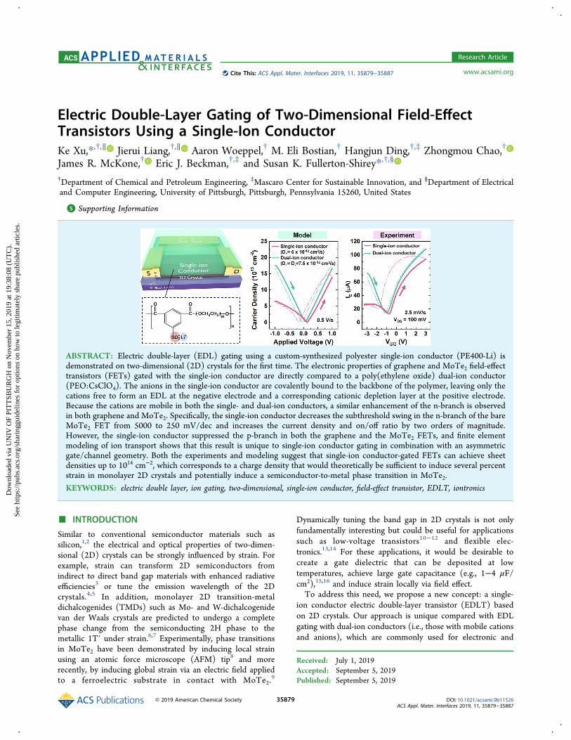
Electric Double-Layer Gating of Two-Dimensional Field-EffectTransistors Using a Single-Ion ConductorKe Xu,*,†,∥ Jierui Liang,†,∥ Aaron Woeppel,† M. Eli Bostian,† Hangjun Ding,†,‡ Zhongmou Chao,†
James R. McKone,† Eric J. Beckman,†,‡ and Susan K. Fullerton-Shirey*,†,§
†Department of Chemical and Petroleum Engineering, ‡Mascaro Center for Sustainable Innovation, and §Department of Electricaland Computer Engineering, University of Pittsburgh, Pittsburgh, Pennsylvania 15260, United States
*S Supporting Information
ABSTRACT: Electric double-layer (EDL) gating using a custom-synthesized polyester single-ion conductor (PE400-Li) isdemonstrated on two-dimensional (2D) crystals for the first time. The electronic properties of graphene and MoTe2 field-effecttransistors (FETs) gated with the single-ion conductor are directly compared to a poly(ethylene oxide) dual-ion conductor(PEO:CsClO4). The anions in the single-ion conductor are covalently bound to the backbone of the polymer, leaving only thecations free to form an EDL at the negative electrode and a corresponding cationic depletion layer at the positive electrode.Because the cations are mobile in both the single- and dual-ion conductors, a similar enhancement of the n-branch is observedin both graphene and MoTe2. Specifically, the single-ion conductor decreases the subthreshold swing in the n-branch of the bareMoTe2 FET from 5000 to 250 mV/dec and increases the current density and on/off ratio by two orders of magnitude.However, the single-ion conductor suppressed the p-branch in both the graphene and the MoTe2 FETs, and finite elementmodeling of ion transport shows that this result is unique to single-ion conductor gating in combination with an asymmetricgate/channel geometry. Both the experiments and modeling suggest that single-ion conductor-gated FETs can achieve sheetdensities up to 1014 cm−2, which corresponds to a charge density that would theoretically be sufficient to induce several percentstrain in monolayer 2D crystals and potentially induce a semiconductor-to-metal phase transition in MoTe2.
KEYWORDS: electric double layer, ion gating, two-dimensional, single-ion conductor, field-effect transistor, EDLT, iontronics
■ INTRODUCTION
Similar to conventional semiconductor materials such assilicon,1,2 the electrical and optical properties of two-dimen-sional (2D) crystals can be strongly influenced by strain. Forexample, strain can transform 2D semiconductors fromindirect to direct band gap materials with enhanced radiativeefficiencies3 or tune the emission wavelength of the 2Dcrystals.4,5 In addition, monolayer 2D transition-metaldichalcogenides (TMDs) such as Mo- and W-dichalcogenidevan der Waals crystals are predicted to undergo a completephase change from the semiconducting 2H phase to themetallic 1T′ under strain.6,7 Experimentally, phase transitionsin MoTe2 have been demonstrated by inducing local strainusing an atomic force microscope (AFM) tip8 and morerecently, by inducing global strain via an electric field appliedto a ferroelectric substrate in contact with MoTe2.
9
Dynamically tuning the band gap in 2D crystals is not onlyfundamentally interesting but could be useful for applicationssuch as low-voltage transistors10−12 and flexible elec-tronics.13,14 For these applications, it would be desirable tocreate a gate dielectric that can be deposited at lowtemperatures, achieve large gate capacitance (e.g., 1−4 μF/cm2),15,16 and induce strain locally via field effect.To address this need, we propose a new concept: a single-
ion conductor electric double-layer transistor (EDLT) basedon 2D crystals. Our approach is unique compared with EDLgating with dual-ion conductors (i.e., those with mobile cationsand anions), which are commonly used for electronic and
Received: July 1, 2019Accepted: September 5, 2019Published: September 5, 2019
Research Article
www.acsami.orgCite This: ACS Appl. Mater. Interfaces 2019, 11, 35879−35887
© 2019 American Chemical Society 35879 DOI: 10.1021/acsami.9b11526ACS Appl. Mater. Interfaces 2019, 11, 35879−35887
Dow
nloa
ded
via
UN
IV O
F PI
TT
SBU
RG
H o
n N
ovem
ber
15, 2
019
at 1
9:38
:08
(UT
C).
See
http
s://p
ubs.
acs.
org/
shar
ingg
uide
lines
for
opt
ions
on
how
to le
gitim
atel
y sh
are
publ
ishe
d ar
ticle
s.

optoelectronic device studies.17−21 Moreover, a wide variety ofEDLTs have been demonstrated on 2D crystals.15,16,22−25
Dual-ion conductors can induce charge densities on the orderof ∼1014 cm−2 for electrons and holes.26,27 This corresponds toa capacitance density up to 10 μF/cm2 and a large electric fieldstrength of ∼V/nm at the interface, allowing access to regimesof transport in semiconductors that cannot be achieved withconventional gate dielectrics.25,28,29 In contrast to a dual-ionconductor, the anions of a single-ion conductor, or ionomer,are covalently bound to the backbone of the polymer, leavingonly the cations free to move in response to an applied field.When polarized, an EDL consisting of densely packed cationsis created at the negative electrode, but there is nocorresponding anionic EDL at the positive electrode. Inresponse to this imbalance, one side of the single-ionconductor (near the negative electrode) undergoes longitudi-nal expansion. The mechanism to induce strain using single-ion conductors has been well investigated for ionic polymermetal composites (IPMCs), which are useful for biomimeticactuators and artificial muscles.30 In electronics, single-ionconductors have been used previously to gate organictransistors31−33 where the motivation for immobilizing oneion over the other was to avoid electrochemical reactionswithin the organic channel. To our knowledge, there has beenno report directly comparing single- and dual-ion conductorswith similar chemistries in the same 2D crystal FETs ordistinguishing the electrostatic gating effects between cationicEDLs and cationic depletion layers on 2D crystals.We present the first demonstration of a single-ion conductor
multilayer 2D crystal EDLT and lay the groundwork fordemonstrating flexible 2D FETs with new functionalitiesinduced by an EDL via strain. Experimentally, we used anionically functionalized polyester (created via the condensationof poly(ethylene glycol) oligomers with dimethyl 5-sulfoisoph-thalate salt34) to electrostatically gate both graphene andMoTe2 FETs. Compared with back gating through SiO2,transfer characteristics using a side gate to control the location
of the ions within both the single- and dual-ion conductorsreveal a comparable enhancement of the n-branch current(e.g., 20-fold improvement of subthreshold swing and twoorders of magnitude increase in on/off for MoTe2 FETs). Thedual-ion conductor gating results agree well with previousreports.16,25,26,35 However, unlike the dual-ion conductor, thesingle-ion conductor quenches the p-branch in graphene andMoTe2 FETs, which has not been reported before. Finiteelement modeling of ion transport in response to an appliedfield shows that the p-branch quenching is unique to single-ionconductor gating via the formation of a cationic depletionregion (as opposed to an anionic EDL) in combination with anasymmetric gate/channel geometry. Both the experiments andmodeling suggest that single-ion conductor-gated FETs canachieve sheet densities up to 1014 cm−2, which could possiblyinduce sufficient strain to access the strain-induced electronicand optoelectronic properties described above.36,37
■ RESULTS AND DISCUSSIONThe EDL-gated multilayer 2D crystal FETs use a side-gategeometry, as shown in Figure 1a. Graphene and MoTe2 weremechanically exfoliated onto a p-doped Si substrate with 90nm SiO2 (used as a back gate). The source/drain and gatecontacts (Ti/Au) were patterned by electron beam lithography(EBL) with the side gate located 10 μm away from thechannel. The solid-state single-ion conductor is poly(ethyleneglycol benzene-1,3-dicarboxylate-5-sulfoisophthalate lithium),abbreviated as PE400-Li, and the solid-state dual-ionconductor is poly(ethylene oxide), abbreviated as (PEO):C-sClO4. The chemical structures of the dual- and single-ionconductors are similar and shown in Figure 1b. The PE400-Liis a polyester with each repeat unit consisting of the ionicgroup, namely, dicarboxylic 5-sulfoisophthalate, and a spacer ofpoly(ethylene glycol) 400, which provides the same repeat unitas PEO.34 Unlike PEO:CsClO4 where the anion, ClO4
−, is freeto respond to the applied field, the negatively chargedfunctional group (SO3
−) in PE400-Li is covalently bound to
Figure 1. (a) Schematic of a 2D crystal FET (either graphene or MoTe2) that can be operated by using a back gate or a single/dual-ion conductorusing a metal side gate. (b) Chemical structures of the dual- and single-ion conductors: PEO:CsClO4 (top row) and the ionically functionalizedpolyester (PE400-Li) (bottom row), respectively. Anions are shaded in red and cations are shaded in blue. Schematics of the (c) dual-ionconducting and (d) single-ion conducting FETs under two polarities. In the single-ion case, only cations are mobile while the anions are bound tothe polymer backbone and therefore fixed. This immobility leads to cationic depletion regions (shaded in pink) at either the gate/single-ionconductor (VG > 0) or single-ion conductor/semiconductor interface (VG < 0), depending on the polarity of the applied field.
ACS Applied Materials & Interfaces Research Article
DOI: 10.1021/acsami.9b11526ACS Appl. Mater. Interfaces 2019, 11, 35879−35887
35880

the polymer backbone, while the cation Li+ is free to moveunder an applied field. The ether oxygen to cation molar ratiosare 76:1 for the dual-ion conductors and 9:1 for the single-ionconductors. Differential scanning calorimetry (DSC) showsthat the single-ion conductor has a markedly higher glasstransition temperature (Tg = 14.5 °C) than the PEO:CsClO4electrolyte (Tg = −31.5 °C) (Figure S1, SupportingInformation), which is consistent with the single-ion conductorhaving a larger salt concentration.38 This difference in Tgsuggests that the single-ion conductor will have lower ionicconductivity than the dual-ion conductor.When no voltage is applied, cations and anions are
homogeneously distributed throughout the electrolyte forboth the single- or dual-ion conductors. The steady-statelocations of cations and anions under VG > 0 and VG < 0 areillustrated in Figure 1c,d for the dual-ion conductor and single-ion conductor, respectively. When a positive gate bias isapplied to a dual-ion conductor (Figure 1c, left), cations (Cs+)are driven to the channel where they induce image charges (inthis case, image charges are electrons) forming a cationic EDLat the channel/electrolyte interface. An analogous anionic EDLwill form as anions (ClO4
−) accumulating at the electrolyte/gate interface. When the polarity of the applied bias is reversed,an anionic EDL forms at the channel and a cationic EDL formsat the gate (Figure 1c, right).For a single-ion conductor, shown in Figure 1d, a positive
gate bias does not result in an anionic EDL at the gate/electrolyte interface; instead, there exists a cationic depletionlayer (Figure 1d, left). When the polarity is reversed, the cationdepletion layer forms at the channel/electrolyte interface(Figure 1d, right). Crucially, the negative charge stored byanions in the cationic depletion layer equals the positive chargein the cationic EDL, while the volumetric charge density ofanions in the depletion layer is fixed and smaller than thevolumetric charge density of the closely packed cations in theEDL. Thus, the depletion layer requires larger thickness (orvolume when considered in 3D) than the EDL to store thesame amount of charge. The presence of such a thick depletionlayer also suggests that the device geometry will affect theinterface capacitance of devices gated by the single-ionconductor because the depletion layer thicknesses will dependon the areas of both channel and gate. In contrast, the EDLthickness is always the distance between the ion and channelsurface (i.e., <1 nm) and is independent of the channel size.Nonetheless, a depletion layer, albeit significantly thicker thanthe EDL, will still serve as a capacitor just with a smallercapacitance density than the EDL.31
To understand how the ion and voltage distributions differunder an applied voltage in a single-ion conductor comparedto a dual-ion conductor and how their distributions will changewith respect to the device geometry, we modeled ion transportusing finite element analysis via COMSOL Multiphysics. Amodified Nernst−Planck−Poisson system of equations39,40
was solved for both single-ion and dual-ion conductors in twoparallel plate capacitor geometries: one with electrodes ofequivalent sized and another where one electrode is 10 timeslarger than the other (i.e., modeling the FET scenario wherethe channel is smaller than the gate). Figure 2 shows theresulting steady-state voltage distributions for applied voltagesof equal and opposite polarities; the voltage is applied to theright electrode with the left electrode grounded. We firstconsider the scenarios where the electrodes have equivalentsize (Figure 2a,b). In the case of a dual-ion conductor, anions
and cations accumulate adjacent to their respective electrodes,producing EDLs of equal charge and thickness. The result is asymmetric voltage profile across the thickness of the capacitorwhere half of the applied voltage drops on each EDL regardlessof the voltage polarity (Figure 2a), and the voltage dropthrough the bulk of the electrolyte is nearly zero.In the case of the single-ion conductor, the majority of the
voltage always drops across the depletion layer, regardless ofpolarity. The voltage drop is approximately 3 times largeracross the depletion layer than the EDL, and the depletionlayer is also approximately 3 times thicker than the EDL(Figure 2b). This result is sensible when consideringconservation of charge across the parallel plate capacitor.Charge (Q) is expressed as ε ε= =Q V C V A
dint int int 0 r , where Vint
is the voltage across the interface, Cint is the interfacecapacitance, A is the area of channel, and d is the thicknessof the interface capacitive layer (i.e., thickness of EDL or thedepletion layers). Thus, the thicker depletion layer has lowerinterface capacitance and therefore requires a larger voltagedrop to balance the charge.For the scenario of equal sized electrodes discussed above,
the voltage distribution across the single-ion conductor differsfrom the dual-ion conductor because the depletion region in asingle-ion conductor requires the majority of the voltage drop.However, when the electrodes are unequal in length, similar towhat would exist between the channel and the gate in a side-gated EDLT geometry, the voltage profiles between the single-and dual-ion conductors are remarkably similar because thegeometry induces the majority of the voltage drop. Specifically,the length of the left (grounded) electrode decreased to one-tenth of the right electrode, and for the dual-ion conductor,90% of the voltage drop across the EDL occurs adjacent to theshorter electrode, regardless of the voltage polarity (Figure 2c).The asymmetric voltage drop again results from chargeconservation: the shorter electrode requires a larger voltagedrop to compensate for its smaller capacitance.In the case of the single-ion conductor (Figure 2d), the
majority of voltage drop is also adjacent to the shorterelectrode for the reason mentioned above, but the details ofthe ion and voltage distributions are more complicated. For V> 0 applied to the longer electrode, ∼85% of the voltage dropis distributed across the ∼0.5 nm-thick cationic EDL at theshorter electrode. When the polarity is reversed to V < 0,almost all of the applied voltage (97%) falls within the ∼1.5nm-thick depletion layer near the shorter electrode (Figure2d). This result is significantly different from Figure 2b wherethe electrode sizes are equal. To understand this difference, wefocus on the voltage distributions near the grounded electrodeonly because the shorter grounded electrode is similar to thechannel in the transfer measurements where VS = 0 V and VDS≪ VGS (see parts 2 and 6 in the Supporting Information).Focusing on the inset of Figure 2d, the depletion layer is ∼3times thicker than the EDL even though the voltage drop isonly 14% larger. This occurs because the grounded electrode is10 times smaller and requires the majority of the potentialdrop regardless of the polarity of V. Even though the depletionlayer thickness is 3 times larger, it is not possible for this layerto have 3 times larger potential drop than the EDL at the sameelectrode, and therefore, the charge at the grounded electrodewill be lower for V < 0 compared to V > 0. This result suggeststhat the single-ion conductor in a side-gated EDLT geometrywill exhibit weaker p-type doping compared to n-type doping.
ACS Applied Materials & Interfaces Research Article
DOI: 10.1021/acsami.9b11526ACS Appl. Mater. Interfaces 2019, 11, 35879−35887
35881

To test these predictions experimentally, we chose grapheneas the first 2D material for two reasons. First, because it is asemi-metal, graphene is highly conductive and ambipolar withan intrinsic charge neutrality point at zero gate voltage, makingit ideal for sensing both p- and n-type changes in conductivity.Second, EDL gating of graphene FETs using a dual-ionconductor has been widely demonstrated,26,35 making itstraightforward to benchmark against previously publishedresults.Graphene FETs with side gate geometry were fabricated by
EBL as depicted above in Figure 1a. After device fabricationand before the single-ion conductor deposition, the channelsurface was cleaned using an AFM in contact mode to removee-beam resist residue.41 Preparing a residue-free surface isessential to achieve the maximum gating effect because theEDL forms within a few nanometers of the surface, similar tothe typical thickness of the EBL residue.41 Figure 3a shows theAFM images of a graphene device after AFM cleaning. Theroot mean square roughness (Rq) of the channel surface wasreduced from ∼1.30 nm before cleaning to ∼0.37 nm aftercleaning, which is close to the reported value for freshlyexfoliated graphene on SiO2 (∼0.32 nm).42 Note that all Rq arereported for a 400 × 400 nm area. The line scan indicates aflake thickness of 1.5 nm, corresponding to ∼5 layers ofgraphene.
The transfer characteristics of the graphene FETs (withoutelectrolyte) were first measured with a back gate (Figure 3b,blue line), and the devices show a Dirac point around VBG = 0V, suggesting that there is negligible intrinsic doping in theexfoliated flakes. Under VDS = 100 mV, the transfer curveexhibits highly symmetric n- and p-branches with a currentmaxima of ∼100 μA (25.4 μA/μm) at |VBG| = 30 V. Theoutput characteristics of the bare graphene FET (Figure 3c,blue lines) also indicate that ID is a linear function of VDS,suggesting good ohmic contact at the source/drain terminals.These results on the bare graphene FETs are in goodagreement with prior reports.35,43,44
After deposition of the single-ion conductor, the transfer andoutput measurements were repeated with EDL gating using theside gate 10 μm away from the channel. A sweep rate of 2.5mV/s was used, which is 2000 times slower than that of thebare FET to allow sufficient time for the ions to respond to thefield. This relatively slow sweep rate is consistent with the highTg of the single-ion conductor that reflects slow ion mobility.Compared to the bare FET, the maximum ID increased in then-branch (VSG > 0 V) by 50% to ∼152 μA at VSG = 3 V. Theincreased current is expected for the EDL gating because of thelarge interfacial capacitance (1−4 μF/cm2) induced byEDLs.15,16 However, unlike conventional EDL gating withdual-ion conductors where the current is enhanced in both the
Figure 2. Steady-state voltage distributions from COMSOL Multiphysics and the corresponding device schematics showing ion positions for both(a, c) dual-ion and (b, d) single-ion conductors in two parallel plate capacitor geometries: electrodes of equal size (upper row) and electrodes ofunequal size where the right electrode is 10 times larger than left (bottom row). Note that the schematics are not drawn to scale. Either ±1 V isapplied on the right-side electrode. Cation and anion layers are highlighted in blue and red, respectively. The anion EDL (dual-ion) or cationicdepletion layer (single-ion) thickness differences are illustrated qualitatively. Specifically, for the dual-ion conductor, the anionic EDL layerthickness is similar to the cationic EDL layer thickness; while for the single-ion conductor, the cationic depletion layer thickness is larger andinfluenced by the electrode size. The steady-state potential distributions under positive and negative voltages are highlighted in the red solid anddashed blue lines, respectively.
ACS Applied Materials & Interfaces Research Article
DOI: 10.1021/acsami.9b11526ACS Appl. Mater. Interfaces 2019, 11, 35879−35887
35882
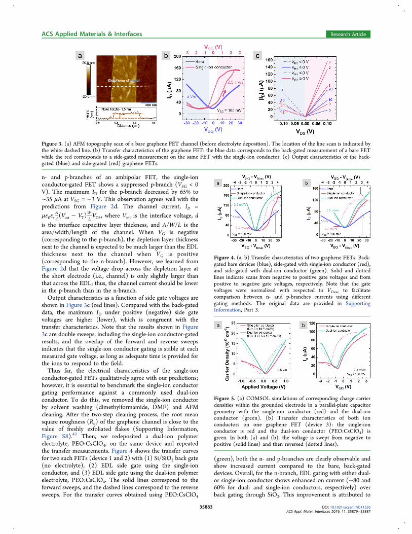
n- and p-branches of an ambipolar FET, the single-ionconductor-gated FET shows a suppressed p-branch (VSG < 0V). The maximum ID for the p-branch decreased by 65% to∼35 μA at VSG = −3 V. This observation agrees well with thepredictions from Figure 2d. The channel current, ID =με ε −V V V( )r
Ad
WL0 int T DS, where Vint is the interface voltage, d
is the interface capacitive layer thickness, and A/W/L is thearea/width/length of the channel. When VG is negative(corresponding to the p-branch), the depletion layer thicknessnext to the channel is expected to be much larger than the EDLthickness next to the channel when VG is positive(corresponding to the n-branch). However, we learned fromFigure 2d that the voltage drop across the depletion layer atthe short electrode (i.e., channel) is only slightly larger thanthat across the EDL; thus, the channel current should be lowerin the p-branch than in the n-branch.Output characteristics as a function of side gate voltages are
shown in Figure 3c (red lines). Compared with the back-gateddata, the maximum ID under positive (negative) side gatevoltages are higher (lower), which is congruent with thetransfer characteristics. Note that the results shown in Figure3c are double sweeps, including the single-ion conductor-gatedresults, and the overlap of the forward and reverse sweepsindicates that the single-ion conductor gating is stable at eachmeasured gate voltage, as long as adequate time is provided forthe ions to respond to the field.Thus far, the electrical characteristics of the single-ion
conductor-gated FETs qualitatively agree with our predictions;however, it is essential to benchmark the single-ion conductorgating performance against a commonly used dual-ionconductor. To do this, we removed the single-ion conductorby solvent washing (dimethylformamide, DMF) and AFMcleaning. After the two-step cleaning process, the root meansquare roughness (Rq) of the graphene channel is close to thevalue of freshly exfoliated flakes (Supporting Information,Figure S8).42 Then, we redeposited a dual-ion polymerelectrolyte, PEO:CsClO4, on the same device and repeatedthe transfer measurements. Figure 4 shows the transfer curvesfor two such FETs (device 1 and 2) with (1) Si/SiO2 back gate(no electrolyte), (2) EDL side gate using the single-ionconductor, and (3) EDL side gate using the dual-ion polymerelectrolyte, PEO:CsClO4. The solid lines correspond to theforward sweeps, and the dashed lines correspond to the reversesweeps. For the transfer curves obtained using PEO:CsClO4
(green), both the n- and p-branches are clearly observable andshow increased current compared to the bare, back-gateddevices. Overall, for the n-branch, EDL gating with either dual-or single-ion conductor shows enhanced on current (∼80 and60% for dual- and single-ion conductors, respectively) overback gating through SiO2. This improvement is attributed to
Figure 3. (a) AFM topography scan of a bare graphene FET channel (before electrolyte deposition). The location of the line scan is indicated bythe white dashed line. (b) Transfer characteristics of the graphene FET: the blue data corresponds to the back-gated measurement of a bare FETwhile the red corresponds to a side-gated measurement on the same FET with the single-ion conductor. (c) Output characteristics of the back-gated (blue) and side-grated (red) graphene FETs.
Figure 4. (a, b) Transfer characteristics of two graphene FETs. Back-gated bare devices (blue), side-gated with single-ion conductor (red),and side-gated with dual-ion conductor (green). Solid and dottedlines indicate scans from negative to positive gate voltages and frompositive to negative gate voltages, respectively. Note that the gatevoltages were normalized with respected to VDirac to facilitatecomparison between n- and p-branches currents using differentgating methods. The original data are provided in SupportingInformation, Part 3.
Figure 5. (a) COMSOL simulations of corresponding charge carrierdensities within the grounded electrode in a parallel-plate capacitorgeometry with the single-ion conductor (red) and the dual-ionconductor (green). (b) Transfer characteristics of both ionconductors on one graphene FET (device 3): the single-ionconductor is red and the dual-ion conductor (PEO:CsClO4) isgreen. In both (a) and (b), the voltage is swept from negative topositive (solid lines) and then reversed (dotted lines).
ACS Applied Materials & Interfaces Research Article
DOI: 10.1021/acsami.9b11526ACS Appl. Mater. Interfaces 2019, 11, 35879−35887
35883
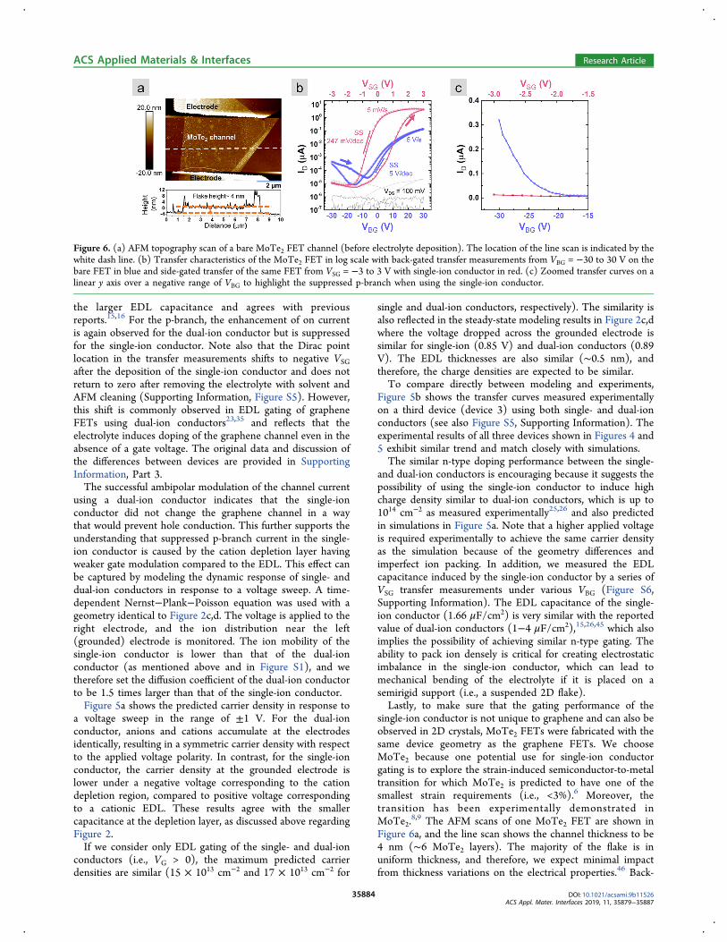
the larger EDL capacitance and agrees with previousreports.15,16 For the p-branch, the enhancement of on currentis again observed for the dual-ion conductor but is suppressedfor the single-ion conductor. Note also that the Dirac pointlocation in the transfer measurements shifts to negative VSGafter the deposition of the single-ion conductor and does notreturn to zero after removing the electrolyte with solvent andAFM cleaning (Supporting Information, Figure S5). However,this shift is commonly observed in EDL gating of grapheneFETs using dual-ion conductors23,35 and reflects that theelectrolyte induces doping of the graphene channel even in theabsence of a gate voltage. The original data and discussion ofthe differences between devices are provided in SupportingInformation, Part 3.The successful ambipolar modulation of the channel current
using a dual-ion conductor indicates that the single-ionconductor did not change the graphene channel in a waythat would prevent hole conduction. This further supports theunderstanding that suppressed p-branch current in the single-ion conductor is caused by the cation depletion layer havingweaker gate modulation compared to the EDL. This effect canbe captured by modeling the dynamic response of single- anddual-ion conductors in response to a voltage sweep. A time-dependent Nernst−Plank−Poisson equation was used with ageometry identical to Figure 2c,d. The voltage is applied to theright electrode, and the ion distribution near the left(grounded) electrode is monitored. The ion mobility of thesingle-ion conductor is lower than that of the dual-ionconductor (as mentioned above and in Figure S1), and wetherefore set the diffusion coefficient of the dual-ion conductorto be 1.5 times larger than that of the single-ion conductor.Figure 5a shows the predicted carrier density in response to
a voltage sweep in the range of ±1 V. For the dual-ionconductor, anions and cations accumulate at the electrodesidentically, resulting in a symmetric carrier density with respectto the applied voltage polarity. In contrast, for the single-ionconductor, the carrier density at the grounded electrode islower under a negative voltage corresponding to the cationdepletion region, compared to positive voltage correspondingto a cationic EDL. These results agree with the smallercapacitance at the depletion layer, as discussed above regardingFigure 2.If we consider only EDL gating of the single- and dual-ion
conductors (i.e., VG > 0), the maximum predicted carrierdensities are similar (15 × 1013 cm−2 and 17 × 1013 cm−2 for
single and dual-ion conductors, respectively). The similarity isalso reflected in the steady-state modeling results in Figure 2c,dwhere the voltage dropped across the grounded electrode issimilar for single-ion (0.85 V) and dual-ion conductors (0.89V). The EDL thicknesses are also similar (∼0.5 nm), andtherefore, the charge densities are expected to be similar.To compare directly between modeling and experiments,
Figure 5b shows the transfer curves measured experimentallyon a third device (device 3) using both single- and dual-ionconductors (see also Figure S5, Supporting Information). Theexperimental results of all three devices shown in Figures 4 and5 exhibit similar trend and match closely with simulations.The similar n-type doping performance between the single-
and dual-ion conductors is encouraging because it suggests thepossibility of using the single-ion conductor to induce highcharge density similar to dual-ion conductors, which is up to1014 cm−2 as measured experimentally25,26 and also predictedin simulations in Figure 5a. Note that a higher applied voltageis required experimentally to achieve the same carrier densityas the simulation because of the geometry differences andimperfect ion packing. In addition, we measured the EDLcapacitance induced by the single-ion conductor by a series ofVSG transfer measurements under various VBG (Figure S6,Supporting Information). The EDL capacitance of the single-ion conductor (1.66 μF/cm2) is very similar with the reportedvalue of dual-ion conductors (1−4 μF/cm2),15,26,45 which alsoimplies the possibility of achieving similar n-type gating. Theability to pack ion densely is critical for creating electrostaticimbalance in the single-ion conductor, which can lead tomechanical bending of the electrolyte if it is placed on asemirigid support (i.e., a suspended 2D flake).Lastly, to make sure that the gating performance of the
single-ion conductor is not unique to graphene and can also beobserved in 2D crystals, MoTe2 FETs were fabricated with thesame device geometry as the graphene FETs. We chooseMoTe2 because one potential use for single-ion conductorgating is to explore the strain-induced semiconductor-to-metaltransition for which MoTe2 is predicted to have one of thesmallest strain requirements (i.e., <3%).6 Moreover, thetransition has been experimentally demonstrated inMoTe2.
8,9 The AFM scans of one MoTe2 FET are shown inFigure 6a, and the line scan shows the channel thickness to be4 nm (∼6 MoTe2 layers). The majority of the flake is inuniform thickness, and therefore, we expect minimal impactfrom thickness variations on the electrical properties.46 Back-
Figure 6. (a) AFM topography scan of a bare MoTe2 FET channel (before electrolyte deposition). The location of the line scan is indicated by thewhite dash line. (b) Transfer characteristics of the MoTe2 FET in log scale with back-gated transfer measurements from VBG = −30 to 30 V on thebare FET in blue and side-gated transfer of the same FET from VSG = −3 to 3 V with single-ion conductor in red. (c) Zoomed transfer curves on alinear y axis over a negative range of VBG to highlight the suppressed p-branch when using the single-ion conductor.
ACS Applied Materials & Interfaces Research Article
DOI: 10.1021/acsami.9b11526ACS Appl. Mater. Interfaces 2019, 11, 35879−35887
35884

gated transfer characteristics were measured on bare devices, asindicated by the blue transfer curve in Figure 6b. The bareMoTe2 FET is ambipolar with a minimum current of ∼10−5μA at VBG of ∼−15 V. The on/off ratio of the n-branch from−5 < VBG < 30 V is <104, and the p-branch from −30 < VBG <−17 V is <100.Using the single-ion conductor, the maximum current
through MoTe2 at VSG = 3 V is ∼32 times larger comparedto the maximum current of the bare FET at VBG = 30 V(Figure 6b). Output characteristics also show effective gatecontrol of the channel current using the single-ion conductor(Figure S9). The on/off ratio of the n-branch increases from104 for the bare FET to ∼106 with the single-ion conductor.Also, the subthreshold swing (SS) of the n-branch decreaseswith the single-ion conductor (from 5000 mV/dec by back-gating the bare device to 247 mV/dec). The strong currentmodulation and the enhanced on/off ratio further confirm thestrong EDL modulation by the single-ion conductor. Similar tothe graphene FETs, the ID of the p-branch remains suppressed,in this case, at the off level of 10−5 μA. The suppressed p-branch is highlighted in a linear plot in Figure 6c.
■ CONCLUSIONSEDL gating using a custom-synthesized single-ion conductor isdemonstrated for the first time on both graphene and MoTe2FETs. Transfer characteristics for all the FETs show anenhanced n-branch using the single-ion conductor and asuppressed p-branch compared with back-gated measurementsof bare FETs. Finite element modeling of ion transport inresponse to an applied field shown that the p-branchsuppression results from the combination of using a single-ion conductor and an asymmetric gate/channel geometry. Inaddition, the two ion conductors compared on the same FETsboth show similar performance in the n-branch (i.e., on/offratio and maximum ion current), suggesting that the single-ionconductor can achieve cationic ion densities similar to the well-studied dual-ion conductor (i.e., up to 1014 cm−2). Thisachievable carrier density is also predicted by modeling andwould be theoretically sufficient to induce several percentstrain in a 2D crystal. This is the first demonstration of asingle-ion conductor-gated multilayer 2D crystal FET, and theresults lay the groundwork for inducing strain in 2D materialslocally via field effect and for demonstrating the 2H to 1T′phase transition. These features are potentially useful forcreating an electronic switch with a low turn-on voltage andsteep subthreshold swing and for 2D flexible electronics withfunctionality controlled by strain.
■ EXPERIMENTAL SECTIONDevice Fabrication and Electrical Characterization. Freshly
cleaved few-layer graphene and MoTe2 flakes (1.5 nm−5 nm-thick)were mechanically exfoliated from their bulk sources (2D semi-conductors) to p-doped silicon substrate with 90 nm SiO2 (GrapheneSupermarket, resistivity of 0.001−0.005 ohm·cm). The flake top-ography and thickness were measured by AFM (Bruker DimensionIcon, ScanAsyst mode). Source/drain electrodes and side gates werepatterned by EBL (Raith e-LINE). Also, Ti (3 nm)/Au (120 nm)metals were deposited by e-beam evaporation (Plassys MEB550Selectron beam evaporator) at a base pressure of <10−6 Torr. Afterliftoff, FETs were transferred to a cryogenic vacuum probe station(Lakeshore, CRX-VF) for vacuum annealing (400 K, 4 h at a pressureof 2 × 10⁻⁶ Torr) and initial electrical measurements. After annealing,FETs were transferred from the probe station to an Ar-filled gloveboxusing an Ar-filled load lock without exposure to ambient air for
electrolyte deposition, before transferring back to the probe station forelectrical measurements. The electrical measurements were conductedusing a Keysight B1500A semiconductor parameter analyzer at aconstant temperature of 300 K.
Single-Ion Conductor Synthesis. The polyester single-ionconductor was synthesized by a two-step melt condensation betweenpoly(ethylene glycol) (PEG) 400 (Mw = 400 g mol−1) and dimethyl5-sulfoisophthalate sodium salt.34 The resulting polyester Na was thensealed in semipermeable dialysis membranes and exposed to an excessof LiCl (0.5 M) in deionized water to exchange Na+ for Li+.34 Thefinal product, polyester Li (PE400-Li), was dissolved in dimethylfor-mamide (DMF) inside an Ar-filled glovebox to obtain a 3 wt %solution. The solution was drop-cast on graphene and MoTe2 FETs(8 μL on the 1 cm2 chip), and the DMF was removed by evaporatingnaturally in the glovebox overnight. The FETs coated with the single-ion conductor were transferred back to the probe station using theload lock for subsequent measurements.
Dual-Ion Conductor. The dual-ion conducting polymer electro-lyte (PEO:CsClO4) was prepared similarly to previously publishedwork.15 PEO (Polymer Standards Service, Mw = 94600 g mol−1) andCsClO4 (Sigma-Aldrich, 99.9%) were dissolved in anhydrousacetonitrile (Sigma-Aldrich) to make a 1 wt % solution with anether oxygen to Cs molar ratio of 76:1. Twenty-five microliters of thesolution was drop-cast onto the 1 cm2 sample of graphene FETs in theglovebox, dried at room temperature until the majority of the solventevaporated, and then annealed at 80 °C for 3 min.
Modeling. The time-dependent, modified Nernst−Planck−Poisson relationship was used in COMSOL Multiphysics to prediction accumulation in response to voltage. Ion migration was modeledusing a modified version of the Nernst−Plank equation:
γ= ∇ ∇ + ∇ +± ± ± ±±D c z c V(ct
D FRT
dd
, where c is the ion concentration,
D is the ion diffusion coefficient, F is faraday’s constant, RT is thethermal energy, γ is the steric repulsion term, and V is the electrolytepotential. The potential is coupled to Poisson’s equation ∇2( − εV) =F∑i = 1
2 (zici), where ε is the permittivity of the electrolyte (∼10 ε0)36
and z is the ion charge number (+1 for cations, −1 for anions). Astern layer, defined by ∇2( − εV) = 0, was used directly adjacent tothe electrode and SiO2 boundaries and set to equal 2 Å. The bulkconcentration of ions corresponds to an ether oxygen to lithium ratioof 20:1, and the density of the polymer is assumed to be 1 g/cm3.
For all four geometries, a 50 μm-long by 5 μm-thick electrolyte wasused; electrodes were modeled as boundary conditions with theappropriate potentials. In the models involving geometries of equal-sized electrodes, the electrode surfaces constituted the entire 50 μmboundary. A zero charge boundary condition (defined as n · D = 0,where n is the surface normal vector and D = − ε ∇ V was used forthe nonelectrode boundaries). The mesh size near the electrodeinterfaces was decreased until the EDL concentrations remainedwithin 1% of its previous value.
In the models involving unequal electrodes, boundary conditionsfor nonelectrode boundaries were defined to mimic SiO2 by using a
modification of the previous boundary condition: · = − ε ϕn Dt
SiO2 ,
where εSiO2 is the permittivity of SiO2, ϕ is the local electrolytepotential at the interface, and t is the oxide thickness (90 nm). Thismodification allowed for a nonzero electric flux through thenonelectrode boundaries (i.e., 90 nm oxide) and therefore allowedions to accumulate near the oxide surface. To determine the carrierdensity in ions/cm2 through the electrolyte, the volumetric chargedensity was integrated using trapezoid approximation along a cutlinetaken across the electrolyte perpendicular to the center of thegrounded electrode beginning at the electrode surface and terminatingat the center of the electrolyte.
DSC Measurements. The DSC samples were prepared inside theAr-filled glovebox. PE400-Li (8.7 mg) and PEO:CsClO4 (7.1 mg)were hermetically sealed in aluminum DSC pans. Measurements weremade on TA 250 calibrated with an indium standard. To measure Tg(glass transition temperature) and Tm (melting temperature), sampleswere heated to 100 °C to erase the thermal history, cooled to −70 °Cat 3 °C min−1, and heated to 100 °C at 5 °C min−1.
ACS Applied Materials & Interfaces Research Article
DOI: 10.1021/acsami.9b11526ACS Appl. Mater. Interfaces 2019, 11, 35879−35887
35885

■ ASSOCIATED CONTENT*S Supporting InformationThe Supporting Information is available free of charge on theACS Publications website at DOI: 10.1021/acsami.9b11526.
DSC measurements; 2D potential profiles fromCOMSOL modeling; transfer measurements on device3; estimation of EDL capacitance in the single-ionconductor-gated FET; impact of device geometry oncharge density from COMSOL simulations; effectivegate size; and output characteristics of single-ionconductor-gated MoTe2 FETs (PDF)
■ AUTHOR INFORMATIONCorresponding Authors*E-mail: [email protected] (K.X.).*E-mail: [email protected] (S.F.-S.).ORCIDKe Xu: 0000-0003-2692-1935Jierui Liang: 0000-0003-1207-8959Zhongmou Chao: 0000-0002-9882-4440James R. McKone: 0000-0001-6445-7884Susan K. Fullerton-Shirey: 0000-0003-2720-0400Author Contributions∥K.X. and J.L. contributed equally to this work. Themanuscript was written through contributions of all authors.All authors have given approval to the final version of themanuscript.NotesThe authors declare no competing financial interest.
■ ACKNOWLEDGMENTSThis work was supported by NSF-DMR-EPM grant no.1607935. J.R.M. acknowledges support from the University ofPittsburgh, Swanson School of Engineering.
■ REFERENCES(1) Thompson, S. E.; Armstrong, M.; Auth, C.; Alavi, M.; Buehler,M.; Chau, R.; Cea, S.; Ghani, T.; Glass, G.; Hoffman, T.; et al. A 90-Nm Logic Technology Featuring Strained-Silicon. IEEE Trans.Electron Devices 2004, 51, 1790−1797.(2) Jacobsen, R. S.; Andersen, K. N.; Borel, P. I.; Fage-Pedersen, J.;Frandsen, L. H.; Hansen, O.; Kristensen, M.; Lavrinenko, A. V.;Moulin, G.; Ou, H.; et al. Strained Silicon as a New Electro-OpticMaterial. Nature 2006, 441, 199−202.(3) Desai, S. B.; Seol, G.; Kang, J. S.; Fang, H.; Battaglia, C.;Kapadia, R.; Ager, J. W.; Guo, J.; Javey, A. Strain-Induced Indirect toDirect Bandgap Transition in Multilayer WSe2. Nano Lett. 2014, 14,4592−4597.(4) Roldan, R.; Castellanos-Gomez, A.; Cappelluti, E.; Guinea, F.Strain Engineering in Semiconducting Two-Dimensional Crystals. J.Phys. Condens. Matter 2015, 27, 313201.(5) Amorim, B.; Cortijo, A.; de Juan, F.; Grushin, A. G.; Guinea, F.;Gutierrez-Rubio, A.; Ochoa, H.; Parente, V.; Roldan, R.; San-Jose, P.;et al. Novel Effects of Strains in Graphene and Other TwoDimensional Materials. Phys. Rep. 2016, 617, 1−54.(6) Duerloo, K.-A. N.; Li, Y.; Reed, E. J. Structural Phase Transitionsin Two-Dimensional Mo- and W-Dichalcogenide Monolayers. Nat.Commun. 2014, 5, 4214.(7) Sharma, M.; Kumar, A.; Ahluwalia, P. K.; Pandey, R. Strain andElectric Field Induced Electronic Properties of Two-DimensionalHybrid Bilayers of Transition-Metal Dichalcogenides. J. Appl. Phys.2014, 116, No. 063711.
(8) Song, S.; Keum, D. H.; Cho, S.; Perello, D.; Kim, Y.; Lee, Y. H.Room Temperature Semiconductor−Metal Transition of MoTe2Thin Films Engineered by Strain. Nano Lett. 2015, 16, 188−193.(9) Hou, W.; Azizimanesh, A.; Sewaket, A.; Pena, T.; Watson, C.;Liu, M.; Askari, H.; Wu, S. M. Strain-Based Room-Temperature Non-Volatile MoTe2 Ferroelectric Phase Change Transistor. Nat. Nano-technol. 2019, 14, 668.(10) Shukla, N.; Thathachary, A. V.; Agrawal, A.; Paik, H.; Aziz, A.;Schlom, D. G.; Gupta, S. K.; Engel-Herbert, R.; Datta, S. A Steep-Slope Transistor Based on Abrupt Electronic Phase Transition. Nat.Commun. 2015, 6, 7812.(11) Seabaugh, A.; Fathipour, S.; Li, W.; Lu, H.; Park, J. H.;Kummel, A. C.; Jena, D.; Fullerton-Shirey, S. K.; Fay, P. SteepSubthreshold Swing Tunnel FETs: GaN/InN/GaN and TransitionMetal Dichalcogenide Channels. In 2015 IEEE International ElectronDevices Meeting (IEDM); IEEE: 2015, 35−36. DOI: 10.1109/IEDM.2015.7409835.(12) Lu, H.; Seabaugh, A. Tunnel Field-Effect Transistors: State-of-the-Art. IEEE J. Electron Devices Soc. 2014, 2, 44−49.(13) Akinwande, D.; Petrone, N.; Hone, J. Two-DimensionalFlexible Nanoelectronics. Nat. Commun. 2014, 5, 5678.(14) Kim, S. J.; Choi, K.; Lee, B.; Kim, Y.; Hong, B. H. Materials forFlexible, Stretchable Electronics: Graphene and 2D Materials. Annu.Rev. Mater. Res. 2015, 45, 63−84.(15) Xu, H.; Fathipour, S.; Kinder, E. W.; Seabaugh, A. C.;Fullerton-Shirey, S. K. Reconfigurable Ion Gating of 2H-MoTe2 Field-Effect Transistors Using Poly(Ethylene Oxide)-CsClO4 Solid PolymerElectrolyte. ACS Nano 2015, 9, 4900−4910.(16) Xu, K.; Islam, M. M.; Guzman, D. M.; Seabaugh, A.; Strachan,A.; Fullerton-Shirey, S. K. Pulse Dynamics of Electric Double LayerFormation on All-Solid-State Graphene Field-Effect Transistors. ACSAppl. Mater. Interfaces 2018, 10, 43166.(17) Kim, J.; Na, J.; Joo, M.-K.; Suh, D. Low-Voltage-OperatedHighly Sensitive Graphene Hall Elements by Ionic Gating. ACS Appl.Mater. Interfaces 2019, 11, 4226−4232.(18) Zhao, W.; Bi, S.; Balke, N.; Rack, P. D.; Ward, T. Z.; Kalinin, S.V.; Dai, S.; Feng, G. Understanding Electric Double-Layer GatingBased on Ionic Liquids: From Nanoscale to Macroscale. ACS Appl.Mater. Interfaces 2018, 10, 43211−43218.(19) Jiang, J.; Hu, W.; Xie, D.; Yang, J.; He, J.; Gao, Y.; Wan, Q. 2DElectric-Double-Layer Phototransistor for Photoelectronic andSpatiotemporal Hybrid Neuromorphic Integration. Nanoscale 2019,11, 1360−1369.(20) Paletti, P.; Yue, R.; Hinkle, C.; Fullerton-Shirey, S. K.;Seabaugh, A. Two-Dimensional Electric-Double-Layer Esaki diode.npj 2D Mater. Appl. 2019, 3, 19.(21) Ren, X.; Wang, Y.; Xie, Z.; Xue, F.; Leighton, C.; Frisbie, C. D.Gate-Tuned Insulator-Metal Transition in Electrolyte-Gated Tran-sistors Based on Tellurene. Nano Lett. 2019, 4738.(22) Fathipour, S.; Pandey, P.; Fullerton-Shirey, S.; Seabaugh, A.Electric-Double-Layer Doping of WSe2 field-effect Transistors UsingPolyethylene-Oxide Cesium Perchlorate. J. Appl. Phys. 2016, 120,234902.(23) Kinder, E. W.; Fuller, A.; Lin, Y.-C.; Robinson, J. A.; Fullerton-Shirey, S. K. Increasing the Room-Temperature Electric Double LayerRetention Time in Two-Dimensional Crystal FETs. ACS Appl. Mater.Interfaces 2017, 9, 25006−25013.(24) Xu, K.; Lu, H.; Kinder, E. W.; Seabaugh, A.; Fullerton-Shirey, S.K. Monolayer Solid-State Electrolyte for Electric Double Layer Gatingof Graphene Field-Effect Transistors. ACS Nano 2017, 11, 5453−5464.(25) Bisri, S. Z.; Shimizu, S.; Nakano, M.; Iwasa, Y. Endeavor ofIontronics: From Fundamentals to Applications of Ion-ControlledElectronics. Adv. Mater. 2017, 29, 1607054.(26) Efetov, D. K.; Kim, P. Controlling Electron-PhononInteractions in Graphene at Ultrahigh Carrier Densities. Phys. Rev.Lett. 2010, 105, 256805.(27) Yuan, H.; Shimotani, H.; Tsukazaki, A.; Ohtomo, A.; Kawasaki,M.; Iwasa, Y. High-Density Carrier Accumulation in ZnO Field-Effect
ACS Applied Materials & Interfaces Research Article
DOI: 10.1021/acsami.9b11526ACS Appl. Mater. Interfaces 2019, 11, 35879−35887
35886

Transistors Gated by Electric Double Layers of Ionic Liquids. Adv.Funct. Mater. 2009, 19, 1046−1053.(28) Ueno, K.; Shimotani, H.; Yuan, H.; Ye, J.; Kawasaki, M.; Iwasa,Y. Field-Induced Superconductivity in Electric Double LayerTransistors. J. Phys. Soc. Jpn. 2014, 83, No. 032001.(29) Du, H.; Lin, X.; Xu, Z.; Chu, D. Electric Double-LayerTransistors: A Review of Recent Progress. J. Mater. Sci. 2015, 50,5641−5673.(30) Vargantwar, P. H.; Roskov, K. E.; Ghosh, T. K.; Spontak, R. J.Enhanced Biomimetic Performance of Ionic Polymer-Metal Compo-site Actuators Prepared with Nanostructured Block Ionomers.Macromol. Rapid Commun. 2012, 33, 61−68.(31) Choi, J.-H.; Xie, W.; Gu, Y.; Frisbie, C. D.; Lodge, T. P. SingleIon Conducting, Polymerized Ionic Liquid Triblock CopolymerFilms: High Capacitance Electrolyte Gates for N-Type Transistors.ACS Appl. Mater. Interfaces 2015, 7, 7294−7302.(32) Herlogsson, L.; Crispin, X.; Tierney, S.; Berggren, M.Polyelectrolyte-Gated Organic Complementary Circuits Operatingat Low Power and Voltage. Adv. Mater. 2011, 23, 4684−4689.(33) Malti, A.; Gabrielsson, E. O.; Berggren, M.; Crispin, X. Ultra-Low Voltage Air-Stable Polyelectrolyte Gated n-Type Organic ThinFilm Transistors. Appl. Phys. Lett. 2011, 99, 063305.(34) Dou, S.; Zhang, S.; Klein, R. J.; Runt, J.; Colby, R. H. Synthesisand Characterization of Poly(Ethylene Glycol)-Based Single-IonConductors. Chem. Mater. 2006, 18, 4288−4295.(35) Li, H.-M.; Xu, K.; Bourdon, B.; Lu, H.; Lin, Y.-C.; Robinson, J.A.; Seabaugh, A. C.; Fullerton-Shirey, S. K. Electric Double LayerDynamics in Poly(Ethylene Oxide) LiClO4 on Graphene Transistors.J. Phys. Chem. C 2017, 121, 16996−17004.(36) Lee, A. A.; Colby, R. H.; Kornyshev, A. A. Electroactuation withSingle Charge Carrier Ionomers: The Roles of Electrostatic Pressureand Steric Strain. Soft Matter 2013, 9, 3767.(37) Lee, A. A.; Colby, R. H.; Kornyshev, A. A. Statics and Dynamicsof Electroactuation with Single-Charge-Carrier Ionomers. J. Phys.Condens. Matter 2013, 25, No. 082203.(38) Fullerton-Shirey, S. K.; Maranas, J. K. Effect of LiClO4 on theStructure and Mobility of PEO-Based Solid Polymer Electrolytes.Macromolecules 2009, 42, 2142−2156.(39) Kilic, M. S.; Bazant, M. Z.; Ajdari, A. Steric Effects in theDynamics of Electrolytes at Large Applied Voltages. II. ModifiedPoisson-Nernst-Planck Equations. Phys. Rev. E 2007, DOI: 10.1103/PhysRevE.75.021503.(40) Wang, H.; Pilon, L. Accurate Simulations of Electric DoubleLayer Capacitance of Ultramicroelectrodes. J. Phys. Chem. C 2011,115, 16711.(41) Liang, J.; Xu, K.; Toncini, B.; Bersch, B.; Jariwala, B.; Lin, Y.-C.;Robinson, J.; Fullerton-Shirey, S. K. Impact of Post-LithographyPolymer Residue on the Electrical Characteristics of MoS2 and WSe2Field Effect Transistors. Adv. Mater. Interfaces 2019, 6, 1801321.(42) Geringer, V.; Liebmann, M.; Echtermeyer, T.; Runte, S.;Schmidt, M.; Ruckamp, R.; Lemme, M. C.; Morgenstern, M. Intrinsicand Extrinsic Corrugation of Monolayer Graphene Deposited onSiO2. Phys. Rev. Lett. 2009, 102, 076102.(43) Schwierz, F. Graphene Transistors. Nat. Nanotechnol. 2010, 5,487−496.(44) Craciun, M. F.; Russo, S.; Yamamoto, M.; Tarucha, S. TuneableElectronic Properties in Graphene. Nano Today 2011, 6, 42−60.(45) Lin, Y.-C.; Jariwala, B.; Bersch, B. M.; Xu, K.; Nie, Y.; Wang, B.;Eichfeld, S. M.; Zhang, X.; Choudhury, T. H.; Pan, Y.; et al. RealizingLarge-Scale, Electronic-Grade Two-Dimensional Semiconductors.ACS Nano 2018, 12, 965−975.(46) Lavini, F.; Calo, A.; Gao, Y.; Albisetti, E.; Li, T.-D.; Cao, T.; Li,G.; Cao, L.; Aruta, C.; Riedo, E. Friction and Work FunctionOscillatory Behavior for an Even and Odd Number of Layers inPolycrystalline MoS2. Nanoscale 2018, 10, 8304−8312.
ACS Applied Materials & Interfaces Research Article
DOI: 10.1021/acsami.9b11526ACS Appl. Mater. Interfaces 2019, 11, 35879−35887
35887
materials
Article
Ion-Locking in Solid Polymer Electrolytes forReconfigurable Gateless Lateral Graphenep-n Junctions
Jierui Liang 1 , Ke Xu 1,* , Swati Arora 2, Jennifer E. Laaser 2 and Susan K. Fullerton-Shirey 1,3,*1 Department of Chemical and Petroleum Engineering, University of Pittsburgh, Pittsburgh, PA 15260, USA;
[email protected] Department of Chemistry, University of Pittsburgh, Pittsburgh, PA 15260, USA; [email protected] (S.A.);
[email protected] (J.E.L.)3 Department of Electrical and Computer Engineering, University of Pittsburgh, Pittsburgh, PA 15260, USA* Correspondence: [email protected] (K.X.); [email protected] (S.K.F.-S.)
Received: 1 December 2019; Accepted: 28 January 2020; Published: 1 March 2020�����������������
Abstract: A gateless lateral p-n junction with reconfigurability is demonstrated on grapheneby ion-locking using solid polymer electrolytes. Ions in the electrolytes are used to configureelectric-double-layers (EDLs) that induce p- and n-type regions in graphene. These EDLs are lockedin place by two different electrolytes with distinct mechanisms: (1) a polyethylene oxide (PEO)-basedelectrolyte, PEO:CsClO4, is locked by thermal quenching (i.e., operating temperature < Tg (glasstransition temperature)), and (2) a custom-synthesized, doubly-polymerizable ionic liquid (DPIL)is locked by thermally triggered polymerization that enables room temperature operation. Bothapproaches are gateless because only the source/drain terminals are required to create the junction,and both show two current minima in the backgated transfer measurements, which is a signature of agraphene p-n junction. The PEO:CsClO4 gated p-n junction is reconfigured to n-p by resetting thedevice at room temperature, reprogramming, and cooling to T < Tg. These results show an alternateapproach to locking EDLs on 2D devices and suggest a path forward to reconfigurable, gateless lateralp-n junctions with potential applications in polymorphic logic circuits.
Keywords: p-n junction; graphene; ion doping; electric double layer; polymer electrolyte
1. Introduction
The p-n junction—one of the building blocks of electronics—is required for diodes, bipolar andtunnel transistors, among other devices [1–3]. While two-dimensional (2D) materials have receivedattention for their unique properties and potential applications in electronics and optoelectronics [4,5],engineering p-n junctions in these materials presents unique challenges, such as achieving precisedoping control over short distances for lateral homojunctions [2,6,7]. Nonetheless, plenty of progresshas been made to engineer permanent p-n junctions in 2D materials. For example, graphene diodes [8,9],photodetectors [10,11], and photovoltaic cells [12] have been demonstrated. Generally, junctions ingraphene are created in three architectures: lateral homojunctions formed at the interface between tworegions of dissimilar doping [6], vertical junctions where two graphene sheets with dissimilar dopingare stacked [3], and heterostructure junctions where a different 2D material is grown adjacent to orstacked with graphene (creating either an in-plane or vertical junction) [13–15].
Among the three architectures, the lateral p-n homojunctions offer a simple design with potentialfor large-scale integration, it does not require in-plane heterostructure growth [16], and it avoidsvertical stacking and flake transfer [17,18]. The most commonly used approaches to achieve lateral p-njunctions is electrostatic doping using split gates [8,19], substitutional doping [6] and chemical doping
Materials 2020, 13, 1089; doi:10.3390/ma13051089 www.mdpi.com/journal/materials

Materials 2020, 13, 1089 2 of 12
resulting from charge transfer from adsorbates [20]. Less common approaches include applying large,local electrical stress [21], and substrate engineering [1]. Although the p-n junctions created by splitgates are reconfigurable, challenges remain including fabrication and parasitics [22]. While grapheneand other 2D materials can be substitutionally or chemically doped over wide areas p- or n-type,and with a dopant concentration range of 1010 to 1013 [6,23–27], one challenge is creating abrupt p-njunctions. Moreover, both substitutional and chemical doping [20] are permanent, meaning that thejunction cannot be reconfigured.
Similar to metal gates, electric double layer (EDL) gating is an electrostatic approach; however,EDL gating involves positioning ions at the interface between an electrolyte and a 2D surface by fieldeffect. The ions induce image charge in the channel, and can achieve doping densities > 1013 cm−2
because of the < nm charge separation distance between ions and image charges [28–36]. Becausethis approach does not rely on replacing atoms in the 2D crystal or transferring charge, this methodavoids permanently changing the crystal structure and potential problems associated with dopingdefects. Moreover, EDL doping is adjustable—ions can be reconfigured by changing the applied field.For these reasons, polymer electrolytes and ionic liquids have been used extensively for reconfigurabledoping of graphene and other 2D materials [29,35,37–39].
Although EDL gating is a highly effective method to control charge transport in 2D materials,a constant gate bias is required to hold the ions in place and avoid EDL dissipation. What wouldbe useful is a “gateless” electrolyte wherein the ions could be placed in a p-n junction configurationand locked into position via a trigger until they can be unlocked later and reconfigured. Such atriggerable locking/unlocking mechanism that enables reconfigurability on demand could be useful inapplications requiring polymorphic electronics. That is, applications in which a circuit implementingone type of operating mode can reconfigure itself on demand and activate new functions in responseto a stimulus [40–43].
One approach to “lock-in” an EDL is to decrease ion mobility by decreasing the temperature ofthe device below the glass transition temperature (Tg) of the polymer electrolyte. This approach hasbeen used previously to lock-in p-n junctions in MoS2 [44], WSe2 [45], and MoTe2 [29]. We have alsoused the same approach for unipolar doping of graphene, but with a polymer electrolyte, poly (vinylalcohol) and LiClO4 (PVA:LiClO4), for which Tg > room temperature [31]. More than 75% of the EDLwas retained at room temperature after removing the field, and the device could be reconfigured byheating to T > Tg. In addition, the concept of ion-locking to form “frozen junctions” has been adoptedin light-emitting electrochemical cells (LECs) where the homojunction of an electroluminescent organicsemiconductor is created by fixing the ion distribution in a polymer electrolyte by cooling or formingcovalent bonds [46–48].
Here, we take two approaches to create and lock-in a p-n junction in graphene. First, weapply the thermal quenching approach to lock a p-n junction using polyethylene oxide and CsClO4
(PEO:CsClO4). Then, we extend the concept to room-temperature operation via a custom-synthesized,doubly-polymerizable ionic liquid (DPIL) where a p-n junction is locked by a thermally triggeredchemical reaction. Both approaches are “gateless” because only the source/drain terminals arerequired to create the junction. After the ions are locked in place using both approaches, backgatedtransfer characteristics show two Dirac points—a signature of a p-n junction in graphene [20,23,49,50].These results suggest that appropriate chemical tailoring of the electrolyte can open possibilities forreconfigurable doping with potential use as polymorphic logic gates.

Materials 2020, 13, 1089 3 of 12
2. Materials and Methods
2.1. Device Fabrication
The four-electrode graphene device used for this study is schematically illustrated in Figure 1a.The electrolyte was either PEO:CsClO4 or DPIL. Graphene flakes (~1.5 nm thick) were exfoliatedfrom the bulk (2D Semiconductors) by mechanical cleaving (i.e., Scotch tape method) and transferredto a 1 × 1 cm2 p-type Si (Graphene Supermarket, resistivity 0.001–0.005 ohm·cm) with 90 nm SiO2.The substrate was pre-cleaned with acetone, isopropanol (IPA), deionized (DI) water and dried withN2. E-beam lithography (EBL, Raith e-LINE) was used to pattern the electrodes. PMMA-950-A4(MicroChem) was spin-coated at 4000 rpm for 1 min and then annealed at 175 ◦C for 7 min. Afterexposure, the resist was developed in methyl isobutyl ketone MIBK:IPA (1:3 volume ratio) for 2 min,and rinsed with IPA for another 2 min. E-beam evaporation (Plassys Electron Beam EvaporatorMEB550S) was used to deposit metal electrodes (3 nm Ti; 130 nm Au) at a base pressure < 1 × 10⁻⁶ Torr.Lift-off was performed in acetone overnight for 9 hours, followed by IPA, DI water rinse and N2 drying.Using contact-mode atomic force microscopy (AFM, Bruker Dimension Icon), e-beam resist residuewas removed from the graphene between the electrodes (SCM-PIT-v2, 3 Nm−1) [33]. Before electricalmeasurements, samples were annealed at 127 ◦C (400 K) in vacuum at a pressure of 9 × 10⁻⁷ Torr for4 hours. Electrical measurements were made on a Cascade Microtech Summit 11000 probe station(PEO:CsClO4 doped samples) or a Lakeshore cryogenic vacuum probe station (DPIL samples), bothusing a Keysight B1500A semiconductor parameter analyzer. After initial measurements on baredevices, the samples were transferred to an Ar-filled glovebox (H2O and O2 concentration < 0.1parts-per-million (ppm)) for electrolyte deposition.
Materials 2019, 12, x FOR PEER REVIEW 3 of 12
beam lithography (EBL, Raith e-LINE) was used to pattern the electrodes. PMMA-950-A4 (MicroChem)
was spin-coated at 4000 rpm for 1 min and then annealed at 175 C for 7 min. After exposure, the resist
was developed in methyl isobutyl ketone MIBK:IPA (1:3 volume ratio) for 2 min, and rinsed with IPA
for another 2 min. E-beam evaporation (Plassys Electron Beam Evaporator MEB550S) was used to
deposit metal electrodes (3 nm Ti; 130 nm Au) at a base pressure < 1 × 10⁻⁶ Torr. Lift-off was performed
in acetone overnight for 9 hours, followed by IPA, DI water rinse and N2 drying. Using contact-mode
atomic force microscopy (AFM, Bruker Dimension Icon), e-beam resist residue was removed from the
graphene between the electrodes (SCM-PIT-v2, 3 Nm−1) [33]. Before electrical measurements, samples
were annealed at 127 C (400 K) in vacuum at a pressure of 9×10⁻⁷ Torr for 4 hours. Electrical
measurements were made on a Cascade Microtech Summit 11000 probe station (PEO:CsClO4 doped
samples) or a Lakeshore cryogenic vacuum probe station (DPIL samples), both using a Keysight
B1500A semiconductor parameter analyzer. After initial measurements on bare devices, the samples
were transferred to an Ar-filled glovebox (H2O and O2 concentration < 0.1 parts-per-million (ppm)) for
electrolyte deposition.
Figure 1. Schematics of a lateral graphene p-n junction with n- and p-type regions created by electric-
double-layer (EDL) doping and subsequent ion-locking. (a) Four-electrode graphene device coated
by a solid polymer electrolyte (i.e., PEO:CsClO4 electrolyte or DPIL). Cations (blue spheres) and
anions (red spheres) dope the graphene channel to form p-type (pink) and n-type (blue) regions,
respectively. (b) The formation of a p-n junction by EDL doping: (1) Programming voltages are
applied to electrodes 2 and 3, while the remaining 2 electrodes and backgate are floated; mobile
cations and anions redistribute in response to the field forming a p-n junction between electrodes 2
and 3. Note that the largest ion concentration occurs near the electrodes and decreases with distance
away from the electrodes as modeled in reference [45]. (2) After the EDL is formed, the ions are locked
into place either by cooling the PEO:CsClO4 device below the Tg of the electrolyte, or by DPIL
polymerization. (3) After locking, the p-n junction remains in the absence of voltage.
2.2. Electrolyte Preparation
PEO:CsClO4 was prepared inside a glovebox as reported previously [29]. In brief, PEO (Polymer
Standards Service, molecular weight 94,600 gmol–1) and CsClO4 (Sigma-Aldrich, St. Louis, USA, 99.9%)
were dissolved in anhydrous acetonitrile (Sigma-Aldrich) to make a 1 wt % solution with the ether
oxygen to Cs molar ratio 76:1. In the glovebox, the polymer electrolyte was drop-cast (25 µL over 1 cm2)
onto bare graphene devices, dried at room temperature until the majority of the solvent evaporated,
and then annealed at 80 °C for 3 min. The thickness of the cast electrolyte was reported previously as
∼1 µm [29]. The samples were transferred back to the probe station to form the p-n junctions.
Programming voltages on electrodes 1 and 4 (V1 = +1 V; V4 = −1 V) were held for 10 min to drive ions
into position, and the device was then cooled to 220 K which is below the Tg of PEO electrolyte (~ 242 K
[29,51]) at a cooling rate of 0.7 K/min to immobilize ions and to fix the p-n junction with programming
Figure 1. Schematics of a lateral graphene p-n junction with n- and p-type regions created byelectric-double-layer (EDL) doping and subsequent ion-locking. (a) Four-electrode graphene devicecoated by a solid polymer electrolyte (i.e., PEO:CsClO4 electrolyte or DPIL). Cations (blue spheres)and anions (red spheres) dope the graphene channel to form p-type (pink) and n-type (blue) regions,respectively. (b) The formation of a p-n junction by EDL doping: (1) Programming voltages are appliedto electrodes 2 and 3, while the remaining 2 electrodes and backgate are floated; mobile cations andanions redistribute in response to the field forming a p-n junction between electrodes 2 and 3. Notethat the largest ion concentration occurs near the electrodes and decreases with distance away fromthe electrodes as modeled in reference [45]. (2) After the EDL is formed, the ions are locked into placeeither by cooling the PEO:CsClO4 device below the Tg of the electrolyte, or by DPIL polymerization.(3) After locking, the p-n junction remains in the absence of voltage.

Materials 2020, 13, 1089 4 of 12
2.2. Electrolyte Preparation
PEO:CsClO4 was prepared inside a glovebox as reported previously [29]. In brief, PEO (PolymerStandards Service, molecular weight 94,600 gmol−1) and CsClO4 (Sigma-Aldrich, St. Louis, USA,99.9%) were dissolved in anhydrous acetonitrile (Sigma-Aldrich) to make a 1 wt % solution withthe ether oxygen to Cs molar ratio 76:1. In the glovebox, the polymer electrolyte was drop-cast(25 µL over 1 cm2) onto bare graphene devices, dried at room temperature until the majority of thesolvent evaporated, and then annealed at 80 ◦C for 3 min. The thickness of the cast electrolyte wasreported previously as ∼1 µm [29]. The samples were transferred back to the probe station to formthe p-n junctions. Programming voltages on electrodes 1 and 4 (V1 = +1 V; V4 = −1 V) were held for10 min to drive ions into position, and the device was then cooled to 220 K which is below the Tg ofPEO electrolyte (~ 242 K [29,51]) at a cooling rate of 0.7 K/min to immobilize ions and to fix the p-njunction with programming voltage still applied. The temperature was controlled by a Lakeshore 365temperature controller to within ± 0.01 K. Once 220 K was reached, the sample was held at 5 min priorto the measurement to establish thermal equilibrium. After the measurement, the sample was heatedto room temperature again where the p-n junction was reprogrammed to n-p by reversing the appliedvoltages (V1 = −1 V; V4 = +1 V).
DPIL monomers, 1-[(2-methacryloyloxy)ethyl]-3-methylimidazolium 1-[3-(methacryloyloxy)propylsulfonyl]-1-(trifluoromethane-sulfonyl)imide, were synthesized according to reference [52–54].One mg of the initiator, azobisisobutyronitrile (AIBN), was dissolved in 100 µL unpolymerized DPILmonomer, and then drop-cast in the glovebox (25 µL over 1 cm2) with thickness estimated to be~200 µm according to the cast volume. The samples were transferred to the probe station via a load-lockusing an Ar-filled stainless steel suitcase. A programming voltage (V2 = +1 V and V3 = −1 V) was heldfor 10 min for p-n junction formation, followed by a 6-hour polymerization anneal at 353 K with thevoltage applied, which is more than sufficient for immobilizing ions by polymerization (Figure S1).After polymerization, the device was cooled at ~ 0.3 K/min to room temperature and the programmingvoltage was removed.
2.3. P-n Junction Formation
Schematics showing the process of p-n junction formation and ion-locking are shown in Figure 1b.At room temperature, the device is programmed by applying +1 V to electrode 2 and −1 V to electrode3 (electrodes 1, 4 and the back gate are floated). Mobile ions in the electrolyte respond to the appliedfield (Figure 1b, row 1). Cationic or anionic EDLs form at the interface between the electrolyte and thegraphene channel/metal electrodes. As modeled in reference [45] where ions are used to create p-njunctions, the highest concentration of ions (~2.4 × 1021 cm−3 at 1.5 V) builds up near the electrodesurface and then dissipates with distance away from the electrode, meaning that a more abrupt junctioncan be expected with decreasing channel length. Note that the device channel lengths reported here are100 times larger than those modeled in reference [45]; however, a channel length of tens of nanometersis not required to observe a junction, as demonstrated previously for MoTe2 [29] and MoS2 [44]. Thus,the junction formed in this study is either a p-n or p-i-n junction. To fix the p-n junction, ions arelocked in place by either cooling the PEO:CsClO4 coated sample to T < Tg (where Tg ~ 242 K) or bypolymerizing the DPIL at 353 K (Figure 1b, row 2). After locking, the voltages are removed and the p-njunction persists (Figure 1b, row 3).
3. Results and Discussions
A cross-sectional schematic and optical images for two types of backgated, 4-electrode graphenedevices are shown in Figure 2a. The type-I device has 4, equivalently sized electrodes where thevoltage to create the junction is applied between the two inner electrodes (i.e., 2 and 3) separatedby 1 µm. The type-II device also has four electrodes, but the two middle electrodes are shorter thanthe outer. In type-II, the outer electrodes (i.e., 1 and 4) are separated by 4.6 µm are used to create

Materials 2020, 13, 1089 5 of 12
the junction, while the two middle electrodes are used to sense the junction. Note that these twogeometries are not designed to work with a specific type of electrolyte—the p-n junction formationprocess should be similar for both. Because the p-n junction relies on EDL formation at the surface ofgraphene, AFM cleaning was used to remove residue from the EBL resist, thus enabling the ions to bepositioned at the closest possible distance from the channel to maximize the capacitance density [33].Figure 2b shows the topology of the channel surface for one representative graphene device measuredbefore (left, as fabricated) and after (right) AFM cleaning. Line scans at the same location before andafter cleaning indicate a channel thickness of ~1.2 nm (four layers) and ~2.2 nm of removed residue.The roughness of the channel surface was reduced from 1.32 ± 0.14 nm to 0.23 ± 0.02 nm after AFMcleaning, which is close to the surface roughness for freshly cleaved graphene on SiO2 [36,51,55]. Notethat the maximum current and mobility are not degraded after AFM cleaning - in accordance with ourprior reports [33,56].Materials 2019, 12, x FOR PEER REVIEW 5 of 12
Figure 2. Bare, 4-electrode graphene devices. (a) Device schematic and optical images of two types of
devices (electrode spacing ~ 1 µm). Type-I device has four electrodes with the same length; Type-II
has two, shorter middle electrodes. (b) AFM topology scan of a representative graphene device as
fabricated with e-beam resist residue (left) and after AFM cleaning (right). The white boxes (400 × 400
nm) on the AFM scans indicate one of the six locations over which roughness was measured; the
dashed lines indicate the locations of the line scans and the corresponding data are shown below the
AFM scans. .
3.1. P-n Junction Formation Using PEO:CsClO4
PEO:CsClO4 has a low gate-to-source leakage current [57] and can induce charge carrier densities
exceeding 1013 cm−2 in 2D materials [29,30,32,37]. In addition, Cs+ has a larger ionic radius than Li+
and is therefore less likely to undergo intercalation, as reported for LiClO4 [58,59]. While we have
used it previously to induce a p-n junction in MoTe2 with Type I device geometry [29], here, we used
it to create a p-n junction in graphene, and with a Type-II geometry. Schematics showing the
mechanism are provided in Figure 3a, following the same general procedure as described in Figure 1.
Voltage was applied to electrodes 1 and 4 (with electrodes 2, 3 and the back gate floated) at room
temperature where the ions were mobile (Tg ~ 242 K) [51] to create the p-n junction. While continuing
to apply the voltages, the device was cooled to 220 K (i.e., T < Tg), which was sufficient to immobilize
the ions and lock the EDLs [29,31]. After locking, the p-n junction forming voltages were no longer
applied and the electrical characteristics were measured. After the measurements, the device was
heated to room temperature, the voltage polarities were reversed to create an n-p junction, and the
device was cooled again and measured.
Figure 2. Bare, 4-electrode graphene devices. (a) Device schematic and optical images of two types ofdevices (electrode spacing ~ 1 µm). Type-I device has four electrodes with the same length; Type-II hastwo, shorter middle electrodes. (b) AFM topology scan of a representative graphene device as fabricatedwith e-beam resist residue (left) and after AFM cleaning (right). The white boxes (400 × 400 nm) on theAFM scans indicate one of the six locations over which roughness was measured; the dashed linesindicate the locations of the line scans and the corresponding data are shown below the AFM scans.
3.1. P-n Junction Formation Using PEO:CsClO4
PEO:CsClO4 has a low gate-to-source leakage current [57] and can induce charge carrier densitiesexceeding 1013 cm−2 in 2D materials [29,30,32,37]. In addition, Cs+ has a larger ionic radius than Li+
and is therefore less likely to undergo intercalation, as reported for LiClO4 [58,59]. While we haveused it previously to induce a p-n junction in MoTe2 with Type I device geometry [29], here, we used itto create a p-n junction in graphene, and with a Type-II geometry. Schematics showing the mechanismare provided in Figure 3a, following the same general procedure as described in Figure 1. Voltagewas applied to electrodes 1 and 4 (with electrodes 2, 3 and the back gate floated) at room temperaturewhere the ions were mobile (Tg ~ 242 K) [51] to create the p-n junction. While continuing to apply thevoltages, the device was cooled to 220 K (i.e., T < Tg), which was sufficient to immobilize the ions andlock the EDLs [29,31]. After locking, the p-n junction forming voltages were no longer applied andthe electrical characteristics were measured. After the measurements, the device was heated to roomtemperature, the voltage polarities were reversed to create an n-p junction, and the device was cooledagain and measured.

Materials 2020, 13, 1089 6 of 12
Materials 2019, 12, x FOR PEER REVIEW 6 of 12
Figure 3. Using a polymer electrolyte (PEO:CsClO4) to create a lateral p-n or n-p junction in graphene.
(a) Schematics of (i) device top view and (ii) device with homogeneously distributed ions before
programming. Equal and opposite voltages are applied to electrodes 1 and 4 ((iii) V1 = +1 V and V4 =
-1 V; (iv) V1 = -1 V and V4 = +1 V) to program the device, followed by cooling to 220 K to lock ions
while the voltage is applied. Note that electrodes 2, 3 and the back gate are floated during
programming and ion-locking. After locking, (v) p-n or (vi) n-p junctions are fixed in the absence of
an applied field. (b) Backgated transfer characteristics (T = 220 K) corresponding to the doping profile
in (iii), with VD = 10 mV and a sweep rate of 3 V/s. Single current minima correspond to p- and n-type
doping between electrodes 1-2 (red dash) and 3-4 (blue dash), respectively. Two current minima
correspond to the p-n junction between electrodes 2-3 (green solid line). (c) Transfer characteristics
corresponding to the to the doping profile in (iv). (d) Fermi-level tuning that gives rise to the I23-VBG
transfer characteristics in (b) and (c). The left and right cones represent the n- and p-type regions in
the absence of VBG after ion-locking, respectively.
The transfer curves for the p-n and n-p configurations are shown in Figure 3b,c. The current
between electrodes 1–2 (I12, red dash) exhibited a single current minimum at VDirac = +32 V in (b) and
VDirac = −25 V in (c) correspondent with p-type doping by anions (ClO4-), and n-type doping by cations.
Similar, but opposite observations were made for current measured between electrodes 3–4. Focusing
now on the current between electrodes 2–3 where the p-n or n-p junctions exist, rectifying behavior
was not expected in graphene due to the lack of a bandgap. Instead, the signature of the junction in
graphene was a double current minimum in the transfer characteristics [20,23,49,50]. Here, the
minima in both configurations occurred at voltages similar to those in the unipolar doped cases of
electrodes 1–2 and 3–4. These data can be understood considering the band structure and Fermi level
Figure 3. Using a polymer electrolyte (PEO:CsClO4) to create a lateral p-n or n-p junction in graphene.(a) Schematics of (i) device top view and (ii) device with homogeneously distributed ions beforeprogramming. Equal and opposite voltages are applied to electrodes 1 and 4 ((iii) V1 = +1 V andV4 = −1 V; (iv) V1 = −1 V and V4 = +1 V) to program the device, followed by cooling to 220 K tolock ions while the voltage is applied. Note that electrodes 2, 3 and the back gate are floated duringprogramming and ion-locking. After locking, (v) p-n or (vi) n-p junctions are fixed in the absenceof an applied field. (b) Backgated transfer characteristics (T = 220 K) corresponding to the dopingprofile in (iii), with VD = 10 mV and a sweep rate of 3 V/s. Single current minima correspond to p- andn-type doping between electrodes 1-2 (red dash) and 3-4 (blue dash), respectively. Two current minimacorrespond to the p-n junction between electrodes 2-3 (green solid line). (c) Transfer characteristicscorresponding to the to the doping profile in (iv). (d) Fermi-level tuning that gives rise to the I23-VBG
transfer characteristics in (b) and (c). The left and right cones represent the n- and p-type regions in theabsence of VBG after ion-locking, respectively.
The transfer curves for the p-n and n-p configurations are shown in Figure 3b,c. The currentbetween electrodes 1–2 (I12, red dash) exhibited a single current minimum at VDirac = +32 V in (b)and VDirac = −25 V in (c) correspondent with p-type doping by anions (ClO4
-), and n-type doping bycations. Similar, but opposite observations were made for current measured between electrodes 3–4.Focusing now on the current between electrodes 2–3 where the p-n or n-p junctions exist, rectifyingbehavior was not expected in graphene due to the lack of a bandgap. Instead, the signature of thejunction in graphene was a double current minimum in the transfer characteristics [20,23,49,50]. Here,the minima in both configurations occurred at voltages similar to those in the unipolar doped cases ofelectrodes 1–2 and 3–4. These data can be understood considering the band structure and Fermi leveltuning of graphene with p- and n-doped regions as illustrated in Figure 3d. The first current minimum(at negative VBG) occurred when the Fermi level aligned with the Dirac point of the n-type graphene

Materials 2020, 13, 1089 7 of 12
doped by cations after locking. Similarly, the second current minimum (at positive VBG) occurredwhen the Fermi level aligned with the Dirac point of the p-type graphene.
3.2. P-n Junction Formation Using DPIL
While ion-locking at low temperature proves that stable junctions can be created in graphene byimmobilizing ions, this low-temperature approach is impractical. However, there are other methods bywhich to immobilize ions for room temperature operation, and we explored a chemical trigger here. DPILhas cations and anions with similar structure as the ionic liquid, [EMIM][TFSI] (1-ethyl-3-methylimidazoliumbis(trifluoromethylsulfonyl)imide), which has been successfully used as an ion gate [38,60], but with themodification of polymerizable functional groups (carbon-carbon double bonds in methacrylate, Figure 4b)on both charged species to perform ion-locking. Before polymerization, DPIL monomers behaved as atypical ionic liquid with mobile ions that can form EDLs in response to an applied field, Figure 4a. Once theions were in place, heat was used to trigger DPIL polymerization, which immobilized the ions [54,61]. Afterpolymerization, the programming voltages were removed, the device was cooled to room temperature, andtransfer characteristics were made (Figure 4c).
Materials 2019, 12, x FOR PEER REVIEW 7 of 12
tuning of graphene with p- and n-doped regions as illustrated in Figure 3d. The first current
minimum (at negative VBG) occurred when the Fermi level aligned with the Dirac point of the n-type
graphene doped by cations after locking. Similarly, the second current minimum (at positive VBG)
occurred when the Fermi level aligned with the Dirac point of the p-type graphene.
3.2. P-n Junction Formation Using DPIL
While ion-locking at low temperature proves that stable junctions can be created in graphene by
immobilizing ions, this low-temperature approach is impractical. However, there are other methods
by which to immobilize ions for room temperature operation, and we explored a chemical trigger
here. DPIL has cations and anions with similar structure as the ionic liquid, [EMIM][TFSI] (1-ethyl-3-
methylimidazolium bis(trifluoromethylsulfonyl)imide), which has been successfully used as an ion
gate [38,60], but with the modification of polymerizable functional groups (carbon-carbon double
bonds in methacrylate, Figure 4b) on both charged species to perform ion-locking. Before
polymerization, DPIL monomers behaved as a typical ionic liquid with mobile ions that can form
EDLs in response to an applied field, Figure 4a. Once the ions were in place, heat was used to trigger
DPIL polymerization, which immobilized the ions [54,61]. After polymerization, the programming
voltages were removed, the device was cooled to room temperature, and transfer characteristics were
made (Figure 4c).
Figure 4. Using DPIL to create lateral p-n junction. (a) Schematics of (i) device with DPIL before
programming; (ii) equal and opposite voltages are applied to electrodes 2 and 3 (V2 = +1 V and V3 = –
1 V) while electrodes 1, 4, and the back gate are floated. After programming, the polymerization is
thermally triggered at 353 K to lock the ions in place with the voltages applied; (iii) voltages removed
after locking and cooling to room temperature, resulting in a fixed p-n junction. (b) Top view
Figure 4. Using DPIL to create lateral p-n junction. (a) Schematics of (i) device with DPIL beforeprogramming; (ii) equal and opposite voltages are applied to electrodes 2 and 3 (V2 = +1 V andV3 = −1 V) while electrodes 1, 4, and the back gate are floated. After programming, the polymerizationis thermally triggered at 353 K to lock the ions in place with the voltages applied; (iii) voltages removedafter locking and cooling to room temperature, resulting in a fixed p-n junction. (b) Top view schematicand chemical structure of DPIL monomers. (c) Backgated transfer characteristics after polymerizationbetween electrodes 1–2 (red dash), 2–3 (green solid line) and 3–4 (blue dash), with VD = 10 mV anda sweep rate of 0.2 V/s. (d) Fermi-level tuning that gives rise to the I23-VBG and I12-VBG transfercharacteristics after ion-locking.
Materials 2020, 13, 1089 8 of 12
One of the most obvious differences between the data in Figures 3 and 4 is that the currentin the DPIL-gated devices in Figure 4 was modulated using a negative VBG, which means that theDPIL was causing an overall n-type doping of the graphene channel. Note that such an n-type shiftwas not observed on the bare graphene device (Figure S2). However, this result is not particularlysurprising when considering the molecular structure of the cations and anions. The charged functionalgroup of the cation (1-ethyl-3-methylimidazolium (EMIM)) had π orbitals that showed a strongeraffinity to graphene due to π-π interactions compared with the charged functional group of theanion (bis(trifluoromethylsulfonyl) (TFSI)) [62]. This structural distinction, combined with the longerpolymerizable group on the anion monomer, suggests that DPIL cations were more likely than anionsto be located at the graphene surface. The stronger chemical affinity of the cations and their lowersteric restrictions would lead to overall n-type doping. This preference for cations to be located nearthe surface is emphasized schematically in Figure 4a.
Focusing again on Figure 4c, I34 showed a current minimum at VBG = −37 V, which is consistentwith the unipolar n-type doping that would be expected between electrodes 3 and 4, in accordancewith the schematic Figure 4 (a, iii). As with PEO:CsClO4, I23 also showed double current minima(1st VDirac = ~ −35 V; 2nd VDirac = −10 V), the signature of a p-n junction and an indication that the ionswere locked into place. However, unlike the PEO:CsClO4-gated device, I12 also exhibited two currentminima (1st VDirac = −33 V; 2nd VDirac = −4 V). At first blush, a p-n junction would not be expectedbetween electrodes 1 and 2. However, as discussed above, the cations of the DPIL seemed to haveaffinity for the graphene surface, which means that they would also preferentially accumulate nearelectrode 1, which was floated during programming and locking. Thus, the preferential accumulationof cations to the graphene surface can explain the additional p-n junction located between electrodes 1and 2. In the future, the p-n junction between electrodes 1 and 2 can be avoided by further materialoptimization to avoid preferential adsorption of one type of ion over the other. The corresponding banddiagrams are shown in Figure 4d with a similar interpretation as shown in Figure 3d for PEO:CsClO4,except for the prominent n-type shift observed for DPIL.
The results of the chemically locked, gateless, graphene p-n junction serve as proof-of-concept thatalternate triggers can be used to semi-permanently dope 2D devices for room temperature operation.In fact, we have also recently shown that incorporation of thermally-labile linkers into polymerizableionic liquids allows ions to be released after the materials are polymerized, which we anticipate willenable DPILs that can be locked and then unlocked with a second trigger [54]. This type of lockingand unlocking—especially if it can be field-controlled—could prove useful for polymorphic circuits.Moving forward, some of the challenges include reducing the heavy n-type doping caused by DPILpolymerization, locking and unlocking the EDLs on demand to demonstrate reconfigurability, andextending the concept to 2D semiconductors to show rectifying behavior.
4. Conclusions
A gateless lateral p-n junction is demonstrated on 4-electrode graphene devices by ion-lockingusing two different solid polymer electrolytes. PEO:CsClO4 is locked by lowering the operatingtemperature to 220 K (i.e., below its Tg), while DPIL is locked by heating to 353 K to polymerize theanions and cations, and then operating the device at room temperature. In both cases, the signature ofthe p-n junction is double current minima—consistent with what is expected for graphene. For thePEO:CsClO4, reconfigurability of the p-n junction is also demonstrated by resetting the device at roomtemperature, reversing the polarity of the applied bias, and cooling the temperature to 220 K to createa n-p junction. While the chemical trigger using DPIL is more practical than the low-temperatureapproach, preferential n-type doping is observed and attributed to the affinity of the cation overthe anion for the graphene surface. Overall, this study provides proof-of-concept that triggerableelectrolytes can lock-in p-n junctions in graphene, and this approach can be extended to other 2Dmaterial, for electronic and optoelectronic applications.

Materials 2020, 13, 1089 9 of 12
Supplementary Materials: The following are available online at http://www.mdpi.com/1996-1944/13/5/1089/s1,Figure S1: Change of ion mobility after polymerization, Figure S2: Transfer characteristics of as-fabricated device.
Author Contributions: J.L. and K.X. contributed equally to this paper. Conceptualization, S.K.F.-S. and K.X.;device fabrication, J.L., K.X.; DPIL synthesis, S.A.; formal analysis, K.X., J.L.; writing—original draft preparation,J.L.; writing—review and editing, S.K.F.-S., K.X., J.E.L., S.A. All authors have read and agreed to the publishedversion of the manuscript.
Funding: This work was supported in part by the National Science Foundation (NSF, U.S.) under Grant No.NSF-DMR-EPM 1607935, and by the Center for Low Energy Systems Technology (LEAST), one of six centers ofSTARnet, a Semiconductor Research Corporation program sponsored by MARCO and DARPA. S.A. and J.E.L.acknowledge support from the Air Force Office of Scientific Research (FA9550-19-1-0196).
Acknowledgments: The authors acknowledge Zhihong Chen and Tao Chu from Purdue University for thenanofabricated device in Figure 3, and Alan Seabaugh at the University of Notre Dame for many helpful discussions.
Conflicts of Interest: The authors declare no conflict of interest.
References
1. Chiu, H.Y.; Perebeinos, V.; Lin, Y.M.; Avouris, P. Controllable P-N Junction Formation in Monolayer GrapheneUsing Electrostatic Substrate Engineering. Nano Lett. 2010, 10, 4634–4639. [CrossRef] [PubMed]
2. Frisenda, R.; Molina-Mendoza, A.J.; Mueller, T.; Castellanos-Gomez, A.; Van Der Zant, H.S.J. AtomicallyThin P-N Junctions Based on Two-Dimensional Materials. Chem. Soc. Rev. 2018, 47, 3339–3358. [CrossRef]
3. Kim, S.; Shin, D.H.; Kim, C.O.; Kang, S.S.; Kim, J.M.; Jang, C.W.; Joo, S.S.; Lee, J.S.; Kim, J.H.; Choi, S.H.; et al.Graphene P-N Vertical Tunneling Diodes. ACS Nano 2013, 7, 5168–5174. [CrossRef] [PubMed]
4. Novoselov, K.S.; Geim, A.K.; Morozov, S.V.; Jiang, D.; Zhang, Y.; Dubonos, S.V.; Grigorieva, I.V.; Firsov, A.A.Electric Field in Atomically Thin Carbon Films. Science 2004, 306, 666–669. [CrossRef] [PubMed]
5. Bhimanapati, G.R.; Lin, Z.; Meunier, V.; Jung, Y.; Cha, J.; Das, S.; Xiao, D.; Son, Y.; Strano, M.S.; Cooper, V.R.; et al.Recent Advances in Two-Dimensional Materials beyond Graphene. ACS Nano 2015, 9, 11509–11539.[CrossRef]
6. Wang, G.; Zhang, M.; Chen, D.; Guo, Q.; Feng, X.; Niu, T.; Liu, X.; Li, A.; Lai, J.; Sun, D.; et al. SeamlessLateral Graphene P–N Junctions Formed by Selective in Situ Doping for High-Performance Photodetectors.Nat. Commun. 2018, 9, 1–9. [CrossRef]
7. Choi, M.S.; Qu, D.; Lee, D.; Liu, X.; Watanabe, K.; Taniguchi, T.; Yoo, W.J. Lateral MoS2 P-N Junction Formedby Chemical Doping for Use in High-Performance Optoelectronics. ACS Nano 2014, 8, 9332–9340. [CrossRef]
8. Cheianov, V.V.; Fal’ko, V.; Altshuler, B.L.; Hynes, J.T.; Wu, Y.; Car, R.; Schwegler, E.; Gygi, F.; Galli, G.;Stone, A.J.; et al. The Focusing of Electron Flow and a Veselago Lens in Graphene P-N Junctions. Science2007, 315, 1252–1255. [CrossRef]
9. Kim, H.Y.; Lee, K.; McEvoy, N.; Yim, C.; Duesberg, G.S. Chemically Modulated Graphene Diodes. Nano Lett.2013, 13, 2182–2188. [CrossRef]
10. Liu, N.; Tian, H.; Schwartz, G.; Tok, J.B.H.; Ren, T.L.; Bao, Z. Large-Area, Transparent, and Flexible InfraredPhotodetector Fabricated Using P-N Junctions Formed by N-Doping Chemical Vapor Deposition GrownGraphene. Nano Lett. 2014, 14, 3702–3708. [CrossRef]
11. Lin, L.; Xu, X.; Yin, J.; Sun, J.; Tan, Z.; Koh, A.L.; Wang, H.; Peng, H.; Chen, Y.; Liu, Z. Tuning ChemicalPotential Difference across Alternately Doped Graphene P-N Junctions for High-Efficiency Photodetection.Nano Lett. 2016, 16, 4094–4101. [CrossRef] [PubMed]
12. Gabor, N.M.; Song, J.C.W.; Ma, Q.; Nair, N.L.; Taychatanapat, T.; Watanabe, K.; Taniguchi, T.; Levitov, L.S.;Jarillo-Herrero, P. Hot Carrier-Assisted Intrinsic Photoresponse in Graphene. Science 2011, 334, 648–652.[CrossRef] [PubMed]
13. Meng, J.; Song, H.D.; Li, C.Z.; Jin, Y.; Tang, L.; Liu, D.; Liao, Z.M.; Xiu, F.; Yu, D.P. Lateral Graphene P-NJunctions Formed by the Graphene/MoS2 Hybrid Interface. Nanoscale 2015, 7, 11611–11619. [CrossRef][PubMed]
14. Tan, H.; Fan, Y.; Rong, Y.; Porter, B.; Lau, C.S.; Zhou, Y.; He, Z.; Wang, S.; Bhaskaran, H.; Warner, J.H. DopingGraphene Transistors Using Vertical Stacked Monolayer WS2 Heterostructures Grown by Chemical VaporDeposition. ACS Appl. Mater. Interfaces 2016, 8, 1644–1652. [CrossRef] [PubMed]

Materials 2020, 13, 1089 10 of 12
15. Subramanian, S.; Deng, D.D.; Xu, K.; Simonson, N.; Wang, K.; Zhang, K.; Li, J.; Feenstra, R.;Fullerton-Shirey, S.K.; Robinson, J.A. Properties of Synthetic Epitaxial Graphene/Molybdenum DisulfideLateral Heterostructures. Carbon N. Y. 2017, 125, 551–556. [CrossRef]
16. Han, G.H.; Rodríguez-Manzo, J.A.; Lee, C.W.; Kybert, N.J.; Lerner, M.B.; Qi, Z.J.; Dattoli, E.N.; Rappe, A.M.;Drndic, M.; Johnson, A.T.C. Continuous Growth of Hexagonal Graphene and Boron Nitride In-PlaneHeterostructures by Atmospheric Pressure Chemical Vapor Deposition. ACS Nano 2013, 7, 10129–10138.[CrossRef]
17. Haigh, S.J.; Gholinia, A.; Jalil, R.; Romani, S.; Britnell, L.; Elias, D.C.; Novoselov, K.S.; Ponomarenko, L.A.;Geim, A.K.; Gorbachev, R. Cross-Sectional Imaging of Individual Layers and Buried Interfaces ofGraphene-Based Heterostructures and Superlattices. Nat. Mater. 2012, 11, 764–767. [CrossRef]
18. Yang, W.; Chen, G.; Shi, Z.; Liu, C.C.; Zhang, L.; Xie, G.; Cheng, M.; Wang, D.; Yang, R.; Shi, D.; et al. EpitaxialGrowth of Single-Domain Graphene on Hexagonal Boron Nitride. Nat. Mater. 2013, 12, 792–797. [CrossRef]
19. Shioya, H.; Yamamoto, M.; Russo, S.; Craciun, M.F.; Tarucha, S. Gate Tunable Non-Linear Currents in BilayerGraphene Diodes. Appl. Phys. Lett. 2012, 100. [CrossRef]
20. Peters, E.C.; Lee, E.J.H.; Burghard, M.; Kern, K. Gate Dependent Photocurrents at a Graphene P-N Junction.Appl. Phys. Lett. 2010, 97, 10–13. [CrossRef]
21. Yu, T.; Liang, C.W.; Kim, C.; Yu, B. Local Electrical Stress-Induced Doping and Formation of MonolayerGraphene P-N Junction. Appl. Phys. Lett. 2011, 98, 2009–2012. [CrossRef]
22. Farmer, D.B.; Lin, Y.M.; Afzali-Ardakani, A.; Avouris, P. Behavior of a Chemically Doped Graphene Junction.Appl. Phys. Lett. 2009, 94, 213106. [CrossRef]
23. Lin, L.; Liao, L.; Yin, J.; Peng, H.; Liu, Z. Building Graphene P-N Junctions for next-Generation Photodetection.Nano Today 2015, 10, 701–716. [CrossRef]
24. Jung, M.; Rickhaus, P.; Zihlmann, S.; Makk, P.; Schönenberger, C. Microwave Photodetection in an UltracleanSuspended Bilayer Graphene P-N Junction. Nano Lett. 2016, 16, 6988–6993. [CrossRef] [PubMed]
25. Kim, S.; Shin, S.; Kim, T.; Du, H.; Song, M.; Kim, K.S.; Cho, S.; Lee, S.W.; Seo, S. A Reliable and ControllableGraphene Doping Method Compatible with Current CMOS Technology and the Demonstration of Its DeviceApplications. Nanotechnology 2017, 28, 175710. [CrossRef] [PubMed]
26. Fang, H.; Tosun, M.; Seol, G.; Chang, T.C.; Takei, K.; Guo, J.; Javey, A. Degenerate N-Doping of Few-LayerTransition Metal Dichalcogenides by Potassium. Nano Lett. 2013, 13, 1991–1995. [CrossRef]
27. Kiriya, D.; Tosun, M.; Zhao, P.; Kang, J.S.; Javey, A. Air-Stable Surface Charge Transfer Doping of MoS2 byBenzyl Viologen. J. Am. Chem. Soc. 2014, 136, 7853–7856. [CrossRef]
28. Kim, S.H.; Hong, K.; Xie, W.; Lee, K.H.; Zhang, S.; Lodge, T.P.; Frisbie, C.D. Electrolyte-Gated Transistors forOrganic and Printed Electronics. Adv. Mater. 2013, 25, 1822–1846. [CrossRef]
29. Xu, H.; Fathipour, S.; Kinder, E.W.; Seabaugh, A.C.; Fullerton-Shirey, S.K. Reconfigurable Ion Gating of2H-MoTe2 Field-Effect Transistors Using Poly(Ethylene Oxide)-CsClO4 Solid Polymer Electrolyte. ACS Nano2015, 9, 4900–4910. [CrossRef]
30. Fathipour, S.; Pandey, P.; Fullerton-Shirey, S.; Seabaugh, A. Electric-Double-Layer Doping of WSe2 Field-EffectTransistors Using Polyethylene-Oxide Cesium Perchlorate. J. Appl. Phys. 2016, 120, 234902. [CrossRef]
31. Kinder, E.W.; Fuller, A.; Lin, Y.C.; Robinson, J.A.; Fullerton-Shirey, S.K. Increasing the Room-TemperatureElectric Double Layer Retention Time in Two-Dimensional Crystal FETs. ACS Appl. Mater. Interfaces 2017, 9,25006–25013. [CrossRef] [PubMed]
32. Xu, K.; Islam, M.M.; Guzman, D.M.; Seaubaugh, A.; Strachan, A.; Fullerton-Shirey, S.K. Pulse Dynamicsof Electric Double Layer Formation on All-Solid-State Graphene Field-Effect Transistors. ACS Appl.Mater. Interfaces 2018, 10, 43166–43176. [CrossRef] [PubMed]
33. Liang, J.; Xu, K.; Toncini, B.; Bersch, B.; Jariwala, B.; Lin, Y.-C.; Robinson, J.; Fullerton-Shirey, S.K. Impact ofPost-Lithography Polymer Residue on the Electrical Characteristics of MoS2 and WSe2 Field Effect Transistors.Adv. Mater. Interfaces 2018, 6, 1801321. [CrossRef]
34. Li, H.M.; Xu, K.; Bourdon, B.; Lu, H.; Lin, Y.C.; Robinson, J.A.; Seabaugh, A.C.; Fullerton-Shirey, S.K. ElectricDouble Layer Dynamics in Poly(Ethylene Oxide) LiClO4 on Graphene Transistors. J. Phys. Chem. C 2017,121, 16996–17004. [CrossRef]
35. Efetov, D.K.; Kim, P. Controlling Electron-Phonon Interactions in Graphene at Ultrahigh Carrier Densities.Phys. Rev. Lett. 2010, 105, 256805. [CrossRef] [PubMed]

Materials 2020, 13, 1089 11 of 12
36. Xu, K.; Lu, H.; Kinder, E.W.; Seabaugh, A.; Fullerton-Shirey, S.K. Monolayer Solid-State Electrolyte forElectric Double Layer Gating of Graphene Field-Effect Transistors. ACS Nano 2017, 11, 5453–5464. [CrossRef]
37. Efetov, D.K.; Maher, P.; Glinskis, S.; Kim, P. Multiband Transport in Bilayer Graphene at High CarrierDensities. Phys. Rev. B—Condens. Matter Mater. Phys. 2011, 84, 1–4. [CrossRef]
38. Pu, J.; Yomogida, Y.; Liu, K.K.; Li, L.J.; Iwasa, Y.; Takenobu, T. Highly Flexible MoS2 Thin-Film Transistorswith Ion Gel Dielectrics. Nano Lett. 2012, 12, 4013–4017. [CrossRef]
39. Perera, M.M.; Lin, M.W.; Chuang, H.J.; Chamlagain, B.P.; Wang, C.; Tan, X.; Cheng, M.M.C.; Tománek, D.;Zhou, Z. Improved Carrier Mobility in Few-Layer MoS2 Field-Effect Transistors with Ionic-Liquid Gating.ACS Nano 2013, 7, 4449–4458. [CrossRef]
40. Stoica, A.; Zebulum, R.S.; Guo, X.; Keymeulen, D.; Ferguson, M.I.; Duong, V. Taking Evolutionary CircuitDesign from Experimentation to Implementation: Some Useful Techniques and a Silicon Demonstration.IEE Proceedings-Computers Digit. Tech. 2004, 151, 295–300. [CrossRef]
41. Ruzicka, R.; Simek, V. Chip Temperature Selfregulation for Digital Circuits Using Polymorphic ElectronicsPrinciples. In Proceedings of the 2011 14th Euromicro Conference on Digital System Design Archit. MethodsTools, DSD, Oulu, Finland, 31 August–2 September 2011. [CrossRef]
42. Stoica, A.; Zebulum, R.; Keymeulen, D. Polymorphic Electronics. In International Conference on EvolvableSystems; Springer: Berlin/Heidelberg, Germany, 2001; pp. 291–302.
43. Negoita, M.G.; Sekanina, L.; Stoica, A. Adaptive and Evolvable Hardware and Systems: The State of the Artand the Prospectus for Future Development. In International Conference on Knowledge-Based and IntelligentInformation and Engineering Systems; Springer: Berlin/Heidelberg, Germany, 2008; pp. 310–318.
44. Zhang, Y.J.; Ye, J.T.; Yomogida, Y.; Takenobu, T.; Iwasa, Y. Formation of a Stable P-N Junction in a Liquid-GatedMoS2 Ambipolar Transistor. Nano Lett. 2013, 13, 3023–3028. [CrossRef] [PubMed]
45. Paletti, P.; Yue, R.; Hinkle, C.; Fullerton-Shirey, S.K.; Seabaugh, A. Two-Dimensional Electric-Double-LayerEsaki Diode. npj 2D Mater. Appl. 2019, 3, 19. [CrossRef]
46. Mindemark, J.; Edman, L. Illuminating the Electrolyte in Light-Emitting Electrochemical Cells. J. Mater.Chem. C 2016, 4, 420–432. [CrossRef]
47. Yu, G.; Cao, Y.; Andersson, M.; Gao, J.; Heeger, A.J. Polymer Light-Emitting Electrochemical Cells withFrozen P-I-N Junction at Room Temperature. Adv. Mater. 1998, 10, 385–388. [CrossRef]
48. Leger, J.M.; Rodovsky, D.B.; Bartholomew, G.P. Self-Assembled, Chemically Fixed Homojunctions inSemiconducting Polymers. Adv. Mater. 2006, 18, 3130–3134. [CrossRef]
49. Hwang, W.S.; Zhao, P.; Kim, S.G.; Yan, R.; Klimeck, G.; Seabaugh, A.; Fullerton-shirey, S.K.; Xing, H.G.;Jena, D. Room-Temperature Graphene-Nanoribbon Tunneling Field-Effect Transistors. npj 2D Mater. Appl.2019, 1–7. [CrossRef]
50. Yu, X.; Shen, Y.; Liu, T.; Wu, T.; Wang, Q.J. Photocurrent Generation in Lateral Graphene P-N JunctionCreated by Electron-Beam Irradiation. Sci. Rep. 2015, 5, 1–8. [CrossRef] [PubMed]
51. Xu, K.; Liang, J.; Woeppel, A.; Bostian, M.E.; Ding, H.; Chao, Z.; McKone, J.R.; Beckman, E.J.;Fullerton-Shirey, S.K. Electric Double-Layer Gating of Two-Dimensional Field-Effect Transistors Usinga Single-Ion Conductor. ACS Appl. Mater. Interfaces 2019, 11, 35879–35887. [CrossRef] [PubMed]
52. Shaplov, A.S.; Lozinskaya, E.I.; Ponkratov, D.O.; Malyshkina, I.A.; Vidal, F.; Aubert, P.H.; Okatova, O.V.;Pavlov, G.M.; Komarova, L.I.; Wandrey, C.; et al. Bis(Trifluoromethylsulfonyl)Amide Based “Polymeric IonicLiquids”: Synthesis, Purification and Peculiarities of Structure-Properties Relationships. Electrochim. Acta2011, 57, 74–90. [CrossRef]
53. Põhako-Esko, K.; Taaber, T.; Saal, K.; Lõhmus, R.; Kink, I.; Mäeorg, U. New Method for Synthesis ofMethacrylate-Type Polymerizable Ionic Liquids. Synth. Commun. 2013, 43, 2846–2852. [CrossRef]
54. Arora, S.; Liang, J.; Fullerton-shirey, S.K.; Laaser, J.E. Triggerable Ion Release in Polymerized Ionic LiquidsContaining Thermally-Labile Diels-Alder Linkages. ACS Mater. Lett. 2020. Available online: https://pubs.acs.org/doi/10.1021/acsmaterialslett.9b00539 (accessed on 1 March 2020). [CrossRef]
55. Geringer, V.; Liebmann, M.; Echtermeyer, T.; Runte, S.; Schmidt, M.; Rückamp, R.; Lemme, M.C.;Morgenstern, M. Intrinsic and Extrinsic Corrugation of Monolayer Graphene Deposited on SiO2. Phys. Rev.Lett. 2009, 102, 1–4. [CrossRef] [PubMed]
56. Liang, J.; Xu, K.; Wu, M.; Hunt, B.M.; Wang, W.-H.; Cho, K.; Fullerton-Shirey, S.K. Molecularly ThinElectrolyte for All-Solid-State Non-Volatile Two-Dimensional Crystal Memory. Nano Lett. 2019, 19, 8911–8919.[CrossRef]

Materials 2020, 13, 1089 12 of 12
57. Ye, Y.S.; Rick, J.; Hwang, B.J. Ionic Liquid Polymer Electrolytes. J. Mater. Chem. A 2013, 1, 2719–2743.[CrossRef]
58. Chhowalla, M.; Shin, H.S.; Eda, G.; Li, L.J.; Loh, K.P.; Zhang, H. The Chemistry of Two-Dimensional LayeredTransition Metal Dichalcogenide Nanosheets. Nat. Chem. 2013, 5, 263–275. [CrossRef] [PubMed]
59. Bao, W.; Wan, J.; Han, X.; Cai, X.; Zhu, H.; Kim, D.; Ma, D.; Xu, Y.; Munday, J.N.; Drew, H.D.; et al.Approaching the Limits of Transparency and Conductivity in Graphitic Materials through LithiumIntercalation. Nat. Commun. 2014, 5, 1–9. [CrossRef]
60. Ha, M.; Xia, Y.; Green, A.A.; Zhang, W.; Renn, M.J.; Kim, C.H.; Hersam, M.C.; Frisbie, C.D. Printed, Sub-3VDigital Circuits on Plastic from Aqueous Carbon Nanotube Inks. ACS Nano 2010, 4, 4388–4395. [CrossRef]
61. Yoshizawa, M.; Ogihara, W.; Ohno, H. Novel Polymer Electrolytes Prepared by Copolymerization of IonicLiquid Monomers. Polym. Adv. Technol. 2002, 13, 589–594. [CrossRef]
62. Frolov, A.I.; Kirchner, K.; Kirchner, T.; Fedorov, M.V. Molecular-Scale Insights into the Mechanisms of IonicLiquids Interactions with Carbon Nanotubes. Faraday Discuss. 2012, 154, 235–247. [CrossRef]
© 2020 by the authors. Licensee MDPI, Basel, Switzerland. This article is an open accessarticle distributed under the terms and conditions of the Creative Commons Attribution(CC BY) license (http://creativecommons.org/licenses/by/4.0/).

Triggerable Ion Release in Polymerized IonicLiquids Containing Thermally Labile Diels−Alder LinkagesSwati Arora, Jierui Liang, Susan K. Fullerton-Shirey, and Jennifer E. Laaser*
Cite This: ACS Materials Lett. 2020, 2, 331−335 Read Online
ACCESS Metrics & More Article Recommendations *sı Supporting Information
ABSTRACT: Controlling the mobile ion content of ion-containing polymers is critical for advanced organic electronicapplications. Here, we report a chemical strategy for achieving“on-demand” release of ions in polymeric materials byincorporating thermally labile Diels−Alder linkages into poly-merized ionic liquids. Electrical characterization demonstrates aclear increase in mobile ion content at the retro-Diels−Aldertemperature, which is retained after the material is returned toroom temperature. This work demonstrates that chemical triggerscan be utilized to release ions and change the mobile ion content of a polymeric material after the sample is prepared, pavingthe way for new classes of responsive organic electronic devices.
Ion-containing polymers, in which charge-carrying ionicspecies are incorporated into mechanically-robust poly-meric materials, have emerged as a versatile platform for
organic electronics.1,2 A wide range of ion-containing polymershave been reported to date. Salt−polymer blends, for example,have been investigated as solid electrolytes for lithium-ionbatteries and as electrolytic gates for two-dimensionalsemiconductors.2−5 Ion gels, in which room-temperatureionic liquids are blended with a polymeric support, haveshown promise both as flexible electrolytes for organicelectronics and as gas separation membranes.6,7 Andpolymerized ionic liquids and ionomers, in which one orboth of the ionic species is covalently bonded to the polymerbackbone, have shown promise as single-ion conductors andhigh performance elastomers, among other applications.8−12
This wide range of potential applications makes ion-containingpolymers an important target for further technologicaldevelopment.One interesting limitation of current ion-containing
polymers is that their mobile ion contents are generally fixedunder a given set of experimental conditions. In polymerizedionic liquids and ionomers, for example, the ionic conductivitycan be controlled by changing the concentration of ions, thechemical nature of the ionic groups, their spacing along thepolymer chains, and their separation from the polymerbackbone.13−17 These factors are typically set, however,when the sample is prepared, and cannot be changed whilethe material is in use. While the ionic conductivity of thesematerials can temporarily be increased by increasing the
temperature,18,19 it returns to its prior level when the materialis cooled, and the ionic conductivity at a given temperature iseffectively fixed. However, new classes of devices might berealizable if the mobile ion content of an ion-containingpolymer could be changed in response to a simple chemical orphysical trigger. For example, such a material could be used todesign electronic devices that permanently turn on or off oncommand. Thus, achieving “triggered” ion release in ion-containing polymers presents an important challenge to enablenew classes of technological applications.Here, we address this challenge by developing a cationic
polymerizable ionic liquid with a thermally-labile linkagebetween the polymer backbone and the cationic side chain.This monomer, shown in Scheme 1a (T-SPIL), is analogous topreviously-reported imidazolium-based polymerizable ionicliquids,20−22 but contains a furan-maleimide Diels−Alderadduct between the charged imidazolium and the polymer-izable methacrylate.23,24 This Diels−Alder adduct undergoes aretro-Diels−Alder reaction above 90 °C,25−27 enablingthermally-triggered ion release. Photopolymerization of thismonomer forms a glassy material with low mobile ion content;after the material is heated to 127 °C (400 K) and returned to
Received: December 19, 2019Accepted: February 21, 2020Published: February 21, 2020
Letter
www.acsmaterialsletters.org
© 2020 American Chemical Society331
https://dx.doi.org/10.1021/acsmaterialslett.9b00539ACS Materials Lett. 2020, 2, 331−335
Dow
nloa
ded
via
UN
IV O
F PI
TT
SBU
RG
H o
n A
pril
26, 2
020
at 2
3:54
:36
(UT
C).
See
http
s://p
ubs.
acs.
org/
shar
ingg
uide
lines
for
opt
ions
on
how
to le
gitim
atel
y sh
are
publ
ishe
d ar
ticle
s.
room temperature, the mobile ion content increases back tothe level observed before polymerization. This resultdemonstrates that incorporation of a thermally-labile linkageallows the mobile ion content of a polymerized ionic liquid tobe changed after the sample is prepared and paves the way fororganic electronics in which the mobile ion content can bechanged on command.Our synthetic approach to the triggerable polymerizable
ionic liquid monomer shown in Scheme 1a is detailed in theSupporting Information. We denote this polymerizable ionicliquid as a triggerable singly-polymerizable ionic liquid,abbreviated T-SPIL, indicating that it contains the thermally-labile furan-maleimide linkage and that only the cationicspecies are polymerizable. In addition, nontriggerable singly-polymerizable ionic liquids lacking the thermally labile Diels−Alder linkage (NT-SPIL),21 and both triggerable and non-
triggerable doubly polymerizable ionic liquids, in which theanion also bore a polymerizable group (T-DPIL and NT-DPIL),22,28−30 were synthesized as comparisons and controls;their structures are summarized in Scheme 1b, and fullsynthetic details are given in the Supporting Information.Cyclic voltammetry indicated that the electrochemicalwindows of all four variants were, at approximately 4 V,comparable to that of [EMIM][TFSI] (see SupportingInformation), making them viable for applications in organicelectronics.22,31,32
To retain the desired capability for thermally-triggered ionrelease, it was important to polymerize the triggerablemonomers without driving cycloreversion of the Diels−Alderadduct. Thermal polymerization with azobis(isobutyronitrile)(AIBN) resulted in deadduction of the endo-Diels−Alderadducts even when the polymerization temperature was limitedto 65 °C (see Supporting Information). Samples photo-polymerized using the photoinitiator 2,2-dimethoxy-2-phenyl-acetophenone (DMPA), on the other hand, showed thecharacteristic thermal signatures of the retro-Diels−Alderreactions of both the endo and exo adducts,24 indicating thatboth adducts remained intact during UV photopolymerizationat room temperature. As seen in Figure 1a, photopolymerizedsamples T-SPIL and T-DPIL exhibited characteristic endo-thermic peaks corresponding to the retro-Diels−Alderreactions of the endo and exo adducts near 100 and 150 °C,respectively, which were not seen in the non-triggerablematerials (NT-SPIL and NT-DPIL) that lacked the Diels−Alder linkage. Additionally, all samples exhibited a very broadglass transition near 10 (SPIL samples) or 40 °C (DPILsamples). We note that the temperatures at which thesethermal transitions occur depend strongly on the scan rate; asshown in Figure 1b, when the T-SPIL material is scanned at 2°C/min, a more distinct Tg is observed at 37 °C, and the retro-Diels−Alder reactions of the endo and exo adducts areobserved at 90 and 130 °C, respectively. Finally, while theinsolubility of the polymerized material in standard NMRsolvents precluded quantification of the monomer conversion,the absence of polymerization exotherms in the DSC traces,and the pronounced reduction in mobile ion content observedin capacitor measurements (see below), indicate that the vastmajority of the ionic monomers were successfully polymerizedin all samples.The polymerization- and temperature-dependent changes in
the mobile ion content of the materials were then assessed bydrop-casting the electrolytes on lithographically-patterned
Scheme 1. Structures of (a) Triggerable SinglyPolymerizable Ionic Liquid T-SPIL and (b) OtherPolymerizable Ionic Liquids Used in This Worka
aFull synthetic and characterization details are given in theSupporting Information.
Figure 1. Differential scanning calorimetry thermograms of (a) all four polymers used in this work and (b) polymerized T-SPIL at twodifferent scan rates. Arrows indicate the glass transition temperatures (midpoints) of each material.
ACS Materials Letters www.acsmaterialsletters.org Letter
https://dx.doi.org/10.1021/acsmaterialslett.9b00539ACS Materials Lett. 2020, 2, 331−335
332

capacitors with 10 μm spacing and measuring their response toa change in applied voltage.33 In these measurements, applyinga step potential results in a current spike due to capacitorcharging and ionic motion, followed by a slow decay as ionsmigrate toward their respective electrodes. This current decaysto a value close to zero as the ions reach their new equilibriumdistribution. The amplitude of the current spike reflects thenumber of ions able to respond to the applied voltage and is auseful proxy for the mobile ion content of the material.Although impedance measurements would give more quanti-tative information about the ionic conductivity in thesematerials, they are difficult to carry out and interpret in thecurrent polymer system. Thus, because our objective isprimarily to identify the conditions under which ions areimmobilized or released, we use the charging currentmeasurement as a simpler gauge of changes in the mobileion content.As seen in Figure 2, a significant decrease in the response
amplitude was observed upon polymerization of both thetriggerable and nontriggerable singly polymerizable materials,reflecting restriction of the ion mobility in the polymerizedsamples, although a small response remained due to thepresence of mobile anions. After a full thermal cycle, in whichthe samples were gradually heated to 127 °C and then returnedto room temperature, the response of the nontriggerablesample returned to its post-polymerization/pre-thermal cyclebaseline, indicating that the thermal cycle had no effect on themobile ion content of this material. The response of thetriggerable SPIL, on the other hand, returned to its pre-
polymerization level, indicating that the thermal cycle drove anincrease in the mobile ion content of the sample. Thesemeasurements thus demonstrate that incorporation ofthermally labile Diels−Alder linkages between the ionic unitsand the polymer backbone enables thermally triggered ionrelease in polymerized ionic liquids, as desired.The temperature dependence of the capacitor response
during the heating cycle provides strong evidence for the retro-Diels−Alder reaction as the origin of the observed increase inmobile ion content. The temperature-dependent responseamplitudes for both the triggerable and nontriggerable singlypolymerized samples are shown in Figure 3. As shown in thisfigure, both materials exhibited a significant increase in mobileion content with increasing temperature. While the response ofthe nontriggerable material increased gradually over the entiretemperature range, as expected for a polymerized ionic liquidabove its glass transition temperature, the response of thetriggerable SPIL exhibited a distinct “turn-on” behaviorbetween 82 and 92 °C. This abrupt transition may additionallyenable these materials to be used as a type of thermal switch.Notably, the temperature at which this transition occurs is veryclose to the temperature at which the retro-Diels−Alderreaction was observed during DSC measurements on thismaterial (∼90 °C, when scanned at 2 °C/min, comparable tothe heating rate in the capacitor measurements), and issignificantly higher than its glass transition temperature (∼37°C). Thus, we conclude that the increase in mobile ion contentobserved in the triggerable SPIL after a full thermal cycle isindeed driven by breakage of the thermally labile furan-
Figure 2. Capacitor response of (a) nontriggerable and (b)triggerable singly polymerized ionic liquids at 298 K, measuredbefore polymerization, immediately after polymerization, and aftera full thermal cycle in which the temperature of the sample wasincreased to 400 K before being returned to room temperature.Each trace depicts the response of the material to a step potentialapplied across a capacitor with 10 μm electrode spacing.
Figure 3. Temperature-dependent current amplitudes for capaci-tors with (a) non-triggerable and (b) triggerable singly-polymerized ionic liquids deposited and polymerized across theelectrodes. Arrows labeled Tg and rDA indicate the glass transitiontemperature and retro-Diels−Alder temperatures of the samples,respectively.
ACS Materials Letters www.acsmaterialsletters.org Letter
https://dx.doi.org/10.1021/acsmaterialslett.9b00539ACS Materials Lett. 2020, 2, 331−335
333

maleimide linkages. We note that although these bonds are inprinciple reversible,25 which should allow the ions to be “re-captured” as the material is cooled, the kinetics of the forwardDiels−Alder reaction may be too slow for this process to occurduring the cooling process, or some degradation of the furanand maleimide units may occur at high temperature,preventing ion re-capture and leaving the material withsignificant mobile ion content even after it is returned toroom temperature.Finally, to determine whether immobilizing the anions can
further amplify the contrast in the mobile ion content beforeand after the thermal cycle, we investigated the response ofsamples in which both the cations and the anions werepolymerized (T-DPIL and NT-DPIL). Interestingly, thesesamples exhibited essentially no measurable response acrossthe entire temperature range of the thermal cycling experi-ments (see Supporting Information) regardless of whether theycontained the thermally labile Diels−Alder linkage in thecationic monomer. This observation may indicate either thatthe ion release is incomplete (i.e. that only a small fraction ofthe cations are successfully released by the retro-Diels−Alderreaction) or that the dynamics of the polymerized ionic liquidwith both polymerized cations and polymerized anions are tooslow to allow transport of the released cations. Whilesynthetically more difficult than the triggerable cationsdescribed here, designing doubly polymerizable ionic liquidswith triggerable groups on both the cations and the anions mayhelp overcome these limitations and will be the subject offuture work.In summary, we have shown that incorporation of a
thermally labile Diels−Alder linkage in the side chain of apolymerizable ionic liquid facilitates thermally triggerable ionrelease when the sample is heated above the cycloreversiontemperature of the Diels−Alder adduct. This approach allowsthe mobile ion content of a polymeric material to be changedafter polymerization, a capability that is not achievable withcurrent classes of ion-containing polymers. In future work, weanticipate that incorporating other types of responsivechemical units between the ionic moiety and the polymerbackbone will give rise to materials that respond to a widerange of other chemical and physical triggers, including light,heat, and mechanical force, enabling new classes of triggerableand stimulus-responsive organic electronics.
■ ASSOCIATED CONTENT*sı Supporting InformationThe following files are available free of charge. The SupportingInformation is available free of charge at https://pubs.acs.org/doi/10.1021/acsmaterialslett.9b00539.
Full synthetic and characterization details of monomersand DSC, CV, and capacitor data for all polymers andcontrols.(PDF)
■ AUTHOR INFORMATIONCorresponding AuthorJennifer E. Laaser − Department of Chemistry, University ofPittsburgh, Pittsburgh, Pennsylvania 15260, United States;orcid.org/0000-0002-0551-9659; Email: [email protected]
AuthorsSwati Arora − Department of Chemistry, University ofPittsburgh, Pittsburgh, Pennsylvania 15260, United States
Jierui Liang − Department of Chemical and PetroleumEngineering, University of Pittsburgh, Pittsburgh, Pennsylvania15213, United States; orcid.org/0000-0003-1207-8959
Susan K. Fullerton-Shirey − Department of Chemical andPetroleum Engineering and Department of Electrical andComputer Engineering, University of Pittsburgh, Pittsburgh,Pennsylvania 15213, United States; orcid.org/0000-0003-2720-0400
Complete contact information is available at:https://pubs.acs.org/10.1021/acsmaterialslett.9b00539
NotesThe authors declare no competing financial interest.
■ ACKNOWLEDGMENTSThis material is based on work supported by the Air ForceOffice of Scientific Research under AFOSR award numberFA9550-19-1-0196 (S.A. and J.E.L.) and by the NationalScience Foundation under award number NSF-DMR-EPM1607935 (J.L. and S.K.F.-S.). This work was performed, inpart, at the Nanoscale Fabrication and CharacterizationFacility, a laboratory of the Gertrude E. and John M. PetersenInstitute of NanoScience and Engineering, housed at theUniversity of Pittsburgh.
■ REFERENCES(1) Weiss, R. A.; MacKnight, W. J.; Lundberg, R. D.; Mauritz, K. A.;Thies, C.; Brant, D. A. ACS Symposium Series; American ChemicalSociety, 1986; pp 2−19.(2) Bisri, S. Z.; Shimizu, S.; Nakano, M.; Iwasa, Y. Endeavor ofIontronics: From Fundamentals to Applications of Ion-ControlledElectronics. Adv. Mater. 2017, 29, 1607054.(3) Xue, Z.; He, D.; Xie, X. Poly(ethylene oxide)-based electrolytesfor lithium-ion batteries. J. Mater. Chem. A 2015, 3, 19218−19253.(4) Xu, H.; Fathipour, S.; Kinder, E. W.; Seabaugh, A. C.; Fullerton-Shirey, S. K. Reconfigurable Ion Gating of 2H-MoTe2 Field-EffectTransistors Using Poly(ethylene oxide)-CsClO4 Solid PolymerElectrolyte. ACS Nano 2015, 9, 4900−4910.(5) Jo, G.; Jeon, H.; Park, M. J. Synthesis of Polymer ElectrolytesBased on Poly(ethylene oxide) and an Anion-Stabilizing HardPolymer for Enhancing Conductivity and Cation Transport. ACSMacro Lett. 2015, 4, 225−230.(6) Moon, H. C.; Lodge, T. P.; Frisbie, C. D. Solution-ProcessableElectrochemiluminescent Ion Gels for Flexible, Low-Voltage,Emissive Displays on Plastic. J. Am. Chem. Soc. 2014, 136, 3705−3712.(7) Cowan, M. G.; Gin, D. L.; Noble, R. D. Poly(ionic liquid)/IonicLiquid Ion-Gels with High “Free” Ionic Liquid Content: PlatformMembrane Materials for CO2/Light Gas Separations. Acc. Chem. Res.2016, 49, 724−732.(8) Lundberg, R. D. Structure and Properties of Ionomers; SpringerNetherlands, 1987; pp 429−438.(9) Yuan, J.; Mecerreyes, D.; Antonietti, M. Poly(ionic liquid)s: Anupdate. Prog. Polym. Sci. 2013, 38, 1009−1036.(10) Osada, I.; de Vries, H.; Scrosati, B.; Passerini, S. Ionic-Liquid-Based Polymer Electrolytes for Battery Applications. Angew. Chem.,Int. Ed. 2016, 55, 500−513.(11) Nykaza, J. R.; Savage, A. M.; Pan, Q.; Wang, S.; Beyer, F. L.;Tang, M. H.; Li, C. Y.; Elabd, Y. A. Polymerized ionic liquid diblockcopolymer as solid-state electrolyte and separator in lithium-ionbattery. Polymer 2016, 101, 311−318.(12) Xu, K.; Liang, J.; Woeppel, A.; Bostian, M. E.; Ding, H.; Chao,Z.; McKone, J. R.; Beckman, E. J.; Fullerton-Shirey, S. K. ElectricDouble-Layer Gating of Two-Dimensional Field-Effect TransistorsUsing a Single-Ion Conductor. ACS Appl. Mater. Interfaces 2019, 11,35879−35887.
ACS Materials Letters www.acsmaterialsletters.org Letter
https://dx.doi.org/10.1021/acsmaterialslett.9b00539ACS Materials Lett. 2020, 2, 331−335
334
(13) Yoshizawa, M.; Ohno, H. Synthesis of molten salt-type polymerbrush and effect of brush structure on the ionic conductivity.Electrochim. Acta 2001, 46, 1723−1728.(14) Ohno, H.; Yoshizawa, M.; Ogihara, W. Development of newclass of ion conductive polymers based on ionic liquids. Electrochim.Acta 2004, 50, 255−261.(15) Iacob, C.; Matsumoto, A.; Brennan, M.; Liu, H.; Paddison, S. J.;Urakawa, O.; Inoue, T.; Sangoro, J.; Runt, J. Polymerized IonicLiquids: Correlation of Ionic Conductivity with Nanoscale Morphol-ogy and Counterion Volume. ACS Macro Lett. 2017, 6, 941−946.(16) Evans, C. M.; Bridges, C. R.; Sanoja, G. E.; Bartels, J.;Segalman, R. A. Role of Tethered Ion Placement on PolymerizedIonic Liquid Structure and Conductivity: Pendant versus BackboneCharge Placement. ACS Macro Lett. 2016, 5, 925−930.(17) Paren, B. A.; Raghunathan, R.; Knudson, I. J.; Freyer, J. L.;Campos, L. M.; Winey, K. I. Impact of building block structure on iontransport in cyclopropenium-based polymerized ionic liquids. Polym.Chem. 2019, 10, 2832−2839.(18) Sangoro, J. R.; Iacob, C.; Agapov, A. L.; Wang, Y.; Berdzinski,S.; Rexhausen, H.; Strehmel, V.; Friedrich, C.; Sokolov, A. P.; Kremer,F. Decoupling of ionic conductivity from structural dynamics inpolymerized ionic liquids. Soft Matter 2014, 10, 3536−3540.(19) Wang, Y.; Fan, F.; Agapov, A. L.; Saito, T.; Yang, J.; Yu, X.;Hong, K.; Mays, J.; Sokolov, A. P. Examination of the fundamentalrelation between ionic transport and segmental relaxation in polymerelectrolytes. Polymer 2014, 55, 4067−4076.(20) Ye, Y.; Elabd, Y. A. Anion exchanged polymerized ionic liquids:High free volume single ion conductors. Polymer 2011, 52, 1309−1317.(21) Pohako-Esko, K.; Taaber, T.; Saal, K.; Lohmus, R.; Kink, I.;Ma eorg, U. New Method for Synthesis of Methacrylate-TypePolymerizable Ionic Liquids. Synth. Commun. 2013, 43, 2846−2852.(22) Kokubo, H.; Sano, R.; Murai, K.; Ishii, S.; Watanabe, M. Ionicpolymer actuators using poly(ionic liquid) electrolytes. Eur. Polym. J.2018, 106, 266−272.(23) Gandini, A. The furan/maleimide Diels−Alder reaction: Aversatile click-unclick tool in macromolecular synthesis. Prog. Polym.Sci. 2013, 38, 1−29.(24) Froidevaux, V.; Borne, M.; Laborbe, E.; Auvergne, R.; Gandini,A.; Boutevin, B. Study of the Diels−Alder and retro-Diels−Alderreaction between furan derivatives and maleimide for the creation ofnew materials. RSC Adv. 2015, 5, 37742−37754.(25) Sauer, J.; Sustmann, R. Mechanistic Aspects of Diels−AlderReactions: A Critical Survey. Angew. Chem., Int. Ed. Engl. 1980, 19,779−807.(26) Nicolaou, K. C.; Snyder, S. A.; Montagnon, T.;Vassilikogiannakis, G. The Diels−Alder Reaction in Total Synthesis.Angew. Chem., Int. Ed. 2002, 41, 1668−1698.(27) Jegat, C.; Mignard, N. Effect of the polymer matrix on thethermal behaviour of a furan-maleimide type adduct in the moltenstate. Polym. Bull. 2008, 60, 799−808.(28) Yoshizawa, M.; Ogihara, W.; Ohno, H. Novel polymerelectrolytes prepared by copolymerization of ionic liquid monomers.Polym. Adv. Technol. 2002, 13, 589−594.(29) Shaplov, A. S.; Vlasov, P. S.; Armand, M.; Lozinskaya, E. I.;Ponkratov, D. O.; Malyshkina, I. A.; Vidal, F.; Okatova, O. V.; Pavlov,G. M.; Wandrey, C.; Godovikov, I. A.; Vygodskii, Y. S. Design andsynthesis of new anionic “polymeric ionic liquids” with high chargedelocalization. Polym. Chem. 2011, 2, 2609.(30) Fouillet, C. C. J.; Greaves, T. L.; Quinn, J. F.; Davis, T. P.;Adamcik, J.; Sani, M.-A.; Separovic, F.; Drummond, C. J.; Mezzenga,R. Copolyampholytes Produced from RAFT Polymerization of ProticIonic Liquids. Macromolecules 2017, 50, 8965−8978.(31) DeVos, N.; Maton, C.; Stevens, C. V. Electrochemical Stabilityof Ionic Liquids: General Influences and Degradation Mechanisms.ChemElectroChem 2014, 1, 1258−1270.(32) Xue, Z.; Qin, L.; Jiang, J.; Mu, T.; Gao, G. Thermal,electrochemical and radiolytic stabilities of ionic liquids. Phys. Chem.Chem. Phys. 2018, 20, 8382−8402.
(33) Horowitz, P.; Hill, W. The Art of Electronics; CambridgeUniversity Press, 2015.
ACS Materials Letters www.acsmaterialsletters.org Letter
https://dx.doi.org/10.1021/acsmaterialslett.9b00539ACS Materials Lett. 2020, 2, 331−335
335
Electric-field-induced optical hysteresis insingle-layer WSe2
Cite as: Appl. Phys. Lett. 115, 161103 (2019); doi: 10.1063/1.5123514Submitted: 7 August 2019 . Accepted: 29 September 2019 .Published Online: 14 October 2019
Zheng Sun,1,a),b) Jonathan Beaumariage,1,a) Ke Xu,2 Jierui Liang,2 Shaocong Hou,3 Stephen R. Forrest,3
Susan K. Fullerton-Shirey,2 and David W. Snoke1,b)
AFFILIATIONS1Department of Physics and Astronomy, University of Pittsburgh, Pittsburgh, Pennsylvania 15260, USA2Department of Chemical and Petroleum Engineering, University of Pittsburgh, Pittsburgh, Pennsylvania 15260, USA3Department of Electric Engineering and Computer Science, University of Michigan, Ann Arbor, Michigan 48109, USA
a)Contributions: Z. Sun and J. Beaumariage contributed equally to this work.b)Authors to whom correspondence should be addressed: [email protected] and [email protected]
ABSTRACT
We demonstrate that the exciton energy of a monolayer of tungsten diselenide on an SiO2/Si substrate can be tuned by an applied in-planeelectric field for two samples with different dielectric capping materials. The exciton energy can be either red- or blue-shifted by up to20meV based on the polarity of the applied electric field. We argue that a piezoelectric effect creates a large internal electric field, which iseither partially aligned or partially antialigned with the external electric field. Additionally, optical hysteresis is observed on cycling of theexternal electric field due to trapped charges.
Published under license by AIP Publishing. https://doi.org/10.1063/1.5123514
The many possible configurations of van der Waals hetero-structures make transition-metal dichalcogenides (TMDs) promis-ing for next-generation electronic and optoelectronic devices.1–4 Amonolayer of TMD with the form MX2 (e.g., M ¼Mo or W; X¼ Sor Se) is a direct bandgap semiconductor.5,6 TMD monolayers alsohave extraordinarily strong optical oscillator strengths and largeexciton binding energies (0.3–0.5 eV).7,8
Strong light-matter coupling leads to polariton states, as reportedin optical microcavities at both room and cryogenic temperatures.9–13
To the best of our knowledge, however, optical nonlinearities andspontaneous coherence have not yet been observed in these systems.These phenomena require resonance between the cavity photonenergy and the TMD exciton energies, either via tuning of the micro-cavity thickness or via tuning of the exciton energy by an electromag-netic field or other external means. Control of the microcavitythickness can be obtained by growing TMD layers over a wide areausing chemical vapor deposition (CVD) or molecular beam epitaxy(MBE), and then a gradient, or wedge, of the microcavity spacer thick-ness can be used to tune the cavity photon energy, as done in III–Vpolariton structures at a low temperature.14 Although many researchgroups are investigating wide-area growth of TMD layers, to date, theoptical quality of these samples is still poor in comparison to small-area samples created via exfoliation. Therefore, various methods to
tune the exciton energy of exfoliated samples may provide an alterna-tive route. Prior work has shown that the bandgap of TMDs can betuned by strain, either by bending a soft substrate15–17 or applying anexternal force through a stressor.18 Unfortunately, neither of thesetechniques can be easily applied in practical devices. Vertical electricfield tuning has been used with spatially indirect excitons in bilayerstructures,19,20 but indirect excitons have a much lower oscillatorstrength, making them less useful as candidates for strong light-mattercoupling. We therefore focus on shifting the energy of the excitons inmonolayers.
Here, we measure the Stark shift predicted in 2D TMD mate-rials due to an applied in-plane electric field.21 This method hasbeen used previously with TMD layers, including using an electricfield to modify the exciton-polariton coupling strength in a micro-cavity.22 However, a systematic investigation of tuning the excitonenergy in monolayer TMDs has not yet been reported. In thispaper, we report a systematic experimental study of the excitonenergy in monolayer tungsten diselenide (WSe2) under continuoustuning by an in-plane electric field. To avoid arcing between con-tacts (which occurs around 10 kV/cm), thin layers of the dielectricmaterials hBN and SiO2 were used as a protective capping layer ofthe TMD flakes. This approach can be extended to other TMDswith optical bandgaps.
Appl. Phys. Lett. 115, 161103 (2019); doi: 10.1063/1.5123514 115, 161103-1
Published under license by AIP Publishing
Applied Physics Letters ARTICLE scitation.org/journal/apl

Isolated monolayer flakes of WSe2 (bulk crystals purchased from2D semiconductors) with a typical size of 5� 15 lm2 were mechani-cally exfoliated and transferred to the surfaces of two separate p-dopedsilicon substrates with 90nm of SiO2 (purchased from the GrapheneSupermarket). The transfer was performed in air. The thicknesses ofthe flakes were characterized by micro-Raman spectroscopy, in whichwe observe the main typical lattice vibration mode A1
g (252 cm�1)(supplementary material, Sec. 1), consistent with the reported valuesfor a monolayer.24 Two contacts were written on top of each flake viae-beam lithography, to give an electric field parallel to the surface; thiswas followed by e-beam deposition of Ti/Au 3/100nm. The metalswere deposited at a pressure of 10�6 Torr. Device 1 was capped with a15-nm film of exfoliated hBN (bulk crystal purchased from 2D semi-conductors), and device 2 was capped with 90nm of SiO2 grown viaplasma-enhanced vapor deposition (PECVD). The contacts were thenwirebonded. In device 1, the wirebonds were in direct contact with thegold pad, while in device 2, the wirebonds were separated from thegold pads by 90nm of SiO2. Figure 1(a) illustrates the design of eachdevice.
The photoluminescence (PL) spectra of monolayer WSe2 weremeasured by nonresonantly pumping the devices at room temperaturewith a 632-nm HeNe laser with a spot size of 5lm at normalincidence through a microscope objective while the substrate wasgrounded. The PL spectra were collected by the same microscopeobjective and directed towards a spectrometer equipped with a chargecoupled device (CCD) camera. The reflected He-Ne laser light wasremoved using several long-pass filters. Even though some of thepump laser overfills the sample, the monolayer region is responsiblefor the vast majority of the signal due to the efficient optical transitionat the K point in the Brillouin zone. The PL spectra of the capped sam-ples are shown in Fig. 1(b). The measurement in Fig. 1(b) (blue curve)was performed on uncapped samples. Before capping, both samplesexhibit a main peak due to exciton A (exA) centered at 1.668 eV withan FWHM of 65meV. After capping device 1 with hBN, the exA peaksignificantly narrows and red shifts, resulting in an FWHM of 37meVcentered at 1.630 eV, while the measured PL intensity does not
significantly change. After capping device 2 with SiO2, the linewidthbroadens to 75meV and further red shifts to 1.597 eV, with the inten-sity of the PL dropping by a factor of 4500 which was fit by theLorentz function. The red shift of TMD exciton energies due to thepresence of capping and substrate materials has been previouslyobserved and was attributed to the change of the dielectric environ-ment, resulting in a change of both the exciton binding energy and ashift of the bandgap.8,25
Electrical characterization without optical pumping was carriedout using a Keysight B1500A semiconductor parameter analyzer in aLakeshore cryogenic vacuum probe station (CRX-VF) at a pressure of2� 10�6 Torr. Figure 2 shows the electrical response of the source-drain current as a function of the source-drain voltage for device 1.The sharp rise in current at around 10V for both positive and negativevoltages indicates that the current is crossing a tunneling barrier. Thehysteresis observed here has been reported previously and was attrib-uted to the behavior to the trapping states induced by absorbed watermolecules on the TMD surface.26 The authors of that work also notedthat the photosensitivity of the TMDs significantly increased the hys-teresis when it was exposed to white illumination, which also indicatesthe presence of trapped charge excited by high-energy photons.
Device 1 was wire-bonded to a chip carrier, which in turn, wasconnected to a Keithley 2326B. Keeping the substrate grounded, thesource-drain voltage was ramped from 0 to 40V, then down to�40V,and back to 0V, all at 1V increments. After cycling several times, thePL was collected as described above, and the center of the dominantpeak position was recorded and plotted vs the bias voltage, as shownin Fig. 2(b).
As seen in Fig. 2, hysteresis is observed in both the electrical cur-rent and the exciton energy in the optical signal. The optical signalshows two additional features. The first is that the energy of theexciton at 0V is permanently blue-shifted relative to its value (from1.63 to 1.644 eV) before the voltage was applied; thus, the red shiftoriginally induced by the capping layer has been decreased. The sec-ond is that we found the Stark shift of the exciton is not always oflower energy, which is unexpected.
The overall red shift of the exciton energy relative to theuncapped sample is likely due to the internal electric field that ariseswhen the capping layer is added, which we attribute to the result ofpiezoelectric effects from the strain between the TMD and the cap.This internal electric field is larger than the external electric field,which either partially cancels or augments it. The permanent, slightblue shift after voltage cycling is presumably the result of the appliedelectric field relaxing the strains, and hence the internal electric field.
The Stark shift is predicted to be quadratic with the total electricfield and is always of lower energy.21 We can write this as the sum ofthe internal and external electric fields,
DE ¼ 12aF2 ¼ 1
2aðFint þ FextÞ2; (1)
where the energy shift DE is given in terms of the polarizability of theexcitons a and the electric field strength F. By taking the externallyapplied electric field as the bias voltage divided by the S/D contact sep-aration distance (5lm), Eq. (1) predicts a quadratic dependence forthe data in Fig. 2(b). Because the measured shift is linear with theapplied electric field, we conclude that the internal field is much largerthan the externally applied field. We approximate the above equation
FIG. 1. (a) Schematics of two samples capped with (top, device 1) a 15 nm film ofexfoliated hBN and (bottom, device 2) 90 nm of SiO2 grown by PECVD. Ti/Ausource/drain contacts were on the WSe2 monolayer flake prior to the addition of thecapping layer. (b) Typical photoluminescence emission spectra of the WSe2excitons in the uncapped sample (blue curve), the sample capped with hBN (graycurve), and the sample capped with SiO2 (red curve) with the Lorentz fit (greencurve). The insets are the optical microscope images of the devices with hBN andSiO2 capping, respectively. Capping the samples red shifts the excitons. Note thatthe sample capped with SiO2 shifts the furthest, in agreement with another study.
23
Applied Physics Letters ARTICLE scitation.org/journal/apl
Appl. Phys. Lett. 115, 161103 (2019); doi: 10.1063/1.5123514 115, 161103-2
Published under license by AIP Publishing

to the first order in Fext, and then take the derivative with respect tothe external field to compare to the slope of the data in Fig. 2(b),
dEdVext
¼ aFintd; (2)
where d is the S/D separation distance of 5lm and Vext ¼ Fextd. Fittingour data to a straight line, we find that a ¼ 5� 10�5 meVcm2/kV2,which is reasonably close to the predicted values for other TMDmateri-als.21 Additionally, we find that the internal electric field is 1220kV/cm,corresponding to about 0.06% strain for a piezoelectric-constant valueof 5pm/V,27,28 which is much larger than our externally applied electricfield of 80 kV/cm, justifying our approximation above.
When the same measurement was done on device 2, some keydifferences were observed. In device 2, cycling through the voltageloop did not permanently reduce the initial red shift introducedwhen the capping layer was added. It has been shown that WSe2 incontact with SiO2 experiences a larger surface strain.23 Thus, weexpect that the surface bonds are stronger and so a larger appliedelectric field would be necessary to relax them. Additionally, wenote that the shifting of the PL in the SiO2-capped sample saturatesat an applied voltage of 10 V. The SiO2 layer between the gold wirebond on the top and the gold contact on the bottom is about
90 nm thick. Given that the applied voltage is 10 V, we see that anelectric field of 1.1MV/cm is plausible in this region, which is nearthe breakdown limit of SiO2. It is therefore likely that a smallleakage current is present, preventing a larger energy shift andresulting in the observed saturation.
When we attempted to obtain an I–V curve for device 2; wefound that the DC was always well below the noise threshold of ourequipment. It should be noted that device 2 has two capacitors formedby the layer of SiO2 between the top metal contacts and the buriedmetal pads as shown in the lower illustration of Fig. 1(a). By measuringthis capacitance (see the supplementary material), we calculatedthe applied electric field as a function of the source-drain voltage[Fig. 3(b)]. The graph shows a linear relationship with respect to theexternal voltage, but with the absolute maximum value of 100 kV/cmfor positive polarity and 30 kV/cm for negative polarity. FromFig. 3(a), we see the exciton energy changes by 9meV for negativepolarity and by 21meV for positive polarity. We attribute the asym-metric energy shifts in Fig. 3(a) to the asymmetric behavior of the in-plane electric field in the WSe2. These polarity-dependent differencesare due to the different contact resistances at the two metal/WSe2interfaces. It has been reported that the Schottky barrier heightsbetween the metal and WSe2 can be different on the same device
FIG. 2. (a) Source-drain current as a function of the source-drain voltage in device 1; the substrate is set to the ground. Optical pumping was not used while these data werecollected; the ramping speed is 20 mV/s. (b) The maximum photon energy of the PL of exA as a function of an externally applied source-drain voltage in device 1, after cyclingthrough the voltage loop several times. The exciton energy at 0 applied voltage switches between 1.644 and 1.641 eV based on the location in the loop. Both of these valuesare between the exciton energies before and after adding the capping layer. The red shift due to capping with hBN was permanently reduced, as found by remeasuring thesample one week later. The inset shows two typical PL spectra under the applied voltages.
FIG. 3. (a) Photoluminescence of exA indevice 2, as a function of an externallyapplied source-drain voltage, after cyclingthrough the voltage loop several times.Unlike device 1, the initial red shift doesnot change after voltage cycling. The exci-ton energy at 0 applied voltage switchesbetween 1.586 and 1.597 eV based on thelocation in the loop. Note that the graph isasymmetric in polarity. (b) The appliedelectric field in the plane of the WSe2 flakeas a function of the source-drain voltage.
Applied Physics Letters ARTICLE scitation.org/journal/apl
Appl. Phys. Lett. 115, 161103 (2019); doi: 10.1063/1.5123514 115, 161103-3
Published under license by AIP Publishing
despite using the same contact metal; this is due to the effect of Fermi-level pinning29,30 or interfacial residue.31
Tuning the exciton energy inside TMD monolayers is essentialfor creating microcavities to study strong light-matter coupling. Thein-plane method of applying the electric field demonstrated here lendsitself to integration with microcavity devices, because there is no needto dope the mirrors. Here, we have shown that the exciton energy ofmonolayer WSe2 can be tuned using an externally applied electricfield. About 10 and 20meV of the total tunable range are demon-strated in hBN- and SiO2-capped samples, respectively, with the SiO2
capped sample showing a larger tunability but a reduced PL intensity.The ability to both red and blue shift the exciton energy suggests thepresence of an internal electric field, consistent with a piezoelectriceffect due to the strain from the capping layer. The hysteresis observedin the voltage-dependent PL is presumably due to trapped charges.Our methods may be extended to tuning the exciton energy of a TMDmonolayer inside a microcavity, eventually leading to novel devices forstudying strong coupling in TMD systems.
See the supplementary material for the complete study of thecapacitor charging measurements and temperature-dependent photo-luminescence of a monolayer WSe2 capped with hBN.
This work was supported by the U.S. Army Research Officeunder MURI Award No. W911NF-17-1-0312. K.X., J.L., and S.K.F.-S. acknowledge funding from the National Science Foundation,Grant No. 1607935. S.R.F. also acknowledges support from theNational Science Foundation, Grant No. 1709163.
REFERENCES1O. Lopez-Sanchez, D. Lembke, M. Kayci, A. Radenovic, and A. Kis, Nat.Nanotechnol. 8(7), 497–501 (2013).
2J. S. Ross, P. Klement, A. M. Jones, N. J. Ghimire, J. Yan, D. G. Mandrus, T.Taniguchi, K. Watanabe, K. Kitamura, W. Yao, D. H. Cobden, and X. Xu, Nat.Nanotechnol. 9(4), 268–272 (2014).
3F. Withers, O. Del Pozo-Zamudio, A. Mishchenko, A. P. Rooney, A. Gholinia,K. Watanabe, T. Taniguchi, S. J. Haigh, A. K. Geim, A. I. Tartakovskii, and K.S. Novoselov, Nat. Mater. 14(3), 301–306 (2015).
4T. Georgiou, R. Jalil, B. D. Belle, L. Britnell, R. V. Gorbachev, S. V. Morozov, Y.J. Kim, A. Gholinia, S. J. Haigh, O. Makarovsky, L. Eaves, L. A. Ponomarenko,A. K. Geim, K. S. Novoselov, and A. Mishchenko, Nat. Nanotechnol. 8(2),100–103 (2013).
5A. Splendiani, L. Sun, Y. Zhang, T. Li, J. Kim, C. Y. Chim, G. Galli, and F.Wang, Nano Lett. 10(4), 1271–1275 (2010).
6K. F. Mak, C. Lee, J. Hone, J. Shan, and T. F. Heinz, “Atomically thin MoS2: Anew direct-gap semiconductor,” Phys. Rev. Lett. 105(13), 2–5 (2010).
7D. Y. Qiu, F. H. Da Jornada, and S. G. Louie, Phys. Rev. Lett. 111(21), 1–5(2013).
8A. Chernikov, T. C. Berkelbach, H. M. Hill, A. Rigosi, Y. Li, O. B. Aslan, D. R.Reichman, M. S. Hybertsen, and T. F. Heinz, Phys. Rev. Lett. 113(7), 1–5(2014).
9X. Liu, T. Galfsky, Z. Sun, F. Xia, E. C. Lin, Y. H. Lee, S. K�ena-Cohen, and V.M. Menon, Nat. Photonics 9(1), 30–34 (2014).
10Z. Sun, J. Gu, A. Ghazaryan, Z. Shotan, C. R. Considine, M. Dollar, B.Chakraborty, X. Liu, P. Ghaemi, S. K�ena-Cohen, and V. M. Menon, Nat.Photonics 11(8), 491–496 (2017).
11S. Dufferwiel, S. Schwarz, F. Withers, A. A. P. Trichet, F. Li, M. Sich, O. DelPozo-Zamudio, C. Clark, A. Nalitov, D. D. Solnyshkov, G. Malpuech, K. S.Novoselov, J. M. Smith, M. S. Skolnick, D. N. Krizhanovskii, and A. I.Tartakovskii, Nat. Commun. 6, 1–7 (2015).
12M. E. Kleemann, R. Chikkaraddy, E. M. Alexeev, D. Kos, C. Carnegie, W.Deacon, A. C. De Pury, C. Große, B. De Nijs, J. Mertens, A. I. Tartakovskii, andJ. J. Baumberg, Nat. Commun. 8(1), 1–7 (2017).
13S. Dufferwiel, T. P. Lyons, D. D. Solnyshkov, A. A. P. Trichet, A. Catanzaro, F.Withers, G. Malpuech, J. M. Smith, K. S. Novoselov, M. S. Skolnick, D. N.Krizhanovskii, and A. I. Tartakovskii, Nat. Commun. 9(1), 4797 (2018).
14D. M. Myers, S. Mukherjee, J. Beaumariage, D. W. Snoke, M. Steger, L. N.Pfeiffer, and K. West, Phys. Rev. B 98, 235302 (2018).
15H. J. Conley, B. Wang, J. I. Ziegler, R. F. Haglund, S. T. Pantelides, and K. I.Bolotin, Nano Lett. 13(8), 3626–3630 (2013).
16K. He, C. Poole, K. F. Mak, and J. Shan, Nano Lett. 13(6), 2931–2936 (2013).17C. R. Zhu, G. Wang, B. L. Liu, X. Marie, X. F. Qiao, X. Zhang, X. X. Wu,H. Fan, P. H. Tan, T. Amand, and B. Urbaszek, Phys. Rev. B 88(12), 1–5(2013).
18Z. Sun, J. Beaumariage, H. C. P. Movva, S. Chowdhury, A. Roy, S. K. Banerjee,and D. W. Snoke, Solid State Commun. 288, 18–21 (2019).
19W. Zefang, C. Yi-Hsin, H. Kevin, M. K. Fai, and S. Jie, Nano Lett. 1(18),137–143 (2018).
20C. Alberto, U. Dmitrii, A. Ahmet, W. Kenji, T. Takashi, and K. Andras, Nat.Photonics 13, 131–136 (2019).
21L. S. R. Cavalcante, D. R. da Costa, G. A. Farias, D. R. Reichman, and A.Chaves, Phys. Rev. B 98, 245309 (2018).
22B. Chakraborty, J. Gu, Z. Sun, M. Khatoniar, R. Bushati, A. L. Boehmke, R.Koots, and V. M. Menon, Nano Lett. 18(10), 6455–6460 (2018).
23W. H. Chae, J. D. Cain, E. D. Hanson, A. A. Murthy, and V. P. Dravid, Appl.Phys. Lett. 111(14), 143106 (2017).
24E. Del Corro, H. Terrones, A. Elias, C. Fantini, S. Feng, M. A. Nguyen, T. E.Mallouk, M. Terrones, and M. A. Pimenta, ACS Nano 8(9), 9629–9635(2014).
25A. Raja, A. Chaves, J. Yu, G. Arefe, H. M. Hill, A. F. Rigosi, T. C. Berkelbach, P.Nagler, C. Sch€uller, T. Korn, C. Nuckolls, J. Hone, L. E. Brus, T. F. Heinz, D. R.Reichman, and A. Chernikov, Nat. Commun. 8, 1–7 (2017).
26D. J. Late, B. Liu, H. S. S. Ramakrishna Matte, V. P. Dravid, and C. N. R. Rao,ACS Nano 6(6), 5635–5641 (2012).
27E. N. Esfahani, T. Li, B. Huang, X. Xu, and J. Li, Nano Energy 52, 117–122(2013).
28M. M. Aly€or€uk, Y. Aierken, D. Cakır, F. M. Peeters, and C. Sevik, J. Phys.Chem. C 119, 23231–23237 (2018).
29A. Islam and P. X.-L. Feng, J. Appl. Phys. 122(8), 085704 (2017).30S. Das and J. Appenzeller, Appl. Phys. Lett. 103(10), 103501 (2013).31J. Liang, K. Xu, B. Toncini, B. Bersch, B. Jariwala, Y.-C. Lin, J. Robinson, and S.K. Fullerton-Shirey, Adv. Mater. Interfaces 6(3), 1801321 (2019).
Applied Physics Letters ARTICLE scitation.org/journal/apl
Appl. Phys. Lett. 115, 161103 (2019); doi: 10.1063/1.5123514 115, 161103-4
Published under license by AIP Publishing

Bibliography
[1] Satria Zulkarnaen Bisri, Sunao Shimizu, Masaki Nakano, and Yoshihiro Iwasa. En-deavor of iontronics: from fundamentals to applications of ion-controlled electronics.Advanced Materials, 29(25):1607054, 2017.
[2] Se Hyun Kim, Kihyon Hong, Wei Xie, Keun Hyung Lee, Sipei Zhang, Timothy P.Lodge, and C. Daniel Frisbie. Electrolyte-gated transistors for organic and printedelectronics. Advanced Materials, 25(13):1822–1846, 2013.
[3] Deepak P. Dubal, Nilesh R. Chodankar, Do-Heyoung Kim, and Pedro Gomez-Romero.Towards flexible solid-state supercapacitors for smart and wearable electronics. Chem-ical Society Reviews, 47(6):2065–2129, 2018.
[4] Ke Xu and Susan K. Fullerton-Shirey. Electric-double-layer-gated transistors basedon two-dimensional crystals: recent approaches and advances. Journal of Physics:Materials, 3(3):032001, 5 2020.
[5] Feng Xiong, Haotian Wang, Xiaoge Liu, Jie Sun, Mark Brongersma, Eric Pop, andYi Cui. Li intercalation in MoS2: in situ observation of its dynamics and tuningoptical and electrical properties. Nano letters, 15(10):6777–6784, 2015.
[6] Jihang Lee and Wei D. Lu. On-demand reconfiguration of nanomaterials: when elec-tronics meets ionics. Advanced Materials, 30(1):1–33, 2018.
[7] Zhongmou Chao, Brian P. Radka, Ke Xu, Garrison M. Crouch, Donghoon Han,David B. Go, Paul W. Bohn, and Susan K. Fullerton-Shirey. Direct-write formationand dissolution of silver nanofilaments in ionic liquid-polymer electrolyte composites.Small, 14(39):1802023, 2018.
[8] Zhongmou Chao, Kutay B. Sezginel, Ke Xu, Garrison M. Crouch, Abigale E. Gray,Christopher E. Wilmer, Paul W. Bohn, David B. Go, and Susan K. Fullerton-Shirey.Silver nanofilament formation dynamics in a polymer-ionic liquid thin film by directwrite. Advanced Functional Materials, 30(6):1907950, 2020.
180

[9] Gang Yu, Yong Cao, Mats Andersson, Jun Gao, and Alan J Heeger. Polymer light-emitting electrochemical cells with frozen p-i-n junction at room temperature. Ad-vanced Materials, 10(5), 1998.
[10] Frank Schwierz, Jorg Pezoldt, and Ralf Granzner. Two-dimensional materials andtheir prospects in transistor electronics. Nanoscale, 7(18):8261–8283, 2015.
[11] Branimir Radisavljevic, Aleksandra Radenovic, Jacopo Brivio, Valentina Giacometti,and Andras Kis. Single-layer MoS2 transistors. Nature nanotechnology, 6(3):147–150,2011.
[12] Deji Akinwande, Nicholas Petrone, and James Hone. Two-dimensional flexible nano-electronics, 12 2014.
[13] Yu Saito, Tsutomu Nojima, and Yoshihiro Iwasa. Highly crystalline 2D superconduc-tors. Nature Reviews Materials, 2(1):16094, 1 2017.
[14] Davide Costanzo, Sanghyun Jo, Helmuth Berger, and Alberto F. Morpurgo. Gate-induced superconductivity in atomically thin MoS2 crystals. Nature Nanotechnology,11(4):339–344, 2016.
[15] John R. Schaibley, Hongyi Yu, Genevieve Clark, Pasqual Rivera, Jason S. Ross,Kyle L. Seyler, Wang Yao, and Xiaodong Xu. Valleytronics in 2D materials. Na-ture Reviews Materials, 1(11), 8 2016.
[16] Di Xiao, Gui Bin Liu, Wanxiang Feng, Xiaodong Xu, and Wang Yao. Coupled spin andvalley physics in monolayers of MoS2 and other group-VI dichalcogenides. PhysicalReview Letters, 108(19):1–5, 2012.
[17] Hongtao Yuan, Mohammad Saeed Bahramy, Kazuhiro Morimoto, Sanfeng Wu, Ken-taro Nomura, Bohm-Jung Yang, Hidekazu Shimotani, Ryuji Suzuki, Minglin Toh,Christian Kloc, Xiaodong Xu, Ryotaro Arita, Naoto Nagaosa, and Yoshihiro Iwasa.Zeeman-type spin splitting controlled by an electric field. Nature Physics, 9(9):563–569, 9 2013.
[18] Hongtao Yuan, Xinqiang Wang, Biao Lian, Haijun Zhang, Xianfa Fang, Bo Shen,Gang Xu, Yong Xu, Shou Cheng Zhang, Harold Y. Hwang, and Yi Cui. Generationand electric control of spin-valley-coupled circular photogalvanic current in WSe2.Nature Nanotechnology, 9(10):851–857, 2014.
181
[19] Y. J. Zhang, T. Oka, R. Suzuki, J. T. Ye, and Y. Iwasa. Electrically switchable chirallight-emitting transistor. Science, 344(May):725–728, 2014.
[20] Huilong Xu, Sara Fathipour, Erich W. Kinder, Alan C. Seabaugh, and Susan K.Fullerton-Shirey. Reconfigurable ion gating of 2H-MoTe2 field-effect transistors usingpoly(ethylene oxide)-CsClO4 solid polymer electrolyte. ACS Nano, 9(5):4900–4910, 52015.
[21] J. T. Ye, S. Inoue, K. Kobayashi, Y. Kasahara, H. T. Yuan, H. Shimotani, andY. Iwasa. Liquid-gated interface superconductivity on an atomically flat film. NatureMaterials, 9(2):125–128, 2 2010.
[22] Daniele Braga, Mingjing Ha, Wei Xie, and C. Daniel Frisbie. Ultralow contact re-sistance in electrolyte-gated organic thin film transistors. Applied Physics Letters,97(19), 2010.
[23] Sara Fathipour, Pratyush Pandey, Susan Fullerton-Shirey, and Alan Seabaugh.Electric-double-layer doping of WSe2 field-effect transistors using polyethylene-oxidecesium perchlorate. Journal of Applied Physics, 120(23), 2016.
[24] Meeghage Madusanka Perera, Ming Wei Lin, Hsun Jen Chuang, Bhim Prasad Cham-lagain, Chongyu Wang, Xuebin Tan, Mark Ming Cheng Cheng, David Tomanek, andZhixian Zhou. Improved carrier mobility in few-layer MoS2 field-effect transistorswith ionic-liquid gating. ACS Nano, 7(5):4449–4458, 5 2013.
[25] Kostya S. Novoselov, Andre K. Geim, Sergei V. Morozov, Dingde Jiang, YanshuiZhang, Sergey V. Dubonos, Irina V. Grigorieva, and Alexandr A. Firsov. Electricfield effect in atomically thin carbon films. science, 306(5696):666–669, 2004.
[26] Manish Chhowalla, Debdeep Jena, and Hua Zhang. Two-dimensional semiconductorsfor transistors. Nature Materials, 1, 2016.
[27] Deji Akinwande, Christopher J. Brennan, J. Scott Bunch, Philip Egberts, Jonathan R.Felts, Huajian Gao, Rui Huang, Joon Seok Kim, Teng Li, Yao Li, Kenneth M. Liechti,Nanshu Lu, Harold S. Park, Evan J. Reed, Peng Wang, Boris I. Yakobson, Teng Zhang,Yong Wei Zhang, Yao Zhou, and Yong Zhu. A review on mechanics and mechanicalproperties of 2D materials—graphene and beyond. Extreme Mechanics Letters, 13:42–77, 2017.
182

[28] K. S. Novoselov, A. Mishchenko, A. Carvalho, and A. H. Castro Neto. 2D materialsand van der waals heterostructures. Science, 353(6298):aac9439, 7 2016.
[29] Tania Roy, Mahmut Tosun, Jeong Seuk Kang, Angada B Sachid, Sujay Desai, MarkHettick, Chenming C Hu, and Ali Javey. Field-effect transistors built from all two-dimensional material components. ACS Nano, 8(6):6259–6264, 2014.
[30] Gwan-Hyoung Lee, Xu Cui, Young Duck Kim, Ghidewon Arefe, Xian Zhang, Chul-Ho Lee, Fan Ye, Kenji Watanabe, Takashi Taniguchi, Philip Kim, and James Hone.Highly stable, dual-gated MoS2 transistors encapsulated by hexagonal boron ni-tride with gate-controllable contact, resistance, and threshold voltage. ACS Nano,9(7):7019–7026, 7 2015.
[31] Chaoliang Tan, Xiehong Cao, Xue Jun Wu, Qiyuan He, Jian Yang, Xiao Zhang,Junze Chen, Wei Zhao, Shikui Han, Gwang Hyeon Nam, Melinda Sindoro, and HuaZhang. Recent advances in ultrathin two-dimensional nanomaterials. Chemical Re-views, 117(9):6225–6331, 2017.
[32] Yu Chuan Lin, Bhakti Jariwala, Brian M. Bersch, Ke Xu, Yifan Nie, Baoming Wang,Sarah M. Eichfeld, Xiaotian Zhang, Tanushree H. Choudhury, Yi Pan, Rafik Ad-dou, Christopher M. Smyth, Jun Li, Kehao Zhang, M. Aman Haque, Stefan Folsch,Randall M. Feenstra, Robert M. Wallace, Kyeongjae Cho, Susan K. Fullerton-Shirey,Joan M. Redwing, and Joshua A. Robinson. Realizing large-scale, electronic-gradetwo-dimensional semiconductors. ACS Nano, 12(2):965–975, 2018.
[33] Ying Yuan Wang, Jun Xiao, Hanyu Zhu, Yao Li, Yousif Alsaid, King Yan Fong, YaoZhou, Siqi Wang, Wu Shi, Ying Yuan Wang, Alex Zettl, Evan J. Reed, and XiangZhang. Structural phase transition in monolayer MoTe2 driven by electrostatic doping.Nature, 550(7677):487–491, 10 2017.
[34] Jeongwoon Hwang, Chenxi Zhang, and Kyeongjae Cho. Structural and electronicphase transitions of MoTe2 induced by Li ionic gating. 2D Materials, 4(4):045012, 92017.
[35] Wenhui Hou, Ahmad Azizimanesh, Arfan Sewaket, Tara Pena, Carla Watson, MingLiu, Hesam Askari, and Stephen M. Wu. Strain-based room-temperature non-volatileMoTe2 ferroelectric phase change transistor. Nature Nanotechnology, 14(July):668–673, 6 2019.
[36] Xiaorong Gan, Lawrence Yoon Suk Lee, Kwok-yin Wong, Tsz Wing Lo, Kwun Hei Ho,Dang Yuan Lei, and Huimin Zhao. 2H/1T phase transition of multilayer MoS2 by elec-
183

trochemical incorporation of S vacancies. ACS Applied Energy Materials, 1(9):4754–4765, 9 2018.
[37] Dante Zakhidov, Daniel A. Rehn, Evan J. Reed, and Alberto Salleo. Reversibleelectrochemical phase change in monolayer to bulk-like MoTe2 by ionic liquid gating.ACS Nano, 14(3):2894–2903, 3 2020.
[38] Dmitri K. Efetov and Philip Kim. Controlling electron-phonon interactions ingraphene at ultrahigh carrier densities. Physical Review Letters, 105(25):256805, 122010.
[39] Jun Hong Park, Hema C P Movva, Evgeniy Chagarov, Kasra Sardashti, Harry Chou,Iljo Kwak, Kai Ting Hu, Susan K. Fullerton-Shirey, Pabitra Choudhury, Sanjay K.Banerjee, and Andrew C. Kummel. In situ observation of initial stage in dielectricgrowth and deposition of ultrahigh nucleation density dielectric on two-dimensionalsurfaces. Nano Letters, 15(10):6626–6633, 2015.
[40] Jun Hong Park, Sara Fathipour, Iljo Kwak, Kasra Sardashti, Christopher F. Ahles,Steven F. Wolf, Mary Edmonds, Suresh Vishwanath, Huili Grace Xing, Susan K.Fullerton-Shirey, Alan Seabaugh, and Andrew C. Kummel. Atomic layer depositionof Al2O3 on WSe2 functionalized by titanyl phthalocyanine. ACS Nano, 10(7):6888–6896, 2016.
[41] Qian Xu, Xingqiang Liu, Bensong Wan, Zheng Yang, Fangtao Li, Junfeng Lu, GuofengHu, Caofeng Pan, and Zhong Lin Wang. In2O3 nanowire field-effect transistors withsub-60 mV/dec subthreshold swing stemming from negative capacitance and theirlogic applications. ACS Nano, 12(9):9608–9616, 2018.
[42] Stephen McDonnell, Barry Brennan, Angelica Azcatl, Ning Lu, Hong Dong, CreightonBuie, Jiyoung Kim, Christopher L. Hinkle, Moon J. Kim, and Robert M. Wallace.HfO2 on MoS2 by atomic layer deposition: Adsorption mechanisms and thicknessscalability. ACS Nano, 7(11):10354–10361, 11 2013.
[43] Peng Luo, Fuwei Zhuge, Qingfu Zhang, Yuqian Chen, Liang Lv, Yu Huang, HuiqiaoLi, and Tianyou Zhai. Doping engineering and functionalization of two-dimensionalmetal chalcogenides. Nanoscale Horizons, 4(1):26–51, 2019.
[44] Yongji Gong, Zheng Liu, Andrew R. Lupini, Gang Shi, Junhao Lin, Sina Najmaei,Zhong Lin, Ana Laura Elıas, Ayse Berkdemir, Ge You, Humberto Terrones, MauricioTerrones, Robert Vajtai, Sokrates T. Pantelides, Stephen J. Pennycook, Jun Lou,
184

Wu Zhou, and Pulickel M. Ajayan. Band gap engineering and layer-by-layer mappingof selenium-doped molybdenum disulfide. Nano Letters, 14(2):442–449, 2 2014.
[45] H. Deuling, E. Klausmann, and A. Goetzberger. Interface states in Si-SiO2 interfaces.Solid-State Electronics, 15(5):559–571, 5 1972.
[46] L.A. Majewski, M. Grell, S.D. Ogier, and J. Veres. A novel gate insulator for flexibleelectronics. Organic Electronics, 4(1):27–32, 6 2003.
[47] L. A. Majewski, R. Schroeder, and M. Grell. Flexible high capacitance gate insulatorsfor organic field effect transistors. Journal of Physics D: Applied Physics, 37(1):21–24,1 2004.
[48] Carmen Bartic, Henri Jansen, Andrew Campitelli, and Staf Borghs. Ta2O5 as gatedielectric material for low-voltage organic thin-film transistors. Organic Electronics,3(2):65–72, 6 2002.
[49] Leszek Artur Majewski, Raoul Schroeder, and Martin Grell. Low-voltage, high-performance organic field-effect transistors with an ultra-thin TiO2 layer as gate in-sulator. Advanced Functional Materials, 15(6):1017–1022, 6 2005.
[50] Dmitri K. Efetov, Patrick Maher, Simas Glinskis, and Philip Kim. Multiband trans-port in bilayer graphene at high carrier densities. Physical Review B - CondensedMatter and Materials Physics, 84(16):1–4, 2011.
[51] Jiang Pu, Yohei Yomogida, Keng Ku Liu, Lain Jong Li, Yoshihiro Iwasa, and TaishiTakenobu. Highly flexible MoS2 thin-film transistors with ion gel dielectrics. NanoLetters, 12(8):4013–4017, 8 2012.
[52] Susan K. Fullerton-Shirey and Janna K. Maranas. Effect of LiClO4 on the structureand mobility of PEO-based solid polymer electrolytes. Macromolecules, 42(6):2142–2156, 3 2009.
[53] Hua Min Li, Ke Xu, Buchanan Bourdon, Hao Lu, Yu Chuan Lin, Joshua A. Robinson,Alan C. Seabaugh, and Susan K. Fullerton-Shirey. Electric double layer dynamics inpoly(ethylene oxide) LiClO4 on graphene transistors. Journal of Physical ChemistryC, 121(31):16996–17004, 8 2017.
[54] Ke Xu, Md Mahbubul Islam, David M. Guzman, Alan Seaubaugh, Alejandro Stra-chan, and Susan K. Fullerton-Shirey. Pulse dynamics of electric double layer formation
185

on all-solid-state graphene field-effect transistors. ACS Applied Materials & Interfaces,page acsami.8b13649, 2018.
[55] Kehao Zhang, Brian M. Bersch, Jaydeep Joshi, Rafik Addou, Christopher R. Cormier,Chenxi Zhang, Ke Xu, Natalie C. Briggs, Ke Wang, Shruti Subramanian, KyeongjaeCho, Susan Fullerton-Shirey, Robert M. Wallace, Patrick M. Vora, and Joshua A.Robinson. Tuning the electronic and photonic properties of monolayer MoS2 via insitu rhenium substitutional doping. Advanced Functional Materials, 28(16):1–7, 42018.
[56] Paolo Paletti, Ruoyu Yue, Christopher Hinkle, Susan K. Fullerton-Shirey, and AlanSeabaugh. Two-dimensional electric-double-layer Esaki diode. npj 2D Materials andApplications, 3(1):19, 12 2019.
[57] Xinglong Ren, Yan Wang, Zuoti Xie, Feng Xue, Chris Leighton, and C. Daniel Fris-bie. Gate-tuned insulator-metal transition in electrolyte-gated transistors based ontellurene. Nano Letters, 19(7):4738–4744, 7 2019.
[58] Wu Shi, Jianting Ye, Yijin Zhang, Ryuji Suzuki, Masaro Yoshida, Jun Miyazaki,Naoko Inoue, Yu Saito, and Yoshihiro Iwasa. Superconductivity series in transitionmetal dichalcogenides by ionic gating. Scientific Reports, 5:1–10, 2015.
[59] Arthur France-Lanord, Yanming Wang, Tian Xie, Jeremiah A. Johnson, Yang Shao-Horn, and Jeffrey C. Grossman. Effect of chemical variations in the structure ofpoly(ethylene oxide)-based polymers on lithium transport in concentrated electrolytes.Chemistry of Materials, 32(1):121–126, 1 2020.
[60] S. Das and A. Ghosh. Ionic conductivity and dielectric permittivity of PEO-LiClO4solid polymer electrolyte plasticized with propylene carbonate. AIP Advances, 5(2),2 2015.
[61] Hui Wu, Oneka T. Cummings, and Collin D. Wick. Computational investigation onthe effect of alumina hydration on lithium ion mobility in poly(ethylene oxide) LiClO4electrolytes. Journal of Physical Chemistry B, 116(51):14922–14932, 12 2012.
[62] David G Mackanic, Xuzhou Yan, Qiuhong Zhang, Naoji Matsuhisa, Zhiao Yu, Yuan-wen Jiang, Tuheen Manika, Jeffrey Lopez, Hongping Yan, Kai Liu, Xiaodong Chen,Yi Cui, and Zhenan Bao. Decoupling of mechanical properties and ionic conductivityin supramolecular lithium ion conductors. Nature Communications, 10(1):1–11, 2019.
186
[63] Mingjia Zhang, Yuan Li, Xiaodong Li, Naiyin Wang, and Changshui Huang.Graphdiyne ink for ionic liquid gated printed transistor. Advanced Electronic Ma-terials, 2000157:2000157, 6 2020.
[64] Takaya Sato, Tatsuya Maruo, Shoko Marukane, and Kentaro Takagi. Ionic liquidscontaining carbonate solvent as electrolytes for lithium ion cells. Journal of PowerSources, 138(1-2):253–261, 11 2004.
[65] Jianting Ye, Monica F. Craciun, Mikito Koshino, Saverio Russo, Seiji Inouea, HongtaoYuan, Hidekazu Shimotani, Alberto F. Morpurgo, and Yoshihiro Iwasa. Accessing thetransport properties of graphene and its multilayers at high carrier density. Proceedingsof the National Academy of Sciences of the United States of America, 108(32):13002–13006, 2011.
[66] Yijin Zhang, Jianting Ye, Yusuke Matsuhashi, and Yoshihiro Iwasa. Ambipolar MoS2thin flake transistors. Nano Letters, 12(3):1136–1140, 2012.
[67] Fenglin Wang, Petr Stepanov, Mason Gray, Chun Ning Lau, Mikhail E. Itkis, andRobert C. Haddon. Ionic liquid gating of suspended MoS2 field effect transistordevices. Nano Letters, 15:5284–5288, 2015.
[68] Hsun-Jen Chuang, Xuebin Tan, Nirmal Jeevi Ghimire, Meeghage Madusanka Perera,Bhim Chamlagain, Mark Ming-Cheng Cheng, Jiaqiang Yan, David Mandrus, DavidTomanek, and Zhixian Zhou. High mobility WSe2 p-and n-type field-effect transis-tors contacted by highly doped graphene for low-resistance contacts. Nano letters,14(6):3594–3601, 2014.
[69] J. T. Ye, Y. J. Zhang, R. Akashi, M. S. Bahramy, R. Arita, and Y. Iwasa. Supercon-ducting dome in a gate-tuned band insulator. Science, 338(6111):1193–1196, 2012.
[70] Sanghyun Jo, Davide Costanzo, Helmuth Berger, and Alberto F. Morpurgo. Electro-statically induced superconductivity at the surface of WS2. Nano Letters, 15(2):1197–1202, 2015.
[71] Erik Piatti, Domenico De Fazio, Dario Daghero, Srinivasa Reddy Tamalampudi,Duhee Yoon, Andrea C. Ferrari, and Renato S. Gonnelli. Multi-valley supercon-ductivity in ion-gated MoS2 layers. Nano Letters, 18(8):4821–4830, 2018.
187

[72] Haifei Wang, Ziya Wang, Jian Yang, Chen Xu, Qi Zhang, and Zhengchun Peng.Ionic gels and their applications in stretchable electronics. Macromolecular RapidCommunications, 39(16):1–17, 2018.
[73] Beom Joon Kim, Soong Ho Um, Woo Chul Song, Yong Ho Kim, Moon Sung Kang, andJeong Ho Cho. Water-gel for gating graphene transistors. Nano Letters, 14(5):2610–2616, 5 2014.
[74] Beom Joon Kim, Seoung-Ki Lee, Moon Sung Kang, Jong-Hyun Ahn, and Jeong HoCho. Coplanar-gate transparent graphene transistors and inverters on plastic. ACSNano, 6(10):8646–8651, 10 2012.
[75] Jing Kai Huang, Jiang Pu, Chang Lung Hsu, Ming Hui Chiu, Zhen Yu Juang,Yung Huang Chang, Wen Hao Chang, Yoshihiro Iwasa, Taishi Takenobu, andLain Jong Li. Large-area synthesis of highly crystalline WSe2 monolayers and de-vice applications. ACS Nano, 8(1):923–930, 2014.
[76] Elias Said, Xavier Crispin, Lars Herlogsson, Sami Elhag, Nathaniel D. Robinson,and Magnus Berggren. Polymer field-effect transistor gated via a poly(styrenesulfonicacid) thin film. Applied Physics Letters, 89(14):10–13, 2006.
[77] Jae Hong Choi, Wei Xie, Yuanyan Gu, C. Daniel Frisbie, and Timothy P. Lodge.Single ion conducting, polymerized ionic liquid triblock copolymer films: high capac-itance electrolyte gates for n-type transistors. ACS Applied Materials and Interfaces,7(13):7294–7302, 4 2015.
[78] Ke Xu, Jierui Liang, Aaron Woeppel, M. Eli Bostian, Hangjun Ding, Zhongmou Chao,James R. McKone, Eric J. Beckman, and Susan K. Fullerton-Shirey. Electric double-layer gating of two-dimensional field-effect transistors using a single-ion conductor.ACS Applied Materials & Interfaces, 11(39):35879–35887, 10 2019.
[79] Zhen Li, Shun Wen Chang, Chun Chung Chen, and Stephen B. Cronin. Enhancedphotocurrent and photoluminescence spectra in MoS2 under ionic liquid gating. NanoResearch, 7(7):973–980, 2014.
[80] Zheng Sun, Jonathan Beaumariage, Ke Xu, Jierui Liang, Shaocong Hou, Stephen R.Forrest, Susan K. Fullerton-Shirey, and David W. Snoke. Electric-field-induced opticalhysteresis in single-layer WSe2. Applied Physics Letters, 115(16):161103, 10 2019.
188

[81] Shruti Subramanian, Donna D. Deng, Ke Xu, Nicholas Simonson, Ke Wang, KehaoZhang, Jun Li, Randall Feenstra, Susan K. Fullerton-Shirey, and Joshua A. Robinson.Properties of synthetic epitaxial graphene/molybdenum disulfide lateral heterostruc-tures. Carbon, 125:551–556, 2017.
[82] Soonyoung Cha, Minji Noh, Jehyun Kim, Jangyup Son, Hyemin Bae, Doeon Lee,Hoil Kim, Jekwan Lee, Ho Seung Shin, Sangwan Sim, Seunghoon Yang, Sooun Lee,Wooyoung Shim, Chul Ho Lee, Moon Ho Jo, Jun Sung Kim, Dohun Kim, and Hyun-yong Choi. Generation, transport and detection of valley-locked spin photocurrentin WSe2–graphene–Bi2Se3 heterostructures. Nature Nanotechnology, 13(10):910–914,2018.
[83] Y. J. Zhang, J. T. Ye, Y. Yomogida, T. Takenobu, and Y. Iwasa. Formation ofa stable p-n junction in a liquid-gated MoS2 ambipolar transistor. Nano Letters,13(7):3023–3028, 7 2013.
[84] Jie Jiang, Wennan Hu, Dingdong Xie, Junliang Yang, Jun He, Yongli Gao, and QingWan. 2D electric-double-layer phototransistor for photoelectronic and spatiotemporalhybrid neuromorphic integration. Nanoscale, 11(3):1360–1369, 1 2019.
[85] Jiadi Zhu, Yuchao Yang, Rundong Jia, Zhongxin Liang, Wen Zhu, Zia Ur Rehman,Lin Bao, Xiaoxian Zhang, Yimao Cai, Li Song, and Ru Huang. Ion gated synap-tic transistors based on 2D van der Waals crystals with tunable diffusive dynamics.Advanced Materials, 30(21):1800195, 5 2018.
[86] Mohammad Taghi Sharbati, Yanhao Du, Jorge Torres, Nolan D. Ardolino, MinheeYun, and Feng Xiong. Low-power, electrochemically tunable graphene synapses forneuromorphic computing. Advanced Materials, 30(36):1802353, 9 2018.
[87] Branimir Radisavljevic and Andras Kis. Mobility engineering and a metal-insulatortransition in monolayer MoS2. Nature Materials, 12(9):815–820, 2013.
[88] A. E. Grigorescu and C. W. Hagen. Resists for sub-20-nm electron beam lithographywith a focus on HSQ: state of the art. Nanotechnology, 20(29):292001, 7 2009.
[89] Hui Fang, Steven Chuang, Ting Chia Chang, Kuniharu Takei, Toshitake Takahashi,and Ali Javey. High-performance single layered WSe2 p-FETs with chemically dopedcontacts. Nano Letters, 12(7):3788–3792, 2012.
189
[90] Benjamin Hunt, Javier D. Sanchez-Yamagishi, Andrea F. Young, Matthew Yankowitz,Brian J. LeRoy, Kenji Watanabe, Takashi Taniguchi, Pilkyung Moon, Mikito Koshino,Pablo Jarillo-Herrero, et al. Massive Dirac fermions and Hofstadter butterfly in a vander Waals heterostructure. Science, 340(6139):1427–1430, 2013.
[91] T. Uwanno, Y. Hattori, T. Taniguchi, K. Watanabe, and K. Nagashio. Fully dryPMMA transfer of graphene on h-BN using a heating/cooling system. 2D Materials,2(4):041002, 11 2015.
[92] Xuesong Li, Yanwu Zhu, Weiwei Cai, Mark Borysiak, Boyang Han, David Chen,Richard D Piner, Luigi Colombo, and Rodney S Ruoff. Transfer of large-areagraphene films for high-performance transparent conductive electrodes. Nano letters,9(12):4359–4363, 2009.
[93] Hye Jin Park, Jannik Meyer, Siegmar Roth, and Viera Skakalova. Growth and proper-ties of few-layer graphene prepared by chemical vapor deposition. Carbon, 48(4):1088–1094, 2010.
[94] Evgeniya H. Lock, Mira Baraket, Matthew Laskoski, Shawn P. Mulvaney, Woo K.Lee, Paul E. Sheehan, Daniel R. Hines, Jeremy T. Robinson, Jacob Tosado, Michael S.Fuhrer, Sandra C. Hernandez, and Scott G. Walton. High-quality uniform dry transferof graphene to polymers. Nano Letters, 12(1):102–107, 2012.
[95] Ji Won Suk, Alexander Kitt, Carl W. Magnuson, Yufeng Hao, Samir Ahmed, JinhoAn, Anna K. Swan, Bennett B. Goldberg, and Rodney S. Ruoff. Transfer of CVD-grown monolayer graphene onto arbitrary substrates. ACS Nano, 5(9):6916–6924, 92011.
[96] Masa Ishigami, J. H. Chen, W. G. Cullen, M. S. Fuhrer, and E. D. Williams. Atomicstructure of graphene on SiO2. Nano Letters, 7(6):1643–1648, 6 2007.
[97] Yuehui Jia, Xin Gong, Pei Peng, Zidong Wang, Zhongzheng Tian, Liming Ren, YunyiFu, and Han Zhang. Toward high carrier mobility and low contact resistance: Lasercleaning of PMMA residues on graphene surfaces. Nano-Micro Letters, 8(4):336–346,2016.
[98] Michael Thompson Pettes, Insun Jo, Zhen Yao, and Li Shi. Influence of polymericresidue on the thermal conductivity of suspended bilayer graphene. Nano Letters,11(3):1195–1200, 2011.
190

[99] Yung Chang Lin, Chuanhong Jin, Jung Chi Lee, Shou Feng Jen, Kazu Suenaga, andPo Wen Chiu. Clean transfer of graphene for isolation and suspension. ACS Nano,5(3):2362–2368, 2011.
[100] Yung Chang Lin, Chun Chieh Lu, Chao Huei Yeh, Chuanhong Jin, Kazu Suenaga, andPo Wen Chiu. Graphene annealing: How clean can it be? Nano Letters, 12(1):414–419, 2012.
[101] Ji Won Suk, Wi Hyoung Lee, Jongho Lee, Harry Chou, Richard D. Piner, YufengHao, Deji Akinwande, and Rodney S. Ruoff. Enhancement of the electrical propertiesof graphene grown by chemical vapor deposition via controlling the effects of polymerresidue. Nano Letters, 13(4):1462–1467, 2013.
[102] A. Pirkle, J. Chan, A. Venugopal, D. Hinojos, C. W. Magnuson, S. McDonnell,L. Colombo, E. M. Vogel, R. S. Ruoff, and R. M. Wallace. The effect of chem-ical residues on the physical and electrical properties of chemical vapor depositedgraphene transferred to SiO2. Applied Physics Letters, 99(12):122108, 9 2011.
[103] Youngkun Ahn, Hyein Kim, Young Hwan Kim, Yeonjin Yi, and Seong Il Kim. Pro-cedure of removing polymer residues and its influences on electronic and structuralcharacteristics of graphene. Applied Physics Letters, 102(9), 3 2013.
[104] Fenglin Wang, Petr Stepanov, Mason Gray, and Chun Ning Lau. Annealing andtransport studies of suspended molybdenum disulfide devices. Nanotechnology,26(10):105709, 2015.
[105] Brian M. Bersch, Sarah M. Eichfeld, Yu-Chuan Lin, Kehao Zhang, Ganesh R.Bhimanapati, Aleksander F. Piasecki, Michael Labella, and Joshua A. Robinson.Selective-area growth and controlled substrate coupling of transition metal dichalco-genides. 2D Materials, 4(2):025083, 4 2017.
[106] Zhen Li, Sisi Yang, Rohan Dhall, Ewa Kosmowska, Haotian Shi, Ioannis Chatzakis,and Stephen B. Cronin. Layer control of WSe2 via selective surface layer oxidation.ACS Nano, 10(7):6836–6842, 7 2016.
[107] Justin Wu, Liming Xie, Yanguang Li, Hailiang Wang, Yijian Ouyang, Jing Guo, andHongjie Dai. Controlled chlorine plasma reaction for noninvasive graphene doping.Journal of the American Chemical Society, 133(49):19668–19671, 2011.
191

[108] Shunfeng Wang, Weijie Zhao, Francesco Giustiniano, and Goki Eda. Effect of oxygenand ozone on p-type doping of ultra-thin WSe2 and MoSe2 field effect transistors.Physical Chemistry Chemical Physics, 18(6):4304–4309, 2016.
[109] Romaneh Jalilian, Luis A. Jauregui, Gabriel Lopez, Jifa Tian, Caleb Roecker,Mehdi M. Yazdanpanah, Robert W. Cohn, Igor Jovanovic, and Yong P. Chen. Scan-ning gate microscopy on graphene: Charge inhomogeneity and extrinsic doping. Nan-otechnology, 22(29), 2011.
[110] Woosuk Choi, Muhammad Arslan Shehzad, Sanghoon Park, and Yongho Seo. Influ-ence of removing PMMA residues on surface of CVD graphene using a contact-modeatomic force microscope. RSC Advances, 7(12):6943–6949, 2017.
[111] Niclas Lindvall, Alexey Kalabukhov, and August Yurgens. Cleaning graphene usingatomic force microscope. Journal of Applied Physics, 111(6):064904, 3 2012.
[112] Wei Sun Leong, Chang Tai Nai, and John T. L. Thong. What does annealing do tometal-graphene contacts? Nano Letters, 14(10):3840–3847, 2014.
[113] Jierui Liang, Ke Xu, Blaec Toncini, Brian Bersch, Bhakti Jariwala, Yu-Chuan Lin,Joshua Robinson, and Susan K. Fullerton-Shirey. Impact of post-lithography polymerresidue on the electrical characteristics of MoS2 and WSe2 field effect transistors.Advanced Materials Interfaces, 6(3):1801321, 2 2019.
[114] Seok Hee Lee. Technology scaling challenges and opportunities of memory devices.Technical Digest - International Electron Devices Meeting, IEDM, pages 1–1, 2017.
[115] International Roadmap for Devices and Systems. IRDS.
[116] Shimeng Yu and Pai-Yu Chen. Emerging memory technologies: Recent trends andprospects. IEEE Solid-State Circuits Magazine, 8(2):43–56, 2016.
[117] Tae Wook Kim, Hyejung Choi, Seung Hwan Oh, Gunuk Wang, Dong Yu Kim, Hyun-sang Hwang, and Takhee Lee. One transistor-one resistor devices for polymer non-volatile memory applications. Advanced Materials, 21(24):2497–2500, 6 2009.
[118] Ankit Sharma and Kaushik Roy. 1T non-volatile memory design using sub-10 nmferroelectric fets. IEEE Electron Device Letters, 39(3):359–362, 3 2018.
192

[119] M. H. Lee, S. T. Fan, C. H. Tang, P. G. Chen, Y. C. Chou, H. H. Chen, J. Y. Kuo,M. J. Xie, S. N. Liu, M. H. Liao, C. A. Jong, K. S. Li, M. C. Chen, and C. W. Liu.Physical thickness 1.x nm ferroelectric HfZrOx negative capacitance FETs. TechnicalDigest - International Electron Devices Meeting, IEDM, pages 1–12, 2017.
[120] Xueqing Li, John Sampson, Asif Khan, Kaisheng Ma, Sumitha George, AhmedullahAziz, Sumeet Kumar Gupta, Sayeef Salahuddin, Meng-Fan Chang, Suman Datta,and Vijaykrishnan Narayanan. Enabling energy-efficient nonvolatile computing withnegative capacitance FET. IEEE Transactions on Electron Devices, 64(8):3452–3458,8 2017.
[121] Ganesh R. Bhimanapati, Zhong Lin, Vincent Meunier, Yeonwoong Jung, Judy Cha,Saptarshi Das, Di Xiao, Youngwoo Son, Michael S. Strano, Valentino R. Cooper,Liangbo Liang, Steven G. Louie, Emilie Ringe, Wu Zhou, Steve S. Kim, Rajesh R.Naik, Bobby G. Sumpter, Humberto Terrones, Fengnian Xia, Yeliang Wang, JunZhu, Deji Akinwande, Nasim Alem, Jon A. Schuller, Raymond E. Schaak, MauricioTerrones, and Joshua A. Robinson. Recent advances in two-dimensional materialsbeyond graphene. ACS Nano, 9(12):11509–11539, 2015.
[122] Lei Liao and Xuming Zou. Interface engineering for high-performance top-gated MoS2field effect transistors. Proceedings - 2014 IEEE 12th International Conference onSolid-State and Integrated Circuit Technology, ICSICT 2014, pages 6255–6261, 2014.
[123] Hao Lu, Iljo Kwak, Jun Hong Park, Katie Oneill, Taniyuki Furuyama, Na-gao Kobayashi, Alan Seabaugh, Andrew Kummel, and Susan K. Fullerton-Shirey.Solution-cast monolayers of cobalt crown ether phthalocyanine on highly ordered py-rolytic graphite. Journal of Physical Chemistry C, 119(38):21992–22000, 2015.
[124] Wei Hua Wang, Cheng Gong, Weichao Wang, Susan K. Fullerton-Shirey, AlanSeabaugh, and Kyeongjae Cho. First-principles study of crown ether and crownether-li complex interactions with graphene. Journal of Physical Chemistry C,119(34):20016–20022, 2015.
[125] Wei Hua Wang, Cheng Gong, Weichao Wang, Fantai Kong, Hanchul Kim, Susan K.Fullerton-Shirey, Alan Seabaugh, and Kyeongjae Cho. Energetics of metal ion adsorp-tion on and diffusion through crown ethers: First principles study on two-dimensionalelectrolyte. Solid State Ionics, 301:176–181, 2017.
[126] Ke Xu, Hao Lu, Erich W. Kinder, Alan Seabaugh, and Susan K. Fullerton-Shirey.Monolayer solid-state electrolyte for electric double layer gating of graphene field-effect transistors. ACS Nano, 11(6):5453–5464, 2017.
193
[127] Soichiro Yoshimoto, Koji Suto, Akinori Tada, Nagao Kobayashi, and Kingo Itaya.Effect of adlayer structure on the host-guest recognition between calcium and crown-ether-substituted phthalocyanine arrays on Au single-crystal surfaces. Journal of theAmerican Chemical Society, 126(25):8020–8027, 2004.
[128] Andres Castellanos-Gomez, Michele Buscema, Rianda Molenaar, Vibhor Singh, Lau-rens Janssen, Herre S.J. Van Der Zant, and Gary A. Steele. Deterministic transfer oftwo-dimensional materials by all-dry viscoelastic stamping. 2D Materials, 1(1), 2014.
[129] Zhi Min Liao, Bing Hong Han, Yang Bo Zhou, and Da Peng Yu. Hysteresis reversionin graphene field-effect transistors. Journal of Chemical Physics, 133(4), 2010.
[130] Haomin Wang, Yihong Wu, Chunxiao Cong, Jingzhi Shang, and Ting Yu. Hysteresisof electronic transport in graphene transistors. ACS Nano, 4(12):7221–7228, 12 2010.
[131] Sujay B. Desai, Gyungseon Seol, Jeong Seuk Kang, Hui Fang, Corsin Battaglia, RehanKapadia, Joel W. Ager, Jing Guo, and Ali Javey. Strain-induced indirect to directbandgap transition in multilayer WSe2. Nano Letters, 14(8):4592–4597, 8 2014.
[132] Rafael Roldan, Andres Castellanos-Gomez, Emmanuele Cappelluti, and FranciscoGuinea. Strain engineering in semiconducting two-dimensional crystals. Journal ofPhysics: Condensed Matter, 27(31):313201, 8 2015.
[133] Bruno Amorim, Alberto Cortijo, F De Juan, AG Grushin, F Guinea, A Gutierrez-Rubio, H Ochoa, V Parente, Rafael Roldan, Pablo San-Jose, et al. Novel effects ofstrains in graphene and other two dimensional materials, 2016.
[134] Karel-Alexander N. Duerloo, Yao Li, and Evan J. Reed. Structural phase transitionsin two-dimensional Mo- and W-dichalcogenide monolayers. Nature Communications,5(1):4214, 9 2014.
[135] Munish Sharma, Ashok Kumar, P. K. Ahluwalia, and Ravindra Pandey. Strainand electric field induced electronic properties of two-dimensional hybrid bilayers oftransition-metal dichalcogenides. Journal of Applied Physics, 116(6):063711, 8 2014.
[136] Seunghyun Song, Dong Hoon Keum, Suyeon Cho, David Perello, Yunseok Kim, andYoung Hee Lee. Room temperature semiconductor–metal transition of MoTe2 thinfilms engineered by strain. Nano Letters, 16(1):188–193, 1 2016.
194

[137] Nikhil Shukla, Arun V. Thathachary, Ashish Agrawal, Hanjong Paik, AhmedullahAziz, Darrell G. Schlom, Sumeet Kumar Gupta, Roman Engel-Herbert, and SumanDatta. A steep-slope transistor based on abrupt electronic phase transition. NatureCommunications, 6:1–6, 8 2015.
[138] Pruthesh H. Vargantwar, Kristen E. Roskov, Tushar K. Ghosh, and Richard J. Spon-tak. Enhanced biomimetic performance of ionic polymer-metal composite actuatorsprepared with nanostructured block ionomers. Macromolecular Rapid Communica-tions, 33(1):61–68, 1 2012.
[139] Lars Herlogsson, Xavier Crispin, Steve Tierney, and Magnus Berggren.Polyelectrolyte-gated organic complementary circuits operating at low power and volt-age. Advanced Materials, 23(40):4684–4689, 10 2011.
[140] Abdellah Malti, Erik O. Gabrielsson, Magnus Berggren, and Xavier Crispin. Ultra-lowvoltage air-stable polyelectrolyte gated n-type organic thin film transistors. AppliedPhysics Letters, 99(6):97–100, 8 2011.
[141] Shichen Dou, Shihai Zhang, Robert J. Klein, James Runt, and Ralph H. Colby.Synthesis and characterization of poly(ethylene glycol)-based single-ion conductors.Chemistry of Materials, 18(18):4288–4295, 9 2006.
[142] Mustafa Sabri Kilic, Martin Z. Bazant, and Armand Ajdari. Steric effects in thedynamics of electrolytes at large applied voltages. II. Modified Poisson-Nernst-Planckequations. Physical Review E - Statistical, Nonlinear, and Soft Matter Physics, 2007.
[143] Hainan Wang and Laurent Pilon. Accurate simulations of electric double layer capac-itance of ultramicroelectrodes. The Journal of Physical Chemistry C, 115(33):16711–16719, 8 2011.
[144] V. Geringer, M. Liebmann, T. Echtermeyer, S. Runte, M. Schmidt, R. Ruckamp,M. C. Lemme, and M. Morgenstern. Intrinsic and extrinsic corrugation of monolayergraphene deposited on SiO2. Physical Review Letters, 102(7):1–4, 2009.
[145] Frank Schwierz. Graphene transistors, 2010.
[146] Huawei Chen, Jingyu Li, Xiaozhang Chen, David Zhang, and Peng Zhou. Dramaticswitching behavior in suspended MoS2 field-effect transistors. Semiconductor Scienceand Technology, 33(2):024001, 2 2018.
195

[147] Riccardo Frisenda, Aday J. Molina-Mendoza, Thomas Mueller, Andres Castellanos-Gomez, and Herre S.J. Van Der Zant. Atomically thin p-n junctions based on two-dimensional materials. Chemical Society Reviews, 47(9):3339–3358, 5 2018.
[148] Gang Wang, Miao Zhang, Da Chen, Qinglei Guo, Xuefei Feng, Tianchao Niu, Xi-aosong Liu, Ang Li, Jiawei Lai, Dong Sun, Zhimin Liao, Yongqiang Wang, Paul K.Chu, Guqiao Ding, Xiaoming Xie, Zengfeng Di, and Xi Wang. Seamless lateralgraphene p–n junctions formed by selective in situ doping for high-performance pho-todetectors. Nature Communications, 9(1):1–9, 12 2018.
[149] Min Sup Choi, Deshun Qu, Daeyeong Lee, Xiaochi Liu, Kenji Watanabe, TakashiTaniguchi, and Won Jong Yoo. Lateral MoS2 p-n junction formed by chemical dopingfor use in high-performance optoelectronics. ACS Nano, 8(9):9332–9340, 9 2014.
[150] W. M. Weber, A. Heinzig, J. Trommer, D. Martin, M. Grube, and T. Mikolajick.Reconfigurable nanowire electronics - a review. Solid-State Electronics, 102:12–24,2014.
[151] Eva C. Peters, Eduardo J.H. H Lee, Marko Burghard, and Klaus Kern. Gate depen-dent photocurrents at a graphene p-n junction. Applied Physics Letters, 97(19):2008–2011, 11 2010.
[152] Vadim V. Cheianov, Vladimir Fal’ko, and B.L. Altshuler. The focusing of electronflow and a veselago lens in graphene p-n junctions. Science, 315(5816):1252–1255,2007.
[153] Hiroki Shioya, Michihisa Yamamoto, Saverio Russo, Monica F. Craciun, and SeigoTarucha. Gate tunable non-linear currents in bilayer graphene diodes. Applied PhysicsLetters, 100(3), 1 2012.
[154] Li Lin, Lei Liao, Jianbo Yin, Hailin Peng, and Zhongfan Liu. Building graphene p-njunctions for next-generation photodetection. Nano Today, 10(6):701–716, 12 2015.
[155] Minkyung Jung, Peter Rickhaus, Simon Zihlmann, Peter Makk, and ChristianSchonenberger. Microwave photodetection in an ultraclean suspended bilayergraphene p-n junction. Nano Letters, 16(11):6988–6993, 11 2016.
[156] Seonyeong Kim, Somyeong Shin, Taekwang Kim, Hyewon Du, Minho Song, Ki SooKim, Seungmin Cho, Sang Wook Lee, and Sunae Seo. A reliable and controllable
196

graphene doping method compatible with current CMOS technology and the demon-stration of its device applications. Nanotechnology, 28(17), 2017.
[157] Hui Fang, Mahmut Tosun, Gyungseon Seol, Ting Chia Chang, Kuniharu Takei, JingGuo, and Ali Javey. Degenerate n-doping of few-layer transition metal dichalcogenidesby potassium. Nano Letters, 2013.
[158] Daisuke Kiriya, Mahmut Tosun, Peida Zhao, Jeong Seuk Kang, and Ali Javey. Air-stable surface charge transfer doping of MoS2 by benzyl viologen. Journal of theAmerican Chemical Society, 136(22):7853–7856, 2014.
[159] Damon B. Farmer, Yu Ming Lin, Ali Afzali-Ardakani, and Phaedon Avouris. Behaviorof a chemically doped graphene junction. Applied Physics Letters, 94(21), 2009.
[160] Erich W. Kinder, Ashley Fuller, Yu Chuan Lin, Joshua A. Robinson, and Susan K.Fullerton-Shirey. Increasing the room-temperature electric double layer retention timein two-dimensional crystal FETs. ACS Applied Materials and Interfaces, 9(29):25006–25013, 7 2017.
[161] Adrian Stoica, R. S. Zebulum, Xin Guo, Didier Keymeulen, M. I. Ferguson, andVu Duong. Taking evolutionary circuit design from experimentation to implementa-tion: some useful techniques and a silicon demonstration. IEE Proceedings-Computersand Digital Techniques, 151(4):295–300, 2004.
[162] Richard Ruzicka and Vaclav Simek. Chip temperature selfregulation for digital cir-cuits using polymorphic electronics principles. Proceedings - 2011 14th EuromicroConference on Digital System Design: Architectures, Methods and Tools, DSD 2011,pages 205–212, 2011.
[163] Adrian Stoica, Ricardo Zebulum, and Didier Keymeulen. Polymorphic electronics. InInternational Conference on Evolvable Systems, pages 291–302. Springer, 2001.
[164] Mircea Gh Negoita, Lukas Sekanina, and Adrian Stoica. Adaptive and evolvablehardware and systems: the state of the art and the prospectus for future develop-ment. In International Conference on Knowledge-Based and Intelligent Informationand Engineering Systems, pages 310–318. Springer, 2008.
[165] J. Mindemark and L. Edman. Illuminating the electrolyte in light-emitting electro-chemical cells. Journal of Materials Chemistry C, 4(3):420–432, 2016.
197

[166] Janelle M. Leger, Deanna B. Rodovsky, and Glenn P. Bartholomew. Self-assembled,chemically fixed homojunctions in semiconducting polymers. Advanced Materials,18(23):3130–3134, 2006.
[167] Mingjing Ha, Yu Xia, Alexander A. Green, Wei Zhang, Mike J. Renn, Chris H. Kim,Mark C. Hersam, and C. Daniel Frisbie. Printed, sub-3V digital circuits on plasticfrom aqueous carbon nanotube inks. ACS Nano, 4(8):4388–4395, 8 2010.
[168] Andrey I. Frolov, Kathleen Kirchner, Tom Kirchner, and Maxim V. Fedorov.Molecular-scale insights into the mechanisms of ionic liquids interactions with car-bon nanotubes. Faraday Discussions, 154:235–247, 2012.
[169] Wan Sik Hwang, Pei Zhao, Sung Geun Kim, Rusen Yan, Gerhard Klimeck, AlanSeabaugh, Susan K. Fullerton-Shirey, Huili Grace Xing, and Debdeep Jena. Room-temperature graphene-nanoribbon tunneling field-effect transistors. npj 2D Materialsand Applications, 3(1):43, 12 2019.
[170] Xuechao Yu, Youde Shen, Tao Liu, Tao Wu, and Qi Jie Wang. Photocurrent genera-tion in lateral graphene p-n junction created by electron-beam irradiation. ScientificReports, 5:1–8, 7 2015.
[171] Yu Bi, Kaveh Shamsi, Jiann-shiun Yuan, Pierre-Emmanuel Gaillardon, Giovanni DeMicheli, Xunzhao Yin, X. Sharon Hu, Michael Niemier, and Yier Jin. Emergingtechnology-based design of primitives for hardware security. ACM Journal on Emerg-ing Technologies in Computing Systems, 13(1):1–19, 12 2016.
[172] Shaahin Angizi, Zhezhi He, An Chen, and Deliang Fan. Hybrid spin-CMOS poly-morphic logic gate with application in In-memory computing. IEEE Transactions onMagnetics, 56(2):1–15, 2 2020.
[173] Richard Ruzicka, Lukas Sekanina, and Roman Prokop. Physical demonstration ofpolymorphic self-checking circuits. In 2008 14th IEEE International On-Line TestingSymposium, pages 31–36. IEEE, 7 2008.
[174] Jurgen Sauer and Reiner Sustmann. Mechanistic aspects of diels-alder reactions: Acritical survey, 1980.
[175] Kyriacos Costa Nicolaou, Scott A. Snyder, Tamsyn Montagnon, and Georgios Vassi-likogiannakis. The diels–alder reaction in total synthesis. Angewandte Chemie Inter-national Edition, 41(10):1668–1698, 2002.
198

[176] Corinne Jegat and Nathalie Mignard. Effect of the polymer matrix on the thermalbehaviour of a furan-maleimide type adduct in the molten state. Polymer bulletin,60(6):799–808, 2008.
[177] Alessandro Gandini. The furan/maleimide diels–alder reaction: A versatile click–unclick tool in macromolecular synthesis. Progress in Polymer Science, 38(1):1–29,2013.
[178] V. Froidevaux, M. Borne, E. Laborbe, R. Auvergne, A. Gandini, and B. Boutevin.Study of the diels–alder and retro-diels–alder reaction between furan derivatives andmaleimide for the creation of new materials. Rsc Advances, 5(47):37742–37754, 2015.
[179] Kaija Pohako-Esko, Triinu Taaber, Kristjan Saal, Runno Lohmus, Ilmar Kink, andUno Maeorg. New method for synthesis of methacrylate-type polymerizable ionicliquids. Synthetic Communications, 43(21):2846–2852, 2013.
[180] Hisashi Kokubo, Ryo Sano, Keita Murai, Shunta Ishii, and Masayoshi Watanabe. Ionicpolymer actuators using poly (ionic liquid) electrolytes. European Polymer Journal,106:266–272, 2018.
[181] Nils De Vos, Cedric Maton, and Christian V. Stevens. Electrochemical stability ofionic liquids: general influences and degradation mechanisms. ChemElectroChem,1(8):1258–1270, 2014.
[182] Zhimin Xue, Li Qin, Jingyun Jiang, Tiancheng Mu, and Guohua Gao. Thermal,electrochemical and radiolytic stabilities of ionic liquids. Physical Chemistry ChemicalPhysics, 20(13):8382–8402, 2018.
[183] Sulagna De, Anil Boda, and Sk Musharaf Ali. Preferential interaction of chargedalkali metal ions (guest) within a narrow cavity of cyclic crown ethers (neutral host):a quantum chemical investigation. Journal of Molecular Structure: THEOCHEM,941(1-3):90–101, 2 2010.
[184] Xiaodong Zhuang, Yiyong Mai, Dongqing Wu, Fan Zhang, and Xinliang Feng. Two-dimensional soft nanomaterials: a fascinating world of materials. Advanced Materials,27(3):403–427, 1 2015.
[185] Robert W. Day, D. Kwabena Bediako, Mehdi Rezaee, Lucas R. Parent, Grigorii Sko-rupskii, Maxx Q. Arguilla, Christopher H. Hendon, Ivo Stassen, Nathan C. Gian-neschi, Philip Kim, and Mircea Dinca. Single crystals of electrically conductive two-
199

dimensional metal–organic frameworks: Structural and electrical transport properties.ACS Central Science, 5(12):1959–1964, 12 2019.
[186] Maokun Wu, Pan Liu, Luyan Li, Hong Dong, Yahui Cheng, Haijun Chen, WeichaoWang, Hui Liu, Feng Lu, Wei-Hua Wang, and Kyeongjae Cho. Ideal two-dimensionalsolid electrolytes for fast ion transport: metal trihalides MX3 with intrinsic atomicpores. Nanoscale, 12(13):7188–7195, 2020.
[187] B.V Derjaguin, V.M Muller, and Yu.P Toporov. Effect of contact deformations onthe adhesion of particles. Journal of Colloid and Interface Science, 53(2):314–326, 111975.
[188] S. Fathipour, M. Remskar, A. Varlec, A. Ajoy, R. Yan, S. Vishwanath, S. Rouvimov,W. S. Hwang, H. G. Xing, D. Jena, and A. Seabaugh. Synthesized multiwall MoS2nanotube and nanoribbon field-effect transistors. Applied Physics Letters, 106(2),2015.
[189] Xin Zhang, Xiao-Fen Fen Qiao, Wei Shi, Jiang-Bin Bin Wu, De-Sheng Sheng Jiang,and Ping-Heng Heng Tan. Phonon and Raman scattering of two-dimensional tran-sition metal dichalcogenides from monolayer, multilayer to bulk material. ChemicalSociety Reviews, 44(9):2757–2785, 2015.
[190] Georg Kresse and J. Hafner. Ab initio molecular dynamcis for liquid metals. PhysicalReview B, 47(1):558, 1993.
[191] G. Kresse and J. Furthmuller. Efficient iterative schemes for ab initio total-energycalculations using a plane-wave basis set. Physical Review B - Condensed Matter andMaterials Physics, 1996.
[192] David M Ceperley and Berni J Alder. Ground state of the electron gas by a stochasticmethod. Physical Review Letters, 45(7):566, 1980.
[193] Thomas Ernst, Sorin Cristoloveanu, Gerard Ghibaudo, Thierry Ouisse, SeijiHoriguchi, Yukinori Ono, Yasuo Takahashi, and Katsumi Murase. Ultimately thindouble-gate SOI MOSFETs. IEEE Transactions on Electron Devices, 50(3):830–838,2003.
[194] Adelmo Ortiz-Conde, Francisco J. Garcia-Sanchez, Juan Muci, Slavica Malobabic,and Juin J. Liou. A review of core compact models for undoped double-gate SOIMOSFETs. IEEE Transactions on Electron Devices, 54(1):131–140, 1 2007.
200
[195] Alexander S. Shaplov, Elena I. Lozinskaya, Denis O. Ponkratov, Inna A.Malyshkina, Frederic Vidal, Pierre Henri Aubert, Ol’ga V. Okatova, George M.Pavlov, Lidiya I. Komarova, Christine Wandrey, and Yakov S. Vygodskii.Bis(trifluoromethylsulfonyl)amide based ”polymeric ionic liquids”: synthesis, purifi-cation and peculiarities of structure-properties relationships. Electrochimica Acta,57(1):74–90, 2011.
[196] Swati Arora, Jierui Liang, Susan K. Fullerton-Shirey, and Jennifer E. Laaser. Trig-gerable ion release in polymerized ionic liquids containing thermally labile diels-alderlinkages. ACS Materials Letters, 2(4):331–335, 2020.
201