
(Invited) Transport and Electroluminescence Properties of Size-Controlled Silicon Nanocrystals...
7
Transport and Electroluminescence Properties of Size-Controlled Silicon Nanocrystals Embedded in SiO 2 Matrix Following the Superlattice Approach Julià López-Vidrier, Yonder Berencén, Lluís López-Conesa, Oriol Blázquez, Joan Manel Ramírez, Sònia Estradé, Francesca Peiró, Sergi Hernández, and Blas Garrido MIND-IN 2 UB, Departament d’Electrònica, Universitat de Barcelona Carrer Martí i Franquès 1, E-08028 Barcelona, Spain We report a thorough analysis of the electrical and optical properties of silicon nanocrystals (Si-NCs)/SiO 2 superlattices (SL), deposited on Si substrate by means of plasma-enhanced chemical-vapor deposition. A post-deposition annealing treatment was performed to induce phase separation and, therefore, precipitate the Si excess in the form of Si NCs. An excellent size control is reached by the limited thickness of the silicon rich layer of the SL. A discussion on the NC size effect on the injection and transport (electrical), and on absorption and electroluminescence (electro-optical) is presented. A strong correlation between charge transport and electroluminescence is revealed. This work demonstrates that Si-NCs are a promising photovoltaic and luminescent material system; especially in the case of a SL-based material. Introduction Silicon nanocrystals (Si NCs) embedded in dielectric matrices have aroused great interest on the scientific community owing to their potential applications as light emitters, within third-generation photovoltaics and for integrated silicon photonics (1,2). For instance, Si NCs embedded in SiO 2 produce a dramatic increase in the luminescent emission with respect to the bulk material because of the quantum confinement of the electron-hole pairs in a small region of space, which is associated with a relaxation of the selection rules of the radiative electronic transitions (3). This way, there is an overlap of the carrier wave functions allowing its radiative recombination. By controlling the size of the Si NCs where the carriers are located, it is possible to tune the emission from about 550 nm to the near infrared (about 900 nm). Thus, silicon becomes an efficient light emitting material in the visible. Additionally, when a material containing Si NC is doped with a rare earth the emission is shifted to the rare earth emission while the Si NC acts as a media to enhance the absorption of energy from the source (either electrical or optical) and the transfer of energy. Likewise, it has been proposed to take advantage of the quantum confinement effect in Si NCs for photovoltaic applications by managing the silicon band gap and consequently producing efficient tandem solar cells (1). Different fabrication techniques have been intensively studied for the formation of such Si NCs in various silicon-based bulk materials. However, most recently, those techniques are being moved towards the development of amorphous superlattices. In particular, SiO 2 -based nanometric superlattice (SL) structures have attracted considerable attention since they allow managing the Si NC size for an optimization of the carrier transport (4,5,6). For instance, a tight control of size and self-organized array of the Si NCs is obtained by adjusting the thickness of the SiO 2 sublayer barrier in a Si NC/SiO 2 superlattice system. This fact makes also possible the modulation of the carrier transport and thus the luminescence properties or photovoltaic effects. In other words, the superlattice approach exhibits many interesting transport and optical properties, which are associated with quantum size effects. Recently, it has also been demonstrated that such SL structures are suitable as efficient light converters in tandem solar cells and electroluminescent layers in light emitting devices (7,8). In this work, we report on the electrical and electroluminescence properties of Si-NCs/SiO 2 superlattices, fabricated on Si substrate by means of plasma-enhanced chemical-vapor deposition (PECVD). In addition, we demonstrate that an excellent NC size control is possible using the superlattice approach. 10.1149/06105.0133ecst ©The Electrochemical Society ECS Transactions, 61 (5) 133-139 (2014) 133 ) unless CC License in place (see abstract). ecsdl.org/site/terms_use address. Redistribution subject to ECS terms of use (see 128.114.163.7 Downloaded on 2014-09-08 to IP
Transcript of (Invited) Transport and Electroluminescence Properties of Size-Controlled Silicon Nanocrystals...
Transport and Electroluminescence Properties of Size-Controlled Silicon
Nanocrystals Embedded in SiO2 Matrix Following the Superlattice Approach
Julià López-Vidrier, Yonder Berencén, Lluís López-Conesa, Oriol Blázquez, Joan Manel Ramírez, Sònia
Estradé, Francesca Peiró, Sergi Hernández, and Blas Garrido
MIND-IN2UB, Departament d’Electrònica, Universitat de Barcelona
Carrer Martí i Franquès 1, E-08028 Barcelona, Spain
We report a thorough analysis of the electrical and optical properties of silicon
nanocrystals (Si-NCs)/SiO2 superlattices (SL), deposited on Si substrate by
means of plasma-enhanced chemical-vapor deposition. A post-deposition
annealing treatment was performed to induce phase separation and, therefore,
precipitate the Si excess in the form of Si NCs. An excellent size control is
reached by the limited thickness of the silicon rich layer of the SL. A discussion
on the NC size effect on the injection and transport (electrical), and on
absorption and electroluminescence (electro-optical) is presented. A strong
correlation between charge transport and electroluminescence is revealed. This
work demonstrates that Si-NCs are a promising photovoltaic and luminescent
material system; especially in the case of a SL-based material.
Introduction
Silicon nanocrystals (Si NCs) embedded in dielectric matrices have aroused great interest on the scientific
community owing to their potential applications as light emitters, within third-generation photovoltaics
and for integrated silicon photonics (1,2). For instance, Si NCs embedded in SiO2 produce a dramatic
increase in the luminescent emission with respect to the bulk material because of the quantum
confinement of the electron-hole pairs in a small region of space, which is associated with a relaxation of
the selection rules of the radiative electronic transitions (3). This way, there is an overlap of the carrier
wave functions allowing its radiative recombination. By controlling the size of the Si NCs where the
carriers are located, it is possible to tune the emission from about 550 nm to the near infrared (about 900
nm). Thus, silicon becomes an efficient light emitting material in the visible. Additionally, when a
material containing Si NC is doped with a rare earth the emission is shifted to the rare earth emission
while the Si NC acts as a media to enhance the absorption of energy from the source (either electrical or
optical) and the transfer of energy. Likewise, it has been proposed to take advantage of the quantum
confinement effect in Si NCs for photovoltaic applications by managing the silicon band gap and
consequently producing efficient tandem solar cells (1).
Different fabrication techniques have been intensively studied for the formation of such Si NCs in various
silicon-based bulk materials. However, most recently, those techniques are being moved towards the
development of amorphous superlattices. In particular, SiO2-based nanometric superlattice (SL) structures
have attracted considerable attention since they allow managing the Si NC size for an optimization of the
carrier transport (4,5,6). For instance, a tight control of size and self-organized array of the Si NCs is
obtained by adjusting the thickness of the SiO2 sublayer barrier in a Si NC/SiO2 superlattice system. This
fact makes also possible the modulation of the carrier transport and thus the luminescence properties or
photovoltaic effects. In other words, the superlattice approach exhibits many interesting transport and
optical properties, which are associated with quantum size effects. Recently, it has also been
demonstrated that such SL structures are suitable as efficient light converters in tandem solar cells and
electroluminescent layers in light emitting devices (7,8).
In this work, we report on the electrical and electroluminescence properties of Si-NCs/SiO2 superlattices,
fabricated on Si substrate by means of plasma-enhanced chemical-vapor deposition (PECVD). In
addition, we demonstrate that an excellent NC size control is possible using the superlattice approach.
10.1149/06105.0133ecst ©The Electrochemical SocietyECS Transactions, 61 (5) 133-139 (2014)
133) unless CC License in place (see abstract). ecsdl.org/site/terms_use address. Redistribution subject to ECS terms of use (see 128.114.163.7Downloaded on 2014-09-08 to IP
Moreover, based on the experimental observations, a correlation between carrier transport and
electroluminescence properties is presented.
Experimental Details
Alternating Si-rich silicon oxide (SRON)/SiO2 superlattices were deposited on p-type Si substrate by
means of PECVD. The thickness of the oxide barriers (tSiO2) and the SRON layers (tSRON) were varied
depending on the particular characterization. The SRON layer stoichiometry was held constant at
SiO0.93N0.23, which corresponds to a Si excess of 17 at.%. After the deposition process, an annealing
treatment was carried out at 1150 °C during 1 h under N2 atmosphere. As a consequence, the precipitation
of the Si excess was promoted and, thus, the formation and crystallization of the Si NCs was achieved.
The vertical device structure was attained by sputtering 70 nm of ITO on top of the SL stack and Al on
the bottom of the Si substrate. Further details on sample preparation and device fabrication can be
consulted elsewhere (5,9).
The correct superlattice deposition and NC growth were monitored by means of energy-filtered
transmission electron microscopy (EFTEM), using a JEOL 2010 instrument (field-emission gun operating
at 200 keV) equipped with a Gatan Imaging Filter (0.8 eV of resolution). The Si contrast was enhanced
by energetically filtering the energy loss spectra around the Si plasmon energy (ESi = 17 eV). Samples
were excited with the 325-nm line of a continuum-pump He-Cd laser, in order to acquire their
photoluminescence (PL) emission spectra with a monochromator coupled to a GaAs photomultiplier tube
(PMT). The electrical characterization was carried out by means of a Cascade Microtech Summit 1100
probe station with a thermal chuck, employing a Faraday cage to avoid undesired electrical noise. The
temperature-dependent electrical measurements were performed on a thermal chuck, varying the
temperature from 300 to 500 K. By means of a 20× objective, the electroluminescence (EL) yielded by
the devices under electrical excitation was collected, and analyzed using a monochromator coupled to a
N2-cooled charge-coupled device. The integrated EL signal was measured with the PMT directly coupled
to the collecting objective.
Si NC Size Control
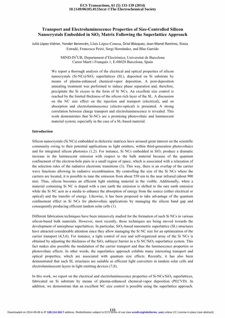
Before the in-depth study of the optoelectronic properties the Si NC superlattices present, it is almost
mandatory to check their deposition control, i.e. the NC size control. For this, direct observation was
carried out by means of cross-section EFTEM. In Fig. 1(a), an EFTEM image from a sample grown with
different tSRON while fixing tSiO2 = 4 nm is shown. By energy filtering the Si plasmon, Si signal could be
highlighted on the oxide background and, therefore, the presence of Si NCs is clearly distinguished
(bright spots). A statistical analysis on the NC size was performed out of the 50 bilayers per SL, whose
results are plotted in Fig. 1(b) against the measured SRON layer thickness before the annealing process.
As can be observed, both parameters are equivalent up to tSRON = 5 nm, beyond which the NC size no
longer grows, establishing an upper limit for NC nucleation and, in turn, for their size control. In other
words, the superlattice approach gives excellent results up to deposited SRON layer thicknesses of 5 nm.
The luminescence properties of the nanostructures were also investigated by means of the
photoluminescence (PL) technique. The PL spectra are displayed in Fig. 1(c). A Gaussian-like emission is
observed, usually ascribed to the excitonic recombination that takes place within the quantum dot (QD).
This recombination is strongly size-dependent, as shown by the peak blueshift at smaller NCs, attributed
to the quantum confinement of the carriers within the QDs (3). Besides, the PL emission intensity at
medium NC sizes was found to be greater than small or large nanostructures, which has been associated
in the past to the higher quantum yield the medium sizes show (10). Therefore, the effect of the size
control on the structural and optical properties of the Si NCs anticipates the change in the electrical and
electro-optical properties this material may present.
ECS Transactions, 61 (5) 133-139 (2014)
134) unless CC License in place (see abstract). ecsdl.org/site/terms_use address. Redistribution subject to ECS terms of use (see 128.114.163.7Downloaded on 2014-09-08 to IP
Figure 1. (a) Cross-section EFTEM image performed on a sample prepared with a constant tSiO2 = 4 nm
while varying its tSRON. The NC size statistics out of some of the layers is summarized in (b). A solid line
has been plotted as a trend indicator. (c) Normalized PL spectra corresponding to samples containing
different NC sizes (written down in the figure).
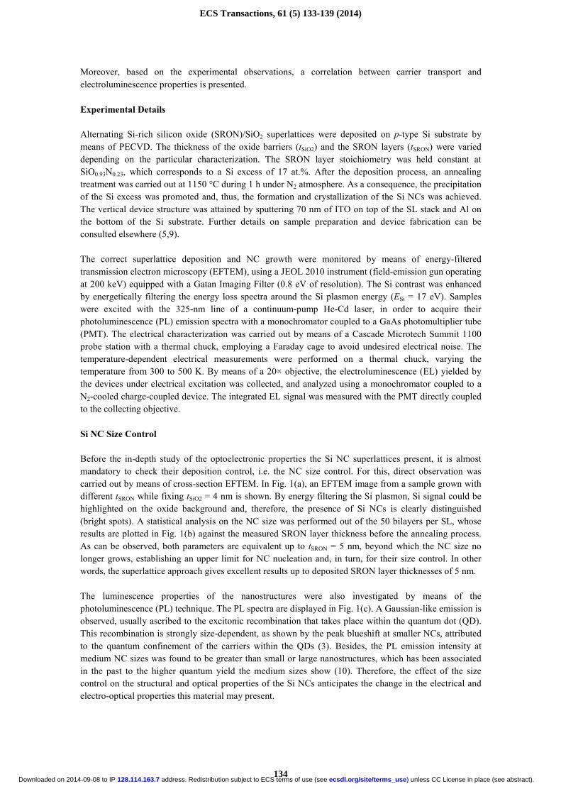
Charge Transport Properties of the NC Superlattices
The electrical properties of devices containing Si NC superlattice stacks as active material were studied,
in order to determine the charge transport mechanisms taking place within the structure. For this study,
the SRON layer thickness was varied with values of 2.5, 3.5, and 4.5 nm, while holding constant tSiO2 = 1
nm. The total number of deposited SRON/SiO2 bilayers was five. In addition, the sputtering of an ITO
layer on top and Al on the bottom completed the device structure [see the device sketch in the inset of
Fig. 2(a)].
The current density versus voltage characteristics, obtained under accumulation (V < 0), are plotted in
Fig. 2(a). As can be observed, the curves present two distinct behaviors, at low and high applied voltages.
At low voltages, the behavior is attributed to displacement current and, therefore, to capacitor-like effects
related to the device geometry (the total active material thickness). Likewise, the high voltage behavior
can be associated to the pure conduction of carriers. Besides, a voltage onset is found for this conduction
to begin. It is worth to realize that both the onset voltage and the conduction regime are strongly tSRON
dependent, which implies that charge transport is tightly related to the NC size. In addition, the strong
dependence of transport on the active layer properties anticipates that the main transport mechanism will
be bulk-limited.
Most works in the past have been focused on the transport through Si nanostructures embedded in bulk
SiO2. These studies revealed injection-limited transport mechanisms such as Fowler-Nordheim (FN)
tunneling at high fields, and trap-assisted tunneling through defects in the SiO2 matrix acting as trap states
(11). However, the superlattice structure presents different carrier pathways because of the NC ordering.
Marconi et al. proposed a bipolar direct tunneling conduction that well correlated with the high
electroluminescence efficiency (8). Afterwards, Gutsch et al. realized that transport in these structures are
strongly modulated by the presence of defects, probably Si-SiO2 interface related, and also advanced
Poole-Frenkel (PF) as a plausible conduction mechanism (5).
According to the amount of interfaces within our structures, and the bulk-limited origin of our emission,
we initially hypothesized a PF-type as the main transport mechanism taking place through our system. In
the PF conduction mechanism, the current intensity dependence on voltage and temperature is given by:
(12)
−−=
d
qV
Tk
qV
d
ANqTVI
r
t
B
tPF επε
φµ0
·exp),( (1)
ECS Transactions, 61 (5) 133-139 (2014)
135) unless CC License in place (see abstract). ecsdl.org/site/terms_use address. Redistribution subject to ECS terms of use (see 128.114.163.7Downloaded on 2014-09-08 to IP
with q the elementary charge, µ the carrier mobility, Nt the trap concentration, A the device area, d the
total SL structure thickness, kB the Boltzmann constant, Φt the energetic level of the trap taken from the
SL conduction band edge, ε0 the vacuum permittivity and εr the relative permittivity of the medium.
Taking into account both the voltage and temperature dependences of the PF current intensity, we could
experimentally prove that our devices well fit Eq. (1). As an example, Fig. 2(b) and Fig. 2(c) display the
PF (V-dependent) and Arrhenius (T-dependent) plots for the device containing tSRON = 3.5 nm,
respectively, the former study performed at room temperature (300 K) and the latter at 13 V (well within
the pure conduction regime). From the mathematical adjustments, we estimated εr = 8.7 and an activation
energy for the pure conduction to take place (EA) of 90 meV. Besides, both parameters increased at
thicker SRON layers, which verifies the transport dependence on the NC size.
Figure 2. (a) Current density versus voltage curves (in absolute value) corresponding to devices with
different tSRON. Vertical lines indicate the voltage onset for pure conduction to begin. The inset shows a
sketch of the device structure. (b) Poole-Frenkel fit from the current density versus voltage characteristic
of the device with tSRON = 3.5 nm. (c) Conductivity versus the inverse of temperature (Arrhenius plot)
from the same device and its correspondent fit.
Electroluminescence Properties of the Si NC Superlattices
To assess the electro-optical properties of Si NC superlattices, the electroluminescence emission of the
devices, integrated throughout the whole spectrum, was investigated. The plots are presented in Fig. 3(a).
It can be easily observed that the device with intermediate SRON layer thickness presents the highest EL
output. To quantify the optical output relative to the electrical excitation input, the power efficiency was
calculated as
optPE(%) 100
W
J V= ×
× (2)
where Wopt is the EL optical power density (per unit surface). The resulting PE values, estimated at J =
10-4
A·cm-2
, vary in the range from 10-4
to 10-3
%. The origin of such a low efficiency must be somehow
related to the bulk-limited conduction-type through the SL systems, but its interpretation still requires a
further analysis.
The following experimental step consisted of the acquisition of the EL spectra yielded by the devices,
exciting them with a constant current density of ~10-4
A·cm-2
. Fig. 3(b) displays the results. A strong
emission feature is observed centered between 1.3 and 1.5 eV, which is related to the excitonic
recombination within the nanostructures (10), as anticipated by the PL characterization. In addition, there
is a clear dependence of the EL on the SRON layer thickness, i.e. on the NC size, a peak blueshift
occurring at smaller NCs as expected from the carriers quantum confinement. Besides, the EL intensity is
optimum at medium NC sizes, which is attributed to the higher quantum yield medium-size NCs present
(13).
ECS Transactions, 61 (5) 133-139 (2014)
136) unless CC License in place (see abstract). ecsdl.org/site/terms_use address. Redistribution subject to ECS terms of use (see 128.114.163.7Downloaded on 2014-09-08 to IP
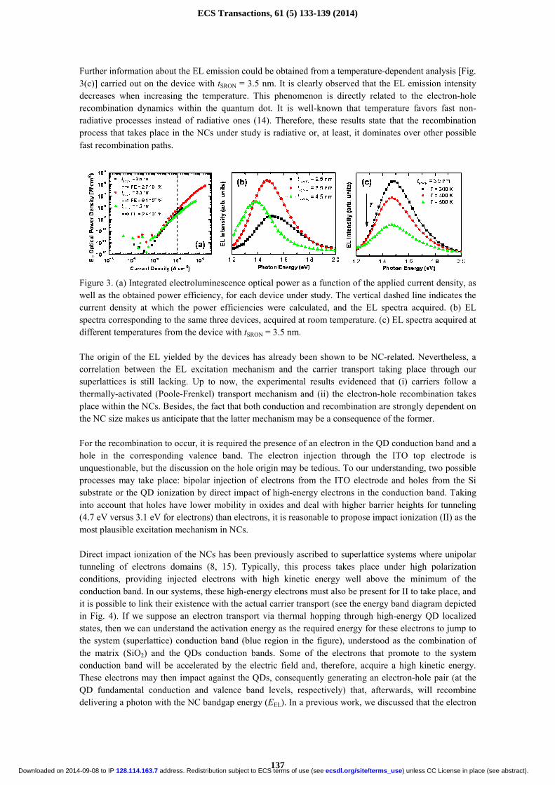
Further information about the EL emission could be obtained from a temperature-dependent analysis [Fig.
3(c)] carried out on the device with tSRON = 3.5 nm. It is clearly observed that the EL emission intensity
decreases when increasing the temperature. This phenomenon is directly related to the electron-hole
recombination dynamics within the quantum dot. It is well-known that temperature favors fast non-
radiative processes instead of radiative ones (14). Therefore, these results state that the recombination
process that takes place in the NCs under study is radiative or, at least, it dominates over other possible
fast recombination paths.
Figure 3. (a) Integrated electroluminescence optical power as a function of the applied current density, as
well as the obtained power efficiency, for each device under study. The vertical dashed line indicates the
current density at which the power efficiencies were calculated, and the EL spectra acquired. (b) EL
spectra corresponding to the same three devices, acquired at room temperature. (c) EL spectra acquired at
different temperatures from the device with tSRON = 3.5 nm.
The origin of the EL yielded by the devices has already been shown to be NC-related. Nevertheless, a
correlation between the EL excitation mechanism and the carrier transport taking place through our
superlattices is still lacking. Up to now, the experimental results evidenced that (i) carriers follow a
thermally-activated (Poole-Frenkel) transport mechanism and (ii) the electron-hole recombination takes
place within the NCs. Besides, the fact that both conduction and recombination are strongly dependent on
the NC size makes us anticipate that the latter mechanism may be a consequence of the former.
For the recombination to occur, it is required the presence of an electron in the QD conduction band and a
hole in the corresponding valence band. The electron injection through the ITO top electrode is
unquestionable, but the discussion on the hole origin may be tedious. To our understanding, two possible
processes may take place: bipolar injection of electrons from the ITO electrode and holes from the Si
substrate or the QD ionization by direct impact of high-energy electrons in the conduction band. Taking
into account that holes have lower mobility in oxides and deal with higher barrier heights for tunneling
(4.7 eV versus 3.1 eV for electrons) than electrons, it is reasonable to propose impact ionization (II) as the
most plausible excitation mechanism in NCs.
Direct impact ionization of the NCs has been previously ascribed to superlattice systems where unipolar
tunneling of electrons domains (8, 15). Typically, this process takes place under high polarization
conditions, providing injected electrons with high kinetic energy well above the minimum of the
conduction band. In our systems, these high-energy electrons must also be present for II to take place, and
it is possible to link their existence with the actual carrier transport (see the energy band diagram depicted
in Fig. 4). If we suppose an electron transport via thermal hopping through high-energy QD localized
states, then we can understand the activation energy as the required energy for these electrons to jump to
the system (superlattice) conduction band (blue region in the figure), understood as the combination of
the matrix (SiO2) and the QDs conduction bands. Some of the electrons that promote to the system
conduction band will be accelerated by the electric field and, therefore, acquire a high kinetic energy.
These electrons may then impact against the QDs, consequently generating an electron-hole pair (at the
QD fundamental conduction and valence band levels, respectively) that, afterwards, will recombine
delivering a photon with the NC bandgap energy (EEL). In a previous work, we discussed that the electron
ECS Transactions, 61 (5) 133-139 (2014)
137) unless CC License in place (see abstract). ecsdl.org/site/terms_use address. Redistribution subject to ECS terms of use (see 128.114.163.7Downloaded on 2014-09-08 to IP
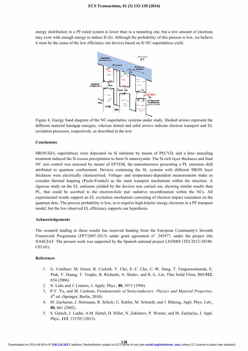
energy distribution in a PF-ruled system is lower than in a tunneling one, but a low amount of electrons
may exist with enough energy to induce II (6). Although the probability of this process is low, we believe
it must be the cause of the low efficiency our devices based on Si NC-superlattices yield.
Figure 4. Energy band diagram of the NC-superlattice systems under study. Dashed arrows represent the
different material bandgap energies, whereas dotted and solid arrows indicate electron transport and EL
excitation processes, respectively, as described in the text.
Conclusions
SRON/SiO2 superlattices were deposited on Si substrate by means of PECVD, and a later annealing
treatment induced the Si excess precipitation to form Si nanocrystals. The Si-rich layer thickness and final
NC size control was assessed by means of EFTEM, the nanostructures presenting a PL emission shift
attributed to quantum confinement. Devices containing the SL systems with different SRON layer
thickness were electrically characterized. Voltage- and temperature-dependent measurements make us
consider thermal hopping (Poole-Frenkel) as the main transport mechanism within the structure. A
rigorous study on the EL emission yielded by the devices was carried out, showing similar results than
PL, that could be ascribed to the electron-hole pair radiative recombination within the NCs. All
experimental results support an EL excitation mechanism consisting of electron impact ionization on the
quantum dots. The process probability is low, as it requires high-kinetic energy electrons in a PF transport
model, but the low observed EL efficiency supports our hypothesis.
Acknowledgements
The research leading to these results has received funding from the European Community's Seventh
Framework Programme (FP7/2007-2013) under grant agreement nº: 245977, under the project title
NASCEnT. The present work was supported by the Spanish national project LEOMIS (TEC2012-38540-
C02-01).
References
1. G. Conibeer, M. Green, R. Corkish, Y. Cho, E.-C. Cho, C.-W. Jiang, T. Fangsuwannarak, E.
Pink, Y. Huang, T. Trupke, B. Richards, A. Shalav, and K.-L. Lin, Thin Solid Films, 511-512,
654 (2006).
2. N. Lalic and J. Linnros, J. Apply. Phys., 80, 5971 (1996).
3. P.Y. Yu, and M. Cardona, Fundamentals of Semiconductors: Physics and Material Properties,
4th
ed. (Springer, Berlin, 2010).
4. M. Zacharias, J. Heitmann, R. Scholz, U. Kahler, M. Schmidt, and J. Bläsing, Appl. Phys. Lett.,
80, 661 (2002).
5. S. Gutsch, J. Laube, A.M. Hartel, D. Hiller, N. Zakharov, P. Werner, and M. Zacharias, J. Appl.
Phys., 113, 133703 (2013).
ECS Transactions, 61 (5) 133-139 (2014)
138) unless CC License in place (see abstract). ecsdl.org/site/terms_use address. Redistribution subject to ECS terms of use (see 128.114.163.7Downloaded on 2014-09-08 to IP
6. J. López-Vidrier, Y. Berencén, S. Hernández, O. Blázquez, S. Gutsch, J. Laube, D. Hiller, P.
Löper, M. Schnabel, S. Janz, M. Zacharias, and B. Garrido, J. Appl. Phys., 114, 163701 (2013).
7. E.-C. Cho, S. Park, X. Hao, D. Song, G. Conibeer, S.-C. Park, and M.A. Green, Nanotechnology,
19, 245201 (2008).
8. A. Marconi, A. Anopchenko, M. Wang, G. Pucker, P. Bellutti, and L. Pavesi, Appl. Phys. Lett.,
94, 221110 (2009).
9. A.M. Hartel, D. Hiller, S. Gutsch, P. Löper, S. Estradé, F. Peiró, B. Garrido, and M. Zacharias,
Thin Solid Films, 520, 121 (2011).
10. J. Valenta, N. Lalic, and J. Linnros, Opt. Mater., 17, 45 (2001).
11. J.M. Ramírez, Y. Berencén, L. López-Conesa, J.M. Rebled, F. Peiró, and B. Garrido, Appl.
Phys. Lett., 103, 081102 (2013).
12. S.M. Sze, and K.K. Ng, Physics of Semiconductor Devices, 3rd
ed. (Wiley, New York, 2007).
13. G. Ledoux, J. Gong, F. Huisken, O. Guillois, and C. Reynaud, Appl. Phys. Lett., 80, 4834
(2002).
14. Y. Berencén, J.M. Ramírez, O. Jambois, C. Domínguez, J.A. Rodríguez, and B. Garrido, J. Appl.
Phys., 112, 033114 (2012).
15. A. Anopchenko, A. Marconi, E. Moser, S. Prezioso, M. Wang, L. Pavesi, G. Pucker, and P.
Bellutti, J. Appl. Phys., 106, 033104 (2009).
ECS Transactions, 61 (5) 133-139 (2014)
139) unless CC License in place (see abstract). ecsdl.org/site/terms_use address. Redistribution subject to ECS terms of use (see 128.114.163.7Downloaded on 2014-09-08 to IP


![Extraordinary properties of nematic phases of bent-core liquid crystals (Invited Paper)[6911-05]](https://static.fdokumen.com/doc/165x107/6333b2707a687b71aa08555a/extraordinary-properties-of-nematic-phases-of-bent-core-liquid-crystals-invited.jpg)

