Investigation of induced parallel magnetic anisotropy at low deposition temperature in...
6
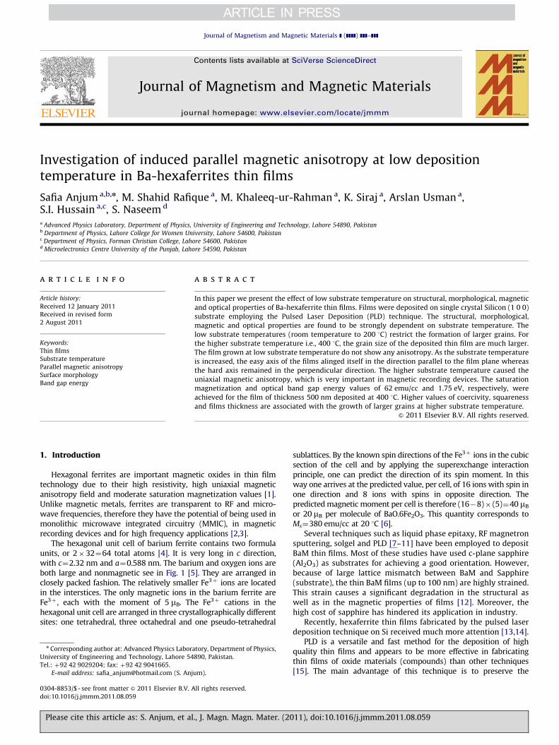
Investigation of induced parallel magnetic anisotropy at low deposition temperature in Ba-hexaferrites thin films Safia Anjum a,b,n , M. Shahid Rafique a , M. Khaleeq-ur-Rahman a , K. Siraj a , Arslan Usman a , S.I. Hussain a,c , S. Naseem d a Advanced Physics Laboratory, Department of Physics, University of Engineering and Technology, Lahore 54890, Pakistan b Department of Physics, Lahore College for Women University, Lahore 54600, Pakistan c Department of Physics, Forman Christian College, Lahore 54600, Pakistan d Microelectronics Centre University of the Punjab, Lahore 54590, Pakistan article info Article history: Received 12 January 2011 Received in revised form 2 August 2011 Keywords: Thin films Substrate temperature Parallel magnetic anisotropy Surface morphology Band gap energy abstract In this paper we present the effect of low substrate temperature on structural, morphological, magnetic and optical properties of Ba-hexaferrite thin films. Films were deposited on single crystal Silicon (1 0 0) substrate employing the Pulsed Laser Deposition (PLD) technique. The structural, morphological, magnetic and optical properties are found to be strongly dependent on substrate temperature. The low substrate temperatures (room temperature to 200 1C) restrict the formation of larger grains. For the higher substrate temperature i.e., 400 1C, the grain size of the deposited thin film are much larger. The film grown at low substrate temperature do not show any anisotropy. As the substrate temperature is increased, the easy axis of the films alinged itself in the direction parallel to the film plane whereas the hard axis remained in the perpendicular direction. The higher substrate temperature caused the uniaxial magnetic anisotropy, which is very important in magnetic recording devices. The saturation magnetization and optical band gap energy values of 62 emu/cc and 1.75 eV, respectively, were achieved for the film of thickness 500 nm deposited at 400 1C. Higher values of coercivity, squareness and films thickness are associated with the growth of larger grains at higher substrate temperature. & 2011 Elsevier B.V. All rights reserved. 1. Introduction Hexagonal ferrites are important magnetic oxides in thin film technology due to their high resistivity, high uniaxial magnetic anisotropy field and moderate saturation magnetization values [1]. Unlike magnetic metals, ferrites are transparent to RF and micro- wave frequencies, therefore they have the potential of being used in monolithic microwave integrated circuitry (MMIC), in magnetic recording devices and for high frequency applications [2,3]. The hexagonal unit cell of barium ferrite contains two formula units, or 2 32 ¼ 64 total atoms [4]. It is very long in c direction, with c ¼ 2.32 nm and a ¼ 0.588 nm. The barium and oxygen ions are both large and nonmagnetic see in Fig. 1 [5]. They are arranged in closely packed fashion. The relatively smaller Fe 3 þ ions are located in the interstices. The only magnetic ions in the barium ferrite are Fe 3 þ , each with the moment of 5 m B . The Fe 3 þ cations in the hexagonal unit cell are arranged in three crystallographically different sites: one tetrahedral, three octahedral and one pseudo-tetrahedral sublattices. By the known spin directions of the Fe 3þ ions in the cubic section of the cell and by applying the superexchange interaction principle, one can predict the direction of its spin moment. In this way one arrives at the predicted value, per cell, of 16 ions with spin in one direction and 8 ions with spins in opposite direction. The predicted magnetic moment per cell is therefore (16 8) (5) ¼ 40 m B or 20 m B per molecule of BaO.6Fe 2 O 3 . This quantity corresponds to M s ¼ 380 emu/cc at 20 1C [6]. Several techniques such as liquid phase epitaxy, RF magnetron sputtering, solgel and PLD [7–11] have been employed to deposit BaM thin films. Most of these studies have used c-plane sapphire (Al 2 O 3 ) as substrates for achieving a good orientation. However, because of large lattice mismatch between BaM and Sapphire (substrate), the thin BaM films (up to 100 nm) are highly strained. This strain causes a significant degradation in the structural as well as in the magnetic properties of films [12]. Moreover, the high cost of sapphire has hindered its application in industry. Recently, hexaferrite thin films fabricated by the pulsed laser deposition technique on Si received much more attention [13,14]. PLD is a versatile and fast method for the deposition of high quality thin films and appears to be more effective in fabricating thin films of oxide materials (compounds) than other techniques [15]. The main advantage of this technique is to preserve the Contents lists available at SciVerse ScienceDirect journal homepage: www.elsevier.com/locate/jmmm Journal of Magnetism and Magnetic Materials 0304-8853/$ - see front matter & 2011 Elsevier B.V. All rights reserved. doi:10.1016/j.jmmm.2011.08.059 n Corresponding author at: Advanced Physics Laboratory, Department of Physics, University of Engineering and Technology, Lahore 54890, Pakistan. Tel.: þ92 42 9029204; fax: þ92 42 9041665. E-mail address: safi[email protected] (S. Anjum). Please cite this article as: S. Anjum, et al., J. Magn. Magn. Mater. (2011), doi:10.1016/j.jmmm.2011.08.059 Journal of Magnetism and Magnetic Materials ] (]]]]) ]]]–]]]
-
Upload
independent -
Category
Documents
-
view
1 -
download
0
Transcript of Investigation of induced parallel magnetic anisotropy at low deposition temperature in...
Journal of Magnetism and Magnetic Materials ] (]]]]) ]]]–]]]
Contents lists available at SciVerse ScienceDirect
Journal of Magnetism and Magnetic Materials
0304-88
doi:10.1
n Corr
Univers
Tel.: þ9
E-m
Pleas
journal homepage: www.elsevier.com/locate/jmmm
Investigation of induced parallel magnetic anisotropy at low depositiontemperature in Ba-hexaferrites thin films
Safia Anjum a,b,n, M. Shahid Rafique a, M. Khaleeq-ur-Rahman a, K. Siraj a, Arslan Usman a,S.I. Hussain a,c, S. Naseem d
a Advanced Physics Laboratory, Department of Physics, University of Engineering and Technology, Lahore 54890, Pakistanb Department of Physics, Lahore College for Women University, Lahore 54600, Pakistanc Department of Physics, Forman Christian College, Lahore 54600, Pakistand Microelectronics Centre University of the Punjab, Lahore 54590, Pakistan
a r t i c l e i n f o
Article history:
Received 12 January 2011
Received in revised form
2 August 2011
Keywords:
Thin films
Substrate temperature
Parallel magnetic anisotropy
Surface morphology
Band gap energy
53/$ - see front matter & 2011 Elsevier B.V. A
016/j.jmmm.2011.08.059
esponding author at: Advanced Physics Labor
ity of Engineering and Technology, Lahore 54
2 42 9029204; fax: þ92 42 9041665.
ail address: [email protected] (S. Anj
e cite this article as: S. Anjum, et al
a b s t r a c t
In this paper we present the effect of low substrate temperature on structural, morphological, magnetic
and optical properties of Ba-hexaferrite thin films. Films were deposited on single crystal Silicon (1 0 0)
substrate employing the Pulsed Laser Deposition (PLD) technique. The structural, morphological,
magnetic and optical properties are found to be strongly dependent on substrate temperature. The
low substrate temperatures (room temperature to 200 1C) restrict the formation of larger grains. For
the higher substrate temperature i.e., 400 1C, the grain size of the deposited thin film are much larger.
The film grown at low substrate temperature do not show any anisotropy. As the substrate temperature
is increased, the easy axis of the films alinged itself in the direction parallel to the film plane whereas
the hard axis remained in the perpendicular direction. The higher substrate temperature caused the
uniaxial magnetic anisotropy, which is very important in magnetic recording devices. The saturation
magnetization and optical band gap energy values of 62 emu/cc and 1.75 eV, respectively, were
achieved for the film of thickness 500 nm deposited at 400 1C. Higher values of coercivity, squareness
and films thickness are associated with the growth of larger grains at higher substrate temperature.
& 2011 Elsevier B.V. All rights reserved.
1. Introduction
Hexagonal ferrites are important magnetic oxides in thin filmtechnology due to their high resistivity, high uniaxial magneticanisotropy field and moderate saturation magnetization values [1].Unlike magnetic metals, ferrites are transparent to RF and micro-wave frequencies, therefore they have the potential of being used inmonolithic microwave integrated circuitry (MMIC), in magneticrecording devices and for high frequency applications [2,3].
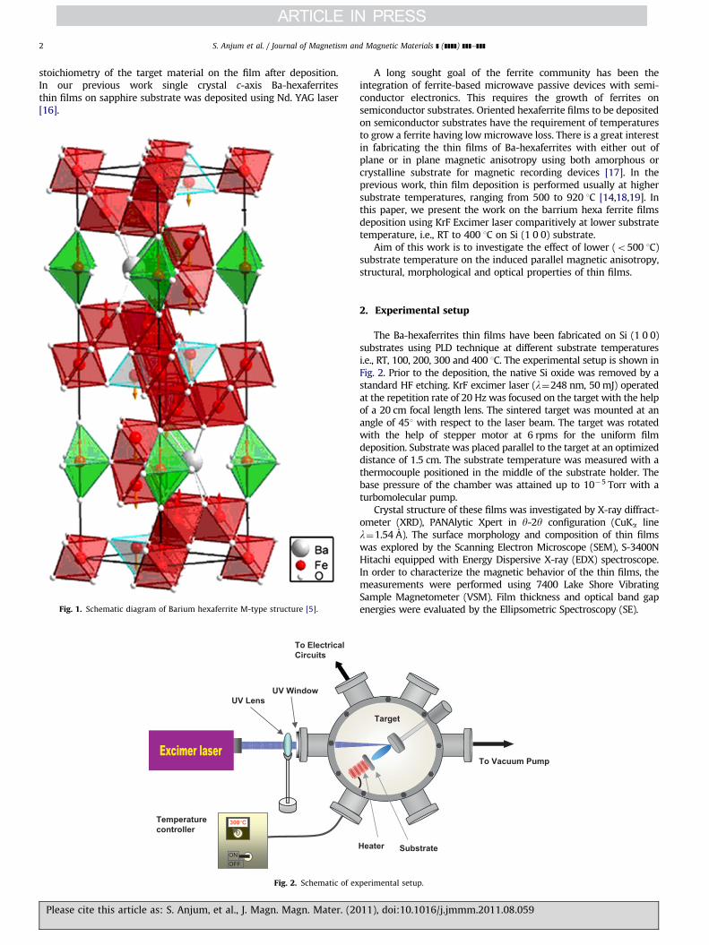
The hexagonal unit cell of barium ferrite contains two formulaunits, or 2�32¼64 total atoms [4]. It is very long in c direction,with c¼2.32 nm and a¼0.588 nm. The barium and oxygen ions areboth large and nonmagnetic see in Fig. 1 [5]. They are arranged inclosely packed fashion. The relatively smaller Fe3þ ions are locatedin the interstices. The only magnetic ions in the barium ferrite areFe3þ , each with the moment of 5 mB. The Fe3þ cations in thehexagonal unit cell are arranged in three crystallographically differentsites: one tetrahedral, three octahedral and one pseudo-tetrahedral
ll rights reserved.
atory, Department of Physics,
890, Pakistan.
um).
., J. Magn. Magn. Mater. (20
sublattices. By the known spin directions of the Fe3þ ions in the cubicsection of the cell and by applying the superexchange interactionprinciple, one can predict the direction of its spin moment. In thisway one arrives at the predicted value, per cell, of 16 ions with spin inone direction and 8 ions with spins in opposite direction. Thepredicted magnetic moment per cell is therefore (16�8)� (5)¼40 mB
or 20 mB per molecule of BaO.6Fe2O3. This quantity corresponds toMs¼380 emu/cc at 20 1C [6].
Several techniques such as liquid phase epitaxy, RF magnetronsputtering, solgel and PLD [7–11] have been employed to depositBaM thin films. Most of these studies have used c-plane sapphire(Al2O3) as substrates for achieving a good orientation. However,because of large lattice mismatch between BaM and Sapphire(substrate), the thin BaM films (up to 100 nm) are highly strained.This strain causes a significant degradation in the structural aswell as in the magnetic properties of films [12]. Moreover, thehigh cost of sapphire has hindered its application in industry.
Recently, hexaferrite thin films fabricated by the pulsed laserdeposition technique on Si received much more attention [13,14].
PLD is a versatile and fast method for the deposition of highquality thin films and appears to be more effective in fabricatingthin films of oxide materials (compounds) than other techniques[15]. The main advantage of this technique is to preserve the
11), doi:10.1016/j.jmmm.2011.08.059
S. Anjum et al. / Journal of Magnetism and Magnetic Materials ] (]]]]) ]]]–]]]2
stoichiometry of the target material on the film after deposition.In our previous work single crystal c-axis Ba-hexaferritesthin films on sapphire substrate was deposited using Nd. YAG laser[16].
Fig. 1. Schematic diagram of Barium hexaferrite M-type structure [5].
To ElectricalCircuits
UV Lens
Temperaturecontroller
300°C
ONOFF
UV Window
Fig. 2. Schematic of ex
Please cite this article as: S. Anjum, et al., J. Magn. Magn. Mater. (20
A long sought goal of the ferrite community has been theintegration of ferrite-based microwave passive devices with semi-conductor electronics. This requires the growth of ferrites onsemiconductor substrates. Oriented hexaferrite films to be depositedon semiconductor substrates have the requirement of temperaturesto grow a ferrite having low microwave loss. There is a great interestin fabricating the thin films of Ba-hexaferrites with either out ofplane or in plane magnetic anisotropy using both amorphous orcrystalline substrate for magnetic recording devices [17]. In theprevious work, thin film deposition is performed usually at highersubstrate temperatures, ranging from 500 to 920 1C [14,18,19]. Inthis paper, we present the work on the barrium hexa ferrite filmsdeposition using KrF Excimer laser comparitively at lower substratetemperature, i.e., RT to 400 1C on Si (1 0 0) substrate.
Aim of this work is to investigate the effect of lower (o500 1C)substrate temperature on the induced parallel magnetic anisotropy,structural, morphological and optical properties of thin films.
2. Experimental setup
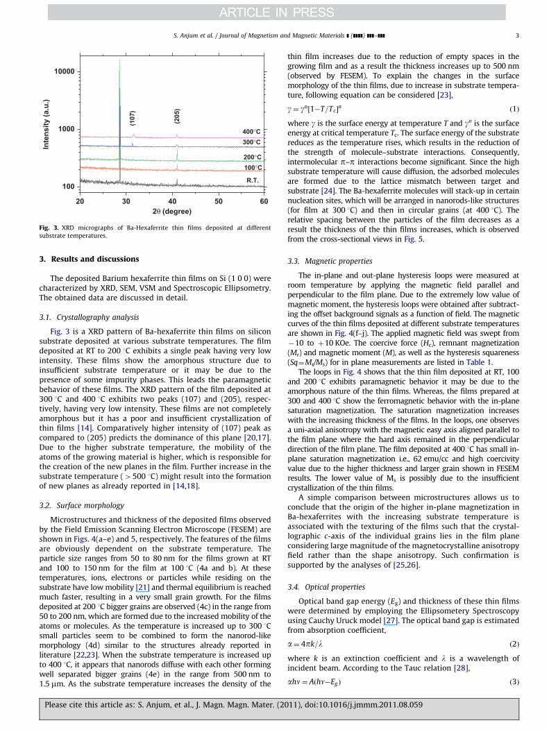
The Ba-hexaferrites thin films have been fabricated on Si (1 0 0)substrates using PLD technique at different substrate temperaturesi.e., RT, 100, 200, 300 and 400 1C. The experimental setup is shown inFig. 2. Prior to the deposition, the native Si oxide was removed by astandard HF etching. KrF excimer laser (l¼248 nm, 50 mJ) operatedat the repetition rate of 20 Hz was focused on the target with the helpof a 20 cm focal length lens. The sintered target was mounted at anangle of 451 with respect to the laser beam. The target was rotatedwith the help of stepper motor at 6 rpms for the uniform filmdeposition. Substrate was placed parallel to the target at an optimizeddistance of 1.5 cm. The substrate temperature was measured with athermocouple positioned in the middle of the substrate holder. Thebase pressure of the chamber was attained up to 10�5 Torr with aturbomolecular pump.
Crystal structure of these films was investigated by X-ray diffract-ometer (XRD), PANAlytic Xpert in y-2y configuration (CuKa linel¼1.54 A). The surface morphology and composition of thin filmswas explored by the Scanning Electron Microscope (SEM), S-3400NHitachi equipped with Energy Dispersive X-ray (EDX) spectroscope.In order to characterize the magnetic behavior of the thin films, themeasurements were performed using 7400 Lake Shore VibratingSample Magnetometer (VSM). Film thickness and optical band gapenergies were evaluated by the Ellipsometric Spectroscopy (SE).
To Vacuum Pump
Target
SubstrateHeater
perimental setup.
11), doi:10.1016/j.jmmm.2011.08.059
20 30 40 50 60
100
1000
10000
400°C300°C
200°C100°C
R.T.(2
05)
(107
)
2θ (degree)
Inte
nsity
(a.u
.)
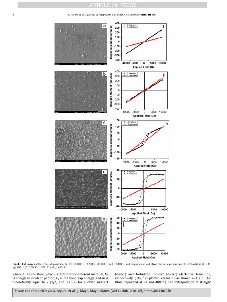
Fig. 3. XRD micrographs of Ba-Hexaferrite thin films deposited at different
substrate temperatures.
S. Anjum et al. / Journal of Magnetism and Magnetic Materials ] (]]]]) ]]]–]]] 3
3. Results and discussions
The deposited Barium hexaferrite thin films on Si (1 0 0) werecharacterized by XRD, SEM, VSM and Spectroscopic Ellipsometry.The obtained data are discussed in detail.
3.1. Crystallography analysis
Fig. 3 is a XRD pattern of Ba-hexaferrite thin films on siliconsubstrate deposited at various substrate temperatures. The filmdeposited at RT to 200 1C exhibits a single peak having very lowintensity. These films show the amorphous structure due toinsufficient substrate temperature or it may be due to thepresence of some impurity phases. This leads the paramagneticbehavior of these films. The XRD pattern of the film deposited at300 1C and 400 1C exhibits two peaks (107) and (205), respec-tively, having very low intensity. These films are not completelyamorphous but it has a poor and insufficient crystallization ofthin films [14]. Comparatively higher intensity of (107) peak ascompared to (205) predicts the dominance of this plane [20,17].Due to the higher substrate temperature, the mobility of theatoms of the growing material is higher, which is responsible forthe creation of the new planes in the film. Further increase in thesubstrate temperature (4500 1C) might result into the formationof new planes as already reported in [14,18].
3.2. Surface morphology
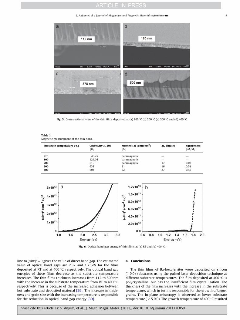
Microstructures and thickness of the deposited films observedby the Field Emission Scanning Electron Microscope (FESEM) areshown in Figs. 4(a–e) and 5, respectively. The features of the filmsare obviously dependent on the substrate temperature. Theparticle size ranges from 50 to 80 nm for the films grown at RTand 100 to 150 nm for the film at 100 1C (4a and b). At thesetemperatures, ions, electrons or particles while residing on thesubstrate have low mobility [21] and thermal equilibrium is reachedmuch faster, resulting in a very small grain growth. For the filmsdeposited at 200 1C bigger grains are observed (4c) in the range from50 to 200 nm, which are formed due to the increased mobility of theatoms or molecules. As the temperature is increased up to 300 1Csmall particles seem to be combined to form the nanorod-likemorphology (4d) similar to the structures already reported inliterature [22,23]. When the substrate temperature is increased upto 400 1C, it appears that nanorods diffuse with each other formingwell separated bigger grains (4e) in the range from 500 nm to1.5 mm. As the substrate temperature increases the density of the
Please cite this article as: S. Anjum, et al., J. Magn. Magn. Mater. (20
thin film increases due to the reduction of empty spaces in thegrowing film and as a result the thickness increases up to 500 nm(observed by FESEM). To explain the changes in the surfacemorphology of the thin films, due to increase in substrate tempera-ture, following equation can be considered [23],
g¼ go½1�T=Tc�n ð1Þ
where g is the surface energy at temperature T and go is the surfaceenergy at critical temperature Tc. The surface energy of the substratereduces as the temperature rises, which results in the reduction ofthe strength of molecule–substrate interactions. Consequently,intermolecular p–p interactions become significant. Since the highsubstrate temperature will cause diffusion, the adsorbed moleculesare formed due to the lattice mismatch between target andsubstrate [24]. The Ba-hexaferrite molecules will stack-up in certainnucleation sites, which will be arranged in nanorods-like structures(for film at 300 1C) and then in circular grains (at 400 1C). Therelative spacing between the particles of the film decreases as aresult the thickness of the thin films increases, which is observedfrom the cross-sectional views in Fig. 5.
3.3. Magnetic properties
The in-plane and out-plane hysteresis loops were measured atroom temperature by applying the magnetic field parallel andperpendicular to the film plane. Due to the extremely low value ofmagnetic moment, the hysteresis loops were obtained after subtract-ing the offset background signals as a function of field. The magneticcurves of the thin films deposited at different substrate temperaturesare shown in Fig. 4(f–j). The applied magnetic field was swept from�10 to þ10 KOe. The coercive force (Hc), remnant magnetization(Mr) and magnetic moment (M), as well as the hysteresis squareness(Sq¼Mr/Ms) for in plane measurements are listed in Table 1.
The loops in Fig. 4 shows that the thin film deposited at RT, 100and 200 1C exhibits paramagnetic behavior it may be due to theamorphous nature of the thin films. Whereas, the films prepared at300 and 400 1C show the ferromagnetic behavior with the in-planesaturation magnetization. The saturation magnetization increaseswith the increasing thickness of the films. In the loops, one observesa uni-axial anisotropy with the magnetic easy axis aligned parallel tothe film plane where the hard axis remained in the perpendiculardirection of the film plane. The film deposited at 400 1C has small in-plane saturation magnetization i.e., 62 emu/cc and high coercivityvalue due to the higher thickness and larger grain shown in FESEMresults. The lower value of Ms is possibly due to the insufficientcrystallization of the thin films.
A simple comparison between microstructures allows us toconclude that the origin of the higher in-plane magnetization inBa-hexaferrites with the increasing substrate temperature isassociated with the texturing of the films such that the crystal-lographic c-axis of the individual grains lies in the film planeconsidering large magnitude of the magnetocrystalline anisotropyfield rather than the shape anisotropy. Such confirmation issupported by the analyses of [25,26].
3.4. Optical properties
Optical band gap energy (Eg) and thickness of these thin filmswere determined by employing the Ellipsometery Spectroscopyusing Cauchy Uruck model [27]. The optical band gap is estimatedfrom absorption coefficient,
a¼ 4pk=l ð2Þ
where k is an extinction coefficient and l is a wavelength ofincident beam. According to the Tauc relation [28],
ahn¼ Aðhn�EgÞ ð3Þ
11), doi:10.1016/j.jmmm.2011.08.059
-150
-100
-50
0
50
100
150
Mag
netic
Mom
ent (
emu/
cc) H inplane
H outplane
Applied Field (Oe)
-400
-300
-200
-100
0
100
200
300
400
Mag
netic
Mom
ent (
emu/
cc) H inplane
H outplane
Applied Field (Oe)
-400-300-200-100
0100200300400
Applied Field (Oe)
Mag
netic
Mom
ent (
emu/
cc) H inplane
H outplane
-60
-40
-20
0
20
40
60
Mag
netic
Mom
ent (
emu/
cc)
H inplaneH outplane
Applied Field (Oe)
-10000 -5000 0 5000 10000
-10000 -5000 0 5000 10000
-10000 -5000 0 5000 10000
-10000 -5000 0 5000 10000
-10000 -5000 0 5000 10000-40
-20
0
20
40
Mag
netic
Mom
ent (
emu/
cc)
Applied Field (Oe)
H inplaneH outplane
Fig. 4. SEM images of thin films deposited at (a) RT (b) 100 1C (c) 200 1C (d) 300 1C and (e) 400 1C and In-plane and out plane magnetic measurements of thin films at (f) RT
(g) 100 1C (h) 200 1C (i) 300 1C and (j) 400 1C.
S. Anjum et al. / Journal of Magnetism and Magnetic Materials ] (]]]]) ]]]–]]]4
where A is a constant, which is different for different material, hnis energy of incident photon, Eg is the band gap energy, and m istheoretically equal to 2 (1/2) and 3 (3/2) for allowed indirect
Please cite this article as: S. Anjum, et al., J. Magn. Magn. Mater. (20
(direct) and forbidden indirect (direct) electronic transition,respectively. (ahn)2 is plotted versus hn as shown in Fig. 6 (forfilms deposited at RT and 400 1C). The extrapolation of straight
11), doi:10.1016/j.jmmm.2011.08.059
500 nm378 nm
112 nm 185 nm
Fig. 5. Cross-sectional view of the thin films deposited at (a) 100 1C (b) 200 1C (c) 300 1C and (d) 400 1C.
Table 1Magnetic measurement of the thin films.
Substrate temperature (1C) Coercivity Hc (0) Moment M (emu/cm3) Mr emu/cc Squareness:Hc :Ms :Mr/Ms
R.T. 46.25 paramagnetic — —
100 126.04 paramagnetic — —
200 619 paramagnetic 17 0.08
300 638 31 16 0.51
400 694 62 27 0.45
0.0
2.0x10¹²
4.0x10¹²
6.0x10¹²
8.0x10¹²
1.0x10¹³
1.2x10¹³
Energy (eV)0.6 0.8 1.0 1.2 1.4 1.6 1.8 2.01.0 1.5 2.0 2.5 3.0 3.5
0
1x10¹²
2x10¹²
3x10¹²
4x10¹²
5x10¹²
(αhν
)2 (c
m-1
ev)
2
(αhν
)2 (c
m-1
ev)
2
Energy (ev)
Fig. 6. Optical band gap energy of thin films at (a) RT and (b) 400 1C.
S. Anjum et al. / Journal of Magnetism and Magnetic Materials ] (]]]]) ]]]–]]] 5
line to (ahn)2¼0 gives the value of direct band gap. The estimated
value of optical band gaps are 2.32 and 1.75 eV for the filmsdeposited at RT and at 400 1C, respectively. The optical band gapenergies of these films decrease as the substrate temperatureincreases. The thin films thickness increases from 112 to 500 nmwith the increase in the substrate temperature from RT to 400 1C,respectively. This is because of the increased adhesion betweenhot substrate and deposited material [29]. The increase in thick-ness and grain size with the increasing temperature is responsiblefor the reduction in optical band gap energy [30].
Please cite this article as: S. Anjum, et al., J. Magn. Magn. Mater. (20
4. Conclusions
The thin films of Ba-hexaferrites were deposited on silicon(1 0 0) substrates using the pulsed laser deposition technique atdifferent substrate temperatures. The film deposited at 400 1C ispolycrystalline, but has the insufficient film crystallization. Thethickness of the film increases with the increase in the substratetemperature, which in turn is responsible for the growth of biggergrains. The in-plane anisotropy is observed at lower substratetemperature (o5 0 0). The growth temperature of 400 1C resulted
11), doi:10.1016/j.jmmm.2011.08.059

S. Anjum et al. / Journal of Magnetism and Magnetic Materials ] (]]]]) ]]]–]]]6
in larger grain size and thicker films, as well as relatively highcoercivity and saturation magnetization. The decrease in the bandgap energy at this substrate temperature is due to the growth oflarger grain and more defects inside the film.
References
[1] A.L. Geiler, S.D. Yoon, Y. Chen, A. Yang, C.N. Chinnasamy, M. Geiler,V.G. Harris, C. Vittoria, Journal of Applied Physics 103 (2008) 07B914.
[2] M. Koleva, P. Atanasov, R. Tomov, O. Vankov, C. Matin, C. Ristoscu,I. Mihailescu, D. Iorgov, S. Angelova, Ch. Ghelev, N. Mihaiov, Applied SurfaceScience 154 (2000) 485.
[3] Yingjian Chen, Memeber, IEEEMark H. Kryder, Fellow, IEEE, IEEE Transactionson Magnetics 34 (1998) 729.
[4] V.G. Harris, Zhaohui Chen, Yajie Chen, Soack Yoon, Tomokuza Sakai,Anton Gieler, Aria Yang, Yongxue He, K.S. Ziemer, X. Nian, Sun and CarmineVittoria 99 (2006) 08M911.
[5] H. Kojima, in: E.P. Wohlfarth (Ed.), Ferromagnetic Materials, vol. 3,North-Holland, New York, 1982.
[6] B.D. Cullity C.D. Graham, Introduction to Magnetic Materials, second ed.,2009.
[7] J.V.A. Santos, M.A. Macedo, F. Cunha, J.M. Sasaki, J.G.S. Duque, MicroelectronicsJournal 34 (2003) 565.
[8] Xiaoyu Sui, Mark H. Kryder, Bunsen Y. Wong, David E. Laughlin, IEEETransactions on Magnetics 29 (1993) 3751.
[9] S. Salemizadeh, S.A.Seyyed Ebrahimi, IEEE Transaction on Magnetics 45(2009) 2538.
[10] X.H. Liu, M.H. Hong, W.D. Song, G.X. Chen, H.M.J. Lam, J.P. Wang, T.C. Chong,Applied Physics A 80 (2005) 611.
[11] A. Lisfi, J.C. Lodder, P. de Haan, M.A. Smithers, F.J.G. Roesthuis, IEEE Transactionon Magnetics 34 (1998) 1654.
Please cite this article as: S. Anjum, et al., J. Magn. Magn. Mater. (20
[12] L. Anton, Aria Yang, Xu Zuo, Soack Dae Yoon, Yajie Chen, Vincent G. Harris,Fellow, IEEECarmine Vittoria, Fellow IEEE, IEEE Transactions on Magnetics 44(2008) 2966.
[13] Caltun O.F. Hsu L.-S., 9 (2007) 1155.[14] X.H. Liu, M.H. Hong, W.D. Song, G.X. Chen, H.M.J. Lam, J.P. Wang, T.c. Chong,
Applied Physics A 80 (2005) 611.[15] B. Chrisey, Graham K. Hubler, Pulsed Laser Deposition of Thin Films Douglas
(1994).[16] M.S. Rafique, M. Khaleeq-ur-Rahman, Saif-ur-Rehman, Safia Anjum,
M. Shahbaz Anwar, K.A. Bhatti, Saba Saeed, M.S. Awan, Vacuum 82 (2008)1233.
[17] R.G. Welch, T.J. Jackson, S.B. Palmer, IEEE Transactions on Magnetics 31(1995) 2752.
[18] X.H. Liu, M.H. Hong, W.D. Song, G.X. Chen, J.F. Chong, J.P. Wang, Y.H. WU,T.C. Chong, Applied Physics A 78 (2004) 423.
[19] P. Dorsey, R. Seed, C. Vittoria, IEEE Transactions on Magnetics 28 (1992)3216.
[20] R. Sathyamoorthy, C. Sharmila, K. Natarajan, S. Velumani, MaterialsCharacterization 58 (2007) 745.
[21] S.G. Yoon, H.K. Kim, M.J. Kim, H.M. Lee, D.H. Yoon, Thin Solid Films 475(2005) 239.
[22] Y.L. Lee, W.C. Tsai, J.R. Maa, Applied Surface Science 173 (2001) 162.[23] S.C. Shich, T.W. Wha, J.H. Fu, T.D. Bau, Organic Electronics 7 (2006) 428.[24] Surachart Kamoldilok, Benchapol Tunhoo, Sarun Sumriddetchkajorn and
Nukeaw, Proceeding of the 2nd IEEE International Conference on Nano/MicroEngineeering and Molecular Systems, 2007, 604.
[25] A. Lisfi, J.C. Lodder, Journal of Magnetism and Magnetic Materials 242 (2002)391.
[26] Xiaoyn Sui, Mark H. Kryder, Applied Physics Letters 63 (1993) 1582.[27] M. Sultan, R. Singh, Journal of Physics D: Applied Physics 42 (2009) 115306-1.[28] J. Tauc, R. Grigorovici, A. Vancu, Physica Status Solidi A 15 (1966) 627.[29] Robert Eason, Pulsed Laser deposition of thin films, John Wiley and Sons,
2007.[30] C.V. Ramana, R.J. Smith, Hussain, Physica Status Solidi A 199 (1) (2003) R4.
11), doi:10.1016/j.jmmm.2011.08.059