
Investigation of digital current control based on zero average current error concept
167
Investigation of Digital Current Control Based on Zero Average Current Error Concept Hamdan Daniyal This thesis is presented for the degree of Doctor of Philosophy of Electrical Engineering at The University of Western Australia School of Electrical, Electronic and Computer Engineering 2011
Transcript of Investigation of digital current control based on zero average current error concept

Investigation of Digital Current Control Based on Zero Average
Current Error Concept Hamdan Daniyal
This thesis is presented for the degree of
Doctor of Philosophy of Electrical Engineering at
The University of Western Australia
School of Electrical, Electronic and Computer Engineering 2011

ii

iii
Abstract Digital current control technique has quickly become one of the active research areas in
power electronics thanks to the rapid increasing of digital platform processing power as
well as the decreasing of its cost. There is a lot of new digital current control technique
developed in the past 20 years; each has its own strength and weaknesses. The focus of the
thesis is to investigate the possibilities of a new all digital current control technique based
on Zero Average Current Error (ZACE) concept.
ZACE concept introduced back in 1993 as a simple and effective idea of controlling
current by choosing the right instance to switch with the intention to deliver constant
switching frequency without relying much on system parameters. There are variations of
current control techniques under ZACE concept, but Polarized Ramptime Current Control
is the most popular since it provides very satisfactory performance. Therefore, Polarized
Ramptime Current Control is chosen as the ideal basis for the new all digital current
control technique.
The thesis presents the comparison test of Polarized Ramptime Current Control with the
linear PI Current Control and the robust Hysteresis Current Control. The prototype for the
test is an APF that provides a challenging platform for the three current controls. The
prototype is presented in detail; therefore it has high repeatability value for any interested
researchers. The results are critically analysed and discussed. The advantages and
disadvantages of every current control are presented.
Then the thesis moves into the new all digital current control based on Polarized
Ramptime. The new current control is called Digital Ramptime Current Control.
Multisampling is chosen as the discretization strategies and the effect of multisampling is
discussed. Digital Ramptime performance is compared with the performance of its
analogue counterpart in the same APF prototype platform. The similarity and contrast
between the two current controls are presented. The thesis goes on further
experimentation that assesses the Digital Ramptime performance on various aspects; ADC

iv
resolution, sampling frequency, changes of system parameters, step change and noise
rejection.
The thesis concludes with the summary of the whole study and its future work. The new
Digital Ramptime Current Control is presented as a significant contribution to the body of
knowledge of digital current control in power electronics.

v
Table of Contents
ABSTRACT .......................................................................................................................................... III
TABLE OF CONTENTS ...................................................................................................................... V
ACKNOWLEDGEMENTS .................................................................................................................. IX
PUBLICATIONS .................................................................................................................................. XI
STATEMENT OF CANDIDATE CONTRIBUTION .................................................................... XII
LIST OF DIAGRAMS .......................................................................................................................... XV
LIST OF TABLES........................................................................................................................... XVIII
ABBREVIATIONS .............................................................................................................................. XX
ACRONYMS ..................................................................................................................................... XXII
CHAPTER 1 ............................................................................................................................................. 1
INTRODUCTION ................................................................................................................................................................ 1
1.1 POWER CONVERTER .............................................................................................................................................. 1
1.2 THE VOLTAGE SOURCE INVERTER EXAMPLE .................................................................................................. 1
1.2.1 TOPOLOGIES .......................................................................................................................................... 2
1.2.2 SWITCHING SCHEMES ............................................................................................................................ 2
1.3 VOLTAGE CONTROL AND CURRENT CONTROL ............................................................................................... 3
1.3.1 VOLTAGE CONTROL ............................................................................................................................. 3
1.3.2 CURRENT CONTROL .............................................................................................................................. 3
1.3.3 DUAL LOOP CONFIGURATION ............................................................................................................. 4
1.4 DIGITAL CURRENT CONTROL FOR FULL-BRIDGE VSI .................................................................................... 5
1.4.1 INTRODUCTION ..................................................................................................................................... 5
1.4.2 QUADRANT 4: THE ALL DIGITAL CURRENT CONTROL ..................................................................... 7
1.4.3 WHY DIGITAL? ....................................................................................................................................... 8
1.5 ZACE CONCEPT IN CURRENT CONTROL ........................................................................................................... 9
1.6 STRUCTURE OF THE THESIS ................................................................................................................................ 10
CHAPTER 2 ........................................................................................................................................... 12
LITERATURE REVIEW: CURRENT CONTROL TECHNIQUES FOR VSI ...................................................................... 12

vi
2.1 LINEAR CURRENT CONTROL ............................................................................................................................. 13
2.1.1 PI CURRENT CONTROL ...................................................................................................................... 14
2.1.2 DIGITAL PREDICTIVE CURRENT CONTROL...................................................................................... 14
2.2 NONLINEAR CURRENT CONTROL .................................................................................................................... 16
2.2.1 CURRENT MODE CONTROL ................................................................................................................ 17
2.2.2 HYSTERESIS CURRENT CONTROL ...................................................................................................... 18
2.2.3 ZACE BASED CURRENT CONTROL ................................................................................................... 20
2.2.4 POLARIZED RAMPTIME CURRENT CONTROL ................................................................................. 21
2.2.5 ADVANCEMENTS OF RAMPTIME ....................................................................................................... 26
2.2.6 RAMPTIME NOMENCLATURE ............................................................................................................. 26
2.3 SUMMARY ............................................................................................................................................................. 27
CHAPTER 3 .......................................................................................................................................... 29
METHODOLOGY: APF AS TESTING PLATFORM ......................................................................................................... 29
3.1 TRADITIONAL TRANSIENT PERFORMANCE TESTING ..................................................................................... 29
3.2 APF APPROACH ................................................................................................................................................... 30
3.2.1 TOPOLOGY .......................................................................................................................................... 33
3.2.2 NONLINEAR LOAD .............................................................................................................................. 36
3.2.3 THE CONTROLLER .............................................................................................................................. 37
3.2.4 THE TEST ............................................................................................................................................. 38
3.3 THE FORMATION OF THE EXPERIMENT .......................................................................................................... 39
3.3.1 VOLTAGE SOURCE INVERTER: SEMIKRON SKS15FB2CI03V12 ................................................. 42
3.3.2 FPGA: ALTERA CYCLONE II 2C70 ON DSP DEVELOPMENT KIT .............................................. 43
3.3.3 DIGITAL AND ANALOGUE INTERFACE (DAI) BOARD .................................................................. 44
3.3.4 REALIZATION OF THE CONTROLLER ............................................................................................... 46
3.3.5 ORIGINS OF THE EXPERIMENT’S COMPONENTS ............................................................................. 55
3.4 DESIRABLE CHARACTERISTIC OF CURRENT CONTROL IN APF ..................................................................... 56
3.4.1 HIGH DYNAMIC PERFORMANCE: SMALL LOW-ORDER HARMONIC DISTORTION ....................... 56
3.4.2 EASY TO FILTER: NARROW SWITCHING FREQUENCY BAND ......................................................... 57
3.4.3 HIGH IMMUNITY TOWARDS PARAMETER CHANGES ....................................................................... 58
3.4.4 HIGH IMMUNITY TOWARDS NOISE ................................................................................................... 58
3.5 PERFORMANCE MEASURES ................................................................................................................................. 59
3.5.1 PERCENTAGE OF ERROR (%ERROR) ................................................................................................ 59
3.5.2 CURRENT TOTAL HARMONIC DISTORTION (THDI) ..................................................................... 59
3.5.3 CURRENT LOWER-ORDER HARMONIC DISTORTION (LHDI) ....................................................... 60
3.5.4 RELATIVE TOTAL HARMONICS (RTH) ............................................................................................ 61
3.5.5 RELATIVE LOWER-ORDER HARMONICS (RLH) .............................................................................. 61
3.5.6 ERROR IN FUNDAMENTAL COMPONENT (ΔI1) ................................................................................ 62
3.5.7 LIMITATION OF REFERENCE-BASED MEASUREMENTS ................................................................... 62
3.5.8 SWITCHING FREQUENCY BAND ........................................................................................................ 63
3.5.9 SUMMARY ............................................................................................................................................. 66
3.6 OTHER IMPORTANT NOTES ............................................................................................................................... 66
3.6.1 EFFECTIVE TIME RESOLUTION OF THE OSCILLOSCOPES ............................................................... 66

vii
3.6.2 SUPPRESSION OF MEASUREMENT NOISE .......................................................................................... 67
3.7 SUMMARY .............................................................................................................................................................. 68
CHAPTER 4 .......................................................................................................................................... 69
STUDY 1: HYSTERESIS, PI AND POLARIZED RAMPTIME CURRENT CONTROL TECHNIQUES FOR ACTIVE
POWER FILTER APPLICATION: AN EXPERIMENTAL COMPARISON ......................................................................... 69
4.1 PI TRIANGULAR CARRIER CURRENT CONTROL [54, 55] ................................................................................ 69
4.1.1 THE TUNING ........................................................................................................................................ 70
4.1.2 EXPERIMENTAL IMPLEMENTATION .................................................................................................. 75
4.2 STANDARD HYSTERESIS CURRENT CONTROL [54] ......................................................................................... 75
4.3 RAMPTIME CURRENT CONTROL ........................................................................................................................ 77
4.3.1 CURRENT ERROR POLARITY (Ε) GENERATOR .................................................................................. 77
4.3.2 INITIALIZATION AND TRANSIENT STRATEGY.................................................................................. 77
4.4 RESULTS ................................................................................................................................................................ 78
4.4.1 OUTER-LOOP DC VOLTAGE CONTROL ............................................................................................ 81
4.4.2 LOW ORDER HARMONICS ................................................................................................................... 81
4.4.3 WAVE-SHAPING AT THE UNCONTROLLABLE REGION ................................................................... 83
4.4.4 SWITCHING FREQUENCY BAND ......................................................................................................... 85
4.4.5 OVERALL PERFORMANCE ................................................................................................................... 87
4.5 RIPPLE FILTER SELECTION BIASED TOWARDS HYSTERESIS CURRENT CONTROL ....................................... 89
4.6 ROBUSTNESS TEST: IMMUNITY TOWARDS PARAMETER CHANGE (LINV) ....................................................... 89
4.6.1 RESULT .................................................................................................................................................. 90
4.7 CLASSICAL CONTROL THEORY: STEP RESPONSE ANALYSIS ............................................................................ 92
4.8 SUMMARY .............................................................................................................................................................. 95
CHAPTER 5 .......................................................................................................................................... 97
STUDY 2: DIGITAL RAMPTIME CURRENT CONTROL: THE NEW ALL-DIGITAL CURRENT CONTROL ................... 97
5.1 MOTIVATION TOWARDS DIGITAL RAMPTIME ................................................................................................. 97
5.2 SAMPLING STRATEGIES ..................................................................................................................................... 100
5.2.1 MULTISAMPLING APPROACH FOR DIGITAL RAMPTIME ............................................................... 102
5.3 EFFECTS OF MULTISAMPLING: SIMULATION STUDY .................................................................................... 104
5.4 EXPERIMENTAL RESULTS ................................................................................................................................. 106
5.4.1 LOW ORDER HARMONIC PERFORMANCE ....................................................................................... 108
5.4.2 WAVE-SHAPING AT THE UNCONTROLLABLE REGION ................................................................. 109
5.4.3 SWITCHING FREQUENCY BAND ....................................................................................................... 112
5.5 EFFECTS OF DIGITAL RESOLUTION OF THE ADC ......................................................................................... 113
5.5.1 RESULTS .............................................................................................................................................. 114
5.6 EFFECTS OF SAMPLING FREQUENCY OF THE ADC ...................................................................................... 116
5.6.1 DUTY CYCLE LIMITATION DUE TO SAMPLING FREQUENCY ........................................................ 119
5.7 ROBUSTNESS TEST: IMMUNITY TOWARDS PARAMETER CHANGE (LINV) ..................................................... 122
5.8 CLASSICAL CONTROL THEORY: STEP RESPONSE ANALYSIS .......................................................................... 123
5.9 NOISE REJECTION TECHNIQUE IN DIGITAL RAMPTIME .............................................................................. 125
5.9.1 EXCESSIVE ZERO CROSSINGS REJECTION ...................................................................................... 125
5.9.2 EARLY ZERO CROSSINGS REJECTION .............................................................................................. 126

viii
5.9.3 SUMMARY ........................................................................................................................................... 128
5.10 SUMMARY ...................................................................................................................................................... 129
CHAPTER 6 ......................................................................................................................................... 131
CONCLUSION ................................................................................................................................................................ 131
6.1 WHAT HAS THE INVESTIGATION REVEALED? ............................................................................................... 131
6.2 OTHER CONTRIBUTIONS .................................................................................................................................. 132
6.2.1 NEW PROPOSED TEST BENCH.......................................................................................................... 132
6.2.2 SWITCHING FREQUENCY BAND ANALYSIS ..................................................................................... 133
6.2.3 COMPARING THE PERFORMANCE OF THE SEMI-DIGITAL RAMPTIME TO PI AND HYSTERESIS
CURRENT CONTROL .......................................................................................................................................... 133
6.3 POTENTIAL FUTURE DEVELOPMENT ............................................................................................................. 133
6.3.1 SAMPLING DELAY COMPENSATION ................................................................................................ 134
6.4 CONCLUSION ..................................................................................................................................................... 139

ix
Acknowledgements
This thesis is a completion of my four years of PhD studies in Power Electronics
Applications and Research Laboratory (PEARL) in the UWA. During that time, I am
blessed to be given an opportunity to work with a number of great people who has
contributed in assorted ways to the research and the making of the thesis. All of them
deserved special mention. Therefore I would like to take this chance to convey my
gratitude to all of them in my humble acknowledgment.
First and foremost I offer my sincerest gratitude to Dr Lawrence Borle, my external
supervisor who was my first supervisor and has supported me throughout my thesis with
his patience and his technical knowledge without hesitation. Without him and his
encouragement and effort, this thesis, would not have been completed or written.
Second, I would like to dedicate my special thanks to my lab mates; Mr. Eric Lam and Dr.
Silvio Ziegler. Eric is an excellent programmer and has taught me a lot on how to use
MATLAB for the data analysis. He also gave big helping hands for the experiments. Silvio
is a very knowledgeable man in the industry and he too, has shared lots of great and
valuable knowledge in power electronics which is very helpful in the construction of my
experiment.
Third, I would like to thank my coordinating supervisor, Assoc. Prof. Herbert Iu, who has
guided and supported me towards the completion of this thesis within the time constraint.
Being experienced in academic and publication world, he has been a great help to me in my
PhD journey.
While I was studying here in Australia, my family especially my parents Daniyal and Habsah
were always wishing the best for me with endless pray. For them and my siblings, I offer
my sincere gratitude.

x
I also would like to express my appreciation towards Mr. Hammad Khan, a lab-mate who
has always accompanied me during my ups and downs, a true friend.
Special thanks to Malaysia Ministry of Higher Education and Universiti Malaysia Pahang
for the sponsorship and study leaves that gave me the opportunity for me to further my
study.
And perhaps the biggest thanks are for my wife Aisyah, son Soleh and daughter Iman for
their dedicated patience and endless support throughout the whole PhD journey.
Lastly, I offer my regards and blessings to all of those who supported me in any respect
during the completion of the project. Thank you.

xi
Publications
Refereed conference papers:
1. H. Daniyal (40%), E. Lam, L. J. Borle, and H. H. C. Iu, "Comparing current control
methods using an active power filter application as the benchmark," in Australasian
Universities Power Engineering Conference, 2008. (AUPEC '08). 2008, pp. 1-6.
2. H. Daniyal (60%), E. Lam, L. J. Borle, and H. H. C. Iu, "Hysteresis, PI and
Ramptime Current Control Techniques for APF: An Experimental Comparison,"
in IEEE Conference on Industrial Electronics and Applications (ICIEA 2011), 2011
(accepted, to be presented).
3. H. Daniyal (70%), L. J. Borle, E. Lam, and H. H. C. Iu, "Design and development
of Digital Ramptime current control technique," in International Conference on Power
Electronics & ECCE Asia (ICPE 2011), 2011 (accepted, to be presented).

xii
Statement of candidate contribution
This thesis is based on work of my own and a number of co-authors from 2007 – 2010.
However, I am the main contributor as I developed the fundamental ideas, carried out the
hardware experiments and performed the analysis for most of the main works.
The main contributions of the study in this thesis are;
1. Developed a new all-digital current control technique named Digital Ramptime
current control which is presented in Chapter 5. Since Ramptime current control
was first invented, this is the first time the technique is performed in all-digital
domain. With multisampling as the discretization technique, Digital Ramptime
performs very well at medium sampling frequency. A comparison of the new all-
digital Digital Ramptime with the original half-digital Original Ramptime current
control is also presented to show the similarities and contrasts between the two.
Every phenomenon worth discussed is explained in detail with the help of proper
diagrams. A large portion of this study will be published in Publication 3.
2. Proposed two noise rejection techniques specifically developed for Digital
Ramptime and Original Ramptime current control. Noise has been identified as the
main cause of the early zero crossing detection and the excessive zero crossing
detection in both current controls; which degrade their performance. Hence, two
noise rejection techniques have been developed and presented in this thesis to
enhance the performance of both current controls.
3. Established a comparison of the performance of the original Ramptime current
control technique with other commonly used current controls. The comparison,
which is presented in Chapter 4, also delivers concrete numerical evidence why PI
and Hysteresis current control are not a good option for active filter application.
About 70% of this chapter has been submitted in Publication 1 and 2.

xiii
4. Developed an experimental study of the importance of current control techniques
in active power filter application. The design of the experiment is completed with
extra care to ensure any disturbance (e.g. noise) is not affecting the results. The
experiment has high repeatability value to be used as the test bench for other
current control techniques. The experimental details are presented in Chapter 3.
5. Propose a new performance measure, “switching frequency band” that is essentially
the spectral width of switching frequency variations. The step by step guide to the
analysis of switching frequency band is presented. This new measure assesses the
level of switching frequency variations. It is a significant contribution to the body
of knowledge of current control and should be used by every research that attempts
to force hysteresis current control to switch at constant frequency.
6. Come up with the idea of new reference-based performance measures RTH, RLH
and ∆I1. All the new measures are explained in details.
In previous Publications section, estimated proportions of my contributions have been
indicated for each publication. Further elaborations of the collaborative work are;
1. Eric Lam and myself have co-authored the Publication 1 that proposes the usage of
active power filter as the benchmark for current control technique. Eric was the
one that come up with the idea of the benchmarking. I put together most of the
hardware experimental setup with some assistance from Eric especially in analogue
current control circuit. I performed most of the experimental design and data
collection. Subsequently, Eric developed automation scripts using MATLAB to
assist the analysis of the result. Together, each of us contributed approximately
similar proportion of effort for the publication.
2. Publication 2 is the continuity of Publication 1, where the active power filter
experiment had been tested at higher power rating. The severe noise issue at higher
power level became the limiting factor for the experiment, which created a demand
for a whole new set of experimental setup with better noise susceptibility. I have
contributed significantly greater percentage of efforts on developing this new
hardware experimental setup and on collecting/analysing the results. Eric
contributions are on providing the automated processing of data in MATLAB and
on supporting the write up of the paper. The new experimental setup is presented
in Chapter 3.
3. Publication 3 is mainly my own work from the fundamental theory, simulation,
hardware experiment, data collection, analysis and write-up.

xiv

xv
List of diagrams
Figure 1.1: Topologies of Voltage Source Inverter. ..................................................................................... 2
Figure 1.2. Inductor voltage and inductor current relationship. ................................................................. 4
Figure 1.3. The typical dual loop control of a switched power converter. .................................................. 5
Figure 1.4. Four quadrants of current control implementation. .................................................................. 6
Figure 1.5: Zero Average Current Error (ZACE) concept. ......................................................................... 9
Figure 2.1: Linear current control system block diagram. ........................................................................ 13
Figure 2.2: Peak CMC and Valley CMC current control block diagram. ................................................. 18
Figure 2.3: Hysteresis current control switching pattern. ......................................................................... 19
Figure 2.4. Block diagram of Polarized Ramptime Current Control. ........................................................ 21
Figure 2.5. Timing diagram of Polarized Ramptime Current Control. ...................................................... 23
Figure 2.6. Division using ramp comparator. ............................................................................................ 25
Figure 3.1. Simple block diagram of a shunt APF system. ....................................................................... 30
Figure 3.2. Currents inside an APF, with diode rectifier as nonlinear load. ............................................. 31
Figure 3.3: Shunt Active Power Filter topologies. ..................................................................................... 33
Figure 3.4. Diode rectifier load used in this experiment. ........................................................................... 36
Figure 3.5. Diode rectifier load current, iLoad captured using oscilloscope; .............................................. 37
Figure 3.6. The dual loop configuration of the APF controller. ................................................................ 37
Figure 3.7. Photograph of the experiment bench. ...................................................................................... 40
Figure 3.8. Semikron SKS15FB2CI03V12 full-bridge VSI. ....................................................................... 42
Figure 3.9. IGBT module Semikron SK30GH123. ..................................................................................... 43
Figure 3.10. FPGA as digital controller. ................................................................................................... 43
Figure 3.11. Digital and Analogue Interface (DAI) Board. ....................................................................... 45
Figure 3.12. The design of DAI Board; (a) component placement and signal route, (b) the four layers of
the PCB. ..................................................................................................................................................... 46
Figure 3.13. Working principle of FPGA and DAI Board. ........................................................................ 47
Figure 3.14. Current sensing connector. ................................................................................................... 49
Figure 3.15. The production of the discrete sinusoidal signal with unity amplitude. ................................ 51
Figure 3.16. The design of the digital and analogue reference current generation. .................................. 52
Figure 3.17. Second order LPF used in analogue reference current generation. ...................................... 53
Figure 3.18. Step change in current reference.digital domain with two different cut-off frequency of the
LPF in reference current generation. ......................................................................................................... 53

xvi
Figure 3.19. Desirable characteristics of average current control. ........................................................... 56
Figure 3.20. Window of data necessary for switching frequency band analysis. ....................................... 64
Figure 3.21. Gaussian bell-shaped curve, indicating a, b, c and the FWHM. ............................................ 65
Figure 3.22. Related time resolutions for the APF experiment in a 20 ms grid cycle. ............................... 67
Figure 3.23. Modification of oscilloscope probe. ....................................................................................... 68
Figure 4.1. The power circuit of the single-phase full-bridge VSI used in the study. ................................. 70
Figure 4.2. Control loop diagram of PI current control in VSI. ................................................................. 72
Figure 4.3. Bode plot of the VSI in this study with PI Current Control. ..................................................... 74
Figure 4.4. Schematic of PI Current Control on DAI board. ..................................................................... 75
Figure 4.5. Switching counting mechanism inside FPGA. ......................................................................... 76
Figure 4.6. The circuit of the generation of ε signal. .................................................................................. 77
Figure 4.7. Waveforms of iS, iLoad and iInv on the oscilloscope. .................................................................. 79
Figure 4.8. Harmonic spectrum of iS given by all three current controllers. ............................................. 82
Figure 4.9. Harmonic spectrum of iGrid given by all three current controllers. .......................................... 82
Figure 4.10. One cycle waveform of iS and iRef (left) and close-up of iS, iRef and iInv at the peak of the
waveform. ................................................................................................................................................... 83
Figure 4.11. Frequency spectrums of iS for (a) PI, (b) Hysteresis and (c) Ramptime current control. ...... 85
Figure 4.12. Biased ripple filter design to accommodate Hysteresis current control. ............................... 89
Figure 4.13. iS LHDi for different value of ripple inductance, LInv. ............................................................ 90
Figure 4.14. Switching frequency band for different value of ripple inductance, LInv. ............................... 91
Figure 4.15. Classical step change test setup. ............................................................................................ 93
Figure 5.1. APF application block diagram with (a) Original Ramptime, and (b) Digital Ramptime. ...... 98
Figure 5.2. Spaces taken by (a) ADC, (b) DAC, (c) reference current generator and (d) ε generator. ..... 99
Figure 5.3. Switching noise occur immediately after switching. .............................................................. 100
Figure 5.4. Sampling strategies usually divided into three categories; .................................................... 100
Figure 5.5. Sampling strategies for PWM-based digital current control; ................................................ 101
Figure 5.6 Sampling delays of Digital Ramptime. .................................................................................... 103
Figure 5.7. Simulation of the APF using PSIM. ....................................................................................... 104
Figure 5.8. LHDi on iS vs sampling rate of iS at 8 kHz switching frequency (red) and at 16 Hz switching
frequency (blue). ....................................................................................................................................... 105
Figure 5.9. Harmonics spectrum of iS given by the Original Ramptime and Digital Ramptime. ............. 108
Figure 5.10. Harmonics spectrum of iGrid given by the Original Ramptime and Digital Ramptime. ........ 108
Figure 5.11. One cycle waveform of iS and iRef (left) and close-up of iS, iRef and iInv at the peak of the
waveform (right). ...................................................................................................................................... 109
Figure 5.12. Initialization/transient mode in the uncontrollable region using; (a) Original Ramptime and
(b) Digital Ramptime current control. ...................................................................................................... 110
Figure 5.13. The effect of sampling delay towards initialization/transient operation of Digital Ramptime
compared to Original Ramptime. ............................................................................................................. 111
Figure 5.14. Switching frequency band analysis (Visual comparison): (a) Original Ramptime and (b)
Digital Ramptime current control ............................................................................................................. 112
Figure 5.15. Harmonics spectrum of iS given by Digital Ramptime current control techniques at three
different ADC resolution; 12-bit, 10-bit and 8-bit. ................................................................................... 116

xvii
Figure 5.16. Harmonics spectrum of iS given by Digital Ramptime current control techniques at three
different sampling frequency; 400 kHz, 200 kHz and 100 kHz. ............................................................... 118
Figure 5.17. Digital Ramptime: Sampling occurred just after actual zero crossing. .............................. 121
Figure 5.18. Digital Ramptime: Sampling occurred just before actual zero crossing. ............................ 121
Figure 5.19. LHDi on iS for different value of ripple inductance, LInv. ..................................................... 122
Figure 5.20. Switching frequency band for different value of ripple inductance, LInv.............................. 123
Figure 5.21. Debounce mechanism in FPGA ........................................................................................... 125
Figure 5.22. ε(digital) (a) without debounce circuit, and (b) with debounce circuit. ................................... 126
Figure 5.23 Noise rejection circuit for early zero crossing detection: Digital circuit. ............................ 127
Figure 5.24 Noise rejection circuit for early zero crossing detection: Timing diagram. ......................... 128
Figure 6.1. Delay compensation of Digital Ramptime current control; .................................................. 135
Figure 6.2. Zero crossing just after reference change. ............................................................................ 138
Figure 6.3. Zero crossing at the edge of reference transition. ................................................................. 138
Figure 6.4. Phantom zero crossing. ......................................................................................................... 138

xviii
List of tables
Table 2-1. Advantages and disadvantages of PI Current Control. ............................................................. 14
Table 2-2. Advantages and disadvantages of Predictive Current Control. ................................................ 16
Table 2-3. State trajectory and switching surface of On-Off current control. ............................................ 18
Table 2-4. State trajectory and switching surface of Hysteresis current control. ....................................... 19
Table 2-5. Advantages and disadvantages of Hysteresis Current Control. ................................................ 20
Table 2-6. Step by step explanation about Polarized Ramptime Current Control working principle. Read
with reference to the timing diagram in Figure 2.5. ................................................................................... 22
Table 2-7. State trajectory and switching surface of Polarized Ramptime Current Control. ..................... 26
Table 2-8. Different nomenclature of Polarized Ramptime in different chapters ....................................... 27
Table 3-1. Legend for Figure 3.2. ............................................................................................................... 31
Table 3-2. The differences between common APF and direct AC current control APF. ............................ 35
Table 3-3 - The differences between the two versions of the experiment .................................................... 39
Table 3-4 - Experiment components and apparatus ................................................................................... 41
Table 3-5 - APF system parameters ........................................................................................................... 41
Table 3-6 – Signal names in Figure 3.13 .................................................................................................... 48
Table 3-7 – Origin of Major Components of the Experiment ..................................................................... 55
Table 3-8. Controlled Current characteristic and performance measure .................................................. 60
Table 4-1. PI current control characteristic ............................................................................................... 73
Table 4-2 - Performance measures of iS ..................................................................................................... 79
Table 4-3 - Performance measures of iGrid .................................................................................................. 79
Table 4-4 - Time Domain Waveforms and Frequency Domain Spectrums of iS and iGrid. The fundamental
component is excluded in all frequency spectrums to emphasise harmonics .............................................. 80
Table 4-5. Switching frequency band analysis based on Gaussian approximation. ................................... 86
Table 4-6. LHDi of iS and the switching frequency band with various values of LInv. ................................ 90
Table 4-7. Variations of closed-loop bandwidth and phase margin of PI with the changes of LInv without
altering PI coefficients ................................................................................................................................ 92
Table 4-8. Step response of PI, Hysteresis and Ramptime current control. ............................................... 94
Table 4-9. Performance summary of PI, Hysteresis and Ramptime current control .................................. 96
Table 5-1 - Performance measures of iS (all value are in percentage) .................................................... 106
Table 5-2 - Performance measures of iGrid (all value are in percentage) ................................................. 106
Table 5-3. Time domain waveforms and frequency domain spectrums of iS and iGrid. .............................. 107

xix
Table 5-4. Switching frequency band analysis (Numerical results): Original Ramptime and Digital
Ramptime current control ........................................................................................................................ 112
Table 5-5. Performance of Digital Ramptime with various sampling resolution. .................................... 114
Table 5-6. Visual comparison of Digital Ramptime performance on various ADC sampling resolution;
12-bit, 10-bit and 8-bit. The sampling frequency is 400 kHz. .................................................................. 115
Table 5-7. Performance of Digital Ramptime with various sampling frequency. .................................... 116
Table 5-8. Visual comparison of Digital Ramptime performance on various ADC sampling frequency;
400 kHz, 200 kHz and 100 kHz. The ADC resolution is 12-bit. ............................................................... 117
Table 5-9. Theoretical duty cycle limitation of Digital Ramptime with various sampling frequency. ..... 120
Table 5-10. LHDi of iS and the switching frequency band with parameter uncertainties by varying the
value of LInv. ............................................................................................................................................. 122
Table 5-11. Step response of Digital Ramptime and Original Ramptime current control. ...................... 124
Table 5-12. Comparison between Digital Ramptime and Original Ramptime ......................................... 130
Table 6-1 Equivalent sampling frequency for higher switching frequency of DC-DC converter as
compared to DC-AC inverter in this experiment. ..................................................................................... 134

xx
Abbreviations iRef Reference current
iCtrl Controlled current / regulated current
iGrid Grid current
iS Source current
iInv Inverter current
iLoad Load current
iError / iErr Error current
ε Current error polarity signal
io Output current
iL Inductor current
vGrid Grid voltage
vPCC PCC voltage
VDC DC link voltage
PWMPI The switching signal of the PI current control
uHysteresis The switching signal of the Hysteresis current control
uRamptime The switching signal of the Ramptime current control
KP Proportional gain
KI Integral gain
Ta Excursion Time when current error is positive
Tar Ramp Away Time when current error is positive
Tb Excursion time when current error is negative

xxi
Tbf Ramp Away Time when current error is negative
Tsw Switching period
fsamp Sampling frequency
LXfmr Power transformer apparent inductance
CS Capacitance for switching frequency ripple filter
cPK Peak to peak voltage of the PWM triangular modulation signal

xxii
Acronyms VSI Voltage source inverter
UPS Uninterruptable power supply
APF Active power filter
FPGA Field-programmable gate array
DSP Digital signal processor
DAC Digital to analogue converter
ADC Analogue to digital converter
ZACE Zero average current error
PWM Pulse width modulation
CMC Current mode control
PI (control) Proportional-Integral (control)
PCC Point of common coupling
PCB Printed circuit board
IGBT Insulated gate bipolar transistor
PLL Phase-locked loop
MUX Multiplexer
GND Ground signal
FWHM Full width at half maximum
THD Total harmonic distortion

Chapter 1
Introduction
1.1 Power converter
In this modern world, electricity is already regarded as a basic necessity. Humans are using
electricity in many applications, sometimes with DC power and other times with AC
power. The conversion between these two types of electrical power is an important part of
electrical engineering body of knowledge, mainly to reduce the amount of energy wasted on
every conversion. Switched power converters are now being used more widely compared to
linear power converters, mainly due to higher power conversion efficiency.
Switched power converters use semiconductor switches to convert electrical energy. The
conversion objective varies from converting different types of power to controlling power
flow to many other specific functions. Usually, the controlled parameters are voltage
and/or current. Many types of switched power converters exist; among others, common
applications are:
DC to AC converter (Inverter)
AC to DC converter (Rectifier)
DC to DC converter
Motor drives
1.2 The Voltage Source Inverter Example
Voltage Source Inverter (VSI) is a power device that converts electrical energy from DC
form to AC form. There are several configurations of VSI available, including single-phase
half-bridge VSI, single-phase full-bridge VSI and three-phase VSI. Single-phase AC power

2
is commonly used in domestic applications, while three-phase AC is essential for higher
rated power machine mainly found in industry application. This research will focus on
single-phase VSI since it is the basic form of VSI. Single phase VSI is usually found in
domestic applications, for example;-
1. Active Power Filter,
2. Solar Power Generation system, and
3. Uninterruptible Power Supply (UPS).
1.2.1 Topologies
Single-phase VSI can be realized mainly by two different topologies; half-bridge and full-
bridge, as shown in Figure 1.1. The difference between both lies in the number of
semiconductor switches used to control power flow. While both produce an AC sinusoidal
waveform, half-bridge VSI uses two switches and full-bridge VSI uses four switches. This
research focus on full-brige VSI because the ability of full-bridge VSI to produce a wider
variety of power waveforms.
(a) Half Bridge VSI (b) Full Bridge VSI
Figure 1.1: Topologies of Voltage Source Inverter. (a) Half-bridge VSI and (b) Full-bridge VSI.
1.2.2 Switching schemes
For full-bridge VSI, there are two switching schemes available; bipolar switching and
unipolar switching.
In bipolar switching scheme, the diagonally opposite switches (Q1, Q4) and (Q2, Q3) in
Figure 1.1 (b) are treated as two switch pairs. These two pairs will be always switched in
opposite state. For example, whenever Q1 and Q4 are switched ON, Q2 and Q3 are switched
OFF, which allows vout = vin. On the other hand, when Q1 and Q4 are switched OFF, Q2 and
Q3 are switched ON, let the power flows in opposite direction which allows vout = -vin.

3
The output voltage of bipolar switched full-bridge VSI is always either vin or -vin. This is the
origin of the scheme name, bipolar which means ‘two polarities’. These two switching
states contribute to high ripple ratio, especially when the inverter tries to deliver zero
output voltage. Hence, it is hard to produce fine zero crossing in bipolar switching scheme
without costly filtering. Unfortunately, heavy filtering yield to significant response time
degradation [1].
In unipolar switching scheme, the switches are not switched in opposite state
simultaneously. In addition to switching states in bipolar scheme, this scheme allows
output voltage to be zero, by two additional switching states;
1. Q1 and Q3 are switched on while Q2 and Q4 are switched off. In this state, va and
vb is both equals to vin, yield vout = va - vb = 0.
2. Q1 and Q3 are switched off while Q2 and Q4 are switched on. In this state, va and
vb is both equals to zero, yield vout = va - vb = 0.
Unipolar switching scheme has been reported to have lower ripple and fewer harmonic
compared to bipolar switching scheme [1].
Although unipolar switching would give better efficiency and lower ripple current, bipolar
switching has been chosen as the switching scheme of this study due to its capability to
provide greater controllability in certain applications.
1.3 Voltage Control and Current Control
Power flow in switched power converter can be controlled by manipulating the
semiconductor switches. To control the semiconductor switches, there are two common
methods; voltage control or current control.
1.3.1 Voltage Control
As named, voltage controller determines the switching pattern in order for the converter to
produce desired output voltage. Voltage control is suitable for applications that need
constant voltage supply while let the current drawn by the load.
1.3.2 Current control
Current controller, instead, controls the switches to get the desired current. Technically, the
study of current control is about controlling the current of an inductor by switching
mechanism. The switching changes the voltage across an inductor which results current
ramping through the inductor;

4
+ -Lv
L
LiL
L
div L
dt
Figure 1.2. Inductor voltage and inductor current relationship. This relationship leaves possibilities to control the current by switching the voltage of the inductor.
The slope of the inductor current, diL/dt is depending on the magnitude of the voltage. The
current will ramp up and down based on the polarity of the voltage. By alternating the
polarity of the voltage using a switch, the inductor current can be shaped into the desired
waveform.
The current control technique has been used decades ago [2, 3]. In early development,
current control was preferable in just a few applications such as AC motors and other AC
loads because it gave a general better performance [4]. For example, current control gives
an intrinsic over-current protection in UPS and directly controls torque in AC motors.
After decades of improvement, it is found that current control has potential to deliver
more benefits to power electronics field. It is now utilized in most power converters that
require fast response, high performance and high accuracy control. Presently, current
control is still extensively studied to increase its performance in various aspects and
applications.
1.3.3 Dual loop configuration
In modern power applications both voltage control scheme and current control scheme
become essential, hence the configuration of dual loop control become more common.
Dual loop configuration consists of voltage control in the outer loop and current control in
the inner loop, as shown in Figure 1.3.
Outer-loop voltage control is responsible on providing the reference current for the inner-
loop current control. The operating bandwidth of the inner-loop is usually much slower
than the operating bandwidth of the outer-loop. Ideally, controlling the current with
current reference signal generated by voltage controller should yield high efficiency in most
case.

5
+
Figure 1.3. The typical dual loop control of a switched power converter. The outer-loop voltage control provides reference current to the inner-loop current control.
1.4 Digital Current Control for Full-bridge VSI
1.4.1 Introduction
In switched power converters, regardless of the controller domain whether analogue or
digital, the output of the controller is always in binary form. The output is a switching
signal that is essentially a binary signal. The only difference in the switching signal between
analogue controller and digital controller is the time resolution. While an analogue
controller provides this switching signal resolution continuously, a digital controller is
always operating on a discrete clock.
The fact that the output is always in binary form drives the development of digital
controller in power electronics. This can be seen by the pattern of current control research
over the past years, as visually presented in Figure 1.4 in quadrants form. Figure 1.4 divides
the current control research based on their controller realization and their error signal
comparison implementation.

6
Quadrant 3
Comparison: AnalogueControl: Digital
Quadrant 4
Comparison: DigitalControl: Digital
Quadrant 1
Comparison: AnalogueControl: Analogue
Quadrant 2
Comparison: DigitalControl: Analogue
Reference ComparisonAnalogue Digital
Trend of researches
Figure 1.4. Four quadrants of current control implementation. Over the past decades, current control researches are steadily advancing towards all digital implementation from all analogue implementation. In the process, some of the current controls are using digital control with analogue comparison.
1. Quadrant 1 is classic solution. The current is sensed and compared with reference
current in analogue domain, usually by using operational amplifiers. Output of that
comparator will then fed to the analogue control circuit which normally consists of
operational amplifiers and analogue comparator. Output of the comparator will be used
to switch the power converter accordingly.
2. Quadrant 2 is very rare or possibly never exists because it is costly and has no
significant advantage.
3. Quadrant 3 is probably the best available solution currently. The error signal is
generated in analogue domain like Quadrant 1 and the controller is implemented in
digital domain, usually in microcontroller, FPGA, DSP or just digital logic ICs.
Generally, the performance of this type of controller is not much differs from
Quadrant 1, yet it gives the flexibility of digital platform. Some microcontroller
manufacturers implant at least one analogue comparator into their microcontroller IC;
such as the Microchip PIC16F887 and the Atmel ATtiny10. This shows that Quadrant
3 is not only advantageous to current control, but to other controls as well.
4. Quadrant 4 is the target of most of current control research. The controlled current is
sampled, meaning that the controller only gets information about the current in
discrete instances. The information then is used to generate control signal in the digital
domain. The controller is realized by either sequential logic using DSP or
microcontroller, or combinatorial logic using digital logic ICs, or the combination of
both sequential and combinatorial logic using FPGA.

7
The curved arrow in the middle of the quadrants represents the advancement in current
control research trend over the past years that starts in Quadrant 1 (the all-analogue
solution) and steadily moving towards Quadrant 4 (the all-digital solution) through
Quadrant 3.
1.4.2 Quadrant 4: The all digital current control
There is a strong reason why Quadrant 4 becomes the goal of many current control
researches. In most practical cases, the controlled current is available in digital domain
regardless of whether the controller is digital or analogue. This is because the information
of the current is required for many auxiliary functions in a power converter. Some
examples of auxiliary function are current limiting, over current protection, current sharing
and current monitoring. For that reason, if the same information can be use for switching
controller, then cheaper power converter can be manufactured, without analogue
comparator and digital to analogue converter (DAC).
However, Quadrant 4 has a limitation of the digital domain where the digital data is not as
accurate as the analogue data in Quadrant 1 and Quadrant 3. Digital data is only an array of
samples taken from analogue data. Like every sampling based system, higher sampling
frequency provides more reliable data.
In other fields such as communication, digital signal processing etc., the Nyquist theorem is
used to ensure the necessary information is captured. If the sampling frequency is lower
than the Nyquist frequency, then the data is under-sampled and the wrong information
might be interpreted through interpolation of the sampled data. Therefore, every system
will ensure that the sampling frequency is higher than the Nyquist frequency.
But in switched power converters, for some elements especially inductor current, there is
not much room for sampling. This is because two major things; the noise and the swinging
(or oscillating). After a switch switches, the data is not reliable because it contains noises
and overshoot/undershoot.
Nevertheless, Quadrant 4 is still a desirable approach because it provides the advantages of
digital platform. With proper design, it is capable to give an acceptable performance that is
comparable to Quadrant 1 and Quadrant 3. This leads to many suggested solutions for
digital current control.

8
1.4.3 Why digital?
There are five categories of reasons why digital control becomes an active research field in
power electronics body of knowledge.
1. Capability
The first category is the capability of digital control to include nonlinearities, parameters
variations, self-analysis, auto-tuning, look-up tables and complicated control law. These
features are very complicated to implement in an analogue circuit.
2. Flexibility
The second category is the flexibility of digital controllers. This flexibility allows engineers
to easily change the control law without major hardware alteration. Furthermore, compared
to an analogue component, a digital IC has no effects of ageing or thermal drifts.
3. Cost
The third category is the cost reduction. This might be the strongest drive force towards a
digital implementation of a power controller. In many power converters, there already
exists a digital processor that serves the auxiliary functions such as safety protection or
man-machine interface. In some cases where an analogue current control is being used in
the power converter, the regulated current is also sampled for auxiliary functions. The
availability of this digital data on regulated current pushes the industry to use an existing
piece of digital hardware in their product to replace the functions of several analogue
control circuits; which reduce a lot of manufacturing cost.
Another strong drive towards the implementation of digital current control is the steadily
decreasing cost of high performance DSPs, FPGAs and microcontrollers.
4. Immunity to noise
Since only two levels of voltage exist in the digital world, digital control has a greater
amount of immunity toward noise. A particular example that is closely related to this
research is about the step change in current reference. In analogue, the reference signal
needs to be filtered so that the noise from the switching action is not disturbing the
reference. This results a smoothing effect on the reference, causing the reference is not
step anymore. While in digital, the step change in the reference can be done without any
noise interference.

9
5. Future smart power
The next generation power converter might have the power switches and the control on
the same chip. The drive towards this is obvious when someone observes how the research
and technology in power electronics are emphasising on higher power density power
converter. This integration of power circuit and control circuit is called smart power
concept, which is the future of power electronics, since it promise compact and powerful
power devices with a built-in controller. Imagine a full operated VSI in a small module
which allow the user to use a computer to adjust its deadtime, to reprogram the control
algorithm or to tune PI coefficients. To realize this concept, digital control is a must.
1.5 ZACE concept in current control
A good average current control technique should be able to shape the regulated current to
follow its reference without generating distortion. To achieve this, the current must be
switched so that the reference is always at the centre of its current ripple. In 1994, this
characteristic is given name Zero Average Current Error (ZACE) [5]. Referring to the
regulated current and reference current in Figure 1.5, ZACE is realized when the area a
equals to the area b.
b
a
Reference current
Regulated current
Figure 1.5: Zero Average Current Error (ZACE) concept. Under ZACE condition, area a is equal to the area b.
ZACE was introduced as a goal for all average current control. Theoretically, given a
sinusoidal reference at relatively low frequency, a current control that is ZACE capable will
be able to deliver a regulated current exactly as the reference without any harmonics up to
switching frequency.
In the attempts to achieve ZACE, a few current control techniques were discovered [6]
with the goal to get an optimum average current control. Detail about the working
principle of some of the current controls will be covered in Chapter 2.
A main conceptual idea of ZACE is that the knowledge of the system parameters is
embedded in the behaviour of the current. Instead of having a model of the systems which

10
may have risks of model mismatch, ZACE controller will predict current behaviour based
on the immediately previous current behaviour. Any variations of circuit parameters will be
seen immediately in the current waveform. Based on that information, a ZACE controller
will produce a controlling signal to maintain the current at the reference value. In power
electronics applications, ZACE has been proven to work in the application of VSI [7] and
active power filter [8].
The literature shows that several scholars have sought to achieve similar results to ZACE,
called True Average Current-Mode Control [9-13] and Zero Average Dynamics (ZAD) [14,
15]. However, all of their controllers rely on topology, line or motor models, so they have
reduced the immunity of the controller towards power circuit parameters variations. As
mentioned above, this leads to control inaccuracy whenever model mismatch happens.
Due to the interesting and promising characteristics of ZACE based current controls, the
ZACE concept has been chosen as the focus of this thesis. The goal of this thesis is to
investigate the effect of discretization on ZACE based current control. The research
question is how well a ZACE current control will perform without the accurate
information of zero crossing. A new all-digital current control based on ZACE concept is
developed. The developed digital current control technique is analysed and compared with
the existing technique.
1.6 Structure of the thesis
The thesis starts with this chapter, Chapter 1, which introduces the reader to the current
control topic in power electronics, particularly current control for voltage source inverter.
The motivation for digital current control is presented and the ZACE concept is
introduced. The aim of the study is defined at the end of the chapter; to investigate the
possibilities of a new fully digital current control based on ZACE concept.
Chapter 2 brings the reader into the history of current control topic. Over the past three
decades, a lot of current control techniques have been discovered. Chapter 2 presents some
of the popular techniques categorized into linear current control and nonlinear current
control family. Chapter 2 also introduces the most successful ZACE based current control,
the Polarized Ramptime Current Control technique and its working principle.
Chapter 3 is the methodology chapter. The whole chapter is written as a series of
experimental procedures. An active power filter is being used as a test bench to evaluate
the performance of current control techniques. The experiment is explained in detail to
ensure it has high repeatability to assists other interested researchers. The attributes of

11
desirable current control technique are introduced, along with the performance measures
of the attributes.
Chapter 4 compares the performance of Polarized Ramptime Current Control with two
common current control techniques; the linear PI Current Control and the nonlinear
Hysteresis Current Control. Results are tabulated and presented by the means of visual data
and quantifiable data. At the end of the chapter, the strength and weakness of all three
current control techniques are discussed.
Chapter 5 discusses about the discretization of Polarized Ramptime Current Control. The
effect of multisampling is presented with the help of simulation results. The experimental
result compares the performance of the new Digital Ramptime Current Control with its
analogue counterpart, the original analogue Polarized Ramptime Current Control. The
chapter presents some further experimentation on the performance of Digital Ramptime
Current Control.
Chapter 6 concludes the whole thesis and presents the potential future research.

12
Chapter 2
Literature Review: Current Control Techniques for VSI
Current control was recorded as early as 1967 [2] and started to become more popular after
a conference named IEEE Power Electronics Specialists Conference (PESC) in 1978 [3].
Since then, current control has developed into one of the active research fields in power
electronics. The popularity of current control is mainly because of its benefit. The accurate
tracking of the controlled current with the desired current reference gives benefits of low
harmonic distortion, high power factor, inherent over current protection and high
efficiency. If the switching frequency is chosen to be relatively high compared to the
fundamental frequency, the design of the current filter would be easier.
In the research of current control, there are two research trends that have been followed.
The first trend is based on studying the small-signal characteristic of a power converter.
Based on the study, a transfer function of the power converter is derived and the classical
linear control theory is applied. A current control is designed using an inductor current as
the control variable. The outcome of the researches that are using this method is called
linear current control.
Linear current control is popular because it is simple to understand since the classical
control theory is a widely known body of knowledge. Linear current control is also
delivered acceptable performance for many applications. However, the dynamic response
of this type of current controller is usually unsatisfactory in applications that demand a fast
and accurate current tracking.
Another research trend in current control is the nonlinear current control. In contrast with
the linear current control, nonlinear current control is based on the large-signal model of a

13
power converter. This is justified because a switched power converter is essentially a
nonlinear system. Many of nonlinear current control solutions directly use the switching
action to force the controlled current to ramp up or down inside a predefine boundary. A
good pre-define boundary guarantees fast and accurate current control, which is the main
reason why nonlinear control is preferred in the applications that are very demanding for
high dynamic performance current control. Such applications include the active power
filter (APF) and the uninterruptable power supply (UPS).
2.1 Linear Current Control
Linear current control has a linear transfer function of the power converter with current
error as the input and modulating signal as the output. The modulating signal is then
compared with a triangular carrier signal and produces a binary switching signal called Pulse
Width Modulation (PWM) signal. The process is shown in Figure 2.1.
+
Figure 2.1: Linear current control system block diagram. The difference between the measured current and reference current is used by the control block to calculate a modulating signal, which is later compared with a triangular waveform. The output of the comparator is the switching signal called Pulse Width Modulation (PWM) signal.
Because of the pulse width modulator block in the Figure 2.1, sometime this type of
controller is called Ramp Comparison Current Control. The block plays a very important
part in linear current control as it guarantees a fixed switching frequency switching signal.
This is the biggest advantage of this current regulator.
The control block in Figure 2.1 is where the control strategy applied. In most cases, it
determines the name of the current control. Among linear current controls, PI current
control and predictive current control are the most popular, and hence are explained in this
thesis.

14
2.1.1 PI Current Control
As the name suggests, PI Current Control use Proportional (P) gain and Integral (I) gain to
change the current error into the control signal. The control signal is the modulating signal
that will be fed into the pulse width modulator to produce the switching signal. The P
component determines the speed of the controller while the I component reduces the
steady state error. As with other PI controls, the gain for both proportional (KP) and
integral (KI) components have to be appropriately chosen to prevent system instability and
to gain optimum performance. The KP and KI tuning process will be explained in detail in
Chapter 4 with VSI as the plant system.
The advantages and disadvantages of PI current control are listed in Table 2-1.
TABLE 2-1. ADVANTAGES AND DISADVANTAGES OF PI CURRENT CONTROL.
The advantages The weaknesses
Fixed switching frequency. Below par dynamic performance.
Easy to understand. The need for accurate tuning.
Small calculation time. Phase lag.
Inherit dead time calculation. Non-zero steady state error.
As with other linear PWM current control, the biggest advantage of PI current control is
the fixed switching frequency, thanks to the PWM modulator. However, PI current control
is known for its poor dynamic performance. The poor dynamic performance is mainly
because the bandwidth of the controller is limited to ensure the stability of the controller.
Apart from the weaknesses, PI control could still perform well in a low bandwidth power
converter system. However, in the applications of a full-bridge VSI like APF and UPS that
need fast dynamic response, PI current control is not preferable. In this thesis, PI current
control is included as the classical example of linear current control for comparison.
2.1.2 Digital predictive current control
As the power electronics industry moves towards digital control, the drive for digital
current control increases. With powerful and fast digital processors, a lot of intention has
been given to heavy computational control such as digital predictive current control. The
name “predictive control” covers a wide definition of control that uses the load and
converter model to predict current behaviour [16-22]. Among others, some of the controls

15
predict the voltage control signal [23], the duty cycle [10], the inductor voltage [19], the
inductor current [24] or the average inverter output voltage [21] and use the information to
force the regulated current to follow its reference. Digital predictive current control is a
cycle-by-cycle based controller, it calculates the prediction at the beginning of the switching
period so as to nullify the current error at the end of the switching period.
The main reason for the popularity of predictive current control is the fact that it is a digital
current control that has high dynamic performance with fixed switching frequency. One of
the successful criteria of predictive current control is its sampling strategy. It is well known
that discrete sampling the inductor current is a very challenging task because of switching
noise. Predictive current control avoids the noise problem by using a strategized sampling;
it only sample once or twice per switching period at the zero crossing of the current error.
Predictive current control also has a high dynamic performance. Its action of nullifying the
current error every switching cycle gives it another name, the “dead-beat” controller. At
each sampling point, predictive current control determines the switching instants required
to force the regulated current to follow the reference current based on the model of the
power converter and its load. By using the sampled current and the converter and load
model, predictive current control will be able to predict future current behaviour. However,
since there is significant information to be processed, predictive current control is time-
consuming with complex control computation. This characteristic is the main cause of high
attention to this current control by researchers subsequent to the development of digital
signal processors, high-speed FPGA including other fast and powerful digital platform.
Comprehensive review and classification of this control method in voltage source inverters
are described in [16, 17].
One disadvantage of predictive controllers is the need for a good knowledge of the system
parameters as a model of the system. Any case of model mismatch in the control system
will affect the control accuracy [18]. Because of this, many attempts for improvement have
been studied to increase the immunity of a predictive current controller towards the
changing system’s parameters and model mismatch [17, 18, 20, 25]. Adding averaging
feedback element has proved to increase the controller robustness in the application of a
PWM rectifier and active filter [21]. In [26], instead of zero, the target of current error at
the end of sampling period is assumed to be equal to half the difference between the
previous two sampling. This has been proved to significantly increase robustness. Although
the robustness has been improved, the algorithm is only stable for a margin of 53%
mismatch of inductor value. With the advancement of digital signal processor, a “sample
before switch” algorithm is claimed to be more robust, but no evidence of high accuracy

16
control in small duty cycle is presented [18]. Note that most digital predictive current
control use the present sampled variable to calculate the next switching period because of
short allowance time in extreme duty cycle. Recently, an adaptive self tuning load model is
used in predictive current control to increase the stability margin of predictive control to
60% mismatch in inductor value and 50% mismatch in resistance value [20]. This has been
proven in both simulation and experiment. However, the adaptive model’s convergence
needs around three milliseconds (3 ms) to get the expected value of inductance and
resistance.
These are just a few examples of the attempts to increase the robustness of the digital
predictive current control. The robustness problem remains as a challenging and interesting
field to be studied since predictive current control provides many desirable characteristics.
The advantages and disadvantages of the predictive current control is summarised in Table
2-2.
TABLE 2-2. ADVANTAGES AND DISADVANTAGES OF PREDICTIVE CURRENT CONTROL.
The advantages The weaknesses
Fixed switching frequency. Low robustness
Dead-beat performance (high dynamic response) High computational power
Digital in nature Relatively complex
In summary, predictive current control provides a digital current control that uses a lot of
processing power and relies on the system model to deliver a high dynamic performance
current control at a fixed switching frequency. The drawback of the control is its low
robustness towards model mismatch and parameter uncertainties as a result of its high
reliance on the system model. This low robustness might result in performance degradation
or system instability. Currently, there is a lot of active research in increasing the robustness
of predictive current control.
2.2 Nonlinear Current Control
In contrast with linear current control, nonlinear current control uses the switch function
to model the power converter. Many solutions of nonlinear current control are using
boundary control methods [27, 28]. Boundary control is a geometric approach control
which is suitable for switched power converters based on time-varying circuit
configuration. Unlike linear control, boundary control does not differentiate start-up,

17
transient and steady state modes of a switched power converter. Every boundary control
defines the “state trajectory” and the “switching surface” based on the control strategy.
The action of switching is taken place at the instant where the switching surface being hit
by the state trajectory; without any modulator like linear current control.
The detailed theory behind boundary control will not be covered in this thesis. However,
the term state trajectory and switching surface are used to explain the differences between
some of the nonlinear control strategies. For further reading about boundary control
method, refer to [27, 29].
2.2.1 Current mode control
Current mode control (CMC) is one of the first kinds of fixed switching frequency current
control introduced. The term “current mode control” means the controlled converter is
working as current source rather than voltage source. By this definition, all current control
exist in the world are subset of CMC. But the term CMC that usually used by many
reputable literatures refer to the original technique originated back in 1978 [3].
CMC was started with peak current mode control (Peak CMC) and valley current mode
control (Valley CMC). Peak CMC sense peak inductor current when the switch is on and
then use that information to turn off the switch. On the other hand, Valley CMC senses
valley inductor current when the switch is off and then uses that information to turn on the
switch. The switching mechanism is called “trailing edge modulation” and “leading edge
modulation” respectively. Both techniques’ circuit and timing diagram showed in Figure
2.2.
Peak CMC is desirable in many power converters, especially AC/DC rectifiers and
DC/DC converters, because it inherently gives over-current protection. However, if CMC
is being used as the output current regulator for a DC/AC inverter, CMC will be unable to
provide zero DC component on the regulated current due to its non-average ripple nature.
The presence of significant DC component in the current is unacceptable in the AC power
systems. Therefore, it is not suitable for the VSI application; hence it will not be discussed
further in this thesis.

18
Valley Current Mode Control
Q
QSET
CLR
S
R
Latch
Comparator
iRef
Clock
iCtrl
Switchingsignal
Figure 2.2: Peak CMC and Valley CMC current control block diagram. Peak CMC switch high at the fixed clock and switch low using the comparator output. Whereas Valley CMC switch low at the fixed clock and switch high using the comparator output.
2.2.2 Hysteresis current control
Hysteresis current control is one of the earliest current control methods, recorded back in
1967 [2]. Hysteresis current control is a type of bang-bang control, which promises the
highest dynamic performance of all current control technique. The basic form of bang-
bang control is the on-off control, where there is only one reference current as the only
switching surface. The state trajectory in on-off control is the current error, iErr and the
switching surface is zero (Table 2-3). The control law is to switch instantly as the current
error crosses zero (in other words, the regulated current crosses the reference current). The
switching frequency of on-off control is too high and it is limited only by the time constant
of the switching device. It puts a lot of stress on the switching device, therefore it is not
practical.
TABLE 2-3. STATE TRAJECTORY AND SWITCHING SURFACE OF ON-OFF CURRENT CONTROL.
State trajectory Switching surface
Erri 0

19
In order to limit the switching frequency of the on-off control, hysteresis control was
developed. To reduce the switching frequency, two hysteresis bands is defined as the
switching surfaces. The hysteresis bands are located on the top and bottom of the
reference current, which are usually symmetrical on the reference line. Like on-off control,
the state trajectory is still the current error, which now passes through zero to one of the
hysteresis band before hitting the band and switching to the other direction, as shown in
Figure 2.3. As a result of the extended trajectory of the current error, a lower switching
frequency is achieved. The boundary control properties of Hysteresis current control is
summarised in Table 2-4.
Figure 2.3: Hysteresis current control switching pattern. The working principle it to switch whenever controlled current ‘hit’ the hysteresis band. Once the switch toggle, the controlled current move on the other direction, until it ‘hit’ the other band.
TABLE 2-4. STATE TRAJECTORY AND SWITCHING SURFACE OF HYSTERESIS CURRENT CONTROL.
Conditions State trajectory Switching surface
1u Erri
h
0u h
Hysteresis current control has a very high dynamic response and is inherently stable. It is
also very robust as none of the system parameters are involved in defining the switching
action. The reduced switching frequency increases the practical value of the controller.
However, the switching frequency still varies too much, which makes it hard to design the
switching ripple filter for this controller. In fact, some of its switching frequencies are still
too high, forcing the power converter to switch at high stress and high losses.

20
This variable switching frequency nature of hysteresis current control is its major drawback.
Nonetheless, the robustness and the excellent dynamic response of hysteresis control are
really desirable features of a current control. This drives a lot of research in the past and
currently trying to force hysteresis current control to switch at a constant frequency. Good
reviews on this topic are covered in [30] and [31].
TABLE 2-5. ADVANTAGES AND DISADVANTAGES OF HYSTERESIS CURRENT CONTROL.
The advantages The weaknesses
Fast dynamic response Variable switching frequency
High robustness
2.2.3 ZACE based current control
In Chapter 1, the ZACE concept is introduced. The ZACE concept is the optimum
behaviour of average current control where the area covered by any excursion of current
error is matched with the area covered by the previous excursion on the other side of
current error, in the same switching period. At as result, the regulated current is precisely
controlled to follow its reference. Theoretically, low order current harmonics will be
eliminated under ZACE condition.
ZACE concept in one of the four requirements drawn by [5] to achieve an optimum
average current control;
1. Precisely recreate the reference current without generating any low order harmonics
(ZACE).
2. Perform with dead-beat performance; means the controller is able to achieve
ZACE within one switching cycle, even from an unknown past condition.
3. Maintain a fixed switching frequency.
4. Use only the current error signal.
Two current controls families were developed under the development of ZACE based
current control; namely Slope Generated Hysteresis and Ramptime. Slope Generated
Hysteresis current control [5] accomplishes ZACE by generating the desired variable
hysteresis band on the basis of the current error slope. The measured slope is used in the
calculation together with the intended switching frequency to achieve constant switching
frequency.

21
The ramptime current control family attempts to calculate the switching instance by relying
only on the information of the zero crossing of the current error. Ramptime’s [32]
switching action forces the next zero crossing to occur precisely at half switching period
after the most recent zero crossing. Ramptime has several variations, namely Ramptime
Current Control (without any prefix), Ramptime-Clock Current Control, Polarized
Ramptime Current Control [33], Polarized Ramptime-Clock Current Control and Dual
Polarized Ramptime Current Control. Among all, Polarized Ramptime performs best and
hence is chosen as the main study of this thesis. Polarized Ramptime will be explained
further in a later subchapter.
For further details regarding the other ZACE based current control method and variations
thereof, please refer to [6].
2.2.4 Polarized Ramptime Current Control
Of the versions of ZACE, the version explored here is the preferred techniques called
Polarized Ramptime Current Control [6, 33]. Polarized Ramptime Current Control was
conceptualized in such a way so the inductor current will precisely follow the desired
reference current signal in a fixed frequency switching scheme. The input to the control
algorithm is the zero crossing instances of the current error signal. Polarized Ramptime
Current Control produces the switching signal based on the instant that the zero crossing
occurs so the current will be forced to follow the reference current. Technically, the
switching signal is generated so that next zero crossing will occur a half switching period
after the previous zero crossing. Polarized Ramptime Current Control is a near fixed
switching frequency current control scheme. It was originally designed to achieve good
dynamic performance like hysteresis while maintaining fixed switching frequency.
ar1T
a1T
2swT
2ar1 swT T
a1T
Figure 2.4. Block diagram of Polarized Ramptime Current Control. The controller consists of a counter, a multiplier (using logic shifter), an accumulator and a comparator.

22
TABLE 2-6. STEP BY STEP EXPLANATION ABOUT POLARIZED RAMPTIME CURRENT CONTROL
WORKING PRINCIPLE. READ WITH REFERENCE TO THE TIMING DIAGRAM IN FIGURE 2.5.
1
The sole input of Polarized Ramptime current control is the error polarity signal, ε. ε marks the change of current error polarity as it crosses zero.
2
The current error signal crosses zero with positive slope, marked by positive edge transition of ε. The “Excursion Counter” and “Ramp Away Counter” are initialized.
At the point of switching action (negative edge of the switching signal, u), the Ramp Away Counter stops. The final count value is the Ramp Away Time, called Tar1 in this example.
4
At the point of the next zero crossing (negative edge transition of ε), the Excursion Counter stops. The final count value is the Excursion Time, called Ta1 in this example.
5 Ta1 and Tar1 are stored in registers. Steps
2 to
4 are repeated for the other half
cycle of the switching period The. Ramp Away Counter and Excursion Counter are each re-initialized and later stopped at Tbf1 and Tb1, respectively. Tbf1 and Tb1 are actually positive values, but illustrated as negative to differentiate between positive half cycle and negative half cycle.
6
Tar1 is multiplied by Tsw/2. The product (Tar1·Tsw/2) is fed to the comparator shown in Figure 2.4 as the positive input.
7
At the next zero crossing (positive edge of ε), the accumulation of Ta1 every clock cycle begins. The accumulation value of Ta1 (∫Ta1) is fed to the comparator shown in Figure 2.4 as the negative input.
Simultaneously, the Ramp Away Counter and Excursion Counter are re-initialized to get the values of Tar2 and Ta2. Tbf1 and Tb1 are stored in registers.
8
When the accumulation of Ta1 is greater than or equal to Tar1·Tsw/2, the output of the comparator, s inverts from low to high. On this positive edge of s, the switching takes place. Consequently, the current error iErr is forced to ramp down.
9 Steps
6 to
8 are repeated for the other half cycle using Tb1 and Tbf1.

23
1
5
Controlled current (iCtrl)
Reference current (iRef)
Switching signal, u
α
β
2
2 3
3
4
6
7
8
8
9
Excursion Counter
Comparator negative input
Ramp Away Counter
Error current(iErr = iRef - iCtrl)
Error polarity signal, ε
ar1T
a1T
2ar1 swT T
a1T
bf1T
b1T
b1T
2bf1 swT T
ar1T
a1TswT
bf1Tb1T
/ 2swT
ar2T
a2T
bf2Tb2T/ 2swT
Close up diagram of this ramp division in Figure 2.6.
0
Comparator output, s
Figure 2.5. Timing diagram of Polarized Ramptime Current Control.

24
The working principle of Polarized Ramptime Current Control is best explained with
Figure 2.4 and Figure 2.5. Figure 2.4 depicts the block diagram of the current control. The
sole input of the Polarized Ramptime control block is a binary signal ε that indicates the
polarity of the error between the controlled current (iCtrl) and the reference current (iRef). ε is
high when iRef is greater than iCtrl and low when iRef is less than iCtrl. Figure 2.5 shows this
clearly in the timing diagram.
Ramptime current control utilizes information from ε and the switching signal, u to obtain
the value of the next switching instance. There are two goals of Polarized Ramptime
Current Control. The first goal is to accomplish ZACE. In this example, ZACE is a
condition where the area of any one excursion (i.e. β in Figure 2.5) is equal to the area of
previous excursion (i.e. α in Figure 2.5). To achieve this, excursion time Ta2 must be equal
to excursion time Tb2. The second goal of Ramptime is to achieve a fixed switching
frequency, which can be obtained by attempting to make each excursion time Ta2 and Tb2
equal to half of switching period, Tsw / 2. In mathematical form, with Polarized Ramptime
Current Control, switching instants are chosen to attempt to make:
2sw
a2 b2
TT T . (2.1)
A counter is used to obtain the value of Tar1 (ramp away time) and Ta1 (excursion time).
Due to the nature of current ramping inside an inductor, the ratio of ramp away time to
excursion time is similar from one excursion to the next on the same current error polarity.
The difference between the two ratios is generally negligible.
ar2 ar1
a2 a1
T T(Ramp away time)
(Excursion time) T T
(2.2)
Replacing the value of Ta2 with TSW / 2 from Equation (2.1) into Equation (2.2), the next
switching instance, Tar2 is calculated as per Equation (2.3).
2ar1 sw
ar2a1
T TT
T
(2.3)
To exercise Equation (2.3), the PWM switching is performed using the ramp division
method, as shown in Figure 2.6.

25
a1T2 a1T
3 a1T
a1nT( 1) a1n T
Accum
ulatio
n of
T a1
ar2T
( 2) a1n T
2ar1 swT T
a1T
+
-
Comparator
s
The product of the previous Ramp Away Time and a half switching frequency
The accumulation of the previous Excursion Time
2ar1 swT T
s
Figure 2.6. Division using ramp comparator. Polarized Ramptime utilises ramp comparator to perform instantaneous division.
In Figure 2.6, the comparator positive input is Tar1Tsw/2 whereas the negative input is the
accumulation of Ta1. Note that the positive input is the product of Tar1 and a half switching
period. Instead of using the resource hunger discrete multiplier, an instantaneous logic
shifter is used to obtain the product. The output of comparator remains high until the
accumulation of Ta1 is greater than or equal to Tar1Tsw/2. At that point, the output is pulled
low. The number of clock cycles needed to reach that point is Tar2, which is equal to the
number of multiplier (n) in the accumulation of Ta1, shown in Equation (2.4).
2ar1 sw
ar2a1
T TT n
T
(2.4)
Similarly on the other half cycle, Tbf2 is computed with the values of Tbf1 and Tb1 using
Equation (2.5).
2bf1 sw
bf2b1
T TT
T (2.5)
The same process repeats at every switching cycle, and hence Polarized Ramptime
adaptively changes the value of next “ramp away time” so that next “excursion time” is
equal to half switching period. As a result, Polarized Ramptime switches at a fixed
switching frequency and nullifies the average current error on a cycle by cycle basis.

26
The boundary control properties of both current controls are summarised in Table 2-7.
Polarized Ramptime was claimed to be able to produces an accurate control with negligible
low order harmonics at relatively narrow switching frequency band [32]. Furthermore, it
only uses the zero crossing information of the current error without relying on system
parameters; which promise a high robustness. These attributes are very interesting that
convinced the author to choose Polarized Ramptime as the basis for the digital current
control investigation.
TABLE 2-7. STATE TRAJECTORY AND SWITCHING SURFACE OF POLARIZED RAMPTIME CURRENT
CONTROL.
Conditions State trajectory Switching surface
0Erri
Accumulation of the
immediate previous
“excursion time” on the
same polarity of current error
aT
The product of the immediate
previous “ramp away time” on the
same polarity of current error with
half switching period
2ar swT T
0Erri bT 2
bf swT T
2.2.5 Advancements of Ramptime
Over the past 17 years since the first development of ZACE based current control
technique, there are very limited publications that address the advancement of Ramptime
current control. Apart from the publication by the original developer, Dr. Lawrence Borle
[6, 33, 34], most of other publications mainly present the usage of Ramptime current
control technique in various applications such as cascaded inverter [7, 35] and shunt active
power filter [8, 36, 37].
At the time of writing this thesis, there is no recent publication that addresses the
advancement of Ramptime current control technique at fundamental level. This thesis is
the first of such research that explore the possibility of an all-digital current controller
based on Ramptime current control technique.
2.2.6 Ramptime nomenclature
From this point forward, Polarized Ramptime current control is the only current control
method from the original Ramptime control family that will be discussed in this thesis. To
simplify the naming of the current control, this thesis will address Polarized Ramptime

27
current control simply as “Ramptime Current Control” or sometime just “Ramptime”
(with capital R) whenever it is compared with other current control techniques such as PI
and Hysteresis in Chapter 3 and Chapter 4.
Later, in Chapter 5, the same Polarized Ramptime discussed here will be compared to a
new proposed Digital Ramptime. Both of the mentioned techniques are essentially the
polarized version of Ramptime, therefore the name Polarized Ramptime cannot be used to
point to only one of these two techniques. The name Analogue Ramptime (as opposed to
Digital Ramptime) is also not appropriate since a large portion of Polarized Ramptime is in
digital domain. Hence, in Chapter 5, the Polarized Ramptime discussed in this chapter will
be called as Original Ramptime.
Table 2-8 summarise the different naming for Polarized Ramptime in different sections of
this thesis.
TABLE 2-8. DIFFERENT NOMENCLATURE OF POLARIZED RAMPTIME IN DIFFERENT CHAPTERS
In comparison with Nomenclature Chapter
The other ZACE based current controls invented in [6]
Polarized Ramptime 2
The other current control techniques (e.g. PI, Hysteresis)
Ramptime 3, 4
The new proposed Digital Ramptime Original Ramptime 5
2.3 Summary
Current control techniques are mainly categorized into linear current control and nonlinear
current control. Linear current control usually utilized a pulse width modulator to generate
its switching signal, which guarantees fixed switching frequency. However, the usage of this
modulator prevents the controller from operating at high bandwidth, and hence PWM
based current control in general has a slow dynamic response. Digital predictive current
control, one of the linear types, solves this dynamic response problem by predicting the
behaviour of the regulated current using system parameters. It calculates the switching
instance to nullify the current error on a cycle by cycle basis. As a result, high dynamic
response can be achieved, unfortunately at the price of robustness since it has a high
reliance on system parameters. It suffers the low tolerance to parameters uncertainties and

28
model mismatches which can degrade the performance or even bring the control loop into
instability.
Nonlinear current control on the other hand, usually uses a boundary control method
which is to directly control the switching function without any modulator. As a result,
nonlinear current control has fast dynamic response and high robustness. However, the
absence of a pulse width modulator makes the switching frequency difficult to control.
Researchers around the globe put efforts on finding ways to get a narrower switching
frequency band without sacrificing the control robustness and the dynamic performance.
Polarized Ramptime current control is one of the outcomes of such research.

29
Chapter 3
Methodology: APF as testing platform
For the sake of advancing knowledge of current control techniques, it is important to
specify a test bench for current controls that can be replicated by many researchers. This
chapter discusses the details on the performance test bench that has been used for this
thesis. The discussion consists of the experimental procedure, the desirable attributes and
the performance measures for current control performance assessment. The whole chapter
is written in details to increase the repeatability value of the experiment so it can be a useful
guide for other researchers.
3.1 Traditional transient performance testing
The traditional approach of determining how well the current control technique is at
controlling current to follow the desired reference is usually done via a step response and is
often simulated via a square-wave in practice. Whilst it might be possible to achieve a
similar level of power content in such a reference, the question is about the magnitude of
the transients and also the frequency at which they occur. If a person consider the
frequency components of a square-wave like reference, he would have already realised that
it will inject harmonics across a large range of frequencies (in the case of square-wave all
frequencies) into the spectrum. If you were to consider a pure step response, then that
would imply DC offsets, which in many applications such as AC systems involving
magnetics is definitely avoided. Thus we are eventually trading-off the complexity (in this
case over-simplification) for questionable assumptions of behaviours expected from a
realistic system and as such we don’t believe it to be particularly useful for analysing and
comparing the performance of various current control methods.

30
3.2 APF approach
Instead of starting with unrealistic assumptions, this thesis consider using the active power
filter application as a realistic means to generate transient response and use this to analyse
the control fidelity of the system. By starting with the active power filter application we
already can easily answer the questions regarding the magnitude and frequency of the
transients, because they will naturally mimic the transient behaviour of any non-linear load
attached. This study will focus on presenting all the test parameters for repeatability of the
measures. However, the most important benefit of establishing a standard platform for
benchmarking different current control methods would to eliminate the necessity of
repeating the analysis of current control methods each time a comparison is needed to be
made. Instead a designer should be able to simply benchmark any new current control
method using the same benchmark approach defined herein and then be able to compare
these with results with those previously attained from a reliable source elsewhere.
Sw
itchi
ng fr
eque
ncy
filte
r
Figure 3.1. Simple block diagram of a shunt APF system. Four main currents are the grid current (iGrid), the source current (iS), the inverter current (iInv) and the load current (iLoad).
Common shunt active power filters have a configuration as shown in Figure 3.1. There are
three major components of the active power filter setup: the load, the grid and the inverter.
A voltage source inverter (VSI) is usually used to supply the distorted harmonic currents
drawn by the nonlinear load. A switching frequency filter is inserted between the grid and
point of common coupling (PCC) to filter out the switching ripple on iS from getting into
the grid.
Figure 3.2 shows the current waveforms inside an APF. The figure composes iS, iLoad and iInv
into three components; namely fundamental component (depicted as fundamental in
subscript suffix in the figure), low order harmonic component (depicted as harmonics in
subscript suffix in the figure) and switching ripple component (depicted as ripple in
subscript suffix in the figure). Figure 3.2 should be read along with Table 3-1, which is the
legend for Figure 3.2.

31
Total current
Fundamental current
Low order harmoniccurrent
Switching ripple
current
iInv,fundamentalSmall, just enough to keep DC link voltage
constant.
iLoad,fundamentalReal power drawn by
the load.
iS,fundamentalTotal real power deliver to both the load and the
inverter.
iSConsists of real power to
both the load and the inverter plus ripple current.
iInvConsists of the real power
of the inverter and the compensation current.
iInv,harmonicsCompensation current to
deliver harmonics required by the nonlinear load.
iLoad,harmonicsHarmonics current drawn
by the load due to nonlinear behavior of diode rectifier.
iLoadTotal current drawn by the diode rectifier load.
iInv,rippleCurrent ripple as a result of switching behavior of voltage
source inverter.
iS,rippleCurrent ripple from
switching action. This ripple will be filtered out by AC harmonics trap.
=
+
+
Sw
itchi
ng
freq
uen
cy fi
lter
NonlinearLoad
VoltageSourceInverter
Grid
iInv iLoad
PCC
iSiGrid
Figure 3.2. Currents inside an APF, with diode rectifier as nonlinear load. iLoad is the load current; heavily distorted by the nature of the nonlinear load. iInv is the compensation current; shaped by VSI to deliver the distortion to the load. iS is the regulated current; remain free from the distortion as a result of the process. iGrid is not shown here. Ideally, iGrid would have similar waveform as iS,fundamental.
TABLE 3-1. LEGEND FOR FIGURE 3.2.
Naming Remarks
ifundamental Represent the fundamental component that delivers the real power.
iharmonics Represent low order harmonics. In time domain waveform, the presence of this harmonics is indicated by the distortion of the current.
iripple Represent switching ripple frequency. It varies depending on the application. For this study, the targetted average switching frequency is 16.67 kHz (the 333rd harmonic).

32
Referring to Figure 3.2, the equation for currents at PCC node is
S Inv Loadi i i . (3.1)
iS, iInv and iLoad can be divided into three components as below
, , ,S S fundamental S harmonics S ripplei i i i (3.2)
, , ,Inv Inv fundamental Inv harmonics Inv ripplei i i i (3.3)
, , ,Load Load fundamental Load harmonics Load ripplei i i i (3.4)
APF works by controlling the inverter current iInv to oppose the distorted current of iLoad.
Assume that the inverter is successfully shaping iInv as required by the load
, ,Inv harmonics Load harmonicsi i , (3.5)
which leaves the low order harmonic component of iS zero;
, , , 0S harmonics Inv harmonics Load harmonicsi i i . (3.6)
Equation (3.6) is the principle of APF. By supplying the distorted current using an inverter,
APF reduce the distortion on the source current to zero in the ideal world.
However, controlling the inverter current iInv introduces switching ripple into iInv. Due to the
nature of the load, this ripple does not exist in the iLoad. Instead, it exists in the iS.
, ,S ripple Inv ripplei i (3.7)
This switching ripple will be easily filtered by the switching filter capacitor that is
positioned between the PCC and the grid. As a result, grid current iGrid is free from
switching ripple.
Fundamental component required by the load is the real power than drawn by the load.
Fundamental component in the iInv is the real power needed to keep the VSI’s DC link
voltage constant. This value is small and often negligible. Fundamental component of iS is
the sum of the fundamental component of iLoad and iInv.
, , ,S fundamental Inv fundamental Load fundamentali i i . (3.8)
The total current of iS is represented by
, , ,S Inv fundamental Inv ripple Load fundamentali i i i . (3.9)

33
3.2.1 Topology
(a)
(b)
Figure 3.3: Shunt Active Power Filter topologies. (a) Conventional APF (b) Direct source current control APF
Most of the literatures consider the three-phase APF topology instead of single-phase APF
like the one explored in this thesis. Note that the focus of the study is not about harmonic
compensation of APF. Instead, the focus is about the practical performance test of current
control technique. Therefore, for this study, the usage of single phase APF is reasonable.

34
While there are many configurations of APF circuits, Figure 3.3 (a) shows the most
common conventional shunt APF that has been discussed in many literatures [38-40]. The
load current is measured then fed into a compensation current generator. Compensation
current generator will separate the real component and the reactive component of the load
current. The compensation current signal for the reactive component of the load is then
generated. The compensation signal is summed with the real component needed to
maintain a constant DC voltage that delivered by the outer-loop DC voltage control. The
summed signal is the reference signal for the current control block. Current control will
attempt to shape the inverter current to match the reference signal. As a result the
conventional APF in Figure 3.3 (a) is able to compensate the harmonic of the nonlinear
load.
However, this study will consider another configuration of APF, called direct AC source
current control APF, as shown in Figure 3.3 (b). The selection is particularly because of its
demand on the current controller. The configuration is able to compensate the distortion
current of the load without sensing the load current [37, 41-43].
The APF in Figure 3.3 (b) operates by simply taking advantage of the inherent power
balance nature of the circuit. Instead of measuring the load current, this configuration of
APF directly measures the source current. The source current is then forced to follow a
sinusoidal reference needed to deliver the distorted load current together with the anti-
distortion inverter current. Whenever the load demands harmonic currents, the inverter
will attempt to supply that current before it gets supplied by the grid. This will be followed
by a change in DC link voltage, vDC, but the outer loop control adjusts iS so as to maintain
vDC at the reference voltage. The inner loop current control shapes iS as a sinusoidal current
with the appropriate amplitude, as requested by the outer-loop voltage control.
The major advantage of this configuration is that knowledge of the type and the size of the
load are inherently not required. Regardless of how distorted the load currents may appear,
the target reference current is still maintained as sinusoidal. This reference is easily
generated at relatively low bandwidth.
The differences between this configuration of APF and other more common configuration
are summarised in. Table 3-2. More detail comparison can be found in [44].

35
TABLE 3-2. THE DIFFERENCES BETWEEN COMMON APF AND DIRECT AC CURRENT CONTROL APF.
Conventional APF Direct current controlled APF
Measured current
Two measured currents: iLoad and iInv. One measured current: iS.
Process 1. iLoad measured.
2. iLoad signal separated into real component, iLoad,fundamental and reactive components, iLoad,harmonics.
3. Signal opposite of iLoad,harmonics is used as the reference signal of iInv.
4. VSI operated so as to force iInv to follow the reference.
1. iS measured.
2. Sinusoidal waveform is being used as the reference of iS.
3. VSI operated so as to force iS to follow the reference.
Working principle
Forcing iInv to oppose iLoad,harmonics will cleanse iS from the low order harmonics.
Forcing iS to be sinusoidal without having to know the behaviour of iLoad.
In other more common APF strategies (Figure 3.3 (a)), the mechanism for mitigating the
distortion of the grid current is achieved by the generation of compensation current in the
compensation current generator. Because of this, the source current cleanliness from
distortion is determined by two tasks;
1. the effectiveness of the harmonic compensation algorithm, and
2. the effectiveness of the current control.
Therefore, any impurity of the source current might not directly correspond to the current
control performance. Hence, the conventional APF strategy is not a proper candidate to
test just the performance of current control. In contrast, the configuration in Figure 3.3 (b)
will always be controlling the output current to have a correct sinusoidal reference
waveform. This leaves the current control technique primarily responsible to minimize the
distortion of iS. The distortion of the grid current (iGrid) then corresponds to a direct test of
the current control itself. Hence, it is a proper candidate as a current controller testing
platform.
In this experiment, the grid voltage, vGrid is 110 V at 50 Hz, produced using an isolation
transformer connected to the power grid. The inverter is the main component of the APF.
A current controlled single phase full-bridge VSI is used with bipolar switching. Although
unipolar switching would give better efficiency and lower ripple current, bipolar switching
is chosen due to its capability to provide greater controllability. This inverter is connected

36
to the PCC via an inductance (LInv) to allow ripple in iS. A capacitor (CS) is used to filter out
the switching components on PCC from getting into the grid. The capacitor and the
isolation transformer effective inductance (LXfmr) perform as a low pass filter with cut-off
frequency 3.35 kHz or 67th harmonic. The load inductor LLoad, is used to decouple the PCC
voltage from voltage stiff loads, and is sized roughly equivalent to the equivalent grid
impedance.
3.2.2 Nonlinear load
To imitate nonlinear loads like computers and other DC powered equipment, a diode
rectifier load is connected to the PCC. The diode rectifier supplies DC power to an 88 Ω
resistive load. This configuration draws roughly 2.6 ARMS from the grid as distorted
current.
CLoad RLoadVLoad
vPCC
Figure 3.4. Diode rectifier load used in this experiment. This is the representation of many DC loads in modern application. In APF, an inductance Lload is put between the PCC and the diode bridge to decouple the stiff load voltage and the vPCC.
A diode rectifier is chosen as the load because; (1) it is a common load in modern
appliances, and (2) it is a very demanding load for an APF application. Figure 3.5 shows the
waveform and frequency spectrum of the diode rectifier load current used in this
experiment. The waveform is captured from the experiment using an oscilloscope and then
plotted using MATLABTM. The rms value of the load current in the figure is 2.55 A and the
THD is 81.86 %.

37
-10 -5 0 5 10
-6
-4
-2
0
2
4
6
Time (ms)
Cu
rre
nt (
A)
Waveform of iLoad
(a) iLoad waveform.
iLoad = 2.55 ARMS
0 5 100
0.5
1
1.5
2
2.5
3
Harmonics no - n
Cu
rre
nt a
mp
litu
de
(A
)
Harmonic spectrum of iLoad
(b) iLoad frequency spectrum.
THDiLoad = 81.86 %
Figure 3.5. Diode rectifier load current, iLoad captured using oscilloscope; (a) waveform and (b) low order frequency spectrum
3.2.3 The Controller
Figure 3.6. The dual loop configuration of the APF controller. The outerloop voltage control provides the reference for the innerloop current control.
The controllers of the APF consist of an outer loop voltage control and an inner loop
current control as shown in Figure 3.6. The outer-loop control is a PI voltage controller
that determines the required amplitude of the reference current. The purpose is to keep
the DC bus voltage relatively constant. Once the tuning is done for the system, this outer
loop control remains unchanged between the various current control methods. The
proportional gain (KP) of the outer-loop PI voltage control is set at 0.025, and the time
constant is set as 80 ms.
The inner loop current control is a faster control loop that forces the controlled current to
follow the sinusoidal reference.
In this setup, Ramptime control is performed in the digital domain within the FPGA with
some analogue circuits. PI and Hysteresis controls are implemented as all analogue circuits

38
with their switching logic passing through the FPGA. With 100 MHz clock on the FPGA,
the effect of discrete time resolution is negligible for PI and Hysteresis control.
It is important to note that only these three current control methods; Ramptime, Hysteresis
and PI are presented in this chapter because all three of them are being compared in this
particular experiment. The detail about the comparison will be presented in the next
chapter. While only these three are presented here, the experiment setup is applicable to
many other current controls.
3.2.4 The Test
In this experiment, the DC link voltage vDC reference is set at 250 V. Higher voltage would
give cleaner grid current, but will have higher losses and will require more expensive
components. Lower voltage means higher efficiency and cheaper components, but greater
distortion on the grid current. 250 V DC link voltage reference was chosen as it is the
optimum solution to both trade-offs based on previous study [37].
The APF experiment is then carried out and all measurements are taken after the APF
reached steady state. All the data are then analysed in MATLABTM to obtain the
performance measures. The ultimate goal of the test is to see how each current control
performs at given conditions.
Note that this current control benchmark study consists of two versions of experiments;
one at low grid voltage and another at practical grid voltage. Both experiments were
collaborative effort between Eric Lam [45] and the author. Initially, the experiment was
conducted with unusual low grid voltage at 27.5 VRMS. Theoretically and practically, even
with this unusual low voltage, the experiment was still able to produce usable result because
the control variable is the inductor current, not the voltage. The result of the experiment
(first version) was presented in Eric Lam master's thesis [45].
However, this unusual low grid voltage was later become a major point of criticism when
the result was submitted for a journal publication. Therefore, the author decides to bring
the study further with practical grid voltage at 110 VRMS. Unfortunately, at this practical
voltage level, the measurements were severely disturbed by switching noise. Therefore, the
author carefully re-designed the whole experiment considering the return path of all
currents that contain switching harmonics component. The new design demanded a new
set of experiment (second version) as presented in this chapter. The main development of
this new experiment was the Digital and Analogue Interface (DAI) Board that will be
presented in section 3.3.3.

39
In summary, the key differences between the two versions of the experiment are tabulated
in Table 3-3.
TABLE 3-3 - THE DIFFERENCES BETWEEN THE TWO VERSIONS OF THE EXPERIMENT
Item First version of the experiment Second version of the experiment
Grid voltage 27.5 VRMS 110 VRMS
Construction of the analogue controllers and interface circuitry
In-lab assembly from loose components on several stripboards
In-lab assembly from loose components on a four-layer PCB designed by the author
Digital controller platform
Altera FLEX10K development board
Altera Cyclone II DSP development board
Inverter In-lab assembly from loose components
Semikron SKS15FB2CI03V12
Presented in Eric Lam’s thesis [45] This thesis
In short, the focus of the study in this thesis is the experimental comparison of the current
control techniques at a practical power rating via a whole new set of a carefully re-designed
experiment. Therefore, the differences between this study and [45] are significant.
3.3 The Formation of the Experiment
To perform the experiment of APF, a few aspects have been taken into account to ensure
fair comparison and high repeatability result. The main aspects are list below, although not
limited to;
Practicality. The purpose of the experiment is to test the performance of current
control techniques in real world. The common step response style of assessment is
found to be not really practical in real world. As such, the APF in this experiment is
design for real application.
Noise. Switching noise is a real problem in the experiment, especially when the
experiment relies on high accuracy reading for performance measures. Current
measurement and interface board is a critical point for noise capture. Therefore, a
new interface board was designed to minimise noise captured in the system. The
board is called Digital and Analogue Interface (DAI) Board.

40
Figure 3.7 shows the photograph of the experiment setup. As labelled, the main
components of the setup are a Field-Programmable Gate Array (FPGA), a Digital and
Analogue Interface Board, a VSI and a diode rectifier load. The Digital and Analogue
Interface Board is an electronic circuit board assembled on a four-layer printer-circuit-
board (PCB) that is specifically designed to provide a noise free environment for current
sensing, voltage sensing, hysteresis current control, PI current control, analogue to digital
conversion (ADC), digital to analogue conversion (DAC) and reference current generation.
It also provides safety protection against over voltage fault and over current fault in
conjunction with the FPGA.
Figure 3.7. Photograph of the experiment bench. Four important components visible; the FPGA, the interface board, the VSI and the nonlinear load.
Table 3-4 and Table 3-5 summarise the major components, apparatus and parameters used
in the system.

41
TABLE 3-4 - EXPERIMENT COMPONENTS AND APPARATUS
Component/Apparatus Model number
Controller - FPGA Altera Cyclone II 2C70
Inverter module Semikron SKS15FB2CI03V12
Switches - IGBT Semikron SK30GH123
Power driver Semikron SKHI20opA
PLL IC core 74297 (in FPGA)
Current sensing LEM LA 55-P/SP1
Oscilloscopes Tektronix TPS2024
PicoScope 4424
TABLE 3-5 - APF SYSTEM PARAMETERS
Parameter Value
Grid/load voltage (vGrid) 110 VRMS
Non-linear load current (iLoad) ~2.6 ARMS
Line frequency (f1) 50 Hz
DC bus voltage (VDC) 250 V
Switching frequency (fSW) 16.67 kHz
Inverter ripple inductance (LInv) 5.6 mH
Load inductance (LLoad) 5.6 mH
Power transformer inductance (LXfmr) 1.13 mH
Switching frequency filter capacitance (CS) 2 μF
DC bus capacitance (CDC) 1000 μF
Load capacitance (CLoad) 470 μF
Load resistance (RLoad) 88 Ω
Blanking time (deadtime) 2 μs

42
3.3.1 Voltage Source Inverter: Semikron SKS15FB2CI03V12
At the early stage of the study, an in-lab-assembled VSI was constructed. Later, it was
found out that the VSI had poor noise susceptibility, especially towards medium power
switching noise. The noise problem became worsen at the measuring equipment, leading to
low quality and unreliable data.
To solve the problem, an industry-assembled VSI model Semikron SKS15FB2CI03V12 is
used. The SKS15FB2CI03V12 utilises the Semikron SK30GH123 IGBT module mounted
underneath the main power PCB (shown in Figure 3.9), which aims to minimize the path
of the IGBT currents. This configuration works very well compared to the previously self-
assembled VSI.
The driver on the VSI is the Semikron SKHI20opA, which need switching signal at ±15V
voltage level. To supply this voltage level from the low voltage controller, a high speed
non-inverting driver IC 4427 is used as the voltage translator.
Figure 3.8. Semikron SKS15FB2CI03V12 full-bridge VSI. Visible in the picture are the four black capacitors, used as a 500V 1000uF capacitor bank. Two smaller blue capacitors CS1 and CS2 are the high frequency capacitor to allow high frequency switching component. The resistors RS1 and RS2 at the bottom right of the picture are used for constantly and slowly discharge the capacitor bank as safety measure.

43
Figure 3.9. IGBT module Semikron SK30GH123. The IGBT is tightly mounted under the PCB; which provides a minimal noise environment which is crucial to this study.
3.3.2 FPGA: Altera Cyclone II 2C70 on DSP Development Kit
Figure 3.10. FPGA as digital controller. The FPGA chosen is the Altera Cyclone II EP2C70F672C6N on the Altera Cyclone II DSP Development Kit

44
The digital controller in this experiment is an FPGA from Altera called Cyclone II
EP2C70F672C6N. The FPGA is mounted on the DSP development kit. This development
kit is chosen based on three attributes:
1. High immunity towards noise. The development board uses a multi-layer PCB
which provides a minimum noise environment.
2. Built in voltage translator interface. The FPGA inputs and outputs (I/Os) are on
the 3.3 V voltage level whereas most of other components in the project are on the
5 V voltage level. Altera Cyclone II DSP development kit has a built in arrays of
voltage translator that allow the 5 V signal and 3.3 V signal works seamlessly.
3. Fast clock. The clock signal on the board is 100 MHz, which is adequate for this
experiment. Furthermore, it provides ample room for improvement especially for
calculation-rich current control development in the future.
The FPGA has been programmed to perform a few functions, as shown in Figure 3.13 as
block diagram.
3.3.3 Digital and Analogue Interface (DAI) Board
One important part in power electronic control is the signal conditioning. Improper signal
conditioning will incorporate switching noise into the control loop, which is not desired.
These can result in a range of consequences from performance degradation to system
instability. For this study, signal conditioning circuit is carefully designed on a four-layer
PCB, called Digital and Analogue Interface (DAI) Board. DAI Board is shown in Figure
3.11 with labels that indicate of the various functions of the board. DAI Board is placed
between the FPGA and the driver of the VSI.

45
Figure 3.11. Digital and Analogue Interface (DAI) Board. All main circuits on the board are labelled. The unlabelled spaces are the power circuit, voltage followers and voltage translators. DAI Board is a four-layer PCB with ground plane and power plane in the middle layer, providing minimum noise condition for the circuits.
One of the strategies to lower the noise susceptibility is the placement of the components
on DAI Board is done on function basis. Components are grouped based on their function
and placed together, as shown in Figure 3.11. Consequently path of the signal in every
circuit is shorten (Figure 3.12 (a), hence lowering the chance of noise catching loop.
Another adapted strategy is using the middle plane as ground plane as practiced in many
engineering application. This shortens the return path of all signals as the current will flow
directly beneath or above the signal path.

46
(a)
(b)
Figure 3.12. The design of DAI Board; (a) component placement and signal route, (b) the four layers of the PCB. The components are placed on the basis of the function of the circuit in order to shorten the signal paths. The top and bottom layer are use as the signal layer. One of the middle layers is used as ground plane while another one for +15V and -15V power plane.
3.3.4 Realization of the Controller
As mentioned before, the controller for this experiment is separated in two; the FPGA and
the Digital and Analogue Interface (DAI) Board. The block diagram of both FPGA and
DAI Board is shown in Figure 3.13.

47
DACInterface
LUT
Ramptime Current Control
PLL
PI Voltage Control
iRef(digital),peakVDC(digital)
VDC(digital)*1
iRef(digital)
iRef(digital),peak
iRef(digital)
iS(digital)MUX
ADCInterface
DAC ADC
iS(analogue)
iRef(analogue)
Reference Signal
Generator
Analogue HysteresisCurrent Control
Analogue PICurrent Control
+
-
DAI Board
v DC
(ana
logu
e)
AP
F
vPCC
iS
vPCC
vDC
iError(analogue)
ε(digital)
128
Pow
er c
ircui
t
Con
trol
circ
uit
MUX
PW
MP
I
u Hys
tere
sis
uRamptime
IGBTdriver
Switching counter
Current sensing
Voltage sensing
iError(analogue)
vPCC(polarity)
vDC(analogue)
ε(analogue)
i S(a
nalo
gue)
Unity amplitude sinusoidal
Safety protection
1
iRef(analogue),peak
PW
MP
I
u Hys
tere
sis
vPCC(polarity)
FPGA
ε(analogue)
Figure 3.13. Working principle of FPGA and DAI Board. FPGA and DAI Board work together as the controller for the APF. The description of the signal names is tabulated in Table 3-6.
Figure 3.13 illustrate the whole controller working principle; both in analogue and digital
domain. The figure might be appreciated by some readers who prefer to see the big picture
of the controller. However, the figure might be confusing for some other readers who
prefer the part by part explanations. Therefore, the explanations about individual block will
be presented later in FPGA and DAI board subchapters, where Figure 3.13 will be referred
repeatedly.

48
TABLE 3-6 – SIGNAL NAMES IN FIGURE 3.13
Signal Description
iS(analogue) Source current
iS(digital) Sampled source current
iRef(analogue) Reference current
iRef(digital) Sampled reference current
iRef(analogue),peak Reference current amplitude
iRef(digital),peak Sampled reference current amplitude
iError(analogue) iRef(analogue) - iS(analogue)
iError(digital) iRef(digital) - iS(digital)
vDC(analogue) DC voltage
vDC(digital) Sampled DC voltage
vDC(digital)* Sampled DC voltage reference
vPCC PCC voltage
vPCC(polarity) The polarity signal of vPCC
ε(analogue) The polarity signal of iError(analogue)
ε(digital) The polarity signal of iError(digital)
PWMPI The switching signal of the PI current control
uHysteresis The switching signal of the Hysteresis current control
uRamptime The switching signal of the Ramptime current control
As one can see from Figure 3.13, there are PI current control, Hysteresis current control
and Ramptime current control among all other function blocks in the controller for the
APF. These are the three current control techniques that will be compared against each
other in the later chapter. Although this experiment presents only these three current
control techniques, the methodology for discusses here are applicable to many other
current controllers.

49
Current sensing
Current sensing is the first part of the signal conditioning for current control. Without
good current sensing, it is pointless to try to control the current since the measured signal
might not represent the real regulated current. It is well known that the inductor current
contains switching noise which can degrade the performance of the current controller.
Furthermore, low pass filtering to remove the noise is not a good approach since it will
smoothen out the current ripple hence reduce the bandwidth of the control. Therefore,
good current sensing is an important engineering task in order to achieve good current
control.
In this experiment, the regulated current in measured using a current transducer named
LA55-P/SP1 developed by LEM that is able to measure the DC and AC. To minimize the
noise captured by the current sensing loop, the current transducer is connected to the DAI
Board using a shielded PS/2 cable as shown in Figure 3.14. PS/2 is chosen because of its
shielded connector and because of its very low cost. Although PS/2 has six conductors,
only three are used for current sensing; +15V, -15V and the secondary current.
(a)
(b)
Figure 3.14. Current sensing connector. (a) Current transducer with PS/2 shielded cable. (b) PS/2 connector on DAI Board.
Current sensing gain is one of the components needed for linear current control design. To
get the gain, the following equation applied;
Ishunt
TI N shuntmeasured
VG K n R , (3.10)
where Vshunt is the shunt voltage at the measurement point, Imeasured is the measured current,
GTI is the current sensing gain, KN is the current transducer conversion ratio (secondary
current : primary current), n is the number of turns of primary current and Rshunt is the shunt
resistance. For this study, KN is 1/2000, n is 4, and Rshunt is 160 Ω, hence GTI is 0.32.

50
Voltage sensing
There are two voltages that are measured in this experiment. The first one is the DC link
voltage, vDC of the VSI. vDC is used for outerloop current control for the APF. The second
sensed voltage is the PCC voltage, vPCC. vPCC is used for synchronisation purpose, where the
frequency of the reference current, iRef is always matched with the frequency of the vPCC. For
that reason, the amplitude of vPCC is not important for this experiment. Therefore, the
measured vPCC is compared with zero to get the polarity of vPCC, called vPCC(polarity) in Figure
3.13.
Analogue to Digital Converter (ADC)
Many auxiliary functions in this APF are accomplished using FPGA, including over current
protection, over voltage protection and DC voltage control. These functions need the
sampled value of the source current, iS and DC link voltage, vDC. For that purpose, a 12-bit
multichannel ADC model AD7891 is used to sample iS and vDC. For this experiment,
synchronous sampling is used, where iS is sampled at 400 kHz and vDC is sampled at 50 Hz.
Phase locked loop (PLL)
Since VSI is normally tied to the power grid, it is extremely important to synchronise the
output of the VSI to the grid frequency and phase. Therefore, the current reference must
always match the frequency of vPCC and the phase of the current reference can also be
adjusted to match accordingly. In APF, it is desirable that the current is in the same phase
with the vPCC to increase the power factor toward unity. This synchronisation is performed
in the FPGA by using the 74297, the all digital phase locked loop (PLL) IC core.
The input to the PLL is the vPCC(polarity), a binary signal which indicate the polarity of the vPCC.
The frequency of vPCC(polarity) is the same as the frequency of the grid voltage, which is around
50 Hz in Australia. The 74297 PLL IC core has been configured to always deliver an
output clock signal at the rate of 1024 time faster than the input frequency. This clock is
always locked to the frequency and phase of the vPCC.
Current reference generation
For this type of APF, the reference current signal is configured as a pure sinusoidal
waveform. There are two different reference current signals in this experiment; one is the
analogue and the other one is the digital. The process of generate these two reference signal
mixes in both digital and analogue domain.

51
In both analogue and digital domain, the sinusoidal reference signal is produced by the
multiplication of two entities. The first entity is a unity amplitude sinusoidal signal and the
second entity is the desired value of the reference current amplitude (iRef,peak) as illustrated in
Equation (3.11), where f1 is the grid frequency and iRef,peak is the amplitude of the desired
reference current.
(sin 2 )Ref Ref,peak 1i (t) i f t ,
(3.11)
In digital, the first entity, the unity amplitude sinusoidal signal is an array of 12-bit data with
10-bit address, stored as a Look-up Table (LUT) in the FPGA. To ensure the sinusoidal
signal is always in sync with the PCC voltage, the synced clock from the PLL introduced
earlier is used. A 10-bit counter is used to transform the synced clock into a 10-bit address
bar to retrieve this sinusoidal discrete signal. The process is illustrated in Figure 3.15.
Figure 3.15. The production of the discrete sinusoidal signal with unity amplitude. The output signal is always in sync with PCC voltage.
In practice, the output signal in Figure 3.15 is a discrete sinusoidal signal with constant
amplitude, instead of unity amplitude. However, the constant value is treated as the “digital
representation of unity” in the design. This signal is then multiplied by the second entity,
the discrete amplitude of desired current reference, (iRef,peak(digital)) to get the reference current
signal (iRef(digital)) as shown in Figure 3.16.
In analogue, the process is similar. As illustrated in Figure 3.16, the analogue reference
current (iRef(analogue)) is a product of the analogue sinusoidal waveform with unity amplitude
and the amplitude of the desired reference (iRef,peak(analogue)). The first entity is a direct
conversion of the discrete unity sinusoidal signal using an ADC. The second entity is the
output of a digital pulse width modulator and a low pass filter (LPF), as shown in Figure
3.16.

52
Figure 3.16. The design of the digital and analogue reference current generation. The reference current is a product of a unity amplitude sinusoidal waveform with the desired amplitude.
In order to produce the iRef,peak(analogue), iRef,peak(digital) is fed into the digital pulse width modulator
and a LPF. The digital pulse width modulator changes the iRef,peak(digital) into a binary signal
with variable pulse width. The width of the pulse is proportional to the desired amplitude
of the reference current. The signal is then passed through a low pass filter as the
demodulator to remove all AC components, hence produce a variable amplitude DC value.
The variable amplitude DC signal is the iRef,peak(analogue). The signal is then multiplied with the
unity amplitude sinusoidal signal using an analogue multiplier circuit to produce iRef(analogue).
Outer-loop voltage control
In Figure 3.16, it is shown that the iRef,peak(digital) is the output of the outer-loop voltage control.
The function of the outer-loop voltage control is to ensure that the DC voltage, vDC is
relatively constant at the reference set point. For this experiment, the reference is set at 250
V. A PI control is used to accomplish this task. The output of the PI control is the
amplitude of the current reference needed, iRef,peak(digital). If vDC is more (less) than 250 V, the
iRef,peak(digital) will decrease (increase). This is then passed through the current reference
generation process, and produced a reference current, iRef with lower (higher) amplitude.
Using current control, the grid current, iGrid is forced to shrink (grow), hence decreasing
(increasing) the vDC.
DAC, low pass filter and impracticality of step change
The DAC on the DAI Board is as one part of the production of reference current, iRef(analogue).
To remove the DC component and high frequency noise on iRef(analogue), the DAC contain two
second order active filters. One is a High Pass Filter (HPF) to filter out the DC component

53
and the other one is a Low Pass Filter (LPF) to filter out the noise. The LPF schematic is
shown in Figure 3.17.
Figure 3.17. Second order LPF used in analogue reference current generation. On the DAI Board, these values are used; α = 1.268, R = R1 = R2 = 47 kΩ, C = C1 = C2 = 3.3 nF, R3 = 100 kΩ. The filter is used to remove high frequency noise higher than 800 Hz.
The LPF such as the one in Figure 3.17 is a must in all analogue current control circuit to
protect the reference current from being distorted by noise, particularly switching noise.
The cut-off frequency of the filter varies depending on the application and the switching
frequency. For this experiment, the gain of the LPF is 1.268 since the configuration used is
a Bessel filter and the cut-off frequency of the LPF is 800 Hz.
The existence of the LPF such as the one shown in Figure 3.17 is the main reason why step
change in reference current is not a practical test. Whenever step change is exercised on the
current reference as shown in Figure 3.18 (a), the high frequency components of the step
change is filtered out by the LPF. The resultant reference is shown in Figure 3.18 (b). This
is common in many real world applications, including the APF in this study.
(a) Ideal digital step change (b) With LPF fc = 800 Hz (c) With LPF fc = 7400 Hz
Figure 3.18. Step change in current reference.digital domain with two different cut-off frequency of the LPF in reference current generation. Time and amplitude scale for (b) and (c): 1 ms/div and 1.25 A/div.
To put a steeper step change in the reference requires higher cut-off frequency of the LPF.
For example, replacing R1 and R2 of Figure 3.17 to 5.1 kΩ increases the cut-off frequency
from 800 Hz to 7.4 kHz. The new resultant reference is shown in Figure 3.18 (c).
Compared to Figure 3.18 (b), the step change is steeper. However, the new LPF allows

54
high frequency noise between 800 Hz to 7.4 kHz to be present in the reference as well.
This is undesirable, especially when a variable switching frequency scheme is being used.
Current control
For this project, three current control techniques are adopted into the controller; PI,
Hysteresis and Ramptime current control. The current control implementation will be
presented in the next chapter. For now, it is enough to note that;
1. all these three current controllers only require the current error signal, iError as the
input,
2. PI and Hysteresis are designed in analogue circuit for optimum performance while
Ramptime are designed in FPGA with some analogue circuitry as it always was,
3. the output of the analogue current controllers are passed through the FPGA before
supplied to the IGBT driver of the VSI, and
4. there is a multiplexer in the FPGA that act as a current controller selector, that
deliver the chosen switching signal to the IGBT driver on the VSI.
Safety protection
For this project, a safety relay is put between the grid and the rest of the circuit. The safety
relay is controlled by the FPGA. The relay is only energized when the source current and
the DC voltage are less than their threshold values. When the relay is closed, the VSI and
the load are connected to the grid. In contrast, when the relay is opened, the VSI and the
load create an island of power flow. During island operation, all power from the DC link
will flow rapidly to the load; discharge the capacitor bank instantly. Hence, it significantly
reduces the potential risk of an electrical shock hazard.
Note that the safety protection technique used in this study only suitable for experimental
study in the lab test. It is not practical for industrial and consumer product since it
disconnects the load from the grid.

55
3.3.5 Origins of the experiment’s components
In this experiment, the voltage source inverter (Semikron SKS15FB2CI03V12) and the
FPGA development board (Altera Cyclone II DSP kit) were purchased off the shelf and
assembled by the author. Other major components of the experiment were development
item. Some of the components were designed solely by the author, whereas some of other
components were designed in collaboration with Eric Lam and Dr. Borle. To highlight the
contribution of the author, Table 3-7 below shows the origin of major components of the
experiment.
TABLE 3-7 – ORIGIN OF MAJOR COMPONENTS OF THE EXPERIMENT
Item Details Origin
VSI Semikron SKS15FB2CI03V12 Commercially available off-the shelf
Installed by the author Digital platform
Altera Cyclone II DSP development board
DAI Board PCB
A four-layer PCB Designed by the author
Manufactured by a PCB manufacturer
Analogue circuitry on DAI Board
PI and Hysteresis current control Designed by Eric Lam and the author
Assembled and tuned by the author
Voltage and current sensing
DAC and ADC circuit
Reference signal generator
PI carrier signal generator circuit
Protection circuit
Designed and assembled by the author
Analogue error signal polarity generator
Originally designed by Dr. Borle
Modified, assembled and tuned by the author
Digital circuitry inside FPGA
Digital error signal polarity generator
DAC and ADC interfacing logics
PLL
PI voltage control
Switching counter
Designed by the author
Ramptime current control Originally designed by Dr. Borle
Modified by the author

56
3.4 Desirable characteristic of current control in APF
Figure 3.19. Desirable characteristics of average current control. The characteristics illustrated here are not just preferable for an APF, but to most applications with average current control.
Figure 3.19 illustrates the general desirable characteristics of a controlled current that are
beneficial to many applications. On many occasions, the purpose of the current controller
is to shape the regulated current while having these characteristic. All these characteristics
are applicable to APF in this experiment.
3.4.1 High dynamic performance: Small low-order harmonic distortion
There is a need for a fast and accurate current control in some modern applications, for
example the UPS and the APF. To serve the purpose of an APF, the current control
method has to be fast in order to react to sudden “spike” currents drawn by non-linear
loads (e.g. diode bridge rectifier load). As such, the current control used in an APF
implementation must be able to achieve good performance in all three transient response
parameters; fast start-up time, low overshoot and fast settling time yet still maintains stable.
Hysteresis Current Control is often recognised as the best current control strategy in this
category. A typical test is to introduce a step change in the reference to assess the transient
response of a current controller.
For an APF, the ability of current control to achieve good dynamic performance will
results a small low-order harmonic distortion on the supply current. This is very important
since it is the main purpose of an APF. Having small low-order harmonic distortion also
might be compulsory for some application where harmonic standard compliance is a must.
There are two well known standards for current harmonics limit, namely the IEEE
Standard 519-1992 that is being used mainly in USA and the IEC Standard 61000-3-2 that
is in practice mostly in Europe. These two standards use different approaches to define the
requirements for compliance.

57
IEEE 519 put the responsibility of keeping the current harmonics low on the customer. To
comply with IEEE 519, the current harmonics at the point of common coupling (PCC) has
to be below certain acceptable limit [46]. The limit depends on the customer load current
rating. The limit is lower for heavier industrial load that drawn significant amount of
current. The same firm limit also applicable for energy resources regardless its load current
rating, because the energy resources are directly injecting current into the utility grid.
On the other hand, the IEC 61000-3-2 limits the current harmonic at the individual
equipment level. IEC 61000-3-2 set the current harmonic limit for low power equipment,
where the current is less than 16 A [47]. There are certain ‘classes’ defined in the standard
based on categories of the equipment, which different ‘classes’ will have different current
harmonic limits.
Both of the standards can be complied by an APF with a high dynamic performance
current control.
In summary, it is desired for a current controller to have a high dynamic performance to
perform well in demanding current application. This will usually lower the current
harmonic distortion especially at low-order harmonics, which is important to comply with
international standards of limiting current harmonic distortion.
3.4.2 Easy to filter: Narrow switching frequency band
In many applications, there is usually a filter that removes the switching ripple of a
regulated inductor current. The filter design is easier if the switching frequency is known
and constant, as delivered by fixed switching frequency control scheme. Because of this,
the desirable ‘fixed switching frequency’ characteristic has become the target for many
current control researches, especially from the variable switching frequency control scheme
such as the hysteresis current control.
Actually for most switched power converter, it is more important to have a successful
switching ripple filtering than to have a fixed switching frequency controller. Fixed
switching frequency controller certainly eases the switching ripple filter design; however it
is not necessary to switch at constant frequency just to achieve appropriate filtering. It is
sufficient to have a narrow switching frequency band controller. Narrow switching
frequency band means that the variation of the switching frequency is low.
In APF for example, the regulated current, iS is separated from the grid current, iGrid by a
switching ripple filter capacitor. The main goal of the APF is to provide clean iGrid, not iS.
Therefore, it is important that switching ripple is filtered well. To filter the switching ripple,

58
a narrow switching frequency band is desired. Although fixed switching frequency will be
filtered slightly easier, the cost of the filter for a narrow switching frequency band will not
differ much compared to the cost of the filter for fixed switching frequency.
Another important aspect of an easy filtering is the immunity towards resonance frequency.
It is important for the switching frequency to not overlap with the resonance frequency of
the switching ripple filter or with the resonance frequency of other loads on the same grid.
A small oscillation at resonance frequency on the source current might develop into a huge
oscillation on the grid current.
To prevent this, it is crucial to properly design the switching ripple filter so that the
resonance frequency is far isolated from the switching frequency of the current controller.
The design will be difficult if the current controller is a variable switching frequency
scheme controller. In contrast, a controller with a narrow switching frequency band will
ease the filter design since the switching frequency does not vary much.
3.4.3 High immunity towards parameter changes
One of the drawbacks of Predictive Current Control is the high reliance on system model,
which makes the current loop sensitive to model mismatch and parameter uncertainties.
Any changes in the system parameter will result different performance of Predictive
Current Control. It is desired for a current control to have a high immunity towards system
parameter changes, or in other words, to be sufficiently robust.
Hysteresis Current Control is regarded as the most robust current control available because
it does not require any value of any system parameter. With a given hysteresis band,
hysteresis will always switch so that the regulated current always inside the band without
having to consider any system parameter.
To achieve high robustness as hysteresis, a current controller needs to minimize the
calculation involving system parameters.
3.4.4 High immunity towards noise
Another type of robustness is the tolerance towards noise in the control loop. Noise is
undesirable but often unavoidable. Although many noise related precautions have to be
taken into account while designing the controller, the existence of noise in current control
loop is most likely always happen in practical. A good controller should have a good
tolerance level to the existence of the noise.

59
3.5 Performance measures
To assess the control characteristics mentioned in subchapter 3.4, three traditional and four
new performance measures are presented.
3.5.1 Percentage of error (%Error)
For our analysis the error measure from [48] suitably incorporates all the necessary aspects
of verifying that the generated grid current follows the reference grid current in being
sinusoidal and of unity power factor. As this measure is all encompassing, the author
believe it may potentially bias comparisons between fixed switching frequency and non-
fixed switching frequency current control methods due to the inclusion of the switching
ripple. Also, it does not distinguish between different sources of distortion.
Note that [48] called Equation (3.12) as percentage of distortion. The author prefer it to be
named as percentage of error because it represents error more than distortion, especially
when the analysed current has high DC bias, high error in fundamental component, and/or
high phase shift.
2100 1% resultant ref
ref,rms T
Error i i dtI T
(3.12)
3.5.2 Current Total Harmonic Distortion (THDi)
Total Current Harmonic Distortion (THDi) is a widely used measure to indicate distortion.
It is the ratio of the root sum of all current harmonics above fundamental over the
fundamental component, as shown in Equation (3.13). It should be noted that the Total
Demand Distortion (TDD) in IEEE 519 standard [46] is very similar to THDi, except that
TDD compares harmonics to the maximum demand current. In this study, the values of
TDD and THDi are very similar because the fundamental of the resultant currents are
pretty much identical for all current controls. This thesis use THDi over TDD due to its
popularity. In support, THDi was utilized in [30] as well.
2 .100%
2resultant,n
ni
resultant,1
I
THDI
(3.13)
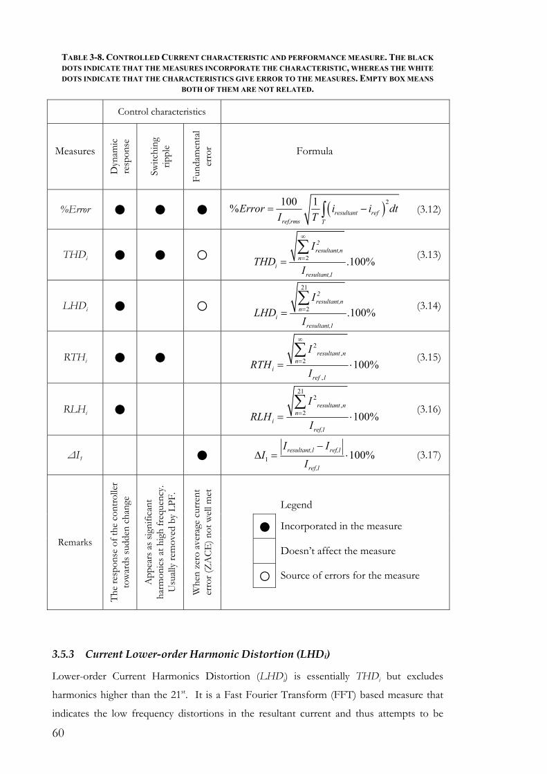
60
TABLE 3-8. CONTROLLED CURRENT CHARACTERISTIC AND PERFORMANCE MEASURE. THE BLACK
DOTS INDICATE THAT THE MEASURES INCORPORATE THE CHARACTERISTIC, WHEREAS THE WHITE
DOTS INDICATE THAT THE CHARACTERISTICS GIVE ERROR TO THE MEASURES. EMPTY BOX MEANS
BOTH OF THEM ARE NOT RELATED.
Control characteristics
Measures
Dyn
amic
re
spon
se
Switc
hing
rip
ple
Fun
dam
enta
l er
ror Formula
%Error 2100 1% resultant ref
ref,rms T
Error i i dtI T
(3.12)
THDi 2 .100%
2resultant,n
ni
resultant,1
I
THDI
(3.13)
LHDi 21
2 .100%
2resultant,n
ni
resultant,1
I
LHDI
(3.14)
RTHi 2
,2
,
100%resultant n
ni
ref 1
I
RTHI
(3.15)
RLHi 21
2,
2 100%resultant n
ni
ref,1
I
RLHI
(3.16)
ΔI1 1 100%resultant,1 ref,1
ref,1
I II
I
(3.17)
Remarks
The
res
pons
e of
the
cont
rolle
r to
war
ds s
udde
n ch
ange
App
ears
as
sign
ifica
nt
harm
onic
s at
hig
h fr
eque
ncy.
U
sual
ly r
emov
ed b
y L
PF
.
Whe
n ze
ro a
vera
ge c
urre
nt
erro
r (Z
AC
E) n
ot w
ell m
et
Legend
Incorporated in the measure
Doesn’t affect the measure
Source of errors for the measure
3.5.3 Current Lower-order Harmonic Distortion (LHDi)
Lower-order Current Harmonics Distortion (LHDi) is essentially THDi but excludes
harmonics higher than the 21st. It is a Fast Fourier Transform (FFT) based measure that
indicates the low frequency distortions in the resultant current and thus attempts to be

61
independent of the switching frequency content. By excluding the switching content, it is
expected that ideally this measure should be very close to zero when the resultant current is
sinusoidal and in phase with the reference. Equation (3.14) defines the LHDi in
mathematical form.
21
2 .100%
2resultant,n
ni
resultant,1
I
LHDI
(3.14)
3.5.4 Relative Total Harmonics (RTH)
In power quality related applications, Total Harmonic Distortion (THD) is often used to
indicate the purity of voltage, current and power. Despite its common use as power quality
standards, THD is not necessarily a good measure for current control fidelity. This is
especially true in the case of the present of error in fundamental component. In fact, higher
positive offset in fundamental frequency gives lower THD.
Due to this fact, Relative Total Harmonics (RTH) is introduced. Unlike THD that
compare the harmonics against the fundamental of the resultant current, RTH compare the
harmonics with the fundamental of reference current as shown in Equation (3.15). This
gives better indication on how well the current controller produces resultant current. In
this study, the highest harmonic counted to RTH is the 900th harmonics.
2,
2
,
100%resultant n
ni
ref 1
I
RTHI
(3.15)
3.5.5 Relative Lower-order Harmonics (RLH)
Relative Lower-order Harmonics (RLH) is essentially RTH but excluding the harmonics
higher than 21st. It is a FFT based measure that indicates the low frequency distortions in
resultant current and thus attempts to be independent of the switching content. Similar to
LHDi, by excluding the switching content, it is expected that this measure should be very
close to zero when the resultant current is sinusoidal and in phase with the reference.
Equation (3.16) defines the RLH in mathematical form.

62
212
,2 100%
resultant nn
iref,1
I
RLHI
(3.16)
3.5.6 Error in fundamental component (ΔI1)
Due to the calculation of %Error in Equation (3.12) that incorporates everything including
the fundamental offset, it is necessary to specifically show the error in fundamental
frequency. ΔI1 is the percentage of difference between rms value of resultant current and
rms value of reference current to fundamental component of reference current. When
there is no fundamental frequency offset, ΔI1 is expected to be zero. Formula for ΔI1 is
shown in Equation (3.17).
1 100%resultant,1 ref,1
ref,1
I II
I
(3.17)
3.5.7 Limitation of reference-based measurements
There is, however, a precaution of using these reference-based measurements (RTH, RLH,
%Error and ΔI1). To get reliable data, the measurements must be taken at the point of
comparison of the reference current and the regulated current for the control. For example,
for analogue current control, both reference current and regulated current should be
measured in analogue domain using analogue measuring instrument such as oscilloscope.
On the other hand, for digital current control, both of the currents need to be measured in
digital domain using digital signal instrument such as logic analyser. The usage of signal
representation in different domain such as ADC and DAC will introduce inaccuracy issues.
ADC will have quantization error and resolution inadequacy while DAC will have noise
and smoothing effect.
In this experiment, this limitation applies as the author have no access to a logic analyser
with decent memory buffer. Whenever a digital current control is being use, an
oscilloscope cannot be used to obtain the accurate reference based measurements because
oscilloscope cannot probe into the control signals for digital controller as the real control
signals are inside FPGA. Oscilloscope can only probe into the analogue representations of
the control signals, which introduce in accuracy for this type of measurement.

63
3.5.8 Switching frequency band
Since many nonlinear current control researches are pointing towards the direction of
constant switching frequency scheme, it is necessary to analyse the switching frequency
band of the regulated current. This switching frequency band determines the “level of
fixedness” of the switching frequency. The narrower the band indicates higher “level of
fixedness” and vice versa.
Although there are a lot of efforts being done by many researches to achieve fixed or less
variable switching frequency on hysteresis current control, the switching frequency band is
presented only as visual information in most literatures. Only limited number of literatures
present switching frequency band as numerical measure [49-52]. However, all of the stated
publications use visual inspection (e.g. using cursor function on oscilloscope) on the
frequency spectrum of the regulated current to estimate the "switching frequency band". In
contrast, the proposed "switching frequency band" indicator in this thesis systematically
analyse the switching content of a controller.
To analyse the switching frequency band, this thesis proposes the usage of Gaussian
function approximation on the frequency spectrum of the regulated current. The outcome
of the approximation will be the Gaussian well-known bell-shaped curve of the switching
frequency components. The analysis consists of three steps;
1. selective harmonics are chosen based on the application,
2. Gaussian function approximation is applied to the selective harmonics, and
3. switching frequency band is calculated using the Gaussian function.
The first step of the analysis is the selection of the harmonic spectrum frequency to be
analysed. It is important to select this harmonic window carefully to ensure that the analysis
is focusing only on the switching frequency component.
Since the analysis is focusing only at the switching frequency contents, the lowest harmonic
being analysed should not contain other significant components such as fundamental and
low order harmonics. For this experiment, harmonic 41st is chosen at the minimum limit of
the analysis window.
On the other hand, the highest harmonic in the window should not contain the switching
component sidebands. For example, since the target switching frequency for this
experiment is at the 333rd harmonic, the first switching ripple sideband should appear at
around the 666th harmonic. Therefore, the analysis is limited to the 600th harmonic. The
selection window or envelope for the analysis is shown in Figure 3.20.

64
0 100 200 300 400 500 600 700 800 900 1000 1100 12000
1
2
3
4
5
6
7
8
9
10
Harmonic order - n
% o
f fu
ndam
enta
l (%
)
Harmonic spectrum of regulated current
Switching frequencysideband
Fundamentalcomponent
and loworder
harmonics
Window forswitchingfrequencybandanalysis
Figure 3.20. Window of data necessary for switching frequency band analysis. The data window need to be chosen carefully to exclude the fundamental component, the low order harmonics and the switching frequency sidebands.
The second step of the analysis is to apply Gaussian approximation using curve fitting. The
output will be a bell-shaped curve. MATLABTM Curve Fitting Tool cftool is used in this
study. The equation used for the curve fitting is the general model of the Gaussian
function;
2
2
( )
2( )x b
cf x a e
, (3.18)
where
x is the harmonic order number,
f(x) is the percentage of harmonic to the fundamental component,
b is the position of the centre of the peak of the Gaussian curve, indicate the
effective average switching frequency,
a is the peak of the Gaussian curve, indicate the percentage of the harmonic at the
effective average switching frequency, and
c is the information of the width of the "bell" in the curve, which will be used to
determine the switching frequency band.
Figure 3.21 shows a, b, and c of the Gaussian function.

65
The third step is to calculate the switching frequency band using the full width at half
maximum (FWHM) index. There is a long history of the usage of FWHM in Gaussian type
of data; for example, FWHM has been utilised in other physics applications such as to
measure the spectral width in optics [53]. Therefore, FWHM is being chosen in this study
to measure the spectral width of switching components in the regulated current. The
equation for FWHM is
(Switching frequency band) 2 2ln 2 2.35482FWHM c c , (3.19)
where c can be found from Equation (3.18).
The bell shaped curve of Gaussian function of the switching components is shown in
Figure 3.21, indicating a, b, c, and the switching frequency band (FWHM).
Per
cent
age
of fu
ndam
enta
l (%
)
2
2
( )
2( )x b
cf x a e
Figure 3.21. Gaussian bell-shaped curve, indicating a, b, c and the FWHM. FWHM is the switching frequency band.
It is important to note that the switching frequency band from this analysis is just an
estimation figure. It will serve it purpose as a comparison variable. For example, it can be
used to quantitatively measure the effectiveness of any current control that attempt to force
hysteresis current control to switch at fixed switching.
However, when it comes to harmonic related design, the switching frequency band from
this analysis should only be used as a rough guidance. For example, in the design of
switching ripple filter, this switching frequency band should not be used as the definitive
bandwidth of the switching ripple.

66
3.5.9 Summary
To assess the performance of current control, a few performance measures presented.
%Error measures the percentage of the current error compared to the current reference in
time domain. It measures the performance of the current control as well as the switching
ripple size. THDi on iS is the typical performance indicator for APF used in academia and
in industry. However, it incorporates the switching ripple component as well. To assess the
performance of the current control technique, LHDi on iS is used; where it only measures
the distortion for 21st harmonics and below. Another method is to use THDi on iGrid, where
all switching component are already removed by the switching ripple filter.
RTH and RLH are similar to THDi and LHDi, respectively. However, instead of
comparing the distortion to the fundamental of the resultant current like THDi and LHDi,
RTH and RLH compare the distortion to the fundamental of the reference current. Both
of them will assess the performance of the current controller directly. However, for digital
current control, a logic analyser with huge memory buffer is needed to accurately measure
RTH and RLH. Same limitation applies to other reference based measurement, including
%Error and ΔI1 that measure the deviation of the resultant fundamental component
compared to the reference fundamental component.
A new measure called switching frequency band is presented. Switching frequency band is a
numerical figure that indicates the variation of switching frequency in the resultant current.
It is an approximation measure based on the Gaussian function that applied to the
harmonics of the resultant current. It is desirable to have a narrow switching frequency
band to ease the design of the switching ripple filter.
3.6 Other important notes
3.6.1 Effective time resolution of the oscilloscopes
As stated in Table 3-4, this study uses two oscilloscopes. One is Tektronix TPS2024 and
the other one is Picoscope 4424. Both of them are visible in the Figure 3.7.
The Tektronix TPS2024 is a digital multichannel oscilloscope with isolated input. It is a
handy tool for its capability to measure isolated signal which is typical in power electronics
application. However, the scope is mainly used in monitoring purposes, not for data
collection because its has low effective time resolution. Although TPS2024 has higher
bandwidth than Picoscope 4424, its memory buffer is limited only to 2500 measurements
points for each channel. This is inadequate for this experiment as its effective measurement
sampling rate is lower than the current control sampling frequency. For data measurement,

67
the Picoscope 4424 is used because it has a bigger memory buffer. Picoscope 4424 is
capable of sampling 400,000 measurement points in a 20 ms grid cycle, as shown in Figure
3.22.
Although not being used as main measurement device, Tektronix TPS2024 is used as a
controlled apparatus. Compared to Picoscope 4424, Tektronix TPS2024 carries greater
reputation in industry as dependable and trustworthy equipment. Therefore, in this
experiment, although both of the equipments are calibrated, the readings by Picoscope
4424 are being compared to the reading by Tektronix TPS2024 from time to time. The
differences recorded are not more than ±3%.
Figure 3.22. Related time resolutions for the APF experiment in a 20 ms grid cycle. Because of the size of memory buffer, the Picoscope 4424 has much greater effective time resolution than the Tektronix TPS2024.
As said before, most of the measurements in this setup are acquired using the PC based
Picoscope 4424 and the data are then analysed in MATLABTM to obtain the performance
measures. The waveforms and the harmonic spectrums presented in this thesis are mostly
plotted using MATLABTM, which may appear to some reader as “simulation look-alike”
result. It is important to note that all results in this thesis are from practical experimental
study, unless stated otherwise.
3.6.2 Suppression of measurement noise
Although the proper design of the four-layer PCB provides minimal switching noise in the
system, but the measurement noise still appear on oscilloscope. The measurement noise is
captured by the loop made by the path of measured signal and its return path on ground
(GND) wire or plane. The DAI board is already minimizing this loop by providing return
path as closest as possible to its forward path using a ground plane. Furthermore, the

68
GND test point is also positioned very close to the measured signal to reduce the loop size
(Figure 3.23 (b)). These design approaches reduce a significant portion of noise
susceptibility.
However, noise is relatively easy to get captured by the oscilloscope measurement probe,
due to its relatively huge loop of forward and return signal path, as shown in Figure 3.23
(a). To reduce this noise vulnerability, a modification is done to the oscilloscope probe.
The ground wire is repositioned to be very close to the tip of the oscilloscope, as shown in
Figure 3.23 (b). This configuration reduces the measurement noise considerably, hence
provides more reliable data for the study.
(a)
(b)
Figure 3.23. Modification of oscilloscope probe. (a) Normal oscilloscope probe with the ground wire quite far from the tip of the probe, providing big loop of signal forward and return path. Hence, more noise is likely being captured through the loop. (b) The modification of one of the probe. The ground terminal is rewired very close to the tip, hence minimize the loop. As a result, less noise captured.
3.7 Summary
Chapter 3 presents the methodology to the study. The chapter starts by introducing active
power filter application as a proper candidate to test the performance of current control
techniques. The power circuit and the controller for the active power filter used in this
study are discussed, along with the experimental details needed to replicate the experiment
in the future. To perform the assessment of current controllers, the desirable characteristics
and the performance measures of current control are discussed.

69
Chapter 4
Study 1: Hysteresis, PI and Polarized Ramptime Current Control Techniques for Active Power Filter Application: An Experimental Comparison
This chapter is written to present the comparison of the actual performance of Hysteresis,
PI and Ramptime current control in active power filter application. It is interesting to see
how Ramptime current control performs with comparisons to classical PI current control
and Hysteresis current control. PI and Hysteresis Current Control are included in this
comparison because they are the two most common control methods available. Due to
their popularity, they are easily understood and replicated. All current control methods are
designed to have the same average switching frequency of 16.67 kHz.
PI current control is claimed to have constant switching frequency and poor dynamic
performance. Hysteresis is claimed to be the fastest current control, but the variable
switching frequency nature make it hard to filter. Ramptime is said to be the optimal
solution between PI and Hysteresis; where it is fast while at the same time able to deliver
near fixed switching frequency. Here in this chapter, all three of the current controls are
presented.
4.1 PI Triangular Carrier Current Control [54, 55]
PI Current Control is a ramp comparison current control scheme, which guarantees a fixed
switching frequency. The PI current control used in this study is implemented in the
analogue domain via op-amps.

70
4.1.1 The tuning
The PI coefficients determine the behaviour of the current control; therefore need to be
chosen appropriately. To properly tune the coefficients of the PI current control, the
transfer function of the full bridge VSI is studied using the state space approach. Most of
the work in this transfer function derivation is adopted from [54] with some changes.
The circuit of the single-phase full-bridge VSI studied is shown in Figure 4.1.
Figure 4.1. The power circuit of the single-phase full-bridge VSI used in the study. RInv is the parasitic resistance of the ripple inductor LInv.
For simplicity, the output voltage of the bridge in Figure 4.1 is define as
ab a bv v v . (4.1)
To get the transfer function of the system, the state space approach is being used. The state
space equations
x Ax Bu
y Cx Du
(4.2)
are applied to the circuit in Figure 4.1, where state vector x, input vector u and output
variable y are selected as;
[ ]ox i , (4.3)
ab
AC
vu
v
and (4.4)
[ ]oy i . (4.5)
Solving these equations yields
Inv
Inv
RA
L
, (4.6)

71
1 1
Inv Inv
BL L
, (4.7)
1C and (4.8)
0 0D . (4.9)
The transfer function between the inverter voltage vab and the output current io can be
derived by performing Laplace transformation on the state space equation;
111
( )( ) ( )
( )Inv ab
oi v
ab
i sG s C sI A B
v s (4.10)
hence,
1 1( )
1Inv abi v
InvInv
Inv
G sLR sR
. (4.11)
The value of vab depends on states of the switches. On fully on and fully off, the value of vab
is
when ( ) 1( )
when ( ) 0DC
abDC
V d tv t
V d t
(4.12)
where d(t) is the duty cycle. From the equation, it can be found that the average value of vab
is
( ) (2 ( ) 1)ab DCv t V d t (4.13)
The relationship between vab and d can be derived from the perturbation of Equation (4.13);
2abDC
vV
d
(4.14)
Now, the transfer function between the output current and the duty cycle can be derived
from Equation (4.11) with Equation (4.14) as the inverter gain, yields
( ) 2 1( )
( ) 1
o DCVSI
InvInv
Inv
i s VG s
Ld s R sR
. (4.15)
Equation (4.15) is the transfer function of the VSI. The relationship between the duty cycle
and the modulating signal of the PI current control is

72
( ) 1( )
( )PWMpk
d sG s
m s c , (4.16)
where m is the output of the PI current control, the modulating signal.
Hence, the transfer function between the output current and the PI modulating signal is
( ) 21 1( )
( ) 1
o DC
Invpk Inv
Inv
i s VG s
Lm s c R sR
. (4.17)
Together with the PI control and current transducer gain, Equation (4.17) will be used for
the tuning of KP and KI coefficient. The close loop control diagram of the PI current
control is shown in Figure 4.2.
IP
KK
s
1
PKc2 DCV
TIG
1 1
1 InvInv
Inv
LR sR
+
*oi oi
Figure 4.2. Control loop diagram of PI current control in VSI. VDC = 250 V is the DC link voltage, LInv = 5.6 mH is the ripple inductance, cPK = 30 V is the peak to peak voltage of triangular modulation signal, RInv = 5 mΩ is the ripple inductor’s resistance, Tsw = 60 μs is the switching period and GTI = 0.32 is the current sensing gain.
The open loop transfer function for the block diagram in Figure 4.2 is derived as
2 1( )
1
DCI TIOL P
Invpk Inv
Inv
VK GG s K
Ls c R sR
. (4.18)
Solving Equation (4.18) for the open loop gain at the crossover angular frequency yields
two equations that are used to calculate the value of KP and KI (Equation (4.19) and
Equation (4.20)). The derivation of these two equations in not discussed here since it is
much alike the one in [54], except the one presented here is neglecting the PWM delay.
1tan 90 tan
CLI
P Invm CL
Inv
K
K L
R
(4.19)

73
2
2
1
2 11
InvCL
InvInvPKP
DC TI I
CL P
L
RRcK
V G K
K
(4.20)
where Φm a is the phase margin and ωCL is the close loop angular frequency.
KP and KI determine the close loop gain of the PI current control. The bandwidth of the
close loop specifies the response of the controller towards the current error. Higher
bandwidth indicates faster response, means the current controller will be able to follow the
reference current with greater accuracy. However, the bandwidth must not be set too high
that the slope of the modulating signal might be greater than the slope of the carrier signal.
This situation might lead to instability. As recommendation, one sixth of the desired
switching frequency is acceptable for close loop bandwidth [54]. This recommendation is
adapted into this study, where the PI current control close loop bandwidth is set at one
sixth of the switching frequency.
Another important variable is the phase margin, which determines the transient response
and the stability of the controller. In order to compare the performance of PI current
control with Hysteresis and Ramptime, it is important to tune PI to have a very good
transient response. Smaller phase margin means better transient performance, however it
brings the controller closer to instability. Therefore, in this experiment, the phase margin of
the PI is set at 60°, the rule-of-thumb phase margin that is considered acceptable for stable
control [54].
After considering all the aspects needed, the PI current control for this experiment has
been tuned for the control loop in Figure 4.2 with PI coefficients KP = 15.87 and KI =
160000 (Table 4-1).
TABLE 4-1. PI CURRENT CONTROL CHARACTERISTIC
Variable Value
KP 15.87
KI 160000
Phase margin (Φm) 60° = 1.047 rad
Close loop bandwidth (ωCL) 2πfsw /6 = 17453 rad/s

74
The bode plot of the system is shown in Figure 4.3.
10-2
10-1
100
101
102
103
104
105
-180
-135
-90
P.M.: 60 degFreq: 1.75e+004 rad/sec
Frequency (rad/sec)
Pha
se (
deg)
-50
0
50
100
150
200
G.M.: InfFreq: NaNStable loop
Open-Loop Bode Editor for Open Loop 1 (OL1)
Mag
nitu
de (
dB)
Figure 4.3. Bode plot of the VSI in this study with PI Current Control. The control is tuned to operate at 60° phase margin.
Note that the work in this subchapter is using io as the output current of the VSI, as being
used in its original source [54]. However, in earlier chapter, iInv is being used to indicate the
input current of the VSI. The relationship between the two variables is
o Invi i . (4.21)
Another difference between the derivation of KP and KI in this thesis and the derivation of
the same components in [54] is the absence of PWM delay in this thesis. In [54], the PWM
delay is incorporated in the transfer function of the VSI because of an assumption that the
PI current control is using a digital PWM. Here in this thesis, the PI current control is
developed using analogue circuit, where the PWM delay is negligible [54].

75
4.1.2 Experimental implementation
comparator
VCC
PWMTriangular carrier
R1 R2
R3
R4
R5
R6
R7
R8
C1
iRef - iS
Figure 4.4. Schematic of PI Current Control on DAI board. TRIWAVE is a triangular carrier waveform at constant frequency.
Figure 4.4 shows the schematic of PI current control implemented on the DAI Board for
this study. The Proportional and Integral components are limited to the op-amp power
rails, so an anti-windup mechanism is inherently incorporated. This helps to reduce
overshoot in the implemented PI current control. Variable resistor R2 and R3 are used to
adjust the control gain, KP and KI according to theoretical analysis. The output of the
controller is then compared with a triangular wave carrier signal that oscillates at the
switching frequency. Output of the comparator is the switching signal PWM in the figure.
4.2 Standard Hysteresis Current Control [54]
Standard Hysteresis Current Control is known as fixed band hysteresis control since it has
two fixed bands defined. The reference current will be in the middle of the two bands.
Switching will happen every instant the measured current hits the upper or lower band.
Hysteresis is known to have a very good dynamic response and is inherently stable. The
main disadvantage of Hysteresis Current Control is that it has a very wide switching
frequency band. This leads to a larger than optimum filter size and potentially less
immunity to noise. For further insight into Hysteresis harmonics modelling in the
frequency domain, please refer to [56].
For the APF setup, the hysteresis band is tuned to switch at an average frequency of 16.67
kHz. This tuning is done by counting the amount of switching instances in every grid
voltage cycle. The counting is done inside the FPGA with a counter that is triggered by
positive edge of switching signal, as shown in Figure 4.5. The target switching instances
(nswitching) in every grid voltage cycle is calculated using Equation (4.22).

76
swswitching
Grid
fn
f
(4.22)
For a 16.67 kHz signal to be operated in parallel with grid frequency of 50 Hz, the value of
nswitching is calculated to be 333. Consequently, the hysteresis band is adjusted xsuch that it has
similar number of switching in the same period.
up countersclr
clock
cnt_en
q[11..0]
lpm_counter17
inst8
DFFdata[11..0]
clock
enableq[11..0]
lpm_dff10
inst19
n_switching[11..0]
clock_100MHzswamount[11..0]
clock_100MHzPWM_positiv e_edge_pulse
50Hz_grid_pulse
n_switching[11..0]
(a)
333switchingn
(b)
Figure 4.5. Switching counting mechanism inside FPGA. Switching counter is used as a tool to properly tune the hysteresis band to operate at desired average switching frequency. (a) The schematic of the counter. (b) The output, n_switching (at the bottom of the table) as viewed from Altera SignalTap digital analyser along with few other variables.

77
4.3 Ramptime Current Control
The working principle of Ramptime current control is introduced in subchapter 2.2.4.
Now, this subchapter will present the implementation of Ramptime current control in this
particular experiment.
4.3.1 Current error polarity (ε) generator
One of the important keys for the successful implementation of Ramptime current control
is the production of the current error polarity signal, ε. ε is a binary signal that has the value
high when iS is more than iRef and low when iS is less than iRef.
The generation of ε is done in an analogue circuit, as depicted in Figure 4.6. To get the zero
error crossing, an operational amplifier and a comparator are used. The amplifier is used to
get the negative error signal by subtracting iRef from iS. The negative error signal is then
compared with zero to get the ε signal. However, due to noise at the error crossing, it is not
a good idea to compare with absolute zero or ground. Therefore, an RC circuit is being
used on the input of the comparator to perform a positive feedback noise rejection.
The ε signal is then delivered to the FPGA as the input to Ramptime current control.
Figure 4.6. The circuit of the generation of ε signal. R5 and C1 provide an RC delay for positive feedback noise rejection mechanism. Since the ε signal is generated using an analogue circuit, it is named ε(analogue).
4.3.2 Initialization and transient strategy
Since Ramptime relies on the previous switching cycle information (excursion time and
ramp away time), incorrect switching operation might occur if the previous information is
not applicable to the immediate switching action. Such an occasion happens at the
initialization state where there is no previous known information. It also happens when the
regulated current is not flowing in a straight line, where the previous ratio of excursion
time and ramp away time are not applicable to a non-straight line current change. On top
of these two occasions, the same condition applies whenever there is a sudden change or
transient on the system.

78
During these occasions, Ramptime utilizes an initialization strategy where it does not need
the previous stored values of excursion time and ramp away time. The strategy is as
follows;
1. Ensure the switching state is bringing the current error towards zero, not away
from zero. This is easily done by set the switching signal, u equal to the invert of
the error polarity signal, ε.
2. After the first zero crossing of the current error, keep the previous switching signal
state for a very short amount of time. After that short interval, invert the switching
signal to force the current error to move towards zero.
3. Finally, after the current error crosses zero for the second time, all values needed
for Ramptime switching algorithm are fully gathered.
Ramptime always utilizes this initialization strategy whenever the stored value of the
excursion time is outside an acceptable range. The range is set at above half of the
switching period (Tsw/2) so that normal operation does not trigger the initialization
mechanism. Thus, the initialization strategy is only exercised during the start-up and
transient operation.
4.4 Results
Figure 4.7 shows waveforms of iS, iLoad and iInv for each of the three current control
methods, captured on the screen of an oscilloscope. This clearly shows that the APF
control is successfully shaping iS to be purely sinusoidal by inherently shaping iInv to oppose
the distorted current demanded by the nonlinear load. The current ripple is visible on the
source current and the inverter current.
Table 4-2 and Table 4-3 show %Error, THDi, LHDi, RTHi, RLHi and ΔI1 for iS and iGrid,
respectively. Note that the numerical results presented here are the average values of 15
readings. Table 4-4 (a) – (l) tabulates the overview of the complete visual results of the
experiment, showing the waveforms and frequency spectrum of iS and iGrid using the three
current control techniques.

79
(a) PI current control
(b) Hysteresis current control
(c) Ramptime current control
Legend:
Ch2: iLoad
6.25 A/div
Ch3: iInv
6.25 A/div
Ch1: iS3.125 A/div
Figure 4.7. Waveforms of iS, iLoad and iInv on the oscilloscope. (a) PI current control, (b) Hysteresis current control, (c) Ramptime current control.
TABLE 4-2 - PERFORMANCE MEASURES OF IS
%Error THDi (%) LHDi (%) RTHi (%) RLHi (%) ΔI1
PI 15.41 14.51 7.00 14.97 7.23 3.18
Hysteresis 10.69 10.38 2.50 10.45 2.52 0.65
Ramptime 13.45 13.24 1.86 13.35 1.88 0.83
TABLE 4-3 - PERFORMANCE MEASURES OF IGRID
%Error THDi (%) LHDi (%) RTHi (%) RLHi (%) ΔI1
PI 10.74 7.53 7.24 7.94 7.64 5.46
Hysteresis 5.23 4.22 2.36 4.33 2.42 2.61
Ramptime 4.07 2.53 2.23 2.60 2.29 2.75

80
TABLE 4-4 - TIME DOMAIN WAVEFORMS AND FREQUENCY DOMAIN SPECTRUMS OF IS AND IGRID. THE
FUNDAMENTAL COMPONENT IS EXCLUDED IN ALL FREQUENCY SPECTRUMS TO EMPHASISE HARMONICS Currents waveform Frequency spectrum
PI
Cur
rent
Con
trol
i S
-10 -5 0 5 10-4
-2
0
2
4
Time (ms)
Cu
rre
nt (
A)
Current waveforms: iS & iRef
iSiRef
(a)
0 200 400 6000
5
10
Harmonics no - n
% o
f fu
nd
am
en
tal (
%) Harmonics Spectrum (fund excluded): iS
(b)
i Gri
d
-10 -5 0 5 10-4
-2
0
2
4
Time (ms)
Cu
rre
nt (
A)
Current waveforms: iGrid & iRef
iGridiRef
(c)
0 200 400 6000
5
10
Harmonics no - n%
of f
un
da
me
nta
l (%
) Harmonics Spectrum (fund excluded): iGrid
(d)
Hys
tere
sis
Cur
rent
Con
trol
i S
-10 -5 0 5 10-4
-2
0
2
4
Time (ms)
Cu
rre
nt (
A)
Current waveforms: iS & iRef
iSiRef
(e)
0 200 400 6000
5
10
Harmonics no - n
% o
f fu
nda
me
nta
l (%
) Harmonics Spectrum (fund excluded): iS
(f)
i Gri
d
-10 -5 0 5 10-4
-2
0
2
4
Time (ms)
Cu
rre
nt (
A)
Current waveforms: iGrid & iRef
iGridiRef
(g)
0 200 400 6000
5
10
Harmonics no - n
% o
f fu
nda
me
nta
l (%
) Harmonics Spectrum (fund excluded): iGrid
(h)
Ram
ptim
e C
urre
nt C
ontr
ol i S
-10 -5 0 5 10-4
-2
0
2
4
Time (ms)
Cu
rre
nt (
A)
Current waveforms: iS & iRef
iSiRef
(i)
0 200 400 6000
5
10
Harmonics no - n
% o
f fu
nd
am
en
tal (
%) Harmonics Spectrum (fund excluded): iS
(j)
i Gri
d
-10 -5 0 5 10-4
-2
0
2
4
Time (ms)
Cu
rre
nt (
A)
Current waveforms: iGrid & iRef
iGridiRef
(k)
0 200 400 6000
5
10
Harmonics no - n
% o
f fu
nd
am
en
tal (
%) Harmonics Spectrum (fund excluded): iGrid
(l)

81
4.4.1 Outer-loop DC voltage control
In this APF experiment, when the VSI is disconnected from the PCC, the nonlinear load
draws distorted current from the grid at 0.73 displacement power factor. The power factor
increases to 1.00 when the VSI is connected to the PCC, showing that the VSI is able to
supply the distorted current demanded by the load.
The outer loop voltage control has been observed maintaining the DC link voltage
constantly at its reference (250 V), which provides enough power to supply the distorted
current to the load. There is, however, an exception at the peak and at the valley of the
reference current. These are where the load current draws high current that forces the APF
to momentarily enter the “uncontrollable region”. The uncontrollable region is where the
inverter is not able to provide sufficient voltage across the inductor, and hence is unable to
control the current. All three current controls in this test setup exhibited momentary
uncontrollability to varying extents.
Note that the uncontrollable phenomenon is inherent in this experiment due to the
topology and the choice of DC link voltage level. As mentioned before (section 3.2.4),
higher DC link voltage will provide more controllability, but will have less efficiency. 250 V
has been chosen as the optimal situation between these trade-offs. Therefore, although the
current at the peak and valley of the reference is temporarily uncontrollable, it is an
advantage to the system because the DC voltage does not have to be increased to higher
levels.
4.4.2 Low order harmonics
Figure 4.8 shows the lower order harmonics spectrum of iS of PI, Hysteresis and Ramptime
current control techniques. The figure is a close-up version of the low order harmonics of
Table 4-4 (b), (f) and (j). To emphasise the harmonics content, the fundamental component
is excluded. The lower order spectrum of iGrid is similar to iS, as shown in Figure 4.9 (close-
up version of the low order harmonics of Table 4-4 (d), (h) and (l)). The similarity between
Figure 4.8 and Figure 4.9 is expected since the cut-off frequency of the switching frequency
filter is greater than the 21st harmonic.

82
2 4 6 8 10 12 14 16 18 200
1
2
3
4
Harmonics no - n
% o
f fu
nd
am
en
tal (
%)
iS Low Order Harmonics Spectrum (excluding fundamental)
PIHysteresisRamptime
Figure 4.8. Harmonic spectrum of iS given by all three current controllers. The fundamental component is excluded to emphasise the harmonic content.
2 4 6 8 10 12 14 16 18 200
1
2
3
4
Harmonics no - n
% o
f fu
nd
am
en
tal (
%)
iGrid Low Order Harmonics Spectrum (excluding fundamental)
PIHysteresisRamptime
Figure 4.9. Harmonic spectrum of iGrid given by all three current controllers. The fundamental component is excluded to emphasise the harmonic content.
As shown in Figure 4.8 and Figure 4.9, PI delivers greater low-order harmonics compared
to Hysteresis and Ramptime. This observation is supported by the largest (poorest)
readings of %Error, THDi, LHDi, RTH and RLH on Table 4-2 and Table 4-3, especially
LHDi and RLH on iS. Hysteresis and Ramptime have comparable low order harmonic
distortion on both iS and iGrid. Both Hysteresis and Ramptime deliver good low-order
harmonic distortion due to their fast dynamic response.

83
4.4.3 Wave-shaping at the uncontrollable region
At the peak and the valley of the reference current, the voltage across the ripple inductor is
low. This low inductor voltage challenges the current control to perform the current wave-
shaping with insufficient slope of the regulated current. The right hand side of Figure 4.10
demonstrates how PI, Hysteresis and Ramptime current control techniques manage the
challenge at the peak of the reference current.
-10 -5 0 5 10-4
-2
0
2
4
Time (ms)
Cu
rre
nt (
A)
Current waveforms: iS & iRef
iSiRef
iRef
iS
iInv
(a) PI Current Control
-10 -5 0 5 10-4
-2
0
2
4
Time (ms)
Cu
rre
nt (
A)
Current waveforms: iS & iRef
iSiRef
iRef
iS
iInv
(b) Hysteresis Current Control
-10 -5 0 5 10-4
-2
0
2
4
Time (ms)
Cu
rre
nt (
A)
Current waveforms: iS & iRef
iSiRef
iRef
iS
iInv
(c) Ramptime Current Control
Figure 4.10. One cycle waveform of iS and iRef (left) and close-up of iS, iRef and iInv at the peak of the waveform. (a) PI, (b) Hysteresis and (c) Ramptime current control. PI is showing significant distortion due to suboptimal dynamic performance. Hysteresis and Original Ramptime are shaping iS to follow the iRef better.

84
PI as predicted always tries to maintain its switching frequency. At the point where the
diode rectifier load demands a surge in the current, PI tries to deliver the current while still
maintaining it fixed switching frequency. However, PI is not fast enough to react to this
sudden surge due to its low control bandwidth. This slow response is shown by the rising
of iS above the iRef in Figure 4.10.
Hysteresis current control technique immediately delivers the sudden current surge by
keeping the regulated current, iS bounces inside its predefined hysteresis band. Although
this technique is fast, it generates some oscillation on the regulated current. The main
reason is because hysteresis current control allows the regulated current to flow freely in
the hysteresis band regardless the behaviour of the current. At the peak of the current
reference, the voltage across the ripple inductor is insufficient for high di/dt, forcing the
current to flow as a curve, not as a straight line. This can be seen clearly in Figure 4.10 (b).
This free flowing nature of hysteresis current control allows oscillations to occur on the
regulated current as long as the current is still in its hysteresis band. Later, in this chapter,
the consequence of this behaviour is presented, where the particular oscillation in Figure
4.10 (b) contains harmonics close to the resonance frequency of the switching ripple filter.
Ramptime current control manages the challenge by trying to maintain ZACE condition
until the current is not in a straight line anymore. In the uncontrollable region, Ramptime
occasionally enters its initialization/transient mode (subchapter 4.3.2) whenever the
excursion time is so long that it reaches its predefined threshold. In the
initialization/transient mode, Ramptime sacrifices ZACE by ensuring that the current error
flows towards zero until the current error reaches zero crossing. Just after the current error
reaches zero, Ramptime performs a quick switching that forces the current error to start
ramping in the other direction. Then, Ramptime continues its normal operation unless the
new excursion time is still too long. In the uncontrollable region, the excursion time might
be too long so that it reaches its threshold when the current is not flowing in straight line
or the di/dt of the current is too large. Once the regulated current is flowing in a straight
line with acceptable di/dt, Ramptime resumes ZACE operation. This strategy of Ramptime
allows the VSI to supply the distorted current to the load without sacrificing much of its
constant switching frequency and its dynamic response.
In summary, all three mentioned current control techniques behave differently to control
the regulated current. PI maintains its switching frequency at the cost of poor dynamic
performance. Hysteresis reacts very fast to the transient behaviour of the load current but
lets oscillation occur at the uncontrollable region. Ramptime uses its initialization strategy

85
to react fast to the transient while at the same time tries to maintain its fixed switching
frequency.
4.4.4 Switching frequency band
As discussed in subchapter 3.5.8, a new analysis is proposed to measure the variations of
switching frequency of a current control technique. The proposed analysis uses Gaussian
function fitting on the harmonic spectrum of the regulated current. Figure 4.11 shows the
harmonic spectrum of the regulated current along with the Gaussian function fitted curved
whereas Table 4-5 shows the data from the analysis.
0 200 400 6000
5
10
Harmonics no - n
% o
f fu
nda
me
nta
l (%
) Harmonics Spectrum (fund excluded): iS
(a)
0 200 400 6000
5
10
Harmonics no - n
% o
f fu
nda
me
nta
l (%
) Harmonics Spectrum (fund excluded): iS
(b)
0 200 400 6000
5
10
Harmonics no - n
% o
f fu
nda
me
nta
l (%
) Harmonics Spectrum (fund excluded): iS
(c)
Figure 4.11. Frequency spectrums of iS for (a) PI, (b) Hysteresis and (c) Ramptime current control. The fundamental component is excluded to emphasise the harmonic content.

86
TABLE 4-5. SWITCHING FREQUENCY BAND ANALYSIS BASED ON GAUSSIAN APPROXIMATION.
Effective average switching frequency (b)
Harmonic intensity at the effective average switching frequency (a)
Switching frequency band (FWHM)
PI 16.50 kHz 11.09 % 0.052 kHz
Hysteresis 21.02 kHz 0.567 % 13.52 kHz
Ramptime 16.16 kHz 1.849 % 1.669 kHz
Figure 4.11 clearly shows that PI has a very narrow switching frequency band whereas
Hysteresis has a very wide switching frequency band. Ramptime, on the other hand, has an
acceptable narrow switching frequency band. The switching frequency band for Ramptime
is considered acceptable because it is small enough that isolate the switching frequency far
from the fundamental frequency. This characteristic is important for APF as it simplify the
switching ripple filter design. Further discussion on the switching filter design is covered in
section 4.5.
In the “plus and minus tolerance” form of writing, the switching frequency variation of the
three current control techniques under test can be written as;
^
2sw
FWHMf b , (4.23)
where fsw^ is the analysed switching frequency variation, b is the effective average switching
frequency and FWHM is the switching frequency band. Note that b and FWHM are shown
in Figure 3.21 from previous chapter.
For this test, the analysed switching frequency variations for the current control techniques
under test are;
1. fsw,PI^ = 16.50 ± 0.026 kHz,
2. fsw,Hysteresis^ = 21.02 ± 6.760 kHz, and
3. fsw,Ramptime^ = 16.16 ± 0.835 kHz.
An ideal controller will be able to provide very low LHD and very small FWHM. In many
cases, these two indicators values contradict each other. For example, with refer to Table
4-2, PI gives small FWHM but large LHD. Hysteresis on the other hand, gives small LHD
but large FWHM. This contradiction usually applied to most current controller.
Therefore, a guideline on the usage of FWHM on controller selection is presented as
follow;

87
a. If an application needs a fast controller with little concern on the size and cost
of the switching ripple filter, then a controller with small LHD even with large
FWHM would suffice.
b. If an application needs a small and low-cost switching ripple filter, or perhaps
strictly needs a fixed switching frequency controller, with little concern on the
transient performance, then a controller with small FWHM even with large
LHD would suffice.
c. If an application needs a fast controller and at the same time need a small and
low-cost switching filter, then the controller candidate must be able to provide
a reasonably small LHD along with a reasonably small FWHM. The adjective
"reasonably", however, does not have a rigid definition as it depends on other
trade-offs in a system such as cost, standard’s compliance, customer’s demand,
etc.
4.4.5 Overall performance
Hysteresis Current Control is the fastest current control among the three in terms of
dynamic response, as evidenced by the lowest reading of %Error and THDi on iS, as shown
in Table 4-2. However, Table 4-3 shows that Hysteresis delivers more distortion (higher
THDi) on iGrid compared to Ramptime. There are three main reasons why Hysteresis is
unable to provide the lowest distortion:
1. Low order harmonics: During the uncontrollable region, Hysteresis exhibits
suboptimal control of the current and thus results in low order harmonics. This is
due to the nature of hysteresis control, where it allows the current to freely flow as
long as it stays within its hysteresis band. The distortion at iGrid is worsened by
resonance effects, since the low order harmonics excites the filter capacitor CS and
inductance LXfmr.
2. Variable switching frequency: The variable switching frequency nature of Hysteresis
Current Control is a big disadvantage. Some of the switching harmonics are very
close to the resonance frequency of the switching frequency filter. This results in a
huge distortion on iGrid, which is clearly visible in Table 4-4 (h) around the 67th
harmonic, the resonance frequency of the filter.
3. The effect of deadtime: Figure 4.10 (b) shows that after an uncontrollable region
the Hysteresis switching ripple is wider than its hysteresis band. This is due to the
2 μs deadtime of the system. This phenomenon only appears as a small error in

88
fundamental component on iS but because of the resonance, iGrid has significant
oscillation.
PI Current Control behaves differently. Figure 4.11 (a) shows the high amplitude switching
frequency component at around the 330th harmonic proving that PI successfully maintains
the switching frequency most of the time. The disadvantage of PI Current Control is a
slower response compared to Hysteresis. This slower response results in the non-zero
steady state error, which is portrayed in Figure 4.8 as low order harmonics. Referring to
Figure 4.11 (a), PI tends to be generating either the high switching frequencies or
significantly lower harmonics. Both are far enough away from the cut-off frequency of the
switching frequency filter and so avoiding resonance effects. Even though these low order
harmonics are not suffering from resonance effects, the THDi of PI iGrid is greater than the
THDi of Hysteresis iGrid. This is because the low order harmonics of PI itself contribute to
greater distortion compared to the distortion of the Hysteresis. As a result, PI delivers the
worst reading of all performance measures in Table 4-2 and Table 4-3.
Figure 4.11 (a) shows that the Ramptime Current Control has near-fixed switching
frequency. Its switching frequency band is wider than the switching frequency band of PI.
Although its switching frequency band is wider, the switching harmonics are well
distributed closely to the 333rd harmonic, which is much higher than the resonance
frequency of the switching frequency filter. Combined with a relatively small amount of
significantly lower frequency harmonics, Ramptime has sufficient immunity to the
resonance. The time domain waveform of iS on Figure 4.10 (c) shows that Ramptime
responds fast enough to follow the shape of iRef. It does that while maintaining the fixed
switching frequency. This is true even in the uncontrollable region, hence it delivers a very
small distortion on iGrid, which is the main purpose of the APF.
As shown in Table 4-2, there is little difference between the traditional measures (THD and
LHD) and the new proposed measures (RTH and RLH). This is because the reference
current (used in RTH & RLH) and the resultant current (used in THD & LHD) is pretty
much alike. In this situation, the usage RTH and RLH seems redundant to the usage of
THD and LHD, respectively. As explained before, RTH and RLH will have distinctive
value compared to THD and LHD when the resultant current is not identical to the
reference current. In real world, this might occurred if a current controller introduces phase
shift or fundamental component offset to the resultant current.
With that being said, a further analysis on the performance of the current controllers can
be performed by comparing THD value and RTH value of iS. Hysteresis and Ramptime
have less than 1% difference between those two indicators, while PI has more than 3%

89
difference. This concludes that PI introduces a little more phase shift or fundamental offset
as compared to Hysteresis and Ramptime.
4.5 Ripple filter selection biased towards Hysteresis current control
Figure 4.11 shows the harmonic content of iS of each current control method. It is clear
that the switching frequency band of Hysteresis is far wider than the switching frequency
bands of Ramptime and PI. In this experiment, the switching frequency filter is designed to
filter most of switching ripple of all three current control methods. The filter cut-off
frequency is set at the 67th harmonic (Figure 4.12) to accommodate the wide switching
frequency band of Hysteresis Current Control. If the filter had been designed to
accommodate the switching ripple of PI and Ramptime only, the cut-off frequency would
be higher, resulting in a smaller and cheaper capacitor. This is another advantage of PI and
Ramptime as they have a narrow switching frequency band.
0 100 200 300 400 500 6000
2
4
6
8
10
Harmonics no - n
% o
f fu
nd
am
en
tal (
%)
HysteresisRamptimePI
Figure 4.12. Biased ripple filter design to accommodate Hysteresis current control. The cut-off frequency of the switching ripple filter could be higher if it is just considering PI and Ramptime current control.
4.6 Robustness test: Immunity towards parameter change (LInv)
One of the challenges of current control is to handle model mismatch. Model mismatch is
the condition where the model that is used to tune the current control loop does not match
with the real system. A good current control will be able to cope with these changes. In this
experiment, the parameter that is used as the model mismatch is the inverter ripple
inductance. The current control is being tested with three different inductances; the default
inductance, 10% lower inductance and 10% higher inductance. The analysis is focusing on
two performance measures;
1. LHDi on iS as the indicator for dynamic response, and
2. switching frequency band as the indicator of the variations of switching frequency.

90
The analysis is only focusing on these two indicators due to the significance of the
indicators when used for evaluating the model mismatch performance. All other
performance measures presented before could provide some additional information,
however at the end will draw similar conclusion. This is because dynamic response and
switching frequency are affected more than other attributes with the variations of ripple
inductance.
4.6.1 Result
TABLE 4-6. LHDI OF IS AND THE SWITCHING FREQUENCY BAND WITH VARIOUS VALUES OF LINV.
LHDi on iS (%) Switching frequency band (kHz)
LInv 5.1 mH 5.6 mH 6.1 mH 5.1 mH 5.6 mH 6.1 mH
PI 6.08 7.00 8.14 0.049 0.052 0.044
Hysteresis 2.72 2.50 2.39 16.51 13.52 12.69
Ramptime 1.91 1.86 1.92 1.953 1.669 2.253
The result of the test of robustness towards variations of ripple inductor is shown in Table
4-6. To visualize the comparison, Figure 4.13 shows the chart of LHDi on iS as a dynamic
performance indicator of the current control techniques against the variations of LInv. On
the other hand, Figure 4.14 shows the chart of the switching frequency band of the current
controls against the same variations.
0
1
2
3
4
5
6
7
8
9
5.1 mH 5.6 mH 6.1 mH
LHDi(%
)
Ripple inductance, LInv
LHDi on iS vs LInv variation
PI
Hysteresis
Ramptime
Figure 4.13. iS LHDi for different value of ripple inductance, LInv. In dynamic performance, Hysteresis and Ramptime share similar immunity towards changes in the value of the inductance, whereas PI’s performance changes significantly.

91
0
2
4
6
8
10
12
14
16
18
5.1 mH 5.6 mH 6.1 mH
Switching frequency band (kH
z)
Ripple inductance, LInv
Switching frequency band vs LInv variation
PI
Hysteresis
Ramptime
Figure 4.14. Switching frequency band for different value of ripple inductance, LInv. The changes of LInv value do not affect much toward the switching frequency band of PI and Ramptime.
The results show that Hysteresis has high robustness towards the changes of ripple
inductance in terms of dynamic performance, but has low robustness in term of switching
frequency variation. Hysteresis’s switching frequency band varies notably with the changes
of the LInv. It is safe to conclude that Hysteresis not only has a very wide switching
frequency band, but also has a “hard to predict” switching frequency range that varies with
the system parameter changes.
In contrast, PI is robust in terms of switching frequency variation. PI is evidently able to
switch at very constant switching frequency because of the usage of PWM modulator.
However, PI is not so robust in dynamic performance. It has been observed in Figure 4.13
that PI performs better with a smaller LInv and performs poorer with a larger LInv. This is
because PI performs with the same PI coefficients throughout the three values of LInv. With
the unchanged values of KP and KI, PI is actually controlling with different closed-loop
bandwidth and different phase margin. Using Equation 4.19 and Equation 4.20, the closed-
loop bandwidth and phase margin for the three values of LInv are tabulated in Table 4-7
below.
Based on the values in Table 4-7, it is clear why PI performs better in dynamic response at
lower LInv. With lower LInv using unchanged values of KP and KI, PI is operating with
higher closed loop bandwidth, hence faster. Vice versa, with higher LInv, PI is operating
with lower closed loop bandwidth, hence slower.

92
TABLE 4-7. VARIATIONS OF CLOSED-LOOP BANDWIDTH AND PHASE MARGIN OF PI WITH THE CHANGES
OF LINV WITHOUT ALTERING PI COEFFICIENTS
LInv KP KI Closed-loop bandwidth, fCL Phase margin, phm
5.1 mH 15.87 160000 3000 Hz 61.83 º
5.6 mH 15.87 160000 2777 Hz 60.00 º
6.1 mH 15.87 160000 2600 Hz 58.30 º
The result of Ramptime robustness demonstrates that neither dynamic performance nor
switching frequency band show a significant discrepancy throughout all three values of LInv.
This proves that Ramptime is able to deliver a high dynamic response at near fixed
switching frequency without relying much on the circuit parameters or system model.
4.7 Classical control theory: step response analysis
As a comparison using conventional control theory, this section presents the classical
control theory step response test. The three current control techniques under test are being
forced to follow a step change on the current reference. The test platform is a 700 W
inverter that is not tied to the grid. The schematic for the test is shown in Figure 4.15,
where the inverter is directly connected to a resistive load (RLoad) via a ripple inductor (L).
The current reference is a combination of two sinusoidal references with different
amplitudes. The step change from the lower amplitude signal to the higher one occurs at
the peak of the reference waveform.
Note that the step change that presented here is not a conventional transient test that is
used to obtain the four transient performance variables; start-up time, overshoot, settling
time and steady state error. In this practical experiment, these variables are kept on
changing in every measurement make it challenging to measure. On top of that, a moving
average filter is required to track the average value of the regulated current. Due to these
complications, most of step responses for transient analysis are done in theoretical study
and simulation. The step change test presented here is simply a means to provide a visual
comparison of the behaviour of the different current control techniques in the transient
state.

93
CDCRDCVDC = 330VL
RLoad
VSI iLoad
Switching signal Current
Control
iLoad
iLoad*
vo
vL
vLoad
Figure 4.15. Classical step change test setup. This configuration forces the regulated current (iLoad) to follow a step change sinusoidal. L = 5.6 mH and RLoad = 15 Ω. Reference current (iLoad*) is a combination of two sinusoidal signals with different amplitudes (3.3 A and 9 A). VDC is a constant voltage at 330 V.
The visual comparison between PI, Hysteresis and Ramptime current control in this step
change test is shown in Figure 4.15. The waveforms shown have been filtered by a low pass
filter (LPF) at two different cut-off frequencies; 1 MHz (Figure 4.15 (a), (c) and (e)) and
100 kHz (Figure 4.15 (b), (d) and (f)). The raw signals are unreadable since there is too
much noise, and are therefore excluded from the comparison. Hysteresis current control
has been tuned to produce similar current ripple size as compared to PI and Ramptime.
PI shows a typical response of a low bandwidth classical PWM controller. There are a few
undesirable attributes of PI that can be seen from the step response;
1. Relatively large overshoot,
2. Duty cycle limitation during the transient due to low control bandwidth,
3. Long settling time, and
4. Non-zero steady state error after the step change.

94
TABLE 4-8. STEP RESPONSE OF PI, HYSTERESIS AND RAMPTIME CURRENT CONTROL. iLoad has been filtered by a 100 MHz LPF iLoad has been filtered by a 100 kHz LPF
PI
Cur
rent
Con
trol
(a)
(b)
Hys
tere
sis
Cur
rent
Con
trol
(c)
(d)
Ram
ptim
e C
urre
nt C
ontr
ol
(e)
(f)
In contrast, Hysteresis is the fastest current control among the three. This attribute is
clearly shown in the step response in Table 4-8, where Hysteresis reacts to the transient
very fast and then reaches steady state immediately. However, after the step change
Hysteresis shows signs of non-ZACE performance. This is clearly shown in Table 4-8 (d)
where the average value of the regulated current is below the current reference, caused by

95
the dead-time delay of the IGBT driver. Since Hysteresis is switching based on the
hysteresis band, it does not incorporate dead-time delay. As a result, the real switching does
not take place until after a short interval from the transition of the switching signal. In
Table 4-8, the effect is negligible before the step change because the slope of the current is
small. However, after the step change, the slope is high and that amplifies the effect of
dead-time. Hence, the regulated current is slightly offset from the reference.
Ramptime performs almost as fast as Hysteresis. An interesting observation about
Ramptime is its ability to achieve ZACE very quick. Although not as immediate as
Hysteresis, but Ramptime is able to settle into steady state within one switching period
after the transient. For a current control technique that targets a fixed switching frequency,
this performance is considered as a very fast settling time. Another observation about
Ramptime is it has zero steady state error as a result of the ZACE condition. This proves
that dead-time is inherently incorporated into the Ramptime switching strategy.
4.8 Summary
Hysteresis, PI and Ramptime Current Controls have been practically implemented by the
means of a “300W Active Power Filter” experiment. The current control techniques are
tested to shape the grid current to be as sinusoidal as possible while feeding harmonic rich
current to the nonlinear diode rectifier load. PI is observed to deliver the highest distortion
due to its non-zero steady state error and slow response. Hysteresis is the fastest current
control, but it delivers undesirable distortion due to variable switching frequency, deadtime
and resonance effect. Ramptime delivered the cleanest current due to the ability to follow
the reference closely and immunity to resonance effects.
In robustness towards variations of ripple inductance, PI is proved robust in maintaining
its switching frequency but not robust in maintaining it dynamic performance. Whereas
Hysteresis consistently performs in dynamic performance however notably varies its
switching frequency band when tested on different values of ripple inductor. Ramptime is
sufficiently robust in both dynamic performance and switching frequency band.
Lastly, the behaviour of the three current ripples is observed via a classical step change
experiment. PI clearly shows its low control bandwidth disadvantages. Hysteresis is on the
other hand fastest of all three, although it suffers from the effects of dead-time which
contribute to non-zero steady state error. Ramptime reacts almost as fast as Hysteresis and
settles down into the ZACE condition in one switching period after the step response.
Table 4-9 tabulates the performance summary of the whole chapter.

96
TABLE 4-9. PERFORMANCE SUMMARY OF PI, HYSTERESIS AND RAMPTIME CURRENT CONTROL
PI Hysteresis Ramptime
Dynamic performance Slow Fastest Fast
Switching frequency Fixed Variable Near fixed
Easy to filter Easy Hard Easy
Immunity towards resonance High Low High
Robustness towards LInv changes: Dynamic performance
Low High High
Robustness towards LInv
changes: Switching frequency band
High Low High
Step change: overshoot Large Smallest Small
Step change: settling time Slow Fastest Fast (one
switching period)
Step change: steady state error
Non-zero due to the
nature of the control
Zero at low current slope
Non-zero at high current
slope due to the dead-time
Always zero due to the ZACE concept and
immunity towards dead-time

97
Chapter 5
Study 2: Digital Ramptime Current Control: The new all-digital current control
In this chapter, a new digital current control technique will be introduced, called Digital
Ramptime current control technique. Since ZACE current control techniques were
developed, there has been no successful attempt on developing a variation of ZACE
control on an all-digital controller. This chapter will discuss about the motivation, theory,
hardware implication and experimental results of the new Digital Ramptime current
control.
There will be a lot of times that Digital Ramptime is compared to the original Ramptime
that has been discussed in Chapter 4. From this point forward, the thesis will address the
new all-digital current control as “Digital Ramptime” current control while address the old
half-digital Ramptime as “Original Ramptime” current control.
5.1 Motivation towards Digital Ramptime
The primary goal of Digital Ramptime current control is to reduce the component count of
the controller which will reduce the size and the cost of the current controller. On top of
that, there are other advantages of digital control over analogue control which have already
been discussed in the Section 1.4.3.
For comparison purposes, the example used in this chapter is the same application as in
Chapter 4, the Active Power Filter (APF). An APF is an application where the current
control technique operates at high bandwidth to cause the power converter to deliver low
order harmonic currents to any connected nonlinear load. Figure 5.1 (a) shows how
Original Ramptime current control works in an APF application using an FPGA together

98
with a few analogue circuits, namely a DAC, reference current generation, current error
polarity (ε) comparator and ADC.
In Figure 5.1(a), although Original Ramptime does not use the ADC, the ADC already
exists in the application for supervisory control, albeit at a slow sampling rate. On top of
that, the source current (iS) is likely already available in the digital domain (iS(digital)) for some
functions such as over current safety protection. The idea of Digital Ramptime Current
Control is to use iS(digital) to generate the ε signal inside the digital processor or FPGA as
shown in Figure 5.1 (b).
FPGA
Switching signal (u)
+
-
Reference current,
iRef(analogue)
Source current, iS(analogue)
Comparator ε(analogue)
Digitalreference
currentDAC
RamptimeCurrentControl
Supervisory controlVoltage Control • Phase Locked Loop •
Over voltage protection • Over current protection
ReferenceCurrent
Generation
PCC Voltage, vPCC(analogue)
vPCC(digital)
iS(digital)
iRef(digital)
ADC
(a) Original Ramptime
(b) Proposed Digital Ramptime
Figure 5.1. APF application block diagram with (a) Original Ramptime, and (b) Digital Ramptime. ADC is already available and used for many supervisory control functions, even without digital current control. Digital Ramptime utilizes the existing ADC to generate a current error polarity signal inside the FPGA.

99
To illustrate better, the photograph in Figure 5.2 shows the interface board used in the
experiment is this study. The board is called the Digital and Analogue Interface (DAI)
Board. The photograph highlights the spaces taken by the circuits of ADC, DAC, reference
current generator and ε signal generator.
Figure 5.2. Spaces taken by (a) ADC, (b) DAC, (c) reference current generator and (d) ε generator. Digital Ramptime only utilize (a) whereas Original Ramptime requires (b), (c) and (d). Although Original Ramptime does not need the ADC but the supervisory control of the system usually makes use of the ADC for many other functions.

100
5.2 Sampling strategies
Figure 5.3. Switching noise occur immediately after switching. Many researches avoid immediate current sampling after every switching action because of the noise.
Due to the noise after every switching (Figure 5.3), the sampling of the inductor current is
not an easy task. Normal sampling, like any other application, will result in sampling the
switching noise together with the real data. Using a lower sampling frequency will result in
aliasing data. Filtering will solve the noise problem; however it will lower the control
bandwidth. Another way to avoid the noise sampling is to practise minimum and maximum
duty cycle; but this will lower the control bandwidth as well. All these sampling challenges
drive some researchers to study about sampling strategies [57, 58].
In general, there are three categories of inductor current sampling strategies as illustrated in
Figure 5.4; (1) sampling once, (2) sampling twice and (3) multisampling.
Figure 5.4. Sampling strategies usually divided into three categories; sampling once per period, sampling twice per period and multisampling.

101
(a)
Regulatedcurrent
PWM
Triangularcarrier
Controller output
(b)
(c)
Figure 5.5. Sampling strategies for PWM-based digital current control; (a) sampling once per switching period with single update PWM (b) sampling twice per switching period with double update PWM (c) multisampling with multiple update PWM
Most of digital average current control techniques utilise the first two sampling strategies;
single sampling per switching period and double sampling per switching period. This is
because the average value of controlled current is the control variable for most of these
average current control techniques. Sampling once or twice per period at the middle of the
current slope make perfect sense since the average value of the current is at the middle of
the slope.
Recently, there is a trend of research that investigates the usage of multisampling for digital
current control. Theoretically multisampling will provide more accurate data, hence higher
control bandwidth. In a practical experiment, the switching noise issue becomes more
critical. There is some research that actively investigated the design of the noise filters for
multisampling current control without significant deterioration of the control bandwidth
[59, 60]. In an experiment, a controller with multisampling plus ripple-compensation filter
has been found to perform better than a controller with single sampling [60].

102
5.2.1 Multisampling approach for Digital Ramptime
Since the sole input of Ramptime is the error polarity signal, ε, Ramptime needs the
information of where the regulated current and reference current crosses each other.
Unlike Predictive Current Control, Ramptime does not need to know the accurate
amplitude of the regulated current. In contrast, Ramptime needs to know the polarity of
the error current. Given that single or double sampling techniques only provide one sample
or two samples per switching period, respectively, it is very difficult to extract the zero
crossing information from that sample(s). Therefore, the multisampling technique is being
chosen as the discretization technique towards the implementation of Digital Ramptime
current control.
Similar to other digital current controls, Digital Ramptime will have quantization error and
sampling delay. The sampling delay is certainly not desired but unavoidable. Due to
sampling delay, the digital error signal polarity, ε(digital) will not be as accurate as its analogue
counterpart, as shown in Figure 5.6.
However, the working principle of Ramptime actually decreases the effect of the sampling
delay; providing that the delay is relatively small compared to the switching frequency. As
shown in Figure 5.6, the ε(digital) is slightly off to the right as the result of the sampling delay.
This inaccuracy of ε(digital) delayed the start of the “ramp away counter” for Tar1(digital) and the
“excursion counter” for Ta1(digital). At the next switching instance, the Tar1(digital) counter stops.
The value of Tar1(digital) is typically lower than its analogue counterpart due to the sampling
delay.

103
Switchingsignal, u
Excursion time
Ramp Away time
Error current(iRef - iS)
εanalogue
ar1(analogue)T
εdigital
( )ar1 digitalT
( )bf1 digitalTbf1(analogue)T
( )a1 digitalTa1(analogue)T
( )b1 digitalTb1(analogue)T
Sampling delay
2( )ar digitalT
Figure 5.6 Sampling delays of Digital Ramptime. The sampling delays change the value of Tar1 and Tbf1, however the value of Ta1 and Tb1 are not changed much. Therefore, there is not much change on switching signal.
On the other hand, the counter for Ta1(digital) is still counting till the next zero crossing, which
is likely delayed by the sampling delay. Due to these two sampling delays, the value of
Ta1(digital) is similar to its analogue counterpart (Ta1(analogue)). When the value of Tar1(digital) and
Ta1(digital) are being used to calculate Tar2(digital) using Equation (2.3), the value of Tar2(digital) will not
be much different from Tar1(digital). Hence, theoretically Digital Ramptime should still be able
to deliver ZACE performance at near fixed switching frequency even with the effect of
sampling delay.

104
Nevertheless, there will be occasions where the sampling delay at the end of the Ta1(digital)
counter is different from the sampling delay at the start of the Ta1(digital) counter. When this
occurs, the value of Ta1(digital) will be different from its analogue counterpart. Digital
Ramptime will adjust the value of Tar2(digital) to bring Ta2(digital) back to half switching frequency.
This situation will only slightly alter the switching frequency of Digital Ramptime. Because
of this, hypothetically the performance of Digital Ramptime would be slightly inferior
compared to the Original Ramptime. However, with proper selection of sampling
frequency, the performance of Digital Ramptime should not be heavily affected by the
sampling delay.
5.3 Effects of Multisampling: Simulation Study
To study the effect of multisampling towards Ramptime Current Control, a series of
simulations were carried using PSIM software, as shown in Figure 5.7.
Figure 5.7. Simulation of the APF using PSIM. Two zero-order-hold (ZOH) blocks are being applied to iRef and iS. The ZOH on iRef is used to discretize the reference signal into 1024 discrete levels in a 20 ms grid cycle. The other ZOH on iS is for ADC sampling emulation. The sampling rate is varies from 100 kHz to 1000 kHz.
Two zero-order-hold (ZOH) blocks are added to the original circuit of APF utilizing
Ramptime Current Control. One ZOH is for reference, which discretize the reference
signal into 1024 discrete levels in one 20 ms period. Another ZOH is for measured signal
(iS) to perform the ADC sampling on the signal. The sampling rate is varied from 100 kHz
to 1 MHz. The simulation is run for 1.4 seconds. Data is only taken from 1.3 s to 1.4 s,
where the outer-loop voltage control is already settled in steady state.

105
The LHDi on iS represents the fidelity and accuracy of the simulated Digital Ramptime
current control. An accurate current control should be capable of shaping iS as sinusoidal as
possible, hence producing a lower LHDi. The sampling process will certainly degrade the
performance of the current control. With the help of the Curve Fitting Toolbox in
MATLAB, it is found that the LHDi of iS has a decaying exponential relationship with the
sampling frequency, as shown in Figure 5.8. The graph shows the LHDi on iS at different
sampling frequencies for 16 kHz switching and for 8 kHz switching.
100 200 300 400 500 600 700 800 900 10000.5
1
1.5
2
ADC sampling rate (kHz)
LHD
i (%
)
LHDi on iS vs sampling rate
fsw = 8 kHz
fit 1fsw = 16 kHz
fit 2
Figure 5.8. LHDi on iS vs sampling rate of iS at 8 kHz switching frequency (red) and at 16 Hz switching frequency (blue). Results are from simulation using PSIM software. The relationship between LHDi and sampling rate is exponential decay.
From the graph, it is clear that higher switching frequency and higher sampling frequency
should deliver more sinusoidal current, hence lower LHDi. There are some interesting
observations about the graph;.
1. At 125 kHz sampling frequency, 8 kHz switching performs better than 16 kHz
switching in terms of LHDi. This is because there are insufficient sampling points for
16 kHz switching at that 125 kHz sampling frequency, while there are enough sampling
points for 8 kHz switching.
2. The performance of Digital Ramptime doess not improve much with the increasing
sampling frequency after a threshold sampling frequency. It is overkill to sample faster
than the threshold sampling frequency. From the simulation result, the threshold

106
sampling frequency for 8 kHz and 16 kHz switching is around 300 kHz and 600 kHz
respectively.
This simulation result is used as the basis for choosing the sampling frequency of the
Digital Ramptime current control in a practical experiment. Since the switching frequency
of the experiment is 16.67 kHz, the sampling frequency is chosen to be 400 kHz; 24 times
faster than the switching frequency.
5.4 Experimental Results
TABLE 5-1 - PERFORMANCE MEASURES OF IS (ALL VALUE ARE IN PERCENTAGE)
%Error THDi LHDi RTH RLH ΔI1
Original Ramptime 13.45 13.24 1.86 13.35 1.88 0.83
Digital Ramptime 15.14 13.23 2.29 13.84 2.39 4.57
TABLE 5-2 - PERFORMANCE MEASURES OF IGRID (ALL VALUE ARE IN PERCENTAGE)
%Error THDi LHDi RTH RLH ΔI1
Original Ramptime 4.07 2.53 2.23 2.60 2.29 2.75
Digital Ramptime 7.81 3.26 2.62 3.47 2.80 6.64
Table 5-1 and Table 5-2 show %Error, THDi, LHDi, RTH, RLH and ΔI1 for iS and iGrid,
respectively. The greyed out cells in the table shows some inaccurate analysis of reference-
based performance measure, namely %Error, RTH, RLH and ΔI1. All these measurement
are comparing the regulated current against its reference. As mentioned before (subchapter
3.5.7), these reference-based analyses require data measurements at the current error
generation.
The data for analysis in Table 5-1 and Table 5-2 is captured using an oscilloscope, not a
digital analyser. As explained before, oscilloscope can only measure analogue signals, not
digital signals as oscilloscope physically cannot probe into real digital control signals inside
the FPGA. For Original Ramptime, the reference-based analyses are accurate because the
current error generation is in analogue domain which is measurable by oscilloscope probes.
However, for Digital Ramptime, the analyses are not accurate since the current error
generation is in the digital domain while the measurement is in analogue domain. Due to
lack of equipment (i.e. fast digital analyser with huge memory buffer), the measurement in

107
the digital domain cannot be done. As a result, the reference-based analyses cannot be used
in this chapter, so all discussion will focus only on THDi and LHDi as the dynamic
performance indicator.
Table 5-3 tabulates the overview of the complete visual results of the experiment, showing
the waveforms and frequency spectrum of iS and iGrid controlled by Original Ramptime and
Digital Ramptime. In visual comparison, the waveforms and frequency spectrum of the
two current control techniques are similar. More analysis on the results will be discussed
later on this chapters.
TABLE 5-3. TIME DOMAIN WAVEFORMS AND FREQUENCY DOMAIN SPECTRUMS OF IS AND IGRID. THE
FUNDAMENTAL COMPONENT IS EXCLUDED IN FREQUENCY SPECTRUMS TO EMPHASISE HARMONICS.
Currents waveform Frequency spectrum
Ori
gina
l Ram
ptim
e C
urre
nt C
ontr
ol
i S
-10 -5 0 5 10-4
-2
0
2
4
Time (ms)
Cu
rre
nt (
A)
Current waveforms: iS & iRef
iSiRef
(a)
0 200 400 6000
5
10
Harmonics no - n
% o
f fu
nd
am
en
tal (
%) Harmonics Spectrum (fund excluded): iS
(b)
i Gri
d
-10 -5 0 5 10-4
-2
0
2
4
Time (ms)
Cu
rre
nt (
A)
Current waveforms: iGrid & iRef
iGridiRef
(c)
0 200 400 6000
5
10
Harmonics no - n
% o
f fu
nd
am
en
tal (
%) Harmonics Spectrum (fund excluded): iGrid
(d)
Dig
ital R
ampt
ime
Cur
rent
Con
trol
i S
-10 -5 0 5 10-4
-2
0
2
4
Time (ms)
Cur
rent
(A
)
Current waveforms: iS & iRef
iSiRef
(e)
0 200 400 6000
5
10
Harmonics no - n
% o
f fu
nda
me
nta
l (%
) Harmonics Spectrum (fund excluded): iS
(f)
i Gri
d
-10 -5 0 5 10-4
-2
0
2
4
Time (ms)
Cu
rre
nt (
A)
Current waveforms: iGrid & iRef
iGridiRef
(g)
0 200 400 6000
5
10
Harmonics no - n
% o
f fu
nda
me
nta
l (%
) Harmonics Spectrum (fund excluded): iGrid
(h)

108
5.4.1 Low order harmonic performance
Figure 5.9 shows the lower order harmonics spectrum of iS of Original Ramptime and
Digital Ramptime current control techniques. To emphasise the harmonics content, the
fundamental component is excluded from the spectrum. The lower order spectrum of iGrid
(Figure 5.10) is very similar to iCtrl, as expected since the cut-off frequency of the switching
ripple filter is greater than the 21st harmonics.
2 4 6 8 10 12 14 16 18 200
0.5
1
1.5
Harmonics no - n
% o
f fu
nd
ame
nta
l (%
)
iS Low Order Harmonics Spectrum (excluding fundamental)
Original RamptimeDigital Ramptime
Figure 5.9. Harmonics spectrum of iS given by the Original Ramptime and Digital Ramptime. The fundamental component is excluded to emphasise the harmonic content.
2 4 6 8 10 12 14 16 18 200
0.5
1
1.5
Harmonics no - n
% o
f fu
nd
ame
nta
l (%
)
iGrid Low Order Harmonics Spectrum (excluding fundamental)
Original RamptimeDigital Ramptime
Figure 5.10. Harmonics spectrum of iGrid given by the Original Ramptime and Digital Ramptime. The fundamental component is excluded to emphasise the harmonic content.
As shown in both figures, the low order harmonic performance of Digital Ramptime is
very similar to the performance of Original Ramptime. This observation is strongly
supported by similar values of LHDi on the source current (iS) in Table 5-1.

109
These results prove that Digital Ramptime can react to sudden changes almost as fast as
Original Ramptime.
5.4.2 Wave-shaping at the uncontrollable region
At the peak of the current waveform, the voltage across the ripple inductor is not sufficient
to permit total control of the current. Therefore, it becomes a challenging situation for
current control technique to manage the uncontrollability. As explained before in a
previous chapter, Original Ramptime tries to maintain ZACE operation until the regulated
current is not flowing in a straight line anymore. Then, Original Ramptime will exercise its
initialization/transient strategy (subchapter 4.3.2) until the current is back in a controllable
state.
-10 -5 0 5 10-4
-2
0
2
4
Time (ms)
Cu
rre
nt (
A)
Current waveforms: iS & iRef
iSiRef
iRef
iS
iInv
(a) Original Ramptime Current Control
-10 -5 0 5 10-4
-2
0
2
4
Time (ms)
Cu
rre
nt (
A)
Current waveforms: iS & iRef
iSiRef
(b) Digital Ramptime Current Control
Figure 5.11. One cycle waveform of iS and iRef (left) and close-up of iS, iRef and iInv at the peak of the waveform (right). (a) Original Ramptime and (b) Digital Ramptime current control.
Digital Ramptime exhibits the same behaviour as Original Ramptime. This is expected
since the only difference between the two techniques is the current error polarity signal
generation, not the working principle. However, close inspection on the Digital Ramptime
current ripple will reveal that Digital Ramptime is managing the situation with slightly

110
bigger ripple than Original Ramptime. This is supported by a slightly greater value of LHDi
on iS. This phenomenon is a result of sampling delay, where the zero crossing of the digital
current error is not as accurate as the analogue current error of Original Ramptime.
Although it has been claimed before that the multisampling delay will not affect Digital
Ramptime to a large extent (Figure 5.6), the situation is different in the uncontrollable
region. In the uncontrollable region, both Original Ramptime and Digital Ramptime are
performing in initialization/transient mode; where multisampling does bring some affects.
Figure 5.12 shows the ripple of the regulated current for Original Ramptime and Digital
Ramptime along with the mode selection signal. The mode selection signal indicates the
current control technique’s operating mode, either 1 for normal ZACE operation or 0 for
initialization/transient operation. It clearly shows that the current ripple of Digital
Ramptime is bigger than the current ripple of Original Ramptime.
(a) Original Ramptime current control
(b) Digital Ramptime current control
Figure 5.12. Initialization/transient mode in the uncontrollable region using; (a) Original Ramptime and (b) Digital Ramptime current control. Because of sampling delay, Digital Ramptime transient mode triggered slightly late; resulting in slightly bigger ripple.
The difference in ripple size between Figure 5.12 (a) and (b) is mainly caused by the
sampling delay of Digital Ramptime. The sampling delay causes the excursion time in
Digital Ramptime to start later than the excursion time in Original Ramptime. Due to this
delayed start, the excursion time in Digital Ramptime reaches the “transient mode
threshold level” slightly late. This delay contributes to the bigger ripple in Digital
Ramptime during transient operation. Figure 5.13 explains this phenomenon in a visual
approach.

111
Switchingsignal, u
Excursion time
ε(analogue)
ε(digital)
a1(analogue)Tthreshold *
( )a1 digitalT
Sampling delay
* if excursion time (i.e. Ta1) is too long that it reaches the threshold, both Original Ramptime and Digital Ramptime will operate in initialization/transient mode
Mode signal1: Normal ZACE0: Transient
iErr(analogue)
0
iErr(digital)
u(OriginalRamptime)u(DigitalRamptime)
Original Ramptime
Digital Ramptime
Figure 5.13. The effect of sampling delay towards initialization/transient operation of Digital Ramptime compared to Original Ramptime. The late start of excursion time in Digital Ramptime results in delayed threshold reach. Hence, causes bigger current ripple.
The bigger current ripple of the regulated current (iS) in Digital Ramptime leads to
noticeable oscillation on iGrid as shown in Table 5-3 (g). In numerical results, this effect of
the sampling delay contributes to slightly higher LHDi on iS (Table 5-1) and THDi on iGrid
(Table 5-2). Based on this discussion, it is confirmed that the sampling delay is causing the
suboptimal dynamic performance of Digital Ramptime in the initialization/transient
operating mode.
In summary, both Digital Ramptime and Original Ramptime implement the same strategy
to manage the challenge of regulating the current in the uncontrollable region. The strategy
is to sacrifice ZACE by operating in initialization/transient mode whenever the excursion
time is too long that it reaches the predefined transient threshold level. Due to the

112
sampling delay, the excursion time for Digital Ramptime reaches the threshold slightly late
and thus results in a slower response.
5.4.3 Switching frequency band
Based on the Gaussian function fitting, the switching frequency band for Digital Ramptime
has been analysed and tabulated in Table 5-4. The analysis for Original Ramptime is
tabulated as comparison.
TABLE 5-4. SWITCHING FREQUENCY BAND ANALYSIS (NUMERICAL RESULTS): ORIGINAL RAMPTIME AND DIGITAL RAMPTIME CURRENT CONTROL
Effective average switching frequency
Harmonic intensity at the effective average switching frequency
Switching frequency band
Original Ramptime 16.16 kHz 1.849 % 1.669 kHz
Digital Ramptime 16.08 kHz 1.494 % 2.831 kHz
0 200 400 6000
5
10
Harmonics no - n
% o
f fu
nda
me
nta
l (%
) Harmonics Spectrum (fund excluded): iS
(a) Original Ramptime Current Control
0 200 400 6000
5
10
Harmonics no - n
% o
f fu
nda
me
nta
l (%
) Harmonics Spectrum (fund excluded): iS
(b) Digital Ramptime Current Control
Figure 5.14. Switching frequency band analysis (Visual comparison): (a) Original Ramptime and (b) Digital Ramptime current control The fundamental component is excluded to emphasise the harmonic content.

113
Figure 5.14 shows the Gaussian function curve fitted onto the switching harmonic
spectrum of the regulated current, iS using Original Ramptime and Digital Ramptime
current control.
From Table 5-4 and Figure 5.14, it is noticeable that the switching frequency band of
Digital Ramptime is wider than the switching frequency band of Original Ramptime. The
result was expected since Original Ramptime achieves ZACE at near fixed switching
frequency by relying on the zero crossing of the current error. A narrower switching
frequency band is achievable with more accurate zero crossing information. With Digital
Ramptime, the zero crossing information is not as accurate; and hence the switching
frequency band is slightly wider.
However, the difference between the switching frequency bands of the two current control
techniques is very small. For this test, the analysed switching frequency variations for the
current control techniques under test are;
1. fsw,Digital_Ramptime^ = 16.08 ± 1.416 kHz, and
2. fsw,Analogue_Ramptime^ = 16.16 ± 0.835 kHz.
Digital Ramptime still has an acceptable narrow switching frequency band that is relatively
easy to filter. The main reason for this decent performance is the inherent delay immunity
that both Digital Ramptime and Original Ramptime possess (Figure 5.6). It is reasonable to
conclude that Digital Ramptime is able to achieve ZACE at near fixed switching frequency
even with the slightly inaccurate zero crossing information.
5.5 Effects of digital resolution of the ADC
The objective of this experiment is to observe the effect of digital resolution towards the
performance of Digital Ramptime. The Digital Ramptime that has been presented in the
previous subchapter is achieved by the maximum resolution of the on board ADC
(AD7891) which is 12-bit. In this subchapter, the active power filter experiment will be
controlled by Digital Ramptime operating at three different digital resolution; 8-bit, 10-bit
and 12-bit. Since it is time consuming to build another board with another ADC, the
experiment will use the same ADC but at different effective sample resolutions. To emulate
the effective different sample resolutions, the experiment will only use a portion of the
available bit of the ADC data bits;
1. Use all 12 bits of ADC data for 12-bit Digital Ramptime,
2. use ten most significant bits for 10-bit Digital Ramptime, and

114
3. use eight most significant bits for 8-bit Digital Ramptime.
The sampling frequency for all three abovementioned variations of Digital Ramptime is
fixed at 400 kHz.
5.5.1 Results
To simplify the analysis, results only focus on three performance measures;
1. LHDi on iS as the indicator of high dynamic performance,
2. THDi on iGrid as the indicator of successful filtering and immunity towards
resonance, and
3. Analysed switching frequency from Equation (4.23) as the indicator of variations of
switching frequency.
All the performance measures mentioned above are tabulated in Table 5-5. Table 5-6
shows the waveforms and harmonic spectrums of iS and iGrid using Digital Ramptime with
three different resolutions. The Gaussian function curves for switching frequency band
analysis are also plotted in Table 5-6.
TABLE 5-5. PERFORMANCE OF DIGITAL RAMPTIME WITH VARIOUS SAMPLING RESOLUTION.
Resolution LHDi on iS THDi on iGrid Analysed switching frequency
12-bit 2.29 % 3.26 % 16.08 ± 1.415 kHz
10-bit 2.22 % 3.31 % 16.08 ± 1.390 kHz
8-bit 2.25 % 3.76 % 15.93 ± 1.682 kHz
In general, the readings in Table 5-5 show little discrepancy on all performance measures
between the different resolutions of Digital Ramptime. This shows that the performance of
Digital Ramptime is not affected much by sampling resolutions, either 12-bit, 10-bit or 8-
bit. Lower than 8-bit resolution will likely deteriorate the performance as the quantization
error becomes more significant compared to the data. Since there is a vast choice of ADC
ICs on the market nowadays, 8-bit ADC can be found at a very cheap price. Furthermore,
it is uncommon for an ADC manufacturer to produce an ADC IC with less than 8-bit
resolution. Therefore, this experiment excludes the test of resolution lower than 8-bit.

115
TABLE 5-6. VISUAL COMPARISON OF DIGITAL RAMPTIME PERFORMANCE ON VARIOUS ADC SAMPLING
RESOLUTION; 12-BIT, 10-BIT AND 8-BIT. THE SAMPLING FREQUENCY IS 400 KHZ.
Currents waveform Frequency spectrum
Dig
ital R
ampt
ime
(12
bit c
onve
rsio
n)
i S
-10 -5 0 5 10-4
-2
0
2
4
Time (ms)
Cur
rent
(A
)
Current waveforms: iS & iRef
iSiRef
(a)
0 200 400 6000
5
10
Harmonics no - n
% o
f fu
nd
am
en
tal (
%) Harmonics Spectrum (fund excluded): iS
(b)
i Gri
d
-10 -5 0 5 10-4
-2
0
2
4
Time (ms)
Cu
rre
nt (
A)
Current waveforms: iGrid & iRef
iGridiRef
(c)
0 200 400 6000
5
10
Harmonics no - n
% o
f fu
nda
me
nta
l (%
) Harmonics Spectrum (fund excluded): iGrid
(d)
Dig
ital R
ampt
ime
(10
bit c
onve
rsio
n)
i S
-10 -5 0 5 10-4
-2
0
2
4
Time (ms)
Cur
rent
(A
)
Current waveforms: iS & iRef
iSiRef
(e)
0 200 400 6000
5
10
Harmonics no - n
% o
f fu
nd
am
en
tal (
%) Harmonics Spectrum (fund excluded): iS
(f)
i Gri
d
-10 -5 0 5 10-4
-2
0
2
4
Time (ms)
Cur
rent
(A
)
Current waveforms: iGrid & iRef
iGridiRef
(g)
0 200 400 6000
5
10
Harmonics no - n
% o
f fu
nda
me
nta
l (%
) Harmonics Spectrum (fund excluded): iGrid
(h)
Dig
ital R
ampt
ime
(8 b
it co
nver
sion
)
i S
-10 -5 0 5 10-4
-2
0
2
4
Time (ms)
Cur
rent
(A
)
Current waveforms: iS & iRef
iSiRef
(i)
0 200 400 6000
5
10
Harmonics no - n
% o
f fu
nd
am
en
tal (
%) Harmonics Spectrum (fund excluded): iS
(j)
i Gri
d
-10 -5 0 5 10-4
-2
0
2
4
Time (ms)
Cur
rent
(A
)
Current waveforms: iGrid & iRef
iGridiRef
(k)
0 200 400 6000
5
10
Harmonics no - n
% o
f fu
nda
me
nta
l (%
) Harmonics Spectrum (fund excluded): iGrid
(l)

116
Figure 5.15 shows the low order harmonics spectrum of Digital Ramptime with the
abovementioned three different resolutions. As expected, the low order harmonics
spectrums among the three are pretty much similar.
2 4 6 8 10 12 14 16 18 200
0.5
1
1.5
Harmonics no - n
% o
f fu
nd
am
en
tal (
%)
iS Low Order Harmonics Spectrum (excluding fundamental)
Digital RT 12-bitDigital RT 10-bitDigital RT 8-bit
Figure 5.15. Harmonics spectrum of iS given by Digital Ramptime current control techniques at three different ADC resolution; 12-bit, 10-bit and 8-bit. The fundamental component is excluded to emphasise the harmonic content.
5.6 Effects of sampling frequency of the ADC
The objective of this experiment is to observe the effect of time resolution towards the
performance of Digital Ramptime. This is done by varying the sampling frequency on the
ADC. Since the ADC used in this experiment have maximum sampling rate at 400 kHz,
the study can only be carried on up to this frequency. The sampling frequencies (fsamp)
chosen for this experiment are 400 kHz, 200 kHz and 100 kHz which corresponds to 24,
12 and 6 samples per target switching period respectively. The resolution of the ADC is
fixed at 12-bit for this test and the switching frequency (fsw) is fixed at 16.67 kHz.
TABLE 5-7. PERFORMANCE OF DIGITAL RAMPTIME WITH VARIOUS SAMPLING FREQUENCY.
fsamp fsamp/fsw LHDi on iS THDi on iGrid Analysed switching frequency
400 kHz 24 2.29 % 3.26 % 16.08 ± 1.415 kHz
200 kHz 12 2.59 % 4.01 % 15.73 ± 1.743 kHz
100 kHz 6 4.37 % 7.15 % 13.86 ± 6.561 kHz

117
TABLE 5-8. VISUAL COMPARISON OF DIGITAL RAMPTIME PERFORMANCE ON VARIOUS ADC SAMPLING
FREQUENCY; 400 KHZ, 200 KHZ AND 100 KHZ. THE ADC RESOLUTION IS 12-BIT.
Currents waveform Frequency spectrum
Dig
ital R
ampt
ime
(400
kH
z) i S
-10 -5 0 5 10-4
-2
0
2
4
Time (ms)
Cu
rre
nt (
A)
Current waveforms: iS & iRef
iSiRef
(a)
0 200 400 6000
5
10
Harmonics no - n
% o
f fu
nda
me
nta
l (%
) Harmonics Spectrum (fund excluded): iS
(b)
i Gri
d
-10 -5 0 5 10-4
-2
0
2
4
Time (ms)
Cur
rent
(A
)
Current waveforms: iGrid & iRef
iGridiRef
(c)
0 200 400 6000
5
10
Harmonics no - n
% o
f fu
nd
am
en
tal (
%) Harmonics Spectrum (fund excluded): iGrid
(d)
Dig
ital R
ampt
ime
(200
kH
z) i S
-10 -5 0 5 10-4
-2
0
2
4
Time (ms)
Cur
rent
(A
)
Current waveforms: iS & iRef
iSiRef
(e)
0 200 400 6000
5
10
Harmonics no - n
% o
f fu
nda
me
nta
l (%
) Harmonics Spectrum (fund excluded): iS
(f)
i Gri
d
-10 -5 0 5 10-4
-2
0
2
4
Time (ms)
Cu
rre
nt (
A)
Current waveforms: iGrid & iRef
iGridiRef
(g)
0 200 400 6000
5
10
Harmonics no - n
% o
f fu
nda
me
nta
l (%
) Harmonics Spectrum (fund excluded): iGrid
(h)
Dig
ital R
ampt
ime
(100
kH
z) i S
-10 -5 0 5 10-4
-2
0
2
4
Time (ms)
Cur
rent
(A
)
Current waveforms: iS & iRef
iSiRef
(i)
0 200 400 6000
5
10
Harmonics no - n
% o
f fu
nda
me
nta
l (%
) Harmonics Spectrum (fund excluded): iS
(j)
i Gri
d
-10 -5 0 5 10-4
-2
0
2
4
Time (ms)
Cur
rent
(A
)
Current waveforms: iGrid & iRef
iGridiRef
(k)
0 200 400 6000
5
10
Harmonics no - n
% o
f fu
nda
me
nta
l (%
) Harmonics Spectrum (fund excluded): iGrid
(l)

118
In contrast with the variation of sampling resolution, the variation of sampling frequency
affects the performance of Digital Ramptime current control to a large extent. All three
performance measures in Table 5-7 show noticeable differences between the three
sampling frequencies. The differences are also visible in waveforms of iS in Table 5-8 (e)
and (i); where the current ripple of iS is getting bigger as the sampling frequency is getting
lower. This bigger ripple contributes to larger oscillation on iGrid, as clearly shown in Table
5-8 (g) and (k).
Table 5-8 (f) and (j) illustrate the effect of sampling frequency towards the switching
frequency band of Digital Ramptime current control. It is clearly shown that the switching
frequency band is drastically widened as the sampling frequency decreases to 100 kHz. At
100 kHz sampling frequency, the switching frequency band of Digital Ramptime is about
as wide as the switching frequency band of Hysteresis current control that has been
analysed in previous chapter.
Figure 5.16 projects the low order harmonics spectrum of iS regulated by Digital Ramptime
current control with different sampling frequency. Supported by the values of LHDi in
Table 5-7, it is proven that lower sampling frequency deteriorates the dynamic performance
of Digital Ramptime.
2 4 6 8 10 12 14 16 18 200
0.5
1
1.5
2
2.5
Harmonics no - n
% o
f fu
nd
am
en
tal (
%)
iS Low Order Harmonics Spectrum (excluding fundamental)
Digital RT 400 kHzDigital RT 200 kHzDigital RT 100 kHz
Figure 5.16. Harmonics spectrum of iS given by Digital Ramptime current control techniques at three different sampling frequency; 400 kHz, 200 kHz and 100 kHz. The fundamental component is excluded to emphasise the harmonic content.
The severe effects of low sampling frequency towards Digital Ramptime are expected as
Digital Ramptime is a time-based current control. Digital Ramptime performance is closely
related to the accurate information of current error zero crossing. The experimental results
here confirm the simulation results in Figure 5.8.

119
5.6.1 Duty cycle limitation due to sampling frequency
The main reason why extremely low sampling frequency is severely affecting the
performance of Digital Ramptime is the duty cycle limitation. Although Digital Ramptime
does not specifically define any duty cycle limitation, the limitation is inherently
incorporated because of the sampling process.
The limitation exists because Digital Ramptime needs the information of the current error
zero crossing on every slope of the current error. After every switching is performed,
Digital Ramptime will wait till the current error crosses zero. Without the zero crossing,
Digital Ramptime will assume that the current error is still in the same side of polarity as it
was when the switching action was performed. Even if the actual current error had crossed
zero, Digital Ramptime will have no knowledge about the crossing until the next sampling.
In Original Ramptime, this is not a problem since Original Ramptime always gets the
information of the actual zero crossing. However, Digital Ramptime relies on the sampling
process to get this information. A higher sampling frequency means that Digital Ramptime
will get the zero crossing information quicker. With extremely low sampling frequency,
Digital Ramptime will have to wait longer for the zero crossing information.
Note that while waiting for the information of the zero crossing, Digital Ramptime will not
switch. Digital Ramptime always needs at least one sampling after the actual zero crossing
to perform the subsequent switching action. This is where the inherent duty cycle
limitation applies.
Duty cycle (D) is the ratio of switching “on” period (Ton) over the whole switching period
(Tsw);
on
sw
TD
T . (5.1)
Assuming that Digital Ramptime needs at least one sample in every current error slope, the
minimum value of Ton is one sampling period;
(min) 1/on sampT f , (5.2)
where fsamp is the sampling frequency.
Combining these two equations gives the minimum duty cycle for Digital Ramptime as:
(min)(min)
on sw
sw samp
T fD
T f . (5.3)
Whereas the maximum duty cycle is

120
(max) (min)1 1 sw
samp
fD D
f . (5.4)
For this experiment, the switching frequency (fsw) is 16.67 kHz. The minimum and
maximum duty cycle for the Digital Ramptime with sampling frequency variation is;
TABLE 5-9. THEORETICAL DUTY CYCLE LIMITATION OF DIGITAL RAMPTIME WITH VARIOUS
SAMPLING FREQUENCY.
fsamp fsamp/fsw D(min) D(max)
400 kHz 24 4.17 % 95.83 %
200 kHz 12 8.33 % 91.67 %
100 kHz 6 16.67 % 83.33 %
However, there is another complication for Digital Ramptime caused by the sampling
delay. The duty cycle limitation in Table 5-9 is actually not the worst case scenario of duty
cycle limitation. The values in the table are derived from the assumption in Equation (5.2)
that Digital Ramptime needs at least one sampling on every slope of current error. While the
assumption is right to some extent, however, Digital Ramptime actually needs at least one
sampling on every slope of current error after the actual zero crossing. Hence, the duty cycle
limitation in Table 5-9 is only achievable when that only required sampling on one current
error slope occurs just after the actual zero crossing.
Figure 5.17 shows an example of Digital Ramptime with intended fsw = 16.67 kHz and fsamp
= 100 kHz. Figure 5.17 shows the condition where the only required sampling occurred
just after the actual zero crossing, allowing Digital Ramptime to perform at minimum duty
cycle, 16.67%. Figure 5.18 on the other hand, illustrates the situation where a sampling
occurred just before the actual zero crossing. In Figure 5.18, Digital Ramptime needs to
wait till another sampling to get the information of the zero crossing. Because of extremely
low sampling frequency, by the time the sampling occurred, the current ripple is already too
large for the intended switching period. As a result, Digital Ramptime cannot perform at
the minimum duty cycle and at the intended switching frequency. This explains the
exceptionally wide switching frequency band of Digital Ramptime at 100 kHz sampling
frequency in Table 5-8 (j).

121
Figure 5.17. Digital Ramptime: Sampling occurred just after actual zero crossing. fsw = 16.67 kHz and fsamp = 100 kHz. A sampling occurred just after the actual zero crossing thus allows Digital Ramptime to perform at minimum duty cycle and at the intended switching frequency.
iS
iRef
Intended Tsw
Tsamp
Actual zero crossing
Sampled zero crossing
Trace of waveform of Figure 5.17
Figure 5.18. Digital Ramptime: Sampling occurred just before actual zero crossing. fsw = 16.67 kHz and fsamp = 100 kHz. A sampling occurred just before the actual zero crossing thus forces Digital Ramptime to wait till another sampling. By the time the other sampling occurred, the current ripple size has grown too large. It is too large not just for minimum duty cycle performance, but also for fixed switching frequency performance.
It is concluded that Digital Ramptime performance is highly related to the sampling
frequency. With sufficiently high sampling frequency, Digital Ramptime can perform very
well as it is immune to a small delay. However, with extremely low sampling frequency, the
performance of Digital Ramptime is severely deteriorated because of its inherent duty cycle
limitation.

122
5.7 Robustness test: Immunity towards parameter change (LInv)
As the test that has been done for PI, Hysteresis and Original Ramptime in a previous
chapter, the test of parameter change robustness is carried onto Digital Ramptime as well.
The previous chapter result shows that Original Ramptime is sufficiently robust towards
the changes in ripple inductor value. It is interesting to see the same test onto Digital
Ramptime. As the other three abovementioned current control techniques, Digital
Ramptime is being tested with three different inductances; the default inductance (5.6 mH),
lower inductance (5.1 mH) and higher inductance (6.1 mH).
TABLE 5-10. LHDI OF IS AND THE SWITCHING FREQUENCY BAND WITH PARAMETER UNCERTAINTIES
BY VARYING THE VALUE OF LINV.
LHDi on iS (%) Switching frequency band (kHz)
LInv 5.1 mH 5.6 mH 6.1 mH 5.1 mH 5.6 mH 6.1 mH
Original Ramptime
1.91 1.86 1.92 1.953 1.669 2.253
Digital Ramptime
2.27 2.29 2.18 2.978 2.831 2.608
0
1
2
3
4
5
5.1 mH 5.6 mH 6.1 mH
LHDi(%
)
Ripple inductance, LInv
LHDi on iS vs LInv variation
Original Ramptime
Digital Ramptime
Figure 5.19. LHDi on iS for different value of ripple inductance, LInv. Original Ramptime and Digital Ramptime share similar immunity towards changes in the value of the inductance.

123
0
1
2
3
4
5
5.1 mH 5.6 mH 6.1 mH
Switching frequency band (kH
z)
Ripple inductance, LInv
Switching frequency band vs LInv variation
Original Ramptime
Digital Ramptime
Figure 5.20. Switching frequency band for different value of ripple inductance, LInv. Original Ramptime and Digital Ramptime share similar immunity towards changes in the value of the inductance.
As expected in this experiment of LInv variation, the robustness performance of Digital
Ramptime is similar to the robustness performance of Original Ramptime. Both of the
current control techniques show similar tolerance towards the change of LInv, either in
dynamic performance or in switching frequency band. As discussed in previous chapter,
the high robustness of Original Ramptime is mainly because of its minimal reliance of the
system parameters. Given the fact that the working principle of Digital Ramptime is the
same as the working principle of Original Ramptime, Digital Ramptime exhibits similar
robustness criteria.
5.8 Classical control theory: step response analysis
As the step change test that has been done for PI, Hysteresis and Ramptime current
control in previous chapter (section 4.7), the same test is exercised on Digital Ramptime.
The main goal is not to get the quantitative measurement of transient variables, but to
observe the behaviour of Digital Ramptime in transient performance. For this test, Digital
Ramptime with 400 kHz sampling frequency and 16.67 kHz switching frequency is used.
Table 5-11 shows the step response of Digital Ramptime. The step response of Original
Ramptime is shown together as comparison.
Before the discussion of the result, it is important to note that the waveforms of iLoad and
iLoad* of Digital Ramptime in Table 5-11 (c) and (d) are not the real control signals. Digital
Ramptime is a digital control where the real control signals are inside the FPGA. Because

124
of lack of digital measurement equipment, an oscilloscope is used to measure the analogue
representation of the control signals. As a result, there will always be unavoidable slight
deviation between the real reference in the FPGA and the representation of the reference
in analogue. To reduce the deviation, a few steps have been taken;
1. The cut off frequency of the LPF in the reference generation circuit has been
increased so iLoad* have a sharp edge step change close to the real digital step
change.
2. The ADC gain, DAC gain and digital gain have been taken into account in
reconstructing iLoad* so that iLoad* closely resembles the real reference in FPGA.
However, this cannot guarantee a perfect match, so a slight deviation still exists.
TABLE 5-11. STEP RESPONSE OF DIGITAL RAMPTIME AND ORIGINAL RAMPTIME CURRENT CONTROL.
iLoad has been filtered by a 100 MHz LPF iLoad has been filtered by a 100 kHz LPF
Ori
gina
l Ram
ptim
e
(a)
(b)
Dig
ital R
ampt
ime
iLoad
(filteredat 1MHz)
iLoad*
(c)
iLoad
(filteredat 10kHz)
iLoad*
(d)
As shown in Table 5-11, the way Digital Ramptime conducts the step change is very similar
to Original Ramptime. Digital Ramptime reacts fast to the step change and then settles
back into steady state in one switching period. However, there are a few differences
between the two the can be observed;

125
1. The offset between iLoad and iLoad* for Digital Ramptime is caused by the inaccurate
analogue representation of the real digital reference inside FPGA.
2. In Table 5-11 (d), after the step change, Digital Ramptime exhibits a low frequency
oscillation. This oscillation is caused by the sampling delay as discussed before.
Apart from those two points, the performance of Digital Ramptime is similar to the
performance of Original Ramptime in classical step change.
5.9 Noise rejection technique in Digital Ramptime
The main goal of Digital Ramptime is the reduction of component count and cost. On top
of that, being a digital controller gives great flexibility to Digital Ramptime. For example, it
is much easier to perform noise rejection in the digital domain compared to the analogue
domain.
5.9.1 Excessive zero crossings rejection
Although digital data has great immunity towards noise due to its binary nature, Digital
Ramptime is still affected by excessive zero crossings detection because of the noise after
switching, as shown in Figure 5.22 (a). This usually only occurs at the extreme duty cycle.
In Original Ramptime, this problem is solved by using a positive feedback noise rejection
circuit, as explained in earlier chapter (Figure 4.6).
For Digital Ramptime, a similar noise rejection technique is being used. Instead of using an
RC delay circuitry as is used for Original Ramptime, Digital Ramptime utilizes a delay
circuit using a digital counter and comparator, as shown in Figure 5.21. After every zero
crossing detection, the counter will reset and the count starts at zero, counting upward. The
count is then compared with the “ignoring period”. Until the count is greater than the
“ignoring period”, the output (ε(filtered)) remains unchanged.
Figure 5.21. Debounce mechanism in FPGA The mechanism will ignore any detected edge for a period of time after the first edge detection.

126
This debounce mechanism will ignore any zero crossing detection for a predefined period.
For example in Figure 5.22 (b), the debounce mechanism ignores any zero crossing
occurring within 10 µs after the first zero crossing. The debounce circuit is inside an
FPGA, and therefore the predefined period is easily altered without any need for a new
component and soldering as with analogue hardware. The predefined ignoring period
should be chosen based on the ripple size and switching frequency. To preserve the current
control bandwidth, it is a good practice to keep the predefined ignoring period as low as
possible. It is found out in this experiment, 1/6 switching period is a good value to start.
(a) (b)
Figure 5.22. ε(digital) (a) without debounce circuit, and (b) with debounce circuit. The severe switching noise events are circled. On (a) the noise is being misdetected as zero crossing, leads to oscillation of error polarity signal, ep. After debouncing applied, (b) the oscillation is not happening, hence better ZACE.
This error rejection technique should not be confused with the minimum duty cycle
limitation. Under the ZACE condition, the zero crossing should occur at a half switching
period after the last zero crossing, regardless the duty cycle. Therefore, this error rejection
technique will act as a noise filter without severely deteriorating the control bandwidth.
5.9.2 Early zero crossings rejection
Although the debounce mechanism successfully suppresses the excessive detections of
zero crossing, it still cannot distinguish between the current error zero crossing and the
noise zero crossing. Usually, the unwanted zero crossing due to noise occurs before the real
current error zero crossing. This is because the switching noise is always higher just after
the switching actions. This is the occasion of early zero crossing detection, which happens
to both Original Ramptime and Digital Ramptime. Figure 5.22 (b) is a good example for

127
this phenomenon. Although the excessive zero crossings are ignored, the zero crossing is
detected earlier than the real current error zero crossing.
To filter the early zero crossing detection due to noise, a delay circuit similar to Figure 5.21
is used. The circuit is illustrated in the Figure 5.23. The different between the two circuits is
the circuit in Figure 5.23 is using the switching signal, u as the trigger for the counter reset,
whereas the circuit in Figure 5.21 is using the ε as the trigger.
Figure 5.23 Noise rejection circuit for early zero crossing detection: Digital circuit. The circuit will ignore any zero crossing detection after every switching for a period of time.
The circuit in Figure 5.23 operates by ignoring any zero crossing detection after every
switching action for a short interval called the ignoring period. The ignoring period varies
according to system parameters such as the switching frequency and dead-time. When the
ignoring period is chosen correctly, the circuit will prevent early zero crossing detection.
For example, Figure 5.24 shows an example of the noise rejection implemented on Digital
Ramptime at extremely low duty cycle.
As depicted in Figure 5.24, the ignoring period extends from the start of switching action
till the end of switching noise oscillations. During this period, the switching noise
oscillations cross zero several times. However, the crossings are being ignored by the
circuits in Figure 5.23. As a result, there is no early zero crossing detection in Figure 5.24.
Unlike the excessive detection rejection, this early-zero-crossing rejection has a major
disadvantage of sacrificing the bandwidth of the control. Therefore, it needs to be used
carefully after considering some parameters of the system. The parameters needed are the
deadtime and the period of the noise oscillations after the switching. This brings to the
second disadvantage of this noise rejection; less robustness. When this early-zero-crossing
rejection is being used, the performance of Digital Ramptime current control varies if there
is a model mismatch on the parameters used.

128
Figure 5.24 Noise rejection circuit for early zero crossing detection: Timing diagram. The “ignoring period” for early zero crossing detection needs to accommodate the deadtime delay together with the noise. This example is at extreme duty cycle.
5.9.3 Summary
Being a digital control rewards Digital Ramptime current control with the flexibility of
digital platform. One of the flexibility is the easy design and implementation without
hardware modification. The noise rejection mechanism is a good example of this flexibility,
where it is not easy to perform in analogue domain.
There are two noise rejection mechanisms presented in this subchapter. The first one is the
excessive-zero-crossing rejection and the second one is the early-zero-crossing rejection.
Excessive-zero-crossing rejection is achieved by ignoring any subsequent zero crossing for
a short interval after a zero crossing is detected. On the other hand, early-zero-crossing
rejection ignores any zero crossing detection for a short period after every switching action
where switching noise is severe. Both of the noise rejection techniques are discussed with
circuits, examples and explanation.
Although the noise rejection mechanisms discussed here are developed for Digital
Ramptime, they are also suitable to be used by Original Ramptime within the FPGA as
well. The author presents these two noise rejection techniques as contributions to improve
the performance of the proposed Digital Ramptime and the conventional Original
Ramptime.

129
5.10 Summary
This chapter presents the investigation of a new digital current control called Digital
Ramptime. The early motivation for Digital Ramptime is to reduce the component count
and cost of the current controller. Multisampling is chosen as the discretization strategy
since it is most likely to work with Digital Ramptime due to its high tolerance to small
delays on the system. It has been found out later that the performance of Digital Ramptime
is highly dependent on the sampling frequency.
However, with sufficient sampling frequency, Digital Ramptime can perform almost as
good as Original Ramptime in many aspects. There is only slightly difference on
performance measures for dynamic response and switching frequency band. This proves
that Digital Ramptime can perform satisfactorily well even with some inaccuracy in current
error zero crossing. This conclusion is strengthened by the step change test, where Digital
Ramptime performs in a similar manner to the Original Ramptime.
The flexibility of the digital platform also allows Digital Ramptime to employ two kinds of
noise rejection technique; the excessive zero crossing rejection and the early zero crossing
rejection. Both of the techniques are easily designed in digital logic compared to the
analogue noise rejection technique of Original Ramptime. However, since a large portion
of Original Ramptime is in FPGA, the noise rejection techniques presented are also
applicable to Original Ramptime.
Table 5-12 summarize the similarities, contrast, advantages and disadvantages of Digital
Ramptime compared to Original Ramptime.

130
TABLE 5-12. COMPARISON BETWEEN DIGITAL RAMPTIME AND ORIGINAL RAMPTIME
Digital Ramptime* Original Ramptime
Component needed ADC DAC,
Reference generation, Current error comparator
Dynamic performance Fast Faster
Switching frequency band Narrow Slightly narrower
Easy to filter Easy Slightly easier
Immunity towards resonance High High
Robustness towards LInv changes: Dynamic performance High High
Robustness towards LInv changes: Switching frequency band
High High
Step change: overshoot Low Low
Step change: settling time Fast Slightly faster
Step change: steady state error Slightly non-zero due to sampling delay
Zero
* Digital Ramptime with sufficient sampling frequency

131
Chapter 6
Conclusion
This thesis presents an investigation of a new all-digital current control technique based on
one of the zero average current control. Among many approaches of current control as
discussed in Chapter 2, ZACE approach is chosen based on its accurate tracking ability at
almost fixed switching frequency using minimal information. Among several current
control techniques in ZACE concept, Polarized Ramptime (as known as Ramptime in
Chapter 3 & Chapter 4 and renamed as Original Ramptime in Chapter 5) is chosen as the
basis of the new digital current control. This selection is supported by a few criterions;
1. A large portion of Polarized Ramptime is already in digital domain,
2. Polarized Ramptime is immune towards short delay such as deadtime delay; thus
make it an ideal candidate for digital control that have inevitable sampling delay,
3. The high performance level of Polarized Ramptime in many aspects as critically
justified in Chapter 4.
The thesis demonstrates how well or how poor Polarized Ramptime performs without an
accurate zero crossing information due to sampling delay. The new all-digital current
control based on Polarized Ramptime is called Digital Ramptime.
6.1 What has the investigation revealed?
The main contribution of the thesis is it reveals that the all-digital Digital Ramptime is able
to perform almost as good as its half-digital counterpart, Original Ramptime. Using 16 kHz
as switching frequency, the thesis presents several tests with moderate sampling frequency
(400 kHz) to low sampling frequency (100 kHz).

132
Moderate sampling frequency, 400 kHz (fsamp/fsw = 24)
The finding from the experiment proves that small sampling delay only causes
exceptionally little performance degradation of Digital Ramptime current control. Using
400 kHz sampling frequency, Digital Ramptime at 16 kHz switching frequency is still able
to achieve ZACE at near fixed switching frequency. Note that at this sampling frequency,
there are only 24 samples in one intended switching period. Yet, the only noticeable
performance degrading is in the transient mode of Ramptime, where sampling delay allows
bigger current ripple thus causes slightly slower response. Other than that, the performance
of Digital Ramptime is almost as good as the performance of Original Ramptime.
Low sampling frequency, 100 kHz (fsamp/fsw = 6)
Extremely low sampling frequency will degrade the performance of Digital Ramptime to a
great extent. Using 100 kHz sampling frequency, Digital Ramptime at 16 kHz switching
frequency degrades performance severely in both dynamic response and switching
frequency fixedness. The main reason is the duty cycle limitation has a significantly effect
when operating at the lower sampling frequency. Digital Ramptime needs at least one
sampling after the actual zero crossing of current error on every current error slope. This
constraint limits the duty cycle significantly, especially when the effective sampling (the
sampling instant that marks the digital current error zero crossing) occurred long after the
actual zero crossing. As a result, the performance of Digital Ramptime with a low sampling
frequency is undesirable.
Noise rejection techniques
Two noise rejection techniques have been introduced in this thesis to improve the
performance of Digital Ramptime and Original Ramptime by reject any noise-caused zero
crossing in two conditions; excessive detection and early detection. Explanation, logic
circuits and examples have been presented as one of the contribution of the thesis.
6.2 Other contributions
6.2.1 New proposed test bench
In contrast with conventional step change test to assess the transient performance of a
current control, this thesis proposes the usage of a practical active power filter as the test
bench. The proposed test bench is designed to directly evaluate the real performance of
current control technique in a demanding real world application. When performing such a

133
test, the current control under test is assessed on their ability to provide the harmonic
current drawn by a diode rectifier load. Successful harmonic current delivery will cleanse
the grid current from low order harmonics. By applying some conventional and new
performance measures on the grid current, the capability and the quality of a current
control technique can be evaluated. The proposed test bench has been proven to deliver
reliable and consistent results in Chapter 4.
6.2.2 Switching frequency band analysis
One of the substantial and original contributions in this thesis is the proposed analytic
performance measure called “switching frequency band”. This original aim of the idea is to
measure the level of variations in switching frequency; where huge variation corresponds to
wide switching frequency band while small variation corresponds to narrow switching
frequency band. This new measure is recommended to all current control researches that
are aiming to achieve fixed switching frequency for hysteresis-like current control.
6.2.3 Comparing the performance of the semi-digital Ramptime to PI and Hysteresis current control
Although the thesis is about the investigation of the all-digital Digital Ramptime, the whole
Chapter 4 is dedicated on performing a fair practical evaluation between the semi-digital
Ramptime and the classical PI and Hysteresis current control. The main reason for the
evaluation is because such comparison is rarely found in literature. As discussed before,
many new current control techniques have been reported individually without proper
comparison with the classical current controls in practical experiment.
The comparison reveals that PI current control can perform quite well for its low
bandwidth nature although insufficient for active power filter applications. Hysteresis is
fast as expected, but it has issues with resonance and ripple filtering. Furthermore, it
switching frequency is unpredictable as it varies with load admittance. Ramptime as
reported is able to perform with acceptable dynamic response and satisfactory switching
frequency variations.
This thesis strongly suggests that all other average current control techniques can also be
evaluated by the same method as well.
6.3 Potential future development
As discussed, the performance of Digital Ramptime is almost as good as the performance
of Original Ramptime. The statement is strongly supported by the experimental findings.

134
However, the finding focuses only on 16 kHz switching frequency, 2 µs dead-time and 400
kHz sampling frequency. These test specification is well suited for IGBT based inverter.
For some other applications, for example the low power DC-DC converter, a higher
switching frequency is desirable. It is interesting to see the behaviour of Digital Ramptime
on higher switching frequency. Theoretically, Digital Ramptime should perform just as well
as the low switching frequency application, provided that the sampling frequencies are
equivalent. For example, Table 6-1 below shows an example of a different switching
frequency with the same equivalent sampling frequency which is about 24 samples per
switching period.
TABLE 6-1 EQUIVALENT SAMPLING FREQUENCY FOR HIGHER SWITCHING FREQUENCY OF DC-DC
CONVERTER AS COMPARED TO DC-AC INVERTER IN THIS EXPERIMENT.
DC-AC inverter DC-DC converter
Switching frequency, fsw 16.7 kHz 333 kHz
Sampling frequency, fsamp 400 kHz 8 MHz
fsamp/fsw 24 24
With present technology, it is not uncommon to get an ADC that is capable of such
sampling frequencies in Table 6-1. Nevertheless, for financial purposes, some applications
might want to use a lower sampling frequency without sacrificing much of the current
control performance. Hence, it becomes an interesting challenge for future research to
cost-effectively optimise performance. One idea would be to implement the sampling delay
compensation.
6.3.1 Sampling delay compensation
In this experiment, an attempt to compensate the sampling delay has been done. However,
the experiment reaches two limitations that prevented further progress. The first limitation
is the time since it is very time consuming to perform experimental study, especially the
trouble-shooting tasks. The second limitation is the lack of equipment. As has been
discussed before, digital current control troubleshooting needs an access to a decent digital
analyser with huge memory buffer. Unfortunately, such equipment is absent in this project.
Therefore, due to these limitations, the delay compensation here is presented as a
theoretical framework for future research.

135
Compensation algorithm
t1 t2
3 4
iS(t1)
iS
iRef
ε(analogue)
ε(digital)
Tsamp
5
6
12
t2calculated
Tsamp
t1calculated
Sampling delay, t1
iS(t2) Last sample before the actual current
error zero crossing (current error
change polarity).
The actual zero crossing. ε(analogue)
changed from zero to one. ε(digital)
remain unchanged.
First sampling after the actual zero
crossing. Edge transition of ε(digital). t1 is
assumed to be zero. Sampled current
is stored as iS(t1).
Second sampling after the actual zero
crossing. t2 is assumed to be one
sampling period, Tsamp.
Sampled current is stored as iS(t2).
t2calculated is calculated using
Both counter are forced to re-start at a
new initial value, t2calculated.
1
2
3
4
5
6
( )
( ) ( )Err 1 samp
2calculated sampErr 2 Err 1
i t Tt T
i t i t
Sampling delay compensation strategy
*count value of “Ramp away counter” and “Excursion counter”
count *
(a) Timing diagram (b) Strategy’s summary
Figure 6.1. Delay compensation of Digital Ramptime current control; (a) Timing diagram and (b) summary of the compensation strategy
The algorithm used for sampling delay compensation can be explained using the timing
diagram in Figure 6.1. The goal of the algorithm is to append the “excursion counter” and
“ramp away counter” (Figure 2.5) with the calculated sampling delay. To calculate the
sampling delay, at least two samplings are needed on every current slope after the regulated
current crosses the reference current. The first sample is the one that marks the transition
of the error polarity signal (ε(digital)). The second sample is the immediate subsequent sample
after the first one.

136
At the first sample, the regulated current is sampled and the current error is calculated. The
current error value is stored in a register as iErr(t1);
( ) ( ) ( )Err 1 Ref 1 S 1i t i t i t . (5.5)
At this moment, “ramp away counter” and “excursion counter” start, hence the count
value for both counter are zero. Note that if the analogue current error zero crossing is
considered, both ramp away time and excursion time should have a nonzero value (t1). This
value is the sampling delay that will be calculated later at the second sample.
At the second sample, the regulated current is sampled, the current error is calculated and
the current error is stored as iErr(t1);
( ) ( ) ( )Err 2 Ref 2 S 2i t i t i t . (5.6)
This time, the count value for both “ramp away counter” and “excursion counter” is the
sampling period (Tsamp). Once again, if one is considering the analogue current error zero
crossing, the count value should be some value called t2, where t2 = t1 + Tsamp. The goal of
the delay compensation is to estimate t2, and reset the counter for both ramp away time and
excursion time to re-start at the calculated t2.
Calculated t2 is called t2calculated and it can be derived from
2calculated 1calculated sampt t T , (5.7)
where t1calculated is the estimated value of t1 using the slope of the current as follow;
1( )1calculated Err 1t i t
slope . (5.8)
slope can be calculated using the height and the base of the triangle made from two samples;
( ) ( )Err 2 Err 1
samp
i t i tslope
T
. (5.9)
Equations (5.9), (5.8) and (5.7) altogether define t2calculated as
( )
( ) ( )Err 1 samp
2calculated sampErr 2 Err 1
i t Tt T
i t i t
. (5.10)
Immediately after the calculation of t2calculated finished, both “ramp away counter” and
“excursion counter” are forced to re-start with t2calculated as the initial count value. The count
will then continue to increase as it was started at the actual zero crossing of the current
error of Original Ramptime. Thus, the sampling delay will be compensated.

137
Before the sampling delay calculation, two tests are needed to ensure the algorithm
calculate the sampling delay correctly. The first test is the switching test. If there is a
switching action between the first two samplings after the transition of ε(digital), then the delay
should not be calculated. The second test is the polarity test. Polarity test is required to
ensure the algorithm does not calculate the sampling delay with inadequate samplings or
incorrect samplings. The algorithm should only being exercised when the second sampling
is still on the same polarity of current error. If the polarity of current error for the first and
the second sampling are different without any switching action in between, then most of
the time it means that there is an error in sampling. Some of the cases are noise being
sampled or an electronic glitch.
Exception on initialization/transient mode
In the implementation of sampling delay, it is important to include an exception during the
initialization/transient mode. In this mode, the priority of the control is to quickly follow
the reference while sacrificing ZACE condition. Any extra calculation will only delayed the
operation, thus cause bigger ripple. Therefore, it is important to exclude the delay
compensation strategy in this mode.
Variations of idea
The algorithm in Figure 6.1 is using two successive samples after the actual zero crossing
of current error to estimate the slope of the current. This is not the only way to estimate
the slope. Instead of using this strategy, the slope of the current can be estimated by;
1. using one sample from each polarity of current error, or
2. progressively updating the slope estimation from all samples.
Complication caused by discrete reference
The delay compensation strategy implemented (Figure 6.1) assumes that current reference
is a continuous signal. Since the reference is actually a discrete signal, more types of delays
have to be considered on delay compensation. Furthermore, there is a complication
introduced by this discrete reference as shown in Figure 6.2, Figure 6.3 and Figure 6.4.

138
Figure 6.2. Zero crossing just after reference change. After considering the interpolation of the reference signal, the actual sampling delay is not as long as predicted in Figure 6.1.
Figure 6.3. Zero crossing at the edge of reference transition. Whenever the zero crossing detected at the transition edge of reference signal, the algorithm in Figure 6.1 assumes that the sampling delay is zero. Actually, sampling delay is not zero once the interpolation of iRef is considered.
Figure 6.4. Phantom zero crossing. Discrete reference and discrete regulated signal sometimes crosses each other in a very short instance, causes phantom zero crossing.

139
In Figure 6.2, the real sampling delay is actually smaller than the one calculated in the delay
compensation strategy. In contrast, the calculated delay in Figure 6.3 is zero, while the
actual delay is non-zero. Figure 6.4 on the other hand shows the phantom zero crossing
causes by the crosses of the discrete regulated current and discrete reference. To avoid
these complications, it is be a good idea to synchronize the reference clock with the
sampling clock.
6.4 Conclusion
In conclusion, the thesis has presented a new digital current control technique based on
ZACE concept. Digital Ramptime current control has been proven worthy as a candidate
for digital control of power converter. Some of the future ideas for improvement are
presented to promote the incremental building of knowledge about current controls. The
author hopes that;
1. Digital Ramptime will be used in industrial and consumer power converters,
2. other current control techniques will be tested on the test bench introduced, and
3. switching frequency band analysis will be adopted as the performance indicator for
many current control technique that aim for fixed switching frequency.

140
Bibliography
[1] N. Mohan, et al., Power Electronics: Converters, Applications, and Design, Third ed.: John
Wiley & Sons Inc., 2003.
[2] L. E. Gallaher and R. J. Redner, "Current regulator with AC and DC feedback," U.
S. Patent 3 350 628, Oct 31, 1967.
[3] C. W. Deisch, "Simple switching control method changes power converter into a
current source," PESC Record - IEEE Power Electronics Specialists Conference, pp. 300-
306, 1978.
[4] L. Malesani and P. Tomasin, "PWM current control techniques of voltage source
converters-a survey," in Proceedings of the International Conference on Industrial Electronics,
Control, and Instrumentation, 1993. IECON '93., 1993, pp. 670-675 vol.2.
[5] L. J. Borle and C. V. Nayar, "ZACE current controlled power flow for AC-DC
power converters," in Proceedings of 1994 Power Electronics Specialist Conference -
PESC'94, 20-25 June 1994, Taipei, Taiwan, 1994, pp. 539-45.
[6] L. J. Borle, "Zero Average Current Error Control Methods for Bidirectional AC-
DC Converters," Degree of Doctor of Philosophy, Curtin University of Technology,
Perth, 1999. [Online]. Available: http://adt.curtin.edu.au/theses/available/adt-
WCU20020610.115609/ [Accessed: May 5, 2011]
[7] M. Calais, "Investigation of a Single-Phase Five Level Cascaded Inverter for DC
Sources such as Photovoltaics," Curtin University of Technology, Perth, 2002.

141
[8] H. H. Tumbelaka, "A Grid Current-controlling Shunt Active Power Filter using
Polarized Ramptime Current Control," Curtin University of Technology, Perth,
2006.
[9] M. E. Fraser and C. D. Manning, "True average current predictive controller for
four-wire PWM reversible rectifiers," IEE Proceedings-Electric Power Applications, vol.
144, pp. 397-400, 1997.
[10] J. A. Gow and C. D. Manning, "Novel fast-acting predictive current mode
controller for power electronic converters," IEE Proceedings-Electric Power
Applications, vol. 148, pp. 133-139, 2001.
[11] M. Jankovic, et al., "A novel approach to current-mode control of the constant
frequency power converters," in Proceedings of the IEEE International Symposium on
Industrial Electronics, 1996. ISIE '96., 1996, pp. 488-492 vol.1.
[12] J. Seung-Gi and W. Myung-Ho, "DSP-based active power filter with predictive
current control," IEEE Transactions on Industrial Electronics, vol. 44, pp. 329-336,
1997.
[13] M. Jankovic and P. Ninkovic, "General approach to a novel average-current-mode
control of the constant frequency power converters," in Proceedings of the Power
Conversion Conference - Nagaoka 1997., 1997, pp. 419-424 vol.1.
[14] R. R. Ramos, et al., "A fixed-frequency quasi-sliding control algorithm: application
to power inverters design by means of FPGA implementation," IEEE Transactions
on Power Electronics, vol. 18, pp. 344-355, 2003.
[15] D. Biel, et al., "Tracking signal in a centered pulse ZAD power inverter," in
International Workshop on Variable Structure Systems, 2006. VSS'06. 2006, pp. 104-109.
[16] R. Kennel and A. Linder, "Predictive control of inverter supplied electrical drives,"
in IEEE 31st Annual Power Electronics Specialists Conference, 2000. PESC 2000., 2000,
pp. 761-766 vol.2.
[17] J. Rodriguez, et al., "Predictive current control of a voltage source inverter," IEEE
Transactions on Industrial Electronics, vol. 54, pp. 495-503, 2007.

142
[18] H. M. Kojabadi, et al., "A novel DSP-based current-controlled PWM strategy for
single phase grid connected inverters," IEEE Transactions on Power Electronics, vol.
21, pp. 985-993, 2006.
[19] D. G. Holmes and D. A. Martin, "Implementation of a direct digital predictive
current controller for single and three phase voltage source inverters," in Conference
Record of the 1996 IEEE Industry Applications Conference, 1996. Thirty-First IAS Annual
Meeting, IAS '96., 1996, pp. 906-913 vol.2.
[20] Y. A. R. I. Mohamed and E. F. El-Saadany, "An Improved Deadbeat Current
Control Scheme With a Novel Adaptive Self-Tuning Load Model for a Three-
Phase PWM Voltage-Source Inverter," IEEE Transactions on Industrial Electronics, vol.
54, pp. 747-759, 2007.
[21] L. Malesani, et al., "Robust dead-beat current control for PWM rectifiers and active
filters," IEEE Transactions on Industry Applications, vol. 35, pp. 613-620, 1999.
[22] J. Holtz, "Pulsewidth modulation-a survey," IEEE Transactions on Industrial
Electronics, vol. 39, pp. 410-420, 1992.
[23] R. Wu, et al., "A PWM AC-to-DC converter with fixed switching frequency," IEEE
Transactions on Industry Applications, vol. 26, pp. 880-885, 1990.
[24] T. Kawabata, et al., "Dead beat control of three phase PWM inverter," IEEE
Transactions on Power Electronics, vol. 5, pp. 21-28, 1990.
[25] I. Voss, et al., "Predictive Digital Current Control Using Advanced Average Current
Sampling Algorithm for Multi-Phase 2-Quadrant DC/DC Converters," 2007, pp.
8-13.
[26] G. H. Bode, et al., "An improved robust predictive current regulation algorithm," in
The Fifth International Conference on Power Electronics and Drive Systems, 2003. PEDS
2003., 2003, pp. 1058-1063 Vol.2.
[27] R. M. Bass and P. T. Krein, "Switching boundary geometry and the control of
single-phase inverters," in Conference Record of the 1989 IEEE Industry Applications
Society Annual Meeting, 1989., 1989, pp. 1052-1056 vol.1.

143
[28] W. Stefanutti and P. Mattavelli, "Fully digital hysteresis modulation with switching-
time prediction," IEEE Transactions on Industry Applications, vol. 42, pp. 763-769,
2006.
[29] J. Y. Hung, et al., "Variable structure control: a survey," IEEE Transactions on
Industrial Electronics, vol. 40, pp. 2-22, 1993.
[30] S. Buso, et al., "Comparison of current control techniques for active filter
applications," IEEE Transactions on Industrial Electronics, vol. 45, pp. 722-729, 1998.
[31] M. P. Kazmierkowski and L. Malesani, "Current control techniques for three-phase
voltage-source PWM converters: a survey," IEEE Transactions on Industrial
Electronics, vol. 45, pp. 691-703, 1998.
[32] L. J. Borle and C. V. Nayar, "Ramptime current control," in IEEE 11th Annual
Applied Power Electronics Conference and ExpositionConference Proceedings, APEC '96,
1996, pp. 828-834 vol.2.
[33] L. J. Borle, "Method and control circuit for a switching regulator," U. S. Patent 5
801 517, 1998.
[34] L. Borle, "Four quadrant power flow in a ramptime current controlled converter,"
in Proceedings of Applied Power Electronics Conference. APEC '96, 3-7 March 1996, San
Jose, CA, USA, 1996, pp. 898-904.
[35] M. Calais, et al., "Dual ramptime nonlinear current control applied to a single phase
five level cascaded inverter," International Journal of Electronics, vol. 90, pp. 721-35,
2003/11/ 2003.
[36] H. H. Tumbelaka, "Power Flow in A Load-Current Sensorless Shunt Active Power
Filter," Jurnal Teknik Elektro, vol. 7, 2007.
[37] H. H. Tumbelaka, et al., "Analysis of a series inductance implementation on a three-
phase shunt active power filter for various types of non-linear loads," Australian
Journal of Electrical and Electronics Engineering, vol. 2, p. 223, 2005.
[38] A. Bhattacharya, et al., "Shunt compensation: Reviewing Traditional Methods of
Reference Current Generation," Industrial Electronics Magazine, IEEE, vol. 3, pp. 38-
49, 2009.

144
[39] B. Singh, et al., "A review of active filters for power quality improvement," IEEE
Transactions on Industrial Electronics, vol. 46, pp. 960-971, 1999.
[40] H. Akagi, "Active harmonic filters," Proceedings of the IEEE, vol. 93, pp. 2128-2141,
2005.
[41] G. Wang and G. Zhang, "Direct AC main current control of shunt active power
filters - feasibility and performance," in IEEE Power Electronics Specialists Conference,
2006. PESC '06. 37th, 2006, pp. 1-6.
[42] X. Huang, et al., "A simplified shunt APF model based on instantaneous energy
equilibrium and its application in DC voltage control," in Power Electronics Specialists
Conference, 2008. PESC 2008. IEEE, 2008, pp. 2235-2241.
[43] K. M. Smedley, et al., "Unified constant-frequency integration control of active
power filters-steady-state and dynamics," IEEE Transactions on Power Electronics, vol.
16, pp. 428-436, 2001.
[44] X. Wang, et al., "A Family of Control Methods for Parallel Active Power Filters
Based on Current Detection," in Applied Power Electronics Conference, APEC 2007 -
Twenty Second Annual IEEE, 2007, pp. 675-681.
[45] E. Lam, "DSP-based Current Control - A Preliminary Investigation," Degree of
Masters in Engineering Science, The University of Western Australia, Perth, 2010.
[46] "IEEE Recommended Practices and Requirements for Harmonic Control in
Electrical Power Systems," in IEEE Std 519-1992, ed, 1993, p. 0_1.
[47] R. Erickson and D. Maksimovic, Fundamentals of power electronics: Springer
Netherlands, 2001.
[48] J. W. Dixon, et al., "Analysis and evaluation of different modulation techniques for
active power filters," in IEEE 9th Annual Applied Power Electronics Conference and
Exposition Conference Proceedings, APEC '94. , 1994, pp. 894-900 vol.2.
[49] S. Sasitharan and M. K. Mishra, "Constant switching frequency band controller for
dynamic voltage restorer," IET Power Electronics, vol. 3, pp. 657-667, 2010.
[50] S. Poulsen and M. A. E. Andersen, "Hysteresis controller with constant switching
frequency," IEEE Transactions on Consumer Electronics, vol. 51, pp. 688-693, 2005.

145
[51] B. J. Kang and C. M. Liaw, "Robust hysteresis current-controlled PWM scheme
with fixed switching frequency," IEE Proceedings - Electric Power Applications, vol. 148,
pp. 503-512, 2001.
[52] C. T. Pan, et al., "A constant hysteresis-band current controller with fixed switching
frequency," in Proceedings of the 2002 IEEE International Symposium on Industrial
Electronics, 2002. ISIE 2002., 2002, pp. 1021-1024 vol.3.
[53] M. Asobe, et al., "Ultrafast all-optical switching using highly nonlinear chalcogenide
glass fiber," Photonics Technology Letters, IEEE, vol. 4, pp. 362-365, 1992.
[54] S. Buso and P. Mattavelli, Digital Control in Power Electronics vol. 1: Morgan &
Claypool, 2006.
[55] J. Dannehl, et al., "Limitations of Voltage-Oriented PI Current Control of Grid-
Connected PWM Rectifiers With LCL Filters," IEEE Transactions on Industrial
Electronics, vol. 56, pp. 380-388, 2009.
[56] A. Z. Albanna and C. J. Hatziadoniu, "Harmonic Modeling of Hysteresis Inverters
in Frequency Domain," IEEE Transactions on Power Electronics, vol. 25, pp. 1110-
1114, 2010.
[57] D. M. Van de Sype, et al., "A sampling algorithm for digitally controlled boost PFC
converters," IEEE Transactions on Power Electronics, vol. 19, pp. 649-657, 2004.
[58] Z. Jinghai, et al., "Novel sampling algorithm for DSP controlled 2 kW PFC
converter," IEEE Transactions on Power Electronics, vol. 16, pp. 217-222, 2001.
[59] H. Fujita, "A single-phase active filter using an H-Bridge PWM converter with a
sampling frequency quadruple of the switching frequency," IEEE Transactions on
Power Electronics, vol. 24, pp. 934-941, 2009.
[60] L. Corradini, et al., "Analysis of multisampled current control for active filters,"
IEEE Transactions on Industry Applications, vol. 44, pp. 1785-1794, 2008.