Interfacial Properties of Bilayer and Trilayer Graphene on Metal Substrates
29
1 Interfacial Properties of Bilayer and Trilayer Graphene on Metal Substrates Jiaxin Zheng, 1,2,† Yangyang Wang, 1, † Lu Wang, 3 Ruge Quhe, 1,2 Zeyuan Ni, 1 Wai-Ning Mei, 3 Zhengxiang Gao, 1 Dapeng Yu, 1 Junjie Shi, 1 and Jing Lu 1,* 1 State Key Laboratory for Mesoscopic Physics and Department of Physics, Peking University, Beijing 100871, P. R. China 2 Academy for Advanced Interdisciplinary Studies, Peking University, Beijing 100871, P. R. China 3 Department of Physics, University of Nebraska at Omaha, Omaha, Nebraska 68182-0266 † These authors contributed equally to this work. *Corresponding author: [email protected] One popular approach to prepare graphene is to grow them on transition metal substrates via chemical vapor deposition. By using the density functional theory with dispersion correction, we systematically investigate for the first time the interfacial properties of bilayer (BLG) and trilayer graphene (TLG) on metal substrates. Three categories of interfacial structures are revealed. The adsorption of B(T)LG on Al, Ag, Cu, Au, and Pt substrates is a weak physisorption, but a band gap can be opened. The adsorption of B(T)LG on Ti, Ni, and Co substrates is a strong chemisorption, and a stacking-insensitive band gap is opened for the two uncontacted layers of TLG. The adsorption of B(T)LG on Pd substrate is a weaker chemisorption, with a band gap opened for the uncontacted layers. This fundamental study also helps for B(T)LG device study due to inevitable graphene/metal contact.
-
Upload
independent -
Category
Documents
-
view
0 -
download
0
Transcript of Interfacial Properties of Bilayer and Trilayer Graphene on Metal Substrates

1
Interfacial Properties of Bilayer and Trilayer Graphene on Metal
Substrates
Jiaxin Zheng,1,2,†
Yangyang Wang,1, †
Lu Wang,3 Ruge Quhe,
1,2 Zeyuan Ni,
1 Wai-Ning
Mei,3 Zhengxiang Gao,
1 Dapeng Yu,
1 Junjie Shi,
1 and Jing Lu
1,*
1State Key Laboratory for Mesoscopic Physics and Department of Physics, Peking
University, Beijing 100871, P. R. China
2Academy for Advanced Interdisciplinary Studies, Peking University, Beijing 100871,
P. R. China
3Department of Physics, University of Nebraska at Omaha, Omaha, Nebraska 68182-0266
†These authors contributed equally to this work.
*Corresponding author: [email protected]
One popular approach to prepare graphene is to grow them on transition metal substrates
via chemical vapor deposition. By using the density functional theory with dispersion
correction, we systematically investigate for the first time the interfacial properties of bilayer
(BLG) and trilayer graphene (TLG) on metal substrates. Three categories of interfacial
structures are revealed. The adsorption of B(T)LG on Al, Ag, Cu, Au, and Pt substrates is a
weak physisorption, but a band gap can be opened. The adsorption of B(T)LG on Ti, Ni, and
Co substrates is a strong chemisorption, and a stacking-insensitive band gap is opened for the
two uncontacted layers of TLG. The adsorption of B(T)LG on Pd substrate is a weaker
chemisorption, with a band gap opened for the uncontacted layers. This fundamental study
also helps for B(T)LG device study due to inevitable graphene/metal contact.
2
Introduction
Graphene has become a ‘hot topic’ due to its extraordinary properties1-3
and wide range
of possible applications4-8
. Synthesis of high-quality graphene on a large scale is the
foundation for its application. Among different preparation methods, growing graphene on
transition metals including Cu9-14
, Co15
, Ni16,17
, Pt18
, Pd19
, Au20
, Ru21,22
, Rh23
, and Ir24,25
via
chemical vapor deposition (CVD) is overwhelming because of high-quality, low preparation
temperature, scalable production, and easy transfer to other substrates. Through CVD method,
not only single layer graphene (SLG) but also few-layer graphene can be synthesized13,14,16
.
Among few-layer graphene, bilayer (BLG) and trilayer graphene (TLG) are the most
extensively studied materials, partially due to the fact that there is an electrically tunable band
gap in BLG26-30
and ABC-stacked TLG31-34
and meanwhile the carrier mobility is not degraded,
which are critical for their application in transistor. Additionally, in an actual device,
graphene has to be contacted with metal electrode. Therefore, the interfacial properties of
B(T)LG and metal contacts should be clarified.
The interfacial properties between SLG and metals have been systematically
studied23,35-38
. The adsorption of SLG on Al, Ag, Cu, Au, and Pt (111) surfaces is a weak
physisorption, which preserves the Dirac cone of SLG. By contrast, the adsorption of SLG on
Ti (0001) surface, and Ni, Co, and Pd (111) surfaces is a strong chemisorption, which perturbs
the electronic structure of SLG significantly. SLG is n-type doped by Al, Ag, Cu, Ti, Co, Ni
and Pd, but p-type doped by Au and Pt. However, a systematic study on the interfacial
properties between B(T)LG and metal substrates is lacking and leaves three fundamental
issues open: (1) How do the B(T)LG/metal interfacial properties change with the species of
metals? In view of the additional layer and easier break of inverse symmetry, new features
may emerge when BLG and ABC-stacked TLG are contacted with metal substrates compared
with SLG cases. (2) How do the TLG/metal interfacial properties depend on the stacking style
of TLG? The second issue becomes especially crucial in light of the fact that the ABC- and
ABA-stacked TLG possess inversion and mirror symmetries, respectively, resulting in a
distinct response to electric field: A vertical electric field can open a band gap in ABC-stacked
TLG but increase the overlap between the conduction and valence bands in ABA-stacked
TLG instead31-34,39
. (3) Previous theoretical studies have been reported that the contact effects
3
between SLG and Al electrodes can affect the transport properties of SLG devices
significantly by inducing an extra conductance minimum at the Dirac point of the contacted
region and giving rise to an electron-hole asymmetry40
. It is open how the metallic contacts
affect the transport properties of B(T)LG devices.
In this Article, we provide the first systematic investigation on the interfacial properties
of BLG and TLG on a variety of metals (Al, Ag, Cu, Au, Pt, Ti, Co, Ni, and Pd) by using the
density functional theory (DFT) with dispersion correction and establish the general physical
picture of the B(T)LG/metal interfaces. Three categories of B(T)LG/metal interfacial
structures are revealed in terms of the adsorption strength and electronic properties: The
adsorption of B(T)LG on metal substrates (Al, Ag, Cu, Au, and Pt) is a weak physisorption in
the first category of interfaces, but a band gap can be opened and its size depends on the
possessed symmetries in graphene. The adsorption of B(T)LG on metal substrates (Ti, Ni, and
Co) is a strong chemisorption in the second category of interfaces, and bands of the upper
layer graphene of BLG are intact while a stacking-insensitive band gap is opened for the two
uncontacted layers of TLG. The adsorption of B(T)LG on metal substrates (Pd) in the third
category of interfaces is a weaker chemisorption, with a stacking-sensitive band gap opened
for the two uncontacted layers of TLG and a band gap of 0.12 eV opened for the upper layer
graphene of BLG. Finally, we design a two-probe model made of BLG contacted with Al and
Ti electrodes, respectively, and calculate their transport properties by using ab initio quantum
transport theory. Distinct transport properties are observed: A clear conductance gap rather
than a conductance minimum appears at the Dirac point of the contacted region with Al as
electrodes but this gap is full filled with Ti as electrodes.
Results
Geometry and stability of B(T)LG on metal substrates
The most stable configurations of the SLG/metal interfaces are shown in Figure 1a
(metal = Co, Ni, and Cu, named after top-fcc interface) and 1b (metal = Al, Ag, Pt, Au, and
Ti)35,36
. We choose the two configurations as the initial configuration of B(T)LG/metal
contacts. As shown in Figure 1c and d, TLG/metal contacts favor split alignment of the first
graphene layer with respect to metals compared with those of the S(B)LG/metal contacts.

4
The calculated key data are presented in Table 1. The binding energy Eb of the
B(T)LG/metal contact is defined as
Eb = (EG + EM – EG/M)/N (1)
Where EG, EM, and EG/M are the relaxed energy for B(T)LG, the clean metal surface, and
the combined system, respectively, and N is the number of carbon atoms in a unit cell. The
interfacial distance dC-M is defined as the average distance of innermost graphene to metal
surfaces. The B(T)LG/metal contacts can be classified into three categories according to the
binding strength and the interfacial distance. In the first category of interfaces (Al, Ag, Cu,
Au, and Pt (111) substrates), B(T)LG are physisorbed on these metal substrates with smaller
binding energies of Eb = 0.032 – 0.063 eV and larger interfacial distances of dC-M = 3.13 –
3.53 Å; for TLG both quantities are insensitive to the stacking order. With larger Eb = 0.094 –
0.210 eV and smaller dC-M = 2.04 – 2.34 Å, B(T)LG are strongly chemisorbed on Ti (0001)
surface, and Ni and Co (111) surfaces, forming the second category of interfaces. Differently,
the binding in the second category of interfaces is always stronger by 0.02 – 0.03 eV for the
ABC stacking style compared with the ABA stacking style. The adsorption of the third
category of interfaces (Pd substrate) is a weak chemisorption (or strong physisorption), which
is intermediate between the physisorption and strong chemisorption, with Eb = 0.08, 0.085,
and 0.103 eV and dC-M = 2.70, 2.54, and 2.50 Å for BLG, ABA-, and ABC-stacked TLG,
respectively. The same classification is applicable to the SLG/metal contacts35,36
, and thus
the graphene layer number has little effect on the adsorption categories. The flat planes of
BLG and TLG are all kept in the first category of interfaces. But the innermost graphene layer
buckles slightly with buckling heights of 0.01 – 0.11 Å in the second category of interfaces
and 0.01 – 0.02 Å in the third category. The buckling height difference also reflects the
difference of interaction strength among three categories of interfaces.
Electronic structure of BLG on metal substrates
The classification is also in accordance with the electronic structure of B(T)LG on metal
surfaces. We calculate the band structures of the first category of interfacial structures. As
showed in Figure 2, the band structure of the BLG can be clearly identified in these systems
because of the weak interaction. Two important changes in the BLG bands are noteworthy:

5
One is the Fermi level (Ef) of BLG is shifted upward or downward when contacted with the
first class of metal surfaces, similar to SLG cases 35,36
. BLG is n-type (upward shift) doped
when contacted with Ag, Al, and Cu but p-type doped (downward shift) when contacted with
Au and Pt. This phenomenon can be attributed to the different work functions of BLG (WG,
the calculated value is 4.58 eV)) and metal surface (WM). The Fermi level shift is defined as
ΔEf = Ef – ED, where ED is the middle energy of the band gap of the BLG adsorbed on metal
substrates. The Fermi level shift ΔEf as a function of (WM – WG) is plotted in Figure 3(a). The
change tendency of ΔEf with (WM – WG) is in accordance with that of the SLG cases35,36
. The
crossover point from n- to p-type doping is not at WM – WG = 0 but at about WM – WG = 0.4
eV (the LDA result for the SLG cases is WM – WG = 0.9 eV) 35,36
. At the crossover point, there
is no charge transfer between metal and BLG. Therefore, the value of WM – WG at that point
reflects the potential step resulting from the BLG-metal chemical interaction (Δc = 0.9 eV).
Such a chemical interaction effectively reduces WM by Δc. As a result, a larger WM is needed
to induce p-type doping in both BLG and SLG.
The other feature of the electronic structures of BLG in the first class of interfaces is the
appearance of a band gap of Eg = 0.102 – 0.200 eV (Table 1), which is absent in their SLG
counterparts. These band gaps are smaller than the maximum band gap of 0.25 eV opened in
BLG under a vertical electric field29,41
and the maximum band gap of 0.34 eV opened in SLG
sandwiched between hexagonal boron nitride under a vertical electric field42
. The mechanism
of band gap opening can be explained by a BLG/metal contact model, as shown in Figure 3(b).
We use Δn, Δn1, and Δn2 to denote the transferred charge on metal surfaces, the bottom layer
graphene, and the upper layer graphene, respectively. The electron transfer assumedly creates
a uniform electric field E and E1 between the sheets. The potential difference between the
two graphene sheets is
ΔU = U2 − U1 = −αΔn2– Δc, α = e2d0/ε0κ (2)
where ε0 is the dielectric constant of vacuum and κ the relative dielectric constant of graphene.
ΔU is thus proportional to the transferred charge on the upper layer graphene. Due to ΔU ≠ 0,
the inversion symmetry of A-B stacked BLG is broken. As a result, a band gap is induced,
which has been confirmed by the tight-binding calculations in the system of depositing
potassium on BLG43
and in few layer graphene under a vertical electric field32,44,45
. The

6
change of the band gap Eg as a function of ΔEf is shown in Figure 3(c). Eg increases with the
increasing |ΔEf| in both the n- and p-type doping regions. The cause lies in the fact with the
increasing doping level in the n-type doping region (reflected by |ΔEf|), the more charge is
transferred, and |Δn2| and |−αΔn2 – Δc| gets larger, leading to a larger |ΔU| and thus a larger Eg.
The Eg – ΔEf data in the n-type doping region even can be roughly fitted by a linear function
Eg = – 0.42 × ΔEf + 0.05 eV (black dashed line). It implies that there is a band gap of 0.05 eV
for BLG physisorbed on metal substrates due to Δc even if the doping level is zero.
Experimentally, the current on/off ratio of a BLG field effect transistor (FET) is
significantly improved by one order of magnitude when the channel BLG is deposited by Al,
suggestive of opening of a transport gap in BLG46
. This result is in agreement with our
calculation that a band gap is opened for BLG on Al substrate. Furthermore, in terms of our
calculations, the current on/off ratio of BLG FETs can also be improved by deposition of Cu,
Ag, Au, and Pt on channel BLG.
The band structures of the second category of interfaces are shown in Figure 4(a-e). The
bands of the bottom layer graphene are strongly disturbed and hybridized with the d bands of
the metal surfaces, and the characteristic cone at the K point is destroyed. The minority spin
bands of Ni and Co hybridize with both the π and π* bands of the bottom layer graphene,
whereas the majority spin bands of Ni and Co hybridize chiefly with the π bands of the
bottom layer graphene, because some of the minority spin bands are above the Dirac point of
graphene while most of the majority spin bands are below the Dirac point. The 3d bands of Ti
hybridize with both the π and π* bands of the bottom layer graphene because they are
distributed widely both below and above the Dirac point. The hybridization between Ti and
the bottom graphene is so strong that we even can’t identify the bands of the bottom layer
graphene, a result consist with the largest binding energy of BLG on Ti. By contrast, the band
structure of the upper layer graphene is almost intact and can be clearly identified, and the
Dirac cone at the K point is preserved perfectly. The only change is that Ef of the upper layer
graphene is shifted upwards, induced an n-type doping. The Fermi-level shift of the upper
layer graphene is −0.364/−0.280 eV (−0.428/−0.381 eV) for the bands of the
majority/minority spin of Ni (Co), respectively, and −0.283 eV for the bands of Ti contact
(Table 1). All these changes indicate that the bottom layer graphene has been strongly bonded
7
with the metal surfaces and formed a new surface. The interaction between the upper layer
graphene and this new surface is a physisorption, so the electronic structure of the upper layer
graphene is well preserved. Our band structure of BLG on Ni (111) surface is in agreement
with that reported by Gong et al.47
Another theoretical work shows that BLG is chemisorbed
on Ru (0001) surface, with an intact band structure for the upper layer graphene and a
strongly perturbed band structure for the bottom layer graphene22
; apparently, BLG/Ru (0001)
also belongs to the second class of interfaces.
The Fermi-level shift of the upper layer graphene on Ni (Co) substrate is −0.364/−0.280 eV
(−0.428/−0.381 eV) for the majority/minority spin bands, respectively (Table 1), which is
comparable with that (−0.361 eV) of BLG on Al substrate. But the work function of Co/Ni is
4.97/4.93 eV, and WCo/Ni – WG = 0.390/0.350 eV, very close to the crossing point WM – WG =
0.4 eV. It appears that the Fermi-level shift should be very small for Co (Ni) contact
according to our previous model. Nevertheless, the bottom layer graphene is strongly
chemisorbed on the Co (Ni) surface, and they actually form a new surface. The work function
of the new surface is Wnew = 4.33/4.32 eV (Co/Ni), and one has Wnew – WG = −0.250/−0.260
(Co/Ni). The Fermi-level shift of the upper graphene on Ni/Co substrate is ΔEf ~ 0.280 eV
from Figure 3(a), which well accounts for the actual values (−0.364/−0.280 eV for Ni and
−0.428/−0.381 eV for Co)
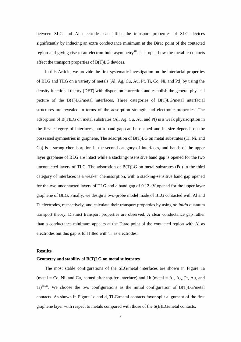
In Figure 4(f), we show the band structure of the third category of interfaces (BLG/Pd).
The conduction bands of the bottom layer graphene can be identified but it is hard to identify
the valence bands, indicating that the Pd 4d/5s bands are chiefly hybridized with the valence
bands of the bottom layer graphene because most of the Pd 4d/5s bands are below the Dirac
point of BLG. Similar to the second class of interfaces, the band structure of the upper layer
graphene can be clearly identified, but a band gap of 0.124 eV is opened. Ef of the upper layer
is shifted upward by 0.160 eV, indicative of n-type doping. This unique interfacial electronic
structure of BLG/Pd is ascribed to the fact that the intermediate interaction between BLG and
Pd surface preserves the partial electronic properties of the bottom layer and it does not
overwhelm the intrinsic graphene interlayer coupling. The dipole field induced by
Pd-graphene charge transfer breaks the inverse symmetry of the two graphene layers, and a
band gap is opened and is chiefly reflected in the upper layer graphene. The Eg – ΔEf datum of
8
BLG on Pd substrate falls in the Eg – ΔEf fitting curve for BLG physisorbed on metal
substrates in the n-doping region (Figure 3c).
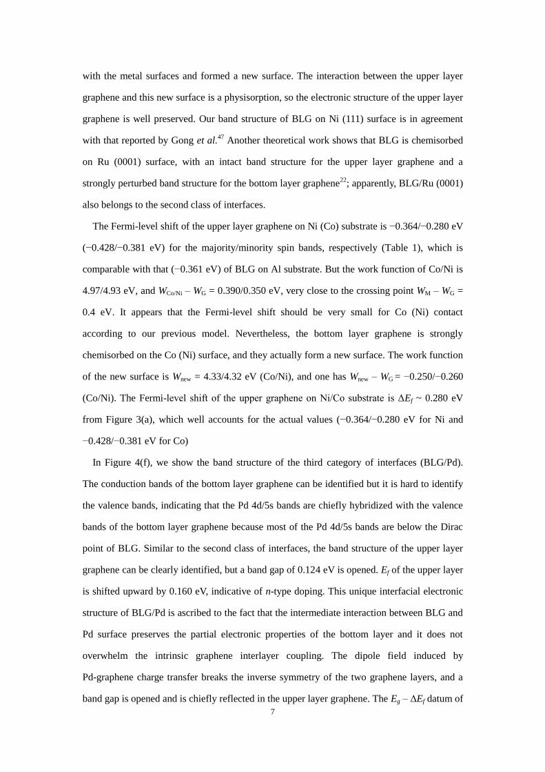
Electronic structure of TLG on metal substrates
The electronic structures of the first category of TLG/metal interfaces are plotted in
Figure 5. It is clearly shown that the band structures of both ABA- and ABC-stacked TLG are
preserved, accompanied by a Fermi level shift and an opened band gap. The same as BLG
cases, TLG is doped with electrons by Al, Ag, and Cu contacts and with holes by Au and Pt
contacts. Table 1 summarizes the evolution of the Fermi-level shift ΔEf = ED – Ef and band
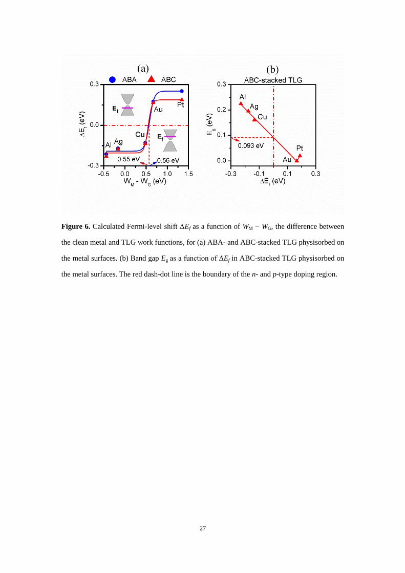
gap Eg of TLG. The Fermi-level shift ΔEf as a function of WM – WG is shown in Figure 6a for
ABA- and ABC-stacked TLG (WG is the calculated work function of TLG, 4.52 eV). The
crossover point from n- to p-type doping is about WM – WG = 0.56 for ABA-stacked TLG and
0.55 eV for ABC-stacked TLG.
Both the Fermi-level shift ΔEf and work function difference WM – WG are less sensitive to
the stacking order. However, the stacking order affects significantly the band gap of TLG:
ABA-stacked TLG has generally smaller band gaps of Eg = 0 − 0.061 eV while ABC-stacked
TLG has generally larger band gaps of Eg = 0 − 0.249 eV. The current on/off ratio of TLG
FET is expected to be increased by deposition of Al, Cu, and Ag on channel TLG due to a
band gap opening. As shown in Figure 6b and Figure S1, the sizes of the band gap of both
ABC- and ABA-stacked TLG rough linearly depend on ΔEf. The band gaps of ABC-stacked
TLG are apparently electron-hole asymmetric: they are significantly larger in the n-type
doping region (Eg = 0.181 – 0.249 eV) than those in the p-type doping region (Eg = 0 – 0.018
eV) at the same |ΔEf |. The band gaps of ABA-stacked TLG are slightly electron-hole
asymmetric: the band gaps are slightly larger in the n-type doping region (Eg = 0.032 – 0.061
eV) than those in the p-type doping region (Eg = 0 eV) given the same |ΔEf | (Figure S1). The
mechanisms of band gap opening in ABA- and ABC-stacked TLG and the reason of
electron-hole asymmetry in band gaps can also be explained with a TLG/metal contact model
(Figure S2).
The electronic structures of the second category of interfaces (TLG/Ti, Co, and Ni
contacts) are plotted in Figure 7. Similar to BLG cases, both the π and π* states of the
9
innermost graphene layer are strongly hybridized with the 3d states of Ti, and minority-spin
3d states of Co and Ni. Only the π states of the innermost graphene layer are strongly
hybridized with the Co and Ni majority-spin 3d states. The strongly coupled innermost
graphene layer serves as an active buffer and effectively passivates the metal d states at the
interface. As a result, the electronic structure of the two uncontacted layers is nearly intact
except that a band gap is opened, similar to the first category of interfaces for BLG/metal. The
band gaps of the uncontaced BLG are less sensitive to the stacking mode, with Eg = 0.100 −
0.229 eV, which approach the maximum band gap of freestanding BLG obtained from the
theoretical (0.25 − 0.28 eV)28,32
and experimental (0.25 eV)29
studies. The band gap opening
is attributed to a potential energy difference between the two uncontacted graphene layers,
which is ΔU32 = −αΔn3 −Δc′, where Δc′ is the potential step resulting from the interaction
between the second graphene layer and the chemically bonded innermost graphene-metal
system. Such a potential energy difference breaks the inversion symmetry of the two
uncontacted graphene layers, thus opening a band gap. TLG is n-type doped in both stacking
styles for the work function of the uncontaced BLG WG is larger than that of the new
graphene-metal surface Wnew.
The electronic structures of the third category of interfaces (TLG/Pd contact) are shown in
the second and fourth top panels of Figure 7. TLG is n-type doped by Pd substrate in both
stacking styles. Though the π states of the innermost graphene layer are perturbed strongly,
the π* states are only slightly affected, leading to BLG-like valence bands (two bands visible
near the K point) and TLG-like conduction bands (three bands visible near the K point). The
cause is the same as BLG cases: most of the Pd 4d states are below the Dirac point of
graphene and they can only hybridize with the π states of the innermost graphene layer.
Analogous to the physisorption cases, the band gap of the two uncontaced layers of TLG on
Pd substrate is strongly dependent on the stacking mode, with Eg = 0.064 and 0.308 eV for
ABA and ABC stacking styles, respectively. The latter band value is even marginally larger
than the maximum band gap of freestanding BLG under a uniform electric field obtained
from the theoretical (0.25 − 0.28 eV)28,32
and experimental (0.25 eV)29
studies and comparable
with the maximum band gap of SLG sandwiched between h-BN sheet under a uniform
electric field42
. The unique behavior of TLG/Pd is also agreement with the intermediate
10
binding between typical physisorption and chemisorption.
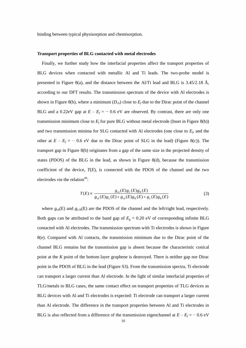
Transport properties of BLG contacted with metal electrodes
Finally, we further study how the interfacial properties affect the transport properties of
BLG devices when contacted with metallic Al and Ti leads. The two-probe model is
presented in Figure 8(a), and the distance between the Al/Ti lead and BLG is 3.45/2.18 Å,
according to our DFT results. The transmission spectrum of the device with Al electrodes is
shown in Figure 8(b), where a minimum (Dch) close to Ef due to the Dirac point of the channel
BLG and a 0.22eV gap at E – Ef = − 0.6 eV are observed. By contrast, there are only one
transmission minimum close to Ef for pure BLG without metal electrode (Inset in Figure 8(b))
and two transmission minima for SLG contacted with Al electrodes (one close to Ef, and the
other at E – Ef = − 0.6 eV due to the Dirac point of SLG in the lead) (Figure 8(c)). The
transport gap in Figure 8(b) originates from a gap of the same size in the projected density of
states (PDOS) of the BLG in the lead, as shown in Figure 8(d), because the transmission
coefficient of the device, T(E), is connected with the PDOS of the channel and the two
electrodes via the relation48:
ch L R
ch L ch R L R
( ) ( ) ( )( )
( ) ( ) ( ) ( ) ( ) ( )
g E g E g ET E
g E g E g E g E g E g E
(3)
where gch(E) and gL/R(E) are the PDOS of the channel and the left/right lead, respectively.
Both gaps can be attributed to the band gap of Eg = 0.20 eV of corresponding infinite BLG
contacted with Al electrodes. The transmission spectrum with Ti electrodes is shown in Figure
8(e). Compared with Al contacts, the transmission minimum due to the Dirac point of the
channel BLG remains but the transmission gap is absent because the characteristic conical
point at the K point of the bottom layer graphene is destroyed. There is neither gap nor Dirac
point in the PDOS of BLG in the lead (Figure S3). From the transmission spectra, Ti electrode
can transport a larger current than Al electrode. In the light of similar interfacial properties of
TLG/metals to BLG cases, the same contact effect on transport properties of TLG devices as
BLG devices with Al and Ti electrodes is expected: Ti electrode can transport a larger current
than Al electrode. The difference in the transport properties between Al and Ti electrodes in
BLG is also reflected from a difference of the transmission eigenchannel at E – Ef = − 0.6 eV
11
and at the (π/3a, 0) point of the k-space. As displayed in Figure 8(f), the transmission
eigenvalue at this point nearly vanishes with Al electrodes, and the incoming wave function is
nearly completely scattered and unable to reach to the other lead. By contrast, the
transmission eigenvalue at the point is 0.96 with Ti electrodes, and the incoming wave
function is scattered little and most of the incoming wave is able to reach to the other lead.
Discussion
No band gap is detected experimentally for graphene on Pt18
and Au49
. However, band
gaps of 0.18, 0.25, and 0.32 eV are detected for graphene on Cu/Ni49
, Cu50
, and Ag/Ni49
substrates, respectively, in angle-resolved photoelectron spectroscopy (ARPES). If graphene
is identified as single layer one, these measurements are apparently in contradiction with the
calculated zero-gap for SLG on Cu and Ag substrates35,36,38
. One possible solution to such a
great discrepancy is to identify graphene as BLG or ABC-stacked TLG, since CVD growth on
Ni substrate can yield few-layer graphene with random stacking order16,17
and on Cu substrate
can yield bilayer12
and few-layer13,14
graphene, breaking the self-limiting nature of growth
process. According to our calculations, BLG on Cu, and Ag (111) surfaces has a band gap of
0.11, 0.13 eV, and ABC-stacked TLG has a band gap of 0.181 and 0.203 eV, respectively, all
of which are comparable with the measured values18,49,50
.
The other interesting point is the different strength of interaction in different categories
of interfaces. In terms of so-called d band model, the bond strength increases when moving to
left and up in the transition metal series51
. As moving from the right to the left, the d band
moves up in energy, the filling of d band decreases and the antibonding graphene-metal d
states become more depopulated, resulting in a strong bonding. Rises of the 3d, 4d, and 5d
states are observed as going from Ni, Co, to Ti, from Ag to Pd, and from Au to Pt,
respectively. From Table 1, we indeed have Eb (Ti) > Eb (Co) > Eb (Ni) > Eb (Cu) for 3d metals,
Eb(Pd) > Eb(Ag) for 4d metals and Eb(Pt) > Eb(Au) for 5d metals. The same binding
difference is available for SLG on metal substrate35,36
. Because the Ni and Co 3d states of the
minority-spin are higher in energy than those of the majority-spin (Figure 5), TLG should
interact more strongly with the minority-spin states of Ni/Co in terms of this model.
As moving down in one group, relativistic effects become more remarkable in the core
12
electrons, therefore the d-state orbitals of metals diffuse more widely, resulting in a worse
overlapping of graphene π states and metal d states and a weaker binding23
. Besides, the
strength of covalent bond generally decreases with the increase of the atomic radius in one
group. The calculated binding energy for group 10 metals (Ni, Pd, and Pt) with TLG indeed
follows this rule and we have Eb (Ni) > Eb (Pd) > Eb (Pt) (See Table 1). In fact, Ti, Pd, and Pt
are the three represents of the three classes of metals: BLG and TLG are strongly
chemisorbed on Ni, and weakly chemisorbed on Pd, while the adsorption of graphene on Pt
degenerates into a physisorption. The interaction strength change of graphene with group 9
metals Co, Rh, and Ir also obeys the same rule15,23-25
.
Epitaxial ABA-stacked TLG on Ru (0001) surface has been investigated by Sutter et al.22
The electronic structure determined by selected-area APPES shows BLG-like π band
dispersion. According to their DFT calculation, the two uncontacted graphene layers on Ru
(0001) surface behaves like freestanding BLG without a band gap though they are heavily
n-type doped (the top of the valence band is located at −0.30 0.05 eV below Ef). This
result is somewhat surprising because the potential difference induced by graphene-metal
electron redistribution will destroy the inversion symmetry of the two uncontacted graphene
layers. We therefore recalculated the ABA-stacked TLG/Ru contact using the same
parameters set by Sutter et al.22
The calculated electronic structure is shown in Figure S4. As
expected, a band gap of 0.127 and 0.147 eV is opened in both the CASTEP and VASP
calculations. The top of the valence band is located at −0.267 and −0.261 eV below Ef in the
CASTEP and VASP calculations (Supplementary information, Figure S4), respectively,
consistent with the micro-ARPES data −0.30 0.05 eV22
. We note that the DFT calculation
of Gong et al.47
for ABA-stacked TLG/Ni contact also found an energy gap of Eg = 0.133 eV
for the majority-spin band, comparable with our value of 0.191 eV. This calculation also
supports our results that the band gap of the uncontacted two layers is generally opened by the
charge redistribution between metal and TLG in the second category of interfaces.
In summary, we present the first systematic first-principles investigation on the
interfacial properties of BLG and TLG on a variety of metal substrates. According to the
adsorption strength and electronic properties, the BLG/metal and TLG/metal interfacial
structures can be classified into three categories. In the first category of interfaces, B(T)LG
13
are physisorbed on Al, Ag, Cu, Au, and Pt substrates; a band gap of 0.1 – 0.2 eV is opened for
BLG, and a stacking-sensitive band gap is opened for TLG, with the values of 0 − 0.061 and 0
− 0.249 eV for ABA- and ABC-stacking styles, respectively. In the second category of
interfaces, B(T)LG are chemisorbed on Ti, Ni, and Co substrates; the bands of the bottom
layer graphene is strongly perturbed, but those of the upper layer graphene of BLG is intact
and a stacking-insensitive band gap is opened for the two uncontacted layers of TLG. In the
third category of interfaces, B(T)LG are weakly chemisorbed on Pd substrate; a band gap of
0.12 eV is opened for the upper layer graphene of BLG and a band gap of 0.064 and 0.308 eV
is opened for the two uncontacted layers of ABA- and ABC-stacked TLG, respectively. An ab
initio quantum transport simulation is performed for a two-probe model made of BLG
contacted with Al or Ti electrodes. A transmission minimum and a transport gap are observed
in the transmission spectrum with Al contact. By contrast, there is only one transmission
minimum in the transmission spectrum with Ti contact due to the strong binding in the
electrodes. This fundamental study not only provides a deeper insight into the interaction
between B(T)LG and metal substrates but also helps to B(T)LG-based device study because
of inevitable B(T)LG/metal contact.
Methods
We use six layers of metal atoms (Ni, Co, Cu, Al, Ag, Cu, Pt, and Au) in (111) orientation
and Ti in (0001) orientation to simulate the metal surface, and a hexagonal supercell is
constructed with a BLG or TLG adsorbed on one side of the metal surface, as shown in Figure
1. We fix in-plane lattice constant of TLG to the experimental value a = 2.46 Å. The 11 unit
cells of Ni, Co, and Cu (111) faces are adjusted to graphene 11 unit cell, and 33 unit
cells of Ti (0001) face and Al, Ag, Cu, Pt, and Au (111) faces are adjusted to graphene 22
unit cell. The approximation is reasonable since the metal surfaces have a small lattice
constants mismatch of less than 4% with that of graphene, as seen in Table 1. A vacuum
buffer space of at least 12 Ǻ is set.
The geometry optimizations and electronic structure calculations are performed with the
ultrasoft pseudopotentials52
plane-wave basis set with energy cut-off of 350 eV, implemented
in the CASTEP code53
.
Generalized gradient approximation (GGA) of
14
Perdew–Burke–Ernzerhof (PBE) form54
to the exchange-correlation functional is used. To
account for the dispersion interaction between graphene, a DFT-D semiempirical
dispersion-correction approach is adopted55
. During the calculations, the cell shape and the
bottom four layers of metal atoms are fixed. To obtain reliable optimized structures, the
maximum residual force is less than 0.01 eV/Å and energies are converged to within 510-6
eV per atom. The Monkhorst-Pack56
k-point mesh is sampled with a separation of about 0.02
and 0.01 Å-1
in the Brillouin zone, respectively, during the relaxation and electronic
calculation periods. The component of the energy band and the plane-averaged excess
electron density are analyzed via additional calculations based on the plane-wave basis set
with a cut-off energy of 400 eV and the projector-augmented wave (PAW) pseudopotential
implemented in the VASP code57,58
. The electronic structures generated by the two packages
are nearly indistinguishable.
TLG/Ru(0001) interface model is constructed from a slab of six layers of Ru with the
bottom four layers are fixed and a TLG adsorbed on one side. Following the previous work by
Sutter et al.22
, ABA-stacked TLG is strained to match the Ru lattice parameter a = 2.68 Å.
Using the same calculation parameters22
, the ABA-stacked TLG/Ru contact is recalculated by
using the CASTEP and VASP codes, respectively. Namely, ultrasoft pseudopotential52
plane-wave basis set with energy cutoff of 340 eV is used. The local density approximation
(LDA) in the Ceperley-Alder form is used for the exchange and correlation functional59,60
.
The Monkhorst-Pack56
k-point is sampled by a 1515 mesh in the Brillouin zone.
To study how the metallic contacts affect the transport properties of the BLG devices, a
two-probe model made of BLG is built, and the BLG channel is contacted with two Al/Ti
electrodes (source and drain). We perform transport calculations at zero source-drain bias by
using the DFT method coupled with nonequilibrium Green’s function (NEGF) method, which
are implemented in ATK 11.2 package61-63
. Single-zeta (SZ) basis set is used, the real-space
mesh cutoff is 150 Ry., and the temperature is set at 300 K. The local-density-approximation
(LDA)59,60
is employed for the exchange–correlation functional. The electronic structures of
electrodes and central region are calculated with a Monkhorst–Pack56
50 × 1 × 100 and 50 × 1
× 1 k-point grid, respectively.
15
Acknowledgement This work was supported by the National Natural Science Foundation
of China (Nos. 11274016, 51072007, 91021017, 11047018, and 60890193), the National
Basic Research Program of China (Nos. 2013CB932604 and 2012CB619304), Fundamental
Research Funds for the Central Universities, National Foundation for Fostering Talents of
Basic Science (No. J1030310/No. J1103205), Program for New Century Excellent Talents in
University of MOE of China, and Nebraska Research Initiative (No. 4132050400) and DOE
DE-EE0003174 in the United States. J. Zheng also acknowledges the financial support from
the China Scholarship Council.
Author Contributions. The idea was conceived by J. L. The calculation was performed by J.
Z. and Y. W. The data analyses were performed by J. Z., Y. W., L. W., R. Q., and J. L.. Z. N.,
W. M., D. Y., J. S., and Z. G. took part in discussion. This manuscript was written by J. Z., Y.
W., and J. L.. All authors reviewed this manuscript.
Additional Information.
Competing Financial Interests
The authors declare no competing financial interests.

16
Author Information
● Affiliations
State Key Laboratory of Mesoscopic Physics and Department of Physics, Peking
University, Beijing 100871, P. R. China
Jiaxin Zheng, Yangyang Wang, Ruge Quhe, Zeyuan Ni, Dapeng Yu, Junjie Shi,
Zhengxiang Gao, Jing Lu
Academy for Advanced Interdisciplinary Studies, Peking University, Beijing 100871,
P. R. China
Jiaxin Zheng, Ruge Quhe
Department of Physics, University of Nebraska at Omaha, Omaha, Nebraska
68182-0266
Lu Wang, Wai-Ning Mei
● Corresponding authors
Correspondence to: Jing Lu ([email protected])

17
References
1 Novoselov, K. S. et al., Electric field effect in atomically thin carbon films. Science
306 (5696), 666-669 (2004).
2 Novoselov, K. S. et al., Two-dimensional gas of massless Dirac fermions in graphene.
Nature 438 (7065), 197-200 (2005).
3 Zhang, Y., Tan, Y.-W., Stormer, H. L., & Kim, P., Experimental observation of the
quantum Hall effect and Berry's phase in graphene. Nature 438 (7065), 201-204
(2005).
4 Stoller, M. D., Park, S., Zhu, Y., An, J., & Ruoff, R. S., Graphene-based
ultracapacitors. Nano Lett. 8 (10), 3498-3502 (2008).
5 Ohno, Y., Maehashi, K., Yamashiro, Y., & Matsumoto, K., Electrolyte-gated graphene
field-effect transistors for detecting pH and protein adsorption. Nano Lett. 9 (9),
3318-3322 (2009).
6 Yoo, E. et al., Large reversible Li storage of graphene nanosheet families for use in
rechargeable lithium ion batteries. Nano Lett. 8 (8), 2277-2282 (2008).
7 Wang, D. et al., Self-assembled TiO2-graphene hybrid nanostructures for enhanced
Li-ion insertion. ACS Nano 3 (4), 907-914 (2009).
8 Gomez De Arco, L. et al., Continuous, highly flexible, and transparent graphene films
by chemical vapor deposition for organic photovoltaics. ACS Nano 4 (5), 2865-2873
(2010).
9 Li, X. S. et al., Large-area synthesis of high-quality and uniform graphene films on
copper foils. Science 324 (5932), 1312-1314 (2009).
10 Bae, S. et al., Roll-to-roll production of 30-inch graphene films for transparent
electrodes. Nat. Nanotech. 5 (8), 574-578 (2010).
11 Lee, S., Lee, K., & Zhong, Z. H., Wafer scale homogeneous bilayer graphene films by
chemical vapor deposition. Nano Lett. 10 (11), 4702-4707 (2010).
12 Yan, K., Peng, H. L., Zhou, Y., Li, H., & Liu, Z. F., Formation of bilayer bernal
graphene: Layer-by-layer epitaxy via chemical vapor deposition. Nano Lett. 11 (3),
1106-1110 (2011).
13 Robertson, A. W. & Warner, J. H., Hexagonal single crystal domains of few-layer
graphene on copper foils. Nano Lett. 11 (3), 1182-1189 (2011).
14 Li, Q. et al., Growth of adlayer graphene on Cu studied by carbon isotope labeling.
Nano Lett., online, dx.doi.org/10.1021/nl303879k.
15 Eom, D. et al., Structure and electronic properties of graphene nanoislands on
Co(0001). Nano Lett. 9 (8), 2844-2848 (2009).
16 Reina, A. et al., Large area, few-layer graphene films on arbitrary substrates by
chemical vapor deposition. Nano Lett. 9 (1), 30-35 (2009).
17 Kim, K. S. et al., Large-scale pattern growth of graphene films for stretchable
transparent electrodes. Nature 457 (7230), 706-710 (2009).
18 Sutter, P., Sadowski, J. T., & Sutter, E., Graphene on Pt(111): Growth and substrate
interaction. Phys. Rev. B 80 (24), 245411 (2009).
19 Kwon, S.-Y. et al., Growth of semiconducting graphene on Palladium. Nano Lett. 9
(12), 3985-3990 (2009).
20 Oznuluer, T. et al., Synthesis of graphene on gold. Appl. Phys. Lett. 98 (18), 3 (2011).
18
21 Starodub, E. et al., Graphene growth by metal etching on Ru(0001). Phys. Rev. B 80
(23), 235422 (2009).
22 Sutter, P., Hybertsen, M. S., Sadowski, J. T., & Sutter, E., Electronic structure of
few-layer epitaxial graphene on Ru(0001). Nano Lett. 9 (7), 2654-2660 (2009).
23 Voloshina, E. & Dedkov, Y., Graphene on metallic surfaces: Problems and
perspectives. Phys. Chem. Chem. Phys. 14 (39), 13502-13514 (2012).
24 Pletikosic ,́ I. et al., Dirac cones and minigaps for graphene on Ir(111). Phys. Rev. Lett.
102 (5), 056808 (2009).
25 Johann, C. et al., Growth of graphene on Ir(111). New J. Phys. 11 (2), 023006 (2009).
26 McCann, E., Asymmetry gap in the electronic band structure of bilayer graphene.
Phys. Rev. B 74 (16), 161403 (2006).
27 Castro, E. V. et al., Biased bilayer graphene: semiconductor with a gap tunable by the
electric field effect. Phys. Rev. Lett. 99 (21), 216802 (2007).
28 Min, H. K., Sahu, B., Banerjee, S. K., & MacDonald, A. H., Ab initio theory of gate
induced gaps in graphene bilayers. Phys. Rev. B 75 (15), 155115 (2007).
29 Zhang, Y. B. et al., Direct observation of a widely tunable bandgap in bilayer
graphene. Nature 459 (7248), 820-823 (2009).
30 Castro, E. V. et al., Electronic properties of a biased graphene bilayer. J.
Phys.-Condes. Matter 22 (17), 175503 (2010).
31 Lui, C. H., Li, Z., Mak, K. F., Cappelluti, E., & Heinz, T. F., Observation of an
electrically tunable band gap in trilayer graphene. Nat. Phys. 7 (12), 944-947 (2011).
32 Tang, K. C. et al., Electric-field-induced energy gap in few-layer graphene. J. Phys.
Chem. C 115 (19), 9458-9464 (2011).
33 Bao, W. et al., Stacking-dependent band gap and quantum transport in trilayer
graphene. Nat. Phys. 7 (12), 948-952 (2011).
34 Zhang, F., Sahu, B., Min, H., & MacDonald, A. H., Band structure of ABC-stacked
graphene trilayers. Phys. Rev. B 82 (3), 035409 (2010).
35 Giovannetti, G. et al., Doping graphene with metal contacts. Phys. Rev. Lett. 101 (2),
026803 (2008).
36 Khomyakov, P. A. et al., First-principles study of the interaction and charge transfer
between graphene and metals. Phys. Rev. B 79 (19), 195425 (2009).
37 Gao, M. et al., Tunable interfacial properties of epitaxial graphene on metal substrates.
Appl. Phys. Lett. 96 (5), 053109 (2010).
38 Xu, Z. P. & Buehler, M. J., Interface structure and mechanics between graphene and
metal substrates: a first-principles study. J. Phys. Condens. Mat. 22 (48), 485301
(2010).
39 Craciun, M. F. et al., Trilayer graphene is a semimetal with a gate-tunable band
overlap. Nat. Nanotech. 4 (6), 383-388 (2009).
40 Barraza-Lopez, S., Vanevic, M., Kindermann, M., & Chou, M. Y., Effects of metallic
contacts on electron transport through graphene. Phys. Rev. Lett. 104 (7), 076807
(2010).
41 Xia, F. N., Farmer, D. B., Lin, Y.-m., & Avouris, P., Graphene field-effect transistors
with high on/off current ratio and large transport band gap at room temperature. Nano
Lett. 10 (2), 715-718 (2010).
19
42 Quhe, R. et al., Tunable and sizable band gap of single-layer graphene sandwiched
between hexagonal boron nitride. NPG Asia Mater. 4, e6; doi:10.1038/am.2012.1010
(2012).
43 Ohta, T., Bostwick, A., Seyller, T., Horn, K., & Rotenberg, E., Controlling the
electronic structure of bilayer graphene. Science 313 (5789), 951-954 (2006).
44 Avetisyan, A. A., Partoens, B., & Peeters, F. M., Electric field tuning of the band gap
in graphene multilayers. Phys. Rev. B 79 (3), 035421 (2009).
45 Avetisyan, A. A., Partoens, B., & Peeters, F. M., Electric-field control of the band gap
and Fermi energy in graphene multilayers by top and back gates. Phys. Rev. B 80 (19),
195401 (2009).
46 Szafranek, B. N., Schall, D., Otto, M., Neumaier, D., & Kurz, H., High on/off ratios
in bilayer graphene field effect transistors realized by surface dopants. Nano Lett. 11
(7), 2640-2643 (2011).
47 Gong, S. J. et al., Spintronic properties of graphene films grown on Ni(111) substrate.
J. Appl. Phys. 110 (4), 043704-043705 (2011).
48 Ni, Z. Y. et al., Tunable bandgap in silicene and germanene. Nano Lett. 12 (1),
113-118 (2012).
49 Varykhalov, A., Scholz, M. R., Kim, T. K., & Rader, O., Effect of noble-metal
contacts on doping and band gap of graphene. Phys. Rev. B 82 (12), 121101 (2010).
50 Walter, A. L. et al., Electronic structure of graphene on single-crystal copper
substrates. Phys. Rev. B 84 (19), 195443 (2011).
51 Hammer, B. & Norskov, J. K., Theoretical surface science and catalysis - calculations
and concepts in Advances in Catalysis: Impact of Surface Science on Catalysis, edited
by B. C. Gates & H. Knozinger (2000), Vol. 45, pp. 71-129.
52 Vanderbilt, D., Soft self-consistent pseudopotentials in a generalized eigenvalue
formalism. Phys. Rev. B 41 (11), 7892-7895 (1990).
53 Clark, S. J. et al., First principles methods using CASTEP. Z. Kristallogr. 220 (5-6),
567-570 (2005).
54 Perdew, J. P., Burke, K., & Ernzerhof, M., Generalized gradient approximation made
simple. Phys. Rev. Lett. 77 (18), 3865-3868 (1996).
55 Tkatchenko, A. & Scheffler, M., Accurate molecular van der Waals interactions from
ground-state electron density and free-atom reference data. Phys. Rev. Lett. 102 (7),
073005 (2009).
56 Monkhorst, H. J. & Pack, J. D., Special points for Brillouin-zone integrations. Phys.
Rev. B 13 (12), 5188-5192 (1976).
57 Kresse, G. & Hafner, J., Abinitio molecular-dynamics for liquid-metals. Phys. Rev. B
47 (1), 558-561 (1993).
58 Kresse, G. & Furthmuller, J., Efficiency of ab-initio total energy calculations for
metals and semiconductors using a plane-wave basis set. Comp. Mater. Sci. 6 (1),
15-50 (1996).
59 Ceperley, D. M. & Alder, B. J., Ground state of the electron gas by a stochastic
method. Phys. Rev. Lett. 45 (7), 566-569 (1980).
60 Perdew, J. P. & Zunger, A., Self-interaction correction to density-functional
approximations for many-electron systems. Phys. Rev. B 23 (10), 5048-5079 (1981).
20
61 Taylor, J., Guo, H., & Wang, J., Ab initio modeling of quantum transport properties of
molecular electronic devices. Phys. Rev. B 63 (24), 245407 (2001).
62 Brandbyge, M., Mozos, J.-L., Ordejn, P., Taylor, J., & Stokbro, K., Density-functional
method for nonequilibrium electron transport. Phys. Rev. B 65 (16), 165401 (2002).
63 ATOMISTIX Toolkit version 11.2. Quantum Wise A/S: Copenhagen, Denmark.
21
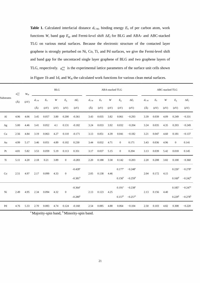
Table 1. Calculated interfacial distance dC-M, binding energy Eb of per carbon atom, work
functions W, band gap Eg, and Fermi-level shift ΔEf for BLG and ABA- and ABC-stacked
TLG on various metal surfaces. Because the electronic structure of the contacted layer
graphene is strongly perturbed on Ni, Co, Ti, and Pd surfaces, we give the Fermi-level shift
and band gap for the uncontaced single layer graphene of BLG and two graphene layers of
TLG, respectively. exp
hexa is the experimental lattice parameters of the surface unit cells shown
in Figure 1b and 1d, and WM the calculated work functions for various clean metal surfaces.
a Majority-spin band,
b Minority-spin band.
Substrates
exp
hexa
(Å)
WM
(eV)
BLG
ABA-stacked TLG
ABC-stacked TLG
dC-M
(Å)
Eb
(eV)
W
(eV)
Eg
(eV)
ΔEf
(eV)
dC-M
(Å)
Eb
(eV)
W
(eV)
Eg
(eV)
ΔEf
(eV)
dC-M
(Å)
Eb
(eV)
W
(eV)
Eg
(eV)
ΔEf
(eV)
Al 4.96 4.06 3.45 0.057 3.80 0.200 -0.361
3.43 0.035 3.82 0.061 −0.293
3.39 0.039 4.09 0.249 −0.331
Ag 5.00 4.46 3.41 0.052 4.1 0.131 -0.182
3.24 0.033 3.92 0.032 −0.204
3.24 0.035 4.35 0.203 −0.249
Cu 2.56 4.84 3.19 0.063 4.27 0.110 -0.171
3.13 0.051 4.39 0.041 −0.182
3.21 0.047 4.60 0.181 −0.137
Au 4.99 5.17 3.46 0.051 4.89 0.102 0.230
3.44 0.032 4.71 0 0.171
3.43 0.036 4.96 0 0.141
Pt 4.81 5.82 3.53 0.059 5.19 0.113 0.351
3.17 0.037 5.15 0 0.204
3.13 0.039 5.42 0.018 0.145
Ti 5.11 4.20 2.18 0.21 3.89 0 -0.283
2.20 0.188 3.58 0.142 −0.203
2.20 0.208 3.82 0.100 −0.360
Co 2.51 4.97 2.17 0.099 4.33 0
-0.428a
2.05 0.138 4.46
0.177a −0.248a
2.04 0.172 4.15
0.226a −0.278a
-0.381b 0.156b −0.259b 0.160b −0.242b
Ni 2.49 4.95 2.34 0.094 4.32 0
-0.364a
2.13 0.123 4.25
0.191a −0.238a
2.13 0.156 4.40
0.185a −0.247a
-0.280b 0.157b −0.257b 0.229b −0.278b
Pd 4.76 5.33 2.70 0.083 4.74 0.124 -0.160
2.54 0.085 4.88 0.064 −0.104
2.50 0.103 4.82 0.308 −0.220

22
Figure 1: Interfacial structures of B(T)LG on metal substrates. (a) Top and side views of
the most stable configuration for SLG (the green balls)35,36
and BLG on Ni, Co, and Cu (111)
surfaces. (b) Top views of the most stable configuration for SLG35,36
and BLG on Ti (0001)
surface, and Pd, Al, Ag, Au, and Pt (111) surfaces. (c) and (d) The relaxed configurations for
TLG on the corresponding metal substrates with split alignment of the first (innermost)
graphene layer to metals compared to (a) and (b). Red and purple balls denote metal atoms of
the first and rest layers, respectively. Green and gray balls denote the first and second layers
of graphene, respectively. The third (outermost) graphene layer (not shown) is vertically
aligned with the first layer for ABA stacking mode and it has a vector translation (labeled by
a black arrow) with respect to the first layer for ABC stacking mode. dC-M is the equilibrium
distance between the metal surface and the bottom layer graphene. The yellow diamonds
represent unit cells.
23
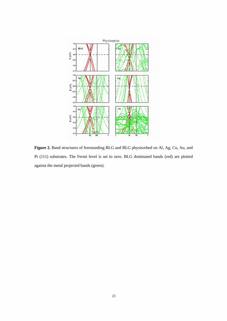
Figure 2. Band structures of freestanding BLG and BLG physisorbed on Al, Ag, Cu, Au, and
Pt (111) substrates. The Fermi level is set to zero. BLG dominated bands (red) are plotted
against the metal projected bands (green).

24
Figure 3. (a) Calculated Fermi-level shift as a function of WM – WG, the difference between
the clean metal and graphene work functions. WM – WG = 0.4 eV is the cross point from n- to
p-type doping. (b) Schematic of the BLG/metal contacts. E and E1 denote the electric fields
between metal and graphene and between the graphene layers, respectively. (c) Band gap as a
function of ΔEf in BLG physisorbed on the metal surfaces. The red dot-dashed line in (c) is a
boundary of n- and p-type doping region. The black dashed line in (c) is a linear fit to the Eg –
ΔEf data in the n-type doped region. The band gap (green diamond) of the upper layer
graphene for BLG weakly chemisorbed on Pd surface is also given.
25
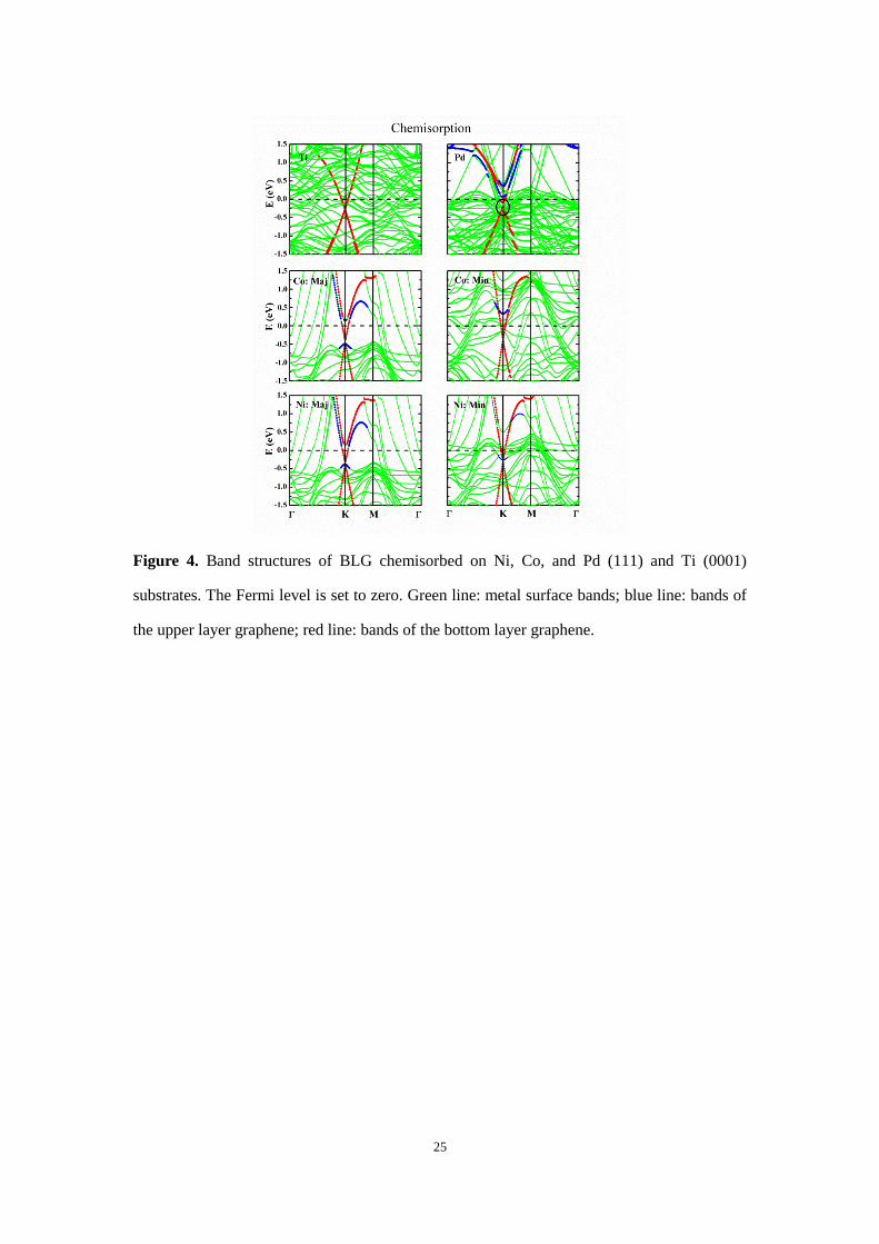
Figure 4. Band structures of BLG chemisorbed on Ni, Co, and Pd (111) and Ti (0001)
substrates. The Fermi level is set to zero. Green line: metal surface bands; blue line: bands of
the upper layer graphene; red line: bands of the bottom layer graphene.

26
Figure 5. Band structures of ABA- and ABC-stacked TLG physisorbed on Al, Ag, Cu, Au,
and Pt (111) surfaces. The Fermi level is set at zero. TLG-dominated bands (red) are plotted
against the metal projected bands (green). The first and third top panels correspond to the
band structure of freestanding ABA- and ABC- stacked TLG with graphene 22 supercell,
respectively.
27
Figure 6. Calculated Fermi-level shift ΔEf as a function of WM − WG, the difference between
the clean metal and TLG work functions, for (a) ABA- and ABC-stacked TLG physisorbed on
the metal surfaces. (b) Band gap Eg as a function of ΔEf in ABC-stacked TLG physisorbed on
the metal surfaces. The red dash-dot line is the boundary of the n- and p-type doping region.

28
Figure 7. Band structures of ABA- and ABC-stacked TLG chemisorbed on Ti (0001), Co, Ni,
and Pd (111) surfaces. The Fermi level is set at zero. TLG-dominated bands are plotted
against the metal projected bands (green). Blue and red lines depict the bands with weight
projected on the innermost graphene layer and the outer graphene bilayer, respectively. The
labels Maj/Min represent the majority- and minority-spin bands, respectively.

29
(a)
(f)
Figure 8. (a) Two-probe model. The length of the channel is Lch = 9.6 nm. Gray ball: C; blue
ball: Al or Ti. (b) Zero-bias transmission spectrum with Al electrodes. Inset: transmission
spectrum of a freestanding BLG with the same Lch. (c) Zero-bias transmission spectrum of
SLG contacted with Al electrodes with Lch = 9.6 nm. (d) Projected density of states (PDOS) of
BLG contacted with Al electrodes. (e) Zero-bias transmission spectrum of BLG contacted
with Ti electrodes with Lch = 9.6 nm. (f) Transmission eigenstates at E – Ef = –0.6 eV and at k
= (π/3a, 0) with Al and Ti electrodes, respectively. The isovalue is 0.2 a.u..
Source Drain