
Influence of test methodology and probe geometry on ...
22
Influence of test methodology and probe geometry on nanoscale fatigue mechanisms of diamond-like carbon thin film Faisal, N. H., Ahmed, R., Goel, S., & Fu, R. (2014). Influence of test methodology and probe geometry on nanoscale fatigue mechanisms of diamond-like carbon thin film. Surface and Coatings Technology, 242, 42-53. https://doi.org/10.1016/j.surfcoat.2014.01.015 Published in: Surface and Coatings Technology Document Version: Peer reviewed version Queen's University Belfast - Research Portal: Link to publication record in Queen's University Belfast Research Portal Publisher rights This is the author’s version of a work that was accepted for publication in Surface and Coatings Technology. Changes resulting from the publishing process, such as peer review, editing, corrections, structural formatting, and other quality control mechanisms may not be reflected in this document. Changes may have been made to this work since it was submitted for publication. A definitive version was subsequently published in Surface and Coatings Technology, vol 242, 15th March 2014, DOI: 10.1016/j.surfcoat.2014.01.015. General rights Copyright for the publications made accessible via the Queen's University Belfast Research Portal is retained by the author(s) and / or other copyright owners and it is a condition of accessing these publications that users recognise and abide by the legal requirements associated with these rights. Take down policy The Research Portal is Queen's institutional repository that provides access to Queen's research output. Every effort has been made to ensure that content in the Research Portal does not infringe any person's rights, or applicable UK laws. If you discover content in the Research Portal that you believe breaches copyright or violates any law, please contact [email protected]. Download date:21. Sep. 2022
-
Upload
khangminh22 -
Category
Documents
-
view
5 -
download
0
Transcript of Influence of test methodology and probe geometry on ...

Influence of test methodology and probe geometry on nanoscalefatigue mechanisms of diamond-like carbon thin film
Faisal, N. H., Ahmed, R., Goel, S., & Fu, R. (2014). Influence of test methodology and probe geometry onnanoscale fatigue mechanisms of diamond-like carbon thin film. Surface and Coatings Technology, 242, 42-53.https://doi.org/10.1016/j.surfcoat.2014.01.015
Published in:Surface and Coatings Technology
Document Version:Peer reviewed version
Queen's University Belfast - Research Portal:Link to publication record in Queen's University Belfast Research Portal
Publisher rights This is the author’s version of a work that was accepted for publication in Surface and Coatings Technology. Changes resulting from thepublishing process, such as peer review, editing, corrections, structural formatting, and other quality control mechanisms may not bereflected in this document. Changes may have been made to this work since it was submitted for publication. A definitive version wassubsequently published in Surface and Coatings Technology, vol 242, 15th March 2014, DOI: 10.1016/j.surfcoat.2014.01.015.
General rightsCopyright for the publications made accessible via the Queen's University Belfast Research Portal is retained by the author(s) and / or othercopyright owners and it is a condition of accessing these publications that users recognise and abide by the legal requirements associatedwith these rights.
Take down policyThe Research Portal is Queen's institutional repository that provides access to Queen's research output. Every effort has been made toensure that content in the Research Portal does not infringe any person's rights, or applicable UK laws. If you discover content in theResearch Portal that you believe breaches copyright or violates any law, please contact [email protected].
Download date:21. Sep. 2022

Influence of test methodology and probe geometry on nanoscale fatigue failure of diamond-like carbon film
N.H. Faisala, ⁎
R. Ahmedb
Saurav Goelc
Y.Q. Fu (Please could you alsoinclude Y. Q. Fu's email as one of the two corresponding authors, email-id: [email protected].)d
aSchool of Engineering, Robert Gordon University, Garthdee Road, Aberdeen, AB10 7GJ, UK
bSchool of Engineering and Physical Sciences, Heriot-Watt University, Edinburgh, EH14 4AS, UK
cSchool of Mechanical and Aerospace Engineering, Queen's University, Belfast, BT9 5AH, UK
dThin Film Centre, Scottish Universities Physics Alliances (SUPA), University of West of Scotland, Paisley, PA1 2BE, UK
⁎Corresponding author. Tel.: + 44 1224 26 2438; fax: + 44 1224 26 2444.
Abstract
The aim of this paper is to investigate the mechanism of nanoscale fatigue using nano-impact and multiple-loading cycle nanoindentation tests, and compare it to previously reported findings of nanoscale fatigue using
integrated stiffness and depth sensing approach. Two different film loading mechanismmechanisms, loading history and indenter shapes are compared to comprehend the influence of test methodology on the nanoscale fatigue
failure mechanisms of a DLC film. An amorphous 100 nm thick DLC film was deposited on a 500 µm silicon substrate using sputtering of graphite target in pure argon atmosphere. Nano-impact and multiple-load cycle indentations
were performed in the load range of 100 100 µN to 1000 1000 µN and 0.1 1 mN to 100 100 mN, respectively. Both test types were conducted using conical and Berkovich indenters. Results indicate that for the case of a conical
indenter, the combination of nano-impact and multiple-loading cycle nanoindentation tests provide provides information on the life and failure mechanism of the DLC film, which is comparable to the previously reported findings using
the integrated stiffness and depth sensing approach. However, the comparison of results is sensitive to the applied load, loading mechanism, test-type and probe geometry. The loading mechanism and load history is are therefore
critical which also leads lead to two different definitions of film failure. The choice of exact test methodology, load and probe geometry should therefore be dictated by the in-service tribological conditions, and where necessary both
test methodologies can be used to provide better insights of failure mechanism. Molecular dynamics (MD) simulations of the elastic response of nanoindentation is are reported, which indicates indicate that the elastic modulus of
the film measured using MD simulation was higher than that experimentally measured. This difference is attributed to the factors related to the presence of material defects, crystal structure, residual stress, indenter geometry and
loading/unloading rate differences between the MD and experimental results.
Keywords: Nano-fatigue; Diamond-like carbon; Nanoindentation; Nano-impact; Molecular dynamics; Micromechanics
1 Introduction
Hydrogen free diamond-like-carbon (DLC) thin films are frequently used as protective coatings on magnetic and optical storage disksdiscs, solar panels, optical windows, medical implants and micro/nano-electromechanical
(MEMS/NEMS) devices [1]. As these applications exhibit tribological aspects, there is a growing interest on advancing the understanding of the nanomechanical behaviour of these films. The mechanical properties of these films are strongly
dependent on the scale of measurement [2]. This consideration has motivated research on the nanoindentation behaviour of a variety of work piece and tool material combinations [3].
Previous experimental investigations have attempted to understand nanoscale contact fatigue behaviour of engineering materials using various commercially available and bespoke instruments and indenter shapes (e.g. [4–16]).
These investigations take advantage of the features in the real time force-–displacement (P-–h), displacement-–time (h-–t) or stiffness curves recorded during repeated loading/unloading of bulk materials and thin films. Test methodologies and
elsevier_SCT_19136
data analysis techniques adapted in previous investigations can be categorised in three main areas. The first one is depth sensing as indicated by Beake et al. [5–9] where a sudden increase in contact depth vs. time or number of impacts
indicate indicates the failure of component or film. The second one is area based calculations as indicated by Bouzakis et al. [10,11] where the fracture ratio of failed area and undamaged film indicates film failure. The third one is contact
stiffness based evaluations as indicated by Bhushan and Li [4,13,17] where failure is defined as the change in contact stiffness of probe. A more recent development is the use of in-situ transmission electron microscopy (TEM) for nano-
fatigue investigations by Wang et al. [15] where phase transformations in thin carbon films were investigated. A different approach was adapted by Liou et al. [18] for a 545 nm thick SiO2 film on a Si wafer, where oscillating loads were used to
evaluate the work required to delaminate the film. Other studies relating to TiN and AlN films [16,19] also considered the mechanism of thick film degradation (micrometer micrometre thickness range) under cyclic indentation loading, whereas
Yonezu et al. [20] considered similar evaluation via incorporating acoustic emission investigation.
However, the literature lacks back-to-back comparison of coatings tested using different loading mechanisms with a view to ascertain failure mechanism of DLC coatings. Recently, authors reported nanoscale fatigue evaluation of
100 nm thick DLC coatings using an integrated stiffness and depth sensing approach and concluded a five-stage failure mechanism of these films [21]. The aim of the current paper is to ascertain the scientific merit of testing the same
coating, using a different loading mechanism and instrument-type, with a view to comprehend the influence of test methodology on the mechanisms of DLC coating failure. To provide a back-to-back analysis, same DLC film was used in the
current investigation as was reported previously [21]. In the current investigation, a P-–h and h-–t approach was adapted to experimentally investigate the mechanisms of film failure using i) nano-impact (low-cycle fatigue) failure and ii)
multiple-load cycle nanoindentation (very low-cycle fatigue) of the DLC film. Furthermore, some molecular dynamics (MD) results are presented to consider the elastic level response of the coating substrate system. Elastic modulus thus
evaluated is compared with the experimental findings of modulus using the nanoindentation system.
2 Experimental work
2.1 Test specimen
The material used for the substrate was a commercially available four inch diameter and 500 µm thick silicon wafer with crystal orientation (100). An amorphous DLC film of 100 nm thickness was deposited on the silicon wafer in pure argon (Ar)
atmosphere using sputtering of graphite target without intentional substrate heating. The substrate holder was rotated throughout the process in order to ensure uniform deposition of the film. The substrate to target distance was 100 mm and flow rate of argon
gas was 15 15 sccm at a pressure of 5 5 mTorr. The base pressure of the chamber was maintained at 2 × 10-− 3 mTorr. The RF plasma power was 150 W. The deposition rate was kept at 12.5 nm/min and the deposition duration was adjusted to achieve a film
thickness of 100 nm [22]. Raman scattering of the DLC film was performed through Raman spectroscopy (Renishaw System 3000) with He–Ne laser (wavelength of 514.5 nm). The wafer curvature before and after film deposition was measured using a
profilometer and the residual stress (σ) was calculated from the change in the radius of curvature (R1 and R2) of the wafer’'s bi-layer structure using Stoney’'s equation [23]:
where Es is the Young’'s modulus of the Si-substrate (130 GPa), νs is the Poisson’'s ratio of the Si-substrate (0.28) and ts and tf are the thicknesses of the Si-substrate and the thin film respectively. As suggested previously, Stoney’'s equation was
applied without any correction [23] since the ratio of tf/ts ≤ 0.1.
2.2 Nanoindentation test
The evaluation of hardness (H) and elastic modulus (Es) of the thin film requires careful assessment of the test parameters. This is due to the fact that measurements may sometime represent a combined property of the film and the substrate rather
than the film alone. A general rule of penetration depth of 1/10th of the film thickness has been recommended by Haanappel et al. [24] to avoid plastic deformation of the film. In the current investigation, the nanoindentation tests were done in depth control
mode of 10 nm, which corresponded to a penetration depth of 1/10th of the film thickness.
Nanoindentation hardness and modulus measurements were performed using a calibrated TriboIndenter® system (Triboscope, Hysitron Inc., Minneapolis, USA) with a standard Berkovich tip. The measurements were taken at room temperature
(~ 20 °C) in depth control of 10 nm. The indentation procedures were programmed as three segments of trapezoidal shape. The first segment increased the load to a maximum value with a loading rate of 200 200 mN/s, following a 5-second holding segment
at the maximum load. The third segment retrieved the indenter tip from the sample with an unloading rate of 200 200 mN/s. The P-–h profiles were analysed using a standard method with the area function for the Berkovich indenter, whereas the modulus and
hardness was were analysed according to the Oliver and Pharr method [25]. For calculation, the elastic modulus (Ei) and Poisson’'s ratio (νi) of the diamond indenter were considered as 1140 GPa and 0.07 respectively, and the Poisson’'s ratio of the DLC thin
film (νs) was considered as 0.22 [26].
2.3 Low cycle nano-fatigue tests
Nano-fatigue tests were conducted using a calibrated NanoTest™ system (Micro Materials Limited, UK). Fig. 1a shows the schematic of the loading mechanism for the NanoTest™ system. The loading mechanism comprises a pendulum which rotates
(1)
elsevier_SCT_19136

around a pivot and loaded electromagnetically. The test sample is mounted vertically and the test probe displacement is measured with a parallel plate capacitor with sub-nm resolution. Further details of the working mechanism of the NanoTest™ system can
be seen elsewhere [5–7]. The NanoTest™ system was also equipped with an optical microscope (OM) and an integrated atomic force microscope (AFM, Nanosurf® Nanite, SPM S50, Liestal, Switzerland) directly linked by an automated positioning system.
Two different types of low cycle nano-fatigue tests were conducted in this investigation on the 100 nm thick DLC film using the NanoTest™ system. These were (i) nano-impact tests and (ii) multiple-loading cycle nanoindentation tests. Both of these
test-types were conducted using the Berkovich indenter probe with a negative rake angle of 65.3°, and also a conical indenter with 60° apex angle and 10 µm tip radius. The former was used to promote stress concentration and drive fracture in the film,
whereas the stress field using the conical indenter did not promote stress concentrations in the contact region due to probe geometry.
(i) Nano-impact tests: Nano-impact experiments were conducted using the pendulum impulse impact option of the NanoTest™ system. A solenoid connected to a time relay was used to generate a repetitive indenter impact on the sample surface. The
indenter was accelerated from a distance of 10 µm from the surface to produce each impact. For Berkovich nanoindenter, the impact loads applied were 100 100 µN, 250 250 µN and 1000 1000 µN, whereas, for conical nanoindenter, the impact loads applied
were 100 100 µN, 250 250 µN, 500 500 µN and 1000 1000 µN. Nano-impact tests constituted linear loading of the specimen to full load in one second1 s, followed by an immediate release of full (100%) load in one second1 s without holding the load at its
peak. Each test was conducted for a total of 1000 fatigue cycles on the same position of the specimen surface. Five repeat tests were done for each load. The evolution of surface impact response was recorded in-situ by monitoring the changes in the position
Fig. 1 Indentation and impact contact model: (a) schematic of before impact and after impact (adapted from Micro Materials Ltd), (b) open loop loading/unloading mechanism for nano-impact tests, (bc) closed loop loading/unloading mechanism used previously [adapted from Ref 12,21]; [I:
indenter, F: film, and S: substrate].
elsevier_SCT_19136

of the indenter (depth vs. time). The failure was defined as the sudden change in depth amplitude with time or number of impacts. After the impact testing, the residual impression was characterized characterised using integrated AFM. Further details of the
testing instrument and measurement procedures are comprehensively described elsewhere [5–10].
Recently, authors also reported the findings of nano-fatigue tests on these 100 nm thick DLC coatings using a different loading mechanism and loading history using a calibrated TriboIndenter® system equipped with a standard Berkovich indenter
[21]. The results of this previous investigation are compared here with the current investigation. The loading mechanism of the TriboIndenter® system was different to the NanoTest™ system, where the loading and unloading cycles involved triangular
loading/unloading curve, linearly loading the specimen to full load in 1 seconds and then releasing 90% of the test load in 1 seconds, with zero hold time at the peak (100%) and minimum (10%) loadloads. As there was contact maintained during each
loading/unloading cycle, the contact stiffness was a measure of the stiffness of the indenter, film and substrate material as shown schematically in Fig. 1c. The failure in this loading mechanism using the TriboIndenter® system was defined differently as the
change in contact stiffness with respect to the contact depth, as opposed to change in contact depth in the current investigation using the NanoTest™ system.
(ii) Multiple-loading cycle nanoindentation tests: Apart from the nano-impact tests, a different strategy of repeated nanoindentations was also adapted to change the loading mechanism and loading rate of DLC films. A three segmented trapezoidal
load function was programmed to perform multiple-loading cycle nanoindentation. The first segment comprises a peak loading in 10 secs, followed by a 5 sec holding at the peak load in the second segment. The third segment retrieved the indenter tip from the
sample in 10 secs to the 30% of the test load before reloading for the next cycle. The ranges of applied load were 0.1 1 mN to 1 1 mN, 1 1 mN to 10 10 mN and 10 10 mN to 100 100 mN. Each test was conducted for a total of 10 incremental multiple-loading
cycles for both indenter shapes (Berkovich and conical). This test method was similar to the previously reported work using the TriboIndenter® system in the sense that a constant stiffness between the indenter, film and substrate is maintained throughout the
test. However, the two tests differ in the loading/unloading rate and the number of stress cycles. Three repeat tests were done for each load range (each inclusive of 10 loading cycles) to investigate the failure mechanism. An equal-displacement approach was
used to keep the loading force (PL) larger than the unloading force (PU), i.e. PL > PU [27]. The residual impressions were mapped using the AFM upon the completion of the indentations. All nanoindentation tests were done under a load control system. The test
and AFM measurements were done in the instrument chamber at a set temperature of 300 K. The chamber was not designed to control humidity, which was controlled through the room air conditioning system with 40% to 60% relative humidity setting.
In order to better understand the differences in loading mechanism and the evolution of film failure, a description of the test methodology of the previously reported integrated stiffness and depth sensing approach is necessary, as summarised in
Fig. 1c. These nano-fatigue experiments were conducted using the calibrated TriboIndenter® system equipped with a standard Berkovich indenter. These measurements were performed in load control. The load values during nano-fatigue tests ranged from
300 300 µN to 1000 1000 µN. The loading and unloading cycles for the nano-fatigue tests involved triangular loading/unloading curve, linearly loading the specimen to full load in 1 1 seconds and then releasing 90% of the test load in 1 1 seconds, with zero
hold time at the peak (100%) and minimum (10%) loadloads. As there was contact maintained during each loading/unloading cycle, the contact stiffness was a measure of the stiffness of the indenter, film and substrate material (Fig. 1c). Each test was
conducted for a total of 999 fatigue cycles. Both indenter depth and contact stiffness were recorded for each fatigue cycle using the computer controlled software (TriboScan®). This integrated stiffness and depth sensing approach was used to investigate the
nanoscale fatigue mechanism during film failure.
2.4 Molecular dynamics (MD) simulation model
A public-domain computer code, known as “Large-scale atomic/molecular massively parallel simulator” (LAMMPS) [28] was used to perform the MD simulation. Visual Molecular Dynamics (VMD) [29] and Ovito [30] were used to visualize and analyse
the atomistic data.
A schematic diagram of the nanoindentation model is shown in Fig. 2. For ease of computation, the diamond indenter was assumed to be a rigid body throughout the simulation. The atoms of the crystalline carbon film and the silicon substrate were
allocated into three different zones: Newton atoms, thermostatic atoms and boundary atoms; where boundary atoms were kept fixed in their initial lattice positions in order to maintain the symmetry of the lattice. While Newton atoms are assumed to follow the
classical Newtonian equation of motion, a heat sink of 300 K was imposed on the thermostatic atoms in order to dissipate the Joule heat generated as a result of the elastic thermal energy.
elsevier_SCT_19136

The inter-atomic interactions governing the kinetics of the whole simulation is are vital and need to be described as accurately as possible. In the current case, a hybrid scheme of chemical interactions was used. An analytical bond order potential
(ABOP) [31] was used for the description of silicon and cross interactions between silicon and carbon, while reactive empirical bond order (REBO) [32] was used for the elastic description of carbon atoms in the film. Further details about these potential
functions and their numerical parameters are available in their respective references.
Following equilibration of the entire system at 300 K, the diamond tip was prescribed with an indentation velocity of 50 m.s-− 1. Table 1 provides the relevant process variables which were used in the MD simulation. A big obstacle to find out a match
between the experimental study and an MD simulation is the relatively slow computational efficiency. This has been a major impediment with MD to develop a sufficiently large size simulation model. However, the purpose of performing an MD simulation in
this work was not to replicate the experiment but to develop a theoretical understanding of the elastic response of film a film–substrate system, albeit at different conditions of indenter velocity and film thickness.
Table 1 Process variables used for the molecular dynamics (MD) simulation.
Equilibrium lattice parameters used (Å): Diamond: 3.59 ÅSilicon: 5.43 Å
Material Crystal orientation Number of atoms Dimension
Silicon substrate (010) 14,976 14 nm × 6.642 nm × 3.231 nm
Carbon thin film (010) 14,040 14 nm × 1.8 nm × 3.231 nm
Diamond indenter Cubic 669 Height = 1.8 nmDiameter at the top = 2.7 nm
Equilibration temperature 300 K
Loading and unloading velocity of the indenter 50 m.s-− 1
Timestep 0.5 fs
3 Results
Fig. 2 Schematic of molecular dynamics (MD) simulation model.
elsevier_SCT_19136

3.1 Thin film characterisation
Prior to nanomechanical tests, the Raman spectroscopy analysis of the DLC film showed the typical G-band peak at 1522.3 cm-− 1 and D band peak at 1326.2 cm-− 1, signifying an ID/IG ratio of about 0.64 (an increase in ID/IG ratio is attributed to an
increase in the number and/or the size of sp2 clusters). Further details about the Raman spectra can be appreciated elsewhere [22]. From the experimental nanoindentation results in depth control, the hardness (H) and elastic modulus (Es) of the thin film were
obtained as 12.5 ± 0.3 GPa, and 153 ± 4 GPa, respectively [21]. The value of pre-existing residual stress by applying the curvature method was obtained as 874 ± 120 MPa (compressive).
3.2 Nano-impact tests
Fig. 3a shows a typical record of displacement-–time curve, whereas Fig. 3b shows a corresponding magnified boxed-view of early stage of impacts for the nano-impact test conducted at 250 250 µN load using the Berkovich indenter. Fig. 3c and d
shows the corresponding post-test AFM images and topography mapping of these impacts. In general, the characterization of the material was done by the size of the impression and/or by the cracking pattern left on the surface upon retraction [33,34].
Typically, the DLC thin film was observed to fracture with a Berkovich probe within the first few impacts for loads as low as 100 100 µN.
Fig. 4a shows typical depth-–time curves (and Fig. 4b shows the corresponding magnified boxed-view of early stage of impacts) for impact under the conical indenter at loads of 250 250 µN. Fig. 4c and d shows the corresponding AFM images and
topographies of the impact.
Fig. 3 Nano-impact test results (Berkovich indenter) of 100 nm thick DLC film at 250 250 µN load: (a) full record of impact depth-–time measurement, (b) corresponding magnified boxed-view of early stage of impacts, (c) corresponding AFM image, and (d) topography passing through the centre
of the residual impression indicated with an arrow to the line TT'′ in (c).
elsevier_SCT_19136

3.3 Multiple-load cycle nanoindentation tests
Fig. 5a shows the typical profile of load-displacementthe load–displacement (P-–h) curve during nanoindentation under a conical indenter in the load range of 1-–10 mN and 10-–100 mN, respectively. Fig. 5b shows the corresponding residual AFM
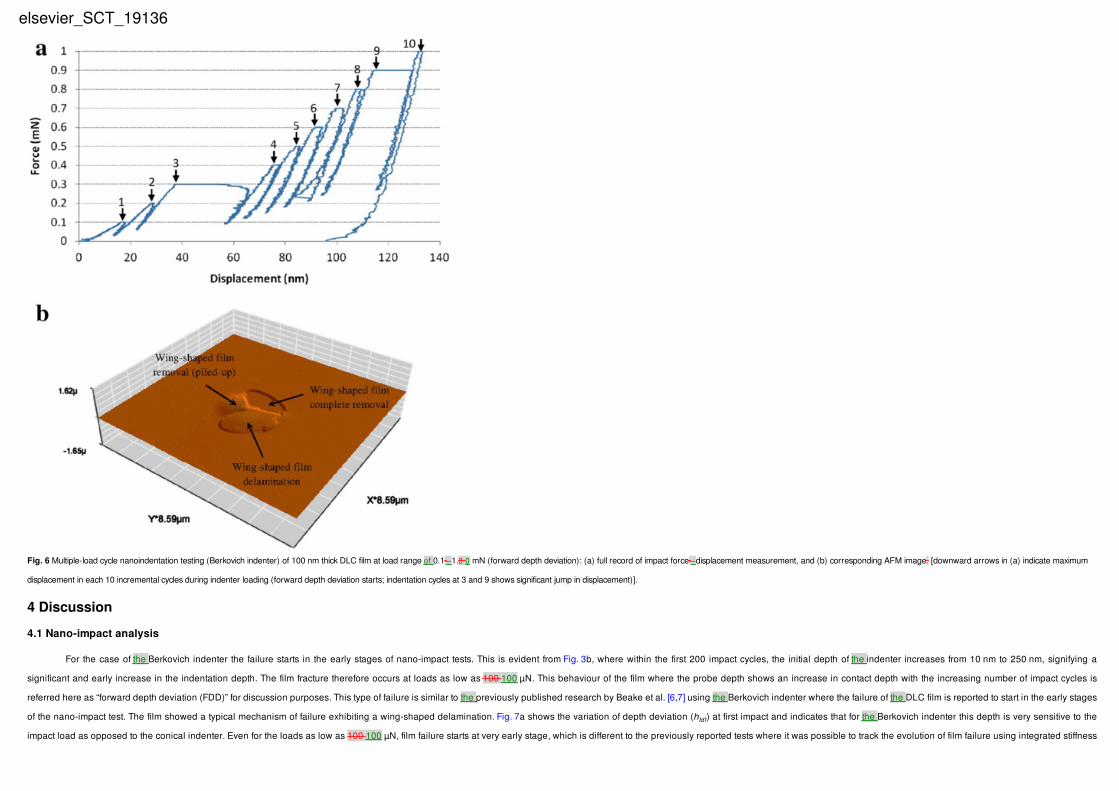
images after the indentation cycles. Fig. 5c shows the cross-section of the residual topography through the centre. Fig. 6 shows the profile of load-displacementthe load–displacement (P-–h) curve and corresponding AFM image of the multiple-load cycle
nanoindentation test using the Berkovich indenter in the load range of 0.1-–1.0 0 mN.
Fig. 4 Nano-impact testing (conical indenter) of 100 nm thick DLC film at 250 250 µN load: (a) full record of depth-–time measurement, (b) corresponding magnified boxed-view of view of early stage of impacts, (c) corresponding AFM image, and (d) topography passing through the centre of
residual impression indicated with an arrow to the line TT'′ in (c). [hfd1: forward depth at first impact cycle, hfdm: maximum forward depth deviation (start of backward deviation), Nfdm: number of impact (fatigue) cycles after which backward depth deviation starts, Nbd: number of impact (fatigue)
cycles after which negative depth starts (backward depth deviation)].
elsevier_SCT_19136

Fig. 5 Typical multiple-load cycle nanoindentation (conical indenter) record of force-–displacement measurement of 100 nm thick DLC film at load ranges: (i) 1 1 mN to 10 10 mN [upward arrow indicates maximum displacement in each cycle during loading stage (backward depth deviation starts)];
and (ii) 10 10 mN to 100 100 mN [horizontal arrow indicates maximum displacement in cycles during loading (neither forward nor backward depth deviation); downward arrows indicate maximum displacement in cycles during loading (forward depth deviation starts)]; where (a) P-–h curve, (b)
corresponding AFM images after finish of the process and (c) corresponding cross-sectional topography passing through the centre of residual impression indicated with a dotted TT'′ line in (b).
elsevier_SCT_19136
4 Discussion
4.1 Nano-impact analysis
For the case of the Berkovich indenter the failure starts in the early stages of nano-impact tests. This is evident from Fig. 3b, where within the first 200 impact cycles, the initial depth of the indenter increases from 10 nm to 250 nm, signifying a
significant and early increase in the indentation depth. The film fracture therefore occurs at loads as low as 100 100 µN. This behaviour of the film where the probe depth shows an increase in contact depth with the increasing number of impact cycles is
referred here as “forward depth deviation (FDD)” for discussion purposes. This type of failure is similar to the previously published research by Beake et al. [6,7] using the Berkovich indenter where the failure of the DLC film is reported to start in the early stages
of the nano-impact test. The film showed a typical mechanism of failure exhibiting a wing-shaped delamination. Fig. 7a shows the variation of depth deviation (hfd1) at first impact and indicates that for the Berkovich indenter this depth is very sensitive to the
impact load as opposed to the conical indenter. Even for the loads as low as 100 100 µN, film failure starts at very early stage, which is different to the previously reported tests where it was possible to track the evolution of film failure using integrated stiffness
Fig. 6 Multiple-load cycle nanoindentation testing (Berkovich indenter) of 100 nm thick DLC film at load range of 0.1-–1.0 0 mN (forward depth deviation): (a) full record of impact force-–displacement measurement, and (b) corresponding AFM image. [downward arrows in (a) indicate maximum
displacement in each 10 incremental cycles during indenter loading (forward depth deviation starts; indentation cycles at 3 and 9 shows significant jump in displacement)].
elsevier_SCT_19136

and depth sensing approach using the Berkovich indenter [21]. The schematic of the failure mechanism previously reported using the integrated stiffness and depth sensing approach is shown in Fig. 8 to aid the discussion. This is mainly because the
mechanism of loading in the current investigation imparts a higher energy to the contact due to the pendulum motion of the loading mechanism, and also due to the absence of constant contact stiffness in this loading arrangement. Both of these differences
were partly overcome by the use of a conical indenter.
elsevier_SCT_19136

Fig. 7 Nano-impact test response of 100 nm DLC film: (a) forward depth deviation at first impact cycle (hfd1) compared between Berkovich and conical indenter using NanoTest® system, (b) number of impact fatigue cycle to initiate adhesive failure (Nfa) under Berkovich indenter using
TriboIndenter® system, and number impact cycles after which negative depth starts (Nbd) leading to adhesive failure under conical indenter using NanoTest® system, and (c) maximum forward depth deviation (hfdm) and corresponding number of impact cycle (Nfdm) using conical indenter using
NanoTest® system. The error bars indicate the standard deviation of the data.
elsevier_SCT_19136

Fig. 8 Schematic of five stage failure mechanism in thin film-–substrate system using Berkovich indenter using integrated stiffness and depth sensing approach: (a) stage-1 showing increase in indentation depth (sinking-in), (b) stage-2 showing vertical cracks (similar to median vent) due to
columnar structure and tensile stress at the edge of contact, cohesive failure starts, (c) stage-3 showing vertical cracks reach the interface leading to debonding at the film/substrate interface, (d) stage-4 showing debonding continues at the interface, and (e) stage-5 showing significant film failure,
and (ii) schematic relationship between contact stiffness, contact depth and the number of impact fatigue cycles identifying five stages of film failure [S: substrate, F: film] [21].
elsevier_SCT_19136

For the case of the conical indenter (Fig. 4), it can be observed from the early stage of impact cycles that the hysteresis curve (depth vs. time) is indicative of sagging of the film for lower load test at 250 250 µN. However during the later stage of the
test, contact depth begun to decrease with the number of contact cycles. This behaviour of decrease in contact depth with the increasing number of impact cycles is consistent with the previously reported results and is referred to as “backward depth deviation
(BDD)” in this discussion. The onset of change in behaviour from FDD to BDD is indicated as hfdm and corresponding number of impact cycle Nfdm in Fig. 4b. At higher loads (500 500 µN, 750 750 µN and 1000 1000 µN), although the contact depth of the
indenter is still below the DLC film thickness of 100 nm, the curve is still backward depth deviating. This behaviour of BDD is indicative of film delamination at the film/substrate interface as observed in the topography map shown in Fig. 4d. It is this same
peculiar behaviour of backward depth deviation (or hogging) which was observed in earlier investigations but could not be understood due to the absence of in-situ AFM imaging in previous investigations [35,36].
Based upon the aforementioned definition of adhesive film failure as the start of BDD, the number of stress cycles to adhesive failure can be quantified as Nbd (conical), which can also then be compared with the previously reported number of stress
cycles to failure Nfa (Berkovich) using the integrated stiffness and depth sensing approach [21]. Fig. 7b provides this comparison and indicates that the number of stress cycles to failure is comparable for both loading mechanisms and provide complimentary
information about the evolution of film failure. The integrated stiffness and depth sensing results of adhesive failure were reported for the Berkovich indenter (Nfa) and it was anticipated that the conical indenter results shown in Fig. 7b would indicate higher
fatigue limit for similar test loads, due to conical indenter geometry which reduces stress concentrations in the contact zone. This difference is attributed to faster crack growth due to an open loop loading mechanism of the loading mechanism reported in the
current investigation, where the entire (100%) load is released allowing the residual stress in the film to drive cracks faster when compared to the previously used closed loop system [21], where 10% of the compressive load was maintained throughout the
duration of the test. Other factors which influence the results are the impact load due to pendulum mechanisms, and the difference in the stress field due to the differences in the shape of indenters used for comparison in Fig. 7b.
Another factor which needs to be considered here is the definition of failure which is different in the two loading mechanisms. In the current case only contact depth information is used to define failure, whereas in the previous investigation an
integrated stiffness and depth sensing information defines the onset of failure. Fig. 7c shows that the maximum FDD depth (hfdm) increaseincreases, and the corresponding number of impact cycles (Nfdm) decreasedecreases, with the increasing impact loads.
Based on these results, a schematic representation of the forward and backward depth deviation deviations is presented in Fig. 9. Hence on the basis of these observations, e.g., depth vs. time plot and AFM images shown in Figs. 3 and 4, the mechanism of
nano-impact (low-cycle fatigue) film failure for the conical indenter can be summarized in three stages: (a) stage 1: forward depth deviation leading to deformation of the thin film and the substrate; (b) stage 2: mismatch in the interfacial strain leads to thin film
delamination from the film/substrate interface; and (c) stage 3: backward depth deviation of the indenter caused by the delaminated film. This mechanism of failure for the conical indenter (Fig. 9b) is similar to that shown in Fig. 8 except for the cracks within the
film which do not occur in the case of the conical indenter. Hence the contact depth (hc) variation with the number of stress cycles shown in Fig. 8(ii) represents the initial increase (from hfd1 to hfdm representing stage 1 of failure in Fig. 8(ii)) and then the decrease
in contact depth with time or number of impacts (Stage stages 2 to 4 in Fig. 8(ii)) shown in Fig. 4. This comparison is further strengthened on the basis of multiple-load cycle nanoindentation analysis in the next section.
elsevier_SCT_19136

The differences in loading mechanisms also lead to the differences in the loading history e.g. in terms of the strain rate. Trelewicz et al.and Schuh has have indicated that the indentation strain rate (ε.) can be approximated as ε. ≈ vin × hmax-− 1, where
hmax is the maximum penetration depth and vin is the velocity of the indenter at the point of contact [37]. The maximum penetration depth in the current impact analysis was of the order of 20 nm for the FDD of the conical indenter (Fig. 7c). Constantinides et al.
has have indicated that the for various loading conditions vin for the NanoTest™ system can range from 0.7 mm/s to 2.5 mm/s [38]. As the load was low in the current investigation, a lower value of 0.7 mm/s can be assumed as average to cover the loading
range considered in this investigation. This will give an approximate strain rate (ε.) of ≈ 0.35 × 10⁵ s-− 1, which is with value orders of magnitude higher.
Although both loading mechanisms and differences associated with their loading history discussed above provide complementary information about the evolution of film failure, the exact choice of test methodology will depend upon the tribological
application and in some cases both test methods can be employed to better understand film failure. Other considerations such as the total energy and momentum at impact should also be considered when trying to mimic the loading conditions in an
accelerated tribological test. These instruments for example may be used to evaluate the damage analysis on solar panels during a sand storm with a typical sand particle velocity of 50 km/hrh ≈ 1.4 × 104 mm/s. Although such velocity is not achievable by the
indenting probes in either of the systems discussed above, there is difference in the mass of the indenter (effective mass of pendulum and tip is 0.21 kg for the NanoTest™ system [37,38]) and the mass of typical sand particle (≈ 10-− 5 kg to 10-− 6 kg). This
difference in mass can be used to compensate the lower impact velocity of the nanoindentation system, and hence can impart the correct momentum and energy during the dynamic contact. Similarly, the approach adapted above can be expanded to evaluate
other coating substrate systems, where hard and brittle coatings are deposited on relatively softer/ductile substrates.
Another aspect which needs to be considered is that nano-impact tests represent a high strain rate loading on the coating substrate system [39]. Silicon is sensitive to high strain rate phase transformations e.g. as recently reported by Beake et al. [40].
However, their investigation indicated that such phase transformations occurred at much higher loads of 100 100 mN to 500 500 mN than the maximum load of 1 mN considered in the current investigation. Hence the probably probability of strain related phase
transformation in the silicon substrate in the current investigation is very low and not investigated further.
Fig. 9 Schematic of the thin film failure (residual impression) with pre-existing compressive residual stress during nano-impact testing showing the mechanism of forward and backward depth deviation deviations under different nanoindenter shape: (a) Berkovich, and (b) conical [σc is pre-existing
compressive residual stress in the film].
elsevier_SCT_19136

4.2 Multiple-load cycle nanoindentation analysis
The loading mechanism of the multiple-load cycle nanoindentation tests were was akin to maintaining continuous contact stiffness between the indenter and film/substrate combination throughout the test; albeit at lower strain rate and number of
stress cycles, when compared to the previously reported integrated stiffness and depth sensing approach [21]. However the lower number of stress cycles and strain rate was compensated by higher and constantly increasing force in the current investigation.
Hence this approach was very similar to the previous investigation except that higher loads accelerated the mechanism of film failure. As summarised in Figs. 5 and 6, there was a tendency for BDD at lower loads (1-–10 mN) using the conical indenter,
whereas at higher loads or with the Berkovich indenter the film failure generally occurred in FDD. Hence, in Fig. 5a(i), each holding curve is backward progressing in contrast to Fig. 5a(ii). Once again as discussed earlier, the type of indentation cycle where the
loading force is less than the unloading force (i.e. PL < PU) is referred here in the discussion as BDD [41,42].
Table 2 summarise summarises the types of P-–h profiles under the conical indenter, indicating combination of FDD and BDD for the lower load range (0.1-–1 mN, 1-–10 mN), and FDD at higher load range (10-–100 mN, e.g. Fig. 5(ii)). The FDD and
BDD response was consistent for each loading cycle in individual tests (Figs. 5 and 6) i.e. there was no evidence of P-–h profiles which indicated a combination of BDD and FDD, suggesting a critical value of nanoindentation load at which BDD occurred with
the conical indenter. The corresponding AFM images, i.e. Figs. 5b(i) and 5c(i) indicates indicate a BDD at a lower load range, whereas, Fig. 5b(ii) and c(ii) indicate indicates FDD at a higher load range (10-–100 mN) with the same conical indenter. The
observation of film delamination at the film/substrate interface as indicated in the AFM images in Figs. 4c,d and 5b(i),c(i) is similar to stages 2 to 5 shown in Fig. 8, except for the cracks within the film which are not formed for the case of the conical indenter in
the current investigation. In the current investigation the film responded in a different manner for the case of the Berkovich indenter. Under a Berkovich indenter, it was identified that the DLC film can fracture within the first few indentation cycles at a load as low
as 0.3 3 mN (e.g. Fig. 6).
Table 2 Summary of load-displacementload–displacement (P-–h) profile under the conical indenter.
Sl. no. Indentation load range (mN) Forward depth deviation (FDD) repeats out of 3 Backward depth deviation (BDD) repeats out of 3
1 0.1-–1 2 1
2 1-–10 1 2
3 10-–100 3 0
The FDD-–BDD transition for the conical indenter at lower loads was related to the film thickness. To gain more and relevant insights, an axi-symmetric elastic finite element model (FEM) was developed to understand the relationship between the
critical stress fields in relation to the indentation load and film thickness. A methodology of the FEM simulation used in this work is described elsewhere [41]. For the purpose of brevity, only the relevant results are directly presented here. The FEM analysis
indicated in Fig. 10a shows contour maps of the von-Mises stress during indentation of the DLC film using the spherical indenter at two different loads of 0.1 1 mN and 1 1 mN. Comparing Fig. 10a with Fig. 10b, a distinct shift is evident in the magnitude of the
maximum stress (von-Mises) from the film towards the film-–substrate interface and then into the substrate with the increase in indentation load from 0.1 1 mN to 10 10 mN. The maximum stress field near the film-–substrate interface and a mismatch in the
maximum subsurface stress field appears appear to be responsible for interfacial strain and delamination at the film film–substrate interface in the tests performed in 0.1 1 mN to 10 10 mN load range. Hence, at low load range (0.1-–1 mN and 1-–10 mN), film
and film/substrate interface plays a significant role in the deformation mechanics whereas, at higher loads (10 10 mN to 100 100 mN), the substrate plays a dominant role as the maximum stress occurs within the substrate. Observation of the AFM topography
(Fig. 5c(i)) also suggests debonding of the DLC film at the film-–substrate interface (adhesive failure). It is for this reason it is concluded that the tendency of BDD, which only occurs at lower loads with the conical indenter, was due to the location of maximum
stress field at the film/substrate interface which leads to coating delamination at this interface (Fig. 5c(i)). The absence of BDD for all tests conducted with the Berkovich indenter indicates catastrophic film fracture after few stress cycles leading to large FDD of
the indenter (Fig. 6).
elsevier_SCT_19136

4.3 MD simulation analysis
Fig. 11 shows the MD simulation force-–displacement (P-–h) plot of the indenter during single loading and unloading cycle of a conical indenter travelling with a velocity of 50 m/s. The force variation shown in Fig. 11 relates to the deformation,
cohesion and de-cohesion of atoms. This plot can be divided into various stages as indicated in the figure. It was observed from the simulation that the indenter started experiencing the forces at point A. At point B, a first jump-out-contact (JC) was observed. It
has been highlighted earlier by Landman et al. [2] that even when the atoms of the tip and substrate are strained they try to optimize their embedding energies while maintaining their individual material cohesive binding energies. This leads to a JC contact in
the P-–h plot during loading.
Fig. 10 Snapshot of an axi-symmetric FEM model (ABAQUS v6.10-1) showing the stress contours during nanoindentation of 100 nm thick DLC film at loads: (a) 0.1 1 mN and (b) 1 1 mN using a spherical indenter. Arrows indicate the position and magnitude of maximum stress (von Mises) at the
film-–substrate (stress magnitude scale × 10 GPa).
elsevier_SCT_19136

As the indenter continues to move, a monotonic increase of forces can be seen until point C, where the C C bonds were observed to fracture in order to accommodate the indenter in the crystalline carbon film. Due to the fracture of the film at this
point, the forces on the indenter decreases decrease suddenly. Following this point with continued advancement of the indenter, other C C bonds stretch further, which causes an increase in the force on the indenter. This increase also exhibited monotonic
nature until point D where the forces were found to decrease. Simulation video showed that this sudden drop at point D was on account of the disturbances in the crystal lattice structure in the substrate, which is not unusual given the small thickness of the film
used in MD simulation. Silicon being softer than carbon film offers lower resistance to deformation. Consequently, change in the crystal structure of silicon facilitates deformation and pronounced sagging of the carbon film at point D. These were the major
stages captured from the simulation during the loading stage of the indenter.
During unloading, the indenter retracts and consequently the force on the indenter decreases. During this stage, the carbon film restores its original position until point E. Thereafter however, cohesion between the carbon atoms and indenter tip
become pronounced. The resultant cohesive forces work against each other in such a way that the C C atoms pull the indenter towards the carbon film while the indenter moves in a direction away from the carbon film. The retraction force of the indenter
was substantially larger than the cohesive force and hence a force hysteresis in the form of negative force on the indenter was seen between point E and point F.
At point F, as the indenter continues to retract, the cohesive bond length between the carbon atoms of the carbon film and the indenter stretches to its maximum limit. Beyond this point, the ultimate separation occurs when the inter-atomic distance
between the last two bonded C C atoms exceeds 1.75 Å. From the literature [43], it was found that, 1.75 Å is the maximum possible bond length between the two carbon atoms which is found consistent with the current observation. The force hysteresis
therefore originated from the cohesive dynamics between the carbon thin film and the diamond tip.
Although the quantitative measure of separation distance [43] of the C C bond of 1.75 Å provide provides confidence in the MD simulation, authors also conducted an evaluation of the modulus of elasticity from the loading and unloading curve
shown in Fig. 11. This was accomplished by applying the Oliver and Pharr method [25] to estimate the value of the elastic modulus of the specimen (E) from the P-–h curve obtained from the MD simulation plot. The Oliver and Pharr method enables one to
estimate the contact area directly from the P-–h curve without assessment of the actual contact area of the indenter. This way, during indentation up to a depth of 1.5 nm (83% of the film thickness), the elastic modulus of the film was obtained as 405 GPa. This
value of the elastic modulus measured from the MD simulation is not only for a crystalline system, but also reflect a combination of film/substrate modulus due to 83% penetration depth. Elastic modulus measured from the MD simulation is higher than the
Fig. 11 Force-–displacement profile obtained from molecular dynamics simulation.
elsevier_SCT_19136

experimentally measured value (153 ± 4 GPa for the DLC film, Section 3.1) or that of a Si wafer (typically 130 GPa [44]). Authors would like to posit that the indentation in the MD simulation was performed in a crystalline carbon film. In practice, the DLC film
contains traces of sp3 carbon distributed in a stochastic manner. During experimental nanoindentation, it is highly likely that a particular sp3 grain is encountered by the indenter. The MD simulation model size is extremely small and is thus considerable as one
such instance. The value of E obtained as 405 GPa is indeed an intermediate value of crystalline carbon film (E = 1000 GPa) and the silicon substrate (E = 130 GPa), and thus represents an upper bound solution of the elastic modulus of a film the
film–substrate system, where a crystalline carbon film is deposited on a Si wafer. Had it been considered as an amorphous DLC film having bulk traces of sp2, the E value would have been closer to 153 GPa.
It compounds further with the fact that this measurement is dependent strongly on the depth of the indentation, indenter shape and velocity. It is difficult to obtain a close value between MD and experimental results owing primarily to the differences
such as sample roughness, air lubrication, sensitivity of the equipment, purity of the material, crystal structure, residual stress and accuracy of the measurements, which may all influence the experimental results. The features embedded in the
force-–displacement loading and unloading curves in MD simulation provide useful quantitative and qualitative insights, and an understanding of film deformation atomic level.
5 Conclusions
Two different approaches of nanoscale fatigue i.e. nano-impact tests and multiple-loading cycle nanoindentation tests are presented in this paper and compared with the previously reported investigation based on integrated stiffness
and depth sensing approach. The main findings of the work can be concluded as follows.
a) The open loop loading mechanism of nano-impact tests provides quantitative fatigue evaluation of the DLC film which is comparable to the closed loop integrated stiffness and depth sensing approach. However, this was dependent upon the indenter shape where only the conical
indenter provided meaningful results of nanoscale fatigue in the current investigation.
b) The multiple loading cycle nanoindentation tests provided further insights to the mechanism of film failure in the form of backward depth deviation of P-–h curves with the conical indenter. Film failure mechanism highlighted in this test was similar to that observed in the previous
findings using closed loop integrated stiffness and depth sensing approach. Hence both test methods provide complimentary information on the failure mechanism, however, the shape of the indenter plays a dominant role in ascertaining this comparison.
c) Backward depth deviation of the film only occurred at lower loads with the conical indenter. This was attributed to the presence of maximum stress field near the film/substrate interface leading to coating delamination at this interface.
d) The MD simulation provides atomic level interactions between the indenter and the film. The elastic modulus of the film measured using MD simulation was higher than that experimentally measured which is attributed to the factors related to the presence of material defects,
crystalline structure, residual stress, indenter geometry and loading/unloading rate differences between the MD and experimental results.
Acknowledgements
Authors are grateful for the support of Alfaisal University, Riyadh, Saudi Arabia in conducting part of the experimental work.
References
[1]
M. Moseler, P. Gumbsch, C. Casiraghi, A.C. Ferrari and J. Robertson, Science 309, 2005, 1545.
[2]
U. Landman, W.D. Luedtke, N.A. Burnham and R.J. Colton, Science 248, 1990, 454.
[3]
B. Bhushan, J.N. Israelachvili and U. Landman, Nature 374, 1995, 607.
[4]
X.D. Li and B. Bhushan, Scr. Mater. 47, 2002, 473.
[5]
B.D. Beake, M.J.I. Garcia and J.F. Smith, Thin Solid Films 398–399, 2002, 438.
[6]
B.D. Beake, S.P. Lau and J.F. Smith, Surf. Coat. Technol. 177–178, 2004, 611.
elsevier_SCT_19136

[7]
B.D. Beake, S.R. Goodes, J.F. Smith, R. Madani, C.A. Rego, R.I. Cherry and T. Wagner, Diamond Relat. Mater. 11, 2002, 1606.
[8]
G.S. Fox-Rabinovich, B.D. Beake, J.L. Endrino, S.C. Veldhuis, R. Parkinson, L.S. Shuster and M.S. Migranov, Surf. Coat. Technol. 200, 2006, 5738.
[9]
B.D. Beake, G.S. Fox-Rabinovich, S.C. Veldhuis and S.R. Goodes, Surf. Coat. Technol. 203, 2009, 1919.
[10]
K.D. Bouzakis, M. Batsiolas, G. Malliaris, M. Pappa, E. Bouzakis and G. Skordaris, Key Eng. Mater. 438, 2010, 107.
[11]
K.D. Bouzakis, M. Pappa, G. Skordaris, E. Bouzakis and S. Gerardis, Surf. Coat. Technol. 205, 2010, 1481.
[12]
B. Bhushan and X. Li, Int. Mater. Rev. 48, 2003, 125.
[13]
B. Bhushan, Wear 259, 2005, 1507.
[14]
S. Zhang, D. Sun, Y.Q. Fu and H. Du, Surf. Coat. Technol. 198, 2005, 74.
[15]
JJJ.J. Wang, AJA.J. Lockwood, YY. Peng, XX. Xu, MSM.S. Bobji and BJB.J. Inkson, Nanotechnology 20, 2009, 1, (art no. 305703).
[16]
T.D. Raju, K. Nakasa and M. Kato, Acta Mater. 51, 2003, 457.
[17]
B. Bhushan and X. Li, Inter. Mater. Rev. 48, 2003, 125.
[18]
J.L. Liou, P.J. Wei, W.L. Liang, C.F. Ai and J.F. Lin, J. Appl. Phys. 103, 2008, 103505.
[19]
J.M. Cairney, R. Tsukano, M.J. Hoffman and M. Yang, Acta Mater. 52, 2004, 3229.
[20]
A. Yonezu, B. Xu and X. Chen, Thin Solid Films 518, 2010, 2082.
[21]
RR. Ahmed, YQY.Q. Fu and NHN.H. Faisal, ASME J. Tribol. 134, 2012, (art no. 012001).
[22]
elsevier_SCT_19136

Y.Q. Fu, J.K. Luo, A.J. Flewitt and W.I. Milne, Appl. Surf. Sci. 252, 2006, 4914, (2006).
[23]
C.A. Klein, J. Appl. Phys. 88, 2000, 5487.
[24]
V.A.C. Haanappel, D.V.D. Vendel, H.S.C. Metselaar, H.D. van Corbach, T. Fransen and P.J. Gellings, Thin Solid Films 254, 1995, 153.
[25]
W.C. Oliver and G.M. Pharr, J. Mater. Res. 7, 1992, 1564, (1992).
[26]
S.J. Cho, K.R. Lee, K.Y. Eun, J.H. Hahn and D.H. Ko, Thin Solid Films 341, 1999, 207.
[27]
N.H. Faisal and R. Ahmed, Recent Patents Mech. Eng. 4, 2011, 138.
[28]
S. Plimpton, J. Comput. Phys. 117, 1995, 1.
[29]
W. Humphrey, A. Dalke and K. Schulten, J. Mol. Graph. 14, 1996, 33.
[30]
A. Stukowski, Model. Simul. Mater. Sci. Eng. 18, 2010, 1.
[31]
P. Erhart and K. Albe, Phys. Rev. B 71, 2005, 035211.
[32]
D.W. Brenner, Phys. Rev. B 42, 1990, 9458.
[33]
N.H. Faisal, J.A. Steel, R. Ahmed and R.L. Reuben, J. Therm. Spray Technol. 18, 2009, 525.
[34]
NHN.H. Faisal, RLR.L. Reuben and R. Ahmed, Meas. Sci. Technol. 22, 2011, 1, (art no. 015703).
[35]
M.D. Drory and JWJ.W. Hutchinson, Proc. R. Soc. Lond. A 452A, 1996, 2319.
[36]
M.J. Cordill, D.F. Bahr, N.R. Moody and W.W. Gerberich, IEEE Trans. Device Mater. Rel. 4, 2004, 163.
[37]
J.R. Trelewicz and C.A. Schuh, Appl. Phys. Lett. 93, 2008, 171916.
elsevier_SCT_19136

[38]
G. Constantinides, C.A. Tweedie, N. Savva, J.F. Smith and K.J. VanVliet, Exp. Mech. 49, 2009, 511.
[39]
J.M. Wheeler and A.G. Gunner, Surf. Coat. Technol. 232, 2013, 264.
[40]
B.D. Beake, T.W. Liskiewicz and J.F. Smith, Surf. Coat. Technol. 206, 2011, 1921.
[41]
N.H. Faisal, R. Ahmed, Y.Q. Fu, Y.O. Elakwah and M. Alhoshan, Mater. Sci. Technol. 28, 2012, 1186.
[42]
NHN.H. Faisal, RR. Ahmed, YQY.Q. Fu, MM. Hadfield and M. Alhoshan, WIT Trans. Eng. Sci. Tribol. Des. II ISSN: 1743-3533, 76, 2012, 43, (on-line).
[43]
A.A. Zavitsas, J. Phys. Chem. A 107, 2003, 897.
[44]
M.A. Hopcroft, W.D. Nix and T.W. Kenny, J. Microelectromech. Syst. 19, 2010, 229.
Highlights
• Test strategies and probe geometry on nanoscale fatigue of DLC film investigated
• Nano-impact and multiple-loading cycle nanoindentation tests investigated
• Test results are sensitive to applied load, load mechanism, test and probe-type.
• Molecular dynamics/finite element analysis of DLC nanoindentation were was performed.
• Choice of testing should be determined by the tribological conditions.
Queries and Answers
Query: Please confirm that given names and surnames have been identified correctly.
Answer: Yes.
elsevier_SCT_19136