Influence of temperature and pressure on the static contact resistance of vacuum heat-treated...
12
Influence of temperature and pressure on the static contact resistance of vacuum heat-treated polyacrylonitrile films Sylvie Guessab * , Lionel Boyer, Fre ´de ´ric Houze ´, Sophie Noe ¨l, Olivier Schneegans Laboratoire de Ge ´nie E ´ lectrique de Paris, UMR CNRS 8507, Universite ´s Paris VI et XI, Supe ´lec, Plateau de Moulon, F91192 Gif-sur-Yvette Cedex, France Received 23 February 2000; accepted 28 July 2000 Abstract The protection against corrosion of low-level electrical contacts is usually insured by metallic terminal coatings. However, they can be degraded by wear and corrosion, which finally causes the failure of the contacts. The field we have been investigating, consists of replacing the terminal metallic layer by an organic conducting film, derived from polyacrylonitrile (PAN) by heat-treatment. In this paper, we present results concerning the static contact resistance (R c ) measured in a ball/plane configuration on metallic coupons over-layered with PAN films and heated under high vacuum at several temperatures: R c at room temperature under a constant normal load; R c at room temperature varying the normal load; R c at a constant normal load varying the temperature of the contact. These experiments reveal a transitional heat- treating temperature. Above this temperature, the film is very conducting and the behavior of the contact is ruled by the metallic electrodes. Below this temperature, the film is moderately conducting and then responsible for the contact resistance. In that case, pressure and temperature dependencies of the contact show that variable-range hopping is the most probable transport mechanism. At the transitional annealing temperature, the values of the contact resistance are scattered. Electrical investigations with a modified atomic force microscope (AFM) show that the film is covered by a very thin layer, non-adherent and poorly conducting. # 2001 Elsevier Science B.V. All rights reserved. Keywords: Electrical contact resistance; Polyacrylonitrile; Heat-treatment; Piezoconductivity; Variable-range hopping; Atomic force microscopy 1. Introduction We have been exploring for several years, an original way for the improvement of the performances and the reliability of low-level electrical contacts: the use of solid organic films as a substitute for terminal metallic coatings. Our researches are focused on films derived from polyacrylonitrile (PAN) by annealing, that offer some decisive advantages: PAN can be grafted on metallic surfaces by electroche- mical deposition, which allows to make very adherent and covering films; though it is initially strongly insulating, it can be made conducting by annealing. Our process consists of depositing films of PAN on metallic substrates. After heat-treatment of the samples, electrical properties are systematically evaluated, using a specific device: the contact resistance R c in a ball/plane configuration is measured, as a function of controlled para- meters, such as the normal load (L) between the ball and the plane, or the temperature of the contact (T cont ). Since the beginning of our investigations on the potentialities of PAN- derivative films for a contact application, we have been testing different configurations of samples, varying the substrate, the thickness of the PAN layer, the modes of deposition and heat-treatment. Our first objective was to elaborate samples in accordance with industrial require- ments. Confronted with inexplicable results attributed to the roughness of the substrate, we changed the orientation of our study to make reproducible, perfectly defined and con- trolled samples. Promising results extracted from previous series of samples have already been presented [1–3]. This paper is concerning this last series of samples. We first describe how they have been elaborated, then we develop original electrical results, attesting for the transfor- mation of the PAN films induced by heat-treatment: R c measured at room temperature under a constant normal load; Synthetic Metals 118 (2001) 121–132 * Corresponding author. Tel.: 33-1-69-85-14-09; fax: 33-1-69-85-14-29. E-mail address: [email protected] (S. Guessab). 0379-6779/01/$ – see front matter # 2001 Elsevier Science B.V. All rights reserved. PII:S0379-6779(00)00400-8
-
Upload
independent -
Category
Documents
-
view
1 -
download
0
Transcript of Influence of temperature and pressure on the static contact resistance of vacuum heat-treated...

In¯uence of temperature and pressure on the static contactresistance of vacuum heat-treated polyacrylonitrile ®lms
Sylvie Guessab*, Lionel Boyer, FreÂdeÂric HouzeÂ, Sophie NoeÈl, Olivier SchneegansLaboratoire de GeÂnie EÂ lectrique de Paris, UMR CNRS 8507, UniversiteÂs Paris VI et XI, SupeÂlec,
Plateau de Moulon, F91192 Gif-sur-Yvette Cedex, France
Received 23 February 2000; accepted 28 July 2000
Abstract
The protection against corrosion of low-level electrical contacts is usually insured by metallic terminal coatings. However, they can be
degraded by wear and corrosion, which ®nally causes the failure of the contacts. The ®eld we have been investigating, consists of replacing
the terminal metallic layer by an organic conducting ®lm, derived from polyacrylonitrile (PAN) by heat-treatment. In this paper, we present
results concerning the static contact resistance (Rc) measured in a ball/plane con®guration on metallic coupons over-layered with PAN ®lms
and heated under high vacuum at several temperatures: Rc at room temperature under a constant normal load; Rc at room temperature
varying the normal load; Rc at a constant normal load varying the temperature of the contact. These experiments reveal a transitional heat-
treating temperature. Above this temperature, the ®lm is very conducting and the behavior of the contact is ruled by the metallic electrodes.
Below this temperature, the ®lm is moderately conducting and then responsible for the contact resistance. In that case, pressure and
temperature dependencies of the contact show that variable-range hopping is the most probable transport mechanism. At the transitional
annealing temperature, the values of the contact resistance are scattered. Electrical investigations with a modi®ed atomic force microscope
(AFM) show that the ®lm is covered by a very thin layer, non-adherent and poorly conducting. # 2001 Elsevier Science B.V. All rights
reserved.
Keywords: Electrical contact resistance; Polyacrylonitrile; Heat-treatment; Piezoconductivity; Variable-range hopping; Atomic force microscopy
1. Introduction
We have been exploring for several years, an original way
for the improvement of the performances and the reliability
of low-level electrical contacts: the use of solid organic ®lms
as a substitute for terminal metallic coatings. Our researches
are focused on ®lms derived from polyacrylonitrile (PAN)
by annealing, that offer some decisive advantages:
� PAN can be grafted on metallic surfaces by electroche-
mical deposition, which allows to make very adherent and
covering films;
� though it is initially strongly insulating, it can be made
conducting by annealing.
Our process consists of depositing ®lms of PAN on
metallic substrates. After heat-treatment of the samples,
electrical properties are systematically evaluated, using a
speci®c device: the contact resistance Rc in a ball/plane
con®guration is measured, as a function of controlled para-
meters, such as the normal load (L) between the ball and the
plane, or the temperature of the contact (Tcont). Since the
beginning of our investigations on the potentialities of PAN-
derivative ®lms for a contact application, we have been
testing different con®gurations of samples, varying the
substrate, the thickness of the PAN layer, the modes of
deposition and heat-treatment. Our ®rst objective was to
elaborate samples in accordance with industrial require-
ments. Confronted with inexplicable results attributed to
the roughness of the substrate, we changed the orientation of
our study to make reproducible, perfectly de®ned and con-
trolled samples. Promising results extracted from previous
series of samples have already been presented [1±3].
This paper is concerning this last series of samples. We
®rst describe how they have been elaborated, then we
develop original electrical results, attesting for the transfor-
mation of the PAN ®lms induced by heat-treatment:
� Rc measured at room temperature under a constant normal
load;
Synthetic Metals 118 (2001) 121±132
* Corresponding author. Tel.: �33-1-69-85-14-09;
fax: �33-1-69-85-14-29.
E-mail address: [email protected] (S. Guessab).
0379-6779/01/$ ± see front matter # 2001 Elsevier Science B.V. All rights reserved.
PII: S 0 3 7 9 - 6 7 7 9 ( 0 0 ) 0 0 4 0 0 - 8

� the evolution of Rc when the normal load L is varied from
4 to 100 gf (loading), then from 100 to 4 gf (unloading);
� the evolution of Rc when Tcont is varied from 100 to
ÿ1008C.
As an intermediate heat-treating temperature revealed
results dif®cult to analyze, we describe in the following
further investigations we achieved on the concerned sample,
using an original laboratory-made device, derived from an
AFM, which can achieve simultaneous cartographies of both
topography and local electrical contact resistance [4±5]. We
summarize our results, discuss them and conclude in the last
part of the paper.
2. Samples preparation
We have selected the substrate, considering it, ®rstly, to be
metallic to allow electrical measurements, secondly, to
present a very low roughness, and lastly, to form with
PAN ®lms an interface resisting to intense heat-treatments.
The chosen substrate consists of hard steel coupons
20 mm� 10 mm� 1 mm, carefully polished, with an
over-layer of 2 mm of nickel deposited by RF magnetron
sputtering. Some characteristics of the as received steel are
shown in Table 1. The conditions of deposition of nickel are
given in Table 2. The PAN ®lm is deposited by spin-coating.
Its thickness (1 mm) has been chosen to be more than 10
times greater than the maximum peak-valley height on the
substrate, and is systematically controlled by pro®lometry
measurements. The roughness and the morphology of the
surfaces are examined by atomic force microscopy (AFM) at
every stage of the elaboration.
The mode of heat-treatment was chosen intense enough to
perform signi®cant transformation of thick PAN ®lms. Thus,
the samples were pyrolyzed in a tubular furnace in high
vacuum (10ÿ6 Torr). The temperature was raised from the
ambient temperature up to a maximum (Tmax) at the rate of
28C minÿ1, and then quickly decreased to room temperature.
We have realized several heat-treatments, at Tmax � 550,
600, 650, 7008C. The electrical results we present in this
paper, revealed a crucial transition between 550 and 6008C.
Consequently, an intermediate annealing has been per-
formed at Tmax � 5758C.
Pro®lometry measurements show that our ®lms get nota-
bly thinner after the heat-treatment: the thickness, which
was initially 1 mm, falls down to 150 nm, whatever the value
of Tmax between 550 and 7008C. We propose three elements
of explanation:
� the loss of matter in the organic film caused by degassing,
already detected by other authors during PAN heat-treat-
ments [6];
� the reticulation of the film, that we have observed for
previous series of samples [7];
� inter-diffusion phenomena, that we have pointed out using
XPS surface analysis [8].
3. Experimental setup for contact resistancemeasurements
3.1. Principle
The dedicated device for the contact resistance measure-
ments has been described in detail in a previous paper [1]. It
is schematically represented in Fig. 1. The principle consists
of simulating the complex geometry of a contact of con-
nector by the idealized sphere/plane con®guration, which is
both representative of reality and is controllable. The plane
is one of the samples we describe above. The sphere is a
3.2 mm diameter copper±beryllium ball, over-layered with
2 mm of galvanic nickel and a 2 mm galvanic cobalt-doped
gold terminal coating. The dome is carefully polished in
order to minimize the effect of roughness. The sphere is
®xed in a `̀ ball holder'' preventing it from rolling. The
electrical study of these sphere/plane contacts is performed
in the static mode, allowing no lateral movement. For that,
the ball holder and the sample are clamped to elastic
diaphragms. We vary the normal load between the ball
and the plane using a stepping motor, and measure it with
a displacement capacitive sensor, via the spring constant of
the diaphragms (a preliminary calibration allows to convert
the measurement of the vertical displacement into the value
of the normal force).
Table 1
Some characteristics of the as received steel
Chemical composition (% in mass) C: 0.75; Si: 0.2; Mn: 0.5; Cr: �0.5; Fe: remainder
Tensile strength (MPa) 1420±1520
Heat-treatment Slow increase of the temperature up to 6508C, then heating at 8108C and quenching
Surface state Polished
Table 2
Conditions of deposition of nickel films, 2 mm thick on hard steel coupons
Deposition method RF magnetron sputtering
Substrate Polished hard steel coupons
Substrate temperature Cooled by a circulation of water
Substrate-to-target distance 8 cm
Target High-purity nickel (99.999%), diameter 6 in.
Residual pressure <3 � 10ÿ6 Torr
Sputtering gas Argon
RF power 300 W
Sputtering pressure 60 mTorr
Deposition time 25 min
122 S. Guessab et al. / Synthetic Metals 118 (2001) 121±132

The elements of the contact are connected to the electrical
setup following the four-wires method. The electrical circuit
mainly involves a Keithley 228A dc voltage/current source,
a Keithley 617 electrometer and a Keithley 182 digital
voltmeter, all controlled over the IEEE-488 bus. As very
low values of voltage or current are easier to measure than to
impose and control, current measurements are preferred
when Rc > 1 O (imposed voltage: 100 mV), whereas vol-
tage measurements are chosen in the opposite case (imposed
current: 10 mA).
3.2. Temperature control
A part of the control system which allows to regulate the
temperature from 100 to ÿ1008C is represented in Fig. 2.
The experimental setup is enclosed in a perspex box. The
sample support is encircled by a ¯ow of cooling gaseous
nitrogen terminally ejected towards the contact. Cool nitro-
gen production is achieved by an electrical resistance
plunged in a carboy of liquid nitrogen. The manual mod-
ulation of the dissipated power allows to vary the ¯ow of
cool evaporated gas. An electrical resistor supplies heat to
the sample support and is automatically commanded so that
the measurement provided by the temperature probe above
the sample support should equalize the demanded tempera-
ture. Beforehand, we gauged the system to make sure the
probe provided the real temperature of the contact (Tcont),
measured with a thermocouple inserted between the ball and
the sample. The software procedure for applying the normal
load was modi®ed in order to compensate the dilatation or
contraction of mechanical elements induced by the tem-
perature variations.
4. Results of the electrical measurements
4.1. Theoretical considerations
4.1.1. Contact between a sphere of material 1 and a plane
of material 2
In the general case, we consider a contact between a
sphere made of material 1 and a plane made of material 2, as
well as the following data:
r1,2 electrical resistivities (independent of pressure)
E1,2 Young's moduli
n1,2 Poisson's coefficients
R radius of the sphere
L normal load between the sphere and the plane
a radius of the contact area
The analytical expression for the contact resistance Rc can
be deduced from Hertz's and Holm's laws [9,10]. The
Holm's law [9] gives Rc (constriction resistance) as a func-
tion of a, r1 and r2.
Rc � Rconstriction � r1 � r2
4a(1)
The Hertz's law [10] provides a relation between a and L.
a�L� � 3RL
4E�
� �1=3
; with E� � 1ÿ n21
E1
� 1ÿ n22
E2
� �ÿ1
(2)
The expression for Rc then becomes
Rc�L� � r1 � r2
4
4E�
3RL
� �1=3
� K1Lÿ1=3 (3)
4.1.2. Presence of an interfacial layer between the sphere
and the plane
We now consider that there is an interfacial layer made of
material 3 (resistivity r3, thickness e) between the sphere
and the plane. In a ®rst approximation, we neglect the
interfacial effects (Schottky effect), which means that the
contact is ohmic (this is veri®ed experimentally by
plotting voltage versus current curves), and we consider
that the current lines are perpendicular to the plane. When
r3 and e are not pressure dependent, the expression for Rc
becomes
Rc � Rconstriction � Rfilm � r1 � r2
4a� r3e
pa2(4)
Fig. 1. Scheme of the setup for contact resistance measurement.
Fig. 2. Part of the temperature control system.
S. Guessab et al. / Synthetic Metals 118 (2001) 121±132 123
We have validated the formulation (4) for a normal load of
50 gf, using a finite elements modelization based on
MATLAB software [8]. We develop two extreme cases.
� If Rfilm ! Rconstriction, then we can refer to the Eqs. (1) and
(3) to express Rc.
� If Rfilm @ Rconstriction, then
Rc � r3e
pa2(5)
In this case, the next step consists of expressing Rc as a
function of L. Using Eq. (2) we obtain
Rc�L� � r3e
p4E�
3RL
� �2=3
� K2Lÿ2=3 (6)
When 1/r3 and e are linearly pressure dependent, it is shown
in the Appendix A that Rc may be expressed by
Rc � 1
AL� BL2=3(7)
where B � Kÿ12 and AL represents the effect of the pressure
on r3 and e.
4.1.3. Our case
In our case, we have several interfacial layers: three of
them are metallic, made out of nickel and gold, and one is
organic, derived from PAN. Calculations show that R®lm due
to the thin intermediate layers of nickel and gold is negli-
gible as compared to Rconstriction. Therefore, we just consider
a contact between a plane of steel and a sphere of copper±
beryllium, with an interfacial layer derived from PAN.
4.2. Contact resistance Rc measured at room temperature,
under a 50 gf normal load
The contact resistance has been measured at room tem-
perature (Tcont � 25�C), under a normal load of 50 gf
between the ball and the plane. For each sample, we have
performed 10 measurements, in 10 different points of con-
tact.
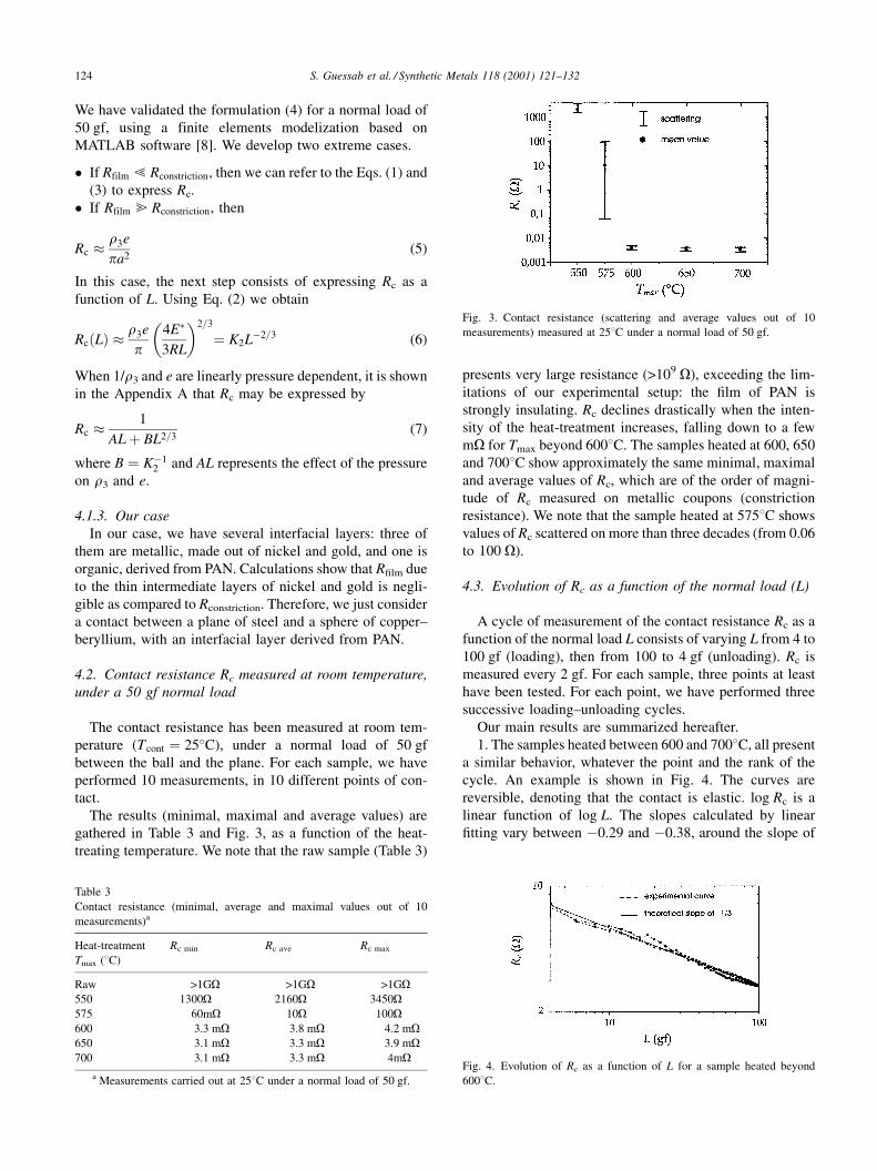
The results (minimal, maximal and average values) are
gathered in Table 3 and Fig. 3, as a function of the heat-
treating temperature. We note that the raw sample (Table 3)
presents very large resistance (>109 O), exceeding the lim-
itations of our experimental setup: the ®lm of PAN is
strongly insulating. Rc declines drastically when the inten-
sity of the heat-treatment increases, falling down to a few
mO for Tmax beyond 6008C. The samples heated at 600, 650
and 7008C show approximately the same minimal, maximal
and average values of Rc, which are of the order of magni-
tude of Rc measured on metallic coupons (constriction
resistance). We note that the sample heated at 5758C shows
values of Rc scattered on more than three decades (from 0.06
to 100 O).
4.3. Evolution of Rc as a function of the normal load (L)
A cycle of measurement of the contact resistance Rc as a
function of the normal load L consists of varying L from 4 to
100 gf (loading), then from 100 to 4 gf (unloading). Rc is
measured every 2 gf. For each sample, three points at least
have been tested. For each point, we have performed three
successive loading±unloading cycles.
Our main results are summarized hereafter.
1. The samples heated between 600 and 7008C, all present
a similar behavior, whatever the point and the rank of the
cycle. An example is shown in Fig. 4. The curves are
reversible, denoting that the contact is elastic. log Rc is a
linear function of log L. The slopes calculated by linear
®tting vary between ÿ0.29 and ÿ0.38, around the slope of
Table 3
Contact resistance (minimal, average and maximal values out of 10
measurements)a
Heat-treatment
Tmax (8C)
Rc min Rc ave Rc max
Raw >1GO >1GO >1GO550 1300O 2160O 3450O575 60mO 10O 100O600 3.3 mO 3.8 mO 4.2 mO650 3.1 mO 3.3 mO 3.9 mO700 3.1 mO 3.3 mO 4mO
a Measurements carried out at 258C under a normal load of 50 gf.
Fig. 3. Contact resistance (scattering and average values out of 10
measurements) measured at 258C under a normal load of 50 gf.
Fig. 4. Evolution of Rc as a function of L for a sample heated beyond
6008C.
124 S. Guessab et al. / Synthetic Metals 118 (2001) 121±132

ÿ1/3 predicted by the Eq. (3) supposed to be constant when
L varies. In that case, R®lm related to the ®lm derived from
PAN is negligible compared to Rconstriction so that Rc �Rconstricion.
2. For the sample heated at 5508C, the evolution of Rc as a
function of L is also rather reproducible, whatever the point
and the rank of the cycle. An example is shown in Fig. 5, on a
linear±linear graph. The dots representing the experimental
values for a loading±unloading cycle attest that the behavior
of the contact is reversible and then elastic. In this case,
Rconstriction (several mO) is negligible compared to Rc
(>1000 O) so that Rc � Rfilm. We have also represented
the ®ttings with two functions corresponding to the
Eqs. (6) and (7). For each function, the plotting software
we used (Microcal Origin 4.0) calculates the parameters (A,
B) to minimize w2 expressed underneath:
w2 � 1
N ÿ p
XN
i�1
oi� f �Li� ÿ y�Li��2 (8)
where N is the total number of experimental points used in
the fitting, p the total number of adjustable parameters
(p � 1 or 2 in our case), f(Li) the value of the fitting function
for the normal load Li, y(Li) the experimental value, oi
represents the weight of each experimental point. Four
different weighting methods are supported by Origin. The
values of Rc cover three decades. Therefore, we have chosen
the statistical method with oi � 1=y�Li�.We observe ®rst that the ®t obtained with the Eq. (6) is
bad. In contrast, a very good ®tting is obtained with the
Eq. (7) which takes into account the in¯uence of the pressure
on the conductivity and thickness of the ®lm.
As it is shown in the Appendix A, the parameter B
provided by the ®tting is linked to other data,
B � pk2
1002=3e0r0
(9)
with e0 � 150 nm, k � �3R=4E��1/3 and when L is in gf. We
then deduced that r0 � 70 O m. This value is intermediate
between the order of magnitude for the resistivity of raw
PAN (1016 O m) and the best performance mentioned in the
literature for heat-treated PAN (10ÿ5 O m).
In the same manner, the parameters a and b de®ned in the
Appendix A are linked to A and B by the relation
a� b � A
Bpk2 (10)
Replacing in Eq. (10), A and B by the values given by the
fitting gives a� b � 6:5� 109 Paÿ1. The maximum value
of the pressure for L � 1 N is Pmax � 0:75 GPa. Thus, we
have �a� b�Pmax� 4:9. Since physically aPmax
< 1, we
deduce that the relative increase of the conductivity due
to the pressure is very large (�5) when L � 1 N. Increases of
the conductivity of the same order of magnitude have
already been observed for poly(3-alkylthiophenes) films
subjected to an hydrostatic pressure of 0.5 GPa [11] and
for polypyrrole subjected to 1 GPa [12].
3. The intermediate sample heated at 5758C presents non-
reproducible and irregular curves that cannot be described
by any analytical model.
4.4. Evolution of Rc as a function of the temperature of the
contact (Tcont)
We have observed for three samples, the evolution of Rc
under a constant normal load (50 gf) when Tcont is varied
from 100 to ÿ1008C. The ®rst sample has been chosen
among those heated at Tmax � 6008C. The second sample is
the one heated at 5508C. The last sample corresponds to the
intermediate heat-treatment, Tmax � 5758C.
1. The experimental results obtained in the ®rst case are
represented by the dots and ®tted by the line in Fig. 6.
Despite ¯uctuations, Rc can be considered as a linear
increasing function of Tcont. This is coherent with the
Eq. (1): if we neglect the variation of a when Tcont varies,
Rc varies like r1 and r2, which are linear increasing func-
tions of the temperature, in the considered interval.
2. The results related to the 5508C sample are represented
by the dots in Fig. 7. Rc is a decreasing function of Tcont. This
could be predicted by the Eq. (7), which can be written as
Rc � e0r0
�a� b�L� pk2L2=3(70)
Here L is constant and if e0, a, b and k are not temperature
dependent and Rc varies like r0 (resistivity at atmospheric
pressure). Medium heat-treated PAN is a semiconductor
Fig. 5. Evolution of Rc as a function of L for a sample heated at 5508C.
Fig. 6. Evolution of Rc as a function of Tcont for a sample heated beyond
6008C.
S. Guessab et al. / Synthetic Metals 118 (2001) 121±132 125

[13], and thus, r0 is a decreasing function of the temperature.
We have tested three fitting equations that might describe the
evolution of Rc. Each of them is associated with a mode of
electrical conduction that has already been mentioned for
films derived from PAN [6,14±16]. The generic formula Ð
with T in Kelvin Ð is
Rc � R1 expT
T0
� �ÿn� �(11)
For n � 0:25, the Eq. (11) is the Mott's law describing the
variable-range hopping conduction in three-dimensions
[17]. For n � 0:5, it corresponds to a structure with con-
ducting clusters scattered in an insulating matrix [18]. For
n � 1, it is associated with thermally activated conduction in
ordered semiconductors.
The mode of ®tting is the same as previously described.
The values of w2 as a function of n are given in Table 4. It
appears that the thermally activated conduction in ordered
semiconductors has to be rejected. As a matter of fact, the
heat-treatment induces an inhomogeneous transformation in
the volume of the PAN ®lm, associated with inter-diffusion
phenomena. This probably leads to an amorphous structure.
The equations associated with n � 0:25 and n � 0:5 both
might be suitable, the Mott's law being the most adequate.
The corresponding ®tting curve is represented in Fig. 7. The
values we found for R1 and T0 (R1 � 1:7� 10ÿ6 O and
T0 � 4:8� 107 K) are coherent with those of the literature
[6,17].
3. The intermediate sample heated at 5758C presents non-
reproducible and irregular curves that cannot be described
by any analytical model.
5. Further investigations
The 5758C sample presenting results dif®cult to analyze,
we have studied its surface as well as that of the 6008Csample, with an original laboratory-made extension asso-
ciated with a commercial AFM. We have obtained simulta-
neously, topographical and local contact resistance surface
cartographies of a given area of each sample.
5.1. Experimental device
A schematic view of the laboratory-made system is
sketched in Fig. 8. The left half of the drawing corresponds
to the commercial AFM (Nanoscope1 III, Digital Instru-
ments); the right half sketches our speci®c home-built
extension for electrical measurements. The commercial
tip and cantilever were made of n-doped silicon coated
with p-doped diamond (Nanosensors DCT-FM). Sample
and cantilever holders were carefully insulated from the
Fig. 7. Evolution of Rc as a function of Tcont for a sample heated at 5508C.
Table 4
w2 as a function of n
n w2
0.25 3.2
0.5 5.9
1 19.8
Fig. 8. Schematic principle of the experimental device derived from classical AFM setup.
126 S. Guessab et al. / Synthetic Metals 118 (2001) 121±132

apparatus frame. When the tip is placed in contact with the
sample, a bias voltage (of typically 1 V) is applied. The x±y
displacement of the piezoelectric block then allows the
sample to be scanned line-by-line by the tip apex, whereas
the applied force is held constant by the z-displacement of
the sample. The resulting current at the input of the con-
version system then re¯ects the local tip/sample contact
resistance (in 102±1011 O range approximately) at each point
where the height datum is acquired. This leads to simulta-
neous cartographies of both the topographical and electrical
features of the studied surface in grey-scaled pictures. All
experiments have been performed at room temperature.
Topographical images are presented in the `̀ illuminate
mode''. For electrical images, the observed contact resis-
Fig. 9. Topographical and electrical images of the samples: (a) heated at 6008C; (b) heated at 5758C.
S. Guessab et al. / Synthetic Metals 118 (2001) 121±132 127

tance values are very high due to the small tip size and,
therefore, to the small tip/sample contact area.
5.2. Analysis of the 575 and 6008C samples
1. The 575 and 6008C samples were analyzed on an area
of 20 mm� 20 mm. The corresponding electrical and topo-
graphical images are shown in Fig. 9. The distributions of
the electrical resistance measured on each area are repre-
sented in Fig. 10 (the bars on the right are caused by the
saturation of the system of electronic conversion).
For the 6008C sample, the topographical image shows
small craters scattered on the `̀ moon-like'' surface. They
must be traces of the degassing induced by heat-treatment
[6]. As far as the electrical contact resistances are concerned,
the distribution is centered on 7� 107 O. Most of the contact
resistance values are counted between 3� 107 and
3� 108 O. This is associated with dark colors on the elec-
trical image. The surface looks uniformly conducting. We
note that the less conducting zones, generally ring-shaped,
correspond to the craters' ridges in the topographical image.
This correlation might reveal that the less conducting rings
have just a topographical cause: due to the high slope, the
side of the crater might not be scanned by the tip (Fig. 11).
However, we have measured this slope by pro®lometry and
it has proved to be gentle enough to be scanned by the
tip. Thus, the ring shapes in the electrical image do not have
Fig. 10. Distribution of the measured resistance: (a) sample heated at 6008C; (b) sample heated at 5758C.
Fig. 11. Effect of the topographical slope on the scanning of the tip.
128 S. Guessab et al. / Synthetic Metals 118 (2001) 121±132

a topographical cause. We believe, degassing traces could
present a higher electrical resistivity due to a special
chemical structure.
For the 5758C sample, less traces of degassing are
observed, which is logical since the heat-treatment is less
intense. The 5758C sample appears less conducting than the
6008C one; the values of contact resistance are 10 times
superior. This can be seen in the electrical image as well as in
the distribution of the contact resistance, which is centered
on 7� 108 O. It is dif®cult to ®nd correlation between the
topographical and the electrical images. We note that the less
conducting zones are uniformly distributed on the analyzed
surface. The observation of another 20 mm� 20 mm area on
the same sample has proved to be similar. The reproduci-
bility of electrical images on several areas of the 5758Csample, as well as the apparent homogeneity of each of
them, are not in accordance with the heterogeneous elec-
trical results in a ball/plane con®guration.
2. The 575 and 6008C samples were scanned on another
area of 50 mm� 50 mm, then on a larger area of
100 mm� 100 mm around this ®rst one. Fig. 12 shows the
last corresponding topographical and electrical cartogra-
phies for the 5758C sample. The area that had already been
scanned appears as more conducting, but no topographic
modi®cation is detected. This behavior has not been
observed for the 6008C sample. We then believe that there
is a very thin layer less conducting on the extreme surface of
the 5758C sample. It is poorly adherent and thus is elimi-
nated by the scanning of the probe. This behavior pointed
out at a nanocontact scale might also occur for microcon-
tacts in the ball/plane con®guration, due to the asperities at
the surface of the ball. It could explain the non-reproducible
results observed in the 5758C sample.
6. Discussion and conclusion
6.1. Summary of the results
Static contact resistance measurements in a ball/plane
con®guration point out the effect of vacuum heat-treatment
on PAN ®lms deposited on metallic coupons. They reveal a
transition around a critical heat-treating temperature
T trans � 5758C.
� Below Ttrans, Rc � Rfilm. The behavior of the contact
resistance when the normal load L varies can be described
by an original relation we derived from the Hertz's law,
taking into account the influence of the pressure on the
conductivity and thickness of the film. The evolution of
Rc, when the temperature of the contact Tcont varies, obeys
the Mott's law which denotes a variable-range hopping
conduction in the film.
� Above Ttrans, Rc � Rconstriction. The behavior of the contact
when L or Tcont varies is coherent and ruled by the metallic
electrodes.
� The intermediate sample shows non-reproducible results
and anomalous curves in a ball/plane configuration.
Coupled topographic and electrical AFM cartographies
suggest, this might be caused by a very thin poorly
adherent layer present at the extreme surface of the
sample.
Fig. 12. Degradation of the sample heated at 5758C by the scanning of the AFM probe.
S. Guessab et al. / Synthetic Metals 118 (2001) 121±132 129

6.2. Discussion
The improvement of the conductivity of PAN induced by
heat-treatment has already been mentioned in the literature
for various modes of annealing (atmospheric conditions,
duration, temperature, etc.), for ®lms [19±23] or ®bers
[14,24]. The conductivity of raw PAN is about
10ÿ14 Oÿ1 cmÿ1, whereas the best performance obtained
after heat-treatment listed in the literature is 103 Oÿ1 cmÿ1
[24]. It has also been largely proved that this increase of the
conductivity is caused by chemical modi®cations [22,25,26]
of PAN. The heat-treatment progressively transforms the
linear chains of PAN into a three-dimensional reticulated
lattice containing more and more cyclized groups. This is
accompanied by denitrogenation and dehydrogenation, so
that PAN evolves towards a graphite-like structure. Linear
chains of PAN present single bonds and localized electronic
states, whereas cyclized groups are associated with deloca-
lized electronic states, which enhances the electrical
conductivity.
Since the beginning of our investigations on heated PAN
®lms, we have been performing systematic surface analysis
by photoelectron spectroscopy, in some cases coupled with
infrared re¯exion/absorption spectroscopy. Our spectra for
every con®guration of samples we have considered are in
good correlation with the chemical transformation men-
tioned above. It has been developed in a previous paper
[1] for very thin PAN ®lms (50 nm) electropolymerized on
brass coupons coated by electroplated nickel and rapidly
heated in a lamp furnace.
Another phenomenon has to be taken into account. XPS
analysis performed on this series of samples not only reveals
the presence at the surface of carbon, oxygen and nitrogen,
but also the detection of nickel and iron for the samples
heated at and above 6008C, that are the ones presenting
satisfying electrical performances. The corresponding
approximate relative concentrations are shown in Table 5.
We underline the XPS analyses several nanometers in the
depth of each sample. We believe that the heat-treatment
causes the inter-diffusion of the metallic substrate with the
organic layer, as well as the chemical transformation of
PAN. For Tmax � 600�C, the whole terminal layer has a
mixed structure, presenting both metallic and organic com-
pounds. It is not possible at this point to tell how they are
arranged. For Tmax � 550�C, there is still a solid pure
organic layer at the surface, more than several nanometers
thick. Considering, on the one hand, the amount of nickel
detected by XPS on the 5758C sample and, on the other
hand, the AFM observations, we think there is a terminal
poorly conducting organic layer, less than several nan-
ometers thick, which is eliminated by the scanning of the
AFM probe.
Considering again the 5508C sample, we have found that
the Mott's law is the most suitable to describe the behavior
of the contact resistance when the temperature varies. When
the contact load varies, that is when the pressure applied to
the ®lm varies, we have found that the ®t by expression (7) is
good. From the values of A and B appearing in Eq. (7), the
ratio of the conductivities at 0.75 GPa and at 1 atm is
estimated close to 5. This value is in agreement with results
found in the literature for the poly(3-alkylthiophenes) [11]
and for the polypyrrole [12]. In these papers, the increase of
conductivity is attributed to a decrease of the Mott's para-
meter T0 due to the compression of the material. Hence we
have a con®rmation that the variable-range hopping is the
better candidate to describe the electrical transport mechan-
ism in the 5508C sample.
6.3. Conclusion
We have studied the electrical transport properties of ®lms
of PAN after transformation by heat-treatment in vacuum.
These ®lms are deposited on steel coupons with a terminal
coating of nickel. Since the industrial goal is to use these
®lms as terminal layers of electrical contacts, they are
studied in a `̀ contact situation'' that is pressed by a golden
ball. The annealing temperature has been the single para-
meter for the sample preparation, the maximum temperature
Tmax, during the process, varying between 550 and 7008C.
By means of a dedicated experimental device, we have
studied the variations of the contact resistance Rc versus
the temperature Tcont of the contact and versus the load L
applied to the contact. For the 5508C samples, the contact
resistance are large (�2000 O under 50 gf at 258C) and due
only to the ®lm. For the variations of Rc versus Tcont, three
®tting laws have been tested, the best being Mott's law. For
the variations of Rc versus L, a good ®t has been obtained
with an analytical law Ð taking into account the variation
of the conductivity with the pressure Ð we have derived
from the Hertz's law. From the parameters obtained with
the ®tting, we have deduced the value of the ®lm resistivity
and the ratio of the conductivities under 0.75 GPa and 1 atm.
The value of 5 found for this ratio is in agreement with
results obtained with other synthetic metals for which the
transport mode is also the variable-range hopping. At this
stage, we should mention that our experimental method,
in which we record the Rc±L variations for a ®lm squeezed
between a plane and a ball carefully polished, could repre-
sent an alternative to the high pressure vessel method
habitually used to study the in¯uence of the pressure on
Table 5
Metals relative concentrations at the surface of the samples
Heat-treatment [Ni]% [Fe]%
Raw ±a ±
5508C ± ±
5758C 0.5 ±
6008C 10 5
6508C 10 5
7008C 10 5
a Not detected.
130 S. Guessab et al. / Synthetic Metals 118 (2001) 121±132

the conductivity of ®lms. For the 5758C samples, the contact
resistance are scattered (from 0.06 to 100 O under 50 gf at
258C). The samples annealed at this temperature seem to be
covered with a very thin poorly conducting non-adherent
layer, revealed by a home-made technique involving an
AFM with a conducting tip. For Tmax � 600�C, the contact
resistances are very low (a few mO) and due only to the
constrictions in the metallic electrodes. This is proved
by the temperature and load curves: Rc±Tcont, and Rc±L.
Unfortunately, it is not possible by our method to
determine the conductivity of the ®lms, which should
be high enough. Surface analyses performed on these
®lms reveal the presence of large amounts of nickel and
iron, probably partly responsible for their good electrical
behavior.
Acknowledgements
Part of this work has been realized in the Laboratory of
Electrochemistry headed by Christophe Bureau (Commis-
sariat aÁ l'EÂ nergie Atomique, Service de Recherche sur les
Surfaces et l'Irradiation de la MatieÁre) with the great help of
Pascal Viel.
Appendix A. Derivation of the Rfilm � F(L) law whenthe resistivity and thickness are pressure dependent
We consider an organic conducting ®lm with a free
thickness e0 and a resistivity r0. When the ®lm is subjected
to a pressure p, we assume that the variations of e and 1/rmay be described by ®rst order expansions
e � e0�1ÿ ap� (A.1)
1
r� 1� bp
r0
(A.2)
Eq. (A.1) is simply an expression of Hooke's law. The
pertinence of Eq. (A.2) is supported by the fact that a
parabolic expansion of the conductivity has been found
satisfactory to describe the behavior of doped polypyrrole
[27]. Here, for simplicity, we stop the expansion at the first
order.
When the ®lm lying on the plane substrate is pressed
against the sphere considered in Section 4.1, it is subjected
to a pressure p(r) inside the contact disc of radius a.
Although, not used in this simple model, the formula giving
p(r) is
p�r� � 3L
2pa21ÿ r2
a2
� �1=2
� Pmax 1ÿ r2
a2
� �1=2
(A.3)
where L is the load. In this work, Pmax � 750 MPa when
L � 1 N.
Denoting by V the voltage drop between the metallic
electrodes (the sphere and the plane), the current density
flowing through the film is
j�r� � V
er� V�1� bp�
e0r0�1ÿ ap� (A.4)
Assuming ap ! 1, Eq. (A.4) may be approximated by
j�r� � V
e0r0
�1� �a� b�p� (A.5)
Eq. (A.5) is indeed a first order expansion of j as a function
of p.
The current I ¯owing through the organic conducting disc
is given by
I � 2pZ a
0
j�r�r dr � pa2V
e0r0
� �a� b�Ve0r0
2pZ a
0
p�r�r dr
� pa2V
e0r0
� �a� b�Ve0r0
L (A.6)
Then, from Eq. (2), we have a � kL1=3 with
k � �3R=4E��1=3. So as I � V=Rfilm, we have
1
Rfilm
� pk2
e0r0
L2=3 � a� be0r0
L (A.7)
Finally, Rfilm may be expressed simply as
Rfilm � 1
AL� BL2=3(A.8)
References
[1] F. HouzeÂ, L. Boyer, S. NoeÈl, P. Viel, G. LeÂcayon, J.M. Bourin, Synth.
Metals 62 (1994) 207.
[2] S. NoeÈl, P. Newton, C. Bodin, F. HouzeÂ, L. Boyer, P. Viel, G.
LeÂcayon, Surf. Interf. Anal. 22 (1994) 393.
[3] S. Guessab, F. HouzeÂ, S. NoeÈl, L. Boyer, P. Viel, G. LeÂcayon, in:
Proceedings of the 43rd IEEE Holm Conference on Electrical
Contacts, Philadelphia, PA, USA, 1997, p. 219.
[4] F. HouzeÂ, R. Meyer, O. Schneegans, L. Boyer, Appl. Phys. Lett. 69
(13) (1996) 1975.
[5] O. Schneegans, F. HouzeÂ, R. Meyer, L. Boyer, in: Proceedings of the
42nd IEEE Holm Conference on Electrical Contacts, Chicago, USA,
1996, p. 205.
[6] D.J. Gillespie, A.C. Ehrlich, J. Non-Cryst. Solids 144 (1992)
231.
[7] P. Newton, TheÁse de doctorat, Universite Pierre et Marie Curie, Paris,
France, 1995.
[8] S. Guessab, TheÁse de doctorat, Universite Pierre et Marie Curie,
Paris, France, 1998.
[9] R. Holm, Electrical Contacts, Springer, Berlin, Germany, 1967, p. 1.
[10] K.L. Johnson, Contact Mechanics, Cambridge University Press,
Cambridge, England, 1989, p. 90.
[11] H. Isotalo, M. Ahlskog, H. Stubb, Synth. Metals 48 (1992) 313.
[12] D.S. Maddison, J. Lusk, J. Unsworth, Synth. Metals 32 (1989)
219.
[13] J. Simon, J.J. AndreÂ, Molecular Semiconductors, Springer, Berlin,
Germany, 1985.
[14] T. Teoh, P.D. Metz, W.G. Wilhelm, Mol. Cryst. Liq. Cryst. 83 (1982)
297.
[15] M. Mehbod, P. Wyder, R. Deltour, C. Pierre, G. Geuskens, Phys. Rev.
B 36 (1987) 7627.
S. Guessab et al. / Synthetic Metals 118 (2001) 121±132 131

[16] K. Jobst, L. Sawtschenko, M. Schwarzenberg, L. Wuckel, Synth.
Metals 47 (1992) 279.
[17] N.F. Mott, Philos. Mag. 19 (1969) 1259.
[18] P. Sheng, B. Abeles, Y. Arie, Phys. Rev. Lett. 31 (1973) 44.
[19] A.V. Topchiev, J. Polym. Sci.: Part A 1 (1963) 591.
[20] M. Suzuki, K. Takahashi, S. Mitani, Jpn. J. Appl. Phys. 14 (1975) 741.
[21] A.H. Bhuiyan, S.V. Bhoraskar, J. Mater. Sci. 24 (1989) 3091.
[22] J.A. Meyers, J. Non-Cryst. Solids 63 (1984) 425.
[23] C.L. Renschler, A.P. Sylwester, L.V. Salgado, J. Mater. Res. 4 (1988)
452.
[24] G. Pan, N. Muto, M. Miyayama, H. Yanagida, J. Mater. Sci. 27
(1992) 3497.
[25] J.J. Ritsko, C. Crecelius, J. Fink, Phys. Rev. B 24 (1986) 2612.
[26] J. Mittal, O.P. Bahl, R.B. Mathur, N.K. Sandle, Carbon 32 (1994)
1133.
[27] D.S. Maddison, J. Unsworth, Synth. Metals 22 (1988) 257.
132 S. Guessab et al. / Synthetic Metals 118 (2001) 121±132