
Industrial and Multimarket Data Sheet LED Controller IC
23
Industrial and Multimarket Data Sheet Rev1.0, 2012-02-28 ICL8002G LED Controller IC Single Stage PFC and Flyback LED Controller
-
Upload
khangminh22 -
Category
Documents
-
view
0 -
download
0
Transcript of Industrial and Multimarket Data Sheet LED Controller IC
Industr ia l and Mult imarket
Data Sheet Rev1.0, 2012-02-28
ICL8002G
LED Control ler ICSingle Stage PFC and Flyback LED Controller

Edition 2012-02-28Published byInfineon Technologies AG81726 Munich, Germany© 2012 Infineon Technologies AGAll Rights Reserved.
Legal DisclaimerThe information given in this document shall in no event be regarded as a guarantee of conditions or characteristics. With respect to any examples or hints given herein, any typical values stated herein and/or any information regarding the application of the device, Infineon Technologies hereby disclaims any and all warranties and liabilities of any kind, including without limitation, warranties of non-infringement of intellectual property rights of any third party.
InformationFor further information on technology, delivery terms and conditions and prices, please contact the nearest Infineon Technologies Office (www.infineon.com).
WarningsDue to technical requirements, components may contain dangerous substances. For information on the types in question, please contact the nearest Infineon Technologies Office.Infineon Technologies components may be used in life-support devices or systems only with the express written approval of Infineon Technologies, if a failure of such components can reasonably be expected to cause the failure of that life-support device or system or to affect the safety or effectiveness of that device or system. Life support devices or systems are intended to be implanted in the human body or to support and/or maintain and sustain and/or protect human life. If they fail, it is reasonable to assume that the health of the user or other persons may be endangered.
Single Stage PFC and Flyback LED ControllerICL8002G
Data Sheet 3 Rev1.0, 2012-02-28
Trademarks of Infineon Technologies AGAURIX™, BlueMoon™, C166™, CanPAK™, CIPOS™, CIPURSE™, COMNEON™, EconoPACK™, CoolMOS™,CoolSET™, CORECONTROL™, CROSSAVE™, DAVE™, EasyPIM™, EconoBRIDGE™, EconoDUAL™,EconoPIM™, EiceDRIVER™, eupec™, FCOS™, HITFET™, HybridPACK™, I²RF™, ISOFACE™, IsoPACK™,MIPAQ™, ModSTACK™, my-d™, NovalithIC™, OmniTune™, OptiMOS™, ORIGA™, PRIMARION™,PrimePACK™, PrimeSTACK™, PRO-SIL™, PROFET™, RASIC™, ReverSave™, SatRIC™, SIEGET™,SINDRION™, SIPMOS™, SMARTi™, SmartLEWIS™, SOLID FLASH™, TEMPFET™, thinQ!™,TRENCHSTOP™, TriCore™, X-GOLD™, X-PMU™, XMM™, XPOSYS™.
Other TrademarksAdvance Design System™ (ADS) of Agilent Technologies, AMBA™, ARM™, MULTI-ICE™, KEIL™,PRIMECELL™, REALVIEW™, THUMB™, µVision™ of ARM Limited, UK. AUTOSAR™ is licensed by AUTOSARdevelopment partnership. Bluetooth™ of Bluetooth SIG Inc. CAT-iq™ of DECT Forum. COLOSSUS™,FirstGPS™ of Trimble Navigation Ltd. EMV™ of EMVCo, LLC (Visa Holdings Inc.). EPCOS™ of Epcos AG.FLEXGO™ of Microsoft Corporation. FlexRay™ is licensed by FlexRay Consortium. HYPERTERMINAL™ ofHilgraeve Incorporated. IEC™ of Commission Electrotechnique Internationale. IrDA™ of Infrared DataAssociation Corporation. ISO™ of INTERNATIONAL ORGANIZATION FOR STANDARDIZATION. MATLAB™ ofMathWorks, Inc. MAXIM™ of Maxim Integrated Products, Inc. MICROTEC™, NUCLEUS™ of Mentor GraphicsCorporation. Mifare™ of NXP. MIPI™ of MIPI Alliance, Inc. MIPS™ of MIPS Technologies, Inc., USA. muRata™of MURATA MANUFACTURING CO., MICROWAVE OFFICE™ (MWO) of Applied Wave Research Inc.,OmniVision™ of OmniVision Technologies, Inc. Openwave™ Openwave Systems Inc. RED HAT™ Red Hat, Inc.RFMD™ RF Micro Devices, Inc. SIRIUS™ of Sirius Satellite Radio Inc. SOLARIS™ of Sun Microsystems, Inc.SPANSION™ of Spansion LLC Ltd. Symbian™ of Symbian Software Limited. TAIYO YUDEN™ of Taiyo YudenCo. TEAKLITE™ of CEVA, Inc. TEKTRONIX™ of Tektronix Inc. TOKO™ of TOKO KABUSHIKI KAISHA TA.UNIX™ of X/Open Company Limited. VERILOG™, PALLADIUM™ of Cadence Design Systems, Inc. VLYNQ™of Texas Instruments Incorporated. VXWORKS™, WIND RIVER™ of WIND RIVER SYSTEMS, INC. ZETEX™ ofDiodes Zetex Limited.Last Trademarks Update 2010-10-26
Revision HistoryPage or Item Subjects (major changes since previous revision)Rev1.0,2012-02-28
<Revision X.Y>, <yyyy-mm-dd>
Single Stage PFC and Flyback LED ControllerICL8002G
Table of Contents
Data Sheet 4 Rev1.0, 2012-02-28
Table of Contents . . . . . . . . . . . . . . . . . . . . . . . . . . . . . . . . . . . . . . . . . . . . . . . . . . . . . . . . . . . . . . . . 4
List of Figures . . . . . . . . . . . . . . . . . . . . . . . . . . . . . . . . . . . . . . . . . . . . . . . . . . . . . . . . . . . . . . . . . . . 5
List of Tables . . . . . . . . . . . . . . . . . . . . . . . . . . . . . . . . . . . . . . . . . . . . . . . . . . . . . . . . . . . . . . . . . . . . 6
1 Single Stage PFC and Flyback LED ControllerProduct Highlight . . . . . . . . . . . . . . . . . . . . . . . . . . . . . . . . . . . . . . . . . . . . . . . . . . . . . . . . . . . . . . . . 7
2 Pin Configuration and Functionality . . . . . . . . . . . . . . . . . . . . . . . . . . . . . . . . . . . . . . . . . . . . . . . . . 92.1 Pin Configuration with PG-DSO-8 . . . . . . . . . . . . . . . . . . . . . . . . . . . . . . . . . . . . . . . . . . . . . . . . . . . . 92.2 Package PG-DSO-8 . . . . . . . . . . . . . . . . . . . . . . . . . . . . . . . . . . . . . . . . . . . . . . . . . . . . . . . . . . . . . . . 92.3 Pin Functionality . . . . . . . . . . . . . . . . . . . . . . . . . . . . . . . . . . . . . . . . . . . . . . . . . . . . . . . . . . . . . . . . . 10
3 Representative Block Diagram . . . . . . . . . . . . . . . . . . . . . . . . . . . . . . . . . . . . . . . . . . . . . . . . . . . . 11
4 Functional Description . . . . . . . . . . . . . . . . . . . . . . . . . . . . . . . . . . . . . . . . . . . . . . . . . . . . . . . . . . . 124.1 VCC Pre-Charging and Typical VCC Voltage During Start-up . . . . . . . . . . . . . . . . . . . . . . . . . . . . . . 124.2 Soft-start . . . . . . . . . . . . . . . . . . . . . . . . . . . . . . . . . . . . . . . . . . . . . . . . . . . . . . . . . . . . . . . . . . . . . . . 134.3 Normal Operation . . . . . . . . . . . . . . . . . . . . . . . . . . . . . . . . . . . . . . . . . . . . . . . . . . . . . . . . . . . . . . . . 134.3.1 Zero Crossing . . . . . . . . . . . . . . . . . . . . . . . . . . . . . . . . . . . . . . . . . . . . . . . . . . . . . . . . . . . . . . . . . 134.3.2 Ringing Suppression Time . . . . . . . . . . . . . . . . . . . . . . . . . . . . . . . . . . . . . . . . . . . . . . . . . . . . . . . . 144.3.2.1 Switch on Determination . . . . . . . . . . . . . . . . . . . . . . . . . . . . . . . . . . . . . . . . . . . . . . . . . . . . . . . 144.3.3 Switch Off Determination . . . . . . . . . . . . . . . . . . . . . . . . . . . . . . . . . . . . . . . . . . . . . . . . . . . . . . . . . 144.4 Current Limitation . . . . . . . . . . . . . . . . . . . . . . . . . . . . . . . . . . . . . . . . . . . . . . . . . . . . . . . . . . . . . . . . 154.4.1 Foldback Point Correction . . . . . . . . . . . . . . . . . . . . . . . . . . . . . . . . . . . . . . . . . . . . . . . . . . . . . . . . 154.4.2 Additional Features in ICL8002G compare to ICL8001G . . . . . . . . . . . . . . . . . . . . . . . . . . . . . . . . . . 164.5 iProtection Functions . . . . . . . . . . . . . . . . . . . . . . . . . . . . . . . . . . . . . . . . . . . . . . . . . . . . . . . . . . . . . 17
5 Electrical Characteristics . . . . . . . . . . . . . . . . . . . . . . . . . . . . . . . . . . . . . . . . . . . . . . . . . . . . . . . . . 185.1 Absolute Maximum Ratings . . . . . . . . . . . . . . . . . . . . . . . . . . . . . . . . . . . . . . . . . . . . . . . . . . . . . . . . 185.2 Operating Range . . . . . . . . . . . . . . . . . . . . . . . . . . . . . . . . . . . . . . . . . . . . . . . . . . . . . . . . . . . . . . . . 185.3 Characteristics . . . . . . . . . . . . . . . . . . . . . . . . . . . . . . . . . . . . . . . . . . . . . . . . . . . . . . . . . . . . . . . . . . 195.3.1 Supply Section . . . . . . . . . . . . . . . . . . . . . . . . . . . . . . . . . . . . . . . . . . . . . . . . . . . . . . . . . . . . . . . . . 195.3.2 Internal Voltage Reference . . . . . . . . . . . . . . . . . . . . . . . . . . . . . . . . . . . . . . . . . . . . . . . . . . . . . . . 195.3.3 PWM Section . . . . . . . . . . . . . . . . . . . . . . . . . . . . . . . . . . . . . . . . . . . . . . . . . . . . . . . . . . . . . . . . . . 205.3.4 Current Sense . . . . . . . . . . . . . . . . . . . . . . . . . . . . . . . . . . . . . . . . . . . . . . . . . . . . . . . . . . . . . . . . . 205.3.5 Soft Start . . . . . . . . . . . . . . . . . . . . . . . . . . . . . . . . . . . . . . . . . . . . . . . . . . . . . . . . . . . . . . . . . . . . . 205.3.6 Foldback Point Correction . . . . . . . . . . . . . . . . . . . . . . . . . . . . . . . . . . . . . . . . . . . . . . . . . . . . . . . . 215.3.7 Digital Zero Crossing . . . . . . . . . . . . . . . . . . . . . . . . . . . . . . . . . . . . . . . . . . . . . . . . . . . . . . . . . . . . 215.3.8 Protection . . . . . . . . . . . . . . . . . . . . . . . . . . . . . . . . . . . . . . . . . . . . . . . . . . . . . . . . . . . . . . . . . . . . . 225.3.9 Gate Drive . . . . . . . . . . . . . . . . . . . . . . . . . . . . . . . . . . . . . . . . . . . . . . . . . . . . . . . . . . . . . . . . . . . . 22
6 Outline Dimension . . . . . . . . . . . . . . . . . . . . . . . . . . . . . . . . . . . . . . . . . . . . . . . . . . . . . . . . . . . . . . 23
References . . . . . . . . . . . . . . . . . . . . . . . . . . . . . . . . . . . . . . . . . . . . . . . . . . . . . . . . . . . . . . . . . . . . 24
Terminology . . . . . . . . . . . . . . . . . . . . . . . . . . . . . . . . . . . . . . . . . . . . . . . . . . . . . . . . . . . . . . . . . . . 25
Table of Contents

Single Stage PFC and Flyback LED ControllerICL8002G
Single Stage PFC and Flyback LED Controller Product Highlight
Data Sheet 7 Rev1.0, 2012-02-28
1 Single Stage PFC and Flyback LED ControllerProduct Highlight
• Quasi-Resonant Control For Highly Efficient LED Driving Solutions• Primary Side Flyback Control With Integrated PFC And Phase-Cut Dimming• Integrated HV Startup Cell For Short Time To Light• Best In Class System BOM For Dimmable LED Bulb• Continous Dimming curve for better diiming behaviour
Features• High, stable efficiency over wide operating range• Optimized for trailing- and leading-edge dimmer• Precise PWM for primary PFC and dimming control• Power cell for Vcc pre-charging with constant current• Built-in digital soft-start• Foldback correction and cycle-by-cycle peak current limitation• VCC over/ under-voltage lockout• Auto restart mode for short circuit protection• Adjustable latch-off mode for output overvoltage protection• Minimize the light shimmering effect for better dimming behaviour.• Enabling the input current shaping for higher PF and lower THD.
DescriptionThe ICL8002G employs quasi-resonant operation mode optimized for off-line LED lighting, especially dimmableLED bulbs for incandescent lamp replacement.Precise PWM generation enables primary control for phase cut dimming and high power factor PF>98%.Significant improved driver efficiency, up to 90%, compared to other conventional solutions. Tthe product has awide operation range (up to 26 V) of IC voltage supply and lower power consumption. Multiple safety functionsensure a full system protection in failure situations.With its full feature set and simple application, the ICL8002G represents an outstanding choice for quasi-resonantflyback LED bulb designs combining feature set and performance at minimum BOM cost.
Single Stage PFC and Flyback LED ControllerICL8002G
Single Stage PFC and Flyback LED Controller Product Highlight
Data Sheet 8 Rev1.0, 2012-02-28
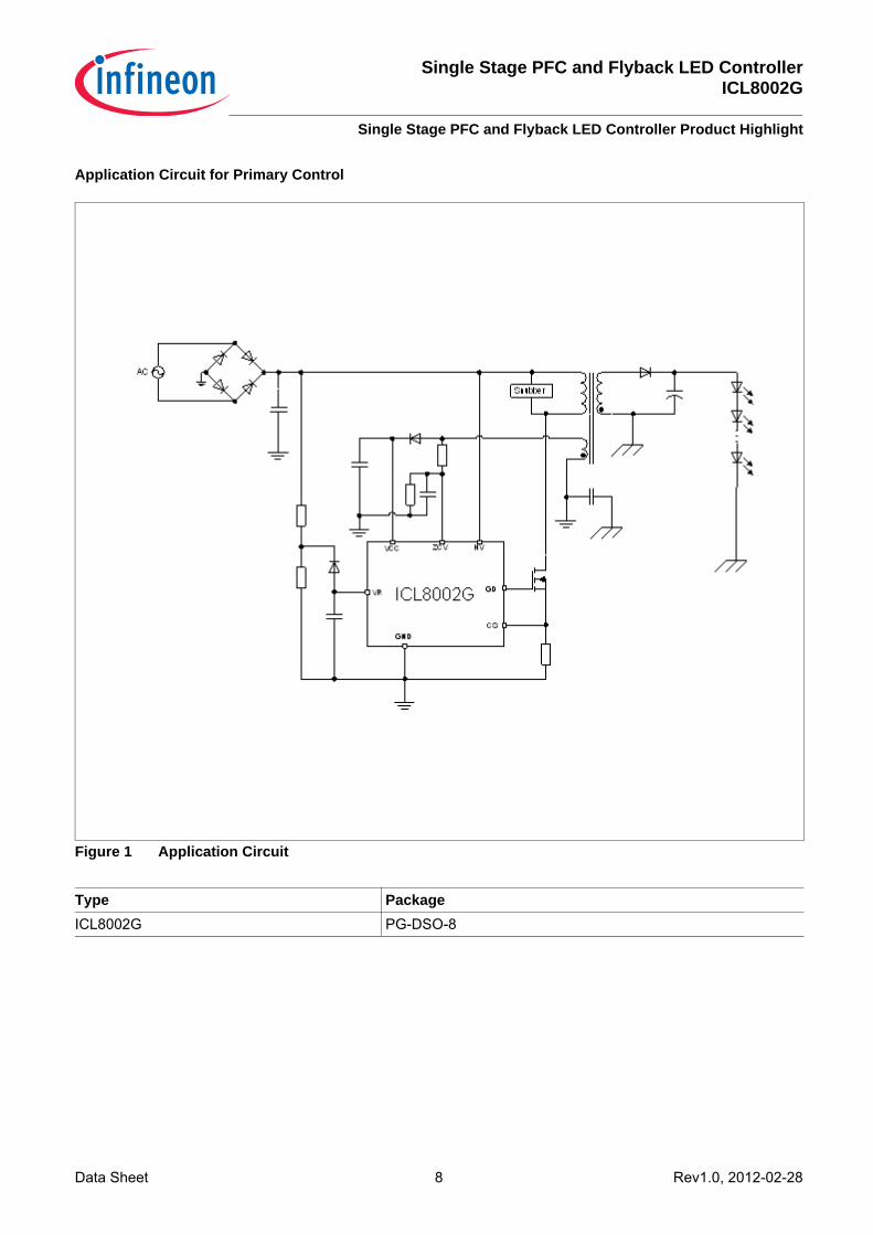
Application Circuit for Primary Control
Figure 1 Application Circuit
Type PackageICL8002G PG-DSO-8
Single Stage PFC and Flyback LED ControllerICL8002G
Pin Configuration and Functionality
Data Sheet 9 Rev1.0, 2012-02-28
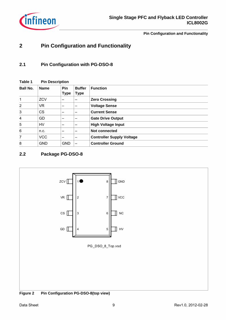
2 Pin Configuration and Functionality
2.1 Pin Configuration with PG-DSO-8
2.2 Package PG-DSO-8
Figure 2 Pin Configuration PG-DSO-8(top view)
Table 1 Pin DescriptionBall No. Name Pin
TypeBuffer Type
Function
1 ZCV – – Zero Crossing2 VR – – Voltage Sense3 CS – – Current Sense4 GD – – Gate Drive Output5 HV – – High Voltage Input6 n.c. – – Not connected7 VCC – – Controller Supply Voltage8 GND GND – Controller Ground
PG_DSO_8_Top.vsd
ZCV
VR
CS
GD
GND
VCC
NC
HV
1
2
3
4 5
6
7
8
Single Stage PFC and Flyback LED ControllerICL8002G
Pin Configuration and Functionality
Data Sheet 10 Rev1.0, 2012-02-28
2.3 Pin Functionality
ZCV (Zero Crossing)At this pin, the voltage from the auxiliary winding after a time delay circuit is applied. Internally, this pin is connectedto the zero-crossing detector for switch-on determination. Additionally, the output overvoltage detection is realizedby comparing the voltage Vzc with an internal preset threshold.
VR (Voltage Sense)The rectified input mains voltage is sensed at this pin. The signal is used to set the peak current of the peak-currentcontrol and therefore allow for the PFC and phase-cut dimming functionality.
CS (Current Sense)This pin is connected to the shunt resistor for the primary current sensing, externally, and the PWM signalgenerator for switch-off determination (together with the feedback voltage), internally. Moreover, short-windingprotection is realised by monitoring the voltage Vcs during on-time of the main power switch.
GD (Gate Drive Output)This output signal drives the external main power switch, which is a power MOSFET in most case.
HV (High Voltage)The pin HV is connected to the bus voltage, externally, and to the power cell, internally. The current through thispin pre-charges the VCC capacitor with constant current once the supply bus voltage is applied.
VCC (Power supply)VCC pin is the positive supply of the IC. The operating range is between VVCCoff and VVCCOVP.
GND (Ground)This is the common ground of the controller.
Single Stage PFC and Flyback LED ControllerICL8002G
Representative Block Diagram
Data Sheet 11 Rev1.0, 2012-02-28
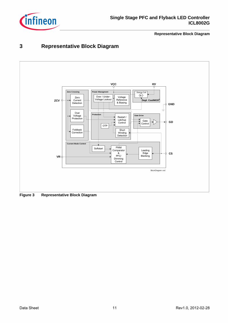
3 Representative Block Diagram
Figure 3 Representative Block Diagram
BlockDiagram .vsd
Depl. CoolMOS®
Startup CellPower ManagmentZero Crossing
Current Mode Control
Gate DriveProtection
HV
GND
GDGate Control
Voltage Reference& Biasing
Over / Under-Voltage Lockout
OTP
Restart / LatchupControl
VCC
CSLeading
Edge BlankingVR
ZCVZero
CurrentDetection
Over Voltage
Protection
Softstart PWMComparator
& PFC/
Dimming Control
FoldbackCorrection
Short Winding
Detection
Single Stage PFC and Flyback LED ControllerICL8002G
Functional Description
Data Sheet 12 Rev1.0, 2012-02-28
4 Functional Description
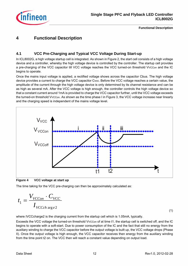
4.1 VCC Pre-Charging and Typical VCC Voltage During Start-upIn ICL8002G, a high voltage startup cell is integrated. As shown in Figure 2, the start cell consists of a high voltagedevice and a controller, whereby the high voltage device is controlled by the controller. The startup cell providesa pre-charging of the VCC capacitor till VCC voltage reaches the VCC turned-on threshold VVCCon and the ICbegins to operate.Once the mains input voltage is applied, a rectified voltage shows across the capacitor Cbus. The high voltagedevice provides a current to charge the VCC capacitor Cvcc. Before the VCC voltage reaches a certain value, theamplitude of the current through the high voltage device is only determined by its channel resistance and can beas high as several mA. After the VCC voltage is high enough, the controller controls the high voltage device sothat a constant current around 1mA is provided to charge the VCC capacitor further, until the VCC voltage exceedsthe turned-on threshold VVCCon. As shown as the time phase I in Figure 3, the VCC voltage increase near linearlyand the charging speed is independent of the mains voltage level.
Figure 4 VCC voltage at start up
The time taking for the VCC pre-charging can then be approximately calculated as:
(1)
where IVCCcharge2 is the charging current from the startup cell which is 1.05mA, typically.Exceeds the VCC voltage the turned-on threshold VVCCon of at time t1, the startup cell is switched off, and the ICbegins to operate with a soft-start. Due to power consumption of the IC and the fact that still no energy from theauxiliary winding to charge the VCC capacitor before the output voltage is built up, the VCC voltage drops (PhaseII). Once the output voltage is high enough, the VCC capacitor receives then energy from the auxiliary windingfrom the time point t2 on. The VCC then will reach a constant value depending on output load.
VVCCon
VVCC
VVCCoff
t1 t t2
i ii iii
2arg1
eVCCch
VCCVCCon
ICVt ⋅
=
Single Stage PFC and Flyback LED ControllerICL8002G
Functional Description
Data Sheet 13 Rev1.0, 2012-02-28
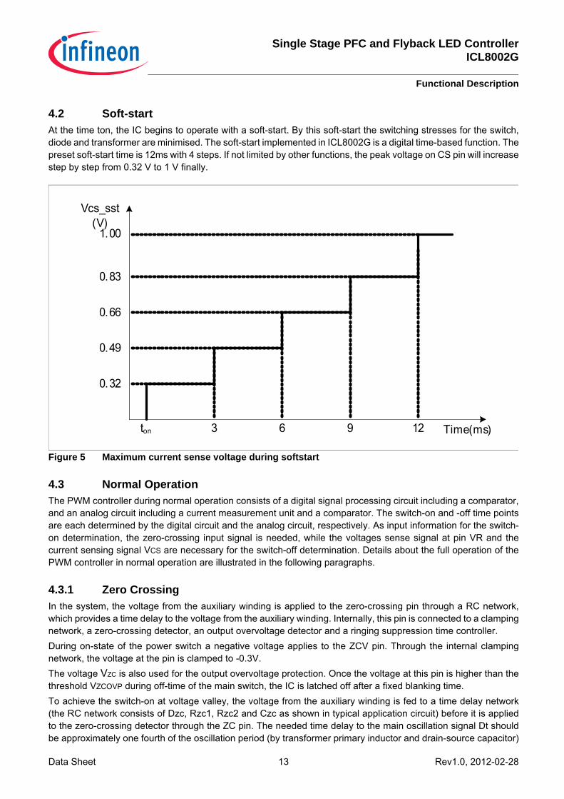
4.2 Soft-startAt the time ton, the IC begins to operate with a soft-start. By this soft-start the switching stresses for the switch,diode and transformer are minimised. The soft-start implemented in ICL8002G is a digital time-based function. Thepreset soft-start time is 12ms with 4 steps. If not limited by other functions, the peak voltage on CS pin will increasestep by step from 0.32 V to 1 V finally.
Figure 5 Maximum current sense voltage during softstart
4.3 Normal OperationThe PWM controller during normal operation consists of a digital signal processing circuit including a comparator,and an analog circuit including a current measurement unit and a comparator. The switch-on and -off time pointsare each determined by the digital circuit and the analog circuit, respectively. As input information for the switch-on determination, the zero-crossing input signal is needed, while the voltages sense signal at pin VR and thecurrent sensing signal VCS are necessary for the switch-off determination. Details about the full operation of thePWM controller in normal operation are illustrated in the following paragraphs.
4.3.1 Zero CrossingIn the system, the voltage from the auxiliary winding is applied to the zero-crossing pin through a RC network,which provides a time delay to the voltage from the auxiliary winding. Internally, this pin is connected to a clampingnetwork, a zero-crossing detector, an output overvoltage detector and a ringing suppression time controller.During on-state of the power switch a negative voltage applies to the ZCV pin. Through the internal clampingnetwork, the voltage at the pin is clamped to -0.3V.The voltage VZC is also used for the output overvoltage protection. Once the voltage at this pin is higher than thethreshold VZCOVP during off-time of the main switch, the IC is latched off after a fixed blanking time.To achieve the switch-on at voltage valley, the voltage from the auxiliary winding is fed to a time delay network(the RC network consists of Dzc, Rzc1, Rzc2 and Czc as shown in typical application circuit) before it is appliedto the zero-crossing detector through the ZC pin. The needed time delay to the main oscillation signal Dt shouldbe approximately one fourth of the oscillation period (by transformer primary inductor and drain-source capacitor)
ton 3 6 9 12
0.32
0.49
0.66
0.83
1.00
Vcs_sst(V)
Time(ms)
Single Stage PFC and Flyback LED ControllerICL8002G
Functional Description
Data Sheet 14 Rev1.0, 2012-02-28
minus the propagation delay from thedetected zero-crossing to the switch-on of the main switch tdelay,theoretically:
(2)
This time delay should be matched by adjusting the time constant of the RC network which is calculated as:
(3)
4.3.2 Ringing Suppression TimeAfter MOSFET is turned off, there will be some oscillation on VDS, which will also appear on the voltage on ZCpin. To avoid that the MOSFET is turned on mistriggerred by such oscillations, a ringing suppression timer isimplemented. The timer is dependent on the voltage VZC. When the voltage VZC is lower than the threshold VZCRS,a longer preset time applies, while a shorter time is set when the voltage VZC is higher than the threshold.
4.3.2.1 Switch on DeterminationAfter the gate drive goes to low, it can not be changed to high during ring suppression time.After ring suppression time, the gate drive can be turned on when the zero crossing is detected.However, it is also possible that the oscillation between primary inductor and drain-source capacitor damps veryfast and IC can not detect a zero crossing. In this case, a maximum off time is implemented. After gate drive hasbeen remained off for the period of tOffMax, the gate drive will be turned on again regardless. This function caneffectively prevent the switching frequency from going lower than 20kHz, otherwise which will cause audible noise,during start up.
4.3.3 Switch Off DeterminationIn the converter system, the primary current is sensed by an external shunt resistor, which is connected betweenlow-side terminal of the main power switch and the common ground. The sensed voltage across the shunt resistorVCS is applied to an internal current measurement unit, and its output voltage V1 is compared with the voltage atpin VR. Once the voltage V1 exceeds the voltage VVR, the output flip-flop is reset. As a result, the main powerswitch is switched off. The relationship between the V1 and the VCS is described by:
(4)
To avoid mistriggering caused by the voltage spike across the shunt resistor at the turn on of the main powerswitch, a leading edge blanking time, tLEB, is applied to the output of the comparator. In other words, once the gatedrive is turned on, the minimum on time of the gate drive is the leading edge blanking time.In addition, there is a maximum on time, tOnMax, limitation implemented in the IC. Once the gate drive has been inhigh state longer than the maximum on time, it will be turned off to prevent the switching frequency from going toolow because of long on time.
delayOSC tTt −=Δ4
21
21
ZCZC
ZCZCZCtd RR
RRC+⋅
⋅=τ
7.03.31 +⋅= CSVV
Single Stage PFC and Flyback LED ControllerICL8002G
Functional Description
Data Sheet 15 Rev1.0, 2012-02-28
4.4 Current LimitationThere is a cycle by cycle current limitation realized by the current limit comparator to provide an overcurrentdetection. The source current of the MOSFET is sensed via a sense resistor RCS. By means of RCS the sourcecurrent is transformed to a sense voltage VCS which is fed into the pin CS. If the voltage VCS exceeds an internalvoltage limit, adjusted according to the Mains voltage, the comparator immediately turns off the gate drive.To prevent the Current Limitation process from distortions caused by leading edge spikes, a Leading EdgeBlanking time (tLEB) is integrated in the current sensing path.A further comparator is implemented to detect dangerous current levels (VCSSW) which could occur if one or moretransformer windings are shorted or if the secondary diode is shorted. To avoid an accidental latch off, a spikeblanking time of tCSSW is integrated in the output path of the comparator.
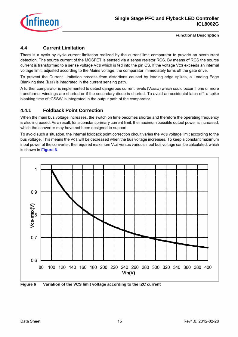
4.4.1 Foldback Point CorrectionWhen the main bus voltage increases, the switch on time becomes shorter and therefore the operating frequencyis also increased. As a result, for a constant primary current limit, the maximum possible output power is increased,which the converter may have not been designed to support.To avoid such a situation, the internal foldback point correction circuit varies the VCS voltage limit according to thebus voltage. This means the VCS will be decreased when the bus voltage increases. To keep a constant maximuminput power of the converter, the required maximum VCS versus various input bus voltage can be calculated, whichis shown in Figure 6.
Figure 6 Variation of the VCS limit voltage according to the IZC current
0.6
0.7
0.8
0.9
1
80 100 120 140 160 180 200 220 240 260 280 300 320 340 360 380 400
Vcs-
max
(V)
Vin(V)
Single Stage PFC and Flyback LED ControllerICL8002G
Functional Description
Data Sheet 16 Rev1.0, 2012-02-28
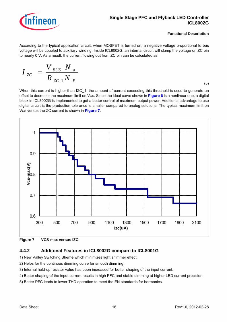
According to the typical application circuit, when MOSFET is turned on, a negative voltage proportional to busvoltage will be coupled to auxiliary winding. Inside ICL8002G, an internal circuit will clamp the voltage on ZC pinto nearly 0 V. As a result, the current flowing out from ZC pin can be calculated as
(5)
When this current is higher than IZC_1, the amount of current exceeding this threshold is used to generate anoffset to decrease the maximum limit on VCS. Since the ideal curve shown in Figure 6 is a nonlinear one, a digitalblock in ICL8002G is implemented to get a better control of maximum output power. Additional advantage to usedigital circuit is the production tolerance is smaller compared to analog solutions. The typical maximum limit onVCS versus the ZC current is shown in Figure 7.
Figure 7 VCS-max versus IZCi
4.4.2 Additonal Features in ICL8002G compare to ICL8001G1) New Valley Switching Sheme which minimizes light shimmer effect.2) Helps for the continous dimming curve for smooth dimming.3) Internal hold-up resistor value has been increased for better shaping of the input current.4) Better shaping of the input current results in high PFC and stable dimming at higher LED current precision.5) Better PFC leads to lower THD operation to meet the EN standards for hormonics.
PZC
aBUSZC NR
NVI1
=
0.6
0.7
0.8
0.9
1
300 500 700 900 1100 1300 1500 1700 1900 2100
Vcs-
max
(V)
Izc(uA)
Single Stage PFC and Flyback LED ControllerICL8002G
Functional Description
Data Sheet 17 Rev1.0, 2012-02-28
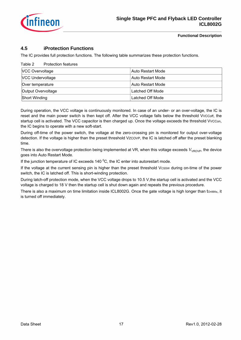
4.5 iProtection FunctionsThe IC provides full protection functions. The following table summarizes these protection functions.
During operation, the VCC voltage is continuously monitored. In case of an under- or an over-voltage, the IC isreset and the main power switch is then kept off. After the VCC voltage falls below the threshold VVCCoff, thestartup cell is activated. The VCC capacitor is then charged up. Once the voltage exceeds the threshold VVCCon,the IC begins to operate with a new soft-start.During off-time of the power switch, the voltage at the zero-crossing pin is monitored for output over-voltagedetection. If the voltage is higher than the preset threshold VZCOVP, the IC is latched off after the preset blankingtime.There is also the overvoltage protection being implemented at VR, when this voltage exceeds VVROVP, the devicegoes into Auto Restart Mode.If the junction temperature of IC exceeds 140 0C, the IC enter into autorestart mode.If the voltage at the current sensing pin is higher than the preset threshold VCSSW during on-time of the powerswitch, the IC is latched off. This is short-winding protection.During latch-off protection mode, when the VCC voltage drops to 10.5 V,the startup cell is activated and the VCCvoltage is charged to 18 V then the startup cell is shut down again and repeats the previous procedure.There is also a maximum on time limitation inside ICL8002G. Once the gate voltage is high longer than tOnMAx, itis turned off immediately.
Table 2 Protection features
VCC Overvoltage Auto Restart ModeVCC Undervoltage Auto Restart ModeOver temperature Auto Restart ModeOutput Overvoltage Latched Off ModeShort Winding Latched Off Mode
Single Stage PFC and Flyback LED ControllerICL8002G
Electrical Characteristics
Data Sheet 18 Rev1.0, 2012-02-28
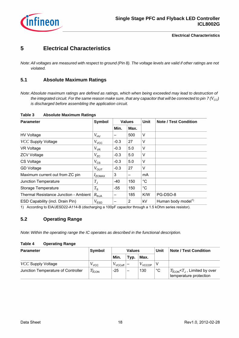
5 Electrical Characteristics
Note: All voltages are measured with respect to ground (Pin 8). The voltage levels are valid if other ratings are not violated.
5.1 Absolute Maximum Ratings
Note: Absolute maximum ratings are defined as ratings, which when being exceeded may lead to destruction of the integrated circuit. For the same reason make sure, that any capacitor that will be connected to pin 7 (VCC) is discharged before assembling the application circuit.
5.2 Operating Range
Note: Within the operating range the IC operates as described in the functional description.
Table 3 Absolute Maximum RatingsParameter Symbol Values Unit Note / Test Condition
Min. Max.HV Voltage VHV – 500 VVCC Supply Voltage VVCC -0.3 27 VVR Voltage VVR -0.3 5.0 VZCV Voltage VZC -0.3 5.0 VCS Voltage VCS -0.3 5.0 VGD Voltage VOUT -0.3 27 VMaximum current out from ZC pin IZCMAX 3 – mAJunction Temperature TJ -40 150 °CStorage Temperature TS -55 150 °CThermal Resistance Junction - Ambient RthJA – 185 K/W PG-DSO-8ESD Capability (incl. Drain Pin) VESD – 2 kV Human body model1) 1) According to EIA/JESD22-A114-B (discharging a 100pF capacitor through a 1.5 kOhm series resistor).
Table 4 Operating RangeParameter Symbol Values Unit Note / Test Condition
Min. Typ. Max.VCC Supply Voltage VVCC VVCCoff – VVCCOP VJunction Temperature of Controller TjCON -25 – 130 °C TjCON<TJ , Limited by over
temperature protection
Single Stage PFC and Flyback LED ControllerICL8002G
Electrical Characteristics
Data Sheet 19 Rev1.0, 2012-02-28
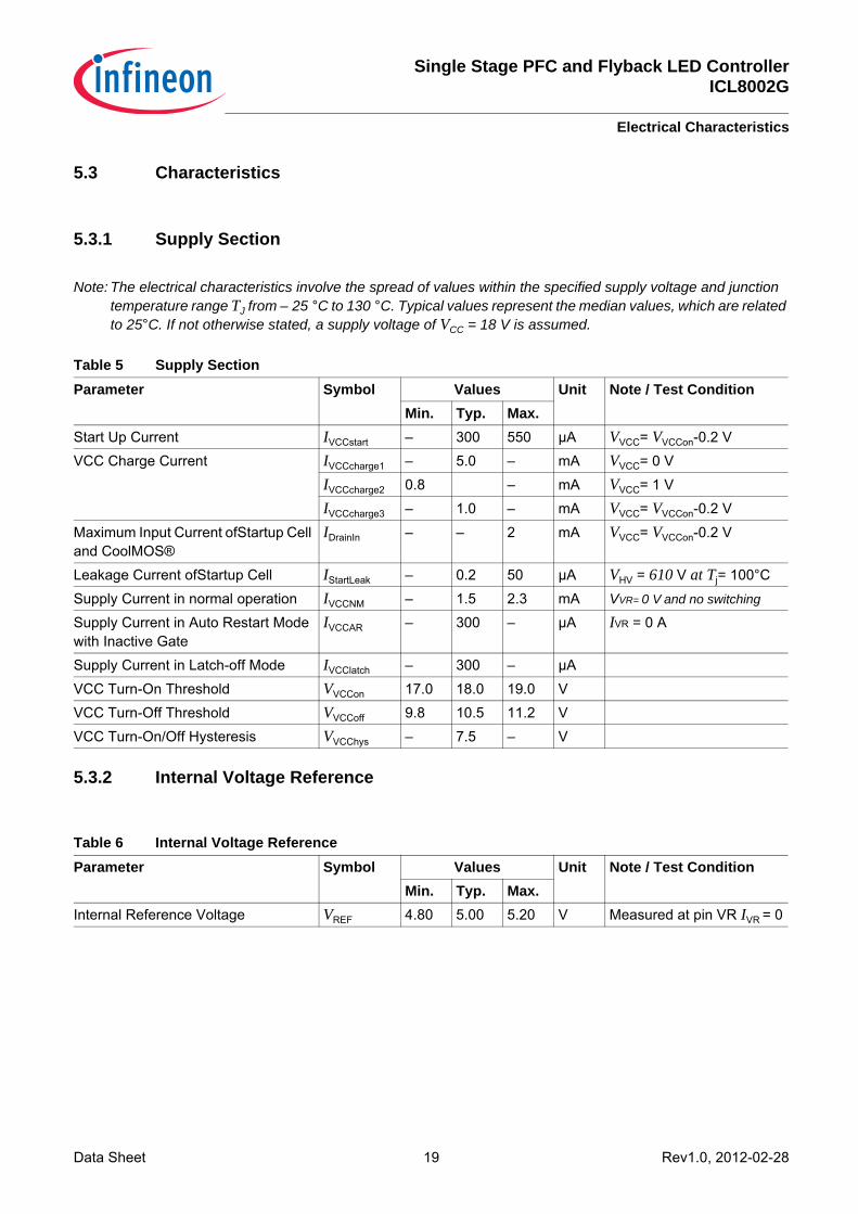
5.3 Characteristics
5.3.1 Supply Section
Note: The electrical characteristics involve the spread of values within the specified supply voltage and junction temperature range TJ from – 25 °C to 130 °C. Typical values represent the median values, which are related to 25°C. If not otherwise stated, a supply voltage of VCC = 18 V is assumed.
5.3.2 Internal Voltage Reference
Table 5 Supply SectionParameter Symbol Values Unit Note / Test Condition
Min. Typ. Max.Start Up Current IVCCstart – 300 550 µA VVCC= VVCCon-0.2 VVCC Charge Current IVCCcharge1 – 5.0 – mA VVCC= 0 V
IVCCcharge2 0.8 – mA VVCC= 1 VIVCCcharge3 – 1.0 – mA VVCC= VVCCon-0.2 V
Maximum Input Current ofStartup Cell and CoolMOS®
IDrainIn – – 2 mA VVCC= VVCCon-0.2 V
Leakage Current ofStartup Cell IStartLeak – 0.2 50 µA VHV = 610 V at Tj= 100°CSupply Current in normal operation IVCCNM – 1.5 2.3 mA VVR= 0 V and no switching
Supply Current in Auto Restart Mode with Inactive Gate
IVCCAR – 300 – µA IVR = 0 A
Supply Current in Latch-off Mode IVCClatch – 300 – µAVCC Turn-On Threshold VVCCon 17.0 18.0 19.0 VVCC Turn-Off Threshold VVCCoff 9.8 10.5 11.2 VVCC Turn-On/Off Hysteresis VVCChys – 7.5 – V
Table 6 Internal Voltage ReferenceParameter Symbol Values Unit Note / Test Condition
Min. Typ. Max.Internal Reference Voltage VREF 4.80 5.00 5.20 V Measured at pin VR IVR = 0
Single Stage PFC and Flyback LED ControllerICL8002G
Electrical Characteristics
Data Sheet 20 Rev1.0, 2012-02-28
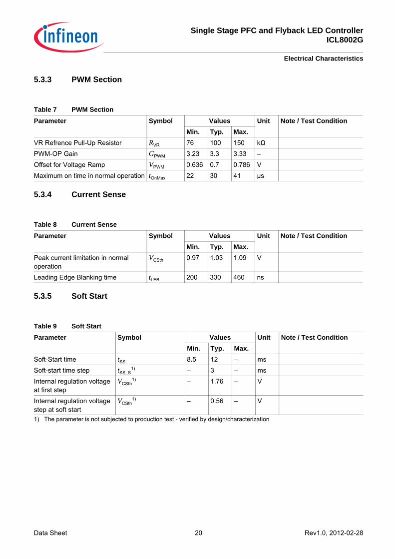
5.3.3 PWM Section
5.3.4 Current Sense
5.3.5 Soft Start
Table 7 PWM SectionParameter Symbol Values Unit Note / Test Condition
Min. Typ. Max.VR Refrence Pull-Up Resistor RVR 76 100 150 kΩPWM-OP Gain GPWM 3.23 3.3 3.33 –Offset for Voltage Ramp VPWM 0.636 0.7 0.786 VMaximum on time in normal operation tOnMax 22 30 41 µs
Table 8 Current SenseParameter Symbol Values Unit Note / Test Condition
Min. Typ. Max.Peak current limitation in normal operation
VCSth 0.97 1.03 1.09 V
Leading Edge Blanking time tLEB 200 330 460 ns
Table 9 Soft StartParameter Symbol Values Unit Note / Test Condition
Min. Typ. Max.Soft-Start time tSS 8.5 12 – msSoft-start time step tSS_S
1)
1) The parameter is not subjected to production test - verified by design/characterization
– 3 – msInternal regulation voltage at first step
VCSth1) – 1.76 – V
Internal regulation voltage step at soft start
VCSth1) – 0.56 – V
Single Stage PFC and Flyback LED ControllerICL8002G
Electrical Characteristics
Data Sheet 21 Rev1.0, 2012-02-28
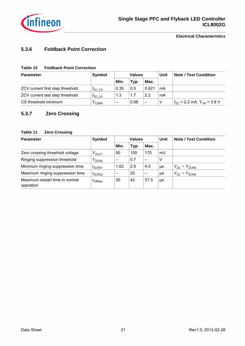
5.3.6 Foldback Point Correction
5.3.7 Zero Crossing
Table 10 Foldback Point CorrectionParameter Symbol Values Unit Note / Test Condition
Min. Typ. Max.ZCV current first step threshold IZC_FS 0.35 0.5 0.621 mAZCV current last step threshold IZC_LS 1.3 1.7 2.2 mACS threshold minimum VCSMF – 0.66 – V IZC = 2.2 mA, VVR = 3.8 V
Table 11 Zero CrossingParameter Symbol Values Unit Note / Test Condition
Min. Typ. Max.Zero crossing threshold voltage VZCCT 50 100 170 mVRinging suppression threshold VZCRS – 0.7 – VMinimum ringing suppression time tZCRS1 1.62 2.5 4.5 µs VZC > VZCRS
Maximum ringing suppression time tZCRS2 – 25 – µs VZC < VZCRS
Maximum restart time in normal operation
tOffMax 30 42 57.5 µs
Single Stage PFC and Flyback LED ControllerICL8002G
Electrical Characteristics
Data Sheet 22 Rev1.0, 2012-02-28
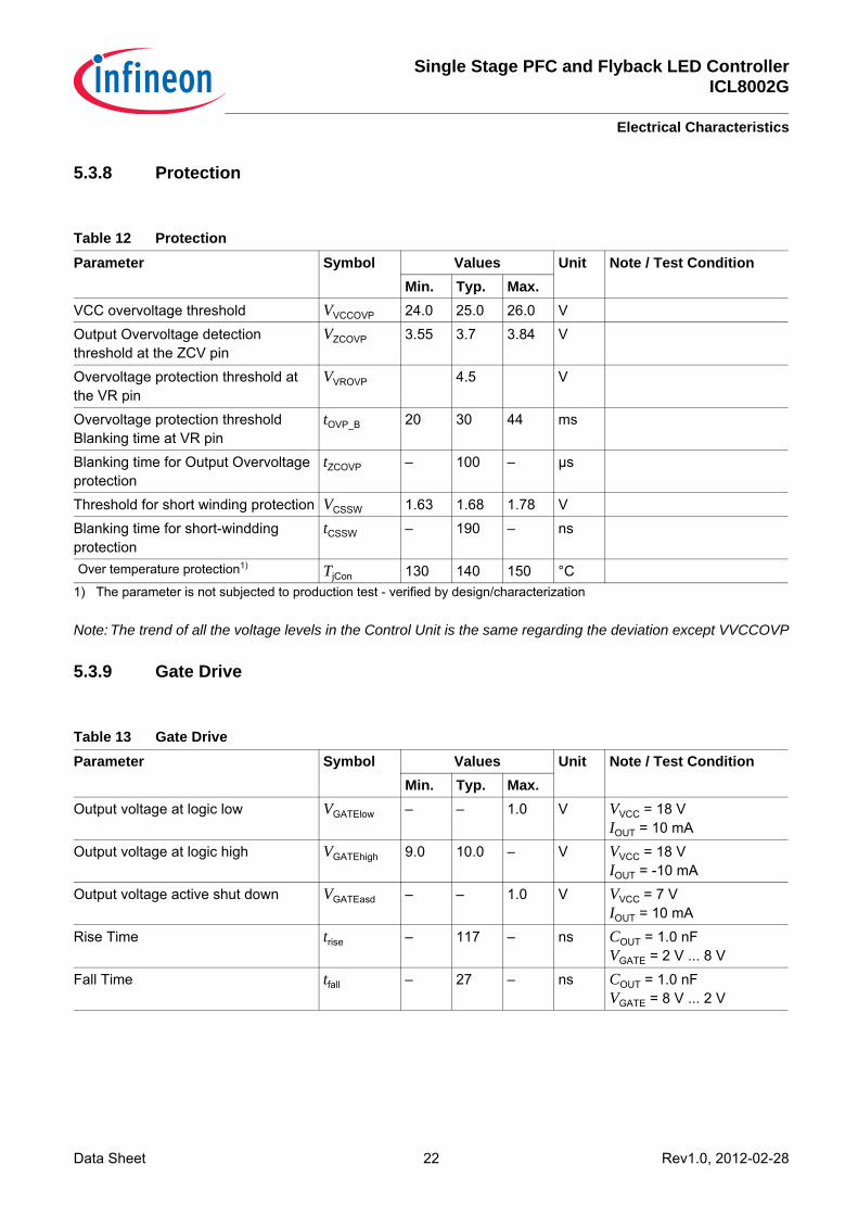
5.3.8 Protection
Note: The trend of all the voltage levels in the Control Unit is the same regarding the deviation except VVCCOVP
5.3.9 Gate Drive
Table 12 ProtectionParameter Symbol Values Unit Note / Test Condition
Min. Typ. Max.VCC overvoltage threshold VVCCOVP 24.0 25.0 26.0 VOutput Overvoltage detection threshold at the ZCV pin
VZCOVP 3.55 3.7 3.84 V
Overvoltage protection threshold at the VR pin
VVROVP 4.5 V
Overvoltage protection threshold Blanking time at VR pin
tOVP_B 20 30 44 ms
Blanking time for Output Overvoltage protection
tZCOVP – 100 – µs
Threshold for short winding protection VCSSW 1.63 1.68 1.78 VBlanking time for short-windding protection
tCSSW – 190 – ns
Over temperature protection1)
1) The parameter is not subjected to production test - verified by design/characterizationTjCon 130 140 150 °C
Table 13 Gate DriveParameter Symbol Values Unit Note / Test Condition
Min. Typ. Max.Output voltage at logic low VGATElow – – 1.0 V VVCC = 18 V
IOUT = 10 mAOutput voltage at logic high VGATEhigh 9.0 10.0 – V VVCC = 18 V
IOUT = -10 mAOutput voltage active shut down VGATEasd – – 1.0 V VVCC = 7 V
IOUT = 10 mARise Time trise – 117 – ns COUT = 1.0 nF
VGATE = 2 V ... 8 VFall Time tfall – 27 – ns COUT = 1.0 nF
VGATE = 8 V ... 2 V
Single Stage PFC and Flyback LED ControllerICL8002G
Outline Dimension
Data Sheet 23 Rev1.0, 2012-02-28
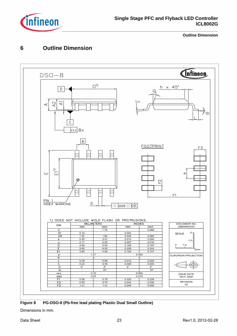
6 Outline Dimension
Figure 8 PG-DSO-8 (Pb-free lead plating Plastic Dual Small Outline)
Dimensions in mm.

Mouser Electronics
Authorized Distributor
Click to View Pricing, Inventory, Delivery & Lifecycle Information: Infineon:
ICL8002G