Inductive Coupling Radio for Syringe-Implantable Smart ...
14
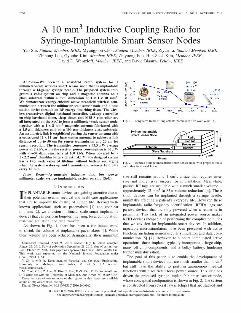
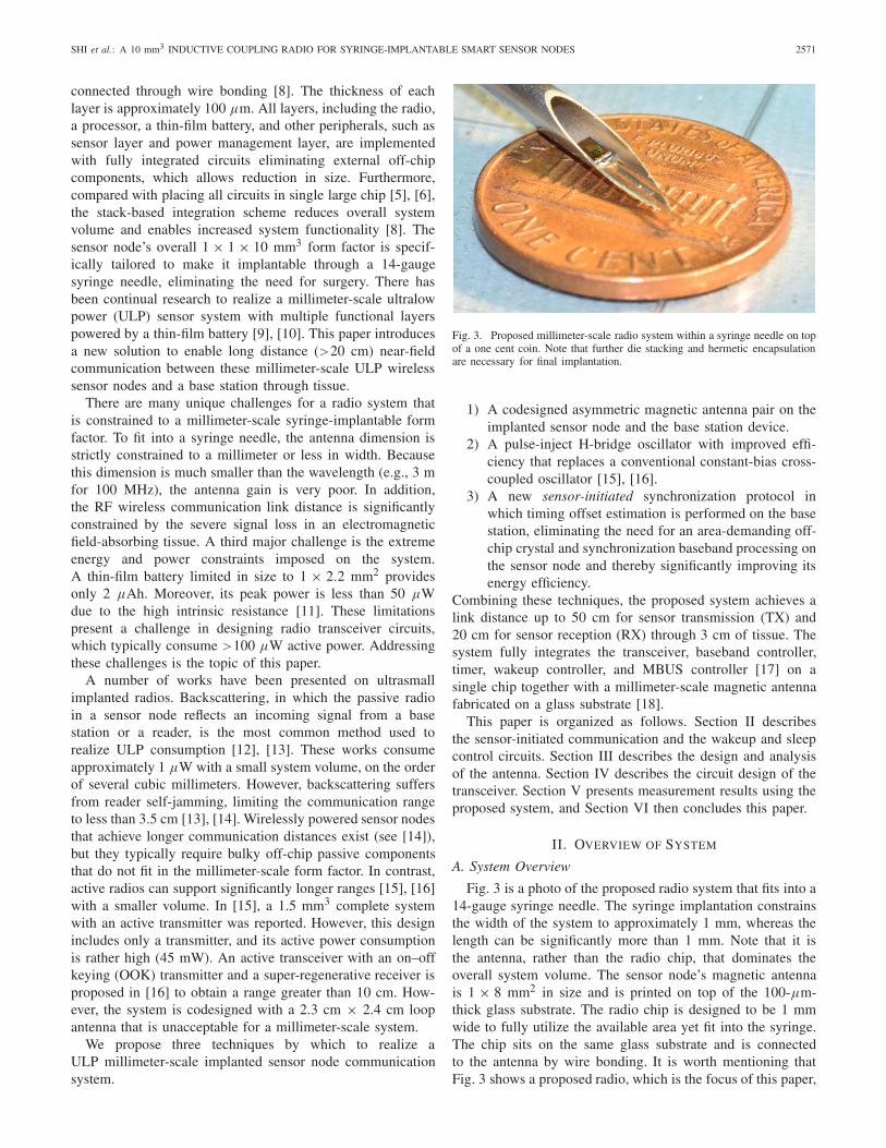
2570 IEEE JOURNAL OF SOLID-STATE CIRCUITS, VOL. 51, NO. 11, NOVEMBER 2016 A 10 mm 3 Inductive Coupling Radio for Syringe-Implantable Smart Sensor Nodes Yao Shi, Student Member, IEEE, Myungjoon Choi, Student Member, IEEE, Ziyun Li, Student Member, IEEE, Zhihong Luo, Gyouho Kim, Member, IEEE , Zhiyoong Foo, Hun-Seok Kim, Member, IEEE, David D. Wentzloff, Member, IEEE, and David Blaauw, Fellow, IEEE Abstract— We present a near-field radio system for a millimeter-scale wireless smart sensor node that is implantable through a 14-gauge syringe needle. The proposed system inte- grates a radio system on chip and a magnetic antenna on a glass substrate within a total dimension of 1 × 1 × 10 mm 3 . We demonstrate energy-efficient active near-field wireless com- munication between the millimeter-scale sensor node and a base station device through an RF energy-absorbing tissue. The wire- less transceiver, digital baseband controller, wakeup controller, on-chip baseband timer, sleep timer, and MBUS controller are all integrated on the SoC to form a millimeter-scale sensor node, together with a 1 × 8 mm 2 magnetic antenna fabricated with a 1.5-μm-thickness gold on a 100 μm-thickness glass substrate. An asymmetric link is established pairing the sensor antenna with a codesigned 11 × 11 cm 2 base station antenna to achieve a link distance of up to 50 cm for sensor transmission and 20 cm for sensor reception. The transmitter consumes a 43.5 μW average power at 2 kb/s, while the receiver power consumption is 36 μW with a -54 dBm sensitivity at 100 kb/s. When powered by a 1 ×2.2 mm 2 thin-film battery (2 μAh, 4.1 V), the designed system has a two week expected lifetime without battery recharging when the system wakes up and transmits and receives 16 b data every 10 min. Index Terms— Asymmetric inductive link, low power, millimeter scale, syringe implantable, system on chip (SoC). I. I NTRODUCTION I MPLANTABLE smart devices are gaining attention due to their potential uses in medical and healthcare applications that aim to improve the quality of human life. Beyond well- known applications such as pacemakers [1] and cochlear implants [2], we envision millimeter-scale smart implantable devices that can perform long-term sensing, local computation, real-time actuation, and data transfer. As shown in Fig. 1, there has been a continuous trend to shrink the volume of implantable pacemakers [3]. While their volume has been reduced dramatically, their minimum Manuscript received April 9, 2016; revised July 6, 2016; accepted August 23, 2016. Date of publication September 28, 2016; date of current ver- sion October 29, 2016. This paper was approved by Guest Editor Wentai Liu. This work was supported by the National Science Foundation under Grant CNS-1111541. Y. Shi is with the Department of Electrical and Computer Engineering, University of Michigan, Ann Arbor, MI 48105 USA (e-mail: [email protected]). M. Choi, Z. Li, Z. Luo, G. Kim, Z. Foo, H.-S. Kim, D. D. Wentzloff, and D. Blaauw are with the University of Michigan, Ann Arbor, MI 48105 USA. Color versions of one or more of the figures in this paper are available online at http://ieeexplore.ieee.org. Digital Object Identifier 10.1109/JSSC.2016.2606162 Fig. 1. Long-term trend of implantable pacemaker size over years [3]. Fig. 2. Targeted syringe-implantable smart sensor node with proposed radio and other functional layers. size still remains around 1 cm 3 , a size that requires inva- sive and more risky surgery for implantation. Meanwhile, passive RF tags are available with a much smaller volume— approximately 12 mm 3 (a 83× volume reduction) [4]. These small devices can be implanted through a syringe needle, minimally affecting a patient’s everyday life. However, these implantable radio-frequency identification (RFID) tags are passive devices that are only powered when a reader is in proximity. This lack of an integrated power source makes RFID devices incapable of performing the complicated duties that we envision for implantable smart devices. In addition, injectable microstimulators have been presented with active functions including neuromuscular stimulation and data com- munication [5]–[7]. However, to support complicated active operations, those implants typically incorporate a large chip, many off-chip components, and a bulky battery, hindering further miniaturization. The goal of this paper is to enable the development of implantable smart devices that are much smaller than 1 cm 3 but still have the ability to perform autonomous medical functions with a restricted local power source. This idea has driven the proposed syringe-implantable smart sensor node, whose conceptual configuration is shown in Fig. 2. The system is constructed from several layers (chips) that are stacked and 0018-9200 © 2016 IEEE. Personal use is permitted, but republication/redistribution requires IEEE permission. See http://www.ieee.org/publications_standards/publications/rights/index.html for more information.
-
Upload
khangminh22 -
Category
Documents
-
view
1 -
download
0
Transcript of Inductive Coupling Radio for Syringe-Implantable Smart ...
2570 IEEE JOURNAL OF SOLID-STATE CIRCUITS, VOL. 51, NO. 11, NOVEMBER 2016
A 10 mm3 Inductive Coupling Radio forSyringe-Implantable Smart Sensor Nodes
Yao Shi, Student Member, IEEE, Myungjoon Choi, Student Member, IEEE, Ziyun Li, Student Member, IEEE,Zhihong Luo, Gyouho Kim, Member, IEEE, Zhiyoong Foo, Hun-Seok Kim, Member, IEEE,
David D. Wentzloff, Member, IEEE, and David Blaauw, Fellow, IEEE
Abstract— We present a near-field radio system for amillimeter-scale wireless smart sensor node that is implantablethrough a 14-gauge syringe needle. The proposed system inte-grates a radio system on chip and a magnetic antenna on aglass substrate within a total dimension of 1 × 1 × 10 mm3.We demonstrate energy-efficient active near-field wireless com-munication between the millimeter-scale sensor node and a basestation device through an RF energy-absorbing tissue. The wire-less transceiver, digital baseband controller, wakeup controller,on-chip baseband timer, sleep timer, and MBUS controller areall integrated on the SoC to form a millimeter-scale sensor node,together with a 1 × 8 mm2 magnetic antenna fabricated witha 1.5-µm-thickness gold on a 100 µm-thickness glass substrate.An asymmetric link is established pairing the sensor antenna witha codesigned 11 × 11 cm2 base station antenna to achieve a linkdistance of up to 50 cm for sensor transmission and 20 cm forsensor reception. The transmitter consumes a 43.5 µW averagepower at 2 kb/s, while the receiver power consumption is 36 µWwith a −54 dBm sensitivity at 100 kb/s. When powered by a1×2.2 mm2 thin-film battery (2 µAh, 4.1 V), the designed systemhas a two week expected lifetime without battery rechargingwhen the system wakes up and transmits and receives 16 b dataevery 10 min.
Index Terms— Asymmetric inductive link, low power,millimeter scale, syringe implantable, system on chip (SoC).
I. INTRODUCTION
IMPLANTABLE smart devices are gaining attention due totheir potential uses in medical and healthcare applications
that aim to improve the quality of human life. Beyond well-known applications such as pacemakers [1] and cochlearimplants [2], we envision millimeter-scale smart implantabledevices that can perform long-term sensing, local computation,real-time actuation, and data transfer.
As shown in Fig. 1, there has been a continuous trendto shrink the volume of implantable pacemakers [3]. Whiletheir volume has been reduced dramatically, their minimum
Manuscript received April 9, 2016; revised July 6, 2016; acceptedAugust 23, 2016. Date of publication September 28, 2016; date of current ver-sion October 29, 2016. This paper was approved by Guest Editor Wentai Liu.This work was supported by the National Science Foundation underGrant CNS-1111541.
Y. Shi is with the Department of Electrical and Computer Engineering,University of Michigan, Ann Arbor, MI 48105 USA (e-mail:[email protected]).
M. Choi, Z. Li, Z. Luo, G. Kim, Z. Foo, H.-S. Kim, D. D. Wentzloff, andD. Blaauw are with the University of Michigan, Ann Arbor, MI 48105 USA.
Color versions of one or more of the figures in this paper are availableonline at http://ieeexplore.ieee.org.
Digital Object Identifier 10.1109/JSSC.2016.2606162
Fig. 1. Long-term trend of implantable pacemaker size over years [3].
Fig. 2. Targeted syringe-implantable smart sensor node with proposed radioand other functional layers.
size still remains around 1 cm3, a size that requires inva-sive and more risky surgery for implantation. Meanwhile,passive RF tags are available with a much smaller volume—approximately 12 mm3 (a 83× volume reduction) [4]. Thesesmall devices can be implanted through a syringe needle,minimally affecting a patient’s everyday life. However, theseimplantable radio-frequency identification (RFID) tags arepassive devices that are only powered when a reader is inproximity. This lack of an integrated power source makesRFID devices incapable of performing the complicated dutiesthat we envision for implantable smart devices. In addition,injectable microstimulators have been presented with activefunctions including neuromuscular stimulation and data com-munication [5]–[7]. However, to support complicated activeoperations, those implants typically incorporate a large chip,many off-chip components, and a bulky battery, hinderingfurther miniaturization.
The goal of this paper is to enable the development ofimplantable smart devices that are much smaller than 1 cm3
but still have the ability to perform autonomous medicalfunctions with a restricted local power source. This idea hasdriven the proposed syringe-implantable smart sensor node,whose conceptual configuration is shown in Fig. 2. The systemis constructed from several layers (chips) that are stacked and
0018-9200 © 2016 IEEE. Personal use is permitted, but republication/redistribution requires IEEE permission.See http://www.ieee.org/publications_standards/publications/rights/index.html for more information.
SHI et al.: A 10 mm3 INDUCTIVE COUPLING RADIO FOR SYRINGE-IMPLANTABLE SMART SENSOR NODES 2571
connected through wire bonding [8]. The thickness of eachlayer is approximately 100 μm. All layers, including the radio,a processor, a thin-film battery, and other peripherals, such assensor layer and power management layer, are implementedwith fully integrated circuits eliminating external off-chipcomponents, which allows reduction in size. Furthermore,compared with placing all circuits in single large chip [5], [6],the stack-based integration scheme reduces overall systemvolume and enables increased system functionality [8]. Thesensor node’s overall 1 × 1 × 10 mm3 form factor is specif-ically tailored to make it implantable through a 14-gaugesyringe needle, eliminating the need for surgery. There hasbeen continual research to realize a millimeter-scale ultralowpower (ULP) sensor system with multiple functional layerspowered by a thin-film battery [9], [10]. This paper introducesa new solution to enable long distance (>20 cm) near-fieldcommunication between these millimeter-scale ULP wirelesssensor nodes and a base station through tissue.
There are many unique challenges for a radio system thatis constrained to a millimeter-scale syringe-implantable formfactor. To fit into a syringe needle, the antenna dimension isstrictly constrained to a millimeter or less in width. Becausethis dimension is much smaller than the wavelength (e.g., 3 mfor 100 MHz), the antenna gain is very poor. In addition,the RF wireless communication link distance is significantlyconstrained by the severe signal loss in an electromagneticfield-absorbing tissue. A third major challenge is the extremeenergy and power constraints imposed on the system.A thin-film battery limited in size to 1 × 2.2 mm2 providesonly 2 μAh. Moreover, its peak power is less than 50 μWdue to the high intrinsic resistance [11]. These limitationspresent a challenge in designing radio transceiver circuits,which typically consume >100 μW active power. Addressingthese challenges is the topic of this paper.
A number of works have been presented on ultrasmallimplanted radios. Backscattering, in which the passive radioin a sensor node reflects an incoming signal from a basestation or a reader, is the most common method used torealize ULP consumption [12], [13]. These works consumeapproximately 1 μW with a small system volume, on the orderof several cubic millimeters. However, backscattering suffersfrom reader self-jamming, limiting the communication rangeto less than 3.5 cm [13], [14]. Wirelessly powered sensor nodesthat achieve longer communication distances exist (see [14]),but they typically require bulky off-chip passive componentsthat do not fit in the millimeter-scale form factor. In contrast,active radios can support significantly longer ranges [15], [16]with a smaller volume. In [15], a 1.5 mm3 complete systemwith an active transmitter was reported. However, this designincludes only a transmitter, and its active power consumptionis rather high (45 mW). An active transceiver with an on–offkeying (OOK) transmitter and a super-regenerative receiver isproposed in [16] to obtain a range greater than 10 cm. How-ever, the system is codesigned with a 2.3 cm × 2.4 cm loopantenna that is unacceptable for a millimeter-scale system.
We propose three techniques by which to realize aULP millimeter-scale implanted sensor node communicationsystem.
Fig. 3. Proposed millimeter-scale radio system within a syringe needle on topof a one cent coin. Note that further die stacking and hermetic encapsulationare necessary for final implantation.
1) A codesigned asymmetric magnetic antenna pair on theimplanted sensor node and the base station device.
2) A pulse-inject H-bridge oscillator with improved effi-ciency that replaces a conventional constant-bias cross-coupled oscillator [15], [16].
3) A new sensor-initiated synchronization protocol inwhich timing offset estimation is performed on the basestation, eliminating the need for an area-demanding off-chip crystal and synchronization baseband processing onthe sensor node and thereby significantly improving itsenergy efficiency.
Combining these techniques, the proposed system achieves alink distance up to 50 cm for sensor transmission (TX) and20 cm for sensor reception (RX) through 3 cm of tissue. Thesystem fully integrates the transceiver, baseband controller,timer, wakeup controller, and MBUS controller [17] on asingle chip together with a millimeter-scale magnetic antennafabricated on a glass substrate [18].
This paper is organized as follows. Section II describesthe sensor-initiated communication and the wakeup and sleepcontrol circuits. Section III describes the design and analysisof the antenna. Section IV describes the circuit design of thetransceiver. Section V presents measurement results using theproposed system, and Section VI then concludes this paper.
II. OVERVIEW OF SYSTEM
A. System Overview
Fig. 3 is a photo of the proposed radio system that fits into a14-gauge syringe needle. The syringe implantation constrainsthe width of the system to approximately 1 mm, whereas thelength can be significantly more than 1 mm. Note that it isthe antenna, rather than the radio chip, that dominates theoverall system volume. The sensor node’s magnetic antennais 1 × 8 mm2 in size and is printed on top of the 100-μm-thick glass substrate. The radio chip is designed to be 1 mmwide to fully utilize the available area yet fit into the syringe.The chip sits on the same glass substrate and is connectedto the antenna by wire bonding. It is worth mentioning thatFig. 3 shows a proposed radio, which is the focus of this paper,
2572 IEEE JOURNAL OF SOLID-STATE CIRCUITS, VOL. 51, NO. 11, NOVEMBER 2016
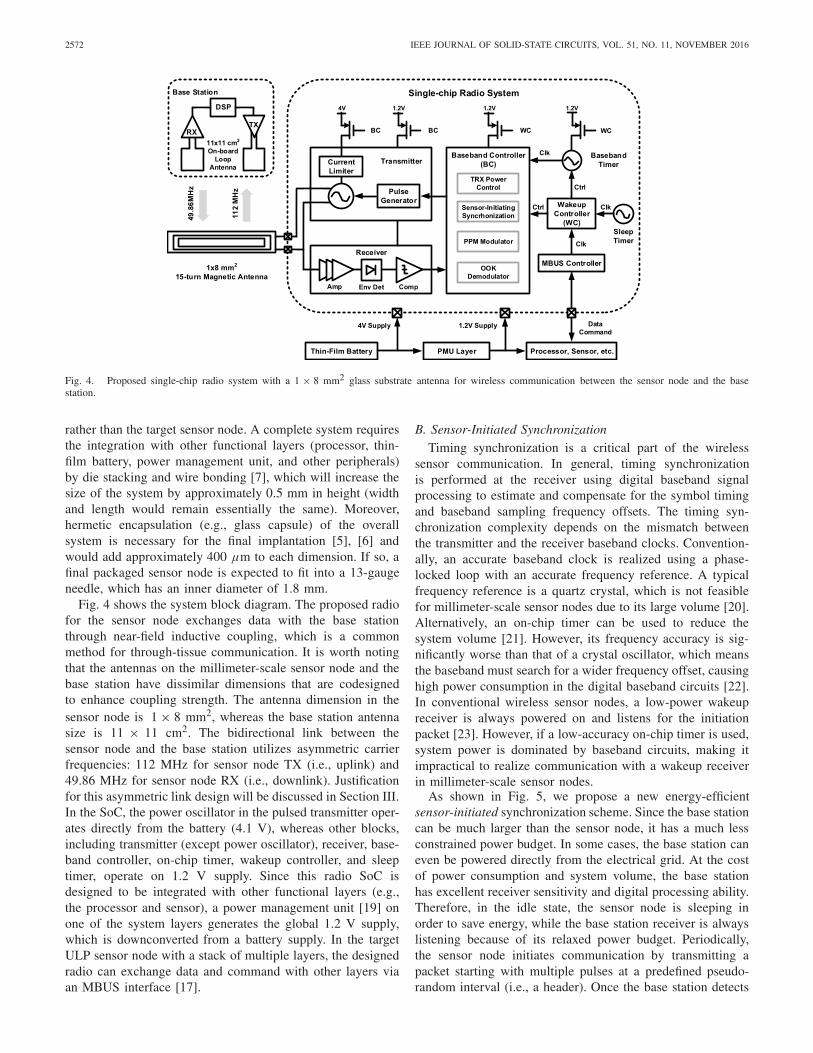
Fig. 4. Proposed single-chip radio system with a 1 × 8 mm2 glass substrate antenna for wireless communication between the sensor node and the basestation.
rather than the target sensor node. A complete system requiresthe integration with other functional layers (processor, thin-film battery, power management unit, and other peripherals)by die stacking and wire bonding [7], which will increase thesize of the system by approximately 0.5 mm in height (widthand length would remain essentially the same). Moreover,hermetic encapsulation (e.g., glass capsule) of the overallsystem is necessary for the final implantation [5], [6] andwould add approximately 400 μm to each dimension. If so, afinal packaged sensor node is expected to fit into a 13-gaugeneedle, which has an inner diameter of 1.8 mm.
Fig. 4 shows the system block diagram. The proposed radiofor the sensor node exchanges data with the base stationthrough near-field inductive coupling, which is a commonmethod for through-tissue communication. It is worth notingthat the antennas on the millimeter-scale sensor node and thebase station have dissimilar dimensions that are codesignedto enhance coupling strength. The antenna dimension in thesensor node is 1 × 8 mm2, whereas the base station antennasize is 11 × 11 cm2. The bidirectional link between thesensor node and the base station utilizes asymmetric carrierfrequencies: 112 MHz for sensor node TX (i.e., uplink) and49.86 MHz for sensor node RX (i.e., downlink). Justificationfor this asymmetric link design will be discussed in Section III.In the SoC, the power oscillator in the pulsed transmitter oper-ates directly from the battery (4.1 V), whereas other blocks,including transmitter (except power oscillator), receiver, base-band controller, on-chip timer, wakeup controller, and sleeptimer, operate on 1.2 V supply. Since this radio SoC isdesigned to be integrated with other functional layers (e.g.,the processor and sensor), a power management unit [19] onone of the system layers generates the global 1.2 V supply,which is downconverted from a battery supply. In the targetULP sensor node with a stack of multiple layers, the designedradio can exchange data and command with other layers viaan MBUS interface [17].
B. Sensor-Initiated SynchronizationTiming synchronization is a critical part of the wireless
sensor communication. In general, timing synchronizationis performed at the receiver using digital baseband signalprocessing to estimate and compensate for the symbol timingand baseband sampling frequency offsets. The timing syn-chronization complexity depends on the mismatch betweenthe transmitter and the receiver baseband clocks. Convention-ally, an accurate baseband clock is realized using a phase-locked loop with an accurate frequency reference. A typicalfrequency reference is a quartz crystal, which is not feasiblefor millimeter-scale sensor nodes due to its large volume [20].Alternatively, an on-chip timer can be used to reduce thesystem volume [21]. However, its frequency accuracy is sig-nificantly worse than that of a crystal oscillator, which meansthe baseband must search for a wider frequency offset, causinghigh power consumption in the digital baseband circuits [22].In conventional wireless sensor nodes, a low-power wakeupreceiver is always powered on and listens for the initiationpacket [23]. However, if a low-accuracy on-chip timer is used,system power is dominated by baseband circuits, making itimpractical to realize communication with a wakeup receiverin millimeter-scale sensor nodes.
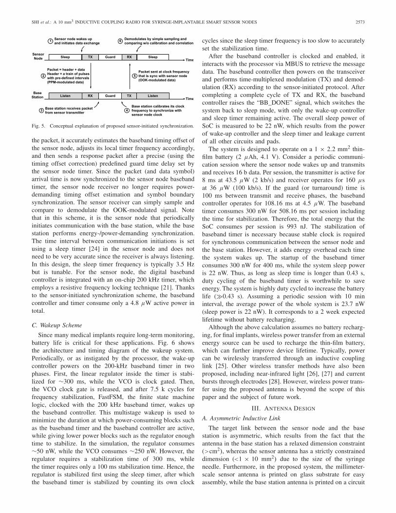
As shown in Fig. 5, we propose a new energy-efficientsensor-initiated synchronization scheme. Since the base stationcan be much larger than the sensor node, it has a much lessconstrained power budget. In some cases, the base station caneven be powered directly from the electrical grid. At the costof power consumption and system volume, the base stationhas excellent receiver sensitivity and digital processing ability.Therefore, in the idle state, the sensor node is sleeping inorder to save energy, while the base station receiver is alwayslistening because of its relaxed power budget. Periodically,the sensor node initiates communication by transmitting apacket starting with multiple pulses at a predefined pseudo-random interval (i.e., a header). Once the base station detects
SHI et al.: A 10 mm3 INDUCTIVE COUPLING RADIO FOR SYRINGE-IMPLANTABLE SMART SENSOR NODES 2573
Fig. 5. Conceptual explanation of proposed sensor-initiated synchronization.
the packet, it accurately estimates the baseband timing offset ofthe sensor node, adjusts its local timer frequency accordingly,and then sends a response packet after a precise (using thetiming offset correction) predefined guard time delay set bythe sensor node timer. Since the packet (and data symbol)arrival time is now synchronized to the sensor node basebandtimer, the sensor node receiver no longer requires power-demanding timing offset estimation and symbol boundarysynchronization. The sensor receiver can simply sample andcompare to demodulate the OOK-modulated signal. Notethat in this scheme, it is the sensor node that periodicallyinitiates communication with the base station, while the basestation performs energy-/power-demanding synchronization.The time interval between communication initiations is setusing a sleep timer [24] in the sensor node and does notneed to be very accurate since the receiver is always listening.In this design, the sleep timer frequency is typically 3.5 Hzbut is tunable. For the sensor node, the digital basebandcontroller is integrated with an on-chip 200 kHz timer, whichemploys a resistive frequency locking technique [21]. Thanksto the sensor-initiated synchronization scheme, the basebandcontroller and timer consume only a 4.8 μW active power intotal.
C. Wakeup Scheme
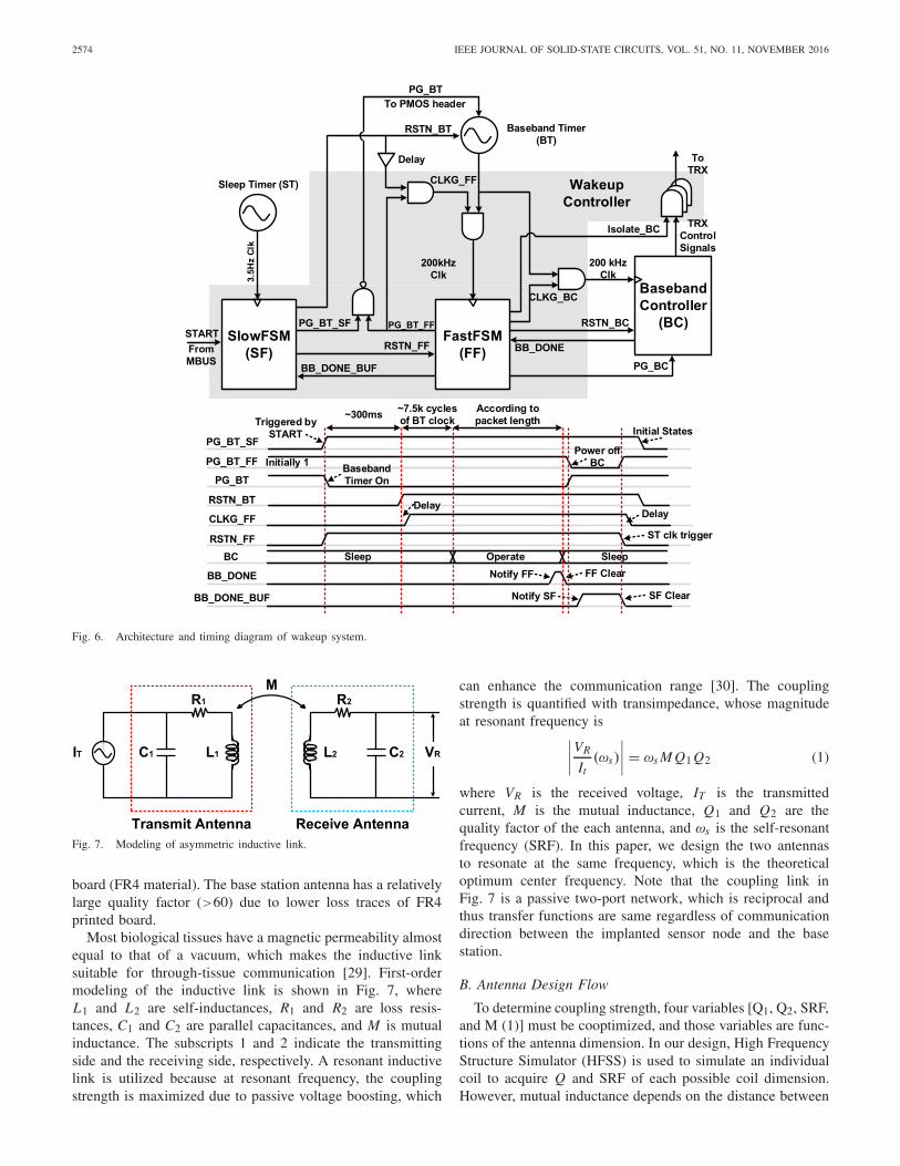
Since many medical implants require long-term monitoring,battery life is critical for these applications. Fig. 6 showsthe architecture and timing diagram of the wakeup system.Periodically, or as instigated by the processor, the wake-upcontroller powers on the 200-kHz baseband timer in twophases. First, the linear regulator inside the timer is stabi-lized for ∼300 ms, while the VCO is clock gated. Then,the VCO clock gate is released, and after 7.5 k cycles forfrequency stabilization, FastFSM, the finite state machinelogic, clocked with the 200 kHz baseband timer, wakes upthe baseband controller. This multistage wakeup is used tominimize the duration at which power-consuming blocks suchas the baseband timer and the baseband controller are active,while giving lower power blocks such as the regulator enoughtime to stabilize. In the simulation, the regulator consumes∼50 nW, while the VCO consumes ∼250 nW. However, theregulator requires a stabilization time of 300 ms, whilethe timer requires only a 100 ms stabilization time. Hence, theregulator is stabilized first using the sleep timer, after whichthe baseband timer is stabilized by counting its own clock
cycles since the sleep timer frequency is too slow to accuratelyset the stabilization time.
After the baseband controller is clocked and enabled, itinteracts with the processor via MBUS to retrieve the messagedata. The baseband controller then powers on the transceiverand performs time-multiplexed modulation (TX) and demod-ulation (RX) according to the sensor-initiated protocol. Aftercompleting a complete cycle of TX and RX, the basebandcontroller raises the “BB_DONE” signal, which switches thesystem back to sleep mode, with only the wake-up controllerand sleep timer remaining active. The overall sleep power ofSoC is measured to be 22 nW, which results from the powerof wake-up controller and the sleep timer and leakage currentof all other circuits and pads.
The system is designed to operate on a 1 × 2.2 mm2 thin-film battery (2 μAh, 4.1 V). Consider a periodic communi-cation session where the sensor node wakes up and transmitsand receives 16 b data. Per session, the transmitter is active for8 ms at 43.5 μW (2 kb/s) and receiver operates for 160 μsat 36 μW (100 kb/s). If the guard (or turnaround) time is100 ms between transmit and receive phases, the basebandcontroller operates for 108.16 ms at 4.5 μW. The basebandtimer consumes 300 nW for 508.16 ms per session includingthe time for stabilization. Therefore, the total energy that theSoC consumes per session is 993 nJ. The stabilization ofbaseband timer is necessary because stable clock is requiredfor synchronous communication between the sensor node andthe base station. However, it adds energy overhead each timethe system wakes up. The startup of the baseband timerconsumes 300 nW for 400 ms, while the system sleep poweris 22 nW. Thus, as long as sleep time is longer than 0.43 s,duty cycling of the baseband timer is worthwhile to saveenergy. The system is highly duty cycled to increase the batterylife (�0.43 s). Assuming a periodic session with 10 mininterval, the average power of the whole system is 23.7 nW(sleep power is 22 nW). It corresponds to a 2 week expectedlifetime without battery recharging.
Although the above calculation assumes no battery recharg-ing, for final implants, wireless power transfer from an externalenergy source can be used to recharge the thin-film battery,which can further improve device lifetime. Typically, powercan be wirelessly transferred through an inductive couplinglink [25]. Other wireless transfer methods have also beenproposed, including near-infrared light [26], [27] and currentbursts through electrodes [28]. However, wireless power trans-fer using the proposed antenna is beyond the scope of thispaper and the subject of future work.
III. ANTENNA DESIGN
A. Asymmetric Inductive Link
The target link between the sensor node and the basestation is asymmetric, which results from the fact that theantenna in the base station has a relaxed dimension constraint(>cm2), whereas the sensor antenna has a strictly constraineddimension (<1 × 10 mm2) due to the size of the syringeneedle. Furthermore, in the proposed system, the millimeter-scale sensor antenna is printed on glass substrate for easyassembly, while the base station antenna is printed on a circuit
2574 IEEE JOURNAL OF SOLID-STATE CIRCUITS, VOL. 51, NO. 11, NOVEMBER 2016
Fig. 6. Architecture and timing diagram of wakeup system.
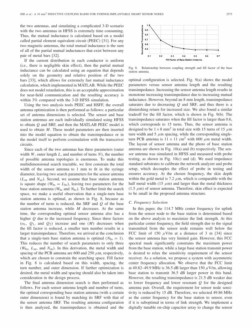
Fig. 7. Modeling of asymmetric inductive link.
board (FR4 material). The base station antenna has a relativelylarge quality factor (>60) due to lower loss traces of FR4printed board.
Most biological tissues have a magnetic permeability almostequal to that of a vacuum, which makes the inductive linksuitable for through-tissue communication [29]. First-ordermodeling of the inductive link is shown in Fig. 7, whereL1 and L2 are self-inductances, R1 and R2 are loss resis-tances, C1 and C2 are parallel capacitances, and M is mutualinductance. The subscripts 1 and 2 indicate the transmittingside and the receiving side, respectively. A resonant inductivelink is utilized because at resonant frequency, the couplingstrength is maximized due to passive voltage boosting, which
can enhance the communication range [30]. The couplingstrength is quantified with transimpedance, whose magnitudeat resonant frequency is
∣∣∣∣
VR
It(ωs)
∣∣∣∣= ωs M Q1 Q2 (1)
where VR is the received voltage, IT is the transmittedcurrent, M is the mutual inductance, Q1 and Q2 are thequality factor of the each antenna, and ωs is the self-resonantfrequency (SRF). In this paper, we design the two antennasto resonate at the same frequency, which is the theoreticaloptimum center frequency. Note that the coupling link inFig. 7 is a passive two-port network, which is reciprocal andthus transfer functions are same regardless of communicationdirection between the implanted sensor node and the basestation.
B. Antenna Design Flow
To determine coupling strength, four variables [Q1, Q2, SRF,and M (1)] must be cooptimized, and those variables are func-tions of the antenna dimension. In our design, High FrequencyStructure Simulator (HFSS) is used to simulate an individualcoil to acquire Q and SRF of each possible coil dimension.However, mutual inductance depends on the distance between
SHI et al.: A 10 mm3 INDUCTIVE COUPLING RADIO FOR SYRINGE-IMPLANTABLE SMART SENSOR NODES 2575
the two antennas, and simulating a complicated 3-D scenariowith the two antennas in HFSS is extremely time consuming.Thus, the mutual inductance is calculated based on a modelcalled partial element equivalent circuit (PEEC) [31]. For anytwo magnetic antennas, the total mutual inductance is the sumof all of the partial mutual inductances that exist between anypair of metal bars [32].
If the current distribution in each conductor is uniform(i.e., there is negligible skin effect), then the partial mutualinductance can be calculated using an equation that dependssolely on the geometry and relative position of the twobars [33], which allows for extremely fast mutual inductancecalculation, which implemented in MATLAB. While the PEECdoes not model retardation, this is an acceptable approximationfor near-field communication and the resulting accuracy iswithin 3% compared with the 3-D HFSS simulation.
Using the two analysis tools PEEC and HSFF, the overallantenna optimization is then performed as follows: a particularset of antenna dimensions is selected. The sensor and basestation antennas are each individually simulated using HFSSto obtain Q and SRF, and then the MATLAB PEEC model isused to obtain M . These model parameters are then insertedinto the model equation to obtain the transimpedance or inthe model itself to perform cosimulation with the transceivercircuits.
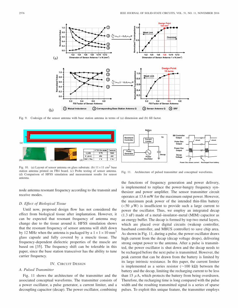
Since each of the two antennas has three parameters (outerwidth W , outer length L, and number of turns N), the numberof possible antenna topologies is enormous. To make thismultidimensional search tractable, we first constrain the totalwidth of the sensor antenna to 1 mm to fit in the syringediameter, leaving two search parameters for the sensor antenna(Lsn and Nsn). Second, we assume that base station antennais square shape (Wbs = Lbs), leaving two parameters for thebase station antenna (Wbs and Nbs). To further limit the searchspace, we make a useful observation that a single-turn basestation antenna is optimal, as shown in Fig. 8, because asthe number of turns is reduced, the SRF and Q of the basestation antenna increase, while M decreases. At the sametime, the corresponding optimal sensor antenna also has ahigher Q due to the increased frequency. Since three factors(ωs , Q1, and Q2) increase and one (M) decreases whenthe fill factor is reduced, a smaller turn number results in alarger transimpedance. Therefore, we arrived at the conclusionthat a single-turn base station antenna is optimal (Nbs = 1).This reduces the number of search parameters to only three(Wbs, Lsn, and Nsn). In this derivation, the metal width andspacing of the PCB antenna are 600 and 250 μm, respectively,which are chosen to constrain the searching space. Fill factorin Fig. 8 is calculated based on this width, spacing, theturn number, and outer dimension. If further optimization isdesired, the metal width and spacing should also be taken intoconsideration in the design process.
The final antenna dimension search is then performed asfollows. For each sensor antenna length and number of turns,the optimal corresponding base station antenna (with a certainouter dimension) is found by matching its SRF with that ofthe sensor antenna SRF. The resulting antenna configurationis then analyzed, the transimpedance is obtained and the
Fig. 8. Relationship between coupling strength and fill factor of the basestation antenna.
optimal configuration is selected. Fig. 9(a) shows the modelparameters versus sensor antenna length and the resultingtransimpedance. Increasing the sensor antenna length results inmonotone increasing transimpedance due to increasing mutualinductance. However, beyond an 8 mm length, transimpedancesaturates due to decreasing Q and SRF, and thus there is adiminishing return for increased size. We also found a similartradeoff for the fill factor, which is shown in Fig. 9(b). Thetransimpedance saturates when the fill factor is larger than 0.6,which corresponds to 15 turns. Thus, the sensor antenna isdesigned to be 1×8 mm2 in total size with 15 turns of 15 μmturn width and 5 μm spacing, while the corresponding single-turn PCB antenna is 11 × 11 cm2 with 600 μm metal width.The layout of sensor antenna and the photo of base stationantenna are shown in Fig. 10(a) and (b) respectively. The sen-sor antenna was simulated in HFSS and measured with probetesting, as shown in Fig. 10(c) and (d). We used impedancestandard substrates to calibrate the network analyzer and probesetup, which decouples the effect of probe in testing andensures accuracy. At the chosen frequency, the skin depthwithin the gold metal is 7.2 μm, which is comparable with thehalf metal width (15 μm) and larger than the metal thickness(1.5 μm) of sensor antenna. Therefore, skin effect is expectedto be small in the proposed antenna structure.
C. Frequency Selection
In this paper, the 114.7 MHz center frequency for uplinkfrom the sensor node to the base station is determined basedon the above analysis to maximize the link strength. At thisparticular center frequency, the field strength due to the signaltransmitted from the sensor node remains well below theFCC limit of 150 μV/m at a distance of 3 m [34] sincethe sensor antenna has very limited gain. However, this FCCspectral mask significantly constrains the maximum powerfrom the base station, while a large base station transmit poweris desired to relax the sensitivity requirement of the sensorreceiver. As a solution, we propose a system with asymmetriccenter frequency allocation. We observe that the FCC limitat 49.82–49.9 MHz is 36.5 dB larger than 150 μV/m, allowingbase station to transmit 36.5 dB larger power in this band.However, the resulting transimpedance is 21.5 dB weaker dueto lower frequency and lower resonant Q for the designedantenna pair. Overall, the requirement for sensor node sensi-tivity is reduced by 15 dB. Therefore, we selected 49.86 MHzas the center frequency for the base station to sensor, evenif it is suboptimal in terms of link strength. We implement adigitally tunable on-chip capacitor array to change the sensor
2576 IEEE JOURNAL OF SOLID-STATE CIRCUITS, VOL. 51, NO. 11, NOVEMBER 2016
Fig. 9. Codesign of the sensor antenna with base station antenna in terms of (a) dimension and (b) fill factor.
Fig. 10. (a) Layout of sensor antenna on glass substrate. (b) 11×11 cm2 basestation antenna printed on FR4 board. (c) Probe testing of sensor antenna.(d) Comparison of HFSS simulation and measurement results for sensorantenna.
node antenna resonant frequency according to the transmit andreceive modes.
D. Effect of Biological Tissue
Until now, proposed design flow has not considered theeffect from biological tissue after implantation. However, itcan be expected that resonant frequency of antenna maychange due to the tissue around it. HFSS simulation showsthat the resonant frequency of sensor antenna will shift downby 12 MHz when the antenna is packaged by a 1×1×10 mm3
glass capsule and fully covered by a muscle tissue. Thefrequency-dependent dielectric properties of the muscle arebased on [35]. The frequency shift can be tolerable in thispaper, since the base station transceiver has the ability to tunecarrier frequency.
IV. CIRCUIT DESIGN
A. Pulsed Transmitter
Fig. 11 shows the architecture of the transmitter and theassociated conceptual waveforms. The transmitter consists ofa power oscillator, a pulse generator, a current limiter, and adecoupling capacitor (decap). The power oscillator, combining
Fig. 11. Architecture of pulsed transmitter and conceptual waveforms.
the functions of frequency generation and power delivery,is implemented to replace the power-hungry frequency syn-thesizer and power amplifier. The sensor transmitter circuitoperates at 13.6 mW for the maximum output power. However,the maximum peak power of the intended thin-film battery(<50 μW) is insufficient to provide such a large current topower the oscillator. Thus, we employ an integrated decap(1.3 nF) made of a metal–insulator–metal (MIM) capacitor asan energy buffer. The decap is formed by top two metal layers,which are placed over digital circuits (wakeup controller,baseband controller, and MBUS controller) to save chip area.As shown in Fig. 11, during a pulse, the power oscillator drawshigh current from the decap (decap voltage drops), deliveringstrong output power to the antenna. After a pulse is transmit-ted, the power oscillator is shut down and the decap needs tobe recharged before the next pulse is transmitted. However, thepeak current that can be drawn from the battery is limited byits large intrinsic resistance. In this paper, the current limiteris implemented as a series resistor (∼100 k�) between thebattery and the decap, limiting the recharging current to be lessthan 15 μA, which protects the battery from being overdrawn.Therefore, the recharging time is long compared with the pulsewidth and the resulting transmitted signal is a series of sparsepulses. To exploit this unique feature, the transmitter employs
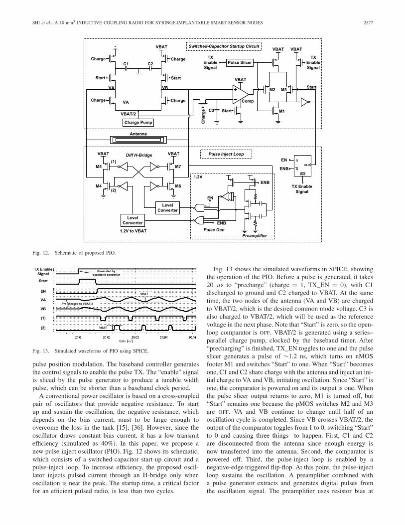
SHI et al.: A 10 mm3 INDUCTIVE COUPLING RADIO FOR SYRINGE-IMPLANTABLE SMART SENSOR NODES 2577
Fig. 12. Schematic of proposed PIO.
Fig. 13. Simulated waveforms of PIO using SPICE.
pulse position modulation. The baseband controller generatesthe control signals to enable the pulse TX. The “enable” signalis sliced by the pulse generator to produce a tunable widthpulse, which can be shorter than a baseband clock period.
A conventional power oscillator is based on a cross-coupledpair of oscillators that provide negative resistance. To startup and sustain the oscillation, the negative resistance, whichdepends on the bias current, must to be large enough toovercome the loss in the tank [15], [36]. However, since theoscillator draws constant bias current, it has a low transmitefficiency (simulated as 40%). In this paper, we propose anew pulse-inject oscillator (PIO). Fig. 12 shows its schematic,which consists of a switched-capacitor start-up circuit and apulse-inject loop. To increase efficiency, the proposed oscil-lator injects pulsed current through an H-bridge only whenoscillation is near the peak. The startup time, a critical factorfor an efficient pulsed radio, is less than two cycles.
Fig. 13 shows the simulated waveforms in SPICE, showingthe operation of the PIO. Before a pulse is generated, it takes20 μs to “precharge” (charge = 1, TX_EN = 0), with C1discharged to ground and C2 charged to VBAT. At the sametime, the two nodes of the antenna (VA and VB) are chargedto VBAT/2, which is the desired common mode voltage. C3 isalso charged to VBAT/2, which will be used as the referencevoltage in the next phase. Note that “Start” is zero, so the open-loop comparator is OFF. VBAT/2 is generated using a series–parallel charge pump, clocked by the baseband timer. After“precharging” is finished, TX_EN toggles to one and the pulseslicer generates a pulse of ∼1.2 ns, which turns on nMOSfooter M1 and switches “Start” to one. When “Start” becomesone, C1 and C2 share charge with the antenna and inject an ini-tial charge to VA and VB, initiating oscillation. Since “Start” isone, the comparator is powered on and its output is one. Whenthe pulse slicer output returns to zero, M1 is turned off, but“Start” remains one because the pMOS switches M2 and M3are OFF. VA and VB continue to change until half of anoscillation cycle is completed. Since VB crosses VBAT/2, theoutput of the comparator toggles from 1 to 0, switching “Start”to 0 and causing three things to happen. First, C1 and C2are disconnected from the antenna since enough energy isnow transferred into the antenna. Second, the comparator ispowered off. Third, the pulse-inject loop is enabled by anegative-edge triggered flip-flop. At this point, the pulse-injectloop sustains the oscillation. A preamplifier combined witha pulse generator extracts and generates digital pulses fromthe oscillation signal. The preamplifier uses resistor bias at
2578 IEEE JOURNAL OF SOLID-STATE CIRCUITS, VOL. 51, NO. 11, NOVEMBER 2016
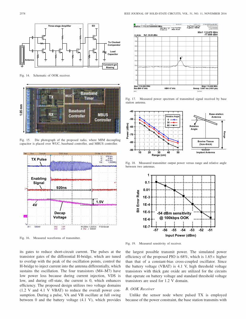
Fig. 14. Schematic of OOK receiver.
Fig. 15. Die photograph of the proposed radio, where MIM decouplingcapacitor is placed over WUC, baseband controller, and MBUS controller.
Fig. 16. Measured waveforms of transmitter.
its gates to reduce short-circuit current. The pulses at thetransistor gates of the differential H-bridge, which are tunedto overlap with the peak of the oscillation points, control theH-bridge to inject current into the antenna differentially, whichsustains the oscillation. The four transistors (M4–M7) havelow power loss because during current injection, VDS islow, and during off-state, the current is 0, which enhancesefficiency. The proposed design utilizes two voltage domains(1.2 V and 4.1 V VBAT) to reduce the overall power con-sumption. During a pulse, VA and VB oscillate at full swingbetween 0 and the battery voltage (4.1 V), which provides
Fig. 17. Measured power spectrum of transmitted signal received by basestation antenna.
Fig. 18. Measured transmitter output power versus range and relative anglebetween two antennas.
Fig. 19. Measured sensitivity of receiver.
the largest possible transmit power. The simulated powerefficiency of the proposed PIO is 68%, which is 1.65× higherthan that of a constant-bias cross-coupled oscillator. Sincethe battery voltage (VBAT) is 4.1 V, high threshold voltagetransistors with thick gate oxide are utilized for the circuitsthat operate on battery voltage and standard threshold voltagetransistors are used for 1.2 V domain.
B. OOK Receiver
Unlike the sensor node where pulsed TX is employedbecause of the power constraint, the base station transmits with
SHI et al.: A 10 mm3 INDUCTIVE COUPLING RADIO FOR SYRINGE-IMPLANTABLE SMART SENSOR NODES 2579
Fig. 20. Measured waveforms at the output of receiver ED wirelessly at the distances of (a) 3 cm and (b) 20 cm.
a continuous OOK scheme. The sensor receiver demodulatesthe OOK signal from the base station continuously drawingcurrent from the 1.2 V supply. It is feasible because itspower consumption is less than the maximum peak powerof the millimeter-scale battery (<50 μW). Fig. 14 shows theschematic of the receiver, which consists of a three-stageamplifier, envelope detector (ED), and clocked comparator.The received signal is amplified and demodulated by the ED.A clocked comparator samples and digitizes the output ofthe ED.
The first-stage amplifier is a current-reuse inverter amplifierfor high current efficiency. The transistors in the amplifier arebiased at the subthreshold region for higher gm/I efficiency.The gain of the three-stage amplifier is simulated as 37 dBat 49.86 MHz. The ED comprises a source follower topology,and the transistor is biased at the nonlinear region, consuming∼200 nA. The load capacitor can be tunable up to 31 pF,filtering out any high frequency components. A constant-gm
biasing circuit is designed for the amplifier and ED. The totalreceiver consumes 36 μW while demodulating a 100 kb/sOOK signal.
V. MEASUREMENT RESULTS
Fig. 15 shows the chip microphotograph of the proposednear-field radio fabricated in a 180 nm CMOS technology. Thechip has a total area of 1050 μm × 2120 μm including thepads. Proposed radio is designed for wireless through-tissuecommunication. To demonstrate this feasibility, a mediumof 3-cm-thick bovine tissue (typical beef steak) is utilized byfollowing the wireless testing of the transceiver.
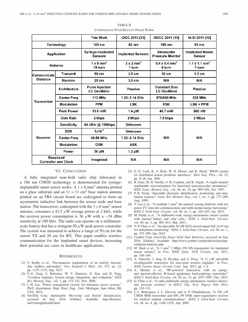
The transmitter was measured when driving the antennaon the glass substrate (sensor antenna). Fig. 16 shows themeasured time-domain waveforms of the transmitter in pulsedmode. Once the pulse is enabled by the baseband controller,the oscillation can start up quickly. With the pulse generator,the pulse width can be digitally tunable from 150 to 1320 ns.When the pulse width is 920 ns, the transmitter supplyvoltage on the decap drops by 1.5 V during every pulse asshown in the measurement but is recharged to its full levelafter ∼500 μs, where the current limiter sets the rechargingcurrent to be less than 15 μA. For the communication rangeand power spectrum measurement setup, we used an external4.1 V supply to allow the sensor node power oscillator tocontinuously draw current. The sensor transmitted signal was
Fig. 21. Measured supply variance of baseband timer frequency.
wirelessly received by the 11 × 11 cm2 base station loopantenna printed on an FR4 board through a 3-cm-thick bovinetissue. Fig. 17 shows the power spectrum measured with aspectrum analyzer, and Fig. 18 shows the measured poweracross a range of distances and relative angles between thetwo antennas. The receiver sensitivity was measured using awired setup where an RF signal generator was connected tothe sensor node receiver via a cable or through the antennapair. The wired setup is used to measure receiver sensitivityquantitatively, where the input of the receiver was connectedto the signal generator (source 50 �) through an SMA cable.Fig. 19 shows the measured sensitivity across input power,which is the value directly read from the signal genera-tor. Note that due to impedance mismatch (receiver inputnon-50 �), actual receiver input power is less than the valueread from the signal generator. At a BER of 10−3 and a datarate of 100 kb/s, the receiver has a sensitivity at −54 dBm andconsumes 36 μW at a supply voltage of 1.2 V. This same BERwas also measured wirelessly at approximately 20 cm throughthe 3 cm-thick bovine tissue, where the RF signal generatorfeeds the OOK-modulated signal into the base station antennawith a 1 W power and the chip detects it using the sensorantenna. While demodulating a 100 kb/s OOK signal, themeasured waveforms of the ED output when the two antennasare separated by 3 and 20 cm are shown in Fig. 20(a) and (b),respectively.
2580 IEEE JOURNAL OF SOLID-STATE CIRCUITS, VOL. 51, NO. 11, NOVEMBER 2016
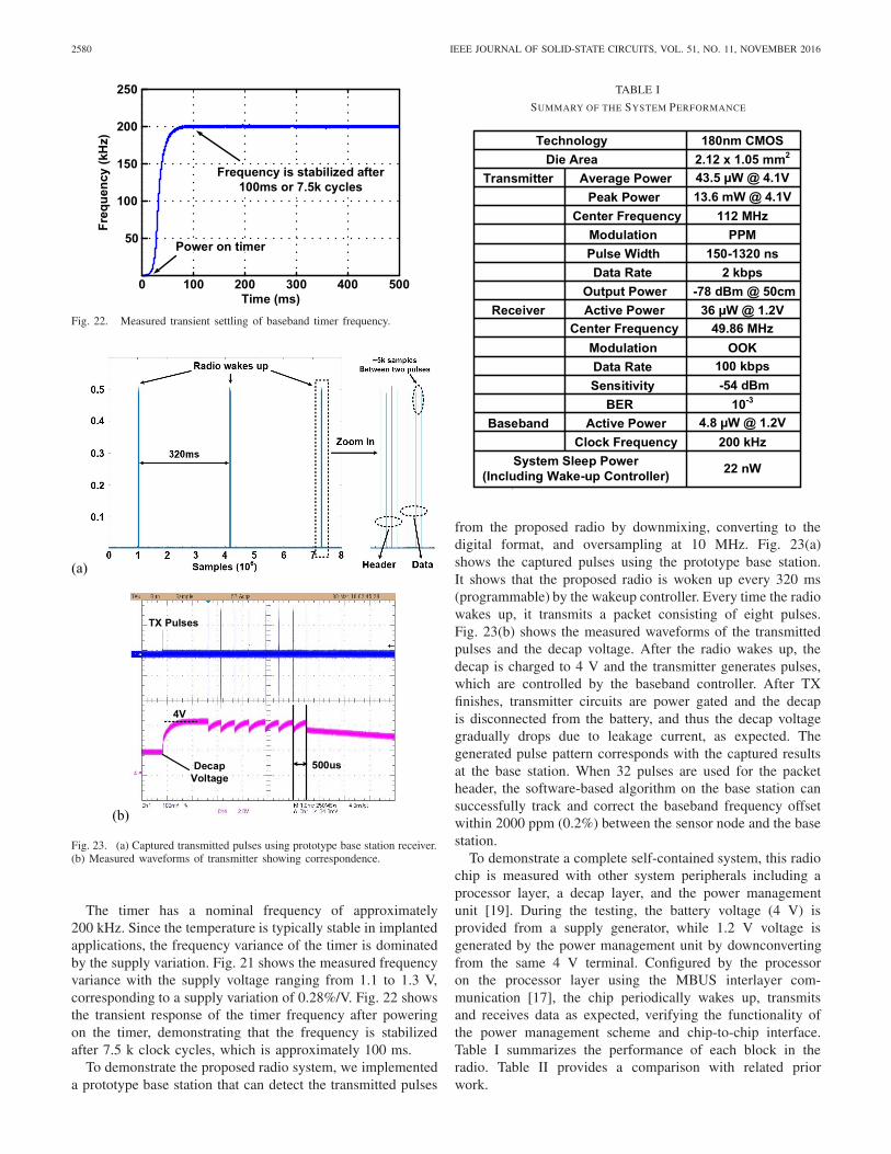
Fig. 22. Measured transient settling of baseband timer frequency.
Fig. 23. (a) Captured transmitted pulses using prototype base station receiver.(b) Measured waveforms of transmitter showing correspondence.
The timer has a nominal frequency of approximately200 kHz. Since the temperature is typically stable in implantedapplications, the frequency variance of the timer is dominatedby the supply variation. Fig. 21 shows the measured frequencyvariance with the supply voltage ranging from 1.1 to 1.3 V,corresponding to a supply variation of 0.28%/V. Fig. 22 showsthe transient response of the timer frequency after poweringon the timer, demonstrating that the frequency is stabilizedafter 7.5 k clock cycles, which is approximately 100 ms.
To demonstrate the proposed radio system, we implementeda prototype base station that can detect the transmitted pulses
TABLE I
SUMMARY OF THE SYSTEM PERFORMANCE
from the proposed radio by downmixing, converting to thedigital format, and oversampling at 10 MHz. Fig. 23(a)shows the captured pulses using the prototype base station.It shows that the proposed radio is woken up every 320 ms(programmable) by the wakeup controller. Every time the radiowakes up, it transmits a packet consisting of eight pulses.Fig. 23(b) shows the measured waveforms of the transmittedpulses and the decap voltage. After the radio wakes up, thedecap is charged to 4 V and the transmitter generates pulses,which are controlled by the baseband controller. After TXfinishes, transmitter circuits are power gated and the decapis disconnected from the battery, and thus the decap voltagegradually drops due to leakage current, as expected. Thegenerated pulse pattern corresponds with the captured resultsat the base station. When 32 pulses are used for the packetheader, the software-based algorithm on the base station cansuccessfully track and correct the baseband frequency offsetwithin 2000 ppm (0.2%) between the sensor node and the basestation.
To demonstrate a complete self-contained system, this radiochip is measured with other system peripherals including aprocessor layer, a decap layer, and the power managementunit [19]. During the testing, the battery voltage (4 V) isprovided from a supply generator, while 1.2 V voltage isgenerated by the power management unit by downconvertingfrom the same 4 V terminal. Configured by the processoron the processor layer using the MBUS interlayer com-munication [17], the chip periodically wakes up, transmitsand receives data as expected, verifying the functionality ofthe power management scheme and chip-to-chip interface.Table I summarizes the performance of each block in theradio. Table II provides a comparison with related priorwork.
SHI et al.: A 10 mm3 INDUCTIVE COUPLING RADIO FOR SYRINGE-IMPLANTABLE SMART SENSOR NODES 2581
TABLE II
COMPARISON WITH RECENT PRIOR WORK
VI. CONCLUSION
A fully integrated near-field radio chip fabricated ina 180 nm CMOS technology is demonstrated for syringe-implantable smart sensor nodes. A 1×8 mm2 antenna printedon a glass substrate and an 11 × 11 cm2 base station antennaprinted on an FR4 circuit board are codesigned to form anasymmetric inductive link between the sensor node and basestation. The transceiver, codesigned with the 1×8 mm2 sensorantenna, consumes a 43.5 μW average power at 2 kb/s, whilethe receiver power consumption is 36 μW with a −54 dBmsensitivity at 100 kb/s. The radio can operate on a millimeter-scale battery that has a stringent 50 μW peak power constraint.The system was measured to achieve a range of 50 cm for thesensor TX and 20 cm for RX. This paper enables wirelesscommunication for the implanted smart devices, increasingtheir potential use cases in healthcare applications.
REFERENCES
[1] V. Reddy et al., “Percutaneous implantation of an entirely intracar-diac leadless pacemaker,” New England J. Med., vol. 373, no. 12,pp. 1125–1135, Sep. 2015.
[2] F.-G. Zeng, S. Rebscher, W. V. Harrison, X. Sun, and H. Feng,“Cochlear implants: System design, integration, and evaluation,” IEEERev. Biomed. Eng., vol. 1, pp. 115–142, Nov. 2008.
[3] I. H. Lee, “Power management circuits for miniature sensor systems,”Ph.D. dissertation, Dept. Elect. Eng., Univ. Michigan, Ann Arbor, MI,USA, 2014.
[4] VeriTeQ Corp. Implantable Microchip and Patient Identification,accessed on Sep. 2016. [Online]. Available: http://divpixel.net/veriteq/patientId.html
[5] G. E. Loeb, R. A. Peck, W. H. Moore, and K. Hood, “BION systemfor distributed neural prosthetic interfaces,” Med. Eng. Phys., vol. 23,pp. 9–18, Jan. 2001.
[6] B. Ziaie, M. D. Nardin, A. R. Coghlan, and K. Najafi, “A single-channelimplantable microstimulator for functional neuromuscular stimulation,”IEEE Trans. Biomed. Eng., vol. 44, no. 10, pp. 909–920, Oct. 1997.
[7] P. R. Troyk, “Injectable electronic identification, monitoring, and stim-ulation systems,” Annu. Rev. Biomed. Eng., vol. 1, no. 1, pp. 177–209,Aug. 1999.
[8] Y. Lee et al., “A modular 1 mm3 die-stacked sensing platform with lowpower I2C inter-die communication and multi-modal energy harvesting,”IEEE J. Solid-State Circuits, vol. 48, no. 1, pp. 229–243, Jan. 2013.
[9] M. Fojtik et al., “A millimeter-scale energy-autonomous sensor systemwith stacked battery and solar cells,” IEEE J. Solid-State Circuits,vol. 48, no. 3, pp. 801–813, Mar. 2013.
[10] Y.-P. Chen et al., “An injectable 64 nW ECG mixed-signal SoC in 65 nmfor arrhythmia monitoring,” IEEE J. Solid-State Circuits, vol. 50, no. 1,pp. 375–390, Jan. 2015.
[11] Cymbet Corp. EnerChip Smart Solid State Batteries, accessed on Sep.2016. [Online]. Available: http://www.cymbet.com/products/enerchip-solidstate-batteries.php
[12] M. Mark et al., “A 1 mm3 2 Mbps 330 fJ/b transponder for implantedneural sensors,” in Proc. IEEE Symp. VLSI Circuits, Jun. 2011,pp. 168–169.
[13] A. Yakovlev, J. Jang, D. Pivonka, and A. Poon, “A 11 μW sub-pJ/bitreconfigurable transceiver for mm-sized wireless implants,” in Proc.IEEE Custom Integr. Circuits Conf., Sep. 2013, pp. 1–4.
[14] A. Shirane et al., “RF-powered transceiver with an energy-and spectral-efficient IF-based quadrature backscattering transmitter,”IEEE J. Solid-State Circuits, vol. 50, no. 12, pp. 2975–2987, Dec. 2015.
[15] G. Chen et al., “A cubic-millimeter energy-autonomous wireless intraoc-ular pressure monitor,” in ISSCC Dig. Tech. Papers, Feb. 2011,pp. 310–311.
[16] J. L. Bohorquez, J. L. Dawson, and A. P. Chandrakasan, “A 350 μWCMOS MSK transmitter and 400 μW OOK super-regenerative receiverfor medical implant communications,” IEEE J. Solid-State Circuits,vol. 44, no. 4, pp. 1248–1259, Apr. 2009.

2582 IEEE JOURNAL OF SOLID-STATE CIRCUITS, VOL. 51, NO. 11, NOVEMBER 2016
[17] G. Kim et al., “A millimeter-scale wireless imaging system with con-tinuous motion detection and energy harvesting,” in Proc. IEEE Symp.VLSI Circuits, Jun. 2014, pp. 1–2.
[18] Y. Shi et al., “A 10 mm3 syringe-implantable near-field radio systemon glass substrate,” in IEEE ISSCC Dig. Tech. Papers, Feb. 2016,pp. 448–449.
[19] W. Jung et al., “A 60%-efficiency 20 nW–500 μW tri-output fullyintegrated power management unit with environmental adaptation andload-proportional biasing for IoT systems,” in ISSCC Dig. Tech. Papers,Jan./Feb. 2016, pp. 154–155.
[20] Epson Corp., Crystal kHz Range/Crystal Unit, accessed onSep. 2016. [Online]. Available: http://www5.epsondevice.com/en/products/khz_range/
[21] M. Choi, S. Bang, T.-K. Jang, D. Blaauw, and D. Sylvester, “A 99 nW70.4 kHz resistive frequency locking on-chip oscillator with 27.4 ppm/°Ctemperature stability,” in Proc. IEEE Symp. VLSI Circuits, Jun. 2015,pp. C238–C239.
[22] K.-K. Huang et al., “An ultra-low-power 9.8 GHz crystal-less UWBtransceiver with digital baseband integrated in 0.18 μm BiCMOS,” IEEEJ. Solid-State Circuits, vol. 48, no. 12, pp. 3178–3189, Dec. 2013.
[23] N. E. Roberts et al., “ A 236 nW −56.5 dBm-sensitivity Bluetooth low-energy wakeup receiver with energy harvesting in 65 nm CMOS,” inISSCC Dig. Tech. Papers, Feb. 2016, pp. 450–451.
[24] I. Lee, D. Sylvester, and D. Blaauw, “A constant energy-per-cycle ringoscillator over a wide frequency range for wireless sensor nodes,” IEEEJ. Solid-State Circuits, vol. 51, no. 3, pp. 697–711, Mar. 2016.
[25] J. S. Ho et al., “Wireless power transfer to deep-tissue microimplants,”Proc. Nat. Acad. Sci. USA, vol. 111, no. 22, pp. 7974–7979, Apr. 2014.
[26] A. Abdo, M. Sahin, D. S. Freedman, E. Cevik, P. S. Spuhler, andM. S. Unlu, “Floating light-activated microelectrical stimulators tested inthe rat spinal cord,” J. Neural Eng., vol. 8, no. 5, p. 056012, Sep. 2011.
[27] K. Mathieson et al., “Photovoltaic retinal prosthesis with high pixeldensity,” Nature Photon., vol. 6, pp. 391–397, May 2012.
[28] A. Ivorra, L. Becerra-Fajardo, and Q. Castellví, “In vivo demonstrationof injectable microstimulators based on charge-balanced rectification ofepidermically applied currents,” J. Neural Eng., vol. 12, no. 6, p. 066010,Oct. 2015.
[29] R. Pethig and D. B. Kell, “The passive electrical properties of biologicalsystems: Their significance in physiology, biophysics and biotechnol-ogy,” Phys. Med. Biol., vol. 32, no. 8, p. 933, Aug. 1987.
[30] S. W. Han, “Wireless interconnect using inductive coupling in 3D-ICs,”Ph.D. dissertation, Dept. Elect. Eng., Univ. Michigan, Ann Arbor, MI,USA, 2012.
[31] K. Gala, D. Blaauw, J. Wang, V. Zolotov, and M. Zhao, “Inductance101: Analysis and design issues,” in Proc. 38th Annu. Design Autom.Conf., Jun. 2001, pp. 329–334.
[32] H. M. Greenhouse, “Design of planar rectangular microelectronicinductors,” IEEE Trans. Parts, Hybrids, Packag., vol. PHP-10, no. 2,pp. 101–109, Jun. 1974.
[33] C. Hoer and C. Love, “Exact inductance equations for rectangularconductors with applications to more complicated geometries,” J. Res.Nat. Bureau Standards, vol. 69C, no. 2, Apr./Jun. 1965.
[34] (Oct. 1993). Federal Communications Commission, Understand-ing the FCC Regulations for Low-power, Non-Licensed Transmit-ters. [Online]. Available: https://transition.fcc.gov/Bureaus/Engineering_Technology/Documents/bulletins/oet63/oet63rev.pdf
[35] S. Gabriel, R. W. Lau, and C. Gabriel, “The dielectric properties ofbiological tissues: III. Parametric models for the dielectric spectrum oftissues,” Phys. Med. Biol., vol. 41, no. 11, p. 2271, Nov. 1996.
[36] P. P. Mercier, S. Bandyopadhyay, A. C. Lysaght, K. M. Stankovic, andA. P. Chandrakasan, “A sub-nW 2.4 GHz transmitter for low data-rate sensing applications,” IEEE J. Solid-State Circuits, vol. 49, no. 7,pp. 1463–1474, Jul. 2014.
Yao Shi (S’14) received the B.S. degree in elec-tronic and information engineering from ZhejiangUniversity, Hangzhou, China, in 2013, and theM.S. degree in electrical engineering from the Uni-versity of Michigan, Ann Arbor, MI, USA, in 2016,where he is currently pursuing the Ph.D. degree.
His current research interests include analog/RFintegrated circuits design, ultralow power radioarchitecture and circuit, and ultralow power wirelesssensor node.
Myungjoon Choi (S’12) received the B.S. degree(summa cum laude) in electrical engineering fromthe Korea Advanced Institute of Science and Tech-nology, Daejeon, South Korea, in 2012, and theM.S. degree in electrical engineering from the Uni-versity of Michigan, Ann Arbor, MI, USA, in 2014,where he is currently pursuing the Ph.D. degree.
His current research interests include fully inte-grated system clock generation, reference currentgeneration, resistive sensor interface circuits, andwireless power transfer circuits for ultralow power
wireless sensor node.Mr. Choi was a recipient of the Doctoral Fellowship from Kwanjeong
Educational Foundation, South Korea.
Ziyun Li (S’15) received the B.S. degree in elec-trical and computer engineering from the Universityof Michigan, Ann Arbor, MI, USA, in 2014, wherehe is currently pursuing the Ph.D. degree with theMichigan Integrated Circuit Laboratories.
His current research interests include high-performance, low power computer vision processingunits to enable autonomous navigation of microaerial vehicles.
Zhihong Luo was born in Shantou, China, in 1994.He is currently pursuing the B.S. degree at theUniversity of Michigan, Ann Arbor, MI, USA, andShanghai Jiaotong University, Shanghai, China.
His current research interests include embeddedsystem design.
Gyouho Kim (M’09) received the B.S., M.S., andPh.D. degrees in electrical engineering from theUniversity of Michigan, Ann Arbor, MI, USA, in2009, 2011, and 2014, respectively.
He is currently a Post-Doctoral Research Fel-low with the University of Michigan. His cur-rent research interests include ultralow power verylarge scale integration design for energy-constrainedsystem.
Zhiyoong Foo received the B.S., M.S., and Ph.D.degrees in electrical engineering from the Universityof Michigan, Ann Arbor, MI, USA.
He is currently the Head of CubeWorks Inc.,a startup spun out of the University of Michigancommercializing ultralow power systems. His cur-rent research interests include low cost and lowpower very large scale integration circuit systemsintegration.
SHI et al.: A 10 mm3 INDUCTIVE COUPLING RADIO FOR SYRINGE-IMPLANTABLE SMART SENSOR NODES 2583
Hun-Seok Kim (M’11) received the B.S. degree inelectrical engineering from Seoul National Univer-sity, Seoul, South Korea, and the M.S. and Ph.D.degrees in electrical engineering from the Universityof California at Los Angeles (UCLA), Los Angeles,CA, USA.
He was a Technical Staff Member with TexasInstruments Incorporated, Dallas, TX, USA, from2010 to 2014, while serving as an Industry Liaisonfor multiple university projects funded by the Semi-conductor Research Cooperation and Texas Instru-
ments Incorporated. He is now an Assistant Professor with the Universityof Michigan, Ann Arbor, MI, USA. He currently holds nine granted patentsand has over 10 pending applications in the areas of digital communication,signal processing, and low power integrated circuits. His current researchinterests include system novel algorithms and efficient very large scaleintegration architectures for low-power/high-performance signal processing,wireless communication, computer vision, and machine learning systems.
Dr. Kim was a recipient of multiple fellowships from the Ministry of Infor-mation and Telecommunication (South Korea), Seoul National University,and UCLA.
David D. Wentzloff (M’07) received the B.S.E.degree in electrical engineering from the Universityof Michigan, Ann Arbor, MI, USA, in 1999, andthe M.S. and Ph.D. degrees from the MassachusettsInstitute of Technology, Cambridge, MA, USA, in2002 and 2007, respectively.
Since 2007, he has been with the Universityof Michigan, where he is currently an AssociateProfessor of Electrical Engineering and ComputerScience. In 2012, he co-founded PsiKick, a fablesssemiconductor company developing ultralow power
wireless system on a chip. His current research interests include RF integratedcircuits, with an emphasis on ultralow power design.
Prof. Wentzloff is a member of the IEEE Circuits and Systems Society,the IEEE Microwave Theory and Techniques Society, the IEEE Solid-StateCircuits Society, and the Tau Beta Pi. He was a recipient of the 2009 DARPAYoung Faculty Award from 2009 to 2010, the Eta Kappa Nu Professor ofthe Year Award, the 2011 DAC/ISSCC Student Design Contest Award, the2012 IEEE Subthreshold Microelectronics Conference Best Paper Award, the2012 NSF CAREER Award, the 2014 ISSCC Outstanding Forum PresenterAward, the 2014–2015 Eta Kappa Nu ECE Professor of the Year Award,the 2014–2015 EECS Outstanding Acheivement Award, and the 2015 Joeland Ruth Spira Excellence in Teaching Award. He has served on theTechnical Program Committee for ICUWB 2008–2010, ISLPED 2011–2015,S3S 2013–2014, and RFIC 2013–2015, and as a Guest Editor of the IEEETRANSACTIONS ON MICROWAVE THEORY AND TECHNIQUES, the IEEECommunications Magazine, and the Elsevier journal Signal Processing: ImageCommunication.
David Blaauw (F’12) received the B.S. degree inphysics and computer science from Duke University,Durham, NC, USA, in 1986, and the Ph.D. degree incomputer science from the University of Illinois atUrbana–Champaign, Champaign, IL, USA, in 1991.
He was the Manager of the High PerformanceDesign Technology group, Motorola, Inc., Austin,TX, USA. Since 2001, he has been with the facultyof the University of Michigan, Ann Arbor, MI, USA,where he is currently a Professor. He has authoredover 500 papers and holds 50 patents. His current
research interests include very large scale integration design with particularemphasis on ultralow power and high performance design for ultralow powersensor nodes.
Prof. Blaauw was the Technical Program Chair and the General Chair forthe International Symposium on Low Power Electronic and Design. He wasalso the Technical Program Co-Chair of the ACM/IEEE Design AutomationConference and a member of the ISSCC Technical Program Committee.