Implementing 4-20 mA Sensor Interface - Dialog Semiconductor
15
Application Note Implementing 4-20 mA Sensor Interface AN-CM-229 Abstract This application note describes how to implement a 4-20 mA interface for measuring the output of an oxygen sensor to detect out-of-range oxygen concentrations. This application note comes complete with design files which can be found in the References section.
-
Upload
khangminh22 -
Category
Documents
-
view
5 -
download
0
Transcript of Implementing 4-20 mA Sensor Interface - Dialog Semiconductor

Application Note
Implementing 4-20 mA Sensor Interface
AN-CM-229
Abstract
This application note describes how to implement a 4-20 mA interface for measuring the output of an oxygen sensor to detect out-of-range oxygen concentrations. This application note comes complete with design files which can be found in the References section.
AN-CM-229
Implementing 4-20 mA Sensor Interface
Application Note Revision 1.0 06-Mar-2018
CFR0014 2 of 15 © 2018 Dialog Semiconductor
Contents
Abstract ................................................................................................................................................ 1
Contents ............................................................................................................................................... 2
Figures .................................................................................................................................................. 2
Terms and Definitions ......................................................................................................................... 3
1 References ..................................................................................................................................... 3
2 Introduction.................................................................................................................................... 4
3 4-20 mA Output General Characteristics .................................................................................... 4
4 Schematic Diagram ....................................................................................................................... 6
5 Implementation .............................................................................................................................. 7
6 Testing .......................................................................................................................................... 12
7 Conclusion ................................................................................................................................... 13
Revision History ................................................................................................................................ 14
Figures
Figure 1: 4-20 mA Loop Schematic ....................................................................................................... 5 Figure 2: Schematic Diagram of Electronic Circuit Interface ................................................................. 5 Figure 3: Schematic Diagram of Sensor Interface ................................................................................ 6 Figure 4: Schematic Diagram of Sensor Interface ................................................................................ 7 Figure 5: Oxygen Concentration Level Block Diagram ......................................................................... 7 Figure 6: PGA Configuration ................................................................................................................. 8 Figure 7: ADC Configuration ................................................................................................................. 8 Figure 8: System Diagram ..................................................................................................................... 9 Figure 9: System Diagram ..................................................................................................................... 9 Figure 10: LUT4 Configuration ............................................................................................................ 10 Figure 11: PIN8 Configuration ............................................................................................................. 11 Figure 12: PIN18 Configuration ........................................................................................................... 11 Figure 13: PIN19 Configuration ........................................................................................................... 11 Figure 14: Matrix0 Block Diagram ....................................................................................................... 11 Figure 15: Matrix 1 Block Diagram ...................................................................................................... 12 Figure 16: Pin 18 Oxygen Concentration Low-Level Detection .......................................................... 13 Figure 17: Pin 19 Oxygen Concentration High-Level Detection.......................................................... 13

AN-CM-229
Implementing 4-20 mA Sensor Interface
Application Note Revision 1.0 06-Mar-2018
CFR0014 3 of 15 © 2018 Dialog Semiconductor
Terms and Definitions
ADC analog to digital converter
PGA programmable gain amplifier
CMIC configurable mixed-signal integrated circuit
1 References
For related documents and software, please visit:
https://www.dialog-semiconductor.com/configurable-mixed-signal.
Download our free GreenPAK Designer software [1] to open the .gp files [2] and view the proposed circuit design. Use the GreenPAK development tools [3] to freeze the design into your own customized IC in a matter of minutes. Dialog Semiconductor provides a complete library of application notes [4] featuring design examples as well as explanations of features and blocks within the Dialog IC.
[1] GreenPAK Designer Software, Software Download and User Guide, Dialog Semiconductor
[2] AN-CM-229 Implementing 4-20 mA Sensor Interface.gp, GreenPAK Design File, Dialog Semiconductor
[3] GreenPAK Development Tools, GreenPAK Development Tools Webpage, Dialog Semiconductor
[4] GreenPAK Application Notes, GreenPAK Application Notes Webpage, Dialog Semiconductor

AN-CM-229
Implementing 4-20 mA Sensor Interface
Application Note Revision 1.0 06-Mar-2018
CFR0014 4 of 15 © 2018 Dialog Semiconductor
2 Introduction
Analog 4–20 mA current loops are one of the most used communication buses in industrial environments, where environmental variables, process sensing, and control is required. This bus type is named after its maximum and minimum current values across the line; 4 mA and 20 mA. Current loops are used not only for receiving information from sensors and field instrumentation, they are also used for transmitting control signals to actuators or other devices to regulate a controlled action.
Current loops, such as 4-20 mA, have been used since the 1950s in many industrial applications. The bus is appealing due to the low implementation cost, high noise immunity due to the non-voltage dependence, and the ability to be used effectively over long distances.
These characteristics are the main reasons for using a 4-20 mA loop for signaling and control. Because of this, there are several industrial sensors which implement a 4-20 mA output to indicate their measurements. Field instrumentation sensors such as pressure sensors, temperature sensors, level or flow sensors, pH sensors, and gas sensors implement a 4-20 mA connection to their outputs. Also, there are several actuators, such as valves, which can be controlled via a 4-20 mA loop.
There are several different brands of commercial IC’s that implement a 4-20 mA bus receiver.
In this application note, a GreenPAK™ is designed as an oxygen sensor with a 4-20 mA output, and is used to detect dangerous concentrations of oxygen for human beings in industrial environments. The app note implements the analog measurement and digital logic required to implement an integrated concentration-level alarm. This application also has a configurable limit value to detect out-of-level concentrations. To implement this 4-20 mA bus receiver, a SLG46621V is used.
3 4-20 mA Output General Characteristics
As described before, in industrial and noisy environments, analog 4–20 mA current loops are one of the most used buses for electronic measurement and control. These buses are used not only for controlling valves or other actuators, they are also used for transmitting sensor information from field instrumentation to the control center.
The main advantages of the 4-20 mA current loop are:
– The data transmission is not affected by the voltage drop over the interconnecting wiring, meaning it can be used over long distances with much less degradation of the signal.
– It allows the system to implement a self-monitoring routine, because currents less than 4 mA and higher than 20 mA can indicate a fault in the circuit
– The 4-20 mA current loop, often, is used also to power the remote device.
– The "live" or "elevated" zero of 4 mA allows powering of the device even with no process signal output from the field transmitter.
The 4-20 mA communication bus is based on the principles of the Kirchhoff’s current law, which states that the sum of currents flowing toward a point is equal to the sum of currents flowing away from that point. With this principle, all current present at the beginning of a loop must reach the end.
This law is the basic principle to explain the behavior of the 4-20 mA loop. The current at any position of the system can be measured and found to be the same result. This is also the main reason for using current loops with low impedance within industrial applications; they provide the benefit of obtaining a longer data path with better noise immunity. A scheme of a 4-20 mA loop can be seen in Figure 1.

AN-CM-229
Implementing 4-20 mA Sensor Interface
Application Note Revision 1.0 06-Mar-2018
CFR0014 5 of 15 © 2018 Dialog Semiconductor
Tx Rx
Figure 1: 4-20 mA Loop Schematic
One of the most commonly used and simple circuits for measuring signals of a 4-20 mA current loop is the shunt resistor circuit.
This circuit is based on Ohm’s Law. The selection of the sense resistor value is made by considering the maximum voltage that our reception device can deal with, assuming that the sense resistor is much lower than 200 kΩ. With the maximum voltage known, the resistor is then calculated by the following expression:
𝑅𝑠𝑒𝑛𝑠𝑒 =𝑉𝑚𝑎𝑥
20𝑚𝐴
In order to not load the interface circuit, it’s recommended to implement an electronic buffer based on an operation amplifier. An electronic circuit that is commonly used for 4-20 mA interface to digital devices with analog inputs is shown in Figure 2.
Figure 2: Schematic Diagram of Electronic Circuit Interface
The shunt resistor is divided in two half-sections. This allows the circuit to prevent the voltage becoming higher than the desired values by fixing the intermediate voltage of the shunt resistor to a local ground. The differential shunt resistor voltage is converted to a single ended voltage with the operational amplifier having a differential amplifier configuration at unity gain. Resistor values of the operational amplifier circuit are selected to not load the current loop.

AN-CM-229
Implementing 4-20 mA Sensor Interface
Application Note Revision 1.0 06-Mar-2018
CFR0014 6 of 15 © 2018 Dialog Semiconductor
4 Schematic Diagram
To show how a GreenPAK can be used for interfacing a 4-20 mA bus, this app note implements an oxygen concentration level alarm useful for industrial applications. In some environments, detecting dangerous oxygen concentrations for human beings is an important safety task.
As everyone knows, oxygen is a vital gas and a typical oxygen concentration is 20.9% v/v. If an environment has an oxygen concentration lower than 19.5 % v/v, it can be considered as an environment with oxygen deficiency. Oxygen concentrations lower than 16 % v/v is unsafe for human beings.
Additionally, higher concentrations of oxygen can also be a risk for humans. If the oxygen concentration rises, material and gas inflammability increase. As an example, if the oxygen concentration is higher than 24 % v/v, some elements such as clothes can start burning spontaneously.
To implement an oxygen concentration alarm, a sensor from Honeywell is used. The MF020-2-LC3 sensor has a measuring range from 0.1 % v/v to 25 % v/v with a 4-20 mA analog output and a power supply of 24 VDC.
To measure the sensor output with a Dialog SLG46621 CMIC, the Programmable Gain Amplifier (PGA) and Analog to Digital Converter (ADC) of the IC are used. To do this, the maximum input voltage of the analog converter must be considered.
If the ADC is used with an internal voltage reference of 1.2 V, and with unity gain, the maximum input voltage for the converter is 1 V. By applying the RSENSE expression shown in previous section, the resistor value needed for the shunt is:
𝑅𝑆𝐸𝑁𝑆𝐸 =1
20 𝑚𝐴= 50 Ω
With the selected RSENSE, the output voltages that will be obtained when the current loop has 4 mA and 20 mA are 200 mV and 1 V respectively. The minimum voltage level is compliant with the minimum input voltage to the SLG46621 ADC, which is 30 mV.
In Figure 3, the electronic circuit that must be used for interfacing the MF020-2-LC3 sensor to the SLG46621 is shown. The operational amplifier used for this application is the SLG88103.
Figure 3: Schematic Diagram of Sensor Interface

AN-CM-229
Implementing 4-20 mA Sensor Interface
Application Note Revision 1.0 06-Mar-2018
CFR0014 7 of 15 © 2018 Dialog Semiconductor
The VOUT signal of the 4-20 mA output is connected to the Analog input of the SLG46621 chip, as seen in Figure 3.
Figure 4: Schematic Diagram of Sensor Interface
5 Implementation
The implementation of the 4-20 mA interface for an oxygen concentration level alarm is made with a SLG46621V GreenPAK. This CMIC has one Analog to Digital Converter, and several Digital Comparators that can be used for analyzing the voltage at the input of the ADC. To configure the comparison levels, the internal comparator registers are used. A block diagram of the implementation can be seen in Figure 5.
Interface Circuit
PGA ADC
DCMP
DCMP
SLG46621V
Figure 5: Oxygen Concentration Level Block Diagram
The allowed upper and lower oxygen concentrations are configured in the registers. This is done by considering that the ADC has an 8-bit resolution. The maximum input voltage (1 V) is converted to 255, which corresponds to an oxygen concentration of 25% v/v. With this consideration, the comparison value that must be configured for the desired concentration can be calculated as follows.
𝐶𝑂𝑀𝑃𝑉𝐴𝐿𝑈𝐸 =𝐶𝑜𝑛𝑐𝑒𝑛𝑡𝑟𝑎𝑡𝑖𝑜𝑛[%]
25%255
In this case, the minimum concentration that is required is 16%, so the corresponding register must be configured to 163. The maximum concentration allowed is 22%, so the corresponding register must be configured to 225.

AN-CM-229
Implementing 4-20 mA Sensor Interface
Application Note Revision 1.0 06-Mar-2018
CFR0014 8 of 15 © 2018 Dialog Semiconductor
To implement the analog to digital conversion, the ADC and PGA of the SLG46621V must be configured. Figure 6 shows the PGA configuration and it is configured as single-end ADC with unity gain.
Figure 6: PGA Configuration
The PGA defines the analog input to be PIN 8 of the GreenPAK™. The ADC complementary configuration defines the internal RC oscillator as the clock source and the internal 1.2 V regulator as the voltage reference. This can be seen in Figure 7.
Figure 7: ADC Configuration

AN-CM-229
Implementing 4-20 mA Sensor Interface
Application Note Revision 1.0 06-Mar-2018
CFR0014 9 of 15 © 2018 Dialog Semiconductor
The ADC output is compared with the configured values in the DCMP0 and DCMP1. In Figure 8 and Figure 9 the configuration of the DCMP’s can be seen. They are configured to compare the ADC output value with the internal registers.
Figure 8: System Diagram
Figure 9: System Diagram
The OUT+ output of each digital comparator will be high when the IN+ input of the comparator is higher than the IN- input. In this case, the DCMP0 OUT+ output will be high when the ADC is higher than the configured value. This comparator is used as the high-level detector, so this OUT+ signal is connected directly to PIN 19 and the Register 0 is configured to 225.
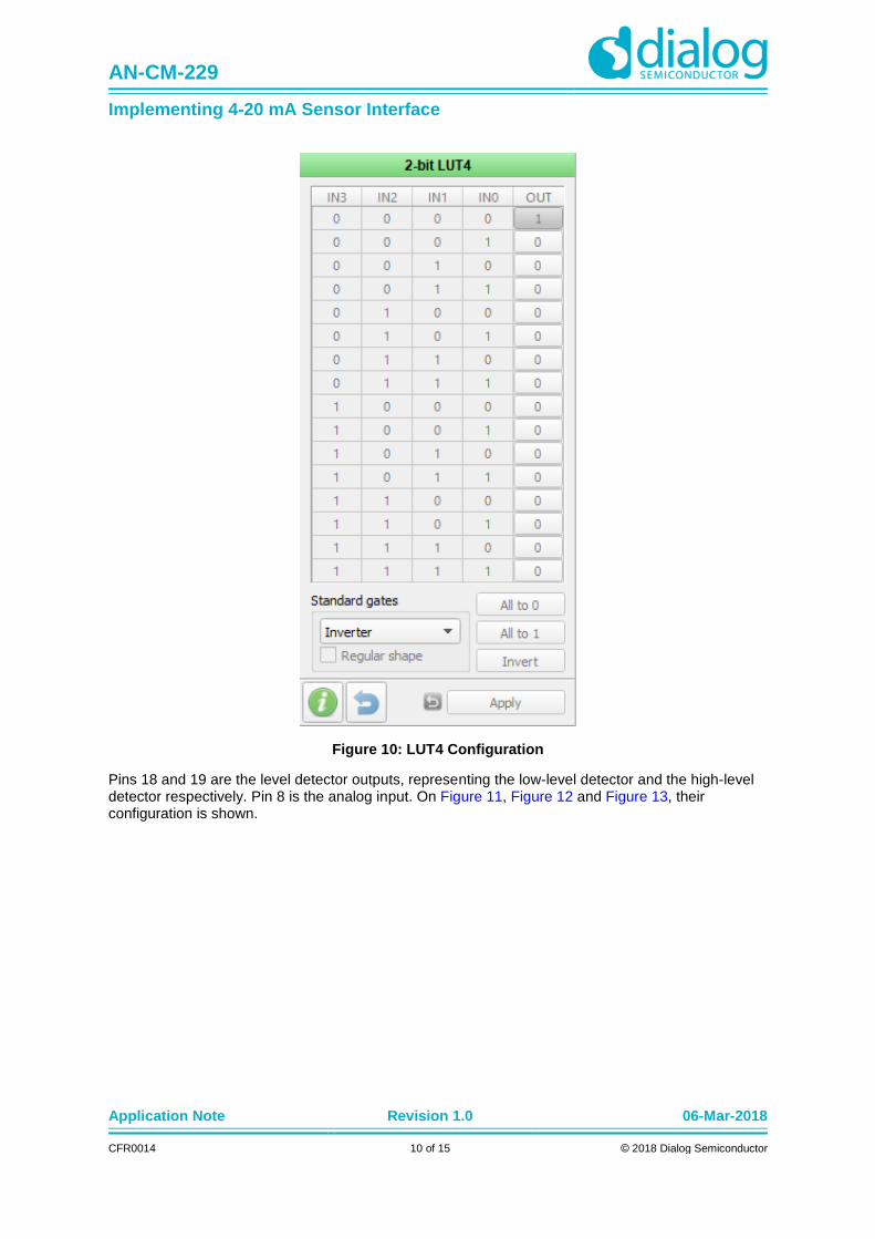
The DCMP1 OUT+ output will be high when the ADC is higher than the configured value. Because this DCMP is used as the low-level detector, the OUT+ output must be inverted to be connected to PIN 18. This is done with 2-bit LUT4, whose configuration is shown on Figure 10. This DCMP compares the ADC conversion with the value configured on Register 3.
AN-CM-229
Implementing 4-20 mA Sensor Interface
Application Note Revision 1.0 06-Mar-2018
CFR0014 10 of 15 © 2018 Dialog Semiconductor
Figure 10: LUT4 Configuration
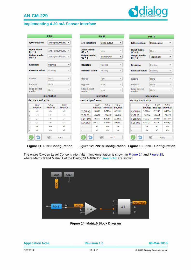
Pins 18 and 19 are the level detector outputs, representing the low-level detector and the high-level detector respectively. Pin 8 is the analog input. On Figure 11, Figure 12 and Figure 13, their configuration is shown.
AN-CM-229
Implementing 4-20 mA Sensor Interface
Application Note Revision 1.0 06-Mar-2018
CFR0014 11 of 15 © 2018 Dialog Semiconductor
Figure 11: PIN8 Configuration
Figure 12: PIN18 Configuration
Figure 13: PIN19 Configuration
The entire Oxygen Level Concentration alarm implementation is shown in Figure 14 and Figure 15, where Matrix 0 and Matrix 1 of the Dialog SLG46621V GreenPAK are shown.
Figure 14: Matrix0 Block Diagram

AN-CM-229
Implementing 4-20 mA Sensor Interface
Application Note Revision 1.0 06-Mar-2018
CFR0014 12 of 15 © 2018 Dialog Semiconductor
Figure 15: Matrix 1 Block Diagram
6 Testing
To test the implementation, a simulated 4-20 mA output of the oxygen sensor was made. This output has the full range of the sensor output and it’s represented as a triangular wave. The current is linearly increased and decreased to show the change in oxygen concentration.
The simulated signal was connected to the interface circuit so it can be measured with the SLG46621V. To analyze the results, pins 18 and 19 were logged with an oscilloscope.
In Figure 16, the simulated sensor output can be seen with the low-level indication of the SLG46621V. It shows how the output of pin 18 holds low when the sensor output is lower than the configured value.

AN-CM-229
Implementing 4-20 mA Sensor Interface
Application Note Revision 1.0 06-Mar-2018
CFR0014 13 of 15 © 2018 Dialog Semiconductor
Figure 16: Pin 18 Oxygen Concentration Low-Level Detection
In Figure 17, the simulated sensor output can be seen with the high-level indication of the SLG46621V. It shows how the output of pin 19 holds high when the sensor output is higher than the configured value.
Figure 17: Pin 19 Oxygen Concentration High-Level Detection
7 Conclusion
In this application note, we implemented a 4-20 mA interface for measuring the output of an oxygen sensor to detect out-of-range oxygen concentrations. 4-20 mA current loops are used in most industrial sensors and actuators because of the buses’ high noise immunity and compatibility with long distance wiring.
There are several methods of interfacing to a 4-20 mA output. In this application note, one of the simplest and most commonly used methods of interpreting a 4-20 mA line is shown. It is also described how the signal can be conditioned to be measured with a Dialog GreenPAK by using the integrated Analog to Digital Converter.
The size of the OpAmps and GreenPAK measurement system is smaller than many other implementations, and it can be further reduced by incorporating more of the logic for the specific application into the SLG46621V.

AN-CM-229
Implementing 4-20 mA Sensor Interface
Application Note Revision 1.0 06-Mar-2018
CFR0014 14 of 15 © 2018 Dialog Semiconductor
Revision History
Revision Date Description
1.0 06-Mar-2018 Initial version

AN-CM-229
Implementing 4-20 mA Sensor Interface
Application Note Revision 1.0 06-Mar-2018
CFR0014 15 of 15 © 2018 Dialog Semiconductor
Status Definitions
Status Definition
DRAFT The content of this document is under review and subject to formal approval, which may result in modifications or
additions.
APPROVED
or unmarked The content of this document has been approved for publication.
Disclaimer
Information in this document is believed to be accurate and reliable. However, Dialog Semiconductor does not give any representations or warranties, expressed or implied, as to the accuracy or completeness of such information. Dialog Semiconductor furthermore takes no responsibility whatsoever for the content in this document if provided by any information source outside of Dialog Semiconductor.
Dialog Semiconductor reserves the right to change without notice the information published in this document, including without limitation the specification and the design of the related semiconductor products, software and applications.
Applications, software, and semiconductor products described in this document are for illustrative purposes only. Dialog Semiconductor makes no representation or warranty that such applications, software and semiconductor products will be suitable for the specified use without further testing or modification. Unless otherwise agreed in writing, such testing or modification is the sole responsibility of the customer and Dialog Semiconductor excludes all liability in this respect.
Customer notes that nothing in this document may be construed as a license for customer to use the Dialog Semiconductor products, software and applications referred to in this document. Such license must be separately sought by customer with Dialog Semiconductor.
All use of Dialog Semiconductor products, software and applications referred to in this document are subject to Dialog Semiconductor’s Standard Terms and Conditions of Sale, available on the company website (www.dialog-semiconductor.com) unless otherwise stated.
Dialog and the Dialog logo are trademarks of Dialog Semiconductor plc or its subsidiaries. All other product or service names are the property of their respective owners.
© 2018 Dialog Semiconductor. All rights reserved.
Contacting Dialog Semiconductor
United Kingdom (Headquarters)
Dialog Semiconductor (UK) LTD
Phone: +44 1793 757700
Germany
Dialog Semiconductor GmbH
Phone: +49 7021 805-0
The Netherlands
Dialog Semiconductor B.V.
Phone: +31 73 640 8822
North America
Dialog Semiconductor Inc.
Phone: +1 408 845 8500
Japan
Dialog Semiconductor K. K.
Phone: +81 3 5769 5100
Taiwan
Dialog Semiconductor Taiwan
Phone: +886 281 786 222
Hong Kong
Dialog Semiconductor Hong Kong
Phone: +852 2607 4271
Korea
Dialog Semiconductor Korea
Phone: +82 2 3469 8200
China (Shenzhen)
Dialog Semiconductor China
Phone: +86 755 2981 3669
China (Shanghai)
Dialog Semiconductor China
Phone: +86 21 5424 9058
Email:
Web site:
www.dialog-semiconductor.com