
perceived benefits and challenges of job rotation in a ... - iaeme
Upload
khangminh22Category
view
0download
0
International Journal of Electrical Engineering and Technology (IJEET), ISSN 0976 – 6545(Print),
ISSN 0976 – 6553(Online) Volume 5, Issue 3, March (2014), pp. 14-26 © IAEME
14
TOPOLOGIES OF POWER CONVERTERS FOR LED LIGHT
APPLICATIONS
Dr. N. R. Bhasme1, Madhuresh Sontakke
2,
1 Asst. Prof, Dept. of Electrical Engg, Govt. College of Engineering Aurangabad, India
2M.E. Student, Dept. of Electrical Engg, Govt. College of Engineering Aurangabad, India
ABSTRACT
This paper presents a very high frequency power converters for domestic and street LED light
applications. Several power converter topologies like Buck, Boost, Buck-Boost, Flyback, Forward,
Push-pull and Resonant Converters are discussed in this paper. Their performances are compared on
the basis of power level, DC voltage gain, input power range and design aspects.
Keywords: High Brightness (HB), Resonant converter, Isolated Converter, Non-isolated Converter,
Symmetric & Asymmetric Converter.
I. INTRODUCTION
Reducing energy consumption has become one of the most important concerns now a days
especially and lighting applications as they represent approximately 20 % of electrical energy
consumption in the world [1]. Therefore, developing efficient lighting systems has become essential
task today. High Brightness (HB) Light Emitting Diodes (LEDs) have become the best choice for
lighting applications. This is due to the rapid advances in material and manufacturing technologies
that enabled significant developments in lighting applications [2]. Based on that, most of
conventional light bulbs have been replaced by LEDs as an efficient way to reduce the energy
consumption. The LED Lamp offers many advantages such as: extremely long life, which is
approximately more than 10 times that of compact fluorescent lamp (CFL), extreme robustness as
there are no glass components or filaments, no external reflector, a modular construction, relatively
high efficiency, no ultra violet (UV) radiation or Infra-Red (IR) output and as they can be dimmed
smoothly from full output to off.
The illumination produced by a LED is relatively weak, so no of LEDs are connected in
series and/or parallel to increase the LUX. The voltage of a series of LEDs is the voltage drop of
individual LED times the number of LEDs in series. The current of a series of LEDs in parallel is the
sum of the LED currents of all the strings. [3]
The LED brightness is mainly dependent on its current because of which efficient control is
needed to regulate the LED current. The LED drivers not only perform the unity power factor
INTERNATIONAL JOURNAL OF ELECTRICAL ENGINEERING &
TECHNOLOGY (IJEET)
ISSN 0976 – 6545(Print)
ISSN 0976 – 6553(Online)
Volume 5, Issue 3, March (2014), pp. 14-26
© IAEME: www.iaeme.com/ijeet.asp
Journal Impact Factor (2014): 6.8310 (Calculated by GISI)
www.jifactor.com
IJEET
© I A E M E

International Journal of Electrical Engineering and Technology (IJEET), ISSN 0976
ISSN 0976 – 6553(Online) Volume 5, Issue
correction but also regulates the current. The size, life time and cost are also other concern of
drivers.
II. DIFFERENT TOPOLOGIES
Depending on the source type regulators are used, if the source is AC then regulator is used
and if the source is D.C. like battery or solar panel then directly DC
applications, the S.M.P.S. topology contains a power transformer. Th
scaling through the turns ratio, and the ability to provide multiple outputs. However, there are non
isolated topologies (without transformers) such as the buck
where the power processing is achieved by inductive energy transfer alone. All of the more complex
arrangements are based on these non
topology of power converters is given
Figure 1 : Classification of Power Converters for LED Applications
A. Non-Isolated Topologies
The majority of the topologies used in
following three non-isolated versions called the buck, the boost and the buck
simplest configurations possible, and have the lowest component count, requiring only one inductor,
capacitor, transistor and diode to generate their single output.
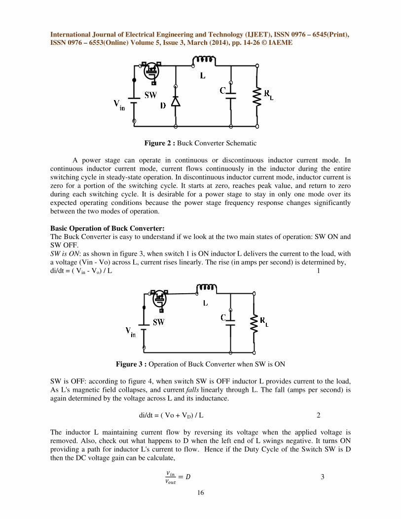
a. Buck Converter Topology The buck is a popular non-
power stage. Power supply designers choose the buck power stage because the required output is
always less than the input voltage. The input current for a buck power stage is discontinuous, or
pulsating, because the power switch (
switching cycle. The output current for a buck power stage is continuous or non
the output current is supplied by the output inductor
Figure 2 shows a simplified schematic of the buck power stage.
power semiconductor switch .Inductor
RL represents the load seen by the power supply output. The diode
diode, or freewheeling diode.
Isolated
Converter
Buck
Boost
Buck Boost
International Journal of Electrical Engineering and Technology (IJEET), ISSN 0976
6553(Online) Volume 5, Issue 3, March (2014), pp. 14-26 © IAEME
correction but also regulates the current. The size, life time and cost are also other concern of
g on the source type regulators are used, if the source is AC then regulator is used
and if the source is D.C. like battery or solar panel then directly DC-DC converters are used. In most
applications, the S.M.P.S. topology contains a power transformer. This provides isolation, voltage
scaling through the turns ratio, and the ability to provide multiple outputs. However, there are non
isolated topologies (without transformers) such as the buck, boost and the buck-
is achieved by inductive energy transfer alone. All of the more complex
arrangements are based on these non-isolate types. In block figure 1 classification of different
topology of power converters is given
fication of Power Converters for LED Applications
The majority of the topologies used in now days for converters are derived from the
isolated versions called the buck, the boost and the buck-boost. These are th
simplest configurations possible, and have the lowest component count, requiring only one inductor,
capacitor, transistor and diode to generate their single output.
-isolated power stage topology, sometimes called a step
power stage. Power supply designers choose the buck power stage because the required output is
always less than the input voltage. The input current for a buck power stage is discontinuous, or
pulsating, because the power switch (SW) current that pulses from zero to fixed
switching cycle. The output current for a buck power stage is continuous or non-pulsating because
the output current is supplied by the output inductor or capacitor combination. [4]
lified schematic of the buck power stage. Switch SW
Inductor L and capacitor C make up the effective output filter. Resistor
represents the load seen by the power supply output. The diode D is usually called
Power Converter(SMPS)
Non-Isolated
Converter
Asymmetric
Flyback
Forward
Symmetric
Push-Pull
Half Bridge
Full Bridge
International Journal of Electrical Engineering and Technology (IJEET), ISSN 0976 – 6545(Print),
correction but also regulates the current. The size, life time and cost are also other concern of such
g on the source type regulators are used, if the source is AC then regulator is used
DC converters are used. In most
is provides isolation, voltage
scaling through the turns ratio, and the ability to provide multiple outputs. However, there are non-
-boost converters,
is achieved by inductive energy transfer alone. All of the more complex
classification of different
fication of Power Converters for LED Applications
are derived from the
boost. These are the
simplest configurations possible, and have the lowest component count, requiring only one inductor,
imes called a step-down
power stage. Power supply designers choose the buck power stage because the required output is
always less than the input voltage. The input current for a buck power stage is discontinuous, or
fixed input every
pulsating because
is high frequency
make up the effective output filter. Resistor
is usually called the catch
Isolated
Converter
International Journal of Electrical Engineering and Technology (IJEET), ISSN 0976 – 6545(Print),
ISSN 0976 – 6553(Online) Volume 5, Issue 3, March (2014), pp. 14-26 © IAEME
16
Figure 2 : Buck Converter Schematic
A power stage can operate in continuous or discontinuous inductor current mode. In
continuous inductor current mode, current flows continuously in the inductor during the entire
switching cycle in steady-state operation. In discontinuous inductor current mode, inductor current is
zero for a portion of the switching cycle. It starts at zero, reaches peak value, and return to zero
during each switching cycle. It is desirable for a power stage to stay in only one mode over its
expected operating conditions because the power stage frequency response changes significantly
between the two modes of operation.
Basic Operation of Buck Converter: The Buck Converter is easy to understand if we look at the two main states of operation: SW ON and
SW OFF.
SW is ON: as shown in figure 3, when switch 1 is ON inductor L delivers the current to the load, with
a voltage (Vin - Vo) across L, current rises linearly. The rise (in amps per second) is determined by,
di/dt = ( Vin - Vo) / L 1
Figure 3 : Operation of Buck Converter when SW is ON
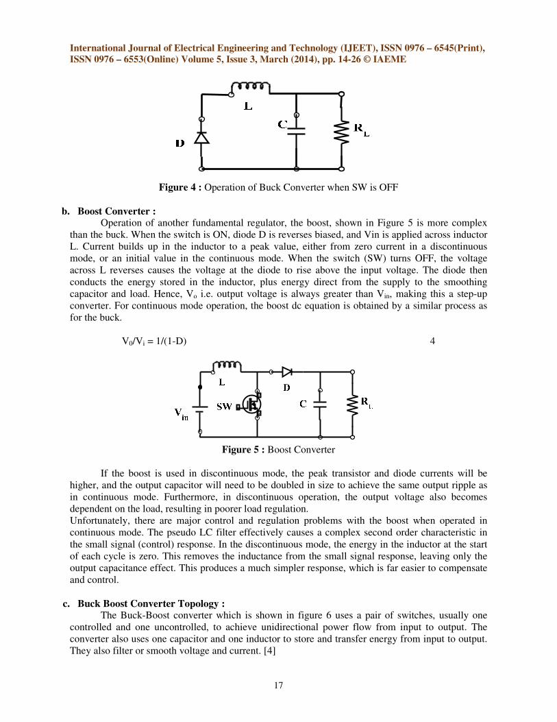
SW is OFF: according to figure 4, when switch SW is OFF inductor L provides current to the load,
As L's magnetic field collapses, and current falls linearly through L. The fall (amps per second) is
again determined by the voltage across L and its inductance.
di/dt = ( Vo + VD) / L 2
The inductor L maintaining current flow by reversing its voltage when the applied voltage is
removed. Also, check out what happens to D when the left end of L swings negative. It turns ON
providing a path for inductor L's current to flow. Hence if the Duty Cycle of the Switch SW is D
then the DC voltage gain can be calculate,
���
����� � 3
International Journal of Electrical Engineering and Technology (IJEET), ISSN 0976 – 6545(Print),
ISSN 0976 – 6553(Online) Volume 5, Issue 3, March (2014), pp. 14-26 © IAEME
17
Figure 4 : Operation of Buck Converter when SW is OFF
b. Boost Converter : Operation of another fundamental regulator, the boost, shown in Figure 5 is more complex
than the buck. When the switch is ON, diode D is reverses biased, and Vin is applied across inductor
L. Current builds up in the inductor to a peak value, either from zero current in a discontinuous
mode, or an initial value in the continuous mode. When the switch (SW) turns OFF, the voltage
across L reverses causes the voltage at the diode to rise above the input voltage. The diode then
conducts the energy stored in the inductor, plus energy direct from the supply to the smoothing
capacitor and load. Hence, Vo i.e. output voltage is always greater than Vin, making this a step-up
converter. For continuous mode operation, the boost dc equation is obtained by a similar process as
for the buck.
V0/Vi = 1/(1-D) 4
Figure 5 : Boost Converter
If the boost is used in discontinuous mode, the peak transistor and diode currents will be
higher, and the output capacitor will need to be doubled in size to achieve the same output ripple as
in continuous mode. Furthermore, in discontinuous operation, the output voltage also becomes
dependent on the load, resulting in poorer load regulation.
Unfortunately, there are major control and regulation problems with the boost when operated in
continuous mode. The pseudo LC filter effectively causes a complex second order characteristic in
the small signal (control) response. In the discontinuous mode, the energy in the inductor at the start
of each cycle is zero. This removes the inductance from the small signal response, leaving only the
output capacitance effect. This produces a much simpler response, which is far easier to compensate
and control.
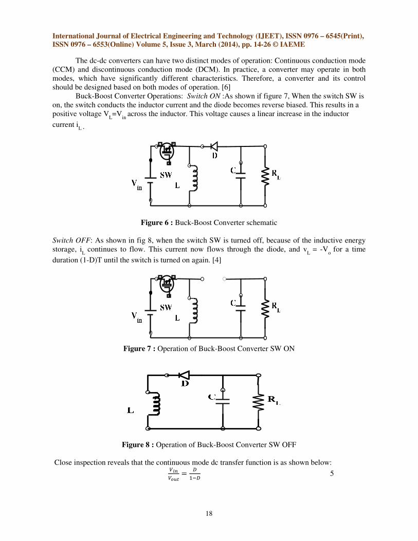
c. Buck Boost Converter Topology : The Buck-Boost converter which is shown in figure 6 uses a pair of switches, usually one
controlled and one uncontrolled, to achieve unidirectional power flow from input to output. The
converter also uses one capacitor and one inductor to store and transfer energy from input to output.
They also filter or smooth voltage and current. [4]
International Journal of Electrical Engineering and Technology (IJEET), ISSN 0976 – 6545(Print),
ISSN 0976 – 6553(Online) Volume 5, Issue 3, March (2014), pp. 14-26 © IAEME
18
The dc-dc converters can have two distinct modes of operation: Continuous conduction mode
(CCM) and discontinuous conduction mode (DCM). In practice, a converter may operate in both
modes, which have significantly different characteristics. Therefore, a converter and its control
should be designed based on both modes of operation. [6]
Buck-Boost Converter Operations: Switch ON :As shown if figure 7, When the switch SW is
on, the switch conducts the inductor current and the diode becomes reverse biased. This results in a
positive voltage VL=V
in across the inductor. This voltage causes a linear increase in the inductor
current iL .
Figure 6 : Buck-Boost Converter schematic
Switch OFF: As shown in fig 8, when the switch SW is turned off, because of the inductive energy
storage, iL
continues to flow. This current now flows through the diode, and vL
= -Vo
for a time
duration (1-D)T until the switch is turned on again. [4]
Figure 7 : Operation of Buck-Boost Converter SW ON
Figure 8 : Operation of Buck-Boost Converter SW OFF
Close inspection reveals that the continuous mode dc transfer function is as shown below:
���
����
�
� 5

International Journal of Electrical Engineering and Technology (IJEET), ISSN 0976 – 6545(Print),
ISSN 0976 – 6553(Online) Volume 5, Issue 3, March (2014), pp. 14-26 © IAEME
19
Isolated Topologies: Isolated switching converters are often derived from non-isolated topologies. A common
scheme is to place a transformer where the high frequency voltage or current pulses are produced. In
such converters, the transformer leakage inductance may produce additional switching losses and
high voltage spikes across the converter switches. Furthermore, the energy stored in the transformer
magnetizing inductance should be reset to prevent it from saturation. The isolated converters can be
classified according to their magnetic cycle swing in the B-H plot which is shown in figure 9. An
isolated converter is asymmetrical if the magnetic operating point of the transformer remains in the
same quadrant. Any other converter is, of course, called symmetrical. [7]
Figure 9 : B-H curve for asymmetric and Symmetric converter
i. Asymmetrical Isolated Converter
a.Flyback Converter Topology : The Flyback Converter is used in both AC/DC and DC/DC conversion with galvanic
isolation between the input and any outputs. More precisely, the flyback converter is a Buck-Boost
conversion with the inductor split to form a transformer, so that the voltage ratios are multiplied with
an additional advantage of isolation.[7] [6]
Figure 10 illustrates the usual configuration of the flyback converter. The MOSFET source
(SW) is connected to the primary-side ground, simplifying the gate drive circuit. The transformer
polarity marks are reversed, to obtain a positive output voltage. A N1:N2 turns ratio is introduced;
this allows better converter optimization.[6]
Operation of Flyback Converter: The schematic of a flyback converter can be seen in Fig. 10. It is equivalent to that of a buck-
boost converter, with the inductor split to form a transformer. Therefore the operating principle of
both converters is very close.

International Journal of Electrical Engineering and Technology (IJEET), ISSN 0976 – 6545(Print),
ISSN 0976 – 6553(Online) Volume 5, Issue 3, March (2014), pp. 14-26 © IAEME
20
Figure 10 : Flyback Converter
Figure 11 : Operation of Flyback Converter SW ON
SW ON: As shown in Fig 11, when the switch is closed, the primary of the transformer is
directly connected to the input voltage source. The primary current and magnetic flux in the
transformer increases storing energy in the transformer. The voltage induced in the secondary
winding is negative, so the diode is reverse-biased (i.e., blocked). The output capacitor supplies
energy to the output load.[6]
SW OFF: As shown in figure 12, when the switch is opened, the primary current and
magnetic flux drops. The secondary voltage is positive, forward-biasing the diode, allowing current
to flow from the transformer. The energy from the transformer core recharges the capacitor and
supplies the load. Hence if the Duty Cycle of the Switch SW is D then the DC voltage gain can be
calculate,[6]
Figure 12 : Operation of Flyback Converter SW OFF

International Journal of Electrical Engineering and Technology (IJEET), ISSN 0976 – 6545(Print),
ISSN 0976 – 6553(Online) Volume 5, Issue 3, March (2014), pp. 14-26 © IAEME
21
���
����� �
� 6
The operation of storing energy in the transformer before transferring to the output of the
converter allows the topology to easily generate multiple outputs with little additional circuitry,
although the output voltages have to be able to match each other through the turns ratio. Also there is
a need for a controlling rail which has to be loaded before load is applied to the uncontrolled rails,
this is to allow the PWM to open up and supply enough energy to the transformer.[7]
b. The Forward Converter:
Operation:
The forward converter is also a single switch isolated topology, and is shown in Fig. 13. This
is based on the buck converter described earlier, with the addition of a transformer and another diode
in the output circuit. The characteristic LC output filter is clearly present. In contrast to the flyback,
the forward converter has a true transformer action, where energy is transferred directly to the output
through the inductor during the transistor on-time. It can be seen that the polarity of the secondary
winding is opposite to that of the flyback, hence allowing direct current flow through blocking diode
D1.
Figure 13 : The Forward Converter
During the on-time, the current flowing causes energy to be built up in the output inductor L.
When the transistor turns off, the secondary voltage reverses, D1 goes from conducting to blocking
mode and the freewheel diode D2 then becomes forward biased and provides a path for the inductor
current to continue to flow. This allows the energy stored in L to be released into the load during the
transistor off time. The forward converter is always operated in continuous mode (in this case the
output inductor current), since this produces very low peak input and output currents and small ripple
components. Going into discontinuous mode would greatly increase these values, as well as
increasing the amount of switching noise generated. No destabilizing right hand plane zero occurs in
the frequency response of the forward in continuous mode (as with the buck). This means that the
control problems that existed with the continuous flyback are not present here. So there are no real
advantages to be gained by using discontinuous mode operation for the forward converter. As we
discussed if D1 is the duty cycle of the switch SW, we can derive the transfer fuction for the forward
converter as follows,
���
����� � � 7

International Journal of Electrical Engineering and Technology (IJEET), ISSN 0976 – 6545(Print),
ISSN 0976 – 6553(Online) Volume 5, Issue 3, March (2014), pp. 14-26 © IAEME
22
ii. Symmetric Isolated Converters
a. Push-Pull Converter
Operation: To utilize the transformer flux swing fully, it is necessary to operate the core symmetrically
as described earlier. This permits much smaller transformer sizes and provides higher output powers
than possible with the single ended types. The symmetrical types always require an even number of
transistor switches. One of the best known of the symmetrical types is the push-pull converter shown
in Figure 14. The primary is a centre-tapped arrangement and each transistor switch is driven
alternately, driving the transformer in both directions. The push-pull transformer is typically half the
size of that for the single ended types, resulting in a more compact design. This push-pull action
produces natural core resetting during each half cycle; hence no clamp winding is required. Power is
transferred to the buck type output circuit during each transistor conduction period. The duty ratio of
each switch is usually less than 0.45. This provides enough dead time to avoid transistor cross
conduction. The power can now be transferred to the output for up to 90% of the switching period,
hence allowing greater throughput power than with the single-ended types. The push-pull
configuration is normally used for output powers in the 100 to 500W range. [9][7]
The bipolar switching action also means that the output circuit is actually operated at twice
the switching frequency of the power transistors. Therefore, the output inductor and capacitor can be
even smaller for similar output ripple levels. Push-pull converters are thus excellent for high power
density, low ripple outputs.[7] the transfer function of the Push-Pull converter can be derived as
follows,
���
����� 2� � 8
Figure 14 : Push Pull Converter
b. LLC Resonant Converters Higher efficiency, higher power density, and higher component density have become
common in power-supply designs and their applications. Resonant power converters especially those
with an LLC half-bridge configuration which is shown in figure 15 are receiving renewed interest
because of this trend and the potential of these converters to achieve both higher switching
frequencies and lower switching losses. However, designing such converters presents many
challenges, among them the fact that the LLC resonant half-bridge converter performs power
conversion with frequency modulation instead of pulse-width modulation, requiring a different
design approach. [5]
Bridge resonant Converter, the converter configuration is mainly divided into three pats.
International Journal of Electrical Engineering and Technology (IJEET), ISSN 0976 – 6545(Print),
ISSN 0976 – 6553(Online) Volume 5, Issue 3, March (2014), pp. 14-26 © IAEME
23
i. Square Wave Generator: Power switches Q1 and Q2, which are usually MOSFETs, are configured to form a square
wave generator. This generator produces a square-wave voltage, Vsq, by driving switches Q1 and Q2,
with alternating 50% duty cycles for each switch. A small dead time is needed between the
consecutive transitions, both to prevent the possibility of cross-conduction and to allow time for ZVS
to be achieved.
Figure 15 : LLC Half Bridge Resonant Converter
ii. Resonant Circuit:
The resonant circuit, also called a resonant network, consists of the resonant capacitance, Cr,
and two inductances the series resonant inductance, Lr, and the Magnetizing Inductance of
transformer, Lm. The transformer’s turn’s ratio is n. The resonant network circulates the electric
current and, as a result, the energy is circulated and delivered to the load through the transformer.
The transformer’s primary winding receives a bipolar square-wave voltage, Vso. This voltage is
transferred to the secondary side, with the transformer providing both electrical isolation and the
turn’s ratio to deliver the required voltage level to the output.
iii. Rectifier Circuit:
On the converter’s secondary side, two diodes constitute a full-wave rectifier to convert AC
input to DC output and supply the load RL. The output capacitor smoothens the rectified voltage and
current.
Operation of LLC Half Bridge Resonant Converter: The operation of LLC resonant converter is divided into three modes namely mode 1, mode
2, and mode 3.
Mode-1, begins when Q2 is turned off at t0. At this moment, resonant inductor Lr current is negative;
it will flow through body diode of Q1, which creates a ZVS condition for Q1. Gate signal of Q1
should be applied during this mode. When resonant inductor Lr current flow through body diode of
Q1, ILr begins to rise, this will force secondary diode D1 to conduct and Io begin to increase. Also,
from this moment, transformer sees output voltage on the secondary side. Lm is
Charged with constant voltage.
Mode-2 begins when resonant inductor current ILr becomes positive. Since Q1 is turned on during
mode 1, current will flow through MOSFET Q1. During this mode, output rectifier diode D1 conduct.
The transformer voltage is clamped at Vo. Lm is linearly charged with output voltage, so it doesn't
participate in the resonant during this period. In this mode, the circuit works like a SRC with
resonant inductor Lr and resonant capacitor Cr. This mode ends when Lr current is the same as Lm
current. Output current reaches zero.
Mode-3, the two inductor’s currents are equal. Output current reach zero. Both output rectifier diodes
D1 and D2 is reverse biased. Transformer secondary voltage is lower than output voltage.
International Journal of Electrical Engineering and Technology (IJEET), ISSN 0976 – 6545(Print),
ISSN 0976 – 6553(Online) Volume 5, Issue 3, March (2014), pp. 14-26 © IAEME
24
During this period, a resonant tank of Lm in series with Lr resonates with Cr. This mode ends when
Q1 is turned off. [5]
As D is the duty cycle of the switch then DC voltage gain can be given as follows,
���
����� � � 9
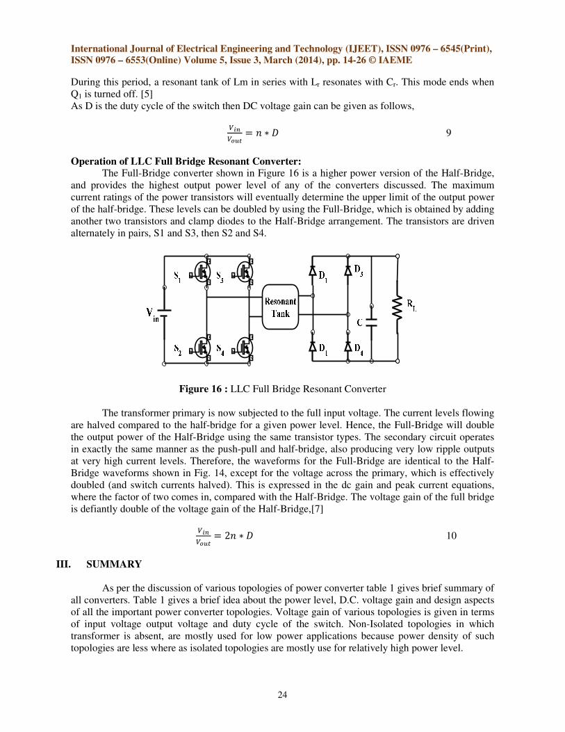
Operation of LLC Full Bridge Resonant Converter: The Full-Bridge converter shown in Figure 16 is a higher power version of the Half-Bridge,
and provides the highest output power level of any of the converters discussed. The maximum
current ratings of the power transistors will eventually determine the upper limit of the output power
of the half-bridge. These levels can be doubled by using the Full-Bridge, which is obtained by adding
another two transistors and clamp diodes to the Half-Bridge arrangement. The transistors are driven
alternately in pairs, S1 and S3, then S2 and S4.
Figure 16 : LLC Full Bridge Resonant Converter
The transformer primary is now subjected to the full input voltage. The current levels flowing
are halved compared to the half-bridge for a given power level. Hence, the Full-Bridge will double
the output power of the Half-Bridge using the same transistor types. The secondary circuit operates
in exactly the same manner as the push-pull and half-bridge, also producing very low ripple outputs
at very high current levels. Therefore, the waveforms for the Full-Bridge are identical to the Half-
Bridge waveforms shown in Fig. 14, except for the voltage across the primary, which is effectively
doubled (and switch currents halved). This is expressed in the dc gain and peak current equations,
where the factor of two comes in, compared with the Half-Bridge. The voltage gain of the full bridge
is defiantly double of the voltage gain of the Half-Bridge,[7]
���
����� 2� � 10
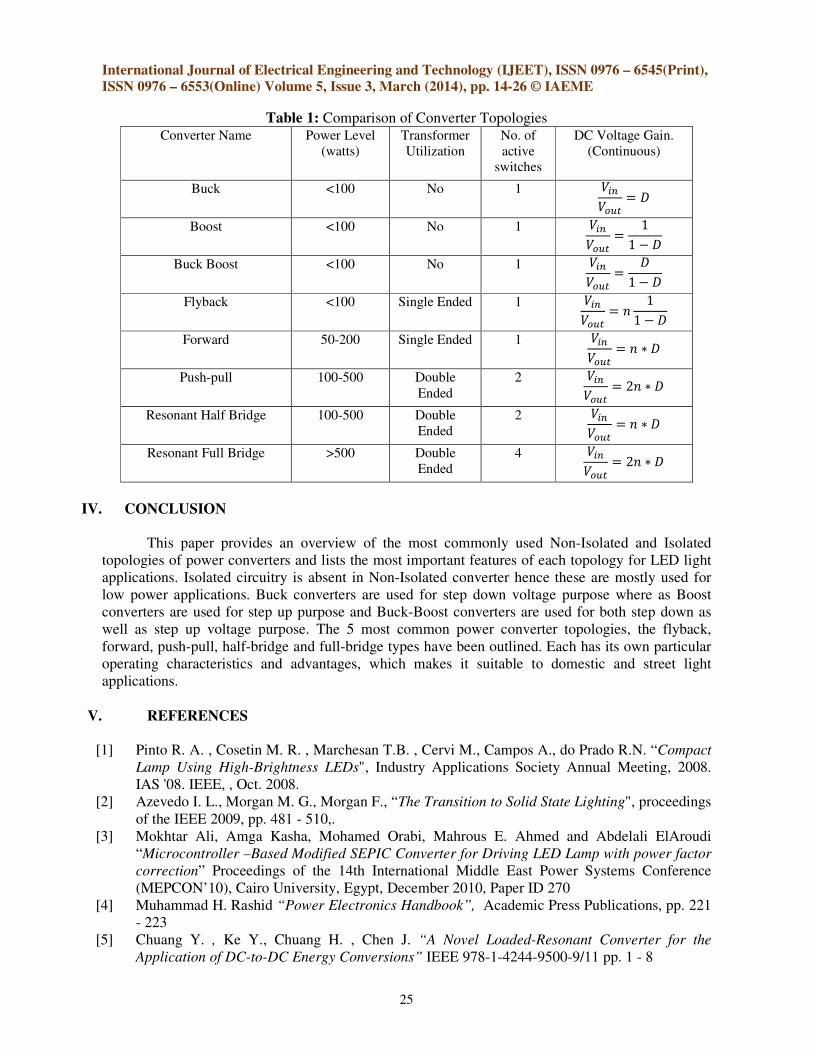
III. SUMMARY
As per the discussion of various topologies of power converter table 1 gives brief summary of
all converters. Table 1 gives a brief idea about the power level, D.C. voltage gain and design aspects
of all the important power converter topologies. Voltage gain of various topologies is given in terms
of input voltage output voltage and duty cycle of the switch. Non-Isolated topologies in which
transformer is absent, are mostly used for low power applications because power density of such
topologies are less where as isolated topologies are mostly use for relatively high power level.
International Journal of Electrical Engineering and Technology (IJEET), ISSN 0976 – 6545(Print),
ISSN 0976 – 6553(Online) Volume 5, Issue 3, March (2014), pp. 14-26 © IAEME
25
Table 1: Comparison of Converter Topologies
Converter Name Power Level
(watts)
Transformer
Utilization
No. of
active
switches
DC Voltage Gain.
(Continuous)
Buck <100 No 1 ���
����� �
Boost <100 No 1 ���
�����
1
1 � �
Buck Boost <100 No 1 ���
�����
�
1 � �
Flyback <100 Single Ended 1 ���
����� �
1
1 � �
Forward 50-200 Single Ended 1 ���
����� � �
Push-pull 100-500 Double
Ended
2 ���
����� 2� �
Resonant Half Bridge 100-500 Double
Ended
2 ���
����� � �
Resonant Full Bridge >500 Double
Ended
4 ���
����� 2� �
IV. CONCLUSION
This paper provides an overview of the most commonly used Non-Isolated and Isolated
topologies of power converters and lists the most important features of each topology for LED light
applications. Isolated circuitry is absent in Non-Isolated converter hence these are mostly used for
low power applications. Buck converters are used for step down voltage purpose where as Boost
converters are used for step up purpose and Buck-Boost converters are used for both step down as
well as step up voltage purpose. The 5 most common power converter topologies, the flyback,
forward, push-pull, half-bridge and full-bridge types have been outlined. Each has its own particular
operating characteristics and advantages, which makes it suitable to domestic and street light
applications.
V. REFERENCES
[1] Pinto R. A. , Cosetin M. R. , Marchesan T.B. , Cervi M., Campos A., do Prado R.N. “Compact
Lamp Using High-Brightness LEDs", Industry Applications Society Annual Meeting, 2008.
IAS '08. IEEE, , Oct. 2008.
[2] Azevedo I. L., Morgan M. G., Morgan F., “The Transition to Solid State Lighting", proceedings
of the IEEE 2009, pp. 481 - 510,.
[3] Mokhtar Ali, Amga Kasha, Mohamed Orabi, Mahrous E. Ahmed and Abdelali ElAroudi
“Microcontroller –Based Modified SEPIC Converter for Driving LED Lamp with power factor
correction” Proceedings of the 14th International Middle East Power Systems Conference
(MEPCON’10), Cairo University, Egypt, December 2010, Paper ID 270
[4] Muhammad H. Rashid “Power Electronics Handbook”, Academic Press Publications, pp. 221
- 223
[5] Chuang Y. , Ke Y., Chuang H. , Chen J. “A Novel Loaded-Resonant Converter for the
Application of DC-to-DC Energy Conversions” IEEE 978-1-4244-9500-9/11 pp. 1 - 8

International Journal of Electrical Engineering and Technology (IJEET), ISSN 0976 – 6545(Print),
ISSN 0976 – 6553(Online) Volume 5, Issue 3, March (2014), pp. 14-26 © IAEME
26
[6] NPTEL Module 3 “DC to DC Converters”, Lesson 22 “ Flyback Type Switched Mode Power
Supply” version 2 EE IIT, Kharagpur pp. 3 - 13
[7] Power Semiconductor Application Notes (Philips Semiconductor) Chapter 2 , S. M. P. S.
Topologies, pp. 103 - 205
[8] Application Notes of STMicroelectronics “Topologies For Switched Mode Power Supplies” by
L. Wuidart, pp.1 - 4
[9] Power Electronics Technology Magazine, Feb 2011 “Topology Key to Power density in
isolated DC-DC Converters” by Belly B. , Hari A. , pp. 16 - 20
[10] Microchip Application Notes 1207, “Switch Mode Power Supplies Part II” by Bersani A., pp. 1
– 18
[11] L.Raguraman and P.Sabarish, “Integrated Bridgeless PWM Based Power Converters”
International Journal of Advanced Research in Engineering & Technology (IJARET), Volume
4, Issue 5, 2013, pp. 17 - 23, ISSN Print: 0976-6480, ISSN Online: 0976-6499, Published by
IAEME.
[12] Mihail Hristov Antchev, Hristo Mihailov Antchev, Mariya Petkova Petkova and Angelina
Mihaylova Tomova, “Computer Investigation Of Three Phase Clarke-Maximum (Maximum P,
Q) Trigonometrical PLL For Grid Connected Power Converters” International journal of
Electronics and Communication Engineering &Technology (IJECET), Volume 5, Issue 1,
2013, pp. 119 - 129, ISSN Print: 0976- 6464, ISSN Online: 0976 –6472, Published by IAEME.
[13] P. Hari Krishna Prasad, Dr. M. Venu Gopal Rao,, “Dc-Dc Converters For Telecom Power
Supply Applications” International Journal of Electrical Engineering & Technology (IJEET),
Volume 3, Issue 1, 2012, pp. 156 - 166, ISSN Print : 0976-6545, ISSN Online: 0976-6553,
Published by IAEME.
Copyright © 2022 FDOKUMEN