III-V nMOSFETs-Some issues associated with roadmap worthiness
6
III–V nMOSFETs – Some issues associated with roadmap worthiness (invited) Iain Thayne a,⇑ , Steven Bentley a , Martin Holland a , Wout Jansen a , Xu Li a , Douglas Macintyre a , Stephen Thoms a , Byungha Shin b,1 , Jaesoo Ahn b , Paul McIntyre b a Nanoelectronics Research Centre, University of Glasgow, Glasgow, UK b Department of Materials Science and Engineering, Stanford University, Stanford, CA 94305, USA article info Article history: Received 18 March 2011 Received in revised form 24 March 2011 Accepted 24 March 2011 Available online 30 March 2011 Keyword: III–V MOSFETs abstract The high electron mobility of compound semiconductor materials, arising from the combination of low effective mass and materials dependent intervalley scattering mechanisms, can result in high velocity and low backscatter electrons being injected at the source side of a III–V nMOSFET. In combination, these factors have the potential to meet the highly challenging performance metrics of the International Tech- nology Roadmap for Semiconductors (ITRS) [1] beyond the 15 nm technology generation, in particular the need to reduce supply voltages towards 0.5 V. This paper highlights some challenges over and above those of developing a high quality dielectric/III–V semiconductor interface, specifically in the areas of scaled source/drain contact formation and channel materials and device architectures which have to be addressed if III–V MOSFETs are to be a credible solution to enable continued scaling of the ITRS beyond 2018. Ó 2011 Elsevier B.V. All rights reserved. 1. Introduction In recent years, the major driver in the mainstream semicon- ductor industry has become density scaling. This is well captured by the MOSFET gate pitch metric (a measure of the total size of a MOSFET, shown schematically in Fig. 1) which, as shown in Table 1, is required to shrink from around 75 nm in 2011, through 30 nm in 2018, with a target of 15 nm by 2024. This relentless increase in transistor density has significant ramifications for power dissipation in an integrated circuit, and as a consequence there is a need, according to the ITRS, to reduce the supply voltages, as shown in Table 1, from around 0.9 V at pres- ent, to 0.6 V by 2024. Density scaling can only be achieved by reducing the size of all contacts in the MOSFET. It is important to remember that whilst the physical gate length of the MOSFET is re- duced, ever shrinking gate pitch requires that the source and drain contacts are also reduced in size, as shown in Table 1. As will be explained below, reducing the source/drain geome- tries results in an increase in access resistance, at a time when the total source drain resistance, as defined in the ITRS, must be re- duced (again shown in Table 1). Arguably, mitigating increases in access resistance due to gate pitch scaling will be one of the key challenges to achieving ultra-high density scaling in the coming years. Review of the ITRS highlights a number of other important fac- tors when considering potential technology solutions. Despite migration to high-k dielectrics to address static gate leakage, the ITRS predicts a steady reduction in gate capacitance as shown in Table 1. This, along with the reduced supply voltage, and therefore lower gate overdrive (as the threshold voltage is predicted to re- duce by only 10% by 2024) means the channel charge density will reduce with time (Table 1). As a consequence, simple analysis sug- gests the average carrier velocity in the device channel will have to increase beyond the steady state saturation value of around 1.0 10 5 ms 1 (Table 1). Compound semiconductor materials are well suited to achiev- ing high electron velocities in non-equilibrium conditions arising from carrier injection into regions of high electric field due to the combination of low effective mass along with the ability to engi- neer the dominant scattering mechanisms by the use of hetero- structures and judicious choice of material compositions. For example, in a high electron mobility transistor (HEMT), large mobility can be achieved by a reduction in ionised impurity scat- tering as a result of spatial separation of the device channel from the donors supplying the charge. Taking the In x Ga 1x As material system as an example, increasing the indium concentration re- duces the overall effective mass, but in addition increases the en- ergy separation between the low mass C valley and the higher mass L valley [3]. Utilising a higher indium concentration channel in short gate length HEMTs means electrons can accelerate for longer in the low mass, high mobility C valley before being trans- ferred to the L valley. As a result, the average channel velocity is increased. 0167-9317/$ - see front matter Ó 2011 Elsevier B.V. All rights reserved. doi:10.1016/j.mee.2011.03.100 ⇑ Corresponding author. Tel.: +44 0 141 330 3859; fax: +44 0 141 330 6010. E-mail address: [email protected] (I. Thayne). 1 Present address: IBM T.J. Watson Research Center, Yorktown Heights, NY 10598, USA. Microelectronic Engineering 88 (2011) 1070–1075 Contents lists available at ScienceDirect Microelectronic Engineering journal homepage: www.elsevier.com/locate/mee
-
Upload
independent -
Category
Documents
-
view
2 -
download
0
Transcript of III-V nMOSFETs-Some issues associated with roadmap worthiness
Microelectronic Engineering 88 (2011) 1070–1075
Contents lists available at ScienceDirect
Microelectronic Engineering
journal homepage: www.elsevier .com/locate /mee
III–V nMOSFETs – Some issues associated with roadmap worthiness (invited)
Iain Thayne a,⇑, Steven Bentley a, Martin Holland a, Wout Jansen a, Xu Li a, Douglas Macintyre a,Stephen Thoms a, Byungha Shin b,1, Jaesoo Ahn b, Paul McIntyre b
a Nanoelectronics Research Centre, University of Glasgow, Glasgow, UKb Department of Materials Science and Engineering, Stanford University, Stanford, CA 94305, USA
a r t i c l e i n f o
Article history:Received 18 March 2011Received in revised form 24 March 2011Accepted 24 March 2011Available online 30 March 2011
Keyword:III–V MOSFETs
0167-9317/$ - see front matter � 2011 Elsevier B.V. Adoi:10.1016/j.mee.2011.03.100
⇑ Corresponding author. Tel.: +44 0 141 330 3859;E-mail address: [email protected] (I. Thay
1 Present address: IBM T.J. Watson Research Center,USA.
a b s t r a c t
The high electron mobility of compound semiconductor materials, arising from the combination of loweffective mass and materials dependent intervalley scattering mechanisms, can result in high velocityand low backscatter electrons being injected at the source side of a III–V nMOSFET. In combination, thesefactors have the potential to meet the highly challenging performance metrics of the International Tech-nology Roadmap for Semiconductors (ITRS) [1] beyond the 15 nm technology generation, in particular theneed to reduce supply voltages towards 0.5 V. This paper highlights some challenges over and abovethose of developing a high quality dielectric/III–V semiconductor interface, specifically in the areas ofscaled source/drain contact formation and channel materials and device architectures which have tobe addressed if III–V MOSFETs are to be a credible solution to enable continued scaling of the ITRS beyond2018.
� 2011 Elsevier B.V. All rights reserved.
1. Introduction
In recent years, the major driver in the mainstream semicon-ductor industry has become density scaling. This is well capturedby the MOSFET gate pitch metric (a measure of the total size of aMOSFET, shown schematically in Fig. 1) which, as shown in Table 1,is required to shrink from around 75 nm in 2011, through 30 nm in2018, with a target of 15 nm by 2024.
This relentless increase in transistor density has significantramifications for power dissipation in an integrated circuit, andas a consequence there is a need, according to the ITRS, to reducethe supply voltages, as shown in Table 1, from around 0.9 V at pres-ent, to 0.6 V by 2024. Density scaling can only be achieved byreducing the size of all contacts in the MOSFET. It is important toremember that whilst the physical gate length of the MOSFET is re-duced, ever shrinking gate pitch requires that the source and draincontacts are also reduced in size, as shown in Table 1.
As will be explained below, reducing the source/drain geome-tries results in an increase in access resistance, at a time whenthe total source drain resistance, as defined in the ITRS, must be re-duced (again shown in Table 1). Arguably, mitigating increases inaccess resistance due to gate pitch scaling will be one of the keychallenges to achieving ultra-high density scaling in the comingyears.
ll rights reserved.
fax: +44 0 141 330 6010.ne).Yorktown Heights, NY 10598,
Review of the ITRS highlights a number of other important fac-tors when considering potential technology solutions. Despitemigration to high-k dielectrics to address static gate leakage, theITRS predicts a steady reduction in gate capacitance as shown inTable 1. This, along with the reduced supply voltage, and thereforelower gate overdrive (as the threshold voltage is predicted to re-duce by only �10% by 2024) means the channel charge density willreduce with time (Table 1). As a consequence, simple analysis sug-gests the average carrier velocity in the device channel will have toincrease beyond the steady state saturation value of around1.0 � 105 ms�1 (Table 1).
Compound semiconductor materials are well suited to achiev-ing high electron velocities in non-equilibrium conditions arisingfrom carrier injection into regions of high electric field due to thecombination of low effective mass along with the ability to engi-neer the dominant scattering mechanisms by the use of hetero-structures and judicious choice of material compositions. Forexample, in a high electron mobility transistor (HEMT), largemobility can be achieved by a reduction in ionised impurity scat-tering as a result of spatial separation of the device channel fromthe donors supplying the charge. Taking the InxGa1�xAs materialsystem as an example, increasing the indium concentration re-duces the overall effective mass, but in addition increases the en-ergy separation between the low mass C valley and the highermass L valley [3]. Utilising a higher indium concentration channelin short gate length HEMTs means electrons can accelerate forlonger in the low mass, high mobility C valley before being trans-ferred to the L valley. As a result, the average channel velocity isincreased.
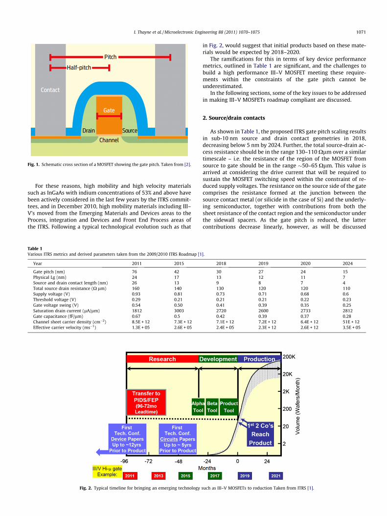
Fig. 1. Schematic cross section of a MOSFET showing the gate pitch. Taken from [2].
I. Thayne et al. / Microelectronic Engineering 88 (2011) 1070–1075 1071
For these reasons, high mobility and high velocity materialssuch as InGaAs with indium concentrations of 53% and above havebeen actively considered in the last few years by the ITRS commit-tees, and in December 2010, high mobility materials including III–V’s moved from the Emerging Materials and Devices areas to theProcess, integration and Devices and Front End Process areas ofthe ITRS. Following a typical technological evolution such as that
Table 1Various ITRS metrics and derived parameters taken from the 2009/2010 ITRS Roadmap [1
Year 2011 2015
Gate pitch (nm) 76 42Physical Lg (nm) 24 17Source and drain contact length (nm) 26 13Total source drain resistance (X lm) 160 140Supply voltage (V) 0.93 0.81Threshold voltage (V) 0.29 0.21Gate voltage swing (V) 0.54 0.50Saturation drain current (lA/lm) 1812 3003Gate capacitance (fF/lm) 0.67 0.5Channel sheet carrier density (cm�2) 8.5E + 12 7.3E + 12Effective carrier velocity (ms�1) 1.3E + 05 2.6E + 05
Fig. 2. Typical timeline for bringing an emerging technology
in Fig. 2, would suggest that initial products based on these mate-rials would be expected by 2018–2020.
The ramifications for this in terms of key device performancemetrics, outlined in Table 1 are significant, and the challenges tobuild a high performance III–V MOSFET meeting these require-ments within the constraints of the gate pitch cannot beunderestimated.
In the following sections, some of the key issues to be addressedin making III–V MOSFETs roadmap compliant are discussed.
2. Source/drain contacts
As shown in Table 1, the proposed ITRS gate pitch scaling resultsin sub-10 nm source and drain contact geometries in 2018,decreasing below 5 nm by 2024. Further, the total source-drain ac-cess resistance should be in the range 130–110 Xlm over a similartimescale – i.e. the resistance of the region of the MOSFET fromsource to gate should be in the range �50–65 Xlm. This value isarrived at considering the drive current that will be required tosustain the MOSFET switching speed within the constraint of re-duced supply voltages. The resistance on the source side of the gatecomprises the resistance formed at the junction between thesource contact metal (or silicide in the case of Si) and the underly-ing semiconductor, together with contributions from both thesheet resistance of the contact region and the semiconductor underthe sidewall spacers. As the gate pitch is reduced, the lattercontributions decrease linearly, however, as will be discussed
].
2018 2019 2020 2024
30 27 24 1513 12 11 79 8 7 4130 120 120 1100.73 0.71 0.68 0.60.21 0.21 0.22 0.230.41 0.39 0.35 0.252720 2600 2733 28120.42 0.39 0.37 0.287.1E + 12 7.2E + 12 6.4E + 12 51E + 122.4E + 05 2.3E + 12 2.6E + 12 3.5E + 05
such as III–V MOSFETs to roduction Taken from ITRS [1].
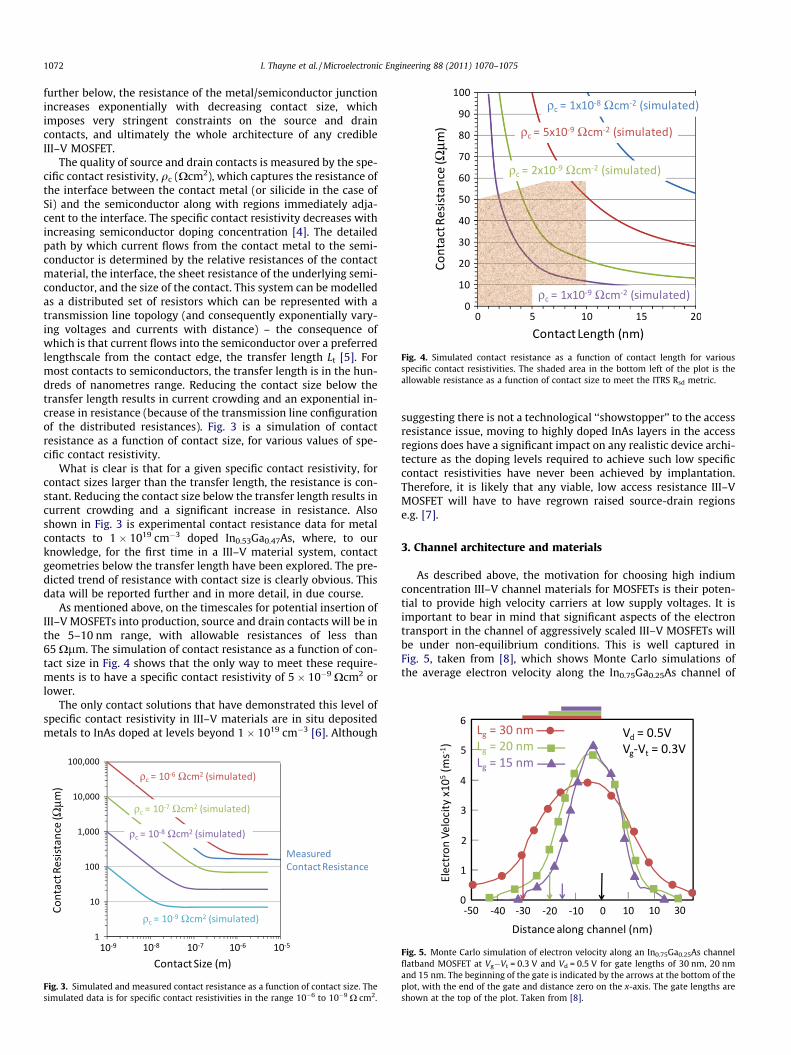
Fig. 4. Simulated contact resistance as a function of contact length for variousspecific contact resistivities. The shaded area in the bottom left of the plot is theallowable resistance as a function of contact size to meet the ITRS Rsd metric.
1072 I. Thayne et al. / Microelectronic Engineering 88 (2011) 1070–1075
further below, the resistance of the metal/semiconductor junctionincreases exponentially with decreasing contact size, whichimposes very stringent constraints on the source and draincontacts, and ultimately the whole architecture of any credibleIII–V MOSFET.
The quality of source and drain contacts is measured by the spe-cific contact resistivity, qc (Xcm2), which captures the resistance ofthe interface between the contact metal (or silicide in the case ofSi) and the semiconductor along with regions immediately adja-cent to the interface. The specific contact resistivity decreases withincreasing semiconductor doping concentration [4]. The detailedpath by which current flows from the contact metal to the semi-conductor is determined by the relative resistances of the contactmaterial, the interface, the sheet resistance of the underlying semi-conductor, and the size of the contact. This system can be modelledas a distributed set of resistors which can be represented with atransmission line topology (and consequently exponentially vary-ing voltages and currents with distance) – the consequence ofwhich is that current flows into the semiconductor over a preferredlengthscale from the contact edge, the transfer length Lt [5]. Formost contacts to semiconductors, the transfer length is in the hun-dreds of nanometres range. Reducing the contact size below thetransfer length results in current crowding and an exponential in-crease in resistance (because of the transmission line configurationof the distributed resistances). Fig. 3 is a simulation of contactresistance as a function of contact size, for various values of spe-cific contact resistivity.
What is clear is that for a given specific contact resistivity, forcontact sizes larger than the transfer length, the resistance is con-stant. Reducing the contact size below the transfer length results incurrent crowding and a significant increase in resistance. Alsoshown in Fig. 3 is experimental contact resistance data for metalcontacts to 1 � 1019 cm�3 doped In0.53Ga0.47As, where, to ourknowledge, for the first time in a III–V material system, contactgeometries below the transfer length have been explored. The pre-dicted trend of resistance with contact size is clearly obvious. Thisdata will be reported further and in more detail, in due course.
As mentioned above, on the timescales for potential insertion ofIII–V MOSFETs into production, source and drain contacts will be inthe 5–10 nm range, with allowable resistances of less than65 Xlm. The simulation of contact resistance as a function of con-tact size in Fig. 4 shows that the only way to meet these require-ments is to have a specific contact resistivity of 5 � 10�9 Xcm2 orlower.
The only contact solutions that have demonstrated this level ofspecific contact resistivity in III–V materials are in situ depositedmetals to InAs doped at levels beyond 1 � 1019 cm�3 [6]. Although
Fig. 3. Simulated and measured contact resistance as a function of contact size. Thesimulated data is for specific contact resistivities in the range 10�6 to 10�9 X cm2.
suggesting there is not a technological ‘‘showstopper’’ to the accessresistance issue, moving to highly doped InAs layers in the accessregions does have a significant impact on any realistic device archi-tecture as the doping levels required to achieve such low specificcontact resistivities have never been achieved by implantation.Therefore, it is likely that any viable, low access resistance III–VMOSFET will have to have regrown raised source-drain regionse.g. [7].
3. Channel architecture and materials
As described above, the motivation for choosing high indiumconcentration III–V channel materials for MOSFETs is their poten-tial to provide high velocity carriers at low supply voltages. It isimportant to bear in mind that significant aspects of the electrontransport in the channel of aggressively scaled III–V MOSFETs willbe under non-equilibrium conditions. This is well captured inFig. 5, taken from [8], which shows Monte Carlo simulations ofthe average electron velocity along the In0.75Ga0.25As channel of
Fig. 5. Monte Carlo simulation of electron velocity along an In0.75Ga0.25As channelflatband MOSFET at Vg�Vt = 0.3 V and Vd = 0.5 V for gate lengths of 30 nm, 20 nmand 15 nm. The beginning of the gate is indicated by the arrows at the bottom of theplot, with the end of the gate and distance zero on the x-axis. The gate lengths areshown at the top of the plot. Taken from [8].
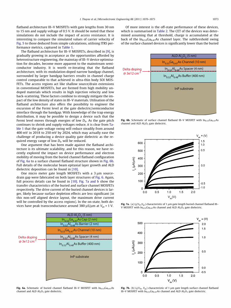
Fig. 6b. Schematic of surface channel flatband III–V MOSFET with In0.53Ga0.47Aschannel and ALD Al2O3 gate dielectric.
Fig. 7a. (a) Id(Vds,Vgs) characteristic of 1 lm gate length buried channel flatband III–V MOSFET with In0.53Ga0.47As channel and ALD Al2O3 gate dielectric.
I. Thayne et al. / Microelectronic Engineering 88 (2011) 1070–1075 1073
flatband architecture III–V MOSFETs with gate lengths from 30 nmto 15 nm and supply voltage of 0.5 V. It should be noted that thesesimulations do not include the impact of access resistance. It isinteresting to compare the simulated values of carrier velocity ofFig. 5 to those deduced from simple calculations, utilising ITRS per-formance metrics, captured in Table 1.
The flatband architecture for III–V MOSFETs, described in [9], isgradually growing in acceptance as the opportunities afforded byheterostructure engineering, the mainstay of III–V device optimisa-tion for decades, become more apparent to the mainstream semi-conductor industry. It is worth re-iterating that the flatbandarchitecture, with its modulation-doped narrow bandgap channel,surrounded by larger bandgap barriers results in channel chargecontrol comparable to that achieved in ultra-thin body SOI MOS-FETs. The access regions act like shallow source/drain extensionsin conventional MOSFETs, but are formed from high mobility un-doped materials which results in high injection velocity and lowback-scattering. These factors combine to strongly mitigate the im-pact of the low density of states in III–V materials. Utilisation of theflatband architecture also offers the possibility to engineer theexcursion of the Fermi level at the gate dielectric/semiconductorinterface through the bandgap. With knowledge of the trap energydistribution, it may be possible to design a device such that theFermi level moves through energies of low Dit. As the gate pitchcontinues to shrink and supply voltages reduce, it is clear from Ta-ble 1 that the gate voltage swing will reduce steadily from around400 mV in 2018 to 250 mV by 2024, which may actually ease thechallenge of producing a device quality gate dielectric as the re-quired energy range of low Dit will be reduced.
One argument that has been made against the flatband archi-tecture is its ultimate scalability, and for this reason, we have re-cently explored the impact on device performance and electronmobility of moving from the buried channel flatband configurationof Fig. 6a to a surface channel flatband structure shown in Fig. 6b.Full details of the molecular beam epitaxial layer growth and ALDdielectric deposition can be found in [10].
One micro meter gate length MOSFETs with a 3 lm source-drain gap were fabricated on both layer structures of Fig. 6. Again,full process details can be found in [10]. Fig. 7a and b show thetransfer characteristics of the buried and surface channel MOSFETsrespectively. The drive current of the buried channel devices is lar-ger, likely because surface depletion effects are less significant (inthis non-self aligned device layout, the maximum drive currentwill be controlled by the access regions). In the on-state, both de-vices have peak transconductance around 380 lS/lm at Vgs = 1 V.
Fig. 6a. Schematic of buried channel flatband III–V MOSFET with In0.53Ga0.47Aschannel and ALD Al2O3 gate dielectric.
Of more interest is the off-state performance of these devices,which is summarised in Table 2. The CET of the devices was deter-mined assuming that at threshold, charge is accumulated at theback of the In0.53Ga0.47As channel layer. The subthreshold swingof the surface channel devices is significantly lower than the buried
Fig. 7b. (b) Id(Vds, Vgs) characteristic of 1 lm gate length surface channel flatbandIII–V MOSFET with In0.53Ga0.47As channel and ALD Al2O3 gate dielectric.
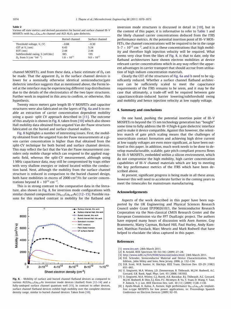
Table 2Various off state metrics and derived parameters for buried and surface channel III–VMOSFETs with In0.53Ga0.47As channel and ALD Al2O3 gate dielectric.
Buried channel Surface channel
Threshold voltage, Vt (V) �0.88 �0.30CET at Vt (nm) 6.43 5.24EOT (nm) 2.44 2.44Subthreshold swing, S (mV/dec) 385 195Dit from S (cm�2eV�1) 1.8 � 1013 9.0 � 1012
1074 I. Thayne et al. / Microelectronic Engineering 88 (2011) 1070–1075
channel MOSFETs, and from these data, a basic estimate of Dit canbe made. That the apparent Dit in the surface channel devices islower for a nominally otherwise identical semiconductor/gatedielectric interface suggests that as mentioned above, the Fermi le-vel at the interface may be experiencing different trap distributionsdue to the details of the electrostatics of the two layer structures.Further work in required in this area to confirm, or otherwise, thishypothesis.
Twenty micro meters gate length III–V MOSFETs and capacitorstructures were also fabricated on the layers of Fig. 6a and b to en-able an extraction of carrier concentration dependent mobilityusing a quasi- split CV approach described in [11]. The outcomeof this analysis is shown in Fig. 8, taken from [10] which also showsHall mobility data obtained from ungated Van der Pauw structuresfabricated on the buried and surface channel wafers.
Fig. 8 highlights a number of interesting issues. First, the mobil-ity obtained from the ungated Van der Pauw measurements at a gi-ven carrier concentration is higher than that obtained from thesplit-CV technique for both buried and surface channel devices.This may reflect the fact that the Van der Pauw measurement con-siders only mobile charge which can respond to the applied mag-netic field, whereas the split-CV measurement, although using1 MHz capacitance data, may still be compromised by traps eitherwith very shallow energies or indeed located within the conduc-tion band. Next, although the mobility from the surface channelstructure is reduced in comparison to the buried channel design,both have mobilities in excess of 2000 cm2/Vs for carrier concen-trations beyond 8 � 1012 cm�2.
This is in strong contrast to the comparative data in the litera-ture, also shown in Fig. 8, for inversion mode configurations withsimilar channel compositions (In0.53Ga0.47As) [12–15]. Possible rea-sons for this marked contrast in mobility for the flatband and
Fig. 8. - Mobility of surface and buried channel flatband devices as compared tovarious ALD/In0.53Ga0.47As inversion mode devices (dashed) from [12–14] and afully-undoped surface channel quantum well [15]. In contrast to other devices,surface channel flatband devices exhibit high mobility over the complete electrondensity range, similar to buried channel devices. Taken from [10].
inversion mode structures is discussed in detail in [10], but inthe context of this paper, it is informative to refer to Table 1 andthe likely channel carrier concentrations deduced from the ITRSperformance metrics. At the potential insertion point of III–V MOS-FETs, the channel concentrations will be required to be in the range5–7 � 1012 cm�2, and it is at these concentrations that high mobil-ity and therefore high injection velocity will be required. Whatseems very clear from the likes of Fig. 8, is that to date, only theflatband architectures have shown electron mobilities at devicerelevant carrier concentrations which in any way reflect the appar-ent advantages in carrier transport that should accrue from utilisa-tion of high indium concentration materials.
Clearly the CET of the structures of Fig. 6a and b need to be sig-nificantly reduced. Whether a surface channel flatband architec-ture can be sufficiently scaled to meet the capacitancerequirements of the ITRS remains to be seem, and it may be thecase that ultimately, a trade-off will be required between gatecapacitance/drain-induced barrier lowering/subthreshold swingand mobility and hence injection velocity at low supply voltage.
4. Summary and conclusions
On one hand, pushing the potential insertion point of III–VMOSFETs to beyond the 15 nm technology generation has ‘‘bought’’some time to fully address the III–V/high-k gate dielectric interfaceand to make it device compatible. Against this however, the relent-less march of gate pitch scaling means that the challenges ofsource/drain contact formation and achieving high drive currentat low supply voltages are even more significant, as have been out-lined in this paper. In addition, much work needs to be done to de-velop manufacturable, scalable, gate pitch compliant process flowsfor III–V MOSFETs, embedded within a silicon environment, whichdo not compromise the high mobility, high carrier concentrationcapabilities of III–V channel materials which are key to meetingthe key performance metrics of the ITRS which have been de-scribed above.
At present, significant progress is being made in all these areas,however this will need to accelerate further in the coming years tomeet the timescales for mainstream manufacturing.
Acknowledgements
Aspects of the work described in this paper have been sup-ported by the UK Engineering and Physical Sciences ResearchCouncil under Grant EP/F002610/1, the Semiconductor ResearchCorporation via the Non-classical CMOS Research Center and theEuropean Commission via the FP7 DualLogic project. The authorshave enjoyed many hours of discussion with Asen Asenov, GuyBrammertz, Matty Caymax, Richard Hill, Paul Hurley, Andy Kum-mel, Matthias Passlack, Marc Meuris and Mark Rodwell that havehelped to elucidate the ideas captured in this paper.
References
[1] www.itrs.net; 24th March 2011.[2] B. Arnold, IEEE Spectrum 50–54 (56) (2009) 27–28.[3] http://www.ioffe.ru/SVA/NSM/Semicond/index.html; 24th March 2011.[4] D.K. Schroder, Semiconductor Material and Device Characterization, Third
Edition., John Wiley and Sons, New Jersey, 2006. p. 132–134.[5] D.B. Scott, W.R. hunter, H. Shichijo, IEEE Trans. Electron Dev. ED-29 (1982)
651–661.[6] U. Singisetti, M.A. Wistey, J.D. Zimmerman, B. Thibeault, M.J.W. Rodwell, A.C.
Gossard, S.R. Bank, Appl. Phys. Lett. 93 (2008) 183502.[7] U. Singisetti, M.A. Wistey, G.J. Burek, A.K. Baraskar, B.J. Thibeault, A.C. Gossard,
M.J.W. Rodwell, B. Shin, E.J. Kim, P.C. Mcintyre, B. Yu, Y. Yuan, D. Wang, Y. Taur,P. Asbeck, Y.-J. Lee, IEEE Electron Dev. Lett. 30 (11) (2009) 1128–1130.
[8] J. Ayubi-Moak, K. Kalna, A. Asenov, high performance In0.75Ga0.25As implant-free n-type MOSFETs for low power applications, in: Proceedings SpanishConference on Electron Devices (2009) 92–95.

I. Thayne et al. / Microelectronic Engineering 88 (2011) 1070–1075 1075
[9] M. Passlack, K. Rajagopalan, J. Abrokwah, R. Droopad, IEEE Trans. Electron Dev.52 (10) (2006) 2454–2459.
[10] S.J. Bentley, M. Holland, X. Li, G.W. Paterson, H. Zhou, O. Ignatova, D.Macintyre, S. Thoms, A. Asenov, B. Shin, J. Ahn, P.C. McIntyre, I.G. Thayne,IEEE Electron Dev. Lett. 32 (4) (2011) 494–496.
[11] R.J.W. Hill, D.A. J Moran, X. Li, H. Zhou, D. Macintyre, S. Thoms, A. Asenov, P.Zurcher, K. Rajagopalan, J. Abrokwah, R. Droopad, M. Passlack, I. G Thayne, IEEEElectron Device Lett. 28 (12) (2007) 1080–1082.
[12] J. Huang, N. Goel, H. Zhao, C.Y. Kang, K.S. Min, G. Bersuker, S. Oktyabrsky, C.K.Gaspe, M.B. Santos, P. Majhi, P.D. Kirsch, H.-H. Tseng, J.C. Lee, R. Jammy, IEDMTech. Dig. (2009) 335–338.
[13] D. Lin, N. Waldron, G. Brammertz, K. Martens, W.-E. Wang, S. Sioncke, A.Delabie, H. Bender, T. Conard, W.H. Tseng, J.C. Lin, K. Temst, A. Vantomme, J.Mitard, M. Caymax, M. Meuris, M. Heyns, T. Hoffmann, ECS Transactions 28 (5)(2010) 173–183.
[14] A. Ali, H. Madan, S. Koveshnikov, S. Datta, IEEE Trans. Electron Devices 57(2010) 742–748.
[15] H. Zhao, Y.-T. Chen, J. Hwan Yum, Y. Wang, N. Goel, J.C. Lee, Appl. Phys. Lett. 94(19) (2009) 193502.