IC Technology at New Nodes Made Easy
99
IC Technology at New Nodes Made Easy Alvin Loke 05-Dec-2013 AUTHORIZATION All copyrights to the material contained in this document are retained by me and my employer. IEEE Solid-State Circuits Society – Central Texas Chapter
-
Upload
khangminh22 -
Category
Documents
-
view
3 -
download
0
Transcript of IC Technology at New Nodes Made Easy
IC Technology at New Nodes Made Easy
Alvin Loke05-Dec-2013
AUTHORIZATIONAll copyrights to the material contained in this document are retained by me and my employer.
IEEE Solid-State Circuits Society – Central Texas Chapter

© Loke, IC Technology at New Nodes Made Easy
Dave Pulfrey
Bruce Wooley
Krishna Saraswat
Simon Wong
Tom Lee
Jim PlummerYing-Keung Leung
Tom Cynkar
Gary Ray
Jeff Wetzel
Chintamani Palsule
Martin Wedepohl
Bob Barnes Dick Dowell
Bich-Yen Nguyen
Wei-Yung Hsu
Qi-Zhong Hong
Tom Lii
Ron KennedyMark Horowitz
John Bravman
Paul Townsend
Joe McPherson
Rick Hernandez
Phil Fisher
Greg Kovacs Steve Kuehne
Charles Moore Michael Oshima Jim Pfiester
Mike Gilsdorf
Tin Tin Wee
Matt Angyal
Bruce Doyle Emerson Fang
Andy Wei
Jung-Suk Goo
Ray Stephany
My Teachers
Shawn Searles
John Faricelli Dennis Fischette
Tom TiedjeGerry TalbotChangsup Ryu
Justin LeungTakamaro Kikkawa
Larry Bair
Ram Venkatraman
Carl-Mikael ZetterlingPatrick Yue
Bob Havemann
Slide 1
Shawming Ma Michael Nix
Joanne Wu
Don Morris
Tom Bryan
Tim Hollis Reza Jalilizeinali
Behzad Razavi Jeff Rearick
© Loke, IC Technology at New Nodes Made Easy
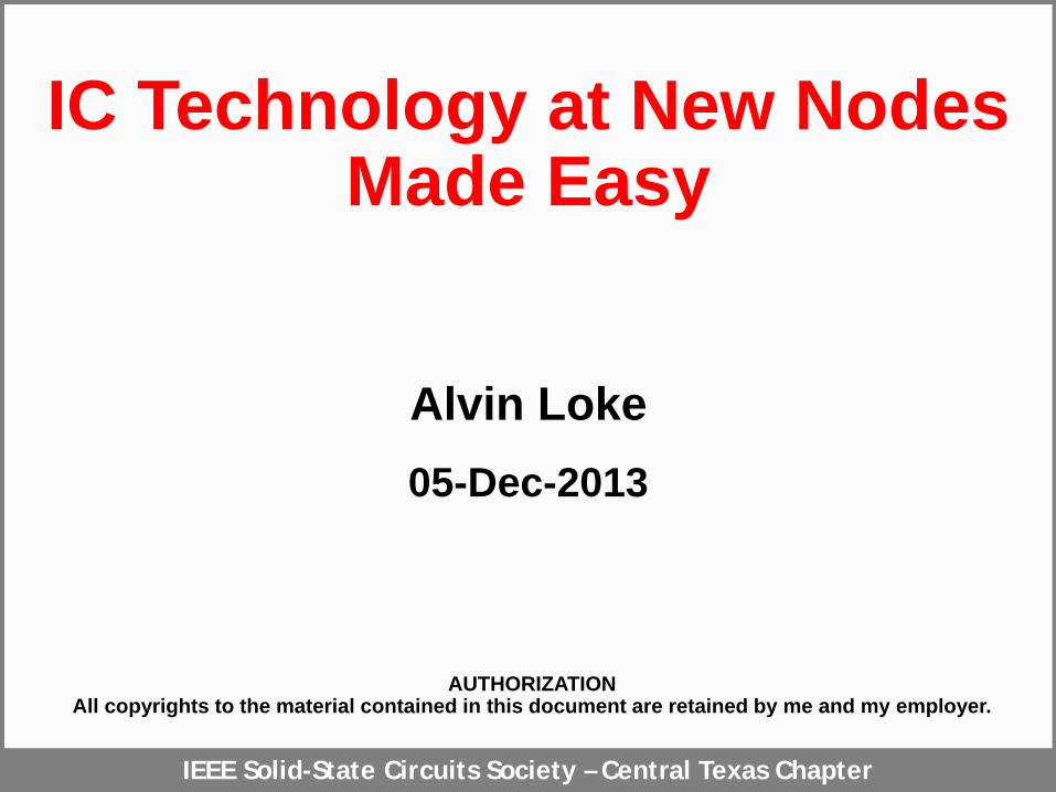
The 10000-Foot View… A Switch
Slide 2
small, fast, thrifty
Scaling Performance Energy-Efficient

© Loke, IC Technology at New Nodes Made Easy
CMOS Scaling Still Alive
Slide 3
Keating, Synopsys [1]
Intel 22nmtri-gate finFETin production
• Leading foundries frantically after manufacturable tri-gate• Intel already demonstrated 14nm Broadwell

© Loke, IC Technology at New Nodes Made Easy
Our Objective• Understand how MOSFET structure has evolved• Understand why it has evolved this way
Slide 4
L=35nm
SiGe
L=35nmL=35nm
SiGe
L=35nm
SiGe
L=35nmL=35nm
SiGe

© Loke, IC Technology at New Nodes Made Easy
Words of WisdomPeople get lostbecause they cannot be found.
Theodorus Loke
Slide 5

© Loke, IC Technology at New Nodes Made Easy
OutlinePart 1
• Motivation• MOSFET & Short-Channel Fundamentals• 130nm Fabrication• More MOSFET Fundamentals• Lithography• Partially-Depleted SOI
Part 2• Strain Engineering (90nm & Beyond)• High-K / Metal-Gate (45nm & Beyond)• Migrating to Fully-Depleted (22nm & Beyond)• Tri-Gate FinFETs• Conclusions
Slide 6
© Loke, IC Technology at New Nodes Made Easy
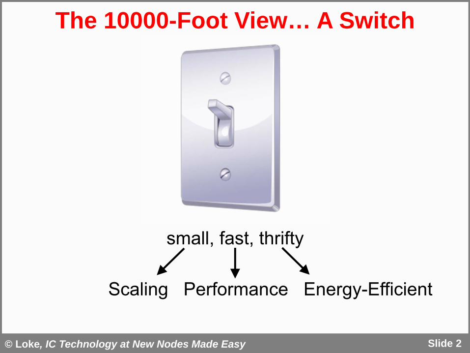
The Basis of All CMOS Digital ICs
Slide 7
• Charging and discharging a capacitor… very quickly!• Shorter delay and lower power
pull-down logic
pull-up logic
inputseff
DDload
eff
loaddelay I
VCI
Qt
fVCP DDloaddynamic2

© Loke, IC Technology at New Nodes Made Easy
Effective Inverter Drive Current
Slide 8
0.0
0.5
1.0
1.5
0.0 0.2 0.4 0.6 0.8 1.0
I D (m
A)
VDS
(V)
VGS
0.5V
0.7V
1.0V
0.2V
IDsat
IDoff
IDlow
IDhigh
IDeff
• IDeff estimates effective inverter current drawn during switching
• More realistic and way less optimistic than IDsat
Na et al., IBM [2]
IDlin
2,
,2
2
DDDSDDGS
DDDSDD
GS
VVVVIDIDhigh
VVVVIDIDlow
IDhighIDlowIDeff
28nm, VDD=1.0V

© Loke, IC Technology at New Nodes Made Easy
Flatband Condition (VGS=VFB)
Slide 9
p-typebody
poly gate
n+
sourcen+
drain
siliconsurface
source-to-bodydepletion
drain-to-bodydepletion
p+ bodycontact
VDS
VGS
VBS
EC
EV
Ei
qbqs
EF
EF
siliconsurface
M O S
qs = qb
Energy Band
Diagram

© Loke, IC Technology at New Nodes Made Easy
Onset of Surface Inversion (s=0)
Slide 10
p-typebody
poly gate
n+
sourcen+
drainp+ bodycontact
VDS
VGS
VBS
surfaceundoped
M O S
Energy Band
Diagram
qs
qs = 0
qb
– – –
+ ++
–
+
+ charge terminating on – charge
© Loke, IC Technology at New Nodes Made Easy
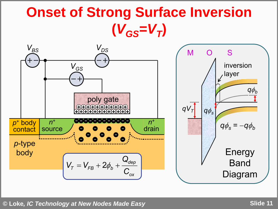
Onset of Strong Surface Inversion (VGS=VT)
Slide 11
p-typebody
poly gate
n+
sourcen+
drainp+ bodycontact
VDS
VGS
VBS M O S
Energy Band
Diagram
– – –
+
– – –
– – – – – – – – – – – –
+ + ++ + + ++ + + ++ + + ++ + + ++ + +
–
–– – –
ox
depbFBT C
QVV 2
ss
qb
qsqVT
qs = qb
inversionlayer
© Loke, IC Technology at New Nodes Made Easy
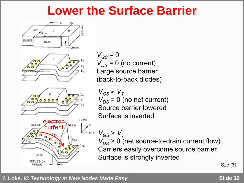
Lower the Surface Barrier
Slide 12
VGS > VTVDS > 0 (net source-to-drain current flow)Carriers easily overcome source barrierSurface is strongly inverted
VGS VTVDS = 0 (no net current)Source barrier loweredSurface is inverted
VGS = 0VDS = 0 (no current)Large source barrier(back-to-back diodes)
electroncurrent
Sze [3]

© Loke, IC Technology at New Nodes Made Easy
Quantifying Charge to Move s by 2b
Slide 13
• Assume uniformly doped p-type body
• How much body must be depleted to reach strong inversion?
––
––
––
––
––
––
qN
xdgate
++++++
++++ body
NqNx bSi
d122
ddep qNxQ
x
V
0 xd
2b
Si
db
qNx
2
22
dxEV
xE0
xd
Si
dqNx
Si
QdAE

© Loke, IC Technology at New Nodes Made Easy
Short-Channel Effects (SCEs)
VDD not scaling as aggressively as L Higher channel electric fields
– Velocity saturation– Mobility degradation
Slide 14
gate
n+
sourcen+
drain
source-to-bodydepletion
drain-to-bodydepletion
L
L
VT
VDS
VT
DIBL
© Loke, IC Technology at New Nodes Made Easy
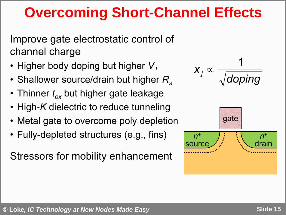
Overcoming Short-Channel Effects
Improve gate electrostatic control of channel charge• Higher body doping but higher VT
• Shallower source/drain but higher Rs
• Thinner tox but higher gate leakage• High-K dielectric to reduce tunneling• Metal gate to overcome poly depletion• Fully-depleted structures (e.g., fins)
Stressors for mobility enhancement
Slide 15
gate
n+
sourcen+
drain
dopingx j
1
© Loke, IC Technology at New Nodes Made Easy
OutlinePart 1
• Motivation• MOSFET & Short-Channel Fundamentals• 130nm Fabrication• More MOSFET Fundamentals• Lithography• Partially-Depleted SOI
Part 2• Strain Engineering (90nm & Beyond)• High-K / Metal-Gate (45nm & Beyond)• Migrating to Fully-Depleted (22nm & Beyond)• Tri-Gate FinFETs• Conclusions
Slide 16

© Loke, IC Technology at New Nodes Made Easy
130nm MOSFET Fabrication
Slide 17
Well Implantation
2 n-well p-well
Gate Oxidation &Poly Definition
3
gate oxide
Source/Drain Extension& Halo Implantation
4halos
Spacer Formation &Source/Drain Implantation
5
Salicidation
6
silicide
PMOS NMOS
Shallow Trench Isolation
1 STIoxidep-Si substrate
© Loke, IC Technology at New Nodes Made Easy
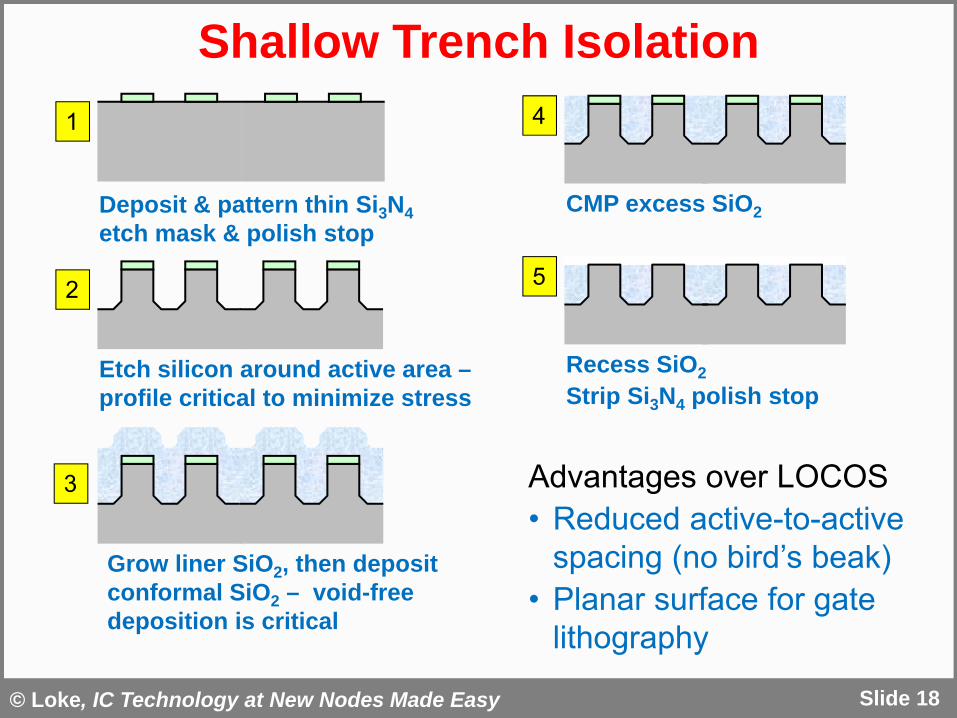
Shallow Trench Isolation
Slide 18
1
2
3
4
5
Advantages over LOCOS• Reduced active-to-active
spacing (no bird’s beak)• Planar surface for gate
lithography
Deposit & pattern thin Si3N4etch mask & polish stop
Etch silicon around active area –profile critical to minimize stress
Grow liner SiO2, then deposit conformal SiO2 – void-free deposition is critical
CMP excess SiO2
Recess SiO2Strip Si3N4 polish stop

© Loke, IC Technology at New Nodes Made Easy
p-wellSTIoxide
STIoxide
Well Implant EngineeringRetrograded well dopant profile(implants before poly deposition)
Shallow/steep surface channel implant • VT control• Slow diffusers critical (In, Sb)
Very deep high-dose implant• Latchup prevention• Noise immunity• Faster diffusers (B, As/P)
Sequence implant to reduce ion channeling, especially for shallow implant
Depth
SubstrateDoping
substratebackground
Deeper subsurface implant• Extra dopants to prevent subsurface
punchthrough under halos• Prevent parasitic channel inversion on
STI sidewall beneath source/drain• Faster diffusers (B, As/P)
Slide 19
© Loke, IC Technology at New Nodes Made Easy
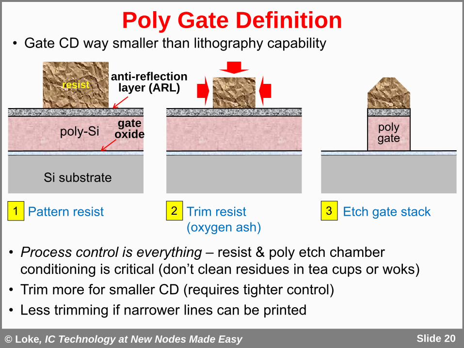
Poly Gate Definition
Si substrate
• Process control is everything – resist & poly etch chamber conditioning is critical (don’t clean residues in tea cups or woks)
• Trim more for smaller CD (requires tighter control)• Less trimming if narrower lines can be printed
poly-Si
1 2 3
anti-reflection layer (ARL)
gateoxide
resist
Pattern resist Trim resist (oxygen ash)
Etch gate stack
polygate
• Gate CD way smaller than lithography capability
Slide 20
© Loke, IC Technology at New Nodes Made Easy
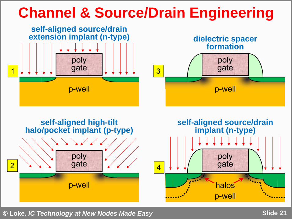
Channel & Source/Drain Engineering
Slide 21
polygate
self-aligned source/drain extension implant (n-type)
p-well
1
dielectric spacerformation
p-well
polygate3
self-aligned source/drain implant (n-type)
4
p-well
polygate
halos
self-aligned high-tilt halo/pocket implant (p-type)
p-well
polygate2
© Loke, IC Technology at New Nodes Made Easy
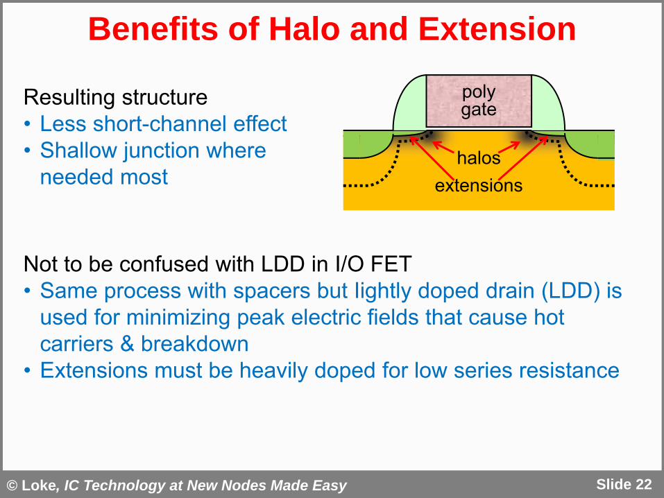
Benefits of Halo and Extension
Slide 22
Resulting structure• Less short-channel effect• Shallow junction where
needed most
polygate
halos
Not to be confused with LDD in I/O FET• Same process with spacers but Iightly doped drain (LDD) is
used for minimizing peak electric fields that cause hot carriers & breakdown
• Extensions must be heavily doped for low series resistance
extensions
© Loke, IC Technology at New Nodes Made Easy
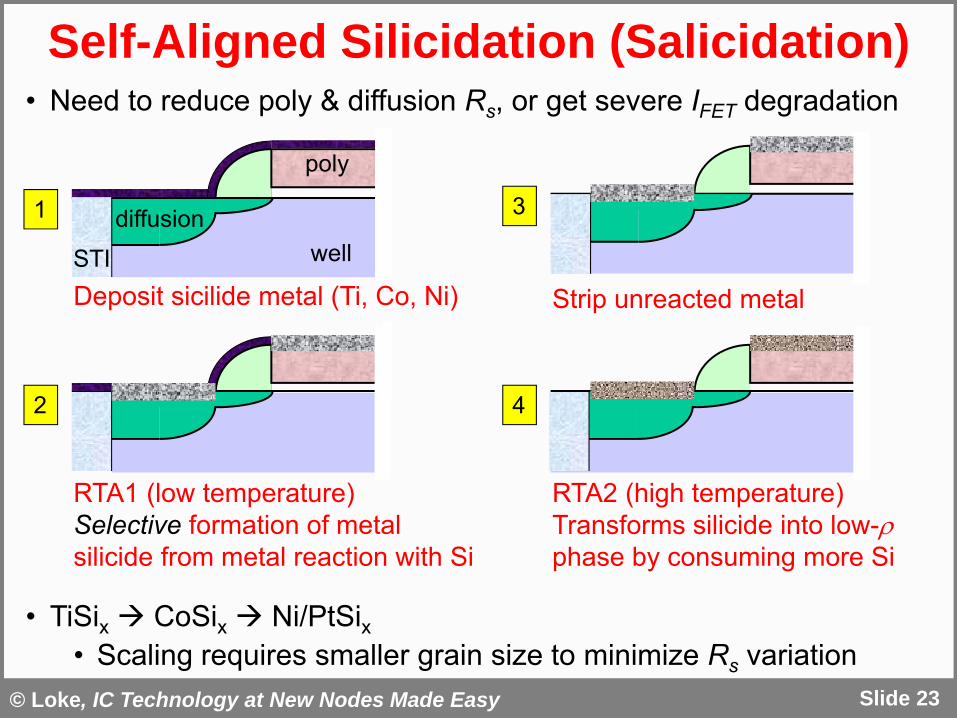
Self-Aligned Silicidation (Salicidation)
Slide 23
• Need to reduce poly & diffusion Rs, or get severe IFET degradation
1
Deposit sicilide metal (Ti, Co, Ni)
RTA1 (low temperature)Selective formation of metal silicide from metal reaction with Si
welldiffusion
2
Strip unreacted metal
3
RTA2 (high temperature)Transforms silicide into low-phase by consuming more Si
4
poly
STI
• TiSix CoSix Ni/PtSix• Scaling requires smaller grain size to minimize Rs variation

© Loke, IC Technology at New Nodes Made Easy
OutlinePart 1
• Motivation• MOSFET & Short-Channel Fundamentals• 130nm Fabrication• More MOSFET Fundamentals• Lithography• Partially-Depleted SOI
Part 2• Strain Engineering (90nm & Beyond)• High-K / Metal-Gate (45nm & Beyond)• Migrating to Fully-Depleted (22nm & Beyond)• Tri-Gate FinFETs• Conclusions
Slide 24

© Loke, IC Technology at New Nodes Made Easy
Not So Fundamental After All
• Body doping has increased by 2–3 orders of magnitude over the decades
• Surface way more conductive at strong inversion condition using “fundamental” VT definition
• What matters is how much OFF leakage you get for a given ON current
• IDoff vs. IDsat (or IDeff) universal plots have become more useful to summarize device performance
Slide 25
M O S
Energy Band
Diagram
fsfs
qb
qfsqVT
qs = qb
inversionlayer
ox
depbFBT C
QVV 2
© Loke, IC Technology at New Nodes Made Easy
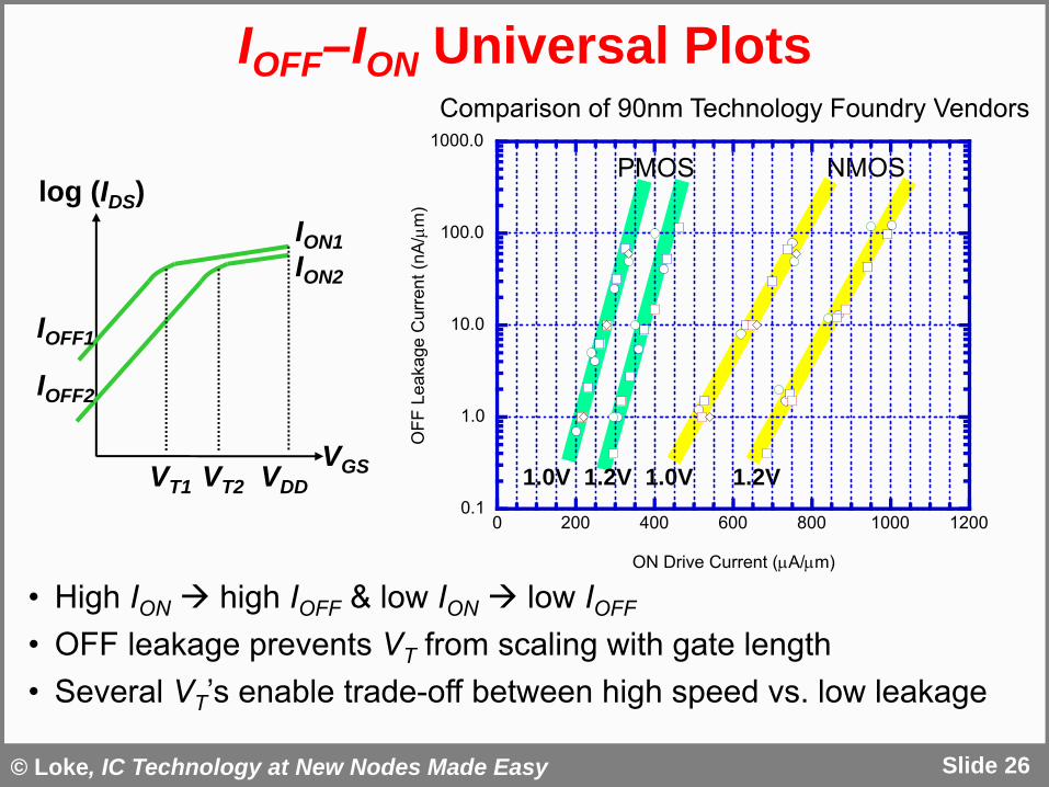
IOFF–ION Universal Plots
Slide 26
Comparison of 90nm Technology Foundry Vendors
1.2V1.0V1.2V1.0V
NMOSPMOS
0.1
1.0
10.0
100.0
1000.0
0 200 400 600 800 1000 1200
OFF
Lea
kage
Cur
rent
(nA
/m
)
ON Drive Current (A/m)
• High ION high IOFF & low ION low IOFF
• OFF leakage prevents VT from scaling with gate length• Several VT’s enable trade-off between high speed vs. low leakage
log (IDS)
VGSVT1 VT2
IOFF1
IOFF2
VDD
ION1ION2

© Loke, IC Technology at New Nodes Made Easy
Subthreshold Leakage
Slide 27
• MOSFET is not perfectly OFF below VT
• VG s lower source-to-channel barrier• Gradually more carriers diffuse from source to drain• Capacitive divider between gate and undepleted body
Cox
CSibody
gate
VG
VB
source
drainVG
Siox
oxGs CC
CV
source drain
s
© Loke, IC Technology at New Nodes Made Easy
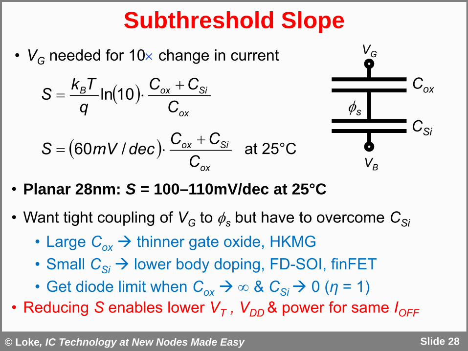
Subthreshold Slope
Slide 28
• Planar 28nm: S = 100–110mV/dec at 25°C
• Want tight coupling of VG to s but have to overcome CSi
• Large Cox thinner gate oxide, HKMG• Small CSi lower body doping, FD-SOI, finFET• Get diode limit when Cox & CSi 0 (η = 1)
• Reducing S enables lower VT , VDD & power for same IOFF
ox
SioxB
CCC
qTkS
10ln
VB
VG
s
ox
Siox
CCCdecmVS
/60 at 25°C
• VG needed for 10 change in current
CSi
Cox
© Loke, IC Technology at New Nodes Made Easy
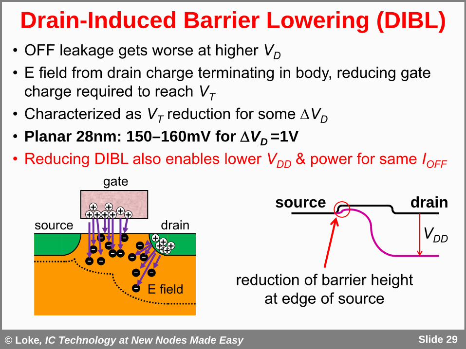
Drain-Induced Barrier Lowering (DIBL)
Slide 29
• OFF leakage gets worse at higher VD
• E field from drain charge terminating in body, reducing gate charge required to reach VT
• Characterized as VT reduction for some VD
• Planar 28nm: 150–160mV for VD =1V• Reducing DIBL also enables lower VDD & power for same IOFF
reduction of barrier heightat edge of source
VDD
source draingate
source drain
–
+++++
–––
–
–
+
+++++++ +
––
––
–––
–
E field

© Loke, IC Technology at New Nodes Made Easy
3-Way Competition for Body Charge
Slide 30
What’s happening to surface potential?
p-well
gate
VB
source
drain
VD
drain
VG
VD
source
drainVG
source
drain|VB|
DIBL
bodyeffect
gate control(what we want)
© Loke, IC Technology at New Nodes Made Easy
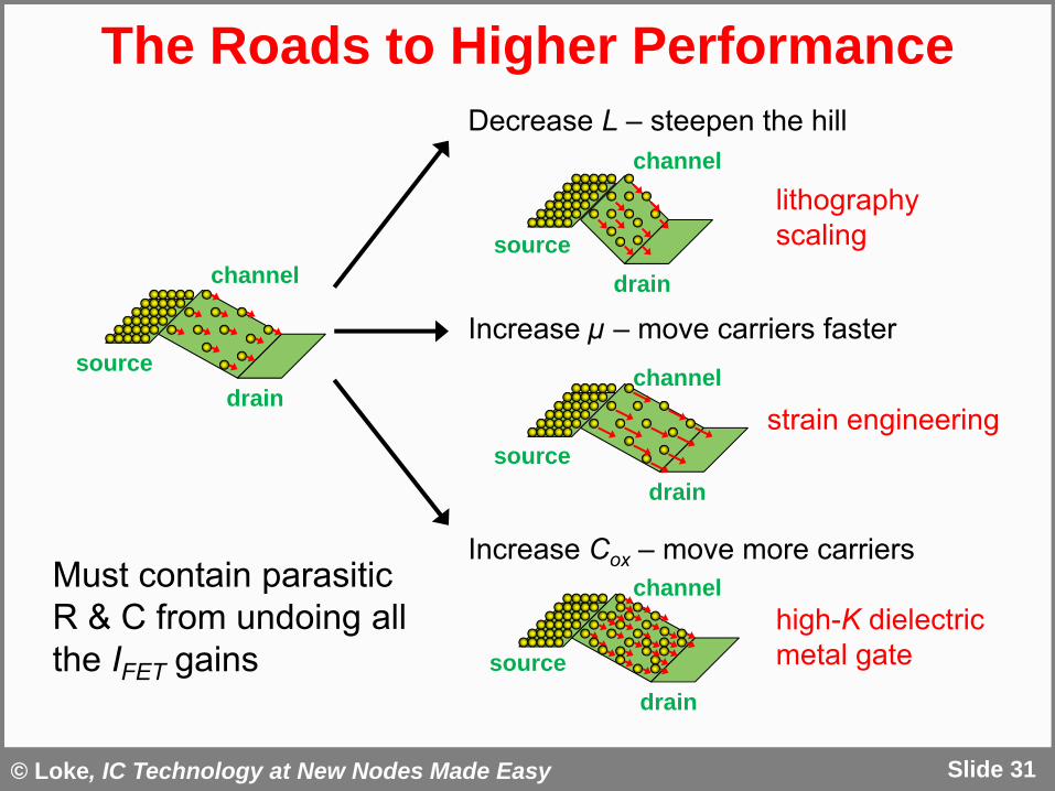
The Roads to Higher Performance
Slide 31
sourcedrain
channel
Decrease L – steepen the hill
sourcedrain
channellithographyscaling
Increase µ – move carriers faster
sourcedrain
channel
strain engineering
sourcedrain
channelIncrease Cox – move more carriers
high-K dielectricmetal gate
Must contain parasitic R & C from undoing all the IFET gains

© Loke, IC Technology at New Nodes Made Easy
OutlinePart 1
• Motivation• MOSFET & Short-Channel Fundamentals• 130nm Fabrication• More MOSFET Fundamentals• Lithography• Partially-Depleted SOI
Part 2• Strain Engineering (90nm & Beyond)• High-K / Metal-Gate (45nm & Beyond)• Migrating to Fully-Depleted (22nm & Beyond)• Tri-Gate FinFETs• Conclusions
Slide 32

© Loke, IC Technology at New Nodes Made Easy
The Roads to Higher Performance
Slide 33
sourcedrain
channel
Decrease L – steepen the hill
sourcedrain
channellithographyscaling
Increase µ – move carriers faster
sourcedrain
channel
strain engineering
sourcedrain
channelIncrease Cox – move more carriers
high-K dielectricmetal gate

© Loke, IC Technology at New Nodes Made Easy
Let There Be Light
Slide 34
Resolution = k1
NA
• Tooling has traditionally driven resolution scaling• Shorter : 436nm 365nm 248nm 193nm• Higher NA lenses capping at 1.35
/ N
A (n
m) • Both and NA have hit
a wall• No new litho tool for
22/20nm nodes (EUV not primetime yet)
• Single patterning limited to ~80nm pitch
Wei, GlobalFoundries [4]
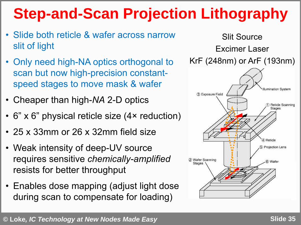
© Loke, IC Technology at New Nodes Made Easy Slide 35
Step-and-Scan Projection Lithography• Slide both reticle & wafer across narrow
slit of light
• Only need high-NA optics orthogonal to scan but now high-precision constant-speed stages to move mask & wafer
• Cheaper than high-NA 2-D optics
• 6” x 6” physical reticle size (4× reduction)
• 25 x 33mm or 26 x 32mm field size
• Weak intensity of deep-UV source requires sensitive chemically-amplifiedresists for better throughput
• Enables dose mapping (adjust light dose during scan to compensate for loading)
Slit SourceExcimer Laser
KrF (248nm) or ArF (193nm)

© Loke, IC Technology at New Nodes Made Easy
Immersion Lithography
Slide 36
NA = n sin = d / 2 f
Resolution =k1
NA
lenswater
12-inch wafer
light
• Remember oil immersion microscopy in biology class?• Extend resolution of refractive optics by squirting water
puddle on wafer surface prior to exposure• nwater ~1.45 vs. nair ~ 1• Tedious but EUV is not primetime yet

© Loke, IC Technology at New Nodes Made Easy
Lithography Misalignment / Overlay
Slide 37
• Mask misalignment tolerance is not keeping pace with gate CD scaling
• ASML has near monopoly on lithography tools largely because of good overlay control (global zero layer patterns)
• Many layout enclosure & spacing rules not scaling with CD
• Examples:• Poly overhang beyond active• Contact spacing to poly• Active enclosure around contact• Metal enclosure around vias
• Layout for matching must be robust against overlay errors
© Loke, IC Technology at New Nodes Made Easy
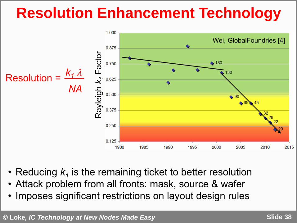
Resolution Enhancement Technology
Slide 38
• Reducing k1 is the remaining ticket to better resolution• Attack problem from all fronts: mask, source & wafer• Imposes significant restrictions on layout design rules
Resolution = k1
NAR
ayle
igh
k 1Fa
ctor
Wei, GlobalFoundries [4]
© Loke, IC Technology at New Nodes Made Easy
OutlinePart 1
• Motivation• MOSFET & Short-Channel Fundamentals• 130nm Fabrication• More MOSFET Fundamentals• Lithography• Partially-Depleted SOI
Part 2• Strain Engineering (90nm & Beyond)• High-K / Metal-Gate (45nm & Beyond)• Migrating to Fully-Depleted (22nm & Beyond)• Tri-Gate FinFETs• Conclusions
Slide 39
© Loke, IC Technology at New Nodes Made Easy
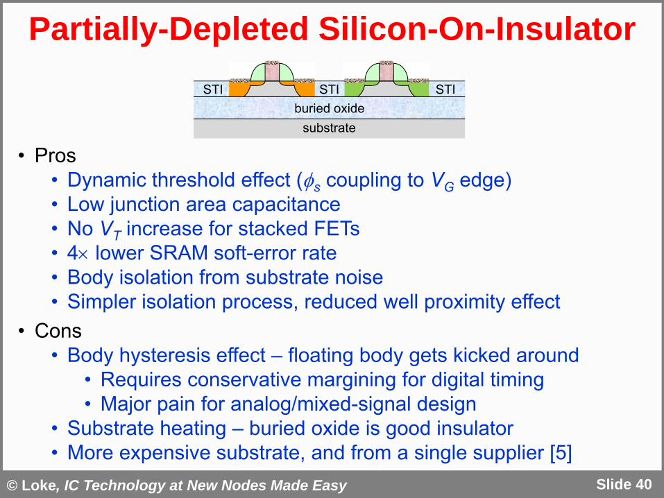
Partially-Depleted Silicon-On-Insulator
Slide 40
• Pros• Dynamic threshold effect (s coupling to VG edge)• Low junction area capacitance• No VT increase for stacked FETs• 4 lower SRAM soft-error rate• Body isolation from substrate noise• Simpler isolation process, reduced well proximity effect
• Cons• Body hysteresis effect – floating body gets kicked around
• Requires conservative margining for digital timing • Major pain for analog/mixed-signal design
• Substrate heating – buried oxide is good insulator• More expensive substrate, and from a single supplier [5]
buried oxidesubstrate
STI STISTI

© Loke, IC Technology at New Nodes Made Easy
The Dreaded Hysteresis Effect
Slide 41
• Floating body is coupled to source, gate, drain & body• Body voltage has memory or history of other terminals, analogous to
intersymbol interference in wireline I/O• Floating body voltage noise VT noise ID noise• Can get hysteresis in bulk if ZSUB is too high
p-well
substrate
buried oxide
n+ source
n+ drain
undepletedfloating body
poly gate
VD
VG
VSUB
ZSUB

© Loke, IC Technology at New Nodes Made Easy
Body-Tied PD-SOI MOSFET (T-Gate)
Slide 42
• Enables body connection to undepleted FET well• High Rbody and extra Cgate limits bandwidth of body connection• NMOS example
p-well
Lateral connection toundepleted p-well
n+n+
p+
body node
p+ diffusion
n+ diffusion
p+ body-tie
n+
sourcen+
drain
SOI active island
Poly gate

© Loke, IC Technology at New Nodes Made Easy
OutlinePart 1
• Motivation• MOSFET & Short-Channel Fundamentals• 130nm Fabrication• More MOSFET Fundamentals• Lithography• Partially-Depleted SOI
Part 2• Strain Engineering (90nm & Beyond)• High-K / Metal-Gate (45nm & Beyond)• Migrating to Fully-Depleted (22nm & Beyond)• Tri-Gate FinFETs• Conclusions
Slide 43

© Loke, IC Technology at New Nodes Made Easy
The Roads to Higher Performance
Slide 44
sourcedrain
channel
Decrease L – steepen the hill
sourcedrain
channellithographyscaling
Increase µ – move carriers faster
sourcedrain
channel
strain engineering
sourcedrain
channelIncrease Cox – move more carriers
high-K dielectricmetal gate

© Loke, IC Technology at New Nodes Made Easy
Mechanical Stresses & Strains
Slide 45
AreaForceStress
atomic spacing > equilibrium spacing
Tension(positive stress)
Compression(negative stress)
atomic spacing < equilibrium spacing
vs.
0
Strain
• Stretching / compressing FET channel atoms by as little as 1%can improve electron / hole mobilities by several times
• Strain perturbs crystal structure (energy bands, density of states, etc.) changes effective mass of electrons & holes
• Increase ION for the same IOFF without increasing COX

© Loke, IC Technology at New Nodes Made Easy
Longitudinal Uni-Axial Strain
Slide 46
tension (stretch atoms apart) faster NMOS
compression (squeeze atoms together) faster PMOS
• Most practical means of incorporating strain for mobility boost• Want 1-3GPa (high-strength steel breaks at 0.8GPa)• How? Deposit strained materials around channel
• Material in tension wants to relax by pulling in• Material in compression wants to relax by pushing out

© Loke, IC Technology at New Nodes Made Easy
Transferring Strain from Material A to B
Slide 47
A AB
A AB
A AB
more A
less B
limitedscalability
need short channel
© Loke, IC Technology at New Nodes Made Easy
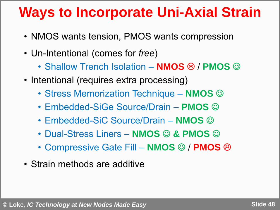
Ways to Incorporate Uni-Axial Strain
Slide 48
• NMOS wants tension, PMOS wants compression
• Un-Intentional (comes for free)• Shallow Trench Isolation – NMOS / PMOS
• Intentional (requires extra processing)• Stress Memorization Technique – NMOS • Embedded-SiGe Source/Drain – PMOS • Embedded-SiC Source/Drain – NMOS • Dual-Stress Liners – NMOS & PMOS • Compressive Gate Fill – NMOS / PMOS
• Strain methods are additive

© Loke, IC Technology at New Nodes Made Easy Slide 49
Shallow Trench Isolation (STI)NMOS & PMOS
• STI oxide under compression• High-Density Plasma CVD SiO2 process (alternating deposition/etch)
deposits intrinsically compressive oxide for good trench fill• 10 CTE mismatch between Si & SiO2 increases compression when
cooled from deposition temperature• Migrated to High Aspect Ratio Process (HARP) fill in recent nodes less compressive oxide
Plummer et al., Stanford [6]
© Loke, IC Technology at New Nodes Made Easy
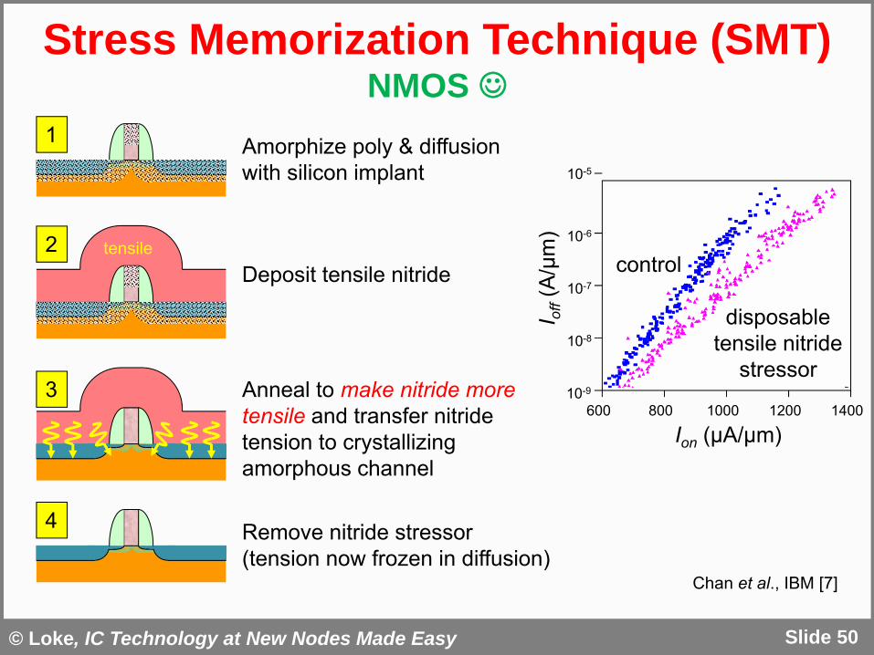
Stress Memorization Technique (SMT)NMOS
Slide 50
Ion (µA/µm)
I off(A
/µm
)
600 800 1000 1200 140010-9
10-8
10-7
10-6
10-5
control
disposable tensile nitride
stressor
tensile
Amorphize poly & diffusion with silicon implant
Deposit tensile nitride
Anneal to make nitride more tensile and transfer nitride tension to crystallizing amorphous channel
Remove nitride stressor (tension now frozen in diffusion)
1
2
3
4
Chan et al., IBM [7]

© Loke, IC Technology at New Nodes Made Easy
Periodic Table Trends
Slide 51
lattice spacing bandgap
• Compound semiconductor like SixGe1-x has lattice spacing & bandgap between Si & Ge
• Same idea with SixC1-x

© Loke, IC Technology at New Nodes Made Easy
Embedded-SiGe Source/Drain (e-SiGe)PMOS
Slide 52
P
P
Etch source/drain recess
Grow SiGe epitaxially in recessed regions
2
SiGe SiGe
• SiGe constrained to Si lattice will be in compression
• Compressive SiGe source/drain transfers compression to Si channel
Ion (µA/µm)
I off
(A/µ
m)
200 300 400 500 700
10-9
10-8
10-7
600
1
L=35nm
SiGe
L=35nmL=35nm
SiGe
• e-SiC is similar but introduces tension instead• Epitaxial SiC much tougher to do than SiGe
Chan et al., IBM [7]
© Loke, IC Technology at New Nodes Made Easy Slide 53
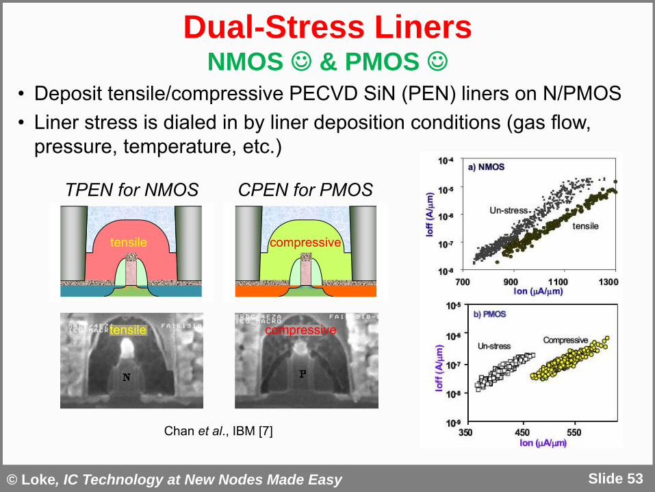
Dual-Stress LinersNMOS & PMOS
• Deposit tensile/compressive PECVD SiN (PEN) liners on N/PMOS• Liner stress is dialed in by liner deposition conditions (gas flow,
pressure, temperature, etc.)
TPEN for NMOS CPEN for PMOS
tensile compressive
tensile compressive
Chan et al., IBM [7]

© Loke, IC Technology at New Nodes Made Easy
Strain Relaxation
Slide 54
When materials of different strain come together…
Material A Tensile Material B Compressive
• Both materials will relax at the interface• Extent of relaxation is gradual, depends on distance from interface• No relaxation far away from interface
interface

© Loke, IC Technology at New Nodes Made Easy
Strain Depends on Channel Location
Slide 55
Xi et al., UC Berkeley [8]
• SA, L & SB specify where channel is located along active area
SA L SB
• Critical for modeling device mobility change due to STI, SMT, e-SiGe, etc.
• Strain at source & drain ends of channel may be different
• Important consideration for matching, e.g., current mirrors
• Concavity & stress polarity will vary with stressors in given technology but concept still applies
STIeffectonly

© Loke, IC Technology at New Nodes Made Easy
Longitudinal DSL Proximity
Slide 56
• Opposite device type nearby in longitudinal direction reduces impact of stress liner mutually slow each other down
• Opposite PEN liner absorbs/relieves stress introduced by PEN
h n _ s tr _ w n w p _ in fp -1 1 -1 5
0.7
0 .75
0.8
0 .85
0.9
0 .95
1
1.05
0 0.2 0 .4 0 .6 0 .8 1 1.2
W NW P L o n g . Dis tan ce (u m )
Ieff
Rat
ioData Mode l
CPEN TPEN
PMOS NMOS
CPEN TPEN
PMOS NMOS
PMOS Longitudinal Proximity
Faricelli, AMD [9]

© Loke, IC Technology at New Nodes Made Easy
Transverse DSL Proximity
Slide 57
• Both NMOS & PMOS like tension in transverse direction, unlike longitudinal direction
• NMOS near PMOS in width direction helps PMOS, hurts NMOS
0.880.9
0.920.940.960.98
11.021.041.06
0 0.2 0.4 0.6 0.8 1 1.2
Transverse Distance
Norm
aliz
ed Id
eff
Data W=0.4Model W=0.4Data W=1.25Model W=1.25
desiredNMOS strain
desiredPMOS strain
CPEN
TPEN
PMOS
NMOS
PMOS Transverse ProximityCPEN
TPEN
PMOS
NMOS
Faricelli, AMD [9]
© Loke, IC Technology at New Nodes Made Easy
OutlinePart 1
• Motivation• MOSFET & Short-Channel Fundamentals• 130nm Fabrication• More MOSFET Fundamentals• Lithography• Partially-Depleted SOI
Part 2• Strain Engineering (90nm & Beyond)• High-K / Metal-Gate (45nm & Beyond)• Migrating to Fully-Depleted (22nm & Beyond)• Tri-Gate FinFETs• Conclusions
Slide 58
© Loke, IC Technology at New Nodes Made Easy
The Roads to Higher Performance
Slide 59
sourcedrain
channel
Decrease L – steepen the hill
sourcedrain
channellithographyscaling
Increase µ – move carriers faster
sourcedrain
channel
strain engineering
sourcedrain
channelIncrease Cox – move more carriers
high-K dielectricmetal gate

© Loke, IC Technology at New Nodes Made Easy
Direct Tunneling Gate Leakage
Slide 60
• tox had to scale with channel length to maintain gate control
• Less SCE• Better FET performance
• Significant direct tunneling for tox< 2nm
EOT (Å)0 5 10 15 20 25 30
Gat
e Le
akag
e (A
/cm
2 )
10-510-410-310-210-1100101102103104
High PerformanceLow PowerSiO2 TrendlineNitrided oxide
McPherson, Texas Instruments [10]
EOT = Equivalent Oxide Thickness
• High-K gate dielectric achieves same Cox with much thicker tox
EOTtC ox
gate
gateox

© Loke, IC Technology at New Nodes Made Easy Slide 61
• Even heavily-doped poly is a limited conductor• Discrepancy between electrical & physical thicknesses since charge
is not intimately in contact with oxide interface
surface charge centroid few Å’s awayfrom oxide interface
n+ poly gate
p-well
gate oxide
poly depletion (band bending)
gate charge centroid few Å’s away from oxide interface
Wong, IBM [11]
Cox
1.5nm (15Å)
poly-Sigate
Sisubstrate
gateoxide
Poly Depletion & Charge CentroidDielectric Only Half the Story

© Loke, IC Technology at New Nodes Made Easy
Enter High-K Dielectric + Metal-Gate
Slide 62
• High-K Dielectric (HK)• Hf-based material with K~20–30 (Zr-based also considered)• Need to overcome hysteretic polarization• High deposition temperature for good film quality
• Metal-Gate (MG)• Thin conductive film intimately in contact with high-K dielectric
to set gate work function M VFB VT• Want band-edge M, i.e., NMOS @ EC & PMOS @ EV
(just like n+ poly & p+ poly) different MG for NMOS & PMOS• Typically complex stack of different metal layers secret sauce• Conductive fill metal on top of M-setting metal-gate
• Key challenges• INTEGRATION, INTEGRATION, INTEGRATION• M shifts when exposed to dopant activation anneals• Getting the right VT for both NMOS & PMOS
© Loke, IC Technology at New Nodes Made Easy
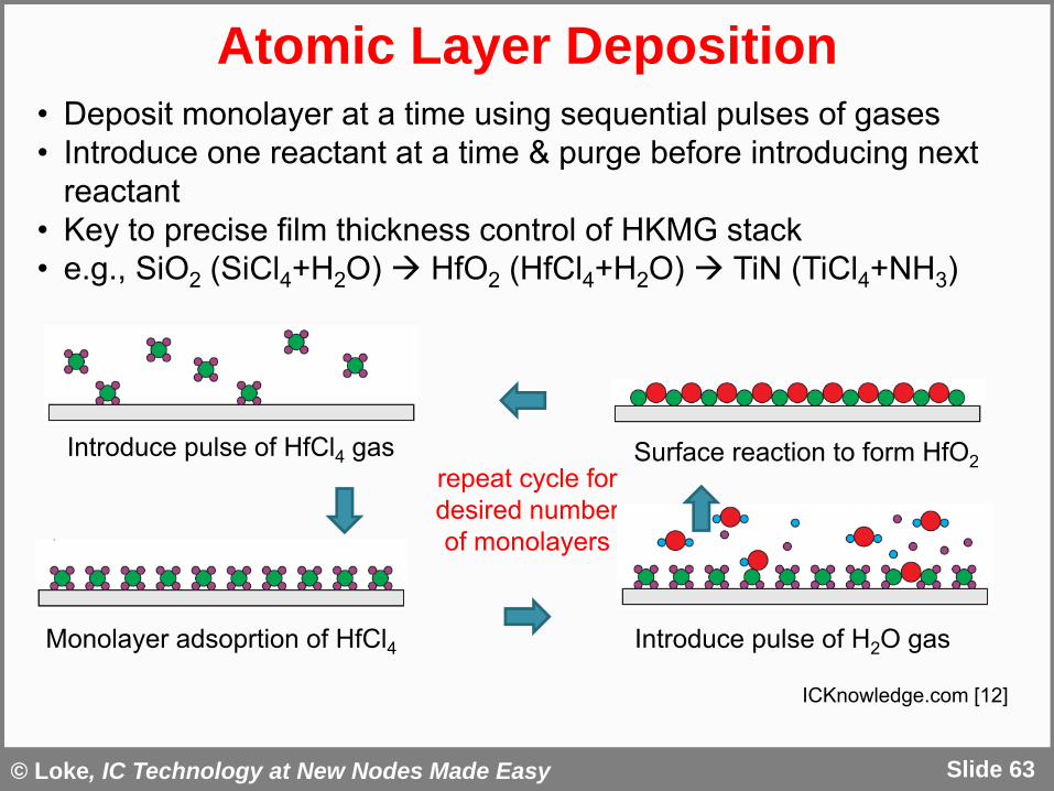
Atomic Layer Deposition
Slide 63
• Deposit monolayer at a time using sequential pulses of gases • Introduce one reactant at a time & purge before introducing next
reactant• Key to precise film thickness control of HKMG stack • e.g., SiO2 (SiCl4+H2O) HfO2 (HfCl4+H2O) TiN (TiCl4+NH3)
Introduce pulse of HfCl4 gas
Monolayer adsoprtion of HfCl4 Introduce pulse of H2O gas
Surface reaction to form HfO2repeat cycle for desired number of monolayers
ICKnowledge.com [12]

© Loke, IC Technology at New Nodes Made Easy
HK-First / MG-First Integration
Slide 64
• Obvious extension of poly-Si gate integration• Seems obvious & “easy” at first but plagued with unstable work
function when HKMG is exposed to activation anneals• Especially problematic with PMOS VT coming out too high
Deposit HKDeposit MG1
Pattern MG1Deposit MG2
Pattern MG2Deposit gatePattern gates / MGs / HK
Implant/anneal S/ D Form silicideDeposit/CMP ILD0Form contacts
321 4

© Loke, IC Technology at New Nodes Made Easy
GlobalFoundries 32nm-SOI
Slide 65
Horstmann et al., GlobalFoundries [13]
poly/SiON HKMG
+35%
IDsat (µA/µm)
IDof
f(nA
/µm
)
poly/SiON HKMG
+25%
IDsat (µA/µm)
IDof
f(nA
/µm
)
NMOS PMOS
epi-cSiGe to set channel M
© Loke, IC Technology at New Nodes Made Easy
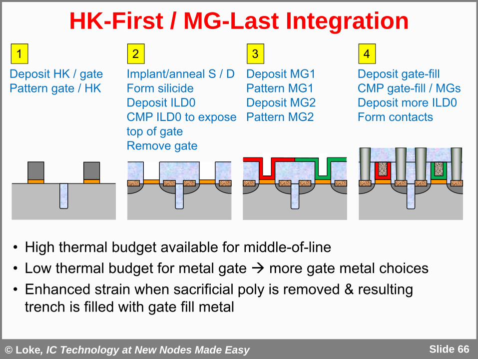
HK-First / MG-Last Integration
Slide 66
• High thermal budget available for middle-of-line• Low thermal budget for metal gate more gate metal choices• Enhanced strain when sacrificial poly is removed & resulting
trench is filled with gate fill metal
Deposit HK / gatePattern gate / HK
Implant/anneal S / DForm silicideDeposit ILD0CMP ILD0 to expose top of gateRemove gate
Deposit MG1Pattern MG1Deposit MG2Pattern MG2
Deposit gate-fillCMP gate-fill / MGsDeposit more ILD0Form contacts
321 4

© Loke, IC Technology at New Nodes Made Easy
Intel 45nm
Slide 67
NMOS PMOS
Auth et al., Intel [14]

© Loke, IC Technology at New Nodes Made Easy
HK-Last / MG-Last Integration
Slide 68
• Same advantages as HK-first / MG-last integration• Overcomes EOT scaling limitations in HK-first / MG-last• Need to postpone silicidation to after opening source/drain etch• DSL relax & no longer useful since contacts cut through FET width
Deposit oxide / gatePattern gate / oxide
Implant/anneal S / DDeposit ILD0CMP ILD0 to expose top of gateRemove gate/oxide
Deposit HKDeposit MG1Pattern MG1Deposit MG2Pattern MG2
Deposit gate-fillCMP gate-fill / MGsCut to expose activeForm silicideDeposit / CMP ILD0Pattern/form contacts
321 4
© Loke, IC Technology at New Nodes Made Easy
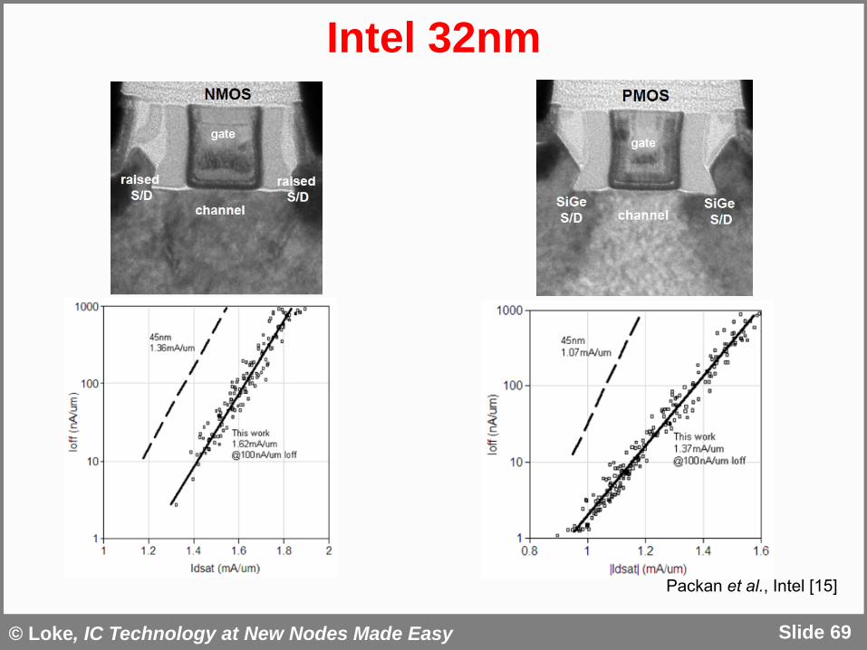
Intel 32nm
Slide 69
Packan et al., Intel [15]
© Loke, IC Technology at New Nodes Made Easy
OutlinePart 1
• Motivation• MOSFET & Short-Channel Fundamentals• 130nm Fabrication• More MOSFET Fundamentals• Lithography• Partially-Depleted SOI
Part 2• Strain Engineering (90nm & Beyond)• High-K / Metal-Gate (45nm & Beyond)• Migrating to Fully-Depleted (22nm & Beyond)• Tri-Gate FinFETs• Conclusions
Slide 70

© Loke, IC Technology at New Nodes Made Easy
What Does Fully-Depleted Really Mean?
Slide 71
• Consider what happens when SOI layer thins down
• Conservation of charge cannot be violated• So once body is fully depleted, extra gate charge must be balanced
by charge elsewhere, e.g., beneath buried oxide• If substrate is insulator, then charge must come from source/drain• No floating body in fully-depleted no hysteresis
p-well
substrate
buried oxide
source drain
p-well
substrate
source drain
fully-depleted when turned on
depletion region
depletion region
© Loke, IC Technology at New Nodes Made Easy Slide 72
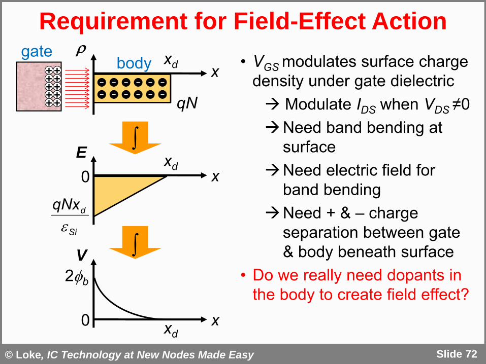
• VGS modulates surface charge density under gate dielectric Modulate IDS when VDS ≠0Need band bending at
surfaceNeed electric field for
band bendingNeed + & – charge
separation between gate & body beneath surface
• Do we really need dopants in the body to create field effect?
––
––
––
––
––
––
qN
xdgate
++++++
++++ body
x
V
0 xd
2b
xE0
xd
Si
dqNx
Requirement for Field-Effect Action
x

© Loke, IC Technology at New Nodes Made Easy Slide 73
Ground-Plane MOSFET
Yan et al., Bell Labs [16]
• Extremely retrograded well profile with no surface dopants• Depletion region cannot extend beyond buried pulse of dopants• All you fundamentally need for field-effect action is a parallel-plate
capacitor with gate dielectric & undoped semiconductor in between plates dopants are not required in the body
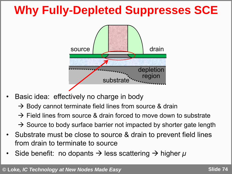
© Loke, IC Technology at New Nodes Made Easy Slide 74
p-well
substrate
source drain
depletion region
• Basic idea: effectively no charge in body Body cannot terminate field lines from source & drain Field lines from source & drain forced to move down to substrate Source to body surface barrier not impacted by shorter gate length
• Substrate must be close to source & drain to prevent field lines from drain to terminate to source
• Side benefit: no dopants less scattering higher µ
Why Fully-Depleted Suppresses SCE

© Loke, IC Technology at New Nodes Made Easy
Benefits of Lower DIBL & S
Slide 75
• Fully-depleted options• Planar: FD-SOI, Bulk with retrograded well• 3-D: FinFET or Tri-Gate – SOI or Bulk
log (IDS)
VGSVTsat VTlin
IDoff
VDD
IDsatIDlin
log (IDS)
VGSVDD
log (IDS)
VGSVDDVTsat VTlin
IDoff
IDsatIDlin
Same SLower DIBL
Lower SSame DIBL
Maintain IDsat & IDoff
VTsat VTlin
IDsatIDlin
IDoff

© Loke, IC Technology at New Nodes Made Easy
The Big Deal with Lower DIBL
Slide 76
Higher performance for the same IDsat & IDoffL. Wei et al., Stanford [17]

© Loke, IC Technology at New Nodes Made Easy
Body Thickness for Fully-Depleted
Slide 77
qNx bSi
d 22
p-well
substratedepletion
region
dx
1015 1016 1017 1018 1019 10201
10
100
1000
Body Doping, N (cm-3)x d
(nm
)
fullydepleted
partiallydepleted

© Loke, IC Technology at New Nodes Made Easy
Fully-Depleted Planar on SOI
Slide 78
K. Cheng et al., IBM [18]
• a.k.a. ET (Extremely Thin) or UTBB (Ultra-Thin Body & BOX) SOI to refer to very thin SOI and Buried Oxide (BOX) layers
• SOI Si layer is so thin that charge mirroring gate charge comes from beneath BOX
buried oxide
substrate
thick to reduce series resistance & apply stress
© Loke, IC Technology at New Nodes Made Easy
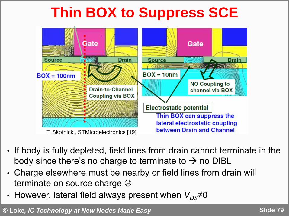
Thin BOX to Suppress SCE
Slide 79
• If body is fully depleted, field lines from drain cannot terminate in the body since there’s no charge to terminate to no DIBL
• Charge elsewhere must be nearby or field lines from drain will terminate on source charge
• However, lateral field always present when VDS≠0
T. Skotnicki, STMicroelectronics [19]
© Loke, IC Technology at New Nodes Made Easy
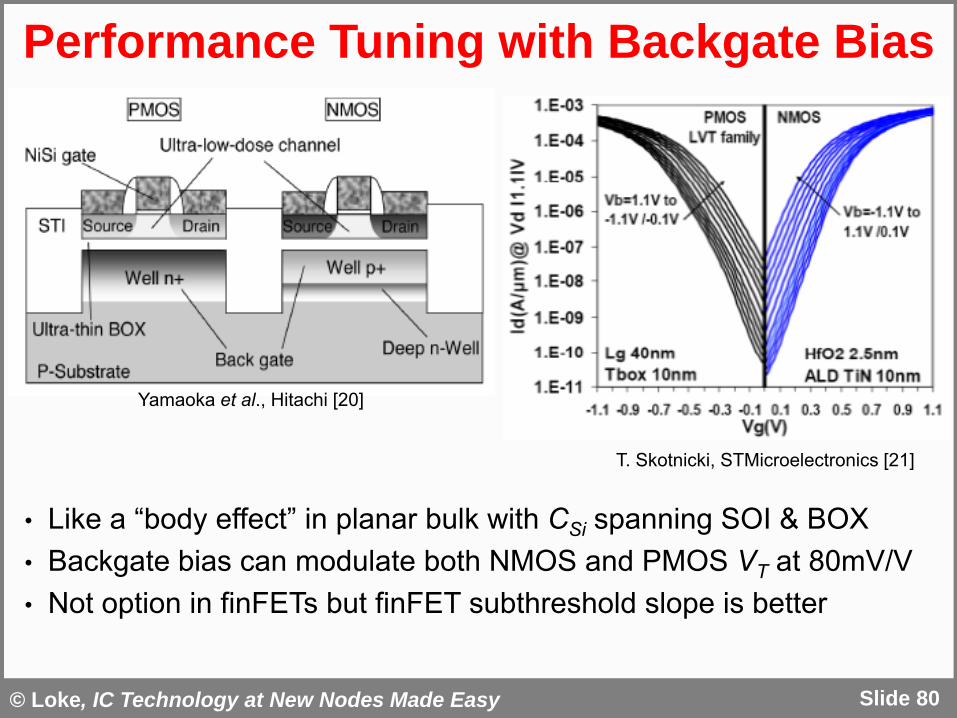
Performance Tuning with Backgate Bias
Slide 80
Yamaoka et al., Hitachi [20]
• Like a “body effect” in planar bulk with CSi spanning SOI & BOX• Backgate bias can modulate both NMOS and PMOS VT at 80mV/V• Not option in finFETs but finFET subthreshold slope is better
T. Skotnicki, STMicroelectronics [21]

© Loke, IC Technology at New Nodes Made Easy
Fully-Depleted Planar on Bulk
Slide 81
Fujita et al., Fujitsu & SuVolta [22]
1 Low-doped layer for RDF reduction (fully depleted)
2 VT setting layer for multiple VT devices3 Highly-doped screening layer to
terminate depletion4 Sub-surface punchthrough prevention
Reduced RDF for tighter VTcontrol & lower SRAM VDDmin

© Loke, IC Technology at New Nodes Made Easy
Random Dopant Fluctuation (RDF)
Slide 82
0
10
20
30
40
50
130nm 90nm 65nm 45nm
minimumlengthNMOS
VT
(mV
)
Auth, Intel [14]
• RDF more prevalent with scaling since number of dopants is decreasing with each MOS generation
• Why does RDF impact magically disappear in fully-depleted?
??
© Loke, IC Technology at New Nodes Made Easy
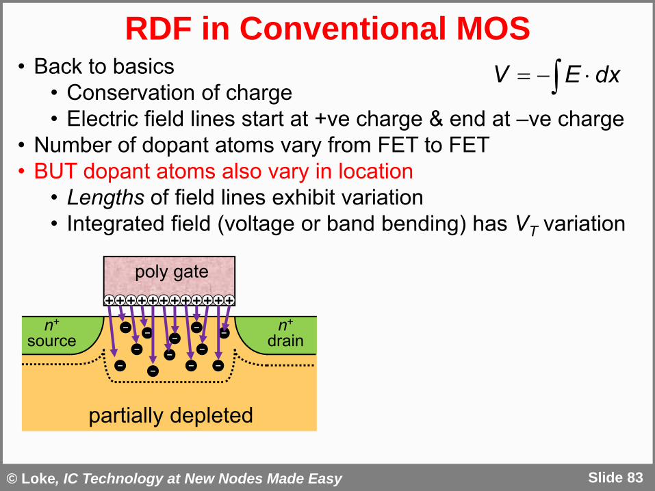
RDF in Conventional MOS
Slide 83
• Back to basics• Conservation of charge• Electric field lines start at +ve charge & end at –ve charge
• Number of dopant atoms vary from FET to FET• BUT dopant atoms also vary in location
• Lengths of field lines exhibit variation• Integrated field (voltage or band bending) has VT variation
poly gate
n+
sourcen+
drain– – –
+
– – –
–
+ + ++ + + ++ + + +
–
–– – –
dxEV
partially depleted

© Loke, IC Technology at New Nodes Made Easy
Why Fully-Depleted Eliminates RDF
Slide 84
poly gate
n+
sourcen+
drain– – –
+
– – –
–
+ + ++ + + ++ + + +
–
–– – –
poly gate
n+
sourcen+
drain
+ + + ++ + + ++ + + +
– – – – – – – – – – – –
undoped
partially depleted fully depleted
• In fully-depleted SOI, field lines from gate cannot terminate in the undoped body (no charge there)
• Mirror charges are localized beneath BOX• Lengths of field lines have tight distribution small VT variation• However, VT now very sensitive to dimensional variation, e.g.,
SOI and BOX thickness• Other sources of variation also present, e.g., MG grains
© Loke, IC Technology at New Nodes Made Easy
OutlinePart 1
• Motivation• MOSFET & Short-Channel Fundamentals• 130nm Fabrication• More MOSFET Fundamentals• Lithography• Partially-Depleted SOI
Part 2• Strain Engineering (90nm & Beyond)• High-K / Metal-Gate (45nm & Beyond)• Migrating to Fully-Depleted (22nm & Beyond)• Tri-Gate FinFETs• Conclusions
Slide 85

© Loke, IC Technology at New Nodes Made Easy
What is Fully-Depleted Tri-Gate?
Slide 86
M. Bohr, Intel [24]
32nm planar 22nm tri-gate
• Channel on 3 sides• Fin width is quantized (SRAM & logic
implications)• Fin so narrow that gate mirror charge
must come from fin baseHu, UC Berkeley [23]

© Loke, IC Technology at New Nodes Made Easy
Tri-Gate FinFETs in Production
Slide 87
Truly impressive!!!fingate
32nm planar 22nm tri-gate
M. Bohr, Intel [24]
© Loke, IC Technology at New Nodes Made Easy
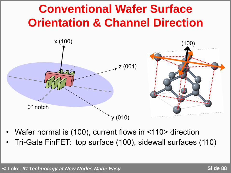
Conventional Wafer Surface Orientation & Channel Direction
Slide 88
0° notch
x (100)
y (010)
z (001)
(100)
• Wafer normal is (100), current flows in <110> direction• Tri-Gate FinFET: top surface (100), sidewall surfaces (110)

© Loke, IC Technology at New Nodes Made Easy
Mobility Dependence on Surface Orientation & Direction of Current
Slide 89
NMOS PMOS
Yang et al., IBM [25]
• Strain-induced mobility boost also depends on surface orientation & channel direction – not as strong for current along sidewalls vs. top of fin
top of fin
sidewalls of fintop of fin
sidewalls of fin
© Loke, IC Technology at New Nodes Made Easy
Fin Patterning – Sidewall Image Transfer
Slide 90
• Standard approach for patterning fins down to 60nm pitch (Intel 22nm)
• In principle, pitch can go down to ~40nm without double patterning
1 Deposit & pattern sacrificial mandrel
2 Deposit & etch spacer
4 Etch target material using spacer as hard mask
5 Remove spacer mask
substrate to etch
mandrel
spacer
3 Remove mandrelhard mask
for patterning
© Loke, IC Technology at New Nodes Made Easy
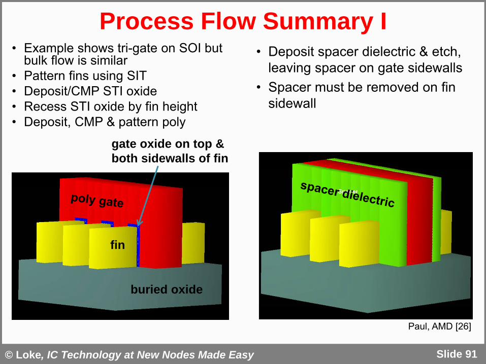
Process Flow Summary I
Slide 91
• Example shows tri-gate on SOI but bulk flow is similar
• Pattern fins using SIT• Deposit/CMP STI oxide• Recess STI oxide by fin height• Deposit, CMP & pattern poly
fin
buried oxide
gate oxide on top & both sidewalls of fin
• Deposit spacer dielectric & etch, leaving spacer on gate sidewalls
• Spacer must be removed on fin sidewall
Paul, AMD [26]

© Loke, IC Technology at New Nodes Made Easy
Process Flow Summary II
Slide 92
• Recess fins• Grow Si epitaxially to merge fins
together for reduced source/drain resistance
• Induce uni-axial channel strain by growing e-SiGe or e-SiC
• Dope source/drain dopants with in situ doping during epi
• Deposit ILD0 & CMP to top of poly• Do replacement-gate HKMG
module• Deposit & pattern contact dielectric• Form trench contacts (note
overlap capacitance to gate)
epigrowth
trench contact
metal gate
Paul, AMD [26]

© Loke, IC Technology at New Nodes Made Easy
Some Tri-Gate Considerations
Slide 93
• Field lines of from gate terminates at base of fins
• Fin base must be heavily doped for fin-to-fin isolation
• Dimensional variation of fins device variation
• Current density is not uniform along width of device – VT & S varies along sidewall
• Series resistance vs. overlap capacitance
• “Dead” space between fins
trench contact
metal gate

© Loke, IC Technology at New Nodes Made Easy
Pacifying The Multi-VT Addiction
Slide 94
• 8 VT’s typical in 28nm (NMOS vs. PMOS, thick vs. thin oxide)• Methods of achieving multiple VT
1. Bias channel length• Exploit SCE (VT rolloff with shorter L)• Increase L for lower ION & IOFF
2. Implant fin body with different dose• Field lines from gate must “work through” available
body dopants before terminating at base of fin• Prone to RDF
3. Integrate more metal gate M • Already 2 M s in standard HKMG flow• More complex integration

© Loke, IC Technology at New Nodes Made Easy
Intel 22nm TEM Cross-Sections
Slide 95
Auth, Intel [27]
Single fin (along W)
Epi merge (along W)
NMOS (along L)
PMOS (along L)

© Loke, IC Technology at New Nodes Made Easy
Intel 22nm Performance at 0.8V
Slide 96
0.1
1
10
100
1000
0.6 0.8 1 1.2 1.4 1.6
IOFF
(nA
/m
)
IDSAT (mA/m)
VDD = 0.8V
HP: 1.26 mA/m
MP: 1.07 mA/m
SP: 0.88 mA/m
32nm
0
1
10
100
1000
0.6 0.8 1 1.2 1.4IO
FF (n
A/
m)
IDSAT (mA/m)
VDD = 0.8V
HP: 1.10 mA/m
MP: 0.95 mA/m
SP: 0.78 mA/m
32nm
1.E-09
1.E-08
1.E-07
1.E-06
1.E-05
1.E-04
1.E-03
1.E-02
-1.0 -0.6 -0.2 0.2 0.6 1.0
IDSA
T (A
/m
)
VGS (V)
0.80V
SS ~69mV/decDIBL ~46 mV/V
SS ~72mV/decDIBL ~50 mV/V
NMOSPMOS
0.05V
0.80V
0.05V
Auth, Intel [27]
NMOS
PMOS
© Loke, IC Technology at New Nodes Made Easy
Conclusions
Slide 97
• Digital needs will continue to drive CMOS scaling but at slower pace
• Expect new learning in 20nm & 14nm as we cope with fin design & layout
• SPICE models will lag to include new effects
• Designers with good technology knowledge are best positioned for silicon success
• Exciting time to be designing

© Loke, IC Technology at New Nodes Made Easy
References[1] M. Keating, “Science fiction or technology roadmap: a look at the future of SoC design,” in SNUG San Jose Conf., Mar. 2010.[2] M. Na et al., “The effective drive current in CMOS inverters,” in IEEE Int. Electron Devices Meeting Tech. Dig., pp. 121–124, Dec. 2002. [3] S.M. Sze, Physics of Semiconductor Devices (2nd ed.), John Wiley & Sons, 1981.[4] A. Wei, “Foundry trends: technology challenges and opportunities beyond 32nm,” in IEEE Vail Computer Elements Workshop, Jun. 2010. [5] www.soitec.com[6] J. Plummer et al., Silicon VLSI Technology– Fundamentals, Practice and Modeling, Prentice-Hall, 2000.[7] V. Chan et al., “Strain for CMOS performance improvement,” in Proc. IEEE Custom Integrated Circuits Conf., pp. 667–674, Sep.2005. [8] X. Xi et al., BSIM4.3.0 MOSFET Model – User’s Manual, The Regents of the University of California at Berkeley, 2003 [9] J. Faricelli, “Layout-dependent proximity effects in deep nanoscale CMOS,” in Proc. IEEE Custom Integrated Circuits Conf., pp. 1–8, Sep.2010.[10] J. McPherson, “Reliability trends with advanced CMOS scaling and the implications on design,” in Proc. IEEE Custom Integrated Circuits Conf., pp. 405–412, Sep.
2007.[11] P. Wong, “Beyond the conventional transistor,” IBM J. Research & Development, pp. 133–168, vol. 2-3, no. 46, Mar. 2002.[12] www.ICKnowledge.com[13] M. Horstmann et al., “Advanced SOI CMOS transistor technologies for high-performance microprocessor applications,” in Proc. IEEE Custom Integrated Circuits
Conf., pp. 149–152, Sep. 2009.[14] C. Auth, “45nm high-k + metal-gate strain-enhanced CMOS transistors,” in Proc. IEEE Custom Integrated Circuits Conf., pp. 379–386, Sep. 2008.[15] P. Packan et al., “High performance 32nm logic technology featuring 2nd generation high-k + metal gate transistors,” in IEEE Int. Electron Devices Meeting Tech. Dig.,
pp. 1–4, Dec. 2009.[16] R.-H. Yan et al., “Scaling the Si MOSFET: From bulk to SOI to bulk,” IEEE Trans. Electron Devices, vol. 39, no. 7, pp. 1704–1710, Jul. 1992.[17] L. Wei et al., “Exploration of device design space to meet circuit speed targeting 22nm and beyond,” in Proc. Int. Conf. Solid State Devices and Materials, pp. 808–
809, Sep. 2009.[18] K. Cheng et al., “Fully depleted extremely thin SOI technology fabricate by a novel integration scheme featuring implant-free, zero-silicon-loss, and faceted raised
source/drain,” in IEEE Symp. VLSI Technology Tech. Dig., pp. 212–213, Jun.2009.[19] T. Skotnicki, “CMOS technologies – trends, scaling and issues ,” in IEEE Int. Electron Devices Meeting Short Course, Dec. 2010.[20] M. Yamaoka et al., “SRAM circuit with expanded operating margin and reduced stand-by leakage current using thin BOX FD-SOI transistors,“ IEEE J. Solid-State
Circuits, vol. 41, no.11, Nov. 2006.[21] T. Skotnicki, “Competitive SOC with UTBB SOI,” in Proc. IEEE SOI Conf., Oct. 2011.[22] K. Fujita et al., “Advanced channel engineering achieving aggressive reduction of VT variation for ultra-low power applications,” in IEEE Int. Electron Devices Meeting
Tech. Dig., pp. 32.3.1–32.3.4, Dec. 2011.[23] C. Hu, “FinFET 3D transistor and the concept behind it,” in IEEE Electron Device Soc. Webinar, Jul. 2011.[24] M. Bohr, “22 nm tri-gate transistors for industry-leading low power capabilities,” in Intel Developer Forum, Sep. 2011.[25] M. Yang et al., “Hybrid-orientation technology (HOT): opportunities and challenges,” IEEE Trans. Electron Devices, vol. 53, no. 5, pp. 965–978, May 2006.[26] S. Paul, “FinFET vs. trigate: parasitic capacitance and resistance”, AMD Internal Presentation, Aug. 2011.[27] C. Auth et al., “A 22nm high performance and low-power CMOS technology featuring fully-depleted tri-gate transistors, self-aligned contacts and high density MIM
capacitors,” in IEEE Symp. VLSI Technology Tech. Dig., pp. 131–132, Jun. 2012.
Slide 98