GENERIC SOPC PLATFORM FOR VIDEO INTERACTIVE SYSTEM WITH MPMC CONTROLLER
11
International Journal of Embedded Systems and Applications (IJESA) Vol.4, No.1, March 2014 DOI : 10.5121/ijesa.2014.4102 13 GENERIC SOPC PLATFORM FOR VIDEO INTERACTIVE SYSTEM WITH MPMC CONTROLLER Lamjed Touil 12 Lilia Kechiche 12 Bouraoui Ouni 13 1 Laboratory EμE, Faculty of Sciences of Monastir, university of Monastir, TUNISIA 2 National Engineering School of Monastir (ENIM). 3 National Engineering School of Sousse (ENISo). ABSTRACT Today, a significant number of embedded systems focus on multimedia applications with almost insatiable demand for low-cost, high performance, and low power hardware cosumption. In this paper, we present a re-configurable and generic hardware platform for image and video processing. The proposed platform uses the benefits offered by the Field Programmable Gate Array (FPGA) to attain this goal. In this context, a prototype system is developed based on the Xilinx Virtex-5 FPGA with the integration of embedded processors, embedded memory, DDR, interface technologies, Digital Clock Managers (DCM) and MPMC. The MPMC is an essential component for design performance tuning and real time video processing. We demonstrate the importance role of this interface in multi video applications. In fact, to successful the deployment of DRAM it is mandatory to use a flexible and scalable interface. Our system introduces diverse modules, such as cut video detection, video zoom-in and out. This provides the utility of using this architecture as a universal video processing platform according to different application requirements. This platform facilitates the development of video and image processing applications. KEYWORDS MPMC, DDR, Cut Detection, Zoom-in, Zoom-out RGB, Image Processing 1. INTRODUCTION Video processing is widely used in several applications, including robotics, medical imaging manufacturing, security systems, and interactive-TV. In this context, the real time image and video processing applications require several treatment constraints. For example, a 1024 x 768 color image has a size of 2,359,296 bytes. This large amount of data needs to be stored in memory, transferred to processing blocks, and sent to the display unit. Designing an image and video processing unit can be very complex, time consuming, and the verification process can take months depending on the system’s complexity. The introduction of reconfigurable platforms such as Field Programmable Gate Arrays (FPGA) and the advent of new high level tools to configure them have made image processing on FPGA an emerging practical solution for most of the problems facing computer vision and image processing. These platforms meet the needs of adaptability and scalability for most of the multimedia applications.
-
Upload
independent -
Category
Documents
-
view
0 -
download
0
Transcript of GENERIC SOPC PLATFORM FOR VIDEO INTERACTIVE SYSTEM WITH MPMC CONTROLLER

International Journal of Embedded Systems and Applications (IJESA) Vol.4, No.1, March 2014
DOI : 10.5121/ijesa.2014.4102 13
GENERIC SOPC PLATFORM FOR VIDEO INTERACTIVE
SYSTEM WITH MPMC CONTROLLER
Lamjed Touil12 Lilia Kechiche12 Bouraoui Ouni13
1Laboratory EµE, Faculty of Sciences of Monastir, university of Monastir, TUNISIA 2 National Engineering School of Monastir (ENIM). 3 National Engineering School of Sousse (ENISo).
ABSTRACT
Today, a significant number of embedded systems focus on multimedia applications with almost insatiable
demand for low-cost, high performance, and low power hardware cosumption. In this paper, we present a
re-configurable and generic hardware platform for image and video processing. The proposed platform
uses the benefits offered by the Field Programmable Gate Array (FPGA) to attain this goal. In this context,
a prototype system is developed based on the Xilinx Virtex-5 FPGA with the integration of embedded
processors, embedded memory, DDR, interface technologies, Digital Clock Managers (DCM) and MPMC.
The MPMC is an essential component for design performance tuning and real time video processing. We
demonstrate the importance role of this interface in multi video applications. In fact, to successful the
deployment of DRAM it is mandatory to use a flexible and scalable interface. Our system introduces
diverse modules, such as cut video detection, video zoom-in and out. This provides the utility of using this
architecture as a universal video processing platform according to different application requirements. This
platform facilitates the development of video and image processing applications.
KEYWORDS
MPMC, DDR, Cut Detection, Zoom-in, Zoom-out RGB, Image Processing
1. INTRODUCTION
Video processing is widely used in several applications, including robotics, medical imaging manufacturing, security systems, and interactive-TV. In this context, the real time image and video processing applications require several treatment constraints. For example, a 1024 x 768 color image has a size of 2,359,296 bytes. This large amount of data needs to be stored in memory, transferred to processing blocks, and sent to the display unit. Designing an image and video processing unit can be very complex, time consuming, and the verification process can take months depending on the system’s complexity. The introduction of reconfigurable platforms such as Field Programmable Gate Arrays (FPGA) and the advent of new high level tools to configure them have made image processing on FPGA an emerging practical solution for most of the problems facing computer vision and image processing. These platforms meet the needs of adaptability and scalability for most of the multimedia applications.

International Journal of Embedded Systems and Applications (IJESA) Vol.4, No.1, March 2014
14
Many applications for image and video processing have been implemented using FPGA [17][18][19][20] as they provide very high performance processing and are also programmable and can be adapted to many standards and applications. One of the major problems facing these challenging solutions is the absence of a fast on-chip memory to store intermediate result of graphic algorithms being executed most of the time with real time constraints. Most of the executing applications use an off-ship memory as a solution for the low storage capacity offered by the internal memory. This solution needs to be enhanced with a fast access to a huge memory data in a high speed in order to be able to process real time tasks. In reality, Simultaneous implementation of the various treatments on chip requires more access to the memory. In the real time video processing domain, traditional solutions interface of the SRAM and DRAM do not present reliable solutions. The design productivity gap is widening with every new video application. In this context, the use of an intelligent interface for dialogue with the memory is needed. To minimize this gap, we needed to build a flexible and scalable DRAM memory interface. Such interface can be incorporated in to different video processing applications. One of the proposed solutions to multi module interfacing with the memory is the multi port memory controller (MPMC) which provides the access to the memory from 1 to 8 ports with a customized priority. In this design we have used the Multi-Port Memory Controller (MPMC) (v6.03.a) [1] to satisfy the real time video constraints. In this paper, we have tested this solution with the implementation of Multi Video Treatments. This work presents a contribution to construct a General-Purpose, multi-task, Reconfigurable circuit based Platform for Image and Video Processing. This paper proposes parallel, flexible hardware SDRAM interface. This interface has been tested for video analysis architecture and the final system is implemented on an FPGA. The proposed architecture can be used to validate a real time video indexing applications. On other hand, there is a need for general purpose hardware platform to support and facilitate complex video and image processing. In fact most of the existing designs and SDRAM interfaces are focused on implementing specific algorithms for domain-specific applications. The paper shows the usefulness of the reconfigurable technology for parallel applications and especially for flexible DRAM memory interface for video processing. In this paper, we present the entire system on a hardware platform based on Virtex-5 FPGA. FPGA solutions provide ASIC-like performance and density with an advantage of more flexibility and better operational characteristics. It allows users to exploit inherent parallelism of the hardware and to bypass fetch-decode-execute cycles. Therefore, FPGA solution was used to implement the proposed video architecture. This paper is prepared as follows. The related work and background are offered in section 2. Section 3, describes an abstraction diagram for acquisition, analysis and multi-display techniques for video processing. The proposed system is also presented in this section. Section 4 introduces the MPMC controller solution for Video processing platform. The specification of the implemented applications and experimental results under different video processing are presented in section 5. Finally, a conclusion and a discussion on future research are discussed in section 6.
2. RELATED WORK
One of the major problems that face the usage of external memory is their interfacing solution with other modules which can not satisfy memory access requests especially in the presence of several processing modules. In the last decade, a number of studies dealing with the problem of access to the memory [4] and the treatment acceleration [5] were published but only few of them use simultaneous memory access. Also several solutions to the problem of processing the video in

International Journal of Embedded Systems and Applications (IJESA) Vol.4, No.1, March 2014
15
parallel using the FPGA-based system were proposed, [6] [7], but the majority of them are dedicated to a specific application. Most of the existing solutions have been targeted to the improvement the DRAM throughput by several methods for example by re-organization of memory addresses or using other memory banks …etc. Recent DRAM systems are structured into ranks, banks, rows, and columns to exploit parallelism. Modern microprocessors usually integrate two to four memory controllers, especially for each DDRx channel. However, in the real time video processing domain, the traditional solutions of the SRAM and DRAM do not present reliable solutions, especially in the presence of real time multiple video applications. For this, there is a need for a generic architecture dedicated to a real time video processing based on a new technology for access to the off-chip memory Memory controllers have attracted many research domains as an interfacing solution for off-ship memories [2][3][14][15][16]. In [14] the authors propose a multi processor architecture for image processing. Each processor is charged with the processing of an asymmetric fraction of the image. It uses the PowerPC hard-core microprocessor as a master and multiple MicroBlaze soft-core microprocessors as slaves. The proposed solution aims to implement fast algorithms treatment for image processing. The interfacing of microprocessors and the external DDR memory is insured by the multi port memory controller (MPMC) core. The MPMC is responsible for communication with the external memory. Experimental results shows the more the number of processors is augmented, the faster the algorithm is processed. One of the limitations that face this approach is the limited number of ports available in the MPMC which is considered as a physical limitation. Authors in [15] used a coarse-grain reconfigurable architecture (CGRA) in order to accelerate algorithms in digital holographic imaging. The used CGRA is an array of processing and memory cells, it is a run-time reconfigurable that allows supporting more functionality at a lower hardware cost compared to the cost of using specific hardware accelerators to map the algorithms to application. The proposed architecture communicates using a communication network, and a stream memory controller connected to a multi port memory access (MPMC) to manage data transfers to external memory. In this work, we propose a general purpose architecture for video processing with the use of an MPMC to manage different access requests to the memory
3. DATAFLOW DIAGRAM OF THE PROPOSED MODEL.
Our major purpose of this system is to prepare hardware platform to provide a general solution for video and image processing, and demonstrate its effectiveness through various application scenarios. In fact, an interactive television service is mainly consists of two phases: Analysis phase of AV content and generation display techniques. In this context, we propose a schematic functional architecture model for video processing and insertion of several interactive display techniques. The proposed architecture includes the stage of video analysis and generation of the results with tools and techniques necessary for visual integration and exploitation of these results. From the figure 1 one can see the FPGA implementation of the functional modules. In this section, we use (PBD) methodology [8]. Platform-based design uses an existing base of components and architectures to decrease design time and uses IP blocks to build system architectures. PBD separates the HW/SW partition into behavior approach, architecture approach, and mapping. This method supports IP reuse, and derivative design. Figure 1 provides the schematic functional architecture model of the proposed system.

International Journal of Embedded Systems and Applications (IJESA) Vol.4, No.1, March 2014
16
The architecture is composed of three essential parts: The first part is reserved for the acquisition of video; the second part deals with the analysis of the video; the third deals with video display techniques. This module is composed by different displays methods such as: multi-display, video zoom-in, video zoom-out. Figure 4 presents the hardware architecture of the entire system. The second block describes the general video content analysis part. It provides the video analysis into three levels: low-level, mid-level and a high level treatment. In the low level treatment we quote several blocks like: Converting to gray scale, converting to HMMD, the Histogram calculation, color and texture descriptors and others. In the intermediate treatment other calculation blocks like the calculation of the key frame, the similarity between shots and others can be applied. After that other treatment blocks are applied in the high level treatment. Third block provides several useful techniques to provide results of video analysis. In fact the video content analysis results that are generated are then applied to block display validation techniques which are based on Bilinear Interpolation method [9]. The choice of one of the techniques is determined by the user. Several display technologies with exploitation of results are available. Among them we quote:
� Picture In Picture (PIP): the possibility of watching two pictures (main and sub) simultaneously. The main is displayed in full screen, and the sub is displayed in a part of the screen
� picture-outside-picture (POP): designs the division of the screen into two same-size pictures.
� Video Mosaic: designs the ability of displaying multiple video sources in small size and at the same time on the same TV screen.
� Zoom-In: increasing image size according to the wishes of the user . � Zoom-out: reducing image size according to the wishes of the user.
International Journal of Embedded Systems and Applications (IJESA) Vol.4, No.1, March 2014
17
Enhanced media Video data
Display module
Acquisition module
Analyse module
Input Video (Y)
FIFO
New line (Y)
Line n (Y)
Line n+1 (Y)
Line n (Y) with new pixels
Line n+1 (Y) with new pixels
Generated zoom in data (Y)
Make new pixels by interpolation
Low level treatment Medium level treatment
Color and texture Descriptors
Motion descriptors
Cut Detection
Faces detection
Event Detection and key words
Search object by visual similarity
Classification TV programs: Doc, sport, advertising...
Histograms calculation
Similarity between plans
Color space conversion
Gray level conversion
Video Stream
Extraction of semantic
signatures Video summary
High level Treatment
(MFCC, LPC..). Visual Model
Objects detection Motion detection
Audio Model
Key Word
Selection of m
ulti-modality fusion
Selection of the treatm
ent and descriptors
EHD
Supervision and control of treatment
Histogram’s Classification
Input Video
(YCrCb) Odd lines data
Generated zoom-out
RIF filter
New line data
Bilinear interpolation
Input Video
(YCrCb) RIF filter Bilinear interpolation
Input Video (YCrCb)
Odd lines data
Input Video (YCrCb)
Odd lines data
Input Video (YCrCb)
Odd lines data
Odd lines data
Image Memory
Image Memory
Image Memory
Bilinear interpolation
Bilinear interpolation
Bilinear interpolation
RIF filter
RIF filter
RIF filter
Image Memory
Image Selection
TFT
Figure 1. Diagram for insertion of video analysis and display techniques Combining different low level treatment with several analysis techniques at different levels are among the most important characteristics of the proposed systems of analysis of AV content. Figure 1 gives a generic structure of the system of analysis of AV content and the dataflow between the various modules. It expresses the possible interactions between different tools of content analysis at different levels of abstraction and for different scene of a video. Each content calls for the development of a specific module with input coming from another module and output possibly feeding a third one. Based on the proposed structure, we developed a model system based on the Xilinx Virtex-5 FPGA [10], [11]. In this document, we propose a preliminary version of hardware architecture to support several video processing applications. In this context, we have implemented three different processing functions: video cut detection, video zoom-in and video zoom-out. We propose the study of the off chip interface controller memory. The aim of this work is to prepare a flexible interface for external memory; this interface is used to ensure the parallelism of several communication treatments with memory.

International Journal of Embedded Systems and Applications (IJESA) Vol.4, No.1, March 2014
18
4. Introduction to MPMC FPGA-Based Video processing platform.
The MPMC is an eight-port DDR SDRAM memory controller, where each port can be chosen from a set of personality interface module (PIMs). The DDR transmits controls and data on the bus. The connection of the ports to the microprocessor (Hard or Soft) is by PLB bus and the MPMC Native Port Interface (NPI). MPMC supports the Soft Direct Memory Access (SDMA) controller that provides full-duplex, high-bandwidth. A Video Frame Buffer Controller (VFBC) PIM is also available. Figure 2 depicts the architecture of MPMC.
PIM0 Configurable
PIM1 Configurable
PIM2 Configurable
PIM3 Configurable
PIM4 Configurable
PIM5 Configurable
PIM6 Configurable
PIM7 Configurable
Port Routing logic
Data Path
Address
Path
Port
Arbitration
DDR Memory Control Logic
Control Registers
Memory
(SDRAM, DDR, or DDR2
PLB Interface
NPI NPI NPI NPI NPI NPI NPI NPI
Figure 2. MPMC Architecture Block Diagram.
Using the MPMC was crucial to the success of the design because of bottlenecks which present a problem in transferring the video data to and from memory. This problem was solved by using more ports and additional buses. In the system, we used “CoreConnect” bus and especially Processor Local Bus “PLB” which is obtained from the Xilinx IP library under the name of “plb_v64”. The PLB bus offers a connection between a PLB masters and slaves. It presents the essential element for transport data from one block to another. To reduce bottleneck to the Memory, we used a sufficient number of PLB buses in our system, for example:
� Used for the video acquisition system. � Used by the display circuit to get data from the memory. � Used by the display system. � Used by the analysing system.
Used for by the microprocessor to communicate with the memory and IIC. In every memory write, the synchronize data and control signals are accessible at an MPMC port. When the write data buffer (burst buffer) is not empty, the Multi Port Memory Controller transfers the data into the burst buffer after acknowledges the request. The data persists in this buffer until the memory bus is accessible. The operating frequencies of DDR memory, MPMC module and the VGA output are respectively 133 MHz, 100MHz and 27 MHz. The general architecture of the application is given by the figure 2. The hardware implementation of the entire design consists of three essentials modules:
International Journal of Embedded Systems and Applications (IJESA) Vol.4, No.1, March 2014
19
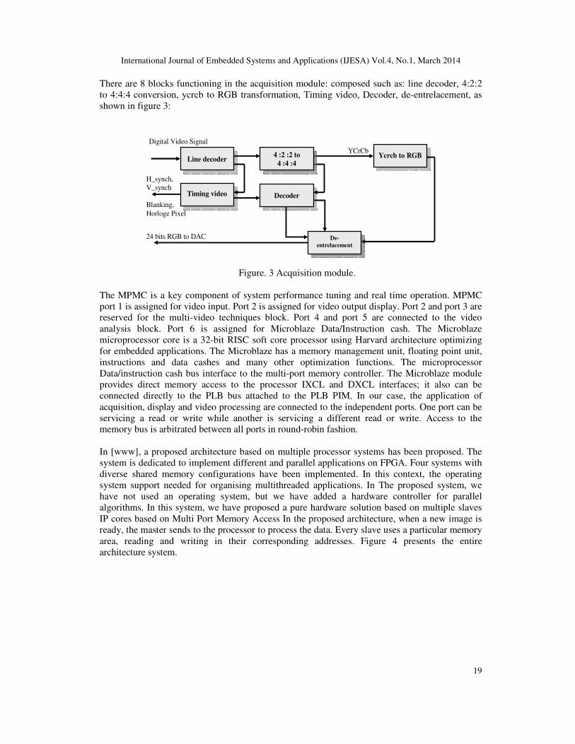
There are 8 blocks functioning in the acquisition module: composed such as: line decoder, 4:2:2 to 4:4:4 conversion, ycrcb to RGB transformation, Timing video, Decoder, de-entrelacement, as shown in figure 3:
Ycrcb to RGB 4 :2 :2 to
4 :4 :4 Line decoder
Decoder Timing video
De-
entrelacement
Digital Video Signal
H_synch, V_synch Blanking, Horloge Pixel
24 bits RGB to DAC
YCrCb
Figure. 3 Acquisition module.
The MPMC is a key component of system performance tuning and real time operation. MPMC port 1 is assigned for video input. Port 2 is assigned for video output display. Port 2 and port 3 are reserved for the multi-video techniques block. Port 4 and port 5 are connected to the video analysis block. Port 6 is assigned for Microblaze Data/Instruction cash. The Microblaze microprocessor core is a 32-bit RISC soft core processor using Harvard architecture optimizing for embedded applications. The Microblaze has a memory management unit, floating point unit, instructions and data cashes and many other optimization functions. The microprocessor Data/instruction cash bus interface to the multi-port memory controller. The Microblaze module provides direct memory access to the processor IXCL and DXCL interfaces; it also can be connected directly to the PLB bus attached to the PLB PIM. In our case, the application of acquisition, display and video processing are connected to the independent ports. One port can be servicing a read or write while another is servicing a different read or write. Access to the memory bus is arbitrated between all ports in round-robin fashion. In [www], a proposed architecture based on multiple processor systems has been proposed. The system is dedicated to implement different and parallel applications on FPGA. Four systems with diverse shared memory configurations have been implemented. In this context, the operating system support needed for organising multithreaded applications. In The proposed system, we have not used an operating system, but we have added a hardware controller for parallel algorithms. In this system, we have proposed a pure hardware solution based on multiple slaves IP cores based on Multi Port Memory Access In the proposed architecture, when a new image is ready, the master sends to the processor to process the data. Every slave uses a particular memory area, reading and writing in their corresponding addresses. Figure 4 presents the entire architecture system.

International Journal of Embedded Systems and Applications (IJESA) Vol.4, No.1, March 2014
20
Port 1 Port 2 Port 3 Port 4
Video
(DAC)
Read block memory and
display controller
PLB BUS
PLB ARB
Multi Display Technical
Analog
Digital
Conversion
Video input
24 bits RGB Vidéo data
Digital Video
Acquisition video
and memory access
controller
(Block)
Microblaze
DDRAM
Output video
Port 5
Analysing video
Port 6 Port 7 Port 8
Architecture dedicated to the acquisition of the video
Display enable
Memory Controlor
Figure 4. Data procession of the proposed design.
Using only one bus is insufficient to handle transactions and the bandwidth is not enough. In fact, word cannot be transferring on every period of the bus, since the buffers are not all the time ready. It takes some cycles to setup a burst write/read. To remedy this situation, we formed two modules for communicate processing reading and writing. And each module has its own PLB bus linking to the memory. This gives the system more flexibility and bandwidth and made the design easier to understand handles and debug. PLB is based on IBM’s 64-bits CoreConnect technology. It uses an arbitration policy to control the slaves devices attached to the bus. It has 64 bits wide data bus, 32 bits wide address bus, and 8 word cache line transfers The XPS_TFT controller is an IP core from the EDK library. It is an IP core provided by the Xilinx core library. It connects to the PLB_v4.6 bus and act as a PLB master. The XPS_TFT reads video frames from MPMC and generates signals to VGA port.
5. EXPERIMENTAL RESULTS
In this work, we have compared the results found by the solution based on the MPMC to the conventional solution based on Xilinx CoreConnect bus with multiple masters and a processor instruction/data caches with key high-speed devices connected by a slave port to the SDRAM. We also conducted an evaluation by constructing a virtual prototype in Mirabilis Design’s VisualSim for a performance modeling and architecture exploration solution. Table 1 shows the instruction and data cache statistics for the virtual prototype model. We ran the simulation on a 2.4 GHz Microsoft Windows XP (SP3 and Standard Edition) with 512 Mb of cache.
TABLE I.INSTRUCTION AND DATA CACHE STATISTICS
Statistic Name CoreConnect MPMC
Inst. Cache Data cache Inst. Cache Data cache
Hit_Ratio_Max 94.03 95.2 93.72 96.23 Hit_Ratio_Mean 89.35 89.43 93.72 96.23 Throughput_MIPs_Max 72.33 2.13 8.54 0.22 Throughput_MIPs_Mean 7.13 0.12 8.54 0.22

International Journal of Embedded Systems and Applications (IJESA) Vol.4, No.1, March 2014
21
With: � Hit_Ratio_Max : Is the maximum percentage of memory accesses satisfied by the cache. � Throughput_MIPs_Max : is the average rate of successful message delivery over a
communication port.
Using the 200-MHz MPMC, the end-to-end latency for the execution of the application benchmark was 89.254 µs, while the 400-MHz CoreConnect was 88.13 µs. Both matched our real-time threshold. We found that the MPMC Memory Controller typically finished its tasks faster than the CoreConnect bus. The MPMC memory controller had a significantly better average hit ratio (93.72% versus 89.35%) for the Icache (instruction). At certain times during the simulation, the CoreConnect bus did get to a 93% hit ratio, but the duration was very short. This indicated that the MPMC arbitrated SDRAM requests better than the CoreConnect bus. We also have compared the power utilisation found by the solution based on the MPMC to the Xilinx CoreConnect based solution only for the acquisition video and video display module. The additional power consumption incurred by adding the MPMC pcore to the design (20mA, 2,4V) is about (0.048W). On the other hand, the design of the application was based on the creation of set of IP and the reuse of others. The VHDL language is proposed to describe the different modules of the proposed system and also EDK Embedded Development Kit and ISE tools are used in the implementation of our application. Table 2 summarizes the major resource utilization characteristics of the system, from which one see the final design utilizes about 30% of memory on chip and 16% of logic resource. Several studies show that the use of multi-core microprocessors architecture reduces the execution time respect to a single microprocessor. In our proposed study, we have shown that the use of a purely material using the “MPMC” solution give good results respect to the “software” solution based on “coreconnect” bus. But this proposed solution has a limit. This limit is determined by the resources of the FPGA and the existing ports of the MPMC.
TABLE II.RESOURCE UTILIZATION OF THE ENTIRE SYSTEM
Hardware
resources
Available Used Utilization
Logic slices 17,280 5,896 30%
Bonded IOBs 800 80 10% CLB 69,120 11,754 16%
Logic Cells 110,592 14,252 13%
DSP-48E Slices 64 10 16%
DCM 12 2 17%
IO Banks 23 5 22%
Block RAM 4608 1314 28.5%

International Journal of Embedded Systems and Applications (IJESA) Vol.4, No.1, March 2014
22
6. Conclusion We compare the result found by the conventional method based on CoreConnect bus and the result found by MPMC method, we conclude that the Xilinx multi-port multichannel (MPMC) memory controller is an extremely efficient technique for interfacing the Microblaze and key rapid devices to SDRAM. The proposed architecture presents a preliminary prototype system for the multi-task video and the image processing. The final system was implemented using the Xilinx Virtex–5 development system. This system provides a scalable and real-time reconfigurable platform to meet the requirements for many video processing applications. Furthermore, the reconfigurable and extendable characteristics of this system allow it to be easily modified to embed into different video and image processing scenarios experimental results. In this paper we have presented a solution based on reconfigurable technology for the validation of processing applications for real-time video. The proposed method presents several advantages:
� It is generic (the number of treatment may be increased). � It uses a relatively advanced technology. � It addresses both the implementation of applications and video analysis techniques display
video. � It presents a prototyping environment for testing new services dedicated to modern digital
television.
In the future work, it would be interesting to integrate more complicated video processing modules [12] into this platform.
References
[1] LogiCORE IP Multi-Port Memory Controller (MPMC) (v6.03.a), DS643 March 1 2011. [2] M. Bojnordi and E. Ipek. PARDIS: A programmable memory controller for the DDRx interfacing
standards. In Proc. ISCA, 2012. [3] J. Reineke et al. PRET DRAM Controller: Bank Privatization for Predictability and Temporal
Isolation. In Proc. CODES+ISSS, 2011. [4] C. Pilato, F. Ferrandi, D. Sciuto, "A design methodology to implement memory accesses in High-
Level Synthesis", Published in: Hardware/Software Codesign and System Synthesis, Proceedings of the 9th International Conference on, Page(s): 49 – 58, Taipei, Oct. 2011.
[5] A. Canis, J. Choi, M. Aldham, V. Zhang, A. Kammoona, J. Anderson, S. Brown, T. Czajkowski, "LegUp: high-level synthesis for FPGA-based processor/accelerator systems" in ACM/SIGDA, FPGA, Volume 3 Issue 3, Article No. 41 ACM, May, 2012.
[6] C. He, A. Papakonstantinou, D. Chen, "A novel SoC architecture on FPGA for ultra fast face detection", Published in: Computer Design, ICCD, IEEE International Conference on 2009.
[7] S. McBader, P. Lee, "An FPGA implementation of a flexible, parallel image processing architecture suitable for embedded vision systems", Parallel and Distributed Processing Symposium, Proceedings. International April 2003.
[8] A. Sangiovanni-Vincentelli, L. Carloni, F. D. Bernardinis, M. Sgroi, “Benefits and Challenges for Platform-Based Design,” Proceedings of Design Automation Conference, pp.409-414, 2004.
[9] K. T. Gribbon, D.G Bailey, "A Novel Approach to Real-time Bilinear Interpolation": Proceedings of the Second IEEE International Workshop on Electronic Design, Test and Applications, IEEE, 0-7695-2081-2/04 2004.
[10] XUPV5-LX110T MIG Design Creation Using ISE 12.2, MIG 3.5 and ChipScope TM August, 2010 http://www.xilinx.com/products/boards/xupv5/design_files_122/MIG/XUPV5.
[11] Xilinx University Program XUPV5-LX110TDevelopment System.

International Journal of Embedded Systems and Applications (IJESA) Vol.4, No.1, March 2014
23
[12] L. Pantaleone and E. Todorovich, ” Accelerating embedded software processing in an FPGA with PowerPC and Microblaze”. INTIA Institute. Universidad Nacional del Centro de la Pcia. 2011.
[13] L. Touil, A. ben Abdelali, A. Mtibaa, Elbey Bourennane. "Towards Hardware implementation of video applications in new telecommunications devices", J T, 2(1):75-85, 04/2010.
[14] Luis Pantaleone and Elias Todorovich, accelerating embedded software processing in an FPGA with PowerPc and Microblaze , National Congress of Computer Science / Information Systems, Argantina, 2013.
[15] Thomas Lenart, Henrik Svensson and Viktor Öwall, Mdeling and exploration of Architecture for Digital Holographic Imaging, International Symposium on Circuits and Systems,. IEEE, 2008.
[16] Sven Goossens, Jasper Kuijsten, Benny Akesson, Kees Goossens, a recongigurable real time SDRAM controller for mixed-time criticality system, IEEE conference on hardware/ software codesign and system synthesis, 2013
[17] Wajdi Elhamzi et al.,FPGA Based Real Time Wavelet Video Coding, International Review on Computers and Software (I.RE.CO.S.), 2013
[18] C. Desmouliers et al., HW/SW Co-design Platform for Image and Video Processing Applications on Virtex-5 FPGA Using PICO, IEEE International Conference on Electro/Information Technology (EIT), 2010.
[19] Jai Gopal Pandey, Abhijit Kannakar and Chandra Shekhar, An Embedded Architecture for Implementation of a
[20] Video Acquisition Module of a Smart Camera System, International Conference on Devices, Circuits and Systems (ICDCS), 2012
[21] Zheng Jing, Zhang Qigui, A Novel Multi-Output Camera Based on FPGA, 3rd International Conference on Advanced Computer Theory and Engineering (ICACTE), 2010.
Authors:
Lamjed Touil Received his degree in Electrical Engineering from ENIM (National Engineering School of Monastir) in 2002 and his DEA in Electronics and Microelectronics degree from FSM (Science Faculty of Monastir) in 2007. He received his Ph.D from (ENIM) in 2013. In 2003 he joined the high Institute of technology of Sousse (ISET), Tunisia, as Technologue. He is a member of the Monastir laboratory of Electronics and microelectronics. His current research interests include FPGA and hardware implementation of video processing applications.
Lilia Kechiche Received her degree in Informatics Engineering from the National School of Engineering of Sousse (ENISO), Tunisia, in 2013. She is currently a Ph.D. student at ENIM. Her current research interests include video processing and reconfigurable architectures. Bouraoui Ouni received his licence and his master respectively in 1999 and 2001 and his thesis in 2008 from the faculty of science of Monastir. Since 2002 he has been an Assistant Professor in Digital Electronic at the High Institute of Informatics and Telecommunication of Hamman Sousse and the National School of Engineering of Sousse. His research interest includes high level synthesis, methodologies development for reconfigurables architectures.