Generated by IntelliSuite CleanRoom
43
Generated by IntelliSuite CleanRoom Electrothermal Actuator 09-09-14
-
Upload
khangminh22 -
Category
Documents
-
view
6 -
download
0
Transcript of Generated by IntelliSuite CleanRoom

Generated by IntelliSuite CleanRoom
Electrothermal Actuator09-09-14

IntelliSuite
1. Substrate Si Czochralski (100)
Substrate thickness: 50
(µm)Comments:

IntelliSuite
2. Deposition Si3N4 PECVD (Ar)
Film Thickness: 600 nm (Conformal)
Comments:

IntelliSuite
3. Deposition PolySi LPCVD (SiH4)
Film Thickness: 500 nm (Conformal)
Comments:Deposit GND POLY

IntelliSuite
4. Lithography UV Contact (Suss)
POLY0
(GDS#13);Leave Photoresist InsideComments:Pattern ground plane

IntelliSuite
5. Etch PolySi Dry (SF6-Plasma)
Etch Thickness: 500 nm (Etch Through)
Comments:

IntelliSuite
6. Lithography UV Contact (Suss)
HOLE0
(GDS#41);Leave Photoresist OutsideComments:provide holes for POLY0

IntelliSuite
7. Etch PolySi Dry (SF6-Plasma)
Etch Thickness: 500 nm (Etch Through)
Comments:
IntelliSuite
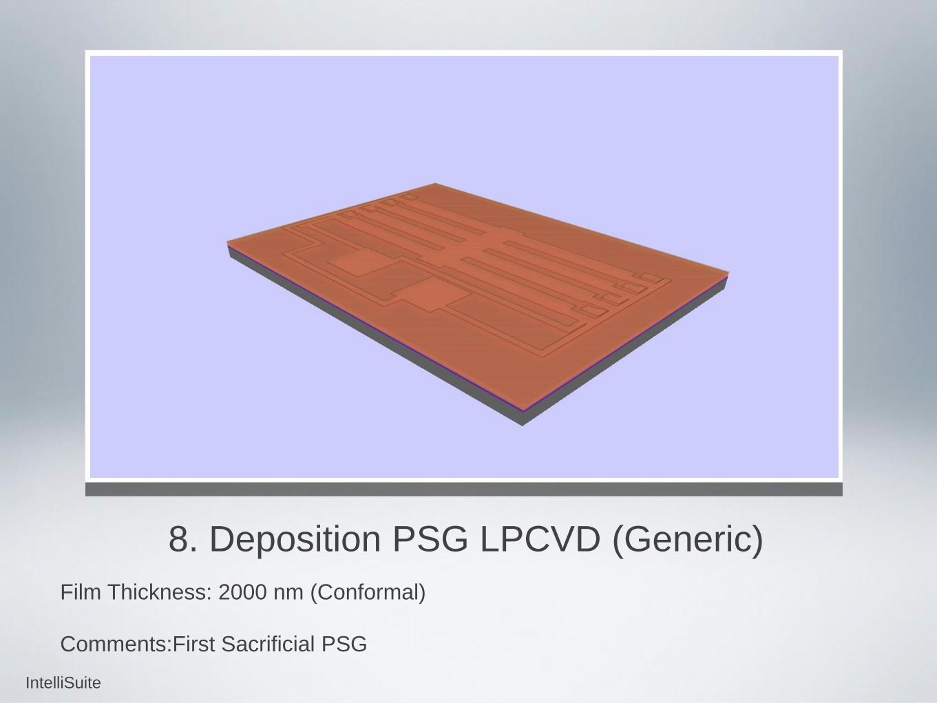
8. Deposition PSG LPCVD (Generic)
Film Thickness: 2000 nm (Conformal)
Comments:First Sacrificial PSG

IntelliSuite
9. Lithography UV Contact (Suss)
DIMPLE
(GDS#50);Leave Photoresist OutsideComments:Dimples mask

IntelliSuite
10. Etch PSG Generic (Generic)
Etch Thickness: 750 nm (Partial Etch)
Comments:

IntelliSuite
11. Lithography UV Contact (Suss)
ANCHOR1
(GDS#43);Leave Photoresist OutsideComments:Anchor 1 mask

IntelliSuite
12. Etch PSG Generic (Generic)
Etch Thickness: 2000 nm (Etch Through)
Comments:

IntelliSuite
13. Deposition PolySi LPCVD (SiH4)
Film Thickness: 2000 nm (Conformal)
Comments:Deposition of second poly (POLY1)

IntelliSuite
14. Lithography UV Contact (Suss)
POLY1
(GDS#45);Leave Photoresist InsideComments:Define POLY1, first structural layer

IntelliSuite
15. Etch PolySi Dry (SF6-Plasma)
Etch Thickness: 2000 nm (Etch Through)
Comments:

IntelliSuite
16. Lithography UV Contact (Suss)
HOLE1
(GDS#0);Leave Photoresist OutsideComments:provide holes for POLY1

IntelliSuite
17. Etch PolySi Dry (SF6-Plasma)
Etch Thickness: 2000 nm (Etch Through)
Comments:

IntelliSuite
18. Deposition PSG Generic (Generic)
Film Thickness: 750 nm (Conformal)
Comments:Deposition of second sacrificial PSG

IntelliSuite
19. Lithography UV Contact (Suss)
POLY1_POLY2_VIA
(GDS#47);Leave Photoresist OutsideComments:P1P2VIA, Provide structural via to connect POLY1 and POLY2

IntelliSuite
20. Etch PSG Generic (Generic)
Etch Thickness: 750 nm (Etch Through)
Comments:

IntelliSuite
21. Lithography UV Contact (Suss)
ANCHOR2
(GDS#52);Leave Photoresist OutsideComments:ANCHOR2: Provide Anchors for second structural POLY

IntelliSuite
22. Etch PSG Generic (Generic)
Etch Thickness: 750 nm (Etch Through)
Comments:

IntelliSuite
23. Deposition PolySi LPCVD (SiH4)
Film Thickness: 1500 nm (Conformal)
Comments:Deposition of second strucutral POLY (POLY2)

IntelliSuite
24. Lithography UV Contact (Suss)
POLY2
(GDS#49);Leave Photoresist InsideComments:Define second structural level (POLY2)

IntelliSuite
25. Etch PolySi Dry (SF6-Plasma)
Etch Thickness: 1500 nm (Etch Through)
Comments:

IntelliSuite
26. Lithography UV Contact (Suss)
HOLE2
(GDS#1);Leave Photoresist OutsideComments:provide holes for POLY2

IntelliSuite
27. Etch PolySi Dry (SF6-Plasma)
Etch Thickness: 1500 nm (Etch Through)
Comments:

IntelliSuite
28. Deposition PR-S3800 Spin (S3810)
Film Thickness: 500 nm (Conformal)
Comments:

IntelliSuite
29. Lithography UV Contact (Suss)
METAL
(GDS#51);Leave Photoresist OutsideComments:pattern METAL level for Lift-off

IntelliSuite
30. Etch PR-S3800 Wet (1112A)
Etch Thickness: 500 nm (Etch Through)
Comments:

IntelliSuite
31. Deposition Al Sputter (Ar-Ambient)
Film Thickness: 1000 nm (Conformal)
Comments:

IntelliSuite
32. Lithography UV Contact (Suss)
HOLEM
(GDS#48);Leave Photoresist OutsideComments:pattern HOLES in METAL

IntelliSuite
33. Etch Al Wet (PAN)
Etch Thickness: 1000 nm (Etch Through)
Comments:

IntelliSuite
34. Etch PR-S3800 Wet (Lift-off)
Etch Thickness: Lift off
Comments:

IntelliSuite
35. Etch PSG Generic (Generic)
Etch Thickness: Sacrificial Etch
Comments:

IntelliSuite
Color Key
Material Step Transparency Color
Si3N4 2 194
PolySi 3 255
PSG 8 32
PolySi 13 255
PSG 18 32
PolySi 23 255
PR-S3800 28 128
Al 31 128

IntelliSuite
Summary (1-1)Lithography: 12 Mask Levels
Layer NameLayer
NumberSide
Leave
PhotoresistComments
POLY013 Top Inside
Pattern ground plane
HOLE041 Top Outside
provide holes for POLY0
DIMPLE50 Top Outside
Dimples mask
ANCHOR143 Top Outside
Anchor 1 mask
POLY145 Top Inside
Define POLY1, first structural layer
HOLE10 Top Outside
provide holes for POLY1
POLY1_POLY2_VIA47 Top Outside
P1P2VIA, Provide structural via to connect POLY1
and POLY2
ANCHOR252 Top Outside
ANCHOR2: Provide Anchors for second structural
POLY

IntelliSuite
Summary (1-2)Lithography: 12 Mask Levels
Layer NameLayer
NumberSide
Leave
PhotoresistComments
POLY249 Top Inside
Define second structural level (POLY2)
HOLE21 Top Outside
provide holes for POLY2
METAL51 Top Outside
pattern METAL level for Lift-off
HOLEM48 Top Outside
pattern HOLES in METAL

IntelliSuite
Summary (2)Depositions/Implants: 8
Material Process Process ID SideThickness
(nm)Comments
Si3N4 PECVD Ar Top 600
PolySi LPCVD SiH4 Top 500Deposit GND POLY
PSG(Sacrifice) LPCVD Generic Top 2000First Sacrificial PSG
PolySi LPCVD SiH4 Top 2000
Deposition of second poly
(POLY1)
PSG(Sacrifice) Generic Generic Top 750
Deposition of second
sacrificial PSG
PolySi LPCVD SiH4 Top 1500
Deposition of second
strucutral POLY (POLY2)
PR-S3800 Spin S3810 Top 500
Al Sputter Ar-Ambient Top 1000

IntelliSuite
Summary (3-1)Etches: 14
Material Process Process ID Side Etch depth (nm) Comments
PolySi Dry SF6-Plasma Top 500(Etch Through)
PolySi Dry SF6-Plasma Top 500(Etch Through)
PSG Generic Generic Top 750(Partial Etch)
PSG Generic Generic Top 2000(Etch Through)
PolySi Dry SF6-Plasma Top 2000(Etch Through)
PolySi Dry SF6-Plasma Top 2000(Etch Through)
PSG Generic Generic Top 750(Etch Through)
PSG Generic Generic Top 750(Etch Through)

IntelliSuite
Summary (3-2)Etches: 14
Material Process Process ID Side Etch depth (nm) Comments
PolySi Dry SF6-Plasma Both 1500(Etch Through)
PolySi Dry SF6-Plasma Both 1500(Etch Through)
PR-S3800 Wet 1112A Top 500(Etch Through)
Al Wet PAN Top 1000(Etch Through)
PR-S3800 Wet Lift-off Top Lift off
PSG Generic Generic Top Sacrificial Etch

www.intellisense.com
IntelliSuiteCompex Design Made Easy
Clean Room
Your Virtual Fab
Blueprint
MEMS Design Editor
Fastfield
Incredibly fast multiphysics
Synple
System Synthesis & Simulation
EDA Linker
Link to your EDA tools
Clean Room, Blueprint, FastField, Synple, EDALinker and IntelliSuite are trademarks of IntelliSense Corporation. All Rights Reserved.