General Specification for PMU series - Flex Power Modules
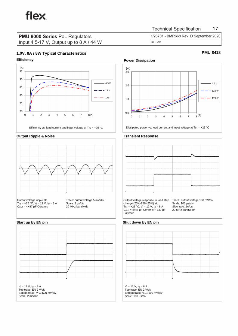
34
INTERNAL USE ONLY PRODUCT SPECIFICATION 1 (4) Prepared (Subject resp) No. jidgjian Grace Jiang 1/1301-BMR668 Approved (Document resp) Checked Date Rev jidgjian Grace Jiang Rainbo 1/3/2020 C Z Key Features • Small size 7.5 x 7.5 x 5.4 mm (0.3 x 0.3 x 0.21 in) • 0.6 V – 5.5V output voltage range • 8A maximum output current • High efficiency, typ. 92.7% at 12 Vin, 3.3 Vout, 6A load • Adjustable fixed switching frequency (200 kHz to 1.6 MHz) • Control loop with fast load transient response • Allows synchronization to an external clock • Meets safety requirements according to IEC/EN/UL 62368-1 • MTBF 171.82 Mh General Characteristics • Output short-circuit protection • Over temperature protection • Remote control • Output voltage adjust function • Soft start (SS) or Tracking is configurable • Power Good • Highly automated manufacturing ensures quality • ISO 9001/14001 certified supplier Safety Approvals Design for Environment Meets requirements in high- temperature lead-free soldering processes. Contents Ordering Information ............................................................. 2 General Information ............................................................. 2 Safety Specification ............................................................. 3 Pin-out Descriptions ............................................................. 4 Absolute Maximum Ratings ............................................................. 5 Electrical Specification 4 A / 0.6-5.5 V PMU8218 ............................................. 6 6 A / 0.6-5.5 V PMU8318 ........................................... 11 8 A / 0.6-5.5 V PMU8418 ........................................... 16 Operating Information ........................................................... 21 Thermal Consideration ........................................................... 29 Mechanical Information ........................................................... 31 Soldering Information ........................................................... 32 Delivery Package Information ........................................................... 33 Product Qualification Specification ........................................................... 34 PMU 8000 Series PoL Regulators Input 4.5-17 V, Output up to 8 A / 44 W © Flex Technical Specification 1/28701 - BMR668 Rev. C January 2020 PMU 8000 Series PoL Regulators Input 4.5-17 V, Output up to 8 A / 44 W © Flex Technical Specification 1/28701 - BMR668 Rev. D September 2020 PMU 8000 Series PoL Regulators Input 4.5-17 V, Output up to 8 A / 44 W © Flex Technical Specification 1/28701 - BMR668 Rev. D September 2020 PMU 8000 Series PoL Regulators Input 4.5-17 V, Output up to 8 A / 44 W © Flex Technical Specification 1/28701 - BMR668 Rev. D September 2020 PMU 8000 Series PoL Regulators Input 4.5-17 V, Output up to 8 A / 44 W © Flex Technical Specification 1/28701 - BMR668 Rev. D September 2020
-
Upload
khangminh22 -
Category
Documents
-
view
1 -
download
0
Transcript of General Specification for PMU series - Flex Power Modules

INTERNAL USE ONLY
PRODUCT SPECIFICATION
1 (4) Prepared (Subject resp) No.
jidgjian Grace Jiang 1/1301-BMR668 Approved (Document resp) Checked Date Rev
jidgjian Grace Jiang Rainbo 1/3/2020 C Z Key Features • Small size
7.5 x 7.5 x 5.4 mm (0.3 x 0.3 x 0.21 in) • 0.6 V – 5.5V output voltage range • 8A maximum output current • High efficiency, typ. 92.7% at 12 Vin, 3.3 Vout, 6A load • Adjustable fixed switching frequency
(200 kHz to 1.6 MHz) • Control loop with fast load transient response • Allows synchronization to an external clock • Meets safety requirements according to IEC/EN/UL
62368-1 • MTBF 171.82 Mh General Characteristics • Output short-circuit protection • Over temperature protection • Remote control • Output voltage adjust function • Soft start (SS) or Tracking is configurable • Power Good • Highly automated manufacturing ensures quality • ISO 9001/14001 certified supplier
Safety Approvals Design for Environment
Meets requirements in high-
temperature lead-free soldering processes.
Contents Ordering Information ............................................................. 2 General Information ............................................................. 2 Safety Specification ............................................................. 3 Pin-out Descriptions ............................................................. 4 Absolute Maximum Ratings ............................................................. 5 Electrical Specification 4 A / 0.6-5.5 V PMU8218 ............................................. 6 6 A / 0.6-5.5 V PMU8318 ........................................... 11 8 A / 0.6-5.5 V PMU8418 ........................................... 16 Operating Information ........................................................... 21 Thermal Consideration ........................................................... 29 Mechanical Information ........................................................... 31 Soldering Information ........................................................... 32 Delivery Package Information ........................................................... 33 Product Qualification Specification ........................................................... 34
PMU 8000 Series PoL Regulators Input 4.5-17 V, Output up to 8 A / 44 W © Flex
Technical Specification 1/28701 - BMR668 Rev. C January 2020PMU 8000 Series PoL Regulators
Input 4.5-17 V, Output up to 8 A / 44 W © Flex
Technical Specification 1/28701 - BMR668 Rev. D September 2020PMU 8000 Series PoL Regulators
Input 4.5-17 V, Output up to 8 A / 44 W © Flex
Technical Specification 1/28701 - BMR668 Rev. D September 2020PMU 8000 Series PoL Regulators
Input 4.5-17 V, Output up to 8 A / 44 W © Flex
Technical Specification 1/28701 - BMR668 Rev. D September 2020PMU 8000 Series PoL Regulators
Input 4.5-17 V, Output up to 8 A / 44 W © Flex
Technical Specification 1/28701 - BMR668 Rev. D September 2020

INTERNAL USE ONLY
PRODUCT SPECIFICATION
2 (4) Prepared (Subject resp) No.
jidgjian Grace Jiang 1/1301-BMR668 Approved (Document resp) Checked Date Rev
jidgjian Grace Jiang Rainbo 9/22/2020 D Z Ordering Information Product number Output PMU8218 0.6-5.5V, 4A/22W PMU8318 0.6-5.5V, 6A/33W PMU8418 0.6-5.5V, 8A/44W Product number and Packaging
PMU8X18 n1 Options n1 Delivery package information ο
Options Description n1
C D
Tape and reel (600 pcs /reel) Tape and reel (150 pcs /reel)
Example: PMU8318 C means a surface mounted, positive logic product with tape and reel packaging, the reel capacity is 600 pcs products per reel. General Information Reliability
The failure rate (λ) and mean time between failures (MTBF= 1/λ) is calculated at max output power and an operating ambient temperature (TA) of +40°C. Flex Power uses Telcordia SR-332 Issue 4 to calculate the mean steady-state failure rate and standard deviation (σ). Telcordia SR-332 Issue 4 also provides techniques to estimate the upper confidence levels of failure rates based on the mean and standard deviation.
Mean steady-state failure rate, λ Std. deviation, σ 6 nFailures/h 3.4 nFailures/h MTBF (mean value) for the PMU series = 171.82 Mh. MTBF at 90% confidence level = 97.88 Mh Compatibility with RoHS requirements The products are compatible with the relevant clauses and requirements of the RoHS directive 2011/65/EU and 2015/863 and have a maximum concentration value of 0.1% by weight in homogeneous materials for lead, mercury, hexavalent chromium, PBB, PBDE, DEHP, BBP, DBP, DIBP and of 0.01% by weight in homogeneous materials for cadmium. Exemptions in the RoHS directive utilized in Flex Power products are found in the Statement of Compliance document. Flex Power fulfills and will continuously fulfill all its obligations under regulation (EC) No 1907/2006 concerning the registration, evaluation, authorization and restriction of
chemicals (REACH) as they enter into force and is through product materials declarations preparing for the obligations to communicate information on substances in the products. Quality Statement The products are designed and manufactured in an industrial environment where quality systems and methods like ISO 9000, Six Sigma, and SPC are intensively in use to boost the continuous improvements strategy. Infant mortality or early failures in the products are screened out and they are subjected to an ATE-based final test. Conservative design rules, design reviews and product qualifications, plus the high competence of an engaged work force, contribute to the high quality of the products. Warranty Warranty period and conditions are defined in Flex General Terms and Conditions of Sale. Limitation of Liability Flex does not make any other warranties, expressed or implied including any warranty of merchantability or fitness for a particular purpose (including, but not limited to, use in life support applications, where malfunctions of product can cause injury to a person’s health or life). © Flex 2020 The information and specifications in this technical specification is believed to be correct at the time of publication. However, no liability is accepted for inaccuracies, printing errors or for any consequences thereof. Flex reserves the right to change the contents of this technical specification at any time without prior notice.
PMU 8000 Series PoL Regulators Input 4.5-17 V, Output up to 8 A / 44 W © Flex
Technical Specification 1/28701 - BMR668 Rev. D September 2020
2PMU 8000 Series PoL Regulators Input 4.5-17 V, Output up to 8 A / 44 W © Flex
Technical Specification 1/28701 - BMR668 Rev. D September 2020
2

INTERNAL USE ONLY
PRODUCT SPECIFICATION
3 (4) Prepared (Subject resp) No.
jidgjian Grace Jiang 1/1301-BMR668 Approved (Document resp) Checked Date Rev
jidgjian Grace Jiang Rainbo 9/22/2020 D Z
Safety Specification General information Flex DC/DC converters and DC/DC regulators are designed in accordance with the safety standards IEC 62368-1, EN 62368-1 and UL 62368-1 Audio/video, information and communication technology equipment - Part 1: Safety requirements IEC/EN/UL 62368-1 contains requirements to prevent injury or damage due to the following hazards:
• Electrical shock • Electrically-caused fire • Injury caused by hazardous substances • Mechanically-caused injury • Skin burn • Radiation-caused injury
On-board DC/DC converters, Power interface modules and DC/DC regulators are defined as component power supplies. As components they cannot fully comply with the provisions of any safety requirements without “conditions of acceptability”. Clearance between conductors and between conductive parts of the component power supply and conductors on the board in the final product must meet the applicable safety requirements. Certain conditions of acceptability apply for component power supplies with limited stand-off (see Mechanical Information for further information). It is the responsibility of the installer to ensure that the final product housing these components complies with the requirements of all applicable safety standards and regulations for the final product. Component power supplies for general use shall comply with the requirements in IEC/EN/UL 62368-1. Product related standards, e.g. IEEE 802.3af Power over Ethernet, and ETS-300132-2 Power interface at the input to telecom equipment, operated by direct current (dc) are based on IEC/EN/UL 60950-1 with regards to safety. Flex DC/DC converters, Power interface modules and DC/DC regulators are UL 62368-1 recognized and certified in accordance with EN 62368-1. The flammability rating for all construction parts of the products meet requirements for V-0 class material according to IEC 60695-11-10, Fire hazard testing, test flames – 50 W horizontal and vertical flame test methods.
Non - isolated DC/DC regulators The DC/DC regulator output is ES1 energy source if the input source meets the requirements for ES1 according to IEC/EN/UL 62368-1.
PMU 8000 Series PoL Regulators Input 4.5-17 V, Output up to 8 A / 44 W © Flex
Technical Specification 1/28701 - BMR668 Rev. D September 2020
3PMU 8000 Series PoL Regulators Input 4.5-17 V, Output up to 8 A / 44 W © Flex
Technical Specification 1/28701 - BMR668 Rev. D September 2020
3

FLEX CONFIDENTIAL PRODUCT SPECIFICATION
1 (27)
Prepared (Subject resp) No.
jidrguaa Rainbo Gu 2/1301-BMR 668 8318 Uen Approved (Document resp) Checked Date Rev
jidrguaa Rainbo Gu jidrguaa 6/18/2019 A Pin configuration and functions
Top view
Pin Functions Pin Designation Type Function
3, 9, 23 AGND G Analog ground, reference for logic signals. Connect these pins together using a plane but do not connect these pins to PGND. These pins are connected internally.
4 DNC Do Not Connect.
10 EN I Enable. Leave open or pull high to enable the device. Connect a voltage divider to implement adjustable undervoltage lockout and hysteresis. See section Undervoltage Lockout (UVLO).
2 FB I Regulator feedback input. Connect the output voltage feedback resistor divider to this pin. See section Output Voltage Adjust (FB).
12, 13, 14, 15, 18, 19, 20, 21 PGND G Power ground. This is the common ground connection for VIN and VOUT
power connections.
7 PGOOD O
Power-Good indicator. This open drain output asserts low if the output voltage is outside of the PGOOD thresholds, VIN is lower than its UVLO threshold, EN is low, device is in thermal shutdown or device is in soft-start. Use a 10-kΩ to 100-kΩ pullup resistor to logic rail or other DC voltage no higher than 6.5 V.
24 RT/CLK I
Switching frequency setting pin. In RT mode, an external timing resistor adjusts the switching frequency. In CLK mode, the device synchronizes to an external clock input to this pin. See sections Switching Frequency (RT) and Synchronization (CLK).
6 SS/TR I
Soft-start and tracking pin. Connecting an external capacitor to this pin adjusts the output voltage soft start ramp slower than its 1.25-ms default setting. This pin can also be used for tracking and sequencing. See section Soft Start (SS) and Output Voltage Sequencing and Tracking (TR).
16, 17 SW O Switch node. Leave these pins open.
5 LO I Loop Optimization pin. Internal loop compensation network. Connect the required Loop Optimization resistor between this pin and AGND. Do not leave this pin floating. See section Loop Optimization (LO).
11, 22 VIN I Input voltage. Connect both pins to the input power source with a low impedance connection.
1, 8 VOUT O Output voltage. These pins are connected to the internal output inductor. Connect these pins to the output load.
PMU 8000 Series PoL Regulators Input 4.5-17 V, Output up to 8 A / 44 W © Flex
Technical Specification 1/28701 - BMR668 Rev. D September 2020PMU 8000 Series PoL Regulators
Input 4.5-17 V, Output up to 8 A / 44 W © Flex
Technical Specification 1/28701 - BMR668 Rev. D September 2020
4PMU 8000 Series PoL Regulators Input 4.5-17 V, Output up to 8 A / 44 W © Flex
Technical Specification 1/28701 - BMR668 Rev. D September 2020
4PMU 8000 Series PoL Regulators Input 4.5-17 V, Output up to 8 A / 44 W © Flex
Technical Specification 1/28701 - BMR668 Rev. D September 2020
4

FLEX CONFIDENTIAL PRODUCT SPECIFICATION
2 (27)
Prepared (Subject resp) No.
jidrguaa Rainbo Gu 2/1301-BMR 668 8318 Uen Approved (Document resp) Checked Date Rev
jidrguaa Rainbo Gu jidrguaa 6/18/2019 A Typical Application Circuit
Absolute Maximum Ratings
Characteristics min max Unit Tref Operating Temperature –40 125 °C TS Storage temperature –40 150 °C
Input Voltage VIN -0.3 19 V EN, PGOOD, SS/TRK, RT/CLK, FB -0.3 6.5 V AGND to PGND -0.3 0.3 V
Output voltage SW -1 VIN+1 V
SW (<10ns transients) -3 VIN+3 V
VOUT -0.3 VIN V Stress in excess of Absolute Maximum Ratings may cause permanent damage. Absolute Maximum Ratings, sometimes referred to as no destruction limits, are normally tested with one parameter at a time exceeding the limits in the Electrical Specification. If exposed to stress above these limits, function and performance may degrade in an unspecified manner.
Recommended Operating Conditions Characteristics min typ max Unit Input voltage, Note 1 4.5 12 17 V Output voltage 0.6 5.5 V
EN voltage Rising threshold 1.2 1.26
V Falling threshold 1.1 1.15
PGOOD pullup voltage 5.5 V PGOOD sink current 1 mA RT/CLK voltage range 0 5.5 V PMU8218 0 4 Output current PMU8318 0 6 A PMU8418 0 8 Operating temperature, TP1 -40 105 °C
Note 1. For output voltages from 0.6V to 5 V, the recommended minimum VIN is 4.5 V or (VOUT + 1 V), whichever is greater. For output voltages 5.0 V to 5.5 V, the recommended minimum VIN is (VOUT + 2 V).
PMU 8000 Series PoL Regulators Input 4.5-17 V, Output up to 8 A / 44 W © Flex
Technical Specification 1/28701 - BMR668 Rev. D September 2020PMU 8000 Series PoL Regulators
Input 4.5-17 V, Output up to 8 A / 44 W © Flex
Technical Specification 1/28701 - BMR668 Rev. D September 2020
5PMU 8000 Series PoL Regulators Input 4.5-17 V, Output up to 8 A / 44 W © Flex
Technical Specification 1/28701 - BMR668 Rev. D September 2020
5PMU 8000 Series PoL Regulators Input 4.5-17 V, Output up to 8 A / 44 W © Flex
Technical Specification 1/28701 - BMR668 Rev. D September 2020
5

FLEX CONFIDENTIAL PRODUCT SPECIFICATION
3 (27)
Prepared (Subject resp) No.
jidrguaa Rainbo Gu 2/1301-BMR 668 8318 Uen Approved (Document resp) Checked Date Rev
jidrguaa Rainbo Gu jidrguaa 6/18/2019 A
1.0V, 4A / 4W Electrical Specification PMU8218
TP1 = -40 to +105 ºC, VI = 4.5 to 17 V, unless otherwise specified under Conditions. Typical values given at: TP1 = +25 °C, VI = 12 V, max IO, unless otherwise specified under Conditions. Additional CIN = 100 µF Electrolytic + 2x10 µF Ceramic capacitors and COUT = 4x47 µF Ceramic capacitors. Characteristics Conditions min typ max Unit VI Input voltage range 4.5 12 17 V VIoff Turn-off input voltage Decreasing input voltage 3.7 3.9 V VIon Turn-on input voltage Increasing input voltage 4.1 4.3 V CI Internal input capacitance 2 μF PO Output power 0 4.0 W
η Efficiency VI = 12 V, 50 % of max IO 87.6
% VI = 12 V, max IO 88.5
Pd Power Dissipation VI = 12 V, 50 % of max IO 0.28 W VI = 12 V, max IO 0.52 W
Pli Input idling power VI = 12 V 0.17 W
PRC Input standby power VI = 12 V 20 mW fs Switching frequency 10-100 % of max IO 350 kHz
VOi Output voltage initial setting and accuracy VI = 12 V, max IO 1.0 V
VO
Output voltage tolerance band 10-100 % of max IO ±1.5 %
Idling voltage VI = 12 V, IO = min IO 1.0 V
Line regulation IO = max Io ±0.1 mV
Load regulation VI = 12 V, 0-100 % of max IO ±0.9 mV
Vtr Load transient voltage deviation
VI = 12 V, Load step 25-75-25 % of max IO, di/dt = 2 A/μs With Loop Optimization COUT = 518 µF; RLO = 3 kΩ
±29 mV
ttr Load transient recovery time 37 µs
tr Ramp-up time (from 10−90 % of VO) VI = 12 V, 100 % of max IO
1.1 ms
ts Start-up time (from VI connection to 90 % of VO) 1.6 ms
tf VI shut-down fall time. (from VI off to 10 % of VO)
VI = 12 V IO = max Io 12.8 ms
IO = min Io 1.0 s
tRC tInh
RC start-up time VI = 12 V, max IO 1.5 ms RC shut-down fall time (from RC off to 10 % of VO)
VI = 12 V IO = max Io 120 µs
IO = min Io 1.2 s
IO Output current 0 4 A Ilim Current limit threshold 11.7 A Isc Short circuit current RMS, 12 mΩ short 2.3 A
Cin External input capacitance Ceramic type 20
µF Non-ceramic type, Note 2 100
Cout External output capacitance Note 3 188 1500 µF VOac Output ripple & noise VI = 12 V IO = max Io 8.5 mVp-p
Note 2. For Non-ceramic type of external input capacitor, a 100 µF bulk capacitor is recommended for application with transient load requirement. An OS-CON capacitor is recommended when adding the bulk capacitor in low temperature. Note 3. A minimum external output ceramic capacitance is required. In low output voltage, more capacitance might to be added considering capacitance derating. The maximum external output capacitor could only be ceramic type or combination of ceramic and a single non-ceramic type.
PMU 8000 Series PoL Regulators Input 4.5-17 V, Output up to 8 A / 44 W © Flex
Technical Specification 1/28701 - BMR668 Rev. D September 2020PMU 8000 Series PoL Regulators
Input 4.5-17 V, Output up to 8 A / 44 W © Flex
Technical Specification 1/28701 - BMR668 Rev. D September 2020
6PMU 8000 Series PoL Regulators Input 4.5-17 V, Output up to 8 A / 44 W © Flex
Technical Specification 1/28701 - BMR668 Rev. D September 2020
6PMU 8000 Series PoL Regulators Input 4.5-17 V, Output up to 8 A / 44 W © Flex
Technical Specification 1/28701 - BMR668 Rev. D September 2020
6

FLEX CONFIDENTIAL PRODUCT SPECIFICATION
4 (27)
Prepared (Subject resp) No.
jidrguaa Rainbo Gu 2/1301-BMR 668 8318 Uen Approved (Document resp) Checked Date Rev
jidrguaa Rainbo Gu jidrguaa 6/18/2019 A
1.0V, 4A / 4W Typical Characteristics
PMU 8218 Efficiency
Power Dissipation
Efficiency vs. load current and input voltage at TP1 = +25 °C Dissipated power vs. load current and input voltage at TP1 = +25 °C
Output Ripple & Noise Transient Response
Output voltage ripple at: TP1 = +25 °C, VI = 12 V, IO = 4 A COUT = 4X47 µF Ceramic
Trace: output voltage 5 mV/div Scale: 2 µs/div 20 MHz bandwidth
Output voltage response to load step change (25%-75%-25%) at: TP1 = +25 °C, VI = 12 V, IO = 4 A COUT = 4x47 µF Ceramic + 330 µF Polymer
Trace: output voltage 50 mV/div Scale: 100 µs/div Slew rate: 2A/µs 20 MHz bandwidth
Start up by EN pin Shut down by EN pin
VI = 12 V, IO = 4 A Top trace: EN 2 V/div Bottom trace: VOUT 500 mV/div Scale: 2 ms/div
VI = 12 V, IO = 4 A Top trace: EN 2 V/div Bottom trace: VOUT 500 mV/div Scale: 200 µs/div
70
75
80
85
90
95
0 1 2 3 4
[%]
[A]
4.5 V
12 V
17V
0.0
0.2
0.4
0.6
0.8
1.0
0 1 2 3 4
[W]
[A]
4.5 V
12.0 V
17.0 V
PMU 8000 Series PoL Regulators Input 4.5-17 V, Output up to 8 A / 44 W © Flex
Technical Specification 1/28701 - BMR668 Rev. D September 2020PMU 8000 Series PoL Regulators
Input 4.5-17 V, Output up to 8 A / 44 W © Flex
Technical Specification 1/28701 - BMR668 Rev. D September 2020
7PMU 8000 Series PoL Regulators Input 4.5-17 V, Output up to 8 A / 44 W © Flex
Technical Specification 1/28701 - BMR668 Rev. D September 2020
7PMU 8000 Series PoL Regulators Input 4.5-17 V, Output up to 8 A / 44 W © Flex
Technical Specification 1/28701 - BMR668 Rev. D September 2020
7

FLEX CONFIDENTIAL PRODUCT SPECIFICATION
5 (27)
Prepared (Subject resp) No.
jidrguaa Rainbo Gu 2/1301-BMR 668 8318 Uen Approved (Document resp) Checked Date Rev
jidrguaa Rainbo Gu jidrguaa 6/18/2019 A
3.3V, 4A / 13.2W Electrical Specification PMU8218 TP1 = -40 to +105 ºC, VI = 4.5 to 17 V, unless otherwise specified under Conditions. Typical values given at: TP1 = +25 °C, VI = 12 V, max IO, unless otherwise specified under Conditions. Additional CIN = 100 µF Electrolytic + 2x10 µF Ceramic capacitors and COUT = 4x47 µF Ceramic capacitors. Characteristics Conditions min typ max Unit VI Input voltage range 4.5 12 17 V VIoff Turn-off input voltage Decreasing input voltage 3.7 3.9 V VIon Turn-on input voltage Increasing input voltage 4.1 4.3 V CI Internal input capacitance 2 µF PO Output power 0 13.2 W
η Efficiency VI = 12 V, 50 % of max IO 91.4
% VI = 12 V, max IO 93.1
Pd Power Dissipation VI = 12 V, 50 % of max IO 0.62 W VI = 12 V, max IO 1.0 W
Pli Input idling power VI = 12 V 0.4 W PRC Input standby power VI = 12 V 20 mW fs Switching frequency 0-100 % of max IO 1.0 MHz
VOi Output voltage initial setting and accuracy VI = 12 V, max IO 3.31 V
VO
Output voltage tolerance band 10-100 % of max IO ±1.5 %
Idling voltage VI = 12 V, IO = min IO 3.31 V
Line regulation IO = max IO ±0.4 mV Load regulation VI = 12 V, 0-100 % of max IO ±1.6 mV
Vtr Load transient voltage deviation
VI = 12 V, Load step 25-75-25 % of max IO, di/dt = 2 A/µs With Loop Optimization COUT = 518 µF; RLO = 11 k
±40 mV
ttr Load transient recovery time 80 μs
tr Ramp-up time (from 10−90 % of VO) VI = 12 V, 100 % of max IO
1.1 ms
ts Start-up time (from VI connection to 90 % of VO) 1.7 ms
tf VI shut-down fall time. (from VI off to 10 % of VO)
VI = 12 V IO = max Io 8.2 ms
IO = min Io 0.13 s
tRC tInh
RC start-up time VI = 12 V, max IO 1.4 ms RC shut-down fall time (from RC off to 10 % of VO)
VI = 12 V IO = max Io 0.36 ms
IO = min Io 1.3 s
IO Output current 0 4 A Ilim Current limit threshold 11.7 A Isc Short circuit current RMS, 12 mΩ short 2.35 A
Cin External input capacitance Ceramic type 20
µF Non-ceramic type, Note 2 100
Cout External output capacitance Note 3 47 1500 µF VOac Output ripple & noise VI = 12 V IO = max IO 3.9 mVp-p Note 2. For Non-ceramic type of external input capacitor, a 100 µF bulk capacitor is recommended for application with transient load requirement. An OS-CON capacitor is recommended when adding the bulk capacitor in low temperature. Note 3. A minimum external output ceramic capacitance is required. In low output voltage, more capacitance might to be added considering capacitance derating. The maximum external output capacitor could only be ceramic type or combination of ceramic and a single non-ceramic type.
PMU 8000 Series PoL Regulators Input 4.5-17 V, Output up to 8 A / 44 W © Flex
Technical Specification 1/28701 - BMR668 Rev. D September 2020PMU 8000 Series PoL Regulators
Input 4.5-17 V, Output up to 8 A / 44 W © Flex
Technical Specification 1/28701 - BMR668 Rev. D September 2020
8PMU 8000 Series PoL Regulators Input 4.5-17 V, Output up to 8 A / 44 W © Flex
Technical Specification 1/28701 - BMR668 Rev. D September 2020
8PMU 8000 Series PoL Regulators Input 4.5-17 V, Output up to 8 A / 44 W © Flex
Technical Specification 1/28701 - BMR668 Rev. D September 2020
8

FLEX CONFIDENTIAL PRODUCT SPECIFICATION
6 (27)
Prepared (Subject resp) No.
jidrguaa Rainbo Gu 2/1301-BMR 668 8318 Uen Approved (Document resp) Checked Date Rev
jidrguaa Rainbo Gu jidrguaa 6/18/2019 A
3.3V, 4A / 13.2W Typical Characteristics
PMU 8218 Efficiency
Power Dissipation
Efficiency vs. load current and input voltage at TP1 = +25 °C Dissipated power vs. load current and input voltage at TP1 = +25 °C
Output Ripple & Noise Transient Response
Output voltage ripple at: TP1 = +25 °C, VI = 12 V, IO = 4 A COUT = 4X47 µF Ceramic
Trace: output voltage 2 mV/div Scale: 1 µs/div 20MHz bandwidth
Output voltage response to load step change (25%-75%-25%) at: TP1 = +25 °C, VI = 12 V, IO = 4 A COUT = 4x47 µF Ceramic + 330 µF Polymer
Trace: output voltage 50 mV/div Scale: 100 µs/div, Slew rate: 2 A/µs 20MHz bandwidth
Start up by EN pin Shut down by EN pin
VI = 12 V, IO = 4 A Top trace: EN 2 V/div Bottom trace: VOUT 2 V/div Scale: 2 ms/div
VI = 12 V, IO = 4 A Top trace: EN 2 V/div Bottom trace: VOUT 2 V/div Scale: 200 µs/div
70
75
80
85
90
95
100
0 1 2 3 4
[%]
[A]
4.5 V
12 V
17.0 V
0.0
0.5
1.0
1.5
2.0
0 1 2 3 4
[W]
[A]
4.5 V
12.0 V
17.0 V
PMU 8000 Series PoL Regulators Input 4.5-17 V, Output up to 8 A / 44 W © Flex
Technical Specification 1/28701 - BMR668 Rev. D September 2020PMU 8000 Series PoL Regulators
Input 4.5-17 V, Output up to 8 A / 44 W © Flex
Technical Specification 1/28701 - BMR668 Rev. D September 2020
9PMU 8000 Series PoL Regulators Input 4.5-17 V, Output up to 8 A / 44 W © Flex
Technical Specification 1/28701 - BMR668 Rev. D September 2020
9PMU 8000 Series PoL Regulators Input 4.5-17 V, Output up to 8 A / 44 W © Flex
Technical Specification 1/28701 - BMR668 Rev. D September 2020
9

FLEX CONFIDENTIAL PRODUCT SPECIFICATION
7 (27)
Prepared (Subject resp) No.
jidrguaa Rainbo Gu 2/1301-BMR 668 8318 Uen Approved (Document resp) Checked Date Rev
jidrguaa Rainbo Gu jidrguaa 6/18/2019 A
Typical Characteristics (VIN = 12V)
PMU 8218 Efficiency
Power Dissipation
Efficiency vs. load current and output voltage at TP1 = +25 °C Dissipated power vs. load current and output voltage at TP1 = +25 °C
Output voltage ripple Output current derating
Ripple voltage vs output current at TP1 = +25 °C
Load current vs. ambient air temperature and airflow at Vo = 1.0 V
Output current derating Output current derating
Load current vs. ambient air temperature and airflow at Vo = 3.3 V. Load current vs. ambient air temperature and airflow at Vo = 5.0 V.
40
50
60
70
80
90
100
0 1 2 3 4
[%]
[A]
0.6V, 250KHz1V, 350KHz1.35V, 500KHz1.8V, 600KHz2.5V, 800KHz3.3V, 1MHz5V, 1.25MHz5.5V, 1.35MHz
0
1
2
3
0 1 2 3 4
[W]
[A]
0.6V, 250KHz1V, 350KHz1.35V, 500KHz1.8V, 600KHz2.5V, 800KHz3.3V, 1MHz5V, 1.25MHz5.5V, 1.35MHz
0
5
10
15
20
25
30
0 1 2 3 4
[mV]
[A]
0.6V, 250KHz1V, 350KHz1.35V, 500KHz1.8V, 600KHz2.5V, 800KHz3.3V, 1MHz5V, 1.25MHz5.5V, 1.35MHz
0
1
2
3
4
5
0 20 40 60 80 100 120
[A]
[°C]
2.0 m/s
1.0 m/s
0.5 m/s
Nat.Conv.
0
1
2
3
4
5
0 20 40 60 80 100 120
[A]
[°C]
2.0 m/s
1.0 m/s
0.5 m/s
Nat.Conv.
0
1
2
3
4
5
0 20 40 60 80 100 120
[A]
[°C]
2.0 m/s
1.0 m/s
0.5 m/s
Nat.Conv.
PMU 8000 Series PoL Regulators Input 4.5-17 V, Output up to 8 A / 44 W © Flex
Technical Specification 1/28701 - BMR668 Rev. D September 2020PMU 8000 Series PoL Regulators
Input 4.5-17 V, Output up to 8 A / 44 W © Flex
Technical Specification 1/28701 - BMR668 Rev. D September 2020
10PMU 8000 Series PoL Regulators Input 4.5-17 V, Output up to 8 A / 44 W © Flex
Technical Specification 1/28701 - BMR668 Rev. D September 2020
10PMU 8000 Series PoL Regulators Input 4.5-17 V, Output up to 8 A / 44 W © Flex
Technical Specification 1/28701 - BMR668 Rev. D September 2020
10

FLEX CONFIDENTIAL PRODUCT SPECIFICATION
8 (27)
Prepared (Subject resp) No.
jidrguaa Rainbo Gu 2/1301-BMR 668 8318 Uen Approved (Document resp) Checked Date Rev
jidrguaa Rainbo Gu jidrguaa 6/18/2019 A
1.0V, 6A / 6W Electrical Specification PMU8318
TP1 = -40 to +105 ºC, VI = 4.5 to 17 V, unless otherwise specified under Conditions. Typical values given at: TP1 = +25 °C, VI = 12 V, max IO, unless otherwise specified under Conditions. Additional CIN = 100 µF Electrolytic + 2x10 µF Ceramic capacitors and COUT = 4x47 µF Ceramic capacitors. Characteristics Conditions min typ max Unit VI Input voltage range 4.5 12 17 V VIoff Turn-off input voltage Decreasing input voltage 3.7 3.9 V VIon Turn-on input voltage Increasing input voltage 4.1 4.3 V CI Internal input capacitance 2 μF PO Output power 0 6.0 W
η Efficiency VI = 12 V, 50 % of max IO 88.6
% VI = 12 V, max IO 87.0
Pd Power Dissipation VI = 12 V, 50 % of max IO 0.40 W VI = 12 V, max IO 0.90 W
Pli Input idling power VI = 12 V 0.17 W
PRC Input standby power VI = 12 V 20 mW fs Switching frequency 10-100 % of max IO 350 kHz
VOi Output voltage initial setting and accuracy VI = 12 V, max IO 1.0 V
VO
Output voltage tolerance band 10-100 % of max IO ±1.5 %
Idling voltage VI = 12 V, IO = min IO 1.0 V
Line regulation IO = max Io ±0.14 mV
Load regulation VI = 12 V, 0-100 % of max IO ±1.6 mV
Vtr Load transient voltage deviation
VI = 12 V, Load step 25-75-25 % of max IO, di/dt = 2 A/μs With Loop Optimization COUT = 518 µF; RLO = 3 kΩ
±39 mV
ttr Load transient recovery time 40 µs
tr Ramp-up time (from 10−90 % of VO) VI = 12 V, 100 % of max IO
1.1 ms
ts Start-up time (from VI connection to 90 % of VO) 1.6 ms
tf VI shut-down fall time. (from VI off to 10 % of VO)
VI = 12 V IO = max Io 9.8 ms
IO = min Io 1.0 s
tRC tInh
RC start-up time VI = 12 V, max IO 1.5 ms RC shut-down fall time (from RC off to 10 % of VO)
VI = 12 V IO = max Io 75.3 µs
IO = min Io 1.2 s
IO Output current 0 6 A Ilim Current limit threshold 11.7 A Isc Short circuit current RMS, 12 mΩ short 2.3 A
Cin External input capacitance Ceramic type 20
µF Non-ceramic type, Note 2 100
Cout External output capacitance Note 3 188 1500 µF VOac Output ripple & noise VI = 12 V IO = max Io 8.25 mVp-p
Note 2. For Non-ceramic type of external input capacitor, a 100 µF bulk capacitor is recommended for application with transient load requirement. An OS-CON capacitor is recommended when adding the bulk capacitor in low temperature. Note 3. A minimum external output ceramic capacitance is required. In low output voltage, more capacitance might to be added considering capacitance derating. The maximum external output capacitor could only be ceramic type or combination of ceramic and a single non-ceramic type.
PMU 8000 Series PoL Regulators Input 4.5-17 V, Output up to 8 A / 44 W © Flex
Technical Specification 1/28701 - BMR668 Rev. D September 2020PMU 8000 Series PoL Regulators
Input 4.5-17 V, Output up to 8 A / 44 W © Flex
Technical Specification 1/28701 - BMR668 Rev. D September 2020
11PMU 8000 Series PoL Regulators Input 4.5-17 V, Output up to 8 A / 44 W © Flex
Technical Specification 1/28701 - BMR668 Rev. D September 2020
11PMU 8000 Series PoL Regulators Input 4.5-17 V, Output up to 8 A / 44 W © Flex
Technical Specification 1/28701 - BMR668 Rev. D September 2020
11

FLEX CONFIDENTIAL PRODUCT SPECIFICATION
9 (27)
Prepared (Subject resp) No.
jidrguaa Rainbo Gu 2/1301-BMR 668 8318 Uen Approved (Document resp) Checked Date Rev
jidrguaa Rainbo Gu jidrguaa 6/18/2019 A
1.0V,6A / 6W Typical Characteristics
PMU 8318 Efficiency
Power Dissipation
Efficiency vs. load current and input voltage at TP1 = +25 °C Dissipated power vs. load current and input voltage at TP1 = +25 °C
Output Ripple & Noise Transient Response
Output voltage ripple at: TP1 = +25 °C, VI = 12 V, IO = 6 A COUT = 4X47 µF Ceramic
Trace: output voltage 5 mV/div Scale: 2 µs/div 20 MHz bandwidth
Output voltage response to load step change (25%-75%-25%) at: TP1 = +25 °C, VI = 12 V, IO = 6 A COUT = 4x47 µF Ceramic + 330 µF Polymer
Trace: output voltage 50 mV/div Scale: 100 µs/div Slew rate: 2A/µs 20 MHz bandwidth
Start up by EN pin Shut down by EN pin
VI = 12 V, IO = 6 A Top trace: EN 2 V/div Bottom trace: VOUT 500 mV/div Scale: 2 ms/div
VI = 12 V, IO = 6 A Top trace: EN 2 V/div Bottom trace: VOUT 500 mV/div Scale: 200 µs/div
70
75
80
85
90
95
0 1 2 3 4 5 6
[%]
[A]
4.5 V
12 V
17V
0.0
0.5
1.0
1.5
2.0
0 1 2 3 4 5 6
[W]
[A]
4.5 V
12.0 V
17.0 V
PMU 8000 Series PoL Regulators Input 4.5-17 V, Output up to 8 A / 44 W © Flex
Technical Specification 1/28701 - BMR668 Rev. D September 2020PMU 8000 Series PoL Regulators
Input 4.5-17 V, Output up to 8 A / 44 W © Flex
Technical Specification 1/28701 - BMR668 Rev. D September 2020
12PMU 8000 Series PoL Regulators Input 4.5-17 V, Output up to 8 A / 44 W © Flex
Technical Specification 1/28701 - BMR668 Rev. D September 2020
12PMU 8000 Series PoL Regulators Input 4.5-17 V, Output up to 8 A / 44 W © Flex
Technical Specification 1/28701 - BMR668 Rev. D September 2020
12

FLEX CONFIDENTIAL PRODUCT SPECIFICATION
10 (27)
Prepared (Subject resp) No.
jidrguaa Rainbo Gu 2/1301-BMR 668 8318 Uen Approved (Document resp) Checked Date Rev
jidrguaa Rainbo Gu jidrguaa 6/18/2019 A
3.3V, 6A / 19.8W Electrical Specification PMU8318 TP1 = -40 to +105 ºC, VI = 4.5 to 17 V, unless otherwise specified under Conditions. Typical values given at: TP1 = +25 °C, VI = 12 V, max IO, unless otherwise specified under Conditions. Additional CIN = 100 µF Electrolytic + 2x10 µF Ceramic capacitors and COUT = 4x47 µF Ceramic capacitors. Characteristics Conditions min typ max Unit VI Input voltage range 4.5 12 17 V VIoff Turn-off input voltage Decreasing input voltage 3.7 3.9 V VIon Turn-on input voltage Increasing input voltage 4.1 4.3 V CI Internal input capacitance 2 µF PO Output power 0 19.8 W
η Efficiency VI = 12 V, 50 % of max IO 92.7
% VI = 12 V, max IO 92.7
Pd Power Dissipation VI = 12 V, 50 % of max IO 0.80 W VI = 12 V, max IO 1.56 W
Pli Input idling power VI = 12 V 0.4 W PRC Input standby power VI = 12 V 20 mW fs Switching frequency 0-100 % of max IO 1.0 MHz
VOi Output voltage initial setting and accuracy VI = 12 V, max IO 3.31 V
VO
Output voltage tolerance band 10-100 % of max IO ±1.5 %
Idling voltage VI = 12 V, IO = min IO 3.31 V
Line regulation IO = max IO ±0.58 mV Load regulation VI = 12 V, 0-100 % of max IO ±1.26 mV
Vtr Load transient voltage deviation
VI = 12 V, Load step 25-75-25 % of max IO, di/dt = 2 A/µs With Loop Optimization COUT = 518 µF; RLO = 11 k
±50 mV
ttr Load transient recovery time 100 μs
tr Ramp-up time (from 10−90 % of VO) VI = 12 V, 100 % of max IO
1.1 ms
ts Start-up time (from VI connection to 90 % of VO) 1.7 ms
tf VI shut-down fall time. (from VI off to 10 % of VO)
VI = 12 V IO = max Io 7.4 ms
IO = min Io 0.13 s
tRC tInh
RC start-up time VI = 12 V, max IO 1.4 ms RC shut-down fall time (from RC off to 10 % of VO)
VI = 12 V IO = max Io 0.36 ms
IO = min Io 1.3 s
IO Output current 0 6 A Ilim Current limit threshold 11.7 A Isc Short circuit current RMS, 12 mΩ short 2.35 A
Cin External input capacitance Ceramic type 20
µF Non-ceramic type, Note 2 100
Cout External output capacitance Note 3 47 1500 µF VOac Output ripple & noise VI = 12 V IO = max IO 2.96 mVp-p Note 2. For Non-ceramic type of external input capacitor, a 100 µF bulk capacitor is recommended for application with transient load requirement. An OS-CON capacitor is recommended when adding the bulk capacitor in low temperature. Note 3. A minimum external output ceramic capacitance is required. In low output voltage, more capacitance might to be added considering capacitance derating. The maximum external output capacitor could only be ceramic type or combination of ceramic and a single non-ceramic type.
PMU 8000 Series PoL Regulators Input 4.5-17 V, Output up to 8 A / 44 W © Flex
Technical Specification 1/28701 - BMR668 Rev. D September 2020PMU 8000 Series PoL Regulators
Input 4.5-17 V, Output up to 8 A / 44 W © Flex
Technical Specification 1/28701 - BMR668 Rev. D September 2020
13PMU 8000 Series PoL Regulators Input 4.5-17 V, Output up to 8 A / 44 W © Flex
Technical Specification 1/28701 - BMR668 Rev. D September 2020
13PMU 8000 Series PoL Regulators Input 4.5-17 V, Output up to 8 A / 44 W © Flex
Technical Specification 1/28701 - BMR668 Rev. D September 2020
13

FLEX CONFIDENTIAL PRODUCT SPECIFICATION
11 (27)
Prepared (Subject resp) No.
jidrguaa Rainbo Gu 2/1301-BMR 668 8318 Uen Approved (Document resp) Checked Date Rev
jidrguaa Rainbo Gu jidrguaa 6/18/2019 A
3.3V, 6A / 19.8W Typical Characteristics
PMU 8318 Efficiency
Power Dissipation
Efficiency vs. load current and input voltage at TP1 = +25 °C Dissipated power vs. load current and input voltage at TP1 = +25 °C
Output Ripple & Noise Transient Response
Output voltage ripple at: TP1 = +25 °C, VI = 12 V, IO = 6 A COUT = 4X47 µF Ceramic
Trace: output voltage 2 mV/div Scale: 1 µs/div 20MHz bandwidth
Output voltage response to load step change (25%-75%-25%) at: TP1 = +25 °C, VI = 12 V, IO = 6 A COUT = 4x47 µF Ceramic + 330 µF Polymer
Trace: output voltage 50 mV/div Scale: 100 µs/div, Slew rate: 2 A/µs 20MHz bandwidth
Start up by EN pin Shut down by EN pin
VI = 12 V, IO = 6 A Top trace: EN 2 V/div Bottom trace: VOUT 2 V/div Scale: 2 ms/div
VI = 12 V, IO = 6 A Top trace: EN 2 V/div Bottom trace: VOUT 2 V/div Scale: 200 µs/div
70
75
80
85
90
95
100
0 1 2 3 4 5 6
[%]
[A]
4.5 V
12 V
17.0 V
0
1
2
3
0 1 2 3 4 5 6
[W]
[A]
4.5 V
12.0 V
17.0 V
PMU 8000 Series PoL Regulators Input 4.5-17 V, Output up to 8 A / 44 W © Flex
Technical Specification 1/28701 - BMR668 Rev. D September 2020PMU 8000 Series PoL Regulators
Input 4.5-17 V, Output up to 8 A / 44 W © Flex
Technical Specification 1/28701 - BMR668 Rev. D September 2020
14PMU 8000 Series PoL Regulators Input 4.5-17 V, Output up to 8 A / 44 W © Flex
Technical Specification 1/28701 - BMR668 Rev. D September 2020
14PMU 8000 Series PoL Regulators Input 4.5-17 V, Output up to 8 A / 44 W © Flex
Technical Specification 1/28701 - BMR668 Rev. D September 2020
14

FLEX CONFIDENTIAL PRODUCT SPECIFICATION
12 (27)
Prepared (Subject resp) No.
jidrguaa Rainbo Gu 2/1301-BMR 668 8318 Uen Approved (Document resp) Checked Date Rev
jidrguaa Rainbo Gu jidrguaa 6/18/2019 A
Typical Characteristics (VIN = 12V)
PMU 8318 Efficiency
Power Dissipation
Efficiency vs. load current and output voltage at TP1 = +25 °C Dissipated power vs. load current and output voltage at TP1 = +25 °C
Output voltage ripple Output current derating
Ripple voltage vs output current at TP1 = +25 °C
Load current vs. ambient air temperature and airflow at Vo = 1.0 V
Output current derating Output current derating
Load current vs. ambient air temperature and airflow at Vo = 3.3 V. Load current vs. ambient air temperature and airflow at Vo = 5.0 V.
40
50
60
70
80
90
100
0 1 2 3 4 5 6
[%]
[A]
0.6V, 250KHz1V, 350KHz1.35V, 500KHz1.8V, 600KHz2.5V, 800KHz3.3V, 1MHz5V, 1.25MHz5.5V, 1.35MHz
0
1
2
3
0 1 2 3 4 5 6
[W]
[A]
0.6V, 250KHz1V, 350KHz1.35V, 500KHz1.8V, 600KHz2.5V, 800KHz3.3V, 1MHz5V, 1.25MHz5.5V, 1.35MHz
0
5
10
15
20
25
30
0 1 2 3 4 5 6
[mV]
[A]
0.6V, 250KHz1V, 350KHz1.35V, 500KHz1.8V, 600KHz2.5V, 800KHz3.3V, 1MHz5V, 1.25MHz5.5V, 1.35MHz
0
1
2
3
4
5
6
7
0 20 40 60 80 100 120
[A]
[°C]
2.0 m/s
1.0 m/s
0.5 m/s
Nat.Conv.
0
1
2
3
4
5
6
7
0 20 40 60 80 100 120
[A]
[°C]
2.0 m/s
1.0 m/s
0.5 m/s
Nat.Conv.
0
1
2
3
4
5
6
7
0 20 40 60 80 100 120
[A]
[°C]
2.0 m/s
1.0 m/s
0.5 m/s
Nat.Conv.
PMU 8000 Series PoL Regulators Input 4.5-17 V, Output up to 8 A / 44 W © Flex
Technical Specification 1/28701 - BMR668 Rev. D September 2020PMU 8000 Series PoL Regulators
Input 4.5-17 V, Output up to 8 A / 44 W © Flex
Technical Specification 1/28701 - BMR668 Rev. D September 2020
15PMU 8000 Series PoL Regulators Input 4.5-17 V, Output up to 8 A / 44 W © Flex
Technical Specification 1/28701 - BMR668 Rev. D September 2020
15PMU 8000 Series PoL Regulators Input 4.5-17 V, Output up to 8 A / 44 W © Flex
Technical Specification 1/28701 - BMR668 Rev. D September 2020
15

FLEX CONFIDENTIAL PRODUCT SPECIFICATION
13 (27)
Prepared (Subject resp) No.
jidrguaa Rainbo Gu 2/1301-BMR 668 8318 Uen Approved (Document resp) Checked Date Rev
jidrguaa Rainbo Gu jidrguaa 6/18/2019 A
1.0V, 8A / 8W Electrical Specification PMU8418
TP1 = -40 to +105 ºC, VI = 4.5 to 17 V, unless otherwise specified under Conditions. Typical values given at: TP1 = +25 °C, VI = 12 V, max IO, unless otherwise specified under Conditions. Additional CIN = 100 µF Electrolytic + 2x10 µF Ceramic capacitors and COUT = 4x47 µF Ceramic capacitors. Characteristics Conditions min typ max Unit VI Input voltage range 4.5 12 17 V VIoff Turn-off input voltage Decreasing input voltage 3.7 3.9 V VIon Turn-on input voltage Increasing input voltage 4.1 4.3 V CI Internal input capacitance 2 μF PO Output power 0 8.0 W
η Efficiency VI = 12 V, 50 % of max IO 88.2
% VI = 12 V, max IO 84.8
Pd Power Dissipation VI = 12 V, 50 % of max IO 0.54 W VI = 12 V, max IO 1.43 W
Pli Input idling power VI = 12 V 0.17 W
PRC Input standby power VI = 12 V 20 mW fs Switching frequency 10-100 % of max IO 350 kHz
VOi Output voltage initial setting and accuracy VI = 12 V, max IO 1.0 V
VO
Output voltage tolerance band 10-100 % of max IO ±1.5 %
Idling voltage VI = 12 V, IO = min IO 1.0 V
Line regulation IO = max Io ±0.18 mV
Load regulation VI = 12 V, 0-100 % of max IO ±1.81 mV
Vtr Load transient voltage deviation
VI = 12 V, Load step 25-75-25 % of max IO, di/dt = 2 A/μs With Loop Optimization COUT = 518 µF; RLO = 3 kΩ
±55 mV
ttr Load transient recovery time 40 µs
tr Ramp-up time (from 10−90 % of VO) VI = 12 V, 100 % of max IO
1.1 ms
ts Start-up time (from VI connection to 90 % of VO) 1.6 ms
tf VI shut-down fall time. (from VI off to 10 % of VO)
VI = 12 V IO = max Io 9.7 ms
IO = min Io 1.0 s
tRC tInh
RC start-up time VI = 12 V, max IO 1.4 ms RC shut-down fall time (from RC off to 10 % of VO)
VI = 12 V IO = max Io 46.6 µs
IO = min Io 1.3 s
IO Output current 0 8 A Ilim Current limit threshold 11.7 A Isc Short circuit current RMS, 12 mΩ short 2.3 A
Cin External input capacitance Ceramic type 20
µF Non-ceramic type, Note 2 100
Cout External output capacitance Note 3 188 1500 µF VOac Output ripple & noise VI = 12 V IO = max Io 9.66 mVp-p
Note 2. For Non-ceramic type of external input capacitor, a 100 µF bulk capacitor is recommended for application with transient load requirement. An OS-CON capacitor is recommended when adding the bulk capacitor in low temperature. Note 3. A minimum external output ceramic capacitance is required. In low output voltage, more capacitance might to be added considering capacitance derating. The maximum external output capacitor could only be ceramic type or combination of ceramic and a single non-ceramic type.
PMU 8000 Series PoL Regulators Input 4.5-17 V, Output up to 8 A / 44 W © Flex
Technical Specification 1/28701 - BMR668 Rev. D September 2020PMU 8000 Series PoL Regulators
Input 4.5-17 V, Output up to 8 A / 44 W © Flex
Technical Specification 1/28701 - BMR668 Rev. D September 2020
16PMU 8000 Series PoL Regulators Input 4.5-17 V, Output up to 8 A / 44 W © Flex
Technical Specification 1/28701 - BMR668 Rev. D September 2020
16PMU 8000 Series PoL Regulators Input 4.5-17 V, Output up to 8 A / 44 W © Flex
Technical Specification 1/28701 - BMR668 Rev. D September 2020
16
FLEX CONFIDENTIAL PRODUCT SPECIFICATION
14 (27)
Prepared (Subject resp) No.
jidrguaa Rainbo Gu 2/1301-BMR 668 8318 Uen Approved (Document resp) Checked Date Rev
jidrguaa Rainbo Gu jidrguaa 6/18/2019 A
1.0V, 8A / 8W Typical Characteristics
PMU 8418 Efficiency
Power Dissipation
Efficiency vs. load current and input voltage at TP1 = +25 °C Dissipated power vs. load current and input voltage at TP1 = +25 °C
Output Ripple & Noise Transient Response
Output voltage ripple at: TP1 = +25 °C, VI = 12 V, IO = 8 A COUT = 4X47 µF Ceramic
Trace: output voltage 5 mV/div Scale: 2 µs/div 20 MHz bandwidth
Output voltage response to load step change (25%-75%-25%) at: TP1 = +25 °C, VI = 12 V, IO = 8 A COUT = 4x47 µF Ceramic + 330 µF Polymer
Trace: output voltage 100 mV/div Scale: 100 µs/div Slew rate: 2A/µs 20 MHz bandwidth
Start up by EN pin Shut down by EN pin
VI = 12 V, IO = 8 A Top trace: EN 2 V/div Bottom trace: VOUT 500 mV/div Scale: 2 ms/div
VI = 12 V, IO = 8 A Top trace: EN 2 V/div Bottom trace: VOUT 500 mV/div Scale: 100 µs/div
70
75
80
85
90
95
0 1 2 3 4 5 6 7 8
[%]
[A]
4.5 V
12 V
17V
0.0
1.0
2.0
3.0
0 1 2 3 4 5 6 7 8
[W]
[A]
4.5 V
12.0 V
17.0 V
PMU 8000 Series PoL Regulators Input 4.5-17 V, Output up to 8 A / 44 W © Flex
Technical Specification 1/28701 - BMR668 Rev. D September 2020PMU 8000 Series PoL Regulators
Input 4.5-17 V, Output up to 8 A / 44 W © Flex
Technical Specification 1/28701 - BMR668 Rev. D September 2020
17PMU 8000 Series PoL Regulators Input 4.5-17 V, Output up to 8 A / 44 W © Flex
Technical Specification 1/28701 - BMR668 Rev. D September 2020
17PMU 8000 Series PoL Regulators Input 4.5-17 V, Output up to 8 A / 44 W © Flex
Technical Specification 1/28701 - BMR668 Rev. D September 2020
17

FLEX CONFIDENTIAL PRODUCT SPECIFICATION
15 (27)
Prepared (Subject resp) No.
jidrguaa Rainbo Gu 2/1301-BMR 668 8318 Uen Approved (Document resp) Checked Date Rev
jidrguaa Rainbo Gu jidrguaa 6/18/2019 A
3.3V, 8A / 26.4W Electrical Specification PMU8418 TP1 = -40 to +105 ºC, VI = 4.5 to 17 V, unless otherwise specified under Conditions. Typical values given at: TP1 = +25 °C, VI = 12 V, max IO, unless otherwise specified under Conditions. Additional CIN = 100 µF Electrolytic + 2x10 µF Ceramic capacitors and COUT = 4x47 µF Ceramic capacitors. Characteristics Conditions min typ max Unit VI Input voltage range 4.5 12 17 V VIoff Turn-off input voltage Decreasing input voltage 3.7 3.9 V VIon Turn-on input voltage Increasing input voltage 4.1 4.3 V CI Internal input capacitance 2 µF PO Output power 0 26.4 W
η Efficiency VI = 12 V, 50 % of max IO 93.0
% VI = 12 V, max IO 91.9
Pd Power Dissipation VI = 12 V, 50 % of max IO 1.0 W VI = 12 V, max IO 2.3 W
Pli Input idling power VI = 12 V 0.4 W PRC Input standby power VI = 12 V 20 mW fs Switching frequency 0-100 % of max IO 1.0 MHz
VOi Output voltage initial setting and accuracy VI = 12 V, max IO 3.31 V
VO
Output voltage tolerance band 10-100 % of max IO ±1.5 %
Idling voltage VI = 12 V, IO = min IO 3.31 V
Line regulation IO = max IO ±0.6 mV Load regulation VI = 12 V, 0-100 % of max IO ±1.0 mV
Vtr Load transient voltage deviation
VI = 12 V, Load step 25-75-25 % of max IO, di/dt = 2 A/µs With Loop Optimization COUT = 518 µF; RLO = 11 k
±70 mV
ttr Load transient recovery time 100 μs
tr Ramp-up time (from 10−90 % of VO) VI = 12 V, 100 % of max IO
1.1 ms
ts Start-up time (from VI connection to 90 % of VO) 1.7 ms
tf VI shut-down fall time. (from VI off to 10 % of VO)
VI = 12 V IO = max Io 6.9 ms
IO = min Io 0.13 s
tRC tInh
RC start-up time VI = 12 V, max IO 1.3 ms RC shut-down fall time (from RC off to 10 % of VO)
VI = 12 V IO = max Io 0.18 ms
IO = min Io 1.3 s
IO Output current 0 8 A Ilim Current limit threshold 11.7 A Isc Short circuit current RMS, 12 mΩ short 2.35 A
Cin External input capacitance Ceramic type 20
µF Non-ceramic type, Note 2 100
Cout External output capacitance Note 3 47 1500 µF VOac Output ripple & noise VI = 12 V IO = max IO 3.96 mVp-p Note 2. For Non-ceramic type of external input capacitor, a 100 µF bulk capacitor is recommended for application with transient load requirement. An OS-CON capacitor is recommended when adding the bulk capacitor in low temperature. Note 3. A minimum external output ceramic capacitance is required. In low output voltage, more capacitance might to be added considering capacitance derating. The maximum external output capacitor could only be ceramic type or combination of ceramic and a single non-ceramic type.
PMU 8000 Series PoL Regulators Input 4.5-17 V, Output up to 8 A / 44 W © Flex
Technical Specification 1/28701 - BMR668 Rev. D September 2020PMU 8000 Series PoL Regulators
Input 4.5-17 V, Output up to 8 A / 44 W © Flex
Technical Specification 1/28701 - BMR668 Rev. D September 2020
18PMU 8000 Series PoL Regulators Input 4.5-17 V, Output up to 8 A / 44 W © Flex
Technical Specification 1/28701 - BMR668 Rev. D September 2020
18PMU 8000 Series PoL Regulators Input 4.5-17 V, Output up to 8 A / 44 W © Flex
Technical Specification 1/28701 - BMR668 Rev. D September 2020
18

FLEX CONFIDENTIAL PRODUCT SPECIFICATION
16 (27)
Prepared (Subject resp) No.
jidrguaa Rainbo Gu 2/1301-BMR 668 8318 Uen Approved (Document resp) Checked Date Rev
jidrguaa Rainbo Gu jidrguaa 6/18/2019 A
3.3V, 8A / 26.4W Typical Characteristics
PMU 8418 Efficiency
Power Dissipation
Efficiency vs. load current and input voltage at TP1 = +25 °C Dissipated power vs. load current and input voltage at TP1 = +25 °C
Output Ripple & Noise Transient Response
Output voltage ripple at: TP1 = +25 °C, VI = 12 V, IO = 8 A COUT = 4X47 µF Ceramic
Trace: output voltage 2 mV/div Scale: 1 µs/div 20MHz bandwidth
Output voltage response to load step change (25%-75%-25%) at: TP1 = +25 °C, VI = 12 V, IO = 8 A COUT = 4x47 µF Ceramic + 330 µF Polymer
Trace: output voltage 50 mV/div Scale: 100 µs/div, Slew rate: 2 A/µs 20MHz bandwidth
Start up by EN pin Shut down by EN pin
VI = 12 V, IO = 8 A Top trace: EN 2 V/div Bottom trace: VOUT 2 V/div Scale: 2 ms/div
VI = 12 V, IO = 8 A Top trace: EN 2 V/div Bottom trace: VOUT 2 V/div Scale: 200 µs/div
70
75
80
85
90
95
100
0 1 2 3 4 5 6 7 8
[%]
[A]
4.5 V
12 V
17.0 V
0
1
2
3
4
0 1 2 3 4 5 6 7 8
[W]
[A]
4.5 V
12.0 V
17.0 V
PMU 8000 Series PoL Regulators Input 4.5-17 V, Output up to 8 A / 44 W © Flex
Technical Specification 1/28701 - BMR668 Rev. D September 2020PMU 8000 Series PoL Regulators
Input 4.5-17 V, Output up to 8 A / 44 W © Flex
Technical Specification 1/28701 - BMR668 Rev. D September 2020
19PMU 8000 Series PoL Regulators Input 4.5-17 V, Output up to 8 A / 44 W © Flex
Technical Specification 1/28701 - BMR668 Rev. D September 2020
19PMU 8000 Series PoL Regulators Input 4.5-17 V, Output up to 8 A / 44 W © Flex
Technical Specification 1/28701 - BMR668 Rev. D September 2020
19

FLEX CONFIDENTIAL PRODUCT SPECIFICATION
17 (27)
Prepared (Subject resp) No.
jidrguaa Rainbo Gu 2/1301-BMR 668 8318 Uen Approved (Document resp) Checked Date Rev
jidrguaa Rainbo Gu jidrguaa 6/18/2019 A
Typical Characteristics (VIN = 12V)
PMU 8418 Efficiency
Power Dissipation
Efficiency vs. load current and output voltage at TP1 = +25 °C Dissipated power vs. load current and output voltage at TP1 = +25 °C
Output voltage ripple Output current derating
Ripple voltage vs output current at TP1 = +25 °C
Load current vs. ambient air temperature and airflow at Vo = 1.0 V
Output current derating Output current derating
Load current vs. ambient air temperature and airflow at Vo = 3.3 V. Load current vs. ambient air temperature and airflow at Vo = 5.0 V.
40
50
60
70
80
90
100
0 1 2 3 4 5 6 7 8
[%]
[A]
0.6V, 250KHz1V, 350KHz1.35V, 500KHz1.8V, 600KHz2.5V, 800KHz3.3V, 1MHz5V, 1.25MHz5.5V, 1.35MHz
0
1
2
3
0 1 2 3 4 5 6 7 8
[W]
[A]
0.6V, 250KHz1V, 350KHz1.35V, 500KHz1.8V, 600KHz2.5V, 800KHz3.3V, 1MHz5V, 1.25MHz5.5V, 1.35MHz
0
5
10
15
20
25
30
0 1 2 3 4 5 6 7 8
[mV]
[A]
0.6V, 250KHz1V, 350KHz1.35V, 500KHz1.8V, 600KHz2.5V, 800KHz3.3V, 1MHz5V, 1.25MHz5.5V, 1.35MHz
0
2
4
6
8
10
0 20 40 60 80 100 120
[A]
[°C]
2.0 m/s
1.0 m/s
0.5 m/s
Nat.Conv.
0
2
4
6
8
10
0 20 40 60 80 100 120
[A]
[°C]
2.0 m/s
1.0 m/s
0.5 m/s
Nat.Conv.
0
2
4
6
8
10
0 20 40 60 80 100 120
[A]
[°C]
2.0 m/s
1.0 m/s
0.5 m/s
Nat.Conv.
PMU 8000 Series PoL Regulators Input 4.5-17 V, Output up to 8 A / 44 W © Flex
Technical Specification 1/28701 - BMR668 Rev. D September 2020PMU 8000 Series PoL Regulators
Input 4.5-17 V, Output up to 8 A / 44 W © Flex
Technical Specification 1/28701 - BMR668 Rev. D September 2020
20PMU 8000 Series PoL Regulators Input 4.5-17 V, Output up to 8 A / 44 W © Flex
Technical Specification 1/28701 - BMR668 Rev. D September 2020
20PMU 8000 Series PoL Regulators Input 4.5-17 V, Output up to 8 A / 44 W © Flex
Technical Specification 1/28701 - BMR668 Rev. D September 2020
20

FLEX CONFIDENTIAL PRODUCT SPECIFICATION
18 (27)
Prepared (Subject resp) No.
jidrguaa Rainbo Gu 2/1301-BMR 668 8318 Uen Approved (Document resp) Checked Date Rev
jidrguaa Rainbo Gu jidrguaa 6/18/20199 B Output Ripple and Noise Output ripple and noise are measured according to figure below.
Output ripple and noise test set-up. The module is designed for low ripple voltage at the module output and will meet the maximum output ripple specification with 0.1 µF ceramic and 10 µF tantalum at the output of the module. The default loop compensation setting is designed to provide stability, accurate line and load regulation and good transient performance for a wide range of operating conditions (switching frequency, input voltage, output voltage, output capacitance). Inherent from the implementation and normal to the product there will be some low frequency ripple at the output, in addition to the fundamental switching frequency output ripple. This low frequency ripple is not related to instability of control loop. The total output ripple and noise is maintained at a low level.
VIN = 12 V, VOUT = 1.0 V, IO = 6 A, COUT = 4 x 47 μF, 10 mV/div, 50 µs/div Example of low frequency ripple at the output.
Operating Information Input Voltage The input voltage range 4.5 to 17 V makes the product easy to use in wide applications. • Telecom and wireless infrastructure • Industrial automated test equipment • Enterprise switching and storage applications • High density distributed power systems Turn-off Input Voltage The product monitors the input voltage and will turn on and turn off at predetermined levels. Remote Control (EN)
The products are equipped with a remote control function referenced to the input negative connection with positive logic. The remote control function allows the product to be turned on/off by an external device like a semiconductor or mechanical switch.
The product turns on when EN is high and turns off when EN is low. EN is also a dedicated pin that can be used to adjust the input undervoltage lockout. See Undervoltage Lockout (UVLO) section. Input and Output Impedance The impedance of both the input source and the load will interact with the impedance of the product. It is important that the input source has low characteristic impedance. If the input voltage source contains significant inductance, the addition of a capacitor with low ESR across the input of the product will ensure stable operation. External Input Capacitor Selection It is recommended to use a combination of ceramic capacitors and an electrolytic capacitor on the input side. The minimum required value of ceramic capacitance is 20 µF with recommended X5R or X7R features. Additional 100 µF non-ceramic capacitance is required for applications with large transient load requirements. At least 25V voltage rating capacitor is recommended to support maximum input voltage. The required ceramic capacitors must be placed as close as possible to both VIN pins to minimize the input voltage ripple. To compensate the derating of ceramic capacitors, a voltage rating of twice the maximum input voltage is recommended. At worst case, when operating at 50% duty cycle and maximum load 8A, the combined ripple current rating of the input capacitors must be at least 4A(rms). See Table 1 for a preferred list of capacitors by vendor.
VOUT
GND
Ceramic Capacitor 0.1 µF
Tantalum Capacitor 10 µF
Load
BNC-contact to oscilloscope
cout
PMU 8000 Series PoL Regulators Input 4.5-17 V, Output up to 8 A / 44 W © Flex
Technical Specification 1/28701 - BMR668 Rev. D September 2020PMU 8000 Series PoL Regulators
Input 4.5-17 V, Output up to 8 A / 44 W © Flex
Technical Specification 1/28701 - BMR668 Rev. D September 2020
21PMU 8000 Series PoL Regulators Input 4.5-17 V, Output up to 8 A / 44 W © Flex
Technical Specification 1/28701 - BMR668 Rev. D September 2020
21PMU 8000 Series PoL Regulators Input 4.5-17 V, Output up to 8 A / 44 W © Flex
Technical Specification 1/28701 - BMR668 Rev. D September 2020
21

FLEX CONFIDENTIAL PRODUCT SPECIFICATION
19 (27)
Prepared (Subject resp) No.
jidrguaa Rainbo Gu 2/1301-BMR 668 8318 Uen Approved (Document resp) Checked Date Rev
jidrguaa Rainbo Gu jidrguaa 6/18/20199 B External Output Capacitor Selection The output capacitor must have a low ESR value to achieve low output ripple voltage. A low ESR value is critical also for a small output voltage deviation during load transients. See Table 2 of recommended output capacitors. External output capacitors must be placed as close as possible to both VOUT pins of the product. It is important to use low resistance and low inductance PCB layout and cabling for capacitance to be effective. Polymer capacitors with capacitance and ESR are required in the range shown in Table 3. Capacitors with lower ESR than the minimum listed ones can be used. However, if using a combination of ceramic and polymer type of output capacitance, only a single polymer capacitor can be used. In addition to output capacitor selection, improved transient response can also be achieved by adjusting the settings of the control loop of the product. See Loop Optimization (LO). Output Voltage Adjust (FB)
The output voltage can be set by means of external voltage divider, connected to the FB pin. The output voltage adjustment range is from 0.6V to 5.5V. The recommended RFBT is 10KΩ. The value for RFBB can be calculated by
RFBB=6
(VOUT - 0.6) (kΩ)
Table 4 provides the selection of RFBB, the recommended switching frequency and minimum required output capacitance for different output voltage . Switching Frequency (RT) The fixed adjustable switching frequency range of the product is 200KHz to 1.6MHz. The switching frequency can be set by connecting a resistor RRT between the RT pin and AGND. RRT value is calculated by below fomula with a desired frequency or simply selected from Table 4.
𝑅𝑅𝑅𝑅𝑅𝑅 = 58650 × 𝐹𝐹𝑠𝑠𝑠𝑠 (kHz)−1.028 (kΩ)
The switching frequency should be selected based on the output voltage setting of the device and the operating input voltage which are shown in Table 5. Loop Optimization (LO) The product includes the LO feature which optimizes the transient response of the device while reducing the quantity of external output capacitors. A loop optimization resistor RLO is required between the LO pin and AGND to properly set the response of the product based on the amount and type of output capacitors. Coefficient K is
introduced to calculate RLO. The value of COUT used in equation below is the total effective output capacitance, which takes into account the effects of applied voltage and temperature.
RLO= K × VOUT × COUT(eff)(µF)
50 -2 (kΩ)
The value of K is listed corresponding to different output voltage range and output capacitor types.
Only Ceramic Output Capacitors
Ceramic + Polymer Output Capacitors
VOUT (V) K VOUT (V) K
1- < 1.2 1 0.6- < 0.7 0.6 1.2- < 1.5 1.12 0.7- < 0.9 0.65 1.5- < 1.8 1.4 0.9- < 1 0.7 1.8- < 2 1.5 1- < 2.5 0.6 2- < 2.5 1.65 2.5- < 3.3 0.72
2.5- < 3.3 1.8 3.3- < 5 0.9 3.3- < 5.5 2.0 5.5 1.2
Transient Response The device transient response is listed in Table 6 for several commom ouptut voltages with different capacitor combinations. The calculated RLO value is included in the table along with typical voltage deviation. All data was taken at the recommended switching frequency for each output voltage. Synchronization (CLK) The product switching frequency can also be synchronized to an external clock from 200 kHz to 1.6 MHz. To secure product working properly, the switching frequency value should be decided according to VIN, VOUT, and IO conditions. See Table 5 for the allowable operating ranges. An internal Phase Locked Loop (PLL) has been implemented to allow synchronization and to switch from RT mode to CLK mode. To implement the synchronization feature, connect a square wave clock signal to the RT/CLK pin with a duty cycle from 20% to 80%. The clock signal amplitude must transit from voltage lower than 0.8 V to higher than 2 V. The start of the switching cycle is synchronized to the falling edge of the RT/CLK pin. When external clock is not present, the device operates in RT mode and the switching frequency is set by the RT resistor. Select RRT to set the frequency close to the external synchronization one. When external clock is present, the CLK mode overrides the RT mode. First time the CLK pin is pulled above the RT/CLK high threshold (2 V), the device switches from the RT mode to the CLK mode and the RT/CLK pin becomes high impedance as the PLL starts to lock onto the frequency of the external clock. Once the external clock is removed, the internal clock frequency begins to drop. After 10 µs without receiving a clock pulse, the device returns to RT mode.
PMU 8000 Series PoL Regulators Input 4.5-17 V, Output up to 8 A / 44 W © Flex
Technical Specification 1/28701 - BMR668 Rev. D September 2020PMU 8000 Series PoL Regulators
Input 4.5-17 V, Output up to 8 A / 44 W © Flex
Technical Specification 1/28701 - BMR668 Rev. D September 2020
22PMU 8000 Series PoL Regulators Input 4.5-17 V, Output up to 8 A / 44 W © Flex
Technical Specification 1/28701 - BMR668 Rev. D September 2020
22PMU 8000 Series PoL Regulators Input 4.5-17 V, Output up to 8 A / 44 W © Flex
Technical Specification 1/28701 - BMR668 Rev. D September 2020
22

FLEX CONFIDENTIAL PRODUCT SPECIFICATION
20 (27)
Prepared (Subject resp) No.
jidrguaa Rainbo Gu 2/1301-BMR 668 8318 Uen Approved (Document resp) Checked Date Rev
jidrguaa Rainbo Gu jidrguaa 6/18/20199 B
Table 2 Recommended Output Capacitors (1)
VENDOR SERIES PART NUMBER CAPACITOR CHARACTERISTICS (1)
VOLTAGE(V) CAPACITANCE (µF) (2) ESR (mΩ) (3)
TDK X7R C3225X7R1C226K 16 22 2
Murata X7R GCJ32ER71C226K 16 22 2
TDK X5R C3225X5R1C226M 16 22 2
Murata X5R GRM32ER61C226K 16 22 2
Murata X7R GCM32ER70J476K 6.3 47 2
Murata X7R GRM32ER71A476K 10 47 2
Murata X5R GRM32ER61C476K 16 47 2
TDK X5R C3225X5R0J107M 6.3 100 2
Murata X5R GRM32ER60J107M 6.3 100 2
Murata X5R GRM32ER61A107M 10 100 2
Panasonic POSCAP 4TPE220MF 4.0 220 15
Kemet T520 T520D227M006ATE015 6.3 220 15 Panasonic POSCAP 6TPE330MAA 6.3 330 10
Kemet T520 T520D337M006ATE010 6.3 330 10
Panasonic POSCAP 2R5TPE470M7 2.5 470 7
Kemet T520 T520D477M2R5ATE007 2.5 470 7
(1) Please consult capacitor suppliers regarding availability, material composition, RoHS and lead-free status, detail technical specification and manufacturing process requirements for any capacitors identified in this table.
(2) Specified capacitance values. (3) Maximum ESR @ 100 kHz, 25 °C.
Table 1 Recommended Input Capacitors (1)
VENDOR SERIES PART NUMBER CAPACITOR CHARACTERISTICS
VOLTAGE(V) CAPACITANCE (µF) (2) ESR (mΩ) (3)
TDK X7R C3225X7R1E106K250AC 25 10 2
Murata X7R GRM32DR71E106KA12L 25 10 2
Panasonic ZA EEHZA1H101P 50 100 28
Panasonic FC EEUFC1H101B 50 100 162
(1) Please consult capacitor suppliers regarding availability, material composition, RoHS and lead-free status, detail technical specification and manufacturing process requirements for any capacitors identified in this table.
(2) Specified capacitance values. (3) Maximum ESR @ 100 kHz, 25 °C.
PMU 8000 Series PoL Regulators Input 4.5-17 V, Output up to 8 A / 44 W © Flex
Technical Specification 1/28701 - BMR668 Rev. D September 2020PMU 8000 Series PoL Regulators
Input 4.5-17 V, Output up to 8 A / 44 W © Flex
Technical Specification 1/28701 - BMR668 Rev. D September 2020
23PMU 8000 Series PoL Regulators Input 4.5-17 V, Output up to 8 A / 44 W © Flex
Technical Specification 1/28701 - BMR668 Rev. D September 2020
23PMU 8000 Series PoL Regulators Input 4.5-17 V, Output up to 8 A / 44 W © Flex
Technical Specification 1/28701 - BMR668 Rev. D September 2020
23

FLEX CONFIDENTIAL PRODUCT SPECIFICATION
21 (27)
Prepared (Subject resp) No.
jidrguaa Rainbo Gu 2/1301-BMR 668 8318 Uen Approved (Document resp) Checked Date Rev
jidrguaa Rainbo Gu jidrguaa 6/18/20199 B
Table 3 Low-ESR Polymer Capacitors
VOUT RANGE CPACITANCE (µF) ESR (mΩ) min max
0.6 V to < 3.3 V(1) 220 12 15
270 9 12
330(1) 7 10
3.3 V to ≤ 5.5 V
150 15 25
220 12 15
270 9 12
330 7 10
(1) Applications operating at input voltages > 15 V, output voltages < 3.3V, and temperatures below 0°C, the 330 μF capacitor is not recommended.
Table 4 Output Voltage Settings
VOUT (V) RFBB (KΩ) FSW (KHz) RRT (KΩ) Minimum Required COUT (µF) (1)(2)
CERAMIC POLYMER (3)
0.6 open 250 200 400 220
0.7 60.4 250 200 400 220
0.8 30.1 300 165 300 220
0.9 20.0 350 143
188 220
1.0 15.0 400 124 188 - 1.1
12.1 400 124 188 -
1.2 10.0 450 110 188 -
1.3 8.66 500 97.6 188 -
1.4 7.50 500 97.6 188 -
1.5 6.65 550 88.7 150 - 1.6
6.04 550 88.7 150 -
1.7 5.49 600 82.5 150 -
1.8 4.99 600 82.5 100 -
1.9 4.64 650 75.0 100 -
2.0 4.32 700 69.8 100 -
2.5 3.16 800 60.4 100 - 3.3
2.21 1000 48.7 47 -
5.0 1.37 1250 39 47 -
5.5 1.20 1350 36 47 -
(1) Additional capacitance above the minimum can be ceramic or polymer type. (2) Load transients with > 2 A/μs slew rates or load steps exceeding 4 A may require additional capacitance, see Loop Optimization (LO). (3) See Table 3 for details on polymer capacitors.
PMU 8000 Series PoL Regulators Input 4.5-17 V, Output up to 8 A / 44 W © Flex
Technical Specification1/28701 - BMR668 Rev. D September 2020PMU 8000 Series PoL Regulators
Input 4.5-17 V, Output up to 8 A / 44 W © Flex
Technical Specification 1/28701 - BMR668 Rev. D September 2020
24PMU 8000 Series PoL Regulators Input 4.5-17 V, Output up to 8 A / 44 W © Flex
Technical Specification 1/28701 - BMR668 Rev. D September 2020
24PMU 8000 Series PoL Regulators Input 4.5-17 V, Output up to 8 A / 44 W © Flex
Technical Specification 1/28701 - BMR668 Rev. D September 2020
24

FLEX CONFIDENTIAL PRODUCT SPECIFICATION
22 (27)
Prepared (Subject resp) No.
jidrguaa Rainbo Gu 2/1301-BMR 668 8318 Uen Approved (Document resp) Checked Date Rev
jidrguaa Rainbo Gu jidrguaa 6/18/20199 B
Table 5 VOUT Range vs Switching Frequency
SWITCHING FREQUENCY
VIN=5V VIN=12V VIN=15V
VOUT RANGE (V) VOUT RANGE (V) VOUT RANGE (V)
min max min max min max
250 KHz 0.6 0.9 0.6 0.8 0.6 0.8 300 KHz 0.6 0.9 0.6 0.9 0.7 0.9 350 KHz 0.6 1.0 0.7 1.0 0.8 1.0 400 KHz 0.6 1.2 0.7 1.2 0.9 1.2 450 KHz 0.6 1.8 0.8 1.5 1.0 1.5 500 KHz 0.6 2.0 0.9 1.8 1.1 1.8 550 KHz 0.6 2.2 1.0 2.0 1.2 2.0 600 KHz 0.6 2.5 1.1 2.5 1.4 2.3 650 KHz 0.6 3.0 1.2 2.7 1.5 2.5 700 KHz 0.6 3.5 1.3 3.0 1.6 2.8 750 KHz 0.6 3.5 1.4 3.3 1.7 3.0 800 KHz 0.7 3.5 1.5 3.6 1.8 3.3 900 KHz 0.7 3.5 1.6 4.0 2.0 4.0 1.0 MHz 0.9 3.5 1.8 5.0 2.2 4.8 1.1 MHz 1.0 3.5 2.0 5.5 2.5 5.5 1.2 MHz 1.1 3.5 2.2 5.5 2.7 5.5 1.3 MHz 1.1 3.5 2.3 5.5 2.9 5.5 1.4 MHz 1.2 3.5 2.4 5.5 3.1 5.5 1.5 MHz 1.3 3.5 2.6 5.5 3.3 5.5 1.6 MHz 1.4 3.5 2.8 5.5 3.5 5.5
PMU 8000 Series PoL Regulators Input 4.5-17 V, Output up to 8 A / 44 W © Flex
Technical Specification1/28701 - BMR668 Rev. D September 2020PMU 8000 Series PoL Regulators
Input 4.5-17 V, Output up to 8 A / 44 W © Flex
Technical Specification 1/28701 - BMR668 Rev. D September 2020
25PMU 8000 Series PoL Regulators Input 4.5-17 V, Output up to 8 A / 44 W © Flex
Technical Specification 1/28701 - BMR668 Rev. D September 2020
25PMU 8000 Series PoL Regulators Input 4.5-17 V, Output up to 8 A / 44 W © Flex
Technical Specification 1/28701 - BMR668 Rev. D September 2020
25

FLEX CONFIDENTIAL PRODUCT SPECIFICATION
23 (27)
Prepared (Subject resp) No.
jidrguaa Rainbo Gu 2/1301-BMR 668 8318 Uen Approved (Document resp) Checked Date Rev
jidrguaa Rainbo Gu jidrguaa 6/18/20199 B
Table 6 Output Voltage Transient Response (1)
VOUT (V) COUT1 Ceramic (µF) COUT2 Bulk (µF) RLO (KΩ) Voltage Deviation (2)
1.5 A Load Step 3 A Load Step
0.6 4 x 47 330 1.62 11.90 mV 32.20 mV 8 x 47 330 3.06 10.00 mV 26.80 mV
1.0
4 x 47 -- 1.80 28.20 mV 74.00 mV 4 x 47 330 4.16 12.70 mV 27.00 mV 8 x 47 -- 5.80 14.40 mV 36.20 mV 8 x 47
330 6.56 9.70 mV 20.20 mV
1.35
4 x 47 -- 3.85 27.00 mV 60.00 mV 4 x 47 330 6.39 11.90 mV 25.80 mV 8 x 47 -- 9.90 14.40 mV 31.90 mV 8 x 47 330 9.63 10.10 mV 20.20 mV
1.8 2 x 47 -- 3.20 45.00 mV 86.00 mV 2 x 47 330 7.09 16.90 mV 34.40 mV 6 x 47 -- 14.00 19.00 mV 39.00 mV
3.3 4 x 47 -- 24.20 33.00 mV 68.00 mV 2 x 47 330 23.34 16.20 mV 33.70 mV 2 x 47 -- 11.00 50.00 mV 98.00 mV
5.0 2 x 47 -- 17.80 60.00 mV 117.00 mV 2 x 47 330 49.40 16.50 mV 36.20 mV 4 x 47 -- 37.80 40.90 mV 82.00 mV
(1) VIN = 12 V, CIN = 2x10 µF Ceramic + 100 µF Elecreolytic, TA = 25 °C. (2) Load step slew rate of 2 A/µs.
PMU 8000 Series PoL Regulators Input 4.5-17 V, Output up to 8 A / 44 W © Flex
Technical Specification1/28701 - BMR668 Rev. D September 2020PMU 8000 Series PoL Regulators
Input 4.5-17 V, Output up to 8 A / 44 W © Flex
Technical Specification 1/28701 - BMR668 Rev. D September 2020
26PMU 8000 Series PoL Regulators Input 4.5-17 V, Output up to 8 A / 44 W © Flex
Technical Specification 1/28701 - BMR668 Rev. D September 2020
26PMU 8000 Series PoL Regulators Input 4.5-17 V, Output up to 8 A / 44 W © Flex
Technical Specification 1/28701 - BMR668 Rev. D September 2020
26

FLEX CONFIDENTIAL PRODUCT SPECIFICATION
24 (27)
Prepared (Subject resp) No.
jidrguaa Rainbo Gu 2/1301-BMR 668 8318 Uen Approved (Document resp) Checked Date Rev
jidrguaa Rainbo Gu jidrguaa 6/18/20199 B
Transient Waveforms
VOUT = 0.6V, COUT = 4 x 47 µF Ceramic + 330 µF Polymer
VOUT = 0.6V, COUT = 8 x 47 µF Ceramic + 330 µF Polymer
Output voltage response to load step change (25%-75%-25%) at: TP1 = +25 °C, VI = 12 V
Trace: Output voltage 50 mV/div Scale: 100 µs/div Slew rate: 2 A/µs
Output voltage response to load step change (25%-75%-25%) at: TP1 = +25 °C, VI = 12 V
Trace: Output voltage 50 mV/div Scale: 100 µs/div Slew rate: 2 A/ µs
VOUT = 1.0 V, COUT = 4 x 47 µF Ceramic + 330 µF Polymer VOUT = 1.0 V, COUT = 8 x 47 µF Ceramic + 330 µF Polymer
Output voltage response to load step change (25%-75%-25%) at: TP1 = +25 °C, VI = 12 V
Trace: Output voltage 50 mV/div Scale: 100 µs/div Slew rate: 2 A/µs
Output voltage response to load step change (25%-75%-25%) at: TP1 = +25 °C, VI = 12 V
Trace: Output voltage 50 mV/div Scale: 100 µs/div Slew rate: 2 A/µs
VOUT = 1.35 V, COUT = 4 x 47 µF Ceramic + 330 µF Polymer VOUT = 1.35 V, COUT = 8 x 47 µF Ceramic + 330 µF Polymer
Output voltage response to load step change (25%-75%-25%) at: TP1 = +25 °C, VI = 12 V
Trace: Output voltage 50 mV/div Scale: 100 µs/div Slew rate: 2 A/µs
Output voltage response to load step change (25%-75%-25%) at: TP1 = +25°C, VI = 12 V
Trace: Output voltage 50 mV/div Scale: 100 µs/div Slew rate: 2 A/µs
PMU 8000 Series PoL Regulators Input 4.5-17 V, Output up to 8 A / 44 W © Flex
Technical Specification1/28701 - BMR668 Rev. D September 2020PMU 8000 Series PoL Regulators
Input 4.5-17 V, Output up to 8 A / 44 W © Flex
Technical Specification 1/28701 - BMR668 Rev. D September 2020
27PMU 8000 Series PoL Regulators Input 4.5-17 V, Output up to 8 A / 44 W © Flex
Technical Specification 1/28701 - BMR668 Rev. D September 2020
27PMU 8000 Series PoL Regulators Input 4.5-17 V, Output up to 8 A / 44 W © Flex
Technical Specification 1/28701 - BMR668 Rev. D September 2020
27

FLEX CONFIDENTIAL PRODUCT SPECIFICATION
25 (27)
Prepared (Subject resp) No.
jidrguaa Rainbo Gu 2/1301-BMR 668 8318 Uen Approved (Document resp) Checked Date Rev
jidrguaa Rainbo Gu jidrguaa 6/18/20199 B Undervoltage Lockout (UVLO) The product implements internal UVLO circuitry on the VIN pin. The device is disabled when the VIN pin voltage falls below the internal VIN UVLO threshold. The internal VIN UVLO rising threshold is 4.1 V (typical) with a typical hysteresis of 200 mV.
Applications may require a higher UVLO threshold to prevent early turn-on, for sequencing requirements, or to prevent input current draw at lower input voltages. An external voltage divider can be added to the EN pin to adjust the UVLO threshold higher. The external resistor divider can be configured as shown in figure.
Standard values for RUVLO1 and RUVLO2 to adjust the UVLO voltage higher are listed below.
Vin UVLO (V) RUVLO1 (KΩ) RUVLO2 (KΩ) Hysteresis (mV)
4.5 68.1 24.3 385 5 68.1 21.5 400 6 68.1 16.9 430 7 68.1 14 465 8
68.1 12.1 500 9 68.1 10.5 530
10 68.1 9.31 565 11 68.1 8.45 600 12 68.1 7.50 640
Soft Start (SS) The default soft-start time is approximately 1.25ms by leaving SS/TR pin open. To increase the soft-start time, additional capacitance between the SS pin and AGND should be added. Increasing soft-start time will reduce inrush current seen by the input source and reduce the current seen by the device when charging the output capacitors. To avoid the activation of current limit and ensure proper start-up, the SS capacitor may need to be increased when operating near the maximum output capacitance limit. To calculate the value
𝑡𝑡𝑠𝑠𝑠𝑠 =0.6𝑉𝑉 × (𝐶𝐶𝑠𝑠𝑠𝑠 + 10𝑛𝑛𝐹𝐹)
5𝑢𝑢𝑢𝑢
Table below listed several typical capacitance and timing.
Css (nF) SS Time (ms)
open 1.25 10 2.4 15 3 22 3.8 47 6.8
During soft start, the output voltage increases from its starting voltage and rises into regulation. The device is allowed to skip pulses as needed whenever the application conditions exceed the minimum on-time of the device. This behavior is a function of input voltage, output voltage, switching frequency, and load current. During the initial rise of the output voltage, adding an additional non-ceramic output capacitor in parallel with the required ceramic capacitance will improve the output voltage ramp-up. Note that testing soft start performance with a pure resistive load is recommended. When using the electronic load, the output voltage noise can be exaggerated due to the control loop of the load. Output Voltage Sequencing and Tracking (TR) Many of the common power supply sequencing methods can be implemented using the SS/TR, EN, and PGOOD pins. The PGOOD pin of the first device is coupled to the EN pin of the second device which enables the second power supply once the primary supply reaches regulation. Simultaneous power supply sequencing can be implemented by connecting the resistor network of R1 and R2 to the output of the power supply that needs to be tracked or to another voltage reference source. Sequencing Schematic Tracking Schematic R1 and R2 can be calculated by
𝑅𝑅1 =𝑉𝑉𝑂𝑂𝑂𝑂𝑅𝑅1 × 5
0.6(kΩ)
𝑅𝑅2 =0.6 × 𝑅𝑅1
𝑉𝑉𝑂𝑂𝑂𝑂𝑅𝑅1 − 0.6(kΩ)
PMU 8000 Series PoL Regulators Input 4.5-17 V, Output up to 8 A / 44 W © Flex
Technical Specification1/28701 - BMR668 Rev. D September 2020PMU 8000 Series PoL Regulators
Input 4.5-17 V, Output up to 8 A / 44 W © Flex
Technical Specification 1/28701 - BMR668 Rev. D September 2020
28PMU 8000 Series PoL Regulators Input 4.5-17 V, Output up to 8 A / 44 W © Flex
Technical Specification 1/28701 - BMR668 Rev. D September 2020
28PMU 8000 Series PoL Regulators Input 4.5-17 V, Output up to 8 A / 44 W © Flex
Technical Specification 1/28701 - BMR668 Rev. D September 2020
28

FLEX CONFIDENTIAL PRODUCT SPECIFICATION
26 (27)
Prepared (Subject resp) No.
jidrguaa Rainbo Gu 2/1301-BMR 668 8318 Uen Approved (Document resp) Checked Date Rev
jidrguaa Rainbo Gu jidrguaa 6/18/20199 B Power Good (PGOOD) The PGOOD pin is an open-drain output requiring an external pullup resistor to output a high signal. Once the output voltage is between 91% and 106% of the setpoint voltage and SS/TR is greater than 0.75 V, the PGOOD pin pulldown is released and the pin floats. A pullup resistor between the values of 10 kΩ and 100 kΩ is recommended to connect to a voltage source of 6.5 V or less. The PGOOD pin is pulled low when the output voltage is lower than 89% or greater than 108% of the setpoint voltage.
Safe Start-up into Pre-Biased Outputs
The device has been designed to prevent the low-side MOSFET from discharging a pre-biased output. During monotonic pre-biased startup, the low-side MOSFET is not allowed to sink current until the SS/TRK pin voltage is higher than the FB pin voltage and the high-side MOSFET begins to switch. Over Current Protection (OCP) The product is protected from over current conditions by cycle-by-cycle current limiting. During this period, the device will enter hiccup to reduce power dissipation. Once the fault is removed, the module automatically recovers and returns to normal operation.
Thermal Consideration General The product is designed to operate in different thermal environments and sufficient cooling must be provided to ensure reliable operation. Cooling is achieved mainly by conduction, from the pins to the host board, and convection, which is dependent on the airflow across the product. Increased airflow enhances the cooling of the product. The Output Current Derating graph found in the Electrical Specification section for each model provides the available output current versus ambient air temperature and air velocity at specified VIN. The product is tested on a 254 x 254 mm, 35 µm (1 oz) test board mounted vertically in a wind tunnel with a cross-section of 203 x 15 mm. The test board has 6 layers. Note that the cooling via power pins does not only have to handle the power loss from the module. A low resistance between module and target device is of major importance to reduce additional power loss. Definition of Product Operating Temperature The temperature at positions P1 and P2 should not exceed the maximum temperatures in the table below. The number of measurement points may vary with different thermal design and topology. Temperatures above specified maximum measured at the specified positions are not allowed and may cause permanent damage.
Position Description Max Temperature
P1 M1, Power Inductor Reference Point TP1 = 125 °C
P2 N1, Controller and Power Mosfet Hot Spot
TP2 = 125 °C
Note that the maximum value is the absolute maximum rating and the Electrical Specification is guaranteed up to Tref +105 °C. Horizontal Direction
Output to input
P1
P2
PMU 8000 Series PoL Regulators Input 4.5-17 V, Output up to 8 A / 44 W © Flex
Technical Specification1/28701 - BMR668 Rev. D September 2020PMU 8000 Series PoL Regulators
Input 4.5-17 V, Output up to 8 A / 44 W © Flex
Technical Specification 1/28701 - BMR668 Rev. D September 2020
29PMU 8000 Series PoL Regulators Input 4.5-17 V, Output up to 8 A / 44 W © Flex
Technical Specification 1/28701 - BMR668 Rev. D September 2020
29PMU 8000 Series PoL Regulators Input 4.5-17 V, Output up to 8 A / 44 W © Flex
Technical Specification 1/28701 - BMR668 Rev. D September 2020
29

FLEX CONFIDENTIAL PRODUCT SPECIFICATION
27 (27)
Prepared (Subject resp) No.
jidrguaa Rainbo Gu 2/1301-BMR 668 8318 Uen Approved (Document resp) Checked Date Rev
jidrguaa Rainbo Gu jidrguaa 6/18/20199 B Definition of Reference Temperature TP1 The temperature at position P1 has been used as a reference temperature for the Electrical Specification data provided. Over Temperature Protection (OTP) The internal thermal shutdown circuitry forces the device to stop switching if the junction temperature exceeds 170 °C typically. The device reinitiates the power up sequence when the junction temperature drops below 155 °C typically. Power Supply Considerations The product is designed to operate from an input voltage supply range between 4.5 V and 17 V. This input supply must be well regulated and able to withstand maximum input current and maintain a stable voltage. The resistance of the input supply rail must be low enough that an input current transient does not cause a high enough drop at the product supply voltage that can cause a false UVLO fault triggering and system reset. If the input supply is located more than a few inches from the product, additional bulk capacitance may be required in addition to the ceramic bypass capacitors. PCB Layout Considerations The radiated EMI performance of the product will depend on the PCB layout and ground layer design. If a ground layer is used, it should be connected to the output of the product and the equipment ground or chassis. A ground layer will increase the stray capacitance in the PCB and improve the high frequency EMC performance. Further layout recommendations are listed below.
• Resistors RFBB, RRT and CSS should be placed as close as possible to their respective pins.
• Avoid current carrying planes under the small signal trace.
• The capacitors CIN should be placed as close as possible to both VIN pins with low impedance connections.
• The capacitors COUT should also be placed close to both VOUT pins. Paralleling same number of output capacitors on each VOUT pin is recommended.
• Use large copper areas for power planes to minimize conduction loss and thermal stress.
• Keep AGND and PGND separate from one another. The connection is made internally.
• Use multiple via to connect the power planes to internal layers for improved thermal performance.
• The module size is 7.5 x 7.5 mm, for layout recommendation. See Mechanical Information.
PMU 8000 Series PoL Regulators Input 4.5-17 V, Output up to 8 A / 44 W © Flex
Technical Specification1/28701 - BMR668 Rev. D September 2020PMU 8000 Series PoL Regulators
Input 4.5-17 V, Output up to 8 A / 44 W © Flex
Technical Specification 1/28701 - BMR668 Rev. D September 2020
30PMU 8000 Series PoL Regulators Input 4.5-17 V, Output up to 8 A / 44 W © Flex
Technical Specification 1/28701 - BMR668 Rev. D September 2020
30PMU 8000 Series PoL Regulators Input 4.5-17 V, Output up to 8 A / 44 W © Flex
Technical Specification 1/28701 - BMR668 Rev. D September 2020
30
INTERNAL USE ONLY PRODUCT SPEC. MECHANICAL 1 (2)
Prepared (Subject resp) No.
jidjliaa Jessie LI 4/1301-BMR 668 Uen Approved (Document resp) Checked Date Rev
jidjliaa Jessie LI See §1 7/23/2019 PA1
Mechanical Information - Surface Mount Version
All component placements – whether shown as physical components or symbolical outline – are for reference only and are subject to change throughout the product’s life cycle, unless explicitly described and dimensioned in this drawing.
PMU 8000 series PoL RegulatorsInput 4.5-17 V, Output up to 6 A / 33 W © Flex
Technical Specification 1/28701 - BMR668 Rev. A October 2019
21PMU 8000 series PoL Regulators Input 4.5-17 V, Output up to 8 A / 44 W © Flex
Technical Specification1/28701 - BMR668 Rev. B November 2019
31PMU 8000 Series PoL Regulators Input 4.5-17 V, Output up to 8 A / 44 W © Flex
Technical Specification 1/28701 - BMR668 Rev. B November 2019
31PMU 8000 Series PoL Regulators Input 4.5-17 V, Output up to 8 A / 44 W © Flex
Technical Specification1/28701 - BMR668 Rev. B November 2019
31PMU 8000 Series PoL Regulators Input 4.5-17 V, Output up to 8 A / 44 W © Flex
Technical Specification 1/28701 - BMR668 Rev. C January 2020
31PMU 8000 Series PoL Regulators Input 4.5-17 V, Output up to 8 A / 44 W © Flex
Technical Specification1/28701 - BMR668 Rev. D September 2020PMU 8000 Series PoL Regulators
Input 4.5-17 V, Output up to 8 A / 44 W © Flex
Technical Specification 1/28701 - BMR668 Rev. D September 2020
31PMU 8000 Series PoL Regulators Input 4.5-17 V, Output up to 8 A / 44 W © Flex
Technical Specification1/28701 - BMR668 Rev. D September 2020
31PMU 8000 Series PoL Regulators Input 4.5-17 V, Output up to 8 A / 44 W © Flex
Technical Specification 1/28701 - BMR668 Rev. D September 2020
31

Internal Use Only PRODUCT SPECIFICATION MECHANICAL.
1 (4)
Prepared (also subject responsible if other) No.
jidjliaa Jessie LI 5/1301-BMR 668 Uen Approved Checked Date Rev Reference
jidjliaa Jessie LI See §1 7/20/2021 C
Soldering Information - Surface Mounting The surface mount product is intended for forced convection or vapor phase reflow soldering in SnPb or Pb-free processes.
The reflow profile should be optimised to avoid excessive heating of the product. It is recommended to have a sufficiently extended preheat time to ensure an even temperature across the host PCB and it is also recommended to minimize the time in reflow.
A no-clean flux is recommended to avoid entrapment of cleaning fluids in cavities inside the product or between the product and the host board, since cleaning residues may affect long time reliability and isolation voltage.
TPRODUCT maximum TPIN minimum
Time
Pin profile
Product profile
TL
Time in reflow
Time in preheat / soak zone
Time 25°C to peak
Temperature
Minimum Pin Temperature Recommendations
General reflow process specifications SnPb eutectic Pb-free
Average ramp-up (TPRODUCT) 3°C/s max 3°C/s max Typical solder melting (liquidus) temperature TL 183°C 221°C
Minimum reflow time above TL 30 s 30 s Minimum pin temperature TPIN 210°C 235°C Peak product temperature TPRODUCT 225°C 260°C Average ramp-down (TPRODUCT) 6°C/s max 6°C/s max Maximum time 25°C to peak 6 minutes 8 minutes
Pin number 11 or 12 are chosen as reference location for the minimum pin temperature recommendation since these will likely be the coolest solder joint during the reflow process.
SnPb solder processes For SnPb solder processes, a pin temperature (TPIN) in excess of the solder melting temperature, (TL, 183°C for Sn63Pb37) for more than 30 seconds and a peak temperature of 210°C is recommended to ensure a reliable solder joint.
For dry packed products only: depending on the type of solder paste and flux system used on the host board, up to a recommended maximum temperature of 245°C could be used, if the products are kept in a controlled environment (dry pack handling and storage) prior to assembly.
Lead-free (Pb-free) solder processes For Pb-free solder processes, a pin temperature (TPIN) in excess of the solder melting temperature (TL, 217 to 221°C for SnAgCu solder alloys) for more than 30 seconds and a peak temperature of 235°C on all solder joints is recommended to ensure a reliable solder joint.
Maximum Product Temperature Requirements Top of the product PCB near pin 4 or 5 is chosen as reference locations for the maximum (peak) allowed product temperature (TPRODUCT) since these will likely be the warmest part of the product during the reflow process.
SnPb solder processes For SnPb solder processes, the product is qualified for MSL 1 according to IPC/JEDEC standard J-STD-020C.
During reflow TPRODUCT must not exceed 225 °C at any time.
Pb-free solder processes For Pb-free solder processes, the product is qualified for MSL 3 according to IPC/JEDEC standard J-STD-020C.
During reflow TPRODUCT must not exceed 260 °C at any time.
Dry Pack Information Surface mounted versions of the products are delivered in standard moisture barrier bags according to IPC/JEDEC standard J-STD-033 (Handling, packing, shipping and use of moisture/reflow sensitivity surface mount devices).
Using products in high temperature Pb-free soldering processes requires dry pack storage and handling. In case the products have been stored in an uncontrolled environment and no longer can be considered dry, the modules must be baked according to J-STD-033.
Thermocoupler Attachment
Pin 11 or 12 for measurement of minimum Pin (solder joint) temperature TPIN
Top of PWB near pin 4 or 5 for measurement of maximum product temperature, TPRODUCT
PMU 8000 Series PoL Regulators Input 4.5-17 V, Output up to 8 A / 44 W © Flex
Technical Specification 1/28701 - BMR668 Rev. D September 2020
32

Internal Use Only PRODUCT SPECIFICATION MECHANICAL.
2 (4)
Prepared (also subject responsible if other) No.
jidjliaa Jessie LI 5/1301-BMR 668 Uen Approved Checked Date Rev Reference
jidjliaa Jessie LI See §1 7/20/2021 C
Surface Mount Assembly
The product requires particular care during assembly. Automatic pick and place equipment should be used to mount the product on the host board. The use of a vision system, utilizing the fiducials on the bottom side of the product, will ensure adequate accuracy. Manual mounting is not recommended.
This module can be used for assembly on the bottom side of a customer board.
Delivery Package Information
The products are delivered in antistatic carrier tape (EIA 481 standard).
Carrier Tape Specifications – 13 inch Reel Material PS, antistatic Surface resistance < 107 Ohm/square
Bakeability The tape is not bakeable Tape width, W 24 mm [0.94 inch] Pocket pitch, P1 16 mm [0.63 inch]
Pocket depth, K0 5.9 mm [0.232 inch]
Reel diameter 330 mm [13 inch] Reel capacity 600 products /reel Reel weight 800 g/full reel
Carrier Tape Specifications – 7 inch Reel Material PS, antistatic Surface resistance < 107 Ohm/square
Bakeability The tape is not bakeable Tape width, W 24 mm [0.94 inch] Pocket pitch, P1 16 mm [0.63 inch]
Pocket depth, K0 5.9 mm [0.232 inch]
Reel diameter 178 mm [7 inch] Reel capacity 150 products /reel Reel weight 220 g/full reel
PIN 1
ROUND SPROCKET HOLES
PMU 8000 Series PoL Regulators Input 4.5-17 V, Output up to 8 A / 44 W © Flex
Technical Specification 1/28701 - BMR668 Rev. D September 2020
33

Internal Use Only PRODUCT SPECIFICATION MECHANICAL.
3 (4)
Prepared (also subject responsible if other) No.
jidjliaa Jessie LI 5/1301-BMR 668 Uen Approved Checked Date Rev Reference
jidjliaa Jessie LI See §1 7/20/2021 C
Product Qualification Specification Characteristics
External visual inspection IPC-A-610
Change of temperature (Temperature cycling) IEC 60068-2-14 Na
Temperature range Number of cycles Dwell/transfer time
-40 to 125°C70015 min/0-1 min
Cold (in operation) IEC 60068-2-1 Ad Temperature TA Duration
-45°C72 h
Damp heat IEC 60068-2-67 Cy Temperature Humidity Duration
85°C 85 % RH 1000 hours
Dry heat IEC 60068-2-2 Bd Temperature Duration
125°C 1000 h
Electrostatic discharge susceptibility
IEC 61340-3-1, JESD 22-A114 IEC 61340-3-2, JESD 22-A115
Human body model (HBM) Machine Model (MM)
Class 2, 2000 V Class 3, 200 V
Immersion in cleaning solvents
IEC 60068-2-45 XA, method 2
Water Glycol ether Isopropyl alcohol
55°C 35°C 35°C
Mechanical shock IEC 60068-2-27 Ea Peak acceleration Duration
100 g 6 ms
Moisture reflow sensitivity J-STD-020C Level 1 (SnPb-eutectic) Level 3 (Pb Free)
225°C 260°C
Operational life test MIL-STD-202G, method 108A Duration 1000 h
Robustness of terminations IEC 60068-2-21 Test Ua1 IEC 60068-2-21 Test Ue1
Through hole mount products Surface mount products
All leads All leads
Solderability
IEC 60068-2-58 test Td Preconditioning Temperature, SnPb Eutectic Temperature, Pb-free
150°C dry bake 16 h 215°C 235°C
Vibration, broad band random
IEC 60068-2-64 Fh, method 1
Frequency Spectral density Duration
10 to 500 Hz 0.07 g2/Hz 10 min in each 3 perpendicular directions
PMU 8000 Series PoL Regulators Input 4.5-17 V, Output up to 8 A / 44 W © Flex
Technical Specification 1/28701 - BMR668 Rev. D September 2020
34