FSFR2100 — Fairchild Power Switch (FPS™) for Half-Bridge ...
17
To learn more about ON Semiconductor, please visit our website at www.onsemi.com Please note: As part of the Fairchild Semiconductor integration, some of the Fairchild orderable part numbers will need to change in order to meet ON Semiconductor’s system requirements. Since the ON Semiconductor product management systems do not have the ability to manage part nomenclature that utilizes an underscore (_), the underscore (_) in the Fairchild part numbers will be changed to a dash (-). This document may contain device numbers with an underscore (_). Please check the ON Semiconductor website to verify the updated device numbers. The most current and up-to-date ordering information can be found at www.onsemi.com. Please email any questions regarding the system integration to [email protected]. Is Now Part of ON Semiconductor and the ON Semiconductor logo are trademarks of Semiconductor Components Industries, LLC dba ON Semiconductor or its subsidiaries in the United States and/or other countries. ON Semiconductor owns the rights to a number of patents, trademarks, copyrights, trade secrets, and other intellectual property. A listing of ON Semiconductor’s product/patent coverage may be accessed at www.onsemi.com/site/pdf/Patent-Marking.pdf. ON Semiconductor reserves the right to make changes without further notice to any products herein. ON Semiconductor makes no warranty, representation or guarantee regarding the suitability of its products for any particular purpose, nor does ON Semiconductor assume any liability arising out of the application or use of any product or circuit, and specifically disclaims any and all liability, including without limitation special, consequential or incidental damages. Buyer is responsible for its products and applications using ON Semiconductor products, including compliance with all laws, regulations and safety requirements or standards, regardless of any support or applications information provided by ON Semiconductor. “Typical” parameters which may be provided in ON Semiconductor data sheets and/or specifications can and do vary in different applications and actual performance may vary over time. All operating parameters, including “Typicals” must be validated for each customer application by customer’s technical experts. ON Semiconductor does not convey any license under its patent rights nor the rights of others. ON Semiconductor products are not designed, intended, or authorized for use as a critical component in life support systems or any FDA Class 3 medical devices or medical devices with a same or similar classification in a foreign jurisdiction or any devices intended for implantation in the human body. Should Buyer purchase or use ON Semiconductor products for any such unintended or unauthorized application, Buyer shall indemnify and hold ON Semiconductor and its officers, employees, subsidiaries, affiliates, and distributors harmless against all claims, costs, damages, and expenses, and reasonable attorney fees arising out of, directly or indirectly, any claim of personal injury or death associated with such unintended or unauthorized use, even if such claim alleges that ON Semiconductor was negligent regarding the design or manufacture of the part. ON Semiconductor is an Equal Opportunity/Affirmative Action Employer. This literature is subject to all applicable copyright laws and is not for resale in any manner.
-
Upload
khangminh22 -
Category
Documents
-
view
0 -
download
0
Transcript of FSFR2100 — Fairchild Power Switch (FPS™) for Half-Bridge ...

To learn more about ON Semiconductor, please visit our website at www.onsemi.com
Please note: As part of the Fairchild Semiconductor integration, some of the Fairchild orderable part numbers will need to change in order to meet ON Semiconductor’s system requirements. Since the ON Semiconductor product management systems do not have the ability to manage part nomenclature that utilizes an underscore (_), the underscore (_) in the Fairchild part numbers will be changed to a dash (-). This document may contain device numbers with an underscore (_). Please check the ON Semiconductor website to verify the updated device numbers. The most current and up-to-date ordering information can be found at www.onsemi.com. Please email any questions regarding the system integration to [email protected].
Is Now Part of
ON Semiconductor and the ON Semiconductor logo are trademarks of Semiconductor Components Industries, LLC dba ON Semiconductor or its subsidiaries in the United States and/or other countries. ON Semiconductor owns the rights to a number of patents, trademarks, copyrights, trade secrets, and other intellectual property. A listing of ON Semiconductor’s product/patent coverage may be accessed at www.onsemi.com/site/pdf/Patent-Marking.pdf. ON Semiconductor reserves the right to make changes without further notice to any products herein. ON Semiconductor makes no warranty, representation or guarantee regarding the suitability of its products for any particular purpose, nor does ON Semiconductor assume any liability arising out of the application or use of any product or circuit, and specifically disclaims any and all liability, including without limitation special, consequential or incidental damages. Buyer is responsible for its products and applications using ON Semiconductor products, including compliance with all laws, regulations and safety requirements or standards, regardless of any support or applications information provided by ON Semiconductor. “Typical” parameters which may be provided in ON Semiconductor data sheets and/or specifications can and do vary in different applications and actual performance may vary over time. All operating parameters, including “Typicals” must be validated for each customer application by customer’s technical experts. ON Semiconductor does not convey any license under its patent rights nor the rights of others. ON Semiconductor products are not designed, intended, or authorized for use as a critical component in life support systems or any FDA Class 3 medical devices or medical devices with a same or similar classification in a foreign jurisdiction or any devices intended for implantation in the human body. Should Buyer purchase or use ON Semiconductor products for any such unintended or unauthorized application, Buyer shall indemnify and hold ON Semiconductor and its officers, employees, subsidiaries, affiliates, and distributors harmless against all claims, costs, damages, and expenses, and reasonable attorney fees arising out of, directly or indirectly, any claim of personal injury or death associated with such unintended or unauthorized use, even if such claim alleges that ON Semiconductor was negligent regarding the design or manufacture of the part. ON Semiconductor is an Equal Opportunity/Affirmative Action Employer. This literature is subject to all applicable copyright laws and is not for resale in any manner.

February 2013
© 2010 Fairchild Semiconductor Corporation www.fairchildsemi.com FSFR2100 • Rev.1.1.0
FS
FR
2100 — F
airchild
Po
wer S
witch
(FP
S™
) for H
alf-Brid
ge R
eson
ant C
on
verters
FSFR2100 — Fairchild Power Switch (FPS™) for Half-Bridge Resonant Converters Features
Variable Frequency Control with 50% Duty Cycle for Half-bridge Resonant Converter Topology
High Efficiency through Zero Voltage Switching (ZVS)
Internal SuperFET™s with Fast-Recovery Type Body Diode (trr=120 ns)
Fixed Dead Time (350 ns) Optimized for MOSFETs
Up to 300kHz Operating Frequency
Pulse Skipping for Frequency Limit (Programmable) at Light-Load Condition
Remote On/Off Control Using Control Pin
Protection Functions: Over-Voltage Protection (OVP), Over-Load Protection (OLP), Over-Current Protection (OCP), Abnormal Over-Current Protection (AOCP), Internal Thermal Shutdown (TSD)
Applications
PDP and LCD TVs
Desktop PCs and Servers
Adapters
Telecom Power Supplies
Audio Power Supplies
Description
The FSFR2100 is a highly integrated power switch designed for high-efficiency half-bridge resonant converters. Offering everything necessary to build a reliable and robust resonant converter, the FSFR2100 simplifies designs and improves productivity, while improving performance. The FSFR2100 combines power MOSFETs with fast-recovery type body diodes, a high-side gate-drive circuit, an accurate current controlled oscillator, frequency limit circuit, soft-start, and built-in protection functions. The high-side gate-drive circuit has a common-mode noise cancellation capability, which guarantees stable operation with excellent noise immunity. The fast-recovery body diode of the MOSFETs improves reliability against abnormal operation conditions, while minimizing the effect of the reverse recovery. Using the zero-voltage-switching (ZVS) technique dramatically reduces the switching losses and efficiency is significantly improved. The ZVS also reduces the switching noise noticeably, which allows a small-sized Electromagnetic Interference (EMI) filter.
The FSFR2100 can be applied to various resonant converter topologies, such as: series resonant, parallel resonant, and LLC resonant converters.
Related Resources
AN-4151 — Half-Bridge LLC Resonant Converter Design Using FSFR2100 Fairchild Power Switch (FPS™)
Evaluation Board: FEBFSFR2100_D015v1
Ordering Information
Part Number
Package Operating Junction
Temperature RDS(ON_MAX)
Maximum Output Power without Heatsink
(VIN=350~400 V)(1,2)
Maximum Output Power with Heatsink(VIN=350~400 V)(1,2)
FSFR2100 9-SIP -40 to +130°C 0.38 200 W 450 W
Notes: 1. The junction temperature can limit the maximum output power. 2. Maximum practical continuous power in an open-frame design at 50C ambient.

© 2010 Fairchild Semiconductor Corporation www.fairchildsemi.com FSFR2100 • Rev.1.1.0 2
FS
FR
2100 — F
airchild
Po
wer S
witch
(FP
S™
) for H
alf-Brid
ge R
eson
ant C
on
verters
Application Circuit Diagram
Figure 1. Typical Application Circuit (LLC Resonant Half-Bridge Converter)
Block Diagram
1.5 s
Figure 2. Internal Block Diagram
© 2010 Fairchild Semiconductor Corporation www.fairchildsemi.com FSFR2100 • Rev.1.1.0 3
FS
FR
2100 — F
airchild
Po
wer S
witch
(FP
S™
) for H
alf-Brid
ge R
eson
ant C
on
verters
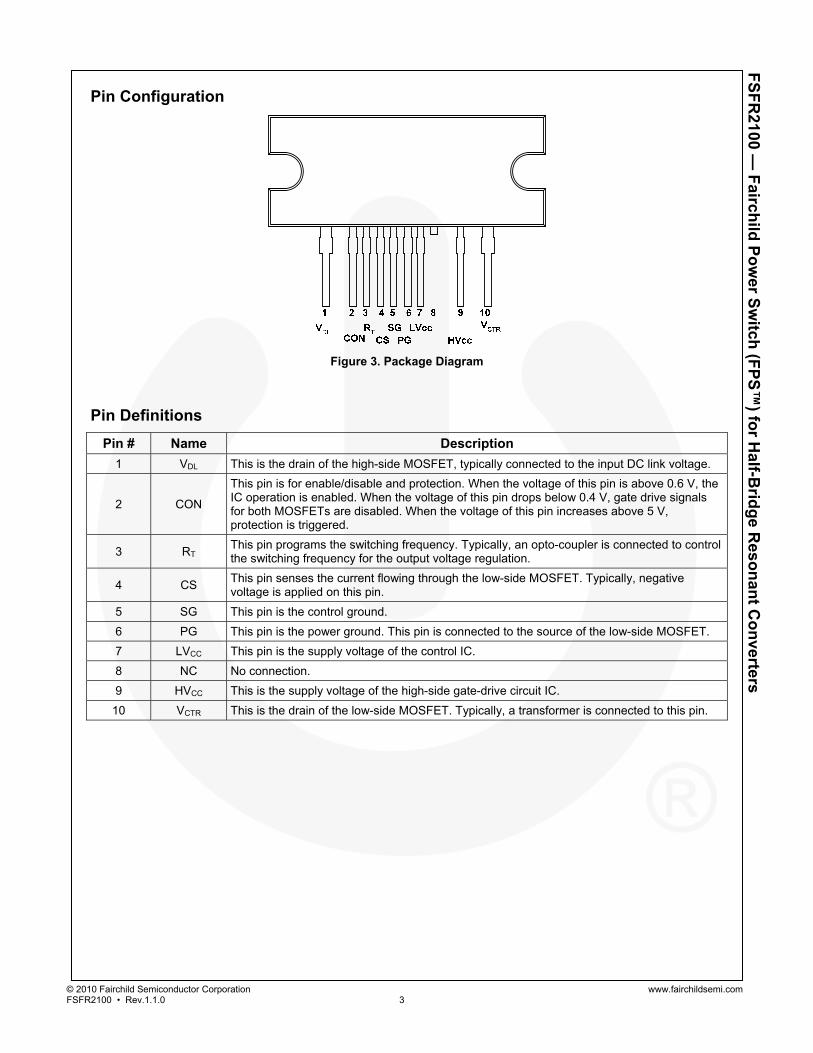
Pin Configuration
Figure 3. Package Diagram
Pin Definitions
Pin # Name Description
1 VDL This is the drain of the high-side MOSFET, typically connected to the input DC link voltage.
2 CON
This pin is for enable/disable and protection. When the voltage of this pin is above 0.6 V, the IC operation is enabled. When the voltage of this pin drops below 0.4 V, gate drive signals for both MOSFETs are disabled. When the voltage of this pin increases above 5 V, protection is triggered.
3 RT This pin programs the switching frequency. Typically, an opto-coupler is connected to control the switching frequency for the output voltage regulation.
4 CS This pin senses the current flowing through the low-side MOSFET. Typically, negative voltage is applied on this pin.
5 SG This pin is the control ground.
6 PG This pin is the power ground. This pin is connected to the source of the low-side MOSFET.
7 LVCC This pin is the supply voltage of the control IC.
8 NC No connection.
9 HVCC This is the supply voltage of the high-side gate-drive circuit IC.
10 VCTR This is the drain of the low-side MOSFET. Typically, a transformer is connected to this pin.

© 2010 Fairchild Semiconductor Corporation www.fairchildsemi.com FSFR2100 • Rev.1.1.0 4
FS
FR
2100 — F
airchild
Po
wer S
witch
(FP
S™
) for H
alf-Brid
ge R
eson
ant C
on
verters
Absolute Maximum Ratings
Stresses exceeding the absolute maximum ratings may damage the device. The device may not function or be operable above the recommended operating conditions and stressing the parts to these levels is not recommended. In addition, extended exposure to stresses above the recommended operating conditions may affect device reliability. The absolute maximum ratings are stress ratings only. TA=25C unless otherwise specified.
Symbol Parameter Min. Max. Unit
VDS Maximum Drain-to-Source Voltage (VDL-VCTR and VCTR-PG) 600 V
LVCC Low-Side Supply Voltage -0.3 25.0 V
HVCC to VCTR High-Side VCC Pin to Low-side Drain Voltage -0.3 25.0 V
HVCC High-Side Floating Supply Voltage -0.3 625.0 V
VCON Control Pin Input Voltage -0.3 LVCC V
VCS Current Sense (CS) Pin Input Voltage -5.0 1.0 V
VRT RT Pin Input Voltage -0.3 5.0 V
dVCTR/dt Allowable Low-Side MOSFET Drain Voltage Slew Rate 50 V/ns
PD Total Power Dissipation(3) 12 W
TJ Maximum Junction Temperature(4) +150
C Recommended Operating Junction Temperature(4) -40 +130
TSTG Storage Temperature Range -55 +150 C
MOSFET Section
VDGR Drain Gate Voltage (RGS=1 M) 600 V
VGS Gate Source (GND) Voltage ±30 V
IDM Drain Current Pulsed(5) 33 A
ID Continuous Drain Current TC=25C 11
A TC=100C 7
Package Section
Torque Recommended Screw Torque 5~7 kgf·cm
Notes: 3. Per MOSFET when both MOSFETs are conducting. 4. The maximum value of the recommended operating junction temperature is limited by thermal shutdown. 5. Pulse width is limited by maximum junction temperature.
Thermal Impedance
TA=25C unless otherwise specified.
Symbol Parameter Value Unit
θJC Junction-to-Case Center Thermal Impedance (Both MOSFETs Conducting) 10.44 ºC/W
θJA Junction-to-Ambient Thermal Impedance 80 ºC/W
© 2010 Fairchild Semiconductor Corporation www.fairchildsemi.com FSFR2100 • Rev.1.1.0 5
FS
FR
2100 — F
airchild
Po
wer S
witch
(FP
S™
) for H
alf-Brid
ge R
eson
ant C
on
verters
Electrical Characteristics
TA=25C unless otherwise specified.
Symbol Parameter Test Conditions Min. Typ. Max. Unit
MOSFET Section
BVDSS Drain-to-Source Breakdown Voltage ID=200 μA, TA=25C 600
V ID=200 μA, TA=125C 650
RDS(ON) On-State Resistance VGS=10 V, ID=5.5 A 0.32 0.38
trr Body Diode Reverse Recovery Time(6) VGS=0 V, IDiode=11.0 A 120 ns
CISS Input Capacitance(6) VDS=25V, VGS=0 V, f=1.0 MHz
1148 pF
COSS Output Capacitance(6) 671 pF
Supply Section
ILK Offset Supply Leakage Current H-VCC=VCTR=600 V/500 V 50 μA
IQHVCC Quiescent HVCC Supply Current (HVCCUV+) - 0.1 V 50 120 μA
IQLVCC Quiescent LVCC Supply Current (LVCCUV+) - 0.1 V 100 200 μA
IOHVCC Operating HVCC Supply Current (RMS Value)
fOSC=100 KHz, VCON > 0.6 V 6 9 mA
No Switching, VCON < 0.4 V 100 200 μA
IOLVCC Operating LVCC Supply Current (RMS Value)
fOSC=100KHz, VCON > 0.6 V 7 11 mA
No Switching, VCON < 0.4 V 2 4 mA
UVLO Section
LVCCUV+ LVCC Supply Under-Voltage Positive-Going Threshold (LVCC Start) 13.0 14.5 16.0 V
LVCCUV- LVCC Supply Under-Voltage Negative-Going Threshold (LVCC Stop) 10.2 11.3 12.4 V
LVCCUVH LVCC Supply Under-Voltage Hysteresis 3.2 V
HVCCUV+ HVCC Supply Under-Voltage Positive-Going Threshold (HVCC Start) 8.2 9.2 10.2 V
HVCCUV- HVCC Supply Under-Voltage Negative-Going Threshold (HVCC Stop) 7.8 8.7 9.6 V
HVCCUVH HVCC Supply Under-Voltage Hysteresis 0.5 V
Oscillator & Feedback Section
VCONDIS Control Pin Disable Threshold Voltage 0.36 0.40 0.44 V
VCONEN Control Pin Enable Threshold Voltage 0.54 0.60 0.66 V
VRT V-I Converter Threshold Voltage
RT=5.2 K
1.5 2.0 2.5 V
fOSC Output Oscillation Frequency 94 100 106 KHz
DC Output Duty Cycle 48 50 52 %
fSS Internal Soft-Start Initial Frequency fSS=fOSC+40 kHz, RT=5.2 K 140 KHz
tSS Internal Soft-Start Time 2 3 4 ms
Continued on the following page…
© 2010 Fairchild Semiconductor Corporation www.fairchildsemi.com FSFR2100 • Rev.1.1.0 6
FS
FR
2100 — F
airchild
Po
wer S
witch
(FP
S™
) for H
alf-Brid
ge R
eson
ant C
on
verters
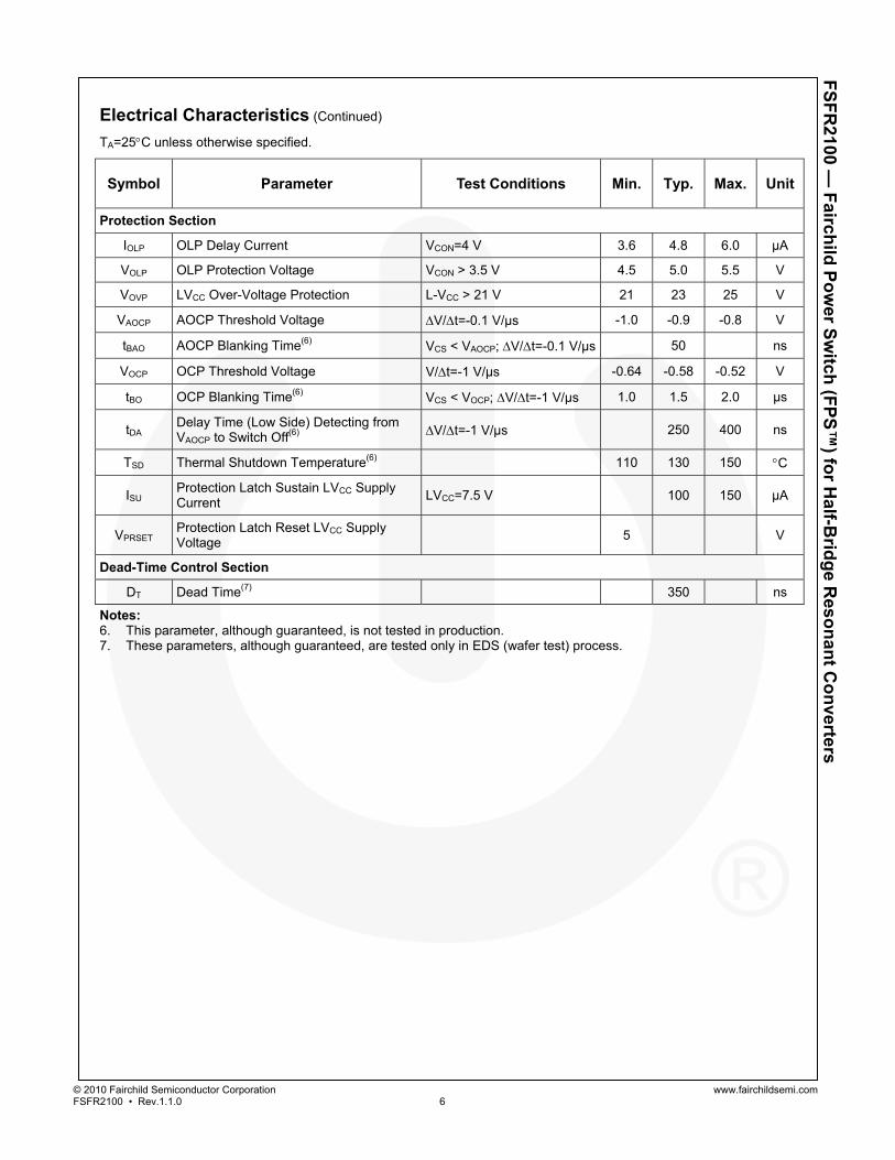
Electrical Characteristics (Continued)
TA=25C unless otherwise specified.
Symbol Parameter Test Conditions Min. Typ. Max. Unit
Protection Section
IOLP OLP Delay Current VCON=4 V 3.6 4.8 6.0 μA
VOLP OLP Protection Voltage VCON > 3.5 V 4.5 5.0 5.5 V
VOVP LVCC Over-Voltage Protection L-VCC > 21 V 21 23 25 V
VAOCP AOCP Threshold Voltage V/t=-0.1 V/µs -1.0 -0.9 -0.8 V
tBAO AOCP Blanking Time(6) VCS < VAOCP; V/t=-0.1 V/µs 50 ns
VOCP OCP Threshold Voltage V/t=-1 V/µs -0.64 -0.58 -0.52 V
tBO OCP Blanking Time(6) VCS < VOCP; V/t=-1 V/µs 1.0 1.5 2.0 μs
tDA Delay Time (Low Side) Detecting from VAOCP to Switch Off(6) V/t=-1 V/µs 250 400 ns
TSD Thermal Shutdown Temperature(6) 110 130 150 C
ISU Protection Latch Sustain LVCC Supply Current
LVCC=7.5 V 100 150 μA
VPRSET Protection Latch Reset LVCC Supply Voltage
5 V
Dead-Time Control Section
DT Dead Time(7) 350 ns
Notes: 6. This parameter, although guaranteed, is not tested in production. 7. These parameters, although guaranteed, are tested only in EDS (wafer test) process.
© 2010 Fairchild Semiconductor Corporation www.fairchildsemi.com FSFR2100 • Rev.1.1.0 7
FS
FR
2100 — F
airchild
Po
wer S
witch
(FP
S™
) for H
alf-Brid
ge R
eson
ant C
on
verters
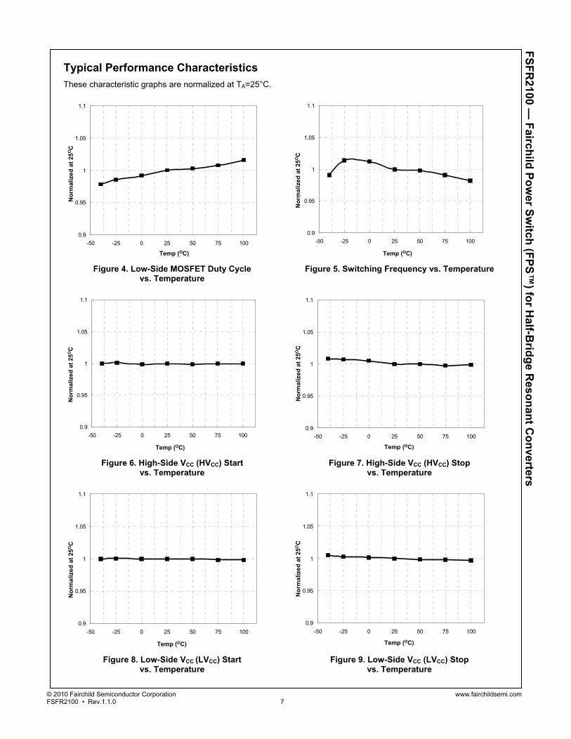
Typical Performance Characteristics
These characteristic graphs are normalized at TA=25°C.
0.9
0.95
1
1.05
1.1
-50 -25 0 25 50 75 100
Temp (OC)
No
rma
lize
d a
t 25
OC
Temp (OC)
0.9
0.95
1
1.05
1.1
-50 -25 0 25 50 75 100
No
rma
lize
d a
t 2
5OC
Figure 4. Low-Side MOSFET Duty Cycle
vs. Temperature Figure 5. Switching Frequency vs. Temperature
0.9
0.95
1
1.05
1.1
-50 -25 0 25 50 75 100
Temp (OC)
No
rma
lize
d a
t 2
5OC
0.9
0.95
1
1.05
1.1
-50 -25 0 25 50 75 100
Temp (OC)
No
rma
lized
at
25O
C
Figure 6. High-Side VCC (HVCC) Start
vs. Temperature Figure 7. High-Side VCC (HVCC) Stop
vs. Temperature
0.9
0.95
1
1.05
1.1
-50 -25 0 25 50 75 100
Temp (OC)
No
rma
lize
d a
t 2
5OC
0.9
0.95
1
1.05
1.1
-50 -25 0 25 50 75 100
Temp (OC)
No
rma
lize
d a
t 2
5OC
Figure 8. Low-Side VCC (LVCC) Start vs. Temperature
Figure 9. Low-Side VCC (LVCC) Stop vs. Temperature
© 2010 Fairchild Semiconductor Corporation www.fairchildsemi.com FSFR2100 • Rev.1.1.0 8
FS
FR
2100 — F
airchild
Po
wer S
witch
(FP
S™
) for H
alf-Brid
ge R
eson
ant C
on
verters
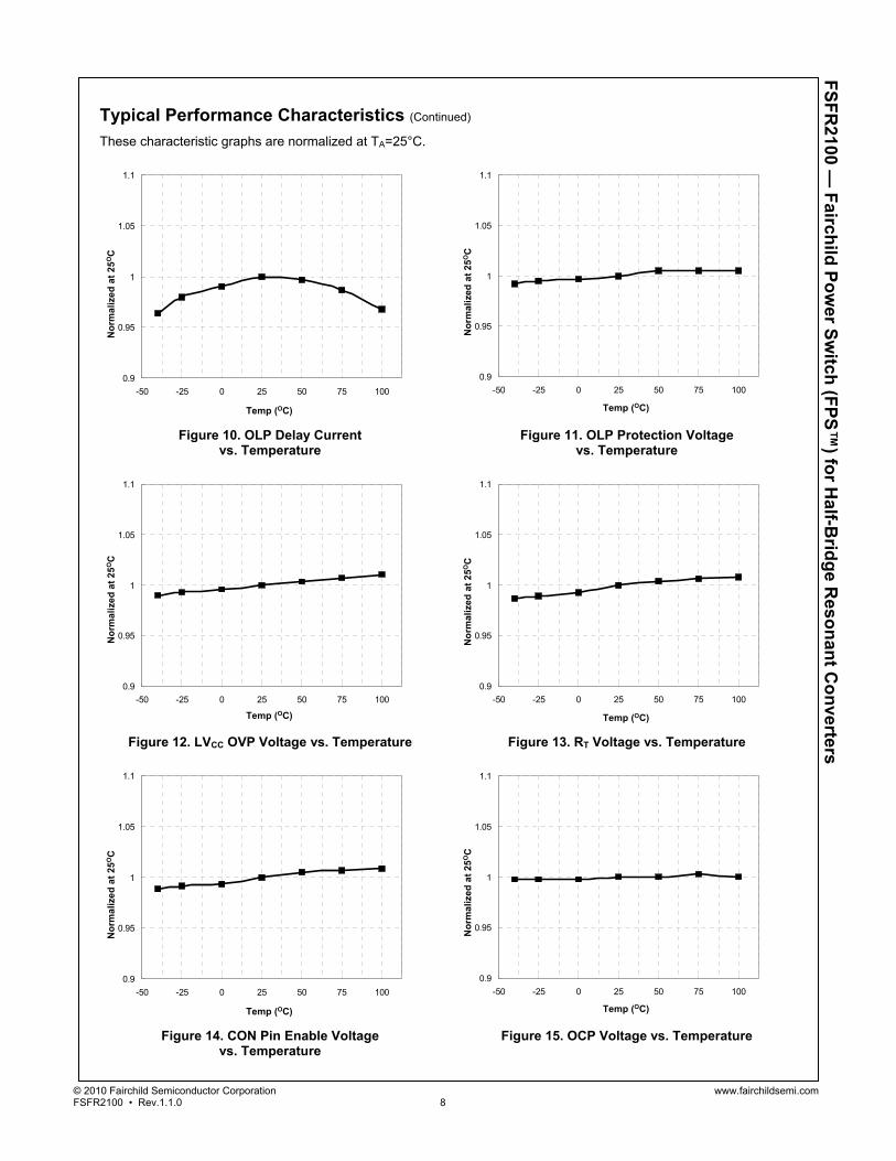
Typical Performance Characteristics (Continued)
These characteristic graphs are normalized at TA=25°C.
0.9
0.95
1
1.05
1.1
-50 -25 0 25 50 75 100
Temp (OC)
No
rma
lize
d a
t 2
5OC
0.9
0.95
1
1.05
1.1
-50 -25 0 25 50 75 100
Temp (OC)
No
rma
lize
d a
t 25
OC
Figure 10. OLP Delay Current vs. Temperature
Figure 11. OLP Protection Voltagevs. Temperature
0.9
0.95
1
1.05
1.1
-50 -25 0 25 50 75 100
Temp (OC)
No
rma
lize
d a
t 2
5OC
0.9
0.95
1
1.05
1.1
-50 -25 0 25 50 75 100
Temp (OC)
No
rmal
ize
d a
t 2
5OC
Figure 12. LVCC OVP Voltage vs. Temperature Figure 13. RT Voltage vs. Temperature
0.9
0.95
1
1.05
1.1
-50 -25 0 25 50 75 100
Temp (OC)
No
rma
lize
d a
t 2
5OC
0.9
0.95
1
1.05
1.1
-50 -25 0 25 50 75 100
Temp (OC)
No
rma
lize
d a
t 25
OC
Figure 14. CON Pin Enable Voltagevs. Temperature
Figure 15. OCP Voltage vs. Temperature
© 2010 Fairchild Semiconductor Corporation www.fairchildsemi.com FSFR2100 • Rev.1.1.0 9
FS
FR
2100 — F
airchild
Po
wer S
witch
(FP
S™
) for H
alf-Brid
ge R
eson
ant C
on
verters
Functional Description
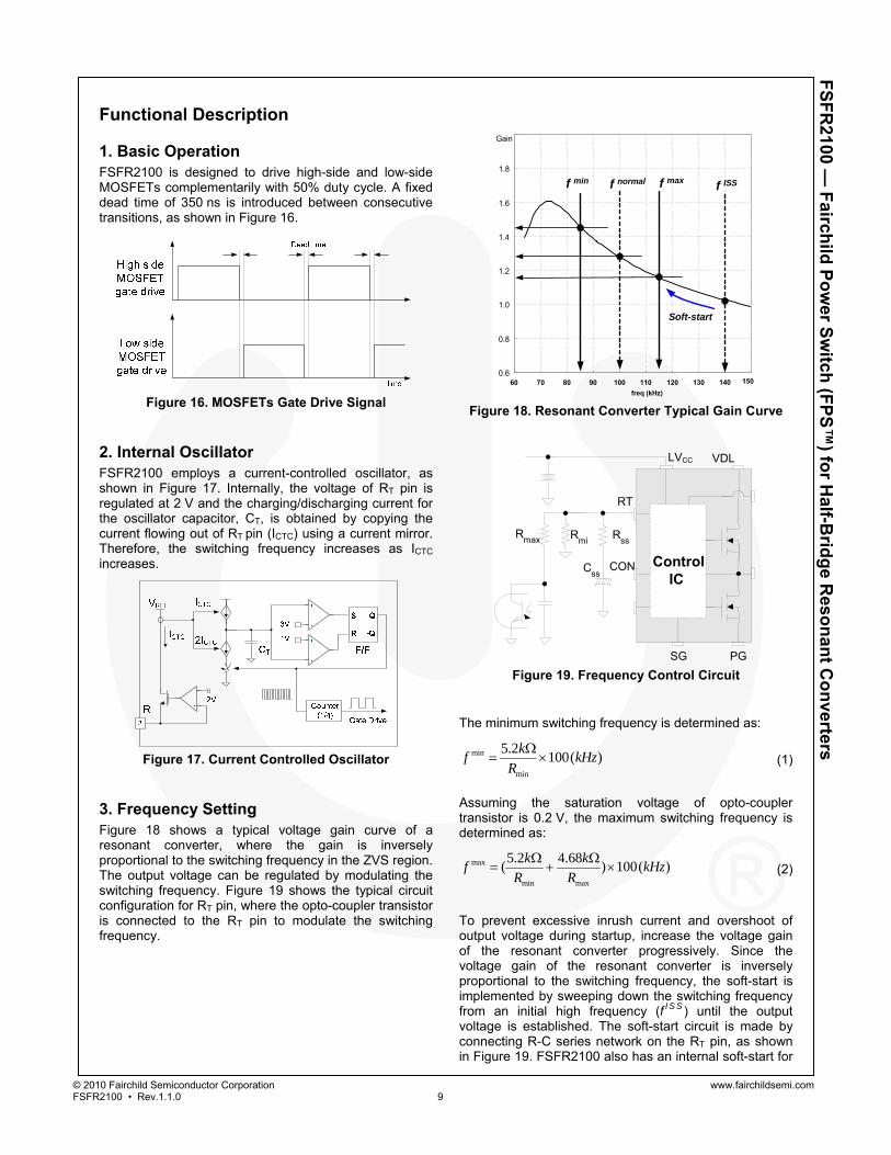
1. Basic Operation FSFR2100 is designed to drive high-side and low-side MOSFETs complementarily with 50% duty cycle. A fixed dead time of 350 ns is introduced between consecutive transitions, as shown in Figure 16.
Figure 16. MOSFETs Gate Drive Signal
2. Internal Oscillator FSFR2100 employs a current-controlled oscillator, as shown in Figure 17. Internally, the voltage of RT pin is regulated at 2 V and the charging/discharging current for the oscillator capacitor, CT, is obtained by copying the current flowing out of RT pin (ICTC) using a current mirror. Therefore, the switching frequency increases as ICTC increases.
Figure 17. Current Controlled Oscillator
3. Frequency Setting Figure 18 shows a typical voltage gain curve of a resonant converter, where the gain is inversely proportional to the switching frequency in the ZVS region. The output voltage can be regulated by modulating the switching frequency. Figure 19 shows the typical circuit configuration for RT pin, where the opto-coupler transistor is connected to the RT pin to modulate the switching frequency.
0.6
0.8
1.0
1.2
1.4
1.6
1.8
Gain
140 15060 70 80 90 100 110 120 130
freq (kHz)
f min f normal f max f ISS
Soft-start
Figure 18. Resonant Converter Typical Gain Curve
Figure 19. Frequency Control Circuit
The minimum switching frequency is determined as:
min
min
5.2100( )
kf kHz
R
(1)
Assuming the saturation voltage of opto-coupler transistor is 0.2 V, the maximum switching frequency is determined as:
max
min max
5.2 4.68( ) 100( )
k kf kHz
R R
(2)
To prevent excessive inrush current and overshoot of output voltage during startup, increase the voltage gain of the resonant converter progressively. Since the voltage gain of the resonant converter is inversely proportional to the switching frequency, the soft-start is implemented by sweeping down the switching frequency from an initial high frequency (f I S S ) until the output voltage is established. The soft-start circuit is made by connecting R-C series network on the RT pin, as shown in Figure 19. FSFR2100 also has an internal soft-start for
ControlIC
VDLLVCC
RT
CON
SG PG
Rmi
Rmax
Css
Rss
© 2010 Fairchild Semiconductor Corporation www.fairchildsemi.com FSFR2100 • Rev.1.1.0 10
FS
FR
2100 — F
airchild
Po
wer S
witch
(FP
S™
) for H
alf-Brid
ge R
eson
ant C
on
verters
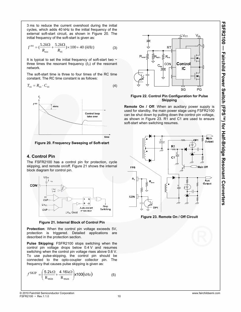
3 ms to reduce the current overshoot during the initial cycles, which adds 40 kHz to the initial frequency of the external soft-start circuit, as shown in Figure 20. The initial frequency of the soft-start is given as:
min
5.2 5.2( ) 100 40 ( )ISS
SS
k kf kHz
R R
(3)
It is typical to set the initial frequency of soft-start two ~ three times the resonant frequency (fO) of the resonant network.
The soft-start time is three to four times of the RC time constant. The RC time constant is as follows:
SS SS SST R C (4)
fs
time
Control looptake over
40kHzf ISS
Figure 20. Frequency Sweeping of Soft-start
4. Control Pin The FSFR2100 has a control pin for protection, cycle skipping, and remote on/off. Figure 21 shows the internal block diagram for control pin.
Figure 21. Internal Block of Control Pin
Protection: When the control pin voltage exceeds 5V, protection is triggered. Detailed applications are described in the protection section.
Pulse Skipping: FSFR2100 stops switching when the control pin voltage drops below 0.4 V and resumes switching when the control pin voltage rises above 0.6 V. To use pulse-skipping, the control pin should be connected to the opto-coupler collector pin. The frequency that causes pulse skipping is given as:
(5)
Figure 22. Control Pin Configuration for Pulse
Skipping
Remote On / Off: When an auxiliary power supply is used for standby, the main power stage using FSFR2100 can be shut down by pulling down the control pin voltage, as shown in Figure 23. R1 and C1 are used to ensure soft-start when switching resumes.
Figure 23. Remote On / Off Circuit
kHz100xR
k16.4
R
k2.5
maxmin
SKIP
© 2010 Fairchild Semiconductor Corporation www.fairchildsemi.com FSFR2100 • Rev.1.1.0 11
FS
FR
2100 — F
airchild
Po
wer S
witch
(FP
S™
) for H
alf-Brid
ge R
eson
ant C
on
verters
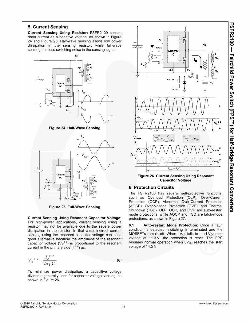
5. Current Sensing Current Sensing Using Resistor: FSFR2100 senses drain current as a negative voltage, as shown in Figure 24 and Figure 25. Half-wave sensing allows low power dissipation in the sensing resistor, while full-wave sensing has less switching noise in the sensing signal.
Figure 24. Half-Wave Sensing
Figure 25. Full-Wave Sensing
Current Sensing Using Resonant Capacitor Voltage: For high-power applications, current sensing using a resistor may not be available due to the severe power dissipation in the resistor. In that case, indirect current sensing using the resonant capacitor voltage can be a good alternative because the amplitude of the resonant capacitor voltage (Vcr
p-p) is proportional to the resonant current in the primary side (Ip
p-p) as:
2
p ppp p
Crs r
IV
f C
(6)
To minimize power dissipation, a capacitive voltage divider is generally used for capacitor voltage sensing, as shown in Figure 26.
delay d dT R C
pksense B
p pCr sense B
V C
V C C 2
pksense
CON
VV
Figure 26. Current Sensing Using Resonant
Capacitor Voltage
6. Protection Circuits The FSFR2100 has several self-protective functions, such as Overload Protection (OLP), Over-Current Protection (OCP), Abnormal Over-Current Protection (AOCP), Over-Voltage Protection (OVP), and Thermal Shutdown (TSD). OLP, OCP, and OVP are auto-restart mode protections; while AOCP and TSD are latch-mode protections, as shown in Figure 27.
6.1 Auto-restart Mode Protection: Once a fault condition is detected, switching is terminated and the MOSFETs remain off. When LVCC falls to the LVCC stop voltage of 11.3 V, the protection is reset. The FPS resumes normal operation when LVCC reaches the start voltage of 14.5 V.
ControlIC
CS
SG PG
Ns
Np Ns
Rsense
Ids
Cr
Ids
VCS
VCS
ControlIC
CS
SG PG
Rsense
Ids
VCS
Ids
VCS
Ns
Np Ns
Cr
© 2010 Fairchild Semiconductor Corporation www.fairchildsemi.com FSFR2100 • Rev.1.1.0 12
FS
FR
2100 — F
airchild
Po
wer S
witch
(FP
S™
) for H
alf-Brid
ge R
eson
ant C
on
verters
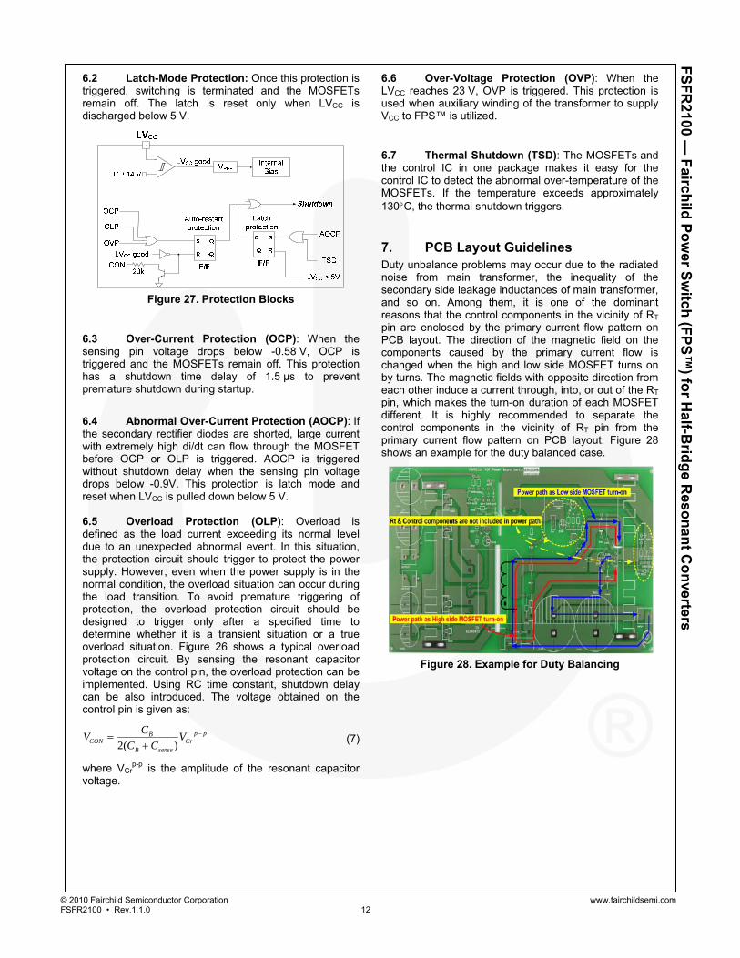
6.2 Latch-Mode Protection: Once this protection is triggered, switching is terminated and the MOSFETs remain off. The latch is reset only when LVCC is discharged below 5 V.
Figure 27. Protection Blocks
6.3 Over-Current Protection (OCP): When the sensing pin voltage drops below -0.58 V, OCP is triggered and the MOSFETs remain off. This protection has a shutdown time delay of 1.5 µs to prevent premature shutdown during startup.
6.4 Abnormal Over-Current Protection (AOCP): If the secondary rectifier diodes are shorted, large current with extremely high di/dt can flow through the MOSFET before OCP or OLP is triggered. AOCP is triggered without shutdown delay when the sensing pin voltage drops below -0.9V. This protection is latch mode and reset when LVCC is pulled down below 5 V. 6.5 Overload Protection (OLP): Overload is defined as the load current exceeding its normal level due to an unexpected abnormal event. In this situation, the protection circuit should trigger to protect the power supply. However, even when the power supply is in the normal condition, the overload situation can occur during the load transition. To avoid premature triggering of protection, the overload protection circuit should be designed to trigger only after a specified time to determine whether it is a transient situation or a true overload situation. Figure 26 shows a typical overload protection circuit. By sensing the resonant capacitor voltage on the control pin, the overload protection can be implemented. Using RC time constant, shutdown delay can be also introduced. The voltage obtained on the control pin is given as:
2( )p pB
CON CrB sense
CV V
C C
(7)
where VCrp-p is the amplitude of the resonant capacitor
voltage.
6.6 Over-Voltage Protection (OVP): When the LVCC reaches 23 V, OVP is triggered. This protection is used when auxiliary winding of the transformer to supply VCC to FPS™ is utilized.
6.7 Thermal Shutdown (TSD): The MOSFETs and the control IC in one package makes it easy for the control IC to detect the abnormal over-temperature of the MOSFETs. If the temperature exceeds approximately 130C, the thermal shutdown triggers.
7. PCB Layout Guidelines Duty unbalance problems may occur due to the radiated noise from main transformer, the inequality of the secondary side leakage inductances of main transformer, and so on. Among them, it is one of the dominant reasons that the control components in the vicinity of RT pin are enclosed by the primary current flow pattern on PCB layout. The direction of the magnetic field on the components caused by the primary current flow is changed when the high and low side MOSFET turns on by turns. The magnetic fields with opposite direction from each other induce a current through, into, or out of the RT pin, which makes the turn-on duration of each MOSFET different. It is highly recommended to separate the control components in the vicinity of RT pin from the primary current flow pattern on PCB layout. Figure 28 shows an example for the duty balanced case.
Figure 28. Example for Duty Balancing
© 2010 Fairchild Semiconductor Corporation www.fairchildsemi.com FSFR2100 • Rev.1.1.0 13
FS
FR
2100 — F
airchild
Po
wer S
witch
(FP
S™
) for H
alf-Brid
ge R
eson
ant C
on
verters
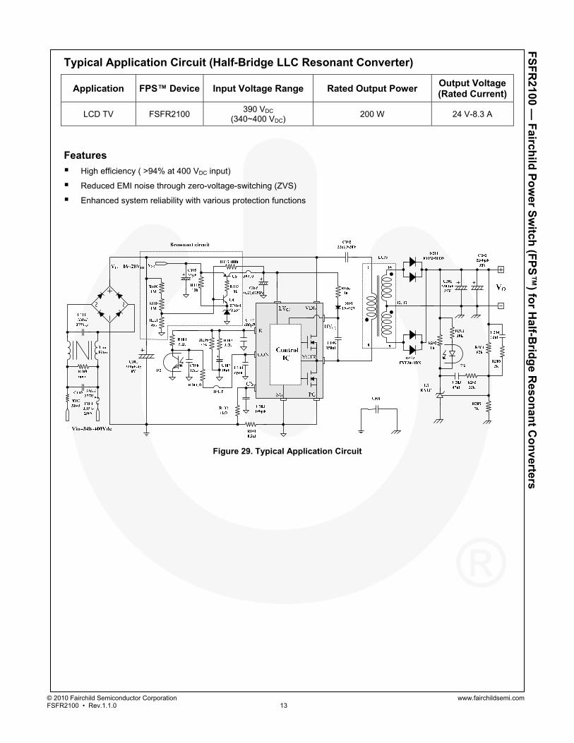
Typical Application Circuit (Half-Bridge LLC Resonant Converter)
Application FPS™ Device Input Voltage Range Rated Output Power Output Voltage (Rated Current)
LCD TV FSFR2100 390 VDC
(340~400 VDC) 200 W 24 V-8.3 A
Features
High efficiency ( >94% at 400 VDC input)
Reduced EMI noise through zero-voltage-switching (ZVS)
Enhanced system reliability with various protection functions
Figure 29. Typical Application Circuit
© 2010 Fairchild Semiconductor Corporation www.fairchildsemi.com FSFR2100 • Rev.1.1.0 14
FS
FR
2100 — F
airchild
Po
wer S
witch
(FP
S™
) for H
alf-Brid
ge R
eson
ant C
on
verters
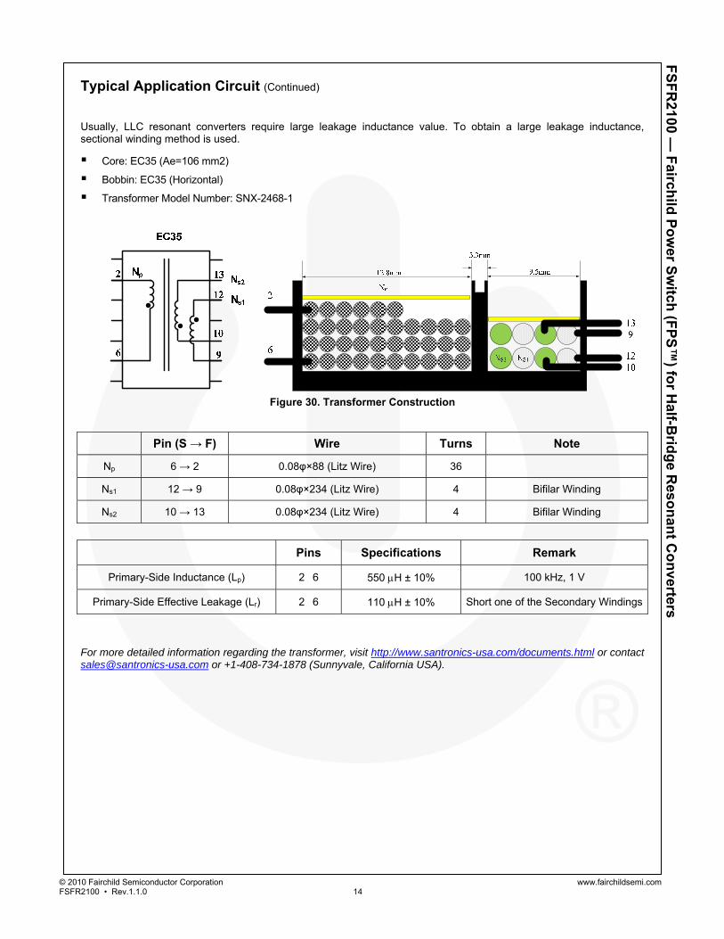
Typical Application Circuit (Continued)
Usually, LLC resonant converters require large leakage inductance value. To obtain a large leakage inductance, sectional winding method is used.
Core: EC35 (Ae=106 mm2)
Bobbin: EC35 (Horizontal)
Transformer Model Number: SNX-2468-1
Figure 30. Transformer Construction
Pin (S → F) Wire Turns Note
Np 6 → 2 0.08φ×88 (Litz Wire) 36
Ns1 12 → 9 0.08φ×234 (Litz Wire) 4 Bifilar Winding
Ns2 10 → 13 0.08φ×234 (Litz Wire) 4 Bifilar Winding
Pins Specifications Remark
Primary-Side Inductance (Lp) 2� 6 550 H ± 10% 100 kHz, 1 V
Primary-Side Effective Leakage (Lr) 2� 6 110 H ± 10% Short one of the Secondary Windings
For more detailed information regarding the transformer, visit http://www.santronics-usa.com/documents.html or contact [email protected] or +1-408-734-1878 (Sunnyvale, California USA).
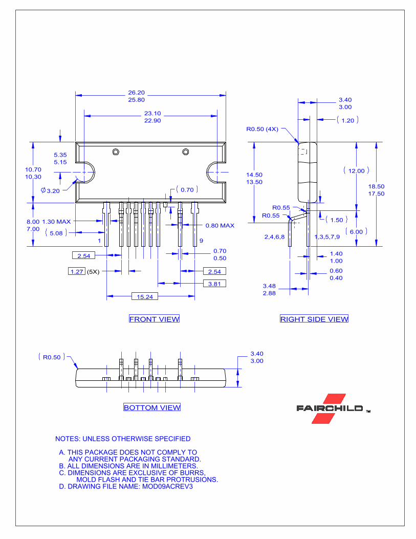
23.1022.90
26.2025.80
0.70
5.355.15
10.7010.30
3.20
8.007.00
5.08
0.700.50
15.24
1.30 MAX0.80 MAX
2.54
1.27 (5X) 2.54
3.81
R0.50 3.403.00
1.20
3.403.00
R0.50 (4X)
18.5017.50
3.482.88
0.600.40
R0.55R0.55
6.00
1.50
12.0014.5013.50
1.401.00
NOTES: UNLESS OTHERWISE SPECIFIED
A. THIS PACKAGE DOES NOT COMPLY TO ANY CURRENT PACKAGING STANDARD. B. ALL DIMENSIONS ARE IN MILLIMETERS. C. DIMENSIONS ARE EXCLUSIVE OF BURRS,
MOLD FLASH AND TIE BAR PROTRUSIONS. D. DRAWING FILE NAME: MOD09ACREV3
1 92,4,6,8 1,3,5,7,9
RIGHT SIDE VIEW
BOTTOM VIEW
FRONT VIEW
www.onsemi.com1
ON Semiconductor and are trademarks of Semiconductor Components Industries, LLC dba ON Semiconductor or its subsidiaries in the United States and/or other countries.ON Semiconductor owns the rights to a number of patents, trademarks, copyrights, trade secrets, and other intellectual property. A listing of ON Semiconductor’s product/patentcoverage may be accessed at www.onsemi.com/site/pdf/Patent−Marking.pdf. ON Semiconductor reserves the right to make changes without further notice to any products herein.ON Semiconductor makes no warranty, representation or guarantee regarding the suitability of its products for any particular purpose, nor does ON Semiconductor assume any liabilityarising out of the application or use of any product or circuit, and specifically disclaims any and all liability, including without limitation special, consequential or incidental damages.Buyer is responsible for its products and applications using ON Semiconductor products, including compliance with all laws, regulations and safety requirements or standards,regardless of any support or applications information provided by ON Semiconductor. “Typical” parameters which may be provided in ON Semiconductor data sheets and/orspecifications can and do vary in different applications and actual performance may vary over time. All operating parameters, including “Typicals” must be validated for each customerapplication by customer’s technical experts. ON Semiconductor does not convey any license under its patent rights nor the rights of others. ON Semiconductor products are notdesigned, intended, or authorized for use as a critical component in life support systems or any FDA Class 3 medical devices or medical devices with a same or similar classificationin a foreign jurisdiction or any devices intended for implantation in the human body. Should Buyer purchase or use ON Semiconductor products for any such unintended or unauthorizedapplication, Buyer shall indemnify and hold ON Semiconductor and its officers, employees, subsidiaries, affiliates, and distributors harmless against all claims, costs, damages, andexpenses, and reasonable attorney fees arising out of, directly or indirectly, any claim of personal injury or death associated with such unintended or unauthorized use, even if suchclaim alleges that ON Semiconductor was negligent regarding the design or manufacture of the part. ON Semiconductor is an Equal Opportunity/Affirmative Action Employer. Thisliterature is subject to all applicable copyright laws and is not for resale in any manner.
PUBLICATION ORDERING INFORMATIONN. American Technical Support: 800−282−9855 Toll FreeUSA/Canada
Europe, Middle East and Africa Technical Support:Phone: 421 33 790 2910
Japan Customer Focus CenterPhone: 81−3−5817−1050
www.onsemi.com
LITERATURE FULFILLMENT:Literature Distribution Center for ON Semiconductor19521 E. 32nd Pkwy, Aurora, Colorado 80011 USAPhone: 303−675−2175 or 800−344−3860 Toll Free USA/CanadaFax: 303−675−2176 or 800−344−3867 Toll Free USA/CanadaEmail: [email protected]
ON Semiconductor Website: www.onsemi.com
Order Literature: http://www.onsemi.com/orderlit
For additional information, please contact your localSales Representative
© Semiconductor Components Industries, LLC