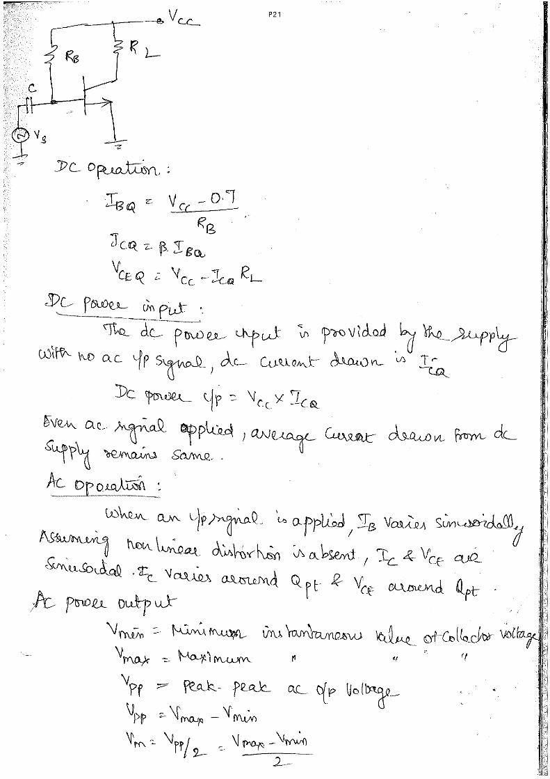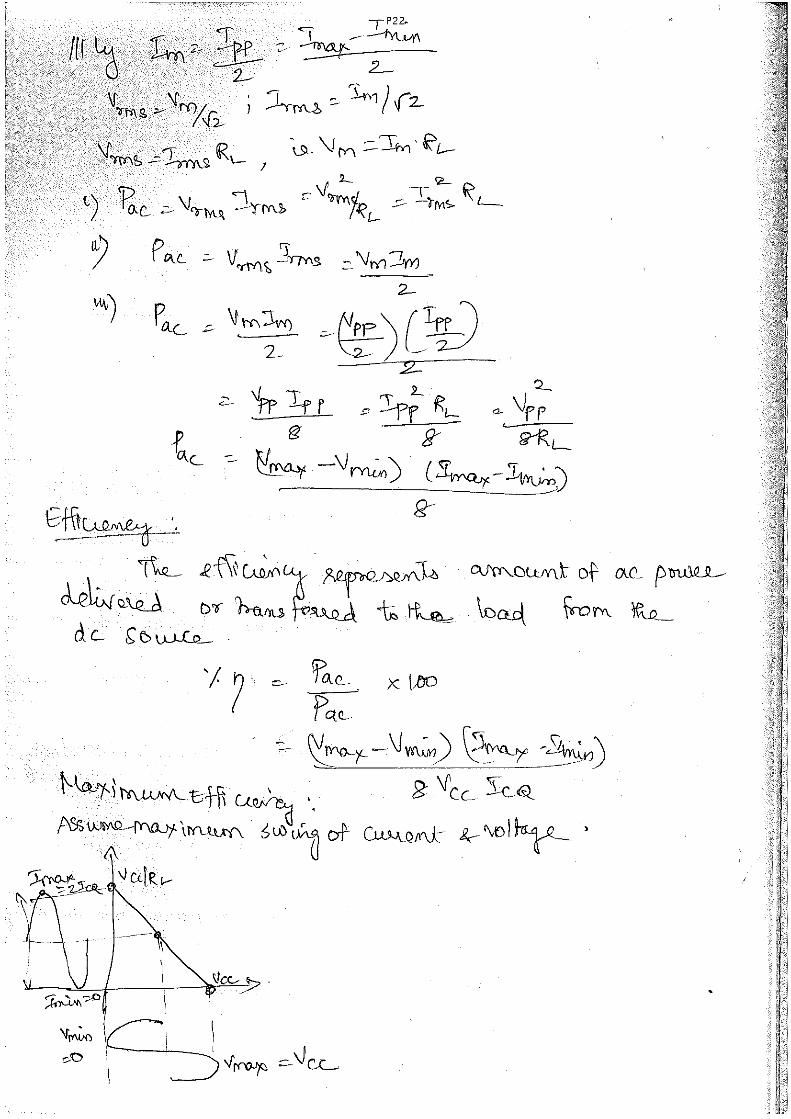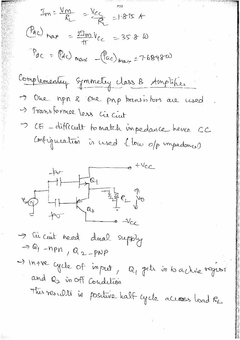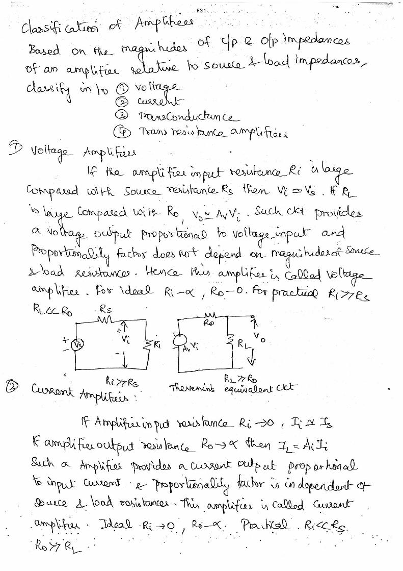
Frequency Response of CE single stage amplifier
96
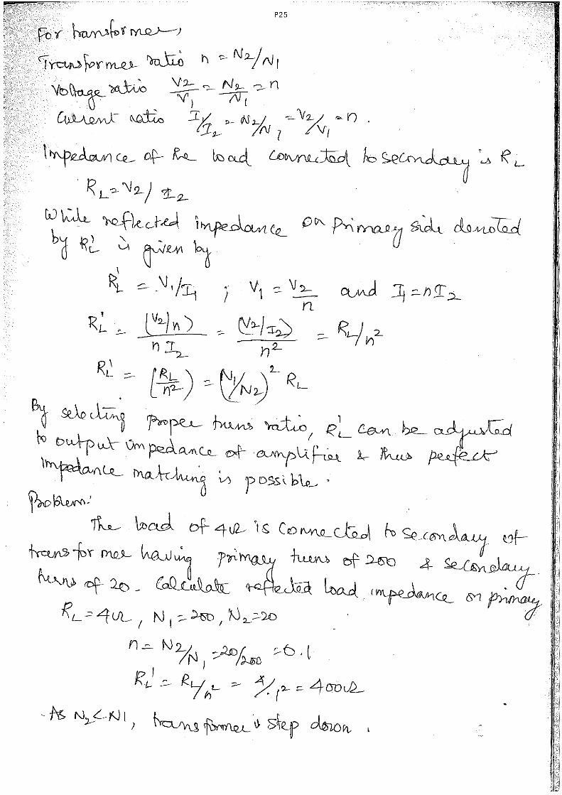
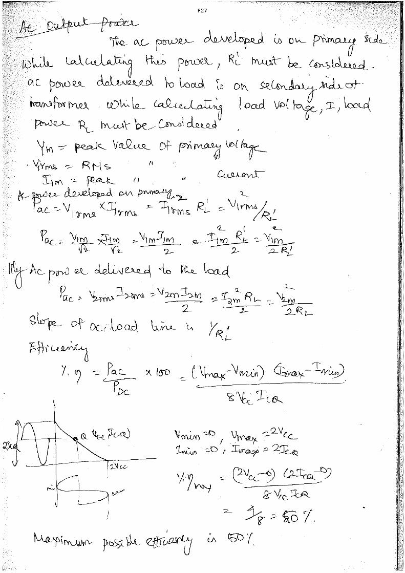
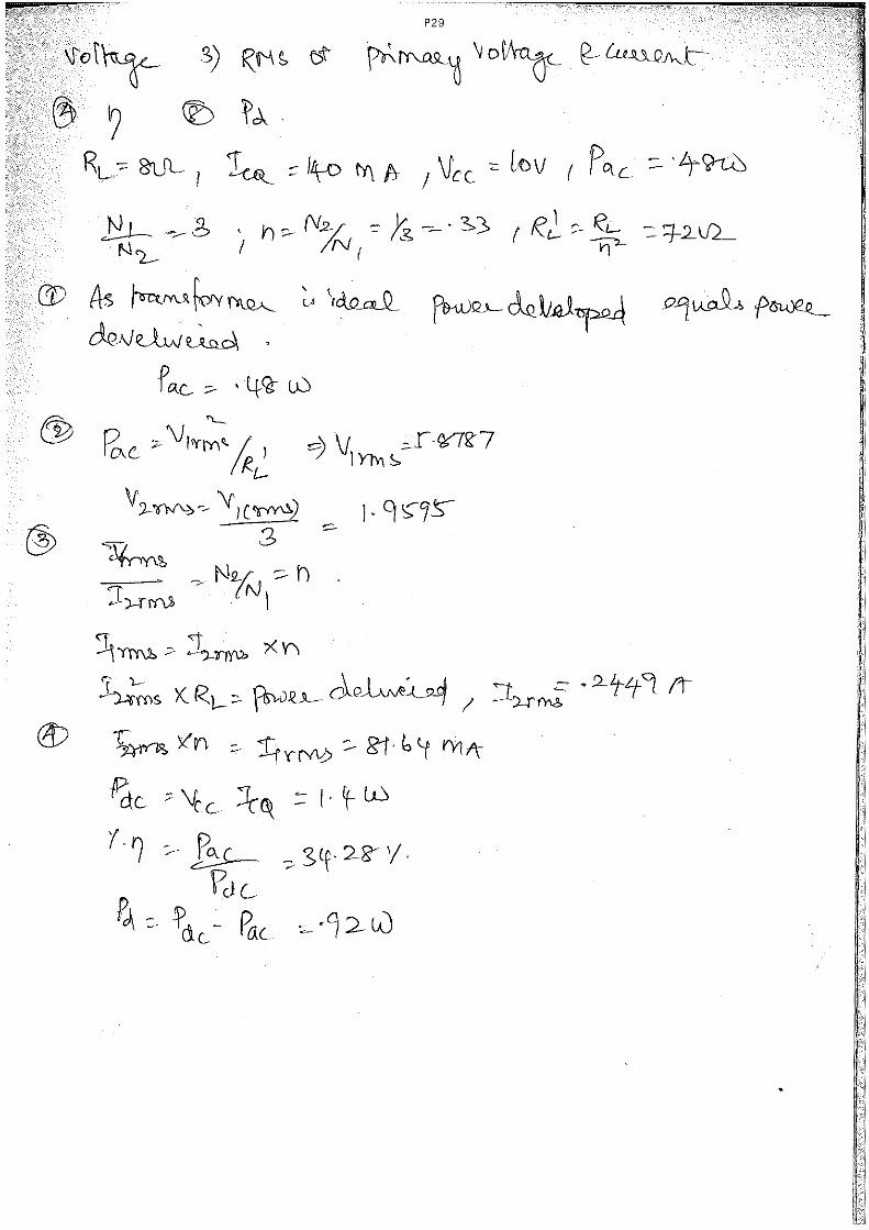
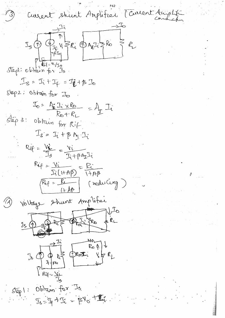
MODULE III Multistage and Power Amplifiers: Frequency Response of CE single stage amplifier - Need for cascading - Cascade and Cascade connection - Darlington connection - Definitions and amplifier types - Transformer coupled Class A amplifiers - Class B amplifier circuits - Amplifier distortion. TRANSISTOR FREQUENCY RESPONSE General Frequency considerations • At low frequencies the coupling and bypass capacitors can no longer be replaced by the short – circuit approximation because of the increase in reactance of these elements. • The frequency – dependent parameters of the small signal equivalent circuits and the stray capacitive elements associated with the active device and the network will limit the high frequency response of the system. • An increase in the number of stages of a cascaded system will also limit both the high and low frequency response. • The horizontal scale of frequency response curve is a logarithmic scale to permit a plot extending from the low to the high frequency • For the RC coupled amplifier, the drop at low frequencies is due to the increasing reactance of CC and CE, whereas its upper frequency limit is determined by either the parasitic capacitive elements of the network or the frequency dependence of the gain of the active device. • In the frequency response, there is a band of frequencies in which the magnitude of the gain is either equal or relatively close to the midband value. • To fix the frequency boundaries of relatively high gain, 0.707AVmid is chosen to be the gain at the cutoff levels. • The corresponding frequencies f1 and f2 are generally called corner, cutoff, band, break, or half – power frequencies. • The multiplier 0.707 is chosen because at this level the output power is half the midband power output, that is, at mid frequencies, • PO mid = | Vo 2 | / Ro = | AVmidVi| 2 / RO • And at the half – power frequencies, POHPF = | 0.707 AVmidVi| 2 / Ro = 0.5| AVmid Vi| 2 / Ro • And, POHPF = 0.5 POmid • The bandwidth of each system is determined by f2 – f1
-
Upload
khangminh22 -
Category
Documents
-
view
6 -
download
0
Transcript of Frequency Response of CE single stage amplifier

MODULE III Multistage and Power Amplifiers: Frequency Response of CE single stage amplifier - Need for cascading - Cascade and Cascade
connection - Darlington connection - Definitions and amplifier types - Transformer coupled
Class A amplifiers - Class B amplifier circuits - Amplifier distortion.
TRANSISTOR FREQUENCY RESPONSE
General Frequency considerations
• At low frequencies the coupling and bypass capacitors can no longer be replaced
by the short – circuit approximation because of the increase in reactance of these
elements.
• The frequency – dependent parameters of the small signal equivalent circuits and
the stray capacitive elements associated with the active device and the network
will limit the high frequency response of the system.
• An increase in the number of stages of a cascaded system will also limit both the
high and low frequency response.
• The horizontal scale of frequency response curve is a logarithmic scale to permit a
plot extending from the low to the high frequency
• For the RC coupled amplifier, the drop at low frequencies is due to the increasing
reactance of CC and CE, whereas its upper frequency limit is determined by either
the parasitic capacitive elements of the network or the frequency dependence of
the gain of the active device.
• In the frequency response, there is a band of frequencies in which the magnitude
of the gain is either equal or relatively close to the midband value.
• To fix the frequency boundaries of relatively high gain, 0.707AVmid is chosen to
be the gain at the cutoff levels.
• The corresponding frequencies f1 and f2 are generally called corner, cutoff,
band, break, or half – power frequencies.
• The multiplier 0.707 is chosen because at this level the output power is half
the midband power output, that is, at mid frequencies, •
PO mid = | Vo2| / Ro = | AVmidVi|
2 / RO
• And at the half – power frequencies,
POHPF = | 0.707 AVmidVi|2 / Ro
= 0.5| AVmid Vi|2 / Ro
• And, POHPF = 0.5 POmid
• The bandwidth of each system is determined by f2 – f1

• A decibel plot can be obtained by applying the equation,
(AV / AVmid )dB
= 20 log10 (AV / AVmid)
Most amplifiers introduce a 180 phase shift between input and output signals. At
low frequencies, there is a phase shift such that Vo lags Vi by an increased angle. At
high frequencies, the phase shift drops below 180.
Frequency analysis of an RC network
• Analysis of the above circuit indicates that,
XC = 1/2πfC ≅ 0 Ω
• Thus, Vo = Vi at high frequencies.
• At f = 0 Hz, XC = ∞, Vo = 0V.
• Between the two extremes, the ratio, AV = Vo / Vi will vary.
As frequency increases, the capacitive reactance decreases and more of the
input voltage appears across the output terminals.
The output and input voltages are related by the voltage – divider rule:
Vo = RVi / ( R – jXC)
the magnitude of Vo = RVi / √R2 + XC2
• For the special case where XC = R,
• The frequency at which this occurs is determined from,
XC = 1/2πf1C = R
where, f1 = 1/ 2πRC
• Gain equation is written as,
= R / (R – jXC) = 1/ ( 1 – j(1/ωCR)
= 1 / [ 1 – j(f1 / f)]

• In the magnitude and phase form,
= [1 /√ 1 + (f1/f)2 ] ∠ tan
-1 (f1 / f)
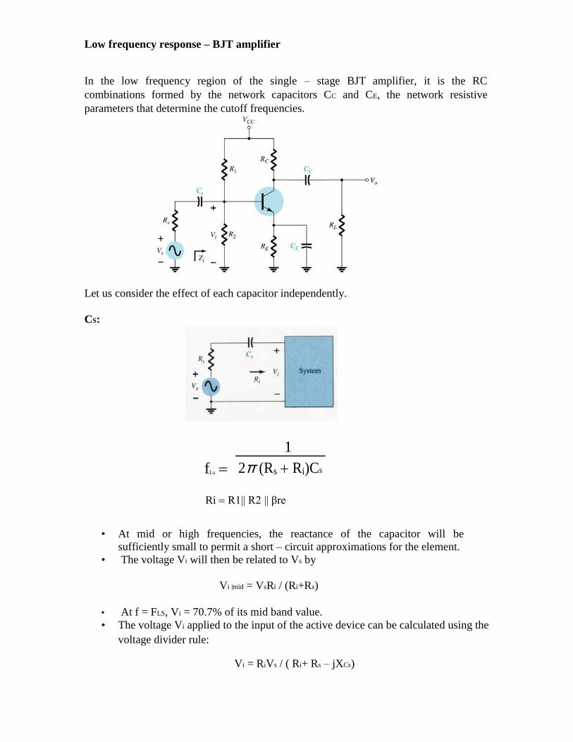
Low frequency response – BJT amplifier
In the low frequency region of the single – stage BJT amplifier, it is the RC
combinations formed by the network capacitors CC and CE, the network resistive
parameters that determine the cutoff frequencies.
Let us consider the effect of each capacitor independently.
CS:
fLs
1
2π (Rs Ri)Cs
Ri R1|| R2 || βre
• At mid or high frequencies, the reactance of the capacitor will be
sufficiently small to permit a short – circuit approximations for the element.
• The voltage Vi will then be related to Vs by
Vi |mid = VsRi / (Ri+Rs)
• At f = FLS, Vi = 70.7% of its mid band value.
• The voltage Vi applied to the input of the active device can be calculated using the
voltage divider rule:
Vi = RiVs / ( Ri+ Rs – jXCs)

Effect of CC:
• Since the coupling capacitor is normally connected between the output of
the active device and applied load, the RC configuration that determines the
low cutoff frequency due to CC appears as in the figure given below.
•
fLC
1
2π(Ro RL)Cc
• Ro = Rc|| ro
Effect of CE:
• The effect of CE on the gain is best described in a quantitative manner by recalling
that the gain for the amplifier without bypassing the emitter resistor is given by:
AV = - RC / ( re + RE) • Maximum gain is obviously available where RE is 0Ω. • At low frequencies, with the bypass capacitor CE in its “open circuit” equivalent
state, all of RE appears in the gain equation above, resulting in minimum gain.

• As the frequency increases, the reactance of the capacitor CE will decrease,
reducing the parallel impedance of RE and CE until the resistor RE is effectively
shorted out by CE.
• The result is a maximum or midband gain determined by AV = - RC / re.
• The input and output coupling capacitors, emitter bypass capacitor will affect only
the low frequency response.
• At the mid band frequency level, the short circuit equivalents for these
capacitors can be inserted.
• Although each will affect the gain in a similar frequency range, the highest low
frequency cutoff determined by each of the three capacitors will have the
greatest impact.
Problem:
Determine the lower cutoff freq. for the network shown using the
following parameters:
Cs = 10μF, CE = 20μF, Cc = 1μF
Rs = 1kΩ, R1= 40kΩ, R2 = 10kΩ,
RE = 2kΩ, RC = 4kΩ, RL = 2.2kΩ,
β = 100, ro = ∞Ω, Vcc = 20V
• Solution:
a. To determine re for the dc conditions, let us check whether βRE > 10R2
Here, βRE = 200kΩ, 10R2 = 100kΩ. The condition is satisfied. Thus
approximate analysis can be carried out to find IE and thus re.
VB = R2VCC / ( R1+R2) = 4V
VE = VB – 0.7 = 3.3V
IE = 3.3V / 2kΩ = 1.65mA
re = 26mV / 1.65mA = 15.76 Ω
Mid band gain:
AV = Vo / Vi = -RC||RL / re = - 90
• Input impedance
Zi = R1 || R2|| βre = 1.32K

• Cut off frequency due to input coupling capacitor ( fLs)
fLs = 1/ [2π(Rs +Ri)CC1 = 6.86Hz.
fLc = 1 / [2π(RC + RL) CC
= 1 / [ 6.28 (4kΩ + 2.2kΩ)1uF]
= 25.68 Hz
Effect of CE:
R′S = RS||R1||R2 = 0.889Ω
Re = RE || (R′S/β + re) = 24.35 Ω
fLe = 1/2π ReCE = 327 Hz
fLe = 327 Hz
fLC = 25.68Hz
fLs = 6.86Hz
Miller Effect Capacitance
• Any P-N junction can develop capacitance. This was mentioned in the chapter on
diodes. • In a BJT amplifier this capacitance becomes noticeable between: the Base-
Collector junction at high frequencies in CE BJT amplifier configurations. • It is called the Miller Capacitance.
• It effects the input and output circuits.
CMi = (1 – Av) Cf
CMi is the Miller effect capacitance.
• For any inverting amplifier, the input capacitance will be increased by a
Miller effect capacitance sensitive to the gain of the amplifier and the inter-
electrode ( parasitic) capacitance between the input and output terminals of
the active device.
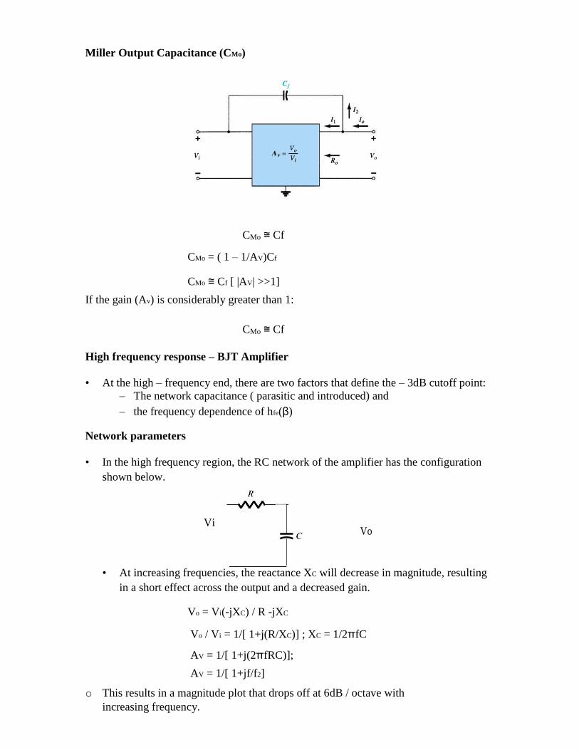
Miller Output Capacitance (CMo)
CMo ≅ Cf
CMo = ( 1 – 1/AV)Cf
CMo ≅ Cf [ |AV| >>1]
If the gain (Av) is considerably greater than 1:
CMo ≅ Cf
High frequency response – BJT Amplifier
• At the high – frequency end, there are two factors that define the – 3dB cutoff point:
– The network capacitance ( parasitic and introduced) and – the frequency dependence of hfe(β)
Network parameters
• In the high frequency region, the RC network of the amplifier has the configuration
shown below.
Vi Vo
• At increasing frequencies, the reactance XC will decrease in magnitude, resulting
in a short effect across the output and a decreased gain.
Vo = Vi(-jXC) / R -jXC
Vo / Vi = 1/[ 1+j(R/XC)] ; XC = 1/2πfC
AV = 1/[ 1+j(2πfRC)];
AV = 1/[ 1+jf/f2]
o This results in a magnitude plot that drops off at 6dB / octave with
increasing frequency.

Network with the capacitors that affect the high frequency response
• Capacitances that will affect the high-frequency response:
Cbe, Cbc, Cce – internal capacitances
Cwi, Cwo – wiring capacitances
CS, CC – coupling capacitors
CE – bypass capacitor
The capacitors CS, CC, and CE are absent in the high frequency equivalent of the BJT
amplifier.The capacitance Ci includes the input wiring capacitance, the transition
capacitance Cbe, and the Miller capacitance CMi.The capacitance Co includes the
output wiring capacitance Cwo, the parasitic capacitance Cce, and the output Miller
capacitance CMo.In general, the capacitance Cbe is the largest of the parasitic
capacitances, with Cce the smallest.
As per the equivalent circuit,
fH = 1 / 2πRthiCi
Rthi = Rs|| R1||R2||Ri
Ci = Cwi+Cbe+CMi = CWi + Cbe+(1- AV) Cbe
At very high frequencies, the effect of Ci is to reduce the total impedance of the
parallel combination of R1 , R2, Ri, and Ci.The result is a reduced level of
voltage across Ci, a reduction in Ib and the gain of the system. For the output
network,
fHo = 1/(2πRThoCo)
RTho = RC||RL||ro
Co = Cwo+Cce+CMo
At very high frequencies, the capacitive reactance of Co will decrease and
consequently reduce the total impedance of the output parallel branches. The net result is that Vo will also decline toward zero as the reactance Xc becomes
smaller.The frequencies fHi and fHo will each define a -6dB/octave asymtote. If the parasitic capacitors were the only elements to determine the high – cutoff
frequency, the lowest frequency would be the determining factor.However, the
decrease in hfe(or β) with frequency must also be considered as to whether its break
frequency is lower than fHi or fHo.
hfe (or β) variation
• The variation of hfe( or β) with frequency will approach the following relationship
hfe = hfe mid / [1+(f/fβ)]
• fβ is that frequency at which hfe of the transistor falls by 3dB with respect to its
mid band value. • The quantity fβ is determined by a set of parameters employed in the hybrid
π model. • Since the base – to – emitter voltage is linearly related to the base current
through Ohm’s law and the output voltage is equal to the difference between the
base the base – to – emitter voltage and collector – to – base voltage, we can say
that the base current is sensitive to the changes in output voltage.
• Thus,
fβ = 1/[2πrπ(Cπ+Cu)]
rπ = βre = hfe mid re
• Therefore,
fβ = 1/[2π hfemid re(Cπ+Cu)] OR
fβ = 1/[2π βmid re(Cπ+Cu)]