FAN7392 - and Low-Side, Gate-Drive IC - Mouser Electronics
21
To learn more about ON Semiconductor, please visit our website at www.onsemi.com Is Now Part of ON Semiconductor and the ON Semiconductor logo are trademarks of Semiconductor Components Industries, LLC dba ON Semiconductor or its subsidiaries in the United States and/or other countries. ON Semiconductor owns the rights to a number of patents, trademarks, copyrights, trade secrets, and other intellectual property. A listing of ON Semiconductor’s product/patent coverage may be accessed at www.onsemi.com/site/pdf/Patent-Marking.pdf. ON Semiconductor reserves the right to make changes without further notice to any products herein. ON Semiconductor makes no warranty, representation or guarantee regarding the suitability of its products for any particular purpose, nor does ON Semiconductor assume any liability arising out of the application or use of any product or circuit, and specifically disclaims any and all liability, including without limitation special, consequential or incidental damages. Buyer is responsible for its products and applications using ON Semiconductor products, including compliance with all laws, regulations and safety requirements or standards, regardless of any support or applications information provided by ON Semiconductor. “Typical” parameters which may be provided in ON Semiconductor data sheets and/or specifications can and do vary in different applications and actual performance may vary over time. All operating parameters, including “Typicals” must be validated for each customer application by customer’s technical experts. ON Semiconductor does not convey any license under its patent rights nor the rights of others. ON Semiconductor products are not designed, intended, or authorized for use as a critical component in life support systems or any FDA Class 3 medical devices or medical devices with a same or similar classification in a foreign jurisdiction or any devices intended for implantation in the human body. Should Buyer purchase or use ON Semiconductor products for any such unintended or unauthorized application, Buyer shall indemnify and hold ON Semiconductor and its officers, employees, subsidiaries, affiliates, and distributors harmless against all claims, costs, damages, and expenses, and reasonable attorney fees arising out of, directly or indirectly, any claim of personal injury or death associated with such unintended or unauthorized use, even if such claim alleges that ON Semiconductor was negligent regarding the design or manufacture of the part. ON Semiconductor is an Equal Opportunity/Affirmative Action Employer. This literature is subject to all applicable copyright laws and is not for resale in any manner.
-
Upload
khangminh22 -
Category
Documents
-
view
3 -
download
0
Transcript of FAN7392 - and Low-Side, Gate-Drive IC - Mouser Electronics

To learn more about ON Semiconductor, please visit our website at www.onsemi.com
Is Now Part of
ON Semiconductor and the ON Semiconductor logo are trademarks of Semiconductor Components Industries, LLC dba ON Semiconductor or its subsidiaries in the United States and/or other countries. ON Semiconductor owns the rights to a number of patents, trademarks, copyrights, trade secrets, and other intellectual property. A listing of ON Semiconductor’s product/patent coverage may be accessed at www.onsemi.com/site/pdf/Patent-Marking.pdf. ON Semiconductor reserves the right to make changes without further notice to any products herein. ON Semiconductor makes no warranty, representation or guarantee regarding the suitability of its products for any particular purpose, nor does ON Semiconductor assume any liability arising out of the application or use of any product or circuit, and specifically disclaims any and all liability, including without limitation special, consequential or incidental damages. Buyer is responsible for its products and applications using ON Semiconductor products, including compliance with all laws, regulations and safety requirements or standards, regardless of any support or applications information provided by ON Semiconductor. “Typical” parameters which may be provided in ON Semiconductor data sheets and/or specifications can and do vary in different applications and actual performance may vary over time. All operating parameters, including “Typicals” must be validated for each customer application by customer’s technical experts. ON Semiconductor does not convey any license under its patent rights nor the rights of others. ON Semiconductor products are not designed, intended, or authorized for use as a critical component in life support systems or any FDA Class 3 medical devices or medical devices with a same or similar classification in a foreign jurisdiction or any devices intended for implantation in the human body. Should Buyer purchase or use ON Semiconductor products for any such unintended or unauthorized application, Buyer shall indemnify and hold ON Semiconductor and its officers, employees, subsidiaries, affiliates, and distributors harmless against all claims, costs, damages, and expenses, and reasonable attorney fees arising out of, directly or indirectly, any claim of personal injury or death associated with such unintended or unauthorized use, even if such claim alleges that ON Semiconductor was negligent regarding the design or manufacture of the part. ON Semiconductor is an Equal Opportunity/Affirmative Action Employer. This literature is subject to all applicable copyright laws and is not for resale in any manner.
© 2009 Fairchild Semiconductor Corporation www.fairchildsemi.com
FA
N73
92 — H
igh
-Cu
rrent, H
igh
- and
Lo
w-S
ide, G
ate-Drive IC
FAN7392 Rev. 1.0.4
July 2012
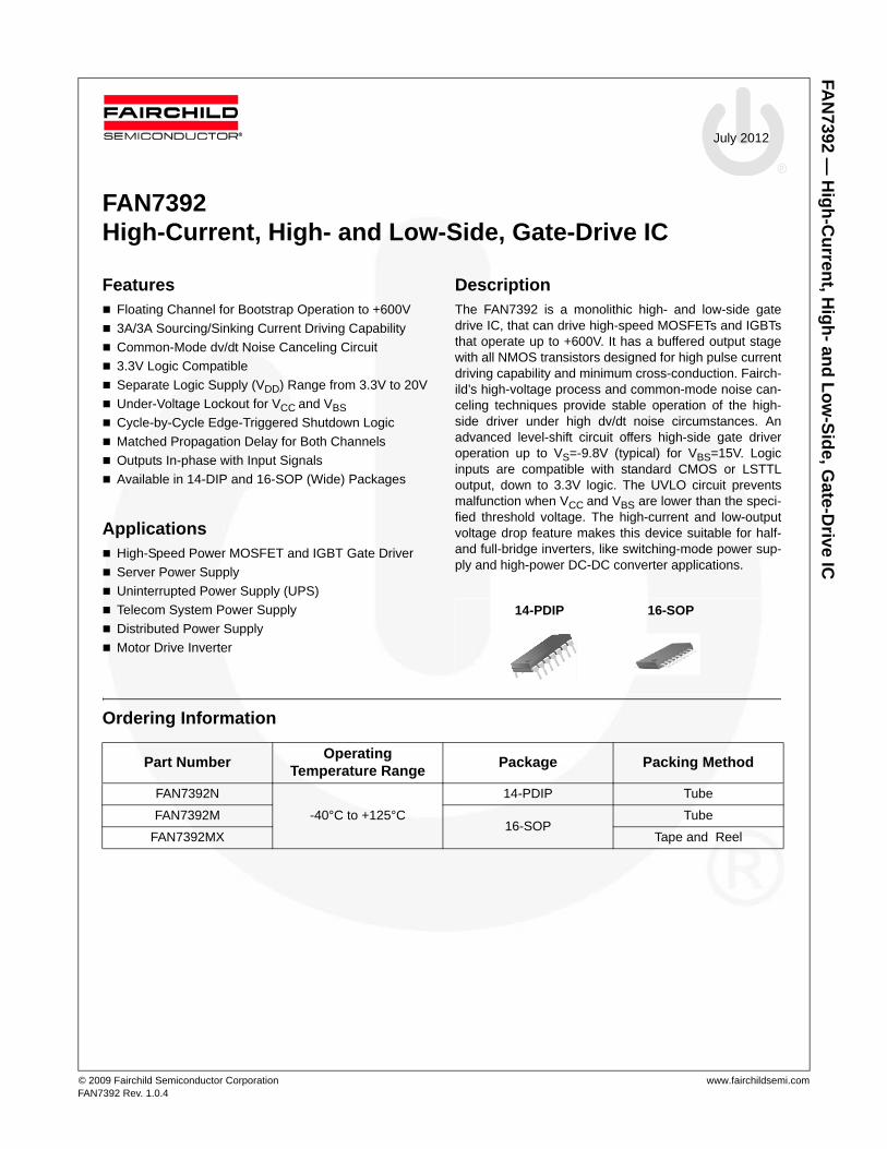
FAN7392High-Current, High- and Low-Side, Gate-Drive IC
Features Floating Channel for Bootstrap Operation to +600V
3A/3A Sourcing/Sinking Current Driving Capability
Common-Mode dv/dt Noise Canceling Circuit
3.3V Logic Compatible
Separate Logic Supply (VDD) Range from 3.3V to 20V
Under-Voltage Lockout for VCC and VBS
Cycle-by-Cycle Edge-Triggered Shutdown Logic
Matched Propagation Delay for Both Channels
Outputs In-phase with Input Signals
Available in 14-DIP and 16-SOP (Wide) Packages
Applications High-Speed Power MOSFET and IGBT Gate Driver
Server Power Supply
Uninterrupted Power Supply (UPS)
Telecom System Power Supply
Distributed Power Supply
Motor Drive Inverter
DescriptionThe FAN7392 is a monolithic high- and low-side gate drive IC, that can drive high-speed MOSFETs and IGBTs that operate up to +600V. It has a buffered output stage with all NMOS transistors designed for high pulse current driving capability and minimum cross-conduction. Fairch-ild’s high-voltage process and common-mode noise can-celing techniques provide stable operation of the high-side driver under high dv/dt noise circumstances. An advanced level-shift circuit offers high-side gate driver operation up to VS=-9.8V (typical) for VBS=15V. Logic inputs are compatible with standard CMOS or LSTTL output, down to 3.3V logic. The UVLO circuit prevents malfunction when VCC and VBS are lower than the speci-fied threshold voltage. The high-current and low-output voltage drop feature makes this device suitable for half- and full-bridge inverters, like switching-mode power sup-ply and high-power DC-DC converter applications.
Ordering Information
14-PDIP 16-SOP
Part NumberOperating
Temperature RangePackage Packing Method
FAN7392N
-40°C to +125°C
14-PDIP Tube
FAN7392M16-SOP
Tube
FAN7392MX Tape and Reel
lhouse
Line
lhouse
Line
lhouse
Line
lhouse
Line

© 2009 Fairchild Semiconductor Corporation www.fairchildsemi.comFAN7392 Rev. 1.0.4 2
FA
N7392 —
Hig
h-C
urren
t, Hig
h- an
d L
ow
-Sid
e, Gate-D
rive IC
Typical Application Diagrams
Figure 1. Typical Application Circuit (Referenced 14-DIP)
Figure 2. Typical Application Circuit (Referenced 16-SOP)
DBOOT
Q1
RBOOT
CBOOT
15V
Q2
C1
R2
R1
Up to 600V
Controller
HIN
LIN
LO
COM
VB
VS
VDD
SD
HIN
NC
13
NC
HO
VSS
NC
12
14
11
10
9
8
2
3
1
4
7
5
6
LIN VCC
SD
15V
Load
DBOOT
Q1
RBOOT
CBOOT
15V
Q2
C1
R2
R1
Up to 600V
Controller
HIN
LIN
LO
COM
VB
VSVDD
SD
HIN
NC
15
NC
HO
VSS
NC
14
16
13
12
11
10
2
3
1
4
8
6
7
LIN VCC
SD
15V
Load
NC 5
NC9

© 2009 Fairchild Semiconductor Corporation www.fairchildsemi.comFAN7392 Rev. 1.0.4 3
FA
N7392 —
Hig
h-C
urren
t, Hig
h- an
d L
ow
-Sid
e, Gate-D
rive IC
Internal Block Diagram
Figure 3. Functional Block Diagram (Referenced 14-Pin)
Figure 4. Functional Block Diagram (Referenced 16-SOP)
UVLO DR
IVE
R
PU
LS
EG
EN
ER
AT
ORHIN
VCC
COM
VB
VS
RR
S QD
RIV
ER
HS(ON/OFF)
LS(ON/OFF)DELAY
LIN UVLO
HO
LO
SCHMITT TRIGGER INPUT
CYCLE-By-CYCLE EDGE TRIGGERED
SHUTDOWN
NOISECANCELLER
VSS/COMLEVELSHIFT
VSS
10
12
13
Pin 4, 8, and 14 are no connection
SD 11
VDD 9
3
2
6
5
1
7
UVLO DR
IVE
R
PU
LS
EG
EN
ER
AT
ORHIN
VCC
COM
VB
VS
RR
S Q
DR
IVE
R
HS(ON/OFF)
LS(ON/OFF)DELAY
LIN UVLO
HO
LO
SCHMITT TRIGGER INPUT
CYCLE-By-CYCLE EDGE TRIGGERED
SHUTDOWN
NOISECANCELLER
VSS/COMLEVELSHIFT
VSS
12
14
15
Pin 4, 5, 9,10 and 16 are no connection
SD 13
VDD 11
3
2
7
6
1
8

© 2009 Fairchild Semiconductor Corporation www.fairchildsemi.comFAN7392 Rev. 1.0.4 4
FA
N7392 —
Hig
h-C
urren
t, Hig
h- an
d L
ow
-Sid
e, Gate-D
rive IC
Pin Configuration
Figure 5. Pin Configurations (Top View)
Pin Definitions
14-Pin 16-Pin Name Description
1 1 LO Low-Side Driver Output
2 2 COM Low-Side Return
3 3 VCC Low-Side Supply Voltage
5 6 VS High-Voltage Floating Supply Return
6 7 VB High-Side Floating Supply
7 8 HO High-Side Driver Output
9 11 VDD Logic Supply Voltage
10 12 HIN Logic Input for High-Side Gate Driver Output
11 13 SD Logic Input for Shutdown Function
12 14 LIN Logic Input for Low-Side Gate Driver Output
13 15 VSS Logic Ground
4,8,14 4, 5, 9, 10, 16 NC No Connect
LO
NC
FA
N7392 HIN
HO NC
VDD
COM
VB
VS
VSS
1
2
3
4
5
6
7
14
13
12
11
10
9
8
SD
NC
VCC LIN
LO
NC
FA
N7392M
HIN
HO
NC
VDD
COM
VB
VS
VSS
1
2
3
4
5
6
7
16
15
14
13 SD
NC
VCC LIN
12
11
10
98
NC
NC
(a) 14-DIP (b) 16-SOP (Wide Body)

© 2009 Fairchild Semiconductor Corporation www.fairchildsemi.comFAN7392 Rev. 1.0.4 5
FA
N7392 —
Hig
h-C
urren
t, Hig
h- an
d L
ow
-Sid
e, Gate-D
rive IC
Absolute Maximum RatingsStresses exceeding the absolute maximum ratings may damage the device. The device may not function or be opera-ble above the recommended operating conditions and stressing the parts to these levels is not recommended. In addi-tion, extended exposure to stresses above the recommended operating conditions may affect device reliability. The absolute maximum ratings are stress ratings only. TA=25°C unless otherwise specified.
Notes:
1. Mounted on 76.2 x 114.3 x 1.6mm PCB (FR-4 glass epoxy material).
2. Refer to the following standards:JESD51-2: Integral circuits thermal test method environmental conditions, natural convection; andJESD51-3: Low effective thermal conductivity test board for leaded surface-mount packages.
3. Do not exceed power dissipation (PD) under any circumstances.
Recommended Operating ConditionsThe Recommended Operating Conditions table defines the conditions for actual device operation. Recommended operating conditions are specified to ensure optimal performance to the datasheet specifications. Fairchild does not recommend exceeding them or designing to absolute maximum ratings.
Symbol Characteristics Min. Max. Unit
VB High-Side Floating Supply Voltage -0.3 625.0 V
VS High-Side Floating Offset Voltage VB-25.0 VB+0.3 V
VHO High-Side Floating Output Voltage VS-0.3 VB+0.3 V
VCC Low-Side Supply Voltage -0.3 25.0 V
VLO Low-Side Floating Output Voltage -0.3 VCC+0.3 V
VDD Logic Supply Voltage -0.3 VSS+25.0 V
VSS Logic Supply Offset Voltage VCC-25.0 VCC+0.3 V
VIN Logic Input Voltage (HIN, LIN and SD) VSS-0.3 VDD+0.3 V
dVS/dt Allowable Offset Voltage Slew Rate ±50 V/ns
PD Power Dissipation(1, 2, 3) 14-PDIP 1.6W
16-SOP 1.3
JA Thermal Resistance14-PDIP 75
C/W16-SOP 95
TJ Maximum Junction Temperature +150 C
TSTG Storage Temperature -55 +150 C
Symbol Parameter Min. Max. Unit
VB High-Side Floating Supply Voltage VS+10 VS+20 V
VS High-Side Floating Supply Offset Voltage 6-VCC 600 V
VHO High-Side Output Voltage VS VB V
VCC Low-Side Supply Voltage 10 20 V
VLO Low-Side Output Voltage 0 VCC V
VDD Logic Supply Voltage VSS+3 VSS+20 V
VSS Logic Supply Offset Voltage -5 5 V
VIN Logic Input Voltage VSS VDD V
TA Operating Ambient Temperature -40 +125 C

© 2009 Fairchild Semiconductor Corporation www.fairchildsemi.comFAN7392 Rev. 1.0.4 6
FA
N7392 —
Hig
h-C
urren
t, Hig
h- an
d L
ow
-Sid
e, Gate-D
rive IC
Electrical Characteristics VBIAS(VCC, VBS, VDD)=15.0V, VSS=COM=0V and TA=25°C, unless otherwise specified. The VIH, VIL, and IINparameters are referenced to VSS and are applicable to the respective input leads: HIN, LIN, and SD. The VO and IOparameters are referenced to VS and COM and are applicable to the respective output leads: HO and LO.
Symbol Characteristics Test Condition Min. Typ. Max. Unit
Low-Side Power Supply Section
IQCC Quiescent VCC Supply Current VIN=0V or VDD 40 80 A
IQDD Quiescent VDD Supply Current VIN=0V or VDD 10 A
IPCC Operating VCC Supply Current fIN=20kHz, rms, VIN=15VPP 430 A
IPDD Operating VDD Supply Current fIN=20kHz, rms, VIN=15VPP 300 A
ISD Shutdown Supply Current SD=VDD 120 A
VCCUV+VCC Supply Under-Voltage Positive-Going Threshold Voltage
VIN=0V, VCC=Sweep 7.7 8.8 9.9 V
VCCUV-VCC Supply Under-Voltage Negative-Going Threshold Voltage
VIN=0V, VCC=Sweep 7.3 8.4 9.5 V
VCCUVHVCC Supply Under-Voltage Lockout Hysteresis Voltage
VIN=0V, VCC=Sweep 0.4 V
Bootstrapped Supply Section
IQBS Quiescent VBS Supply Current VIN=0V or VDD 60 130 A
IPBS Operating VBS Supply Current fIN=20kHz, rms value 500 A
VBSUV+VBS Supply Under-Voltage Positive-Going Threshold Voltage
VIN=0V, VBS=Sweep 7.7 8.8 9.9 V
VBSUV-VBS Supply Under-Voltage Negative-Going Threshold Voltage
VIN=0V, VBS=Sweep 7.3 8.4 9.5 V
VBSUVHVBS Supply Under-Voltage Lockout Hysteresis Voltage
VIN=0V, VBS=Sweep 0.4 V
ILK Offset Supply Leakage Current VB=VS=600V 50 A
Input Locic Section (HIN, LIN, and SD)
VIH Logic “1” Input Threshold VoltageVDD=3V 2.4 V
VDD=15V 9.5 V
VIL Logic “0” Input Threshold VoltageVDD=3V 0.8 V
VDD=15V 4.5 V
IIN+ Logic Input High Bias Current VIN=VDD 20 40 A
IIN- Logic Input Low Bias Current VIN=0V 3 A
RIN Logic Input Pull-Down Resistance 375 750 K
Gate Driver Output Section
VOH High-Level Output Voltage (VBIAS - VO) No Load (IO=0A) 1.5 V
VOL Low-Level Output Voltage No Load (IO=0A) 200 mV
IO+ Output High, Short-Circuit Pulsed Current(4) VO=0V, PW 10µs 2.5 3.0 A
IO- Output Low, Short-Circuit Pulsed Current(4) VO=15V, PW 10µs 2.5 3.0 A
VSS/COM VSS-COM/COM-VSS Voltage Endurability -5.0 5.0 V
- VSAllowable Negative VS Pin Voltage for HIN Signal Propagation to HO
-9.8 -7.0 V

© 2009 Fairchild Semiconductor Corporation www.fairchildsemi.comFAN7392 Rev. 1.0.4 7
FA
N7392 —
Hig
h-C
urren
t, Hig
h- an
d L
ow
-Sid
e, Gate-D
rive IC
Dynamic Electrical Characteristics VBIAS(VCC, VBS, VDD)=15.0V, VSS=COM=0V, CLOAD=1000pF, TA=25°C, unless otherwise specified.
Note: 4. These parameters guaranteed by design.
Symbol Parameter Conditions Min. Typ. Max. Unit
ton Turn-On Propagation Delay Time VS=0V 130 180 ns
toff Turn-Off Propagation Delay Time VS=0V 150 200 ns
tsd Shutdown propagation Delay Time(4) 130 180 ns
tr Turn-On Rise Time 25 50 ns
tf Turn-Off Fall Time 20 45 ns
MT Delay Matching, HO & LO Turn-On/Off 35 ns

FA
N73
92 — H
igh
-Cu
rrent, H
igh
- and
Lo
w-S
ide, G
ate-Drive IC
© 2009 Fairchild Semiconductor Corporation www.fairchildsemi.comFAN7392 Rev. 1.0.4 8
Typical Characteristics
Figure 6. Turn-On Propagation Delay vs. Temperature
Figure 7. Turn-Off Propagation Delay vs. Temperature
Figure 8. Turn-On Rise Time vs. Temperature
Figure 9. Turn-Off Fall Time vs. Temperature
Figure 10. Turn-On Delay Matching vs. Temperature Figure 11. Turn-Off Delay Matching vs. Temperature
-40 -20 0 20 40 60 80 100 12080
100
120
140
160
180
t ON [n
s]
Temperature [°C]
-40 -20 0 20 40 60 80 100 120100
120
140
160
180
200
t OF
F [n
s]
Temperature [°C]
-40 -20 0 20 40 60 80 100 1200
10
20
30
40
50
t R [n
s]
Temperature [°C]
-40 -20 0 20 40 60 80 100 1200
10
20
30
40
50
t F [n
s]
Temperature [°C]
-40 -20 0 20 40 60 80 100 1200
10
20
30
MT
ON [n
s]
Temperature [°C]-40 -20 0 20 40 60 80 100 1200
10
20
30
MT
OF
F [n
s]
Temperature [°C]

FA
N73
92 — H
igh
-Cu
rrent, H
igh
- and
Lo
w-S
ide, G
ate-Drive IC
© 2009 Fairchild Semiconductor Corporation www.fairchildsemi.comFAN7392 Rev. 1.0.4 9
Typical Characteristics (Continued)
Figure 12. Shutdown Propagation Delay vs. Temperature
Figure 13. Logic Input High Bias Current vs. Temperature
Figure 14. Quiescent VCC Supply Current vs. Temperature
Figure 15. Quiescent VBS Supply Current vs. Temperature
Figure 16. Operating VCC Supply Current vs. Temperature
Figure 17. Operating VBS Supply Current vs. Temperature
-40 -20 0 20 40 60 80 100 12080
100
120
140
160
180
t SD [n
s]
Temperature [°C]-40 -20 0 20 40 60 80 100 1200
10
20
30
40
I IN+ [A]
Temperature [°C]
-40 -20 0 20 40 60 80 100 1200
10
20
30
40
50
60
70
80
I QC
C [A]
Temperature [°C]
-40 -20 0 20 40 60 80 100 1200
20
40
60
80
100
120
I Q
BS [A]
Temperature [°C]
-40 -20 0 20 40 60 80 100 1200
200
400
600
800
1000
I PC
C [A]
Temperature [°C]
-40 -20 0 20 40 60 80 100 1200
200
400
600
800
1000
I PB
S [A]
Temperature [°C]
FA
N73
92 — H
igh
-Cu
rrent, H
igh
- and
Lo
w-S
ide, G
ate-Drive IC
© 2009 Fairchild Semiconductor Corporation www.fairchildsemi.comFAN7392 Rev. 1.0.4 10
Typical Characteristics (Continued)
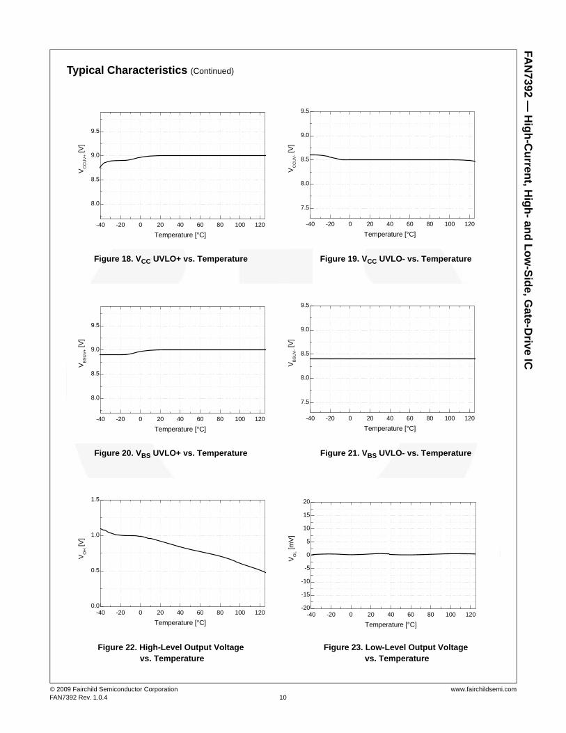
Figure 18. VCC UVLO+ vs. Temperature Figure 19. VCC UVLO- vs. Temperature
Figure 20. VBS UVLO+ vs. Temperature Figure 21. VBS UVLO- vs. Temperature
Figure 22. High-Level Output Voltage vs. Temperature
Figure 23. Low-Level Output Voltage vs. Temperature
-40 -20 0 20 40 60 80 100 120
8.0
8.5
9.0
9.5
VC
CU
V+ [V
]
Temperature [°C]
-40 -20 0 20 40 60 80 100 120
7.5
8.0
8.5
9.0
9.5
VC
CU
V- [V
]
Temperature [°C]
-40 -20 0 20 40 60 80 100 120
8.0
8.5
9.0
9.5
VB
SU
V+ [V
]
Temperature [°C]
-40 -20 0 20 40 60 80 100 120
7.5
8.0
8.5
9.0
9.5
V
BS
UV
- [V]
Temperature [°C]
-40 -20 0 20 40 60 80 100 1200.0
0.5
1.0
1.5
VO
H [V
]
Temperature [°C]-40 -20 0 20 40 60 80 100 120
-20
-15
-10
-5
0
5
10
15
20
VO
L [mV
]
Temperature [°C]

FA
N73
92 — H
igh
-Cu
rrent, H
igh
- and
Lo
w-S
ide, G
ate-Drive IC
© 2009 Fairchild Semiconductor Corporation www.fairchildsemi.comFAN7392 Rev. 1.0.4 11
Typical Characteristics (Continued)
Figure 24. Logic High Input Voltage vs. Temperature
Figure 25. Logic Low Input Voltage vs. Temperature
Figure 26. Allowable Negative VS Voltage vs. Temperature
Figure 27. Input Logic (HIN & LIN) Threshold Voltage vs. VDD Supply Voltage
.
Figure 28. Allowable Negative Vs Voltage for HIN Signal Propagation to High Side vs. Supply Voltage
-40 -20 0 20 40 60 80 100 1206
7
8
9
10
11
VDD
= 15V
VIH
[V]
Temperature [°C]
-40 -20 0 20 40 60 80 100 1203
4
5
6
7
8
9
10
VDD
= 15V
VIL [V
]
Temperature [°C]
-40 -20 0 20 40 60 80 100 120-12
-11
-10
-9
-8
-7
VS [V
]
Temperature [°C]0 2 4 6 8 10 12 14 16 18 20
0
2
4
6
8
10
12
VIH
VIL
L
og
ic T
hre
sho
ld V
olta
ge
[V]
VDD
Logic Supply Voltage [V]
10 11 12 13 14 15 16 17 18 19 20
-16
-14
-12
-10
-8
-6
-4
VS
[V]
Supply Voltage [V]
VCC=VBS
COM=0V
TA=25C

© 2009 Fairchild Semiconductor Corporation www.fairchildsemi.comFAN7392 Rev. 1.0.4 12
FA
N7392 —
Hig
h-C
urren
t, Hig
h- an
d L
ow
-Sid
e, Gate-D
rive IC
Switching Time Definitions
Figure 29. Switching Time Test Circuit (Referenced 14-DIP)
Figure 30. Input/Output Timing Diagram
Figure 31. Switching Time Waveform Definitions
1nF 100nF
1nF
100nF
15V
LO
COM
VB
VS
VDD
SD
HIN
NC
13
NC
HO
VSS
NC14
11
10
9
8
LIN VCC
15V
12
2
3
1
4
7
5
6
15V
LO
HO
(0 to 600V)HIN
SD
LIN
10F
10F
10F
Shutdown Skip
HIN
LIN
HO
LO
SD
50%
90%
50%
tON
10%
tR tOFF tF
10%
90%
HIN
LIN
HO
LO
© 2009 Fairchild Semiconductor Corporation www.fairchildsemi.comFAN7392 Rev. 1.0.4 13
FA
N7392 —
Hig
h-C
urren
t, Hig
h- an
d L
ow
-Sid
e, Gate-D
rive IC
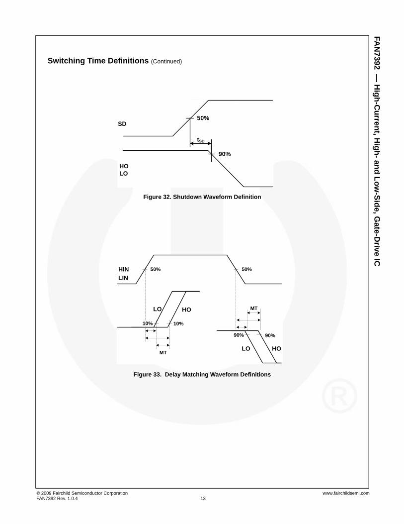
Switching Time Definitions (Continued)
Figure 32. Shutdown Waveform Definition
Figure 33. Delay Matching Waveform Definitions
90%
50%
tSD
HOLO
SD
HIN
LIN
LO
50% 50%
10%
90%
HO
MTHOLO
MT
90%
10%

FA
N73
92 — H
igh
-Cu
rrent, H
igh
- and
Lo
w-S
ide, G
ate-Drive IC
© 2009 Fairchild Semiconductor Corporation www.fairchildsemi.comFAN7392 Rev. 1.0.4 14
Application Information
Negative VS TransientThe bootstrap circuit has the advantage of being simple and low cost, but has some limitations. The biggest diffi-culty with this circuit is the negative voltage present at the emitter of the high-side switching device when high-side switch is turned-off in half-bridge application.
If the high-side switch, Q1, turns-off while the load cur-rent is flowing to an inductive load, a current commuta-tion occurs from high-side switch, Q1, to the diode, D2, in parallel with the low-side switch of the same inverter leg. Then the negative voltage present at the emitter of the high-side switching device, just before the freewheel-ing diode, D2, starts clamping, causes load current to suddenly flow to the low-side freewheeling diode, D2, as shown in Figure 34.
Figure 34. Half-Bridge Application Circuits
This negative voltage can be trouble for the gate driver’s output stage, there is the possibility to develop an over-voltage condition of the bootstrap capacitor, input signal missing and latch-up problems because it directly affects the source VS pin of the gate driver, as shown in Figure 35. This undershoot voltage is called “negative VS tran-sient”.
Figure 35. VS Waveforms During Q1 Turn-Off
Figure 36 and Figure 37 show the commutation of the load current between high-side switch, Q1, and low-side freewheelling diode, D3, in same inverter leg. The para-sitic inductances in the inverter circuit from the die wire bonding to the PCB tracks are jumped together in LC and LE for each IGBT. When the high-side switch, Q1, and low-side switch, Q4, are turned on, the VS1 node is below DC+ voltage by the voltage drops associated with the power switch and the parasitic inductances of the cir-cuit due to load current is flows from Q1 and Q4, as shown in Figure 36. When the high-side switch, Q1, is turned off and Q4, remained turned on, the load current to flows the low-side freewheeling diode, D3, due to the inductive load connected to VS1 as shown in Figure 37. The current flows from ground (which is connected to the COM pin of the gate driver) to the load and the negative voltage present at the emitter of the high-side switching device.
In this case, the COM pin of the gate driver is at a higher potential than the VS pin due to the voltage drops associ-ated with freewheeling diode, D3, and parasitic ele-ments, LC3 and LE3.
Figure 36. Q1 and Q4 Turn-On
Figure 37. Q1 Turn-Off and D3 Conducting
Q1
Q2
DC+ Bus
VS
iLOAD
ifreewheeling
Load
D1
D2
Q1
VS
Freewheeling
GND
GND
Q1
Q3
DC+ Bus
VS1
iLOAD
ifreewheeling
Q2
Q4
VS2
LC2
LE2
LC4
LE4
LC1
LE1
LC3
LE3
VLC1
VLE1
VLC4
VLE4
Load
D1
D3
D2
D4
Q1
Q3
DC+ Bus
VS1
iLOAD
ifreewheeling
Q2
Q4
VS2
LC2
LE2
LC4
LE4
LC1
LE1
LC3
LE3
VLC3
VLE3
VLC4
VLE4
D1
D3
D2
D4
Load

FA
N73
92 — H
igh
-Cu
rrent, H
igh
- and
Lo
w-S
ide, G
ate-Drive IC
© 2009 Fairchild Semiconductor Corporation www.fairchildsemi.comFAN7392 Rev. 1.0.4 15
The FAN7392 has a negative VS transient performance curve, as shown in Figure 38.
Figure 38. Negative VS Transient Chracteristic
Even though the FAN7392 has been shown able to han-dle these negative VS tranient conditions, it is strongly recommended that the circuit designer limit the negative VS transient as much as possible by careful PCB layout to minimized the value of parasitic elements and compo-nent use. The amplitude of negative VS voltage is pro-portional to the parasitic inductances and the turn-off speed, di/dt, of the switching device.
General Guidelines
Printed Circuit Board Layout
The relayout recommended for minimized parasitic ele-ments is as follows:
Direct tracks between switches with no loops or devia-tion.
Avoid interconnect links. These can add significant inductance.
Reduce the effect of lead-inductance by lowering package height above the PCB.
Consider co-locating both power switches to reduce track length.
To minimize noise coupling, the ground plane should not be placed under or near the high-voltage floating side.
To reduce the EM coupling and improve the power switch turn-on/off performance, the gate drive loops must be reduced as much as possible.
Placement of Components
The recommended placement and selection of compo-nent as follows:
Place a bypass capacitor between the VDD and VSS pins. A ceramic 1µF capacitor is suitable for most applications. This component should be placed as close as possible to the pins to reduce parasitic ele-ments.
The bypass capacitor from VCC to COM supports both the low-side driver and bootstrap capacitor recharge. A value at least ten times higher than the bootstrap capacitor is recommended.
The bootstrap resistor, RBOOT, must be considered in sizing the bootstrap resistance and the current devel-oped during initial bootstrap charge. If the resistor is needed in series with the bootstrap diode, verify that VB does not fall below COM (ground). Recommended use is typically 5 ~ 10 that increase the VBS time constant. If the votage drop of of bootstrap resistor and diode is too high or the circuit topology does not allow a sufficient charging time, a fast recovery or ultra-fast recovery diode can be used.
The bootstrap capacitor, CBOOT, uses a low-ESR capacitor, such as ceramic capacitor.
It is stongly recommended that the placement of compo-nents is as follows:
Place components tied to the floating voltage pins (VB and VS) near the respective high-voltage portions of the device and the FAN7392. NC (not connected) pins in this package maximize the distance between the high-voltage and low-voltage pins (see Figure 5).
Place and route for bypass capacitors and gate resis-tors as close as possible to gate drive IC.
Locate the bootstrap diode, DBOOT, as close as possi-ble to bootstrap capacitor, CBOOT.
The bootstrap diode must use a lower forward voltage drop and minimal switching time as soon as possible for fast recovery or ultra-fast diode.
0
-10
100 200 300 400 500 600 700 800 900 1000
Pulse Width [ns]
VS [
V]
-20
-30
-40
-50
-60
-70
-80
-90
-100
0

© 2009 Fairchild Semiconductor Corporation www.fairchildsemi.comFAN7392 Rev. 1.0.4 16
FA
N7392 —
Hig
h-C
urren
t, Hig
h- an
d L
ow
-Sid
e, Gate-D
rive IC
Physical Dimensions .
Figure 39. 14-Lead Dual In-Line Package (DIP)
Package drawings are provided as a service to customers considering Fairchild components. Drawings may change in any manner without notice. Please note the revision and/or date on the drawing and contact a Fairchild Semiconductor representative to verify or obtain the most recent revision. Package specifications do not expand the terms of Fairchild’s worldwide terms and conditions, specifically the warranty therein, which covers Fairchild products.
Always visit Fairchild Semiconductor’s online packaging area for the most recent package drawings:http://www.fairchildsemi.com/packaging/.
14 8
71
NOTES: UNLESS OTHERWISE SPECIFIED
A) THIS PACKAGE CONFORMS TO
JEDEC MS-001 VARIATION AA B) ALL DIMENSIONS ARE IN MILLIMETERS.
C) DIMENSIONS ARE EXCLUSIVE OF BURRS,
MOLD FLASH, AND TIE BAR EXTRUSIONS. D) DIMENSIONS AND TOLERANCES PER
ASME Y14.5-1994E) DRAWING FILE NAME: MKT-N14AREV8
5.33 MAX
0.38 MIN
2.54
7.116.10
1.781.14
0.560.36
4.952.92
19.6918.67
3.812.92
8.267.62
(1.21)4X
0.280.20
10.92 MAX
0.25 C

© 2009 Fairchild Semiconductor Corporation www.fairchildsemi.comFAN7392 Rev. 1.0.4 17
FA
N7392 —
Hig
h-C
urren
t, Hig
h- an
d L
ow
-Sid
e, Gate-D
rive IC
Physical Dimensions (Continued)
.
Figure 40. 16-Lead Small Outline Package (SOP)
Package drawings are provided as a service to customers considering Fairchild components. Drawings may change in any manner without notice. Please note the revision and/or date on the drawing and contact a Fairchild Semiconductor representative to verify or obtain the most recent revision. Package specifications do not expand the terms of Fairchild’s worldwide terms and conditions, specifically the warranty therein, which covers Fairchild products.
Always visit Fairchild Semiconductor’s online packaging area for the most recent package drawings:http://www.fairchildsemi.com/packaging/.
pdip8_dim.pdf
2.65 MAX
M16BREV2
0.20±0.100.10 C
C
10.30±0.20 A
SEE DETAIL A
0.330.20
NOTES: UNLESS OTHERWISE SPECIFIED
A) THIS PACKAGE CONFORMS TO JEDEC MS-013, ISSUE E, DATED SEPT 2005.
B) ALL DIMENSIONS ARE IN MILLIMETERS. C) DIMENSIONS DO NOT INCLUDE MOLD FLASH OR BURRS.
D) LANDPATTERN STANDARD: SOIC127P1030X265-16L
9.44
PIN ONEINDICATOR
0.25
11.270.51
0.35
8
BC AM
10.325
16 9
8.890
7.50±0.10
B
X 45°0.750.25
(R0.10)
(R0.10)
0.40~1.27
8°0°
SEATING PLANE(1.40)
0.25
GAGE PLANE
DETAIL ASCALE: 2:1
SEATING PLANE
1.27 TYP0.55 TYP
LAND PATTERN RECOMMENDATION
1.75 TYP
9.2 10.95
E) DRAWING FILENAME: MKT-16Brev2

FA
N73
92 — H
igh
-Cu
rrent, H
igh
- and
Lo
w-S
ide, G
ate-Drive IC
© 2009 Fairchild Semiconductor Corporation www.fairchildsemi.comFAN7392 Rev. 1.0.4 18

www.onsemi.com1
ON Semiconductor and are trademarks of Semiconductor Components Industries, LLC dba ON Semiconductor or its subsidiaries in the United States and/or other countries.ON Semiconductor owns the rights to a number of patents, trademarks, copyrights, trade secrets, and other intellectual property. A listing of ON Semiconductor’s product/patentcoverage may be accessed at www.onsemi.com/site/pdf/Patent−Marking.pdf. ON Semiconductor reserves the right to make changes without further notice to any products herein.ON Semiconductor makes no warranty, representation or guarantee regarding the suitability of its products for any particular purpose, nor does ON Semiconductor assume any liabilityarising out of the application or use of any product or circuit, and specifically disclaims any and all liability, including without limitation special, consequential or incidental damages.Buyer is responsible for its products and applications using ON Semiconductor products, including compliance with all laws, regulations and safety requirements or standards,regardless of any support or applications information provided by ON Semiconductor. “Typical” parameters which may be provided in ON Semiconductor data sheets and/orspecifications can and do vary in different applications and actual performance may vary over time. All operating parameters, including “Typicals” must be validated for each customerapplication by customer’s technical experts. ON Semiconductor does not convey any license under its patent rights nor the rights of others. ON Semiconductor products are notdesigned, intended, or authorized for use as a critical component in life support systems or any FDA Class 3 medical devices or medical devices with a same or similar classificationin a foreign jurisdiction or any devices intended for implantation in the human body. Should Buyer purchase or use ON Semiconductor products for any such unintended or unauthorizedapplication, Buyer shall indemnify and hold ON Semiconductor and its officers, employees, subsidiaries, affiliates, and distributors harmless against all claims, costs, damages, andexpenses, and reasonable attorney fees arising out of, directly or indirectly, any claim of personal injury or death associated with such unintended or unauthorized use, even if suchclaim alleges that ON Semiconductor was negligent regarding the design or manufacture of the part. ON Semiconductor is an Equal Opportunity/Affirmative Action Employer. Thisliterature is subject to all applicable copyright laws and is not for resale in any manner.
PUBLICATION ORDERING INFORMATIONN. American Technical Support: 800−282−9855 Toll FreeUSA/Canada
Europe, Middle East and Africa Technical Support:Phone: 421 33 790 2910
Japan Customer Focus CenterPhone: 81−3−5817−1050
www.onsemi.com
LITERATURE FULFILLMENT:Literature Distribution Center for ON Semiconductor19521 E. 32nd Pkwy, Aurora, Colorado 80011 USAPhone: 303−675−2175 or 800−344−3860 Toll Free USA/CanadaFax: 303−675−2176 or 800−344−3867 Toll Free USA/CanadaEmail: [email protected]
ON Semiconductor Website: www.onsemi.com
Order Literature: http://www.onsemi.com/orderlit
For additional information, please contact your localSales Representative
© Semiconductor Components Industries, LLC

Mouser Electronics
Authorized Distributor
Click to View Pricing, Inventory, Delivery & Lifecycle Information: Fairchild Semiconductor:
FAN7392M FAN7392MX