FAN1080M6X - Offline Primary-Side-Regulation (PSR) Quasi ...
19
© Semiconductor Components Industries, LLC, 2018 June, 2019 − Rev. 2 1 Publication Order Number: FAN1080M6X/D FAN1080M6X Offline Primary-Side-Regulation (PSR) Quasi-Resonant Valley Switch Controller FAN1080 is offline Primary−Side−Regulation (PSR) PWM controller with Quasi−Resonant (QR) mode controller to achieved constant−voltage (CV) and constant−current (CC) control for Travel Adaptor (TA) requirement and provide cost−effective, simplified circuit for energy−efficient power supplies. FAN1080 is designed to have good energy efficiency technology that offers options to users to meet different power consumption targets using different startup components. FAN1080 can be used in Travel Adapter design by stand−alone or co−work with secondary−side SR controller FAN6250/FAN6251. While pairing with FAN6292C, FAN1080 can be used to design a high density Type−C travel adapter in compact system BOM. Features • Ultra−Low Standby Power Consumption Feasible: < 30 mW through HV FET and < 75 mW through HV Resistor • Constant−Current (CC) and Constant−Voltage(CV) with Primary − Side Regulation Eliminates Secondary−Side Feedback Component • Valley Switch Operation for Highest Average Efficiency • Dynamic Response Enhancement (DRE) Function for Excellent Dynamic Response without the Need of OPTO • Low EMI Emissions and Common Mode Noise • Programmable Brown−In and Brown−Out Protection • Output Over−Voltage Protection (OVP) • Output Under−Voltage Protection (UVP) • Secondary Side Rectifier Short Detection via Current Sense Protection(CSP) • Cycle−by−Cycle Current Limiting • These Devices are Pb−Free, Halogen Free and are RoHS Compliant Typical Applications • Travel Adapter for Smart Phones, Feature Phones, and Tablet PCs • AC−DC Adapters for Portable Devices or Battery Chargers that Require CV/CC Control SOT23 CASE 527AJ See detailed ordering and shipping information on page 17 of this data sheet. ORDERING INFORMATION MARKING DIAGRAM www. onsemi.com . . . . = Year Code PXX = 080: FAN1080M6X XX = Die Run Code _ _ _ = Week Code PIN CONNECTIONS PXXXX − − − − CS GND GATE AUX VS VDD
-
Upload
khangminh22 -
Category
Documents
-
view
0 -
download
0
Transcript of FAN1080M6X - Offline Primary-Side-Regulation (PSR) Quasi ...

© Semiconductor Components Industries, LLC, 2018
June, 2019 − Rev. 21 Publication Order Number:
FAN1080M6X/D
FAN1080M6X
OfflinePrimary-Side-Regulation(PSR) Quasi-ResonantValley Switch Controller
FAN1080 is offline Primary−Side−Regulation (PSR) PWMcontroller with Quasi−Resonant (QR) mode controller to achievedconstant−voltage (CV) and constant−current (CC) control for TravelAdaptor (TA) requirement and provide cost−effective, simplifiedcircuit for energy−efficient power supplies.
FAN1080 is designed to have good energy efficiency technologythat offers options to users to meet different power consumptiontargets using different startup components.
FAN1080 can be used in Travel Adapter design by stand−alone orco−work with secondary−side SR controller FAN6250/FAN6251.While pairing with FAN6292C, FAN1080 can be used to design a highdensity Type−C travel adapter in compact system BOM.
Features• Ultra−Low Standby Power Consumption Feasible: < 30 mW through
HV FET and < 75 mW through HV Resistor• Constant−Current (CC) and Constant−Voltage(CV) with Primary− Side Regulation Eliminates Secondary−Side Feedback Component
• Valley Switch Operation for Highest Average Efficiency
• Dynamic Response Enhancement (DRE) Function for ExcellentDynamic Response without the Need of OPTO
• Low EMI Emissions and Common Mode Noise
• Programmable Brown−In and Brown−Out Protection
• Output Over−Voltage Protection (OVP)
• Output Under−Voltage Protection (UVP)
• Secondary Side Rectifier Short Detection via Current SenseProtection(CSP)
• Cycle−by−Cycle Current Limiting
• These Devices are Pb−Free, Halogen Free and are RoHS Compliant
Typical Applications• Travel Adapter for Smart Phones, Feature Phones, and Tablet PCs
• AC−DC Adapters for Portable Devices or Battery Chargers thatRequire CV/CC Control
SOT23CASE 527AJ
See detailed ordering and shipping information on page 17 ofthis data sheet.
ORDERING INFORMATION
MARKING DIAGRAM
www.onsemi.com
. . . . = Year CodePXX = 080: FAN1080M6XXX = Die Run Code_ _ _ = Week Code
PIN CONNECTIONS
PXXXX− − −−
CS
GND
GATE
AUX
VS
VDD

FAN1080M6X
www.onsemi.com2
Figure 1. FAN1080 Typical Application Schematic
GATE
DRAIN
SDVDD
GND
VIN
FAN6250
VO
COUT
RGATE
CSNSRSNS
RSDNTC
TX
NSCSNP NP
DSNP
RSNP
CBLK2
LF
CBLK1
AC IN
Bridge
GATE
CS
VDD
VS
GND
CCSF
RCS_COMPRCS
RGF
RGR
DG
AUX
ChokeFuse
XC
FAN1080
RHV
RSNP1
RDNa
RVS−U
RVS−L CVS
CVDD
DAUX
Figure 2. FAN1080 Typical Application Schematic
GATE
DRAIN
SDVDD
GND
VIN
FAN6250
VO
COUT
RGATE
CSNSRSNS
RSDNTC
TX
NSCSNP NP
DSNP
RSNP
CBLK2
LF
CBLK1
AC IN
Bridge
GATE
CS
VDD
VS
GND
CCSF
RCS_COMPRCS
RGF
RGR
DG
AUX
ChokeFuse
XC
FAN1080
RHV
RSNP1
Na
RVS−U
RVS−L CVS
CVDD
DAUX

FAN1080M6X
www.onsemi.com3
Figure 3. FAN1080 Block Diagram
CSLEB
VDD
AUX
VS
6
Valley Detection Frequency Hopping
VCS−LIM
IO Estimator
OSC
1
tDIS
tDIS
5
VDD OVP FaultVVDD−OVP
VDD UVLO17.5V/6.5V
4Debounce
VD D
C
Q
Q
CLK
VDD
DriverControl GATE
Maximum On Time
3
VS UVP FaultVDD OVP Fault
2 GND
Peak Current
Auto−RestartProtection
OTP FaultVS OVP Fault
Brown IN/OUT
VDD UVLO
VCS
VCS
ICOMP
VNVS
VCS Fault
5V
AV−CV CSProtection
VCS Fault
VCS
AV−CC
VNVS
DREDetection
Cable DropCompensation
S/H S/H = Sampling and Hold
VS OVP Fault
VS UVP Fault
VS−SH
VSProtection
COMV
FB−CC
2.5V
Compensator
FB−CV
FB−CV
Hi−Z ModeControl
GATE
FB−CV
�
PIN FUNCTION DESCRIPTION
Pin No. Name Description
1 CS Current Sense. This pin connects to a current−sense resistor to detect the MOSFET current forPeak−Current−Mode control for output regulation. The current−sense information is also used toestimate the output current for CC regulation
2 GND Ground.
3 GATE PWM Signal Output. This pin has an internal totem−pole output driver to drive the power MOS-FET. The gate driving voltage is internally clamped at 7.5 V
4 VDD Power Supply. IC operating current and MOSFET driving current are supplied through this pin. This pin is typically connected to an external VDD capacitor
5 VS Voltage Sense. The VS voltage is used to detect resonant valleys for quasi−resonant switching.This pin detects the output voltage information and diode current discharge time based on the auxiliary winding voltage. It also senses input voltage for Brown−IN/OUT protection
6 AUX Auxiliary Function. The pin is used for startup with external depletion HV FET

FAN1080M6X
www.onsemi.com4
MAXIMUM RATINGS
Parameter Symbol Value Unit
DC Supply Voltage VVDD 30 V
Maximum Voltage on GATE Pin VGETE −0.3 to 30 V
Maximum Voltage on Low Power Pins (Except Pin 3, Pin 4, Pin 6) Vmax −0.3 to 6 V
Power Dissipation (TA = 25�C) PD 467.4 mW
Thermal Resistance (Junction−to−Ambient) �JA 218.5 C/W
Thermal Resistance (Junction−to−Top) �JT 33.1 �C/W
Operating Junction Temperature TJ −40 to +150 �C
Storage Temperature Range TSTG −40 to +150 �C
Electrostatic Discharge Capability
Human Body Model,JEDEC:JESD22_A114
ESD
1.5
kVCharged Device Model,JEDEC:JESD22_C101 0.5
Stresses exceeding those listed in the Maximum Ratings table may damage the device. If any of these limits are exceeded, device functionalityshould not be assumed, damage may occur and reliability may be affected.1. All voltage values, except differential voltages, are given with respect to GND pin.2. Stresses beyond those listed under Maximum Ratings may cause permanent damage to the device.3. Meets JEDEC standards JS−001−2012 and JESD 22−C101.
RECOMMENDED OPERATING RANGES
Parameter Symbol Min Max Unit
VDD Pin Supply Voltage VVDD 6 25 V
VS Pin Supply Voltage VVS 0.65 3.0 V
CS Pin Supply Voltage VCS 0 0.8 V
AUX Pin Supply Voltage VAUX 0 VDD − 5V V
Operating Temperature TA −40 +85 �C
Functional operation above the stresses listed in the Recommended Operating Ranges is not implied. Extended exposure to stresses beyondthe Recommended Operating Ranges limits may affect device reliability.4. The Recommended Operating Conditions table defines the conditions for actual device operation. Recommended operating conditions are
specified to ensure optimal performance. ON Semiconductor does not recommend exceeding them or designing to Maximum Ratings.
ELECTRICAL CHARACTERISTICS
For typical values TJ = 25°C, for min/max values TJ = −40°C to 125°C, VDD = 12 V; unless otherwise noted.
Parameter Test Conditions Symbol Min Typ Max Unit
VDD SECTION
Turn−On Threshold Voltage VDD Rising VDD−ON 16.5 17.5 18.5 V
Turn−Off Threshold Voltage VDD Falling VDD−OFF 6.1 6.5 6.9 V
Startup Current VDD = VDD−ON−0.16 V IDD−ST − 20 �A
Operating Supply Current IDD−OP − 1.2 mA
Deep Green−Mode Operating Supply Cur-rent
IDD−DPGN − − 460 �A
VDD Over−Voltage−Protection Level VVDD−OVP 26.5 28.0 29.5 V
VDD Over−Voltage−Protection DebounceTime
tD−VDDOVP − 120 200 �s

FAN1080M6X
www.onsemi.com5
ELECTRICAL CHARACTERISTICS (continued)
For typical values TJ = 25°C, for min/max values TJ = −40°C to 125°C, VDD = 12 V; unless otherwise noted.
Parameter UnitMaxTypMinSymbolTest Conditions
OSCILLATOR SECTION
Maximum Blanking Frequency fBNK−MAX 70 77 83 kHz
Minimum Blanking Frequency fBNK−MIN 24 27 30 kHz
Maximum DCM Operation Frequency fOSC−DCM−MAX 22 25 28 kHz
Minimum DCM Operation Frequency fOSC−DCM−MIN 0.080 0.105 0.130 kHz
Minimum Frequency for CCM Prevention fOSC−CCM 18 21 24 kHz
Frequency Hopping Range �fHopping 3 4 5 kHz
Frequency Hopping Period �tHopping 1.8 2.5 3.2 ms
AUX SECTION
Clamping Voltage between VDD and AUXpin
VDD = VDD−ON �VCLAMP − 5 − V
CURRENT−SENSE SECTION
Current Limit Threshold Voltage VCS−LIM 0.67 0.70 0.73 V
High Threshold Voltage of Current Sense VCS−IMIN 0.200 0.225 0.250 V
GATE Output Turn−Off Delay (Note 5) tPD − 100 − ns
Leading−Edge Blanking Time tLEB 290 345 400 ns
CONSTANT CURRENT ESTIMATOR SECTION
Reference Voltage of Constant Current VVR−CC 1.19 1.2 1.21 V
Peak Value Amplifying Gain (Note 5) APK 3.6 V/V
CONSTANT CURRENT CORRECTION SECTION
High Line Compensation Current VIN = 264 Vrms ICOMP−H 71 75 79 �A
Low Line Compensation Current VIN = 90 Vrms ICOMP−L 23.5 25.5 27.5 �A
Internal Line Voltage Compensation Resis-tance (Note 5)
RCOMP−LINE 575 �
CABLE DROP COMPENSATION SECTION
Cable Drop Compensation Voltage �VCDC 135 145 155 mV
OVER−TEMPERATURE PROTECTION SECTION
Threshold Temperature for Over−Temperature−Protection (Note 5) TOTP−H − 130 − �C
Threshold Temperature for Over−Temperature−Protection (Note 5) TOTP−L − 110 − �C
VOLTAGE−SENSE SECTION
Reference Voltage of Constant Voltage VVR−CV 2.475 2.500 2.525 V
VS Sampling Blanking Time L TJ = 25°C tVS−BNK−L 1.8 1.9 2.0 �s
VS Sampling Blanking Time H TJ = 25°C tVS−BNK−H 2.2 2.3 2.4 �s
VS Source Current Threshold to EnableBrown−OUT
Set VIN = 264 VAC (373 VDC)NP:NS:NA = 54:8:4, RVS−U = 27.4 k�
IVS−Brown−OUT 270 320 370 �A
Brown−OUT Debounce Time tD−Brown−OUT 12 17 22 ms
VS Source Current Threshold to EnableBrown−IN
Set VIN = 264 VAC (373 VDC)NP:NS:NA=54:8:4, RVS−U = 27.4 k�
IVS−Brown−IN 395 465 535 �A
Brown−IN Debounce Time NBrown−IN − 4 − Pulse
Output Over−Voltage−Protection with VsSampling Voltage
VVS−OVP 2.85 2.95 3.05 V

FAN1080M6X
www.onsemi.com6
ELECTRICAL CHARACTERISTICS (continued)
For typical values TJ = 25°C, for min/max values TJ = −40°C to 125°C, VDD = 12 V; unless otherwise noted.
Parameter UnitMaxTypMinSymbolTest Conditions
VOLTAGE−SENSE SECTION
Output Over−Voltage−Protection DebouncePulse Counts
NVS−OVP − 4 − Pulse
Output Under−Voltage−Protection with VsSampling Voltage
VVS−UVP−L 1.50 1.60 1.70 V
Output Under−Voltage−Protection Debounce Pulse Counts
NVS−UVP − 4 − Pulse
Output Under−Voltage Protection BlankingTime at start−up
tVS−UVP−BLANK 30 40 50 ms
DYNAMIC RESPONSE ENHANCEMENT
Dynamic Event Enable Threshold Voltage TJ = 25°C VVS−EAV−DYN−EN 2.413 2.45 2.488 V
Dynamic Event Disable Threshold Voltage VVS−EAV−DYN−DIS 2.475 V
Hi−Z Mode Enable Time tHIZ−EN 90 100 110 �s
Hi−Z Mode Clamping Voltage VCLMP−HIZ 1.0 1.4 1.8 V
GATE SECTION
Gate Output Voltage Low VGATE−L 0 − 1.5 V
Internal Gate PMOS Driver ON VDD−PMOS−ON 7.0 7.5 8.0 V
Internal Gate PMOS Driver OFF VDD−PMOS−OFF 9.0 9.5 10.0 V
Rising Time tr 100 140 180 ns
Falling Time tf 30 50 70 ns
Gate Output Clamping Voltage VGATE−CLAMP 7.0 7.5 8.0 V
Maximum On Time tON−MAX 15 − 22 �s
Product parametric performance is indicated in the Electrical Characteristics for the listed test conditions, unless otherwise noted. Productperformance may not be indicated by the Electrical Characteristics if operated under different conditions.5. Design guaranteed.
FAN1080M6X
www.onsemi.com7
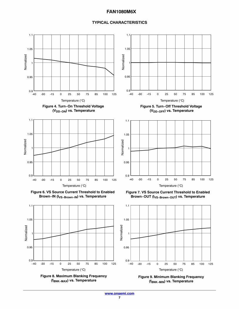
TYPICAL CHARACTERISTICS
Figure 4. Turn−On Threshold Voltage (VDD−ON) vs. Temperature
Figure 5. Turn−Off Threshold Voltage (VDD−OFF) vs. Temperature
0.9
0.95
1
1.05
1.1
−40 −30 −15 0 25 50 75 85 100 125
Nor
mal
ized
0.9
0.95
1
1.05
1.1
−40 −30 −15 0 25 50 75 85 100 125
Nor
mal
ized
Temperature (°C) Temperature (°C)
0.9
0.95
1
1.05
1.1
−40 −30 −15 0 25 50 75 85 100 125
Nor
mal
ized
0.9
0.95
1
1.05
1.1
−40 −30 −15 0 25 50 75 85 100 125
Nor
mal
ized
Figure 6. VS Source Current Threshold to EnabledBrown−IN (IVS−Brown−IN) vs. Temperature
Figure 7. VS Source Current Threshold to EnabledBrown−OUT (IVS−Brown−OUT) vs. Temperature
Temperature (°C) Temperature (°C)
0.9
0.95
1.05
1.1
−30 −15 0 25 50 75 85 100 125
Nor
mal
ized
0.9
0.95
1
1.05
1.1
−30 −15 0 25 50 75 85 100 125
Nor
mal
ized
Figure 8. Maximum Blanking Frequency(fBNK−MAX) vs. Temperature
Figure 9. Minimum Blanking Frequency(fBNK−MIN) vs. Temperature
Temperature (°C) Temperature (°C)
1
−40 −40

FAN1080M6X
www.onsemi.com8
TYPICAL CHARACTERISTICS (continued)
0.9
0.95
1
1.05
1.1
−40 −30 −15 0 25 50 75 85 100 125
Nor
mal
ized
0.9
0.95
1
1.05
1.1
−40 −30 −15 0 25 50 75 85 100 125
Nor
mal
ized
Figure 10. Reference Voltage of Constant Voltage(VVR−CV) vs. Temperature
Figure 11. Reference Voltage of Constant Current(VVR−CC) vs. Temperature
Temperature (°C) Temperature (°C)
Figure 12. VS Sampling Blanking Time L(tVS-BNK−L) vs. Temperature
Figure 13. VS Sampling Blanking Time H(tVS−BNK−H) vs. Temperature
0.9
0.95
1
1.05
1.1
−40 −30 −15 0 25 50 75 85 100 125
Nor
mal
ized
0.9
0.95
1
1.05
1.1
−40 −30 −15 0 25 50 75 85 100 125
Nor
mal
ized
Temperature (°C) Temperature (°C)
0.9
0.95
1
1.05
1.1
−40 −30 −15 0 25 50 75 85 100 125
Nor
mal
ized
0.9
0.95
1
1.05
1.1
−40 −30 −15 0 25 50 75 85 100 125
Nor
mal
ized
Figure 14. Output Over−Voltage-Protection (VVS−OVP) vs. Temperature
Figure 15. Output Under-Voltage Protection(VVS−UVP) vs. Temperature
Temperature (°C) Temperature (°C)

FAN1080M6X
www.onsemi.com9
TYPICAL CHARACTERISTICS (continued)
0.9
0.95
1
1.05
1.1
−40 −30 −15 0 25 50 75 85 100 125
Nor
mal
ized
0.9
0.95
1
1.05
1.1
−40 −30 −15 0 25 50 75 85 100 125
Nor
mal
ized
Figure 16. Current Limit Threshold Voltage (VCS-LIM) vs. Temperature
Figure 17. High Threshold Voltage of Current Sense(VCS-IMIN) vs. Temperature
Temperature (°C) Temperature (°C)
0.9
0.95
1
1.05
1.1
−40 −30 −15 0 25 50 75 85 100 125
Nor
mal
ized
0.9
0.95
1
1.05
1.1
−30 −15 0 25 50 75 85 100 125
Nor
mal
ized
Figure 18. VDD Over−Voltage Protection Level(VVDD−OVP) vs. Temperature
Figure 19. Cable Drop Compensation Voltage (△VCDC) vs. Temperature
Temperature (°C) Temperature (°C)
0.9
0.95
1
1.05
1.1
−40 −30 −15 0 25 50 75 85 100 125
Nor
mal
ized
0.9
0.95
1
1.05
1.1
− 40 −30 −15 0 25 50 75 85 100 125
Nor
mal
ized
Figure 20. Leading−Edge Blanking Time(tLEB) vs. Temperature
Figure 21. Maximum On Time (tON−MAX) vs. Temperature
Temperature (°C) Temperature (°C)

FAN1080M6X
www.onsemi.com10
APPLICATIONS INFORMATION
FAN1080 is a flyback power supply controller providinga means to implement primary side constant−voltage (CV)and constant−current (CC) regulation. This technique cansimplify feedback circuit and secondary side circuitcompare to traditional flyback converter. FAN1080implements a current−mode architecture operation inquasi−resonant mode. The quasi−resonant mode operationis able to minimize the switching loss to optimize the powersupply efficiency and get better EMI performance.
FAN1080 quasi−resonance operation in peak currentmode control is monitor the auxiliary winding voltage onprimary side via the resistor divider to voltage sense pin(VS) and current sense pin (CS). Extremely accuratelyconstant voltage (CV) mode and constant current (CC)mode could meet strict requirement from market.
Figure 22. CV and CC Mode
VO
IO
VO−NOM
0 IO−CC−NOM
CV Mode
CC Mode
FAN1080 implements deep green mode (DPGN) withlowest switching frequency, limits IC current consumption(460 �A) for excellent system standby power performance.Furthermore, the system design allows two kinds of startupcircuit one is with startup resistor the other is with highvoltage FET.
Protections such as over−voltage protection (VS−OVP),under−voltage protection (VS−UVP), internalover−temperature protection (OTP), brown−in andbrown−out protection, cycle by cycle current limit, currentsense resistor short protection and secondary rectifier shortprotection.
Startup OperationFAN1080 supports high voltage start up with depletion
FET that can make better standby power and shorter start uptime. Figure 23 shows startup sequence with AUXcontrolling. The initial AUX pin status should be defined byresistor of RD. At system power on moment, the initial VDDvoltage is zero, internal switch S1 is turn−on and externaldepletion FET also is turn−on, the CVDD is charged throughdepletion FET till VDD reach VDD−ON. While internalswitch S1is turn−off and VGS of depletion FET will close tointernal clamping voltage (VCLAMP) which less thandepletion FET VGS turn−on threshold. Meanwhile VDDenergy supplement is turn to auxiliary winding. The voltagegap between VDD and VAUX is kept at △VCLAMP tillcontroller shut−down by protection or VDD touchingVDD−OFF.
Figure 23. Startup Sequence with AUX Controlling
CBLK
AC IN
Bridge
FAN1080
RHV
RD
Na
RVS−U
RVS−L
CVDD
DAUX
Depletion NMOS (Normal ON)
VDD
VAUX
t
VDD−ON
VDD−VAUX = △VCLAMP = 5V
VDD−OFF
VDD AUX6
UVLOVDD−ON / VDD−OFF
4
VCLAMP
S1

FAN1080M6X
www.onsemi.com11
Primary Side Regulation: Constant Voltage OperationAs illustrated by Figure 24, the voltage of auxiliary
winding (VWAUX) is reflected to output voltage scaled bythe auxiliary and secondary turns ratio minus the drainvoltage of synchronous rectifier (SR) FET.
To reach an accurate primary−side constant−voltageregulation, the controller detects the end of thedemagnetization time and precisely sample output voltagelevel seen on the auxiliary winding.
Therefore, when the secondary current ISEC reaches zeroampere, the voltage of auxiliary winding is sensed as:
VWAUX � VO �Na
Ns(eq. 1)
where Na and NS are respectively the turns of secondary andauxiliary.
Figure 25 shows how the constant voltage feedback hasbeen built. The auxiliary winding voltage must be scaleddown via the resistor divider to VVR−CV level beforebuilding the constant voltage feedback error.
VVR�CV �RVS�L
RVS�U � RVS�L� VWAUX (eq. 2)
By inserting Equation 1 into Equation 2 we obtain thefollowing equation:
VVR�CV �RVS�L
RVS�U � RVS�L� VO �
Na
Ns(eq. 3)
A VS blanking time (tVS−BNK) start from primary switchturned off. Most of TA design has VS oscillation afterprimary switch turned off that is caused by the resonance ofleakage inductance and parasitic capacitance at transformer.In order to avoid VS sampling procedure get impacted bythat ringing, after tVS−BNK the oscillation should be settleddown. Figure 25 shows feedback signal sampling timing,after the VS blanking time, the controller samples the VS pinvoltage as VSD. Once VS is lower than the threshold voltageof VTDIS (VS−200 mV), the VSD signal will be held asVS−SH.
Figure 24. Typical Idealized Waveforms of a Flyback Transformer in DCM
CSNP
Np
DSNP
RSNP
RCS
RSNP1
VOCOUT
NS
VS
Na
RVS−U
RVS−L CVS
VO
ISEC
VDrain
VDrain
VO
SR FET
SR FET ON
0V
ISEC
VWAUX
VWAUX(t)
IPRI(t)
ISEC(t)
IPRI
time
time
timeton tdemag
tSW
VWAUX(t) � [Vo ��� ISEC(t)� rDS(ON)�� Na
NS
Figure 25. Constant Voltage Feedback Circuit and VS signal Sampling Timing
VS
tVS−BNK
HOLD
SP
VTDIS = VS−200mV
TBNKB
VSD
VVR−CV
GM−CV
VS−SH
COMVVS
Na
CVS
RVS−U
RVS−L
Compensator
time
time
time
time
VS−SH
Low PassFilter
S/H

FAN1080M6X
www.onsemi.com12
Primary Side Regulation: Constant Current OperationFigure 26 shows the key waveforms of a flyback converter
operation in DCM. The output current (IO) is estimated bycalculating the average of secondary current (ISEC) in oneswitching cycle. The output current (IO) can be calculated as
IO � 12
1RCS
VCS�PK⋅TDIS
TSW
Np
NS� � 1
21
RCS
VVR�CC
APK
Np
NS� (eq. 4)
When the secondary current reaches zero, the transformerwinding voltage begins to drop sharply, and VS pin voltagedrops as well. When VS pin voltage drops below the VS by
more than 200 mV, zero current point of secondary currentis obtained.The output current can be programmed by setting the currentsensing resistor as:
RCS � 12
⋅ 1IO
⋅VVR�CC
APK⋅NP
NS⋅� (eq. 5)
where VVR−CC is the internal voltage for constant currentcontrol, � is efficiency of flyback and APK is the IC designparameter, 3.6 for FAN1080.
Figure 26. Constant Current Feedback Circuit and Control Sequence
VCS
S/H
VVR−CC
VCS−PK VCS−PKAPK IO_ESTM
COMI
IO_ESTM
VCS−PK
TONTDIS TQR
Defined the Zero Current
ISEC
VVR−CC
VCS−PKAPK
VS
tVS−BNK
VTDIS = VS−200mV
time
time
APK
GM−CC
Compensator
timeTSW
VCS−PK
AveragingCircuit
Line Voltage CompensationThe output current estimation is also affected by the
turn−off delay of the power FET as shown in Figure 27. Theactual power FET’s turn−off time is delayed due to the FETgate charge and gate driver’s capability, resulting in peakcurrent detection error as
�IPKDS �
VBLK
Lm� tOFF.DLY (eq. 6)
where Lm is the transformer’s primary side magnetizinginductance and VBLK is bulk voltage. Since the outputcurrent error is proportional to the line voltage, theFAN1080 incorporates line voltage compensation toimprove output current estimation accuracy.
Figure 27. MOSFET Turn-off Delay
Actual secondary currentEstimated secondary current
GATE
tOFF.DLY
IDSPKRCS
IDSRCSILmRCS
VGS
TDIS
�
Line information is obtained through the line voltagedetector as shown in Figure 29. ICOMP is an internal currentsource which is proportional to line voltage. The linecompensation gain is programmed by using CS pin seriesresistor, RCS_COMP, depending on the power FET turn−offdelay (tOFF.DLY). ICOMP creates a voltage drop (VOFFSET)across RCS_COMP. This line compensation offset isproportional to the DC link capacitor voltage (VBLK) andturn−off delay (tOFF.DLY). Figure 28 demonstrates the effectof the line compensation.
Figure 28. Line Voltage Compensation
RCS_COMPRCS
CS
ICOMP
+ −VOFFSET IDS
VOFFSET−HVOFFSET−L
VGS
tOFF.DLY
IDSRCS
VCS
VGS
VCS
IDSRCS
Low Line High Line
CCSF < 20pF
IDSRCS
tOFF.DLY
IDSRCS
COMIVCS
time
time
time
��

FAN1080M6X
www.onsemi.com13
CV / CC PWM Control PrincipleFigure 29 shows a simplified CV / CC PWM control
circuit of the FAN1080. The Constant Voltage (CV)regulation is implemented internally with primary−sidecontrol. The output signal of compensation (COMV) isscaled down by attenuator AV−CV to generate a VFB−CVsignal. This VFB−CV signal is applied to the PWMcomparator to determine the duty cycle.
The Constant Current (CC) regulation is implementedinternally with primary−side control. The output currentestimator calculates the output current using the transformerprimary−side current and secondary current discharge time(TDIS). By comparing the estimated output current withinternal reference signal, a COMI signal is generated. The
COMI signal is scaled down by attenuator AV−CC to generatea VFB−CC signal. This VFB−CC signal is applied to the PWMcomparator to determine the duty cycle.
These two control signals, VFB−CV and VFB−CC arecompared with a voltage of current sense (VCS) by twoPWM comparators to determine the duty cycle. Figure 29illustrates the outputs of two comparators combined with anOR gate, to determine the power FET turn−off instant.Either of VFB−CV or VFB−CC, the lower signal determinesthe duty cycle. During CV regulation, VFB−CV determinesthe duty cycle while VFB−CC is saturated to HIGH level.During CC regulation, VFB−CC determines the duty cyclewhile VFB−CV is saturated to HIGH level.
Figure 29. Simplified PSR Flyback Converter Circuit
CV
VFB−CC
VCS
GATE
CC
PWM ControlLogic Block
AV−CV
Vo
VBLK
VFB−CC
GATE
OFF TRIG
Blanking TimeON TRIG
VS
Line VoltageDetector
IVS
0V
VWAUX
NP NS
−VWAUX = VBLK (Na/NP)
CS
VSNa
RVS−U
RVS−L
VWAUX
AV−CC
CV CC
COMV COMI
VFB−CV
VCS
Zero CurrentDetector
VSSampling
Valley Detector
VFB−CV
ICOMP
Valley Detection and Frequency Fold−backThe quasi−resonant (QR) switching is a method to reduce
primary side switching losses. To perform QR turn−on of thepower FET, the valley of the resonance occurring betweentransformer magnetizing inductance (Lm) and effectiveoutput capacitance (Coss−eff) must be detected.
The resonant period is detected by monitoring the time of1/4 resonant period from end of secondary current dischargetime (TDIS) to VS signal reaches zero. FAN1080 will turn onthe power FET at 1/2 resonant period after the blankingfrequency as shown in Figure 30.
For heavy load condition, the blanking time for the valleydetection is fixed and primary side peak current will bemodulated by voltage level of feedback (VFB−CV). For themedium load condition, the blanking time is modulated asa function of load current such that the upper limit of theblanking frequency varies from fBNK−MAX as loaddecreases where the blanking frequency reduction stop pointis fBNK−MIN. For the light load condition, the peak of VCSis fixed by VCS−IMIN (0.225 V) and the energy will bemodulated by the function of Pulse Frequency Modulation(PFM), as shown in Figure 31.
Figure 30. Valley Detection
VWAUX
TON TDIS
tQR/4
0V
VS
GATE
VS Zero−Crossing Detect
tQR
tQR/2
ISEC

FAN1080M6X
www.onsemi.com14
Figure 31. Frequency Fold−back Function
VCS
VDS
f =1/ tBNK−MIN tEXT
Modulated Blanking Time
tBNK
VFB−CV
f BNK−MIN = 1/t BNK−MAX
VCS−IMIN
PFM
tBNK tEXTtBNK tEXTtBNKBNK−MAX
Fixed Blanking Time Fixed Blanking Time
Cable Drop Compensation (CDC)FAN1080 integrates cable drop compensation function;
this circuitry compensates the drop due to the cableconnected between the PCB output of the charger and thefinal equipment. As the drop is linearly varying with theoutput current level, this level can be compensated byaccounting for the load output current.
The weighting of CDC provides a constant output voltageat the end of the cable over the entire load range in CV mode.The voltage of cable drop compensation at output isproportional to VS compensation weighting that is internalreference voltage with CDC compensation as
VO �NS
Na�1 �
RVS�U
RVS�L�� �VVR�CV � �VCDC �
IOIO�CC�NOM
�(eq. 7)
Figure 32. CV−CC Curve with CDC
VVS
IO
VVR−CV
VVR−CV+ VCDC△VCDC =145 mV
0 IO−CC−NOM
CV Mode
ProtectionsThe FAN1080 self−protection includes VDD
Over−Voltage−Protection (VDD−OVP), Internal ChipOver−Temperature−Protection (OTP), VS Over−VoltageProtection (VS−OVP), VS Under−Voltage Protection(VS−UVP), CS pin Protection (CSP), Brown−out andBrown−In protection, and all of protection are implementedas Auto Restart (AR) mode. When the Auto−Restart Modeprotection is triggered, switching is terminated and thepower FET remains off, causing VDD to drop because of IC
operating current IDD−OP (1.2 mA). When VDD drops to theVDD turn−off voltage VDD−OFF (6.5 V), operation currentreduces to IDD−ST (20 �A) and the protection is reset and thesupply current drawn from bulk capacitor begins to chargethe VDD hold−up capacitor. When VDD reaches theturn−on voltage VDD−ON (17.5 V), the FAN1080 resumesnormal operation. In this manner, the Auto−Restart modealternately enables and disables the switching of the powerFET until the abnormal condition is eliminated as shown inFigure 33.
Figure 33. Auto−Restart Mode Operation
VDD−OFF
VDD−ON
VDS
Power On
IDD−OP
VDD−OVP
Fault Removed
Fault Occurs
IDD−ST
VDD Over−Voltage−Protection (VDD−OVP)VDD over−voltage protection prevents IC damage from
over−voltage stress. It is operated in Auto−Restart mode.When the VDD voltage exceeds VDD−OVP (28 V) for thede−bounce time, tD−VDDOVP (120 �s), due to abnormalcondition, the protection is triggered. This protection istypically caused by the auxiliary winding turns are too many,load regulation is not good between transformer winding,VS information is not available anyhow and so on.

FAN1080M6X
www.onsemi.com15
Brown−In and Brown−OutLine voltage information is used for brown−out and
brown−in protection. When the IVS current out of the VS pinduring the power FET conduction time is less thanIVS−Brown−OUT (320 �A) for longer than 17 ms, thebrown−out is triggered. The brown−out is set to around 20%margin of the minimum voltage on the bulk capacitor toallow adapter deliver maximum power under the low linefull load condition. The input bulk capacitor voltage totrigger brown−out protection is given as
VBO �VBLK⋅MIN
1.2� IVS�Brown�OUT �
RVS�U
Na
Np
(eq. 8)
where VBLK.MIN is the minimum voltage on the bulkcapacitor.
For the brown−in protection, when the IVS current out ofthe VS pin during the power FET conduction time is overthan IVS−Brown−OUT (465 �A) for more than 4 consecutiveswitching cycles, the brown−in is triggered. The input bulkcapacitor voltage to trigger brown−in protection is given as
VBI � IVS�Brown�IN �RVS�U
Na
Np
(eq. 9)
VS Over−Voltage Protection (VS−OVP)VS over−voltage protection prevents damage caused by
output over−voltage condition. It is operated inAuto−Restart mode. Figure 34 shows the internal circuit ofVS−OVP protection. When abnormal system conditionsoccur, which cause VS sampling voltage to exceed VVS−OVP(2.95 V) for more than de−bounce cycles (NVS−OVP), PWMpulses are disabled and FAN1080 enters Auto−Restartprotection. VS over−voltage conditions are usually causedby open circuit of the feedback network or a fault conditionin the VS pin voltage divider resistors. For VS pin voltagedivider design, RVS−U is obtained from Equation 8 and 9 andRVS−L is determined by Equation 3. VO−OVP can bedetermined by Equation 10
VO�OVP �Ns
Na�1 �
RVS�U
RVS�L�� VVS�OVP (eq. 10)
Figure 34. VS−OVP Protection Circuit
S/HD Q
PWM
Counter
VS
VWAUX
Na
VS−OVPDebounce timeAuto Restart
RVS−U
RVS−L
V
VS Under−Voltage Protection (VS−UVP)In the event of an output short, output voltage will drop
and the primary peak current will increase. To preventoperation for a long time in this condition, FAN1080incorporates under−voltage protection through VS pin.Figure 35 shows the internal circuit for VS−UVP. Bysampling the auxiliary winding voltage on the VS pin at theend of SR FET conduction time, the output voltage isindirectly sensed. When VS sampling voltage is less thanVVS−UVP (1.6 V) and longer than de−bounce cyclesNVS−UVP, VS−UVP is triggered and the FAN1080 entersAuto−Restart Mode.
To avoid VS−UVP triggering during the startup sequencea startup blanking time, tVS−UVP−BLANK (40 ms), isincluded when system is power−on. For VS pin voltagedivider design, RVS−U is obtained from Equation 8, 9 andRVS−L is determined by Equation 3. VO−UVP can bedetermined by Equation 11.
VO�UVP �Ns
Na�1 �
RVS�U
RVS�L�� VVS�UVP (eq. 11)
Figure 35. VS−UVP Protection Circuit
S/HD Q
PWM
Counter
Auto Restart
VSNa
RVS−U
RVS−L
VVS−UVP
VS−UVPDebounce time
V
Cycle−by−Cycle Current LimitDuring startup or overload condition, the feedback loop is
saturated to high and is unable to control the primary peakcurrent. To limit the current during such conditions,FAN1080 has cycle−by−cycle current limit protectionwhich forces the GATE to turn off when the CS pin voltagereaches the current limit threshold, VCS−LIM (0.7 V).
Secondary−Side Diode Shot ProtectionWhen the secondary−side diode is damaged, the slope of
the primary−side peak current will be sharp withinleading−edge blanking time. To limit the current during suchconditions, FAN1080 has secondary−side diode shortprotection which forces the GATE to turn off when the CSpin voltage reaches 1.6 V. After one switching cycle, it willoperate in Auto−Restart mode as shown in Figure 36.

FAN1080M6X
www.onsemi.com16
Current Sense Short ProtectionFigure 36 shows the internal circuit of current sense short
protection. When abnormal system conditions occur, whichcause CS pin voltage lower than 0.2 V PWM pulses aredisabled and FAN1080 enters Cycle−by−Cycle protection.The ICS−Short is an internal current source, which isproportional to line voltage. The de−bounce time (tCS−short)is created by ICS−short, capacitor (1 pF) and thresholdvoltage (2.0 V). This de−bounce time (tCS−short) is inverselyproportional to the DC link capacitor voltage, VBLK.
Figure 36. Current Sense Protection Circuit
1 pF2 V
ICS−Short
0.2 V
CCSF
RCS_COMP
RCS
IDS
GATE
CS
D Q
PWM
NP
GATE
tCS−Short
VBLK
1.6 V
0.7 V
D Q
Counter
Auto Restart
PWM
LEBPulse-by-Pulse
Pulse-by-Pulse
Dynamic Response Enhancement (DRE)PSR flyback converter regulates output voltage within
requirement specification through detects VS signal whichproportional to output voltage, However VS signal can onlydetect when power FET is switched. To get better standbypower performance, the switching frequency is decreases toquite low frequency, the output voltage cannot bemaintained as load suddenly increases from extremely lightload to heavy load during such conditions. Therefore,FAN1080 build in a Dynamic Response Enhancement(DRE) function to detect output voltage droppingimmediately when FAN1080 pair with FAN6250. Figure 37shows DRE function relative signal working sequence. Inthe light load to no load condition, when the time ofswitching period is longer than time tHIZ−EN (100 �s), theHi−Z mode will be enabled which is let GATE pin becomehigh impedance. Therefore, the GATE pin is changed fromoutput to input and the signal on the GATE pin can bereceived.
FAN6250 VIN pin can detect the output voltage (VO).When VO is lower than the threshold of VDRE, the FAN6250drain pin will sink a current (IDRE) from the secondarywinding to ground and this current is via the transformer toprimary side. Because of the transformer leakage inductanceand the drain lumped capacitance, some voltage ringing
appears on the drain node. The FAN1080 GATE pin canreceive the voltage ringing via CDS and CGS, is given as
VGATE �CGD
CGD � CGS� VDrain (eq. 12)
Once GATE pin received the signal of voltage ringing,FAN1080 will turn on the power FET immediately and getoutput voltage information via VS pin. If the voltage of VSpin is lower than the threshold of VVS−DNY−EN, theswitching frequency increases immediately.
Figure 37. DRE Function Detecting Sequence
Np NS
HiZ CGD
CGS
IDRE
VBLK
CDS
VDD
DriverControl
GATE
M−H
M−L 200 kΩ
VO
IO−MAX
VDRE
IDRE
GATE
t
t
t
t
Hi−Z ModeEnabled
tHIZ−EN tHIZ−EN tHIZ−EN
Hi−Z ModeEnabled
VS
t
VVS−DNY−EN
VVS−DNY−DIS
GATE
DRAIN
SDVDD
GND
VIN
FAN6250
VOCOUT
RGATE
CSNSRSNS
NTC
Drain
PCB Layout GuidelinePrint circuit board (PCB) layout and design are very
import for switching power supplies where the voltage andcurrent change with high dv/dt and di/dt. A good PCB layoutminimizes excessive EMI and prevents the power supplyfrom being disrupted during surge/ESD tests. The followingguidelines are recommended for layout designs.• To improve EMI performance and reduce line frequency
ripples, the output of the bridge rectifier should beconnected to capacitors CBLK1 and CBLK2 first, then tothe transformer and MOSFET
• The primary−side high−voltage current loop is CBLK2 −Transformer − MOSFET − RCS − CBLK2. The area

FAN1080M6X
www.onsemi.com17
enclosed by this current loop should be as small aspossible. The trace for the control signal (CS, VS andGATE) should not go across this primary high−voltagecurrent loop to avoid interference
• Place RHV for protection against the inrush spike on thedrain pin of depletion FET (200 k� isrecommended).RCS should be connected to the ground ofCBLK2 directly. Keep the trace short and wide (Trace 4 to1) and place it close to the CS pin to reduce switchingnoise. High−voltage traces related to the drain ofMOSFET and RCD snubber should be away from controlcircuits to prevent unnecessary interference. If a heat sinkis used for the MOSFET, connect this heat sink to ground
• As indicated by 2, the area enclosed by the transformerauxiliary winding, DAUX and CVDD, should also be small
• Place CVDD, CVS, RVS−L, RCS_COMP and CCSF close tothe controller for good decoupling and low switchingnoise
• As indicated by 3, the ground of the control circuitsshould be connected as a single point first, then to othercircuitry
• Connect ground by 3 to 2 to 4 to 1 sequence. This helpsto avoid common impedance interference for the sensesignal
• Regarding the ESD discharge path, use the shortcut padbetween AC line and DC output (most recommended).Another method is to discharge the ESD energy to the ACline through the primary−side main ground 1. BecauseESD energy is delivered from the secondary side to theprimary side through the transformer stray capacitor orthe Y capacitor, the controller circuit should not be placedon the discharge path. 5 shows where the point−dischargeroute can be placed to effectively bypass the staticelectricity energy
• For the surge path, select fusible resistor of wire woundtype to reduce inrush current and surge energy and use �input filter (two bulk capacitors and one inductance) toshare the surge energy
Figure 38. Recommended Layout for FAN1080
VO
DR
COCSNP Np
DSNP
RSNP Ns
CSNPRSNS
RCS_COMP RCS
RGF
RGR
DG
RHV
TX
DAUX
3 4
CY
GATE
CS
VDD
VSGND
AUX
FAN1080
RD
CBLK2
LF
CBLK1
AC IN
BridgeChokeFuse
XC
1
Na
RVS−U
RVS−LCVS
CVDD
CCSF
2
5
5
ORDERING INFORMATION
Device Operating Temperature Range Package Shipping†
FAN1080M6X −40�C to +125�C 6−Lead, SOT23(Pb-Free / Halogen Free)
3,000 / Tape & Reel
†For information on tape and reel specifications, including part orientation and tape sizes, please refer to our Tape and Reel PackagingSpecifications Brochure, BRD8011/D.

SOT−23, 6 LeadCASE 527AJ
ISSUE BDATE 29 FEB 2012
D
A1
5
1 2
DETAIL A
L
E1
b
A
DETAIL A
c
SCALE 2:1
1
XXX M�
�
XXX = Specific Device CodeM = Date Code� = Pb−Free Package
*This information is generic. Please refer todevice data sheet for actual part marking.Pb−Free indicator, “G” or microdot “ �”,may or may not be present.
GENERICMARKING DIAGRAM*
DIM MIN MAXMILLIMETERS
A1 0.00 0.15A2 0.90 1.30b 0.20 0.50c 0.08 0.26D 2.70 3.00E 2.50 3.10E1 1.30 1.80e 0.95 BSC
L2 0.25 BSCL
NOTES:1. DIMENSIONING AND TOLERANCING PER
ASME Y14.5M, 1994.2. CONTROLLING DIMENSION: MILLIMETERS.3. DATUM C IS THE SEATING PLANE.
0.20 0.60
(Note: Microdot may be in either location)
A --- 1.453
6 4
E
A2
SIDE VIEW
TOP VIEW
END VIEW
A
SAM0.20
6X
SEATINGPLANE
B
C SBe
*For additional information on our Pb−Free strategy and solderingdetails, please download the ON Semiconductor Soldering andMounting Techniques Reference Manual, SOLDERRM/D.
SOLDERING FOOTPRINT*
3.30
0.95
0.856X
DIMENSIONS: MILLIMETERS
0.56
PITCH
6X
RECOMMENDED
0.10 C
C6X
SEATINGPLANE
L2GAGEPLANE
MECHANICAL CASE OUTLINE
PACKAGE DIMENSIONS
ON Semiconductor and are trademarks of Semiconductor Components Industries, LLC dba ON Semiconductor or its subsidiaries in the United States and/or other countries.ON Semiconductor reserves the right to make changes without further notice to any products herein. ON Semiconductor makes no warranty, representation or guarantee regardingthe suitability of its products for any particular purpose, nor does ON Semiconductor assume any liability arising out of the application or use of any product or circuit, and specificallydisclaims any and all liability, including without limitation special, consequential or incidental damages. ON Semiconductor does not convey any license under its patent rights nor therights of others.
98AON34321EDOCUMENT NUMBER:
DESCRIPTION:
Electronic versions are uncontrolled except when accessed directly from the Document Repository.Printed versions are uncontrolled except when stamped “CONTROLLED COPY” in red.
PAGE 1 OF 1SOT−23, 6 LEAD
© Semiconductor Components Industries, LLC, 2019 www.onsemi.com
onsemi, , and other names, marks, and brands are registered and/or common law trademarks of Semiconductor Components Industries, LLC dba “onsemi” or its affiliatesand/or subsidiaries in the United States and/or other countries. onsemi owns the rights to a number of patents, trademarks, copyrights, trade secrets, and other intellectual property.A listing of onsemi’s product/patent coverage may be accessed at www.onsemi.com/site/pdf/Patent−Marking.pdf. onsemi reserves the right to make changes at any time to anyproducts or information herein, without notice. The information herein is provided “as−is” and onsemi makes no warranty, representation or guarantee regarding the accuracy of theinformation, product features, availability, functionality, or suitability of its products for any particular purpose, nor does onsemi assume any liability arising out of the application or useof any product or circuit, and specifically disclaims any and all liability, including without limitation special, consequential or incidental damages. Buyer is responsible for its productsand applications using onsemi products, including compliance with all laws, regulations and safety requirements or standards, regardless of any support or applications informationprovided by onsemi. “Typical” parameters which may be provided in onsemi data sheets and/or specifications can and do vary in different applications and actual performance mayvary over time. All operating parameters, including “Typicals” must be validated for each customer application by customer’s technical experts. onsemi does not convey any licenseunder any of its intellectual property rights nor the rights of others. onsemi products are not designed, intended, or authorized for use as a critical component in life support systemsor any FDA Class 3 medical devices or medical devices with a same or similar classification in a foreign jurisdiction or any devices intended for implantation in the human body. ShouldBuyer purchase or use onsemi products for any such unintended or unauthorized application, Buyer shall indemnify and hold onsemi and its officers, employees, subsidiaries, affiliates,and distributors harmless against all claims, costs, damages, and expenses, and reasonable attorney fees arising out of, directly or indirectly, any claim of personal injury or deathassociated with such unintended or unauthorized use, even if such claim alleges that onsemi was negligent regarding the design or manufacture of the part. onsemi is an EqualOpportunity/Affirmative Action Employer. This literature is subject to all applicable copyright laws and is not for resale in any manner.
PUBLICATION ORDERING INFORMATIONTECHNICAL SUPPORTNorth American Technical Support:Voice Mail: 1 800−282−9855 Toll Free USA/CanadaPhone: 011 421 33 790 2910
LITERATURE FULFILLMENT:Email Requests to: [email protected]
onsemi Website: www.onsemi.com
Europe, Middle East and Africa Technical Support:Phone: 00421 33 790 2910For additional information, please contact your local Sales Representative
◊