Exploiting three-dimensional (3D) memory stacking to improve image data access efficiency for motion...
10
Exploiting Three-Dimensional (3D) Memory Stacking to Improve Image Data Access Efficiency for Motion Estimation Accelerators Yiran Li a , Yang Liu b , Tong Zhang a a ECSE Department, Rensselaer Polytechnic Institute, 110 8th Street, Troy, NY 12180, USA b Juniper Networks, 1194 North Mathilda Avenue, Sunnyvale, CA 94089, USA Abstract Enabled by the emerging three-dimensional (3D) integration technologies, 3D integrated computing platforms that stack high-density DRAM die(s) with a logic circuit die appear to be attractive for memory-hungry applications such as mul- timedia signal processing. This paper considers the design of motion estimation accelerator under a 3D logic-DRAM integrated heterogeneous multi-core system framework. In this work, we develop one specific DRAM organization and image frame storage strategy geared to motion estimation. This design strategy can seamlessly support various motion es- timation algorithms and variable block size with high energy efficiency. With a DRAM performance modeling/estimation tool and ASIC design at 65nm, we demonstrate the energy efficiency of such 3D integrated motion estimation accelerators with a case study on HDTV multi-frame motion estimation. Key words: Motion estimation (ME), 3D memory stacking 1. Introduction As the most resource demanding operation in video encoding, motion estimation has been widely studied over the past two decades and many motion estimation algo- rithms have been developed, covering a wide spectrum of trade-offs between motion estimation accuracy and com- putational complexity. Most existing algorithms perform block-based motion estimation, where the basic operations are calculation and comparison of the matching functions between current image macroblock (MB) and all the can- didate MBs inside a confined area in reference frame(s). The most common matching function is the sum of ab- solute differences (SAD). In current design practice, the entire current and reference frames are typically stored in large-capacity off-chip commodity DRAM, and logic chips that implement video coding typically contain on- chip SRAM as buffers to streamline the operations and reduce the off-chip DRAM access frequency. Such on-chip SRAM tends to occupy a relatively large amount of sil- icon area, e.g., more than half of the video codec area is occupied by SRAM in the design reported in [1], and most on-chip SRAM is used for motion estimation. As video image resolution and frame rate continue to increase and multi-frame based motion estimation is being widely used, image data access tends to account for an increas- ingly significant percentage of overall video coding energy consumption. Although tremendous research efforts have been de- voted to energy-efficient realizations of motion estimation, under the current design practice where motion estima- tion computation and image frame storage locate on sep- arate chips, the achievable energy efficiency is subject to a fundamental limit: Under the logic die size constraint in practice, the on-chip SRAM buffer can only hold a small portion of the reference image(s). As a result, we still need relatively frequent access to the off-chip large- capacity commodity DRAM and the same reference im- age may be fetched for several times. Hence, the off-chip commodity DRAM access tends to consume a significant amount of energy, regardless to how the motion estima- tion algorithms are being designed and optimized. More- over, to maximize the energy efficiency of many systems, particularly portable devices, it is highly desirable to im- prove the power awareness. This demands the motion es- timation engine should be able to support algorithms with different energy consumption and performance trade-offs. However, because memory data access tends to account for a significant percentage of overall energy consumption, the separation of frame storage and motion estimation compu- tation in current design practice tends to make it difficult to seamlessly support such dynamic configuration for the realization of graceful power awareness. Because of significant recent developments of three- dimensional (3D) integration technology with massive ver- tical interconnect bandwidth towards high manufactura- bility [2], 3D logic-memory integrated processing platform, which consists of one logic die and one or more high-density memory (such as DRAM) die(s), appears to be very at- tractive for memory-hungry applications. In general, 3D integration refers to a variety of technologies which pro- vide electrical connectivity between multiple active de- vice planes. Monolithic, wafer-level, back-end-of-the-line Preprint submitted to Signal Processing: Image Communication March 31, 2010
-
Upload
independent -
Category
Documents
-
view
1 -
download
0
Transcript of Exploiting three-dimensional (3D) memory stacking to improve image data access efficiency for motion...

Exploiting Three-Dimensional (3D) Memory Stacking to Improve Image DataAccess Efficiency for Motion Estimation Accelerators
Yiran Lia, Yang Liub, Tong Zhanga
aECSE Department, Rensselaer Polytechnic Institute, 110 8th Street, Troy, NY 12180, USAbJuniper Networks, 1194 North Mathilda Avenue, Sunnyvale, CA 94089, USA
Abstract
Enabled by the emerging three-dimensional (3D) integration technologies, 3D integrated computing platforms that stackhigh-density DRAM die(s) with a logic circuit die appear to be attractive for memory-hungry applications such as mul-timedia signal processing. This paper considers the design of motion estimation accelerator under a 3D logic-DRAMintegrated heterogeneous multi-core system framework. In this work, we develop one specific DRAM organization andimage frame storage strategy geared to motion estimation. This design strategy can seamlessly support various motion es-timation algorithms and variable block size with high energy efficiency. With a DRAM performance modeling/estimationtool and ASIC design at 65nm, we demonstrate the energy efficiency of such 3D integrated motion estimation acceleratorswith a case study on HDTV multi-frame motion estimation.
Key words: Motion estimation (ME), 3D memory stacking
1. Introduction
As the most resource demanding operation in videoencoding, motion estimation has been widely studied overthe past two decades and many motion estimation algo-rithms have been developed, covering a wide spectrum oftrade-offs between motion estimation accuracy and com-putational complexity. Most existing algorithms performblock-based motion estimation, where the basic operationsare calculation and comparison of the matching functionsbetween current image macroblock (MB) and all the can-didate MBs inside a confined area in reference frame(s).The most common matching function is the sum of ab-solute differences (SAD). In current design practice, theentire current and reference frames are typically storedin large-capacity off-chip commodity DRAM, and logicchips that implement video coding typically contain on-chip SRAM as buffers to streamline the operations andreduce the off-chip DRAM access frequency. Such on-chipSRAM tends to occupy a relatively large amount of sil-icon area, e.g., more than half of the video codec areais occupied by SRAM in the design reported in [1], andmost on-chip SRAM is used for motion estimation. Asvideo image resolution and frame rate continue to increaseand multi-frame based motion estimation is being widelyused, image data access tends to account for an increas-ingly significant percentage of overall video coding energyconsumption.
Although tremendous research efforts have been de-voted to energy-efficient realizations of motion estimation,under the current design practice where motion estima-tion computation and image frame storage locate on sep-
arate chips, the achievable energy efficiency is subject toa fundamental limit: Under the logic die size constraintin practice, the on-chip SRAM buffer can only hold asmall portion of the reference image(s). As a result, westill need relatively frequent access to the off-chip large-capacity commodity DRAM and the same reference im-age may be fetched for several times. Hence, the off-chipcommodity DRAM access tends to consume a significantamount of energy, regardless to how the motion estima-tion algorithms are being designed and optimized. More-over, to maximize the energy efficiency of many systems,particularly portable devices, it is highly desirable to im-prove the power awareness. This demands the motion es-timation engine should be able to support algorithms withdifferent energy consumption and performance trade-offs.However, because memory data access tends to account fora significant percentage of overall energy consumption, theseparation of frame storage and motion estimation compu-tation in current design practice tends to make it difficultto seamlessly support such dynamic configuration for therealization of graceful power awareness.
Because of significant recent developments of three-dimensional (3D) integration technology with massive ver-tical interconnect bandwidth towards high manufactura-bility [2], 3D logic-memory integrated processing platform,which consists of one logic die and one or more high-densitymemory (such as DRAM) die(s), appears to be very at-tractive for memory-hungry applications. In general, 3Dintegration refers to a variety of technologies which pro-vide electrical connectivity between multiple active de-vice planes. Monolithic, wafer-level, back-end-of-the-line
Preprint submitted to Signal Processing: Image Communication March 31, 2010
(BEOL) compatible 3D integration, which is enabled bywafer alignment, bonding, thinning and inter-wafer inter-connections with through silicon vias (TSVs), appears tobe the most economically and technologically viable op-tion for mass-product 3D integration [2]. Hence, this workconsiders the use of such wafer-level TSV-based 3D in-tegration. By providing massive interconnect bandwidthbetween logic and memory dies with very short distance,3D logic-memory integration can most effectively enablethe heterogeneous multi-core platform for future convergedcomputing and multimedia processing systems. It shouldbe pointed out that the 3D stacked memory does not in-tend to replace off-chip large-capacity commodity DRAM.This is mainly because 3D stacked memory must have thesame die size as the logic die, which may be much smallerthan the die size of off-chip commodity memory. More-over, to serve for various cores and accelerators, the 3Dstacked memory should have a highly distributed struc-ture with many I/O interfaces, which tends to result ina reduced storage density. Therefore, 3D stacked mem-ory in our interested 3D logic-memory integration may notbe able to satisfy the overall storage capacity required bythe entire heterogeneous multi-core system. In fact, the3D stacked memory can be considered as an in-packagecache/buffer for the off-chip commodity memory, e.g., 3Dstacked memory may serve as a large-capacity last-levelcache for general-purpose processor cores.
Under such a 3D logic-memory integrated heteroge-neous multi-core platform, this work concerns the design ofenergy-efficient and highly versatile motion estimation ac-celerators. Because of the high density and low cost advan-tages of DRAM, we are particularly interested in 3D logic-DRAM integration. Intuitively, we can use the 3D stackedDRAM to store a few complete image frames required forpresent motion estimation operations, which clearly canconvert a majority of off-chip commodity DRAM data ac-cess to 3D stacked DRAM data access. Because 3D stackedDRAM data access can be more energy efficient, it is rea-sonable to expect improvement of motion estimation en-ergy efficiency. Moreover, the use of 3D stacking providesa large room for DRAM structure customization and op-timization geared to target applications. In this work, wedevelop one specific DRAM architecture design and cor-responding image frame storage strategy geared to mo-tion estimation, which can effectively leverage the highlogic-DRAM interconnect bandwidth enabled by 3D inte-gration, and meanwhile seamlessly support various motionestimation algorithms and hence enable a graceful power-awareness. Moreover, we develop a bit-plane DRAM or-ganization strategy that can naturally support on-the-flyconfiguration of the trade-off between image pixel preci-sion and 3D DRAM data access power consumption. Wenote that, in the presence of such customized 3D DRAMfor image storage, we can either completely eliminate on-chip SRAM buffer to reduce the logic die area or stillkeep on-chip SRAM buffer as in current design practiceto further reduce energy consumption. We carry out de-
tailed 3D DRAM modeling and ASIC design at 65nm nodeand consider various design scenarios out to quantitativelydemonstrate the energy efficiency of such 3D DRAM basedmotion estimation and study the involved trade-offs.
2. Proposed Design Strategies
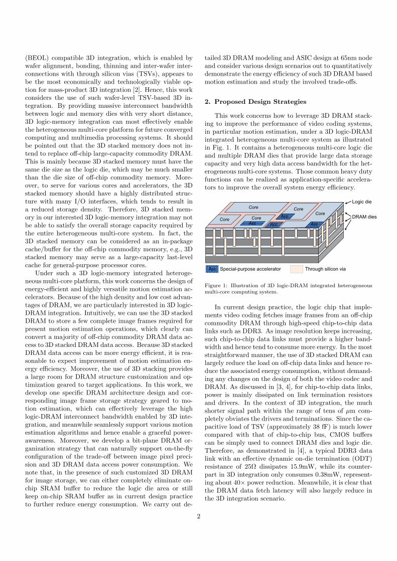
This work concerns how to leverage 3D DRAM stack-ing to improve the performance of video coding systems,in particular motion estimation, under a 3D logic-DRAMintegrated heterogeneous multi-core system as illustratedin Fig. 1. It contains a heterogeneous multi-core logic dieand multiple DRAM dies that provide large data storagecapacity and very high data access bandwidth for the het-erogeneous multi-core systems. Those common heavy dutyfunctions can be realized as application-specific accelera-tors to improve the overall system energy efficiency.
Core CoreAcc
AccAccCore Core
Core
Acc
Figure 1: Illustration of 3D logic-DRAM integrated heterogeneousmulti-core computing system.
In current design practice, the logic chip that imple-ments video coding fetches image frames from an off-chipcommodity DRAM through high-speed chip-to-chip datalinks such as DDR3. As image resolution keeps increasing,such chip-to-chip data links must provide a higher band-width and hence tend to consume more energy. In the moststraightforward manner, the use of 3D stacked DRAM canlargely reduce the load on off-chip data links and hence re-duce the associated energy consumption, without demand-ing any changes on the design of both the video codec andDRAM. As discussed in [3, 4], for chip-to-chip data links,power is mainly dissipated on link termination resistorsand drivers. In the context of 3D integration, the muchshorter signal path within the range of tens of µm com-pletely obviates the drivers and terminations. Since the ca-pacitive load of TSV (approximately 38 fF) is much lowercompared with that of chip-to-chip bus, CMOS bufferscan be simply used to connect DRAM dies and logic die.Therefore, as demonstrated in [4], a typical DDR3 datalink with an effective dynamic on-die termination (ODT)resistance of 25Ω dissipates 15.9mW, while its counter-part in 3D integration only consumes 0.38mW, represent-ing about 40× power reduction. Meanwhile, it is clear thatthe DRAM data fetch latency will also largely reduce inthe 3D integration scenario.
2
Beyond being used to reduce image fetch power con-sumption as discussed above, 3D DRAM stacking can befurther exploited to improve overall system performanceif we could rethink how to architect the video codec andDRAM. It is well known that motion estimation is themost resource demanding operation in video coding andlargely determines the overall system performance. Hence,this work focuses on the design of DRAM architecturefor implementing motion estimation accelerators. As thekey operation of motion estimation, SAD computation in-volves two tasks, including image data retrieval and arith-metic computation. The essential objective of motion es-timation accelerator design is to most effectively carry outthe SAD computations according to certain motion vectorsearch rules as specified by different motion estimation al-gorithms. In this section, aiming at exploiting 3D DRAMstacking, we present one DRAM organization and imagedata storage strategy.
2.1. DRAM Architecture for Image Frame Storage
It is feasible and certainly preferable to store bothcurrent and a few corresponding reference frames in 3Dstacked DRAM. Due to the access latency and energy con-sumption overhead induced by DRAM row activation, it isalways favorable to make as many consecutive reads/writesas possible on the same row before switching to anotherrow. Therefore, if image blocks are linearly row-by-row (orcolumn-by-column) mapped to the physical address space,a significant amount of row activations will occur, leadingto high access latency and energy consumption. It is verystraightforward that, instead of such a linear translatedmapping, a MB-by-MB mapping geared to motion estima-tion should be used [5], i.e., each row stores the luminanceintensity data of one or more MBs.
Usually a search region spans several MBs in referenceframes. Let each MB be N×N , and SW and SH representthe width and height of the search region, each search re-gion spans SBW ×SBH MBs in the reference frame, where
SBW = 2 ·⌈SW −N
2 ·N
⌉+ 1,
SBH = 2 ·⌈SH −N
2 ·N
⌉+ 1.
In this work, we are mainly interested in the scenariowhere the 3D stacked DRAM delivers a candidate MB row-by-row to the logic die, i.e., during each clock cycle, the3D stacked DRAM delivers the luminance intensity dataof one row within a candidate MB to the logic die. Thisis referred to as per-row DRAM-to-logic data delivery.
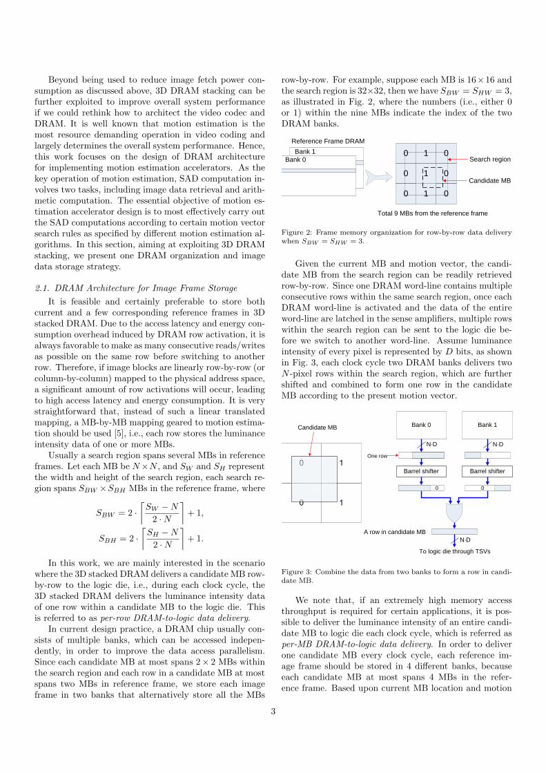
In current design practice, a DRAM chip usually con-sists of multiple banks, which can be accessed indepen-dently, in order to improve the data access parallelism.Since each candidate MB at most spans 2× 2 MBs withinthe search region and each row in a candidate MB at mostspans two MBs in reference frame, we store each imageframe in two banks that alternatively store all the MBs
row-by-row. For example, suppose each MB is 16×16 andthe search region is 32×32, then we have SBW = SHW = 3,as illustrated in Fig. 2, where the numbers (i.e., either 0or 1) within the nine MBs indicate the index of the twoDRAM banks.
10 0
0 0
10 0
1
Reference Frame DRAMBank 1
Bank 0 Search region
Total 9 MBs from the reference frame
Candidate MB
Figure 2: Frame memory organization for row-by-row data deliverywhen SBW = SHW = 3.
Given the current MB and motion vector, the candi-date MB from the search region can be readily retrievedrow-by-row. Since one DRAM word-line contains multipleconsecutive rows within the same search region, once eachDRAM word-line is activated and the data of the entireword-line are latched in the sense amplifiers, multiple rowswithin the search region can be sent to the logic die be-fore we switch to another word-line. Assume luminanceintensity of every pixel is represented by D bits, as shownin Fig. 3, each clock cycle two DRAM banks delivers twoN -pixel rows within the search region, which are furthershifted and combined to form one row in the candidateMB according to the present motion vector.
A row in candidate MB
Candidate MB
One row
0
Bank 0
Barrel shifter
Bank 1
Barrel shifter
0
To logic die through TSVs
N·D N·D
N·D
Figure 3: Combine the data from two banks to form a row in candi-date MB.
We note that, if an extremely high memory accessthroughput is required for certain applications, it is pos-sible to deliver the luminance intensity of an entire candi-date MB to logic die each clock cycle, which is referred asper-MB DRAM-to-logic data delivery. In order to deliverone candidate MB every clock cycle, each reference im-age frame should be stored in 4 different banks, becauseeach candidate MB at most spans 4 MBs in the refer-ence frame. Based upon current MB location and motion
3

vector, one corresponding word-line in each bank is acti-vated and delivers the luminance intensity of one MB atonce. All the four MBs from the four DRAM banks aresent to a two-dimensional barrel shifter array in order toform the candidate MB. This per-MB data delivery strat-egy can achieve very high throughput, but obviously willdemand a large amount of TSVs and incur much higherenergy consumption. Therefore, we only focus on the per-row DRAM-to-logic data delivery strategy throughout theremainder of this paper.
We note that since each row contains several MBs andeach MB may contain a few hundred bits (e.g., given N =16 and D = 8, each MB contains 2048 bits), a row withina bank should be further partitioned into several segmentsin order to maintain a reasonable access speed. Therefore,we follow the conventional DRAM design practice thatemploys a bank→sub-bank→sub-array hierarchy. EachDRAM bank consists of several identical sub-banks andat one time only one sub-bank can be accessed. By seg-menting each row within one sub-bank, each sub-bank isfurther partitioned into a certain number of sub-arraysthat collectively carry out DRAM access, and each sub-array contains an indivisible array of DRAM cells sur-rounded by supporting peripheral circuits such as addressdecoders/drivers, sense amplifiers and output drivers etc.
To map the MB luminance intensity data onto the sub-arrays within each sub-bank, we propose a bit-plane datamapping strategy to ensure the memory data access reg-ularity across all the sub-arrays. Recall that the lumi-nance intensity of one pixel uses D bits. We partitioneach sub-bank into D sub-arrays, A0, A1, ..., AD−1, andeach sub-array Ai stores the i-th bit of the luminance in-tensity data, as depicted in Fig. 4. Clearly, this bit-planestorage strategy ensures that all the sub-arrays within thesame sub-bank can readily share the same row and columnaddress and have a minimum sub-array data I/O routingoverhead. In particular, each sub-array only needs to sendN bits for realizing per-row DRAM-to-logic data delivery.In contrast, if we store the D bits for each pixel consec-utively in the same sub-array, in stead of using such bit-plane storage strategy, different sub-arrays may contributeto the candidate MB data differently. As a result, the sub-arrays within the same sub-bank may not be able to fullyshare all the row and column address and each sub-arraymust have a data I/O width of N ·D bits.
Another advantage of this proposed bit-plane storagestrategy is that it can easily support run-time graceful per-formance vs. energy trade-off, because the bit-plane struc-ture makes it very easy to adjust the precision of lumi-nance intensity data participating in motion estimation.It is well-known that appropriate pixel truncation [6] canlead to substantial reduction on computational complex-ity and power consumption without significantly affectingimage quality. Such bit-plane memory structure can nat-urally support dynamic pixel truncation, which can mean-while reduce the power consumption of memory data ac-cess. Given the D-bit full precision of luminance intensity
D-1
D-2
1
0
D Sub-arrays
D bits of a pixel’s luminance intensity
Memory cell array
Peripheral circuits
Address
NData/D
NData/D
NData/D
NData/D
Figure 4: Illustration of bit-plane data mapping strategy. All D sub-arrays share the same row and column address. Ndata-bit data busis uniformly distributed across D sub-arrays, where Ndata = N ·D.
data, if we only use Dr < D bits in motion estimation, wecan directly switch the D−Dr sub-arrays, which store thelowerD−Dr bits for each pixel, into an idle mode to reducethe DRAM power consumption. It is intuitive that suchlower-precision operation can be dynamically adjusted toallow more flexible performance vs. energy trade-off, e.g.,we could first use low-precision data to calculate coarseSADs, and then run block matching with full precision ina small region around the candidate MB with the leastcoarse SAD.
It should be pointed out that, unlike conventional de-sign solutions, the above presented design strategy underthe 3D logic-DRAM integrated system framework can re-alize any arbitrary and discontinuous motion vector searchand hence seamlessly support most existing motion esti-mation algorithms. Finally, we note that, although theabove discussion only focuses on data storage for motionestimation, the same DRAM storage approaches can beused to facilitate the motion compensation as well in bothvideo encoders and decoders.
2.2. Logic and Memory Interface
With the above presented DRAM architecture designstrategies, the motion estimation engine on the logic diecan access the 3D DRAM to efficiently fetch the currentMB and candidate MB through a simple interface. Assumethe video encoder supports a multi-frame motion estima-tion with up-to m reference frames. In order to seamlesslysupport multi-frame motion estimation while maintainingthe same video encoding throughput, we store all these mreference frames separately, each reference frame is storedin 2 banks when using per-row DRAM-to-logic data deliv-ery. The motion estimation engine can access all the mreference frames simultaneously, i.e., the motion estima-tion engine contains m parallel units, each one carries outmotion estimation based upon one reference frame. We
4

MB in Bank i
... ...Top MB in bank i
... ...
......
......
yoff-set
Candidate MB
xoff-set
xoff-set N-xoff-set
yoff-set N-yoff-set
xoff-set N-xoff-set
Top MB in bank j
Bottom MB in bank i
Bottom MB in bank j
MB in Bank j
MB in Bank i MB in Bank j
Figure 5: Illustration of calculating memory access address to fetch one candidate MB.
assign each MB with a two-dimensional index with theorigin at the top-left corner of each image, i.e., assumingeach frame contains FW×FH MBs, the MBs at the top-leftcorner and bottom-right corner of each frame have the in-dex of (0, 0) and (FW − 1, FH − 1), respectively. Assumeeach word-line in one bank stores s MBs, and we storeeach MB row-by-row along a DRAM word-line. Hence,given the MB index (x, y), we first can identify its bankindex and the DRAM row/column address for proposedDRAM architectures as listed in Table 1. Since each ad-dress location in one bank corresponds to one row in oneMB and each MB has N rows, each MB spans N consec-utive column addresses. The first column address is Acol
in the table, and the N consecutive column addresses areAcol, Acol + 1, · · · , Acol +N − 1.
Table 1: Memory access address for proposed DRAM architectures.
Bank Index x%2
Row Address⌊y·FW+x
2·s
⌋Column Address (Acol) ((y · FW + x)%s) ·N
For each motion estimation unit on the logic die to ac-cess one reference frame, it only needs to provide two setsof parameters, 2D position index of current MB (xMB , yMB)and motion vector (xMV , yMV ), which determine the lo-cation of the candidate MB in the reference frame. Giventhese inputs, DRAM will deliver the corresponding candi-date MB to the logic die. Leveraging the specific DRAMarchitecture described above, each DRAM frame storagecan easily derive its own internal row and column addressand the corresponding configuration parameters for thebarrel shifters, which is described as follows.
As pointed out earlier, each candidate MB may spanat most 4 adjacent MBs in the reference frame as illus-trated in Fig. 3. Given the 2D position index of currentMB (xMB , yMB) and motion vector (xMV , yMV ), we candirectly derive the 2D position indices of these up-to 4
adjacent MBs as(xMB + sx ·
⌈|xMV |N
⌉, yMB + sy ·
⌈|yMV |N
⌉),(
xMB + sx ·⌈|xMV |N
⌉, yMB + sy ·
⌊|yMV |N
⌋),(
xMB + sx ·⌊|xMV |N
⌋, yMB + sy ·
⌈|yMV |N
⌉),(
xMB + sx ·⌊|xMV |N
⌋, yMB + sy ·
⌊|yMV |N
⌋),
where sx = sign(xMV ) and sy = sign(yMV ), and sign(·)represents the sign of the operand. Clearly, dependentupon the specific values of xMV and yMV , we may have1, 2, or 4 distinctive indices, i.e., the candidate MB mayspan 1, 2, or 4 adjacent MBs in the reference frame. Forthe general case, let us consider the scenario when onecandidate MB spans 4 adjacent MBs in the reference frameas illustrated in Fig. 5, where i 6= j and i, j ∈ 0, 1.
After obtaining the indices of the 4 reference MBs, wecan directly calculate the corresponding DRAM row ad-dresses. In order to determine the range of the columnaddresses in the case of per-row DRAM-to-logic data de-livery, we should calculate
yoff-set =
|yMV |%N, yMV ≥ 0N − |yMV |%N, yMV < 0
. (1)
The candidate MB spans the last N − yoff-set rows in thetwo top MBs and the first yoff-set rows in the two bottomMBs, as illustrated in Fig. 5. Hence, we can correspond-ingly determine the column addresses. Then we shoulddetermine the configuration data for the barrel shiftersthat form one row in the candidate MB, i.e., we shouldcalculate
xoff-set =
|xMV |%N, xMV ≥ 0N − |xMV |%N, xMV < 0
. (2)
For each row read from the reference MBs on the left asshown in Fig. 5, the barrel shifters shift the data towardsleft by xoff-set pixels; for each row read from the ref-erence MBs on the right as shown in Fig. 5, the barrel
5

Table 2: Modeling results for one 2M-byte 2-bank 3D stacked DRAM in the case of per-row DRAM-to-logic data delivery.
1-layer stacking
Number of sub-banks 1 2 4 8
Access time (non-burst) (ns) 9.49 7.37 6.65 6.57
Burst access time (ns) 7.17 4.83 4.11 3.91
Energy per access (non-burst) (nJ) 0.71 1.00 1.29 1.61
Energy per burst access (nJ) 0.15 0.45 0.76 1.08
Footprint (mm2) 1.10 2.08 3.12 4.79
4-layer stacking
Number of sub-banks 1 2 4 8
Access time (non-burst) (ns) 9.36 7.25 6.53 6.44
Burst access time (ns) 7.09 4.84 4.03 3.83
Energy per access (non-burst) (nJ) 0.93 1.22 1.28 1.59
Energy per burst access (nJ) 0.13 0.43 0.74 1.06
Footprint (mm2) 0.22 0.34 0.47 0.69
shifters shift the data towards right by N − xoff-set pix-els. By implementing the above simple calculations in theDRAM domain, the 3D stacked DRAM can readily deliverthe candidate MB to the motion estimation engine on thelogic die, while the motion estimation engine only needs tosupply the current motion vector and the position of thecurrent MB.
3. Simulation Results
This section presents our case study on multi-framemotion estimation to demonstrate the above presented de-sign approach. In particular, we set the following param-eters. The size of each MB is 16× 16 and search region is80×80 for HDTV1080p (1920×1080) with a frame rate of30 frames per second. We assume the luminance intensityof each pixel uses 8 bits, hence each DRAM sub-bank has8 sub-arrays. We assume up-to 5 reference frames can beused during video encoding. Therefore, to access data ineach frame simultaneously using the per-row DRAM-to-logic data delivery strategy, the 3D stacked DRAM has2 × 6 = 12 banks and an aggregate data I/O width of16 × 8 × 6 = 768 bits (i.e., 768 TSVs). For DRAM per-formance modeling and energy estimation, we use the 3DDRAM design strategy presented in [7] that has been im-plemented based upon the widely used memory modelingtool CACTI [8]. All the DRAM modeling is carried out atthe 65nm technology node.
When using the per-row DRAM-to-logic data delivery,each frame is stored in two banks and each bank has a128-bit data I/O width. Although each two-bank DRAMmodule can store multiple frames, in this work we onlyconsider the storage of a single frame with 2M-byte. Weexplore the 3D DRAM design space by varying the sizeof each sub-array and the number of sub-banks. In thisstudy, the number of bit-lines in each sub-bank is fixed as512. Table 2 shows the parameters of 3D stacked DRAM,where both 1-layer and 4-layer DRAM die stacking areconsidered.
In DRAM, the access time is the time to read a randombit from a pre-charged sub-bank, while it takes less time toread data along the same word-line (i.e., during the burstmode of DRAM access) as shown in Table 2, because itdoes not require additional time for word-line address de-coding and activations, etc. Clearly, the same argumentapplies to DRAM access energy consumption. By reduc-ing the word-line activation frequency, the MB-orientedDRAM storage adopted in this work can effectively speedup the operation and save the energy consumption. Asshown in Table 2 4-layer DRAM stacking can achieve muchless footprint and slightly better energy efficiency than its1-layer counterpart. If each memory bank is partitionedinto smaller sub-banks, the burst read energy becomeshigher, since more energy is consumed on the memoryglobal routing. The access time does not change mono-tonically with size of sub-banks as observed in the table,because when the sub-banks become smaller, the delay inperipheral circuits tends to increase, even though it takesless time to access the memory core.
As pointed out in the above, the 3D stacked DRAMdata storage strategy can naturally support various blockmatching schemes, including exhaustive full search (FS),three step search (TSS) [9], new three step search (NTSS)[10], four step search (FSS) [11, 12], and diamond search(DS) [13, 14]. Moreover, hybrid block matching can alsobe seamlessly supported, e.g., we can first run three stepsearch motion estimation on the search region of referenceframe and then run full search motion estimation againon the search region with the least SAD value. Since allthe search schemes are seamlessly supported, the trade-offbetween motion estimation accuracy and computationalcomplexity (hence power consumption) can be easily andgracefully configured on the fly. In this work, we use twoHDTV 1080p video sequences Tractor and Rush hour [15]for the purpose of demonstration, where 15 frames are ex-tracted and analyzed in each video sequence. Fig. 6 andFig. 7 show the peak signal-to-noise ratio (PSNR) of var-ious multi-frame motion estimation algorithms over 3DDRAM energy consumption to process one image frame
6

0.5 1 1.5 2 2.5 3 3.5 435.5
36
36.5
37
37.5
38
38.5
39
39.5 Rush hour (HDTV 1080p)
Memory energy consumption per frame (mJ)
PSN
R (
dB)
0.5 1 1.5 2 2.5 3 3.5 4 4.5 528
29
30
31
32
33
34 Tractor (HDTV 1080p)
Memory energy consumption per frame (mJ)
PSN
R (
dB)
5 10 15 20 2536
36.5
37
37.5
38
38.5
39
39.5
40
40.5
41 Full search for Tractor and Rush hour
Memory energy consumption per frame (mJ)
PSN
R (
dB)
Three step searchNew three step searchFour step searchDiamond step search
Three step searchNew three step searchFour step searchDiamond step search
TractorRush hour
Figure 6: Performance of various advanced motion estimation algorithms vs. 3D DRAM access energy consumption without on-chip SRAMbuffer, where we assume there is 1-layer 3D DRAM stacking and 1 sub-bank per bank in 3D DRAM.
without using the on-chip SRAM buffer. Each curve con-tains five points, corresponding to the scenarios using 1,2, 3, 4 and 5 reference frames respectively. The mem-ory access energy consumption for each point is obtainedbased on DRAM parameters with 1-layer DRAM stackingand 1 sub-bank per bank. Due to the regular memory ac-cess pattern in full search, explicit memory access can begreatly reduced by data reuse [16] in motion estimationengine. In this study, we set the full search motion esti-mation design approach can fully exploit such data reuse.However, since the search region is 80× 80, the number offull search computation needed to find a best match of acurrent MB is much larger than the number of other ad-vanced algorithms, and energy consumption of full searchis still much higher, so we plot the curves for full searchin Fig. 7 and curves for the other algorithms in Fig. 6 tomake the figures more legible.
0.5 1 1.5 2 2.5 3 3.5 435.5
36
36.5
37
37.5
38
38.5
39
39.5 Rush hour (HDTV 1080p)
Memory energy consumption per frame (mJ)
PSN
R (
dB)
0.5 1 1.5 2 2.5 3 3.5 4 4.5 528
29
30
31
32
33
34 Tractor (HDTV 1080p)
Memory energy consumption per frame (mJ)
PSN
R (
dB)
5 10 15 20 2536
36.5
37
37.5
38
38.5
39
39.5
40
40.5
41 Full search for Tractor and Rush hour
Memory energy consumption per frame (mJ)
PSN
R (
dB)
Three step searchNew three step searchFour step searchDiamond step search
Three step searchNew three step searchFour step searchDiamond step search
TractorRush hour
Figure 7: Performance of full search algorithm vs. 3D DRAM accessenergy consumption without on-chip SRAM buffer, where we assumethere is 1-layer 3D DRAM stacking and 1 sub-bank per bank in 3DDRAM.
Based upon the above 3D DRAM parameters, we esti-mate the overall memory sub-system power consumptionand obtain the comparison with conventional design prac-tice. Regardless to whether 3D DRAM stacking is used ornot, we assume the image frames are originally stored inan off-chip 4Gb commodity DRAM, which also stores dataand instructions for other cores in the envisioned heteroge-neous multi-core systems. In the case of conventional de-sign practice, the motion estimation accelerator containsan on-chip SRAM buffer to store the current MB and a80 × 80 search region in each reference frame (i.e., a to-tal 250Kb when using 5 reference frames). In the case of3D-based design, we consider two scenarios: (i) we elimi-nate the on-chip SRAM buffer in order to reduce the logicdie area, where motion estimation computation blocks di-rectly obtain image data from 3D stacked DRAM, and(ii) we still keep the on-chip SRAM buffer in order toreduce the frequency of 3D stacked DRAM access. Theestimation and comparison results are list in Table 3 andTable 4, in which full search and three step search algo-rithms are used respectively. The access power listed inthe table is the power consumed for memory read/writeunder the real-time constraint (i.e., 30 frames per secondfor HDTV1080p), including address decoder, sense ampli-fiers, repeaters, routing, etc. The I/O power of DRAMand SRAM is aggregated and listed in the table. It clearlyshows the energy efficiency advantages when 3D stackedDRAM is being used, especially in three step search case,mainly because the use of 3D stacked DRAM can largelyreduce the frequency of off-chip 4Gb commodity DRAMaccess and data access to the small 3D stacked DRAM ded-icated for motion estimation is much more energy-efficientthan access to off-chip 4Gb commodity DRAM. Neverthe-less, accessing 3D DRAM directly without on-chip SRAMconsumes a large amount of power if full search is used. Itis because a large search region imposes more frequent data
7

Table 3: Comparison between current design practice and the design using 3D stacked DRAM with full search.
Current practiceDesign using 3D stacked DRAM
(w/o on-chip SRAM) (w/ on-chip SRAM)
Off-chip DRAMCapacity (Gb) 4 4 4
Access power (mW) 274.56 21.90 21.90I/O Power (mW) 124.02 9.89 9.89
3D DRAM
Capacity (Mb) N/A 100 100Access power (mW) N/A 910.93 18.50
Leakage power (mW) N/A 31.03 31.03Barrel shifter power (mW) N/A ??? ???
I/O power (mW) N/A 146.03 2.96
On-chip SRAMCapacity (Kb) 250 N/A 250
Footprint (mm2) 0.91 N/A 0.91Access power (mW) 187.12 N/A 187.12
Total memory access power (mW) 585.70 1119.79 271.39
1 2 3 4 50
1000
2000
3000
4000
Number of Reference Frames
Pow
er C
onsu
mpt
ion
(mW
)
Computation FS without on−chip SRAM FS with on−chipSRAM
Figure 9: Average power consumption of entire motion estimationusing full search algorithm.
access from 3D DRAM. Moreover, the above two differ-ent scenarios (i.e., with and without on-chip SRAM bufferwhen using 3D stacked DRAM) essentially represent dif-ferent trade-offs between the logic die area reduction andtotal memory access power consumption.
Using Synopsys tool sets and a 65nm CMOS standardcell library, we synthesize parallel motion estimation com-putation engines and estimate the power consumption.Combining the above memory sub-system power consump-tion results, we estimate the overall average motion esti-mation power consumption as shown in Fig. 8 and Fig. 9,where we consider both with and without on-chip SRAMbuffer. Because the search steps of NTSS, FS-TSS andDS algorithms may vary during the run time, we show theaverage values obtained from computer simulations. Thelower and upper parts of each bar in the figures representmemory access and computation logic power consumptionrespectively. The power consumption is obtained at theclock frequencies that are just fast enough for real-timeprocessing in all the studies.
Finally, we evaluate the potential of leveraging the bit-plane DRAM storage structure to enable graceful perfor-mance vs. energy consumption. We only consider the sce-nario of 3D stacked DRAM without on-chip SRAM buffer.We carry out simulations with full search, three step search
and new three step search algorithms with one referenceframe, and we take the DRAM parameters of 1-layer stack-ing and 1 sub-bank per bank listed in Table 2. For fullsearch, we simply study the use of 4 bits, 5 bits,· · · , 8bits of every pixel in motion estimation. For three stepsearch, because of the relatively large search region (i.e.,80×80), every MB actually takes five steps to find the bestmatched MB. In the first step, since 9 candidate MBs arewell separated away from each other in a reference frameand their SADs between current MB tend to largely dif-fer, less number of bits may be sufficient, hence 4 bits ofeach pixel are used in the first step. On the other hand,search in the last two steps is limited into a small regionand the accuracy directly affects the motion estimationperformance, therefore we used full precision in the lasttwo steps. We only vary the number of bits used for mo-tion estimation in the second and third steps. For newthree step search, which evolves from three step search,the number of steps can be either 2 or 5 for every currentMB. So we only vary the precision in the first step, and wekeep the full precision during the following 1 or 4 step(s).The PSNR vs. memory access energy consumption resultsare shown in Fig. 10. The five points on each full-searchcurve correspond to using 4, 5, 6, 7 and 8 bits in motionestimation; the five points on each new-three-step-searchcurve correspond to using 4, 5, 6, 7 and 8 bits in the firststep; the left five points on each three-step-search curvecorrespond to using 4, 5, 6, 7 and 8 bits in the second andthird steps and the rightmost point represents the resultwhen the full precision is being used in all the five steps.The simulation results clearly show the trade-offs in vari-ous design scenarios. In particular, for three step search,if we only reduce the first step precision from 8 bits to 4bits and keep the full precision in the rest steps, PSNRperformance does not degrade at all, while it can save al-most 15% of memory access power consumption as well ascomputation logic power consumption.
8

Table 4: Comparison between current design practice and the design using 3D stacked DRAM with three step search.
Current practiceDesign using 3D stacked DRAM
(w/o on-chip SRAM) (w/ on-chip SRAM)
Off-chip DRAMCapacity (Gb) 4 4 4
Access power (mW) 274.56 21.90 21.90I/O power (mW) 124.02 9.89 9.89
3D DRAM
Capacity (Mb) N/A 100 100Access power (mW) N/A 146.49 18.50Leakage power(mW) N/A 31.03 31.03
Barrel shifter power (mW) N/A ??? ???I/O power (mW) N/A 23.48 2.96
On-chip SRAMCapacity (Kb) 250 N/A 250
Footprint (mm2) 0.91 N/A 0.91Access power (mW) 29.97 N/A 29.97
Total memory access power (mW) 428.55 232.79 114.24
1 2 3 4 50
50
100
150
200
Number of Reference Frames
Pow
er C
onsu
mpt
ion
(mW
)
Computation TSS NTSS FS−TSS DS
(a)
1 2 3 4 50
10
20
30
40
50
60
70
Number of Reference Frames
Pow
er C
onsu
mpt
ion
(mW
)
Computation TSS NTSS FS−TSS DS
(b)
Figure 8: Average power consumption of entire motion estimation using advanced algorithms (a) without on-chip SRAM buffer, and (b) withon-chip SRAM buffer.
9

0.4 0.45 0.5 0.55 0.6 0.65 0.7 0.75 0.824
26
28
30
32
34
36
38
Memory energy consumption per frame (mJ)
PSN
R (
dB)
Tractor TSSTractor NTSSRush hour TSSRush hour NTSS
2 2.5 3 3.5 4 4.5 525
30
35
40
Memory energy consumption per frame (mJ)
PSN
R (
dB)
Tractor FSRush hour FS
(a)
0.4 0.45 0.5 0.55 0.6 0.65 0.7 0.75 0.824
26
28
30
32
34
36
38
Memory energy consumption per frame (mJ)
PSN
R (
dB)
Tractor TSSTractor NTSSRush hour TSSRush hour NTSS
2 2.5 3 3.5 4 4.5 525
30
35
40
Memory energy consumption per frame (mJ)
PSN
R (
dB)
Tractor FSRush hour FS
(b)
Figure 10: Motion estimation PSNR vs. memory access energy when varying pixel luminance intensity precisions, where different points onthe same curve correspond to different bit precisions for block matching: (a) Three step search and new three step search for both videosequences; (b) Full search for both video sequences.
4. Conclusion
With 3D memory stacking, memory access may nolonger be a bottleneck for video encoding, in particularfor motion estimation. This provides new opportunities toexplore efficient motion estimation accelerator architecturedesign. In this paper, we investigate motion estimationaccelerator architectures to effectively utilize the 3D inte-grated DRAM. We develop one specific 3D DRAM datastorage organization and frame storage strategy geared tomotion estimation, which can be seamlessly coupled withparallel motion estimation computation engines. The pre-sented design strategy has a good energy efficiency andcan seamlessly support various motion estimation algo-rithms with variable block size. Using DRAM performancemodeling/estimation tool and ASIC design at 65nm tech-nology node, we demonstrate the effectiveness of such 3Dintegrated motion estimation accelerator design for multi-frame motion estimation.
5. Acknowledgement
The authors sincerely appreciate the anonymous re-viewers for their very insightful and constructive commentsthat greatly helped to improve the quality and presenta-tion of this work.
References
[1] Y. H. et.al, A 1.3TOPS H.264/AVC single-chip encoder forHDTV applications, in: Proc. of IEEE Intl. Solid-State CircuitConf. (ISSCC), San Francisco, 2005, pp. 128–129.
[2] J.-Q. Lu, 3-D Hyperintegration and Packaging Technologies forMicro-Nano Systems, Proceedings of the IEEE 97 (2009) 18–30.
[3] M.Facchini, T.Carlson, A.Vignon, M.Palkovic, F.Catthoor,W.Dehaene, L.Benini, P.Marchal, System-levelpower/performance evaluation of 3d stacked drams formobile applications, in: Proc. of Design, Automation & Test inEurope Conference & Exhibition, 2009, pp. 923–928.
[4] S. Gu, P. Marchal, M. Facchini, F. Wang, M. Suh, D. Lisk,M. Nowak, Stackable memory of 3D chip integration for mobileapplications, in: Proc. of IEEE International Electron DevicesMeeting (IEDM), 2008, pp. 1–4.
[5] E. Jaspers, P. de With, Bandwidth reduction for video process-ing in consumer systems, IEEE Trans. on Consumer Electronics47 (4) (2001) 885–894.
[6] Z.-L. He, C.-Y. Tsui, K.-K. Chan, M. Liou, Low-power vlsidesign for motion estimation using adaptive pixel truncation,IEEE Trans. on Circuits and Systems for Video Technology10 (5) (2000) 669–678.
[7] R. Anigundi, H. Sun, J. Lu, K. Rose, T. Zhang, Architecture De-sign Exploration of Three-Dimensional (3D) Integrated DRAM,in: Proc. of IEEE International Symposium on Quality Elec-tronic Design (ISQED), 2009.
[8] CACTI: An integrated cache and memory access time,cycle time, area, leakage, and dynamic power model,http://www.hpl.hp.com/research/cacti/.
[9] L.-P. Chau, X. Jing, Efficient three-step search algorithm forblock motion estimation video coding, in: Proc. of IEEE Inter-national Conference on Acoustics, Speech, and Signal Process-ing, 2003, pp. 421–424.
[10] R. Li, B. Zeng, M. L. Liou, A new three-step search algorithmfor block motion estimation, IEEE Trans. on Circuits and Sys-tems for Video Technology 4 (1994) 438–442.
[11] L.-M. Po, W.-C. Ma, A novel four-step search algorithm for fastblock motion estimation, IEEE Trans. on Circuits and Systemsfor Video Technology 6 (1996) 313–317.
[12] K.-T. Wang, O.-C. Chen, Motion estimation using an efficientfour-step search method, in: Proc. of IEEE International Sym-posium on Circuits and Systems, 1998, pp. 217–220.
[13] J. Y. Tham, S. Ranganath, M. Ranganath, A. A. Kassim, Anovel unrestricted center-biased diamond search algorithms forblock motion estimation, IEEE Trans. on Circuits and Systemsfor Video Technology 8 (1998) 369–377.
[14] J. Y. Tham, S. Ranganath, M. Ranganath, A. A. Kassim, Anew diamond search algorithm for fast block-matching motionestimation, IEEE Trans. on Image processing 9 (2000) 287–290.
[15] Sveriges Television (SVT), http://www.svt.se.[16] J. Tuan, T. Chang, C. Jen, On the data reuse and memory
bandwidth analysis for full-searchblock-matching VLSI archi-tecture, IEEE Trans. on Circuits and Systems on Video Tech-nology 12 (1) (2002) 561–72.
10