
Exploiting Hierarchical Identity-Based Encryption for Access ...
Upload
khangminh22Category
view
2download
0
University of South FloridaScholar Commons
Graduate Theses and Dissertations Graduate School
May 2017
Exploiting On-Chip Voltage Regulators as aCountermeasure Against Power Analysis AttacksWeize YuUniversity of South Florida, [email protected]
Follow this and additional works at: http://scholarcommons.usf.edu/etd
Part of the Computer Engineering Commons, and the Electrical and Computer EngineeringCommons
This Dissertation is brought to you for free and open access by the Graduate School at Scholar Commons. It has been accepted for inclusion inGraduate Theses and Dissertations by an authorized administrator of Scholar Commons. For more information, please [email protected].
Scholar Commons CitationYu, Weize, "Exploiting On-Chip Voltage Regulators as a Countermeasure Against Power Analysis Attacks" (2017). Graduate Theses andDissertations.http://scholarcommons.usf.edu/etd/6986
Exploiting On-Chip Voltage Regulators as a Countermeasure Against Power Analysis Attacks
by
Weize Yu
A dissertation submitted in partial fulfillmentof the requirements for the degree of
Doctor of PhilosophyDepartment of Electrical Engineering
College of EngineeringUniversity of South Florida
Major Professor: Selcuk Kose, Ph.D.Lingling Fan, Ph.D.Ismail Uysal, Ph.D.
Srinivas Katkoori, Ph.D.Ulya Karpuzcu, Ph.D.
Date of Approval:February 22, 2017
Keywords: Hardware security, side-channel attacks, differential power analysis attacks, leakagepower analysis attacks, on-chip voltage regulation
Copyright c© 2017, Weize Yu

DEDICATION
This work is dedicated to my parents and girlfriend.

ACKNOWLEDGMENTS
Almost three years have passed since I transfered from Virginia Tech to University of South
Florida (USF) to pursue my Ph.D. degree. During this period, a number of individuals helped and
encouraged me to finish my Ph.D. study. Firstly, I would like to express my great appreciation to
my Ph.D. supervisor Dr. Selcuk Kose. I remember when I applied to the Ph.D. program of electrical
engineering department of USF in Fall 2014, Dr. Selcuk Kose tried his best to help me to get the
prestigious USF presidential doctoral fellowship which is offered only to top five Ph.D. students
each year. Owing to the awarded fellowship from USF, I become quite self-confident and produced
a good number of creative works during my Ph.D. study. Dr. Selcuk Kose played a significant role
in guiding my research. When I was enrolled in USF, Dr. Selcuk Kose wanted me to do research
on hardware security. At first, I had made a little progress in my research since I did not have
much background in hardware security. In order to strengthen my research abilities, Dr. Selcuk
Kose persuaded me to take a lot of courses from computer science and engineering department.
These courses facilitated my self-learning and self-analyzing abilities, which helped me greatly in
publishing creative works.
I also would like to thank my lab mates Orhun Aras Uzun, Mahmood Azhar, and Longfei
Wang for their selfless support. When I was starting my research with Cadence simulations, I
came across some technical issues. However, Orhun devoted his time and patience to guide me to
solve those issues. When I have new ideas on my research topic, Longfei always showed interest in
discussing with me to improve my idea.
I would also like to thank all my Ph.D. committee members: Dr. Lingling Fan, Dr. Ismail
Uysal, Dr. Srinivas Katkoori, Dr. Ulya Karpuzcu, and Dr. Mingyang Li for their time, support,
and encouragement.
Finally, I would like to thank my parents and Jia Chen for their unconditional support
every time when I ran into difficulties in my Ph.D. study.
TABLE OF CONTENTS
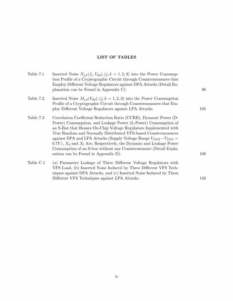
LIST OF TABLES iv
LIST OF FIGURES v
ABSTRACT xi
CHAPTER 1: INTRODUCTION 11.1 Side-Channel Attacks 11.2 Power Analysis Attacks 2
1.2.1 Simple Power Analysis (SPA) Attacks 21.2.2 Differential Power Analysis (DPA) Attacks 31.2.3 Leakage Power Analysis (LPA) Attacks 4
1.3 On-Chip Voltage Regulation Against Power Analysis Attacks 51.3.1 Converter-Gating (CoGa) Voltage Converter Against Power
Analysis Attacks 51.3.2 Our Contribution 8
CHAPTER 2: CONVERTER-RESHUFFLING TECHNIQUE 92.1 Motivation 92.2 Treat Model 102.3 Review of Converter-Gating (CoGa) 112.4 Converter-Reshuffling (CoRe) 122.5 Evaluation 122.6 Conclusion 18
CHAPTER 3: TIME-DELAYED CONVERTER-RESHUFFLING TECHNIQUE 193.1 Motivation 193.2 Modeling 19
3.2.1 Converter-Reshuffling (CoRe) Technique 203.2.2 Time-delayed Converter-Reshuffling (CoRe) Technique 23
3.3 Results and Discussions 273.4 Conclusion 29
CHAPTER 4: CHARGE-WITHHELD CONVERTER-RESHUFFLING TECHNIQUE 314.1 Motivation 314.2 Architecture Design 32
4.2.1 Architecture of the Converter-Reshuffling (CoRe) Technique 32
i

4.2.2 Architecture of the Charge-Withheld Converter-Reshuffling(CoRe) Technique 34
4.3 Security Evaluation Model 364.3.1 Security Evaluation Against DPA Attacks 364.3.2 Security Evaluation Against Machine Learning (ML)-Based
DPA Attacks 394.4 Efficiency Analysis 414.5 Results and Discussions 424.6 Conclusion 44
CHAPTER 5: CO-DESIGNING CORE TECHNIQUE WITH AES ENGINE 455.1 Introduction 455.2 Security of a Switching Converter against Power Analysis Attacks 485.3 Correlation Analysis of On-Chip Voltage Regulators 49
5.3.1 Modeling Correlation Coefficient of Converter-Gating (CoGa)and Converter-Reshuffling (CoRe) Regulators 49
5.3.2 Modeling Correlation Coefficient of Conventional On-ChipVoltage Regulators 55
5.3.3 Validation of the Proposed Correlation Coefficient Modelswith Practical Parameters 56
5.4 Conventional Pipelined (CP) AES Engine with Converter-Reshuffling 605.4.1 Practical Power Attacks on a Pipelined AES Engine without
On-Chip Voltage Regulation 605.4.2 Conventional Pipelined (CP) AES Engine with a Distributed
CoRe Technique 605.4.3 Conventional Pipelined (CP) AES Engine with a Centralized
CoRe Technique 625.5 Improved Pipelined (IP) AES Engine with Centralized CoRe Technique 655.6 Circuit Level Simulation 715.7 Conclusion 72
CHAPTER 6: SECURITY-ADAPTIVE VOLTAGE CONVERSION TECHNIQUE 746.1 Introduction 746.2 Architecture Design 756.3 Parameter Design 766.4 Security Evaluation Against LPA Attacks 77
6.4.1 Sampling a Single Clock Period as One Sample of Input Power Data 786.4.2 Sampling Multiple Clock Periods as One Sample of Input
Power Data 816.5 Circuit Level Verification 846.6 LPA Attacks Simulation 856.7 Conclusion 86
CHAPTER 7: ON-CHIP VOLTAGE REGULATION WITH VFS 877.1 Introduction 877.2 On-Chip Voltage Regulation with VFS Load 90
ii
7.2.1 Low-Dropout (LDO) Regulator with VFS Load 907.2.2 Buck Converter with VFS Load 917.2.3 Switched-Capacitor (SC) Converter with VFS Load 94
7.3 Security Evaluation of On-Chip Voltage Regulation with VFS Tech-nique Against DPA Attacks 98
7.3.1 Security of On-Chip Voltage Regulation with True RandomVFS Technique Against DPA Attacks 99
7.4 Security Evaluation of On-Chip Voltage Regulation with VFS Tech-nique Against LPA Attacks 104
7.5 Overhead Analysis 1077.6 DPA and LPA Attack Simulations 1097.7 Conclusion 111
CHAPTER 8: CONCLUSION 112
CHAPTER 9: FUTURE WORK 1149.1 Utilizing On-Chip Multi-Phase Buck Converter as a Countermeasure
Against Electro-Magnetic (EM) Attacks 1149.2 Utilizing On-Chip Multi-Phase SC Converter as a Physical Unclonable
Function (PUF) 116
REFERENCES 118
APPENDICES 126Appendix A: Correlation Coefficient of Conventional On-Chip Voltage Regulators 127Appendix B: Guidelines on the Selection of a Suitable Active Critical Fre-
quency Fac 129Appendix C: Detailed Explanation of Table 7.1 and Table 7.2 132Appendix D: Power Consumption Overhead of Different Countermeasures 134Appendix E: On-Chip Voltage Regulation with Normally Distributed VFS
Technique 136Appendix F: Copyright Permissions 140
ABOUT THE AUTHOR End Page
iii
LIST OF TABLES
Table 7.1 Inserted Noise Nj,k(fc, Vdd), (j, k = 1, 2, 3) into the Power Consump-tion Profile of a Cryptographic Circuit through Countermeasures thatEmploy Different Voltage Regulators against DPA Attacks (Detail Ex-planation can be Found in Appendix C). 98
Table 7.2 Inserted Noise Mj,k(Vdd), (j, k = 1, 2, 3) into the Power ConsumptionProfile of a Cryptographic Circuit through Countermeasures that Em-ploy Different Voltage Regulators against LPA Attacks. 105
Table 7.3 Correlation Coefficient Reduction Ratio (CCRR), Dynamic Power (D-Power) Consumption, and Leakage Power (L-Power) Consumption ofan S-Box that Houses On-Chip Voltage Regulators Implemented withTrue Random and Normally Distributed VFS-based Countermeasuresagainst DPA and LPA Attacks (Supply Voltage Range VDD2−VDD1 =0.7V ), Xd and Xl Are, Respectively, the Dynamic and Leakage PowerConsumption of an S-box without any Countermeasure (Detail Expla-nation can be Found in Appendix D). 108
Table C.1 (a) Parameter Leakage of Three Different Voltage Regulators withVFS Load, (b) Inserted Noise Induced by Three Different VFS Tech-niques against DPA Attacks, and (c) Inserted Noise Induced by ThreeDifferent VFS Techniques against LPA Attacks. 133
iv

LIST OF FIGURES
Figure 1.1 SPA attacks on the input power profile of RSA cryptographic circuit in [1]. 2
Figure 1.2 Flow of implementing DPA attacks from [2]. 3
Figure 1.3 Relationship between the hamming-weight of input data and leakagecurrent of a cryptographic circuit in [3]. 4
Figure 1.4 All the possible keys versus the correlation coefficient from [3]: (a)LPA attacks and (b) DPA attacks. 5
Figure 1.5 (a) 2:1 single phase SC converter [4] and (b) Power efficiency of asingle phase SC converter versus load current and flying capacitance [4]. 5
Figure 1.6 (a) Schematic of an 8-phase CoGa regulator [4], (b) Modulation blocksof GoGa regulator [4], and (c) Power efficiency of CoGa regulatorversus output current [4]. 6
Figure 1.7 Relationship between the input and load current profiles for differenton-chip voltage regulators [4]: (a) Load power profile, (b) Input cur-rent profile of an LDO voltage regulator, (c) Input current profile of aconventional 8-phase SC voltage converter, (d) Zoomed current profileduring transitions for the conventional 8-phase SC voltage converter,(e) Input current profile of an 8-phase CoGa voltage converter, and(f) Zoomed current profile during transitions for the 8-phase CoGavoltage converter. 7
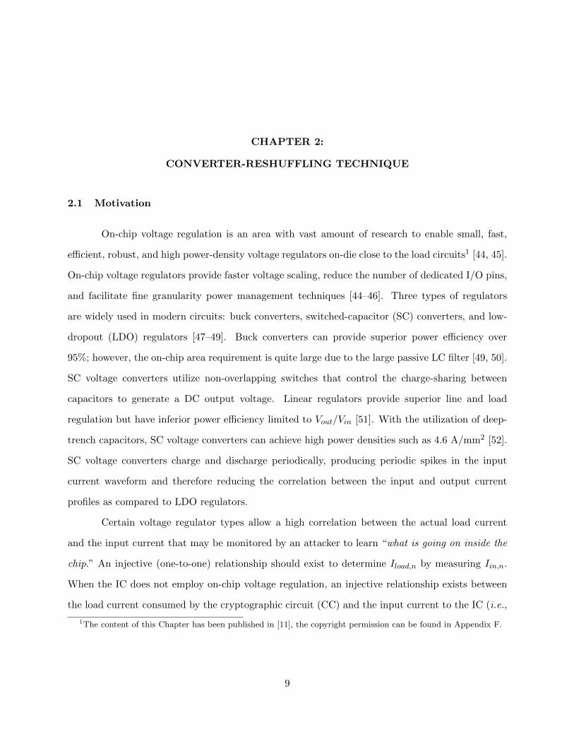
Figure 2.1 Proposed technique disrupts the one-to-one transformation and ac-complishes a non-injective relationship between the load current andinput current. 10
Figure 2.2 Active and gated converters are juggled with converter-reshuffling. 11
Figure 2.3 Relationship between the input power and AES core power. 14
Figure 2.4 Relationship between the number of phases and the PTEs for fourdifferent kinds of voltage regulation schemes without employing DVFS(DVFS in this work represents random DVFS). 15
Figure 2.5 Relationship between the number of phases and the PTEs for fourdifferent kinds of voltage regulation schemes with DVFS enabled AES core. 16
v
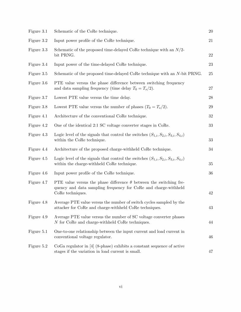
Figure 3.1 Schematic of the CoRe technique. 20
Figure 3.2 Input power profile of the CoRe technique. 21
Figure 3.3 Schematic of the proposed time-delayed CoRe technique with an N/2-bit PRNG. 22
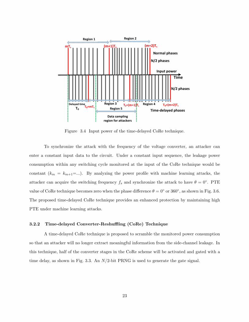
Figure 3.4 Input power of the time-delayed CoRe technique. 23
Figure 3.5 Schematic of the proposed time-delayed CoRe technique with an N -bit PRNG. 25
Figure 3.6 PTE value versus the phase difference between switching frequencyand data sampling frequency (time delay T0 = Ts/2). 27
Figure 3.7 Lowest PTE value versus the time delay. 28
Figure 3.8 Lowest PTE value versus the number of phases (T0 = Ts/2). 29
Figure 4.1 Architecture of the conventional CoRe technique. 32
Figure 4.2 One of the identical 2:1 SC voltage converter stages in CoRe. 33
Figure 4.3 Logic level of the signals that control the switches (S1,i, S2,i, S3,i, S4,i)within the CoRe technique. 33
Figure 4.4 Architecture of the proposed charge-withheld CoRe technique. 34
Figure 4.5 Logic level of the signals that control the switches (S1,i, S2,i, S3,i, S4,i)within the charge-withheld CoRe technique. 35
Figure 4.6 Input power profile of the CoRe technique. 36
Figure 4.7 PTE value versus the phase difference θ between the switching fre-quency and data sampling frequency for CoRe and charge-withheldCoRe techniques. 42
Figure 4.8 Average PTE value versus the number of switch cycles sampled by theattacker for CoRe and charge-withheld CoRe techniques. 43
Figure 4.9 Average PTE value versus the number of SC voltage converter phasesN for CoRe and charge-withheld CoRe techniques. 44
Figure 5.1 One-to-one relationship between the input current and load current inconventional voltage regulator. 46
Figure 5.2 CoGa regulator in [4] (8-phase) exhibits a constant sequence of activestages if the variation in load current is small. 47
vi

Figure 5.3 Input power data sampling for the attacker within K consecutiveswitching periods when the CoGa or CoRe techniques are enabled(Ts is the switching period of the CoGa or CoRe regulator). 50
Figure 5.4 Phase difference versus correlation coefficient of CoGa and CoRe techniques. 56
Figure 5.5 Sampling switching periods versus average correlation coefficient. 57
Figure 5.6 Sampling switching periods versus MTD enhancement ratio (M1 ≈ 5). 58
Figure 5.7 Number of phases and power undertaken by each phase versus averagecorrelation coefficient. 59
Figure 5.8 1st encryption round of a typical 128-bit pipelined AES engine. 61
Figure 5.9 A conventional pipelined AES engine with a distributed on-chip CoRetechnique. 62
Figure 5.10 A conventional pipelined AES engine with a centralized on-chip CoRetechnique. 63
Figure 5.11 Sampling switching periods versus average correlation coefficient andvariance of power noise of the distributed and centralized CoRe architectures. 64
Figure 5.12 Sampling switching periods versus MTD enhancement ratios of thedistributed and centralized CoRe architectures (M1 ≈ 5). 65
Figure 5.13 Full encryption rounds of an 128-bit improved pipelined (IP) AESengine, please note that invert boxes are added before the 1st roundand the mask removal operation is performed after the 11th round (thearchitecture of the reconstructed S-box can be founded in [5, 6]). 66
Figure 5.14 Internal logic circuits of the yth invert box. 67
Figure 5.15 Sampling switching periods versus average correlation coefficient andvariance of power noise of the CP AES engine with a centralized CoReregulator and the IP AES engine with a centralized CoRe regulator. 68
Figure 5.16 Sampling switching periods versus MTD enhancement ratio of the CPAES engine with a centralized CoRe regulator and the IP AES enginewith a centralized CoRe regulator (M1 ≈ 3, 5, and 7). 69
Figure 5.17 (a) Masking operation in conventional masked AES engine and (b)Masking operation in the IP AES engine that we proposed. 70
vii
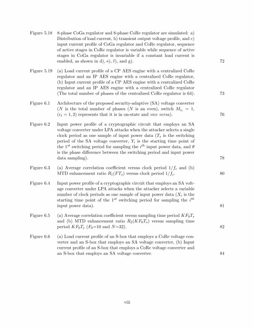
Figure 5.18 8-phase CoGa regulator and 8-phase CoRe regulator are simulated: a)Distribution of load current, b) transient output voltage profile, and c)input current profile of CoGa regulator and CoRe regulator, sequenceof active stages in CoRe regulator is variable while sequence of activestages in CoGa regulator is invariable if a constant load current isenabled, as shown in d), e), f), and g). 72
Figure 5.19 (a) Load current profile of a CP AES engine with a centralized CoReregulator and an IP AES engine with a centralized CoRe regulator,(b) Input current profile of a CP AES engine with a centralized CoReregulator and an IP AES engine with a centralized CoRe regulator(The total number of phases of the centralized CoRe regulator is 64). 73
Figure 6.1 Architecture of the proposed security-adaptive (SA) voltage converter(N is the total number of phases (N is an even), switch Mi1 = 1,(i1 = 1, 2) represents that it is in on-state and vice versa). 76
Figure 6.2 Input power profile of a cryptographic circuit that employs an SAvoltage converter under LPA attacks when the attacker selects a singleclock period as one sample of input power data (Ts is the switchingperiod of the SA voltage converter, Yi is the starting time point ofthe 1st switching period for sampling the ith input power data, and θis the phase difference between the switching period and input powerdata sampling). 78
Figure 6.3 (a) Average correlation coefficient versus clock period 1/fc and (b)MTD enhancement ratio R1(FTs) versus clock period 1/fc. 80
Figure 6.4 Input power profile of a cryptographic circuit that employs an SA volt-age converter under LPA attacks when the attacker selects a variablenumber of clock periods as one sample of input power data (Xi is thestarting time point of the 1st switching period for sampling the ith
input power data). 81
Figure 6.5 (a) Average correlation coefficient versus sampling time period KF0Tsand (b) MTD enhancement ratio R2(KF0Ts) versus sampling timeperiod KF0Ts (F0=10 and N=32). 82
Figure 6.6 (a) Load current profile of an S-box that employs a CoRe voltage con-verter and an S-box that employs an SA voltage converter, (b) Inputcurrent profile of an S-box that employs a CoRe voltage converter andan S-box that employs an SA voltage converter. 84
viii
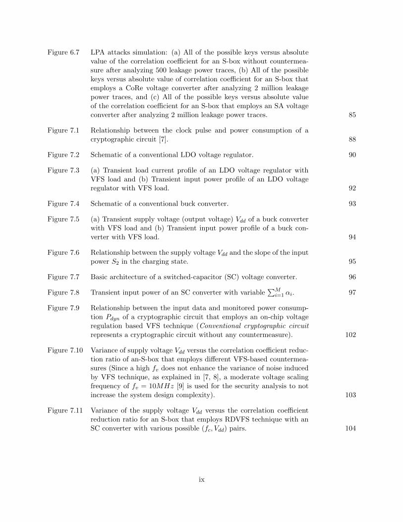
Figure 6.7 LPA attacks simulation: (a) All of the possible keys versus absolutevalue of the correlation coefficient for an S-box without countermea-sure after analyzing 500 leakage power traces, (b) All of the possiblekeys versus absolute value of correlation coefficient for an S-box thatemploys a CoRe voltage converter after analyzing 2 million leakagepower traces, and (c) All of the possible keys versus absolute valueof the correlation coefficient for an S-box that employs an SA voltageconverter after analyzing 2 million leakage power traces. 85
Figure 7.1 Relationship between the clock pulse and power consumption of acryptographic circuit [7]. 88
Figure 7.2 Schematic of a conventional LDO voltage regulator. 90
Figure 7.3 (a) Transient load current profile of an LDO voltage regulator withVFS load and (b) Transient input power profile of an LDO voltageregulator with VFS load. 92
Figure 7.4 Schematic of a conventional buck converter. 93
Figure 7.5 (a) Transient supply voltage (output voltage) Vdd of a buck converterwith VFS load and (b) Transient input power profile of a buck con-verter with VFS load. 94
Figure 7.6 Relationship between the supply voltage Vdd and the slope of the inputpower S2 in the charging state. 95
Figure 7.7 Basic architecture of a switched-capacitor (SC) voltage converter. 96
Figure 7.8 Transient input power of an SC converter with variable∑M
i=1 αi. 97
Figure 7.9 Relationship between the input data and monitored power consump-tion Pdyn of a cryptographic circuit that employs an on-chip voltageregulation based VFS technique (Conventional cryptographic circuitrepresents a cryptographic circuit without any countermeasure). 102
Figure 7.10 Variance of supply voltage Vdd versus the correlation coefficient reduc-tion ratio of an-S-box that employs different VFS-based countermea-sures (Since a high fv does not enhance the variance of noise inducedby VFS technique, as explained in [7, 8], a moderate voltage scalingfrequency of fv = 10MHz [9] is used for the security analysis to notincrease the system design complexity). 103
Figure 7.11 Variance of the supply voltage Vdd versus the correlation coefficientreduction ratio for an S-box that employs RDVFS technique with anSC converter with various possible (fc, Vdd) pairs. 104
ix
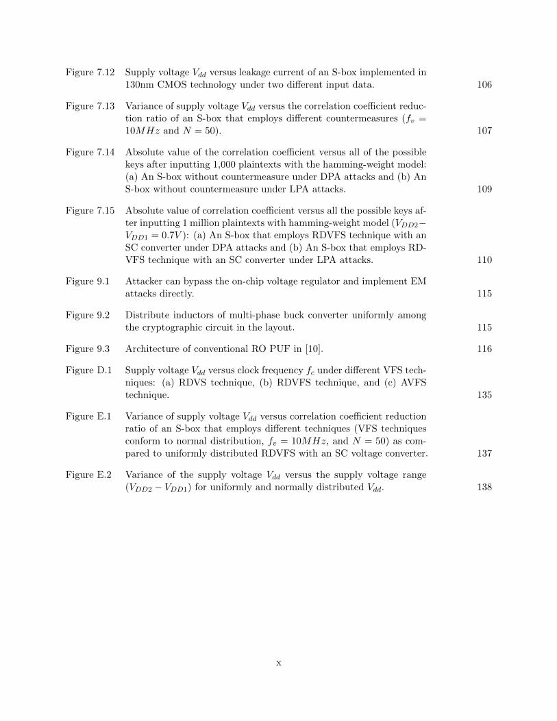
Figure 7.12 Supply voltage Vdd versus leakage current of an S-box implemented in130nm CMOS technology under two different input data. 106
Figure 7.13 Variance of supply voltage Vdd versus the correlation coefficient reduc-tion ratio of an S-box that employs different countermeasures (fv =10MHz and N = 50). 107
Figure 7.14 Absolute value of the correlation coefficient versus all of the possiblekeys after inputting 1,000 plaintexts with the hamming-weight model:(a) An S-box without countermeasure under DPA attacks and (b) AnS-box without countermeasure under LPA attacks. 109
Figure 7.15 Absolute value of correlation coefficient versus all the possible keys af-ter inputting 1 million plaintexts with hamming-weight model (VDD2−VDD1 = 0.7V ): (a) An S-box that employs RDVFS technique with anSC converter under DPA attacks and (b) An S-box that employs RD-VFS technique with an SC converter under LPA attacks. 110
Figure 9.1 Attacker can bypass the on-chip voltage regulator and implement EMattacks directly. 115
Figure 9.2 Distribute inductors of multi-phase buck converter uniformly amongthe cryptographic circuit in the layout. 115
Figure 9.3 Architecture of conventional RO PUF in [10]. 116
Figure D.1 Supply voltage Vdd versus clock frequency fc under different VFS tech-niques: (a) RDVS technique, (b) RDVFS technique, and (c) AVFStechnique. 135
Figure E.1 Variance of supply voltage Vdd versus correlation coefficient reductionratio of an S-box that employs different techniques (VFS techniquesconform to normal distribution, fv = 10MHz, and N = 50) as com-pared to uniformly distributed RDVFS with an SC voltage converter. 137
Figure E.2 Variance of the supply voltage Vdd versus the supply voltage range(VDD2 − VDD1) for uniformly and normally distributed Vdd. 138
x
ABSTRACT
Non-invasive side-channel attacks (SCA) are powerful attacks which can be used to obtain
the secret key in a cryptographic circuit in feasible time without the need for expensive measurement
equipment. Power analysis attacks (PAA) are a type of SCA that exploit the correlation between
the leaked power consumption information and processed/stored data. Differential power analysis
(DPA) and leakage power analysis (LPA) attacks are two types of PAA that exploit different
characteristics of the side-channel leakage profile. DPA attacks exploit the correlation between
the input data and dynamic power consumption of cryptographic circuits. Alternatively, LPA
attacks utilize the correlation between the input data and leakage power dissipation of cryptographic
circuits.
There is a growing trend to integrate voltage regulators fully on-chip in modern integrated
circuits (ICs) to reduce the power noise, improve transient response time, and increase power
efficiency. Therefore, when on-chip voltage regulation is utilized as a countermeasure against power
analysis attacks, the overhead is low. However, a one-to-one relationship exists between the input
power and load power when a conventional on-chip voltage regulator is utilized. In order to break
the one-to-one relationship between the input power and load power, two methodologies can be
considered: (a) selecting multi-phase on-chip voltage regulator and using pseudo-random number
generator (PRNG) to scramble the activation or deactivation pattern of the multi-phase voltage
regulator in the input power profile, (b) enabling random voltage/scaling on conventional on-chip
voltage regulators to insert uncertainties to the load power profile.
In this dissertation, on-chip voltage regulators are utilized as lightweight countermeasures
against power analysis attacks. Converter-reshuffling (CoRe) technique is proposed as a counter-
measure against DPA attacks by using a PRNG to scramble the input power profile. The time-
delayed CoRe technique is designed to eliminate machine learning-based DPA attacks through
xi
inserting a certain time delay. The charge-withheld CoRe technique is proposed to enhance the
entropy of the input power profile against DPA attacks with two PRNGs. The security-adaptive
(SA) voltage converter is designed to sense LPA attacks and activate countermeasure with low
overhead. Additionally, three conventional on-chip voltage regulators: low-dropout (LDO) regula-
tor, buck converter, and switched-capacitor converter are combined with three different kinds of
voltage/frequency scaling techniques: random dynamic voltage and frequency scaling (RDVFS),
random dynamic voltage scaling (RDVS), and aggressive voltage and frequency scaling (AVFS),
respectively, against both DPA and LPA attacks.
xii

CHAPTER 1:
INTRODUCTION
1.1 Side-Channel Attacks
Hardware security has become an important design metric during the past decade with the
increase in the number of attacks at different hardware abstraction levels1. Along with the other
important metrics such as higher power efficiency, better performance, and lower noise, hardware
security is also added as an important design objective in modern computing devices. It has been
demonstrated that software level countermeasures may not be sufficient to protect the encrypted
data from an attacker who has physical access to the device under attack (DuA). Even flawless
implementations of state-of-the-art encryption algorithms are typically vulnerable against hardware
attacks. The primary reason is that the modern integrated circuits (ICs) heavily depend on com-
plementary metal oxide semiconductor (CMOS) transistors which have switching characteristics
that are easily analyzed to determine the underlying circuit functionality. The side channel leakage
originating from the switching activity of transistors can be monitored with simple measurement
equipment by an attacker. This side channel leakage can manifest itself in the form of power con-
sumption profile, timing profile, electromagnetic emanations (EME), acoustic waveforms, and heat.
An efficient implementation of side-channel attacks can retrieve the secret key from an advanced
encryption standard (AES) algorithm in a couple of minutes whereas it can take up to 149 trillion
years to crack a 128-bit AES key with a supercomputer [12].
Various techniques have been proposed as a countermeasure against different types of side-
channel attacks both at the circuit and architectural levels [13]. To reduce the dependency of the
side-channel leakage on the actual power consumption profile, leakage reduction techniques have
1The content of this Chapter partially has been published in [11], the copyright permission can be found inAppendix F.
1
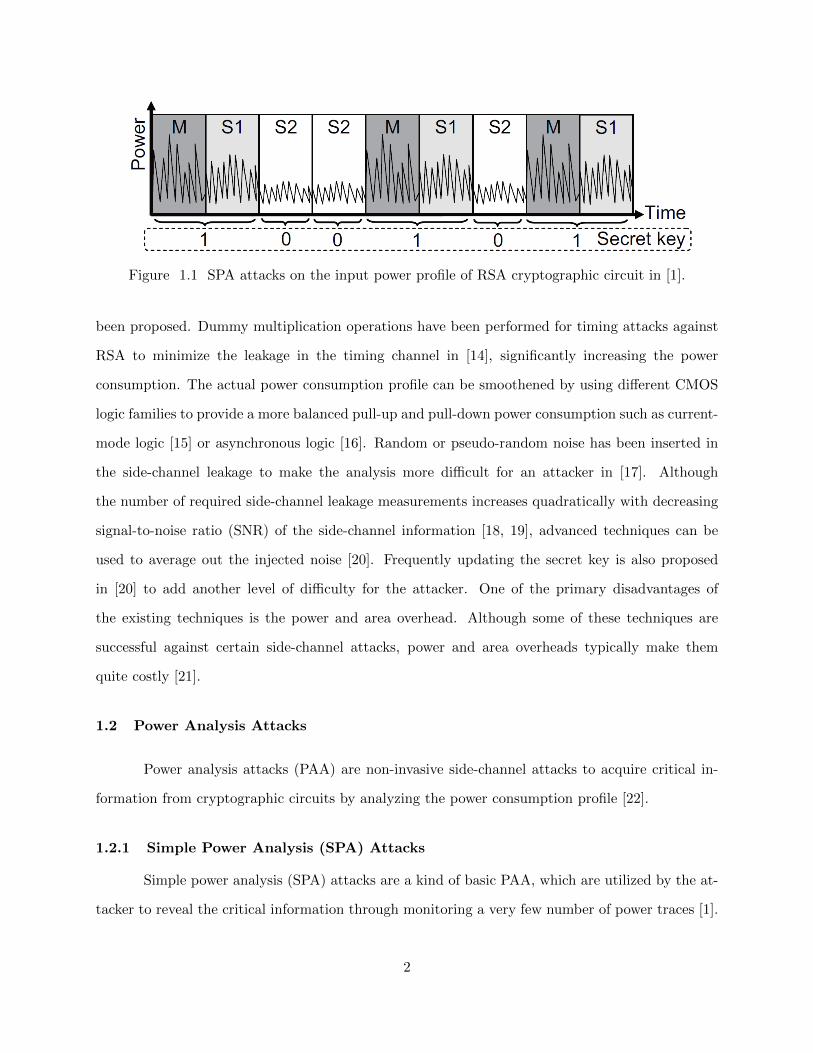
Figure 1.1 SPA attacks on the input power profile of RSA cryptographic circuit in [1].
been proposed. Dummy multiplication operations have been performed for timing attacks against
RSA to minimize the leakage in the timing channel in [14], significantly increasing the power
consumption. The actual power consumption profile can be smoothened by using different CMOS
logic families to provide a more balanced pull-up and pull-down power consumption such as current-
mode logic [15] or asynchronous logic [16]. Random or pseudo-random noise has been inserted in
the side-channel leakage to make the analysis more difficult for an attacker in [17]. Although
the number of required side-channel leakage measurements increases quadratically with decreasing
signal-to-noise ratio (SNR) of the side-channel information [18, 19], advanced techniques can be
used to average out the injected noise [20]. Frequently updating the secret key is also proposed
in [20] to add another level of difficulty for the attacker. One of the primary disadvantages of
the existing techniques is the power and area overhead. Although some of these techniques are
successful against certain side-channel attacks, power and area overheads typically make them
quite costly [21].
1.2 Power Analysis Attacks
Power analysis attacks (PAA) are non-invasive side-channel attacks to acquire critical in-
formation from cryptographic circuits by analyzing the power consumption profile [22].
1.2.1 Simple Power Analysis (SPA) Attacks
Simple power analysis (SPA) attacks are a kind of basic PAA, which are utilized by the at-
tacker to reveal the critical information through monitoring a very few number of power traces [1].
2

Figure 1.2 Flow of implementing DPA attacks from [2].
As shown in Fig. 1.12, different math operations that occur in the cryptographic cause the circuit
to have varying power dissipation profiles. The attacker may obtain the critical information by
analyzing the variations of power traces. Although SPA attacks are simple and convenient, imple-
menting SPA attacks on a modern cryptographic circuit may not be sufficient to leak the critical
information due to the protection of complex encryption algorithm.
1.2.2 Differential Power Analysis (DPA) Attacks
A differential power analysis (DPA) attack is an advanced PAA that statistically analyzes a
large number of dynamic power traces to determine whether a secret key guess is correct or not [20].
DPA attacks are widely utilized by attackers due to the high efficiency and low cost.
The detailed flow of implementing DPA attacks is shown in Fig. 1.23. First, the attacker
inputs a series of plaintexts to the cryptographic circuit and hypothesizes all of the possible keys
of the cryptographic circuit. The intermediate data values can be obtained through combining the
plaintexts and hypothesized keys with the cryptographic algorithm. When the intermediate data
are acquired, the attacker can predict the dynamic power consumption of the cryptographic circuit
by combining the intermediate data with a suitable power model. The next step for the attacker
is measuring the actual dynamic power consumption of the cryptographic circuit under different
plaintexts. When the attacker performs a statistical analysis between the predicted dynamic power
2Copyright permission can be found in Appendix F.3Copyright permission can be found in Appendix F.
3
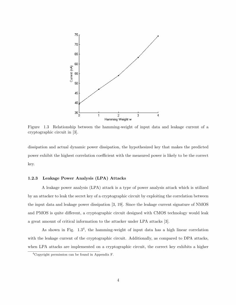
Figure 1.3 Relationship between the hamming-weight of input data and leakage current of acryptographic circuit in [3].
dissipation and actual dynamic power dissipation, the hypothesized key that makes the predicted
power exhibit the highest correlation coefficient with the measured power is likely to be the correct
key.
1.2.3 Leakage Power Analysis (LPA) Attacks
A leakage power analysis (LPA) attack is a type of power analysis attack which is utilized
by an attacker to leak the secret key of a cryptographic circuit by exploiting the correlation between
the input data and leakage power dissipation [3, 19]. Since the leakage current signature of NMOS
and PMOS is quite different, a cryptographic circuit designed with CMOS technology would leak
a great amount of critical information to the attacker under LPA attacks [3].
As shown in Fig. 1.34, the hamming-weight of input data has a high linear correlation
with the leakage current of the cryptographic circuit. Additionally, as compared to DPA attacks,
when LPA attacks are implemented on a cryptographic circuit, the correct key exhibits a higher
4Copyright permission can be found in Appendix F.
4

(a) (b)
Figure 1.4 All the possible keys versus the correlation coefficient from [3]: (a) LPA attacks and(b) DPA attacks.
(a) (b)
Figure 1.5 (a) 2:1 single phase SC converter [4] and (b) Power efficiency of a single phase SCconverter versus load current and flying capacitance [4].
correlation coefficient, as shown in Fig. 1.45. The higher correlation coefficient indicates a larger
amount of information leakage. As a result, LPA attacks may be a more serious threat under
certain conditions.
1.3 On-Chip Voltage Regulation Against Power Analysis Attacks
1.3.1 Converter-Gating (CoGa) Voltage Converter Against Power Analysis Attacks
On-chip power delivery is an efficient way to reduce the power noise [23–37] and improve
transient response time [37–39]. Multi-phase on-chip voltage converter is a kind of fully integrated
on-chip voltage converters, which can achieve high power efficiency by optimizing the number of
5Copyright permission can be found in Appendix F.
5
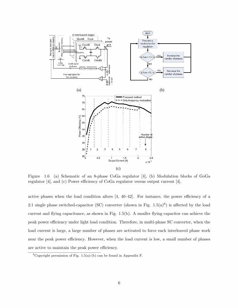
(a) (b)
(c)
Figure 1.6 (a) Schematic of an 8-phase CoGa regulator [4], (b) Modulation blocks of GoGaregulator [4], and (c) Power efficiency of CoGa regulator versus output current [4].
active phases when the load condition alters [4, 40–42]. For instance, the power efficiency of a
2:1 single phase switched-capacitor (SC) converter (shown in Fig. 1.5(a)6) is affected by the load
current and flying capacitance, as shown in Fig. 1.5(b). A smaller flying capacitor can achieve the
peak power efficiency under light load condition. Therefore, in multi-phase SC converter, when the
load current is large, a large number of phases are activated to force each interleaved phase work
near the peak power efficiency. However, when the load current is low, a small number of phases
are active to maintain the peak power efficiency.
6Copyright permission of Fig. 1.5(a)-(b) can be found in Appendix F.
6
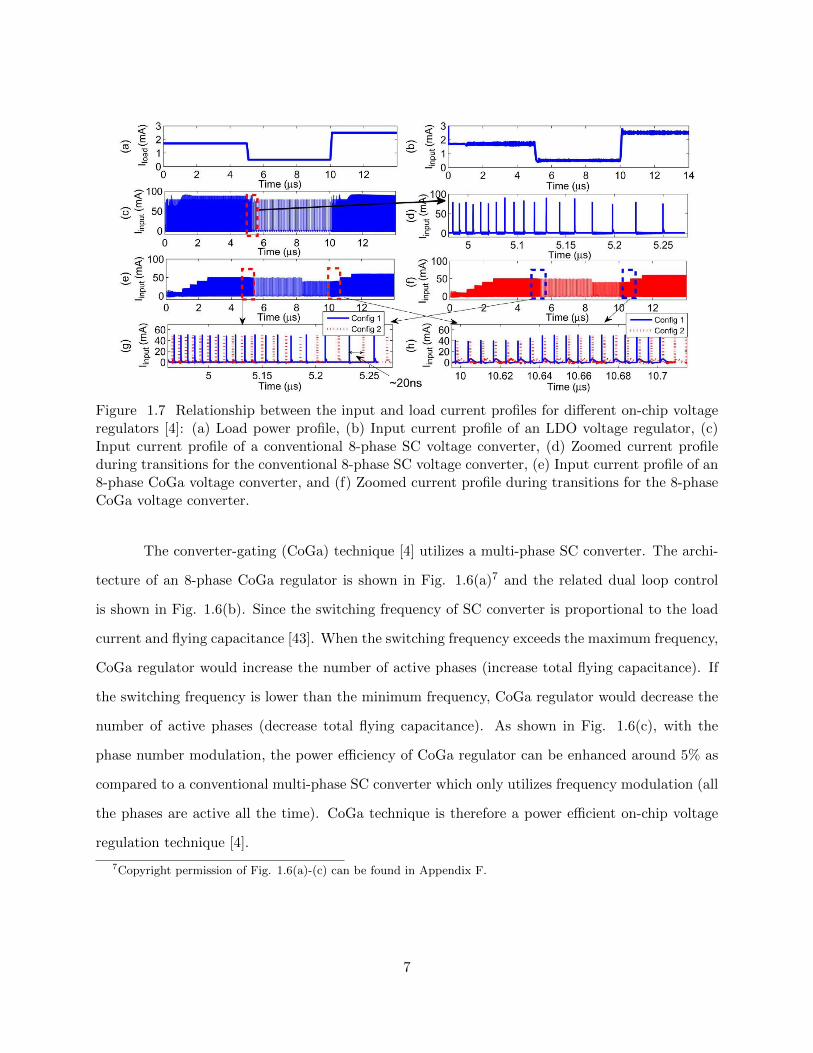
Figure 1.7 Relationship between the input and load current profiles for different on-chip voltageregulators [4]: (a) Load power profile, (b) Input current profile of an LDO voltage regulator, (c)Input current profile of a conventional 8-phase SC voltage converter, (d) Zoomed current profileduring transitions for the conventional 8-phase SC voltage converter, (e) Input current profile of an8-phase CoGa voltage converter, and (f) Zoomed current profile during transitions for the 8-phaseCoGa voltage converter.
The converter-gating (CoGa) technique [4] utilizes a multi-phase SC converter. The archi-
tecture of an 8-phase CoGa regulator is shown in Fig. 1.6(a)7 and the related dual loop control
is shown in Fig. 1.6(b). Since the switching frequency of SC converter is proportional to the load
current and flying capacitance [43]. When the switching frequency exceeds the maximum frequency,
CoGa regulator would increase the number of active phases (increase total flying capacitance). If
the switching frequency is lower than the minimum frequency, CoGa regulator would decrease the
number of active phases (decrease total flying capacitance). As shown in Fig. 1.6(c), with the
phase number modulation, the power efficiency of CoGa regulator can be enhanced around 5% as
compared to a conventional multi-phase SC converter which only utilizes frequency modulation (all
the phases are active all the time). CoGa technique is therefore a power efficient on-chip voltage
regulation technique [4].
7Copyright permission of Fig. 1.6(a)-(c) can be found in Appendix F.
7
As shown in Fig. 1.7(a)8 and Fig. 1.7(b), low-dropout (LDO) regulator has a poor security
against power analysis attacks since there is an approximated linear relationship between the input
current and load current. By contrast, as shown in Fig. 1.7(c) and Fig. 1.7(d), conventional
multi-phase SC converter can obscure the correlation between the input and load current profiles
by charging and discharging the flying capacitors with a certain switching frequency. However,
CoGa converter can further scramble the correlation between the input and load current profiles
with a pseudo-random number generator (PRNG) that alters the activation or deactivation pattern
of phases, as shown in Fig. 1.7(e), Fig. 1.7(f), Fig. 1.7(g) and Fig. 1.7(h).
1.3.2 Our Contribution
Although CoGa technique was proposed in [4] as a countermeasure against power analy-
sis attacks, it is demonstrated in our work that CoGa technique is not sufficiently secure against
power analysis attacks. Therefore, we proposed another five novel efficient on-chip voltage regula-
tion techniques against power analysis attacks. The content of our contribution is summarized as
follows9
• Chapter 2 introduces converter-reshuffling (CoRe) voltage conversion against DPA attacks.
• Chapter 3 proposes time-delayed converter-reshuffling (CoRe) voltage conversion against ma-
chine learning-based DPA attacks.
• Chapter 4 introduces a high entropy charge-withheld converter-reshuffling (CoRe) voltage
conversion against DPA attacks.
• Chapter 5 co-designs on-chip voltage regulation with advanced encryption standard (AES)
engine against DPA attacks.
• Chapter 6 introduces security-adaptive (SA) voltage conversion against LPA attacks.
• Chapter 7 explores conventional on-chip voltage conversion with voltage/frequency scaling
against both DPA and LPA attacks.
8Copyright permission of Fig. 1.7(a)-(h) can be found in Appendix F.9The parameters defined in each chapter are independent, different chapters may share the same parameter sign
with different meanings.
8
CHAPTER 2:
CONVERTER-RESHUFFLING TECHNIQUE
2.1 Motivation
On-chip voltage regulation is an area with vast amount of research to enable small, fast,
efficient, robust, and high power-density voltage regulators on-die close to the load circuits1 [44, 45].
On-chip voltage regulators provide faster voltage scaling, reduce the number of dedicated I/O pins,
and facilitate fine granularity power management techniques [44–46]. Three types of regulators
are widely used in modern circuits: buck converters, switched-capacitor (SC) converters, and low-
dropout (LDO) regulators [47–49]. Buck converters can provide superior power efficiency over
95%; however, the on-chip area requirement is quite large due to the large passive LC filter [49, 50].
SC voltage converters utilize non-overlapping switches that control the charge-sharing between
capacitors to generate a DC output voltage. Linear regulators provide superior line and load
regulation but have inferior power efficiency limited to Vout/Vin [51]. With the utilization of deep-
trench capacitors, SC voltage converters can achieve high power densities such as 4.6 A/mm2 [52].
SC voltage converters charge and discharge periodically, producing periodic spikes in the input
current waveform and therefore reducing the correlation between the input and output current
profiles as compared to LDO regulators.
Certain voltage regulator types allow a high correlation between the actual load current
and the input current that may be monitored by an attacker to learn “what is going on inside the
chip.” An injective (one-to-one) relationship should exist to determine Iload,n by measuring Iin,n.
When the IC does not employ on-chip voltage regulation, an injective relationship exists between
the load current consumed by the cryptographic circuit (CC) and the input current to the IC (i.e.,
1The content of this Chapter has been published in [11], the copyright permission can be found in Appendix F.
9
PVR: Proposed voltage regulator
Non-injective surjective transformation
CCIin Iload
PVR
IC
Iin,1
Iin,2
Iin,n
- -
- -
-
Iload,1
Iload,2
Iload,n
- -
- -
-
Figure 2.1 Proposed technique disrupts the one-to-one transformation and accomplishes a non-injective relationship between the load current and input current.
Iload,n = Iin,n), as shown in Fig. 2.1. If the on-chip power delivery network can provide a non-
injective relationship between the load and input current profiles, as illustrated in Fig. 2.1, (i.e.,
a particular load current leads to more than one input current profile), the outside attacker can
no longer obtain the internal information by measuring the input current. SC voltage converters
charge and discharge periodically, produce spikes in the input current waveform, and therefore
reduce the correlation between the input and output current profiles.
2.2 Treat Model
The attack is assumed to be non-invasive and the attacker is assumed to have access to
the circuit where s/he can monitor the side-channel leakage information. For example, the power
consumption profile can be monitored by measuring the I/O pins dedicated to power/ground,
10
Gated stages
Time
1-3-5-7
0-2-4-6
1-4-6-7
0-2-3-5
0-4-5-6
1-2-3-7 1-4-6-7
0-2-3-5Active stages
t1 t2 t3 t4
...
...
Figure 2.2 Active and gated converters are juggled with converter-reshuffling.
shown as Iin in Fig. 2.1. Alternatively, the attacker can use near-field antennas to monitor the EM
emanations. Additionally, the DuA is assumed to have on-chip voltage regulators.
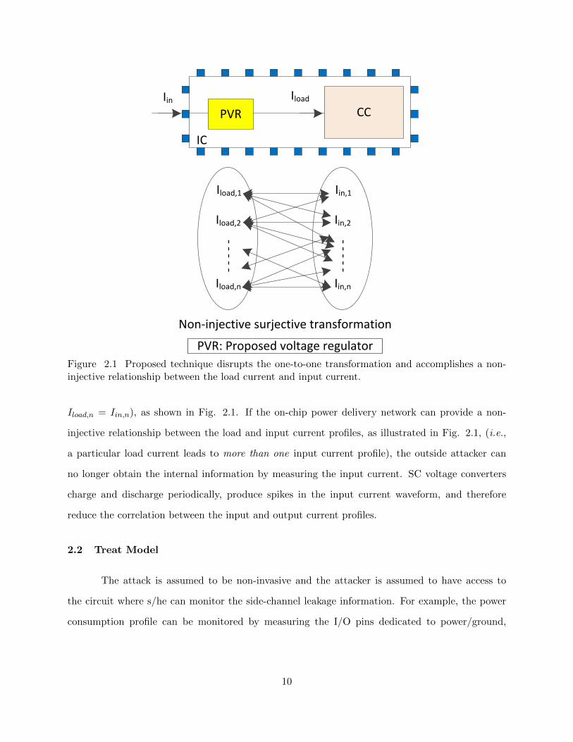
2.3 Review of Converter-Gating (CoGa)
Converter-gating (CoGa) is the adaptive activation and deactivation of certain stages of a
multiphase on-chip SC voltage converter based on the workload information [4]. When the current
demand increases (decreases), an additional passive (active) stage is activated (gated) to provide
a higher (lower) load current without sacrificing power conversion efficiency. The additional stage
that is being activated or gated is determined based on a pseudo-random number generator (PRNG)
to scramble the input current consumption of the SC voltage converter (i.e., Iin as shown in Fig.
2.1). Since each interleaved stage within an SC voltage converter is driven with a different phase
of the input clock signal, each interleaved stage charges and discharges with a certain time shift.
The amount of time shift depends on the frequency of the clock signal. For example, a timing shift
of 0.5 µs can be achieved by activating the 4th stage instead of the 0th stage when an eight stage
SC converter operates at 1 MHz.
Although CoGa makes the attackers’ job more difficult by scrambling the power consump-
tion profile and inserting additional spikes in the input current profile, the DuA would still be
vulnerable under advanced attacks as the activation/deactivation occurs when there is a change
in the workload demand. Particularly, an attacker can effectively bypass the CoGa technique if
an attack is performed such that the changes in the load current demand are not large enough to
trigger CoGa to activate/deactivate interleaved stages. Furthermore, the input current profile that
is monitored by an attacker would still be correlated with the actual current profile even if CoGa is
triggered since the activation/deactivation occurs when there is a change in the workload demand.
11
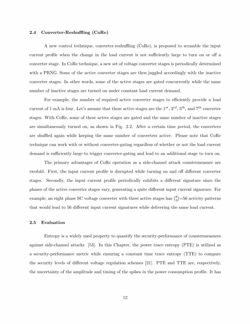
2.4 Converter-Reshuffling (CoRe)
A new control technique, converter-reshuffling (CoRe), is proposed to scramble the input
current profile when the change in the load current is not sufficiently large to turn on or off a
converter stage. In CoRe technique, a new set of voltage converter stages is periodically determined
with a PRNG. Some of the active converter stages are then juggled accordingly with the inactive
converter stages. In other words, some of the active stages are gated concurrently while the same
number of inactive stages are turned on under constant load current demand.
For example, the number of required active converter stages to efficiently provide a load
current of 1 mA is four. Let’s assume that these active stages are the 1st, 3rd, 5th, and 7th converter
stages. With CoRe, some of these active stages are gated and the same number of inactive stages
are simultaneously turned on, as shown in Fig. 2.2. After a certain time period, the converters
are shuffled again while keeping the same number of converters active. Please note that CoRe
technique can work with or without converter-gating regardless of whether or not the load current
demand is sufficiently large to trigger converter-gating and lead to an additional stage to turn on.
The primary advantages of CoRe operation as a side-channel attack countermeasure are
twofold. First, the input current profile is disrupted while turning on and off different converter
stages. Secondly, the input current profile periodically exhibits a different signature since the
phases of the active converter stages vary, generating a quite different input current signature. For
example, an eight phase SC voltage converter with three active stages has(83
)=56 activity patterns
that would lead to 56 different input current signatures while delivering the same load current.
2.5 Evaluation
Entropy is a widely used property to quantify the security-performance of countermeasures
against side-channel attacks [53]. In this Chapter, the power trace entropy (PTE) is utilized as
a security-performance metric while ensuring a constant time trace entropy (TTE) to compare
the security levels of different voltage regulation schemes [21]. PTE and TTE are, respectively,
the uncertainty of the amplitude and timing of the spikes in the power consumption profile. It has
12
been shown in [21] that TTE is zero without dynamic voltage and frequency scaling (DVFS). When
DVFS is activated, a constant non-zero TTE of 6.02 [21] is used in the evaluation. Intuitively, TTE
increases when the operating frequency changes over time as in the case of DVFS. We assume
that the power consumption of an advanced encryption standard (AES) core is P (t) at time t,
the number of phases N changes between 30 and 100, the switching frequency and period of each
phase are, respectively, fs and Ts, the frequency of the input data for AES core is f0, the phase
difference between actual power consumption and sampling of the attacker is 2πθ. The relationship
between the input power and AES core power while employing either CoGa or CoRe is illustrated
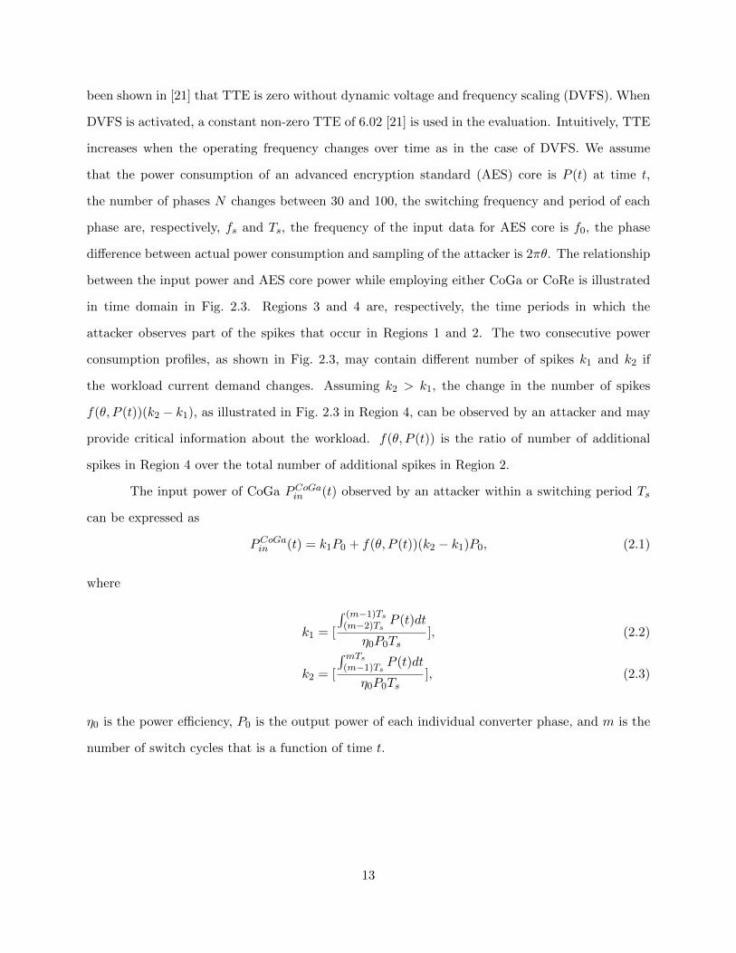
in time domain in Fig. 2.3. Regions 3 and 4 are, respectively, the time periods in which the
attacker observes part of the spikes that occur in Regions 1 and 2. The two consecutive power
consumption profiles, as shown in Fig. 2.3, may contain different number of spikes k1 and k2 if
the workload current demand changes. Assuming k2 > k1, the change in the number of spikes
f(θ, P (t))(k2 − k1), as illustrated in Fig. 2.3 in Region 4, can be observed by an attacker and may
provide critical information about the workload. f(θ, P (t)) is the ratio of number of additional
spikes in Region 4 over the total number of additional spikes in Region 2.
The input power of CoGa PCoGain (t) observed by an attacker within a switching period Ts
can be expressed as
PCoGain (t) = k1P0 + f(θ, P (t))(k2 − k1)P0, (2.1)
where
k1 = [
∫ (m−1)Ts(m−2)Ts P (t)dt
η0P0Ts], (2.2)
k2 = [
∫mTs(m−1)Ts P (t)dt
η0P0Ts], (2.3)
η0 is the power efficiency, P0 is the output power of each individual converter phase, and m is the
number of switch cycles that is a function of time t.
13

(m-1)Ts mTs (m+1)Ts
Number of spikes is k1
time
Number of spikes is k2
P(t) P(t+Ts)
AES core power
2πθ
Input power
Number of spikes is k3
Region 1 Region 2
Region 3 Region 4
Region 5
Figure 2.3 Relationship between the input power and AES core power.
The input power of CoRe PCoRein (t) observed by an attacker within a switching period Ts
can be expressed as
PCoRein (t) = α(θ, P (t))P0 + β(θ, P (t))P0, (2.4)
where α(θ, P (t)) and β(θ, P (t)) are the number of spikes that is monitored by an attacker, respec-
tively, in Regions 3 and 4.
In differential power analysis (DPA) attacks, the attacker monitors the dynamic power
consumption [21]. To obtain a useful level of PTE from CoGa and CoRe, the probability of detecting
the changes in the power profile for each possible input power value needs to be calculated. This
probability γi(θ, P (t)) for CoGa when θ 6= 0 is
γi(θ, P (t)) =
([θN ]−k3
i
)([(1−θ)N ]−k1+k3k2−k1−i
)(N−k1k2−k1
) , (2.5)
i ∈ [A,B] = [max0, k2 − k3 − [(1− θ)N ],
min[θN ]− k3, k2 − k1], (2.6)
14

3 0 4 0 5 0 6 0 7 0 8 0 9 0 1 0 0 1 1 00 . 0
0 . 5
1 . 0
1 . 5
2 . 0
2 . 5
3 . 0
PTE
T h e n u m b e r o f p h a s e s : N
C o R e C o G a S C c o n v e r t e r L D O
Figure 2.4 Relationship between the number of phases and the PTEs for four different kindsof voltage regulation schemes without employing DVFS (DVFS in this work represents randomDVFS).
where k3 is the number of spikes in Region 5, as illustrated in Fig. 2.3. The PTE value for CoGa
PTECoGaDPA (t) is therefore
PTECoGaDPA (t) = −B∑i=A
γi(θ, P (t))log(γi(θ,P (t)))2 . (2.7)
Note that if θ = 0, the probability γi(0, P (t)) = 1 and the PTE for CoGa becomes 0.
However, in practice, the switching frequency fs is not constant, but has a narrow frequency range.
It is quite difficult for an attacker to keep the value of θ as 0 all the time. Therefore, in the rest of
this Chapter, we assume θ 6= 0.
For CoRe, the probability function λj(θ, P (t)) for achieving different input powers is
λj(θ, P (t)) =
(Nj
)(N
k1+k2−j)(
Nk1
)(Nk2
) , (2.8)
j ∈ [C,D] = [max0, k1 + k2 −N,minN, k1 + k2], (2.9)
15
3 0 4 0 5 0 6 0 7 0 8 0 9 0 1 0 00 . 0
0 . 5
1 . 0
1 . 5
2 . 0
2 . 5
3 . 0
3 . 5
4 . 0
PTE
T h e n u m b e r o f p h a s e s : N
C o R e + D V F S S C c o n v e r t e r + D V F S L D O + D V F S C o G a + D V F S
Figure 2.5 Relationship between the number of phases and the PTEs for four different kinds ofvoltage regulation schemes with DVFS enabled AES core.
when θ 6= 0. In (2.8), j = i1+ i2 where i1 and i2 are the number of spikes, respectively, in Regions 3
and 4. The constraints for (i1, i2) are (i1 ≤ k1, i2 ≤ k2). Accordingly, the PTE of CoRe PTECoReDPA (t)
becomes
PTECoReDPA (t) = −D∑j=C
λj(θ, P (t))log(λj(θ,P (t)))2 . (2.10)
The relationship between the number of phases and the PTE value for four different kinds of
voltage regulation schemes is illustrated in Fig. 2.4 when load power demand varies from (1/2)Pmax
to (7/8)Pmax where Pmax is the maximum dynamic power consumption for AES core. As shown
in Fig. 2.4, the PTE of CoRe is about 13% greater as compared to the PTE of CoGa and therefore
CoRe provides better security than CoGa.
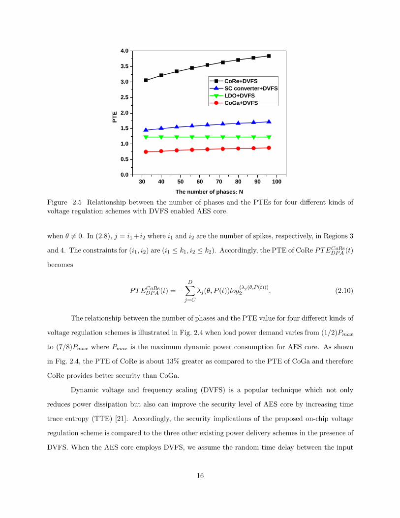
Dynamic voltage and frequency scaling (DVFS) is a popular technique which not only
reduces power dissipation but also can improve the security level of AES core by increasing time
trace entropy (TTE) [21]. Accordingly, the security implications of the proposed on-chip voltage
regulation scheme is compared to the three other existing power delivery schemes in the presence of
DVFS. When the AES core employs DVFS, we assume the random time delay between the input
16
data and power consumption variation caused by DVFS is T0. In other words, the input power
would vary within 0 to T0 after the input data completed. In the case of CoGa, the variations in
the power consumption appear within the first switching period only after the input data has been
processed. This can cause CoGa a non-zero PTE. The PTE for CoGa PTECoGaDV FS(t) with DVFS
therefore becomes
PTECoGaDV FS(t) = −(1− TsT0
)log(1−Ts
T0)
2 −N−1∑
[θN ]=1
B∑i=A
TsNT0
γi(θ, P (t))log(∑N−1
[θN ]=1TsNT0
γi(θ,P (t)))
2 . (2.11)
The PTE for CoRe is, however, quite different in the presence of DVFS. The input power
of CoRe keeps reshuffling regardless of the workload demand and therefore always has a non-zero
PTE. As a result, the PTE of CoRe PTECoReDV FS(t) is much greater than the PTE of CoGa and can
be shown as
PTECoReDV FS(t) = −N−1∑
[θN ]=1
D∑j=C
1
N(1− Ts
T0)λ1j (θ, P (t))
× log(∑N−1
[θN ]=11N(1−Ts
T0)λ1j (θ,P (t)))
2 −N−1∑
[θN ]=1
D∑j=C
λj(θ, P (t))
× TsNT0
log(∑N−1
[θN ]=1TsNT0
λj(θ,P (t)))
2 . (2.12)
The probability function λ1j (θ, P (t))) is the same as λj(θ, P (t))) if k2 = k1. Similarly, the PTEs of
a conventional SC voltage converter PTESCDV FS and an LDO regulator PTELDODV FS with DVFS are
PTESCDV FS = −(1− TsT0
)log(1−Ts
T0)
2
− TsT0log
(TsT0
1maxk1,k2
)
2 , (2.13)
PTELDODV FS = −(1− TsT0
)log(1−Ts
T0)
2
− TsT0log
(TsT0
fsfclock
)
2 , (2.14)
where fclock is the clock frequency of the AES core.
17

The PTEs of the aforementioned four different voltage regulation schemes for different
number of voltage converter stages are illustrated in Fig. 2.5 when DVFS is employed. In Fig. 2.5,
the load power consumption varies from (1/2)Pmax to (7/8)Pmax where Pmax denotes the maximum
dynamic power consumption for AES core. The clock frequency is selected between 250 MHz and
450 MHz and the TTE value is 6.02 in [21]. The switching frequency for CoGa and CoRe is 30
MHz.
The PTE of CoRe increases ∼40% when DVFS is activated. The primary reason for this
enhancement is that the reshuffling behavior is workload-agnostic and DVFS further enhances the
scrambling behavior. The PTE of SC voltage converter and LDO regulator also increases to a
non-zero value with DVFS, but still much smaller than the PTE of CoRe. Alternatively, the PTE
of CoGa reduces ∼64% in the presence of DVFS. Therefore, CoRe technique provides significantly
higher security as compared to other power delivery schemes when DVFS is activated.
2.6 Conclusion
A new on-chip power management technique, converter-reshuffling (CoRe), is proposed as
a power efficient countermeasure against side channel attacks. A theoretical proof based on the
power trace entropy (PTE) analysis is developed to compare CoRe with three other existing on-chip
power delivery schemes. CoRe performs better than the other schemes with or without DVFS. The
PTE of CoRe significantly increases when DVFS is activated whereas other techniques may have
degraded PTE levels with DVFS.
18

CHAPTER 3:
TIME-DELAYED CONVERTER-RESHUFFLING TECHNIQUE
3.1 Motivation
A workload-agnostic converter-reshuffling (CoRe) technique has been proposed in Chapter
2 to randomly activate and deactivate converter stages to scramble the power consumption profile
with a pseudo-random number generator (PRNG)1. The main drawback of the conventional CoRe
technique in Chapter 2 is that the attacker can obtain switching frequency fs and phase information
with machine learning attacks. If the attacker can synchronize the attack with the switching
frequency of the on-chip switched-capacitor (SC) converter, the average power within a switching
period would leak critical information to the attacker that may annihilate the added security benefit
of reshuffling the converter stages.
In this Chapter, a new technique, time-delayed CoRe, is introduced to cope with machine
learning-based DPA attacks. In the proposed time-delayed CoRe technique, half of converter stages
are delayed with a certain time-shift, eliminating possible synchronization of the attacker’s sampling
frequency with the switching frequency of the converter. With this technique, the minimum power
trace entropy (PTE) value is significantly increased as compared to the conventional CoRe technique
in Chapter 2 under machine learning attacks even when the attacker’s sampling frequency is in
complete synchronization with the SC voltage converter.
3.2 Modeling
Entropy is commonly used in information theory to model the level of uncertainty (or ran-
domness) in a given data set. In cryptography, entropy is used to evaluate the security performance
1The content of this Chapter has been published in [54], the copyright permission can be found in Appendix F.
19

N-bit PRNG
N-phase CoRe regulator
LoadPower Supply
Control Circuit
LDO regulator
Accurate
Core
Figure 3.1 Schematic of the CoRe technique.
of integrated systems against side-channel attacks (SCA) [53, 55]. We will use entropy to quantify
the security performance of different on-chip voltage converters. The input power of a voltage
converter Hi(t), (i = 1, 2, ..., k) can have k different values while delivering the same output power
Pout(t) to the load circuits depending on the design parameters of the voltage converter and the
phase and frequency of the input switching signal. Let’s assume that the probability of having
different input power values is pi(t), (i = 1, 2, ..., k). The input power trace entropy PTE(t) of a
voltage converter can then be defined as
PTE(t) = −k∑i=1
pi(t)logpi(t)2 . (3.1)
3.2.1 Converter-Reshuffling (CoRe) Technique
Primarily, two parameters of an on-chip SC converter can leak the load power information
to attackers: switching frequency and number of active converter stages. The switching frequency
fs has a monotonic relationship with the output power Pout [52]. fs is therefore fixed in this Chapter
to eliminate possible leakage of the workload information. The number of active converter stages
increases with the workload and therefore may leak the workload information to the attacker.
A system level architecture of the CoRe technique is illustrated in Fig. 3.1. The output
power resolutionN/Pout at the output of SC converter can be degraded while using a fixed-frequency
20

TimemTs (m+1)Ts (m+2)Ts
Input power
Number of spikes is km
Number of spikes is km+1
Phase difference θ Data sampling region
for attackers
Region 3
Region 1 Region 2
Number of spikes is km-1
Region 0
(m-1)Ts
Figure 3.2 Input power profile of the CoRe technique.
modulation if the number of phases N is small. A low-dropout (LDO) regulator can be inserted at
the output of the SC converter to mitigate the possible output DC shift. If the number of phases N
is sufficiently large, the CoRe technique has a fine output power resolution and the LDO regulator
can be removed.
The input power of the CoRe technique, which may be monitored by an attacker, is illus-
trated in Fig. 3.2. fs and Ts are, respectively, the switching frequency and period. The number of
spikes in regions 0, 1, and 2 are, respectively, km−1, km, and km+1. The phase difference between
switching frequency and data sampling by the attacker is θ and the power consumption at each
converter stage is P0. To represent the input power information between mTs and (m + 2)Ts, an
array Am is defined as
Am = [am,1, ..., am,N , am,(N+1), ..., am,2N ]P0, (3.2)
where∑N
i=1 am,i = km,∑2N
i=N+1 am,i = km+1, and am,i ∈ 0, 1, (i = 1, 2, ..., 2N). We define
another array Hm = [h1, h2, ..., h2N ] to represent the monitored power data by the attacker within
a switching period with the values hi as
hi =
0 , i ≤ [θ/360 ∗N ]
1 , [θ/360 ∗N ] < i ≤ [θ/360 ∗N ] +N
0 , i > [θ/360 ∗N ] +N .
(3.3)
21
N/2-bit PRNG
N/2-phase CoRe
regulator
Power Supply
Accurate
N/2-phase CoRe
regulator
TimeDelay
LDO regulator Load
Control Circuit
Core
Figure 3.3 Schematic of the proposed time-delayed CoRe technique with an N/2-bit PRNG.
The input power data Ps,m sampled by an attacker within a switching period can then be written
as
Ps,m = AmHTm. (3.4)
The next step is to enumerate all of the possible arrays Am and count the number of
each sampled power Ps,m. If the frequency for all the possible sampled power data Ps,m is
gj(θ, km, km+1), (j = 1, 2, ..., D) where D is the total number of possible sampled input power
data, the corresponding probability βj(θ, km, km+1), (j = 1, 2, ..., D) is
βj(θ, km, km+1) =gj(θ, km, km+1)(
Nkm
)(N
km+1
) . (3.5)
The PTE value of CoRe technique PTE1 can be written as
PTE1 = −D∑j=1
gj(θ, km, km+1)(Nkm
)(N
km+1
) log
gj(θ,km,km+1)
( Nkm)( Nkm+1
)2 . (3.6)
22
(m+2)Ts
Time
mTs
Input power
Data sampling region for attackers
Region 5
Region 2
(m+1)Ts
Region 3T0+mTs
T0+(m+1)Ts T0+(m+2)TsDelayed time
T0
Region 4
Region 1
N/2 phases
N/2 phases
Normal phases
Time-delayed phases
Figure 3.4 Input power of the time-delayed CoRe technique.
To synchronize the attack with the frequency of the voltage converter, an attacker can
enter a constant input data to the circuit. Under a constant input sequence, the leakage power
consumption within any switching cycle monitored at the input of the CoRe technique would be
constant (km = km+1=...). By analyzing the power profile with machine learning attacks, the
attacker can acquire the switching frequency fs and synchronize the attack to have θ = 0. PTE
value of CoRe technique becomes zero when the phase difference θ = 0 or 360, as shown in Fig. 3.6.
The proposed time-delayed CoRe technique provides an enhanced protection by maintaining high
PTE under machine learning attacks.
3.2.2 Time-delayed Converter-Reshuffling (CoRe) Technique
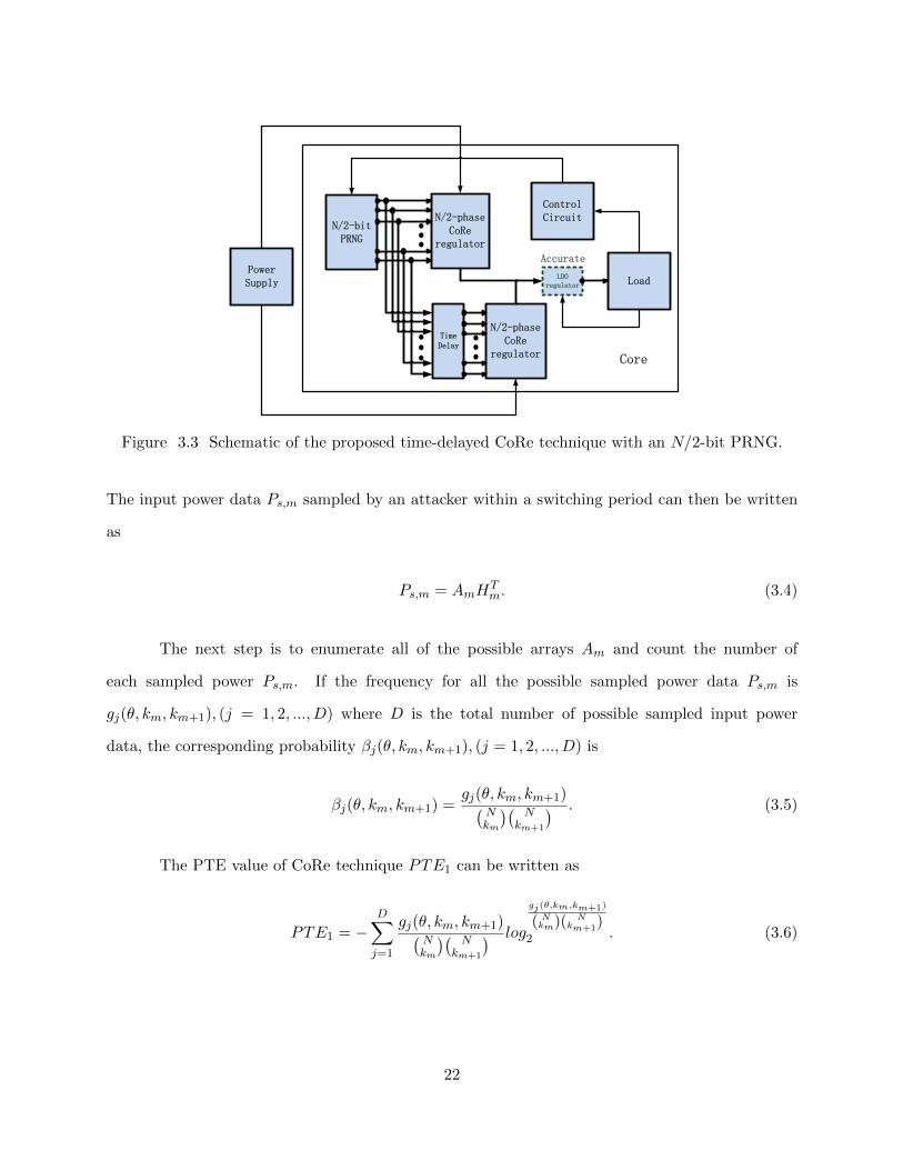
A time-delayed CoRe technique is proposed to scramble the monitored power consumption
so that an attacker will no longer extract meaningful information from the side-channel leakage. In
this technique, half of the converter stages in the CoRe scheme will be activated and gated with a
time delay, as shown in Fig. 3.3. An N/2-bit PRNG is used to generate the gate signal.
23
An array Bm is defined to represent the input power information from (m−1)Ts to (m+2)Ts,
as shown in Fig. 3.4, as
Bm = [b(m−1),1, ..., b(m−1),N/2, b(m−1),N/2+1,
..., b(m−1),N , b(m−1),N+1, ..., b(m−1),3N/2]P0, (3.7)
where b(m−1),i ∈ 0, 1, (i = 1, 2, ..., 3N/2) and
[
N/2∑i=1
b(m−1),i,
N∑i=N/2+1
b(m−1),i,
3N/2∑i=N+1
b(m−1),i]
= [km−1/2, km/2, km+1/2]. (3.8)
In time-delayed CoRe, instead of Hm, there are two different arrays Zm = [z1, z2, ..., z3N/2] and
Wm = [w1, w2, ..., w3N/2] which represent, respectively, the power data monitored by an attacker
from the conventional N/2 phases and time-delayed N/2 phases. zi and wi can be written as
zi =
0 , i ≤ [(θ/360) ∗ (N/2)] +N/2
1 , [ θ360 ∗
N2 ] + N
2 < i ≤ [ θ360 ∗
N2 ] +N
0 , i > [(θ/360) ∗ (N/2)] +N ,
(3.9)
wi =
0 , i ≤ [((θ − α)/360) ∗ (N/2)] +N/2
1 , [ (θ−α)360 ∗N2 ] + N
2 < i ≤ [ (θ−α)360 ∗N2 ] +N
0 , i > [((θ − α)/360) ∗ (N/2)] +N ,
(3.10)
where α = (T0/Ts)∗360 is the delayed phase angle and T0 is the time delay. The input power data
P′s,m of time-delayed CoRe that is monitored by an attacker within a switching period becomes
P′s,m = BmZ
Tm +BmW
Tm. (3.11)
24

N-bit PRNG
N/2-phase CoRe
regulator
Power Supply
Accurate
N/2-phase CoRe
regulator
TimeDelay
LDO regulator Load
Control Circuit
Core
Low N/2 bits
High N/2 bits
Figure 3.5 Schematic of the proposed time-delayed CoRe technique with an N -bit PRNG.
The next step is to execute all the possible arrays Bm and count the number of each sampled
power P′s,m. If the number of all possible sampled input power data is xj(θ, km−1, km, km+1), (j =
1, 2, ..., E) where E is the total number of possible sampled input power data, then the probability
γj(θ, km−1, km, km+1), (j = 1, 2, ..., E) for all the possible input power data P′s,m sampled by the
attacker is
γj(θ, km−1, km, km+1) =xj(θ, km−1, km, km+1)( N/2km−1/2
)( N/2km/2
)( N/2km+1/2
) . (3.12)
The input power trace entropy PTE2 for time-delayed CoRe technique with an N/2-bit PRNG
therefore becomes
PTE2 = −E∑j=1
γj(θ, km−1, km, km+1)logγj(θ,km−1,km,km+1)2 . (3.13)
To investigate the effect of the PRNG bit length on the entropy level, an N -bit PRNG is
used, as shown in Fig. 3.5, as compared to the N/2-bit PRNG, as shown in Fig. 3.3. C′m and C
′′m
arrays are defined to represent the input power information of normal phases and time-delayed
25

phases from (m− 1)Ts to (m+ 2)Ts, as shown in Fig. 3.4, and can be written as
C′m = [c
′
(m−1),1, ..., c′
(m−1),N/2, c′
(m−1),N/2+1,
..., c′
(m−1),N , c′
(m−1),N+1, ..., c′
(m−1),3N/2]P0, (3.14)
C′′m = [c
′′
(m−1),1, ..., c′′
(m−1),N/2, c′′
(m−1),N/2+1,
..., c′′
(m−1),N , c′′
(m−1),N+1, ..., c′′
(m−1),3N/2]P0, (3.15)
where c′
(m−1),i, c′′
(m−1),i ∈ 0, 1, (i = 1, 2, ..., 3N/2), and
[
N/2∑i=1
(c′
(m−1),i + c′′
(m−1),i),N∑
i=N/2+1
(c′
(m−1),i + c′′
(m−1),i),
3N/2∑i=N+1
(c′
(m−1),i + c′′
(m−1),i)] = [km−1, km, km+1]. (3.16)
The input power data P′′s,m of time-delayed CoRe with N -bit PRNG monitored by an
attacker within a switching period is
P′′s,m = C
′mZ
Tm + C
′′mW
Tm. (3.17)
When all possible values of C′m and C
′′m are listed, the frequency yj(θ, km−1, km, km+1), (j =
1, 2, ..., F ) for each sampled power P′′s,m can be determined, where F is the total number of possible
sampled input power data. So the corresponding probability λj(θ, km−1, km, km+1), (j = 1, 2, ..., F )
is
λj(θ, km−1, km, km+1) =yj(θ, km−1, km, km+1)(
Nkm−1
)(Nkm
)(N
km+1
) . (3.18)
26
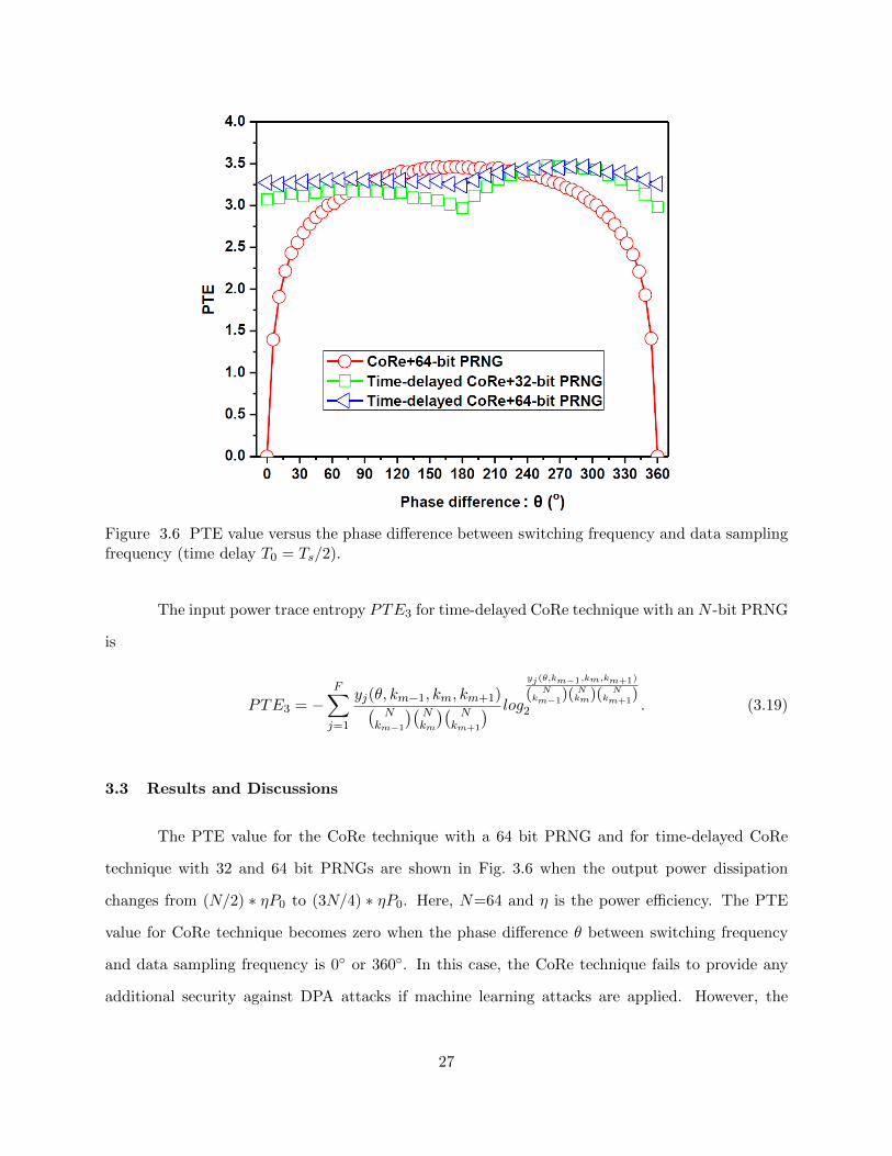
Figure 3.6 PTE value versus the phase difference between switching frequency and data samplingfrequency (time delay T0 = Ts/2).
The input power trace entropy PTE3 for time-delayed CoRe technique with an N -bit PRNG
is
PTE3 = −F∑j=1
yj(θ, km−1, km, km+1)(N
km−1
)(Nkm
)(N
km+1
) log
yj(θ,km−1,km,km+1)
( Nkm−1
)( Nkm)( Nkm+1
)2 . (3.19)
3.3 Results and Discussions
The PTE value for the CoRe technique with a 64 bit PRNG and for time-delayed CoRe
technique with 32 and 64 bit PRNGs are shown in Fig. 3.6 when the output power dissipation
changes from (N/2) ∗ ηP0 to (3N/4) ∗ ηP0. Here, N=64 and η is the power efficiency. The PTE
value for CoRe technique becomes zero when the phase difference θ between switching frequency
and data sampling frequency is 0 or 360. In this case, the CoRe technique fails to provide any
additional security against DPA attacks if machine learning attacks are applied. However, the
27
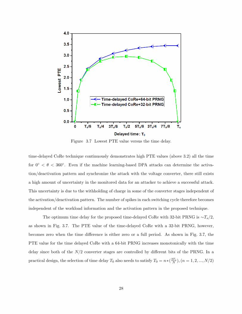
Figure 3.7 Lowest PTE value versus the time delay.
time-delayed CoRe technique continuously demonstrates high PTE values (above 3.2) all the time
for 0 < θ < 360. Even if the machine learning-based DPA attacks can determine the activa-
tion/deactivation pattern and synchronize the attack with the voltage converter, there still exists
a high amount of uncertainty in the monitored data for an attacker to achieve a successful attack.
This uncertainty is due to the withholding of charge in some of the converter stages independent of
the activation/deactivation pattern. The number of spikes in each switching cycle therefore becomes
independent of the workload information and the activation pattern in the proposed technique.
The optimum time delay for the proposed time-delayed CoRe with 32-bit PRNG is ∼Ts/2,
as shown in Fig. 3.7. The PTE value of the time-delayed CoRe with a 32-bit PRNG, however,
becomes zero when the time difference is either zero or a full period. As shown in Fig. 3.7, the
PTE value for the time delayed CoRe with a 64-bit PRNG increases monotonically with the time
delay since both of the N/2 converter stages are controlled by different bits of the PRNG. In a
practical design, the selection of time delay T0 also needs to satisfy T0 = n∗(2TsN ), (n = 1, 2, ..., N/2)
28
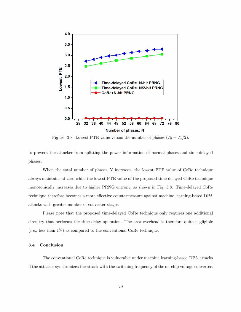
Figure 3.8 Lowest PTE value versus the number of phases (T0 = Ts/2).
to prevent the attacker from splitting the power information of normal phases and time-delayed
phases.
When the total number of phases N increases, the lowest PTE value of CoRe technique
always maintains at zero while the lowest PTE value of the proposed time-delayed CoRe technique
monotonically increases due to higher PRNG entropy, as shown in Fig. 3.8. Time-delayed CoRe
technique therefore becomes a more effective countermeasure against machine learning-based DPA
attacks with greater number of converter stages.
Please note that the proposed time-delayed CoRe technique only requires one additional
circuitry that performs the time delay operation. The area overhead is therefore quite negligible
(i.e., less than 1%) as compared to the conventional CoRe technique.
3.4 Conclusion
The conventional CoRe technique is vulnerable under machine learning-based DPA attacks
if the attacker synchronizes the attack with the switching frequency of the on-chip voltage converter.
29
Time-delayed CoRe technique delays half of the converter stages, making it infeasible to synchronize
the attack with the switching frequency. An analytical expression for the PTE is developed to
evaluate the security-performance of the conventional and time-delayed CoRe techniques. The
lowest PTE value of the time-delayed CoRe technique is enhanced significantly even under machine
learning-based DPA attacks.
30
CHAPTER 4:
CHARGE-WITHHELD CONVERTER-RESHUFFLING TECHNIQUE
4.1 Motivation
Converter-reshuffling (CoRe) technique in Chapter 2 utilizes a multi-phase switched ca-
pacitor (SC) voltage converter and is based on converter-gating (CoGa) [4] as a countermeasure
against DPA attacks with negligible power overhead1. The number of required converter stages is
determined based on the workload information whereas the activation pattern of these stages is de-
termined by a pseudo-random number generator (PRNG) to scramble the input power profile of the
voltage converter. As a result, if an attacker is unable to synchronize the sampling frequency of the
power data with the switching frequency of the on-chip voltage converter, a large amount of noise
is inserted within the leakage data that is sampled by the attacker. Alternatively, if the attacker
is able to synchronize the attack with the switching frequency of the on-chip voltage converter by
using machine-learning attacks, the scrambled power data can be unscrambled by the attacker and
the CoRe technique may effectively be neutralized. The reason is that the total number of acti-
vated phases within a switching period has a high correlation with the load power dissipation. A
charge-withheld CoRe technique is proposed in this Chapter to prevent the attacker from acquiring
accurate load power information even if the attacker can synchronize the data sampling.
The switching frequency fs of an SC voltage converter is proportional to the output power
Pout [52]. The fluctuations in fs therefore can leak critical workload information to the attacker. In
the proposed charge-withheld CoRe technique, fs is kept constant under varying workload condi-
tions (i.e., fs is workload-agnostic) to minimize the leakage of workload information. Instead, the
number of activated phases is adaptively changed to satisfy the workload demand. As compared to
1The content of this Chapter has been published in [56], the copyright permission can be found in Appendix F.
31

N-bit
PRNG
N-phase SC ConverterLDO
RegulatorLoad
Time delay
ΔT1
Power Supply
Turn on km+g phasesRandomly choose km+g phases
for charging and discharging
Time delay
ΔT2
Time delay
ΔTN-1
Time delay
ΔTN
PRNG1
PRNG2
PRNGN-1
PRNGN
PRNG’1
PRNG’2
PRNG’N-1
PRNG’N
Figure 4.1 Architecture of the conventional CoRe technique.
the CoRe technique where only a single PRNG is utilized, as shown in Fig. 4.1, the charging and
discharging states of the flying capacitors in the charge-withheld CoRe technique are controlled by
two independent PRNGs (PRNG1 and PRNG2), as illustrated in Fig. 4.4. For instance, for an
N -phase charge-withheld CoRe technique, if the load requires to activate km+g additional phases
based on the workload, the PRNG1 would randomly select Vm+g, (km+g ≤ Vm+g ≤ N) phases for
charging. When the charging period ends, the PRNG2 would choose km+g phases out of the selected
Vm+g phases for discharging. As a result, the energy stored in the corresponding (Vm+g − km+g)
phases is used for power delivery in the next couple of switch cycles. With this charge withhold-
ing technique, the total number of activated phases within a switching period is no longer highly
correlated with the actual load power consumption.
4.2 Architecture Design
4.2.1 Architecture of the Converter-Reshuffling (CoRe) Technique
In the conventional CoRe technique, the activation/deactivation pattern of a multi-phase
SC voltage converter is controlled by an N -bit PRNG, as shown in Fig. 1.1. The PRNG produces
an N -bit random sequence PRNGi, (i = 1, 2, ..., N) that is delayed by ∆Ti to get synchronized
32
Vin Vout
Cfly
S1, i S2, i
S3, i S4, i
V1(t)
V2(t)
Figure 4.2 One of the identical 2:1 SC voltage converter stages in CoRe.
S1,i, S4,i
S2,i, S3,i
CLKi
Charging stage
Discharging stage
Off-state stage
PRNG’i
Off-state stage
(m+i/N)Ts(m+1+i/N)Ts (m+2+i/N)Ts
The ith phase turned on
The ith phase turned off
Figure 4.3 Logic level of the signals that control the switches (S1,i, S2,i, S3,i, S4,i) within the CoRetechnique.
with the clock signal CLKi generated by a phase shifter. The time delay ∆Ti is
∆Ti =i
NTs, (4.1)
where Ts = 1/fs is the switching period. An optional low-dropout (LDO) regulator can be utilized
at the output of the CoRe technique if the number of phases N in the SC converter is not sufficient
to meet the accuracy requirement of the load.
A high-level schematic of one of the identical phases within the multi-phase SC converter
is shown in Fig. 4.2. The time delayed signal PRNG′i, (i = 1, 2, ..., N), as illustrated in Fig. 4.1,
with the clock signal CLKi controls the states of switches (S1,i, S2,i, S3,i, S4,i) in the ith converter
33
Time delay
ΔTN-1
N-bit
PRNG1
N-phase SC Converter
N-bit
PRNG2
LDO
RegulatorLoad
Time delay
ΔT1
Power Supply
Turn on km+g phases
Charging
Controller
Discharging
Controller
Randomly turn-on
km+g phases for
discharging
Randomly turn-on Vm+g,
(km+g≤Vm+g≤N) phases for charging
Turn on n phases
Time delay
ΔT2
Time delay
ΔTN-1
Time delay
ΔTN
Time delay
ΔT2
Time delay
ΔT1
Time delay
ΔTN
PRNG1, 1
PRNG1, 2
PRNG1, N-1
PRNG1, N
PRNG’1, 1
PRNG’1, 2
PRNG’1, N-1
PRNG’1, N
PRNG2, 1
PRNG2, 2
PRNG2,N-1
PRNG2, N
PRNG’2, 1
PRNG’2, 2
PRNG’2, N-1
PRNG’2, N
Figure 4.4 Architecture of the proposed charge-withheld CoRe technique.
stage as follows
S1,i, S4,i = PRNG′i ⊗ CLKi, (4.2)
S2,i, S3,i = PRNG′i ⊗ CLKi. (4.3)
The corresponding signal waveforms controlling the switches (S1,i, S2,i, S3,i, S4,i) are illustrated in
Fig. 4.3. The signal PRNG′i is a binary variable and utilized to determine whether the ith phase
should be turned-on or turned-off within the next switching cycle. The circuit level implementation
details of the CoRe technique can be found in [4] and [11].
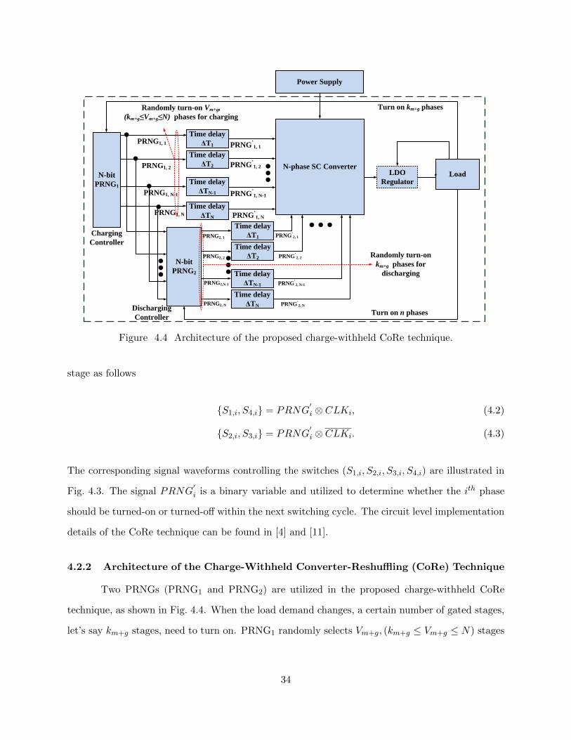
4.2.2 Architecture of the Charge-Withheld Converter-Reshuffling (CoRe) Technique
Two PRNGs (PRNG1 and PRNG2) are utilized in the proposed charge-withheld CoRe
technique, as shown in Fig. 4.4. When the load demand changes, a certain number of gated stages,
let’s say km+g stages, need to turn on. PRNG1 randomly selects Vm+g, (km+g ≤ Vm+g ≤ N) stages
34

S1,i, S4,i
S2,i, S3,i
CLKi
Charging stage
Discharging stage
Off-state stage
PRNG’1,i
Off-state stage
(m+i/N)Ts(m+1+i/N)Ts (m+2+i/N)Ts
The ith phase turned on for
charging
The ith phase turned on for
discharging
PRNG’2,i
Figure 4.5 Logic level of the signals that control the switches (S1,i, S2,i, S3,i, S4,i) within thecharge-withheld CoRe technique.
and concurrently transmits the logic signal PRNG1,i, (i = 1, 2, ..., N) both to the corresponding
converter stages and to PRNG2. The ith converter stage turns-on if the corresponding PRNG′1,i
value is 1. During the discharging stage, when PRNG2 receives data generated by PRNG1, after
half a switching period, PRNG2 sends out signal PRNG2,i, (i = 1, 2, ..., N) to discharge km+g
phases out of the selected Vm+g phases by PRNG1. Under this condition, the stages that charge
and discharge are independent and controlled, respectively, by PRNG1 and PRNG2. The state of
the switches (S1,i, S2,i, S3,i, S4,i) in charge-withheld CoRe technique is
S1,i, S4,i = PRNG′1,i ⊗ CLKi, (4.4)
S2,i, S3,i = PRNG′2,i ⊗ CLKi, (4.5)
where PRNG′1,i and PRNG
′2,i are, respectively, the delayed output signal from PRNG1 and
PRNG2. As compared to the conventional CoRe technique, the signal waveforms of switches
(S1,i, S2,i, S3,i, S4,i) in charge-withheld CoRe are controlled by two different PRNGs, as shown in
Fig. 4.5. PRNG1 controls the switches (S1,i, S4,i) for charging while PRNG2 controls the switches
(S2,i, S3,i) for discharging.
35
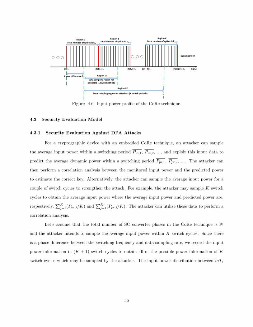
TimemTs (m+1)Ts (m+2)Ts
Input power
Total number of spikes is km
Phase difference θ
Data sampling region for attackers (1 switch period)
Region 01
Region 0 Region 1Total number of spikes is km+KTotal number of spikes is km+1
Region K
Region 0K
Data sampling region for attackers (K switch periods)
(m+K)Ts (m+K+1)Ts
Figure 4.6 Input power profile of the CoRe technique.
4.3 Security Evaluation Model
4.3.1 Security Evaluation Against DPA Attacks
For a cryptographic device with an embedded CoRe technique, an attacker can sample
the average input power within a switching period Pin,1, Pin,2, ..., and exploit this input data to
predict the average dynamic power within a switching period Ppr,1, Ppr,2, .... The attacker can
then perform a correlation analysis between the monitored input power and the predicted power
to estimate the correct key. Alternatively, the attacker can sample the average input power for a
couple of switch cycles to strengthen the attack. For example, the attacker may sample K switch
cycles to obtain the average input power where the average input power and predicted power are,
respectively,∑K
j=1(Pin,j/K) and∑K
j=1(Ppr,j/K). The attacker can utilize these data to perform a
correlation analysis.
Let’s assume that the total number of SC converter phases in the CoRe technique is N
and the attacker intends to sample the average input power within K switch cycles. Since there
is a phase difference between the switching frequency and data sampling rate, we record the input
power information in (K + 1) switch cycles to obtain all of the possible power information of K
switch cycles which may be sampled by the attacker. The input power distribution between mTs
36
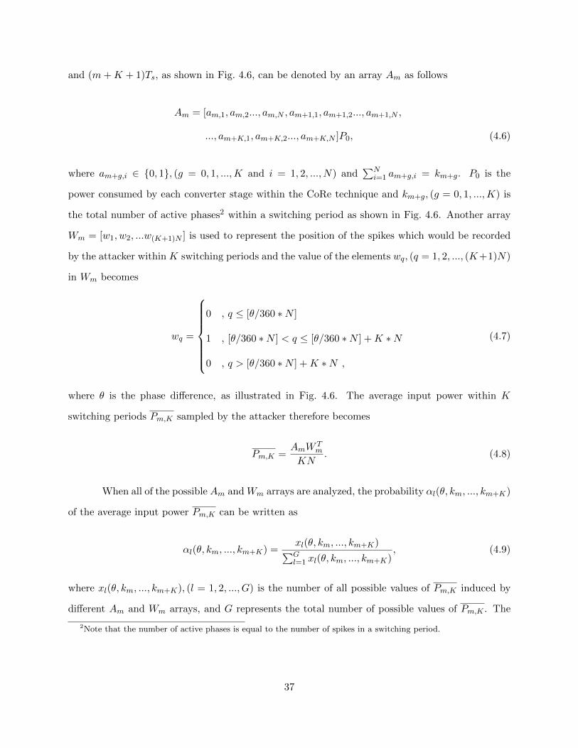
and (m+K + 1)Ts, as shown in Fig. 4.6, can be denoted by an array Am as follows
Am = [am,1, am,2..., am,N , am+1,1, am+1,2..., am+1,N ,
..., am+K,1, am+K,2..., am+K,N ]P0, (4.6)
where am+g,i ∈ 0, 1, (g = 0, 1, ...,K and i = 1, 2, ..., N) and∑N
i=1 am+g,i = km+g. P0 is the
power consumed by each converter stage within the CoRe technique and km+g, (g = 0, 1, ...,K) is
the total number of active phases2 within a switching period as shown in Fig. 4.6. Another array
Wm = [w1, w2, ...w(K+1)N ] is used to represent the position of the spikes which would be recorded
by the attacker within K switching periods and the value of the elements wq, (q = 1, 2, ..., (K+1)N)
in Wm becomes
wq =
0 , q ≤ [θ/360 ∗N ]
1 , [θ/360 ∗N ] < q ≤ [θ/360 ∗N ] +K ∗N
0 , q > [θ/360 ∗N ] +K ∗N ,
(4.7)
where θ is the phase difference, as illustrated in Fig. 4.6. The average input power within K
switching periods Pm,K sampled by the attacker therefore becomes
Pm,K =AmW
Tm
KN. (4.8)
When all of the possible Am and Wm arrays are analyzed, the probability αl(θ, km, ..., km+K)
of the average input power Pm,K can be written as
αl(θ, km, ..., km+K) =xl(θ, km, ..., km+K)∑Gl=1 xl(θ, km, ..., km+K)
, (4.9)
where xl(θ, km, ..., km+K), (l = 1, 2, ..., G) is the number of all possible values of Pm,K induced by
different Am and Wm arrays, and G represents the total number of possible values of Pm,K . The
2Note that the number of active phases is equal to the number of spikes in a switching period.
37
power trace entropy (PTE) of CoRe technique PTECR(θ) then becomes
PTECR(θ) = −G∑l=1
HllogHl2 , (4.10)
Hl = αl(θ, km, ..., km+K), (4.11)
and the average PTE value of the CoRe technique PTECR is
PTECR =
∫ 3600 PTECR(θ)dθ
360. (4.12)
For the charge-withheld CoRe technique, we define a matrix Bm(K + 1, N) to denote the
phase sequences that are selected for charging within (K+ 1) consecutive switch cycles by PRNG1.
Bm(K + 1, N) can be written as
Bm(K + 1, N) =
bm,1 . . . bm,N
bm+1,1 . . . bm+1,N
. . . . .
. . . . .
. . . . .
bm+K,1 . . . bm+K,N
, (4.13)
where bm+g,i ∈ 0, 1, (g = 0, 1, ...,K and i = 1, 2, ..., N) and km+g ≤ Vm+g =∑N
i=1 bm+g,i ≤ N .
Another matrix Cm(K+1, N) is defined to record whether the flying capacitor in the corresponding
converter stage has already withheld charge or not before being selected by PRNG1 for charging.
Note the elements cm+g,i in matrix Cm(K+1, N) are also binary. Accordingly, only the ith converter
stage which is selected for charging and does not have withheld charge from the previous cycles
can exhibit the related power spike in the input power profile. Additionally, we define a matrix
Dm(K + 1, N) to reflect the input power information within the (K + 1) consecutive switching
38
periods. Note that the elements dm+g,i in Dm(K + 1, N) satisfy the following expression
dm+g,i = (bm+g,i ⊗ 1)⊗ (cm+g,i ⊗ 1). (4.14)
Another binary (K + 1)×N matrix Em(K + 1, N) is used to record the phases which are
chosen by PRNG2 for discharging. The relationship between the elements em+g,i in Em(K + 1, N)
and bm+g,i is
bm+g,i − em+g,i ≥ 0, (4.15)
N∑i=1
(bm+g,i ⊗ em+g,i) = km+g. (4.16)
Finally, in the voltage conversion system, the number of charged phases needs to be equal
to the number of discharged phases plus the number of charge-withheld phases all the time. This
constraint is satisfied as
cm+g+1,i = cm+g,i + dm+g,i − em+g,i. (4.17)
After all of the elements dm+g,i in Dm(K + 1, N) have been obtained, the matrix Dm(K +
1, N) can be converted into a 1× (K + 1)N array A′m which is similar to the array Am as
A′m = [dm,1, dm,2..., dm,N , dm+1,1, dm+1,2..., dm+1,N ,
..., dm+K,1, dm+K,2..., dm+K,N ]P0. (4.18)
After satisfying all of the aforementioned constraints, the PTE value of the proposed charge-
withheld CoRe technique can be determined with (4.10).
4.3.2 Security Evaluation Against Machine Learning (ML)-Based DPA Attacks
To perform a successful ML based DPA attack, two steps are required. The first step is
to determine the switching period and phase difference (Ts, θ) with machine-learning attacks. The
39

second step is to synchronize the data sampling rate with the switching frequency. To estimate
the switching period Ts, the attacker can apply a number of random input data to determine the
minimum time gap ∆Ts between the two adjacent spikes in the input power profile. For an N -
phase SC converter, the switching period Ts is equal to N∆Ts, therefore the attacker only needs
to determine the number of phases N to acquire the correct Ts.
Assume that the attacker estimates the switching period as Ts = F∆Ts, (F = 1, 2, ...) and
sequentially applies two different input data (data1 and data2) with the frequency f0 = 1/(F∆Ts).
The attacker then estimates θ = [0 : 360/F : 360] as all of the possible phase difference scenarios
between the attack and switching frequency to synchronize the attack. If the estimation of (F, θ)
is correct, the total number of spikes km+g, as illustrated in Fig. 4.6, can be written as
km+g = k′, (g = 0, 2, 4, ...) (4.19)
km+g = k′′, (g = 1, 3, 5, ...), (4.20)
where k′
and k′′
are, respectively, the total number of input power spikes due to inputs data1
and data2. In this case, the total number of input power spikes within two consecutive switching
periods is (k′
+ k′′), which is a constant value. If the attacker can synchronize the attack such
that a constant average power profile in any two consecutive switching periods is obtained, the
correct switching period and phase difference (Ts, θ) are successfully determined. Once the correct
(Ts, θ) are obtained, the attacker can eliminate all of the noise inserted by the CoRe technique and
perform a successful DPA attack.
ML based DPA attacks are rather difficult to implement for the charge-withheld CoRe
technique as the total number of spikes within a switching period is variable. Even if the attacker
can obtain the information about (Ts, θ) and synchronize the attack with the switching frequency,
the attacker can only eliminate the noise data induced by the CoRe technique. However, the noise
data due to the charge-withholding operation cannot be eliminated with ML based DPA attacks.
40
4.4 Efficiency Analysis
During the charge-withholding operation, a number of flying capacitors within a multi-
stage SC voltage converter are charged. Some of these capacitors maintain the charge for a random
number of cycles, instead of discharging after each charging phase. The power dissipation in the
form of leakage from the flying capacitors is investigated in this section.
For a multi-phase 2:1 SC converter, as shown in Fig. 4.2, the top plate voltage V1(t) and
the bottom plate voltage V2(t) of the flying capacitor in a charge-withheld phase can be denoted
as follows
V1(t) = (Vin − Vout)e(−t/RoffCfly,top) + Vout, (4.21)
V2(t) = Voute(−t/RoffαCfly,top), (4.22)
where Vin and Vout are, respectively, the input and output voltages. t is the discharging time, Roff
is the off-state resistance of the MOSFET switch, Cfly,top is the top plate flying capacitance and α
is the bottom plate capacitance ratio. The total dissipated energy ratio µ(t) of the flying capacitor
due to the charge leakage can be written as
µ(t) = 1−12Cfly,topV
21 (t) + 1
2αCfly,topV22 (t)
12Cfly,topV
2in + 1
2αCfly,topV2out
. (4.23)
By substituting (4.21) and (4.22) into (4.23), the number of switch cycles M (M = t/Ts) required
to deplete the corresponding energy in a flying capacitor can be obtained.
The number of switch cycles M required to dissipate 1% of the total stored energy in the
flying capacitor through leakage is about 101 cycles assuming a flying capacitor Cfly,top=1 pF, the
bottom plate capacitance ratio α = 6.5% [57], input voltage Vin=1.2 V [58], switching frequency
fs=60 MHz [58], and off-state resistance of a MOSFET in 90 nm [58] Roff=240 MΩ. The proposed
charge-withholding technique therefore practically does not cause any efficiency degradation due
to the charge leakage from the flying capacitors during the withholding operation.
41
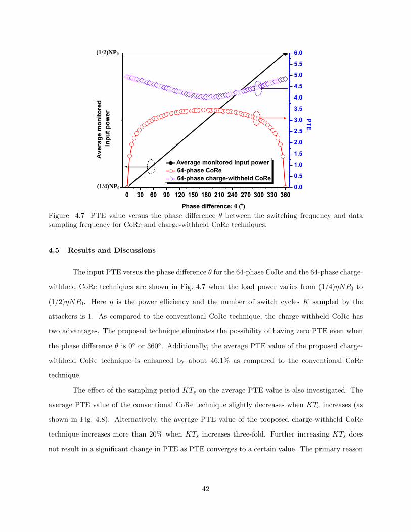
0 30 60 90 120 150 180 210 240 270 300 330 360
0
6
Average monitored input power
64-phase CoRe
64-phase charge-withheld CoRe
Phase difference
Av
era
ge
mo
nit
ore
d
inp
ut
po
we
r
0.0
0.5
1.0
1.5
2.0
2.5
3.0
3.5
4.0
4.5
5.0
5.5
6.0
PT
E
(1/4)NP0
(1/2)NP0
: θ (o)
Figure 4.7 PTE value versus the phase difference θ between the switching frequency and datasampling frequency for CoRe and charge-withheld CoRe techniques.
4.5 Results and Discussions
The input PTE versus the phase difference θ for the 64-phase CoRe and the 64-phase charge-
withheld CoRe techniques are shown in Fig. 4.7 when the load power varies from (1/4)ηNP0 to
(1/2)ηNP0. Here η is the power efficiency and the number of switch cycles K sampled by the
attackers is 1. As compared to the conventional CoRe technique, the charge-withheld CoRe has
two advantages. The proposed technique eliminates the possibility of having zero PTE even when
the phase difference θ is 0 or 360. Additionally, the average PTE value of the proposed charge-
withheld CoRe technique is enhanced by about 46.1% as compared to the conventional CoRe
technique.
The effect of the sampling period KTs on the average PTE value is also investigated. The
average PTE value of the conventional CoRe technique slightly decreases when KTs increases (as
shown in Fig. 4.8). Alternatively, the average PTE value of the proposed charge-withheld CoRe
technique increases more than 20% when KTs increases three-fold. Further increasing KTs does
not result in a significant change in PTE as PTE converges to a certain value. The primary reason
42

1 2 3 4 5
2.0
2.5
3.0
3.5
4.0
4.5
5.0
5.5
6.0
Av
era
ge
PT
E
Sampling period: K
64-phase charge-withheld CoRe
32-phase charge-withheld CoRe
64-phase CoRe
Ts Ts
Ts
Ts Ts Ts
Figure 4.8 Average PTE value versus the number of switch cycles sampled by the attacker forCoRe and charge-withheld CoRe techniques.
for the convergence of PTE is that as the attacker increases the sampling period, the probability for
the withheld charge to be delivered to the power grid within the same sampling period increases.
Since the effective number of charge withholding from one sampling cycle to another sampling cycle
reduces by increasing the attacker’s sampling period, the PTE value converges to a constant value.
Lastly, the impact of the number of stages within the SC voltage converter on the average PTE
value is investigated, as shown in Fig. 4.9. The average PTE value increases with a larger number
of phases N for both conventional and charge-withheld CoRe techniques. The average PTE value
of the proposed charge-withheld CoRe technique, however, has a steeper slope, indicating better
security-performance against DPA attacks with a larger number of converter phases.
The flying capacitors that withhold charge in the charge-withheld CoRe technique cannot
be utilized as a filter capacitor as these capacitors are not connected to the output node during the
charge-withholding operation. This would slightly increase the output voltage ripple. For example,
the amplitude of the output ripple voltage increases less than 2.5 mV for a 32 phase SC voltage
43
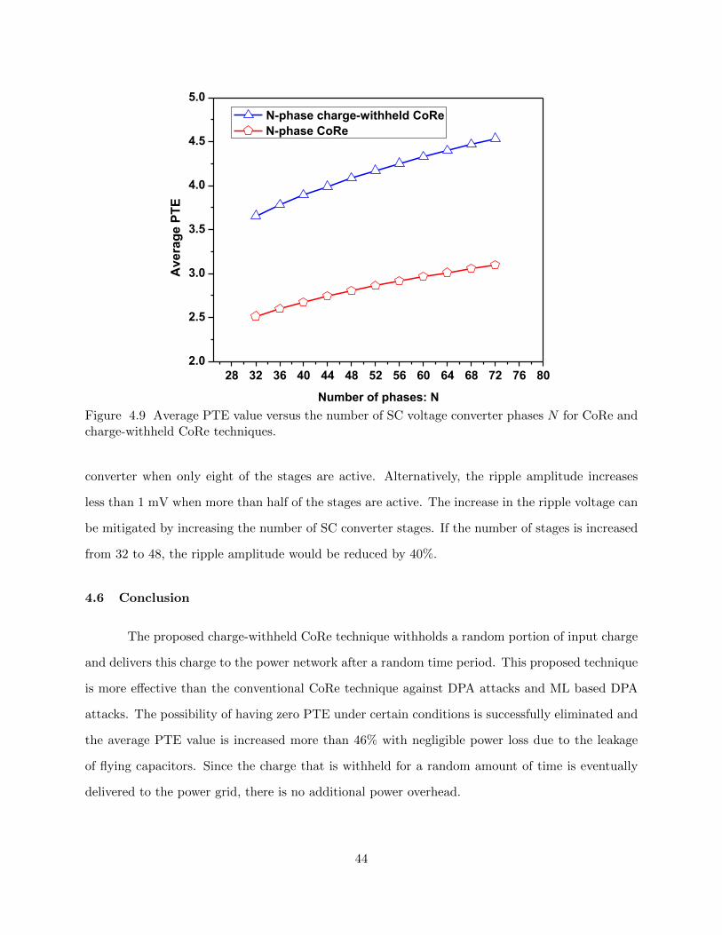
28 32 36 40 44 48 52 56 60 64 68 72 76 80
2.0
2.5
3.0
3.5
4.0
4.5
5.0
Av
era
ge
PT
E
Number of phases: N
N-phase charge-withheld CoRe
N-phase CoRe
Figure 4.9 Average PTE value versus the number of SC voltage converter phases N for CoRe andcharge-withheld CoRe techniques.
converter when only eight of the stages are active. Alternatively, the ripple amplitude increases
less than 1 mV when more than half of the stages are active. The increase in the ripple voltage can
be mitigated by increasing the number of SC converter stages. If the number of stages is increased
from 32 to 48, the ripple amplitude would be reduced by 40%.
4.6 Conclusion
The proposed charge-withheld CoRe technique withholds a random portion of input charge
and delivers this charge to the power network after a random time period. This proposed technique
is more effective than the conventional CoRe technique against DPA attacks and ML based DPA
attacks. The possibility of having zero PTE under certain conditions is successfully eliminated and
the average PTE value is increased more than 46% with negligible power loss due to the leakage
of flying capacitors. Since the charge that is withheld for a random amount of time is eventually
delivered to the power grid, there is no additional power overhead.
44

CHAPTER 5:
CO-DESIGNING CORE TECHNIQUE WITH AES ENGINE
5.1 Introduction
DPA attacks are high efficiency and low cost power attacks, which are widely utilized
by attackers to leak the critical information of cryptographic circuit1. Various countermeasures
have been proposed against DPA attacks [7, 60–64]. Although certain countermeasures are quite
effective to increase the trustworthiness of modern integrated circuits (ICs), the corresponding
power, area, and performance overheads of existing countermeasures are typically quite large to be
widely utilized.
There is a growing trend to integrate voltage regulators (VRs) fully on-chip in modern ICs
to reduce the power noise, improve transient response time and increase power efficiency [65–68].
A one-to-one relationship exists between the input current Iin and load current Iload, as shown in
Fig. 5.1, when a conventional on-chip VR (such as a low-dropout (LDO) regulator, a buck converter,
and a switched-capacitor (SC) converter) is utilized. Therefore, an attacker can determine what
is going on inside a CC by monitoring the input power profile of a conventional on-chip VR [54].
To break the one-to-one relationship between the input current and load current, converter-gating
(CoGa) technique is proposed in [4] to achieve a non-injective relationship between the input current
and output current. A multi-phase SC converter is utilized in the CoGa technique where the total
number of active converter phases is adaptively altered based on the load power requirement to
achieve a high power conversion efficiency [4]. A pseudo-random number generator (PRNG) is
also inserted to randomize the sequence of the activated phases when the load current changes.
However, if the variation in the load current is small, as shown in Fig. 5.2, CoGa technique is not
1The content of this Chapter has been published in [59], the copyright permission can be found in Appendix F.
45
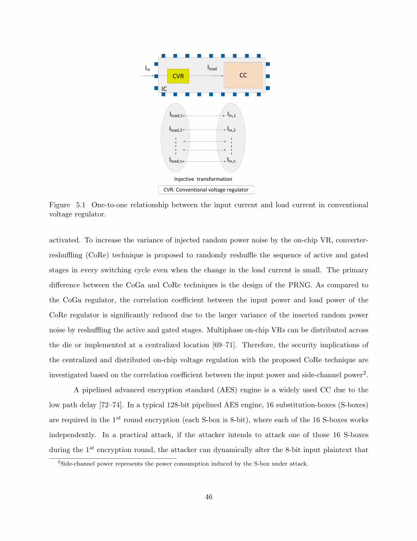
CVR: Conventional voltage regulator
Injective transformation
CCIin Iload
CVR
IC
Iin,1
Iin,2
Iin,n
- -
- -
-
Iload,1
Iload,2
Iload,n
- -
- -
-
Figure 5.1 One-to-one relationship between the input current and load current in conventionalvoltage regulator.
activated. To increase the variance of injected random power noise by the on-chip VR, converter-
reshuffling (CoRe) technique is proposed to randomly reshuffle the sequence of active and gated
stages in every switching cycle even when the change in the load current is small. The primary
difference between the CoGa and CoRe techniques is the design of the PRNG. As compared to
the CoGa regulator, the correlation coefficient between the input power and load power of the
CoRe regulator is significantly reduced due to the larger variance of the inserted random power
noise by reshuffling the active and gated stages. Multiphase on-chip VRs can be distributed across
the die or implemented at a centralized location [69–71]. Therefore, the security implications of
the centralized and distributed on-chip voltage regulation with the proposed CoRe technique are
investigated based on the correlation coefficient between the input power and side-channel power2.
A pipelined advanced encryption standard (AES) engine is a widely used CC due to the
low path delay [72–74]. In a typical 128-bit pipelined AES engine, 16 substitution-boxes (S-boxes)
are required in the 1st round encryption (each S-box is 8-bit), where each of the 16 S-boxes works
independently. In a practical attack, if the attacker intends to attack one of those 16 S-boxes
during the 1st encryption round, the attacker can dynamically alter the 8-bit input plaintext that
2Side-channel power represents the power consumption induced by the S-box under attack.
46
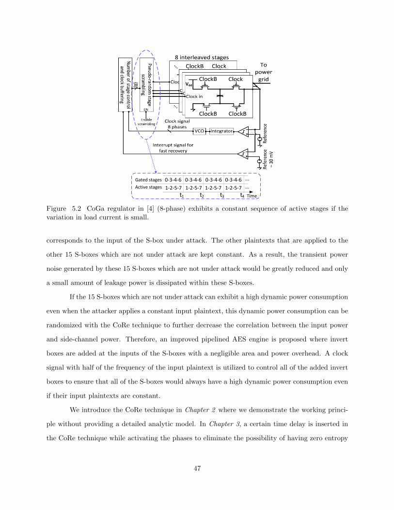
Gated stages
Time
1-2-5-7
0-3-4-6
1-2-5-7
0-3-4-6
1-2-5-7
0-3-4-6 0-3-4-6
1-2-5-7Active stages
t1 t2 t3 t4
...
...
Vdd
Figure 5.2 CoGa regulator in [4] (8-phase) exhibits a constant sequence of active stages if thevariation in load current is small.
corresponds to the input of the S-box under attack. The other plaintexts that are applied to the
other 15 S-boxes which are not under attack are kept constant. As a result, the transient power
noise generated by these 15 S-boxes which are not under attack would be greatly reduced and only
a small amount of leakage power is dissipated within these S-boxes.
If the 15 S-boxes which are not under attack can exhibit a high dynamic power consumption
even when the attacker applies a constant input plaintext, this dynamic power consumption can be
randomized with the CoRe technique to further decrease the correlation between the input power
and side-channel power. Therefore, an improved pipelined AES engine is proposed where invert
boxes are added at the inputs of the S-boxes with a negligible area and power overhead. A clock
signal with half of the frequency of the input plaintext is utilized to control all of the added invert
boxes to ensure that all of the S-boxes would always have a high dynamic power consumption even
if their input plaintexts are constant.
We introduce the CoRe technique in Chapter 2 where we demonstrate the working princi-
ple without providing a detailed analytic model. In Chapter 3, a certain time delay is inserted in
the CoRe technique while activating the phases to eliminate the possibility of having zero entropy
47
under machine learning attacks. A finite amount of charge is withheld in the flying capacitor for
a random amount of time in Chapter 4 to increase the entropy of the input power profile. The
key contributions of this Chapter are to lay the mathematical foundations of the CoRe technique
through a detailed analysis of the correlation between the input and output power of both conven-
tional and proposed voltage regulation techniques. The correlation coefficient and measurement to
disclose (MTD) are used as the security metric in this Chapter instead of the power trace entropy
used in [11, 54, 56]. The implications of the physical placement of the VRs on the correlation co-
efficient are investigated with centralized and distributed implementations of the CoRe regulators.
We have recently noticed that the CoRe technique with an improved pipelined AES engine inserts
both additive and multiplicative noise to the input power profile. An improved lightweight AES
engine is accordingly proposed to further scramble the input power even if the attacker applies
a constant plaintext to the S-boxes that are not under attack. The security implications of the
proposed techniques are analytically proven using the correlation coefficient and MTD.
5.2 Security of a Switching Converter against Power Analysis Attacks
The correlation coefficient between the input data and actual dynamic power dissipation of
a cryptographic circuit (CC) γ is [75]
γ '√m0
m1(5.1)
and the corresponding MTD value is [75]
MTD ∝ 1
γ2, (5.2)
where m1 is the total number of bits of the input data and m0 is the number of bits which
strongly correlates with the actual dynamic power consumption in the input data. The correlation
coefficient γ between the input data and actual dynamic power consumption is determined by the
architecture of a CC. If the architecture of a CC is not modified at runtime γ and MTD would not
have a significant variation.
48
A switching converter has two phases in each switching period: charging phase and dis-
charging phase. The average input power within a switching period strongly correlates with the
load power within that switching period. Let us assume that the switching frequency of the con-
verter is fs and the clock frequency of the CC is fc. In modern ICs, fc is typically greater than
fs [71, 76] (we assume fc = M1fs). To obtain accurate power data generated by a CC from the
input side of the switching converter, the attacker needs to sample the average input power within
a switching period as one sample of the power data. However, from a CC without a switching
converter, the attacker can obtain M1 different power data samples within that switching period.
As a result, if a CC is powered with a switching converter, the MTD is inherently enhanced M1
times, as compared to the MTD of a CC without a switching converter. Decreasing the switching
frequency is therefore an effective way to enhance the MTD value, but lower switching frequency
may increase the area of output capacitance of the voltage converter. So there is a trade-off between
the area and security of switching converters.
5.3 Correlation Analysis of On-Chip Voltage Regulators
In this section, the correlation coefficient models are presented for the CoGa and CoRe
techniques as well as for the conventional on-chip VRs.
5.3.1 Modeling Correlation Coefficient of Converter-Gating (CoGa) and Converter-
Reshuffling (CoRe) Regulators
The CoGa regulator [4] consists of two types of modulations: frequency modulation and
number of activated phases modulation. The switching frequency fs in CoGa regulator has a
narrow variation range [fs,pk − ∆fs/2, fs,pk + ∆fs/2], where fs,pk is the corresponding switching
frequency to achieve the peak power conversion efficiency and ∆fs is the amplitude of the variation
in the switching frequency fs. If fs is higher than fs,pk + ∆fs/2, an additional phase is activated to
provide more power to the load. When an additional phase is activated, fs is reduced to a nominal
value. If fs is lower than fs,pk −∆fs/2, an active phase is gated to reduce the output power while
fs is increased to a nominal value.
49
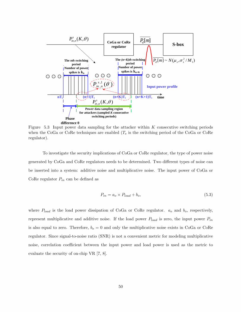
CoGa or CoRe
regulatorS-box
nTs (n+1)Ts (n+K+1)Ts time
][mPd),(, KPs
nin
)/,(~][ 1
2 MNmP ssd
Input power profile
Phase
difference θ
The (n+K)th switching
period
Number of power
spikes is kn+K
),(, KP s
nin
(n+K)Ts
)(1,
, s
ninP
Power data sampling region
for attackers (sampled K consecutive
switching periods)
The nth switching
period
Number of power
spikes is kn
Figure 5.3 Input power data sampling for the attacker within K consecutive switching periodswhen the CoGa or CoRe techniques are enabled (Ts is the switching period of the CoGa or CoReregulator).
To investigate the security implications of CoGa or CoRe regulator, the type of power noise
generated by CoGa and CoRe regulators needs to be determined. Two different types of noise can
be inserted into a system: additive noise and multiplicative noise. The input power of CoGa or
CoRe regulator Pin can be defined as
Pin = ao × Pload + bo, (5.3)
where Pload is the load power dissipation of CoGa or CoRe regulator. ao and bo, respectively,
represent multiplicative and additive noise. If the load power Pload is zero, the input power Pin
is also equal to zero. Therefore, bo = 0 and only the multiplicative noise exists in CoGa or CoRe
regulator. Since signal-to-noise ratio (SNR) is not a convenient metric for modeling multiplicative
noise, correlation coefficient between the input power and load power is used as the metric to
evaluate the security of on-chip VR [7, 8].
50

The dynamic power consumption Pd[m] of a single S-box in an AES engine induced by
the mth, (m = 1, 2, ...) input plaintext conforms to a normal distribution [75], where the mean and
variance of Pd[m] are, respectively, µs and σ2s . Assuming that the clock frequency of the AES engine
is M1 times greater than the switching frequency of the CoGa or CoRe regulator (i.e.,fc = M1fs),
the average dynamic power consumption of a single S-box within a switching period Pd[m] can be
written as
Pd[m] =
M1−1∑p=0
Pd[m+ p]
M1. (5.4)
When Pd[m], Pd[m+ 1], ..., Pd[m+M1 − 1] are mutually independent, the average dynamic power
consumption of a single S-box within a switching period Pd[m] also conforms to a normal distribu-
tion with mean µs and variance σ2s as
µs =
M1−1∑p=0
µsM1
= µs, (5.5)
σ2s =
M1−1∑p=0
(σsM1
)2 =σ2sM1
. (5.6)
The minimum and maximum average dynamic power dissipation of a single S-box within
a single switching period are, respectively, jminP0 and jmaxP0 where P0 is the power resolution.
Assuming P0 is sufficiently small, the following approximated equation can be written as
jmax∑j=jmin
P0
√M1
σs√
2πexp
(− (j×P0−µs)2
2σ2s/M1) ≈ 1. (5.7)
If the total number of input plaintexts applied by the attacker is W , the number Wj which corre-
sponds to the average dynamic power of a single S-box jP0, (j ∈ [jmin, jmax]) within a switching
51
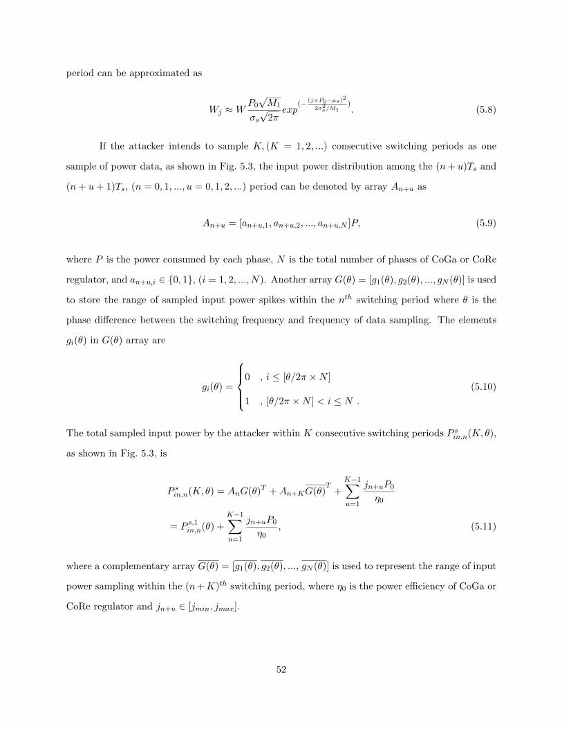
period can be approximated as
Wj ≈WP0
√M1
σs√
2πexp
(− (j×P0−µs)2
2σ2s/M1). (5.8)
If the attacker intends to sample K, (K = 1, 2, ...) consecutive switching periods as one
sample of power data, as shown in Fig. 5.3, the input power distribution among the (n+ u)Ts and
(n+ u+ 1)Ts, (n = 0, 1, ..., u = 0, 1, 2, ...) period can be denoted by array An+u as
An+u = [an+u,1, an+u,2, ..., an+u,N ]P, (5.9)
where P is the power consumed by each phase, N is the total number of phases of CoGa or CoRe
regulator, and an+u,i ∈ 0, 1, (i = 1, 2, ..., N). Another array G(θ) = [g1(θ), g2(θ), ..., gN (θ)] is used
to store the range of sampled input power spikes within the nth switching period where θ is the
phase difference between the switching frequency and frequency of data sampling. The elements
gi(θ) in G(θ) array are
gi(θ) =
0 , i ≤ [θ/2π ×N ]
1 , [θ/2π ×N ] < i ≤ N .
(5.10)
The total sampled input power by the attacker within K consecutive switching periods P sin,n(K, θ),
as shown in Fig. 5.3, is
P sin,n(K, θ) = AnG(θ)T +An+KG(θ)T
+
K−1∑u=1
jn+uP0
η0
= P s,1in,n(θ) +
K−1∑u=1
jn+uP0
η0, (5.11)
where a complementary array G(θ) = [g1(θ), g2(θ), ..., gN (θ)] is used to represent the range of input
power sampling within the (n+K)th switching period, where η0 is the power efficiency of CoGa or
CoRe regulator and jn+u ∈ [jmin, jmax].
52

For the CoRe regulator, the total number of power spikes kn+u within the (n+u)th switching
period can be determined as
kn+u = [jn+u × P0
η0 × P]. (5.12)
Additionally, the element an+u,i in An+u needs to satisfy∑N
i=1 an+u,i = kn+u.
In the CoRe regulator, the total sampled input power within the nth switching period and
the (n+K)th switching period is P s,1in,n(θ) = lP, (l = 0, 1, 2, ..., N). The number of the corresponding
input power samples can be counted as xl,jn,jn+K (θ) after all of the possible An and An+K are
enumerated. When W input plaintexts are applied by the attacker, the number of total input
power samples xl(θ) for the corresponding sampled input power P s,1in,n(θ) can be calculated as
xl(θ) =
jmax∑jn+K=jmin
jmax∑jn=jmin
WjnWjn+Kxl,jn,jn+K (θ). (5.13)
The mean value of the total sampled input power within K consecutive switching periods µin(K, θ)
becomes3
µin(K, θ) = E(P sin,n(K, θ))
= E(P s,1in,n(θ)) + E(K−1∑u=1
jn+uP0
η0)
=
∑Nl=0 lP × xl(θ)∑N
l=0 xl(θ)+ (K − 1)µ
′s, (5.14)
where µ′s is
µ′s ≈
jmax∑j=jmin
jP0
√M1
η0σs√
2πexp
(− (j×P0−µs)2
2σ2s/M1). (5.15)
3E represents the sign for the calculation of the mean value.
53
The variance of total sampled input power within K consecutive switching periods σ2in(K, θ) can
be written as4
σ2in(K, θ) = V ar(P sin,n(K, θ))
= V ar(P s,1in,n(θ)) + V ar(
K−1∑u=1
jn+uP0
η0)
=
∑Nl=0(xl(θ)× (lP − µin(θ))2)∑N
l=0 xl(θ)+ (K − 1)(σ
′s)
2, (5.16)
where (σ′s)
2 is
(σ′s)
2 =1
jmax − jmin + 1
jmax∑j=jmin
(jP0/η0 − µ′s)
2. (5.17)
The load power of the CoRe regulator Pload,n(K, θ) that corresponds to the sampled input
power P sin,n(K, θ) can be written as
Pload,n(K, θ) = (1− θ
2π)jn+1P0 +
θ
2πjn+K+1P0 +
K∑u=2
jn+uP0. (5.18)
The mean value of the load power µL(K, θ) and variance of the load power σ2L(K, θ), respectively,
are
µL(K, θ) = (1− θ
2π)µs +
θ
2πµs + (K − 1)µs = Kµs, (5.19)
σ2L(K, θ) = (1− θ
2π)σ2sM1
+θ
2π
σ2sM1
+ (K − 1)σ2sM1
=Kσ2sM1
. (5.20)
4V ar represents the sign for the calculation of the variance.
54
The correlation coefficient of the on-chip CoRe regulator γ(K, θ) is determined as5
γ(K, θ) =E(P sin,n(K, θ)× Pload,n(K, θ))
σin(K, θ)×√K/M1σs
− µin(K, θ)×Kµsσin(K, θ)×
√K/M1σs
, (5.21)
where E(P sin,n(K, θ)× Pload,n(K, θ)) is
E(P sin,n(K, θ)× Pload,n(K, θ)) =1
(jmax − jmin + 1)K+2×
(
jmax∑jn+K+1=jmin
...
jmax∑jn=jmin
((P s,1in,n(θ) +
K−1∑u=1
jn+uP0
η0)×
((1− θ
2π)jn+1P0 +
θ
2πjn+K+1P0 +
K∑u=2
jn+uP0))). (5.22)
The average correlation coefficient of the CoRe regulator γ(K) can be denoted as
γ(K) =1
2π
∫ 2π
0γ(K, θ)dθ. (5.23)
The correlation coefficient modeling of the CoGa regulator is quite similar to the modeling
of the CoRe regulator with one extra condition that needs to be added to the element an+u,i in
An+u as
an+u+1,i − an+u,i ≥ 0 , if kn+u+1 ≥ kn+u
an+u,i − an+u+1,i ≥ 0 , if kn+u < kn+u+1 .
(5.24)
5.3.2 Modeling Correlation Coefficient of Conventional On-Chip Voltage Regulators
Conventional on-chip (COC) VRs such as LDO regulator/buck converter/SC converter
typically do not insert any randomness in the input or output power profile unless their architectures
are tailored to scramble the input and output impedance characteristics. The relationship between
5The attacker sampled the total input power within K consecutive switching periods as one sample of the powerdata.
55

Figure 5.4 Phase difference versus correlation coefficient of CoGa and CoRe techniques.
the input power and load power of a COC VR can be modeled as
P′in(t+ ∆t) =
1
η1× Pload(t), (5.25)
where ∆t is the time delay between the input power and load power, η1 is the power efficiency,
P′in(t+ ∆t) is the transient input power, and Pload(t) is the load power of a COC VR.
The detailed correlation coefficient derivation of COC VRs can be found in Appendix A.
5.3.3 Validation of the Proposed Correlation Coefficient Models with Practical Pa-
rameters
Substitution-box (S-box) is a circuit which is widely used in cryptography to mask the
relationship between the secret key and ciphertext [77–79]. Since an S-box can perform a non-
linear transformation, for an S-box with m1 bits of input data, the output data can be m2 bits that
are masked through the non-linear transformations. An S-box with a clock frequency fc of 200 MHz
56
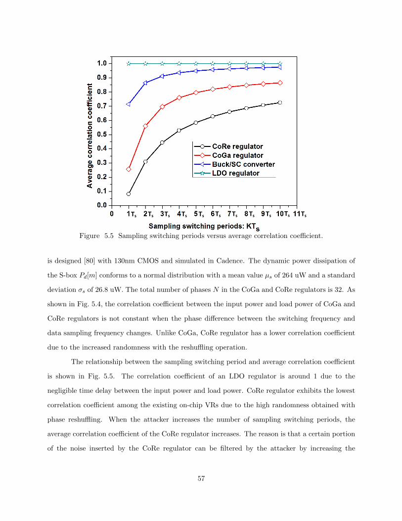
Ts Ts Ts Ts Ts Ts Ts Ts Ts Ts Ts
Figure 5.5 Sampling switching periods versus average correlation coefficient.
is designed [80] with 130nm CMOS and simulated in Cadence. The dynamic power dissipation of
the S-box Pd[m] conforms to a normal distribution with a mean value µs of 264 uW and a standard
deviation σs of 26.8 uW. The total number of phases N in the CoGa and CoRe regulators is 32. As
shown in Fig. 5.4, the correlation coefficient between the input power and load power of CoGa and
CoRe regulators is not constant when the phase difference between the switching frequency and
data sampling frequency changes. Unlike CoGa, CoRe regulator has a lower correlation coefficient
due to the increased randomness with the reshuffling operation.
The relationship between the sampling switching period and average correlation coefficient
is shown in Fig. 5.5. The correlation coefficient of an LDO regulator is around 1 due to the
negligible time delay between the input power and load power. CoRe regulator exhibits the lowest
correlation coefficient among the existing on-chip VRs due to the high randomness obtained with
phase reshuffling. When the attacker increases the number of sampling switching periods, the
average correlation coefficient of the CoRe regulator increases. The reason is that a certain portion
of the noise inserted by the CoRe regulator can be filtered by the attacker by increasing the
57

Ts Ts Ts Ts Ts Ts Ts Ts Ts Ts Ts
Figure 5.6 Sampling switching periods versus MTD enhancement ratio (M1 ≈ 5).
number of switching periods for each sampling. The cost is that more measurements are required
for a successful attack, potentially increasing the MTD.
Let’s assume that the correlation coefficient between the predicted and actual dynamic
power consumption of an S-box is γ1 and the correlation coefficient between the actual dynamic
power consumption of an S-box and input power of an on-chip VR is γ2. Since the operations that
occur in the S-box are independent of the operations of the on-chip VR, the correlation coefficient
between the input data and input power of an on-chip VR γ3 can be denoted as [75]
γ3 = γ1 × γ2. (5.26)
For a single S-box, the relationship between MTD value MTD0 and correlation coefficient γ1 is [75]
MTD0 ' C/γ21 . (5.27)
58

2 2 2 4 2 6 2 8 3 0 3 2 3 4 3 6 3 8 4 0 4 20 . 2 90 . 3 00 . 3 10 . 3 20 . 3 30 . 3 40 . 3 5
C o R e r e g u l a t o r
C o R e r e g u l a t o r
Avera
ge co
rrelat
ion co
effici
ent
N u m b e r o f p h a s e s : N
1 0 1 2 1 4 1 6 1 8 2 00 . 2 60 . 2 80 . 3 00 . 3 20 . 3 40 . 3 60 . 3 8
Avera
ge
corre
lation
coeff
icien
t
P o w e r u n d e r t a k e n b y e a c h p h a s e : P ( u W )
Figure 5.7 Number of phases and power undertaken by each phase versus average correlationcoefficient.
where C is the success rate dependent constant [75]. Accordingly, for a single S-box powered by an
on-chip VR, the measurement to disclose MTD1 becomes
MTD1 'M1K
γ22×MTD0 = R×MTD0, (5.28)
where R is the MTD enhancement ratio of a single S-box powered by an on-chip VR. As compared
to an S-box without an on-chip VR, as shown in Fig. 5.6, a single S-box with the CoRe regulator has
the highest MTD enhancement ratio. The lowest MTD enhancement ratio of the CoRe regulator
with S-box is 71.4 when the attacker optimizes the sampling duration of the attack and selects the
total input power within 4 consecutive switching periods as a single sample of the power data.
The average correlation coefficient of the CoRe regulator decreases when the total number
of phases N increases, as shown in Fig. 5.7. The reason is that when N increases, more number
of gated phases are utilized to increase the randomness of the CoRe regulator. Additionally, if
the power P consumed by each phase increases, the average correlation coefficient of the CoRe
59

regulator reduces due to the larger variance of the random noise caused by the phase reshuffling
within every switching cycle.
5.4 Conventional Pipelined (CP) AES Engine with Converter-Reshuffling
In this section, the security concerns of a conventional pipelined AES engine are presented.
Additionally, the implications of centralized and distributed on-chip voltage regulations with the
CoRe technique on the security of the AES engine are investigated.
5.4.1 Practical Power Attacks on a Pipelined AES Engine without On-Chip Voltage
Regulation
For a conventional 128-bit pipelined AES Engine, 16 S-boxes need to be placed in the 1st
round encryption block, as shown in Fig. 5.8. If an attacker intends to implement a DPA attack
on one of the 16 S-boxes in the 1st encryption round, the attacker can apply a suitable input
plaintext combination to simplify the attack. For example, when S-box1 is being targeted with a
DPA attack, the attacker can input a different 8-bit plaintext1 to combine the 8-bit cipher key1
with the input side of S-box1 sequentially while also maintaining the rest of the input plaintexts
(plaintext2, plaintext3, ..., plaintext16) as constant. As a result, S-box1 would exhibit a high dy-
namic power consumption while the other 15 S-boxes would show a low leakage power dissipation.
The leakage power generated by the other 15 S-boxes with a constant input plaintext can be treated
as an additive power noise to the S-box1 that is under attack.
5.4.2 Conventional Pipelined (CP) AES Engine with a Distributed CoRe Technique
Since 16 S-boxes exist in the 1st round encryption block of the CP AES engine, if a dis-
tributed CoRe technique is employed, 16 CoRe regulators are needed to power all of the S-boxes, as
shown in Fig. 5.9. Let us assume that the total number of phases in the distributed CoRe regulators
is N and the number of phases in each distributed CoRe regulator is N/16. In this case, the phase
60

8-bit
plaintext1
8-bit S-box1
8-bit cipher key1
8-bit
plaintext2
8-bit S-box2
8-bit cipher key2
8-bit
plaintext16
8-bit S-box16
8-bit cipher key16
Shift rows
Mix columns
Add round key
1st
round
DPA attacks
Constant
plaintext
Low leakage
power
Variable
plaintexts
Figure 5.8 1st encryption round of a typical 128-bit pipelined AES engine.
shift βy,z in each distributed CoRe regulator can be written as
βy,z =2π
N(y + 16× (z − 1)), (5.29)
where y represents the yth(y = 1, 2, ..., 16) CoRe regulator and z is the zth(z = 1, 2, ..., N/16) phase
in the yth CoRe regulator. The total sampled input power P s,din,n(K, θ) of a CP AES engine with 16
61
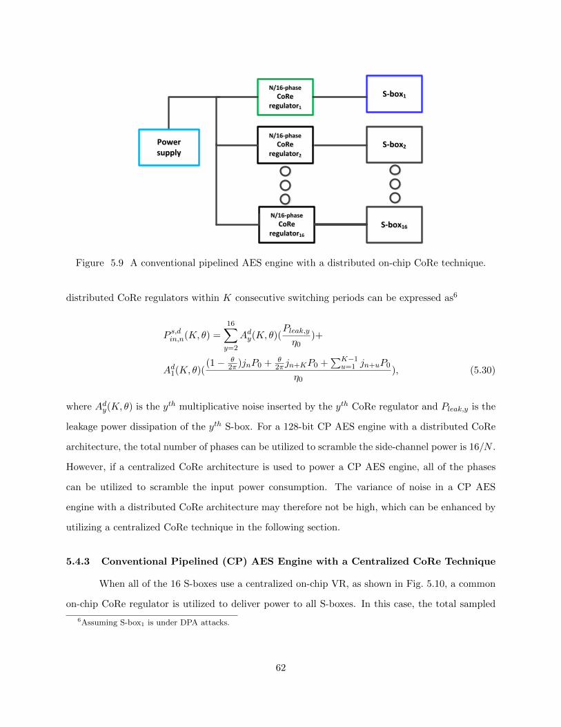
S-box1S-box1
S-box2S-box2
S-box16S-box16
N/16-phase
CoReregulator1
N/16-phase
CoReregulator1
Power supply
Power supply
N/16-phase
CoReregulator2
N/16-phase
CoReregulator2
N/16-phase
CoReregulator16
N/16-phase
CoReregulator16
Figure 5.9 A conventional pipelined AES engine with a distributed on-chip CoRe technique.
distributed CoRe regulators within K consecutive switching periods can be expressed as6
P s,din,n(K, θ) =
16∑y=2
Ady(K, θ)(Pleak,yη0
)+
Ad1(K, θ)((1− θ
2π )jnP0 + θ2π jn+KP0 +
∑K−1u=1 jn+uP0
η0), (5.30)
where Ady(K, θ) is the yth multiplicative noise inserted by the yth CoRe regulator and Pleak,y is the
leakage power dissipation of the yth S-box. For a 128-bit CP AES engine with a distributed CoRe
architecture, the total number of phases can be utilized to scramble the side-channel power is 16/N .
However, if a centralized CoRe architecture is used to power a CP AES engine, all of the phases
can be utilized to scramble the input power consumption. The variance of noise in a CP AES
engine with a distributed CoRe architecture may therefore not be high, which can be enhanced by
utilizing a centralized CoRe technique in the following section.
5.4.3 Conventional Pipelined (CP) AES Engine with a Centralized CoRe Technique
When all of the 16 S-boxes use a centralized on-chip VR, as shown in Fig. 5.10, a common
on-chip CoRe regulator is utilized to deliver power to all S-boxes. In this case, the total sampled
6Assuming S-box1 is under DPA attacks.
62
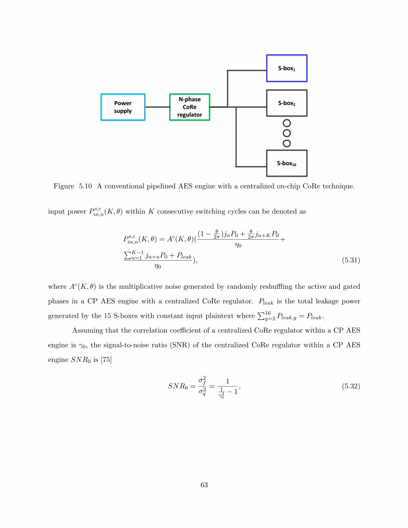
S-box1S-box1
S-box2S-box2
S-box16S-box16
N-phaseCoRe
regulator
N-phaseCoRe
regulator
Power supply
Power supply
Figure 5.10 A conventional pipelined AES engine with a centralized on-chip CoRe technique.
input power P s,cin,n(K, θ) within K consecutive switching cycles can be denoted as
P s,cin,n(K, θ) = Ac(K, θ)((1− θ
2π )jnP0 + θ2π jn+KP0
η0+∑K−1
u=1 jn+uP0 + Pleakη0
), (5.31)
where Ac(K, θ) is the multiplicative noise generated by randomly reshuffling the active and gated
phases in a CP AES engine with a centralized CoRe regulator. Pleak is the total leakage power
generated by the 15 S-boxes with constant input plaintext where∑16
y=2 Pleak,y = Pleak.
Assuming that the correlation coefficient of a centralized CoRe regulator within a CP AES
engine is γ0, the signal-to-noise ratio (SNR) of the centralized CoRe regulator within a CP AES
engine SNR0 is [75]
SNR0 =σ2fσ2q
=1
1γ20− 1
, (5.32)
63
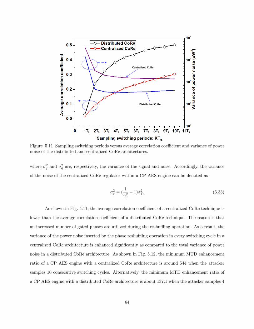
Distributed CoRe
Centralized CoRe
Ts Ts Ts Ts Ts Ts Ts Ts Ts Ts Ts
Figure 5.11 Sampling switching periods versus average correlation coefficient and variance of powernoise of the distributed and centralized CoRe architectures.
where σ2f and σ2q are, respectively, the variance of the signal and noise. Accordingly, the variance
of the noise of the centralized CoRe regulator within a CP AES engine can be denoted as
σ2q = (1
γ20− 1)σ2f . (5.33)
As shown in Fig. 5.11, the average correlation coefficient of a centralized CoRe technique is
lower than the average correlation coefficient of a distributed CoRe technique. The reason is that
an increased number of gated phases are utilized during the reshuffling operation. As a result, the
variance of the power noise inserted by the phase reshuffling operation in every switching cycle in a
centralized CoRe architecture is enhanced significantly as compared to the total variance of power
noise in a distributed CoRe architecture. As shown in Fig. 5.12, the minimum MTD enhancement
ratio of a CP AES engine with a centralized CoRe architecture is around 544 when the attacker
samples 10 consecutive switching cycles. Alternatively, the minimum MTD enhancement ratio of
a CP AES engine with a distributed CoRe architecture is about 137.1 when the attacker samples 4
64
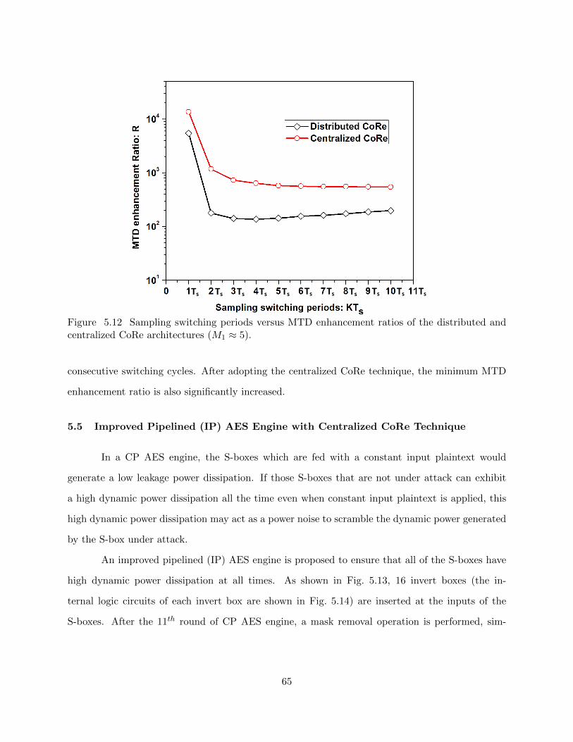
Ts Ts Ts Ts Ts Ts Ts Ts Ts Ts Ts
Figure 5.12 Sampling switching periods versus MTD enhancement ratios of the distributed andcentralized CoRe architectures (M1 ≈ 5).
consecutive switching cycles. After adopting the centralized CoRe technique, the minimum MTD
enhancement ratio is also significantly increased.
5.5 Improved Pipelined (IP) AES Engine with Centralized CoRe Technique
In a CP AES engine, the S-boxes which are fed with a constant input plaintext would
generate a low leakage power dissipation. If those S-boxes that are not under attack can exhibit
a high dynamic power dissipation all the time even when constant input plaintext is applied, this
high dynamic power dissipation may act as a power noise to scramble the dynamic power generated
by the S-box under attack.
An improved pipelined (IP) AES engine is proposed to ensure that all of the S-boxes have
high dynamic power dissipation at all times. As shown in Fig. 5.13, 16 invert boxes (the in-
ternal logic circuits of each invert box are shown in Fig. 5.14) are inserted at the inputs of the
S-boxes. After the 11th round of CP AES engine, a mask removal operation is performed, sim-
65
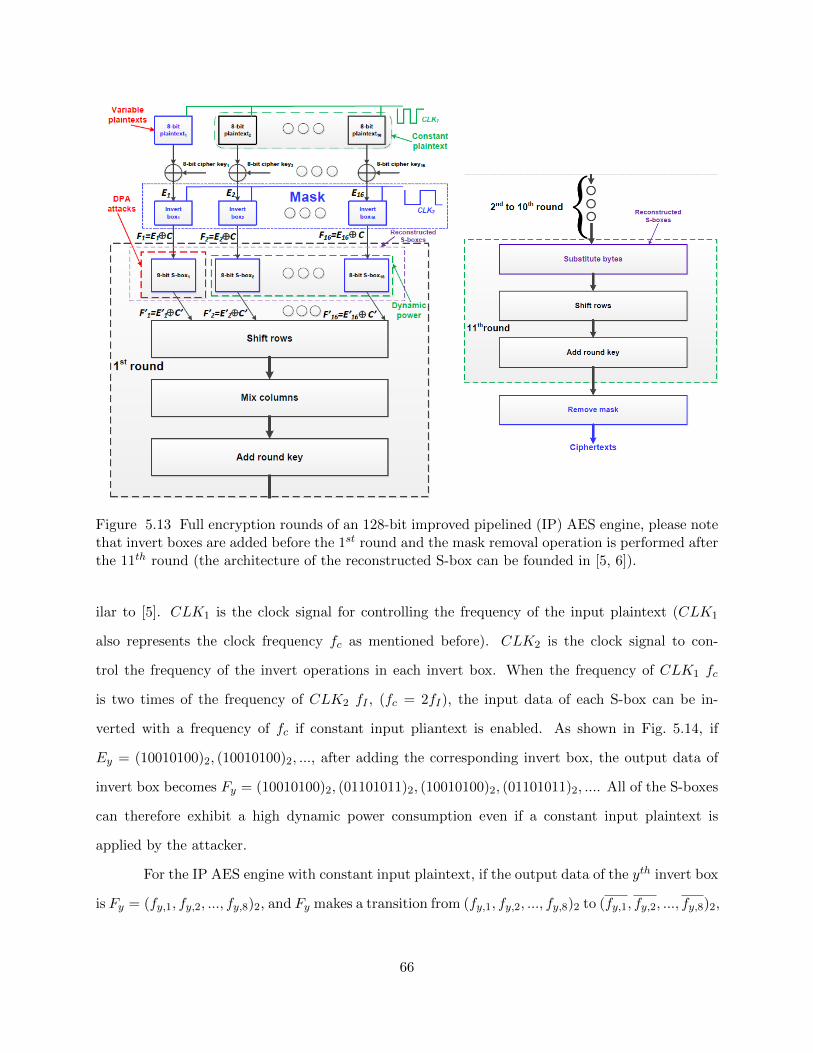
Figure 5.13 Full encryption rounds of an 128-bit improved pipelined (IP) AES engine, please notethat invert boxes are added before the 1st round and the mask removal operation is performed afterthe 11th round (the architecture of the reconstructed S-box can be founded in [5, 6]).
ilar to [5]. CLK1 is the clock signal for controlling the frequency of the input plaintext (CLK1
also represents the clock frequency fc as mentioned before). CLK2 is the clock signal to con-
trol the frequency of the invert operations in each invert box. When the frequency of CLK1 fc
is two times of the frequency of CLK2 fI , (fc = 2fI), the input data of each S-box can be in-
verted with a frequency of fc if constant input pliantext is enabled. As shown in Fig. 5.14, if
Ey = (10010100)2, (10010100)2, ..., after adding the corresponding invert box, the output data of
invert box becomes Fy = (10010100)2, (01101011)2, (10010100)2, (01101011)2, .... All of the S-boxes
can therefore exhibit a high dynamic power consumption even if a constant input plaintext is
applied by the attacker.
For the IP AES engine with constant input plaintext, if the output data of the yth invert box
is Fy = (fy,1, fy,2, ..., fy,8)2, and Fy makes a transition from (fy,1, fy,2, ..., fy,8)2 to (fy,1, fy,2, ..., fy,8)2,
66
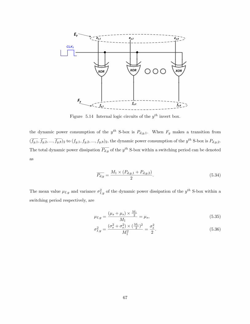
Fy
Ey
CLK2
ey,1 ey,2 ey,8
fy,1fy,2 fy,8
XOR XOR XOR
Figure 5.14 Internal logic circuits of the yth invert box.
the dynamic power consumption of the yth S-box is Pd,y,1. When Fy makes a transition from
(fy,1, fy,2, ..., fy,8)2 to (fy,1, fy,2, ..., fy,8)2, the dynamic power consumption of the yth S-box is Pd,y,2.
The total dynamic power dissipation Pd,y of the yth S-box within a switching period can be denoted
as
Pd,y =M1 × (Pd,y,1 + Pd,y,2)
2. (5.34)
The mean value µI,y and variance σ2I,y of the dynamic power dissipation of the yth S-box within a
switching period respectively, are
µI,y =(µs + µs)× M1
2
M1= µs, (5.35)
σ2I,y =(σ2s + σ2s)× (M1
2 )2
M21
=σ2s2. (5.36)
67
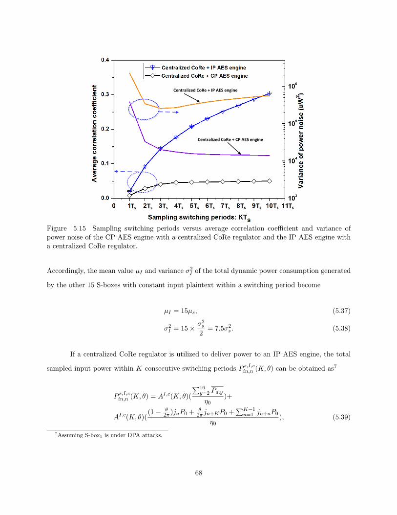
Centralized CoRe + IP AES engine
Centralized CoRe + CP AES engine
Ts Ts Ts Ts Ts Ts Ts Ts Ts Ts Ts
Figure 5.15 Sampling switching periods versus average correlation coefficient and variance ofpower noise of the CP AES engine with a centralized CoRe regulator and the IP AES engine witha centralized CoRe regulator.
Accordingly, the mean value µI and variance σ2I of the total dynamic power consumption generated
by the other 15 S-boxes with constant input plaintext within a switching period become
µI = 15µs, (5.37)
σ2I = 15× σ2s2
= 7.5σ2s . (5.38)
If a centralized CoRe regulator is utilized to deliver power to an IP AES engine, the total
sampled input power within K consecutive switching periods P s,I,cin,n (K, θ) can be obtained as7
P s,I,cin,n (K, θ) = AI,c(K, θ)(
∑16y=2 Pd,y
η0)+
AI,c(K, θ)((1− θ
2π )jnP0 + θ2π jn+KP0 +
∑K−1u=1 jn+uP0
η0), (5.39)
7Assuming S-box1 is under DPA attacks.
68
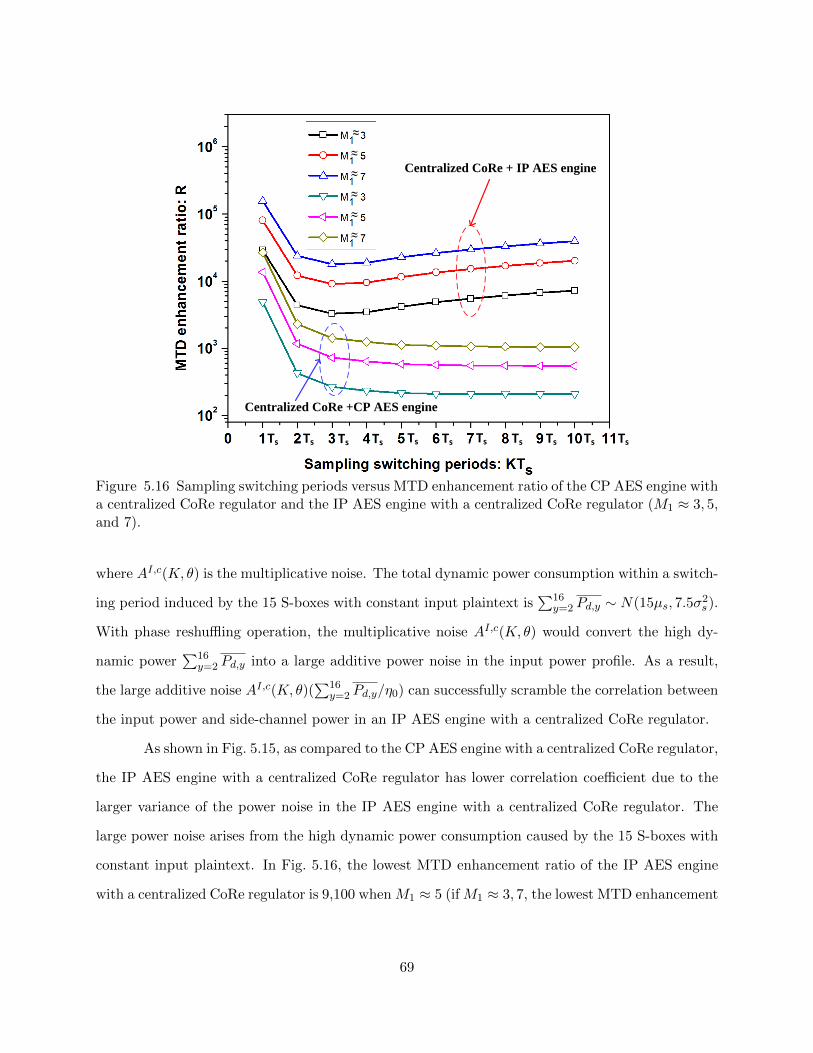
Ts Ts Ts Ts Ts Ts Ts Ts Ts Ts Ts
Centralized CoRe + IP AES engine
Centralized CoRe +CP AES engine
≈
≈
≈
≈
≈
≈
Figure 5.16 Sampling switching periods versus MTD enhancement ratio of the CP AES engine witha centralized CoRe regulator and the IP AES engine with a centralized CoRe regulator (M1 ≈ 3, 5,and 7).
where AI,c(K, θ) is the multiplicative noise. The total dynamic power consumption within a switch-
ing period induced by the 15 S-boxes with constant input plaintext is∑16
y=2 Pd,y ∼ N(15µs, 7.5σ2s).
With phase reshuffling operation, the multiplicative noise AI,c(K, θ) would convert the high dy-
namic power∑16
y=2 Pd,y into a large additive power noise in the input power profile. As a result,
the large additive noise AI,c(K, θ)(∑16
y=2 Pd,y/η0) can successfully scramble the correlation between
the input power and side-channel power in an IP AES engine with a centralized CoRe regulator.
As shown in Fig. 5.15, as compared to the CP AES engine with a centralized CoRe regulator,
the IP AES engine with a centralized CoRe regulator has lower correlation coefficient due to the
larger variance of the power noise in the IP AES engine with a centralized CoRe regulator. The
large power noise arises from the high dynamic power consumption caused by the 15 S-boxes with
constant input plaintext. In Fig. 5.16, the lowest MTD enhancement ratio of the IP AES engine
with a centralized CoRe regulator is 9,100 when M1 ≈ 5 (if M1 ≈ 3, 7, the lowest MTD enhancement
69
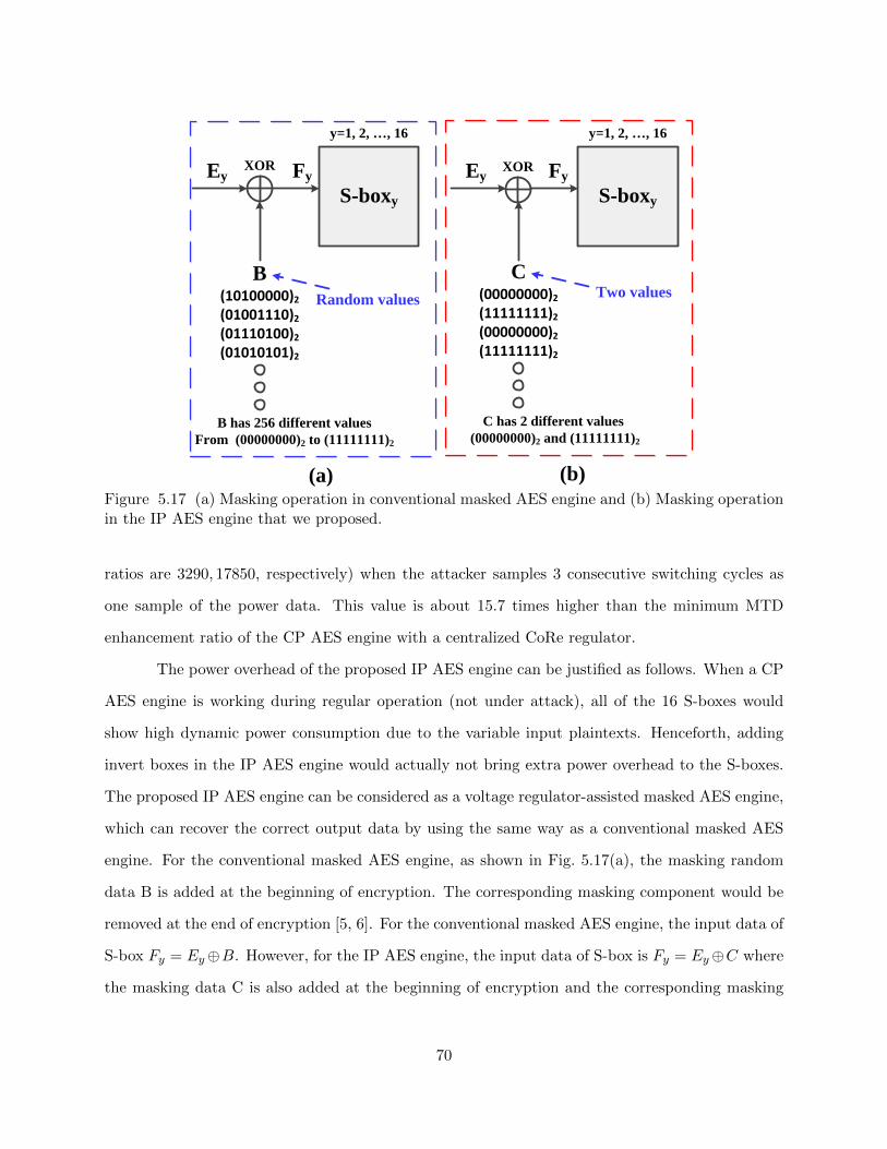
S-boxy
B(10100000)2(01001110)2(01110100)2(01010101)2
Ey Fy
Random values
y=1, 2, …, 16
B has 256 different values
From (00000000)2 to (11111111)2
S-boxy
C(00000000)2(11111111)2(00000000)2(11111111)2
Ey Fy
Two values
y=1, 2, …, 16
C has 2 different values
(00000000)2 and (11111111)2
(a) (b)
XOR XOR
Figure 5.17 (a) Masking operation in conventional masked AES engine and (b) Masking operationin the IP AES engine that we proposed.
ratios are 3290, 17850, respectively) when the attacker samples 3 consecutive switching cycles as
one sample of the power data. This value is about 15.7 times higher than the minimum MTD
enhancement ratio of the CP AES engine with a centralized CoRe regulator.
The power overhead of the proposed IP AES engine can be justified as follows. When a CP
AES engine is working during regular operation (not under attack), all of the 16 S-boxes would
show high dynamic power consumption due to the variable input plaintexts. Henceforth, adding
invert boxes in the IP AES engine would actually not bring extra power overhead to the S-boxes.
The proposed IP AES engine can be considered as a voltage regulator-assisted masked AES engine,
which can recover the correct output data by using the same way as a conventional masked AES
engine. For the conventional masked AES engine, as shown in Fig. 5.17(a), the masking random
data B is added at the beginning of encryption. The corresponding masking component would be
removed at the end of encryption [5, 6]. For the conventional masked AES engine, the input data of
S-box Fy = Ey⊕B. However, for the IP AES engine, the input data of S-box is Fy = Ey⊕C where
the masking data C is also added at the beginning of encryption and the corresponding masking
70
component can be removed at the end of encryption by using the same way as the conventional
masked AES engine, as shown in Fig. 5.13 and Fig. 5.17(b).
The primary difference between the conventional masked AES engine and IP AES engine
we proposed is the masking data. For the conventional AES engine, the masking data B is an 8-bit
random value, so B can have 28 = 256 different values. 256 masking values would increase the size
of look-up table (LUT) and computational complexity of the AES engine significantly [6]. As a
result, the area and performance overhead of the conventional masked AES engine is quite large [6].
For an implemented masked AES engine based on field-programmable gate array (FPGA) [81], the
area overhead is 60.1% and the frequency decreases about 11% [81].
However, for the proposed IP AES engine, the masking data C can only have two values:
(00000000)2 and (11111111)2 (Ey⊕(00000000)2 = Ey and Ey⊕(11111111)2 = Ey). As compared to
the conventional masked AES engine, the overhead of IP AES engine would therefore be reduced to
2/256 = 1/128. The approximate area overhead of the proposed IP AES engine would be around
60.1% ∗ (1/128) = 0.47% and the frequency reduction of the IP AES engine would be around
11% ∗ (1/128) = 0.09%.
5.6 Circuit Level Simulation
The CoGa and CoRe techniques are designed with 130nm IBM CMOS technology and
simulated in Cadence where the switching frequency is swept between 30 and 60 MHz. As shown
in Fig. 5.18, when the load current Iload is constant, the CoGa regulator is not triggered, and the
active and gated phases do not change as long as the variations in the load current demand are
small. However, the sequence of active and passive stages continuously alters over time in the CoRe
regulator regardless of the variations in the workload demand. Therefore, as compared to CoGa,
input power consumption of the CoRe regulator shows an uncertain sequence of active stages even
if the load current demand does not change, increasing the variance of multiplicative power noise
in input power profile.
As shown in Fig. 5.19(a), the dynamic power consumption of an IP AES engine is much
higher than the dynamic power consumption of a CP AES engine. The reason is that all 16 S-
71

5.2 5.4 5.6 5.8
0.7
0.72
Time (μs)(a
)I lo
ad (
mA
)5.2 5.4 5.6 5.8
0.540.550.56
Time (μs)
(b)
Vou
t (V
)
5.1 5.2 5.3 5.4 5.5 5.6 5.7 5.8
0
0.2
0.4
Time (ns)
(c)
I inpu
t (A
)
5.18 5.19 5.2 5.21
0
0.2
0.4
Time (μs)
(d)
I inpu
t (A
)
5.39 5.4 5.41 5.42
0
0.2
0.4
Time (μs)
(e)
I inpu
t (A
)
5.6 5.61 5.62 5.63
0
0.2
0.4
Time (μs)
(f)
I inpu
t (A
)
5.81 5.82 5.83 5.84
0
0.2
0.4
Time (μs)
(g)
I inpu
t (A
)
CoReCoGa
CoReCoGa
CoReCoGa
CoReCoGa
CoReCoGa
CoReCoGa
Figure 5.18 8-phase CoGa regulator and 8-phase CoRe regulator are simulated: a) Distributionof load current, b) transient output voltage profile, and c) input current profile of CoGa regulatorand CoRe regulator, sequence of active stages in CoRe regulator is variable while sequence of activestages in CoGa regulator is invariable if a constant load current is enabled, as shown in d), e), f),and g).
boxes have high dynamic power dissipation in an IP AES engine while only the S-box under attack
contributes to the dynamic power dissipation in a CP AES engine. As shown in Fig. 5.19(b), only
2 stages are activated in the CP AES engine with a centralized CoRe regulator in a switching cycle
while a greater number of stages are turned-on in the centralized CoRe regulator. Hence, the power
noise generated by those 15 S-boxes which are not under attack are reshuffled in the input power
profile, further reducing the correlation between the input power and side-channel power in the IP
AES engine with a centralized CoRe regulator.
5.7 Conclusion
An on-chip CoRe technique is utilized to reinforce a lightweight AES engine as an efficient
countermeasure against power analysis attacks due to the high multiplicative power noise induced
by reshuffling active and gated converter stages. A detailed analytical analysis of the correlation
between the input and output power of both conventional and proposed voltage regulation tech-
niques is presented. The security implications of the physical placement of the voltage regulators
72
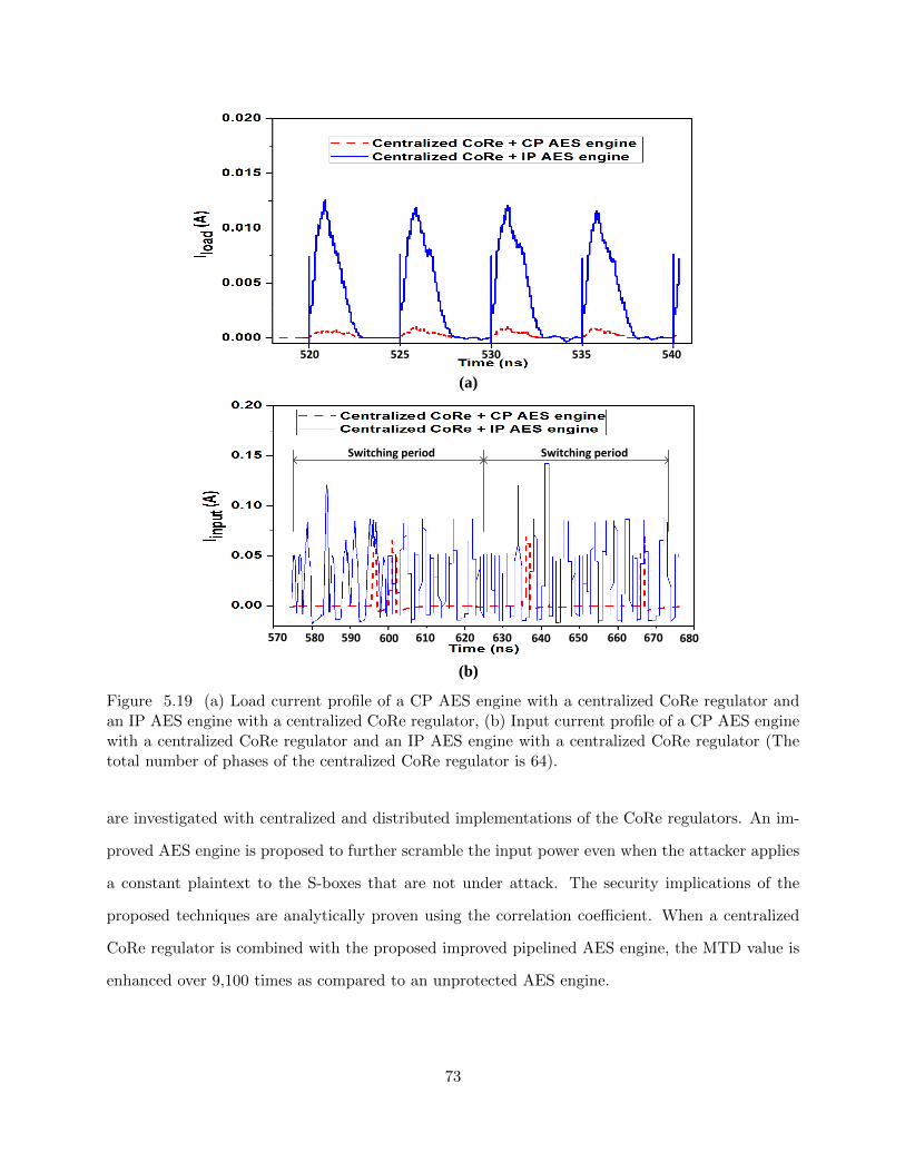
520 525 530 535 540
(a)
(b)
Switching period Switching period
580 590 600 610 620 630 640 650 660 670 680570
Figure 5.19 (a) Load current profile of a CP AES engine with a centralized CoRe regulator andan IP AES engine with a centralized CoRe regulator, (b) Input current profile of a CP AES enginewith a centralized CoRe regulator and an IP AES engine with a centralized CoRe regulator (Thetotal number of phases of the centralized CoRe regulator is 64).
are investigated with centralized and distributed implementations of the CoRe regulators. An im-
proved AES engine is proposed to further scramble the input power even when the attacker applies
a constant plaintext to the S-boxes that are not under attack. The security implications of the
proposed techniques are analytically proven using the correlation coefficient. When a centralized
CoRe regulator is combined with the proposed improved pipelined AES engine, the MTD value is
enhanced over 9,100 times as compared to an unprotected AES engine.
73
CHAPTER 6:
SECURITY-ADAPTIVE VOLTAGE CONVERSION TECHNIQUE
6.1 Introduction
DPA attacks are one of the most widely studied SCAs that exploit the switching activities
within the cryptographic circuits while processing different input data1. Recently leakage power
analysis (LPA) attacks have been proposed by M. Alioto et al. [3] to obtain the critical infor-
mation by analyzing the correlation between the input data and leakage power dissipation of the
cryptographic circuit. LPA attacks exploit the fact that the leakage current signature of NMOS
and PMOS transistors is different [3]. The amplitude of the leakage power is orders of magnitude
smaller than the amplitude of dynamic power consumption. To perform a successful LPA attack,
the attacker must mitigate the measurement noise that can make the analysis quite difficult due
to the small signal-to-noise ratio (SNR) of the monitored leakage power. An effective technique to
mitigate the measurement noise is to lower the operating frequency of the cryptographic circuit [83].
Since the leakage mechanisms in DPA and LPA attacks are quite different, DPA-resistant
cryptographic circuits may still be vulnerable against LPA attacks [84]. There is therefore a strong
need for effective countermeasures against LPA attacks. Converter-reshuffling (CoRe) technique
has been proposed in [11, 59] as a countermeasure against DPA attacks with low overhead. CoRe
technique utilizes a multi-phase switched-capacitor (SC) voltage converter where each phase delivers
a portion of the required power to the cryptographic circuit with a different time delay. A pseudo-
random number generator (PRNG) is used to scramble the sequence of activate phases to insert a
varying amount of uncertain power noise in each switching period against DPA attacks. However, if
the attacker implements an LPA attack on a cryptographic circuit with a CoRe voltage converter,
1The content of this Chapter has been published in [82], the copyright permission can be found in Appendix F.
74
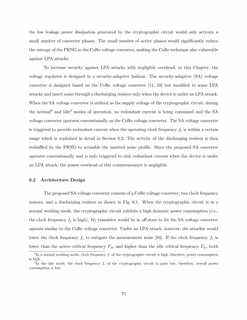
the low leakage power dissipation generated by the cryptographic circuit would only activate a
small number of converter phases. The small number of active phases would significantly reduce
the entropy of the PRNG in the CoRe voltage converter, making the CoRe technique also vulnerable
against LPA attacks.
To increase security against LPA attacks with negligible overhead, in this Chapter, the
voltage regulator is designed in a security-adaptive fashion. The security-adaptive (SA) voltage
converter is designed based on the CoRe voltage converter [11, 59] but modified to sense LPA
attacks and insert noise through a discharging resistor only when the device is under an LPA attack.
When the SA voltage converter is utilized as the supply voltage of the cryptographic circuit, during
the normal2 and idle3 modes of operation, no redundant current is being consumed and the SA
voltage converter operates conventionally as the CoRe voltage converter. The SA voltage converter
is triggered to provide redundant current when the operating clock frequency fc is within a certain
range which is explained in detail in Section 6.2. The activity of the discharging resistor is then
reshuffled by the PRNG to scramble the inserted noise profile. Since the proposed SA converter
operates conventionally and is only triggered to sink redundant current when the device is under
an LPA attack, the power overhead of this countermeasure is negligible.
6.2 Architecture Design
The proposed SA voltage converter consists of a CoRe voltage converter, two clock frequency
sensors, and a discharging resistor as shown in Fig. 6.1. When the cryptographic circuit is in a
normal working mode, the cryptographic circuit exhibits a high dynamic power consumption (i.e.,
the clock frequency fc is high), M1 transistor would be in off-state to let the SA voltage converter
operate similar to the CoRe voltage converter. Under an LPA attack, however, the attacker would
lower the clock frequency fc to mitigate the measurement noise [83]. If the clock frequency fc is
lower than the active critical frequency Fac and higher than the idle critical frequency Fic, both
2In a normal working mode, clock frequency fc of the cryptographic circuit is high, therefore, power consumptionis high.
3In the idle mode, the clock frequency fc of the cryptographic circuit is quite low, therefore, overall powerconsumption is low.
75

SC converter
Cryptographiccircuit
Power source
SC converter
SC converter
N-bitPRNG
Rc
M1
Driver
Phase-1
Phase-2
Phase-N
N-phase CoRe converter
Vin
Vout
Frequency comparator2
Driver
Fic
M2
fc
Clock frequency sensor2
Clock
Discharging resistor
Frequency comparator1
Fac
Clock frequency sensor1
fc≥FacM1 =0M2=1
M1 =1M2=1Fic< fc<Fac
fc≤FicM1 =1M2=0
Figure 6.1 Architecture of the proposed security-adaptive (SA) voltage converter (N is the totalnumber of phases (N is an even), switch Mi1 = 1, (i1 = 1, 2) represents that it is in on-state andvice versa).
M1 transistor and M2 transistor would be in on-state, letting some amount of redundant current
flow through the discharging resistor Rc. The redundant power dissipation induced by Rc is then
reshuffled by the N -phase CoRe converter to scramble the inserted power noise.
When the clock frequency fc of the cryptographic circuit is lower than the idle critical
frequency Fic, the M2 transistor would be turned-off, deactivating the discharging resistor Rc as
shown in Fig. 6.1. When the cryptographic circuit is in an idle mode (fc << Fic), the discharging
resistor Rc is therefore inactive to avoid power overhead. The design guidelines on the selection of
suitable Fic and Fac to maximize security are provided in Section 6.4 and Appendix B, respectively.
6.3 Parameter Design
To maximize the entropy of the N -bit PRNG that resides within the SA voltage con-
verter, the number of active phases of an SA voltage converter in each switching period should be
around N/2 (the entropy of the N -bit PRNG reaches the maximum value −(NN/2
)× 1
( NN/2)
log
1
( NN/2)
2 =
log( NN/2)
2 ). Let’s assume the mean value of leakage power dissipation of the cryptographic circuit
within a switching period under LPA attacks is µc and the output voltage of an N -phase CoRe
converter within the SA voltage converter is Vout. When the cryptographic circuit employs an SA
76
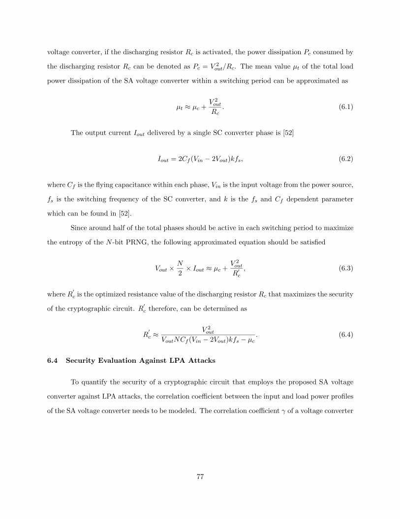
voltage converter, if the discharging resistor Rc is activated, the power dissipation Pc consumed by
the discharging resistor Rc can be denoted as Pc = V 2out/Rc. The mean value µt of the total load
power dissipation of the SA voltage converter within a switching period can be approximated as
µt ≈ µc +V 2out
Rc. (6.1)
The output current Iout delivered by a single SC converter phase is [52]
Iout = 2Cf (Vin − 2Vout)kfs, (6.2)
where Cf is the flying capacitance within each phase, Vin is the input voltage from the power source,
fs is the switching frequency of the SC converter, and k is the fs and Cf dependent parameter
which can be found in [52].
Since around half of the total phases should be active in each switching period to maximize
the entropy of the N -bit PRNG, the following approximated equation should be satisfied
Vout ×N
2× Iout ≈ µc +
V 2out
R′c, (6.3)
where R′c is the optimized resistance value of the discharging resistor Rc that maximizes the security
of the cryptographic circuit. R′c therefore, can be determined as
R′c ≈
V 2out
VoutNCf (Vin − 2Vout)kfs − µc. (6.4)
6.4 Security Evaluation Against LPA Attacks
To quantify the security of a cryptographic circuit that employs the proposed SA voltage
converter against LPA attacks, the correlation coefficient between the input and load power profiles
of the SA voltage converter needs to be modeled. The correlation coefficient γ of a voltage converter
77
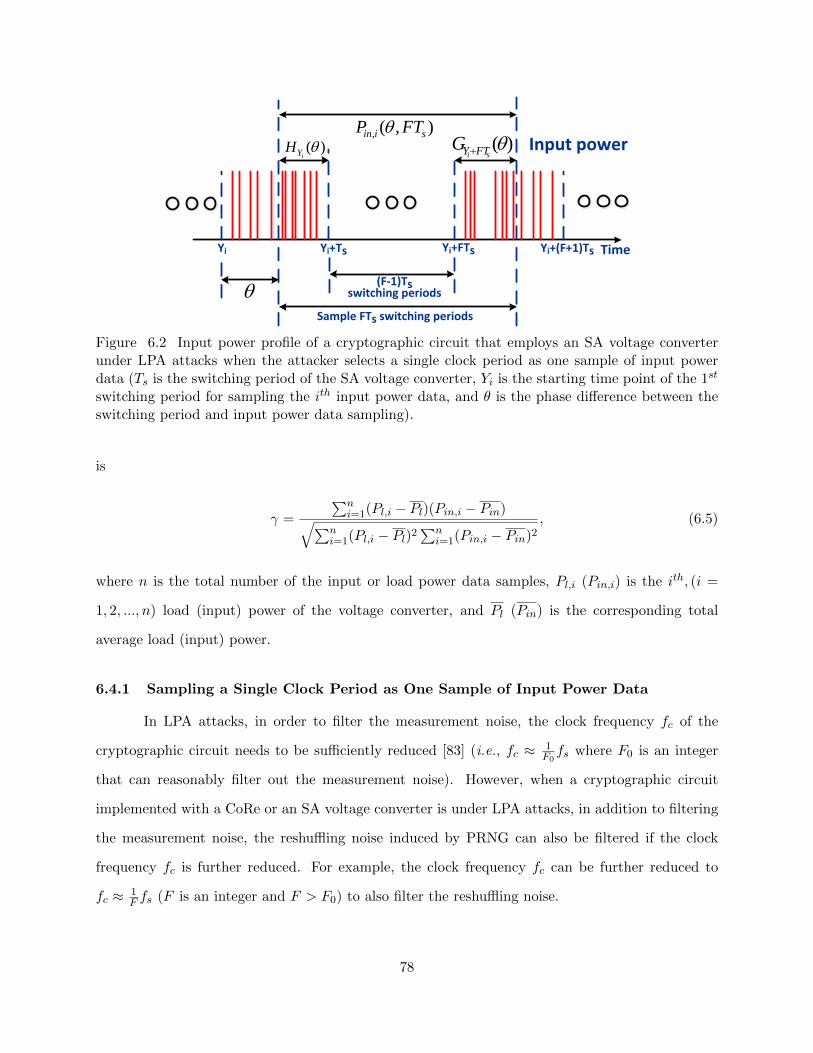
Yi TimeYi+Ts Yi+FTs Yi+(F+1)Ts
(F-1)Ts switching periods
)(iYH )(
si FTYG
Sample FTs switching periods
),(, siin FTP Input power
Figure 6.2 Input power profile of a cryptographic circuit that employs an SA voltage converterunder LPA attacks when the attacker selects a single clock period as one sample of input powerdata (Ts is the switching period of the SA voltage converter, Yi is the starting time point of the 1st
switching period for sampling the ith input power data, and θ is the phase difference between theswitching period and input power data sampling).
is
γ =
∑ni=1(Pl,i − Pl)(Pin,i − Pin)√∑n
i=1(Pl,i − Pl)2∑n
i=1(Pin,i − Pin)2, (6.5)
where n is the total number of the input or load power data samples, Pl,i (Pin,i) is the ith, (i =
1, 2, ..., n) load (input) power of the voltage converter, and Pl (Pin) is the corresponding total
average load (input) power.
6.4.1 Sampling a Single Clock Period as One Sample of Input Power Data
In LPA attacks, in order to filter the measurement noise, the clock frequency fc of the
cryptographic circuit needs to be sufficiently reduced [83] (i.e., fc ≈ 1F0fs where F0 is an integer
that can reasonably filter out the measurement noise). However, when a cryptographic circuit
implemented with a CoRe or an SA voltage converter is under LPA attacks, in addition to filtering
the measurement noise, the reshuffling noise induced by PRNG can also be filtered if the clock
frequency fc is further reduced. For example, the clock frequency fc can be further reduced to
fc ≈ 1F fs (F is an integer and F > F0) to also filter the reshuffling noise.
78
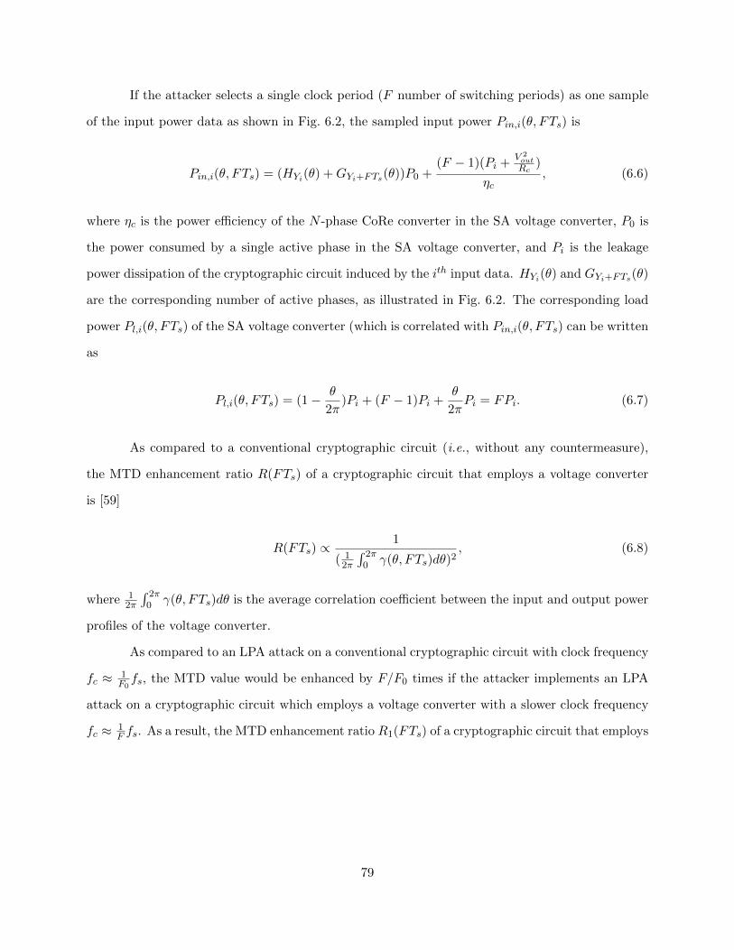
If the attacker selects a single clock period (F number of switching periods) as one sample
of the input power data as shown in Fig. 6.2, the sampled input power Pin,i(θ, FTs) is
Pin,i(θ, FTs) = (HYi(θ) +GYi+FTs(θ))P0 +(F − 1)(Pi +
V 2outRc
)
ηc, (6.6)
where ηc is the power efficiency of the N -phase CoRe converter in the SA voltage converter, P0 is
the power consumed by a single active phase in the SA voltage converter, and Pi is the leakage
power dissipation of the cryptographic circuit induced by the ith input data. HYi(θ) and GYi+FTs(θ)
are the corresponding number of active phases, as illustrated in Fig. 6.2. The corresponding load
power Pl,i(θ, FTs) of the SA voltage converter (which is correlated with Pin,i(θ, FTs) can be written
as
Pl,i(θ, FTs) = (1− θ
2π)Pi + (F − 1)Pi +
θ
2πPi = FPi. (6.7)
As compared to a conventional cryptographic circuit (i.e., without any countermeasure),
the MTD enhancement ratio R(FTs) of a cryptographic circuit that employs a voltage converter
is [59]
R(FTs) ∝1
( 12π
∫ 2π0 γ(θ, FTs)dθ)2
, (6.8)
where 12π
∫ 2π0 γ(θ, FTs)dθ is the average correlation coefficient between the input and output power
profiles of the voltage converter.
As compared to an LPA attack on a conventional cryptographic circuit with clock frequency
fc ≈ 1F0fs, the MTD value would be enhanced by F/F0 times if the attacker implements an LPA
attack on a cryptographic circuit which employs a voltage converter with a slower clock frequency
fc ≈ 1F fs. As a result, the MTD enhancement ratio R1(FTs) of a cryptographic circuit that employs
79
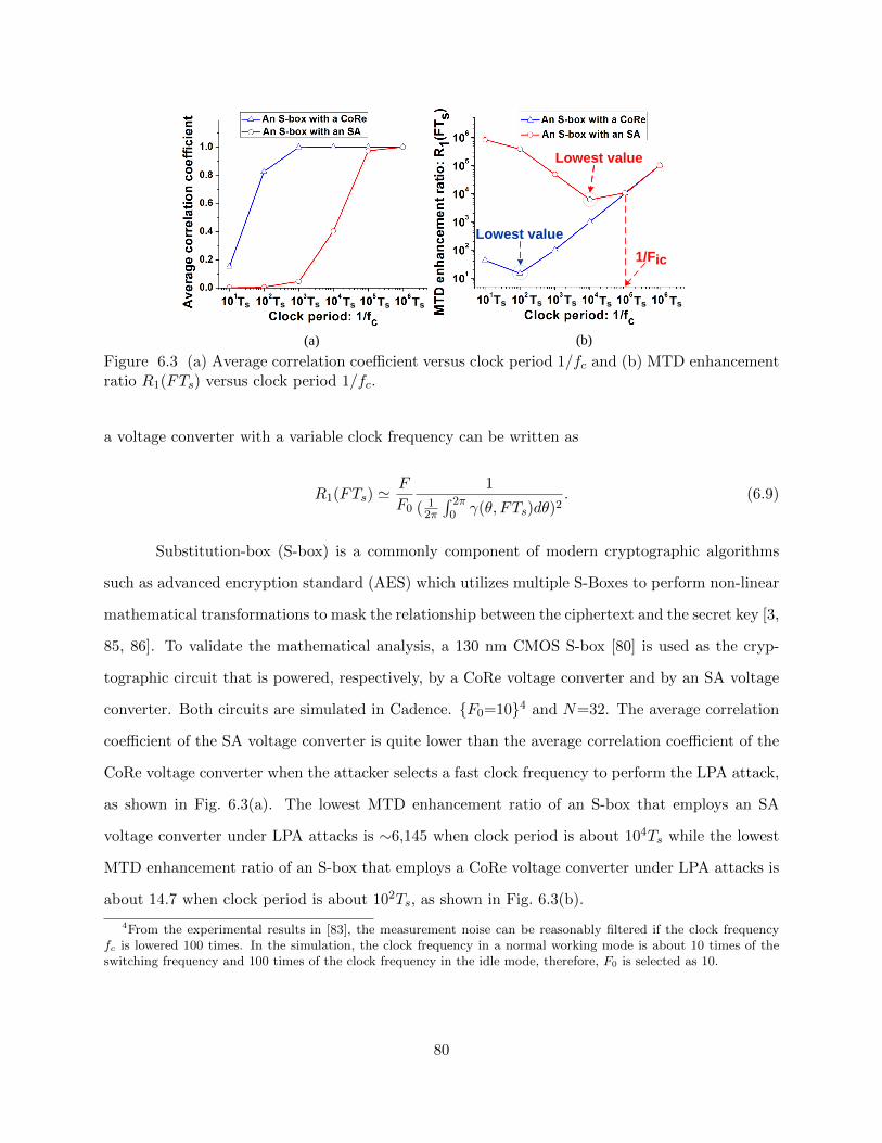
(a) (b)
Lowest value
Ts
Lowest value
Ts Ts Ts Ts Ts Ts Ts Ts Ts Ts Ts
1/Fic
Figure 6.3 (a) Average correlation coefficient versus clock period 1/fc and (b) MTD enhancementratio R1(FTs) versus clock period 1/fc.
a voltage converter with a variable clock frequency can be written as
R1(FTs) 'F
F0
1
( 12π
∫ 2π0 γ(θ, FTs)dθ)2
. (6.9)
Substitution-box (S-box) is a commonly component of modern cryptographic algorithms
such as advanced encryption standard (AES) which utilizes multiple S-Boxes to perform non-linear
mathematical transformations to mask the relationship between the ciphertext and the secret key [3,
85, 86]. To validate the mathematical analysis, a 130 nm CMOS S-box [80] is used as the cryp-
tographic circuit that is powered, respectively, by a CoRe voltage converter and by an SA voltage
converter. Both circuits are simulated in Cadence. F0=104 and N=32. The average correlation
coefficient of the SA voltage converter is quite lower than the average correlation coefficient of the
CoRe voltage converter when the attacker selects a fast clock frequency to perform the LPA attack,
as shown in Fig. 6.3(a). The lowest MTD enhancement ratio of an S-box that employs an SA
voltage converter under LPA attacks is ∼6,145 when clock period is about 104Ts while the lowest
MTD enhancement ratio of an S-box that employs a CoRe voltage converter under LPA attacks is
about 14.7 when clock period is about 102Ts, as shown in Fig. 6.3(b).
4From the experimental results in [83], the measurement noise can be reasonably filtered if the clock frequencyfc is lowered 100 times. In the simulation, the clock frequency in a normal working mode is about 10 times of theswitching frequency and 100 times of the clock frequency in the idle mode, therefore, F0 is selected as 10.
80
Xi TimeXi+Ts
(KF0-1)Ts switching periods
)(iXW )(
0
si TKFXU
Sample KF0Ts switching periods
),( 0, siin TKFP Input power
Xi+KF0Ts Xi+(KF0+1)Ts
Figure 6.4 Input power profile of a cryptographic circuit that employs an SA voltage converterunder LPA attacks when the attacker selects a variable number of clock periods as one sample ofinput power data (Xi is the starting time point of the 1st switching period for sampling the ith
input power data).
6.4.2 Sampling Multiple Clock Periods as One Sample of Input Power Data
The technique of sampling multiple clock/switching periods as one sample of input power
data is quite efficient for filtering the power noise generated from reshuffling-based voltage converters
in DPA attacks [59]. When an attacker implements an LPA attack on a cryptographic circuit
that houses a CoRe voltage converter or an SA voltage converter, the attacker can also filter the
reshuffling noise by sampling K, (K ≥ 2) number of clock periods as one sample of input power data
instead of lowering the clock frequency (fc ≈ 1F0fs) further, as shown in Fig. 6.4. The corresponding
input power Pin,i(θ,KF0Ts) and load power Pl,i(θ,KF0Ts) of the SA voltage converter can be,
respectively, written as
Pin,i(θ,KF0Ts) = (WXi(θ) + UXi+KF0Ts(θ))P0+
(F0 − 1)(P(i−1)K+1 +V 2outRc
)
ηc+ F0
K∑j=2
(P(i−1)K+j +V 2outRc
)
ηc, (6.10)
81

(a) (b)
Lowest value
Ts
Lowest value
Ts Ts Ts Ts Ts Ts Ts Ts Ts Ts Ts
Figure 6.5 (a) Average correlation coefficient versus sampling time period KF0Ts and (b) MTDenhancement ratio R2(KF0Ts) versus sampling time period KF0Ts (F0=10 and N=32).
Pl,i(θ,KF0Ts) = (1− θ
2π)P(i−1)K+1 + (F0 − 1)P(i−1)K+1
+ F0
K∑j=2
P(i−1)K+j +θ
2πP(i−1)K+K+1, (6.11)
where P(i−1)K+j , (j = 1, 2, ...) is the leakage power dissipation of the cryptographic circuit induced
by the ((i − 1)K + j)th input data. WXi(θ) and UXi+KF0Ts(θ) are the corresponding number of
active phases, as illustrated in Fig. 6.4.
As compared to sampling a single clock period as one sample of input power data, sampling
K number of clock periods as one sample of input power data would enhance the MTD value to
K times [59]. Therefore, the MTD enhancement ratio R2(KF0Ts) of a cryptographic circuit that
employs a voltage converter is
R2(KF0Ts) ' K1
( 12π
∫ 2π0 γ(θ,KF0Ts)dθ)2
, (6.12)
when utilizing K number of clock periods as one sample of input power data.
When the attacker increases the sampling time period to KF0Ts, the average correlation
coefficient of the SA voltage converter has a marginal enhancement, as shown in Fig. 6.5(a). This
indicates that sampling multiple clock periods as one sample of input power data to mitigate noise
is not sufficiently effective. The lowest MTD enhancement ratio of an S-box with an SA (CoRe)
82
voltage converter is 826446 (43) (shown in Fig. 6.5(b)), which is much higher than the lowest MTD
enhancement ratio 6,145 (14.7) (shown in Fig. 6.3(b)). That means further reducing the clock
frequency fc is more effective than sampling multiple clock periods as one sample of input power
data to enhance the power of LPA attacks on an S-box with a voltage converter. The primary
reason is that under the same sampling time period (FTs = KF0Ts), the variance of the load power
of a voltage converter with a variable clock frequency D(Pl,i(θ, FTs)) is
D(Pl,i(θ, FTs)) = D(FPi) = D(KF0Pi) = K2F 20 σ
2s , (6.13)
where σ2s is the variance of the leakage power dissipation of the cryptographic circuit. However,
the variance of load power of a voltage converter while sampling K number of clock periods as one
sample of input power data D(Pl,i(θ,KF0Ts)) is (F0 > 1)
D(Pl,i(θ,KF0Ts)) =
D((1− θ
2π)P(i−1)K+1 + (F0 − 1)P(i−1)K+1)
+D(F0
K∑j=2
P(i−1)K+j) +D(θ
2πP(i−1)K+K+1)
= (F0 −θ
2π)2σ2s + F 2
0 (K − 1)σ2s + (θ
2π)2σ2s
= KF 20 σ
2s −
θ
πF0σ
2s +
θ2
2π2σ2s < KF 2
0 σ2s −
θ
πσ2s +
θ2
2π2σ2s
≤ KF 20 σ
2s −
θ
π
θ
2πσ2s +
θ2
2π2σ2s = KF 2
0 σ2s . (6.14)
As compared to sampling K number of clock periods as one sample of input power data, further
lowering clock frequency fc can therefore enhance the variance of the load power of the voltage
converter over K times. A larger variance of the load power enhances the SNR of the voltage
converter and decreases the lowest MTD enhancement ratio.
Lowering clock frequency fc further is more efficient than sampling multiple clock periods
as one sample of input power data to enhance the power of LPA attacks. When the attacker further
lowers clock frequency fc, as shown in Fig. 6.3(b), the idle critical frequency Fic can be selected
83
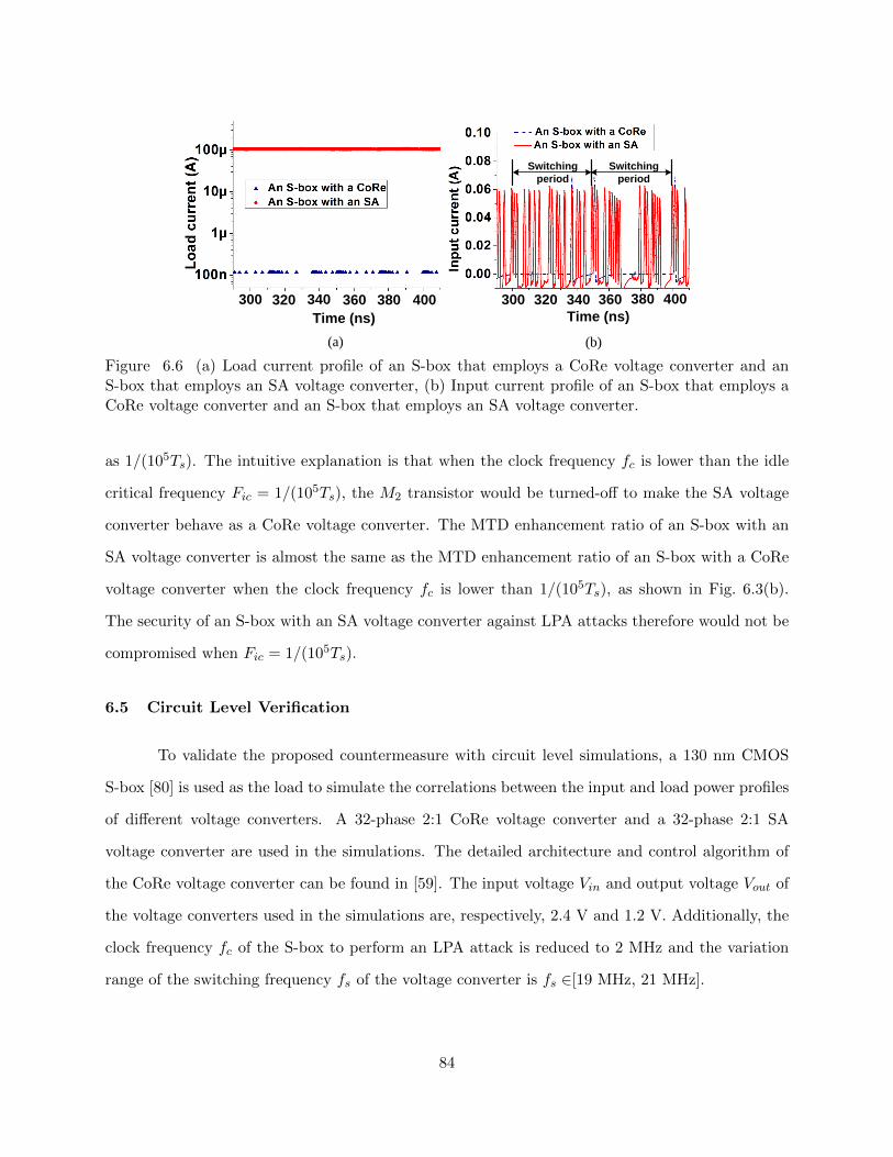
(a) (b)
300 320 340 360 380 400
Time (ns)
300 320 340 360 380 400
Time (ns)
Switching
period
Switching
period
Figure 6.6 (a) Load current profile of an S-box that employs a CoRe voltage converter and anS-box that employs an SA voltage converter, (b) Input current profile of an S-box that employs aCoRe voltage converter and an S-box that employs an SA voltage converter.
as 1/(105Ts). The intuitive explanation is that when the clock frequency fc is lower than the idle
critical frequency Fic = 1/(105Ts), the M2 transistor would be turned-off to make the SA voltage
converter behave as a CoRe voltage converter. The MTD enhancement ratio of an S-box with an
SA voltage converter is almost the same as the MTD enhancement ratio of an S-box with a CoRe
voltage converter when the clock frequency fc is lower than 1/(105Ts), as shown in Fig. 6.3(b).
The security of an S-box with an SA voltage converter against LPA attacks therefore would not be
compromised when Fic = 1/(105Ts).
6.5 Circuit Level Verification
To validate the proposed countermeasure with circuit level simulations, a 130 nm CMOS
S-box [80] is used as the load to simulate the correlations between the input and load power profiles
of different voltage converters. A 32-phase 2:1 CoRe voltage converter and a 32-phase 2:1 SA
voltage converter are used in the simulations. The detailed architecture and control algorithm of
the CoRe voltage converter can be found in [59]. The input voltage Vin and output voltage Vout of
the voltage converters used in the simulations are, respectively, 2.4 V and 1.2 V. Additionally, the
clock frequency fc of the S-box to perform an LPA attack is reduced to 2 MHz and the variation
range of the switching frequency fs of the voltage converter is fs ∈[19 MHz, 21 MHz].
84
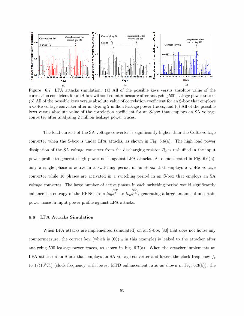
(a) (b) (c)
Correct key 66Complement of the
correct key 189
0.1743
Correct key 66 Complement of the
correct key 189
0.1511Correct key 66
Complement of the
correct key 189
0.0687
Figure 6.7 LPA attacks simulation: (a) All of the possible keys versus absolute value of thecorrelation coefficient for an S-box without countermeasure after analyzing 500 leakage power traces,(b) All of the possible keys versus absolute value of correlation coefficient for an S-box that employsa CoRe voltage converter after analyzing 2 million leakage power traces, and (c) All of the possiblekeys versus absolute value of the correlation coefficient for an S-box that employs an SA voltageconverter after analyzing 2 million leakage power traces.
The load current of the SA voltage converter is significantly higher than the CoRe voltage
converter when the S-box is under LPA attacks, as shown in Fig. 6.6(a). The high load power
dissipation of the SA voltage converter from the discharging resistor Rc is reshuffled in the input
power profile to generate high power noise against LPA attacks. As demonstrated in Fig. 6.6(b),
only a single phase is active in a switching period in an S-box that employs a CoRe voltage
converter while 16 phases are activated in a switching period in an S-box that employs an SA
voltage converter. The large number of active phases in each switching period would significantly
enhance the entropy of the PRNG from log(321 )2 to log
(3216)2 , generating a large amount of uncertain
power noise in input power profile against LPA attacks.
6.6 LPA Attacks Simulation
When LPA attacks are implemented (simulated) on an S-box [80] that does not house any
countermeasure, the correct key (which is (66)10 in this example) is leaked to the attacker after
analyzing 500 leakage power traces, as shown in Fig. 6.7(a). When the attacker implements an
LPA attack on an S-box that employs an SA voltage converter and lowers the clock frequency fc
to 1/(104Ts) (clock frequency with lowest MTD enhancement ratio as shown in Fig. 6.3(b)), the
85

correct key cannot be obtained by the attacker even after analyzing two million leakage power
traces, as shown in Fig. 6.7(c). By contrast, when the attacker lowers the clock frequency fc to
1/(104Ts) and implements an LPA attack on an S-box which employs a CoRe voltage converter,
after analyzing 2 million leakage power traces, the correct key is leaked to the attacker, as shown
in Fig. 6.7(b). Therefore, as compared to an S-box that employs a CoRe voltage converter, the
reshuffled redundant load power dissipation in the SA voltage converter can successfully act as
noise to enhance the MTD value.
6.7 Conclusion
A security-adaptive (SA) voltage converter is utilized as a lightweight countermeasure
against LPA attacks. The discharging resistor in the SA voltage converter can significantly in-
crease the amount of noise insertion in the input power profile when LPA attacks are sensed by
the proposed technique. Through scrambling the redundant load power dissipation in the input
power profile, the MTD value of a cryptographic circuit that employs the SA voltage converter is
enhanced over 6,145 times as compared to the MTD value of a conventional cryptographic circuit
that has no countermeasure.
86
CHAPTER 7:
ON-CHIP VOLTAGE REGULATION WITH VFS
7.1 Introduction
Dynamic power consumption of a cryptographic circuit is Pdyn = αfcV2dd where fc, Vdd,
and α are, respectively, the clock frequency, supply voltage, and activity factor1. Activity fac-
tor α is determined by the number of 0 → 1 transitions that occur in the cryptographic circuit
under different input data [75]. To hide the actual dynamic power consumption Pdyn of a cryp-
tographic circuit, different logic families are proposed to make the dynamic power consumption
constant under different input data values. The wave dynamic differential logic (WDDL), which
is a type of balanced logic gate, is proposed in [85, 88] to make the activity factor α constant
regardless of the input data values. A switched-capacitor current equalizer-based countermeasure
is proposed in [61] to achieve a constant Pdyn through discharging the residual charge in every
switching cycle. However, DPA attacks countermeasures that hide the dynamic power dissipation
of a cryptographic circuit by maintaining constant dynamic power consumption typically cause
significant power/area/performance overhead [2, 61]. Alternatively, masking technique [5, 6] is an
effective DPA attacks countermeasure that uses random intermediate data values to be inserted
among the actual side channel leakage data to reduce the correlation between the input data and
α. However, masking technique may also induce significant area overhead due to the large look-up
table (LUT) when a large amount of random data is inserted [5, 6]. Please note that the effec-
tiveness of masking-based countermeasures is directly correlated with the number of inserted data
values. There is therefore a tradeoff between the LUT size and the effectiveness of the masking
operation.
1The content of this Chapter has been published in [87], the copyright permission can be found in Appendix F.
87
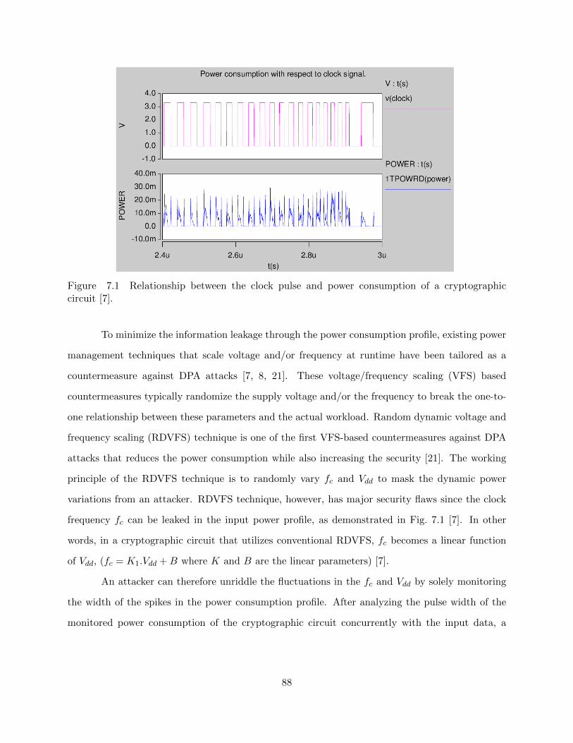
Figure 7.1 Relationship between the clock pulse and power consumption of a cryptographiccircuit [7].
To minimize the information leakage through the power consumption profile, existing power
management techniques that scale voltage and/or frequency at runtime have been tailored as a
countermeasure against DPA attacks [7, 8, 21]. These voltage/frequency scaling (VFS) based
countermeasures typically randomize the supply voltage and/or the frequency to break the one-to-
one relationship between these parameters and the actual workload. Random dynamic voltage and
frequency scaling (RDVFS) technique is one of the first VFS-based countermeasures against DPA
attacks that reduces the power consumption while also increasing the security [21]. The working
principle of the RDVFS technique is to randomly vary fc and Vdd to mask the dynamic power
variations from an attacker. RDVFS technique, however, has major security flaws since the clock
frequency fc can be leaked in the input power profile, as demonstrated in Fig. 7.1 [7]. In other
words, in a cryptographic circuit that utilizes conventional RDVFS, fc becomes a linear function
of Vdd, (fc = K1.Vdd +B where K and B are the linear parameters) [7].
An attacker can therefore unriddle the fluctuations in the fc and Vdd by solely monitoring
the width of the spikes in the power consumption profile. After analyzing the pulse width of the
monitored power consumption of the cryptographic circuit concurrently with the input data, a
88
cryptographic circuit that houses the RDVFS technique can therefore be breached with negligible
effort [7]. Another VFS-based countermeasure, random dynamic voltage scaling (RDVS) technique,
is proposed in [7] to disrupt the linear relationship between fc and Vdd. Unfortunately, this technique
introduces significant power overhead to disrupt the relationship between fc and Vdd where the
security increases with higher power overhead. In order to minimize the power overhead while
utilizing VFS as a countermeasure to secure a cryptographic circuit, Avirneni et al. [8] proposed
the aggressive voltage and frequency scaling (AVFS) technique. In the AVFS technique, fc and Vdd
are independent so that an attacker can no longer estimate the changes in Vdd by solely monitoring
the pulse width of the spikes in the monitored power dissipation profile. AVFS technique, however,
increases the total chip area by about 3% due to redundant register duplication to minimize the
circuit contamination delay [8].
Leakage power dissipation primarily has two components: subthreshold power leakage and
gate-oxide power leakage [89]. These two power leakage components increase significantly with the
continuous scaling of the silicon technology and the reduced supply voltage levels. Conventional
LPA attacks are quite sensitive to measurement noise [90] and therefore have attracted relatively less
attention as compared to DPA attacks. LPA attacks can still be quite effective if the clock frequency
of the cryptographic circuit is lowered by the attacker and the analysis is reinforced with average
sampling analysis [83]. Although there are no VFS-based countermeasures specifically tailored
against LPA attacks, the leakage power dissipation is naturally affected by the voltage scaling
techniques and the aforementioned VFS-based countermeasures are also partly effective against
LPA attacks. Moreover, on-chip voltage regulation is becoming an essential part of cryptographic
circuits, enabling faster and more power efficient voltage/frequency scaling (VFS) [71] with less
than 1% area overhead [91]. In this Chapter, we investigate the security implications of three
different on-chip voltage regulator topologies: low-dropout (LDO) regulator, buck converter, and
switched-capacitor (SC) converter that can be implemented with countermeasures such as RDVFS,
RDVS, and AVFS against both DPA and LPA attacks.
89

Load
Error
amplifier PMOS
Vin
Vdd
VRef
Cout
R1
R2
Iin
IR
Icap Iload
Figure 7.2 Schematic of a conventional LDO voltage regulator.
7.2 On-Chip Voltage Regulation with VFS Load
Each voltage regulator topology has different input and output voltage/current characteris-
tics. These differences change the way how different voltage regulators may leak critical information.
In this section, the side-channel leakage mechanisms of three widely used on-chip voltage regulator
topologies are investigated.
7.2.1 Low-Dropout (LDO) Regulator with VFS Load
The relationship between the input current Iin and the load current Iload of an LDO regu-
lator, as shown in Fig. 7.2, is
Iin = IR + Icap + Iload, (7.1)
where IR and Icap are, respectively, the resistor and capacitor current. To minimize the power
conversion loss, the resistances of R1 and R2 are typically quite large, making the resistor current
IR negligible. Recently, output-capacitorless LDO voltage regulators have proliferated to reduce
the area of LDO regulators [65, 92]. As a result, the capacitor current Icap can also be ignored in
90
our derivations without loss of generality. The relationship between Iin and Iload can therefore be
approximated as
Iin ≈ Iload. (7.2)
Similarly, the relationship between the input power Pin and load current Iload can be denoted as
Pin ≈ VinIload, (7.3)
where Vin is the input voltage. Since there is an approximated linear relationship between Pin and
Iload, certain characteristics of the clock frequency fc can be estimated by an attacker by monitoring
the input power profile.
The relationship between the load current and input power of an LDO voltage regulator is
analyzed under a switching load where the clock frequency and supply voltage (fc, Vdd) pair varies
between (440 MHz, 0.8 V) and (830 MHz, 1.2 V) [8]. As shown in Figs. 7.3(a) and 7.3(b), a linear
relationship exists between the load current Iload and input power Pin of an LDO regulator. An
attacker can therefore determine the variations in fc by monitoring the variations in Pin to nullify
RDVFS technique under DPA attacks. The correlation between the input power and load current
of an LDO regulator is so high that an attacker can visually extract the workload information
without using any advanced analysis techniques.
7.2.2 Buck Converter with VFS Load
A buck converter, as shown in Fig. 7.4, can have three different operating modes: continuous
conduction mode (CCM), discontinuous conduction mode (DCM), and the boundary between CCM
and DCM, (BCM). The relationships between the input voltage Vin and the output voltage Vdd of
91

Time (ns)
230 232 234 236 238 240 242 244 246 248 250
Load current
(mA)
100
200
0
50
150
250
fc=440MHz
fc=830MHz
(a)
230 232 234 236 238 240 242 244 246 248 250
450
400
350
300
250
200
150
100
50
0
Input power
(mW)
Time (ns)
fc=440MHz
fc=830MHz
(b)
Figure 7.3 (a) Transient load current profile of an LDO voltage regulator with VFS load and (b)Transient input power profile of an LDO voltage regulator with VFS load.
a buck converter (shown in Fig. 7.4) operating in these three operating modes are
Vdd =
DVin , K2 > 1−D, (CCM)
DVin , K2 = 1−D, (BCM)
2Vin1+√
1+4K2/D2, K2 < 1−D, (DCM)
, (7.4)
where D is the duty cycle of the input switching signal. The critical value is K2 = 2Lfs/R where
L is the inductance of the filter inductor, fs is the switching frequency, and R is the impedance of
load. It is quite difficult for an attacker to analyze the variations of Vdd if the buck converter works
92
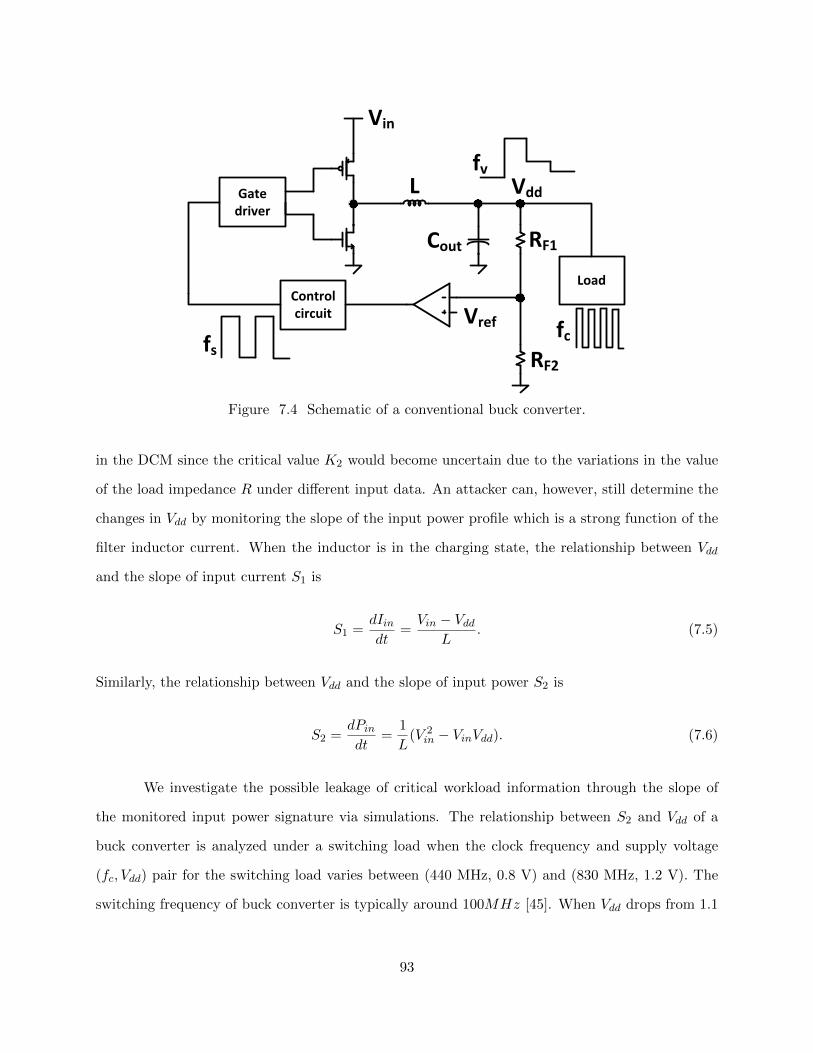
Controlcircuit
Gatedriver
Load
Vin
L Vdd
Cout RF1
RF2
Vref fcfs
fv
Figure 7.4 Schematic of a conventional buck converter.
in the DCM since the critical value K2 would become uncertain due to the variations in the value
of the load impedance R under different input data. An attacker can, however, still determine the
changes in Vdd by monitoring the slope of the input power profile which is a strong function of the
filter inductor current. When the inductor is in the charging state, the relationship between Vdd
and the slope of input current S1 is
S1 =dIindt
=Vin − Vdd
L. (7.5)
Similarly, the relationship between Vdd and the slope of input power S2 is
S2 =dPindt
=1
L(V 2in − VinVdd). (7.6)
We investigate the possible leakage of critical workload information through the slope of
the monitored input power signature via simulations. The relationship between S2 and Vdd of a
buck converter is analyzed under a switching load when the clock frequency and supply voltage
(fc, Vdd) pair for the switching load varies between (440 MHz, 0.8 V) and (830 MHz, 1.2 V). The
switching frequency of buck converter is typically around 100MHz [45]. When Vdd drops from 1.1
93

Supply voltage:
Vdd (V) 1.30
1.20
1.10
1.00
0.90
0.802.80 2.90 3.00 3.10 3.20 3.30 3.40
0.9 V
1.1 V
Time (us)
(a)
2.80 2.90 3.00 3.10 3.20 3.30 3.40
Time (us)
0
5
10
15
20
25
30Input power
(mW)
Slope=1.78mW/nsSlope=2.27mW/ns
(b)
Figure 7.5 (a) Transient supply voltage (output voltage) Vdd of a buck converter with VFS loadand (b) Transient input power profile of a buck converter with VFS load.
V to 0.9 V, S2 increases from 1.78 mW/ns to 2.27 mW/ns, as shown in Fig. 7.5. An inversely linear
relationship exists between S2 and Vdd, as illustrated in Fig. 7.6. This inversely linear relationship
demonstrates the possible information leakage through the slope of input power profile that may
nullify RDVFS technique under DPA attacks.
7.2.3 Switched-Capacitor (SC) Converter with VFS Load
An SC voltage converter utilizes one or multiple flying capacitors with a switch network
where the flying capacitors charge from the input voltage Vin and discharge to the output node
periodically to generate a DC output voltage Vdd. The basic architecture of an SC voltage converter
is illustrated in Fig. 7.7. Different voltage conversion ratios can be obtained by modifying the
connections of the switches and capacitors within an SC converter.
94
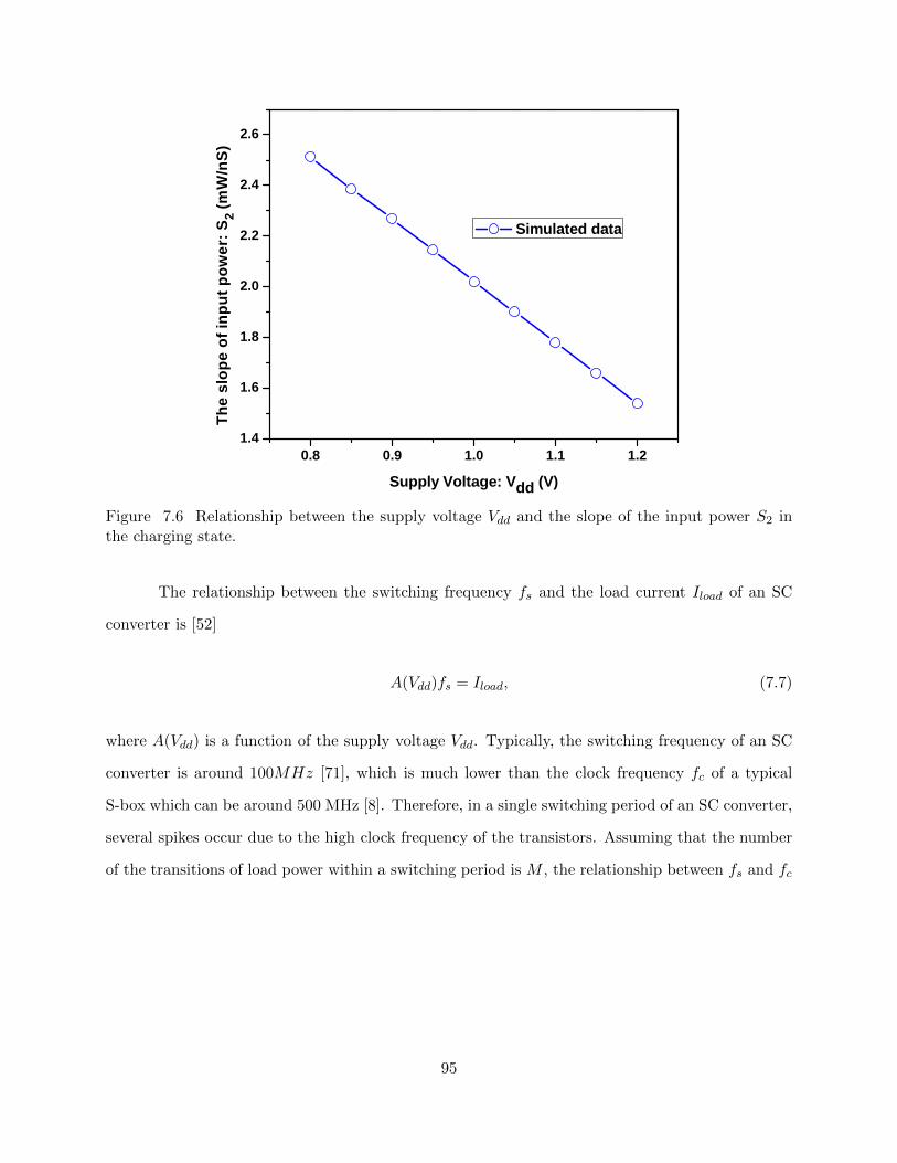
0 . 8 0 . 9 1 . 0 1 . 1 1 . 21 . 4
1 . 6
1 . 8
2 . 0
2 . 2
2 . 4
2 . 6
The s
lope o
f inpu
t pow
er: S 2 (m
W/nS
)
S u p p l y V o l t a g e : V d d ( V )
S i m u l a t e d d a t a
Figure 7.6 Relationship between the supply voltage Vdd and the slope of the input power S2 inthe charging state.
The relationship between the switching frequency fs and the load current Iload of an SC
converter is [52]
A(Vdd)fs = Iload, (7.7)
where A(Vdd) is a function of the supply voltage Vdd. Typically, the switching frequency of an SC
converter is around 100MHz [71], which is much lower than the clock frequency fc of a typical
S-box which can be around 500 MHz [8]. Therefore, in a single switching period of an SC converter,
several spikes occur due to the high clock frequency of the transistors. Assuming that the number
of the transitions of load power within a switching period is M , the relationship between fs and fc
95
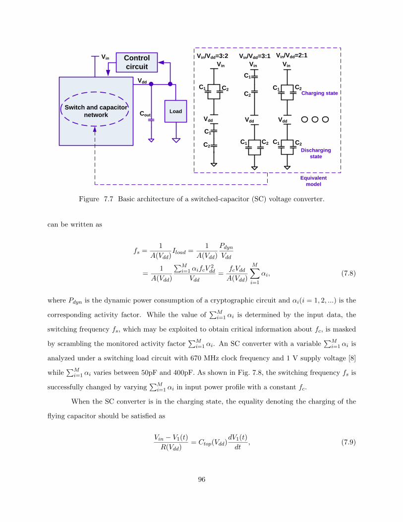
Switch and capacitor
network
C1 C2
C1
C1C1
C1 C2
C2
C1
C2
C2C2
Vin Vin Vin
Vdd Vdd Vdd
Vin/Vdd=3:2 Vin/Vdd=3:1 Vin/Vdd=2:1
Charging state
Discharging
state
Load
Vdd
Vin
Cout
Equivalent
model
Control
circuit
Figure 7.7 Basic architecture of a switched-capacitor (SC) voltage converter.
can be written as
fs =1
A(Vdd)Iload =
1
A(Vdd)
PdynVdd
=1
A(Vdd)
∑Mi=1 αifcV
2dd
Vdd=
fcVddA(Vdd)
M∑i=1
αi, (7.8)
where Pdyn is the dynamic power consumption of a cryptographic circuit and αi(i = 1, 2, ...) is the
corresponding activity factor. While the value of∑M
i=1 αi is determined by the input data, the
switching frequency fs, which may be exploited to obtain critical information about fc, is masked
by scrambling the monitored activity factor∑M
i=1 αi. An SC converter with a variable∑M
i=1 αi is
analyzed under a switching load circuit with 670 MHz clock frequency and 1 V supply voltage [8]
while∑M
i=1 αi varies between 50pF and 400pF. As shown in Fig. 7.8, the switching frequency fs is
successfully changed by varying∑M
i=1 αi in input power profile with a constant fc.
When the SC converter is in the charging state, the equality denoting the charging of the
flying capacitor should be satisfied as
Vin − V1(t)R(Vdd)
= Ctop(Vdd)dV1(t)
dt, (7.9)
96
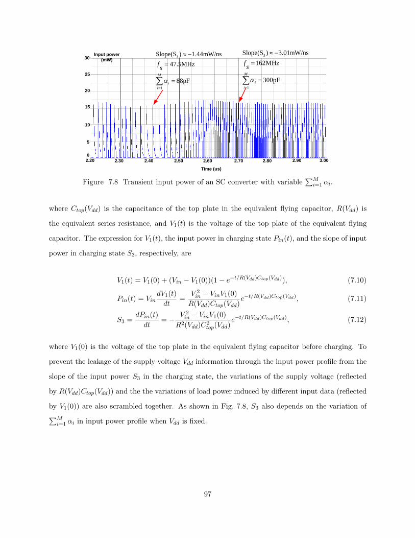
2.20 2.30 2.40 2.50 2.60 2.70 2.80 2.90 3.00
Time (us)
0
5
10
15
20
25
30Input power
(mW)
M
i
i
sf
1
3
pF300
MHz162
mW/ns01.3)Slope(S
M
i
i
sf
1
3
pF88
MHz5.47
mW/ns44.1)Slope(S
Figure 7.8 Transient input power of an SC converter with variable∑M
i=1 αi.
where Ctop(Vdd) is the capacitance of the top plate in the equivalent flying capacitor, R(Vdd) is
the equivalent series resistance, and V1(t) is the voltage of the top plate of the equivalent flying
capacitor. The expression for V1(t), the input power in charging state Pin(t), and the slope of input
power in charging state S3, respectively, are
V1(t) = V1(0) + (Vin − V1(0))(1− e−t/R(Vdd)Ctop(Vdd)), (7.10)
Pin(t) = VindV1(t)
dt=
V 2in − VinV1(0)
R(Vdd)Ctop(Vdd)e−t/R(Vdd)Ctop(Vdd), (7.11)
S3 =dPin(t)
dt= − V 2
in − VinV1(0)
R2(Vdd)C2top(Vdd)
e−t/R(Vdd)Ctop(Vdd), (7.12)
where V1(0) is the voltage of the top plate in the equivalent flying capacitor before charging. To
prevent the leakage of the supply voltage Vdd information through the input power profile from the
slope of the input power S3 in the charging state, the variations of the supply voltage (reflected
by R(Vdd)Ctop(Vdd)) and the the variations of load power induced by different input data (reflected
by V1(0)) are also scrambled together. As shown in Fig. 7.8, S3 also depends on the variation of∑Mi=1 αi in input power profile when Vdd is fixed.
97
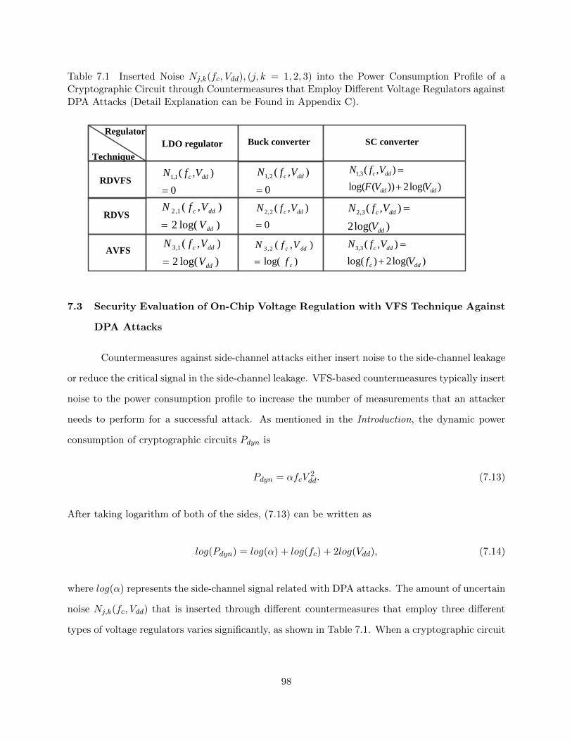
Table 7.1 Inserted Noise Nj,k(fc, Vdd), (j, k = 1, 2, 3) into the Power Consumption Profile of aCryptographic Circuit through Countermeasures that Employ Different Voltage Regulators againstDPA Attacks (Detail Explanation can be Found in Appendix C).
Regulator
Technique
LDO regulator Buck converter SC converter
RDVFS)log(2))(log(
),(3,1
dddd
ddc
VVF
VfN
RDVS
AVFS
0
),(1,1
ddc VfN
)log(2
),(1,2
dd
ddc
V
VfN
)log(2
),(1,3
dd
ddc
V
VfN
0
),(2,1
ddc VfN
0
),(2,2
ddc VfN
)log(
),(2,3
c
ddc
f
VfN
)log(2
),(3,2
dd
ddc
V
VfN
)log(2)log(
),(3,3
ddc
ddc
Vf
VfN
7.3 Security Evaluation of On-Chip Voltage Regulation with VFS Technique Against
DPA Attacks
Countermeasures against side-channel attacks either insert noise to the side-channel leakage
or reduce the critical signal in the side-channel leakage. VFS-based countermeasures typically insert
noise to the power consumption profile to increase the number of measurements that an attacker
needs to perform for a successful attack. As mentioned in the Introduction, the dynamic power
consumption of cryptographic circuits Pdyn is
Pdyn = αfcV2dd. (7.13)
After taking logarithm of both of the sides, (7.13) can be written as
log(Pdyn) = log(α) + log(fc) + 2log(Vdd), (7.14)
where log(α) represents the side-channel signal related with DPA attacks. The amount of uncertain
noise Nj,k(fc, Vdd) that is inserted through different countermeasures that employ three different
types of voltage regulators varies significantly, as shown in Table 7.1. When a cryptographic circuit
98

employs the AVFS technique with an SC converter, the inserted noise would contain both random
fc and random Vdd due to the independent relationship between fc and Vdd. When a cryptographic
circuit employs the RDVS technique with an SC converter, the inserted noise would only contain
random Vdd as the clock frequency fc is fixed. The inserted noise would be zero when the RDVFS
technique employs an LDO regulator or a buck converter as either fc or Vdd would leak through
the input power profile. By utilizing the correlation between fc and Vdd, the inserted noise in
the side-channel through the countermeasures may be eliminated . However, if a cryptographic
circuit employs an SC converter with the RDVFS technique, the uncertain noise would contain
both the random clock frequency and supply voltage. As compared to the AVFS technique, a
linear relationship exists between the clock frequency fc and supply voltage Vdd when the RDVFS
technique employs an SC converter. The clock frequency can therefore be denoted as a function of
the supply voltage (i.e., fc = F (Vdd) = K1.Vdd + B where K1 = 975 MHz/V and B = −340 MHz
when Vdd ∈ [0.8V, 1.2V ] and fc ∈ [440MHz, 830MHz] [8]).
7.3.1 Security of On-Chip Voltage Regulation with True Random VFS Technique
Against DPA Attacks
When all of the aforementioned techniques are true random, the clock frequency fc and
supply voltage Vdd would have uniform distributions. Let’s assume that VDD1 and VDD2 are,
respectively, the minimum and maximum voltage values that Vdd can operate. Similarly, f1 and f2
are, respectively, the minimum and maximum frequency values that fc can take. When the number
of discrete values that Vdd can take within [VDD1, VDD2] is N , the resolution of supply voltage ∆Vdd
and ith, (i = 1, 2, 3, ..., N) possible value Vdd,i within [VDD1, VDD2] can be, respectively, denoted as
∆Vdd,i =VDD2 − VDD1
N − 1, (7.15)
Vdd,i =(i− 1)× (VDD2 − VDD1)
N − 1+ VDD1. (7.16)
99
Similarly, assuming that frequency can get N different values within [f1, f2], the ith possible value
fc,i can be denoted as
fc,i =(i− 1)× (f2 − f1)
N − 1+ f1. (7.17)
If the frequency2 of the voltage scaling operation is fv, the mean value of the inserted noise
E(Nj,k(fc, Vdd)) for on-chip voltage regulation based and uniformly distributed RDVFS technique
(j = 1), RDVS technique (j = 2), and AVFS technique (j = 3), respectively, are
E(N1,k(fc, Vdd)) =1∑N
i=1[fc,ifv
]
N∑i=1
[fc,ifv
]N1,k(fc,i, Vdd,i), (7.18)
E(N2,k(fc, Vdd)) =1
N
N∑i=1
N2,k(fc, Vdd,i), (7.19)
E(N3,k(fc, Vdd)) =1
N∑N
l=1[fc,lfv
]
N∑l=1
N∑i=1
[fc,lfv
]N3,k(fc,l, Vdd,i). (7.20)
The corresponding variance of the inserted noise V ar(Nj,k(fc, Vdd)) can be denoted, respectively,
as
V ar(N1,k(fc, Vdd)) =
1∑Ni=1[
fc,ifv
]
N∑i=1
[fc,ifv
](N1,k(fc,i, Vdd,i)− E(N1,k(fc, Vdd)))2, (7.21)
2Since on-chip voltage regulator can generate variable supply voltage levels Vdd, we assume that the frequency ofthe voltage scaling is fv.
100
V ar(N2,k(fc, Vdd)) =
1
N
N∑i=1
(N2,k(fc, Vdd,i)− E(N2,k(fc, Vdd)))2, (7.22)
V ar(N3,k(fc, Vdd)) =1
N∑N
i=1[fc,lfv
]×
N∑l=1
N∑i=1
[fc,lfv
](N3,k(fc,l, Vdd,i)− E(N3,k(fc, Vdd)))2. (7.23)
A cryptographic circuit that employs on-chip voltage regulation based VFS technique can
be modeled with two separate noise insertion blocks (noise block1 and noise block2), as shown
in Fig. 7.9. Accordingly, the correlation coefficient between the input data and monitored power
consumption Pdyn of that cryptographic circuit can be represented with the correlation between the
input data and monitored power dissipation of those two noise insertion blocks. The signal-to-noise
ratio (SNR) at the output of the noise block2 SNR′′j,k can be denoted as
SNR′′j,k =
V ar(log(α))
V ar(Nj,k(fc, Vdd)), (7.24)
where V ar(log(α)) represents the variance of log(α). The correlation coefficient γ′′j,k between the
activity factor α and monitored power dissipation Pdyn of the cryptographic circuit can be obtained
as [75]
γ′′j,k =
1√1 + 1
SNR′′j,k
. (7.25)
Correlation coefficient between the input data and monitored power dissipation of the cryp-
tographic circuit is widely used as a metric to evaluate the level of security [3, 75, 93]. Since the
operations that take place in the noise block1 are independent of the operations that take place
in the noise block2, the correlation coefficient γj,k between the input data and monitored power
101
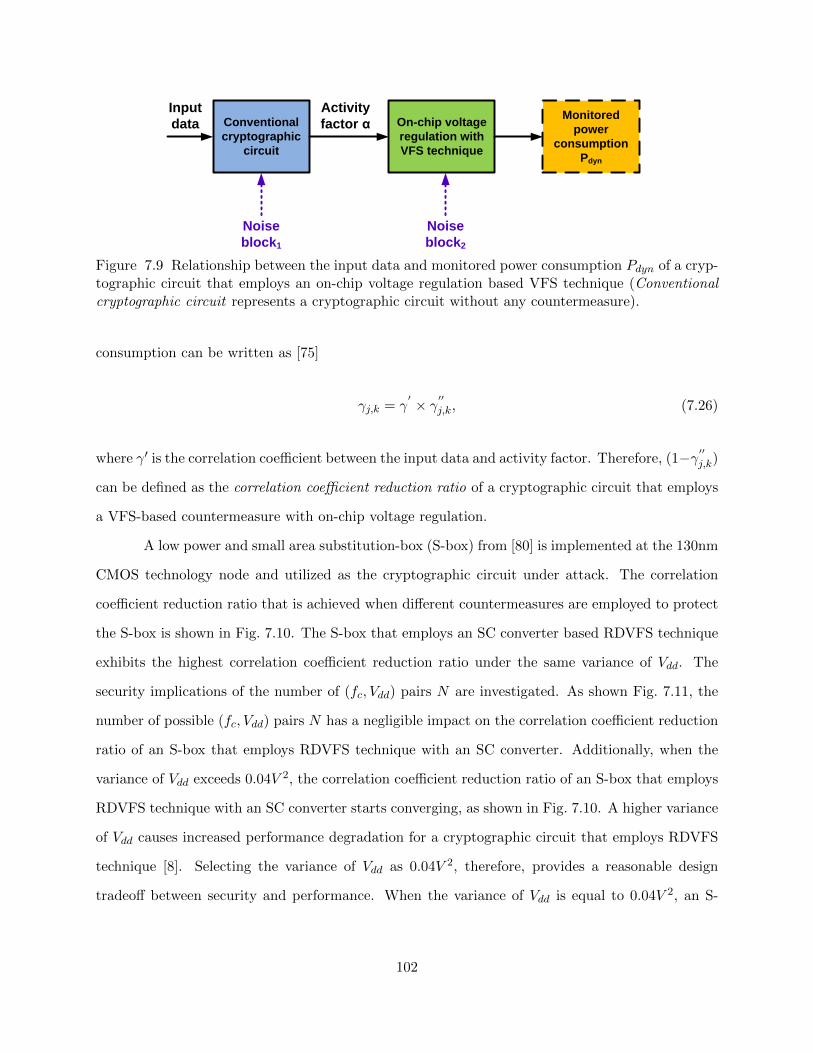
Conventional
cryptographic
circuit
On-chip voltage
regulation with
VFS technique
Monitored
power
consumption
Pdyn
Input
data
Activity
factor α
Noise
block1
Noise
block2
Figure 7.9 Relationship between the input data and monitored power consumption Pdyn of a cryp-tographic circuit that employs an on-chip voltage regulation based VFS technique (Conventionalcryptographic circuit represents a cryptographic circuit without any countermeasure).
consumption can be written as [75]
γj,k = γ′ × γ′′j,k, (7.26)
where γ′ is the correlation coefficient between the input data and activity factor. Therefore, (1−γ′′j,k)
can be defined as the correlation coefficient reduction ratio of a cryptographic circuit that employs
a VFS-based countermeasure with on-chip voltage regulation.
A low power and small area substitution-box (S-box) from [80] is implemented at the 130nm
CMOS technology node and utilized as the cryptographic circuit under attack. The correlation
coefficient reduction ratio that is achieved when different countermeasures are employed to protect
the S-box is shown in Fig. 7.10. The S-box that employs an SC converter based RDVFS technique
exhibits the highest correlation coefficient reduction ratio under the same variance of Vdd. The
security implications of the number of (fc, Vdd) pairs N are investigated. As shown Fig. 7.11, the
number of possible (fc, Vdd) pairs N has a negligible impact on the correlation coefficient reduction
ratio of an S-box that employs RDVFS technique with an SC converter. Additionally, when the
variance of Vdd exceeds 0.04V 2, the correlation coefficient reduction ratio of an S-box that employs
RDVFS technique with an SC converter starts converging, as shown in Fig. 7.10. A higher variance
of Vdd causes increased performance degradation for a cryptographic circuit that employs RDVFS
technique [8]. Selecting the variance of Vdd as 0.04V 2, therefore, provides a reasonable design
tradeoff between security and performance. When the variance of Vdd is equal to 0.04V 2, an S-
102
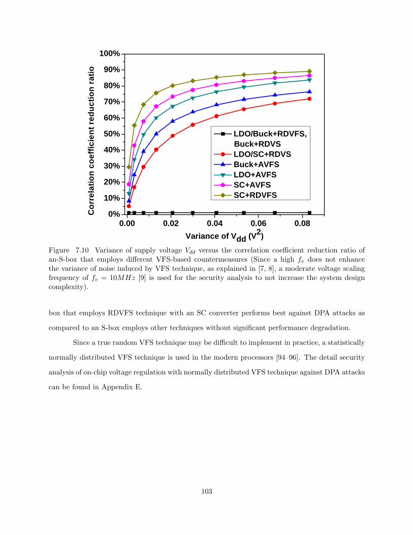
0 . 0 0 0 . 0 2 0 . 0 4 0 . 0 6 0 . 0 80 %
1 0 %2 0 %3 0 %4 0 %5 0 %6 0 %7 0 %8 0 %9 0 %
1 0 0 %
Corre
lation
coeff
icien
t red
uctio
n rati
o
V a r i a n c e o f V d d ( V 2 )
L D O / B u c k + R D V F S , B u c k + R D V S
L D O / S C + R D V S B u c k + A V F S L D O + A V F S S C + A V F S S C + R D V F S
Figure 7.10 Variance of supply voltage Vdd versus the correlation coefficient reduction ratio ofan-S-box that employs different VFS-based countermeasures (Since a high fv does not enhancethe variance of noise induced by VFS technique, as explained in [7, 8], a moderate voltage scalingfrequency of fv = 10MHz [9] is used for the security analysis to not increase the system designcomplexity).
box that employs RDVFS technique with an SC converter performs best against DPA attacks as
compared to an S-box employs other techniques without significant performance degradation.
Since a true random VFS technique may be difficult to implement in practice, a statistically
normally distributed VFS technique is used in the modern processors [94–96]. The detail security
analysis of on-chip voltage regulation with normally distributed VFS technique against DPA attacks
can be found in Appendix E.
103
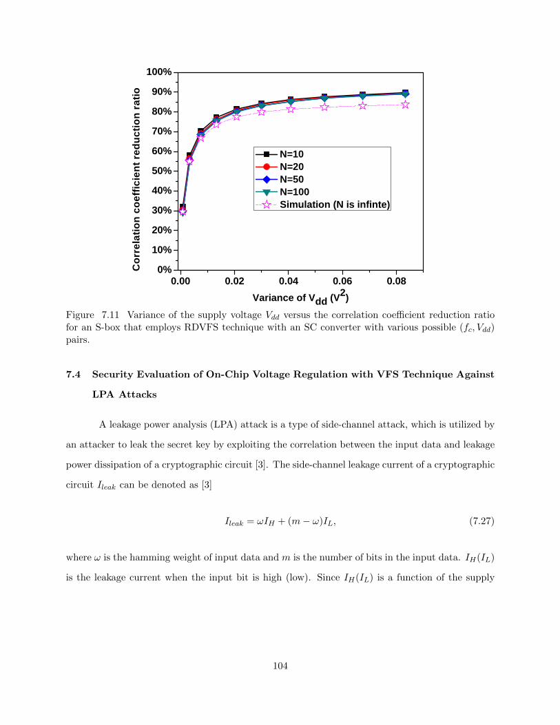
0 . 0 0 0 . 0 2 0 . 0 4 0 . 0 6 0 . 0 80 %
1 0 %2 0 %3 0 %4 0 %5 0 %6 0 %7 0 %8 0 %9 0 %
1 0 0 %
Corre
lation
coeff
icien
t red
uctio
n rati
o
V a r i a n c e o f V d d ( V 2 )
N = 1 0 N = 2 0 N = 5 0 N = 1 0 0 S i m u l a t i o n ( N i s i n f i n t e )
Figure 7.11 Variance of the supply voltage Vdd versus the correlation coefficient reduction ratiofor an S-box that employs RDVFS technique with an SC converter with various possible (fc, Vdd)pairs.
7.4 Security Evaluation of On-Chip Voltage Regulation with VFS Technique Against
LPA Attacks
A leakage power analysis (LPA) attack is a type of side-channel attack, which is utilized by
an attacker to leak the secret key by exploiting the correlation between the input data and leakage
power dissipation of a cryptographic circuit [3]. The side-channel leakage current of a cryptographic
circuit Ileak can be denoted as [3]
Ileak = ωIH + (m− ω)IL, (7.27)
where ω is the hamming weight of input data and m is the number of bits in the input data. IH(IL)
is the leakage current when the input bit is high (low). Since IH(IL) is a function of the supply
104
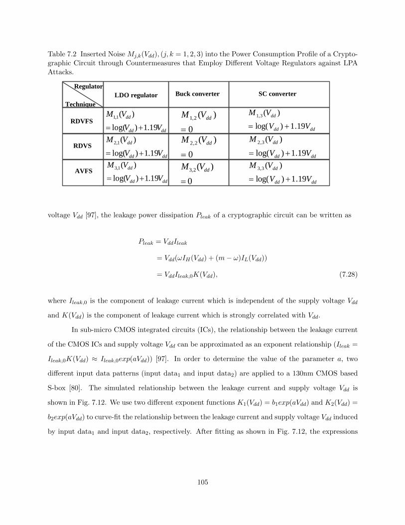
Table 7.2 Inserted Noise Mj,k(Vdd), (j, k = 1, 2, 3) into the Power Consumption Profile of a Crypto-graphic Circuit through Countermeasures that Employ Different Voltage Regulators against LPAAttacks.
Regulator
Technique
LDO regulator Buck converter SC converter
RDVFS
RDVS
AVFS
dddd
dd
VV
VM
19.1)log(
)(1,1
0
)(2,1
ddVM
dddd
dd
VV
VM
19.1)log(
)(1,2
dddd
dd
VV
VM
19.1)log(
)(1,3
0
)(2,2
ddVM
0
)(2,3
ddVM
dddd
dd
VV
VM
19.1)log(
)(3,1
dddd
dd
VV
VM
19.1)log(
)(3,2
dddd
dd
VV
VM
19.1)log(
)(3,3
voltage Vdd [97], the leakage power dissipation Pleak of a cryptographic circuit can be written as
Pleak = VddIleak
= Vdd(ωIH(Vdd) + (m− ω)IL(Vdd))
= VddIleak,0K(Vdd), (7.28)
where Ileak,0 is the component of leakage current which is independent of the supply voltage Vdd
and K(Vdd) is the component of leakage current which is strongly correlated with Vdd.
In sub-micro CMOS integrated circuits (ICs), the relationship between the leakage current
of the CMOS ICs and supply voltage Vdd can be approximated as an exponent relationship (Ileak =
Ileak,0K(Vdd) ≈ Ileak,0exp(aVdd)) [97]. In order to determine the value of the parameter a, two
different input data patterns (input data1 and input data2) are applied to a 130nm CMOS based
S-box [80]. The simulated relationship between the leakage current and supply voltage Vdd is
shown in Fig. 7.12. We use two different exponent functions K1(Vdd) = b1exp(aVdd) and K2(Vdd) =
b2exp(aVdd) to curve-fit the relationship between the leakage current and supply voltage Vdd induced
by input data1 and input data2, respectively. After fitting as shown in Fig. 7.12, the expressions
105

0 . 4 0 . 6 0 . 8 1 . 0 1 . 2 1 . 4
4 0
6 0
8 0
1 0 0
1 2 0
1 4 0
1 6 0
Leak
age c
urren
t (nA)
S u p p l y v o l t a g e V d d ( V )
I n p u t d a t a 1 ( S i m u l a t i o n ) M a t c h i n g w i t h K 1 ( V d d ) I n p u t d a t a 2 ( S i m u l a t i o n ) M a t c h i n g w i t h K 2 ( V d d )
Figure 7.12 Supply voltage Vdd versus leakage current of an S-box implemented in 130nm CMOStechnology under two different input data.
of K1(Vdd) and K2(Vdd) can be respectively determined as
K1(Vdd) = 27× exp(1.19× Vdd) ≈ 27K(Vdd), (7.29)
K2(Vdd) = 28.29× exp(1.19× Vdd) ≈ 28.29K(Vdd). (7.30)
Therefore, the leakage power dissipation of the S-box Pleak can be denoted as
Pleak = VddIleak,0K(Vdd),
≈ Vdd × Ileak,0 × exp(1.19× Vdd). (7.31)
After taking logarithm of both sides, (7.31) becomes
log(Pleak) ≈ log(Ileak,0) + log(Vdd) + 1.19Vdd, (7.32)
106

0 . 0 0 0 . 0 2 0 . 0 4 0 . 0 6 0 . 0 80 %
1 0 %2 0 %3 0 %4 0 %5 0 %6 0 %7 0 %8 0 %9 0 %
1 0 0 %
Corre
lation
coeff
icien
t red
uctio
n rati
o
V a r i a n c e o f V d d ( V 2 )
L D O / S C + R D V F S / A V F S ( u n i f o r m l y d i s t r i b u t e d )
L D O / S C + R D V S ( u n i f o r m l y d i s t r i b u t e d )
L D O / S C + R D V F S / A V F S ( n o r m a l l y d i s t r i b u t e d )
L D O / S C + R D V S ( n o r m a l l y d i s t r i b u t e d )
B u c k + R D V F S / R D V S / A V F S
Figure 7.13 Variance of supply voltage Vdd versus the correlation coefficient reduction ratio of anS-box that employs different countermeasures (fv = 10MHz and N = 50).
where log(Ileak,0) is the side-channel signal which may provide useful information under an LPA
attack. The characteristics of the inserted noise Mj,k(Vdd) to an S-box through different coun-
termeasures against LPA attacks are listed in Table 7.2. Since a buck converter leaks the supply
voltage Vdd from the slope of input power, the uncertain noise Mj,2(Vdd) that is inserted by a buck
converter based VFS technique becomes zero.
As shown in Fig. 7.13, an S-box that employs the RDVFS technique with an SC converter
can achieve a correlation coefficient reduction ratio of over 90% when the variance of supply voltage
Vdd is greater than 0.04V 2.
7.5 Overhead Analysis
The power overhead of several VFS-based countermeasures with on-chip voltage regulation
is summarized in Table 7.3. An S-box [80] that houses an SC voltage converter exhibits the
107
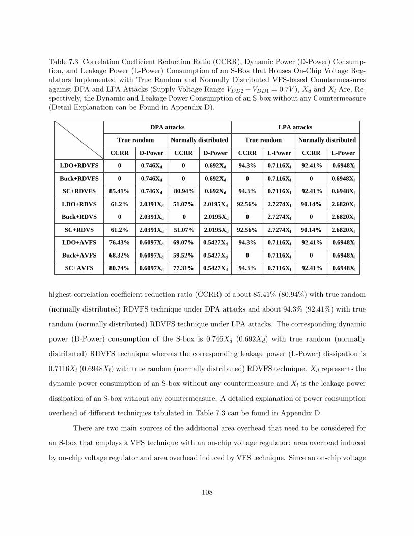
LDO+RDVFS
Buck+RDVFS
SC+RDVFS
LDO+RDVS
Buck+RDVS
SC+RDVS
LDO+AVFS
Buck+AVFS
SC+AVFS
DPA attacks
True random
0
0
85.41%
61.2%
0
61.2%
76.43%
68.32%
80.74%
0.746Xd
0.746Xd
0.746Xd
2.0391Xd
2.0391Xd
2.0391Xd
0.6097Xd
0.6097Xd
0.6097Xd
Normally distributed
0
0
80.94%
51.07%
0
51.07%
69.07%
59.52%
77.31%
0.692Xd
0.692Xd
0.692Xd
2.0195Xd
2.0195Xd
2.0195Xd
0.5427Xd
0.5427Xd
0.5427Xd
LPA attacks
True random
94.3%
0
94.3%
92.56%
0
92.56%
94.3%
0
94.3%
0.7116Xl
0.7116Xl
0.7116Xl
2.7274Xl
2.7274Xl
2.7274Xl
0.7116Xl
0.7116Xl
0.7116Xl
Normally distributed
92.41%
0
92.41%
90.14%
0
90.14%
92.41%
0
92.41%
0.6948Xl
0.6948Xl
0.6948Xl
2.6820Xl
2.6820Xl
2.6820Xl
0.6948Xl
0.6948Xl
0.6948Xl
CCRR D-Power CCRR D-Power CCRR L-Power CCRR L-Power
Table 7.3 Correlation Coefficient Reduction Ratio (CCRR), Dynamic Power (D-Power) Consump-tion, and Leakage Power (L-Power) Consumption of an S-Box that Houses On-Chip Voltage Reg-ulators Implemented with True Random and Normally Distributed VFS-based Countermeasuresagainst DPA and LPA Attacks (Supply Voltage Range VDD2− VDD1 = 0.7V ), Xd and Xl Are, Re-spectively, the Dynamic and Leakage Power Consumption of an S-box without any Countermeasure(Detail Explanation can be Found in Appendix D).
highest correlation coefficient reduction ratio (CCRR) of about 85.41% (80.94%) with true random
(normally distributed) RDVFS technique under DPA attacks and about 94.3% (92.41%) with true
random (normally distributed) RDVFS technique under LPA attacks. The corresponding dynamic
power (D-Power) consumption of the S-box is 0.746Xd (0.692Xd) with true random (normally
distributed) RDVFS technique whereas the corresponding leakage power (L-Power) dissipation is
0.7116Xl (0.6948Xl) with true random (normally distributed) RDVFS technique. Xd represents the
dynamic power consumption of an S-box without any countermeasure and Xl is the leakage power
dissipation of an S-box without any countermeasure. A detailed explanation of power consumption
overhead of different techniques tabulated in Table 7.3 can be found in Appendix D.
There are two main sources of the additional area overhead that need to be considered for
an S-box that employs a VFS technique with an on-chip voltage regulator: area overhead induced
by on-chip voltage regulator and area overhead induced by VFS technique. Since an on-chip voltage
108
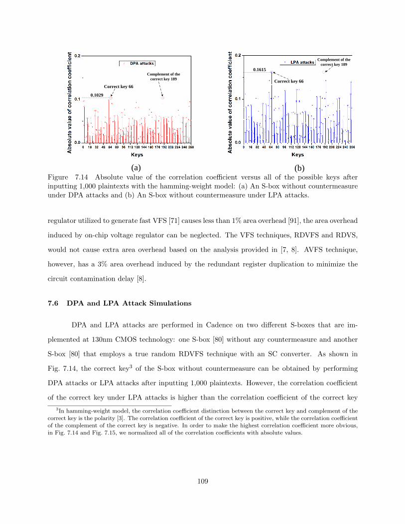
Correct key 66
Complement of the
correct key 189
0.1029
Correct key 66
Complement of the
correct key 189
0.1615
(a) (b)Figure 7.14 Absolute value of the correlation coefficient versus all of the possible keys afterinputting 1,000 plaintexts with the hamming-weight model: (a) An S-box without countermeasureunder DPA attacks and (b) An S-box without countermeasure under LPA attacks.
regulator utilized to generate fast VFS [71] causes less than 1% area overhead [91], the area overhead
induced by on-chip voltage regulator can be neglected. The VFS techniques, RDVFS and RDVS,
would not cause extra area overhead based on the analysis provided in [7, 8]. AVFS technique,
however, has a 3% area overhead induced by the redundant register duplication to minimize the
circuit contamination delay [8].
7.6 DPA and LPA Attack Simulations
DPA and LPA attacks are performed in Cadence on two different S-boxes that are im-
plemented at 130nm CMOS technology: one S-box [80] without any countermeasure and another
S-box [80] that employs a true random RDVFS technique with an SC converter. As shown in
Fig. 7.14, the correct key3 of the S-box without countermeasure can be obtained by performing
DPA attacks or LPA attacks after inputting 1,000 plaintexts. However, the correlation coefficient
of the correct key under LPA attacks is higher than the correlation coefficient of the correct key
3In hamming-weight model, the correlation coefficient distinction between the correct key and complement of thecorrect key is the polarity [3]. The correlation coefficient of the correct key is positive, while the correlation coefficientof the complement of the correct key is negative. In order to make the highest correlation coefficient more obvious,in Fig. 7.14 and Fig. 7.15, we normalized all of the correlation coefficients with absolute values.
109
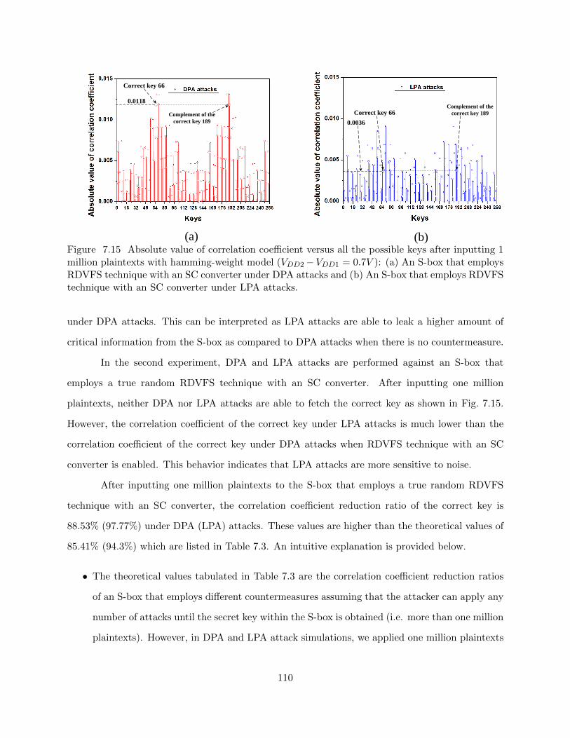
Correct key 66
Complement of the
correct key 189
0.0118
Correct key 66Complement of the
correct key 189
0.0036
(a) (b)Figure 7.15 Absolute value of correlation coefficient versus all the possible keys after inputting 1million plaintexts with hamming-weight model (VDD2−VDD1 = 0.7V ): (a) An S-box that employsRDVFS technique with an SC converter under DPA attacks and (b) An S-box that employs RDVFStechnique with an SC converter under LPA attacks.
under DPA attacks. This can be interpreted as LPA attacks are able to leak a higher amount of
critical information from the S-box as compared to DPA attacks when there is no countermeasure.
In the second experiment, DPA and LPA attacks are performed against an S-box that
employs a true random RDVFS technique with an SC converter. After inputting one million
plaintexts, neither DPA nor LPA attacks are able to fetch the correct key as shown in Fig. 7.15.
However, the correlation coefficient of the correct key under LPA attacks is much lower than the
correlation coefficient of the correct key under DPA attacks when RDVFS technique with an SC
converter is enabled. This behavior indicates that LPA attacks are more sensitive to noise.
After inputting one million plaintexts to the S-box that employs a true random RDVFS
technique with an SC converter, the correlation coefficient reduction ratio of the correct key is
88.53% (97.77%) under DPA (LPA) attacks. These values are higher than the theoretical values of
85.41% (94.3%) which are listed in Table 7.3. An intuitive explanation is provided below.
• The theoretical values tabulated in Table 7.3 are the correlation coefficient reduction ratios
of an S-box that employs different countermeasures assuming that the attacker can apply any
number of attacks until the secret key within the S-box is obtained (i.e. more than one million
plaintexts). However, in DPA and LPA attack simulations, we applied one million plaintexts
110
and the S-box that employs a true random RDVFS technique with an SC converter could not
be cracked after inputting one million plaintexts as shown in Fig. 7.15. This indicates the
presence of significant amount of noise in the S-box. If more plaintexts are applied to filter
the noise, the correlation coefficient of the correct key would be enhanced and the correlation
coefficient reduction ratio would decrease, approaching the theoretical value.
7.7 Conclusion
The security implications of different on-chip voltage regulator topologies implemented
within various voltage/frequency scaling-based countermeasures such as RDVFS, RDVS, and AVFS
techniques against power analysis attacks are investigated. The side-channel leakage mechanisms
of three widely used on-chip voltage regulator topologies are investigated. The security impact
of on-chip voltage regulators is evaluated based on the correlation coefficient between the input
data and monitored power consumption of a cryptographic circuit. Correlation coefficient reduc-
tion ratio is proposed to simplify the security evaluation. RDVFS technique implemented with
a switched-capacitor voltage converter can reduce correlation coefficient over 80% (92%) against
DPA (LPA) attacks and the measurement-to-disclose (MTD) value is enhanced over 1 million by
masking the clock frequency, supply voltage, and dynamic power consumption information from a
malicious attacker.
111
CHAPTER 8:
CONCLUSION
On-chip voltage regulation can be utilized as a lightweight and efficient countermeasure
against power analysis attacks. Converter-reshuffling (CoRe) voltage converter utilizes a pseudo-
random number generator (PRNG) to increase the input power trace entropy against DPA attacks.
Time-delayed CoRe voltage converter eliminates the risk of having a zero input power trace entropy
against machine learning-based DPA attacks by delaying half of phases with a certain time period.
However, charge-withheld CoRe voltage converter further enhances the input power trace entropy
against DPA attacks through utilizing two PRNGs to control the charging and discharging of flying
capacitors.
As compared to a substitution-box (S-box) without employing on-chip voltage regulation,
the measurement-to-disclose (MTD) value is enhanced about 71.4 times against DPA attacks if
CoRe voltage converter is utilized to power an S-box. When a conventional AES engine employs
a centralized CoRe voltage converter, the MTD value is enhanced over 544 times against DPA
attacks. However, when CoRe voltage converter is co-designed with an improved AES engine, the
MTD value can be enhanced over 9,100 times against DPA attacks by reshuffling the power noise
generated from the S-boxes which are not under DPA attacks.
If the CoRe voltage converter is designed with security adaptive mode, the MTD value
is enhanced over 6,145 times against LPA attacks through activating the discharging resistor to
scramble the input power profile when LPA attacks are sensed. As shown in the simulation results,
when an S-box is powered by a security-adaptive (SA) voltage converter, the MTD value of the
S-box is over 2 million against LPA attacks. By contrast, the MTD value of an S-box without
countermeasure is less than 500.
112

Additionally, if conventional switched-capacitor (SC) converter employs random dynamic
voltage and frequency scaling (RDVFS), the correlation coefficient between the input data and
monitored power dissipation reduces over 80 (92) percent against DPA (LPA) attacks. As demon-
strated in the simulations, the MTD value of an S-box that employs RDVFS with an SC converter
is over 1 million against both DPA and LPA attacks by masking the leakage of the clock fre-
quency and supply voltage information in the input power profile. However, for an S-box without
countermeasure, the MTD value is less than 1,000 against both DPA and LPA attacks.
113
CHAPTER 9:
FUTURE WORK
9.1 Utilizing On-Chip Multi-Phase Buck Converter as a Countermeasure Against
Electro-Magnetic (EM) Attacks
In my previous research works [11, 54, 56, 59, 82, 87], we mainly utilized on-chip multi-phase
switched-capacitor (SC) converter to mask the actual power dissipation of the cryptographic circuit
from a malicious attacker in the input power profile against power analysis attacks. However, as
shown in Fig. 9.1, the attacker may bypass the on-chip voltage regulator and implement electro-
magnetic (EM) attacks on the cryptographic circuit directly. The attacker may use a near-field
or far-field probe to capture the EM emissions radiated from the cryptographic circuit and exploit
the correlation between the input data and EM emissions leaked from the cryptographic circuit.
As a result, a cryptographic circuit with on-chip multi-phase SC converter may still be vulnerable
against EM attacks.
To protect a cryptographic circuit against EM attacks, a multi-phase buck converter can
be utilized to co-design with the cryptographic circuit. The EM radiation from an inductor is
significantly stronger than a capacitor [98]. Therefore, as shown in Fig. 9.2, all the inductors in the
multi-phase buck converter can be uniformly distributed among the cryptographic circuit in the
layout. Under such condition, with the impact of pseudo-random number generator (PRNG), the
random EM emissions radiated from randomly reshuffled inductors in each switching period can
act as noise to reduce the signal-to-noise ratio (SNR) significantly against EM attacks.
Although multi-phase buck converter can be utilized as a countermeasure against EM at-
tacks, if the attacker implements power analysis attacks and EM attacks on a cryptographic circuit
with on-chip multi-phase buck converter simultaneously, the secret key in the cryptographic circuit
114
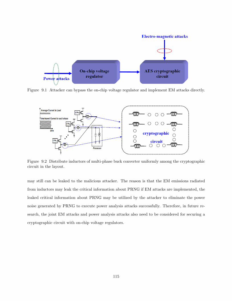
Figure 9.1 Attacker can bypass the on-chip voltage regulator and implement EM attacks directly.
Figure 9.2 Distribute inductors of multi-phase buck converter uniformly among the cryptographiccircuit in the layout.
may still can be leaked to the malicious attacker. The reason is that the EM emissions radiated
from inductors may leak the critical information about PRNG if EM attacks are implemented, the
leaked critical information about PRNG may be utilized by the attacker to eliminate the power
noise generated by PRNG to execute power analysis attacks successfully. Therefore, in future re-
search, the joint EM attacks and power analysis attacks also need to be considered for securing a
cryptographic circuit with on-chip voltage regulators.
115
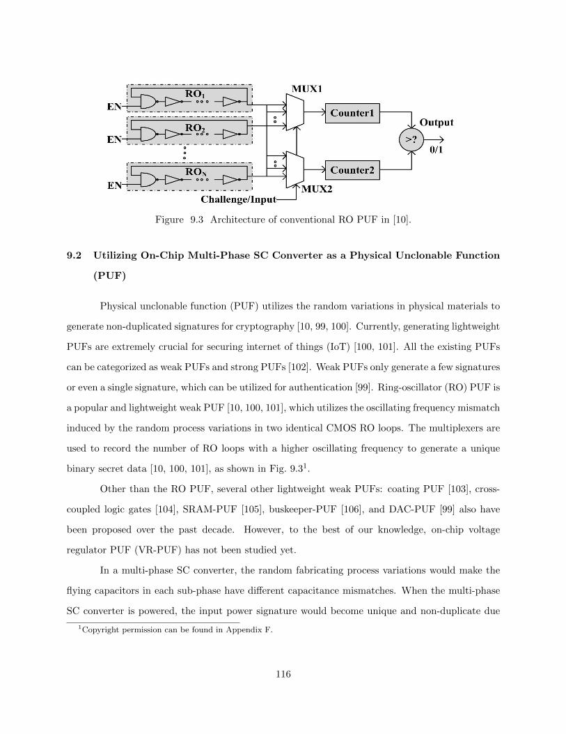
Figure 9.3 Architecture of conventional RO PUF in [10].
9.2 Utilizing On-Chip Multi-Phase SC Converter as a Physical Unclonable Function
(PUF)
Physical unclonable function (PUF) utilizes the random variations in physical materials to
generate non-duplicated signatures for cryptography [10, 99, 100]. Currently, generating lightweight
PUFs are extremely crucial for securing internet of things (IoT) [100, 101]. All the existing PUFs
can be categorized as weak PUFs and strong PUFs [102]. Weak PUFs only generate a few signatures
or even a single signature, which can be utilized for authentication [99]. Ring-oscillator (RO) PUF is
a popular and lightweight weak PUF [10, 100, 101], which utilizes the oscillating frequency mismatch
induced by the random process variations in two identical CMOS RO loops. The multiplexers are
used to record the number of RO loops with a higher oscillating frequency to generate a unique
binary secret data [10, 100, 101], as shown in Fig. 9.31.
Other than the RO PUF, several other lightweight weak PUFs: coating PUF [103], cross-
coupled logic gates [104], SRAM-PUF [105], buskeeper-PUF [106], and DAC-PUF [99] also have
been proposed over the past decade. However, to the best of our knowledge, on-chip voltage
regulator PUF (VR-PUF) has not been studied yet.
In a multi-phase SC converter, the random fabricating process variations would make the
flying capacitors in each sub-phase have different capacitance mismatches. When the multi-phase
SC converter is powered, the input power signature would become unique and non-duplicate due
1Copyright permission can be found in Appendix F.
116
to the random flying capacitance in each sub-phase. For instance, in a 16-phase SC converter,
assume six phases are activated to provide power to the load and the sequence of active phases is
#2-#4-#5-#8-#12-#15. If another 16-phase SC converter is designed with the same parameter
and same sequence of active phases, the input power signatures of those two 16-phase SC converters
are different due to the impact of random capacitance variations in the flying capacitors.
Since there is a PRNG in the multi-phase SC converter, when the sequence of active phases
is reshuffled by the PRNG, the multi-phase SC converter would generate another different input
power profile. Therefore, with the impact of PRNG, multi-phase SC converter also can be designed
as strong PUFs since a large amount of different input power signatures can be achieved. In future
research, intra-HD and inter-HD will be the two vital parameters to evaluate the proposed VR-PUF.
For a perfect weak PUF, the intra-HD should be 0% and inter-HD should be 50% [99]. In addition,
if the proposed VR-PUF is applied as a strong PUF, the challenge-response-pairs (CRP) [99, 102]
need to be considered to evaluate how many different signatures can VR-PUF output.
117
REFERENCES
[1] D. Oswald and R.-U. Bochum, “ID and IP theft with side-channel attacks,” 2014. [On-line]. Available: http://www.slideshare.net/phdays/1300-david-oswald-id-and-ip-theft-with-sidechannel-attacks.
[2] P.-C. Liu, H.-C. Chang, and C.-Y. Lee, “A low overhead DPA countermeasure circuit basedon ring oscillators,” IEEE Transactions on Circuits and System II: Express Briefs, vol. 57,no. 7, pp. 546–550, Jul. 2010.
[3] M. Alioto, L. Giancane, G. Scotti, and A. Trifiletti, “Leakage power analysis attacks: A novelclass of attacks to nanometer cryptographic circuits,” IEEE Transactions on Circuits andSystem I: Regular Papers, vol. 57, no. 2, pp. 355–367, Feb. 2010.
[4] O. A. Uzun and S. Kose, “Converter-gating: A power efficient and secure on-chip powerdelivery system,” IEEE Journal on Emerging and Selected Topics in Circuits and Systems,vol. 4, no. 2, pp. 169–179, Jun. 2014.
[5] Y. Wang and Y. Ha, “FPGA-based 40.9-Gbits/s masked AES with area optimization forstorage area network,” IEEE Transactions on Circuits and System II: Express Briefs, vol. 60,no. 1, pp. 36–40, Jan. 2013.
[6] F. Regazzoni, Y. Wang, and F. X. Standaert, “Fault attack for the iterative operation ofAES S-Box,” in Proc. Constructive Side-Channel Analysis and Secure Design (COSADE),Feb. 2011, pp. 56–66.
[7] K. Baddam and M. Zwolinski, “Evaluation of dynamic voltage and frequency scaling as adifferential power analysis countermeasure,” in Proc. VLSI design, Jan. 2007, pp. 854–862.
[8] N. D. P. Avirneni and A. K. Somani, “Countering power analysis attacks using reliable andaggressive designs,” IEEE Transactions on Computers, vol. 63, no. 6, pp. 1408–1420, Jun.2014.
[9] B. Lee, E. Nurvitadhi, R. Dixit, C. Yu, and M. Kim, “Dynamic voltage scaling techniquesfor power efficient video decoding,” the EUROMICRO Journal, vol. 51, no. 10, pp. 633–652,2005.
[10] M. T. Rahman, F. Rahman, D. Forte, and M. Tehranipoor, “An aging-resistant RO-PUF forreliable key generation,” IEEE Transactions on Emerging Topics in Computing, vol. 4, no. 3,pp. 335–348, Sep. 2016.
[11] W. Yu and S. Kose, “Leveraging on-chip voltage regulators as a countermeasure againstside-channel attacks,” in Proc. Design Automation Conference (DAC), Jun. 2015, pp. 1–6.
118

[12] M. Arora, “How secure is AES against brute force attacks?” 2012. [Online]. Available:http://www.eetimes.com/document.asp?doc id=1279619.
[13] W. Yu and S. Kose, “A Lightweight Masked AES Implementation for Securing IoT AgainstCPA Attacks,” IEEE Transactions on Circuits and System I: Regular Papers, in press.
[14] P. Rakers, L. Connell, T. Collins, and D. Russell, “Secure contactless smartcard ASIC withDPA protection,” IEEE Journal of Solid-State Circuits, vol. 36, no. 3, pp. 559–565, Mar.2001.
[15] A. Cevrero, F. Regazzoni, M. Schwander, S. Badel, P. Ienne, and Y. Leblebici, “Power-gatedMOS current mode Logic (PG-MCML): A power aware DPA-resistant standard cell library,”in Proc. Design Automation Conference (DAC), May 2011, pp. 1014–1019.
[16] W. Cilio, M. Linder, C. Porter, J. Di, D. R. Thompson, and S. C. Smith, “Mitigatingpower- and timing-based side-channel attacks using dual-spacer dual-rail delay-insensitiveasynchronous logic,” Microelectronics Journal, vol. 44, no. 3, pp. 258–269, Mar. 2013.
[17] J. A. Ambrose, R. G. Ragel, and S. Parameswaran, “Randomized instruction injectionto counter power analysis attacks,” ACM Transactions on Embedded Computing Systems,vol. 11, no. 3, pp. 69:1–69:28, Mar. 2012.
[18] C. Clavier, J.-S. Coron, and N. Dabbous, Eds., Differential power analysis in the presence ofhardware countermeasures. Springer, 2000.
[19] W. Yu and S. Kose, “Security implications of simultaneous dynamic and leakage power anal-ysis attacks on nanoscale cryptographic circuits,” IET Electronics Letters, vol. 52, no. 6, pp.466–468, Mar. 2016.
[20] P. Kocher, J. Jaffe, B. Jun, and P. Rohatgi, “Introduction to differential power analysis,”Journal of Cryptographic Engineering, vol. 1, no. 1, pp. 5–27, 2011.
[21] S. Yang, W. Wolf, N. Vijaykrishnan, D. Serpanos, and Y. Xie, “Power attack resistant cryp-tosystem design: A dynamic voltage and frequency switching aproach,” in Proc. Design,Automation and Test in Europe (DATE), Mar. 2005, pp. 64–69.
[22] W. Yu and S. Kose, “False key-controlled aggressive voltage scaling: A countermeasureagainst LPA attacks,” IEEE Transactions on Computer-Aided Design of Integrated Circuitsand Systems, in press.
[23] S. Kose and E. G. Friedman, “An area efficient fully monolithic hybrid voltage regulator,” inProc. ISCAS, May 2010, pp. 2718–2721.
[24] I. Vaisband, B. Price, S. Kose, Y. Kolla, E. G. Friedman, and J. Fischer, “Distributed LDOregulators in a 28 nm power delivery system,” Analog Integrated Circuits and Signal Process-ing, vol. 83, no. 3, pp. 295–309, 2015.
[25] S. Kose and E. G. Friedman, “Fast algorithms for power grid analysis based on effectiveresistance,” in Proc. ISCAS, May 2010, pp. 3661–3664.
119

[26] I. Vaisband, M. Azhar, E. G. Friedman, and S. Kose, “Digitally controlled pulse width mod-ulator for on-chip power management,” IEEE Transactions on Very Large Scale Integration(VLSI) Systems, vol. 22, no. 12, pp. 2527–2534, Dec. 2014.
[27] S. Kose and E. G. Friedman, “On-chip point-of-load voltage regulator for distributed powersupplies,” in Proc. GLVLSI, May 2010, pp. 377–380.
[28] S. Kose, E. Salman, and E. G. Friedman, “Shielding methodologies in the presence ofpower/ground noise,” IEEE Transactions on Very Large Scale Integration (VLSI) Systems,vol. 19, no. 8, pp. 1458–1468, Aug. 2011.
[29] S. Kose and E. G. Friedman, “Effective resistance of a two layer mesh,” IEEE Transactionson Circuits and System II: Express Briefs, vol. 58, no. 11, pp. 739–743, Nov. 2011.
[30] S. Kose, I. Vaisband, and E. G. Friedman, “Digitally controlled wide range pulse widthmodulator for on-chip power supplies,” in Proc. ISCAS, May 2013, pp. 2251–2254.
[31] S. Kose and E. G. Friedman, “Distributed power delivery for energy efficient and low powersystems,” in Proc. Signals, Systems, and Computers, Nov. 2012, pp. 757–761.
[32] S. Kose, S. Tam, S. Pinzon, B. McDermott, and E. G. Friedman, “An area effcient on-chiphybrid voltage regulator,” in Proc. ISQED, Mar. 2012, pp. 398–403.
[33] S. Kose and E. G. Friedman, “Fast algorithms for IR voltage drop analysis exploiting locality,”in Proc. Design Automation Conference (DAC), Jun. 2011, pp. 996–1001.
[34] I. Savidis, S. Kose, and E. G. Friedman, “Power grid noise in TSV-based 3-D integratedsystems,” in Proc. Government Microcircuit Applications and Critical Technology, Mar. 2011,pp. 129–132.
[35] S. Kose and E. G. Friedman, “Distributed power network co-design with on-chip power sup-plies and decoupling capacitors,” in Proc. System Level Interconnect Prediction (SLIP), Jun.2011.
[36] S. Kose, E. Salman, and E. G. Friedman, “Shielding methodologies in the presence ofpower/ground noise,” in Proc. ISCAS, May 2009, pp. 2277–2280.
[37] S. Kose and E. G. Friedman, “Design methodology to distribute on-chip power in next gen-eration integrated circuits,” in Proc. SoC, Sep. 2010, pp. 15–18.
[38] M. J. Azhar and S. Kose, “An enhanced pulse width modulator with adaptive duty cycle andfrequency control,” in Proc. ISCAS, May 2014, pp. 958–961.
[39] I. Savidis, S. Kose, and E. G. Friedman, “Power noise in TSV-based 3-D integrated circuits,”IEEE Journal of Solid-State Circuits, vol. 48, no. 2, pp. 587–597, Feb. 2013.
[40] S. Kose, “Thermal implications of on-chip voltage regulation: Upcoming challenges and pos-sible solutions,” in Proc. Design Automation Conference (DAC), Jun. 2014, pp. 1–6.
[41] O. A. Uzun and S. Kose, “Regulator-gating methodology with distributed switched capacitorvoltage converters,” in Proc. ISVLSI, Jul. 2014, pp. 13–18.
120
[42] S. Kose, “Regulator-gating: Adaptive management of on-chip voltage regulators,” in Proc.GLVLSI, May 2014, pp. 105–110.
[43] Y. K. Ramadass, A. A. Fayed, and A. P. Chandrakasan, “A fully-integrated switched-capacitor step-down DC-DC converter with digital capacitance modulation in 45 nm CMOS,”IEEE Journal of Solid-State Circuits, vol. 45, no. 12, pp. 2557–2565, Dec. 2010.
[44] E. Alon and M. Horowitz, “Integrated regulation for energy-efficient digital circuits,” IEEEJournal of Solid-State Circuits, vol. 43, no. 8, pp. 1795–1807, Aug. 2008.
[45] W. Kim, M. S. Gupta, G.-Y. Wei, and D. Brooks, “System level analysis of fast, per-coreDVFS using on-chip switching regulators,” in Proc. High Performance Computer Architecture(HPCA), Feb. 2008, pp. 123–134.
[46] L. Benini, A. Bogliolo, and G. D. Micheli, “A survey of design techniques for system-leveldynamic power management,” IEEE Transactions on Very Large Scale Integration (VLSI)Systems, vol. 8, no. 3, pp. 299–316, Mar. 2000.
[47] V. Kursun and E. G. Friedman, Eds., Multi-voltage CMOS circuit design. John Wiley &Sons, 2006.
[48] G. R. Mora, Ed., Analog IC design with low-dropout regulators (LDOs). McGraw-Hill Pub-lishers, 2009.
[49] C. F. Lee and P. K. Mok, “A monolithic current-mode CMOS DC-DC converter with on-chipcurrent-sensing technique,” IEEE Journal of Solid-State Circuits, vol. 39, no. 1, pp. 3–14,Jan. 2004.
[50] V. Kursun, S. G. Narendra, V. K. De, and E. G. Friedman, “Analysis of buck converters foron-chip integration with a dual supply voltage microprocessor,” IEEE Transactions on VeryLarge Scale Integration (VLSI) Systems, vol. 11, no. 3, pp. 514–522, Jun. 2003.
[51] G. A. R. Mora, Ed., Current efficient, low voltage, low drop-out regulators. Ph.D. thesis,Georgia Institute of Technology, 1996.
[52] T. M. A. et al., “A 4.6 W/mm2 power density 86% efficiency on-chip switched capacitorDC-DC converter in 32 nm SOI CMOS,” in Proc. Applied Power Electronics Conference andExposition, Mar. 2013, pp. 692–699.
[53] B. Kopf and D. Basin, “An information-theoretic model for adaptive side-channel attacks,”in Proc. Computer and communications security (CCS), Oct. 2007, pp. 286–296.
[54] W. Yu and S. Kose, “Time-delayed converter-reshuffling: An efficient and secure power de-livery architecture,” IEEE Embedded Systems Letters, vol. 7, no. 3, pp. 73–76, Sep. 2015.
[55] H. Maghrebi, S. Guilley, J. L. Danger, and F. Flament, “Entropy-based power attack,” inProc. Hardware-Oriented Security and Trust (HOST), Jun. 2010, pp. 1–6.
[56] W. Yu and S. Kose, “Charge-withheld converter-reshuffling (CoRe): A countermeasureagainst power analysis attacks,” IEEE Transactions on Circuits and System II: ExpressBriefs, vol. 63, no. 5, pp. 438–442, May 2016.
121

[57] H. Jeon, Ed., Fully integrated on-chip switched capacitor DC-DC converters for battery-powered mixed-signal SoCs. Ph.D. thesis, Northeastern Univ., 2012.
[58] M. D. Seeman, Ed., A design methodology for switched-capacitor DC-DC converters. Ph.D.thesis, Univ.of California at Berkeley, 2009.
[59] W. Yu and S. Kose, “A voltage regulator-assisted lightweight AES implementation againstDPA attacks,” IEEE Transactions on Circuits and System I: Regular Papers, vol. 63, no. 8,pp. 1152–1163, Aug. 2016.
[60] D. Wu, X. Cui, W. Wei, R. Li, D. Yu, and X. Cui, “Research on circuit level countermeasuresfor differential power analysis attacks,” in Proc. Solid-State and Integrated Circuit Technolody,Oct. 2012, pp. 1–3.
[61] C. Tokunaga and D. Blaauw, “Securing encryption systems with a switched capacitor currentequalizer,” IEEE Journal of Solid-State Circuits, vol. 45, no. 1, pp. 23–31, Jan. 2010.
[62] X. Wang, W. Yueh, D. B. Roy, S. Narasimhan, Y. Zheng, S. Mukhopadhyay, D. Mukhopad-hyay, and S. Bhunia, “Role of power grid in side channel attack and power-grid-aware securedesign,” in Proc. Design Automation Conference (DAC), Jun. 2013, pp. 1–9.
[63] G. Khedkar, D. Kudithipudi, and G. S. Rose, “Power profile obfuscation using nanoscalememristive devices to counter DPA attacks,” IEEE Transactions on Nanotechnology, vol. 14,no. 1, pp. 26–35, Jan. 2015.
[64] F. Regazzoni, T. Eisenbarth, J.Grobschadl, L. Breveglieri, P. Ienne, I. Koren, and C.Paar,“Power attacks resistance of cryptographic S-boxes with added error detection circuits,” inProc. Defect and Fault-Tolerance in VLSI Systems, Sep. 2007, pp. 508–516.
[65] S. Kose, S. Tam, S. Pinzon, B. McDermott, and E. G. Friedman, “Active filter based hybridon-chip DC-DC converters for point-of-load voltage regulation,” IEEE Transactions on VeryLarge Scale Integration (VLSI) Systems, vol. 21, no. 4, pp. 680–691, Apr. 2013.
[66] J. D. Vos, D. Flandre, and D. Bol, “A sizing methodology for on-chip switched-capacitorDC/DC converters,” IEEE Transactions on Circuits and System I: Regular Papers, vol. 61,no. 5, pp. 1597–1606, May 2014.
[67] Y. Lu, Y. Wang, Q. Pan, W.-H. Ki, and C. P. Yue, “A fully-integrated low-dropout regulatorwith full-spectrum power supply rejection,” IEEE Transactions on Circuits and System I:Regular Papers, vol. 62, no. 3, pp. 707–716, Mar. 2015.
[68] S.-W. Hong and G.-H. Cho, “High-gain wide-bandwidth capacitor-less low-dropout regulator(LDO) for mobile applications utilizing frequency response of multiple feedback loops,” IEEETransactions on Circuits and System I: Regular Papers, vol. 63, no. 1, pp. 46–57, Jan. 2016.
[69] Z. Toprak-Deniz, M. Sperling, J. F. Bulzacchelli, G. Still, R. Kruse, S. Kim, D. Boerstler,T. Gloekler, R. Robertazzi, K. Stawiasz, T. Diemoz, G. English, D. Hui, P. Muench, andJ. Friedrich, “Distributed system of digitally controlled microregulators enabling per-coreDVFS for the POWER8TM microprocessor,” in Proc. IEEE International Solid-State CircuitsConference (ISSCC), Feb. 2014, pp. 98–99.
122
[70] S. Kose and E. G. Friedman, “Distributed on-chip power delivery,” IEEE Journal on Emerg-ing and Selected Topics in Circuits and Systems, vol. 2, no. 4, pp. 704–713, Dec. 2012.
[71] P. Zhou, A. Paul, C. H. Kim, and S. S. Sapatnekar, “Distributed on-chip switched-capacitorDC-DC converters supporting DVFS in multicore systems,” IEEE Transactions on Very LargeScale Integration (VLSI) Systems, vol. 22, no. 9, pp. 1954–1967, Sep. 2014.
[72] A. Hodjat and I. Verbauwhede, “Area-throughput trade-offs for fully pipelined 30 to 70Gbits/s AES processors,” IEEE Transactions on Computers, vol. 55, no. 4, pp. 366–372,Apr. 2006.
[73] F. Wu, L. Wang, and J. Wan, “A low cost and inner-round pipelined design of ECB-AES-256crypto engine for solid state disk,” in Proc. Networking, Architecture and Storage (NAS), Jul.2010, pp. 485–491.
[74] T. Good and M. Benaissa, “Very small FPGA application-specific instruction processor forAES,” IEEE Transactions on Circuits and System I: Regular Papers, vol. 53, no. 7, pp.1477–1486, Jul. 2006.
[75] F. Standaert, E. Peeters, G. Rouvroy, and J. Quisquater, “An overview of power analysisattacks against field programmable gate arrays,” Proceedings of the IEEE, vol. 94, no. 2, pp.383–394, Feb. 2006.
[76] E. A. Burton, G. Schrom, F. Paillet, J. Douglas, W. J. Lambert, K. Radhakrishnan, and M. J.Hill, “FIVR-Fully integrated voltage regulators on 4th generation Intel Core SoCs,” in Proc.Applied Power Electronics Conference and Exposition (APEC), Mar. 2014, pp. 432–439.
[77] P. A. Hung, K. Klomkarn, and P. Sooraksa, “Image encryption based on chaotic map and dy-namic S-box,” in Proc. Intelligent Signal Processing and Communications Systems (ISPACS),Nov. 2013, pp. 435–439.
[78] A. Joshi, P. K. Dakhole, and A. Thatere, “Implementation of S-Box for advanced encryptionstandard,” in Proc. Engineering and Technology (ICETECH), Mar. 2015, pp. 1–5.
[79] J. Park, S. Moon, D. Choi, Y. Kang, and J. Ha, “Fault attack for the iterative operation ofAES S-Box,” in Proc. Computer Sciences and Convergence Information Technology (ICCIT),Nov. 2010, pp. 550–555.
[80] N. Ahmad and S. M. R. Hasan, “Low-power compact composite field AES S-Box/Inv S-Boxdesign in 65 nm CMOS using novel XOR gate,” Integration, the VLSI Journal, vol. 46, no. 4,pp. 333–344, Sep. 2013.
[81] N. Kamoun, L. Bossuet, and A. Ghazel, “Correlated power noise generator as a low cost DPAcountermeasures to secure hardware AES cipher,” in Proc. Signals, Circuits and Systems(SCS), Nov. 2009, pp. 1–6.
[82] W. Yu and S. Kose, “Security-adaptive voltage conversion as a lightweight countermeasureagainst LPA attacks,” IEEE Transactions on Very Large Scale Integration (VLSI) Systems,in press.
123
[83] S. M. D. Pozo, F.-X. Standaert, D. Kamel, and A. Moradi, “Side-channel attacks from staticpower: When should we care?” in Proc. Design, Automation and Test in Europe (DATE),Mar. 2015, pp. 145–150.
[84] M. Alioto, S. Bongiovanni, M. Djukanovic, G. Scotti, and A. Trifiletti, “Effectiveness ofleakage power analysis attacks on DPA-resistant logic styles under process variations,” IEEETransactions on Circuits and System I: Regular Papers, vol. 61, no. 2, pp. 429–442, Feb. 2014.
[85] D. D. Huang, K. Tiri, A. Hodjat, B.-C. Lai, S. Yang, P. Schaumont, and I. Verbauwhede,“AES-based security coprocessor IC in 0.18-um CMOS with resistance to differential poweranalysis side-channel attacks,” IEEE Journal of Solid-State Circuits, vol. 41, no. 4, pp. 781–791, Apr. 2006.
[86] M. Avital, H. Dagan, I. Levi, O. Keren, and A. Fish, “DPA-secured quasi-adiabatic logic(SQAL) for low-power passive RFID tags employing S-boxes,” IEEE Transactions on Circuitsand System I: Regular Papers, vol. 62, no. 1, pp. 149–156, Jan. 2015.
[87] W. Yu and S. Kose, “Exploiting voltage regulators to enhance various power attack counter-measures,” IEEE Transactions on Emerging Topics in Computing, in press.
[88] K. Tiri and I. Verbauwhede, “A logic level design methodology for a secure DPA resistantASIC or FPGA implementation,” in Proc. Design, Automation and Test in Europe (DATE),Feb. 2004, pp. 246–251.
[89] N. S. Kim, K. Flautner, D. Blaauw, and T. Mudge, “Drowsy instruction caches. Leakagepower reduction using dynamic voltage scaling and cache sub-bank prediction,” in Proc.Microarchitecture, 2002, pp. 219–230.
[90] A. Moradi, “Side-channel leakage through static power-Should we care about in practice?-,”in Proc. Cryptographic Hardware and Embedded Systems, 2014, pp. 562–579.
[91] E. J. F. et al., “The 12-Core POWER8 processor with 7.6 Tb/s IO bandwidth, integratedvoltage regulation, and resonant clocking,” IEEE Journal of Solid-State Circuits, vol. 50,no. 1, pp. 10–23, Jan. 2015.
[92] X. Qu, Z.-K. Zhou, B. Zhang, and Z.-J. Li, “An ultralow-power fast-transient capacitor-freelow-dropout regulator with assistant pushpull output stage,” IEEE Transactions on Circuitsand System II: Express Briefs, vol. 60, no. 2, pp. 96–100, Feb. 2013.
[93] S. A. Seyyedi, M. Kamal, H. Noori, and S. Safari, “Securing embedded processors againstpower analysis based side channel attacks using reconfigurable architecture,” in Proc. Em-bedded and Ubiquitous Computing (EUC), Oct. 2011, pp. 255–260.
[94] J. Kim, S. Yoo, and C.-M. Kyung, “Program phase and runtime distribution-aware onlineDVFS for combined Vdd/Vbb scaling,” in Proc. Design, Automation and Test in Europe(DATE), Apr. 2009, pp. 417–422.
[95] S. Garg, D. Marculescu, R. Marculescu, and U. Ogras, “Technology-driven limits on DVFScontrollability of multiple voltage-frequency island designs: A system-level perspective,” inProc. Design Automation Conference (DAC), Jul. 2009, pp. 818–821.
124
[96] Q. Wu, P. Juang, M. Martonosi, and D. W. Clark, “Voltage and frequency control with adap-tive reaction time in multiple-clock-domain processors,” in Proc. High-Performance ComputerArchitecture, Feb. 2005, pp. 178–189.
[97] C. Gopalakrishnan, Ed., High level techniques for leakage power estimation and optimizationin VLSI ASICs. Ph.D. Dissertation, Univ. of South Florida, 2003.
[98] H. W. Ott, “Understanding and controlling common-mode emissions in high-power electron-ics,” http://www.hottconsultants.com/pdf files/APEC-2002.pd.
[99] A. Herkle, J. Becker, and M. Ortmanns, “Exploiting weak PUFs from data converternonlinearity-E.g., a multibit CT ∆
∑Modulator,” IEEE Transactions on Circuits and Sys-
tem I: Regular Papers, vol. 63, no. 7, pp. 994–1004, Jul. 2016.
[100] Y. Cao, L. Zhang, C.-H. Chang, and S. Chen, “A low-power hybrid RO PUF with improvedthermal stability for lightweight applications,” IEEE Transactions on Computer-Aided Designof Integrated Circuits and Systems, vol. 34, no. 7, pp. 1143–1147, Jul. 2015.
[101] D. Yamamoto, M. Takenaka, K. Sakiyama, and N. Torii, “Security evaluation of bistablering PUFs on FPGAs using differential and linear analysis,” in Proc. Computer Science andInformation Systems (FedCSIS), Sep. 2014, pp. 911–918.
[102] C. Herder, M.-D. Yu, F. Koushanfar, and S. Devadas, “Physical unclonable functions andapplications: A tutorial,” Proceedings of the IEEE, vol. 102, no. 8, pp. 1126–1141, Aug. 2014.
[103] P. Tuyls, G.-J. Schrijen, B. Skoric, J. Geloven, N. Verhaegh, and R. Wolters, “Read-proofhardware from protective coatings,” in Proc. Cryptographic Hardware and Embedded Systems(CHES), Oct. 2006, pp. 369–383.
[104] Y. Su, J. Holleman, and B. Otis, “A digital 1.6 pJ/bit chip identification circuit using processvariations,” IEEE Journal of Solid-State Circuits, vol. 43, no. 1, pp. 69–77, Jan. 2008.
[105] J. Guajardo, S. S. Kumar, G.-J. Schrijen, and P. Tuyls, “FPGA intrinsic PUFs and their usefor IP protection,” in Proc. Cryptographic Hardware and Embedded Systems (CHES), Sep.2007, pp. 63–80.
[106] P. Simons, E. v. d. Sluis, and V. v. d. Leest, “Buskeeper PUFs, a promising alternative to Dflip-flop PUFs,” in Proc. HOST, Jun. 2012, pp. 7–12.
125

APPENDICES
126
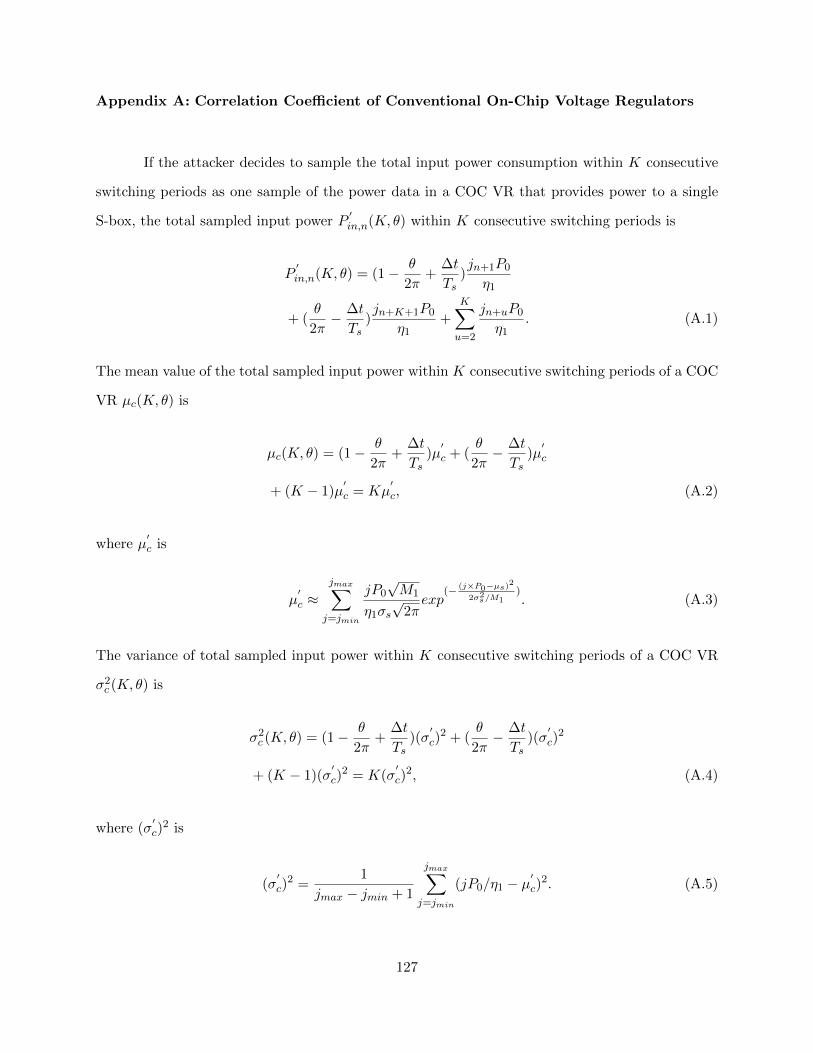
Appendix A: Correlation Coefficient of Conventional On-Chip Voltage Regulators
If the attacker decides to sample the total input power consumption within K consecutive
switching periods as one sample of the power data in a COC VR that provides power to a single
S-box, the total sampled input power P′in,n(K, θ) within K consecutive switching periods is
P′in,n(K, θ) = (1− θ
2π+
∆t
Ts)jn+1P0
η1
+ (θ
2π− ∆t
Ts)jn+K+1P0
η1+
K∑u=2
jn+uP0
η1. (A.1)
The mean value of the total sampled input power within K consecutive switching periods of a COC
VR µc(K, θ) is
µc(K, θ) = (1− θ
2π+
∆t
Ts)µ′c + (
θ
2π− ∆t
Ts)µ′c
+ (K − 1)µ′c = Kµ
′c, (A.2)
where µ′c is
µ′c ≈
jmax∑j=jmin
jP0
√M1
η1σs√
2πexp
(− (j×P0−µs)2
2σ2s/M1). (A.3)
The variance of total sampled input power within K consecutive switching periods of a COC VR
σ2c (K, θ) is
σ2c (K, θ) = (1− θ
2π+
∆t
Ts)(σ
′c)
2 + (θ
2π− ∆t
Ts)(σ
′c)
2
+ (K − 1)(σ′c)
2 = K(σ′c)
2, (A.4)
where (σ′c)
2 is
(σ′c)
2 =1
jmax − jmin + 1
jmax∑j=jmin
(jP0/η1 − µ′c)
2. (A.5)
127
The correlation coefficient γc(K, θ) of a COC VR can therefore be obtained as
γc(K, θ) =E(P
′in,n(K, θ)× Pload,n(K, θ))
σc(K, θ)×√K/M1σs
− µc(K, θ)×Kµsσc(K, θ)×
√K/M1σs
, (A.6)
where
E(P′in,n(K, θ)× Pload,n(K, θ)) =
1
(jmax − jmin + 1)K+1
× (
jmax∑jn+K+1=jmin
...
jmax∑jn+1=jmin
(((1− θ
2π+
∆t
Ts)jn+1P0
η1
+ (θ
2π− ∆t
Ts)jn+K+1P0
η1+
K∑u=2
jn+uP0
η1)×
((1− θ
2π)jn+1P0 +
θ
2πjn+K+1P0 +
K∑u=2
jn+uP0))). (A.7)
Accordingly, the average correlation coefficient of a COC VR γc(K) can be denoted as
γc(K) =1
2π
∫ 2π
0γc(K, θ)dθ. (A.8)
128
Appendix B: Guidelines on the Selection of a Suitable Active Critical Frequency Fac
Two different kinds of noise may impact the MTD enhancement ratio of a cryptographic
circuit that employs a CoRe voltage converter: i) measurement power noise from devices that are
used to perform the measurement and ii) reshuffling power noise from the CoRe voltage converter.
When a cryptographic circuit is in a normal working mode (i.e., clock frequency fc ≈ F1fs
and F1 is an integer), the measured input power PMIP,i of the CoRe voltage converter induced by
the ith input data is
PMIP,i = P ∗in,i(θ, 1/(F1fs)) + PM,i, (B.1)
where P ∗in,i(θ, 1/(F1fs)) is the actual input power of the CoRe voltage converter induced by the
ith input data and PM,i is the corresponding measurement power noise. When the variance of
P ∗in,i(θ, 1/(F1fs)) is σ21(θ, 1/(F1fs)), the average variance σ21(1/(F1fs)) of P ∗in,i(θ, 1/(F1fs)) becomes
σ21(1/(F1fs)) =1
2π
∫ 2π
0σ21(θ, 1/(F1fs))dθ. (B.2)
Accordingly, the signal-to-noise ratio (SNR) of the input power profile SNRM (1/(F1fs)) can be
written as
SNRM (1/(F1fs)) =σ21(1/(F1fs))
σ2M, (B.3)
where σ2M is the variance of the measurement power noise.
However, when the attacker lowers the clock frequency from F1fs to fc (i.e., F1fs/fc is an
integer, the attacker can measure F1fs/fc number of leakage power data), the total measured input
power PTMIP,i of the CoRe voltage converter induced by the ith input data is
PTMIP,i = P ∗in,i(θ, 1/fc) +
F1fs/fc∑j1=1
PM,i,j1 , (B.4)
129
where PM,i,j1 is the corresponding measurement power noise related with the jth1 measurement
under the ith input data. Therefore, the SNR of the input power profile SNRM (1/fc) can be
written as
SNRM (1/fc) =σ21(1/fc)F1fsfcσ2M
. (B.5)
The correlation coefficient γM (1/fc) between the actual input power and measured input power of
the CoRe voltage converter with measurement power noise when the clock frequency is fc can be
written as [75]
γM (1/fc) =1√
1 + 1SNRM (1/fc)
. (B.6)
When the clock frequency is fc and the average correlation coefficient between the actual
input power and load power of the CoRe voltage converter is γRe(1/fc)1, the measurement power
noise and reshuffling power noise from the CoRe voltage converter are independent. The correlation
coefficient γt(1/fc) between the measured input power and load power of the CoRe voltage converter
can therefore be written as [75]
γt(1/fc) = γM (1/fc)× γRe(1/fc). (B.7)
The total MTD enhancement ratio MTDt(1/fc) induced by the measurement power noise and
reshuffling power noise from the CoRe voltage converter is [75]
MTDt(1/fc) ∝1
(γt(1/fc))2. (B.8)
1Modeling of the average correlation coefficient of voltage converter with a variable clock frequency is analyzed inSection 6.4.1.
130
As compared to a cryptographic circuit with the clock frequency of (1/F0)fs, the MTD value
of a cryptographic circuit with the clock frequency of fc would be enhanced fs/(fcF0) times.
MTDt(1/fc) therefore becomes
MTDt(1/fc) '1F0fs
fc× 1
(γt(1/fc))2. (B.9)
As shown in Fig. 6.3(b), the minimum MTD enhancement ratio of a cryptographic circuit
with the SA voltage converter is 6,145. When the MTD enhancement ratio induced by the mea-
surement power noise and reshuffling power noise from the CoRe voltage converter is lower than the
minimum MTD enhancement ratio induced by the SA voltage converter, the discharging resistor
Rc needs to be activated to trigger the SA voltage converter to enhance the security. Therefore, an
approximately optimum active critical frequency Fac can be determined by solving
MTDt(1/Fac) '1F0fs
Fac× 1
(γt(1/Fac))2= 6145. (B.10)
131
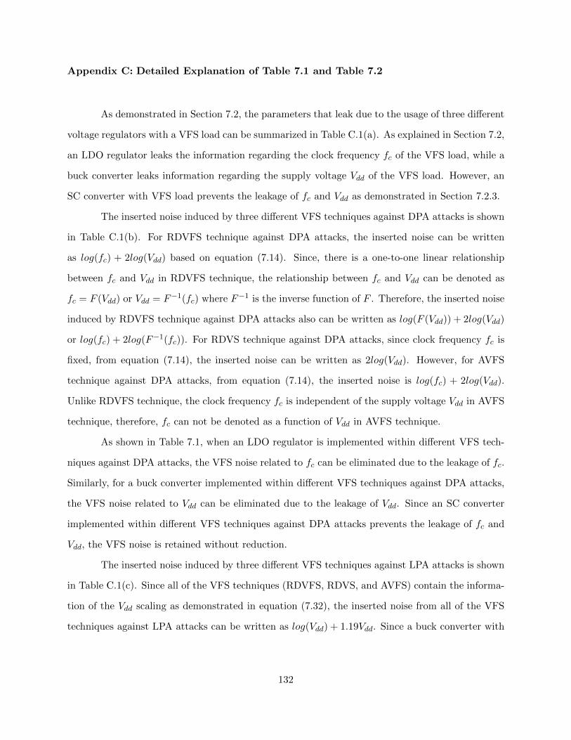
Appendix C: Detailed Explanation of Table 7.1 and Table 7.2
As demonstrated in Section 7.2, the parameters that leak due to the usage of three different
voltage regulators with a VFS load can be summarized in Table C.1(a). As explained in Section 7.2,
an LDO regulator leaks the information regarding the clock frequency fc of the VFS load, while a
buck converter leaks information regarding the supply voltage Vdd of the VFS load. However, an
SC converter with VFS load prevents the leakage of fc and Vdd as demonstrated in Section 7.2.3.
The inserted noise induced by three different VFS techniques against DPA attacks is shown
in Table C.1(b). For RDVFS technique against DPA attacks, the inserted noise can be written
as log(fc) + 2log(Vdd) based on equation (7.14). Since, there is a one-to-one linear relationship
between fc and Vdd in RDVFS technique, the relationship between fc and Vdd can be denoted as
fc = F (Vdd) or Vdd = F−1(fc) where F−1 is the inverse function of F . Therefore, the inserted noise
induced by RDVFS technique against DPA attacks also can be written as log(F (Vdd)) + 2log(Vdd)
or log(fc) + 2log(F−1(fc)). For RDVS technique against DPA attacks, since clock frequency fc is
fixed, from equation (7.14), the inserted noise can be written as 2log(Vdd). However, for AVFS
technique against DPA attacks, from equation (7.14), the inserted noise is log(fc) + 2log(Vdd).
Unlike RDVFS technique, the clock frequency fc is independent of the supply voltage Vdd in AVFS
technique, therefore, fc can not be denoted as a function of Vdd in AVFS technique.
As shown in Table 7.1, when an LDO regulator is implemented within different VFS tech-
niques against DPA attacks, the VFS noise related to fc can be eliminated due to the leakage of fc.
Similarly, for a buck converter implemented within different VFS techniques against DPA attacks,
the VFS noise related to Vdd can be eliminated due to the leakage of Vdd. Since an SC converter
implemented within different VFS techniques against DPA attacks prevents the leakage of fc and
Vdd, the VFS noise is retained without reduction.
The inserted noise induced by three different VFS techniques against LPA attacks is shown
in Table C.1(c). Since all of the VFS techniques (RDVFS, RDVS, and AVFS) contain the informa-
tion of the Vdd scaling as demonstrated in equation (7.32), the inserted noise from all of the VFS
techniques against LPA attacks can be written as log(Vdd) + 1.19Vdd. Since a buck converter with
132
Table C.1 (a) Parameter Leakage of Three Different Voltage Regulators with VFS Load, (b)Inserted Noise Induced by Three Different VFS Techniques against DPA Attacks, and (c) InsertedNoise Induced by Three Different VFS Techniques against LPA Attacks.
LeakageLeakage
LDO regulatorLDO regulator
fcfc VddVdd
SC converterSC converter
00
Buck Converter
NoiseNoise
RDVFSRDVFS
oror
AVFSAVFSRDVS
)log(2))(log( dddd VVF
)log(2)log( ddc Vf )log(2 ddV
))(log(2)log( 1
cc fFf
NoiseNoise
RDVFSRDVFS AVFSAVFSRDVS
dddd VV 19.1)log( dddd VV 19.1)log( dddd VV 19.1)log(
(a)
(b)
(c)
a VFS load leaks the supply voltage Vdd, the inserted noise from a buck converter with different
VFS techniques related with Vdd against LPA attacks can be eliminated, as tabulated in Table 7.2.
133
Appendix D: Power Consumption Overhead of Different Countermeasures
The dynamic power dissipation Pdyn of the S-box mentioned in Chapter 7 is
Pdyn = αfcV2dd. (D.33)
In Fig. D.1(a), (f′c,0, V
′dd,0) is the clock frequency and supply voltage of an S-box that does not
employ a VFS technique. When the S-box employs RDVS technique as shown in Fig. D.1(a), the
supply voltage becomes higher than V′dd,0, increasing the dynamic power dissipation of the S-box
as compared to the dynamic power dissipation of the S-box without a VFS technique.
When an S-box employs RDVFS technique as shown in Fig. D.1(b), the clock frequency
and supply voltage can be lower than f′c,0 and V
′dd,0, respectively. As a result, the dynamic power
dissipation of the S-box that employs RDVFS technique is lower than the dynamic power dissipation
of the S-box without a VFS technique.
When an S-box employs AVFS technique as shown in Fig. D.1(c), the clock frequency and
supply voltage can also be lower than f′c,0 and V
′dd,0, respectively. However, as compared to RDVFS
technique, the clock frequency and supply voltage of an S-box that employs AVFS technique no
longer have a one-to-one relationship (i.e., the clock frequency is independent of the supply voltage).
Therefore, when the supply voltage is high, the clock frequency does not need to be high in AVFS
technique. This property of the AVFS technique can make the dynamic power dissipation of the
S-box that employs AVFS technique lower than the dynamic power dissipation of the S-box that
employs RDVFS technique.
The leakage power dissipation Pleak of an S-box as derived in equation (7.31) is
Pleak ≈ Vdd × Ileak,0 × exp(1.19× Vdd). (D.31)
Unlike the dynamic power dissipation Pdyn of an S-box, the leakage power dissipation Pleak is
actually independent of the clock frequency fc.
134
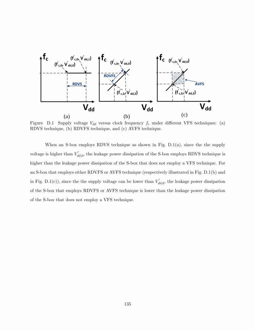
Vdd
fc
Vdd Vdd
fc fc(f’c,0, V’
dd,0)
(f’c,0, V’dd,1)
RDVS
(f’c,0, V’dd,0)
(f’c,2, V’dd,2)
(a)
RDVFS
(f’c,0, V’dd,0)
(f’c,2, V’dd,2)
AVFS
(b) (c)
Figure D.1 Supply voltage Vdd versus clock frequency fc under different VFS techniques: (a)RDVS technique, (b) RDVFS technique, and (c) AVFS technique.
When an S-box employs RDVS technique as shown in Fig. D.1(a), since the the supply
voltage is higher than V′dd,0, the leakage power dissipation of the S-box employs RDVS technique is
higher than the leakage power dissipation of the S-box that does not employ a VFS technique. For
an S-box that employs either RDVFS or AVFS technique (respectively illustrated in Fig. D.1(b) and
in Fig. D.1(c)), since the the supply voltage can be lower than V′dd,0, the leakage power dissipation
of the S-box that employs RDVFS or AVFS technique is lower than the leakage power dissipation
of the S-box that does not employ a VFS technique.
135
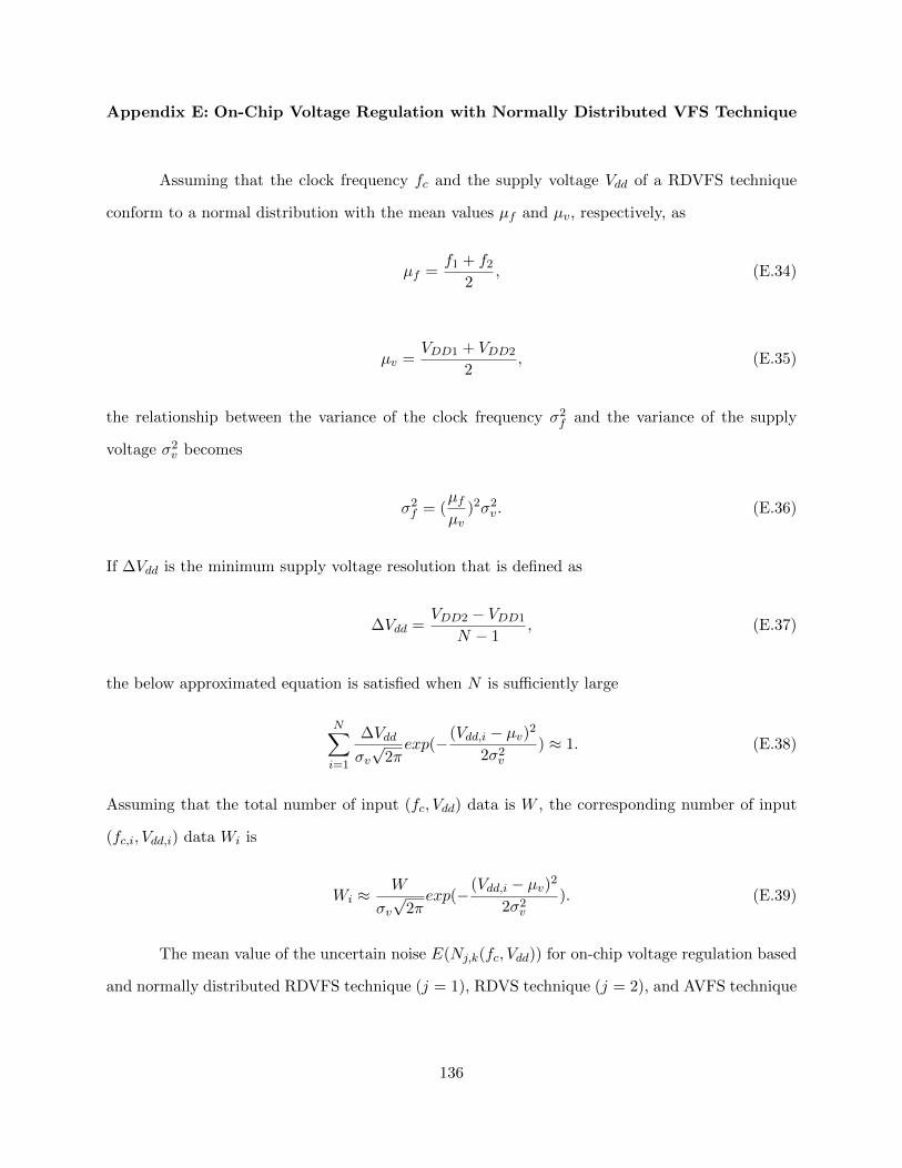
Appendix E: On-Chip Voltage Regulation with Normally Distributed VFS Technique
Assuming that the clock frequency fc and the supply voltage Vdd of a RDVFS technique
conform to a normal distribution with the mean values µf and µv, respectively, as
µf =f1 + f2
2, (E.34)
µv =VDD1 + VDD2
2, (E.35)
the relationship between the variance of the clock frequency σ2f and the variance of the supply
voltage σ2v becomes
σ2f = (µfµv
)2σ2v . (E.36)
If ∆Vdd is the minimum supply voltage resolution that is defined as
∆Vdd =VDD2 − VDD1
N − 1, (E.37)
the below approximated equation is satisfied when N is sufficiently large
N∑i=1
∆Vdd
σv√
2πexp(−
(Vdd,i − µv)2
2σ2v) ≈ 1. (E.38)
Assuming that the total number of input (fc, Vdd) data is W , the corresponding number of input
(fc,i, Vdd,i) data Wi is
Wi ≈W
σv√
2πexp(−
(Vdd,i − µv)2
2σ2v). (E.39)
The mean value of the uncertain noise E(Nj,k(fc, Vdd)) for on-chip voltage regulation based
and normally distributed RDVFS technique (j = 1), RDVS technique (j = 2), and AVFS technique
136
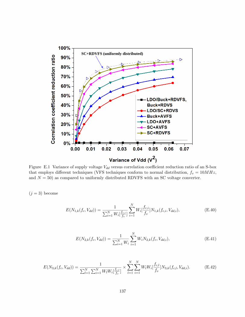
SC+RDVFS (uniformly distributed)
Figure E.1 Variance of supply voltage Vdd versus correlation coefficient reduction ratio of an S-boxthat employs different techniques (VFS techniques conform to normal distribution, fv = 10MHz,and N = 50) as compared to uniformly distributed RDVFS with an SC voltage converter.
(j = 3) become
E(N1,k(fc, Vdd)) =1∑N
i=1Wi[fc,ifv
]
N∑i=1
Wi[fc,ifv
]N1,k(fc,i, Vdd,i), (E.40)
E(N2,k(fc, Vdd)) =1∑N
i=1Wi
N∑i=1
WiN2,k(fc, Vdd,i), (E.41)
E(N3,k(fc, Vdd)) =1∑N
l=1
∑Ni=1WlWi[
fc,lfv
]×
N∑l=1
N∑i=1
WlWi[fc,lfv
]N3,k(fc,l, Vdd,i). (E.42)
137
0 . 0 0 . 2 0 . 4 0 . 6 0 . 8 1 . 00 . 0 0
0 . 0 2
0 . 0 4
0 . 0 6
0 . 0 8Va
rianc
eofV
dd(V
2 )
S u p p l y V o l t a g e r a n g e : ( V D D 2 - V D D 1 ) ( V )
U n i f o r m l y d i s t r i b u t e d V d dN o r m a l l y d i s t r i b u t e d V d d
Figure E.2 Variance of the supply voltage Vdd versus the supply voltage range (VDD2− VDD1) foruniformly and normally distributed Vdd.
The corresponding variance of uncertain noise V ar(N1,k(fc, Vdd)) can be written as
V ar(N1,k(fc, Vdd)) =1∑N
i=1Wi[fc,ifv
]×
N∑i=1
Wi[fc,ifv
](N1,k(fc,i, Vdd,i)− E(N1,k(fc, Vdd)))2, (E.43)
V ar(N2,k(fc, Vdd)) =1∑N
i=1Wi
×N∑i=1
Wi(N2,k(fc, Vdd,i)− E(N2,k(fc, Vdd)))2, (E.44)
138
V ar(N3,k(fc, Vdd)) =1∑N
l=1
∑Ni=1WlWi[
fc,lfv
]×
N∑l=1
N∑i=1
WlWi[fc,lfv
](N3,k(fc,l, Vdd,i)− E(N3,k(fc, Vdd)))2. (E.45)
As shown in Fig. E.1, an S-box [80] with the RDVFS technique employing an SC converter
still exhibits the highest correlation coefficient reduction ratio as compared to the S-boxes that
employ other techniques. Moreover, as compared to the S-box with uniformly distributed RDVFS
technique employing an SC converter, the S-box with normally distributed RDVFS technique em-
ploying an SC converter has a slightly lower correlation coefficient reduction ratio under the same
variance of the supply voltage. However, as shown in Fig. E.2, for achieving the same variance
of supply voltage, the normally distributed RDVFS technique needs to have a larger supply volt-
age range (VDD2 − VDD1), which would degrade the performance of the cryptographic circuits as
compared to the uniformly distributed RDVFS technique.
139

Appendix F: Copyright Permissions
Title: Chosen-message SPA attacks against FPGA-based RSA hardware implementations
Conference Proceedings:
2008 International Conference on Field Programmable Logic and Applications
Author: Atsushi Miyamoto; Naofumi Homma; Takafumi Aoki; Akashi Satoh
Publisher: IEEE
Date: 8-10 Sept. 2008Copyright © 2008, IEEE
If you're a copyright.com user, you can login to RightsLink using your copyright.com credentials.Already a RightsLink user or want to learn more?
Thesis / Dissertation Reuse
The IEEE does not require individuals working on a thesis to obtain a formal reuse license, however, you may print out this statement to be used as a permission grant:
Requirements to be followed when using any portion (e.g., figure, graph, table, or textual material) of an IEEE copyrighted paper in a thesis:
1) In the case of textual material (e.g., using short quotes or referring to the work within these papers)users must give full credit to the original source (author, paper, publication) followed by the IEEEcopyright line 2011 IEEE.2) In the case of illustrations or tabular material, we require that the copyright line [Year of originalpublication] IEEE appear prominently with each reprinted figure and/or table.3) If a substantial portion of the original paper is to be used, and if you are not the senior author, alsoobtain the senior authors approval.
Requirements to be followed when using an entire IEEE copyrighted paper in a thesis:
1) The following IEEE copyright/ credit notice should be placed prominently in the references: [yearof original publication] IEEE. Reprinted, with permission, from [author names, paper title, IEEEpublication title, and month/year of publication]2) Only the accepted version of an IEEE copyrighted paper can be used when posting the paper or yourthesis on-line.3) In placing the thesis on the author's university website, please display the following message in aprominent place on the website: In reference to IEEE copyrighted material which is used withpermission in this thesis, the IEEE does not endorse any of [university/educational entity's name goeshere]'s products or services. Internal or personal use of this material is permitted. If interested inreprinting/republishing IEEE copyrighted material for advertising or promotional purposes or forcreating new collective works for resale or redistribution, please go tohttp://www.ieee.org/publications_standards/publications/rights/rights_link.html to learn how to obtaina License from RightsLink.
If applicable, University Microfilms and/or ProQuest Library, or the Archives of Canada may supply single copies of the dissertation.
Copyright © 2017 Copyright Clearance Center, Inc. All Rights Reserved. Privacy statement. Terms and Conditions. Comments? We would like to hear from you. E-mail us at [email protected]
The following copyright permission notice is for the Fig. 1.1 of Chapter 1
140

Title: A True Random-Based Differential Power Analysis Countermeasure Circuit for an AES Engine
Author: Po-Chun Liu
Publication: Circuits and Systems Part II: Express Briefs, IEEE Transactions on
Publisher: IEEE
Date: Feb. 2012Copyright © 2012, IEEE
If you're a copyright.com user, you can login to RightsLink using your copyright.com credentials.Already a RightsLink user or want to learn more?
Thesis / Dissertation Reuse
The IEEE does not require individuals working on a thesis to obtain a formal reuse license, however, you may print out this statement to be used as a permission grant:
Requirements to be followed when using any portion (e.g., figure, graph, table, or textual material) of an IEEE copyrighted paper in a thesis:
1) In the case of textual material (e.g., using short quotes or referring to the work within these papers)users must give full credit to the original source (author, paper, publication) followed by the IEEEcopyright line 2011 IEEE.2) In the case of illustrations or tabular material, we require that the copyright line [Year of originalpublication] IEEE appear prominently with each reprinted figure and/or table.3) If a substantial portion of the original paper is to be used, and if you are not the senior author, alsoobtain the senior authors approval.
Requirements to be followed when using an entire IEEE copyrighted paper in a thesis:
1) The following IEEE copyright/ credit notice should be placed prominently in the references: [yearof original publication] IEEE. Reprinted, with permission, from [author names, paper title, IEEEpublication title, and month/year of publication]2) Only the accepted version of an IEEE copyrighted paper can be used when posting the paper or yourthesis on-line.3) In placing the thesis on the author's university website, please display the following message in aprominent place on the website: In reference to IEEE copyrighted material which is used withpermission in this thesis, the IEEE does not endorse any of [university/educational entity's name goeshere]'s products or services. Internal or personal use of this material is permitted. If interested inreprinting/republishing IEEE copyrighted material for advertising or promotional purposes or forcreating new collective works for resale or redistribution, please go tohttp://www.ieee.org/publications_standards/publications/rights/rights_link.html to learn how to obtaina License from RightsLink.
If applicable, University Microfilms and/or ProQuest Library, or the Archives of Canada may supply single copies of the dissertation.
Copyright © 2017 Copyright Clearance Center, Inc. All Rights Reserved. Privacy statement. Terms and Conditions. Comments? We would like to hear from you. E-mail us at [email protected]
The following copyright permission notice is for the Fig. 1.2 of Chapter 1
141

Title: Leakage Power Analysis Attacks: A Novel Class of Attacks to Nanometer Cryptographic Circuits
Author: Massimo Alioto
Publication: Circuits and Systems Part I: Regular Papers, IEEE Transactions on
Publisher: IEEE
Date: Feb. 2010Copyright © 2010, IEEE
If you're a copyright.com user, you can login to RightsLink using your copyright.com credentials.Already a RightsLink user or want to learn more?
Thesis / Dissertation Reuse
The IEEE does not require individuals working on a thesis to obtain a formal reuse license, however, you may print out this statement to be used as a permission grant:
Requirements to be followed when using any portion (e.g., figure, graph, table, or textual material) of an IEEE copyrighted paper in a thesis:
1) In the case of textual material (e.g., using short quotes or referring to the work within these papers)users must give full credit to the original source (author, paper, publication) followed by the IEEEcopyright line 2011 IEEE.2) In the case of illustrations or tabular material, we require that the copyright line [Year of originalpublication] IEEE appear prominently with each reprinted figure and/or table.3) If a substantial portion of the original paper is to be used, and if you are not the senior author, alsoobtain the senior authors approval.
Requirements to be followed when using an entire IEEE copyrighted paper in a thesis:
1) The following IEEE copyright/ credit notice should be placed prominently in the references: [yearof original publication] IEEE. Reprinted, with permission, from [author names, paper title, IEEEpublication title, and month/year of publication]2) Only the accepted version of an IEEE copyrighted paper can be used when posting the paper or yourthesis on-line.3) In placing the thesis on the author's university website, please display the following message in aprominent place on the website: In reference to IEEE copyrighted material which is used withpermission in this thesis, the IEEE does not endorse any of [university/educational entity's name goeshere]'s products or services. Internal or personal use of this material is permitted. If interested inreprinting/republishing IEEE copyrighted material for advertising or promotional purposes or forcreating new collective works for resale or redistribution, please go tohttp://www.ieee.org/publications_standards/publications/rights/rights_link.html to learn how to obtaina License from RightsLink.
If applicable, University Microfilms and/or ProQuest Library, or the Archives of Canada may supply single copies of the dissertation.
Copyright © 2017 Copyright Clearance Center, Inc. All Rights Reserved. Privacy statement. Terms and Conditions. Comments? We would like to hear from you. E-mail us at [email protected]
The following copyright permission notice is for the Fig. 1.3 and Fig. 1.4 of Chapter 1
142

Title: Converter-Gating: A Power Efficient and Secure On-Chip Power Delivery System
Author: Orhun Aras Uzun; Selçuk Köse
Publication: Emerging and Selected Topics in Circuits and Systems, IEEE Journal on
Publisher: IEEE
Date: June 2014Copyright © 2014, IEEE
If you're a copyright.com user, you can login to RightsLink using your copyright.com credentials.Already a RightsLink user or want to learn more?
Thesis / Dissertation Reuse
The IEEE does not require individuals working on a thesis to obtain a formal reuse license, however, you may print out this statement to be used as a permission grant:
Requirements to be followed when using any portion (e.g., figure, graph, table, or textual material) of an IEEE copyrighted paper in a thesis:
1) In the case of textual material (e.g., using short quotes or referring to the work within these papers)users must give full credit to the original source (author, paper, publication) followed by the IEEEcopyright line 2011 IEEE.2) In the case of illustrations or tabular material, we require that the copyright line [Year of originalpublication] IEEE appear prominently with each reprinted figure and/or table.3) If a substantial portion of the original paper is to be used, and if you are not the senior author, alsoobtain the senior authors approval.
Requirements to be followed when using an entire IEEE copyrighted paper in a thesis:
1) The following IEEE copyright/ credit notice should be placed prominently in the references: [yearof original publication] IEEE. Reprinted, with permission, from [author names, paper title, IEEEpublication title, and month/year of publication]2) Only the accepted version of an IEEE copyrighted paper can be used when posting the paper or yourthesis on-line.3) In placing the thesis on the author's university website, please display the following message in aprominent place on the website: In reference to IEEE copyrighted material which is used withpermission in this thesis, the IEEE does not endorse any of [university/educational entity's name goeshere]'s products or services. Internal or personal use of this material is permitted. If interested inreprinting/republishing IEEE copyrighted material for advertising or promotional purposes or forcreating new collective works for resale or redistribution, please go tohttp://www.ieee.org/publications_standards/publications/rights/rights_link.html to learn how to obtaina License from RightsLink.
If applicable, University Microfilms and/or ProQuest Library, or the Archives of Canada may supply single copies of the dissertation.
Copyright © 2017 Copyright Clearance Center, Inc. All Rights Reserved. Privacy statement. Terms and Conditions. Comments? We would like to hear from you. E-mail us at [email protected]
The following copyright permission notice is for the Fig. 1.5, Fig. 1.6, and Fig. 1.7 of
Chapter 1
143

Title: Leveraging on-chip voltage regulators as a countermeasure against side-channel attacks
Conference Proceedings:
2015 52nd ACM/EDAC/IEEE Design Automation Conference (DAC)
Author: Weize Yu; Orhun Aras Uzun; Selçuk Köse
Publisher: IEEE
Date: 8-12 June 2015Copyright © 2015, IEEE
If you're a copyright.com user, you can login to RightsLink using your copyright.com credentials.Already a RightsLink user or want to learn more?
Thesis / Dissertation Reuse
The IEEE does not require individuals working on a thesis to obtain a formal reuse license, however, you may print out this statement to be used as a permission grant:
Requirements to be followed when using any portion (e.g., figure, graph, table, or textual material) of an IEEE copyrighted paper in a thesis:
1) In the case of textual material (e.g., using short quotes or referring to the work within these papers)users must give full credit to the original source (author, paper, publication) followed by the IEEEcopyright line 2011 IEEE.2) In the case of illustrations or tabular material, we require that the copyright line [Year of originalpublication] IEEE appear prominently with each reprinted figure and/or table.3) If a substantial portion of the original paper is to be used, and if you are not the senior author, alsoobtain the senior authors approval.
Requirements to be followed when using an entire IEEE copyrighted paper in a thesis:
1) The following IEEE copyright/ credit notice should be placed prominently in the references: [yearof original publication] IEEE. Reprinted, with permission, from [author names, paper title, IEEEpublication title, and month/year of publication]2) Only the accepted version of an IEEE copyrighted paper can be used when posting the paper or yourthesis on-line.3) In placing the thesis on the author's university website, please display the following message in aprominent place on the website: In reference to IEEE copyrighted material which is used withpermission in this thesis, the IEEE does not endorse any of [university/educational entity's name goeshere]'s products or services. Internal or personal use of this material is permitted. If interested inreprinting/republishing IEEE copyrighted material for advertising or promotional purposes or forcreating new collective works for resale or redistribution, please go tohttp://www.ieee.org/publications_standards/publications/rights/rights_link.html to learn how to obtaina License from RightsLink.
If applicable, University Microfilms and/or ProQuest Library, or the Archives of Canada may supply single copies of the dissertation.
Copyright © 2017 Copyright Clearance Center, Inc. All Rights Reserved. Privacy statement. Terms and Conditions. Comments? We would like to hear from you. E-mail us at [email protected]
The following copyright permission notice is for the content of Chapter 2
144

Title: Time-Delayed Converter-Reshuffling: An Efficient and Secure Power Delivery Architecture
Author: Weize Yu; Selçuk Köse
Publication: IEEE Embedded Systems Letters
Publisher: IEEE
Date: Sept. 2015Copyright © 2015, IEEE
If you're a copyright.com user, you can login to RightsLink using your copyright.com credentials.Already a RightsLink user or want to learn more?
Thesis / Dissertation Reuse
The IEEE does not require individuals working on a thesis to obtain a formal reuse license, however, you may print out this statement to be used as a permission grant:
Requirements to be followed when using any portion (e.g., figure, graph, table, or textual material) of an IEEE copyrighted paper in a thesis:
1) In the case of textual material (e.g., using short quotes or referring to the work within these papers)users must give full credit to the original source (author, paper, publication) followed by the IEEEcopyright line 2011 IEEE.2) In the case of illustrations or tabular material, we require that the copyright line [Year of originalpublication] IEEE appear prominently with each reprinted figure and/or table.3) If a substantial portion of the original paper is to be used, and if you are not the senior author, alsoobtain the senior authors approval.
Requirements to be followed when using an entire IEEE copyrighted paper in a thesis:
1) The following IEEE copyright/ credit notice should be placed prominently in the references: [yearof original publication] IEEE. Reprinted, with permission, from [author names, paper title, IEEEpublication title, and month/year of publication]2) Only the accepted version of an IEEE copyrighted paper can be used when posting the paper or yourthesis on-line.3) In placing the thesis on the author's university website, please display the following message in aprominent place on the website: In reference to IEEE copyrighted material which is used withpermission in this thesis, the IEEE does not endorse any of [university/educational entity's name goeshere]'s products or services. Internal or personal use of this material is permitted. If interested inreprinting/republishing IEEE copyrighted material for advertising or promotional purposes or forcreating new collective works for resale or redistribution, please go tohttp://www.ieee.org/publications_standards/publications/rights/rights_link.html to learn how to obtaina License from RightsLink.
If applicable, University Microfilms and/or ProQuest Library, or the Archives of Canada may supply single copies of the dissertation.
Copyright © 2017 Copyright Clearance Center, Inc. All Rights Reserved. Privacy statement. Terms and Conditions. Comments? We would like to hear from you. E-mail us at [email protected]
The following copyright permission notice is for the content of Chapter 3
145

Title: Charge-Withheld Converter-Reshuffling: A Countermeasure Against Power Analysis Attacks
Author: Weize Yu; Selçuk Köse
Publication: Circuits and Systems Part II: Express Briefs, IEEE Transactions on
Publisher: IEEE
Date: May 2016Copyright © 2016, IEEE
If you're a copyright.com user, you can login to RightsLink using your copyright.com credentials.Already a RightsLink user or want to learn more?
Thesis / Dissertation Reuse
The IEEE does not require individuals working on a thesis to obtain a formal reuse license, however, you may print out this statement to be used as a permission grant:
Requirements to be followed when using any portion (e.g., figure, graph, table, or textual material) of an IEEE copyrighted paper in a thesis:
1) In the case of textual material (e.g., using short quotes or referring to the work within these papers)users must give full credit to the original source (author, paper, publication) followed by the IEEEcopyright line 2011 IEEE.2) In the case of illustrations or tabular material, we require that the copyright line [Year of originalpublication] IEEE appear prominently with each reprinted figure and/or table.3) If a substantial portion of the original paper is to be used, and if you are not the senior author, alsoobtain the senior authors approval.
Requirements to be followed when using an entire IEEE copyrighted paper in a thesis:
1) The following IEEE copyright/ credit notice should be placed prominently in the references: [yearof original publication] IEEE. Reprinted, with permission, from [author names, paper title, IEEEpublication title, and month/year of publication]2) Only the accepted version of an IEEE copyrighted paper can be used when posting the paper or yourthesis on-line.3) In placing the thesis on the author's university website, please display the following message in aprominent place on the website: In reference to IEEE copyrighted material which is used withpermission in this thesis, the IEEE does not endorse any of [university/educational entity's name goeshere]'s products or services. Internal or personal use of this material is permitted. If interested inreprinting/republishing IEEE copyrighted material for advertising or promotional purposes or forcreating new collective works for resale or redistribution, please go tohttp://www.ieee.org/publications_standards/publications/rights/rights_link.html to learn how to obtaina License from RightsLink.
If applicable, University Microfilms and/or ProQuest Library, or the Archives of Canada may supply single copies of the dissertation.
Copyright © 2017 Copyright Clearance Center, Inc. All Rights Reserved. Privacy statement. Terms and Conditions. Comments? We would like to hear from you. E-mail us at [email protected]
The following copyright permission notice is for the content of Chapter 4
146

Title: A Voltage Regulator-Assisted Lightweight AES Implementation Against DPA Attacks
Author: Weize Yu; Selçuk Köse
Publication: Circuits and Systems Part I: Regular Papers, IEEE Transactions on
Publisher: IEEE
Date: Aug. 2016Copyright © 2016, IEEE
If you're a copyright.com user, you can login to RightsLink using your copyright.com credentials.Already a RightsLink user or want to learn more?
Thesis / Dissertation Reuse
The IEEE does not require individuals working on a thesis to obtain a formal reuse license, however, you may print out this statement to be used as a permission grant:
Requirements to be followed when using any portion (e.g., figure, graph, table, or textual material) of an IEEE copyrighted paper in a thesis:
1) In the case of textual material (e.g., using short quotes or referring to the work within these papers)users must give full credit to the original source (author, paper, publication) followed by the IEEEcopyright line 2011 IEEE.2) In the case of illustrations or tabular material, we require that the copyright line [Year of originalpublication] IEEE appear prominently with each reprinted figure and/or table.3) If a substantial portion of the original paper is to be used, and if you are not the senior author, alsoobtain the senior authors approval.
Requirements to be followed when using an entire IEEE copyrighted paper in a thesis:
1) The following IEEE copyright/ credit notice should be placed prominently in the references: [yearof original publication] IEEE. Reprinted, with permission, from [author names, paper title, IEEEpublication title, and month/year of publication]2) Only the accepted version of an IEEE copyrighted paper can be used when posting the paper or yourthesis on-line.3) In placing the thesis on the author's university website, please display the following message in aprominent place on the website: In reference to IEEE copyrighted material which is used withpermission in this thesis, the IEEE does not endorse any of [university/educational entity's name goeshere]'s products or services. Internal or personal use of this material is permitted. If interested inreprinting/republishing IEEE copyrighted material for advertising or promotional purposes or forcreating new collective works for resale or redistribution, please go tohttp://www.ieee.org/publications_standards/publications/rights/rights_link.html to learn how to obtaina License from RightsLink.
If applicable, University Microfilms and/or ProQuest Library, or the Archives of Canada may supply single copies of the dissertation.
Copyright © 2017 Copyright Clearance Center, Inc. All Rights Reserved. Privacy statement. Terms and Conditions. Comments? We would like to hear from you. E-mail us at [email protected]
The following copyright permission notice is for the content of Chapter 5
147

Title: Security-Adaptive Voltage Conversion as a Lightweight Countermeasure Against LPA Attacks
Author: Weize Yu; Selçuk Köse
Publication: Very Large Scale Integration Systems, IEEE Transactions on
Publisher: IEEE
Date: Dec 31, 1969Copyright © 1969, IEEE
If you're a copyright.com user, you can login to RightsLink using your copyright.com credentials.Already a RightsLink user or want to learn more?
Thesis / Dissertation Reuse
The IEEE does not require individuals working on a thesis to obtain a formal reuse license, however, you may print out this statement to be used as a permission grant:
Requirements to be followed when using any portion (e.g., figure, graph, table, or textual material) of an IEEE copyrighted paper in a thesis:
1) In the case of textual material (e.g., using short quotes or referring to the work within these papers)users must give full credit to the original source (author, paper, publication) followed by the IEEEcopyright line 2011 IEEE.2) In the case of illustrations or tabular material, we require that the copyright line [Year of originalpublication] IEEE appear prominently with each reprinted figure and/or table.3) If a substantial portion of the original paper is to be used, and if you are not the senior author, alsoobtain the senior authors approval.
Requirements to be followed when using an entire IEEE copyrighted paper in a thesis:
1) The following IEEE copyright/ credit notice should be placed prominently in the references: [yearof original publication] IEEE. Reprinted, with permission, from [author names, paper title, IEEEpublication title, and month/year of publication]2) Only the accepted version of an IEEE copyrighted paper can be used when posting the paper or yourthesis on-line.3) In placing the thesis on the author's university website, please display the following message in aprominent place on the website: In reference to IEEE copyrighted material which is used withpermission in this thesis, the IEEE does not endorse any of [university/educational entity's name goeshere]'s products or services. Internal or personal use of this material is permitted. If interested inreprinting/republishing IEEE copyrighted material for advertising or promotional purposes or forcreating new collective works for resale or redistribution, please go tohttp://www.ieee.org/publications_standards/publications/rights/rights_link.html to learn how to obtaina License from RightsLink.
If applicable, University Microfilms and/or ProQuest Library, or the Archives of Canada may supply single copies of the dissertation.
Copyright © 2017 Copyright Clearance Center, Inc. All Rights Reserved. Privacy statement. Terms and Conditions. Comments? We would like to hear from you. E-mail us at [email protected]
The following copyright permission notice is for the content of Chapter 6
148

Title: Exploiting Voltage Regulators to Enhance Various Power Attack Countermeasures
Author: Weize Yu; Selcuk Kose
Publication: IEEE Transactions on Emerging Topics in Computing
Publisher: IEEE
Date: Dec 31, 1969Copyright © 1969, IEEE
If you're a copyright.com user, you can login to RightsLink using your copyright.com credentials.Already a RightsLink user or want to learn more?
Thesis / Dissertation Reuse
The IEEE does not require individuals working on a thesis to obtain a formal reuse license, however, you may print out this statement to be used as a permission grant:
Requirements to be followed when using any portion (e.g., figure, graph, table, or textual material) of an IEEE copyrighted paper in a thesis:
1) In the case of textual material (e.g., using short quotes or referring to the work within these papers)users must give full credit to the original source (author, paper, publication) followed by the IEEEcopyright line 2011 IEEE.2) In the case of illustrations or tabular material, we require that the copyright line [Year of originalpublication] IEEE appear prominently with each reprinted figure and/or table.3) If a substantial portion of the original paper is to be used, and if you are not the senior author, alsoobtain the senior authors approval.
Requirements to be followed when using an entire IEEE copyrighted paper in a thesis:
1) The following IEEE copyright/ credit notice should be placed prominently in the references: [yearof original publication] IEEE. Reprinted, with permission, from [author names, paper title, IEEEpublication title, and month/year of publication]2) Only the accepted version of an IEEE copyrighted paper can be used when posting the paper or yourthesis on-line.3) In placing the thesis on the author's university website, please display the following message in aprominent place on the website: In reference to IEEE copyrighted material which is used withpermission in this thesis, the IEEE does not endorse any of [university/educational entity's name goeshere]'s products or services. Internal or personal use of this material is permitted. If interested inreprinting/republishing IEEE copyrighted material for advertising or promotional purposes or forcreating new collective works for resale or redistribution, please go tohttp://www.ieee.org/publications_standards/publications/rights/rights_link.html to learn how to obtaina License from RightsLink.
If applicable, University Microfilms and/or ProQuest Library, or the Archives of Canada may supply single copies of the dissertation.
Copyright © 2017 Copyright Clearance Center, Inc. All Rights Reserved. Privacy statement. Terms and Conditions. Comments? We would like to hear from you. E-mail us at [email protected]
The following copyright permission notice is for the content of Chapter 7
149

Title: An Aging-Resistant RO-PUF for Reliable Key Generation
Author: MD. Tauhidur Rahman; FahimRahman; Domenic Forte; MarkTehranipoor
Publication: IEEE Transactions on Emerging Topics in Computing
Publisher: IEEE
Date: July-Sept. 2016Copyright © 2016, IEEE
If you're a copyright.com user, you can login to RightsLink using your copyright.com credentials.Already a RightsLink user or want to learn more?
Thesis / Dissertation Reuse
The IEEE does not require individuals working on a thesis to obtain a formal reuse license, however, you may print out this statement to be used as a permission grant:
Requirements to be followed when using any portion (e.g., figure, graph, table, or textual material) of an IEEE copyrighted paper in a thesis:
1) In the case of textual material (e.g., using short quotes or referring to the work within these papers)users must give full credit to the original source (author, paper, publication) followed by the IEEEcopyright line 2011 IEEE.2) In the case of illustrations or tabular material, we require that the copyright line [Year of originalpublication] IEEE appear prominently with each reprinted figure and/or table.3) If a substantial portion of the original paper is to be used, and if you are not the senior author, alsoobtain the senior authors approval.
Requirements to be followed when using an entire IEEE copyrighted paper in a thesis:
1) The following IEEE copyright/ credit notice should be placed prominently in the references: [yearof original publication] IEEE. Reprinted, with permission, from [author names, paper title, IEEEpublication title, and month/year of publication]2) Only the accepted version of an IEEE copyrighted paper can be used when posting the paper or yourthesis on-line.3) In placing the thesis on the author's university website, please display the following message in aprominent place on the website: In reference to IEEE copyrighted material which is used withpermission in this thesis, the IEEE does not endorse any of [university/educational entity's name goeshere]'s products or services. Internal or personal use of this material is permitted. If interested inreprinting/republishing IEEE copyrighted material for advertising or promotional purposes or forcreating new collective works for resale or redistribution, please go tohttp://www.ieee.org/publications_standards/publications/rights/rights_link.html to learn how to obtaina License from RightsLink.
If applicable, University Microfilms and/or ProQuest Library, or the Archives of Canada may supply single copies of the dissertation.
Copyright © 2017 Copyright Clearance Center, Inc. All Rights Reserved. Privacy statement. Terms and Conditions. Comments? We would like to hear from you. E-mail us at [email protected]
The following copyright permission notice is for the Fig. 9.3 of Future Work
150
ABOUT THE AUTHOR
Weize Yu received the B.S. and M.S. degrees in electrical engineering from University of
Electronic Science and Technology of China, Chengdu, China, and Institute of Microelectronics
of Chinese Academy of Sciences, Beijing, China, respectively, in 2009 and 2012. He joined the
electrical engineering department of University of South Florida to pursue his Ph.D. degree in Fall
2014. He is awarded with the USF presidential fellowship from 2014 to 2017. During his Ph.D.
study, his research interests are mainly focused on power management IC and hardware security.
Copyright © 2022 FDOKUMEN