Experimental and numerical analysis of extraordinary optical transmission through nano-hole arrays...
16
Experimental and numerical analysis on the optical resonance transmission properties of nano-hole arrays Mohamadreza Najiminaini, 1,2 Fartash Vasefi, 1,2,3 Bozena Kaminska, 1 and Jeffrey J. L. Carson 2,3,* 1 The School of Engineering Science, Simon Fraser University, Burnaby, British Columbia, Canada 2 Imaging Program, Lawson Health Research Institute, London, Ontario, Canada 3 Medical Biophysics, Schulich School of Medicine and Dentistry, University of Western Ontario, London, Ontario, Canada *[email protected] Abstract: In this paper, we present experimental and numerical analysis on Extraordinary Optical Transmission (EOT) or optical resonance transmission through various nano-hole arrays constructed from an optically thick metal film within the visible and near infra-red spectrum. Nano-hole arrays with different geometrical parameters (hole size, hole shape, and hole periodicity) having their EOT properties in the visible and near-infrared regime were simulated based on Finite Difference Time Domain (FDTD). Large nano-hole arrays with geometric properties similar to the simulated arrays were fabricated using Electron Beam Lithography (EBL). The optical resonance transmission properties (resonance position, transmission efficiency, and spectral bandwidth of resonance peak) of the fabricated nano-hole arrays were characterized. Finally, the experimental and numerical results were analyzed to determine the dependencies and discrepancies between optical resonance transmission properties for various nano-hole arrays. ©2010 Optical Society of America OCIS codes: (240.6680) Surface Plasmon; (250.5403) Plasmonics; (220.4241) Nanostructure fabrication. References and links 1. T. Thio, H. F. Ghaemi, H. J. Lezec, P. A. Wolff, and T. W. Ebbesen, “Surface-plasmon-enhanced transmission through hole arrays in Cr films,” J. Opt. Soc. Am. B 16(10), 1743–1748 (1999). 2. R. Gordon, A. G. Brolo, D. Sinton, and K. L. Kavanagh, “Resonant optical transmission through hole-arrays in metal films: physics and applications,” Laser Photon. Rev., 1–25 (2009). 3. A. G. Brolo, S. C. Kwok, M. G. Moffitt, R. Gordon, J. Riordon, and K. L. Kavanagh, “Enhanced fluorescence from arrays of nanoholes in a gold film,” J. Am. Chem. Soc. 127(42), 14936–14941 (2005). 4. J. R. Lakowicz, M. H. Chowdhury, K. Ray, J. Zhang, Y. Fu, R. Badugu, C. R. Sabanayagam, K. Nowaczyk, H. Szmacinski, K. Aslan, and C. D. Geddes, “Plasmon-controlled fluorescence: A new detection technology,” Proc SPIE 6099, 9–1-9–14 (2009). 5. A. Lesuffleur, H. Im, N. C. Lindquist, K. S. Lim, and S. H. Oh, “Laser-illuminated nanohole arrays for multiplex plasmonic microarray sensing,” Opt. Express 16(1), 219–224 (2008). 6. F. M. Huang, Y. Chen, F. J. Garcia de Abajo, and N. I. Zheludev, “Focusing of light by a Nanohole array,” Appl. Phys. Lett. 90(9), 091119 (2007). 7. R. Gordon, A. G. Brolo, A. McKinnon, A. Rajora, B. Leathem, and K. L. Kavanagh, “Strong polarization in the optical transmission through elliptical nanohole arrays,” Phys. Rev. Lett. 92(3), 037401 (2004). 8. S. G. Rodrigo, F. J. García-Vidal, and L. Martín-Moreno, “Influence of material properties on extraordinary optical transmission through hole arrays,” Phys. Rev. Lett B 77, 075401 (2008). 9. F. Przybilla, A. Degiron, J. Y. Laluet, C. Genet, and T. W. Ebbesen, “Optical transmission in perforated noble and transition metal films,” J. Opt. A, Pure Appl. Opt. 8(5), 458–463 (2006). 10. T. W. Ebbesen, H. J. Lezec, H. F. Ghaemi, T. Thio, and P. A. Wolff, “Extraordinary optical transmission through sub-wavelength hole arrays,” Nature 391(6668), 667–669 (1998). #132890 - $15.00 USD Received 4 Aug 2010; revised 28 Aug 2010; accepted 29 Aug 2010; published 6 Oct 2010 (C) 2010 OSA 11 October 2010 / Vol. 18, No. 21 / OPTICS EXPRESS 22255
-
Upload
independent -
Category
Documents
-
view
1 -
download
0
Transcript of Experimental and numerical analysis of extraordinary optical transmission through nano-hole arrays...
Experimental and numerical analysis on the
optical resonance transmission properties of
nano-hole arrays
Mohamadreza Najiminaini,1,2
Fartash Vasefi,1,2,3
Bozena Kaminska,1 and
Jeffrey J. L. Carson2,3,*
1The School of Engineering Science, Simon Fraser University, Burnaby, British Columbia, Canada
2Imaging Program, Lawson Health Research Institute, London, Ontario, Canada 3Medical Biophysics, Schulich School of Medicine and Dentistry, University of Western Ontario, London, Ontario,
Canada
Abstract: In this paper, we present experimental and numerical analysis on
Extraordinary Optical Transmission (EOT) or optical resonance
transmission through various nano-hole arrays constructed from an optically
thick metal film within the visible and near infra-red spectrum. Nano-hole
arrays with different geometrical parameters (hole size, hole shape, and hole
periodicity) having their EOT properties in the visible and near-infrared
regime were simulated based on Finite Difference Time Domain (FDTD).
Large nano-hole arrays with geometric properties similar to the simulated
arrays were fabricated using Electron Beam Lithography (EBL). The optical
resonance transmission properties (resonance position, transmission
efficiency, and spectral bandwidth of resonance peak) of the fabricated
nano-hole arrays were characterized. Finally, the experimental and
numerical results were analyzed to determine the dependencies and
discrepancies between optical resonance transmission properties for various
nano-hole arrays.
©2010 Optical Society of America
OCIS codes: (240.6680) Surface Plasmon; (250.5403) Plasmonics; (220.4241) Nanostructure
fabrication.
References and links
1. T. Thio, H. F. Ghaemi, H. J. Lezec, P. A. Wolff, and T. W. Ebbesen, “Surface-plasmon-enhanced transmission
through hole arrays in Cr films,” J. Opt. Soc. Am. B 16(10), 1743–1748 (1999).
2. R. Gordon, A. G. Brolo, D. Sinton, and K. L. Kavanagh, “Resonant optical transmission through hole-arrays in
metal films: physics and applications,” Laser Photon. Rev., 1–25 (2009).
3. A. G. Brolo, S. C. Kwok, M. G. Moffitt, R. Gordon, J. Riordon, and K. L. Kavanagh, “Enhanced fluorescence
from arrays of nanoholes in a gold film,” J. Am. Chem. Soc. 127(42), 14936–14941 (2005).
4. J. R. Lakowicz, M. H. Chowdhury, K. Ray, J. Zhang, Y. Fu, R. Badugu, C. R. Sabanayagam, K. Nowaczyk, H.
Szmacinski, K. Aslan, and C. D. Geddes, “Plasmon-controlled fluorescence: A new detection technology,” Proc
SPIE 6099, 9–1-9–14 (2009).
5. A. Lesuffleur, H. Im, N. C. Lindquist, K. S. Lim, and S. H. Oh, “Laser-illuminated nanohole arrays for multiplex
plasmonic microarray sensing,” Opt. Express 16(1), 219–224 (2008).
6. F. M. Huang, Y. Chen, F. J. Garcia de Abajo, and N. I. Zheludev, “Focusing of light by a Nanohole array,” Appl.
Phys. Lett. 90(9), 091119 (2007).
7. R. Gordon, A. G. Brolo, A. McKinnon, A. Rajora, B. Leathem, and K. L. Kavanagh, “Strong polarization in the
optical transmission through elliptical nanohole arrays,” Phys. Rev. Lett. 92(3), 037401 (2004).
8. S. G. Rodrigo, F. J. García-Vidal, and L. Martín-Moreno, “Influence of material properties on extraordinary
optical transmission through hole arrays,” Phys. Rev. Lett B 77, 075401 (2008).
9. F. Przybilla, A. Degiron, J. Y. Laluet, C. Genet, and T. W. Ebbesen, “Optical transmission in perforated noble
and transition metal films,” J. Opt. A, Pure Appl. Opt. 8(5), 458–463 (2006).
10. T. W. Ebbesen, H. J. Lezec, H. F. Ghaemi, T. Thio, and P. A. Wolff, “Extraordinary optical transmission through
sub-wavelength hole arrays,” Nature 391(6668), 667–669 (1998).
#132890 - $15.00 USD Received 4 Aug 2010; revised 28 Aug 2010; accepted 29 Aug 2010; published 6 Oct 2010(C) 2010 OSA 11 October 2010 / Vol. 18, No. 21 / OPTICS EXPRESS 22255

11. K. Shuford, M. A. Ratner, S. K. Gray, and G. C. Schatz, “Finite-difference time-domain studies of light
transmission through nanohole structures,” Appl. Phys. B 84(1-2), 11–18 (2006).
12. J. Bravo-Abad, L. Martín-Moreno, and F. J. Garcia-Vidal, “Resonant transmission of light through
subwavelength holes in thick metal films,” IEEE J. Sel. Top. Quantum Electron. 12(6), 1221–1227 (2006).
13. F. Przybilla, A. Degiron, C. Genet, T. W. Ebbesen, F. de Léon-Pérez, J. Bravo-Abad, F. J. García-Vidal, and L.
Martín-Moreno, “Efficiency and finite size effects in enhanced transmission through subwavelength apertures,”
Opt. Express 16(13), 9571–9579 (2008).
14. A. Krishnan, T. Thio, T. J. Kim, H. J. Lezec, T. W. Ebbesen, P. A. Wolff, J. Pendry, L. Martin-Moreno, and F. J.
Garcia-Vidal, “Evanescently coupled resonance in surface plasmon enhanced transmission,” Opt. Commun.
200(1-6), 1–7 (2001).
15. F. J. Garcia de Abajo, “Light transmission through a single cylindrical hole in a metallic film,” Opt. Express
10(25), 1475–1484 (2002).
16. R. Gordon, and P. Marthandam, “Plasmonic Bragg reflectors for enhanced extraordinary optical transmission
through nano-hole arrays in a gold film,” Opt. Express 15(20), 12995–13002 (2007).
17. C. Genet, and T. W. Ebbesen, “Light in tiny holes,” Nature 445(7123), 39–46 (2007).
18. N. F. van Hulst, “Plasmonics: Sorting colours,” Nat. Photonics 2(3), 139–140 (2008).
19. W. L. Barnes, A. Dereux, and T. W. Ebbesen, “Surface plasmon subwavelength optics,” Nature 424(6950), 824–
830 (2003).
20. K. S. Yee, “Numerical solution of initial boundary value problems involving Maxwell’s equations in isotropic
media,” IEEE Trans. Antenn. Propag. 14(3), 302–307 (1966).
21. A. Taflove, and S. C. Hagness, Computational electrodynamics: The Finite-Difference Time-Domain method,
2nd Ed” (Artech House Publishers, Boston, 2000).
22. E. D. Palik, Handbook of Optical Constants of Solids, Academic Press, New York, (1985).
23. K. L. van der Molen, F. B. Segerink, N. F. van Hulst, and L. Kuipers, “Influence of hole size on the extraordinary
transmission through subwavelength hole arrays,” Appl. Phys. Lett. 85(19), 4316–4318 (2004).
24. Z. Yu, H. Gao, W. Wu, H. Ge, and S. Y. Chou, “Fabrication of large area subwavelength antireflection structures
on Si using trilayer resist nanoimprint lithography and liftoff,” J. Vac. Sci. Technol. B 21(6), 2874–2877 (2003).
25. V. Malyarchuk, F. Hua, N. Mack, V. Velasquez, J. White, R. Nuzzo, and J. Rogers, “High performance
plasmonic crystal sensor formed by soft nanoimprint lithography,” Opt. Express 13(15), 5669–5675 (2005).
26. A. A. Tseng, “Recent developments in nanofabrication using focused ion beams,” Small 1(10), 924–939 (2005).
27. J. Chen, J. Shi, D. Decanini, E. Cambril, Y. Chen, and A. Haghiri-Gosnet, “Gold nanohole arrays for biochemical
sensing fabricated by soft UV nanoimprint lithography,” Microelectron. Eng. 86(4-6), 632–635 (2009).
1. Introduction
The interaction of light with perforated sub-wavelength holes in metallic films generates
extraordinary effects that can be employed to miniaturize photonic devices to sub-wavelength
scales. The optical characteristics of these sub-wavelength holes in a metallic film are created
by the coupling of light with Surface Plasmon (SP) modes [1,2]. Surface Plasmon (SP) is the
oscillation of free electrons at the interface of a metal and a dielectric and has been recognized
to transmit light through sub-wavelength holes causing Extraordinary Optical Transmission
(EOT) within the specific spectral range. Hence, a flat metal film, with a thickness that blocks
light transmission (optically thick), can be perforated with an array of sub-wavelength holes to
transmit light efficiently. EOT has been exploited in many applications such as Surface
Enhanced Raman Spectroscopy (SERS), Surface Enhanced Fluorescence Spectroscopy
(SEFS), focusing of light below the sub-wavelength regime, non-linear optics, and biosensors
[2–6].
Recently, studies have investigated the dependence of EOT on a variety of parameters to
improve optical transmission properties of nano-hole arrays [7–17]. Regarding geometrical
parameters, the excitation of SP modes depends highly on the spacing between adjacent holes
(periodicity) and dielectric constants of the metal and dielectric. Ebbessen [1,10] was first to
derive an equation describing the dependence of the wavelength (λmax) of the SP resonance
modes (EOTs) on the arrangement of nano-holes for a square lattice when the incident light is
normal to the plane of the nano-hole array:
0
max2 2
,m d
m d
a
m n
(1)
#132890 - $15.00 USD Received 4 Aug 2010; revised 28 Aug 2010; accepted 29 Aug 2010; published 6 Oct 2010(C) 2010 OSA 11 October 2010 / Vol. 18, No. 21 / OPTICS EXPRESS 22256
where a0 is the periodicity of holes, εd and εm are the dielectric constants of the incident
medium (at the top or bottom surface of the nano-hole) and the metal film, and m and n are
integers expressing the scattering mode indices. A transmission minimum is often observed
before each EOT peak due to Wood’s anomaly [2]. It has been discovered that the nano-hole
shape can robustly control both the polarization properties and the intensity of the EOT [7].
With regard to material properties, Ag, Au, and Cu have larger optical resonant transmission
peaks than nano-hole arrays in a perfect metal conductor with the same geometrical
parameters [8,9]. However for Ni and Cr, the transmittance is much smaller due to the
absorption properties of these metals [8]. In addition, it is recognized that some metals
particularly Au and Ag are more likely to display EOT properties compared to others such as
Ni and Co [9]. Also, variations in the nano-hole radii, groove period, groove depth, locations
of the grooves and slap thickness can significantly influence the transmission spectrum [11].
The optical transmission efficiency of the nano-hole array reaches an asymptotic upper value
with a specific finite number of holes in the array [12,13]. The optical resonant transmission
of a nano-hole array is enhanced by exploiting the same dielectric constant on the back and
front surface of a nano-hole array as a result of the same Surface Plasmon energy on both
sides [14]. Fabrication of a Bragg reflector on the boundary of a nano-hole array has been
shown to enhance the optical resonance transmission of the array by preventing losses at the
edges of the array such as those seen in classic optical diffraction filters [16].
Not only can nano-hole arrays in a metal film be used for enhancing the transmission of
light by a means of the Surface Plasmon properties [17], their bandpass properties provide the
opportunity to construct miniaturized spectral filters. Some groups have investigated the use
of nano-hole arrays as color coding devices [18,19]. Another potential application for
miniaturized spectral filters is spectroscopic optical imaging such as multispectral
fluorescence microscopy. Although many studies have investigated the dependence of EOT
properties on various geometrical properties of the nano-hole array, a comprehensive and
systematic analysis of the dependence of EOT on nano-hole array geometry and the impact of
the geometric properties on usage of nano-hole arrays as miniaturized spectral filters has yet
to be done. Hence, in this study, a more complete characterization of the optical properties
related to EOT was performed. Properties of the nano-hole array in a thick metal film
included the wavelength of the peak transmission (optical resonance position), the intensity of
the transmitted light at the peak (optical resonance transmission efficiency), and the spectral
bandwidth (optical resonance bandwidth).
Our approach was to compare numerical and experimental analyses from a series of nano-
hole arrays with various geometrical designs (hole size, hole shape and periodicity) having
optical resonance properties in the visible and near infra-red spectral regions. Numerical
analysis was performed with FDTD simulation. Large nano-hole arrays were fabricated with
electron beam lithography and characterized with optical transmission spectroscopy.
2. Methods
2.1 FDTD simulation of nano-hole arrays
The three-dimensional (3D) FDTD method was employed to simulate the interaction between
light and a nano-hole array in a thick metal film with the goal of predicting the optical
transmission properties. FDTD is a numerical method to solve the two and three dimensional
Maxwell’s equations in linear and non-linear dispersive media. We used the FDTD package
from Lumerical Inc. (Vancouver, Canada). Computations were performed with a computing
grid (West grid (www.westgrid.ca)). With Lumerical, the user can specify arbitrary geometric
structures and various input excitation sources. The software represents the electric
[E(x,y,z,t)], magnetic [H(x,y,z,t)] and current density fields [J(x,y,z,t)] on a spatial grid and
employs time spacing algorithms to perform the FDTD [20,21]. The dielectric constants for
each material were defined by the relative dielectric constant [εr(x,y,z,ω)]. Since absorption
#132890 - $15.00 USD Received 4 Aug 2010; revised 28 Aug 2010; accepted 29 Aug 2010; published 6 Oct 2010(C) 2010 OSA 11 October 2010 / Vol. 18, No. 21 / OPTICS EXPRESS 22257
and permittivity for a metallic material depend highly on frequency, the dispersion properties
of the metal were considered. We used the dielectric constant for metallic and dielectric
materials provided by Palik [22].
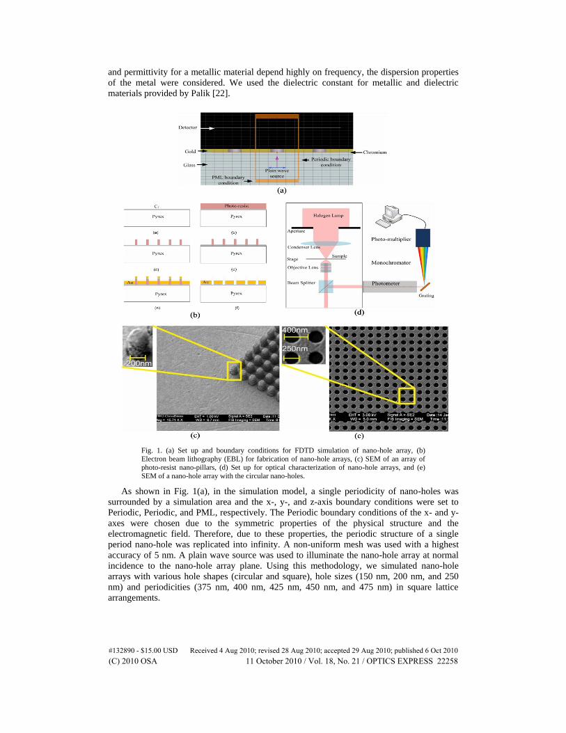
Fig. 1. (a) Set up and boundary conditions for FDTD simulation of nano-hole array, (b)
Electron beam lithography (EBL) for fabrication of nano-hole arrays, (c) SEM of an array of
photo-resist nano-pillars, (d) Set up for optical characterization of nano-hole arrays, and (e)
SEM of a nano-hole array with the circular nano-holes.
As shown in Fig. 1(a), in the simulation model, a single periodicity of nano-holes was
surrounded by a simulation area and the x-, y-, and z-axis boundary conditions were set to
Periodic, Periodic, and PML, respectively. The Periodic boundary conditions of the x- and y-
axes were chosen due to the symmetric properties of the physical structure and the
electromagnetic field. Therefore, due to these properties, the periodic structure of a single
period nano-hole was replicated into infinity. A non-uniform mesh was used with a highest
accuracy of 5 nm. A plain wave source was used to illuminate the nano-hole array at normal
incidence to the nano-hole array plane. Using this methodology, we simulated nano-hole
arrays with various hole shapes (circular and square), hole sizes (150 nm, 200 nm, and 250
nm) and periodicities (375 nm, 400 nm, 425 nm, 450 nm, and 475 nm) in square lattice
arrangements.
#132890 - $15.00 USD Received 4 Aug 2010; revised 28 Aug 2010; accepted 29 Aug 2010; published 6 Oct 2010(C) 2010 OSA 11 October 2010 / Vol. 18, No. 21 / OPTICS EXPRESS 22258
2.2 Electron Beam Lithography (EBL) fabrication methodology
We used electron beam lithography (EBL) fabrication methodology for fabricating nano-hole
arrays in a 100-nm optically thick gold film. The fabrication process used is shown in
Fig. 1(b). Chromium (5 nm) was deposited on a Pyrex substrate in order to make the substrate
surface conductive for the EBL process. Afterward, 500 nm photo-resist (Negative Tone
photo-resist ma-N 2403) was spin-coated and soft-baked on the chromium layer. The nano-
hole array pattern was written using an EBL machine (LEO, 1530 e-beam lithography), the
sample was developed leaving behind photo-resist pillars. Chromium (10 nm) was then
deposited as an adhesion layer followed by 100 nm deposition of gold on to the sample. A
SEM image of the photo-resist pillars covered with gold is shown in Fig. 1(c). Finally, in a
lift-off process, the sample was exposed to Acetone and Nano-stripper to remove the pillars.
A SEM image of a fabricated nano-hole array is shown in Fig. 1(e). We fabricated nano-hole
arrays with various hole shapes (circular and square), hole sizes (150 nm, 200 nm, and 250
nm) and hole periodicities (375 nm, 400 nm, 425 nm, 450 nm, and 475 nm) in a square lattice
arrangement. These geometrical parameters were selected to enable optical resonance
transmission of each array in the visible and near-infrared regime. The number of holes in
each nano-hole array was 150 × 150.
2.3 Optical characterization setup
We used a standard inverted microscope (Nikon, TE300) attached to a photometer (PTI,
D104), monochromator (PTI, 101), and photo-multiplier (PTI, 710) for the optical
characterization of each nano-hole array as shown in Fig. 1(d). Unpolarized white light from a
100 W halogen lamp was focused on the sample using the bright-field and condenser lens
(NA = 0.3) of the microscope. The scattered light was collected with a 20 × objective (NA =
0.45; Nikon, 93150) and guided with a beam splitter to the photometer. Using the aperture
adjustment on the photometer, light from a desired region of a given sample was selected,
then guided to the monochromator for spectral characterization, and detection by the photo-
multiplier tube. The optical transmission spectra were obtained by first subtracting the
background signals obtained from a hole-free region of the gold film from the spectra
transmitted through a given nano-hole array, and then divided by the measured white light
spectrum. The ratio cancels the wavelength variant signal caused by the light source,
monochromator and the wavelength responsivity of the detector.
2.4 Analysis of the optical transmission spectra
In order to employ EOTs (optical resonance peaks) of a nano-hole array as a spectral filter, the
optical characteristics of EOT related to spectral performance were analyzed. These optical
properties consist of the center wavelength, the transmission efficiency of a center wavelength
and the spectral bandwidth. In some instances, although the position of the peaks was
measurable, the peak location was corrupted due to the large bandwidth of the spectral
features and was not interpretable. In these cases, the peak positions were not reported. The
spectral bandwidth of each EOT computed in such a way that the spectral bandwidth is the
full width of the EOT where the optical transmission was 12
of the optical transmission
peak.
3. Results
3.1 Experimental observations in Nano-hole array fabrication
Prior to writing nano-hole patterns with EBL, initial tests were performed to optimize the EBL
area dose used for fabrication of nano-hole arrays with specific feature parameters (hole size,
hole shape, and periodicity of hole). The area dose required to fabricate each design was
#132890 - $15.00 USD Received 4 Aug 2010; revised 28 Aug 2010; accepted 29 Aug 2010; published 6 Oct 2010(C) 2010 OSA 11 October 2010 / Vol. 18, No. 21 / OPTICS EXPRESS 22259
dependent on hole shape, hole size, periodicity, and the type and age of the photo-resist. The
area dose varied from 70 µC/cm2 to 125 µC/cm2.
All nano-hole array devices were imaged with SEM. The SEM measurements verified that
the hole size and periodicity were within 5-10% of the intended size and periodicity. The
average corner radius for nano-holes with square hole shape was measured and was about 50
nm. As a result, square nano-holes less than 100 nm on a side were effectively circular in
shape. Also, for the 500 nm photo-resist pillars, the ratio of the top to the bottom diameter was
1.18.
3.2 Simulation results
The simulation results for optical transmission spectra of the nano-hole arrays with square
lattice arrangement, various hole shapes (circular and square), hole sizes (150 nm, 200 nm,
and 250 nm), and periodicities (375 nm, 400 nm, 425 nm, 450 nm, and 475 nm) are shown in
Fig. 2. The optical transmission spectrum of each nano-hole array was normalized to the
combined area of the holes relative to the area corresponding to the lattice (i.e. square in shape
and determined by the periodicity and number of holes). The optical resonance peaks related
to (1,0) and (1,1) SP excitation modes from the Pyrex-gold side and (1,0) SP excitation mode
from the air-gold side were generally observed (see Table 1) in the optical transmission
spectrum of each nano-hole array and are indicated by two separate brown dashed lines
(Pyrex-gold side resonance peaks) and blue dashed lines (air-gold side resonance peaks) in
Fig. 2. The optical resonance peaks were observed in the visible and near infra-red regime. A
transmission minimum was observed between the (1,0) and (1,1) optical resonance peaks
related to the Pyrex-gold side and is indicated in Fig. 2 by the orange dashed line.
The position, transmission efficiency, and bandwidth of (1,0) optical resonance peaks
related to the Pyrex-gold side was extracted from each optical transmission spectrum and
shown in Fig. 3. The optical resonance position related to the (1,0) SP excitation red-shifted as
the periodicity increased [Fig. 3(a)]. For a given periodicity, the resonance position generally
slightly red-shifted as the hole size increased, except for arrays with square holes and larger
hole sizes (200 nm and 250 nm), which showed a minor blue-shift as the hole size increased.
In Fig. 3(b), the optical resonance transmission efficiency related to the (1,0) SP excitation
decreased as periodicity increased. For a given periodicity, the transmission efficiency
increased as the hole size increased. In Fig. 3(c), the (1,0) optical resonance bandwidth (see
Table 1) was generally unaffected (e.g., D200) or decreased as the periodicity increased. In
two specific instances, the bandwidth was smaller for the arrays with square hole shape when
the periodicity was 375 nm compared to 400 nm. For all arrays at a given periodicity, the
bandwidth increased with hole size.
#132890 - $15.00 USD Received 4 Aug 2010; revised 28 Aug 2010; accepted 29 Aug 2010; published 6 Oct 2010(C) 2010 OSA 11 October 2010 / Vol. 18, No. 21 / OPTICS EXPRESS 22260
Fig. 2. Optical transmission spectra for nano-hole arrays with various hole shape (square and
circular), diameters (150 nm, 200 nm, and 250 nm), and periodicities or P (375 nm, 400 nm,
425 nm, 450 nm, and 475 nm) based on FDTD simulation: (a) circular holes with 150 nm
diameter, (b) circular holes with 200 nm diameter, (c) circular holes with 250 nm diameter, (d)
square holes with 150 nm length, (e) square holes with 200 nm length, and (f) square holes
with 250 nm length. (ag) represents the optical resonance peak from air-gold side. (Pg)
represents the optical resonance peak from Pyrex-gold side.
#132890 - $15.00 USD Received 4 Aug 2010; revised 28 Aug 2010; accepted 29 Aug 2010; published 6 Oct 2010(C) 2010 OSA 11 October 2010 / Vol. 18, No. 21 / OPTICS EXPRESS 22261
Table 1. Summary of simulation results related to optical resonance peaks
circular hole Square hole
(1,0)P (1,1)P (1,1)A (1,0)P (1,1)P (1,1)A
S150-P375 NM NM NM NM NM -
S150-P400 NM NM 82 NM 40 -
S150-P425 NM NM 76 NM NM 59
S150-P450 NM NM 68 NM NM 64
S150-P475 NM NM 56 NM NM 62
S200-P375 151 55 NM 160 NM -
S200-P400 149 59 NM 178 NM -
S200-P425 154 NM 71 165 68 62
S200-P450 150 NM 66 159 NM 82
S200-P475 148 NM 63 151 NM 99
S250-P375 179 NM NM 194 NM -
S250-P400 178 54 NM 218 NM -
S250-P425 172 NM 72 207 NM NM
S250-P450 165 NM 85 195 93 96
S250-P475 158 NM 79 180 NM 117 Not Measurable (NM), - (not observed)
The optical resonance position versus periodicity for the (1,1) optical resonance peaks
from the Pyrex-gold side and the (1,1) optical resonance transmission efficiency from the
Pyrex-gold side are shown in Fig. 3(d) and 3(e), respectively. The (1,1) resonance peaks red-
shifted as the hole periodicity increased. However, at a given periodicity, all arrays of various
hole shape and hole size had identical (1,1) optical resonance positions (therefore, only one
line is plotted). In Fig. 3(e), the optical resonance transmission efficiency related to (1,1) SP
excitation increased as the hole size increased. Also, as the hole size increased a transition
from a decrease in transmission efficiency with periodicity to an increase in transmission
efficiency with periodicity was observed in the simulation results. For example, the array with
square hole size of 250 nm increased in transmission efficiency as a function of periodicity
from 375 nm to 450 nm. The (1,0) optical resonance peak related to the air-gold side was
observed for all arrays with circular hole shape, but only observed at higher periodicities for
arrays with square hole shape [Table 1; Fig. 3(f)]. In Fig. 3(f), the (1,0) optical resonance peak
related to the air-gold side red-shifted as the periodicity of the holes increased. Also, as the
hole size increased for arrays with square and circular holes, the (1,0) optical resonance
position increased and this effect was more apparent for arrays with larger periodicities. For
arrays with circular holes and smaller periodicities, no dependence on hole size was observed.
#132890 - $15.00 USD Received 4 Aug 2010; revised 28 Aug 2010; accepted 29 Aug 2010; published 6 Oct 2010(C) 2010 OSA 11 October 2010 / Vol. 18, No. 21 / OPTICS EXPRESS 22262
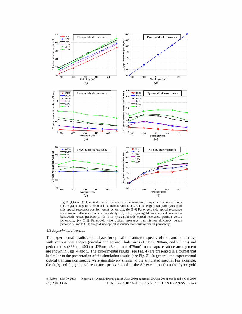
Fig. 3. (1,0) and (1,1) optical resonance analyses of the nano-hole arrays for simulation results
(in the graphs legend, D circular hole diameter and L square hole length): (a) (1,0) Pyrex-gold
side optical resonance position versus periodicity, (b) (1,0) Pyrex-gold side optical resonance
transmission efficiency versus periodicity, (c) (1,0) Pyrex-gold side optical resonance
bandwidth versus periodicity, (d) (1,1) Pyrex-gold side optical resonance position versus
periodicity, (e) (1,1) Pyrex-gold side optical resonance transmission efficiency versus
periodicity, and f) (1,0) air-gold side optical resonance transmission versus periodicity.
4.3 Experimental results
The experimental results and analysis for optical transmission spectra of the nano-hole arrays
with various hole shapes (circular and square), hole sizes (150nm, 200nm, and 250nm) and
periodicities (375nm, 400nm, 425nm, 450nm, and 475nm) in the square lattice arrangement
are shown in Figs. 4 and 5. The experimental results (see Fig. 4) are presented in a format that
is similar to the presentation of the simulation results (see Fig. 2). In general, the experimental
optical transmission spectra were qualitatively similar to the simulated spectra. For example,
the (1,0) and (1,1) optical resonance peaks related to the SP excitation from the Pyrex-gold
#132890 - $15.00 USD Received 4 Aug 2010; revised 28 Aug 2010; accepted 29 Aug 2010; published 6 Oct 2010(C) 2010 OSA 11 October 2010 / Vol. 18, No. 21 / OPTICS EXPRESS 22263
side and Wood’s anomaly were observed. However, there were differences in the number of
observable peaks and measurable bandwidths (compare Table 2 to Table 1). For instance, the
(1,0) resonance peak from the air-gold side was not clearly observed in the experimentally
measured spectra for the most of the arrays except the arrays with 150 nm circular hole and
periodicities of 450 nm and 475 nm. Furthermore, the (1,1) optical resonance peaks from
Pyrex-gold side had measurable bandwidths for the most of the arrays in the experimental
results, which were not generally measurable in simulation studies (compare Table 2 to
Table 1).
The dependence of the (1,0) optical resonance position, (1,0) optical resonance
transmission efficiency, and (1,0) optical resonance bandwidth on periodicity, hole size and
hole shape were generally similar to the corresponding metrics derived from simulations (see
Fig. 3 and 5). Both simulation and experimental results agreed with respect to the red-shift of
the (1,0) optical resonance position as the periodicity of the holes increased [see Fig. 3(a) and
Fig. 5 (a)]. Also, the (1,0) optical resonance position derived from the simulation results was
in good agreement with the experimental results. However, the experimental results showed
less dependence of the (1,0) optical resonance position on hole size compared to the
simulation results for the arrays with the same periodicity. The red-shift was generally
observed for the (1,0) resonance position as hole size increased in the simulation results, while
there was no systematic dependence of resonance position on hole size for the experimental
results (both blue-shifts and red-shifts were observed). With respect to the (1,0) optical
resonance transmission efficiency, both the simulation and experimental results were
generally in agreement for the smallest hole size [see Fig. 3(b) and Fig. 5(b)]. However, as the
hole size increased a transition from a decrease in transmission efficiency with periodicity to
an increase in transmission efficiency with periodicity was observed in the experimental
results. For example, the transmission efficiency of the array with 250 nm square hole size
increased as a function of periodicity. This was largely true for the circular hole shaped arrays
with 250 nm holes, except for devices with periodicities of 425 nm and higher where the
transmission efficiency was observed to be relatively constant. Although the optical resonance
bandwidth was not highly dependent on periodicity in the simulations, the bandwidth
decreased with periodicity in the experimental results and bandwidths were significantly
smaller (compare Tables 1 and 2) and [see Fig. 3(c) and Fig. 5(c)]. Furthermore, the
dependence of bandwidth on hole size was greater for the experimental results compared to
the simulations. For example, for simulations, arrays with circular holes of 200 nm and 250
nm, the bandwidths were measured to be 149 and 178 nm, respectively, while the
corresponding experimental observations resulted in bandwidths of 86 and 143 nm,
respectively.
#132890 - $15.00 USD Received 4 Aug 2010; revised 28 Aug 2010; accepted 29 Aug 2010; published 6 Oct 2010(C) 2010 OSA 11 October 2010 / Vol. 18, No. 21 / OPTICS EXPRESS 22264
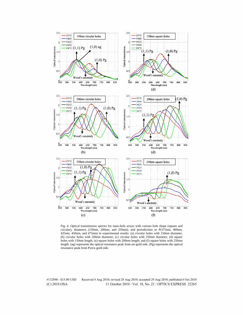
Fig. 4. Optical transmission spectra for nano-hole arrays with various hole shape (square and
circular), diameters (150nm, 200nm, and 250nm), and periodicities or P(375nm, 400nm,
425nm, 450nm, and 475nm) in experimental results: (a) circular holes with 150nm diameter,
(b) circular holes with 200nm diameter, (c) circular holes with 250nm diameter, (d) square
holes with 150nm length, (e) square holes with 200nm length, and (f) square holes with 250nm
length. (ag) represents the optical resonance peak from air-gold side. (Pg) represents the optical
resonance peak from Pyrex-gold side.
#132890 - $15.00 USD Received 4 Aug 2010; revised 28 Aug 2010; accepted 29 Aug 2010; published 6 Oct 2010(C) 2010 OSA 11 October 2010 / Vol. 18, No. 21 / OPTICS EXPRESS 22265
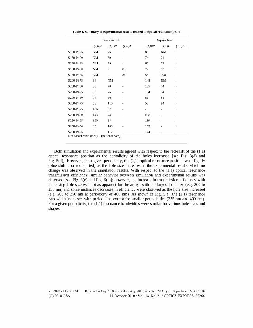
Table 2. Summary of experimental results related to optical resonance peaks
circular hole Square hole
(1,0)P (1,1)P (1,0)A (1,0)P (1,1)P (1,0)A
S150-P375 NM 76 - 88 NM -
S150-P400 NM 69 - 74 71 -
S150-P425 NM 79 - 67 77 -
S150-P450 NM - 85 72 93 -
S150-P475 NM - 86 54 108 -
S200-P375 94 NM - 148 NM -
S200-P400 86 70 - 125 74 -
S200-P425 80 76 - 104 74 -
S200-P450 74 96 - 86 84 -
S200-P475 53 110 - 58 94 -
S250-P375 186 87 - - - -
S250-P400 143 74 - NM - -
S250-P425 120 88 - 189 - -
S250-P450 95 100 - 153 - -
S250-P475 95 117 - 124 - - Not Measurable (NM), - (not observed)
Both simulation and experimental results agreed with respect to the red-shift of the (1,1)
optical resonance position as the periodicity of the holes increased [see Fig. 3(d) and
Fig. 5(d)]. However, for a given periodicity, the (1,1) optical resonance position was slightly
(blue-shifted or red-shifted) as the hole size increases in the experimental results which no
change was observed in the simulation results. With respect to the (1,1) optical resonance
transmission efficiency, similar behavior between simulation and experimental results was
observed [see Fig. 3(e) and Fig. 5(e)]; however, the increase in transmission efficiency with
increasing hole size was not as apparent for the arrays with the largest hole size (e.g. 200 to
250 nm) and some instances decreases in efficiency were observed as the hole size increased
(e.g. 200 to 250 nm at periodicity of 400 nm). As shown in Fig. 5(f), the (1,1) resonance
bandwidth increased with periodicity, except for smaller periodicities (375 nm and 400 nm).
For a given periodicity, the (1,1) resonance bandwidths were similar for various hole sizes and
shapes.
#132890 - $15.00 USD Received 4 Aug 2010; revised 28 Aug 2010; accepted 29 Aug 2010; published 6 Oct 2010(C) 2010 OSA 11 October 2010 / Vol. 18, No. 21 / OPTICS EXPRESS 22266
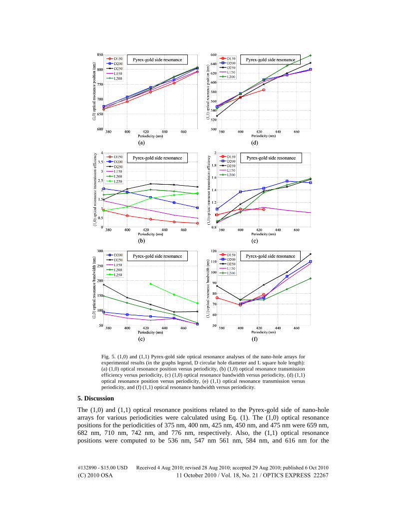
Fig. 5. (1,0) and (1,1) Pyrex-gold side optical resonance analyses of the nano-hole arrays for
experimental results (in the graphs legend, D circular hole diameter and L square hole length):
(a) (1,0) optical resonance position versus periodicity, (b) (1,0) optical resonance transmission
efficiency versus periodicity, (c) (1,0) optical resonance bandwidth versus periodicity, (d) (1,1)
optical resonance position versus periodicity, (e) (1,1) optical resonance transmission versus
periodicity, and (f) (1,1) optical resonance bandwidth versus periodicity.
5. Discussion
The (1,0) and (1,1) optical resonance positions related to the Pyrex-gold side of nano-hole
arrays for various periodicities were calculated using Eq. (1). The (1,0) optical resonance
positions for the periodicities of 375 nm, 400 nm, 425 nm, 450 nm, and 475 nm were 659 nm,
682 nm, 710 nm, 742 nm, and 776 nm, respectively. Also, the (1,1) optical resonance
positions were computed to be 536 nm, 547 nm 561 nm, 584 nm, and 616 nm for the
#132890 - $15.00 USD Received 4 Aug 2010; revised 28 Aug 2010; accepted 29 Aug 2010; published 6 Oct 2010(C) 2010 OSA 11 October 2010 / Vol. 18, No. 21 / OPTICS EXPRESS 22267
corresponding periodicities. The resonance peak positions observed in experiment and
simulation were in good qualitative agreement with the theoretical estimates.
Although there was general agreement between the optical properties of nano-hole arrays
studied by experiment and simulation, there were several notable differences. First, the
transmission efficiency for (1,0) and (1,1) resonance peaks related to the Pyrex-gold side
obtained through simulation was significantly lower compared to the experimental results.
This was likely due to the high sensitivity of the simulated transmission spectra on presence of
the chromium layer. For example, sharp resonance peaks were observed when the chromium
layer was excluded (data not shown) in a manner similar to other work [8]. It is possible that
the selection of the mesh accuracy, although small enough to adequately sample the
chromium layer, resulted in an underestimation of the transmission efficiency. The slight
discrepancy between simulation and experimental results due to the selection of the mesh
accuracy enabled manageable computation times. Second, although the optical resonance
peaks related to the (1,0) air-gold side were observed in the simulation studies, they were not
observed consistently in the experimental studies. This was most likely on account of the
closeness of the (1,1) resonance peak position to (1,0) resonance and the poorer transmission
efficiency of the (1,0) resonance from air-gold side. As a result, the (1,0) resonance peaks on
the air-gold side were not observed for all of the arrays, except for the arrays with 150 nm
circular hole size and higher periodicities (450 nm and 475 nm). Since the arrays with 150 nm
holes and higher periodicities (450 nm and 475 nm) had a smaller total hole area compared to
the other tested arrays, the resonance peaks of longer wavelength had lower transmission
efficiency compared to other arrays with larger hole sizes. As a result, the (1,1) resonance
peak from the Pyrex-gold side and the (1,0) resonance peak from air-gold side appeared at
longer and shorter wavelengths, respectively. This effect resulted in more pronounced (1,0)
resonance peaks from the air-gold side for these arrays (150 nm circular hole with 450 nm and
475 nm periodicities) and suppression of the (1,1) resonance peak from the Pyrex-gold side.
Third, in the simulations, the transmission efficiency of the (1,0) Pyrex-gold side resonance
peak improved with hole size. Based on geometric considerations, the transmission behaviour
was consistent with the total effective aperture of the nano-hole array, i.e. larger holes and
closer hole spacing resulted in larger total opening size compared to nano-hole arrays with
smaller holes and wider hole spacing. This geometric dependence of the optical transmission
efficiency on hole area has been known for over a decade [10]. Although this general optical
transmission behaviour was observed in experiments performed with nano-hole arrays with
circular holes, the transmission efficiency determined through experiment did not increase in a
manner consistent with the effective aperture hypothesis. The discrepancy was most apparent
for nano-hole arrays with square holes. For example, nano-hole arrays with square holes 200
nm in size had greater transmission efficiency than arrays of identical periodicity with square
holes either 150 nm or 250 nm in size. Although the reason for this behaviour is not fully
understood, it may be related to more efficient coupling of the light to the SP with this
specific hole size in the visible and near infra-red regime, which could potentially result in a
higher transmission efficiency.
It has been reported in early literature that the optical resonance position is not dependent
on hole size [1]. However, we found experimentally that the (1,0) optical resonance position
varied slightly (blue-shifted or red-shifted) with hole size. In agreement with our results, it has
been reported for nano-hole arrays with square hole shape that a similar shift in resonance
position behavior occurs, which was attributed to a cutoff behavior related to the hole size
[23]. Also, in agreement with literature (see ref [10].), we also observed that the (1,0) optical
resonance bandwidth became larger for larger holes and narrower for larger periodicities.
Using the EBL fabrication methodology, the pattern on the photoresist for a nano-hole
array 1 mm by 1 mm can be written in a couple of hours with reasonable cost. However,
compared to other methods such as Focused Ion Beam (FIB) milling technology, EBL
fabrication methodology requires a thicker adhesion layer (such as 8 nm to 20 nm Chromium
#132890 - $15.00 USD Received 4 Aug 2010; revised 28 Aug 2010; accepted 29 Aug 2010; published 6 Oct 2010(C) 2010 OSA 11 October 2010 / Vol. 18, No. 21 / OPTICS EXPRESS 22268
or Titanium) to allow for an aggressive lift-off process without damaging an array. Since the
adhesion layer is deposited between the gold and Pyrex substrate, the optical performance of
the nano-hole array is affected. For example, we observed that the bandwidth of the (1,0) and
(1,1) resonance peak was broadened and the transmission efficiency was lower. However,
deposition of metal materials such as aluminum or silver on the Pyrex substrate does not
require an adhesion layer, but these materials are sensitive to oxidization that leads to loss of
the SP properties. Also, unlike other methods for nano-hole-array fabrication, patterns such as
grooves, corrugations, and dimples cannot be fabricated about the holes easily with EBL.
Other fabrication methodologies such as Nano-Imprint Lithography (NIL) and FIB are proven
methods for fabrication of nano-hole arrays [24–27]. FIB fabrication methodology can be
used to fabricate arbitrary nano-hole array designs with fine resolution, but at the cost of
speed. Alternatively, very large nano-hole arrays can be fabricated with NIL methodology
very quickly, but with poorer resolution and higher cost. Therefore, EBL provides a rapid and
competitive fabrication solution for nano-hole arrays of intermediate size where fidelity of
nanostructures is important.
Although the motivation for this study was the potential development of nano-hole arrays
as spectral filters. The analysis of the EOT properties of various nano-hole array designs
revealed that the band-pass characteristics of the devices simulated and tested was far from
optimal when compared to conventional commercially available interference filters.
Typically, it was observed that the nano-hole arrays had at least two pass bands with poor
blocking between and on either side. Poor out of band blocking would result in bleed through
of out of band wavelengths and corruption of spectroscopic data, for example. To improve
band-pass performance several options remain including manipulation of the dielectrics on
either side of the gold and incorporation of nano-scale features to enhance wavelength
selectivity and transmission efficiency. For example, a nano-hole array surrounded with the
material of the same dielectric constant on both sides is known to increase the transmission
efficiency of the resonance peak due to SP energy coincidence on both sides of a nano-hole
array [14]. Also, structures such as grooves, corrugations, and dimples about the holes of a
nano-hole array or surrounding an entire nano-hole array can enhance transmission efficiency
of the resonance peak [11,16]. For example, it has been shown that a nano-hole array
surrounded by dimples with the same size and shape as the holes and at half periodicity of the
holes can improve transmission efficiently by a factor of two [16]. In addition to the hole size
effect on the bandwidth of the resonance peaks, the bandwidth can be reduced if the nano-hole
array is fabricated in a thicker metal film. However, the transmission efficiency of the
resonance peak decays as thickness of metal film increases [1]. Also, a 10 to 20 nm adhesion
layer of Chromium can cause broadening of the bandwidth of the resonance peaks related to
the Pyrex-gold side of the nano-hole array. As a result, by exploiting other materials such as
Ag or Al [8], the need for a Chromium layer can be eliminated and narrower bandwidths can
be achieved.
Regardless of the poor blocking characteristics of the nano-hole arrays studied here, an
interesting aspect of nano-hole arrays is their scalable size. The nano-hole array dimension
can be varied from several microns to several centimeters in size. This provides interesting
opportunities to utilize the same base technology for applications that work at microscopic
scales to applications that work at macroscopic scales. For example, the optical resonance of
nano-hole arrays for various geometrical parameters can be exploited in applications such as
SEFS and bio-sensing applications, where the optical resonance transmission properties of the
nano-hole arrays can enhance the detectability of fluorescence emission and bio-molecules
[2–5].
In the future, additional studies will need to be directed at improving the optical resonance
transmission efficiency of nano-hole arrays and reducing bandwidth if nano-hole arrays are to
be used as spectral band-pass filters for biomedical applications. Probably the most success
will come from examining new substrates and dielectric matching of the top and bottom
#132890 - $15.00 USD Received 4 Aug 2010; revised 28 Aug 2010; accepted 29 Aug 2010; published 6 Oct 2010(C) 2010 OSA 11 October 2010 / Vol. 18, No. 21 / OPTICS EXPRESS 22269
layers. As a result, in future work, we are planning to do a comprehensive experimental and
numerical analyses on optical transmission of nano-hole arrays when they are surrounded by
transparent materials such as Polymethyl methacrylate (PMMA), transparent SU-8, and
silicon dioxide.
6. Conclusion
We presented a comprehensive experimental and numerical (FDTD) study on Extraordinary
Optical Transmission (EOT) through various nano-hole arrays in a thick metal film within the
visible and near infra-red spectral regions. Large nano-hole arrays were fabricated using EBL
methodology and they were optically characterized. We analyzed the simulation and the
optical characterization results of optical resonance of nano-hole arrays with respect to optical
resonance peak position, optical resonance transmission efficiency, and optical resonance
bandwidth. As a result, regarding these parameters, the simulation results showed relatively
good agreement with the experimental analyses although there were some notable differences.
The hole size was recognized as a main factor in the appearance of the optical resonance
peaks in the transmission spectra. There were no significant differences between optical
transmission spectra of nano-hole arrays with circular or square hole shapes. However, the
opening area of the hole had a major effect on the optical resonance transmission properties.
The effect of the chromium adhesion layer between the gold film and the Pyrex substrate
reduced the transmission efficiency for the optical resonance peaks related to SP excitation
from Pyrex-gold side. Finally, the analyses showed that for macroscopic applications such as
optical band-pass filters, improved out of band blocking are needed. One possibility for
achieving this optical characteristic is the matching of the SP energy on both sides of the array
by index-matching.
#132890 - $15.00 USD Received 4 Aug 2010; revised 28 Aug 2010; accepted 29 Aug 2010; published 6 Oct 2010(C) 2010 OSA 11 October 2010 / Vol. 18, No. 21 / OPTICS EXPRESS 22270