Experiment Sheet - Mastering Digital Design Part 1 - Imperial ...
12
Mastering Digital Design Department of EEE with Verilog on FPGAs Imperial College London V5.0 - PYK Cheung, 9 Oct 2017 Part 1 - 1 MSc Course on Analogue and Digital IC Design Imperial College London Laboratory Experiment – Mastering Digital Design (webpage: http://www.ee.ic.ac.uk/pcheung/teaching/MSc_Experiment/) This Laboratory Experiment is intended to ensure all students on the ADIC MSc course reach an expected level of competence in digital design using a hardware description language (such as Verilog) implemented on an FPGA. Those students with limited or no prior experience in both Verilog and/or FPGA may need to devote time outside the scheduled period to complete the experiment. The experiment is organized in four parts, each with clearly defined learning outcomes. See the document entitled: “Mastering Digital Design – Experiment Specification Document”. Objectives By the end of this experiment, you should have learned: • How to design digital circuits using Intel/Altera’s Quartus II Design software; • How to design digital circuits targeting Altera’s Cyclone V FPGA using Terasic’s DE1- SoC Board; • How to design digital circuits in efficient, synthesizable Verilog HDL; • How to evaluate your design in terms of resource utilization and clock speed; • How to use the DE1-SoC FPGA board with its custom daughter board for analogue I/O functions; • Have designed something yourself for the Cyclone V FPGA. Before you start Before you come to the laboratory, you are expected to: • Have understood the lectures on Verilog • Be familiar with the basic architecture inside the FPGA • Have read through this Laboratory instructions
-
Upload
khangminh22 -
Category
Documents
-
view
1 -
download
0
Transcript of Experiment Sheet - Mastering Digital Design Part 1 - Imperial ...
MasteringDigitalDesign DepartmentofEEEwithVerilogonFPGAs ImperialCollegeLondon
V5.0-PYKCheung,9Oct2017 Part1-1
MScCourseonAnalogueandDigitalICDesign
ImperialCollegeLondon
LaboratoryExperiment–MasteringDigitalDesign
(webpage:http://www.ee.ic.ac.uk/pcheung/teaching/MSc_Experiment/)
ThisLaboratoryExperimentisintendedtoensureallstudentsontheADICMSccoursereachanexpectedlevelofcompetenceindigitaldesignusingahardwaredescriptionlanguage(suchasVerilog)implementedonanFPGA.ThosestudentswithlimitedornopriorexperienceinbothVerilogand/orFPGAmayneedtodevotetimeoutsidethescheduledperiodtocompletetheexperiment.
Theexperimentisorganizedinfourparts,eachwithclearlydefinedlearningoutcomes.Seethedocumententitled:“MasteringDigitalDesign–ExperimentSpecificationDocument”.
Objectives
Bytheendofthisexperiment,youshouldhavelearned:
• HowtodesigndigitalcircuitsusingIntel/Altera’sQuartusIIDesignsoftware;• HowtodesigndigitalcircuitstargetingAltera’sCycloneVFPGAusingTerasic’sDE1-
SoCBoard;• Howtodesigndigitalcircuitsinefficient,synthesizableVerilogHDL;• Howtoevaluateyourdesignintermsofresourceutilizationandclockspeed;• HowtousetheDE1-SoCFPGAboardwith itscustomdaughterboard foranalogue
I/Ofunctions;• HavedesignedsomethingyourselffortheCycloneVFPGA.
Beforeyoustart
Beforeyoucometothelaboratory,youareexpectedto:
• HaveunderstoodthelecturesonVerilog• BefamiliarwiththebasicarchitectureinsidetheFPGA• HavereadthroughthisLaboratoryinstructions

MasteringDigitalDesign DepartmentofEEEwithVerilogonFPGAs ImperialCollegeLondon
V5.0-PYKCheung,9Oct2017 Part1-2
BoththeexperimentalboardandaPCwouldbemadeavailabletoyouduringyourallottedperiodinthelaboratory.Inaddition,youmayalsoborrowaDE1-SoCboardtouseathomeforthedurationofthisexperiment.
Thisinstructionmanualisdividedintofourparts,oneforeachweek.Eachparthasitsowngoalsandlearningoutcomes.
Somestudentswill findthisexperimentharderoreasier thanaverage,dependingonyourpriorexperiencewithdigitallogic.Therefore,thefourLabsessionscontainthecompulsoryswellasoptionalexercisers.Ifyoufallbehindthisexperimentduringanyweek, it iswisetofind a bit of spare time to catch up outside the official laboratory sessions and restrictyourselftothecompulsorypartsonly.
PARTI–SchematictoVerilog(LearningOutcomes)
BasiccompetenceinusingIntel/Altera’sQuartusdesignsystemsforCyclone-VFPGA;appreciatethesuperiorityofhardwaredescriptionlanguageoverschematiccapturefordigitaldesign;useofcasestatementtospecifycombinatorialcircuit;usehigherlevelconstructsinVerilogtospecifycomplexcombinatorialcircuits;developcompetenceintakingadesignfromdescriptiontohardware.
1.0Introduction
You should have done some background reading before attending thelaboratorysessionassuggestedattheLecture.
FPGAs is a type of programmable logic devices introduced by Xilinx in1985. It is now the predominant technology for implementing digitallogic in lowtomoderatevolumeproduction. Thebasic structureofanFPGA is shown below. It consists of threemain types of resources: 1)LogicBlocks (orElements);2)RoutingResources;3) I/OPad. Formore

MasteringDigitalDesign DepartmentofEEEwithVerilogonFPGAs ImperialCollegeLondon
V5.0-PYKCheung,9Oct2017 Part1-3
informationaboutFPGA,seeLecture1notesavailableontheE2DigitalElectronicscoursewebpage.
1.1 QuartusDesignSuite
Quartus provides a complete environment for you to implement your design on anAlteraFPGA. It supportsallaspectsof thedesign flow,which is typically followingtheflowdiagramshownhere.ThebestwaytolearnQuartusistogothroughthisexperimentstep-by-step.Afteryouhavelearnedthebasics,youcanstarttoexploreotheraspectsoftheQuartussystem.
1.2 DE1-SoCBoard
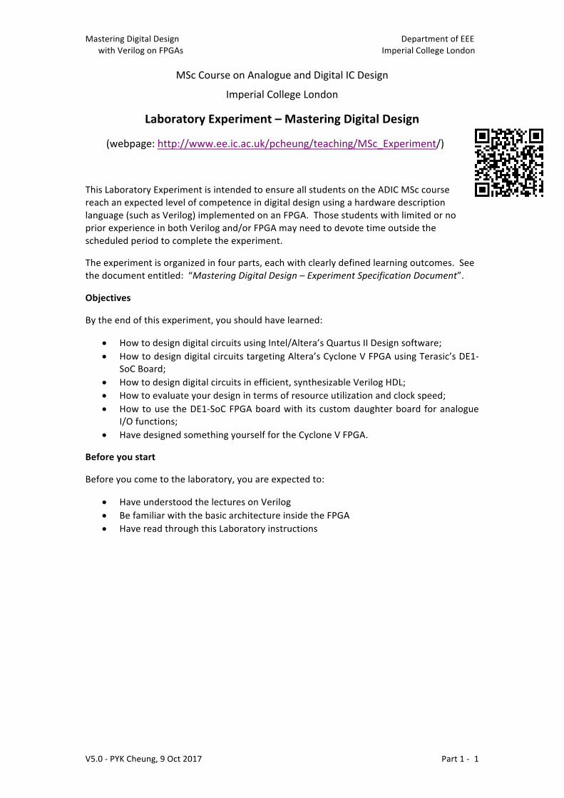
DE1-SoCBoardisdesignedandmadebyTerasic.ItisbasedaroundaCycloneVFPGAfromAltera.IncludeontheDE1boardarevariousI/Odevicessuchas7-segmentLEDdisplays,LED,switches,VGAport,RS232port,SDcardslotetc.Ablockdiagramof theDE1board is shownbelow. Although theCycloneVincludes adual-coreARMprocessor,wewill onlybeusing the FPGApartoftheFPGAforthisexperiment.
1.4 VerilogHardwareDescriptionLanguage
Oneof thekey learningobjectiveof thisexperiment is foryou to learn theVerilogHardwareDescriptionLanguage(HDL),which iscommonlyusedtospecifyFPGAandothertypesofchipdesigns.Anexcellenttutorialcanbefoundon:
http://www.asic-world.com/verilog/veritut.html. A Verilog Syntax Summary sheet isprovidedinAppendixA.
1.5 UsingQuartusPrimesoftwareandDE1athome
Ifyourownlaptopissufficientlypowerful(atleast4GBofRAM)andhasplentyoffreediskspace(atleast1GBoffreediskspace),youmaywanttoinstallacopyoftheQuartusdesignsoftwareonyourowncomputer.ThelatestversionisQuartusversion17.
YourclassisdividedintoGroupsoftwostudents.Youmaychooseyourowngrouppartner.If youdon’t find anyone toworkwith, letme knowand Iwill pair youupwith someone.Each pair of students will be issued with your own DE1-SoC board with an analogue I/Oboardforthedurationofthisexperiment.YoumaytaketheboardhomewithyouoruseitinRoom909(MScLab).However,youareresponsiblefortheboarduntilitisreturned.
To install your own copy of Quartus, you should go to Altera’s website to register, thendownload the free Quartus Prime Light Edition from: http://dl.altera.com/?edition=web.NotethatQuartusandtheDE1boardonlyworkswithMSWindowsorLinux. IfyouareaMacuser,youwouldneedto runavirtualmachine (e.g.VirtualBox,ParallelsorVMware),loadaversionofWindowsorLinux,andthenrunQuartusunderthatenvironment.
PlugtheDE1boardtoaUSBportonyourcomputerandturnitON(redbutton).Itwillaskyouforadevicedriver,whichcanbefoundintheQuartussoftwaredirectory….\drivers.See“DE1-SoCGettingStartedGuide”fromtheexperimentwebpage.
MasteringDigitalDesign DepartmentofEEEwithVerilogonFPGAs ImperialCollegeLondon
V5.0-PYKCheung,9Oct2017 Part1-4
BlockDiagramoftheDE1-SoCBoard
Experiment1:SchematiccaptureusingQuartus–7-SegmentDisplay
Ifyouhavecometothelaboratorysessionprepared,PartIofexperimentVERIshouldtakenomorethanONE3-hoursession.Itwillleadyouthroughtheentiredesignofa7-segmentdecoderusingschematicentrymethod.Itwillusefourslideswitchesontheright(SW3toSW0)ontheDE1boardasinput,anddisplaythe4-bitbinarynumberasahexadecimaldigitontheright-most7-segmentdisplay(HEX0).

MasteringDigitalDesign DepartmentofEEEwithVerilogonFPGAs ImperialCollegeLondon
V5.0-PYKCheung,9Oct2017 Part1-5
Step1:Creatingagooddirectorystructure
Before you start carrying out any design for thisexercise,itwouldbeveryhelpfulifyoufirstcreateinyour home directory a directory structure on theh:\driveforthisexperiment.Shownontheright isapossible directory structure that youmay choose tocreate. Each folder is empty for now, but as youprogress through the four Lab Sessions, you will becreatingeachdesignineachofthefolders.
Step2:SeewhatyouareaimingforGototheExperimentwebpage(seeabove)anddownloadacopyofthesolutionforExercise1:“ex1sol.sof”toyourhomedirectory (orwherever that is). Now turnON theDE1board.
Step3:ProgrammetheFPGA
Start up Quartus software on your computer. Clickcommand:Tools > Programmer. In the popupwindow,click:HardwareSetup…. Youshouldseesomething likethe diagram on the right. Then select:DE-SOC [USB-1].ThisistotellQuartussoftwarethatyouareusingtheDE1-SoCUSBinterfacetoprogram(orblast)theFPGA.ThenclickAutoDetectbuttonontheleft.AwindowwillpopupandyouneedtoselectSCSEMA5radiobuttontotellthesystemwhichtypeofCycloneVFPGAchipyouareusing(whichis5CSEMA5).
Youwillnowsee two lines in theProgrammerwindowas shownon theright.Sinceweareonlyconfiguring(i.e.sendingabit-streamto)theFPGApart of the CycloneV chip,we need todelete the SOCVHPS (stands forSystem-on-ChipVHighPerformanceSystem,whichistheARMprocessor)fromtheprogrammersetup.
Next click the AddFile button. Navigate to the folder containing theex1sol.soffile.Selectthis.FinallyclicktheStartbutton.
The ex1sol.sof file contains the solution to Exercise 1designed by me. It has the bit-stream to configure (orprogramme)theFPGApartofCycloneV.Oncethebit-streamissuccessfullysenttotheFPGAchip,thisdesignwilltakeoverthe function of the chip. You should be able to change theleast significant four switches and see a hexadecimal number displayed on rightmost 7-segmentdisplay.
You should leave the programmer utility running in the background for ease of sendinganotherdesigntotheFPGAlater.ReturntoQuartussoftwarebyclickingitswindow.
Step4:PaperDesign
Theoverallblockdiagramforthedecoder isshownbelow. Thedecoderoutputsout[6..0]drive the seven segments on the display. Note that the LED segments are low active,meaningthattheLEDwilllightup(ON)ifthecorrespondingdigitalsignalisat0V.
MasteringDigitalDesign DepartmentofEEEwithVerilogonFPGAs ImperialCollegeLondon
V5.0-PYKCheung,9Oct2017 Part1-6
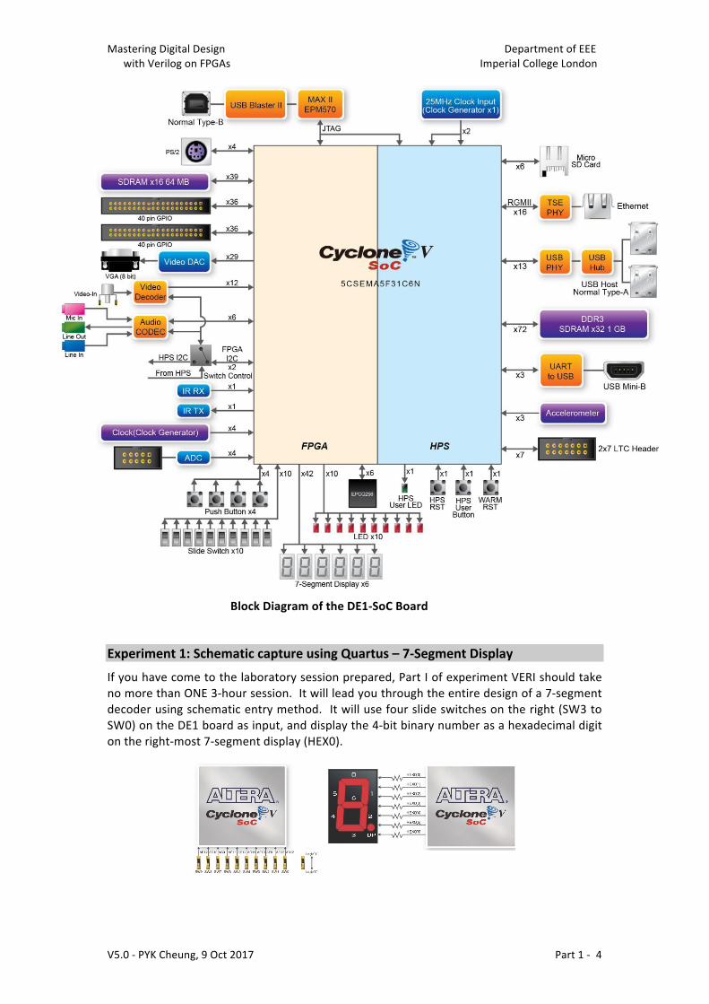
Thetruth-tableforthedecoderisshownhere:
Withwhatyouhave learned inthefirstyear,you should be able to design the decoder inthe form of seven Boolean equations, andthen use K-map to minimise the logic. Inorder to save time, only derive the Booleanequation for out[4] as a Boolean function ofin[3..0].
YoualsoshouldnotuseK-maptoperformanyoptimization. Quartus (andothermodernCADdesignsoftware)willperformlogicminimizationforyouandwilldoamuchbetterjob,takingintoaccountthearchitectureoftheFPGAchip.
Step5:Createtheproject“ex1”
• Createinyourhomedirectorythefolder../part_1/ex1.
• Clickfile>NewProjectWizard,completetheform.Useex1astheprojectnameandex1_topastop-designname.
• SelecttheFPGAdeviceasCycloneV5CSEMA5F31C6.ThenclickFinish.
Step6:Specifythe7-segmentdecoderasschematic
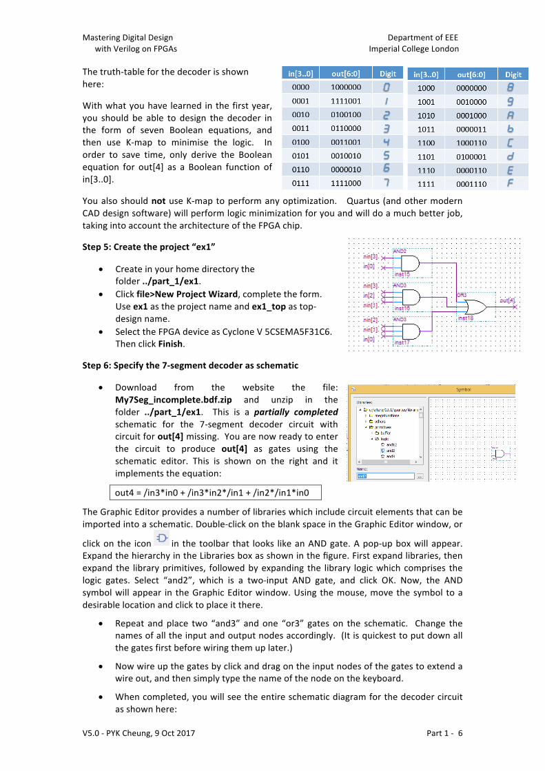
• Download from the website the file:My7Seg_incomplete.bdf.zip and unzip in thefolder ../part_1/ex1. This is a partially completedschematic for the 7-segment decoder circuit withcircuitforout[4]missing.Youarenowreadytoenterthe circuit to produce out[4] as gates using theschematic editor. This is shown on the right and itimplementstheequation:
out4=/in3*in0+/in3*in2*/in1+/in2*/in1*in0
TheGraphicEditorprovidesanumberoflibrarieswhichincludecircuitelementsthatcanbeimportedintoaschematic.Double-clickontheblankspaceintheGraphicEditorwindow,or
clickon the icon in the toolbar that looks likeanANDgate.Apop-upboxwillappear.ExpandthehierarchyintheLibrariesboxasshowninthefigure.Firstexpandlibraries,thenexpand the libraryprimitives, followedbyexpanding the library logicwhichcomprises thelogic gates. Select “and2”, which is a two-input AND gate, and click OK. Now, the ANDsymbolwillappear in theGraphicEditorwindow.Using themouse,movethesymbol toadesirablelocationandclicktoplaceitthere.
• Repeat andplace two “and3” andone “or3” gateson the schematic. Change thenamesofalltheinputandoutputnodesaccordingly.(Itisquickesttoputdownallthegatesfirstbeforewiringthemuplater.)
• Nowwireupthegatesbyclickanddragontheinputnodesofthegatestoextendawireout,andthensimplytypethenameofthenodeonthekeyboard.
• Whencompleted,youwillseetheentireschematicdiagramforthedecodercircuitasshownhere:
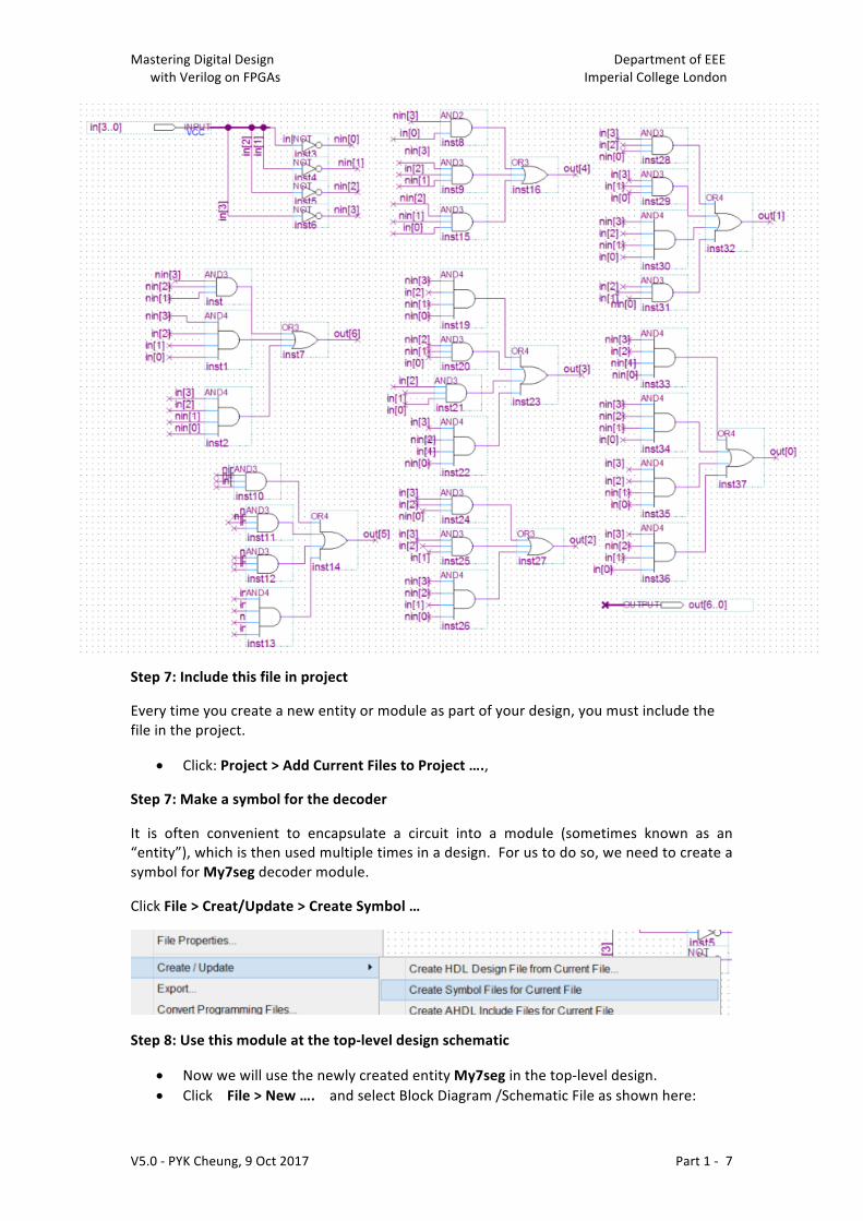
MasteringDigitalDesign DepartmentofEEEwithVerilogonFPGAs ImperialCollegeLondon
V5.0-PYKCheung,9Oct2017 Part1-7
Step7:Includethisfileinproject
Everytimeyoucreateanewentityormoduleaspartofyourdesign,youmustincludethefileintheproject.
• Click:Project>AddCurrentFilestoProject….,
Step7:Makeasymbolforthedecoder
It is often convenient to encapsulate a circuit into a module (sometimes known as an“entity”),whichisthenusedmultipletimesinadesign.Forustodoso,weneedtocreateasymbolforMy7segdecodermodule.
ClickFile>Creat/Update>CreateSymbol…
Step8:Usethismoduleatthetop-leveldesignschematic
• NowwewillusethenewlycreatedentityMy7seginthetop-leveldesign.• ClickFile>New….andselectBlockDiagram/SchematicFileasshownhere:

MasteringDigitalDesign DepartmentofEEEwithVerilogonFPGAs ImperialCollegeLondon
V5.0-PYKCheung,9Oct2017 Part1-8
• Use the button to select and place the My7seg module, input port andoutputportontheschematic.
• Double click the port symbol to edit the input and output pin names asSW[3..0]andHEX0[6..0]respectively.
• Usethebuswiring tool towireup theports to themoduleas twobussesasshownbelow.
• Savethisfile.
Step9:Pinassignment&Compilation
YouneedtoassociateyourdesignwiththephysicalpinsoftheCycloneVFPGAontheDE1-SOCboard.
• Check that the device is corrected assigned as5CSEMA5F31C6using:Assignments>Device…
• Click:Processing>Start>StartAnalysisandElaboration.Thiswillwork out the input/output port names for yourdesign. This should completewithouterror. Otherwise,fixallerrorsandre-analyse.(Therewillbemanywarnings–generallywarningsarenot important.But thereMUSTnotbeerrors,whichwillbeshowninRED.)
• ClickAssignment>PinPlannerandanewwindowwiththe chip package diagram. You should also see the top-levelinput/outputportsshownasalist.

MasteringDigitalDesign DepartmentofEEEwithVerilogonFPGAs ImperialCollegeLondon
V5.0-PYKCheung,9Oct2017 Part1-9
• Clickontheappropriatepinsonebyone,andselectthecorrespondinglocationfromadropdownlistaccordingtothelistshowninthepinassignmenttableabove.TheI/Ostandard(i.e.interfacevoltages)shouldbe“3.3VLVTTL”.
• Click:Processing>StartCompilation,tobuildtheentiredesign,andtogenerateallthenecessaryfiles.ThereshouldbeNOerror,buttherewillbemanywarnings.
Step10:ProgramtheFPGAontheDE1Board
• Youhavenowcreatedinthe../part_1/ex1/output_files/folderthefileex1_top.sof,whichcontainyourdesign.(ThisshouldbethesamedesignastheoneIgaveyoutotryoutinStep2ofthisexercise.)
• ProgramtheDE1boardwithyourversionofex1_top.sofandtestthatitisworkingproperly.
Step11:PropagationDelayfrominputstooutputs
• Click:Tools > TimeQuest TimingAnalyzer to invoke thebuilt in timinganalyzerofQuartus.AnewTimeQuestwindowwillappear.
• Click:Netlist>CreateTimingNetlist.Thenselectpost-fitandslow-corner,thenOK.• Inthe“SetOperatingConditions”window,select“Slow1100mV0°Cmodel”.• Now click: Netlist > Update Timing Netlist … This will use the specified timing
modelandconditiontoproduceasetoftimingdata.• Click:Report>Datasheet>ReportDatasheet.Thiswillproduceatableshowingthe
input-to-outputpropagationdelayforvariouscombinationofriseandfalltimes(RR,RF,FRandFF).Makesurethatyouunderstandingwhatthistablemeans.

MasteringDigitalDesign DepartmentofEEEwithVerilogonFPGAs ImperialCollegeLondon
V5.0-PYKCheung,9Oct2017 Part1-10
• Repeat the procedcure again but for “Slow 1100mV85°CModel”.What is thedelaydifferenceat thesetwotemperatureextremes?Why?
Step12:Examinetheresourcesused
• Now examine the Compilation Report. You shouldseesomethingasshownhere.
• It shows that this design used only 4 out of 32,070ALMs(AdaptiveLogicModules),11ofthe457I/Opinsandnoneoftheotherresources.
Congratulations!YouhavenowcompletedyourfirstFPGAdesign!
Experiment2:7-SegmentdecoderinVerilogHDL
I hope you now appreciate how limiting and slow it is to enter a design as a schematicdiagram.ModerndigitaldesignersDONOTUSEschematicasamethodofentryanymore.Instead a designer would either use Verilog or VHDL hardware description language, orsome high level language such as OpenCL or Vivaldo HLS to specify the design. In thisexperiment, you will design the Verilog version of what you have done in Experiment 1.Hopefullythiswillconvinceyounevertouseschematiccapturefordigitaldesignagain!§
Step1:hex_to_7seg.v
• Create a new project ex2 as before and a top-levelmoduleex2_topasbeforeinex2folder.
• In Quartus, create a design file in Verilog HDLknownashex_to_7seg.vusing:
File > New …. and select Verilog HDLfromthelist.
• Type the Verilog source file as shown below.(You should have seen this during one of theLectures earlier). Make sure you pay attentiontothesyntaxofVerilog.Saveyourfile.
• A full compilation can take a long time. A farmore efficient way to check the syntax of yourcodebyclicking:Process>Analyzecurrentfile.You should get into ahabit ofALWAYSperformthis step to make sure that the new Verilogmodule you have created is as error free as
possible.Itwillsaveyoualotoftime.
Step2:CreateTop-LevelSpecificationinVerilog
• Instead of using schematic capture for the top-level module (that connects to physical pins onthe FPGA), we will do this also in Verilog bycreatingthefile:“ex2_top.v”asshownhere.SetthisasTop-Levelentity.
• Click: Project > Add/Remove Files, and removethe.bdffileaspartofthisproject.

MasteringDigitalDesign DepartmentofEEEwithVerilogonFPGAs ImperialCollegeLondon
V5.0-PYKCheung,9Oct2017 Part1-11
• Thisallowsyoutoremovethe.bdffileandreplaceitwiththe.vfileforthetop-levelspecification.
• Verify that everything works properly with: Process > Start > Start analysis &elaboration.Make sure that there is no error. (Warnings often capture potentialerrors. However, theQuartus system generatesmanywarnings, and nearly all ofwhicharenot important. Onceyouhavegainconfidenceonthesystem,youmaystartignoringthewarning,butneverignoreanyerror.)
YouwillsavealotoftimeifyouALWAYSusethesetwosteps:analyze,andanalysis&elaboration,andensurethatALLerrorsaredealtwith(andwarningunderstood).
Step3:PinAssignment–thequickway
• Earlieryouusedthepinassignmenteditortoassociatepinsonthepackagetoyoursignals.Thisisatediousprocess.Inex1,ifyouhavecorrectlycompletedthedesign,thepinassignmentwouldhavebeenstoredinafile:“ex1_top.qsf”file.
• Openthis file,eitherusingQuartus’built-ineditorbyclicking:File>Open file…oruseyourownfavouriteeditonyourPC.
• Youwillfindlinesofstatementsuchas:
• ThefirstlinedefinesthevoltagestandardusedbytheHEX0[4]signal(3.3Vlogic).• ThesecondlinedefinesthephysicalpinlocationofHEX0[4]isPIN_AF28.• Nowopentheex2_top.qsffile.Youwillseethatthereisnopinassignmentforthis
designyet.Beforefullcompilation,weneedtotellQuartuswhichsignalisconnecttowhichphysicalpinontheFPGA.
• Instead of using the tedious pin assignment editor in ex1, we will modify theex2_top.qsffilewithourtexteditortoincludethepinassignmentinformation.Todothis,firstdownloadfromtheexperimentwebpagethefile:pin_assignment.txttotheVERIdirectory.
• Thenuse:Edit>InsertFile…inQuartustoinsertthewholeofpin_assignment.txtinex2_top.qsf.
• Notethatweonlyuse7pins inex2_top.v,butpin_assignment.txtdefinesallpinsusedbythefourpartsofExperimentVERI. Quartuswillgenerate lotsofwarningswhichyoumayignoreabouttheseunusedpinsnotbeingdriven. Itwillnotcreateanyerrorandthepinassignmentsforunusedpinswillbeignored.
Step5:Testyourdesign
• Recompileyourdesign.• Go to the Programmer window (assuming that you still have it opened). Delete
the.soffileentryandaddthecurrent.soffile.• Testyourdesignontheboard.
Step6:Putmoduleinmylib
OverthefourweeksintheLab,youwilldesignandverifyvariousVerilogmoduleswhichyouwill reuse. Youshouldcopy these to the“mylib” folderand includethem inyournewdesignasnecessary.
Note:Whenyouperformacompilation,theremaybeapopupwindowinformingyouthatsome“Chain_x.cdf”filehasbeenmodified,andaskifyouwishtosaveit.JustclickNO.

MasteringDigitalDesign DepartmentofEEEwithVerilogonFPGAs ImperialCollegeLondon
V5.0-PYKCheung,9Oct2017 Part1-12
Experiment 3: Test yourself - 10-bit binary switch values on three 7-segmentdisplays
Here is a “test yourself” exercise. Create your own design to display all 10-bit slidingswitchesashexadecimalonthreeofthe7-segmentLEDdisplays.
Checkpoint:Youshouldgettothispointbytheendofthe3-hourLabSessionorearlier.
Experiment4:Displaying10-bitbinaryasBCDdigitsonthe7-segmentdisplays
Inoneofthelectures,youhavebeentaughthowtoconvertbinarynumberstobinary-code-decimal digits using the “shift and add 3” algorithm. You have been shown how toimplementan8-bitbinarytoBCDconverterusingVerilog.Furthermoreinproblemsheet1,youhavebeenaskedtoextendthistoa10-bitconverter(bin2bcd_10.v).
Forthisoptionalexercise,youarerequiredtodisplaythe10-bitbinarynumberasspecifiedbythe10slidingswitchesSW[9:0]asadecimalnumberusingyour10-bitconvertermoduleandthe7-segmentdecoder.Recordtheresourceusageofyourdesign.
• Now download from the experiment website a 16-bit binary to BCD convertermoduleprovided(bin2bcd_16.v),andreplaceyour10-bitconverterwiththisone.
• Wheninstantiatingthe16-bitconverter,butonlyusing10ofthe16bits,youshouldspecifytheinputportsas:{6’b0,SW[9:0]}.(Rememberthatthe{…}operatorisforbit-concatenation.)
• TestyourdesignontheDE1Board.• Comparetheresourceusagebythisdesign(withbin2bcd_16.v)withthatusingthe
10-bitversion (bin2bcd_10.v). Youwill find that in fact thenumberofALMsusedwillbethesame.
• BasicallyQuartusoptimizer removesunused resources. Themodulebin2bcd_16.vhas sixof its input connected to0, andonly12of itsoutput connected tooutputpins.TheCADsoftwarewilleliminatealltheredundantlogic.ThisshouldresultinthesamenumberofALMbeingusedasthatwitha10-bitconverter.Inotherwords,for such combinational circuit, you only need to keep the 16-bit version for anynumberswith16bitsorlower.
BeforeyoumoveontoPart IIoftheexperiment,youshouldcopythecomponents(modules)youhavedesignedtothe“mylib”folder.Inthefollowing sessions, you will be using the various .v files from thisrepositoryofyourowndesign.Youwillalsobeaddingtoitlater.