Exciton footprint of self-assembled AlGaAs quantum dots in core-shell nanowires
9
PHYSICAL REVIEW B 90, 075307 (2014) Exciton footprint of self-assembled AlGaAs quantum dots in core-shell nanowires Yannik Fontana, 1 , * Pierre Corfdir, 2 , * Barbara Van Hattem, 2 Eleonora Russo-Averchi, 1 Martin Heiss, 1 Samuel Sonderegger, 3 Cesar Magen, 4 Jordi Arbiol, 5 Richard T. Phillips, 2 and Anna Fontcuberta i Morral 1 , † 1 Laboratoire des Mat´ eriaux Semiconducteurs, Institut des Mat´ eriaux, ´ Ecole Polytechnique F´ ed´ erale de Lausanne, 1015 Lausanne, Switzerland 2 Cavendish Laboratory, University of Cambridge, J. J. Thomson Avenue, Cambridge CB3 0HE, United Kingdom 3 Attolight AG, EPFL innovation Square/PSE D, 1015 Lausanne, Switzerland 4 Laboratorio de Microscopias Avanzadas (LMA) - Instituto de Nanociencia de Aragon (INA) and Departamento de Fisica de la Materia Condensada, Universidad de Zaragoza, 50018 Zaragoza, Spain 5 Instituci´ o Catalana de Recerca i Estudis Avanc ¸ats (ICREA) and Institut de Ci` encia de Materials de Barcelona, ICMAB-CSIC, E-08193 Bellaterra, Catalonia, Spain (Received 25 May 2014; revised manuscript received 21 July 2014; published 15 August 2014) Quantum-dot-in-nanowire systems constitute building blocks for advanced photonics and sensing applications. The electronic symmetry of the emitters impacts their function capabilities. Here we study the fine structure of gallium-rich quantum dots nested in the shell of GaAs-Al 0.51 Ga 0.49 As core-shell nanowires. We used optical spectroscopy to resolve the splitting resulting from the exchange terms and extract the main parameters of the emitters. Our results indicate that the quantum dots can host neutral as well as charged excitonic complexes and that the excitons exhibit a slightly elongated footprint, with the main axis tilted with respect to the long axis of the host nanowire. GaAs-Al x Ga 1−x As emitters in a nanowire are particularly promising for overcoming the limitations set by strain in other systems, with the benefit of being integrated in a versatile photonic structure. DOI: 10.1103/PhysRevB.90.075307 PACS number(s): 73.21.La, 74.25.Gz, 78.66.Fd, 78.67.Bf I. INTRODUCTION The emergence of semiconductor nanowires (NWs) as a class of functional material has triggered interest in the scien- tific community. Several fields benefit from the opportunities brought by these nanostructures. Nanowires enable hybridiza- tion of fields, among which localized sensing [1,2], electronic transport [3], nanophotonics [4–6], nanomechanics [7,8] and solid-state quantum optics [9,10] to a degree hardly reached before. In particular, the latter aims at controlling and carrying quantum information with photons rather than electrons. In this context, NWs can provide significant and differential advantages. A workhorse in solid-state quantum optics is the system based on Stranski-Krastanov self-assembled quantum dots (QDs), usually grown on planar substrates [11]. Despite excellent properties, in particular regarding linewidth and fine structure splitting, planar structures suffer from a poor light extraction efficiency mainly limited by total-internal reflection at the semiconductor/free-space interface. Serious efforts have been made to overcome this limitation, mainly through cavity engineering [12,13]. In standing NWs, funneling the emitted light into well-defined modes—even nonresonant—allows directional coupling to free space. The read-out signal is improved significantly without the necessity of a radiation rate increase through the Purcell effect in a high-Q cavity. Outstanding results have been achieved with NWs in different geometries, illustrating the advantage of using NWs to mediate light-matter interactions [14,15]. The bottom-up fabrication of QDs in NWs is usually achieved by modulating the composition of the semiconductor during the growth. A nanoscale region with a smaller band gap acting as a QD * These authors contributed equally to this work. † anna.fontcuberta-morral@epfl.ch is then defined [16]. Initially, the proximity of the QDs to the external surfaces and existence of crystal-phase mixing strongly limited the realization of narrow-linewidth emitters. Crystal-phase control as well as the ability to deposit in situ an epitaxial protective shell resulted in impressive improvement of the inhomogenous broadening [17,18]. Nevertheless, in this kind of QD the geometry is mostly determined by the NW core. Off-axis QD applications such as sensing or coupling to nanomechanical resonators are precluded here. Recently, small and localized Ga-rich islands nested in the AlGaAs shell of GaAs/AlGaAs core-shell NWs were identified [19]. These shell QDs exhibit linewidth down to 30 μeV and behave as bright single-photon emitters. High-resolution structural and chemical analysis on the QDs showed that they can form at the external part of the NW shell, making them ideal for sensing applications. The symmetry of electronic states of this type of QDs has not been reported yet despite being an important parameter for a single-photons source. In this paper we therefore present a polarization and magnetic field dependent study of the light emission of these types of QDs. We also show that the QDs can be loaded with extra carriers in addition to the primary electron-hole pair. Our results give important insights on the symmetry and localization properties of the excitons. This paper is structured as follows: In Sec. II the sample and various measurement techniques used are described. The results are shown and discussed in Sec. III. Section IV briefly sums up the results obtained on shell QDs. II. EXPERIMENTAL DETAILS A. Sample The shell-QD structures studied here were grown by molecular beam epitaxy (MBE) on a DCA P600 system. GaAs NW cores were first obtained on a Si(111) substrate at 640 ◦ C 1098-0121/2014/90(7)/075307(9) 075307-1 ©2014 American Physical Society
Transcript of Exciton footprint of self-assembled AlGaAs quantum dots in core-shell nanowires

PHYSICAL REVIEW B 90, 075307 (2014)
Exciton footprint of self-assembled AlGaAs quantum dots in core-shell nanowires
Yannik Fontana,1,* Pierre Corfdir,2,* Barbara Van Hattem,2 Eleonora Russo-Averchi,1 Martin Heiss,1 Samuel Sonderegger,3
Cesar Magen,4 Jordi Arbiol,5 Richard T. Phillips,2 and Anna Fontcuberta i Morral1,†1Laboratoire des Materiaux Semiconducteurs, Institut des Materiaux, Ecole Polytechnique Federale de Lausanne,
1015 Lausanne, Switzerland2Cavendish Laboratory, University of Cambridge, J. J. Thomson Avenue, Cambridge CB3 0HE, United Kingdom
3Attolight AG, EPFL innovation Square/PSE D, 1015 Lausanne, Switzerland4Laboratorio de Microscopias Avanzadas (LMA) - Instituto de Nanociencia de Aragon (INA) and Departamento de Fisica de la Materia
Condensada, Universidad de Zaragoza, 50018 Zaragoza, Spain5Institucio Catalana de Recerca i Estudis Avancats (ICREA) and Institut de Ciencia de Materials de Barcelona,
ICMAB-CSIC, E-08193 Bellaterra, Catalonia, Spain(Received 25 May 2014; revised manuscript received 21 July 2014; published 15 August 2014)
Quantum-dot-in-nanowire systems constitute building blocks for advanced photonics and sensing applications.The electronic symmetry of the emitters impacts their function capabilities. Here we study the fine structure ofgallium-rich quantum dots nested in the shell of GaAs-Al0.51 Ga0.49 As core-shell nanowires. We used opticalspectroscopy to resolve the splitting resulting from the exchange terms and extract the main parameters of theemitters. Our results indicate that the quantum dots can host neutral as well as charged excitonic complexes andthat the excitons exhibit a slightly elongated footprint, with the main axis tilted with respect to the long axisof the host nanowire. GaAs-AlxGa1−xAs emitters in a nanowire are particularly promising for overcoming thelimitations set by strain in other systems, with the benefit of being integrated in a versatile photonic structure.
DOI: 10.1103/PhysRevB.90.075307 PACS number(s): 73.21.La, 74.25.Gz, 78.66.Fd, 78.67.Bf
I. INTRODUCTION
The emergence of semiconductor nanowires (NWs) as aclass of functional material has triggered interest in the scien-tific community. Several fields benefit from the opportunitiesbrought by these nanostructures. Nanowires enable hybridiza-tion of fields, among which localized sensing [1,2], electronictransport [3], nanophotonics [4–6], nanomechanics [7,8] andsolid-state quantum optics [9,10] to a degree hardly reachedbefore. In particular, the latter aims at controlling and carryingquantum information with photons rather than electrons. Inthis context, NWs can provide significant and differentialadvantages. A workhorse in solid-state quantum optics is thesystem based on Stranski-Krastanov self-assembled quantumdots (QDs), usually grown on planar substrates [11]. Despiteexcellent properties, in particular regarding linewidth and finestructure splitting, planar structures suffer from a poor lightextraction efficiency mainly limited by total-internal reflectionat the semiconductor/free-space interface. Serious efforts havebeen made to overcome this limitation, mainly through cavityengineering [12,13]. In standing NWs, funneling the emittedlight into well-defined modes—even nonresonant—allowsdirectional coupling to free space. The read-out signal isimproved significantly without the necessity of a radiationrate increase through the Purcell effect in a high-Q cavity.Outstanding results have been achieved with NWs in differentgeometries, illustrating the advantage of using NWs to mediatelight-matter interactions [14,15]. The bottom-up fabricationof QDs in NWs is usually achieved by modulating thecomposition of the semiconductor during the growth. Ananoscale region with a smaller band gap acting as a QD
*These authors contributed equally to this work.†[email protected]
is then defined [16]. Initially, the proximity of the QDs tothe external surfaces and existence of crystal-phase mixingstrongly limited the realization of narrow-linewidth emitters.Crystal-phase control as well as the ability to deposit in situ anepitaxial protective shell resulted in impressive improvementof the inhomogenous broadening [17,18]. Nevertheless, in thiskind of QD the geometry is mostly determined by the NWcore. Off-axis QD applications such as sensing or couplingto nanomechanical resonators are precluded here. Recently,small and localized Ga-rich islands nested in the AlGaAs shellof GaAs/AlGaAs core-shell NWs were identified [19]. Theseshell QDs exhibit linewidth down to 30 μeV and behave asbright single-photon emitters. High-resolution structural andchemical analysis on the QDs showed that they can format the external part of the NW shell, making them ideal forsensing applications. The symmetry of electronic states ofthis type of QDs has not been reported yet despite beingan important parameter for a single-photons source. In thispaper we therefore present a polarization and magnetic fielddependent study of the light emission of these types of QDs.We also show that the QDs can be loaded with extra carriersin addition to the primary electron-hole pair. Our results giveimportant insights on the symmetry and localization propertiesof the excitons. This paper is structured as follows: In Sec. IIthe sample and various measurement techniques used aredescribed. The results are shown and discussed in Sec. III.Section IV briefly sums up the results obtained on shell QDs.
II. EXPERIMENTAL DETAILS
A. Sample
The shell-QD structures studied here were grown bymolecular beam epitaxy (MBE) on a DCA P600 system. GaAsNW cores were first obtained on a Si(111) substrate at 640 ◦C
1098-0121/2014/90(7)/075307(9) 075307-1 ©2014 American Physical Society

YANNIK FONTANA et al. PHYSICAL REVIEW B 90, 075307 (2014)
under a Ga flux equivalent to a planar growth rate of 0.03 nm/sand V/III flux ratio of 60, rotating the substrate holder at7 rpm [20]. To grow the AlGaAs shells, the Ga flux wasclosed for about 5 min, the arsenic pressure was increasedto 2×10⁻⁵ mbar, and the substrate temperature decreased to460 ◦C, thus switching the growth direction from axial to radial[21,22]. The shell was 50 nm thick with a aluminum:galliumfraction of 51%. The wires were further capped with a 5 nmGaAs protection layer to prevent oxidation. Figure 1 presentsthe general characteristics of this type of NWs and QDs. Crosssections of the nanowires perpendicular to the growth axis wereprepared by mechanical polishing and ion milling. For annulardark field (ADF) scanning transmission electron microscopyanalyses a TITAN 60-300 aberration corrected microscopeoperated at 300 keV was used. The low temperature scanningelectron microscopy (SEM) cathodoluminescence (CL) map-ping were realized at 10 K in a dedicated CL-SEM microscope(Attolight AG). The system allows quantitative measurementsthanks to a proprietary design. The light was collected anddispersed by a 300 mm spectrometer and projected on anelectron-multiplying charge-coupled device (EM-CCD). Theleft panel of Fig. 1(a) shows an ADF STEM micrograph ofthe cross section of the NW system. The global schematicof the cross section of such NWs is presented in the rightpanel of Fig. 1(a). The darker regions correspond to areas withhigher Al content. Regions with higher Al content generallyoccur at the six vertices of the hexagonally shaped shell. Thesegregation process results from the different mobilities andsticking coefficients of Al and Ga on the facets and subfacetsof the shell [23]. This phenomenon is far from being trivial anddepends on many factors, including the polarity of the {112}type subfacets [24]. During the growth, one of the Al-richridges may diverge and form a more complex structure wherean Al-rich layer wraps around a Ga-rich island. In the ADFSTEM cross section of Fig. 1(a), the NW is actually cut afew nanometers above the segregated island and allows thevisualization of the segregated plane intersecting the Al-richlayer enclosing the Ga-rich island. Calculations confirmed thatsuch islands may act as potential traps for electrons-hole pairsand thus behave as optically active QDs [19]. Indeed, sharpemission lines are observed in luminescence measurements.Figure 1(b) shows a schematic of the band structure of a genericQD and two examples of possible confined excitonic states(single and charged exciton, with different origins). Differentcharge states along with multiexcitonic states account for theobservation of several emission peaks spaced by few meV. Weshow in Fig. 1(c) a CL-SEM image revealing several emitterscolor coded in red (emission 1.85 eV). The band gap emissionat 1.51 eV is represented in blue and is fairly homogeneousalong the wire, while the red-encoded emitters are extremelylocalized. In the case of shell QDs, multiple emitters can befound within the same NW, making the investigation of theeffect of structural features on the QDs possible.
B. Optical spectroscopy
A drawback of both STEM and CL-SEM is the lack ofinformation on the QDs symmetry, and on the electronicstates. As schematically drawn in Fig. 1(d), a typical way toobtain such information is to study the polarization-dependent
1 μm
20 nm(a)
(b)
(c) (d) k||
k
EvEh
(1-1
1)B
field
GaAs
Al GaAs0.5
Al GaAs~0.7
(011)
(121
)
(1-11)
QD
X
QD
CX
hole charging
QD
X slow
fast
FIG. 1. (Color online) (a) ADF STEM image of a segregated is-land nested in the AlGaAs shell of a NW. Darker contrast correspondsto higher aluminum fraction. The triangular feature correspondsto the Al-rich shell enclosing an Al-depleted island. A wide-scaledrawing of such a cross section is provided on the right; the spaceframe up-right indicates the important crystallographic directions.(b) Possible processes leading to the co-observation of exciton andcharged-exciton (trion), here described for positive charging due tounintentional background doping (left) or an imbalance in free carriercapture rate (right). (c) 10 K CL-SEM of two NWs. GaAs emission at1.49–1.51 eV is color coded in blue. Red is used to encode the signalrecorded at 1.85 eV. The QDs luminescence at 1.85 eV is efficientlygenerated by the electron beam only very locally. (d) Tridimensionalsketch of a segregated island embedded in the shell of a NW. Thedirection of the magnetic field used in this study is drawn, as wellas the observation direction in the MPL experiment (k‖ label). Theobservation direction for the polarization measurements done on NWstransferred on a substrate is also indicated (k⊥ label).
emission properties of the QDs with polarization-resolved pho-toluminescence (PRPL). Magnetophotoluminescence (MPL)studies also provide further understanding on the symmetryand localization properties of the excitons. For optical studiesthe NWs were excited using the red-emitting, 632.8 nm line ofa continuous wave helium-neon laser. For PRPL experiments,the samples were mounted in vacuum on the cold finger ofa helium cryostat. The emitted light was first analyzed by
075307-2

EXCITON FOOTPRINT OF SELF-ASSEMBLED AlGaAs . . . PHYSICAL REVIEW B 90, 075307 (2014)
a Glan-Thompson polarizer followed by a half-waveplate,before being sent to a triple-stage spectrometer operatingin additive mode. The light was detected by an EMCCD.For MPL, the sample was mounted at the bottom of theinsert of a helium bath cryostat and kept at liquid heliumtemperature in a small He gas pressure. The sample was excitedthrough the fiber-coupled objective mounted on the insert.The same objective was used to collect the PL in a confocalconfiguration, the single-mode optical fiber acting like apinhole (more details in Ref. [25]). The PL was then dispersedon a single-stage 500 mm spectrometer and imaged on a CCD.The magnetic field was swept in 250 mT steps between 0and 10 T.
III. MEASUREMENTS AND DISCUSSION
Our detailed analysis of the QD electronic structureconsists of an excitation power, polarization, and magneticfield dependence microphotoluminescence study at the singleNW and single QD level. This combination of methodsallows the identification of the different emission peaks andgives information on the morphology of the shell QDs, forwhich the application of typical 3D imaging techniques ishighly challenging. We start with a general description ofthe electronic system. The ground state of an exciton (X)confined in a QD is usually composed of an electron anda heavy hole. The total angular momentum projection is±1/2 for the conduction band electron and ±3/2 for thevalence band heavy hole. We represent them further by theirpseudospin value. In total four electron-hole combinations arepossible: ↑⇓, ↓⇑, ↑⇑, and ↓⇓, where the single (double) arrowrepresents the pseudospin of the electron (hole). According tooptical selection rules only the states with a composite totalangular momentum M = ±1 are allowed to undergo radiativetransitions: ↑⇓, ↓⇑. Allowed and forbidden transitions areusually referred, respectively, as bright and dark excitontransitions. If spin-related interactions between the electronsand holes are not considered, both the two bright and darkstates are degenerate. The exchange interaction (EI) lifts thedegeneracy between bright and dark states, which are splitby a value δ0. Exchange terms also introduce a splitting ofthe forbidden doublet via the so-called isotropic exchangeinteraction (IEI). The energy difference between the two darkstates is labeled δ2 and is on the order of μeV. In a QD withD2d or C3v symmetry, ↑⇓, ↓⇑ remain degenerate eigenstatesof the system, exhibiting opposite circular polarization [26,27].While symmetric QDs can be achieved by colloidal chemistry[28], this is hardly the case for QDs in a semiconductormatrix. A myriad of causes such as shape, strain, and/or alloydiffusion can introduce a slight asymmetry in the confiningpotential. The consequent anisotropic exchange interaction(AEI) hybridizes the bright states and split them by a value δ1.The two eigenstates are linearly polarized, which allows fortheir identification. Furthermore, the hybridized eigenstatesare mutually orthogonal. From now on we refer to them asstates H and V , from the laboratory reference frame. Thesplitting between H and V is representative of the anisotropy ofthe QDs and the polarization orientation reflects the elongationaxis of the QD [29].
Pea
k ar
ea (
cts)
104
103
102
101
0.1 1 10 0.1 1 10 0.1 1 10 0.1 1 10
X CX CX’ XX
Power (μW)
0.95s= 1.61s= 1.53s= 1.96s=
(c)
1
0.5
0PL
int.
(a.u
.)
Energy (meV)187018751880
(b)
1
0.5
01.91.81.71.61.51.4
PL
int.
(a.u
.)
Energy (eV)
GaAs QD
(a)
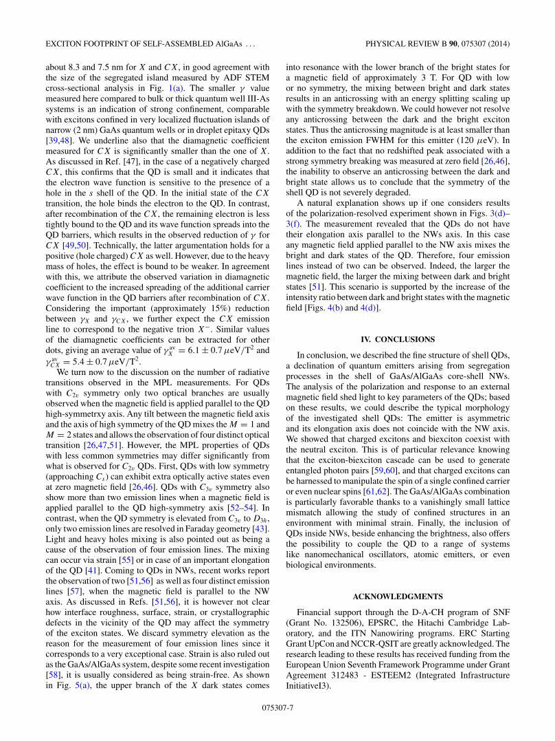
FIG. 2. (Color online) Photoluminescence of an isolated shellQD. (a) The emission intensities from both GaAs core and QD canbe compared. The antenna effect expresses itself in a very brightemission from the nanoscale QD. (b) Spectral closeup of the QDoutlined in (a). Several emission peaks can clearly be seen with anexcitation power of 5 μW. (c) Evolution of the intensity of the fourpeaks marked in (b). The exciton (X, black circles) and biexciton(XX, orange squares) can be identified thanks to their linear andquadratic dependence on laser input power (fitted with a linearfunction of slope s). The two intermediate peaks show intermediate(superlinear) dependencies, typical of charged excitons (CX and CX,red and blue triangles).
A. Power-dependent microphotoluminescence
In the excitation power and polarization dependence study,the NWs were dispersed on a Si substrate, in a lyingconfiguration. We display in Fig. 2(a) a typical spectrumshowing the emission of a single QD in a single nanowire. Thebroad peak at 1.51 eV corresponds to the emission from theGaAs core. The narrow lines in the 1.88 eV range are attributedto the QDs. It is important to note that the high brightness ofthe QD cannot be attributed to an enhanced carrier collectionby the QD: From the CL-SEM scan in Fig. 2(c), we can inferthat the carrier capture length for the emitters is of the order of170 nm (see Supplementary Figure S1 [30]). This low valueis a consequence of the GaAs core acting as a sink for carriersbut also of the existence of a thin potential barrier around theQD. Figure 2(b) details the emission spectrum of a single QDin the 1.87–1.88 eV range. At the power used to acquire thisspectrum (5 μW), several emission lines can be observed. Inorder to understand the origin of the different observed peaks,we measured their luminescence intensity as a function ofthe optical power (P ). The results are compiled in Fig. 2(c).The intensities of the different peaks evolve differently withrespect to P . This behavior makes us associate the peaks with
075307-3

YANNIK FONTANA et al. PHYSICAL REVIEW B 90, 075307 (2014)
different possible types of excitation confined in the QDs.The linear dependence with P of the intensity of the higherenergy transition (black circles, labeled X) is characteristic ofneutral exciton (X). In clear contrast, the intensity of the line at1.871 eV exhibits a quadratic increase with P (orange squares),allowing us to ascribe it to biexciton (XX) recombination. The6 meV XX binding energy of the shell QD compares well towhat has been reported for GaAs QDs made by droplet epitaxy[31,32]. For other QDs, like InAs Stranski-Krastanov, thebinding energy is usually slightly smaller. For InAs QDs in thestrong confinement regime, the XX binding energy was foundto be independent of the emission energy, while it increasesfor weakly confined GaAs natural QDs [33]. Thus one mayspeculate that when GaAs QDs enter the strong confinementregime, the XX binding energy saturates as well. This wouldexplain the consistent measurement of a XX binding energyaround 4–6 meV for strongly confined GaAs QDs. The twolines at 1.874 and 1.872 eV show an intermediate behaviorwith P : As shown in Fig. 2(b), their emission intensitiesare proportional to P 1.61 and P 1.53. They correspond to twocharged cases, where an exciton is accompanied by either anextra electron (negatively charged exciton, or trion X−) or anextra hole (positively charged exciton, or trion X+) [34]. Sincewe do not have the possibility to unambiguously differentiateX− and X+, we will in the following simply refer to themas CX and CX′ [red upward and blue downward trianglesin Fig. 2(c), respectively]. Their origin can be manifold.Common mechanisms are a slight background doping in thesemiconductor matrix as depicted in Fig. 1(b) (left), or alocal imbalance in the injection rate of the optically generatedcarriers resulting from small electric fields or interface trappingof a preferred species [Fig. 1(b) right]. The latter is likelyto explain the CX peak, as background doping should beweak and the intensity would be expected to saturate at moremoderate power.
B. Polarization-resolved microphotoluminescence
We now focus on a more detailed analysis of the X andCX emission by analyzing their polarization. For both X andCX, the emission polarization anisotropy is dominated bythe NW-related antenna effect. Such an effect is commonlyobserved in NW-based systems where the NW diameter issmaller than (quasistatic case) or of the order of the wavelength(Mie-like resonances) [35,36] and is induced by the dielectricmismatch between the NW and its environment. We showin Figs. 3(a) and 3(b) the CX and X polarization-resolvedspectra. The CX emission line preserves the same spectralshape and shows a constant emission energy: Variation inits intensity is the result of the antenna effect. In order todeconvolute the antenna effect from effects linked to theelectronic structure, the spectra were thus normalized withrespect to the CX peak. As it can be seen in Fig. 3(b), theevolution of X emission spectra with polarization is much moreintricate: The shape of the spectra varies with the polarizationin a alternated pattern. We attribute this to the splitting of thebright exciton states induced by anisotropic exchange effect.To quantify the main orientation of the states H and V as wellas the anisotropic exchange splitting energy, we performed aglobal fit on the whole data set simultaneously. An example of
0
180
0.5
IH(θ) IV(θ)
H V
2 2.5 3
00.10.20.3
EE CX- (meV)
δ1
0-0.25 0.250
1
EE CX- (meV)
Nor
m. i
nt. C
X (a
.u.)
CX
2.52 30
1
EE CX- (meV)
Nor
m. i
nt. C
X (a
.u.)
X
Rel
. int
.(a
.u.)
II
(c) (d)
0
180
1
ICX(θ)(e)
= 31.76 degΔθV-CX
= 121.29 degΔθH-CX
= 89.52 degΔθH-V
(f)
(a) (b)
FIG. 3. (Color online) Polarization analysis of X and CX emis-sion lines. (a) Normalized emission from CX. The peak does not shiftwith polarization thanks to spin pairing. The polarizer orientation inthe laboratory reference frame is represented by the left-hand arrowquadrant. (b) Emission from X. In contrast to its charged counterpart,the X emission peak shape varies as a function of the polarizationas a result of the anisotropic exchange interaction between the holeand electron forming the exciton. (c) Example of an X spectrumfitted in order to retrieve the energy difference between the exchangeinteraction admixed states. Both linewidth and splitting result from aglobal fit on the full data set. (d) Polar representation of the intensityof the two AEI-split states H and V . As expected, the states areorthogonal one to the other. (e) Intensity of the CX as a functionof polarization. Due to spin pairing, CX is protected against theexchange interaction. In this case, the intensity modulation comesfrom the photonic effect of the nanowire through the antenna effect.(f) Cartoon of the orientation of the different states. H and V statesare orthogonal to each other, but neither of them coincide with theorientation given by the CX emission.
a deconvoluted spectrum is shown in Fig. 3(c). The spectra inFigs. 3(a) and 3(b) were fitted using two Gaussian functions toaccount for the broadening of the optical transition. Since weexpect a similar broadening for the two peaks, their full-widthat half-maximum (FWHM) are constrained to equality. Thelatter point is justified by the relatively large broadening ofthe optical transition. If the main source of broadening was
075307-4

EXCITON FOOTPRINT OF SELF-ASSEMBLED AlGaAs . . . PHYSICAL REVIEW B 90, 075307 (2014)
the radiative decay of X, one could expect different FWHMdue to different dephasing rates of the split states [37]. Yetin this case the FWHM would reflect the lifetime of X, i.e.,a linewidth around 200 MHz. The linewidths measured inour case are still orders of magnitude higher (in the GHzrange), and are most likely due to electrostatic fluctuation inthe AlGaAs matrix, with a similar effect on both split states.The value obtained for the splitting δ1 between the two statesH and V is 97 μeV, as shown in Fig. 3(c). If the H and V
states FWMH are not constricted to equality, the extractedvalue for δ1 is 107 μeV, with a linewidth difference of around5%. This slightly higher value is obtained at the expense ofa good convergence of the global fit; this is a consequence ofthe increase of fitting parameters, but can be considered as anupper limit. In comparison, droplet epitaxy GaAs QDs grownon (100) wafers showing geometrical anisotropy typicallybetween 10% and 25% exhibit an anisotropic splitting between50 and 250 μeV [38].
We then show the polar plots for both CX and normalizedX. In the case of X the two hybridized eigenstates H andV are orthogonal and linearly polarized. Their main axeslie at 31.8◦ and 121.3◦ with respect to the NW long axis[Fig. 3(d)]. As expected, the emission of CX does not show afine structure splitting at zero magnetic field and is polarized
along the NW axis [Fig. 3(e), illustrating the strength of thepurely photonic antenna effect]. Figure 3(f) summarizes thecharacteristic polarization orientation of the CX peak andof the H and V states. The orthogonality between H andV states is expected and commonly observed in particularfor systems with moderate or zero strain, like GaAs-AlGaAs,where the polarization axes are inline and perpendicular withthe elongation axis of the QD [29,39]. We emphasize that thepolarization axes of the H and V states axis are not alignedwith the NW axis. We can therefore conclude that the shellQDs are not bound to be elongated along the NW axis, norperfectly perpendicular to it.
C. Magnetophotoluminescence
Additional information on the shell-QDs symmetry wasobtained using MPL. The experiments in magnetic fieldwere carried out on as-grown nanowires, standing on the Sisubstrate, with the magnetic field parallel to the NWs axis.In this case, polarization could not be resolved. We displayin Fig. 4 the evolution of X and CX emission energies whenthe magnetic field is increased from 0 to 10 T for two QDs,A and B. In the presence of a magnetic field, the peaks splitand shift with magnetic field due to Zeeman and diamagnetic
1844 1845 1846
10 T
8 T
6 T
Inte
nsity
(arb
. uni
ts)
PL energy (meV)
0 T
CX X
(b)
CX X
(d)
1844 1845 1846PL energy (meV)
Inte
nsity
(arb
. uni
ts)
10 T
8 T
6 T
0 T
Magnetic field (T)0 2 4 6 8 10
Ene
rgy
(meV
)
1844
1845
1846X
CX
(a)
Magnetic field (T)0 2 4 6 8 10
Ene
rgy
(meV
)
1844
1845
1846
X
CX
(c)QD A QD B
QD A QD B
FIG. 4. (Color online) MPL of two single QDs in a nanowire. (a) and (c) Color scans showing the evolution of the spectra of QD A (a)and QD B (c) as the magnetic field is progressively increased. In both cases, X and CX are visible. The zero field peaks are split in groupsof two doublets by the Zeeman effect and shifted because of diamagnetism. The bright and dark doublets are particularly obvious for the CX,as the splitting between dark and bright states at zero field is nonexistent. (b) and (d) Spectra at different magnetic fields for the QD A and B.the spectra are shifted in intensity for clarity. Black (gray) arrows denote the position of the dark peaks of the X (CX). The behavior of thedots is very similar, differing marginally because of the different magnitude of the Lande factors, diamagnetic coefficients, and X-CX bindingenergies.
075307-5

YANNIK FONTANA et al. PHYSICAL REVIEW B 90, 075307 (2014)
effects [26,40–42]. The spectra of X and CX for magneticfields between 0 and 10 T are plotted in Figs. 4(b) and 4(d).The PL of both X and CX splits into four distinct lines. Basedon their respective intensities at low magnetic field, these fourtransitions are attributed to bright and dark states. In Figs. 4(b)and 4(d) the peaks corresponding to dark states are indicatedby arrows. Comparing QDs A and B, one can see that apartfrom slightly different splittings and shifts, the behavior isvery similar. When the induced splitting are larger than theexchange terms, the dominant effects are given by the Zeemancontribution and by the diamagnetic shift, the energy of thepeaks can be written as follows:
EB/D(B) = E0B/D ± 1
2μBgXB/DB + γB2, (1)
where μB is the Bohr magneton, and gX and γ are the excitonLande factor and diamagnetic coefficient, respectively. Thesubscripts B and D refer to the bright and dark excitons,respectively. We assume γB = γD = γ as the spin configura-tion should not affect significantly the diamagnetic coefficient[43]. Lande factors and diamagnetic coefficients can then beextracted by fitting the evolution of the X and CX emissionlines as a function of B with Eq. (1). The fits also allowone to extrapolate the energy splitting between the bright andthe dark states at zero field [shown in Figs. 5(a) and 5(c)].Thus we can now attribute the CX-labeled peak to a chargedexciton with certainty: Only a spin-paired exciton complexcan exhibit a vanishing IEI as can be seen in Fig. 4 andmore clearly in Fig. 5(a) (red solid and dashed lines). For
QD A we obtain for the couple X/CX |gXB/D| = 0.88/1.38,
|gCXB/D| = 0.45/1.44, γX = 5.8 μeV/T2, γCX = 4.8 μeV/T2,
and δ0 = 170 μeV for the QD A. Values for the Lande factorsof other emitters are plotted in Fig. 5(b) as a function of theemission energy. Three main observations can be made: (i) Ingeneral, in this energy range, the values between differentQDs (given the same carriers and spins configurations) donot vary in an extreme way. (ii) A slight but noticeable trendcan be seen: The Lande factors for all configurations tend toincrease monotonically as the emission energy increases, asalready reported in other systems [44]. (iii) The Lande factorsof the dark states are systematically larger than the brightones. The δ0 value of our shell QDs, with an average value of249 ± 54 μeV, is larger than what has been reported for thebulk value of GaAs [45]. This is expected for QDs excitons,as the isotropic exchange splitting energy δ0 can be seen as ameasure of the QD volume [26]. While the δ0 values for ourshell QD is slightly smaller than what is usually reported forInAs lens-shape QDs [46,47], it is similar or larger than the δ0
found for interface fluctuation GaAs QDs.Coming to the X diamagnetic coefficient, it is directly
related to the spatial extent of the X wave function in the planeperpendicular to the magnetic field: γ = e2
8μ⊥〈ρ2
⊥〉, where μ⊥and 〈ρ2
⊥〉 are the exciton reduced mass and the electron-holecorrelation length in the plane perpendicular to the magneticfield. For a reduced mass of 0.068 m0 for Al0.1Ga0.9As(corresponding to an intradot Al fraction of 0.1) the correlationlength for QD A leads to an estimated confinement radius of
B-Field (T)
Pl e
nerg
y (m
eV)
(a)1846.0
1845.5
1845.0
1844.5
1844.0
1086420
X
CX
δ0
|gXB|(b)
Land
é fa
ctor
|g|
0.0
0.5
1.0
1.5
2.0
2.5
1820 1840 1860 1880PL energy (meV)
|gCXB|
|gXD|
|gCXD|
(c)
Ene
rgy
δ1
|0
|H|V
|BX+
|BX−
|DX−
|DX+
δ0
+1h (1e)
ZeemanSpin-pairing IES IES+AESZeemanB ≠ 0B ≠ 0 B = 0 B = 0 B = 0
BC
X+
DC
X+
DC
X-
BC
X-
FIG. 5. (Color online) (a) Fitting of the energetic splitting and shift for QD A with 1. (b) X and CX Lande factors from different QDs,showing consistent values between different QDs. The dark states |gX/CX
D | are systematical larger than the bright ones and the Lande factorsof the bright and the dark states slightly increase with the emission energy. (c) Schematic depicting the splittings for X (right) and CX (left).For zero magnetic field, X states are split by the isotropic and anisotropic exchange interactions, while the spin-paired CX levels are stilldegenerated. The application of an external magnetic field lifts the degeneracy and mixes the pure states, leading to the observation of brightand dark optical transitions.
075307-6
EXCITON FOOTPRINT OF SELF-ASSEMBLED AlGaAs . . . PHYSICAL REVIEW B 90, 075307 (2014)
about 8.3 and 7.5 nm for X and CX, in good agreement withthe size of the segregated island measured by ADF STEMcross-sectional analysis in Fig. 1(a). The smaller γ valuemeasured here compared to bulk or thick quantum well III-Assystems is an indication of strong confinement, comparablewith excitons confined in very localized fluctuation islands ofnarrow (2 nm) GaAs quantum wells or in droplet epitaxy QDs[39,48]. We underline also that the diamagnetic coefficientmeasured for CX is significantly smaller than the one of X.As discussed in Ref. [47], in the case of a negatively chargedCX, this confirms that the QD is small and it indicates thatthe electron wave function is sensitive to the presence of ahole in the s shell of the QD. In the initial state of the CX
transition, the hole binds the electron to the QD. In contrast,after recombination of the CX, the remaining electron is lesstightly bound to the QD and its wave function spreads into theQD barriers, which results in the observed reduction of γ forCX [49,50]. Technically, the latter argumentation holds for apositive (hole charged) CX as well. However, due to the heavymass of holes, the effect is bound to be weaker. In agreementwith this, we attribute the observed variation in diamagneticcoefficient to the increased spreading of the additional carrierwave function in the QD barriers after recombination of CX.Considering the important (approximately 15%) reductionbetween γX and γCX, we further expect the CX emissionline to correspond to the negative trion X−. Similar valuesof the diamagnetic coefficients can be extracted for otherdots, giving an average value of γ av
X = 6.1 ± 0.7 μeV/T2 andγ av
CX = 5.4 ± 0.7 μeV/T2.We turn now to the discussion on the number of radiative
transitions observed in the MPL measurements. For QDswith C2v symmetry only two optical branches are usuallyobserved when the magnetic field is applied parallel to the QDhigh-symmetrxy axis. Any tilt between the magnetic field axisand the axis of high symmetry of the QD mixes the M = 1 andM = 2 states and allows the observation of four distinct opticaltransition [26,47,51]. However, the MPL properties of QDswith less common symmetries may differ significantly fromwhat is observed for C2v QDs. First, QDs with low symmetry(approaching Cs) can exhibit extra optically active states evenat zero magnetic field [26,46]. QDs with C3v symmetry alsoshow more than two emission lines when a magnetic field isapplied parallel to the QD high-symmetry axis [52–54]. Incontrast, when the QD symmetry is elevated from C3v to D3h,only two emission lines are resolved in Faraday geometry [43].Light and heavy holes mixing is also pointed out as being acause of the observation of four emission lines. The mixingcan occur via strain [55] or in case of an important elongationof the QD [41]. Coming to QDs in NWs, recent works reportthe observation of two [51,56] as well as four distinct emissionlines [57], when the magnetic field is parallel to the NWaxis. As discussed in Refs. [51,56], it is however not clearhow interface roughness, surface, strain, or crystallographicdefects in the vicinity of the QD may affect the symmetryof the exciton states. We discard symmetry elevation as thereason for the measurement of four emission lines since itcorresponds to a very exceptional case. Strain is also ruled outas the GaAs/AlGaAs system, despite some recent investigation[58], it is usually considered as being strain-free. As shownin Fig. 5(a), the upper branch of the X dark states comes
into resonance with the lower branch of the bright states fora magnetic field of approximately 3 T. For QD with lowor no symmetry, the mixing between bright and dark statesresults in an anticrossing with an energy splitting scaling upwith the symmetry breakdown. We could however not resolveany anticrossing between the dark and the bright excitonstates. Thus the anticrossing magnitude is at least smaller thanthe exciton emission FWHM for this emitter (120 μeV). Inaddition to the fact that no redshifted peak associated with astrong symmetry breaking was measured at zero field [26,46],the inability to observe an anticrossing between the dark andbright state allows us to conclude that the symmetry of theshell QD is not severely degraded.
A natural explanation shows up if one considers resultsof the polarization-resolved experiment shown in Figs. 3(d)–3(f). The measurement revealed that the QDs do not havetheir elongation axis parallel to the NWs axis. In this caseany magnetic field applied parallel to the NW axis mixes thebright and dark states of the QD. Therefore, four emissionlines instead of two can be observed. Indeed, the larger themagnetic field, the larger the mixing between dark and brightstates [51]. This scenario is supported by the increase of theintensity ratio between dark and bright states with the magneticfield [Figs. 4(b) and 4(d)].
IV. CONCLUSIONS
In conclusion, we described the fine structure of shell QDs,a declination of quantum emitters arising from segregationprocesses in the shell of GaAs/AlGaAs core-shell NWs.The analysis of the polarization and response to an externalmagnetic field shed light to key parameters of the QDs; basedon these results, we could describe the typical morphologyof the investigated shell QDs: The emitter is asymmetricand its elongation axis does not coincide with the NW axis.We showed that charged excitons and biexciton coexist withthe neutral exciton. This is of particular relevance knowingthat the exciton-biexciton cascade can be used to generateentangled photon pairs [59,60], and that charged excitons canbe harnessed to manipulate the spin of a single confined carrieror even nuclear spins [61,62]. The GaAs/AlGaAs combinationis particularly favorable thanks to a vanishingly small latticemismatch allowing the study of confined structures in anenvironment with minimal strain. Finally, the inclusion ofQDs inside NWs, beside enhancing the brightness, also offersthe possibility to couple the QD to a range of systemslike nanomechanical oscillators, atomic emitters, or evenbiological environments.
ACKNOWLEDGMENTS
Financial support through the D-A-CH program of SNF(Grant No. 132506), EPSRC, the Hitachi Cambridge Lab-oratory, and the ITN Nanowiring programs. ERC StartingGrant UpCon and NCCR-QSIT are greatly acknowledged. Theresearch leading to these results has received funding from theEuropean Union Seventh Framework Programme under GrantAgreement 312483 - ESTEEM2 (Integrated InfrastructureInitiativeI3).
075307-7

YANNIK FONTANA et al. PHYSICAL REVIEW B 90, 075307 (2014)
[1] X. P. A. Gao, G. Zheng, and C. M. Lieber, Nano Lett. 10, 547(2010).
[2] J.-I. Hahm and C. M. Lieber, Nano Lett. 4, 51 (2004).[3] M. T. Bjork, C. Thelander, A. E. Hansen, L. E. Jensen, M. W.
Larsson, L. R. Wallenberg, and L. Samuelson, Nano Lett. 4,1621 (2004).
[4] G. Grzela, R. Paniagua-Domınguez, T. Barten, Y. Fontana,J. A. Sanchez-Gil, and J. Gomez-Rivas, Nano Lett. 12, 5481(2012).
[5] A. Tribu, G. Sallen, T. Aichele, R. Andre, J.-P. Poizat,C. Bougerol, S. Tatarenko, and K. Kheng, Nano Lett. 8, 4326(2008).
[6] J. Claudon, J. Bleuse, N. S. Malik, M. Bazin, P. Jaffrennou,N. Gregersen, C. Sauvan, P. Lalanne, and J.-M. Gerard, Nat.Photon. 4, 174 (2010).
[7] I. Yeo, P.-L. De Assis, A. Gloppe, P. Verlot, N. S. Malik,E. Dupuy, J. Claudon, A. Auffeves, G. Nogues, S. Seidelin,J.-P. Poizat, O. Arcizet, M. Richard, and J.-M. Gerard, Nat.Nanotech. 9, 106 (2014).
[8] M. Montinaro, G. Wust, M. Munsch, Y. Fontana, E. Russo-Averchi, M. Heiss, A. Fontcuberta i Morral, R. J. Warburton,and M. Poggio, Nano Lett. (2014), doi:10.1021/nl501413t.
[9] E. D. Minot, F. Kelkensberg, M. Van Kouwen, J. A. van Dam,L. P. Kouwenhoven, V. Zwiller, M. T. Borgstrom, O. Wunnicke,M. A. Verheijen, and E. P. A. M. Bakkers, Nano Lett. 7, 367(2007).
[10] M. P. Van Kouwen, M. H. M. Van Weert, M. E. Reimer,N. Akopian, U. Perinetti, R. E. Algra, E. P. A. M. Bakkers,L. P. Kouwenhoven, and V. Zwiller, Appl. Phys. Lett. 97, 113108(2010).
[11] A. J. Shields, Nat. Photon. 1, 215 (2007).[12] M. Pelton, C. Santori, J. Vuckovic, B. Zhang, G. S. Solomon,
J. Plant, and Y. Yamamoto, Phys. Rev. Lett. 89, 233602(2002).
[13] S. Buckley, K. Rivoire, and J. Vukovi, Rep. Prog. Phys. 75,126503 (2012).
[14] M. Reimer, G. Bulgarini, N. Akopian, M. Hocevar, M. BouwesBavinck, M. A. Verheijen, E. P. A. M. Bakkers, L. P. Kouwen-hoven, and V. Zwiller, Nat. Commun. 3, 737 (2012).
[15] M. Munsch, N. S. Malik, E. Dupuy, A. Delga, J. Bleuse, J.-M.Gerard, J. Claudon, N. Gregersen, and J. Mørk, Phys. Rev. Lett.110, 177402 (2013).
[16] M. T. Borgstrom, V. Zwiller, E. Muller, and A. Imamoglu, NanoLett. 5, 1439 (2005).
[17] D. Dalacu, K. Mnaymneh, J. Lapointe, X. Wu, P. J. Poole,G. Bulgarini, V. Zwiller, and M. E. Reimer, Nano Lett. 12, 5919(2012).
[18] I. Yeo, N. S. Malik, M. Munsch, E. Dupuy, J. Bleuse,Y.-M. Niquet, J.-M. Grard, J. Claudon, E. Wagner, S. Seidelin,A. Auffves, J.-P. Poizat, and G. Nogues, Appl. Phys. Lett. 99,233106 (2011).
[19] M. Heiss, Y. Fontana, A. Gustafsson, G. Wust, C. Magen,D. O’Regan, J. W. Luo, B. Ketterer, S. Conesa-Boj,A. Kuhlmann, J. Houel, E. Russo-Averchi, J. R. Morrante,M. Cantoni, N. Marzari, J. Arbiol, A. Zunger, R. Warburton,and A. Fontcuberta i Morral, Nat. Mater. 12, 439 (2013).
[20] E. Uccelli, J. Arbiol, C. Magen, P. Krogstrup, E. Russo-Averchi,M. Heiss, G. Mugny, F. Morier-Genoud, J. Nygard, J. R.Morante, and A. Fontcuberta i Morral, Nano Lett. 11, 3827(2011).
[21] A. Fontcuberta i Morral, D. Spirkoska, J. Arbiol, M. Heigoldt,J. R. Morante, and G. Abstreiter, Small 4, 899 (2008).
[22] M. Heigoldt, J. Arbiol, D. Spirkoska, J. Rebled, S. Conesa-Boj,G. Abstreiter, F. Peiro, J. R. Morante, and A. Fontcuberta iMorral, J. Mater. Chem. 19, 840 (2009).
[23] N. Skold, J. B. Wagner, G. Karlsson, T. Hernn, W. Seifert, M.-E.Pistol, and L. Samuelson, Nano Lett. 6, 2743 (2006).
[24] C. Zheng, J. Wong-Leung, Q. Gao, H. H. Tan, C. Jagadish, andJ. Etheridge, Nano Lett. 13, 3742 (2013).
[25] T. Kehoe, M. Ediger, R. T. Phillips, and M. Hopkinson, Rev.Sci. Instrum. 81, 013906 (2010).
[26] M. Bayer, G. Ortner, O. Stern, A. Kuther, A. A. Gorbunov,A. Forchel, P. Hawrylak, S. Fafard, K. Hinzer, T. L. Reinecke,S. N. Walck, J. P. Reithmaier, F. Klopf, and F. Schafer, Phys.Rev. B 65, 195315 (2002).
[27] T. Takagahara, Phys. Rev. B 62, 16840 (2000).[28] I. Moreels, G. Raino, R. Gomes, Z. Hens, T. Stoferle, and R. F.
Mahrt, ACS Nano 5, 8033 (2011).[29] R. J. Young, R. M. Stevenson, A. J. Shields, P. Atkinson,
K. Cooper, D. A. Ritchie, K. M. Groom, A. I. Tartakovskii,and M. S. Skolnick, Physica E 32, 97 (2006).
[30] See Supplemental Material at http://link.aps.org/supplemental/10.1103/PhysRevB.90.075307 for measurement of the carriersdiffusion length with cathodoluminescence.
[31] T. Mano, M. Abbarchi, T. Kuroda, C. Mastrandrea, A. Vinattieri,S. Sanguinetti, K. Sakoda, and M. Gurioli, Nanotechnology 20,395601 (2009).
[32] T. Kuroda, T. Mano, N. Ha, H. Nakajima, H. Kumano,B. Urbaszek, M. Jo, M. Abbarchi, Y. Sakuma, K. Sakoda,I. Suemune, X. Marie, and T. Amand, Phys. Rev. B 88, 041306(2013).
[33] G. Moody, R. Singh, H. Li, I. A. Akimov, M. Bayer, D. Reuter,A. D. Wieck, A. S. Bracker, D. Gammon, and S. T. Cundiff,Phys. Rev. B 87, 041304 (2013).
[34] R. Phillips, G. Nixon, T. Fujita, M. Simmons, and D. Ritchie,Solid State Commun. 98, 287 (1996).
[35] J. Wang, M. S. Gudiksen, X. Duan, Y. Cui, and C. M. Lieber,Science 293, 1455 (2001).
[36] M. H. M. van Weert, N. Akopian, F. Kelkensberg, U. Perinetti,M. P. van Kouwen, J. Gomez-Rivas, M. T. Borgstrom, R. E.Algra, M. A. Verheijen, E. P. A. M. Bakkers, L. P. Kouwenhoven,and V. Zwiller, Small 5, 2134 (2009).
[37] W. Langbein, P. Borri, U. Woggon, V. Stavarache, D. Reuter,and A. D. Wieck, Phys. Rev. B 70, 033301 (2004).
[38] M. Abbarchi, C. A. Mastrandrea, T. Kuroda, T. Mano, K.Sakoda, N. Koguchi, S. Sanguinetti, A. Vinattieri, and M.Gurioli, Phys. Rev. B 78, 125321 (2008).
[39] M. Abbarchi, T. Kuroda, T. Mano, K. Sakoda, and M. Gurioli,Phys. Rev. B 81, 035334 (2010).
[40] A. Kuther, M. Bayer, A. Forchel, A. Gorbunov, V. B. Timofeev,F. Schafer, and J. P. Reithmaier, Phys. Rev. B 58, R7508 (1998).
[41] L. Besombes, K. Kheng, and D. Martrou, Phys. Rev. Lett. 85,425 (2000).
[42] J. G. Tischler, A. S. Bracker, D. Gammon, and D. Park, Phys.Rev. B 66, 081310 (2002).
[43] D. Y. Oberli, Phys. Rev. B 85, 155305 (2012).[44] N. A. J. M. Kleemans, J. van Bree, M. Bozkurt, P. J.
van Veldhoven, P. A. Nouwens, R. Notzel, A. Y. Silov, P.M. Koenraad, and M. E. Flatte, Phys. Rev. B 79, 045311(2009).
075307-8

EXCITON FOOTPRINT OF SELF-ASSEMBLED AlGaAs . . . PHYSICAL REVIEW B 90, 075307 (2014)
[45] R. Ishii, M. Funato, and Y. Kawakami, Phys. Rev. B 87, 161204(2013).
[46] J. J. Finley, D. J. Mowbray, M. S. Skolnick, A. D. Ashmore,C. Baker, A. F. G. Monte, and M. Hopkinson, Phys. Rev. B 66,153316 (2002).
[47] B. Van Hattem, P. Corfdir, P. Brereton, P. Pearce, A. M. Graham,M. J. Stanley, M. Hugues, M. Hopkinson, and R. T. Phillips,Phys. Rev. B 87, 205308 (2013).
[48] M. Erdmann, C. Ropers, M. Wenderoth, R. Ulbrich, S. Malzer,and G. Dohler, Phys. Rev. B 74, 125412 (2006).
[49] Y. J. Fu, S. D. Lin, M. F. Tsai, H. Lin, C. H. Lin, H. Y. Chou,S. J. Cheng, and W. H. Chang, Phys. Rev. B 81, 113307(2010).
[50] C. Schulhauser, D. Haft, R. J. Warburton, K. Karrai, A. O.Govorov, A. V. Kalameitsev, A. Chaplik, W. Schoenfeld,J. M. Garcia, and P. M. Petroff, Phys. Rev. B 66, 193303 (2002).
[51] B. J. Witek, R. W. Heeres, U. Perinetti, E. P. A. M. Bakkers,L. P. Kouwenhoven, and V. Zwiller, Phys. Rev. B 84, 195305(2011).
[52] K. F. Karlsson, M. A. Dupertuis, D. Y. Oberli, E. Pelucchi,A. Rudra, P. O. Holtz, and E. Kapon, Phys. Rev. B 81, 161307(2010).
[53] G. Sallen, B. Urbaszek, M. M. Glazov, E. L. Ivchenko,T. Kuroda, T. Mano, S. Kunz, M. Abbarchi, K. Sakoda,D. Lagarde, A. Balocchi, X. Marie, and T. Amand, Phys. Rev.Lett. 107, 166604 (2011).
[54] M. V. Durnev, M. M. Glazov, E. L. Ivchenko, M. Jo, T. Mano,T. Kuroda, K. Sakoda, S. Kunz, G. Sallen, L. Bouet, X. Marie,D. Lagarde, T. Amand, and B. Urbaszek, Phys. Rev. B 87,085315 (2013).
[55] Y. Leger, L. Besombes, L. Maingault, and H. Mariette, Phys.Rev. B 76, 045331 (2007).
[56] P. Corfdir, B. Van Hattem, E. Uccelli, S. Conesa-Boj,P. Lefebvre, A. Fontcuberta i Morral, and R. T. Phillips, NanoLett. 13, 5303 (2013).
[57] N. Akopian, G. Patriarche, L. Liu, J.-C. Harmand, and V. Zwiller,Nano Lett. 10, 1198 (2010).
[58] M. Hocevar, T.-G. Le-Thuy, R. Songmuang, M. den Hertog,L. Besombes, J. Bleuse, Y.-M. Niquet, and N. T. Pelekanos,Appl. Phys. Lett. 102, 191103 (2013).
[59] O. Benson, C. Santori, M. Pelton, and Y. Yamamoto, Phys. Rev.Lett. 84, 2513 (2000).
[60] N. Akopian, N. Lindner, E. Poem, Y. Berlatzky, J. Avron,D. Gershoni, B. Gerardot, and P. M. Petroff, Phys. Rev. Lett.96, 130501 (2006).
[61] B. D. Gerardot, D. Brunner, P. A. Dalgarno, P. Ohberg,S. Seidl, M. Kroner, K. Karrai, N. G. Stolz, P. M.Petroff, and R. J. Warburton, Nature (London) 451, 441(2008).
[62] G. Sallen, S. Kunz, T. Amand, L. Bouet, T. Kuroda, T. Mano,D. Paget, O. Krebs, X. Marie, K. Sakoda, and B. Urbaszek, Nat.Commun. 5, 3268 (2014).
075307-9