Evaluating the frequency hopping capability of the AFE74xx
24
1 SLAA870 – February 2019 Submit Documentation Feedback Copyright © 2019, Texas Instruments Incorporated Evaluating the frequency hopping capability of the AFE74xx Application Report SLAA870 – February 2019 Evaluating the frequency hopping capability of the AFE74xx Yusuf Agoro ABSTRACT This application note describes the NCO-based frequency hopping capability of the RF-sampling AFE7422 and AFE7444 (AFE74xx). The AFE7422 and AFE7444 are quad-channel, wideband, RF-sampling analog front ends (AFE) based on 14-bit, 9-GSPS DACs, and 14-bit, 3-GSPS ADCs. With operation at an RF of up to 6 GHz, these devices enable direct RF sampling into the C-band frequency range without the need for additional frequency conversions stages. The AFE74xx improvement in density and flexibility enables high-channel-count, multimission systems, and makes these devices a very attractive option for wideband, frequency-hopping applications. Contents 1 Introduction .................................................................................................................. 3 2 Phase Coherency vs Phase Continuity .................................................................................. 3 3 AFE74xx Architecture ...................................................................................................... 4 3.1 AFE74xx Receivers: Multiband DDC............................................................................. 4 3.2 AFE74xx Transmitters: Multiband DUC.......................................................................... 5 3.3 Numerically Controlled Oscillator (NCO) ........................................................................ 6 4 Frequency Hopping Methods .............................................................................................. 9 4.1 Maintaining Phase Continuity .................................................................................... 9 4.2 Maintaining Phase Coherency .................................................................................. 14 5 NCO Frequency Resolution Versus Hop Time ........................................................................ 21 6 Fast Frequency Hopping With the Load and Switch .................................................................. 21 7 Register Addresses ........................................................................................................ 22 8 References .................................................................................................................. 23 List of Figures 1 Example of Phase Coherent Frequency Hopping ....................................................................... 3 2 Example of Phase Continuous Frequency Hopping .................................................................... 3 3 Basic Block Diagram of AFE74xx Multi-DDC Architecture ............................................................ 4 4 Basic Block Diagram of AFE74xx Multi-DUC Architecture ............................................................ 5 5 NCO Block Diagram ......................................................................................................... 6 6 Loading the TXNCO1 Configuration File ................................................................................. 7 7 Enabling DDS Mode in DAC A............................................................................................. 8 8 DAC A Output of 1700 MHz in DDS Mode ............................................................................... 8 9 Implementing Phase Continuous Frequency Hopping With the AFE74xx Evaluation Module (EVM) ........... 9 10 Model Timing Diagram for Phase Continuous Frequency Hopping ................................................. 10 11 SPI Bus Write Cycle ....................................................................................................... 10 12 Test Setup for Measuring Hop Time From 10 MHz to 100 MHz..................................................... 11 13 Programming TXNCO0 to 10 MHz Through the AFE74xx GUI ...................................................... 11 14 Updating the Frequency in One NCO Requires Approximately 4.6 μs ............................................. 12 15 Using SYSREF to Update NCO Output Requires Approximately 200 ns to Update the NCO Output.......... 13 16 Phase Coherent Frequency Hopping With an AFE74xx Transmitter ............................................... 14
-
Upload
khangminh22 -
Category
Documents
-
view
4 -
download
0
Transcript of Evaluating the frequency hopping capability of the AFE74xx
1SLAA870–February 2019Submit Documentation Feedback
Copyright © 2019, Texas Instruments Incorporated
Evaluating the frequency hopping capability of the AFE74xx
Application ReportSLAA870–February 2019
Evaluating the frequency hopping capability of theAFE74xx
Yusuf Agoro
ABSTRACTThis application note describes the NCO-based frequency hopping capability of the RF-sampling AFE7422and AFE7444 (AFE74xx). The AFE7422 and AFE7444 are quad-channel, wideband, RF-sampling analogfront ends (AFE) based on 14-bit, 9-GSPS DACs, and 14-bit, 3-GSPS ADCs. With operation at an RF ofup to 6 GHz, these devices enable direct RF sampling into the C-band frequency range without the needfor additional frequency conversions stages. The AFE74xx improvement in density and flexibility enableshigh-channel-count, multimission systems, and makes these devices a very attractive option for wideband,frequency-hopping applications.
Contents1 Introduction .................................................................................................................. 32 Phase Coherency vs Phase Continuity .................................................................................. 33 AFE74xx Architecture ...................................................................................................... 4
3.1 AFE74xx Receivers: Multiband DDC............................................................................. 43.2 AFE74xx Transmitters: Multiband DUC.......................................................................... 53.3 Numerically Controlled Oscillator (NCO) ........................................................................ 6
4 Frequency Hopping Methods .............................................................................................. 94.1 Maintaining Phase Continuity .................................................................................... 94.2 Maintaining Phase Coherency .................................................................................. 14
5 NCO Frequency Resolution Versus Hop Time ........................................................................ 216 Fast Frequency Hopping With the Load and Switch .................................................................. 217 Register Addresses ........................................................................................................ 228 References .................................................................................................................. 23
List of Figures
1 Example of Phase Coherent Frequency Hopping ....................................................................... 32 Example of Phase Continuous Frequency Hopping .................................................................... 33 Basic Block Diagram of AFE74xx Multi-DDC Architecture ............................................................ 44 Basic Block Diagram of AFE74xx Multi-DUC Architecture ............................................................ 55 NCO Block Diagram......................................................................................................... 66 Loading the TXNCO1 Configuration File ................................................................................. 77 Enabling DDS Mode in DAC A............................................................................................. 88 DAC A Output of 1700 MHz in DDS Mode............................................................................... 89 Implementing Phase Continuous Frequency Hopping With the AFE74xx Evaluation Module (EVM) ........... 910 Model Timing Diagram for Phase Continuous Frequency Hopping ................................................. 1011 SPI Bus Write Cycle ....................................................................................................... 1012 Test Setup for Measuring Hop Time From 10 MHz to 100 MHz..................................................... 1113 Programming TXNCO0 to 10 MHz Through the AFE74xx GUI...................................................... 1114 Updating the Frequency in One NCO Requires Approximately 4.6 µs ............................................. 1215 Using SYSREF to Update NCO Output Requires Approximately 200 ns to Update the NCO Output.......... 1316 Phase Coherent Frequency Hopping With an AFE74xx Transmitter ............................................... 14

www.ti.com
2 SLAA870–February 2019Submit Documentation Feedback
Copyright © 2019, Texas Instruments Incorporated
Evaluating the frequency hopping capability of the AFE74xx
17 Hop Time When Switching From One NCO to Another is Approximately 658 ns ................................. 1518 Timing Model for DAC Settling Time .................................................................................... 1619 DAC Settling Time: Hardware Setup .................................................................................... 1620 AFE74xx DAC Settling Time of Approximately 11 ns ................................................................. 1721 TXNCO0 to TXNCO1 Total Transition Time is Approximately 90 ns................................................ 1722 AFE74xx Pinbank J9 Containing RX NCO GPIO Pins ................................................................ 1823 Test Setup for Measuring RX NCO Hop Time Using the GPIO Pins ............................................... 1924 Programming RXNCO0 and RXNCO1 to 100 MHz and 10 MHz, Respectively ................................... 1925 Configuring RX NCO Selection Through the GPIO Pins Using the AFE74xx GUI ................................ 2026 RX NCO Switching Time Using GPIO Pins............................................................................. 2027 Example of Frequency Hopping With Multiple NCOs ................................................................. 21
List of Tables
1 Programming TXNCO1 to 1700 MHz ..................................................................................... 72 Relationship Between Enabled GPIO Pins to Selected NCO ........................................................ 183 Trade-Off Between NCO Resolution and Overall Hop Time ......................................................... 214 RXNCO0 Register Address ............................................................................................... 225 RXNCO1 Register Address ............................................................................................... 226 RXNCO2 Register Address ............................................................................................... 227 TXNCO0 Register Address ............................................................................................... 228 TXNCO1 Register Address ............................................................................................... 229 TX NCO Selection Address ............................................................................................... 22
TrademarksAll trademarks are the property of their respective owners.

NCO0: F1
NCO1: F2
RF output
NCO0: F1Selected
NCO1: F2Selected
NCO0: F1Selected
Time
NCO0: F1
NCO1: F2
RF output
NCO0: F1Selected
NCO1: F2Selected
NCO0: F1Selected
Time
www.ti.com Introduction
3SLAA870–February 2019Submit Documentation Feedback
Copyright © 2019, Texas Instruments Incorporated
Evaluating the frequency hopping capability of the AFE74xx
1 IntroductionFrequency hopping describes a method in which communication systems rapidly change the operatingfrequency for a specific application. Applications such as radar, electronic warfare (EW), andcommunications use frequency hopping in order to avoid interference, avoid detection, or find signals thatare attempting to remain undetected. The faster these systems can change frequencies, or frequency hop,the more agile these systems become, thus increasing the chance to avoid interference and detection. Ina traditional frequency hopping system, where an analog mixer and PLL or VCO is used as a localoscillator, changing frequencies can take quite a long time. As RF sampling has become more prevalent,frequency hopping is moving toward a NCO-based hopping technique.
2 Phase Coherency vs Phase ContinuityPhase coherency, or phase memory, defines the ability for a synthesizer to maintain phase so that whenswitching to another source, the original frequency source runs continuously in the background andmaintains phase, even when not selected. Therefore, upon returning to the original frequency, the originalphase is unaltered. Phase coherency is especially useful in systems where multiple frequency sourcesuse a single reference clock. The overall system may switch sources to reflect the desired frequencysource on the RF output, while all other synthesizers run continuously in the background while maintainingphases relative to the reference. Phase-coherent radar systems eliminate the need for recalibration whenswitching between multiple frequencies because the phase relationship relative to the reference ismaintained. Figure 1 shows an example of phase-coherent frequency hopping between NCO0 and NCO1(programmed to frequencies f1 and f2, respectively), and run continuously, even when not selected.
Figure 1. Example of Phase Coherent Frequency Hopping
Phase continuity, however, refers to a smooth and continuous transition from one frequency to another onthe RF output when the selected source changes frequencies. Noncontinuous or abrupt transitions in theoutput frequency may lead to unwanted spurious content during fast Fourier transform (FFT) analysis.Figure 2 shows an example of continuous frequency hopping, where the selected source switches fromNCO0 (programmed to F1) to NCO1 (programmed to F2). As seen in Figure 2, when frequency hoppingfrom frequency 1 to frequency 2, there is a continuous transition between frequency 1 and frequency 2.
Figure 2. Example of Phase Continuous Frequency Hopping

JES
D204B
Transm
itter
Crossbar M
ux
AnalogPower
Detectors
ADC
DigitalPower
Detectors
2x Dual DDC
RXBDSA1P
RXBDSA1M
Bypass Path
NCO 0
NCO 3
M
N
ADC
2x Dual DDC
Bypass Path
NCO 0
NCO 3
M
N
STX8P
STX8M
STX2P
STX2M
STX1P
STX1M
RXBDSA2P
RXBDSA2M
RXDDSA1P
RXDDSA1M
RXDDSA2P
RXDDSA2M
DSA
DSA
DSA
DSA
AFE74xx Architecture www.ti.com
4 SLAA870–February 2019Submit Documentation Feedback
Copyright © 2019, Texas Instruments Incorporated
Evaluating the frequency hopping capability of the AFE74xx
3 AFE74xx Architecture
3.1 AFE74xx Receivers: Multiband DDCThe AFE74xx receivers contain two digital-down converters (DDCs), also known as a multi-DDC, eachwith a complex digital mixer, 32-bit numerically controlled oscillators (NCOs), and digital decimationfiltering. There are three independent NCOs (NCO0, NCO1, NCO2) in the top DDC chain, called DDC0.The bottom DDC chain, called DDC1, has only one NCO (NCO3). The NCOs allow for flexible frequencytuning within the Nyquist zone before digital filtering. Figure 3 shows a basic block diagram of theAFE74xx Multi-DDC architecture.
Figure 3. Basic Block Diagram of AFE74xx Multi-DDC Architecture

Multi-DUC
Multi-DUC
I
Q
Q
xN
xN
NCO 4
IFS
Conjugate
I
Q
Q
xN
xN
Conjugate
I
I
NCO 2
NCO 1
N = 1.5, 2, 3, 4, 6x
M = 4, 6x
Output Delay
Output Delay
Digital Att. TXA
SPI
TXTDDTXDSASW
TXENABLE
TXALARM
Path AB
Path CD
Path AB
Path CD
Gain
Gain
PAP
PAP
NCO 6
NCO 3 NCO 5
JES
D Interface TXA DSA
14-BitDAC
xM
xM
xsin(x)
M = 4, 6x
www.ti.com AFE74xx Architecture
5SLAA870–February 2019Submit Documentation Feedback
Copyright © 2019, Texas Instruments Incorporated
Evaluating the frequency hopping capability of the AFE74xx
3.2 AFE74xx Transmitters: Multiband DUCAs for the transmitter, each DAC in the AFE74xx contains a dual-band digital upconverter (DUC), alsoknown as a multi-DUC, and each DUC contains two, independently programmed, back stage NCOaccumulators. Figure 4 shows the basic block diagram of one TX_TOP (including two transmitters) in theAFE74xx, where the signal processing features of each of the two multi-DUCs is highlighted in theshadowed area.
Figure 4. Basic Block Diagram of AFE74xx Multi-DUC Architecture
Frequency
Register
32Accumulator
32
RESETCLK
fDAC_front NCO SYNC
32
32
PhaseRegister
16
16
16 Look UpTable
16
16
sin
cos
� �
AFE74xx Architecture www.ti.com
6 SLAA870–February 2019Submit Documentation Feedback
Copyright © 2019, Texas Instruments Incorporated
Evaluating the frequency hopping capability of the AFE74xx
3.3 Numerically Controlled Oscillator (NCO)The complex digital mixers in the AFE7444 DDC and DUC include digital quadrature modulator (DQM)blocks with independent NCOs. The NCOs converts the complex input signal to a real output signal withflexible frequency placement between 0 and fDAC / 2, where fDAC is the DAC sampling clock frequency. TheNCOs have a 32-bit frequency accumulator value that generates the sine and cosine terms for thecomplex mixing. The NCO block diagram is shown in Figure 5.
Figure 5. NCO Block Diagram
The NCOs in the AFE74xx receivers and transmitters run continuously, whether currently selected or not,maintaining phase coherency over time. The numerically controlled oscillators in the DDC and DUCgenerate a complex exponential sequence, as shown in Equation 1:
(1)
A 32-bit register setting, also known as the accumulator word, determines the frequency (ω) in Equation 1.The complex exponential sequence is multiplied by the real input from the ADC or DAC to mix the desiredcarrier to a frequency equal to:
fIN + fNCO
where• fIN is the analog input frequency after aliasing (in undersampling systems)• fNCO is the programmed NCO frequency (2)
3.3.1 Programming the NCO frequencyA 32-bit accumulator word programs the desired NCO register address to determine the correspondingNCO frequency. Programming the NCO register addresses are done through the AFE74xx GUI usingserial peripheral interface (SPI) commands. Equation 3 shows how to derive the 32-bit accumulator wordfor a given frequency:
where• f32bitword = 32-bit accumulator value• fNCO = NCO output frequency• fDAC = AFE74xx DAC sampling clock (3)

www.ti.com AFE74xx Architecture
7SLAA870–February 2019Submit Documentation Feedback
Copyright © 2019, Texas Instruments Incorporated
Evaluating the frequency hopping capability of the AFE74xx
3.3.1.1 Example: Programming NCO to 1700MHzEquation 4 gives an example that shows how to derive a 32-bit accumulator word for an NCO frequencyof 1700 MHz when the DAC sampling clock is 8847.36 MHz.
(4)
Converting the decimal value of 825268148.1 to hexadecimal yields the 32-bit NCO word.(5)
Each AFE74xx NCO contains four designated register addresses, each responsible for storing a byte of a32-bit accumulator word corresponding to the NCO output frequency.
Table 1 displays an sequence of register writes that program the TXNCO1 frequency to 1700 MHz bywriting the hex value 0x313097B4 to the TXNCO1 register addresses.
Table 1. Programming TXNCO1 to 1700 MHz
Read or Write Address Value CommentW 0x10 0x55 \\ Open DUC register page of all four DACsW 0x110 0xb4 \\ TXNCO1_word[7:0]W 0x111 0x97 \\ TXNCO1_word[15:8]W 0x112 0x30 \\ TXNCO1_word[23:16]W 0x113 0x31 \\ TXNCO1_word[31:24]
To program TXNCO1 to 1700 MHz, copy the lines of register addresses and values found in Table 1 intoa text file, and save the document as a configuration file by adding the .cfg extension at the end of the filename. After the AFE74xx is fully configured in a desired mode, the TXNCO1 configuration file is loaded tothe device through the Low-Level tab in the AFE74xx GUI, as shown in Figure 6. The register address forall of the available RX and TX NCOs in the AFE74xx are listed in Section 7.
Figure 6. Loading the TXNCO1 Configuration File

AFE74xx Architecture www.ti.com
8 SLAA870–February 2019Submit Documentation Feedback
Copyright © 2019, Texas Instruments Incorporated
Evaluating the frequency hopping capability of the AFE74xx
3.3.2 Direct Digital Synthesis (DDS) ModeDirect digital synthesis (or DDS) mode is a technique to generate an analog signal at a frequencyspecified by a digital code. The AFE74xx supports DDS mode where the DAC outputs a constant analogsignal at a frequency specified by the 32-bit accumulator word of the active TX NCO. Each DAC canoperate in DDS mode independent of all other DACs. For example, it is possible to transmit a modulatedwaveform on DAC A and DAC C, while DDS mode is enabled in DAC B and DAC D. DDS mode isenabled by navigating to the Configuration tab in the AFE74xx GUI and selecting on in the constant tonedrop-down menu of the respective DAC, as shown in Figure 7.
Figure 7. Enabling DDS Mode in DAC A
Although each DAC contains two NCOs, TXNCO0 is the selected by default and is programmed to 1700MHz. Therefore, when DDS mode is enabled, the DAC A output signal is 1700 MHz. Figure 8 shows theoutput of DAC A on a spectrum analyzer.
Figure 8. DAC A Output of 1700 MHz in DDS Mode

0 MSPS
SPI
TX NCO0 TX NCO1
To DAC RF Output
Digital Up Converter (DUC)
3. TX Frequency Hopping Sequence
RF output
1. Constant Tone Generation
Frequency Hopping for Phase Continuity
2. Continually update Frequency Word of active NCO
DACComplex Digital Mixer
Digital Interpolation
Filters
Frequency (Hz) Fdac/20Hz
www.ti.com Frequency Hopping Methods
9SLAA870–February 2019Submit Documentation Feedback
Copyright © 2019, Texas Instruments Incorporated
Evaluating the frequency hopping capability of the AFE74xx
4 Frequency Hopping Methods
4.1 Maintaining Phase ContinuityWhen updating the output frequency of single RX or TX NCO, phase continuity is maintained using SPI.The programmed frequency is reflected at the receiver or transmitter output only after the newlyprogrammed NCO is reset. NCO reset can occur through SPI, SYSREF, or JESD SYNC signal. For thescope of this application report, both SPI and SYSREF are evaluated as methods for issuing the NCOreset.
In the following experiments, the hop time is characterized using the AFE74xx transmitter and transmitterNCOs. Phase continuous frequency hopping is implemented using a single TX NCO. The DAC isconfigured in DDS mode to output a single tone, and The TXNCO0 accumulator word is continuallyreprogrammed to effectively hop the constant tone output anywhere between 0 Hz and fS / 2, where fS isthe sampling frequency. Figure 9 is a visual depiction that shows how phase continuous frequencyhopping is implemented with the AFE74xx.
Figure 9. Implementing Phase Continuous Frequency Hopping With the AFE74xx Evaluation Module(EVM)

SDEN\
SDI
SDO
A15 A14 A13 A2 A1 A0 D7 D1D2D3D4D5D6 D0
1 432 1514 16 17 232221201918 24
D7 D1D2D3D4D5D6 D0
SCLKAddr N Addr N+1 (ascending), Addr N-1 (descending)
25 313029282726 32
R/W
Hop time
SPI_Write NCOF1 + ResetSPI
NCO0 ±�F0 NCO0 ±�F1NCO used and output
frequency
Frequency Hopping Methods www.ti.com
10 SLAA870–February 2019Submit Documentation Feedback
Copyright © 2019, Texas Instruments Incorporated
Evaluating the frequency hopping capability of the AFE74xx
4.1.1 Phase Continuous Hop TimeWhen frequency hopping to maintain phase continuity, the hop time is an accumulation of the timerequired to write the 32-bit frequency word plus the time required for the RF output to update after togglingthe NCO reset.Figure 10 shows a model scope shot of the theoretical hop time when the SPI is used toreset the NCO.
Figure 10. Model Timing Diagram for Phase Continuous Frequency Hopping
4.1.1.1 Serial Peripheral Interface (SPI)Understanding the SPI instruction cycle is critical to approximating the time required for the AFE74xx tohop frequencies after the command is received through SPI. Each SPI read/write operation is framed bysignal SDEN (serial data enable bar) asserted low. The first two bytes are the instruction cycle thatidentifies the following data transfer cycle as read or write, as well as the 15-bit address to be accessed.The last byte labeled D7 through D0 in the SPI instruction cycle contains the data written to thedesignated AFE74xx register address.
Figure 11. SPI Bus Write Cycle
The reprogramming the NCO frequency in the AFE74xx DAC, the first four SPI writes program the 32-bitNCO accumulator word. The last two SPI writes toggle the NCO reset bit to reflect the change infrequency on the designated DAC output.
AFE74xxEVM
Oscilloscope
Ch. A
SDEN SPI pin
Ch. B
DAC A output
www.ti.com Frequency Hopping Methods
11SLAA870–February 2019Submit Documentation Feedback
Copyright © 2019, Texas Instruments Incorporated
Evaluating the frequency hopping capability of the AFE74xx
4.1.1.2 Test SetupThe next experiment characterizes the time required for DAC A on the AFE74xx to hop from 10 MHz to100 MHz using a maximum SPI clock of 39.4 MHz to reprogram a single 32-bit NCO. Figure 12 shows thetest setup for measuring the hop time when updating the frequency in a single NCO. The output of DAC Aon the AFE74xxEVM (AFE7422EVM or AFE7444EVM) is connected to the channel 1 input of anoscilloscope. Channel 2 of the oscilloscope is connected to SDEN SPI pin, which indicates the start of theSPI write sequence.
Figure 12. Test Setup for Measuring Hop Time From 10 MHz to 100 MHz
4.1.1.3 Software ConfigurationTo conduct the experiment, bring up the AFE74xxEVM in any mode. For this experiment, the AFE74xxEVM is configured to mode 4 (for more information on EVM operating modes, see the RF DAC and ADCOperating Mode Configurations table in the Device Functional Modes section of the respective device datasheet). After the AFE74xx is configured, enable direct digital synthesis (DDS) mode. See Section 3.3.2 tosee how to enable DDS mode.
After DDS mode is enabled, the default frequency for TXNCO0 is 1700 MHz, and must be reprogrammedto 10 MHz. Program TXNCO0 to 10 MHz by entering 10 in the RF_TX_NCO field located in the Advancedtab in the AFE74xx GUI. Then press the TX NCO UPDATE button, as shown in Figure 13.
Figure 13. Programming TXNCO0 to 10 MHz Through the AFE74xx GUI

Frequency Hopping Methods www.ti.com
12 SLAA870–February 2019Submit Documentation Feedback
Copyright © 2019, Texas Instruments Incorporated
Evaluating the frequency hopping capability of the AFE74xx
At this point, DAC A outputs a constant tone at the location specified by TXNCO0; in this case, 10 MHz.This constant tone is shown on the oscilloscope connected to DAC A SMA output, labeled I_OUTA on theAFE74xxEVM.
The next step is to reprogram TXNCO0 to 100 MHz while capturing the transition on the oscilloscope. Inthe NCO Settings section of the AFE74xx GUI, change the frequency from 10 MHz to 100 MHz byentering a value of 100 in the TX_RF_NCO field. Before pressing the TX NCO UPDATE button, makesure that the trigger settings on the oscilloscope is set for negative-edge triggering of the SDEN signal.After the trigger is set, navigate back to the Advanced tab in the AFE74xx GUI, make sure that 100 isentered into the TX_RF_NCO field, and press TX NCO UPDATE to reprogram TXNCO0 to 100 MHz.Pressing the TX NCO UPDATE button actively reprograms the frequency in TXNCO0 from 10 MHz to 100MHz through the GUI using the SPI, and activates the trigger on the oscilloscope to capture the transition.
4.1.1.4 Test ResultsFigure 14 shows the oscilloscope shot that displays the frequency hop time from 10 MHz to 100 MHzwhen updating a single NCO. Channel 1 of the oscilloscope is connected to the DAC A output, and isshown as the yellow signal. Channel 2 is connected to the SPIEN pin, which initiates the beginning ofevery SPI write, and is shown as the blue signal. As seen in the oscilloscope shot, frequency hoppingfrom 10 MHz to 100 MHz using a single TX NCO requires a little less than 4 µs with a SPI clock ofapproximately 40 MHz. The default SPI clock on the AFE74xxEVM is much slower.
Figure 14. Updating the Frequency in One NCO Requires Approximately 4.6 µs
In Figure 14, the last two de-assertions made by the blue SDEN signal are the SPI writes responsible fortoggling and resetting the NCO, and require approximately 1.2 µs to complete.
SYSREF
DAC OUTPUT
20MHz 10MHz
Less than 200ns
www.ti.com Frequency Hopping Methods
13SLAA870–February 2019Submit Documentation Feedback
Copyright © 2019, Texas Instruments Incorporated
Evaluating the frequency hopping capability of the AFE74xx
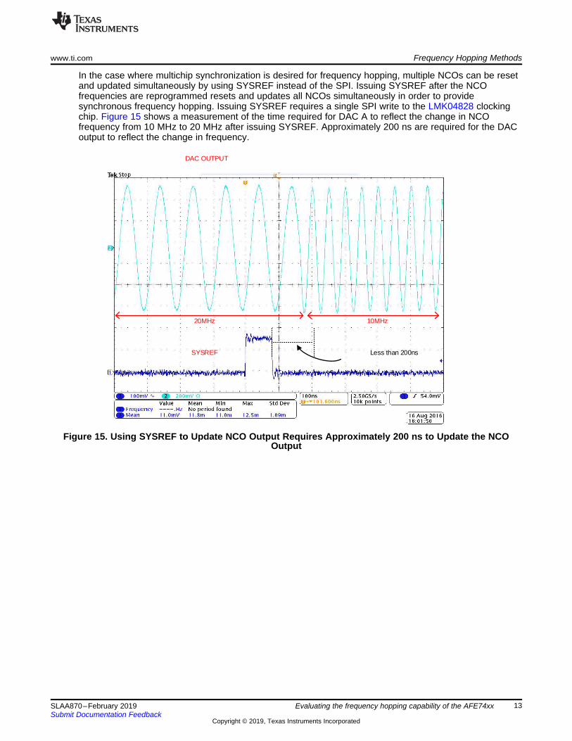
In the case where multichip synchronization is desired for frequency hopping, multiple NCOs can be resetand updated simultaneously by using SYSREF instead of the SPI. Issuing SYSREF after the NCOfrequencies are reprogrammed resets and updates all NCOs simultaneously in order to providesynchronous frequency hopping. Issuing SYSREF requires a single SPI write to the LMK04828 clockingchip. Figure 15 shows a measurement of the time required for DAC A to reflect the change in NCOfrequency from 10 MHz to 20 MHz after issuing SYSREF. Approximately 200 ns are required for the DACoutput to reflect the change in frequency.
Figure 15. Using SYSREF to Update NCO Output Requires Approximately 200 ns to Update the NCOOutput

0 MSPS
SPI
TX NCO0 TX NCO1
To DAC RF Output
Digital Up Converter (DUC)
3. TX Frequency Hopping Sequence
RF output
1. Constant Tone Generation
Frequency Hopping for Phase Coherency
2. Toggle selected TXNCO
DACComplex
Digital Mixer
Digital Interpolation
Filters
Frequency (Hz) Fdac/20Hzf1 f2
f1 f2
Frequency Hopping Methods www.ti.com
14 SLAA870–February 2019Submit Documentation Feedback
Copyright © 2019, Texas Instruments Incorporated
Evaluating the frequency hopping capability of the AFE74xx
4.2 Maintaining Phase Coherency
4.2.1 TX NCO Hopping Using SPIPhase coherency is maintained when dynamically switching between NCOs because NCOs runcontinuously, whether currently selected or not. Rapidly switching between two or three fixed frequenciesis a suitable use case for certain applications, such as radar attempting to frustrate the efforts of a jammersignal.
In the case of the AFE74xx, a one-time SPI write is required when switching between the RX or TX NCOs.Though the AFE74xx receivers can switch NCOs through the SPI or GPIO, the AFE74xx transmitters canonly switch NCOs through the SPI. Figure 16 gives a visual depiction of how phase-coherent frequencyhopping is implemented on the AFE74xx transmitter.
Figure 16. Phase Coherent Frequency Hopping With an AFE74xx Transmitter
The following experiment calculates the hop time when switching from TXNCO0 to TXNCO1 using theSPI. The test setup for measuring phase coherency is the same setup used to measure continuity.
4.2.1.1 TX NCO Switch Using SPI Hop Time
4.2.1.1.1 Software ConfigurationFirst, program TXNCO0 to 100 MHz through the Advanced tab in the AFE74xx GUI. See Section 4.1.1.3for programming instructions.
Next, program TXNCO1 to 10 MHz by using a configuration file to update the TXNCO1 registers. Theconfiguration file containing the necessary register writes to program TXNCO1 to 10 MHz is found inSection 7.
Before issuing the command to switch from TXNCO0 to TXNCO1 as the active NCO, make sure that thetrigger setting on the oscilloscope is set to trigger on the negative edge of the SDEN signal. Then, load theconfiguration file containing the SPI writes required to switch from TXNCO0 to TXNCO1. The registerwrites used to select the active TX NCO are located in Section 7. The oscilloscope triggers after the SPIcommand is sent, capturing the transition from TXNCO0 to TXNCO1.

www.ti.com Frequency Hopping Methods
15SLAA870–February 2019Submit Documentation Feedback
Copyright © 2019, Texas Instruments Incorporated
Evaluating the frequency hopping capability of the AFE74xx
4.2.1.1.2 Test ResultsFigure 17 shows that the time required to switch from TXNCO0 (100 MHz) to TXNCO1 (10 MHz) isapproximately 658 ns from the issuance of the command through the SPI clock of approximately 40 MHz
Figure 17. Hop Time When Switching From One NCO to Another is Approximately 658 ns

AFE74xEVM
Real-Time Spectrum Analyzer
RF input
SDEN SPI pin
Trigger input
DAC A output
Settling Time
Nominal Hop Freq.
Freq
uenc
y (H
z)
Hop Begin
Setting Tolerance
Frequency
Trigger
Frequency Hopping Methods www.ti.com
16 SLAA870–February 2019Submit Documentation Feedback
Copyright © 2019, Texas Instruments Incorporated
Evaluating the frequency hopping capability of the AFE74xx
4.2.1.2 AFE74xx DAC Settling TimeThe DAC settling time is the time required for the DAC output to reach a final value within a specifiedpercentage when hopping from one frequency to another. The DAC settling time has a direct impact onthe total hop time. Figure 18 shows a model for the DAC settling time.
Figure 18. Timing Model for DAC Settling Time
4.2.1.2.1 Hardware SetupMeasuring the settling time for the AFE74xx DACs requires a spectrum analyzer capable of real-time,frequency-domain analysis. As shown inFigure 19, the spectrum analyzer is connected to the DAC A SMAoutput labeled I_OUTA on the AFE74xxEVM. The SPI clock on the AFE74xxEVM is the trigger source forthe spectrum analyzer as the AFE74xx active TX NCO switches from TXNCO0 to TXNCO1.
Figure 19. DAC Settling Time: Hardware Setup
4.2.1.2.2 Software ConfigurationThis example begins by first programming TXNCO0 and TXNCO1 to two different frequencies, and thenswitching the active NCO, all while observing the transition on a spectrum analyzer. In this example,TXNCO0 and TXNCO1 are programmed through the AFE74xx GUI to be 313 MHz and 236 MHz,respectively. See Section 3.3.1.1 for an NCO programming example.
www.ti.com Frequency Hopping Methods
17SLAA870–February 2019Submit Documentation Feedback
Copyright © 2019, Texas Instruments Incorporated
Evaluating the frequency hopping capability of the AFE74xx
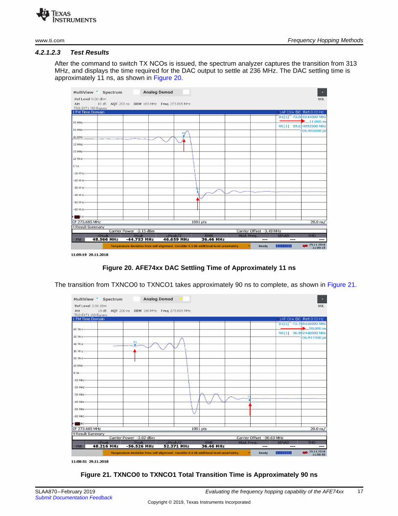
4.2.1.2.3 Test ResultsAfter the command to switch TX NCOs is issued, the spectrum analyzer captures the transition from 313MHz, and displays the time required for the DAC output to settle at 236 MHz. The DAC settling time isapproximately 11 ns, as shown in Figure 20.
Figure 20. AFE74xx DAC Settling Time of Approximately 11 ns
The transition from TXNCO0 to TXNCO1 takes approximately 90 ns to complete, as shown in Figure 21.
Figure 21. TXNCO0 to TXNCO1 Total Transition Time is Approximately 90 ns

Frequency Hopping Methods www.ti.com
18 SLAA870–February 2019Submit Documentation Feedback
Copyright © 2019, Texas Instruments Incorporated
Evaluating the frequency hopping capability of the AFE74xx
4.2.2 RX NCO Hopping Using the GPIO PinsIf a receiver application requires three NCO for frequency hopping, the AFE74xx supports seamlesshopping using the GPIO pins in real time. The advantage of this method is that no SPI writes are requiredto change NCOs, thus greatly reducing hop time. There are two GPIO pins per two receivers: RXFBNCO0and RXFBNCO1 for RX channels A and B, respectively; and RXFBNCO2 and RXFBNCO3 for RXchannels C and D, respectively. Figure 22 shows where GPIO pins RXFBNCO0 to RXFBNCO3 arelocated.
Figure 22. AFE74xx Pinbank J9 Containing RX NCO GPIO Pins
Table 2 shows the relationship between enabled GPIO pins to selected NCO.
Table 2. Relationship Between Enabled GPIO Pins to Selected NCO
GPIO PinNCO ID
RXFBNCO-1/3 RXFBNCO-0/20 0 NCO_00 1 NCO_11 0 NCO_21 1 Not applicable

RXFBNCO0 GPIO Pin
Trigger input
AFE74xxEVM TSW14J56EVM Rev D
Signal Generator
ADC A input
Function Generator
www.ti.com Frequency Hopping Methods
19SLAA870–February 2019Submit Documentation Feedback
Copyright © 2019, Texas Instruments Incorporated
Evaluating the frequency hopping capability of the AFE74xx
4.2.2.1 Test SetupGPIO hop time is calculated using a TSW14J56EVM connected to an AFE74xxEVM. The TSW14J56EVMis a data capture card with an input-trigger feature, where data capture begins as soon as the designatedSMA input receives a 1.8-V logic high signal. A function generator connects to both the RXFBNCO0 GPIOpin and the SMA trigger input of the TSW14J56EVM. The function generator outputs a single-pulsesquare wave at 1 Hz with an amplitude of 1.8 V. The signal from the function generator activates theTSW14J56 trigger and switches the selected NCO from RXNCO0 to RXNCO1. The TSW14J56EVMcaptures the change in frequency from 100 MHz to 10 MHz as the enabled NCO switches from RXNCO0to RXNCO1. The test setup for this example is shown in Figure 23.
Figure 23. Test Setup for Measuring RX NCO Hop Time Using the GPIO Pins
4.2.2.2 Software ConfigurationTo configure the AFE74xx receiver NCOs to switch using the GPIO pins, follow the normal AFE74xx GUIbringup procedure with one difference. Before pressing set mode after selecting a mode, navigate to theAdvanced tab in the GUI, and observe the NCO Freq Setting section at the bottom left of the window. TheRX_NCO# fields are where each NCO is programmed. NCO#0, NCO#1, and NCO#2 are the three NCOsavailable in the single band DDC. NCO#3 is the single NCO found in the second DDC and is onlyavailable in dual-band mode. RX IDs determine the ADC in which the NCOs are programmed. RX NCOIDs enable the NCOs to be programmed.
In the example shown in Figure 24, NCO0 is programmed to 100 MHz and NCO1 is programmed to 10MHz. Select NCO IDs 0,1 because only NCO0 and NCO1 are used. For RX ID, select RX 0 because thisexperiment requires programming only one ADC. After entering the desired RX NCO values, press NCOupdate to automatically update the corresponding RX NCO registers.
Figure 24. Programming RXNCO0 and RXNCO1 to 100 MHz and 10 MHz, Respectively

Frequency Hopping Methods www.ti.com
20 SLAA870–February 2019Submit Documentation Feedback
Copyright © 2019, Texas Instruments Incorporated
Evaluating the frequency hopping capability of the AFE74xx
After programming the RX NCO values, the AFE74xx receivers must be configured to selectively switchNCOs using the GPIO pins. RX NCO selection using the GPIO pins is configured through the AFE74xx inthe Advanced tab under the Dynamic Switch section. Select ON under the RX_FBRX drop-down menu.Select NCO selection by RXFBNCO 0/1 (ADC A/B) or 2/3 (ABC C/D) under the RX/FB NCO drop-downmenu, as shown in Figure 25.
Figure 25. Configuring RX NCO Selection Through the GPIO Pins Using the AFE74xx GUI
4.2.2.3 Test ResultsFigure 26 shows the measured latency when switching from RXNCO0 (programmed to 100 MHz) toRXNCO1 (programmed to 10 MHz).
Figure 26. RX NCO Switching Time Using GPIO Pins

RXA NCO0
RXA NCO1
RXA NCO2
Load Load Selected
Frequency (Hz)
Selected Band
SPI/GPIO
N
www.ti.com NCO Frequency Resolution Versus Hop Time
21SLAA870–February 2019Submit Documentation Feedback
Copyright © 2019, Texas Instruments Incorporated
Evaluating the frequency hopping capability of the AFE74xx
5 NCO Frequency Resolution Versus Hop TimeThere is a trade-off between NCO RF step size (resolution) and hop time. As mentioned previously, a 32-bit accumulator word determines the output frequency of the NCO, and there are four designated NCOregisters that each store a byte of the total 32-bit accumulator word. Thus, a single SPI write is required toprogram each byte of the total accumulator word. Each SPI write adds about 600 ns to the overall hoptime. Therefore, reducing the NCO resolution from 32 bits to 24 bits by programming only the first threeNCO registers bypasses the NCO register containing the 8-LSB bits, and ultimately reduces overall hoptime by 600 ns. The trade-off is that reducing NCO resolution from 32 bits to 24 bits decreases the NCOresolution. A 32-bit NCO can move in frequency steps of approximately 2 Hz. A 24-bit NCO can saveroughly 600 ns of hop time compared to a 32-bit NCO, but NCO resolution decreases from 2 Hz to roughly527.35 Hz. If an RF step-size of 135 kHz is suitable for an application, only the 16 most significant bits ofthe NCO accumulator word must be programmed, reducing the number of required SPI writes, andultimately reducing the overall hop time by approximately 1.2 µs compared to the full 32-bit NCO. Table 3shows the trade-off between NCO resolution and overall hop time.
Table 3. Trade-Off Between NCO Resolution and Overall Hop Time
NCO Word MSBFrequencyStep Size
(Resolution)
Total SPI Write Time(Update NCO
Frequency + NCOReset)
SettlingTime
Total Hop TimeWhen Updating 1
NCOTotal Hops per Second
32 bits of NCO word 2.06 Hz 4.2 µs 90 ns 4.29 µs 1 / (4.29 µs + Dwell time)24 MSB of NCO word 527.35 Hz 3.6 µs 90 ns 3.69 µs 1 / (3.69 µs + Dwell time)16 MSB of NCO word 135.00274 kHz 2.4 µs 90 ns 2.49 µs 1 / (2.49 µs + Dwell time)8 MSB of NCO word 34.43 MHz 1.0 µs 90 ns 1.09 µs 1 / (1.09 µs + Dwell time)
6 Fast Frequency Hopping With the Load and SwitchFaster frequency hopping can be achieved when multiple frequency-flexible NCOs are available, asopposed to reprogramming one NCO.
When multiple NCOs are available, program the NCOs that are not selected to different frequencies in thebackground using the SPI while the currently selected NCO is active. When ready to change frequencies,change the selected NCO.
Figure 27 gives an example of this method using TI’s AFE74xx. In the AFE74xx each receiver (Rx)contains four available NCOs in dual-band mode, and three available NCOs in single-band mode. NCOsRXNCO0 and RXNCO1 respectively load the center frequencies of the blue and red bands in the inputspectrum, while RXNCO2 is currently selected to downconvert the green band in the input spectrum.Thus, in order to hop to a different color band, send a command to select an NCO already programmed tothe desired band frequency, greatly reducing hop time. Much less time is required to change NCOs thanto reprogram a single NCO.
Figure 27. Example of Frequency Hopping With Multiple NCOs

Register Addresses www.ti.com
22 SLAA870–February 2019Submit Documentation Feedback
Copyright © 2019, Texas Instruments Incorporated
Evaluating the frequency hopping capability of the AFE74xx
7 Register AddressesTable 4 to Table 7 list the register address for all of the available RX and TX NCOs in the AFE74xx.Table 9 lists the register address for the TX NXO selection bit.
Table 4. RXNCO0 Register AddressRXNCO0 Register Address Value Comment
0x16 0xF \\ Open DDC register page of all four ADCs.
0x01E6 \\ RX_NCO0_word[7:0] address
0x01E7 \\ RX_NCO0_word[15:8] address
0x01F0 \\ RX_NCO0_word[23:16] address
0x01F1 \\ RX_NCO0_word[31:24] address
Table 5. RXNCO1 Register AddressRXNCO1 Register Address Value Comment
0x16 0xF \\ Open DDC register page of all four ADCs.
0x01EA \\ RX_NCO0_word[7:0] address
0x01EB \\ RX_NCO0_word[15:8] address
0x01F4 \\ RX_NCO0_word[23:16] address
0x01F5 \\ RX_NCO0_word[31:24] address
Table 6. RXNCO2 Register AddressRXNCO2 Register Address Value Comment
0x16 0xF \\ Open DDC register page of all four ADCs.
0x01EE \\ RX_NCO0_word[7:0] address
0x01EF \\ RX_NCO0_word[15:8] address
0x01F8 \\ RX_NCO0_word[23:16] address
0x01F9 \\ RX_NCO0_word[31:24] address
Table 7. TXNCO0 Register AddressTXNCO0 Register Address Value Comment
0x10 0x55 \\ Open DUC register page of all four DACs.
0x48 \\ TX_NCO0_word[7:0] address
0x49 \\ TX_NCO0_word[15:8] address
0x4A \\ TX_NCO0_word[23:16] address
0x4B \\ TX_NCO0_word[31:24] address
Table 8. TXNCO1 Register AddressTXNCO1 Register Address Value Comment
0x10 0x55 \\ Open DUC register page of all four DACs.
0x0110 \\ TX_NCO1_word[7:0] address
0x0111 \\ TX_NCO1_word[15:8] address
0x0112 \\ TX_NCO1_word[23:16] address
0x0113 \\ TX_NCO1_word[31:24] address
Table 9. TX NCO Selection AddressTX NCO Selection Address Value Comment
0x10 0x55 \\ Open DUC register page of all four DACs.
0x2B 0x23 \\ Select TXNCO0
0x2B 0xA3 \\ Select TXNCO1

www.ti.com References
23SLAA870–February 2019Submit Documentation Feedback
Copyright © 2019, Texas Instruments Incorporated
Evaluating the frequency hopping capability of the AFE74xx
8 References• Rohde&Schwarz, Sander, K.U. (2018), Frequency and Phase settling time measurements on PLL
circuits Application Note

IMPORTANT NOTICE AND DISCLAIMERTI PROVIDES TECHNICAL AND RELIABILITY DATA (INCLUDING DATA SHEETS), DESIGN RESOURCES (INCLUDING REFERENCE DESIGNS), APPLICATION OR OTHER DESIGN ADVICE, WEB TOOLS, SAFETY INFORMATION, AND OTHER RESOURCES “AS IS” AND WITH ALL FAULTS, AND DISCLAIMS ALL WARRANTIES, EXPRESS AND IMPLIED, INCLUDING WITHOUT LIMITATION ANY IMPLIED WARRANTIES OF MERCHANTABILITY, FITNESS FOR A PARTICULAR PURPOSE OR NON-INFRINGEMENT OF THIRD PARTY INTELLECTUAL PROPERTY RIGHTS.These resources are intended for skilled developers designing with TI products. You are solely responsible for (1) selecting the appropriate TI products for your application, (2) designing, validating and testing your application, and (3) ensuring your application meets applicable standards, and any other safety, security, regulatory or other requirements.These resources are subject to change without notice. TI grants you permission to use these resources only for development of an application that uses the TI products described in the resource. Other reproduction and display of these resources is prohibited. No license is granted to any other TI intellectual property right or to any third party intellectual property right. TI disclaims responsibility for, and you will fully indemnify TI and its representatives against, any claims, damages, costs, losses, and liabilities arising out of your use of these resources.TI’s products are provided subject to TI’s Terms of Sale or other applicable terms available either on ti.com or provided in conjunction with such TI products. TI’s provision of these resources does not expand or otherwise alter TI’s applicable warranties or warranty disclaimers for TI products.TI objects to and rejects any additional or different terms you may have proposed. IMPORTANT NOTICE
Mailing Address: Texas Instruments, Post Office Box 655303, Dallas, Texas 75265Copyright © 2022, Texas Instruments Incorporated