Evaluating Run Evaluating Run--Time Techniques Time Techniques for Leakage Power Reduction for...
30
http://www.cse.psu.edu/~mdl Evaluating Run Evaluating Run- Time Techniques Time Techniques for Leakage Power Reduction for Leakage Power Reduction D. Duarte, Y-F. Tsai, N. Vijaykrishnan, M.J. Irwin, Microsystems Design Lab Pennsylvania State University
Transcript of Evaluating Run Evaluating Run--Time Techniques Time Techniques for Leakage Power Reduction for...
http://www.cse.psu.edu/~mdl
Evaluating RunEvaluating Run--Time Techniques Time Techniques for Leakage Power Reductionfor Leakage Power Reduction
D. Duarte, Y-F. Tsai, N. Vijaykrishnan, M.J. Irwin,Microsystems Design Lab
Pennsylvania State University
2 © PSU, 2000VLSI Design/ASPDAC 2002
OutlineOutline
uu MotivationMotivation
uu Achieving Leakage Power ReductionAchieving Leakage Power Reductionss By input vector control By input vector control ss By increasing the threshold voltageBy increasing the threshold voltagess By gating the supply voltageBy gating the supply voltage
uu Characterization of leakage reduction techniquesCharacterization of leakage reduction techniquesss Input vector control (IVC)Input vector control (IVC)ss Body Bias Control (BBC)Body Bias Control (BBC)ss Power Supply Gating (PSG) Power Supply Gating (PSG)
uu ConclusionsConclusions

3 © PSU, 2000VLSI Design/ASPDAC 2002
Power Will Be a LimiterPower Will Be a Limiter
5KW18KW
1.5KW500W
40048008
80808085
8086286
386486
Pentium®
0.1
1
10
100
1000
10000
100000
1971 1974 1978 1985 1992 2000 2004 2008
Powe
r (W
atts
)q Microprocessor power continues to increase exponentially
q Power delivery and dissipation will be prohibitive !Source: Borkar, De Intel
P6
4 © PSU, 2000VLSI Design/ASPDAC 2002
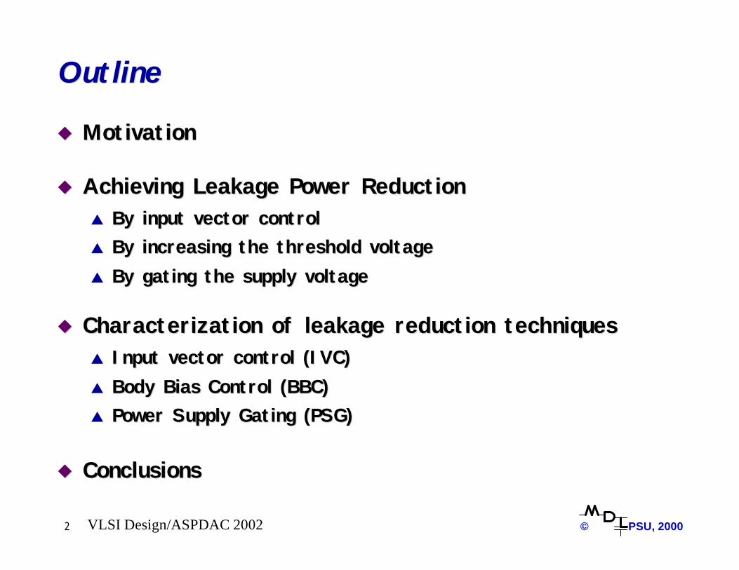
0.25µ , 15mm die, 2V
0% 0% 0% 0% 1% 1% 1% 2% 3%
-
10
20
30
40
50
60
70
30 40 50 60 70 80 90 100
110
Temp (C)
Pow
er (W
atts
)
LeakageActive
0.18µ , 15mm die, 1.4V
0% 0% 1% 1% 2% 3% 5% 7% 9%
-
10
20
30
40
50
60
70
30 40 50 60 70 80 90 100
110
Temp (C)
Pow
er (W
atts
)
LeakageActive
0.13µ , 15mm die. 1V
1% 2% 3% 5% 8% 11% 15% 20%26%
-
10
20
30
40
50
60
70
30 40 50 60 70 80 90 100
110
Temp (C)
Pow
er (W
atts
)
LeakageActive
0.1µ , 15mm die, 0.7V
6% 9% 14% 19%26%
33%41% 49% 56%
-
10
20
30
40
50
60
70
30 40 50 60 70 80 90 100
110
Temp (C)
Pow
er (W
atts
)
LeakageActive
Active & standby leakage power trends
Source: Vivek De Intel
5 © PSU, 2000VLSI Design/ASPDAC 2002
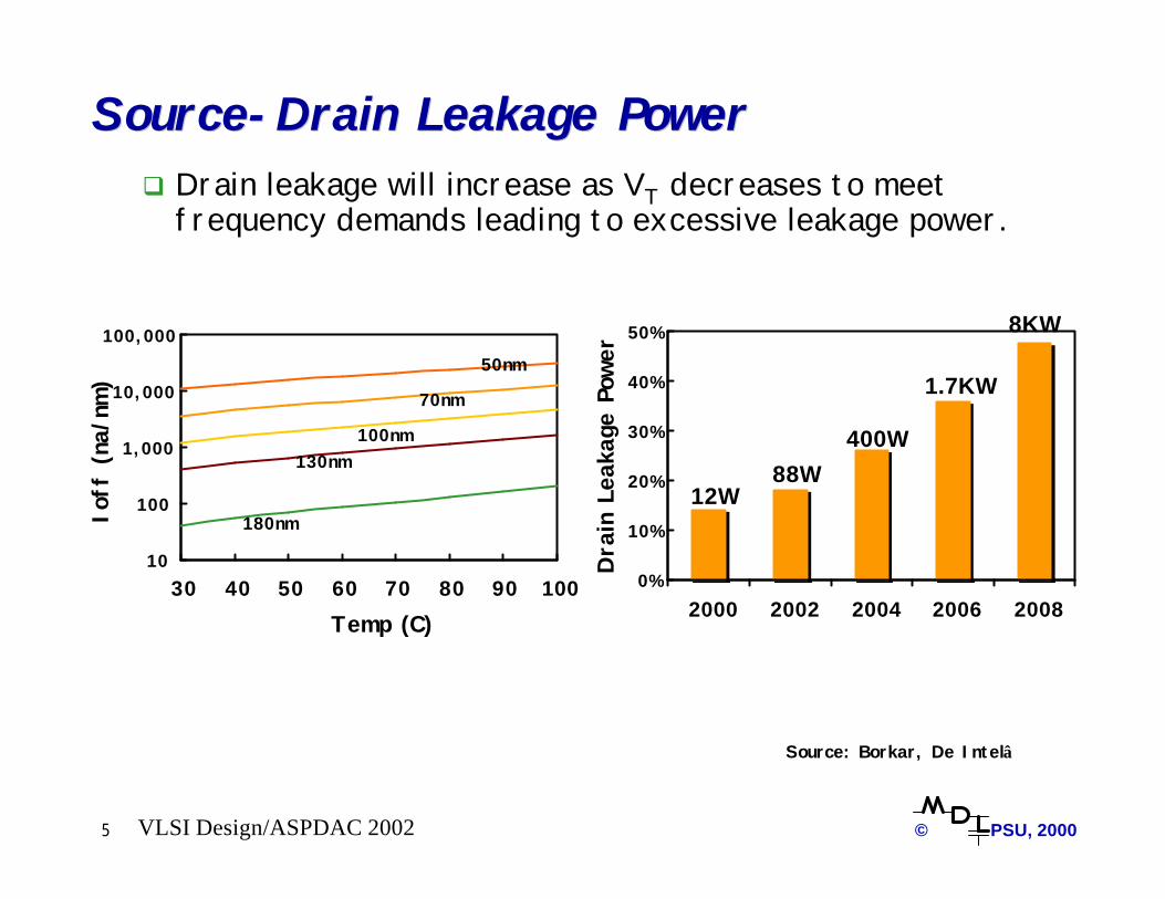
SourceSource--Drain Leakage Power Drain Leakage Power
10
100
1,000
10,000
100,000
30 40 50 60 70 80 90 100Temp (C)
Ioff
(na/
nm)
180nm
130nm100nm
70nm
50nm
8KW
1.7KW
400W
88W 12W
0%
10%
20%
30%
40%
50%
2000 2002 2004 2006 2008Dra
in L
eaka
ge P
ower
q Drain leakage will increase as VT decreases to meet frequency demands leading to excessive leakage power.
Source: Borkar, De Intel
6 © PSU, 2000VLSI Design/ASPDAC 2002
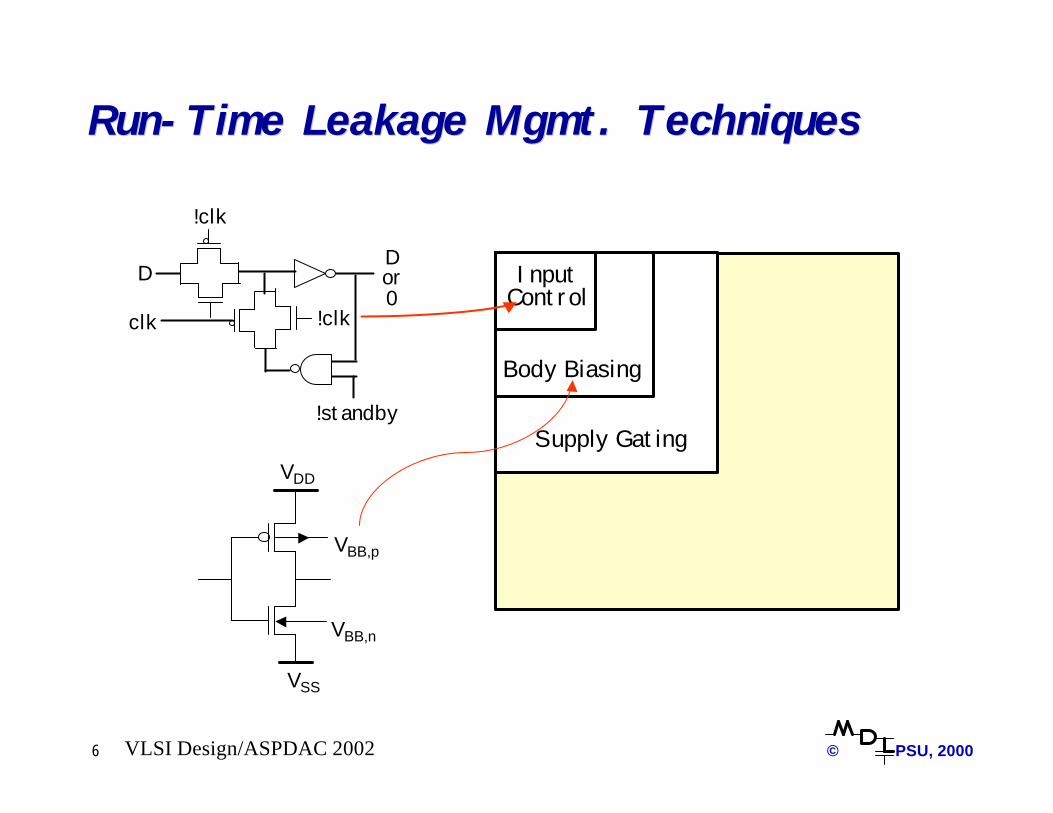
RunRun--Time Leakage Mgmt. TechniquesTime Leakage Mgmt. Techniques
Supply Gating
Body Biasing
Input Control
clk !clk
!clk
!standby
D or 0
D
VDD
VBB,p
VBB,n
VSS
7 © PSU, 2000VLSI Design/ASPDAC 2002
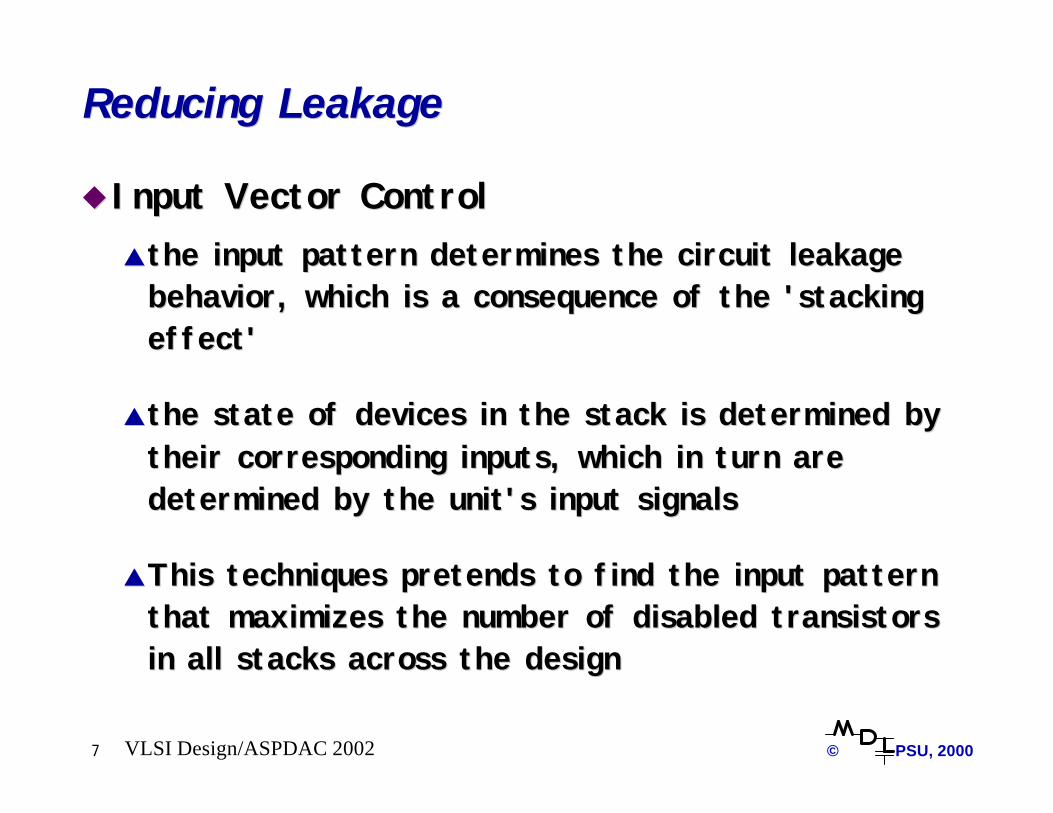
Reducing LeakageReducing Leakage
uuInput Vector ControlInput Vector Controlssthe input pattern determines the circuit leakage the input pattern determines the circuit leakage behavior, which is a consequence of the 'stacking behavior, which is a consequence of the 'stacking effect' effect'
ssthe state of devices in the stack is determined by the state of devices in the stack is determined by their corresponding inputs, which in turn are their corresponding inputs, which in turn are determined by the unit's input signalsdetermined by the unit's input signals
ssThis techniques pretends to find the input pattern This techniques pretends to find the input pattern that maximizes the number of disabled transistors that maximizes the number of disabled transistors in all stacks across the design in all stacks across the design

8 © PSU, 2000VLSI Design/ASPDAC 2002
Input Vector Activation MechanismInput Vector Activation Mechanism
uuTransistor Stack Effect: the leakage Transistor Stack Effect: the leakage reduction effect in a transistor stack when reduction effect in a transistor stack when more than one transistor is turned offmore than one transistor is turned off..uu Leakage is dependent on Leakage is dependent on VVdsds, , VVgsgs and and VVtt
A
B
B
VDD
GND
VM
M1
M2
For M1, Vgs < 0à leakage
For M1, Vbb>0, body effect àleakage
Small drain current àVM > 0V
There is a best input vector introducing smallest leakage
DG
S

9 © PSU, 2000VLSI Design/ASPDAC 2002
Reducing LeakageReducing Leakage
uu Increasing the Threshold VoltageIncreasing the Threshold Voltagess Takes advantage of the logarithmic dependence of the Takes advantage of the logarithmic dependence of the IIsubthsubth
with Vwith VTHTH
ss In MultipleIn Multiple--Threshold Voltage CMOS (MTCMOS), a highThreshold Voltage CMOS (MTCMOS), a high--VVTHTHdevice is inserted in series with lowdevice is inserted in series with low--VVTHTH circuitry, creating a circuitry, creating a sleep transistor. sleep transistor.
ss Dual VDual VTHTH CMOS, uses highCMOS, uses high--VVTHTH devices on nondevices on non--critical paths critical paths and lowand low--VVTHTH devices on the critical ones. devices on the critical ones.
( ) 1.
'8.1
2
−
=
⋅+⋅−−−kT
qVVVVVV
kTnq
eff
effoxOsubth
DSDSSTHOSG
eeeq
kTL
WCI
ηγµ

10 © PSU, 2000VLSI Design/ASPDAC 2002
Reducing LeakageReducing Leakage
uuIncreasing the Threshold VoltageIncreasing the Threshold VoltagessIn Dynamic Threshold MOS (DTMOS), the body and In Dynamic Threshold MOS (DTMOS), the body and gate of each transistor are tied together such that gate of each transistor are tied together such that whenever the device is off, low leakage is achieved whenever the device is off, low leakage is achieved while when the device is on, higher current drives while when the device is on, higher current drives are possible [13]. are possible [13].
ssThe Standby Power Reduction (SPR) or The Standby Power Reduction (SPR) or Variable Variable Threshold CMOS (VTCMOS)Threshold CMOS (VTCMOS) technique raises Vtechnique raises VTHTHduring standby mode by making the substrate during standby mode by making the substrate voltage either higher thanvoltage either higher than VVdddd (P devices) or lower (P devices) or lower than ground (N devices). than ground (N devices).

11 © PSU, 2000VLSI Design/ASPDAC 2002
Reducing LeakageReducing Leakage
uuGating the Power SupplyGating the Power SupplyssThe power supply is shut down so that idle units do The power supply is shut down so that idle units do not consume leakage powernot consume leakage power
ssThis can be done using This can be done using ““sleepsleep”” transistors transistors (MTCMOS). (MTCMOS).
uuIf there is intention to provide support for If there is intention to provide support for Dynamic Voltage Scaling (DVS):Dynamic Voltage Scaling (DVS):ssSwitching regulatorsSwitching regulatorsssOnOn--chip voltage generatorschip voltage generators (PLL)(PLL)

12 © PSU, 2000VLSI Design/ASPDAC 2002
Experimentation FrameworkExperimentation Framework
uuThe effectiveness of the techniques were The effectiveness of the techniques were studied in various designs.studied in various designs.
Unit Avg. leakage power (nW)
Avg. dynamic power (mW)
32-bit Carry Lookahead Adder 93.34 6.458x8-bit Multiplier (0.35um) 348.42 3.898-bit Static Adder 4.95 0.3132-bit Shifter 936.34 3.8115-bit Carry Lookahead Adder 34.42 4.573-to-1 Multiplexer (9-bit) 2.12 0.5632 2-input XOR (32-bit word) 1.13 0.6832 2-input NAND (32-bit word) 8.24 0.2332 2-input AND (32-bit word) 75.04 0.5432 2-input NOR (32-bit word) 48.80 0.3232 2-input OR (32-bit word) 60.56 0.66

13 © PSU, 2000VLSI Design/ASPDAC 2002
Experimentation FrameworkExperimentation Framework
uu One technique per category described earlier as One technique per category described earlier as selected each of which is controllable at runselected each of which is controllable at run--time. time.
uu We usedWe used MicroMagicMicroMagic MAX for layout creation and MAX for layout creation and HSPICE (T= 25HSPICE (T= 25OOC) for circuitC) for circuit--level simulation. level simulation.
uu Experiments were performed on a 0.25um technology Experiments were performed on a 0.25um technology with threshold voltages of 0.47V/0.59V for N/P with threshold voltages of 0.47V/0.59V for N/P devices and a 2.5V power supply. devices and a 2.5V power supply.

14 © PSU, 2000VLSI Design/ASPDAC 2002
I. Input Vector Control (IVC)I. Input Vector Control (IVC)
uuThe minimumThe minimum--leakage input vector for the leakage input vector for the given design is found through simulationgiven design is found through simulation
uu Design is modified by hardwiring the input Design is modified by hardwiring the input values in minimumvalues in minimum--leakage vector to each input leakage vector to each input latch, which is controlled by “sleep” signal.latch, which is controlled by “sleep” signal.
A_extA_int
!sleep
sleep
VDD
A_ext A_int
!sleep
sleep
gnd
Modified latches with optimum sleep values stored(1 left, 0 right)
15 © PSU, 2000VLSI Design/ASPDAC 2002
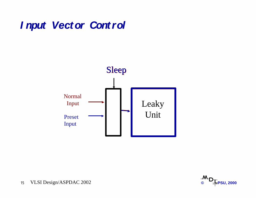
Input Vector ControlInput Vector Control
Sleep
NormalInput
PresetInput
LeakyUnit
Sleep

16 © PSU, 2000VLSI Design/ASPDAC 2002
Leakage DistributionLeakage Distribution
Leakage Current Distribution32-bit CLA Adder
0%
5%
10%
15%
20%
25%
30%
0 5 10 15 20 25 30 35 40 45 50 55 60 65 70
Leakage Current (nA)
Per
cent
age

17 © PSU, 2000VLSI Design/ASPDAC 2002
Input Vector ControlInput Vector Control
uuMinimum Idle time (Minimum Idle time (ttidleidle))
)(
)2(
)(
)(
_
_
_
21_
nleakleak
trnleaktr
nleakleak
trtrnleaktridle PP
tPE
PP
ttPEt
−
⋅−≈
−
+⋅−>

18 © PSU, 2000VLSI Design/ASPDAC 2002
Input Vector ControlInput Vector Control
uuSimulated performance parametersSimulated performance parameters
Unit Leakage Reduction (%)
Area Increase (%)
Min. idle time (us)
32-bit CLA 64.84 0.92 25.168x8 Multiplier 21.00 0.13 112.368-bit Static Add 95.22 2.05 10.5232-bit Shifter 79.13 0.27 22.4015-bit CLA 66.02 0.96 46.663-to-1 Mux 95.19 1.65 27.7732 2-input XOR 24.11 6.37 20.0132 2-input NAND 93.81 9.37 0.7032 2-input AND 98.53 8.22 0.3932 2-input NOR 97.71 6.87 0.1132 2-input OR 98.82 5.46 0.52

19 © PSU, 2000VLSI Design/ASPDAC 2002
Leakage control by natural stacks
0%
10%
20%
30%
5.0 5.6 6.2 6.8 7.4 105.0 120.0 135.0
Standby leakage current (uA)
% o
f in
pu
t ve
cto
rs
Low VtHigh Vt
32-bit KS adder
Reduction
High VtAverage
Worst
1.5X
2.5X
Low VtAverage
Worst
1.5X
2X
High Vt Low Vt
Energyoverhead
1.64 nJ 1.84 nJ
Savings 2.2 µA 38.4 µA
Min. time instandby 84 µS 5.4 µS
* Y. Ye et. al., 1998 Symp. VLSI Circuits
20 © PSU, 2000VLSI Design/ASPDAC 2002
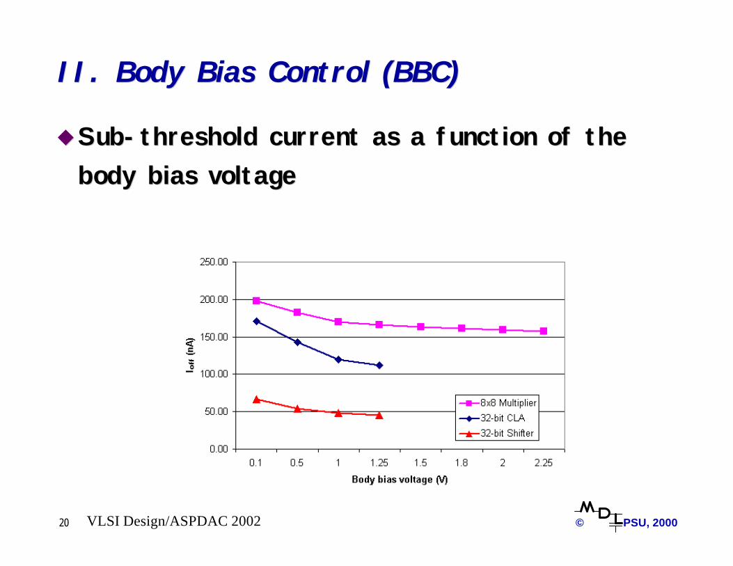
II. Body Bias Control (BBC)II. Body Bias Control (BBC)
uuSubSub--threshold current as a function of the threshold current as a function of the body bias voltagebody bias voltage
21 © PSU, 2000VLSI Design/ASPDAC 2002
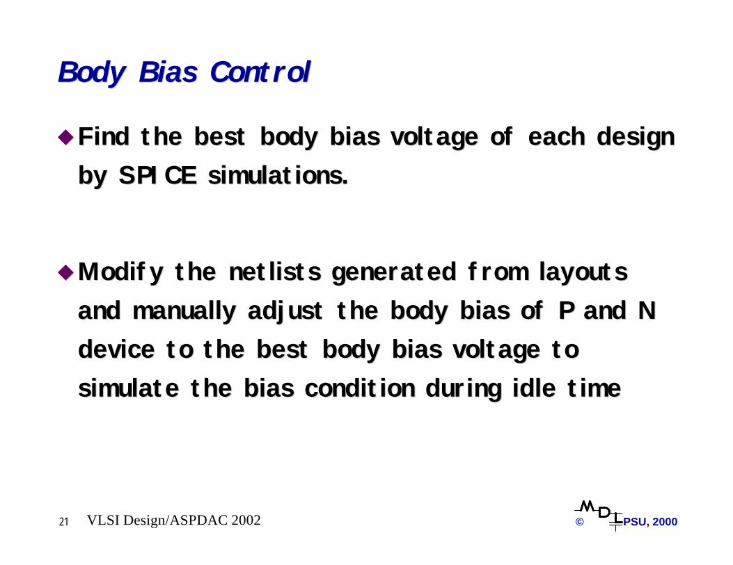
Body Bias ControlBody Bias Control
uuFind the best body bias voltage of each design Find the best body bias voltage of each design by SPICE simulations.by SPICE simulations.
uuModify the Modify the netlists netlists generated from layouts generated from layouts and manually adjust the body bias of P and N and manually adjust the body bias of P and N device to the best body bias voltage to device to the best body bias voltage to simulate the bias condition during idle timesimulate the bias condition during idle time

22 © PSU, 2000VLSI Design/ASPDAC 2002
Body Bias ControlBody Bias Control
uuPower overhead is incurred for charging Power overhead is incurred for charging substrate when entering sleep modesubstrate when entering sleep mode
uuRequired response time can be obtained by Required response time can be obtained by tuning chargetuning charge--pump driving current and pump driving current and frequency.frequency.
)()()( /22 ACVCVE Asubchsubschsubsch ∆=∆=−

23 © PSU, 2000VLSI Design/ASPDAC 2002
Body Bias ControlBody Bias Control
uuSimulated performance parametersSimulated performance parametersLeakage
Reduction (%)Area
Overhead (%)Transition
Energy (pJ)Min. idle time
(ms)32-bit CLA 66.54 5.24 28.37 0.918x8 Multiplier 20.58 2.17 68.37 1.928-bit Static Adder 20.68 45.83 3.25 6.3432-bit Shifter 61.22 2.94 50.94 0.1815-bit CLA 64.39 11.36 13.05 1.183-to-1 Mux 85.94 51.73 2.88 3.1732 2-input XOR 51.24 44.67 3.33 474.2332 2-input NAND 98.36 75.19 1.99 15.7232 2-input AND 94.77 62.53 2.39 2.1532 2-input NOR 67.62 49.28 3.02 5.8632 2-input OR 72.99 36.89 4.03 5.83

24 © PSU, 2000VLSI Design/ASPDAC 2002
III. Power Supply Gating (PSG)III. Power Supply Gating (PSG)
uu We use a PhaseWe use a Phase--Locked Loop (PLL) as a voltage Locked Loop (PLL) as a voltage regulator, intended to support DVS at runregulator, intended to support DVS at run--time and time and leakage reduction during idle timesleakage reduction during idle times
ssSleep signal Sleep signal ⇒⇒ global supply gatingglobal supply gatingssBuffer enable signal Buffer enable signal ⇒⇒ local supply gatinglocal supply gating
25 © PSU, 2000VLSI Design/ASPDAC 2002
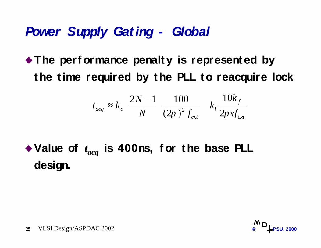
Power Supply Gating Power Supply Gating -- GlobalGlobal
uuThe performance penalty is represented by The performance penalty is represented by the time required by the PLL to reacquire lockthe time required by the PLL to reacquire lock
uuValue of Value of ttacqacq is 400ns, for the base PLL is 400ns, for the base PLL design.design.
ext
fl
extcacq f
kk
fNN
ktπξπ 2
10
)2(10012
2 +
−≈

26 © PSU, 2000VLSI Design/ASPDAC 2002
Power Supply Gating Power Supply Gating -- GlobalGlobaluu Area overheadArea overhead is determined by the ratio of is determined by the ratio of
the PLL area and that of the target unit. the PLL area and that of the target unit.
uu Power overhead is not limited to the enabling or Power overhead is not limited to the enabling or disabling actions. The operating PLL power:disabling actions. The operating PLL power:
uu This estimate is within 5% of SPICE and a This estimate is within 5% of SPICE and a value of 1.1mW is used as power overhead value of 1.1mW is used as power overhead number.number.ss The shutdown and enabling power can be roughly The shutdown and enabling power can be roughly
estimated as 65% and about 4 estimated as 65% and about 4 -- 6% above of the 6% above of the power consumed during the lockpower consumed during the lock
( ) biasvcoddFDIVVCOPFDlockPLL PfVCCCP +++= 2_
27 © PSU, 2000VLSI Design/ASPDAC 2002
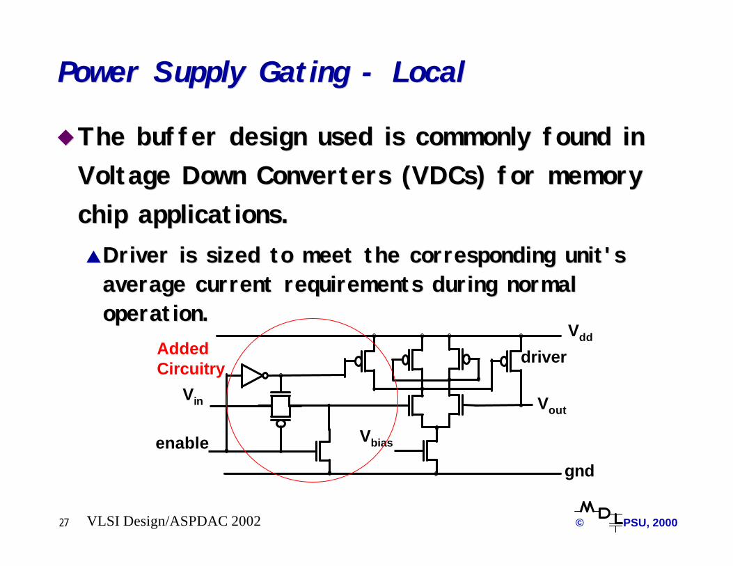
Power Supply Gating Power Supply Gating -- LocalLocal
uuThe buffer The buffer design used is commonly found in design used is commonly found in Voltage Down Converters (Voltage Down Converters (VDCsVDCs) for memory ) for memory chip applications.chip applications.ssDriver is sized to meet the corresponding unit's Driver is sized to meet the corresponding unit's average current requirements during normal average current requirements during normal operation.operation.
Vdd
gnd
Vbiasenable
VoutVin
driverAdded Circuitry
28 © PSU, 2000VLSI Design/ASPDAC 2002
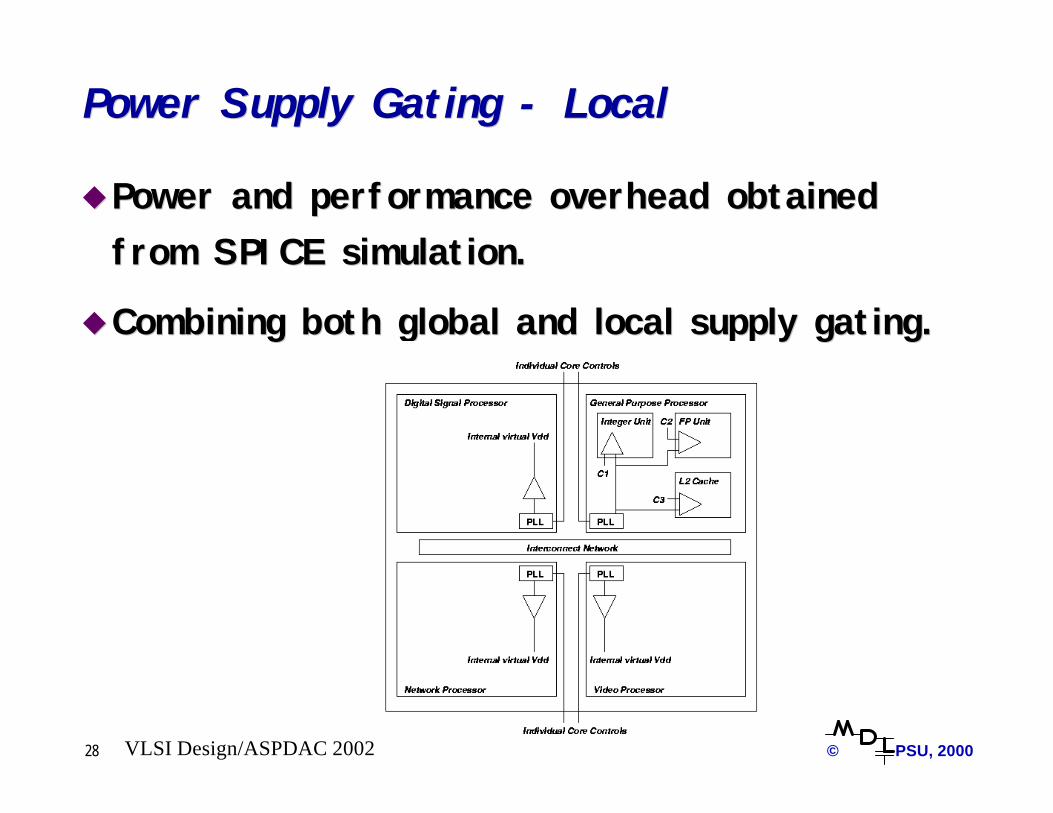
Power Supply Gating Power Supply Gating -- LocalLocal
uuPower and performance overhead obtained Power and performance overhead obtained from SPICE simulation.from SPICE simulation.
uuCombining both global and local supply gating.Combining both global and local supply gating.

29 © PSU, 2000VLSI Design/ASPDAC 2002
Power Supply GatingPower Supply Gating
uu Leakage power reduction is almost 100%. Leakage power reduction is almost 100%.
Area Overhead PLL+Buffer %
Area Overhead(buffer only) %
Buffer Enable Time (ns)
Buffer Nominal Power (uW)
Min. Idle Time (buffer only) ms
32-bit CLA 19.70 7.10 578.1 155.80 0.206
8x8 Multiplier 7.67 2.48 348.3 94.30 0.046
8-bit St.Adder 116.43 5.12 27.8 8.40 0.186
32-bit Shifter 9.39 2.39 341.1 92.40 0.012
15-bit CLA 38.61 11.12 409.4 110.7 0.395
3:1 Mux 134.08 8.42 50.1 14.40 0.786
32 2-in. XOR 116.89 8.39 61.1 17.40 57.38
32 2-in NAND 189.97 7.25 21.0 6.63 2.711
32 2-in. AND 161.89 9.96 48.6 14.00 0.687
32 2-in.NOR 125.28 5.57 28.3 8.57 0.615
32 2-in. OR 96.32 6.73 58.8 16.74 1.032
30 © PSU, 2000VLSI Design/ASPDAC 2002
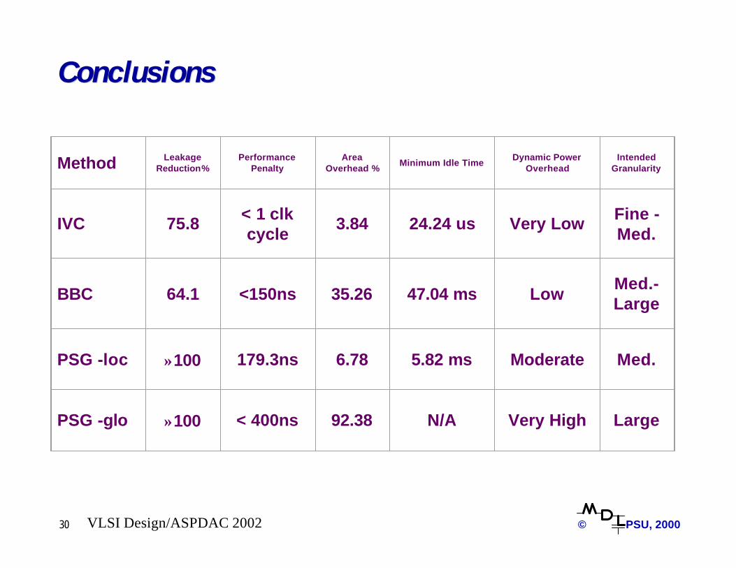
ConclusionsConclusions
Method Leakage Reduction%
Performance Penalty
Area Overhead %
Minimum Idle TimeDynamic Power
OverheadIntended
Granularity
IVC 75.8 < 1 clkcycle
3.84 24.24 us Very Low Fine -Med.
BBC 64.1 <150ns 35.26 47.04 ms LowMed.-Large
PSG -loc ≈100 179.3ns 6.78 5.82 ms Moderate Med.
PSG -glo ≈100 < 400ns 92.38 N/A Very High Large