escuela politécnica superior - RUC
462
ESCUELA POLITÉCNICA SUPERIOR TRABAJO FIN DE MÁSTER CURSO 2016/2017 DISEÑO Y DESARROLLO DEL SISTEMA DE COMUNICACIONES INALÁMBRICO DE UN ENJAMBRE DE UAV’S COLABORATIVOS MÁSTER EN INGENIERÍA INDUSTRIAL ALUMNO Cristian Méndez Sanmartín TUTORES Francisco Javier Bellas Bouza Félix Orjales Saavedra FECHA Junio 2017
-
Upload
khangminh22 -
Category
Documents
-
view
0 -
download
0
Transcript of escuela politécnica superior - RUC

ESCUELA POLITÉCNICA SUPERIOR
TRABAJO FIN DE MÁSTER CURSO 2016/2017
DISEÑO Y DESARROLLO DEL SISTEMA DE COMUNICACIONES INALÁMBRICO DE UN ENJAMBRE DE UAV’S COLABORATIVOS
MÁSTER EN INGENIERÍA INDUSTRIAL
ALUMNO
Cristian Méndez Sanmartín
TUTORES
Francisco Javier Bellas Bouza
Félix Orjales Saavedra
FECHA
Junio 2017

DOCUMENTO DEL PROYECTO - RESUMEN
MÁSTER EN INGENIERÍA INDUSTRIAL 1
TÍTULO Diseño y Desarrollo del Sistema de Comunicaciones
Inalámbrico de un Enjambre de UAV’s Colaborativos.
AUTOR Cristian Méndez Sanmartín
TUTORES Francisco Javier Bellas Bouza
Félix Orjales Saavedra
GRUPO DE INVESTIGACIÓN Grupo Integrado de Ingeniería (GII)
LÍNEA DE INVESTIGACIÓN Inteligencia Computacional (IC)
ÁREA DE TRABAJO Inteligencia Colectiva y Sistemas de Comunicaciones.
TITULACIÓN Máster en Ingeniería Industrial
FECHA DE ENTREGA 19 de Junio de 2017
IDIOMA Castellano
RESUMEN DEL TRABAJO:
La Inteligencia Colectiva, dentro del campo de la Inteligencia Computacional, aborda temas de estudio como
el comportamiento de los agentes individuales dentro de un sistema global y la asociación de la información
para la resolución conjunta de problemas complejos.
Dentro de la línea de investigación de Inteligencia Computacional e Inteligencia Colectiva, el Grupo Integrado
de Ingeniería (GII) ha propuesto como proyecto de estudio el abordar un análisis exhaustivo de las tecnologías
IoT de comunicación existentes, con el fin de adoptar la más adecuada a los requerimientos e incorporarla a
un modelo de enjambre de UAV’s colaborativos.
Las características más valoradas a la hora de la adopción del sistema serán las inherentes a los UAV’s, como
son el alcance o la eficiencia energética, además de obtener las mejores prestaciones a la hora de establecer
el radioenlace, como obtener el máximo ancho de banda, optimización de latencias y ciclos de CPU y la mayor
inmunidad posible frente a interferencias.
Una vez elegido el sistema, se tratará de optimizar para su uso en UAV’s y se realizarán pruebas de vuelo en
escenarios reales para obtener datos específicos sobre consumo energético, rendimiento y alcance máximo.

DOCUMENTO DEL PROYECTO - RESUMEN
MÁSTER EN INGENIERÍA INDUSTRIAL 2
RESUMO DO TRABALLO:
A Intelixencia Colectiva, dentro do campo do campo da Intelixencia Computacional, aborda temas de estudo
como o comportamento dos axentes individuais dentro dun sistema global e a asociación da información para
a resolución conxunta de problemas complexos.
Dentro da liña de Investigación da Intelixencia Computacional e Intelixencia Colectiva, o Grupo Integrado de
Enxeñaría (GII) propuxo como proxecto de estudo abordar un análise exhaustivo das tecnoloxías IoT de
comunicacións existentes, coa fin de adoptar a máis adecuada ós requirimentos e incorporala a un modelo
de enxame de UAV’s cooperativos.
As características mais valoradas á hora da adopción do sistema serán as inherentes ós UAV’s, como son o
alcance ou a eficiencia enerxética, ademais de obter as mellores prestacións á hora de establecer o
radioenlace, como obter o máximo ancho de banda, optimización de latencias e ciclos de CPU e a maior
inmunidade posible fronte as interferencias.
Unha vez elixido o sistema, tratarase de optimizar para o seu uso en UAV’s e realizaranse probas de voo en
escenarios reais para obter datos específicos sobre consumo enerxético, rendemento e alcance máximo.
ABSTRACT:
Collective Intelligence, into the field of Computational Intelligence, approach topics of study such as the
behaviour of individual agents in global systems and the association of information for common resolution of
complex issues.
In the research line of Computational Intelligence and Collective Intelligence, the Integrated Engineering
Group (GII) has proposed a study project to approach a comprehensive analysis of existing IoT communication
technologies to adopt the most appropriate to the requirements and incorporate it into a swarm model of
collaborative UAV’s.
The most valued characteristics for the adoption of the system will be those inherent to the UAV’s, such as
range or energy efficiency, moreover to obtain the best benefits when stablishing the radio link, as obtain the
maximum bandwidth, optimization of latencies and CPU cycles and highest immunity possible to interference.
Once the system is chosen, it will be optimized for use in UAV’s and flight test will be carried out in real
scenarios to obtain specific data on energy consumption, performance and maximum range.

ESCUELA POLITÉCNICA SUPERIOR
TRABAJO FIN DE MÁSTER
CURSO 2016/2017
DISEÑO Y DESARROLLO DEL SISTEMA DE COMUNICACIONES INALÁMBRICO DE UN ENJAMBRE DE UAV’S COLABORATIVOS
MÁSTER EN INGENIERÍA INDUSTRIAL
DOCUMENTO DEL PROYECTO
MEMORIA

ÍNDICE DE MEMORIA
ÍNDICE DE CONTENIDOS
1 INTRODUCCIÓN 1
2 OBJETIVOS 2
3 ESTADO DEL ARTE 3
3.1 INTRODUCCIÓN 3 3.2 TEORÍA DE ONDAS ELECTROMAGNÉTICAS 4 3.3 TRANSMISIÓN DE ONDAS 6 3.4 FACTORES QUE AFECTAN LA CALIDAD DE LA SEÑAL 11 3.5 TECNOLOGÍAS DE RADIOFRECUENCIA 12 3.6 DISEÑO DE UN SISTEMA DE COMUNICACIONES 13 3.7 PROTOCOLOS DE COMUNICACIÓN 19 3.8 INTERNET DE LAS COSAS Y REDES DE BAJA POTENCIA 21
4 METODOLOGÍA 22
4.1 ANÁLISIS COMPARATIVO ENTRE TECNOLOGÍAS LPWAN 22 4.2 LORA Y LORAWAN 26 4.3 DISEÑO DE LA RED 35 4.4 PUESTA EN MARCHA DE DISPOSITIVOS 38 4.5 PRUEBAS DE LA TECNOLOGÍA EN ESCENARIOS REALES 48
5 CONCLUSIONES 58
6 BIBLIOGRAFÍA 59

ÍNDICE DE MEMORIA
ÍNDICE DE FIGURAS
ÍNDICE DE DIAGRAMAS
DIAGRAMA 3.1.1: SISTEMA DE COMUNICACIONES. ............................................................................................................ 3 DIAGRAMA 3.8.1: BASES DE LA IMPLEMENTACIÓN DEL IOT. .............................................................................................. 21
ÍNDICE DE ECUACIONES
ECUACIÓN 3.4.1: ATENUACIÓN DE POTENCIA. ................................................................................................................ 11 ECUACIÓN 3.4.2: EMITANCIA ESPECTRAL DE PLANCK. ...................................................................................................... 11 ECUACIÓN 3.5.1: TEOREMA SHANNON - HARTLEY. .......................................................................................................... 12 ECUACIÓN 3.6.1: RELACIÓN P/DBM. ............................................................................................................................ 13 ECUACIÓN 3.6.2: PÉRDIDAS EN EL ESPACIO LIBRE. ........................................................................................................... 14 ECUACIÓN 3.6.3: SENSIBILIDAD DEL RECEPTOR. .............................................................................................................. 15 ECUACIÓN 3.6.4: CÁLCULO DEL RADIO DEL ELIPSOIDE DE FRESNEL. ..................................................................................... 17 ECUACIÓN 3.6.5: CÁLCULO DE ATENUACIÓN POR OBSTÁCULOS EN EL ELIPSOIDE DE FRESNEL. .................................................. 17 ECUACIÓN 3.6.6: PRESUPUESTO DE POTENCIA DEL ENLACE (LINK BUDGET). ......................................................................... 18 ECUACIÓN 3.6.7: MODELO DE LOS DOS RAYOS. ............................................................................................................... 18 ECUACIONES 4.2.1: CÁLCULO DEL PERÍODO Y EL RATIO DE SÍMBOLOS. ................................................................................. 27 ECUACIÓN 4.2.2: CÁLCULO DE LA VELOCIDAD DE MODULACIÓN. ........................................................................................ 27 ECUACIÓN 4.2.3: CÁLCULO DEL TOFF EN FUNCIÓN DEL CICLO DE TRABAJO Y EL TIEMPO DE TRANSMISIÓN. ................................. 31 ECUACIÓN 4.5.1: CONSUMO DEL TRANSCEPTOR RN2483. ............................................................................................... 49 ECUACIÓN 4.5.2: CAPACIDAD DE BATERÍA. ..................................................................................................................... 51
ÍNDICE DE GRÁFICAS
GRÁFICA 3.3.1: PÉRDIDAS DE POR ABSORCIÓN EN OXÍGENO O VAPOR DE AGUA. ..................................................................... 8 GRÁFICA 3.5.1: NARROWBAND VS SPREAD SPECTRUM. .................................................................................................... 12
ÍNDICE DE ILUSTRACIONES
ILUSTRACIÓN 1.1: REPRESENTACIÓN ABSTRACTA DE IA. ...................................................................................................... 1 ILUSTRACIÓN 2.1: GRUPO INTEGRADO DE INGENIERÍA (GII). ................................................................................................ 2 ILUSTRACIÓN 3.2.1: HEINRICH RUDOLF HERTZ – JAMES CLERK MAXWELL. ............................................................................. 4 ILUSTRACIÓN 3.2.2: ONDAS ELECTROMAGNÉTICAS. ........................................................................................................... 4 ILUSTRACIÓN 3.2.3: ESPECTRO ELECTROMAGNÉTICO. ......................................................................................................... 5 ILUSTRACIÓN 3.3.1: EMISIÓN DE ONDAS TERRESTRES O DE SUPERFICIE. ................................................................................. 6 ILUSTRACIÓN 3.3.2: EMISIÓN DE ONDAS REFLEJADAS O IONOSFÉRICAS. ................................................................................. 6 ILUSTRACIÓN 3.3.3: EMISIÓN DE ONDAS DIRECTAS. ........................................................................................................... 7 ILUSTRACIÓN 3.3.4: EMISIÓN DE ONDAS ESPACIALES. ........................................................................................................ 7 ILUSTRACIÓN 3.3.5: FENÓMENO DE DIFRACCIÓN. PRINCIPIO DE FRESNEL - HÜYGENS. .............................................................. 9 ILUSTRACIÓN 3.3.6: FENÓMENO DE REFRACCIÓN. ........................................................................................................... 10 ILUSTRACIÓN 3.3.7: EFECTO MULTIPATH. ...................................................................................................................... 10 ILUSTRACIÓN 3.5.1: OPERADORES NARROWBAND. .......................................................................................................... 12 ILUSTRACIÓN 3.5.2: OPERADORES SPREAD SPECTRUM. .................................................................................................... 12 ILUSTRACIÓN 3.6.1: ANTENA DE RADIOFRECUENCIA. ........................................................................................................ 13 ILUSTRACIÓN 3.6.2: ANTENA SECTORIAL – ANTENA OMNIDIRECCIONAL. .............................................................................. 14
ÍNDICE DE MEMORIA
ILUSTRACIÓN 3.6.3: PÉRDIDAS EN EL ESPACIO LIBRE. ........................................................................................................ 14 ILUSTRACIÓN 3.6.4: COMPARATIVA DE SENSIBILIDAD EN RECEPTORES. ................................................................................ 15 ILUSTRACIÓN 3.6.5: DESVANECIMIENTO (FADING). .......................................................................................................... 16 ILUSTRACIÓN 3.6.6: ELIPSOIDE DE FRESNEL. ................................................................................................................... 17 ILUSTRACIÓN 3.6.7: MODELO DE LOS DOS RAYOS. ........................................................................................................... 18 ILUSTRACIÓN 3.6.8: REPRESENTACIÓN DEL PRESUPUESTO DE ENLACE (LINK BUDGET)............................................................. 18 ILUSTRACIÓN 3.7.1: INTERNATIONAL STANDARDS ORGANIZATION (ISO). ............................................................................. 19 ILUSTRACIÓN 3.7.2: CAPAS DEL MODELO DE REFERENCIA ISO-OSI..................................................................................... 20 ILUSTRACIÓN 3.8.1: REDES DE COMUNICACIÓN DEL INTERNET DE LAS COSAS. ....................................................................... 21 ILUSTRACIÓN 3.8.2: PRINCIPALES TECNOLOGÍAS LPWAN. ................................................................................................ 21 ILUSTRACIÓN 4.1.1: SIGFOX. ....................................................................................................................................... 22 ILUSTRACIÓN 4.1.2: KEY FIGURES DE SIGFOX. ................................................................................................................. 22 ILUSTRACIÓN 4.1.3: LORA. ......................................................................................................................................... 23 ILUSTRACIÓN 4.1.4: NB-IOT. ...................................................................................................................................... 23 ILUSTRACIÓN 4.1.5: UAV’S DEL GRUPO INTEGRADO DE INGENIERÍA. ................................................................................... 24 ILUSTRACIÓN 4.2.1: SEMTECH. .................................................................................................................................... 26 ILUSTRACIÓN 4.2.2: MODULACIÓN LORA Y FACTORES DE ENSANCHAMIENTO. ...................................................................... 26 ILUSTRACIÓN 4.2.3: LORA ALLIANCE. ............................................................................................................................ 27 ILUSTRACIÓN 4.2.4: CLASES DE DISPOSITIVOS LORA. ........................................................................................................ 28 ILUSTRACIÓN 4.2.5: PRINCIPALES EMPRESAS PROVEEDORAS DE GATEWAY LORAWAN™. ...................................................... 29 ILUSTRACIÓN 4.2.6: CONFIGURACIÓN DE RED POR CONEXIÓN DIRECTA A GATEWAY LORAWAN™. .......................................... 29 ILUSTRACIÓN 4.2.7: CONFIGURACIÓN DE RED POR CONEXIÓN EN MODO P2P. ..................................................................... 30 ILUSTRACIÓN 4.2.8: CONFIGURACIÓN DE RED POR CONEXIÓN EN MODO HÍBRIDO. ................................................................ 30 ILUSTRACIÓN 4.3.11: CONFIGURACIÓN DE RED POR CONEXIÓN EN MODO HÍBRIDO – THE THINGS NETWORK™. ........................ 35 ILUSTRACIÓN 4.3.2: COMPONENTES DE RED LORAWAN™ CON SOPORTE DE THE THINGS NETWORK™. .................................... 35 ILUSTRACIÓN 4.3.3: DESARROLLO DE END-NODES CON RASPBERRY PI MODELO B Y MICROCHIP RN2483. ............................... 36 ILUSTRACIÓN 4.3.4: DESARROLLO DEL GATEWAY CON RASPBERRY PI COMPUTE MODULE Y SX1276MB1XAS. .......................... 37 ILUSTRACIÓN 4.3.5: LOGO DE PYTHON .......................................................................................................................... 37 ILUSTRACIÓN 4.4.1: RASPBIAN JESSIE LITE. ..................................................................................................................... 38 ILUSTRACIÓN 4.4.2: ACTIVACIÓN DE SERVIDOR SSH Y SPI................................................................................................. 41 ILUSTRACIÓN 4.4.3: PROGRAMAS PUTTY Y WINSCP. ...................................................................................................... 41 ILUSTRACIÓN 4.4.4: COMPUTE MODULE I/O BOARD – SEMTECH SX1276. ......................................................................... 42 ILUSTRACIÓN 4.4.5: SUBIDA DE CÓDIGO DESDE WINSCP. ................................................................................................. 43 ILUSTRACIÓN 4.4.6: EJECUCIÓN DE CÓDIGO DESDE PUTTY. ............................................................................................... 44 ILUSTRACIÓN 4.4.7: FUNCIONAMIENTO NORMAL DEL GATEWAY. ....................................................................................... 44 ILUSTRACIÓN 4.4.8: MENSAJE RECIBIDO POR EL GATEWAY. ............................................................................................... 45 ILUSTRACIÓN 4.4.9: MENSAJE RECIBIDO POR EL SERVIDOR PYTHON. ................................................................................... 46 ILUSTRACIÓN 4.4.10: FUNCIONAMIENTO NORMAL DEL END-NODE. ................................................................................... 47 ILUSTRACIÓN 4.5.1: FASES DE TRANSMISIÓN DE MENSAJES. .............................................................................................. 48 ILUSTRACIÓN 4.5.2: CONSUMO MEDIO DEL END-NODE. ................................................................................................... 49 ILUSTRACIÓN 4.5.3: CONSUMO EN TRANSMISIÓN DEL END-NODE. ..................................................................................... 50 ILUSTRACIÓN 4.5.4: BATERÍA TURNIGY 5.000 MAH......................................................................................................... 51 ILUSTRACIÓN 4.5.5: PUNTOS DE MEDICIÓN DE ALCANCE. ................................................................................................. 56 ILUSTRACIÓN 4.5.6: PRUEBAS DE ALCANCE EN EL PUNTO 2. .............................................................................................. 57
ÍNDICE DE TABLAS
TABLA 3.5.1 CARACTERÍSTICAS SPREAD SPECTRUM. ......................................................................................................... 12 TABLA 4.1.1: ANÁLISIS COMPARATIVO DE CARACTERÍSTICAS DE LAS TECNOLOGÍAS LPWAN. ................................................... 24 TABLA 4.1.2: ANÁLISIS COMPARATIVO DE AFINIDAD A REQUISITOS DE DISEÑO. .................................................................... 25 TABLA 4.2.1: CARACTERÍSTICAS DE CANALES EU863-870. ............................................................................................... 31 TABLA 4.2.2: CARACTERÍSTICAS DEL CANAL EU433. ........................................................................................................ 32 TABLA 4.2.3: ESTRUCTURA DE DIRECCIÓN DE DISPOSITIVO. ............................................................................................... 33 TABLA 4.3.1: GAMA DE PRODUCTOS SEMTECH. .............................................................................................................. 36 TABLA 4.3.2: CARACTERÍSTICAS DEL DESARROLLO ORIGINAL DEL GATEWAY. ......................................................................... 37

ÍNDICE DE MEMORIA
TABLA 4.4.1: CABLEADO DE PINES RASPBERRY PI – SEMTECH SX1276. .............................................................................. 43 TABLA 4.5.1: CARACTERÍSTICAS DE LOS DISTINTOS MODOS DE FUNCIONAMIENTO................................................................... 48 TABLA 4.5.2: THROUGHPUT CON MÍNIMO PAYLOAD. ....................................................................................................... 52 TABLA 4.5.3: THROUGHPUT CON MENSAJES DE 32 BYTES. ................................................................................................ 52 TABLA 4.5.4: THROUGHPUT CON MENSAJES DE 64 BYTES. ................................................................................................ 53 TABLA 4.5.5: THROUGHPUT CON EL MÁXIMO PAYLOAD. .................................................................................................. 53 TABLA 4.5.6: THROUGHPUT AJUSTADO CON EL MÁXIMO PAYLOAD. ................................................................................... 54 TABLA 4.5.7: LATENCIA CON MENSAJES DE MÁXIMO PAYLOAD. ......................................................................................... 55 TABLA 4.5.8: RESULTADOS DE ALCANCE EN BANDA DE FRECUENCIA DE 433 MHZ. ................................................................ 57 TABLA 4.5.9: RESULTADOS DE ALCANCE EN BANDA DE FRECUENCIA DE 868 MHZ. ................................................................ 57
DOCUMENTO DEL PROYECTO - MEMORIA
MÁSTER EN INGENIERÍA INDUSTRIAL 1
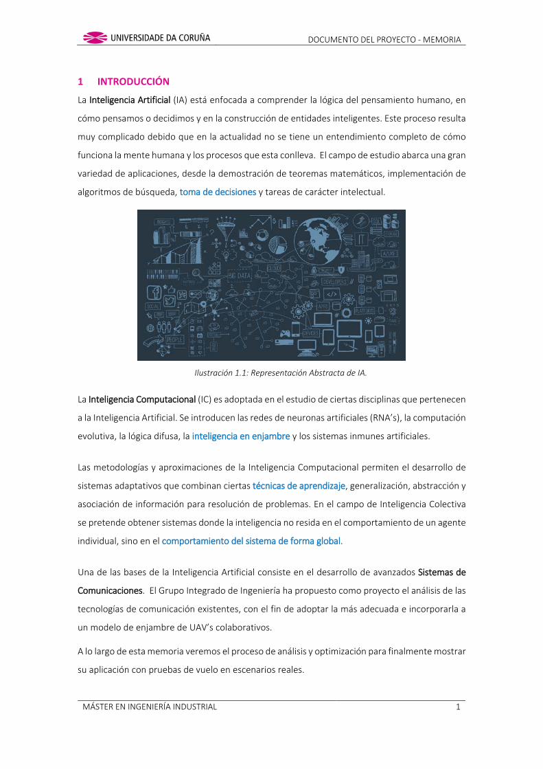
1 INTRODUCCIÓN
La Inteligencia Artificial (IA) está enfocada a comprender la lógica del pensamiento humano, en
cómo pensamos o decidimos y en la construcción de entidades inteligentes. Este proceso resulta
muy complicado debido que en la actualidad no se tiene un entendimiento completo de cómo
funciona la mente humana y los procesos que esta conlleva. El campo de estudio abarca una gran
variedad de aplicaciones, desde la demostración de teoremas matemáticos, implementación de
algoritmos de búsqueda, toma de decisiones y tareas de carácter intelectual.
Ilustración 1.1: Representación Abstracta de IA.
La Inteligencia Computacional (IC) es adoptada en el estudio de ciertas disciplinas que pertenecen
a la Inteligencia Artificial. Se introducen las redes de neuronas artificiales (RNA’s), la computación
evolutiva, la lógica difusa, la inteligencia en enjambre y los sistemas inmunes artificiales.
Las metodologías y aproximaciones de la Inteligencia Computacional permiten el desarrollo de
sistemas adaptativos que combinan ciertas técnicas de aprendizaje, generalización, abstracción y
asociación de información para resolución de problemas. En el campo de Inteligencia Colectiva
se pretende obtener sistemas donde la inteligencia no resida en el comportamiento de un agente
individual, sino en el comportamiento del sistema de forma global.
Una de las bases de la Inteligencia Artificial consiste en el desarrollo de avanzados Sistemas de
Comunicaciones. El Grupo Integrado de Ingeniería ha propuesto como proyecto el análisis de las
tecnologías de comunicación existentes, con el fin de adoptar la más adecuada e incorporarla a
un modelo de enjambre de UAV’s colaborativos.
A lo largo de esta memoria veremos el proceso de análisis y optimización para finalmente mostrar
su aplicación con pruebas de vuelo en escenarios reales.

DOCUMENTO DEL PROYECTO - MEMORIA
MÁSTER EN INGENIERÍA INDUSTRIAL 2
2 OBJETIVOS
El presente TFM se enmarca dentro de la línea de investigación sobre los UAV (Unmanned Aerial
Vehicles) del GII (Grupo Integrado de Ingeniería). El objetivo global de la línea es el desarrollo de
un enjambre consistente en varios UAV que puedan volar de forma autónoma y colaborar entre
sí para realizar una tarea en común.
Las comunicaciones entre los UAV del enjambre, la estación de tierra y el PC de supervisión se
realizarán de forma inalámbrica. Para las labores de supervisión, se enviarán periódicamente los
datos de la telemetría de todos los UAV del equipo a la estación de tierra.
Los objetivos marcados para este proyecto serán los siguientes:
Análisis de la capacidad del sistema de comunicaciones empleado en un enjambre de
UAV’s Colaborativos.
Optimización de la configuración del sistema para obtener el máximo ancho de banda
posible, minimizando el uso de CPU, los paquetes perdidos y su latencia.
Utilización en medida de lo posible de software libre durante el desarrollo del proyecto.
Ilustración 2.1: Grupo Integrado de Ingeniería (GII).
DOCUMENTO DEL PROYECTO - MEMORIA
MÁSTER EN INGENIERÍA INDUSTRIAL 3
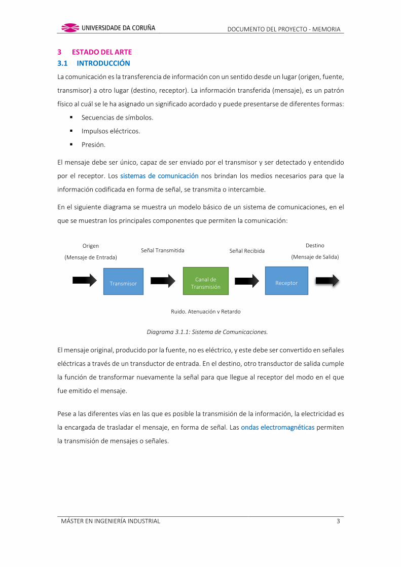
3 ESTADO DEL ARTE 3.1 INTRODUCCIÓN
La comunicación es la transferencia de información con un sentido desde un lugar (origen, fuente,
transmisor) a otro lugar (destino, receptor). La información transferida (mensaje), es un patrón
físico al cuál se le ha asignado un significado acordado y puede presentarse de diferentes formas:
Secuencias de símbolos.
Impulsos eléctricos.
Presión.
El mensaje debe ser único, capaz de ser enviado por el transmisor y ser detectado y entendido
por el receptor. Los sistemas de comunicación nos brindan los medios necesarios para que la
información codificada en forma de señal, se transmita o intercambie.
En el siguiente diagrama se muestra un modelo básico de un sistema de comunicaciones, en el
que se muestran los principales componentes que permiten la comunicación:
Diagrama 3.1.1: Sistema de Comunicaciones.
El mensaje original, producido por la fuente, no es eléctrico, y este debe ser convertido en señales
eléctricas a través de un transductor de entrada. En el destino, otro transductor de salida cumple
la función de transformar nuevamente la señal para que llegue al receptor del modo en el que
fue emitido el mensaje.
Pese a las diferentes vías en las que es posible la transmisión de la información, la electricidad es
la encargada de trasladar el mensaje, en forma de señal. Las ondas electromagnéticas permiten
la transmisión de mensajes o señales.
Transmisor Receptor Canal de Transmisión
Origen
(Mensaje de Entrada) Señal Transmitida Señal Recibida
Ruido, Atenuación y Retardo
Destino
(Mensaje de Salida)

DOCUMENTO DEL PROYECTO - MEMORIA
MÁSTER EN INGENIERÍA INDUSTRIAL 4
3.2 TEORÍA DE ONDAS ELECTROMAGNÉTICAS
El físico alemán Heinrich Rudolf Hertz, en 1887, demostró que la electricidad puede transmitirse
en forma de ondas electromagnéticas. Se basó en la teoría de James Clerk Maxwell quien afirmó
que las oscilaciones eléctricas pueden propagarse por el espacio.
Ilustración 3.2.1: Heinrich Rudolf Hertz – James Clerk Maxwell.
Estas se difunden en el espacio de modo similar al movimiento del agua en un estanque, tal como
puede observarse al arrojar en él una piedra y se desplazan a 311.000.000 m/s en el vacío. Pero
cuando atraviesan materiales de diferente densidad, su velocidad se verá afectada, decreciendo
en función de la densidad de los materiales interpuestos.
Los campos eléctricos y magnéticos de estas ondas vibran en un plano generalmente horizontal
o vertical. Estos campos son perpendiculares entre sí y su dirección de propagación es también
perpendicular a los mismos.
Ilustración 3.2.2: Ondas Electromagnéticas.

DOCUMENTO DEL PROYECTO - MEMORIA
MÁSTER EN INGENIERÍA INDUSTRIAL 5
Las ondas electromagnéticas se caracterizan por las siguientes magnitudes:
Amplitud: es la magnitud que mide la variación máxima que presenta una onda periódica
a lo largo del tiempo.
Frecuencia: es la magnitud que mide el número de oscilaciones o ciclos por unidad de
tiempo. La medida adoptada por el Sistema Internacional es el Hertzio (Hz).
Longitud de Onda (λ): es la magnitud que mide la distancia que recorre una onda en un
tiempo igual al período. La medida adoptada por el Sistema Internacional para ondas
electromagnéticas es el metro (m).
El espectro electromagnético abarca el rango de todas las ondas electromagnéticas, ahora bien,
no todas las ondas electromagnéticas son propicias para usarse como medios de transmisión, de
forma que sólo las que se encuentran en determinado rango serán susceptibles de ser empleadas.
El espectro radioeléctrico será la subdivisión donde operan los servicios de comunicaciones.
Ilustración 3.2.3: Espectro Electromagnético.
Debido a la cantidad de servicios que se pueden prestar por medio del espectro radioeléctrico,
su organización y regulación resulta imprescindible para permitir el desarrollo del mismo. Para
la correcta administración del espectro radioeléctrico, este se subdivide en bandas de frecuencia,
que designan porciones del espectro radioeléctrico atendiendo a criterios técnicos relacionados
con los servicios que, por las características propias, resultan viables en determinada banda.
El Cuadro Nacional de Atribución de Frecuencias (CNAF) es el instrumento legal, dependiente del
Ministerio de Industria, Energía y Turismo de España, utilizado para asignar a distintos servicios
de radiocomunicaciones las diferentes bandas de frecuencias, estas bandas se extienden desde
aproximadamente 8,30 kHz hasta 3.000 GHz (véase en Anexo de Normativa).

DOCUMENTO DEL PROYECTO - MEMORIA
MÁSTER EN INGENIERÍA INDUSTRIAL 6
3.3 TRANSMISIÓN DE ONDAS
Las ondas radioeléctricas pueden transmitirse sin necesidad del uso de cables de un lugar a otro
y dependiendo de la frecuencia o longitud de onda, éstas viajan de diferentes maneras. Las de
baja frecuencia, por ejemplo, no siguen el mismo curso que las que tiene altas o muy altas
frecuencias. Podemos dividir las ondas en tres tipos dependientes de las formas de propagación:
Ondas Terrestres o de Superficie:
Son ondas que en parte se desplazan pegadas a la corteza terrestre. Al ir tan cerca del suelo, las
características de éste influyen bastante en su forma de propagación. Viajan incómodas sobre
suelos secos, como el desierto, y recorren mayores distancias si el terreno es húmedo, porque les
ofrece mejor conductividad. Las ondas que se propagan de esta forma no se despegan de la tierra.
Presentan como ventaja que no le afectan mucho los obstáculos, pero al mismo tiempo esto es
un inconveniente ya que este roce las va atenuando o desgastando.
Ilustración 3.3.1: Emisión de Ondas Terrestres o de Superficie.
Ondas Reflejadas o Ionosféricas:
Son ondas que se proyectan contra la atmósfera, pero se encuentran con un escudo, una capa de
la misma, llamada ionosfera que, por sus características, actúa como un espejo y las rebota
devolviéndolas a la tierra, tras esto, las ondas rebotan contra la corteza terrestre y vuelven a subir
repitiéndose el proceso sucesivamente.
Ilustración 3.3.2: Emisión de Ondas Reflejadas o Ionosféricas.
Ionosfera

DOCUMENTO DEL PROYECTO - MEMORIA
MÁSTER EN INGENIERÍA INDUSTRIAL 7
La ionosfera está situada entre 60 y 400 km de la corteza terrestre. Dependiendo de la hora del
día y las condiciones de la atmósfera, sus características pueden cambian drásticamente. Esto
hace que las radiocomunicaciones de esta clase varíen mucho en función de la estación del año
o del momento del día. El invierno y las horas nocturnas son más beneficiosas cuando, por la falta
de rayos solares, la capa se vuelve más densa y se aleja de la tierra permitiendo a las ondas llegar
más lejos. La mayoría de las ondas no eligen un solo camino para propagarse, sino que estas
realizan una combinación de este tipo de transmisión y la anterior.
Ondas Directas o Espaciales:
Son ondas de alta frecuencia que tienen longitudes de onda muy pequeñas. Se realiza su
transmisión en línea recta, hasta donde alcanza la vista. Son muy vulnerables a los obstáculos,
incluso la misma curvatura de la tierra hace que se pierda la señal. Por esta limitación, las antenas
transmisoras siempre se colocan en lugares elevados para no perder la línea de visión.
Ilustración 3.3.3: Emisión de Ondas Directas.
Si aumentamos la frecuencia y la potencia dirigiendo las antenas hacia lugares donde no haya
nada, como el espacio, alcanzamos distancias muy superiores. Estas ondas no son reflejadas en
la ionosfera y la traspasan, viajando miles de kilómetros. Son las encargadas de mandar señales a
los satélites para transmisiones de largo alcance que luego regresan rebotadas.
Ilustración 3.3.4: Emisión de Ondas Espaciales.
Estos satélites están situados en la ”Órbita de Clarke” (Órbita Geoestacionaria), de excentridad
nula y movimiento de Oeste a Este, siendo vistos desde la tierra como un objeto inmóvil en el
cielo, situándose a una distancia sobre el nivel del mar de 35.786 kilómetros.

DOCUMENTO DEL PROYECTO - MEMORIA
MÁSTER EN INGENIERÍA INDUSTRIAL 8
Como se ha comentado, la mayoría de las ondas no eligen un solo camino para propagarse, esto
está provocado por las interacciones con objetos en el ambiente que, a su vez, están asociados
con el método de propagación. Esto es provocado por los siguientes fenómenos:
Absorción:
Cuando las ondas radioeléctricas atraviesan materiales, se debilitan y se atenúan. La cantidad de
potencia perdida dependerá de la frecuencia y del material. La potencia decrecerá de manera
exponencial y la energía absorbida se transformará en calor.
En redes de comunicación, los metales y el agua son considerados absorbentes perfectos, no van
a poder ser atravesados (salvo que estén presentes como capas finas, lo cual permitiría que una
pequeña porción de potencia los traspase). Cuando se habla del agua, es importante tener en
cuenta que se puede encontrar en diferentes formas como lluvia, niebla, vapor o nubes bajas.
Gráfica 3.3.1: Pérdidas de por Absorción en Oxígeno o Vapor de Agua.
(Recomendación UIT -R P676)
Además, existen otros materiales que tienen efectos más complejos en la absorción de radiación,
como la madera, dependiente de la cantidad de agua y resto de compuestos químicos.
Reflexión:
La reflexión de las ondas radioeléctricas ocurre cuando una onda incidente choca con una barrera
existente y parte de la potencia incidente no penetra en el mismo. Debido a que todas las ondas
reflejadas permanecen en el mismo medio que las ondas incidentes, sus velocidades son iguales
y por lo tanto el ángulo de reflexión es el mismo que el de incidencia.

DOCUMENTO DEL PROYECTO - MEMORIA
MÁSTER EN INGENIERÍA INDUSTRIAL 9
Difracción:
La difracción ocurre cuando la trayectoria que siguen las ondas radioeléctricas entre el emisor y
el receptor se encuentra obstruida por una superficie con irregularidades. Las ondas que resultan
tras la superficie de obstrucción se desvían en el espacio y flectan alrededor del obstáculo.
Ilustración 3.3.5: Fenómeno de Difracción. Principio de Fresnel - Hüygens.
El “Principio de Fresnel - Hüygens” es enunciado para comprender este comportamiento:
“Todo punto de un frente de onda inicial puede considerarse como una fuente de ondas esféricas
secundarias que se extienden en todas las direcciones con la misma velocidad, frecuencia y longitud de
onda que el frente de onda del que proceden.”
En la difracción se genera una pérdida de potencia de transmisión, siendo la potencia de la onda
difractado mucho menor que el frente de onda que la provoca. Este fenómeno se da en todas las
frecuencias, a menor frecuencia mayor difracción, pero en contraposición, a mayor frecuencia
mayor pérdida.
Dispersión:
La dispersión ocurre cuando el medio utilizado para la transmisión de las ondas radioeléctricas
está ocupado por una gran cantidad de obstáculos de dimensiones pequeñas comparables a la
longitud de onda (λ) o donde existe un gran número de obstáculos por unidad de volumen. Las
ondas dispersadas son irradiadas en un gran número de direcciones diferentes, siendo estas
añadidas a interferencias destructivas de la señal.

DOCUMENTO DEL PROYECTO - MEMORIA
MÁSTER EN INGENIERÍA INDUSTRIAL 10
Refracción:
La refracción es manifestada como el cambio de dirección de una onda radioeléctrica conforme
pasa oblicuamente de un medio a otro con diferentes velocidades de propagación.
Ilustración 3.3.6: Fenómeno de Refracción.
Por lo tanto, la refracción ocurre siempre que la onda pasa de un medio a otro que presente
diferente densidad. El ángulo de incidencia es el formado entre la onda incidente y la normal y el
ángulo de refracción el formado entre la onda refractada y la normal.
Multitrayectoria (Multipath):
El efecto multipath ocurre debido a que las ondas radioeléctricas llegan al receptor a través de
diferentes caminos y a diferentes tiempos. Esto provoca retardos e interferencia en los sistemas
de comunicaciones, acrecentándose en transmisiones interiores. Las ondas recibidas pueden ser
directas desde la línea de visión, ondas reflejadas, ondas dispersadas u ondas difractadas.
El sistema de comunicación debe ser diseñado para que este efecto sea reducido al mínimo.
Existen dos clases de efecto multitrayectoria:
• Multitrayectoria Especular: provoca un nivel de ruido de fondo de interferencia.
• Multitrayectoria Difusa: provoca interrupciones de la señal o puntos muertos.
Señal directa.
Señal Reflejada.
Combinación de Señales.
Ilustración 3.3.7: Efecto Multipath.

DOCUMENTO DEL PROYECTO - MEMORIA
MÁSTER EN INGENIERÍA INDUSTRIAL 11
3.4 FACTORES QUE AFECTAN LA CALIDAD DE LA SEÑAL
Además de los efectos explicados en el subcapítulo 3.3 durante la transmisión de señal existen
una serie de factores que afectan a la calidad de las ondas radioeléctricas transmitidas por lo que
nunca serán iguales a las recibidas. Las principales son:
• Atenuación: efecto de desgaste por el cual la señal presenta una pérdida de potencia
ocasionada por la distancia entre emisor y receptor. Esta aumenta con la frecuencia, la
temperatura y el tiempo. Es medida en decibelios por unidad de distancia (dB/m).
𝛼𝛼 = 10𝑙𝑙𝑙𝑙𝑙𝑙𝑃𝑃1𝑃𝑃2
Ecuación 3.4.1: Atenuación de Potencia.
• Distorsión: efecto de deformación que experimenta una señal al ser transmitida por un
canal por la respuesta imperfecta del sistema, desaparece al dejar de aplicar la señal.
• Interferencia: efecto de contaminación de señal causado por señales extrañas al sistema
originadas de forma artificial. Esta es conocida como EMI (ElectroMagnetic Interference)
o RFI (Radio Frequency Interference).
• Ruido: efecto de contaminación de señal causado por señales aleatorias e impredecibles
originadas de forma natural. Estas señales pueden agregarse a la señal original portadora
alterándola y quedando ocultas, no pudiendo ser eliminado completamente. Existen
numerosos tipos de ruido, siendo algunos de ellos los siguientes:
• Ruido Atmosférico: es producido por las descargas atmosféricas que se propagan
en todas las direcciones por reflexión ionosférica.
• Ruido Galáctico: es producido por disturbios o perturbaciones producidas fuera
de la atmósfera. La fuente primaria es el sol y este tipo de ruido tiene su base en
la teoría de la “Emitancia Espectral de Planck”.
𝑀𝑀(λ, T) = (𝑎𝑎 λ5 )(𝑒𝑒𝑏𝑏λT − 1)
Ecuación 3.4.2: Emitancia Espectral de Planck.
• Ruido Térmico: es producido por la agitación térmica de los electrones presente
en las resistencias y se manifiesta en toda la naturaleza. Solo en condiciones de
Zero Absoluto (0 K) cesaría, por tanto, siempre va a existir y es inevitable.

DOCUMENTO DEL PROYECTO - MEMORIA
MÁSTER EN INGENIERÍA INDUSTRIAL 12
3.5 TECNOLOGÍAS DE RADIOFRECUENCIA
Existen dos tipos de tecnología de radiofrecuencia para transmitir la información:
Tecnología de Banda Estrecha (Narrowband):
El fundamento básico es una modulación de la señal a transmitir en un rango muy reducido de
frecuencias. Debido a ese reducido ancho de banda, la velocidad de transmisión se ve disminuida.
Ilustración 3.5.1: Operadores Narrowband.
𝑅𝑅𝑏𝑏(bit/s) = 𝐵𝐵𝐵𝐵 𝑙𝑙𝑙𝑙𝑙𝑙(1 + 𝑆𝑆𝑅𝑅 )
Ecuación 3.5.1: Teorema Shannon - Hartley.
Tecnología de Banda Ancha (Spread Spectrum):
El fundamento básico es una modulación por ensanchamiento de la señal a transmitir a lo largo
de una banda muy ancha de frecuencias. La señal de espectro ensanchado, puede coexistir con
señales en banda estrecha, ya que sólo les aportan un pequeño incremento en el ruido.
Ventajas Desventajas
Resistente a gran parte de interferencias. Ineficiencia del uso del ancho de banda.
Eliminación o atenuación del efecto multipath. Complejidad en implementación.
Posibilidad de compartir banda.
Tabla 3.5.1 Características Spread Spectrum.
Ilustración 3.5.2: Operadores Spread Spectrum.
Gráfica 3.5.1: Narrowband vs Spread Spectrum.

DOCUMENTO DEL PROYECTO - MEMORIA
MÁSTER EN INGENIERÍA INDUSTRIAL 13
3.6 DISEÑO DE UN SISTEMA DE COMUNICACIONES
En sistemas de comunicación, las características del diseño de instalación se pueden transformar
en obstáculos capaces de arruinar nuestra comunicación, por ello debemos abordar con criterio
los siguientes aspectos fundamentales:
Potencia de Radiofrecuencia:
Es medida por lo general en Watts (W) o miliwatts (mW) aunque en muchas aplicaciones, también
se encuentran referencias a esta magnitud expresada en decibelios por metro (dBm). La relación
que existe entre ambas formas sigue la siguiente fórmula:
𝑑𝑑𝐵𝐵𝑑𝑑 = 10𝑙𝑙𝑙𝑙𝑙𝑙𝑃𝑃
Ecuación 3.6.1: Relación P/dBm.
Una cuestión a tener en cuenta es el número de antenas,
estas pueden sumarse en un número progresivo en base 2,
por lo tanto, al duplicar el número de antenas duplicamos
la potencia.
Ilustración 3.6.1: Antena de Radiofrecuencia.
Relación Frecuencia-Propagación:
La gran mayoría de las aplicaciones industriales, domésticas, científicas y de investigación, suelen
trabajar con sistemas de transmisión que operan en las Bandas Libres.
Las organizaciones que administran el uso racional del espectro radioeléctrico de cada país
asignan porciones o bandas de frecuencias donde no se hace necesario solicitar una autorización,
abonar cánones o impuestos para trabajar de forma libre dentro de sus límites.
Estas bandas son conocidas también como Bandas ISM (Industrial, Scientific and Medical) y los
valores más populares son:
• Bandas de 2,40/ 5,80 GHz (Global).
• Bandas de 433/868 MHz (Europa).
• Banda de 915 MHz (América).
La gran ventaja de poder trabajar en frecuencias cada vez más altas es que el ancho del canal a
utilizar aumenta. Esto significa tener la posibilidad de transmitir una mayor cantidad de datos o
información dentro de un canal único.

DOCUMENTO DEL PROYECTO - MEMORIA
MÁSTER EN INGENIERÍA INDUSTRIAL 14
La desventaja de esto es que la distancia a enlazar y la capacidad de la señal para superar
obstáculos decrece de manera notable al aumentar la frecuencia de transmisión. A su vez, el
trabajar a frecuencias bajas requieren de antenas de mayor tamaño, mientras que, a frecuencias
mayores, se pueden colocar sistemas de antenas de mayor ganancia para suplir las pérdidas
mencionadas anteriormente.
Optimización de las Antenas:
La optimización constructiva de las antenas permitirá obtener unas ganancias significativas para
garantizar una transmisión óptima.
Ilustración 3.6.2: Antena Sectorial – Antena Omnidireccional.
Las antenas unidireccionales son capaces de enfocar toda la potencia que llega a ellas en una
única dirección. A su vez, una antena omnidireccional emitirá hacia todos los sentidos, perdiendo
la concentración de señal. Cuando colocamos las antenas de los sistemas en un espacio abierto y
libre de obstáculos entre ellas, la atenuación provocada por el medio se incrementa con una
relación del cuadrado de la distancia. La atenuación provocada por otros obstáculos incrementa
también notablemente las pérdidas.
𝐹𝐹𝑆𝑆𝑃𝑃𝐹𝐹 = 4πdλ
2
= 4πdf
c 2
𝐹𝐹𝑆𝑆𝑃𝑃𝐹𝐹 (𝑑𝑑𝐵𝐵) = 20 log(𝑑𝑑) + 20 log(𝑓𝑓) − 147,55
Ecuación 3.6.2: Pérdidas en el Espacio Libre.
(Modelo de Friis – Región de Fraunhöfer)
Ilustración 3.6.3: Pérdidas en el Espacio Libre.
DOCUMENTO DEL PROYECTO - MEMORIA
MÁSTER EN INGENIERÍA INDUSTRIAL 15
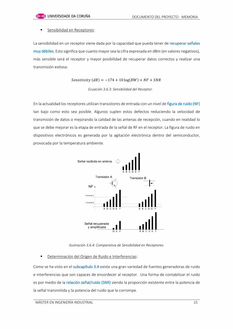
Sensibilidad en Receptores:
La sensibilidad en un receptor viene dada por la capacidad que pueda tener de recuperar señales
muy débiles. Esto significa que cuanto mayor sea la cifra expresada en dBm (en valores negativos),
más sensible será el receptor y mayor posibilidad de recuperar datos correctos y realizar una
transmisión exitosa.
𝑆𝑆𝑒𝑒𝑆𝑆𝑆𝑆𝑆𝑆𝑆𝑆𝑆𝑆𝑆𝑆𝑆𝑆𝑆𝑆𝑆𝑆 (𝑑𝑑𝐵𝐵) = −174 + 10 log(𝐵𝐵𝐵𝐵) + 𝑁𝑁𝐹𝐹 + 𝑆𝑆𝑁𝑁𝑅𝑅
Ecuación 3.6.3: Sensibilidad del Receptor.
En la actualidad los receptores utilizan transistores de entrada con un nivel de figura de ruido (NF)
tan bajo como esto sea posible. Algunos suplen estos defectos reduciendo la velocidad de
transmisión de datos o mejorando la calidad de las antenas de recepción, cuando en realidad lo
que se debe mejorar es la etapa de entrada de la señal de RF en el receptor. La figura de ruido en
dispositivos electrónicos es generada por la agitación electrónica dentro del semiconductor,
provocada por la temperatura ambiente.
Ilustración 3.6.4: Comparativa de Sensibilidad en Receptores.
Determinación del Origen de Ruido e Interferencias:
Como se ha visto en el subcapítulo 3.4 existe una gran variedad de fuentes generadoras de ruido
e interferencias que son capaces de ensordecer al receptor. Una forma de contabilizar el ruido
es por medio de la relación señal/ruido (SNR) siendo la proporción existente entre la potencia de
la señal transmitida y la potencia del ruido que la corrompe.

DOCUMENTO DEL PROYECTO - MEMORIA
MÁSTER EN INGENIERÍA INDUSTRIAL 16
Margen de Desvanecimiento (Fading):
Una transmisión debe ser capaz de soportar las pérdidas de señal que pueden acarrear cambios
climáticos severos. El valor que se toma como norma es de 10 dB de pérdida de señal y aun así
seguir manteniendo la transmisión activa. Es muy importante tener prevista esta condición ya
que, si tenemos una recepción en el límite de las posibilidades, esto se transforma en un vínculo
muy frágil que deja de funcionar con apenas un poco de lluvia.
Ilustración 3.6.5: Desvanecimiento (Fading).
Pérdidas en Medios de Transmisión:
La elección del cable y los conectores apropiados para lograr una transmisión exitosa dependen
de muchos factores y todos varían de un escenario a otro. Esta situación algo difícil de equilibrar
se basa en la propiedad de atenuación que poseen todos los cables coaxiales utilizados para
enlazar los equipos con la antena. Un estudio preliminar de las distancias a cubrir, junto a la
potencia del equipo transmisor y la ganancia de las antenas ayuda a seleccionar la mejor opción.
En cuanto al medio de transmisión inalámbrico, debe admitir una tasa de error y corrección de
datos en la transmisión o recepción superior a lo que podría ser mediante una conexión por cable.
El protocolo de comunicación de los datos a enlazar, debe ser capaz de sortear las deficiencias
lógicas que posee el sistema inalámbrico. Las terminales de transmisión y recepción deben
sincronizar su velocidad de proceso y adaptarse al límite que imponga la transmisión de acuerdo
a su frecuencia de trabajo y ancho de banda.
En sistemas operados a altas frecuencias, es importante mantener la línea de visión para evitar
pérdidas importantes. Para modelar las pérdidas que se producen por la obstrucción del enlace
radioeléctrico se utiliza el concepto de las llamadas “Zonas de Fresnel”.

DOCUMENTO DEL PROYECTO - MEMORIA
MÁSTER EN INGENIERÍA INDUSTRIAL 17
Estas zonas consisten en unos elipsoides concéntricos que rodean a las ondas radioeléctricas
directas de un enlace radioeléctrico y que quedan definidos a partir de las posiciones de las
antenas transmisora y receptora.
Ilustración 3.6.6: Elipsoide de Fresnel.
Las Zonas de Fresnel tienen la propiedad de que una onda derivada de la antena transmisora se
puede reflejar sobre la superficie del elipsoide y después incidir sobre la antena receptora
habiendo recorrido una distancia superior a la recorrida por la onda radioeléctrica directa en
múltiplos de media longitud de onda.
𝑟𝑟𝑛𝑛 = 𝑆𝑆λ𝑑𝑑1𝑑𝑑2𝑑𝑑1+𝑑𝑑2
Ecuación 3.6.4: Cálculo del Radio del Elipsoide de Fresnel.
La obstrucción permitida depende del factor K (curvatura de la tierra), por tanto, durante la fase
de planificación del radioenlace, debe asegurarse que la primera zona de Fresnel se encuentre
libre de obstáculos considerando un factor K = 4/3 y despejada en un 60% considerando un factor
K = 2/3.
Para estimar las pérdidas por obstáculos cercanos a un enlace radioeléctrico suele emplearse la
Recomendación UIT-R P530 (Apartado 2.2.):
𝐴𝐴 (𝑑𝑑𝐵𝐵) = −20ℎ𝑟𝑟1
+ 10
Ecuación 3.6.5: Cálculo de Atenuación por Obstáculos en el Elipsoide de Fresnel.

DOCUMENTO DEL PROYECTO - MEMORIA
MÁSTER EN INGENIERÍA INDUSTRIAL 18
Presupuesto de Potencia del Enlace (Link Budget):
El presupuesto de potencia para un enlace de transmisión de datos es el balance de ganancias y
pérdidas desde el transmisor, a través de cables, conectores y espacio libre hacia el receptor. La
estimación del valor de potencia en diferentes partes del radioenlace es necesaria para hacer el
mejor diseño y elegir el equipamiento adecuado.
𝐹𝐹𝑆𝑆𝑆𝑆𝐿𝐿 𝐵𝐵𝐵𝐵𝑑𝑑𝑙𝑙𝑒𝑒𝑆𝑆 (𝑑𝑑𝐵𝐵) = 𝑇𝑇𝑇𝑇 (𝑑𝑑𝐵𝐵) − 𝑅𝑅𝑇𝑇(𝑑𝑑𝐵𝐵) + 𝐺𝐺𝑎𝑎𝑆𝑆𝑆𝑆 (𝑑𝑑𝐵𝐵) − 𝐹𝐹𝑙𝑙𝑆𝑆𝑆𝑆𝑒𝑒𝑆𝑆 (𝑑𝑑𝐵𝐵)
Ecuación 3.6.6: Presupuesto de Potencia del Enlace (Link Budget).
Los elementos pueden ser divididos en 3 partes principales:
• Lado de Transmisión: la potencia de transmisión, las pérdidas en conectores y la ganancia
de antena.
• Espacio de Transmisión: pérdidas por propagación en el espacio, (como las pérdidas en
el espacio libre siguen un modelo ideal, se suele utilizar el Modelo de los 2 Rayos).
𝑀𝑀𝑃𝑃𝑃𝑃𝐹𝐹 (𝑑𝑑𝐵𝐵) = 40 log(𝑑𝑑) − 10log (𝐺𝐺𝑇𝑇𝐺𝐺𝑅𝑅ℎ𝑡𝑡2ℎ𝑟𝑟2)
Ecuación 3.6.7: Modelo de los dos rayos.
Ilustración 3.6.7: Modelo de los dos rayos.
• Lado de Recepción: la ganancia de antena, las pérdidas en conectores y la sensibilidad
del dispositivo receptor.
Ilustración 3.6.8: Representación del Presupuesto de Enlace (Link Budget).
DOCUMENTO DEL PROYECTO - MEMORIA
MÁSTER EN INGENIERÍA INDUSTRIAL 19
3.7 PROTOCOLOS DE COMUNICACIÓN
El primer paso hacia la estandarización internacional de los protocolos para la comunicación de
red fue introducido por la International Standards Organization (ISO) en 1978 con el modelo ISO
para sistemas abiertos de interconexión (OSI).
Ilustración 3.7.1: International Standards Organization (ISO).
El modelo de referencia OSI es el modelo principal para las comunicaciones por red. Aunque
existen otros modelos, en la actualidad la mayoría de los fabricantes de redes relacionan sus
productos con el modelo de referencia OSI.
Este modelo es utilizado para comprender el cómo viaja la información a través de una red y
visualizar cómo la información o los paquetes de datos viajan desde los programas de aplicación
a través de un medio de red, hasta otra aplicación ubicada en otro dispositivo de la red, aun
cuando el transmisor y el receptor tengan distintos tipos de medios de red.
En el modelo de referencia OSI, hay siete capas numeradas, cada una de las cuales ilustra una
función de red específica. Esta división de las funciones de networking se denomina división en
capas. Si la red se divide en estas siete capas, se obtienen las siguientes ventajas:
Divide la comunicación de red en partes más pequeñas y sencillas.
Normaliza los componentes de red para permitir el desarrollo y el soporte de los
productos de diferentes fabricantes.
Permite a los distintos tipos de hardware y software de red comunicarse entre sí.
Impide que los cambios en una capa puedan afectar las demás capas, para que se puedan
desarrollar con más rapidez.

DOCUMENTO DEL PROYECTO - MEMORIA
MÁSTER EN INGENIERÍA INDUSTRIAL 20
El problema de trasladar información entre dispositivos se divide problemas más pequeños y
simples representados en el modelo de referencia OSI en capas, siendo estas:
1. Capa Física: esta capa define las especificaciones eléctricas, mecánicas, de procedimiento
y funcionales para activar, mantener y desactivar el enlace físico entre sistemas finales.
2. Capa de Enlace: esta capa proporciona el tránsito de los datos confiables a través de un
enlace físico. Al hacerlo, la capa de enlace de datos se ocupa del direccionamiento físico,
la topología y acceso a red, la notificación de errores, entrega de tramas y control de
flujo.
3. Capa de Red: esta capa proporciona conectividad y selección de ruta entre dos sistemas
que pueden estar ubicados en redes geográficamente distintas.
4. Capa de Transporte: esta capa efectúa el transporte de los datos originados por el emisor
y recibidos por el receptor, independizando el tipo de red física utilizada.
5. Capa de Sesión: esta capa establece, administra y finaliza el enlace entre dos dispositivos
que están transmitiendo datos. Dada una sesión establecida entre dos dispositivos, la
misma efectúa las operaciones definidas de principio a fin reanudándolas en caso de
interrupción.
6. Capa de Presentación: esta capa garantiza la presentación de información de manera
que, aunque los dispositivos tengan distintos formatos, los datos obtenidos sean
reconocibles. Incluso de ser necesario, esta capa traduce estos formatos a uno en común.
7. Capa de Aplicación: esta capa es la más cercana al usuario del modelo OSI, ofrece a las
aplicaciones externas al modelo la posibilidad de acceder a los servicios del resto de capas
y define protocolos para intercambio de datos.
Ilustración 3.7.2: Capas del Modelo de Referencia ISO-OSI

DOCUMENTO DEL PROYECTO - MEMORIA
MÁSTER EN INGENIERÍA INDUSTRIAL 21
3.8 INTERNET DE LAS COSAS Y REDES DE BAJA POTENCIA
El Internet de las Cosas o Internet of Things (IoT) es un concepto un concepto que nació en el
Instituto de Tecnología de Massachusetts (MIT). Se trata una revolución en las relaciones entre
los objetos y las personas, que se conectarán entre ellos y la red ofreciendo datos en tiempo real,
dicho de otro modo, acerca la digitalización del mundo físico.
Diagrama 3.8.1: Bases de la Implementación del IOT.
“Si una persona se conecta a la red, le cambia la vida. Pero si todas las cosas y objetos se conectan, es
el mundo el que cambia.” Hans Vestberg (CEO Ericsson)
Ilustración 3.8.1: Redes de Comunicación del Internet de las Cosas.
Las tecnologías LPWAN están diseñadas para conectar una gran cantidad de dispositivos de forma
bidireccional, con un bajo coste, con un consumo de energía reducido y con un uso bajo de ancho
de banda. Actualmente no existe un standard preestablecido para las LPWAN, pues las principales
tecnologías en cuanto a desarrollo son las siguientes:
Ilustración 3.8.2: Principales Tecnologías LPWAN.
Sensores Redes Gestión de
Información Análisis
Inteligente

DOCUMENTO DEL PROYECTO - MEMORIA
MÁSTER EN INGENIERÍA INDUSTRIAL 22
4 METODOLOGÍA 4.1 ANÁLISIS COMPARATIVO ENTRE TECNOLOGÍAS LPWAN
Como primer paso, debemos realizar un análisis comparativo entre tecnologías LPWAN existentes
con el fin de conseguir una solución óptima acorde a los requisitos de diseño de UAV’s. Como
primer approach realizaremos una introducción estas tecnologías:
SIGFOX:
Sigfox es una empresa francesa fundada en 2009, basa su actividad principalmente en desarrollo
de redes inalámbricas independientes para su implementación en el internet de las cosas.
Para su uso, es necesario la incorporación de chips compatibles, para ello trabaja con fabricantes
como Texas Instruments, Atmel, Silicon Labs, entre otros, para poder ofrecer los distintos tipos
de SOC, transceptores y componentes de conexión a su red.
Sigfox fue inspirado en el sistema de comunicaciones existente
en los submarinos de la II Guerra Mundial, que eran capaces
de transmitir mensajes cortos a todo el mundo por medio de
transmisores bidireccionales de baja potencia.
Esta tecnología se presenta como un complemento o alternativa al uso de las redes actuales. La
red actualmente se encuentra disponible en 32 países, entre ellos España y presenta previsiones
de una expansión mayor en un corto plazo de tiempo.
Ilustración 4.1.2: Key Figures de Sigfox.
Ilustración 4.1.1: Sigfox.

DOCUMENTO DEL PROYECTO - MEMORIA
MÁSTER EN INGENIERÍA INDUSTRIAL 23
LoRa y LoRaWAN:
Una serie de líderes de la industria del internet como ARM, Cisco, IBM, Microchip, Semtech, entre
otros, fundaron la LoRa Alliance con el objetivo de desarrollar un nuevo tipo de tecnología de
comunicación más eficiente y conseguir un standard de tecnología para el internet de las cosas.
Estas comunicaciones están enfocadas para pequeños dispositivos que
desean transmitir poca información y, por tanto, no tener la necesidad
de una gran velocidad, pero si con la clara intención de emplear el menor
consumo posible para mantener el servicio de estos dispositivos.
Este tipo de tecnología es la evolución de las tecnologías de espectro ensanchado usadas en la II
Guerra Mundial donde los esfuerzos de investigación y desarrollo se centraban en contramedidas
de radares, interceptación de señales y balizas de navegación.
Actualmente existen redes abiertas a usuarios finales en Francia, Bélgica, Suiza, Países Bajos y
Sudáfrica, desplegadas por grandes operadores de telecomunicaciones como Orange. En España,
no exista actualmente una red operativa, aunque parece que Orange, al igual que en Francia,
tiene intención de desplegar una en España.
NB-IoT:
NarrowBand IoT es una tecnología standard evolución de la tecnología LTE/4G para su adaptación
al internet de las cosas. Es desarrollado por Vodafone, Huawei y U-Blox, presentando la gran
apuesta de las operadoras por la implementación de versiones reducidas de tecnología móvil 4G.
El Grupo Aguas de Valencia y Vodafone España han presentado
recientemente una prueba piloto que demuestra la viabilidad de
esta tecnología con resultados muy positivos.
Vodafone anunció en octubre de 2016 que implementará las primeras redes NB-IoT comerciales
en Alemania, Irlanda, Países Bajos y España en los primeros meses de 2017.
Vodafone contará precisamente en España con más de 1.000 estaciones de red actualizadas con
esta tecnología, permitiendo cada una de ellas, conectar más de 100.000 dispositivos a internet.
Ilustración 4.1.3: LoRa.
Ilustración 4.1.4: NB-IoT.

DOCUMENTO DEL PROYECTO - MEMORIA
MÁSTER EN INGENIERÍA INDUSTRIAL 24
Tras esta introducción, exponemos las principales características de estas tecnologías LPWAN:
Características
Tecnología Ultra Narrowband Spread Spectrum Ultra Narrowband
Modulación BPSK / GFSK CSS / FSK OFDMA
Topología Estrella Estrella Estrella
Bandas de Frecuencia (EU) 868 MHz 433/868 MHz 800 MHz
Tipo de Banda de Frecuencia Libre (ISM) Libre (ISM) Licenciada (4G)
Ancho de Banda 100 Hz 125-500 kHz 200 kHz
Rango de Alcance Urbano 3-10 km 2-5 km Red Móvil
Rango de Alcance Suburbano 30-50 km 15 km Red Móvil
Velocidad de Transmisión 100 bps 290 bps - 50 kbps 20 kbps
Tamaño del Mensaje 12 bytes 242 bytes -
Limitación de Mensajes 140 mensajes/día Ilimitado Ilimitado
Eficiencia Energética Alta Alta Alta
Inmunidad Interferencias Baja Alta Baja
Desarrolladores Sigfox Lora Alliance 3GPP
Disponibilidad en España Si Si 2017
* NB-IoT es el nombre dado a LTE Cat. 13 NB1, desarrollado por Vodafone, Huawei y U-Blox.
Tabla 4.1.1: Análisis Comparativo de Características de las Tecnologías LPWAN.
Una vez establecidas las características de las tecnologías a valorar, debemos establecer el criterio
de valoración, para ello expondremos las características demandadas para este proyecto.
Ilustración 4.1.5: UAV’s del Grupo Integrado de Ingeniería.
DOCUMENTO DEL PROYECTO - MEMORIA
MÁSTER EN INGENIERÍA INDUSTRIAL 25
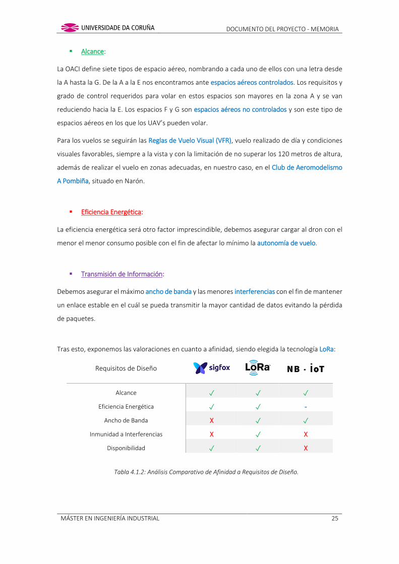
Alcance:
La OACI define siete tipos de espacio aéreo, nombrando a cada uno de ellos con una letra desde
la A hasta la G. De la A a la E nos encontramos ante espacios aéreos controlados. Los requisitos y
grado de control requeridos para volar en estos espacios son mayores en la zona A y se van
reduciendo hacia la E. Los espacios F y G son espacios aéreos no controlados y son este tipo de
espacios aéreos en los que los UAV’s pueden volar.
Para los vuelos se seguirán las Reglas de Vuelo Visual (VFR), vuelo realizado de día y condiciones
visuales favorables, siempre a la vista y con la limitación de no superar los 120 metros de altura,
además de realizar el vuelo en zonas adecuadas, en nuestro caso, en el Club de Aeromodelismo
A Pombiña, situado en Narón.
Eficiencia Energética:
La eficiencia energética será otro factor imprescindible, debemos asegurar cargar al dron con el
menor el menor consumo posible con el fin de afectar lo mínimo la autonomía de vuelo.
Transmisión de Información:
Debemos asegurar el máximo ancho de banda y las menores interferencias con el fin de mantener
un enlace estable en el cuál se pueda transmitir la mayor cantidad de datos evitando la pérdida
de paquetes.
Tras esto, exponemos las valoraciones en cuanto a afinidad, siendo elegida la tecnología LoRa:
Requisitos de Diseño
Alcance
Eficiencia Energética -
Ancho de Banda X
Inmunidad a Interferencias X X
Disponibilidad X
Tabla 4.1.2: Análisis Comparativo de Afinidad a Requisitos de Diseño.

DOCUMENTO DEL PROYECTO - MEMORIA
MÁSTER EN INGENIERÍA INDUSTRIAL 26
4.2 LORA Y LORAWAN
LoRa es una técnica de modulación basada en tecnología de espectro ensanchado y es a su vez
una variación de la modulación Chirp Spread Spectrum (CSS). Este tipo de modulación mejora de
manera notable la sensibilidad del receptor, utilizando todo el ancho de banda para la transmisión
de la señal y dándole robustez frente a ruido o interferencias. Se define como la Capa Física (véase
subcapítulo 3.7) dentro del sistema de comunicaciones. Fue desarrollada por Cycleo SAS en 2010
y posteriormente adquirida por Semtech.
Ilustración 4.2.1: Semtech.
La modulación de espectro ensanchado LoRa se realiza representando cada bit del área de datos
como múltiples pedazos” de información. La velocidad con la que la información ensanchada es
enviada se denomina velocidad de símbolo (Symbol Rate o Rs) y la relación entre velocidad de
símbolo y la velocidad de pedazos de información se denomina factor de ensanchamiento (SF),
representando el número de símbolos que son enviados por cada bit de información.
Spread Factor SF
SF7.
SF8
SF9
Ilustración 4.2.2: Modulación LoRa y Factores de Ensanchamiento.
Band
wid
th
Symbol Period

DOCUMENTO DEL PROYECTO - MEMORIA
MÁSTER EN INGENIERÍA INDUSTRIAL 27
Para aumentar la robustez del enlace, LoRa emplea una codificación por redundancia cíclica (CRC)
para realizar detección y corrección de errores hacia adelante (FEC), siendo particularmente
eficiente mejorando la fiabilidad del enlace en la presencia de interferencias.
𝑇𝑇𝑆𝑆 = 2𝑆𝑆𝐹𝐹𝐵𝐵𝐵𝐵 𝑅𝑅𝑆𝑆(sym/s) = 1
𝑇𝑇𝑆𝑆
Ecuaciones 4.2.1: Cálculo del Período y el Ratio de Símbolos.
𝑅𝑅𝑏𝑏(bit/s) = 𝑆𝑆𝐹𝐹 𝑥𝑥 𝑅𝑅𝑆𝑆 𝑥𝑥 4
4 + 𝐶𝐶𝑅𝑅
Ecuación 4.2.2: Cálculo de la Velocidad de Modulación.
LoRaWAN™ es una especificación de red de área amplia de baja potencia (LPWAN) propuesta por
LoRa Alliance, ofreciendo la Capa de Enlace o MAC (véase subcapítulo 3.7). LoRaWAN™ se centra
en los requisitos clave de Internet de las cosas, como la comunicación bidireccional segura, la
movilidad y servicios de localización, siguiendo la LoRaWAN™ Specification.
Ilustración 4.2.3: LoRa Alliance.
La arquitectura de red se presenta típicamente en una topología de estrella y su funcionamiento
se basa en establecer una red de dispositivos conectados llamados nodos, que establecerán un
enlace inalámbrico con modulación LoRa con un elemento más potente capaz de comunicarse
con todos estos elementos de manera gestionada llamado Gateway. A su vez, este gateway será
capaz de comunicarse por otro método de red, con mayor ancho de banda y transmitir toda la
información de estos dispositivos a aquellos elementos que la soliciten.

DOCUMENTO DEL PROYECTO - MEMORIA
MÁSTER EN INGENIERÍA INDUSTRIAL 28
La LoRaWAN™ Specification distingue en una red LoRa las siguientes clases de dispositivos:
Dispositivos Finales – End Nodes (Clase A):
Los dispositivos de clase A permiten las comunicaciones bidireccionales con la limitación de solo recibir
datos (canal downlink) siempre y cuando se haya enviado antes un paquete (canal uplink). El paquete
de vuelta contiene la confirmación o acknowledgement (ACK) del paquete enviado, así como los datos
de la aplicación si esto fuese necesario. Esta clase presenta menor consumo energético y es
implementada como la clase básica compatible con LoRaWAN™.
Dispositivos Finales con Ranuras de Recepción Programadas – Gateway (Clase B):
Los dispositivos de clase B eliminan la limitación de recepción de datos con la necesidad de enviar
previamente un paquete, de esta forma, se permite el envío de datos a los dispositivos de forma
programada. Los gateway deben enviar periódicamente beacons, que permiten mantener los
dispositivos sincronizados. Este tipo de dispositivos presentan un mayor consumo de energía que los
dispositivos de clase A.
Dispositivos Finales con Ranuras de Recepción Máximas- Base Station (Clase C):
Los dispositivos de clase C están casi continuamente escuchando (modo de recepción). Esta clase
proporciona la menor latencia y capacidad de envío entre el servidor a los dispositivos. Por la contra,
presenta un consumo energético mucho mayor que las clases A y B.
Ilustración 4.2.4: Clases de Dispositivos LoRa.

DOCUMENTO DEL PROYECTO - MEMORIA
MÁSTER EN INGENIERÍA INDUSTRIAL 29
Los módulos LoRaWAN™ permiten el envío de datos directamente a cualquier Gateway que sea
compatible con LoRaWAN™. Esta es la principal conexión dentro de las diferentes configuraciones
de red. Las principales empresas que nos ofrecen este tipo de soluciones actualmente son:
Cisco.
Kerlink.
Link-Labs.
Multitech
Ilustración 4.2.5: Principales Empresas Proveedoras de Gateway LoRaWAN™.
Para visualizar la información también se necesitará una plataforma en la nube o un servidor local,
donde los datos sean enviados. Normalmente, al adquirir el gateway, este ya cuenta con una la
licencia para plataformas en la nube o software compatible.
Ilustración 4.2.6: Configuración de Red por Conexión Directa a Gateway LoRaWAN™.
Debido a que estos gateway y/o licencias presentan actualmente un precio prohibitivo, existen
modos de conexión alternativos dentro de las configuraciones de red, podemos destacar el modo
P2P y el modo Híbrido.

DOCUMENTO DEL PROYECTO - MEMORIA
MÁSTER EN INGENIERÍA INDUSTRIAL 30
En Modo P2P, los dispositivos finales pueden conectarse directamente entre ellos sin costes, ya
que no utilizan infraestructura de red. Este modo funciona sin la necesidad de una estación base,
ya que se usará un dispositivo final como gateway, además tampoco se necesitará una cuenta en
la nube, no requiriendo la compra de una licencia.
Ilustración 4.2.7: Configuración de Red por Conexión en Modo P2P.
En Modo Híbrido, se utiliza una combinación de los modos LoRaWAN™ y P2P que permite enviar
mensajes utilizando redes LoRaWAN™. Los nodos utilizan una topología de estrella en modo P2P
para llegar al dispositivo final que actúa como gateway y hacer que se acceda a la red LoRaWAN™.
Este modo requiere licencia o acceso a plataformas libres en la nube como The Things Network™.
Ilustración 4.2.8: Configuración de Red por Conexión en Modo Híbrido.

DOCUMENTO DEL PROYECTO - MEMORIA
MÁSTER EN INGENIERÍA INDUSTRIAL 31
Las características de la transmisión vienen especificadas para las diferentes bandas de frecuencia
en la LoRaWAN™ Specification:
7.1.2. Frecuencias de Canales en la Banda ISM EU863-870:
En Europa, la asignación del espectro radioeléctrico es la banda ISM definida por ETSI [EN300.220].
Los operadores o desarrolladores pueden atribuir libremente los canales de red. Sin embargo, los tres
primeros canales especificados, por defecto, deben ser implementados en cada dispositivo final EU868.
Estos canales deben ser los mínimos que todos los gateway deben estar siempre escuchando.
MODULACIÓN LoRa
ANCHO DE BANDA (kHz) 125
FRECUENCIA DE CANALES (MHz) 868,10 / 868,30 / 868,50
VELOCIDAD DE TRANSMISIÓN (FSK / LoRa) DR0 – DR5 / 0,30 -5 kbps
NÚMERO DE CANALES 3
CICLO DE TRABAJO < 1%
Tabla 4.2.1: Características de Canales EU863-870.
Para acceder al medio físico, la normativa ETSI imponen algunas restricciones, como el tiempo máximo
que el transmisor puede estar encendido o el tiempo que puede estar transmitiendo por hora. A su vez,
estas permiten la elección del uso de limitaciones por Ciclo de Trabajo o gestión de transmisiones por
agilidad de frecuencia para Escuchar antes de Hablar (LBT AFA).
LoRaWAN impone una limitación del ciclo de trabajo por sub-banda. Tras la transmisión, la sub-banda
no podrá ser utilizada durante TOFF segundos:
𝑇𝑇𝑜𝑜𝑜𝑜𝑜𝑜 = 𝑇𝑇𝑆𝑆𝑑𝑑𝑒𝑒𝑇𝑇𝑆𝑆𝐴𝐴𝑆𝑆𝑟𝑟𝐷𝐷𝐵𝐵𝑆𝑆𝑆𝑆 𝐶𝐶𝑆𝑆𝐶𝐶𝑙𝑙𝑒𝑒 − 𝑇𝑇𝑆𝑆𝑑𝑑𝑒𝑒𝑇𝑇𝑆𝑆𝐴𝐴𝑆𝑆𝑟𝑟
Ecuación 4.2.3: Cálculo del Toff en función del Ciclo de Trabajo y el Tiempo de Transmisión.
Durante el tiempo de indisponibilidad de la sub-banda, el dispositivo podrá transmitir por otras sub-
bandas. Si estas estuvieran ocupadas el dispositivo se pondría en modo de espera.
Los dispositivos que utilicen la banda ISM de EU868MHz deben utilizar los siguientes parámetros por
defecto:
• Potencia de transmisión radiada: 14 dBm. Ecuación 3.6.1 (25 mW).
Cumple con la Normativa Unión Europea para Dispositivos de Corto Alcance (2006/771/EC).
DOCUMENTO DEL PROYECTO - MEMORIA
MÁSTER EN INGENIERÍA INDUSTRIAL 32
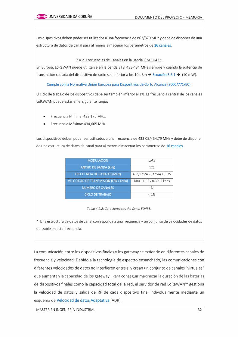
Los dispositivos deben poder ser utilizados a una frecuencia de 863/870 MHz y debe de disponer de una
estructura de datos de canal para al menos almacenar los parámetros de 16 canales.
7.4.2. Frecuencias de Canales en la Banda ISM EU433:
En Europa, LoRaWAN puede utilizarse en la banda ETSI 433-434 MHz siempre y cuando la potencia de
transmisión radiada del dispositivo de radio sea inferior a los 10 dBm Ecuación 3.6.1 (10 mW).
Cumple con la Normativa Unión Europea para Dispositivos de Corto Alcance (2006/771/EC).
El ciclo de trabajo de los dispositivos debe ser también inferior al 1%. La frecuencia central de los canales
LoRaWAN puede estar en el siguiente rango:
• Frecuencia Mínima: 433,175 MHz.
• Frecuencia Máxima: 434,665 MHz.
Los dispositivos deben poder ser utilizados a una frecuencia de 433,05/434,79 MHz y debe de disponer
de una estructura de datos de canal para al menos almacenar los parámetros de 16 canales.
MODULACIÓN LoRa
ANCHO DE BANDA (kHz) 125
FRECUENCIA DE CANALES (MHz) 433,175/433,375/433,575
VELOCIDAD DE TRANSMISIÓN (FSK / LoRa) DR0 – DR5 / 0,30 -5 kbps
NÚMERO DE CANALES 3
CICLO DE TRABAJO < 1%
Tabla 4.2.2: Características del Canal EU433.
* Una estructura de datos de canal corresponde a una frecuencia y un conjunto de velocidades de datos
utilizable en esta frecuencia.
La comunicación entre los dispositivos finales y los gateway se extiende en diferentes canales de
frecuencia y velocidad. Debido a la tecnología de espectro ensanchado, las comunicaciones con
diferentes velocidades de datos no interfieren entre sí y crean un conjunto de canales "virtuales"
que aumentan la capacidad de los gateway. Para conseguir maximizar la duración de las baterías
de dispositivos finales como la capacidad total de la red, el servidor de red LoRaWAN™ gestiona
la velocidad de datos y salida de RF de cada dispositivo final individualmente mediante un
esquema de Velocidad de datos Adaptativa (ADR).

DOCUMENTO DEL PROYECTO - MEMORIA
MÁSTER EN INGENIERÍA INDUSTRIAL 33
Para participar en una red LoRaWAN™, cada dispositivo final debe ser personalizado y activado.
Como indica la LoRaWAN™ Specification, la siguiente información ha de ser almacenada en los
dispositivos finales:
Dirección de Dispositivo (DevAddr):
El DevAddr consiste en 32 bits que identifican al dispositivo final dentro de la red actual.
Bit [31 … 25] [24 … 0]
DevAddr Bits NwkID NwkAddr
Tabla 4.2.3: Estructura de Dirección de Dispositivo.
Los 7 bits más significativos se utilizan como identificador de red (NwkID) para separar direcciones en
redes territorialmente superpuestas de operadores de redes y para remediar problemas de roaming.
Los menos significativos 25 bits, la dirección de red (NwkAddr) del dispositivo final, pueden ser asignado
arbitrariamente por el administrador de la red.
Identificador de Aplicación Global (AppEUI):
El AppEUI es un identificador de aplicación global en las direcciones IEEE EUI64 que identificará de forma
única al proveedor de la aplicación del dispositivo final (propietario). Esta se almacenará en el dispositivo
antes de ejecutar el procedimiento de activación.
Clave de Sesión de Red (NwkSKey):
El NwkSKey es una clave de sesión de red específica para el dispositivo final. Es utilizado tanto por el
servidor de red y el dispositivo final para calcular y verificar el código de integridad del mensaje (MIC)
para garantizar la integridad de los datos. También se utiliza para cifrar y descifrar el campo de carga útil
en mensajes de carácter de protocolo de red (MAC).
Clave de Sesión de Aplicación (AppSKey):
La AppSKey es una clave de sesión de aplicación específica para el dispositivo final. Es utilizado tanto por
servidor de red y el dispositivo final para cifrar y descifrar el campo de mensajes de datos específicos de
la aplicación. También se utiliza para calcular y verificar una un nivel de aplicación que pueda incluirse
en la carga útil de mensajes de datos específicos de la aplicación.

DOCUMENTO DEL PROYECTO - MEMORIA
MÁSTER EN INGENIERÍA INDUSTRIAL 34
Según la LoRaWAN™ Specification, existen dos métodos para la conexión de dispositivos a una
red LoRaWAN™:
Activación sobre el Aire (OTTA):
Para la Activación sobre el Aire, los dispositivos finales deben seguir un procedimiento previo de
conexión para poder participar en intercambios de datos con el servidor. Además de esto, cada
dispositivo que pierda la información de la sesión debe volver a conectarse nuevamente.
El procedimiento de conexión requiere que el dispositivo final haya sido personalizado con la siguiente
información:
• Identificador de Dispositivo Final Global (DevEUI): identificación de dispositivo final global
en las direcciones IEEE EUI64 que identifica al dispositivo de forma única.
• Identificador de Aplicación Global (AppEUI).
• Llave de Aplicación (AppKey): clave de aplicación con cifrado AES-128 para dispositivo final
asignada por el propietario de la aplicación y llave de administración específica bajo control
del proveedor de la aplicación. Se utiliza para derivar las claves de sesión NwkSKey y
AppSKey específicas para el cifrado y verificación del dispositivo final.
Activación por Personalización (ABP):
Bajo ciertas circunstancias, los dispositivos finales se pueden activar mediante la personalización. Para
la Activación por Personalización, se vinculará directamente un dispositivo final a una red específica
omitiendo la petición de conexión y el procedimiento de aceptación.
La activación por personalización implica que la DevAddr, NwkSKey y AppSKey se almacenarán
directamente en el dispositivo final en lugar delos DevEUI, AppEUI y AppKey como se hacía con el
procedimiento de Activación sobre el Aire (OTTA).
El dispositivo LoRa estará equipado con la información necesaria para su participación en una red
específica cuando se inicia. Cada dispositivo tendrá sus únicos respectivos NwSKey y AppSKey, no
comprometiendo la seguridad de comunicación con el resto de dispositivos.
El proceso de construcción de las claves debe ser hecho de tal forma que la información de las claves no
se puede derivar de ninguna manera.

DOCUMENTO DEL PROYECTO - MEMORIA
MÁSTER EN INGENIERÍA INDUSTRIAL 35
4.3 DISEÑO DE LA RED
Para este proyecto se llevará a cabo un diseño de red en Modo P2P por motivos de seguridad y
privacidad. De igual manera, con vistas a una posible migración, el código ha sido desarrollado
para permitir la activación del Modo Híbrido modificando el servidor y la codificación de mensaje,
combinando el modo LoRaWAN™, P2P y el soporte de la plataforma libre The Things Network™.
Ilustración 4.3.1: Configuración de Red por Conexión en Modo Híbrido – The Things Network™.
The Things Network™ utiliza tecnología LoRaWAN™ para la conexión de una red descentralizada
de código abierto para intercambio de datos con aplicaciones y otras plataformas.
Ilustración 4.3.2: Componentes de Red LoRaWAN™ con soporte de The Things Network™.
DOCUMENTO DEL PROYECTO - MEMORIA
MÁSTER EN INGENIERÍA INDUSTRIAL 36
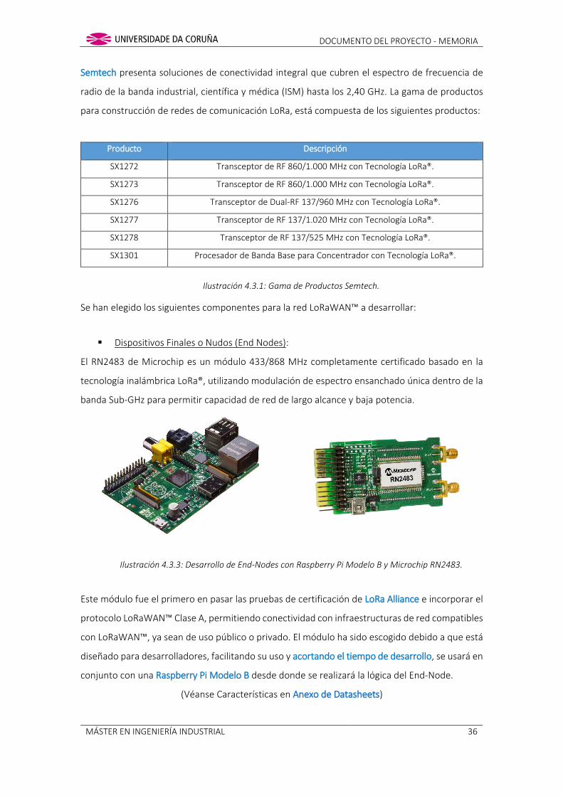
Semtech presenta soluciones de conectividad integral que cubren el espectro de frecuencia de
radio de la banda industrial, científica y médica (ISM) hasta los 2,40 GHz. La gama de productos
para construcción de redes de comunicación LoRa, está compuesta de los siguientes productos:
Producto Descripción
SX1272 Transceptor de RF 860/1.000 MHz con Tecnología LoRa®.
SX1273 Transceptor de RF 860/1.000 MHz con Tecnología LoRa®.
SX1276 Transceptor de Dual-RF 137/960 MHz con Tecnología LoRa®.
SX1277 Transceptor de RF 137/1.020 MHz con Tecnología LoRa®.
SX1278 Transceptor de RF 137/525 MHz con Tecnología LoRa®.
SX1301 Procesador de Banda Base para Concentrador con Tecnología LoRa®.
Ilustración 4.3.1: Gama de Productos Semtech.
Se han elegido los siguientes componentes para la red LoRaWAN™ a desarrollar:
Dispositivos Finales o Nudos (End Nodes):
El RN2483 de Microchip es un módulo 433/868 MHz completamente certificado basado en la
tecnología inalámbrica LoRa®, utilizando modulación de espectro ensanchado única dentro de la
banda Sub-GHz para permitir capacidad de red de largo alcance y baja potencia.
Ilustración 4.3.3: Desarrollo de End-Nodes con Raspberry Pi Modelo B y Microchip RN2483.
Este módulo fue el primero en pasar las pruebas de certificación de LoRa Alliance e incorporar el
protocolo LoRaWAN™ Clase A, permitiendo conectividad con infraestructuras de red compatibles
con LoRaWAN™, ya sean de uso público o privado. El módulo ha sido escogido debido a que está
diseñado para desarrolladores, facilitando su uso y acortando el tiempo de desarrollo, se usará en
conjunto con una Raspberry Pi Modelo B desde donde se realizará la lógica del End-Node.
(Véanse Características en Anexo de Datasheets)

DOCUMENTO DEL PROYECTO - MEMORIA
MÁSTER EN INGENIERÍA INDUSTRIAL 37
Gateway:
Como se ha comentado en el subcapítulo 4.2 la compra de un gateway comercial actualmente,
dadas las dimensiones del proyecto, se hace PROHIBITIVO. Por ello se ha decidido desarrollar un
prototipo de gateway por medio de una Raspberry Pi Compute Module y un SX1276 de Semtech.
Ilustración 4.3.4: Desarrollo del Gateway con Raspberry Pi Compute Module y SX1276MB1xAS.
El diseño original del gateway ha sido hecho por Thomas Telkamp, desarrollador de arquitecturas
en red para The Things Network™. Este desarrollo consiste en un gateway de canal único utilizado
exclusivamente para desarrollo, ya que este, no mantendría la filosofía de gateway planteado por
la LoRaWAN™ Specification no siendo multicanal.
Para este proyecto, se ha desarrollado un código más adecuado a los requisitos de diseño y escrito
en el lenguaje de programación Python, basado en la solución anteriormente presentada.
Ilustración 4.3.5: Logo de Python
Ilustración 4.3.2: Características del Desarrollo Original del Gateway.
Desarrollador Original Thomas Telkamp
GitHub https://github.com/tftelkamp
Dominio Web https://www.thethingsnetwork.org

DOCUMENTO DEL PROYECTO - MEMORIA
MÁSTER EN INGENIERÍA INDUSTRIAL 38
4.4 PUESTA EN MARCHA DE DISPOSITIVOS
Este apartado se dividirá en dos partes. En primer lugar, dispondremos la configuración y montaje
del Gateway y por último de la configuración de los End-Nodes.
Como primer paso en la configuración de nuestro Gateway debemos realizar la instalación del
sistema operativo, en nuestro caso será Raspbian Jessie Lite.
Ilustración 4.4.1: Raspbian Jessie Lite.
La Raspberry Compute Module dispone de una interfaz eMMC conectada a la tarjeta SD, que se
encuentra integrada en el módulo, por tanto, para instalar el sistema operativo, es necesario
acceder al mismo por medio de las conexiones que nos ofrece la Compute Module I/O Board.
Debemos asegurarnos del correcto acoplamiento de la Raspberry Compute Module a la Compute
Module I/O Board por medio de los clips de acoplamiento disponibles y que la conexión del puerto
J4 (Usb Slave Boot Enable) esté en posición “EN”.
Debemos disponer de otro sistema operativo desde donde realizar la instalación en remoto (se
recomiendan principalmente sistemas Linux como Ubuntu o un sistema Windows 7) e instalar
RPIBoot (en este caso Kubuntu) siguiendo los siguientes pasos:
1. Utilizamos Git para obtener el código fuente RPIBoot, por tanto, aseguramos de que Git esté instalado.
sudo apt-get install git

DOCUMENTO DEL PROYECTO - MEMORIA
MÁSTER EN INGENIERÍA INDUSTRIAL 39
2. Al utilizar Git, se puede producir un error por fecha incorrecta, por tanto, ejecutaremos lo siguiente:
sudo date MMDDhhmm
Siendo MM es el mes, DD el día, hh las horas y mm los minutos respectivamente
3. Debemos asegurarnos de que libusb esté instalado:
sudo apt-get install libusb-1.0-0-dev
4. Clonamos por medio de Git el repositorio de herramientas usbboot:
git clone --depth = 1 https://github.com/raspberrypi/usbboot
5. Nos situamos en la carpeta del repositorio descargado y lo compilamos:
cd usbboot
make
6. Ejecutamos la herramienta usbboot y esperamos la conexión.
sudo ./rpiboot
7. Ahora conectamos el ordenador a la placa por medio de un cable micro USB a través del puerto J15 y
encendemos la Compute Module I/O Board. La herramienta RPIBoot accederá al Compute Module y
permitirá el acceso a la eMMC.
8. En este paso se escribirá la imagen previamente descargada de Raspbian en el dispositivo.
sudo dd if=raw 2017-04-10-raspbian-jessie-lite.img of=/dev/sdc bs=4MiB
9. Cuando termine, debemos asegurarnos de que el puerto J4 esté desactivado y no hay nada enchufado
al puerto J15. Al alimentar la Compute Module I/O Board debería iniciar el sistema desde la eMMC.
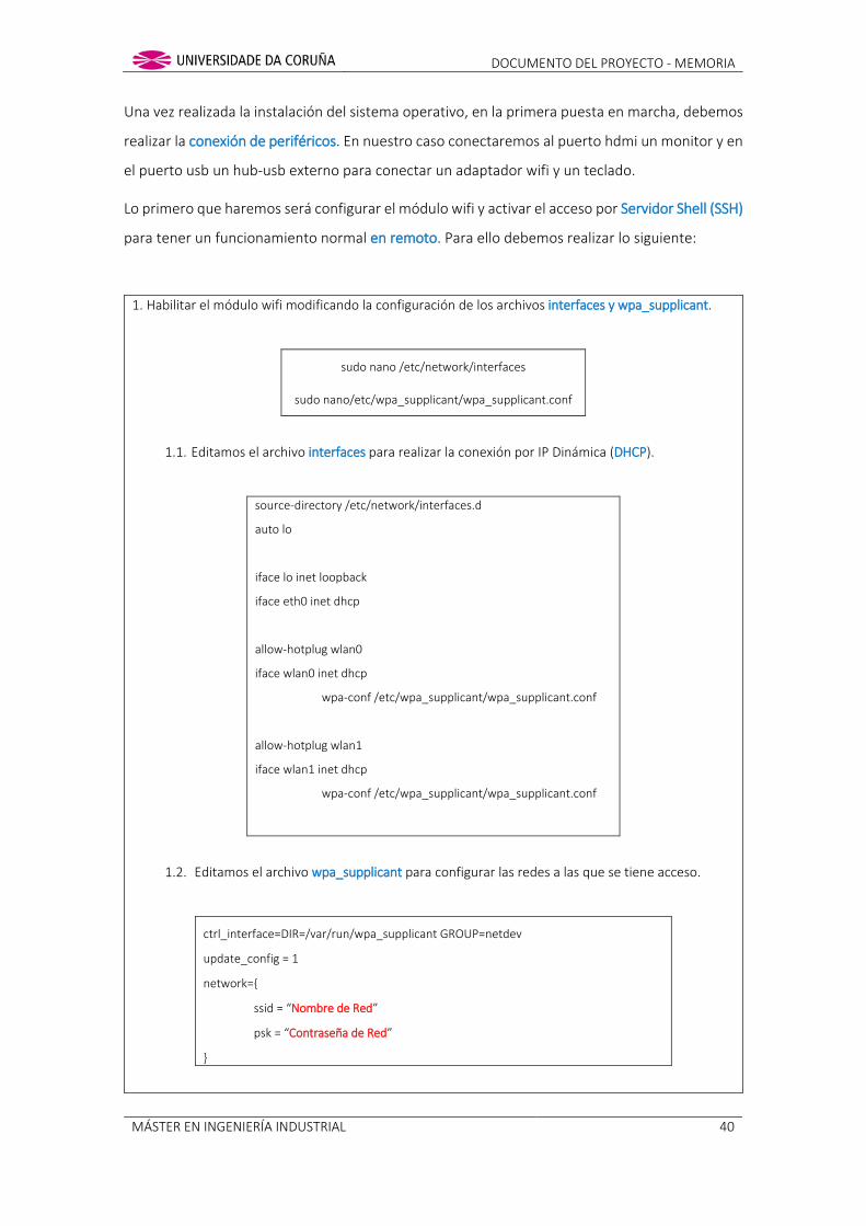
DOCUMENTO DEL PROYECTO - MEMORIA
MÁSTER EN INGENIERÍA INDUSTRIAL 40
Una vez realizada la instalación del sistema operativo, en la primera puesta en marcha, debemos
realizar la conexión de periféricos. En nuestro caso conectaremos al puerto hdmi un monitor y en
el puerto usb un hub-usb externo para conectar un adaptador wifi y un teclado.
Lo primero que haremos será configurar el módulo wifi y activar el acceso por Servidor Shell (SSH)
para tener un funcionamiento normal en remoto. Para ello debemos realizar lo siguiente:
1. Habilitar el módulo wifi modificando la configuración de los archivos interfaces y wpa_supplicant.
sudo nano /etc/network/interfaces
sudo nano/etc/wpa_supplicant/wpa_supplicant.conf
1.1. Editamos el archivo interfaces para realizar la conexión por IP Dinámica (DHCP).
source-directory /etc/network/interfaces.d
auto lo
iface lo inet loopback
iface eth0 inet dhcp
allow-hotplug wlan0
iface wlan0 inet dhcp
wpa-conf /etc/wpa_supplicant/wpa_supplicant.conf
allow-hotplug wlan1
iface wlan1 inet dhcp
wpa-conf /etc/wpa_supplicant/wpa_supplicant.conf
1.2. Editamos el archivo wpa_supplicant para configurar las redes a las que se tiene acceso.
ctrl_interface=DIR=/var/run/wpa_supplicant GROUP=netdev
update_config = 1
network=
ssid = “Nombre de Red”
psk = “Contraseña de Red”

DOCUMENTO DEL PROYECTO - MEMORIA
MÁSTER EN INGENIERÍA INDUSTRIAL 41
2. Habilitar la opción de Acceso por Servidor Shell (SSH).
sudo raspi-config
Ilustración 4.4.2: Activación de Servidor SSH y SPI.
* Activaremos a su vez el bus de comunicaciones SPI necesario para la aplicación desarrollada del Gateway.
Tras este proceso, podremos comunicarnos en remoto de forma inalámbrica, eliminando el uso
de periféricos salvo el módulo wifi.
Los programas para la gestión en remoto serán PuTTY (servidor SSH) para realizar un control
desde terminal y WinSCP (cliente SFTP) para el intercambio de archivos.
Ilustración 4.4.3: Programas PuTTy y WinSCP.
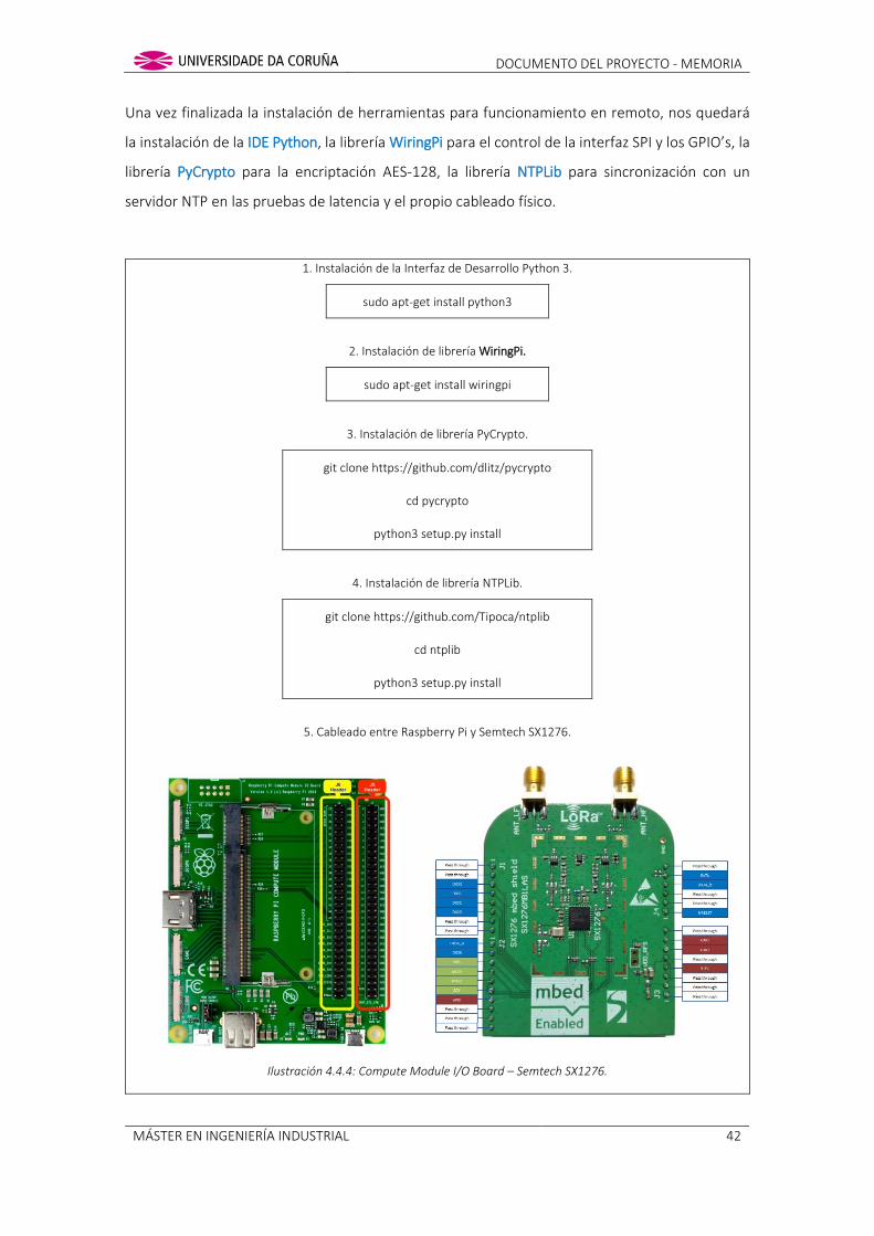
DOCUMENTO DEL PROYECTO - MEMORIA
MÁSTER EN INGENIERÍA INDUSTRIAL 42
Una vez finalizada la instalación de herramientas para funcionamiento en remoto, nos quedará
la instalación de la IDE Python, la librería WiringPi para el control de la interfaz SPI y los GPIO’s, la
librería PyCrypto para la encriptación AES-128, la librería NTPLib para sincronización con un
servidor NTP en las pruebas de latencia y el propio cableado físico.
1. Instalación de la Interfaz de Desarrollo Python 3.
sudo apt-get install python3
2. Instalación de librería WiringPi.
sudo apt-get install wiringpi
3. Instalación de librería PyCrypto.
git clone https://github.com/dlitz/pycrypto
cd pycrypto
python3 setup.py install
4. Instalación de librería NTPLib.
git clone https://github.com/Tipoca/ntplib
cd ntplib
python3 setup.py install
5. Cableado entre Raspberry Pi y Semtech SX1276.
Ilustración 4.4.4: Compute Module I/O Board – Semtech SX1276.

DOCUMENTO DEL PROYECTO - MEMORIA
MÁSTER EN INGENIERÍA INDUSTRIAL 43
Pines Raspberry Pi Pines Semtech SX1276
GPIO 0 * NReset
GPIO 6 * NSS
GPIO 7 * DIO0
SPI-MISO (9) MISO
SPI-MOSI (10) MOSI
SPI-SCLK (11) SCK
GND GND (J3)
3.3V 3.3V (J3)
* Determinados por el software desarrollado. Son configurables modificando líneas de código en la aplicación.
Tabla 4.4.1: Cableado de Pines Raspberry Pi – Semtech SX1276.
Una vez realizados todos estos pasos, procederemos a subir el código realizado y ejecutarlo. Para
ello realizaremos los siguientes pasos:
1. Subimos el código a la Raspberry Pi por medio de WinSCP.
Ilustración 4.4.5: Subida de Código desde WinSCP.

DOCUMENTO DEL PROYECTO - MEMORIA
MÁSTER EN INGENIERÍA INDUSTRIAL 44
2. Iniciamos Sesión en PuTTY y entramos en la carpeta:
Ilustración 4.4.6: Ejecución de Código desde PuTTy.
3. Ejecutamos el código para poner en funcionamiento el Gateway:
Ilustración 4.4.7: Funcionamiento Normal del Gateway.
La aplicación realizada para el Gateway está expuesta en el Anexo IV (Aplicaciones Desarrolladas)
y consistirá en un bucle de lectura de mensajes entrantes. Si se recibe una IRQ desde el dio0,
tendremos un paquete recibido en el buffer FIFO del transceptor SX1276, al cual se accederá por
medio del bus de comunicaciones SPI. Si el mensaje que se ha recibido es correcto, se realiza la
desencriptación de la carga útil y se convierte de hexadecimal a código ASCII.

DOCUMENTO DEL PROYECTO - MEMORIA
MÁSTER EN INGENIERÍA INDUSTRIAL 45
Como podemos ver en esta simulación, se inicia el Gateway mostrando su dirección MAC y sus
parámetros de trabajo, frecuencia de 433 MHz con SF7BW125. Tras esto se recibe un mensaje
en hexadecimal desde un end-node y el Gateway mostrará como resultado los parámetros del
envío recibido como el RSSI (nivel de potencia de la señal recibida), la SNR (relación señal/ruido),
la longitud del paquete y la transcripción del mensaje de hexadecimal a código ASCII.
Ilustración 4.4.8: Mensaje Recibido por el Gateway.
Como podemos observar, el código desarrollado nos permite recibir la actualización del estado
del Gateway y el estado de paquetes en el intervalo de tiempo pre-configurado. Además de esto,
si se activa el parámetro Statistics por código, se recibirán también los tiempos en los cuales se
ha realizado una recepción de mensaje (Timestamp) y las medias del RSSI y el SNR.

DOCUMENTO DEL PROYECTO - MEMORIA
MÁSTER EN INGENIERÍA INDUSTRIAL 46
Como función adicional, se ha desarrollado también un Servidor en Python para la monitorización
del Gateway desde diferentes puntos de la topología de red desarrollada. Este servidor se inicia
en modo de espera y en el momento que el Gateway se activa, establece comunicación por medio
del protocolo de comunicación User Datagram Protocol (UDP) perteneciente a la Capa de
Transporte (véase subcapítulo 3.7).
Ilustración 4.4.9: Mensaje Recibido por el Servidor Python.
Con vistas a una posible migración, como se ha planteado previamente en el subcapítulo 4.3 el
código ha sido desarrollado para permitir la activación del Modo Híbrido modificando el servidor
y la codificación de mensaje, combinando el modo LoRaWAN™, P2P y el soporte de la plataforma
libre The Things Network™.

DOCUMENTO DEL PROYECTO - MEMORIA
MÁSTER EN INGENIERÍA INDUSTRIAL 47
Como último paso, se realizará la configuración de los End-Nodes. Debido a la mayor simplicidad
de la Raspberry Pi Modelo B será más sencillo instalar Raspbian Jessie Lite. Para ello debemos
descomprimir la imagen previamente descargada para el Gateway y cargarla en la SD externa que
irá en la Raspberry. En este caso, se ha llevado a cabo por medio del programa Etcher.
Tras esto se debe activar el módulo wifi, el servidor SSH e instalar la IDE de Python junto con la
librería NTPLib, como previamente se ha realizado para el Gateway.
Una vez realizado esto, nos queda cargar el programa desarrollado en Python para establecer su
funcionamiento normal. Primero se creará una comunicación serie entre la Raspberry y el módulo
RN2483 de Microchip y, tras ello, se cargará la configuración del End-Node y se iniciará el bucle
de envío de paquetes.
Ilustración 4.4.10: Funcionamiento Normal del End-Node.
Como podemos observar, el código también nos permite activar el parámetro Statistics por
código, por el cual se obtendrán los tiempos en los cuales se ha realizado el envío del paquete.

DOCUMENTO DEL PROYECTO - MEMORIA
MÁSTER EN INGENIERÍA INDUSTRIAL 48
4.5 PRUEBAS DE LA TECNOLOGÍA EN ESCENARIOS REALES
En los apartados anteriores se presentan las principales características de la tecnología LoRa y
LoRaWAN junto con los principales componentes de nuestra red. En este apartado, se llevará a
cabo el desarrollo de pruebas en las que analizar los resultados de su aplicación en un sistema de
UAV’s. Estas pruebas consistirán en analizar el consumo energético, el throughput o rendimiento,
la latencia y el alcance máximo, en los diferentes estados de transmisión.
Estudio de Consumo Energético:
Uno de los parámetros más importantes será el análisis del consumo de los end-nodes debido a
que esto nos afectará directamente a la autonomía de vuelo. Para analizar esto, debemos analizar
el consumo en el estado de funcionamiento normal del UAV, que en nuestro caso será el modo
que nos asegure el mayor ancho de banda (DR5).
DR Configuración Tamaño Máx. Mensaje Bitrate Capa Física
DR0 LoRa: SF12 / 125 kHz 64 bytes 250 bits/s
DR1 LoRa: SF11 / 125 kHz 64 bytes 440 bits/s
DR2 LoRa: SF10 / 125 kHz 64 bytes 980 bits/s
DR3 LoRa: SF9 / 125 kHz 128 bytes 1.760 bits/s
DR4 LoRa: SF8 / 125 kHz 255 bytes 3.125 bits/s
DR5 LoRa: SF7 / 125 kHz 255 bytes 5.470 bits/s
Tabla 4.5.1: Características de los distintos modos de funcionamiento.
Durante el vuelo, el end-node experimentará diferentes estados, como pudiera ser el estado de
inactividad o de transmisión y recepción de datos, mostrando diferentes consumos.
Ilustración 4.5.1: Fases de Transmisión de Mensajes.

DOCUMENTO DEL PROYECTO - MEMORIA
MÁSTER EN INGENIERÍA INDUSTRIAL 49
Tras realizar el envío de un mensaje, el transceptor abrirá dos ventanas de recepción como indica
la LoRaWAN™ Specification, por tanto, para estimar el consumo medio del transceptor debemos
aplicar la siguiente fórmula:
𝐼𝐼𝑚𝑚𝑚𝑚𝑚𝑚𝑚𝑚𝑚𝑚 = 𝑆𝑆𝑡𝑡𝑟𝑟𝑚𝑚𝑛𝑛𝑡𝑡. 𝑥𝑥 𝐼𝐼𝑡𝑡𝑟𝑟𝑚𝑚𝑛𝑛𝑡𝑡. + 𝑆𝑆𝑣𝑣𝑚𝑚𝑛𝑛𝑡𝑡𝑚𝑚𝑛𝑛𝑚𝑚 1 𝑥𝑥 𝐼𝐼𝑣𝑣𝑚𝑚𝑛𝑛𝑡𝑡𝑚𝑚𝑛𝑛𝑚𝑚 1 + 𝑆𝑆𝑣𝑣𝑚𝑚𝑛𝑛𝑡𝑡𝑚𝑚𝑛𝑛𝑚𝑚 2 𝑥𝑥 𝐼𝐼𝑣𝑣𝑚𝑚𝑛𝑛𝑡𝑡𝑚𝑚𝑛𝑛𝑚𝑚 2 + 𝑆𝑆𝑡𝑡𝑠𝑠𝑚𝑚𝑚𝑚𝑠𝑠 𝑥𝑥 𝐼𝐼𝑡𝑡𝑠𝑠𝑚𝑚𝑚𝑚𝑠𝑠
Ecuación 4.5.1: Consumo del Transceptor RN2483.
Como en nuestro caso el end-node está compuesto de una Raspberry Pi con un Módulo Wi-Fi y el
Módulo Transceptor RN2483, la medición de la intensidad se hace más complicada, por tanto,
realizaremos mediciones por medio de un Osciloscopio Tektronix y un circuito con una resistencia
de 1 Ω que nos convierte la intensidad a voltaje (1:1), pudiendo ser medido por el osciloscopio.
Las mediciones obtenidas han sido las siguientes:
Ilustración 4.5.2: Consumo Medio del End-Node.

DOCUMENTO DEL PROYECTO - MEMORIA
MÁSTER EN INGENIERÍA INDUSTRIAL 50
Ilustración 4.5.3: Consumo en Transmisión del End-Node.
El consumo de la Raspberry Pi 1 Modelo B se estima entre 360 mA en reposo y 480 mA en pleno
funcionamiento, mientras que el módulo RN2483 se estima en 40 mA en transmisión, 14 mA en
recepción y 100-150 µA en reposo.
Nota: el consumo puede variar en función de la versión de firmware de los módulos RN2483 de
Microchip respecto al mostrado en el datasheet.
http://ww1.microchip.com/downloads/en/DeviceDoc/80000689A.pdf
En la primera foto, en estado de inactividad, observamos que el consumo medio del sistema será
aproximadamente de 400 mA, mientras que, en la segunda, ya a pleno rendimiento, podemos
destacar que el dispositivo pasa por distintas fases. En una primera podemos observar que el
consumo aumenta en el momento que se recibe y ejecuta una orden recibida desde el servidor
SSH del módulo Wi-Fi y tras ella, se observa un fuerte pico de consumo, donde se estima que se
inicia la comunicación LoRa, finalizando nuevamente en el estado de inactividad.

DOCUMENTO DEL PROYECTO - MEMORIA
MÁSTER EN INGENIERÍA INDUSTRIAL 51
Los resultados obtenidos y estimaciones realizadas están bastante próximos. Dado que durante
el tiempo que se ejecuta la orden recibida del servidor SSH y se realiza la transmisión del mensaje
es de aproximadamente de 100 ms, en conjunto a ser utilizado el modo de mayor consumo (DR5),
presentando un ritmo mínimo entre mensajes de 2,25s (como se puede observar en la prueba de
throughput), se estima un consumo medio total aproximado de 405 mA.
El UAV sobre el que se realizan las pruebas presenta 2 Baterías Turnigy de 5.000 mAh y se estima
una autonomía de vuelo de 45 – 60 min según el modo de vuelo.
Ilustración 4.5.4: Batería Turnigy 5.000 mAh.
Estos datos nos permiten estimar la repercusión global de la instalación de este dispositivo sobre
la autonomía de vuelo, siendo determinada por la siguiente fórmula:
𝐶𝐶 = 𝐼𝐼 𝑥𝑥 𝑆𝑆
Ecuación 4.5.2: Capacidad de Batería.
Aumentando el consumo previsto (405 mA) al consumo actual (10.000 mA - 13.333 mA), nos dará
una autonomía de entre 43,67 – 57,67 min. De esta forma veremos una reducción de autonomía
de vuelo en un rango de 1,31 - 2,33 min, lo que se nos presenta como un consumo asumible.
Debe además destacarse que el consumo de LoRa representa un porcentaje muy pequeño en
relación al consumo total del dispositivo end-node.

DOCUMENTO DEL PROYECTO - MEMORIA
MÁSTER EN INGENIERÍA INDUSTRIAL 52
Estudio Throughput o Rendimiento:
Otro parámetro fundamental a analizar es el throughput o ancho de banda efectivo, siendo este
la velocidad real de transporte de la información a través de la red e inferior al ancho de banda.
Esta prueba se ha dividido en dos fases, en la primera se ha propuesto el desarrollo de un bucle
de envío de mensajes, en concreto 2.400 mensajes con una diferencia de tiempos de 40 (espera)
+ 10 (timeout) ms, con diferentes longitudes. Los resultados obtenidos han sido los siguientes:
Frecuencia DR Recibidos Tiempo Envío (s) Ritmo Envío (s) Bitrate (bits/s)
433 MHz
DR0 11 125.71 11.43 9.80
DR1 19 126.07 6.64 16.88
DR2 43 125.48 2.92 38.38
DR3 52 125.62 2.42 46.36
DR4 54 125.36 2.32 48.25
DR5 55 125.41 2.28 49.12
868 MHz
DR0 11 124.96 11.36 9.86
DR1 19 125.98 6.63 16.89
DR2 43 125.42 2.92 38.40
DR3 52 125.43 2.41 46.43
DR4 54 125.28 2.32 48.28
DR5 56 125.34 2.24 50.04
Tabla 4.5.2: Throughput con Mínimo Payload.
Frecuencia DR Recibidos Tiempo Envío (s) Ritmo Envío (s) Bitrate (bits/s)
433 MHz
DR0 9 149.85 16.65 15.38
DR1 15 149.31 9.95 25.72
DR2 33 149.47 4.53 56.52
DR3 59 149.08 2.53 101.31
DR4 62 149.05 2.40 106.49
DR5 64 149.02 2.33 109.94
868 MHz
DR0 9 149.85 16.65 15.38
DR1 15 149.31 9.95 25.72
DR2 32 149.51 4.67 54.79
DR3 58 149.08 2.57 99.60
DR4 62 149.05 2.40 106.49
DR5 64 149.02 2.33 109.94
Tabla 4.5.3: Throughput con Mensajes de 32 Bytes.

DOCUMENTO DEL PROYECTO - MEMORIA
MÁSTER EN INGENIERÍA INDUSTRIAL 53
Frecuencia DR Recibidos Tiempo Envío (s) Ritmo Envío (s) Bitrate (bits/s)
433 MHz
DR0 6 149.88 24.98 20.50
DR1 10 149.53 14.95 34.24
DR2 22 149.05 6.78 75.57
DR3 37 148.30 4.01 127.74
DR4 59 149.10 2.53 202.60
DR5 62 150.00 2.42 211.63
868 MHz
DR0 6 149.88 24.98 20.50
DR1 10 149.53 14.95 34.24
DR2 22 149.02 6.77 75.59
DR3 37 148.30 4.01 127.74
DR4 59 149.10 2.53 202.60
DR5 62 150.00 2.42 211.63
Tabla 4.5.4: Throughput con Mensajes de 64 Bytes.
Frecuencia DR Recibidos Tiempo Envío (s) Ritmo Envío (s) Bitrate (bits/s)
433 MHz
DR0 5 126.65 25.33 20.21
DR1 9 126.35 14.04 36.47
DR2 18 125.99 7.00 73.15
DR3 27 186.30 6.90 148.41
DR4 39 291.38 7.47 273.05
DR5 69 293.35 4.25 479.84
868 MHz
DR0 5 126.89 25.38 20.17
DR1 9 126.53 14.06 36.42
DR2 18 126.06 7.00 73.11
DR3 26 186.71 7.18 142.60
DR4 39 193.56 7.53 271.02
DR5 69 293.21 4.25 480.07
Tabla 4.5.5: Throughput con el Máximo Payload.
Como se observa, el máximo ancho de banda se obtiene al aumentar al máximo la longitud de
mensaje, por otra parte, también se ve claramente afectado el tiempo entre mensajes.
De esto obtenemos que sería útil mantener un buffer de memoria para realizar envíos grandes
de datos, ya que de por sí, los envíos de paquetes que se llevarán a cabo desde el avión tendrán
una longitud aproximada de 50 bytes.

DOCUMENTO DEL PROYECTO - MEMORIA
MÁSTER EN INGENIERÍA INDUSTRIAL 54
Cabe destacar que el Ciclo de Trabajo utilizado en ambas frecuencias ha sido del 10 %, debido a
la limitación impuesta por la Normativa Europea. Esta limitación nos arrastrará el bitrate a valores
próximos al 10% del ancho de banda.
El canal de frecuencia usado en 433 MHz corresponde al canal 0 especificado en la LoRaWAN™
Specification (433,175 MHz) y posee una limitación de ciclo de trabajo del 10%, pero los canales
en frecuencia 868 MHz disponen de una limitación del 1%, debido a esto, se ha utilizado el canal
de frecuencia de 869,525 MHz, que dispone de la limitación del 10%.
La segunda fase de esta prueba, será ajustar los tiempos para asegurar el envío y recepción
completa de los paquetes. Para ello, se han ajustado los tiempos y se han enviado 10 mensajes
con la diferencia de tiempos de la primera fase para el caso de longitud máxima, que será de
donde obtengamos el máximo ancho de banda. Los resultados obtenidos han sido:
Frecuencia DR Recepción Ritmo Ajustado (s) Tiempo Envío (s) Bitrate (bits/s)
433 MHz
DR0 10/10 28.25 282.52 18.12
DR1 10/10 15.75 157.52 32.50
DR2 10/10 7.25 72.52 70.60
DR3 10/10 7.00 70.27 145.72
DR4 10/10 7.50 75.77 269.24
DR5 10/10 4.50 45.76 445.80
868 MHz
DR0 10/10 28.25 282.52 18.12
DR1 10/10 15.75 157.52 32.50
DR2 10/10 7.25 72.52 70.60
DR3 10/10 7.00 70.27 145.72
DR4 10/10 7.50 75.77 269.24
DR5 10/10 4.50 45.77 445.71
Tabla 4.5.6: Throughput Ajustado con el Máximo Payload.
Como resultado de esta prueba, podemos decir que el protocolo LoRa dispone de un throughput
limitado, que nos permitirá el envío de pequeños volúmenes de datos para usos que no requieran
de transmisión en continuo. En nuestro caso, para transmitir datos de telemetría periódicamente.
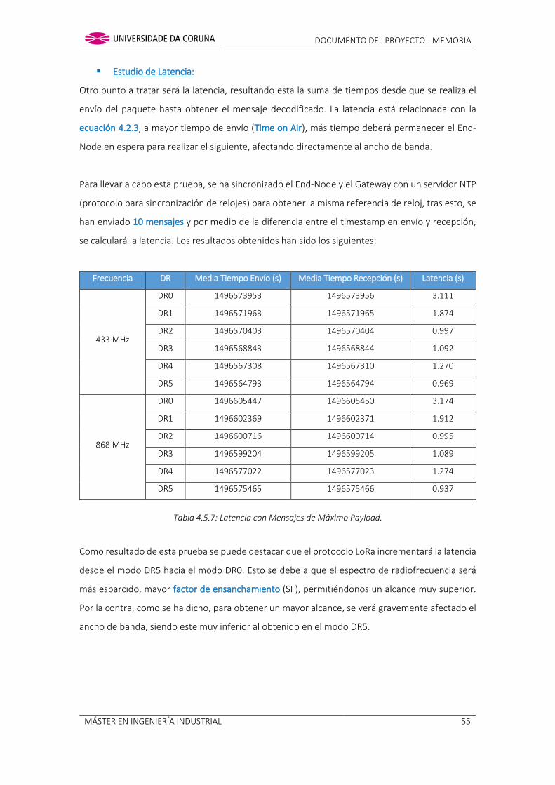
DOCUMENTO DEL PROYECTO - MEMORIA
MÁSTER EN INGENIERÍA INDUSTRIAL 55
Estudio de Latencia:
Otro punto a tratar será la latencia, resultando esta la suma de tiempos desde que se realiza el
envío del paquete hasta obtener el mensaje decodificado. La latencia está relacionada con la
ecuación 4.2.3, a mayor tiempo de envío (Time on Air), más tiempo deberá permanecer el End-
Node en espera para realizar el siguiente, afectando directamente al ancho de banda.
Para llevar a cabo esta prueba, se ha sincronizado el End-Node y el Gateway con un servidor NTP
(protocolo para sincronización de relojes) para obtener la misma referencia de reloj, tras esto, se
han enviado 10 mensajes y por medio de la diferencia entre el timestamp en envío y recepción,
se calculará la latencia. Los resultados obtenidos han sido los siguientes:
Frecuencia DR Media Tiempo Envío (s) Media Tiempo Recepción (s) Latencia (s)
433 MHz
DR0 1496573953 1496573956 3.111
DR1 1496571963 1496571965 1.874
DR2 1496570403 1496570404 0.997
DR3 1496568843 1496568844 1.092
DR4 1496567308 1496567310 1.270
DR5 1496564793 1496564794 0.969
868 MHz
DR0 1496605447 1496605450 3.174
DR1 1496602369 1496602371 1.912
DR2 1496600716 1496600714 0.995
DR3 1496599204 1496599205 1.089
DR4 1496577022 1496577023 1.274
DR5 1496575465 1496575466 0.937
Tabla 4.5.7: Latencia con Mensajes de Máximo Payload.
Como resultado de esta prueba se puede destacar que el protocolo LoRa incrementará la latencia
desde el modo DR5 hacia el modo DR0. Esto se debe a que el espectro de radiofrecuencia será
más esparcido, mayor factor de ensanchamiento (SF), permitiéndonos un alcance muy superior.
Por la contra, como se ha dicho, para obtener un mayor alcance, se verá gravemente afectado el
ancho de banda, siendo este muy inferior al obtenido en el modo DR5.

DOCUMENTO DEL PROYECTO - MEMORIA
MÁSTER EN INGENIERÍA INDUSTRIAL 56
Estudio de Alcance:
Como último, se procederá a realizar la prueba del alcance máximo. Para ello, compararemos los
niveles de RSSI (nivel de potencia de la señal recibida), la SNR (relación señal/ruido) y Porcentaje
de Paquetes Perdidos, en puntos situados a diferentes distancias.
Para realizar la prueba se enviarán 100 mensajes de 17 bytes, en modo DR5, con el fin de saber el
máximo alcance que tenemos con el modo que nos permite el máximo ancho de banda.
Esta prueba se realizará en el La Malata (Ferrol), sobre tierra, debido a las malas condiciones por
viento presentadas durante los días a realizar las pruebas, lo que nos impide realizarlas en vuelo.
El alcance máximo que nos interesa será marcado por las Reglas de Vuelo Visual (VFR), realizando
pruebas de alcance hasta una distancia máxima de 1 km. El Gateway y el End-Node activarán su
funcionamiento por medio de dos Access-Points de forma independiente.
Los puntos sobre los que se harán las mediciones y las distancias entre el Gateway y el End-Node
serán marcados en la siguiente imagen:
Ilustración 4.5.5: Puntos de Medición de Alcance.

DOCUMENTO DEL PROYECTO - MEMORIA
MÁSTER EN INGENIERÍA INDUSTRIAL 57
Una vez establecidos los puntos desde donde se realizarán las pruebas de alcance, se comenzará
la prueba, resultando para ambas frecuencias:
Puntos Distancia RSSI Paquete (dB) RSSI (dB) SNR (dB) Paquetes Recibidos
1 252 m - 110 - 105 4 98 %
2 510 m - 115 - 106 8 42 %
3 756 m - 113 - 110 9 63 %
4 1.040 m - 114 - 108 10 25 %
Tabla 4.5.8: Resultados de Alcance en Banda de Frecuencia de 433 MHz.
Puntos Distancia RSSI Paquete (dB) RSSI (dB) SNR (dB) Paquetes Recibidos
1 252 m - 104 - 109 4 98 %
2 510 m - 107 - 107 4 84 %
3 756 m - 113 - 113 6 81 %
4 1.040 m - 113 - 116 7 55 %
Tabla 4.5.9: Resultados de Alcance en Banda de Frecuencia de 868 MHz.
Como observamos, la potencia de la señal de la banda de frecuencia de 868 MHz nos afecta en
la calidad de señal, permitiendo un mejor ratio de paquetes recibidos respecto a 433 MHz. A su
vez, al mantener línea de visión, se mantendrá un alto nivel de paquetes recibidos hasta distancias
cercanas a los 750 m, a partir de donde podemos considerar que distancia comienza a afectar la
recepción de paquetes, reflejándose en el parámetro SNR.
Ilustración 4.5.6: Pruebas de Alcance en el Punto 2.
Como último punto, cabe destacar la anomalía detectada en la medición del Punto 2 en la banda
de frecuencia de 433 MHz con un valor anómalo que no sigue la tendencia lógica. Se ha asumido
este valor como el resultado de algún tipo de interferencia o apantallamiento.
DOCUMENTO DEL PROYECTO - MEMORIA
MÁSTER EN INGENIERÍA INDUSTRIAL 58
5 CONCLUSIONES
A lo largo del presente proyecto, se ha realizado un análisis de las tecnologías de comunicaciones
LPWAM con el fin de obtener una idoneidad de adopción a un enjambre de UAV’s colaborativos.
Las tecnologías más interesantes respecto a las características de diseño del proyecto han sido
LoRa, Sigfox y NB-IoT, siendo finalmente elegida LoRa debido a sus numerosas ventajas como la
versatilidad de sus modos de transmisión, el alcance, la eficiencia energética, la mayor inmunidad
a interferencias y su disponibilidad actual.
Como principal hándicap, se presenta la limitación del ciclo de trabajo, no permitiendo explotar
el máximo ancho de banda posible e impidiéndonos la posibilidad de transmisión en continuo.
En cuanto a la configuración del sistema, se ha realizado una topología en estrella, disponiendo
los end-nodes en los UAV’s y disponiendo un Gateway o estación central, en tierra, desde donde
se realizará la recepción y tratamiento de los datos.
Para llevar a cabo la optimización del sistema, se han realizado pruebas de consumo energético,
throughput, latencia y alcance bajo las Reglas de Vuelo Visual (VFR). Las conclusiones han sido que
LoRa ha cumplido los objetivos propuestos, suponiendo al UAV un consumo energético que no
influye de manera elevada sobre su autonomía de vuelo y permitiendo obtener el mayor ancho
de banda en línea de visión directa con radioenlace estable a grandes distancias.
La programación de los componentes ha sido la parte más compleja del proyecto debido a que
LoRa se trata de una tecnología emergente y existe relativamente poca información en la red, de
hecho, los desarrollos encontrados no implementan todas las características o se encuentran bajo
fase de desarrollo actualmente.
La programación de componentes ha sido realizada íntegramente en lenguaje de programación
Python 3 debido a ser multiplataforma y software libre, disponer de fácil acceso a documentación
y ser muy intuitivo a la hora de programar.
Como líneas futuras, surge la necesidad de sincronizar la lectura de los sensores al programa de
end-nodes en Python y generar un caudal de datos que pueda ofrecernos una visión real del vuelo.
Además, el Gateway se encuentra en fase de desarrollo, pudiendo ser programadas nuevas
características como Channel Activity Detection (CAD) para la detección automática del Spreading
Factor o Frequency Hopping para la detección de mensajes desde distintos canales.

DOCUMENTO DEL PROYECTO - MEMORIA
MÁSTER EN INGENIERÍA INDUSTRIAL 59
6 BIBLIOGRAFÍA
[1] Gemalto, Actility and Semtech, “LoRaWAN Security. Full end-to-end encryption for IoT
Application Providers”, LoRa Alliance White Papers, February 2017.
Available in: www.lora-alliance.org
[2] George Margelis, Robert Piechocki, Dritan Kaleshi, Paul Thomas, “Low throughput networks
for the IoT: Lessons learned from industrial implementations”, IEEE, Internet of Things (WF-IoT),
2015 IEEE 2nd World Forum On, January 2016.
Available in: www.ieeexplore.ieee.org
[3] Hardy Schmidbauer, “NB-IoT vs LoRa Technology. Which could take gold?”, LoRa Alliance
White Papers, September 2016.
Available in: www.lora-alliance.org
[4] Jean-Paul Bardyn, Thierry Melly, Olivier Seller, Nicolas Sornin, “IoT: The era of LPWAN is
starting now”, IEEE, European Solid-State Circuits Conference, ESSCIRC Conference 2016: 42nd,
October 2016.
Available in: www.ieeexplore.ieee.org
[5] Juha Petäjäjärvi, Konstantin Mikhaylov, Antti Roivainen, Tuomo Hänninen, “Range evaluation
and channel attenuation model for LoRa Technology”, IEEE, 14th International Conference on ITS
Telecommunications (ITST), December 2015.
Available in: www.ieeexplore.ieee.org
[6] Juha Petäjäjärvi, Konstantin Mikhaylov, Marko Pettissalo, Janne Janhunen and Jari Iinatti,
“Performance of a low power wide area network based on LoRa Technology: Doppler Robustness,
Scalability and Coverage”, Sage Journals, volume 13, issue 3, March 2017.
Available in: www.journals.sagepub.com

DOCUMENTO DEL PROYECTO - MEMORIA
MÁSTER EN INGENIERÍA INDUSTRIAL 60
[7] Konstantin Mikhaylov, Juha Petäjäjärvi, Janne Janhunen, “On LoRaWAN Scalability: Empirical
evaluation of susceptibility to inter-network interference”, pre-print of article to be presented at
the European Conference on Networking and Communications (EUCNC), June 2017.
Available in: www.arxiv.org
[8] Konstantin Mikhaylov, Juha Petäjäjärvi, Tuomo Hänninen, “Analysis of capacity and scalability
of the LoRa low power wide area network technology”, VDE, European Wireless 2016, 22th
European Wireless Conference, June 2016.
Available in: www.ieeexplore.ieee.org
[9] LoRa Alliance Technical Marketing Workgroup, “LoRaWAN. What is it? A technical overview of
LoRa and LoRaWAN”, LoRa Alliance White Papers, November 2015.
Available in: www.lora-alliance.org
[10] Machina Research, “LPWA Technologies. Unlock new IoT market potential”, LoRa Alliance
White Papers, November 2015.
Available in: www.lora-alliance.org
[11] N.Sornin (Semtech), M.Luis (Semtech), T. Eirich (IBM), T. Kramp (IBM) , O.Hersent (Actility),
“LoRaWAN Specification V1.0”, LoRa Alliance, January 2015.
Available in: www.lora-alliance.org
[12] Rashmi Sharan Sinha, Yiqiao Wei and Seung-Hoon Hwang, “A survey on LPWA Technology:
LoRa and NB-IoT”, ICT Express, volume 3 (issue 1), pages 14-21, March 2017.
Available in: www.sciencedirect.com
[13] Thomas Telkamp, “LoRa crash Course”, The Things Network, Webinar, November 2016.
Available in: www.thethingsnetwork.org

ESCUELA POLITÉCNICA SUPERIOR
TRABAJO FIN DE MÁSTER
CURSO 2016/2017
DISEÑO Y DESARROLLO DEL SISTEMA DE COMUNICACIONES INALÁMBRICO DE UN ENJAMBRE DE
UAV’S COLABORATIVOS
MÁSTER EN INGENIERÍA INDUSTRIAL
DOCUMENTO DEL PROYECTO
ANEXOS

ÍNDICE DE ANEXOS
ÍNDICE DE ANEXOS
ANEXO I - NORMATIVA
NORMATIVA EUROPEA PARA DISPOSITIVOS DE CORTO ALCANCE (2006/771/EC). CUADRO NACIONAL DE ATRIBUCIÓN DE FRECUENCIA (CNAF).
ANEXO II – LORAWAN SPECIFICATION
LORAWAN SPECIFICATION.
ANEXO III – TRANSMISIÓN DE MENSAJES
ESTRUCTURA DE MENSAJES. DECODIFICACIÓN DE MENSAJES.
ANEXO IV – APLICACIONES DESARROLLADAS
APLICACIÓN DESARROLLADA PARA EL GATEWAY. APLICACIONES DESARROLLADA PARA LOS END – NODES. APLICACIÓN DESARROLLADA PARA EL SERVIDOR DE MONITORIZACIÓN REMOTA.
ANEXO V – DATASHEETS
DATASHEET MICROCHIP RN2483. DATASHEET RASPBERRY PI MODELO 1 B. DATASHEET RASPBERRY PI COMPUTE MODULE. DATASHEET SEMTECH SX1276.
ANEXO VI – GUÍAS DE USUARIO
RN2483 TECHNOLOGY MODULE COMMAND REFERENCE USER’S GUIDE.
ESCUELA POLITÉCNICA SUPERIOR
TRABAJO FIN DE MÁSTER
CURSO 2016/2017
DISEÑO Y DESARROLLO DEL SISTEMA DE COMUNICACIONES INALÁMBRICO DE UN ENJAMBRE DE
UAV’S COLABORATIVOS
MÁSTER EN INGENIERÍA INDUSTRIAL
DOCUMENTO DEL PROYECTO
ANEXO I - NORMATIVA

ANEXO I - NORMATIVA
NORMATIVA EUROPEA PARA DISPOSITIVOS DE CORTO ALCANCE (2016/771/EC)

DECISIÓN DE LA COMISIÓN
de 9 de noviembre de 2006
sobre la armonización del espectro radioeléctrico para su uso por dispositivos de corto alcance
[notificada con el número C(2006) 5304]
(Texto pertinente a efectos del EEE)
(2006/771/CE)
LA COMISIÓN DE LAS COMUNIDADES EUROPEAS,
Visto el Tratado constitutivo de la Comunidad Europea,
Vista la Decisión no 676/2002/CE del Parlamento Europeo y delConsejo, de 7 de marzo de 2002, sobre un marco regulador dela política del espectro radioeléctrico en la Comunidad Europea(Decisión del espectro radioeléctrico) (1), y, en particular, suartículo 4, apartado 3,
Considerando lo siguiente:
(1) Dada su amplia utilización en la Comunidad Europea yen el mundo, los dispositivos de corto alcance estándesempeñando un papel cada vez más importante en laeconomía y en la vida de los ciudadanos, teniendo dife-rentes tipos de aplicaciones como alarmas, equipos decomunicaciones locales, aparatos de apertura de puertaso implantes sanitarios. El desarrollo de aplicaciones ba-sadas en los dispositivos de corto alcance en la Comuni-dad Europea podría contribuir también a la consecuciónde objetivos concretos de las políticas comunitarias,como la plena realización del mercado interior, la pro-moción de la innovación y la investigación, y el desarro-llo de la sociedad de la información.
(2) Los dispositivos de corto alcance son generalmente pro-ductos portátiles o con un mercado de masas que puedenllevarse y utilizarse a través de las fronteras con facilidad;por ello, las diferencias en las condiciones de acceso alespectro impiden su libre circulación, aumentan sus cos-tes de producción y crean riesgos de interferencias per-judiciales con otras aplicaciones y servicios radioeléctri-cos. A fin de recoger los beneficios que aporta el mer-cado interior para este tipo de dispositivos, impulsar lacompetitividad de la industria manufacturera comunitariaal aumentar las economías de escala, y rebajar los costesa los consumidores, el espectro radioeléctrico debe ofre-cerse en la Comunidad con arreglo a unas condicionestécnicas armonizadas.
(3) Como este tipo de dispositivo utiliza el espectro radio-eléctrico con una baja potencia de emisión y una capa-cidad de emisión de corto alcance, sus posibilidades decausar interferencias con otros usuarios del espectro esnormalmente muy limitada. Por lo tanto, estos aparatos
pueden compartir bandas de frecuencias con otros servi-cios, sujetos, o no, a autorización particular, sin causarinterferencias perjudiciales, y pueden coexistir con otrosdispositivos de corto alcance. Por consiguiente, su uso nodebe estar sujeto a autorización con arreglo a la Directiva2002/20/CE del Parlamento Europeo y del Consejo (2).Además, los servicios de radiocomunicaciones, definidosen el Reglamento de Radiocomunicaciones de la UniónInternacional de Telecomunicaciones, tienen preferenciasobre los dispositivos de corto alcance y no están obli-gados a asegurar la protección contra interferencias dedeterminados tipos de dispositivos de corto alcance. Porlo tanto, al no poder asegurarse a los usuarios de dispo-sitivos de corto alcance una protección contra interferen-cias, es responsabilidad de los fabricantes de estos apara-tos protegerlos contra interferencias perjudiciales de losservicios de radiocomunicaciones, así como de otros dis-positivos de corto alcance que funcionen de acuerdo conlas disposiciones nacionales o comunitarias aplicables. Envirtud de la Directiva 1999/5/CE del Parlamento Europeoy del Consejo, de 9 de marzo de 1999, sobre equiposradioeléctricos y equipos terminales de telecomunicacióny reconocimiento mutuo de su conformidad (3), los fa-bricantes deben asegurar que los dispositivos de cortoalcance utilicen de forma eficaz el espectro radioléctricopara evitar las interferencias perjudiciales con otros dis-positivos del mismo tipo.
(4) Un buen número de estos dispositivos ya están clasifica-dos, o es probable que lo estén en el futuro, comoequipos de la «categoría 1» en virtud de la Decisión2000/299/CE de la Comisión, de 6 de abril de 2000,relativa al establecimiento de la clasificación inicial delos equipos radioeléctricos y equipos terminales de tele-comunicación y los identificadores asociados (4), adop-tada de conformidad con el artículo 4, apartado 1, dela Directiva sobre equipos radioeléctricos y equipos ter-minales de telecomunicación. La Decisión 2000/299/CEreconoce la equivalencia de las interfaces radioeléctricasque cumplan las condiciones de la «categoría 1», de ma-nera que estos equipos pueden comercializarse y ponerseen servicio sin restricciones en toda la Comunidad.
(5) Dado que la disponibilidad de espectro armonizado y lascondiciones de uso consiguientes determinan la clasifica-ción como «categoría 1», la presente Decisión reforzará lacontinuidad de esta clasificación, una vez conseguida.
ESL 312/66 Diario Oficial de la Unión Europea 11.11.2006
(1) DO L 108 de 24.4.2002, p. 1.
(2) DO L 108 de 24.4.2002, p. 21.(3) DO L 91 de 7.4.1999, p. 10.(4) DO L 97 de 19.4.2000, p. 13.

(6) Por ello, el 11 de marzo de 2004, la Comisión dio unmandato (5) a la CEPT, en virtud del artículo 4, apartado2, de la Decisión sobre el espectro radioeléctrico, paraarmonizar el uso de frecuencias de los dispositivos decorto alcance. Respondiendo a ese mandato, en su in-forme (6) de 15 de noviembre de 2004, la CEPT estable-ció la lista de medidas voluntarias de armonización exis-tentes en la Comunidad Europea para los dispositivos decorto alcance y declaró que se requería una compromisomás vinculante por parte de los Estados miembros a finde asegurar la estabilidad jurídica de la armonización defrecuencias conseguida en la CEPT. Por tanto, es necesa-rio establecer un mecanismo para hacer que estas medi-das de armonización sean jurídicamente vinculantes en laComunidad Europea.
(7) Los Estados miembros pueden permitir, a nivel nacional,el funcionamiento de equipos en condiciones más permi-sivas que las especificadas en la presente Decisión. Sinembargo, en este caso estos equipos no podrían funcio-nar en toda la Comunidad sin restricciones y, por tanto,se considerarían equipos de la «categoría 2» según laclasificación de la Directiva sobre equipos radioeléctricosy equipos terminales de telecomunicación.
(8) La armonización con arreglo a la presente Decisión noexcluye la posibilidad de que un Estado miembro aplique,cuando esté justificado, períodos de transición o acuerdosde uso compartido del espectro radioeléctrico. Estos pe-ríodos o medidas deben reducirse al mínimo, ya quelimitarían los beneficios que reporta la clasificación enla «categoría 1».
(9) La presente Decisión general de armonización técnica seentiende sin perjuicio de las medidas comunitarias dearmonización técnica que se aplican a determinados tiposde dispositivos y bandas, como la Decisión 2004/545/CEde la Comisión, de 8 de julio de 2004, relativa a laarmonización del espectro radioeléctrico en la gama de79 GHz para el uso de equipos de radar de corto alcancepara automóviles en la Comunidad (7), la Decisión2005/50/CE de la Comisión, de 17 de enero de 2005,relativa a la armonización del espectro radioeléctrico enla banda de 24 GHz para el uso temporal por equipos deradar de corto alcance para automóviles en la Comuni-dad (8), la Decisión 2005/513/CE de la Comisión, de 11de julio de 2005, por la que se armoniza la utilizacióndel espectro radioeléctrico en la banda de frecuencias de5 GHz con vistas a la aplicación de los sistemas deacceso inalámbrico, incluidas las redes radioeléctricas deárea local (WAS/RLAN) (9), o la Decisión 2005/928/CEde la Comisión, de 20 de diciembre de 2005, sobre laarmonización de la banda de frecuencias de 169,4 a169,8125 MHz en la Comunidad (10).
(10) El uso del espectro está sujeto a las obligaciones queimpone la legislación comunitaria sobre protección dela salud pública, en particular la Directiva 2004/40/CEdel Parlamento Europeo y del Consejo (11) y la Recomen-dación 1999/519/CE del Consejo (12). La protección de lasalud en lo que respecta a los equipos radioeléctricos estáasegurada por la conformidad de estos equipos con losrequisitos esenciales que establece la Directiva sobre equi-pos radioeléctricos y equipos terminales de telecomuni-cación.
(11) Debido a los rápidos cambios experimentados en la tec-nología y la demanda social, surgirán nuevas aplicacionesde los dispositivos de corto alcance que requerirán unexamen constante de las condiciones de armonizacióndel espectro, teniendo en cuenta los beneficios económi-cos de las nuevas aplicaciones y las necesidades de laindustria y los usuarios. Los Estados miembros tendránque estar atentos a esta evolución. Por tanto, serán ne-cesarias actualizaciones periódicas de la presente Decisiónpara responder a la evolución del mercado y la tecnolo-gía. Por ello, el anexo se revisará, al menos, una vez alaño basándose en la información recogida por los Esta-dos miembros y facilitada a la Comisión. También podráiniciarse una revisión cuando algún Estado miembro hayatomado las medidas adecuadas a las que se refiere elartículo 9 de la Directiva sobre equipos radioeléctricosy equipos terminales de telecomunicación. Cuando unarevisión muestre la necesidad de adaptar la Decisión, lasmodificaciones a que haya lugar se decidirán ateniéndosea los procedimientos especificados en la Decisión sobre elespectro radioeléctrico para la adopción de las medidasde aplicación. Las actualizaciones podrían incluir perío-dos de transición, teniendo en cuenta la existencia desituaciones heredadas.
(12) Las medidas previstas en la presente Decisión se ajustanal dictamen del Comité del Espectro Radioeléctrico.
HA ADOPTADO LA PRESENTE DECISIÓN:
Artículo 1
La finalidad de la presente Decisión es armonizar las bandas defrecuencias y los parámetros técnicos conexos a fin de poderdisponer de espectro radioeléctrico para los dispositivos decorto alcance y de conseguir un mejor aprovechamiento deeste, de manera que estos dispositivos puedan beneficiarse dela clasificación en la «categoría 1» de la Decisión 2000/299/CEde la Comisión.
Artículo 2
A efectos de la presente Decisión:
1) «dispositivos de corto alcance» significa los transmisores deradio que proporcionan comunicación unidireccional o bidi-reccional y transmiten a corta distancia y baja potencia;
ES11.11.2006 Diario Oficial de la Unión Europea L 312/67
(5) Mandato a la CEPT para analizar la mayor armonización de lasbandas de frecuencia utilizadas para dispositivos de corto alcance(DCA).
(6) Informe final del Comité de Comunicaciones Electrónicas (EEC, ensu sigla inglesa) en respuesta al mandato de la CE a la CEPT sobre laarmonización del espectro radioeléctrico de los dispositivos decorto alcance.
(7) DO L 241 de 13.7.2004, p. 66.(8) DO L 21 de 25.1.2005, p. 15.(9) DO L 187 de 19.7.2005, p. 22.(10) DO L 344 de 27.12.2005, p. 47.
(11) DO L 159 de 30.4.2004, p. 1. Versión corregida en el DO L 184de 24.5.2004, p. 1.
(12) DO L 199 de 30.7.1999, p. 59.
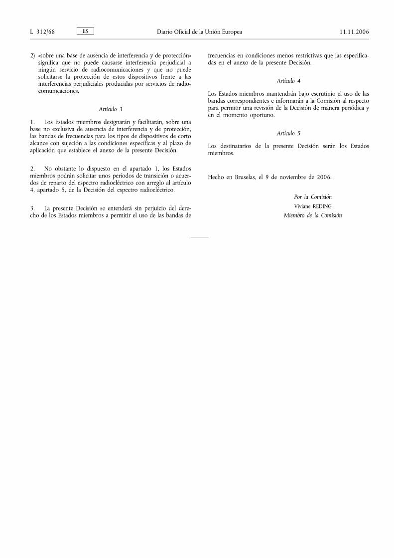
2) «sobre una base de ausencia de interferencia y de protección»significa que no puede causarse interferencia perjudicial aningún servicio de radiocomunicaciones y que no puedesolicitarse la protección de estos dispositivos frente a lasinterferencias perjudiciales producidas por servicios de radio-comunicaciones.
Artículo 3
1. Los Estados miembros designarán y facilitarán, sobre unabase no exclusiva de ausencia de interferencia y de protección,las bandas de frecuencias para los tipos de dispositivos de cortoalcance con sujeción a las condiciones específicas y al plazo deaplicación que establece el anexo de la presente Decisión.
2. No obstante lo dispuesto en el apartado 1, los Estadosmiembros podrán solicitar unos períodos de transición o acuer-dos de reparto del espectro radioeléctrico con arreglo al artículo4, apartado 5, de la Decisión del espectro radioeléctrico.
3. La presente Decisión se entenderá sin perjuicio del dere-cho de los Estados miembros a permitir el uso de las bandas de
frecuencias en condiciones menos restrictivas que las especifica-das en el anexo de la presente Decisión.
Artículo 4
Los Estados miembros mantendrán bajo escrutinio el uso de lasbandas correspondientes e informarán a la Comisión al respectopara permitir una revisión de la Decisión de manera periódica yen el momento oportuno.
Artículo 5
Los destinatarios de la presente Decisión serán los Estadosmiembros.
Hecho en Bruselas, el 9 de noviembre de 2006.
Por la ComisiónViviane REDING
Miembro de la Comisión
ESL 312/68 Diario Oficial de la Unión Europea 11.11.2006
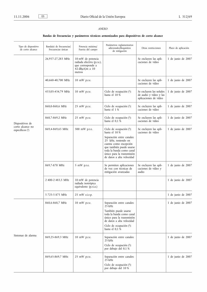
ANEXO
Bandas de frecuencias y parámetros técnicos armonizados para dispositivos de corto alcance
Tipo de dispositivode corto alcance
Banda(s) de frecuencias/Frecuencias únicas
Potencia máxima/Fuerza del campo
Parámetros reglamentariosadicionales/Requisitos
de mitigaciónOtras restricciones Plazo de aplicación
Dispositivos decorto alcance noespecíficos (1)
26,957-27,283 MHz 10 mW de potenciaradiada efectiva (p.r.e.),que corresponde a42 dBμA/m a 10metros
Se excluyen las apli-caciones de vídeo
1 de junio de 2007
40,660-40,700 MHz 10 mW p.r.e. Se excluyen las apli-caciones de vídeo
1 de junio de 2007
433,05-434,79 MHz 10 mW p.r.e. Ciclo de ocupación (2):hasta el 10 %
Se excluyen las señalesde audio y vídeo y lasaplicaciones de vídeo
1 de junio de 2007
868,0-868,6 MHz 25 mW p.r.e. Ciclo de ocupación (2):hasta el 1 %
Se excluyen las apli-caciones de vídeo
1 de junio de 2007
868,7-869,2 MHz 25 mW p.r.e. Ciclo de ocupación (2):hasta el 0,1 %
Se excluyen las apli-caciones de vídeo
1 de junio de 2007
869,4-869,65 MHz 500 mW p.r.e. Ciclo de ocupación (2):hasta el 10 %
Separación entre canales:25 kHz, teniendo encuenta como excepciónque también puede usarsetoda la banda como canalúnico para la transmisiónde datos a alta velocidad
Se excluyen las apli-caciones de vídeo
1 de junio de 2007
869,7-870 MHz 5 mW p.r.e. Se permiten aplicacionesde voz con técnicas demitigación avanzadas
Se excluyen las apli-caciones de vídeo yaudio
1 de junio de 2007
2 400-2 483,5 MHz 10 mW de potenciaradiada isotrópicaequivalente (p.r.i.e.)
1 de junio de 2007
5 725-5 875 MHz 25 mW e.i.r.p. 1 de junio de 2007
Sistemas de alarma
868,6-868,7 MHz 10 mW p.r.e. Separación entre canales:25 kHz
También puede usarsetoda la banda como canalúnico para la transmisiónde datos a alta velocidad
Ciclo de ocupación (2):hasta el 0,1 %
1 de junio de 2007
869,25-869,3 MHz 10 mW p.r.e. Separación entre canales:25 kHz
Ciclo de ocupación (2):por debajo del 0,1 %
1 de junio de 2007
869,65-869,7 MHz 25 mW p.r.e. Separación entre canales:25 kHz
Ciclo de ocupación (2):por debajo del 10 %
1 de junio de 2007
ES11.11.2006 Diario Oficial de la Unión Europea L 312/69

Tipo de dispositivode corto alcance
Banda(s) de frecuencias/Frecuencias únicas
Potencia máxima/Fuerza del campo
Parámetros reglamentariosadicionales/Requisitos
de mitigaciónOtras restricciones Plazo de aplicación
Alarmas deteleasistencia (3)
869,20-869,25 MHz 10 mW p.r.e. Separación entre canales:25 kHz
Ciclo de ocupación (2):por debajo del 0,1 %
1 de junio de 2007
Aplicacionesinductivas (4)
20,05-59,75 kHz 72 dBμA/m a 10 me-tros
1 de junio de 2007
59,75-60,25 kHz 42 dBμA/m a 10 me-tros
1 de junio de 2007
60,25-70 kHz 69 dBμA/m a 10 me-tros
1 de junio de 2007
70-119 kHz 42 dBμA/m a 10 me-tros
1 de junio de 2007
119-127 kHz 66 dBμA/m a 10 me-tros
1 de junio de 2007
127-135 kHz 42 dBμA/m a 10 me-tros
1 de junio de 2007
6 765-6 795 kHz 42 dBμA/m a 10 me-tros
1 de junio de 2007
13,553-13,567 MHz 42 dBμA/m a 10 me-tros
1 de junio de 2007
Implantes sanitariosactivos (5)
402-405 MHz 25 mW p.r.e. Separación entre canales:25 kHz
Otras restricciones sobrecanales: distintos trans-misores pueden combinarcanales adyacentes paraaumentar el ancho debanda con técnicas demitigación avanzadas
1 de junio de 2007
Aplicaciones de audioinalámbricas (6)
863-865 MHz 10 mW p.r.e. 1 de junio de 2007
(1) Esta categoría está disponible para cualquier tipo de aplicaciones que cumplan las condiciones técnicas (los usos habituales son la telemetría, los mandos a distancia, lasalarmas, los datos en general y otras aplicaciones semejantes).
(2) Ciclo de ocupación: proporción del tiempo en el que un equipo está transmitiendo de forma activa dentro de un período de una hora.(3) Los dispositivos de teleasistencia se emplean para asistir a las personas mayores o discapacitadas que viven en sus hogares, en caso de que necesiten socorro.(4) Esta categoría cubre, por ejemplo, los dispositivos para la inmovilización de vehículos, la identificación de animales, los sistemas de alarma, la detección de cables, la
gestión de residuos, la identificación de personas, los enlaces de voz inalámbricos, el control de acceso, los sensores de proximidad, los sistemas antirrobo —incluidos lossistemas de inducción antirrobo RF—, la transferencia de datos a dispositivos manuales, la identificación automática de artículos, los sistemas de control inalámbricos y elpago de peajes automático.
(5) Esta categoría cubre la parte radioléctrica de un producto sanitario implantable activo en el sentido del artículo 1 de la Directiva 90/385/CEE del Consejo, de 20 de juniode 1990, relativa a la aproximación de las legislaciones de los Estados miembros sobre los productos sanitarios implantables activos y sus periféricos.
(6) Aplicaciones para sistemas de audio inalámbricos, incluyendo: altavoces inalámbricos; auriculares inalámbricos; auriculares inalámbricos portátiles, por ejemplo, paraaparatos portátiles de lectura de CD o casetes o de radio; auriculares inalámbricos para uso en vehículos, por ejemplo, para una radio o teléfono móvil, etc.; controlmediante aparatos en la oreja para uso en conciertos o representaciones.
ESL 312/70 Diario Oficial de la Unión Europea 11.11.2006

ANEXO I - NORMATIVA
CUADRO NACIONAL DE ATRIBUCIÓN DE FRECUENCIA (CNAF)
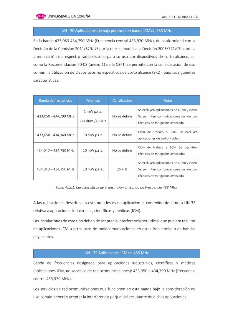
ANEXO I - NORMATIVA
UN - 30 Aplicaciones de baja potencia en banda ICM de 433 MHz
En la banda 433,050-434,790 MHz (Frecuencia central 433,920 MHz), de conformidad con la
Decisión de la Comisión 2011/829/UE por la que se modifica la Decisión 2006/771/CE sobre la
armonización del espectro radioeléctrico para su uso por dispositivos de corto alcance, así
como la Recomendación 70-03 (anexo 1) de la CEPT, se permite con la consideración de uso
común, la utilización de dispositivos no específicos de corto alcance (SRD), bajo las siguientes
características:
Banda de frecuencias Potencia Canalización Notas
433,050 - 434,790 MHz 1 mW p.r.a.
-13 dBm /10 kHz No se define
Se excluyen aplicaciones de audio y vídeo.
Se permiten comunicaciones de voz con
técnicas de mitigación avanzada.
433,050 - 434,040 MHz 10 mW p.r.a. No se define Ciclo de trabajo ≤ 10%. Se excluyen
aplicaciones de audio y vídeo.
434,040 – 434,790 MHz 10 mW p.r.a. No se define Ciclo de trabajo ≤ 10%. Se permiten
técnicas de mitigación avanzadas
434,040 – 434,790 MHz 10 mW p.r.a. 25 kHz
Se excluyen aplicaciones de audio y vídeo.
Se permiten comunicaciones de voz con
técnicas de mitigación avanzada.
Tabla AI.2.1: Características de Transmisión en Banda de Frecuencia 433 MHz.
A las utilizaciones descritas en esta nota les es de aplicación el contenido de la nota UN-32
relativa a aplicaciones industriales, científicas y médicas (ICM).
Las instalaciones de este tipo deben de aceptar la interferencia perjudicial que pudiera resultar
de aplicaciones ICM u otros usos de radiocomunicaciones en estas frecuencias o en bandas
adyacentes.
UN - 32 Aplicaciones ICM en 433 MHz
Banda de frecuencias designada para aplicaciones industriales, científicas y médicas
(aplicaciones ICM, no servicios de radiocomunicaciones): 433,050 a 434,790 MHz (frecuencia
central 433,920 MHz).
Los servicios de radiocomunicaciones que funcionen en esta banda bajo la consideración de
uso común deberán aceptar la interferencia perjudicial resultante de dichas aplicaciones.

ANEXO I - NORMATIVA
UN - 39 Banda de 868-870 MHz
Esta banda de se destina para aplicaciones de baja potencia y de datos en general de
conformidad con la Decisión de la Comisión 2011/829/UE por la que se modifica la Decisión
2006/771/CE sobre la armonización del espectro radioeléctrico para su uso por dispositivos de
corto alcance, así como la Recomendación 70-03 (anexos 1 y 7) de la CEPT, conforme a la
siguiente clasificación de dispositivos:
Dispositivos de baja potencia no especificados para aplicaciones genéricas:
• 868 - 868,600 MHz con 25 mW (p.r.a.) de potencia radiada aparente máxima.
Estos dispositivos deberán utilizar técnicas de acceso y mitigación de
interferencias con rendimiento al menos equivalente a las técnicas descritas
en las normas armonizadas según la Directiva 1995/5/CE, o alternativamente
no sobrepasar el 1% de ciclo de trabajo.
Se excluyen las aplicaciones analógicas de vídeo.
• 868 ,700 – 869,200 MHz con 25 mW (p.r.a.) de potencia radiada aparente
máxima. Estos dispositivos deberán utilizar técnicas de acceso y mitigación de
interferencias con rendimiento al menos equivalente a las técnicas descritas
en las normas armonizadas según la Directiva 1995/5/CE, o alternativamente
no sobrepasar el 0,1% de ciclo de trabajo.
Se excluyen las aplicaciones analógicas de vídeo.
• 869,400 – 869,650 MHz con 500 mW (p.r.a.) de potencia radiada aparente
máxima y 25 kHz de canalización, si bien pudiera utilizarse toda la banda como
canal único de datos de alta velocidad. Estos dispositivos deberán utilizar
técnicas de acceso y mitigación de interferencias con rendimiento al menos
equivalente a las técnicas descritas en las normas armonizadas según la
Directiva 1995/5/CE, o alternativamente no sobrepasar el 10% de ciclo de
trabajo.
Se excluyen las aplicaciones analógicas de vídeo.
Con potencia igual o inferior a 25 mW se permiten aplicaciones de voz
utilizando técnicas de voz, utilizando técnicas de acceso y mitigación de
interferencias con rendimiento al menos equivalente a las técnicas descritas
en las normal armonizadas según la Directiva 1995/5/CE, o alternativamente
no sobrepasar el 0,1% de ciclo de trabajo.

ANEXO I - NORMATIVA
• 869,700 – 870 MHz con 5 mW (p.r.a.) de potencia radiada aparente máxima.
Se permiten aplicaciones de voz con técnicas de mitigación avanzadas,
excluyéndose aplicaciones de audio y de vídeo.
• 869,700 – 870 MHz con 25 mW (p.r.a.) de potencia radiada aparente máxima.
Estos dispositivos deberán utilizar técnicas de acceso y mitigación de
interferencias con rendimiento al menos equivalente a las técnicas descritas
en las normas armonizadas según la Directiva 1995/5/CE, o alternativamente
no sobrepasar el 1% de ciclo de trabajo.
Se excluyen las aplicaciones analógicas de vídeo.
Alarmas:
• 868,600 – 868,700 MHz con 10 mW (p.r.a.) de potencia radiada aparente
máxima y 25 kHz de canalización, si bien pudiera utilizarse toda la banda como
canal único de datos de alta velocidad. Ciclo de trabajo máximo del 1%.
• 869,250 – 869,300 MHz con 10 mW (p.r.a.) de potencia radiada aparente
máxima y 25 kHz de canalización. Ciclo de trabajo máximo del 0,1%.
• 869,300 – 869,400 MHz con 10 mW (p.r.a.) de potencia radiada aparente
máxima y 25 kHz de canalización. Ciclo de trabajo máximo del 1%.
• 869,650 – 869,700 MHz con 25 mW (p.r.a.) de potencia radiada aparente
máxima y 25 kHz de canalización. Ciclo de trabajo máximo del 10%.
Alarmas de teleasistencia:
• 869,200 – 869,700 MHz con 10 mW (p.r.a.) de potencia radiada aparente
máxima y 25 kHz de canalización. Ciclo de trabajo máximo del 0,1%.
La norma técnica de referencia para estos dispositivos es la EN 300 220.
Los títulos habilitantes existentes en estas frecuencias, habrán de ajustarse a
las características indicadas en esta nota a más tardar la caducidad de los
mismos, pasando a uso común.
ESCUELA POLITÉCNICA SUPERIOR
TRABAJO FIN DE MÁSTER
CURSO 2016/2017
DISEÑO Y DESARROLLO DEL SISTEMA DE COMUNICACIONES INALÁMBRICO DE UN ENJAMBRE DE
UAV’S COLABORATIVOS
MÁSTER EN INGENIERÍA INDUSTRIAL
DOCUMENTO DEL PROYECTO
ANEXO II – LORAWAN SPECIFICATION

ANEXO II – LORAWAN SPECIFICATION
LORAWAN SPECIFICATION

©2015 LoRa™ Alliance Page 1 of 82 The authors reserve the right to change specifications without notice.
1
LoRa Specification 2 Copyright © 2015 LoRa Alliance, Inc. All rights reserved. 3
4
NOTICE OF USE AND DISCLOSURE 5
Copyright © LoRa Alliance, Inc. (2015). All Rights Reserved. 6 7 The information within this document is the property of the LoRa Alliance (―The Alliance‖) and its use and 8 disclosure are subject to LoRa Alliance Corporate Bylaws, Intellectual Property Rights (IPR) Policy and 9 Membership Agreements. 10 11 Elements of LoRa Alliance specifications may be subject to third party intellectual property rights, including 12 without limitation, patent, copyright or trademark rights (such a third party may or may not be a member of LoRa 13 Alliance). The Alliance is not responsible and shall not be held responsible in any manner for identifying or failing 14 to identify any or all such third party intellectual property rights. 15 16 This document and the information contained herein are provided on an ―AS IS‖ basis and THE ALLIANCE 17 DISCLAIMS ALL WARRANTIES EXPRESS OR IMPLIED, INCLUDING BUT NOTLIMITED TO (A) ANY 18 WARRANTY THAT THE USE OF THE INFORMATION HEREINWILL NOT INFRINGE ANY RIGHTS OF THIRD 19 PARTIES (INCLUDING WITHOUTLIMITATION ANY INTELLECTUAL PROPERTY RIGHTS INCLUDING 20 PATENT, COPYRIGHT OR TRADEMARK RIGHTS) OR (B) ANY IMPLIED WARRANTIES OF 21 MERCHANTABILITY, FITNESS FOR A PARTICULAR PURPOSE,TITLE OR NONINFRINGEMENT. 22 23 IN NO EVENT WILL THE ALLIANCE BE LIABLE FOR ANY LOSS OF PROFITS, LOSS OF BUSINESS, LOSS 24 OF USE OF DATA, INTERRUPTION OFBUSINESS, OR FOR ANY OTHER DIRECT, INDIRECT, SPECIAL OR 25 EXEMPLARY, INCIDENTIAL, PUNITIVE OR CONSEQUENTIAL DAMAGES OF ANY KIND, IN CONTRACT OR 26 IN TORT, IN CONNECTION WITH THIS DOCUMENT OR THE INFORMATION CONTAINED HEREIN, EVEN IF 27 ADVISED OF THE POSSIBILITY OF SUCH LOSS OR DAMAGE. 28 29 30 The above notice and this paragraph must be included on all copies of this document that are made. 31 32 LoRa Alliance, Inc. 33 2400 Camino Ramon, Suite 375 34 San Ramon, CA 94583 35 Note: All Company, brand and product names may be trademarks that are the sole property of their respective 36 owners. 37 38 39 40 41 42 43 44
45

LoRaWAN Specification
©2015 LoRa™ Alliance Page 2 of 82 The authors reserve the right to change specifications without notice.
1
2
LoRaWAN™ Specification 3
4 Authors: 5 N. Sornin (Semtech), M. Luis (Semtech), T. Eirich (IBM), T. Kramp (IBM), 6 O.Hersent (Actility) 7 8 Version: V1.0 9 Date: 2015 January 10 Status: Released 11 12 13 14 15
Important note: This is a candidate specification for the 16 LoRa™ Alliance protocol named LoRaWAN™. 17
18 19
20

LoRaWAN Specification
©2015 LoRa™ Alliance Page 3 of 82 The authors reserve the right to change specifications without notice.
Contents 1
1 Introduction .................................................................................................................. 7 2 1.1 LoRaWAN Classes .................................................................................................. 7 3 1.2 Conventions ............................................................................................................. 8 4
2 Introduction on LoRaWAN options ............................................................................... 9 5 2.1 LoRaWAN Classes .................................................................................................. 9 6 2.2 Specification scope ................................................................................................ 10 7
Class A – All end-devices ................................................................................................... 11 8 3 Physical Message Formats ........................................................................................ 12 9
3.1 Uplink Messages .................................................................................................... 12 10 3.2 Downlink Messages ............................................................................................... 12 11 3.3 Receive Windows................................................................................................... 12 12
3.3.1 First receive window channel, data rate, and start ............................................ 13 13 3.3.2 Second receive window channel, data rate, and start ....................................... 13 14 3.3.3 Receive window duration .................................................................................. 13 15 3.3.4 Receiver activity during the receive windows .................................................... 13 16 3.3.5 Network sending a message to an end-device ................................................. 13 17 3.3.6 Important notice on receive windows ................................................................ 14 18 3.3.7 Receiving or transmitting other protocols .......................................................... 14 19
4 MAC Message Formats ............................................................................................. 15 20 4.1 MAC Layer (PHYPayload) ...................................................................................... 15 21 4.2 MAC Header (MHDR field) ..................................................................................... 15 22
4.2.1 Message type (MType bit field) ......................................................................... 16 23 4.2.2 Major version of data message (Major bit field) ................................................ 16 24
4.3 MAC Payload of Data Messages (MACPayload) .................................................... 17 25 4.3.1 Frame header (FHDR) ...................................................................................... 17 26 4.3.2 Port field (FPort) ............................................................................................... 20 27 4.3.3 MAC Frame Payload Encryption (FRMPayload) ............................................... 20 28
4.4 Message Integrity Code (MIC)................................................................................ 21 29 5 MAC Commands........................................................................................................ 22 30
5.1 Link Check commands (LinkCheckReq, LinkCheckAns) ........................................ 23 31 5.2 Link ADR commands (LinkADRReq, LinkADRAns) ................................................ 23 32 5.3 End-Device Transmit Duty Cycle (DutyCycleReq, DutyCycleAns) .......................... 25 33 5.4 Receive Windows Parameters (RXParamSetupReq, RXParamSetupAns) ............ 26 34 5.5 End-Device Status (DevStatusReq, DevStatusAns) ............................................... 27 35 5.6 Creation / Modification of a Channel (NewChannelReq, NewChannelAns) ............ 27 36 5.7 Setting delay between TX and RX (RXTimingSetupReq, RXTimingSetupAns) ...... 28 37
6 End-Device Activation ................................................................................................ 30 38 6.1 Data Stored in the End-device after Activation ....................................................... 30 39
6.1.1 End-device address (DevAddr) ......................................................................... 30 40 6.1.2 Application identifier (AppEUI) .......................................................................... 30 41 6.1.3 Network session key (NwkSKey) ...................................................................... 30 42 6.1.4 Application session key (AppSKey) .................................................................. 30 43
6.2 Over-the-Air Activation ........................................................................................... 30 44 6.2.1 End-device identifier (DevEUI) ......................................................................... 31 45 6.2.2 Application key (AppKey) ................................................................................. 31 46 6.2.3 Join procedure.................................................................................................. 31 47 6.2.4 Join-request message ...................................................................................... 31 48 6.2.5 Join-accept message........................................................................................ 32 49
6.3 Activation by Personalization ................................................................................. 33 50

LoRaWAN Specification
©2015 LoRa™ Alliance Page 4 of 82 The authors reserve the right to change specifications without notice.
7 Physical Layer ........................................................................................................... 34 1 7.1 EU 863-870MHz ISM Band .................................................................................... 34 2
7.1.1 EU863-870 Preamble Format ........................................................................... 34 3 7.1.2 EU863-870 ISM Band channel frequencies ...................................................... 34 4 7.1.3 EU863-870 Data Rate and End-point Output Power encoding ......................... 35 5 7.1.4 EU863-870 JoinAccept CFList .......................................................................... 35 6 7.1.5 EU863-870 LinkAdrReq command ................................................................... 36 7 7.1.6 EU863-870 Maximum payload size .................................................................. 36 8 7.1.7 EU863-870 Receive windows ........................................................................... 37 9 7.1.8 EU863-870 Default Settings ............................................................................. 37 10
7.2 US 902-928MHz ISM Band .................................................................................... 39 11 7.2.1 US902-928 Preamble Format ........................................................................... 39 12 7.2.2 US902-928 Channel Frequencies .................................................................... 39 13 7.2.3 US902-928 Data Rate and End-point Output Power encoding ......................... 39 14 7.2.4 US902-928 JoinResp CFList ............................................................................ 40 15 7.2.5 US902-928 LinkAdrReq command ................................................................... 40 16 7.2.6 US902-928 Maximum payload size .................................................................. 41 17 7.2.7 US902-928 Receive windows ........................................................................... 42 18 7.2.8 US902-928 Default Settings ............................................................................. 42 19
7.3 China 779-787MHz ISM Band ................................................................................ 43 20 7.3.1 CN779-787 Preamble Format ........................................................................... 43 21 7.3.2 CN779-787 ISM Band channel frequencies ...................................................... 43 22 7.3.3 CN779-787 Data Rate and End-point Output Power encoding ........................ 44 23 7.3.4 CN779-787 JoinAccept CFList ........................................................................ 44 24 7.3.5 CN779-787 LinkAdrReq command .................................................................. 45 25 7.3.6 CN779-787 Maximum payload size ................................................................. 45 26 7.3.7 CN779-787 Receive windows ........................................................................... 46 27 7.3.8 CN779-787 Default Settings ............................................................................ 46 28
7.4 EU 433MHz ISM Band ........................................................................................... 47 29 7.4.1 EU433 Preamble Format .................................................................................. 47 30 7.4.2 EU433 ISM Band channel frequencies ............................................................. 47 31 7.4.3 EU433 Data Rate and End-point Output Power encoding ................................ 48 32 7.4.4 EU433 JoinAccept CFList ................................................................................. 48 33 7.4.5 EU433 LinkAdrReq command .......................................................................... 49 34 7.4.6 EU433 Maximum payload size ......................................................................... 49 35 7.4.7 EU433 Receive windows .................................................................................. 50 36 7.4.8 EU433 Default Settings .................................................................................... 50 37
Class B – Beacon ............................................................................................................... 51 38 8 Introduction to Class B ............................................................................................... 52 39 9 Principle of synchronous network initiated downlink (Class-B option) ......................... 53 40 10 Uplink frame in Class B mode .................................................................................... 55 41 11 Downlink Ping frame format (Class B option) ............................................................. 56 42
11.1 Physical frame format ............................................................................................ 56 43 11.2 Unicast & Multicast MAC messages ....................................................................... 56 44
11.2.1 Unicast MAC message format .......................................................................... 56 45 11.2.2 Multicast MAC message format ........................................................................ 56 46
12 Beacon acquisition and tracking ................................................................................. 57 47 12.1 Minimal beacon-less operation time ....................................................................... 57 48 12.2 Extension of beacon-less operation upon reception ............................................... 57 49 12.3 Minimizing timing drift ............................................................................................. 57 50
13 Class B Downlink slot timing ...................................................................................... 58 51 13.1 Definitions .............................................................................................................. 58 52 13.2 Slot randomization ................................................................................................. 59 53

LoRaWAN Specification
©2015 LoRa™ Alliance Page 5 of 82 The authors reserve the right to change specifications without notice.
14 Class B MAC commands ........................................................................................... 60 1 14.1 PingSlotInfoReq ..................................................................................................... 60 2 14.2 BeaconFreqReq ..................................................................................................... 61 3 14.3 PingSlotChannelReq .............................................................................................. 61 4 14.4 BeaconTimingReq .................................................................................................. 62 5 14.5 BeaconTimingAns .................................................................................................. 63 6
15 Beaconing (Class B option) ........................................................................................ 64 7 15.1 Beacon physical layer ............................................................................................ 64 8
15.1.1 EU 863-870MHz ISM Band .............................................................................. 64 9 15.1.2 US 902-928MHz ISM Band .............................................................................. 64 10
15.2 Beacon frame content ............................................................................................ 65 11 15.3 Beacon GwSpecific field format .............................................................................. 66 12
15.3.1 Gateway GPS coordinate:InfoDesc = 0, 1 or 2 ................................................. 67 13 15.4 Beaconing precise timing ....................................................................................... 67 14 15.5 Network downlink route update requirements ......................................................... 67 15
16 Class B unicast & multicast downlink channel frequencies ......................................... 69 16 16.1 EU 863-870MHz ISM Band .................................................................................... 69 17 16.2 US 902-928MHz ISM Band .................................................................................... 69 18
Class C – Continuously listening ......................................................................................... 70 19 17 Class C: Continuously listening end-device................................................................ 71 20
17.1 Second receive window duration for Class C ......................................................... 71 21 17.2 Class C Multicast downlinks ................................................................................... 71 22
Support information ............................................................................................................. 72 23 18 Examples and Application Information ....................................................................... 73 24
18.1 Uplink Timing Diagram for Confirmed Data Messages ........................................... 73 25 18.2 The third ACK frame in this example also carries an application payload. A 26
downlink frame can carry any combination of ACK, MAC control commands 27 and payload. Downlink Diagram for Confirmed Data Messages ............................. 73 28
18.3 Downlink Timing for Frame-Pending Messages ..................................................... 74 29 18.4 Data-Rate Adaptation during Message Retransmissions........................................ 76 30
19 Recommendation on contract to be provided to the network server by the end-31 device provider at the time of provisioning .......................................................................... 77 32 20 Recommendation on finding the locally used channels .............................................. 78 33 21 Revisions ................................................................................................................... 79 34
21.1 Revision 1.0 ........................................................................................................... 79 35 22 Glossary .................................................................................................................... 80 36 23 Bibliography ............................................................................................................... 81 37
23.1 References............................................................................................................. 81 38 24 NOTICE OF USE AND DISCLOSURE ....................................................................... 82 39 40
Tables 41
Table 1: MAC message types ............................................................................................. 16 42 Table 2: Major list ................................................................................................................ 16 43 Table 3: FPort list ................................................................................................................ 20 44 Table 4: MAC commands .................................................................................................... 22 45 Table 5: Channel state table ............................................................................................... 24 46 Table 6: LinkADRAns status bits signification ..................................................................... 25 47 Table 7: RX2SetupAns status bits signification ................................................................... 26 48 Table 8: Battery level decoding ........................................................................................... 27 49 Table 9: NewChannelAns status bits signification ............................................................... 28 50

LoRaWAN Specification
©2015 LoRa™ Alliance Page 6 of 82 The authors reserve the right to change specifications without notice.
Table 10: Del mapping table ............................................................................................... 29 1 Table 11: EU863-870 synch words ..................................................................................... 34 2 Table 12: EU863-870 default channels ............................................................................... 34 3 Table 13: EU863-870 JoinReq Channel List ....................................................................... 35 4 Table 14: Data rate and TX power table .............................................................................. 35 5 Table 15: ChMaskCntl value table....................................................................................... 36 6 Table 16: EU863-870 maximum payload size ..................................................................... 37 7 Table 17 : EU863-870 maximum payload size (not repeater compatible) ............................ 37 8 Table 18: Data rate and TX power table (Rem: DR4 is identical to DR12, DR8..13 must be 9 implemented in end-devices and are reserved for future applications) ................................ 40 10 Table 19: ChMaskCntl value table....................................................................................... 40 11 Table 20: US902-928 maximum payload size (repeater compatible) ................................... 41 12 Table 21 : US902-928 maximum payload size (not repeater compatible) ............................ 41 13 Table 22: Data rate mapping ............................................................................................... 42 14 Table 23: CN779-787 synch words .................................................................................... 43 15 Table 24: CN780 JoinReq Channel List .............................................................................. 43 16 Table 25: Data rate and TX power table .............................................................................. 44 17 Table 26: ChMaskCntl value table....................................................................................... 45 18 Table 27: CN780 maximum payload size ............................................................................ 45 19 Table 28 : CN780 maximum payload size (not repeater compatible) ................................... 46 20 Table 29: EU433 synch words ............................................................................................ 47 21 Table 30: EU433 JoinReq Channel List .............................................................................. 47 22 Table 31: Data rate and TX power table .............................................................................. 48 23 Table 32: ChMaskCntl value table....................................................................................... 49 24 Table 33: EU433 maximum payload size ............................................................................ 49 25 Table 34 : EU433 maximum payload size (not repeater compatible) ................................... 50 26 Table 35: Beacon timing ..................................................................................................... 58 27
28
Figures 29
Figure 1: LoRaWAN Classes ................................................................................................ 9 30 Figure 2: Uplink PHY structure ............................................................................................ 12 31 Figure 3: Downlink PHY structure ....................................................................................... 12 32 Figure 4: End-device receive slot timing. ............................................................................. 13 33 Figure 5: Radio PHY structure (CRC* is only available on uplink messages) ...................... 15 34 Figure 6: PHY payload structure ......................................................................................... 15 35 Figure 7: MAC payload structure ......................................................................................... 15 36 Figure 8: Frame header structure ........................................................................................ 15 37 Figure 9: LoRa message format elements ........................................................................... 15 38 Figure 10: US902-928 channel frequencies ........................................................................ 39 39 Figure 11: Beacon reception slot and ping slots .................................................................. 54 40 Figure 12 : beacon-less temporary operation ...................................................................... 57 41 Figure 13: Beacon timing .................................................................................................... 58 42 Figure 14: Class C end-device receive slot timing. .............................................................. 71 43 Figure 15: Uplink timing diagram for confirmed data messages .......................................... 73 44 Figure 16: Downlink timing diagram for confirmed data messages ...................................... 74 45 Figure 17: Downlink timing diagram for frame-pending messages, example 1 .................... 75 46 Figure 18: Downlink timing diagram for frame-pending messages, example 2 .................... 75 47 Figure 19: Downlink timing diagram for frame-pending messages, example 3 .................... 75 48 49

LoRaWAN Specification
©2015 LoRa™ Alliance Page 7 of 82 The authors reserve the right to change specifications without notice.
1 Introduction 1
This document describes the LoRaWAN™ network protocol which is optimized for battery-2 powered end-devices that may be either mobile or mounted at a fixed location. 3
LoRaWAN networks typically are laid out in a star-of-stars topology in which gateways1 4 relay messages between end-devices2 and a central network server at the backend. 5 Gateways are connected to the network server via standard IP connections while end-6 devices use single-hop LoRa™ or FSK communication to one or many gateways.3 All 7 communication is generally bi-directional, although uplink communication from an end-8 device to the network server is expected to be the predominant traffic. 9
Communication between end-devices and gateways is spread out on different frequency 10 channels and data rates. The selection of the data rate is a trade-off between 11 communication range and message duration, communications with different data rates do 12 not interfere with each other. LoRa data rates range from 0.3 kbps to 50 kbps. To maximize 13 both battery life of the end-devices and overall network capacity, the LoRa network 14 infrastructure can manage the data rate and RF output for each end-device individually by 15 means of an adaptive data rate (ADR) scheme. 16
End-devices may transmit on any channel available at any time, using any available data 17 rate, as long as the following rules are respected: 18
The end-device changes channel in a pseudo-random fashion for every 19 transmission. The resulting frequency diversity makes the system more robust to 20 interferences. 21
The end-device respects the maximum transmit duty cycle relative to the sub-band 22 used and local regulations. 23
The end-device respects the maximum transmit duration (or dwell time) relative to 24 the sub-band used and local regulations. 25
Note: Maximum transmit duty-cycle and dwell time per sub-band are 26 region specific and are defined in the Chapter 6. 27
1.1 LoRaWAN Classes 28
All LoRaWAN devices implement at least the Class A functionality as described in this 29 document. In addition they may implement options named Class B, Class C as also 30 described in this document or others to be defined. In all cases, they must remain 31 compatible with Class A. 32
1 Gateways are also known as concentrators or base stations.
2 End-devices are also known as motes.
3 Support for intermediate elements – repeaters – is not described in the document, however payload
restrictions for encapsulation overhead are included in this specification. A repeater is defined as using LoRaWAN as its backhaul mechanism.

LoRaWAN Specification
©2015 LoRa™ Alliance Page 8 of 82 The authors reserve the right to change specifications without notice.
1.2 Conventions 1
MAC commands are written LinkCheckReq, bits and bit fields are written FRMPayload, 2 constants are written RECEIVE_DELAY1, variables are written N. 3
In this document, 4
The octet order for all multi-octet fields is little endian and 5
EUI are 64 bits integers and are transmitted as little endian. 6
LoRaWAN Specification
©2015 LoRa™ Alliance Page 9 of 82 The authors reserve the right to change specifications without notice.
2 Introduction on LoRaWAN options 1
LoRa™ is a wireless modulation for long-range low-power low-data-rate applications 2 developed by Semtech. Devices implementing more than Class A are generally named 3 ―higher Class end-devices‖ in this document. 4
2.1 LoRaWAN Classes 5
A LoRa network distinguishes between a basic LoRaWAN (named Class A) and optional 6 features (Class B, Class C …): 7
Application
LoRa MAC
LoRa Modulation
EU868
EU433
US915
AS430
…
Class B (beacon)
Class C (Continuous)
Application
MAC
MAC options
Modulation
Regional ISM band
Class A (baseline)
8 Figure 1: LoRaWAN Classes 9
Bi-directional end-devices (Class A): End-devices of Class A allow for bi-10 directional communications whereby each end-device‘s uplink transmission is 11 followed by two short downlink receive windows. The transmission slot scheduled by 12 the end-device is based on its own communication needs with a small variation 13 based on a random time basis (ALOHA-type of protocol). This Class A operation is 14 the lowest power end-device system for applications that only require downlink 15 communication from the server shortly after the end-device has sent an uplink 16 transmission. Downlink communications from the server at any other time will have to 17 wait until the next scheduled uplink. 18
Bi-directional end-devices with scheduled receive slots (Class B): End-devices 19 of Class B allow for more receive slots. In addition to the Class A random receive 20 windows, Class B devices open extra receive windows at scheduled times. In order 21 for the End-device to open it receive window at the scheduled time it receives a time 22 synchronized Beacon from the gateway. This allows the server to know when the 23 end-device is listening. 24
Bi-directional end-devices with maximal receive slots (Class C): End-devices of 25 Class C have nearly continuously open receive windows, only closed when 26 transmitting. Class C end-device will use more power to operate than Class A or 27 Class B but they offer the lowest latency for server to end-device communication. 28

LoRaWAN Specification
©2015 LoRa™ Alliance Page 10 of 82 The authors reserve the right to change specifications without notice.
2.2 Specification scope 1
This LoRaWAN specification describes the additional functions differentiating an end-device 2 higher Class from one of Class A. A higher Class end-device shall also implement all the 3 functionality described in the LoRaWAN Class A specification. 4
NOTE: Physical message format, MAC message format, and other 5 parts of this specification that are common to both end-devices of 6 Class A and higher Classes are described only in the LoRaWAN 7 Class A specification to avoid redundancy. 8

LoRaWAN Specification
©2015 LoRa™ Alliance Page 11 of 82 The authors reserve the right to change specifications without notice.
CLASS A – ALL END-DEVICES 1
All LoRaWAN end-devices must implement Class A features. 2

LoRaWAN Specification
©2015 LoRa™ Alliance Page 12 of 82 The authors reserve the right to change specifications without notice.
3 Physical Message Formats 1
The LoRa terminology distinguishes between uplink and downlink messages. 2
3.1 Uplink Messages 3
Uplink messages are sent by end-devices to the network server relayed by one or many 4 gateways. 5
Uplink messages use the LoRa radio packet explicit mode in which the LoRa physical 6 header (PHDR) plus a header CRC (PHDR_CRC) are included.1 The integrity of the payload 7 is protected by a CRC. 8
The PHDR, PHDR_CRC and payload CRC fields are inserted by the radio transceiver. 9
Uplink PHY: 10
Preamble PHDR PHDR_CRC PHYPayload CRC
Figure 2: Uplink PHY structure 11
3.2 Downlink Messages 12
Each downlink message is sent by the network server to only one end-device and is 13 relayed by a single gateway.2 14
Downlink messages use the radio packet explicit mode in which the LoRa physical header 15 (PHDR) and a header CRC (PHDR_CRC) are included.3 16
Downlink PHY: 17
Preamble PHDR PHDR_CRC PHYPayload
Figure 3: Downlink PHY structure 18
3.3 Receive Windows 19
Following each uplink transmission the end-device opens two short receive windows. The 20 receive window start times is a configured periods are the end of the transmission of the last 21 uplink bit. 22
1 See the LoRa radio transceiver datasheet for a description of LoRa radio packet implicit/explicit
modes. 2 This specification does not describe the transmission of multicast messages from a network server
to many end-devices. 3 No payload integrity check is done at this level to keep messages as short as possible with minimum
impact on any duty-cycle limitations of the ISM bands used.

LoRaWAN Specification
©2015 LoRa™ Alliance Page 13 of 82 The authors reserve the right to change specifications without notice.
1 Figure 4: End-device receive slot timing. 2
3.3.1 First receive window channel, data rate, and start 3
The first receive window RX1 uses the same frequency channel as the uplink and a data 4 rate that is a function of the data rate used for the uplink. RX1 opens RECEIVE_DELAY11 5 seconds (+/- 20 microseconds) after the end of the uplink modulation. The relationship 6 between uplink and RX1 slot downlink data rate is region specific and detailed in the Section 7 7. By default the first receive window datarate is identical to the datarate of the last uplink. 8
3.3.2 Second receive window channel, data rate, and start 9
The second receive window RX2 uses a fixed configurable frequency and data rate and 10 opens RECEIVE_DELAY21 seconds (+/- 20 microseconds) after the end of the uplink 11 modulation. The frequency and data rate used can be modified through MAC commands 12 (see Section 5).The default frequency and data rate to use are region specific and detailed 13 in the Section 7 . 14
3.3.3 Receive window duration 15
The length of a receive window must be at least the time required by the end-device‘s radio 16 transceiver to effectively detect a downlink preamble. 17
3.3.4 Receiver activity during the receive windows 18
If a preamble is detected during one of the receive windows, the radio receiver stays active 19 until the downlink frame is demodulated. If a frame was detected and subsequently 20 demodulated during the first receive window and the frame was intended for this end-device 21 after address and MIC (message integrity code) checks, the end-device does not open the 22 second receive window. 23
3.3.5 Network sending a message to an end-device 24
If the network intends to transmit a downlink to an end-device, it will always initiate the 25 transmission precisely at the beginning of one of those two receive windows. 26
1 RECEIVE_DELAY1 and RECEIVE_DELAY2 are described in Chapter 6.

LoRaWAN Specification
©2015 LoRa™ Alliance Page 14 of 82 The authors reserve the right to change specifications without notice.
3.3.6 Important notice on receive windows 1
An end-device shall not transmit another uplink message before it either has received a 2 downlink message in the first or second receive window of the previous transmission, or the 3 second receive window of the previous transmission is expired. 4
3.3.7 Receiving or transmitting other protocols 5
The node may listen or transmit other protocols or do any transactions between the 6 LoRaWAN transmission and reception windows, as long as the end-device remains 7 compatible with the local regulation and compliant with the LoRaWAN specification. 8

LoRaWAN Specification
©2015 LoRa™ Alliance Page 15 of 82 The authors reserve the right to change specifications without notice.
4 MAC Message Formats 1
All LoRa uplink and downlink messages carry a PHY payload (Payload) starting with a 2 single-octet MAC header (MHDR), followed by a MAC payload (MACPayload)1, and ending 3 with a 4-octet message integrity code (MIC). 4 5
Radio PHY layer: 6
Preamble PHDR PHDR_CRC PHYPayload CRC*
Figure 5: Radio PHY structure (CRC* is only available on uplink messages) 7
PHYPayload: 8
MHDR MACPayload MIC
Figure 6: PHY payload structure 9
MACPayload: 10
FHDR FPort FRMPayload
Figure 7: MAC payload structure 11
FHDR: 12
DevAddr FCtrl FCnt FOpts
Figure 8: Frame header structure 13
Figure 9: LoRa message format elements 14
4.1 MAC Layer (PHYPayload) 15
16 Size (bytes) 1 1..M 4
PHYPayload MHDR MACPayload MIC
17
The maximum length (M) of the MACPayload field is region specific and is specified in 18 Chapter 6. 19
4.2 MAC Header (MHDR field) 20
21 Bit# 7..5 4..2 1..0
MHDR bits MType RFU Major
22
The MAC header specifies the message type (MType) and according to which major version 23 (Major) of the frame format of the LoRaWAN layer specification the frame has been 24 encoded. 25
1 Maximum payload size is detailed in the Chapter 6.

LoRaWAN Specification
©2015 LoRa™ Alliance Page 16 of 82 The authors reserve the right to change specifications without notice.
4.2.1 Message type (MType bit field) 1
The LoRaWAN distinguishes between six different MAC message types: join request, join 2 accept, unconfirmed data up/down, and confirmed data up/down. 3
MType Description
000 Join Request
001 Join Accept
010 Unconfirmed Data Up
011 Unconfirmed Data Down
100 Confirmed Data Up
101 Confirmed Data Down
110 RFU
111 Proprietary Table 1: MAC message types 4
4.2.1.1 Join-request and join-accept messages 5
The join-request and join-accept messages are used by the over-the-air activation procedure 6 described in Chapter 6.2. 7
4.2.1.2 Data messages 8
Data messages are used to transfer both MAC commands and application data, which can 9 be combined together in a single message. A confirmed-data message has to be 10 acknowledged by the receiver, whereas an unconfirmed-data message does not require 11 an acknowledgment.1 Proprietary messages can be used to implement non-standard 12 message formats that are not interoperable with standard messages but must only be used 13 among devices that have a common understanding of the proprietary extensions. 14
Message integrity is ensured in different ways for different message types and is described 15 per message type below. 16
4.2.2 Major version of data message (Major bit field) 17
18 Major bits Description
00 LoRaWAN R1
01..11 RFU Table 2: Major list 19
Note: The Major version specifies the format of the messages 20 exchanged in the join procedure (see Chapter 6.2) and the first four 21 bytes of the MAC Payload as described in Chapter 4. For each major 22 version, end-devices may implement different minor versions of the 23 frame format. The minor version used by an end-device must be made 24 known to the network server beforehand using out of band messages 25 (e.g., as part of the device personalization information). 26
1 A detailed timing diagram of the acknowledge mechanism is given in Section 18.

LoRaWAN Specification
©2015 LoRa™ Alliance Page 17 of 82 The authors reserve the right to change specifications without notice.
4.3 MAC Payload of Data Messages (MACPayload) 1
The MAC payload of the data messages, a so-called ―data frame‖, contains a frame header 2 (FHDR) followed by an optional port field (FPort) and an optional frame payload field 3 (FRMPayload). 4
4.3.1 Frame header (FHDR) 5
The FHDR contains the short device address of the end-device (DevAddr), a frame control 6 octet (FCtrl), a 2-octets frame counter (FCnt), and up to 15 octets of frame options (FOpts) 7 used to transport MAC commands. 8
9 Size (bytes) 4 1 2 0..15
FHDR DevAddr FCtrl FCnt FOpts
For downlink frames the FCtrl content of the frame header is: 10 Bit# 7 6 5 4 [3..0]
FCtrl bits ADR ADRACKReq ACK FPending FOptsLen
For uplink frames the FCtrl content of the frame header is: 11 Bit# 7 6 5 4 [3..0]
FCtrl bits ADR ADRACKReq ACK RFU FOptsLen
4.3.1.1 Adaptive data rate control in frame header (ADR, ADRACKReq in FCtrl) 12
LoRa network allows the end-devices to individually use any of the possible data rates. This 13 feature is used by the LoRaWAN to adapt and optimize the data rate of static end-devices. 14 This is referred to as Adaptive Data Rate (ADR) and when this is enabled the network will be 15 optimized to use the fastest data rate possible. 16
Mobile end-devices should use their fixed default data rate as data rate management is not 17 practical when the moving end-device causes fast changes in the radio environment. 18
If the ADR bit is set, the network will control the data rate of the end-device through the 19 appropriate MAC commands. If the ADR bit is not set, the network will not attempt to control 20 the data rate of the end-device regardless of the received signal quality. The ADR bit may 21 be set and unset by the end-device or the Network on demand. However, whenever 22 possible, the ADR scheme should be enabled to increase the battery life of the end-device 23 and maximize the network capacity. 24
Note: Even mobile end-devices are actually immobile most of the time. 25 So depending on its state of mobility, an end-device can request the 26 network to optimize its data rate using ADR. 27
If an end-device whose data rate is optimized by the network to use a data rate higher than 28 its default data rate, it periodically needs to validate that the network still receives the uplink 29 frames. Each time the uplink frame counter is incremented (for each new uplink, repeated 30 transmissions do not increase the counter), the device increments an ADR_ACK_CNT 31 counter. After ADR_ACK_LIMIT uplinks (ADR_ACK_CNT >= ADR_ACK_LIMIT) without any 32 downlink response, it sets the ADR acknowledgment request bit (ADRACKReq). The 33 network is required to respond with a downlink frame within the time set by the 34 ADR_ACK_DELAY, any received downlink frame following an uplink frame resets the 35 ADR_ACK_CNT counter. The downlink ACK bit does not need to be set as any response 36 during the receive slot of the end-device indicates that the gateway has still received the 37 uplinks from this device. If no reply is received within the next ADR_ACK_DELAY uplinks 38

LoRaWAN Specification
©2015 LoRa™ Alliance Page 18 of 82 The authors reserve the right to change specifications without notice.
(i.e., after a total of ADR_ACK_LIMIT + ADR_ACK_DELAY), the end-device may try to 1 regain connectivity by switching to the next lower data rate that provides a longer radio 2 range. The end-device will further lower its data rate step by step every time 3 ADR_ACK_LIMIT is reached. The ADRACKReq shall not be set if the device uses its 4 default data rate because in that case no action can be taken to improve the link range. 5
Note: Not requesting an immediate response to an ADR 6 acknowledgement request provides flexibility to the network to 7 optimally schedule its downlinks. 8 9
Note: In uplink transmissions the ADRACKReq bit is set if 10 ADR_ACK_CNT >= ADR_ACK_LIMIT and the current data-rate is 11 greater than the device defined minimum data rate, it is cleared in 12 other conditions. 13
4.3.1.2 Message acknowledge bit and acknowledgement procedure (ACK in FCtrl) 14
When receiving a confirmed data message, the receiver shall respond with a data frame that 15 has the acknowledgment bit (ACK) set. If the sender is an end-device, the network will send 16 the acknowledgement using one of the receive windows opened by the end-device after the 17 send operation. If the sender is a gateway, the end-device transmits an acknowledgment at 18 its own discretion. 19
Acknowledgements are only sent in response to the latest message received and are never 20 retransmitted. 21
22
Note: To allow the end-devices to be as simple as possible and have 23 as few states as possible it may transmit an explicit (possibly empty) 24 acknowledgement data message immediately after the reception of a 25 data message requiring a confirmation. Alternatively the end-device 26 may defer the transmission of an acknowledgement to piggyback it 27 with its next data message. 28
4.3.1.3 Retransmission procedure 29
The number of retransmissions (and their timing) for the same message where an 30 acknowledgment is requested but not received is at the discretion of the end device and 31 may be different for each end-device, it can also be set or adjusted from the network server. 32
Note: Some example timing diagrams of the acknowledge mechanism 33 are given in Chapter 18. 34
35
Note: If an end-device has reached its maximum number of 36 retransmissions without receiving an acknowledgment, it can try to re-37 gain connectivity by moving to a lower data rate with longer reach. It is 38 up to the end-device to retransmit the message again or to forfeit that 39 message and move on. 40
41
Note: If the network server has reached its maximum number of 42 retransmissions without receiving an acknowledgment, it will generally 43 consider the end-device as unreachable until it receives further 44

LoRaWAN Specification
©2015 LoRa™ Alliance Page 19 of 82 The authors reserve the right to change specifications without notice.
messages from the end-device. It is up to the network server to 1 retransmit the message once connectivity to the end-device in question 2 is regained or to forfeit that message and move on. 3
4
Note: The recommended data rate back-off strategy during re-5 transmissions is described in Chapter 18.4 6
4.3.1.4 Frame pending bit (FPending in FCtrl, downlink only) 7
The frame pending bit (FPending) is only used in downlink communication, indicating that 8 the gateway has more data pending to be sent and therefore asking the end-device to open 9 another receive window as soon as possible by sending another uplink message. 10
The exact use of FPending bit is described in Chapter 18.3. 11
4.3.1.5 Frame counter (FCnt) 12
Each end-device has two frame counters to keep track of the number of data frames sent 13 uplink to the network server (FCntUp), incremented by the end-device and received by the 14 end-device downlink from the network server (FCntDown), which is incremented by the 15 network server. The network server tracks the uplink frame counter and generates the 16 downlink counter for each end-device. After a join accept, the frame counters on the end-17 device and the frame counters on the network server for that end-device are reset to 0. 18 Subsequently FCntUp and FCntDown are incremented at the sender side by 1 for each data 19 frame sent in the respective direction. At the receiver side, the corresponding counter is 20 kept in sync with the value received provided the value received has incremented compared 21 to the current counter value and is less than the value specified by MAX_FCNT_GAP1 after 22 considering counter rollovers. If this difference is greater than the value of MAX_FCNY_GAP 23 then too many data frames have been lost then subsequent will be discarded. 24
The LoRaWAN allows the use of either 16-bits or 32-bits frame counters. The network side 25 needs to be informed out-of-band about the width of the frame counter implemented in a 26 given end-device. If a 16-bits frame counter is used, the FCnt field can be used directly as 27 the counter value, possibly extended by leading zero octets if required. If a 32-bits frame 28 counter is used, the FCnt field corresponds to the least-significant 16 bits of the 32-bits 29 frame counter (i.e., FCntUp for data frames sent uplink and FCntDown for data frames sent 30 downlink). 31
The end-device shall not reuse the same FCntUp value, except for retransmission, with the 32 same application and network session keys. 33
Note: Since the FCnt field carries only the least-significant 16 bits of 34 the 32-bits frame counter, the server must infer the 16 most-significant 35 bits of the frame counter from the observation of the traffic. 36
4.3.1.6 Frame options (FOptsLen in FCtrl, FOpts) 37
The frame-options length field (FOptsLen) in FCtrl byte denotes the actual length of the 38 frame options field (FOpts) included in the frame. 39
1 Actual value for MAX_FCNT_GAP, RECEIVE_DELAY1 and RECEIVE_DELAY2 can be found at
7.1.7 for EU863-870 or 7.2.7 for US902-928.

LoRaWAN Specification
©2015 LoRa™ Alliance Page 20 of 82 The authors reserve the right to change specifications without notice.
FOpts transport MAC commands of a maximum length of 15 octets that are piggybacked 1
onto data frames; see Chapter 4.4 for a list of valid MAC commands. 2
If FOptsLen is 0, the FOpts field is absent. If FOptsLen is different from 0, i.e. if MAC 3 commands are present in the FOpts field, the port 0 cannot be used (FPort must be either 4 not present or different from 0). 5
MAC commands cannot be simultaneously present in the payload field and the frame 6 options field. 7
4.3.2 Port field (FPort) 8
If the frame payload field is not empty, the port field must be present. If present, an FPort 9
value of 0 indicates that the FRMPayload contains MAC commands only; see Chapter 4.4 10 for a list of valid MAC commands. FPort values 1..223 (0x01..0xDF) are application-11 specific. FPort values 224..255 (0xE0..0xFF) are reserved for future standardized 12 application extensions. 13
14 Size (bytes) 7..23 0..1 0..N
MACPayload FHDR FPort FRMPayload
N is the number of octets of the application payload. The valid range for N is region specific 15 and is defined in Section 7 16
N should be equal or smaller than: 17 N ≤ M - 1 - (length of FHDR in octets) 18
where M is the maximum MAC payload length. 19
4.3.3 MAC Frame Payload Encryption (FRMPayload) 20
If a data frame carries a payload, FRMPayload must be encrypted before the message 21 integrity code (MIC) is calculated. 22
The encryption scheme used is based on the generic algorithm described in IEEE 23 802.15.4/2006 Annex B [IEEE802154] using AES with a key length of 128 bits. 24
As a default, the encryption/decryption is done by the LoRaWAN layer for all FPort. The 25 encryption/decryption may be done above the LoRaWAN layer for specific FPorts except 0, 26 if this is more convenient for the application. The information concerning which FPort from 27 which node is encrypted/decrypted outside of the LoRaWAN layer must be communicated to 28 the server using an out-of-band channel (see Section 19). 29
4.3.3.1 Encryption in LoRaWAN 30
The key K used depends on the FPort of the data message: 31
32 FPort K
0 NwkSKey
1..255 AppSKey Table 3: FPort list 33
The fields encrypted are: 34 pld = FRMPayload 35
For each data message, the algorithm defines a sequence of Blocks Ai for i = 1..k with k = 36 ceil(len(pld) / 16): 37

LoRaWAN Specification
©2015 LoRa™ Alliance Page 21 of 82 The authors reserve the right to change specifications without notice.
1 Size (bytes) 1 4 1 4 4 1 1
Ai 0x01 4 x 0x00 Dir DevAddr FCntUp or FCntDown
0x00 i
2
The direction field (Dir) is 0 for uplink frames and 1 for downlink frames. 3
The blocks Ai are encrypted to get a sequence S of blocks Si: 4 5 Si = aes128_encrypt(K, Ai) for i = 1..k 6 S = S1 | S2 | .. | Sk 7
Encryption and decryption of the payload is done by truncating 8 9 (pld | pad16) xor S 10
to the first len(pld) octets. 11
4.3.3.2 Encryption above the LoRaWAN layer 12
If the layers above LoRaWAN provide pre-encrypted FRMPayload to LoRaWAN on selected 13 ports (but not on FPort 0 which is reserved for MAC commands), LoRaWAN transfers 14 FRMPayload from MACPayload to the application and FRMPayload from the application to 15 MACPayload without any modification of FRMPayload. 16
17
4.4 Message Integrity Code (MIC) 18
The message integrity code (MIC) is calculated over all the fields in the message. 19 20 msg = MHDR | FHDR | FPort | FRMPayload 21
whereby len(msg) denotes the length of the message in octets. 22
The MIC is calculated as follows [RFC4493]: 23 24 cmac = aes128_cmac(NwkSKey, B0 | msg) 25 MIC = cmac[0..3] 26 27 whereby the block B0 is defined as follows: 28 Size (bytes) 1 4 1 4 4 1 1
B0 0x49 4 x 0x00 Dir DevAddr FCntUp or FCntDown
0x00 len(msg)
29
The direction field (Dir) is 0 for uplink frames and 1 for downlink frames. 30

LoRaWAN Specification
©2015 LoRa™ Alliance Page 22 of 82 The authors reserve the right to change specifications without notice.
5 MAC Commands 1
For network administration, a set of MAC commands may be exchanged exclusively 2 between the network server and the MAC layer on an end-device. MAC layer commands 3 are never visible to the application or the application server or the application running on the 4 end-device. 5
A single data frame can contain any sequence of MAC commands, either piggybacked in the 6 FOpts field or, when sent as a separate data frame, in the FRMPayload field with the FPort 7 field being set to 0. Piggybacked MAC commands are always sent without encryption and 8 must not exceed 15 octets. MAC commands sent as FRMPayload are always encrypted 9 and must not exceed the maximum FRMPayload length. 10
Note: MAC commands whose content shall not be disclosed to an 11 eavesdropper must be sent in the FRMPayload of a separate data 12 message. 13
A MAC command consists of a command identifier (CID) of 1 octet followed by a possibly 14 empty command-specific sequence of octets. 15
16 CID Command Transmitted by Short Description
End-device
Gateway
0x02 LinkCheckReq x Used by an end-device to validate its connectivity to a network.
0x02 LinkCheckAns x Answer to LinkCheckReq command. Contains the received signal power
estimation indicating to the end-device the quality of reception (link margin).
0x03 LinkADRReq x Requests the end-device to change data rate, transmit power, repetition rate or
channel.
0x03 LinkADRAns x Acknowledges the LinkRateReq.
0x04 DutyCycleReq x Sets the maximum aggregated transmit duty-cycle of a device
0x04 DutyCycleAns x Acknowledges a DutyCycleReq command
0x05 RXParamSetupReq x Sets the reception slots parameters
0x05 RXParamSetupAns x Acknowledges a RXSetupReq command
0x06 DevStatusReq x Requests the status of the end-device
0x06 DevStatusAns x Returns the status of the end-device, namely its battery level and its demodulation margin
0x07 NewChannelReq x Creates or modifies the definition of a radio channel
0x07 NewChannelAns x Acknowledges a NewChannelReq command
0x08 RXTimingSetupReq x Sets the timing of the of the reception slots
0x08 RXTimingSetupAns x Acknowledge RXTimingSetupReq command
0x80 to
0xFF
Proprietary x x Reserved for proprietary network command extensions
Table 4: MAC commands 17
Note: The length of a MAC command is not explicitly given and must 18 be implicitly known by the MAC implementation. Therefore unknown 19 MAC commands cannot be skipped and the first unknown MAC 20 command terminates the processing of the MAC command sequence. 21 It is therefore advisable to order MAC commands according to the 22

LoRaWAN Specification
©2015 LoRa™ Alliance Page 23 of 82 The authors reserve the right to change specifications without notice.
version of the LoRaWAN specification which has introduced a MAC 1 command for the first time. This way all MAC commands up to the 2 version of the LoRaWAN specification implemented can be processed 3 even in the presence of MAC commands specified only in a version of 4 the LoRaWAN specification newer than that implemented. 5
6
Note: Any values adjusted by the network server (e.g., RX2, new or 7 adjusted channels definitions) remain only valid until the next join of 8 the end-device. Therefore after each successful join procedure the 9 end-device uses the default parameters again and it is up to the 10 network server to re-adjust the values again as needed. 11
5.1 Link Check commands (LinkCheckReq, LinkCheckAns) 12
13
With the LinkCheckReq command, an end-device may validate its connectivity with the 14 network. The command has no payload. 15
When a LinkCheckReq is received by the network server via one or multiple gateways, it 16 responds with a LinkCheckAns command. 17
18 Size (bytes) 1 1
LinkCheckAns Payload Margin GwCnt
The demodulation margin (Margin) is an 8-bit unsigned integer in the range of 0..254 19 indicating the link margin in dB of the last successfully received LinkCheckReq command. 20 A value of ―0‖ means that the frame was received at the demodulation floor (0 dB or no 21 margin) while a value of ―20‖, for example, means that the frame reached the gateway 20 dB 22 above the demodulation floor. Value ―255‖ is reserved. 23
The gateway count (GwCnt) is the number of gateways that successfully received the last 24 LinkCheckReq command. 25
5.2 Link ADR commands (LinkADRReq, LinkADRAns) 26
27
With the LinkADRReq command, the network server requests an end-device to perform a 28 rate adaptation. 29
30 Size (bytes) 1 2 1
LinkADRReq Payload DataRate_TXPower ChMask Redundancy
31 Bits [7:4] [3:0]
DataRate_TXPower DataRate TXPower
32
The requested date rate (DataRate) and TX output power (TXPower) are region-specific 33 and are encoded as indicated in Chapter 7. 34

LoRaWAN Specification
©2015 LoRa™ Alliance Page 24 of 82 The authors reserve the right to change specifications without notice.
The channel mask (ChMask) encodes the channels usable for uplink access as follows with 1 bit 0 corresponding to the LSB: 2
Bit# Usable channels
0 Channel 1
1 Channel 2
.. ..
15 Channel 16 Table 5: Channel state table 3
A bit in the ChMask field set to 1 means that the corresponding channel can be used for 4 uplink transmissions if this channel allows the data rate currently used by the end-device. A 5 bit set to 0 means the corresponding channels should be avoided. 6 7
Bits 7 [6:4] [3:0]
Redundancy bits RFU ChMaskCntl NbRep
In the Redundancy bits the number of repetitions (NbRep) field is the number of repetition 8 for each uplink message. This applies only to ―unconfirmed‖ uplink frames. The default value 9 is 1. The valid range is [1:15]. If NbRep==0 is received the end-device should use the 10 default value. This field can be used by the network manager to control the redundancy of 11 the node uplinks to obtain a given Quality of Service. The end-device performs frequency 12 hopping as usual between repeated transmissions, it does wait after each repetition until the 13 receive windows have expired. 14
The channel mask control (ChMaskCntl) field controls the interpretation of the previously 15 defined ChMask bit mask. This field will only be non-zero values in networks where more 16 than 16 channels are implemented. It controls the block of 16 channels to which the 17 ChMask applies. It can also be used to globally turn on or off all channels using specific 18 modulation. This field usage is region specific and is defined in Chapter 7. 19
The channel frequencies are region-specific and they are defined in Chapter 6. An end-20 device answers to a LinkADRReq with a LinkADRAns command. 21
22 Size (bytes) 1
LinkADRAns Payload Status
23 24
Bits [7:3] 2 1 0
Status bits RFU Power ACK Data rate ACK Channel mask ACK
25

LoRaWAN Specification
©2015 LoRa™ Alliance Page 25 of 82 The authors reserve the right to change specifications without notice.
The LinkADRAns Status bits have the following meaning: 1 2 Bit = 0 Bit = 1
Channel mask ACK The channel mask sent enables a yet undefined channel. The command was discarded and the end-device state was not changed.
The channel mask sent was successfully interpreted. All currently defined channel states were set according to the mask.
Data rate ACK The data rate requested is unknown to the end-device or is not possible given the channel mask provided (not supported by any of the enabled channels). The command was discarded and the end-device state was not changed.
The data rate was successfully set.
Power ACK The requested power level is not implemented in the device. The command was discarded and the end-device state was not changed.
The power level was successfully set.
Table 6: LinkADRAns status bits signification 3
If any of those three bits equals 0, the command did not succeed and the node has kept the 4 previous state. 5
5.3 End-Device Transmit Duty Cycle (DutyCycleReq, DutyCycleAns) 6
The DutyCycleReq command is used by the network coordinator to limit the maximum 7 aggregated transmit duty cycle of an end-device. The aggregated transmit duty cycle 8 corresponds to the transmit duty cycle over all sub-bands. 9 10
Size (bytes) 1
DutyCycleReq Payload MaxDCycle
11 The maximum end-device transmit duty cycle allowed is: 12
The valid range for MaxDutyCycle is [0 : 15]. A value of 0 corresponds to ―no duty cycle 13 limitation‖ except the one set by the regional regulation. 14
A value of 255 means that the end-device shall become silent immediately. It is equivalent to 15 remotely switching off the end-device. 16
An end-device answers to a DutyCycleReq with a DutyCycleAns command. The 17 DutyCycleAns MAC reply does not contain any payload. 18

LoRaWAN Specification
©2015 LoRa™ Alliance Page 26 of 82 The authors reserve the right to change specifications without notice.
5.4 Receive Windows Parameters (RXParamSetupReq, 1
RXParamSetupAns) 2
The RXParamSetupReq command allows a change to the frequency and the data rate set 3 for the second receive window (RX2) following each uplink. The command also allows to 4 program an offset between the uplink and the RX1 slot downlink data rates. 5
6 Size (bytes) 1 3
RX2SetupReq Payload DLsettings Frequency
7 Bits 7 6:4 3:0
DLsettings RFU RX1DRoffset RX2DataRate
8 The RX1DRoffset field sets the offset between the uplink data rate and the downlink data 9 rate used to communicate with the end-device on the first reception slot (RX1). As a default 10 this offset is 0.. The offset is used to take into account maximum power density constraints 11 for base stations in some regions and to balance the uplink and downlink radio link margins. 12
The data rate (RX2DataRate) field defines the data rate of a downlink using the second 13 receive window following the same convention as the LinkADRReq command (0 means 14 DR0/125kHz for example). The frequency (Frequency) field corresponds to the frequency of 15 the channel used for the second receive window, whereby the frequency is coded following 16 the convention defined in the NewChannelReq command. 17
The RXParamSetupAns command is used by the end-device to acknowledge the reception 18 of RXParamSetupReq command. The payload contains a single status byte. 19
Size (bytes) 1
RX2SetupAns Payload Status
20 The status (Status) bits have the following meaning. 21
Bits 7:3 2 1 0
Status bits
RFU RX1DRoffset ACK
RX2 Data rate ACK
Channel ACK
22 Bit = 0 Bit = 1
Channel ACK The frequency requested is not usable by the end-device.
RX2 slot channel was successfully set
RX2 Data rate ACK The data rate requested is unknown to the end-device.
RX2 slot data rate was successfully set
RX1DRoffset ACK the uplink/downlink data rate offset for RX1 slot is not in the allowed range
RX1DRoffset was successfully set
Table 7: RX2SetupAns status bits signification 23
If either of the 3 bits is equal to 0, the command did not succeed and the previous 24 parameters are kept. 25 26

LoRaWAN Specification
©2015 LoRa™ Alliance Page 27 of 82 The authors reserve the right to change specifications without notice.
5.5 End-Device Status (DevStatusReq, DevStatusAns) 1
With the DevStatusReq command a network server may request status information from an 2 end-device. The command has no payload. If a DevStatusReq is received by an end-3 device, it responds with a DevStatusAns command. 4
Size (bytes) 1 1
DevStatusAns Payload Battery Margin
The battery level (Battery) reported is encoded as follows: 5 Battery Description
0 The end-device is connected to an external power source.
1..254 The battery level, 1 being at minimum and 254 being at maximum
255 The end-device was not able to measure the battery level.
Table 8: Battery level decoding 6
The margin (Margin) is the demodulation signal-to-noise ratio in dB rounded to the nearest 7 integer value for the last successfully received DevStatusReq command. It is a signed 8 integer of 6 bits with a minimum value of -32 and a maximum value of 31. 9
Bits 7:6 5:0
Status RFU Margin
5.6 Creation / Modification of a Channel (NewChannelReq, 10
NewChannelAns) 11
12 The NewChannelReq command can be used to either modify the parameters of an existing 13 channel or to create a new one. The command sets the center frequency of the new channel 14 and the range of data rates usable on this channel: 15
Size (bytes) 1 3 1
NewChannelReq Payload ChIndex Freq DrRange
16
The channel index (ChIndex) is the index of the channel being created or modified. 17 Depending on the region and frequency band used, the LoRaWAN specification imposes 18 default channels which must be common to all devices and cannot be modified by the 19 NewChannelReq command (cf. Chapter 6). If the number of default channels is N, the 20 default channels go from 0 to N-1, and the acceptable range for ChIndex is N to 15. A 21 device must be able to handle at least 16 different channel definitions. In certain region the 22 device may have to store more than 16 channel definitions. 23 24
The frequency (Freq) field is a 24 bits unsigned integer. The actual channel frequency in Hz 25 is 100 x Freq whereby values representing frequencies below 100 MHz are reserved for 26 future use. This allows setting the frequency of a channel anywhere between 100 MHz to 27 1.67 GHz in 100 Hz steps. A Freq value of 0 disables the channel. The end-device has to 28 check that the frequency is actually allowed by its radio hardware and return an error 29 otherwise. 30 31
The data-rate range (DrRange) field specifies the data-rate range allowed for this channel. 32 The field is split in two 4-bit indexes: 33
Bits 7:4 3:0
DrRange MaxDR MinDR

LoRaWAN Specification
©2015 LoRa™ Alliance Page 28 of 82 The authors reserve the right to change specifications without notice.
1
Following the convention defined in Section 5.2 the minimum data rate (MinDR) subfield 2 designate the lowest data rate allowed on this channel. For example 0 designates DR0 / 125 3 kHz. Similarly, the maximum data rate (MaxDR) designates the highest data rate. For 4 example, DrRange = 0x77 means that only 50 kbps GFSK is allowed on a channel and 5 DrRange = 0x50 means that DR0 / 125 kHz to DR5 / 125 kHz are supported. 6
The newly defined channel is enabled and can immediately be used for communication. 7
The end-device acknowledges the reception of a NewChannelReq by sending back a 8 NewChannelAns command. The payload of this message contains the following 9 information: 10
Size (bytes) 1
NewChannelAns Payload Status
11
The status (Status) bits have the following meaning: 12 Bits 7:2 1 0
Status RFU Data rate range ok
Channel frequency ok
13 Bit = 0 Bit = 1
Data rate range ok The designated data rate range exceeds the ones currently defined for this end-device
The data rate range is compatible with the possibilities of the end-device
Channel frequency ok The device cannot use this frequency
The device is able to use this frequency.
Table 9: NewChannelAns status bits signification 14
If either of those 2 bits equals 0, the command did not succeed and the new channel has not 15 been created. 16
5.7 Setting delay between TX and RX (RXTimingSetupReq, 17
RXTimingSetupAns) 18
The RXTimingSetupReq command allows configuring the delay between the end of the TX 19 uplink and the opening of the first reception slot. The second reception slot opens one 20 second after the first reception slot. 21
Size (bytes) 1
RXTimingSetupReq Payload Settings
22
The delay (Delay) field specifies the delay. The field is split in two 4-bit indexes: 23 Bits 7:4 3:0
Settings RFU Del
24
The delay is expressed in seconds. Del 0 is mapped on 1 s. 25 Del Delay [s]
0 1
1 1
2 2
3 3
.. ..

LoRaWAN Specification
©2015 LoRa™ Alliance Page 29 of 82 The authors reserve the right to change specifications without notice.
15 15 Table 10: Del mapping table 1
2
An end device answers RXTimingSetupReq with RXTimingSetupAns with no payload. 3

LoRaWAN Specification
©2015 LoRa™ Alliance Page 30 of 82 The authors reserve the right to change specifications without notice.
6 End-Device Activation 1
To participate in a LoRaWAN network, each end-device has to be personalized and 2 activated. 3
Activation of an end-device can be achieved in two ways, either via Over-The-Air 4 Activation (OTAA) when an end-device is deployed or reset, or via Activation By 5 Personalization (ABP) in which the two steps of end-device personalization and activation 6 are done as one step. 7
6.1 Data Stored in the End-device after Activation 8
After activation, the following information is stored in the end-device: a device address 9 (DevAddr), an application identifier (AppEUI), a network session key (NwkSKey), and an 10 application session key (AppSKey). 11
6.1.1 End-device address (DevAddr) 12
The DevAddr consists of 32 bits identifies the end-device within the current network. Its 13 format is as follows: 14
Bit# [31..25] [24..0]
DevAddr bits NwkID NwkAddr
The most significant 7 bits are used as network identifier (NwkID) to separate addresses of 15 territorially overlapping networks of different network operators and to remedy roaming 16 issues. The least significant 25 bits, the network address (NwkAddr) of the end-device, can 17 be arbitrarily assigned by the network manager. 18
6.1.2 Application identifier (AppEUI) 19
The AppEUI is a global application ID in IEEE EUI64 address space that uniquely identifies 20 the application provider (i.e., owner) of the end-device. 21
The AppEUI is stored in the end-device before the activation procedure is executed. 22
6.1.3 Network session key (NwkSKey) 23
The NwkSKey is a network session key specific for the end-device. It is used by both the 24 network server and the end-device to calculate and verify the MIC (message integrity code) 25 of all data messages to ensure data integrity. It is further used to encrypt and decrypt the 26 payload field of a MAC-only data messages. 27
6.1.4 Application session key (AppSKey) 28
The AppSKey is an application session key specific for the end-device. It is used by both 29 the network server and the end-device to encrypt and decrypt the payload field of 30 application-specific data messages. It is also used to calculate and verify an application-31 level MIC that may be included in the payload of application-specific data messages. 32
6.2 Over-the-Air Activation 33
For over-the-air activation, end-devices must follow a join procedure prior to participating in 34 data exchanges with the network server. An end-device has to go through a new join 35 procedure every time it has lost the session context information. 36

LoRaWAN Specification
©2015 LoRa™ Alliance Page 31 of 82 The authors reserve the right to change specifications without notice.
The join procedure requires the end-device to be personalized with the following information 1 before its starts the join procedure: a globally unique end-device identifier (DevEUI), the 2 application identifier (AppEUI), and an AES-128 key (AppKey). 3
The AppEUI is described above in 6.1.2. 4
Note: For over-the-air-activation, end-devices are not personalized 5 with any kind of network key. Instead, whenever an end-device joins a 6 network, a network session key specific for that end-device is derived 7 to encrypt and verify transmissions at the network level. This way, 8 roaming of end-devices between networks of different providers is 9 facilitated. Using both a network session key and an application 10 session key further allows federated network servers in which 11 application data cannot be read or tampered with by the network 12 provider. 13
6.2.1 End-device identifier (DevEUI) 14
The DevEUI is a global end-device ID in IEEE EUI64 address space that uniquely identifies 15 the end-device. 16
6.2.2 Application key (AppKey) 17
The AppKey is an AES-128 application key specific for the end-device that is assigned by 18 the application owner to the end-device and most likely derived from an application-specific 19 root key exclusively known to and under the control of the application provider.1 Whenever 20 an end-device joins a network via over-the-air activation, the AppKey is used to derive the 21 session keys NwkSKey and AppSKey specific for that end-device to encrypt and verify 22 network communication and application data. 23
6.2.3 Join procedure 24
From an end-device‘s point of view, the join procedure consists of two MAC messages 25 exchanged with the server, namely a join request and a join accept. 26
6.2.4 Join-request message 27
The join procedure is always initiated from the end-device by sending a join-request 28 message. 29
30 Size (bytes) 8 8 2
Join Request AppEUI DevEUI DevNonce
The join-request message contains the AppEUI and DevEUI of the end-device followed by a 31 nonce of 2 octets (DevNonce). 32
DevNonce is a random value.2 For each end-device, the network server keeps track of a 33 certain number of DevNonce values used by the end-device in the past, and ignores join 34 requests with any of these DevNonce values from that end-device. 35
1. Since all end-devices end up with unrelated application keys specific for each end-device, extracting the AppKey from an end-device only compromises this one end-device. 2 The DevNonce can be extracted by issuing a sequence of RSSI measurements under the
assumption that the quality of randomness fulfills the criteria of true randomness

LoRaWAN Specification
©2015 LoRa™ Alliance Page 32 of 82 The authors reserve the right to change specifications without notice.
Note: This mechanism prevents replay attacks by sending previously 1 recorded join-request messages with the intention of disconnecting the 2 respective end-device from the network. 3
The message integrity code (MIC) value (see Chapter 4 for MAC message description) for a 4 join-request message is calculated as follows:1 5 6 cmac = aes128_cmac(AppKey, MHDR | AppEUI | DevEUI | DevNonce) 7 MIC = cmac[0..3] 8
The join-request message is not encrypted. 9
6.2.5 Join-accept message 10
The network server will respond to the join-request message with a join-accept message if 11 the end-device is permitted to join a network. The join-accept message is sent like a normal 12 downlink but uses delays JOIN_ACCEPT_DELAY1 or JOIN_ACCEPT_DELAY2 (instead of 13 RECEIVE_DELAY1 and RECEIVE_DELAY2, respectively). The channel frequency and data 14 rate used for these two receive windows are identical to the one used for the RX1 and RX2 15 receive windows described in the ―receive windows‖ section of the ―Physical Layer‖ chapter 16
No response is given to the end-device if the join request is not accepted. 17
The join-accept message contains an application nonce (AppNonce) of 3 octets, a network 18 identifier (NetID), an end-device address (DevAddr), a delay between TX and RX 19 (RxDelay) and an optional list of channel frequencies (CFList) for the network the end-20 device is joining. The CFList option is region specific and is defined in Section 7. 21
22 Size (bytes) 3 3 4 1 1 (16) Optional
Join Accept AppNonce NetID DevAddr DLSettings RxDelay CFList
The AppNonce is a random value or some form of unique ID provided by the network server 23 and used by the end-device to derive the two session keys NwkSKey and AppSKey as 24 follows:3 25 NwkSKey = aes128_encrypt(AppKey, 0x01 | AppNonce | NetID | DevNonce | pad16) 26 AppSKey = aes128_encrypt(AppKey, 0x02 | AppNonce | NetID | DevNonce | pad16) 27
The MIC value for a join-accept message is calculated as follows:4 28 cmac = aes128_cmac(AppKey, 29
MHDR | AppNonce | NetID | DevAddr | RFU | RxDelay | CFList) 30 MIC = cmac[0..3] 31
The join-accept message itself is encrypted with the AppKey as follows: 32 aes128_decrypt(AppKey, AppNonce | NetID | DevAddr | RFU | RxDelay | CFList | MIC) 33
Note: The network server uses an AES decrypt operation in ECB 34 mode to encrypt the join-accept message so that the end-device can 35 use an AES encrypt operation to decrypt the message. This way an 36 end-device only has to implement AES encrypt but not AES decrypt. 37
38
1 [RFC4493]
3 The pad16 function appends zero octets so that the length of the data is a multiple of 16.
4 [RFC4493]

LoRaWAN Specification
©2015 LoRa™ Alliance Page 33 of 82 The authors reserve the right to change specifications without notice.
Note: Establishing these two session keys allows for a federated 1 network server infrastructure in which network operators are not able 2 to eavesdrop on application data. In such a setting, the application 3 provider must support the network operator in the process of an end-4 device actually joining the network and establishing the NwkSKey for 5 the end-device. At the same time the application provider commits to 6 the network operator that it will take the charges for any traffic incurred 7 by the end-device and retains full control over the AppSKey used for 8 protecting its application data. 9
The format of the NetID is as follows: The seven LSB of the NetID are called NwkID and 10 match the seven MSB of the short address of an end-device as described before. 11 Neighboring or overlapping networks must have different NwkIDs. The remaining 17 MSB 12 can be freely chosen by the network operator. 13
The DLsettings field contains the downlink configuration: 14
15 Bits 7 6:4 3:0
DLsettings RFU RX1DRoffset RX2 Data rate
16 The RX1DRoffset field sets the offset between the uplink data rate and the downlink data 17 rate used to communicate with the end-device on the first reception slot (RX1). By default 18 this offset is 0. The downlink data rate is always lower or equal than the uplink data rate. The 19 offset is used to take into account maximum power density constraints for base stations in 20 some regions and to balance the uplink and downlink radio link margins. 21
The actual relationship between the uplink and downlink data rate is region specific and 22 detailed in the ―Physical Layer‖ section 23
The delay RxDelay follows the same convention as the Delay field in the 24 RXTimingSetupReq command. 25
6.3 Activation by Personalization 26
Under certain circumstances, end-devices can be activated by personalization. Activation by 27 personalization directly ties an end-device to a specific network by-passing the join request 28 - join accept procedure. 29
Activating an end-device by personalization means that the DevAddr and the two session 30 keys NwkSKey and AppSKey are directly stored into the end-device instead of the DevEUI, 31 AppEUI and the AppKey. The end-device is equipped with the required information for 32 participating in a specific LoRa network when started. 33
Each device should have a unique set of NwkSKey and AppSKey. Compromising the keys 34 of one device shouldn‘t compromise the security of the communications of other devices. 35 The process to build those keys should be such that the keys cannot be derived in any way 36 from publicly available information (like the node address for example). 37
LoRaWAN Specification
©2015 LoRa™ Alliance Page 34 of 82 The authors reserve the right to change specifications without notice.
7 Physical Layer 1
7.1 EU 863-870MHz ISM Band 2
7.1.1 EU863-870 Preamble Format 3
The following synchronization words should be used: 4 5
Modulation Sync word Preamble length
LORA 0x34 8 symbols
GFSK 0xC194C1 5 bytes Table 11: EU863-870 synch words 6
7.1.2 EU863-870 ISM Band channel frequencies 7
In Europe, radio spectrum allocation is the ISM band is defined by ETSI [EN300.220]. 8
The network channels can be freely attributed by the network operator. However the three 9 following default channels must be implemented in every EU868MHz end-device. Those 10 channels are the minimum set that all network gateways should always be listening on. 11
12 Modulation Bandwidth [kHz] Channel
Frequency [MHz]
FSK Bitrate or LoRa DR / Bitrate
Nb Channels
Duty cycle
LoRa 125 868.10 868.30 868.50
DR0 to DR5
/ 0.3-5 kbps
3 <1%
Table 12: EU863-870 default channels 13
In order to access the physical medium the ETSI regulations impose some restrictions such 14 maximum time the transmitter can be on or the maximum time a transmitter can transmit per 15 hour. The ETSI regulations allow the choice of using either a duty-cycle limitation or a so-16 called Listen Before Talk Adaptive Frequency Agility (LBT AFA) transmissions 17 management. The current LoRaWAN specification exclusively uses duty-cycled limited 18 transmissions to comply with the ETSI regulations. 19
The LoRaWAN enforces a per sub-band duty-cycle limitation. Each time a frame is 20 transmitted in a given sub-band, the time of emission and the on-air duration of the frame 21 are recorded for this sub-band. The same sub-band cannot be used again during the next 22 Toff seconds where: 23
During the unavailable time of a given sub-band, the device may still be able to transmit on 24 another sub-band. If all sub-bands are unavailable, the device has to wait before any further 25 transmission. The device adapts its channel hoping sequence according to the sub-band 26 availability. 27
Example: A device just transmitted a 0.5 s long frame on one default channel. This channel 28 is in a sub-band allowing 1% duty-cycle. Therefore this whole sub-band (868 – 868.6) will be 29 unavailable for 49.5 s. 30

LoRaWAN Specification
©2015 LoRa™ Alliance Page 35 of 82 The authors reserve the right to change specifications without notice.
EU868MHz ISM band end-devices should use the following default parameters 1
Default radiated transmit output power: 14 dBm 2
EU868Mhz end-devices should be capable of operating in the 863 to 870 MHz frequency 3 band and should feature a channel data structure to store the parameters of at least 16 4 channels. A channel data structure corresponds to a frequency and a set of data rates 5 usable on this frequency. 6
The first three channels correspond to 868.1, 868.3, and 868.5 MHz / DR0 to DR5 and must 7 be implemented in every end-device. Those default channels cannot be modified through 8 the NewChannelReq command and guarantee a minimal common channel set between 9 end-devices and network gateways. 10
The following table gives the list of frequencies that should be used by end-devices to 11 broadcast the JoinReq message. The JoinReq message transmit duty-cycle should never 12 exceed 0.1% 13 14 Modulation Bandwidth [kHz] Channel
Frequency [MHz]
FSK Bitrate
or LoRa DR
/ Bitrate
Nb Channels
Duty cycle
LoRa
125 864.10 864.30 864.50 868.10 868.30 868.50
DR0 – DR5
/ 0.3-5 kbps
6 <0.1%
Table 13: EU863-870 JoinReq Channel List 15
7.1.3 EU863-870 Data Rate and End-point Output Power encoding 16
The following encoding is used for Data Rate (DR) and End-point Output Power (TXPower) 17 in the EU863-870 band: 18 DataRate Configuration Indicative physical
bit rate [bit/s] TXPower Configuration
0 LoRa: SF12 / 125 kHz 250 0 20 dBm (if supported)
1 LoRa: SF11 / 125 kHz 440 1 14 dBm
2 LoRa: SF10 / 125 kHz 980 2 11 dBm
3 LoRa: SF9 / 125 kHz 1760 3 8 dBm
4 LoRa: SF8 / 125 kHz 3125 4 5 dBm
5 LoRa: SF7 / 125 kHz 5470 5 2 dBm
6 LoRa: SF7 / 250 kHz 11000 6..15 RFU
7 FSK: 50 kbps 50000
8..15 RFU Table 14: Data rate and TX power table 19
7.1.4 EU863-870 JoinAccept CFList 20
21
The EU 863-870 ISM band LoRaWAN implements an optional channel frequency list 22 (CFlist) of 16 octets in the JoinAccept message. 23

LoRaWAN Specification
©2015 LoRa™ Alliance Page 36 of 82 The authors reserve the right to change specifications without notice.
In this case the CFList is a list of five channel frequencies for the channels four to eight 1 whereby each frequency is encoded as a 24 bits unsigned integer (three octets). All these 2 channels are usable for DR0 to DR5 125kHz LoRa modulation. The list of frequencies is 3 followed by a single RFU octet for a total of 16 octets. 4
5 Size
(bytes) 3 3 3 3 3 1
CFList Freq Ch4 Freq Ch5 Freq Ch6 Freq CN7 Freq Ch8 RFU
The actual channel frequency in Hz is 100 x frequency whereby values representing 6 frequencies below 100 Mhz are reserved for future use. This allows setting the frequency of 7 a channel anywhere between 100 MHz to 1.67 GHz in 100 Hz steps. Unused channels have 8 a frequency value of 0. The CFList is optional and its presence can be detected by the 9 length of the join-accept message. If present, the CFList replaces all the previous channels 10 stored in the end-device apart from the three default channels as defined in Chapter 6. The 11 newly defined channels are immediately enabled and usable by the end-device for 12 communication. 13
7.1.5 EU863-870 LinkAdrReq command 14
The EU863-870 LoRaWAN only supports a maximum of 16 channels. When ChMaskCntl 15 field is 0 the ChMask field individually enables/disables each of the 16 channels. 16 17 ChMaskCntl ChMask applies to
0 Channels 1 to 16
1 RFU
.. ..
4 RFU
5 RFU
6 All channels ON The device should enable all currently defined channels independently of the ChMask field
value.
7 RFU Table 15: ChMaskCntl value table 18
If the ChMask field value is one of values meaning RFU, the end-device should reject the 19 command and unset the ―Channel mask ACK‖ bit in its response. 20
7.1.6 EU863-870 Maximum payload size 21
The maximum MACPayload size length (M) is given by the following table. It is derived from 22 limitation of the PHY layer depending on the effective modulation rate used taking into 23 account a possible repeater encapsulation layer. The maximum application payload length in 24 the absence of the optional FOpt control field (N) is also given for information only. The 25 value of N might be smaller if the FOpt field is not empty: 26 27 DataRate M N
0 59 51
1 59 51
2 59 51
3 123 115
4 230 222

LoRaWAN Specification
©2015 LoRa™ Alliance Page 37 of 82 The authors reserve the right to change specifications without notice.
5 230 222
6 230 222
7 230 222
8:15 Not defined Table 16: EU863-870 maximum payload size 1
If the end-device will never operate with a repeater then the maximum application payload 2 length in the absence of the optional FOpt control field should be: 3 4 DataRate M N
0 59 51
1 59 51
2 59 51
3 123 115
4 250 242
5 250 242
6 250 242
7 250 242
8:15 Not defined Table 17 : EU863-870 maximum payload size (not repeater compatible) 5
7.1.7 EU863-870 Receive windows 6
The RX1 receive window uses the same channel than the preceding uplink. The data rate is 7 a function of the uplink data rate and the RX1DROffset as given by the following table. The 8 allowed values for RX1DROffset are in the [0:5] range. Values in the [6:7] range are 9 reserved for future use. 10
11
12 RX1DROffset 0 1 2 3 4 5
Upstream data rate Downstream data rate in RX1 slot
DR0 DR0 DR0 DR0 DR0 DR0 DR0
DR1 DR1 DR0 DR0 DR0 DR0 DR0
DR2 DR2 DR1 DR0 DR0 DR0 DR0
DR3 DR3 DR2 DR1 DR0 DR0 DR0
DR4 DR4 DR3 DR2 DR1 DR0 DR0
DR5 DR5 DR4 DR3 DR2 DR1 DR0
DR6 DR6 DR5 DR4 DR3 DR2 DR1
DR7 DR7 DR6 DR5 DR4 DR3 DR2
13
The RX2 receive window uses a fixed frequency and data rate. The default parameters are 14 869.525 MHz / DR0 (SF12, 125 kHz) 15
7.1.8 EU863-870 Default Settings 16
The following parameters are recommended values for the EU863-870Mhz band. 17
RECEIVE_DELAY1 1 s 18 RECEIVE_DELAY2 2 s (must be RECEIVE_DELAY1 + 1s) 19 JOIN_ACCEPT_DELAY1 5 s 20
LoRaWAN Specification
©2015 LoRa™ Alliance Page 38 of 82 The authors reserve the right to change specifications without notice.
JOIN_ACCEPT_DELAY2 6 s 1 MAX_FCNT_GAP 16384 2 ADR_ACK_LIMIT 64 3 ADR_ACK_DELAY 32 4 ACK_TIMEOUT 2 +/- 1 s (random delay between 1 and 3 seconds) 5
If the actual parameter values implemented in the end-device are different from those default 6 values (for example the end-device uses a longer RECEIVE_DELAY1 and 7 RECEIVE_DELAY2 latency), those parameters must be communicated to the network 8 server using an out-of-band channel during the end-device commissioning process. The 9 network server may not accept parameters different from those default values. 10
11

LoRaWAN Specification
©2015 LoRa™ Alliance Page 39 of 82 The authors reserve the right to change specifications without notice.
7.2 US 902-928MHz ISM Band 1
7.2.1 US902-928 Preamble Format 2
The following synchronization words should be used: 3 4
Modulation Sync word Preamble length
LORA 0x34 8 symbols
LoRaWAN does not make use of GFSK modulation in the US902-928 ISM band. 5
7.2.2 US902-928 Channel Frequencies 6
The 915 MHz ISM Band shall be divided into the following channel plans. 7
Upstream – 64 channels numbered 0 to 63 utilizing LoRa 125 kHz BW varying from 8 DR0 toDR3 starting at 902.3 MHz and incrementing linearly by 200 kHz to 914.9 9 MHz 10
Upstream – 8 channels numbered 64 to 71 utilizing LoRa 500 kHz BW at DR4 11 starting at 903.0 MHz and incrementing linearly by 1.6 MHz to 914.2 MHz 12
Downstream – 8 channels numbered 0 to 7 utilizing LoRa 500 kHz BW at DR10 to 13 DR13) starting at 923.3 MHz and incrementing linearly by 600 kHz to 927.5 MHz 14
15
16 Figure 10: US902-928 channel frequencies 17
915 MHz ISM band end-devices should use the following default parameters: 18
Default radiated transmit output power: 20 dBm 19 o Devices, when transmitting with 125 kHz BW may use a maximum of 20
+30 dBm. The transmission should never last more than 400 ms. 21 o Devices, when transmitting with 500 kHz BW may use a maximum of 22
+26 dBm 23
US902-928 end-devices should be capable of operating in the 902 to 928 MHz frequency 24 band and should feature a channel data structure to store the parameters of 72 channels. A 25 channel data structure corresponds to a frequency and a set of data rates usable on this 26 frequency. 27
If using the over-the-air activation procedure, the end-device should broadcast the JoinReq 28 message alternatively on a random 125 kHz channel amongst the 64 channels defined using 29 DR0 and a random 500 kHz channel amongst the 8 channels defined using DR4. The end-30 device should change channel for every transmission. 31
7.2.3 US902-928 Data Rate and End-point Output Power encoding 32
The following encoding is used for Data Rate (DR) and End-point Output Power (TXPower) 33 in the US902-928 band: 34
903.0902.3 904.6 914.2
….
923.3 923.9 927.5
….
8x downlink channels64 + 8 uplink channels

LoRaWAN Specification
©2015 LoRa™ Alliance Page 40 of 82 The authors reserve the right to change specifications without notice.
1 DataRate Configuration Indicative
physical bit rate [bit/sec]
TXPower
Configuration
0 LoRa: SF10 / 125 kHz 980 0 30 dBm – 2*TXpower
1 LoRa: SF9 / 125 kHz 1760 1 28 dBm
2 LoRa: SF8 / 125 kHz 3125 2 26 dBm
3 LoRa: SF7 / 125 kHz 5470 3 : 9 ….
4 LoRa: SF8 / 500 kHz 12500 10 10 dBm
5:7 RFU 11:15 RFU
8 LoRa: SF12 / 500 kHz 980
9 LoRa: SF11 / 500 kHz 1760
10 LoRa: SF10 / 500 kHz 3900
11 LoRa: SF9 / 500 kHz 7000
12 LoRa: SF8 / 500 kHz 12500
13 LoRa: SF7 / 500 kHz 21900
14:15 RFU Table 18: Data rate and TX power table (Rem: DR4 is identical to DR12, DR8..13 must be implemented in 2 end-devices and are reserved for future applications) 3
7.2.4 US902-928 JoinResp CFList 4
The US902-928 LoRaWAN does not support the use of the optional CFlist appended to the 5 JoinResp message. If the CFlist is not empty it is ignored by the end-device. 6
7.2.5 US902-928 LinkAdrReq command 7
For the US902-928 version the ChMaskCntl field of the LinkADRReq command has the 8 following meaning: 9 10 ChMaskCntl ChMask applies to
0 Channels 0 to 15
1 Channels 16 to 31
.. ..
4 Channels 64 to 71
5 RFU
6 All 125 kHz ON ChMask applies to channels 65 to 72
7 All 125 kHz OFF ChMask applies to channels 65 to 72
Table 19: ChMaskCntl value table 11
If ChMaskCntl = 6 (resp 7) then 125 kHz channels are enabled (resp disabled). 12 Simultaneously the channels 64 to 71 are set according to the ChMask bit mask. 13
Note: FCC regulation requires hopping over at least 50 channels when 14 using maximum output power. It is possible to have end-devices with 15 less channels (at least six 125 kHz channels) when limiting the end-16 device transmit power to 21 dBm. 17

LoRaWAN Specification
©2015 LoRa™ Alliance Page 41 of 82 The authors reserve the right to change specifications without notice.
7.2.6 US902-928 Maximum payload size 1
The maximum MACPayload size length (M) is given by the following table. It is derived from 2 the maximum allowed transmission time at the PHY layer taking into account a possible 3 repeater encapsulation. The maximum application payload length in the absence of the 4 optional FOpt MAC control field (N) is also given for information only. The value of N might 5 be smaller if the FOpt field is not empty: 6 7 DataRate M N
0 19 11
1 61 53
2 137 129
3 250 242
4 250 242
5:7 Not defined
8 41 33
9 117 109
10 230 222
11 230 222
12 230 222
13 230 222
14:15 Not defined Table 20: US902-928 maximum payload size (repeater compatible) 8
The greyed lines correspond to the data rates that may be used by an end-device behind a 9 repeater. 10
If the end-device will never operate under a repeater then the maximum application payload 11 length in the absence of the optional FOpt control field should be: 12 13 DataRate M N
0 19 11
1 61 53
2 137 129
3 250 242
4 250 242
5:7 Not defined
8 61 53
9 137 129
10 250 242
11 250 242
12 250 242
13 250 242
14:15 Not defined Table 21 : US902-928 maximum payload size (not repeater compatible) 14

LoRaWAN Specification
©2015 LoRa™ Alliance Page 42 of 82 The authors reserve the right to change specifications without notice.
7.2.7 US902-928 Receive windows 1
The RX1 receive channel is a function of the upstream channel used to initiate the 2 data exchange. The RX1 receive channel can be determined as follows. 3
o RX1 Channel Number = Transmit Channel Number modulo 8 4
The RX1 window data rate depends on the transmit data rate (see Table 22 below). 5
The RX2 (second receive window) settings uses a fixed data rate and frequency. 6 Default parameters are 923.3Mhz / DR8 7
8 Upstream data rate Downstream data rate
RX1DROffset 0 1 2 3
DR0 DR10 DR9 DR8 DR8
DR1 DR11 DR10 DR9 DR8
DR2 DR12 DR11 DR10 DR9
DR3 DR13 DR12 DR11 DR10
DR4 DR13 DR13 DR12 DR11
DR8 DR8 DR8 DR8 DR8
DR9 DR9 DR8 DR8 DR8
DR10 DR10 DR9 DR8 DR8
DR11 DR11 DR10 DR9 DR8
DR12 DR12 DR11 DR10 DR9
DR13 DR13 DR12 DR11 DR10 Table 22: Data rate mapping 9
The allowed values for RX1DROffset are in the [0:3] range. Values in the range [4:7] are 10 reserved for future use. 11
7.2.8 US902-928 Default Settings 12
The following parameters are recommended values for the US902-928 band. 13 RECEIVE_DELAY1 1 s 14 RECEIVE_DELAY2 2 s (must be RECEIVE_DELAY1 + 1s) 15 JOIN_ACCEPT_DELAY1 5 s 16 JOIN_ACCEPT_DELAY2 6 s 17 MAX_FCNT_GAP 16384 18 ADR_ACK_LIMIT 64 19 ADR_ACK_DELAY 32 20 ACK_TIMEOUT 2 +/- 1 s (random delay between 1 and 3 seconds) 21
If the actual parameter values implemented in the end-device are different from those default 22 values (for example the end-device uses a longer RECEIVE_DELAY1 & 2 latency), those 23 parameters must be communicated to the network server using an out-of-band channel 24 during the end-device commissioning process. The network server may not accept 25 parameters different from those default values. 26
27

LoRaWAN Specification
©2015 LoRa™ Alliance Page 43 of 82 The authors reserve the right to change specifications without notice.
7.3 China 779-787MHz ISM Band 1
7.3.1 CN779-787 Preamble Format 2
The following synchronization words should be used : 3 4
Modulation Sync word Preamble length
LORA 0x34 8 symbols
GFSK 0xC194C1 5 bytes Table 23: CN779-787 synch words 5
7.3.2 CN779-787 ISM Band channel frequencies 6
7
The LoRaWAN can be used in the Chinese 779-787MHz band as long as the radio device 8 EIRP is less than 10mW (or 10dBm). 9
The end-device transmit duty-cycle should be lower than 1%. 10
The LoRaWAN channels center frequency can be in the following range: 11
Minimum frequency : 779.5Mhz 12
Maximum frequency : 786.5 MHz 13
CN780Mhz end-devices should be capable of operating in the 779 to 787 MHz frequency 14 band and should feature a channel data structure to store the parameters of at least 16 15 channels. A channel data structure corresponds to a frequency and a set of data rates 16 usable on this frequency. 17
The first three channels correspond to 779.5, 779.7 and 779.9 MHz with DR0 to DR5 and 18 must be implemented in every end-device. Those default channels cannot be modified 19 through the NewChannelReq command and guarantee a minimal common channel set 20 between end-devices and gateways of all networks. Other channels can be freely distributed 21 across the allowed frequency range on a network per network basis. 22
The following table gives the list of frequencies that should be used by end-devices to 23 broadcast the JoinReq message. The JoinReq message transmit duty-cycle should never 24 exceed 0.1% 25 26 Modulation Bandwidth [kHz] Channel
Frequency [MHz]
FSK Bitrate
or LoRa DR
/ Bitrate
Nb Channels
Duty cycle
LoRa
125 779.5 779.7 779.9 780.5 780.7 780.9
DR0 – DR5
/ 0.3-5 kbps
6 <0.1%
Table 24: CN780 JoinReq Channel List 27

LoRaWAN Specification
©2015 LoRa™ Alliance Page 44 of 82 The authors reserve the right to change specifications without notice.
7.3.3 CN779-787 Data Rate and End-point Output Power encoding 1
The following encoding is used for Data Rate (DR) and End-point Output Power (TXPower) 2 in the CN780 band: 3 DataRate Configuration Indicative physical
bit rate [bit/s] TXPower Configuration
0 LoRa: SF12 / 125 kHz 250 0 10 dBm
1 LoRa: SF11 / 125 kHz 440 1 7 dBm
2 LoRa: SF10 / 125 kHz 980 2 4 dBm
3 LoRa: SF9 / 125 kHz 1760 3 1 dBm
4 LoRa: SF8 / 125 kHz 3125 4 -2 dBm
5 LoRa: SF7 / 125 kHz 5470 5 -5 dBm
6 LoRa: SF7 / 250 kHz 11000 6..15 RFU
7 FSK: 50 kbps 50000
8..15 RFU Table 25: Data rate and TX power table 4
7.3.4 CN779-787 JoinAccept CFList 5
The CN780 ISM band LoRaWAN implements an optional channel frequency list (CFlist) of 6 16 octets in the JoinAccept message. 7
In this case the CFList is a list of five channel frequencies for the channels four to eight 8 whereby each frequency is encoded as a 24 bits unsigned integer (three octets). All these 9 channels are usable for DR0 to DR5 125kHz LoRa modulation. The list of frequencies is 10 followed by a single RFU octet for a total of 16 octets. 11
12 Size
(bytes) 3 3 3 3 3 1
CFList Freq Ch4 Freq Ch5 Freq Ch6 Freq CN7 Freq Ch8 RFU
The actual channel frequency in Hz is 100 x frequency whereby values representing 13 frequencies below 100 Mhz are reserved for future use. This allows setting the frequency of 14 a channel anywhere between 100 MHz to 1.67 GHz in 100 Hz steps. Unused channels have 15 a frequency value of 0. The CFList is optional and its presence can be detected by the 16 length of the join-accept message. If present, the CFList replaces all the previous channels 17 stored in the end-device apart from the three default channels as defined in Chapter 6. 18
The newly defined channels are immediately enabled and usable by the end-device for 19 communication. 20

LoRaWAN Specification
©2015 LoRa™ Alliance Page 45 of 82 The authors reserve the right to change specifications without notice.
7.3.5 CN779-787 LinkAdrReq command 1
2 The CN780 LoRaWAN only supports a maximum of 16 channels. When ChMaskCntl field is 3 0 the ChMask field individually enables/disables each of the 16 channels. 4 5 ChMaskCntl ChMask applies to
0 Channels 1 to 16
1 RFU
.. ..
4 RFU
5 RFU
6 All channels ON The device should enable all currently defined channels independently of the ChMask field
value.
7 RFU Table 26: ChMaskCntl value table 6
If the ChMask field value is one of values meaning RFU, then end-device should reject the 7 command and unset the ―Channel mask ACK‖ bit in its response. 8
7.3.6 CN779-787 Maximum payload size 9
The maximum MACPayload size length (M) is given by the following table. It is derived from 10 limitation of the PHY layer depending on the effective modulation rate used taking into 11 account a possible repeater encapsulation layer. The maximum application payload length in 12 the absence of the optional FOpt control field (N) is also given for information only. The 13 value of N might be smaller if the FOpt field is not empty: 14 15 DataRate M N
0 59 51
1 59 51
2 59 51
3 123 115
4 230 222
5 230 222
6 250 242
7 230 222
8:15 Not defined Table 27: CN780 maximum payload size 16
If the end-device will never operate with a repeater then the maximum application payload 17 length in the absence of the optional FOpt control field should be: 18 19 DataRate M N
0 59 51
1 59 51
2 59 51
3 123 115
4 250 242
5 250 242
6 250 242
7 250 242

LoRaWAN Specification
©2015 LoRa™ Alliance Page 46 of 82 The authors reserve the right to change specifications without notice.
8:15 Not defined Table 28 : CN780 maximum payload size (not repeater compatible) 1
7.3.7 CN779-787 Receive windows 2
The RX1 receive window uses the same channel than the preceding uplink. The data rate is 3 a function of the uplink data rate and the RX1DROffset as given by the following table. The 4 allowed values for RX1DROffset are in the [0:5] range. Values in the range [6:7] are 5 reserved for future use 6
7 RX1DROffset 0 1 2 3 4 5
Upstream data rate Downstream data rate in RX1 slot
DR0 DR0 DR0 DR0 DR0 DR0 DR0
DR1 DR1 DR0 DR0 DR0 DR0 DR0
DR2 DR2 DR1 DR0 DR0 DR0 DR0
DR3 DR3 DR2 DR1 DR0 DR0 DR0
DR4 DR4 DR3 DR2 DR1 DR0 DR0
DR5 DR5 DR4 DR3 DR2 DR1 DR0
DR6 DR6 DR5 DR4 DR3 DR2 DR1
DR7 DR7 DR6 DR5 DR4 DR3 DR2
8
The RX2 receive window uses a fixed frequency and data rate. The default parameters are 9 786 MHz / DR0. 10
7.3.8 CN779-787 Default Settings 11
The following parameters are recommended values for the CN779-787MHz band. 12 RECEIVE_DELAY1 1 s 13 RECEIVE_DELAY2 2 s (must be RECEIVE_DELAY1 + 1s) 14 JOIN_ACCEPT_DELAY1 5 s 15 JOIN_ACCEPT_DELAY2 6 s 16 MAX_FCNT_GAP 16384 17 ADR_ACK_LIMIT 64 18 ADR_ACK_DELAY 32 19 ACK_TIMEOUT 2 +/- 1 s (random delay between 1 and 3 seconds) 20
If the actual parameter values implemented in the end-device are different from those default 21 values (for example the end-device uses a longer RECEIVE_DELAY1 and 22 RECEIVE_DELAY2 latency), those parameters must be communicated to the network 23 server using an out-of-band channel during the end-device commissioning process. The 24 network server may not accept parameters different from those default values.25
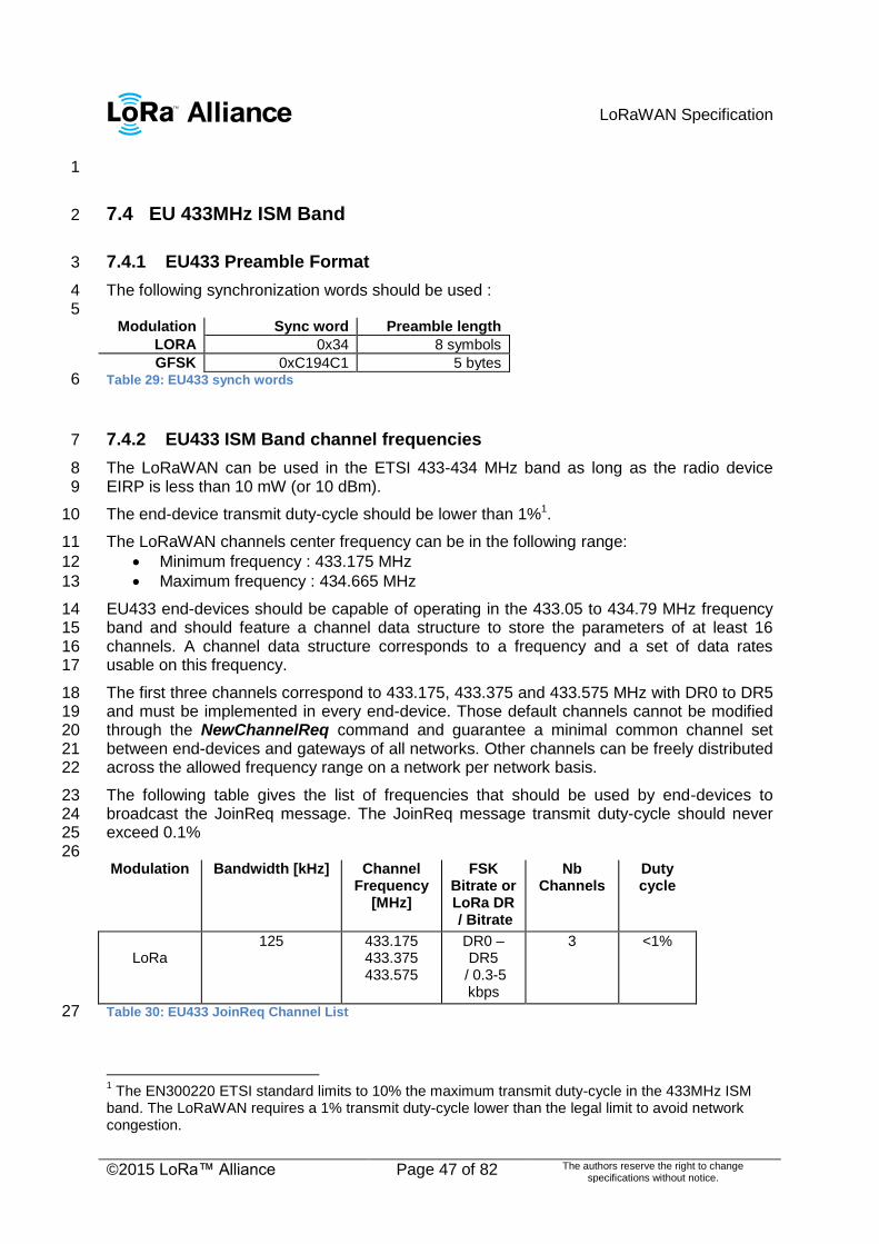
LoRaWAN Specification
©2015 LoRa™ Alliance Page 47 of 82 The authors reserve the right to change specifications without notice.
1
7.4 EU 433MHz ISM Band 2
7.4.1 EU433 Preamble Format 3
The following synchronization words should be used : 4 5
Modulation Sync word Preamble length
LORA 0x34 8 symbols
GFSK 0xC194C1 5 bytes Table 29: EU433 synch words 6
7.4.2 EU433 ISM Band channel frequencies 7
The LoRaWAN can be used in the ETSI 433-434 MHz band as long as the radio device 8 EIRP is less than 10 mW (or 10 dBm). 9
The end-device transmit duty-cycle should be lower than 1%1. 10
The LoRaWAN channels center frequency can be in the following range: 11
Minimum frequency : 433.175 MHz 12
Maximum frequency : 434.665 MHz 13
EU433 end-devices should be capable of operating in the 433.05 to 434.79 MHz frequency 14 band and should feature a channel data structure to store the parameters of at least 16 15 channels. A channel data structure corresponds to a frequency and a set of data rates 16 usable on this frequency. 17
The first three channels correspond to 433.175, 433.375 and 433.575 MHz with DR0 to DR5 18 and must be implemented in every end-device. Those default channels cannot be modified 19 through the NewChannelReq command and guarantee a minimal common channel set 20 between end-devices and gateways of all networks. Other channels can be freely distributed 21 across the allowed frequency range on a network per network basis. 22
The following table gives the list of frequencies that should be used by end-devices to 23 broadcast the JoinReq message. The JoinReq message transmit duty-cycle should never 24 exceed 0.1% 25 26 Modulation Bandwidth [kHz] Channel
Frequency [MHz]
FSK Bitrate or LoRa DR / Bitrate
Nb Channels
Duty cycle
LoRa
125 433.175 433.375 433.575
DR0 – DR5
/ 0.3-5 kbps
3 <1%
Table 30: EU433 JoinReq Channel List 27
1 The EN300220 ETSI standard limits to 10% the maximum transmit duty-cycle in the 433MHz ISM
band. The LoRaWAN requires a 1% transmit duty-cycle lower than the legal limit to avoid network congestion.

LoRaWAN Specification
©2015 LoRa™ Alliance Page 48 of 82 The authors reserve the right to change specifications without notice.
7.4.3 EU433 Data Rate and End-point Output Power encoding 1
The following encoding is used for Data Rate (DR) and End-point Output Power (TXPower) 2 in the EU433 band: 3 DataRate Configuration Indicative physical
bit rate [bit/s] TXPower Configuration
0 LoRa: SF12 / 125 kHz 250 0 10 dBm
1 LoRa: SF11 / 125 kHz 440 1 7 dBm
2 LoRa: SF10 / 125 kHz 980 2 4 dBm
3 LoRa: SF9 / 125 kHz 1760 3 1 dBm
4 LoRa: SF8 / 125 kHz 3125 4 -2 dBm
5 LoRa: SF7 / 125 kHz 5470 5 -5 dBm
6 LoRa: SF7 / 250 kHz 11000 6..15 RFU
7 FSK: 50 kbps 50000
8..15 RFU Table 31: Data rate and TX power table 4
7.4.4 EU433 JoinAccept CFList 5
6 The EU433 ISM band LoRaWAN implements an optional channel frequency list (CFlist) of 7 16 octets in the JoinAccept message. 8
In this case the CFList is a list of five channel frequencies for the channels four to eight 9 whereby each frequency is encoded as a 24 bits unsigned integer (three octets). All these 10 channels are usable for DR0 to DR5 125 kHz LoRa modulation. The list of frequencies is 11 followed by a single RFU octet for a total of 16 octets. 12
13 Size
(bytes) 3 3 3 3 3 1
CFList Freq Ch4 Freq Ch5 Freq Ch6 Freq CN7 Freq Ch8 RFU
The actual channel frequency in Hz is 100 x frequency whereby values representing 14 frequencies below 100 Mhz are reserved for future use. This allows setting the frequency of 15 a channel anywhere between 100 MHz to 1.67 GHz in 100 Hz steps. Unused channels have 16 a frequency value of 0. The CFList is optional and its presence can be detected by the 17 length of the join-accept message. If present, the CFList replaces all the previous channels 18 stored in the end-device apart from the three default channels as defined in Chapter 6. 19
The newly defined channels are immediately enabled and usable by the end-device for 20 communication. 21
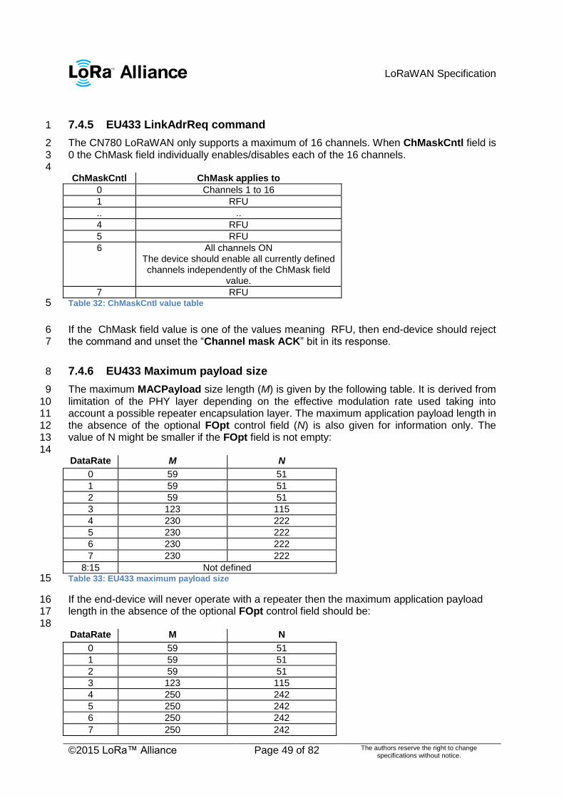
LoRaWAN Specification
©2015 LoRa™ Alliance Page 49 of 82 The authors reserve the right to change specifications without notice.
7.4.5 EU433 LinkAdrReq command 1
The CN780 LoRaWAN only supports a maximum of 16 channels. When ChMaskCntl field is 2 0 the ChMask field individually enables/disables each of the 16 channels. 3 4 ChMaskCntl ChMask applies to
0 Channels 1 to 16
1 RFU
.. ..
4 RFU
5 RFU
6 All channels ON The device should enable all currently defined channels independently of the ChMask field
value.
7 RFU Table 32: ChMaskCntl value table 5
If the ChMask field value is one of the values meaning RFU, then end-device should reject 6 the command and unset the ―Channel mask ACK‖ bit in its response. 7
7.4.6 EU433 Maximum payload size 8
The maximum MACPayload size length (M) is given by the following table. It is derived from 9 limitation of the PHY layer depending on the effective modulation rate used taking into 10 account a possible repeater encapsulation layer. The maximum application payload length in 11 the absence of the optional FOpt control field (N) is also given for information only. The 12 value of N might be smaller if the FOpt field is not empty: 13 14 DataRate M N
0 59 51
1 59 51
2 59 51
3 123 115
4 230 222
5 230 222
6 230 222
7 230 222
8:15 Not defined Table 33: EU433 maximum payload size 15
If the end-device will never operate with a repeater then the maximum application payload 16 length in the absence of the optional FOpt control field should be: 17 18 DataRate M N
0 59 51
1 59 51
2 59 51
3 123 115
4 250 242
5 250 242
6 250 242
7 250 242

LoRaWAN Specification
©2015 LoRa™ Alliance Page 50 of 82 The authors reserve the right to change specifications without notice.
8:15 Not defined Table 34 : EU433 maximum payload size (not repeater compatible) 1
2
7.4.7 EU433 Receive windows 3
The RX1 receive window uses the same channel than the preceding uplink. The data rate is 4 a function of the uplink data rate and the RX1DROffset as given by the following table. The 5 allowed values for RX1DROffset are in the [0:5] range. Values in the range [6:7] are 6 reserved for future use. 7
8 RX1DROffset 0 1 2 3 4 5
Upstream data rate Downstream data rate in RX1 slot
DR0 DR0 DR0 DR0 DR0 DR0 DR0
DR1 DR1 DR0 DR0 DR0 DR0 DR0
DR2 DR2 DR1 DR0 DR0 DR0 DR0
DR3 DR3 DR2 DR1 DR0 DR0 DR0
DR4 DR4 DR3 DR2 DR1 DR0 DR0
DR5 DR5 DR4 DR3 DR2 DR1 DR0
DR6 DR6 DR5 DR4 DR3 DR2 DR1
DR7 DR7 DR6 DR5 DR4 DR3 DR2
9
10
11
The RX2 receive window uses a fixed frequency and data rate. The default parameters are 12 434.665MHz / DR0 (SF12 , 125kHz) 13
7.4.8 EU433 Default Settings 14
The following parameters are recommended values for the EU863-870Mhz band. 15 RECEIVE_DELAY1 1 s 16 RECEIVE_DELAY2 2 s (must be RECEIVE_DELAY1 + 1s) 17 JOIN_ACCEPT_DELAY1 5 s 18 JOIN_ACCEPT_DELAY2 6 s 19 MAX_FCNT_GAP 16384 20 ADR_ACK_LIMIT 64 21 ADR_ACK_DELAY 32 22 ACK_TIMEOUT 2 +/- 1 s (random delay between 1 and 3 seconds) 23 24 If the actual parameter values implemented in the end-device are different from those default 25 values (for example the end-device uses a longer RECEIVE_DELAY1 & 2 latency) , those 26 parameters must be communicated to the network server using an out-of-band channel 27 during the end-device commissioning process. The network server may not accept 28 parameters different from those default values. 29

LoRaWAN Specification
©2015 LoRa™ Alliance Page 51 of 82 The authors reserve the right to change specifications without notice.
CLASS B – BEACON 1

LoRaWAN Specification
©2015 LoRa™ Alliance Page 52 of 82 The authors reserve the right to change specifications without notice.
8 Introduction to Class B 1
This section describes the LoRaWAN Class B layer which is optimized for battery-powered 2 end-devices that may be either mobile or mounted at a fixed location. 3
End-devices should implement Class B operation when there is a requirement to open 4 receive windows at fixed time intervals for the purpose of enabling server initiated downlink 5 messages. 6
LoRaWAN Class B option adds a synchronized reception window on the end-device. 7
One of the limitations of LoRaWAN Class A is the Aloha method of sending data from the 8 end-device; it does not allow for a known reaction time when the customer application or the 9 server wants to address the end-device. The purpose of Class B is to have an end-device 10 available for reception on a predictable time, in addition to the reception windows that 11 follows the random uplink transmission from the end-device of Class A. Class B is achieved 12 by having the gateway sending a beacon on a regular basis to synchronize the all the end-13 devices in the network so that the end-device can opening a short extra reception window 14 (called ―ping slot‖) at a predictable time during a periodic time slot. 15
Note: The decision to switch from Class A to Class B comes from the 16 application layer of the end-device. If this class A to Class B switch 17 needs to be controlled from the network side, the customer application 18 must use one of the end-device‘s Class A uplinks to send back a 19 downlink to the application layer, and it needs the application layer on 20 the end-device to recognize this request – this process is not managed 21 at the LoRaWAN level. 22
LoRaWAN Specification
©2015 LoRa™ Alliance Page 53 of 82 The authors reserve the right to change specifications without notice.
9 Principle of synchronous network initiated downlink (Class-B 1
option) 2
For a network to support end-devices of Class B, all gateways must synchronously 3 broadcast a beacon providing a timing reference to the end-devices. Based on this timing 4 reference the end-devices can periodically open receive windows, hereafter called ―ping 5 slots‖, which can be used by the network infrastructure to initiate a downlink communication. 6 A network initiated downlink using one of these ping slots is called a ―ping‖. The gateway 7 chosen to initiate this downlink communication is selected by the network server based on 8 the signal quality indicators of the last uplink of the end-device. For this reason, if an end-9 device moves and detects a change in the identity advertised in the received beacon, it must 10 send an uplink to the network server so that the server can update the downlink routing path 11 database. 12
All end-devices start and join the network as end-devices of Class A. The end-device 13 application can then decide to switch to Class B. This is done through the following process: 14
The end-device application requests the LoRaWAN layer to switch to Class B mode. 15 The LoRaWAN layer in the end-device searches for a beacon and returns either a 16 BEACON_LOCKED service primitive to the application if a network beacon was 17 found and locked or a BEACON_NOT_FOUND service primitive. To accelerate the 18 beacon discovery the LoRaWAN layer may use the ―BeaconTimingReq‖ message 19 described later. 20
Based on the beacon strength and the battery life constraints, the end-device 21 application selects a ping slot data rate and periodicity, this is then requested them 22 from the end-device LoRaWAN layer. 23
Once in Class B mode, the MAC layer sets to 1 the Class B bit of the FCTRL field of 24 every uplink frame transmitted. This bit signals to the server that the device has 25 switched to Class B. The MAC layer will autonomously schedule a reception slot for 26 each beacon and each ping slot. When the beacon reception is successful the end-27 device LoRaWAN layer forwards the beacon content to the application together with 28 the measured radio signal strength. The end-device LoRaWAN layer takes into 29 account the maximum possible clock drift in the scheduling of the beacon reception 30 slot and ping slots. When a downlink is successfully demodulated during a ping slot, 31 it is processed similarly to a downlink as described in the LoRaWAN Class A 32 specification. 33
A mobile end-device must periodically inform the network server of its location to 34 update the downlink route. This is done by transmitting a normal (possibly empty) 35 ―unconfirmed‖ or ―confirmed‖ uplink. The end-device LoRaWAN layer will 36 appropriately set the Class B bit to 1. Optimally this can be done more efficiently if 37 the application detects that the node is moving by analyzing the beacon content. In 38 that case the end-device must apply a random delay (as defined in Section 15.5 39 between the beacon reception and the uplink transmission to avoid systematic uplink 40 collisions. 41
If no beacon has been received for a given period (as defined in Section 12.2), the 42 synchronization with the network is lost. The MAC layer must inform the application 43 layer that it has switched back to Class A. As a consequence the end-device 44 LoRaWAN layer stops setting the Class B bit in all uplinks and this informs the 45 network server that the end-device is no longer in Class B mode. The end-device 46 application can try to switch back to Class B periodically. This will restart this process 47 starting with a beacon search. 48

LoRaWAN Specification
©2015 LoRa™ Alliance Page 54 of 82 The authors reserve the right to change specifications without notice.
The following diagram illustrates the concept of beacon reception slots and ping slots. 1
2 Figure 11: Beacon reception slot and ping slots 3
In this example, given the beacon period is 128 s, the end-device also opens a ping 4 reception slot every 32 s. Most of the time this ping slot is not used by the server and 5 therefore the end-device reception window is closed as soon as the radio transceiver has 6 assessed that no preamble is present on the radio channel. If a preamble is detected the 7 radio transceiver will stay on until the downlink frame is demodulated. The MAC layer will 8 then process the frame, check that its address field matches the end-device address and 9 that the Message Integrity Check is valid before forwarding it to the application layer. 10
gateway
End-device
End-device RX windows
Network beacon transmission
Network beacon transmission
ping
End-device response

LoRaWAN Specification
©2015 LoRa™ Alliance Page 55 of 82 The authors reserve the right to change specifications without notice.
10 Uplink frame in Class B mode 1
The uplink frames in Class B mode are same as the Class A uplinks with the exception of 2 the RFU bit in the FCtrl field in the Frame header. In the Class A uplink this bit is unused 3 (RFU). This bit is used for Class B uplinks. 4 5
Bit# 7 6 5 4 3..0
FCtrl ADR ADRACKReq ACK Class B FOptsLen
6 The Class B bit set to 1 in an uplink signals the network server that the device as switched to 7 Class B mode and is now ready to receive scheduled downlink pings. 8 9 The signification of the FPending bit for downlink is unaltered and still signals that one or 10 more downlink frames are queued for this device in the server and that the device should 11 keep is receiver on as described in the Class A specification. 12 13

LoRaWAN Specification
©2015 LoRa™ Alliance Page 56 of 82 The authors reserve the right to change specifications without notice.
11 Downlink Ping frame format (Class B option) 1
11.1 Physical frame format 2
A downlink Ping uses the same format as a Class A downlink frame but might follow a 3 different channel frequency plan. 4
11.2 Unicast & Multicast MAC messages 5
Messages can be ―unicast‖ or ―multicast‖. Unicast messages are sent to a single end-device 6 and multicast messages are sent to multiple end-devices. All devices of a multicast group 7 must share the same multicast address and associated encryption keys. The LoRaWAN 8 Class B specification does not specify means to remotely setup such a multicast group or 9 securely distribute the required multicast key material. This must either be performed during 10 the node personalization or through the application layer. 11
11.2.1 Unicast MAC message format 12
The MAC payload of a unicast downlink Ping uses the format defined in the Class A 13 specification. It is processed by the end-device in exactly the same way. The same frame 14 counter is used and incremented whether the downlink uses a Class B ping slot or a Class A 15 ―piggy-back‖ slot. 16
11.2.2 Multicast MAC message format 17
The Multicast frames share most of the unicast frame format with a few exceptions: 18
They are not allowed to carry MAC commands, neither in the FOpt field, nor in the 19 payload on port 0 because a multicast downlink does not have the same 20 authentication robustness as a unicast frame. 21
The ACK and ADRACKReq bits must be zero. The MType field must carry the value 22 for Unconfirmed Data Down. 23
The FPending bit indicates there is more multicast data to be sent. If it is set the 24 next multicast receive slot will carry a data frame. If it is not set the next slot may or 25 may not carry data. This bit can be used by end-devices to evaluate priorities for 26 conflicting reception slots. 27
28

LoRaWAN Specification
©2015 LoRa™ Alliance Page 57 of 82 The authors reserve the right to change specifications without notice.
12 Beacon acquisition and tracking 1
Before switching from Class A to Class B, the end-device must first receive one of the 2 network beacons to align his internal timing reference with the network. 3
Once in Class B, the end-device must periodically search and receive a network beacon to 4 cancel any drift of its internal clock time base, relative to the network timing. 5
A Class B device may be temporarily unable to receive beacons (out of range from the 6 network gateways, presence of interference, ..). In this event, the end-device has to 7 gradually widen its beacon and ping slots reception windows to take into account a possible 8 drift of its internal clock. 9
Note: For example, a device which internal clock is defined with a +/-10 10ppm precision may drift by +/-1.3mSec every beacon period. 11
12.1 Minimal beacon-less operation time 12
In the event of beacon loss, a device shall be capable of maintaining Class B operation for 2 13 hours (120 minutes) after it received the last beacon. This temporary Class B operation 14 without beacon is called ―beacon-less‖ operation. It relies on the end-device‘s own clock to 15 keep timing. 16
During beacon-less operation, unicast, multicast and beacon reception slots must all be 17 progressively expanded to accommodate the end-device‘s possible clock drift. 18 19
20 Figure 12 : beacon-less temporary operation 21
12.2 Extension of beacon-less operation upon reception 22
During this 120 minutes time interval the reception of any beacon directed to the end-device, 23 should extend the Class B beacon-less operation further by another 120 minutes as it allows 24 to correct any timing drift and reset the receive slots duration. 25
12.3 Minimizing timing drift 26
The end-devices may use the beacon‘s (when available) precise periodicity to calibrate their 27 internal clock and therefore reduce the initial clock frequency imprecision. As the timing 28 oscillator‘s exhibit a predictable temperature frequency shift, the use of a temperature 29 sensor could enable further minimization of the timing drift. 30
End-device
End-device receives the
beacon
Beacon reception window
End-device temporarily stop receiving beacon
End-device receives a beacon and resets the
reception window length
Reception window enlarges to
accommodate clock drift

LoRaWAN Specification
©2015 LoRa™ Alliance Page 58 of 82 The authors reserve the right to change specifications without notice.
13 Class B Downlink slot timing 1
13.1 Definitions 2
To operate successfully in Class B the end-device must open reception slots at precise 3 instants relative to the infrastructure beacon. This section defines the required timing. 4
The interval between the start of two successive beacons is called the beacon period. The 5 beacon frame transmission is aligned with the beginning of the BEACON_RESERVED 6 interval. Each beacon is preceded by a guard time interval where no ping slot can be placed. 7 The length of the guard interval corresponds to the time on air of the longest allowed frame. 8 This is to insure that a downlink initiated during a ping slot just before the guard time will 9 always have time to complete without colliding with the beacon transmission. The usable 10 time interval for ping slot therefore spans from the end of the beacon reserved time interval 11 to the beginning of the next beacon guard interval. 12
13 Figure 13: Beacon timing 14
Beacon_period 128 s
Beacon_reserved 2.120 s
Beacon_guard 3.000 s
Beacon-window 122.880 s Table 35: Beacon timing 15
The beacon frame time on air is actually much shorter than the beacon reserved time 16 interval to allow appending network management broadcast frames in the future. 17
The beacon window interval is divided into 212 = 4096 ping slots of 30 ms each numbered 18 from 0 to 4095. 19
An end-device using the slot number N must turn on its receiver exactly Ton seconds after 20 the start of the beacon where: 21
Ton = beacon_reserved + N * 30 ms 22
N is called the slot index. 23
The latest ping slot starts at beacon_reserved + 4095 * 30 ms = 124 970 ms after the 24 beacon start or 3030 ms before the beginning of the next beacon. 25

LoRaWAN Specification
©2015 LoRa™ Alliance Page 59 of 82 The authors reserve the right to change specifications without notice.
13.2 Slot randomization 1
To avoid systematic collisions or over-hearing problems the slot index is randomized and 2 changed at every beacon period. 3
The following parameters are used: 4
5
DevAddr Device 32 bit network unicast or multicast address
pingNb Number of ping slots per beacon period. This must be a power of 2 integer: pingNb = 2k where 1 <= k <=7
pingPeriod Period of the device receiver wake-up expressed in number of slots: pingPeriod = 212 / pingNb
pingOffset Randomized offset computed at each beacon period start. Values can range from 0 to (pingPeriod-1)
beaconTime The time carried in the field BCNPayload.Time of the immediately preceding beacon frame
slotLen Length of a unit ping slot = 30 ms
6
At each beacon period the end-device and the server compute a new pseudo-random offset 7 to align the reception slots. An AES encryption with a fixed key of all zeros is used to 8 randomize: 9 Key = 16 x 0x00 10 Rand = aes128_encrypt(Key, beaconTime | DevAddr | pad16) 11
pingOffset = (Rand[0] + Rand[1]x 256) modulo pingPeriod 12
The slots used for this beacon period will be: 13 pingOffset + N x pingPeriod with N=[0:pingNb-1] 14
The node therefore opens receive slots starting at : 15 First slot Beacon_reserved + pingOffset x slotLen
Slot 2 Beacon_reserved + (pingOffset + pingPeriod) x slotLen
Slot 3 Beacon_reserved + (pingOffset + 2 x pingPeriod) x slotLen
… …
If the end-device serves simultaneously a unicast and one or more multicast slots this 16 computation is performed multiple times at the beginning of a new beacon period. Once for 17 the unicast address (the node network address) and once for each multicast group address. 18
In the case where a multicast ping slot and a unicast ping slot collide and cannot be served 19 by the end-device receiver then the end-device should preferentially listen to the multicast 20 slot. If there is a collision between multicast reception slots the FPending bit of the previous 21 multicast frame can be used to set a preference. 22
The randomization scheme prevents a systematic collision between unicast and multicast 23 slots. If collisions happen during a beacon period then it is unlikely to occur again during the 24 next beacon period. 25

LoRaWAN Specification
©2015 LoRa™ Alliance Page 60 of 82 The authors reserve the right to change specifications without notice.
14 Class B MAC commands 1
All commands described in the Class A specification shall be implemented in Class B 2 devices. The Class B specification adds the following MAC commands. 3
4 CID Command Transmitted by Short Description
End-device
Gateway
0x10 PingSlotInfoReq x Used by the end-device to communicate the ping unicast slot data rate and periodicity to the network server
0x10 PingSlotInfoAns x Used by the network to acknowledge a PingInfoSlotReq command
0x11 PingSlotChannelReq x Used by the network server to set the unicast ping channel of an end-device
0x11 PingSlotFreqAns x Used by the end-device to acknowledge a PingSlotChannelReqcommand
0x12 BeaconTimingReq x Used by end-device to request next beacon timing & channel to network
0x12 BeaconTimingAns x Used by network to answer a BeaconTimingReq uplink
0x13 BeaconFreqReq x Command used by the network server to modify the frequency at which the end-device expects to receive beacon broadcast
0x13 BeaconFreqAns x Used by the end-device to acknowledge a BeaconFreqReq command
14.1 PingSlotInfoReq 5
With the PingSlotInfoReq command an end-device informs the server of its unicast ping 6 slot periodicity and expected data rate. This command must only be used to inform the 7 server of the parameters of a UNICAST ping slot. A multicast slot is entirely defined by the 8 application and should not use this command. 9
10 Size (bytes) 1
PingSlotInfoReq Payload Periodicity & data rate
11 Bit# 7 [6:4] [3:0]
Periodicity & data rate RFU Periodicity Data rate
The Periodicity subfield is an unsigned 3 bits integer encoding the ping slot period currently 12 used by the end-device using the following equation. 13
in seconds 14
Periodicity = 0 means that the end-device opens a ping slot every second 15
Periodicity = 7 , every 128 seconds which is the maximum ping period supported by 16 the LoRaWAN Class B specification. 17
The Data rate subfield encodes the data rate at which the end-point expects any ping. This 18 uses the same encoding scheme that the LinkAdrReq command described in the Class A 19 specification. 20

LoRaWAN Specification
©2015 LoRa™ Alliance Page 61 of 82 The authors reserve the right to change specifications without notice.
The server needs to be aware of the end-device ping slot periodicity or expected data rate 1 else Class B downlinks will not happen successfully. For that purpose the PingSlotInfoReq 2 MAC command must be acknowledged with a PingSlotInfoAns before the device can 3 switch from class A to Class B. To change its ping slot scheduling or data rate a device 4 should first revert to Class A , send the new parameters through a PingSlotInfoReq 5 command and get an acknowledge from the server through a PinSlotInfoAns . It can then 6 switch back to Class B with the new parameters. 7
This command can be concatenated with any other MAC command in the FHDRFOpt field 8 as described in the Class A specification frame format. 9
14.2 BeaconFreqReq 10
This command is sent by the server to the end-device to modify the frequency on which this 11 end-device expects the beacon. 12
13 Octets 3
PingSlotChannelReqPayload
Frequency
14
The Frequency coding is identical to the NewChannelReq MAC command defined in the 15 Class A. 16
Frequency is a 24bits unsigned integer. The actual beacon channel frequency in Hz is 100 17 x frequ. This allows defining the beacon channel anywhere between 100 MHz to 1.67 GHz 18 by 100 Hz step. The end-device has to check that the frequency is actually allowed by its 19 radio hardware and return an error otherwise. 20
A valid non-zero Frequency will force the device to listen to the beacon on a fixed frequency 21 channel even if the default behavior specifies a frequency hopping beacon (i.e US ISM 22 band). 23
A value of 0 instructs the end-device to use the default beacon frequency plan as defined in 24 the ―Beacon physical layer‖ section. Where applicable the device resumes frequency 25 hopping beacon search. 26
14.3 PingSlotChannelReq 27
This command is sent by the server to the end-device to modify the frequency on which this 28 end-device expects the downlink pings. 29
30 Octets 3 1
PingSlotChannelReq Payload
Frequency DrRange
31
The Frequency coding is identical to the NewChannelReq MAC command defined in the 32 Class A. 33
Frequency is a 24bits unsigned integer. The actual ping channel frequency in Hz is 100 x 34 frequ. This allows defining the ping channel anywhere between 100MHz to 1.67GHz by 35 100Hz step. The end-device has to check that the frequency is actually allowed by its radio 36 hardware and return an error otherwise. 37
A value of 0 instructs the end-device to use the default frequency plan. 38

LoRaWAN Specification
©2015 LoRa™ Alliance Page 62 of 82 The authors reserve the right to change specifications without notice.
DrRange is the data rate range allowed on this channel. This byte is split in two 4-bit 1 indexes. 2 3
Bits 7:4 3:0
DrRange Max data rate Min data rate
4
Following the convention defined in the ―Physical layer‖ section of the Class A specification, 5 the ―Min data rate‖ subfield designates the lowest data rate allowed on this channel. For 6 example 0 designates DR0 / 125 kHz in the EU physical layer. Similarly ―Max data rate‖ 7 designates the highest data rate. For example in the EU spec, DrRange = 0x77 means that 8 only 50 kbps GFSK is allowed on a channel and DrRange = 0x50 means that DR0 / 125 kHz 9 to DR5 / 125 kHz are supported. 10
Upon reception of this command the end-device answers with a PingSlotFreqAns 11 message. The MAC payload of this message contains the following information: 12
13 Size (bytes) 1
pingSlotFreqAns Payload Status
The Status bits have the following meaning: 14
Bits 7:2 1 0
Status RFU Data rate range
ok Channel
frequency ok
15 Bit = 0 Bit = 1
Data rate range ok The designated data rate range exceeds the ones currently defined for this end device, the previous range is kept
The data rate range is compatible with the possibilities of the end device
Channel frequency ok The device cannot use this frequency, the previous ping frequency is kept
The device is able to use this frequency.
14.4 BeaconTimingReq 16
This command is sent by the end-device to request the next beacon timing and channel. 17 This MAC command has no payload. The BeaconTimingReq & BeaconTimingAns 18 mechanism is only meant to accelerate the initial beacon search to lower the end-device 19 energy requirement. 20
The network may answer only a limited number of requests per a given time period. An end-21 device must not expect that BeaconTimingReq is answered immediately with a 22 BeaconTimingAns. Class A end-devices wanting to switch to Class B should not transmit 23 more than one BeaconTimingReq per hour. 24
End-devices requiring a fast beacon lock must implement an autonomous beacon finding 25 algorithm. 26

LoRaWAN Specification
©2015 LoRa™ Alliance Page 63 of 82 The authors reserve the right to change specifications without notice.
14.5 BeaconTimingAns 1
This command is sent by the network to answer a BeaconInfoReq request. 2 Size (bytes) 2 1
BeaconInfoReqPayload Delay Channel
The ―Delay‖ field is a 16bits unsigned integer. If the remaining time between the end of the 3 current downlink frame and the start of the next beacon frame is noted RTime then: 4
30 ms x (Delay+1) > RTime >= 30 ms x Delay 5
In networks where the beacon uses alternatively several channels, the ―Channel‖ field is the 6 index of the beaconing channel on which the next beacon will be broadcasted. For networks 7 where the beacon broadcast frequency is fixed then this field content is 0. 8 9

LoRaWAN Specification
©2015 LoRa™ Alliance Page 64 of 82 The authors reserve the right to change specifications without notice.
15 Beaconing (Class B option) 1
15.1 Beacon physical layer 2
Besides relaying messages between end-devices and network servers, all gateways 3 participate in providing a time-synchronization mechanisms by sending beacons at regular 4 fixed intervals configurable per network (BEACON_INTERVAL). All beacons are transmitted 5 in radio packet implicit mode, that is, without a LoRa physical header and with no CRC being 6 appended by the radio. 7 8
PHY Preamble BCNPayload
The beacon Preamble begins with (a longer than default) 10 unmodulated symbols. This 9 allows end-devices to implement a low power duty-cycled beacon search. 10
The beacon frame length is tightly coupled to the operation of the radio Physical layer. 11 Therefore the actual frame length might change from one region implementation to another. 12 The changing fields are highlighted in Bold in the following sections. 13
15.1.1 EU 863-870MHz ISM Band 14
The beacons are transmitted using the following settings 15
DR 3 Corresponds to SF9 spreading factor with 125 kHz BW
CR 1 Coding rate = 4/5
frequency 869.525 MHz This is the recommended frequency allowing +27 dBm EIRP. Network operators may use
a different frequency as long as ETSI compliance is achieved
The beacon frame content is: 16 Size (bytes) 3 4 1 7 2
BCNPayload NetID Time CRC GwSpecific CRC
15.1.2 US 902-928MHz ISM Band 17
The beacons are transmitted using the following settings: 18
DR 10 Corresponds to SF10 spreading factor with 500kHz bw
CR 1 Coding rate = 4/5
frequencies 923.3 to 927.5MHz with 600kHz steps
Beaconing is performed on the same channel that normal downstream traffic as
defined in the Class A specification
The downstream channel used for a given beacon is: 19
Channel = * (
)+ 20
whereby beacon_time is the integer value of the 4 bytes ―Time‖ field of the beacon 21 frame 22
whereby beacon_period is the periodicity of beacons , 128 seconds 23
whereby floor(x) designates rounding to the integer immediately inferior to x 24 25

LoRaWAN Specification
©2015 LoRa™ Alliance Page 65 of 82 The authors reserve the right to change specifications without notice.
Example: the first beacon will be transmitted on 923.3Mhz , the second 1 on 923.9MHz, the 9th beacon will be on 923.3Mhz again. 2
3 4 5 6
Beacon channel nb Frequency [MHz]
0 923.3
1 923.9
2 924.5
3 925.1
4 925.7
5 926.3
6 926.9
7 927.5
7 8 The beacon frame content is: 9
Size (bytes) 3 4 2 7 1 2
BCNPayload NetID Time CRC GwSpecific RFU CRC
10
15.2 Beacon frame content 11
The beacon payload BCNPayload consists of a network common part and a gateway-12 specific part. 13
14 Size (bytes) 3 4 1/2 7 0/1 2
BCNPayload NetID Time CRC GwSpecific RFU CRC
The network common part contains a network identifier NetID to uniquely identify the 15 network for which the beacon is sent, and a timestamp Time in seconds since 00:00:00 16 Coordinated Universal Time (UTC), 1 January 1970. The integrity of the beacon‘s network 17 common part is protected by an 8 or 16 bits CRC depending on PHY layer parameters. The 18 CRC-16 is computed on the NetID+Time fields as defined in the IEEE 802.15.4-2003 section 19 7.2.1.8. When an 8 bits CRC is required then the 8 LSBs of the computed CRC-16 are used. 20
For example: This is a valid EU868 beacon frame: 21 AA BB CC | 00 00 02 CC | 7E | 00 | 01 20 00 | 00 81 03 | DE 55 22
Bytes are transmitted left to right. The corresponding field values are: 23
24 Field NetID Time CRC InfoDesc lat long CRC
Value Hex CCBBAA CC020000 7E 0 002001 038100 55DE
The CRC-16 of the NetID+Time fields is 0xC87E but only the 8LSBs are used in that case 25
26
The seven LSB of the NetID are called NwkID and match the seven MSB of the short 27 address of an end-device. Neighboring or overlapping networks must have different 28 NwkIDs. 29
LoRaWAN Specification
©2015 LoRa™ Alliance Page 66 of 82 The authors reserve the right to change specifications without notice.
The gateway specific part provides additional information regarding the gateway sending a 1 beacon and therefore may differ for each gateway. The RFU field when applicable (region 2 specific) should be equal to 0. The optional part is protected by a CRC-16 computed on the 3 GwSpecific+RFU fields. The CRC-16 definition is the same as for the mandatory part. 4
For example: This is a valid US900 beacon: 5 Field NetID Time CRC InfoDesc lat long RFU CRC
Value Hex CCBBAA CC020000 C87E 0 002001 038100 00 D450
Over the air the bytes are sent in the following order: 6 AA BB CC | 00 00 02 CC | 7E C8 | 00 | 01 20 00 | 00 81 03 |00 | 50 D4 7
Listening and synchronizing to the network common part is sufficient to operate a stationary 8 end-device in Class B mode. A mobile end-device should also demodulate the gateway 9 specific part of the beacon to be able to signal to the network server whenever he is moving 10 from one cell to another. 11
Note: As mentioned before, all gateways send their beacon at exactly 12 the same point in time (i.e., time-synchronously) so that for network 13 common part there are no visible on-air collisions for a listening end-14 device even if the end-device simultaneously receives beacons from 15 several gateways. With respect to the gateway specific part, collision 16 occurs but an end-device within the proximity of more than one 17 gateway will still be able to decode the strongest beacon with high 18 probability. 19
15.3 Beacon GwSpecific field format 20
The content of the GwSpecific field is as follow: 21 Size (bytes) 1 6
GwSpecific InfoDesc Info
The information descriptorInfoDesc describes how the information field Info shall be 22 interpreted. 23
24 InfoDesc Meaning
0 GPS coordinate of the gateway first antenna
1 GPS coordinate of the gateway second antenna
2 GPS coordinate of the gateway third antenna
3:127 RFU
128:255 Reserved for custom network specific broadcasts
For a single omnidirectional antenna gateway the InfoDesc value is 0 when broadcasting 25 GPS coordinates. For a site featuring 3 sectored antennas for example, the first antenna 26 broadcasts the beacon with InfoDesc equals 0, the second antenna with InfoDesc field 27 equals 1, etc … 28

LoRaWAN Specification
©2015 LoRa™ Alliance Page 67 of 82 The authors reserve the right to change specifications without notice.
15.3.1 Gateway GPS coordinate:InfoDesc = 0, 1 or 2 1
For InfoDesc = 0 ,1 or 2, the content of the Info field encodes the GPS coordinates of the 2 antenna broadcasting the beacon 3
Size (bytes) 3 3
Info Lat Lng
The latitude and longitude fields (Lat and Lng, respectively) encode the geographical 4 location of the gateway as follows: 5
The north-south latitude is encoded using a signed 24 bit word where -223 6 corresponds to 90° south (the South Pole) and 223 corresponds to 90° north (the 7 North Pole). The equator corresponds to 0. 8
The east-west longitude is encoded using a signed 24 bit word where - 9 223corresponds to 180° west and 223 corresponds to 180° east. The Greenwich 10 meridian corresponds to 0. 11
15.4 Beaconing precise timing 12
The beacon is sent every 128 seconds starting at 00:00:00 Coordinated Universal Time 13 (UTC), 1 January 1970 plus NwkID plus TBeaconDelay. Therefore the beacon is sent at 14 BT = k * 128 + NwkID + TBeaconDelay 15
seconds after 00:00:00 Coordinated Universal Time (UTC), 1 January 1970 16
wherebyk is the smallest integer for which 17 k * 128 + NwkID>T 18
whereby 19 T = seconds since 00:00:00 Coordinated Universal Time (UTC), 1 January 1970. 20
Note: T is not (!) Unix time. Similar to GPS time and unlike Unix time, 21 T is strictly monotonically increasing and is not influenced by leap 22 seconds. 23
Whereby TBeaconDelay is a network specific delay in the [0:50] ms range. 24 TBeaconDelay may vary from one network to another and is meant to allow a slight 25 transmission delay of the gateways. TBeaconDelay must be the same for all gateways of a 26 given network. TBeaconDelay must be smaller than 50 ms. All end-devices ping slots use 27 the beacon transmission time as a timing reference, therefore the network server as to take 28 TBeaconDelay into account when scheduling the class B downlinks. 29 30
15.5 Network downlink route update requirements 31
When the network attempts to communicate with an end-device using a Class B downlink 32 slot, it transmits the downlink from the gateway which was closest to the end-device when 33 the last uplink was received. Therefore the network server needs to keep track of the rough 34 position of every Class B device. 35
Whenever a Class B device moves and changes cell, it needs to communicate with the 36 network server in order to update its downlink route. This update can be performed simply 37 by sending a ―confirmed‖ or ―unconfirmed‖ uplink, possibly without applicative payload. 38
The end-device has the choice between 2 basic strategies: 39

LoRaWAN Specification
©2015 LoRa™ Alliance Page 68 of 82 The authors reserve the right to change specifications without notice.
Systematic periodic uplink: simplest method that doesn‘t require demodulation of the 1 ―gateway specific‖ field of the beacon. Only applicable to slowly moving or stationery 2 end-devices. There are no requirements on those periodic uplinks. 3
Uplink on cell change: The end-device demodulates the ―gateway specific‖ field of 4 the beacon, detects that the ID of the gateway broadcasting the beacon it 5 demodulates has changed, and sends an uplink. In that case the device should 6 respect a pseudo random delay in the [0:120] seconds range between the beacon 7 demodulation and the uplink transmission. This is required to insure that the uplinks 8 of multiple Class B devices entering or leaving a cell during the same beacon period 9 will not systematically occur at the same time immediately after the beacon 10 broadcast. 11
Failure to report cell change will result in Class B downlink being temporary not operational. 12 The network server may have to wait for the next end-device uplink to transmit downlink 13 traffic. 14 15 16
LoRaWAN Specification
©2015 LoRa™ Alliance Page 69 of 82 The authors reserve the right to change specifications without notice.
16 Class B unicast & multicast downlink channel frequencies 1
16.1 EU 863-870MHz ISM Band 2
All unicast&multicastClass B downlinks use a single frequency channel defined by the 3 ―PingSlotChannelReq” MAC command. The default frequency is 869.525MHz 4
16.2 US 902-928MHz ISM Band 5
By default Class B downlinks use a channel function of the Time field of the last beacon (see 6 Beacon Frame content) and the DevAddr. 7
[ (
)]
Whereby Beacon_Time is the 32 bit Time field of the current beacon period 8
Beacon_period is the length of the beacon period (defined as 128sec in the 9 specification) 10
Floor designates rounding to the immediately lower integer value 11
DevAddr is the 32 bits network address of the device 12
Class B downlinks therefore hop across 8 channels in the ISM band and all Class B end-13 devices are equally spread amongst the 8 downlink channels. 14
If the ―PingSlotChannelReq” command with a valid non-zero argument is used to set the 15 Class B downlink frequency then all subsequent ping slots should be opened on this single 16 frequency independently of the last beacon frequency. 17
If the ―PingSlotChannelReq” command with a zero argument is sent, the end-device 18 should resume the default frequency plan, id Class B ping slots hoping across 8 channels. 19
The underlying idea is to allow network operators to configure end-devices to use a single 20 proprietary dedicated frequency band for the Class B downlinks if available, and to keep as 21 much frequency diversity as possible when the ISM band is used. 22
23

LoRaWAN Specification
©2015 LoRa™ Alliance Page 70 of 82 The authors reserve the right to change specifications without notice.
CLASS C – CONTINUOUSLY LISTENING 1

LoRaWAN Specification
©2015 LoRa™ Alliance Page 71 of 82 The authors reserve the right to change specifications without notice.
17 Class C: Continuously listening end-device 1
The end-devices implanting the Class C option are used for applications that have sufficient 2 power available and thus do not need to minimize reception time. 3
Class C end-devices cannot implement Class B option. 4
The Class C end-device will listen with RX2 windows parameters as often as possible. The 5 end-device listens on RX2 when it is not either (a) sending or (b) receiving on RX1, 6 according to Class A definition. To do so, it will open a short window on RX2 parameters 7 between the end of the uplink transmission and the beginning of the RX1 reception window 8 and it will switch to RX2 reception parameters as soon as the RX1 reception window is 9 closed; the RX2 reception window will remain open until the end-device has to send another 10 message. 11
Note: There is not specific message for a node to tell the server that it 12 is a Class C node. It is up to the application on server side to know that 13 it manages Class C nodes based on the contract passed during the 14 join procedure. 15
17.1 Second receive window duration for Class C 16
Class C devices implement the same two receive windows as Class A devices, but they do 17 not close RX2 window until they need to send again. Therefore they may receive a downlink 18 in the RX2 window at nearly any time. A short listening window on RX2 frequency and data 19 rate is also opened between the end of the transmission and the beginning of the RX1 20 receive window. 21
Transmit RX1
RX2RX2
Transmit On Air TimeRECEIVE_DELAY1
RECEIVE_DELAY2Extends to next uplink
22 Figure 14: Class C end-device receive slot timing. 23
17.2 Class C Multicast downlinks 24
Similarly to Class B, Class C devices may receive multicast downlink frames. The multicast 25 address and associated network session key and application session key must come from 26 the application layer. The same limitations apply for Class C multicast downlink frames: 27
They are not allowed to carry MAC commands, neither in the FOpt field, nor in the 28 payload on port 0 because a multicast downlink does not have the same 29 authentication robustness as a unicast frame. 30
The ACK and ADRACKReq bits must be zero. The MType field must carry the value 31 for Unconfirmed Data Down. 32
The FPending bit indicates there is more multicast data to be sent. Given that a 33 Class C device keeps its receiver active most of the time, the FPending bit does not 34 trigger any specific behavior of the end-device. 35

LoRaWAN Specification
©2015 LoRa™ Alliance Page 72 of 82 The authors reserve the right to change specifications without notice.
SUPPORT INFORMATION 1
This sub-section is only a recommendation. 2
3

LoRaWAN Specification
©2015 LoRa™ Alliance Page 73 of 82 The authors reserve the right to change specifications without notice.
18 Examples and Application Information 1
Examples are illustrations of the LoRaWAN spec for information, but they are not part of the 2 formal specification. 3
18.1 Uplink Timing Diagram for Confirmed Data Messages 4
The following diagram illustrates the steps followed by an end-device trying to transmit two 5 confirmed data frames (Data0 and Data1): 6 7
8 Figure 15: Uplink timing diagram for confirmed data messages 9
The end-device first transmits a confirmed data frame containing the Data0 payload at an 10 arbitrary instant and on an arbitrary channel. The frame counter Cu is simply derived by 11 adding 1 to the previous uplink frame counter. The network receives the frame and 12 generates a downlink frame with the ACK bit set exactly RECEIVE_DELAY1 seconds later, 13 using the first receive window of the end-device. This downlink frame uses the same data 14 rate and the same channel as the Data0 uplink. The downlink frame counter Cd is also 15 derived by adding 1 to the last downlink towards that specific end-device. If there is no 16 downlink payload pending the network shall generate a frame without a payload. In this 17 example the frame carrying the ACK bit is not received. 18
If an end-point does not receive a frame with the ACK bit set in one of the two receive 19 windows immediately following the uplink transmission it may resend the same frame with 20 the same payload and frame counter again at least ACK_TIMEOUT seconds after the 21 second reception window. This resend must be done on another channel and must obey the 22 duty cycle limitation as any other normal transmission. If this time the network receives the 23 ACK downlink during its first receive window, as soon as the ACK frame is demodulated, the 24 end-device is free to transmit a new frame on a new channel. 25
18.2 The third ACK frame in this example also carries an application 26
payload. A downlink frame can carry any combination of ACK, MAC 27
control commands and payload. Downlink Diagram for Confirmed 28
Data Messages 29
The following diagram illustrates the basic sequence of a ―confirmed‖ downlink. 30 31 32
gateway
End-point Confirmed Data0
Cu
ACK
Cd
Confirmed Data0
Cu
ACK
Cd+1
Confirmed Data1
Cu+1
Data + ACK
Cd+2
ok ok ok
ko ok
ok
Receive slots
(diag 1)

LoRaWAN Specification
©2015 LoRa™ Alliance Page 74 of 82 The authors reserve the right to change specifications without notice.
1 Figure 16: Downlink timing diagram for confirmed data messages 2
The frame exchange is initiated by the end-device transmitting an ―unconfirmed‖ application 3 payload or any other frame on channel A. The network uses the downlink receive window to 4 transmit a ―confirmed‖ data frame towards the end-device on the same channel A. Upon 5 reception of this data frame requiring an acknowledgement, the end-device transmits a 6 frame with the ACK bit set at its own discretion. This frame might also contain piggybacked 7 data or MAC commands as its payload. This ACK uplink is treated like any standard uplink, 8 and as such is transmitted on a random channel that might be different from channel A. 9
Note: To allow the end-devices to be as simple as possible and have 10 keep as few states as possible it may transmit an explicit (possibly 11 empty) acknowledgement data message immediately after the 12 reception of a data message requiring an acknowledgment. 13 Alternatively the end-device may defer the transmission of an 14 acknowledgement to piggyback it with its next data message. 15
18.3 Downlink Timing for Frame-Pending Messages 16
The next diagram illustrates the use of the frame pending (FPending) bit on a downlink. 17 The FPending bit can only be set on a downlink frame and informs the end-device that the 18 network has several frames pending for him; the bit is ignored for all uplink frames. 19
If a frame with the FPending bit set requires an acknowledgement, the end-device shall do 20 so as described before. If no acknowledgment is required, the end-device may send an 21 empty data message to open additional receive windows at its own discretion, or wait until it 22 has some data to transmit itself and open receive windows as usual. 23
Note: The FPending bit is independent to the acknowledgment 24 scheme. 25
26
gateway
End-point Unconfirmed data
Cu
Confirmed Data
Cd
ok ok
Receive slots
ok
ACK
Cu+1
gateway
End-point Data uplink
cu
Confirmed Data0+F_P
cd
ACK
cu+1
Confirmed Data1
cd+1
ACK
cu+2
ok ok ok
(*) F_P means ‗frame pending‘ bit set
Receive slots

LoRaWAN Specification
©2015 LoRa™ Alliance Page 75 of 82 The authors reserve the right to change specifications without notice.
Figure 17: Downlink timing diagram for frame-pending messages, example 1 1
In this example the network has two confirmed data frames to transmit to the end-device. 2 The frame exchange is initiated by the end-device via a normal ―unconfirmed‖ uplink 3 message on channel A. The network uses the first receive window to transmit the Data0 with 4 the bit FPending set as a confirmed data message. The device acknowledges the reception 5 of the frame by transmitting back an empty frame with the ACK bit set on a new channel B. 6 RECEIVE_DELAY1 seconds later, the network transmits the second frame Data1 on 7 channel B, again using a confirmed data message but with the FPending bit cleared. The 8 end-device acknowledges on channel C. 9
10 Figure 18: Downlink timing diagram for frame-pending messages, example 2 11
In this example, the downlink frames are ―unconfirmed‖ frames, the end-device does not 12 need to send back and acknowledge. Receiving the Data0 unconfirmed frame with the 13 FPending bit set the end-device sends an empty data frame. This first uplink is not received 14 by the network. If no downlink is received during the two receive windows, the network has 15 to wait for the next spontaneous uplink of the end-device to retry the transfer. The end-16 device can speed up the procedure by sending a new empty data frame. 17
Note: An acknowledgement is never sent twice. 18
The FPending bit, the ACK bit, and payload data can all be present in the same downlink. 19 For example, the following frame exchange is perfectly valid. 20
21
22 Figure 19: Downlink timing diagram for frame-pending messages, example 3 23
The end-device sends a ―confirmed data‖ uplink. The network can answer with a confirmed 24 downlink containing Data + ACK + ―Frame pending‖ then the exchange continues as 25 previously described. 26
gateway
End-point Data uplink
cu
Data0+F_P
cd
void
cu+1
ok
void
cu+3
okok
Data1+F_P
cd
void
cu+2
gateway
End-pointConfirmed Data uplink
cu
Confirmed Data0+F_P+ACK
cd
ACK
cu+1
Confirmed Data1+F_P
cd+1
ACK
cu+3
ok
void
cu+2
Receiving a frame without the ACK bit set , server retransmits Data1
okok Confirmed Data1+F_P
cd+1
(diag 2)

LoRaWAN Specification
©2015 LoRa™ Alliance Page 76 of 82 The authors reserve the right to change specifications without notice.
18.4 Data-Rate Adaptation during Message Retransmissions 1
When an end-device attempts the transmission of a ―confirmed‘ frame toward the network it 2 expects to receive an acknowledgement in one of the subsequent reception slot. In the 3 absence of the acknowledgement it will try to re-transmit the same data again. This re-4 transmission happens on a new frequency channel, but can also happen at a different data 5 rate (preferable lower) than the previous one. It is strongly recommended to adopt the 6 following re-transmission strategy. 7
The first transmission of the ―confirmed‖ frame happens with a data rate DR. 8 9 Transmission nb Data Rate
1 (first) DR
2 DR
3 max(DR-1,0)
4 max(DR-1,0)
5 max(DR-2,0)
6 max(DR-2,0)
7 max(DR-3,0)
8 max(DR-3,0)
The Data Rate max(a,b) stands for maximum of a and b values. 10
If after a recommended 8 transmissions, the frame has not been acknowledged the MAC 11 layer should return an error code to the application layer. 12
Note: For each re-transmission, the frequency channel is selected 13 randomly as for normal transmissions. 14
Any further transmission uses the last data rate used. 15
For example if an end-device sends a ―confirmed‖ frame first using DR5 and has to 16 retransmit 3 times (twice at DR5 then twice at DR4), the next frame transmitted will use DR4 17
Other example, if an end-device sends a ―confirmed‖ frame first using DR5 and does not 18 receive an acknowledge after 8 transmissions (2 at DR5, 2 at DR4, … , 2 at DR2), and the 19 application of this end-device re-initiates a ―confirmed‖ transmission a little later, the first two 20 transmission will be tentatively at DR2, then switch to DR1, then to DR0. 21

LoRaWAN Specification
©2015 LoRa™ Alliance Page 77 of 82 The authors reserve the right to change specifications without notice.
19 Recommendation on contract to be provided to the network 1
server by the end-device provider at the time of provisioning 2
Configuration data related to the end-device and its characteristics must be known by the 3 network server at the time of provisioning. –This provisioned data is called the ―contract‖. 4 This contract cannot be provided by the end-device and must be supplied by the end-device 5 provider using another channel (out-of-band communication). 6
This end-device contract is stored in the network server. It can be used by the application 7 server and the network controller to adapt the algorithms. 8
This data will include: 9
End-device specific radio parameters (device frequency range, device maximal 10 output power, device communication settings - RECEIVE_DELAY1, 11 RECEIVE_DELAY2) 12
Application type (Alarm, Metering, Asset Tracking, Supervision, Network Control) 13
LoRaWAN Specification
©2015 LoRa™ Alliance Page 78 of 82 The authors reserve the right to change specifications without notice.
20 Recommendation on finding the locally used channels 1
End-devices that can be activated in territories that are using different frequencies for 2 LoRaWAN will have to identify what frequencies are supported for join message at their 3 current location before they send any message. The following methods are proposed: 4
A GPS enabled end-device can use its GPS location to identify which frequency 5 band to use. 6
End-device can search for a beacon and use its frequency to identify its region 7
End-device can search for a beacon and if this one is sending the antenna GPS 8 coordinate, it can use this to identify its region 9
End-device can search for a beacon and if this one is sending a list of join 10 frequencies, it can use this to send its join message 11

LoRaWAN Specification
©2015 LoRa™ Alliance Page 79 of 82 The authors reserve the right to change specifications without notice.
21 Revisions 1
21.1 Revision 1.0 2
Draft version of LoRaWAN 3
4

LoRaWAN Specification
©2015 LoRa™ Alliance Page 80 of 82 The authors reserve the right to change specifications without notice.
22 Glossary 1
2 ADR Adaptive Data Rate 3 AES Advanced Encryption Standard 4 AFA Adaptive Frequency Agility 5 AR Acknowledgement Request 6 CBC Cipher Block Chaining 7 CMAC Cipher-based Message Authentication Code 8 CR Coding Rate 9 CRC Cyclic Redundancy Check 10 DR Data Rate 11 ECB Electronic Code Book 12 ETSI European Telecommunications Standards Institute 13 EIRP Equivalent Isotropically Radiated Power 14 FSK Frequency Shift Keying modulation technique 15 GPRS General Packet Radio Service 16 HAL Hardware Abstraction Layer 17 IP Internet Protocol 18 LBT Listen Before Talk 19 LoRa™ Long Range modulation technique 20 LoRaWAN™ Long Range Network protocol 21 MAC Medium Access Control 22 MIC Message Integrity Code 23 RF Radio Frequency 24 RFU Reserved for Future Usage 25 Rx Receiver 26 RSSI Received Signal Strength Indicator 27 SF Spreading Factor 28 SNR Signal Noise Ratio 29 SPI Serial Peripheral Interface 30 SSL Secure Socket Layer 31 Tx Transmitter 32 USB Universal Serial Bus 33 34

LoRaWAN Specification
©2015 LoRa™ Alliance Page 81 of 82 The authors reserve the right to change specifications without notice.
23 Bibliography 1
23.1 References 2
[IEEE802154]: IEEE Standard for Local and Metropolitan Area Networks—Part 15.4: Low-3 Rate Wireless Personal Area Networks (LR-WPANs), IEEE Std 802.15.4TM-2011 (Revision 4 of IEEE Std 802.15.4-2006), September 2011. 5
[RFC4493]: The AES-CMAC Algorithm, June 2006. 6

LoRaWAN Specification
©2015 LoRa™ Alliance Page 82 of 82 The authors reserve the right to change specifications without notice.
24 NOTICE OF USE AND DISCLOSURE 1
Copyright © LoRa Alliance, Inc. (2015). All Rights Reserved. 2
The information within this document is the property of the LoRa Alliance (―The Alliance‖) and its use and 3 disclosure are subject to LoRa Alliance Corporate Bylaws, Intellectual Property Rights (IPR) Policy and 4 Membership Agreements. 5
Elements of LoRa Alliance specifications may be subject to third party intellectual property rights, including 6 without limitation, patent, copyright or trademark rights (such a third party may or may not be a member of LoRa 7 Alliance). The Alliance is not responsible and shall not be held responsible in any manner for identifying or failing 8 to identify any or all such third party intellectual property rights. 9
This document and the information contained herein are provided on an ―AS IS‖ basis and THE ALLIANCE 10 DISCLAIMS ALL WARRANTIES EXPRESS OR IMPLIED, INCLUDING BUT NOT LIMITED TO (A) ANY 11 WARRANTY THAT THE USE OF THE INFORMATION HEREIN WILL NOT INFRINGE ANY RIGHTS OF THIRD 12 PARTIES (INCLUDING WITHOUT LIMITATION ANY INTELLECTUAL PROPERTY RIGHTS INCLUDING 13 PATENT, COPYRIGHT OR TRADEMARK RIGHTS) OR (B) ANY IMPLIED WARRANTIES OF 14 MERCHANTABILITY, FITNESS FOR A PARTICULAR PURPOSE, TITLE OR NONINFRINGEMENT. 15
IN NO EVENT WILL THE ALLIANCE BE LIABLE FOR ANY LOSS OF PROFITS, LOSS OF BUSINESS, LOSS 16 OF USE OF DATA, INTERRUPTION OFBUSINESS, OR FOR ANY OTHER DIRECT, INDIRECT, SPECIAL OR 17 EXEMPLARY, INCIDENTIAL, PUNITIVE OR CONSEQUENTIAL DAMAGES OF ANY KIND, IN CONTRACT OR 18 IN TORT, IN CONNECTION WITH THIS DOCUMENT OR THE INFORMATION CONTAINED HEREIN, EVEN IF 19 ADVISED OF THE POSSIBILITY OF SUCH LOSS OR DAMAGE. 20
The above notice and this paragraph must be included on all copies of this document that are made. 21
LoRa Alliance, Inc. 22
2400 Camino Ramon, Suite 375 23
San Ramon, CA 94583 24
Note: All Company, brand and product names may be trademarks that are the sole property of their respective 25 owners. 26

ESCUELA POLITÉCNICA SUPERIOR
TRABAJO FIN DE MÁSTER
CURSO 2016/2017
DISEÑO Y DESARROLLO DEL SISTEMA DE COMUNICACIONES INALÁMBRICO DE UN ENJAMBRE DE
UAV’S COLABORATIVOS
MÁSTER EN INGENIERÍA INDUSTRIAL
DOCUMENTO DEL PROYECTO
ANEXO III – TRANSMISIÓN DE MENSAJES

ANEXO III – TRANSMISIÓN DE MENSAJES
ESTRUCTURA DE MENSAJES

ANEXO III – TRANSMISIÓN DE MENSAJES
Los paquetes a transmitir en las redes LoRaWAN™ siguen la estructura definida por la LoRaWAN™
Specification, separando la estructura de Capa Física (PHY) y de Capa de Enlace (MAC).
La terminología de LoRa distingue entre dos tipos de mensajes:
Los Mensajes Uplink son enviados por dispositivos finales al servidor de red retransmitido
por uno o varios gateway.
Los Mensajes Downlink son enviados por desde el servidor de red a un único dispositivo
final y es retransmitido a su vez por un único gateway.
Los paquetes en una comunicación en red LoRaWAN™ contarán con la siguiente estructura:
Preamble o sincronización (LoRA: 0x34, (G)FSK: 0xC194C1).
LoRa Physical Header (PHDR), establecido por el transceptor de radio.
Header CRC (PHDR_CRC), establecido por el transceptor de radio.
Physical Payload (PHYPayload).
Codificación de Redundancia Cíclica (CRC), establecido por el transceptor de radio.
Preamble PHDR PHDR_CRC PHYPayload CRC*
* En el caso de mensajes downlink no estaría disponible la estructura CRC.
Estructura AIII.1.1: Estructura de Mensajes.
Todos los paquetes en LoRa presentan una estructura de PHYPayload que se descompone en las
siguientes estructuras:
Preamble PHDR PHDR_CRC PHYPayload CRC*
MHDR MACPayload MIC
FHDR FPort FRMPayload
DevAddr FCtrl FCnt FOpts
Estructura AIII.1.2: Descomposición de la PHYPayload.

ANEXO III – TRANSMISIÓN DE MENSAJES
La descomposición de PHYPayload nos deriva en las siguientes estructuras:
MAC Header (MHDR):
La MAC Header especificará el tipo de mensaje (MType) y la versión principal (Major) del formato
de la trama de la especificación de la capa LoRaWAN™ con la que ha sido codificada.
Bit [7 … 5] [4 … 2] [1 … 0]
MHDR bits MType RFU Major
Estructura AIII.1.3: Estructura del MAC Header (MHDR).
La LoRaWAN™ Specification distingue entre seis diferentes tipos de mensajes MAC (MType):
MType Description
000 Join Request
001 Join Accept
010 Unconfirmed Data Up
011 Unconfirmed Data Down
100 Confirmed Data Up
101 Confirmed Data Down
110 RFU
Tabla AIII.1.1: Tipos de Mensajes MAC.
La versión principal (Major) especificará el formato de los mensajes intercambiados en el proceso
de conexión a red y los primeros cuatro bytes del MAC Payload. La versión secundaria utilizada
por el dispositivo final debe ser previamente conocida por el servidor de red, utilizando mensajes
fuera de banda (como parte de la información de personalización del dispositivo).

ANEXO III – TRANSMISIÓN DE MENSAJES
MAC Payload (MACPayload):
La MAC Payload es denominada como “marco de datos”. Se compone del Frame Header (FHDR),
un Port Field (FPort) opcional y el Frame Payload (FRMPayload).
Como podemos observar, el Frame Header (FHDR) se descompondrá de la siguiente manera:
Bytes [4] [1] [2] [0 … 15]
FHDR DevAddr FCtrl FCnt FOpts
Estructura AIII.1.4: Estructura del Frame Header (FHDR).
El FHDR contiene la dirección del dispositivo final (DevAddr), un Frame Control (FCtrl) que nos
permitirá activar el Velocidad de Datos Adaptativa (ADR) y la Recepción de ACK en paquetes con
confirmación, un Frame Control (FCnt) que es usado como un contador en Seguimiento de Envíos
y Recepciones y un Frame Options (FOpts) utilizado para el transporte de comandos MAC.
Ilustración AIII.1.1: Comunicación LoRa sin y con Acknowledgement (ACK).
Como se ha visto antes, el Port Field (FPort) presenta un carácter opcional, esto es debido a que
si el FRMPayload estuviera vacío no sería necesario. Puede presentar diferentes valores, un valor
de 0 indica que el FRMPayload contiene comandos MAC, si este valor fuera entre [1 … 223]
contendría aplicaciones específicas y entre [224 … 255] sería espacio reservado para futuras
extensiones.

ANEXO III – TRANSMISIÓN DE MENSAJES
Si el FRMPayload contiene cierta carga útil, este debe ser cifrado antes de que se calcule el Código
de Integridad del Mensaje (MIC). El esquema de cifrado utilizado se basa en el algoritmo genérico
descrito en IEEE 802.15.4 /2006 Anexo B, utilizando AES-128.
Como valor predeterminado, el cifrado/descifrado se realiza mediante la capa LoRaWAN™ para
todos los Port Fields (FPorts). El cifrado/descifrado se puede hacer encima de la capa LoRaWAN™
para Port Fields (FPorts) específicos excepto el puerto 0, si esto fuera más conveniente.
Ilustración AIII.1.2: Cifrado AES-128 de la Carga Útil del Mensaje.
Message Integrity Code (MIC):
El Message Integrity Code es un código de seguridad que es calculado sobre todos los campos del
mensaje.
MIC MHDR FHDR FPort FRMPayload
Estructura AIII.1.5: Estructura del Message Integrity Code (MIC).

ANEXO III – TRANSMISIÓN DE MENSAJES
DECODIFICACIÓN DE MENSAJES

ANEXO III – TRANSMISIÓN DE MENSAJES
En este apartado, se llevará a cabo un ejemplo de Decodificación de Mensaje, se explicará el
tratamiento de datos por medio de un ejemplo hecho durante las pruebas de diseño del Gateway.
La AppSKey yNwkSKey estarán previamente establecidas y serán utilizadas en función del FPort
utilizado para la transmisión del mensaje:
FPort Key
0 NwkSKey
[1, …, 255] AppSKey
Tabla AIII.2.1: Clave utilizada en función de FPort.
El mensaje transmitido por el end-node será sin confirmación (unconfirmed), contendrá la carga
útil “LoRa” (hexadecimal), y será enviado a través del FPort 1. Por tanto, la orden transmitida al
emisor será la siguiente:
mac tx uncnf 1 4c6f5261
Una vez transmitido el mensaje, el gateway recibirá el mensaje, que deberá descomponerse de
la siguiente manera:
MHDR FHDR FPort FRMPayload MIC
40 a2 1c 01 26 00 01 00 01 79 36 7c 14 e3 85 ce 96
Estructura AIII.2.1: Descomposición del Mensaje Recibido.
Una vez descompuesto, nos queda descifrar la carga útil. Para ello, haremos uso de la LoRaWAN™
Specification, que nos dice que, para el descifrado de los mensajes, se debe trabajar en bloques
en 16 bytes.
En primera instancia debemos realizar la creación de bloques de 16 bytes con la carga útil y, en
segundo lugar, llevar a cabo la creación de los Bloques A, de mismo número que el resultante de
bloques creados con la carga útil.

ANEXO III – TRANSMISIÓN DE MENSAJES
La estructura de los Bloques A estará compuesta de la siguiente manera:
Size (bytes) 1 4 1 4 4 1 1
Ai 0x01 0x00 Dir DevAddr FCnt 0x00 i
Estructura AIII.2.2: Descomposición del Mensaje Recibido.
Por tanto, nuestro mensaje al disponer solo de 4 bytes, dispondrá de un único bloque de Payload
y Bloque A:
Payload [0x79, 0x36, 0x7c, 0x14, 0x00, 0x00, 0x00, 0x00, 0x00, 0x00, 0x00, 0x00, 0x00,
0x00, 0x00, 0x00]
Bloque A [0x01, 0x00, 0x00, 0x00, 0x00, 0x00, 0xa2, 0x1c, 0x01, 0x26, 0x04, 0x00, 0x00,
0x00, 0x00, 0x01]
Tabla AIII.2.2: Composición de Payload y Bloque A (16 bytes).
Una vez realizado esto, por medio de la AppSKey debemos encriptar los Bloques A generados con
cifrado AES-128. El resultado será recogido con el nombre de Bloques S, resultando en este caso:
AppSKey [0xa4, 0x10, 0x9c, 0x15, 0x0e, 0x24, 0x92, 0xd5, 0x47, 0x9a, 0x78, 0x26, 0x45,
0x75, 0x8b, 0x3b]
Bloque S [0x35, 0x59, 0x2e, 0x75, 0x88, 0xbc, 0x39, 0x87, 0x14, 0x36, 0xdb, 0xfb, 0xd8,
0xf7, 0x88, 0x7b]
Tabla AIII.2.3: Cifrado AES-128 de Bloque A - Bloque B (16 bytes).
Como último paso, solo nos quedará realizar la operación lógica XOR entre los Bloques Payload y
el Bloques S, y al resultado obtenido, eliminando la parte agregada sobre la longitud original del
payload, realizar la conversión de hexadecimal a Código ASCII. El resultado obtenido será:
XOR [0x4c, 0x6f, 0x52, 0x61, 0x88, 0xbc, 0x39, 0x87, 0x14, 0x36, 0xdb, 0xfb, 0xd8,
0xf7, 0x88, 0x7b]
Resultado Final [0x4c, 0x6f, 0x52, 0x61] -- LoRa
Tabla AIII.2.3: Resultado de Operación Lógica XOR y Resultado Final.

ESCUELA POLITÉCNICA SUPERIOR
TRABAJO FIN DE MÁSTER
CURSO 2016/2017
DISEÑO Y DESARROLLO DEL SISTEMA DE COMUNICACIONES INALÁMBRICO DE UN ENJAMBRE DE
UAV’S COLABORATIVOS
MÁSTER EN INGENIERÍA INDUSTRIAL
DOCUMENTO DEL PROYECTO
ANEXO IV – APLICACIONES DESARROLLADAS

ANEXO IV – APLICACIONES DESARROLLADAS
APLICACIÓN DESARROLLADA PARA EL GATEWAY
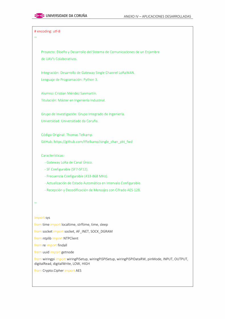
ANEXO IV – APLICACIONES DESARROLLADAS
# encoding: utf-8
'''
Proyecto: Diseño y Desarrollo del Sistema de Comunicaciones de un Enjambre
de UAV's Colaborativos.
Integración: Desarrollo de Gateway Single Channel LoRaWAN.
Lenguaje de Programación: Python 3.
Alumno: Cristian Méndez Sanmartín.
Titulación: Máster en Ingeniería Industrial.
Grupo de Investigación: Grupo Integrado de Ingeniería.
Universidad: Universidade da Coruña.
Código Original: Thomas Telkamp.
GitHub: https://github.com/tftelkamp/single_chan_pkt_fwd
Características:
- Gateway LoRa de Canal Único.
- SF Configurable (SF7-SF12).
- Frecuencia Configurable (433-868 MHz).
- Actualización de Estado Automática en Intervalo Configurable.
- Recepción y Decodificación de Mensajes con Cifrado AES-128.
'''
import sys
from time import localtime, strftime, time, sleep
from socket import socket, AF_INET, SOCK_DGRAM
from ntplib import NTPClient
from re import findall
from uuid import getnode
from wiringpi import wiringPiSetup, wiringPiSPISetup, wiringPiSPIDataRW, pinMode, INPUT, OUTPUT, digitalRead, digitalWrite, LOW, HIGH
from Crypto.Cipher import AES
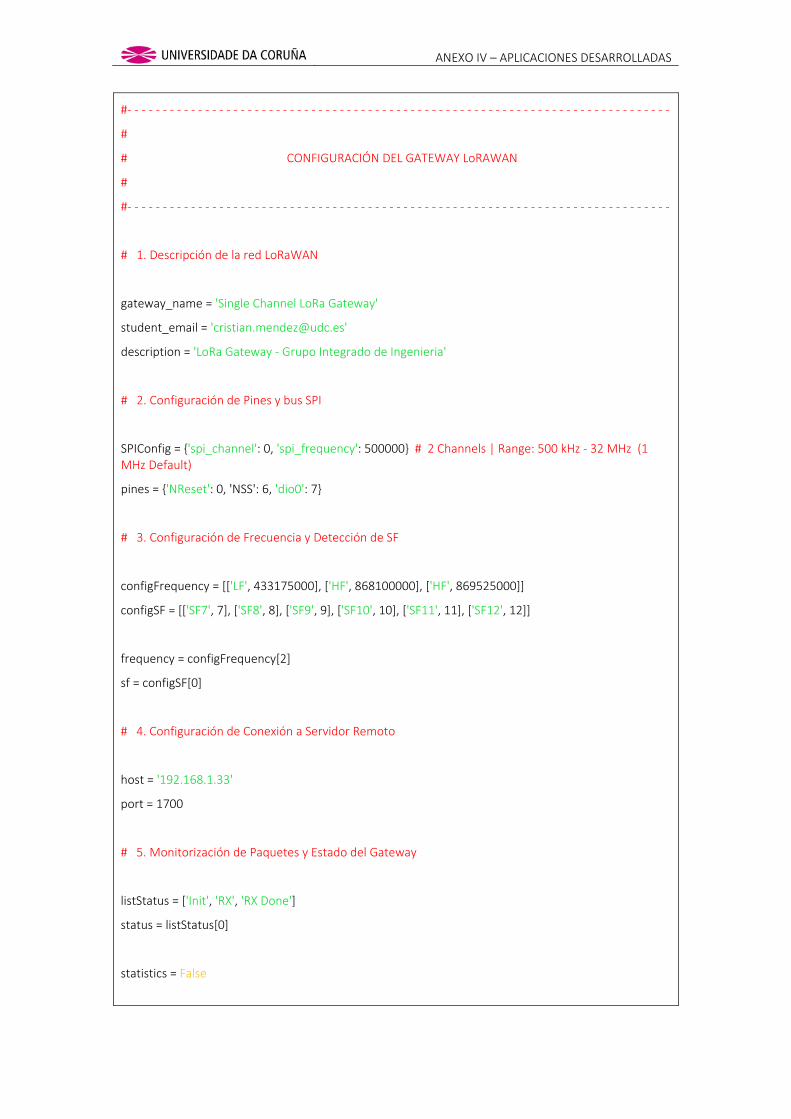
ANEXO IV – APLICACIONES DESARROLLADAS
#- - - - - - - - - - - - - - - - - - - - - - - - - - - - - - - - - - - - - - - - - - - - - - - - - - - - - - - - - - - - - - - - - - - - - - - - - - - - -
#
# CONFIGURACIÓN DEL GATEWAY LoRAWAN
#
#- - - - - - - - - - - - - - - - - - - - - - - - - - - - - - - - - - - - - - - - - - - - - - - - - - - - - - - - - - - - - - - - - - - - - - - - - - - - -
# 1. Descripción de la red LoRaWAN
gateway_name = 'Single Channel LoRa Gateway'
student_email = '[email protected]'
description = 'LoRa Gateway - Grupo Integrado de Ingenieria'
# 2. Configuración de Pines y bus SPI
SPIConfig = 'spi_channel': 0, 'spi_frequency': 500000 # 2 Channels | Range: 500 kHz - 32 MHz (1 MHz Default)
pines = 'NReset': 0, 'NSS': 6, 'dio0': 7
# 3. Configuración de Frecuencia y Detección de SF
configFrequency = [['LF', 433175000], ['HF', 868100000], ['HF', 869525000]]
configSF = [['SF7', 7], ['SF8', 8], ['SF9', 9], ['SF10', 10], ['SF11', 11], ['SF12', 12]]
frequency = configFrequency[2]
sf = configSF[0]
# 4. Configuración de Conexión a Servidor Remoto
host = '192.168.1.33'
port = 1700
# 5. Monitorización de Paquetes y Estado del Gateway
listStatus = ['Init', 'RX', 'RX Done']
status = listStatus[0]
statistics = False

ANEXO IV – APLICACIONES DESARROLLADAS
if statistics is True:
NTPServer = 'es.pool.ntp.org'
timestamp = []
midPacketRSSI =[]
midRSSI = []
midSNR = []
receivedPackets = 0
correctPackets = 0
updateInterval = 15
#- - - - - - - - - - - - - - - - - - - - - - - - - - - - - - - - - - - - - - - - - - - - - - - - - - - - - - - - - - - - - - - - - - - - - - - - - - - - -
#
# CONFIGURACIÓN DE REGISTROS LoRa
#
#- - - - - - - - - - - - - - - - - - - - - - - - - - - - - - - - - - - - - - - - - - - - - - - - - - - - - - - - - - - - - - - - - - - - - - - - - - - - -
# 1. LoRa Mode Register Map
REG_FIFO = 0x00
REG_OP_MODE = 0x01
REG_FRF_MSB = 0x06
REG_FRF_MID = 0x07
REG_FRF_LSB = 0x08
REG_PA_CONFIG = 0x09
REG_PA_RAMP = 0x0A
REG_OCP = 0x0B
REG_LNA = 0x0C
REG_FIFO_ADDR_PTR = 0x0D
REG_FIFO_TX_BASE_ADDR = 0x0E
REG_FIFO_RX_BASE_ADDR = 0x0F
REG_FIFO_RX_CURRENT_ADDR = 0x10
REG_IRQ_FLAGS_MASK = 0x11
REG_IRQ_FLAGS = 0x12
REG_RX_NB_BYTES = 0x13
REG_RX_HEADER_CNT_VALUE_MSB = 0x14
REG_RX_HEADER_CNT_VALUE_LSB = 0x15

ANEXO IV – APLICACIONES DESARROLLADAS
REG_RX_PACKET_CNT_VALUE_MSB = 0x16
REG_RX_PACKET_CNT_VALUE_LSB = 0x17
REG_MODEM_STAT = 0x18
REG_PACKET_SNR_VALUE = 0x19
REG_PACKET_RSSI_VALUE = 0x1A
REG_RSSI_VALUE = 0x1B
REG_HOP_CHANNEL = 0x1C
REG_MODEM_CONFIG_1 = 0x1D
REG_MODEM_CONFIG_2 = 0x1E
REG_SYMB_TIMEOUT_LSB = 0x1F
REG_PREAMBLE_MSB = 0x20
REG_PREAMBLE_LSB = 0x21
REG_PAYLOAD_LENGTH = 0x22
REG_MAX_PAYLOAD_LENGTH = 0x23
REG_HOP_PERIOD = 0x24
REG_FIFO_RX_BYTE_ADDR = 0x25
REG_MODEM_CONFIG_3 = 0x26
REG_FEI_MSB = 0x28
REG_FEI_MID = 0x29
REG_FEI_LSB = 0x2A
REG_RSSI_WIDEBAND = 0x2C
REG_DETEC_OPTIMIZE = 0x31
REG_INVERT_IQ = 0x33
REG_DETECTION_THRESHOLD = 0x37
REG_SYNC_WORD = 0x39
# 2. Modos de Operación
SLEEP_MODE = 0x00
STANDBY_MODE = 0x01
FSTX_MODE = 0x02
TX_MODE = 0x03
FSRX_MODE = 0x04
RX_CONTINUOUS_MODE = 0x05
RX_SINGLE_MODE = 0x06
CAD_MODE = 0x07

ANEXO IV – APLICACIONES DESARROLLADAS
# 3. IRQ's del Transceptor SX1276
CAD_DETECTED_MASK = 0x01
FHHS_CHANGE_CHANNEL_MASK = 0x02
CAD_DONE_MASK = 0x04
TX_DONE_MASK = 0x08
VALID_HEADER_MASK = 0x10
PAYLOAD_CRC_ERROR_MASK = 0x20
RX_DONE_MASK = 0x40
RX_TIMEOUT_MASK = 0x80
#- - - - - - - - - - - - - - - - - - - - - - - - - - - - - - - - - - - - - - - - - - - - - - - - - - - - - - - - - - - - - - - - - - - - - - - - - - - - -
def readRegister(address):
digitalWrite(pines['NSS'], LOW) # Select Chip Through SPI
SPIReading = wiringPiSPIDataRW(SPIConfig['spi_channel'], bytes([address & 0x7F, 0x00])) # 1 byte: 1 bit: read access (0) | 7 bits: address
digitalWrite(pines['NSS'], HIGH) # Unselect Chip Through SPI
return SPIReading[1][1] # Return of Read Value
def writeRegister(address, data):
digitalWrite(pines['NSS'], LOW) # Select Chip Through SPI
wiringPiSPIDataRW(SPIConfig['spi_channel'], bytes([ 0x80 | address, data])) # 1 byte: 1 bit: write access (1) | 7 bits: address | 1 byte: data
digitalWrite(pines['NSS'], HIGH) # Unselect Chip Through SPI
#- - - - - - - - - - - - - - - - - - - - - - - - - - - - - - - - - - - - - - - - - - - - - - - - - - - - - - - - - - - - - - - - - - - - - - - - - - - - -
def eventHandler():
global status
if digitalRead(pines['dio0']) is HIGH:
dio0Interrupt() # Set Input polling dio0 interrupt
if status is listStatus[2]:
receivePacket() # Reception of Packets
status = listStatus[1] # Reset to RX Status
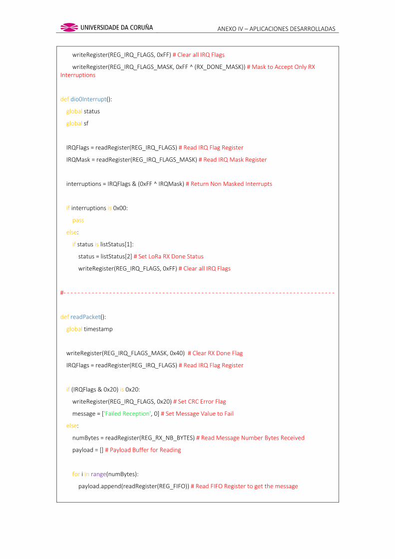
ANEXO IV – APLICACIONES DESARROLLADAS
writeRegister(REG_IRQ_FLAGS, 0xFF) # Clear all IRQ Flags
writeRegister(REG_IRQ_FLAGS_MASK, 0xFF ^ (RX_DONE_MASK)) # Mask to Accept Only RX Interruptions
def dio0Interrupt():
global status
global sf
IRQFlags = readRegister(REG_IRQ_FLAGS) # Read IRQ Flag Register
IRQMask = readRegister(REG_IRQ_FLAGS_MASK) # Read IRQ Mask Register
interruptions = IRQFlags & (0xFF ^ IRQMask) # Return Non Masked Interrupts
if interruptions is 0x00:
pass
else:
if status is listStatus[1]:
status = listStatus[2] # Set LoRa RX Done Status
writeRegister(REG_IRQ_FLAGS, 0xFF) # Clear all IRQ Flags
#- - - - - - - - - - - - - - - - - - - - - - - - - - - - - - - - - - - - - - - - - - - - - - - - - - - - - - - - - - - - - - - - - - - - - - - - - - - - -
def readPacket():
global timestamp
writeRegister(REG_IRQ_FLAGS_MASK, 0x40) # Clear RX Done Flag
IRQFlags = readRegister(REG_IRQ_FLAGS) # Read IRQ Flag Register
if (IRQFlags & 0x20) is 0x20:
writeRegister(REG_IRQ_FLAGS, 0x20) # Set CRC Error Flag
message = ['Failed Reception', 0] # Set Message Value to Fail
else:
numBytes = readRegister(REG_RX_NB_BYTES) # Read Message Number Bytes Received
payload = [] # Payload Buffer for Reading
for i in range(numBytes):
payload.append(readRegister(REG_FIFO)) # Read FIFO Register to get the message

ANEXO IV – APLICACIONES DESARROLLADAS
message = [payload, numBytes] # Compose the message with Payload and Number Bytes Received
return message # Return Payload and Number Bytes Received
def decodePacket(message):
decodedMessage = '' # Decoded Message Buffer
blockLength = 16 # Standard Block Length (Could vary in the last block)
counter = 9 # Counter for Payload Read (Byte 0: MHDR | Bytes 1-7: FHDR | Byte 8: FPort)
dataLength = message[1] - 13 # Payload Length: Message Bytes - (Byte 0: MHDR | Bytes 1-7: FHDR | Byte 8: FPort | Bytes n-3 - n: MIC)
numBlocks = int(dataLength / 16) # Number of Block A
restLength = dataLength % 16 # Rest May Needed for the Last Block A
if restLength > 0:
numBlocks += 1 # Aditional Block A
devAddr = [message[0][1], message[0][2], message[0][3], message[0][4]] # Get Device Address from Message
frameCounter = [message[0][6], message[0][7]] # Get Frame Counter from Message
for i in range(numBlocks):
AppSKey = bytes([0xA4, 0x10, 0x9C, 0x15, 0x0E, 0x24, 0x92, 0xD5, 0x47, 0x9A, 0x78, 0x26, 0x45, 0x75, 0x8B, 0x3B]) # Application Session Key for AES-128 Encrypt
mode = AES.MODE_CBC # Set AES CBC Encrypt Mode
IV = bytes(16 * [0x00]) # Set IV Null
Crypto = AES.new(AppSKey, mode, IV) # Define new AES Encrypt Object
BlockA = bytes([0x01, 0x00, 0x00, 0x00, 0x00, 0x00, devAddr[0], devAddr[1], devAddr[2], devAddr[3], frameCounter[0], frameCounter[1], 0x00, 0x00, 0x00, i + 1]) # Composing Block A as LoRaWAN Specification
BlockS = Crypto.encrypt(BlockA) # Get Block S in Cypher Library Format from Encpypted Block A
if i is (numBlocks - 1) and restLength > 0:
blockLength = restLength # Set Last Block Length if vary from 16 bytes

ANEXO IV – APLICACIONES DESARROLLADAS
for j in range(blockLength):
decodedMessage += str(chr(message[0][counter] ^ BlockS[j])) # Get Decoded Message XORing Payload and Blocks S
counter += 1 # Increase Count of Payload
return decodedMessage # Return Decoded Message
def receivePacket():
global receivedPackets
global correctPackets
message = readPacket() # Read Message Received (CRC Error | Correct Message)
receivedPackets += 1 # Increase Received Packet Counter
if message[1] > 0:
decodedMessage = decodePacket(message) # Function call for decoding
if statistics:
timestamp.append(NTP.request(NTPServer).tx_time) # Latency medition
correctPackets += 1 # Increase Correct Packet Counter
if readRegister(REG_PACKET_SNR_VALUE) & 0x80:
SNR = -(((( 0xFF ^ readRegister(REG_PACKET_SNR_VALUE)) + 1) & 0xFF) >> 2) # Get SNR Value
else:
SNR = (readRegister(REG_PACKET_SNR_VALUE) & 0xFF) >> 2 # Get SNR Value
if frequency[0] is 'LF':
if SNR >= 0:
RSSI = -164 + (16/15) * readRegister(REG_RSSI_VALUE) # Get RSSI from Adjusted Standard Formula
packetRSSI = -164 + (16/15) * readRegister(REG_PACKET_RSSI_VALUE) # Get Packet Strenght from Standard Formula
else:
RSSI = -164 + readRegister(REG_RSSI_VALUE) # Get RSSI from Standard Formula
packetRSSI = -164 + readRegister(REG_PACKET_RSSI_VALUE) + 0.25 * SNR # Get Packet Strenght from Adjusted Formula

ANEXO IV – APLICACIONES DESARROLLADAS
else:
if SNR >= 0:
RSSI = -157 + (16/15) * readRegister(REG_RSSI_VALUE) # Get RSSI from Adjusted Standard Formula
packetRSSI = -157 + (16/15) * readRegister(REG_PACKET_RSSI_VALUE) # Get Packet Strenght from Standard Formula
else:
RSSI = -157 + readRegister(REG_RSSI_VALUE) # Get RSSI from Standard Formula
packetRSSI = -157 + readRegister(REG_PACKET_RSSI_VALUE) + 0.25 * SNR # Get Packet Strenght from Adjusted Formula
if statistics:
midPacketRSSI.append(packetRSSI) # RSSI Packet medition
midRSSI.append(RSSI) # RSSI Packet medition
midSNR.append(SNR) # RSSI Packet medition
print('-----------------------------------------------------------------------')
print('Parámetros de transmisión del paquete:\n RSSI del paquete: ' + str(int(packetRSSI)) + '.\n RSSI: ' + str(int(RSSI)) + '.\n SNR: ' + str(int(SNR)) + '.\n Longitud de paquete: ' + str(message[1]) + '.\n Mensaje: ' + decodedMessage + '.')
print('-----------------------------------------------------------------------\n')
sendUDP('Parametros de transmision del paquete:| RSSI del paquete: ' + str(int(packetRSSI)) + '.| RSSI: ' + str(int(RSSI)) + '.| SNR: ' + str(int(SNR)) + '.| Longitud de paquete: ' + str(message[1]) + '.| Mensaje: ' + decodedMessage + '.') # Send by UDP Correct Message Report
else:
print('-----------------------------------------------------------------------')
print('Parámetros de transmisión del paquete:\n Error en Recepción: CRC.')
print('-----------------------------------------------------------------------\n')
sendUDP('Parametros de transmision del paquete:| Error en Recepcion: CRC.') # Send by UDP Message Error Report
#- - - - - - - - - - - - - - - - - - - - - - - - - - - - - - - - - - - - - - - - - - - - - - - - - - - - - - - - - - - - - - - - - - - - - - - - - - - - -
def sendStatus(time):
print('-----------------------------------------------------------------------')
print ('Actualización de estado:\n Estado: ' + status + '.\n Actividad: ' + str(int(time)) + 's.\n Fecha: ' + str(strftime('%d/%m/%Y')) +'.\n Hora: ' + str(strftime('%H:%M:%S')) + '.\n Plataforma: ' + gateway_name + '.\n E-mail: ' + student_email + '.\n Descripción: ' + description + '.')

ANEXO IV – APLICACIONES DESARROLLADAS
print('-----------------------------------------------------------------------')
print ('Información de paquetes:\n Recibidos: ' + str(receivedPackets) + '.\n Correctos: ' + str(correctPackets) + '.\n Incorrectos: ' + str(receivedPackets - correctPackets) + '.')
sendUDP('Actualizacion de estado:| Estado: ' + status + '.| Actividad: ' + str(int(time)) + 's.| Fecha: ' + str(strftime('%d/%m/%Y')) +'.| Hora: ' + str(strftime('%H:%M:%S')) + '.| Plataforma: ' + gateway_name + '.| E-mail: ' + student_email + '.| Descripcion: ' + description + '.') # Send by UDP Status Report
sendUDP('Informacion de paquetes:| Recibidos: ' + str(receivedPackets) + '.| Correctos: ' + str(correctPackets) + '.| Incorrectos: ' + str(receivedPackets - correctPackets) + '.') # Send by UDP Packet Report
if statistics and correctPackets > 0:
statPacketRSSI = 0
statRSSI = 0
statSNR = 0
for i in range(len(midPacketRSSI)):
statPacketRSSI += midPacketRSSI[i] # Acumulate value from Packet RSSI list
statRSSI += midRSSI[i] # Acumulate value from RSSI list
statSNR += midSNR[i] # Acumulate value from SNR list
print('-----------------------------------------------------------------------')
print('Informacion de estadisticas:\n Timestamp: ' + str(timestamp) + '.\n RSSI de paquetes (media): ' + str(int(statPacketRSSI/len(midPacketRSSI))) + '.\n RSSI (media): ' + str(int(statRSSI/len(midRSSI))) + '.\n SNR (media): ' + str(int(statSNR/len(midSNR))) + '.')
sendUDP('Informacion de estadisticas:| Timestamp: '+ str(timestamp) + '.| RSSI de paquetes (media): ' + str(int(statPacketRSSI/len(midPacketRSSI))) + '.| RSSI (media): ' + str(int(statRSSI/len(midRSSI))) + '.| SNR (media): ' + str(int(statSNR/len(midSNR))) + '.')
print('-----------------------------------------------------------------------\n')
def sendUDP(message):
socket_udp.sendto(message.encode(), (host, port)) # Send UDP Message
#- - - - - - - - - - - - - - - - - - - - - - - - - - - - - - - - - - - - - - - - - - - - - - - - - - - - - - - - - - - - - - - - - - - - - - - - - - - - -
def setSPI():
wiringPiSetup() # Set up WiringPi Library
wiringPiSPISetup(SPIConfig['spi_channel'], SPIConfig['spi_frequency']) # Set Up Serial Peripherical Interface (SPI)

ANEXO IV – APLICACIONES DESARROLLADAS
pinMode(pines['NReset'], OUTPUT) # Set Reset Pin as Output
pinMode(pines['NSS'], OUTPUT) # Set Pin Chip Select as Output
pinMode(pines['dio0'], INPUT) # Set Pin Dio0 as Input
digitalWrite(pines['NReset'], LOW) # Low NReset for Manual Reset of the Chip
sleep(0.01) # 10 ms Wait in Reset Process
digitalWrite(pines['NReset'], HIGH) # High NReset for Manual Reset of the Chip
sleep(0.01) # 10 ms Wait in Reset Process
def setMode(mode):
if frequency[0] is 'LF':
newMode = 0x80 | 0x08 # LoRa LF Mode
else:
newMode = 0x80 # LoRa HF Mode
newMode |= mode # Compose New Operation Mode
writeRegister(REG_OP_MODE, newMode) # Set New Operation Mode
def setFrequency(frequency):
frf = int((frequency[1] << 19) / 32000000) # FRF Stablished
MSB = frf >> 16
MID = frf >> 8 ^ (MSB << 8)
LSB = frf ^ (MSB << 16 ^ MID << 8)
writeRegister(REG_FRF_MSB, MSB) # Set RFR MSB Register
writeRegister(REG_FRF_MID, MID) # Set FRF MID Register
writeRegister(REG_FRF_LSB, LSB) # Set FRF LSB Register
def setRate(sf):
writeRegister(REG_MODEM_CONFIG_1, 0x72) # BW 125 | CRC 4/5
writeRegister(REG_MODEM_CONFIG_2, sf[1] << 4 | 0x04) #SF | CRC ON
if sf[0] is 'SF11' or sf[0] is 'SF12':
writeRegister(REG_MODEM_CONFIG_3, 0x0C) # Symbol Length Exceed 16 ms | LNA internal AGC Loop
else:
writeRegister(REG_MODEM_CONFIG_3, 0x04) # LNA internal AGC Loop
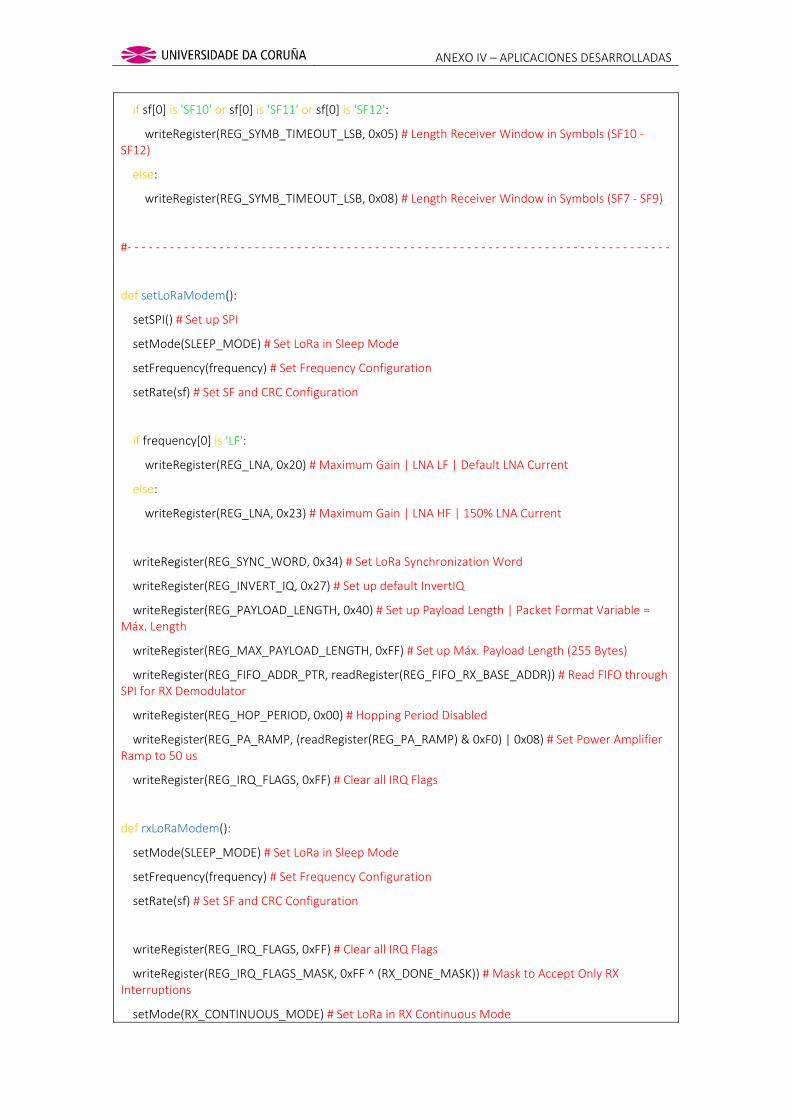
ANEXO IV – APLICACIONES DESARROLLADAS
if sf[0] is 'SF10' or sf[0] is 'SF11' or sf[0] is 'SF12':
writeRegister(REG_SYMB_TIMEOUT_LSB, 0x05) # Length Receiver Window in Symbols (SF10 - SF12)
else:
writeRegister(REG_SYMB_TIMEOUT_LSB, 0x08) # Length Receiver Window in Symbols (SF7 - SF9)
#- - - - - - - - - - - - - - - - - - - - - - - - - - - - - - - - - - - - - - - - - - - - - - - - - - - - - - - - - - - - - - - - - - - - - - - - - - - - -
def setLoRaModem():
setSPI() # Set up SPI
setMode(SLEEP_MODE) # Set LoRa in Sleep Mode
setFrequency(frequency) # Set Frequency Configuration
setRate(sf) # Set SF and CRC Configuration
if frequency[0] is 'LF':
writeRegister(REG_LNA, 0x20) # Maximum Gain | LNA LF | Default LNA Current
else:
writeRegister(REG_LNA, 0x23) # Maximum Gain | LNA HF | 150% LNA Current
writeRegister(REG_SYNC_WORD, 0x34) # Set LoRa Synchronization Word
writeRegister(REG_INVERT_IQ, 0x27) # Set up default InvertIQ
writeRegister(REG_PAYLOAD_LENGTH, 0x40) # Set up Payload Length | Packet Format Variable = Máx. Length
writeRegister(REG_MAX_PAYLOAD_LENGTH, 0xFF) # Set up Máx. Payload Length (255 Bytes)
writeRegister(REG_FIFO_ADDR_PTR, readRegister(REG_FIFO_RX_BASE_ADDR)) # Read FIFO through SPI for RX Demodulator
writeRegister(REG_HOP_PERIOD, 0x00) # Hopping Period Disabled
writeRegister(REG_PA_RAMP, (readRegister(REG_PA_RAMP) & 0xF0) | 0x08) # Set Power Amplifier Ramp to 50 us
writeRegister(REG_IRQ_FLAGS, 0xFF) # Clear all IRQ Flags
def rxLoRaModem():
setMode(SLEEP_MODE) # Set LoRa in Sleep Mode
setFrequency(frequency) # Set Frequency Configuration
setRate(sf) # Set SF and CRC Configuration
writeRegister(REG_IRQ_FLAGS, 0xFF) # Clear all IRQ Flags
writeRegister(REG_IRQ_FLAGS_MASK, 0xFF ^ (RX_DONE_MASK)) # Mask to Accept Only RX Interruptions
setMode(RX_CONTINUOUS_MODE) # Set LoRa in RX Continuous Mode

ANEXO IV – APLICACIONES DESARROLLADAS
def setupLoRa():
global status
setLoRaModem() # Set LoRa Initial Configuration
status = listStatus[1] # Set LoRa RX Status
rxLoRaModem() # Set LoRa RX Configuration
#- - - - - - - - - - - - - - - - - - - - - - - - - - - - - - - - - - - - - - - - - - - - - - - - - - - - - - - - - - - - - - - - - - - - - - - - - - - - -
if __name__ == '__main__':
print('-----------------------------------------------------------------------\n')
print(' Gateway LoRaWAN - Grupo Integrado de Ingeniería.\n')
print('-----------------------------------------------------------------------\n')
print('-----------------------------------------------------------------------')
print('Iniciando Gateway ...\nGateway ID: ' + str(':'.join(findall('..', '%02x' % getnode())).upper()) + '.\nEscuchando a frecuencia: ' + str(frequency[1]/1000000) + ' MHz.\nSpreading Factor: ' + str(sf[0]) + '.')
print('-----------------------------------------------------------------------\n')
socket_udp = socket(AF_INET, SOCK_DGRAM) # Set Socket for UDP Transmissions to Server
if statistics:
NTP = NTPClient() # Set NTP Server for Latency Statistics
setupLoRa() # Set up LoRa Configuration
sendUDP(' Gateway LoRaWAN - Grupo Integrado de Ingenieria.') # Send by UDP Gateway Header
sendUDP('Iniciando Gateway ...|Gateway ID: ' + str(':'.join(findall('..', '%02x' % getnode())).upper()) + '.|Escuchando a frecuencia: ' + str(frequency[1]/1000000) + ' MHz.|Spreading Factor: ' + str(sf[0]) + '.') #Send by UDP Initial Status and Configuration
firstTime = time() # Set first time reference for Activity
pastTime = firstTime # Set past time reference for Status Update
while(1):
try:
eventHandler() # Set LoRa funcion for Incoming Events
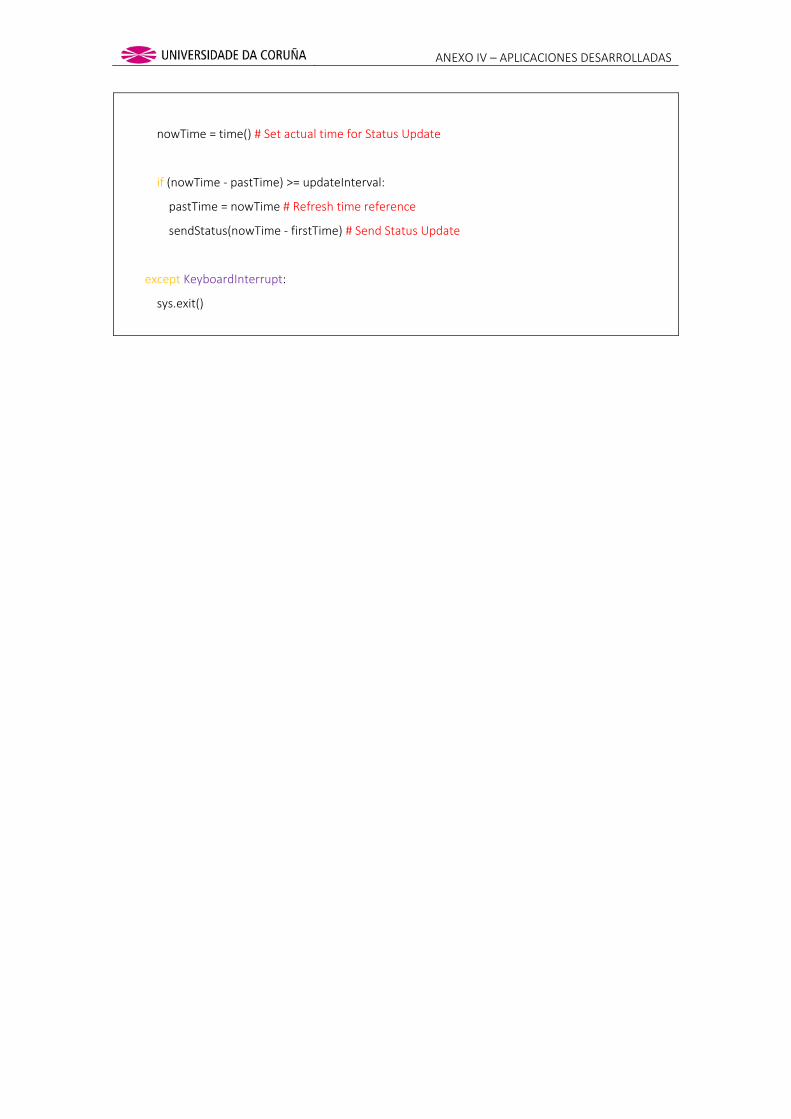
ANEXO IV – APLICACIONES DESARROLLADAS
nowTime = time() # Set actual time for Status Update
if (nowTime - pastTime) >= updateInterval:
pastTime = nowTime # Refresh time reference
sendStatus(nowTime - firstTime) # Send Status Update
except KeyboardInterrupt:
sys.exit()

ANEXO IV – APLICACIONES DESARROLLADAS
APLICACIONES DESARROLLADAS PARA LOS END-NODES
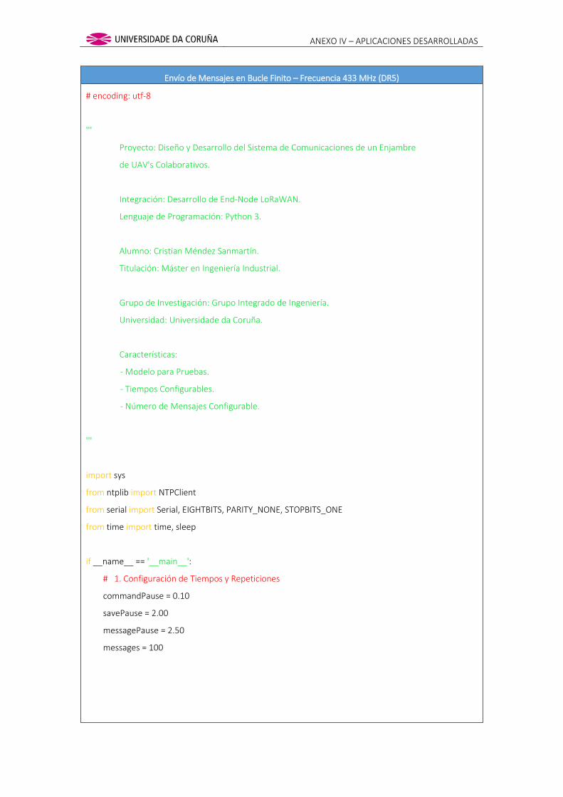
ANEXO IV – APLICACIONES DESARROLLADAS
Envío de Mensajes en Bucle Finito – Frecuencia 433 MHz (DR5)
# encoding: utf-8
'''
Proyecto: Diseño y Desarrollo del Sistema de Comunicaciones de un Enjambre
de UAV's Colaborativos.
Integración: Desarrollo de End-Node LoRaWAN.
Lenguaje de Programación: Python 3.
Alumno: Cristian Méndez Sanmartín.
Titulación: Máster en Ingeniería Industrial.
Grupo de Investigación: Grupo Integrado de Ingeniería.
Universidad: Universidade da Coruña.
Características:
- Modelo para Pruebas.
- Tiempos Configurables.
- Número de Mensajes Configurable.
'''
import sys
from ntplib import NTPClient
from serial import Serial, EIGHTBITS, PARITY_NONE, STOPBITS_ONE
from time import time, sleep
if __name__ == '__main__':
# 1. Configuración de Tiempos y Repeticiones
commandPause = 0.10
savePause = 2.00
messagePause = 2.50
messages = 100

ANEXO IV – APLICACIONES DESARROLLADAS
# 2. Configuración de Puerto Serie
mySerialPort = Serial('/dev/ttyACM0',
baudrate = 57600,
bytesize = EIGHTBITS,
parity = PARITY_NONE,
stopbits = STOPBITS_ONE,
timeout = 0.010
)
mySerialPort.flushInput()
mySerialPort.flushOutput()
# 3. Configuración del Servidor NTP
statistics = False
NTPServer = 'es.pool.ntp.org'
timestamp = []
if statistics:
NTP = NTPClient()
#- - - - - - - - - - - - - - - - - - - - - - - - - - - - - - - - - - - - - - - - - - - - - - - - - - - - - - - - - - - - - - - - - - - - - - - - -
print('-----------------------------------------------------------------------\n')
print(' Iniciando End-Node LoRaWAN.\n ')
print('-----------------------------------------------------------------------\n')
print('-----------------------------------------------------------------------\n')
if mySerialPort.isOpen():
print('Comunicación establecida con ' + mySerialPort.name)
print ('Enviando Comandos de Setup ...')
print ('-----------------------------------------------------------------------\n')
#- - - - - - - - - - - - - - - - - - - - - - - - - - - - - - - - - - - - - - - - - - - - - - - - - - - - - - - - - - - - - - - - - - - - - - - - -
try:
print('Comando enviado: mac reset 433')
mySerialPort.write('mac reset 433'.encode('ascii') + '\r\n'.encode('ascii'))
sleep(commandPause)

ANEXO IV – APLICACIONES DESARROLLADAS
print('Respuesta: ' + str(mySerialPort.read(15)).lstrip ("b'").replace ("'", "").replace("\\r\\n", " "))
print('Comando enviado: mac set ch status 1 off')
mySerialPort.write('mac set ch status 1 off'.encode('ascii') + '\r\n'.encode('ascii'))
sleep(commandPause)
print('Respuesta: ' + str(mySerialPort.read(15)).lstrip ("b'").replace ("'", "").replace("\\r\\n", " "))
print('Comando enviado: mac set ch status 2 off')
mySerialPort.write('mac set ch status 2 off'.encode('ascii') + '\r\n'.encode('ascii'))
sleep(commandPause)
print('Respuesta: ' + str(mySerialPort.read(15)).lstrip ("b'").replace ("'", "").replace("\\r\\n", " "))
print('Comando enviado: mac set ch dcycle 0 9')
mySerialPort.write('mac set ch dcycle 0 9'.encode('ascii') + '\r\n'.encode('ascii'))
sleep(commandPause)
print('Respuesta: ' + str(mySerialPort.read(15)).lstrip ("b'").replace ("'", "").replace("\\r\\n", " "))
print('Comando enviado: mac set dr 5')
mySerialPort.write('mac set dr 5'.encode('ascii') + '\r\n'.encode('ascii'))
sleep(commandPause)
print('Respuesta: ' + str(mySerialPort.read(15)).lstrip ("b'").replace ("'", "").replace("\\r\\n", " "))
print('Comando enviado: mac set pwridx 0')
mySerialPort.write('mac set pwridx 0'.encode('ascii') + '\r\n'.encode('ascii'))
sleep(commandPause)
print('Respuesta: ' + str(mySerialPort.read(15)).lstrip ("b'").replace ("'", "").replace("\\r\\n", " "))
print('Comando enviado: mac set devaddr 26011CA2')
mySerialPort.write('mac set devaddr 26011CA2'.encode('ascii') + '\r\n'.encode('ascii'))
sleep(commandPause)
print('Respuesta: ' + str(mySerialPort.read(15)).lstrip ("b'").replace ("'", "").replace("\\r\\n", " "))

ANEXO IV – APLICACIONES DESARROLLADAS
print('Comando enviado: mac set appskey A4109C150E2492D5479A782645758B3B')
mySerialPort.write('mac set appskey A4109C150E2492D5479A782645758B3B'.encode('ascii') + '\r\n'.encode('ascii'))
sleep(commandPause)
print('Respuesta: ' + str(mySerialPort.read(15)).lstrip ("b'").replace ("'", "").replace("\\r\\n", " "))
print('Comando enviado: mac set nwkskey 437009D0F91CF5F9694E4EB2AE7EB9D3')
mySerialPort.write('mac set nwkskey 437009D0F91CF5F9694E4EB2AE7EB9D3'.encode('ascii') + '\r\n'.encode('ascii'))
sleep(commandPause)
print('Respuesta: ' + str(mySerialPort.read(15)).lstrip ("b'").replace ("'", "").replace("\\r\\n", " "))
print('Comando enviado: mac save')
mySerialPort.write('mac save'.encode('ascii') + '\r\n'.encode('ascii'))
sleep(savePause)
print('Respuesta: ' + str(mySerialPort.read(15)).lstrip ("b'").replace ("'", "").replace("\\r\\n", " "))
print('Comando enviado: mac join ABP')
mySerialPort.write('mac join ABP'.encode('ascii') + '\r\n'.encode('ascii'))
sleep(savePause)
print('Respuesta: ' + str(mySerialPort.read(15)).lstrip ("b'").replace ("'", "").replace("\\r\\n", " "))
print('\n-----------------------------------------------------------------------')
print('Iniciando Bucle de Envío de Mensajes ... ')
print('-----------------------------------------------------------------------\n')
init = time() # Comenzamos a contar el tiempo de envío
for i in range(messages):
print('Comando enviado: mac tx uncnf 1 27536920637265657320717565207075656465732c2079612065737461732061206d6564696f2063616d696e6f2e27')
if statistics:
timestamp.append(NTP.request(NTPServer).tx_time)

ANEXO IV – APLICACIONES DESARROLLADAS
mySerialPort.write('mac tx uncnf 1 27536920637265657320717565207075656465732c2079612065737461732061206d6564696f2063616d696e6f2e27'.encode('ascii') + '\r\n'.encode('ascii'))
sleep(messagePause)
print('Respuesta: ' + str(mySerialPort.read(15)).lstrip ("b'").replace ("'", "").replace("\\r\\n", " "))
print('\n-----------------------------------------------------------------------')
if statistics:
print('Timestamp: ' + str(timestamp))
print('-----------------------------------------------------------------------')
print('Tiempo de Envio Total: ' + str(round(time() - init, 2)) + ' s.')
print('-----------------------------------------------------------------------')
sleep(180)
except KeyboardInterrupt:
mySerialPort.close() # Cerramos el Puerto Serie
sys.exit() # Salida de Programa
mySerialPort.close() # Cerramos el Puerto Serie

ANEXO IV – APLICACIONES DESARROLLADAS
Envío de Mensajes en Bucle Infinito – Frecuencia 433 MHz (DR5)
# encoding: utf-8
'''
Proyecto: Diseño y Desarrollo del Sistema de Comunicaciones de un Enjambre
de UAV's Colaborativos.
Integración: Desarrollo de End-Node LoRaWAN.
Lenguaje de Programación: Python 3.
Alumno: Cristian Méndez Sanmartín.
Titulación: Máster en Ingeniería Industrial.
Grupo de Investigación: Grupo Integrado de Ingeniería.
Universidad: Universidade da Coruña.
Características:
- Modelo Final.
- Tiempos Configurables.
- Pendiente bucle de lectura de sensores.
'''
import sys
from ntplib import NTPClient
from serial import Serial, EIGHTBITS, PARITY_NONE, STOPBITS_ONE
from time import time, sleep
if __name__ == '__main__':
# 1. Configuración de Tiempos
commandPause = 0.10
savePause = 2.00
messagePause = 2.50

ANEXO IV – APLICACIONES DESARROLLADAS
# 2. Configuración de Puerto Serie
mySerialPort = Serial('/dev/ttyACM0',
baudrate = 57600,
bytesize = EIGHTBITS,
parity = PARITY_NONE,
stopbits = STOPBITS_ONE,
timeout = 0.010
)
mySerialPort.flushInput()
mySerialPort.flushOutput()
# 3. Configuración del Servidor NTP
statistics = False
NTPServer = 'es.pool.ntp.org'
timestamp = []
if statistics:
NTP = NTPClient()
#- - - - - - - - - - - - - - - - - - - - - - - - - - - - - - - - - - - - - - - - - - - - - - - - - - - - - - - - - - - - - - - - - - - - - - - - -
print('-----------------------------------------------------------------------\n')
print(' Iniciando End-Node LoRaWAN.\n ')
print('-----------------------------------------------------------------------\n')
print('-----------------------------------------------------------------------\n')
if mySerialPort.isOpen():
print('Comunicación establecida con ' + mySerialPort.name)
print ('Enviando Comandos de Setup ...')
print ('-----------------------------------------------------------------------\n')
#- - - - - - - - - - - - - - - - - - - - - - - - - - - - - - - - - - - - - - - - - - - - - - - - - - - - - - - - - - - - - - - - - - - - - - - - -
try:
print('Comando enviado: mac reset 433')
mySerialPort.write('mac reset 433'.encode('ascii') + '\r\n'.encode('ascii'))
sleep(commandPause)

ANEXO IV – APLICACIONES DESARROLLADAS
print('Respuesta: ' + str(mySerialPort.read(15)).lstrip ("b'").replace ("'", "").replace("\\r\\n", " "))
print('Comando enviado: mac set ch status 1 off')
mySerialPort.write('mac set ch status 1 off'.encode('ascii') + '\r\n'.encode('ascii'))
sleep(commandPause)
print('Respuesta: ' + str(mySerialPort.read(15)).lstrip ("b'").replace ("'", "").replace("\\r\\n", " "))
print('Comando enviado: mac set ch status 2 off')
mySerialPort.write('mac set ch status 2 off'.encode('ascii') + '\r\n'.encode('ascii'))
sleep(commandPause)
print('Respuesta: ' + str(mySerialPort.read(15)).lstrip ("b'").replace ("'", "").replace("\\r\\n", " "))
print('Comando enviado: mac set ch dcycle 0 9')
mySerialPort.write('mac set ch dcycle 0 9'.encode('ascii') + '\r\n'.encode('ascii'))
sleep(commandPause)
print('Respuesta: ' + str(mySerialPort.read(15)).lstrip ("b'").replace ("'", "").replace("\\r\\n", " "))
print('Comando enviado: mac set dr 5')
mySerialPort.write('mac set dr 5'.encode('ascii') + '\r\n'.encode('ascii'))
sleep(commandPause)
print('Respuesta: ' + str(mySerialPort.read(15)).lstrip ("b'").replace ("'", "").replace("\\r\\n", " "))
print('Comando enviado: mac set pwridx 0')
mySerialPort.write('mac set pwridx 0'.encode('ascii') + '\r\n'.encode('ascii'))
sleep(commandPause)
print('Respuesta: ' + str(mySerialPort.read(15)).lstrip ("b'").replace ("'", "").replace("\\r\\n", " "))
print('Comando enviado: mac set devaddr 26011CA2')
mySerialPort.write('mac set devaddr 26011CA2'.encode('ascii') + '\r\n'.encode('ascii'))
sleep(commandPause)
print('Respuesta: ' + str(mySerialPort.read(15)).lstrip ("b'").replace ("'", "").replace("\\r\\n", " "))
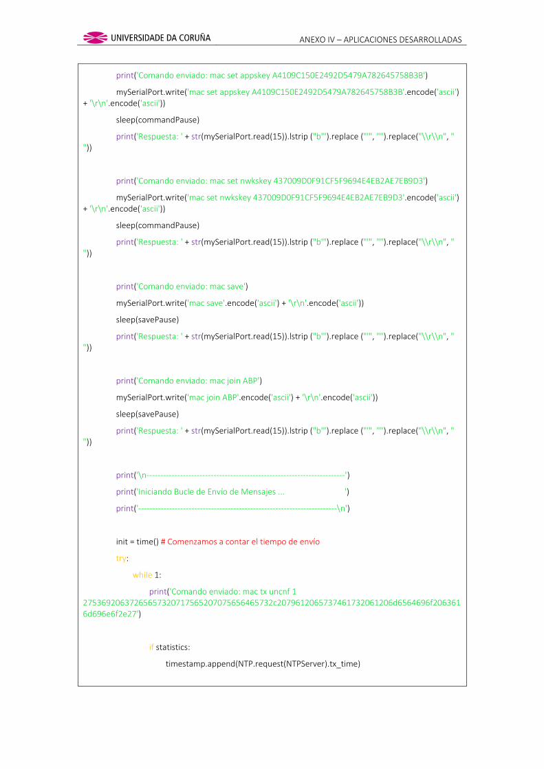
ANEXO IV – APLICACIONES DESARROLLADAS
print('Comando enviado: mac set appskey A4109C150E2492D5479A782645758B3B')
mySerialPort.write('mac set appskey A4109C150E2492D5479A782645758B3B'.encode('ascii') + '\r\n'.encode('ascii'))
sleep(commandPause)
print('Respuesta: ' + str(mySerialPort.read(15)).lstrip ("b'").replace ("'", "").replace("\\r\\n", " "))
print('Comando enviado: mac set nwkskey 437009D0F91CF5F9694E4EB2AE7EB9D3')
mySerialPort.write('mac set nwkskey 437009D0F91CF5F9694E4EB2AE7EB9D3'.encode('ascii') + '\r\n'.encode('ascii'))
sleep(commandPause)
print('Respuesta: ' + str(mySerialPort.read(15)).lstrip ("b'").replace ("'", "").replace("\\r\\n", " "))
print('Comando enviado: mac save')
mySerialPort.write('mac save'.encode('ascii') + '\r\n'.encode('ascii'))
sleep(savePause)
print('Respuesta: ' + str(mySerialPort.read(15)).lstrip ("b'").replace ("'", "").replace("\\r\\n", " "))
print('Comando enviado: mac join ABP')
mySerialPort.write('mac join ABP'.encode('ascii') + '\r\n'.encode('ascii'))
sleep(savePause)
print('Respuesta: ' + str(mySerialPort.read(15)).lstrip ("b'").replace ("'", "").replace("\\r\\n", " "))
print('\n-----------------------------------------------------------------------')
print('Iniciando Bucle de Envío de Mensajes ... ')
print('-----------------------------------------------------------------------\n')
init = time() # Comenzamos a contar el tiempo de envío
try:
while 1:
print('Comando enviado: mac tx uncnf 1 27536920637265657320717565207075656465732c2079612065737461732061206d6564696f2063616d696e6f2e27')
if statistics:
timestamp.append(NTP.request(NTPServer).tx_time)
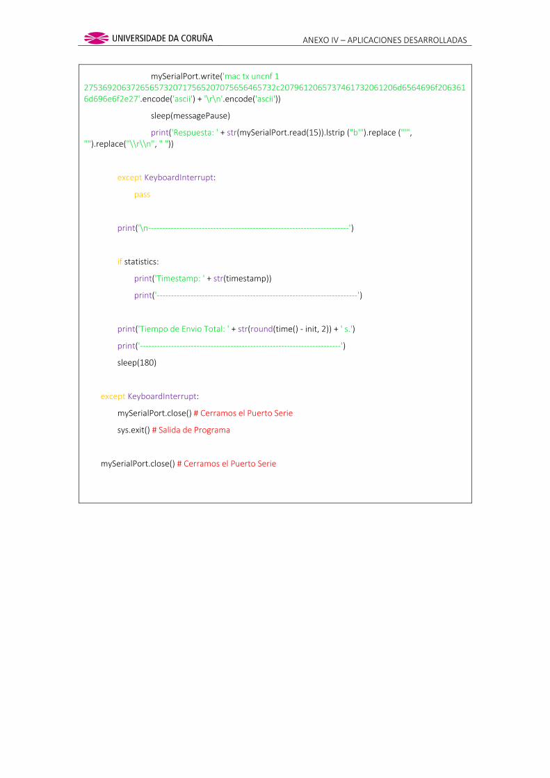
ANEXO IV – APLICACIONES DESARROLLADAS
mySerialPort.write('mac tx uncnf 1 27536920637265657320717565207075656465732c2079612065737461732061206d6564696f2063616d696e6f2e27'.encode('ascii') + '\r\n'.encode('ascii'))
sleep(messagePause)
print('Respuesta: ' + str(mySerialPort.read(15)).lstrip ("b'").replace ("'", "").replace("\\r\\n", " "))
except KeyboardInterrupt:
pass
print('\n-----------------------------------------------------------------------')
if statistics:
print('Timestamp: ' + str(timestamp))
print('-----------------------------------------------------------------------')
print('Tiempo de Envio Total: ' + str(round(time() - init, 2)) + ' s.')
print('-----------------------------------------------------------------------')
sleep(180)
except KeyboardInterrupt:
mySerialPort.close() # Cerramos el Puerto Serie
sys.exit() # Salida de Programa
mySerialPort.close() # Cerramos el Puerto Serie

ANEXO IV – APLICACIONES DESARROLLADAS
Envío de Mensajes en Bucle Finito – Frecuencia 868 MHz (DR5)
# encoding: utf-8
'''
Proyecto: Diseño y Desarrollo del Sistema de Comunicaciones de un Enjambre
de UAV's Colaborativos.
Integración: Desarrollo de End-Node LoRaWAN.
Lenguaje de Programación: Python 3.
Alumno: Cristian Méndez Sanmartín.
Titulación: Máster en Ingeniería Industrial.
Grupo de Investigación: Grupo Integrado de Ingeniería.
Universidad: Universidade da Coruña.
Características:
- Modelo para Pruebas.
- Tiempos Configurables.
- Número de Mensajes Configurable.
'''
import sys
from ntplib import NTPClient
from serial import Serial, EIGHTBITS, PARITY_NONE, STOPBITS_ONE
from time import time, sleep
if __name__ == '__main__':
# 1. Configuración de Tiempos y Repeticiones
commandPause = 0.10
savePause = 2.00
messagePause = 2.50
messages = 100

ANEXO IV – APLICACIONES DESARROLLADAS
# 2. Configuración de Puerto Serie
mySerialPort = Serial('/dev/ttyACM0',
baudrate = 57600,
bytesize = EIGHTBITS,
parity = PARITY_NONE,
stopbits = STOPBITS_ONE,
timeout = 0.010
)
mySerialPort.flushInput()
mySerialPort.flushOutput()
# 3. Configuración del Servidor NTP
statistics = False
NTPServer = 'es.pool.ntp.org'
timestamp = []
if statistics:
NTP = NTPClient()
#- - - - - - - - - - - - - - - - - - - - - - - - - - - - - - - - - - - - - - - - - - - - - - - - - - - - - - - - - - - - - - - - - - - - - - - - -
print('-----------------------------------------------------------------------\n')
print(' Iniciando End-Node LoRaWAN.\n ')
print('-----------------------------------------------------------------------\n')
print('-----------------------------------------------------------------------\n')
if mySerialPort.isOpen():
print('Comunicación establecida con ' + mySerialPort.name)
print ('Enviando Comandos de Setup ...')
print ('-----------------------------------------------------------------------\n')
#- - - - - - - - - - - - - - - - - - - - - - - - - - - - - - - - - - - - - - - - - - - - - - - - - - - - - - - - - - - - - - - - - - - - - - - - -
try:
print('Comando enviado: mac reset 868')
mySerialPort.write('mac reset 868'.encode('ascii') + '\r\n'.encode('ascii'))
sleep(commandPause)

ANEXO IV – APLICACIONES DESARROLLADAS
print('Respuesta: ' + str(mySerialPort.read(15)).lstrip ("b'").replace ("'", "").replace("\\r\\n", " "))
print('Comando enviado: mac set ch status 0 off')
mySerialPort.write('mac set ch status 0 off'.encode('ascii') + '\r\n'.encode('ascii'))
sleep(commandPause)
print('Respuesta: ' + str(mySerialPort.read(15)).lstrip ("b'").replace ("'", "").replace("\\r\\n", " "))
print('Comando enviado: mac set ch status 1 off')
mySerialPort.write('mac set ch status 1 off'.encode('ascii') + '\r\n'.encode('ascii'))
sleep(commandPause)
print('Respuesta: ' + str(mySerialPort.read(15)).lstrip ("b'").replace ("'", "").replace("\\r\\n", " "))
print('Comando enviado: mac set ch status 2 off')
mySerialPort.write('mac set ch status 2 off'.encode('ascii') + '\r\n'.encode('ascii'))
sleep(commandPause)
print('Respuesta: ' + str(mySerialPort.read(15)).lstrip ("b'").replace ("'", "").replace("\\r\\n", " "))
print('Comando enviado: mac set ch freq 3 869525000')
mySerialPort.write('mac set ch freq 3 869525000'.encode('ascii') + '\r\n'.encode('ascii'))
sleep(commandPause)
print('Respuesta: ' + str(mySerialPort.read(15)).lstrip ("b'").replace ("'", "").replace("\\r\\n", " "))
print('Comando enviado: mac set ch dcycle 3 9')
mySerialPort.write('mac set ch dcycle 3 9'.encode('ascii') + '\r\n'.encode('ascii'))
sleep(commandPause)
print('Respuesta: ' + str(mySerialPort.read(15)).lstrip ("b'").replace ("'", "").replace("\\r\\n", " "))
print('Comando enviado: mac set ch drrange 3 0 5')
mySerialPort.write('mac set ch drrange 3 0 5'.encode('ascii') + '\r\n'.encode('ascii'))
sleep(commandPause)
print('Respuesta: ' + str(mySerialPort.read(15)).lstrip ("b'").replace ("'", "").replace("\\r\\n", " "))

ANEXO IV – APLICACIONES DESARROLLADAS
print('Comando enviado: mac set ch status 3 on')
mySerialPort.write('mac set ch status 3 on'.encode('ascii') + '\r\n'.encode('ascii'))
sleep(commandPause)
print('Respuesta: ' + str(mySerialPort.read(15)).lstrip ("b'").replace ("'", "").replace("\\r\\n", " "))
print('Comando enviado: mac set dr 5')
mySerialPort.write('mac set dr 5'.encode('ascii') + '\r\n'.encode('ascii'))
sleep(commandPause)
print('Respuesta: ' + str(mySerialPort.read(15)).lstrip ("b'").replace ("'", "").replace("\\r\\n", " "))
print('Comando enviado: mac set pwridx 1')
mySerialPort.write('mac set pwridx 1'.encode('ascii') + '\r\n'.encode('ascii'))
sleep(commandPause)
print('Respuesta: ' + str(mySerialPort.read(15)).lstrip ("b'").replace ("'", "").replace("\\r\\n", " "))
print('Comando enviado: mac set devaddr 26011CA2')
mySerialPort.write('mac set devaddr 26011CA2'.encode('ascii') + '\r\n'.encode('ascii'))
sleep(commandPause)
print('Respuesta: ' + str(mySerialPort.read(15)).lstrip ("b'").replace ("'", "").replace("\\r\\n", " "))
print('Comando enviado: mac set appskey A4109C150E2492D5479A782645758B3B')
mySerialPort.write('mac set appskey A4109C150E2492D5479A782645758B3B'.encode('ascii') + '\r\n'.encode('ascii'))
sleep(commandPause)
print('Respuesta: ' + str(mySerialPort.read(15)).lstrip ("b'").replace ("'", "").replace("\\r\\n", " "))
print('Comando enviado: mac set nwkskey 437009D0F91CF5F9694E4EB2AE7EB9D3')
mySerialPort.write('mac set nwkskey 437009D0F91CF5F9694E4EB2AE7EB9D3'.encode('ascii') + '\r\n'.encode('ascii'))
sleep(commandPause)
print('Respuesta: ' + str(mySerialPort.read(15)).lstrip ("b'").replace ("'", "").replace("\\r\\n", " "))
print('Comando enviado: mac save')
mySerialPort.write('mac save'.encode('ascii') + '\r\n'.encode('ascii'))
sleep(savePause)

ANEXO IV – APLICACIONES DESARROLLADAS
print('Respuesta: ' + str(mySerialPort.read(15)).lstrip ("b'").replace ("'", "").replace("\\r\\n", " "))
print('Comando enviado: mac join ABP')
mySerialPort.write('mac join ABP'.encode('ascii') + '\r\n'.encode('ascii'))
sleep(savePause)
print('Respuesta: ' + str(mySerialPort.read(15)).lstrip ("b'").replace ("'", "").replace("\\r\\n", " "))
print('\n-----------------------------------------------------------------------')
print('Iniciando Bucle de Envío de Mensajes ... ')
print('-----------------------------------------------------------------------\n')
init = time() # Comenzamos a contar el tiempo de envío
for i in range(messages):
print('Comando enviado: mac tx uncnf 1 27536920637265657320717565207075656465732c2079612065737461732061206d6564696f2063616d696e6f2e27')
if statistics:
timestamp.append(NTP.request(NTPServer).tx_time)
mySerialPort.write('mac tx uncnf 1 27536920637265657320717565207075656465732c2079612065737461732061206d6564696f2063616d696e6f2e27'.encode('ascii') + '\r\n'.encode('ascii'))
sleep(messagePause)
print('Respuesta: ' + str(mySerialPort.read(15)).lstrip ("b'").replace ("'", "").replace("\\r\\n", " "))
print('\n-----------------------------------------------------------------------')
if statistics:
print('Timestamp: ' + str(timestamp))
print('-----------------------------------------------------------------------')
print('Tiempo de Envio Total: ' + str(round(time() - init, 2)) + ' s.')
print('-----------------------------------------------------------------------')
sleep(180)

ANEXO IV – APLICACIONES DESARROLLADAS
except KeyboardInterrupt:
mySerialPort.close() # Cerramos el Puerto Serie
sys.exit() # Salida de Programa
mySerialPort.close() # Cerramos el Puerto Serie

ANEXO IV – APLICACIONES DESARROLLADAS
Envío de Mensajes en Bucle Infinito – Frecuencia 868 MHz (DR5)
# encoding: utf-8
'''
Proyecto: Diseño y Desarrollo del Sistema de Comunicaciones de un Enjambre
de UAV's Colaborativos.
Integración: Desarrollo de End-Node LoRaWAN.
Lenguaje de Programación: Python 3.
Alumno: Cristian Méndez Sanmartín.
Titulación: Máster en Ingeniería Industrial.
Grupo de Investigación: Grupo Integrado de Ingeniería.
Universidad: Universidade da Coruña.
Características:
- Modelo Final.
- Tiempos Configurables.
- Pendiente bucle de lectura de sensores.
'''
import sys
from ntplib import NTPClient
from serial import Serial, EIGHTBITS, PARITY_NONE, STOPBITS_ONE
from time import time, sleep
if __name__ == '__main__':
# 1. Configuración de Tiempos
commandPause = 0.10
savePause = 2.00
messagePause = 2.50

ANEXO IV – APLICACIONES DESARROLLADAS
# 2. Configuración de Puerto Serie
mySerialPort = Serial('/dev/ttyACM0',
baudrate = 57600,
bytesize = EIGHTBITS,
parity = PARITY_NONE,
stopbits = STOPBITS_ONE,
timeout = 0.010
)
mySerialPort.flushInput()
mySerialPort.flushOutput()
# 3. Configuración del Servidor NTP
statistics = False
NTPServer = 'es.pool.ntp.org'
timestamp = []
if statistics:
NTP = NTPClient()
#- - - - - - - - - - - - - - - - - - - - - - - - - - - - - - - - - - - - - - - - - - - - - - - - - - - - - - - - - - - - - - - - - - - - - - - - -
print('-----------------------------------------------------------------------\n')
print(' Iniciando End-Node LoRaWAN.\n ')
print('-----------------------------------------------------------------------\n')
print('-----------------------------------------------------------------------\n')
if mySerialPort.isOpen():
print('Comunicación establecida con ' + mySerialPort.name)
print ('Enviando Comandos de Setup ...')
print ('-----------------------------------------------------------------------\n')
#- - - - - - - - - - - - - - - - - - - - - - - - - - - - - - - - - - - - - - - - - - - - - - - - - - - - - - - - - - - - - - - - - - - - - - - - -
try:
print('Comando enviado: mac reset 868')
mySerialPort.write('mac reset 868'.encode('ascii') + '\r\n'.encode('ascii'))
sleep(commandPause)
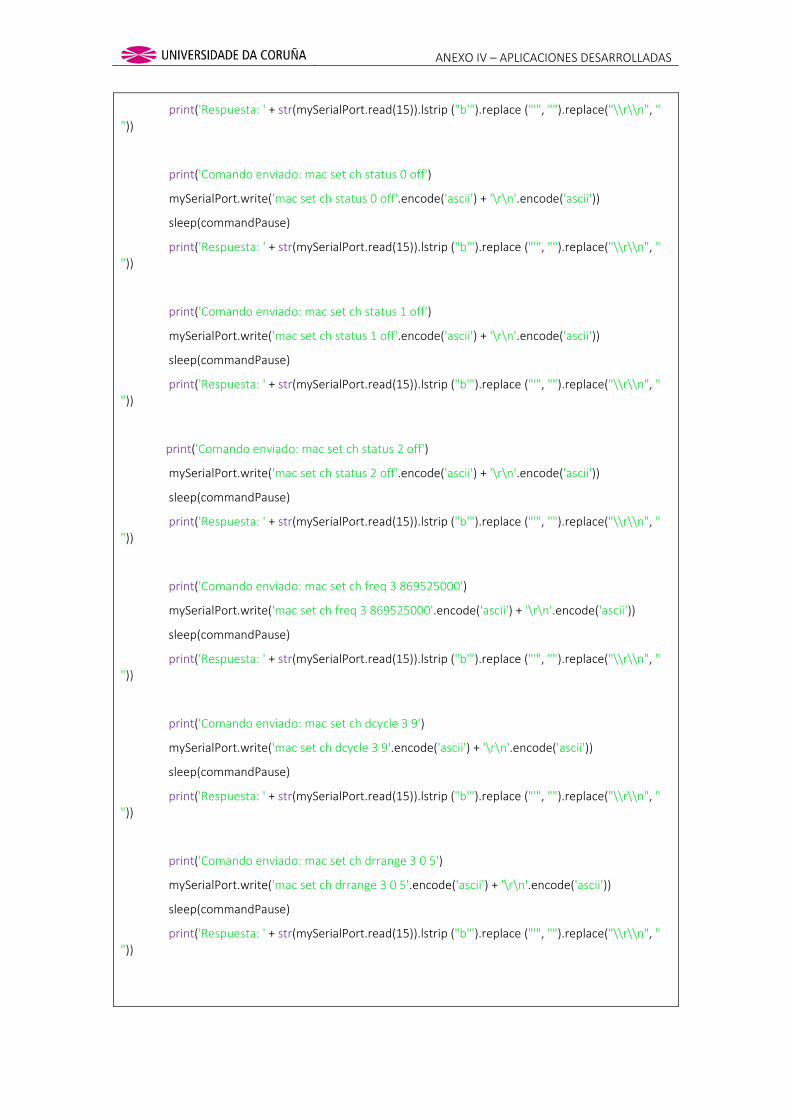
ANEXO IV – APLICACIONES DESARROLLADAS
print('Respuesta: ' + str(mySerialPort.read(15)).lstrip ("b'").replace ("'", "").replace("\\r\\n", " "))
print('Comando enviado: mac set ch status 0 off')
mySerialPort.write('mac set ch status 0 off'.encode('ascii') + '\r\n'.encode('ascii'))
sleep(commandPause)
print('Respuesta: ' + str(mySerialPort.read(15)).lstrip ("b'").replace ("'", "").replace("\\r\\n", " "))
print('Comando enviado: mac set ch status 1 off')
mySerialPort.write('mac set ch status 1 off'.encode('ascii') + '\r\n'.encode('ascii'))
sleep(commandPause)
print('Respuesta: ' + str(mySerialPort.read(15)).lstrip ("b'").replace ("'", "").replace("\\r\\n", " "))
print('Comando enviado: mac set ch status 2 off')
mySerialPort.write('mac set ch status 2 off'.encode('ascii') + '\r\n'.encode('ascii'))
sleep(commandPause)
print('Respuesta: ' + str(mySerialPort.read(15)).lstrip ("b'").replace ("'", "").replace("\\r\\n", " "))
print('Comando enviado: mac set ch freq 3 869525000')
mySerialPort.write('mac set ch freq 3 869525000'.encode('ascii') + '\r\n'.encode('ascii'))
sleep(commandPause)
print('Respuesta: ' + str(mySerialPort.read(15)).lstrip ("b'").replace ("'", "").replace("\\r\\n", " "))
print('Comando enviado: mac set ch dcycle 3 9')
mySerialPort.write('mac set ch dcycle 3 9'.encode('ascii') + '\r\n'.encode('ascii'))
sleep(commandPause)
print('Respuesta: ' + str(mySerialPort.read(15)).lstrip ("b'").replace ("'", "").replace("\\r\\n", " "))
print('Comando enviado: mac set ch drrange 3 0 5')
mySerialPort.write('mac set ch drrange 3 0 5'.encode('ascii') + '\r\n'.encode('ascii'))
sleep(commandPause)
print('Respuesta: ' + str(mySerialPort.read(15)).lstrip ("b'").replace ("'", "").replace("\\r\\n", " "))

ANEXO IV – APLICACIONES DESARROLLADAS
print('Comando enviado: mac set ch status 3 on')
mySerialPort.write('mac set ch status 3 on'.encode('ascii') + '\r\n'.encode('ascii'))
sleep(commandPause)
print('Respuesta: ' + str(mySerialPort.read(15)).lstrip ("b'").replace ("'", "").replace("\\r\\n", " "))
print('Comando enviado: mac set dr 5')
mySerialPort.write('mac set dr 5'.encode('ascii') + '\r\n'.encode('ascii'))
sleep(commandPause)
print('Respuesta: ' + str(mySerialPort.read(15)).lstrip ("b'").replace ("'", "").replace("\\r\\n", " "))
print('Comando enviado: mac set pwridx 1')
mySerialPort.write('mac set pwridx 1'.encode('ascii') + '\r\n'.encode('ascii'))
sleep(commandPause)
print('Respuesta: ' + str(mySerialPort.read(15)).lstrip ("b'").replace ("'", "").replace("\\r\\n", " "))
print('Comando enviado: mac set devaddr 26011CA2')
mySerialPort.write('mac set devaddr 26011CA2'.encode('ascii') + '\r\n'.encode('ascii'))
sleep(commandPause)
print('Respuesta: ' + str(mySerialPort.read(15)).lstrip ("b'").replace ("'", "").replace("\\r\\n", " "))
print('Comando enviado: mac set appskey A4109C150E2492D5479A782645758B3B')
mySerialPort.write('mac set appskey A4109C150E2492D5479A782645758B3B'.encode('ascii') + '\r\n'.encode('ascii'))
sleep(commandPause)
print('Respuesta: ' + str(mySerialPort.read(15)).lstrip ("b'").replace ("'", "").replace("\\r\\n", " "))
print('Comando enviado: mac set nwkskey 437009D0F91CF5F9694E4EB2AE7EB9D3')
mySerialPort.write('mac set nwkskey 437009D0F91CF5F9694E4EB2AE7EB9D3'.encode('ascii') + '\r\n'.encode('ascii'))
sleep(commandPause)
print('Respuesta: ' + str(mySerialPort.read(15)).lstrip ("b'").replace ("'", "").replace("\\r\\n", " "))
print('Comando enviado: mac save')
mySerialPort.write('mac save'.encode('ascii') + '\r\n'.encode('ascii'))
sleep(savePause)

ANEXO IV – APLICACIONES DESARROLLADAS
print('Respuesta: ' + str(mySerialPort.read(15)).lstrip ("b'").replace ("'", "").replace("\\r\\n", " "))
print('Comando enviado: mac join ABP')
mySerialPort.write('mac join ABP'.encode('ascii') + '\r\n'.encode('ascii'))
sleep(savePause)
print('Respuesta: ' + str(mySerialPort.read(15)).lstrip ("b'").replace ("'", "").replace("\\r\\n", " "))
print('\n-----------------------------------------------------------------------')
print('Iniciando Bucle de Envío de Mensajes ... ')
print('-----------------------------------------------------------------------\n')
init = time() # Comenzamos a contar el tiempo de envío
try:
while 1:
print('Comando enviado: mac tx uncnf 1 27536920637265657320717565207075656465732c2079612065737461732061206d6564696f2063616d696e6f2e27')
if statistics:
timestamp.append(NTP.request(NTPServer).tx_time)
mySerialPort.write('mac tx uncnf 1 27536920637265657320717565207075656465732c2079612065737461732061206d6564696f2063616d696e6f2e27'.encode('ascii') + '\r\n'.encode('ascii'))
sleep(messagePause)
print('Respuesta: ' + str(mySerialPort.read(15)).lstrip ("b'").replace ("'", "").replace("\\r\\n", " "))
except KeyboardInterrupt:
pass
print('\n-----------------------------------------------------------------------')
if statistics:
print('Timestamp: ' + str(timestamp))
print('-----------------------------------------------------------------------')
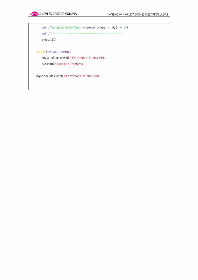
ANEXO IV – APLICACIONES DESARROLLADAS
print('Tiempo de Envio Total: ' + str(round(time() - init, 2)) + ' s.')
print('-----------------------------------------------------------------------')
sleep(180)
except KeyboardInterrupt:
mySerialPort.close() # Cerramos el Puerto Serie
sys.exit() # Salida de Programa
mySerialPort.close() # Cerramos el Puerto Serie

ANEXO IV – APLICACIONES DESARROLLADAS
APLICACIÓN DESARROLLADA PARA EL SERVIDOR DE MONITORIZACIÓN REMOTA

ANEXO IV – APLICACIONES DESARROLLADAS
# encoding: utf-8
'''
Proyecto: Diseño y Desarrollo del Sistema de Comunicaciones de un Enjambre
de UAV's Colaborativos.
Integración: Desarrollo de Servidor LoRa - Python.
Lenguaje de Programación: Python 3.
Alumno: Cristian Méndez Sanmartín.
Titulación: Máster en Ingeniería Industrial.
Grupo de Investigación: Grupo Integrado de Ingeniería.
Universidad: Universidade da Coruña.
'''
import sys
from socket import socket, AF_INET, SOCK_DGRAM
if __name__ == '__main__':
# Definimos el Host y el Puerto
host = '192.168.0.3'
port = 1700
# Instanciamos un Objeto para trabajar con el Socket Server
socket_udp = socket(AF_INET, SOCK_DGRAM)
# Asignamos Host y Puerto al Objeto con el Método Bind
socket_udp.bind((host, port))
print('-----------------------------------------------------------------------\n')
print(' Servidor LoRa - Python del Grupo Integrado de Ingeniería.\n')
print('-----------------------------------------------------------------------')
print('Esperando Comunicación ...')

ANEXO IV – APLICACIONES DESARROLLADAS
# Iniciamos Contador para Impresión de Direcciones IP
counter = 0
# Iniciamos Bucle de Comunicación con el Cliente
try:
while 1:
# Recibimos el Mensaje con el Método Recvfrom
message = socket_udp.recvfrom(1024)
data = str(message[0])
# Imprimimos Direcciones IP
if counter is 0:
counter += 1
address = message [1]
print('-----------------------------------------------------------------------')
print('Comunicación Establecida entre: ')
print(' Dirección IP Servidor: ' + host)
print(' Dirección IP Gateway: ' + str(address[0]))
print('-----------------------------------------------------------------------')
# Eliminamos Caracteres Incluídos Durante la Transmisión
data = data.lstrip("b'")
data = data.replace("'", "")
# División del Mensaje Recibido
divisions = data.split("|")
# Impresión de Separadores Iniciales de Mensaje
if 'Gateway LoRaWAN' in divisions[0]:
print('\n-----------------------------------------------------------------------\n')
if 'Iniciando' in divisions[0]:
print ('\n-----------------------------------------------------------------------')
if 'Actualizacion' in divisions[0]:
print ('\n-----------------------------------------------------------------------')

ANEXO IV – APLICACIONES DESARROLLADAS
if 'Informacion de paquetes' in divisions[0]:
print ('-----------------------------------------------------------------------')
if 'Parametros' in divisions[0]:
print ('\n-----------------------------------------------------------------------')
# Impresión del Mensaje Recibido
for i in range(len(divisions)):
print (divisions[i])
# Impresión de Separadores Finales de Mensaje
if 'Gateway LoRaWAN' in divisions[0]:
print('\n-----------------------------------------------------------------------')
if 'Iniciando' in divisions[0]:
print('-----------------------------------------------------------------------')
if 'Informacion' in divisions[0]:
print('-----------------------------------------------------------------------')
if 'Parametros' in divisions[0]:
print('-----------------------------------------------------------------------')
except KeyboardInterrupt:
socket_udp.close() # Cerramos el Socket Server
sys.exit() # Salida de Programa

ESCUELA POLITÉCNICA SUPERIOR
TRABAJO FIN DE MÁSTER
CURSO 2016/2017
DISEÑO Y DESARROLLO DEL SISTEMA DE COMUNICACIONES INALÁMBRICO DE UN ENJAMBRE DE
UAV’S COLABORATIVOS
MÁSTER EN INGENIERÍA INDUSTRIAL
DOCUMENTO DEL PROYECTO
ANEXO V – DATASHEETS

ANEXO V – DATASHEETS
DATASHEET MICROCHIP RN2483

2015 Microchip Technology Inc. Advance Information DS50002346A-page 1
RN2483
General Features• On-board LoRaWAN™ Class A protocol stack• ASCII command interface over UART• Compact form factor: 17.8 x 26.7 x 3 mm• Castellated SMT pads for easy and reliable PCB
mounting• Environmentally friendly, RoHS compliant• European R&TTE Directive Assessed Radio
Module• Device Firmware Upgrade (DFU) over UART, see
“RN2483 LoRa™ Technology Module Command Reference User’s Guide” (DS40001784A)
Operational• Single operating voltage: 2.1V to 3.6V (3.3V
typical)• Temperature range: -40°C to +85°C• Low-power consumption• Programmable RF Communication Bit Rate up to
300 kbps with FSK modulation, 5468 bps with LoRa™ Technology modulation
• Integrated MCU, Crystal, EUI-64 Node Identity Serial EEPROM, Radio Transceiver with Analog Front End, Matching Circuitry
• 14 GPIOs for control and status
RF/Analog Features• Low-Power Long Range Transceiver operating in
the 433 MHz and 868 MHz frequency bands• High Receiver Sensitivity: down to -148 dBm• TX Power: adjustable up to +14 dBm high
efficiency PA• FSK, GFSK, and LoRa Technology modulation• IIP3 = -11 dBm• >15 km coverage at suburban and >5 km
coverage at urban area
DescriptionMicrochip’s RN2483 Low-Power Long Range LoRaTechnology Transceiver module provides an easy touse, low-power solution for long range wireless datatransmission. The advanced command interface offersrapid time to market.
The RN2483 module complies with the LoRaWANClass A protocol specifications. It integrates RF, abaseband controller, command ApplicationProgramming Interface (API) processor, making it acomplete long range Solution.
The RN2483 module is suitable for simple long rangesensor applications with external host MCU.
Applications• Automated Meter Reading• Home and Building Automation• Wireless Alarm and Security Systems• Industrial Monitoring and Control• Machine to Machine• Internet of Things (IoT)
Low-Power Long Range LoRa™ TechnologyTransceiver Module

RN2483
DS50002346A-page 2 Advance Information 2015 Microchip Technology Inc.
Table of Contents1.0 Device Overview .......................................................................................................................................................................... 32.0 General Specifications.................................................................................................................................................................. 63.0 Typical Hardware Connections..................................................................................................................................................... 84.0 Physical Dimensions .................................................................................................................................................................... 95.0 Application Information............................................................................................................................................................... 106.0 Regulatory Approval................................................................................................................................................................... 12Appendix A: Revision History............................................................................................................................................................... 13The Microchip Web Site ....................................................................................................................................................................... 15Customer Change Notification Service ................................................................................................................................................ 15Customer Support ................................................................................................................................................................................ 15Product Identification System............................................................................................................................................................... 17
TO OUR VALUED CUSTOMERSIt is our intention to provide our valued customers with the best documentation possible to ensure successful use of your Microchipproducts. To this end, we will continue to improve our publications to better suit your needs. Our publications will be refined andenhanced as new volumes and updates are introduced. If you have any questions or comments regarding this publication, please contact the Marketing Communications Department viaE-mail at [email protected]. We welcome your feedback.
Most Current Data SheetTo obtain the most up-to-date version of this data sheet, please register at our Worldwide Web site at:
http://www.microchip.comYou can determine the version of a data sheet by examining its literature number found on the bottom outside corner of any page.The last character of the literature number is the version number, (e.g., DS30000000A is version A of document DS30000000).
ErrataAn errata sheet, describing minor operational differences from the data sheet and recommended workarounds, may exist for currentdevices. As device/documentation issues become known to us, we will publish an errata sheet. The errata will specify the revisionof silicon and revision of document to which it applies.To determine if an errata sheet exists for a particular device, please check with one of the following:• Microchip’s Worldwide Web site; http://www.microchip.com• Your local Microchip sales office (see last page)When contacting a sales office, please specify which device, revision of silicon and data sheet (include literature number) you areusing.
Customer Notification SystemRegister on our web site at www.microchip.com to receive the most current information on all of our products.
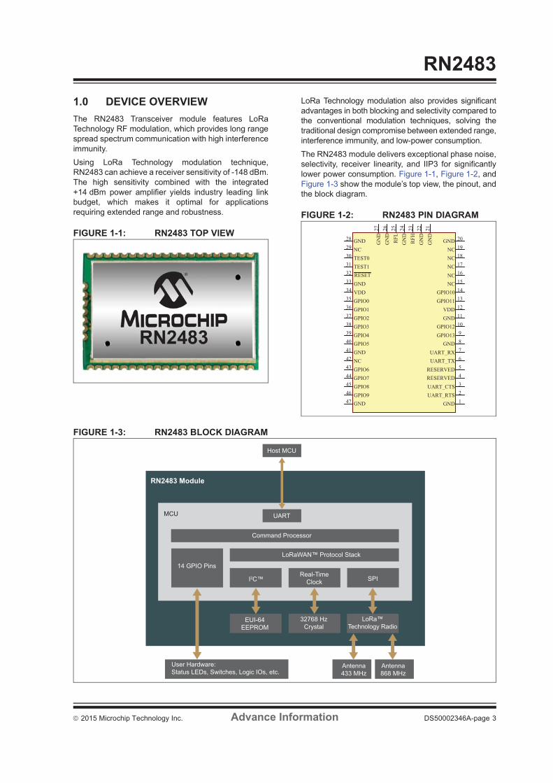
2015 Microchip Technology Inc. Advance Information DS50002346A-page 3
RN2483
1.0 DEVICE OVERVIEWThe RN2483 Transceiver module features LoRaTechnology RF modulation, which provides long rangespread spectrum communication with high interferenceimmunity.
Using LoRa Technology modulation technique,RN2483 can achieve a receiver sensitivity of -148 dBm.The high sensitivity combined with the integrated+14 dBm power amplifier yields industry leading linkbudget, which makes it optimal for applicationsrequiring extended range and robustness.
FIGURE 1-1: RN2483 TOP VIEW
LoRa Technology modulation also provides significantadvantages in both blocking and selectivity compared tothe conventional modulation techniques, solving thetraditional design compromise between extended range,interference immunity, and low-power consumption.
The RN2483 module delivers exceptional phase noise,selectivity, receiver linearity, and IIP3 for significantlylower power consumption. Figure 1-1, Figure 1-2, andFigure 1-3 show the module’s top view, the pinout, andthe block diagram.
FIGURE 1-2: RN2483 PIN DIAGRAM
FIGURE 1-3: RN2483 BLOCK DIAGRAM
1GND
2UART_RTS
3UART_CTS
4RESERVED
5RESERVED
6UART_TX
7UART_RX
8GND
GND
9GPIO13
10GPIO12
11GND
20GND
12VDD
13GPIO11
14GPIO10
15NC
16NC
17NC
18NC
19NC
4039383736353433323130
21
2928
27 26 25 24 23 22
GND GND
GND
GND
GND
GND
RFHRFL
VDD
GND
47464544434241
GND
NCTEST0TEST1RESET
GPIO0GPIO1GPIO2GPIO3GPIO4GPIO5
GPIO6GPIO7GPIO8GPIO9
NC
RN2483 Module
Host MCU
UARTMCU
Command Processor
14 GPIO Pins
I2C™
LoRaWAN™ Protocol Stack
Real-TimeClock
EUI-64EEPROM
User Hardware:Status LEDs, Switches, Logic IOs, etc.
32768 HzCrystal
Antenna433 MHz
Antenna868 MHz
LoRa™Technology Radio
SPI
RN2483 Module
Host MCU
UARTMCU
Command Processor
14 GPIO Pins
I2C™
LoRaWAN™ Protocol Stack
Real-TimeClock
EUI-64EEPROM
User Hardware:Status LEDs, Switches, Logic IOs, etc.
32768 HzCrystal
Antenna433 MHz
Antenna868 MHz
LoRa™Technology Radio
SPI
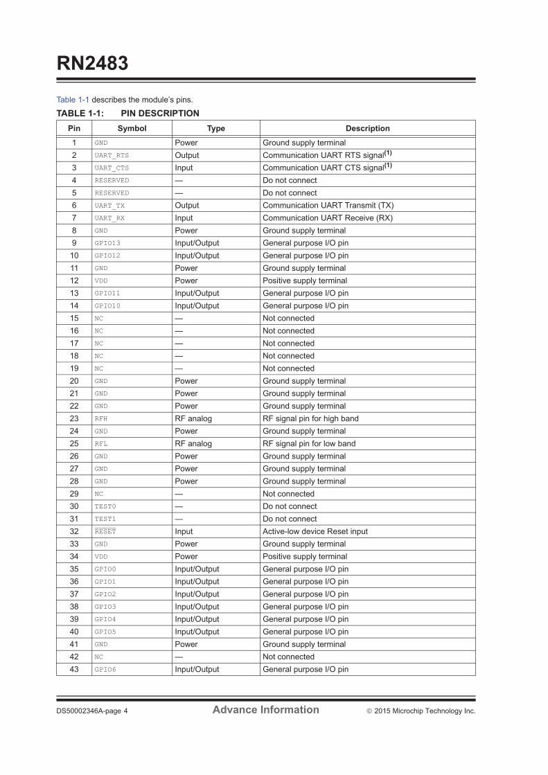
RN2483
DS50002346A-page 4 Advance Information 2015 Microchip Technology Inc.
Table 1-1 describes the module’s pins.
TABLE 1-1: PIN DESCRIPTIONPin Symbol Type Description
1 GND Power Ground supply terminal2 UART_RTS Output Communication UART RTS signal(1)
3 UART_CTS Input Communication UART CTS signal(1)
4 RESERVED — Do not connect5 RESERVED — Do not connect6 UART_TX Output Communication UART Transmit (TX)7 UART_RX Input Communication UART Receive (RX)8 GND Power Ground supply terminal9 GPIO13 Input/Output General purpose I/O pin
10 GPIO12 Input/Output General purpose I/O pin11 GND Power Ground supply terminal12 VDD Power Positive supply terminal13 GPIO11 Input/Output General purpose I/O pin14 GPIO10 Input/Output General purpose I/O pin15 NC — Not connected16 NC — Not connected17 NC — Not connected18 NC — Not connected19 NC — Not connected20 GND Power Ground supply terminal21 GND Power Ground supply terminal22 GND Power Ground supply terminal23 RFH RF analog RF signal pin for high band24 GND Power Ground supply terminal25 RFL RF analog RF signal pin for low band26 GND Power Ground supply terminal27 GND Power Ground supply terminal28 GND Power Ground supply terminal29 NC — Not connected30 TEST0 — Do not connect31 TEST1 — Do not connect32 RESET Input Active-low device Reset input33 GND Power Ground supply terminal34 VDD Power Positive supply terminal35 GPIO0 Input/Output General purpose I/O pin36 GPIO1 Input/Output General purpose I/O pin37 GPIO2 Input/Output General purpose I/O pin38 GPIO3 Input/Output General purpose I/O pin39 GPIO4 Input/Output General purpose I/O pin40 GPIO5 Input/Output General purpose I/O pin41 GND Power Ground supply terminal42 NC — Not connected43 GPIO6 Input/Output General purpose I/O pin
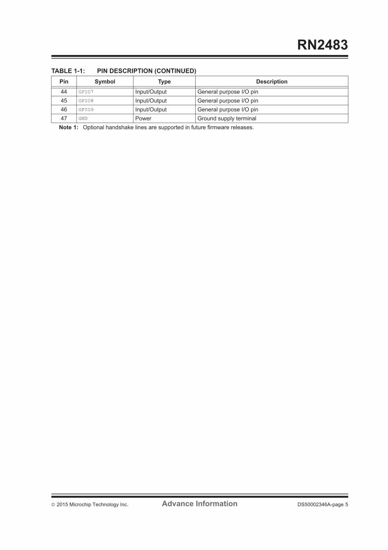
2015 Microchip Technology Inc. Advance Information DS50002346A-page 5
RN2483
44 GPIO7 Input/Output General purpose I/O pin45 GPIO8 Input/Output General purpose I/O pin46 GPIO9 Input/Output General purpose I/O pin47 GND Power Ground supply terminal
Note 1: Optional handshake lines are supported in future firmware releases.
TABLE 1-1: PIN DESCRIPTION (CONTINUED)Pin Symbol Type Description

RN2483
DS50002346A-page 6 Advance Information 2015 Microchip Technology Inc.
2.0 GENERAL SPECIFICATIONSTable 2-1 provides the general specifications for the module. Table 2-2 and Table 2-3 provide the module's electricalcharacteristics and current consumption. Table 2-4 and Table 2-5 show the module's dimensions and the RF outputpower calibration data.TABLE 2-1: GENERAL SPECIFICATIONS
Specification Description
Frequency Band 863.000 MHz to 870.000 MHz; 433.050 MHz to 434.790 MHzModulation Method FSK, GFSK, and LoRa™ Technology modulationMaximum Over-the-Air Data Rate 300 kbps with FSK modulation; 5468 bps with LoRa Technology modulationRF connection Board edge connectionInterface UARTOperation Range >15 km coverage at suburban; >5 km coverage at urban areaSensitivity at 0.1% BER -148 dBm(1) RF TX Power Adjustable up to max. 10 dBm on 433 MHz band (limited to meet regulations);
max. 14 dBm on the 868 MHz band(2)
Temperature (operating) -40°C to +85°CTemperature (storage) -40°C to +115°CHumidity 10% ~ 90%
non-condensingNote 1: Depends on modulation. Expand Spreading Factor (SF).
2: TX power is adjustable. For more information, refer to the “RN2483 LoRa™ Technology Module CommandReference User’s Guide” (DS40001784A).
TABLE 2-2: ELECTRICAL CHARACTERISTICSParameter Min. Typ. Max. Units
Supply Voltage 2.1 — 3.6 VVoltage on any pin with respect to VSS (except VDD) -0.3 — VDD + 0.3 VVoltage on VDD with respect to VSS -0.3 — 3.9 VInput Clamp Current (IIK) (VI < 0 or VI > VDD) — — +/-20 mAOutput Camp Current (IOK) (VO < 0 or VO > VDD) — — +/-20 mAGPIO sink/source current each — — 25/25 mATotal GPIO sink/source current — — 200/185 mARAM Data Retention Voltage (in Sleep mode or Reset state) 1.5 — — VVDD Start Voltage to ensure internal Power-on Reset signal — — 0.7 VVDD Rise Rate to ensure internal Power-on Reset signal 0.05 — — V/msBrown-out Reset Voltage 1.75 1.9 2.05 VLogic Input Low Voltage — — 0.15 x VDD VLogic Input High Voltage 0.8 x VDD — — VInput Leakage at <25°C(VSS<VPIN<VDD, Pin at high-impedance)
— 0.1 50 nA
Input Leakage at +60°C(VSS<VPIN<VDD, Pin at high-impedance)
— 0.7 100 nA
Input Leakage at +85°C(VSS<VPIN<VDD, Pin at high-impedance)
— 4 200 nA
RF Input Level — — +10 dBm

2015 Microchip Technology Inc. Advance Information DS50002346A-page 7
RN2483
TABLE 2-3: CURRENT CONSUMPTIONMode Typical Current at 3V (mA)
Idle 2.8RX 14.2Deep Sleep 0.0099
TABLE 2-4: MODULE DIMENSIONSParameter Value
Dimensions 17.8 x 26.7 x 3 mmWeight 2.05g
TABLE 2-5: OUTPUT POWER OF TX POWER SETTING
Band TX Power Setting
Output Power (dBm)
Typical Supply
Current at 3V (mA)
868 MHz
-3 -4.0 17.3-2 -2.9 18.0-1 -1.9 18.70 -1.7 20.21 -0.6 21.22 0.4 22.33 1.4 23.54 2.5 24.75 3.6 26.16 4.7 27.57 5.8 28.88 6.9 30.09 8.1 31.2
10 9.3 32.411 10.4 33.712 11.6 35.113 12.5 36.514 13.5 38.015 14.1 38.9
433 MHz
-3 -3.5 14.7-2 -2.3 15.1-1 -1.3 15.60 -2.3 15.81 -1.2 16.42 -0.1 17.03 1.0 17.74 2.1 18.55 3.2 19.46 4.3 20.37 5.4 21.48 6.5 22.39 7.6 23.3
10 8.8 24.511 9.9 25.812 10.9 27.313 11.9 28.814 12.9 30.715 13.6 32.9

RN2483
DS50002346A-page 8 Advance Information 2015 Microchip Technology Inc.
3.0 TYPICAL HARDWARE CONNECTIONSFigure 3-1 shows the typical hardware connections.
FIGURE 3-1: HARDWARE CONNECTIONS
3.1 INTERFACE TO HOST MCUThe RN2483 module has a dedicated UART interfaceto communicate with a host controller. Optionalhandshake lines are supported in future firmwarereleases. The “RN2483 LoRa™ Technology ModuleCommand Reference User’s Guide” (DS40001784A)provides a detailed UART command description.Table 3-1 shows the default settings for the UARTcommunication.
3.2 GPIO PINS (GPIO0-GPIO13)The module has 14 GPIO pins. These lines can beconnected to switches, LEDs, and relay outputs. Thepins are either logic inputs or outputs that can beaccessed via the module firmware. These pins havelimited sink and source capabilities. Electricalcharacteristics are described in Table 2-2.
3.3 RF CONNECTIONS (RFL, RFH)RFL is the RF analog port for the lower frequency band(433 MHz) while RFH is for the higher frequency band(868 MHz). When routing RF paths, use proper striplines with an impedance of 50 Ohm.
3.4 RESET PINThe module’s reset pin is an active-low logic input.
3.5 POWER PINSIt is recommended to connect power pins (Pin 12 and34) to a stable supply voltage with sufficient sourcecurrent. Table 2-2 shows the current consumption.
Additional filtering capacitors are not required but canbe used to ensure stable supply voltage in noisyenvironment.
Note 1: Optional handshake lines are supported in future firmware releases.
TABLE 3-1: DEFAULT UART SETTINGSSpecification Description
Baud Rate 57600 bpsPacket Length 8 bitParity Bit NoStop Bits 1 bitHardware Flow Control No

2015 Microchip Technology Inc. Advance Information DS50002346A-page 9
RN2483
4.0 PHYSICAL DIMENSIONSFigure 4-1 and Figure 4-2 illustrate the physical dimensions and the recommended PCB layout for the RN2483 module.
FIGURE 4-1: RN2483 PHYSICAL DIMENSIONS
FIGURE 4-2: RECOMMENDED PCB FOOTPRINT
Note: Host PCB top layer copper traces must have solder mask to avoid shorting test pins on the bottom of the module.

RN2483
DS50002346A-page 10 Advance Information 2015 Microchip Technology Inc.
5.0 APPLICATION INFORMATION
5.1 RF pins and strip lineThe RF signals must be routed with properly terminated 50 Ohm strip lines. Use curves instead of sharp corners. Keepthe routing path as short as possible. When routing the RF paths, use proper strip lines with an impedance of 50 Ohm.Figure 5-1 shows a routing example.
FIGURE 5-1: RF ROUTING (EXAMPLE)

RN2483
DS50002346A-page 11 Advance Information 2015 Microchip Technology Inc.
5.2
APP
LIC
ATIO
N S
CH
EMAT
ICFi
gure
5-2
show
s th
e sc
hem
atic
for t
he R
N24
83 P
ICta
il™/P
ICta
il P
lus
Dau
ghte
r Boa
rd.
FIG
UR
E 5-
2:PI
CTA
IL™
/PIC
TAIL
PLU
S D
AU
GH
TER
BO
AR
D S
CH
EMA
TIC

RN2483
DS50002346A-page 12 Advance Information 2015 Microchip Technology Inc.
6.0 REGULATORY APPROVALThis section outlines the regulatory information for theRN2483 module for Europe.
6.1 EuropeThe RN2483 module is an R&TTE Directive assessedradio module that is CE marked and has beenmanufactured and tested with the intention of beingintegrated into a final product.
The RN2483 module has been tested to R&TTEDirective 1999/5/EC Essential Requirements for Healthand Safety (Article 3.1a), ElectromagneticCompatibility (EMC) (Article 3.1b), and Radio (Article3.2) and are summarized in Table 6-1: EuropeanCompliance Testing. A Notified Body Opinion has alsobeen issued. All test reports are available on theproduct web page at http://www.microchip.com.
The R&TTE Compliance Association providesguidance on modular devices in document TechnicalGuidance Note 01 available at http://www.rtteca.com/html/download_area.htm.
6.1.1 LABELING AND USER INFORMATION REQUIREMENTS
The label on the final product which contains theRN2483 module must follow CE marking requirements.The “R&TTE Compliance Association TechnicalGuidance Note 01” provides guidance on final productCE marking.
6.1.2 EXTERNAL ANTENNA REQUIREMENTS
From R&TTE Compliance Association documentTechnical Guidance Note 01:
Provided the integrator installing an assessed radiomodule with an integral or specific antenna andinstalled in conformance with the radio modulemanufacturer's installation instructions requires nofurther evaluation under Article 3.2 of the R&TTEDirective and does not require further involvement ofan R&TTE Directive Notified Body for the final product(Section 2.2.4).
6.1.3 HELPFUL WEB SITESA document that can be used as a starting point inunderstanding the use of Short Range Devices (SRD)in Europe is the European Radio CommunicationsCommittee (ERC) Recommendation 70-03 E, whichcan be downloaded from the European RadioCommunications Office (ERO) at: http://www.ero.dk/.
Additional helpful web sites are:
• Radio and Telecommunications Terminal Equipment (R&TTE): http://ec.europa.eu/enterprise/sectors/rtte/regulatory-framework/index_en.htm
• European Conference of Postal and Telecommunications Administrations (CEPT): http://www.cept.org
• European Telecommunications Standards Institute (ETSI): http://www.etsi.org
• European Radio Communications Office (ERO): http://www.ero.dk/
• The Radio and Telecommunications Terminal Equipment Compliance Association (R&TTE CA):http://www.rtteca.com/
Note: To maintain conformance to the testinglisted in Table 6-1: European ComplianceTesting, the module shall be installed inaccordance with the installation instruc-tions in this data sheet and shall not bemodified. When integrating a radio module into acompleted product the integratorbecomes the manufacturer of the finalproduct and is therefore responsible fordemonstrating compliance of the finalproduct with the essential requirements ofthe R&TTE Directive.
TABLE 6-1: EUROPEAN COMPLIANCE TESTINGCertification Standards Article Laboratory Report Number Date
Safety IEC 60950-1:2005 (2nd Ed: A1:2009)
(3.1a) TRaC Global Ltd. TRA-025134-43-00A 2/12/2015
Health EN 62479 — TRaC Global Ltd. TRA-025134-01-47-03A 2/12/2015EMC EN 301 489-3 v1.6.1 (3.1b) TRaC Global Ltd. TRA-025134-43-00A 2/12/2015Radio EN 300 220-2 v2.4.1 (3.2) TRaC Global Ltd. TRA-025134-01-47-00A
(433 MHz) TRA-025134-01-47-01A(868MHz)
2/12/2015

2015 Microchip Technology Inc. Advance Information DS50002346A-page 13
RN2483
APPENDIX A: REVISION HISTORY
Revision A (March 2015)This is the initial release of this document.

RN2483
DS50002346A-page 14 Advance Information 2015 Microchip Technology Inc.
NOTES:
2015 Microchip Technology Inc. Advance Information DS50002346A-page 15
RN2483
THE MICROCHIP WEB SITEMicrochip provides online support via our WWW site atwww.microchip.com. This web site is used as a meansto make files and information easily available tocustomers. Accessible by using your favorite Internetbrowser, the web site contains the followinginformation:
• Product Support – Data sheets and errata, application notes and sample programs, design resources, user’s guides and hardware support documents, latest software releases and archived software
• General Technical Support – Frequently Asked Questions (FAQ), technical support requests, online discussion groups, Microchip consultant program member listing
• Business of Microchip – Product selector and ordering guides, latest Microchip press releases, listing of seminars and events, listings of Microchip sales offices, distributors and factory representatives
CUSTOMER CHANGE NOTIFICATION SERVICEMicrochip’s customer notification service helps keepcustomers current on Microchip products. Subscriberswill receive e-mail notification whenever there arechanges, updates, revisions or errata related to aspecified product family or development tool of interest.
To register, access the Microchip web site atwww.microchip.com. Under “Support”, click on“Customer Change Notification” and follow theregistration instructions.
CUSTOMER SUPPORTUsers of Microchip products can receive assistancethrough several channels:
• Distributor or Representative• Local Sales Office• Field Application Engineer (FAE)• Technical Support
Customers should contact their distributor,representative or Field Application Engineer (FAE) forsupport. Local sales offices are also available to helpcustomers. A listing of sales offices and locations isincluded in the back of this document.
Technical support is available through the web siteat: http://microchip.com/support

RN2483
DS50002346A-page 16 Advance Information 2015 Microchip Technology Inc.
NOTES:
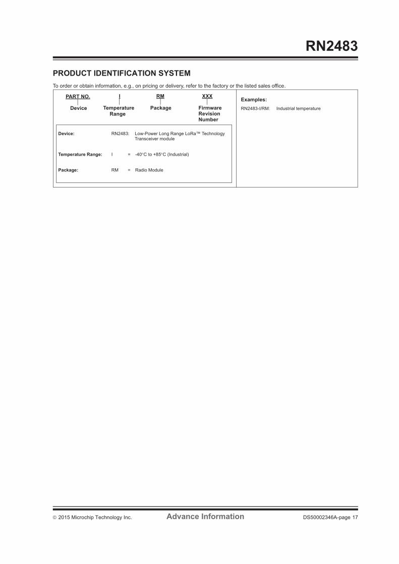
2015 Microchip Technology Inc. Advance Information DS50002346A-page 17
RN2483
PRODUCT IDENTIFICATION SYSTEMTo order or obtain information, e.g., on pricing or delivery, refer to the factory or the listed sales office.
PART NO. I RM XXX
FirmwarePackageTemperatureRange
Device
Device: RN2483: Low-Power Long Range LoRa™ Technology
Transceiver module
Temperature Range: I = -40 C to +85 C (Industrial)
Package: RM = Radio Module
Examples:RN2483-I/RM: Industrial temperature
RevisionNumber

RN2483
DS50002346A-page 18 Advance Information 2015 Microchip Technology Inc.
NOTES:

2015 Microchip Technology Inc. Advance Information DS50002346A-page 19
Information contained in this publication regarding deviceapplications and the like is provided only for your convenienceand may be superseded by updates. It is your responsibility toensure that your application meets with your specifications.MICROCHIP MAKES NO REPRESENTATIONS ORWARRANTIES OF ANY KIND WHETHER EXPRESS ORIMPLIED, WRITTEN OR ORAL, STATUTORY OROTHERWISE, RELATED TO THE INFORMATION,INCLUDING BUT NOT LIMITED TO ITS CONDITION,QUALITY, PERFORMANCE, MERCHANTABILITY ORFITNESS FOR PURPOSE. Microchip disclaims all liabilityarising from this information and its use. Use of Microchipdevices in life support and/or safety applications is entirely atthe buyer’s risk, and the buyer agrees to defend, indemnify andhold harmless Microchip from any and all damages, claims,suits, or expenses resulting from such use. No licenses areconveyed, implicitly or otherwise, under any Microchipintellectual property rights.
Trademarks
The Microchip name and logo, the Microchip logo, dsPIC, FlashFlex, flexPWR, JukeBlox, KEELOQ, KEELOQ logo, Kleer, LANCheck, MediaLB, MOST, MOST logo, MPLAB, OptoLyzer, PIC, PICSTART, PIC32 logo, RightTouch, SpyNIC, SST, SST Logo, SuperFlash and UNI/O are registered trademarks of Microchip Technology Incorporated in the U.S.A. and other countries.
The Embedded Control Solutions Company and mTouch are registered trademarks of Microchip Technology Incorporated in the U.S.A.
Analog-for-the-Digital Age, BodyCom, chipKIT, chipKIT logo, CodeGuard, dsPICDEM, dsPICDEM.net, ECAN, In-Circuit Serial Programming, ICSP, Inter-Chip Connectivity, KleerNet, KleerNet logo, MiWi, MPASM, MPF, MPLAB Certified logo, MPLIB, MPLINK, MultiTRAK, NetDetach, Omniscient Code Generation, PICDEM, PICDEM.net, PICkit, PICtail, RightTouch logo, REAL ICE, SQI, Serial Quad I/O, Total Endurance, TSHARC, USBCheck, VariSense, ViewSpan, WiperLock, Wireless DNA, and ZENA are trademarks of Microchip Technology Incorporated in the U.S.A. and other countries.
SQTP is a service mark of Microchip Technology Incorporated in the U.S.A.
Silicon Storage Technology is a registered trademark of Microchip Technology Inc. in other countries.
GestIC is a registered trademarks of Microchip Technology Germany II GmbH & Co. KG, a subsidiary of Microchip Technology Inc., in other countries.
All other trademarks mentioned herein are property of their respective companies.
© 2015, Microchip Technology Incorporated, Printed in the U.S.A., All Rights Reserved.
ISBN: 978-1-63277-123-0
Note the following details of the code protection feature on Microchip devices:• Microchip products meet the specification contained in their particular Microchip Data Sheet.
• Microchip believes that its family of products is one of the most secure families of its kind on the market today, when used in the intended manner and under normal conditions.
• There are dishonest and possibly illegal methods used to breach the code protection feature. All of these methods, to our knowledge, require using the Microchip products in a manner outside the operating specifications contained in Microchip’s Data Sheets. Most likely, the person doing so is engaged in theft of intellectual property.
• Microchip is willing to work with the customer who is concerned about the integrity of their code.
• Neither Microchip nor any other semiconductor manufacturer can guarantee the security of their code. Code protection does not mean that we are guaranteeing the product as “unbreakable.”
Code protection is constantly evolving. We at Microchip are committed to continuously improving the code protection features of ourproducts. Attempts to break Microchip’s code protection feature may be a violation of the Digital Millennium Copyright Act. If such actsallow unauthorized access to your software or other copyrighted work, you may have a right to sue for relief under that Act.
Microchip received ISO/TS-16949:2009 certification for its worldwide headquarters, design and wafer fabrication facilities in Chandler and Tempe, Arizona; Gresham, Oregon and design centers in California and India. The Company’s quality system processes and procedures are for its PIC® MCUs and dsPIC® DSCs, KEELOQ® code hopping devices, Serial EEPROMs, microperipherals, nonvolatile memory and analog products. In addition, Microchip’s quality system for the design and manufacture of development systems is ISO 9001:2000 certified.
QUALITY MANAGEMENT SYSTEM CERTIFIED BY DNV
== ISO/TS 16949 ==

DS50002346A-page 20 Advance Information 2015 Microchip Technology Inc.
AMERICASCorporate Office2355 West Chandler Blvd.Chandler, AZ 85224-6199Tel: 480-792-7200 Fax: 480-792-7277Technical Support: http://www.microchip.com/supportWeb Address: www.microchip.comAtlantaDuluth, GA Tel: 678-957-9614 Fax: 678-957-1455Austin, TXTel: 512-257-3370 BostonWestborough, MA Tel: 774-760-0087 Fax: 774-760-0088ChicagoItasca, IL Tel: 630-285-0071 Fax: 630-285-0075ClevelandIndependence, OH Tel: 216-447-0464 Fax: 216-447-0643DallasAddison, TX Tel: 972-818-7423 Fax: 972-818-2924DetroitNovi, MI Tel: 248-848-4000Houston, TX Tel: 281-894-5983IndianapolisNoblesville, IN Tel: 317-773-8323Fax: 317-773-5453Los AngelesMission Viejo, CA Tel: 949-462-9523 Fax: 949-462-9608New York, NY Tel: 631-435-6000San Jose, CA Tel: 408-735-9110Canada - TorontoTel: 905-673-0699 Fax: 905-673-6509
ASIA/PACIFICAsia Pacific OfficeSuites 3707-14, 37th FloorTower 6, The GatewayHarbour City, KowloonHong KongTel: 852-2943-5100Fax: 852-2401-3431Australia - SydneyTel: 61-2-9868-6733Fax: 61-2-9868-6755China - BeijingTel: 86-10-8569-7000 Fax: 86-10-8528-2104China - ChengduTel: 86-28-8665-5511Fax: 86-28-8665-7889China - ChongqingTel: 86-23-8980-9588Fax: 86-23-8980-9500China - DongguanTel: 86-769-8702-9880 China - HangzhouTel: 86-571-8792-8115 Fax: 86-571-8792-8116China - Hong Kong SARTel: 852-2943-5100 Fax: 852-2401-3431China - NanjingTel: 86-25-8473-2460Fax: 86-25-8473-2470China - QingdaoTel: 86-532-8502-7355Fax: 86-532-8502-7205China - ShanghaiTel: 86-21-5407-5533 Fax: 86-21-5407-5066China - ShenyangTel: 86-24-2334-2829Fax: 86-24-2334-2393China - ShenzhenTel: 86-755-8864-2200 Fax: 86-755-8203-1760China - WuhanTel: 86-27-5980-5300Fax: 86-27-5980-5118China - XianTel: 86-29-8833-7252Fax: 86-29-8833-7256
ASIA/PACIFICChina - XiamenTel: 86-592-2388138 Fax: 86-592-2388130China - ZhuhaiTel: 86-756-3210040 Fax: 86-756-3210049India - BangaloreTel: 91-80-3090-4444 Fax: 91-80-3090-4123India - New DelhiTel: 91-11-4160-8631Fax: 91-11-4160-8632India - PuneTel: 91-20-3019-1500Japan - OsakaTel: 81-6-6152-7160 Fax: 81-6-6152-9310Japan - TokyoTel: 81-3-6880- 3770 Fax: 81-3-6880-3771Korea - DaeguTel: 82-53-744-4301Fax: 82-53-744-4302Korea - SeoulTel: 82-2-554-7200Fax: 82-2-558-5932 or 82-2-558-5934Malaysia - Kuala LumpurTel: 60-3-6201-9857Fax: 60-3-6201-9859Malaysia - PenangTel: 60-4-227-8870Fax: 60-4-227-4068Philippines - ManilaTel: 63-2-634-9065Fax: 63-2-634-9069SingaporeTel: 65-6334-8870Fax: 65-6334-8850Taiwan - Hsin ChuTel: 886-3-5778-366Fax: 886-3-5770-955Taiwan - KaohsiungTel: 886-7-213-7828Taiwan - TaipeiTel: 886-2-2508-8600 Fax: 886-2-2508-0102Thailand - BangkokTel: 66-2-694-1351Fax: 66-2-694-1350
EUROPEAustria - WelsTel: 43-7242-2244-39Fax: 43-7242-2244-393Denmark - CopenhagenTel: 45-4450-2828 Fax: 45-4485-2829France - ParisTel: 33-1-69-53-63-20 Fax: 33-1-69-30-90-79Germany - DusseldorfTel: 49-2129-3766400Germany - MunichTel: 49-89-627-144-0 Fax: 49-89-627-144-44Germany - PforzheimTel: 49-7231-424750Italy - Milan Tel: 39-0331-742611 Fax: 39-0331-466781Italy - VeniceTel: 39-049-7625286 Netherlands - DrunenTel: 31-416-690399 Fax: 31-416-690340Poland - WarsawTel: 48-22-3325737 Spain - MadridTel: 34-91-708-08-90Fax: 34-91-708-08-91Sweden - StockholmTel: 46-8-5090-4654UK - WokinghamTel: 44-118-921-5800Fax: 44-118-921-5820
Worldwide Sales and Service
01/27/15

ANEXO V – DATASHEETS
DATASHEET RASPBERRY PI MODELO 1 B

www.rs-components.com/raspberrypi
Product Name Raspberry Pi Model B
Product Description The Raspberry Pi is a small, powerful and lightweight ARM based computer which can do many of the things a desktop PC can do. The powerful graphics capabilities and HDMi video output make it ideal for multimedia applications such as media centres and narrowcasting solutions. The Raspberry Pi is based on a Broadcom BCM2835 chip. It does not feature a built-in hard disk or solid-state drive, instead relying on an SD card for booting and long-term storage.
RS Part Number 756-8308
Specifications
Chip Broadcom BCM2835 SoC (a)
Core architecture ARM11
CPU 700 MHz Low Power ARM1176JZFS Applications Processor
GPU Dual Core VideoCore IV® Multimedia Co-Processor
Provides Open GL ES 2.0, hardware-accelerated OpenVG, and 1080p30 H.264 high-profile decode
Capable of 1Gpixel/s, 1.5Gtexel/s or 24GFLOPs with texture filtering and DMA infrastructure
Memory 512MB SDRAM
Operating System Boots from SD card, running a version of the Linux operating system
Dimensions 85.6 x 53.98 x 17mm
Power Micro USB socket 5V, 1.2A (l)
Connectors:
Ethernet 10/100 BaseT Ethernet socket (b)
Video Output HDMI (rev 1.3 & 1.4) (c); Composite RCA (PAL and NTSC) (d)
Audio Output 3.5mm jack (e), HDMI
USB 2.0 Dual USB Connector (f)
GPIO Connector 26-pin 2.54 mm (100 mil) expansion header: 2x13 strip. Providing 8 GPIO pins plus access to I²C, SPI and UART as well as +3.3 V, +5 V and GND supply lines (g)
Camera Connector 15-pin MIPI Camera Serial Interface (CSI-2) (h)
JTAG Not populated (i)
Display Connector Display Serial Interface (DSI) 15 way flat flex cable connector with two data lanes and a clock lane (j)
Memory Card Slot SDIO (k)
56mm
85m
m
STATUSLEDs
USB 2.0x 1x 2
ETHERNET
LAN / USB HUBCONTROLLER
CSI CAMERACONNECTOR
JTAGCONNECTOR
HDMI
MICRO USBPOWER SUPPY
SD CARD
GPIO CONNECTOR
DSI CONNECTOR
RCA VIDEO
AUDIOJACK
Models A B
A
B
RAM 256 MO
BROADCOM BCM2835ARM11 700MHZ
512 MOA
B
B
5V 1A DC
MODEL B
Accessories
Camera Module775-7731
International power supply765-3311
8GB SD card pre-programmed with NOOBS - 779-6770
Expansion board772-2974
WiFi dongle760-3621
10400mAh Li-Ion battery pack775-7517
Raspberry Pi user guide768-6686
j
i
hg
c
a
d
e f
b
k
l

ANEXO V – DATASHEETS
DATASHEET RASPBERRY PI COMPUTE MODULE

DATASHEET
Raspberry Pi Compute Module (CM1)
Raspberry Pi Compute Module 3 (CM3)
Raspberry Pi Compute Module 3 Lite (CM3L)
Version 1.0, October 2016
Copyright 2016 Raspberry Pi (Trading) Ltd. All rights reserved.

Compute Module DatasheetCopyright Raspberry Pi (Trading) Ltd. 2016
Table 1: Revision History
Revision Date Description
1.0 13/10/2016 First release
1 Version 1.0

Compute Module DatasheetCopyright Raspberry Pi (Trading) Ltd. 2016
Contents
1 Introduction 5
2 Features 62.1 Hardware . . . . . . . . . . . . . . . . . . . . . . . . . . . . . . . . . . . . . . . . . . 62.2 Peripherals . . . . . . . . . . . . . . . . . . . . . . . . . . . . . . . . . . . . . . . . . 62.3 Software . . . . . . . . . . . . . . . . . . . . . . . . . . . . . . . . . . . . . . . . . . . 6
3 Block Diagram 7
4 Mechanical Specification 9
5 Pin Assignments 11
6 Electrical Specification 13
7 Power Supplies 147.1 Supply Sequencing . . . . . . . . . . . . . . . . . . . . . . . . . . . . . . . . . . . . . 157.2 Power Requirements . . . . . . . . . . . . . . . . . . . . . . . . . . . . . . . . . . . . 15
8 Booting 16
9 Peripherals 179.1 GPIO . . . . . . . . . . . . . . . . . . . . . . . . . . . . . . . . . . . . . . . . . . . . 17
9.1.1 GPIO Alternate Functions . . . . . . . . . . . . . . . . . . . . . . . . . . . . . 189.1.2 Secondary Memory Interface (SMI) . . . . . . . . . . . . . . . . . . . . . . . . 199.1.3 Display Parallel Interface (DPI) . . . . . . . . . . . . . . . . . . . . . . . . . . 199.1.4 SD/SDIO Interface . . . . . . . . . . . . . . . . . . . . . . . . . . . . . . . . . 20
9.2 CSI (MIPI Serial Camera) . . . . . . . . . . . . . . . . . . . . . . . . . . . . . . . . . 209.3 DSI (MIPI Serial Display) . . . . . . . . . . . . . . . . . . . . . . . . . . . . . . . . . 209.4 USB . . . . . . . . . . . . . . . . . . . . . . . . . . . . . . . . . . . . . . . . . . . . . 209.5 HDMI . . . . . . . . . . . . . . . . . . . . . . . . . . . . . . . . . . . . . . . . . . . . 209.6 Composite (TV Out) . . . . . . . . . . . . . . . . . . . . . . . . . . . . . . . . . . . . 21
10 Thermals 2110.1 Temperature Range . . . . . . . . . . . . . . . . . . . . . . . . . . . . . . . . . . . . . 21
11 Availability 21
12 Support 21
2 Version 1.0
Compute Module DatasheetCopyright Raspberry Pi (Trading) Ltd. 2016
List of Figures
1 CM1 Block Diagram . . . . . . . . . . . . . . . . . . . . . . . . . . . . . . . . . . . . 72 CM3/CM3L Block Diagram . . . . . . . . . . . . . . . . . . . . . . . . . . . . . . . . 83 CM1 Mechanical Dimensions . . . . . . . . . . . . . . . . . . . . . . . . . . . . . . . 94 CM3 and CM3L Mechanical Dimensions . . . . . . . . . . . . . . . . . . . . . . . . . 105 Digital IO Characteristics . . . . . . . . . . . . . . . . . . . . . . . . . . . . . . . . . . 14
3 Version 1.0

Compute Module DatasheetCopyright Raspberry Pi (Trading) Ltd. 2016
List of Tables
1 Revision History . . . . . . . . . . . . . . . . . . . . . . . . . . . . . . . . . . . . . . 12 Compute Module SODIMM Connector Pinout . . . . . . . . . . . . . . . . . . . . . . . 113 Pin Functions . . . . . . . . . . . . . . . . . . . . . . . . . . . . . . . . . . . . . . . . 124 Absolute Maximum Ratings . . . . . . . . . . . . . . . . . . . . . . . . . . . . . . . . 135 DC Characteristics . . . . . . . . . . . . . . . . . . . . . . . . . . . . . . . . . . . . . 136 Digital I/O Pin AC Characteristics . . . . . . . . . . . . . . . . . . . . . . . . . . . . . 147 Power Supply Operating Ranges . . . . . . . . . . . . . . . . . . . . . . . . . . . . . . 158 Mimimum Power Supply Requirements . . . . . . . . . . . . . . . . . . . . . . . . . . 169 GPIO Bank0 Alternate Functions . . . . . . . . . . . . . . . . . . . . . . . . . . . . . . 1810 GPIO Bank1 Alternate Functions . . . . . . . . . . . . . . . . . . . . . . . . . . . . . . 19
4 Version 1.0

Compute Module DatasheetCopyright Raspberry Pi (Trading) Ltd. 2016
1 Introduction
The Raspberry Pi Compute Module (CM1), Compute Module 3 (CM3) and Compute Module 3 Lite(CM3L) are DDR2-SODIMM-mechanically-compatible System on Modules (SoMs) containing pro-cessor, memory, eMMC Flash (for CM1 and CM3) and supporting power circuitry. These modulesallow a designer to leverage the Raspberry Pi hardware and software stack in their own custom systemsand form factors. In addition these module have extra IO interfaces over and above what is available onthe Raspberry Pi model A/B boards opening up more options for the designer.
The CM1 contains a BCM2835 processor (as used on the original Raspberry Pi and Raspberry Pi B+models), 512MByte LPDDR2 RAM and 4Gbytes eMMC Flash. The CM3 contains a BCM2837 pro-cessor (as used on the Raspberry Pi 3), 1Gbyte LPDDR2 RAM and 4Gbytes eMMC Flash. Finally theCM3L product is the same as CM3 except the eMMC Flash is not fitted, and the SD/eMMC interfacepins are available for the user to connect their own SD/eMMC device.
Note that the BCM2837 processor is an evolution of the BCM2835 processor. The only real differencesare that the BCM2837 can address more RAM (up to 1Gbyte) and the ARM CPU complex has beenupgraded from a single core ARM11 in BCM2835 to a Quad core Cortex A53 with dedicated 512KbyteL2 cache in BCM2837. All IO interfaces and peripherals stay the same and hence the two chips arelargely software and hardware compatible.
The pinout of CM1 and CM3 are identical. Apart from the CPU upgrade and increase in RAM theother significant hwardware differences to be aware of are that CM3 has grown from 30mm to 31mmin height, the VBAT supply can now draw significantly more power under heavy CPU load, and theHDMI HPD N 1V8 (GPIO46 1V8 on CM1) and EMMC EN N 1V8 (GPIO47 1V8 on CM1) are nowdriven from an IO expander rather than the processor. If a designer of a CM1 product has a suitablyspecified VBAT, can accomodate the extra 1mm module height increase and has followed the designrules with respect to GPIO46 1V8 and GPIO47 1V8 then a CM3 should work fine in a board designedfor a CM1.
5 Version 1.0

Compute Module DatasheetCopyright Raspberry Pi (Trading) Ltd. 2016
2 Features
2.1 Hardware
• Low cost
• Low power
• High availability
• High reliability
– Tested over millions of Raspberry Pis Produced to date
– Module IO pins have 35u hard gold plating
2.2 Peripherals
• 48x GPIO
• 2x I2C
• 2x SPI
• 2x UART
• 2x SD/SDIO
• 1x HDMI 1.3a
• 1x USB2 HOST/OTG
• 1x DPI (Parallel RGB Display)
• 1x NAND interface (SMI)
• 1x 4-lane CSI Camera Interface (up to 1Gbps per lane)
• 1x 2-lane CSI Camera Interface (up to 1Gbps per lane)
• 1x 4-lane DSI Display Interface (up to 1Gbps per lane)
• 1x 2-lane DSI Display Interface (up to 1Gbps per lane)
2.3 Software
• ARMv6 (CM1) or ARMv7 (CM3, CM3L) Instruction Set
• Mature and stable Linux software stack
– Latest Linux Kernel support
– Many drivers upstreamed
– Stable and well supported userland
– Full availability of GPU functions using standard APIs
6 Version 1.0

Compute Module DatasheetCopyright Raspberry Pi (Trading) Ltd. 2016
3 Block Diagram
512MByteLPDDR2
200
Pin
SO
DIM
M C
on
ne
cto
r
Core SMPS
GPIO[0:27]
VDD_GPIO0-27
GPIO[28:45]
VDD_GPIO28-45
VBAT
3V3
1V8
VDAC
4GByte eMMC
TVDAC
CSI CAM0
CSI CAM12 Lane CSI Camera
4 Lane CSI Camera
BCM2835
DSI DISP0
DSI DISP12 Lane DSI Display
4 Lane DSI Display
HDMI TMDSCLOCK & DATA
CMCHOKES
RUN
HDMI CEC, DDC
HDMI_HPD_N_1V8 (GPIO46_1V8)
EMMC_EN_N_1V8 (GPIO47_1V8)
JTAG
EMMC_DISABLE_N
USB
USB2USB_OTGID
HDMI CEC & I2C
3V3RUN
TVDAC
GPIOBANK0
GPIOBANK1
3V3
SD_CLK
SD_CMD, Dx
SD I/O VOLTAGE1V8
eMMC I/O Voltage fixed at 1V8
Figure 1: CM1 Block Diagram
7 Version 1.0
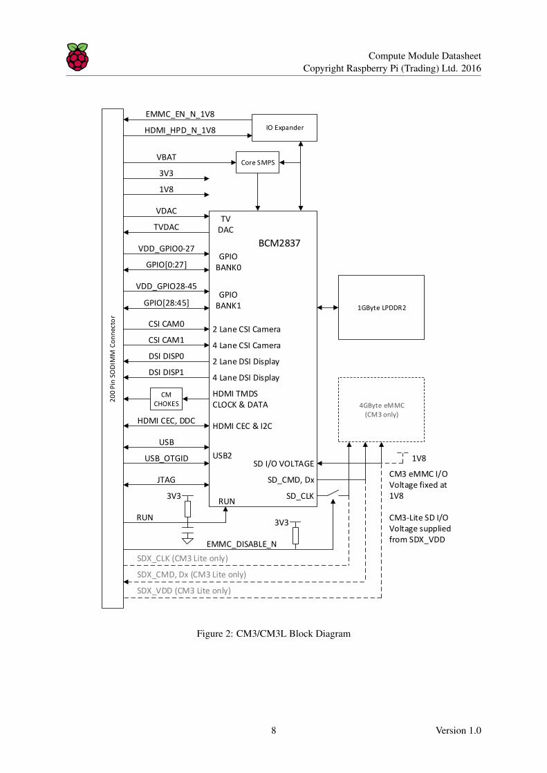
Compute Module DatasheetCopyright Raspberry Pi (Trading) Ltd. 2016
1GByte LPDDR2
20
0 P
in S
OD
IMM
Co
nn
ecto
r
IO Expander
Core SMPS
GPIO[0:27]
VDD_GPIO0-27
GPIO[28:45]
VDD_GPIO28-45
VBAT
3V3
1V8
VDAC
4GByte eMMC(CM3 only)
TVDAC
CSI CAM0
CSI CAM12 Lane CSI Camera
4 Lane CSI Camera
BCM2837
DSI DISP0
DSI DISP12 Lane DSI Display
4 Lane DSI Display
HDMI TMDSCLOCK & DATA
CMCHOKES
RUN
HDMI CEC, DDC
HDMI_HPD_N_1V8
EMMC_EN_N_1V8
JTAG
EMMC_DISABLE_N
USB
USB2USB_OTGID
HDMI CEC & I2C
SDX_CMD, Dx (CM3 Lite only)
SDX_CLK (CM3 Lite only)
3V3RUN
TVDAC
GPIOBANK0
GPIOBANK1
3V3
SD_CLK
SD_CMD, Dx
SDX_VDD (CM3 Lite only)
SD I/O VOLTAGE1V8
CM3 eMMC I/O Voltage fixed at 1V8
CM3-Lite SD I/O Voltage supplied from SDX_VDD
Figure 2: CM3/CM3L Block Diagram
8 Version 1.0

Compute Module DatasheetCopyright Raspberry Pi (Trading) Ltd. 2016
4 Mechanical Specification
The Compute Modules conform to JEDEC MO-224 mechanical specification for 200 pin DDR2 (1.8V)SODIMM modules (with the exception that the CM3, CM3L modules are 31mm in height rather than30mm of CM1) and therefore should work with the many DDR2 SODIMM sockets available on themarket. (Please note that the pinout of the Compute Module is not the same as a DDR2 SODIMMmodule; they are not electrically compatible.)
The SODIMM form factor was chosen as a way to provide the 200 pin connections using a standard,readily available and low cost connector compatible with low cost PCB manufacture.
The maximum component height on the underside of the Compute Module is 1.2mm.
The maximum component height on the top side of the Compute Module is 1.5mm.
The Compute Module PCB thickness is 1.0mm +/- 0.1mm.
Note that the location and arrangement of components on the Compute Module may change slightlyover time due to revisions for cost and manufacturing considerations; however, maximum componentheights and PCB thickness will be kept as specified.
Figure 3 gives the CM1 mechanical dimensions. Figure 4 gives the CM3 and CM3L mechanical dimen-sions.
Figure 3: CM1 Mechanical Dimensions
9 Version 1.0

Compute Module DatasheetCopyright Raspberry Pi (Trading) Ltd. 2016
Figure 4: CM3 and CM3L Mechanical Dimensions
10 Version 1.0

Compute Module DatasheetCopyright Raspberry Pi (Trading) Ltd. 2016
5 Pin Assignments
CM1 CM3-Lite CM3 PIN PIN CM3 CM3-Lite CM1
1 2
3 4 NC SDX_VDD NC
5 6 NC SDX_VDD NC
7 8 NC
9 10 NC SDX_CLK NC
11 12 NC SDX_CMD NC
13 14 NC
15 16 NC SDX_D0 NC
17 18 NC SDX_D1 NC
19 20 NC
21 22 NC SDX_D2 NC
23 24 NC SDX_D3 NC
25 26
27 28
29 30
31 32
33 34
35 36
37 38
39 40
41 42
43 44
45 46
47 48
49 50
51 52
53 54
55 56
57 58
59 60
61 62
63 64
65 66
67 68
69 70
71 72
73 74
75 76
77 78
79 80
81 82
83 84
85 86
87 88 GPIO46_1V8
89 90 GPIO47_1V8
91 92
93 94
95 96
97 98
99 100
101 102
103 104
105 106
107 108
109 110
111 112
113 114
115 116
117 118
119 120
121 122
123 124
125 126
127 128
129 130
131 132
133 134
135 136
137 138
139 140
141 142
143 144
145 146
147 148
149 150
151 152
153 154
155 156
157 158
159 160
161 162
163 164
165 166
167 168
169 170
171 172
173 174
175 176
177 178
179 180
181 182
183 184
185 186
187 188
189 190
191 192
193 194
195 196
197 198
199 200
3V3
3V3
GND
VBAT
VBAT
HDMI_HPD_N_1V8
EMMC_EN_N_1V8
VDD_CORE (DO NOT CONNECT)
GND
1V8
1V8
GND
VDAC
USB_DM
GND
HDMI_CEC
HDMI_SDA
HDMI_SCL
RUN
CAM1_DN1
GND
CAM1_DP0
CAM1_DN0
GND
USB_DP
CAM1_DN2
GND
CAM1_CP
CAM1_CN
GND
CAM1_DP1
HDMI_D2_P
GND
CAM1_DP3
CAM1_DN3
GND
CAM1_DP2
HDMI_D0_P
GND
HDMI_D1_N
HDMI_D1_P
GND
HDMI_D2_N
DSI0_CP
GND
HDMI_CLK_N
HDMI_CLK_P
GND
HDMI_D0_N
DSI0_DP1
GND
DSI0_DN0
DSI0_DP0
GND
DSI0_CN
GPIO25
GND
GPIO26
GPIO27
GND
DSI0_DN1
GPIO21
GND
GPIO22
GPIO23
GND
GPIO24
GPIO17
GND
GPIO18
GPIO19
GND
GPIO20
GPIO13
GND
GPIO14
GPIO15
GND
GPIO16
GND
GPIO0-27_VDD
GPIO28-45_VDD
GND
GPIO12
GND
GPIO8
GPIO9
GND
GPIO10
GPIO11
GND
GPIO4
GPIO5
GND
GPIO6
GPIO7
GND
GPIO0
GPIO1
GND
GPIO2
GPIO3
VDAC
3V3
3V3
GND
VBAT
VBAT
VC_TDO
VC_TCK
GND
1V8
1V8
GND
TVDAC
USB_OTGID
GND
VC_TRST_N
VC_TDI
VC_TMS
NC
NC
NC
NC
NC
GND
CAM0_CP
CAM0_CN
GND
CAM0_DP1
CAM0_DN1
GND
NC
NC
GND
CAM0_DP0
CAM0_DN0
GND
DSI1_DP1
DSI1_DN1
GND
NC
NC
NC
DSI1_DP3
DSI1_DN3
GND
DSI1_DP2
DSI1_DN2
GND
DSI1_DP0
DSI1_DN0
GND
DSI1_CP
DSI1_CN
GND
GPIO44
GPIO45
GND
GND
GPIO40
GPIO41
GND
GPIO42
GPIO43
GND
GPIO36
GPIO37
GND
GPIO38
GPIO39
GND
GPIO32
GPIO33
GND
GPIO34
GPIO35
GND
GPIO30
GPIO31
GND
GPIO0-27_VDD
GPIO28-45_VDD
GND
KEY
EMMC_DISABLE_N
GND
GND
GND
GND
GPIO28
GPIO29
GND
Table 2: Compute Module SODIMM Connector Pinout
Table 2 gives the Compute Module pinout and Table 3 gives the Compute Module pin functions.
11 Version 1.0

Compute Module DatasheetCopyright Raspberry Pi (Trading) Ltd. 2016
Pin Name DIR Voltage Ref PDNa State If Unused Description/Notes
RUN and Boot Control (see text for usage guide)
RUN I 3V3b Pull High Leave open Has internal 10k pull upEMMC DISABLE N I 3V3b Pull High Leave open Has internal 10k pull upEMMC EN N 1V8 O 1V8 Pull High Leave open Has internal 2k2 pull up
GPIO
GPIO[27:0] I/O GPIO0-27 VDD Pull or Hi-Zc Leave open GPIO Bank 0GPIO[45:28] I/O GPIO28-45 VDD Pull or Hi-Zc Leave open GPIO Bank 1
Primary SD Interfaced,e
SDX CLK O SDX VDD Pull High Leave open Primary SD interface CLKSDX CMD I/O SDX VDD Pull High Leave open Primary SD interface CMDSDX Dx I/O SDX VDD Pull High Leave open Primary SD interface DATA
USB Interface
USB Dx I/O - Z Leave open Serial interfaceUSB OTGID I 3V3 Tie to GND OTG pin detect
HDMI Interface
HDMI SCL I/O 3V3b Zf Leave open DDC Clock (5.5V tolerant)HDMI SDA I/O 3V3b Zf Leave open DDC Data (5.5V tolerant)HDMI CEC I/O 3V3 Z Leave open CEC (has internal 27k pull up)HDMI CLKx O - Z Leave open HDMI serial clockHDMI Dx O - Z Leave open HDMI serial dataHDMI HPD N 1V8 I 1V8 Pull High Leave open HDMI hotplug detect
CAM0 (CSI0) 2-lane Interface
CAM0 Cx I - Z Leave open Serial clockCAM0 Dx I - Z Leave open Serial data
CAM1 (CSI1) 4-lane Interface
CAM1 Cx I - Z Leave open Serial clockCAM1 Dx I - Z Leave open Serial data
DSI0 (Display 0) 2-lane Interface
DSI0 Cx O - Z Leave open Serial clockDSI0 Dx O - Z Leave open Serial data
DSI1 (Display 1) 4-lane Interface
DSI1 Cx O - Z Leave open Serial clockDSI1 Dx O - Z Leave open Serial data
TV Out
TVDAC O - Z Leave open Composite video DAC output
JTAG Interface
TMS I 3V3 Z Leave open Has internal 50k pull upTRST N I 3V3 Z Leave open Has internal 50k pull upTCK I 3V3 Z Leave open Has internal 50k pull upTDI I 3V3 Z Leave open Has internal 50k pull upTDO O 3V3 O Leave open Has internal 50k pull upa The PDN column indicates power-down state (when RUN pin LOW)b Must be driven by an open-collector driverc GPIO have software enabled pulls which keep state over power-downd Only available on Lite variantse The CM will always try to boot from this interface firstf Requires external pull-up resistor to 5V as per HDMI spec
Table 3: Pin Functions
12 Version 1.0

Compute Module DatasheetCopyright Raspberry Pi (Trading) Ltd. 2016
6 Electrical Specification
Caution! Stresses above those listed in Table 4 may cause permanent damage to the device. This isa stress rating only; functional operation of the device under these or any other conditions above thoselisted in the operational sections of this specification is not implied. Exposure to absolute maximumrating conditions for extended periods may affect device reliability.
Symbol Parameter Minimum Maximum Unit
VBAT Core SMPS Supply -0.5 6.0 V
3V3 3V3 Supply Voltage -0.5 4.10 V
1V8 1V8 Supply Voltage -0.5 2.10 V
VDAC TV DAC Supply -0.5 4.10 V
GPIO0-27 VDD GPIO0-27 I/O Supply Voltage -0.5 4.10 V
GPIO28-45 VDD GPIO28-27 I/O Supply Voltage -0.5 4.10 V
SDX VDD Primary SD/eMMC Supply Voltage -0.5 4.10 V
Table 4: Absolute Maximum Ratings
DC Characteristics are defined in Table 5
Symbol Parameter Conditions Minimum Typical Maximum Unit
VIL Input low voltagea VDD IO = 1.8V - - 0.6 VVDD IO = 2.7V - - 0.8 V
VIH Input high voltagea VDD IO = 1.8V 1.0 - - VVDD IO = 2.7V 1.3 - - V
IIL Input leakage current TA = +85C - - 5 µA
CIN Input capacitance - - 5 - pF
VOL Output low voltageb VDD IO = 1.8V, IOL = -2mA - - 0.2 VVDD IO = 2.7V, IOL = -2mA - - 0.15 V
VOH Output high voltageb VDD IO = 1.8V, IOH = 2mA 1.6 - - VVDD IO = 2.7V, IOH = 2mA 2.5 - - V
IOL Output low currentc VDD IO = 1.8V, VO = 0.4V 12 - - mAVDD IO = 2.7V, VO = 0.4V 17 - - mA
IOH Output high currentc VDD IO = 1.8V, VO = 1.4V 10 - - mAVDD IO = 2.7V, VO = 2.3V 16 - - mA
RPU Pullup resistor - 50 - 65 kΩ
RPD Pulldown resistor - 50 - 65 kΩa Hysteresis enabledb Default drive strength (8mA)c Maximum drive strength (16mA)
Table 5: DC Characteristics
13 Version 1.0

Compute Module DatasheetCopyright Raspberry Pi (Trading) Ltd. 2016
AC Characteristics are defined in Table 6 and Fig. 5.
Pin Name Symbol Parameter Minimum Typical Maximum Unit
Digital outputs trise 10-90% rise timea - 1.6 - ns
Digital outputs tfall 90-10% fall timea - 1.7 - ns
GPCLK tJOSC Oscillator-derived GPCLK - - 20 pscycle-cycle jitter (RMS)
GPCLK tJPLL PLL-derived GPCLK - - 48 pscycle-cycle jitter (RMS)
a Default drive strength, CL = 5pF, VDD IOx = 3.3V
Table 6: Digital I/O Pin AC Characteristics
tfall trise
DIGITALOUTPUT
Figure 5: Digital IO Characteristics
7 Power Supplies
The Compute Module has six separate supplies that must be present and powered at all times; you cannotleave any of them unpowered, even if a specific interface or GPIO bank is unused. The six supplies areas follows:
1. VBAT is used to power the BCM283x processor core. It feeds the SMPS that generates the chipcore voltage.
2. 3V3 powers various BCM283x PHYs, IO and the eMMC Flash.
3. 1V8 powers various BCM283x PHYs, IO and SDRAM.
4. VDAC powers the composite (TV-out) DAC.
5. GPIO0-27 VREF powers the GPIO 0-27 IO bank.
6. GPIO28-45 VREF powers the GPIO 28-45 IO bank.
14 Version 1.0

Compute Module DatasheetCopyright Raspberry Pi (Trading) Ltd. 2016
Supply Descripion Minimum Typical Maximum Unit
VBAT Core SMPS Supply 2.5 - 5.0 + 5% V
3V3 3V3 Supply Voltage 3.3 - 5% 3.3 3.3 + 5% V
1V8 1V8 Supply Voltage 1.8 - 5% 1.8 1.8 + 5% V
VDAC TV DAC Supplya 2.5 - 5% 2.8 3.3 + 5% V
GPIO0-27 VDD GPIO0-27 I/O Supply Voltage 1.8 - 5% - 3.3 + 5% V
GPIO28-45 VDD GPIO28-27 I/O Supply Voltage 1.8 - 5% - 3.3 + 5% V
SDX VDD Primary SD/eMMC Supply Voltage 1.8 - 5% - 3.3 + 5% Va Requires a clean 2.5-2.8V supply if TV DAC is used, else connect to 3V3
Table 7: Power Supply Operating Ranges
7.1 Supply Sequencing
Supplies should be staggered so that the highest voltage comes up first, then the remaining voltagesin descending order. This is to avoid forward biasing internal (on-chip) diodes between supplies, andcausing latch-up. Alternatively supplies can be synchronised to come up at exactly the same time aslong as at no point a lower voltage supply rail voltage exceeds a higher voltage supply rail voltage.
7.2 Power Requirements
Exact power requirements will be heavily dependent upon the individual use case. If an on-chip subsys-tem is unused, it is usually in a low power state or completely turned off. For instance, if your applicationdoes not use 3D graphics then a large part of the core digital logic will never turn on and need power.This is also the case for camera and display interfaces, HDMI, USB interfaces, video encoders anddecoders, and so on.
Powerchain design is critical for stable and reliable operation of the Compute Module. We stronglyrecommend that designers spend time measuring and verifying power requirements for their particularuse case and application, as well as paying careful attention to power supply sequencing and maximumsupply voltage tolerance.
Table 8 specifies the recommneded minimum power supply outputs required to power the ComputeModule.
15 Version 1.0

Compute Module DatasheetCopyright Raspberry Pi (Trading) Ltd. 2016
Supply Minimum Requirement Unit
VBAT (CM1) 2000a mW
VBAT (CM3,3L) 3500a mW
3V3 250 mA
1V8 250 mA
VDAC 25 mA
GPIO0-27 VDD 50b mA
GPIO28-45 VDD 50b mA
SDX VDD 50b mAa Recommended minimum. Actual power drawn is very dependent on use-caseb Each GPIO can supply up to 16mA, aggregate current per bank must not exceed 50mA
Table 8: Mimimum Power Supply Requirements
8 Booting
The 4GB eMMC Flash device on CM3 is directly connected to the primary BCM2837 SD/eMMC inter-face. These connections are not accessible on the module pins. On CM3L this SD interface is availableon the SDX pins.
When initially powered on, or after the RUN pin has been held low and then released, the BCM2837will try to access the primary SD/eMMC interface. It will then look for a file called bootcode.bin on theprimary partition (which must be FAT) to start booting the system. If it cannot access the SD/eMMCdevice or the boot code cannot be found, it will fall back to waiting for boot code to be written to it overUSB; in other words, its USB port is in slave mode waiting to accept boot code from a suitable host.
A USB boot tool is available on Github which allows a host PC running Linux to write the BCM2837boot code over USB to the module. That boot code then runs and provides access to the SD/eMMC as aUSB mass storage device, which can then be read and written using the host PC. Note that a Raspberry Pican be used as the host machine. For those using Windows a precompiled and packeged tool is available.For more information see here.
The Compute Module has a pin called EMMC DISABLE N which when shorted to GND will disablethe SD/eMMC interface (by physically disconnecting the SD CMD pin), forcing BCM2837 to boot fromUSB. Note that when the eMMC is disabled in this way, it takes a couple of seconds from powering upfor the processor to stop attempting to talk to the SD/eMMC device and fall back to booting from USB.
Note that once booted over USB, BCM2837 needs to re-enable the SD/eMMC device (by releasingEMMC DISABLE N) to allow access to it as mass storage. It expects to be able to do this by drivingthe EMMC EN N 1V8 pin LOW, which at boot is initially an input with a pull up to 1V8. If an end userwishes to add the ability to access the SD/eMMC over USB in their product, similar circuitry to thatused on the Compute Module IO Board to enable/disable the USB boot and SD/eMMC must be used;that is, EMMC DISABLE N pulled low via MOSFET(s) and released again by MOSFET, with the gatecontrolled by EMMC EN N 1V8. Ensure you use MOSFETs suitable for switching at 1.8V (i.e. use adevice with gate threshold voltage, Vt, suitable for 1.8V switching).
16 Version 1.0

Compute Module DatasheetCopyright Raspberry Pi (Trading) Ltd. 2016
9 Peripherals
9.1 GPIO
BCM283x has in total 54 GPIO lines in 3 separate voltage banks. All GPIO pins have at least twoalternative functions within the SoC. When not used for the alternate peripheral function, each GPIOpin may be set as an input (optionally as an interrupt) or an output. The alternate functions are usuallyperipheral I/Os, and most peripherals appear twice to allow flexibility on the choice of I/O voltage.
On CM1, CM3 and CM3L bank2 is used on the module to connect to the eMMC device and, on CM3and CM3L, for an on-board I2C bus (to talk to the core SMPS and control the special function pins). OnCM3L most of bank 2 is exposed to allow a user to connect their choice of SD card or eMMC device (ifrequired).
Bank0 and 1 GPIOs are available for general use. GPIO0 to GPIO27 are bank 0 and GPIO28-45 makeup bank1. GPIO0-27 VDD is the power supply for bank0 and GPIO28-45 VDD is the power supply forbank1. SDX VDD is the supply for bank2 on CM3L. These supplies can be in the range 1.8V-3.3V (seeTable 7) and are not optional; each bank must be powered, even when none of the GPIOs for that bankare used.
Note that the HDMI HPD N 1V8 and EMMC EN N 1V8 pins (on CM1 these were called GPIO46 1V8and GPIO47 1V8 respectively) are 1.8V IO and are used for special functions (HDMI hot plug de-tect and boot control respectively). Please do not use these pins for any other purpose, as thesoftware for the Compute Module will always expect these pins to have these special functions. Ifthey are unused please leave them unconnected.
All GPIOs except GPIO28, 29, 44 and 45 have weak in-pad pull-ups or pull-downs enabled when thedevice is powered on. It is recommended to add off-chip pulls to GPIO28, 29, 44 and 45 to make surethey never float during power on and initial boot.
17 Version 1.0

Compute Module DatasheetCopyright Raspberry Pi (Trading) Ltd. 2016
9.1.1 GPIO Alternate Functions
DefaultGPIO Pull ALT0 ALT1 ALT2 ALT3 ALT4 ALT5
0 High SDA0 SA5 PCLK - - -
1 High SCL0 SA4 DE - - -
2 High SDA1 SA3 LCD VSYNC - - -
3 High SCL1 SA2 LCD HSYNC - - -
4 High GPCLK0 SA1 DPI D0 - - ARM TDI
5 High GPCLK1 SA0 DPI D1 - - ARM TDO
6 High GPCLK2 SOE N DPI D2 - - ARM RTCK
7 High SPI0 CE1 N SWE N DPI D3 - - -
8 High SPI0 CE0 N SD0 DPI D4 - - -
9 Low SPI0 MISO SD1 DPI D5 - - -
10 Low SPI0 MOSI SD2 DPI D6 - - -
11 Low SPI0 SCLK SD3 DPI D7 - - -
12 Low PWM0 SD4 DPI D8 - - ARM TMS
13 Low PWM1 SD5 DPI D9 - - ARM TCK
14 Low TXD0 SD6 DPI D10 - - TXD1
15 Low RXD0 SD7 DPI D11 - - RXD1
16 Low FL0 SD8 DPI D12 CTS0 SPI1 CE2 N CTS1
17 Low FL1 SD9 DPI D13 RTS0 SPI1 CE1 N RTS1
18 Low PCM CLK SD10 DPI D14 - SPI1 CE0 N PWM0
19 Low PCM FS SD11 DPI D15 - SPI1 MISO PWM1
20 Low PCM DIN SD12 DPI D16 - SPI1 MOSI GPCLK0
21 Low PCM DOUT SD13 DPI D17 - SPI1 SCLK GPCLK1
22 Low SD0 CLK SD14 DPI D18 SD1 CLK ARM TRST -
23 Low SD0 CMD SD15 DPI D19 SD1 CMD ARM RTCK -
24 Low SD0 DAT0 SD16 DPI D20 SD1 DAT0 ARM TDO -
25 Low SD0 DAT1 SD17 DPI D21 SD1 DAT1 ARM TCK -
26 Low SD0 DAT2 TE0 DPI D22 SD1 DAT2 ARM TDI -
27 Low SD0 DAT3 TE1 DPI D23 SD1 DAT3 ARM TMS -
Table 9: GPIO Bank0 Alternate Functions
18 Version 1.0

Compute Module DatasheetCopyright Raspberry Pi (Trading) Ltd. 2016
DefaultGPIO Pull ALT0 ALT1 ALT2 ALT3 ALT4 ALT5
28 None SDA0 SA5 PCM CLK FL0 - -
29 None SCL0 SA4 PCM FS FL1 - -
30 Low TE0 SA3 PCM DIN CTS0 - CTS1
31 Low FL0 SA2 PCM DOUT RTS0 - RTS1
32 Low GPCLK0 SA1 RING OCLK TXD0 - TXD1
33 Low FL1 SA0 TE1 RXD0 - RXD1
34 High GPCLK0 SOE N TE2 SD1 CLK - -
35 High SPI0 CE1 N SWE N - SD1 CMD - -
36 High SPI0 CE0 N SD0 TXD0 SD1 DAT0 - -
37 Low SPI0 MISO SD1 RXD0 SD1 DAT1 - -
38 Low SPI0 MOSI SD2 RTS0 SD1 DAT2 - -
39 Low SPI0 SCLK SD3 CTS0 SD1 DAT3 - -
40 Low PWM0 SD4 - SD1 DAT4 SPI2 MISO TXD1
41 Low PWM1 SD5 TE0 SD1 DAT5 SPI2 MOSI RXD1
42 Low GPCLK1 SD6 TE1 SD1 DAT6 SPI2 SCLK RTS1
43 Low GPCLK2 SD7 TE2 SD1 DAT7 SPI2 CE0 N CTS1
44 None GPCLK1 SDA0 SDA1 TE0 SPI2 CE1 N -
45 None PWM1 SCL0 SCL1 TE1 SPI2 CE2 N -
Table 10: GPIO Bank1 Alternate Functions
Table 9 and Table 10 detail the default pin pull state and available alternate GPIO functions. Most ofthese alternate peripheral functions are described in detail in the Broadcom Peripherals Specificationdocument and have Linux drivers available.
9.1.2 Secondary Memory Interface (SMI)
The SMI peripheral is an asynchronous NAND type bus supporting Intel mode80 type transfers at 8 or16 bit widths and available in the ALT1 positions on GPIO banks 0 and 1 (see Table 9 and Table 10). Itis not publicly documented in the Broadcom Peripherals Specification but a Linux driver is available inthe Raspberry Pi Github Linux repository (bcm2835 smi.c in linux/drivers/misc).
9.1.3 Display Parallel Interface (DPI)
A standard parallel RGB (DPI) interface is available on bank 0 GPIOs. This up-to-24-bit parallel inter-face can support a secondary display. Again this interface is not documented in the Broadcom Peripher-als Specification but documentation can be found here.
19 Version 1.0

Compute Module DatasheetCopyright Raspberry Pi (Trading) Ltd. 2016
9.1.4 SD/SDIO Interface
The BCM283x supports two SD card interfaces, SD0 and SD1.
The first (SD0) is a proprietary Broadcom controller that does not support SDIO and is the primaryinterface used to boot and talk to the eMMC or SDX x signals.
The second interface (SD1) is standards compliant and can interface to SD, SDIO and eMMC devices;for example on a Raspberry Pi 3 it is used to talk to the on-board BCM43438 WiFi device in SDIOmode.
Both interfaces can support speeds up to 50MHz single ended (SD High Speed Mode).
9.2 CSI (MIPI Serial Camera)
Currently the CSI interface is not openly documented and only CSI camera sensors supported by theofficial Raspberry Pi firmware will work with this interface. Supported sensors are the OmniVisionOV5647 and Sony IMX219.
It is recommended to attach other cameras via USB.
9.3 DSI (MIPI Serial Display)
Currently the DSI interface is not openly documented and only DSI displays supported by the officialRaspberry Pi firmware will work with this interface.
Displays can also be added via the parallel DPI interface which is available as a GPIO alternate function- see Table 9 and Section 9.1.3
9.4 USB
The BCM283x USB port is On-The-Go (OTG) capable. If using either as a fixed slave or fixed master,please tie the USB OTGID pin to ground.
The USB port (Pins USB DP and USB DM) must be routed as 90 ohm differential PCB traces.
Note that the port is capable of being used as a true OTG port however there is no official documentation.Some users have had success making this work.
9.5 HDMI
BCM283x supports HDMI V1.3a.
It is recommended that users follow a similar arrangement to the Compute Module IO Board circuitryfor HDMI output.
The HDMI CK P/N (clock) and D0-D2 P/N (data) pins must each be routed as matched length 100ohm differential PCB traces. It is also important to make sure that each differential pair is closely phasematched. Finally, keep HDMI traces well away from other noise sources and as short as possible.
Failure to observe these design rules is likely to result in EMC failure.
20 Version 1.0

Compute Module DatasheetCopyright Raspberry Pi (Trading) Ltd. 2016
9.6 Composite (TV Out)
The TVDAC pin can be used to output composite video (PAL or NTSC). Please route this signal awayfrom noise sources and use a 75 ohm PCB trace.
Note that the TV DAC is powered from the VDAC supply which must be a clean supply of 2.5-2.8V. Itis recommended users generate this supply from 3V3 using a low noise LDO.
If the TVDAC output is not used VDAC can be connected to 3V3, but it must be powered even if theTV-out functionality is unused.
10 Thermals
The BCM283x SoC employs DVFS (Dynamic Voltage and Frequency Scaling) on the core voltage.When the processor is idle (low CPU utilisation), it will reduce the core frequency and voltage to reducecurrent draw and heat output. When the core utilisation exceeds a certain threshold the core votlageis increased and the core frequency is boosted to the maximum working frerquency. The voltage andfrequency are throttled back when the CPU load reduces back to an ’idle’ level OR when the silicontemperature as mesured by the on-chip temperature sensor exceeds 85C (thermal throttling).
A designer must pay careful attention to the thermal design of products using the CM3/CM3L so thatperformance is not artificially curtailed due to the processor thermal throttling, as the Quad ARM com-plex in the BCM2837 can generate significant heat output.
10.1 Temperature Range
The operating temperature range of the module is set by the lowest maximum and highest minimum ofany of the components used.
The eMMC and LPDDR2 have the narrowest range, these are rated for -25 to +80 degrees Celsius.Therefore the nominal range for the CM3 and CM3L is -25C to +80C.
However, this range is the maximum for the silicon die; therefore, users would have to take into accountthe heat generated when in use and make sure this does not cause the temperature to exceed 80 degreesCelsius.
11 Availability
Raspberry Pi guarantee availability of CM1, CM3 and CM3 Lite until at least January 2023.
12 Support
For support please see the hardware documentation section of the Raspberry Pi website and post ques-tions to the Raspberry Pi forum.
21 Version 1.0

ANEXO V – DATASHEETS
DATASHEET SEMTECH SX1276
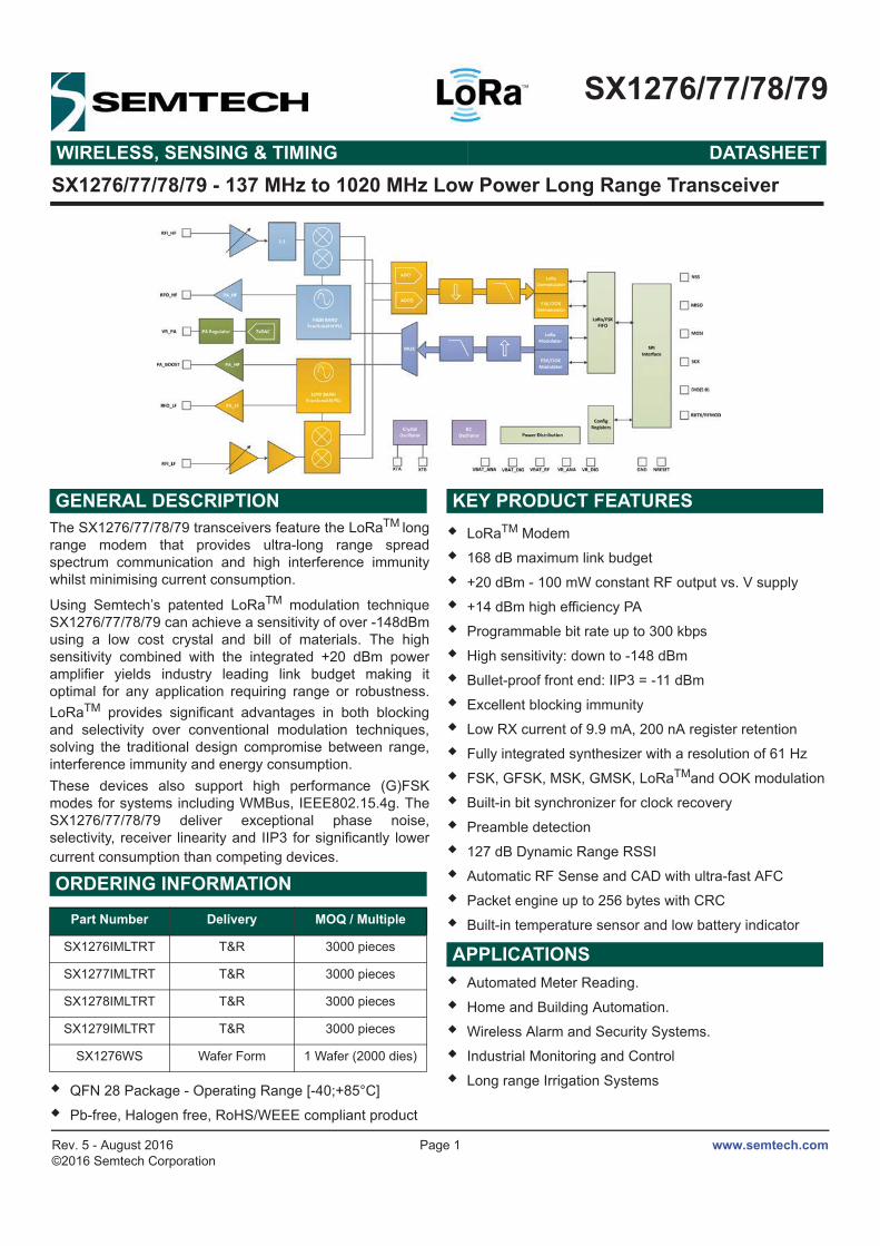
SX1276/77/78/79
www.semtech.comPage 1
WIRELESS, SENSING & TIMING DATASHEETSX1276/77/78/79 - 137 MHz to 1020 MHz Low Power Long Range Transceiver
Rev. 5 - August 2016©2016 Semtech Corporation
The SX1276/77/78/79 transceivers feature the LoRaTM long range modem that provides ultra-long range spread spectrum communication and high interference immunity whilst minimising current consumption.
Using Semtech’s patented LoRaTM modulation technique SX1276/77/78/79 can achieve a sensitivity of over -148dBm using a low cost crystal and bill of materials. The high sensitivity combined with the integrated +20 dBm power amplifier yields industry leading link budget making it optimal for any application requiring range or robustness. LoRaTM provides significant advantages in both blocking and selectivity over conventional modulation techniques, solving the traditional design compromise between range, interference immunity and energy consumption.These devices also support high performance (G)FSK modes for systems including WMBus, IEEE802.15.4g. The SX1276/77/78/79 deliver exceptional phase noise, selectivity, receiver linearity and IIP3 for significantly lower current consumption than competing devices.
QFN 28 Package - Operating Range [-40;+85°C]
Pb-free, Halogen free, RoHS/WEEE compliant product
LoRaTM Modem
168 dB maximum link budget
+20 dBm - 100 mW constant RF output vs. V supply
+14 dBm high efficiency PA
Programmable bit rate up to 300 kbps
High sensitivity: down to -148 dBm
Bullet-proof front end: IIP3 = -11 dBm
Excellent blocking immunity
Low RX current of 9.9 mA, 200 nA register retention
Fully integrated synthesizer with a resolution of 61 Hz
FSK, GFSK, MSK, GMSK, LoRaTMand OOK modulation
Built-in bit synchronizer for clock recovery
Preamble detection
127 dB Dynamic Range RSSI
Automatic RF Sense and CAD with ultra-fast AFC
Packet engine up to 256 bytes with CRC
Built-in temperature sensor and low battery indicator
Automated Meter Reading.
Home and Building Automation.
Wireless Alarm and Security Systems.
Industrial Monitoring and Control
Long range Irrigation Systems
GENERAL DESCRIPTION
ORDERING INFORMATION
Part Number Delivery MOQ / Multiple
SX1276IMLTRT T&R 3000 pieces
SX1277IMLTRT T&R 3000 pieces
SX1278IMLTRT T&R 3000 pieces
SX1279IMLTRT T&R 3000 pieces
SX1276WS Wafer Form 1 Wafer (2000 dies)
KEY PRODUCT FEATURES
APPLICATIONS
www.semtech.comPage 2
Section PageTable of contents
SX1276/77/78/79
WIRELESS, SENSING & TIMING DATASHEET
Rev. 5 - August 2016©2016 Semtech Corporation
1. General Description ................................................................................................................................................. 91.1. Simplified Block Diagram ................................................................................................................................. 91.2. Product Versions ............................................................................................................................................101.3. Pin Diagram ................................................................................................................................................... 101.4. Pin Description ...............................................................................................................................................111.5. Package Marking ...........................................................................................................................................12
2. Electrical Characteristics ....................................................................................................................................... 132.1. ESD Notice .................................................................................................................................................... 132.2. Absolute Maximum Ratings ........................................................................................................................... 132.3. Operating Range............................................................................................................................................ 132.4. Thermal Properties ........................................................................................................................................ 132.5. Chip Specification ..........................................................................................................................................14
2.5.1. Power Consumption .................................................................................................................................. 142.5.2. Frequency Synthesis................................................................................................................................. 142.5.3. FSK/OOK Mode Receiver .........................................................................................................................162.5.4. FSK/OOK Mode Transmitter ..................................................................................................................... 172.5.5. Electrical Specification for LoRaTM Modulation ........................................................................................192.5.6. Digital Specification ...................................................................................................................................22
3. SX1276/77/78/79 Features.................................................................................................................................... 233.1. LoRaTM Modem ............................................................................................................................................ 243.2. FSK/OOK Modem .......................................................................................................................................... 24
4. SX1276/77/78/79 Digital Electronics ..................................................................................................................... 254.1. The LoRaTM Modem ..................................................................................................................................... 25
4.1.1. Link Design Using the LoRaTM Modem ....................................................................................................264.1.2. LoRaTM Digital Interface ...........................................................................................................................344.1.3. Operation of the LoRaTM Modem............................................................................................................. 364.1.4. Frequency Settings ...................................................................................................................................374.1.5. Frequency Error Indication ........................................................................................................................ 374.1.6. LoRaTM Modem State Machine Sequences .............................................................................................384.1.7. Modem Status Indicators........................................................................................................................... 46
4.2. FSK/OOK Modem .......................................................................................................................................... 464.2.1. Bit Rate Setting ......................................................................................................................................... 464.2.2. FSK/OOK Transmission ............................................................................................................................ 474.2.3. FSK/OOK Reception ................................................................................................................................. 484.2.4. Operating Modes in FSK/OOK Mode ........................................................................................................ 544.2.5. Startup Times ............................................................................................................................................564.2.6. Receiver Startup Options .......................................................................................................................... 594.2.7. Receiver Restart Methods......................................................................................................................... 604.2.8. Top Level Sequencer ................................................................................................................................ 61

www.semtech.comPage 3
Section PageTable of contents
SX1276/77/78/79
WIRELESS, SENSING & TIMING DATASHEET
Rev. 5 - August 2016©2016 Semtech Corporation
4.2.9. Data Processing in FSK/OOK Mode ......................................................................................................... 654.2.10. FIFO ........................................................................................................................................................664.2.11. Digital IO Pins Mapping ...........................................................................................................................694.2.12. Continuous Mode ....................................................................................................................................704.2.13. Packet Mode ........................................................................................................................................... 714.2.14. io-homecontrol® Compatibility Mode ...................................................................................................... 79
4.3. SPI Interface ..................................................................................................................................................805. SX1276/77/78/79 Analog & RF Frontend Electronics............................................................................................ 81
5.1. Power Supply Strategy .................................................................................................................................. 815.2. Low Battery Detector ..................................................................................................................................... 815.3. Frequency Synthesis ..................................................................................................................................... 81
5.3.1. Crystal Oscillator ....................................................................................................................................... 815.3.2. CLKOUT Output ........................................................................................................................................ 825.3.3. PLL ............................................................................................................................................................ 825.3.4. RC Oscillator ............................................................................................................................................. 82
5.4. Transmitter Description ..................................................................................................................................835.4.1. Architecture Description ............................................................................................................................ 835.4.2. RF Power Amplifiers.................................................................................................................................. 835.4.3. High Power +20 dBm Operation ............................................................................................................... 845.4.4. Over Current Protection ............................................................................................................................85
5.5. Receiver Description...................................................................................................................................... 855.5.1. Overview ................................................................................................................................................... 855.5.2. Receiver Enabled and Receiver Active States.......................................................................................... 855.5.3. Automatic Gain Control In FSK/OOK Mode .............................................................................................. 855.5.4. RSSI in FSK/OOK Mode ........................................................................................................................... 865.5.5. RSSI and SNR in LoRaTM Mode.............................................................................................................. 875.5.6. Channel Filter ............................................................................................................................................ 885.5.7. Temperature Measurement....................................................................................................................... 89
6. Description of the Registers................................................................................................................................... 906.1. Register Table Summary ............................................................................................................................... 906.2. FSK/OOK Mode Register Map .......................................................................................................................936.3. Band Specific Additional Registers .............................................................................................................. 1066.4. LoRaTM Mode Register Map....................................................................................................................... 108
7. Application Information ........................................................................................................................................ 1167.1. Crystal Resonator Specification................................................................................................................... 1167.2. Reset of the Chip ......................................................................................................................................... 116
7.2.1. POR......................................................................................................................................................... 1167.2.2. Manual Reset ..........................................................................................................................................117
7.3. Top Sequencer: Listen Mode Examples ...................................................................................................... 117

www.semtech.comPage 4
Section PageTable of contents
SX1276/77/78/79
WIRELESS, SENSING & TIMING DATASHEET
Rev. 5 - August 2016©2016 Semtech Corporation
7.3.1. Wake on Preamble Interrupt ................................................................................................................... 1177.3.2. Wake on SyncAddress Interrupt ..............................................................................................................120
7.4. Top Sequencer: Beacon Mode ....................................................................................................................1237.4.1. Timing diagram........................................................................................................................................ 1237.4.2. Sequencer Configuration......................................................................................................................... 123
7.5. Example CRC Calculation ...........................................................................................................................1257.6. Example Temperature Reading ...................................................................................................................126
8. Packaging Information ......................................................................................................................................... 1288.1. Package Outline Drawing ............................................................................................................................ 1288.2. Recommended Land Pattern ....................................................................................................................... 1298.3. Tape & Reel Information .............................................................................................................................. 1308.4. Wafer Delivery ............................................................................................................................................. 130
9. Revision History................................................................................................................................................... 131

www.semtech.comPage 5
Section PageTable of contents
SX1276/77/78/79
WIRELESS, SENSING & TIMING DATASHEET
Rev. 5 - August 2016©2016 Semtech Corporation
Table 1. SX1276/77/78/79 Device Variants and Key Parameters .................................................................................10Table 2. Pin Description ................................................................................................................................................11Table 3. Absolute Maximum Ratings .............................................................................................................................13Table 4. Operating Range .............................................................................................................................................13Table 5. Thermal Properties ..........................................................................................................................................13Table 6. Power Consumption Specification ...................................................................................................................14Table 7. Frequency Synthesizer Specification ..............................................................................................................14Table 8. FSK/OOK Receiver Specification ....................................................................................................................16Table 9. Transmitter Specification .................................................................................................................................17Table 10. LoRa Receiver Specification .........................................................................................................................19Table 11. Digital Specification .......................................................................................................................................22Table 12. Example LoRaTM Modem Performances, 868MHz Band .............................................................................25Table 13. Range of Spreading Factors ..........................................................................................................................27Table 14. Cyclic Coding Overhead ................................................................................................................................27Table 15. LoRa Bandwidth Options ...............................................................................................................................28Table 16. LoRaTM Operating Mode Functionality .........................................................................................................36Table 17. LoRa CAD Consumption Figures ..................................................................................................................45Table 18. DIO Mapping LoRaTM Mode .........................................................................................................................46Table 19. Bit Rate Examples .........................................................................................................................................47Table 20. Preamble Detector Settings ...........................................................................................................................53Table 21. RxTrigger Settings to Enable Timeout Interrupts ..........................................................................................54Table 22. Basic Transceiver Modes ..............................................................................................................................54Table 23. Receiver Startup Time Summary ..................................................................................................................57Table 24. Receiver Startup Options ..............................................................................................................................60Table 25. Sequencer States ..........................................................................................................................................61Table 26. Sequencer Transition Options .......................................................................................................................62Table 27. Sequencer Timer Settings .............................................................................................................................63Table 28. Status of FIFO when Switching Between Different Modes of the Chip .........................................................67Table 29. DIO Mapping, Continuous Mode ...................................................................................................................69Table 30. DIO Mapping, Packet Mode ..........................................................................................................................69Table 31. CRC Description ...........................................................................................................................................77Table 32. Frequency Bands ..........................................................................................................................................82Table 33. Power Amplifier Mode Selection Truth Table ................................................................................................83Table 34. High Power Settings ......................................................................................................................................84Table 35. Operating Range, +20dBm Operation ...........................................................................................................84Table 36. Operating Range, +20dBm Operation ...........................................................................................................84Table 37. Trimming of the OCP Current ........................................................................................................................85Table 38. LNA Gain Control and Performances ............................................................................................................86Table 39. RssiSmoothing Options .................................................................................................................................86
www.semtech.comPage 6
Section PageTable of contents
SX1276/77/78/79
WIRELESS, SENSING & TIMING DATASHEET
Rev. 5 - August 2016©2016 Semtech Corporation
Table 40. Available RxBw Settings ................................................................................................................................88Table 41. Registers Summary .......................................................................................................................................90Table 42. Register Map .................................................................................................................................................93Table 43. Low Frequency Additional Registers ...........................................................................................................106Table 44. High Frequency Additional Registers ..........................................................................................................107Table 45. Crystal Specification ....................................................................................................................................116Table 46. Listen Mode with PreambleDetect Condition Settings .................................................................................119Table 47. Listen Mode with PreambleDetect Condition Recommended DIO Mapping ...............................................119Table 48. Listen Mode with SyncAddress Condition Settings .....................................................................................122Table 49. Listen Mode with PreambleDetect Condition Recommended DIO Mapping ...............................................122Table 50. Beacon Mode Settings ................................................................................................................................124Table 51. Revision History ...........................................................................................................................................131

www.semtech.comPage 7
Section PageTable of contents
SX1276/77/78/79
WIRELESS, SENSING & TIMING DATASHEET
Rev. 5 - August 2016©2016 Semtech Corporation
Figure 1. Block Diagram .................................................................................................................................................9Figure 2. Pin Diagrams .................................................................................................................................................10Figure 3. Marking Diagram ...........................................................................................................................................12Figure 4. SX1276/77/78/79 Block Schematic Diagram ................................................................................................23Figure 5. LoRaTM Modem Connectivity .......................................................................................................................26Figure 6. LoRaTM Packet Structure .............................................................................................................................29Figure 7. Interrupts Generated in the Case of Successful Frequency Hopping Communication. ................................33Figure 8. LoRaTM Data Buffer .....................................................................................................................................34Figure 9. LoRaTM Modulation Transmission Sequence. .............................................................................................38Figure 10. LoRaTM Receive Sequence. ......................................................................................................................39Figure 11. LoRaTM CAD Flow .....................................................................................................................................43Figure 12. CAD Time as a Function of Spreading Factor .............................................................................................44Figure 13. Consumption Profile of the LoRa CAD Process ..........................................................................................45Figure 14. OOK Peak Demodulator Description ...........................................................................................................49Figure 15. Floor Threshold Optimization ......................................................................................................................50Figure 16. Bit Synchronizer Description .......................................................................................................................51Figure 17. Startup Process ...........................................................................................................................................56Figure 18. Time to RSSI Sample ..................................................................................................................................57Figure 19. Tx to Rx Turnaround ...................................................................................................................................58Figure 20. Rx to Tx Turnaround ...................................................................................................................................58Figure 21. Receiver Hopping ........................................................................................................................................59Figure 22. Transmitter Hopping ....................................................................................................................................59Figure 23. Timer1 and Timer2 Mechanism ...................................................................................................................63Figure 24. Sequencer State Machine ...........................................................................................................................64Figure 25. SX1276/77/78/79 Data Processing Conceptual View .................................................................................65Figure 26. FIFO and Shift Register (SR) ......................................................................................................................66Figure 27. FifoLevel IRQ Source Behavior ...................................................................................................................67Figure 28. Sync Word Recognition ...............................................................................................................................68Figure 29. Continuous Mode Conceptual View ............................................................................................................70Figure 30. Tx Processing in Continuous Mode .............................................................................................................70Figure 31. Rx Processing in Continuous Mode ............................................................................................................71Figure 32. Packet Mode Conceptual View ...................................................................................................................72Figure 33. Fixed Length Packet Format .......................................................................................................................73Figure 34. Variable Length Packet Format ...................................................................................................................74Figure 35. Unlimited Length Packet Format .................................................................................................................74Figure 36. Manchester Encoding/Decoding .................................................................................................................78Figure 37. Data Whitening Polynomial .........................................................................................................................79Figure 38. SPI Timing Diagram (single access) ...........................................................................................................80Figure 39. TCXO Connection .......................................................................................................................................81

www.semtech.comPage 8
Section PageTable of contents
SX1276/77/78/79
WIRELESS, SENSING & TIMING DATASHEET
Rev. 5 - August 2016©2016 Semtech Corporation
Figure 40. RF Front-end Architecture Shows the Internal PA Configuration. ...............................................................83Figure 41. Temperature Sensor Response ..................................................................................................................89Figure 42. POR Timing Diagram ................................................................................................................................116Figure 43. Manual Reset Timing Diagram ..................................................................................................................117Figure 44. Listen Mode: Principle ...............................................................................................................................117Figure 45. Listen Mode with No Preamble Received .................................................................................................118Figure 46. Listen Mode with Preamble Received .......................................................................................................118Figure 47. Wake On PreambleDetect State Machine .................................................................................................119Figure 48. Listen Mode with no SyncAddress Detected .............................................................................................120Figure 49. Listen Mode with Preamble Received and no SyncAddress .....................................................................120Figure 50. Listen Mode with Preamble Received & Valid SyncAddress ....................................................................121Figure 51. Wake On SyncAddress State Machine .....................................................................................................121Figure 52. Beacon Mode Timing Diagram ..................................................................................................................123Figure 53. Beacon Mode State Machine ....................................................................................................................123Figure 54. Example CRC Code ..................................................................................................................................125Figure 55. Example Temperature Reading ................................................................................................................126Figure 56. Example Temperature Reading (continued) .............................................................................................127Figure 57. Package Outline Drawing ..........................................................................................................................128Figure 58. Recommended Land Pattern ....................................................................................................................129Figure 59. Tape and Reel Information ........................................................................................................................130

www.semtech.comPage 9
SX1276/77/78/79
WIRELESS, SENSING & TIMING DATASHEET
Rev. 5 - August 2016©2016 Semtech Corporation
1. General DescriptionThe SX1276/77/78/79 incorporates the LoRaTM spread spectrum modem which is capable of achieving significantly longer range than existing systems based on FSK or OOK modulation. At maximum data rates of LoRaTM the sensitivity is 8dB better than FSK, but using a low cost bill of materials with a 20ppm XTAL LoRaTM can improve receiver sensitivity by more than 20dB compared to FSK. LoRaTM also provides significant advances in selectivity and blocking performance, further improving communication reliability. For maximum flexibility the user may decide on the spread spectrum modulation bandwidth (BW), spreading factor (SF) and error correction rate (CR). Another benefit of the spread modulation is that each spreading factor is orthogonal - thus multiple transmitted signals can occupy the same channel without interfering. This also permits simple coexistence with existing FSK based systems. Standard GFSK, FSK, OOK, and GMSK modulation is also provided to allow compatibility with existing systems or standards such as wireless MBUS and IEEE 802.15.4g.
The SX1276 and SX1279 offer bandwidth options ranging from 7.8 kHz to 500 kHz with spreading factors ranging from 6 to 12, and covering all available frequency bands. The SX1277 offers the same bandwidth and frequency band options with spreading factors from 6 to 9. The SX1278 offers bandwidths and spreading factor options, but only covers the lower UHF bands.
1.1. Simplified Block Diagram
Figure 1. Block Diagram

www.semtech.comPage 10
SX1276/77/78/79
WIRELESS, SENSING & TIMING DATASHEET
Rev. 5 - August 2016©2016 Semtech Corporation
1.2. Product VersionsThe features of the four product variants are detailed in the following table.
Table 1 SX1276/77/78/79 Device Variants and Key Parameters
1.3. Pin DiagramThe following diagram shows the pin arrangement of the QFN package, top view.
Figure 2. Pin Diagrams
Part Number Frequency Range Spreading Factor Bandwidth Effective Bitrate Est. Sensitivity
SX1276 137 - 1020 MHz 6 - 12 7.8 - 500 kHz .018 - 37.5 kbps -111 to -148 dBm
SX1277 137 - 1020 MHz 6 - 9 7.8 - 500 kHz 0.11 - 37.5 kbps -111 to -139 dBm
SX1278 137 - 525 MHz 6- 12 7.8 - 500 kHz .018 - 37.5 kbps -111 to -148 dBm
SX1279 137 - 960MHz 6- 12 7.8 - 500 kHz .018 - 37.5 kbps -111 to -148 dBm
1 RFI_LF
3 VBAT_ANA
4 VR_DIG
5 XTA
6 XTB
7 NRESET
8 D
IO0
9 D
IO1
10 D
IO2
11 D
IO3
12 D
IO4
13 D
IO5
14 V
BAT_
DIG
21 RFI_HF
20 RXTX/RFMOD
19 NSS
18 MOSI
17 MISO
16 SCK
15 GND
25 V
R_PA
27 P
A_BO
OST
26 G
ND
28 R
FO_L
F
23 G
ND
0 GND
SX1276/77/79 SX1278
2 VR_ANA
24 V
BAT_
RF
22 R
FO_H
F
1 RFI_LF
3 VBAT_ANA
4 VR_DIG
5 XTA
6 XTB
7 NRESET
8 D
IO0
9 D
IO1
10 D
IO2
11 D
IO3
12 D
IO4
13 D
IO5
14 V
BAT_
DIG
21 GND
20 RXTX/RFMOD
19 NSS
18 MOSI
17 MISO
16 SCK
15 GND
25 V
R_PA
27 P
A_BO
OST
26 G
ND
28 R
FO_L
F
23 G
ND
0 GND
2 VR_ANA
24 V
BAT_
RF
22 G
ND

www.semtech.comPage 11
SX1276/77/78/79
WIRELESS, SENSING & TIMING DATASHEET
Rev. 5 - August 2016©2016 Semtech Corporation
1.4. Pin DescriptionTable 2 Pin Description
Number Name Type Description
SX1276/77/79/(78) SX1276/77/79/(78) SX1276/77/79/(78)
0 GROUND - Exposed ground pad
1 RFI_LF I RF input for bands 2&3
2 VR_ANA - Regulated supply voltage for analogue circuitry
3 VBAT_ANA - Supply voltage for analogue circuitry
4 VR_DIG - Regulated supply voltage for digital blocks
5 XTA I/O XTAL connection or TCXO input
6 XTB I/O XTAL connection
7 NRESET I/O Reset trigger input
8 DIO0 I/O Digital I/O, software configured
9 DIO1/DCLK I/O Digital I/O, software configured
10 DIO2/DATA I/O Digital I/O, software configured
11 DIO3 I/O Digital I/O, software configured
12 DIO4 I/O Digital I/O, software configured
13 DIO5 I/O Digital I/O, software configured
14 VBAT_DIG - Supply voltage for digital blocks
15 GND - Ground
16 SCK I SPI Clock input
17 MISO O SPI Data output
18 MOSI I SPI Data input
19 NSS I SPI Chip select input
20 RXTX/RF_MOD O Rx/Tx switch control: high in Tx
21 RFI_HF (GND) I (-) RF input for band 1 (Ground)
22 RFO_HF (GND) O (-) RF output for band 1 (Ground)
23 GND - Ground
24 VBAT_RF - Supply voltage for RF blocks
25 VR_PA - Regulated supply for the PA
26 GND - Ground
27 PA_BOOST O Optional high-power PA output, all frequency bands
28 RFO_LF O RF output for bands 2&3

www.semtech.comPage 12
SX1276/77/78/79
WIRELESS, SENSING & TIMING DATASHEET
Rev. 5 - August 2016©2016 Semtech Corporation
1.5. Package Marking
Figure 3. Marking Diagram
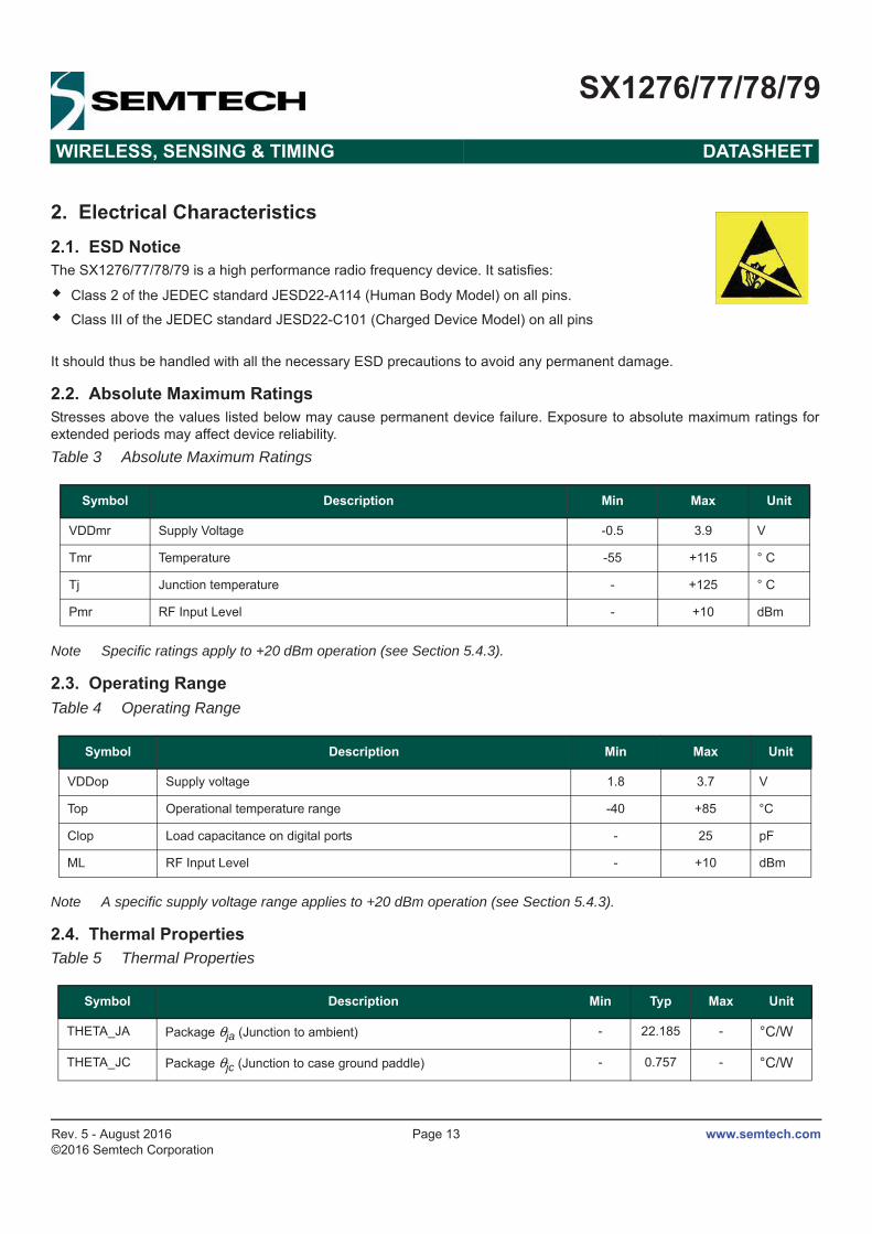
www.semtech.comPage 13
SX1276/77/78/79
WIRELESS, SENSING & TIMING DATASHEET
Rev. 5 - August 2016©2016 Semtech Corporation
2. Electrical Characteristics2.1. ESD NoticeThe SX1276/77/78/79 is a high performance radio frequency device. It satisfies:
Class 2 of the JEDEC standard JESD22-A114 (Human Body Model) on all pins.
Class III of the JEDEC standard JESD22-C101 (Charged Device Model) on all pins
It should thus be handled with all the necessary ESD precautions to avoid any permanent damage.
2.2. Absolute Maximum RatingsStresses above the values listed below may cause permanent device failure. Exposure to absolute maximum ratings for extended periods may affect device reliability.Table 3 Absolute Maximum Ratings
Note Specific ratings apply to +20 dBm operation (see Section 5.4.3).
2.3. Operating RangeTable 4 Operating Range
Note A specific supply voltage range applies to +20 dBm operation (see Section 5.4.3).
2.4. Thermal PropertiesTable 5 Thermal Properties
Symbol Description Min Max Unit
VDDmr Supply Voltage -0.5 3.9 V
Tmr Temperature -55 +115 ° C
Tj Junction temperature - +125 ° C
Pmr RF Input Level - +10 dBm
Symbol Description Min Max Unit
VDDop Supply voltage 1.8 3.7 V
Top Operational temperature range -40 +85 °C
Clop Load capacitance on digital ports - 25 pF
ML RF Input Level - +10 dBm
Symbol Description Min Typ Max Unit
THETA_JA Package θja (Junction to ambient) - 22.185 - °C/W
THETA_JC Package θjc (Junction to case ground paddle) - 0.757 - °C/W

www.semtech.comPage 14
SX1276/77/78/79
WIRELESS, SENSING & TIMING DATASHEET
Rev. 5 - August 2016©2016 Semtech Corporation
2.5. Chip SpecificationThe tables below give the electrical specifications of the transceiver under the following conditions: Supply voltage VDD=3.3 V, temperature = 25 °C, FXOSC = 32 MHz, FRF = 169/434/868/915 MHz (see specific indication), Pout = +13dBm, 2-level FSK modulation without pre-filtering, FDA = 5 kHz, Bit Rate = 4.8 kb/s and terminated in a matched 50 Ohm impedance, shared Rx and Tx path matching, unless otherwise specified.
Note Specification whose symbol is appended with “_LF” corresponds to the performance in Band 2 and/or Band 3, as described in section 5.3.3. “_HF” refers to the upper Band 1
2.5.1. Power ConsumptionTable 6 Power Consumption Specification
2.5.2. Frequency SynthesisTable 7 Frequency Synthesizer Specification
Symbol Description Conditions Min Typ Max Unit
IDDSL Supply current in Sleep mode - 0.2 1 uA
IDDIDLE Supply current in Idle mode RC oscillator enabled - 1.5 - uA
IDDST Supply current in Standby mode Crystal oscillator enabled - 1.6 1.8 mA
IDDFS Supply current in Synthesizer mode FSRx - 5.8 - mA
IDDR Supply current in Receive modeLnaBoost Off, band 1LnaBoost On, band 1Bands 2&3
---
10.811.512.0
---
mA
IDDT Supply current in Transmit mode with impedance matching
RFOP = +20 dBm, on PA_BOOSTRFOP = +17 dBm, on PA_BOOSTRFOP = +13 dBm, on RFO_LF/HF pinRFOP = + 7 dBm, on RFO_LF/HF pin
----
120872920
----
mAmAmAmA
Symbol Description Conditions Min Typ Max Unit
FR Synthesizer frequency rangeBand 3
Programmable Band 2(*for SX1279) Band 1
137410
862 (*779)
---
175 (*160)525 (*480)1020 (*960)
MHz
FXOSC Crystal oscillator frequency - 32 - MHz
TS_OSC Crystal oscillator wake-up time - 250 - us
TS_FS Frequency synthesizer wake-up time to PllLock signal From Standby mode - 60 - us

www.semtech.comPage 15
SX1276/77/78/79
WIRELESS, SENSING & TIMING DATASHEET
Rev. 5 - August 2016©2016 Semtech Corporation
Note: For Maximum Bit rate, the maximum modulation index is 0.5.
TS_HOPFrequency synthesizer hop time at most 10 kHz away from the target frequency
200 kHz step1 MHz step5 MHz step7 MHz step
12 MHz step20 MHz step25 MHz step
-------
20205050505050
-------
ususususususus
FSTEP Frequency synthesizer step FSTEP = FXOSC/219 - 61.0 - Hz
FRC RC Oscillator frequency After calibration - 62.5 - kHz
BRF Bit rate, FSK Programmable values (1) 1.2 - 300 kbps
BRA Bit rate Accuracy, FSK ABS(wanted BR - available BR) - - 250 ppm
BRO Bit rate, OOK Programmable 1.2 - 32.768 kbps
BR_L Bit rate, LoRa Mode From SF6, BW=500kHz toSF12, BW=7.8kHz
0.018 - 37.5 kbps
FDA Frequency deviation, FSK (1) ProgrammableFDA + BRF/2 =< 250 kHz
0.6 - 200 kHz

www.semtech.comPage 16
SX1276/77/78/79
WIRELESS, SENSING & TIMING DATASHEET
Rev. 5 - August 2016©2016 Semtech Corporation
2.5.3. FSK/OOK Mode ReceiverAll receiver tests are performed with RxBw = 10 kHz (Single Side Bandwidth) as programmed in RegRxBw, receiving a PN15 sequence. Sensitivities are reported for a 0.1% BER (with Bit Synchronizer enabled), unless otherwise specified. Blocking tests are performed with an unmodulated interferer. The wanted signal power for the Blocking Immunity, ACR, IIP2, IIP3 and AMR tests is set 3 dB above the receiver sensitivity level.
Table 8 FSK/OOK Receiver Specification
Symbol Description Conditions Min Typ Max Unit
RFS_F_LF
Direct tie of RFI and RFO pins, shared Rx, Tx paths FSK sensitiv-ity, highest LNA gain.Bands 2&3
FDA = 5 kHz, BR = 1.2 kb/sFDA = 5 kHz, BR = 4.8 kb/sFDA = 40 kHz, BR = 38.4 kb/s*FDA = 20 kHz, BR = 38.4 kb/s**FDA = 62.5 kHz, BR = 250 kb/s***
-----
-121-117-107-108-95
-----
dBmdBmdBmdBmdBm
Split RF paths, the RF switch insertion loss is not accounted for.Bands 2&3
FDA = 5 kHz, BR = 1.2 kb/sFDA = 5 kHz, BR = 4.8 kb/sFDA = 40 kHz, BR = 38.4 kb/s*FDA = 20 kHz, BR = 38.4 kb/s**FDA = 62.5 kHz, BR = 250 kb/s***
-----
-123-119-109-110-97
-----
dBmdBmdBmdBmdBm
RFS_F_HF
Direct tie of RFI and RFO pins, shared Rx, Tx paths FSK sensitiv-ity, highest LNA gain.Band 1
FDA = 5 kHz, BR = 1.2 kb/sFDA = 5 kHz, BR = 4.8 kb/sFDA = 40 kHz, BR = 38.4 kb/s*FDA = 20 kHz, BR = 38.4 kb/s**FDA = 62.5 kHz, BR = 250 kb/s***
-----
-119-115-105-105-92
-----
dBmdBmdBmdBmdBm
Split RF paths, LnaBoost is turned on, the RF switch insertion loss is not accounted for.Band 1
FDA = 5 kHz, BR = 1.2 kb/sFDA = 5 kHz, BR = 4.8 kb/sFDA = 40 kHz, BR = 38.4 kb/s*FDA = 20 kHz, BR = 38.4 kb/s**FDA = 62.5 kHz, BR = 250 kb/s***
-----
-123-119-109-109-96
-----
dBmdBmdBmdBmdBm
RFS_O OOK sensitivity, highest LNA gainshared Rx, Tx paths
BR = 4.8 kb/sBR = 32 kb/s
--
-117-108
--
dBmdBm
CCR Co-Channel Rejection, FSK - -9 - dB
ACR Adjacent Channel Rejection
FDA = 5 kHz, BR=4.8kb/sOffset = +/- 25 kHz or +/- 50kHz
Band 1 Band 2Band 3
---
505660
---
dBdBdB
BI_HF Blocking Immunity, Band 1Offset = +/- 1 MHzOffset = +/- 2 MHzOffset = +/- 10 MHz
---
717684
---
dBdBdB
BI_LF Blocking Immunity, Bands 2&3Offset = +/- 1 MHzOffset = +/- 2 MHzOffset = +/- 10 MHz
---
717278
---
dBdBdB

www.semtech.comPage 17
SX1276/77/78/79
WIRELESS, SENSING & TIMING DATASHEET
Rev. 5 - August 2016©2016 Semtech Corporation
* RxBw = 83 kHz (Single Side Bandwidth)
** RxBw = 50 kHz (Single Side Bandwidth)
*** RxBw = 250 kHz (Single Side Bandwidth)
2.5.4. FSK/OOK Mode TransmitterTable 9 Transmitter Specification
IIP22nd order Input Intercept PointUnwanted tones are 20 MHz above the LO
Highest LNA gain - +55 - dBm
IIP3_HF3rd order Input Intercept pointUnwanted tones are 1MHz and 1.995 MHz above the LO
Band 1Highest LNA gain G1LNA gain G2, 5dB sensitivity hit
--
-11-6
--
dBmdBm
IIP3_LF3rd order Input Intercept pointUnwanted tones are 1MHz and 1.995 MHz above the LO
Band 2Highest LNA gain G1LNA gain G2, 2.5dB sensitivity hit
--
-22-15
--
dBmdBm
Band 3Highest LNA gain G1LNA gain G2, 2.5dB sensitivity hit
--
-15-11
--
dBmdBm
BW_SSB Single Side channel filter BW Programmable 2.7 - 250 kHz
IMR Image Rejection Wanted signal 3dB over sensitivityBER=0.1% - 50 - dB
IMA Image Attenuation - 57 - dB
DR_RSSI RSSI Dynamic Range AGC enabled Min Max
--
-1270
--
dBmdBm
Symbol Description Conditions Min Typ Max Unit
RF_OP RF output power in 50 ohmson RFO pin (High efficiency PA).
Programmable with steps Max Min
--
+14-1
--
dBmdBm
RF_OP_V
RF output power stability on RFO pin versus voltage supply.
VDD = 2.5 V to 3.3 V VDD = 1.8 V to 3.7 V
--
38
--
dBdB
RF_OPH RF output power in 50 ohms, on PA_BOOST pin (Regulated PA).
Programmable with 1dB steps MaxMin
--
+17+2
--
dBmdBm
RF_OPH_MAX
Max RF output power, onPA_BOOST pin High power mode - +20 - dBm
RF_OPH_V
RF output power stability on PA_-BOOST pin versus voltage supply. VDD = 2.4 V to 3.7 V - +/-1 - dB
RF_TRF output power stability versus temperature on PA_BOOST pin. From T = -40 °C to +85 °C - +/-1 - dB

www.semtech.comPage 18
SX1276/77/78/79
WIRELESS, SENSING & TIMING DATASHEET
Rev. 5 - August 2016©2016 Semtech Corporation
PHN Transmitter Phase Noise
169 MHz, Band 3 10kHz Offset 50kHz Offset 400kHz Offset 1MHz Offset
----
-118-118-128-134
----
dBc/Hz
433 MHz, Band 2 10kHz Offset 50kHz Offset 400kHz Offset 1MHz Offset
----
-110-110-122 -129
----
dBc/Hz
868/915 MHz, Band 1 10kHz Offset 50kHz Offset 400kHz Offset 1MHz Offset
----
-103-103-115 -122
----
dBc/Hz
ACP Transmitter adjacent channel power (measured at 25 kHz offset)
BT=1. Measurement conditions as defined by EN 300 220-1 V2.3.1 - - -37 dBm
TS_TR Transmitter wake up time, to the first rising edge of DCLK
Frequency Synthesizer enabled, PaR-amp = 10us, BR = 4.8 kb/s - 120 - us

www.semtech.comPage 19
SX1276/77/78/79
WIRELESS, SENSING & TIMING DATASHEET
Rev. 5 - August 2016©2016 Semtech Corporation
2.5.5. Electrical Specification for LoRaTM ModulationThe table below gives the electrical specifications for the transceiver operating with LoRaTM modulation. Following conditions apply unless otherwise specified:
Supply voltage = 3.3 VTemperature = 25° CfXOSC = 32 MHzbandwidth (BW) = 125 kHzSpreading Factor (SF) = 12Error Correction Code (EC) = 4/6Packet Error Rate (PER)= 1%CRC on payload enabledOutput power = 13 dBm in transmissionPayload length = 64 bytesPreamble Length = 12 symbols (programmed register PreambleLength=8)With matched impedances
Table 10 LoRa Receiver Specification
Symbol Description Conditions Min. Typ Max Unit
IDDR_L Supply current in receiver LoRaTM mode, LnaBoost off
Bands 2&3, BW=7.8 to 62.5 kHzBands 2&3, BW = 125 kHzBands 2&3, BW = 250 kHzBands 2&3, BW = 500 kHz
----
11.011.512.413.8
----
mAmAmAmA
Band 1, BW=7.8 to 62.5 kHzBand 1, BW = 125 kHzBand 1, BW = 250 kHzBand 1, BW = 500 kHz
----
9.910.311.112.6
----
mAmAmAmA
IDDT_L Supply current in transmitter mode RFOP = 13 dBmRFOP = 7 dBm
--
2820
--
mAmA
IDDT_H_LSupply current in transmitter mode with an external impedance transformation
Using PA_BOOST pinRFOP = 17 dBm - 90 - mA
BI_L Blocking immunity,CW interferer
offset = +/- 1 MHzoffset = +/- 2 MHzoffset = +/- 10 MHz
-8994
100-
dBdBdB
IIP2_L2nd order Input Intercept PointUnwanted tones are 20 MHz above the LO
Highest LNA gain - +55 - dBm
IIP3_L_HF3rd order Input Intercept pointUnwanted tones are 1MHz and 1.995 MHz above the LO
Band 1Highest LNA gain G1LNA gain G2, 5dB sensitivity hit
--
-11-6
--
dBmdBm

www.semtech.comPage 20
SX1276/77/78/79
WIRELESS, SENSING & TIMING DATASHEET
Rev. 5 - August 2016©2016 Semtech Corporation
IIP3_L_LF3rd order Input Intercept pointUnwanted tones are 1MHz and 1.995 MHz above the LO
Band 2Highest LNA gain G1LNA gain G2,2.5dB sensitivity hit
--
-22-15
--
dBmdBm
RFS_L10_HF
RF sensitivity, Long-Range Mode, highest LNA gain, LnaBoost for Band 1, using split Rx/Tx path10.4 kHz bandwidth
SF = 6SF = 7SF = 8SF = 11
----
-131-134-138-146
----
dBmdBmdBmdBm
RFS_L62_HF
RF sensitivity, Long-Range Mode, highest LNA gain, LnaBoost for Band 1, using split Rx/Tx path62.5 kHz bandwidth
SF = 6SF = 7SF = 8SF = 9SF = 10SF = 11SF = 12
-------
-121-126-129-132-135-137-139
-------
dBmdBmdBmdBmdBmdBmdBm
RFS_L125_HF
RF sensitivity, Long-Range Mode, highest LNA gain, LnaBoost for Band 1, using split Rx/Tx path125 kHz bandwidth
SF = 6SF = 7SF = 8SF = 9SF = 10SF = 11SF = 12
-------
-118-123-126-129-132-133-136
-------
dBmdBmdBmdBmdBmdBmdBm
RFS_L250_HF
RF sensitivity, Long-Range Mode, highest LNA gain, LnaBoost for Band 1, using split Rx/Tx path250 kHz bandwidth
SF = 6SF = 7SF = 8SF = 9SF = 10SF = 11SF = 12
-------
-115-120-123-125-128-130-133
-------
dBmdBmdBmdBmdBmdBmdBm
RFS_L500_HF
RF sensitivity, Long-Range Mode, highest LNA gain, LnaBoost for Band 1, using split Rx/Tx path500 kHz bandwidth
SF = 6SF = 7SF = 8SF = 9SF = 10SF = 11SF = 12
-------
-111-116-119-122-125-128-130
-------
dBmdBmdBmdBmdBmdBmdBm
RFS_L7.8_LF
RF sensitivity, Long-Range Mode, highest LNA gain, Band 2 or 3, using split Rx/Tx path7.8 kHz bandwidth
SF = 12SF = 11
--
-148-145
--
dBmdBm
RFS_L10_LFRF sensitivity, Long-Range Mode, highest LNA gain, Band 3,10.4 kHz bandwidth
SF = 6SF = 7SF = 8
---
-132-136-138
---
dBmdBmdBm
RFS_L62_LFRF sensitivity, Long-Range Mode, highest LNA gain, Band 3, 62.5 kHz bandwidth
SF = 6SF = 7SF = 8SF = 9SF = 10SF = 11SF = 12
-------
-123-128-131-134-135-137-140
-------
dBmdBmdBmdBmdBmdBmdBm
Symbol Description Conditions Min. Typ Max Unit

www.semtech.comPage 21
SX1276/77/78/79
WIRELESS, SENSING & TIMING DATASHEET
Rev. 5 - August 2016©2016 Semtech Corporation
RFS_L125_LFRF sensitivity, Long-Range Mode, highest LNA gain, Band 3,125 kHz bandwidth
SF = 6SF = 7SF = 8SF = 9SF = 10SF = 11SF = 12
-------
-121-125-128-131-134-136-137
-------
dBmdBmdBmdBmdBmdBmdBm
RFS_L250_LFRF sensitivity, Long-Range Mode, highest LNA gain, Band 3250 kHz bandwidth
SF = 6SF = 7SF = 8SF = 9SF = 10SF = 11SF = 12
-------
-118-122-125-128-131-133-134
-------
dBmdBmdBmdBmdBmdBmdBm
RFS_L500_LFRF sensitivity, Long-Range Mode, highest LNA gain, Band 3500 kHz bandwidth
SF = 6SF = 7SF = 8SF = 9SF = 10SF = 11SF = 12
-------
-112-118-121-124-127-129-130
-------
dBmdBmdBmdBmdBmdBmdBm
CCR_LCWCo-channel rejectionSingle CW tone = Sens +6 dB1% PER
SF = 7SF = 8SF = 9SF = 10SF = 11SF = 12
------
59.512
14.417
19.5
------
dBdBdBdBdBdB
CCR_LL Co-channel rejectionInterferer is a LoRaTM signal using same BW and same SF.Pw = Sensitivity + 3 dB
-6
dB
ACR_LCW Adjacent channel rejection
Interferer is 1.5*BW_L from the wanted signal center frequency1% PER, Single CW tone = Sens + 3 dB
SF = 7SF = 12
--
6072
--
dBdB
IMR_LCW Image rejection after calibration. 1% PER, Single CW tone = Sens +3 dB - 66 - dB
FERR_L
Maximum tolerated frequency offset between transmitter and receiver, no sensitivity degradation, SF6 thru 12
All BW, +/-25% of BWThe tighter limit applies (see below)
+/-25% BW
Maximum tolerated frequency offset between transmitter and receiver, no sensitivity degradation, SF10 thru 12
SF = 12SF = 11SF = 10
-50-100-200
---
50100200
ppmppmppm
Symbol Description Conditions Min. Typ Max Unit

www.semtech.comPage 22
SX1276/77/78/79
WIRELESS, SENSING & TIMING DATASHEET
Rev. 5 - August 2016©2016 Semtech Corporation
2.5.6. Digital SpecificationConditions: Temp = 25° C, VDD = 3.3 V, FXOSC = 32 MHz, unless otherwise specified.
Table 11 Digital Specification
Symbol Description Conditions Min Typ Max Unit
VIH Digital input level high 0.8 - - VDD
VIL Digital input level low - - 0.2 VDD
VOH Digital output level high Imax = 1 mA 0.9 - - VDD
VOL Digital output level low Imax = -1 mA - - 0.1 VDD
FSCK SCK frequency - - 10 MHz
tch SCK high time 50 - - ns
tcl SCK low time 50 - - ns
trise SCK rise time - 5 - ns
tfall SCK fall time - 5 - ns
tsetup MOSI setup time From MOSI change to SCK rising edge.
30 - - ns
thold MOSI hold time From SCK rising edge to MOSI change.
20 - - ns
tnsetup NSS setup time From NSS falling edge to SCK rising edge.
30 - - ns
tnhold NSS hold time From SCK falling edge to NSS rising edge, normal mode.
100 - - ns
tnhigh NSS high time between SPI accesses
20 - - ns
T_DATA DATA hold and setup time 250 - - ns

www.semtech.comPage 23
SX1276/77/78/79
WIRELESS, SENSING & TIMING DATASHEET
Rev. 5 - August 2016©2016 Semtech Corporation
3. SX1276/77/78/79 FeaturesThis section gives a high-level overview of the functionality of the SX1276/77/78/79 low-power, highly integrated transceiver. The following figure shows a simplified block diagram of the SX1276/77/78/79.
Figure 4. SX1276/77/78/79 Block Schematic Diagram
SX1276/77/78/79 is a half-duplex, low-IF transceiver. Here the received RF signal is first amplified by the LNA. The LNA inputs are single ended to minimize the external BoM and for ease of design. Following the LNA inputs, the conversion to differential is made to improve the second order linearity and harmonic rejection. The signal is then down-converted to in-phase and quadrature (I&Q) components at the intermediate frequency (IF) by the mixer stage. A pair of sigma delta ADCs then perform data conversion, with all subsequent signal processing and demodulation performed in the digital domain. The digital state machine also controls the automatic frequency correction (AFC), received signal strength indicator (RSSI) and automatic gain control (AGC). It also features the higher-level packet and protocol level functionality of the top level sequencer (TLS), only available with traditional FSK and OOK modulation schemes.
The frequency synthesizers generate the local oscillator (LO) frequency for both receiver and transmitter, one covering the lower UHF bands (up to 525 MHz), and the other one covering the upper UHF bands (from 779 MHz). The PLLs are optimized for user-transparent low lock time and fast auto-calibrating operation. In transmission, frequency modulation is performed digitally within the PLL bandwidth. The PLL also features optional pre-filtering of the bit stream to improve spectral purity.
SX1276/77/78/79 feature three distinct RF power amplifiers. Two of those, connected to RFO_LF and RFO_HF, can deliver up to +14 dBm, are unregulated for high power efficiency and can be connected directly to their respective RF receiver inputs via a pair of passive components to form a single antenna port high efficiency transceiver. The third PA, connected to the PA_BOOST pin and can deliver up to +20 dBm via a dedicated matching network. Unlike the high efficiency PAs, this high-stability PA covers all frequency bands that the frequency synthesizer addresses.
SX1276/77/78/79 also include two timing references, an RC oscillator and a 32 MHz crystal oscillator.

www.semtech.comPage 24
SX1276/77/78/79
WIRELESS, SENSING & TIMING DATASHEET
Rev. 5 - August 2016©2016 Semtech Corporation
All major parameters of the RF front end and digital state machine are fully configurable via an SPI interface which gives access to SX1276/77/78/79’s configuration registers. This includes a mode auto sequencer that oversees the transition and calibration of the SX1276/77/78/79 between intermediate modes of operation in the fastest time possible.
The SX1276/77/78/79 are equipped with both standard FSK and long range spread spectrum (LoRaTM) modems. Depending upon the mode selected either conventional OOK or FSK modulation may be employed or the LoRaTM spread spectrum modem.
3.1. LoRaTM ModemThe LoRaTM modem uses a proprietary spread spectrum modulation technique. This modulation, in contrast to legacy modulation techniques, permits an increase in link budget and increased immunity to in-band interference. At the same time the frequency tolerance requirement of the crystal reference oscillator is relaxed - allowing a performance increase for a reduction in system cost. For a detailed description of the design trade-offs and operation of the SX1276/77/78/79 please consult Section 4.1 of the datasheet.
3.2. FSK/OOK ModemIn FSK/OOK mode the SX1276/77/78/79 supports standard modulation techniques including OOK, FSK, GFSK, MSK and GMSK. The SX1276/77/78/79 is especially suited to narrow band communication thanks the low-IF architecture employed and the built-in AFC functionality. For full information on the FSK/OOK modem please consult Section 4.2 of this document.

www.semtech.comPage 25
SX1276/77/78/79
WIRELESS, SENSING & TIMING DATASHEET
Rev. 5 - August 2016©2016 Semtech Corporation
4. SX1276/77/78/79 Digital Electronics
4.1. The LoRaTM ModemThe LoRaTM modem uses spread spectrum modulation and forward error correction techniques to increase the range and robustness of radio communication links compared to traditional FSK or OOK based modulation. Examples of the performance improvement possible, for several possible settings, are summarised in the table below. Here the spreading factor and error correction rate are design variables that allow the designer to optimise the trade-off between occupied bandwidth, data rate, link budget improvement and immunity to interference.
Table 12 Example LoRaTM Modem Performances, 868MHz Band
Notes - for all bandwidths lower than 62.5 kHz, it is advised to use a TCXO as a frequency reference. This is required to meet the frequency error tolerance specifications given in the Electrical Specification
- Higher spreading factors and longer transmission times impose more stringent constraints on the short term frequency stability of the reference. Please get in touch with a Semtech representative to implement extremely low sensitivity products.
For European operation the range of crystal tolerances acceptable for each sub-band (of the ERC 70-03) is given in the specifications table. For US based operation a frequency hopping mode is available that automates both the LoRaTM
spread spectrum and frequency hopping spread spectrum processes.
Another important facet of the LoRaTM modem is its increased immunity to interference. The LoRaTM modem is capable of co-channel GMSK rejection of up to 20 dB. This immunity to interference permits the simple coexistence of LoRaTM
modulated systems either in bands of heavy spectral usage or in hybrid communication networks that use LoRaTM to extend range when legacy modulation schemes fail.
Bandwidth(kHz) Spreading Factor Coding rate Nominal Rb
(bps)
Sensitivityindication
(dBm)
FrequencyReference
10.4 6 4/5 782 -131
TCXO12 4/5 24 -147
20.8 6 4/5 1562 -12812 4/5 49 -144
62.5 6 4/5 4688 -121
XTAL12 4/5 146 -139
125 6 4/5 9380 -11812 4/5 293 -136

www.semtech.comPage 26
SX1276/77/78/79
WIRELESS, SENSING & TIMING DATASHEET
Rev. 5 - August 2016©2016 Semtech Corporation
4.1.1. Link Design Using the LoRaTM Modem
4.1.1.1. Overview
The LoRaTM modem is setup as shown in the following figure. This configuration permits the simple replacement of the FSK modem with the LoRaTM modem via the configuration register setting RegOpMode. This change can be performed on the fly (in Sleep operating mode) thus permitting the use of both standard FSK or OOK in conjunction with the long range capability. The LoRaTM modulation and demodulation process is proprietary, it uses a form of spread spectrum modulation combined with cyclic error correction coding. The combined influence of these two factors is an increase in link budget and enhanced immunity to interference.
Figure 5. LoRaTM Modem Connectivity
A simplified outline of the transmit and receive processes is also shown above. Here we see that the LoRaTM modem has an independent dual port data buffer FIFO that is accessed through an SPI interface common to all modes. Upon selection of LoRaTM mode, the configuration register mapping of the SX1276/77/78/79 changes. For full details of this change please consult the register description of Section 6.
So that it is possible to optimise the LoRaTM modulation for a given application, access is given to the designer to three critical design parameters. Each one permitting a trade off between link budget, immunity to interference, spectral occupancy and nominal data rate. These parameters are spreading factor, modulation bandwidth and error coding rate.

www.semtech.comPage 27
SX1276/77/78/79
WIRELESS, SENSING & TIMING DATASHEET
Rev. 5 - August 2016©2016 Semtech Corporation
4.1.1.2. Spreading Factor
The spread spectrum LoRaTM modulation is performed by representing each bit of payload information by multiple chips of information. The rate at which the spread information is sent is referred to as the symbol rate (Rs), the ratio between the nominal symbol rate and chip rate is the spreading factor and represents the number of symbols sent per bit of information. The range of values accessible with the LoRaTM modem are shown in the following table.
Table 13 Range of Spreading Factors
Note that the spreading factor, SpreadingFactor, must be known in advance on both transmit and receive sides of the link as different spreading factors are orthogonal to each other. Note also the resulting signal to noise ratio (SNR) required at the receiver input. It is the capability to receive signals with negative SNR that increases the sensitivity, so link budget and range, of the LoRa receiver.
Spreading Factor 6SF = 6 Is a special use case for the highest data rate transmission possible with the LoRa modem. To this end several settings must be activated in the SX1276/77/78/79 registers when it is in use. These settings are only valid for SF6 and should be set back to their default values for other spreading factors:
Set SpreadingFactor = 6 in RegModemConfig2
The header must be set to Implicit mode.
Set the bit field DetectionOptimize of register RegLoRaDetectOptimize to value "0b101".
Write 0x0C in the register RegDetectionThreshold.
4.1.1.3. Coding Rate
To further improve the robustness of the link the LoRaTM modem employs cyclic error coding to perform forward error detection and correction. Such error coding incurs a transmission overhead - the resultant additional data overhead per transmission is shown in the table below.
Table 14 Cyclic Coding Overhead
SpreadingFactor(RegModulationCfg)
Spreading Factor (Chips / symbol)
LoRa Demodulator SNR
6 64 -5 dB7 128 -7.5 dB8 256 -10 dB9 512 -12.5 dB10 1024 -15 dB11 2048 -17.5 dB12 4096 -20 dB
CodingRate(RegTxCfg1)
Cyclic Coding Rate Overhead Ratio
1 4/5 1.252 4/6 1.53 4/7 1.754 4/8 2

www.semtech.comPage 28
SX1276/77/78/79
WIRELESS, SENSING & TIMING DATASHEET
Rev. 5 - August 2016©2016 Semtech Corporation
Forward error correction is particularly efficient in improving the reliability of the link in the presence of interference. So that the coding rate (and so robustness to interference) can be changed in response to channel conditions - the coding rate can optionally be included in the packet header for use by the receiver. Please consult Section 4.1.1.6 for more information on the LoRaTM packet and header.
4.1.1.4. Signal BandwidthAn increase in signal bandwidth permits the use of a higher effective data rate, thus reducing transmission time at the expense of reduced sensitivity improvement. There are of course regulatory constraints in most countries on the permissible occupied bandwidth. Contrary to the FSK modem which is described in terms of the single sideband bandwidth, the LoRaTM modem bandwidth refers to the double sideband bandwidth (or total channel bandwidth). The range of bandwidths relevant to most regulatory situations is given in the LoRaTM modem specifications table (see Section 2.5.5).
Table 15 LoRa Bandwidth Options
Note In the lower band (169 MHz), the 250 kHz and 500 kHz bandwidths are not supported.
4.1.1.5. LoRaTM Transmission Parameter Relationship
With a knowledge of the key parameters that can be controlled by the user we define the LoRaTM symbol rate as:
where BW is the programmed bandwidth and SF is the spreading factor. The transmitted signal is a constant envelope signal. Equivalently, one chip is sent per second per Hz of bandwidth.
Bandwidth(kHz) Spreading Factor Coding rate Nominal Rb
(bps)7.8 12 4/5 1810.4 12 4/5 2415.6 12 4/5 3720.8 12 4/5 4931.2 12 4/5 7341.7 12 4/5 9862.5 12 4/5 146125 12 4/5 293250 12 4/5 586500 12 4/5 1172
Rs BW2SF---------=

www.semtech.comPage 29
SX1276/77/78/79
WIRELESS, SENSING & TIMING DATASHEET
Rev. 5 - August 2016©2016 Semtech Corporation
4.1.1.6. LoRaTM Packet Structure
The LoRaTM modem employs two types of packet format, explicit and implicit. The explicit packet includes a short header that contains information about the number of bytes, coding rate and whether a CRC is used in the packet. The packet format is shown in the following figure. The LoRaTM packet comprises three elements:
A preamble.An optional header.The data payload.
Figure 6. LoRaTM Packet Structure
PreambleThe preamble is used to synchronize receiver with the incoming data flow. By default the packet is configured with a 12 symbol long sequence. This is a programmable variable so the preamble length may be extended, for example in the interest of reducing to receiver duty cycle in receive intensive applications. However, the minimum length suffices for all communication. The transmitted preamble length may be changed by setting the register PreambleLength from 6 to 65535, yielding total preamble lengths of 6+4 to 65535+4 symbols, once the fixed overhead of the preamble data is considered. This permits the transmission of a near arbitrarily long preamble sequence.The receiver undertakes a preamble detection process that periodically restarts. For this reason the preamble length should be configured identical to the transmitter preamble length. Where the preamble length is not known, or can vary, the maximum preamble length should be programmed on the receiver side.
HeaderDepending upon the chosen mode of operation two types of header are available. The header type is selected by the ImplicitHeaderModeOn bit found within the RegModemConfig1 register.
Explicit Header ModeThis is the default mode of operation. Here the header provides information on the payload, namely:
The payload length in bytes.
The forward error correction code rate
The presence of an optional 16-bits CRC for the payload.

www.semtech.comPage 30
SX1276/77/78/79
WIRELESS, SENSING & TIMING DATASHEET
Rev. 5 - August 2016©2016 Semtech Corporation
The header is transmitted with maximum error correction code (4/8). It also has its own CRC to allow the receiver to discard invalid headers.
Implicit Header ModeIn certain scenarios, where the payload, coding rate and CRC presence are fixed or known in advance, it may be advantageous to reduce transmission time by invoking implicit header mode. In this mode the header is removed from the packet. In this case the payload length, error coding rate and presence of the payload CRC must be manually configured on both sides of the radio link.
Note With SF = 6 selected, implicit header mode is the only mode of operation possible.
Explicit Header Mode:In Explicit Header Mode, the presence of the CRC at the end of the payload in selected only on the transmitter side through the bit RxPayloadCrcOn in the register RegModemConfig1. On the receiver side, the bit RxPayloadCrcOn in the register RegModemConfig1 is not used and once the payload has been received, the user should check the bit CrcOnPayload in the register RegHopChannel. If the bit CrcOnPayload is at ‘1’, the user should then check the Irq Flag PayloadCrcError to make sure the CRC is valid.If the bit CrcOnPayload is at ‘0’, it means there was no CRC on the payload and thus the IRQ Flag PayloadCrcError will not be trigged even if the payload has errors.
Implicit Header Mode;In Implicit Header Mode, it is necessary to set the bit RxPayloadCrcOn in the register RegModemConfig1 on both sides (TX and RX)
Explicit Header Transmitter Receiver CRC Status
Value of the bit RxPayloadCrcOn
0 0 CRC is not checked
0 1 CRC is not checked
1 0 CRC is checked
1 1 CRC is checked
Implicit Header Transmitter Receiver CRC Status
Value of the bit RxPayloadCrcOn
0 0 CRC is not checked
0 1 CRC is always wrong
1 0 CRC is not checked
1 1 CRC is checked

www.semtech.comPage 31
SX1276/77/78/79
WIRELESS, SENSING & TIMING DATASHEET
Rev. 5 - August 2016©2016 Semtech Corporation
Low Data Rate OptimizationGiven the potentially long duration of the packet at high spreading factors the option is given to improve the robustness of the transmission to variations in frequency over the duration of the packet transmission and reception. The bit LowDataRateOptimize increases the robustness of the LoRa link at these low effective data rates. Its use is mandated when the symbol duration exceeds 16ms. Note that both the transmitter and the receiver must have the same setting for LowDataRateOptimize.
PayloadThe packet payload is a variable-length field that contains the actual data coded at the error rate either as specified in the header in explicit mode or in the register settings in implicit mode. An optional CRC may be appended. For more information on the payload and how it is loaded from the data buffer FIFO please see Section 4.1.2.3.
4.1.1.7. Time on airFor a given combination of spreading factor (SF), coding rate (CR) and signal bandwidth (BW) the total on-the-air transmission time of a LoRaTM packet can be calculated as follows. From the definition of the symbol rate it is convenient to define the symbol rate:
The LoRa packet duration is the sum of the duration of the preamble and the transmitted packet. The preamble length is calculated as follows:
where npreamble is the programmed preamble length, taken from the registers RegPreambleMsb and RegPreambleLsb.The payload duration depends upon the header mode that is enabled. The following formula gives the number of payload symbols.
With the following dependencies:
PL is the number of Payload bytes (1 to 255)
SF is the spreading factor (6 to 12)
IH=0 when the header is enabled, IH=1 when no header is present
DE=1 when LowDataRateOptimize=1, DE=0 otherwise
CR is the coding rate (1 corresponding to 4/5, 4 to 4/8)The Payload duration is then the symbol period multiplied by the number of Payload symbols
The time on air, or packet duration, in simply then the sum of the preamble and payload duration.
Ts 1Rs------=
Tpreamble npreamble 4.25+( )Tsym=
npayload 8 max ceil 8PL 4SF– 28 16CRC 20IH–+ +( )4 SF 2DE–( )
---------------------------------------------------------------------------------------- CR 4+( ) 0,+=
Tpayload npayload Ts×=
Tpacket Tpreamble Tpayload+=

www.semtech.comPage 32
SX1276/77/78/79
WIRELESS, SENSING & TIMING DATASHEET
Rev. 5 - August 2016©2016 Semtech Corporation
4.1.1.8. Frequency Hopping with LoRaTM
Frequency hopping spread spectrum (FHSS) is typically employed when the duration of a single packet could exceed regulatory requirements relating to the maximum permissible channel dwell time. This is most notably the case in US operation where the 902 to 928 MHz ISM band which makes provision for frequency hopping operation. To ease the implementation of FHSS systems the frequency hopping mode of the LoRaTM modem can be enabled by setting FreqHoppingPeriod to a non-zero value in register RegHopPeriod.
Principle of OperationThe principle behind the FHSS scheme is that a portion of each LoRaTM packet is transmitted on each hopping channel from a look up table of frequencies managed by the host microcontroller. After a predetermined hopping period the transmitter and receiver change to the next channel in a predefined list of hopping frequencies to continue transmission and reception of the next portion of the packet. The time which the transmission will dwell in any given channel is determined by FreqHoppingPeriod which is an integer multiple of symbol periods:
The frequency hopping transmission and reception process starts at channel 0. The preamble and header are transmitted first on channel 0. At the beginning of each transmission the channel counter FhssPresentChannel (located in the registerRegHopChannel) is incremented and the interrupt signal FhssChangeChannel is generated. The new frequency must then be programmed within the hopping period to ensure it is taken into account for the next hop, the interrupt ChangeChannelFhss is then to be cleared by writing a logical ‘1’.
FHSS Reception always starts on channel 0. The receiver waits for a valid preamble detection before starting the frequency hopping process as described above. Note that in the eventuality of header CRC corruption, the receiver will automatically request channel 0 and recommence the valid preamble detection process.
Timing of Channel UpdatesThe interrupt requesting the channel change, FhssChangeChannel, is generated upon transition to the new frequency. The frequency hopping process is illustrated in the diagram below:
HoppingPeriod Ts FreqHoppingPeriod×=

www.semtech.comPage 33
SX1276/77/78/79
WIRELESS, SENSING & TIMING DATASHEET
Rev. 5 - August 2016©2016 Semtech Corporation
Figure 7. Interrupts Generated in the Case of Successful Frequency Hopping Communication.

www.semtech.comPage 34
SX1276/77/78/79
WIRELESS, SENSING & TIMING DATASHEET
Rev. 5 - August 2016©2016 Semtech Corporation
4.1.2. LoRaTM Digital InterfaceThe LoRaTM modem comprises three types of digital interface, static configuration registers, status registers and a FIFO data buffer. All are accessed through the SX1276/77/78/79’s SPI interface - full details of each type of register are given below. Full listings of the register addresses used for SPI access are given in Section 6.4.
4.1.2.1. LoRaTM Configuration RegistersConfiguration registers are accessed through the SPI interface. Registers are readable in all device mode including Sleep. However, they should be written only in Sleep and Standby modes. Please note that the automatic top level sequencer (TLS modes) are not available in LoRaTM mode and the configuration register mapping changes as shown in Table 41. The content of the LoRaTM configuration registers is retained in FSK/OOK mode. For the functionality of mode registers common to both FSK/OOK and LoRaTM mode, please consult the Analog and RF Front End section of this document (Section 5).
4.1.2.2. Status RegistersStatus registers provide status information during receiver operation.
4.1.2.3. LoRaTM Mode FIFO Data BufferOverviewThe SX1276/77/78/79 is equipped with a 256 byte RAM data buffer which is uniquely accessible in LoRa mode. This RAM area, herein referred to as the FIFO Data buffer, is fully customizable by the user and allows access to the received, or to be transmitted, data. All access to the LoRaTM FIFO data buffer is done via the SPI interface. A diagram of the user defined memory mapping of the FIFO data buffer is shown below. These FIFO data buffer can be read in all operating modes except sleep and store data related to the last receive operation performed. It is automatically cleared of old content upon each new transition to receive mode.
Figure 8. LoRaTM Data Buffer

www.semtech.comPage 35
SX1276/77/78/79
WIRELESS, SENSING & TIMING DATASHEET
Rev. 5 - August 2016©2016 Semtech Corporation
Principle of Operation
Thanks to its dual port configuration, it is possible to simultaneously store both transmit and receive information in the FIFO data buffer. The register RegFifoTxBaseAddr specifies the point in memory where the transmit information is stored. Similarly, for receiver operation, the register RegFifoRxBaseAddr indicates the point in the data buffer where information will be written to in event of a receive operation.
By default, the device is configured at power up so that half of the available memory is dedicated to Rx (RegFifoRxBaseAddr initialized at address 0x00) and the other half is dedicated for Tx (RegFifoTxBaseAddr initialized at address 0x80). However, due to the contiguous nature of the FIFO data buffer, the base addresses for Tx and Rx are fully configurable across the 256 byte memory area. Each pointer can be set independently anywhere within the FIFO. To exploit the maximum FIFO data buffer size in transmit or receive mode, the whole FIFO data buffer can be used in each mode by setting the base addresses RegFifoTxBaseAddr and RegFifoRxBaseAddr at the bottom of the memory (0x00).
The FIFO data buffer is cleared when the device is put in SLEEP mode, consequently no access to the FIFO data buffer is possible in sleep mode. However, the data in the FIFO data buffer are retained when switching across the other LoRaTM
modes of operation, so that a received packet can be retransmitted with minimum data handling on the controller side. The FIFO data buffer is not self-clearing (unless if the device is put in sleep mode) and the data will only be “erased” when a new set of data is written into the occupied memory location.
The FIFO data buffer location to be read from, or written to, via the SPI interface is defined by the address pointer RegFifoAddrPtr. Before any read or write operation it is hence necessary to initialize this pointer to the corresponding base value. Upon reading or writing to the FIFO data buffer (RegFifo) the address pointer will then increment automatically.
The register RegRxNbBytes defines the size of the memory location to be written in the event of a successful receive operation. The register RegPayloadLength indicates the size of the memory location to be transmitted. In implicit header mode, the register RegRxNbBytes is not used as the number of payload bytes is known. Otherwise, in explicit header mode, the initial size of the receive buffer is set to the packet length in the received header. The register RegFifoRxCurrentAddr indicates the location of the last packet received in the FIFO so that the last packet received can be easily read by pointing the register RegFifoAddrPtr to this register.
It is important to notice that all the received data will be written to the FIFO data buffer even if the CRC is invalid, permitting user defined post processing of corrupted data. It is also important to note that when receiving, if the packet size exceeds the buffer memory allocated for the Rx, it will overwrite the transmit portion of the data buffer.
4.1.2.4. Interrupts in LoRa Mode
Two registers are used to control the IRQ in LoRa mode, the register RegIrqFlagsMask which is used to mask the interrupts and the register RegIrqFlags which indicates which IRQ has been trigged.In the register RegIrqFlagsMask, setting a bit to ‘1’ will mask the interrupt, meaning this interrupt is disactivated. By default all the interrupt are available.In the register RegIrqFlags, a ‘1’ indicates a given IRQ has been trigged and then the IRQ must be clear by writing a ‘1’.

www.semtech.comPage 36
SX1276/77/78/79
WIRELESS, SENSING & TIMING DATASHEET
Rev. 5 - August 2016©2016 Semtech Corporation
4.1.3. Operation of the LoRaTM Modem
4.1.3.1. Operating Mode ControlThe operating modes of the LoRaTM modem are accessed by enabling LoRaTM mode (setting the LongRangeMode bit of RegOpMode). Depending upon the operating mode selected the range of functionality and register access is given by the following table:
Table 16 LoRaTM Operating Mode Functionality
It is possible to access any mode from any other mode by changing the value in the RegOpMode register.
Operating Mode Description
SLEEPLow-power mode. In this mode only SPI and configuration registers are accessible. Lora FIFO is not accessible.Note that this is the only mode permissible to switch between FSK/OOK mode and LoRa mode.
STANDBY both Crystal oscillator and Lora baseband blocks are turned on.RF part and PLLs are disabled
FSTX This is a frequency synthesis mode for transmission. The PLL selected for transmission is locked and active at the transmit frequency. The RF part is off.
FSRX This is a frequency synthesis mode for reception. The PLL selected for reception is locked and active at the receive frequency. The RF part is off.
TX When activated the SX1276/77/78/79 powers all remaining blocks required for transmit, ramps the PA, transmits the packet and returns to Standby mode.
RXCONTINUOUS When activated the SX1276/77/78/79 powers all remaining blocks required for reception, processing all received data until a new user request is made to change operating mode.
RXSINGLE When activated the SX1276/77/78/79 powers all remaining blocks required for reception, remains in this state until a valid packet has been received and then returns to Standby mode.
CAD When in CAD mode, the device will check a given channel to detect LoRa preamble signal

www.semtech.comPage 37
SX1276/77/78/79
WIRELESS, SENSING & TIMING DATASHEET
Rev. 5 - August 2016©2016 Semtech Corporation
4.1.4. Frequency Settings Recalling that the frequency step is given by:
In order to set LO frequency values following registers are available.Frf is a 24-bit register which defines carrier frequency. The carrier frequency relates to the register contents by following formula:
4.1.5. Frequency Error IndicationThe SX1276/77/78/79 derives its RF centre frequency from a crystal reference oscillator which has a finite frequency precision. Errors in reference frequency will manifest themselves as errors of the same proportion from the RF centre frequency.In LoRa receive mode the SX1276/77/78/79 is capable of measuring the frequency offset between the receiver centre frequency and that of an incoming LoRa signal. The modem is intolerant of frequency offsets in the region of +/- 25% of the bandwidth and will accurately report the error over this same range.
The error is read by reading the three RegFei registers. The contents of which are a signed 20 bit two's compliment word, FreqError. The frequency error is determined from the register contents by:
Where Fxtal is the crystal frequency.
To correct the measured frequency error there are two steps to be taken. First the frequency error is subtracted from the RF centre frequency. This calculation must be performed locally (or in a look-up-table), no provision is made in the circuit to apply the correction automatically.
Secondly, assuming that the frequency error is due to reference oscillator drift, the data rate of the LoRa modem must also be compensated accordingly. This is done by
PpmOffset = 0.95 * measured Offset [PPM]
Where PpmOffset is the value to be programmed into register 0x27 and the measured Offset is the PPM drift equivalent to the frequency error reported by the LoRa frequency error indicator. The PpmOffset value is a signed two’s compliment value.
FSTEPFXOSC
219----------------=
FRF FSTEP Frf 23 0( , )×=
FErrorFreqError 224×
Fxtal------------------------------------------ BW kHz[ ]
500------------------------×=

www.semtech.comPage 38
SX1276/77/78/79
WIRELESS, SENSING & TIMING DATASHEET
Rev. 5 - August 2016©2016 Semtech Corporation
4.1.6. LoRaTM Modem State Machine SequencesThe sequence for transmission and reception of data to and from the LoRaTM modem, together with flow charts of typical sequences of operation, are detailed below.
Data Transmission SequenceIn transmit mode power consumption is optimized by enabling RF, PLL and PA blocks only when packet data needs to be transmitted. Figure 9 shows a typical LoRaTM transmit sequence.
Figure 9. LoRaTM Modulation Transmission Sequence.
Static configuration registers can only be accessed in Sleep mode, Standby mode or FSTX mode.
The LoRaTM FIFO can only be filled in Standby mode.
Data transmission is initiated by sending TX mode request.
Upon completion the TxDone interrupt is issued and the radio returns to Standby mode.
Following transmission the radio can be manually placed in Sleep mode or the FIFO refilled for a subsequent Tx operation.

www.semtech.comPage 39
SX1276/77/78/79
WIRELESS, SENSING & TIMING DATASHEET
Rev. 5 - August 2016©2016 Semtech Corporation
LoRaTM Transmit Data FIFO FillingIn order to write packet data into FIFO user should:1 Set FifoPtrAddr to FifoTxPtrBase.2 Write PayloadLength bytes to the FIFO (RegFifo)
Data Reception SequenceFigure 10 shows typical LoRaTM receive sequences for both single and continuous receiver modes of operation.
Figure 10. LoRaTM Receive Sequence.
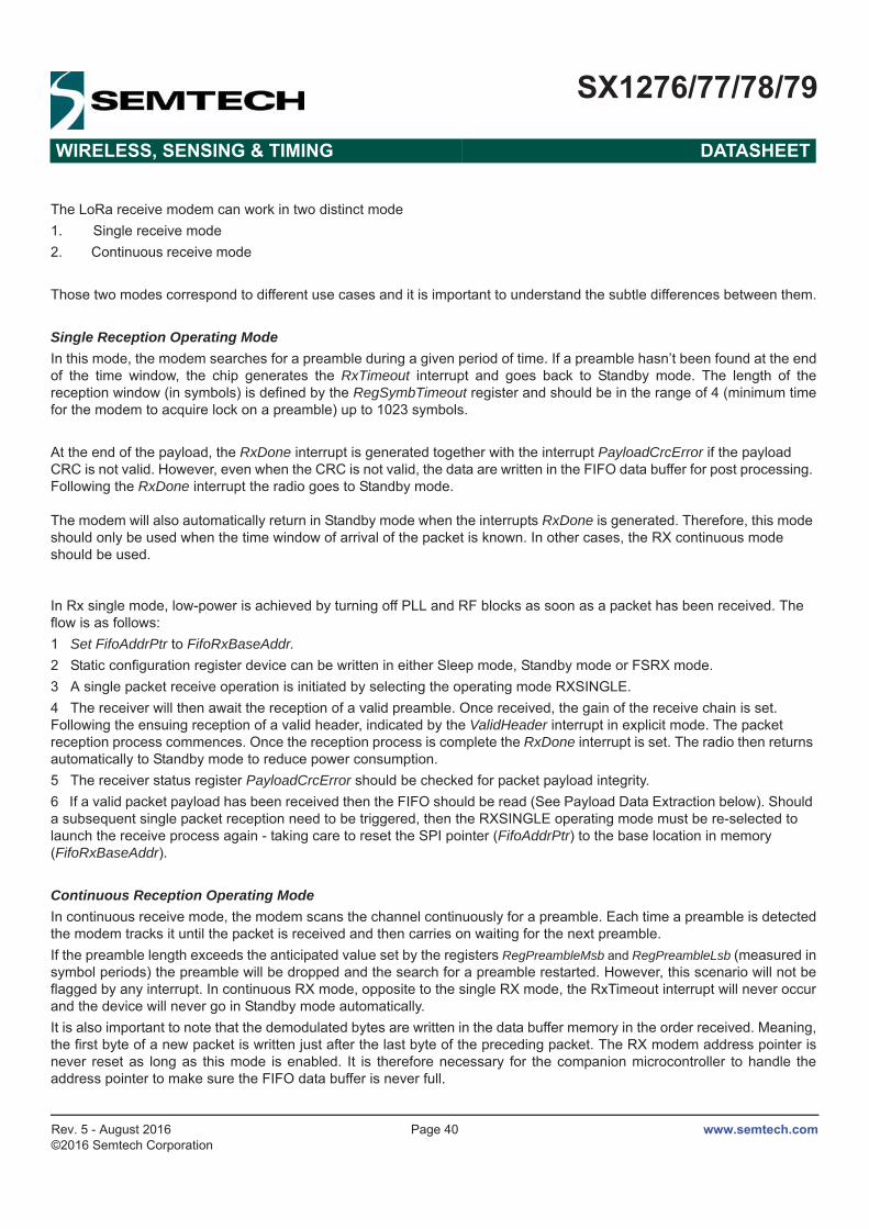
www.semtech.comPage 40
SX1276/77/78/79
WIRELESS, SENSING & TIMING DATASHEET
Rev. 5 - August 2016©2016 Semtech Corporation
The LoRa receive modem can work in two distinct mode1. Single receive mode2. Continuous receive mode
Those two modes correspond to different use cases and it is important to understand the subtle differences between them.
Single Reception Operating ModeIn this mode, the modem searches for a preamble during a given period of time. If a preamble hasn’t been found at the end of the time window, the chip generates the RxTimeout interrupt and goes back to Standby mode. The length of the reception window (in symbols) is defined by the RegSymbTimeout register and should be in the range of 4 (minimum time for the modem to acquire lock on a preamble) up to 1023 symbols.
At the end of the payload, the RxDone interrupt is generated together with the interrupt PayloadCrcError if the payload CRC is not valid. However, even when the CRC is not valid, the data are written in the FIFO data buffer for post processing. Following the RxDone interrupt the radio goes to Standby mode.
The modem will also automatically return in Standby mode when the interrupts RxDone is generated. Therefore, this mode should only be used when the time window of arrival of the packet is known. In other cases, the RX continuous mode should be used.
In Rx single mode, low-power is achieved by turning off PLL and RF blocks as soon as a packet has been received. The flow is as follows:1 Set FifoAddrPtr to FifoRxBaseAddr.2 Static configuration register device can be written in either Sleep mode, Standby mode or FSRX mode. 3 A single packet receive operation is initiated by selecting the operating mode RXSINGLE.4 The receiver will then await the reception of a valid preamble. Once received, the gain of the receive chain is set. Following the ensuing reception of a valid header, indicated by the ValidHeader interrupt in explicit mode. The packet reception process commences. Once the reception process is complete the RxDone interrupt is set. The radio then returns automatically to Standby mode to reduce power consumption.5 The receiver status register PayloadCrcError should be checked for packet payload integrity. 6 If a valid packet payload has been received then the FIFO should be read (See Payload Data Extraction below). Should a subsequent single packet reception need to be triggered, then the RXSINGLE operating mode must be re-selected to launch the receive process again - taking care to reset the SPI pointer (FifoAddrPtr) to the base location in memory (FifoRxBaseAddr).
Continuous Reception Operating ModeIn continuous receive mode, the modem scans the channel continuously for a preamble. Each time a preamble is detected the modem tracks it until the packet is received and then carries on waiting for the next preamble.If the preamble length exceeds the anticipated value set by the registers RegPreambleMsb and RegPreambleLsb (measured in symbol periods) the preamble will be dropped and the search for a preamble restarted. However, this scenario will not be flagged by any interrupt. In continuous RX mode, opposite to the single RX mode, the RxTimeout interrupt will never occur and the device will never go in Standby mode automatically. It is also important to note that the demodulated bytes are written in the data buffer memory in the order received. Meaning, the first byte of a new packet is written just after the last byte of the preceding packet. The RX modem address pointer is never reset as long as this mode is enabled. It is therefore necessary for the companion microcontroller to handle the address pointer to make sure the FIFO data buffer is never full.

www.semtech.comPage 41
SX1276/77/78/79
WIRELESS, SENSING & TIMING DATASHEET
Rev. 5 - August 2016©2016 Semtech Corporation
In continuous mode the received packet processing sequence is given below.1 Whilst in Sleep or Standby mode select RXCONT mode.2 Upon reception of a valid header CRC the RxDone interrupt is set. The radio remains in RXCONT mode waiting for the
next RX LoRaTM packet.3 The PayloadCrcError flag should be checked for packet integrity.4 If packet has been correctly received the FIFO data buffer can be read (see below).5 The reception process (steps 2 - 4) can be repeated or receiver operating mode exited as desired.
In continuous mode status information are available only for the last packet received, i.e. the corresponding registers should be read before the next RxDone arrives.
Rx Single and Rx Continuous Use CasesThe LoRa single reception mode is used mainly in battery operated systems or in systems where the companion microcontroller has a limited availability of timers. In such systems, the use of the timeout present in Rx Single reception mode allows the end user to limit the amount of time spent in reception (and thus limiting the power consumption) while not using any of the companion MCU timers (the MCU can then be in sleep mode while the radio is in the reception mode). The RxTimeout interrupt generated at the end of the reception period is then used to wake-up the companion MCU. One of the advantages of the RxSingle mode is that the interrupt RxTimeout will not be triggered if the device is currently receiving data, thus giving the priority to the reception of the data over the timeout. However, if during the reception, the device loses track of the data due to external perturbation, the device will drop the reception, flag the interrupt RxTimeout and go in StandBy mode to decrease the power consumption of the system.
On the other hand, The LoRa continuous reception mode is used in systems which do not have power restrictions or on system where the use of a companion MCU timer is preferred over the radio embedded timeout system. In RxContinuous mode, the radio will track any LoRa signal present in the air and carry on the reception of packets until the companion MCU sets the radio into another mode of operation. Upon reception the interrupt RxDone will be trigged but the device will stay in Rx Mode, ready for the reception of the next packet.
Payload Data Extraction from FIFO
In order to retrieve received data from FIFO the user must ensure that ValidHeader, PayloadCrcError, RxDone and RxTimeout interrupts in the status register RegIrqFlags are not asserted to ensure that packet reception has terminated successfully (i.e. no flags should be set). In case of errors the steps below should be skipped and the packet discarded. In order to retrieve valid received data from the FIFO the user must:
RegRxNbBytes Indicates the number of bytes that have been received thus far.RegFifoAddrPtr is a dynamic pointer that indicates precisely where the Lora modem received data has been written up to.Set RegFifoAddrPtr to RegFifoRxCurrentAddr. This sets the FIFO pointer to the location of the last packet received in the FIFO. The payload can then be extracted by reading the register RegFifo, RegRxNbBytes times.Alternatively, it is possible to manually point to the location of the last packet received, from the start of the current packet, by setting RegFifoAddrPtr to RegFifoRxByteAddr minus RegRxNbBytes. The payload bytes can then be read from the FIFO by reading the RegFifo address RegRxNbBytes times.

www.semtech.comPage 42
SX1276/77/78/79
WIRELESS, SENSING & TIMING DATASHEET
Rev. 5 - August 2016©2016 Semtech Corporation
Packet Filtering based on Preamble Start
The LoRa modem does automatically filter received packets based upon any addressing. However the SX1276/77/78/79 permit software filtering of the received packets based on the contents of the first few bytes of payload. A brief example is given below for a 4 byte address, however, the address length can be selected by the designer.
The objective of the packet filtering process is to determine the presence, or otherwise, of a valid packet designed for the receiver. If the packet is not for the receiver then the radio returns to sleep mode in order to improve battery life.
The software packet filtering process follows the steps below:
Each time the RxDone interrupt is received, latch the RegFifoRxByteAddr[7:0] register content in a variable, this variable will be called start_address. The RegFifoRxByteAddr[7:0] register of the SX1276/77/78/79 gives in real time the address of the last byte written in the data buffer + 1 (or the address at which the next byte will be written) by the receive LoRa modem. So by doing this, we make sure that the variable start_address always contains the start address of the next packet.
Upon reception of the interrupt ValidHeader, start polling the RegFifoRxByteAddr[7:0] register until it begins to increment. The speed at which this register will increment depends on the Spreading factor, the error correction code and the modulation bandwidth. (Note that this interrupt is still generated in implicit mode).
As soon as RegFifoRxByteAddr[7:0] >= start address + 4, the first 4 bytes (address) are stored in the FIFO data buffer. These can be read and tested to see if the packet is destined for the radio and either remaining in Rx mode to receive the packet or returning to sleep mode if not.
Receiver Timeout OperationIn LoRaTM Rx Single mode, a receiver timeout functionality is available that permits the receiver to listen for a predetermined period of time before generating an interrupt signal to indicate that no valid packets have been received. The timer is absolute and commences as soon as the radio is placed in single receive mode. The interrupt itself, RxTimeout, can be found in the interrupt register RegIrqFlags. In Rx Single mode, the device will return to Standby mode as soon as the interrupt occurs. The user must then clear the interrupt or go into Sleep mode before returning into Rx Single mode. The programmed timeout value is expressed as a multiple of the symbol period and is given by:
TimeOut LoraRxTimeout Ts⋅=
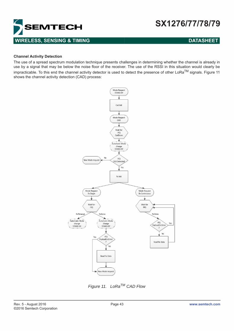
www.semtech.comPage 43
SX1276/77/78/79
WIRELESS, SENSING & TIMING DATASHEET
Rev. 5 - August 2016©2016 Semtech Corporation
Channel Activity DetectionThe use of a spread spectrum modulation technique presents challenges in determining whether the channel is already in use by a signal that may be below the noise floor of the receiver. The use of the RSSI in this situation would clearly be impracticable. To this end the channel activity detector is used to detect the presence of other LoRaTM signals. Figure 11 shows the channel activity detection (CAD) process:
Figure 11. LoRaTM CAD Flow

www.semtech.comPage 44
SX1276/77/78/79
WIRELESS, SENSING & TIMING DATASHEET
Rev. 5 - August 2016©2016 Semtech Corporation
Principle of Operation
The channel activity detection mode is designed to detect a LoRa preamble on the radio channel with the best possible power efficiency. Once in CAD mode, the SX1276/77/78/79 will perform a very quick scan of the band to detect a LoRa packet preamble.
During a CAD the following operations take place:
The PLL locks
The radio receiver captures LoRa preamble symbol of data from the channel. The radio current consumption during that phase corresponds to the specified Rx mode currentThe radio receiver and the PLL turn off, and the modem digital processing starts.
The modem searches for a correlation between the radio captured samples and the ideal preamble waveform. This correlation process takes a little bit less than a symbol period to perform. The radio current consumption during that phase is greatly reduced.Once the calculation is finished the modem generates the CadDone interrupt. If the correlation was successful, CadDetected is generated simultaneously.The chip goes back to Standby mode.
If a preamble was detected, clear the interrupt, then initiate the reception by putting the radio in RX single mode or RX continuous mode.
The time taken for the channel activity detection is dependent upon the LoRa modulation settings used. For a given configuration the typical CAD detection time is shown in the graph below, expressed as a multiple of the LoRa symbol period. Of this period the radio is in receiver mode for (2SF + 32) / BW seconds. For the remainder of the CAD cycle the radio is in a reduced consumption state.
Figure 12. CAD Time as a Function of Spreading Factor

www.semtech.comPage 45
SX1276/77/78/79
WIRELESS, SENSING & TIMING DATASHEET
Rev. 5 - August 2016©2016 Semtech Corporation
To illustrate this process and the respective consumption in each mode, the CAD process follows the sequence of events outlined below:
Figure 13. Consumption Profile of the LoRa CAD Process
The receiver is then in full receiver mode for just over half of the activity detection, followed by a reduced consumption processing phase where the consumption varies with the LoRa bandwidth as shown in the table below.
Table 17 LoRa CAD Consumption Figures
Note These numbers can be slightly lower when using Band 2 and 3, on the low frequency port.
4.1.6.1. Digital IO Pin Mapping
Six of SX1276/77/78/79’s general purpose IO pins are available used in LoRaTM mode. Their mapping is shown below and depends upon the configuration of registers RegDioMapping1 and RegDioMapping2.
Bandwidth(kHz)
Full Rx, IDDR_L(mA)
Processing, IDDC_L(mA)
7.8 to 41.7 11 5.262.5 11 5.6125 11.5 6250 12.4 6.8500 13.8 8.3

www.semtech.comPage 46
SX1276/77/78/79
WIRELESS, SENSING & TIMING DATASHEET
Rev. 5 - August 2016©2016 Semtech Corporation
Table 18 DIO Mapping LoRaTM Mode
4.1.7. Modem Status IndicatorsThe state of the LoRa modem is accessible with the ModemStatus bits in RegModemStat. They can mostly used for debug in Rx mode and the useful indicators are:
Bit 0: Signal Detected indicates that a valid LoRa preamble has been detected
Bit 1: Signal Synchronized indicates that the end of Preamble has been detected, the modem is in lock
Bit 3: Header Info Valid toggles high when a valid Header (with correct CRC) is detected
4.2. FSK/OOK Modem
4.2.1. Bit Rate SettingThe bitrate setting is referenced to the crystal oscillator and provides a precise means of setting the bit rate (or equivalently chip) rate of the radio. In continuous transmit mode (Section 4.2.12) the data stream to be transmitted can be input directly to the modulator via pin 10 (DIO2/DATA) in an asynchronous manner, unless Gaussian filtering is used, in which case the DCLK signal on pin 9 (DIO1/DCLK) is used to synchronize the data stream. See section 4.2.2.3 for details on the Gaussian filter.
In Packet mode or in Continuous mode with Gaussian filtering enabled, the Bit Rate (BR) is controlled by bits Bitrate in RegBitrateMsb and RegBitrateLsb
Note: BitrateFrac bits have no effect (i.e may be considered equal to 0) in OOK modulation mode.
The quantity BitrateFrac is hence designed to allow very high precision (max. 250 ppm programing resolution) for any bitrate in the programmable range. Table 19 below shows a range of standard bitrates and the accuracy to within which they may be reached.
Operating Mode
DIOxMapping DIO5 DIO4 DIO3 DIO2 DIO1 DIO0
ALL
00 ModeReady CadDetected CadDone FhssChangeChannel RxTimeout RxDone
01 ClkOut PllLock ValidHeader FhssChangeChannel FhssChangeChannel TxDone
10 ClkOut PllLock PayloadCrcError FhssChangeChannel CadDetected CadDone
11 - - - - - -
BitRate FXOSC
BitRate 15 0( , ) BitrateFrac16
-------------------------------+-------------------------------------------------------------------------=

www.semtech.comPage 47
SX1276/77/78/79
WIRELESS, SENSING & TIMING DATASHEET
Rev. 5 - August 2016©2016 Semtech Corporation
Table 19 Bit Rate Examples
4.2.2. FSK/OOK Transmission
4.2.2.1. FSK ModulationFSK modulation is performed inside the PLL bandwidth, by changing the fractional divider ratio in the feedback loop of the PLL. The high resolution of the sigma-delta modulator, allows for very narrow frequency deviation. The frequency deviation FDEV is given by:
To ensure correct modulation, the following limit applies:
Note No constraint applies to the modulation index of the transmitter, but the frequency deviation must be set between 600 Hz and 200 kHz.
Type BitRate(15:8)
BitRate(7:0)
(G)FSK(G)MSK OOK Actual BR
(b/s)
Classical modem baud rates (multiples of 1.2 kbps)
0x68 0x2B 1.2 kbps 1.2 kbps 1200.015
0x34 0x15 2.4 kbps 2.4 kbps 2400.060
0x1A 0x0B 4.8 kbps 4.8 kbps 4799.760
0x0D 0x05 9.6 kbps 9.6 kbps 9600.960
0x06 0x83 19.2 kbps 19.2 kbps 19196.16
0x03 0x41 38.4 kbps 38415.36
0x01 0xA1 76.8 kbps 76738.60
0x00 0xD0 153.6 kbps 153846.1
Classical modem baud rates (multiples of 0.9 kbps)
0x02 0x2C 57.6 kbps 57553.95
0x01 0x16 115.2 kbps 115107.9
Round bit rates(multiples of 12.5, 25 and50 kbps)
0x0A 0x00 12.5 kbps 12.5 kbps 12500.00
0x05 0x00 25 kbps 25 kbps 25000.00
0x80 0x00 50 kbps 50000.00
0x01 0x40 100 kbps 100000.0
0x00 0xD5 150 kbps 150234.7
0x00 0xA0 200 kbps 200000.0
0x00 0x80 250 kbps 250000.0
0x00 0x6B 300 kbps 299065.4
Watch Xtal frequency 0x03 0xD1 32.768 kbps 32.768 kbps 32753.32
FDEV FSTEP Fdev 13 0( , )×=
FDEVBR2
------- 250( )kHz≤+

www.semtech.comPage 48
SX1276/77/78/79
WIRELESS, SENSING & TIMING DATASHEET
Rev. 5 - August 2016©2016 Semtech Corporation
4.2.2.2. OOK ModulationOOK modulation is applied by switching on and off the power amplifier. Digital control and ramping are available to improve the transient power response of the OOK transmitter.
4.2.2.3. Modulation ShapingModulation shaping can be applied in both OOK and FSK modulation modes, to improve the narrow band response of the transmitter. Both shaping features are controlled with PaRamp bits in RegPaRamp.
In FSK mode, a Gaussian filter with BT = 0.5 or 1 is used to filter the modulation stream, at the input of the sigma-delta modulator. If the Gaussian filter is enabled when the SX1276/77/78/79 is in Continuous mode, DCLK signal on pin 10 (DIO1/DCLK) will trigger an interrupt on the uC each time a new bit has to be transmitted. Please refer to section 4.2.12.2 for details.When OOK modulation is used, the PA bias voltages are ramped up and down smoothly when the PA is turned on and off, to reduce spectral splatter.
Note The transmitter must be restarted if the ModulationShaping setting is changed, in order to recalibrate the built-in filter.
4.2.3. FSK/OOK Reception
4.2.3.1. FSK DemodulatorThe FSK demodulator of the SX1276/77/78/79 is designed to demodulate FSK, GFSK, MSK and GMSK modulated signals. It is most efficient when the modulation index of the signal is greater than 0.5 and below 10:
The output of the FSK demodulator can be fed to the Bit Synchronizer to provide the companion processor with a synchronous data stream in Continuous mode.
4.2.3.2. OOK DemodulatorThe OOK demodulator performs a comparison of the RSSI output and a threshold value. Three different threshold modes are available, configured through bits OokThreshType in RegOokPeak.The recommended mode of operation is the “Peak” threshold mode, illustrated in Figure 14:
0.5 β≤2 FDEV×
BR---------------------- 10≤=

www.semtech.comPage 49
SX1276/77/78/79
WIRELESS, SENSING & TIMING DATASHEET
Rev. 5 - August 2016©2016 Semtech Corporation
Figure 14. OOK Peak Demodulator DescriptionIn peak threshold mode the comparison threshold level is the peak value of the RSSI, reduced by 6dB. In the absence of an input signal, or during the reception of a logical ‘0’, the acquired peak value is decremented by one OokPeakThreshStepevery OokPeakThreshDec period.
When the RSSI output is null for a long time (for instance after a long string of “0” received, or if no transmitter is present), the peak threshold level will continue falling until it reaches the “Floor Threshold”, programmed in OokFixedThresh.
The default settings of the OOK demodulator lead to the performance stated in the electrical specification. However, in applications in which sudden signal drops are awaited during a reception, the three parameters should be optimized accordingly.
Optimizing the Floor ThresholdOokFixedThresh determines the sensitivity of the OOK receiver, as it sets the comparison threshold for weak input signals (i.e. those close to the noise floor). Significant sensitivity improvements can be generated if configured correctly.
Note that the noise floor of the receiver at the demodulator input depends on:
The noise figure of the receiver.
The gain of the receive chain from antenna to base band.
The matching - including SAW filter if any.
The bandwidth of the channel filters.
Zoom
Period as defined in OokPeakThreshDec
Decay in dB as defined in OokPeakThreshStep Fixed 6dB difference
RSSI [dBm]
Noise floor of receiver
‘’Floor’’ threshold defined by OokFixedThresh
Time
‘’Peak -6dB’’ Threshold
Zoom

www.semtech.comPage 50
SX1276/77/78/79
WIRELESS, SENSING & TIMING DATASHEET
Rev. 5 - August 2016©2016 Semtech Corporation
It is therefore important to note that the setting of OokFixedThresh will be application dependent. The following procedure is recommended to optimize OokFixedThresh.
Figure 15. Floor Threshold Optimization
The new floor threshold value found during this test should be used for OOK reception with those receiver settings.
Optimizing OOK Demodulator for Fast Fading SignalsA sudden drop in signal strength can cause the bit error rate to increase. For applications where the expected signal drop can be estimated, the following OOK demodulator parameters OokPeakThreshStep and OokPeakThreshDec can be optimized as described below for a given number of threshold decrements per bit. Refer to RegOokPeak to access those settings.
Set SX1276/7/8/9 in OOK Rx mode Adjust Bit Rate, Channel filter BW Default OokFixedThresh setting
No input signal Continuous Mode
Optimization complete
Glitch activity on DATA ?
Monitor DIO2/DATA pin
Increment OokFixedThresh

www.semtech.comPage 51
SX1276/77/78/79
WIRELESS, SENSING & TIMING DATASHEET
Rev. 5 - August 2016©2016 Semtech Corporation
Alternative OOK Demodulator Threshold ModesIn addition to the Peak OOK threshold mode, the user can alternatively select two other types of threshold detectors:
Fixed Threshold: The value is selected through OokFixedThresh
Average Threshold: Data supplied by the RSSI block is averaged, and this operation mode should only be used with DC-free encoded data.
4.2.3.3. Bit SynchronizerThe bit synchronizer provides a clean and synchronized digital output based upon timing recovery information gleaned from the received data edge transitions. Its output is made available on pin DIO1/DCLK in Continuous mode and can be disabled through register settings. However, for optimum receiver performance, especially in Continuous receive mode, its use is strongly advised.
The Bit Synchronizer is automatically activated in Packet mode. Its bit rate is controlled by BitRateMsb and BitRateLsb in RegBitrate.
Figure 16. Bit Synchronizer Description
To ensure correct operation of the Bit Synchronizer, the following conditions have to be satisfied:
A preamble (0x55 or 0xAA) of at least 12 bits is required for synchronization, the longer the synchronization phase is the better the ensuing packet detection rate will be.The subsequent payload bit stream must have at least one edge transition (either rising or falling) every 16 bits during data transmission.The absolute error between transmitted and received bit rate must not exceed 6.5%.
Raw demodulator
output (FSK or OOK)
DCLK
DATA BitSync Output
To pin DATA and DCLK in continuous
mode

www.semtech.comPage 52
SX1276/77/78/79
WIRELESS, SENSING & TIMING DATASHEET
Rev. 5 - August 2016©2016 Semtech Corporation
4.2.3.4. Frequency Error Indicator
This frequency error indicator measures the frequency error between the programmed RF centre frequency and the carrier frequency of the modulated input signal to the receiver. When the FEI is performed, the frequency error is measured and the signed result is loaded in FeiValue in RegFei, in 2’s complement format. The time required for an FEI evaluation is 4 bit periods.
To ensure correct operation of the FEI:
The measurement must be launched during the reception of preamble.
The sum of the frequency offset and the 20 dB signal bandwidth must be lower than the base band filter bandwidth. i.e. The whole modulated spectrum must be received.
The 20 dB bandwidth of the signal can be evaluated as follows (double-side bandwidth):
The frequency error, in Hz, can be calculated with the following formula:
The FEI is enabled automatically upon the transition to receive mode and automatically updated every 4 bits.
4.2.3.5. AFCThe AFC is based on the FEI measurement, therefore the same input signal and receiver setting conditions apply. When the AFC procedure is performed the AfcValue is directly subtracted from the register that defines the frequency of operation of the chip, FRF. The AFC is executed each time the receiver is enabled, if AfcAutoOn = 1.
When the AFC is enabled (AfcAutoOn = 1), the user has the option to:
Clear the former AFC correction value, if AfcAutoClearOn = 1. Allowing the next frequency correction to be performed from the initial centre frequency.Start the AFC evaluation from the previously corrected frequency. This may be useful in systems in which the centre frequency experiences cumulative drift - such as the ageing of a crystal reference.
The SX1276/77/78/79 offers an alternate receiver bandwidth setting during the AFC phase allowing the accommodation of larger frequency errors. The setting RegAfcBw sets the receive bandwidth during the AFC process. In a typical receiver application the, once the AFC is performed, the radio will revert to the receiver communication or channel bandwidth (RegRxBw) for the ensuing communication phase.
Note that the FEI measurement is valid only during the reception of preamble. The provision of the PreambleDetect flag can hence be used to detect this condition and allow a reliable AFC or FEI operation to be triggered. This process can be performed automatically by using the appropriate options in StartDemodOnPreamble found in the RegRxConfig register.
A detailed description of the receiver setup to enable the AFC is provided in section 4.2.6.
BW20dB 2 FDEVBR2
-------+×=
FEI FSTEP FeiValue×=

www.semtech.comPage 53
SX1276/77/78/79
WIRELESS, SENSING & TIMING DATASHEET
Rev. 5 - August 2016©2016 Semtech Corporation
4.2.3.6. Preamble DetectorThe Preamble Detector indicates the reception of a carrier modulated with a 0101...sequence. It is insensitive to the frequency offset, as long as the receiver bandwidth is large enough. The size of detection can be programmed from 1 to 3 bytes with PreambleDetectorSize in RegPreambleDetect as defined in the next table.
Table 20 Preamble Detector Settings
For normal operation, PreambleDetectTol should be set to be set to 10 (0x0A), with a qualifying preamble size of 2 bytes.
The PreambleDetect interrupt (either in RegIrqFlags1 or mapped to a specific DIO) then goes high every time a valid preamble is detected, assuming PreambleDetectorOn=1.
The preamble detector can also be used as a gate to ensure that AFC and AGC are performed on valid preamble. See section 4.2.6. for details.
4.2.3.7. Image Rejection MixerThe SX1276/77/78/79 employs an image rejection mixer (IRM) which, uncalibrated, 35 dB image rejection. A low phase noise PLL is used to perform calibration of the receiver chain. This increases the typical image rejection to 48 dB.
4.2.3.8. Image and RSSI CalibrationAn automated process is implemented to calibrate the phase and gain imbalances of I and Q receive paths. This calibration enhances image rejection and improves RSSI precision. It is launched under the following circumstances:
Automatically at Power On Reset or after a Manual Reset of the chip (refer to section 7.2), only for the Low Frequency front-end, and is performed at 434MHzAutomatically when a pre-defined temperature change is observed, if the option is enabled. A selectable temperature change, set with TempThreshold (5, 10, 15 or 20°C), is detected and reported in TempChange, if the temperature monitoring is turned On with TempMonitorOff=0.This interrupt flag can be used by the application to launch a new image calibration at a convenient time if AutoImageCalOn=0, or immediately when this temperature variation is detected, if AutoImageCalOn=1Upon user request, by setting bit ImageCalStart in RegImageCal, when the device is in Standby mode
Notes - The calibration procedure takes approximately 10ms. It is recommended to disable the fully automated (temperature-dependent) calibration, to better control when it is triggered (and avoid unexpected packet losses)
- To perform the calibration, the radio must be temporarily returned to FSK/OOK mode
- The automatic IQ and RSSI calibration done at POR and Reset is only valid at 434 MHz (the value of RegFrf at POR). To improve accuracy of RSSI and image rejection, this calibration should be replicated at the frequency (ies)
PreambleDetectorSize # of Bytes
00 1
01 2 (recommended)
10 3
11 reserved

www.semtech.comPage 54
SX1276/77/78/79
WIRELESS, SENSING & TIMING DATASHEET
Rev. 5 - August 2016©2016 Semtech Corporation
of interest, for instance a calibration should be launched with Frf set to 868.3 MHz if the high frequency port supports communication in this frequency band. Conversely if the product is used at 169 MHz, the calibration should be repeated with Frf=169MHz
- FormerTemp and TempChange in SX1276/77/79 are frequency-specific and the IC keeps a copy of these variables when switching between the low frequency and the high frequency domains (along with the corresponding calibration values, stored in test registers)
- FormerTemp and TempChange cannot be read in Sleep mode (although they are saved). They should be read in Standby mode
4.2.3.9. Timeout FunctionThe SX1276/77/78/79 includes a Timeout function, which allows it to automatically shut-down the receiver after a receive sequence and therefore save energy.
Timeout interrupt is generated TimeoutRxRssi x 16 x Tbit after switching to Rx mode if the Rssi flag does not raise within this time frame (RssiValue > RssiThreshold)Timeout interrupt is generated TimeoutRxPreamble x 16 x Tbit after switching to Rx mode if the PreambleDetect flag does not raise within this time frameTimeout interrupt is generated TimeoutSignalSync x 16 x Tbit after switching to Rx mode if the SyncAddress flag does not raise within this time frame
This timeout interrupt can be used to warn the companion processor to shut down the receiver and return to a lower power mode. To become active, these timeouts must also be enabled by setting the correct RxTrigger parameters in RegRxConfig:
Table 21 RxTrigger Settings to Enable Timeout Interrupts
4.2.4. Operating Modes in FSK/OOK ModeThe SX1276/77/78/79 has several working modes, manually programmed in RegOpMode. Fully automated mode selection, packet transmission and reception is also possible using the Top Level Sequencer described in Section 4.2.8.Table 22 Basic Transceiver Modes
ReceiverTriggering Event
RxTrigger(2:0)
Timeout onRssi
Timeout onPreamble
Timeout onSyncAddress
None 000 Off Off
ActiveRssi Interrupt 001 Active Off
PreambleDetect 110 Off ActiveRssi Interrupt & PreambleDetect 111 Active Active
Mode Selected mode Symbol Enabled blocks
000 Sleep mode Sleep None
001 Standby mode Stdby Top regulator and crystal oscillator
010 Frequency synthesiser to Tx frequency FSTx Frequency synthesizer at Tx frequency (Frf)
011 Transmit mode Tx Frequency synthesizer and transmitter

www.semtech.comPage 55
SX1276/77/78/79
WIRELESS, SENSING & TIMING DATASHEET
Rev. 5 - August 2016©2016 Semtech Corporation
When switching from a mode to another the sub-blocks are woken up according to a pre-defined optimized sequence.
100 Frequency synthesiser to Rx frequency FSRx Frequency synthesizer at frequency for reception (Frf-IF)
101 Receive mode Rx Frequency synthesizer and receiver
Mode Selected mode Symbol Enabled blocks

www.semtech.comPage 56
SX1276/77/78/79
WIRELESS, SENSING & TIMING DATASHEET
Rev. 5 - August 2016©2016 Semtech Corporation
4.2.5. Startup TimesThe startup time of the transmitter or the receiver is Dependant upon which mode the transceiver was in at the beginning. For a complete description, Figure 17 below shows a complete startup process, from the lower power mode “Sleep”.
Figure 17. Startup Process
TS_OSC is the startup time of the crystal oscillator which depends on the electrical characteristics of the crystal. TS_FS is the startup time of the PLL including systematic calibration of the VCO.
Typical values of TS_OSC and TS_FS are given in Section 2.5.2.
4.2.5.1. Transmitter Startup TimeThe transmitter startup time, TS_TR, is calculated as follows in FSK mode:
,
where PaRamp is the ramp-up time programmed in RegPaRamp and Tbit is the bit time.
In OOK mode, this equation can be simplified to the following:
4.2.5.2. Receiver Startup TimeThe receiver startup time, TS_RE, only depends upon the receiver bandwidth effective at the time of startup. When AFC is enabled (AfcAutoOn=1), AfcBw should be used instead of RxBw to extract the receiver startup time:
Sleepmode
Transmit
Stdbymode
FSTx
FSRx Receive
Timeline
0 TS_OSC TS_OSC+TS_FS
TS_OSC+TS_FS+TS_TR
TS_OSC+TS_FS+TS_RE
CurrentDrain
IDDSLIDDST
IDDFS
IDDR (Rx) or IDDT (Tx)
TbitPaRampsTRTS ×+×+=2125.15_ μ
TbitsTRTS ×+=215_ μ

www.semtech.comPage 57
SX1276/77/78/79
WIRELESS, SENSING & TIMING DATASHEET
Rev. 5 - August 2016©2016 Semtech Corporation
Table 23 Receiver Startup Time Summary
TS_RE or later after setting the device in Receive mode, any incoming packet will be detected and demodulated by the transceiver.
4.2.5.3. Time to RSSI EvaluationThe first RSSI sample will be available TS_RSSI after the receiver is ready, in other words TS_RE + TS_RSSI after the receiver was requested to turn on.
Figure 18. Time to RSSI Sample
TS_RSSI depends on the receiver bandwidth, as well as the RssiSmoothing option that was selected. The formula used to calculate TS_RSSI is provided in section 5.5.4.
RxBw if AfcAutoOn=0RxBwAfc if AfcAutoOn=1
TS_RE(+/-5%)
2.6 kHz 2.33 ms3.1 kHz 1.94 ms3.9 kHz 1.56 ms5.2 kHz 1.18 ms6.3 kHz 984 us7.8 kHz 791 us
10.4 kHz 601 us12.5 kHz 504 us15.6 kHz 407 us20.8 kHz 313 us25.0 kHz 264 us31.3 kHz 215 us41.7 kHz 169 us50.0 kHz 144 us62.5 kHz 119 us83.3 kHz 97 us100.0 kHz 84 us125.0 kHz 71 us166.7 kHz 85 us200.0 kHz 74 us250.0 kHz 63 us
FSRx RxRssi IRQ
Rssi sample ready
Timeline
0 TS_RE TS_RE+TS_RSSI

www.semtech.comPage 58
SX1276/77/78/79
WIRELESS, SENSING & TIMING DATASHEET
Rev. 5 - August 2016©2016 Semtech Corporation
4.2.5.4. Tx to Rx Turnaround Time
Figure 19. Tx to Rx Turnaround
Note The SPI instruction times are omitted, as they can generally be very small as compared to other timings (up to 10MHz SPI clock).
4.2.5.5. Rx to Tx
Figure 20. Rx to Tx Turnaround
Tx Mode 1. set new Frf (*)2. set Rx mode
Timeline
0 TS_HOP+TS_RE
(*) Optional
Rx Mode
Rx Mode 1. set new Frf (*)2. set Tx mode
Timeline
0 TS_HOP+TS_TR
(*) Optional
Tx Mode

www.semtech.comPage 59
SX1276/77/78/79
WIRELESS, SENSING & TIMING DATASHEET
Rev. 5 - August 2016©2016 Semtech Corporation
4.2.5.6. Receiver Hopping, Rx to Rx
Two methods are possible:
Figure 21. Receiver Hopping
The second method is quicker, and should be used if a very quick RF sniffing mechanism is to be implemented.
4.2.5.7. Tx to Tx
Figure 22. Transmitter Hopping
4.2.6. Receiver Startup OptionsThe SX1276/77/78/79 receiver can automatically control the gain of the receive chain (AGC) and adjust the receiver LO frequency (AFC). Those processes are carried out on a packet-by-packet basis. They occur:
When the receiver is turned On.
When the Receiver is restarted upon user request, through the use of trigger bits RestartRxWithoutPllLock orRestartRxWithPllLock, in RegRxConfig.When the receiver is automatically restarted after the reception of a valid packet, or after a packet collision.
Rx Mode,Channel A
1. set new Frf2. set RestartRxWithPllLock
Timeline
0 TS_HOP+TS_RE
Rx Mode,Channel B
First method
Rx Mode,Channel A
1. set FastHopOn=12. set new Frf (*)
3. wait for TS_HOP
Timeline
0 ~TS_HOP
Rx Mode,Channel B
Second method
(*) RegFrfLsb must be written to trigger a frequency change
1. set new Frf (*)2. set FSTx mode FSTx
Timeline
~PaRamp+TS_HOP
~PaRamp+TS_HOP+TS_TR
0
Tx Mode,Channel A
Tx Mode,Channel BSet Tx mode

www.semtech.comPage 60
SX1276/77/78/79
WIRELESS, SENSING & TIMING DATASHEET
Rev. 5 - August 2016©2016 Semtech Corporation
Automatic restart capabilities are detailed in Section 4.2.7.The receiver startup options available in SX1276/77/78/79 are described in Table 24.
Table 24 Receiver Startup Options
When AgcAutoOn=0, the LNA gain is manually selected by choosing LnaGain bits in RegLna.
4.2.7. Receiver Restart MethodsThe options for restart of the receiver are covered below. This is typically of use to prepare for the reception of a new signal whose strength or carrier frequency is different from the preceding packet to allow the AGC or AFC to be re-evaluated.
4.2.7.1. Restart Upon User RequestIn Receive mode the user can request a receiver restart - this can be useful in conjunction with the use of a Timeout interrupt following a period of inactivity in the channel of interest. Two options are available:
No change in the Local Oscillator upon restart: the AFC is disabled, and the Frf register has not been changed through SPI before the restart instruction: set bit RestartRxWithoutPllLock in RegRxConfig to 1.Local Oscillator change upon restart: if AFC is enabled (AfcAutoOn=1), and/or the Frf register had been changed during the last Rx period: set bit RestartRxWithPllLock in RegRxConfig to 1.
Note ModeReady must be at logic level 1 for a new RestartRx command to be taken into account.
4.2.7.2. Automatic Restart after valid Packet ReceptionThe bits AutoRestartRxMode in RegSyncConfig control the automatic restart feature of the SX1276/77/78/79 receiver, when a valid packet has been received:
If AutoRestartRxMode = 00, the function is off, and the user should manually restart the receiver upon valid packet reception (see section 4.2.7.1).If AutoRestartRxMode = 01, after the user has emptied the FIFO following a PayloadReady interrupt, the receiver will automatically restart itself after a delay of InterPacketRxDelay, allowing for the distant transmitter to ramp down, hence avoiding a false RSSI detection on the ‘tail’ of the previous packet.If AutoRestartRxMode = 10 should be used if the next reception is expected on a new frequency, i.e. Frf is changed after the reception of the previous packet. An additional delay is systematically added, in order for the PLL to lock at a new frequency.
Triggering Event Realized Function AgcAutoOn AfcAutoOn RxTrigger(2:0)
None None 0 0 000
Rssi InterruptAGC 1 0 001
AGC & AFC 1 1 001
PreambleDetectAGC 1 0 110
AGC & AFC 1 1 110Rssi Interrupt
&PreambleDetect
AGC 1 0 111
AGC & AFC 1 1 111

www.semtech.comPage 61
SX1276/77/78/79
WIRELESS, SENSING & TIMING DATASHEET
Rev. 5 - August 2016©2016 Semtech Corporation
4.2.7.3. Automatic Restart when Packet Collision is Detected
In receive mode the SX1276/77/78/79 is able to detect packet collision and restart the receiver. Collisions are detected by a sudden rise in received signal strength, detected by the RSSI. This functionality can be useful in network configurations where many asynchronous slaves attempt periodic communication with a single a master node.
The collision detector is enabled by setting bit RestartRxOnCollision to 1.
The decision to restart the receiver is based on the detection of RSSI change. The sensitivity of the system can be adjusted in 1 dB steps by using register RssiCollisionThreshold in RegRxConfig.
4.2.8. Top Level Sequencer Depending on the application, it is desirable to be able to change the mode of the circuit according to a predefined sequence without access to the serial interface. In order to define different sequences or scenarios, a user-programmable state machine, called Top Level Sequencer (Sequencer in short), can automatically control the chip modes.
NOTE THAT THIS FUNCTIONALITY IS ONLY AVAILABLE IN FSK/OOK MODE.
The Sequencer is activated by setting the SequencerStart bit in RegSeqConfig1 to 1 in Sleep or Standby mode (called initial mode). It is also possible to force the Sequencer off by setting the Stop bit in RegSeqConfig1 to 1 at any time.
Note SequencerStart and Stop bit must never be set at the same time.
4.2.8.1. Sequencer StatesAs shown in the table below, with the aid of a pair of interrupt timers (T1 and T2), the sequencer can take control of the chip operation in all modes.
Table 25 Sequencer States
SequencerState Description
SequencerOff StateThe Sequencer is not activated. Sending a SequencerStart command will launch it.When coming from LowPowerSelection state, the Sequencer will be Off, whilst the chip will return to its initial mode (either Sleep or Standby mode).
Idle State The chip is in low-power mode, either Standby or Sleep, as defined by IdleMode in RegSeqConfig1. The Sequencer waits only for the T1 interrupt.
Transmit State The transmitter in on.
Receive State The receiver in on.
PacketReceived The receiver is on and a packet has been received. It is stored in the FIFO.
LowPowerSelection Selects low power state (SequencerOff or Idle State)
RxTimeout Defines the action to be taken on a RxTimeout interrupt.RxTimeout interrupt can be a TimeoutRxRssi, TimeoutRxPreamble or TimeoutSignalSync interrupt.

www.semtech.comPage 62
SX1276/77/78/79
WIRELESS, SENSING & TIMING DATASHEET
Rev. 5 - August 2016©2016 Semtech Corporation
4.2.8.2. Sequencer TransitionsThe transitions between sequencer states are listed in the forthcoming table.Table 26 Sequencer Transition Options
Variable Transition
IdleModeSelects the chip mode during Idle state:0: Standby mode1: Sleep mode
FromStart
Controls the Sequencer transition when the SequencerStart bit is set to 1 in Sleep or Standby mode:00: to LowPowerSelection 01: to Receive state 10: to Transmit state 11: to Transmit state on a FifoThreshold interrupt
LowPowerSelection
Selects Sequencer LowPower state after a to LowPowerSelection transition0: SequencerOff state with chip on Initial mode1: Idle state with chip on Standby or Sleep mode depending on IdleModeNote: Initial mode is the chip LowPower mode at Sequencer start.
FromIdleControls the Sequencer transition from the Idle state on a T1 interrupt:0: to Transmit state 1: to Receive state
FromTransmitControls the Sequencer transition from the Transmit state:0: to LowPowerSelection on a PacketSent interrupt1: to Receive state on a PacketSent interrupt
FromReceive
Controls the Sequencer transition from the Receive state:000 and 111: unused001: to PacketReceived state on a PayloadReady interrupt010: to LowPowerSelection on a PayloadReady interrupt011: to PacketReceived state on a CrcOk interrupt. If CRC is wrong (corrupted packet, with CRC on but CrcAutoClearOn is off), the PayloadReady interrupt will drive the sequencer to RxTimeout state.100: to SequencerOff state on a Rssi interrupt101: to SequencerOff state on a SyncAddress interrupt110: to SequencerOff state on a PreambleDetect interruptIrrespective of this setting, transition to LowPowerSelection on a T2 interrupt
FromRxTimeout
Controls the state-machine transition from the Receive state on a RxTimeout interrupt (and on PayloadReady if FromReceive = 011):00: to Receive state via ReceiveRestart01: to Transmit state10: to LowPowerSelection11: to SequencerOff stateNote: RxTimeout interrupt is a TimeoutRxRssi, TimeoutRxPreamble or TimeoutSignalSync interrupt.
FromPacketReceived
Controls the state-machine transition from the PacketReceived state:000: to SequencerOff state001: to Transmit on a FifoEmpty interrupt010: to LowPowerSelection011: to Receive via FS mode, if frequency was changed100: to Receive state (no frequency change)

www.semtech.comPage 63
SX1276/77/78/79
WIRELESS, SENSING & TIMING DATASHEET
Rev. 5 - August 2016©2016 Semtech Corporation
4.2.8.3. TimersTwo timers (Timer1 and Timer2) are also available in order to define periodic sequences. These timers are used to generate interrupts, which can trigger transitions of the Sequencer.
T1 interrupt is generated (Timer1Resolution * Timer1Coefficient) after T2 interrupt or SequencerStart. command.T2 interrupt is generated (Timer2Resolution * Timer2Coefficient) after T1 interrupt.
The timers’ mechanism is summarized on the following diagram.
Figure 23. Timer1 and Timer2 Mechanism
Note The timer sequence is completed independently of the actual Sequencer state. Thus, both timers need to be on to achieve periodic cycling.
Table 27 Sequencer Timer Settings
Variable Description
Timer1Resolution
Resolution of Timer100: disabled01: 64 us10: 4.1 ms11: 262 ms
Timer2Resolution
Resolution of Timer200: disabled01: 64 us10: 4.1 ms11: 262 ms
Timer1Coefficient Multiplying coefficient for Timer1
Timer2Coefficient Multiplying coefficient for Timer2
T2interrupt
T1interrupt
Timer1Timer2
Sequencer Start

www.semtech.comPage 64
SX1276/77/78/79
WIRELESS, SENSING & TIMING DATASHEET
Rev. 5 - August 2016©2016 Semtech Corporation
4.2.8.4. Sequencer State Machine
The following graphs summarize every possible transition between each Sequencer state. The Sequencer states are highlighted in grey. The transitions are represented by arrows. The condition activating them is described over the transition arrow. For better readability, the start transitions are separated from the rest of the graph.
Transitory states are highlighted in light grey, and exit states are represented in red. It is also possible to force the Sequencer off by setting the Stop bit in RegSeqConfig1 to 1 at any time.
Figure 24. Sequencer State Machine
Sequencer: Start transitions
Sequencer: State machine
Transmit
LowPowerSelection Idle
Receive
PacketReceived
RxTimeout
If LowPowerSelection = 1
On T1 if FromIdle = 0
On PacketSentif FromTransmit = 1
On PayloadReady if FromReceive = 001On CrcOk if FromReceive = 011
On PayloadReadyif FromReceive = 010
If FromRxTimeout = 01
If FromRxTimeout = 10
If FromPacketReceived = 010
If FromPacketReceived = 100Via FS mode if FromPacketReceived = 011
On PacketSentif FromTransmit = 0Via ReceiveRestart
if FromRxTimeout = 00
On RxTimeout
On T2
On T1 if FromIdle = 1
If LowPowerSelection = 0( Mode Initial mode )
On Rssi if FromReceive = 100 On SyncAdress if FromReceive = 101 On Preamble if FromReceive = 110
If FromRxTimeout = 11
If FromPacketReceived = 000
Sequencer Off
Standby if IdleMode = 0Sleep if IdleMode = 1
TransmitLowPowerSelection Receive
StartIf FromStart = 00
If FromStart = 01 If FromStart = 10
Sequencer Off
Sequencer Off&
Initial mode = Sleep or Standby
On SequencerStart bit rising edge
On FifoThresholdif FromStart = 11
On PayloadReady if FromReceive = 011(CRC failed and CrcAutoClearOn=0)

www.semtech.comPage 65
SX1276/77/78/79
WIRELESS, SENSING & TIMING DATASHEET
Rev. 5 - August 2016©2016 Semtech Corporation
4.2.9. Data Processing in FSK/OOK Mode
4.2.9.1. Block DiagramFigure below illustrates the SX1276/77/78/79 data processing circuit. Its role is to interface the data to/from the modulator/demodulator and the uC access points (SPI and DIO pins). It also controls all the configuration registers.
The circuit contains several control blocks which are described in the following paragraphs.
Figure 25. SX1276/77/78/79 Data Processing Conceptual View
The SX1276/77/78/79 implements several data operation modes, each with their own data path through the data processing. Depending on the data operation mode selected, some control blocks are active whilst others remain disabled.
4.2.9.2. Data Operation ModesThe SX1276/77/78/79 has two different data operation modes selectable by the user:
Continuous mode: each bit transmitted or received is accessed in real time at the DIO2/DATA pin. This mode may be used if adequate external signal processing is available.Packet mode (recommended): user only provides/retrieves payload bytes to/from the FIFO. The packet is automatically built with preamble, Sync word, and optional CRC and DC-free encoding schemes The reverse operation is performed in reception. The uC processing overhead is hence significantly reduced compared to Continuous mode. Depending on the optional features activated (CRC, etc) the maximum payload length is limited to 255, 2047 bytes or unlimited.
Each of these data operation modes is fully described in the following s.
CONTROL
SPI PACKET HANDLER
SYNC RECOG.
DIO1
MISO MOSI SCK NSS
Rx
Tx
Tx/Rx
Data
FIFO (+SR)
Potential datapaths (data operation mode dependant)
DIO2
DIO0
DIO3 DIO4 DIO5

www.semtech.comPage 66
SX1276/77/78/79
WIRELESS, SENSING & TIMING DATASHEET
Rev. 5 - August 2016©2016 Semtech Corporation
4.2.10. FIFOOverview and Shift Register (SR)In packet mode of operation, both data to be transmitted and that has been received are stored in a configurable FIFO (First In First Out) device. It is accessed via the SPI interface and provides several interrupts for transfer management.
The FIFO is 1 byte wide hence it only performs byte (parallel) operations, whereas the demodulator functions serially. A shift register is therefore employed to interface the two devices. In transmit mode it takes bytes from the FIFO and outputs them serially (MSB first) at the programmed bit rate to the modulator. Similarly, in Rx the shift register gets bit by bit data from the demodulator and writes them byte by byte to the FIFO. This is illustrated in figure below.
Figure 26. FIFO and Shift Register (SR)
Note When switching to Sleep mode, the FIFO can only be used once the ModeReady flag is set (quasi immediate from all modes except from Tx)
The FIFO size is fixed to 64 bytes.
Interrupt Sources and FlagsFifoEmpty: FifoEmpty interrupt source is high when byte 0, i.e. whole FIFO, is empty. Otherwise it is low. Note that when retrieving data from the FIFO, FifoEmpty is updated on NSS falling edge, i.e. when FifoEmpty is updated to low state the currently started read operation must be completed. In other words, FifoEmpty state must be checked after each read operation for a decision on the next one (FifoEmpty = 0: more byte(s) to read; FifoEmpty = 1: no more byte to read).FifoFull: FifoFull interrupt source is high when the last FIFO byte, i.e. the whole FIFO, is full. Otherwise it is low.
FifoOverrunFlag: FifoOverrunFlag is set when a new byte is written by the user (in Tx or Standby modes) or the SR (in Rx mode) while the FIFO is already full. Data is lost and the flag should be cleared by writing a 1, note that the FIFO will also be cleared.PacketSent: PacketSent interrupt source goes high when the SR's last bit has been sent.
FifoLevel: Threshold can be programmed by FifoThreshold in RegFifoThresh. Its behavior is illustrated in figure below.
Data Tx/Rx
8
1SR (8bits)
byte0 byte1
FIFO
MSB LSB

www.semtech.comPage 67
SX1276/77/78/79
WIRELESS, SENSING & TIMING DATASHEET
Rev. 5 - August 2016©2016 Semtech Corporation
Figure 27. FifoLevel IRQ Source Behavior
Notes - FifoLevel interrupt is updated only after a read or write operation on the FIFO. Thus the interrupt cannot be dynamically updated by only changing the FifoThreshold parameter
- FifoLevel interrupt is valid as long as FifoFull does not occur. An empty FIFO will restore its normal operation
FIFO Clearing Table below summarizes the status of the FIFO when switching between different modes
Table 28 Status of FIFO when Switching Between Different Modes of the Chip
4.2.10.1. Sync Word RecognitionOverviewSync word recognition (also called Pattern recognition) is activated by setting SyncOn in RegSyncConfig. The bit synchronizer must also be activated in Continuous mode (automatically done in Packet mode).
The block behaves like a shift register; it continuously compares the incoming data with its internally programmed Sync word and sets SyncAddressMatch when a match is detected. This is illustrated in Figure 28 below.
From To FIFO status CommentsStdby Sleep Not clearedSleep Stdby Not cleared
Stdby/Sleep Tx Not cleared To allow the user to write the FIFO in Stdby/Sleep before TxStdby/Sleep Rx Cleared
Rx Tx ClearedRx Stdby/Sleep Not cleared To allow the user to read FIFO in Stdby/Sleep mode after Rx Tx Any Cleared
# of bytes in FIFO
FifoLevel
0
1
B B+1

www.semtech.comPage 68
SX1276/77/78/79
WIRELESS, SENSING & TIMING DATASHEET
Rev. 5 - August 2016©2016 Semtech Corporation
Figure 28. Sync Word Recognition
During the comparison of the demodulated data, the first bit received is compared with bit 7 (MSB) of RegSyncValue1 and the last bit received is compared with bit 0 (LSB) of the last byte whose address is determined by the length of the Sync word.
When the programmed Sync word is detected the user can assume that this incoming packet is for the node and can be processed accordingly.
SyncAddressMatch is cleared when leaving Rx or FIFO is emptied.
ConfigurationSize: Sync word size can be set from 1 to 8 bytes (i.e. 8 to 64 bits) via SyncSize in RegSyncConfig. In Packet mode this field is also used for Sync word generation in Tx mode.Value: The Sync word value is configured in SyncValue(63:0). In Packet mode this field is also used for Sync word generation in Tx mode.
Note SyncValue choices containing 0x00 bytes are not allowed
Packet HandlerThe packet handler is the block used in Packet mode. Its functionality is fully described in Section 4.2.13.
ControlThe control block configures and controls the full chip's behavior according to the settings programmed in the configuration registers.
Rx DATA (NRZ)
DCLK
Bit N-x = Sync_value[x]
Bit N-1 = Sync_value[1]
Bit N = Sync_value[0]
SyncAddressMatch

www.semtech.comPage 69
SX1276/77/78/79
WIRELESS, SENSING & TIMING DATASHEET
Rev. 5 - August 2016©2016 Semtech Corporation
4.2.11. Digital IO Pins MappingSix general purpose IO pins are available on the SX1276/77/78/79, and their configuration in Continuous or Packet mode is controlled through RegDioMapping1 and RegDioMapping2.
Table 29 DIO Mapping, Continuous Mode
Table 30 DIO Mapping, Packet Mode
DIOx Mapping Sleep Standby FSRx/Tx Rx Tx00 SyncAddress TxReady01 Rssi / PreambleDetect -10 RxReady TxReady110001 Rssi / PreambleDetect -10110001101100 Timeout -01 Rssi / PreambleDetect -1011 -000110 TimeOut -11 -00 ClkOut if RC0110 Rssi / PreambleDetect -11 -
PllLock
ModeReady ModeReady
DIO0
DIO1
DIO3
DIO2
-
--
DIO5
DIO4
--
-
--
---
---
-
ModeReady ModeReady
Dclk
DataDataData
ClkOut ClkOut
TempChange / LowBat TempChange / LowBatTempChange / LowBat
PllLock
Data
-----
DIOx Mapping Sleep Standby FSRx/Tx Rx Tx00 PayloadReady PacketSent01 CrcOk -1011 -00 FifoLevel01 FifoEmpty10 FifoFull1100 FifoFull01 RxReady -10 TimeOut FifoFull11 SyncAddress FifoFull00 FifoEmpty01 TxReady10 FifoEmpty11 FifoEmpty00 -0110 TimeOut -11 Rssi / PreambleDetect -00 ClkOut if RC011011 -
FifoEmpty
ModeReady
FifoEmpty
FifoEmptyFifoEmpty
DIO5 - PllLock- Data
ClkOut ClkOut
ModeReady
DIO4 - PllLock--
TempChange / LowBat TempChange / LowBat
DIO3 -
FifoEmpty
DIO2 -FifoFullFifoFull
FifoFull FifoFull
FifoEmpty
DIO1
-
FifoLevelFifoEmpty FifoEmpty
FifoLevel
FifoFull FifoFull
DIO0
--
-TempChange / LowBatTempChange / LowBat

www.semtech.comPage 70
SX1276/77/78/79
WIRELESS, SENSING & TIMING DATASHEET
Rev. 5 - August 2016©2016 Semtech Corporation
4.2.12. Continuous Mode
4.2.12.1. General DescriptionAs illustrated in Figure 29, in Continuous mode the NRZ data to (from) the (de)modulator is directly accessed by the uC on the bidirectional DIO2/DATA pin. The FIFO and packet handler are thus inactive.
Figure 29. Continuous Mode Conceptual View
4.2.12.2. Tx ProcessingIn Tx mode, a synchronous data clock for an external uC is provided on DIO1/DCLK pin. Clock timing with respect to the data is illustrated in Figure 30. DATA is internally sampled on the rising edge of DCLK so the uC can change logic state anytime outside the grayed out setup/hold zone.
Figure 30. Tx Processing in Continuous Mode
Note the use of DCLK is required when the modulation shaping is enabled.
CONTROL
SPI
SYNC RECOG.
DIO1/DCLK
MISO MOSI SCK NSS
Rx
Tx/Rx
Data
DIO2/DATA
DIO0
DIO3 DIO4 DIO5
DCLK
T_DATA T_DATA
DATA (NRZ)

www.semtech.comPage 71
SX1276/77/78/79
WIRELESS, SENSING & TIMING DATASHEET
Rev. 5 - August 2016©2016 Semtech Corporation
4.2.12.3. Rx ProcessingIf the bit synchronizer is disabled, the raw demodulator output is made directly available on DATA pin and no DCLK signal is provided.
Conversely, if the bit synchronizer is enabled, synchronous cleaned data and clock are made available respectively on DIO2/DATA and DIO1/DCLK pins. DATA is sampled on the rising edge of DCLK and updated on the falling edge as illustrated below.
Figure 31. Rx Processing in Continuous Mode
Note In Continuous mode it is always recommended to enable the bit synchronizer to clean the DATA signal even if the DCLK signal is not used by the uC (bit synchronizer is automatically enabled in Packet mode).
4.2.13. Packet Mode
4.2.13.1. General DescriptionIn Packet mode the NRZ data to (from) the (de)modulator is not directly accessed by the uC but stored in the FIFO and accessed via the SPI interface.
In addition, the SX1276/77/78/79 packet handler performs several packet oriented tasks such as Preamble and Sync word generation, CRC calculation/check, whitening/dewhitening of data, Manchester encoding/decoding, address filtering, etc. This simplifies software and reduces uC overhead by performing these repetitive tasks within the RF chip itself.
Another important feature is ability to fill and empty the FIFO in Sleep/Stdby mode, ensuring optimum power consumption and adding more flexibility for the software.
DATA (NRZ)
DCLK
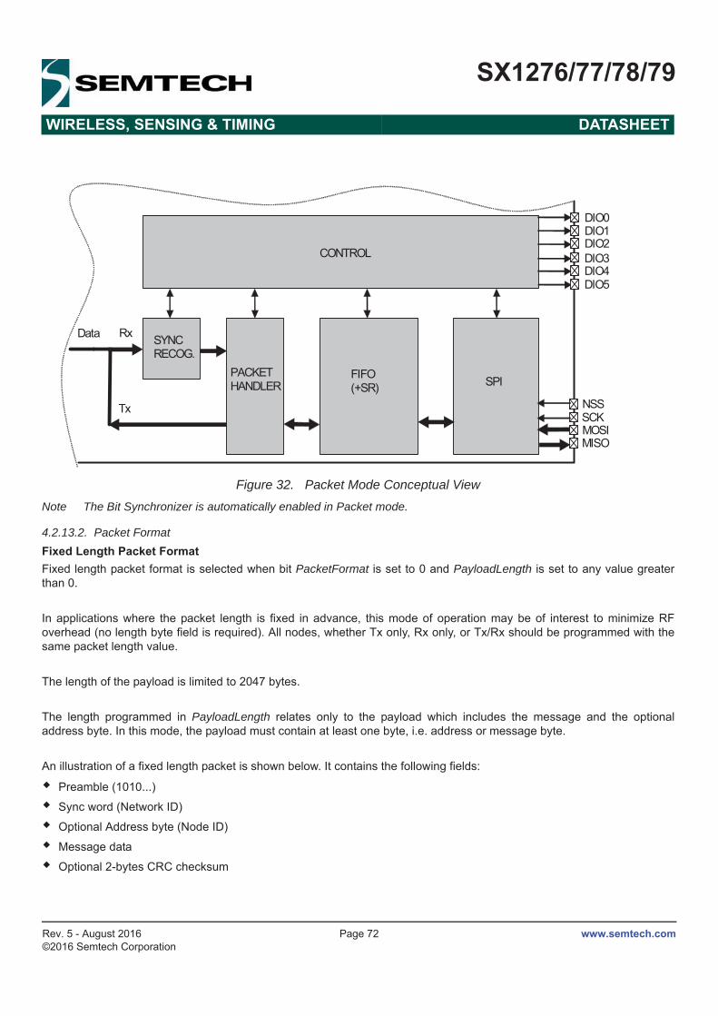
www.semtech.comPage 72
SX1276/77/78/79
WIRELESS, SENSING & TIMING DATASHEET
Rev. 5 - August 2016©2016 Semtech Corporation
Figure 32. Packet Mode Conceptual View
Note The Bit Synchronizer is automatically enabled in Packet mode.
4.2.13.2. Packet FormatFixed Length Packet FormatFixed length packet format is selected when bit PacketFormat is set to 0 and PayloadLength is set to any value greater than 0.
In applications where the packet length is fixed in advance, this mode of operation may be of interest to minimize RF overhead (no length byte field is required). All nodes, whether Tx only, Rx only, or Tx/Rx should be programmed with the same packet length value.
The length of the payload is limited to 2047 bytes.
The length programmed in PayloadLength relates only to the payload which includes the message and the optional address byte. In this mode, the payload must contain at least one byte, i.e. address or message byte.
An illustration of a fixed length packet is shown below. It contains the following fields:
Preamble (1010...)
Sync word (Network ID)
Optional Address byte (Node ID)
Message data
Optional 2-bytes CRC checksum
CONTROL
SPI PACKET HANDLER
SYNC RECOG.
DIO1
MISO MOSI SCK NSS
Rx
Tx
Data
FIFO (+SR)
DIO2
DIO0
DIO3 DIO4 DIO5

www.semtech.comPage 73
SX1276/77/78/79
WIRELESS, SENSING & TIMING DATASHEET
Rev. 5 - August 2016©2016 Semtech Corporation
Figure 33. Fixed Length Packet Format
Variable Length Packet FormatVariable length packet format is selected when bit PacketFormat is set to 1.
This mode is useful in applications where the length of the packet is not known in advance and can vary over time. It is then necessary for the transmitter to send the length information together with each packet in order for the receiver to operate properly.
In this mode the length of the payload, indicated by the length byte, is given by the first byte of the FIFO and is limited to 255 bytes. Note that the length byte itself is not included in its calculation. In this mode, the payload must contain at least 2 bytes, i.e. length + address or message byte.
An illustration of a variable length packet is shown below. It contains the following fields:
Preamble (1010...)
Sync word (Network ID)
Length byte
Optional Address byte (Node ID)
Message data
Message Up to 2047 bytes
Address byte
CRC 2-bytes
Sync Word 0 to 8 bytes
Payload (min 1 byte)
CRC checksum calculation
Fields added by the packet handler in Tx and processed and removed in Rx
Optional User provided fields which are part of the payload
Message part of the payload
Optional DC free data coding
Preamble 0 to 65536 bytes

www.semtech.comPage 74
SX1276/77/78/79
WIRELESS, SENSING & TIMING DATASHEET
Rev. 5 - August 2016©2016 Semtech Corporation
Optional 2-bytes CRC checksum
Figure 34. Variable Length Packet Format
Unlimited Length Packet FormatUnlimited length packet format is selected when bit PacketFormat is set to 0 and PayloadLength is set to 0. The user can then transmit and receive packet of arbitrary length and PayloadLength register is not used in Tx/Rx modes for counting the length of the bytes transmitted/received.
In Tx the data is transmitted depending on the TxStartCondition bit. On the Rx side the data processing features like Address filtering, Manchester encoding and data whitening are not available if the sync pattern length is set to zero (SyncOn = 0). The CRC detection in Rx is also not supported in this mode of the packet handler, however CRC generation in Tx is operational. The interrupts like CrcOk & PayloadReady are not available either.
An unlimited length packet shown below is made up of the following fields:
Preamble (1010...).
Sync word (Network ID).
Optional Address byte (Node ID).
Message data
Optional 2-bytes CRC checksum (Tx only)
Figure 35. Unlimited Length Packet Format
4.2.13.3. Tx Processing
Message Up to 255 bytes
Address byte
Length byte
CRC 2-bytes
Sync Word 0 to 8 bytes
Preamble 0 to 65536 bytes
Payload (min 2 bytes)
CRC checksum calculation
Fields added by the packet handler in Tx and processed and removed in Rx
Optional User provided fields which are part of the payload
Message part of the payload
Optional DC free data coding
Message
unlimited length
Address
byte Sync Word
0 to 8 bytes
Preamble
0 to 65535
bytes
Payload
Fields added by the packet handler in Tx and processed and removed in Rx
Optional User provided fields which are part of the payload
Message part of the payload
DC free Data encoding

www.semtech.comPage 75
SX1276/77/78/79
WIRELESS, SENSING & TIMING DATASHEET
Rev. 5 - August 2016©2016 Semtech Corporation
In Tx mode the packet handler dynamically builds the packet by performing the following operations on the payload available in the FIFO:
Add a programmable number of preamble bytes
Add a programmable Sync word
Optionally calculating CRC over complete payload field (optional length byte + optional address byte + message) and appending the 2 bytes checksum.Optional DC-free encoding of the data (Manchester or whitening)
Only the payload (including optional address and length fields) is required to be provided by the user in the FIFO.
The transmission of packet data is initiated by the Packet Handler only if the chip is in Tx mode and the transmission condition defined by TxStartCondition is fulfilled. If transmission condition is not fulfilled then the packet handler transmits a preamble sequence until the condition is met. This happens only if the preamble length /= 0, otherwise it transmits a zero or one until the condition is met to transmit the packet data.
The transmission condition itself is defined as:
if TxStartCondition = 1, the packet handler waits until the first byte is written into the FIFO, then it starts sending the preamble followed by the sync word and user payloadIf TxStartCondition = 0, the packet handler waits until the number of bytes written in the FIFO is equal to the number defined in RegFifoThresh + 1If the condition for transmission was already fulfilled i.e. the FIFO was filled in Sleep/Stdby then the transmission of packet starts immediately on enabling Tx
4.2.13.4. Rx ProcessingIn Rx mode the packet handler extracts the user payload to the FIFO by performing the following operations:
Receiving the preamble and stripping it off
Detecting the Sync word and stripping it off
Optional DC-free decoding of data
Optionally checking the address byte
Optionally checking CRC and reflecting the result on CrcOk.
Only the payload (including optional address and length fields) is made available in the FIFO.
When the Rx mode is enabled the demodulator receives the preamble followed by the detection of sync word. If fixed length packet format is enabled then the number of bytes received as the payload is given by the PayloadLengthparameter. In variable length mode the first byte received after the sync word is interpreted as the length of the received packet. The internal length counter is initialized to this received length. The PayloadLength register is set to a value which is greater than the maximum expected length of the received packet. If the received length is greater than the maximum length stored in PayloadLength register the packet is discarded otherwise the complete packet is received. If the address check is enabled then the second byte received in case of variable length and first byte in case of fixed length is the address byte. If the address matches to the one in the NodeAddress field, reception of the data continues otherwise it's stopped. The CRC check is performed if CrcOn = 1 and the result is available in CrcOk indicating that the

www.semtech.comPage 76
SX1276/77/78/79
WIRELESS, SENSING & TIMING DATASHEET
Rev. 5 - August 2016©2016 Semtech Corporation
CRC was successful. An interrupt (PayloadReady) is also generated on DIO0 as soon as the payload is available in the FIFO. The payload available in the FIFO can also be read in Sleep/Standby mode. If the CRC fails the PayloadReady interrupt is not generated and the FIFO is cleared. This function can be overridden by setting CrcAutoClearOff = 1, forcing the availability of PayloadReady interrupt and the payload in the FIFO even if the CRC fails.
4.2.13.5. Handling Large PacketsWhen PayloadLength exceeds FIFO size (64 bytes) whether in fixed, variable or unlimited length packet format, in addition to PacketSent in Tx and PayloadReady or CrcOk in Rx, the FIFO interrupts/flags can be used as described below:
For Tx:FIFO can be prefilled in Sleep/Standby but must be refilled “on-the-fly” during Tx with the rest of the payload.1) Pre-fill FIFO (in Sleep/Standby first or directly in Tx mode) until FifoThreshold or FifoFull is set2) In Tx, wait for FifoThreshold or FifoEmpty to be set (i.e. FIFO is nearly empty)3) Write bytes into the FIFO until FifoThreshold or FifoFull is set.4) Continue to step 2 until the entire message has been written to the FIFO (PacketSent will fire when the last bit of the packet has been sent).
For Rx:FIFO must be unfilled “on-the-fly” during Rx to prevent FIFO overrun.1) Start reading bytes from the FIFO when FifoEmpty is cleared or FifoThreshold becomes set.2) Suspend reading from the FIFO if FifoEmpty fires before all bytes of the message have been read3) Continue to step 1 until PayloadReady or CrcOk fires4) Read all remaining bytes from the FIFO either in Rx or Sleep/Standby mode
4.2.13.6. Packet Filtering The SX1276/77/78/79 packet handler offers several mechanisms for packet filtering, ensuring that only useful packets are made available to the uC, reducing significantly system power consumption and software complexity.
Sync Word BasedSync word filtering/recognition is used for identifying the start of the payload and also for network identification. As previously described, the Sync word recognition block is configured (size, value) in RegSyncConfig and RegSyncValue(i) registers. This information is used, both for appending Sync word in Tx, and filtering packets in Rx.
Every received packet which does not start with this locally configured Sync word is automatically discarded and no interrupt is generated.
When the Sync word is detected, payload reception automatically starts and SyncAddressMatch is asserted.
Note Sync Word values containing 0x00 byte(s) are forbidden

www.semtech.comPage 77
SX1276/77/78/79
WIRELESS, SENSING & TIMING DATASHEET
Rev. 5 - August 2016©2016 Semtech Corporation
Address BasedAddress filtering can be enabled via the AddressFiltering bits. It adds another level of filtering, above Sync word (i.e. Sync must match first), typically useful in a multi-node networks where a network ID is shared between all nodes (Sync word) and each node has its own ID (address).
Two address based filtering options are available:
AddressFiltering = 01: Received address field is compared with internal register NodeAddress. If they match then the packet is accepted and processed, otherwise it is discarded.AddressFiltering = 10: Received address field is compared with internal registers NodeAddress and BroadcastAddress. If either is a match, the received packet is accepted and processed, otherwise it is discarded. This additional check with a constant is useful for implementing broadcast in a multi-node networks
Please note that the received address byte, as part of the payload, is not stripped off the packet and is made available in the FIFO. In addition, NodeAddress and AddressFiltering only apply to Rx. On Tx side, if address filtering is expected, the address byte should simply be put into the FIFO like any other byte of the payload.
As address filtering requires a Sync word match, both features share the same interrupt flag SyncAddressMatch.
Length BasedIn variable length Packet mode, PayloadLength must be programmed with the maximum payload length permitted. If received length byte is smaller than this maximum then the packet is accepted and processed, otherwise it is discarded.
Please note that the received length byte, as part of the payload, is not stripped off the packet and is made available in the FIFO.
To disable this function the user should set the value of the PayloadLength to 2047.
CRC BasedThe CRC check is enabled by setting bit CrcOn in RegPacketConfig1. It is used for checking the integrity of the message.
On Tx side a two byte CRC checksum is calculated on the payload part of the packet and appended to the end of the messageOn Rx side the checksum is calculated on the received payload and compared with the two checksum bytes received. The result of the comparison is stored in bit CrcOk.
By default, if the CRC check fails then the FIFO is automatically cleared and no interrupt is generated. This filtering function can be disabled via CrcAutoClearOff bit and in this case, even if CRC fails, the FIFO is not cleared and only PayloadReadyinterrupt goes high. Please note that in both cases, the two CRC checksum bytes are stripped off by the packet handler and only the payload is made available in the FIFO. Two CRC implementations are selected with bit CrcWhiteningType.
Table 31 CRC Description
A C code implementation of each CRC type is proposed in Application Section 7.
Crc Type CrcWhiteningType Polynomial Seed Value ComplementedCCITT 0 (default) X16 + X12 + X5 + 1 0x1D0F Yes
IBM 1 X16 + X15 + X2 + 1 0xFFFF No

www.semtech.comPage 78
SX1276/77/78/79
WIRELESS, SENSING & TIMING DATASHEET
Rev. 5 - August 2016©2016 Semtech Corporation
4.2.13.7. DC-Free Data MechanismsThe payload to be transmitted may contain long sequences of 1's and 0's, which introduces a DC bias in the transmitted signal. The radio signal thus produced has a non uniform power distribution over the occupied channel bandwidth. It also introduces data dependencies in the normal operation of the demodulator. Thus it is useful if the transmitted data is random and DC free.
For such purposes, two techniques are made available in the packet handler: Manchester encoding and data whitening.
Note Only one of the two methods can be enabled at a time.
Manchester EncodingManchester encoding/decoding is enabled if DcFree = 01 and can only be used in Packet mode.
The NRZ data is converted to Manchester code by coding '1' as “10” and '0' as “01”.
In this case, the maximum chip rate is the maximum bit rate given in the specifications and the actual bit rate is half the chip rate. Manchester encoding and decoding is only applied to the payload and CRC checksum while preamble and Sync word are kept NRZ. However, the chip rate from preamble to CRC is the same and defined by BitRate in RegBitRate (Chip Rate = Bit Rate NRZ = 2 x Bit Rate Manchester).
Manchester encoding/decoding is thus made transparent for the user, who still provides/retrieves NRZ data to/from the FIFO.
Figure 36. Manchester Encoding/DecodingData WhiteningAnother technique called whitening or scrambling is widely used for randomizing the user data before radio transmission. The data is whitened using a random sequence on the Tx side and de-whitened on the Rx side using the same sequence. Comparing to Manchester technique it has the advantage of keeping NRZ data rate i.e. actual bit rate is not halved.
The whitening/de-whitening process is enabled if DcFree = 10. A 9-bit LFSR is used to generate a random sequence. The payload and 2-byte CRC checksum is then XORed with this random sequence as shown below. The data is de-whitened on the receiver side by XORing with the same random sequence.
Payload whitening/de-whitening is thus made transparent for the user, who still provides/retrieves NRZ data to/from the FIFO.
...Sync Payload... RF chips @ BR ... 1 1 1 0 1 0 0 1 0 0 1 0 1 1 0 1 0 ... User/NRZ bits Manchester OFF ... 1 1 1 0 1 0 0 1 0 0 1 0 1 1 0 1 0 ...
User/NRZ bits Manchester ON ... 1 1 1 0 1 0 0 1 0 0 1 1 ...
t
1/BR 1/BR

www.semtech.comPage 79
SX1276/77/78/79
WIRELESS, SENSING & TIMING DATASHEET
Rev. 5 - August 2016©2016 Semtech Corporation
Figure 37. Data Whitening Polynomial
4.2.13.8. Beacon Tx ModeIn some short range wireless network topologies a repetitive message, also known as beacon, is transmitted periodically by a transmitter. The Beacon Tx mode allows for the re-transmission of the same packet without having to fill the FIFO multiple times with the same data.
When BeaconOn in RegPacketConfig2 is set to 1, the FIFO can be filled only once in Sleep or Stdby mode with the required payload. After a first transmission, FifoEmpty will go high as usual, but the FIFO content will be restored when the chip exits Transmit mode. FifoEmpty, FifoFull and FifoLevel flags are also restored.
This feature is only available in Fixed packet format, with the Payload Length smaller than the FIFO size. The control of the chip modes (Tx-Sleep-Tx....) can either be undertaken by the microcontroller, or be automated in the Top Sequencer. See example in Section 4.2.13.8.
The Beacon Tx mode is exited by setting BeaconOn to 0, and clearing the FIFO by setting FifoOverrun to 1.
4.2.14. io-homecontrol® Compatibility Mode
The SX1276/77/78/79 features a io-homecontrol® compatibility mode. Please contact your local Semtech representative for details on its implementation.
X 7 X 6 X 5 X 4 X 3 X 2 X 1 X 0 X 8
LFSR Polynom ial =X 9 + X 5 + 1
Transm it data W hitened data

www.semtech.comPage 80
SX1276/77/78/79
WIRELESS, SENSING & TIMING DATASHEET
Rev. 5 - August 2016©2016 Semtech Corporation
4.3. SPI InterfaceThe SPI interface gives access to the configuration register via a synchronous full-duplex protocol corresponding to CPOL = 0 and CPHA = 0 in Motorola/Freescale nomenclature. Only the slave side is implemented.Three access modes to the registers are provided:
SINGLE access: an address byte followed by a data byte is sent for a write access whereas an address byte is sent and a read byte is received for the read access. The NSS pin goes low at the beginning of the frame and goes high after the data byte.BURST access: the address byte is followed by several data bytes. The address is automatically incremented internally between each data byte. This mode is available for both read and write accesses. The NSS pin goes low at the beginning of the frame and stay low between each byte. It goes high only after the last byte transfer.FIFO access: if the address byte corresponds to the address of the FIFO, then succeeding data byte will address the FIFO. The address is not automatically incremented but is memorized and does not need to be sent between each data byte. The NSS pin goes low at the beginning of the frame and stay low between each byte. It goes high only after the last byte transfer.
The figure below shows a typical SPI single access to a register.
Figure 38. SPI Timing Diagram (single access)MOSI is generated by the master on the falling edge of SCK and is sampled by the slave (i.e. this SPI interface) on the rising edge of SCK. MISO is generated by the slave on the falling edge of SCK.
A transfer is always started by the NSS pin going low. MISO is high impedance when NSS is high.
The first byte is the address byte. It is comprises:
A wnr bit, which is 1 for write access and 0 for read access.
Then 7 bits of address, MSB first.
The second byte is a data byte, either sent on MOSI by the master in case of a write access or received by the master on MISO in case of read access. The data byte is transmitted MSB first.
Proceeding bytes may be sent on MOSI (for write access) or received on MISO (for read access) without a rising NSS edge and re-sending the address. In FIFO mode, if the address was the FIFO address then the bytes will be written / read at the FIFO address. In Burst mode, if the address was not the FIFO address, then it is automatically incremented for each new byte received.
The frame ends when NSS goes high. The next frame must start with an address byte. The SINGLE access mode is therefore a special case of FIFO / BURST mode with only 1 data byte transferred.During the write access, the byte transferred from the slave to the master on the MISO line is the value of the written register before the write operation.

www.semtech.comPage 81
SX1276/77/78/79
WIRELESS, SENSING & TIMING DATASHEET
Rev. 5 - August 2016©2016 Semtech Corporation
5. SX1276/77/78/79 Analog & RF Frontend Electronics5.1. Power Supply StrategyThe SX1276/77/78/79 employs an internal voltage regulation scheme which provides stable operating voltage, and hence device characteristics, over the full industrial temperature and operating voltage range of operation. This includes up to +17 dBm of RF output power which is maintained from 1.8 V to 3.7 V and +20 dBm from 2.4 V to 3.7 V.
The SX1276/77/78/79 can be powered from any low-noise voltage source via pins VBAT_ANA, VBAT_RF and VBAT_DIG. Decoupling capacitors should be connected, as suggested in the reference design of the applications section of this document, on VR_PA, VR_DIG and VR_ANA pins to ensure correct operation of the built-in voltage regulators.
5.2. Low Battery DetectorA low battery detector is also included allowing the generation of an interrupt signal in response to the supply voltage dropping below a programmable threshold that is adjustable through the register RegLowBat. The interrupt signal can be mapped to any of the DIO pins by programming RegDioMapping.
5.3. Frequency Synthesis
5.3.1. Crystal OscillatorThe crystal oscillator is the main timing reference of the SX1276/77/78/79. It is used as the reference for the PLL’s frequency synthesis and as the clock signal for all digital processing.
The crystal oscillator startup time, TS_OSC, depends on the electrical characteristics of the crystal reference used, for more information on the electrical specification of the crystal see section 7.1. The crystal connects to the Pierce oscillator on pins XTA and XTB. The SX1276/77/78/79 optimizes the startup time and automatically triggers the PLL when the oscillator signal is stable.
Optionally, an external clock can be used to replace the crystal oscillator. This typically takes the form of a tight tolerance temperature compensated crystal oscillator (TCXO). When using an external clock source the bit TcxoInputOn of registerRegTcxo should be set to 1 and the external clock has to be provided on XTA (pin 5). XTB (pin 6) should be left open.
The peak-peak amplitude of the input signal must never exceed 1.8 V. Please consult your TCXO supplier for an appropriate value of decoupling capacitor, CD.
Figure 39. TCXO Connection
XTA XTB
32 MHzTCXO
NC
OP
VccGND CD
Vcc

www.semtech.comPage 82
SX1276/77/78/79
WIRELESS, SENSING & TIMING DATASHEET
Rev. 5 - August 2016©2016 Semtech Corporation
5.3.2. CLKOUT OutputThe reference frequency, or a fraction of it, can be provided on DIO5 (pin 13) by modifying bits ClkOut in RegDioMapping2. Two typical applications of the CLKOUT output include:
To provide a clock output for a companion processor, thus saving the cost of an additional oscillator. CLKOUT can be made available in any operation mode except Sleep mode and is automatically enabled at power on reset.To provide an oscillator reference output. Measurement of the CLKOUT signal enables simple software trimming of the initial crystal tolerance.
Note To minimize the current consumption of the SX1276/77/78/79, please ensure that the CLKOUT signal is disabled when not required.
5.3.3. PLL The local oscillator of the SX1276/77/78/79 is derived from two almost identical fractional-N PLLs that are referenced to the crystal oscillator circuit. Both PLLs feature a programmable bandwidth setting where one of four discrete preset bandwidths may be accessed.
The SX1276/77/78/79 PLL uses a 19-bit sigma-delta modulator whose frequency resolution, constant over the whole frequency range, is given by:
The carrier frequency is programmed through RegFrf, split across addresses 0x06 to 0x08:
Note The Frf setting is split across 3 bytes. A change in the center frequency will only be taken into account when the least significant byte FrfLsb in RegFrfLsb is written. This allows the potential for user generation of m-ary FSK at very low bit rates. This is possible where frequency modulation is achieved by direct programming of the programmed RF centre frequency. To enable this functionality set the FastHopOn bit of register RegPllHop.
Three frequency bands are supported, defined as follows:Table 32 Frequency Bands
* For SX1279
5.3.4. RC OscillatorAll timing operations in the low-power Sleep state of the Top Level Sequencer rely on the accuracy of the internal low-power RC oscillator. This oscillator is automatically calibrated at the device power-up not requiring any user input.
Name Frequency Limits Products
Band 1 (HF) 862 (*779)-1020 (*960) MHz SX1276/77/79
Band 2 (LF) 410-525 (*480) MHz SX1276/77/78/79
Band 3 (LF) 137-175 (*160)MHz SX1276/77/78/79
FSTEPFXOSC
219----------------=
FRF FSTEP Frf 23 0( , )×=
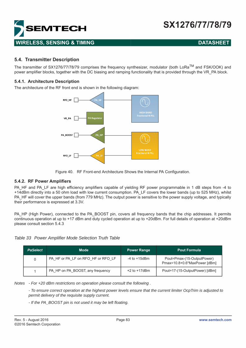
www.semtech.comPage 83
SX1276/77/78/79
WIRELESS, SENSING & TIMING DATASHEET
Rev. 5 - August 2016©2016 Semtech Corporation
5.4. Transmitter DescriptionThe transmitter of SX1276/77/78/79 comprises the frequency synthesizer, modulator (both LoRaTM and FSK/OOK) and power amplifier blocks, together with the DC biasing and ramping functionality that is provided through the VR_PA block.
5.4.1. Architecture DescriptionThe architecture of the RF front end is shown in the following diagram:
Figure 40. RF Front-end Architecture Shows the Internal PA Configuration.
5.4.2. RF Power AmplifiersPA_HF and PA_LF are high efficiency amplifiers capable of yielding RF power programmable in 1 dB steps from -4 to +14dBm directly into a 50 ohm load with low current consumption. PA_LF covers the lower bands (up to 525 MHz), whilst PA_HF will cover the upper bands (from 779 MHz). The output power is sensitive to the power supply voltage, and typically their performance is expressed at 3.3V.
PA_HP (High Power), connected to the PA_BOOST pin, covers all frequency bands that the chip addresses. It permits continuous operation at up to +17 dBm and duty cycled operation at up to +20dBm. For full details of operation at +20dBm please consult section 5.4.3
Table 33 Power Amplifier Mode Selection Truth Table
Notes - For +20 dBm restrictions on operation please consult the following .
- To ensure correct operation at the highest power levels ensure that the current limiter OcpTrim is adjusted to permit delivery of the requisite supply current.
- If the PA_BOOST pin is not used it may be left floating.
PaSelect Mode Power Range Pout Formula
0 PA_HF or PA_LF on RFO_HF or RFO_LF -4 to +15dBm Pout=Pmax-(15-OutputPower)Pmax=10.8+0.6*MaxPower [dBm]
1 PA_HP on PA_BOOST, any frequency +2 to +17dBm Pout=17-(15-OutputPower) [dBm]

www.semtech.comPage 84
SX1276/77/78/79
WIRELESS, SENSING & TIMING DATASHEET
Rev. 5 - August 2016©2016 Semtech Corporation
5.4.3. High Power +20 dBm OperationThe SX1276/77/78/79 have a high power +20 dBm capability on PA_BOOST pin, with the following settings:
Table 34 High Power Settings
Notes - High Power settings must be turned off when using PA_LF or PA_HF
- The Over Current Protection limit should be adapted to the actual power level, in RegOcp
Specific Absolute Maximum Ratings and Operating Range restrictions apply to the +20 dBm operation. They are listed in Table 35 and Table 36.
Table 35 Operating Range, +20dBm Operation
Table 36 Operating Range, +20dBm Operation
The duty cycle of transmission at +20 dBm is limited to 1%, with a maximum VSWR of 3:1 at antenna port, over the standard operating range [-40;+85°C]. For any other operating condition, contact your Semtech representative.
Register Address Value forHigh Power
Default valuePA_HF/LF or
+17dBmDescription
RegPaDac 0x4d 0x87 0x84 Set Pmax to +20dBm for PA_HP
Symbol Description Min Max Unit
DC_20dBm Duty Cycle of transmission at +20 dBm output - 1 %
VSWR_20dBm Maximum VSWR at antenna port, +20 dBm output - 3:1 -
Symbol Description Min Max Unit
VDDop_20dBm Supply voltage, +20 dBm output 2.4 3.7 V

www.semtech.comPage 85
SX1276/77/78/79
WIRELESS, SENSING & TIMING DATASHEET
Rev. 5 - August 2016©2016 Semtech Corporation
5.4.4. Over Current ProtectionThe power amplifiers of SX1276/77/78/79 are protected against current over supply in adverse RF load conditions by the over current protection block. This has the added benefit of protecting battery chemistries with limited peak current capability and minimising worst case PA consumption in battery life calculation. The current limiter value is controlled by the OcpTrim bits in RegOcp, and is calculated according to the following formulae:
Table 37 Trimming of the OCP Current
Note Imax sets a limit on the current drain of the Power Amplifier only, hence the maximum current drain of the SX1276/77/78/79 is equal to Imax + IDDFS.
5.5. Receiver Description
5.5.1. OverviewThe SX1276/77/78/79 features a digital receiver with the analog to digital conversion process being performed directly following the LNA-Mixers block. In addition to the LoRaTM modulation scheme the low-IF receiver is able to demodulate ASK, OOK, (G)FSK and (G)MSK modulation. All filtering, demodulation, gain control, synchronization and packet handling is performed digitally allowing a high degree of programmable flexibility. The receiver also has automatic gain calibration, this improves the precision of RSSI measurement and enhances image rejection.
5.5.2. Receiver Enabled and Receiver Active StatesIn the receiver operating mode two states of functionality are defined. Upon initial transition to receiver operating mode the receiver is in the ‘receiver-enabled’ state. In this state the receiver awaits for either the user defined valid preamble or RSSI detection criterion to be fulfilled. Once met the receiver enters ‘receiver-active’ state. In this second state the received signal is processed by the packet engine and top level sequencer. For a complete description of the digital functions of the SX1276/77/78/79 receiver please see section 4 of the datasheet.
5.5.3. Automatic Gain Control In FSK/OOK ModeThe AGC feature allows receiver to handle a wide Rx input dynamic range from the sensitivity level up to maximum input level of 0dBm or more, whilst optimizing the system linearity.
The following table shows typical NF and IIP3 performances for the SX1276/77/78/79 LNA gains available.
OcpTrim IMAX Imax Formula
0 to 15 45 to 120 mA 45 + 5*OcpTrim [mA]
16 to 27 130 to 240 mA -30 + 10*OcpTrim [mA]
27+ 240 mA 240 mA

www.semtech.comPage 86
SX1276/77/78/79
WIRELESS, SENSING & TIMING DATASHEET
Rev. 5 - August 2016©2016 Semtech Corporation
Table 38 LNA Gain Control and Performances
5.5.4. RSSI in FSK/OOK ModeThe RSSI provides a measure of the incoming signal power at RF input port, measured within the receiver bandwidth. The signal power is available in RssiValue. This value is absolute in units of dBm and with a resolution of 0.5 dB. The formula below relates the register value to the absolute input signal level at the RF input port:
The RSSI value can be compensated to take into account the loss in the matching network or even the gain of an additional LNA by using RssiOffset. The offset can be chosen in 1 dB steps from -16 to +15 dB. When compensation is applied, the effective signal strength is read as follows:
The RSSI value is smoothed on a user defined number of measured RSSI samples. The precision of the RSSI value is related to the number of RSSI samples used. RssiSmoothing selects the number of RSSI samples from a minimum of 2 samples up to 256 samples in increments of power of 2. Table 39 gives the estimation of the RSSI accuracy for a 10 dB SNR and response time versus the number of RSSI samples programmed in RssiSmoothing.Table 39 RssiSmoothing Options
The RSSI is calibrated when the image and RSSI calibration process is launched.
RX input level (Pin) GainSetting LnaGain Relative LNA
Gain [dB]
NFBand 3/2/1
[dB]
IIP3Band 3/2/1
[dBm]
Pin <= AgcThresh1 G1 ‘001’ 0 dB 4/5.5/7 -15/-22/-11
AgcThresh1 < Pin <= AgcThresh2 G2 ‘010’ -6 dB 6.5/8/12 -11/-15/-6
AgcThresh2 < Pin <= AgcThresh3 G3 ‘011’ -12 dB 11/12/17 -11/-12/0
AgcThresh3 < Pin <= AgcThresh4 G4 ‘100’ -24 dB 20/21/27 2/3/9
AgcThresh4 < Pin <= AgcThresh5 G5 ‘110’ -26 dB 32/33/35 10/10/14
AgcThresh5 < Pin G6 ‘111’ -48 dB 44/45/43 11/12/14
RssiSmoothing Number of Samples Estimated Accuracy Response Time‘000’ 2 ± 6 dB‘001’ 4 ± 5 dB‘010’ 8 ± 4 dB‘011’ 16 ± 3 dB‘100’ 32 ± 2 dB‘101’ 64 ± 1.5 dB‘110’ 128 ± 1.2 dB‘111’ 256 ± 1.1 dB
[ ] [ ]dBRssiOffsetdBmlevelRFRssiValue +⋅−= 2
[ ]2
RssiValuedBmRSSI −=
( )[ ] [ ]mskHzRxBw
ingRssiSmooth
⋅
+
42 1
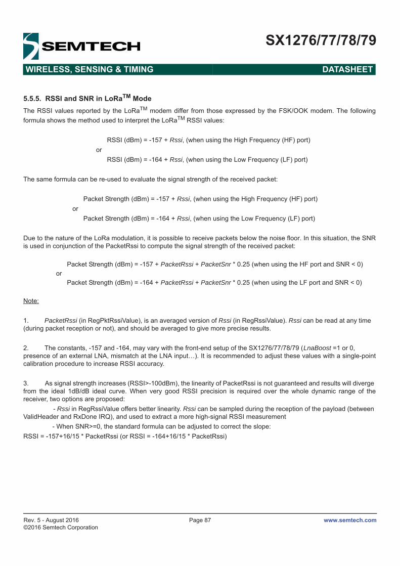
www.semtech.comPage 87
SX1276/77/78/79
WIRELESS, SENSING & TIMING DATASHEET
Rev. 5 - August 2016©2016 Semtech Corporation
5.5.5. RSSI and SNR in LoRaTM ModeThe RSSI values reported by the LoRaTM modem differ from those expressed by the FSK/OOK modem. The following formula shows the method used to interpret the LoRaTM RSSI values:
RSSI (dBm) = -157 + Rssi, (when using the High Frequency (HF) port) or RSSI (dBm) = -164 + Rssi, (when using the Low Frequency (LF) port)
The same formula can be re-used to evaluate the signal strength of the received packet:
Packet Strength (dBm) = -157 + Rssi, (when using the High Frequency (HF) port) or Packet Strength (dBm) = -164 + Rssi, (when using the Low Frequency (LF) port)
Due to the nature of the LoRa modulation, it is possible to receive packets below the noise floor. In this situation, the SNR is used in conjunction of the PacketRssi to compute the signal strength of the received packet:
Packet Strength (dBm) = -157 + PacketRssi + PacketSnr * 0.25 (when using the HF port and SNR < 0) or Packet Strength (dBm) = -164 + PacketRssi + PacketSnr * 0.25 (when using the LF port and SNR < 0)
Note:
1. PacketRssi (in RegPktRssiValue), is an averaged version of Rssi (in RegRssiValue). Rssi can be read at any time (during packet reception or not), and should be averaged to give more precise results.
2. The constants, -157 and -164, may vary with the front-end setup of the SX1276/77/78/79 (LnaBoost =1 or 0, presence of an external LNA, mismatch at the LNA input…). It is recommended to adjust these values with a single-point calibration procedure to increase RSSI accuracy.
3. As signal strength increases (RSSI>-100dBm), the linearity of PacketRssi is not guaranteed and results will diverge from the ideal 1dB/dB ideal curve. When very good RSSI precision is required over the whole dynamic range of the receiver, two options are proposed: - Rssi in RegRssiValue offers better linearity. Rssi can be sampled during the reception of the payload (between ValidHeader and RxDone IRQ), and used to extract a more high-signal RSSI measurement - When SNR>=0, the standard formula can be adjusted to correct the slope:RSSI = -157+16/15 * PacketRssi (or RSSI = -164+16/15 * PacketRssi)

www.semtech.comPage 88
SX1276/77/78/79
WIRELESS, SENSING & TIMING DATASHEET
Rev. 5 - August 2016©2016 Semtech Corporation
5.5.6. Channel FilterThe role of the channel filter is to reject noise and interference outside of the wanted channel. The SX1276/77/78/79 channel filtering is implemented with a 16-tap finite impulse response (FIR) filter. Rejection of the filter is high enough that the filter stop-band performance is not the dominant influence on adjacent channel rejection performance. This is instead limited by the SX1276/77/78/79 local oscillator phase noise.
Note To respect sampling criterion in the decimation chain of the receiver, the communication bit rate cannot be set at a higher than twice the single side receiver bandwidth (BitRate < 2 x RxBw)
The single-side channel filter bandwidth RxBw is controlled by the parameters RxBwMant and RxBwExp in RegRxBw:
The following channel filter bandwidths are hence accessible in the case of a 32 MHz reference oscillator:
Table 40 Available RxBw Settings
RxBwMant(binary/value)
RxBwExp(decimal)
RxBw (kHz)FSK/OOK
10b / 24 7 2.601b / 20 7 3.100b / 16 7 3.910b / 24 6 5.201b / 20 6 6.300b / 16 6 7.810b / 24 5 10.401b / 20 5 12.500b / 16 5 15.610b / 24 4 20.801b / 20 4 25.000b / 16 4 31.310b / 24 3 41.701b / 20 3 50.000b / 16 3 62.510b / 24 2 83.301b / 20 2 100.000b / 16 2 125.010b / 24 1 166.701b / 20 1 200.000b / 16 1 250.0
Other settings reserved
RxBw FXOSCRxBwMant 2RxBwExp 2+×------------------------------------------------------------------=

www.semtech.comPage 89
SX1276/77/78/79
WIRELESS, SENSING & TIMING DATASHEET
Rev. 5 - August 2016©2016 Semtech Corporation
5.5.7. Temperature MeasurementA stand alone temperature measurement block is used in order to measure the temperature in any mode except Sleep and Standby. It is enabled by default, and can be stopped by setting TempMonitorOff to 1. The result of the measurement is stored in TempValue in RegTemp.
Due to process variations, the absolute accuracy of the result is +/- 10 °C. Higher precision requires a calibration procedure at a known temperature. The figure below shows the influence of just such a calibration process. For more information, including source code, please consult the applications section of this document.
Figure 41. Temperature Sensor Response
When using the temperature sensor in the application, the following sequence should be followed:
Set the device to Standby and wait for oscillator startup
Set the device to FSRx mode
Set TempMonitorOff = 0 (enables the sensor). It is not required to wait for the PLL Lock indication
Wait for 140 microseconds
Set TempMonitorOff = 1
Set device back to Sleep of Standby mode
Access temperature value in RegTemp

www.semtech.comPage 90
SX1276/77/78/79
WIRELESS, SENSING & TIMING DATASHEET
Rev. 5 - August 2016©2016 Semtech Corporation
6. Description of the RegistersThe register mapping depends upon whether FSK/OOK or LoRaTM mode has been selected. The following table summarises the location and function of each register and gives an overview of the changes in register mapping between both modes of operation.
6.1. Register Table SummaryTable 41 Registers Summary
AddressRegister Name Reset
(POR)Default(FSK)
Description
FSK/OOK Mode LoRaTM Mode FSK Mode LoRaTM Mode0x00 RegFifo 0x00 FIFO read/write access0x01 RegOpMode 0x01 Operating mode & LoRaTM / FSK selection0x02 RegBitrateMsb
Unused
0x1A Bit Rate setting, Most Significant Bits0x03 RegBitrateLsb 0x0B Bit Rate setting, Least Significant Bits0x04 RegFdevMsb 0x00 Frequency Deviation setting, Most Significant Bits0x05 RegFdevLsb 0x52 Frequency Deviation setting, Least Significant Bits0x06 RegFrfMsb 0x6C RF Carrier Frequency, Most Significant Bits0x07 RegFrfMid 0x80 RF Carrier Frequency, Intermediate Bits0x08 RegFrfLsb 0x00 RF Carrier Frequency, Least Significant Bits0x09 RegPaConfig 0x4F PA selection and Output Power control0x0A RegPaRamp 0x09 Control of PA ramp time, low phase noise PLL0x0B RegOcp 0x2B Over Current Protection control0x0C RegLna 0x20 LNA settings
0x0D RegRxConfig RegFifoAddrPtr 0x08 0x0E AFC, AGC, ctrl FIFO SPI pointer
0x0E RegRssiConfig RegFifoTxBa-seAddr 0x02 RSSI Start Tx data
0x0F RegRssiCollision RegFifoRxBa-seAddr 0x0A RSSI Collision detector Start Rx data
0x10 RegRssiThresh FifoRxCurren-tAddr 0xFF RSSI Threshold control Start address of last
packet received0x11 RegRssiValue RegIrqFlagsMask n/a n/a RSSI value in dBm Optional IRQ flag mask0x12 RegRxBw RegIrqFlags 0x15 Channel Filter BW Control IRQ flags0x13 RegAfcBw RegRxNbBytes 0x0B AFC Channel Filter BW Number of received bytes
0x14 RegOokPeak RegRxHeaderCntValueMsb
0x28 OOK demodulatorNumber of valid headers received
0x15 RegOokFix RegRxHeaderCntValueLsb
0x0C Threshold of the OOK demod
0x16 RegOokAvg RegRxPacketCntValueMsb
0x12 Average of the OOK demodNumber of valid packets received
0x17 Reserved17 RegRxPacketCntValueLsb
0x47 -
0x18 Reserved18 RegModemStat 0x32 - Live LoRaTM modem status
0x19 Reserved19 RegPktSnrValue 0x3E - Espimation of last packetSNR
0x1A RegAfcFei RegPktRssiValue 0x00 AFC and FEI control RSSI of last packet

www.semtech.comPage 91
SX1276/77/78/79
WIRELESS, SENSING & TIMING DATASHEET
Rev. 5 - August 2016©2016 Semtech Corporation
0x1B RegAfcMsb RegRssiValue 0x00 n/a Frequency correction value of the AFC
Current RSSI0x1C RegAfcLsb RegHopChannel 0x00 n/a FHSS start channel0x1D RegFeiMsb RegModemConfig
10x00 n/a
Value of the calculatedfrequency error
Modem PHY config 1
0x1E RegFeiLsb RegModemConfig2
0x00 n/a Modem PHY config 2
0x1F RegPreambleDe-tect
RegSymbTimeoutLsb
0x40 0xAA Settings of the Preamble Detector Receiver timeout value
0x20 RegRxTimeout1 RegPreambleMsb 0x00 Timeout Rx request and RSSISize of preamble0x21 RegRxTimeout2 RegPreambleLsb 0x00 Timeout RSSI and Pay-
loadReady0x22 RegRxTimeout3 RegPay-
loadLength0x00 Timeout RSSI and SyncAd-
dressLoRaTM payload length
0x23 RegRxDelay RegMaxPayloadLength
0x00Delay between Rx cycles LoRaTM maximum pay-
load length0x24 RegOsc RegHopPeriod 0x05 0x07 RC Oscillators Settings, CLK-
OUT frequency FHSS Hop period
0x25 RegPreambleMsb RegFifoRxByteAddr
0x00Preamble length, MSB Address of last byte
written in FIFO0x26 RegPreambleLsb RegModemCon-
fig30x03 Preamble length, LSB Modem PHY config 3
0x27 RegSyncConfig RESERVED 0x93 Sync Word Recognition control RESERVED0x28 RegSyncValue1 RegFeiMsb 0x55 0x01 Sync Word bytes 1
Estimated frequency error
0x29 RegSyncValue2 RegFeiMid 0x55 0x01 Sync Word bytes 2
0x2A RegSyncValue3 RegFeiLsb 0x55 0x01 Sync Word bytes 3
0x2B RegSyncValue4 RESERVED 0x55 0x01 Sync Word bytes 4 RESERVED
0x2C RegSyncValue5 RegRssiWide-band
0x55 0x01 Sync Word bytes 5 Wideband RSSI meas-urement
0x2D-0x2F
RegSyncValue6-8 RESERVED 0x55 0x01 Sync Word bytes, 6 to 8RESERVED
0x30 RegPacketConfig1 RESERVED 0x90 Packet mode settings0x31 RegPacketConfig2 RegDetectOpti-
mize0x40 Packet mode settings LoRa detection Optimize
for SF60x32 RegPayloadLength RESERVED 0x40 Payload length setting RESERVED0x33 RegNodeAdrs RegInvertIQ 0x00
Node address Invert LoRa I and Q signals
0x34 RegBroadcastAdrs
RESERVED
0x00 Broadcast address
RESERVED0x35 RegFifoThresh 0x0F 0x1F Fifo threshold, Tx start condi-tion
0x36 RegSeqConfig1 0x00 Top level Sequencer settings0x37 RegSeqConfig2 RegDetection-
Threshold0x00
Top level Sequencer settings LoRa detection thresholdfor SF6
0x38 RegTimerResol RESERVED 0x00 Timer 1 and 2 resolution control RESERVED0x39 RegTimer1Coef RegSyncWord 0xF5 0x12 Timer 1 setting LoRa Sync Word
AddressRegister Name Reset
(POR)Default(FSK)
Description
FSK/OOK Mode LoRaTM Mode FSK Mode LoRaTM Mode
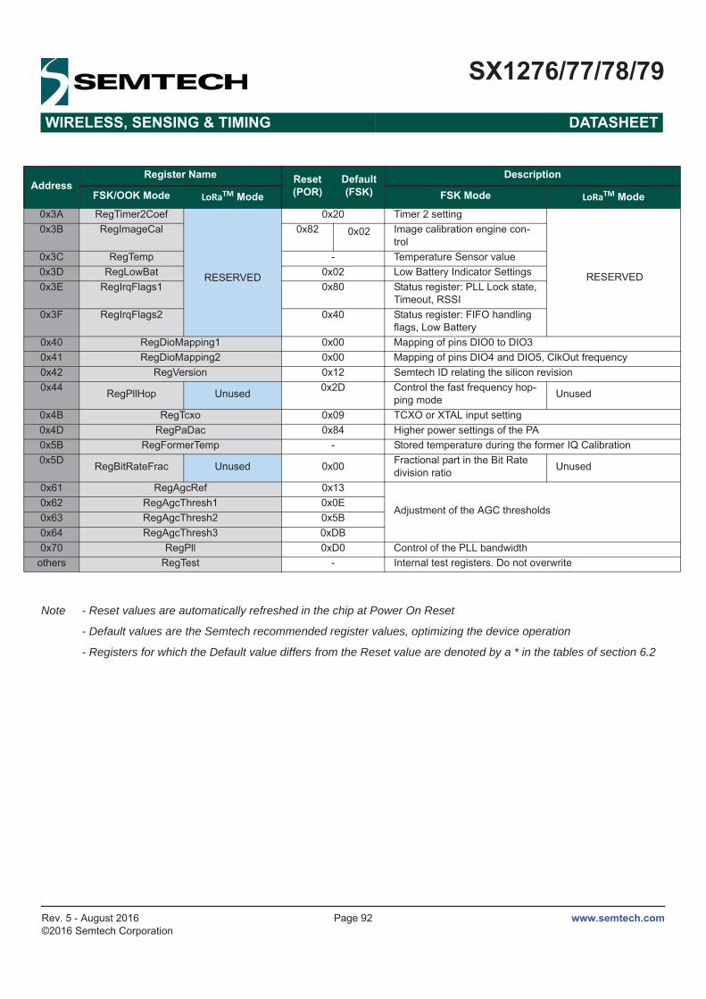
www.semtech.comPage 92
SX1276/77/78/79
WIRELESS, SENSING & TIMING DATASHEET
Rev. 5 - August 2016©2016 Semtech Corporation
Note - Reset values are automatically refreshed in the chip at Power On Reset
- Default values are the Semtech recommended register values, optimizing the device operation
- Registers for which the Default value differs from the Reset value are denoted by a * in the tables of section 6.2
0x3A RegTimer2Coef
RESERVED
0x20 Timer 2 setting
RESERVED
0x3B RegImageCal 0x82 0x02 Image calibration engine con-trol
0x3C RegTemp - Temperature Sensor value0x3D RegLowBat 0x02 Low Battery Indicator Settings0x3E RegIrqFlags1 0x80 Status register: PLL Lock state,
Timeout, RSSI0x3F RegIrqFlags2 0x40 Status register: FIFO handling
flags, Low Battery 0x40 RegDioMapping1 0x00 Mapping of pins DIO0 to DIO30x41 RegDioMapping2 0x00 Mapping of pins DIO4 and DIO5, ClkOut frequency0x42 RegVersion 0x12 Semtech ID relating the silicon revision0x44 RegPllHop Unused 0x2D Control the fast frequency hop-
ping mode Unused
0x4B RegTcxo 0x09 TCXO or XTAL input setting0x4D RegPaDac 0x84 Higher power settings of the PA0x5B RegFormerTemp - Stored temperature during the former IQ Calibration0x5D RegBitRateFrac Unused 0x00 Fractional part in the Bit Rate
division ratio Unused
0x61 RegAgcRef 0x13
Adjustment of the AGC thresholds0x62 RegAgcThresh1 0x0E0x63 RegAgcThresh2 0x5B0x64 RegAgcThresh3 0xDB0x70 RegPll 0xD0 Control of the PLL bandwidth
others RegTest - Internal test registers. Do not overwrite
AddressRegister Name Reset
(POR)Default(FSK)
Description
FSK/OOK Mode LoRaTM Mode FSK Mode LoRaTM Mode

www.semtech.comPage 93
SX1276/77/78/79
WIRELESS, SENSING & TIMING DATASHEET
Rev. 5 - August 2016©2016 Semtech Corporation
6.2. FSK/OOK Mode Register MapThis section details the SX1276/77/78/79 register mapping and the precise contents of each register in FSK/OOK mode.
Convention: r: read, w: write, t:trigger, c: clear
Table 42 Register Map
Name(Address) Bits Variable Name Mode Default
value FSK/OOK Description
RegFifo(0x00) 7-0 Fifo rw 0x00 FIFO data input/output
Registers for Common settings
RegOpMode(0x01)
7 LongRangeMode r 0x00
0 FSK/OOK Mode1 LoRaTM ModeThis bit can be modified only in Sleep mode. A write operation on other device modes is ignored.
6-5 ModulationType rw 0x00
Modulation scheme:00 FSK01 OOK10 11 reserved
4 reserved r 0x0 reserved
3 LowFrequencyModeOn rw 0x01Access Low Frequency Mode registers (from address 0x61 on)0 High Frequency Mode (access to HF test registers)1 Low Frequency Mode (access to LF test registers)
2-0 Mode rw 0x01
Transceiver modes000 Sleep mode001 Stdby mode010 FS mode TX (FSTx)011 Transmitter mode (Tx)100 FS mode RX (FSRx)101 Receiver mode (Rx)110 reserved111 reserved
RegBitrateMsb(0x02) 7-0 BitRate(15:8) rw 0x1a MSB of Bit Rate (chip rate if Manchester encoding is enabled)
RegBitrateLsb(0x03) 7-0 BitRate(7:0) rw 0x0b
LSB of bit rate (chip rate if Manchester encoding is enabled)
Default value: 4.8 kb/s
RegFdevMsb(0x04)
7-6 reserved rw 0x00 reserved
5-0 Fdev(13:8) rw 0x00 MSB of the frequency deviation
RegFdevLsb(0x05) 7-0 Fdev(7:0) rw 0x52
LSB of the frequency deviation
Default value: 5 kHz
BitRate FXOSC
BitRate 15 0( , ) BitrateFrac16
-------------------------------+-------------------------------------------------------------------------=
Fdev Fstep Fdev 15 0( , )×=

www.semtech.comPage 94
SX1276/77/78/79
WIRELESS, SENSING & TIMING DATASHEET
Rev. 5 - August 2016©2016 Semtech Corporation
RegFrfMsb(0x06) 7-0 Frf(23:16) rw 0x6c MSB of the RF carrier frequency
RegFrfMid(0x07) 7-0 Frf(15:8) rw 0x80 MSB of the RF carrier frequency
RegFrfLsb(0x08) 7-0 Frf(7:0) rw 0x00
LSB of RF carrier frequency
Default value: 434.000 MHzThe RF frequency is taken into account internally only when:- entering FSRX/FSTX modes- re-starting the receiver
Registers for the Transmitter
RegPaConfig(0x09)
7 PaSelect rw 0x00Selects PA output pin0 RFO pin. Maximum power of +14 dBm1 PA_BOOST pin. Maximum power of +20 dBm
6-4 MaxPower rw 0x04 Select max output power: Pmax=10.8+0.6*MaxPower [dBm]
3-0 OutputPower rw 0x0f Pout=Pmax-(15-OutputPower) if PaSelect = 0 (RFO pins)Pout=17-(15-OutputPower) if PaSelect = 1 (PA_BOOST pin)
RegPaRamp(0x0A)
7 unused r 0x00 unused
6-5 ModulationShaping rw 0x00
Data shaping:In FSK:00 no shaping01 Gaussian filter BT = 1.010 Gaussian filter BT = 0.511 Gaussian filter BT = 0.3In OOK:00 no shaping01 filtering with fcutoff = bit_rate10 filtering with fcutoff = 2*bit_rate (for bit_rate < 125 kb/s)11 reserved
4 reserved rw 0x00 reserved
3-0 PaRamp rw 0x09
Rise/Fall time of ramp up/down in FSK0000 3.4 ms0001 2 ms0010 1 ms0011 500 us0100 250 us0101 125 us0110 100 us0111 62 us1000 50 us1001 40 us (d)1010 31 us1011 25 us1100 20 us1101 15 us1110 12 us1111 10 us
Name(Address) Bits Variable Name Mode Default
value FSK/OOK Description
Frf Fstep Frf 23 0;( )×=

www.semtech.comPage 95
SX1276/77/78/79
WIRELESS, SENSING & TIMING DATASHEET
Rev. 5 - August 2016©2016 Semtech Corporation
RegOcp(0x0B)
7-6 unused r 0x00 unused
5 OcpOn rw 0x01Enables overload current protection (OCP) for the PA:0 OCP disabled1 OCP enabled
4-0 OcpTrim rw 0x0b
Trimming of OCP current:Imax = 45+5*OcpTrim [mA] if OcpTrim <= 15 (120 mA) /Imax = -30+10*OcpTrim [mA] if 15 < OcpTrim <= 27 (130 to 240 mA)Imax = 240mA for higher settingsDefault Imax = 100mA
Registers for the Receiver
RegLna(0x0C)
7-5 LnaGain rw 0x01
LNA gain setting:000 reserved001 G1 = highest gain010 G2 = highest gain – 6 dB011 G3 = highest gain – 12 dB100 G4 = highest gain – 24 dB101 G5 = highest gain – 36 dB110 G6 = highest gain – 48 dB111 reservedNote:Reading this address always returns the current LNA gain (which may be different from what had been previously selected if AGC is enabled.
4-3 LnaBoostLf rw 0x00Low Frequency (RFI_LF) LNA current adjustment00 Default LNA currentOther Reserved
2 reserved rw 0x00 reserved
1-0 LnaBoostHf rw 0x00High Frequency (RFI_HF) LNA current adjustment00 Default LNA current11 Boost on, 150% LNA current
Name(Address) Bits Variable Name Mode Default
value FSK/OOK Description

www.semtech.comPage 96
SX1276/77/78/79
WIRELESS, SENSING & TIMING DATASHEET
Rev. 5 - August 2016©2016 Semtech Corporation
RegRxConfig(0x0d)
7 RestartRxOnCollision rw 0x00
Turns on the mechanism restarting the receiver automatically if it gets saturated or a packet collision is detected0 No automatic Restart1 Automatic restart On
6 RestartRxWithoutPllLock wt 0x00Triggers a manual Restart of the Receiver chain when set to 1.Use this bit when there is no frequency change, RestartRxWithPllLock otherwise.
5 RestartRxWithPllLock wt 0x00Triggers a manual Restart of the Receiver chain when set to 1.Use this bit when there is a frequency change, requiring some time for the PLL to re-lock.
4 AfcAutoOn rw 0x00 0 No AFC performed at receiver startup1 AFC is performed at each receiver startup
3 AgcAutoOn rw 0x01 0 LNA gain forced by the LnaGain Setting1 LNA gain is controlled by the AGC
2-0 RxTrigger rw 0x06*
Selects the event triggering AGC and/or AFC at receiver startup. See Table 24 for a description.
RegRssiConfig(0x0e)
7-3 RssiOffset rw 0x00Signed RSSI offset, to compensate for the possible losses/gains in the front-end (LNA, SAW filter...)1dB / LSB, 2’s complement format
2-0 RssiSmoothing rw 0x02
Defines the number of samples taken to average the RSSI result:000 2 samples used001 4 samples used010 8 samples used011 16 samples used100 32 samples used101 64 samples used110 128 samples used111 256 samples used
RegRssiCollision(0x0f) 7-0 RssiCollisionThreshold rw 0x0a
Sets the threshold used to consider that an interferer is detected, witnessing a packet collision. 1dB/LSB (only RSSI increase)Default: 10dB
RegRssiThresh(0x10) 7-0 RssiThreshold rw 0xff RSSI trigger level for the Rssi interrupt:
- RssiThreshold / 2 [dBm]
RegRssiValue(0x11) 7-0 RssiValue r - Absolute value of the RSSI in dBm, 0.5dB steps.
RSSI = - RssiValue/2 [dBm]
RegRxBw(0x12)
7 unused r - unused
6-5 reserved rw 0x00 reserved
4-3 RxBwMant rw 0x02Channel filter bandwidth control:00 RxBwMant = 16 10 RxBwMant = 2401 RxBwMant = 20 11 reserved
2-0 RxBwExp rw 0x05 Channel filter bandwidth control
RegAfcBw(0x13)
7-5 reserved rw 0x00 reserved
4-3 RxBwMantAfc rw 0x01 RxBwMant parameter used during the AFC
2-0 RxBwExpAfc rw 0x03 RxBwExp parameter used during the AFC
Name(Address) Bits Variable Name Mode Default
value FSK/OOK Description
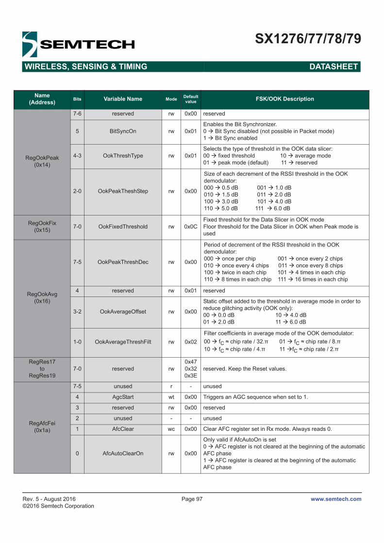
www.semtech.comPage 97
SX1276/77/78/79
WIRELESS, SENSING & TIMING DATASHEET
Rev. 5 - August 2016©2016 Semtech Corporation
RegOokPeak(0x14)
7-6 reserved rw 0x00 reserved
5 BitSyncOn rw 0x01Enables the Bit Synchronizer.0 Bit Sync disabled (not possible in Packet mode)1 Bit Sync enabled
4-3 OokThreshType rw 0x01Selects the type of threshold in the OOK data slicer:00 fixed threshold 10 average mode01 peak mode (default) 11 reserved
2-0 OokPeakTheshStep rw 0x00
Size of each decrement of the RSSI threshold in the OOK demodulator:000 0.5 dB 001 1.0 dB010 1.5 dB 011 2.0 dB100 3.0 dB 101 4.0 dB110 5.0 dB 111 6.0 dB
RegOokFix(0x15) 7-0 OokFixedThreshold rw 0x0C
Fixed threshold for the Data Slicer in OOK modeFloor threshold for the Data Slicer in OOK when Peak mode is used
RegOokAvg(0x16)
7-5 OokPeakThreshDec rw 0x00
Period of decrement of the RSSI threshold in the OOK demodulator:000 once per chip 001 once every 2 chips010 once every 4 chips 011 once every 8 chips100 twice in each chip 101 4 times in each chip110 8 times in each chip 111 16 times in each chip
4 reserved rw 0x01 reserved
3-2 OokAverageOffset rw 0x00
Static offset added to the threshold in average mode in order to reduce glitching activity (OOK only):00 0.0 dB 10 4.0 dB01 2.0 dB 11 6.0 dB
1-0 OokAverageThreshFilt rw 0x02Filter coefficients in average mode of the OOK demodulator:00 fC chip rate / 32. 01 fC chip rate / 8.10 fC chip rate / 4. 11 fC chip rate / 2.
RegRes17to
RegRes197-0 reserved rw
0x470x320x3E
reserved. Keep the Reset values.
RegAfcFei(0x1a)
7-5 unused r - unused
4 AgcStart wt 0x00 Triggers an AGC sequence when set to 1.
3 reserved rw 0x00 reserved
2 unused - - unused
1 AfcClear wc 0x00 Clear AFC register set in Rx mode. Always reads 0.
0 AfcAutoClearOn rw 0x00
Only valid if AfcAutoOn is set0 AFC register is not cleared at the beginning of the automatic AFC phase1 AFC register is cleared at the beginning of the automatic AFC phase
Name(Address) Bits Variable Name Mode Default
value FSK/OOK Description

www.semtech.comPage 98
SX1276/77/78/79
WIRELESS, SENSING & TIMING DATASHEET
Rev. 5 - August 2016©2016 Semtech Corporation
RegAfcMsb(0x1b) 7-0 AfcValue(15:8) rw 0x00 MSB of the AfcValue, 2’s complement format. Can be used to
overwrite the current AFC value
RegAfcLsb(0x1c) 7-0 AfcValue(7:0) rw 0x00 LSB of the AfcValue, 2’s complement format. Can be used to
overwrite the current AFC value
RegFeiMsb(0x1d) 7-0 FeiValue(15:8) rw - MSB of the measured frequency offset, 2’s complement. Must be
read before RegFeiLsb.
RegFeiLsb(0x1e) 7-0 FeiValue(7:0) rw - LSB of the measured frequency offset, 2’s complement
Frequency error = FeiValue x Fstep
RegPreambleDetect (0x1f)
7 PreambleDetectorOn rw 0x01*
Enables Preamble detector when set to 1. The AGC settings supersede this bit during the startup / AGC phase.0 Turned off1 Turned on
6-5 PreambleDetectorSize rw 0x01*
Number of Preamble bytes to detect to trigger an interrupt00 1 byte 10 3 bytes01 2 bytes 11 Reserved
4-0 PreambleDetectorTol rw 0x0A*
Number or chip errors tolerated over PreambleDetectorSize. 4 chips per bit.
RegRxTimeout1(0x20) 7-0 TimeoutRxRssi rw 0x00
Timeout interrupt is generated TimeoutRxRssi*16*Tbit after switching to Rx mode if Rssi interrupt doesn’t occur (i.e. RssiValue > RssiThreshold)0x00: TimeoutRxRssi is disabled
RegRxTimeout2(0x21) 7-0 TimeoutRxPreamble rw 0x00
Timeout interrupt is generated TimeoutRxPreamble*16*Tbit after switching to Rx mode if Preamble interrupt doesn’t occur0x00: TimeoutRxPreamble is disabled
RegRxTimeout3(0x22) 7-0 TimeoutSignalSync rw 0x00
Timeout interrupt is generated TimeoutSignalSync*16*Tbit after the Rx mode is programmed, if SyncAddress doesn’t occur0x00: TimeoutSignalSync is disabled
RegRxDelay(0x23) 7-0 InterPacketRxDelay rw 0x00 Additional delay before an automatic receiver restart is launched:
Delay = InterPacketRxDelay*4*Tbit
RC Oscillator registers
RegOsc(0x24)
7-4 unused r - unused
3 RcCalStart wt 0x00 Triggers the calibration of the RC oscillator when set. Always reads 0. RC calibration must be triggered in Standby mode.
2-0 ClkOut rw 0x07*
Selects CLKOUT frequency:000 FXOSC001 FXOSC / 2010 FXOSC / 4011 FXOSC / 8100 FXOSC / 16101 FXOSC / 32110 RC (automatically enabled)111 OFF
Packet Handling registers
Name(Address) Bits Variable Name Mode Default
value FSK/OOK Description

www.semtech.comPage 99
SX1276/77/78/79
WIRELESS, SENSING & TIMING DATASHEET
Rev. 5 - August 2016©2016 Semtech Corporation
RegPreambleMsb(0x25) 7-0 PreambleSize(15:8) rw 0x00 Size of the preamble to be sent (from TxStartCondition fulfilled).
(MSB byte)
RegPreambleLsb(0x26) 7-0 PreambleSize(7:0) rw 0x03 Size of the preamble to be sent (from TxStartCondition fulfilled).
(LSB byte)
RegSyncConfig(0x27)
7-6 AutoRestartRxMode rw 0x02
Controls the automatic restart of the receiver after the reception of a valid packet (PayloadReady or CrcOk):00 Off01 On, without waiting for the PLL to re-lock10 On, wait for the PLL to lock (frequency changed)11 reserved
5 PreamblePolarity rw 0x00Sets the polarity of the Preamble0 0xAA (default)1 0x55
4 SyncOn rw 0x01Enables the Sync word generation and detection:0 Off1 On
3 reserved rw 0x00 reserved
2-0 SyncSize rw 0x03 Size of the Sync word:(SyncSize + 1) bytes, (SyncSize) bytes if ioHomeOn=1
RegSyncValue1(0x28) 7-0 SyncValue(63:56) rw 0x01
*1st byte of Sync word. (MSB byte)Used if SyncOn is set.
RegSyncValue2(0x29) 7-0 SyncValue(55:48) rw 0x01
*2nd byte of Sync wordUsed if SyncOn is set and (SyncSize +1) >= 2.
RegSyncValue3(0x2a) 7-0 SyncValue(47:40) rw 0x01
*3rd byte of Sync word. Used if SyncOn is set and (SyncSize +1) >= 3.
RegSyncValue4(0x2b) 7-0 SyncValue(39:32) rw 0x01
*4th byte of Sync word. Used if SyncOn is set and (SyncSize +1) >= 4.
RegSyncValue5(0x2c) 7-0 SyncValue(31:24) rw 0x01
*5th byte of Sync word.Used if SyncOn is set and (SyncSize +1) >= 5.
RegSyncValue6(0x2d) 7-0 SyncValue(23:16) rw 0x01
*6th byte of Sync word. Used if SyncOn is set and (SyncSize +1) >= 6.
RegSyncValue7(0x2e) 7-0 SyncValue(15:8) rw 0x01
*7th byte of Sync word. Used if SyncOn is set and (SyncSize +1) >= 7.
RegSyncValue8(0x2f) 7-0 SyncValue(7:0) rw 0x01
*8th byte of Sync word. Used if SyncOn is set and (SyncSize +1) = 8.
Name(Address) Bits Variable Name Mode Default
value FSK/OOK Description

www.semtech.comPage 100
SX1276/77/78/79
WIRELESS, SENSING & TIMING DATASHEET
Rev. 5 - August 2016©2016 Semtech Corporation
RegPacketConfig1(0x30)
7 PacketFormat rw 0x01Defines the packet format used:0 Fixed length1 Variable length
6-5 DcFree rw 0x00
Defines DC-free encoding/decoding performed:00 None (Off)01 Manchester10 Whitening11 reserved
4 CrcOn rw 0x01Enables CRC calculation/check (Tx/Rx):0 Off 1 On
3 CrcAutoClearOff rw 0x00
Defines the behavior of the packet handler when CRC check fails:0 Clear FIFO and restart new packet reception. No PayloadReady interrupt issued.1 Do not clear FIFO. PayloadReady interrupt issued.
2-1 AddressFiltering rw 0x00
Defines address based filtering in Rx:00 None (Off)01 Address field must match NodeAddress10 Address field must match NodeAddress or BroadcastAddress11 reserved
0 CrcWhiteningType rw 0x00Selects the CRC and whitening algorithms:0 CCITT CRC implementation with standard whitening1 IBM CRC implementation with alternate whitening
RegPacketConfig2(0x31)
7 unused r - unused
6 DataMode rw 0x01Data processing mode:0 Continuous mode1 Packet mode
5 IoHomeOn rw 0x00Enables the io-homecontrol® compatibility mode0 Disabled1 Enabled
4 IoHomePowerFrame rw 0x00 reserved - Linked to io-homecontrol® compatibility mode
3 BeaconOn rw 0x00 Enables the Beacon mode in Fixed packet format
2-0 PayloadLength(10:8) rw 0x00 Packet Length Most significant bits
RegPayloadLength(0x32) 7-0 PayloadLength(7:0) rw 0x40 If PacketFormat = 0 (fixed), payload length.
If PacketFormat = 1 (variable), max length in Rx, not used in Tx.
RegNodeAdrs(0x33) 7-0 NodeAddress rw 0x00 Node address used in address filtering.
RegBroadcastAdrs(0x34) 7-0 BroadcastAddress rw 0x00 Broadcast address used in address filtering.
Name(Address) Bits Variable Name Mode Default
value FSK/OOK Description

www.semtech.comPage 101
SX1276/77/78/79
WIRELESS, SENSING & TIMING DATASHEET
Rev. 5 - August 2016©2016 Semtech Corporation
RegFifoThresh(0x35)
7 TxStartCondition rw 0x01*
Defines the condition to start packet transmission:0 FifoLevel (i.e. the number of bytes in the FIFO exceeds FifoThreshold)1 FifoEmpty goes low(i.e. at least one byte in the FIFO)
6 unused r - unused
5-0 FifoThreshold rw 0x0f Used to trigger FifoLevel interrupt, when:number of bytes in FIFO >= FifoThreshold + 1
Sequencer registers
RegSeqConfig1(0x36)
7 SequencerStart wt 0x00
Controls the top level SequencerWhen set to ‘1’, executes the “Start” transition.The sequencer can only be enabled when the chip is in Sleep or Standby mode.
6 SequencerStop wt 0x00 Forces the Sequencer Off.Always reads ‘0’
5 IdleMode rw 0x00Selects chip mode during the state:0: Standby mode1: Sleep mode
4-3 FromStart rw 0x00
Controls the Sequencer transition when SequencerStart is set to 1 in Sleep or Standby mode:00: to LowPowerSelection 01: to Receive state 10: to Transmit state11: to Transmit state on a FifoLevel interrupt
2 LowPowerSelection rw 0x00
Selects the Sequencer LowPower state after a to LowPowerSelection transition:0: SequencerOff state with chip on Initial mode1: Idle state with chip on Standby or Sleep mode depending on IdleModeNote: Initial mode is the chip LowPower mode at
Sequencer Start.
1 FromIdle rw 0x00
Controls the Sequencer transition from the Idle state on a T1 interrupt:0: to Transmit state 1: to Receive state
0 FromTransmit rw 0x00Controls the Sequencer transition from the Transmit state:0: to LowPowerSelection on a PacketSent interrupt1: to Receive state on a PacketSent interrupt
Name(Address) Bits Variable Name Mode Default
value FSK/OOK Description

www.semtech.comPage 102
SX1276/77/78/79
WIRELESS, SENSING & TIMING DATASHEET
Rev. 5 - August 2016©2016 Semtech Corporation
RegSeqConfig2(0x37)
7-5 FromReceive rw 0x00
Controls the Sequencer transition from the Receive state000 and 111: unused001: to PacketReceived state on a PayloadReady interrupt010: to LowPowerSelection on a PayloadReady interrupt011: to PacketReceived state on a CrcOk interrupt (1)100: to SequencerOff state on a Rssi interrupt101: to SequencerOff state on a SyncAddress interrupt110: to SequencerOff state on a PreambleDetect interrupt
Irrespective of this setting, transition to LowPowerSelection on a T2 interrupt
(1) If the CRC is wrong (corrupted packet, with CRC on but CrcAutoClearOn=0), the PayloadReady interrupt will drive the sequencer to RxTimeout state.
4-3 FromRxTimeout rw 0x00
Controls the state-machine transition from the Receive state on a RxTimeout interrupt (and on PayloadReady if FromReceive = 011):00: to Receive State, via ReceiveRestart01: to Transmit state10: to LowPowerSelection11: to SequencerOff state
Note: RxTimeout interrupt is a TimeoutRxRssi, TimeoutRxPreamble or TimeoutSignalSync interrupt
2-0 FromPacketReceived rw 0x00
Controls the state-machine transition from the PacketReceived state:000: to SequencerOff state001: to Transmit state on a FifoEmpty interrupt010: to LowPowerSelection011: to Receive via FS mode, if frequency was changed100: to Receive state (no frequency change)
RegTimerResol(0x38)
7-4 unused r - unused
3-2 Timer1Resolution rw 0x00
Resolution of Timer 100: Timer1 disabled01: 64 us10: 4.1 ms11: 262 ms
1-0 Timer2Resolution rw 0x00
Resolution of Timer 200: Timer2 disabled01: 64 us10: 4.1 ms11: 262 ms
RegTimer1Coef(0x39) 7-0 Timer1Coefficient rw 0xf5 Multiplying coefficient for Timer 1
RegTimer2Coef(0x3a) 7-0 Timer2Coefficient rw 0x20 Multiplying coefficient for Timer 2
Name(Address) Bits Variable Name Mode Default
value FSK/OOK Description

www.semtech.comPage 103
SX1276/77/78/79
WIRELESS, SENSING & TIMING DATASHEET
Rev. 5 - August 2016©2016 Semtech Corporation
Service registers
RegImageCal(0x3b)
7 AutoImageCalOn rw 0x00*
Controls the Image calibration mechanism0 Calibration of the receiver depending on the temperature is disabled1 Calibration of the receiver depending on the temperature enabled.
6 ImageCalStart wt - Triggers the IQ and RSSI calibration when set in Standby mode.
5 ImageCalRunning r 0x00 Set to 1 while the Image and RSSI calibration are running. Toggles back to 0 when the process is completed
4 unused r - unused
3 TempChange r 0x00
IRQ flag witnessing a temperature change exceeding TempThreshold since the last Image and RSSI calibration:0 Temperature change lower than TempThreshold1 Temperature change greater than TempThreshold
2-1 TempThreshold rw 0x01
Temperature change threshold to trigger a new I/Q calibration00 5 °C01 10 °C10 15 °C11 20 °C
0 TempMonitorOff rw 0x00
Controls the temperature monitor operation:0 Temperature monitoring done in all modes except Sleep and Standby1 Temperature monitoring stopped.
RegTemp(0x3c) 7-0 TempValue r -
Measured temperature -1°C per LsbNeeds calibration for absolute accuracy
RegLowBat(0x3d)
7-4 unused r - unused
3 LowBatOn rw 0x00Low Battery detector enable signal0 LowBat detector disabled1 LowBat detector enabled
2-0 LowBatTrim rw 0x02
Trimming of the LowBat threshold:000 1.695 V001 1.764 V010 1.835 V (d)011 1.905 V100 1.976 V101 2.045 V110 2.116 V111 2.185 V
Status registers
Name(Address) Bits Variable Name Mode Default
value FSK/OOK Description
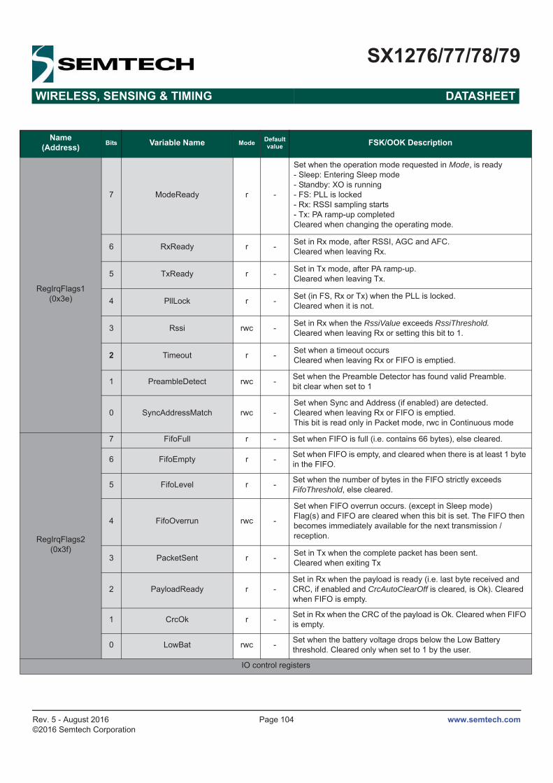
www.semtech.comPage 104
SX1276/77/78/79
WIRELESS, SENSING & TIMING DATASHEET
Rev. 5 - August 2016©2016 Semtech Corporation
RegIrqFlags1(0x3e)
7 ModeReady r -
Set when the operation mode requested in Mode, is ready- Sleep: Entering Sleep mode- Standby: XO is running- FS: PLL is locked- Rx: RSSI sampling starts- Tx: PA ramp-up completedCleared when changing the operating mode.
6 RxReady r - Set in Rx mode, after RSSI, AGC and AFC.Cleared when leaving Rx.
5 TxReady r - Set in Tx mode, after PA ramp-up.Cleared when leaving Tx.
4 PllLock r - Set (in FS, Rx or Tx) when the PLL is locked.Cleared when it is not.
3 Rssi rwc - Set in Rx when the RssiValue exceeds RssiThreshold. Cleared when leaving Rx or setting this bit to 1.
2 Timeout r - Set when a timeout occursCleared when leaving Rx or FIFO is emptied.
1 PreambleDetect rwc - Set when the Preamble Detector has found valid Preamble.bit clear when set to 1
0 SyncAddressMatch rwc -Set when Sync and Address (if enabled) are detected.Cleared when leaving Rx or FIFO is emptied.This bit is read only in Packet mode, rwc in Continuous mode
RegIrqFlags2(0x3f)
7 FifoFull r - Set when FIFO is full (i.e. contains 66 bytes), else cleared.
6 FifoEmpty r - Set when FIFO is empty, and cleared when there is at least 1 byte in the FIFO.
5 FifoLevel r - Set when the number of bytes in the FIFO strictly exceeds FifoThreshold, else cleared.
4 FifoOverrun rwc -
Set when FIFO overrun occurs. (except in Sleep mode)Flag(s) and FIFO are cleared when this bit is set. The FIFO then becomes immediately available for the next transmission / reception.
3 PacketSent r - Set in Tx when the complete packet has been sent.Cleared when exiting Tx
2 PayloadReady r -Set in Rx when the payload is ready (i.e. last byte received and CRC, if enabled and CrcAutoClearOff is cleared, is Ok). Cleared when FIFO is empty.
1 CrcOk r - Set in Rx when the CRC of the payload is Ok. Cleared when FIFO is empty.
0 LowBat rwc - Set when the battery voltage drops below the Low Battery threshold. Cleared only when set to 1 by the user.
IO control registers
Name(Address) Bits Variable Name Mode Default
value FSK/OOK Description

www.semtech.comPage 105
SX1276/77/78/79
WIRELESS, SENSING & TIMING DATASHEET
Rev. 5 - August 2016©2016 Semtech Corporation
RegDioMapping1(0x40)
7-6 Dio0Mapping rw 0x00
Mapping of pins DIO0 to DIO5
See Table 18 for mapping in LoRa mode
See Table 29 for mapping in Continuous modeSeeTable 30 for mapping in Packet mode
5-4 Dio1Mapping rw 0x00
3-2 Dio2Mapping rw 0x00
1-0 Dio3Mapping rw 0x00
RegDioMapping2(0x41)
7-6 Dio4Mapping rw 0x00
5-4 Dio5Mapping rw 0x00
3-1 reserved rw 0x00 reserved. Retain default value
0 MapPreambleDetect rw 0x00
Allows the mapping of either Rssi Or PreambleDetect to the DIO pins, as summarized on Table 29 and Table 30 0 Rssi interrupt1 PreambleDetect interrupt
Version register
RegVersion(0x42) 7-0 Version r 0x12 Version code of the chip. Bits 7-4 give the full revision number;
bits 3-0 give the metal mask revision number.
Additional registers
RegPllHop(0x44)
7 FastHopOn rw 0x00
Bypasses the main state machine for a quick frequency hop. Writing RegFrfLsb will trigger the frequency change.0 Frf is validated when FSTx or FSRx is requested1 Frf is validated triggered when RegFrfLsb is written
6-0 reserved rw 0x2d reserved
RegTcxo(0x4b)
7-5 reserved rw 0x00 reserved. Retain default value
4 TcxoInputOn rw 0x00Controls the crystal oscillator0 Crystal Oscillator with external Crystal1 External clipped sine TCXO AC-connected to XTA pin
3-0 reserved rw 0x09 Reserved. Retain default value.
RegPaDac(0x4d)
7-3 reserved rw 0x10 reserved. Retain default value
2-0 PaDac rw 0x04Enables the +20dBm option on PA_BOOST pin0x04 Default value0x07 +20dBm on PA_BOOST when OutputPower=1111
RegFormerTemp(0x5b) 7-0 FormerTemp rw - Temperature saved during the latest IQ (RSSI and Image)
calibration. Same format as TempValue in RegTemp.
RegBitrateFrac(0x5d)
7-4 unused r 0x00 unused
3-0 BitRateFrac rw 0x00
Fractional part of the bit rate divider (Only valid for FSK)If BitRateFrac> 0 then:
Name(Address) Bits Variable Name Mode Default
value FSK/OOK Description
BitRate FXOSC
BitRate 15 0( , ) BitrateFrac16
-------------------------------+-------------------------------------------------------------------------=

www.semtech.comPage 106
SX1276/77/78/79
WIRELESS, SENSING & TIMING DATASHEET
Rev. 5 - August 2016©2016 Semtech Corporation
6.3. Band Specific Additional RegistersThe registers in the address space from 0x61 to 0x73 are specific for operation in the lower frequency bands (below 525 MHz), or in the upper frequency bands (above 779 MHz). Their programmed value may differ, and are retained when switching from lower to high frequency and vice-versa. The access to the band specific registers is granted by enabling or disabling the bit 3 LowFrequencyModeOn of the RegOpMode register. By default, the bit LowFrequencyModeOn is at ‘1’ indicating that the registers are configured for the low frequency band.
Table 43 Low Frequency Additional Registers
RegAgcRef(0x61)
7-6 unused r - unused
5-0 AgcReferenceLevel rw 0x19
Sets the floor reference for all AGC thresholds:AGC Reference[dBm]=-174dBm+10*log(2*RxBw)+SNR+AgcReferenceLevelSNR = 8dB, fixed value
RegAgcThresh1(0x62)
7-5 unused r - unused
4-0 AgcStep1 rw 0x0c Defines the 1st AGC Threshold
RegAgcThresh2(0x63)
7-4 AgcStep2 rw 0x04 Defines the 2nd AGC Threshold:
3-0 AgcStep3 rw 0x0b Defines the 3rd AGC Threshold:
RegAgcThresh3(0x64)
7-4 AgcStep4 rw 0x0c Defines the 4th AGC Threshold:
3-0 AgcStep5 rw 0x0c Defines the 5th AGC Threshold:
Name(Address) Bits Variable Name Mode Default
value Low Frequency Additional Registers
RegAgcRefLf(0x61)
7-6 unused r - unused
5-0 AgcReferenceLevel rw 0x19
Sets the floor reference for all AGC thresholds:AGC Reference[dBm]=-174dBm+10*log(2*RxBw)+SNR+AgcReferenceLevelSNR = 8dB, fixed value
RegAgcThresh1Lf(0x62)
7-5 unused r - unused
4-0 AgcStep1 rw 0x0c Defines the 1st AGC Threshold
RegAgcThresh2Lf(0x63)
7-4 AgcStep2 rw 0x04 Defines the 2nd AGC Threshold:
3-0 AgcStep3 rw 0x0b Defines the 3rd AGC Threshold:
RegAgcThresh3Lf(0x64)
7-4 AgcStep4 rw 0x0c Defines the 4th AGC Threshold:
3-0 AgcStep5 rw 0x0c Defines the 5th AGC Threshold:
RegPllLf(0x70)
7-6 PllBandwidth rw 0x03Controls the PLL bandwidth:00 75 kHz 10 225 kHz01 150 kHz 11 300 kHz
5-0 reserved rw 0x10 reserved. Retain default value
Name(Address) Bits Variable Name Mode Default
value FSK/OOK Description

www.semtech.comPage 107
SX1276/77/78/79
WIRELESS, SENSING & TIMING DATASHEET
Rev. 5 - August 2016©2016 Semtech Corporation
Table 44 High Frequency Additional Registers
Name(Address) Bits Variable Name Mode Default
value Low Frequency Additional Registers
RegAgcRefHf(0x61)
7-6 unused r - unused
5-0 AgcReferenceLevel rw 0x1c
Sets the floor reference for all AGC thresholds:AGC Reference[dBm]=-174dBm+10*log(2*RxBw)+SNR+AgcReferenceLevelSNR = 8dB, fixed value
RegAgcThresh1Hf(0x62)
7-5 unused r - unused
4-0 AgcStep1 rw 0x0e Defines the 1st AGC Threshold
RegAgcThresh2Hf(0x63)
7-4 AgcStep2 rw 0x05 Defines the 2nd AGC Threshold:
3-0 AgcStep3 rw 0x0b Defines the 3rd AGC Threshold:
RegAgcThresh3Hf(0x64)
7-4 AgcStep4 rw 0x0c Defines the 4th AGC Threshold:
3-0 AgcStep5 rw 0x0c Defines the 5th AGC Threshold:
RegPllHf(0x70)
7-6 PllBandwidth rw 0x03Controls the PLL bandwidth:00 75 kHz 10 225 kHz01 150 kHz 11 300 kHz
5-0 reserved rw 0x10 reserved. Retain default value

www.semtech.comPage 108
SX1276/77/78/79
WIRELESS, SENSING & TIMING DATASHEET
Rev. 5 - August 2016©2016 Semtech Corporation
6.4. LoRaTM Mode Register MapThis details the SX1276/77/78/79 register mapping and the precise contents of each register in LoRaTM mode.
It is essential to understand that the LoRaTM modem is controlled independently of the FSK modem. Therefore, care should be taken when accessing the registers, especially as some register may have the same name in LoRaTM or FSK mode.The LoRa registers are only accessible when the device is set in Lora mode (and, in the same way, the FSK register are only accessible in FSK mode). However, in some cases, it may be necessary to access some of the FSK register while in LoRa mode. To this aim, the AccesSharedReg bit was created in the RegOpMode register. This bit, when set to ‘1’, will grant access to the FSK register 0x0D up to the register 0x3F. Once the setup has been done, it is strongly recommended to clear this bit so that LoRa register can be accessed normally.Convention: r: read, w: write, c : set to clear and t: trigger.
Name(Address) Bits Variable Name Mode Reset LoRaTM Description
RegFifo(0x00) 7-0 Fifo rw 0x00 LoRaTM base-band FIFO data input/output. FIFO is cleared an not
accessible when device is in SLEEP mode
Common Register Settings
RegOpMode(0x01)
7 LongRangeMode rw 0x0
0 FSK/OOK Mode1 LoRaTM ModeThis bit can be modified only in Sleep mode. A write operation on other device modes is ignored.
6 AccessSharedReg rw 0x0
This bit operates when device is in Lora mode; if set it allows access to FSK registers page located in address space (0x0D:0x3F) while in LoRa mode0 Access LoRa registers page 0x0D: 0x3F1 Access FSK registers page (in mode LoRa) 0x0D: 0x3F
5-4 reserved r 0x00 reserved
3 LowFrequencyModeOn rw 0x01Access Low Frequency Mode registers0 High Frequency Mode (access to HF test registers)1 Low Frequency Mode (access to LF test registers)
2-0 Mode rwt 0x01
Device modes000 SLEEP 001 STDBY 010 Frequency synthesis TX (FSTX)011 Transmit (TX)100 Frequency synthesis RX (FSRX)101 Receive continuous (RXCONTINUOUS)110 receive single (RXSINGLE)111 Channel activity detection (CAD)
(0x02) 7-0 reserved r 0x00 -
(0x03) 7-0 reserved r 0x00 -
(0x04) 7-0 reserved rw 0x00 -
(0x05) 7-0 reserved r 0x00 -
RegFrMsb(0x06) 7-0 Frf(23:16) rw 0x6c MSB of RF carrier frequency

www.semtech.comPage 109
SX1276/77/78/79
WIRELESS, SENSING & TIMING DATASHEET
Rev. 5 - August 2016©2016 Semtech Corporation
RegFrMid(0x07) 7-0 Frf(15:8) rw 0x80 MSB of RF carrier frequency
RegFrLsb(0x08) 7-0 Frf(7:0) rwt 0x00
LSB of RF carrier frequency
Resolution is 61.035 Hz if F(XOSC) = 32 MHz. Default value is 0x6c8000 = 434 MHz. Register values must be modified only when device is in SLEEP or STAND-BY mode.
Registers for RF blocks
RegPaConfig(0x09)
7 PaSelect rw 0x00Selects PA output pin0 RFO pin. Output power is limited to +14 dBm.1 PA_BOOST pin. Output power is limited to +20 dBm
6-4 MaxPower rw 0x04 Select max output power: Pmax=10.8+0.6*MaxPower [dBm]
3-0 OutputPower rw 0x0f Pout=Pmax-(15-OutputPower) if PaSelect = 0 (RFO pin)Pout=17-(15-OutputPower) if PaSelect = 1 (PA_BOOST pin)
RegPaRamp(0x0A)
7-5 unused r - unused
4 reserved rw 0x00 reserved
3-0 PaRamp(3:0) rw 0x09
Rise/Fall time of ramp up/down in FSK0000 3.4 ms0001 2 ms0010 1 ms0011 500 us0100 250 us0101 125 us0110 100 us0111 62 us1000 50 us1001 40 us 1010 31 us1011 25 us1100 20 us1101 15 us1110 12 us1111 10 us
RegOcp(0x0B
7-6 unused r 0x00 unused
5 OcpOn rw 0x01Enables overload current protection (OCP) for PA:0 OCP disabled1 OCP enabled
4-0 OcpTrim rw 0x0b
Trimming of OCP current:Imax = 45+5*OcpTrim [mA] if OcpTrim <= 15 (120 mA) /Imax = -30+10*OcpTrim [mA] if 15 < OcpTrim <= 27 (130 to240 mA)Imax = 240mA for higher settingsDefault Imax = 100mA
Name(Address) Bits Variable Name Mode Reset LoRaTM Description
fRFF(XOSC) Frf⋅
219------------------------------------=
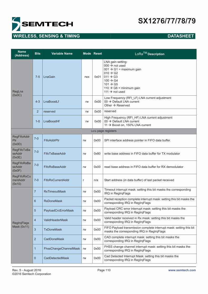
www.semtech.comPage 110
SX1276/77/78/79
WIRELESS, SENSING & TIMING DATASHEET
Rev. 5 - August 2016©2016 Semtech Corporation
RegLna(0x0C)
7-5 LnaGain rwx 0x01
LNA gain setting:000 not used001 G1 = maximum gain010 G2011 G3 100 G4101 G5110 G6 = minimum gain111 not used
4-3 LnaBoostLf rw 0x00Low Frequency (RFI_LF) LNA current adjustment00 Default LNA currentOther Reserved
2 reserved rw 0x00 reserved
1-0 LnaBoostHf rw 0x00High Frequency (RFI_HF) LNA current adjustment00 Default LNA current11 Boost on, 150% LNA current
Lora page registers
RegFifoAddrPtr(0x0D)
7-0 FifoAddrPtr rw 0x00 SPI interface address pointer in FIFO data buffer.
RegFifoTxBaseAddr(0x0E)
7-0 FifoTxBaseAddr rw 0x80 write base address in FIFO data buffer for TX modulator
RegFifoRxBaseAddr(0x0F)
7-0 FifoRxBaseAddr rw 0x00 read base address in FIFO data buffer for RX demodulator
RegFifoRxCurrentAddr(0x10)
7-0 FifoRxCurrentAddr r n/a Start address (in data buffer) of last packet received
RegIrqFlagsMask (0x11)
7 RxTimeoutMask rw 0x00 Timeout interrupt mask: setting this bit masks the corresponding IRQ in RegIrqFlags
6 RxDoneMask rw 0x00 Packet reception complete interrupt mask: setting this bit masks the corresponding IRQ in RegIrqFlags
5 PayloadCrcErrorMask rw 0x00 Payload CRC error interrupt mask: setting this bit masks the corresponding IRQ in RegIrqFlags
4 ValidHeaderMask rw 0x00 Valid header received in Rx mask: setting this bit masks the corresponding IRQ in RegIrqFlags
3 TxDoneMask rw 0x00 FIFO Payload transmission complete interrupt mask: setting this bit masks the corresponding IRQ in RegIrqFlags
2 CadDoneMask rw 0x00 CAD complete interrupt mask: setting this bit masks the corresponding IRQ in RegIrqFlags
1 FhssChangeChannelMask rw 0x00 FHSS change channel interrupt mask: setting this bit masks the corresponding IRQ in RegIrqFlags
0 CadDetectedMask rw 0x00 Cad Detected Interrupt Mask: setting this bit masks the corresponding IRQ in RegIrqFlags
Name(Address) Bits Variable Name Mode Reset LoRaTM Description
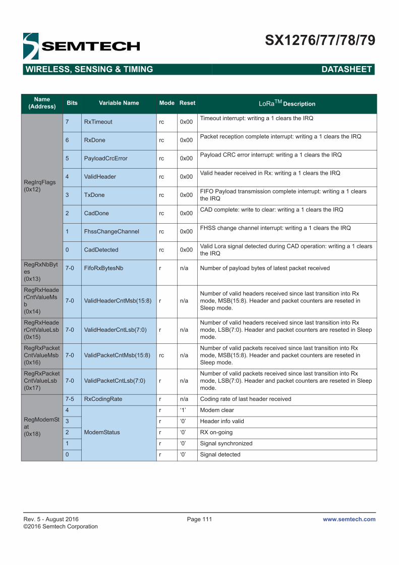
www.semtech.comPage 111
SX1276/77/78/79
WIRELESS, SENSING & TIMING DATASHEET
Rev. 5 - August 2016©2016 Semtech Corporation
RegIrqFlags(0x12)
7 RxTimeout rc 0x00 Timeout interrupt: writing a 1 clears the IRQ
6 RxDone rc 0x00 Packet reception complete interrupt: writing a 1 clears the IRQ
5 PayloadCrcError rc 0x00 Payload CRC error interrupt: writing a 1 clears the IRQ
4 ValidHeader rc 0x00 Valid header received in Rx: writing a 1 clears the IRQ
3 TxDone rc 0x00 FIFO Payload transmission complete interrupt: writing a 1 clears the IRQ
2 CadDone rc 0x00 CAD complete: write to clear: writing a 1 clears the IRQ
1 FhssChangeChannel rc 0x00 FHSS change channel interrupt: writing a 1 clears the IRQ
0 CadDetected rc 0x00 Valid Lora signal detected during CAD operation: writing a 1 clears the IRQ
RegRxNbBytes(0x13)
7-0 FifoRxBytesNb r n/a Number of payload bytes of latest packet received
RegRxHeaderCntValueMsb(0x14)
7-0 ValidHeaderCntMsb(15:8) r n/aNumber of valid headers received since last transition into Rx mode, MSB(15:8). Header and packet counters are reseted in Sleep mode.
RegRxHeaderCntValueLsb(0x15)
7-0 ValidHeaderCntLsb(7:0) r n/aNumber of valid headers received since last transition into Rx mode, LSB(7:0). Header and packet counters are reseted in Sleep mode.
RegRxPacketCntValueMsb(0x16)
7-0 ValidPacketCntMsb(15:8) rc n/aNumber of valid packets received since last transition into Rx mode, MSB(15:8). Header and packet counters are reseted in Sleep mode.
RegRxPacketCntValueLsb(0x17)
7-0 ValidPacketCntLsb(7:0) r n/aNumber of valid packets received since last transition into Rx mode, LSB(7:0). Header and packet counters are reseted in Sleep mode.
RegModemStat(0x18)
7-5 RxCodingRate r n/a Coding rate of last header received
4
ModemStatus
r ‘1’ Modem clear
3 r ‘0’ Header info valid
2 r ‘0’ RX on-going
1 r ‘0’ Signal synchronized
0 r ‘0’ Signal detected
Name(Address) Bits Variable Name Mode Reset LoRaTM Description

www.semtech.comPage 112
SX1276/77/78/79
WIRELESS, SENSING & TIMING DATASHEET
Rev. 5 - August 2016©2016 Semtech Corporation
RegPktSnrValue(0x19)
7-0 PacketSnr r n/a
Estimation of SNR on last packet received.In two’s compliment format mutiplied by 4.
RegPktRssiValue(0x1A)
7-0 PacketRssi r n/a
RSSI of the latest packet received (dBm):
RSSI[dBm] = -157 + Rssi (using HF output port, SNR >= 0) or
RSSI[dBm] = -164 + Rssi (using LF output port, SNR >= 0)
(see section 5.5.5 for details)
RegRssiValue(0x1B)
7-0 Rssi r n/a
Current RSSI value (dBm)
RSSI[dBm] = -157 + Rssi (using HF output port) or
RSSI[dBm] = -164 + Rssi (using LF output port)
(see section 5.5.5 for details)
RegHopChannel(0x1C)
7 PllTimeout r n/aPLL failed to lock while attempting a TX/RX/CAD operation1 PLL did not lock0 PLL did lock
6 CrcOnPayload r n/a
CRC Information extracted from the received packet header (Explicit header mode only)0 Header indicates CRC off1 Header indicates CRC on
5-0 FhssPresentChannel r n/a Current value of frequency hopping channel in use.
Name(Address) Bits Variable Name Mode Reset LoRaTM Description
SNR dB[ ] PacketSnr twos complement[ ]4
-----------------------------------------------------------------------------------=

www.semtech.comPage 113
SX1276/77/78/79
WIRELESS, SENSING & TIMING DATASHEET
Rev. 5 - August 2016©2016 Semtech Corporation
RegModemConfig1(0x1D)
7-4 Bw rw 0x07
Signal bandwidth:0000 7.8 kHz0001 10.4 kHz0010 15.6 kHz0011 20.8kHz0100 31.25 kHz0101 41.7 kHz0110 62.5 kHz0111 125 kHz1000 250 kHz1001 500 kHzother values reservedIn the lower band (169MHz), signal bandwidths 8&9 are notsupported)
3-1 CodingRate rw ‘001’
Error coding rate001 4/5010 4/6011 4/7100 4/8All other values reservedIn implicit header mode should be set on receiver to determine expected coding rate. See 4.1.1.3
0 ImplicitHeaderModeOn rw 0x0 0 Explicit Header mode1 Implicit Header mode
RegModemConfig2(0x1E)
7-4 SpreadingFactor rw 0x07
SF rate (expressed as a base-2 logarithm)6 64 chips / symbol7 128 chips / symbol8 256 chips / symbol9 512 chips / symbol10 1024 chips / symbol11 2048 chips / symbol12 4096 chips / symbolother values reserved.
3 TxContinuousMode rw 00 normal mode, a single packet is sent1 continuous mode, send multiple packets across the FIFO (used for spectral analysis)
2 RxPayloadCrcOn rw 0x00
Enable CRC generation and check on payload: 0 CRC disable 1 CRC enable If CRC is needed, RxPayloadCrcOn should be set: - in Implicit header mode: on Tx and Rx side - in Explicit header mode: on the Tx side alone (recovered from the header in Rx side)
1-0 SymbTimeout(9:8) rw 0x00 RX Time-Out MSB
RegSymbTimeoutLsb(0x1F)
7-0 SymbTimeout(7:0) rw 0x64
RX Time-Out LSBRX operation time-out value expressed as number of symbols:
Name(Address) Bits Variable Name Mode Reset LoRaTM Description
TimeOut SymbTimeout Ts⋅=
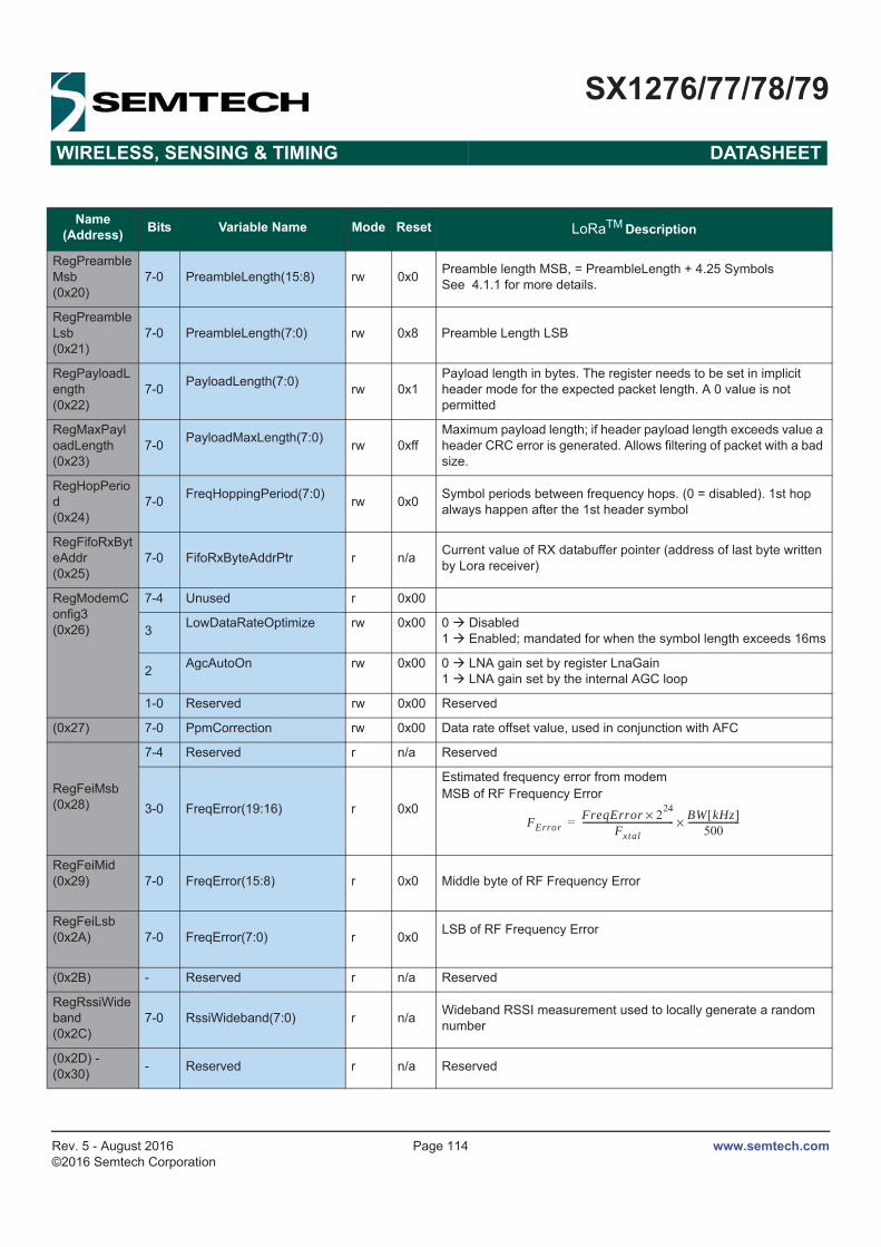
www.semtech.comPage 114
SX1276/77/78/79
WIRELESS, SENSING & TIMING DATASHEET
Rev. 5 - August 2016©2016 Semtech Corporation
RegPreambleMsb(0x20)
7-0 PreambleLength(15:8) rw 0x0 Preamble length MSB, = PreambleLength + 4.25 SymbolsSee 4.1.1 for more details.
RegPreambleLsb(0x21)
7-0 PreambleLength(7:0) rw 0x8 Preamble Length LSB
RegPayloadLength(0x22)
7-0 PayloadLength(7:0) rw 0x1Payload length in bytes. The register needs to be set in implicit header mode for the expected packet length. A 0 value is not permitted
RegMaxPayloadLength(0x23)
7-0 PayloadMaxLength(7:0) rw 0xffMaximum payload length; if header payload length exceeds value a header CRC error is generated. Allows filtering of packet with a bad size.
RegHopPeriod(0x24)
7-0 FreqHoppingPeriod(7:0) rw 0x0 Symbol periods between frequency hops. (0 = disabled). 1st hop always happen after the 1st header symbol
RegFifoRxByteAddr(0x25)
7-0 FifoRxByteAddrPtr r n/a Current value of RX databuffer pointer (address of last byte written by Lora receiver)
RegModemConfig3(0x26)
7-4 Unused r 0x00
3 LowDataRateOptimize rw 0x00 0 Disabled1 Enabled; mandated for when the symbol length exceeds 16ms
2 AgcAutoOn rw 0x00 0 LNA gain set by register LnaGain1 LNA gain set by the internal AGC loop
1-0 Reserved rw 0x00 Reserved
(0x27) 7-0 PpmCorrection rw 0x00 Data rate offset value, used in conjunction with AFC
RegFeiMsb(0x28)
7-4 Reserved r n/a Reserved
3-0 FreqError(19:16) r 0x0
Estimated frequency error from modemMSB of RF Frequency Error
RegFeiMid(0x29) 7-0 FreqError(15:8) r 0x0 Middle byte of RF Frequency Error
RegFeiLsb(0x2A) 7-0 FreqError(7:0) r 0x0 LSB of RF Frequency Error
(0x2B) - Reserved r n/a Reserved
RegRssiWideband(0x2C)
7-0 RssiWideband(7:0) r n/a Wideband RSSI measurement used to locally generate a random number
(0x2D) - (0x30) - Reserved r n/a Reserved
Name(Address) Bits Variable Name Mode Reset LoRaTM Description
FErrorFreqError 224×
Fxtal------------------------------------------ BW kHz[ ]
500------------------------×=

www.semtech.comPage 115
SX1276/77/78/79
WIRELESS, SENSING & TIMING DATASHEET
Rev. 5 - August 2016©2016 Semtech Corporation
RegDetectOptimize(0x31)
7-3 Reserved r 0xC0 Reserved
2-0 DetectionOptimize rw 0x03LoRa Detection Optimize0x03 SF7 to SF120x05 SF6
(0x32) - Reserved r n/a Reserved
RegInvertIQ(0x33)
7 Reserved rw 0x0 Reserved
6 InvertIQ rw 0x0Invert the LoRa I and Q signals0 normal mode1 I and Q signals are inverted
5-0 Reserved rw 0x27 Reserved
(0x34) - (0x36) 7-0 Reserved r n/a Reserved
RegDetectionThreshold(0x37)
7-0 DetectionThreshold rw 0x0ALoRa detection threshold0x0A SF7 to SF120x0C SF6
(0x38) - Reserved r n/a Reserved
RegSyncWord(0x39)
7-0 SyncWord rw 0x12 LoRa Sync Word Value 0x34 is reserved for LoRaWAN networks
(0x3A) - (0x3F) - Reserved r n/a Reserved
Name(Address) Bits Variable Name Mode Reset LoRaTM Description

www.semtech.comPage 116
SX1276/77/78/79
WIRELESS, SENSING & TIMING DATASHEET
Rev. 5 - August 2016©2016 Semtech Corporation
7. Application Information7.1. Crystal Resonator SpecificationTable 45 shows the crystal resonator specification for the crystal reference oscillator circuit of the SX1276/77/78/79. This specification covers the full range of operation of the SX1276/77/78/79 and is employed in the reference design.
Table 45 Crystal Specification
Notes - the initial frequency tolerance, temperature stability and aging performance should be chosen in accordance with the target operating temperature range and the receiver bandwidth selected.
- the loading capacitance should be applied externally, and adapted to the actual Cload specification of the XTAL.
7.2. Reset of the ChipA power-on reset of the SX1276/77/78/79 is triggered at power up. Additionally, a manual reset can be issued by controlling pin 7.
7.2.1. PORIf the application requires the disconnection of VDD from the SX1276/77/78/79, despite of the extremely low Sleep Mode current, the user should wait for 10 ms from of the end of the POR cycle before commencing communications over the SPI bus. Pin 7 (NRESET) should be left floating during the POR sequence.
Figure 42. POR Timing Diagram
Please note that any CLKOUT activity can also be used to detect that the chip is ready.
Symbol Description Conditions Min Typ Max Unit
FXOSC XTAL Frequency - 32 - MHz
RS XTAL Serial Resistance - 15 100 ohms
C0 XTAL Shunt Capacitance - 1 3 pF
CFOOT External Foot Capacitance On each pin XTA and XTB 10 15 22 pF
CLOAD Crystal Load Capacitance 6 - 12 pF

www.semtech.comPage 117
SX1276/77/78/79
WIRELESS, SENSING & TIMING DATASHEET
Rev. 5 - August 2016©2016 Semtech Corporation
7.2.2. Manual ResetA manual reset of the SX1276/77/78/79 is possible even for applications in which VDD cannot be physically disconnected. Pin 7 should be pulled low for a hundred microseconds, and then released. The user should then wait for 5 ms before using the chip.
Figure 43. Manual Reset Timing Diagram
Note whilst pin 7 is driven low, an over current consumption of up to one milliampere can be seen on VDD.
7.3. Top Sequencer: Listen Mode ExamplesIn this scenario, the circuit spends most of the time in Idle mode, during which only the RC oscillator is on. Periodically the receiver wakes up and looks for incoming signal. If a wanted signal is detected, the receiver is kept on and data are analyzed. Otherwise, if there was no wanted signal for a defined period of time, the receiver is switched off until the next receive period.
During Listen mode, the Radio stays most of the time in a Low Power mode, resulting in very low average power consumption. The general timing diagram of this scenario is given in Figure 44.
Figure 44. Listen Mode: Principle
An interrupt request is generated on a packet reception. The user can then take appropriate action.
Depending on the application and environment, there are several ways to implement Listen mode:
Wake on a PreambleDetect interrupt
Wake on a SyncAddress interrupt
Wake on a PayloadReady interrupt
7.3.1. Wake on Preamble InterruptIn one possible scenario, the sequencer polls for a Preamble detection. If a preamble signal is detected, the sequencer is switched off and the circuit stays in Receive mode until the user switches modes. Otherwise, the receiver is switched off until the next Rx period.
Listen mode : principle
Receive ReceiveIdle ( Sleep + RC ) Idle
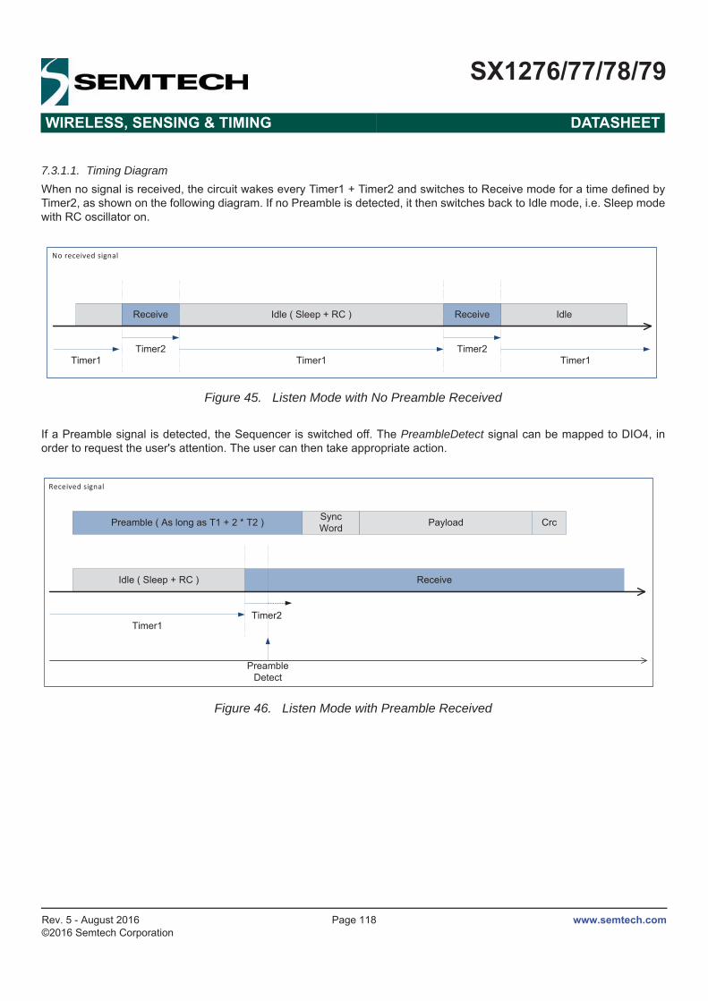
www.semtech.comPage 118
SX1276/77/78/79
WIRELESS, SENSING & TIMING DATASHEET
Rev. 5 - August 2016©2016 Semtech Corporation
7.3.1.1. Timing DiagramWhen no signal is received, the circuit wakes every Timer1 + Timer2 and switches to Receive mode for a time defined by Timer2, as shown on the following diagram. If no Preamble is detected, it then switches back to Idle mode, i.e. Sleep mode with RC oscillator on.
Figure 45. Listen Mode with No Preamble Received
If a Preamble signal is detected, the Sequencer is switched off. The PreambleDetect signal can be mapped to DIO4, in order to request the user's attention. The user can then take appropriate action.
Figure 46. Listen Mode with Preamble Received
No received signal
Receive ReceiveIdle ( Sleep + RC ) Idle
Timer2Timer1
Timer2Timer1Timer1
Timer2
Received signal
Preamble ( As long as T1 + 2 * T2 ) SyncWord Payload Crc
ReceiveIdle ( Sleep + RC )
Timer1
Preamble Detect
Timer2
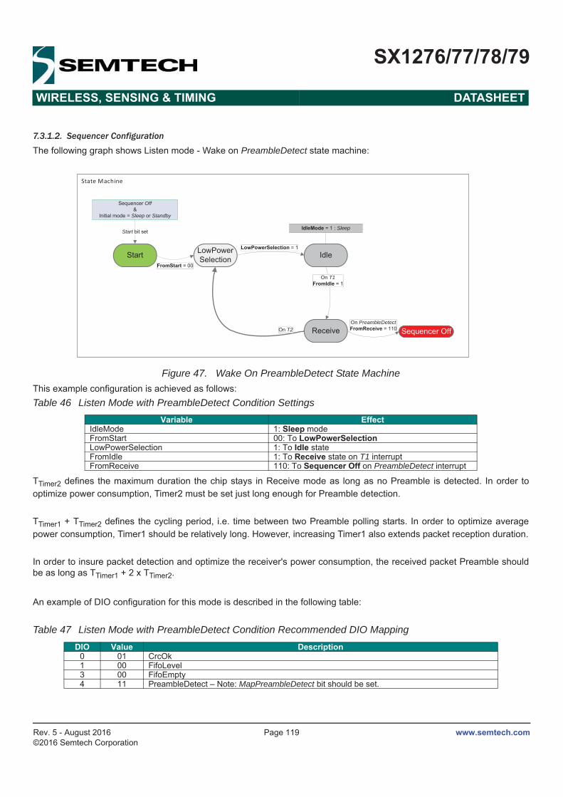
www.semtech.comPage 119
SX1276/77/78/79
WIRELESS, SENSING & TIMING DATASHEET
Rev. 5 - August 2016©2016 Semtech Corporation
7.3.1.2. Sequencer Configuration
The following graph shows Listen mode - Wake on PreambleDetect state machine:
Figure 47. Wake On PreambleDetect State MachineThis example configuration is achieved as follows:Table 46 Listen Mode with PreambleDetect Condition Settings
TTimer2 defines the maximum duration the chip stays in Receive mode as long as no Preamble is detected. In order to optimize power consumption, Timer2 must be set just long enough for Preamble detection.
TTimer1 + TTimer2 defines the cycling period, i.e. time between two Preamble polling starts. In order to optimize average power consumption, Timer1 should be relatively long. However, increasing Timer1 also extends packet reception duration.
In order to insure packet detection and optimize the receiver's power consumption, the received packet Preamble should be as long as TTimer1 + 2 x TTimer2.
An example of DIO configuration for this mode is described in the following table:
Table 47 Listen Mode with PreambleDetect Condition Recommended DIO Mapping
Variable EffectIdleMode 1: Sleep modeFromStart 00: To LowPowerSelectionLowPowerSelection 1: To Idle stateFromIdle 1: To Receive state on T1 interruptFromReceive 110: To Sequencer Off on PreambleDetect interrupt
DIO Value Description0 01 CrcOk1 00 FifoLevel3 00 FifoEmpty4 11 PreambleDetect – Note: MapPreambleDetect bit should be set.
State Machine
LowPowerSelection Idle
Receive
LowPowerSelection = 1
On T2
On T1FromIdle = 1
On PreambleDetectFromReceive = 110 Sequencer Off
IdleMode = 1 : Sleep
Start
Sequencer Off&
Initial mode = Sleep or Standby
Start bit set
FromStart = 00

www.semtech.comPage 120
SX1276/77/78/79
WIRELESS, SENSING & TIMING DATASHEET
Rev. 5 - August 2016©2016 Semtech Corporation
7.3.2. Wake on SyncAddress InterruptIn another possible scenario, the sequencer polls for a Preamble detection and then for a valid SyncAddress interrupt. If events occur, the sequencer is switched off and the circuit stays in Receive mode until the user switches modes. Otherwise, the receiver is switched off until the next Rx period.
7.3.2.1. Timing DiagramMost of the sequencer running time is spent while no wanted signal is received. As shown by the timing diagram in Figure 48, the circuit wakes periodically for a short time, defined by RxTimeout. The circuit is in a Low Power mode for the rest of Timer1 + Timer2 (i.e. Timer1 + Timer2 - TrxTimeout)
Figure 48. Listen Mode with no SyncAddress Detected
If a preamble is detected before RxTimeout timer ends, the circuit stays in Receive mode and waits for a valid SyncAddress detection. If none is detected by the end of Timer2, Receive mode is deactivated and the polling cycle resumes, without any user intervention.
Figure 49. Listen Mode with Preamble Received and no SyncAddress
But if a valid Sync Word is detected, a SyncAddress interrupt is fired, the Sequencer is switched off and the circuit stays in Receive mode as long as the user doesn't switch modes.
No wanted signal
Receive ReceiveIdle ( Sleep + RC )Idle Idle
Timer2Timer1
Timer2Timer1Timer1
RxTimeout RxTimeout
Unwanted Signal
Preamble ( Preamble + Sync = T2 ) WrongWord Payload Crc
Preamble Detect
Receive ReceiveIdleIdle Idle
Timer2Timer1
Timer2Timer1Timer1
RxTimeoutRxTimeout

www.semtech.comPage 121
SX1276/77/78/79
WIRELESS, SENSING & TIMING DATASHEET
Rev. 5 - August 2016©2016 Semtech Corporation
Figure 50. Listen Mode with Preamble Received & Valid SyncAddress
7.3.2.2. Sequencer ConfigurationThe following graph shows Listen mode - Wake on SyncAddress state machine:
Figure 51. Wake On SyncAddress State Machine
Wanted Signal
Preamble ( Preamble + Sync = T2 ) SyncWord Payload Crc
Preamble Detect
ReceiveIdle
Timer2Timer1
SyncAddress
FifoLevel
RxTimeout
State Machine
LowPowerSelection Idle
ReceiveRxTimeout
LowPowerSelection = 1
FromRxTimeout = 10
On RxTimeout
On T2
On T1FromIdle = 1
On SyncAdressFromReceive = 101 Sequencer Off
IdleMode = 1 : Sleep
StartFromStart = 00
Sequencer Off&
Initial mode = Sleep or Standby
Start bit set

www.semtech.comPage 122
SX1276/77/78/79
WIRELESS, SENSING & TIMING DATASHEET
Rev. 5 - August 2016©2016 Semtech Corporation
This example configuration is achieved as follows:
Table 48 Listen Mode with SyncAddress Condition Settings
TTimeoutRxPreamble should be set to just long enough to catch a preamble (depends on PreambleDetectSize and BitRate).
TTimer1 should be set to 64 μs (shortest possible duration).
TTimer2 is set so that TTimer1 + TTimer2 defines the time between two start of reception.
In order to insure packet detection and optimize the receiver power consumption, the received packet Preamble should be defined so that TPreamble = TTimer2 - TSyncAddress with TSyncAddress = (SyncSize + 1)*8/BitRate.
An example of DIO configuration for this mode is described in the following table:
Table 49 Listen Mode with PreambleDetect Condition Recommended DIO Mapping
Variable EffectIdleMode 1: Sleep modeFromStart 00: To LowPowerSelectionLowPowerSelection 1: To Idle stateFromIdle 1: To Receive state on T1 interruptFromReceive 101: To Sequencer off on SyncAddress interruptFromRxTimeout 10: To LowPowerSelection
DIO Value Description0 01 CrcOk1 00 FifoLevel2 11 SyncAddress3 00 FifoEmpty4 11 PreambleDetect – Note: MapPreambleDetect bit should be set.

www.semtech.comPage 123
SX1276/77/78/79
WIRELESS, SENSING & TIMING DATASHEET
Rev. 5 - August 2016©2016 Semtech Corporation
7.4. Top Sequencer: Beacon ModeIn this mode, a repetitive message is transmitted periodically. If the Payload being sent is always identical, and PayloadLength is smaller than the FIFO size, the use of the BeaconOn bit in RegPacketConfig2 together with the Sequencer permit to achieve periodic beacon without any user intervention.
7.4.1. Timing diagramIn this mode, the Radio is switched to Transmit mode every TTimer1 + TTimer2 and back to Idle mode after PacketSent, as shown in the diagram below. The Sequencer insures minimal time is spent in Transmit mode, and therefore power consumption is optimized.
Figure 52. Beacon Mode Timing Diagram
7.4.2. Sequencer ConfigurationThe Beacon mode state machine is presented in the following graph. It is noticeable that the sequencer enters an infinite loop and can only be stopped by setting SequencerStop bit in RegSeqConfig1.
Figure 53. Beacon Mode State Machine
Beacon mode
Transmit TransmitIdle ( Sleep + RC )Idle Idle
Timer2Timer1 Timer1Timer1
Timer2
PacketSent
PacketSent
State Machine
Transmit
On T1FromIdle = 0
On PacketSentFromTransmit = 0
LowPowerSelection Idle
LowPowerSelection = 1
IdleMode = 1 : Sleep
StartFromStart = 00
Sequencer Off&
Initial mode = Sleep or Standby
Start bit set

www.semtech.comPage 124
SX1276/77/78/79
WIRELESS, SENSING & TIMING DATASHEET
Rev. 5 - August 2016©2016 Semtech Corporation
This example is achieved by programming the Sequencer as follows:
Table 50 Beacon Mode Settings
TTimer1 + TTimer2 define the time between the start of two transmissions.
Variable EffectIdleMode 1: Sleep modeFromStart 00: To LowPowerSelectionLowPowerSelection 1: To Idle stateFromIdle 0: To Transmit state on T1 interruptFromTransmit 0: To LowPowerSelection on PacketSent interrupt

www.semtech.comPage 125
SX1276/77/78/79
WIRELESS, SENSING & TIMING DATASHEET
Rev. 5 - August 2016©2016 Semtech Corporation
7.5. Example CRC CalculationThe following routine(s) may be implemented to mimic the CRC calculation of the SX1276/77/78/79:
Figure 54. Example CRC Code

www.semtech.comPage 126
SX1276/77/78/79
WIRELESS, SENSING & TIMING DATASHEET
Rev. 5 - August 2016©2016 Semtech Corporation
7.6. Example Temperature ReadingThe following routine(s) may be implemented to read the temperature and calibrate the sensor:
Figure 55. Example Temperature Reading
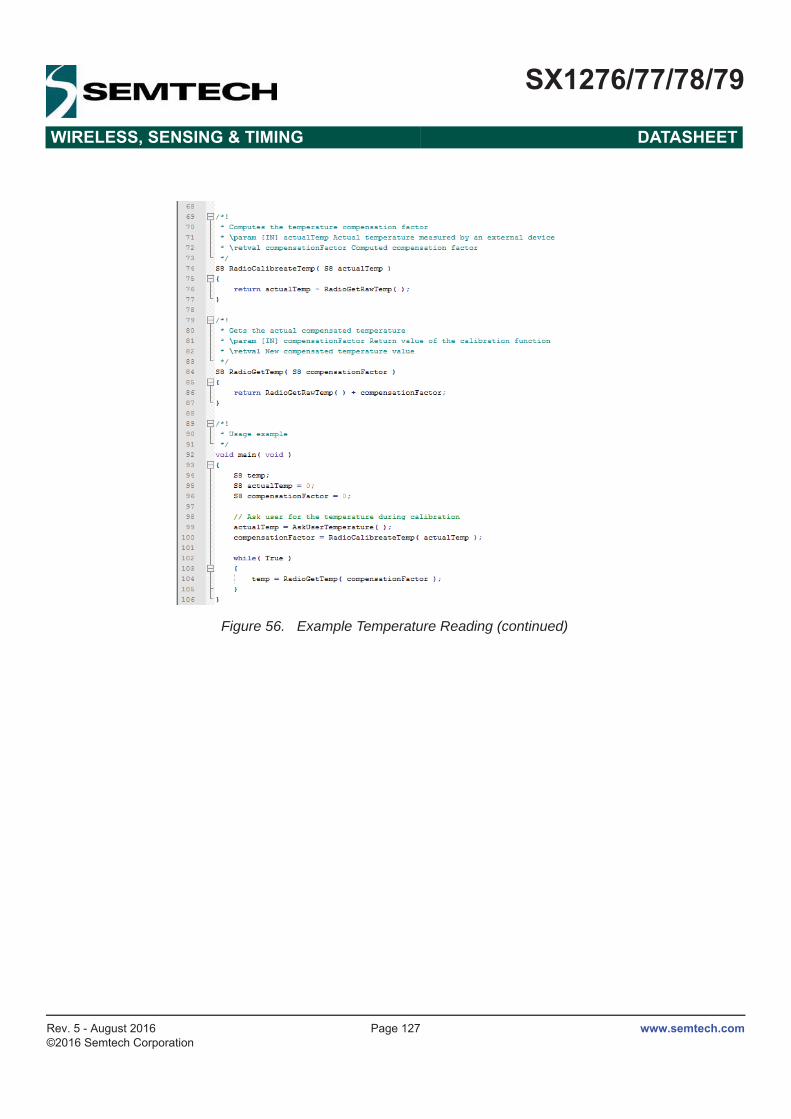
www.semtech.comPage 127
SX1276/77/78/79
WIRELESS, SENSING & TIMING DATASHEET
Rev. 5 - August 2016©2016 Semtech Corporation
Figure 56. Example Temperature Reading (continued)

www.semtech.comPage 128
SX1276/77/78/79
WIRELESS, SENSING & TIMING DATASHEET
Rev. 5 - August 2016©2016 Semtech Corporation
8. Packaging Information8.1. Package Outline DrawingThe SX1276/77/78/79 is available in a 28-lead QFN package as shown in Figure 57.
Figure 57. Package Outline Drawing

www.semtech.comPage 129
SX1276/77/78/79
WIRELESS, SENSING & TIMING DATASHEET
Rev. 5 - August 2016©2016 Semtech Corporation
8.2. Recommended Land Pattern
Figure 58. Recommended Land Pattern

www.semtech.comPage 130
SX1276/77/78/79
WIRELESS, SENSING & TIMING DATASHEET
Rev. 5 - August 2016©2016 Semtech Corporation
8.3. Tape & Reel Information
Figure 59. Tape and Reel Information
8.4. Wafer DeliveryPlease get in touch with a Semtech representative for wafer delivery option.Semtech will deliver probed wafers with a die picking map.The specifications given in Section 2.5. "Chip Specification" on page 14 are determined from the reference design with QFN 28 package (see the reference design available on the Semtech website). In order to fulfill these specifications, the die assembly must be done with similar wire constraints as in the QFN 28 package, see Addendum2 in the SX1276WS devivery specification.A complete wafer delivery specification is available on request.

www.semtech.comPage 131
SX1276/77/78/79
WIRELESS, SENSING & TIMING DATASHEET
Rev. 5 - August 2016©2016 Semtech Corporation
9. Revision History
Table 51 Revision HistoryRevision Date Comment
1 Sept 2013 First FINAL release
2 Nov 2014
Miscellaneous typographical corrections Correction of RxPayloadCrcOn description Improve description in the RSSI and IQ calibration mechanism Correction of ToA formulae Inclusion of FEI and automatic frequency correction for LoRa Corrected Rssi Formula in Lora mode
3 Nov 2014 Addition of part SX1279
4 March 2015
Clarified operation modes for Rx Single and Rx Continuous mode in LoRa Added use cases for Rx Single and Rx Continuous mode in LoRa mode Clarified used of LoRa RxPayloadCrcOn in Register Table Added description of register RegSyncWord in LoRa register table Changed Stand-By typo into Standby
5 August 2016 Addition of part SX1276WS
www.semtech.comPage 132
Semtech CorporationWireless,Sensing & Timing Products Division
200 Flynn Road, Camarillo, CA 93012Phone: (805) 498-2111 Fax: (805) 498-3804
E-mail: [email protected][email protected]
Internet: http://www.semtech.com
Contact information
SX1276/77/78/79
WIRELESS, SENSING & TIMING DATASHEET
Rev. 5 - August 2016©2016 Semtech Corporation
© Semtech 2016 All rights reserved. Reproduction in whole or in part is prohibited without the prior written consent of the copyright owner. The information presented in this document does not form part of any quotation or contract, is believed to be accurate and reliable and may be changed without notice. No liability will be accepted by the publisher for any consequence of its use. Publication thereof does not convey nor imply any license under patent or other industrial or intellectual property rights. Semtech assumes no responsibility or liability whatsoever for any failure or unexpected operation resulting from misuse, neglect improper installation, repair or improper handling or unusual physical or electrical stress including, but not limited to, exposure to parameters beyond the specified maximum ratings or operation outside the specified range. SEMTECH PRODUCTS ARE NOT DESIGNED, INTENDED, AUTHORIZED OR WARRANTED TO BE SUITABLE FOR USE IN LIFE-SUPPORT APPLICATIONS, DEVICES OR SYSTEMS OR OTHER CRITICAL APPLICATIONS. INCLUSION OF SEMTECH PRODUCTS IN SUCH APPLICATIONS IS UNDERSTOOD TO BE UNDERTAKEN SOLELY AT THE CUSTOMER’S OWN RISK. Should a customer purchase or use Semtech products for any such unauthorized application, the customer shall indemnify and hold Semtech and its officers, employees, subsidiaries, affiliates, and distributors harmless against all claims, costs damages and attorney fees which could arise.
ESCUELA POLITÉCNICA SUPERIOR
TRABAJO FIN DE MÁSTER
CURSO 2016/2017
DISEÑO Y DESARROLLO DEL SISTEMA DE COMUNICACIONES INALÁMBRICO DE UN ENJAMBRE DE
UAV’S COLABORATIVOS
MÁSTER EN INGENIERÍA INDUSTRIAL
DOCUMENTO DEL PROYECTO
ANEXO VI – GUÍAS DE USUARIO

ANEXO VI – GUÍAS DE USUARIO
RN2483 TECHNOLOGY MODULE COMMAND REFERENCE USER’S GUIDE

2015-2017 Microchip Technology Inc. DS40001784F
RN2483 LoRa® Technology ModuleCommand Reference User’s Guide

DS40001784F-page 2 2015-2017 Microchip Technology Inc.
Information contained in this publication regarding deviceapplications and the like is provided only for your convenienceand may be superseded by updates. It is your responsibility toensure that your application meets with your specifications.MICROCHIP MAKES NO REPRESENTATIONS ORWARRANTIES OF ANY KIND WHETHER EXPRESS ORIMPLIED, WRITTEN OR ORAL, STATUTORY OROTHERWISE, RELATED TO THE INFORMATION,INCLUDING BUT NOT LIMITED TO ITS CONDITION,QUALITY, PERFORMANCE, MERCHANTABILITY ORFITNESS FOR PURPOSE. Microchip disclaims all liabilityarising from this information and its use. Use of Microchipdevices in life support and/or safety applications is entirely atthe buyer’s risk, and the buyer agrees to defend, indemnify andhold harmless Microchip from any and all damages, claims,suits, or expenses resulting from such use. No licenses areconveyed, implicitly or otherwise, under any Microchipintellectual property rights unless otherwise stated.
Note the following details of the code protection feature on Microchip devices:• Microchip products meet the specification contained in their particular Microchip Data Sheet.
• Microchip believes that its family of products is one of the most secure families of its kind on the market today, when used in the intended manner and under normal conditions.
• There are dishonest and possibly illegal methods used to breach the code protection feature. All of these methods, to our knowledge, require using the Microchip products in a manner outside the operating specifications contained in Microchip’s Data Sheets. Most likely, the person doing so is engaged in theft of intellectual property.
• Microchip is willing to work with the customer who is concerned about the integrity of their code.
• Neither Microchip nor any other semiconductor manufacturer can guarantee the security of their code. Code protection does not mean that we are guaranteeing the product as “unbreakable.”
Code protection is constantly evolving. We at Microchip are committed to continuously improving the code protection features of ourproducts. Attempts to break Microchip’s code protection feature may be a violation of the Digital Millennium Copyright Act. If such actsallow unauthorized access to your software or other copyrighted work, you may have a right to sue for relief under that Act.
Microchip received ISO/TS-16949:2009 certification for its worldwide headquarters, design and wafer fabrication facilities in Chandler and Tempe, Arizona; Gresham, Oregon and design centers in California and India. The Company’s quality system processes and procedures are for its PIC® MCUs and dsPIC® DSCs, KEELOQ® code hopping devices, Serial EEPROMs, microperipherals, nonvolatile memory and analog products. In addition, Microchip’s quality system for the design and manufacture of development systems is ISO 9001:2000 certified.
QUALITY MANAGEMENT SYSTEM CERTIFIED BY DNV
== ISO/TS 16949 ==
TrademarksThe Microchip name and logo, the Microchip logo, AnyRate, AVR, AVR logo, AVR Freaks, BeaconThings, BitCloud, chipKIT, chipKIT logo, CryptoMemory, CryptoRF, dsPIC, FlashFlex, flexPWR, Heldo, JukeBlox, KEELOQ, KEELOQ logo, Kleer, LANCheck, LINK MD, maXStylus, maXTouch, MediaLB, megaAVR, MOST, MOST logo, MPLAB, OptoLyzer, PIC, picoPower, PICSTART, PIC32 logo, Prochip Designer, QTouch, RightTouch, SAM-BA, SpyNIC, SST, SST Logo, SuperFlash, tinyAVR, UNI/O, and XMEGA are registered trademarks of Microchip Technology Incorporated in the U.S.A. and other countries.
ClockWorks, The Embedded Control Solutions Company, EtherSynch, Hyper Speed Control, HyperLight Load, IntelliMOS, mTouch, Precision Edge, and Quiet-Wire are registered trademarks of Microchip Technology Incorporated in the U.S.A.
Adjacent Key Suppression, AKS, Analog-for-the-Digital Age, Any Capacitor, AnyIn, AnyOut, BodyCom, CodeGuard, CryptoAuthentication, CryptoCompanion, CryptoController, dsPICDEM, dsPICDEM.net, Dynamic Average Matching, DAM, ECAN, EtherGREEN, In-Circuit Serial Programming, ICSP, Inter-Chip Connectivity, JitterBlocker, KleerNet, KleerNet logo, Mindi, MiWi, motorBench, MPASM, MPF, MPLAB Certified logo, MPLIB, MPLINK, MultiTRAK, NetDetach, Omniscient Code Generation, PICDEM, PICDEM.net, PICkit, PICtail, PureSilicon, QMatrix, RightTouch logo, REAL ICE, Ripple Blocker, SAM-ICE, Serial Quad I/O, SMART-I.S., SQI, SuperSwitcher, SuperSwitcher II, Total Endurance, TSHARC, USBCheck, VariSense, ViewSpan, WiperLock, Wireless DNA, and ZENA are trademarks of Microchip Technology Incorporated in the U.S.A. and other countries.
SQTP is a service mark of Microchip Technology Incorporated in the U.S.A.
Silicon Storage Technology is a registered trademark of Microchip Technology Inc. in other countries.
GestIC is a registered trademark of Microchip Technology Germany II GmbH & Co. KG, a subsidiary of Microchip Technology Inc., in other countries.
All other trademarks mentioned herein are property of their respective companies.
© 2015-2017, Microchip Technology Incorporated, All Rights Reserved.
ISBN: 978-1-5224-1484-1

RN2483 LoRa® TECHNOLOGY MODULECOMMAND REFERENCE USER’S GUIDE
2015-2017 Microchip Technology Inc. DS40001784F-page 3
Table of Contents
Preface ........................................................................................................................... 7Chapter 1. Introduction
1.1 Overview ...................................................................................................... 131.2 Features ....................................................................................................... 141.3 Configuration ................................................................................................ 141.4 UART Interface ............................................................................................. 15
Chapter 2. Command Reference2.1 Command Syntax ......................................................................................... 172.2 Command Organization ............................................................................... 172.3 System Commands ...................................................................................... 18
2.3.1 sys sleep <length> ................................................................................... 182.3.2 sys reset ................................................................................................... 182.3.3 sys eraseFW ............................................................................................ 182.3.4 sys factoryRESET .................................................................................... 192.3.5 System Set Commands ............................................................................ 19
2.3.5.1 sys set nvm <address> <data> ................................................ 192.3.5.2 sys set pinmode <pinname> <pinFunc> .................................... 192.3.5.3 sys set pindig <pinName> <pinState> ...................................... 20
2.3.6 System Get Commands ........................................................................... 202.3.6.1 sys get ver ................................................................................ 202.3.6.2 sys get nvm <address> ............................................................ 212.3.6.3 sys get vdd ................................................................................ 212.3.6.4 sys get hweui ............................................................................ 212.3.6.5 sys get pindig <pinname> .......................................................... 212.3.6.6 sys get pinana <pinName> ........................................................ 21
2.4 MAC Commands .......................................................................................... 222.4.1 mac reset <band> .................................................................................... 222.4.2 mac tx <type> <portno> <data> ............................................................... 232.4.3 mac join <mode> ...................................................................................... 252.4.4 mac save .................................................................................................. 262.4.5 mac forceENABLE ................................................................................... 262.4.6 mac pause ................................................................................................ 272.4.7 mac resume .............................................................................................. 272.4.8 MAC Set Commands ............................................................................... 28
2.4.8.1 mac set devaddr <address> ..................................................... 282.4.8.2 mac set deveui <devEUI> ........................................................ 292.4.8.3 mac set appeui <appEUI> ........................................................ 292.4.8.4 mac set nwkskey <nwkSessKey> ............................................ 292.4.8.5 mac set appskey <appSessKey> ............................................. 302.4.8.6 mac set appkey <appKey> ....................................................... 302.4.8.7 mac set pwridx <pwrIndex> ...................................................... 30

RN2483 LoRa® Technology Module Command Reference User’s Guide
DS40001784F-page 4 2015-2017 Microchip Technology Inc.
2.4.8.8 mac set dr <dataRate> .............................................................312.4.8.9 mac set adr <state> ..................................................................312.4.8.10 mac set bat <level> .................................................................312.4.8.11 mac set retx <reTxNb> ...........................................................312.4.8.12 mac set linkchk <linkCheck> ...................................................322.4.8.13 mac set rxdelay1 <rxDelay> ...................................................322.4.8.14 mac set ar <state> ..................................................................322.4.8.15 mac set rx2 <dataRate> <frequency> .....................................332.4.8.16 mac set sync <synchWord> ....................................................332.4.8.17 mac set upctr <fCntUp> ..........................................................332.4.8.18 mac set dnctr <FCntDown> ....................................................342.4.8.19 MAC Set Channel Commands ................................................34
2.4.9 MAC Get Commands .................................................................................362.4.9.1 mac get devaddr .......................................................................372.4.9.2 mac get deveui ..........................................................................372.4.9.3 mac get appeui .........................................................................372.4.9.4 mac get dr .................................................................................372.4.9.5 mac get band ............................................................................372.4.9.6 mac get pwridx ..........................................................................372.4.9.7 mac get adr ...............................................................................382.4.9.8 mac get retx ..............................................................................382.4.9.9 mac get rxdelay1 .......................................................................382.4.9.10 mac get rxdelay2 .....................................................................382.4.9.11 mac get ar ...............................................................................382.4.9.12 mac get rx2 <freqband> ..........................................................392.4.9.13 mac get dcycleps ....................................................................392.4.9.14 mac get mrgn ..........................................................................392.4.9.15 mac get gwnb ..........................................................................392.4.9.16 mac get status .........................................................................402.4.9.17 mac get sync ............................................................................402.4.9.18 mac get upctr ...........................................................................402.4.9.19 mac get dnctr ...........................................................................402.4.9.20 MAC Get Channel Commands ...............................................42
2.5 Radio Commands ......................................................................................... 442.5.1 radio rx <rxWindowSize> ..........................................................................452.5.2 radio tx <data> ..........................................................................................462.5.3 radio cw <state> ........................................................................................462.5.4 Radio Set Commands ...............................................................................47
2.5.4.1 radio set bt <gfBT> ...................................................................472.5.4.2 radio set mod <mode> ..............................................................472.5.4.3 radio set freq <frequency> ........................................................472.5.4.4 radio set pwr <pwrOut> .............................................................482.5.4.5 radio set sf <spreadingFactor> .................................................482.5.4.6 radio set afcbw <autoFreqBand> ..............................................482.5.4.7 radio set rxbw <rxBandwidth> ...................................................482.5.4.8 radio set bitrate <fskBitrate> .....................................................482.5.4.9 radio set fdev <freqDev> ...........................................................492.5.4.10 radio set prlen <preamble> .....................................................492.5.4.11 radio set crc < crcHeader > .....................................................492.5.4.12 radio set iqi <iqInvert> .............................................................492.5.4.13 radio set cr <codingRate> .......................................................49

2015-2017 Microchip Technology Inc. DS40001784F-page 5
2.5.4.14 radio set wdt <watchDog> ...................................................... 502.5.4.15 radio set sync <syncWord> .................................................... 502.5.4.16 radio set bw <bandWidth> ...................................................... 50
2.5.5 Radio Get Commands ............................................................................... 512.5.5.1 radio get bt ................................................................................ 512.5.5.2 radio get mod ............................................................................ 512.5.5.3 radio get freq ............................................................................ 522.5.5.4 radio get pwr ............................................................................. 522.5.5.5 radio get sf ................................................................................ 522.5.5.6 radio get afcbw ......................................................................... 522.5.5.7 radio get rxbw ........................................................................... 522.5.5.8 radio get bitrate ......................................................................... 532.5.5.9 radio get fdev ............................................................................ 532.5.5.10 radio get prlen ......................................................................... 532.5.5.11 radio get crc ............................................................................ 532.5.5.12 radio get iqi ............................................................................. 532.5.5.13 radio get cr .............................................................................. 532.5.5.14 radio get wdt ........................................................................... 542.5.5.15 radio get bw ............................................................................ 542.5.5.16 radio get snr ............................................................................ 542.5.5.17 radio get sync .......................................................................... 54
Chapter 3. Bootloader Usage3.1 Protocol ........................................................................................................ 553.2 RN Module Bootloader Commands .............................................................. 563.3 Command Details ......................................................................................... 56
Appendix A. Current Firmware Features and Fixes Worldwide Sales and Service .................................................................................... 63

RN2483 LoRa® Technology Module Command Reference User’s Guide
DS40001784F-page 6 2015-2017 Microchip Technology Inc.
NOTES:

2015-2017 Microchip Technology Inc. DS40001784F-page 7
RN2483 LoRa® TECHNOLOGY MODULECOMMAND REFERENCE USER’S GUIDE
Preface
INTRODUCTIONThis chapter contains general information that will be useful to know before using the RN2483 module. Topics discussed in this chapter include:• Document Layout• Conventions Used in this Guide• Recommended Reading• The Microchip Website• Development Systems Customer Change Notification Service• Customer Support• Revision History
DOCUMENT LAYOUTThis command reference user’s guide provides information for configuring the RN2483 low-power long-range LoRa® technology transceiver module, including a description of communication and command references. The document is organized as follows:• Chapter 1. “Introduction” – This chapter introduces the RN2483 module and
provides a brief overview of its features.• Chapter 2. “Command Reference” – This chapter provides information on the
commands used to configure the RN2483 module with examples.• Chapter 3. “Bootloader Usage” - This chapter gives further information on the
bootloader usage and protocol commands. • Appendix A. “Current Firmware Features and Fixes ” – This chapter provides
information on the release notes for each revision of the firmware.
NOTICE TO CUSTOMERS
All documentation becomes dated, and this manual is no exception. Microchip tools and documentation are constantly evolving to meet customer needs, so some actual dialogs and/or tool descriptions may differ from those in this document. Please refer to our website (www.microchip.com) to obtain the latest documentation available.
Documents are identified with a “DS” number. This number is located on the bottom of each page, in front of the page number. The numbering convention for the DS number is “DSXXXXXA”, where “XXXXX” is the document number and “A” is the revision level of the document.
For the most up-to-date information on development tools, see the MPLAB® IDE online help. Select the Help menu, and then Topics to open a list of available online help files.

DS40001784F-page 8 2015-2017 Microchip Technology Inc.
RN2483 LoRa® Technology Module Command Reference User’s Guide
CONVENTIONS USED IN THIS GUIDEThis manual uses the following documentation conventions:
DOCUMENTATION CONVENTIONSDescription Represents Examples
Arial font:Italic characters Referenced books MPLAB® IDE User’s Guide
Emphasized text ...is the only compiler...Initial caps A window the Output window
A dialog the Settings dialogA menu selection select Enable Programmer
Quotes A field name in a window or dialog
“Save project before build”
Underlined, italic text with right angle bracket
A menu path File>Save
Bold characters A dialog button Click OKA tab Click the Power tab
N‘Rnnnn A number in verilog format, where N is the total number of digits, R is the radix and n is a digit.
4‘b0010, 2‘hF1
Text in angle brackets < > A key on the keyboard Press <Enter>, <F1>Courier New font:Plain Courier New Sample source code #define START
Filenames autoexec.batFile paths c:\mcc18\hKeywords _asm, _endasm, staticCommand-line options -Opa+, -Opa-Bit values 0, 1Constants 0xFF, ‘A’
Italic Courier New A variable argument file.o, where file can be any valid filename
Square brackets [ ] Optional arguments mcc18 [options] file [options]
Curly brackets and pipe character: |
Choice of mutually exclusive arguments; an OR selection
errorlevel 0|1
Ellipses... Replaces repeated text var_name [, var_name...]
Represents code supplied by user
void main (void) ...

Preface
2015-2017 Microchip Technology Inc. DS40001784F-page 9
RECOMMENDED READINGThis command reference user’s guide describes how to configure the RN2483 module. The module-specific data sheet contains current information on the module specifications. Other useful documents are listed below. The following documents are available and recommended as supplemental reference resources:
RN2483 Low-Power Long-Range LoRa® Technology Transceiver Module Data Sheet (DS50002346)This data sheet provides detailed specifications for the RN2483 module.
LoRa® Alliance: LoRaWAN™ SpecificationThis document describes the LoRaWAN Class A protocol, which is optimized for battery-powered end devices. This specification is available from the LoRa Alliance at http://www.lora-alliance.org.To obtain any of Microchip’s documents, visit the Microchip website at www.microchip.com.
THE MICROCHIP WEBSITEMicrochip provides online support via our website at www.microchip.com. This website is used as a means to make files and information easily available to customers. Acces-sible by using your favorite Internet browser, the website contains the following infor-mation:• Product Support – Data sheets and errata, application notes and sample
programs, design resources, user’s guides and hardware support documents, latest software releases and archived software
• General Technical Support – Frequently Asked Questions (FAQs), technical support requests, online discussion groups, Microchip consultant program member listing
• Business of Microchip – Product selector and ordering guides, latest Microchip press releases, listing of seminars and events, listings of Microchip sales offices, distributors and factory representatives

DS40001784F-page 10 2015-2017 Microchip Technology Inc.
RN2483 LoRa® Technology Module Command Reference User’s Guide
DEVELOPMENT SYSTEMS CUSTOMER CHANGE NOTIFICATION SERVICEMicrochip’s customer notification service helps keep customers current on Microchip products. Subscribers will receive e-mail notification whenever there are changes, updates, revisions or errata related to a specified product family or development tool of interest.To register, access the Microchip website at www.microchip.com, click on Customer Change Notification and follow the registration instructions.The Development Systems product group categories are:• Compilers – The latest information on Microchip C compilers, assemblers, linkers
and other language tools. These include all MPLAB C compilers; all MPLAB assemblers (including MPASM™ assembler); all MPLAB linkers (including MPLINK™ object linker); and all MPLAB librarians (including MPLIB™ object librarian).
• Emulators – The latest information on Microchip in-circuit emulators.This includes the MPLAB REAL ICE™ and MPLAB ICE 2000 in-circuit emulators.
• In-Circuit Debuggers – The latest information on the Microchip in-circuit debuggers. This includes MPLAB ICD 3 in-circuit debuggers and PICkit™ 3 debug express.
• MPLAB® IDE – The latest information on Microchip MPLAB IDE, the Windows® Integrated Development Environment for development systems tools. This list is focused on the MPLAB IDE, MPLAB IDE Project Manager, MPLAB Editor and MPLAB SIM simulator, as well as general editing and debugging features.
• Programmers – The latest information on Microchip programmers. These include production programmers such as MPLAB REAL ICE in-circuit emulator, MPLAB ICD 3 in-circuit debugger and MPLAB PM3 device programmers. Also included are non-production development programmers such as PICSTART® Plus and PICkit 2 and 3.
CUSTOMER SUPPORTUsers of Microchip products can receive assistance through several channels:• Distributor or Representative• Local Sales Office• Field Application Engineer (FAE)• Technical SupportCustomers should contact their distributor, representative or field application engineer (FAE) for support. Local sales offices are also available to help customers. A listing of sales offices and locations is included in the back of this document.Technical support is available through the website at: http://www.microchip.com/support.

Preface
2015-2017 Microchip Technology Inc. DS40001784F-page 11
REVISION HISTORY
Revision A (March 2015)Initial release of the document.
Revision B (March 2015)Update to Section 1.4.
Revision C (November 2015)Added 2.3.6.5, 2.3.6.6, 2.3.6.7, 2.4.8.16, 2.4.8.17 sections; Updated 2-4, 2-6, 2-8 and 2-14 Tables, Updated 2.3.5.2, 2.4.4, 2.4.9.7, 2.4.9.18, and 2.5.5.17 sections; Other minor corrections.
Revision D (February 2016)Added a new Note box in section 2.4.9.2, updated section 2.4.9.16 and Figure 2-1, added A.3 section; Other minor corrections.
Revision E (February 2016)Removed Version 1.0.2 in section A.4; Other minor corrections.
Revision F (March 2017)Added Chapter 3 (Bootloader Usage); Other minor corrections.

DS40001784F-page 12 2015-2017 Microchip Technology Inc.
RN2483 LoRa® Technology Module Command Reference User’s Guide
NOTES:

RN2483 LoRa® TECHNOLOGY MODULECOMMAND REFERENCE USER’S GUIDE
2015-2017 Microchip Technology Inc. DS40001784F-page 13
Chapter 1. Introduction
1.1 OVERVIEWThe Microchip RN2483 module provides LoRaWAN™ protocol connectivity using a simple UART interface. This module handles the LoRaWAN Class A protocol and provides an optimized text command/response interface to the host system. This document is intended to describe an implementation of the LoRaWAN Class A protocol. LoRaWAN protocol terms are described in more detail in the LoRaWAN Specification available from the LoRa Alliance (http://www.lora-alliance.org). Thus, it is recommended to review the LoRaWAN Specification before using the RN2483 module.The required configuration for accessing a LoRa technology network is minimal and can be stored in the module’s EEPROM, allowing for factory configuration of these parameters, lowering the requirements for the host system while also increasing system security. The module also features GPIO pins that can be configured through the UART interface.A simple use case is described in Figure 1-1 where an end device, containing a host MCU which reads a sensor, commands the RN2483 to transmit the sensor reading over the LoRa network. Data are encrypted by the RN2483 and the radio packet is received by one or multiple gateways which forward it to the network server. The network server sends the data to the application server which has the key to decrypt the application data. Similarly, a development platform may consist of an RN2483 directly connected over UART to a PC which becomes the host system in this case. Users can then type commands into the module using a terminal program.
FIGURE 1-1: SIMPLE LoRa® TECHNOLOGY NETWORK DIAGRAM
The flow of data can be followed as it gets generated by an end device and transported on the network.
Network Server
RN2483
UART
LoRaTM end device
UARTPC with terminal software
Sensor
Sensor reading: 0x23A5 mac tx uncnf 30 23A5 40340120030000001EADBCE2ABFFDA
Encrypted data
IP Connection
Application Server
[…]1E[…]ADBC[…]
IP Connection
Application
Port: 30Data: 23A5
Development platform
These devices deal with plaintext application data
These entities hold secret keys that can encrypt/decrypt application data
These devices relay encrypted application data without being able to decrypt it
)))
LoRaTM Gateway
(((
RN2483Host MCU
)))
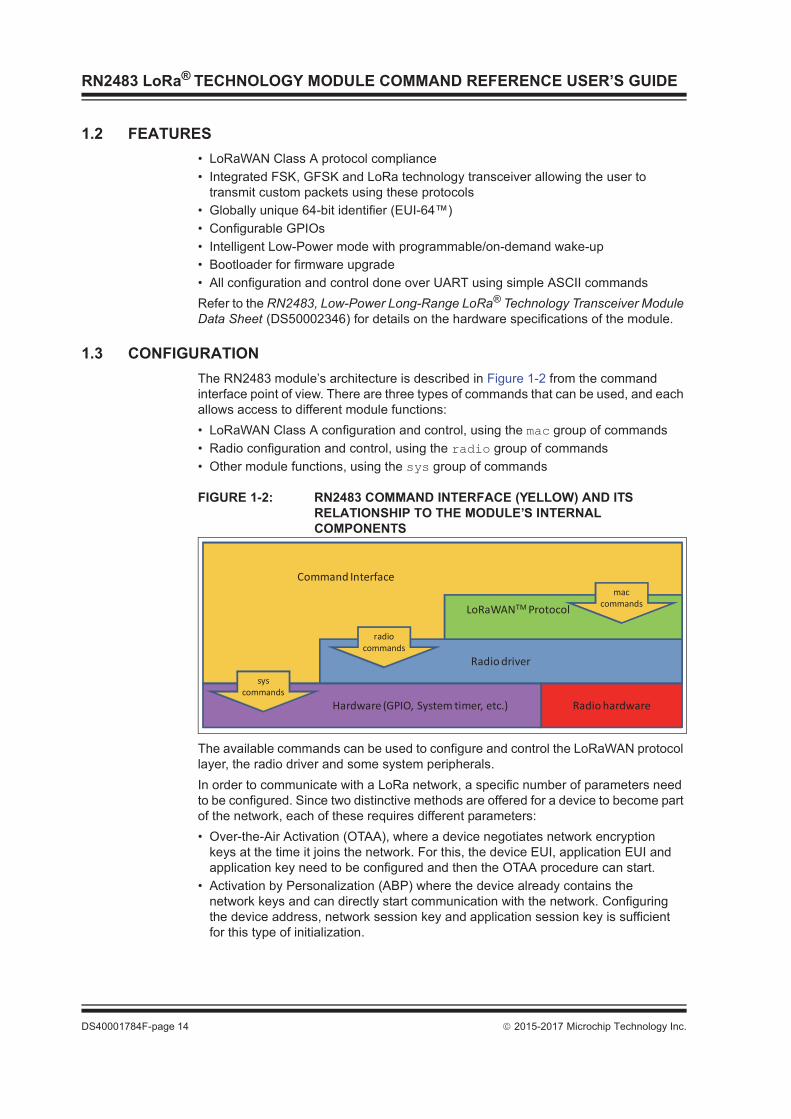
RN2483 LoRa® TECHNOLOGY MODULE COMMAND REFERENCE USER’S GUIDE
DS40001784F-page 14 2015-2017 Microchip Technology Inc.
1.2 FEATURES• LoRaWAN Class A protocol compliance• Integrated FSK, GFSK and LoRa technology transceiver allowing the user to
transmit custom packets using these protocols• Globally unique 64-bit identifier (EUI-64™)• Configurable GPIOs• Intelligent Low-Power mode with programmable/on-demand wake-up• Bootloader for firmware upgrade• All configuration and control done over UART using simple ASCII commandsRefer to the RN2483, Low-Power Long-Range LoRa® Technology Transceiver Module Data Sheet (DS50002346) for details on the hardware specifications of the module.
1.3 CONFIGURATIONThe RN2483 module’s architecture is described in Figure 1-2 from the command interface point of view. There are three types of commands that can be used, and each allows access to different module functions:• LoRaWAN Class A configuration and control, using the mac group of commands• Radio configuration and control, using the radio group of commands• Other module functions, using the sys group of commands
FIGURE 1-2: RN2483 COMMAND INTERFACE (YELLOW) AND ITS RELATIONSHIP TO THE MODULE’S INTERNAL COMPONENTS
The available commands can be used to configure and control the LoRaWAN protocol layer, the radio driver and some system peripherals.In order to communicate with a LoRa network, a specific number of parameters need to be configured. Since two distinctive methods are offered for a device to become part of the network, each of these requires different parameters:• Over-the-Air Activation (OTAA), where a device negotiates network encryption
keys at the time it joins the network. For this, the device EUI, application EUI and application key need to be configured and then the OTAA procedure can start.
• Activation by Personalization (ABP) where the device already contains the network keys and can directly start communication with the network. Configuring the device address, network session key and application session key is sufficient for this type of initialization.
Command Interface
Radio driver
LoRaWANTM Protocolmac
commands
radiocommands
Hardware (GPIO, System timer, etc.)
syscommands
Radio hardware

Introduction
2015-2017 Microchip Technology Inc. DS40001784F-page 15
For increased security, these parameters can be configured and stored in the module’s EEPROM during manufacturing of devices requiring LoRaWAN connectivity. Thus, the keys do not need to be sent over the UART interface by the host system every time the device powers up.
1.4 UART INTERFACEAll of the RN2483 module’s settings and commands are transmitted over UART using the ASCII interface. All commands need to be terminated with <CR><LF> and any replies they generate will also be terminated by the same sequence.The default settings for the UART interface are 57600 bps, 8 bits, no parity, 1 Stop bit, no flow control. The baud rate can be changed by triggering the auto-baud detection sequence of the module. To do this, the host system needs to transmit to the module a break condition followed by a 0x55 character at the new baud rate. The auto-baud detection mechanism can also be triggered during Sleep to wake the module up before the predetermined time has expired.
Note: A break condition is signaled to the module by keeping the UART_RX pin low for longer than the time to transmit a complete character. For example, at the default baud rate of 57600 bps keeping the UART_RX pin low for 938
s is a valid break condition, whereas at 9600 bps this would be interpreted as a 0x00 character. Thus, the break condition needs to be long enough to still be interpreted as such at the baud rate that is currently in use.

RN2483 LoRa® TECHNOLOGY MODULE COMMAND REFERENCE USER’S GUIDE
DS40001784F-page 16 2015-2017 Microchip Technology Inc.
NOTES:

RN2483 LoRa® TECHNOLOGY MODULECOMMAND REFERENCE USER’S GUIDE
2015-2017 Microchip Technology Inc. DS40001784F-page 17
Chapter 2. Command Reference
The RN2483 LoRa technology module supports a variety of commands for configuration. This section describes these commands in detail and provides examples.
2.1 COMMAND SYNTAXTo issue commands to the RN2483 module, the user sends keywords followed by optional parameters. Commands (keywords) are case sensitive, and spaces must not be used in parameters. Hex input data can be uppercase or lowercase. String text data, such as OTAA used for the join procedure, is case-insensitive. The use of shorthand for parameters is NOT supported.Depending on the command, the parameter may expect values in either decimal or hexadecimal form; refer to the command description for the expected form. For example, when configuring the frequency, the command expects a decimal value in Hertz such as 868100000 (868.1 MHz). Alternatively, when configuring the LoRaWAN device address, the hex value is entered into the parameter as aabbccdd. To enter a number in hex form, use the value directly. For example, the hex value 0xFF would be entered as FF.
2.2 COMMAND ORGANIZATIONThere are three general command categories, as shown in Table 2-1.
Once the LoRaWAN Class A protocol configuration is complete, the user must save the settings to store the configuration data, otherwise it will not take effect upon reboot or Reset.
TABLE 2-1: COMMAND TYPESCommand Type Keyword Description
System <sys> Issues system level behavior actions, gathers status information on the firmware and hardware version, or accesses the module user EEPROM memory.
LoRaWAN™ Class A Protocol <mac> Issues LoRaWAN Class A protocol network communication behaviors, actions and configurations commands.
Transceiver commands <radio> Issues radio specific configurations, directly accessing and updating the transceiver setup.
Note: Upon successful reception of commands, the module will respond with one of the following:
• ok • invalid_param • Requested Information• Descriptive Error Message

RN2483 LoRa® TECHNOLOGY MODULE COMMAND REFERENCE USER’S GUIDE
DS40001784F-page 18 2015-2017 Microchip Technology Inc.
2.3 SYSTEM COMMANDSSystem commands begin with the system keyword <sys> and include the categories shown in Table 2-2, Table 2-3 and Table 2-4.
2.3.1 sys sleep <length><length>: decimal number representing the number of milliseconds the system is
put to Sleep, from 100 to 4294967296.Response: ok after the system gets back from Sleep mode
invalid_param if the length is not validThis command puts the system to Sleep for the specified number of milliseconds. The module can be forced to exit from Sleep by sending a break condition followed by a 0x55 character at the new baud rate. Note that the break condition needs to be long enough not to be interpreted as a valid character at the current baud rate.Example: sys sleep 120 // Puts the system to Sleep for 120 ms.
2.3.2 sys resetResponse: RN2483 X.Y.Z MMM DD YYYY HH:MM:SS, where X.Y.Z is firmware version, MMM is month, DD is day, HH:MM:SS is hour, minutes, seconds (format: [HW] [FW] [Date] [Time]). [Date] and [Time] refer to the release of the firmware.This command resets and restarts the RN2483 module; stored internal configurations will be loaded automatically upon reboot.Example: sys reset // Resets and restarts the RN2483 module.
2.3.3 sys eraseFWResponse: no responseThis command deletes the current RN2483 module application firmware and prepares it for firmware upgrade. The RN2483 module bootloader is ready to receive new firmware.Example: sys eraseFW // Deletes the current RN2483 module
application firmware.
Note: To facilitate the sharing of the radio between user custom applications and the LoRaWAN MAC, please refer to the mac pause and mac resume commands. Since no sharing exists between sys and other types of commands, there is no need for additional pause commands.
TABLE 2-2: SYSTEM COMMANDSParameter Description
sleep Puts the system in Sleep for a finite number of milliseconds.reset Resets and restarts the RN2483 module.eraseFW Deletes the current RN2483 module application firmware and prepares it for
firmware upgrade. The RN2483 module bootloader is ready to receive new firmware.
factoryRESET Resets the RN2483 module’s configuration data and user EEPROM to factory default values and restarts the RN2483 module.
set(1) Sets specified system parameter values. get(1) Gets specified system parameter values. Note 1: Refer to Table 2-3 for system <set> and Table 2-4 for system <get> command
summaries.

Command Reference
2015-2017 Microchip Technology Inc. DS40001784F-page 19
2.3.4 sys factoryRESETResponse: RN2483 X.Y.Z MMM DD YYYY HH:MM:SS, where X.Y.Z is firmware version, MMM is month, DD is day, HH:MM:SS is hour, minutes, seconds (format: [HW] [FW] [Date] [Time]). [Date] and [Time] refer to the release of the firmware.This command resets the module’s configuration data and user EEPROM to factory default values and restarts the module. After factoryRESET, the RN2483 module will automatically reset and all configuration parameters are restored to factory default values.Example: sys factoryRESET // Restores factory default values.
2.3.5 System Set Commands
2.3.5.1 sys set nvm <address> <data>
<address>: hexadecimal number representing user EEPROM address, from 300 to 3FF
<data>: hexadecimal number representing data, from 00 to FFResponse: ok if the parameters (address and data) are valid
invalid_param if the parameters (address and data) are not validThis command allows the user to modify the user EEPROM at <address> with the value supplied by <data>. Both <address> and <data> must be entered as hex values. The user EEPROM memory is located inside the MCU on the module.Example: sys set nvm 300 A5 // Stores the value 0xA5 at user EEPROM
address 0x300.
2.3.5.2 sys set pinmode <pinname> <pinFunc>
<pinname>: string representing the pin. Parameters can be: GPIO0 - GPIO13, UART_CTS, UART_RTS, TEST0, TEST1<pinFunc>: string representing the function of the pin. Parameters can be: digout, digin or ana. Response: ok if the parameters are valid
invalid_param if the parameters are not valid
This command allows the user to configure the function on a pin. A pin can be configured as digital output by using the digout parameter. A pin can be configured as digital input by using the digin parameter. A pin can be configured as analog input by using the ana parameter.
TABLE 2-3: SYSTEM SET COMMANDSParameter Description
nvm Stores <data> to a location <address> of user EEPROM.pindig Allows user to set and clear available digital pins.pinmode Allows user to set the functionality of a pin to either digital input, digital output
or analog input (if available).
Note: Not all pins have analog input functionality.
RN2483 LoRa® TECHNOLOGY MODULE COMMAND REFERENCE USER’S GUIDE
DS40001784F-page 20 2015-2017 Microchip Technology Inc.
Example: sys set pinmode GPIO0 ana //Configures GPIO0 as analog input
2.3.5.3 sys set pindig <pinname> <pinstate>
<pinname>: string representing the pin. Parameter values can be: GPIO0 - GPIO13, UART_CTS, UART_RTS, TEST0, TEST1
<pinstate>: decimal number representing the state. Parameter values can be: 0 or 1.
Response: ok if the parameters (<pinname>, <pinstate>) are validinvalid_param if the parameters (<pinname>, <pinstate>) are not valid
This command allows the user to modify the unused pins available for use by the module. The selected <pinname> is driven high or low depending on the desired <pinstate>.Default: GPIO0-GPIO13, UART_CTS, UART_RTS, TEST0 and TEST1 are driven low (value 0).Example: sys set pindig GPIO5 1 // Drives GPIO5 high 1, VDD.
2.3.6 System Get Commands
2.3.6.1 sys get ver
Response: RN2483 X.Y.Z MMM DD YYYY HH:MM:SS, where X.Y.Z is firmware version, MMM is month, DD is day, HH:MM:SS is hour, minutes, seconds (format: [HW] [FW] [Date] [Time]). [Date] and [Time] refer to the release of the firmware.This command returns the information related to the hardware platform, firmware version, release date and time stamp on firmware creation.Example: sys get ver // Returns version-related information.
Note: This command must be called prior to reading or setting the value of a pin in order to have correct behavior.
Note: In order for the pin to be driven to a value, make sure you have first configured the pin to be a digital output using the command sys set pinmode <pinname> digout.
TABLE 2-4: SYSTEM GET COMMANDSParameter Description
ver Returns the information on hardware platform, firmware version, release date.
nvm Returns data from the requested user EEPROM <address>.vdd Returns measured voltage in mV.hweui Returns the preprogrammed EUI node address.pindig Returns the state of a digital input.pinana Returns the state of an analog input.

Command Reference
2015-2017 Microchip Technology Inc. DS40001784F-page 21
2.3.6.2 sys get nvm <address>
<address>: hexadecimal number representing user EEPROM address, from 300 to 3FF
Response: 00 – FF (hexadecimal value from 00 to FF) if the address is validinvalid_param if the address is not valid
This command returns the data stored in the user EEPROM of the RN2483 module at the requested <address> location.Example: sys get nvm 300 // Returns the 8-bit hex value stored at
300.
2.3.6.3 sys get vdd
Response: 0–3600 (decimal value from 0 to 3600)This command informs the RN2483 module to do an ADC conversion on the VDD. The measurement is converted and returned as a voltage (mV).Example: sys get vdd // Returns mV measured on the VDD
module.
2.3.6.4 sys get hweui
Response: hexadecimal number representing the preprogrammed EUI node addressThis command reads the preprogrammed EUI node address from the RN2483 module. The value returned by this command is a globally unique number provided by Microchip.Example: sys get hweui // Reads the preprogrammed EUI node
address.
2.3.6.5 sys get pindig <pinname>
<pinname>: string representing the pin. Parameters can be: GPIO0 - GPIO13, UART_CTS, UART_RTS, TEST0, TEST1Response: decimal number representing the state (either 0 or 1).This command allows the user to read the state of a digital input. To be used as a digital input, a pin needs to be configured using the sys set pinmode command.Example: sys get pindig GPIO0 //Reads the state of the GPIO0 digital input
2.3.6.6 sys get pinana <pinname>
<pinname>: string representing the pin. Parameters can be: GPIO0 - GPIO3, GPIO5 - GPIO13Response: decimal number representing the result of the conversion, from 0 to 1023, where 0 represents 0V and 1023 is VDD, the supply voltage of the module.This command allows the user to read the state of an analog input. To be used as an analog input, a pin needs to be configured using the sys set pinmode command.Example: sys get pinana GPIO0 //Reads the state of the GPIO0 analog input
Note: The preprogrammed EUI node address is a read-only value and cannot be changed or erased. This value can be used to configure the device EUI using the mac set deveui command (see Section 2.4.8.2).
Note: The sys set pinmode <pinname> digin command must be called to configure the function of the pin prior to reading its digital input value.
RN2483 LoRa® TECHNOLOGY MODULE COMMAND REFERENCE USER’S GUIDE
DS40001784F-page 22 2015-2017 Microchip Technology Inc.
2.4 MAC COMMANDSLoRaWAN Class A protocol commands begin with the system keyword mac and include the categories shown in Table 2-5 through Table 2-9.
2.4.1 mac reset <band><band>: decimal number representing the frequency band, either 868 or 433Response: ok if band is valid
invalid_param if band is not validThis command will automatically reset the software LoRaWAN stack and initialize it with the parameters for the selected band.Example: mac reset 868 // Sets the default values and selects the 868
default band.
Note: The sys set pinmode <pinname> ana command must be called to configure the function of the pin prior to reading its analog input value.
TABLE 2-5: MAC COMMANDSParameter Description
reset Resets the RN2483 module to a specific frequency band. tx Sends the data string on a specified port number and sets default values for
most of the LoRaWAN™ parameters.join Informs the RN2483 module to join the configured network. save Saves LoRaWAN Class A configuration parameters to the user EEPROM.forceENABLE Enables the RN2483 module after the LoRaWAN network server
commanded the end device to become silent immediately.pause Pauses LoRaWAN stack functionality to allow transceiver (radio)
configuration.resume Restores the LoRaWAN stack functionality.set Accesses and modifies specific MAC related parameters.get Reads back current MAC related parameters from the module.
Note: This command will set default values for most of the LoRaWAN™ parameters. Everything set prior to this command will lose its set value.

Command Reference
2015-2017 Microchip Technology Inc. DS40001784F-page 23
2.4.2 mac tx <type> <portno> <data><type>: string representing the uplink payload type, either cnf or uncnf
(cnf – confirmed, uncnf – unconfirmed)<portno>: decimal number representing the port number, from 1 to 223<data>: hexadecimal value. The length of <data> bytes capable of being transmitted are dependent upon the set data rate (please refer to the LoRaWAN™ Specification for further details).Response: this command may reply with two responses. The first response will be received immediately after entering the command. In case the command is valid (ok reply received), a second reply will be received after the end of the uplink transmission. Please refer to the LoRaWAN™ Specification for further details.Response after entering the command:• ok – if parameters and configurations are valid and the packet was forwarded to
the radio transceiver for transmission• invalid_param – if parameters (<type> <portno> <data>) are not valid• not_joined – if the network is not joined• no_free_ch – if all channels are busy • silent – if the module is in a Silent Immediately state• frame_counter_err_rejoin_needed – if the frame counter rolled over• busy – if MAC state is not in an Idle state • mac_paused – if MAC was paused and not resumed back• invalid_data_len if application payload length is greater than the maximum
application payload length corresponding to the current data rate Response after the uplink transmission:• mac_tx_ok if uplink transmission was successful and no downlink data was
received back from the server;• mac_rx <portno> <data> if transmission was successful, <portno>: port
number, from 1 to 223; <data>: hexadecimal value that was received from the server;
• mac_err if transmission was unsuccessful, ACK not received back from the server
• invalid_data_len if application payload length is greater than the maximum application payload length corresponding to the current data rate
A confirmed message will expect an acknowledgment from the server; otherwise, the message will be retransmitted by the number indicated by the command mac set retx <value>, whereas an unconfirmed message will not expect any acknowledgment back from the server. Please refer to the LoRaWAN™ Specification for further details.

RN2483 LoRa® TECHNOLOGY MODULE COMMAND REFERENCE USER’S GUIDE
DS40001784F-page 24 2015-2017 Microchip Technology Inc.
If the automatic reply feature is enabled and the server sets the Frame Pending bit or initiates downlink confirmed transmissions, multiple responses will be displayed after each downlink packet is received by the module. A typical scenario for this case would be (prerequisites: free LoRaWAN channels available and automatic reply enabled):• The module sends a packet on port 4 with application payload 0xAB• Radio transmission is successful and the module will display the first response: ok
• The server needs to send two separate downlink confirmed packets back on port 1 with the following data: 0xAC, then 0xAF. First it will transmit the first one (0xAC) and will set the Frame Pending bit. The module will display the second response mac_rx 1 AC
• The module will initiate an automatic uplink unconfirmed transmission with no application payload on the first free channel because the Frame Pending bit was set in the downlink transmission
• The server will send back the second confirmed packet (0xAF). The module will display a third response mac_rx 1 AF
• The module will initiate an automatic unconfirmed transmission with no application payload on the first free channel because the last downlink transmission was confirmed, so the server needs an ACK
• If no reply is received back from the server, the module will display the fourth response after the end of the second Receive window: mac_tx_ok
• After this scenario, the user is allowed to send packets when at least one enabled channel is free
Based on this scenario, the following responses will be displayed by the module:• mac tx cnf 4 AB• ok• mac_rx 1 AC• mac_rx 1 AF• mac_tx_ok
Example: mac tx cnf 4 5A5B5B // Sends a confirmed frame on port 4 with application payload 5A5B5B.

Command Reference
2015-2017 Microchip Technology Inc. DS40001784F-page 25
2.4.3 mac join <mode><mode>: string representing the join procedure type (case-insensitive), either otaa
or abp (otaa – over-the-air activation, abp – activation by personalization).
Response: this command may reply with two responses. The first response will be received immediately after entering the command. In case the command is valid (ok reply received) a second reply will be received after the end of the join procedure. Please refer to the LoRaWAN™ Specification for further details.Response after entering the command:• ok – if parameters and configurations are valid and the join request packet was
forwarded to the radio transceiver for transmission• invalid_param – if <mode> is not valid• keys_not_init – if the keys corresponding to the Join mode (otaa or abp)
were not configured• no_free_ch – if all channels are busy • silent – if the device is in a Silent Immediately state• busy – if MAC state is not in an Idle state • mac_paused – if MAC was paused and not resumed backResponse after the join procedure:• denied if the join procedure was unsuccessful (the module attempted to join the
network, but was rejected);• accepted if the join procedure was successful;This command informs the RN2483 module it should attempt to join the configured network. Module activation type is selected with <mode>. Parameter values can be otaa (over-the-air activation) or abp (activation by personalization). The <mode> parameter is not case sensitive. Before joining the network, the specific parameters for each activation type should be configured (for over the air activation: device EUI, application EUI, application key; for activation by personalization: device address, network session key, application session key). Example: mac join otaa // Attempts to join the network using
over-the-air activation.

RN2483 LoRa® TECHNOLOGY MODULE COMMAND REFERENCE USER’S GUIDE
DS40001784F-page 26 2015-2017 Microchip Technology Inc.
2.4.4 mac saveResponse: okThe mac save command must be issued after configuration parameters have been appropriately entered from the mac set <cmd> commands. This command will save LoRaWAN Class A protocol configuration parameters to the user EEPROM. When the next sys reset command is issued, the LoRaWAN Class A protocol configuration will be initialized with the last saved parameters.The LoRaWAN Class A protocol configuration savable parameters are:• band: Band• fcntup: Uplink Frame Counter• fcntdown: Downlink Frame Counter• dr: Data Rate• rx2dr: Data Rate parameter for the second receive window• rx2freq: Frequency parameter for the second receive window• adr: Adaptive Data Rate state• deveui: End-Device Identifier• appeui: Application Identifier• appkey: Application Key• nwkskey: Network Session Key• appskey: Application Session Key• devaddr: End Device Address• ch: All Channel Parameter
- freq: Frequency- dcycle: Duty Cycle- drrange: Data Rate Range- status: Status
Example: mac save // Saves the LoRaWAN Class A protocol configuration parameters to the user EEPROM.
2.4.5 mac forceENABLEResponse: okThe network can issue a certain command (Duty Cycle Request frame with parameter 255) that would require the RN2483 module to go silent immediately. This mechanism disables any further communication of the module, effectively isolating it from the network. Using mac forceENABLE, after this network command has been received, restores the module’s connectivity by allowing it to send data.Example: mac forceENABLE // Disables the Silent Immediately state.

Command Reference
2015-2017 Microchip Technology Inc. DS40001784F-page 27
2.4.6 mac pauseResponse: 0 – 4294967295 (decimal number representing the number of milliseconds
the mac can be paused)This command pauses the LoRaWAN stack functionality to allow transceiver (radio) configuration. Through the use of mac pause, radio commands can be generated between a LoRaWAN Class A protocol uplink application (mac tx command), and the LoRaWAN Class A protocol Receive windows (second response for the mac tx command). This command will reply with the time interval in milliseconds that the transceiver can be used without affecting the LoRaWAN functionality. The maximum value (4294967295) is returned whenever the LoRaWAN stack functionality is in Idle state and the transceiver can be used without restrictions. ‘0’ is returned when the LoRaWAN stack functionality cannot be paused. After the radio configuration is complete, the mac resume command should be used to return to LoRaWAN Class A protocol commands.Example: mac pause // Pauses the LoRaWAN stack
functionality if the response is different from 0.
2.4.7 mac resumeResponse: okThis command resumes LoRaWAN stack functionality, in order to continue normal functionality after being paused.Example: mac resume // Resumes the LoRaWAN stack functionality.
Note: If already joined to a network, this command MUST be called BEFORE configuring the radio parameters, initiating radio reception, or transmission.
Note: This command MUST be called AFTER all radio commands have been issued and all the corresponding asynchronous messages have been replied.

RN2483 LoRa® TECHNOLOGY MODULE COMMAND REFERENCE USER’S GUIDE
DS40001784F-page 28 2015-2017 Microchip Technology Inc.
2.4.8 MAC Set Commands
2.4.8.1 mac set devaddr <address>
<address>: 4-byte hexadecimal number representing the device address, from 00000000 – FFFFFFFF
Response: ok if address is validinvalid_param if address is not valid
This command configures the module with a 4-byte unique network device address <address>. The <address> MUST be UNIQUE to the current network. This must be directly set solely for activation by personalization devices. This parameter must not be set before attempting to join using over-the-air activation because it will be overwritten once the join process is over. Example: mac set devaddr ABCDEF01
TABLE 2-6: MAC SET COMMANDSParameter Description
devaddr Sets the unique network device address for the RN2483 module.deveui Sets the globally unique identifier for the RN2483 module.appeui Sets the application identifier for the RN2483 module.nwkskey Sets the network session key for the RN2483 module.appskey Sets the application session key for the RN2483 module. appkey Sets the application key for the RN2483 module. pwridx Sets the output power to be used on the next transmissions. dr Sets the data rate to be used for the next transmissions.adr Sets if the adaptive data rate is to be enabled, or disabled. bat Sets the battery level needed for Device Status Answer frame command
response. retx Sets the number of retransmissions to be used for an uplink confirmed
packet.linkchk Sets the time interval for the link check process to be triggered. rxdelay1 Sets the value used for the first Receive window delay.ar Sets the state of the automatic reply. rx2 Sets the data rate and frequency used for the second Receive window. sync Sets the synchronization word for the LoRaWAN™ communication.upctr Sets the value of the uplink frame counter that will be used for the next uplink
transmission.dnctr Sets the value of the downlink frame counter that will be used for the next
downlink reception.ch Allows modification of channel related parameters.
Note: If this parameter had previously been saved to user EEPROM by issuing the mac save command, after modifying its value, the mac save command should be called again.
Command Reference
2015-2017 Microchip Technology Inc. DS40001784F-page 29
2.4.8.2 mac set deveui <devEUI>
<devEUI>: 8-byte hexadecimal number representing the device EUIResponse: ok if address is valid
invalid_param if address is not validThis command sets the globally unique device identifier for the module. The identifier must be set by the host MCU. The module contains a pre-programmed unique EUI and can be retrieved using the sys get hweui command (see Section 2.3.6.4) or user provided EUI can be configured using the mac set deveui command. Example: mac set deveui 0004A30B001A55ED
2.4.8.3 mac set appeui <appEUI>
<appEUI>: 8-byte hexadecimal number representing the application EUIResponse: ok if EUI is valid
invalid_param if EUI is not validThis command sets the application identifier for the module. The application identifier should be used to identify device types (sensor device, lighting device, etc.) within the network.Example: mac set appeui FEDCBA9876543210
2.4.8.4 mac set nwkskey <nwksesskey>
<nwkSessKey>: 16-byte hexadecimal number representing the network session keyResponse: ok if key is valid
invalid_param if key is not validThis command sets the network session key for the module. This key is 16 bytes in length, and provides security for communication between the module and network server.Example: mac set nwkskey 1029384756AFBECD5647382910DACFEB
Note: If this parameter was previously saved to user EEPROM by issuing the mac save command, after modifying its value, the mac save command should be called again.
Note: If this parameter was previously saved to user EEPROM by issuing the mac save command, after modifying its value, the mac save command should be called again.
Note: If this parameter was previously saved to user EEPROM by issuing the mac save command, after modifying its value, the mac save command should be called again.

RN2483 LoRa® TECHNOLOGY MODULE COMMAND REFERENCE USER’S GUIDE
DS40001784F-page 30 2015-2017 Microchip Technology Inc.
2.4.8.5 mac set appskey <appSesskey>
<appSessKey>: 16-byte hexadecimal number representing the application session key
Response: ok if key is validinvalid_param if key is not valid
This command sets the application session key for the module. This key provides security for communication between module and application server.Example: mac set appskey AFBECD56473829100192837465FAEBDC
2.4.8.6 mac set appkey <appKey>
<appKey>: 16-byte hexadecimal number representing the application keyResponse: ok if key is valid
invalid_param if key is not validThis command sets the application key for the module. The application key is used to derive the security credentials for communication during over-the-air activation. Example: mac set appkey 00112233445566778899AABBCCDDEEFF
2.4.8.7 mac set pwridx <pwrIndex>
<pwrIndex>: decimal number representing the index value for the output power, from 0 to 5 for 433 MHz frequency band and from 1 to 5 for 868 MHz frequency band.
Response: ok if power index is validinvalid_param if power index is not valid
This command sets the output power to be used on the next transmissions. Refer to the LoRaWAN™ Specification for the output power corresponding to the <pwrIndex> and also to the RN2483 Low-Power Long-Range LoRa® Technology Transceiver Module Data Sheet (DS50002346) for the actual radio power capabilities.Example: mac set pwridx 1 // Sets the TX output power to 14 dBm on the
next transmission for a 868 MHz EU module.
Note: If this parameter was previously saved to user EEPROM by issuing the mac save command, after modifying its value, the mac save command should be called again.
Note: If this parameter was previously saved to user EEPROM by issuing the mac save command, after modifying its value, the mac save command should be called again.

Command Reference
2015-2017 Microchip Technology Inc. DS40001784F-page 31
2.4.8.8 mac set dr <dataRate>
<dataRate>: decimal number representing the data rate, from 0 and 7, but within the limits of the data rate range for the defined channels.
Response: ok if data rate is validinvalid_param if data rate is not valid
This command sets the data rate to be used for the next transmission. Please refer to the LoRaWAN™ Specification for the description of data rates and the corresponding spreading factors.Example: mac set dr 5 // On EU863-870; SF7/125 kHz.
2.4.8.9 mac set adr <state>
<state>: string value representing the state, either on or off.Response: ok if state is valid
invalid_param if state is not validThis command sets if the adaptive data rate (ADR) is to be enabled, or disabled. The server is informed about the status of the module’s ADR in every uplink frame it receives from the ADR field in uplink data packet. If ADR is enabled, the server will optimize the data rate and the transmission power of the module based on the information collected from the network.Example: mac set adr on // This will enable the ADR mechanism.
2.4.8.10 mac set bat <level>
<level>: decimal number representing the level of the battery, from 0 to 255. ‘0’ means external power, ‘1’ means low level, 254 means high level, 255 means the end device was not able to measure the battery level.
Response: ok if the battery level is validinvalid_param if the battery level is not valid
This command sets the battery level required for Device Status Answer frame in use with the LoRaWAN Class A protocol. Example: mac set bat 127 // Battery is set to ~50%.
2.4.8.11 mac set retx <reTxNb>
<reTxNb>: decimal number representing the number of retransmissions for an uplink confirmed packet, from 0 to 255.
Response: ok if <retx> is validinvalid_param if <retx> is not valid
This command sets the number of retransmissions to be used for an uplink confirmed packet, if no downlink acknowledgment is received from the server.Example: mac set retx 5 // The number of retransmissions made
for an uplink confirmed packet is set to 5.
Note: If this parameter had previously been saved to user EEPROM by issuing the mac save command, after modifying its value, the mac save command should be called again.
Note: If this parameter had previously been saved to user EEPROM by issuing the mac save command, after modifying its value, the mac save command should be called again.

RN2483 LoRa® TECHNOLOGY MODULE COMMAND REFERENCE USER’S GUIDE
DS40001784F-page 32 2015-2017 Microchip Technology Inc.
2.4.8.12 mac set linkchk <linkCheck>
<linkCheck>: decimal number that sets the time interval in seconds for the link check process, from 0 to 65535
Response: ok if the time interval is validinvalid_param if the time interval is not valid
This command sets the time interval for the link check process to be triggered periodically. A <value> of ‘0’ will disable the link check process. When the time interval expires, the next application packet that will be sent to the server will include also a link check MAC command. Please refer to the LoRaWAN™ Specification for more information on the Link Check MAC command.Example: mac set linkchk 600 // The module will attempt a link check
process at 600-second intervals.
2.4.8.13 mac set rxdelay1 <rxDelay>
<rxDelay>: decimal number representing the delay between the transmission and the first Reception window in milliseconds, from 0 to 65535.
Response: ok if <rxDelay> is validinvalid_param if <rxDelay> is not valid
This command will set the delay between the transmission and the first Reception window to the <rxDelay> in milliseconds. The delay between the transmission and the second Reception window is calculated in software as the delay between the transmission and the first Reception window + 1000 (ms).Example: mac set rxdelay1 1000 // Set the delay between the transmission
and the first Receive window to 1000 ms.
2.4.8.14 mac set ar <state>
<state>: string value representing the state, either on or off.Response: ok if state is valid
invalid_param if state is not validThis command sets the state of the automatic reply. By enabling the automatic reply, the module will transmit a packet without a payload immediately after a confirmed downlink is received, or when the Frame Pending bit has been set by the server. If set to OFF, no automatic reply will be transmitted.Example: mac set ar on // Enables the automatic reply process
inside the module.
Note: If the command mac reset is issued, the link check process will be set as disabled.
Note: The RN2483 module implementation will initiate automatic transmissions with no application payload if the automatic reply feature is enabled and the server sets the Frame Pending bit or initiates a confirmed downlink transmission. In this case, if all enabled channels are busy due to duty cycle limitations, the stack will wait for the first channel that will become free to transmit. The user will not be able to initiate uplink transmissions until the automatic transmissions are done.
Command Reference
2015-2017 Microchip Technology Inc. DS40001784F-page 33
2.4.8.15 mac set rx2 <dataRate> <frequency>
<dataRate>: decimal number representing the data rate, from 0 to 7.<frequency>: decimal number representing the frequency, from 863000000 to
870000000 or from 433050000 to 434790000, in Hz.Response: ok if parameters are valid
invalid_param if parameters are not validThis command sets the data rate and frequency used for the second Receive window. The configuration of the Receive window parameters should be in concordance with the server configuration.Example: mac set rx2 3 865000000 // Receive window 2 is configured with
SF9/125 kHz data rate with a center frequency of 865 MHz.
2.4.8.16 mac set sync <synchWord>
<synchWord>: one byte long hexadecimal number representing the synchronization word for the LoRaWAN communicationResponse: ok if parameters are valid
invalid_param if parameter is not valid
This command sets the synchronization word for the LoRaWAN communication. The configuration of the synchronization word should be in concordance with the Gateway configuration.Example: mac set sync 34 //Synchronization word is configured to
use the 0x34 value
2.4.8.17 mac set upctr <fCntUp>
<fCntUp>: decimal number representing the value of the uplink frame counter that will be used for the next uplink transmission, from 0 to 4294967295.Response: ok if parameter is valid
invalid_param if parameter is not valid
This command sets the value of the uplink frame counter that will be used for the next uplink transmission.Example: mac set upctr 10
Note: If this parameter had previously been saved to user EEPROM by issuing the mac save command, after modifying its value, the mac save command should be called again.
Note: If this parameter had previously been saved to user EEPROM by issuing the mac save command, after modifying its value, the mac save command should be called again.

RN2483 LoRa® TECHNOLOGY MODULE COMMAND REFERENCE USER’S GUIDE
DS40001784F-page 34 2015-2017 Microchip Technology Inc.
2.4.8.18 mac set dnctr <fCntDown>
<fCntDown>: decimal number representing the value of the downlink frame counter that will be used for the next downlink reception, from 0 to 4294967295.Response: ok if parameter is valid
invalid_param if parameter is not valid
This command sets the value of the downlink frame counter that will be used for the next downlink reception.Example: mac set dnctr 30
2.4.8.19 MAC SET CHANNEL COMMANDS
2.4.8.19.1 mac set ch freq <channelID> <frequency><channelId>: decimal number representing the channel number, from 3 to 15. <frequency>: decimal number representing the frequency, from 863000000 to
870000000 or from 433050000 to 434790000, in Hz.Response: ok if parameters are valid
invalid_param if parameters are not validThis command sets the operational frequency on the given channel ID. The default channels (0-2) cannot be modified in terms of frequency.Example: mac set ch freq 13 864000000 // Define frequency for channel
13 to be 864 MHz.
Note: If this parameter had previously been saved to user EEPROM by issuing the mac save command, after modifying its value, the mac save command should be called again.
TABLE 2-7: MAC SET CHANNEL COMMANDSParameter Description
freq Sets the module operation frequency on a given channel ID. dcycle Sets the module operation duty cycle on a given channel ID.drrange Sets the module allowed data rate range (min.- max.) allowed on a given
channel ID.status Sets the use of the specified channel ID.
Note: If this parameter was previously saved to user EEPROM by issuing the mac save command, after modifying its value, the mac save command should be called again.

Command Reference
2015-2017 Microchip Technology Inc. DS40001784F-page 35
2.4.8.19.2 mac set ch dcycle <channelID> <dutyCycle> <channelId>: decimal number representing the channel number, from 0 to 15. <dutyCycle>: decimal number representing the duty cycle, from 0 to 65535.Response: ok if parameters are valid
invalid_param if parameters are not validThis command sets the duty cycle used on the given channel ID on the module. The <dutyCycle> value that needs to be configured can be obtained from the actual duty cycle X (in percentage) using the following formula: <dutyCycle> = (100/X) – 1. The default settings consider only the three default channels (0-2), and their default duty cycle is 0.33%. If a new channel is created either by the server or by the user, all the channels (including the default ones) must be updated by the user in terms of duty cycle to comply with the ETSI regulations.Example: mac set ch dcycle 13 9 // Defines duty cycle for channel 13 to be
10%. Since (100/10) – 1 = 9, the parameter that gets configured is 9.
2.4.8.19.3 mac set ch drrange <channelID> <minRange> <maxRange><channelId>: decimal number representing the channel number, from 0 to 15<minRange>: decimal number representing the minimum data rate, from 0 to 7<maxRange>: decimal number representing the maximum data rate, from 0 to 7Response: ok if parameters are valid
invalid_param if parameters are not validThis command sets the operating data rate range, min. to max., for the given <channelId>. By doing this the module can vary data rates between the <minRange> and <maxRange> on the specified <channelId>. Please refer to the LoRaWAN™ Specification for the actual values of the data rates and the corresponding spreading factors (SF).Example: mac set ch drrange 13 0 2 // Using EU863-870 band: on channel
13 the data rate can range from 0 (SF12/125 kHz) to 2 (SF10/125 kHz) as required.
Note: If this parameter was previously saved to user EEPROM by issuing the mac save command, after modifying its value, the mac save command should be called again.
Note: If this parameter was previously saved to user EEPROM by issuing the mac save command, after modifying its value, the mac save command should be called again.

RN2483 LoRa® TECHNOLOGY MODULE COMMAND REFERENCE USER’S GUIDE
DS40001784F-page 36 2015-2017 Microchip Technology Inc.
2.4.8.19.4 mac set ch status <channel ID> <status><channelId>: decimal number representing the channel number, from 0 to 15. <status>: string value representing the state, either on or off.Response: ok if parameters are valid
invalid_param if parameters are not validThis command sets the operation of the given <channelId>.
Example: mac set ch status 4 off // Channel ID 4 is disabled from use.
2.4.9 MAC Get Commands
WARNING
<ChannelId> parameters (frequency, data range, duty cycle) must be issued prior to enabling the status of that channel.
Note: If this parameter was previously saved to user EEPROM by issuing the mac save command, after modifying its value, the mac save command should be called again.
TABLE 2-8: MAC GET COMMANDSParameter Description
devaddr Gets the current stored unique network device address for that specific end device.
deveui Gets the current stored globally unique identifier for that specific end device. appeui Gets the application identifier for the end device.dr Gets the data rate to be used for the next transmission.band Gets the current frequency band in operation. pwridx Gets the output power index value. adr Gets the state of adaptive data rate for the device.retx Gets the number of retransmissions to be used for an uplink confirmed packet.rxdelay1 Gets the interval value stored for rxdelay1.rxdelay2 Gets the interval value stored for rxdelay2.ar Gets the state of the automatic reply.rx2 Gets the data rate and frequency used for the second Receive window. dcycleps Gets the duty cycle prescaler which can only be configured by the server. mrgn Gets the demodulation margin as received in the last Link Check Answer frame.gwnb Gets the number of gateways that successfully received the last Link Check
Request frame. status Gets the current status of the RN2483 module. sync Gets the synchronization word for the LoRaWAN communication.upctr Gets the value of the uplink frame counter that will be used for the next uplink
transmission.dnctr Gets the value of the downlink frame counter that will be used for the next
downlink reception.ch Gets parameters related information which pertains to channel operation and
behaviors.

Command Reference
2015-2017 Microchip Technology Inc. DS40001784F-page 37
2.4.9.1 mac get devaddr
Response: 4-byte hexadecimal number representing the device address, from 00000000 to FFFFFFFF.
This command will return the current end-device address of the module. Default: 00000000Example: mac get devaddr
2.4.9.2 mac get deveui
Response: 8-byte hexadecimal number representing the device EUI.This command returns the globally unique end-device identifier, as set in the module. Default: pre-programmed EUI node addressExample: mac get deveui
2.4.9.3 mac get appeui
Response: 8-byte hexadecimal number representing the application EUI.This command will return the application identifier for the module. The applicationidentifier is a value given to the device by the network. Default: 0000000000000000Example: mac get appeui
2.4.9.4 mac get dr
Response: decimal number representing the current data rate.This command will return the current data rate. Default: 5Example: mac get dr
2.4.9.5 mac get band
Response: decimal number representing the frequency band, either 868 or 433.This command returns the current frequency band of operation. The band reflects the module’s operation types.Default: 868Example: mac get band
2.4.9.6 mac get pwridx
Response: decimal number representing the current output power index value, from 0 to 5.This command returns the current output power index value. Default: 1Example: mac get pwridx
Note: After the mac reset <band> command is explicitly called, the device EUI value will be set to all zeros. Make certain that a valid value is given to the device EUI.

RN2483 LoRa® TECHNOLOGY MODULE COMMAND REFERENCE USER’S GUIDE
DS40001784F-page 38 2015-2017 Microchip Technology Inc.
2.4.9.7 mac get adr
Response: string representing the state of the adaptive data rate mechanism, either on or off.
This command will return the state of the adaptive data rate mechanism. It will reflect if the ADR is on or off on the requested device.Default: offExample: mac get adr
2.4.9.8 mac get retx
Response: decimal number representing the number of retransmissions, from 0 to 255.This command will return the currently configured number of retransmissions which are attempted for a confirmed uplink communication when no downlink response has been received. Default: 7Example: mac get retx
2.4.9.9 mac get rxdelay1
Response: decimal number representing the interval, in milliseconds, for rxdelay1, from 0 to 65535.This command will return the interval, in milliseconds, for rxdelay1. Default: 1000 Example: mac get rxdelay1
2.4.9.10 mac get rxdelay2
Response: decimal number representing the interval, in milliseconds, for rxdelay2, from 0 to 65535.
This command will return the interval, in milliseconds, for rxdelay2. Default: 2000 Example: mac get rxdelay2
2.4.9.11 mac get ar
Response: string representing the state of the automatic reply, either on or off.This command will return the current state for the automatic reply (AR) parameter. The response will indicate if the AR is on or off.Default: offExample: mac get ar

Command Reference
2015-2017 Microchip Technology Inc. DS40001784F-page 39
2.4.9.12 mac get rx2 <freqBand>
<freqBand>: decimal number representing the frequency band, either 868 or 433.Response: decimal number representing the data rate configured for the second Receive window, from 0 to 7 and a decimal number for the frequency configured for the second Receive window, from 863000000 to 870000000 or from 433050000 to 434790000, in Hz.This command will return the current data rate and frequency configured to be used during the second Receive window. Default: 0 869525000 // for 868 band
0 434665000 // for 433 bandExample: mac get rx2 868
2.4.9.13 mac get dcycleps
Response: decimal number representing the prescaler value, from 0 to 65535.This command returns the duty cycle prescaler. The value of the prescaler can be configured ONLY by the SERVER through use of the Duty Cycle Request frame. Upon reception of this command from the server, the duty cycle prescaler is changed for all enabled channels.Default: 1Example: mac get dcycleps
2.4.9.14 mac get mrgn
Response: decimal number representing the demodulation margin, from 0 to 255.This command will return the demodulation margin as received in the last Link Check Answer frame. Please refer to the LoRaWAN™ Specification for the description of the values.Default: 255Example: mac get mrgn
2.4.9.15 mac get gwnb
Response: decimal number representing the number of gateways, from 0 to 255.This command will return the number of gateways that successfully received the last Link Check Request frame command, as received in the last Link Check Answer. Default: 0Example: mac get gwnb

RN2483 LoRa® TECHNOLOGY MODULE COMMAND REFERENCE USER’S GUIDE
DS40001784F-page 40 2015-2017 Microchip Technology Inc.
2.4.9.16 mac get status
Response: 4-byte hexadecimal number representing the current status of the module.This command will return the current status of the module. The value returned is a bit mask represented in hexadecimal form. Please refer to Figure 2-1 for the significance of the bit mask.Default: 00000000Example: mac get status
2.4.9.17 mac get sync
Response: one byte long hexadecimal number representing the synchronization word for the LoRaWAN communication.This command will return the synchronization word for the LoRaWAN communication. Default: 34Example: mac get sync
2.4.9.18 mac get upctr
Response: decimal number representing the value of the uplink frame counter that will be used for the next uplink transmission, from 0 to 4294967295.This command will return the value of the uplink frame counter that will be used for the next uplink transmission.Default: 0Example: mac get upctr
2.4.9.19 mac get dnctr
Response: decimal number representing the value of the downlink frame counter that will be used for the next downlink reception, from 0 to 4294967295.This command will return the value of the downlink frame counter that will be used for the next downlink reception.Default: 0Example: mac get dnctr

Command Reference
2015-2017 Microchip Technology Inc. DS40001784F-page 41
FIGURE 2-1: MAC STATUS BIT-MAPPED REGISTER (1)
015 14 13 12 11 10 123456789
Join status (‘0’ – network not joined, ‘1’ – network joined)
Mac state (2)
Automatic reply status (‘0’ – disabled, ‘1’ – enabled)
ADR status (‘0’ – ADR is disabled, ‘1’ – ADR is disabled)
Silent immediately status (‘0’ – disabled, ‘1’ – enabled)
Mac pause status (‘0’ – mac is not paused, ‘1’ – mac is paused)
RFU
Link check status (‘0’ – link check is disabled, ‘1’ – link check is enabled)
Channels updated (‘0’ – not updated, ‘1’ – updated via CFList or NewChannelReq MAC command)
Output power updated (‘0’ – not updated, ‘1’ – updated via LinkADRReq MAC command)
NbRep updated (‘0’ – not updated, ‘1’ – updated via LinkADRReq MAC command)(3)
Prescaler updated (‘0’ – not updated, ‘1’ – updated via DutyCycleReq MAC command)
Second Receive window parameters updated (‘0’ – not updated, ‘1’ – updated RX ParamSetupReq command)
TX timing setup updated (‘0’ – not updated, ‘1’ – updated via RX TimingSetupReq MAC command)
Note 1: Bits 10 (Channels updated), 11 (Output power updated), 12 (NbRep updated), 13 (Prescaler updated), 14 (Second Receive window parameters updated) and 15 (TX timing setup updated) are cleared after issuing a “mac get status” command.
2: Mac state:0 – Idle (transmissions are possible)
1 – Transmission occurring
2 – Before the opening of Receive window 1
3 – Receive window 1 is open
4 – Between Receive window 1 and Receive window 2
5 – Receive window 2 is open
6 – Ack_timeout (Ack_timeout is described in more detail in the LoRaWAN™ specification)3: NbRep is the number of repetitions for unconfirmed packets (please refer to the LoRaWAN™
Specification for more details).
1631-17
Rejoin needed (‘0’ – end device functional, ‘1’ – end device not functional and rejoin is needed)
RFU

RN2483 LoRa® TECHNOLOGY MODULE COMMAND REFERENCE USER’S GUIDE
DS40001784F-page 42 2015-2017 Microchip Technology Inc.
2.4.9.20 MAC GET CHANNEL COMMANDS
2.4.9.20.1 mac get ch freq <ChannelId>
<channelId>: decimal number representing the channel number, from 0 to 15.Response: decimal number representing the frequency of the channel, from 863000000 to 870000000 or from 433050000 to 434790000, in Hz, depending on the frequency band selected.This command returns the frequency on the requested <channelId>, entered in decimal form.Default: see Table 2-10 Example: mac get ch freq 0
TABLE 2-9: MAC GET CHANNEL COMMANDSParameter Description
freq Gets the module operation frequency for the specified channel ID. dcycle Gets the module duty cycle used for transmission on the specified channel
ID. drrange Gets the valid data rate range (min. to max.) allowed for the module on the
specified channel IDstatus Gets the status for the specified channel ID to indicate if it is enabled for use.
TABLE 2-10: DEFAULT PARAMETERS FOR CHANNELS
Channel Number ParametersFrequency band
868 433
Channel 0 Frequency (Hz) 868100000 433175000Duty cycle (1) 302 302Data rate range 0-5 0-5Status On On
Channel 1 Frequency (Hz) 868300000 433375000Duty cycle(1) 302 302Data rate range 0-5 0-5Status On On
Channel 2 Frequency (Hz) 868500000 433575000Duty cycle(1) 302 302Data rate range 0-5 0-5Status On On
Channels 3-15 Frequency (Hz) 0 0Duty cycle(1) 65535 65535Data rate range 15 15 15 15Status Off Off
Note 1: The default settings consider only the three default channels (0-2), and their default duty cycle is 0.33%. If a new channel is created either by the server or by the user, all the channels (including the default ones) must be updated by the user in terms of duty cycle to comply with the ETSI regulations.

Command Reference
2015-2017 Microchip Technology Inc. DS40001784F-page 43
2.4.9.20.2 mac get ch dcycle <channelId>
<channelId>: decimal number representing the channel number, from 0 to 15.Response: decimal number representing the duty cycle of the channel, from 0 to 65535.This command returns the duty cycle on the requested <channelId>. The duty cycle is returned in decimal value. The actual duty cycle (in percentage) can be obtained using the returned value V as: percent = 100/(V + 1).Default: see Table 2-10 Example: mac get ch dcycle 0 // Reads back duty cycle setting on Channel
ID 0. If the value reported back is 99, the actual duty cycle on the channel (in percentage) is 100/(99 + 1) = 1.
2.4.9.20.3 mac get ch drrange <channelId>
<channelId>: decimal number representing the channel number, from 0 to 15.Response: decimal number representing the minimum data rate of the channel, from 0 to 7 and a decimal number representing the maximum data rate of the channel, from 0 to 7This command returns the allowed data rate index range on the requested <channelId>, entered in decimal form. The <minRate> and <maxRate> index values are returned in decimal form and reflect index values. Please refer to the LoRaWAN™ Specification for the description of data rates and the corresponding spreading factors.Default: see Table 2-10 Example: mac get ch drrange 0
2.4.9.20.4 mac get ch status <channelId>
<channelId>: decimal number representing the channel number, from 0 to 15.Response: string representing the state of the channel, either on or off.This command returns if <channelId> is currently enabled for use. <channelId> is entered in decimal form and the response will be on or off reflecting the channel is enabled or disabled appropriately.Default: see Table 2-10 Example: mac get ch status 2
Note: <ChannelId> parameters must be issued prior to enabling the status of that channel. If a channel is disabled through the <status>, all channel parameters must be reconfigured prior to enabling.

RN2483 LoRa® TECHNOLOGY MODULE COMMAND REFERENCE USER’S GUIDE
DS40001784F-page 44 2015-2017 Microchip Technology Inc.
2.5 RADIO COMMANDS
TABLE 2-11: RADIO COMMANDS(1)
Parameter Description
rx This command configures the radio to receive simple radio packets according to prior configuration settings.
tx This command configures a simple radio packet transmission according to prior configuration settings.
cw This command will put the module into a Continuous Wave (cw) Transmission for system tuning or certification use.
set This command allows modification to the radio setting directly. This command allows for the user to change the method of radio operation within module type band limits.
get This command grants the ability to read out radio settings as they are currently configured.
Note 1: The mac pause command must be called before any radio transmission or reception, even if no MAC operations have been initiated before.
TABLE 2-12: RADIO PARAMETERS AVAILABILITY FOR DIFFERENT OPERATIONS
Command radio get radio setAvailability for
LoRa® ModulationAvailability for FSK
Modulation
bt —
mod
freq
pwr
sf —
afcbw —
rxbw —
bitrate —
fdev —
prlen —
crc
iqi —
cr —
wdt
sync
bw —
snr — —
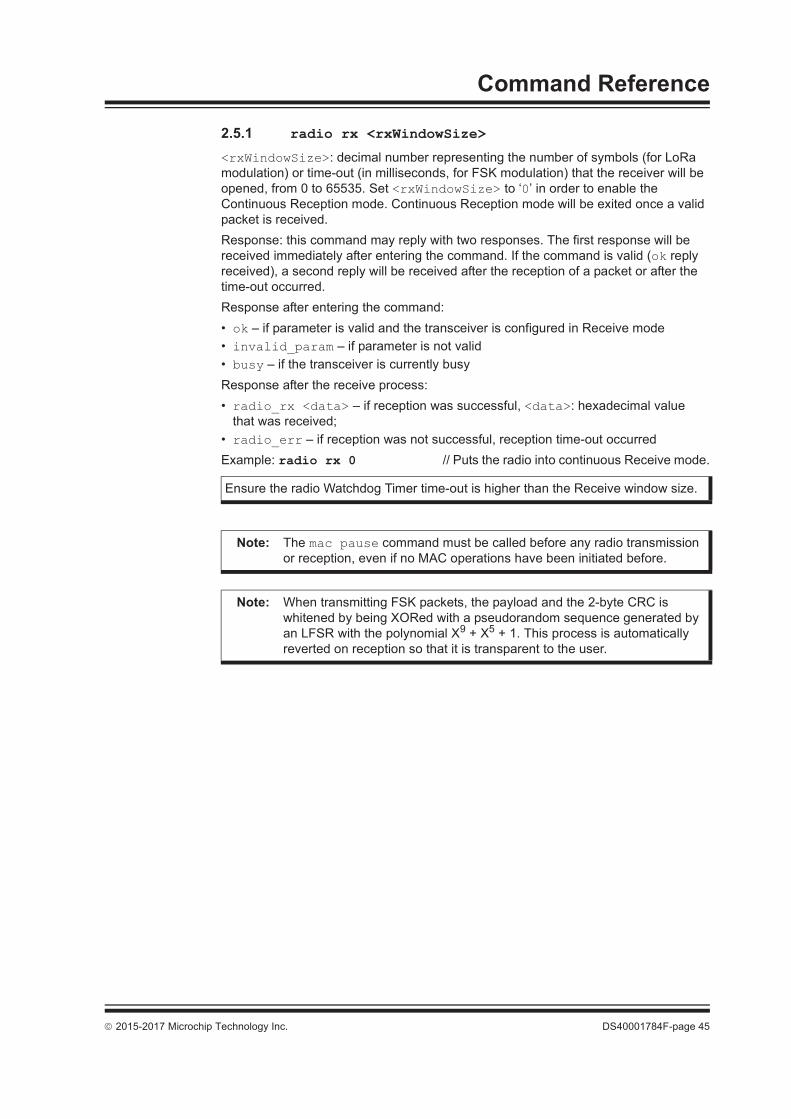
Command Reference
2015-2017 Microchip Technology Inc. DS40001784F-page 45
2.5.1 radio rx <rxWindowSize>
<rxWindowSize>: decimal number representing the number of symbols (for LoRa modulation) or time-out (in milliseconds, for FSK modulation) that the receiver will be opened, from 0 to 65535. Set <rxWindowSize> to ‘0’ in order to enable the Continuous Reception mode. Continuous Reception mode will be exited once a valid packet is received.Response: this command may reply with two responses. The first response will be received immediately after entering the command. If the command is valid (ok reply received), a second reply will be received after the reception of a packet or after the time-out occurred.Response after entering the command:• ok – if parameter is valid and the transceiver is configured in Receive mode• invalid_param – if parameter is not valid• busy – if the transceiver is currently busy Response after the receive process:• radio_rx <data> – if reception was successful, <data>: hexadecimal value
that was received;• radio_err – if reception was not successful, reception time-out occurredExample: radio rx 0 // Puts the radio into continuous Receive mode.
Ensure the radio Watchdog Timer time-out is higher than the Receive window size.
Note: The mac pause command must be called before any radio transmission or reception, even if no MAC operations have been initiated before.
Note: When transmitting FSK packets, the payload and the 2-byte CRC is whitened by being XORed with a pseudorandom sequence generated by an LFSR with the polynomial X9 + X5 + 1. This process is automatically reverted on reception so that it is transparent to the user.

RN2483 LoRa® TECHNOLOGY MODULE COMMAND REFERENCE USER’S GUIDE
DS40001784F-page 46 2015-2017 Microchip Technology Inc.
2.5.2 radio tx <data><data>: hexadecimal value representing the data to be transmitted, from 0 to 255 bytes for LoRa modulation and from 0 to 64 bytes for FSK modulation.Response: this command may reply with two responses. The first response will be received immediately after entering the command. If the command is valid (ok reply received), a second reply will be received after the effective transmission.Response after entering the command:• ok – if parameter is valid and the transceiver is configured in Transmit mode• invalid_param – if parameter is not valid• busy – if the transceiver is currently busyResponse after the effective transmission:• radio_tx_ok – if transmission was successful• radio_err – if transmission was unsuccessful (interrupted by radio Watchdog
Timer time-out)This command transmits the <data> passed. Example: radio tx 48656c6C6F // Transmits a packet of
[0x48][0x65][0x6c][0x6C][0x6F]; Hello.
2.5.3 radio cw <state><state>: string representing the state of the Continuous Wave (CW) mode, either on or off.Response: ok if state is valid invalid_param if state is not validThis command will enable or disable the CW mode on the module. CW mode allows the user to put the transceiver into Transmission mode to observe the generated signal. By altering the settings for the radio the user can observe the changes in transmissions levels.Example: radio cw on
Note: In order to meet ETSI regulations in the given frequency bands, the radio has to use either Listen Before Talk (LBT) + Adaptive Frequency Agility (AFA) or duty cycle limitations. By issuing the radio tx <data> command the module does not perform LBT before transmission, thus the user has to make sure that duty cycle limits are not violated. For more information on duty cycle limits please check the EN 300 220-2 v2.4.1 standard.
Note: The mac pause command must be called before any radio transmission or reception, even if no MAC operations have been initiated before.
Note: When transmitting FSK packets, the payload and the 2-byte CRC is whitened by being XORed with a pseudorandom sequence generated by an LFSR with the polynomial X9 + X5 + 1. This process is automatically reverted on reception so that it is transparent to the user.
Note: Please note that using radio cw off resets the module, this command being semantically identical to sys reset.

Command Reference
2015-2017 Microchip Technology Inc. DS40001784F-page 47
2.5.4 Radio Set Commands
2.5.4.1 radio set bt <gfBT>
<gfBT>: string representing the Gaussian baseband data shaping, enabling GFSK modulation. Parameter values can be: none, 1.0, 0.5, 0.3.Response: ok if the data shaping is valid invalid_param if the data shaping is not validThis command modifies the data shaping applied to FSK transmissions. Entering any <gfBT> other than none will result in a Gaussian Filter BT being applied to transmissions in FSK mode. Example: radio set bt none // Data shaping in FSK mode is disabled or null.
2.5.4.2 radio set mod <mode>
<mode>: string representing the modulation method, either lora or fsk.Response: ok if the modulation is valid invalid_param if the modulation is not validThis command changes the modulation method being used by the module. Altering the mode of operation does not affect previously set parameters, variables or registers. FSK mode also allows GFSK transmissions when data shaping is enabled.Example: radio set mod lora
2.5.4.3 radio set freq <frequency>
<frequency>: decimal representing the frequency, from 433050000 to 434790000 or from 863000000 to 870000000, in Hz.Response: ok if the frequency is valid invalid_param if the frequency is not validThis command changes the communication frequency of the radio transceiver.Example: radio set freq 868000000
TABLE 2-13: RADIO SET COMMANDSParameter Description
bt Set the data shaping for frequency shift keying (FSK) modulation type. mod Set the module Modulation mode. freq Set the current operation frequency for the radio.pwr Set the output power level used by the radio during transmission.sf Set the requested spreading factor (SF) to be used during transmission. afcbw Set the value used by the automatic frequency correction bandwidth. rxbw Set the operational receive bandwidth.bitrate Set the frequency shift keying (FSK) bit rate. fdev Set the frequency deviation allowed by the end device.prlen Set the preamble length used during transmissions. crc Set if a CRC header is to be used. iqi Set if IQ inversion is used. cr Set the coding rate used by the radio.wdt Set the time-out limit for the radio Watchdog Timer.sync Set the sync word used. bw Set the value used for the radio bandwidth.

RN2483 LoRa® TECHNOLOGY MODULE COMMAND REFERENCE USER’S GUIDE
DS40001784F-page 48 2015-2017 Microchip Technology Inc.
2.5.4.4 radio set pwr <pwrout>
<pwrOut>: signed decimal number representing the transceiver output power, from -3 to 15.
Response: ok if the output power is validinvalid_param if the output power is not valid
This command changes the transceiver output power. However, note that the transceiver is designed to transmit a maximum of +14 dBm. It is possible to set the output power above the regulatory limits. This power setting allows some compensation on the cable or transmission line loss. For more details on output power please check the RN2483 Low-Power Long-Range LoRa® Technology Transceiver Module Data Sheet.Example: radio set pwr 14
2.5.4.5 radio set sf <spreadingfactor>
<spreadingFactor>: string representing the spreading factor. Parameter values can be: sf7, sf8, sf9, sf10, sf11 or sf12.
Response: ok if the spreading factor is validinvalid_param if the spreading factor is not valid
This command sets the spreading factor used during transmission.Example: radio set sf sf7
2.5.4.6 radio set afcbw <autoFreqBand>
<autoFreqBand>: float representing the automatic frequency correction, in kHz. Parameter values can be: 250, 125, 62.5, 31.3, 15.6, 7.8, 3.9, 200, 100, 50, 25, 12.5, 6.3, 3.1, 166.7, 83.3, 41.7, 20.8, 10.4, 5.2, 2.6.
Response: ok if the automatic frequency correction is validinvalid_param if the automatic frequency correction is not valid
This command modifies the automatic frequency correction bandwidth for receiving/transmitting. Example: radio set afcbw 125
2.5.4.7 radio set rxbw <rxbandwidth>
<rxBandwidth>: float representing the signal bandwidth, in kHz. Parameter values can be: 250, 125, 62.5, 31.3, 15.6, 7.8, 3.9, 200, 100, 50, 25, 12.5, 6.3, 3.1, 166.7, 83.3, 41.7, 20.8, 10.4, 5.2, 2.6.
Response: ok if the signal bandwidth is validinvalid_param if signal bandwidth is not valid
This command sets the signal bandwidth when receiving.Example: radio set rxbw 250 // Signal bandwidth for receiving is 250 kHz.
2.5.4.8 radio set bitrate <fskBitRate>
<fskBitRate>: decimal number representing the FSK bit rate value, from 1 to 300000.Response: ok if the bit rate value is valid
invalid_param if the bit rate value is not validThis command sets the FSK bit rate value.

Command Reference
2015-2017 Microchip Technology Inc. DS40001784F-page 49
Example: radio set bitrate 5000 // FSK bit rate is set to 5 kb/s.
2.5.4.9 radio set fdev <freqdev>
<freqDev>: decimal number representing the frequency deviation, from 0 to 200000.Response: ok if the frequency deviation is valid
invalid_param if frequency deviation is not validThis command sets the frequency deviation during operation.Example: radio set fdev 5000 // Frequency deviation is 5 kHz.
2.5.4.10 radio set prlen <preamble>
<preamble>: decimal number representing the preamble length, from 0 to 65535.Response: ok if the preamble length is valid
invalid_param if the preamble length is not validThis command sets the preamble length for transmit/receive.Example: radio set prlen 8 // Preamble length is 8.
2.5.4.11 radio set crc < crcHeader >
<crcHeader>: string representing the state of the CRC header, either on or off.Response: ok if the state is valid
invalid_param if the state is not validThis command enables or disables the CRC header for communications.Example: radio set crc on // Enables the CRC header.
2.5.4.12 radio set iqi <iqInvert>
<iqInvert>: string representing the state of the invert IQ, either on or off.Response: ok if the state is valid
invalid_param if the state is not validThis command enables or disables the Invert IQ for communications.Example: radio set iqi on // Invert IQ is enabled.
2.5.4.13 radio set cr <codingRate>
<codingRate>: string representing the coding rate. Parameter values can be: 4/5, 4/6, 4/7, 4/8.Response: ok if the coding rate is valid
invalid_param if the coding rate is not validThis command modifies the coding rate currently being used by the radio.Example: radio set cr 4/7 // The coding rate is set to 4/7.

RN2483 LoRa® TECHNOLOGY MODULE COMMAND REFERENCE USER’S GUIDE
DS40001784F-page 50 2015-2017 Microchip Technology Inc.
2.5.4.14 radio set wdt <watchDog>
<watchDog>: decimal number representing the time-out length for the Watchdog Timer, from 0 to 4294967295. Set to ‘0’ to disable this functionality.
Response: ok if the watchdog time-out is validinvalid_param if the watchdog time-out is not valid
This command updates the time-out length, in milliseconds, applied to the radio Watchdog Timer. If this functionality is enabled, then the Watchdog Timer is started for every transceiver reception or transmission. The Watchdog Timer is stopped when the operation in progress in finished.Example: radio set wdt 2000 // The Watchdog Timer is configured for
2000 ms.
2.5.4.15 radio set sync <syncWord>
<syncWord>: hexadecimal value representing the Sync word used during communication. For LoRa modulation one byte is used, for FSK up to eight bytes can be entered.
Response: ok if the sync word is validinvalid_param if the sync word is not valid
This command configures the sync word used during communication. Example: radio set sync 12 // Set the sync word to a single byte with the
value 0x12.
2.5.4.16 radio set bw <bandWidth>
<bandWidth>: decimal representing the operating radio bandwidth, in kHz. Parameter values can be: 125, 250, 500.
Response: ok if the bandwidth is validinvalid_param if the bandwidth is not valid
This command sets the operating radio bandwidth for LoRa operation.Example: radio set bw 250 // The operating bandwidth is 250 kHz.
Note: Ensure the value configured for the Watchdog Timer matches the radio configurations. For example, set the <watchDog> value to ‘0’ in order to disable this functionality during the radio continuous reception.

Command Reference
2015-2017 Microchip Technology Inc. DS40001784F-page 51
2.5.5 Radio Get Commands
2.5.5.1 radio get bt
Response: string representing the configuration for data shaping. Parameter values can be: none, 1.0, 0.5, 0.3.This command reads back the current configuration for data shaping applied to FSK transmissions.Default: 0.5Example: radio get bt // Reads the current data shaping FSK
configuration.
2.5.5.2 radio get mod
Response: string representing the current mode of operation of the module, either lora or fsk.This command reads back the current mode of operation of the module.Default: loraExample: radio get mod // Reads if module is modulating in LoRa or
FSK.
TABLE 2-14: RADIO GET COMMANDSParameter Description
bt Get the data shaping for frequency shift keying (FSK) modulation type. mod Get the module Modulation mode. freq Get the current operation frequency for the radio.pwr Get the output power level used by the radio during transmission.sf Get the requested spreading factor (SF) to be used during transmission. afcbw Get the value used by the automatic frequency correction bandwidth. rxbw Get the operational receive bandwidth.bitrate Get the frequency shift keying (FSK) bit rate. fdev Get the frequency deviation allowed by the end device.prlen Get the preamble length used during transmissions. crc Get if a CRC header is to be used. iqi Get if IQ inversion is used. cr Get the coding rate used by the radio.wdt Get the time-out limit for the Watchdog Timer.bw Get the value used for the radio bandwidth.snr Get the signal noise ratio (SNR) of the last received packet. sync Get the synchronization word used for communication.

RN2483 LoRa® TECHNOLOGY MODULE COMMAND REFERENCE USER’S GUIDE
DS40001784F-page 52 2015-2017 Microchip Technology Inc.
2.5.5.3 radio get freq
Response: decimal number representing the frequency, from 433050000 to 434790000 or from 863000000 to 870000000, in Hz.This command reads back the current operation frequency of the module.Default: 868100000Example: radio get freq // Reads back the current frequency the
transceiver communicates on.
2.5.5.4 radio get pwr
Response: signed decimal representing the current power level, from -3 to 15.This command reads back the current power level settings used in operation.Default: 1Example: radio get pwr // Reads back the current transmit output
power.
2.5.5.5 radio get sf
Response: string representing the current spreading factor.This command reads back the current spreading factor being used by the transceiver. Parameter values can be: sf7, sf8, sf9, sf10, sf11, sf12”Default: sf12Example: radio get sf // Reads back the current spreading factor
settings.
2.5.5.6 radio get afcbw
Response: float representing the automatic frequency correction band, in kHz. Parameter values can be: 250, 125, 62.5, 31.3, 15.6, 7.8, 3.9, 200, 100, 50, 25, 12.5, 6.3, 3.1, 166.7, 83.3, 41.7, 20.8, 10.4, 5.2, 2.6.This command reads back the status of the Automatic Frequency Correction Bandwidth.Default: 41.7Example: radio get afcbw // Reads back the current automatic
frequency correction bandwidth.
2.5.5.7 radio get rxbw
Response: float representing the signal bandwidth, in kHz. Parameter values can be: 250, 125, 62.5, 31.3, 15.6, 7.8, 3.9, 200, 100, 50, 25, 12.5, 6.3, 3.1, 166.7, 83.3, 41.7, 20.8, 10.4, 5.2, 2.6.This command reads back the signal bandwidth used for receiving.Default: 25Example: radio get rxbw // Reads back the receive signal bandwidth.

Command Reference
2015-2017 Microchip Technology Inc. DS40001784F-page 53
2.5.5.8 radio get bitrate
Response: signed decimal representing the configured bit rate, from 1 to 300000.This command reads back the configured bit rate for FSK communications.Default: 50000Example: radio get bitrate // Reads back the current FSK bit rate
setting.
2.5.5.9 radio get fdev
Response: signed decimal representing the frequency deviation setting, from 0 to 200000.This command reads frequency deviation setting on the transceiver.Default: 25000Example: radio get fdev // Reads back current configured frequency
deviation setting.
2.5.5.10 radio get prlen
Response: signed decimal representing the preamble length, from 0 to 65535.This command reads the current preamble length used for communication.Default: 8Example: radio get prlen // Reads back the preamble length used by
the transceiver.
2.5.5.11 radio get crc
Response: string representing the status of the CRC header, either on or offThis command reads back the status of the CRC header, to determine if it is to be included during operation.Default: onExample: radio get crc // Reads back if the CRC header is enabled
for use.
2.5.5.12 radio get iqi
Response: string representing the status of the Invert IQ functionality, either on or off.This command reads back the status of the Invert IQ functionality.Default: offExample: radio get iqi // Reads back the status of the Invert IQ
functionality.
2.5.5.13 radio get cr
Response: string representing the current value settings used for the coding rate. Parameter values can be: 4/5, 4/6, 4/7, 4/8. This command reads back the current value settings used for the coding rate during communication.Default: 4/5Example: radio get cr // Reads back the current coding rate
transceiver settings.

RN2483 LoRa® TECHNOLOGY MODULE COMMAND REFERENCE USER’S GUIDE
DS40001784F-page 54 2015-2017 Microchip Technology Inc.
2.5.5.14 radio get wdt
Response: decimal number representing the length used for the watchdog time-out, from 0 to 4294967295.This command reads back, in milliseconds, the length used for the watchdog time-out.Default: 15000Example: radio get wdt // Reads back the current time-out value
applied to the Watchdog Timer
2.5.5.15 radio get bw
Response: decimal representing the current operating radio bandwidth, in kHz. Parameter values can be: 125, 250 or 500.This command reads back the current operating radio bandwidth used by the transceiver.Default: 125Example: radio get bw // Reads back the current operational
bandwidth applied to transmissions.
2.5.5.16 radio get snr
Response: signed decimal number representing the signal to noise ratio (SNR), from -128 to 127.This command reads back the Signal Noise Ratio (SNR) for the last received packet.Default: -128Example: radio get snr // Reads back the measured SNR for the
previously packet reception.
2.5.5.17 radio get sync
Response: hexadecimal number representing the synchronization word used for radio communication. This command reads back the configured synchronization word used for radio communication. One byte long synchronization word is used for the LoRa modulation while up to eight bytes can be entered for FSK.Default: 34Example: radio get sync

RN2483 LoRa® TECHNOLOGY MODULECOMMAND REFERENCE USER’S GUIDE
2015-2017 Microchip Technology Inc. DS40001784F-page 55
Chapter 3. Bootloader Usage
IntroductionThis chapter describes the operation of the bootloader that exists on Microchip RN2483 LoRa modules and the process to upgrade the firmware using this bootloader. This paper assumes that there is a microcontroller or other similar device attached to the UART lines of the RN2483 module, and that this microcontroller has enough storage to hold the image that is to be programmed into the module.The bootloader on the RN2483 module is based on the standard 8-bit UART bootloader which can be found on Microchip's website at http://www.microchip.com/bootloader.In the Protocol section of the bootloader generator user's guide, there is a table of supported commands. The RN2483 bootloader supports each of these commands; however, there are some subtle nuances that need to be followed for successful operation.
3.1 PROTOCOLThe standard 8-bit UART bootloader has a common command protocol for all commands.
<Command><LenLSB><LenMSB><Key1><Key2><address(4 bytes)LSB..MSB>
TABLE 3-1: SUPPORTED COMMANDSCommand Description
0x00 Get Version and other info0x01 Read Flash0x02 Write Flash0x03 Erase Flash0x04 Read EE Data0x05 Write EE Data0x06 Read Configuration Words0x07 Write Configuration Words0x08 Calculate and return Flash checksum0x09 Reset Device
TABLE 3-2: COMMAND PROTOCOL Byte: 0 1 2 3 4 5 6 7 8
Fields: CMD Length(LSB..MSB) Key 1 Key 2 Address (LSB..MSB)

RN2483 LoRa® TECHNOLOGY MODULE COMMAND REFERENCE USER’S GUIDE
DS40001784F-page 56 2015-2017 Microchip Technology Inc.
Byte OrderThere are two multi-byte fields common to all commands. These are the Length field, and the Address field. These values are sent in little-endian format. This means that the low-order byte (Least Significant Byte) is sent first, and the high-order byte (Most Significant Byte) is sent last.Write OperationsWhen an Erase or Write command is issued, the two key fields must be supplied with correct values. For read operations, they key fields are not used. The values of the keys are always:• Key1 = 0x55• Key2 = 0xaaGeneral Differences from 8-Bit Bootloader• Module bootloader only uses the first-length byte and ignores the second-length
byte in all commands. The protocol still requires that the second length-byte be sent, but the bootloader ignores this value.
• Each command is preceded by 0x55 (ASCII ‘U’); this is used for auto-baud detection.
3.2 RN MODULE BOOTLOADER COMMANDSBecause of the differences between the normal Microchip 8-bit bootloader and the bootloader in the RN2483 module, the command format has an initial byte of 0x55, and the second byte of the length field (MSB) is always 0x00.
<0x55><Command><Len><0x00><Key1><Key2><address(4 bytes)LSB..MSB>
3.3 COMMAND DETAILS
This command returns bootloader version and memory information.Response: <0x55><0x01><Len><0x00><0x00><0x00><address(4 bytes)LSB..MSB>
TABLE 3-3: RN MODULE BOOTLOADER COMMANDSByte: 0 1 2 3 4 5 6 7 8 9
Fields: 0x55 CMD Len 0x00 Key1 Key2 Address (LSB..MSB)
TABLE 3-4: GET VERSION INFOByte: 0 1 2 3 4 5 6 7 8 9
Values: 0x55 0x00 0x00 0x00 0x00 0x00 0x00 0x00 0x00 0x00

Bootloader Usage
2015-2017 Microchip Technology Inc. DS40001784F-page 57
Len bytes of information follow the address field.
This command returns data read from the Flash memory. The length field can range from 0 to 255. This determines the number of bytes read from Flash and returned by the bootloader in the response.Response:
<0x55><0x01><Len><0x00><0x00><0x00><address(4 bytes)LSB..MSB><byte0><byte1>...<byteN>
Len bytes are returned after the address field.
This command writes data into the Flash memory. The length field can range from 0 to 255. This determines the number of bytes written to Flash. The Write Flash command does not erase any Flash memory before writing data; therefore, this command should be preceded by an Erase Flash command for proper operation.Response:
<0x55><0x02><Len><0x00><Key1><Key2><address(4 bytes)LSB..MSB><Status>Status is either a ‘0’ indicating that the command failed, or a ‘1’ indicating the command was successful
TABLE 3-5:Byte Value
0 Bootloader version – low byte1 Bootloader version – high byte2 Max. packet size – low byte (not used)3 Max. packet size – high byte (not used)4 ACK packet size – low byte (not used)5 ACK packet size – high byte (not used)6 Device ID – low byte7 Device ID – high byte8 (not used)9 (not used)10 Erase Row size11 Write Latch size12 User ID 113 User ID 214 User ID 315 User ID 4
TABLE 3-6: READ FLASHByte: 0 1 2 3 4 5 6 7 8 9
Values: 0x55 0x01 Len 0x00 0x00 0x00 Address
TABLE 3-7: WRITE FLASHByte: 0 1 2 3 4 5 6 7 8 9
Values: 0x55 0x02 Len 0x00 Key1 Key2 Address
Byte: Len Number of bytes (9 through 8+Len)
Values: Data[0]-Data[Len-1]

RN2483 LoRa® TECHNOLOGY MODULE COMMAND REFERENCE USER’S GUIDE
DS40001784F-page 58 2015-2017 Microchip Technology Inc.
.
This command erases one or more blocks of Flash memory, starting at address Address. The Blocks field can range from 0 to 255. The 1-255 value of the Blocks field represents the number of blocks to erase. If the Blocks field is ‘0’, the bootloader will erase 256 blocks.Response:
<0x55><0x03><Blocks><0x00><Key1><Key2><address(4 bytes)LSB..MSB><Status>Status is either a ‘0’ indicating that the command failed, or a ‘1’ indicating the command was successful.
This command reads data from the EEPROM memory located on the embedded PIC® device in the module beginning at address Address. Len can range from 0 to 255.Response:
<0x55><0x04><Len><0x00><0x00><0x00><address(4 bytes)LSB..MSB><byte0><byte1>...<byteN>
Len bytes are returned after the Address field.
This command writes data into the EEPROM memory of the embedded PIC device. The Len field can range from 0 to 255. This determines the number of bytes written to EEPROM. The Write EE command does not require any form of Erase command to be issued prior to writing data into the EEPROM.Response:
<0x55><0x05><Len><0x00><Key1><Key2><address(4 bytes)LSB..MSB><Status>Status is either a ‘0’ indicating that the command failed, or a ‘1’ indicating the command was successful.
TABLE 3-8: ERASE FLASHByte: 0 1 2 3 4 5 6 7 8 9
Values: 0x55 0x03 Blocks 0x00 Key1 Key2 Address
TABLE 3-9: READ EEByte: 0 1 2 3 4 5 6 7 8 9
Values: 0x55 0x04 Len 0x00 0x00 0x00 Address
TABLE 3-10: WRITE EEByte: 0 1 2 3 4 5 6 7 8 9
Values: 0x55 0x05 Len 0x00 Key1 Key2 Address
Byte: Len Number of bytes (9 through 8+Len)
Values: Data[0]-Data[Len-1]
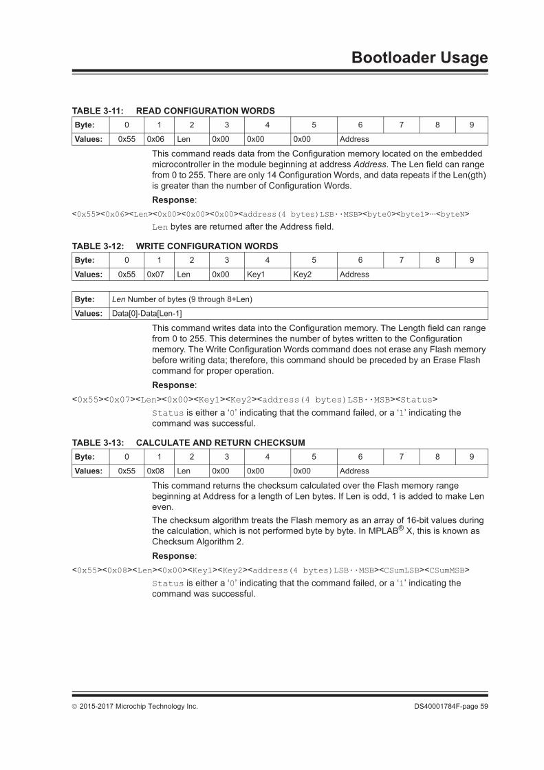
Bootloader Usage
2015-2017 Microchip Technology Inc. DS40001784F-page 59
This command reads data from the Configuration memory located on the embedded microcontroller in the module beginning at address Address. The Len field can range from 0 to 255. There are only 14 Configuration Words, and data repeats if the Len(gth) is greater than the number of Configuration Words.Response:
<0x55><0x06><Len><0x00><0x00><0x00><address(4 bytes)LSB..MSB><byte0><byte1>...<byteN>Len bytes are returned after the Address field.
This command writes data into the Configuration memory. The Length field can range from 0 to 255. This determines the number of bytes written to the Configuration memory. The Write Configuration Words command does not erase any Flash memory before writing data; therefore, this command should be preceded by an Erase Flash command for proper operation.Response:
<0x55><0x07><Len><0x00><Key1><Key2><address(4 bytes)LSB..MSB><Status>Status is either a ‘0’ indicating that the command failed, or a ‘1’ indicating the command was successful.
This command returns the checksum calculated over the Flash memory range beginning at Address for a length of Len bytes. If Len is odd, 1 is added to make Len even.The checksum algorithm treats the Flash memory as an array of 16-bit values during the calculation, which is not performed byte by byte. In MPLAB® X, this is known as Checksum Algorithm 2.Response:
<0x55><0x08><Len><0x00><Key1><Key2><address(4 bytes)LSB..MSB><CSumLSB><CSumMSB>Status is either a ‘0’ indicating that the command failed, or a ‘1’ indicating the command was successful.
TABLE 3-11: READ CONFIGURATION WORDSByte: 0 1 2 3 4 5 6 7 8 9
Values: 0x55 0x06 Len 0x00 0x00 0x00 Address
TABLE 3-12: WRITE CONFIGURATION WORDSByte: 0 1 2 3 4 5 6 7 8 9
Values: 0x55 0x07 Len 0x00 Key1 Key2 Address
Byte: Len Number of bytes (9 through 8+Len)
Values: Data[0]-Data[Len-1]
TABLE 3-13: CALCULATE AND RETURN CHECKSUMByte: 0 1 2 3 4 5 6 7 8 9
Values: 0x55 0x08 Len 0x00 0x00 0x00 Address
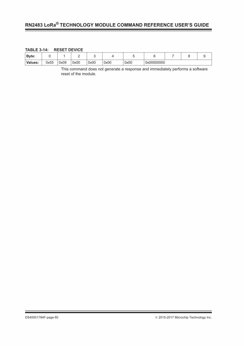
RN2483 LoRa® TECHNOLOGY MODULE COMMAND REFERENCE USER’S GUIDE
DS40001784F-page 60 2015-2017 Microchip Technology Inc.
This command does not generate a response and immediately performs a software reset of the module.
TABLE 3-14: RESET DEVICEByte: 0 1 2 3 4 5 6 7 8 9
Values: 0x55 0x09 0x00 0x00 0x00 0x00 0x00000000

RN2483 LoRa® TECHNOLOGY MODULECOMMAND REFERENCE USER’S GUIDE
2015-2017 Microchip Technology Inc. DS40001784F-page 61
Appendix A. Current Firmware Features and Fixes
Please check the product web page for the current RN2483 firmware version at www.microchip.com/lora.
A.1. Version 0.9.5Initial release of the firmware.A.2. Version 1.0.0Release for LoRaWAN™ specification V1.0• Added support for additional RN2483 commands: mac set sync
mac get sync
mac set upctr
mac get upctr
mac set dnctr
mac get dnctr
sys set pinmode
sys get pindig
sys get pinana
radio get sync
• Added new parameters to be saved in nonvolatile memory whenever a mac save command is triggered
LoRaWAN current data rate LoRaWAN RX2 window parameters (data rate and frequency) Adaptive Data Rate status LoRaWAN uplink frame counter LoRaWAN downlink frame counter• Changed the default value for the LoRaWAN End-Device Identifier (deveui)• Changed the valid range for the radio set fdev parameter to [0.. 200000]• Changed the valid range for the radio set bitrate parameter to [1.. 300000]• Changed sys sleep command behavior to not influence the GPIO configuration• Changed the 433 MHz radio frequency band to [433050000 .. 434790000]• Fixed an issue that may have caused the RN2483 module to mishandle data on
LoRaWAN port 0• Fixed an issue that may have caused the module to fail joining• Fixed radio get snr command to display correct value
RN2483 LoRa® Technology Module Command Reference User’s Guide
DS40001784F-page 62 2015-2017 Microchip Technology Inc.
A.3. Version 1.0.1Release containing modifications needed to successfully pass the LoRaWAN Certification Program testing in 868 MHz band.• Added support for usage of the reserved ports, from 224 to 255 for transmitting
and receiving Application Data• Increased the size of the value returned by the mac get status command from
2 bytes to 4 bytes• Updated the size of the LoRaWAN receive windows and the moment in time at
which these are opened• Fixed an issue that may have caused the RN2483 module to mishandle packets
received with DR = 7• Fixed an issue that may have caused the RN2483 module to mishandle the
LoRaWAN RXParamSetupReq command• Fixed an issue that may have caused the RN2483 module to mishandle the usage
of LoraWAN ADRACKReq in packets

2015-2017 Microchip Technology Inc. DS40001784F-page 63
AMERICASCorporate Office2355 West Chandler Blvd.Chandler, AZ 85224-6199Tel: 480-792-7200 Fax: 480-792-7277Technical Support: http://www.microchip.com/supportWeb Address: www.microchip.comAtlantaDuluth, GA Tel: 678-957-9614 Fax: 678-957-1455Austin, TXTel: 512-257-3370 BostonWestborough, MA Tel: 774-760-0087 Fax: 774-760-0088ChicagoItasca, IL Tel: 630-285-0071 Fax: 630-285-0075DallasAddison, TX Tel: 972-818-7423 Fax: 972-818-2924DetroitNovi, MI Tel: 248-848-4000Houston, TX Tel: 281-894-5983IndianapolisNoblesville, IN Tel: 317-773-8323Fax: 317-773-5453Tel: 317-536-2380Los AngelesMission Viejo, CA Tel: 949-462-9523Fax: 949-462-9608Tel: 951-273-7800 Raleigh, NC Tel: 919-844-7510New York, NY Tel: 631-435-6000San Jose, CA Tel: 408-735-9110Tel: 408-436-4270Canada - TorontoTel: 905-695-1980 Fax: 905-695-2078
ASIA/PACIFICAsia Pacific OfficeSuites 3707-14, 37th FloorTower 6, The GatewayHarbour City, KowloonHong KongTel: 852-2943-5100Fax: 852-2401-3431Australia - SydneyTel: 61-2-9868-6733Fax: 61-2-9868-6755China - BeijingTel: 86-10-8569-7000 Fax: 86-10-8528-2104China - ChengduTel: 86-28-8665-5511Fax: 86-28-8665-7889China - ChongqingTel: 86-23-8980-9588Fax: 86-23-8980-9500China - DongguanTel: 86-769-8702-9880 China - GuangzhouTel: 86-20-8755-8029 China - HangzhouTel: 86-571-8792-8115 Fax: 86-571-8792-8116China - Hong Kong SARTel: 852-2943-5100 Fax: 852-2401-3431China - NanjingTel: 86-25-8473-2460Fax: 86-25-8473-2470China - QingdaoTel: 86-532-8502-7355Fax: 86-532-8502-7205China - ShanghaiTel: 86-21-3326-8000 Fax: 86-21-3326-8021China - ShenyangTel: 86-24-2334-2829Fax: 86-24-2334-2393China - ShenzhenTel: 86-755-8864-2200 Fax: 86-755-8203-1760China - WuhanTel: 86-27-5980-5300Fax: 86-27-5980-5118China - XianTel: 86-29-8833-7252Fax: 86-29-8833-7256
ASIA/PACIFICChina - XiamenTel: 86-592-2388138 Fax: 86-592-2388130China - ZhuhaiTel: 86-756-3210040 Fax: 86-756-3210049India - BangaloreTel: 91-80-3090-4444 Fax: 91-80-3090-4123India - New DelhiTel: 91-11-4160-8631Fax: 91-11-4160-8632India - PuneTel: 91-20-3019-1500Japan - OsakaTel: 81-6-6152-7160 Fax: 81-6-6152-9310Japan - TokyoTel: 81-3-6880- 3770 Fax: 81-3-6880-3771Korea - DaeguTel: 82-53-744-4301Fax: 82-53-744-4302Korea - SeoulTel: 82-2-554-7200Fax: 82-2-558-5932 or 82-2-558-5934Malaysia - Kuala LumpurTel: 60-3-6201-9857Fax: 60-3-6201-9859Malaysia - PenangTel: 60-4-227-8870Fax: 60-4-227-4068Philippines - ManilaTel: 63-2-634-9065Fax: 63-2-634-9069SingaporeTel: 65-6334-8870Fax: 65-6334-8850Taiwan - Hsin ChuTel: 886-3-5778-366Fax: 886-3-5770-955Taiwan - KaohsiungTel: 886-7-213-7830Taiwan - TaipeiTel: 886-2-2508-8600 Fax: 886-2-2508-0102Thailand - BangkokTel: 66-2-694-1351Fax: 66-2-694-1350
EUROPEAustria - WelsTel: 43-7242-2244-39Fax: 43-7242-2244-393Denmark - CopenhagenTel: 45-4450-2828 Fax: 45-4485-2829Finland - EspooTel: 358-9-4520-820France - ParisTel: 33-1-69-53-63-20 Fax: 33-1-69-30-90-79France - Saint CloudTel: 33-1-30-60-70-00 Germany - GarchingTel: 49-8931-9700Germany - HaanTel: 49-2129-3766400Germany - HeilbronnTel: 49-7131-67-3636Germany - KarlsruheTel: 49-721-625370Germany - MunichTel: 49-89-627-144-0 Fax: 49-89-627-144-44Germany - RosenheimTel: 49-8031-354-560Israel - Ra’anana Tel: 972-9-744-7705Italy - Milan Tel: 39-0331-742611 Fax: 39-0331-466781Italy - PadovaTel: 39-049-7625286 Netherlands - DrunenTel: 31-416-690399 Fax: 31-416-690340Norway - TrondheimTel: 47-7289-7561Poland - WarsawTel: 48-22-3325737 Romania - BucharestTel: 40-21-407-87-50Spain - MadridTel: 34-91-708-08-90Fax: 34-91-708-08-91Sweden - GothenbergTel: 46-31-704-60-40Sweden - StockholmTel: 46-8-5090-4654UK - WokinghamTel: 44-118-921-5800Fax: 44-118-921-5820
Worldwide Sales and Service
11/07/16