EP activity report 2013 - Europractice
44
-
Upload
khangminh22 -
Category
Documents
-
view
3 -
download
0
Transcript of EP activity report 2013 - Europractice


EUROPRACTICE IC service The right cocktail of ASIC Services
EUROPRACTICE IC Service offers you a proven route to ASICs that features:•Low-costASICprototyping
•Flexibleaccesstosiliconcapacityforsmallandmediumvolumeproductionquantities
•Partnershipswithleadingworld-classfoundries,assemblyandtesthouses
•WidechoiceofICtechnologies
•Distributionandfullsupportofhigh-qualitycelllibrariesanddesignkitsforthemostpopularCAD
tools
•RTL-to-Layoutservicefordeep-submicrontechnologies
•Front-endASICdesignthroughAlliancePartners
Industry is rapidlydiscovering thebenefitsofusing theEUROPRACTICE ICservice tohelpbringnew
productdesignstomarketquicklyandcost-effectively.TheEUROPRACTICEASICroutesupportsespe-
ciallythosecompanieswhodon’tneedalwaysthefullrangeofservicesorhighproductionvolumes.
Those companieswill gain from the flexible access to silicon prototype and production capacity at
leadingfoundries,designservices,highqualitysupportandmanufacturingexpertisethatincludesIC
manufacturing,packagingandtest.ThisyoucangetallfromEUROPRACTICEICservice,aservicethatis
alreadyestablishedfor15yearsinthemarket.
The EUROPRACTICE IC Services are offered by the following centers:
• imec,Leuven(Belgium)
•Fraunhofer-InstitutfuerIntegrierteSchaltungen(FraunhoferIIS),Erlangen(Germany)
By courtesy of imec
This project has received funding from the European Union’s Seventh Programme for research, technological development and
demonstration under grant agreement N° 315961.
This funding is exclusively used to support European universities and research laboratories.
Dear EUROPRACTICE customers,
I am very pleased to announce that in 2013 the funding of the Europractice project towards the 650 European universities and
research institutes has been secured for another 3 years. Indeed imec and consortium partners STFC and Fraunhofer IIS have
signed a 3-years contract “EUROPRACTICE 2013” with the EC starting 1 July 2013 until 30 June 2016. This allows us to plan
ahead and to secure continuation of access to CAD tools and prototyping services for our European Academia.
Continuation means introduction of new versions and functionalities of existing CAD tools and introduction of new CAD
tools. Similarly we are looking to introduce new IC and specialty (such as MEMS, SiPhotonics, ...) technologies. In 2013
we reached an agreement with XFAB to offer their specialty 0.18µ XH018 (high voltage, eflash CMOS) and 0.18µ XT018
(high voltage SOI CMOS) technologies.
From UMC we introduced 0.11µ CIS (CMOS Image Sensor) technology for more advanced imager design. From TSMC we
introduced their 0.18µ HV BCD Gen-2 technology.
From imec we introduced the SiPhotonics Full Platform technology including advanced passives, modulators, detectors and
heaters. The introduction in general of SiPhotonics technologies from imec and LETI as specialty technologies have been very
successful and is considered as a very important technology for design of future telecommunication systems.
It is to be expected that in the course of 2014 other new technologies will become available as well as more advanced
CMOS (like 28nm) as specialty More-than-Moore technologies.
In 2013 we have seen the confirmation that a majority of users is switching from 0.35µ towards the 0.18µ/0.15µ node.
Indeed 39% of the total designs have been prototyped in 0.18µ/0.15µ.
In our new project with the EC “EUROPRACTICE 2013” we are also offering training
courses. We have seen that introducing new design methodologies and technologies
is very difficult at the universities without offering relevant training courses. Over the
past years we had the opportunity to offer advanced IC design methodology courses
through the EC-funded IDESA project and MEMS design courses through the EC-fund-
ed STIMESI project. As both projects have ended, we are now offering these kind of
courses through Europractice. More information (titles, schedule, registration) about
the courses is available at http://www.europractice.stfc.ac.uk/training/.
We further support companies, mainly SMEs and start-up companies, with prototyp-
ing of their new IC designs, help them with packaging, test development, qualifica-
tion, ramp-up and production volumes. European SME’s are very well placed to play
a role in the new developments in the area of IoT (Internet of Things), healthcare,
security, optical, ... applications.
Finally, let me wish you a very successful 2014 in your curricula, training new young
engineers. New bright engineers that will help the European SMEs and start-up com-
panies with new innovative products on the market.
Sincerely yours,
Dr. C. Das
Chairman EUROPRACTICE IC Service
imec (Belgium)
Foreword
1europractice | a total solution

Table of contents
Foreword ...........................................................................................................................................1
Your Total and Turn-Key ASIC Solution ............................................................................................. 3
Easy access .............................................................................................................................. 3
ASIC Design ............................................................................................................................. 4
Backend Operation Services through cooperation with certified partners ............................... 4
From prototypes to initial volumes .......................................................................................... 5
From initial volumes to full production .................................................................................... 6
EUROPRACTICE offers deep submicron design support service ................................................ 7
Low cost IC-prototyping ............................................................................................................ 8
Technologies / Supply partners / mini@sic .............................................................................. 9
Space Qualification according to ESCC9000 ............................................................................10
Web site / EUROPRACTICE-online ............................................................................................ 11
Results.............................................................................................................................................12
MPW prototyping service ........................................................................................................12
Small volume projects .............................................................................................................13
Examples of ASIC projects ...............................................................................................................16
onsemi .....................................................................................................................................16
austriamicrosystems ................................................................................................................18
IHP ......................................................................................................................................... 22
UMC ....................................................................................................................................... 23
TSMC ...................................................................................................................................... 28
imec ....................................................................................................................................... 29
MEMSCAP ...............................................................................................................................31
List of customers ............................................................................................................................ 33
2 europractice | a total solution
EUROPRACTICE provides semiconductor and system companies with a total
and turn-key ASIC solution including :
• easyaccesstofoundrydesignrules,celllibrariesanddesignkits
• deepsubmicronRTL-to-layoutservice
• lowcostprototypefabricationservice
• volumefabricationserviceincludingwaferfabrication,packagingandtest
• ASICqualification
• logistics
• technicalcustomersupport
New fables startup companies as well as small companies or companies
having small ASIC volume products in niche markets experience huge prob-
lems to get access to foundries since their volume is too small.
EUROPRACTICE has wafer foundry agreements with different leading sup-
pliers, allowing to offer the most advanced as well as specific technologies
to those customers. Our foundry partners acknowledge the EUROPRACTICE
Service as the optimal solution to provide wafer capacity to smaller custom-
ers. Suppliers see EUROPRACTICE as one big customer representing about
650 universities, research centers and 300 companies world-wide. Through
agreements with foundry partners, EUROPRACTICE is able to offer ASIC solu-
tions ranging from a few wafers to thousands of wafers per year.
Easy accessThrough its agreement with foundries
and library partners, EUROPRACTICE
is allowed to distribute foundry tech-
nology information and cell libraries
upon simple signature of a standard
Non-Disclosure Agreements or a De-
sign Kit License Agreement. Those
agreements can be downloaded from
the EUROPRACTICE website. In this
way you have access in a few days
without having to go through a pain-
ful customer qualification procedure
at the foundry. Foundry information
includes design rules, spice param-
eters, design & layout manuals and
DRC/ERC/LVS decks. Cell library
information includes library manu-
als and design kits for most of the
popular CAD tools (Cadence, Synop-
sys, Mentor Graphics, Tanner, etc.).
This foundry and library information
is distributed on the EUROPRACTICE
CD-ROM or via FTP.
EUROPRACTICE :
Your Total and Turn-Key ASIC Solution
3europractice | a total solution
When customers have received design rules, cell libraries,
etc., they can start the ASIC design. ASIC design can be
split up into front-end design and back-end design. Front-
end design covers ASIC specification feasibility study and
design including tasks such as schematic entry, VHDL
description, scan insertion, simulation and synthesis.
The front-end design can be carried out by the customer
himself or can be subcontracted to a design house. During
this design phase, Europractice offers technical support
on technology, test, type of package, etc. Important know-
how and feedback from the test house will be used to
improve the DFT (Design For Testability). ”State-of-the-art”
CAD tools are used during the ASIC design phase.
When the netlist is ready the backend design activity
starts including layout generation using state-of-the art
layout tools. Deep submicron digital place & route tasks
are in most cases not performed by the customers. For
those customers that have not their own layout tools,
EUROPRACTICE is offering such deep submicron layout
service (see deep submicron layout service on page 7).
After initial layout, timing verification is carried out by the
customer using parasitic layout information and layout is
iterated until timing is met. Verification of the design needs
to be done in all technology corners.
When layout is finished, a final DRC (Design Rule Check)
and LVS (Layout versus Schematic) is performed on the
GDS-II database in order to deliver a correct GDS-II to the
foundry for manufacturing.
Backend Operation Services through cooperation with certified partners
ASIC Design
A history of more than 25 years offering programs to micro-
electronics industry and academia endorse Europractice as
the key partner to your ASIC’s success. We embrace COT
and turnkey business models to adapt to your require-
ments with a maximum level of transparency and flexibil-
ity. Side by side with world class partners and our long
term agreements, Europractice boosts the deployment
of your chip backend operations activities. This business
environment is strengthened by a skilled team of in-house
engineers who provide a reliable integrated service, from
technical aspects up to logistics and supply chain manage-
ment.
Through these collaborative agreements our customers
can benefit of working with highly recognized chip industry
players. The most relevant companies involved in our semi-
conductor supply chain are listed below:
• Foundry partners:
TSMC, UMC, ON Semi, ams, IHP, LFoundry, XFAB
• Ceramic assembly partners:
HCM, Systrel, Optocap, Kyocera
• Plastic assembly partners:
ASE, Kyocera
• Wafer bumping partner:
Pactech, ASE
• Test partners:
ASE, Microtest, Delta, Rood Technology and
Blue test
• Failure analysis:
Maser Engineering
• Library partners:
Faraday, ARM
4 europractice | a total solution
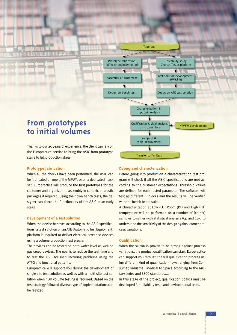
Prototype fabrication(MPW or engineering lot)
Debug on bench test
Assembly of prototypes
Testability studyChoicer Tester platform
Test solution development (HW&SW)
Debug on ATE test solution
HW/SW development
Characterization & Cp, Cpk analysis
Ramp-up & yield improvement
Qualification & yield analysis on 3 corner lots
Tape-out
Transfer to Far East
From prototypes to initial volumes
Prototype fabricationWhen all the checks have been performed, the ASIC can
be fabricated on one of the MPW’s or on a dedicated mask
set. Europractice will produce the first prototypes for the
customer and organize the assembly in ceramic or plastic
packages if required. Using their own bench tests, the de-
signer can check the functionality of the ASIC in an early
stage.
Development of a test solutionWhen the device behaves according to the ASIC specifica-
tions, a test solution on an ATE (Automatic Test Equipment)
platform is required to deliver electrical screened devices
using a volume production test program.
The devices can be tested on both wafer level as well on
packaged devices. The goal is to reduce the test time and
to test the ASIC for manufacturing problems using the
ATPG and functional patterns.
Europractice will support you during the development of
single site test solution as well as with a multi-site test so-
lution when high volume testing is required. Based on the
test strategy followed diverse type of implementations can
be realized.
Debug and characterizationBefore going into production a characterization test pro-
gram will check if all the ASIC specifications are met ac-
cording to the customer expectations. Threshold values
are defined for each tested parameter. The software will
test all different IP blocks and the results will be verified
with the bench test results.
A characterization at Low (LT), Room (RT) and High (HT)
temperature will be performed on a number of (corner)
samples together with statistical analysis (Cp and Cpk) to
understand the sensitivity of the design against corner pro-
cess variations.
QualificationWhen the silicon is proven to be strong against process
variations, the product qualification can start. Europractice
can support you through the full qualification process us-
ing different kind of qualification flows ranging from Con-
sumer, Industrial, Medical to Space according to the Mili-
tary, Jedec and ESCC standards....
In this stage of the project, qualification boards must be
developed for reliability tests and environmental tests.
Thanks to our 25 years of experience, the client can rely on
the Europractice service to bring the ASIC from prototype
stage to full production stage.
5europractice | a total solution
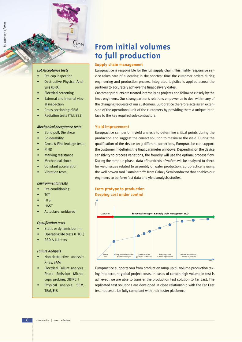
From initial volumes to full productionSupply chain managementEuropractice is responsible for the full supply chain. This highly responsive ser-
vice takes care of allocating in the shortest time the customer orders during
engineering and production phases. Integrated logistics is applied across the
partners to accurately achieve the final delivery dates.
Customer products are treated internally as projects and followed closely by the
imec engineers. Our strong partner’s relations empower us to deal with many of
the changing requests of our customers. Europratice therefore acts as an exten-
sion of the operational unit of the customers by providing them a unique inter-
face to the key required sub-contractors.
Yield improvementEuropractice can perform yield analysis to determine critical points during the
production and suggest the correct solution to maximize the yield. During the
qualification of the device on 3 different corner lots, Europractice can support
the customer in defining the final parameter windows. Depending on the device
sensitivity to process variations, the foundry will use the optimal process flow.
During the ramp-up phase, data of hundreds of wafers will be analyzed to check
for yield issues related to assembly or wafer production. Europractice is using
the well proven tool Examinator™ from Galaxy Semiconductor that enables our
engineers to perform fast data and yield analysis studies.
From protype to productionKeeping cost under control
Europractice supports you from production ramp up till volume production tak-
ing into account global project costs. In cases of certain high volume in test is
achieved, we are able to transfer the production test solution to Far East. The
replicated test solutions are developed in close relationship with the Far East
test houses to be fully compliant with their tester platforms.
Lot Acceptance tests
• Pre-cap inspection
• Destructive Physical Anal-
ysis (DPA)
• Electrical screening
• External and Internal visu-
al inspection
• Cross sectioning: SEM
• Radiation tests (Tid, SEE)
Mechanical Acceptance tests
• Bond pull, Die shear
• Solderability
• Gross & Fine leakage tests
• PIND
• Marking resistance
• Mechanical shock
• Constant acceleration
• Vibration tests
Environmental tests
• Pre-conditioning
• TCT
• HTS
• HAST
• Autoclave, unbiased
Qualification tests
• Static or dynamic burn-in
• Operating life tests (HTOL)
• ESD & LU tests
Failure Analysis
• Non-destructive analysis:
X-ray, SAM
• Electrical Failure analysis:
Photo Emission Micros-
copy, probing, OBIRCH
• Physical analysis: SEM,
TEM, FIB
Yiel
d
Time
Bench tests
Europractice support & supply chain management 24/7
Debug & characterization Statistical analysis
Qualification on 3 process corner lots
Ramp-up phase& Yield improvement
Volume Production &Transfer to Far East
From Prototype to Production
Customer
6 europractice | a total solution

Synthesis and layout of deep submicron chips is not
straightforward. You need a highly trained team of en-
gineers equipped with expensive state-of-the art EDA
tools to tape out first time right Silicon. The chips are
growing in size while the technology dimensions are
getting smaller and power specifications are becoming
more stringent. Because of this, chip designers have to
understand how to tackle issues like: hierarchical lay-
out, clock skew, latencies of interacting clock domains,
IR-drop on the power distribution, electro-migration and
signal integrity, handling many metal layers in the back-
end, incorporating IP blocks in the design, on-chip vari-
ation, design for packaging, design for manufacturing...
And the list goes on.
Supporting high-level system designers on the road to
tapeout, EUROPRACTICE IC Service provides a physical
design support service starting from RTL code in VHDL or
Verilog or from a synthesized netlist.
The service supports the whole back-end design flow in-
cluding synthesis, floorplanning, deep-submicron place
and route and multi-mode multi-corner optimization,
timing analysis, extraction, scan and BIST insertion and
ATPG, tape-out preparation, etc. The service is equipped
with state-of-the art tools from the major EDA vendors
and has already supported technologies from many dif-
ferent foundries down to 28nm.
Many circuits were successfully taped out for in-house
developed Systems-On-a-Chip as well as for ASICs devel-
oped by companies, design houses, research institutes
and universities. These circuits included a.o. analog full
custom blocks, memory macro’s from different vendors,
special I/O cells and RTL level (soft and firm) IP. The team
is well versed in low-power techniques as well as the
state-of-the art power format descriptions (CPF/UPF).
Interrelated gated clock domains, power shut-off, multi
supply-voltage and backbiasing have been successfully
implemented.
EUROPRACTICE offers deep submicron design support service
Imec’s BOA chip showcases the Boadres DSP core for
wireless applications in 40nm.
(By courtesy of imec)
Mixed mode ASIC, with multiple microcontrollers,
based on imec’s radiation hardened DARE library cells.
(By courtesy of imec)
7europractice | a total solution
The cost of producing a new ASIC
for a dedicated application within
a small market can be high, if
directly produced by a commercial
foundry. This is largely due to the
NRE (Non-Recurring Engineering)
overheads associated with design,
manufacturing and test.
EUROPRACTICE has reduced the
NRE, especially for ASIC prototyping,
by two techniques:
(i) Multi Project Wafer Runs or
(ii) Multi Level Masks.
Multi Project Wafer RunsBy combining several designs from
different customers onto one mask
set and prototype run, known as
Multi Project Wafer (MPW) runs,
the high NRE costs of a mask set
is shared among the participating
customers.
Fabrication of prototypes can thus
be as low as 5% to 10% of the cost
of a full prototyping wafer run. A
limited number of tested or untested
ASIC prototypes, typically 20-50,
are delivered to the customer for
evaluation, either as naked dies or as
encapsulated devices. Only prototypes
from fully qualified wafers are taken
to ensure that the chips delivered will
function “right first time”.
In order to achieve this, extensive
Design Rule and Electrical Rule
Checkings are performed on all
designs submitted to the Service.
EUROPRACTICE is organising about
200 MPW runs per year in various
technologies.
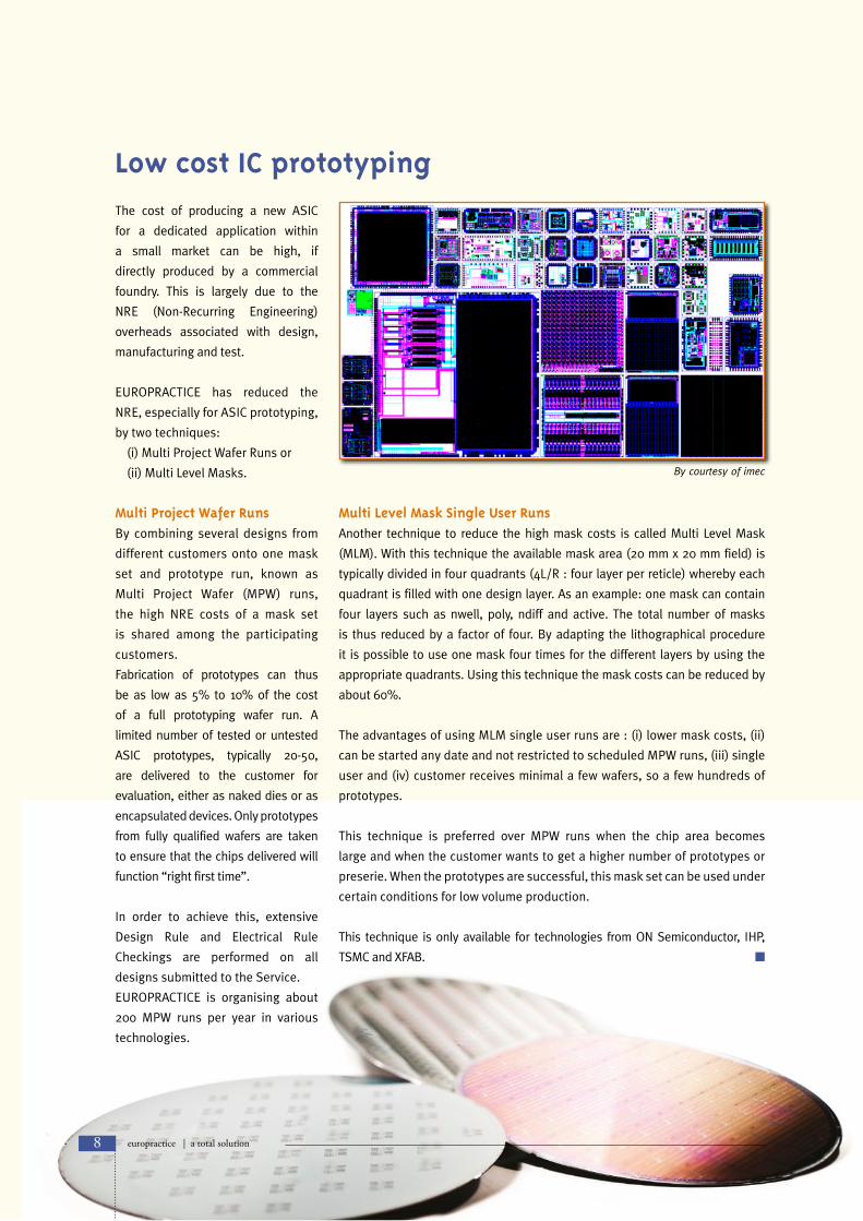
Multi Level Mask Single User RunsAnother technique to reduce the high mask costs is called Multi Level Mask
(MLM). With this technique the available mask area (20 mm x 20 mm field) is
typically divided in four quadrants (4L/R : four layer per reticle) whereby each
quadrant is filled with one design layer. As an example: one mask can contain
four layers such as nwell, poly, ndiff and active. The total number of masks
is thus reduced by a factor of four. By adapting the lithographical procedure
it is possible to use one mask four times for the different layers by using the
appropriate quadrants. Using this technique the mask costs can be reduced by
about 60%.
The advantages of using MLM single user runs are : (i) lower mask costs, (ii)
can be started any date and not restricted to scheduled MPW runs, (iii) single
user and (iv) customer receives minimal a few wafers, so a few hundreds of
prototypes.
This technique is preferred over MPW runs when the chip area becomes
large and when the customer wants to get a higher number of prototypes or
preserie. When the prototypes are successful, this mask set can be used under
certain conditions for low volume production.
This technique is only available for technologies from ON Semiconductor, IHP,
TSMC and XFAB. ■
Low cost IC prototyping
8 europractice | a total solution
TechnologiesFor 2014, EUROPRACTICE has extended its technology portfolio. Currently customers can have access to prototype and production fabrication in the following technologies :•AMIS 0.7µ C07M-D 2M/1P & AMIS 0.7µ C07M-A 2M/1P/PdiffC/HR•AMIS 0.5µ CMOS EEPROM C5F & C5N •AMIS 0.35µ C035U 4M (3M & 5M optional) only thick top metal•AMIS 0.7µ C07M-I2T100 100 V - 2M & 3M options•AMIS 0.7µ C07M-I2T30 & I2T30E 30 V - 2M & 3M options•AMIS 0.35µ C035 - I3T80U 80 V 4M - 3M optional (5M on special request)•AMIS 0.35µ C035 - I3T50 50 V 4M - 3M optional (5M on special request)•AMIS 0.35µ C035 - I3T50(E) 50 V 4M - 3M optional (5M on special request)•AMIS 0.35µ C035 - I3T25 3.3/25 V 4M (3M & 5M optional) only thick top metal•ams 0.35µ CMOS C35B3C3 3M/2P/HR/5V IO•ams 0.35µ CMOS C35B4C3 4M/2P/HR/5V IO•ams 0.35µ CMOS C35OPTO 4M/2P/5V IO•ams 0.35µ HV CMOS H35 120V 3M & 4M•ams 0.35µ SiGe-BiCMOS S35 4M/4P•ams 0.18µ CMOS C18 6M/1P/MIM/1.8V/5V•ams 0.18µ HV CMOS H18 6M/50V/20V/5V/1.8V/MIM•IHP SGB25V 0.25µ SiGe:C Ft=75GHz@BVCEO 2.4V•IHP SGB25VGD 0.25µ SiGe:C Ft=75GHz@BVCEO 2.4V + RF HV-LDMOS GD-Module 22V•IHP SG25H1 0.25µ SiGe:C Ft/Fmax=190GHz/220GHz 5M/MIM•IHP SG25H3P 0.25µ Complementary SiGe:C Ft/Fmax (npn)110/180GHz / (pnp)90/120GHz 5M/MIM•IHP SG25H3 0.25µ SiGe:C Ft/Fmax= 110/180GHz 5M/MIM•IHP SG25 PIC (Photonics, Ge Photo-diode, BEOL)•IHP SG13S SiGe:C Bipolar/Analog/CMOS Ft/Fmax= 250/300GHz 7M/MIM•IHP SG13C SiGe:C CMOS 7M/MIM•IHP SG13G2 SiGe:C Bipolar/Analog Ft/Fmax= 300/500GHz 7M/MIM•IHP BEOL SG25 (M1 and Metal Layers Above) + RF-MEMS + LBE•IHP BEOL SG13 (M1 and Metal Layers Above) + LBE + Cu•X-FAB XH018 0.18µ HV NVM CMOS E-FLASH•X-FAB XT018 0.18µ HV SOI CMOS•TSMC 0.25µ CMOS General LOGIC, MS OR MS RF•TSMC 0.18µ CMOS General LOGIC, MS or MS RF (MIM: 1.0 or 2.0 fFum2 / UTM: 20kÅ)•TSMC 0.18µ CMOS High Voltage Mixed-Signal (CV018LD 1.8/3.3/32V)•TSMC 0.18µ CMOS High Voltage BCD Gen 2 (1.8V/5V...70V)•TSMC 0.13µ CMOS General LOGIC, MS or MS RF (8-inch)•TSMC 0.13µ CMOS General LOGIC, MS or MS RF (12-inch)•TSMC 90nm CMOS General or LP Logic , MS or MS/RF (12-inch)•TSMC 65nm CMOS General or LP MS/RF•TSMC 40nm CMOS General or LP MS/RF•UMC L180 Mixed-Mode/RF•UMC L180 Logic GII•UMC L180 Logic Low Leakage•UMC L180 EFLASH Logic GII•UMC CIS180 Image Sensor 1P4M - CONV diode•UMC CIS180 Image Sensor 2P4M - ULTRA diode•UMC CIS11 - image sensor•UMC L130 Logic•UMC L130 Mixed-Mode/RF•UMC L110AE Logic/Mixed-Mode/RF•UMC L90N Logic/Mixed-Mode/RF (upon request)•UMC L65N Logic/Mixed-Mode/RF - LL•UMC L65N Logic/Mixed-Mode/RF - SP•MEMSCAP METALMUMPS•MEMSCAP PolyMUMPS•MEMSCAP SOIMUMPS•MEMSCAP PIEZOMUMPS•ePIXfab-imec SiPhotonics Passives•ePIXfab-imec SiPhotonics Full Platform•ePIXfab-LETI SiPhotonics Passives + Heater
mini@sic prototyping conditions for universities and research laboratories
Prototyping costs have been increasing with scaled technolo-gies due to high mask costs. Even on MPW runs with shared costs, the minimum prototyping fee (corresponding to a minimum chip area) is high for advanced technologies such as 90, 65 and 40nm.
In order to stimulate universities and research institutes to proto-type small ASIC designs, Euro-practice has introduced in 2003 the concept of mini@sic.
That means that Europractice has selected several MPW runs on se-lected technologies on which uni-versities and research institutes have the opportunity to proto-type very small ASIC designs at a highly reduced minimum pro-totype fee. The minimum charged chip area is highly reduced.
Through the mini@sic concept, the price is reduced consider-ably. For the most advanced technologies however, the pro-totyping fee is further reduced through extra funding by the European Commission through the Europractice project (only for European universities and research institutes).
9europractice | a total solution
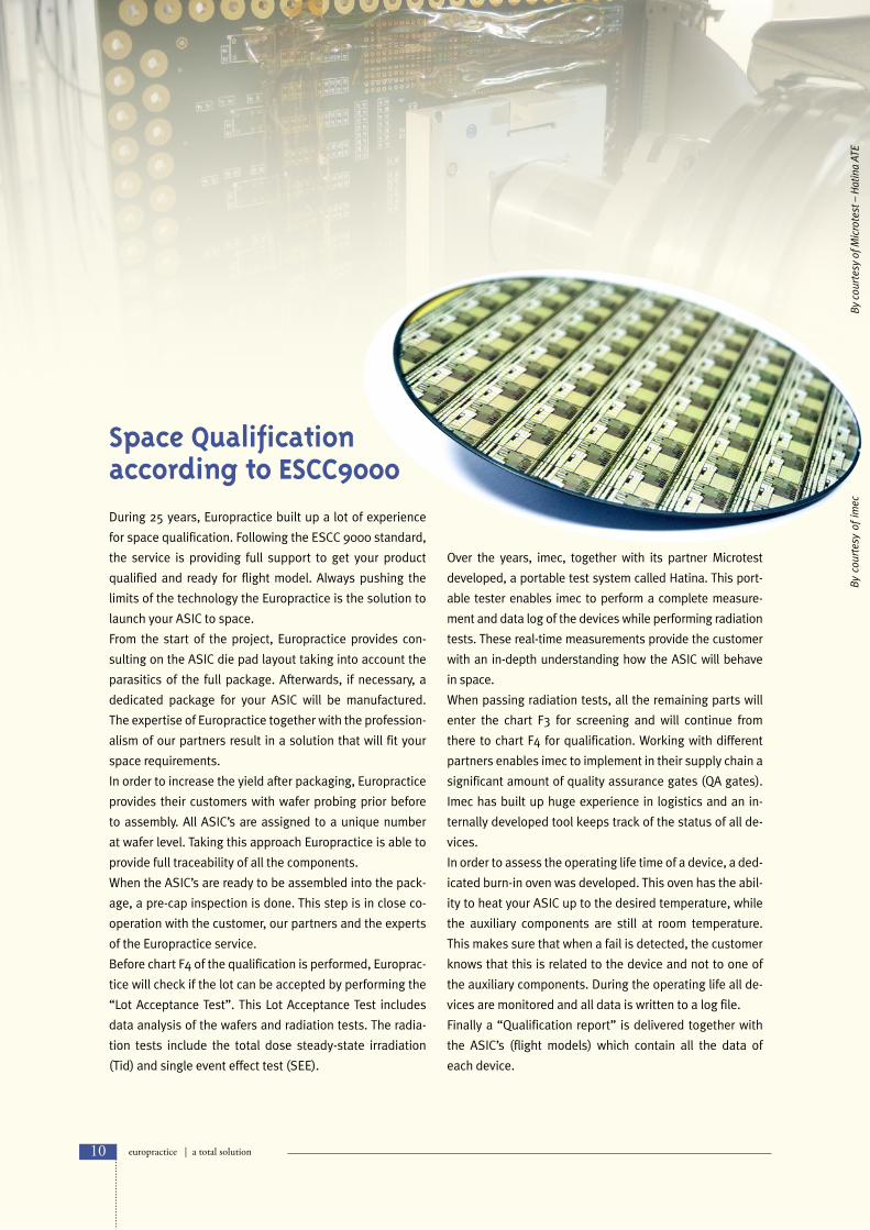
Space Qualification according to ESCC9000During 25 years, Europractice built up a lot of experience
for space qualification. Following the ESCC 9000 standard,
the service is providing full support to get your product
qualified and ready for flight model. Always pushing the
limits of the technology the Europractice is the solution to
launch your ASIC to space.
From the start of the project, Europractice provides con-
sulting on the ASIC die pad layout taking into account the
parasitics of the full package. Afterwards, if necessary, a
dedicated package for your ASIC will be manufactured.
The expertise of Europractice together with the profession-
alism of our partners result in a solution that will fit your
space requirements.
In order to increase the yield after packaging, Europractice
provides their customers with wafer probing prior before
to assembly. All ASIC’s are assigned to a unique number
at wafer level. Taking this approach Europractice is able to
provide full traceability of all the components.
When the ASIC’s are ready to be assembled into the pack-
age, a pre-cap inspection is done. This step is in close co-
operation with the customer, our partners and the experts
of the Europractice service.
Before chart F4 of the qualification is performed, Europrac-
tice will check if the lot can be accepted by performing the
“Lot Acceptance Test”. This Lot Acceptance Test includes
data analysis of the wafers and radiation tests. The radia-
tion tests include the total dose steady-state irradiation
(Tid) and single event effect test (SEE).
Over the years, imec, together with its partner Microtest
developed, a portable test system called Hatina. This port-
able tester enables imec to perform a complete measure-
ment and data log of the devices while performing radiation
tests. These real-time measurements provide the customer
with an in-depth understanding how the ASIC will behave
in space.
When passing radiation tests, all the remaining parts will
enter the chart F3 for screening and will continue from
there to chart F4 for qualification. Working with different
partners enables imec to implement in their supply chain a
significant amount of quality assurance gates (QA gates).
Imec has built up huge experience in logistics and an in-
ternally developed tool keeps track of the status of all de-
vices.
In order to assess the operating life time of a device, a ded-
icated burn-in oven was developed. This oven has the abil-
ity to heat your ASIC up to the desired temperature, while
the auxiliary components are still at room temperature.
This makes sure that when a fail is detected, the customer
knows that this is related to the device and not to one of
the auxiliary components. During the operating life all de-
vices are monitored and all data is written to a log file.
Finally a “Qualification report” is delivered together with
the ASIC’s (flight models) which contain all the data of
each device.
By
cour
tesy
of M
icro
test
– H
atin
a AT
E
10 europractice | a total solution
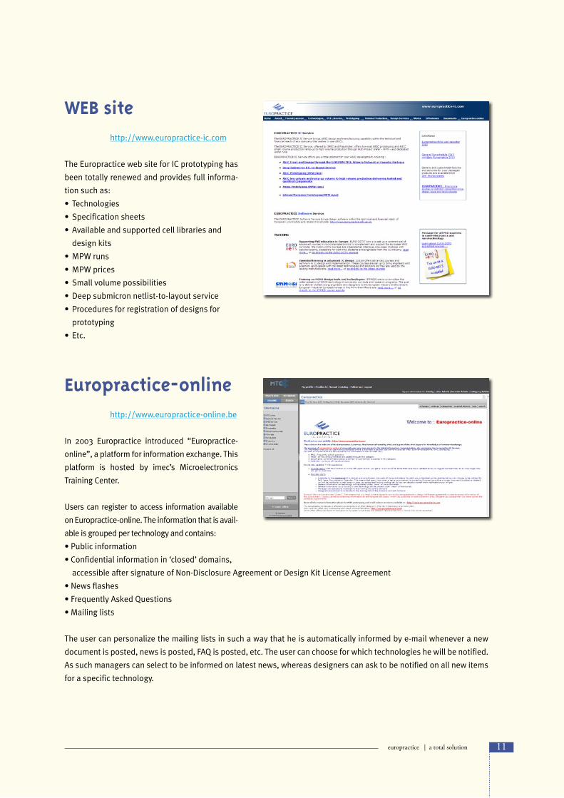
WEB site http://www.europractice-ic.com
The Europractice web site for IC prototyping has
been totally renewed and provides full informa-
tion such as:
• Technologies
• Specificationsheets
• Availableandsupportedcelllibrariesand
design kits
•MPWruns
•MPWprices
• Smallvolumepossibilities
• Deepsubmicronnetlist-to-layoutservice
• Proceduresforregistrationofdesignsfor
prototyping
• Etc.
Europractice-online http://www.europractice-online.be
In 2003 Europractice introduced “Europractice-
online”, a platform for information exchange. This
platform is hosted by imec’s Microelectronics
Training Center.
Users can register to access information available
on Europractice-online. The information that is avail-
able is grouped per technology and contains:
•Publicinformation
•Confidentialinformationin‘closed’domains,
accessible after signature of Non-Disclosure Agreement or Design Kit License Agreement
•Newsflashes
•FrequentlyAskedQuestions
•Mailinglists
The user can personalize the mailing lists in such a way that he is automatically informed by e-mail whenever a new
document is posted, news is posted, FAQ is posted, etc. The user can choose for which technologies he will be notified.
As such managers can select to be informed on latest news, whereas designers can ask to be notified on all new items
for a specific technology.
11europractice | a total solution

ASICs prototyped on MPW runsIn 2013, a total of 538 ASICs
have been prototyped.
73% of the designs are sent in
by European universities and
research laboratories while the
remaining 27% of the designs is
being sent in by non-European
universities and companies
world-wide.
Geometry mixYear over year we see a shift
towards newest technologies.
Also in 2013 the same trend is
shown. Again, the majority of
designs is done in 0.18µ / 0.15µ
technology (39%). Also the
number of designs in Silicon
Photonics (MEMS) technology
has taken up.
0
100
200
300
400
500
600
Industry + non-Europeanuniv/research
Europractice Research
Europractice Academic
140
27
313
2000
159
46
281
2001
155
13
237
2002
115
48
200
2003
128
52
234
2004
138
69
243
2005
134
84
215
2006
154
87
298
2007
164
85
285
2008
153
87
305
2009
113
83
337
2010
143
96
321
2011
139
105
301
2012
144
87
307
2013
Results
MPW prototyping service
MPW designs in 2013
Industry + non-European univ/research 27%
Europractice Research 16%
Europractice Academic 57%
mini@sicVery encouraging is the fact that the mini@sic concept continues to be accepted
very well by the universities in 2013.
12 europractice | results

Small volume projects
More and more customers are us-
ing the COT (Customer Own Tool-
ing) model when they need vol-
ume production. Through this COT
model they have full control about
every aspect of the total design and
production flow. Large customers
with sufficient ASIC starts and vol-
ume production can invest in the
COT model as it requires a consid-
erable knowledge and experience
about all aspects such as librar-
ies, design kits, transistor models,
testing, packaging, yield, etc. For
smaller customers the COT model is
very attractive but very difficult due
to the lack of experience. For those
customers EUROPRACTICE offers
the solution by guiding the custom-
ers through the full production flow
applying the COT model. EURO-
PRACTICE helps you with technical
assistance in the selection of the
right package, setting up the test
solution, yield analysis, qualifica-
tion, etc.
Through EUROPRACTICE you can
also experience the benefits of the
COT model.
0.35µ 132
0.25µ 400.18...0.15µ 210
0.13µ...0.11µ 52
90nm 2065nm 25 40nm 9
0.8...0.5µ 8MEMS 42
MPW designs in 2013: technology node and number of designs
Geometry mix
0
50
100
150
200
250
MEMS 0.8…0.5µ 0.35µ 0.25µ 0.18...0.15µ 0.13µ 90nm 65nm
2003 2004 2005 2006 2011 2013
20122007 2008 2009 2010
40nm
Geometry mix
0.8…0.5µ 2%
0.35µ 19%
0.25µ 10%0.18...0.15µ 43%
0.13µ 15% 90nm 6%
65nm 4%
40nm 1%
mini@sic designs per gatelength in 2013
0
50
100
150
200
250
300
350
2004 2005 2006 2007 2008 2009 2010 2011 2012 2013
90nm
65nm
40nm
0.13µ
0.18...0.15µ
0.25µ
0.35µ
0.8…0.5µ
13europractice | results
0 10 20 30 40 50 60 70 80 90 100
USA
United Kingdom
Turkey
Thailand
Taiwan
Switzerland
Sweden
Spain
South Africa
Singapore
Serbia and Montenegro
Saudi Arabia
Russia
Romania
Portugal
Poland
Norway
Netherlands
Mexico
Malta
Lithuana
Korea, Republic
Japan
Italy
Israel
Ireland
India
Greece
Germany
France
Finland
Denmark
Czech Republic
China & Hong Kong
Canada
Brazil
Belgium
Belarus
Austria
Australia
Algeria
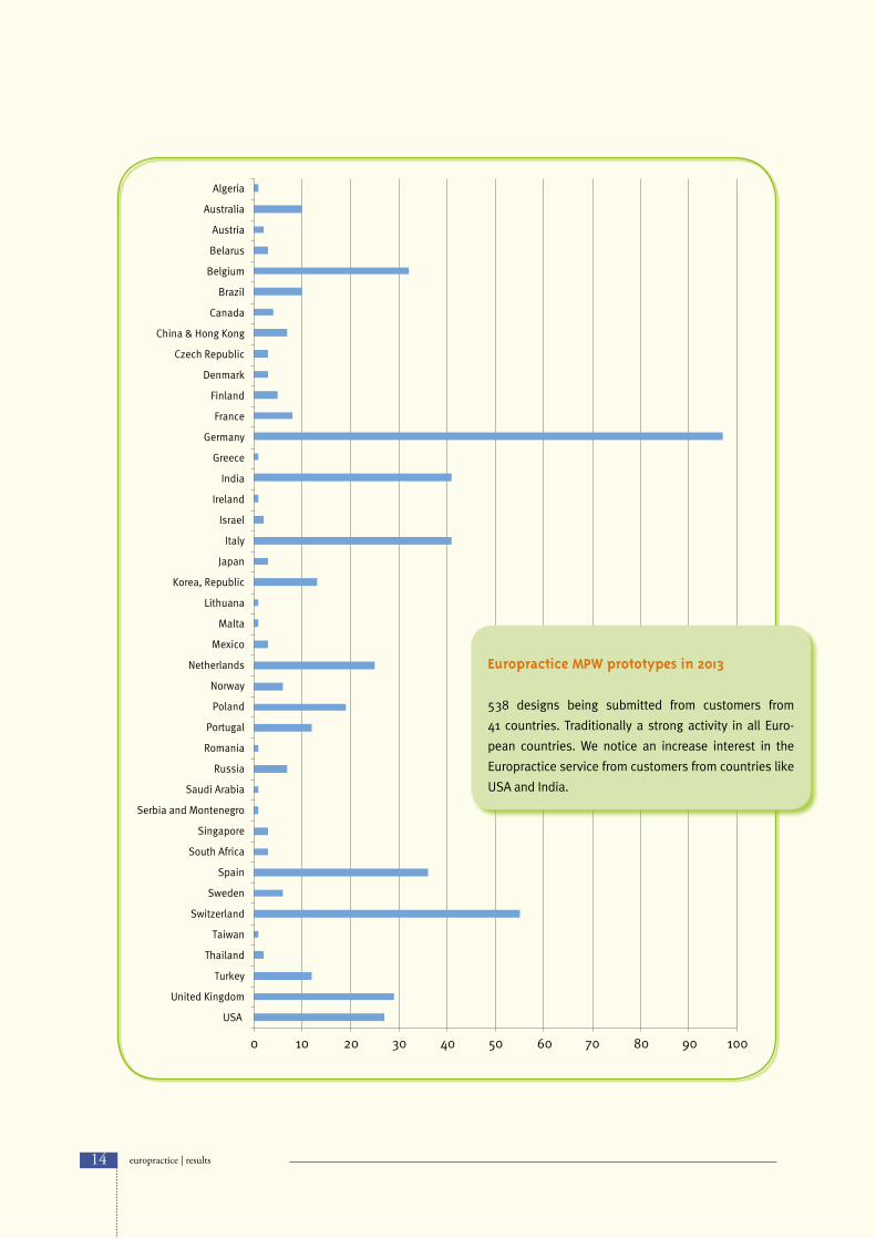
Europractice MPW prototypes in 2013
538 designs being submitted from customers from
41 countries. Traditionally a strong activity in all Euro-
pean countries. We notice an increase interest in the
Europractice service from customers from countries like
USA and India.
14 europractice | results

0 200 400 600 800 1000 1200 1400 1600
USA
United Kingdom
Turkey
Thailand
Taiwan
Switzerland
Sweden
Spain
South America
South Africa
Slovenia
Slovakia
Singapore
Serbia and Montenegro
Saudi Arabia
Russia
Romania
Puerto Rico
Portugal
Poland
Norway
New Zealand
Netherlands
Mexico
Malta
Malaysia
Lithuana
Lebanon
Korea
Japan
Italy
Israel
Ireland
India
Hungary
Greece
Germany
France
Finland
Estonia
Egypt
Denmark
Czech Republic
Cyprus
Croatia
Costa Rica
China & Hong Kong
Canada
Bulgaria
Brazil
Belgium
Belarus
Austria
Australia
Algeria
Total designs
EUROPRACTICE has offered since 1996 its low cost ASIC MPW prototyping
services to customers from 55 countries worldwide. As the service is based
in Europe, the majority of the designs come from European customers.
But the interest from non-European countries is growing fast.
15europractice | results
Examples of ASIC projects
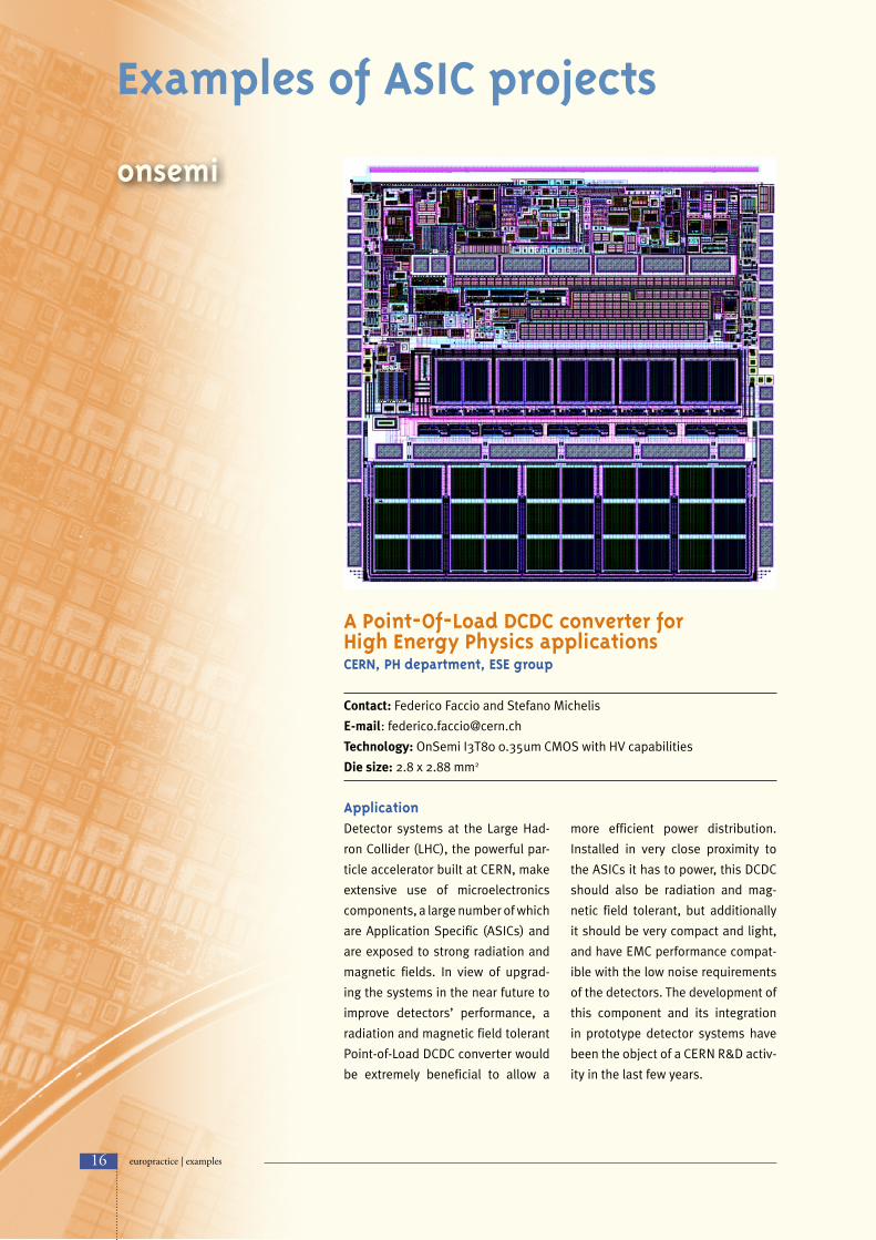
onsemi
A Point-Of-Load DCDC converter for High Energy Physics applicationsCERN, PH department, ESE group
Contact: Federico Faccio and Stefano Michelis
E-mail: [email protected]
Technology: OnSemi I3T80 0.35um CMOS with HV capabilities
Die size: 2.8 x 2.88 mm2
ApplicationDetector systems at the Large Had-
ron Collider (LHC), the powerful par-
ticle accelerator built at CERN, make
extensive use of microelectronics
components, a large number of which
are Application Specific (ASICs) and
are exposed to strong radiation and
magnetic fields. In view of upgrad-
ing the systems in the near future to
improve detectors’ performance, a
radiation and magnetic field tolerant
Point-of-Load DCDC converter would
be extremely beneficial to allow a
more efficient power distribution.
Installed in very close proximity to
the ASICs it has to power, this DCDC
should also be radiation and mag-
netic field tolerant, but additionally
it should be very compact and light,
and have EMC performance compat-
ible with the low noise requirements
of the detectors. The development of
this component and its integration
in prototype detector systems have
been the object of a CERN R&D activ-
ity in the last few years.
16 europractice | examples

DCDC circuit descriptionThe POL converter is a single-phase buck topology built around an ASIC designed by
CERN engineers in the OnSemi I3T80 technology. This circuit, named FEAST, embeds
on the same 2.8 x 2.88 mm2 silicon both the power switches, bootstrap diode and
the control circuitry. Capable of operating from an input voltage of 5 to 12V, it has
a selectable output voltage range between 0.6 and 5V and can provide up to 4A of
output current (within the limit of 10W output power). Switching at a frequency of
1-3MHz (selectable) to work with a 200-700nH air-core inductor, the circuit includes
protections for over-current and over-temperature events, and has an under-voltage
lock-out feature. Radiation tolerance is achieved with the systematic use of hard-
ness-by-design techniques both for Total Ionising Dose (TID), displacement damage
and Single Event Effects (SEE).
After several generation of prototypes, the design integrated in the April 2013 MPW run
was verified to be production-ready. Electrical performance is compliant with specifica-
tions, and all protection features are correctly working. Radiation tolerance require-
ments have been verified with X-rays, neutron, proton and heavy ion irradiation tests.
While samples from this run have been packaged and are now being assembled in a
pre-production run of full DCDC plug-in modules (Figure 1), a version of the ASIC with
improved SEE tolerance has being included in a December MPW run in the same tech-
nology. This version should satisfy the radiation tolerance requirements of even the
LHC tracker detectors, installed where the radiation environment is the most severe.
Full prototype DCDC modules with a footprint of about 38 x 17 mm. The FEAST ASIC, packaged in a qfn32 package, is covered by the custom air-core inductor of 450nH, then a copper shield encloses all noisy components so that the final plug-in module (to the left) achieves excellent EMC performance for conducted and radiated noise.
Why EuropracticeThe Europractice IC service was in-
strumental in giving us easy access
to the High-Voltage I3T80 technol-
ogy from OnSemi. Thanks to the
mini@sic program, the cost is very
reasonable and there is practically
no lower limit on the silicon area for
the design: in the early stages of
the project, this allowed us easy in-
tegration of test structures to probe
the natural radiation performance
of the technology. At the end of the
development, Europractice could
organise a small dedicated pro-
duction run for our project, yield-
ing enough samples for our needs
(small volume for a silicon manu-
facturer). All our wishes, from first
small prototypes to final produc-
tion, were hence satisfied fully.
17europractice | examples

ams Front End ASIC for 2D array of capacitive micromachined ultrasound transducers (CMUT) JSC Minatech, Kaunas University of Technology Panevezys Institute and Vilnius Gediminas Technical University, Lithuania
Contact: Darius Viržonis, Gailius Vanagas, Vaidotas Barzdėnas
E-mail: [email protected], [email protected]
Technology: AMS 0.18 µm HV CMOS 6M
Die size: 5250x5250 µm
Fig. 1. Plot of the ASIC.
IntroductionCMUT device can be drafted as a ca-
pacitor with one fixed and one move-
able electrode, which is coupled with
the membrane of adequate elastic
properties.
One of the applications of CMUT
concept is the real-time three-dimen-
sional (3D) medical imaging, which
is possible only at limited resolu
tion with existing techniques. With
CMUT concept two-dimensional (2D)
transducer arrays for high resolution
real-time 3D imaging can be manu-
factured within reasonable efforts.
However, due to the high number of
transducer elements and small di-
mensions proper use of such an ar-
ray becomes challenging:
18 europractice | examples

1. low signal-to-noise ratio due the
small element dimensions;
2. large number of conductors in
very limited space;
3. parasitic capacitance of inter-
connecting leads.
Therefore integration of the front-
end electronics (containing pulsers,
beamformers, switches and pre-am-
plifiers) with CMUT array is the nec-
essary solution.
Description of the ASICUltrasound Transceiver for 2D CMUT
Front End (FE) Core integrated circuit
(IC) is a device primarily intended to
individually excite CMUT elements
and to receive, buffer and amplify
receiving signals from individual
CMUT elements. CMUT FE Core has
256 CMUT elements connection
points (CCP) subdivided into 4 ap-
ertures laid out as aperture matrix
of 2 rows and 2 columns. Each aper-
ture has 64 CCPs laid out as matrix
of 8 rows and 8 columns. Each CCP
is able to drive single CMUT element
or to receive and amplify the signal
coming from a single CMUT element.
CMUT FE Core has 64 75 Ω terminat-
ed inputs able to receive the trans-
mitting pulse signals. CMUT FE Core
64 inputs are shared with 64 out-
puts. CMUT FE Core has 64 outputs
able to drive 1.5 m long coaxial cable.
The 256 CCPs are multiplexed to
64 outputs by the internal multiplex-
ing structure. The latter structure
multiplexes each i-th CCP of j-th ap-
erture to i-th output. 4 digital chan-
nels clocked by one clock provide the
pixel selection data. The mode signal
puts the CMUT FE to transmit or re-
ceive mode.
Fig. 2. Photo of the fabricated chip.
The CMUT FE core is capable to drive 16x16 matrix of CMUT elements simulta-
neously. The grid of the CCPs is distributed with 250 µm pitch. Each individual
transceiver channel contains logic circuit, pulser to generate the excitation
pulses of +50 V, preamplifier and protection circuit to protect the preamplifier
during the transmit cycle. Average power dissipation is 60 mW per channel.
Receive preamplifier has the input-referred noise density of 4 nV/sqrt(Hz).
Amplifier recovery time after TX pulse 0.3 µs.
Why Europractice? Europractice provides exclusive opportunities to prototype small series of
experimental ICs with large selection of microelectronics fabrication tech-
nologies. We selected AMS 0.18 µm HV CMOS 6M technology provided by
Europractice because of good match between production costs and required
complexity. All this in combination with professional service and discount poli-
cy for academia projects makes Europractice service affordable and attractive.
And it shortens the path between the research and applications.
AcknowledgementsThis research was partially supported by EU and Lithuanian governments
grant VP2-1.3-ŪM-02-K-01-102.
19europractice | examples

A CMOS Power-Supply Technique for Minimizing the Current-Source Power of Implanted Chips Department of Electrics and Electronical Engineering, Yeditepe University, Istanbul, Turkey
Contacts:Sercan İpek and Uğur Çilingiroğlu E-mails: [email protected] , [email protected] Technology: AMS 0.18μm HV CMOS (H18A6) Die size: 2.25 x 2.25 mm2
IntroductionImplanted chips are widely used for
functional electrical stimulation in
treating various disorders such as
deafness, blindness, paralysis and
cardiac arrhytmia [1]. In almost all ap-
plications these chips are power-sup-
plied from an external battery via an
inefficient inductive link operating at
radio frequencies. This is why power
efficiency is the dominant constraint
in their design. Most of their power
consumption is due to the stimula-
tion current drawn from the power
supply. This current is generated by
a current source, and flows through
the electrode/tissue impedence.
Therefore, the power-supply volt-
age has to be equal or larger than
the sum of the maximum voltages
across the current source and the
impedence but, under most of the
stimulation conditions, neither the
current nor the impedence is maxi-
mum. This is why the power-supply
voltage turns out to be unnecessarily
large for the majority of stimulation
episodes, resulting in power waste
across the current source.
DescriptionThe technique we propose in this
project relies on zero-voltage switch-
ing for generating the supply volt-
age and updating it at a rate equal
to or less than the radio frequency
(RF) of the inductive link depend-
ing on power demand. A feedback
loop confined to the secondary of
the inductive link adjusts the timing
and conduction angle of switching
to provide just the right amount of
supply voltage needed for keeping
the current-source voltage constant
at compliance limit. Current-source
power is thus minimized. Since drive
is based on current instead of volt-
age, and supply-voltage update is
near real-time, the quality of the
current pulses is high regardless of
how evolves during stimulation. By
scaling the switching frequency ac-
cording to power demand, the tech-
nique further improves overall power
consumption of the stimulator. The
technique is implemented with a
very simple control circuitry compris-
ing a comparator, a Schmitt trigger
and a logic gate of seven devices in
addition to an on-chip switch and an
off-chip capacitor [2].
ResultsThe proposed technique keeps the
voltage across the current source
continuously at the compliance
limit, and thus minimizes the power
dissipation of the source. Control
is accomplished at a near-real time
resolution. Testing of the prototype;
shows that functional electrical
stimulation is accomplished with
only 25% power of conventional sys-
tem in most typical cases. Although
increasing stimulation current and
stimulation period raises the power
consumption of the proposed tech-
nique up to 90% of the power of the
conventional system, the superior-
ity of power efficiency is retained
throughout the entire scale of appli-
cation conditions.
Why Europractice?Our university have an access to de-
sign tools and various CMOS tech-
nologies through Europractice. Sev-
eral undergraduate and graduate
students have gained educational and
research experience in microelectron-
ics in our research laboratory by using
these design tools and technologies.
The mini@sic program enables us to
fabricate the prototypes design in dif-
ferent technologies to be produced
with affordable prices. This provides
our students with a great opportunity
to take part in academic research.
AcknowledgmentThis work wassupported by The Sci-
entific and Technological Research
Council of Turkey (TÜBİTAK112E166).
20 europractice | examples
References[1] F. Soulier, S. Bernard, G. Cathébras, and D. Guiraud,
“Advances inimplanted functional electrical stimulation,”
in Proc. Int. Conf. Designand Technology of Integrated Sys-
tems in Nanoscale Era, 2011, pp. 1–6.
[2] U. Cilingiroglu, S. Ipek, “A zero-voltage switching technique
for minimizing the current-source power of implanted stim-
ulators”, IEEE Trans. on Biomedical Circuits and Systems,
Vol:7, Issue: 4, pp.469-479, 6 February, 2013.
Radiation hard programmable delay lineLIFAELS, La Salle, Universitat Ramon Llull / ECM, ICC, Universitat de Barcelona
Contact: Joan Mauricio, David Gascón, Xavier Vilasís, Eduardo Picatoste
E-mail: [email protected]
Technology: AMS 0.35 µm CMOS
Die size: 2400 x 2400 µm2
IntroductionDelay lines are commonly used in
high energy physics experiments,
such as LHCb, since synchronization
is critical for such kind of applica-
tions. The operating principle of digi-
tal delay lines is very simple: the user
can set an arbitrary delay and thus
compensate the latency introduced,
for example, by cables or fibers. The
radiation requirements of the hard-
ware disposed in the LHCb cavern
(which is expected to reach 5 krad)
discard the possibility of using com-
mercial delay lines, and justify a full
custom design able to cope with ra-
diation.
DescriptionThis chip implements an SPI-pro-
grammable (Serial Peripheral Inter-
face) delay line based on a Delay
Locked Loop (DLL), with 12 inde-
pendent LVDS clock outputs. The
user can configure up to 25 different
clock phases to cover the 25 ns LHC
clock in 1 ns steps.
This design is mainly constrained
by reliability, since Single Event Ef-
fects (SEEs) produced by radiation
may endanger not only the correct
operation of the chip (transients
and upsets), but also may lead to
its destruction due to overcurrent
(latchups). To minimize the latchup
probability, a radiation hard digital
standard cells library was devel-
oped: the distance between NMOS
and PMOS transistors is increased in
comparison with the common stand-
ard cells, and guard rings are inter-
posed between NMOS and PMOS
transistors. To avoid transients in
critical signals such as reset, a glitch
suppressor was implemented. Final-
ly, Triple Modular Redundancy (TMR)
registers enable a safe storage of
DLL configuration and thus avoiding
data corruption caused by Single
Event Upsets (SEUs).
Measurement ResultsOn the one hand, the standard devia-
tion of the Differential Non-Linearity
(DNL) measured in this delay chip is
23 ps, i.e. a coefficient of variation
of 2.3 %. And the RMS jitter of the
output clocks is below 5 ps. On the
other hand, the SPI interface exhibits
a frame error rate lower than 10-5 at
15 Mbps. Also, a testbeam to qualify
for radiation hardness is envisaged.
Why Europractice?The mini@sic MPW program gives
us the opportunity to implement our
prototypes at an affordable price. It
is also a good choice for small vol-
ume ASIC productions. Moreover,
Europractice provides us the EDA
tools needed for the design and tech-
nical support.
21europractice | examples
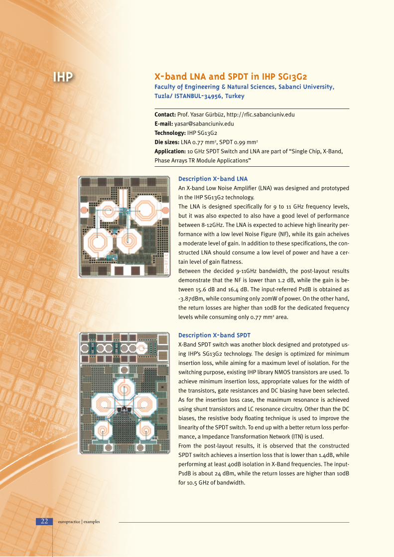
IHP X-band LNA and SPDT in IHP SG13G2Faculty of Engineering & Natural Sciences, Sabanci University, Tuzla/ ISTANBUL-34956, Turkey
Contact: Prof. Yasar Gürbüz, http://rfic.sabanciuniv.edu
E-mail: [email protected]
Technology: IHP SG13G2
Die sizes: LNA 0.77 mm2, SPDT 0.99 mm2
Application: 10 GHz SPDT Switch and LNA are part of “Single Chip, X-Band,
Phase Arrays TR Module Applications”
Description X-band LNAAn X-band Low Noise Amplifier (LNA) was designed and prototyped
in the IHP SG13G2 technology.
The LNA is designed specifically for 9 to 11 GHz frequency levels,
but it was also expected to also have a good level of performance
between 8-12GHz. The LNA is expected to achieve high linearity per-
formance with a low level Noise Figure (NF), while its gain acheives
a moderate level of gain. In addition to these specifications, the con-
structed LNA should consume a low level of power and have a cer-
tain level of gain flatness.
Between the decided 9-11GHz bandwidth, the post-layout results
demonstrate that the NF is lower than 1.2 dB, while the gain is be-
tween 15.6 dB and 16.4 dB. The input-referred P1dB is obtained as
-3.87dBm, while consuming only 20mW of power. On the other hand,
the return losses are higher than 10dB for the dedicated frequency
levels while consuming only 0.77 mm2 area.
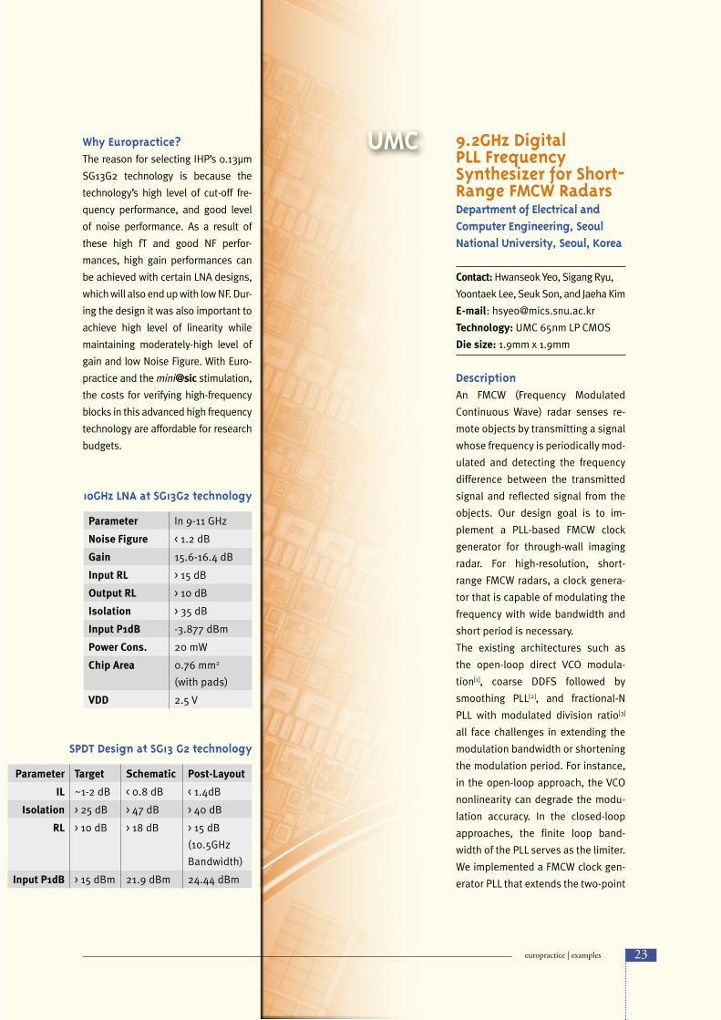
Description X-band SPDTX-Band SPDT switch was another block designed and prototyped us-
ing IHP’s SG13G2 technology. The design is optimized for minimum
insertion loss, while aiming for a maximum level of isolation. For the
switching purpose, existing IHP library NMOS transistors are used. To
achieve minimum insertion loss, appropriate values for the width of
the transistors, gate resistances and DC biasing have been selected.
As for the insertion loss case, the maximum resonance is achieved
using shunt transistors and LC resonance circuitry. Other than the DC
biases, the resistive body floating technique is used to improve the
linearity of the SPDT switch. To end up with a better return loss perfor-
mance, a Impedance Transformation Network (ITN) is used.
From the post-layout results, it is observed that the constructed
SPDT switch achieves a insertion loss that is lower than 1.4dB, while
performing at least 40dB isolation in X-Band frequencies. The input-
P1dB is about 24 dBm, while the return losses are higher than 10dB
for 10.5 GHz of bandwidth.
22 europractice | examples
UMCWhy Europractice?The reason for selecting IHP’s 0.13µm
SG13G2 technology is because the
technology’s high level of cut-off fre-
quency performance, and good level
of noise performance. As a result of
these high fT and good NF perfor-
mances, high gain performances can
be achieved with certain LNA designs,
which will also end up with low NF. Dur-
ing the design it was also important to
achieve high level of linearity while
maintaining moderately-high level of
gain and low Noise Figure. With Euro-
practice and the mini@sic stimulation,
the costs for verifying high-frequency
blocks in this advanced high frequency
technology are affordable for research
budgets.
10GHz LNA at SG13G2 technology
Parameter In 9-11 GHzNoise Figure < 1.2 dBGain 15.6-16.4 dBInput RL > 15 dBOutput RL > 10 dBIsolation > 35 dBInput P1dB -3.877 dBmPower Cons. 20 mWChip Area 0.76 mm2
(with pads)VDD 2.5 V
SPDT Design at SG13 G2 technology
Parameter Target Schematic Post-LayoutIL ~1-2 dB < 0.8 dB < 1.4dB
Isolation > 25 dB > 47 dB > 40 dBRL > 10 dB > 18 dB > 15 dB
(10.5GHz Bandwidth)
Input P1dB > 15 dBm 21.9 dBm 24.44 dBm
9.2GHz Digital PLL Frequency Synthesizer for Short-Range FMCW RadarsDepartment of Electrical and Computer Engineering, Seoul National University, Seoul, Korea
Contact: Hwanseok Yeo, Sigang Ryu,
Yoontaek Lee, Seuk Son, and Jaeha Kim
E-mail: [email protected]
Technology: UMC 65nm LP CMOS
Die size: 1.9mm x 1.9mm
DescriptionAn FMCW (Frequency Modulated
Continuous Wave) radar senses re-
mote objects by transmitting a signal
whose frequency is periodically mod-
ulated and detecting the frequency
difference between the transmitted
signal and reflected signal from the
objects. Our design goal is to im-
plement a PLL-based FMCW clock
generator for through-wall imaging
radar. For high-resolution, short-
range FMCW radars, a clock genera-
tor that is capable of modulating the
frequency with wide bandwidth and
short period is necessary.
The existing architectures such as
the open-loop direct VCO modula-
tion[1], coarse DDFS followed by
smoothing PLL[2], and fractional-N
PLL with modulated division ratio[3]
all face challenges in extending the
modulation bandwidth or shortening
the modulation period. For instance,
in the open-loop approach, the VCO
nonlinearity can degrade the modu-
lation accuracy. In the closed-loop
approaches, the finite loop band-
width of the PLL serves as the limiter.
We implemented a FMCW clock gen-
erator PLL that extends the two-point
23europractice | examples
modulation (TPM) technique, origi-
nally used for RF transmitters [4]. The
TPM technique injects the frequency-
modulation signals at two points of
the PLL (i.e. divider and oscillator),
so that their respective high-pass
and low-pass transfer functions can
sum up to an all-pass characteristic.
The frequency can be modulated at
a high bandwidth and short period,
without being limited by the PLL
loop bandwidth. However, various
gain and delay mismatch among the
circuit components may limit the
effectiveness of the approach and
calibration is typically necessary. The
proposed FMCW PLL depicted in Fig.
1 eliminates this need for extra cali-
bration by using a third-order digital
loop filter in the PLL. That is, the loop
filter generates the second injection
signal by itself by adjusting the ramp
slope via normal PLL feedback op-
eration.
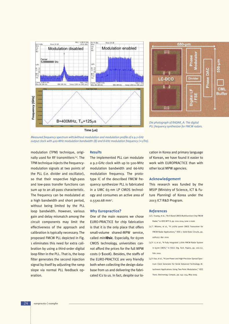
ResultsThe implemented PLL can modulate
a 9.2-GHz clock with up to 500-MHz
modulation bandwidth and 66-kHz
modulation frequency. The proto-
type IC of the described FMCW fre-
quency synthesizer PLL is fabricated
in a UMC 65-nm LP CMOS technol-
ogy and consumes an active area of
0.55x0.68 mm2.
Why Europractice?One of the main reasons we chose
EURO-PRACTICE for chip fabrication
is that it is the only place that offers
small-volume shared-MPW service,
called mini@sic. Especially, for 65nm
CMOS technology, universities can-
not afford the prices for the full MPW
costs (> $100K). Besides, the staffs of
the EURO-PRACTICE are very friendly
both when collecting the design data-
base from us and delivering the fabri-
cated ICs to us. In fact, despite our lo-
cation in Korea and primary language
of Korean, we have found it easier to
work with EUROPRACTICE than with
other local MPW agencies.
AcknowledgementThis research was funded by the
MSIP (Ministry of Science, ICT & Fu-
ture Planning) of Korea under the
2013 ICT R&D Program.
References[1] C. Tzuang, et al., “An X-Band CMOS Multifunction-Chip FMCW
Radar,” in IEEE MTT-S, pp. 2011-2014, June 2 2006.
[2] T. Mitomo, et al., “A 77GHz 90nm CMOS Transceiver for
FMCW Radar Applications,” IEEE J. Solid-State Circuits, pp.
928-937, Apr. 2010.
[3] Y. Li, et al., “A Fully Integrated 77GHz FMCW Radar System
in 65nm CMOS,” in ISSCC Dig. Tech. Papers, pp. 216-217,
Feb. 2010.
[4] Y. Kao, et al., “A Low-Power and High-Precision Spread Spec-
trum Clock Generator for Serial Advanced Technology At-
tachment Applications Using Two-Point Modulation,” IEEE
Trans. Electromag. Compat., pp. 245–254, May 2009.
Measured frequency spectrum with/without modulation and modulation profile of a 9.2-GHz output clock with 400-MHz modulation bandwidth (B) and 8-kHz modulation frequency (=1/Tm).
Die photograph of RADAR_A: The digital PLL frequency synthesizer for FMCW radars.
24 europractice | examples
Time to Digital Converter for Time of Flight Positron Emission TomographyDepartment of Information Engineering, University of Pisa, and INFN section of Pisa, Italy
Contact: Nahema Marino, Federico Baronti, Maria
Giuseppina Bisogni, Alberto Del Guerra, Luca Fanucci,
Roberto Roncella, Sergio Saponara
E-mail: [email protected]
Technology: UMC 65 nm Low Leakage LVT
Die size: 1875 µm x 1875 µm
IntroductionPositron emission tomography (PET) is a molecular imaging
technique which informs about the physiological processes
inside the body. A PET scanner typically consists of a ring of
detectors coupled to readout electronics which evaluate the
line of response (LOR) and the energy of pairs of gamma rays
emitted by annihilation by a tracer labelled with a positron
emitting radionuclide. 3D images of the radiotracer concen-
tration are then obtained through computer reconstruction.
In clinical applications, PET image quality benefits from
the time of flight (TOF) feature either using analytical or
iterative reconstruction algorithms. Indeed, by measuring
the photons arrival time on the detectors, the annihilation
point can be estimated, thus leading to better noise level,
contrast and clarity of detail in the reconstructed images
with respect to conventional PET [1]. This added information
enables the reconstruction algorithm to provide the final
image with fewer iterations and less image noise when in-
creasing the time resolution for large size objects [2].
The 4D-MPET (4 Dimensions Magnetic compatible module
for Positron Emission Tomography) INFN project collabora-
tion exploits the characteristics of silicon photomultipliers
(SiPM), novel scintillation materials and innovative elec-
tronics in order to develop a magnetic-field compatible TOF
PET detector prototype with good spatial, time and energy
resolution [3]. The combination of LYSO crystals with SiPMs
has proven to be suitable for TOF applications, since a time
resolution of 102 ps can be achieved [4]. Then, the readout
must be designed so that it can measure the photon arrival
time with a resolution less than 100 ps. In this scenario, a
time to digital converter (TDC) can be used to provide the
TOF information.
DescriptionSiPM photodetectors can be arranged in large matrices
of small squared pixels to improve the spatial resolution.
This translates into a high number of channels to be read
out, demanding for compact multichannel front-end de-
sign. Moreover, SiPMs exhibit a high noise rate which re-
quires the implementation of noise rejection algorithms
that do not impair the acquisition capability of the read-
out system. Finally, PET measurements are not repeat-
able and require an electronic equipment with high linear
performances. These requirements have suggested the
main guidelines for the design of the TDC to be used in
the readout of the TOF PET detector prototype.
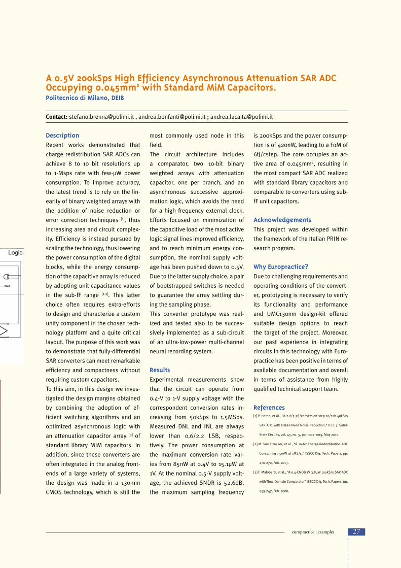
The TDC architecture is based on a classical two-step archi-
tecture where a counter is coupled to a delay locked loop
(DLL) to provide a coarse time and a fine time measurement,
respectively. However, an innovative approach based on
pipeline structures combined with dynamic logics is used.
The converter also features a real time noise rejection algo-
rithm which is based on the measurement of the input pulse
width so as to handle the sampling function of the two-step
core without loss of information. Eight channels are accom-
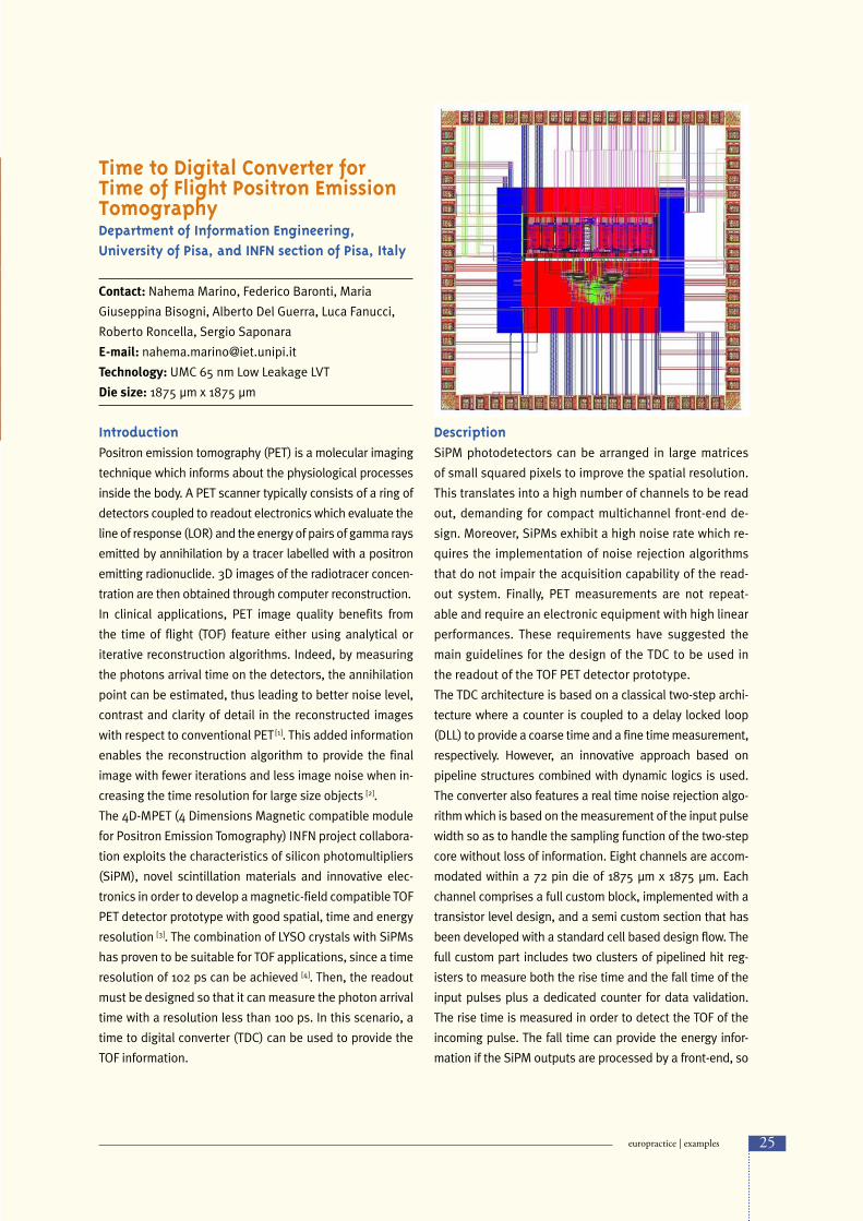
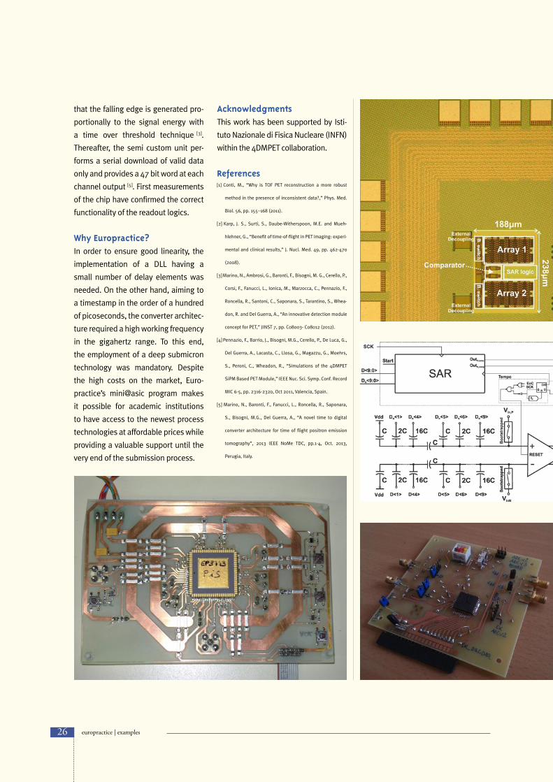
modated within a 72 pin die of 1875 µm x 1875 µm. Each
channel comprises a full custom block, implemented with a
transistor level design, and a semi custom section that has
been developed with a standard cell based design flow. The
full custom part includes two clusters of pipelined hit reg-
isters to measure both the rise time and the fall time of the
input pulses plus a dedicated counter for data validation.
The rise time is measured in order to detect the TOF of the
incoming pulse. The fall time can provide the energy infor-
mation if the SiPM outputs are processed by a front-end, so
25europractice | examples
that the falling edge is generated pro-
portionally to the signal energy with
a time over threshold technique [3].
Thereafter, the semi custom unit per-
forms a serial download of valid data
only and provides a 47 bit word at each
channel output [5]. First measurements
of the chip have confirmed the correct
functionality of the readout logics.
Why Europractice?In order to ensure good linearity, the
implementation of a DLL having a
small number of delay elements was
needed. On the other hand, aiming to
a timestamp in the order of a hundred
of picoseconds, the converter architec-
ture required a high working frequency
in the gigahertz range. To this end,
the employment of a deep submicron
technology was mandatory. Despite
the high costs on the market, Euro-
practice’s mini@asic program makes
it possible for academic institutions
to have access to the newest process
technologies at affordable prices while
providing a valuable support until the
very end of the submission process.
AcknowledgmentsThis work has been supported by Isti-
tuto Nazionale di Fisica Nucleare (INFN)
within the 4DMPET collaboration.
References[1] Conti, M., “Why is TOF PET reconstruction a more robust
method in the presence of inconsistent data?,” Phys. Med.
Biol. 56, pp. 155–168 (2011).
[2] Karp, J. S., Surti, S., Daube-Witherspoon, M.E. and Mueh-
hlehner, G., “Benefit of time-of-flight in PET imaging: experi-
mental and clinical results,” J. Nucl. Med. 49, pp. 462-470
(2008).
[3] Marino, N., Ambrosi, G., Baronti, F., Bisogni, M. G., Cerello, P.,
Corsi, F., Fanucci, L., Ionica, M., Marzocca, C., Pennazio, F.,
Roncella, R., Santoni, C., Saponara, S., Tarantino, S., Whea-
don, R. and Del Guerra, A., “An innovative detection module
concept for PET,” JINST 7, pp. C08003- C08012 (2012).
[4] Pennazio, F., Barrio, J., Bisogni, M.G., Cerello, P., De Luca, G.,
Del Guerra, A., Lacasta, C., Llosa, G., Magazzu, G., Moehrs,
S., Peroni, C., Wheadon, R., “Simulations of the 4DMPET
SiPM Based PET Module,” IEEE Nuc. Sci. Symp. Conf. Record
MIC 6-5, pp. 2316-2320, Oct 2011, Valencia, Spain.
[5] Marino, N., Baronti, F., Fanucci, L., Roncella, R., Saponara,
S., Bisogni, M.G., Del Guerra, A., “A novel time to digital
converter architecture for time of flight positron emission
tomography”, 2013 IEEE NoMe TDC, pp.1-4, Oct. 2013,
Perugia, Italy.
26 europractice | examples
A 0.5V 200kSps High Efficiency Asynchronous Attenuation SAR ADC Occupying 0.045mm2 with Standard MiM Capacitors.Politecnico di Milano, DEIB
Contact: [email protected] , [email protected] ; [email protected]
DescriptionRecent works demonstrated that
charge redistribution SAR ADCs can
achieve 8 to 10 bit resolutions up
to 1-Msps rate with few-µW power
consumption. To improve accuracy,
the latest trend is to rely on the lin-
earity of binary weighted arrays with
the addition of noise reduction or
error correction techniques [1], thus
increasing area and circuit complex-
ity. Efficiency is instead pursued by
scaling the technology, thus lowering
the power consumption of the digital
blocks, while the energy consump-
tion of the capacitive array is reduced
by adopting unit capacitance values
in the sub-fF range [1-2]. This latter
choice often requires extra-efforts
to design and characterize a custom
unity component in the chosen tech-
nology platform and a quite critical
layout. The purpose of this work was
to demonstrate that fully-differential
SAR converters can meet remarkable
efficiency and compactness without
requiring custom capacitors.
To this aim, in this design we inves-
tigated the design margins obtained
by combining the adoption of ef-
ficient switching algorithms and an
optimized asynchronous logic with
an attenuation capacitor array [3] of
standard library MIM capacitors. In
addition, since these converters are
often integrated in the analog front-
ends of a large variety of systems,
the design was made in a 130-nm
CMOS technology, which is still the
most commonly used node in this
field.
The circuit architecture includes
a comparator, two 10-bit binary
weighted arrays with attenuation
capacitor, one per branch, and an
asynchronous successive approxi-
mation logic, which avoids the need
for a high frequency external clock.
Efforts focused on minimization of
the capacitive load of the most active
logic signal lines improved efficiency,
and to reach minimum energy con-
sumption, the nominal supply volt-
age has been pushed down to 0.5V.
Due to the latter supply choice, a pair
of bootstrapped switches is needed
to guarantee the array settling dur-
ing the sampling phase.
This converter prototype was real-
ized and tested also to be succes-
sively implemented as a sub-circuit
of an ultra-low-power multi-channel
neural recording system.
ResultsExperimental measurements show
that the circuit can operate from
0.4-V to 1-V supply voltage with the
correspondent conversion rates in-
creasing from 50kSps to 1.5MSps.
Measured DNL and INL are always
lower than 0.6/2.2 LSB, respec-
tively. The power consumption at
the maximum conversion rate var-
ies from 85nW at 0.4V to 15.1µW at
1V. At the nominal 0.5-V supply volt-
age, the achieved SNDR is 52.6dB,
the maximum sampling frequency
is 200kSps and the power consump-
tion is of 420nW, leading to a FoM of
6fJ/cstep. The core occupies an ac-
tive area of 0.045mm2, resulting in
the most compact SAR ADC realized
with standard library capacitors and
comparable to converters using sub-
fF unit capacitors.
AcknowledgementsThis project was developed within
the framework of the Italian PRIN re-
search program.
Why Europractice?Due to challenging requirements and
operating conditions of the convert-
er, prototyping is necessary to verify
its functionality and performance
and UMC130nm design-kit offered
suitable design options to reach
the target of the project. Moreover,
our past experience in integrating
circuits in this technology with Euro-
practice has been positive in terms of
available documentation and overall
in terms of assistance from highly
qualified technical support team.
References[1] P. Harpe, et al., “A 2.2/2.7fJ/conversion-step 10/12b 40kS/s
SAR ADC with Data-Driven Noise Reduction,” IEEE J. Solid-
State Circuits, vol. 45, no. 5, pp. 1007-1015, May 2010.
[2] M. Van Elzakker, et al., “A 10-bit Charge-Redistribution ADC
Consuming 1.9mW at 1MS/s,” ISSCC Dig. Tech. Papers, pp.
270-272, Feb. 2013.
[3] F. Maloberti, et al., “A 9.4-ENOB 1V 3.8µW 100kS/s SAR ADC
with Time-Domain Comparator” ISSCC Dig. Tech. Papers, pp.
245-247, Feb. 2008.
27europractice | examples
16-Channel Readout ASIC for Next Generation of PET Scanners
Contact: [email protected], Jose Gabriel Macias Montero
Technology: TSMC 0.25UM CMOS LOGIC/MS
Die size: 5300um x 6740um
TSMC
New generation of Positron-Emission
Tomography (PET) scanners use sol-
id-state detectors such as pixelated
Cadmium-Telluride (CdTe) detectors
as the gamma photon detection de-
vice. They provide excellent sensi-
bility, energy resolution, and spatial
resolution compare to scintillating
crystals. For PET scanners, pixelated
CdTe detectors must be connected to
2D readout electronics ASICs to ob-
tain the position of the impact with 1
mm resolution, the energy deposited
by the photon with 1% resolution at
full range, and the time of the photon
interaction with 10 ns resolution.
Available readout ASICs for CdTe
pixelated detectors provide just half
solution since they offer good en-
ergy resolution but poor time infor-
mation. We developed a “16-pixels
version” as a proof of concept of
a final 100-pixels readout ASIC for
CdTe detectors to be used in medi-
cal imaging applications such as PET
scanners. The 16-channel 2D readout
ASIC includes a main digital control-
ler, a time to digital converter (TDC)
with 1ns resolution, a temperature
sensor, five programmable voltage
references, and a matrix of 16 “smart
pixels”. Every pixel integrates an
analog front-end electronics, a 10-
bit ADC, and a digital controller in an
area of 0.7 mm x 0.5 mm. The analog
front-end consists of a charge sensi-
tive amplifier, a fast discriminator, a
CR-RC active shaper, and a peak de-
tect circuit which is connected to the
ADC to provide the value of the inte-
grated charge which is proportional
to the deposited energy. The time
slot of the interaction is provided by
the trigger generated by the discrimi-
nator and the global TDC.
The ASIC has several operation
modes such as programming the
configuration register, TDC calibra-
tion, Temperature sensing, and data
acquisition among others. During
data acquisition, the pixel matrix is
quiet since all pixels are in standby
mode waiting for a photon inter-
action. When a trigger occurs, the
clocks and control signals are sent
only to the triggered channel and
to the 8 adjacent neighbors for of-
fline charge sharing compensation.
Once the ADCs of all 9 channels are
read, the main digital controller cre-
ates and sends to an external FPGA
a data package with the address of
the triggered pixel, the TDC data, the
temperature, and the 9 ADCs values.
The information of all photon inter-
actions is stored externally and ana-
lyzed offline.
The ASIC is biased with a single
power supply of 2.5 V and consumes
200 µW per pixel. The measurements
show per pixel an energy resolution
of 0.4 % at full range, a minimum
threshold of 3 keV, a TDC resolution
of 0.6 ns, and a temperature resolu-
tion of 0.4 degree. According to the
results, the developed ASIC is the
28 europractice | examples
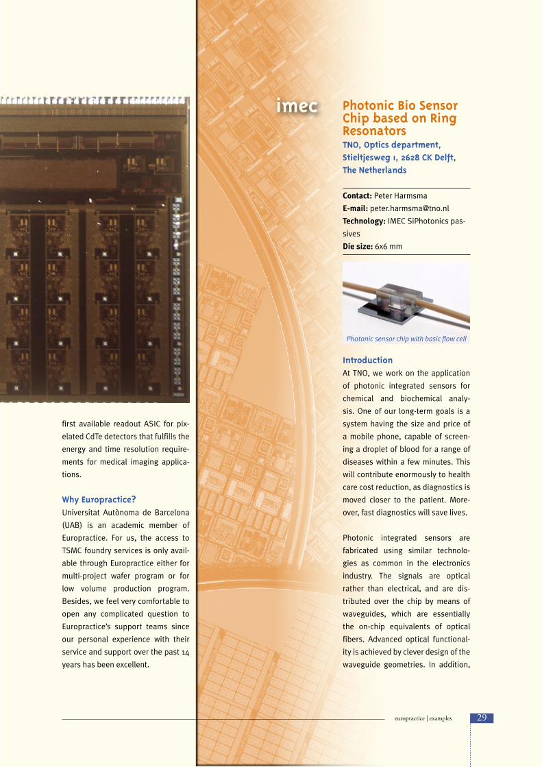
first available readout ASIC for pix-
elated CdTe detectors that fulfills the
energy and time resolution require-
ments for medical imaging applica-
tions.
Why Europractice?Universitat Autònoma de Barcelona
(UAB) is an academic member of
Europractice. For us, the access to
TSMC foundry services is only avail-
able through Europractice either for
multi-project wafer program or for
low volume production program.
Besides, we feel very comfortable to
open any complicated question to
Europractice’s support teams since
our personal experience with their
service and support over the past 14
years has been excellent.
Photonic Bio Sensor Chip based on Ring ResonatorsTNO, Optics department, Stieltjesweg 1, 2628 CK Delft, The Netherlands
Contact: Peter Harmsma
E-mail: [email protected]
Technology: IMEC SiPhotonics pas-
sives
Die size: 6x6 mm
IntroductionAt TNO, we work on the application
of photonic integrated sensors for
chemical and biochemical analy-
sis. One of our long-term goals is a
system having the size and price of
a mobile phone, capable of screen-
ing a droplet of blood for a range of
diseases within a few minutes. This
will contribute enormously to health
care cost reduction, as diagnostics is
moved closer to the patient. More-
over, fast diagnostics will save lives.
Photonic integrated sensors are
fabricated using similar technolo-
gies as common in the electronics
industry. The signals are optical
rather than electrical, and are dis-
tributed over the chip by means of
waveguides, which are essentially
the on-chip equivalents of optical
fibers. Advanced optical functional-
ity is achieved by clever design of the
waveguide geometries. In addition,
imec
Photonic sensor chip with basic flow cell
29europractice | examples
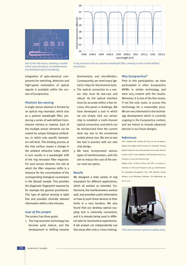
integration of opto-electrical com-
ponents for switching, detection and
high-speed modulation of optical
signals is available within the con-
text of Europractice.
Photonic bio sensingA single sensor element is formed by
an optical ring resonator, which acts
as a passive wavelength filter, pro-
ducing a series of well-defined trans-
mission minima or maxima. Each of
the multiple sensor elements can be
coated by unique biological antibod-
ies, to which only specific biomark-
ers will bind. This binding process at
the chip surface causes a change in
the ambient refractive index, which
in turn results in a wavelength shift
of the ring resonator filter response.
For each sensor element, the rate at
which the filter response shifts is a
measure for the concentration of the
corresponding biological counterpart
in the (blood) sample. This provides
the diagnostic fingerprint required by
for example the general practitioner.
This type of optical sensing is label
free and provides clinically relevant
information within a few minutes.
Goal of this projectThe project has three goals:
1. The ring resonator technology has
become quite mature, and the
development is shifting towards
biochemistry and microfluidics.
Consequently, we need many (ge-
neric) chips for biochemical tests.
2. The optical connection to a sen-
sor chip must be low-cost and
robust. As the optical interface
must be accurate within a few mi-
crons, this poses a challenge. We
have developed a tool in which
we can simply click our sensor
chip to establish a multi-channel
optical connection, and which can
be miniaturized from the current
desk top size to the envisioned
mobile phone size. We aim to test
the tool in practice with our new
chip design.
3. We have incorporated various
types of interferometers, with the
aim to reduce the cost of the sen-
sor read-out optics.
ResultsWe designed a wide variety of ring
resonators for different applications,
which all worked as intended. Fur-
thermore, the interferometers worked
well, and provided useful information
on how to push these devices to their
limits in a next iteration. We also
found that our desktop optical cou-
pling tool is extremely convenient,
and it is already being used in differ-
ent labs for biochemical experiments.
A lab analyst can independently use
this setup after only a 1-hour training.
Why Europractice?Prior to this participation, we have
participated in other Europractice
MPWs in similar technology, and
were very content with the results.
Moreover, it is one of the few routes,
if not the only route, to access this
technology for a reasonable price.
We are very interested in the technol-
ogy development which is currently
ongoing in the Europractice context,
and we intend to include advanced
devices in our future designs.
ReferencesS.M.C. Abdulla, B.M. de Boer, J.M. Pozo, J.H. van den Berg, A.
Abutan, R.A.J. Hagen, D.M.R. Lo Cascio, P. J. Harmsma, “Sensing
platform based on micro-ring resonator and on-chip reference
sensors in SOI”, to be published in SPIE photonics west 2014,
February 1-6, 2014, San Francisco, USA.
Abdulla, S.M.C., De Boer, B, Pozo, J.M, S.M.C., Lo Cascio, D.,
Harmsma, P.,”SOI and InP based on-chip 3x3 interferometers
for wavelength interrogation”, Proc. IEEE Photonics Society
Benelux, 25-26 November, Eindhoven, The Netherlands, pp
69-72, 2013.
A ring resonator acts as a passive wavelenght filter, creating a series of well-defined resonances.
Part of the chip layout, showing a number of test ring resonators, an interferometer, and dedicated optical interfacing.
‘click-and-measure’ optical coupling setup.
30 europractice | examples

Testing and Calibration Structures for Piezoresistive Transducers and Varactors Institute for Applied Microelectronics (IUMA), University of Las Palmas de Gran Canaria, 35017 Las Palmas de Gran Canaria, Spain
Contact: Juan A. Montiel–Nelson
E-mail: [email protected]
Technology: MEMSCAP, MetalMUMPs Process
MEMSCAP
IntroductionDue to variations in manufacturing of
MEMS devices some test structures
are provided for developing calibra-
tion techniques and obtaining ac-
curate physical models –including
process dispersion. By using Metal-
MUMPS process form MEMSCAP,
22 membranes –each one includes
a varactor and four piezoresistive
transducers– and 2 RF switches are
implemented. The obtained results
are used for accurate design and
simulation of accelerometers and RF
switches in this technology.
DescriptionThe stress profile of each diaphragm,
for an equivalent operating pressure
of 25 KPa, has been studied for the
effective placement of the piezore-
sistors and varactors. Using both AN-
SYS and CoventorWare, an extensive
analysis of the mechanical and elec-
trical behavior of the membrane has
been obtained by using multi-phys-
ics solvers. For a square shaped pol-
ysilicon membrane encapsulated by
two nitride layers (MetalMUMPs pro-
cess), the stress distribution along
X-X’ and Y-Y’ have been calculated.
31europractice | examples

Taking into account the previews re-
sults, and varying the offset of the pi-
ezoresistors along both x and y axis
from the diaphragm edge to center,
it is possible to detect the position
where resistance values experience
the maximum change without affect-
ing to sensor linearity, which means
the maximum sensitivity.
The testing structures include a ca-
pacitive sensor (varactor) made with
MetalMUMPs process, which is an
electroplated nickel micromachining
process on a single silicon wafer and
where polysilicon (Poly) layer has
been used as both capacitive and
piezoresistive sensor. Though pi-
ezoresistors have been isolated from
the rest of the Poly, they also suffer
strain due to the fact that upper and
lower nitride layers experiment de-
flection when a voltage is applied
to the capacitor in Poly on the cen-
tral diaphragm. Fig. 1 illustrates the
chips that have been fabricated. As
it is shown, the final design has been
implemented for different sizes in
order to check experimentally the re-
lationship among performance, scal-
ing and die dispersion.
In order to get measures and to apply
voltage to the devices, some connec-
tors have been used, which link the
device terminals to probe station for
parametric testing. The contribution
of the probe pads both in resistance
and capacitance has been consid-
ered and compensated. On the other
hand, the perforation for release etch
has been considered during previous
analysis.
Why Europractice?For small volume MEMS production
EUROPRACTICE offers an excellent
solution both in the frequency of
MPW runs (mini@sic program) as in
price and tools needed for the de-
sign. Therefore, it offers not only the
opportunity for research institutes
and universities to manufacture de-
signs of prototypes with relevant
innovations but also improving DFM
techniques and models.
AcknowledgmentsThis work was funded by project BAT-
TLEWISE (TEC2011-29148-C02-01)
of the Spanish Ministry of Economy
and Competitiveness. We thanks the
Europractice staff at IMEC for provid-
ing an excellent service and technical
support. ■
List of Customers per country and number of designs they have sent in for MPW fabrication
32 europractice | examples
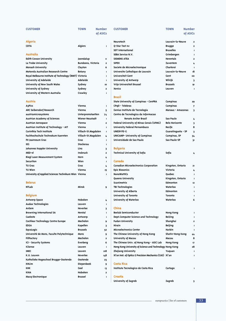
Algeria CDTA Algiers 1
Australia Edith Cowan University Joondalup 11
La Trobe University Bundoora, Victoria 2
Monash University Clayton 6
Motorola Australian Ressearch Centre Botany 1
Royal Melbourne Institute of Technology (RMIT) Victoria 1
University of Adelaide Adelaide 1
University of New South Wales Sydney 10
University of Sydney Sydney 2
University of Western Australia Crawley 1
Austria A3Pics Vienna 1
ARC Seibersdorf Research Vienna 5
austriamicrosystems Unterpremstaetten 74
Austrian Academy of Sciences Wiener Neustadt 1
Austrian Aerospace Vienna 2
Austrian Institute of Technology - AIT Vienna 1
Carinthia Tech Institute Villach-St.Magdalen 1
Fachhochschule Technokum Kaernten Villach-St.Magdalen 4
FH Joanneum Graz Graz 1
IEG Stockerau 1
Johannes Keppler University Linz 3
MED-el Insbruck 2
Riegl Laser Measurement System Horn 4
Securiton Wien 1
TU Graz Graz 4
TU Wien Vienna 19
University of Applied Sciences Technikum Wien Vienna 1
Belarus NTLab Minsk 9
Belgium Antwerp Space Hoboken 4
Audax Technologies Leuven 1
AnSem Heverlee 3
Browning International SA Herstal 1
Caeleste Antwerp 1
Cochlear Technology Centre Europe Mechelen 9
ED&A Kapellen 3
EqcoLogic Brussels 52
Université de Mons, Faculte Polytechnique Mons 9
FillFactory Mechelen 2
ICI - Security Systems Everberg 6
ICSense Leuven 1
IMEC Leuven 218
K.U. Leuven Heverlee 148
Katholieke Hogeschool Brugge-Oostende Oostende 23
KHLim Diepenbeek 9
KHK Geel 13
KIHA Hoboken 2
Macq Electronique Brussel 1
Neurotech Louvain-la-Neuve 2
Q-Star Test nv Brugge 2
SDT International Bruxelles 1
SEBA Service N.V. Grimbergen 1
SIEMENS ATEA Herentals 2
SIPEX Zaventem 4
Societe de Microelectronique Charleroi 1
Universite Catholique de Louvain Louvain-la-Neuve 18
Universiteit Gent Gent 101
University of Antwerp Wilrijk 3
Vrije Universiteit Brussel Brussels 91
Xenics Leuven 1
Brazil State University of Campinas - CenPRA Campinas 29
CPqD - Telebras Campinas 7
Genius Instituto de Tecnologia Manaus - Amazonas 3
Centro de Tecnologica da Informacao
Renato Archer Brasil Sao Paulo 4
Federal University of Minas Gerais (UFMG) Belo Horizonte 3
University Federal Pernambuco Recife 8
UNESP/FE-G Guaratingueta - SP 3
UNICAMP- University of Campinas Campinas, SP 34
Universidade de Sao Paulo Sao Paulo-SP 31
Bulgaria Technical University of Sofia Sofia 4
Canada Canadian Microelectronics Corporation Kingston, Ontario 21
Epic Biosonics Victoria 4
NanoWattICs Quebec 1
Queens University Kingston, Ontario 1
Scanimetrix Edmonton 12
TBI Technologies Waterloo 1
University of Alberta Edmonton 1
University of Toronto Toronto 1
University of Waterloo Waterloo 6
China Beelab Semiconductor Hong Kong 1
Dept.Computer Science and Technology BeiJing 1
Fudan University Shanghai 2
Hirain Beijing 1
Microelectronics Center Harbin 1
The Chinese University of Hong Kong Shatin-Hong Kong 44
University of Macau Macau 8
The Chinese Univ. of Hong Kong - ASIC Lab Hong Kong 17
Hong Kong University of Science and Technology Hong Kong 28
Zhejiang University Yuquan 1
Xi’an Inst. of Optics & Precision Mechanics (CAS) Xi’an 1
Costa Rica Instituto Tecnologico de Costa Rica Cartago 1
Croatia University of Zagreb Zagreb 5
CUSTOMER TOWN Number of ASICs
CUSTOMER TOWN Number of ASICs
33europractice | list of customers
europractice | list of customers
Cyprus University of Cyprus Nicosia 2
Czech Republic ASICentrum s.r.o. Praha 4 6
Brno University of Technology Brno 18
Czech Technical University-FEE Prague 9
Institute of Physics ASCR Prague 2
Denmark Aalborg University Aalborg 51
Aalto University Aalto 9
Algo Nordic A/S Copenhagen 1
Bang & Olufsen Struer 4
DELTA Hoersholm 11
GN-Danavox A/S Taastrup 4
Microtronic A/S Roskilde 1
Oticon A/S Hellerup 14
PGS Electronic Systems Frb. 1
Techtronic A/S Roskilde 1
Technical University of Denmark Lyngby 13
Thrane&Thrane Lyngby 1
Egypt American university of Cairo Cairo 1
Bahgat Group - IEP Cairo 4
Estonia Tallinn Technical University Tallinn 1
Finland Aalto University Espro 1
Detection Technology Inc. Li 1
Fincitec Oy Oulu 4
Kovilta Oy Salo 1
Helsinki University of Technology Espoo 9
Nokia Networks Espoo 2
Tampere University of Technology Tampere 8
University of Oulu Oulu 20
University of Turku Turku 3
VTI Technologies Vantaa 2
VTT Electronics Espoo 109
France Atmel Nantes, Cedex 3 3
C4i Archamps 14
CCESMAA -IXL Talence 2
CEA Grenoble 40
CMP-TIMA Grenoble 7
CNES Toulouse Cedex 01 4
CPPM Marseille 2
Dibcom Palaiseau 1
Dolphin Integration Meylan 4
EADS Defense&security 1
ELA Recherche Meylan 4
ENSEA Cergy Pontoise 2
ENST Paris Paris 2
ESIEE Noisy Le Grand 3
IN2P3 - LPNHE - Universites 6 et 7 Paris Cedex 5 9
Institut des Sciences Nucleaires Grenoble 5
Institut de Physique Nucleaire Villeurbanne 7
Institut Sup. d Electronique de Bretagne Brest 2
IRAP Toulouse 1
ISEN Recherche Lille cedex 5
LAAS/CNRS Toulouse 9
Labo PCC CNRS/IN2P3 Paris cedex05 2
Laboratoire de l Accelerateur Lineaire Orsay 6
Laboratoire de Physique des Plasmas, LPP Saint-Maur des Fossés 2
LAPP Annecy-le-Vieux 7
LEA Cesson Sevigne 1
LEPSI Strasbourg 15
Ecole Polytechnique route de Saclay , LPP Palaiseau 1
LETI-CEA Grenoble 4
LIRMM Montpellier 2
Midi Ingenierie Labege 1
MXM Laboratories Vallauris 3
NeoVision France Bagneux 3
NXP Semiconductor Caen 2
PMIPS - IEF Orsay 2
SODERN Limeil-Brevannes 2
ISAE Toulouse Cedex 17
Supelec Gif-sur-Yvette 3
TTPCOM Sophia Antipolis 1
Universite Joseph Fourier Grenoble 1
Universite Louis Pasteur - InESS Strassbourg 2
Universite Pierre et Marie Curie Paris 4
Vision Integree Nogent sur Marne 3
Germany Acam Stutensee 1
AEG infrarot-module 1
Albert-Ludwig University - IMTEK Freiburg 3
ALV-Laser Vertriebsgesellschaft mbH Langen 1
austriamicrosystems Dresden 2
Balluff 1
Bergische Universitaet Wuppertal Wuppertal 2
Biotronik GmbH & Co Erlangen 9
Bruker AXS Karlsruhe 3
Bruker Biospin 6
Cairos Technologies Karlsbad 8
Comtech GmbH St. Georgen 3
Daimler-Benz AG Ulm 3
Darmstadt University of Technology Darmstadt 3
Dr. Johannes Haidenhain 1
ESM Eberline Erlangen 1
ETA Erlangen 1
Fachhochschule Aalen Aalen 3
Fachhochschule Aschaffenburg Aschaffenburg 3
Fachhochschule Augsburg Augsburg 1
Fachhochschule Brandenburg Brandenburg 13
CUSTOMER TOWN Number of ASICs
CUSTOMER TOWN Number of ASICs
34

Fachhochschule Bremen Bremen 3
Fachhochschule Darmstadt Darmstadt 9
Fachhochschule Dortmund Dortmund 3
Fachhochschule Esslingen Goeppingen 2
Fachhochschule Furtwangen Furtwangen 6
Fachhochschule Giessen-Friedberg Giessen 16
Fachhochschule Koeln Gummersbach 3
Fachhochschule Mannheim Mannheim 3
Fachhochschule Nuernberg Nuernberg 1
Fachhochschule Offenburg Offenburg 29
Fachhochschule Osnabrueck Osnabrueck 4
Fachhochschule Pforzheim Pforzheim 1
Fachhochschule Ulm Ulm 18
Fachhochschule Wilhelmshaven Wilhelmshaven 1
Fachhochschule Wuerzburg Wuerzburg 1
FAG-Kugelfischer Schweinfurt 3
FH Hannover Hannover 5
FH Karlsruhe Karlsruhe 1
FH Niederrhein Krefeld 5
FH-Münster Steinfurt 1
FORMIKROSYS Erlangen 2
Forschungszentrum Juelich GmbH Juelich 2
Fraunhofer Heinrich - Hertz Berlin 30
Fraunhofer IIS Erlangen 249
Fraunhofer institute silicontechnology Itzehoe 18
Fraunhofer IPMS Dresden 6
Fraunhofer ISC 1
Friedrich-Schiller-University Jena 3
GEMAC Chemnitz 7
Gesellschaft für Schwerionenforschung Darmstadt 44
Geyer Nuernberg 6
GMD St. Augustin 1
Hella 1
Helmholtz Zentrum München Munchen 1
Hochschule TWG Konstanz 2
Hyperstone AG Konstanz 1
iAd GmbH Grosshabersdorf 1
IHP Frankfurt(Oder) 1
IIP-Technologies GmbH Bonn 6
IMKO Micromodultechnik GmbH Ettlingen 3
IMMS Ilmenau 3
IMST GmbH Kamp-Lintfort 4
INOVA Semiconductor Munich 1
Institut fuer Mikroelectronik Stuttgart Stuttgart 2
Institut fur Mobil- und Satellitenfunktechnik Kamp-Lintfort 10
Institute for Integrated Systemes Aachen 1
Institute of Microsystem Techology Freiburg 2
Jakob Maul GmbH Bad Koenig 1
Joh.-Wolfgang-Goethe-Universitaet Frankfurt 5
Johannes Gutenberg-Universitaet Mainz 9
Karlsruher Institut fuer Technologie (KIT) Karlsruhe 1
KVG Quatrz Crystal Neckarbisch 1
Lenze GmbH Aerzen 2
LHR Comtech St. Georgen 1
MAN Nüremberg 1
Marquardt GmbH Rietheim-Weilheim 1
Max Planck Institute Munchen 12
MAZ Brandenburg Brandenburg 2
Med-El GmbH 1
MEODAT Ilmenau 2
Metzeler Automotive 3
MPI-Halbleiterlabor Munich 2
NeuroConnex Meckenheim 2
Optek Systems Innovations 1
OPTRONICS 1
Phisikalisches Institut Bonn 2
Preh Werke NA 2
Rechner Industrieelektronik GmbH 1
Rohde & Schwarz München 2
Ruhr-University Bochum Bochum 8
RWTH Aachen Aachen 53
Scanditronix Wellhöfer NA 3
Schleicher GmbH & Co Relais-Werke KG 1
Schleifring und Apparatebau GmbH 3
Seuffer Calw-Hirsau 5
Sican Braunschweig GmbH Braunschweig 1
Siemens 4
Technical University Ilmenau Ilmenau 75
Technical University of Berlin Berlin 11
Technische Hochschule Mittelhessen Friedberg 1
TESAT-Spacecom Backnang 3
Trias Krefeld 1
Trinamic Hamburg 1
TU Berlin Berlin 16
TU Braunschweig Braunschweig 18
TU Chemnitz Chemnitz 12
TU Darmstadt Darmstadt 18
TU Dresden Dresden 31
TU Hamburg-Harburg Hamburg 54
Universitaet Dortmund Dortmund 2
Universitaet Duisburg - Essen Duisburg 2
Universitaet Hannover Hannover 14
Universitaet Kaiserslautern Kaiserslautern 21
Universitaet Paderborn Paderborn 14
Universität Rostock Rostock 8
University of Bonn Bonn 12
University of Bielefeld Bielefeld 1
University of Bremen Bremen 38
University of Erlangen-Nuernberg Erlangen 37
University of Freiburg Freiburg 11
University of Hamburg, HAW - Applied Sciences Hamburg 2
University of Heidelberg Heidelberg 93
University of Kassel Kassel 5
University of Magdeburg Magdeburg 13
University of Mannheim Mannheim 36
University of Munich Munich 1
University of Oldenburg Oldenburg 1
University of Saarland Saarbruecken 4
University of Siegen Siegen 18
University of Stuttgart Stuttgart 1
University of Ulm Ulm 36
Vishay semiconductor Heilbronn 2
CUSTOMER TOWN Number of ASICs
CUSTOMER TOWN Number of ASICs
35europractice | list of customers

europractice | list of customers
Wellhoeffer Schwarzenbruck 2
Work Microwave GmbH Holzkirchen 1
Greece ACE Power Electronics LTD AG Dimitrios 1
Aristotle Univ. of Thessaloniki Thessaloniki 12
Athena Semiconductors SA Alimos - Athens 2
Crypto SA Marousi 1
Datalabs Athens 1
Democritus University of Thrace Xanthi 6
Found. for Research and Techn.-Hellas Heraklion 1
InAccess Athens 1
HELIC SA Athens 1
Hellenic Semiconductor Applications Athens 2
Intracom Paiania 1
National Tech. Univ. of Athens Athens 16
NCSR Athens 23
NTNU n/a 2
RETECO LTD. Athens 1
Technical University of Crete Crete 1
Technological Educational Institute of Chalkis Chalkis 3
Unibrain SA Athens 1
University of IONNINA Ioannina 2
University of Patras - VLSI Laboratory Rio - Patras 24
Hungary Hungarian Academy and Science Budapest 2
Peter Pazmany Catholic University Budapest 5
Computer and Automation Inst. Budapest 6
JATE University Szeged 1
India Bengal Engineering and Science University Shibpur 1
Birla Institute of Technology and Science Pilani 1
CEERI Pilani 9
College of Eng. Guindy Anna Univesity Chennai 2
Concept2Silicon Systems Bangalore 1
Electronics Corporation of India Hyderabad 19
Indian Institute of Science Bangalore 25
Indian Institute of Technology - Bombay Mumbai 18
Indian Institute of Technology - Gandhinagar Gandhinagar 1
Indian Institute of Technology - New-Dehli New Dehli 25
Indian Institute of Technology, Kanpur Assam 3
Indian Institute of Technology, Kharagpur Kharagpur 13
Indian Institute of Technology - Madras Chennai 44
Indian Institute of Science New Dehli 6
Integrated Microsystem Gurgaon 1
National Institute of Technology, Hyderabad Hyderabad 2
National Institute of Technology, Karnataka Surathkal 1
National Institute of Technology Trichirappalli Trichirappalli 1
National Institute of Technology Warangal Warangal 1
SITAR Bangalore 28
TIFR Colaba 1
VECC Kolkata 6
Ireland ChipSensors Ltd Limerick 3
Cork Institute of Technology Cork 4
Duolog LtD Dublin 2
National University of Ireland Kildare 3
Farran Technology Ballincollig 1
Tyndall National Institute Cork 20
Parthus Technologies (SSL) Cork 7
TELTEC Cork 1
University College Cork Cork 15
University of Limerick Limerick 17
Waterford Institute of Technology Waterford 8
Israel CoreQuest Petach Tikva 2
Check - Cap Ltd Isfiya 1
DSP Semiconductors Givat Shmuel 1
Technion - Israel Institute of Techn. Haifa 4
Tel Aviv University Tel Aviv 8
Italy Alcatel Alenia L’Aquila 1
Agemont Amaro 2
Alimare SRL Favria Canavese (Torino) 1
Aurelia Microelettronica S.p.A. Navacchio PISA 18
BIOTRONIC SRL San Benedetto 1
Cesvit Microelettronica s.r.l. Prato 2
DEEI - University of Trieste Trieste 2
Eye-Tech Portenone 2
Fondazione Bruno Kessler Trento 57
Fondazione CNAO Pavia 1
INFN Bari 1
INFN Bologna 1
INFN Cagliari 1
INFN Catania 15
INFN Ferrara 1
INFN Genova 2
INFN Milano 12
INFN Padova 4
INFN Pisa 1
INFN Roma 6
INFN S.Piero a Grado (PISA) 2
INFN Torino 8
INFN Trieste 11
Instituto di Sanita Roma 4
IIT Genova Genova 1
IIT Torino Torino 4
ISE Vecchiano 1
Italian Institute of Technology Genova 10
LABEN S.p.A. Vimodrone (MI) 3
Microgate S.r.L Bolzano 5
Microtest Altopascio 1
Neuricam Trento 3
Optoelettronica Italia Terlago 1
Politecnico di Bari Bari 8
Politecnico di Milano Milano 131
CUSTOMER TOWN Number of ASICs
CUSTOMER TOWN Number of ASICs
36
europractice | list of customers
Politecnico di Torino Torino 7
Scuola Superiore Sant’Anna Pisa 4
Silis s.r.l Parma 1
Sincrotrone Trieste SCpA Trieste 3
SITE Technology s.r.l. Oricola 1
SYEL S.r.l. Pontadera 1
Universita degli Studi Dell Aquila L Aquila 3
Universita di Torino Torino 7
Università degli Studi di Ancona Ancona 4
Universita degli Studi di Firenze Firenze 3
Universita della Calabria Arcavacata di Rende 1
Universita di Cagliari Cagliari 18
Universita di Catania Catania 38
University of Bologna Bologna 31
University of Brescia Brescia 12
University of Genova Genova 15
University of Milano-Bicocca Milano 4
University of Modena and Regio Emilia Modena 4
University of Naples Napoli 7
University of Padova Padova 30
University of Parma Parma 13
University of Pavia Pavia 18
University of Perugia Perugia 7
University of Pisa Pisa 29
University of Rome La Sapienza Roma 2
University of Rome Tor Vergata Roma 10
University of Salento Lecce 5
University of Siena Siena 2
XGLab Milano 8
Japan MAPLUS Kitsuki-City 1
Marubeni Solutions Osaka 11
Hokkaido University Sapporo 23
Kobe University Kobe 9
Rigaku Corporation Tokyo 7
Tokyo Institute of Technology Tokyo 1
Yamatake Kanagawa 1
Korea 3SoC Inc. Seoul 1
Electronics & Telecommunications Research Inst. Taejon 2
JOSUYA TECHNOLOGY Taejon 1
KAIST Daejeon 4
Korean Elektrotechnology Research Institute Changwon 1
Macam Co., Ltd Seoul 2
M.I.tech Corp. Gyeonggi-do 1
Nurobiosys Seoul 10
Radtek Yusung-Ku, Daejeon 1
Samsung Advanced Institute of Technology Yongin-si Gyeonggi-do 5
Samsung Electro-Mechanics Suwon 1
Seoul National University Seoul 8
Seloco Seoul 49
SoC8611 Gyeonggi-do 3
SML Seoul 7
Lebanon American university of Beirut Beirut 1
Lithuania Kaunas University of Technology Kaunas 1
Malaysia MIMOS Kuala Lumpur 1
SunSem Sdn. Bhd. Kuala Lumpur 1
University of Technology Skudai 1
Malta University Of Malta Msida 16
Mexico INAOE Puebla 32
Universidad Autonoma de Baja California Tijuana 1
Universidad Autonoma de Puebla Puebla 1
Netherlands Aemics Hengolo 8
ASTRON Dwingeloo 1
Catena Microelectronics BV Delft 1
Cavendish Kinetics ‘s Hertogenbosch 1
Delft University of Technology Delft 192
ESA - ESTEC AG Noordwijk ZH 6
GreenPeak Technology Utrecht 12
Hogeschool Heerlen Heerlen 1
IMEC-NL Eindhoven 51
Intrinsic-ID Eindhoven 1
Lucent Technologies Nederland BV Huizen 1
Mesa Research Institute Twente 5
NFRA Dwingeloo 1
Nikhef Amsterdam 5
Smart Telecom Solutions 1
Sonion Amsterdam 3
SRON Utrecht 13
Technische Universiteit Eindhoven Eindhoven 49
TNO - Delft Delft 1
TNO - FEL The Hague 18
TNO Industrie Eindhoven 1
University of Amsterdam Amsterdam 1
University of Twente Enschede 5
Xensor Integration Delfgauw 3
New Zealand Industrial Research Ltd Lower Hutt 4
Massey University Albany 1
Norway AME As Horten 1
IDE AS Oslo 2
Interon Asker 19
Nordic VLSI Trondheim 38
Norwegian Institute of Technology Trondheim 22
Novelda Oslo 1
CUSTOMER TOWN Number of ASICs
CUSTOMER TOWN Number of ASICs
37

europractice | list of customers
Nygon Asker 1
SINTEF Trondheim 19
University of Bergen Bergen 6
University of Oslo Oslo 89
Vestfold University College Tonsberg 2
Poland AGH University of Science and Technology Krakow 89
Institute of Electron Technology Warsaw 49
Military University of Technology Warsaw 2
Technical University of Gdansk Gdansk 10
Technical University of Lodz Lodz 10
University of Mining and Metallurgy Krakow 24
University of Technology & Agriculture Bydgoszcz 1
University of Technology - Poznan Poznan 2
Warsaw University of Technology Warsaw 20
Portugal Acacia Semiconductor Lisboa 6
Chipidea Oeiras 22
INESC Lisboa 40
INETI Lisboa 1
Instituto de Telecomunicacoes Lisboa 35
Instituto Superior Tecnico Lisboa 6
Universidade de Aveiro Aveiro 19
University of Minho Guimaraes 8
University of Porto Porto 16
ISEL-IPL LIsboa 1
University of Tras-os-Montes e Alto Vila Real 3
Universidade Nova de Lisboa - Uninova Caparica 13
Puerto Rico University of Puerto Rico Mayaguez 1
Romania Nat. Inst. for Physics and Nuclear Engineering Bucharest 1
Polytechnic inst. Bucharest Bucharest 2
Russia Budker Institute of Nuclear Physics Novosibirsdk 2
IPMCE Moscow 3
JSC “NTLAB” Moscow 2
Moscow Institute of Electronic Technology Moscow 5
Moscow Institute of Physics and Technology Moscow 4
Moscow Engineering Physics Institute Moscow 15
N.I. Lobachevsky State Univ Nizhni Novgorod 8
SRIET-SMS CJSC Voronezh 6
University St Petersburg St Petersburg 4
Vladimir State university Vladimir 1
Saudi Arabia King Abdullah Univ. of Science and Technology Thuwal 5
King Saud University Riyadh 1
Serbia and Montenegro University of Novi Sad Novi Sad 1
University of Nis Nis 2
Singapore Agilent Singapore 2
DSO National Laboratories Singapore 6
Nanyang Technology University Singapore 6
Slovakia Inst. of Computer Systems Bratislava 1
Slovak University of Technology Bratislava 5
Slovenia Iskraemeco d.d. Kranj 19
NOVOPAS Maribor 1
University of Ljubljana Ljubljana 8
University of Maribor Maribor 1
South Africa Solid State Technology Pretoria 8
University of Pretoria Pretoria 34
South America CNM/Iberchip 74
Spain Acorde S.A. Santander 30
Anafocus Sevilla 2
Arquimea Ingenieria Madrid 1
CIEMAT Madrid 1
CNM Bellaterra 89
Design of Systems on Silicon Paterna 7
EUSS Barcelona 1
Facultad de Informática UPV/EHU San Sebastián 2
Oncovision Valencia 2
Technical University of Madrid Madrid 3
Univ. Las Palmas Gran Canaria Las Palmas de Gran Canaria 22
Universidad Autonoma de Barcelona Barcelona 18
Universidad Carlos III Madrid Madrid 1
Universidad de Cantabria Santander 34
Universidad de Extremadura Badajoz 28
Universidad de Navarra San Sebastian 36
Universidad de Santiago de Compostela Santiago de Compostela 2
Universidad del Pais Vasco Bilbao 3
Universidad Politecnica de Cartagena Cartagena 4
Universidad Politecnica de Madrid Madrid 2
Universidad Publica de Navarra Pamplona 16
Universitat de Barcelona Barcelona 50
Universitat Illes Balears Palma Mallorca 3
Universitat Politecnica de Catalunya Barcelona 47
Universitat Ramon Llull - La Salle Barcelona 1
Universitat Rovira i Virgili Tarragona 2
University of Malaga Malaga 3
University of Seville Sevilla 89
University of Valencia Valencia 3
University of Valladolid Valladolid 1
University of Vigo Vigo 3
CUSTOMER TOWN Number of ASICs
CUSTOMER TOWN Number of ASICs
38

europractice | list of customers
University of Zaragoza Zaragoza 33
Sweden Aeroflex Gaisler Goteborg 1
Bofors Defence AB Karskoga 2
Chalmers University Goteborg 6
Chalmers University of Technology Gothenburg 66
Defence Researh Establishment Linkoping 5
Ericsson Molndal 2
Ericsson Microelectronics Kista 2
Halmstad University Halmstad 2
Institutet for Rymdfysik Kiruna 1
Imego AB Goteborg 1
Lulea University of Technology Lulea 11
Lund University Lund 179
Malardalens University Vasteras 2
Mid Sweden University Sundsvall 12
Royal Institute of Technology Kista 37
RUAG Aerospace Sweden Goteborg 2
SiCon AB Linkoping 4
Svenska Grindmatriser AB Linkoping 3
University of Trollhattan Trollhattan 3
University of Linköping Linköping 157
Uppsala University Uppsala 11
Switzerland Agilent Technologies Plan-les-Ouates 2
Asulab SA Marin 22
austriamicrosystems 2
Bernafon Bern 1
Biel School of Engineering Biel 9
CERN Geneva 26
CSEM Zurich 59
CT-Concept 9
Ecole d’ingenieurs de Geneve Geneve 1
Ecole d’ingenieurs et d’Archtectes Fribourg 7
EPFL IMT ESPLAB Neuchatel 20
EPFL Lausanne Lausanne 308
ETH Zurich Zurich 163
HMT Microelectronics Ltd Biel/Bienne 3
Hochschule Rapperswill Rapperswill 1
HTA Luzern Horw 2
HTL Brugg-Windisch Windisch 2
id Quantique Carouge 19
Innovative Silicon S.A. Lausanne 1
Institut MNT Yverdon-les-Bains 1
Institute of Microelectronics,
Uni. of Applied Sciences Northwest Windisch 2
University of Applied Sciences HES-SO Valais 2
Landis + Gyr AG 1
Leica Geosystems Heerbrugg 1
LEM Plan-les-Ouates 3
MEAD Microelectronics S.A. St-Sulpice 2
MICROSWISS Rapperswil 2
Paul-Scherrer-Institute Villigen 18
Photonfocus Lachen 3
Senis Zurich 1
Sensima technologies Nyon 7
Sensirion Staefa 2
Sentron AG Lausanne 7
siemens Zug 2
Smart Silicon Systems SA Lausanne 2
SUPSI-DIE Manno 1
Suter IC-Design AG Waldenburg 4
University of Neuchatel Neuchatel 22
University of Zurich Zurich 63
Uster Technolgies Uster 1
Xemics SA - CSEM Neuchatel 33
Taiwan Feng Chia University Taichung 1
National Cheng Kung University 1
National Sun Yat-Sen University Kaohsiung 1
National Tsing Hua University Hsinchu 4
Thailand Microelectronic Technologies Bangkok 2
NECTEC Bangkok 36
Turkey ASELSAN Ankara 1
Bahcesehir Universitesi Istanbul 1
Bilkent University Ankara 6
Bogazici University Istanbul 18
Istanbul Technical University Istanbul 27
Kardiosis Ankara 1
KOC University Istanbul 1
Kocaeli University Izmit 1
Middle East Technical Univ. Ankara 11
Sabanci University Istanbul 21
Tubitak Bilten Ankara 4
Yeditepe University Istanbul 9
United Kingdom Aberdeen University Aberdeen 1
Barnard Microsystems Limited London 2
Bournemouth University Poole 3
Bradford University Bradford 7
Brunel university Uxbridge 1
Cadence Design Systems Ltd Bracknell 1
Cambridge Consultants Ltd. Cambridge 3
Cardiff University Cardiff 5
CCLRC - RAL Oxon 58
CML Microcircuits Ltd. Maldon 19
Control Technique Newtown 4
Data Design & Developmentsq Stone 1
Dukosi Edinburgh 2
Edinburgh University Edinburgh 71
ELBIT Systems Ltd. 1
Epson Cambridge research lab Cambridge 2
Heriot-Watt University Edinburgh 2
Imperial College London 61
CUSTOMER TOWN Number of ASICs
CUSTOMER TOWN Number of ASICs
39
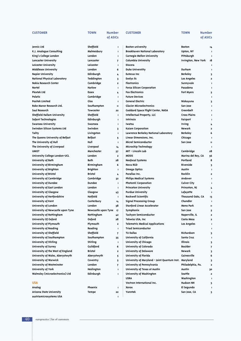
europractice | list of customers
Jennic Ltd Sheffield 1
K.J. Analogue Consulting Malmesbury 1
King’s College London London 1
Lancaster University Lancaster 7
Leicester University Leicester 1
Middlesex University London 6
Napier University Edinburgh 4
National Physical Laboratory Teddington 3
Nokia Research Center Cambridge 2
Nortel Harlow 1
Plextek Ltd Essex 4
Polatis Cambridge 1
Positek Limited Glos 1
Roke Manor Research Ltd. Southampton 11
Saul Research Towcester 22
Sheffield Hallam University Sheffield 1
Sofant Technologies Edinburgh 1
Swansea University Swansea 1
Swindon Silicon Systems Ltd Swindon 3
Tality Livingston 1
The Queens University of Belfast Belfast 5
The University of Hull Hull 1
The University of Liverpool Liverpool 14
UMIST Manchester 57
University College London-UCL London 2
University of Bath Bath 28
University of Birmingham Birmingham 6
University of Brighton Brighton 1
University of Bristol Bristol 4
University of Cambridge Cambridge 32
University of Dundee Dundee 1
University of East London London 1
University of Glasgow Glasgow 43
University of Hertfordshire Hatfield 1
University of Kent Canterbury 14
University of London London 38
University of Newcastle upon Tyne Newcastle upon Tyne 17
University of Nottingham Nottingham 42
University Of Oxford Oxford 28
University of Plymouth Plymouth 2
University of Reading Reading 1
University of Sheffield Sheffield 7
University of Southampton Southampton 35
University of Stirling Stirling 1
University of Surrey Guildford 6
University of the West of England Bristol 2
University of Wales, Aberystwyth Aberystwyth 5
University of Warwick Coventry 5
University of Westminster London 7
University of York Heslington 1
Walmsley (microelectronics) Ltd Edinburgh 1
USA Analog Phoenix 1
Arizona State University Tempe 22
austriamicrosystems USA 1
Boston university Boston 14
Brookhaven National Laboratory Upton, NY 1
Carnegie Mellon University Pittsburgh 1
Columbia University Irvington, New York 18
Discera 1
Duke Universtity Durham 1
Eutecus Inc Berkeley 3
Exelys Ilc Los Angeles 2
Flextronics Sunnyvale 1
Forza Silicon Corporation Pasadena 1
Fox Electronics Fort Myers 5
Future Devices 1
General Electric Niskayuna 3
Glacier Microelectronics San Jose 1
Goddard Space Flight Center, NASA Greenbelt 1
Intellectual Property, LLC Cross Plains 1
Intrinsix Fairport 1
Iwatsu Irving 4
Kaiam Corporation Newark 2
Lawrence Berkeley National Laboratory Berkeley 6
Linear Dimensions, Inc. Chicago 1
Micrel Semiconductor San Jose 11
Microchip Technology 1
MIT - Lincoln Lab Cambridge 28
MOSIS Marina del Rey, CA 56
Neofocal Systems Portland 8
Nova R&D Riverside 3
Omega Optics Austin 1
Parallax Inc. Rocklin 2
Philips Medical Systems Andover 1
PhotonIC Corporation Culver City 1
Princeton University Princeton, NJ 4
Purdue University Lafayette 1
Rockwell Scientific Thousand Oaks, CA 13
Signal Processing Group Chandler 1
Stanford Linear Accelerator Meno Park 11
Symphonix San Jose 5
Tachyon Semiconductor Naperville, IL 2
Tekwiss USA, Inc Costa Mesa 2
Telemetric Medical Applications Los Angeles 1
Triad Semiconductor 1
TU Dallas Richardson 3
University of California Santa Cruz 1
University of Chicago Illinois 3
University of Colorado Boulder 7
University of Delaware Newark 3
University of Florida Gainesville 6
University of Maryland - Joint Quantum Inst. Maryland 3
University of Pennsylvania Philadelphia, Pa. 2
University of Texas at Austin Austin 30
University of Washington Seattle 2
USRA Washington 1
Vectron International Inc. Hudson NH 5
Xerox El Segundo 1
Yanntek San Jose, CA 5
CUSTOMER TOWN Number of ASICs
CUSTOMER TOWN Number of ASICs
40

All information for MPW runs schedule, prices, etc. is available on-line on our WEB site
www.europractice-ic.com
For more information, please contact one of the EUROPRACTICE service centers.
imec
General EUROPRACTICE IC office &
IC Manufacturing Center
C. Das
Kapeldreef 75
B-3001 Leuven, Belgium
Tel : + 32 16 281 248
Fax : + 32 16 281 584
http://www.europractice-ic.com/
Fraunhofer IIS
IC Manufacturing Center
T. Drischel, J. Sauerer
Am Wolfsmantel 33
D-91058 Erlangen, Germany
Tel : + 49 9131 776 4463
Fax : + 49 9131 776 4499
http://www.iis.fraunhofer.de/asic/svasic
desig
n &
layo
ut:
This project has received funding from the European Union’s Seventh
Programme for research, technological development and demonstration under
grant agreement No 315961.