TPS2041B-EP - TI.com
25
1 2 3 5 4 IN EN OC GND GND OUT DBV PACKAGE (TOP VIEW) TPS2041B-EP www.ti.com SLVSAX8 – SEPTEMBER 2011 CURRENT-LIMITED POWER-DISTRIBUTION SWITCH Check for Samples: TPS2041B-EP 1FEATURES APPLICATIONS • 70-mΩ High-Side MOSFET • Heavy Capacitive Loads • 500-mA Continuous Current • Short-Circuit Protection • Thermal and Short-Circuit Protection SUPPORTS DEFENSE, AEROSPACE, • Current Limit: AND MEDICAL APPLICATIONS 0.45 A (Min), 1.55 A (Max) • Controlled Baseline • Operating Range: 2.7 V to 5.5 V • One Assembly/Test Site • 0.6-ms Typical Rise Time • One Fabrication Site • Undervoltage Lockout • Available in Military (–55°C/125°C) • Deglitched Fault Report (OC) Temperature Range • No OC Glitch During Power Up • Extended Product Life Cycle • Maximum Standby Supply Current: 1 μA • Extended Product-Change Notification • Bidirectional Switch • Product Traceability • ESD Protection Level Per AEC-Q100 Classification • UL Recognized, File Number E169910 DESCRIPTION The TPS2041B power-distribution switch is intended for applications where heavy capacitive loads and short circuits are likely to be encountered. This device incorporates 70-mΩ N-channel MOSFET power switches for power-distribution systems that require multiple power switches in a single package. Each switch is controlled by a logic enable input. Gate drive is provided by an internal charge pump designed to control the power-switch rise times and fall times to minimize current surges during switching. The charge pump requires no external components and allows operation from supplies as low as 2.7 V. When the output load exceeds the current-limit threshold or a short is present, the device limits the output current to a safe level by switching into a constant-current mode, pulling the overcurrent (OC) logic output low. When continuous heavy overloads and short circuits increase the power dissipation in the switch, causing the junction temperature to rise, a thermal protection circuit shuts off the switch to prevent damage. Recovery from a thermal shutdown is automatic once the device has cooled sufficiently. Internal circuitry ensures that the switch remains off until valid input voltage is present. This power-distribution switch is designed to set current limit at 1 A (typ). 1 Please be aware that an important notice concerning availability, standard warranty, and use in critical applications of Texas Instruments semiconductor products and disclaimers thereto appears at the end of this data sheet. PRODUCTION DATA information is current as of publication date. Copyright © 2011, Texas Instruments Incorporated Products conform to specifications per the terms of the Texas Instruments standard warranty. Production processing does not necessarily include testing of all parameters.
-
Upload
khangminh22 -
Category
Documents
-
view
0 -
download
0
Transcript of TPS2041B-EP - TI.com

1
2
3
5
4
IN
ENOC
GNDGND
OUT
DBV PACKAGE
(TOP VIEW)
TPS2041B-EP
www.ti.com SLVSAX8 –SEPTEMBER 2011
CURRENT-LIMITED POWER-DISTRIBUTION SWITCHCheck for Samples: TPS2041B-EP
1FEATURES APPLICATIONS• 70-mΩ High-Side MOSFET • Heavy Capacitive Loads• 500-mA Continuous Current • Short-Circuit Protection• Thermal and Short-Circuit Protection
SUPPORTS DEFENSE, AEROSPACE,• Current Limit:AND MEDICAL APPLICATIONS0.45 A (Min), 1.55 A (Max)• Controlled Baseline• Operating Range: 2.7 V to 5.5 V• One Assembly/Test Site• 0.6-ms Typical Rise Time• One Fabrication Site• Undervoltage Lockout• Available in Military (–55°C/125°C)• Deglitched Fault Report (OC)
Temperature Range• No OC Glitch During Power Up• Extended Product Life Cycle• Maximum Standby Supply Current: 1 μA• Extended Product-Change Notification• Bidirectional Switch• Product Traceability• ESD Protection Level Per AEC-Q100
Classification• UL Recognized, File Number E169910
DESCRIPTIONThe TPS2041B power-distribution switch is intended for applications where heavy capacitive loads and shortcircuits are likely to be encountered. This device incorporates 70-mΩ N-channel MOSFET power switches forpower-distribution systems that require multiple power switches in a single package. Each switch is controlled bya logic enable input. Gate drive is provided by an internal charge pump designed to control the power-switch risetimes and fall times to minimize current surges during switching. The charge pump requires no externalcomponents and allows operation from supplies as low as 2.7 V.
When the output load exceeds the current-limit threshold or a short is present, the device limits the output currentto a safe level by switching into a constant-current mode, pulling the overcurrent (OC) logic output low. Whencontinuous heavy overloads and short circuits increase the power dissipation in the switch, causing the junctiontemperature to rise, a thermal protection circuit shuts off the switch to prevent damage. Recovery from a thermalshutdown is automatic once the device has cooled sufficiently. Internal circuitry ensures that the switch remainsoff until valid input voltage is present. This power-distribution switch is designed to set current limit at 1 A (typ).
1
Please be aware that an important notice concerning availability, standard warranty, and use in critical applications of TexasInstruments semiconductor products and disclaimers thereto appears at the end of this data sheet.
PRODUCTION DATA information is current as of publication date. Copyright © 2011, Texas Instruments IncorporatedProducts conform to specifications per the terms of the TexasInstruments standard warranty. Production processing does notnecessarily include testing of all parameters.
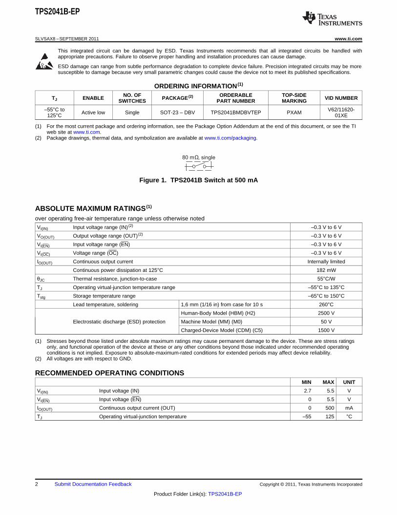
80 mΩ, single
TPS2041B-EP
SLVSAX8 –SEPTEMBER 2011 www.ti.com
This integrated circuit can be damaged by ESD. Texas Instruments recommends that all integrated circuits be handled withappropriate precautions. Failure to observe proper handling and installation procedures can cause damage.
ESD damage can range from subtle performance degradation to complete device failure. Precision integrated circuits may be moresusceptible to damage because very small parametric changes could cause the device not to meet its published specifications.
ORDERING INFORMATION (1)
NO. OF ORDERABLE TOP-SIDETJ ENABLE PACKAGE (2) VID NUMBERSWITCHES PART NUMBER MARKING
–55°C to V62/11620-Active low Single SOT-23 – DBV TPS2041BMDBVTEP PXAM125°C 01XE
(1) For the most current package and ordering information, see the Package Option Addendum at the end of this document, or see the TIweb site at www.ti.com.
(2) Package drawings, thermal data, and symbolization are available at www.ti.com/packaging.
Figure 1. TPS2041B Switch at 500 mA
ABSOLUTE MAXIMUM RATINGS (1)
over operating free-air temperature range unless otherwise noted
VI(IN) Input voltage range (IN) (2) –0.3 V to 6 V
VO(OUT) Output voltage range (OUT) (2) –0.3 V to 6 V
VI(EN) Input voltage range (EN) –0.3 V to 6 V
VI(OC) Voltage range (OC) –0.3 V to 6 V
IO(OUT) Continuous output current Internally limited
Continuous power dissipation at 125°C 182 mW
θJC Thermal resistance, junction-to-case 55°C/W
TJ Operating virtual-junction temperature range –55°C to 135°CTstg Storage temperature range –65°C to 150°C
Lead temperature, soldering 1,6 mm (1/16 in) from case for 10 s 260°CHuman-Body Model (HBM) (H2) 2500 V
Electrostatic discharge (ESD) protection Machine Model (MM) (M0) 50 V
Charged-Device Model (CDM) (C5) 1500 V
(1) Stresses beyond those listed under absolute maximum ratings may cause permanent damage to the device. These are stress ratingsonly, and functional operation of the device at these or any other conditions beyond those indicated under recommended operatingconditions is not implied. Exposure to absolute-maximum-rated conditions for extended periods may affect device reliability.
(2) All voltages are with respect to GND.
RECOMMENDED OPERATING CONDITIONSMIN MAX UNIT
VI(IN) Input voltage (IN) 2.7 5.5 V
VI(EN) Input voltage (EN) 0 5.5 V
IO(OUT) Continuous output current (OUT) 0 500 mA
TJ Operating virtual-junction temperature –55 125 °C
2 Submit Documentation Feedback Copyright © 2011, Texas Instruments Incorporated
Product Folder Link(s): TPS2041B-EP
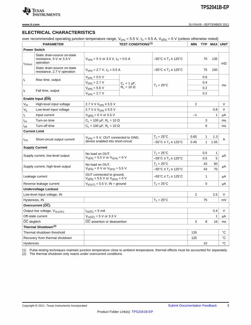
TPS2041B-EP
www.ti.com SLVSAX8 –SEPTEMBER 2011
ELECTRICAL CHARACTERISTICSover recommended operating junction temperature range, VI(IN) = 5.5 V, IO = 0.5 A, VI(EN) = 0 V (unless otherwise noted)
PARAMETER TEST CONDITIONS (1) MIN TYP MAX UNIT
Power Switch
Static drain-source on-stateresistance, 5-V or 3.3-V VI(IN) = 5 V or 3.3 V, IO = 0.5 A –55°C ≤ TJ ≤ 125°C 70 135operationrDS(on) mΩStatic drain-source on-state VI(IN) = 2.7 V, IO = 0.5 A –55°C ≤ TJ ≤ 125°C 75 150resistance, 2.7-V operation
VI(IN) = 5.5 V 0.6tr Rise time, output
VI(IN) = 2.7 V 0.4CL = 1 μF, TJ = 25°C msRL = 10 ΩVI(IN) = 5.5 V 0.2tf Fall time, output
VI(IN) = 2.7 V 0.2
Enable Input (EN)
VIH High-level input voltage 2.7 V ≤ VI(IN) ≤ 5.5 V 2 V
VIL Low-level input voltage 2.7 V ≤ VI(IN) ≤ 5.5 V 0.8 V
II Input current VI(EN) = 0 V or 5.5 V –1 1 μA
ton Turn-on time CL = 100 μF, RL = 10 Ω 3 ms
toff Turn-off time CL = 100 μF, RL = 10 Ω 6 ms
Current Limit
TJ = 25°C 0.65 1 1.3VI(IN) = 5 V, OUT connected to GND,IOS Short-circuit output current Adevice enabled into short-circuit –55°C ≤ TJ ≤ 125°C 0.45 1 1.55
Supply Current
TJ = 25°C 0.5 1No load on OUT,Supply current, low-level output μAVI(EN) = 5.5 V or VI(EN) = 0 V –55°C ≤ TJ ≤ 125°C 0.5 5
TJ = 25°C 43 60No load on OUT,Supply current, high-level output μAVI(EN) = 0 V or VI(EN) = 5.5 V –55°C ≤ TJ ≤ 125°C 43 70
OUT connected to ground,Leakage current –55°C ≤ TJ ≤ 125°C 1 μAVI(EN) = 5.5 V or VI(EN) = 0 V
Reverse leakage current VI(OUT) = 5.5 V, IN = ground TJ = 25°C 0 μA
Undervoltage Lockout
Low-level input voltage, IN 2 2.5 V
Hysteresis, IN TJ = 25°C 75 mV
Overcurrent (OC)
Output low voltage, VOL(/OC) IO(OC) = 5 mA 0.4 V
Off-state current VO(OC) = 5 V or 3.3 V 1 μA
OC deglitch OC assertion or deassertion 3 8 16 ms
Thermal Shutdown (2)
Thermal shutdown threshold 135 °CRecovery from thermal shutdown 125 °CHysteresis 10 °C
(1) Pulse-testing techniques maintain junction temperature close to ambient temperature; thermal effects must be accounted for separately.(2) The thermal shutdown only reacts under overcurrent conditions.
Copyright © 2011, Texas Instruments Incorporated Submit Documentation Feedback 3
Product Folder Link(s): TPS2041B-EP

OUT
OC
IN
EN
GND
Current
LimitDriver
UVLO
Charge
Pump
CS
Thermal
Sense
Deglitch
(See Note A)
TPS2041B-EP
SLVSAX8 –SEPTEMBER 2011 www.ti.com
DEVICE INFORMATION
Terminal FunctionsTERMINAL
I/O DESCRIPTIONNAME NO.
EN 4 I Enable input, logic low turns on power switch
GND 2 Ground
IN 5 I Input voltage
OC 3 O Overcurrent, open-drain output, active low
OUT 1 O Power-switch output
Functional Block Diagram
A. CS = Current sense
4 Submit Documentation Feedback Copyright © 2011, Texas Instruments Incorporated
Product Folder Link(s): TPS2041B-EP

RL CL
OUT
tr tf
90% 90%
10%10%
50% 50%
90%
10%
VO(OUT)
VI(EN)
VO(OUT)
VOLTAGE WAVEFORMS
TEST CIRCUIT
ton toff
50% 50%
90%
10%
VI(EN)
VO(OUT)
ton toff
VI(EN)VI(EN)5 V/div
VO(OUT)2 V/div
RL = 10 ,CL = 1 FTA = 25C
t − Time − 500 s/div
VI(EN)VI(EN)5 V/div
VO(OUT)2 V/div
RL = 10 ,CL = 1 FTA = 25C
t − Time − 500 s/div
TPS2041B-EP
www.ti.com SLVSAX8 –SEPTEMBER 2011
PARAMETER MEASUREMENT INFORMATION
Figure 2. Test Circuit and Voltage Waveforms
Figure 3. Turn-On Delay and Rise Time With 1-μF Figure 4. Turn-Off Delay and Fall Time With 1-μFLoad Load
Copyright © 2011, Texas Instruments Incorporated Submit Documentation Feedback 5
Product Folder Link(s): TPS2041B-EP

VI(EN)VI(EN)5 V/div
VO(OUT)2 V/div
RL = 10 ,CL = 100 FTA = 25C
t − Time − 500 s/div
VO(OUT)2 V/div
VI(EN)VI(EN)5 V/div
RL = 10 ,CL = 100 FTA = 25C
t − Time − 500 s/div
220 F470 F
100 F
VI = 5 V,RL = 10 ,TA = 25C
VI(EN)VI(EN)5 V/div
IO(OUT)500 mA/div
t − Time − 500 s/div
VI(EN)VI(EN)5 V/div
IO(OUT)500 mA/div
t − Time − 500 s/div
TPS2041B-EP
SLVSAX8 –SEPTEMBER 2011 www.ti.com
PARAMETER MEASUREMENT INFORMATION (continued)
Figure 5. Turn-On Delay and Rise Time With Figure 6. Turn-Off Delay and Fall Time With 100-μF100-μF Load Load
Figure 7. Short-Circuit Current, Figure 8. Inrush Current With DifferentDevice Enabled Into Short Load Capacitance
6 Submit Documentation Feedback Copyright © 2011, Texas Instruments Incorporated
Product Folder Link(s): TPS2041B-EP

VO(OC)2 V/div
IO(OUT)500 mA/div
t − Time − 2 ms/div
VO(OC)2 V/div
IO(OUT)500 mA/div
t − Time − 2 ms/div
TPS2041B-EP
www.ti.com SLVSAX8 –SEPTEMBER 2011
PARAMETER MEASUREMENT INFORMATION (continued)
Figure 9. 3-Ω Load Connected to Enabled Device Figure 10. 2-Ω Load Connected to Enabled Device
Copyright © 2011, Texas Instruments Incorporated Submit Documentation Feedback 7
Product Folder Link(s): TPS2041B-EP

0
0.1
0.2
0.3
0.4
0.5
0.6
0.7
0.8
0.9
1.0
2 3 4 5 6
Turn
on T
ime
− m
s
VI − Input V oltage − V
CL = 100 F,RL = 10 ,TA = 25C
2.8
2.9
3
3.1
3.2
3.3
2 3 4 5 6Tu
rnof
f Tim
e −
ms
VI − Input V oltage − V
CL = 100 F,RL = 10 ,TA = 25C
0
0.1
0.2
0.3
0.4
0.5
0.6
2 3 4 5 6
Ris
e T
ime
− m
s
VI − Input V oltage − V
CL = 1 F,RL = 10 ,TA = 25C
0
0.05
0.1
0.15
0.2
0.25
2 3 4 5 6
CL = 1 F,RL = 10 ,TA = 25C
Fal
l Tim
e −
ms
VI − Input V oltage − V
TPS2041B-EP
SLVSAX8 –SEPTEMBER 2011 www.ti.com
TYPICAL CHARACTERISTICSTURN-ON TIME TURN-OFF TIME
vs vsINPUT VOLTAGE INPUT VOLTAGE
Figure 11. Figure 12.
RISE TIME FALL TIMEvs vs
INPUT VOLTAGE INPUT VOLTAGE
Figure 13. Figure 14.
8 Submit Documentation Feedback Copyright © 2011, Texas Instruments Incorporated
Product Folder Link(s): TPS2041B-EP

0
10
20
30
40
50
60
70
0 50 100 150
−S
up
ply
Cu
rre
nt,
Ou
tpu
t E
na
ble
d−
II
(IN
)A
µ
-55
V = 3.3 VI
V = 5.5 VI
V = 5 VI
V = 2.7 VI
-25 25 75 125
T - Junction Temperature - °CJ−
Su
pp
ly C
urr
en
t, O
utp
ut
Dis
ab
led
−I I (
IN)
Aµ
0
0.05
0.1
0.15
0.2
0.25
0.3
0.35
0.4
0.45
0.5
-55 0 50 100 150
VI = 5.5 V
VI = 5 V
VI = 3.3 VVI = 2.7 V
-25 25 75 125
T - Junction Temperature - °CJ
0.9
0.92
0.94
0.96
0.98
1.0
1.02
1.04
1.06
1.08
−S
ho
rt-C
ircu
it O
utp
ut
Cu
rre
nt
−A
I OS
-55 0 50 100 150-25 25 75 125
T - Junction Temperature - °CJ
VI = 5 V
VI = 3.3 V
VI = 5.5 V
VI = 2.7 V
0
20
40
60
80
100
120
rD
S(o
n)−
Sta
tic D
rain
-Sourc
e O
n-S
tate
Resis
tance
−m
Ω
-55 0 50 100 150-25 25 75 125
T - Junction Temperature - °CJ
IO = 0.5 A
VI = 2.7 V
VI = 5 V
VI = 3.3 V
TPS2041B-EP
www.ti.com SLVSAX8 –SEPTEMBER 2011
TYPICAL CHARACTERISTICS (continued)SUPPLY CURRENT, OUTPUT ENABLED SUPPLY CURRENT, OUTPUT DISABLED
vs vsJUNCTION TEMPERATURE JUNCTION TEMPERATURE
Figure 15. Figure 16.
STATIC DRAIN-SOURCE ON-STATE RESISTANCE SHORT-CIRCUIT OUTPUT CURRENTvs vs
JUNCTION TEMPERATURE JUNCTION TEMPERATURE
Figure 17. Figure 18.
Copyright © 2011, Texas Instruments Incorporated Submit Documentation Feedback 9
Product Folder Link(s): TPS2041B-EP
2.1
2.14
2.18
2.22
2.26
2.3
UV
LO
−U
nd
erv
olta
ge
Lo
cko
ut
−V
-55 0 50 100 150-25 25 75 125
T - Junction Temperature - °CJ
UVLO Rising
UVLO Falling
Thr
esho
ld T
rip C
urre
nt −
A
VI − Input V oltage − V
1
1.2
1.4
1.6
1.8
2
2.5 3 3.5 4 4.5 5 5.5 6
TA = 25CLoad Ramp = 1 A/10 ms
0
20
40
60
80
100
0 2.5 5 7.5 10 12.5Peak Current − A
VI = 5 V,TA = 25C
Cur
rent
-Lim
it R
espo
nse
− s
µ
TPS2041B-EP
SLVSAX8 –SEPTEMBER 2011 www.ti.com
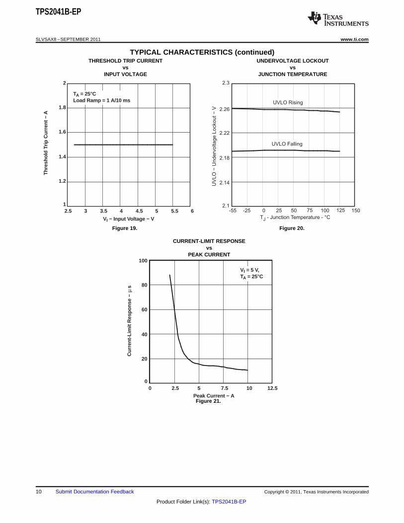
TYPICAL CHARACTERISTICS (continued)THRESHOLD TRIP CURRENT UNDERVOLTAGE LOCKOUT
vs vsINPUT VOLTAGE JUNCTION TEMPERATURE
Figure 19. Figure 20.
CURRENT-LIMIT RESPONSEvs
PEAK CURRENT
Figure 21.
10 Submit Documentation Feedback Copyright © 2011, Texas Instruments Incorporated
Product Folder Link(s): TPS2041B-EP
IN
OC
EN
5
3
1
0.1 µF 22 µF
LoadOUT
Power Supply
2.7 V to 5.5 V
4
GND
0.1 µF
TPS2041B
2
TPS2041B-EP
www.ti.com SLVSAX8 –SEPTEMBER 2011
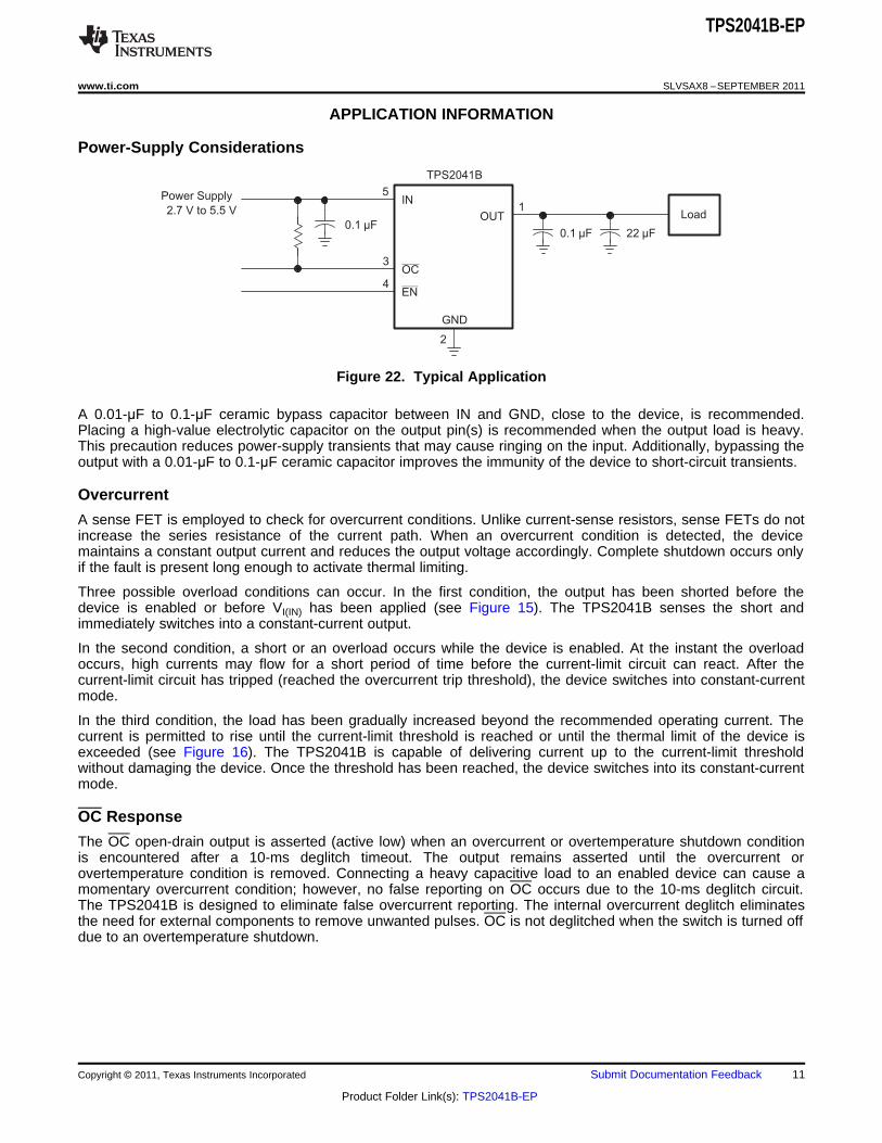
APPLICATION INFORMATION
Power-Supply Considerations
Figure 22. Typical Application
A 0.01-μF to 0.1-μF ceramic bypass capacitor between IN and GND, close to the device, is recommended.Placing a high-value electrolytic capacitor on the output pin(s) is recommended when the output load is heavy.This precaution reduces power-supply transients that may cause ringing on the input. Additionally, bypassing theoutput with a 0.01-μF to 0.1-μF ceramic capacitor improves the immunity of the device to short-circuit transients.
Overcurrent
A sense FET is employed to check for overcurrent conditions. Unlike current-sense resistors, sense FETs do notincrease the series resistance of the current path. When an overcurrent condition is detected, the devicemaintains a constant output current and reduces the output voltage accordingly. Complete shutdown occurs onlyif the fault is present long enough to activate thermal limiting.
Three possible overload conditions can occur. In the first condition, the output has been shorted before thedevice is enabled or before VI(IN) has been applied (see Figure 15). The TPS2041B senses the short andimmediately switches into a constant-current output.
In the second condition, a short or an overload occurs while the device is enabled. At the instant the overloadoccurs, high currents may flow for a short period of time before the current-limit circuit can react. After thecurrent-limit circuit has tripped (reached the overcurrent trip threshold), the device switches into constant-currentmode.
In the third condition, the load has been gradually increased beyond the recommended operating current. Thecurrent is permitted to rise until the current-limit threshold is reached or until the thermal limit of the device isexceeded (see Figure 16). The TPS2041B is capable of delivering current up to the current-limit thresholdwithout damaging the device. Once the threshold has been reached, the device switches into its constant-currentmode.
OC Response
The OC open-drain output is asserted (active low) when an overcurrent or overtemperature shutdown conditionis encountered after a 10-ms deglitch timeout. The output remains asserted until the overcurrent orovertemperature condition is removed. Connecting a heavy capacitive load to an enabled device can cause amomentary overcurrent condition; however, no false reporting on OC occurs due to the 10-ms deglitch circuit.The TPS2041B is designed to eliminate false overcurrent reporting. The internal overcurrent deglitch eliminatesthe need for external components to remove unwanted pulses. OC is not deglitched when the switch is turned offdue to an overtemperature shutdown.
Copyright © 2011, Texas Instruments Incorporated Submit Documentation Feedback 11
Product Folder Link(s): TPS2041B-EP

GND
IN
EN
OC
OUT
TPS2041BRpullup
V+
TPS2041B-EP
SLVSAX8 –SEPTEMBER 2011 www.ti.com
Figure 23. Typical Circuit for the OC Pin
Power Dissipation and Junction Temperature
The low on-resistance on the N-channel MOSFET allows the small surface-mount packages to pass largecurrents. The thermal resistances of these packages are high compared to those of power packages; it is gooddesign practice to check power dissipation and junction temperature. Begin by determining the rDS(on) of theN-channel MOSFET relative to the input voltage and operating temperature. As an initial estimate, use thehighest operating ambient temperature of interest and read rDS(on) from Figure 17. Using this value, the powerdissipation per switch can be calculated by:
PD = rDS(on) × I2
Multiply this number by the number of switches being used. This step renders the total power dissipation fromthe N-channel MOSFETs.
Finally, calculate the junction temperature:TJ = PD × RθJA + TA
Where:TA = Ambient temperature (°C)RθJA = Thermal resistancePD = Total power dissipation based on number of switches being used.
Compare the calculated junction temperature with the initial estimate. If they do not agree within a few degrees,repeat the calculation, using the calculated value as the new estimate. Two or three iterations are generallysufficient to get a reasonable answer.
Thermal Protection
Thermal protection prevents damage to the IC when heavy-overload or short-circuit faults are present forextended periods of time. The TPS2041B implements a thermal sensing to monitor the operating junctiontemperature of the power distribution switch. In an overcurrent or short-circuit condition, the junction temperaturerises due to excessive power dissipation. Once the die temperature rises to approximately 140°C due toovercurrent conditions, the internal thermal sense circuitry turns the power switch off, thus preventing the powerswitch from damage. Hysteresis is built into the thermal sense circuit, and after the device has cooledapproximately 10°C, the switch turns back on. The switch continues to cycle in this manner until the load fault orinput power is removed. The OC open-drain output is asserted (active low) when an overtemperature shutdownor overcurrent occurs.
Undervoltage Lockout (UVLO)
The UVLO ensures that the power switch is in the off state at power up. Whenever the input voltage falls belowapproximately 2 V, the power switch is quickly turned off. This facilitates the design of hot-insertion systemswhere it is not possible to turn off the power switch before input power is removed. The UVLO also keeps theswitch from being turned on until the power supply has reached at least 2 V, even if the switch is enabled. Onreinsertion, the power switch is turned on, with a controlled rise time to reduce EMI and voltage overshoots.
12 Submit Documentation Feedback Copyright © 2011, Texas Instruments Incorporated
Product Folder Link(s): TPS2041B-EP

IN
OC
EN
GND
0.1 µF
5
3
4
1
0.1 µF 120 µF GND
OUT
TPS2041B
Power Supply
D+
D-
VBUS
Downstream
USB Ports
USB
Control
3.3 V 5 V
2
TPS2041B-EP
www.ti.com SLVSAX8 –SEPTEMBER 2011
Universal Serial Bus (USB) Applications
The universal serial bus (USB) interface is a 12-Mb/s, or 1.5-Mb/s, multiplexed serial bus designed forlow-to-medium bandwidth PC peripherals (e.g., keyboards, printers, scanners, and mice). The four-wire USBinterface is conceived for dynamic attach-detach (hot plug-unplug) of peripherals. Two lines are provided fordifferential data, and two lines are provided for 5-V power distribution.
USB data is a 3.3-V level signal, but power is distributed at 5 V to allow for voltage drops in cases where poweris distributed through more than one hub across long cables. Each function must provide its own regulated 3.3 Vfrom the 5-V input or its own internal power supply.
The USB specification defines the following five classes of devices, each differentiated by power-consumptionrequirements:• Hosts/self-powered hubs (SPHs)• Bus-powered hubs (BPHs)• Low-power bus-powered functions• High-power bus-powered functions• Self-powered functions
Self-powered and bus-powered hubs distribute data and power to downstream functions. The TPS2041B canprovide power-distribution solutions to many of these classes of devices.
Hosts/Self-Powered Hubs and Bus-Powered Hubs
Hosts and self-powered hubs have a local power supply that powers the embedded functions and thedownstream ports (see Figure 24). This power supply must provide from 5.25 V to 4.75 V to the board side of thedownstream connection under full-load and no-load conditions. Hosts and SPHs are required to havecurrent-limit protection and must report overcurrent conditions to the USB controller. Typical SPHs are desktopPCs, monitors, printers, and stand-alone hubs.
Figure 24. Typical One-Port USB Host/Self-Powered Hub
Bus-powered hubs obtain all power from upstream ports and often contain an embedded function. The hubs arerequired to power up with less than one unit load. The BPH usually has one embedded function, and power isalways available to the controller of the hub. If the embedded function and hub require more than 100 mA onpower up, the power to the embedded function may need to be kept off until enumeration is completed. This canbe accomplished by removing power or by shutting off the clock to the embedded function. Power switching theembedded function is not necessary if the aggregate power draw for the function and controller is less than oneunit load. The total current drawn by the bus-powered device is the sum of the current to the controller, theembedded function, and the downstream ports, and it is limited to 500 mA from an upstream port.
Copyright © 2011, Texas Instruments Incorporated Submit Documentation Feedback 13
Product Folder Link(s): TPS2041B-EP
IN
OC
5
3
4
1
0.1 µF 10 µF
Internal
Function
OUT
Power Supply
3.3 V
EN
0.1 µF10 µF
USB
Control
GND
VBUS
D−
D+
GND
2
TPS2041B
TPS2041B-EP
SLVSAX8 –SEPTEMBER 2011 www.ti.com
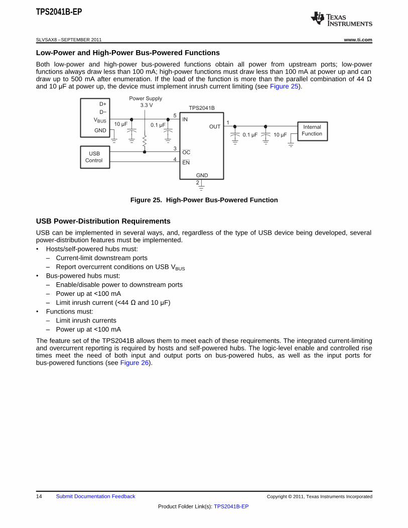
Low-Power and High-Power Bus-Powered Functions
Both low-power and high-power bus-powered functions obtain all power from upstream ports; low-powerfunctions always draw less than 100 mA; high-power functions must draw less than 100 mA at power up and candraw up to 500 mA after enumeration. If the load of the function is more than the parallel combination of 44 Ωand 10 μF at power up, the device must implement inrush current limiting (see Figure 25).
Figure 25. High-Power Bus-Powered Function
USB Power-Distribution Requirements
USB can be implemented in several ways, and, regardless of the type of USB device being developed, severalpower-distribution features must be implemented.• Hosts/self-powered hubs must:
– Current-limit downstream ports– Report overcurrent conditions on USB VBUS
• Bus-powered hubs must:– Enable/disable power to downstream ports– Power up at <100 mA– Limit inrush current (<44 Ω and 10 μF)
• Functions must:– Limit inrush currents– Power up at <100 mA
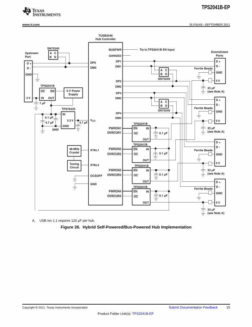
The feature set of the TPS2041B allows them to meet each of these requirements. The integrated current-limitingand overcurrent reporting is required by hosts and self-powered hubs. The logic-level enable and controlled risetimes meet the need of both input and output ports on bus-powered hubs, as well as the input ports forbus-powered functions (see Figure 26).
14 Submit Documentation Feedback Copyright © 2011, Texas Instruments Incorporated
Product Folder Link(s): TPS2041B-EP
DP1
DM1
DP2
DM2
DP3
DM3
DP4
PWRON1
OVRCUR1
PWRON2
OVRCUR2
PWRON3
OVRCUR3
PWRON4
OVRCUR4
DM4
DP0
DM0
VCC
XTAL1
XTAL2
OCSOFF
SN75240
D +
D -
5 V
GND
D +
D -
5 V
D +
D -
5 V
D +
D -
5 V
48-MHz
Crystal
Downstream
Ports
TUSB2046
Hub Controller
Tuning
Circuit
A
B
C
D
33 µF
(see Note A)
SN75240
A
B
C
D
GND
GND
GND
D +
D -
Upstream
Port
TPS2041B
SN75240
A
B
5 V
GND
C
D
1 µF
IN
GND
Ferrite Beads
Ferrite Beads
Ferrite Beads
Ferrite Beads
BUSPWR
GANGED
Tie to TPS2041B EN Input
OC EN
OUT
5-V PowerSupply
IN
GND
3.3 V4.7 µF
0.1 µF
4.7 µF
GND
EN
OC
IN
TPS2041B
OUT
EN
OC
IN
TPS2041B
OUT
EN
OC
IN
TPS2041B
OUT
EN
OC
IN
TPS2041B
OUT
TPS76333
0.1 µF
33 µF
(see Note A)
33 µF
(see Note A)
33 µF
(see Note A)
0.1 µF
0.1 µF
0.1 µF
TPS2041B-EP
www.ti.com SLVSAX8 –SEPTEMBER 2011
A. USB rev 1.1 requires 120 μF per hub.
Figure 26. Hybrid Self-Powered/Bus-Powered Hub Implementation
Copyright © 2011, Texas Instruments Incorporated Submit Documentation Feedback 15
Product Folder Link(s): TPS2041B-EP

Power
Supply
0.1 µF1000 µF
Optimum
2.7 V to 5.5 V
PC BoardOvercurrent Response
TPS2041B
OCGND
EN
IN OUT
Block of
Circuitry
TPS2041B-EP
SLVSAX8 –SEPTEMBER 2011 www.ti.com
Generic Hot-Plug Applications
In many applications, it may be necessary to remove modules or PC boards while the main unit is still operating.These are considered hot-plug applications. Such implementations require the control of current surges seen bythe main power supply and the card being inserted. The most effective way to control these surges is to limit andslowly ramp the current and voltage being applied to the card, similar to the way in which a power supplynormally turns on. Due to the controlled rise times and fall times of the TPS2041B, these devices can be used toprovide a softer startup to devices being hot-plugged into a powered system. The UVLO feature of theTPS2041B also ensures that the switch is off after the card has been removed, and that the switch is off duringthe next insertion. The UVLO feature ensures a soft start with a controlled rise time for every insertion of the cardor module.
Figure 27. Typical Hot-Plug Implementation
By placing the TPS2041B between the VCC input and the rest of the circuitry, the input power reaches thesedevices first after insertion. The typical rise time of the switch is approximately 1 ms, providing a slow voltageramp at the output of the device. This implementation controls system surge currents and provides ahot-plugging mechanism for any device.
DETAILED DESCRIPTION
Power Switch
The power switch is an N-channel MOSFET with a low on-state resistance. Configured as a high-side switch, thepower switch prevents current flow from OUT to IN and IN to OUT when disabled. The power switch supplies aminimum current of 500 mA.
Charge Pump
An internal charge pump supplies power to the driver circuit and provides the necessary voltage to pull the gateof the MOSFET above the source. The charge pump operates from input voltages as low as 2.7 V and requireslittle supply current.
Driver
The driver controls the gate voltage of the power switch. To limit large current surges and reduce the associatedelectromagnetic interference (EMI) produced, the driver incorporates circuitry that controls the rise times and falltimes of the output voltage.
Enable (EN)
The logic enable pin disables the power switch and the bias for the charge pump, driver, and other circuitry toreduce the supply current. The supply current is reduced to less than 1 μA or 2 μA when a logic high is presenton EN. A logic zero input on EN restores bias to the drive and control circuits and turns the switch on. Theenable input is compatible with both TTL and CMOS logic levels.
16 Submit Documentation Feedback Copyright © 2011, Texas Instruments Incorporated
Product Folder Link(s): TPS2041B-EP

TPS2041B-EP
www.ti.com SLVSAX8 –SEPTEMBER 2011
Overcurrent (OC)
The OC open-drain output is asserted (active low) when an overcurrent or overtemperature condition isencountered. The output remains asserted until the overcurrent or overtemperature condition is removed. A10-ms deglitch circuit prevents the OC signal from oscillation or false triggering. If an overtemperature shutdownoccurs, the OC is asserted instantaneously.
Current Sense
A sense FET monitors the current supplied to the load. The sense FET measures current more efficiently thanconventional resistance methods. When an overload or short circuit is encountered, the current-sense circuitrysends a control signal to the driver. The driver in turn reduces the gate voltage and drives the power FET into itssaturation region, which switches the output into a constant-current mode and holds the current constant whilevarying the voltage on the load.
Thermal Sense
The TPS2041B implements a thermal sensing to monitor the operating temperature of the power distributionswitch. In an overcurrent or short-circuit condition, the junction temperature rises. When the die temperature risesto approximately 140°C due to overcurrent conditions, the internal thermal sense circuitry turns off the switch,thus preventing the device from damage. Hysteresis is built into the thermal sense, and after the device hascooled approximately 10 degrees, the switch turns back on. The switch continues to cycle off and on until thefault is removed. The open-drain false reporting output (OC) is asserted (active low) when an overtemperatureshutdown or overcurrent occurs.
Undervoltage Lockout (UVLO)
A voltage sense circuit monitors the input voltage. When the input voltage is below approximately 2 V, a controlsignal turns off the power switch.
Copyright © 2011, Texas Instruments Incorporated Submit Documentation Feedback 17
Product Folder Link(s): TPS2041B-EP
PACKAGE OPTION ADDENDUM
www.ti.com 10-Dec-2020
Addendum-Page 1
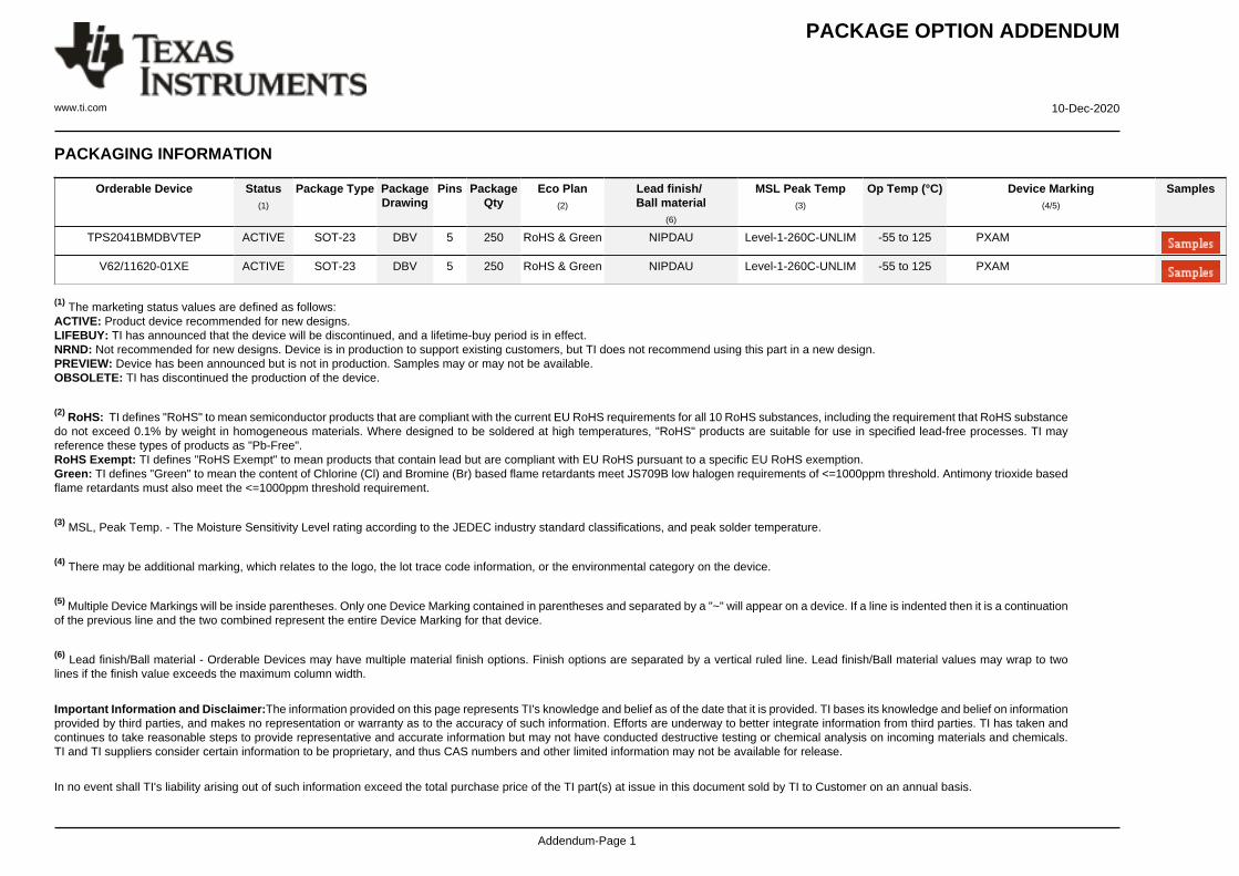
PACKAGING INFORMATION
Orderable Device Status(1)
Package Type PackageDrawing
Pins PackageQty
Eco Plan(2)
Lead finish/Ball material
(6)
MSL Peak Temp(3)
Op Temp (°C) Device Marking(4/5)
Samples
TPS2041BMDBVTEP ACTIVE SOT-23 DBV 5 250 RoHS & Green NIPDAU Level-1-260C-UNLIM -55 to 125 PXAM
V62/11620-01XE ACTIVE SOT-23 DBV 5 250 RoHS & Green NIPDAU Level-1-260C-UNLIM -55 to 125 PXAM
(1) The marketing status values are defined as follows:ACTIVE: Product device recommended for new designs.LIFEBUY: TI has announced that the device will be discontinued, and a lifetime-buy period is in effect.NRND: Not recommended for new designs. Device is in production to support existing customers, but TI does not recommend using this part in a new design.PREVIEW: Device has been announced but is not in production. Samples may or may not be available.OBSOLETE: TI has discontinued the production of the device.
(2) RoHS: TI defines "RoHS" to mean semiconductor products that are compliant with the current EU RoHS requirements for all 10 RoHS substances, including the requirement that RoHS substancedo not exceed 0.1% by weight in homogeneous materials. Where designed to be soldered at high temperatures, "RoHS" products are suitable for use in specified lead-free processes. TI mayreference these types of products as "Pb-Free".RoHS Exempt: TI defines "RoHS Exempt" to mean products that contain lead but are compliant with EU RoHS pursuant to a specific EU RoHS exemption.Green: TI defines "Green" to mean the content of Chlorine (Cl) and Bromine (Br) based flame retardants meet JS709B low halogen requirements of <=1000ppm threshold. Antimony trioxide basedflame retardants must also meet the <=1000ppm threshold requirement.
(3) MSL, Peak Temp. - The Moisture Sensitivity Level rating according to the JEDEC industry standard classifications, and peak solder temperature.
(4) There may be additional marking, which relates to the logo, the lot trace code information, or the environmental category on the device.
(5) Multiple Device Markings will be inside parentheses. Only one Device Marking contained in parentheses and separated by a "~" will appear on a device. If a line is indented then it is a continuationof the previous line and the two combined represent the entire Device Marking for that device.
(6) Lead finish/Ball material - Orderable Devices may have multiple material finish options. Finish options are separated by a vertical ruled line. Lead finish/Ball material values may wrap to twolines if the finish value exceeds the maximum column width.
Important Information and Disclaimer:The information provided on this page represents TI's knowledge and belief as of the date that it is provided. TI bases its knowledge and belief on informationprovided by third parties, and makes no representation or warranty as to the accuracy of such information. Efforts are underway to better integrate information from third parties. TI has taken andcontinues to take reasonable steps to provide representative and accurate information but may not have conducted destructive testing or chemical analysis on incoming materials and chemicals.TI and TI suppliers consider certain information to be proprietary, and thus CAS numbers and other limited information may not be available for release.
In no event shall TI's liability arising out of such information exceed the total purchase price of the TI part(s) at issue in this document sold by TI to Customer on an annual basis.

PACKAGE OPTION ADDENDUM
www.ti.com 10-Dec-2020
Addendum-Page 2
OTHER QUALIFIED VERSIONS OF TPS2041B-EP :
• Catalog: TPS2041B
• Automotive: TPS2041B-Q1
NOTE: Qualified Version Definitions:
• Catalog - TI's standard catalog product
• Automotive - Q100 devices qualified for high-reliability automotive applications targeting zero defects

TAPE AND REEL INFORMATION
*All dimensions are nominal
Device PackageType
PackageDrawing
Pins SPQ ReelDiameter
(mm)
ReelWidth
W1 (mm)
A0(mm)
B0(mm)
K0(mm)
P1(mm)
W(mm)
Pin1Quadrant
TPS2041BMDBVTEP SOT-23 DBV 5 250 178.0 9.0 3.3 3.2 1.4 4.0 8.0 Q3
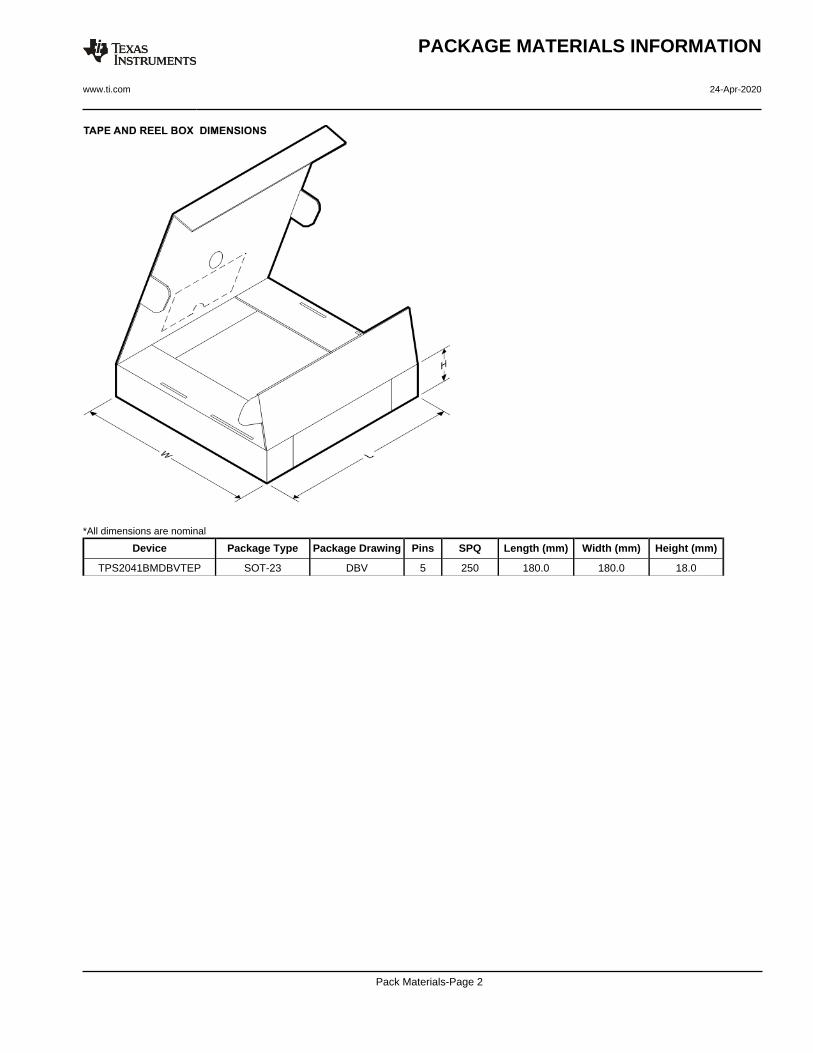
PACKAGE MATERIALS INFORMATION
www.ti.com 24-Apr-2020
Pack Materials-Page 1
*All dimensions are nominal
Device Package Type Package Drawing Pins SPQ Length (mm) Width (mm) Height (mm)
TPS2041BMDBVTEP SOT-23 DBV 5 250 180.0 180.0 18.0
PACKAGE MATERIALS INFORMATION
www.ti.com 24-Apr-2020
Pack Materials-Page 2

www.ti.com
PACKAGE OUTLINE
C
0.220.08 TYP
0.25
3.02.6
2X 0.95
1.9
1.450.90
0.150.00 TYP
5X 0.50.3
0.60.3 TYP
80 TYP
1.9
A
3.052.75
B1.751.45
(1.1)
SOT-23 - 1.45 mm max heightDBV0005ASMALL OUTLINE TRANSISTOR
4214839/F 06/2021
NOTES: 1. All linear dimensions are in millimeters. Any dimensions in parenthesis are for reference only. Dimensioning and tolerancing per ASME Y14.5M.2. This drawing is subject to change without notice.3. Refernce JEDEC MO-178.4. Body dimensions do not include mold flash, protrusions, or gate burrs. Mold flash, protrusions, or gate burrs shall not exceed 0.25 mm per side.
0.2 C A B
1
34
5
2
INDEX AREAPIN 1
GAGE PLANE
SEATING PLANE
0.1 C
SCALE 4.000

www.ti.com
EXAMPLE BOARD LAYOUT
0.07 MAXARROUND
0.07 MINARROUND
5X (1.1)
5X (0.6)
(2.6)
(1.9)
2X (0.95)
(R0.05) TYP
4214839/F 06/2021
SOT-23 - 1.45 mm max heightDBV0005ASMALL OUTLINE TRANSISTOR
NOTES: (continued) 5. Publication IPC-7351 may have alternate designs. 6. Solder mask tolerances between and around signal pads can vary based on board fabrication site.
SYMM
LAND PATTERN EXAMPLEEXPOSED METAL SHOWN
SCALE:15X
PKG
1
3 4
5
2
SOLDER MASKOPENINGMETAL UNDER
SOLDER MASK
SOLDER MASKDEFINED
EXPOSED METAL
METALSOLDER MASKOPENING
NON SOLDER MASKDEFINED
(PREFERRED)
SOLDER MASK DETAILS
EXPOSED METAL

www.ti.com
EXAMPLE STENCIL DESIGN
(2.6)
(1.9)
2X(0.95)
5X (1.1)
5X (0.6)
(R0.05) TYP
SOT-23 - 1.45 mm max heightDBV0005ASMALL OUTLINE TRANSISTOR
4214839/F 06/2021
NOTES: (continued) 7. Laser cutting apertures with trapezoidal walls and rounded corners may offer better paste release. IPC-7525 may have alternate design recommendations. 8. Board assembly site may have different recommendations for stencil design.
SOLDER PASTE EXAMPLEBASED ON 0.125 mm THICK STENCIL
SCALE:15X
SYMM
PKG
1
3 4
5
2

IMPORTANT NOTICE AND DISCLAIMERTI PROVIDES TECHNICAL AND RELIABILITY DATA (INCLUDING DATASHEETS), DESIGN RESOURCES (INCLUDING REFERENCEDESIGNS), APPLICATION OR OTHER DESIGN ADVICE, WEB TOOLS, SAFETY INFORMATION, AND OTHER RESOURCES “AS IS”AND WITH ALL FAULTS, AND DISCLAIMS ALL WARRANTIES, EXPRESS AND IMPLIED, INCLUDING WITHOUT LIMITATION ANYIMPLIED WARRANTIES OF MERCHANTABILITY, FITNESS FOR A PARTICULAR PURPOSE OR NON-INFRINGEMENT OF THIRDPARTY INTELLECTUAL PROPERTY RIGHTS.These resources are intended for skilled developers designing with TI products. You are solely responsible for (1) selecting the appropriateTI products for your application, (2) designing, validating and testing your application, and (3) ensuring your application meets applicablestandards, and any other safety, security, or other requirements. These resources are subject to change without notice. TI grants youpermission to use these resources only for development of an application that uses the TI products described in the resource. Otherreproduction and display of these resources is prohibited. No license is granted to any other TI intellectual property right or to any third partyintellectual property right. TI disclaims responsibility for, and you will fully indemnify TI and its representatives against, any claims, damages,costs, losses, and liabilities arising out of your use of these resources.TI’s products are provided subject to TI’s Terms of Sale (https:www.ti.com/legal/termsofsale.html) or other applicable terms available eitheron ti.com or provided in conjunction with such TI products. TI’s provision of these resources does not expand or otherwise alter TI’sapplicable warranties or warranty disclaimers for TI products.IMPORTANT NOTICE
Mailing Address: Texas Instruments, Post Office Box 655303, Dallas, Texas 75265Copyright © 2021, Texas Instruments Incorporated