ENERGY HARVESTING FROM HUMAN PASSIVE POWER
263
ENERGY HARVESTING FROM HUMAN PASSIVE POWER by M. a Loreto Mateu S´ aez Thesis Advisor: Dr. Francesc Moll A dissertation submitted in partial fulfillment of the requirements for the degree of Doctor in Electronic Engineering in Universitat Polit` ecnica de Catalunya 2009
-
Upload
khangminh22 -
Category
Documents
-
view
1 -
download
0
Transcript of ENERGY HARVESTING FROM HUMAN PASSIVE POWER

ENERGY HARVESTING
FROM HUMAN PASSIVE POWER
by
M.a Loreto Mateu Saez
Thesis Advisor: Dr. Francesc Moll
A dissertation submitted in partial fulfillmentof the requirements for the degree of
Doctor in Electronic Engineeringin Universitat Politecnica de Catalunya
2009


to my parents, Isabel and Josep, and to Duncan


ACKNOWLEDGEMENTS
I would like to thank first of all my thesis advisor, Dr. Francesc Moll, for all his support,motivation and exchange of ideas during these years. I would like to thank Ferran Martorell forlistening to my ideas and for contributing with his own ideas during all the thesis and also for hisunconditional support; and to the rest of the persons of the High Performance Integrated Circuitsand Systems Design Group. I would also like to thank all the people of the Fraunhofer InstitutIntegrierte Schaltungen in Nurenberg, Germany, and specially to: Nestor Lucas, Cosmin Codrea,Javier Gutierrez, Markus Pollak, Santiago Urquijo, Peter Spies and Gunter Rohmer for their supportand cooperation in the accomplishment of this thesis. I would also like to thank Carlos Villaviejafor helping me with the acceleration measurements here presented.
I express my thanks also to the Universitat Politecnica de Catalunya for giving me a UPCresearch grant for doing my PhD.


Contents
I General Discussion 11
1 Motivation and Objectives 131.1 Motivation . . . . . . . . . . . . . . . . . . . . . . . . . . . . . . 141.2 Objectives and Document Structure . . . . . . . . . . . . . . . . 151.3 Document Structure . . . . . . . . . . . . . . . . . . . . . . . . . 17
2 State of the art 212.1 Energy Harvesting Generators . . . . . . . . . . . . . . . . . . . . 21
2.1.1 Photovoltaic Cells . . . . . . . . . . . . . . . . . . . . . . 212.1.2 Mechanical Energy Harvesting Transducers . . . . . . . . 222.1.3 Thermogenerators . . . . . . . . . . . . . . . . . . . . . . 262.1.4 Other Energy Harvesting Sources . . . . . . . . . . . . . . 28
2.2 Energy Harvesting Sources . . . . . . . . . . . . . . . . . . . . . 282.2.1 Environment . . . . . . . . . . . . . . . . . . . . . . . . . 292.2.2 Human body . . . . . . . . . . . . . . . . . . . . . . . . . 29
2.3 Energy Storage Elements . . . . . . . . . . . . . . . . . . . . . . 332.3.1 Batteries . . . . . . . . . . . . . . . . . . . . . . . . . . . 342.3.2 Capacitors and Supercapacitors . . . . . . . . . . . . . . . 37
3 Piezoelectric Energy Harvesting Generator 393.1 Piezoelectric Equivalent Model . . . . . . . . . . . . . . . . . . . 403.2 Piezoelectric Bending Beam Analysis for Energy Harvesting using
Shoe Inserts . . . . . . . . . . . . . . . . . . . . . . . . . . . . . . 433.3 Piezoelectric Beams Measurements . . . . . . . . . . . . . . . . . 443.4 Conclusions of the Piezoelectric Beam Measurements . . . . . . . 483.5 Comparison of different Symmetric Heterogeneous Piezoelectric
Beams in terms of Electrical and Mechanical Configurations . . . 523.6 Optimum Storage Capacitor for the Direct Discharge Circuit . . 603.7 System-level simulation with piezoelectric energy harvesting . . . 61
4 Inductive Energy Harvesting Generator 654.1 Accelerometer sensor calibration . . . . . . . . . . . . . . . . . . 664.2 Acceleration Measurements on the Human Body . . . . . . . . . 684.3 Simulation results in the time domain . . . . . . . . . . . . . . . 72
1

4.4 Conclusions of the Simulation Results obtained with AccelerationMeasurements of the Human Body . . . . . . . . . . . . . . . . . 73
5 Thermoelectric Generator 815.1 Electrical model of a Thermocouple . . . . . . . . . . . . . . . . 81
5.1.1 Thermocooler Electrical Model . . . . . . . . . . . . . . . 825.1.2 Thermogenerator Electrical Model . . . . . . . . . . . . . 85
5.2 Design Considerations . . . . . . . . . . . . . . . . . . . . . . . . 875.3 Characterization of Thermoelectric Modules (TEMs) . . . . . . . 905.4 Power Management Unit for Thermogenerators . . . . . . . . . . 93
5.4.1 Energy Storage Element . . . . . . . . . . . . . . . . . . . 935.4.2 Power Management Circuit . . . . . . . . . . . . . . . . . 94
6 System-level Simulation 996.1 Energy Harvesting Transducer and Load Energy Profile . . . . . 1006.2 General Conditions for Energy Neutral Operation . . . . . . . . . 103
6.2.1 Conditions for Energy Neutral Operation with two PowerConsumption Modes . . . . . . . . . . . . . . . . . . . . . 106
6.2.2 Conditions for Energy Neural Operation with N PowerConsumption Modes . . . . . . . . . . . . . . . . . . . . . 107
6.3 System-level Simulation Example . . . . . . . . . . . . . . . . . . 109
7 Conclusions 1217.1 Smart Clothes and Energy Harvesting . . . . . . . . . . . . . . . 1237.2 Power Management Unit . . . . . . . . . . . . . . . . . . . . . . . 1237.3 Energy and Power requirements of Applications . . . . . . . . . . 125
II Included Papers 127
8 Paper 1: Review of Energy Harvesting Techniques for Micro-electronics 129
9 Paper 2: Optimum Piezoelectric Bending Beam Structures forEnergy Harvesting using Shoe Inserts 145
10 Paper 3: Appropriate charge control of the storage capacitor ina piezoelectric energy harvesting device for discontinuous loadoperation 157
11 Paper 4: Physics-Based Time-Domain Model of a MagneticInduction Microgenerator 167
12 Paper 5: Human Body Energy Harvesting Thermogeneratorfor Sensing Applications 179
2

13 Paper 6: System-level simulation of a self-powered sensor withpiezoelectric energy harvesting 187
III Appendixes 195
A Relations between Piezoelectric Constants 197
B Relations between Piezoelectric Constants for PVDF and Ce-ramic Materials 201B.1 Polyvinylidene Fluoride films . . . . . . . . . . . . . . . . . . . . 201
B.1.1 Piezoelectrical constants for PVDF in mode 31 . . . . . . 205B.1.2 Piezoelectrical constants for PVDF in mode 33 . . . . . . 206
B.2 Ceramic Material . . . . . . . . . . . . . . . . . . . . . . . . . . . 206
C Electromechanical Piezoelectric Model for different WorkingModes 209C.1 Electromechanical coupling circuits for mode 31 and state vari-
ables F , ν, V and I . . . . . . . . . . . . . . . . . . . . . . . . . 209C.1.1 Connection of a Load to the Electromechanical Coupling
Circuit . . . . . . . . . . . . . . . . . . . . . . . . . . . . . 211C.2 Electromechanical coupling circuits for mode 33 and state vari-
ables F , ν, V and I . . . . . . . . . . . . . . . . . . . . . . . . . 213C.2.1 Connection of a Load to the Electromechanical Coupling
Circuit . . . . . . . . . . . . . . . . . . . . . . . . . . . . . 215C.3 Electromechanical piezoelectric model for mode 31 and state vari-
ables T , S, E and D . . . . . . . . . . . . . . . . . . . . . . . . . 215C.3.1 Connection of a Load to the Electromechanical Coupling
Circuit . . . . . . . . . . . . . . . . . . . . . . . . . . . . . 218C.4 Electromechanical piezoelectric model for mode 33 and state vari-
ables T , S, E and D . . . . . . . . . . . . . . . . . . . . . . . . . 220
D Acceleration Measurements on the Human Body 223
E Characterization of Thermoelectric Modules (TEMs) 229
F Battery 233F.1 State of Charge . . . . . . . . . . . . . . . . . . . . . . . . . . . . 233F.2 Electrical Models . . . . . . . . . . . . . . . . . . . . . . . . . . . 235F.3 Battery Measurements and Parameters Calculation of the Elec-
trical Model . . . . . . . . . . . . . . . . . . . . . . . . . . . . . . 237
3

4
List of Figures
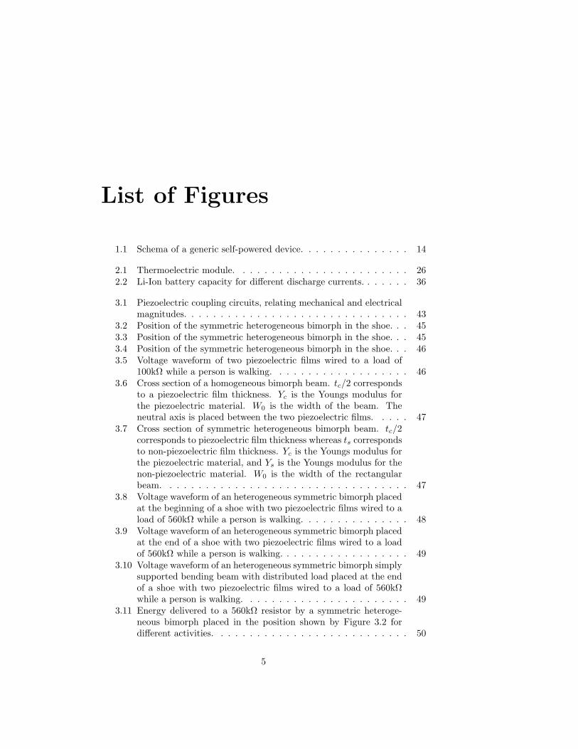
1.1 Schema of a generic self-powered device. . . . . . . . . . . . . . . 14
2.1 Thermoelectric module. . . . . . . . . . . . . . . . . . . . . . . . 262.2 Li-Ion battery capacity for different discharge currents. . . . . . . 36
3.1 Piezoelectric coupling circuits, relating mechanical and electricalmagnitudes. . . . . . . . . . . . . . . . . . . . . . . . . . . . . . . 43
3.2 Position of the symmetric heterogeneous bimorph in the shoe. . . 453.3 Position of the symmetric heterogeneous bimorph in the shoe. . . 453.4 Position of the symmetric heterogeneous bimorph in the shoe. . . 463.5 Voltage waveform of two piezoelectric films wired to a load of
100kΩ while a person is walking. . . . . . . . . . . . . . . . . . . 463.6 Cross section of a homogeneous bimorph beam. tc/2 corresponds
to a piezoelectric film thickness. Yc is the Youngs modulus forthe piezoelectric material. W0 is the width of the beam. Theneutral axis is placed between the two piezoelectric films. . . . . 47
3.7 Cross section of symmetric heterogeneous bimorph beam. tc/2corresponds to piezoelectric film thickness whereas ts correspondsto non-piezoelectric film thickness. Yc is the Youngs modulus forthe piezoelectric material, and Ys is the Youngs modulus for thenon-piezoelectric material. W0 is the width of the rectangularbeam. . . . . . . . . . . . . . . . . . . . . . . . . . . . . . . . . . 47
3.8 Voltage waveform of an heterogeneous symmetric bimorph placedat the beginning of a shoe with two piezoelectric films wired to aload of 560kΩ while a person is walking. . . . . . . . . . . . . . . 48
3.9 Voltage waveform of an heterogeneous symmetric bimorph placedat the end of a shoe with two piezoelectric films wired to a loadof 560kΩ while a person is walking. . . . . . . . . . . . . . . . . . 49
3.10 Voltage waveform of an heterogeneous symmetric bimorph simplysupported bending beam with distributed load placed at the endof a shoe with two piezoelectric films wired to a load of 560kΩwhile a person is walking. . . . . . . . . . . . . . . . . . . . . . . 49
3.11 Energy delivered to a 560kΩ resistor by a symmetric heteroge-neous bimorph placed in the position shown by Figure 3.2 fordifferent activities. . . . . . . . . . . . . . . . . . . . . . . . . . . 50
5

3.12 Energy delivered to a 560kΩ resistor by a symmetric heteroge-neous bimorph placed in the position shown by Figure 3.3 fordifferent activities. . . . . . . . . . . . . . . . . . . . . . . . . . . 50
3.13 Energy delivered to a 560kΩ resistor by a symmetric heteroge-neous bimorph placed in the position shown by Figure 3.4 fordifferent activities. . . . . . . . . . . . . . . . . . . . . . . . . . . 51
3.14 Cross section of symmetric heterogeneous bimorph beam. tc/2corresponds to piezoelectric film thickness whereas ts correspondsto non-piezoelectric film thickness. Yc is the Youngs modulus forthe piezoelectric material, and Ys is the Youngs modulus for thenon-piezoelectric material. W0 is the width of the rectangularbeam. . . . . . . . . . . . . . . . . . . . . . . . . . . . . . . . . . 52
3.15 Cross section of n piezoelectric symmetric heterogeneous bimorphbeams. . . . . . . . . . . . . . . . . . . . . . . . . . . . . . . . . . 55
3.16 Cross section of a piezoelectric symmetric heterogeneous bimorphbeam with a piezoelectric film of thickness ntc/2 placed at eachside of the non piezoelectric material with thickness nts. . . . . . 55
3.17 Cross section of a piezoelectric symmetric heterogeneous bimorphbeam with a piezoelectric film of thickness tc/2 placed at eachside of the non piezoelectric material with thickness ts(n), seeEquation (3.23) . . . . . . . . . . . . . . . . . . . . . . . . . . . . 56
3.18 Ratio of the maximum mean electrical power of the parallel con-nection of the top and bottom piezoelectric elements of the struc-ture shown in Figure 3.14 and the maximum electrical power ofthe top or bottom piezoelectric elements. . . . . . . . . . . . . . 57
3.19 Ratio of the maximum mean electrical power of structure A andstructure of Figure 3.14 versus n. . . . . . . . . . . . . . . . . . . 58
3.20 Ratio of the maximum mean electrical power of structure B andstructure of Figure 3.14 versus n. . . . . . . . . . . . . . . . . . . 59
3.21 Ratio of the maximum mean electrical power of structure A andstructure of Figure 3.14 versus τ and n. . . . . . . . . . . . . . . 59
3.22 Working mode of the direct discharge circuit with control andregulator circuit to supply power to a load. . . . . . . . . . . . . 61
3.23 Structure of a symmetric heterogeneous bimorph with triangularshape. . . . . . . . . . . . . . . . . . . . . . . . . . . . . . . . . . 62
4.1 Mica 2 sensor board employed for the human body accelerationmeasurements. . . . . . . . . . . . . . . . . . . . . . . . . . . . . 66
4.2 Acceleration measurements obtained by placing the sensor nodeon a knee while a person was walking with Ts=0.013s. . . . . . . 69
4.3 X-axis acceleration measurements obtained by placing the sensornode on a knee while a person was walking with Ts=0.013s. . . . 69
4.4 Y-axis acceleration measurements obtained by placing the sensornode on a knee while a person was walking with Ts=0.013s. . . . 70
6

4.5 Acceleration measurements obtained by placing the sensor nodeon a knee while a person was descending and ascending stairswith Ts=0.013s. . . . . . . . . . . . . . . . . . . . . . . . . . . . . 70
4.6 X-axis acceleration measurements obtained by placing the sensornode on a knee while a person was descending and ascendingstairs with Ts=0.013s. . . . . . . . . . . . . . . . . . . . . . . . . 71
4.7 Y-axis acceleration measurements obtained by placing the sensornode on a knee while a person was descending and ascendingstairs with Ts=0.013s. . . . . . . . . . . . . . . . . . . . . . . . . 71
4.8 Acceleration spectrum calculated from measurements obtainedby placing an accelerometer on the knee of a person that waswalking with Ts=0.013s for X-direction. . . . . . . . . . . . . . . 72
4.9 Acceleration spectrum calculated from measurements obtainedby placing an accelerometer on a knee while a person was de-scending and ascending stairs with Ts=0.013s for X-direction. . . 73
4.10 Acceleration spectrum calculated from measurements obtainedby placing an accelerometer on a knee while a person was de-scending and ascending stairs with Ts=0.013s for X-direction. . . 74
4.11 X-axis acceleration measurements obtained by placing the sensornode on the knee of a person when is walking. . . . . . . . . . . . 75
4.12 Position of the proof mass when the external acceleration of Fig-ure 4.11 is applied to the microgenerator. The parameters em-ployed during the simulation are k = 600N/m, z0 = 10mm andb = 0.1. . . . . . . . . . . . . . . . . . . . . . . . . . . . . . . . . 79
4.13 Energy dissipated in the load when the external acceleration ofFigure 4.11 is applied to the microgenerator. The parametersemployed during the simulation are k = 600N/m, z0 = 10mmand b = 0.1. . . . . . . . . . . . . . . . . . . . . . . . . . . . . . . 79
5.1 The thermogenerator converts the heat flow existing between thehuman hand and the ambient in electrical energy. . . . . . . . . . 82
5.2 Thermocooler equivalent circuit [1]. . . . . . . . . . . . . . . . . . 835.3 Thermocooler equivalent circuit [2]. . . . . . . . . . . . . . . . . . 845.4 Thermogenerator equivalent circuit based in the model of Chavez
et al. [1]. . . . . . . . . . . . . . . . . . . . . . . . . . . . . . . . . 865.5 Voltage as a function of current for the 17 A 1015 H 200 Peltron
thermogenerator. . . . . . . . . . . . . . . . . . . . . . . . . . . . 905.6 Power as a function of current for the 17 A 1015 H 200 Peltron
thermogenerator. . . . . . . . . . . . . . . . . . . . . . . . . . . . 915.7 Voltage as a function of current for the 128 A 1030 Peltron ther-
mogenerator. . . . . . . . . . . . . . . . . . . . . . . . . . . . . . 915.8 Power as a function of current for the 128 A 1030 Peltron ther-
mogenerator. . . . . . . . . . . . . . . . . . . . . . . . . . . . . . 925.9 Low-input voltage power management circuit. . . . . . . . . . . . 955.10 Efficiency versus output current for Vout=2V . . . . . . . . . . . 975.11 Electrical characteristics of the Power Management Unit . . . . . 98
7

6.1 Power delivered by the energy harvesting transducer to the energystorage element as a function of time. . . . . . . . . . . . . . . . 101
6.2 Power consumption of the load as a function of time. . . . . . . . 102
6.3 Power consumption of the load as a function of time. . . . . . . . 107
6.4 Schematic of a battery-powered RF transmitter . . . . . . . . . . 109
6.5 Simulation results with load for the parameters summarized inTable 6.1. The waveform called SOC shows the state of chargeof the battery with a voltage range from 0 to 1 V. IRPB4 isthe current flowing into the battery. vinreg is the voltage atthe input of the linear regulator and vdload is the voltage of thebattery that is supplied to the RF transmitter. . . . . . . . . . . 112
6.6 Zoom view of the simulation results with load for the parameterssummarized in Table 6.1. . . . . . . . . . . . . . . . . . . . . . . 113
6.7 Simulation results without charge for n=20, T=1.2 s and therest of parameters summarized in Table 6.1. The waveform calledSOC shows the state of charge of the battery with a voltage rangefrom 0 to 1 V. IRPB4 is the current flowing into the battery,vinreg is the voltage at the input of the linear regulator andvdload is the voltage of the battery that is supplied to the RFtransmitter. . . . . . . . . . . . . . . . . . . . . . . . . . . . . . . 114
6.8 Simulation results with charge for n=20, T=1.2 s and the rest ofparameters summarized in Table 6.1. The waveform called SOCshows the state of charge of the battery in per one, IRPB4 is thecurrent flowing into the battery, vinreg is the voltage at the inputof the linear regulator and vdload is the voltage of the batterythat is supplied to the Enocean transmitter. . . . . . . . . . . . . 115
6.9 Schematic of a battery-powered RF transmitter simulated withthe parameters of Table 6.3. . . . . . . . . . . . . . . . . . . . . . 115
6.10 Total mechanical excitation combined from three different me-chanical excitations. . . . . . . . . . . . . . . . . . . . . . . . . . 117
6.11 Simulation results without load for the parameters summarizedin Table 6.3. The waveform called SOC shows the state of chargeof the battery in per one. IRPB4 is the current flowing into thebattery. vinreg is the voltage at the input of the linear regulatorand vdload is the voltage of the battery that is supplied to theRF transmitter. . . . . . . . . . . . . . . . . . . . . . . . . . . . . 118
6.12 Simulation results with the Enocean transmitter as a load forthe parameters summarized in Table 6.3. The waveform calledSOC shows the state of charge of the battery in per one, IRPB4is the current flowing into the battery, vinreg is the voltage atthe input of the linear regulator and vdload is the voltage of thebattery that is supplied to the RF transmitter. . . . . . . . . . . 119
8

6.13 Simulation results with the Enocean transmitter as a load forthe parameters summarized in Table 6.3. The waveform calledSOC shows the state of charge of the battery in per one, IRPB4is the current flowing into the battery, vinreg is the voltage atthe input of the linear regulator and vdload is the voltage of thebattery that is supplied to the Enocean transmitter. . . . . . . . 120
B.1 Mechanical axis position for piezoelectric materials. . . . . . . . . 203B.2 Mechanical excitation of the piezoelectric film along axis 1. . . . 204B.3 Mechanical excitation of the piezoelectric film along axis 3. . . . 205
C.1 Piezoelectric coupling circuits, relating mechanical and electricalmagnitudes with state variables F , ν, V , and I. . . . . . . . . . . 209
C.2 Piezoelectric coupling circuits, relating mechanical and electricalmagnitudes. . . . . . . . . . . . . . . . . . . . . . . . . . . . . . . 212
C.3 Piezoelectric coupling circuits, relating mechanical and electricalmagnitudes. . . . . . . . . . . . . . . . . . . . . . . . . . . . . . . 216
C.4 Piezoelectric coupling circuit relating mechanical and electricalmagnitudes with a resistive load. . . . . . . . . . . . . . . . . . . 219
D.1 Acceleration measurements obtained by placing the sensor nodeon the ankle while a person was walking and descending andascending stairs with Ts=0.013s. . . . . . . . . . . . . . . . . . . 223
D.2 X-axis acceleration measurements obtained by placing the sensornode on the ankle while a person was walking with Ts=0.013s. . 224
D.3 Y-axis acceleration measurements obtained by placing the sensornode on the ankle while a person was walking with Ts=0.013s. . 225
D.4 Acceleration spectrum calculated from measurements obtainedby placing an accelerometer on the ankle of a person that waswalking with Ts=0.013s for X-direction. . . . . . . . . . . . . . . 225
D.5 Acceleration spectrum calculated from measurements obtainedby placing an accelerometer on the ankle of a person that waswalking with Ts=0.013s for Y-direction. . . . . . . . . . . . . . . 226
D.6 Acceleration measurements obtained by placing the sensor nodeon the wrist while a person was walking with Ts=0.013s. . . . . . 226
D.7 X-axis acceleration measurements obtained by placing the sensornode on the wrist while a person was walking with Ts=0.013s. . . 227
D.8 Y-axis acceleration measurements obtained by placing the sensornode on the wrist while a person was walking with Ts=0.013s. . . 227
D.9 Acceleration spectrum calculated from measurements obtainedby placing an accelerometer on the wrist of a person that waswalking with Ts=0.013s for Y-direction. . . . . . . . . . . . . . . 228
F.1 Electrical model of the battery [3] . . . . . . . . . . . . . . . . . 236F.2 Lithium polymer battery, model 602030 from Bullith . . . . . . . 237
9

F.3 Measurement setup for battery characterization including a cli-mate chamber. . . . . . . . . . . . . . . . . . . . . . . . . . . . . 238
F.4 Li-Ion battery charging and discharging stages. . . . . . . . . . . 239F.5 Capacity that can be extracted from one battery sample at 20 C. 240F.6 Capacity that can be extracted from one battery sample at 20 C. 241F.7 Capacity that can be extracted from one battery sample at 0 C. 242F.8 Battery voltage and current during charge stage and discharge
pulses at 1C. . . . . . . . . . . . . . . . . . . . . . . . . . . . . . 242F.9 Battery voltage and current during charge stage and discharge
pulses at 2C. . . . . . . . . . . . . . . . . . . . . . . . . . . . . . 243F.10 Voc extracted parameter for the Bullith lithium battery 602030
at 20 C. . . . . . . . . . . . . . . . . . . . . . . . . . . . . . . . . 243F.11 Rseries extracted parameter for the Bullith lithium battery 602030
at 20 C. . . . . . . . . . . . . . . . . . . . . . . . . . . . . . . . . 244F.12 RtranS
extracted parameter for the Bullith lithium battery 602030at 20 C. . . . . . . . . . . . . . . . . . . . . . . . . . . . . . . . . 244
F.13 RtranLextracted parameter for the Bullith lithium battery 602030
at 20 C. . . . . . . . . . . . . . . . . . . . . . . . . . . . . . . . . 245F.14 CtranS
extracted parameter for the Bullith lithium battery 602030at 20 C. . . . . . . . . . . . . . . . . . . . . . . . . . . . . . . . . 245
F.15 CtranLextracted parameter for the Bullith lithium battery 602030
at 20 C. . . . . . . . . . . . . . . . . . . . . . . . . . . . . . . . . 246
10

Part I
General Discussion
11


Chapter 1
Motivation and Objectives
This thesis deals with the topic of energy harvesting (also called energy scav-enging) that is defined as the process by which energy is collected from theenvironment employing a generator that transforms the input energy into elec-trical energy to power autonomous electronic devices. A self-powered systembased on environment energy harvesting is composed of several components, seeFigure 1.1, that are:
• Energy transducer (also called energy harvesting generator), used to con-vert some available ambient energy into electrical energy. The environmen-tal energy sources available for conversion may be thermal (thermoelectriccells), light (photovoltaic cells), RF (rectifying antennas), and mechanical(piezoelectric, magnetic induction, electrostatic converters).
• Storage capacitor. Some of the above energy transducers do not provideDC current, and in this case it is necessary to rectify the current andaccumulate the energy into a capacitor.
• Voltage regulator, to adapt the voltage level to the requirements of thepowered device.
• Optional battery, depending on the requirements of the application. Insome applications the powered device can be completely switched off dur-ing certain intervals and a battery is not necessary, while in others apermanent powering is mandatory. In any case, this battery will have alower weight, volume and capacity than a battery that is expected to sup-ply power to an electronic device without an energy harvesting generator.It depends on the requirements of the application if a capacitor can beused instead of a battery.
• Electronic device that typically has different power consumption modes.This fact allows to operate the device frequently in a low-power consump-tion mode and to operate it in active mode only during limited time pe-riods to decrease its energy consumption.
13
Figure 1.1: Schema of a generic self-powered device.
In this chapter, it is given the motivation of the thesis as well as the objectivesaccomplished. It also contains an introduction of the state of art of energyharvesting generators and energy storage elements.
1.1 Motivation
Portable equipments are the first evolution from fixed equipments that makepossible that computers are part of our everyday lives. The trends in technologyallow the decrease in both size and power consumption of complex electronicsystems. This decrease in size and power rises the concept of wearable deviceswhich are integrated in everyday personal belongings like clothes, watch, glasses,et cetera [4, 5]. The term wearable device receives several definitions in [4] andin the thesis is employed for a self-powered electronic device with low powerconsumption and communication capabilities integrated in smart clothes. Thus,if the complete energy harvesting system of Figure 1.1 would be integrated inclothes, it would be a wearable device.
Power supply is a limiting factor in wearable devices since the employmentof a primary battery (a battery to be used only once) means that the user ofthe portable product has to carry an extra battery while the use of a secondarybattery (rechargeable battery) means that the user has to plug in the portableproduct to grid to recharge it. This fact limits the mobility of the wearabledevice which is restricted to the lifetime of the battery. Furthermore, due tothe costs and inaccessible locations, the replacement or recharging of batteriesis often not feasible for wearable devices integrated in smart clothes. More-over, the increasing number of battery-powered portable products is creating
14

an important environmental impact.Wearable devices are distributed devices in personal belongings and thus,
an alternative for powering them is to harvest energy from the user. Therefore,the power can be harvested, distributed and supplied over the human body.Wearable devices can create, like the sensors of a Wireless Sensor Network(WSN), a network called in this case, Personal Area Network (PAN) [6, 7],Body Area Network [8] or WearNET [9].
Nowadays, the main application for energy harvesting generators are Wire-less Sensor Networks (WSNs) that harvest energy from the environment. Thereare several publications related with this topic [10–12]. Applications with verylow power consumption electrical loads are the right ones to be powered by en-ergy harvesting generators. The sensors that are part of a WSN can be poweredusing energy harvested from the environment. However, for powering wearabledevices the human body seems to be a more trustworthy source since it is alwaysavailable.
Electrical energy can be harvested from multiple sources (kinetic, solar, tem-perature gradient, et cetera). The physical principle of an energy harvestinggenerator is obviously the same no matter whether it is employed with an envi-ronmental or human body source. Nevertheless, the limitations related to lowvoltage, current and frequency levels obtained from human body sources bringnew requirements to the energy harvesting topic that were not present in thecase of the environment sources and that are mandatory to analyze properly.This analysis is the motivation for this thesis.
1.2 Objectives and Document Structure
The transducers (piezoelectric, electromagnetic and thermogenerator) and theelectrical circuits used for conditioning the electrical energy in this thesis arewell known. However, there is a gap between this specific and isolated knowledgeand its application to the topic of energy harvesting from passive human power(see Section 2.2.2). An electrical model and the equations that govern thetransducers operation are necessary when their energy source is the human body.The energy source must also be characterized and coupled to the transducer andthis is the reason why the thesis is multidisciplinary, since in order to increasethe efficiency of energy harvesting generators it is sometimes not only neededto improve the electric circuits but also the mechanical parts.
Furthermore, it is also necessary to characterize the electric output obtainedfrom energy transducers. This output is a low power signal with a voltage inthe order of units of volts and current in the order of units of microamps forpiezoelectrics placed inside the insole of a shoe, hundreds of millivolts and unitsor tens of milliamps for thermogenerators, that employ the temperature gradientbetween human body and environment as thermal source, and tens or hundredsof millivolts and units of milliamps in the best case for inductive transducers.
In energy harvesting applications the control unit is powered with the har-vested energy and this fact entails that no energy consuming control techniques
15
can be employed due to the low power levels harvested and that a starter circuitis mandatory to avoid the dependency on energy storage elements. Moreover,the electronic load operation must be adapted to the available energy. Thus, thedc-dc converter designed for the application with thermogenerators as energyharvesting transducers has been done taking these facts into consideration.
In energy harvesting applications, the energy harvested in a certain timeis a more relevant magnitude than the instantaneous power harvested due tothe discontinuous nature of energy harvesting sources. This is the reason foremploying energy instead of power in most of the results of the thesis.
More specific objectives of the thesis for every component of the energyharvesting generator system are given in this section.
• A study of piezoelectric, inductive and thermoelectric generators that har-vest passive human power is the main objective. A model of the completeenergy harvesting system, including the transducer which is a componentof critical importance, is necessary in order to simulate it and optimizeits parameters [13]. This model can be done with electronic componentsand simulated with electronic simulators like SPICE or ADS. Alterna-tively, they can be described with hardware description language [14] likeVerilog-A in combination with compatible simulators like SPICE or Spec-tre or using a generic system-level simulator, like Ptolemy [15]. BothVerilog-A and Ptolemy allow to simulate hybrid systems where mechanicaland electrical disciplines are combined, like in our case of study. There-fore, it is necessary to obtain a model of the transducers with physicalequations that describe how the input energy is converted into electricalenergy.
• Before modeling the transducer, it is required to characterize them in ameasurement stage. This stage is necessary for the comparison betweenmeasurements and simulations in order to evaluate the accuracy of themodel. Furthermore, sometimes a measurement stage is required in or-der to extract the parameters employed in the model. The transducer isoptimized for the activity from which the energy is harvested. Physicalparameters of the transducers must be optimized in order to increase theirefficiency. In summary, in the thesis, the following characterizations havebeen done:
– voltage measurements of the energy harvesting generator based onpiezoelectric films inserted inside a shoe,
– acceleration measurements of different parts of the human body, forthe case of the inductive transducers, in order to estimate the energythat can be harvested, the best location and the optimization of theenergy harvesting generator,
– voltage and current measurements at different temperature gradientsto characterize the thermoelectrical generators.
16

• Increase of the mechanical coupling efficiency. Once the physical equa-tions of the transducers are analyzed it can be studied if a better me-chanical coupling between the transducer and the human body can beaccomplished.
• Definition of the load requirements in terms of power consumption. Theobjective of the thesis does not include the design of the load to be pow-ered by the energy harvesting generator. The data recollection of state ofthe art sensors and communication modules power consumption providesan idea about what can be done with the harvested energy. A wearabledevice can be composed by a sensor and a communication module (a mi-croprocessor and a RF transceiver). Microprocessors and RF transceivershave different power consumption modes (sleep, standby, active,...). Amodel of the communication module in power consumption terms will de-termine an appropriate power consumption profile for the communicationmodule, which ensures that the available energy harvested from the humanbody is enough to power it. Therefore, the model of the electronic loadcan be generated only taking into account the power consumption profilesof different working modes given by low power wireless communicationmodules [16,17].
• The battery model. A battery or another storage element is used whenpermanent powering is mandatory. The objective in this field is simply thecharacterization of batteries using the battery model presented by Chenet al. [3].
• A more general objective and related with the different energy harvestingtransducers and their locations on the human body is the quantificationof the harvested energy. Once the energy is quantified, a further step isanalyze what can be done with it.
1.3 Document Structure
The general objectives detailed above have been accomplished in the paperspresented as part of the thesis.
* [18] provides several methods to design an energy harvesting device de-pending on the type of available energy. Nowadays, the trends in tech-nology allow the decrease in both size and power consumption of com-plex digital systems. This decrease in size and power gives rise to newparadigms of computing and use of electronics, with many small devicesworking collaboratively or at least with strong communication capabilities.Examples of these new paradigms are wearable devices and wireless sensornetworks. One possibility to overcome the power limitations of batteriesis to harvest energy from the environment to either recharge a battery, oreven to directly power the electronic device.
17

* In [19], the possibility to use piezoelectric film-bending beams inside a shoein order to harvest part of the mechanical energy associated to walkingactivity is exposed. This study analyzes several bending beam structuressuitable for the intended application (shoe inserts and walking-type exci-tation) and obtains the resulting strain for each type as a function of theirgeometrical parameters and material properties. As a result, the optimumstructure for the application can be selected.
* [20] gives the optimal way to convert the mechanical energy generatedby human activity (like walking) into electrical energy using piezoelectricfilms when it is collected in the form of charge accumulated in a storagecapacitor. Under this scheme, the storage capacitor needs only to be con-nected to the load when it has enough energy for the requested operation.This time interval depends on several parameters: piezoelectric type andmagnitude of excitation, required energy and voltage, and magnitude ofthe capacitor. This work analyzes these parameters to find an appropriatechoice of storage capacitor and voltage intervals.
* [21] presents a study of a time-domain model of a magnetic inductionmicrogenerator for energy harvesting applications. The model is based ona simple structure for which an analytical expression of the magnetic fielddistribution can be computed. From this analytical expression, geometricparameters that are not taken into account in the previous literature onmicrogenerators are considered. Starting from the magnetic field distri-bution in space of a circular current loop, the paper derives the inducedelectromotive force in a coil depending on the distance to the magnet. Sim-ulations give insight into the validity of linear models implicitly assumedin frequency domain analysis of these systems.
* In [22], a low temperature thermal energy harvesting system to supplypower to wireless sensing modules is introduced. The thermoelectric gen-erator module (TEG) makes use of the temperature gradient between thehuman body (the heat source) and the ambient to deliver a low voltageoutput that is up converted by means of a power management circuit.This regulated power source is able to reliably supply a wireless commu-nication module that transmits the collected temperature, current andvoltage measurements.
* [13] presents a complete system simulation of a self-powered sensor. Thecomponents are described with the Verilog-A language, that allows a be-havioral description based on the most important characteristics. Thesimulations here shown compare a battery-less versus a battery-poweredRF transmitter module, in both cases with a piezoelectric device gener-ating electrical energy. Results show how design choices of the systemchange the periodicity of the transmission and the ability to recharge thebattery.
18

Chapter 2 is a summary of the state of the art of energy harvesting generatorsand their applications. This summary is centered in different kinds of energyharvesting generators with a classification that distinguishes between those thatharvest the energy from the human body and those that harvest the energy fromthe environment. The state of the art of energy storage elements is also includedin this chapter.
The results obtained during the realization of this thesis are highlighted andanalyzed in Chapters 3 through 6 and Appendixes A through F. Thus, Chapter 3presents the study of piezoelectric generators. An electromechanical model isobtained from constitutive piezoelectric equations for the case of PVDF piezo-electric material. Additional information related with piezoelectric constantsand the electromechanical piezoelectric model is given in Appendixes A, B andC. It is analyzed how to maximize the electrical energy converted during walk-ing activity and therefore, the use of bending beam structures is introduced .The contribution of the physical dimensions and constants of the material inthe acquisition of the converted electrical energy is also analyzed. The directdischarge circuit is employed for walking activity and the calculation of theoptimum storage capacitor is pursued in this chapter.
Chapter 4 presents acceleration measurements of the human body which areexpanded in Appendix D. The setup employed for obtaining the measured datais presented as well as the calibration procedure done. These measurementswere done in order to have real data to employ as input for the simulation of aninductive generator in the time domain. A comparison between the energy har-vested from the different parts of the human body analyzed is done. Moreover,the values of the parameters of inductive generators that harvest more energyare analyzed.
Chapter 5 is focused on TEGs. First, a theoretical analysis and an equivalentcircuit with the thermal and electrical parts is presented. Afterwards, the char-acterization of some TEGs and the calculation of their parameters, employedfor the electrical model of TEGs, is shown and extended results are availablein Appendix E. This characterization and the knowledge of the TEG param-eters are used for the design of the power management unit which deals withlow input voltages for indoor applications. A power management circuit thatworks with temperature gradients in the range of 3 K-5 K is introduced andcharacterized.
In additon, Chapter 6 explains the methodology employed to create an an-alytical model and simulate a complete energy harvesting system. In an energyharvesting system that employs an energy storage element, it can be calcu-lated the minimum size of the energy storage element (e.g. named as capacityfor the batteries) to assure that no energy generated by the energy harvestingpower supply is going to be wasted. Moreover, the minimum amount of energythat must have the energy storage element to assure proper operation is alsocalculated.
Finally, Chapter 7 summarizes the conclusions obtained for the appropri-ate design of an energy harvesting generator from human body. In addition,an explanation about when a battery-less application is possible and when a
19
battery-powered application is necessary are given. The differences to take intoaccount in the design of energy harvesting generators powered by environmentalsources and by human body are included in this final chapter. The feasibility tointegrate energy harvesting generators based on human power is also discussed.
Appendixes A, B and C are related with the topic of piezoelectric transduc-ers. Appendix A contains the theoretical analysis of the relation between thepiezoelectric constants calculated from the piezoelectric constitutive equations.Appendix B contains the same analysis applied to PVDF and ceramic piezoelec-tric materials for different working modes. Moreover, the working mode thatharvests more energy is deduced as well as its relation with the dimensions of thematerial and their piezoelectric constants. Appendix C gives a detailed analysisof the electromechanical coupling circuits for PVDF piezoelectric materials inworking modes 31 and 33 employing to sets of state variables: F, ν, V, I andT, S, E, D
.
Appendix D shows additional acceleration measurements on the human bodyand its frequency spectrum.
Appendix E contains voltage measurements obtained for different thermo-generators connected to several resistors at different temperature gradients.Moreover, the Seebeck coefficient and the internal resistance have been cal-culated at different temperature gradients.
Appendix F shows the measurements done and results obtained to charac-terize a Lithium polymer battery employing the model presented by Chen et al.in [3].
20

Chapter 2
State of the art
2.1 Energy Harvesting Generators
There are several ways to convert different kinds of energy into electrical en-ergy. This conversion is made by energy harvesting generator systems. In thissection, the most usual types of conversion are presented and classified by thekind of energy harvesting transducer employed: solar cells, electromagnetics,electrostatics, piezoelectrics and thermoelectrics. Another classification thatdistinguishes between energy harvesting applications powered by environmentalsources and by human body is made in Section 2.2.
2.1.1 Photovoltaic Cells
Light is an environmental energy source available to power electronic devices. Aphotovoltaic system generates electricity by the conversion of light into electric-ity. Photovoltaic systems are found from the megawatt to the milliwatt rangeproducing electricity for a wide number of applications: from grid-connected PVsystems to wristwatches. The application of photovoltaics in portable productscould be a valid option under the appropriate circumstances.
The power conversion efficiency of a PV solar cell is defined as the ratiobetween the solar cell output power and the solar power (irradiance) impingingthe solar cell surface. For a solar cell of 100 cm2, 1 W can be generated, if thesolar irradiation is 1000 W/m2 and the efficiency of the solar cell is 10%. ThePV solar cells have a lifetime around 20-30 years.
Outdoors, the solar radiation is the energy source for PV system. Solarradiation varies over the earth’s surface due to the weather conditions and thelocation (longitude and latitude). For each location exists an optimum inclina-tion angle and orientation of the PV solar cells in order to obtain the maximumradiation over the surface of the solar cell [23].
M. Veefkind et al. presented the Solar Tergo prototype, a charger for smallportable products such as mobile telephones and MP3 players, for use in combi-nation with a backpack. The Solar Tergo consists of PV cells and a cell battery
21

pack [24,25].UCLA University has developed a solar harvesting module to power sensor
nodes called Heliomote. This module can power the most commonly sensornodes like Crossbow’s Mica2 and MicaZ. Heliomote employs commercial solarpanels to harvest energy and manages the storage and the use of the harvestedenergy. The energy demands of sensors are adapted to the available energy [26].A commercial edition of Heliomote is now available in ATLA Labs [27].
Solar energy is also a valid power source for pacemakers, and other implantsand biosensors. Actual devices use lithium based batteries that power duringa limited period, three years, the devices. The Instituto de Energa Solar fromUnviersidad Politcnica de Madrid and the Grupo de Dispositivos Semiconduc-tores from Universitat Politcnica de Catalunya have designed a system to powerthis class of devices with solar energy. The system consists on an optical fiberthat is placed under the skin in an accessible situation by the sun. The opticalfiber goes to the the implant in which it is placed a PV cell [28].
Nowadays, a new technology of solar cells is being developed. At the mo-ment, solar power has required expensive silicon-based panels that produce elec-tricity four to ten times more costly than conventional power plants. The newtechnology of solar cells provides cheap and flexible solar cells. Advances in ma-terial science, including nanomaterials, is the base of printable solar cells. Gen-eral Electric, Konarka technologies, Nanosolar, Siemens and STMicroelectronicsare working in the revolution of solar cells. Konarka is producing strips of flexi-ble plastic that are converting the light into electricity. Siemens predicts that ina short period of time their printable solar cells will have an efficiency of 10%.Nanosolar is developing the idea of spraying nano solar cells onto almost anysurface. This technology could enable Nanosolar to spray-paint photovoltaicsonto building tiles, vehicles,etc. and wire them up to electrodes [29].
Power density of photovoltaic cells in indoor environments is lower than10 µW/cm2 which is a low value compared with other energy harvesting sources[11]. Moreover, long dark periods imply the need of an energy storage elementsince there is not enough power to operate the load continuously. Moreover, thecapacity of the energy storage element is related to the time between operationsof the electronic load [18,30].
2.1.2 Mechanical Energy Harvesting Transducers
The principle behind kinetic energy harvesting is the displacement of a movingpart or the mechanical deformation of some structure inside the energy har-vesting device. This displacement or deformation can be converted to electricalenergy by three different methods, that are explained in subsequent subsections:inductive, electrostatic and piezoelectric conversion.
Each one of these transducers can convert kinetic energy into electrical en-ergy with two different methods: inertial and non-inertial transducers. Inertialtransducers are based on a spring-mass system. In this case, the proof massvibrates or suffers a displacement due to the kinetic energy applied. The en-ergy obtained will depend on this mass, and therefore this type is called inertial
22

converters. Mitcheson et al. have classified inertial converters in function ofthe force opposing the displacement of the proof mass [31]. These convertersresonate at a particular frequency and many of them are designed to resonateat the frequency of the mechanical input source at input mechanical vibrationsfrequency since at this frequency (resonance frequency), the energy obtainedis maximum. However, as the converters are miniaturized to integrate themon microelectronic devices, the resonance frequency increases, and it becomesmuch higher than characteristic frequencies of many everyday mechanical stim-uli associated to human body. For example, typical acceleration frequencies ofthe human body in movement are below 20 Hz [32].
For non-inertial converters, an external element applies a pressure that istransformed into elastic energy, causing a deformation that is converted to elec-trical energy by the converter. In this case, there is no proof mass and the ob-tained energy depends on mechanical constraints or geometric dimensions [19].The following sections give an overview of inductive, electrostatic and piezoelec-tric inertial generator whereas the case of non-inertial piezoelectric generator isdetailed in Section 2.2.2.
Inductive (micro)Generators
Inductive generators are also called Voltage Damped Resonant Generators (VDRG).This transducer is based on Faraday’s Law. The analysis of an inductive gen-erator in the frequency domain is given in [31].
Table 2.1 shows a summary of inductive inertial generators with the refer-ence of the design, the frequency and amplitude of the mechanical input, theoutput power generated at a certain output voltage and the dimensions of thetransducers.
Table 2.1: Summary table of Inductive Inertial Generators.Design Author Mechanical excitation Output power Dimensions
Williams et al. [33] f = 4 kHz 0.3µW mm3
Amplitude = 300 nm
Li et al. [34] f = 64Hz 10 µW 1cm3
Amplitude = 1000µm @ 2 V
Ching et al. [35] f = 104Hz 5 µW -Amplitude = 190µm
Amirtharajah et al. [36] f = 2 Hz 400 µW -Amplitude = 2 cm @ 180 mV
Yuen et al. [37] f = 80 Hz 120 µW 2.3 cm3
Amplitude = 250 µm @ 900 µV
23

Electrostatic (micro)Generators
The physical principle of electrostatic generators is based on the fact that themoving part of the transducer moves against an electrical field, thus generatingelectrical energy. The energy conversion principle of electrostatic generators issummarized in [31].
Electrostatic generators are also called Coulomb-damped resonant gener-ators (CDRGs) based on electrostatic damping. Meninger et al. present anelectrostatic generator that employs a variable micro-machined capacitor withtwo different designs: a parallel capacitor operated with a constant charge anda comb capacitor operated with a constant voltage [38]. If the charge on thecapacitor is maintained constant while the capacitance decreases (reducing theoverlap area of the plates or increasing the distance between them), the voltagewill increase. If the voltage on the capacitor is maintained constant while thecapacitance decreases, the charge will decrease. The mechanical energy con-verted into electrical energy is greater when the voltage across the capacitoris constrained than when the charge across the capacitor is constrained. How-ever, the initial voltage source needed to place an initial charge on the capacitorplates has a smaller value, if the charge across the capacitor is constrained.A way to increase the electrical energy for the charge constrained method isadding a capacitor in parallel with the MEMS capacitor. The disadvantage ofthis solution is that the initial voltage source has to increase its value. Theenergy is transduced through a variable capacitor and generates 8 µW froma 2,520 Hz excitation input [38]. Roundy et al. called this topology in-planeoverlap converter since the capacitance variation is produced by the change inthe overlap area of the interdigitated fingers [39,40]. When the plate moves, thecapacitance changes as a consequence of the overlap area of the interdigitatedfingers. Roundy et al. designed three different topologies of a MEMS CDRGwith constant charge [41].
Table 2.2 shows a summary of electrostatic inertial generators with the ref-erence of the design, the frequency and amplitude of the mechanical input, theoutput power generated at a certain output voltage and the dimensions of thetransducers.
Table 2.2: Summary table of Electrostatic Inertial Generators.Design Author Mechanical excitation Output power DimensionsMeninger et al. [38] f = 2.52 kHz 8µW 0.075 cm3
Sterken et al. [42] f = 1, 200Hz 100 µW@2V -Amplitude = 20 µm
Miyazaki et al. [43] f = 45 Hz 120 nW -Amplitude = 1 µm
24

Piezoelectric Generators
Piezoelectric materials are materials that are physically deformed in the presenceof an electric field or that produce an electrical charge when they are mechan-ically deformed. Piezoelectric generators combine most of the advantages ofboth inductive and electrostatic generators. However, piezoelectric convertersare difficult to implement on micromachined processes.
S. Roundy designed and fabricated a bimorph PZT generator with a steelcenter shim [12]. The cantilever structure has an attached mass and the volumeof the total structure is 1 cm3. A model of the developed piezoelectric generatorwas made and validated (Design 1). For an input vibration of 2.25 m/s2 at about120 Hz, power from 125 µW to 975 µW was generated depending on the load.More piezoelectric inertial generators are summarized in Table 2.3 where themechanical excitation is described in terms of its frequency and acceleration.
Table 2.3: Summary table of Piezoelectric Inertial Generators.Design Author Mechanical excitation Output power Dimensions
S. Roundy et al. [12] a = 2.25 m/s2 207 µW 1 cm3
Design 1 f = 85 Hz @ 10 VS. Roundy et al. [12] a = 2.25 m/s2 335 µW 1 cm3
Design 2 f = 60 Hz @ 12 VS. Roundy et al. [12] a = 2.25 m/s2 1700 µW 4.8 cm3
Design 3 f = 40 Hz @ 12 V
H. Hu [44] a = 1 m/s2 246 µW/cm3
-f = 50 Hz @ 18.5 V
A comparison between piezoelectric, electrostatic and inductive inertial trans-ducers is given in [12]. Piezoelectric and inductive transducers don’t need anexternal voltage source while the electrostatic does. However, the voltage levelsobtained with electromagnetic generators are in the order of hundreds of milli-volts. Another advantage of piezoelectric transducers is that the output voltageobtained is large enough to not need a transformer like in the case of inductivetransducers. However, piezoelectric transducer is the most difficult to integrateon chip whereas electrostatic is the easiest to integrate on chip [12]. Roundyet al. compare also these three kinds of transducers from the point of view ofthe energy storage density obtained and the results show that the values forpiezoelectric generators are greater than for the other generators [11].
Ottman et al. presented a circuit with a piezoelectric element connected toa diode bridge with a tank capacitor wired to a switch-mode dc-dc converter.An analysis is realized in order to obtain the optimal duty cycle of the converterthat maximizes the harvested power of the piezoelectric element. This powermanagement unit was designed for recovering energy from environmental vibra-tions. The use of the proposed system increases the harvested power by 325% as compared to when the battery is directly charged with the piezoelectricrectified source. In the analysis done the piezoelectric source is supposed to
25

be a sinusoidal waveform. The switch-mode dc-dc converter is placed in orderto control that voltage across the tank capacitor will be the optimum value toensure that energy transferred from the piezoelectric element to the chargingbattery is maximum [45,46]. Mitcheson et al. describe different power processingcircuits for electromagnetic, electrostatic and piezoelectric inertial energy scav-engers [47]. A complete explanation for the power management unit presentedin [47] for the case of electrostatic energy scavengers is given in [48].
2.1.3 Thermogenerators
Figure 2.1 illustrates a thermoelectric pair (thermocouple). The thermoelectricmodule consists of pairs of p-type and n-type semiconductors forming thermo-couples that are connected electrically in series and thermally in parallel. Thethermogenerator, based on the Seebeck effect, produces an electrical currentproportional to the temperature gradient between the hot and cold junctions.The output voltage obtained for N thermocouples is N times the voltage ob-tained for a single thermocouple whereas the current is the same as for a singlecouple [49, 50]. The Seebeck coefficient is positive for p-type materials andnegative for n-type materials. The heat that enters or leaves a junction of athermoelectric device has two reasons: the presence of a temperature gradientat the junction and the absorption or liberation of energy due to the Peltiereffect [49].
Figure 2.1: Thermoelectric module.
The figure of merit of thermoelectric modules, Z, is a measure of the cross-effect between electrical and thermal effects that takes place in TEGs (see Chap-ter 5). The figure of merit is sometimes represented multiplied by the tempera-ture, ZT . A large value of ZT corresponds to a high efficiency in the conversion
26

of thermal to electric power [49,51]. Ryan et al. predict a specific power around0.5 W/cm2 for a 10 K temperature gradient at room temperature with a figureof merit, ZT , equal to 0.9 [51]. Starner [52] estimates that the Carnot efficiencyat this temperature conditions is 5.5%. Thermoelectric microconverters are ex-pected to provide milliwatts of power at several volts. Microconverters can beemployed to convert rejected heat to electric power, providing electric powerand passive cooling at the same time. Ryan et al. also expound that manipulat-ing electrical and thermal transport on the nanoscale it is possible to improveconversion efficiency and ZT is predicted to increase by a factor of 2.5-3 nearroom temperature [51].
Carnot efficiency sets an upper theoretical limit to the heat energy that canbe recovered. The human body is a heat source and the temperature gradientbetween the body and the environment, e.g. room temperature (20C), can beemployed by a TEG to obtain electrical energy. In a warmer environment theCarnot efficiency drops while it rises in a colder one. The previous calculationsare made assuming that all the heat radiated by the human body can be re-covered and transformed into electrical power, so that the obtained power isoverestimated. A further issue of interest is the location of the device dedicatedto capture human body heat. Starner recommends the neck as a good locationfor the TEG since it is part of the core region, those parts of the body thatalways must be warm. Moreover, the neck is an accessible part of the body andthe engine can be easily removed by the user without creating discomfort. It isestimated that approximately a power between 0.2W-0.32W could be recoveredby a neck brace.
Leonov et al. presented a thermal circuit used for modeling a TEG withmultiple stages placed on the skin [53, 54]. Moreover, their analysis is orientedto the necessity of thermal matching between the TEG and the environment toobtain output voltages around 1 V with electrical matched load.
Stordeur and Stark developed in 1997 a Low Power Thermoelectric Gen-erator (LPTG) for the D.T.S. GmbH company [55]. The LPTG of D.T.S. isa small compact thermoelectric generator whose output is compatible to therequirements of micro electronic systems in terms of dimensions and outputpower. The working range of LPTG is near room temperature with hot sidetemperature of the TEG not higher than 120C. The LPTG provides a poweroutput of 20 µW and a voltage of about 4 V under load at ∆T=20K [56]. Anew approach was presented two years after the previous work that is capableof converting 15 µW/cm2 from a 10 K temperature gradient [57]. Other energyharvesting TEGs are presented in Table 2.4 including applications oriented toenergy harvesting from human body that are more detailed in Section 2.2.2.
Several power management methods can be employed with TEGs. A boostconverter or a charge pump [62, 63] is usually necessary due to the low outputvoltage of TEGs (in the range of mV) in applications with temperature gradi-ents around 5K at room temperature. Higher output voltages can be obtainedconnecting more thermocouple of the TEG in series but this involves an increasein its size.
27
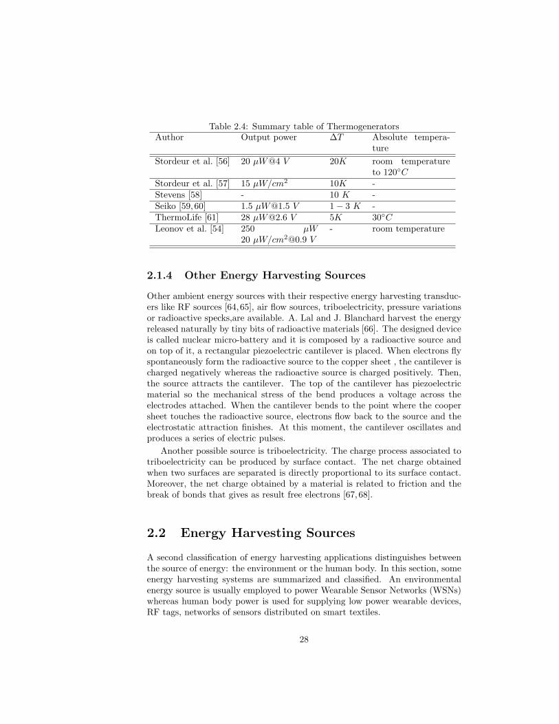
Table 2.4: Summary table of ThermogeneratorsAuthor Output power ∆T Absolute tempera-
tureStordeur et al. [56] 20 µW@4 V 20K room temperature
to 120CStordeur et al. [57] 15 µW/cm2 10K -Stevens [58] - 10 K -Seiko [59,60] 1.5 µ[email protected] V 1− 3 K -ThermoLife [61] 28 µ[email protected] V 5K 30CLeonov et al. [54] 250 µW
20 µW/[email protected] V- room temperature
2.1.4 Other Energy Harvesting Sources
Other ambient energy sources with their respective energy harvesting transduc-ers like RF sources [64,65], air flow sources, triboelectricity, pressure variationsor radioactive specks,are available. A. Lal and J. Blanchard harvest the energyreleased naturally by tiny bits of radioactive materials [66]. The designed deviceis called nuclear micro-battery and it is composed by a radioactive source andon top of it, a rectangular piezoelectric cantilever is placed. When electrons flyspontaneously form the radioactive source to the copper sheet , the cantilever ischarged negatively whereas the radioactive source is charged positively. Then,the source attracts the cantilever. The top of the cantilever has piezoelectricmaterial so the mechanical stress of the bend produces a voltage across theelectrodes attached. When the cantilever bends to the point where the coopersheet touches the radioactive source, electrons flow back to the source and theelectrostatic attraction finishes. At this moment, the cantilever oscillates andproduces a series of electric pulses.
Another possible source is triboelectricity. The charge process associated totriboelectricity can be produced by surface contact. The net charge obtainedwhen two surfaces are separated is directly proportional to its surface contact.Moreover, the net charge obtained by a material is related to friction and thebreak of bonds that gives as result free electrons [67,68].
2.2 Energy Harvesting Sources
A second classification of energy harvesting applications distinguishes betweenthe source of energy: the environment or the human body. In this section, someenergy harvesting systems are summarized and classified. An environmentalenergy source is usually employed to power Wearable Sensor Networks (WSNs)whereas human body power is used for supplying low power wearable devices,RF tags, networks of sensors distributed on smart textiles.
28

2.2.1 Environment
The application of a WSN will determine the energy source (solar energy, vi-brations, thermal gradient,...) to use. The main environmental energy sourcesemployed to supply power to WSNs are solar energy and mechanical vibrations.The main application of WSNs is to sense the environment in order to collectdata that are employed to improve the comfort and health of intelligent build-ings. One of the most famous WSNs hardware platforms is the Mica. MicaMotes are nodes created by Crossbow Technology Inc. [69]. These nodes em-ploys TinyOS as operating system [70]. They are modular with a processing andcommunication board and a sensing board. The first board includes a micro-controller (µC), an antenna, a flash memory, a power connector , an expansionconnector and a CC1000 single chip transceiver. The sensor board has a lightsensor, a temperature sensor, a sounder, a microphone, a tone detector, an ac-celerometer and a magnetometer. All these motes are designed to be batterypowered.
S. Roundy et al. estimated that assuming an average distance between wire-less sensor nodes of 10 m, the peak power consumed by the radio transmissionwill be around 2 to 3 mW whereas the peak power consumed during the receptionis less than 1 mW [11]. It is estimated a maximum peak power of 5 mW takinginto account the processor and communication units as well as the sensing andperipheral circuitry. The microcontroller and the communication transceivermodules have low power consumption modes (sleep mode, standby mode, ...)where the power consumption is reduced to the range of tens of µW . Assumingthat the nodes will be active 1% of the time, it is calculated an average powerconsumption around 100 µW. Taking into account this average power consump-tion, a Lithium battery of 1 cm3 must be replaced once every nine months.Thus, batteries are not a recommended power source for wireless sensors sincethe power source would limit the lifetime of the sensor [40]. Energy harvestinggenerators that employ vibrational energy sources have a power density around375 µW/cm3. In the case of energy harvesting generators based on solar energyit is generated 15,000 µW/cm2 and 10 µW/cm2 for outdoor and indoor solarsource [11].
2.2.2 Human body
A.J. Jansen employs the term human power as short for human powered energysystems in consumer products [71]. The Personal Energy System (PES) researchgroup of the Delft University of Technology distinguishes between active andpassive energy harvesting method. The active powering of electronic devicestakes place when the user of the electronic product has to do a specific workin order to power the product that otherwise the user would not have done.The passive powering of electronic devices takes place when the user does nothave to do any task different to the normal tasks associated with the product.In this case, the energy is harvested from the user’s everyday actions (walking,breathing, body heat, blood pressure, finger motion, ...).
29

Active Human Power
Some examples of electronic devices supplied from active human power extractedfor activities like pedaling, walking, ... are given in this section. The accessto Internet via bicycle-powered computer and a Wi-Fi network from a LaosVillage is presented in [72]. The computer is an ultra-efficient Linux PC thatsends signals via a wireless connection to a solar-powered relay station. The PCpower is supplied by a car battery charged by a person pedaling a stationarybike. 1 minute of pedaling generates around 5 minutes of power.
Windstream Power Systems Incorporated offers human power generatorslike MkIII, HPG MkIII which can be pedaled or cranked by hand and it cangenerate an average continuous power about 125 W by pedaling and 50 W byhand-cranking. The Bike Power Module consists on a generator, bearings, andfrictional wheel all mounted on a steel bracket in order to generate 100-300W [73].
T. Baylis designed a low cost radio, BayGen Freeplay, that worked on ahand crank. The BayGen Freeplay requires only a couple of human caloriesto work. If the user wind up to the hand crank during 30 seconds, the radiostores enough power in a fully wound-up spring to listen to the radio during30 minutes [74]. Freeplay continued to develop their radio adding a capacitorand later a rechargeable batteries and solar panels [75]. The company alsohas introduced another products powered by arm motion while has continuedinnovating in the radio market [76]. Another portable radio powered by analternative system is the Dynamo & Solar (D&S) radio, produced in China [77].
Another company offering human powered products is Atkin Design andDevelopment, AD&D. Their prototype Sony radio delivers 1.5 hours play timefor a 60 second wind. Their Motorola phone charger prototype provides 2 hoursstandby and 10 minutes talk time for every 60 seconds wind. The Professionaltorch model shine for 15 minutes on a 60 second wind and can be used asattachable charger unit for the radio and phone [78].
The Nissho’s Allandinpower is a hand-powered device that one cranks bysqueezing. It produces 1.6 W of power when the handle is squeezed at 90 timesper minute. The device is capable of providing energy to general applicationslike a phone or flashlight. One minute of powering gives one minute of talk timewhen a mobile phone is powered [75, 79]. Nissho has also a stepcharger thatis powered by the movement of the feet and can generate up to 6 W [75, 79].Freeplay has also developed a similar product called Freecharge Portable MarinePower that can be also powered by solar and wind energy [76].
Passive Human Power
The option to parasitically harvest energy from everyday human activity (pas-sive power) implies that an unobtrusive technique has to be adopted. Somepassive human power generators are summarized in this section. Starner pre-sented human power as possible source for wearable computers [52]. He analyzedpower generation from breathing, body heat, blood transport, arm motion, typ-
30

ing, and walking and provides the power dissipated by the human body duringseveral activities. A more recent study appears in [80] where it is explained thestate of the art of passive human power to power body-worn mobile electronics.
Walking is one of the usual human activities that have associated moreenergy [52] and [81]. Piezoelectric materials, dielectric elastomers and rotatorygenerators have been employed in order to harvest energy from human walkingactivity.
The MIT Media Lab developed a full system that harvests parasitic powerin shoes employing piezoelectric materials. The low-frequency piezoelectric shoesignals are converted into a continuous electrical energy source. The first sys-tem consisted on harvesting the energy dissipated in bending the ball of thefoot, placing a multilaminar PVDF bimorph under the insole. The second oneconsisted on harvesting the foot strike energy by flattening curved, prestressedspring metal strips laminated with a semiflexible form of PZT under the heel.Both devices were excited under a 0.9 Hz walking activity. The PVDF staveobtained an average power of 1.3 mW in a 250 kΩ load whereas the PZT bi-morph obtained an average power of 8.4 mW in a 500 kΩ load. Therefore, theelectromechanical efficiency for the PVDF stave is 0.5% and for the bimorph is20% [82].
Shenck et al. presented two electronic circuits to convert the electrical outputof the piezoelectric element into a stable dc output voltage. The first circuitconsisted on a diode bridge connected to the piezoelectric element to rectifyits output. The charge is transferred to a tank capacitor since the momentthat the charge exceeds a voltage value. At that moment the tank capacitor isconnected to a linear regulator that provides a stable output voltage. In thesecond circuit, the linear regulator was substituted by a high-frequency forward-switching regulator in order to improve efficiency. The control and regulationcircuitry was not activated until voltage across the tank capacitor, Cb, exceededa certain voltage value. A starter circuit was included in order to accumulatecharge on Cb while there was not enough charge to activate the switches of thecircuit. The converter’s electrical efficiency was 17.6% [83].
Dielectric elastomers are electroactive polymers (EAPs) that can produceelectric power from human activity. The main development area of EAPs areartificial muscles since EAPs hold promise for becoming the artificial musclesof the future. The electrostatic forces due to the electrodes voltage differencesqueeze and strech the film [84]. Dielectric elastomers can grow by as much as400% of their initial size and produce electric power when working in generatormode. When a voltage is applied across the dielectric elastomer which is de-formed by an external force, the effective capacitance of the device changes andwith the appropriate electronic circuits, electrical energy is generated [85] follow-ing the same principles of electrostatic generators as explained in Section 2.1.2.The energy density of these materials is high, some of them can generate about21 times the specific energy density of single-crystal piezoelectrics [84]. DARPAand the U.S. Army funded the development of a heel-strike generator basedon dielectric elastomers to power electronic devices in place of batteries. Theclaimed power generated is 1 W during normal walking activity [85].
31

The Media MIT Laboratory also developed another technique for extractingenergy from foot pressure: an electromagnetic generator. Kymissis et al. ana-lyzed an electromagnetic generator made by the Fascinations Corp. of Seattlethat was mounted in the outside of a shoe. The first design obtained an averagepower of 0.23 W in a 10 Ω load, which matched its impedance, for a 3 cm strokewhich interferes with walking [86]. J.Y. Hayashida et al. present an unobtrusivemagnetic generator system integrated into common footwear [87]. The averagepower obtained was 58.1 mW, with a peak power reaching 1.61 W, in a 47 Ωload. The width of the pulses is around 110 ms. The average power is lowerthan in the previous design due to the fact that for the 90% of the stride, nopower is harvested by the generator.
T. von Buren et al. optimize inertial micropower generators also for humanwalking activity obtaining power densities in the range of 8.7 − 2100 µW/cm3
depending on the kind of generator, its size and its location on the humanbody [88].
The number of commercial products that employ human power and morespecifically arm motion has significantly increased since the 1990s. In 1992,Seiko introduced the Kinetic, a wrist watch powered by a micro generator thatconverts the motion of the watch while it is worn by its user into electricalenergy stored in a capacitor. The idea was not new but Seiko improved thetechnology. The average power output generated when the watch is worn is5 µW. However, when the watch is forcibly shaken, the power generated is 1 mW.After Seiko Kinetic, the Swatch Group launched another watch that is self-powered, the ETA Autoquartz Self-Winding Electric Watch that is discontinuedsince 2006 [89].
The Seiko Thermic watch, also discontinued, employs a thermoelectric gen-erator to convert heat from the wrist into electrical energy. The watch absorbsbody heat through the back of the watch. It was the first watch powered by en-ergy generated between the body and environment temperature. The watch wasfirst produced in December 1998 but nowadays it is no longer manufactured.The system consists on a thermoelectric generator converts the temperaturedifference into electricity to power the watch. The thermoelectric generatorproduces a power of 1.5 µW or more when the temperature difference is 1C-3C. A boosting and controlling circuit connects the thermoelectric generatorto the titanium-based lithium-ion rechargeable battery of 1.5 V. The batterysupplies power to the motors of the watch and the movement driver that con-trols them. For this device, Seiko Instruments Inc. developed at the time theworld’s smallest π-type Peltier cooling element [59].
Applied Digital Solutions (ADS) developed in 2001 a miniature thermo-electric generator that converts body heat flow into 1.5 V. The thermoelectricgenerator known as Thermo Life has several applications: attachable medicaldevices, electronic wrist watches, self powered heat sensors, and mobile electron-ics [90]. Thermo Life has a volume of 95 mm3 and delivers with a ∆T = 5Ka maximum power of 28µW at 2.6 V . The material employed for this TEG isBi2Te3 which presents the best thermoelectrical properties to work in the rangeof room temperature [61].
32

Leonov et al. also showed an application where a watch-size thermoelectricwrist generator powers a radio transmitter [54]. It is also explained a simplethermal equivalent circuit for the TEG placed on the skin and different waysfor increasing the output voltage given by the TEG. It is obtained a power of250 µW which corresponds to about 20 µW/cm2 when the output load matchesthe internal resistance of the TEG with ∆ = 20K. The open circuit volt-age obtained with these conditions is 1.8 V (an output voltage of 0.9 V for amatched load). This result implies that more power per square centimeter canbe generated with TEGs than with solar cells in indoor applications [54].
It can be concluded that some efforts have been done in the last years inthe human passive energy harvesting topic. However, most of the work donein the energy harvesting field is related with harvesting energy from the envi-ronment instead of doing it from the human body. Moreover, an exhaustiveformal analysis for the energy harvesting transducers that allows to increase themechanical coupling with the human body and the electrical coupling with thepower management unit is not available. The analysis of the energy harvest-ing transducers is centered on their formal equations and electrical equivalentcircuits. Furthermore, an analytical study allows to generate a simulation en-vironment for energy harvesting power supplies where it is possible to size themechanical and electrical components as a function of the power requirementsof the electronic load. In summary, the thesis deals with the energy harvestingtopic from the formal side.
2.3 Energy Storage Elements
The two parameters employed to evaluate a storage element are energy andpower density. Both of them are expressed in terms of weight or volume. Thus,energy density is the measure of the available energy in terms of weight (gravi-metric energy density) or volume (volumetric energy density). The expressionfor gravimetric energy density is given by Equation (2.1) and for volumetricenergy density by Equation (2.2):
Gravimetric Energy Density =Capacity ×Nominal Voltage
Cell Weight(2.1)
Volumetric Energy Density =Capacity ×Nominal Voltage
Cell Volume(2.2)
Therefore, the energy density defines the amount of energy that can bestored in a certain volume or weight whereas the power density is a measure ofthe speed of the energy storage element to be charged or discharged. High valuesof power density indicates that the charge and discharge of the energy storageelement is fast whereas low values of power density indicates that the charge anddischarge is slow. The ideal energy storage element must have both high energyand power density. In batteries, energy density is high whereas power density
33

is low. On the other hand, capacitors are the opposite case of batteries withhigh values of power density and low values of energy density. An alternative tocapacitors and batteries are supercapacitors (or ultracapacitors) since they area compromise between batteries and capacitors offering both a high energy andpower density. Some gravimetric, volumetric energy density and power densityvalues for secondary batteries, capacitors and supercapacitors are summarizedin Table 2.5 [91,92].
Table 2.5: Energy and power density of energy storage elementsParameter NiCd NiMH Li-ion Capacitor SupercapacitorVolumetric EnergyDensity (Whl−1)
90-150 160-310 200-280 - -
Gravimetric En-ergy Density(WhKg−1)
30-60 50-90 90-115 0.02-0.08 1-9
Gravimetric PowerDensity (WKg−1)
150 1800 6000-8000 1000-7000
2.3.1 Batteries
Primary (non rechargeable) batteries compared to secondary (rechargeable) bat-teries are relatively long lasting. However, a large-scale adoption would resultin important environmental issues. Rechargeable batteries require that the usercan access to the electrical grid to recharge them which is not always availableeven in urban areas.
The demand of primary and secondary batteries is rising due to the gen-eration of energy-hungry portable devices like digital cameras, camera phones,PDAs, etc. Lithium-ion (Li-Ion) batteries are nowadays (and probably also inthe future) the secondary batteries leader of the market for powering portabledevices. NiCd batteries market is shrinking and is being replaced by NiMH forenvironmental reasons [93].
Battery Terminology
Definitions concerning battery terminology are given to properly understand thebehavior and characteristics of batteries [91,93,94]:
• Ampere-hour. It is the amount of electric charge carried by a current of1 A flowing during 1 hour.
• Capacity (C) or Nominal Capacity (NC). It is the amount of charge ex-pressed in Ampere-hour that can be delivered by a battery. It is usuallyspecified at room temperature and at a low discharge current (0.1C).
• Charge rate. A charge or discharge current of a battery is measured inC-rate. A discharge current of 1C draws a current equal to the rated
34

capacity. For example, a battery rated at 1000mAh provides 1000mA forone hour if discharged at 1C rate.
• Cycle life. The number of cycles that a battery can be charged and dis-charged. Primary batteries or non-rechargeable batteries have a unitarycycle life whereas secondary batteries also called rechargeable batterieshave a cycle life greater than one, dependent on the battery chemistry.
• Cut-off-voltage. The lowest voltage of a discharged battery. When thebattery voltage is equal to this value, the discharge process has to finish toassure the integrity of the battery. It is also known as the end of dischargevoltage (EODV) or the end of life (EOL) voltage by some manufacturers.
• Nominal voltage. The nominal voltage also called average discharge volt-age is defined as the mid-point voltage of the battery voltage range duringcharge or discharge. For example, a battery with a voltage range of 1.8Vto 2.8V has a nominal voltage of 2.3V.
• State of charge (SOC). Is the percentage of the maximum possible chargethat is present inside the battery.
• Self-discharge. Capacity loss during storage due to the internal leakage.The self-discharge of Li-Ion batteries is not relevant.
It is usual to present the capacity of a battery in a figure where it appears thevoltage as a function of the percentage of the nominal capacity for different dis-charge rate values, see Figure 2.2. The discharge curve of Li-Ion batteries can beconsidered flat during almost all the battery voltage range and is flatter for lowdischarge C-rates. Therefore, employing Li-Ion batteries the electronic deviceto power must tolerate less voltage variations of the supply source. For low dis-charge currents, the capacity of the battery is greater (an approximately equalto the nominal capacity of the battery) than for high discharge currents [95].This unexpected variation of the energy dispensed by the battery as a functionof the discharge C-rate is due to energy loss that occurs inside the battery anda drop in voltage that causes the battery to reach the low-end voltage cut-offsooner. The internal resistance of the battery is the cause of the discrepancyin the capacity for different discharge C-rates. If the battery has a low internalresistance, the differences in the nominal capacity for different discharge C-ratesis in the range of only a few percentage points whereas if the battery has a highinternal resistance, the difference in the capacity is around a 10 percent or more.
Another factor that has an influence over the battery capacity is the temper-ature. Temperatures near the room temperature (23 C) with a discharge rateof 0.1C have a capacity around the 100 percent of the nominal capacity. Forhigher temperatures, the capacity is even greater than the 100 percent of thenominal capacity (but only a few percentage) whereas for lower temperatures,the capacity is reduced in the range of tens of percentage. However, using thebatteries at high temperatures decreases their cycle life.
35

0 10 20 30 40 50 60 70 80 90 1001.8
2.0
2.2
2.4
2.6
2.8
3.0
Vba
t (V)
Nominal Capacity (%) Ibat
=2C I
bat=1C
Ibat
=0.5C
Figure 2.2: Li-Ion battery capacity for different discharge currents.
Battery Management
The behavior of batteries is characterized by the charge and discharge curves.There are several methods employed to charge and discharge batteries withoutdamaging them. This section is focused in Li-Ion batteries since they are themost common rechargeable batteries for portable devices.
There are three different voltage regulator topologies to use in devices pow-ered by batteries: switching regulators, linear voltage regulators and charge-pumps [96]. The use of linear voltage regulators is appropriate for batterieswith a flat discharge curve during almost all the battery voltage range. Nev-ertheless, a higher conversion efficiency is obtained by switching regulators [97]in the case of batteries with steep discharge curves. For the case of Li-Ionbatteries, discharge curves are more flat with low discharge currents than withhigh discharge currents, see Figure 2.2. There are also battery chargers forLi-ion batteries that employ charge-pump technique [98]. Moreover, switchingregulators are very popular to recharge battery powered devices [97].
It is better for Li-ion battery partial discharge cycles than deep dischargecycles. Up to 1000 cycles can be achieved if the battery is only partially dis-charged. Besides cycling, the performance of the Li-ion is also affected by aging.Different discharge methods, notably pulse discharging, also affect the longevityof some battery chemistries. While NiCd and Li-ion are robust and show min-
36

imal deterioration when pulse discharged, the NiMH exhibits a reduced cyclelife when powering a digital load [99].
2.3.2 Capacitors and Supercapacitors
The following table summarizes a comparison between batteries and capacitors.
Table 2.6: Comparison between batteries and capacitorsBatteries Capacitors
Advantages + High capacity + High power density+ Flat discharge curve + No charging circuit
needed
Disadvantages - Voltage as a function ofchemistry
- Low energy density
- Charging circuit needed - Voltage proportional tothe stored energy
Supercapacitors are rated in units of 1 F and higher. The gravimetric energydensity is 1 to 10Wh/kg. This energy density is high in comparison to theelectrolytic capacitor but lower than batteries. The supercapacitor provides theenergy of approximately one tenth of the NiMH battery. Whereas the electro-chemical battery delivers an almost constant voltage during the discharge cycle,the voltage of the supercapacitor drops linearly from full voltage to zero voltswithout the flat voltage discharge curve that characterizes most of chemicalbatteries. Due to this linear discharge behavior, the supercapacitor is unable todeliver the full charge to the load. The percentage of charge that is available togive depends on the supply voltage of the load to power [99].
A supercapacitor is modeled as a constant capacitor, Co, with a parallelcapacitor, Cu, which has a linear dependence on the voltage u. Two otherparameters are conventional for a supercapacitor model. The first one is theseries resistor, Rs that induces voltage drops during charge and discharge. Itsvalue influences the energy efficiency of the component and its power density.The second conventional parameter is the leakage resistor, Rl that induces loadlosses when the component is in a stand-by mode [100].
Generally, the charge of supercapacitors is realized with a constant currentfrom a dc voltage source. In particular cases, the charge, but most currentlythe discharge are realized with a constant power.
Table 2.7 summarizes the advantages and limitations of supercapacitors.
37

Table 2.7: Advantages and disadvantages of supercapacitors.Advantages Disadvantages+ Virtually unlimited cycle life(not subject to the wear and ag-ing experienced by the electro-chemical battery).
- Unable to deliver the full energystored since the voltage dischargecurve is not flat.
+ Low impedance (enhancespulse current handling by par-alleling with an electrochemicalbattery).
- Low energy density (typicallyholds one-fifth to one-tenth theenergy of an electrochemical bat-tery)
+ Rapid charging (low-impedance supercapacitorscharge in seconds).
- Cells have low voltages (serialconnections are needed to obtainhigher voltages. Voltage balanc-ing is required if more than threecapacitors are connected in se-ries).
+ Simple charge methods(voltage-limiting circuit com-pensates for self-discharge; nofull-charge detection circuitneeded).
- High self-discharge (the self-discharge is considerably higherthan that of an electrochemicalbattery).
+ Cost-effective energy stor-age(lower energy density is com-pensated by a very high cyclecount).
38

Chapter 3
Piezoelectric EnergyHarvesting Generator
Piezoelectric materials have multiple applications due to their properties. Theyare employed as sensors, actuators and energy harvesting generators. The piezo-electric effect was discovered by Jacques and Pierre Curie in 1880. Curie’sbrothers found that certain materials, when subjected to mechanical strain,suffered an electrical polarization that was proportional to the applied strain.If the electrodes are not short-circuited, a voltage associated with the chargeappears. This is the piezoelectric effect used for mechanical to electrical en-ergy conversion. Therefore, piezoelectrics are materials that allow conversionbetween mechanical and electrical energy. This property is used for harvestingenergy from the environment. The materials which have this property also havethe inverse piezoelectric effect that consists of the deformation of the materialwhen an electrical field is applied.
There is previous research related with the topic of piezoelectric energy har-vesting generators from different approaches. Applications for WSNs employpiezoelectric generators to convert mechanical vibrations to electrical energyat the resonance frequency of the piezoelectric material. Another approach ismade by J. Paradiso et al. that transform the mechanical strain suffered bya piezoelectric material inserted inside a shoe into electrical energy [83]. Pa-pers [13, 19, 20] focus on energy harvesting from walking activity since it has ahigh amount of energy associated [52,80]. However, some of the results that ap-pear in [13,18–20] can be extrapolated to other mechanical activities associatedwith the human body (like the movement of the arm, knee, et cetera).
This section continues the approach to the generation of electrical energyfrom passive human power employing piezoelectric materials. Additional andextended results related with each paper presented in the thesis and relatedwith this topic are included in this section.
39

3.1 Piezoelectric Equivalent Model
Section 4.2 Piezoelectric generator [18] explains the piezoelectric effect and thepiezoelectric constitutive equations employing Einstein notation. These generalequations are expressed in a matrix form.
Si = sEijTj + dliElDm = εTmnEn + dmkTk
for i, j, k = 1, . . . , 6 and l,m, n = 1, 2, 3 (3.1)
There are three other ways to express the piezoelectric phenomenon. Eachcase differs from the others in the independent state variables and the piezo-electric constants employed:
Si = sDijTj + gliDl
Em = −gmkTk + βTmnDnfor i, j, k = 1, . . . , 6 and l,m, n = 1, 2, 3 (3.2)
Ti = cDijSj − hliDl
Em = −hmkSk + βSmlDlfor i, j, k = 1, . . . , 6 and l,m, n = 1, 2, 3 (3.3)
Ti = cEijSj − eliElDm = emkSk + εSmnEn
for i, j, k = 1, . . . , 6 and l,m, n = 1, 2, 3 (3.4)
In these equations, T [N/m2] is the applied mechanical stress matrix, E[N/C] is the applied electric field matrix, D [C/m2] is the electric displacementmatrix and S [m/m] is the mechanical strain matrix. Table 3.1 gives a defini-tion of the piezoelectric constants employed in the four different piezoelectricconstitutive equations shown. The bold characters are employed to representthe matrix notation. Comparing the four different possible ways to expressthe piezoelectric constitutive equations, the relations between the different con-stants of the piezoelectric materials can be obtained. These general relationsare deduced in Appendix A and summarized in Table 3.2.
The relation between the piezoelectric constants depends on the kind ofpiezoelectric material employed and the direction of the mechanical stress andthe electrical displacement as it is shown in Appendix B. Piezoelectric mate-rials have different working modes related with the axis where the mechanicalexcitation and the electrical response are obtained. For example, working mode31 corresponds to a mechanical excitation along axis 1 whereas the electricalresponse is obtained in the plane perpendicular to axis 3. Table 3.3 shows therelation between the piezoelectric constants for PVDF material in the particu-lar case of working mode 31 that is deduced in Appendix B. In Table 3.3, itis introduced a new piezoelectric constant k31 that is the piezoelectric couplingconstant for PVDF. Appendix B shows the piezoelectric constitutive equationsfor the specific case of PVDF and ceramic materials.
40

Table 3.1: Definition of the piezoelectric constants.Constant Definition S.I. unitsd, piezoelectriccharge constant
Dielectric displacement devel-oped when a mechanical stressis developed. E=constant
[CN
]
Strain developed when anelectric field is applied.T=constant
[mV
]
g, piezoelectricvoltage constant
Electric field developed whena mechanical stress is applied.D=constant
[VmN
]
Strain developed when a di-electric displacement is applied.T=constant
[m2
C
]
eDielectric displacement devel-oped when a mechanical strainis applied. E=constant
[Cm2
]
Mechanical stress developedwhen an electric field is applied.S=constant
[NVm
]
hElectric field developed whena mechanical strain is applied.D=constant
[Vm
]
Mechanical stress developedwhen a dielectric displacementis applied. S=constant
[NC
]
sE , compliance Mechanical strain developedwhen a mechanical stress is ap-plied. E=constant
[m2
N
]
sD, compliance Mechanical strain developedwhen a mechanical stress is ap-plied. D=constant
[m2
N
]
εT , permittivity Dielectric displacement devel-oped when an electric field isapplied. T=constant
[CVm
]=[Fm
]
εS , permittivity Dielectric displacement devel-oped when an electric field isapplied. S=constant
[CVm
]=[Fm
]
cE Mechanical stress developedwhen a mechanical strain is ap-plied. E=constant
[Nm2
]
cD Mechanical stress developedwhen a mechanical strain is ap-plied. D=constant
[Nm2
]
βT Electrical field developed whena dielectric displacement is ap-plied. T=constant
[mCV
]=[mF
]
βS Electrical field developed whena dielectric displacement is ap-plied. T=constant
[mCV
]=[mF
]41

Table 3.2: Relation between piezoelectric matrix constants.Relation between piezoelectric constants
[s]E =[cE]−1
[d] =[cE]−1 [e] = [s]E [e][
εT]
=[βT]−1
[d] =[βT]−1
[g] =[εT]
[g][sD]
=[cD]−1
[g] =[cD]−1 [h] =
[sD]
[h][εS]
=[βS]−1
[e] =[βS]−1
[h] =[εS]
[h][sD]
=[sE]− [d]
[εT]−1 [d][
cD]−1 =
[cE]−1 − [d]
[εT]−1 [d][
βS]−1
=[βT]−1
− [d][sE]−1 [d]
Table 3.3: Relation between piezoelectric constants for PVDF in mode 31.Relation between piezoelectric constantsd31 = g31ε
T33
sE11 = 1/cE11
d31 = e31/cE11 = e31s
E11
sD11 = 1/cD11
g31 = h31/cD11 = h31s
D11
e31 = h31εS33
εS33 = εT33
(1− d2
31/(sE11ε
T33
))= εT33
(1− k2
31
)
sD11 = sE11
(1− d2
31/(sE11ε
T33
))= sE11
(1− k2
31
)
From the piezoelectric constitutive equations, an electromechanical modelcan be derived. This model consists of a circuit where mechanical and electricalvariables present in the piezoelectric effect are related. Figures 3.1(a) and 3.1(b)show an electromechanical piezoelectric model presented in [101] and [102] wherethe state variables are F , ν, V , and I instead of the state variables (T , S, E, andD) employed in the model that appears in [18]. For example, Table 3.4 showsthe relation between the variables that appear in Figure 3.1(a) and 3.1(b) andthe piezoelectric constants for the particular working mode 31. Similar resultscan be obtained for other working modes and piezoelectric materials. A detailedanalysis of the electromechanical piezoelectric model is done in Appendix C.
The analysis done gives as a result an electromechanical piezoelectric modelthat employs only electrical components (e.g. the force applied over the piezo-electric material is a voltage source). Thus, it is possible to use this model in anelectrical simulator, like HSPICE, both the mechanical and the electrical part
42

F
1:n1
C'p V
I
Ft
C
m
υ
(a) (b)
Figure 3.1: Piezoelectric coupling circuits, relating mechanical and electricalmagnitudes.
Table 3.4: Relation between piezoelectric constants for PVDF in mode 31.Relation between piezoelectric constants
Cm31 = LsE11
Wtc
C ′p31 = Cp31 − d231L2
t2cCm31= Cp
(1− d231
sE11ε
T33
)= Cp31
(1− k2
31
)
n1 = VFt
= −Cm31tcd31L
C′m31 = Cm31
(1− L2d231
t2cCpCm31
)= Cm31
(1− k2
31
)
Cp31 = εT33Atc
n2 = Vt
F = −d31LtcCp
of the model.
3.2 Piezoelectric Bending Beam Analysis for En-ergy Harvesting using Shoe Inserts
This section summarizes and highlights the main results obtained in [19] wherea study of different piezoelectric bending beams is done since different struc-tures were not compared thoroughly before. One piezoelectric material that issuitable to be integrated in the insole of shoes and harvest energy from walkingactivity is a polymer called Polyvinylidene fluoride (PVDF) which is flexible andthus, easier to integrate in a shoe than piezoelectric ceramics. [19] exposes howto obtain the equations for PVDF from the piezoelectric constitutive matrixequation. The result obtained (that is well known) concludes that the efficiencyfor this material is greater in the working mode 31 than in the two other possibleworking modes (33 and 32). This fact motivates the analysis of different bend-ing beam structures since the mechanical force exerted during walking activityfor the heel of the foot is realized in direction 3 and therefore, bending beamsstructures are employed to cause a stress in direction 1.
The bending beam structures are analyzed from three different points ofview:
43

• Support. Each end of the beam can be attached to one of the differenttypes of existing supports which provide different reaction forces to thebeam.
• Composite beams. A composite beam consists on piezoelectric and nonpiezoelectric material.
• Width of the beam. The shape of the width of the beam is another variabletaken into account.
First of all, an homogeneous triangular and rectangular cantilever are com-pared and it is concluded that greater values are obtained with the first onein terms of maximum deflection and average strain. In addition, two differentcomposite beams are introduced: the symmetric and asymmetric heterogeneousbimorph. From the comparison between the heterogeneous and homogeneousbimorphs, it is concluded that the most efficient vertical structure is the asym-metric heterogeneous bimorph with a large value of Ys/Yc.
The analysis of all the structures is made assuming that the maximum deflec-tion is limited to a fix value D as can be seen in Figure 4 of [19]. Figures 7 and 8in [19] show that the average strain in the case of the symmetric heterogeneousbimorph depends on the relation between the thickness of the piezoelectric andnon-piezoelectric material but not on the relation between their Young’s modu-lus. The average strain calculated in the case of the symmetric cantilever onlytakes into account a piezoelectric material thickness of tc/2 whereas the averagestrain calculated for the asymmetric cantilever takes into account a piezoelectricmaterial thickness of tc. Therefore, with the appropriate electrical connectionof the piezoelectric films, the results shown in the graph for the symmetriccantilever can be doubled.
A step forward is done the section titled simply supported beam of [19] toanalyze the closer structure to the real case of placing piezoelectric films insidethe insole of a shoe placed under the heel of the foot or even to increase the effi-ciency of placing the films in the beginning of the foot. Therefore, the structureanalyzed is a simply supported beam with a distributed load q and rectangularwidth. The comparison shown in Figure 11 of [19] concludes that the simplysupported beam with distributed load is the best of the structures analyzed.The case of simply supported beam with a distributed load q and triangularwidth was not analyzed in the paper and it is presented here.
3.3 Piezoelectric Beams Measurements
When a person is walking, running, et cetera, the beginning of the foot is stressedbasically in direction 1 and thus, no additional mechanical structure is necessaryto obtain a notorious improvement in the harvested energy of a piezoelectricmaterial placed in this position. However, when the bimorph is placed in theheel of the shoe, a mechanical structure (a beam) is necessary to convert loadforce in direction 3 into mechanical stress in direction 1 (axial stress) when
44
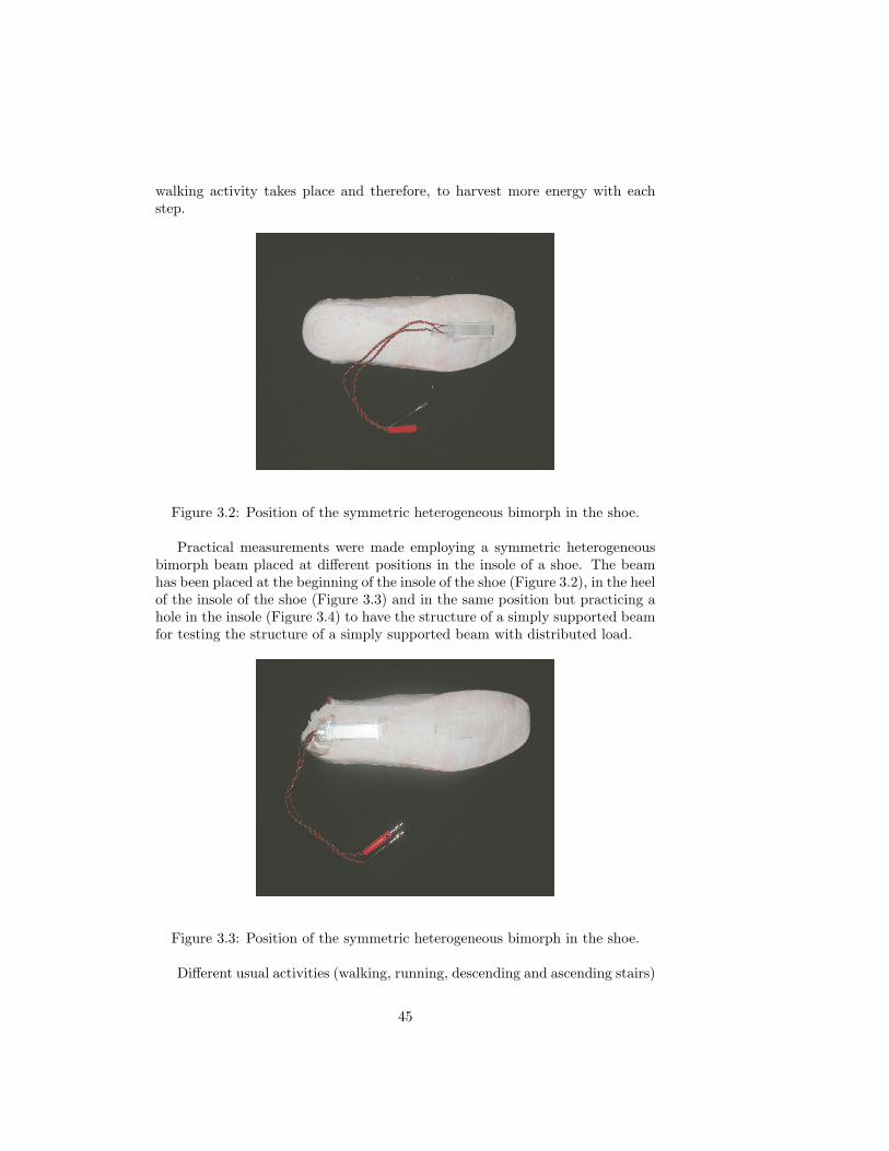
walking activity takes place and therefore, to harvest more energy with eachstep.
Figure 3.2: Position of the symmetric heterogeneous bimorph in the shoe.
Practical measurements were made employing a symmetric heterogeneousbimorph beam placed at different positions in the insole of a shoe. The beamhas been placed at the beginning of the insole of the shoe (Figure 3.2), in the heelof the insole of the shoe (Figure 3.3) and in the same position but practicing ahole in the insole (Figure 3.4) to have the structure of a simply supported beamfor testing the structure of a simply supported beam with distributed load.
Figure 3.3: Position of the symmetric heterogeneous bimorph in the shoe.
Different usual activities (walking, running, descending and ascending stairs)
45
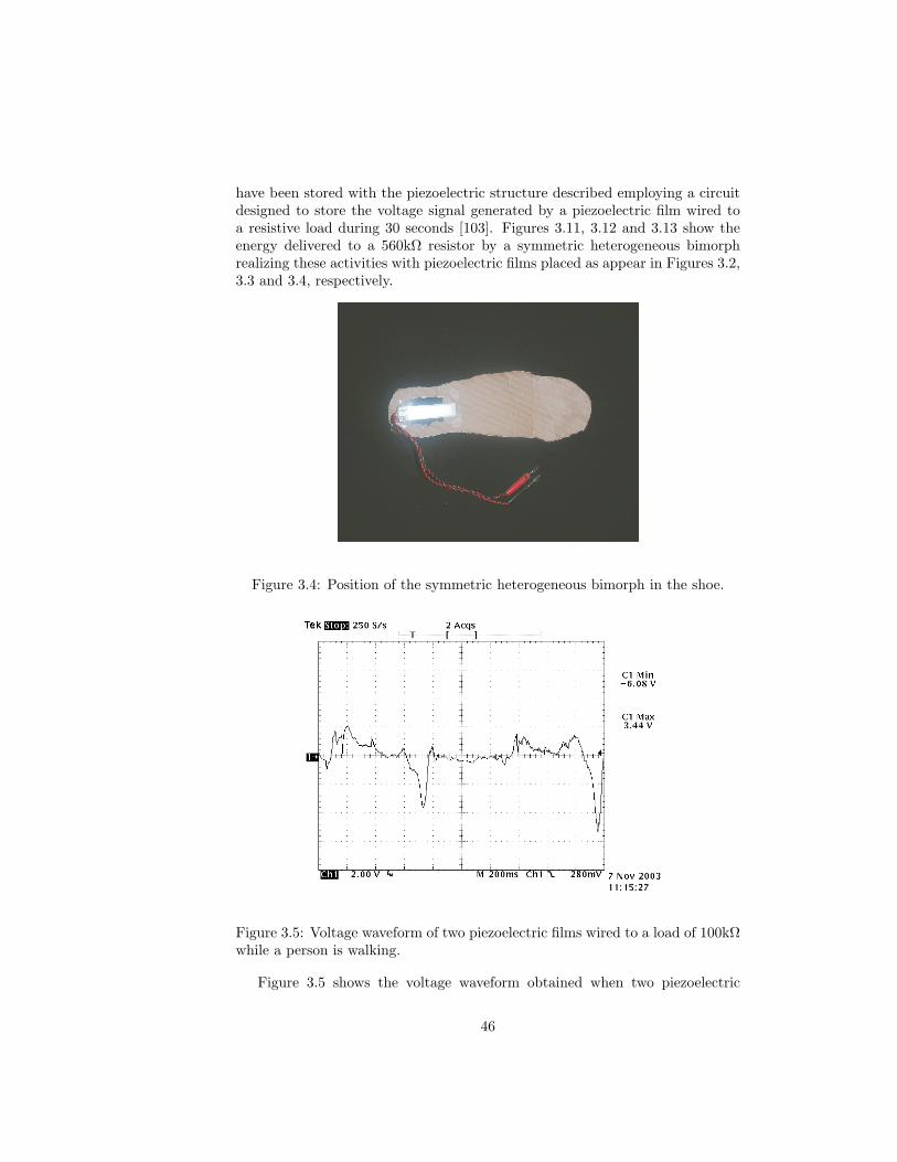
have been stored with the piezoelectric structure described employing a circuitdesigned to store the voltage signal generated by a piezoelectric film wired toa resistive load during 30 seconds [103]. Figures 3.11, 3.12 and 3.13 show theenergy delivered to a 560kΩ resistor by a symmetric heterogeneous bimorphrealizing these activities with piezoelectric films placed as appear in Figures 3.2,3.3 and 3.4, respectively.
Figure 3.4: Position of the symmetric heterogeneous bimorph in the shoe.
Figure 3.5: Voltage waveform of two piezoelectric films wired to a load of 100kΩwhile a person is walking.
Figure 3.5 shows the voltage waveform obtained when two piezoelectric
46

W0
tc/2
tc/2 Yc
Yc
Figure 3.6: Cross section of a homogeneous bimorph beam. tc/2 correspondsto a piezoelectric film thickness. Yc is the Youngs modulus for the piezoelectricmaterial. W0 is the width of the beam. The neutral axis is placed between thetwo piezoelectric films.
Figure 3.7: Cross section of symmetric heterogeneous bimorph beam. tc/2 corre-sponds to piezoelectric film thickness whereas ts corresponds to non-piezoelectricfilm thickness. Yc is the Youngs modulus for the piezoelectric material, and Ysis the Youngs modulus for the non-piezoelectric material. W0 is the width ofthe rectangular beam.
films(homogeneous bimorph, see Figure 3.6) are placed at the beginning of ashoe and connected to a 100kΩ resistive load while a person is walking. It canbe seen, that there are positive and negative parts in the waveform dependingif the piezoelectric film is being compressed or tensed. The first positive parthappens when the piezoelectric films are deformed but the foot is still on theground whereas the first negative part occurs when the foot is already in the airand the piezoelectric films are relaxed (not suffering compression or tension).The second positive and negative peaks are always smaller than the first ones.The second positive peak occurs when the foot is placed again in the groundand the negative peak is the response to the relaxation of the piezoelectric filmswhen the foot is still in the ground.
Figures 3.8, 3.9 and 3.10 show also the voltage waveform obtained but inthis case with the storing device developed in [103] where the voltage waveformis stored after a diode bridge. Figure 3.8 is the voltage waveform obtained forthe case of the heterogeneous symmetric bimorph placed at the beginning of theshoe. It can be seen in this figure that the period of the signal is approximately1 second. Comparing Figures 3.9 and 3.10, it is deduced that higher voltagesare obtained after employing a simply supported beam in the same location, the
47

heel of the shoe, and developing the same activity (walking).
4.0 4.2 4.4 4.6 4.8 5.0 5.2 5.4 5.6 5.8 6.00
2
4
6
Vol
tage
(V)
time (s)
Figure 3.8: Voltage waveform of an heterogeneous symmetric bimorph placedat the beginning of a shoe with two piezoelectric films wired to a load of 560kΩwhile a person is walking.
Figure 3.11 shows that the activity that delivers more energy placing thesymmetric heterogeneous bimorph structure at the beginning of the shoe isrunning followed by walking whereas descending and ascending stairs are theactivities that harvest less energy. The curves for ascending and descendingstairs, see Figure 3.12, change their slopes at t=14s and t=12.5s, respectively,due to a displacement at the location of the beam structure. Similarly, inFigure 3.13 the walking waveform also has a change in its slope at t=12.5s.
3.4 Conclusions of the Piezoelectric Beam Mea-surements
Table 3.5 summarizes the energy delivered to a 560k Ω resistor by the threedifferent structures analyzed. Ebeginning is the energy delivered by the struc-ture that appears in Figure 3.11, Eheel is the energy delivered by the structurethat appears in Figure 3.12 and the term Eheel−hole corresponds to the energydelivered by the structure of Figure 3.13. Table 3.6 repeats the informationgiven by Table 3.5 but assuming no change in the slope of the energy deliveredby the different activities.
Comparing the values of the energy delivered by the three different struc-
48

11.8 12.0 12.2 12.4 12.6 12.8 13.0 13.2 13.4 13.6 13.8 14.00.0
0.2
0.4
0.6
0.8
1.0
1.2
Vol
tage
(V)
time (s)
Figure 3.9: Voltage waveform of an heterogeneous symmetric bimorph placedat the end of a shoe with two piezoelectric films wired to a load of 560kΩ whilea person is walking.
3.0 3.2 3.4 3.6 3.8 4.0 4.2 4.4 4.6 4.8 5.00.0
0.5
1.0
1.5
2.0
2.5
3.0
3.5
Vol
tage
(V)
time (s)
Figure 3.10: Voltage waveform of an heterogeneous symmetric bimorph simplysupported bending beam with distributed load placed at the end of a shoe withtwo piezoelectric films wired to a load of 560kΩ while a person is walking.
49

0 5 10 15 20 25 300
5µ
10µ
15µ
20µ
25µ
30µ
35µ
40µ
45µ
Ene
rgy
(J)
time (s) Running Walking Descending stairs Ascending stairs
Figure 3.11: Energy delivered to a 560kΩ resistor by a symmetric heterogeneousbimorph placed in the position shown by Figure 3.2 for different activities.
0 5 10 15 20 25 30
200.0n
400.0n
600.0n
800.0n
3.0µ3.5µ
4.0µ4.5µ
5.0µ5.5µ
Ene
rgy
(J)
time (s) Running Walking Descending stairs Ascending stairs
Figure 3.12: Energy delivered to a 560kΩ resistor by a symmetric heterogeneousbimorph placed in the position shown by Figure 3.3 for different activities.
50

0 5 10 15 20 25 300
5µ
10µ
15µ
20µ
25µ
Ene
rgy
(J)
time (s) Running Walking Descending stairs
Figure 3.13: Energy delivered to a 560kΩ resistor by a symmetric heterogeneousbimorph placed in the position shown by Figure 3.4 for different activities.
Table 3.5: Energy delivered by the symmetric heterogenous bimporh structureplaced in a shoe after t=30.42s of activity.
Activity Ebeginning (µJ) Eheel (µJ) Eheel−hole (µJ)Running 42.83 4.96 22.9Walking 26.13 0.771 2.41Descending stairs 13.51 0.539 6.45Ascending stairs 5.61 0.219 -
tures that appear in Table 3.6, it can be concluded that placing the bimorphstructure at the beginning of the shoe harvests more energy than placing thesame structure in the heel of the shoe. The heel of the foot receives mostlyan impact in direction 3 but more energy is harvested, if the strain is made indirection 1 [19] as happens with the beginning of the shoe. This is the reasonthat explains that the results of placing the same bending beam structure at thebeginning of the shoe and at the heel give better results for the first location.
A way to increase the energy harvested by piezoelectric transducers placed inthe heel of the shoe is to deform also the piezoelectric in direction 1. Therefore,a considerable improvement is done employing the simply supported beam withdistributed load as was suggested in [19] and the energy obtained with the simplysupported beam structure in the heel of the shoe is in the same range than theenergy obtained at the beginning of the shoe. An improvement of 866% forrunning, 217% for walking and 706% for descending stairs is obtained comparing
51

Table 3.6: Energy delivered by the symmetric heterogenous bimorph structureplaced in a shoe after t=30.42s of activity assuming no change in the slopes.
Activity Ebeginning (µJ) Eheel (µJ) Eheel−hole (µJ)Running 42.83 4.96 47.9Walking 26.13 0.771 2.41Descending stairs 13.51 0.8 6.45Ascending stairs 5.61 0.4 -
Figure 3.14: Cross section of symmetric heterogeneous bimorph beam. tc/2corresponds to piezoelectric film thickness whereas ts corresponds to non-piezoelectric film thickness. Yc is the Youngs modulus for the piezoelectricmaterial, and Ys is the Youngs modulus for the non-piezoelectric material. W0
is the width of the rectangular beam.
the structure with the hole to the structure without the hole at the heel. Thepractical measurements done demonstrates that employing mechanical couplingwith bending beams improves the harvested energy of piezoelectric films placedin the insoles of shoes.
3.5 Comparison of different Symmetric Hetero-geneous Piezoelectric Beams in terms of Elec-trical and Mechanical Configurations
The electrical output obtained with the measurements done in the previous sec-tion, where PVDF films are excited by the walking activity of human body, isin the order of some micro amperes and units of volts. The current generatedby the piezoelectric elements is proportional to the average strain done. How-ever, this current can be not enough for the electric load to be powered by thepiezoelectric transducer. In order to increase this low current, three different al-ternatives are presented in this section for using with symmetric heterogeneousbimorph beams.
Figure 3.14 shows the cross section of a symmetric heterogeneous bimorphbeam composed by two piezoelectric elements placed at the top and bottom
52

of the structure with a thickness tc/2 and a Young’s modulus Yc, and a non-piezoelectric element with thickness ts and Young’s modulus Ys. In this struc-ture, one piezoelectric film is placed at each side of the neutral axis position,and therefore one of the films is tensed whereas the other one is compressedwith an average strain at each side S. First, it is introduced the calculation ofthe current and power for this structure in working mode 31 in order to cancompare the three alternative structures with this one.
Piezoelectric constitutive equations relate the dielectric displacement, theelectrical field and the mechanical strain, see Equation (3.5).
D3 = ε33S E3 + e31S1 (3.5)
Integrating the above equation to obtain the mean value along the thickness,it is obtained:
∫ (ts+tc)/2
ts/2
D3dh =∫ (ts+tc)/2
ts/2
ε33S E3dh+
∫ (ts+tc)/2
ts/2
e31S1dh (3.6)
Solving the previous equation and assuming that E = dV/dh the result is:
D3tc2
= ε33S V3 + e31Sx
tc2
(3.7)
If it is assumed a sinusoidal steady state for the three state variables, Equa-tion (3.7) is rewritten as:
D3ejωt = 2ε33
S
V3ejωt
tc+ e31Sxe
jωt (3.8)
Multiplying by the area of the triangular beam (A = W0L/2), doing thederivative of the previous equation and taking into account that I = dq/dt, itis obtained:
−I3 = jωA
[2ε33S
V3
tc+ e31S1
](3.9)
Assuming that the piezoelectric film is connected to a resistive load, R, therelation between the current generated and the voltage on the load is VR = I3R.Therefore, the following expressions represent the current and voltage generated.
I3 =−jωAe31S1
jω2Aε33S
tcR+ 1
(3.10)
VR =−jωAe31S1R
jω2Aε33S
tcR+ 1
(3.11)
Following the notation shown in Section 3.1, it is known that C ′p = 2AεS33
tcand therefore the current and voltage equations can be rewritten as:
53

I3 =−jωAe31S1
jωC ′pR+ 1(3.12)
VR =−jωAe31S1R
jωC ′pR+ 1(3.13)
The expressions for the modulus of the current and voltage are:
|I3| =Ae31ωS1√
1 + ω2C ′2p R2(3.14)
|VR| =Ae31ωS1R√1 + ω2C ′2p R2
(3.15)
The mean electrical power generated by one piezoelectric film is:
〈P3〉 =|VR|22R
= |I3|2 2R =(Ae31ωS1)2
R
2(1 + ω2C ′2p R2
) (3.16)
The maximum mean electrical power occurs when R = 1/(ωC ′p
).
The average strain for the top or bottom piezoelectric films of a symmetricheterogeneous bimorph beam is:
S1 = ymaxtc (1 + 2ts/tc)
2L2(3.17)
Connecting electrically in parallel the top and the bottom films of the struc-ture shown in Figure 3.14, the capacitance and current will be doubled. There-fore, the mean electrical power dissipated on the load is:
〈P3parallel〉 =2 (Ae31ωS1)2
R(1 + ω24C ′2p R2
) (3.18)
In this case, the maximum mean electrical power occurs when R = 1/(2ωC ′p
)
1. Structure A. n piezoelectric symmetric heterogeneous bimorph beams witha piezoelectric film of thickness tc/2 at each side and a non piezoelectricmaterial of thickness ts, see Figure 3.15. All the beams have the sameaverage strain connected electrically in parallel and the top and bottomfilms also connected in parallel. Therefore, the current generated with thisstructure is:
I3A =−jω2nAe31S1
1 + jω2nC ′pR(3.19)
The mean electrical power generated by this structure is:
54

Figure 3.15: Cross section of n piezoelectric symmetric heterogeneous bimorphbeams.
Figure 3.16: Cross section of a piezoelectric symmetric heterogeneous bimorphbeam with a piezoelectric film of thickness ntc/2 placed at each side of the nonpiezoelectric material with thickness nts.
〈P3A〉 =(2nAe31ωSx)2
R
2(1 + ω24n2C ′2p31R
2) (3.20)
In this case the maximum mean electrical power is generated when R =1/(2nωC ′p
).
2. Structure B. A piezoelectric symmetric heterogeneous bimorph with apiezoelectric film of thickness ntc/2 at each side and a non piezoelectricmaterial of thickness nts, see Figure 3.16.
The average strain for the top or bottom film of thickness ntc/2 is S1B =nS1. Thus, the current generated by the parallel electrical connection oftwo piezoelectric films of thickness ntc/2 is:
I3B =−jω2nAe31S1
1 + jω2/nC ′p31R(3.21)
The mean electrical power is given by the following expression:
〈P3B〉 =(2nAe31ωSx)2
R
2(1 + ω24/n2C ′2p R2
) (3.22)
55

Figure 3.17: Cross section of a piezoelectric symmetric heterogeneous bimorphbeam with a piezoelectric film of thickness tc/2 placed at each side of the nonpiezoelectric material with thickness ts(n), see Equation (3.23).
In this case the maximum mean electrical power is generated when R =n/(2ωC ′p
)
3. Structure C. This structure is shown in Figure 3.17 where one piezoelectricfilm of thickness tc/2 is placed at each side of the support film whichhas a thickness of ts (n), see Equation 3.23. The total thickness of thisstructure is the same as the thickness of the two structures describedbefore. However, in this case only one piezoelectric film is placed at thetop and bottom of the beam.
ts (n) = nts1 + (n− 1) tc (3.23)
The average strain for one of the piezoelectric films placed at the top orbottom of the structure is:
S1C (n) = ymaxtc
(1 + 2ts(n)
tc
)
2L2= nS1 +
ymax2L2
tc (n− 1) (3.24)
The total current generated by the parallel connection of the two piezo-electric films of thickness tc/2 is:
I3C =−jω2Ae31S1 (n+ tc (n− 1) / (tc + 2ts))
1 + jω2C ′pR(3.25)
The mean electrical power generated with this structure is:
〈P3C〉 =(2Ae31ωS1 (n+ tc (n− 1) / (tc + 2ts)))
2R
2(1 + ω24C ′2p R2
) (3.26)
56

Figure 3.18: Ratio of the maximum mean electrical power of the parallel con-nection of the top and bottom piezoelectric elements of the structure shown inFigure 3.14 and the maximum electrical power of the top or bottom piezoelectricelements.
First, it is compared the power generated by the parallel electrical connectionof the piezoelectric films located at the bottom and top of the structure ofFigure 3.14 with the power generated by one of the piezoelectric films, seeFigure 3.18. The results show that the power is doubled with the parallelconnection. It must be taken into consideration that for each structure analyzed,the value of R has been substituted by its optimum value that makes maximumthe mean electrical power. In order to compare the three different structurespresented, the ratio of the maximum mean electrical power obtained with eachstructure and the maximum mean electrical power generated by the parallelelectrical connection of the structure of Figure 3.14 has been plotted employingthe values shown in Table 3.7. Figures 3.19 and 3.20 show the ratio as a functionof n. Structure B is better than structure A since it generates more power sincethe strain made with this structure is n times bigger. Figure 3.21 shows theratio of power for structure C as a function of τ = ts/tc and n. This structure isnot better than structure B but it is the better structure in terms of generatedpower as a function of the number of piezoelectric films employed since thethickness of the non piezoelectric material helps to obtain also a high strain.
57

Figure 3.19: Ratio of the maximum mean electrical power of structure A andstructure of Figure 3.14 versus n.
Table 3.7: Parameters employed for the simulation of structure A, B and C.The piezoelectric constants employed are for the PVDF films of Msiusa [104].
W0 4 cmL 5 cme31 0.07 C/m2
tc 56 µmts τ ∗ tcεS33 106e-12 F/m
58

Figure 3.20: Ratio of the maximum mean electrical power of structure B andstructure of Figure 3.14 versus n.
Figure 3.21: Ratio of the maximum mean electrical power of structure A andstructure of Figure 3.14 versus τ and n.
59
3.6 Optimum Storage Capacitor for the DirectDischarge Circuit
Whereas the topic of increasing the harvested energy with piezoelectric materialsplaced in the insole of a shoe has been analyzed from the mechanical point ofview in [19], the electrical point of view of the topic is covered by [20].
[20] in Chapter 10 employ an already described circuit [12,82,105], the directdischarge circuit, but with a new approach. The direct discharge circuit consistson the piezoelectric equivalent model for low frequencies wired to a full-wavediode rectifier connected to a storage capacitor, C2. The piezoelectric equivalentmodel at low frequencies is shown in Figure 1 of [20]. It is composed basicallyby a current source, ip, and a capacitor, C1. [20] and Chapter 10 use a realisticcurrent source, derived from measurements done during walking activity, for thecalculation of the optimum value of C2. However, all the equations are givenas a function of the generated charge during walking activity and therefore, thecalculus can be extrapolated to any mechanical activity where the generatedcharge is known.
The main contribution of [20] and Chapter 10 is the calculation of the op-timum storage capacitor and the number of piezoelectric films connected inparallel that give the needed energy to power a low-power electronic device (likean RF transmitter) with a discontinuous load profile in the minimum time be-tween operations. This section gives a more detailed qualitative explanation ofthe results obtained
Figure 16 of [20] shows the initial number of mechanical cycles needed topower on the electric load the first time, kini, the number of mechanical cyclesneeded to power on the electric load after the first time, ks, and the value of thestorage capacitance, C2. It can be also shown in Figure 16 of [20] that there is avalue for the graph ks that gives the required energy with the minimum numberof mechanical cycles. This optimal value is named ks,opt and the voltage atwhich the electric load must be turned on is called Von,opt. The initial numberof steps and the storage capacitance are selected for Von,opt. Therefore, thevalues of Von and C2 are selected to assure that the electric load will be turnedon in the minimum time between operations.
An application example where an RF communication module is powered in-termittently to send a sensing data is given in section 5 of [20] to prove validityof the obtained results. The circuit operation is as follows. As the piezoelectricelement is repetitively stressed, the voltage in the storage capacitor increases.Whenever this voltage reaches a certain limit (Von),the capacitor is connectedto the regulator input and it is discharged to a lower voltage, Voff , providingthe energy required to sense and transmit the data, Ereq (including the energyneeded by the regulator). The capacitor is then disconnected from the load oncemore, allowing it to be recharged as can be shown in Figure 3.22. The value ofVoff is determined by the voltage supply of the load and Von is determined bythe energy required by the load to operate. Therefore, as it is represented inFigure 3.22, the number of initial steps kini is bigger than ks and an RF trans-
60

mission can be done every Tks seconds (after the first one), where T correspondsto the period of one mechanical cycle.
Figure 3.22: Working mode of the direct discharge circuit with control andregulator circuit to supply power to a load.
3.7 System-level simulation with piezoelectric en-ergy harvesting
Chapter 13 [13] presents a complete simulation at system level using Verilog-Alanguage. The energy harvesting transducer employed is PVDF piezoelectricfilm. The structure of the piezoelectric transducer employed during simulationscorresponds to a symmetric heterogeneous bimorph with triangular shape, seeFigure 3.23. A more detailed explanation of the equations and constants thatare employed to model the piezoelectric transducer in Verilog-A is given in thissection.
The mechanical conditions required to operate in mode 31 are: T2 = T3 = 0and S2 = S3 = 0. Therefore, mechanical stress is only applied in direction 1, T1
(length expansion working mode) and the electric displacement obtained is:
D3 = d31T1 (3.27)
In length expansion working mode, mechanical stress and strain are relatedby:
T1 = Y11S1 (3.28)
where Yc corresponds to the Youngs modulus of the piezoelectric material thatis defined as the mechanical stress obtained when a strain is applied. For Equa-tion (3.28), the Young’s modulus of the piezoelectric material corresponds toY11 since the mechanical stress and the strain are in direction 1.
Q3 = D3A (3.29)
61

Figure 3.23: Structure of a symmetric heterogeneous bimorph with triangularshape.
where A is the area of the piezoelectric film. For the particular case shown inFigure 3.23, A = W0L/2.
Combining Equations (3.29) and (3.28), it is obtained:
Q3 = d31Y11S1A (3.30)
In [19], it was calculated the maximum deflection, ymax, and the averagestrain, S1, for different bending beams structures including the structure shownin Figure 3.23. For the case of a triangular symmetric heterogeneous bimorphcantilever, S1 is:
S1 =ymaxtc
2L2(1 + 2τ) (3.31)
where τ = ts/tc, tc is the piezoelectric material thickness, ts is the non-piezoelectricmaterial thickness and L is the length of the beam structure.
The maximum deflection is given by the following expression:
ymax =6FL3
Y11W0t3c
11 + 3τ + 3τ2 + ητ3
(3.32)
where η = Ys/Y11, Y11 is the piezoelectric material Young’s modulus, Ys is thenon-piezoelectric material Young’s modulus and W0 is the base of the triangularcantilever.
For the piezoelectric generator model in Verilog-A, the mechanical inputfor the beam structure can be selected between the input force, F1, and themaximum deflection of the beam, ymax. One variable depend on the other andare related by ke, the elastic constant of the beam:
F1 = keymax (3.33)
62

The charge generated by the top and bottom piezoelectric films, Q3, is pro-portional to the maximum mechanical deflection and the charge constant, kq ofthe beam.
Q3 = kqymax (3.34)
As it was shown in Section 3.6, the electrical model for low frequencies ofa piezoelectric transducer is composed by a current source in parallel with acapacitor. The current source value is related with the mechanical part of themodel by:
i =dQ3
dt= kq ymax (3.35)
The expression for kq and ke depends on the structure of the beam selected.From Equations (3.33) and (3.32), it is deduced that the value for ke is:
ke =YcW0t
3c
6L3
(1 + 3τ + 3τ2 + ητ3
)(3.36)
Substituting into Equation (3.30), the value of S1 given by Equation (3.31)and comparing the result with Equation (3.34), it is obtained the value of kq.
kq =W0tc2L
d31Y11 (1 + 2τ) (3.37)
where τ = ts/tc, η = Ys/Y11, Yc is the piezoelectric material Young’s modulus,Ys is the non-piezoelectric material Young’s modulus, W0 is the base of thetriangular cantilever.
The capacitance of one of the piezoelectric films with thickness tc/2 is:
C1 =2εT33W0L
tc
(1− k2
31
)(3.38)
where εT33 is the dielectric displacement developed in a plane perpendicularto direction 3 when an electric field is applied in direction 3 with a constantmechanical stress and k31 is the electromechanical coupling coefficient for thelength expansion working mode.
These equations are included in the piezoelectric transducer Verilog-A model.If the top and the bottom piezoelectric films are connected in parallel (as in thesimulations developed in the present paper), the current generated is two timesthe current given in Equation (3.35) as well as the total capacitance is two timesthe capacitance shown in Equation (3.38).
63

64

Chapter 4
Inductive EnergyHarvesting Generator
The principle governing inductive generators is the well known Faraday’s law.Any change in the magnetic environment of a coil of wire will cause a voltageto be induced in the coil, of magnitude given by Faraday’s law:
εinduced = −dφmdt
(4.1)
where φm is the flux of the magnetic field through the surface of the coil. Thechange could be produced by changing the magnetic field strength, moving amagnet toward or away from the coil, moving the coil into or out of the magneticfield, rotating the coil relative to the magnet, etc.
In the case of a fixed magnet causing the magnetic field, an inductive gen-erator can be designed to harvest kinetic energy, since vibrations can modifythe position of the coil with respect to the magnet. Most of the applicationsof electromagnetic transducers based on this principle are designed to harvestenergy from vibrating machinery to power WSNs.
Previous works modeling electromagnetic induction microgenerators [31,35,106–108] describe the response of the system in the frequency domain. Thefrequency-domain analysis gives insight on important design parameters, espe-cially regarding the mechanical resonance oscillation frequency of the converterin relation to the frequency spectrum of input accelerations. It is indeed possi-ble to obtain from frequency-domain the analysis of some electrical magnitudes(e.g. peak power), but other magnitudes, like accumulated energy, can onlybe obtained from time-domain analysis. In addition, frequency-domain modelsrely on linear approximations of the mechanical and electrical system (smallswing oscillations of the mass in the magnetic field, and a linear electrical load)and therefore, large swing oscillations are not adequately modeled. These factsmotivate the time-domain analysis made in [21].
For the time domain analysis, it is necessary to do real acceleration mea-surements of different parts of human body in order to analyze the use of induc-
65

Figure 4.1: Mica 2 sensor board employed for the human body accelerationmeasurements.
tive energy harvesting generators that recover energy from human body vibra-tions. Next sections explain the method employed for the sensor calibration andpresent the measurements obtained. The acceleration measurements obtainedplacing the sensors at the knee of a person while the person was walking werepresented and analyzed in [21]. However, this section gives the results of thecomplete set of measurements done placing the accelerometers at different partsof the human body doing different activities.
4.1 Accelerometer sensor calibration
The measurement setup employs Mica2 motes with its sensor board, see Fig-ure 4.1. This sensor board has a 2-axis accelerometer, ADXL202JE [109], witha range of ±2g. The accelerometer has an analog and a digital output with aduty cycle proportional to the measured acceleration. The analog sensitivityis of 167 mV/g while the digital sensitivity is 11 % duty cycle change per gand a resolution of 2 mg. Only the digital output was employed for the ac-celeration measurements done. The duty cycle outputs are connected to themicroprocessor counter of the Mica2 motes that has 10 bit resolution.
Before starting the measurements, it is necessary to calibrate the accelerom-eters [110–112]. Tables 4.1, 4.2 and 4.3 show the measurements obtained fromthe digital output to calibrate the 2-axis accelerometer included in the sensorboard. It is necessary to calculate the offset, o, and the sensitivity, s, of thesensors for each one of its axis. Equations (4.2-4.5) allow to calculate thesetwo parameters for x-axis and y-axis and thus, to calibrate the accelerometers.The calibration process is done by rotating the sensor into known accelerations.When the axis of the sensor is placed in the same direction and sense that the
66

gravity, 1g, the value obtained is named X1g and Y1g for x-axis and y-axis, re-spectively. When the axis of the sensor is placed in the opposite direction of thegravity, −1g, the value measured is called X−1g and Y−1g for x-axis and y-axis,respectively.
By rotating the sensor into a +1 G and a 1 G position, the offset andsensitivity can be calculated to within
Table 4.1: Calibration measurements for sensor board 1.Position X-axis [g] X-axis [count] Y-axis [g] Y-axis [count]
1 0 519 0 4762 -1 461 0 4763 1 574 0 4754 0 519 1 5325 0 521 -1 417
Table 4.2: Calibration measurements for sensor board 2, first measurementPosition X-axis [g] X-axis [count] Y-axis [g] Y-axis [count]
1 0 517 0 4502 -1 461 0 4503 1 580 0 4494 0 515 1 5105 0 515 -1 390
Table 4.3: Calibration measurements for sensor board 2, second measurementPosition X-axis [g] X-axis [count] Y-axis [g] Y-axis [count]
1 0 520 0 4522 -1 462 0 4523 1 584 0 4544 0 521 1 5125 0 520 -1 392
ox =X1g +X−1g
2(4.2)
sx =X1g −X−1g
2(4.3)
oy =Y1g + Y−1g
2(4.4)
sy =Y1g − Y−1g
2(4.5)
67

The results obtained for offset and sensitivity from the calibration measure-ments done are presented in Table 4.4 where the subindex indicates the sensorboard employed. The results for sensor board 2 have been calculated with themean value of the two measurements done.
Table 4.4: Calibration results for sensor board 1 and 2.ox1 sx1 oy1 sy1 ox2 sx2 oy2 sy2
517.5 56.5 474.5 57.5 521.75 59.75 451 60
Employing the measured number of counts (X for an x-axis measurementand Y for an y-axis measurement), the measured acceleration expressed in g,Acc, is calculated as:
Accx =X − oxsx
(4.6)
Accy =Y − oysy
(4.7)
4.2 Acceleration Measurements on the HumanBody
Human activities like walking, ascending and descending stairs were done withthe sensor nodes placed on the knee, ankle and wrist of a person. Some of thegraphs of the acceleration measurements are shown in this section whereas therest are in Appendix D.
Figure 4.2 shows the acceleration measurements of X-axis and Y-axis ofan accelerometer placed on a knee while a person was walking. Figure 4.3 andFigure 4.4 show a zoom of the previous figure for X-axis and Y-axis, respectively,where it is possible to observe the periodicity of the signal. The period of thesignal is approximately 1 s.
Figure 4.5 shows the acceleration measurements of X-axis and Y-axis of anaccelerometer placed on a knee while a person was ascending and descendingstairs. Figure 4.6 and Figure 4.7 show a zoom of the previous figure for X-axisand Y-axis, respectively.
S. Roundy [105] analyzed different vibration sources present in everydayobjects like microwaves, refrigerator, etc. He concludes that the vibrationshave a sinusoidal nature and therefore, it is possible to work with a transducermodel in the frequency domain. However, it can be observed in the accelerationgraphs shown in this section that the human body movements are not periodicalmovements with sinusoidal nature. It is also deduced from the graphs that themovements are somehow similar and that have associated low frequencies.
Two representative acceleration spectrum of a sensor placed on a knee whilea person was walking and going up and down stairs are shown in Figures 4.8,
68

300 320 340 360 380
-40
-20
0
20
40
Walking
acce
lera
tion
(m/s
2 )
time (s) X-axis Y-axis
Figure 4.2: Acceleration measurements obtained by placing the sensor node ona knee while a person was walking with Ts=0.013s.
320.0 320.5 321.0 321.5 322.0 322.5 323.0-10
0
10
20
30
40
acce
lera
tion
(m/s
2 )
time (s)
Figure 4.3: X-axis acceleration measurements obtained by placing the sensornode on a knee while a person was walking with Ts=0.013s.
4.9 and 4.10 respectively, in order to obtain more information about the accel-eration behavior in the frequency domain. The acceleration spectrum graphswere obtained applying a Hamming window and the FFT algorithm to the ac-celeration measured data. The acceleration spectrum graphs show accelerationamplitudes in the same order of magnitude at different frequencies lower than3 Hz. Therefore, mechanical movements of the human body have associated as
69

320.0 320.5 321.0 321.5 322.0 322.5 323.0-16
-12
-8
-4
0
4
8
12
acce
lera
tion
(m/s
2 )
time (s)
Figure 4.4: Y-axis acceleration measurements obtained by placing the sensornode on a knee while a person was walking with Ts=0.013s.
120 160 200-30
-20
-10
0
10
20
30
Descending stairs Ascending stairs
Descending and ascending stairs
acce
lera
tion
(m/s
2 )
time (s) X-axis Y-axis
Figure 4.5: Acceleration measurements obtained by placing the sensor node ona knee while a person was descending and ascending stairs with Ts=0.013s.
expected low frequencies.The magnitude and frequency spectrum of the human body accelerations
are very different from one activity to another and they also change throughoutthe same activity even taking into account the same point of the human body.However, from the amplitudes obtained it can be deduced that the wrist is aworst location than the ankle or the knee for harvesting energy. The frequency
70

140.0 140.5 141.0 141.5 142.0 142.5 143.0
0
10
20
30
40
acce
lera
tion
(m/s
2 )
time (s)
Figure 4.6: X-axis acceleration measurements obtained by placing the sen-sor node on a knee while a person was descending and ascending stairs withTs=0.013s.
140.0 140.5 141.0 141.5 142.0 142.5 143.0-20
-15
-10
-5
0
5
10
acce
lera
tion
(m/s
2 )
time (s)
Figure 4.7: Y-axis acceleration measurements obtained by placing the sen-sor node on a knee while a person was descending and ascending stairs withTs=0.013s.
domain can obtain the peak power harvested by the converter but other im-portant magnitudes like the accumulated energy, can only be obtained fromtime-domain analysis. Thus, it has been demonstrated from the measurementsthat a model of the inductive energy harvesting generator for converting human
71

Figure 4.8: Acceleration spectrum calculated from measurements obtainedby placing an accelerometer on the knee of a person that was walking withTs=0.013s for X-direction.
movements must be done in the time domain. Next section shows the results ob-tained with time domain simulations employing the acceleration data measuredas input parameter.
4.3 Simulation results in the time domain
As it is explained in [21] and Chapter 11, frequency-domain models assumeimplicitly a linear approximation of the mechanical and electrical system (smallswing oscillations of the mass in the magnetic field, and a linear electrical load).Therefore, large swing oscillations are not adequately modeled. A linear and anon linear model were implemented in [21] and Chapter 11 employing the mixedsimulator Ptolemy [15] in order to compare their results in the time domain andevaluate when the linear approximation for the model is valid. It was concludedthat the linear model approximation is not valid for small swing oscillations ofthe mass in the magnetic fied. Thus, the simulation results shown in this sectionare done employing the non linear model.
Table 4.5 to Table 4.10 complete the simulations results obtained in [21] andChapter 11 employing the non linear model and the acceleration measurementsstored for different human activities.
72

Figure 4.9: Acceleration spectrum calculated from measurements obtained byplacing an accelerometer on a knee while a person was descending and ascendingstairs with Ts=0.013s for X-direction.
4.4 Conclusions of the Simulation Results ob-tained with Acceleration Measurements ofthe Human Body
Table 4.11 shows a summary of the previous tables with the highest averagepower of each location at the human body while a human activity takes place.It is selected the average power for comparison between the different activitiessince the duration of each recorded activity was different.
The results shown in Table 4.11 were obtained for z0=10 mm and the lowestvalue of the spring constant, k=400 N/m or k=600 N/m. In some simulationsthe magnet collides with the coil and for this reason, the spring constant isincreased from 400 N/m to 600 N/m.
From the simulation results summarized in Table 4.11, it is deduced that thelocation of the knee, while a person is walking, is the one that generates moreenergy per second, 20.34µJ , with the simulation parameters k = 600N/m, z0 =10mm and b = 0.1. The acceleration measurements, the simulated position ofthe proof mass of the inductive generator and the energy dissipated on the loadfor this case are shown in Figure 4.11, Figure 4.12 and Figure 4.13, respectively.With the same simulation parameters (k = 600N/m, z0 = 10mm and b = 0.1)
73

Figure 4.10: Acceleration spectrum calculated from measurements obtained byplacing an accelerometer on a knee while a person was descending and ascendingstairs with Ts=0.013s for X-direction.
the energy per second dissipated on the load, if the microgenerator is located inthe ankle while a person is walking, is 11.68µJ . Placing the inductive generatorin the knee while a person is ascending and descending stairs is the activity thatgenerates less energy per second.
Therefore, it is concluded that the lower parts of the human body, knee andankle, are the best ones to place inductive microgenerators and harvest energyfrom human activities like walking.
74

Table 4.5: Non linear model simulation results from acceleration x-axis measure-ments of the knee of a person while is going up and down stairs with b = 0.1.
z0 =50 mm (β0 = 2.5)k (N/m) Vpeak (mV) E28sec (J) ∆β f0 (Hz) ζe ζm30 6.1 822.7E-9 3.11 3.9 1.57E-7 4.1E-250 8.84 810.1E-9 2.37 5.03 1.21E-7 3.2E-2400 3.24 450.4E-9 462E-3 14.2 4.29E-8 1.1E-22000 2.17 95.3E-9 135.5E-3 31.8 1.92E-8 5E-3
z0 =10 mm (β0 = 0.5)k (N/m) Vpeak (mV) E28sec (J) ∆β f0 (Hz) ζe ζm400 60.8 144E-6 462E-3 14.2 3.2E-4 1.1E-22000 40.4 32E-6 134.7E-3 31.8 1.43E-4 5E-38000 15.2 9.1E-6 28.7E-3 63.7 7.16E-5 2.5E-380000 4.82 588.5E-9 2.57E-3 201.3 2.26E-5 7.9E-4
z0 =2 mm (β0 = 0.1)k (N/m) Vpeak (mV) E28sec (J) ∆β f0 (Hz) ζe ζm2000 47.3 29.84E-6 112.9E-3 31.8 6.4E-3 5E-38000 19 9.31E-6 27.6E-3 63.7 3.2E-3 2.5E-380000 6.3 566.2E-9 2.45E-3 201.3 1E-3 7.9E-4
Figure 4.11: X-axis acceleration measurements obtained by placing the sensornode on the knee of a person when is walking.
75

Table 4.6: Non linear model simulation results from acceleration y-axis measure-ments of the knee of a person while is going up and down stairs with b = 0.1.
z0 =50 mm (β0 = 2.5)k (N/m) Vpeak (mV) E28sec (J) ∆β f0 (Hz) ζe ζm50 127 79.3E-6 4.48 5.03 1.21E-7 3.2E-2400 3.66 415E-9 0.495 14.2 4.29E-8 1.1E-22000 0.735 14.9E-9 65E-3 31.8 1.92E-8 5E-3
z0 =10 mm (β0 = 0.5)k (N/m) Vpeak (mV) E28sec (J) ∆β f0 (Hz) ζe ζm400 72.6 145E-6 0.488 14.2 3.2E-4 1.1E-22000 13.68 5.13E-6 65E-3 31.8 1.43E-4 5E-38000 14.75 6.44E-6 25.5E-3 63.7 7.16E-5 2.5E-380000 2.54 143.9E-9 1.89E-3 201.3 2.26E-5 7.9E-4
z0 =2 mm (β0 = 0.1)k (N/m) Vpeak (mV) E28sec (J) ∆β f0 (Hz) ζe ζm2000 15.3 4.33E-6 59.8E-3 31.8 6.4E-3 5E-38000 17.2 5.17E-6 22.36E-3 63.7 3.2E-3 2.5E-380000 2.66 114.1E-9 1.62E-3 201.3 1E-3 7.9E-4
Table 4.7: Non linear model simulation results from acceleration x-axis mea-surements of the knee of a person while is walking with b = 0.1.
z0 =50 mm (β0 = 2.5)k (N/m) Vpeak (mV) E89sec (J) ∆β f0 (Hz) ζe ζm30 20.2 7.01E-6 4.54 3.9 1.57E-7 4.1E-250 14.1 5.47E-6 3.27 5.03 1.21E-7 3.2E-2400 11.9 6.39E-6 1.34 14.2 4.29E-8 1.1E-22000 2.11 238E-9 0.165 31.8 1.92E-8 5E-38000 2.12 329.8E-9 66.5E-3 63.7 9.6E-9 2.5E-3
z0 =10 mm (β0 = 0.5)k (N/m) Vpeak (mV) E89sec (J) ∆β f0 (Hz) ζe ζm600 144 1.81E-3 730.5E-3 17.43 2.61E-4 9.1E-32000 36.65 80E-6 163.5E-3 31.8 1.43E-4 5E-38000 39.6 112.1E-6 65.5E-3 63.7 7.16E-5 2.5E-380000 6.88 1.61E-6 3.5E-3 201.3 2.26E-5 7.9E-4
z0 =2 mm (β0 = 0.1)k (N/m) Vpeak (mV) E89sec (J) ∆β f0 (Hz) ζe ζm2000 59.77 76.21E-6 154.55E-3 31.8 6.4E-3 5E-38000 48.45 91.84E-6 60E-3 63.7 3.2E-3 2.5E-380000 8.93 1.51E-6 3.8E-3 201.3 1E-3 7.9E-4
76

Table 4.8: Non linear model simulation results from acceleration y-axis mea-surements of the knee of a person while is walking with b = 0.1.
z0 =50 mm (β0 = 2.5)k (N/m) Vpeak (mV) E89sec (J) ∆β f0 (Hz) ζe ζm60 55.44 62.67E-6 3.69 5.51 1.1E-7 2.9E-2400 5.36 1.91E-6 688E-3 14.2 4.29E-8 1.1E-22000 1.6 125.3E-9 115.5E-3 31.8 1.92E-8 5E-38000 1.11 85.33E-9 34.5E-3 63.7 9.6E-9 2.5E-3
z0 =10 mm (β0 = 0.5)k (N/m) Vpeak (mV) E89sec (J) ∆β f0 (Hz) ζe ζm400 107.7 671.03E-6 679.5E-3 14.2 3.2E-4 11.2E-32000 29.97 42.9E-6 115.5E-3 31.8 1.43E-4 5E-38000 20.8 29.2E-6 34E-3 63.7 7.16E-5 2.5E-380000 4.46 893.6E-9 3E-3 201.3 2.26E-5 7.9E-4
z0 =2 mm (β0 = 0.1)k (N/m) Vpeak (mV) E89sec (J) ∆β f0 (Hz) ζe ζm2000 34.31 30.8E-6 102.88E-3 31.8 6.4E-3 5E-38000 24.8 23.68E-6 31E-3 63.7 3.2E-3 2.5E-380000 5.46 756.1E-9 2.5E-3 201.3 1E-3 7.9E-4
Table 4.9: Non linear model simulation results from acceleration x-axis mea-surements of the ankle of a person while is walking with b = 0.1.
z0 =50 mm (β0 = 2.5)k (N/m) Vpeak (mV) E131sec (J) ∆β f0 (Hz) ζe ζm30 16.88 4.18E-6 4.81 3.9 1.57E-7 4.1E-250 15.73 10.57E-6 3.45 5.03 1.21E-7 3.2E-2400 4.47 2.22E-6 575E-3 14.2 4.29E-8 1.1E-22000 3.25 936.2E-9 203.5E-3 31.8 1.92E-8 5E-38000 0.52 29.78E-9 5.055E-3 63.7 9.6E-9 2.5E-3
z0 =10 mm (β0 = 0.5)k (N/m) Vpeak (mV) E131sec (J) ∆β f0 (Hz) ζe ζm400 86.8 704.37E-6 573.9E-3 14.2 3.2E-4 11.2E-32000 60.6 315.25E-6 202.45E-3 31.8 1.43E-4 5E-38000 21.05 42.54E-6 44.1E-3 63.7 7.16E-5 2.5E-380000 9.76 10.13E-6 5E-3 201.3 2.26E-5 7.9E-4
z0 =2 mm (β0 = 0.1)k (N/m) Vpeak (mV) E131sec (J) ∆β f0 (Hz) ζe ζm2000 69.9 313.2E-6 169E-3 31.8 6.4E-3 5E-38000 26.9 36.1E-6 40.2E-3 63.7 3.2E-3 2.5E-380000 11.77 7.62E-6 4.76E-3 201.3 1E-3 7.9E-4
77

Table 4.10: Non linear model simulation results from acceleration y-axis mea-surements of the ankle of a person while is walking with b = 0.1.
z0 =50 mm (β0 = 2.5)k (N/m) Vpeak (mV) E131sec (J) ∆β f0 (Hz) ζe ζm30 113.5 66.18E-6 4.49 3.9 1.57E-7 4.1E-250 39.66 19.02E-6 3.51 5.03 1.21E-7 3.2E-2400 9.77 5.47E-6 1.07 14.2 4.29E-8 1.1E-22000 4.31 1.64E-6 250E-3 31.8 1.92E-8 5E-38000 1.87 263.2E-9 56.5E-3 63.7 9.6E-9 2.5E-3
z0 =10 mm (β0 = 0.5)k (N/m) Vpeak (mV) E131sec (J) ∆β f0 (Hz) ζe ζm600 148.4 1.53E-3 679.5E-3 17.43 1.3E-4 9.1E-32000 82.37 561.8E-6 249.5E-3 31.8 1.43E-4 5E-38000 35.1 89.9E-6 56.5E-3 63.7 7.16E-5 2.5E-3
z0 =2 mm (β0 = 0.1)k (N/m) Vpeak (mV) E131sec (J) ∆β f0 (Hz) ζe ζm2500 76.9 218.9E-6 159.81E-3 35.59 5.7E-3 4.5E-38000 42.85 70.48E-6 51.5E-3 63.7 3.2E-3 2.5E-380000 16.5 10.48E-6 6.55E-3 201.3 1E-3 7.9E-4
Table 4.11: Summary table with the highest average power for measurementsdone in different parts of the human body while various activities where realized.
P (µW) k (N/m) Vpeak (mV) ∆β f0 (Hz)Knee− Stairsx 5.14 400 60.8 462E-3 14.2Knee− Stairsy 5.18 400 72.6 488E-3 14.2Knee−Walkingx 20.34 600 144 730.5E-3 17.43Knee−Walkingy 7.54 400 107.7 679.5E-3 14.2Ankle−Walkingx 5.38 400 86.8 573.9E-3 14.2Ankle−Walkingy 11.68 600 148.4 679.5E-3 17.43
78

Figure 4.12: Position of the proof mass when the external acceleration of Fig-ure 4.11 is applied to the microgenerator. The parameters employed during thesimulation are k = 600N/m, z0 = 10mm and b = 0.1.
Figure 4.13: Energy dissipated in the load when the external acceleration ofFigure 4.11 is applied to the microgenerator. The parameters employed duringthe simulation are k = 600N/m, z0 = 10mm and b = 0.1.
79

80

Chapter 5
Thermoelectric Generator
The thermoelectric generator (TEG) also called thermogenerator basically con-sists of one or more thermocouples, each one being composed of a p-type andn-type semiconductor connected electrically in series and thermally in parallel.The TEG is based on the Seebeck effect and produces an electrical voltage pro-portional to the temperature difference between hot and cold junctions and tothe number of thermocouples since the electrical connection allows to add thevoltage obtained at each thermocouple. The heat flux that enters or leaves ajunction of a thermoelectric device is generated by two mechanisms: the pres-ence of a temperature gradient at the junction and the absorption or liberationof energy due to the Peltier effect [49].
This section shows the electrical model of the thermogenerator, characterizessome commercial thermogenerators in order to select one of them and finallypresents a power management unit designed to supply power to an applicationwhere a sensor unit and an RF transmitter send the sensing data with the energygenerated by a TEG that converts the heat flow existing between the humanhand and the ambient, see Figure 5.1.
5.1 Electrical model of a Thermocouple
A Peltier device can be employed as a thermocooler (TEC) or as a thermogener-ator (TEG). In the first case, an electrical energy is applied to the TEC that isable to create a temperature gradient between its two sides. In the second case,a voltage is generated with the temperature gradient present between the twosides of the TEG. An electrical model of a TEG allows to simulate the completeenergy harvesting generator based on a thermoelectric transducer to predict itsbehavior. Therefore, electrical and thermal circuits can be simulated togetherand it can be predicted the minimum temperature difference necessary to startup the power management unit or the response of the circuit to variations in thethermal source. It is first introduced the TEC electrical model since it appearsin the literature and afterwards it is presented the electrical model for the TEG,
81

Figure 5.1: The thermogenerator converts the heat flow existing between thehuman hand and the ambient in electrical energy.
based in the previous one.
5.1.1 Thermocooler Electrical Model
Chavez et al. in [1] and Lineykin et al. in [2] presented two equivalent SPICEmodels for TECs. In the TEC, the heat is emitted by the cold side and it isabsorbed by the hot side when electrical energy is applied to the Peltier device.Figure 5.2 shows the TEC equivalent circuit based on the model presented byChavez et al. whereas Figure 5.3 shows the TEC circuit based on the modelpresented by Lineykin et al. Two different circuits can be distinguished in bothmodels. On one hand, the circuit that models the thermal behavior and onthe other hand, the circuit that models the electrical behavior. The circuit thatmodels the TEC electrical response has a temperature dependent voltage source,Vα, and a resistor, Rm. The value of the voltage source is proportional to thetemperature gradient between the hot side, TH , and the cold side, TC of theTEC and to the Seebeck’s coefficient, αm. Rm represents the equivalent electricresistance of the thermoelectric module. For the case of a TEC, an externalcurrent source (I in Figures 5.2 and 5.3) or voltage source must be connectedto the electrical circuit in order to create a temperature gradient between bothsides of the thermoelectric module, TEM.
Some definitions of thermal parameters are necessary in order to understandthe thermal part of the model. Specific heat capacity, also known simply asspecific heat, c, is the measure of the heat energy required to raise the temper-
82

Figure 5.2: Thermocooler equivalent circuit [1].
ature of one gram of a substance by one Kelvin. Volumetric heat capacity, cv,is the measure of the heat energy required to raise the temperature of one cubicmeter of a substance by one Kelvin. It is different from specific heat capacity inthat the volumetric heat capacity depends on the volume of the material, whilethe specific heat depends on the mass of the material. Thermal mass (alsocalled heat capacity), C, is a measurable physical quantity that characterizesthe ability of a body to store heat as it changes in temperature:
C = mc = V cv [J/K] (5.1)
Thermal conductivity, k, is the property of a material that indicates itsability to conduct heat. It is defined as the quantity of heat, ∆Q, transmittedduring time ∆t through a thickness L, in a direction normal to a surface of areaA, due to a temperature difference ∆T , under steady state conditions and whenthe heat transfer is dependent only on the temperature gradient.
k =Q
t
L
A∆T[W/ (mK)] (5.2)
Thermal conductance, K, is the ability of a material to transfer heat perunit time:
K =kA
L[W/K] (5.3)
83

Figure 5.3: Thermocooler equivalent circuit [2].
Thermal resistance, Θ, is the difference of temperature between oppositefaces due to 1W of heat flowing in a unit time through a plate of area A andthickness L.
Θ =L
kA=
1K
[K/W ] (5.4)
The thermal part of the model, illustrated by Figures 5.2 and 5.3, is com-posed by two capacitors at each side of the TEM, CH and CC . CH is thethermal mass of the hot side of the Peltier element whereas CC is the ther-mal mass of the hot side of the Peltier element. A resistor that represents thethermal conductance of the material, Km, and two voltage controlled currentsources also appear in the model whereas model based on [1] whereas the modelbased on [2] employs a voltage-controlled voltage source and the thermal re-sistance, Θm, instead of the thermal conductance. Both models are equivalentsince km = 1/Θm.
qC is the heat absorbed by the cold side and qH is the heat emitted at thehot side. The thermal part of the TEC model is illustrated by Figure 5.2 anddescribed by Equations (5.5) and (5.6).
qC = αmTCI −I2Rm
2−Km∆T (5.5)
where αTCI corresponds to the Seebeck’s power generation, 12I
2Rm correspondsto the Joule heating effect, the term Km∆T (and ∆T
Θm) is due to thermal con-
84

Table 5.1: Thermal parameters.Parameter Definition UnitCH Thermal mass of the hot side of the Peltier module [J/K]CC Thermal mass of the cold side of the Peltier module [J/K]Km Thermal conductance [W/K]Θm Thermal resistance [K/W ]Rm Electrical resistance [Ω]αm Seebeck’s coefficient [V/K]
vection and ∆T = TH − TC . Thompson phenomenon (1/2τmI∆T ) is small andtherefore is neglected in the models.
qH = αmTHI +I2Rm
2−Km∆T (5.6)
The electrical characteristic of the thermoelectric module can be modeledby a voltage source proportional to the temperature gradient between the hotand the cold side.
Vα = α (TH − TC) = α∆T (5.7)
When the TEM is employed as a TEC both sides of the TEM will be at am-bient temperature at the beginning. Therefore, in order to simulate the model,it is necessary to give the ambient temperature as voltage initial conditions ofcapacitors CH and CC . The current or voltage delivered at the electrical partof the circuit will generate a temperature difference between the two sides ofthe TEM.
5.1.2 Thermogenerator Electrical Model
Figure 5.4 shows the equivalent circuit for a TEG based on the model explainedin the previous section for a TEC. In the case of a TEG the electrical circuitis connected to the electrical load to power (modeled in the figure by resistorRload) instead of an electrical energy source. Moreover, the sense in the heatfluxes and the current dependent sources is also different with respect to theprevious model. In addition, taking into account that in the TEG, the heat isabsorbed by the hot side and it is emitted by the cold side, the equations forthe thermal part of the circuit are:
qC = αmTCI +I2Rm
2+ km∆T (5.8)
qH = αmTHI −I2Rm
2+ km∆T (5.9)
The equation for the electrical part of the TEG is:
85

Figure 5.4: Thermogenerator equivalent circuit based in the model of Chavezet al. [1].
Vload = Vα − IRm (5.10)
The open circuit voltage is the Seebeck coefficient for the TEG times thetemperature gradient.
Voc = α∆T (5.11)
Iopt =α∆T
R(m′opt + 1
) (5.12)
The output power delivered to the load, Rload, is:
Po = I2Rload (5.13)
If a transient response of the TEG is not necessary and it is only requireda static characterization, the capacitors CH and CC can be removed in theequivalent circuit.
86

5.2 Design Considerations
The first step is the selection of the n- and p-type materials that form the TEM.A parameter to maximize in its design is the thermal efficiency , ηTEG, is definedas the ratio of the electrical power output, Po, to the thermal power absorbedby the hot junction, qH [49].
ηTEG = Po/qH (5.14)
The output power is:
Po = I2Rload (5.15)
The current that flows through the electrical load, Rload, is:
I =αm∆T
Rm +Rload(5.16)
Therefore, Equation (5.14) can be expressed as:
ηTEG =I2Rload
km∆T + αmTHI − 12I
2Rm(5.17)
A new variable m′ that relates Rload and Rm is introduced in order tocalculate how to maximize the thermal efficiency of the TEG.
m′ =RloadRm
(5.18)
Expressing Equation (5.17) as a function of m′:
ηTEG =m′ (∆T/TH)
(1+m′)2
TH
Rkm
α2 + (1 +m′)− 12
∆TTH
(5.19)
If it is considered that all parameters of Equation (5.19) remain constantexcept the product Rmkm, the smaller this parameter is, the higher efficiencyis obtained.
The following analysis relates the product Rmkm with the dimensions andproperties of the thermogenerator material. The thermal conductance of theTEG is:
km = λnAn/ln + λpAp/lp = λnγn + λpγp (5.20)
where An is the cross sectional area of n-type material, Ap is the the crosssectional area of n-type material, ln is the length of the n-type material, lp isthe cross sectional area of p-type material, λn is the thermal conductivity ofn-type material [W/(mK)], λp is the thermal conductivity of p-type material,γn is the ratio An/ln [m] and γp is the ratio Ap/lp.
The internal resistance of the TEG is:
87

Rm = ρn/γn + ρp/γp (5.21)
where ρn and ρp are the electrical resistivity [Ωm] of the n-type and p-typematerial, respectively.
Rmkm = λnρn + λnρp (γn/γp) + λpρn (γp/γn) + λpρp (5.22)
Doing the derivative of Rmkm with respect to γn/γp and equaling to zero,it is obtained that the minimum value of the product is obtained when:
γn/γp =[(ρnλn)1/2 + (ρpλp)
1/2]2
(5.23)
The expression for the figure of merit, Z, of a Peltier element is defined as:
Z =α2m
Rmkm=α2mΘm
km=α2mσmλm
(5.24)
The selection of the materials employed to fabricate the thermopair de-pends on the temperature ranges the thermogenerator must cope with. Al-tenkirch [113] concluded that good thermoelectric materials have large Seebeckcoefficients, α, and electrical conductivity, σ, whereas they have low thermalconductivity, λ. These three variables are related with the figure of merit Z,(5.24).
Another way to define the figure of merit is ZT since Z varies with thetemperature. Therefore, the ideal materials for a TEG employed at ambienttemperatures should have a large value of ZT under these working conditions.
The expression for the figure of merit for a combination of materials thatform a couple is:
Z =(|αn|+ |αp|)2
λnρn + λnρp (γn/γp) + λpρn (γp/γn) + λpρp(5.25)
Substituting in Equation (5.25) the result obtained for (Rmkm)min deducedfrom Equations (5.23) and (5.22), it is obtained the expression for the figure ofmerit that provides the maximum efficiency of the TEG when its geometry isoptimized, Z∗.
Z∗ =(|αn|+ |αp|)2
[(ρnλn)1/2 + (ρpλp)
1/2]2 (5.26)
These equations fix geometrical conditions to maximize the efficiency of theTEG and therefore, the efficiency can be optimized in the design step. If Equa-tion (5.26) substitutes the value α2
m/(Rmkm) in Equation (5.19), it is obtainedthe thermal efficiency of a TEG that has optimum geometry.
ηTEG−maxgeometry =m′ (∆T/TH)
(1+m′)2
Z∗TH+ (1 +m′)− 1
2∆TTH
(5.27)
88

Once the TEG is designed to work with the maximum efficiency, the loadresistance can also be properly selected to maximize the efficiency. The optimumvalue of m′, m′opt is obtained doing the derivative of Equation (5.27) with respectto m′ and equaling to zero.
m′opt = (1 + Z∗Tav)1/2 (5.28)
where Tav = (TC + TH) /2Therefore, if the efficiency is optimized in the design step of the TEG and
in the selection of the load, it is obtained the maximum efficiency of the TEG,ηTEG−max.
ηTEG−max =
(m′opt − 1
)(∆T/TH)
m′opt + TC/TH(5.29)
The maximization of the TEG efficiency requires to optimize it in the designphase. However, if it is not possible to do this, an improvement can be donemaximizing the output power of the TEG. The output power, Po, as a functionof the resistance ratio m′ is expressed as:
Po =(αm∆T )2
m′
(1 +m′)2Rm
(5.30)
The maximum output power is obtained for m′ = 1 (Rload = Rm). Thus,the efficiency obtained for maximizing the output power is:
ηTEG−maxp =∆T/TH
4/ (ZTH) + 2− 12 (∆T/TH)
(5.31)
The maximum output power is obtained from Equation (5.30) when m′ = 1:
Po−max =(αm∆T )2
4Rm=
(αm∆T )2
4 [ρnln/An + ρplp/Ap](5.32)
If it is assumed that A = An + Ap and ln = lp = l, Equation (5.32) can besimplified to:
Po−max =(αm∆T )2
A
4l [ρn + ρp]=
(αm∆T )2A
4lρ(5.33)
From Equation (5.33), it is deduced that the maximum output power gener-ated by a TEG is proportional to A/l where A is the cross-sectional area and l isthe length of a p-n thermoelectric leg couple. Therefore, decreasing the lengthof the thermocouples and increasing their section, the maximum output powergenerated will be increased. Thus, maintaining the same volume in the TEG,higher output power values can be obtained increasing its area and decreasingits length.
89

5.3 Characterization of Thermoelectric Modules(TEMs)
The characterization of the TEM is of special interest for the design of the powermanagement unit of the TEG. Once the TEM to employ is characterized, it ispossible to predict the voltage and power generated for different temperaturegradients, as well as, the internal electrical resistance of the TEG. Moreover,once a power management unit is designed, it can be evaluated the percentageof the total available power that is extracted with the converter.
Figure 5.5: Voltage as a function of current for the 17 A 1015 H 200 Peltronthermogenerator.
A TEG can be modeled taking into account three of its parameters: the See-becks coefficient, αm, the internal resistance, Rm, and the thermal resistance,Θm. The parameters of a TEG can be extracted following the methodologydescribed in [114]. Nevertheless, most of the manufacturers of thermoelectricmodules give this information in their datasheets. Sometimes, this informationis not available in a direct way and it has to be calculated from another pa-rameters [2,115]. However, these parameters are dependent of the temperatureand this dependence is not taken into account either by the models employedin [1, 2, 115] or by the manufacturers.
90

Figure 5.6: Power as a function of current for the 17 A 1015 H 200 Peltronthermogenerator.
Figure 5.7: Voltage as a function of current for the 128 A 1030 Peltron thermo-generator.
91

Figure 5.8: Power as a function of current for the 128 A 1030 Peltron thermo-generator.
Table E.1 and Table E.2 included in Appendix E show the measurementsobtained employing two different thermogenerators. From these measurements,the parameters αm and Rm of the TEGs needed to its model can be calculated.The results obtained for the characterization of the two different TEGs [116] arepresented in two different figures. Figure 5.5 and Figure 5.7 show the voltage asa function of current for different ∆T for the models 17 A 1015 H 200, 128 A 1030and 128 A 0020 respectively, whereas Figure 5.6 and Figure 5.8 show the powerof the TEG as a function of current for the same values of ∆T . The value ofthe internal resistance, Rm, of the TEG was calculated for every ∆T and themaximum output power is obtained when the load resistance connected to theTEG is equal to Rm.
The Peltron thermogenerator 128 A 1030 was selected to power the appli-cation presented in [22] (Chapter 12) since it delivers higher output power andvoltage than the other model for the same temperature gradients. For indoorapplications, the temperature gradient between the human body and the ambi-ent will be lower than 6 K, around 3 K-5 K. Then, this TEG, that has a Seebeckcoefficient of 49.71 mV/K, is expected that provides a voltage between 149 mVand 249 mV in open circuit with the proposed temperature gradient. When theTEG is delivering the maximum power, its output voltage is half of its opencircuit voltage. Thus, if the power management circuit is working in the maxi-mum power point, the output voltage of the TEG will be between 74.5 mV and124.5 mV.
92

5.4 Power Management Unit for Thermogener-ators
From the results of the characterization of the thermogenerators presented inthe previous section, it is found that there is a gap between the output ofthermoelectrical energy transducers and the minimum required input voltageof state-of-the- art voltage converters. For example, commercial DC-DC boostregulators have a minimum input voltage of 500 mV [117]. In energy harvestinggenerators, it is possible to employ a battery or a capacitor to store the energythat is not immediately consumed by the electronic load. However, an energyharvesting system must not be dependent on the energy storage element to beable to start its operation. Therefore, a start-up circuit to assure initial volt-age conversion only employing a thermoelectric transducer is included in powermanagement circuit designed in [22, 118] and Chapter 12. The starter circuitconsists of a charge-pump in conjunction with a step-up DC-DC converter.The power management unit presented is designed to convert input voltagesof the order of few hundreds of millivolts to the voltage supply required byEnocean RF transmitter (3-4 V) employed as a load. However, better resultsare obtained with a step-up converter based on coupled inductors in terms ofefficiency, above 70% for input voltages higher than 300 mV, and lower start-upvoltage (116 mV) [119].
The approach presented in [22,118] and Chapter 12 is focused in the design ofa power management unit able to operate with the low output voltages obtainedwith low temperature gradients applied to TEGs. The IMEC has developed adifferent approach where the main point is the design of an optimum multistagestructure for the TEGs. The objective of this configuration is to have a minimumoutput voltage on the TEG, once it is connected to the power managementunit, of 0.7 V that is a value that can be step-up converted by the state ofthe art converters. Different power management units that are used with thismultistage structure have been designed and tested [54, 120, 121]. Moreover, itis tested which location of the wrist is the optimum one for placing a TEG.
5.4.1 Energy Storage Element
An energy storage element can be employed for two reasons. On one hand, itpermanently accumulates the available energy delivered by the thermogenera-tor, even though no continuous power is demanded by the electronic application.On the other hand, if excessive power bursts, e.g. upon start-up or during trans-mission, are required, they can be drawn out of the energy buffer. Moreover,in the designed circuit, the charge-pump needs in the order of 100 seconds tocharge its output capacitor. Therefore, to avoid this delay, the battery can beconnected at the beginning as input to the power management circuit.
The output voltage that must be provided by the power management unitdepends on the supply voltage range required by the electrical load. The energystorage element must also be selected according to this criterion and the energy
93

requirements of the load as well. Two possible storage elements are batteriesand large capacitors.
• Batteries. For a supply voltage range between 2V and 2.8V two-cell-NiMH [122] or one-cell-lithium-polymer with lithium-titanium-oxide [123]batteries can be taken into account. For higher supply voltages up to4.2V, typical 3.7V lithium batteries can be selected.
• Capacitors. High value capacitors (Supercaps, Gold Caps, Ultra Caps)can replace the batteries. However, their capacity is generally lower thanthose of batteries, they don’t have a flat discharge curve and the limitedvoltage rating has also to be considered. An advantage is the higher powerdensity, such that they can withstand higher current pulses.
The selected energy storage element for the power management unit is thebattery in order to have the option of reducing the start-up time of the circuit(as it is explained in the next section) connecting the battery to the input ofthe circuit instead of the TEG.
5.4.2 Power Management Circuit
Figure 5.9 shows the power management circuit designed to power an RF com-munication module [22, 118] (Chapter 12). This section gives additional dataabout this circuit that is not presented in (Chapter 12). The main blocks ofthe power management circuit are a charge pump and a step-up converter. Atfirst moment, the charge-pump is employed to increase the input voltage of theTEG to a value that can be operated by the boost converter.
The charge pump was first tested at several input voltages under no loadcondition. An external power supply, Vin was employed as input energy source.The recorded input currents, Iin, for the charge-pump are shown in Table 5.2.An external power supply Vin was also employed as input energy source whilethe output of the step-up converter was adjusted to 2.8 V in order to calculatethe efficiency of the power management unit, see Table 5.3, attached to two-cellNiMH battery pack with an open circuit overall voltage of 1.8 V. Ibat correspondsto the current flowing into the battery.
Table 5.2: Measurements of the input voltage and charge-pump current con-sumption.
Vin(mV ) Iin
300 350µA250 1.5mA200 3.5mA150 2.6mA140 6mA130 6.4mA
94
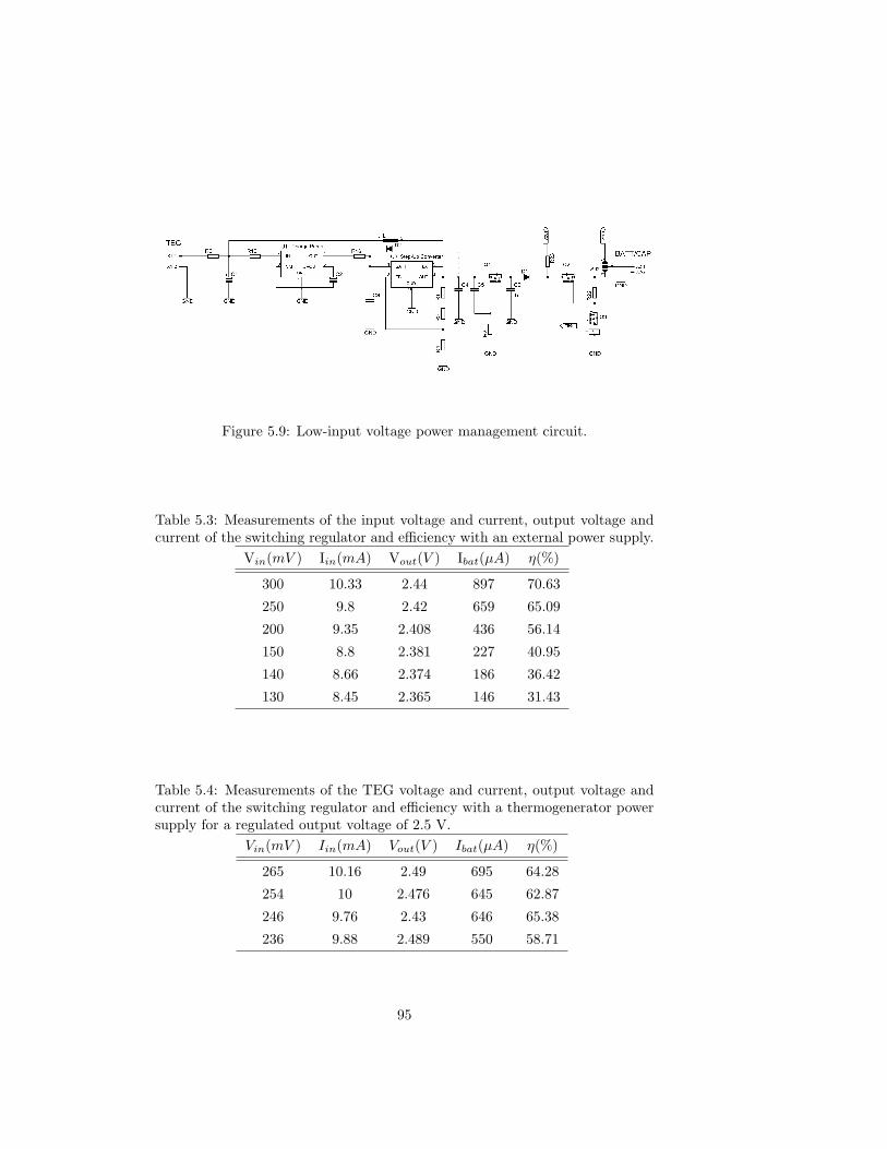
Figure 5.9: Low-input voltage power management circuit.
Table 5.3: Measurements of the input voltage and current, output voltage andcurrent of the switching regulator and efficiency with an external power supply.
Vin(mV ) Iin(mA) Vout(V ) Ibat(µA) η(%)
300 10.33 2.44 897 70.63
250 9.8 2.42 659 65.09
200 9.35 2.408 436 56.14
150 8.8 2.381 227 40.95
140 8.66 2.374 186 36.42
130 8.45 2.365 146 31.43
Table 5.4: Measurements of the TEG voltage and current, output voltage andcurrent of the switching regulator and efficiency with a thermogenerator powersupply for a regulated output voltage of 2.5 V.
Vin(mV ) Iin(mA) Vout(V ) Ibat(µA) η(%)
265 10.16 2.49 695 64.28
254 10 2.476 645 62.87
246 9.76 2.43 646 65.38
236 9.88 2.489 550 58.71
95

Table 5.5: Measurements of the TEG voltage and current, output voltage andcurrent of the switching regulatorand efficiency with a thermogenerator powersupply for a regulated output voltage of 3.8 V.
Vin(mV ) Iin(mA) Vout(V ) Ibat(µA) η(%)
400 9.15 3.77 346 35.63
300 13.28 3.745 344 32.34
250 17 3.695 339 29.47
220 16.01 3.33 306 28.93
150 8.69 2.058 189 29.83
Table 5.6: Electrical characteristics of the Power Management Unit
96

The external supply was replaced by the 128 A 1030 thermoelectric modulefrom Peltron. By means of human body to ambient temperature difference thecircuit was powered-up after around 100 seconds providing a regulated outputof 2.8 V. Upon power-up, the output voltage of the TEG dropped from 350mVto 250mV. The step-up converter kept regulating down to an input voltage of150mV. Table 5.4 and 5.5 shows the measured data as well as the calculatedefficiency output voltages of 2.5 V and 3.8 V, respectively. The efficiency of theconverter is lower for the case of the output voltage fixed at 3.8 V. Moreover, theoutput voltage in this case is not regulated when the TEG provides an outputvoltage lower than 250 mV.
Figure 5.10: Efficiency versus output current for Vout=2V
Table 5.6 summarizes the electrical characteristics of the designed powermanagement unit while Figures 5.10 and 5.11 show the efficiency versus outputcurrent for an output voltage of 3.8 V and 2 V. The curves of both figures stopat a point where the power management circuit was not regulating its outputanymore for the load connected. First row of Table 5.6 show the values of theminimum input voltage at which the power management circuit kept regulatingfor different output voltages. The minimum input voltage after startup decreaseswith the output voltage and increases with the value of the load connected. Thetypical minimum input voltage for starting to operate the converter circuit is290 mV after 100 s to 150 s. The startup time decreases with input voltagedramatically, e.g. for an input voltage of 400 mV, the startup time is between6 s and 15.8 s.
It is possible to connect the power management circuit to a battery in or-der to charge it. However, this connection does not require to make use ofa conventional battery charger (that includes a current-limit, a voltage-limitregulation loop and a time-limited charge termination circuit) and thus energyand area can be saved. A current-limit regulation loop is usually required to
97

Figure 5.11: Electrical characteristics of the Power Management Unit
avoid overcharging during the fast charging stage of NiMH and lithium batter-ies [94]. The designed circuit takes advantage of the intrinsic current limitingcharacteristics of the TEG for charging the battery without the need of dedi-cated hardware. Additionally, the voltage-limit regulation loop is undertakenby the boost DC-DC converter since it provides the required charging voltageat the output of the power management unit. Time-limited charge terminationcircuitry is also avoided by selecting a regulated voltage slightly below the max-imum topping voltage specified by battery manufacturers. A battery charger isreplaced though by a diode, D1, connected between the output of the regula-tor and the battery. This approach is more advisable for lithium-polymer thanfor NiMH accumulators, since the latter suffer from memory effect degradationwhen the charging procedure is not completed. This topology can be enhancedin terms of reliability by placing a Zener diode that limits the charging voltagein case of failure. It is also possible to connect the battery to the input of thepower management circuit in order to reduce the startup time and afterwordsconnect the TEG as input voltage for the power management circuit.
More detailed information about the power management unit and the ap-plication designed to power a wireless communication data that is able to senseand transmit information once every second is given in [22,118] (Chapter 12).
98

Chapter 6
System-level Simulation
The amount of available power in a system that employs an energy harvestingtransducer as a power supply is limited and it is not constant with time. Ifan energy storage element is employed, the requirement to fulfill is to generateenough energy to supply the electronic load connected to the energy harvestingsystem.
The evolution in the area of microprocessors and transceivers has made possi-ble communication modules with different power consumption modes dependingon its state. There are several power consumption modes: standby, transmis-sion, reception, sleep, etc. and some of them need a minimum time to beoperative.
In a given time interval, it is desirable to make equal the energy harvestedby the generator and the energy consumed by the load to assure an energyneutral operation, in other words, to assure that there will always be availableenergy to supply the load. This is the same as stating that the average powerin the time interval generated and spent must be the same for neutral opera-tion. A system-level simulation allows to design and modify a complete system(from the transducer to the load) that employs energy harvesting power sup-plies in the same simulation environment. Furthermore, it is possible to simulatehow a modification in the transducer affects the available energy for supplyingpower to the load. During the thesis, two different simulation environmentsthat combine mechanical and electrical models have been developed. An induc-tive generator model was analyzed in [21] (Chapter 11) employing the Ptolemysimulator whereas a piezoelectric generator model described with Verilog-A waspresented in [13] (Chapter 13). Both system-level simulations are done in thetime domain instead of the frequency domain.
Each one of the blocks that compose the complete system-level simulationof [13] (Chapter 13) must be modeled and included in the simulation of thecomplete energy harvesting generator. The energy transducer (a piezoelectrictransducer), the voltage regulator (a linear regulator) and the electronic load(an RF transmitter) are modeled at a behavioral level whereas the battery andthe converter were modeled at a circuit level.
99

The power consumption profile of the electronic load can be changed intwo different ways. The first one is the replacement of some hardware of thecommunication module (microprocessor, transceiver,) and the second one is achange in the power consumption mode of the communication module.
6.1 Energy Harvesting Transducer and Load En-ergy Profile
In the section titled 7. Power Conditioning Circuits of [18] (Chapter 8), the twooperation modes of an electronic load powered by an energy harvesting generatorare explained: continuous and intermittent. An energy storage element is notnecessary if the power consumption of the electronic device is lower than thepower generated by the energy harvesting generator and is only operated whenthere is generated power. For the rest of the cases, an energy storage elementis necessary , e.g. a battery.
The application and the harvested and consumed energy will determine theoperating mode to select. The objective of this chapter is to present a wayto calculate the initial charge of the storage element before starting operationas well as, the maximum quantity of energy that is required to store. Themethod is based on the works made by Kansal et al. presented in [124] and [30].This technique consists of a model to characterize environmental sources andelectronic loads that allows to determine the size of the energy storage elementemployed as a function of the power consumption profile of the load to assureenergy neutral operation.
When the difference between the last maximum and minimum of the meanpower delivered by the energy harvesting transducer to the energy storage de-vice is ∆, this means that the error to calculate the energy neutral operationpoint has an error margin of ±∆ and that no more stored power data are neces-sary [124]. Therefore, this method is feasible for periodical or quasi-periodicalenergy harvesting sources but not for non-periodical ones. Kansal et al. de-veloped this method for solar panels in outdoors applications where there ispower available only under sunlight and the cycles of converted power causedby day and night alternation are quasi-periodic. Nevertheless, this behaviour isnot limited to solar energy since mechanical energy sources or thermal energysources can also be periodical or quasi-periodical.
First of all, it is necessary to define the energy delivered by the transducerto the energy storage element and the energy consumed by the load in a math-ematical way. Figure 6.1 shows the power harvested by an energy harvestingtransducer and delivered to the energy storage element, Ps, as a function oftime. The mean power, ρs, is defined as
ρs =1T
∫
T
Ps(t)dt (6.1)
where T is the interval of time considered for the calculations that gives an errorof ±∆.
100

Figure 6.1: Power delivered by the energy harvesting transducer to the energystorage element as a function of time.
If it is assumed that Tlows−i is the i− th contiguous time duration for whichPs (t) ≤ ρs (t), then σ2 is defined as the maximum deficit of energy of the energyharvesting transducer, see Figure 6.1.
σ2 = maxi
∫
Tlows−i
ρs − Ps(t)dt
(6.2)
If it is assumed that Thighs−i is the i−th contiguous time duration for whichPs (t) ≥ ρs (t), then σ1 is defined as the maximum excess of energy of the energyharvesting transducer, see Figure 6.1.
σ1 = maxi
∫
Thighs−i
Ps(t)− ρsdt
(6.3)
The energy harvested by the transducer and delivered to the energy storageelement will be inside a certain margin limited by Esmin and Esmax:
Esmin ≤∫
T
Ps(t)dt ≤ Esmax ∀ t (6.4)
where Esmin is the lower limit and Esmax is the upper limit of the energydelivered by the energy harvesting transducer to the energy storage element.Esmin (T ) and Esmax (T ) are piecewise functions defined as:
Esmin (T ) =
ρsT − σ2
TTlows−i
∀T ≤ Tlows−i,ρsT − σ2 ∀ T ≥ Tlows−i.
(6.5)
Esmax (T ) =
ρsT + σ1
TThighs
∀ T ≤ Thighs−i,ρsT + σ1 ∀t ≥ Thighs−i.
(6.6)
Figure 6.2 shows the power consumption of an electronic load,Pl, as a func-tion of time. ρl is the average power consumption of the load. P1 is the power
101

Figure 6.2: Power consumption of the load as a function of time.
consumption of the load in the highest power consumption mode (e.g., trans-mission mode in a communication module) and it takes place during a timeinterval t1. P2 is the power consumption of the load in the lowest power con-sumption mode (e.g., standby mode in a communication module) and it takesplace during a time interval t2. Therefore, the electronic load consumption canbe defined as a function of the parameters (ρl, σ3, σ4).
ρl =1T
∫
T
Pl(t)dt (6.7)
If it is assumed that Thighs−i is the i−th contiguous time duration for whichPl (t) ≥ ρl (t), then σ3 is defined as the maximum overconsumption of energymade by the load, see Figure 6.2.
σ3 = maxi
∫
Thighl−i
Pl(t)− ρldt
(6.8)
If it is assumed that Thighs−i is the i−th contiguous time duration for whichPl (t) ≥ ρl (t), then σ4 is defined as the maximum less consumption of energymade by the load, see Figure 6.2.
σ4 = maxi
∫
Tlowl−i
ρl − Pl(t)dt
(6.9)
The lower and upper limits of the energy consumed by the electronic loadare:
Elmin (T ) =
ρlT − σ4
TTlowl−i
∀ T ≤ Tlowl−i,ρlT − σ4 ∀ T ≥ Tlowl−i.
(6.10)
Elmax (T ) =
ρlT + σ3
TThighl−i
∀ T ≤ Thighl−i,ρlT + σ3 ∀ T ≥ Thighl−i.
(6.11)
102

6.2 General Conditions for Energy Neutral Op-eration
When a wearable device, e.g., a node of a WSN, employs an energy harvestingsystem to be powered, the objective to achieve is to eliminate the need to replaceor recharge externally their battery. Thus, it is necessary to assure energyneutral operation or in other words, to assure that the battery will have alwaysthe energy required by the electronic device. Thus, the energy storage elementis defined with two parameters that are its initial charge when it is connected tothe energy harvesting system, B0, and the amount of energy that can be stored,B. The value of both parameters are calculated in this section.
In order to achieve energy neutral operation, the total energy in the system,ΣE, has to be greater than zero since the energy harvesting transducer, Es, plusthe initial energy stored in the battery, B0 has to be greater than the energyconsumed by the electronic load, El. Moreover, it is desirable in an energyharvesting system to assure that no energy is wasted or that the battery isdamaged due to overcharge. These two conditions can be expressed as:
ΣE ≥ 0 (6.12)
ΣE ≤ B (6.13)
The available energy in the system is equal to the initial energy stored in thebattery plus the energy harvested by the transducer minus the energy consumedby the load and minus the leakage energy due to the energy storage element.
ΣE = B0 + Es − El −∫
T
PleakTdt (6.14)
where Pleak is the leakage power of the energy storage element.The value of B0 can be calculated using the condition expressed by Equa-
tion (6.12). This condition is evaluated when the worst case takes place, that iswhen the generated energy by the harvesting transducer to the energy storagedevice is minimum, Esmin, and the energy consumed by the electronic load ismaximum, Elmax.
B0 + Esmin − Elmax −∫
T
PleakTdt ≥ 0 (6.15)
The above condition can be expressed as:
B0 + Esmin − Elmax − ρleakT ≥ 0 (6.16)
where ρleak is the mean leakage power of the energy storage element.In a similar way, the value of B can be calculated using the condition ex-
pressed by Equation (6.13). This condition is evaluated when the worst casetakes place, that is when the generated energy by the harvesting transducer
103

is maximum, Esmax, and the energy consumed by the electronic load is mini-mum, Elmin. In this case, the energy storage element will have at its maximumcapacity.
B0 + Esmax − Elmin −∫
T
PleakTdt ≤ B (6.17)
The above condition can be expressed as:
B0 + Esmax − Elmin − ρleakT ≤ B (6.18)
If the value of T tends to infinity for the two conditions expressed by Equa-tion (6.16) and Equation (6.18), it is obtained:
ρs − ρl − ρleak ≥ 0 (6.19)
ρs − ρl − ρleak ≤ 0 (6.20)
Equation (6.19) and Equation (6.20) can be simplified as:
ρs − ρl − ρleak = 0 (6.21)
Substituting in Equation (6.16), the value given for Esmin and Elmax byEquation (6.5) and Equation (6.11), respectively, and taking into considerationthe previous expression, it is obtained:
B0 − σ2T
Tlows−(σ3
T
Thighl
)≥ 0
∀ T ≤ Tlows and ∀ T ≤ Thighl(6.22)
B0 − σ2T
Tlows− (σ3) ≥ 0
∀ T ≤ Tlows and ∀ T ≥ Thighl(6.23)
B0 − σ2 −(σ3
T
Thighl
)≥ 0
∀ T ≥ Tlows and ∀ T ≤ Thighl(6.24)
B0 − σ2 − (σ3) ≥ 0∀ T ≥ Tlows and ∀ T ≥ Thighl
(6.25)
There are two conditions that give as a result the worst scenario and there-fore, the minimum value of B0. One of these conditions occurs when T is equalto Tlows and this value is greater than Thighl. The second condition occurs when
104

T is equal to Thighl and this value is greater than Tlows. For both cases the sameexpression is obtained:
B0 ≥ σ2 + σ3
∀ T = Tlows and ∀ T ≥ Thighl∀ T = Thighl and ∀ T ≥ Tlows
(6.26)
When the conditions given by Equation (6.26) and Equation (6.21) are ac-complished, the energy harvesting system can operate forever.
The conditions to avoid overcharging the energy storage element are ob-tained substituting in Equation (6.18), the value given for Esmax and Elminby Equation (6.6) and Equation (6.10), respectively, it is obtained a piecewiseexpression:
B0 + σ1T
Thighs−(−σ4
T
Tlowl
)≤ B
∀ T ≤ Thighs and ∀ T ≤ Tlowl(6.27)
B0 + σ1T
Thighs− (−σ4) ≤ B
∀ T ≤ Thighs and ∀ T ≥ Tlowl(6.28)
B0 + σ1 −(−σ4
T
Tlowl
)≤ B
∀ T ≥ Thighs and ∀ T ≤ Tlowl(6.29)
B0 − σ2 − (σ3) ≤ B∀ T ≥ Thighs and ∀ T ≥ Tlowl
(6.30)
The maximum amount of stored energy B will occur when the maximumdelivered energy by the transducer and the minimum spent energy by the loadare coincident in time. In this case, it is obtained the expression:
B0 + σ1 + σ4 ≤ B (6.31)
Combining (6.26) and (6.31), it is deduced that:
σ1 + σ2 + σ3 + σ4 ≤ B (6.32)
When this condition is accomplished, then no waste energy is produced fromthe energy harvesting transducer since all the energy generated can be storedin the energy buffer.
105

6.2.1 Conditions for Energy Neutral Operation with twoPower Consumption Modes
The electronic load is defined in terms of ρl, σ3 and σ4 whereas the energyharvesting transducer is defined in terms of ρs, σ1 and σ2. However, the con-sumption of the load can be chosen. This selection is made to assure that therewill be enough energy in the system to power the load. Nowadays, it is possiblethat electronic loads like microprocessors and RF transceivers work in differentpower consumption modes. Therefore, if the electronic load is for example acommunication module, it is possible to adapt its power consumption to theharvested energy by the transducer. This adaptation can be made in terms ofthe duration of a certain mode (sleep mode, stand by mode, transmission mode,reception mode, etc.) and the combination of the available operating modes.This section analyzes how to adapt the electronic load to the available harvestedenergy.
For this first approach, it is assumed that the electronic load works with twodifferent consumption modes: P1 and P2 (P1 > P2), each one with a durationt1 and t2, respectively. The consumption profile shown in Figure 6.2 is repeatedwith period τ . Next section gives a more general analysis with N differentconsumption modes for the electronic load.
The mean power consumed by the load, ρl, is:
ρl = x1P1 + x2P2 (6.33)
where x2 = 1− x1, t1 = x1τ and t2 = x2τ .The contiguous time duration for which Pl(t) ≥ ρl(t) is t1. Therefore, σ3 is
expressed as:
σ3 =∫
t1
(P1 − ρl) dt (6.34)
Substituting in the above equation the value of ρl given in Equation (6.33),it is obtained:
σ3 = (1− x1)x1τ (P1 − P2) (6.35)
In a similar way, it is obtained the value for σ4:
σ4 = (1− x1)x1τ (P1 − P2) (6.36)
To assure energy neutral operation, the value of ρl must be equal to ρtminus ρleakage. Taking this fact into account as well as the fact that the valuesfor P1 and P2 are fixed by the electronic load selected, the value of x1 can becalculated.
x1 =ρs − ρleak − P2
P1 − P2(6.37)
106

Thus, the value of x2 is:
x2 =P1 − ρs + ρleak
P1 − P2(6.38)
Once the value of x1 is calculated, the value of B, B0 and τ must be selectedin a compromise way that allows proper operation of the electronic load andthe selection of an energy storage elements that fit with the requirements of thesystem (for example, in terms of dimensions and weight). There is a minimumtime needed for the tasks associated to power consumption P1 and P2 that mustbe respected in order to allow the proper operation of the load. Therefore, aminimum value for τ is fixed by the requirements of the load.
t1 ≥ x1τmin (6.39)
t2 ≥ x2τmin (6.40)
For the case of only two different consumption modes, σ3 is equal to σ4 andthus, the conditions for the battery capacity and initial charge are:
σ1 + σ2 + 2 (1− x1) t1 (P1 − P2) ≤ B (6.41)
σ2 + (1− x1) t1 (P1 − P2) ≤ B0 (6.42)
6.2.2 Conditions for Energy Neural Operation with N PowerConsumption Modes
Figure 6.3: Power consumption of the load as a function of time.
107

Figure 6.3 shows a load with N different power consumption modes. PNis the lowest power consumption mode whereas P1 is the highest power con-sumption mode. The rest of the power consumption modes between these twovalues increase consecutively their power consumption from PN to P1. Whenthis assumption is accepted, for the general case of N different consumptionmodes, it is calculated that:
τ =N∑
i=1
xiτ (6.43)
where τ is period of the power consumed by the load and xi is the percentageof τ where the power consumed by the load is Pi.
ρl =N∑
i=1
Pixi (6.44)
The expressions for σ3 and σ4 are:
σ3 = τ
((P1 − ρl)x1 +
N−1∑
i=2
〈Pi − ρl〉xi)
= τ
N∑
i=1
〈Pi − ρl〉xi (6.45)
σ4 = τ
((ρl − PN )xN
N−1∑
i=2
〈ρl − Pi〉xi)
= τ
N∑
i=1
〈ρl − Pi〉xi (6.46)
The addition of σ3 and σ4 gives as a result:
σ3 + σ4 = τ
(N∑
i=1
〈ρl − Pi〉xi +N∑
i=1
〈Pi − ρl〉xi)
= τ
((P1 − ρl)x1
N−1∑
i=2
〈ρl − Pi〉xi +N−1∑
i=2
〈Pi − ρl〉xi + (ρl − PN )xN
)
(6.47)
(ρl − PN )xNτ can be expressed as a function of the rest of the power con-sumption modes:
(ρl − PN )xNτ = ρcT
(1−
N−1∑
i=1
xi
)− PNxNT
=
(N−1∑
i=1
(Pi − ρc)xi)τ
(6.48)
Therefore, substituting the above expression in Equation 6.47, it is obtained:
108

σ3 + σ4 = 2τN−1∑
i=1
〈ρl − Pi〉xi (6.49)
Therefore, the conditions to be fulfilled for energy neutral operation by aelectronic load with N consumption modes are summarized here employingexpressions (6.26) and (6.32).
σ2 + T
N−1∑
i=1
〈Pi − ρl〉xi ≤ B0 (6.50)
σ1 + σ2 + 2TN−1∑
i=1
〈Pi − ρl〉xi ≤ B (6.51)
6.3 System-level Simulation Example
A complete system-level simulation is shown in [13]. The schematic of the elec-tronic circuit simulated, see Figure 6.4, is composed by five different blockswhich have their functionality described with Verilog-A. The block called tri-angpos has a description of the deflection done by the piezoelectric element. Thesecond block, piezofilm, contains a description of the behavior of a triangularcantilever with a concentrated load applied at its end and composed with piezo-electric and non-piezoelectric material. Between the two output terminals ofthe block piezofilm, it is obtained the voltage generated by the bending beam.The variables of these two blocks have an appropriate value for simulating thestep of a person walking. Then, a voltage doubler is employed as rectifier withSchottky diodes. Afterwards, a capacitor stores the energy delivered by thepiezoelectric bending beam. The block GenRegulator is a linear regulator thatwhen it is active charges the battery. The electronic device selected as electronicload is an RF transmitter.
Figure 6.4: Schematic of a battery-powered RF transmitter
109

The simulation is first done without a load connected in order to measureρs, σ1 and σ2. Therefore, the mean power delivered by the energy harvestingtransducer to the energy storage device is measured with the voltage doubler andthe linear regulator connected. In this way, it is not necessary any assumptionabout the efficiency of the electronics which depends on the voltage and currentdelivered by the transducer and the fixed input and output voltages for theoperation of the linear regulator. This kind of simulation environment allows tomake a complete simulation of an energy harvesting system. Thus, it is possibleto predict for example, when the electronic load is a RF transmitter module,how often it is achievable to transmit data without discharging the battery,how changes in the piezoelectric element modify the electrical energy generatedand calculate the appropriate parameters of the battery to employ. A secondsimulation with the load, a transmitter module, connected is done in order toprove the theoretical analysis done with the calculated parameters.
Table 6.1: Parameters employed for the simulation.Parameter ValueSOCi 500 mVW0 30 mmts 1 mmn 10L 30 mmvreg 3.2 Vvlimsup 10 Vvliminf vreg+0.1 VRint−reg 150 mΩT 400 mstr 350mstf 125msiconsreg 10µAcintreg 10µFcap 10µFamplm 6mmCBAT 2mAh
The parameters employed for the simulation are summarized in Table 6.1where SOCi corresponds to the initial state of charge of the battery, W0 isthe width of the piezoelectric beam, ts is the thickness of the non piezoelectricmaterial that composes the beam, T is the period of the triangular mechanicalexcitation, tr is the rise time for the mechanical excitation, tf is the fall timeof the mechanical excitation, n is the number of piezoelectric films connectedin series, vreg is the minimum voltage needed by the linear regulator, vliminfis the minimum voltage at which the energy transducer gives electrical energyto the battery and the load, vlimsup is the maximum voltage at which thecapacitor is charged, iconsreg is the consumption of the linear regulator, cintreg
110

is the internal capacitor of the linear regulator and cap is the value of thecapacitor connected after the voltage doubler and before the linear regulator.Employing the parameters shown in Table 6.1, it is obtained a value of ρs=14.88 µW. Therefore, the power that is delivered from the transducer to thebattery is known.
The power consumption profile of the load is always a well known data. Thewireless transmitter employed in the simulations has a power consumption insleep mode, Psleep, of 5.79 µW and a power consumption in transmission mode,PTx, of 27 mW. The minimum transmission time, Tx, required is 300µs whereasthe time between transmissions, τ , will be calculated taking into account the en-ergy delivered by the transducer. If it is considered that the mean leakage powerof the battery is zero, the power generated by the transducer and consumed bythe load must be equal, see Equation 6.21, ρl = ρs, the following expressionrelates the mean power generated by the energy harvesting transducer with theparameters of the load.
ρl =1τ
[PTxTx+ Psleep (τ − Tx)] (6.52)
From Equation (6.52) it is deduced that time between transmissions, τ , is:
τ =(27mW − 5.79µW ) 0.3ms
14.88µW − 5.79µW= 891ms (6.53)
The values of σ3 and σ4 are calculated in Equations 6.54 and 6.55.
σ3 = (PTx − ρs)Tx = (27mW − 14.88µW ) 0.3ms = 8.1µJ (6.54)
σ4 = (ρs − Psleep) (τ − Tx) == (14.88µW − 5.79µW ) (891ms− 0.3ms) = 8.1µJ
(6.55)
With the data extracted from the simulation done without load connectedto the energy harvesting system, the values of σ1 and σ2 are calculated em-ploying Equation 6.3 and Equation 6.2, respectively. The values obtained areσ1=127 µJ and σ2=185.1 µJ. Therefore, applying Equation 6.41 and Equa-tion 6.42, the parameters of the battery are calculated. The values obtainedare B ≥330.28 µJ and B0 ≥194.19 µJ. Thus, CBAT and SOCi can be deducedemploying Equations (6.56) and (6.57), respectively.
CBAT =3600BVdload
(6.56)
SOCi =3600B0
VdloadCBAT(6.57)
However, the values chosen for the initial state of charge of the battery,SOCi, and the capacity of the battery, CBAT , were different, see Table 6.1,
111

since the values obtained were very small and the values to use just must begreater than these values. 2 mAh of capacity is a value for lithium coin batteries.Simulations with values of SOCi and CBAT close to the minimum ones aredone later. The simulation results with the parameters of Table 6.1 and anRF transmitter connected as a load are shown in Figures 6.5 and 6.6. Fromthese simulation results it is deduced that the time between transmission is theappropriated one since the state of charge of the battery almost remains constantas well as the voltage on the battery. The transmissions are done periodicallyevery 891 ms from the first moment.
Figure 6.5: Simulation results with load for the parameters summarized in Ta-ble 6.1. The waveform called SOC shows the state of charge of the batterywith a voltage range from 0 to 1 V. IRPB4 is the current flowing into thebattery. vinreg is the voltage at the input of the linear regulator and vdload isthe voltage of the battery that is supplied to the RF transmitter.
Another simulation has been realized. The number of piezoelectric elementsconnected in parallel has been doubled from the previous simulation but theperiod of the mechanical excitations has been tripled. The results obtainedfrom this simulation are summarized in Table 6.2. Figure 6.7 shows the resultsobtained with no load connected to the system. From this simulation, thevalues shown in Table 6.2 have been calculated. The change in the period ofthe mechanical excitation causes that less electrical energy is generated by the
112

Figure 6.6: Zoom view of the simulation results with load for the parameterssummarized in Table 6.1.
transducer and therefore stored in the battery despite the fact of incrementingthe number of piezoelectric films from 10 to 20. Figure 6.8 shows the resultsfor the simulation with the Enocean transmitter connected and a time betweentransmissions of 1.45 s.
Table 6.2: Results obtained from the simulation.Parameter Valueρs 11.39 µWτ 1.45 sσ3 8.1 µJσ4 8.1 µJσ1 133.64 µJσ2 178.26 µJBmin 328.1 µJB0min 186.36 µJ
In the two previous simulations, the values obtained for the capacity andinitial charge of the battery are small since the mechanical excitation of theenergy harvesting transducer is done periodically. Next simulation shows a
113

Figure 6.7: Simulation results without charge for n=20, T=1.2 s and the restof parameters summarized in Table 6.1. The waveform called SOC shows thestate of charge of the battery with a voltage range from 0 to 1 V. IRPB4 isthe current flowing into the battery, vinreg is the voltage at the input of thelinear regulator and vdload is the voltage of the battery that is supplied to theRF transmitter.
different scenario where the energy harvesting transducer is not excited periodi-cally. Therefore, there is not mechanical excitation over the transducer between0 and 100 s and also between 450 s and 500 s. Moreover, there are three dif-ferent mechanical excitations connected through an adder to the piezoelectrictransducer to create a non-periodic mechanical excitation as can be seen in theschematic simulated, Figure 6.9. Each one of these three different mechanicalexcitations has values of rise time, tr1, tr2, tr3 and fall time, tf1, tf2 and tf3.The value selected for the rise and fall time of the mechanical excitations isthe same while the period of the three mechanical excitations is related sinceT2 = 2T1 and T3 = 3T1. The input and output of the block called piezofilmare shown in Figure 6.10. The first waveform corresponds to the voltage atthe output of the piezoelectric elements connected in parallel and the secondwaveform is the mechanical excitation applied to the piezoelectric films.
The parameters employed during the simulation are shown in Table 6.3 andthe simulation waveforms obtained without electrical load are displayed in Fig-ure 6.11. The results obtained from the simulation are summarized in Table 6.4.
114

Figure 6.8: Simulation results with charge for n=20, T=1.2 s and the rest ofparameters summarized in Table 6.1. The waveform called SOC shows thestate of charge of the battery in per one, IRPB4 is the current flowing into thebattery, vinreg is the voltage at the input of the linear regulator and vdload isthe voltage of the battery that is supplied to the Enocean transmitter.
Figure 6.9: Schematic of a battery-powered RF transmitter simulated with theparameters of Table 6.3.
115

Table 6.3: Parameters employed for the simulation.Parameter ValueSOCi 500 mVW0 30 mmts 1 mmn 10L 30 mmvreg 3.2 Vvlimsup 10 Vvliminf vreg+0.1 VRint−reg 5 ΩT1 400 msT2 2T1
T3 3T1
tr1 350 mstr2 350 mstr3 350 mstf1 125 mstf2 125 mstf3 125 msiconsreg 10µAcintreg 10µFcap 10µFamplm1 6 mmamplm2 1 mmamplm3 1 mmCBAT 300 nAh
The mean power generated is in the same order of magnitude than in the twoprevious simulations as well as σ3, σ4 and the period between transmissions.Nevertheless, the values for B0min and Bmin have increased one order of mag-nitude since there is no mechanical excitation during all the simulating time.Thus, the simulation with the RF transmitter connected would allow to probethe validity of Equation 6.51 and Equation 6.50. The RF transmitter blockdescribed in Verilog-A employs a resistor of 132 Ω and a resistor of 633 kΩ tosimulate the power consumed when the transmitter is sending data and in sleep-ing mode, respectively. Therefore, the power consumed by this load depends onthe voltage supplied by the battery and this voltage also depends on the stateof charge of the battery. Thus, it has been supposed a battery voltage of 2.05 Vfor calculating the period between transmissions.
The values for the minimum capacity of the battery and its minimum initialstate of charge are calculated from the values obtained for Bmin and B0min inTable 6.4 and the values obtained are CBATmin=203 nAh and SOCimin=0.9.Figure 6.12 shows the simulation results employing those values. The results
116

Figure 6.10: Total mechanical excitation combined from three different mechan-ical excitations.
obtained show that the RF transceiver stops to transmit at 100 s since thevoltage on the battery is lower than 1.9 V that is the minimum supply voltage ofthe transceiver. At this moment the state of charge of the battery is 6.3%, theminimum obtained during the simulation. Afterwards the battery is chargeda 101% from this minimum state of charge to its maximum state of charge(107.84%) and then decreases again due to the fact that there is no mechanicalexcitation from 450 s until the end of the simulation. However, the state ofcharge at the end of the simulation is not the same as at the beginning, what isconsidered energy neutral operation, due to the fact that the mean voltage ofthe battery during the simulation is greater than that employed for calculatingthe time between transmissions.
Figure 6.12 shows the simulation results obtained with CBAT=1 µAh andSOCi=0.3. The capacity chosen for the battery is bigger than the 203 nAhobtained as a minimum value and its initial state of charge is also bigger than theminimum initial charge of 182nAh calculated. In this case, the RF transmitteris supplied during all the simulation and the minimum state of charge of thebattery 12.7%. The maximum state of charge obtained is of 35.4% at t=450 sand decreases to 0.29% at t=500 s since there is no mechanical excitation inthis time interval. In this case the initial state of charge and the final state ofcharge are almost equal since the mean value of the battery voltage during the
117

Figure 6.11: Simulation results without load for the parameters summarized inTable 6.3. The waveform called SOC shows the state of charge of the batteryin per one. IRPB4 is the current flowing into the battery. vinreg is the voltageat the input of the linear regulator and vdload is the voltage of the battery thatis supplied to the RF transmitter.
simulation is practically the same that the employed for the calculation of thetime between RF transmissions. The voltage on the battery is quite constantsince the state of charge of the battery is also almost constant since the capacityof the battery in this simulation is five times the minimum capacity calculated.Then, the system works in energy neutral operation.
118

Table 6.4: Results obtained from the simulation.Parameter Valueρs 10.96 µWτ 2.02 sσ3 8.1 µJσ4 8.1 µJσ1 138.06 µJσ2 1.3 mJBmin 1.46 mJB0min 1.31 mJ
Figure 6.12: Simulation results with the Enocean transmitter as a load for theparameters summarized in Table 6.3. The waveform called SOC shows thestate of charge of the battery in per one, IRPB4 is the current flowing into thebattery, vinreg is the voltage at the input of the linear regulator and vdload isthe voltage of the battery that is supplied to the RF transmitter.
119

Figure 6.13: Simulation results with the Enocean transmitter as a load for theparameters summarized in Table 6.3. The waveform called SOC shows thestate of charge of the battery in per one, IRPB4 is the current flowing into thebattery, vinreg is the voltage at the input of the linear regulator and vdload isthe voltage of the battery that is supplied to the Enocean transmitter.
120

Chapter 7
Conclusions
This chapter gives the general conclusions of the thesis whereas each paperincluded in Part II has its specific conclusions for the addressed problem. Thereare several general remarks to do for the design of an energy harvesting powersupply from human power.
It is important to distinguish between energy harvesting from human bodyand from the environment. Both cases can use the same transducers and inputenergies. Nevertheless, the design of the transducer, the power managementunit or the electronic load to power is different since the energy input levels inboth cases as well as the amplitude and frequency of the signals of mechanicalvibrations are not comparable. Normally, the energy levels associated to humanbody are lower than the energy levels associated to environmental sources whichgives as a result that sophisticated techniques must be used to increase theefficiency of the transducer, to control the power management unit and to powerthe load.
An energy harvesting power supply has to be considered as a complete systemwhere each element must be adapted to accomplish the requirements of the load.A system-level simulation is of special interest because it allows to simulate themechanical and electrical elements together. This is a great advantage in orderto increase the efficiency of both elements in the same simulation environment.Moreover, it is useful to decide the energy profile of the load (continuous ordiscontinuous operation) and the use of an energy storage element. Furthermore,with a system-level simulation, a trade off between the requirements of the loadand the dimensions of the transducer can be easily made.
An application example for energy harvesting systems is to sense and trans-mit data. Therefore, a communication module with a microprocessor and atransceiver can be considered as a standard load for an energy harvesting sys-tem. Taking into account today’s energy consumption requirements of low powertransmission modules and the amount of energy that is harvested from humanbody, the most usual scenario is the discontinuous operation of the load. Theinclusion of an energy storage element like a lithium ion battery, a capacitor ora supercapacitor must be evaluated taking into account different scenarios and
121

parameters. It must be considered if the load must operate continuously, thedifferent power consumption modes of the load, the minimum operation timethat needs each power consumption mode, the maximum time between trans-missions, the amount of energy that can be stored in the energy storage elementand the size, weight and volume that adds this element to the complete system.
A system-level simulation is ideal to make this kind of decisions since themodeling of the system elements can be done as in [13] with the physical equa-tions of the transducer in order to include the mechanical part of the systemand electrical or behavioral models for the rest of the components. In this way,it is simple for example to evaluate different transmission modules only takinginto account their voltage supply and power consumption.
Once a general conclusion from the system point of view is made, specificconclusions for each element that is present in an energy harvesting power supplyare given. The type of input energy and transducer form a tandem since theelection of one imposes the other. The input energy must be measured ormodeled in order to include it as the input variable of the system. In thecase of TEGs the input energy can be modeled without the help of a previousmeasurement, only taking into account that the skin temperature is not constantover the body. However, for kinetic energies it is necessary to measure them inorder to incorporate this data to a simulation environment or to model them.These measurements allow to include real inputs to the system and thereforeto obtain realistic results and predictions. It is important that measurementsare done in different parts of the human body doing different physical activitiesto locate which positions and activities produce more energy. However, someapplications force the location of the energy transducer to a specific part of thehuman body close to the wearable device to supply.
There are several ways to model a transducer. One way consists in the useof the physical equations of the transducer like in [13] (Chapter 13) where thephysical equations of a piezoelectric transducer were included directly in themodel. A second method is to employ a circuit model that includes the con-version of the available energy into electrical energy as was shown in Chapter 3where an electrical circuit that contains mechanical and electrical parts is givenas well as in Chapter 5 where thermal and electrical parts are combined. Thethird proposed model presented contains only the electrical part of the completemodel like in [20] (Chapter 10). The two first methods allow to improve thecoupling between the energy source and the transducer modifying the physi-cal parameters of the transducer. However, the third method only takes intoaccount the electrical response of the transducer without the possibility of re-arranging its physical design. Therefore, the two first approaches are indicatedwhen the the coupling between body and transducer wants to be explored andimproved whereas the last one is a simplified model that can be employed asthe electrical voltage supply for the power management unit.
For all the cases, it is necessary to take into account the location of the energyharvesting transducer that usually depends strongly on the application. Mea-surements done with the energy harvesting transducer in the selected locationare of special importance to adjust and validate the models for the transducers
122

since each location even with the same transducer generates different voltageand current waveforms. For the third way under consideration to model an en-ergy harvesting transducer, the measurements are the only possibility to adjustthe electrical source of the model.
7.1 Smart Clothes and Energy Harvesting
Nowadays, there is not yet available a real integration of wearable devices inclothes and it is only possible to attach external portable devices to clothes.Clothes and shoes are in direct contact with body skin. Thus, it is desirablethat textiles and clothes are involved in different ways in the human body energyharvesting system:
• Developing comfortable connection technologies to integrate the transduc-ers into fabrics. Furthermore, also the fabrics can be developed to act asan energy human transducers themselves (energy-harvesting fabrics).
• Developing conductive properties to create electronic circuits that con-nect the different components of the energy harvesting system (the energyharvesting transducers, the power management unit and the electric load).
This gives as a result a step further in the textile sector: e-textiles andsmartclohtes. The improvement in these technologies and their merge withenergy harvesting supplies employing human energy would be an improvementfactor in this field based in the fact that the integration of the transducer insmartclothes or e-textiles would increase the surface of the transducer and itsmechanical coupling with human body and therefore, more electrical energywould be generated. The mechanical coupling between the transducer and thehuman body depends on the location of the transducer and the activity thatis done. A specific design taking this into account can increase very much theefficiency of the transducer as has been demonstrated in [19,21] ( Chapter 3 andChapter 4).
7.2 Power Management Unit
The transducer is the element that converts the available human body energyinto electrical energy. The combination of transducer and human body locationgives as a result different output voltage and current levels generated by thetransducer. These levels condition the power management unit design. Lowoutput voltage levels obtained by TEGs and inductive transducers are no longeran issue for the design of power management units with the new technologiesin the field of CMOS transistors that have low gate threshold voltages likeALD110800 with a gate threshold voltage of 0 V, ALD110802 [125] with a gatethreshold voltage of 0.2 V or BSH105 [126] with a higher threshold voltage(0.57 V) but a lower drain source resistor than the other ones when a discrete
123

design is required. Another already known solution can be the employment ofN-channel FETs which are self-conducting with a zero gate voltage [119]. Thenext step is the integration of the power conditioning circuits on the same chipto be powered. Several CMOS and BiCMOS technologies would be suitable forthis purpose. More advances in the field of power management circuits wouldimprove a lot the possibilities and simplify the designs of energy harvestingpower supplies employing human body as input energy source.
There are two important factors to take into account in the design of thepower management unit. The first one is related with the design of a startercircuit for the main power converter. A starter circuit initially stores enoughvoltage and/or current level to start switching the transistors of the main powermanagement circuit [119]. A starter circuit must be included when it can notbe assured that there will be enough energy for starting the operation of themain DC-DC converter circuit. The second one is related with the efficiencyof the power management circuits. As important as increasing the efficiency ofthe power management circuit itself is developing techniques that ensure thatthe energy extracted from the transducer is the maximum available. For thecase of piezoelectric transducers, it was calculated the optimum value of thecapacitor for defined load conditions. For other transducers like the TEGs, themaximum power point tracking method can be applied, if the design of a lowpower consumption control loop can be achieved [127,128].
Energy harvesting power supplies are able to supply power to present-daylow power electronic devices as was demonstrated for example with the appli-cation presented in [22, 118]. Obviously, the load must be a low power con-sumption device and it is preferable to operate in a discontinuous way withouta battery. This conclusion is based on the simulation results obtained in [13](Chapter 13). This method is also employed to supply the RF communicationmodule connected to the TEG in [22, 118] (Chapter 12). However, the evolu-tion in low power transmission modules can change this conclusion dependingmostly on the evolution of the power consumption in stand-by mode and theconfiguration time in transmission operation.
For the case of an energy harvesting power supply from human body itis not required to make use of a conventional battery charger (that includes acurrent-limit, a voltage-limit regulation loop and a time-limited charge termina-tion circuit) and thus energy and area can be saved. A current-limit regulationloop is usually required to avoid overcharging during the fast charging stageof NiMH and lithium batteries [94] that is not required in our case due to thethe intrinsic current limiting characteristics of the TEG, piezoelectric films andinductive generators. Additionally, the voltage-limit regulation loop is under-taken by the power management unit that has to adapt the output voltage levelof the transducer to the requirements of the load. Time-limited charge termina-tion circuitry is also avoided by selecting a regulated voltage slightly below themaximum topping voltage specified by battery manufacturers. Hence, for thiscase, a battery charger is replaced by a diode or a transistor connected betweenthe output of the regulator and the battery to avoid the supply of the converterwith the battery. This approach is more advisable for lithium-polymer than
124

for Ni-MH accumulators, since the latter suffer from memory effect degradationwhen the charging procedure is not completed [118]. This topology can be en-hanced in terms of reliability by placing a Zener diode that limits the chargingvoltage in case of failure.
7.3 Energy and Power requirements of Applica-tions
It is better to do the quantification of energy harvesting power supplies in termsof energy than power since it is a more meaningful magnitude when dealing withthe discontinuous events of the load and the source of the system. The design ofthe electronic load to power with the energy harvesting power supply is not anobjective of the thesis. Nevertheless, considering a communication module asthe load, some conclusions and suggestions can be given. An important factorrelated with the energy consumption of the load is the communication protocolemployed by its transceiver.
The particular needs of the application must be evaluated before assumingthe employment of a de-facto standard communication protocol like for exampleZigBee. The communication protocols can be compared in terms of radio effi-ciency (defined as the ratio between the payload and the gross data rate) and interms of Time on Air (defined as the duration of the data transmission) [118].In [118] a comparison between the Nordic proprietary solution and ZigBee wasmade in these terms and it was concluded that the Nordic protocol was the bestone for the particular needs exposed (less than 200 bits of payload).
It is also interesting to notice that the energy consumption of the micropro-cessor (that form part of the communication module) can be reduced applyingchanges in its code. It was demonstrated in [129] that a code optimization ofthe operating system employed by wireless sensor networks reduce their energyconsumption.
125

126

Part II
Included Papers
127


Chapter 8
Paper 1: Review of EnergyHarvesting Techniques forMicroelectronics
Loreto Mateu and Francesc Moll
Proceedings of SPIE Microtechnologies for the New Millenium, pp.359–373, Sevilla, 2005.
129

Review of Energy Harvesting Techniques and Applicationsfor Microelectronics
Loreto Mateu and Francesc Moll
Universitat Politecnica de CatalunyaDept. of Electronic Engineering
Barcelona, Spain
ABSTRACT
The trends in technology allow the decrease in both size and power consumption of complex digital systems.This decrease in size and power gives rise to new paradigms of computing and use of electronics, with manysmall devices working collaboratively or at least with strong communication capabilities. Examples of these newparadigms are wearable devices and wireless sensor networks. Currently, these devices are powered by batteries.However, batteries present several disadvantages: the need to either replace or recharge them periodically andtheir big size and weight compared to high technology electronics. One possibility to overcome these powerlimitations is to extract (harvest) energy from the environment to either recharge a battery, or even to directlypower the electronic device. This paper presents several methods to design an energy harvesting device dependingon the type of energy avaliable.
Keywords: Energy harvesting, wearable devices, wireless sensor networks
1. INTRODUCTION
One of the most important trends in the electronic equipment technology from its origins has been the reduction insize and the increase in functionality. Nowadays small, handheld, though very powerful devices are commerciallyavailable that allow the user to play music, to wirelessly communicate or to compute practically everywhere or,in other words, ubiquitously. In the next years there will be new products available providing vision and otherextended functions to the wearer. The size of such devices is becoming so small that instead of portable devicesthey are becoming wearable devices that can be integrated in everyday use objects like watches, glasses, clothes,etc.1
All those units, based on today’s microelectronic technology, need an external power supply. The size of theelectronic circuit and the energy needed to perform a single (binary) operation2 has been drastically reducedduring the last decades, following Moore’s Law. Therefore, advances in low power design open the possibility toharvest energy from the environment to power electronic circuits.
This work presents current approaches of using energy extracted from the environment to power microelec-tronic devices. The electrical energy to power the electronics is generated from either kinetic, electromagneticor thermal energy. The obtained energy can then be used to recharge a secondary battery or, in some cases, topower directly the electronics. The output voltage and current of the generators is transient and discontinuousin nature, and must be converted to a DC signal. Therefore it is necessary to design a converter and/or storagecircuit that needs to take into account the output signal of the generator and its impedance.
The structure of the paper is as follows: First, in section 2, the technology trends for both battery (energygeneration) and electronic devices (energy consumption) are briefly sketched. Then, energy harvesting devicesare classified in section 3 according to source and type of energy. Sections 4 through 6 review the principlesbehind different types of energy conversion. In section 7 it is discussed the power conditioning needed by electronicdevices relying on energy harvesting, depending on their consumption and energy generation possibilities. Finally,in section 8, the conclusions of the work are presented.
Further author information: (Send correspondence to F. Moll)F. Moll: E-mail: [email protected]. Mateu: E-mail: [email protected]
Keynote Address
VLSI Circuits and Systems II, edited by José Fco. López, Francisco V. Fernández,José María López-Villegas, José M. de la Rosa, Proceedings of SPIE Vol. 5837(SPIE, Bellingham, WA, 2005) 0277-786X/05/$15 · doi: 10.1117/12.613046
359
130

Table 1. Characteristics of batteries.Battery type Vol. Energy density Grav. Energy density Self-discharge Cycle Life
Wh/dm3 Wh/kg % per year no.Alkaline 300 125 4% 1Ni-Cd 100 30-35 15-20% 300Ni-MH 175 50 20% 300Li-ion 200 90 5-10% 500
2. TECHNOLOGY TRENDS
2.1. Battery evolution
In the great majority of today’s wearable or portable devices, the energy necessary for their operation is providedby batteries. Batteries are a significant fraction of the total size and weight of the system. As technologyscales down, this fraction is expected to further increase. Also very important is the requirement for propermaintenance of batteries, with the need to either replace or recharge them. This is a serious limitation tocomputing paradigms like ubiquitous computing or sensor networks, in which there are dozens or hundreds ofsmall systems with batteries to maintain.
Of course, these inconvenients do not hide the advantages of batteries as a reservoir energy source. Forexample, we can characterize the batteries by their energy density, with respect to volume and weight, calledvolumetric and gravimetric energy density respectively. Table 1 shows some typical values of energy densitiesand self-discharge values for commercial batteries. It is seen how the most modern batteries (Li-ion) presentbetter characteristics of energy density, self-discharge current and number of cycles.
It is worth noting that these values of energy density are the best option available today. Recent advancesin capacitor technology have led to the development of the so-called ultracapacitors, with a capacitance value ofthe order of kF. Such impressively large capacitors, however, present an energy density around 3 Wh/kg, veryfar from average battery values.3 The main advantages of ultracapacitors is the supplied peak power, and thenumber of cycles. These characteristics make them more oriented to automotive applications than to low powerelectronic devices, where batteries are still the choice for energy storage.
Still, battery technology has evolved very slowly compared to electronic technology.4 For example, while diskstorage density has increased over 1,200 times since 1990, battery’s energy density has increased only about3 times. New approaches are on the way for very small size portable batteries that may enable the size andweight reduction of wearable systems and sensor networks. They are based on new technologies as the thin-film Lithium-ion or Lithium polymer cells and some of them are still under development.5 One of the mostpromising alternatives is the fuel cell, power generators that use chemical fuels (i.e. Hydrogen or Methanol).The gravimetric energy density of fuel cells is expected to be three to five times larger than Li-ion cells andmore than ten times better than Ni-Cd or Ni-MH batteries whereas the volumetric energy density is six to seventimes larger than Li-ion.6 However, the maintenance problem is not solved; these cells need to be refueled oralternatively they have to be manufactured carrying enough fuel to sustain the battery operation during all itsexpected lifetime.
Secondary batteries are in principle a better choice for ubiquitous or wearable systems because they can berecharged in several ways, in many cases without extracting the battery from the system. Actually, one of thepossibilities to recharge such batteries is to use energy harvested from the environment.7 In this sense, energyharvesting is not trying to replace batteries, but instead alleviating some of their drawbacks, especially in relationwith the maintenance issue.
2.2. Power consumption of microelectronic devices
Following Moore’s law, integrated circuit technology evolves following a transistor size shrinking trend. Togetherwith this trend and because of reliability reasons the supply voltage (VDD) is also reduced. The net result is areduction in energy consumption due to the reduction in the size of parasitic components. For a scale reduction
360 Proc. of SPIE Vol. 5837
131

Table 2. Classes of energy harvesting devices.
Energy Source Type of EnergyHuman Kinetic, ThermalEnvironment Kinetic, Thermal, Radiation
with a factor α (α > 1), the energy consumed by a given shrunk circuit performing a given task is reduced by(1/α)3, as dicussed elsewhere.8
It is also important to consider the use model of the electronic device. For example, the power consumptionof a wearable can be scaled following two different scenarios:
1. Maximum performance use: the improvement in technology allows to reduce the time per service, but itis used to give a higher number of services. In this case the total power consumption for the processingfunctions is scaled as (1/α)2.
2. Constant number of services: the improvement in technology reduces the time per service and the powerconsumption but the user does not increase the number of required services. The power consumption forthe processing functions is scaled as (1/α)3.
Current portable electronic devices have different low power or sleep modes to save energy during times ofinactivity. The management of these modes is very important in relation with an energy harvesting strategy,allowing to “refill” the energy reservoir of the system during these periods of low activity. This means thatgenerally, a discontinuous operation use model is mandatory for the energy harvesting approach.
3. ENERGY HARVESTING DEVICES
Before starting to discuss the different methods of energy harvesting, let us look at the definition of an energyharvesting device as understood in this paper.
An energy harvesting device generates electric energy from its surroundings using some method of what iscalled in the literature Direct Energy Conversion techniques.9 Therefore, the energy harvesting devices hereconsidered do not consume any fuel or substance, so that the maintenance problem mentioned above does notapply. On the other hand, as the environment energy levels are very low (at least for today’s electronic devicesrequirements), the use models mentioned in the previous section are very important.
3.1. Classification of Energy Harvesting devices
We may classify the different energy harvesting devices in two ways: considering who or what provides the energyfor conversion, and what type of energy is converted. Table 2 relates the two classification schemes.
In the first classification scheme we can distinguish between two kinds of devices. First, devices that use partof the energy of the user of the electronic appliance. It will usually be a human, but it could be also an animal,for example for a remote monitoring device. We call this first kind of devices Human Energy∗ devices.10 Thesecond kind of energy harvesting device gets its energy from the environment, and thus we call them EnvironmentEnergy devices. This classification takes into account that, following the first principle of thermodynamics, agreater amount of energy must be spent to obtain a certain amount of electrical energy. In the case of HumanPower it is the user that in some way or other provides this energy and, though the energy levels are verysmall, the effect may prove noticeable when several devices depend on the activity of a single user. In order toevaluate the burden of energy harvesting on user activities, it is possible to use a simple biomechanical model tocalculate the energy involved in a human step,11 obtaining around 40 J. In comparison, the energy of a short RFtransmission can be evaluated in the order of 100 µW. This means that the extra energy demanded to obtain
∗In most of the literature the term Power is used instead of Energy. We prefer the term Human Energy instead ofHuman Power because energy is a more meaningful magnitude when dealing with discontinuous events, as discussed insubsection 7.1.
Proc. of SPIE Vol. 5837 361
132

enough energy is very small for some applications, and therefore it makes sense to consider human beings as apossible energy source.
The second classification scheme may consider three types of energy: kinetic, electromagnetic radiation(including light and RF), and thermal.
For Human Energy devices only kinetic and thermal energy are available. In the case of kinetic Humanenergy, one may distinguish between those actions made specifically to generate energy and casual movementsmade during normal behavior. These two cases are called by the Human Power research group of the DelftUniversity of Technology12 Active and Passive Human Energy respectively. Following this definition, thermalHuman Energy is always passive.
Environment Energy sources include kinetic energy in the form of vibrations, radiation as solar energy or RFradiation, and thermal energy. The energy harvesting devices may pick up vibrations when located on machines,building elements or other places near vibrating sources. Radiation may come from natural or artificial sources.Thermal energy depends on the existence of a temperature gradient. While the transducing methods may besimilar to the Human Energy devices, the excitation magnitudes, frequency spectra and periodicity are verydifferent, and therefore each case must be studied separately. This will also have consequences in the electricalpower conditioning circuit.
3.2. Some working examples
There are several examples, both commercial and in the research stage that apply energy harvesting to powerelectronic products.
3.2.1. Human Active Energy
This is an old concept that has revived recently, basically improving the ratio of time of use with respect to timeof charge.
Devices in the market using human energy as the only energy source include radio receivers, electric torchesand phone battery chargers.13–15 These devices use kinetic energy provided by winding a hand crank, or shakingthe device, and they offer a good ratio between charging time and use time.16
3.2.2. Human Passive Energy
While Human active energy is interesting as an industrial concept, it is Human Passive Energy that presentsa real challenge and is most attractive because it eliminates the power maintenance problem in portable andwearable devices.
Among commercial products, the first devices were wristwatches, because they have a very low power con-sumption. Both kinetic and thermal energy powered watches have been commercialized, although currently, onlythe kinetic is being manufactured by several companies. For kinetic energy, the power output is 5 µW in normalconditions, and up to 1 mW when the watch is forcibly shaken. For thermal conversion, around 1.5 µW or moreis generated when the temperature difference is 1–3C.17
Miniature thermoelectric generators are also developed18 that converts body heat flow into electricity. It isclaimed that it can generate 40 µW at 3 V with a 5 degree difference in temperature. Potential applicationsinclude attachable medical devices, electronic wrist watches, self powered heat sensors, and mobile electronics.
Another application already commecialized for energy harvesting is in the remote control area. The mechan-ical force employed to push down the switch is used to bend a cantilever piezoelectric ceramic.19 This kind ofdevices is considered as Human Passive energy harvesting because the same movement of pushing the switch isused to generate the energy for a wireless communication.
362 Proc. of SPIE Vol. 5837
133

3.2.3. Environment Energy
Several approaches have been made during the last few years in order to harvest energy from the environmentto power wireless sensor networks. Batteries are not a recommended power source for wireless sensors since thepower source would limit the lifetime of the sensor. The energy needed by a wireless sensor is in the order ofhundreds of micro watts. The main power sources studied for wireless sensor networks are solar power (outdoorsor indoors) and mechanical vibration. Roundy et al.20 analyzed and fabricated a bimorph piezoelectric (PZT)generator with a steel center shim. The cantilever structure has an attached mass. The volume of the totalstructure is 1 cm3. A model of the developed piezoelectric generator was made and validated. For an inputvibration of 2.25 m/s2 at about 120 Hz, power from 125 µW to 975 µW were generating depending of the load.The power recovered was analyzed connecting the generator directly to a resistive load or to a capacitive load.Later, a DC-DC converter was included and the generator supplied power to a low power transceiver. The radiotransmits at 1.9 GHz and consumes 10 mA at 1.2 V and the vibration source was 2.25 m/s2 at 60 Hz.
4. KINETIC ENERGY
Kinetic energy is one of the most readily available energy source, both for Human and for Environment energyharvesting devices. This section briefly explains the principles of the different transducers for obtaining electricalenergy from kinetic energy.
4.1. Types of kinetic energy transducersThe principle behind kinetic energy harvesting is the displacement of a moving part or the mechanical deformationof some structure inside the energy harvesting device. This displacement or deformation can be converted toelectrical energy by three methods, that are explained in subsequent subsections: by a piezoelectric material(subsection 4.2), by electrostatic energy (subsection 4.3) and by magnetic induction (subsection 4.4).
With respect to mechanical structures, there are two types of possible converters. One responds to thekinetic energy with a vibration or displacement of a proof mass. The energy obtained will depend on thismass, and therefore we will call this first class Inertial converters. Mitcheson et al.21 have classified inertialconverters in function of the force opposing the displacement of the proof mass as Voltage Damped ResonantGenerators (VDRG), appropriate to describe magnetic induction transducers, Coulomb Damped Resonant Gen-erators (CDRG), which describe vibrating electrostatic transducers, and Coulomb Force Parametric Generators(CFPG) that correspond to displacement electrostatic generator type. There are also inertial converters basedon piezoelectric, in which an accelerated mass causes a deformation of a piezoelectric material, either by impactor vibration.
Many inertial converters are based on a spring-mass system that resonates at a particular frequency. Whenthe mechanical stimulus vibrates at that resonance frequency, the enery obtained is maximum. However, asthe converters are miniaturized to integrate them on microelectronic devices, the resonance frequency increases,and it becomes much higher than characteristic frequencies of many everyday mechanical stimuli. For example,typical acceleration frequencies of the human body in movement are below 20 Hz.22 As was recognized byMitcheson et al.21 for such cases, either a CFPG type of converter, or a non inertial converter is best suited.
In the second case (Non-Inertial converters), an external element applies pressure that is transformed aselastic energy, causing a deformation that is converted to electrical energy by a piezoelectric material. In thiscase, the obtained energy does not depend on the mass of the converter, but generally, on the rate of deformation,thus given by mechanical constraints like Young’s modulus or geometric dimensions.23
4.2. Piezoelectric generatorThe piezoelectric effect was discovered by Jacques and Pierre Curie in 1880. Curie’s brothers found that certainmaterials, when subjected to mechanical strain, suffered an electrical polarization that was proportional to theapplied strain. This is the piezoelectric effect used for mechanical to electrical energy conversion.
The phenomenon of piezoelectricity is described by the following equations:
Si = 1Yc,ij
Tj + dikEkDl = εlmEm + dlnTn for j, n = 1, . . . , 6 and i, k, l, m = 1, 2, 3 (1)
Proc. of SPIE Vol. 5837 363
134

Table 3. Subscripts of the reduced notation for piezoelectric constitutive equations.
Reduced notation Corresponding direction of axes1 Longitudinal in x direction2 Longitudinal in y direction3 Longitudinal in z direction4 Shear y-z5 Shear z-x6 Shear x-y
C'pT
1:-1/(dYc)
S D
E
1/Yc
C'm
S
T
1:-d/ε
D
Cp
E
(a) (b)
Figure 1. Piezoelectric coupling circuits, relating mechanical and electrical magnitudes.
In these equations, subscripts correspond to the 6 directions of the axes, three cartesian directions plus theshear around the three axes, as shown in Table 3. Repeated subscripts in the products imply a summation overthe different components: T , applied mechanical stress [N/m2]. E, applied electric field [N/C]. d, piezo straintensor [(C/m2)/(N/m2)]. ε, permittivity tensor [F/m]. D, electric displacement [C/m2]. S, mechanical strain[m/m]. Yc, Young’s modulus tensor [N/m2].
A piezoelectric material mechanically stressed at a low frequency can be modelled electrically by a time-dependent charge source, that is accumulated in a capacitor.
If the piezoelectic constitutive equations are transformed to the Laplace domain, the following equations areobtained:
S = jω TYc
+ jωdE D = jωεT E + jωdT (2)
This relationship is represented by the piezoelectric coupling circuit of Figure 1(a). The transformer relatesmechanical magnitudes (stress) and electrical magnitudes (electric field).
C′p = εT
(1 − d2Yc
εT
)= εT (1 − k2) (3)
Another possibility for the representation of the piezoelectric coupling circuit is shown in Figure 1(b), wherecapacitors C′
m and Cp are given by:
C′m = 1
Yc
(1 − d2Yc
ε
)= 1
Yc(1 − k2) ; Cp = εT A
t (4)
The two most common types of piezoelectric materials are PVDF, polyvinylidene fluoride, and PZT, leadzirconate titanate. There are three different ways to excite a piezoelectric material in order to generate electricalenergy: by compression, slap and bending.
For the analysis of the piezoelectric response, it is assumed that electrical terminals are located along direction3, parallel to the poling axis (the direction of the polar molecules that form the piezoelectric effect). The twomost common ways to employ piezoelectric materials are modes 31 and 33. In mode 31, the stress is applied in
364 Proc. of SPIE Vol. 5837
135

Table 4. Voltage V3 and charge q3 obtained applying a mechanical stress in direction 1, mode 31, and in direction 3,mode 33. Constants gij are defined as dij/ε.
Mode 31 Mode 33V3 g31
F1W g33
F3WLH
q3 d31F1LH d33F3
direction 1 whereas the electric field (voltage mode) or the electric displacement (charge mode) are in direction3. In mode 33, the stress is applied in direction 3.
Table 3 gives the obtained voltage or charge resulting from an applied force in a certain direction, F1 or F3
for each mode.
If the same force is applied in direction 3 and in direction 1 over a piezoelectric material with similardimensions in length L, width W and thickness H , mode 33 excitation can generate more charge and voltagethan mode 31 because d33 is usually larger than d31. However, the geometrical dimensions of the materialplay a very significant role. For example, in a thin PVDF film, the ratio L/H is on the order of 1000, whiled31 = 23 · 10−12m/V and d33 = −33 · 10−12m/V .24 If it is considered again that F1 is equal to F3, the obtainedvalue for V3 and q3 for the mode 31 will be on the order of 700 times greater than for the mode 33. Therefore,the mechanical structure must take into account both the geometry and the mechanical coupling in order toapply the deformation in the optimum way.
Piezoelectric thin films are used for several systems due to their adaptability. In this case, the most advan-tageous way of excitation is by bending piezoelectric materials configured in cantilever-like structures. Thereare different kinds of support, and different vertical structures of the material that is going to be bent. Thecombination of these structures generates several options.23
When several piezoelectric elements are present in the structure, they can be connected either in parallelor in series. In a parallel connection, the charge generated by the piezoelectrics is added whereas in a seriesconnection, the charge generated corresponds to the strain of one of the piezoelectric elements connected, andthe voltage of the piezoelectric elements is added. In order to adequately connect the piezoelectric elements inseries or parallel, the orientation of the poling axis has to be taken into account.
In summary, piezoelectric converters have most of the advantages of inductive and electrostatic generators, andthey are also very robust. On the other hand, piezoelectric converters are difficult to implement on micromachinedprocesses, and therefore to miniaturize.20
4.3. Electrostatic energy generator
The principle of electrostatic generators is that the moving part of the transducer moves against an electricalfield, thus generating energy.
Meninger et al.25 of MIT presented an electrostatic generator that employs a variable micromachined ca-pacitor. Two different designs were studied: a parallel capacitor operated with a constant charge and a combcapacitor operated with a constant voltage. These generators are also called Coulomb-damped resonant gener-ators (CDRGs) because they are based on electrostatic damping. If the charge on the capacitor is maintainedconstant while the capacitance decreases (e.g. reducing the overlap area of the plates or increasing the dis-tance between them), the voltage will increase. If the voltage on the capacitor is maintained constant while thecapacitance decreases, the charge will decrease.
Figure 2 illustrates the process of charging and discharging the capacitance following constant charge (pathA-B-D-A) or constant voltage (path A-C-D-A) approaches. The energy enclosed by the total path is the energyextracted in the process.
The charge constrained conversion cycle starts when the micromachined capacitance (given by the slope ofthe Q-V curve) is maximum. At this moment, a voltage source charges the MEMS capacitor to an initial voltage,Vstart, that has a smaller value than Vmax, and therefore the cycle conversion goes from point A to point B. Thepath B-D corresponds to the plates moving from maximum capacitance, Cmax, to minimum capacitance, Cmin
Proc. of SPIE Vol. 5837 365
136
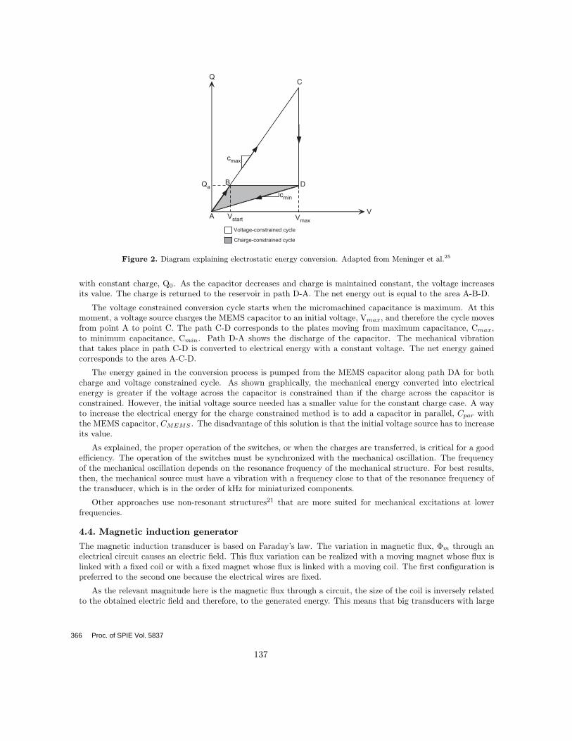
cmax
cmin
Voltage-constrained cycle
Charge-constrained cycle
V
Q
Vstart VmaxA
B
C
DQa
Figure 2. Diagram explaining electrostatic energy conversion. Adapted from Meninger et al.25
with constant charge, Q0. As the capacitor decreases and charge is maintained constant, the voltage increasesits value. The charge is returned to the reservoir in path D-A. The net energy out is equal to the area A-B-D.
The voltage constrained conversion cycle starts when the micromachined capacitance is maximum. At thismoment, a voltage source charges the MEMS capacitor to an initial voltage, Vmax, and therefore the cycle movesfrom point A to point C. The path C-D corresponds to the plates moving from maximum capacitance, Cmax,to minimum capacitance, Cmin. Path D-A shows the discharge of the capacitor. The mechanical vibrationthat takes place in path C-D is converted to electrical energy with a constant voltage. The net energy gainedcorresponds to the area A-C-D.
The energy gained in the conversion process is pumped from the MEMS capacitor along path DA for bothcharge and voltage constrained cycle. As shown graphically, the mechanical energy converted into electricalenergy is greater if the voltage across the capacitor is constrained than if the charge across the capacitor isconstrained. However, the initial voltage source needed has a smaller value for the constant charge case. A wayto increase the electrical energy for the charge constrained method is to add a capacitor in parallel, Cpar withthe MEMS capacitor, CMEMS . The disadvantage of this solution is that the initial voltage source has to increaseits value.
As explained, the proper operation of the switches, or when the charges are transferred, is critical for a goodefficiency. The operation of the switches must be synchronized with the mechanical oscillation. The frequencyof the mechanical oscillation depends on the resonance frequency of the mechanical structure. For best results,then, the mechanical source must have a vibration with a frequency close to that of the resonance frequency ofthe transducer, which is in the order of kHz for miniaturized components.
Other approaches use non-resonant structures21 that are more suited for mechanical excitations at lowerfrequencies.
4.4. Magnetic induction generator
The magnetic induction transducer is based on Faraday’s law. The variation in magnetic flux, Φm through anelectrical circuit causes an electric field. This flux variation can be realized with a moving magnet whose flux islinked with a fixed coil or with a fixed magnet whose flux is linked with a moving coil. The first configuration ispreferred to the second one because the electrical wires are fixed.
As the relevant magnitude here is the magnetic flux through a circuit, the size of the coil is inversely relatedto the obtained electric field and therefore, to the generated energy. This means that big transducers with large
366 Proc. of SPIE Vol. 5837
137

m
k
Bm
y(t)
z(t)
RL
Rc
-
+fm
VZ
ksBms
1
m2 ++ cRRLs
BlRs
++
R
Blfe
(a) (b)
Figure 3. Magnetic induction transducer model. Adapted from Ching et al.26
area coils will perform better than smaller transducers, unless a larger time derivative is involved with the smallscale generators.
We briefly present the analysis of a simple generator.26 When the generator vibrates, the oscillating masshas a relative displacement with respect to the housing. The magnetic induction generator converts this relativedisplacement into electrical energy. The transducer is modelled as a damped spring-mass system, since theenergy extraction damps the mass movement with a factor Bm. The mass m, the magnet, which is joined to aspring with a spring constant k moves through a constant magnetic field, B, when the generator oscillates.
The relative displacement, z(t), is related to the voltage across the coil by a first order system as can beshown in Figure 3(a). L is the inductance of the coil, Rc is the parasitic resistance of the coil, l is the length ofthe coil, and R is the load resistance.
Figure 3(b) shows the transfer function block diagram that relates the mechanical input force with the outputvoltage. The current induced in the coil generates an electromechanical force, fe that dampes the movementof the magnet. From the Newton’s second Law of motion, the transfer function between the input mechanicalforce, fm, and the relative displacement of the mass can be obtained. After some algebra, the transfer functionthat relates the output voltage V , across the load resistor with the input mechanical force fm is:
V (s)fm(s)
=(BlR)s
(Ls + R + Rc)(ms2 + Bms + k) + (Bl)2s(5)
The third order system can be simplified to a second order system by assuming that the electrical timeconstant is much smaller than the mechanical time constant. With this assumption, the transfer function isexpressed as:
V (s)fm(s)
=(Bl)s
m
(s2 + 2ζωns + ω2n)
(6)
where ζ and ωn are the damping factor and the spring natural frequency, respectively.
ωn =
√k
m(7)
ζ =BmR + (Bl)2
2R√
mk=
Bm
2ωnm+
(Bl)2/R
2ωnm= ζm + ζe (8)
Proc. of SPIE Vol. 5837 367
138

The damping factor is expressed as the addition of a mechanical damping factor ζm, and an electrical dampingfactor, ζe.
The power generated for a sinusoidal input displacement, y(t) = Y0 cos(ωt), is given by:
P =mζeY
20 (ω/ωn)3ω3[
1 −(
ωωn
2)]2
+ 2ζ(
ωωn
)2 (9)
The output power is maximum at resonance, and proportional to the third power of ωn, while the corre-sponding voltage Vpmax is proportional to ωn:
Pmax = P (ωn) =mζeY
20 ω3
n
4ζ2(10)
Vpmax =√
2PmaxR =BlY0ωn
2ζ(11)
Several examples following this principle can be found in the literature.
Amirtharajah et al.27designed with an electromagnetic VDRG built using discrete components which gener-ates a power on the order of 400 µW using human walking as a vibrational power source.
Williams et al.28 from the University of Sheffield fabricated an electromagnetic MEMS VDRG. A mm scaledemonstrator, implementing an electromagnetic micro-generator, generates 0.3 µW from a 4 MHz excitationinput.
Li et al.29 from the University of Hong Kong have fabricated an electromagnetic MEMS VDRG with a volumeof 1 cm3. The micro-generator generates 10 µW power at 2 V DC with 64 Hz input frequency and 1000 µminput vibration amplitude.
5. ELECTROMAGNETIC RADIATION
Another source of energy present in the environment is electromagnetic radiation, either in the form of light(known as solar energy), or lower frequency RF radiation. Both methods are extensively used in many presentdevices, and only some comments will be made here, regarding their prospect as energy harvesting strategies.
5.1. Solar energy
Solar energy is a mature technology for large scale energy generation. Photovoltaic systems are found fromthe Megawatt to the milliwatt range producing electricity for a wide range of applications: from wristwatch togrid-connected PV systems. The application of photovoltaics in portable products is a valid option under theappropriate circumstances.
Outdoors, solar radiation is the energy source of the PV system. Solar radiation varies over the earth’ssurface due to weather conditions and the location (longitude and latitude). For each location exists an optimuminclination angle and orientation of the PV solar cells in order to obtain the maximum radiation over the surface ofthe solar cell. Yearly irradiance is for example 992 kWh/m2 in The Netherlands and 2026 kWh/m2 in Tanzania.However, indoor irradiance is smaller, around 3.5 to 20 W/m2. Nowadays, the majority of solar cells are madefrom semi-conductor materials: crystalline silicon (89%), amorphous silicon (10%), cadmium telluride (0.5%),copper indium, diselenide and gallium arsenide. The power conversion efficiency of a PV solar cell is defined asthe ratio between the solar cell output power and the solar power (irradiance) impinging the solar cell surface.For a solar cell of 100 cm2, 1 W can be generated, if the solar irradiation is 1000 W/m2 and the efficiency of thesolar cell is 10%.
368 Proc. of SPIE Vol. 5837
139

5.2. RF radiation
RF radiation is employed to power ID cards by directing high power electromagnetic energy to the devices froma nearby source. In addition to energy, it is possible to send information as well.
However, the term energy harvesting implies that it is the same device which gets its energy from theenvironment. In cities and very populated areas there is a large number of potential RF sources: broadcastradio and tv, mobile telephony, wireless networks, etc. The problem is collecting all these disparate sources andconverting them in useful energy. The conversion is based on a rectifying antenna (rectenna), constructed witha Schottky diode located between the antenna dipoles.
The energy levels actually present are so low that no present electronic device can use them. However, futuretechnologies may allow the fabrication of lower power devices that would “recycle” RF energy generated for otherpurposes by different elements.30
6. THERMAL ENERGY
Thermal energy is the other form of energy readily present in the environment. Thermal energy harvesting devicescould use the thermal energy of different sources: persons and animals, machines or other natural sources.
A thermoelectric generator basically consists of a thermocouple, comprising a p-type and n-type semiconduc-tor connected electrically in series and thermally in parallel. The thermogenerator (based on the Seebeck effect)produces an electrical current proportional to the temperature difference between the hot and cold junctions.An electrical load is connected in series with the thermogenerator creating an electric circuit. The Seebeckcoefficient is positive for p-type materials and negative for n-type materials. The heat that enters or leaves ajunction of a thermoelectric device has two reasons: 1) the presence of a temperature gradient at the junction2) the absorption or liberation of energy due to the Peltier effect.9
Carnot efficiency puts an upper limit on the heat energy that can be recovered. In the case of temperaturedifference between the human body and the environment, e.g. room temperature (20C), Starner31 estimatesthat the Carnot efficiency with this temperature conditions is 5.5%. In a warmer environment the Carnotefficiency drops while in a colder environment the Carnot efficiency rises. The recoverable energy yields 3.7-6.4 W of power. However, evaporative heat loss account for 25% of the total heat dissipation, and therefore themaximum power available drops to 2.8-4.8 W. The previous calculations are made assuming that all the heatradiated by the human body can be recovered and transformed into electrical power, so that the obtained poweris overestimated. Another problem is the location of the device dedicated to the capture of the heat of the humanbody. When the skin surface detects cold air, a rapid constriction of the blood vessels in the skin reduces theskin temperature to the temperature of the cold air. Therefore, the efficiency of the Carnot device will drop.Some research is needed to more accurately evaluate the feasibility of thermal energy harvesting from humanactivity. A thermal human body model is necessary in order to know how much heat energy can be harvestedfrom a part of the human body without disturbing the user.
7. POWER CONDITIONING CIRCUITS
The energy present in the environment that can potentially be harvested is discontinuous in nature. Therefore,not only the voltage level must be adjusted, but, because at times there is no energy at all, there must be someway to store the energy for use at a convenient time. This storage element can be a capacitor, or a secondarybattery.
7.1. Operation modes
The discontinuous nature of energy harvesting has consequences on the way the electronic devices powered byenergy harvesting are operated. The electronic device will be able to operate only when there is enough energyin its energy storage element. In principle, we can distinguish two situations:
1. The power consumption of the electronic device is lower than the average power provided by the environ-ment. In this case, the electronic device may operate continuously.
Proc. of SPIE Vol. 5837 369
140

time
Energy
Power
generatedspent
time
generatedspent
ON
time
Energy
Power
generatedspent
time
generatedspent
ON OFF ON OFF ON
(a) (b)
Figure 4. Case of continuous (a) and discontinuous (b) operation. In the case of discontinuous operation, the devicemust be OFF until enough energy is collected in the storage element.
time
Power
generatedspent
Figure 5. Generated and spent power when the device operation is only at times when there is energy generation.
2. The power consumption of the device is greater than the power provided by the environment. The operationmust be discontinuous, and the time between operations depends on the stored energy of the device.
Figure 4 schematically shows the two cases. It is seen how for both cases the energy storage element isnecessary to provide energy during the moments where transiently the generated power is zero. A special casewould be one in which the device is operated exclusively during the time when there is generated power, andthe power consumption is at all times smaller than generated power (Figure 5). In this case, the energy storageelement is not necessary, although voltage regulation is.
In the general case of discontinuous operation, energy is a more relevant magnitude than power when dis-cussing generation, because it is generated energy which determines the time between operations.
7.2. Power conditioning for piezoelectric energy harvesting
A piezoelectric generator can produce voltages on the order of two to tens of volts and currents on the order of twoto tens of microAmps.20 These are the voltage and current levels that the piezoelectric power conditioning circuithas to manage. In addition, a piezoelectric source for human walking activity has low frequency (approximatelyone cycle per second) and low-duty-cycle current pulses.
370 Proc. of SPIE Vol. 5837
141

CMEMSCpar
CresLoad &Control Electronics
SW1
SW2+
-
VDD
+
-
VCL
IL
IL
VC
t1 t2 t3 t4 t5
SW2ON
SW1ON
SW1ON
SW2ON
VDD
Vmax+VDD
(a) (b)
Figure 6. Diagram explaining electrostatic energy conversion circuit (adapted from Meninger et al.25).
The simplest method of power conversion is by direct discharge.32 The piezoelectric element is connected toa diode bridge to rectify its output. The charge is transferred to a tank capacitor, C2 where the electrical energyis stored for use by the electronic system to be powered. This circuit is appropriate for applications where a lowpower device has to be power supplied at tens-second intervals. The storage capacitor C2 is connected to theelectronic system each time that its energy reaches a value enough to power the application.
In this scheme, each time that the piezoelectric device is stressed, a certain amount of current flows, chargingthe piezoelectric element capacitor, C1, as well as the storage capacitor, C2. If the piezo element is cyclicallyexcited and the current is rectified, the observed voltage in C2 will increase its value for each cycle, until a limit isasymptotically reached. The choice of the storage capacitor and the range of voltage when it should be connectedare not arbitrary, but depend on the energy requirements of the load and the piezoelectric characteristics.
Ottman et al.33 presented a circuit that uses a switch-mode dc-dc converter after the tank capacitor. Theypresent an analysis of the converter in order to obtain the optimal duty cycle of the converter that maximizes theharvested power, taking in to account the generated current and internal capacitance of the piezoelectric. Theuse of the system proposed increases the harvested power by 325% as compared to when the battery is directlycharged with the piezoelectric rectified source. However, the switch mode converter also spends some energy.They present a solution making a two-mode converter circuit. When the generated energy is too low to powerthe switching converter, it is accumulated in the battery in a manner similar to the direct discharge method.When there is enough energy, the switching converter starts up to increase the efficiency of the conversion.
7.3. Power conditioning for the electrostatic energy generator
The MEMS variable capacitor designed by Meninger et al. presents a power electronics circuit. The low-powercontroller directs energy conversion cycles by generating the timing pulses to control the gates of the FETS ofthe power circuit. It is responsible for charging the MEMS capacitor to Vstart and Vmax during the charge andthe voltage constrained case, respectively.
Fig 6 shows the converter and the associated waveforms for the charge constrained case. t1 starts when it isdetected that CMEMS = Cmax. During t1 SW2 is ON and SW1 is OFF, and therefore energy is transferred fromthe initial voltage source to the inductor L. During t2 SW1 is ON and SW2 is OFF, so the energy is transferredfrom L to MEMS capacitor. During t3 both switches are OFF and the MEMS capacitor changes its value fromCmax to Cmin due to mechanical vibration. During t4 SW1 is ON, SW2 is OFF, and CMEMS + CPAR transferelectrical energy to inductor L. t4 corresponds to the path D-A of Figure 2. During t5, SW2 is ON and SW1 isOFF and the energy stored in the inductor is transferred to the reservoir capacitor, Cres.
Proc. of SPIE Vol. 5837 371
142

8. CONCLUSIONS
Nowadays there is an active research area investigating a number of alternatives to extract energy energy fromthe environment and convert it to electrical energy to power an electronic device. Taken one by one, eachalternative still provides a low level of energy compared to the power requirements of today’s electronic devices,except for specific applications. However, it is expected that energy harvesting will have an important role infuture microelectronic devices for a number of reasons.
First, it is possible to increase the generated energy using new transducer designs or new materials, as well asinnovative power conditioning circuits and energy storage elements. Also, the combination in the same device ofseveral energy harvesting strategies will increase its capabilities to obtain energy in different situations. However,as observed with the comparison between past evolution of batteries and electronic technology, it is in the partof electronic consumption that there are more possibilities to close the gap between generated and spent energy.Electronic technology will continue its evolution of decreasing energy consumption thanks to continuing scalingdown of devices, nanotechnology and eventually, molecular electronics. New processing and communicationtechniques will also help reducing power consumption.
Finally, the trend of increasing mobility and autonomy of electronic devices has a natural step in the energeticindependence from the user. In this sense, such electronic devices will be completely autonomous entities, blurringthe frontier between live beings and inanimated objects.
ACKNOWLEDGMENTS
This work has been partially supported by the Spanish Ministry of Science and Technology and the RegionalEuropean Development Funds (FEDER) from the European Union through project TEC2004-03289.
REFERENCES1. M. Billinghurst and T. Starner, “Wearable devices. new ways to manage information,” IEEE Computer 32,
pp. 57–64, January 1999.2. J. Meindl, “Low power microelectonics: retrospect and prospect,” Proceedings of the IEEE 83, pp. 619–635,
April 1995.3. G. Zorpette, “Super charged,” IEEE Spectrum 42, pp. 26–31, January 2005.4. T. E. Starner, “Powerful change part 1: batteries and possible alternatives for the mobile market,” IEEE
Pervasive computing 2, pp. 86–88, October-December 2003.5. R. Hahn and H. Reichl, “Batteries and power supplies for wearable and ubiquitous computing,” in Third
Intl Symp. on Wearable Computers, 1999.6. A. Hansen, S. van Leeuwen, and A. Stevels, “Design of a fuel cell powered radio, a feasibility study in
alternative power sources for portable products,” in IEEE Intl. Symp. on Electronics and the Environment,2000.
7. T. Starner, “Human-powered wearable computing,” IBM Systems Journal 35(3&4), 1996.8. J. L. Gonzalez, A. Rubio, and F. Moll, “Human powered piezoelectric batteries to supply
power of wereables electronic devices,” Int. J. Soc. Mater. Eng. Resour. 10(1), pp. 34–40, 2002.http://pmos.upc.es/blues/publications/EnergyEfficientSystems/papers EnergyEfficientSystems.html.
9. S. Angrist, Direct Energy Conversion, Allyn & Bacon, 1982.10. T. Starner and J. Paradiso, “Human generated power for mobile electronics,” in Low Power Electronics
Design, C. Piguet, ed., ch. 45, CRC Press, 2004.11. F. Moll and A. Rubio, “An approach to the analysis of wearable body-power systems,” in Mixed Signal
Design Workshop, MIXDES’00, 2000.12. A. Jansen, S. Fridstedt, and A. Weernink, “A batteryless remote control for Volvo, results of a feasibility
study,” in ISATA 2000 Conf. on Automotive and Transportation Technology, 25-29 September 2000.13. J. Drake, “The greatest shoe on earth,” Wired , February 1996.14. Freeplay Energy Plc. http://www.freeplayenergy.com.15. Atkin Design and Development Ltd. http://www.windup-powerup.co.uk.
372 Proc. of SPIE Vol. 5837
143
16. A. Stevels and A. J. Jansen, “Renewable energy in portable radios: an environmental benchmarking study,”The Journal of Sustainable Product Design , January 1998.
17. Seiko Instruments Inc. http://www.sii.co.jp/info/eg/thermic main.html.18. Applied Digital. http://www.adsx.com/prodservpart/thermolife.html.19. Enocean. http://www.enocean.com.20. S. Roundy, P. K. Wright, and J. M. Rabaey, Energy scavenging for wireless sensor networks with special
focus on vibrations, Kluwer Academic Publishers, 2004.21. P. D. Mitcheson, T. C. Green, E. M. Yeatman, and A. S. Holmes, “Architectures for vibration-driven
micropower generators,” J. of Microelectromechanical Systems 13, June 2004.22. C. V. C. Bouten, K. T. M. Koekkoek, M. Verduin, R. Kodde, and J. D. Janssen, “A triaxial accelerometer
and portable data processing unit for the assessment of daily physical activity,” IEEE Trans. on BiomedicalEngineering 44, pp. 136–147, March 1997.
23. L. Mateu and F. Moll, “Optimum piezoelectric bending beam structures for energy harvesting using shoeinserts,” J. of Intelligent Material Systems and Structures , 2005. accepted for publication.
24. Measurement Specialities, Piezo Film Sensors Technical Manual. http://www.msiusa.com.25. S. Meninger, J. Mur-Miranda, R. Amirtharajah, A. P. Chandrasakan, and J. H. Lang, “Vibration to electric
energy conversion,” IEEE Trans. on VLSI 9, February 2001.26. N. N. H. Ching, G. M. H. Chan, W. J. Li, H. Y. Wong, and P. H. W. Leong, “Pcb integrated micro generator
for wireless systems,” in Intl. Symp. on Smart Structures and Microsystems, 19-21 October 2000.27. R. Amirtharajah and A. Chandrakasan, “Self-powered signal processing using vibration-based power gen-
eration,” Solid-State Circuits, IEEE Journal of 33(5), pp. 687–695, 1998.28. C. Williams, C. Shearwood, M. Harradine, P. Mellor, T. Birch, and R. Yates, “Development of an electro-
magnetic micro-generator,” IEE Proc. G-Circuits, Devices and Systems 148, pp. 337–342, December 2001.29. W. Li, T. Ho, G. Chan, P. Leong, and H. Y. Wong, “Infrared signal transmission by a laser-micromachined,
vibration-induced power generator,” in Circuits and Systems, 2000. Proceedings of the 43rd IEEE MidwestSymposium on, 1, pp. 236–239 vol.1, 2000.
30. J. Hagerty, F. Helmbrecht, W. McCalpin, R. Zane, and Z. Popovic, “Recycling ambient microwave energywith broad-band rectenna arrays,” IEEE Trans. on Microwave Theory and Techniques 52(3), pp. 1014–1024,2004.
31. T. Starner and Y. Maguire, “A heat dissipation tutorial for wearable computers,” in 2nd InternationalSymp. on Wearable Computers, 1998.
32. N. S. Shenck, “A demonstration of useful electric energy generation from piezoceramics in a shoe,” Master’sthesis, Massachussets Institute of Technology, 1997.
33. G. Ottman, H. Hofmann, and G. Lesieutre, “Optimized piezoelectric energy harvesting circuit using step-down converter in discontinuous conduction mode,” IEEE Trans. on Power Electronics 18(2), pp. 696–703,2003.
Proc. of SPIE Vol. 5837 373
144

Chapter 9
Paper 2: OptimumPiezoelectric Bending BeamStructures for EnergyHarvesting using ShoeInserts
Loreto Mateu and Francesc Moll
J. of Intelligent Material Systems and Structures, vol. 16, no. 10,pp. 835–845, 2005.
145

Optimum Piezoelectric Bending Beam Structuresfor Energy Harvesting using Shoe Inserts
LORETO MATEU* AND FRANCESC MOLL
Department of Electronic Engineering, Polytechnical University of CataloniaC/Jordi Girona s/n, Barcelona, 08034
ABSTRACT: The small amount of power demanded by many present-day electronic devicesopens up the possibility to convert part of the energy present in the environment into electricalenergy, using several methods. One such method is to use piezoelectric film-bending beamsinside a shoe, and use part of the mechanical energy employed during normal walking activity.This study analyzes several bending beam structures suitable for the intended application(shoe inserts and walking-type excitation) and obtains the resulting strain for each type asa function of their geometrical parameters and material properties. As a result, the optimumconfiguration can be selected.
Key Words: energy harvesting, piezoelectric films, bending beams, maximum deflection,
power generation.
INTRODUCTION
THE trends in technology provide scope for thedecrease in both size and power consumption of
complex digital systems. This decrease in size and powerconsumption gives rise to the concept of wearabledevices in which digital systems are integrated ineveryday personal belongings like clothes, watches,glasses, etc. Batteries are the power source used inwearable devices. However, the disadvantage of bat-teries is the need to either replace or recharge themperiodically. An alternative to batteries is harvestingenergy from the environment (energy harvesting).The polyvinylidene fluoride (PVDF) films have been
employed (Kendall, 1998; Kymissis et al., 1998; Shenck,1999; Shenck and Paradiso, 2001; Starner and Paradiso,2004) to harvest electrical power from human walkingactivity. Roundy et al. (2004) presented a piezoelectriccantilever beam to harvest maximum electrical poweravailable from a vibrational source. However, differentstructures were not compared thoroughly.This article is an exhaustive and meticulous study
of different piezoelectric beam structures. The studyanalyzes the advantages and disadvantages of thesestructures. The final application is an assembly ofa piezoelectric bending beam in the insole of a shoe toconvert mechanical human walking activity into electricpower.
The differences between the analyzed piezoelectricbeams can be grouped by shape, employed materialand its position, the kind of supports, and restrictionsbecause of the space available for the application.To calculate the average power generated by humanwalking activity, the average strain of the beam isobtained for each analyzed structure.
The next section presents piezoelectric constitutiveequations for PVDF and analyzes the fact that inpiezoelectric films, the excitation mode 31 is moreefficient than mode 33. However, the force exertedby walking is in the direction 3 (z-axis). One way tocircumvent this problem is to use bending beamstructures to cause a stress in direction 1 when a forcein direction 3 is applied. Different bending beamstructures are analyzed in the subsequent two sectionsto select the most appropriate one for the application.Two kinds of beams are analyzed: piezoelectric homo-geneous and heterogeneous bimorphs (Smits and Choi,1991). The piezoelectric bimorphs are made up of twopiezoelectric films, one on each side of the neutral axis.These piezoelectric beams can be connected in parallelto add current, or in series to add voltage. On the otherhand, heterogeneous bimorphs consist of piezo-electric elements and a non-piezoelectric element thatonly provides elastic function. Two types are consid-ered within this group. The first type consists of anon-piezoelectric element sandwiched between piezo-electric films, which is called as symmetric hetero-geneous bimorph. The second type is made up of one ormore piezoelectric films on top of a non-piezoelectricmaterial (Eggborn, 2003), and it is named as asymmetric*Author to whom correspondence should be addressed.
E-mail: [email protected]
JOURNAL OF INTELLIGENT MATERIAL SYSTEMS AND STRUCTURES, Vol. 16—October 2005 835
1045-389X/05/10 0835–11 $10.00/0 DOI: 10.1177/1045389X05055280 2005 Sage Publications
146

heterogeneous bimorph. The possibility of limiting thedeflection of the beam to a given value in accordancewith the restrictions of space and comfort of theapplication is also examined. The next section describesthe electrical power harvested from mechanical activityfor the different structures analyzed previously. Acomparison of the analyzed beams and some conclu-sions derived from the previous analysis are alsopresented.
CONSTITUTIVE EQUATIONS FOR PVDF
Polyvinylidene fluoride (PVDF) is a piezoelectricpolymer with mm2 crystal symmetry. Due to thisfact the piezoelectric constitutive equations shown inEquation (1) are simplified to Equation (2) (Ikeda,1990).
Si½ ¼ sij
Tj
þ dik½ Ek½
Dl½ ¼ "lm½ Em½ þ dln½ Tn½
j, n ¼ 1, . . . , 6 i, k, l,m ¼ 1, 2, 3
ð1Þ
where repeated subscripts in the products imply asummation over the different components. T is theapplied mechanical stress (N/m2); E is the appliedelectric field (N/C); d is the piezo strain tensor ((C/m2)/(N/m2)); " is the permittivity tensor (F/m); D is theelectric displacement (C/m2); S is the mechanical strain(m/m); s is the compliance tensor (m2/N).The subscripts correspond to the six directions of
the axes, the three Cartesian directions and the sheararound the three axes, as shown in Table 1 (Kino,2000).
s11 s12 s13 d31
s12 s22 s23 d32
s13 s23 s33 d33
d31 d32 d33 "33
26666664
37777775
T1
T2
T3
E3
26666664
37777775¼
S1
S2
S3
D3
26666664
37777775
s44 d24
d24 "22
" #T4
E2
" #¼
S4
D2
" #
s55 d15
d15 "11
" #T5
E1
" #¼
S5
D1
" #
s66T6 ¼ S6
ð2Þ
The PVDF films are only metalized in the planeperpendicular to direction 3, so that D1¼D2¼ 0.Equation (3) reflects this assumption when no externalelectric field is applied.
D3 ¼ d31T1 þ d32T2 þ d33T3 ð3Þ
There are three possible modes to use the PVDF films:31, 32, and 33. Mode 32 is discarded since d32 is 10 timesless than d31 or d33 (Brown, 2002). In mode 31, the stressis applied in direction 1, and in mode 33, the stress isapplied in direction 3. The voltage and charge obtainedresulting from an applied force in a certain direction, F1
or F3, are shown in Table 2.In a thin PVDF film, the ratio L/H is on the order
of 1000, while d31¼ 23 1012m/V and d33¼331012m/V (Measurement Specialties). If it is assumedthat F1¼F3, then Vo and q for the mode 31 will be onthe order of 700 times greater than Vo and q for themode 33, as can be seen from Table 2. Therefore, for thesame mechanical energy input, more electrical energyoutput is obtained in mode 31 than in mode 33 whenthe PVDF piezoelectric films are employed. For otherpiezoelectric materials, mode 33 excitation can be abetter solution than mode 31 if the length, width, andthickness of the piezoelectric material are similar.
A piezoelectric film placed inside a shoe as shownlater, in Figure 4, would receive a stress applied indirection 3. Therefore, a mechanical coupling is neces-sary to transform the stress applied in the direction 3 toa stress applied in the direction 1. This problem is solvedusing bending beams.
CANTILEVERS WITH LIMITED
MAXIMUM DEFLECTION
There are different kinds of bending beams dependingon their supports, shapes, position of the applied pointload or distributed load, etc. (Beer and Johnston, 1993;
Table 1. Subscripts reduced notation for piezoelectricconstitutive equations of piezoelectric materials.
Reduced notationCorresponding direction
of axes
1 Longitudinal in the x-direction2 Longitudinal in the y-direction3 Longitudinal in the z-direction4 Shear y–z5 Shear z–x6 Shear x–y
Table 2. Voltage, Vo, and charge, q, obtained in the planeperpendicular to direction 3 applying a mechanicalstress in direction 1, mode 31, and in direction 3,mode 33. g is the piezo stress constant ((m/m)/(C/m2))and is defined as g¼d/e.
Mode 31 Mode 33
Vo g31ðF1=WÞ g33HðF3=ðWLÞÞq d31ðF1L=HÞ d33F3
836 L. MATEU AND F. MOLL
147

Senturia, 2001; Young, 2002; Yee, 2003). Moreover,beams can have one or multiple layers of different typesof materials. For usual values of the forces applied, thecalculated maximum deflection is greater than the heightavailable between the beam and the insole of the shoe.Therefore, the assembly conditions limit the maximumattainable deflection.The first subsection analyzes the relationship between
average strain and maximum deflection for homo-geneous cantilevers with an applied point load at x¼Lwhereas the next subsection analyzes the case forheterogeneous cantilevers.
Triangular versus Rectangular
Homogeneous Cantilever
The beam that offers the maximum average strain fora given applied force, F, is the cantilever. The averagestrain for a homogeneous beam, Figure 1, with any typeof support employed is given by Equation (4) and it isdefined as net strain along axis 1 (length), x, and axis 3(thickness), z.
Saverage ¼1
tc=2
1
L
Z tc=2
0
Z L
0
z
xð Þdxdz ð4Þ
where (x) is the radius of curvature of the bendingbeam. Equation (4) corresponds to the average strain ofa homogeneous bimorph with a thickness of tc/2.If the two piezo films shown in Figure 1 are connected
in parallel, the charge generated by the strain of boththe films must be added. For a series connection, thecharge generated corresponds to the strain of one ofthe films, and the voltage of both the films is added.Figures 2 and 3 show how to connect both the films inseries or parallel depending on the poling axis orienta-tion of each piezoelectric film as it is being tensed orcompressed.If the cantilever is triangular (Kendall, 1998), its width
varies as expressed in Equation (5),
W xð Þ ¼W0 1x
L
ð5Þ
where W0 is the base of the triangle and L is the lengthof the beam and the height of the triangle.
Table 3 shows the average strain, Sx, for one of thetwo films in a bimorph as shown in Figure 1, the deflec-tion in function of position, y(x), and the maximumdeflection, ymax, of the cantilever beam. Maximumdeflection of the cantilever beam occurs when x¼L.
In the case of a triangular cantilever, the radius ofcurvature of the cantilever is constant along its length,which implies that the strain along the direction x is alsoconstant.
As can be seen in these expressions, the cantilever witha triangular shape suffers more strain than a canti-lever with a rectangular shape for identical load. Therectangular cantilever average strain is 75% of thetriangular cantilever average strain, expressed as a
Figure 2. Connection between the top and bottom piezoelectricfilms to add current or voltage when the poling axes are identicallyoriented.
Figure 3. Connection between the top and bottom piezoelectricfilms to add current or voltage when the poling axes are opposed.
W0
tc/2
tc/2
Yc
Yc
Figure 1. Cross section of a homogeneous bimorph beam. tc/2corresponds to a piezoelectric film thickness. Yc is the Young’smodulus for the piezoelectric material. W0 is the width of the beam.The neutral axis is placed between the two piezoelectric films.
Optimum Piezoelectric Bending Beam Structures for Energy Harvesting 837
148

function of its maximum deflection. The maximumdeflection is also greater for the triangular cantileverstructure. Therefore, a triangular cantilever would bepreferred for a shoe insert, as was pointed out in Shenck(1999). A mechanical device must be placed inside theshoe at x¼L to apply all the stress generated by humanwalking activity.It should be noted that in a practical implementation,
the usual force applied by normal walking activitywould give a value of ymax well in excess of that of acomfortable cavity depth. Therefore, the maximumdeflection is actually limited by the cavity depth, D, asshown in Figure 4. The value of D for a practical shoeinsert is of the order of a few millimeters, and such asmall deflection ensures that the linear analysis appliedin this study can be considered valid.
Triangular Heterogeneous Cantilever
The maximum strain in a beam takes place at itssurface, at z¼ tc/2 and z¼tc/2. One way to increasethe average strain for the piezoelectric film, andtherefore, the harvested power, is to increase the beamthickness. This can be done keeping the same amount ofpiezoelectric material by using heterogeneous bimorphscomposed of non-piezoelectric films and piezoelectricfilms as shown in Figures 5 and 6.The neutral axis for a composite beam is calculated
with the general expression of Equation (6).
zs ¼
Pni¼1 zi Yi=Yrð ÞAiPni¼1 Yi=Yrð ÞAi
ð6Þ
where n is the number of layers of different materials,zi is the height for layer i, Yi is the Young’s modulusfor layer i, Yr is the Young’s modulus for layer r, andAi is the area of cross section for layer i.
Figure 5 (Eggborn, 2003) shows a symmetric hetero-geneous bimorph whereas Figure 6 shows an asym-metric heterogeneous bimorph. In both the structures,the respective dimensions of piezoelectric film and non-piezoelectric film are the same.
Table 4 shows the average strain, Sx, deflection in thefunction of the position x, maximum deflection, ymax,and the position of the neutral axis, zs, of the triangularcantilever. It is assumed, as explained in the previoussection, that the maximum deflection is limited by thecavity depth, D. The expression for ymax correspondsto an unrestricted deflection, and is also given here forcompleteness.
From the expressions in Table 4, it is seen that thesymmetric heterogeneous bimorph is independent ofYoung’s modulus whereas the asymmetric hetero-geneous bimorph is dependent of Yc and Ys, as alsoshown in Figure 7. Both the heterogeneous cantileversprovide a greater average strain than a homogeneousconfiguration, and the relationship depends on the
Table 3. Average strain, Sx, deflection, y(x), and max-imum deflection, ymax, for triangular cantilever andrectangular cantilever, where tc is the thickness, W0 isthe width of the rectangular beam and the base of thetriangular beam, F is the point load applied at x¼ L andYc is the Young’s modulus of the beam.
Triangular cantilever Rectangular cantilever
Sx3FL
YcW0t2c¼
ymaxtc2L2
3FL
2YcW0t2c¼
3
8
ymaxtcL2
y(x)6FLx2
YcW0t3c
6FL
YcW0t3cx2 1
x
3L
ymax6FL3
YcW0t3c
4FL3
YcW0t3c
W0
Yctc
tsYs
Figure 6. Cross section of asymmetric heterogeneous bimorphbeam. tc corresponds to piezoelectric film thickness whereas tscorresponds to non-piezoelectric film thickness. Yc is the Young’smodulus for the piezoelectric material and Ys is the Young’s modulusfor the non-piezoelectric material. W0 is the width of the beam.
Figure 5. Cross section of symmetric heterogeneous bimorphbeam. tc/2 corresponds to piezoelectric film thickness whereas tscorresponds to non-piezoelectric film thickness. Yc is the Young’smodulus for the piezoelectric material, and Ys is the Young’s modulusfor the non-piezoelectric material. W0 is the width of the beam.
L
D
tc
F
Figure 4. Cantilever assembly in the insole of the shoe with a limiteddeflection, D.
838 L. MATEU AND F. MOLL
149

thickness of the non-piezoelectric material. Figure 8shows the dependence of the relative strain to thehomogeneous cantilever with relative thickness ofthe non-piezoelectric to the piezoelectric films. It isseen how for large ts/tc, the strain is much larger thanthe homogeneous cantilever, and the influence of therelative Young’s modulus is smaller. In both thesefigures, it is assumed that the maximum deflection islimited by the same amount, D in all the structures.
It is to be noted that the strain in Figures 7 and 8 forthe symmetric configuration corresponds to one of thefilms, and this strain is similar in magnitude to the wholepiezoelectric film of the asymmetric configuration,with double the thickness. This means that by using asymmetric heterogeneous cantilever with both the filmsconnected in parallel, we obtain approximately doublethe charge than with an asymmetric configuration.On the other hand, the asymmetric bimorph structureis the only one that allows the use of a single piezo-electric film. Therefore, its connection is the simplestpossible, and this offers a certain advantage with respectto symmetric bimorph structures, in spite of its smallercharge generation capability.
SIMPLY SUPPORTED BEAM
Point Load
A simply supported beam has a pinned support oneach end of the beam. Table 5 shows the average strain,Sx, deflection in the function of the position x, y(x), andmaximum deflection, ymax, of the simply supportedbeam with a point load F located at x¼L/2 to obtainthe maximum deflection possible with these supports.
Table 6 shows the average strain, Sx, maximumdeflection, ymax, and the location of the neutral axis,zs, for a homogeneous bimorph, a symmetric hetero-geneous bimorph, and an asymmetric heterogeneousbimorph simply supported beams with a point load Flocated at x¼L/2. As in Table 4, Sx is put in functionof cavity depth, D.
Distributed Load
Another type of loading for the simply supportedbeam is a distributed load, as shown in Figure 9. Tocalculate the strain of this structure, we consider the caseof a limited maximum deflection, to be equivalent totwo cantilever-type deflections. The part of the footthat is in contact with the piezoelectric material causesa distributed load q. This part of the foot acts as afixed support for each half of the beam, while thepinned support is equivalent to a force that acts overthe equivalent cantilever to deflect it. In these twoequivalent cantilevers, we assume that the part of theirT
ab
le4.
Eq
uati
on
sfo
rave
rag
est
rain
,S
x,
wit
hd
efl
ec
tio
nlim
ite
db
yth
ec
avi
tyd
ep
th,
D,
maxi
mu
md
efl
ec
tio
n,
y max,
an
dn
eu
tral
axi
sp
osi
tio
n,
z s.
Th
ean
aly
zed
can
tile
vers
have
atr
ian
gu
lar
shap
e.
Ho
mo
ge
ne
ou
sb
imo
rph
Sym
me
tric
he
tero
ge
ne
ou
sb
imo
rph
Asym
me
tric
he
tero
ge
ne
ou
sb
imo
rph
Sx
Dt c
2L
2
Dt c
2L
21þ
2t s t c
Dt c L2
t s t c
Y s Y c
1þðt
s=t
cÞ
1þðt
s=t
cÞð
Y s=Y
cÞ
ðÞ
y ma
x6
FL
3
YW0t3 c
6F
L3
Y cW
0t3 c
1
1þ
3ðt
s=t
cÞþ
3ðt
s=t
cÞ2þðY
s=Y
cÞð
t s=t
cÞ3
6F
L3
Y cW
0t3 c
1þðð
t s=t
cÞð
Y s=Y
cÞÞ
1þ
4ðY
s=Y
cÞð
t s=t
cÞþ
6ðY
s=Y
cÞð
t s=t
cÞ2þ
4ðY
s=Y
cÞð
t s=t
cÞ3þðY
s=Y
cÞ2ðt
s=t
cÞ4
z st c 2
t cþ
t s2
t c 2
1þ
2ðt
s=t
cÞþðY
s=Y
cÞð
t s=t
cÞ2
1þðð
Y s=Y
cÞð
t s=t
cÞ2Þ
Optimum Piezoelectric Bending Beam Structures for Energy Harvesting 839
150

length under the mass (Lm/2) is not deflected. The restof the length, L0 ¼ (LLm)/2 is deflected as shown inFigure 10.The total strain for the simply supported beam with
distributed load can be then calculated as the addition of
the strains of both the equivalent cantilevers. The resultsare shown in Table 7.
Figure 11 shows the average strain for the differenttypes of support analyzed here, as a function of the masslength of the distributed load, Lm. It can be seen that the
0
5
10
15
20
25
0 1 2 3 4 5
Sx/
Sho
m
Ys/Yc
Average strain relative to homogeneous bimorph
Asymmetric heterogeneous ts/tc=5Symmetric heterogeneous ts/tc=5
Asymmetric heterogeneous ts/tc=10Symmetric heterogeneous ts/tc=10
Figure 7. Average strain relative to the homogeneous cantilever for asymmetric and symmetric heterogeneous bimorph triangular cantilevers,and for two values of ts/tc: 5 and 10. The symmetric cantilever strain corresponds to one of the two films, with thickness half of that of theasymmetric cantilever.
1
10
100
1000
1 10 100
Sx/
Sho
m
ts/tc
Average strain relative to homogeneous bimorph
Symmetric heterogeneousAsymmetric heterogeneous Ys/Yc=1Asymmetric heterogeneous Ys/Yc=4
Figure 8. Average strain relative to the homogeneous cantilever for asymmetric and symmetric heterogeneous bimorph triangular cantilevers,and for two values of Ys/Yc: 1 and 4. The symmetric cantilever strain corresponds to one of the two films, with thickness half of that of theasymmetric cantilever.
840 L. MATEU AND F. MOLL
151

case of distributed load always presents a larger averagestrain than the other cases.
ELECTRICAL POWER HARVESTED
After studying the mechanical properties of thedifferent structures, this section analyzes the powergenerated by the piezoelectric elements. A simplifiedapproach is used for calculation of power, following(Kendall, 1998). Consider a resistor connected betweenthe terminals of the piezoelectric films. The excitation isassumed to be sinusoidal. While this assumption is onlyapproximate, it can be useful to compare the differentstructures. A more realistic power calculation providingthe excitation corresponding to walking activity is stillunder study.The dissipated power on the load resistor is expressed
by Equation (7) for a piezoelectric beam with area A,capacitance Ceq (which depends on the film dimensionsas well as their connection), average strain Sx, under asinusoidal mechanical excitation of angular frequency !,that gives rise to a sinusoidal voltage waveform withamplitude |Vp|. This expression has a maximum whenEquation (8) is verified, corresponding to a resistormatching the internal impedance of the piezoelectricfilm. Equation (9) expresses this value of the maximumaverage power as a function of Ceq.
Ph i ¼Vp
22R¼
d31YcSxA!ð Þ2R
2 1þ !2C2eqR
2 ð7Þ
R ¼1
!Ceqð8Þ
Pmaxh i ¼d231Y
2cS
2xA
2!
4Ceqð9Þ
We now compare the different structures analyzedpreviously, calculating the different magnitudes that arepart of Equation (9). First, the area A can be calculatedas the area of one piezoelectric film T
ab
le6.
Eq
uati
on
so
fave
rag
est
rain
,S
x,
maxi
mu
md
efl
ec
tio
n,
y max,
an
dn
eu
tral
axi
sp
osi
tio
n,
z s.
Th
esi
mp
lysu
pp
ort
ed
be
am
an
aly
zed
has
rec
tan
gu
lar
base
.
Ho
mo
ge
ne
ou
sb
imo
rph
Sym
me
tric
he
tero
ge
ne
ou
sb
imo
rph
Asym
me
tric
he
tero
ge
ne
ou
sb
imo
rph
Sx
3 2
Dt c L2
3D
t c2
L2
1þ
2t s t c
3D
t cL
2
t s t c
Y s Y c
1þðt
s=t
cÞ
1þðt
s=t
cÞð
Y s=Y
cÞ
y ma
xF
L3
4YW
0t3 c
FL
3
4Y c
W0t3 c
1
1þ
3ðt
s=t
cÞþ
3ðt
s=t
cÞ2þðY
s=Y
cÞð
t s=t
cÞ3
FL
3
4Y c
W0t3 c
1þðt
s=t
cÞð
Y s=Y
cÞ
1þ
4ðY
s=Y
cÞð
t s=t
cÞþ
6ðY
s=Y
cÞð
t s=t
cÞ2þ
4ðY
s=Y
cÞð
t s=t
cÞ3þðY
s=Y
cÞ2ðt
s=t
cÞ4
z st c 2
t cþ
t s2
t c 2
1þ
2ðt
s=t
cÞþðY
s=Y
cÞð
t s=t
cÞ2
1þðY
s=Y
cÞð
t s=t
cÞ2
Table 5. Average strain, Sx, deflection, y(x), and max-imum deflection, ymax, for a simply supported beamwhere tc is the thickness, W0 is the width for rectangularbeam, F is the point load applied at x¼ L and Y is theYoung’s modulus of the beam.
Simply supported beam
Sx3
8
FL
YW0t2c¼
3
2
ymaxtcL2
y(x) F
YW0t3cx3 2hx L=2i3
3
4L2x
ymaxFL3
4YW0t3c
Optimum Piezoelectric Bending Beam Structures for Energy Harvesting 841
152

A ¼W0L ð10Þ
Capacitance Ceq is the equivalent capacitance for theconnection made with the piezoelectric films employed.The piezoelectric films for the homogeneous andsymmetric structures, each of thickness tc/2, can bewired in series or in parallel. The resulting capacitancecan be expressed as a parameter c, such that c¼ 1corresponds to a series connection, while c¼ 2 corre-sponds to a parallel connection, as illustrated earlier.Table 8 shows the resulting expressions for equivalentcapacitance as a function of their connection type.
Table 9 shows the relationship between the con-nection (parameter c) of homogeneous and symmetricheterogeneous bimorph piezoelectric films, and thegenerated charge and voltage.
The strain results from previous sections are sub-stituted into Equation (9) to obtain the maximum powerobtainable from the different structures analyzed in thisarticle, shown in the equations of Tables 10–12.
0
2
4
6
8
10
12
0 0.1 0.2 0.3 0.4 0.5
Sx/
Str
ican
t
Lm/L
Average strain relative to triangular cantilever
Triangular cantileverSimply supported point loadSimply supported distributed
Figure 11. Relative average strain for the triangular bimorph cantilever, the simply supported beam with point load and with distributed load,as a function of Lm/L.
Table 7. Equations of average strain, Sx, for the simplysupported beam of Figure 9.
Homo-geneousbimorph
Symmetricheterogeneous
bimorph
Asymmetricheterogeneous
bimorph
Sx 3DtcL L Lmð Þ
3DtcL L Lmð Þ
1þ 2tstc
6Dtc
L L Lmð Þ
tstc
Ys
Yc
1þ ðts=tcÞ
1þ ððts=tcÞðYs=YcÞÞ
Figure 9. Simply supported beam with a limited maximum deflec-tion. The beam with a length L is deflected by a distributed load qalong Lm and causes a deflection enough to cause a contactbetween the beam beneath the mass and the insole of the shoe.
Table 8. Equivalent capacitor for bimorphs, symmetricheterogeneous bimorphs, and asymmetric hetero-geneous bimorphs.
Homogeneous and symmetricheterogeneous bimorph
Asymmetricheterogeneous bimorph
Ceq c2"A
tc
"A
tc
Figure 10. Cantilever of length L0 with a point load, F, at x¼ L0. F isthe force reaction of the support A and B that produces an equivalentdeflection, D, to that produced by the distributed load, q, in thesimply supported beam of Figure 9.
842 L. MATEU AND F. MOLL
153

From equations given in Tables 10–12, the appro-priate dimensions of the structure and its elastic andpiezoelectric properties can be derived. A small lengthand a large width and thickness is recommended. The
most suitable PVDF film would be the one with largeYoung’s modulus, Yc, and piezo strain constant, d31,but with small permittivity, ". Moreover, the maximumaverage power depends linearly on the walkingfrequency and the limited height D.
COMPARISON OF STRUCTURES
A detailed analysis of several structures suitable forshoe inserts was presented in the previous sections.In summary, the structures considered can be classifiedaccording to two properties. One of them is the verticalstructure (homogeneous bimorph, and symmetric orasymmetric heterogeneous bimorph). The second prop-erty is the kind of support: cantilever with a triangularhorizontal shape for maximum efficiency, and simplesupport at both the ends, either with a point load, ora distributed load.
From the expressions obtained and shown inTables 3–12, it can be observed that the relationshipbetween vertical structures for strain and power isalways the same, independent of the kind of supportused. This relationship is shown in Table 13, as afunction of S1 and P1 the strain and power of thehomogeneous bimorph structure. This relationshipcan be graphically observed in Figure 12, as a functionof non-dimensional magnitudes ts/tc and Ys/Yc.From this figure, it can be concluded that the mostefficient vertical structure is the asymmetric hetero-geneous bimorph with a large value of Ys/Yc.
Similarly, the relation of strain and power betweenthe three kinds of support is also independent of verticalstructure, as shown in Table 14. It is seen from this tablethat the most efficient support is in general the simplysupported beam with distributed load.
Therefore, the optimum selection for the piezoelectricinserts studied is the asymmetric heterogeneous bimorphwith a simply supported beam with distributed load.Higher the ratio (Ys/Yc), better will be the averagegenerated power.
Table 13. Average strain and power general equationsthat express the relationship between the verticalstructures considered in this article: homogeneousbimorph, symmetric heterogeneous bimorph and asym-metric heterogeneous bimorph.
Homo-
geneous
bimorph
Symmetric
heterogeneous
bimorph
Asymmetric
heterogeneous
bimorph
Sx S1 S1 1þ2tstc
2S1
tstc
Ys
Yc
1þ ðts=tcÞ
1þ ððts=tcÞðYs=YcÞÞ
Pmaxh i P1 P1 1þ2tstc
2
P14tstc
2 Ys
Yc
2ð1þ ðts=tcÞÞ
1þ ððts=tcÞðYs=YcÞÞ
2
Table 10. Maximum average power for triangular canti-lever with point load applied at x¼ L.
Pmaxh i
Homogeneous bimorphY2
c d231D2t3c W0!
16L3"
Symmetric heterogeneous bimorphY2
c d231D2tc ðtc=2Þ þ tsð Þ
2W0!
4L3"
Asymmetric heterogeneous bimorphY2
c d231D2tcY2
s t2s tc þ tsð Þ2W0!
4L3" tcYc þ tsYsð Þ2
Table 12. Maximum average power for simply supportedbeam with distributed load.
Pmaxh i
Homogeneous bimorph 9Y2c d2
31D2t3c W0!
4L L Lmð Þ2"
Symmetric heterogeneous bimorph9Y2
c d231D2tc ðtc=2Þ þ tsð Þ
2W0!
L L Lmð Þ2"
Asymmetric heterogeneous bimorph9Y2
c d231D2tcY2
s t2s tc þ tsð Þ2W0!
L L Lmð Þ2" tcYc þ tsYsð Þ
2
Table 9. Equivalent charge, voltage, and peak voltagemodulus for bimorphs, symmetric heterogeneousbimorphs, and asymmetric heterogeneous bimorphs.
Homogeneousand symmetric
heterogeneous bimorph
Asymmetricheterogeneous
bimorph
q cD3A D3A
V E3tcc
E3tc
Vp
cd31YcASx!Rffiffiffiffiffiffiffiffiffiffiffiffiffiffiffiffiffiffiffiffiffiffiffiffiffiffiffi1þ !2C2
eqR2q d31YcASx!Rffiffiffiffiffiffiffiffiffiffiffiffiffiffiffiffiffiffiffiffiffiffiffiffiffiffiffi
1þ !2C2eqR2
q
Table 11. Maximum average power for simply supportedbeam with point load applied at x¼ L/2.
Pmaxh i
Homogeneous bimorph 9Y2c d2
31D2t3c W0!
16L3"
Symmetric heterogeneous bimorph9Y2
c d231D2tc ðtc=2Þ þ tsð Þ
2W0!
4L3"
Asymmetric heterogeneous bimorph9Y2
c d231D2tcY2
s t2s tc þ tsð Þ2W0!
4L3" tcYc þ tsYsð Þ2
Optimum Piezoelectric Bending Beam Structures for Energy Harvesting 843
154

CONCLUSIONS
In this study it was analytically shown how toconstruct an optimum beam-type shoe insert in termsof its vertical structure and the kind of support to use. Inthis analysis it was taken into account that under normalwalking type excitation, the force exerted on the insert isstrong enough, given the usual piezoelectric film elasticproperties, to cause a deflection limited by the shoecavity dimensions where the insert is to be placed.Therefore, the cavity dimension is also a factor toconsider. From the linear analysis performed, it can beconcluded that deeper the cavity, better is the benefit.Other factors as walking comfort or facility ofconstruction should also be evaluated.The conclusions presented can be useful guides in
the construction of a prototype, which must validatethis analysis experimentally. A detailed evaluation ofthe harvested energy as a function of the usual gaitexcitation is necessary.
ACKNOWLEDGMENTS
The authors gratefully acknowledge ProfessorJoseph A. Paradiso from the Massachusetts Instituteof Technology, Professor Shad Roundy from AustralianNational University, and R. Brown from MeasurementSpecialties for kindly responding to our queries. Thisstudy has been partially supported by the SpanishMinistry of Science and Technology and the RegionalEuropean Development Funds (FEDER) from theEuropean Union through project TIC2001/2337.
REFERENCES
Beer, F.P. and Johnston, E.R. 1993.Mechanics of Materials, McGraw-Hill, New York, NY.
Brown, R. 2002. Private correspondence with R. Brown. MeasurementSpecialties.
Eggborn, T. 2003. ‘‘Analytical Models to Predict Power Harvestingwith Piezoelectric Materials,’’ MSc Thesis, Virginia PolytechnicInstitute and State University, Blacksburg, Virginia.
Ikeda, T. 1990. Fundamentals of Piezoelectricity, Oxford SciencePublications, Oxford.
Kendall, C. 1998. ‘‘Parasitic Power Collection in Shoe MountedDevices,’’ BSc Thesis, Massachusetts Institute of Technology,Massachusetts.
Kino, G.S. 2000. Acoustic Waves: Devices, Imaging, and Analog SignalProcessing, Prentice-Hall, Inc., Englewood Cliffs, NJ.
Kymissis, J., Kendall, C., Paradiso, J. and Gershenfeld, N. 1998.‘‘Parasitic Power Harvesting in Shoes,’’ In: Second IEEEInternational Conference on Wearable Computing, pp. 132–139.
Measurement Specialties. Piezo Film Sensors, Technical Manual,http://www.msiusa.com.
Paradiso, J. 2004. Private correspondence with J. Paradiso.Massachusetts Institute of Technology, Massachusetts.
1
10
100
1000
10000
100000
1 10 100
P/P
1
ts/tc
Average power relative to homogeneous bimorph
Symmetric heterogeneousAsymmetric heterogeneous Ys/Yc=1Asymmetric heterogeneous Ys/Yc=4
Figure 12. Average power general relation for the vertical structures
Table 14. Average strain general equations that expressthe relationship between triangular cantilever, simplysupported beam with point load and simply supportedbeam with distributed load.
Triangularcantilever
Simply supportedbeam withpoint load
Simply supportedbeam with
distributed load
Sx S2 3S26
1 ðLm=LÞð Þ2
S2
Pmaxh i P2 9P236
1 ðLm=LÞð Þ2
P2
844 L. MATEU AND F. MOLL
155

Roundy, S., Wright, P.K. and Rabaey, J. 2004. Energy Scavenging forWireless Sensor Networks with Special Focus on Vibrations, KluwerAcademic Publishers, Boston, MA.
Senturia, S.D. 2001. Microsystem Design, Kluwer AcademicPublishers, Boston, MA.
Shenck, N. 1999. ‘‘A Demonstration of Useful Electric EnergyGeneration from Piezoceramics in a Shoe,’’ MSc Thesis,Massachusetts Institute of Technology, Massachusetts.
Shenck, N. and Paradiso, J. 2001.‘‘Energy Scavenging with Shoe-Mounted Piezoelectrics,’’ IEEE Micro, 21(3):30–42.
Smits, J.G. and Choi, W. 1991. ‘‘The Constituent Equations ofPiezoelectric Heterogeneous Bimorphs,’’ IEEE Transactions onUltrasonics, Ferroelectrics, and Frequency Control, 38(3):256–270.
Starner, T. and Paradiso, J. 2004. ‘‘Human Generated Power forMobile Electronics’’.
Yee, J.K. 2003. ‘‘Shock Resistance of Ferromagnetic MicromechanicalMagnetometers,’’ MSc Thesis, University of California, LosAngeles.
Young, W.C. and Budynas, R.G. 2002. Roark’s Formulas for Stressand Strain, McGraw-Hill, New York, NY.
Optimum Piezoelectric Bending Beam Structures for Energy Harvesting 845
156

Chapter 10
Paper 3: Appropriatecharge control of thestorage capacitor in apiezoelectric energyharvesting device fordiscontinuous loadoperation
Loreto Mateu and Francesc Moll
Sensors and Actuators A: Physical, vol. 132, pp. 302–310, 2006.
157

Sensors and Actuators A 132 (2006) 302–310
Appropriate charge control of the storage capacitor in a piezoelectricenergy harvesting device for discontinuous load operation
Loreto Mateu ∗, Francesc MollDepartment of Electronic Engineering, Universitat Politecnica de Catalunya, C/Gran Capita s/n, Ed. C4. Barcelona 08034, Spain
Received 15 September 2005; received in revised form 9 June 2006; accepted 19 June 2006Available online 28 July 2006
Abstract
Mechanical energy generated by human activity may be converted to electrical energy using piezoelectric film inserts inside a shoe. Thiselectrical energy can be collected in the form of charge accumulated in a storage capacitor. Under this scheme, the storage capacitor needs only tobe connected to the load when it has enough energy for the requested operation. This time interval depends on several parameters: piezoelectrictype and magnitude of excitation, required energy and voltage, and magnitude of the capacitor. This work analyzes these parameters to find anappropriate choice of storage capacitor and voltage intervals.© 2006 Elsevier B.V. All rights reserved.
Keywords: Micro power generation; Piezoelectric conversion
1. Introduction
Advances in the low-power design of electronic circuits haveopened the possibility of harvesting energy from the environ-ment in order to supply energy to an electronic system. Thispossibility may be exploited in several low-power systems, forexample in wearable devices or in sensor networks, so that bat-teries are not needed for certain applications. One of the possiblemethods to harvest energy is the conversion from mechanical toelectrical domains by using a piezoelectric material. The gen-erated charge depends on the mechanical coupling between thestress exerted by walking activity and the stress exerted over thepiezoelectric film [1]. The obtained electrical energy may thenbe stored in a capacitor (storage capacitor) for later use by theelectronic system to be powered.
Several previous works have addressed the problem of storingthe converted energy, either directly [2,3], or using a switchedconverter [2–4]. References [2,4] use vibrations as the mechan-ical source that excites the piezoelectric element and, therefore,they assume a sinusoidal current source waveform. Reference[3] assumes in its analysis that the current source waveform is asquare pulse.
∗ Corresponding author. Tel.: +34 934016846; fax: +34 934016756.E-mail addresses: [email protected] (L. Mateu), [email protected]
(F. Moll).
The main difference between the present work and thosealready mentioned is the use of a realistic current waveformin our analysis, characteristic of normal walking activity whena piezoelectric film is placed in the insole of a shoe.
The goals of the present work are twofold: to find an expres-sion for the value of the maximum voltage that can be accu-mulated in the storage capacitor, and the election of appropriatevalues for both the storage capacitor and the number of piezo-electric films connected in parallel so that a minimum timebetween operations of the low-power device is obtained, givencertain requirements of the load’s energy and power supply volt-age.
The structure of the paper is as follows. Section 2 presentsthe piezoelectric model and describes the method employedto obtain the characteristic current source waveform whena walking activity excites the piezoelectric element. Section3 describes the direct discharge circuit employed to storethe energy generated by piezoelectric films and the equa-tions needed to predict the maximum accumulated voltageand time at which this happens. Section 4 explains thecontrol circuit for the direct discharge circuit. Section 5presents an application case in which the minimum numberof steps needed to supply power to a low-power wearabledevice and the value of the storage capacitor are calculated.Finally, Section 6 draws some conclusions from the previousanalyses.
0924-4247/$ – see front matter © 2006 Elsevier B.V. All rights reserved.doi:10.1016/j.sna.2006.06.061
158

L. Mateu, F. Moll / Sensors and Actuators A 132 (2006) 302–310 303
Fig. 1. Piezoelectric equivalent circuit with a resistive load, RL. The equivalentcircuit is composed by a current source, ip, a capacitor, C1 and a loss resistance,Rloss, that can usually be neglected in the analysis.
2. Piezoelectric model and electrical characterization ofa piezoelectric film-based power generator
The circuit shown in Fig. 1 can model the piezoelectricelement electrically. The current (charge) source waveformdepends on the mechanical excitation exerted on the piezo-electric element, and can be experimentally determined frommeasured voltage across a loading resistance, RL. By employ-ing the optimization features in HSPICE it is possible to obtainthe parameters of a current waveform that gives the measuredvoltage waveform. The voltage measurements were obtainedwith the setup shown in Fig. 2: two piezoelectric films wereput inside a shoe and they were connected in parallel for anincreased charge generation (more than two films may give evenmore charge and, therefore, energy). The loading resistance was500 k connected between the film terminals, and the resultingvoltage was measured with an oscilloscope. The capacitance ofeach film was 11 nF [5], giving a total capacitance of 22 nF forthe two films wired in parallel. The loss resistance was so greatthat it could not be measured and, due to the fact that it was alsofar greater than the 500 k load, it was not taken into accountin the model.
The mechanical stress applied on the film corresponds toa normal walking activity by a man who weighs 68 kg. Eight
Fig. 2. Prototype of the piezoelectric film inserted in shoe. There are two DT4-028K/L piezoelectric films from MSIUSA in parallel inside the shoe.
Fig. 3. First piezoelectric characteristic voltage waveform of one human step.
graphs were obtained. All measured waveforms can be classifiedin two waveform types, shown in Figs. 3 and 4, respectively. Theobjective of the HSPICE optimization process is to reproduce thevoltage waveform by generating a matching current source. Therelevant parameters of the measured waveforms can be denotedas: Vmaxn, nth positive peak, Vminn, nth negative peak, and tczn,nth time at which the voltage crosses by 0.
To obtain the voltage waveform in Fig. 3 we assume that thecurrent source has the waveform shown in Fig. 5(a). Firstly, apositive current causes a voltage increase. Secondly, a negativecurrent causes a decreasing voltage, making it negative. Then,a positive current once again increases the voltage. The currentwaveform in Fig. 5(a) is characterized by the following param-eters: td, tr, ts, tz, tr2, ts2, tz2, tr3, ts3, ip1, ip2 and in. The averagecurrent value must be zero, so this condition must be added tothe optimization process. From Fig. 5(a):
in = −ip1(tr + ts) − ip2(tr3 + ts3)
tr2 + ts2(1)
Fig. 4. Second piezoelectric characteristic voltage waveform.
159

304 L. Mateu, F. Moll / Sensors and Actuators A 132 (2006) 302–310
Fig. 5. Current source waveform parameters to be optimized by HSPICE.
Table 1Measured parameters for the eight voltage waveforms measured
Parameter Measure 1 Measure 2 Measure 3 Measure 4 Measure 5 Measure 6 Measure 7 Measure 8
Vmax1 (V) 0.60 0.72 1.52 0.84 0.72 0.84 1.6 1.16Vmin1 (V) −2.96 0.36 −1.52 0.6 −4.44 −4.32 −1.68 0.52Vmax2 (V) 1.16 0.96 0.84 1.52 0.88 1.08 0.92 0.68Vmin2 (V) – −3.32 – −5.76 – – – −3.68Vmax3 (V) – 0.92 – 1.16 – – – 1.12tcz1 (ms) 779.7 1032.71 1039.25 431.803 504.006 1384.94 453.074 384.145tcz2 (ms) 872 1172.71 1295.25 531.803 620.006 1488.94 649.074 500.145tcz3 (ms) 1039.7 1224.71 1359.25 691.803 756.006 1640.94 677.074 588.145
In the same way, the current waveform that generates the mea-sured voltage waveform in Fig. 4 is the one shown in Fig. 5(b).This waveform is characterized by the following parameters: td,tr1, ts1, tz1, tr2, ts2, tz2, tr3, ts3, tz2, ts4, tr4, ts5, ip1, ip2, ip3, ip4 andin. So, for Fig. 5(b):
in = −ip1(tr1 + ts1) − ip2((1/2)tr1 + (1/2)tr2 + ts2)
tr3 + ts4
+ −ip3(tr2 + ts3) − ip4(tr4 + ts5)
tr3 + ts4(2)
After setting the appropriate goals, the optimization processcalculates the current waveform parameters. The results ofthe measured and optimized waveform parameters are shownin Tables 1 and 2, respectively, for the eight measurementsobtained. Figs. 6 and 7 show measured and simulated voltagewaveforms. As seen, the agreement between measurement andsimulation is good for the two models presented, and thereforewe can be confident that the obtained current waveform is a goodapproximation to the actual charge derivative. Table 3 shows thecurrent waveform parameters.
Table 2Simulated parameters obtained after an HSPICE optimization process for the eight voltage waveforms measured
Parameter HSPICE 1 HSPICE 2 HSPICE 3 HSPICE 4 HSPICE 5 HSPICE 6 HSPICE 7 HSPICE 8
Vmax1 (V) 0.5996 0.7198 1.5158 0.8396 0.7845 0.84010 1.5666 1.1569Vmin1 (V) −2.9643 −0.35997 −1.5223 −0.59987 −4.4366 −4.3209 −1.7014 0.5195Vmax2 (V) 1.1591 0.96006 0.83857 1.52 0.78450 1.0809 0.91217 0.68028Vmin2 (V) – −3.3199 – −5.7633 – – – −3.69Vmax3 (V) – 0.92372 – 1.1598 – – – 1.1165tcz1 (ms) 751.12 1029.0 1016.8 430.82 510.47 1367.9 429.82 375.7tcz2 (ms) 872.68 1118.1 1262.9 530.81 603.7 1484.3 601.56 471.38tcz3 (ms) 1059.6 1291.1 1426.2 697.56 772.42 1670.2 771.79 644.88
160

L. Mateu, F. Moll / Sensors and Actuators A 132 (2006) 302–310 305
Fig. 6. Comparison between measured and simulated voltage after optimizationof the output voltage waveform 1.
Fig. 7. Comparison between measured and simulated voltage after optimizationof the output voltage waveform 2.
Fig. 8. Direct discharge circuit. ip and C1 belong to the equivalent circuit forthe piezoelectric film. C2 is the storage capacitor. Io is the current consumed bythe control circuit.
3. Direct discharge circuit
The use of a storage capacitor after a rectifier is known asa direct discharge circuit, and it is shown in Fig. 8. With thiscircuit, each time that the piezoelectric device is stressed, a cer-tain amount of current flows, charging the piezoelectric elementcapacitor, C1. When the voltage across C1 is greater than thevoltage across C2 plus two times the forward bias voltage of thediode, the generated current charges both C1 and C2.
The direct discharge circuit is appropriate for applicationswhere a low-power device has to be operated at 10-s intervals.The storage capacitor C2 may be connected to the power sup-ply terminals of a low-power device each time that its voltageand energy reach the required values. The direct discharge circuitused in this way needs only a simple control circuit, since it onlyneeds a threshold-controlled switch. This simplicity is advan-tageous because it presents a minimum increment of energyconsumption in the control, and that is a critical aspect. The Iocurrent source shown in Fig. 8 models the consumption of thecontrol circuit that regulates the connection and disconnectionof the capacitor C2. Finally, it may be necessary to connect alinear regulator after the switch in order to fix the power supplyvoltage of the low-power device, and this will be addressed inSection 5.
Fig. 9 displays the current waveform obtained after measure-ments as explained in Section 2. Three regions can be distin-
Table 3Parameters obtained for the current source waveform after an HSPICE optimization process from the eight voltage waveforms measured
Parameter HSPICE 1 HSPICE 2 HSPICE 3 HSPICE 4 HSPICE 5 HSPICE 6 HSPICE 7 HSPICE 8
ip1 (A) 1.2033 1.4445 3.0448 1.6840 1.3680 1.6849 3.2958 2.3235ip2 (A) 2.6414 721.893 4.2409 1.2024 2.3548 2.4683 2.7857 1.0407ip3 (A) – 1.9268 – 3.0620 – – – 1.3773ip4 (A) – 2.5755 – 5.5465 – – – 3.2926in (A) −6.2579 −14.478 −5.6657 −23.415 −9.2379 −9.4777 −3.4605 −11.349tr1 (ms) 127.705 98.5015 109.69 101.114 146.36 132.85 103.102 80.9894tr2 (ms) 50 62.3410 84.8891 17.8092 30.242 50 51.8782 36.2931tr3 (ms) 5 41.5943 101.56 × 10⁻³ 28.8292 1 × 10⁻⁹ 5 1.9553 × 10⁻³ 46.5136tr4 (ms) – 102.5231 – 419.05 – – – 2.5744 × 10⁻³
ts1 (ms) 145.67 57.7050 45.9560 87.6011 182.65 148.69 6.5566 50.1784ts2 (ms) 14.8497 79.5952 79.8327 46.5778 23.82 8 65.7202 54.5523ts3 (ms) 24.1028 56.1113 6.7571 46.2425 20.96 25.5200 14.3923 22.1904ts4 (ms) – 1.0047 – 9.8370 × 10⁻³ – – – 3.0545ts5 (ms) – 18.3929 – 6.0999 – – – 18.0432tz1 (ms) 50 2.5266 18.6644 7.7923 34.57 46.6427 75.7957 1.3065tz2 (ms) 1 5.5607 409.783 × 10⁻³ 46.9468 690.05 × 10⁻³ 1.0749 23.1774 × 10⁻³ 1.1447 × 10⁻⁹
161

306 L. Mateu, F. Moll / Sensors and Actuators A 132 (2006) 302–310
Fig. 9. Current waveform, ip for two piezoelectric films of PVDF.
guished. Region A goes from 0 to tz1 and it corresponds to thefirst positive region of the current waveform. Region B goes fromtz1 to tz2 and it corresponds to the negative region of the currentwaveform. Region C is the last region and goes from tz2 to T.The integration of one period of the piezoelectric current sourceis zero since no charge is accumulated on the piezoelectric aftereach period. Hence, the sum of Qa, charge from 0 to tz1, Qb,charge from tz1 to tz2, and Qc, charge from tz2 to T, is zero. Qbis greater than Qa and Qc, therefore the maximum voltage on C2takes place at the end of Region B, tz2. Table 4 shows the chargegenerated for the eight different steps measured.
If the piezoelectric element is cyclically excited and the cur-rent is rectified, the observed voltage in C2 will have an evolutionas shown in Fig. 10. Initially, when C2 is discharged, all the cur-rent generated by the piezoelectric film, ip, charges both C1 andC2. Therefore, the voltage on C2 increases rapidly at first, butduring the subsequent steps it becomes increasingly difficult toturn on the diodes. Finally, when the peak voltage on C1 is equalto the voltage on C2 plus 2Vd, the diodes turn off definitivelyand V2 no longer increases. The limit of the voltage on C2 iscalculated in the following section.
3.1. Direct discharge on storage capacitor for realisticwaveform source with no current consumption
Fig. 10 shows the voltage response on the storage capacitorwith the current source waveform shown in Fig. 9. The voltagewaveform on C2 is similar to an RC response to a continuousvoltage. Different curves are represented in Fig. 10 for variousvalues of current consumption of the control circuit, Io.
Fig. 10. Simulated voltage waveform on C2 for different current consumptionsof the control circuit. The values employed for the HSPICE simulation areC1 = 22 nF, and C2 = 1 F. The diode model selected is 1n4148.
Parameters Qa, Qb, and Qc are defined as the charge generatedbetween every cross by zero in the current source waveform:
Qa =∫ tz1
0ip(t) dt (3)
Qb =∫ tz2
tz1
ip(t) dt (4)
Qc =∫ T
tz2
ip(t) dt (5)
As shown in Fig. 11, between tz2 and T, the diodes are turned off.Hence, the maximum voltage on C2 during a period is reachedat tz2. Taking this into account and assuming for simplicity thatthe forward voltage of the diodes is zero, we obtain:
V′1(k) = Qa + C2V2(k − 1) + C1V1(k − 1)
C1 + C2(6)
V′′1 (k) = V
′1(k)(C2 − C1) − Qb
C1 + C2(7)
V1(k) = Qc − C1V′′1 (k)
C1(8)
V2(k) = V′′1 (k) (9)
Table 4Generated charge obtained from the HSPICE optimization process and calculated with Eqs. (3)–(5) for the eight voltage waveforms measured
Parameter HSPICE 1 HSPICE 2 HSPICE 3 HSPICE 4 HSPICE 5 HSPICE 6 HSPICE 7 HSPICE 8
Qa (nC) 328.94 569.889 473.894 641.423 450.075 474.372 361.414 503.118Qb (nC) −405.82 −616.76 −933.25 −675.26 −499.42 −549.7 −406.95 −562.53Qc (nC) 76.8714 47.3712 45.9362 33.8354 49.3437 75.3325 45.54 59.409
162

L. Mateu, F. Moll / Sensors and Actuators A 132 (2006) 302–310 307
Fig. 11. Simulated voltage waveform on C1 (V1), and on C2 (V2). The valuesemployed for the HSPICE simulation are C1 = 22 nF and C2 = 1 F. The diodemodel selected is 1n4148.
Now, we can obtain the voltage on C2 as a function of its valueat the previous step by substituting Eqs. (6)–(8) into Eq. (9).
V2(k) = (Qa + V2(k − 1)(C2 − C1) + Qc)(C2 − C1)
(C1 + C2)2
− Qb
C1 + C2(10)
When the voltage across capacitor C2 in a step k is equal to thevoltage across C2 in the previous step k − 1, the voltage on C2has reached its maximum value, VmaxC2 .
V2(k) = V2(k − 1) (11)
VmaxC2∣∣Io=0 = − Qb
2C1(12)
As this last expression shows, this limit of V2, VmaxC2 , is relatedto the piezoelectric capacitance C1, and the mechanical excita-tion, given by the total positive (or negative) generated charge.Table 5 shows the values of VmaxC2 for each of the eight stepsmeasured.
Now we can calculate how many steps are needed to reachthis maximum voltage value. From (11) and (12), we can obtainthe expression for the voltage on C2 from the voltage on C2 at
Table 5Maximum voltage on the storage capacitor, VmaxC2 , calculated with Eq. (12) forthe eight voltage waveforms measured
Simulation VmaxC2 (V)
HSPICE 1 9.223HSPICE 2 14.017HSPICE 3 21.21HSPICE 4 15.347HSPICE 5 11.35HSPICE 6 12.493HSPICE 7 9.249HSPICE 8 12.785
the previous step, along with its final voltage:
V2(k) = 4C1C2
(C1 + C2)2 [VmaxC2 − V2(k − 1)] + V2(k − 1) (13)
And, using expression (10):
V2(k) =[
1 −(
C2 − C1
C1 + C2
)2k]
VmaxC2 (14)
The number of steps k needed in order to achieve a voltage V2on C2 is obtained from (14).
k = 1
2
ln(1 − (V2(k)/VmaxC2))
ln((C2 − C1)/(C1 + C2))(15)
The number of steps is independent from the period of the currentsource. The time can be obtained by multiplying the number ofsteps by the step period. We define tf as being the time requiredin order to achieve a voltage across C2 that is equal to 95% ofthe final voltage across C2.
kf = 1
2
ln(0.05)
ln((C2 − C1)/(C1 + C2))(16)
tf = kfT (17)
Analogously, it is possible to calculate the number of stresscycles needed to increase the voltage of C2 from a given voltage,Voff, to another voltage, Von:
ks = 1
2
ln((VmaxC2 − Von)/(VmaxC2 − Voff))
ln((C2 − C1)/(C1 + C2))(18)
Now, some comments can be made about the number of filmsrequired. One way to increase the current supplied is to con-nect more piezoelectric films in parallel. This solution does notimply an increase in the final voltage across C2 since, if C1is multiplied by n piezoelectric films wired in parallel, Qb isalso multiplied by n. Nevertheless, kf will decrease and fewersteps will be necessary to reach the final voltage across C2, if nincreases its value, as shown in Figs. 12 and 13. Eqs. (19) and
Fig. 12. . Number of steps required to have a voltage across C2 equal to the 95%of the final voltage across C2, kf, increases with C2 and decreases with C1.
163

308 L. Mateu, F. Moll / Sensors and Actuators A 132 (2006) 302–310
Fig. 13. The number of steps required to have a voltage across C2 equal to the95% of the final voltage across C2, kf, increases with C2 and decreases with thenumber of piezoelectric films connected in parallel, n.
(20) give the expression for kf and ks when n piezoelectric filmsare connected in parallel.
kfn = 1
2
ln(0.05)
ln((C2 − nC1)/(nC1 + C2))(19)
ksn = 1
2
ln((VmaxC2 − Von)/(VmaxC2 − Voff))
ln((C2 − nC1)/(nC1 + C2))(20)
3.2. Direct discharge on the storage capacitor for realisticwaveform source with current consumption
In order to calculate the limit voltage in C2 for the case withcurrent consumption, some simplifications have been made. Ithas been considered that C2 is not discharged in Region B.
In this case, the limit of the voltage in C2 is given by thefollowing expression:
VmaxC2 = VmaxC2∣∣Io=0 − Io(C2 − C1)(tz1 − tz2p)
4C1C2(21)
where tz2p corresponds to the second time that the current wave-form crosses 0 A of the previous period.
If n piezoelectric films are connected in parallel, the limit ofthe voltage in C2 is:
VmaxC2n = VmaxC2∣∣Io=0 − Io(C2 − nC1)(tz1 − tz2p)
4nC1C2(22)
Table 6 shows the value of VmaxC2 obtained from equations in thethird column and from an HSPICE simulation based on a realisticpiezoelectric current source waveform. The observed differencebetween the simulated and calculated values of VmaxC2 , whenthe current consumption of the control circuit is zero, is due tothe voltage drop on diodes that has not been taken into accountin our equations. The differences observed between simulatedand calculated values with current consumption are due to thevoltage drop on diodes and the simplification made.
Fig. 14 shows VmaxC2 as a function of C2 for C1 = 22 nF withdifferent current consumptions. The value of VmaxC2 decreaseswhenever C2 increases.
Table 6Calculated and simulated values for VmaxC2 with different values of piezoelectricfilms connected in parallel, n, and current consumption, Io, for C1 = 22 nF andC2 = 1 F
n Io (A) VmaxC2
calculated (V)VmaxC2
simulated (V)
1 0 12.5 121 20 × 10−9 12.25 11.641 50 × 10−9 11.75 11.151 100 × 10−9 11 10.31 200 × 10−9 9.5 8.61 400 × 10−9 6.5 5.2
10 200 × 10−9 12.26 11.610 400 × 10−9 12 11.310 2 × 10⁻⁶ 10.1 9.0610 4 × 10⁻⁶ 7.75 6.48
Fig. 14. VmaxC2 as a function of C2 with C1 = 22 nF and n = 1 for different currentconsumptions of the control circuit.
The value of VmaxC2 , as can be observed in Table 6, decreaseswith the current consumption. Connecting piezoelectric films inparallel increases the value of VmaxC2 given the same value of Io.
4. Control circuit
Fig. 15 shows the direct discharge circuit with its control.The circuit operation is as follows. As the piezoelectric ele-ment is repetitively stressed, the voltage in the storage capacitorincreases. Whenever this voltage reaches a certain limit (Von),the capacitor is connected to the regulator input and it is dis-charged to a lower voltage, Voff, providing the energy Ereq(including the energy needed by the regulator). The capacitoris then disconnected from the load once more, allowing it to berecharged.
The control circuit can be composed of a microprocessorvoltage monitor and a S–R latch. The ICL7665 is a micropro-cessor voltage monitor with dual over/undervoltage detectionand, therefore, it has an output to detect when the voltage acrossC2 is higher than Von and another output to detect when thevoltage across C2 is lower than Voff. The ICL7665 has a current
164

L. Mateu, F. Moll / Sensors and Actuators A 132 (2006) 302–310 309
Fig. 15. Direct discharge circuit with control and regulator circuit to supply power to the load.
consumption of 3 A. One output of the ICL7665 can be con-nected to the set input, and the other to the reset input of an S–Rlatch in order to supply energy to the load when Ereq is available.
5. Application
This section analyses the supply of an electronic elementusing the direct discharge and control circuit studied in previoussections. The electronic element to be powered can be charac-terized by two parameters. First, the energy needed to performits operation, Ereq. The second parameter is the power supplyvoltage of the device, Vdd. We assume it is fixed by a voltageregulator.
The circuit operation is as described in the previous section,with the capacitor going between Voff and Von. The number ofstress cycles, given a certain piezoelectric element and type ofexcitation, depends on the capacitance C2 as well as the values ofVon and Voff. It is then desirable to choose these three parametersso as to minimize the number of cycles for the recharge.
We begin by fixing the minimum allowed voltage, Voff, whichmust be greater than Vdd to allow a proper operation of the volt-age regulator.
Voff = Vdd + ε (23)
In general, the energy that must be provided by C2 is:
E2 = 1
2C2(V 2
on − V 2off) = 1
2C2(V 2
on − (Vdd + ε)2) (24)
From (22), C2 can be obtained as a function of Von. Then, bysubstituting the C2 obtained from (22) into (13) and into (16),we obtain the relation between the number of steps and Von forthe required energy.
kini = 1
2
ln(1 − (Von/VmaxC2))
ln((2Ereq/(V 2on − (Vdd + ε)2) − C1)/(2Ereq/(V 2
on − (Vdd + ε)2) + C1))(25)
ks = 1
2
ln((VmaxC2 − Von)/(VmaxC2 − (Vdd + ε)))
ln((2Ereq/(V 2on − (Vdd + ε)2) − C1)/(2Ereq/(V 2
on − (Vdd + ε)2) + C1))(26)
kini (Eq. (25)) gives the number of steps necessary to increasethe voltage from 0 V to a value Von across C2 whereas ks (Eq.(26)) gives the number of steps necessary to increase the voltagefrom Voff to a value Von across C2.
As a first example for the application section, a low-powerwearable device that requires 100 J and that is powered at 3 Vis considered. (For example, a circuit with 55 mA consumption
Fig. 16. Optimum value of kini, ks and C2 in order to supply 100 J to a low-power wearable device powered at 3 V with C1 = 22 nF and n = 1.
during 600 s). After the direct discharge circuit, a linear reg-ulator is connected. The linear regulator must have a voltagegreater than 3.1 V to supply the low-power device.
Magnitudes C2, kini and ks from Eqs. (24)–(26), respectively,are represented in the graph in Fig. 16 as a function of Von. It isobserved in Fig. 16 that generically there exists a minimum valueof the number of steps, ks,opt, for a certain voltage across capac-itor C2, Von,opt. The corresponding value of C2 for this Von,optis the required capacitor, C2,opt. If another capacitance valueof C2 is selected, the number of steps needed to ensure 100 Jof energy to supply the low-power device increases. Therefore,the selection of the appropriate capacitance value is importantin order to use fewer steps to supply power to the low-powerdevice.
The optimum value for the capacitor and the voltage acrosscapacitor C2 is not the same for kini (the number of cycles for thefirst initial charge) as for ks (the number of cycles for recharging).However, the most appropriate value of C2 will be the one thatminimizes ks, C2,opt, since the initial charge cycle takes placeonly once in the supply of the low-power device.
165

310 L. Mateu, F. Moll / Sensors and Actuators A 132 (2006) 302–310
Table 7Parameters to obtain 100 J for VmaxC2 = 12.5 V and Vdd = 3 V
n Von,opt (V) kini,opt/ks,opt C2,opt (F)
1 7.7 43.8/30.75 4.0210 7.73 4.36/3.07 3.99
Table 8Parameters to obtain 100 J for VmaxC2 = 12.5 V and Vdd = 5 V
n Von,opt (V) kini,opt/ks,opt C2,opt (F)
1 6.81 87.8/29.3 9.810 6.82 8.74/2.93 9.75
Table 9Parameters to obtain 100 J for Voff = 3.1 V with a current consumption
n Io (A) Von,opt (V) kini,opt/ks,opt C2,opt (F)
1 200 × 10−9 6.41 81.8/58.1 6.361 400 × 10−9 3.25 1445/111.5 176
10 200 × 10−9 7.5 4.65/3.2 4.310 400 × 10−9 7.36 4.9/3.4 4.510 2 × 10⁻⁶ 5.74 9/5.16 8.5610 4 × 10⁻⁶ 3.47 72.8/11.1 82
Table 7 shows the simulated optimum values, ks,opt, kini,opt,Von,opt and C2,opt obtained for the case represented in Fig. 16and for the same case but with n = 10. The parallel connectionof piezoelectric films reduces the number of steps that are nec-essary in order to obtain the needed energy. The value of Von,optincreases slightly with n while C2,opt also slightly decreases itsvalue.
The second example of the application section is for a low-power wearable device that requires 100 J and that is poweredat 5 V. It is considered that the linear regulator must have avoltage greater than 5.1 V to supply power to the low-powerdevice. Table 8 shows the simulated optimum values, ks,opt,kini,opt, Von,opt and C2,opt obtained for this case.
An increase in the voltage supply of the low-power device,and therefore in Voff, causes an increase of the number of cyclesfor the first initial charge, the corresponding optimum value ofVon and the optimum value of C2. Nevertheless, the number ofcycles for the recharging case is reduced as well the optimumvalue of Von, whereas the optimum value of C2 increases.
Table 9 shows the case of a current consumption. Increasesin the current consumption produce an increase in the numberof cycles for the first initial charge and for the recharge, as wellas an increase in the optimum value of C2. Nevertheless, theoptimum value of Von is reduced.
6. Conclusions
The choice of the storage capacitor and the range of voltagewhen it should be connected are not arbitrary, but depend on theenergy requirements of the load and the piezoelectric character-istics. This paper presents a simple method to choose appropriatevalues for minimum time between operations of the electronicdevice. It is interesting to note that if a higher Voff voltage is cho-sen, the optimum Von is closer to Voff and, therefore, the numberof required cycles for recharging is somewhat lower. This is atthe cost of a higher initial number of cycles, due to the greatercapacitance that is needed.
The present analysis also considers the control circuit con-sumption. With the increase of the current consumption of thecontrol circuit the value of VmaxC2 decreases, and it is alsoobserved that the optimum Von is closer to Voff. Finally, the num-bers of required cycles for recharges and for the initial chargeincrease their value, as does the value of the storage capacitance.
References
[1] L. Mateu, F. Moll, Optimum piezoelectric bending beam structures forenergy harvesting using shoe inserts, J. Intell. Mater., Syst. Struct. 16 (2005)835–845.
[2] S. Roundy, P.K. Wright, J. Rabaey, Energy scavenging for wireless sensornetworks, Kluwer Academic Publishers, 2004, pp. 51–114.
[3] N. Shenck, A demonstration of useful electric energy generation from piezo-ceramics in a shoe, MSc. Thesis, Massachusetts Institute of Techology,Massachusetts, 1999.
[4] G.K. Ottman, H.F. Hofmann, A.C. Bhatt, G.A. Lesieutre, Adaptive piezo-electric energy harvesting circuit for wireless remote power supply, IEEETrans. Power Electron. 17 (2002) 669–676.
[5] Measurement Specialities, Piezo Film Sensors, Technical Manual,http://www.msiusa.com.
Biographies
Loreto Mateu received her MSc in electronic engineering from the Poly-technical University of Catalonia in 2002. At present, she is a PhD studentin the Department of Electronic Engineering, Technical University of Cat-alonia, Spain. Her area of research is energy harvesting to power wearabledevices. Her focus is on piezoelectric materials, thermoelectric generators,and electromagnetic power conversion. In addition, she is also interestedin DC–DC converters to power wearable devices from harvested electricalenergy.
Francesc Moll received the equivalent of an MSc degree in physics from theUniversity of Balearic Islands (UIB), Spain, in 1991, and a PhD degree in elec-tronic engineering from the Technical University of Catalonia (UPC), Spain, in1995. Since 1991, he has been with the Department of Electronic Engineering,Technical University of Catalonia, Spain, where he is currently an associateprofessor. His current research activities include methods for energy harvestingoriented towards low-power RF communication devices.
166

Chapter 11
Paper 4: Physics-BasedTime-Domain Model of aMagnetic InductionMicrogenerator
Loreto Mateu, Carlos Villavieja and Francesc Moll
IEEE Transactions on Magnetics, vol. 43, no. 3, pp. 992–1001, 2007.
167

992 IEEE TRANSACTIONS ON MAGNETICS, VOL. 43, NO. 3, MARCH 2007
Physics-Based Time-Domain Model of a MagneticInduction MicrogeneratorLoreto Mateu1, Carlos Villavieja2, and Francesc Moll1
High Performance IC Design Group, Department of Electronic Engineering, Universitat Politecnica de Catalunya,08034 Barcelona, Spain
High Performance Computing Group, Department of Computer Architecture, Universitat Politecnica de Catalunya,08034 Barcelona, Spain
This paper presents a study of a time-domain model of a magnetic induction microgenerator for energy harvesting applications. Themodel is based on a simple structure for which an analytical expression of the magnetic field distribution can be computed. From thisanalytical expression, geometric parameters that are not taken into account in the previous literature on microgenerators are considered.Starting from the magnetic field distribution in space of a circular current loop, the paper derives the induced electromotive force in acoil depending on the distance to the magnet. Simulations give insight into the validity of linear models implicitly assumed in frequency-domain analysis of these systems.
Index Terms—Electromechanical model, energy harvesting, microgenerators.
I. INTRODUCTION
SINCE the beginning of the electronic industry, a continuoustrend of size reduction and functionality increase has been
observed. Nowadays, handheld systems are powerful enoughto allow the user to play music, to wirelessly communicate, orto compute practically everywhere. The size of such devicesis becoming so small that instead of portable devices they arebecoming wearable devices that can be integrated in everydayuse objects like watches, glasses, clothes, etc. [1].
As devices are becoming portable, the power supply must alsobecome smaller. The size of the electronic circuitry and the en-ergy needed to perform a single (binary) operation [2] has beendrastically reduced during the last decades, following Moore’slaw. Therefore, advances in low power design open the possi-bility to harvest energy from the environment to power elec-tronic circuits, generated from either kinetic, electromagnetic,or thermal energy [3]. The obtained energy can then be used torecharge a secondary battery or, in some applications, to directlypower the electronics.
One of the best known methods of mechanical to electrical en-ergy conversion is the use of magnetic induction devices basedon Faraday’s law. Mitcheson et al. [4] classify the inductive en-ergy harvesting microgenerators as velocity-damped resonantgenerators (VDRGs), considering that the damping force is dueto the magnetic field. Other works like [6] and [7] define adamping factor, , resulting from the addition of a mechanicaldamping factor (corresponding to mechanical losses due to fric-tion) and an electromagnetic damping factor (corresponding tothe magnetic field).
Digital Object Identifier 10.1109/TMAG.2006.888194
Previous works modeling electromagnetic induction micro-generators [4]–[9] describe the response of the system in the fre-quency domain. The frequency-domain analysis gives insight onimportant design parameters, especially regarding the mechan-ical resonance oscillation frequency of the converter in relationto the frequency spectrum of input accelerations. It is especiallyappropriate for accelerations due to vibrating machinery [10].
However, the mechanical excitation of a converter is in gen-eral irregular in time when one considers the conversion fromhuman motion, for example. In this situation, the magnitudeand frequency spectrum of the accelerations are very differentfrom one activity to another and they also change throughout thesame activity. It is indeed possible to obtain from frequency-do-main analysis some electrical magnitudes (e.g., peak power),but other magnitudes, like accumulated energy, can only be ob-tained from time-domain analysis. Perhaps more importantly,frequency-domain models rely on linear approximations of themechanical and electrical system (small swing oscillations ofthe mass in the magnetic field, and a linear electrical load). Largeswing oscillations are therefore not adequately modeled.
All the restrictions mentioned above can be overcome bytime-domain models as the one presented in this work. The fre-quency information is in this way complemented by a time-do-main description that gives insight to design parameters as ge-ometry of the magnet and coil, elastic constant and mass, orelectrical load. Moreover, the time-domain analysis allows tocalculate the energy recovered by the microgenerator. Energy isa more valuable information than power to estimate the opera-tions that can be made by the electrical load, because the gen-erated instantaneous power is usually too small and it is gener-ated for too short intervals to be directly used. Therefore, energymust be stored in a capacitor or a battery to be used by the systemat determined intervals.
The objective of this paper is to illustrate the use of non-linear time-domain models and compare the results to simpler
0018-9464/$25.00 © 2007 IEEE
168
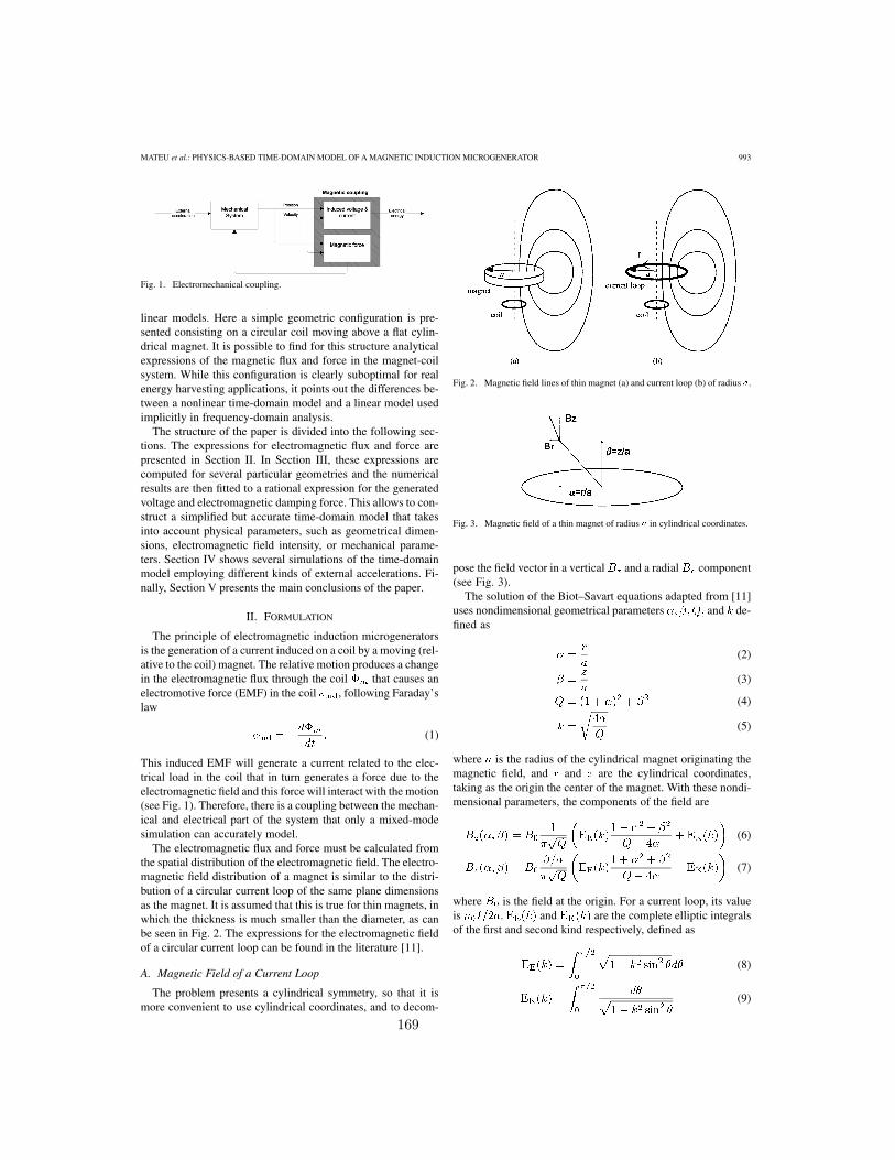
MATEU et al.: PHYSICS-BASED TIME-DOMAIN MODEL OF A MAGNETIC INDUCTION MICROGENERATOR 993
Fig. 1. Electromechanical coupling.
linear models. Here a simple geometric configuration is pre-sented consisting on a circular coil moving above a flat cylin-drical magnet. It is possible to find for this structure analyticalexpressions of the magnetic flux and force in the magnet-coilsystem. While this configuration is clearly suboptimal for realenergy harvesting applications, it points out the differences be-tween a nonlinear time-domain model and a linear model usedimplicitly in frequency-domain analysis.
The structure of the paper is divided into the following sec-tions. The expressions for electromagnetic flux and force arepresented in Section II. In Section III, these expressions arecomputed for several particular geometries and the numericalresults are then fitted to a rational expression for the generatedvoltage and electromagnetic damping force. This allows to con-struct a simplified but accurate time-domain model that takesinto account physical parameters, such as geometrical dimen-sions, electromagnetic field intensity, or mechanical parame-ters. Section IV shows several simulations of the time-domainmodel employing different kinds of external accelerations. Fi-nally, Section V presents the main conclusions of the paper.
II. FORMULATION
The principle of electromagnetic induction microgeneratorsis the generation of a current induced on a coil by a moving (rel-ative to the coil) magnet. The relative motion produces a changein the electromagnetic flux through the coil that causes anelectromotive force (EMF) in the coil , following Faraday’slaw
(1)
This induced EMF will generate a current related to the elec-trical load in the coil that in turn generates a force due to theelectromagnetic field and this force will interact with the motion(see Fig. 1). Therefore, there is a coupling between the mechan-ical and electrical part of the system that only a mixed-modesimulation can accurately model.
The electromagnetic flux and force must be calculated fromthe spatial distribution of the electromagnetic field. The electro-magnetic field distribution of a magnet is similar to the distri-bution of a circular current loop of the same plane dimensionsas the magnet. It is assumed that this is true for thin magnets, inwhich the thickness is much smaller than the diameter, as canbe seen in Fig. 2. The expressions for the electromagnetic fieldof a circular current loop can be found in the literature [11].
A. Magnetic Field of a Current Loop
The problem presents a cylindrical symmetry, so that it ismore convenient to use cylindrical coordinates, and to decom-
Fig. 2. Magnetic field lines of thin magnet (a) and current loop (b) of radius a.
Fig. 3. Magnetic field of a thin magnet of radius a in cylindrical coordinates.
pose the field vector in a vertical and a radial component(see Fig. 3).
The solution of the Biot–Savart equations adapted from [11]uses nondimensional geometrical parameters and de-fined as
(2)
(3)
(4)
(5)
where is the radius of the cylindrical magnet originating themagnetic field, and and are the cylindrical coordinates,taking as the origin the center of the magnet. With these nondi-mensional parameters, the components of the field are
(6)
(7)
where is the field at the origin. For a current loop, its valueis . and are the complete elliptic integralsof the first and second kind respectively, defined as
(8)
(9)
169

994 IEEE TRANSACTIONS ON MAGNETICS, VOL. 43, NO. 3, MARCH 2007
Fig. 4. Forces on coil due to induced current for vertical motion with respectto a fixed magnet.
B. Induced Current and Force on a Coil
In this paper, we consider a configuration consisting of a thincylindrical magnet and a parallel circular coil such that both cen-ters are aligned along the vertical axis . The coil movesvertically along the vertical axis. This case presents radial sym-metry, and the total flux linked with the coil at a scaled verticaldistance , can be calculated as
(10)
where and are the normalized radial and vertical coor-dinates, respectively, and is the normalized coil radius
.On the other hand, the induced current produced by the EMF
will interact with the electromagnetic field generating a mechan-ical force. The current is perpendicular to both and , andtherefore, the force has two components; one is radial and theother is vertical, both tending to reduce the flux variation. Theradial force tends to compensate the coil area with the flux vari-ation, and the vertical force tends to oppose the motion. The me-chanical equations must take into account the electromagneticforce, which depends in a complex way on the induced current,related to the induced EMF by the circuit connected to the coil,and on the position and the velocity of the coil.
The radial components of the mechanical force at opposingsides of the coil are in opposite directions and equal in magni-tude due to the symmetry of the problem, as illustrated in Fig. 4.On the other hand, there is a net vertical force, that causes amotion damping. Its magnitude is given by the product of theradial component of the field evaluated at the coil’s radius, andthe magnitude of the induced current, integrated along the coil’slength:
(11)
The magnetic field depends on nondimensional variables and,therefore, it is invariant if the geometry of the magnet and coilsystem is proportionally scaled. On the other hand, the magneticflux and the force depend on the absolute value of the magnet’sradius and the coil’s radius , respectively, and they de-crease when dimensions are reduced.
The previous expressions for the flux and force must be cal-culated numerically for particular cases. The calculations havebeen carried out using the mathematics package Maple [12]. Theloop’s radius is 2 cm in the calculations considered here, but
Fig. 5. Comparison between calculated flux and force (with points, num label)and approximate rational functions (continuous lines, rat label) for vertical mo-tion of a coil above a magnet.
the results for other values of radius are easily derived becausethe expressions for flux and force are strictly proportional toand , respectively.
Now, in order to use these results in a mixed simulator, likePtolemy II [13] or others [14], it is necessary to extract a sim-plified analytical expression of the flux and force as a functionof coil distance. This is presented in the next section.
III. MODEL OF THE MICROGENERATOR
It is important to reduce the computational complexity of theexpressions for the flux and force, so that a transient simulatorcan calculate the response of the system in reasonable time. Theresults of the Maple computations of magnetic flux and forcewere plotted against normalized coil position for several ge-ometries . Fig. 5 shows these plots (num labels for thecurves obtained from computations). From the numerical plots,it is possible to fit an appropriate function. Given the mono-tonical behavior of the curves, we chose a rational approxima-tion, where several parameters are introduced arbitrarily so asto achieve a satisfactory fitting.
A. Rational Approximation for the Flux and EMF
Observing the flux computed numerically with Maple,Fig. 5(a), it is seen that for short vertical distances ,
170

MATEU et al.: PHYSICS-BASED TIME-DOMAIN MODEL OF A MAGNETIC INDUCTION MICROGENERATOR 995
TABLE IPARAMETERS OF THE RATIONAL APPROXIMATION FOR THE FLUX,
FOLLOWING (12)
the flux is almost constant. Therefore, after trying severalcandidates, we selected the form of the rational approximationas
(12)
The values of the parameters in expression (12) obtained froma least squares fitting procedure are shown in Table I. The lastrow corresponds to the reduced chi-square of the fit, ,equal to
(13)
where is the number of data points, and is the number ofdegrees of freedom (data points minus number of parametersin the function). To consider a satisfactory ffiting, the value of
must be two or three orders of magnitude smaller thanthe minimum value obtained from (10). Given that the minimumvalue computed is on the order of 1E-4 (values in Fig. 5(a) di-vided by ), the values can be considered small andthe fitting adequate.
With this expression for the flux, the induced EMF is obtainedtaking the derivate of (12)
(14)
where
(15)
In the literature on the modeling of inductive microgenerators,the induced EMF is simplified as
(16)
where is an effective electromagnetic field intensity. Thislast expression corresponds to a first-order approximation of theflux variation, neglecting variations with in expression (15)and thus valid only for small displacements from a given dis-tance of the coil to the magnet, . Fig. 6 shows a plot of function
in (14), where it can be estimated the range of ver-tical motion where this function is nearly constant (EMF strictlyproportional to ). This range, where the linear approximation is
Fig. 6. Normalized EMF corresponding to function ( ; ) in (14) for sev-eral values of between 0.2 and 1.2.
Fig. 7. Measurements of generated voltage when a magnet vibrates above aspiral inductor. The magnet is located 2 cm above the spiral plane and its initialposition is in contact with it. The vibration amplitude decreases with time dueto mechanical losses.
valid, is larger for slightly smaller than unity. The nonlinearityof the model is observable for systems more complex than thegeometric configuration considered here. For example, Fig. 7shows the measured voltage waveform of a magnet moving si-nusoidally above a planar spiral inductor. The voltage waveformis not sinusoidal for large swing oscillations, as it should be ac-cording to (16).
Another important problem with the linear approximation isthat it is difficult to compute the value of , because it dependson the distance , on the magnet strength, as well as on magnetand coil dimensions.
Instead, the model presented in this paper gives a soundermethod to compute the EMF for different distances, and it isalso valid for larger swing vibrations.
B. Rational Approximation for the ElectromagneticDamping Force
From the computed results for the vertical electromagneticforce, we try an approximate expression of the form
(17)
171

996 IEEE TRANSACTIONS ON MAGNETICS, VOL. 43, NO. 3, MARCH 2007
TABLE IIPARAMETERS OF THE RATIONAL APPROXIMATION FOR THE FORCE,
FOLLOWING (17)
TABLE IIIPARAMETERS OF THE RATIONAL APPROXIMATION FOR THE FORCE CASE
= 1, FOLLOWING (19)
where again we consider a rational function. From the numericalresults computed for the force and plotted in Fig. 5(b) it is seenthat for small the force is not constant as happened with theflux. Thus, we tried a rational approximation of the form
(18)
The behavior for is different, and in this case a dif-ferent rational approximation is taken as explained below. Thevalues of the parameters in (17) are shown in Table II. The am-plitude increases with , as should be expected.
With respect to the case , the above expression isnot easily fitted. The following approximation was tried:
(19)
The results for and especially for (shownin Table III) show a rather large statistical uncertainty in theparameters, represented by the value of . However, theadjustment can be considered fairly good by visual inspectionof Fig. 5(b).
C. Equations of Motion
With the above expressions, the model can be built at a mod-erate computational cost. Let us assume a one-dimensional mo-tion in the variable, with a magnet of mass suspended froman elastic support with Hooke’s constant above a coil loadedwith an electrical resistance . A mechanical damping force dueto friction can also be introduced. The equations of motion are
(20)
where and are respectively elastic force,electromagnetic damping force, frictional mechanical dampingforce, and external force. Mechanical damping force isdifficult to model because several loss mechanisms may bepresent. Such an analysis exceeds the object of this paper and,
Fig. 8. Factor of proportionality of _z in F , corresponding to ( ; )
'( ; ) in (23). between 0.2 and 1.2.
therefore, we consider a linear loss model. The forces are givenby
(21)
(22)
(23)
where is the spring constant, is the distance at rest, isthe mechanical damping coefficient, is the number of par-allel coils assuming the total height of the coils is much smallerthan the distance to the magnet, and is the rationalapproximation in (17) or (19).
The equations of the electrical system are given by the rela-tion between voltage and current. For a resistive load and lowmechanical oscillation frequencies, so that the self-inductanceof the coil may be neglected, the equations are
(24)
(25)
where is the rational approximations in (14).The electromagnetic damping force can be expressed as a pro-
portionality function of velocity
(26)
A linear model is valid for a constant proportionality function,independent of . On the other hand, the consideration of a largemotion amplitude makes this proportionality function stronglydependent on position, and therefore makes the equation of mo-tion nonlinear. Fig. 8 plots the proportionality factor of as afunction of mass position . As shown, small vibrations result inan expression of closely proportional to , especially whenmoving in the range of . With respect to , it can alsobe considered as proportional to only for small displacements(see Fig. 6). Otherwise, nonlinear effects will dominate foramplitudes greater than or on the order of 0.5.
In a linear damped oscillation equation, the damping factoris a useful quantitative measure of the motion. In our nonlinearequation, we will use an analog electromagnetic damping factordefinition. Although this definition does not correspond to the
172

MATEU et al.: PHYSICS-BASED TIME-DOMAIN MODEL OF A MAGNETIC INDUCTION MICROGENERATOR 997
TABLE IVNONLINEAR MODEL SIMULATION RESULTS FOR 5 m/s SINUSOIDAL AT 200
Hz WITH b = 0
TABLE VNONLINEAR MODEL SIMULATION RESULTS FOR 5 m/s SINUSOIDAL
AT 2 Hz WITH b = 0
mathematical solution, it is a qualitative measure of the impor-tance of the electromagnetic damping. We define an electromag-netic damping factor and a mechanical damping factor as
(27)
(28)
where is the natural frequency of the mechan-ical oscillator. A small value of the damping factors implies alarger motion amplitude and velocity, and consequently, a largergenerated electrical power and energy. Therefore, these factorsgive an idea of the efficiency in generating energy. The smallerthe damping factors are, the better the efficiency, which meansthat mechanical systems with large will have, in principle, abetter efficiency.
We also use the damping factors to compare a linear modelwith the complete nonlinear model.
IV. SIMULATION RESULTS
The model equations obtained above have been used to builda Ptolemy II model, that uses Ptolemy’s built-in time-domainsimulator. Ptolemy [15] is an open source tool for modeling and
Fig. 9. Comparison between linear and nonlinear model computations for z =
50 mm, 200 Hz, of peak power (a) and energy after 1 s (b).
simulation of concurrent and hybrid systems. In this paper it isonly used for its time-domain simulation capabilities, althoughthe tool’s applications are much more general [13].
We will study the system by changing several parameters: ini-tial distance between coil and magnet, mechanical spring con-stant, to vary the mechanical oscillation frequency, and me-chanical damping coefficient. For each parameter variation twodifferent types of mechanical excitation, external accelerationwaveform, are applied: a sinusoidal excitation with two differentfrequencies and a waveform obtained from measurement of aperson walking.
Considering that the microgenerator could be integrated witha personal electronic device, we selected rather arbitrarily thefollowing dimensions and parameters: proof mass g,maximum electromagnetic field T, magnet radius
cm, coil radius cm, number of turns of thecoil , and load resistance .
A. Sinusoidal Acceleration
A sinusoidal acceleration is an appropriate model for amechanical vibration. We consider two cases: low-frequency(2 Hz), and mid-frequency (200 Hz) vibrations (Tables IVand V, respectively). Low-frequency vibrations are the maincomponents of human motion (analyzed in more detail below),
173

998 IEEE TRANSACTIONS ON MAGNETICS, VOL. 43, NO. 3, MARCH 2007
Fig. 10. Comparison between linear and nonlinear model computations forz = 50 mm, 2 Hz, of peak power (a) and energy after 1 s (b).
while other vibration sources (machines and furniture) willpresent higher frequencies.
The results show that, as frequency-domain analysis pre-dicts, the effectiveness of energy conversion depends largelyon the proximity between acceleration frequency and naturalfrequency of the oscillator . A significant amountof energy is generated when the oscillator is close to resonanceeven for a large distance between coil and magnet. Conversely,when acceleration frequency is very different from resonancefrequency, a very small amount of energy is generated althoughthe distance is very short.
For the frequencies considered here, 2 and 200 Hz, and themass of 50 g, resonance condition is achieved by N/mand N/m, respectively. The case of mid-frequencygives more energy because the parameter is smaller than theone at low frequency.
There is a modeling problem when working at resonance fre-quencies, that is, the large displacement of the magnet may col-lide with the coil. This kind of phenomenon is best observedin the time-domain model, and poses a limitation in the dis-tance between magnet and coil at rest, , as well as the valueof the spring constant, . For this reason, the resonance condi-tion ( N/m) is not included in Table V. is defined asthe maximum displacement above minus the maximum dis-placement below over the magnet radius:
(29)
Fig. 11. Measured acceleration at the knee of a person walking.
TABLE VINONLINEAR MODEL SIMULATION RESULTS FOR MEASURED ACCELERATION AT
THE KNEE OF A PERSON WALKING. MECHANICAL DAMPING CONSTANT: b = 0
Figs. 9 and 10 show the comparison between computations ofpower and energy using a nonlinear or a linear model for thefrequencies of 200 and 2 Hz, respectively. For the case repre-sented in Fig. 9, there is no difference between the nonlinearand the linear model since the movement of the magnet is small;
has a value between and . In Fig. 10,where , it can be shown a difference for the case of
N/m where . However, for the other twocases: N/m and N/m
, the difference between nonlinear and linearmodel is inappreciable. The rest of cases studied in Tables IVand V present almost no difference between a linear or non-linear model.
B. Measured Acceleration for Human Walking Motion
We measured the acceleration at the knee of a person walking.With this acceleration, the time-domain response of the micro-generator is obtained. In this case, a frequency-domain analysisis difficult to apply and the advantage of the time-domain modelis evident. The acceleration data (shown in Fig. 11) have beenobtained employing the ADXL202 accelerometer of the Mica2sensor board [16].
Tables VI and VII for human walking acceleration show twodifferent cases: , and , respectively. The external
174

MATEU et al.: PHYSICS-BASED TIME-DOMAIN MODEL OF A MAGNETIC INDUCTION MICROGENERATOR 999
TABLE VIINONLINEAR MODEL SIMULATION RESULTS FOR MEASURED ACCELERATION AT THE KNEE OF A PERSON WALKING. MECHANICAL DAMPING CONSTANT: b = 0:1
Fig. 12. Acceleration spectrum for measured human walking waveform shownin Fig. 11.
acceleration for human walking motion has associated low fre-quencies, as can be seen in Fig. 12. Therefore, it can be ex-pected that low values of give the best results in terms ofenergy. However, low values of imply high values of and
. Therefore, a tradeoff between the parameters andgives the best results.
Figs. 13 and 14 show the position of the vibrating element(magnet or coil, depending on chosen setup) and the electricalenergy dissipated at the resistor in function of time, respectively.
The comparison between a linear and a nonlinear model isshown in Fig. 15 for the case of . A big difference can beseen between both models for the values of N/m
and N/m since the displacements arelarge. For the case of N/m , it canbe seen that the difference between the nonlinear and the linearmodel is slight. For the rest of the cases, there is no differencenoticeable between the nonlinear and the linear model.
V. CONCLUSION
In this work, it is considered a flux and force dependence oncoil’s position based on the physics of the problem. This consid-eration leads to more complex expressions for these magnitudesthan assumed in previous works. However, it was not consid-ered the magnetic field distortion due to coil proximity, or more
Fig. 13. Position of the proof mass when it is moved with the accelerationshown in Fig. 11. Parameters k = 400 N/m, z = 10 mm, ( = 0:5); b =0:1.
Fig. 14. Energy dissipated in the load when the external acceleration shown inFig. 11 is applied to the microgenerator. Parameters k = 400 N/m, z = 10mm, ( = 0:5); b = 0:1.
complex mechanical losses than the linear model used here. Thepurpose of using this structure and model was to get insight ondifferent design parameters and on the influence of nonlinear
175

1000 IEEE TRANSACTIONS ON MAGNETICS, VOL. 43, NO. 3, MARCH 2007
Fig. 15. Comparison between linear and nonlinear model computations forz = 50 mm, and measured acceleration of peak power (a) and energy after10 s (b) with b = 0:1.
effects in the model. The method presented here should be ap-plied to more realistic geometries and mechanical configura-tions. A detailed analysis of such structures based on finite-ele-ment computations can be carried out to compute flux and forcedependence on position, and then a fitting procedure like theone performed in this paper would allow a realistic time-domainsimulation.
The influence of nonlinear effects was shown to be impor-tant when the value of is greater than . For example, inthe case of the measured acceleration at the knee of a personwalking with , the difference in the estimated energybetween considering a linear or nonlinear model is % for
N/m and , % for N/m andand % for N/m and
in the case of . The difference in the estimation of themaximum power is in the same range of magnitude. Thedifference obtained in the estimation of the energy for the caseof N/m and is 5.6% forwhereas for the case of N/m andis % for . In summary, it was shown that a linearmodel underestimates the energy that can be generated, espe-cially in the cases where this energy is greater. This underes-timation could lead to overdesigned, and therefore suboptimalmicrogenerator design.
The time-domain analysis presented here also allows to cal-culate some magnitudes that are not available in frequency do-main. For example, the maximum power can be calcu-lated in frequency domain, but for energy harvesting applica-tions it is more interesting to know the value of the recoveredenergy during a certain time, or average power. This value isgiven by the time-domain analysis presented in this paper. A
proper power conditioning system should be used, taking intoaccount that the power generation is highly discontinuous.
Finally, several conclusions can be drawn with respect tothe design of an electromagnetic induction energy harvestingdevice.
The microgenerator is best suited for acceleration waveformswith important high-frequency components, since a resonantgenerator in this case implies high values of . This impliesthat the values of and will be small, and therefore, a higheramount of harvested energy can be stored.
The present analysis also allows to deduce some properties ofgeometric scaling of the microgenerator. It was shown in (25)that the induced EMF is proportional to the product .Assume that both magnet, coil, and distances are uniformlyscaled. The velocity is related to the maximum displacementin the case of an oscillation. Thus, a reduction of vertical di-mensions (implying a reduction in ) can be compensated byan increase of horizontal dimensions (therefore increase of themagnet radius, ). A reduction of the volume of the microgener-ator (both vertical and horizontal dimensions) can only be com-pensated by an increase of the product .
REFERENCES
[1] M. Billinghurst and T. Starner, “Wearable devices. New ways tomanage information,” IEEE Computer, vol. 32, no. 1, pp. 57–64, Jan.1999.
[2] J. Meindl, “Low power microelectonics: Retrospect and prospect,”Proc. IEEE, vol. 83, no. 4, pp. 619–635, Apr. 1995.
[3] T. Starner and J. Paradise, , C. Piguet, Ed., “Human generated power formobile electronics,” in Low Power Electronics Design. Boca Raton,FL: CRC, 2004, ch. 45.
[4] P. D. Mitcheson, T. C. Green, E. M. Yeatman, and A. S. Holmes, “Ar-chitectures for vibration-driven micropower generators,” J. Microelec-tromech. Syst., vol. 13, no. 3, June 2004.
[5] C. R. Saha, T. O’Donnell, H. Loder, S. Beeby, and J. Tudor, “Opti-mization of an electromagnetic energy harvesting device,” IEEE Trans.Magn., vol. 42, no. 10, pp. 3509–3511, Oct. 2006.
[6] N. N. H. Ching, G. M. H. Chan, W. J. Li, H. Y. Wong, and P. H. W.Leong, “PCB integrated micro generator for wireless systems,” in Int.Symp. Smart Structures and Microsystems, Oct. 19–21, 2000.
[7] W. Li, T. Ho, G. Chan, P. Leong, and H. Y. Wong, “Infrared signaltransmission by a laser-micromachined, vibration-induced power gen-erator,” in Proc. 43rd IEEE Midwest Symp. Circuits and Systems, 2000,vol. 1, pp. 236–239.
[8] T. von Buren, P. Mitcheson, T. Green, E. Yeatman, A. Holmes, andG. Troster, “Optimization of inertial micropower generators for humanwalking motion,” IEEE Sensors J., vol. 6, no. 1, pp. 28–38, 2006.
[9] R. Amirtharajah and A. Chandrakasan, “Self-powered signal pro-cessing using vibration-based power generation,” IEEE J. Solid-StateCircuits, vol. 33, no. 5, pp. 687–695, May 1998.
[10] S. Ohashi and T. Matsuzuka, “Basic characteristics of the linear syn-chronous generator using mechanical vibration,” IEEE Trans. Magn.,vol. 41, no. 10, pp. 3829–3831, Oct. 2005.
[11] W. Smythe, Static and Dynamic Electricity, 3rd ed. New York:Taylor and Francis, 1989.
[12] Maplesoft, [Online]. Available: http://www.maplesoft.com[13] J. Liu and E. A. Lee, “A component-based approach to modeling and
simulating mixed-signal and hybrid systems,” ACM Trans. Model.Comput. Simul., vol. 12, no. 4, pp. 343–368, 2002.
[14] F. Pecheux, C. Lallement, and A. Vachoux, “VHDL-AMS and Ver-ilog-AMS as alternative hardware description languages for efficientmodeling of multidiscipline systems,” IEEE Trans. Comput.-AidedDes. Integr. Circuits Syst., vol. 24, no. 2, pp. 204–225, Feb. 2005.
[15] Ptolemy Project, [Online]. Available: http://ptolemy.eecs.berkeley.edu[16] Berkeley Mica Motes, [Online]. Available: http://www.xbow.com
Manuscript received May 23, 2006; revised November 15, 2006. Corre-sponding author: F. Moll (e-mail: [email protected]).
176

MATEU et al.: PHYSICS-BASED TIME-DOMAIN MODEL OF A MAGNETIC INDUCTION MICROGENERATOR 1001
Loreto Mateu received the equivalent of the M.Sc. degree in electronic engi-neering from the Technical University of Catalonia (UPC), Spain, in 2002. Sheis a Ph.D. student in the Department of Electronic Engineering, Technical Uni-versity of Catalonia.
Her area of research is energy harvesting to power wearable devices. Herfocus is on piezoelectric materials, thermoelectric generators, and electromag-netic power conversion. In addition, she is also interested in dc/dc converters topower wearable devices from harvested electrical energy.
Carlos Villavieja received the equivalent of the M.Sc. degree in computer en-gineering from La Salle School of Engineering at Ramon Llull University in2000.
He is a Ph.D. student and Lecturer Professor in the Department of ComputerArchitecture, Technical University of Catalonia (UPC), Spain. His area of re-
search is global system optimization. He is focused in operating system resourcemanagement for embedded processors. He has been working in power manage-ment and in security at the operating system level.
Francesc Moll received the equivalent of the M.Sc. degree in physics from theUniversity of Balearic Islands (UIB), Spain, in 1991, and the Ph.D. degree inelectronic engineering from the Technical University of Catalonia (UPC), Spain,in 1995.
Since 1991, he has been with the Department of Electronic Engineering,Technical University of Catalonia, where he is currently an Associate Professor.His current research activities include methods for energy harvesting orientedto low-power microelectronic circuits.
177

178

Chapter 12
Paper 5: Human BodyEnergy HarvestingThermogenerator forSensing Applications
Loreto Mateu, Cosmin Codrea, Nestor Lucas, Markus Pollak andPeter Spies
Sensor Technologies and Applications, 2007. International Confer-ence on SensorComm 2007, pp. 366–372, Valencia, 2007.
179

Human Body Energy Harvesting Thermogenerator for Sensing Applications
Loreto MateuUniversitat Politecnica de Catalunya (UPC)
Electronic Engineering DepartmentCampus Nord, Edifici C4
C/ Jordi Girona 1-308034 Barcelona, Spain
Cosmin Codrea, Nestor Lucas,Markus Pollak and Peter Spies
Fraunhofer IISPower Efficient Systems Department
Nordostpark 93D90411 Nrnberg, Germany
Abstract
A low temperature thermal energy harvesting system tosupply power to wireless sensing modules is introduced.The thermoelectric generator module (TEG) makes use ofthe temperature gradient between the human body (the heatsource) and the ambient to deliver a low voltage output thatis up-converted by means of a power management circuit.This regulated power source is able to reliably supply awireless communication module that transmits the collectedtemperature, current and voltage measurements.
1 Introduction
The presence of ubiquitous electronics in everyday’s lifeis rapidly growing and the complexity of these devicesseems to know no limits. However, one of the most im-portant challenges mobile devices face is the need to en-sure a reliable power supply beyond the limitations posedby batteries. A solution to this problem is the developmentof devices capable of harvesting energy from the user’s en-vironment or from the user’s body. The electrical energycan be transformed from either kinetic, electromagnetic orthermal energy employing the appropriate energy harvest-ing generator in each case.
The human body continuously radiates heat. Devices indirect contact to the human body can harvest this wastedenergy by means of thermogenerators (TEGs). The TEG(based on the Seebeck effect) is a thermocouple module thatproduces an electrical voltage proportional to the tempera-ture difference between hot and cold junctions. In our case,the TEG employs the temperature gradient between the hot(body) and cold (ambient) side of the thermopair to gener-ate electrical energy. A significant constraint for this kind ofsystems relies on the relative low temperature gradient (in
the range of 5 C-10 C, or even lower) between the humanbody and the environment resulting in low voltage levelsprovided by the TEG.
This paper presents an energy harvesting applicationcontaining a sensor unit and a wireless communicationmodule, as shown in Figure 1. A similar application thatgenerates an average power of 100μW with an output volt-age of 2.4V is presented in [14].
Special care has been taken in the design of power andbattery management units that convert the energy harvestedfrom the TEG. Additionally, a procedure to obtain electricalmodels for TEGs and batteries is discussed, in order to builda library of models that will enable simulations of the entiresystem in the close future.
The structure of the paper is as follows. Section 2 showsthe performed TEG characterization as well as the simula-tion results obtained for the implemented electrical model.Section 3 describes the power management unit. An il-lustration of battery management and the extraction of anelectrical battery model is given in Section 4. FollowingSection 5 presents an application for the energy harvestingTEG, where a wireless communication module sends sens-ing data. Finally, Section 6 draws the main conclusions ofthe paper.
2 Energy Harvesting with Thermogenerators
A thermoelectric generator module mainly consists of athermocouple comprising a p-type and n-type semiconduc-tor connected electrically in series and thermally in parallel.The electrical connection allows to add the voltage obtainedat each thermocouple due to the Seebeck effect. Therefore,the output voltage of the TEG is proportional to the numberof thermocouples and to the temperature gradient betweenthe cold and the hot side.
Several thermogenerators [1] were characterized in or-
2007 International Conference on Sensor Technologies and Applications
0-7695-2988-7/07 $25.00 © 2007 IEEEDOI 10.1109/SENSORCOMM.2007.42
366
2007 International Conference on Sensor Technologies and Applications
0-7695-2988-7/07 $25.00 © 2007 IEEEDOI 10.1109/SENSORCOMM.2007.42
366180

Figure 1. System overview of the energy har-vesting application.
der to determine an optimum in terms of efficiency for thepresent application.
2.1 Characterization of the employedthermogenerator
The small-sized (2.5 x 2.5 cm) TEG with heat sink se-lected for our application is shown in Figure 2. The charac-terization curves measured for the selected Peltier elementPKE 128 A 1030 are shown in Figure 3. This figure showsthe voltage as a function of current for different values ofΔT and TH . This figure shows also the electrical powergenerated by the TEG as a function of its current. The TEGconversion efficiency is defined as the ratio between the out-put electrical power, Po, and the input thermal power in thehot junction, qH . qH is a function of ΔT , the temperaturedifference between the hot and the cold side of the TEG,Θm, the thermal resistance of the TEG, αm, the Seebeck’scoefficient of the TEG and Rm, the electrical resistance ofthe TEG. Employing Equation 1, the efficiency for the TEGwas computed. The maximum power and efficiency are ob-tained when the output resistance connected to the TEG isequal to Rm.
η =Po
qH(1)
Table 1 shows the measured data TH , ΔT and Voc andthe calculated thermal parameters of the TEG αm and Rm
from the measured values.
2.2 ADS Electrical model of the thermo-generator
Chavez et. al. [16] and Lineykin et. al. [19] present aSPICE model for thermoelectric elements. These modelsallow to make simulations of TEG based systems. This pa-per takes the mentioned works as a reference to develop anADS [2] electrical model for the selected Peltron TEG. Atransient response of the TEG is not necessary in our case
Figure 2. Thermogenerator with heat sink se-lected to power the sensors unit.
Table 1. Measured thermal parameters of thePeltron element PKE 128 A 1030.
TH ΔT αm Rm Voc Pmax ηmax
(K) (K)(mV
K
)(Ω) (V) (mW) (%)
312.06 6.71 49.7 10.213 0.333 2.05 0.16322.09 11.36 46.7 10.649 0.531 4.97 0.24332.13 16.55 44.9 11.066 0.743 9.37 0.32342.16 21.72 44.2 11.478 0.96 15.07 0.39352.18 26.93 43.8 11.891 1.18 21.89 0.46362.23 32.05 43.5 12.302 1.39 29.6 0.52
since we are looking for a static characterization. There-fore, it is not necessary to include the capacitors that appearin the SPICE models [16], [19] and [20].
The simulation results are presented in Figure 3 and Ta-ble 2. In simulation 1, the values of αm and Rm have beencalculated with equations given in [19] from the values ob-tained from Peltron for Qmax, Vmax, Imax, Th and ΔTmax.Simulation 2 employs the datasheet values for αm and Rm.Simulation 3 uses the values of αm and Rm calculated fromthe measurements. Θm is the same in all the simulations,Θm=6.38K/W, since it is not a value given by Peltron and itcan not be calculated from our measurements. Simulation 1obtains the same results of Pmax and ηmax than the mea-surements for ΔT=6.71K and the most similar results forΔT=11.36K. Nevertheless, simulation 3 obtains the sameresults of Voc than the measurements.
3 Power Management Unit
The main difficulty in the design of a power managementunit for a TEG is provided by the output voltage levels ofthe thermogenerator. These are proportional to the appliedtemperature gradient. Observing Table 2, it is deduced that
367367181

Table 2. Comparison of the values obtained for the Peltron element PKE 128 A 1030 from measure-ments and simulations.
TH(K) ΔT (K) αm(mV/K) Rm(Ω) Voc(mV ) Pmax(mW ) η (%)
Measurement 312.21 6.71 49.7 10.213 334 2.05 0.17
Simulation 1 312.21 6.71 39 8.306 264 2.05 0.17
Simulation 2 312.21 6.71 49 7.7 329 3.52 0.26
Simulation 3 312.21 6.71 49.7 10.213 334 2.73 0.21
Measurement 322.24 11.36 46.7 10.649 530 4.97 0.24
Simulation 1 322.24 11.36 39 8.306 440 5.9 0.28
Simulation 2 322.24 11.36 49 7.7 557 10 0.43
Simulation 3 322.24 11.36 46.7 10.649 530 6.7 0.31
0,0
400,0
800,0
1,2m
1,6m
2,0m
2,4m
2,8m
0 5m 10m 15m 20m 25m 30m0
50m
100m
150m
200m
250m
300m
350m
P (
W)
η (%
)V
ou
t (V
)
I (A) V
out Simulation 1
P Simulation 1
η Simulation 1
Vout
measured
P measured
η measured
Figure 3. Simulated output characteristic forthe TEG employed in the application. Volt-age, power and efficiency as a function ofcurrent for ΔT = 6.71 K and TH=312.06 K.
it is situated in the range of 45mV per Kelvin for the PKE128 A 1030 TEG characterized. Taking into account thatthe hot side of the TEG is heated up by the human body andthe cold side is at ambient temperature, it can be concludedthat the temperature difference between both sides of theTEG will oscillate between 5K and 10K.
The power management unit is designed to convert in-put voltages in the order of few hundreds of millivolts intohigher output voltages to supply the wireless communica-tion module and the sensors and eventually to store the re-maining energy into a storage element like a battery or a
capacitor. A picture of the PCB prototype is presented inFigure 5.
Commercial step-up (boost) DC-DC converters startwith input voltages of 0.7V limited by the threshold volt-age of the switching transistors. If lower input signals haveto be processed, special low-threshold transistors have tobe used or dedicated architectures of boost dcdc convertershave to be adapted. The designed power management cir-cuit is shown in Figure 4. It consists of a charge-pump [3]in conjunction with a step-up DC-DC converter [4]. Thecharge-pump employs SOI (silicon on insulator) transistorswith low threshold voltages. Table 3 shows the current con-sumption of the charge pump with respect to the input volt-ages. The voltage range generated by the TEG employinghuman hand heat radiation covers a range from 150mV to250mV with a maximum current of 18mA. Therefore, alow-voltage charge pump can be employed as a start-up cir-cuit to deliver the required 0.7V for a conventional boostconverter.
The charge-pump, U1, charges a high value capacitor,C2. As soon as it reaches a threshold of 1.8V, an internaltransistor turns on and the stored voltage on C2 is deliveredto the output. Thus, the step-up converter, U2, starts switch-ing by means of this available start-up energy. Once theconverter starts regulating and its output rises, the charge-pump is not needed anymore. Therefore, the boost con-verter supplies its own control power by feeding the out-put voltage to the input of its switching circuitry by meansof an internal diode of the step-up converter, D2, and thecharge pump can be short-circuited by the inductor, L1, ofthe step-up converter. Thus, the step-up converter entersstand-alone operation mode and keeps supplying a regu-lated output even though the input voltage decreases belowthe 250mV overall start-up margin. Switching at an inputvoltage as low as 150mV was recorded. The output volt-age of the boost converter is 3.7V since the supply voltage
368368182

range of the communication module selected is 3V-4V. Theefficiency range of the converter for the TEG input voltagesis 63%-40%.
Table 3. Measurements of the input voltageand charge pump current consumption.
Vin(mV ) 300 250 200 150 130Iin(mA) 0.35 1.5mA 3.5mA 2.6mA 6.4mA
Care must be taken in the choice of the values of therequired energy storage elements, i.e. the capacitor of thecharge-pump, C2, and the inductor of the step-up-converter,L1. A trade-off must be made when dimensioning thevalue of the charge-pump capacitor. A high value capac-itance is required to provide the necessary start-up powerof the next stage, while a lower value reduces the start-uptime. Thus, the lowest but still functional value was selected(C2 = 100μF ). As the energy source is very restricted, cur-rent limitation issues are of no concern for the application.High inductor values may be employed by the step-up con-verter in order to reduce the minimal start-up voltage and toprovide high efficiency as well. Thus a high value inductorwas employed (L1 = 330μH). The output capacitor of theconverter, C4, is critical as well. If its value is too large, theconverter may be prevented from regulating the output withthe available start-up energy. Here, a 1μF capacitance wasemployed.
A PMOS transistor, Q1, is required to delay upon power-up the connection of the converter’s output to the electricalload or the energy storage element since at first it can notdeliver enough energy for the stand-alone operation and theload. The time delay is set by C5 and R2 and it is in theorder of tens of milliseconds. An additional circuit withMOS transistors Q2 and Q3 can be connected in order tocharge the battery or supply the load only if it is verifiedthat the TEG has an output voltage of at least 0.2V. Due tothe intrinsic current limitation of thermogenerators and thevoltage limitation undertaken by the DC-DC converter inconjunction with a diode, D1, no additional battery chargeris needed to protect the battery against over-voltage, under-voltage or over-current.
The jumpers and external switches of the circuit allowdifferent operation modes of the power management unitthat are summarized in Table 4. In operation mode 4, thebattery is connected to the input of the power managementunit during a few seconds to avoid the delay due to the start-up of the circuit with the very low voltage output of theTEG.
Figure 5. The PCB prototype of the powermanagement unit.
Table 4. Operation modes of the power man-agement unit.
Option Description1 Self-sufficient operation mode to power
communication and sensor unit2 Battery charger3 Self-sufficient operation mode to power
communication and sensor unit and tocharge a battery
4 Self-sufficient operation mode with batterystart-up
4 Energy Storage Element
In an energy harvesting system, an energy storage ele-ment can be employed for two reasons. On one hand, itpermanently accumulates the available energy delivered bythe thermogenerator, even though no continuous power isdemanded by the electronic application. On the other hand,if excessive power bursts, e.g. upon start-up or during trans-mission are required, they can be drawn out of the energybuffer.
4.1 Design considerations for batterymanagement
The battery has to be selected based on the supply volt-age of the electrical load. A second SMPS needed to bridgethe gap between battery and load voltages can thereforebe avoided. For a supply voltage range between 2V and2.8V two-cell-NiMH [5] or one-cell-lithium-polymer withlithium-titanium-oxide [6] batteries can be taken into ac-count whereas for a supply voltage range between 3V and
369369183

Figure 4. Low-input voltage power management circuit.
4V, typical 3.7V lithium batteries can be selected. In thisspecial case the battery is charged at a nominal constantvoltage thus, a current-limit regulation loop is usually re-quired to avoid overcharging during the fast charging stageof NiMH and lithium batteries [18]. The designed circuittakes advantage of the intrinsic current limiting characteris-tics of the TEG for charging the battery without the need ofdedicated hardware. Additionally, the voltage-limit regula-tion loop is undertaken by the boost DC-DC converter sinceit provides the required charging voltage at the output ofthe power management unit. A battery charger is replacedthough by a diode, D1, connected between the output ofthe regulator and the battery. Time-limited charge termina-tion circuitry is also avoided by selecting a regulated voltageslightly below the maximum topping voltage specified bybattery manufacturers. This approach is more advisable forlithium-polymer than for NiMH accumulators, since the lat-ter suffer from memory effect degradation when the charg-ing procedure is not completed. This topology can be en-hanced in terms of reliability by placing a Zener diode thatlimits the charging voltage in case of failure.
The selected battery [7] is a rechargeable Lithium-Ionbattery with a nominal voltage of 3.7V and a typical capac-ity of 150mAh since the wireless communication modulesupply voltage range is 3V-4V.
4.2 Battery model
An electrical battery model can enable the simulation ofthe complete energy harvesting circuit. The advantage ofthe model provided by Chen et al. [17] over the model pro-posed by Schweighofer et al. [21] is that it includes a cir-cuit to estimate the state of charge of the battery in additionto the electrical model for the voltage and current charac-
teristics of the battery. This improvement allows to com-pute the increase in the state of charge (SOC) employingthe designed energy harvesting system. The equation thatdescribes the electrical model of the batteries is:
VBatt = VOC + IBattRSeries + IBattRS(1− e(−t/τS))
+ IBattRL(1− e(−t/τL))(2)
where VOC is the open-circuit voltage of the battery,RSeries is the constant part of the internal resistance ofthe battery, IBatt is the current of the battery (positive forcharging the battery and negative for discharging it), τL andτS are the cause of the long and short time constant of thebattery, respectively, to a current pulse.
The electrical model of the battery includes two RC net-works. The RL CL network has a long time constant, τL
(τL = RLCL), while the RS CS network has a short timeconstant, τS (τS = RSCS), when a current pulse is appliedto the battery. Another parameter that appears in the elec-trical model is the capacity of the battery, Ccapacity. Theseparameters are expressed as a function of the SOC.
The method employed to calculate the value of these pa-rameters is to discharge the battery with ten current pulsesin order to obtain their values for ten different values ofthe state of charge of the battery. The duration of the dis-charge current pulses, tdisch, is calculated with Equation (3)whereas the duration of the time with current equal to zero(relaxation time, trelax) that is when the parameters of thebattery are calculated must be at least equal to the large timeconstant. Therefore, it is determined with test and errormethod. The calculus to obtain the values for the param-eters of the battery model is done during trelax since theSOC of the battery is constant.
370370184

Figure 6. Prototype of the thermogenerator-based energy harvesting system and visual-ization infrastructure.
tdisch =CI1
I13600 (3)
where CI1 is the capacity of the battery for a dischargecurrent I1. The capacity of the battery increases with thediminution of the discharge current. Therefore, the capac-ity must be measured for the different discharge currents forwhich the battery model parameters.
The battery measurement infrastructure consists of aBasytec battery test system [8], a Metrahit multimeter [9]and a CTS temperature chamber T-40/50 [10]. The requiredMatlab [11] code was written employing EasyFit [12] tool-box to calculate the parameters of the electrical model ofthe battery. The latter has been simulated using ADS.
5 Application Example: Power-efficientWireless Communication and Sensor Unit
A prototype system has been built based on the re-sults provided by simulations run using the extracted elec-tric models and the design considerations introduced inthe previous sections. Figure 6 shows the deployedthermogenerator-based energy harvesting system alongwith the required monitoring infrasture. The main pur-pose was, on the one hand, to confirm the validity of ourassumptions and on the other, to assess the performanceof thermogenerator-based energy harvesting solutions usingstate of the art components.
The harvested energy from the human body under reg-ular room temperature or outdoor conditions is limited.Hence, an optimized, energy-aware operation of the em-ployed communication module has a significant impact
Figure 7. Sensor circuit schematic
on the functionality and the runtime of the device. Fordemonstration purposes the EnOcean RF sensor transmit-ter STM 100 and receiver RCM 120 modules have been se-lected due to their low power consumption. The energy re-quirements are summarized in Table 5. The board is poweroptimized and consumes 25nA in stand-by.
Table 5. Power requirements for the EnOceantx module STM 100.
Power supply range 3V-4V
Current consumption in stand-by ∼25 nA
Maximum power consumption in Tx mode 10 mW
The transmitter is employed to send the measures ob-tained by power-efficient sensors. Three different sensors,see Figure 7, are connected to the communication mod-ule’s ADC inputs. The sensor unit contains a temperature,a current and a voltage sensor. The current sense amplifierCSA1 with a quiescent current of 30 μA is used to measurethe current generated by the TEG. The temperature sensor
371371185

circuit measures the ambient temperature whereas two op-erational amplifiers (OPAMP1 and OPAMP2) are em-ployed in a bridge amplifier circuit as shown in [15]. Thevoltage generated by the TEG is simply measured usinga third operational amplifier OPAMP3, so that the low-output voltage of the TEG is up-converted to satisfy the re-quirements of the transmitter module’s ADC. The quiescentcurrent of each operational amplifiers is about 750nA.
The energy scavenged from the contact with a humanhand suffices to power the sensor unit and to transmit theperformed measurements every 1 second by means of thementioned wireless communication module. The transmit-ted information is visualized connecting the EnOcean re-ceiver module to a computer.
The gradient between the hand and the ambient temper-ature provides a TEG maximum output current of 18mAand a TEG output voltage between 150mV and 250mV. TheTEG maximum output power is approximately 3mW. Theminimal temperature difference that allows the systems topower the electrical load is 5K. The thermoelectrical powersupply output is 3.7V.
The prototype system was proved with energy storageelements as well. On one hand, a common lithium batteryand on the other a supercap were employed. With both el-ements the functionality of the system could be maintainedwith discontinuous available TEG power.
6 Conclusions and Future Work
A complete solution for thermogenerator-based energyautarkic wireless communication and sensing was build. Inorder to make use of the thermoelectrical energy, a powermanagement unit consisting of a charge-pump and a step-upDC-DC regulator was designed. Thus, the available energyis employed to transmit sensor data by means of a wire-less communication module. RF transmissions and mea-surements are performed every 1 second only with the heatradiated by the human body.A more power efficient wire-less communication transmissions can be realized designinga communication circuit employing the nRF24E1 Nordictransceiver [13]. Moreover, dynamic power managementcan be applied as well by adjusting the transmission rate tothe available energy.
Electrical models for diverse components of this energyharvesting system have been generated. Implementation de-cisions at sub-system level have been taken based on runsimulations whereas a system level simulation environmentis still under development.
Acknowledgment
The authors would like to thank Alexandre Jacquot fromthe Fraunhofer-Institut fur Physikalische Messtechnik IPMfor his technical support. The authors would further like tothank Fraunhofer for founding the project NanoTEC.
Loreto Mateu acknowledges the UPC-Recerca grantfrom the Universitat Politecnica de Catalunya (UPC).
References
[1] Peltron GmbH Peltier-Technik. http://www.peltron.de.[2] Agilent Advanced Design System (ADS).
http://eesof.tm.agilent.com/products/ads main.html.[3] Seiko Instruments Inc. http://www.seiko.com.[4] Maxim Dallas Semiconductor. http://www.maxim-ic.com.[5] Sanyo Eneloop Ready to use Rechargeable Battery.
http://www.eneloop.info.[6] Bullith Batteries. http://www.bullith.de.[7] Varta Microbattery. http://www.varta-microbattery.com.[8] BaSyTec Battery-Test-Systems.
http://www.basytec.de/produkte e/testgeraete/technik MDS.html.[9] METRAHit 29S.
http://www.gossenmetrawatt.com/english/produkte/metrahi1.htm.[10] Clima Temperatur Systeme CTS.
http://www.cts-umweltsimulation.de.[11] The MathWorks. http://www.mathworks.com/.[12] EasyFit:: Distribution Fitting Made Easy.
http://www.mathwave.com/products/easyfit.html.[13] Nordic Semiconductor. http://www.nvlsi.no.[14] Imecs watch-size thermoelectric generator powers wireless
sensor modules. IMEC Newsletter, page 14, October 2005.[15] RF Sensor Transmitter Module STM100. User Manual V1.5,
September 2005. page 29.[16] J. A. Chavez, J. A. Ortega, J. Salazar, A. Turo, and M. J.
Garcia. “SPICE model of thermoelectric elements includingthermal effects”. In 17th IEEE Instrumentation and Mea-surement Technology Conference 2000, volume 2, pages1019–1023, May 2000.
[17] M. Chen and G. Rincon-Mora. Accurate electrical batterymodel capable of predicting runtime and i-v performance.IEEE Transactions on Energy Conversion, 21(2):504–511,June 2005.
[18] D. Linden and T. Reddy. Handbook of Batteries. 3rd ed.McGraw-Hill, 2002.
[19] S. Lineykin and S. Ben-Yaakov. “SPICE compatible equiva-lent circuit of the energy conversion processes in thermo-electric modules”. In 23rd IEEE Convention of Electri-cal and Electronics Engineering, pages 346–349, September2004.
[20] S. Lineykin and S. Ben-Yaakow. Analysis of thermoelec-tric coolers by a spice-compatible equivalent-circuit model.IEEE Power Electronics Letters, 3(2):63–66, June 2005.
[21] B. Schweighofer, K. Raab, and G. Brasseur. Modeling ofhigh power automotive batteries by the use of an automatedtest system. IEEE Transactions on Instrumentation andMeasurement, 52(4):1087–1091, August 2003.
372372186

Chapter 13
Paper 6: System-levelsimulation of a self-poweredsensor with piezoelectricenergy harvesting
Loreto Mateu and Francesc Moll
Sensor Technologies and Applications, 2007. International Confer-ence on SensorComm 2007, pp. 399–404, Valencia, 2007.
187
System-level simulation of a self-powered sensor with piezoelectric energyharvesting
Loreto Mateu and Francesc MollUniversitat Politecnica de Catalunya (UPC)
Department of Electronic EngineeringCampus Nord, Edifici C4, C/ Jordi Girona 1-3, 08034 Barcelona, Spain
mateu,[email protected]
Abstract
This paper presents a complete system simulation of aself-powered communication module. The components aredescribed with the Verilog-A language, that allows to mergethe electrical and mechanical models of the system. Theself-powered sensor system is composed by an energy har-vesting piezoelectric generator that powers a RF transmit-ter. The simulations here presented compare between thecase of a battery-less and battery-powered system. The re-sults obtained with the simulation model implemented allowto show how design choices of the system change the peri-odicity of the transmission and the ability to recharge thebattery.
1 Introduction
Since the beginning of the electronic industry, a contin-uous trend of size reduction and functionality increase hasbeen observed. This trend has allowed the design of verysmall and powerful sensors that are able to transmit the datato a central receiver or to other sensors, forming what isknown as sensor networks.
One particular area of application of these small sensorsis the measurement of some property related to a person,like acceleration or medical parameters. For these appli-cations it has been proposed that energy coming from theuser activity may be harvested [10] to feed a network ofvery low power sensors, e.g. Body Area Network (BAN)and Personal Area Network (PAN) [11].
The area of energy harvesting has been active since thelate 1990s with pioneering work by Starner [9] and Paradisoat MIT on piezoelectric films inserted on shoes [4]. Othermethods to harvest energy from the environment have beenproposed and investigated. During the last years a lot ofadvances in modeling of these energy sources have taken
place.
From the point of view of the application, it is neces-sary a model of the complete system, preferably integratedin a standard CAE environment, to optimize the design ofthe complete system. The optimization of the separate com-ponents is not possible considering them independently be-cause all the parts of the system (energy source, power con-ditioning, and load energy consumption) interact with eachother. Some laboratories proposed to model a piezoelectricgenerator employing Verilog-A or VHDL-AMS to connectit to the electrical blocks of the self powered system, pre-senting the results obtained from a piezoelectric generatormodel done in VHDL-AMS [1]. The electrical part of theself powered system presented was also modeled in VHDL-AMS to allow the simulation of the complete system inthe same environment, thus decreasing the simulation timecompared to a simulation made in a mixed-environment.
This paper presents a simulation environment based onthe high level mixed signal modeling language Verilog-A [8]. This language is the analog subset of the Verilog-AMS language, and it allows the description of both electri-cal or non-electrical components, allowing a whole energyharvesting system to be described and subsequently simu-lated with a standard simulator. The objective of this paperis to pcreate a simulation environment that combines me-chanical and electrical models involved in energy harvest-ing applications. The piezoelectric transducer mechanicalmodel and the electrical components model (rectifier, volt-age regulator, RF transmitter, battery) of the self-poweredsensor system allow to evaluate the feasibility of differentpossible scenarios (e.g. RF energy consumption profiles, orbattery versus battery-less operation).
The structure of the paper is divided in the followingsections. The description of the simulation components ismade in section 2. Section 3 shows several simulations ofthe time domain model considering two examples: a sensorwith RF transmission and the charging of a battery. Finally,
2007 International Conference on Sensor Technologies and Applications
0-7695-2988-7/07 $25.00 © 2007 IEEEDOI 10.1109/SENSORCOMM.2007.33
399188

section 4 presents the main conclusions of the paper.
2 Structure of a self-powered system
A self-powered system based on environment energyharvesting is composed generically of several components(Figure 1):
• Energy transducer, to convert some available energysource into electrical energy. The environmental en-ergy sources available for conversion may be thermal(thermoelectric cells), light (photovoltaic cells), RF(rectifying antennas), and mechanical (piezoelectric,magnetic induction, electrostatic converters).
• Storage capacitor. Some of the above energy trans-ducers do not provide DC current, and in that case itis necessary to rectify the current and accumulate theenergy into a capacitor.
• Voltage regulator, to adapt the voltage level to the re-quirements of the powered device.
• Battery, depending on the requirements of the applica-tion. In some applications the powered device can becompletely switched off during certain intervals and abattery is not necessary, while in others a permanentpowering is mandatory.
• Electronic device, with varying power requirementsdepending on the application.
Figure 1. Schema of a generic self-powereddevice.
In this work, to illustrate the simulation environment,we present the case of a piezoelectric film inserted inside ashoe. In this case, the storage capacitor and rectification arenecessary because each bending of the film produces a suc-cession of alternating current peaks. In addition, being theenergy source discontinuous, it is necessary to connect theload only when there is enough energy stored in the capaci-tor. Next, the description of each component is presented.
Figure 2. Mechanical excitation of the piezo-electric film along axis 1.
2.1 Piezoelectric film
The piezoelectric effect is a property of certain materials,that when subjected to mechanical strain, suffer an electri-cal polarization proportional to the applied strain. The phe-nomenon of piezoelectricity is described by the piezoelec-tric constitutive equations:
Si = sEijTj + dliEl
Dm = εTmnEn + dmkTk
for i, j, k = 1, . . . , 6 and l,m, n = 1, 2, 3(1)
where T is the applied mechanical stress [N/m2], E isthe applied electric field [N/C], d corresponds to the piezostrain [(C/m2)/(N/m2)], εT is the permittivity [F/m] underconditions of constant stress, D is the electric displace-ment [C/m2], S is the mechanical strain [m/m], and sE isthe compliance tensor [m2/N] under conditions of constantelectrical field.
Following this behavior, a piezoelectric generator elec-trical model consists in a charge source in parallel with acapacitor.
The selected piezoelectric material is a PVDF film.These films are only metalized in the plane perpendicular todirection 3, so that D1 = D2 = 0. The mechanical excita-tion is along axis 1 (orthogonal to film surface), and externalapplied electric filed is zero for the generator. Equation (2)expresses the electric displacement generated in the piezo-electric element under these conditions. The mechanicalstress is related to the strain S1 by Young’s modulus Y11
D3 = d31T1 = d31Y11S1 (2)
Given that the charge is given by the film area times theelectric displacement, Q3 = D3A:
Q3 = d31Y11S1A (3)
400189

Figure 3. Structure of the piezoelectric can-tilever.
2.1.1 Triangular cantilever structure
One convenient method to cause a mechanical excitationin the 1 axis is to use a cantilever structure with a verticalstructure as shown in Figure 3, consisting in two piezoelec-tric films attached (each of thickness tc/2) to the top andbottom surfaces of a support material of thickness ts. It canbe shown that for a given vertical force, a maximum strainis obtained for a triangular shape. The expression of strainin function of vertical deflection can be calculated [5] forthe structure shown in Figure 3, giving a charge related todeflection y:
Q3 = yW0tc2L
d31Y11 (1 + 2τ) (4)
where τ = ts/tc is the ratio of piezoelectric film thicknessto support material thickness. On the other hand, the valueof piezoelectric capacitor, Cp, is:
Cp =4εT
33W0L
tc
(1 − k2
31
)(5)
Finally, for varying deflection in time, a current is pro-duced by the piezoelectric film, as:
ip =dQ3
dt= y
W0tc2L
d31Y11 (1 + 2τ) (6)
These expressions are included in the piezoelectricVerilog-A model. In our example, the piezoelectric elementis placed inside the insole of a shoe. The mechanical walk-ing activity cause a mechanical deflection on the piezoelec-tric films. From voltage measurements on the piezoelec-tric films, it has been deduced the waveforms that appearin Figure 4. Thus, the maximum deflection, ymax, appliedat x = L over the cantilever beam is taken as a triangularwaveform with tz1 = 110 ms rise time, tz2 = 80 ms falltime, Ampl = 3 mm, and a period of T = 400 ms, see Fig-ure 4a). Figure 4b) is deduced from Figure 4a) employingEquation 6 and 4.
The dimensions and the constants of the piezoelectricfilms employed are: W0 = 30 mm, L = 30 mm, tc/2 =
Figure 4. Maximum deflection, ymax, appliedto the piezoelectric film and generated cur-rent waveform, ip.
28 µm, ts = 1 mm, ymax = 3 mm, Y11 = 3E9 N/m2,k31 = 0.12, and d31 = 23E − 12 C/N. In order to increasethe generated current, a parallel electrical connection of thecantilevers is considered.
2.2 Storage capacitor
The energy needed to power the electronic device, Ereq,employing a linear regulator is accumulated in a storagecapacitor, Cs. The circuit operation is as follows. As thepiezoelectric element is repetitively stressed, the voltage onthe storage capacitor, Cs, increases. Whenever this voltagereaches a certain limit (Von), the capacitor is connected tothe regulator input by the control circuit, and it is dischargeddown to a lower voltage (Voff = Vdd + ε) that ensuresa proper operation of the control circuit and the regulator,providing the energy required by the load (Ereq).
Ereq =12Cs
(V 2
on − V 2off
)(7)
The number of steps needed to reach Von obviously in-creases with the value of Von. On the other hand, the valueof capacitor Cs and the voltage interval
(V 2
on − V 2off
)are
related by the required energy. An optimum value of capac-itor can be found relating these magnitudes [6].
2.3 Voltage conversion/regulation
The voltage regulator can be modeled at a behaviorallevel as an element that provides a constant voltage whenthe input voltage surpasses a certain level. Then, the loaddrains a certain amount of current. This current, plus an ad-ditional ground current of the regulator is the input current
401190

that must be provided by the storage capacitor and piezo-electric film. Then, the behavioral model can be describedschematically as shown in Figure 5.
Figure 5. Behavioral model of the voltage reg-ulator.
As the voltage regulator drains current from the storagecapacitor, its voltage starts to decrease. Therefore, hystere-sis needs to be implemented to avoid continuous ON/OFFoscillations of the regulator output.
2.4 Battery
A recently published battery model developed by Chenet al. is used in this paper, capable of predicting runtime andtransient response [2]. Whenever the voltage regulator isconnected, there will be a transfer of energy to the battery.Figure 6 shows the schema of the model, that is also im-plemented in Verilog-A. The values of the parameters weretaken from [2] corresponding to a polymer Li-ion battery.
Figure 6. Electrical model of the battery.
2.5 Electronic device
Finally, the electronic device can be modeled as a firstapproximation as a resistor of value V 2/Pc, where Pc is therated power consumption of the device. In complex devicesthere can be several consumption modes, and each of themhas a different power consumption. Verilog-A allows themodeling of this complex behavior, changing the value ofthe resistor depending on specified conditions that mimicthe real device behavior.
3 Simulation examples
In this work, two examples are considered: a battery-lesssensor with an RF transmitter powered with a discontinuous
operation profile, and a battery connected to the energy har-vesting system that supplies power to the RF transmissionmodule continuously.
We considered the component from Nordic nRF24E1,a microcontroller with an integrated RF transmitter at1 Mbps [7]. This device needs a 3 ms phase of configu-ration time with a power consumption of 5.7 mW, then ashort interval (0.3 ms approximately) to access the ADCand RF transmitter, with a power consumption of 27 mW.After that, the chip enters in sleep mode. The Verilog-Amodel of the Nordic load takes into account this power con-sumption profile, in such a way that after configuration, themessage is repeated 4 times in 40 ms.
3.1 Battery-less RF transmitter
In the case of the battery-less transmitter, it is assumedthat the sensor is normally completely switched off, not al-lowing even to operate the device in sleep mode or other lowconsumption modes. Whenever a predetermined amount ofenergy has been collected after some time, the device is con-nected to the power supply system, then draining the stor-age capacitor until another predetermined voltage level, andthen it is again disconnected waiting for a replenishment ofthe storage capacitor. Figure 7 shows the schematic designof the system to be simulated.
Figure 7. Schematic of a battery-less self-powered RF transmitter.
The voltage supply is 2 V, and this fact together withthe short transmission time has as a result a relatively smallstorage capacitor (7 µF) giving a periodicity of transmissionof 11.8 s. This is shown in Figure 8.
3.2 Battery charger
For a system including the battery, the device is not re-stricted to await operation in completely switched off state,but it can be in some of the various low power modes avail-able. While the storage capacitor is below the voltage levelneeded to activate the regulator, the battery supplies the en-ergy to the device. During the time when the regulator is ac-tive, the battery can accept energy coming from the storage
402191

Figure 8. Simulation waveforms of the regula-tor input voltage, vinreg, and Nordic modulevoltage supply, vdload.
capacitor via the regulator. A diode avoids discharging thebattery through the regulator when it is not active. Figure 9shows the schematic design of the system to be simulated.
Figure 9. Schematic of a battery-powered RFtransmitter.
The employed battery model gives the battery’s state ofcharge (SoC), so that from the simulations it is possible toevaluate if the battery is being charged or discharged. In anenergy harvesting application, it is desirable to have energyneutral operation [3], that means, to ensure that the energyharvesting transducer is generating at least the same amountof energy as the energy consumed by the electric load. Inother words, the charge transferred during recharge shouldexceed that which was lost during the off times. This can beexpressed as a relation between average currents:
〈Ireg〉 = 〈Iload〉 + 〈Ignd〉 (8)
where 〈Ireg〉 is the average current flowing into the voltageregulator, 〈Iload〉 is the average current consumption of theload, and 〈Ignd〉 is the average current of the ground currentlost through the regulator and voltage monitoring circuitry.
The expression for 〈Iload〉 is:
〈Iload〉 = Isleep +tRF
TRF(IRF − Isleep) (9)
where Isleep is the current consumption of the communica-tion module in sleep mode, tRF is the time needed to trans-mit a packet data, TRF is the period between transmissionsand IRF is the current consumed during a transmission. De-pending on the value of the transmission period, TRF , theaverage current consumed by the load can be calculated,giving a value always greater than 3.16 µA which corre-sponds to the sleep mode current consumption.
On the other hand, the regulator gives an average currentthat can be calculated as:
〈Ireg〉 = Ionton
Ton(10)
where Ion is the input current of the regulator, ton is thetime in which the regulator is activated and Ton is the periodbetween activations. Ion depends on the diode forward volt-age, that can only be increased through increasing the regu-lator output voltage (the diode’s cathode voltage is fixed bythe battery). The ratio ton/Ton can be increased especiallyby increasing the number of piezoelectric films, so that theregulator switches on more often. Both ton and Ton dependon the product Cs(Vlim − Vreg) so that its ratio remains es-sentially constant by changing the storage capacitor, Cs, orthe voltage drop, (Vlim − Vreg).
Figure 10 shows the simulation results of the voltagewaveforms and the state of charge of the battery for con-venient values of storage capacitor (10 µF) and number ofdevices (10). Table 1 shows the results for other configura-tions. It is observed how a smaller number of devices do notprovide enough average current, and therefore are not ableto work in energy neutral operation.
n Ireg (µA) Iload (µA) SoC5 1.957 3.364 0.7617 2.775 3.369 0.783
10 3.964 3.378 0.816
Table 1. Average currents and final state ofcharge after 100 s operation for several sys-tems with different number of parallel piezo-electric elements, n. Initial state of charge is0.8. The transmission period, TRF , is fixed at30 s. Storage capacitor, Cs, is 10 µF.
403192

Figure 10. Simulation of voltage waveforms atinput and output of the regulator (top). Wave-forms of battery voltage and state of charge(SOC) (bottom).
4 Conclusions
It was here presented a simulation environment basedon Verilog-A that allows to assess the feasibility of a self-powered electronic device based on a mechanical energyharvesting generator and make the necessary adjustmentsin the electrical and mechanical part of the system to ac-complish the desired objectives.
Two configurations were studied: a battery-less devicein which the RF communication module is powered inter-mittently, and a more complex system where the RF moduleis powered continuously aided by a battery. The Verilog-Amodel allows to predict the time between transmissions.
It was shown that the battery-less alternative is easier toaccomplish. This is a useful alternative for such applica-tions where the system does not require to make any op-eration in between transmission events, and there is not arequirement for a minimum fixed transmission periodicity.
On the other hand, the battery allows to maintain opera-tion of the device, at the cost of a higher average consump-tion current. In order to have a positive energetic balanceand thus allowing a recharge of the battery, the energy har-vesting device needs to compensate the average current.
Acknowledgments
This research work has been partially supported by theFUTURIC project of the Spanish Ministry of Science andEducation, TEC2005/02739. Loreto Mateu wishes to ac-knowledge the UPC-Recerca grant from UPC.
References
[1] Tima 2006 annual report, March 2007.[2] M. Chen and G. Rincon-Mora. Accurate electrical battery
model capable of predicting runtime and I-V performance.Energy Conversion, IEEE Transactions on, 21(2):504–511,2006.
[3] A. Kansal, D. Potter, and M. Srivastava. Performance awaretasking for environmentally powered sensor networks. InJoint International Conference on Measurement and Model-ing of Computer Systems, 2004.
[4] J. Kymissis, C. Kendall, J. Paradiso, and N. Gershenfeld.Parasitic power harvesting in shoes. In IEEE 2nd Intl Confon Wearable Computing, 1998.
[5] L. Mateu and F. Moll. Optimum piezoelectric bendingbeam structures for energy harvesting using shoe inserts.JOURNAL OF INTELLIGENT MATERIAL SYSTEMS ANDSTRUCTURES, 16(October):835–846, 2005.
[6] L. Mateu and F. Moll. Appropriate charge control of thestorage capacitor in a piezoelectric energy harvesting devicefor discontinuous load operation. Sensors And Actuators A-Physical, 132(1):302–310, Nov 8 2006.
[7] Nordic. nRF24E1. 2.4GHz RF transceiver with embedded8051 compatible microcontroller and 9 input, 10 bit ADC.Technical specification, March 2006.
[8] Open Verilog International. Verilog-A Language ReferenceManual. Analog Extensions to Verilog HDL, version 1.0 edi-tion, 1996.
[9] T. Starner. Human-powered Wearable Computing. IBM Sys-tems Journal, 35(3&4), 1996.
[10] T. Starner and J. Paradiso. Human generated power for mo-bile electronics. In C. Piguet, editor, Low Power ElectronicsDesign, chapter 45. CRC Press, 2004.
[11] T. Zimmerman. Personal area networks: near-field intrabodycommunication. IBM Systems J., 35(3 & 4):609–617, 1996.
404193

194

Part III
Appendixes
195


Appendix A
Relations betweenPiezoelectric Constants
The relations between the different piezoelectric constants, summarized in Ta-ble 3.2 of Section 3.1, are deduced from the comparison of the four differentways to express the piezoelectric constitutive equations.
Dl = εTlmEm + dliTiEm = −gmiTi + βTmlDl
for i, j, k = 1, . . . , 6 and l,m, n = 1, 2, 3 (A.1)
[εT]
=[βT]−1
(A.2)
[d] =[βT]−1
[g] =[εT]
[g] (A.3)
If these equations are compared, it is found a relation between their piezo-electric constants (
[sD],[cD], [g] and [h]).
Si = sDijTj + gliDl
Tj = cDjiSi − hljDlfor i, j, k = 1, . . . , 6 and l,m, n = 1, 2, 3 (A.4)
[sD]
=[cD]−1
(A.5)
[g] =[cD]−1
[h] =[sD]
[h] (A.6)
If the following equations are compared, it is found a relation between theirpiezoelectric constants.
El = −hliSi + βSlmDm
Dm = emiSi + εSmlElfor i, j, k = 1, . . . , 6 and l,m, n = 1, 2, 3 (A.7)
197

[εS]
=[βS]−1
(A.8)
[e] =[βS]−1
[h] =[εS]
[h] (A.9)
The relation between[sE]
and[sD]
is more difficult to find than the previ-ous ones. The method to obtain the expression that relates both piezoelectricconstants is detailed in the following lines. First of all, the two piezoelectricexpressions S(T,E) and S(T,D) are equaled.
sEijTj + dilEl = sDijTj + gimDm for i, j, k = 1, . . . , 6 and l,m, n = 1, 2, 3(A.10)
If [Dm] is sbstituted, this new expression is obtained,
sEijTj + dilEl = sDijTj + gim(εTmlEl + dmjTj
)for i, j, k = 1, . . . , 6 and l,m, n = 1, 2, 3
(A.11)Substituting gim for the expression obtained in Equation A.3
sEijTj + dilEl = sDijTj + dil(εTml)−1 (
εTmlEl + dmjTj)
for i, j, k = 1, . . . , 6 and l,m, n = 1, 2, 3(A.12)
This equation can be simplified to obtain:
[sD]
=[sE]− [d]
[εT]−1
[d] (A.13)
From the existing relation between [s] and [c]. It can be deduced the follow-ing relation between [c] and
[cE],
[cD]−1
=[cE]−1 − [d]
[εT]−1
[d] (A.14)
In a similar way the relation between[εS]
and[εT]
is deduced. First of all,the two piezoelectric expressions D(S,E) and D(E,T) are equaled.
eliSi + εSlmEm = εTlmEm + dljTjfor i, j, k = 1, . . . , 6 and l,m, n = 1, 2, 3 (A.15)
If Tj is substituted, this new expression is obtained,
eliSi + εSlmEm = εTlmEm + dlj(cEjiSi − ejmEm
)
for i, j, k = 1, . . . , 6 and l,m, n = 1, 2, 3(A.16)
Substituting dlj by elj((cEji)−1)t
and ejm by(sEij)−1
dim. As cEji is a sym-metric matrix, it is obtained:
[εS]
=[εT]− [d]
[sE]−1
[d] (A.17)
198

From the existing relation between [ε] and [β]. It can be deduced the fol-lowing relation between
[cD]
and[cE],
[βS]−1
=[βT]−1
− [d][sE]−1
[d] (A.18)
199

200

Appendix B
Relations betweenPiezoelectric Constants forPVDF and CeramicMaterials
The piezoelectric constitutive equations are general, without any considerationon the value of matrix elements. For real materials, the corresponding matricespresent some properties that lead to simplified equations. The two most commontypes of piezoelectric materials are PVDF, polyvinylidene fluoride, and PZT,lead zirconate titanate that is a ceramic piezoelectric material. In this appendix,it is analyzed the relation of the piezoelectric constitutive equations and deducedwhich is the best mechanical excitation mode for these two materials.
B.1 Polyvinylidene Fluoride films
Polyvinylidene fluoride (PVDF) is a piezoelectric polymer with mm2 crystalsymmetry [130]. Due to this fact the piezoelectric constitutive equations shownin equation 3.1 can be expressed in a matrix form as:
sE11 sE12 sE13 0 0 0 0 0 d31
sE12 sE22 sE23 0 0 0 0 0 d32
sE13 sE23 sE33 0 0 0 0 0 d33
0 0 0 sE44 0 0 0 d24 00 0 0 0 sE55 0 d15 0 00 0 0 0 0 sE66 0 0 00 0 0 0 d15 0 εT11 0 00 0 0 d24 0 0 0 εT22 0d31 d32 d33 0 0 0 0 0 εT33
T1
T2
T3
T4
T5
T6
E1
E2
E3
=
S1
S2
S3
S4
S5
S6
D1
D2
D3
(B.1)
201

A more compact way to express Equation B.1 is:
sE11 sE12 sE13 d31
sE12 sE22 sE23 d32
sE13 sE23 sE33 d33
d31 d32 d33 εT33
T1
T2
T3
E3
=
S1
S2
S3
D3
(B.2)
[sE44 d24
d24 εT22
] [T4
E2
]=[S4
D2
](B.3)
[sE55 d15
d15 εT11
] [T5
E1
]=[S5
D1
](B.4)
sE66T6 = S6 (B.5)
PVDF films are usually only metalized in the plane perpendicular to direc-tion 3, so that D1 = D2 = 0. Equation (B.6) expresses the electric displacementgenerated in the piezoelectric element in charge mode (shortcircuit between thefilm connectors and therefore no electric field is applied).
D3 = d31T1 + d32T2 + d33T3 (B.6)
Equation (B.6) can be expressed in Einstein notation as:
D3 = d3pTp for p = 1, 2, 3 (B.7)
The equivalent expression in voltage mode (open circuit between the filmconnectors and therefore no electric displacement is applied) can be obtained ina similar way from Equation (3.2):
sD11 sD12 sD13 0 0 0 0 0 g31
sD12 sD22 sD23 0 0 0 0 0 g32
sD13 sD23 sD33 0 0 0 0 0 g33
0 0 0 sD44 0 0 0 g24 00 0 0 0 sD55 0 g15 0 00 0 0 0 0 sD66 0 0 00 0 0 0 −g15 0 βT11 0 00 0 0 −g24 0 0 0 βT22 0−g31 −g32 −g33 0 0 0 0 0 βT33
T1
T2
T3
T4
T5
T6
D1
D2
D3
=
=
S1
S2
S3
S4
S5
S6
E1
E2
E3
(B.8)
202

The voltage mode equation with Einstein notation is:
V3 = g3pTptc for p = 1, 2, 3 (B.9)
where tc is the thickness of the piezoelectric material.This expression shows that only the longitudinal directions and not the shear
directions (4, 5 and 6) take part in the generated voltage. Therefore, there arethree possible modes to use the PVDF films: 31, 32, and 33. Figure B.1 showsa piezoelectric PVDF film positioned in its correspondent Cartesian coordinatesystem. The length of the rod, L, is oriented along axis 1, the width, W , alongaxis 2 and the thickness, tc, along axis 3 [104].
1
2
3
4
5
6
W L
tc
Figure B.1: Mechanical axis position for piezoelectric materials.
Mode 31 corresponds to a mechanical excitation along axis 1 whereas theelectrical answer is obtained in the plane perpendicular to axis 3 as can be shownin Figure B.2. In this figure it is observed a mechanical force, F1, applied alongaxis 1 that causes a strain of the piezoelectric film in the same direction. Themechanical stress generates a voltage in the piezoelectric element in the planeperpendicular to axis 3 since it is open circuited. In the case of a piezoelectricelement shortcircuited, it would be obtained an electrical current instead ofa voltage. Figure B.3 illustrates the case of working mode 33. In this case,
203

the mechanical excitation is applied along axis 3 which causes a strain of thematerial in the same direction. The electrical answer is obtained, as in theprevious case, in the plane perpendicular to axis 3.
1
2
3
W L
tc
F1
F1
V3
Figure B.2: Mechanical excitation of the piezoelectric film along axis 1.
Mode 32 is discarded since d32 is 10 times less than d31 or d33 (Brown,2002). In mode 31, the stress is applied in direction 1, and in mode 33, thestress is applied in direction 3. The voltage and charge obtained resulting froman applied force in a certain direction, F1 or F3, are shown in Table B.1.
Table B.1: Voltage, V3, and charge, q3, obtained in the plane perpendicular todirection 3 applying a mechanical stress in direction 1, mode 31, and in direction3, mode 33.
Mode 31 Mode 33V3 g31
F1W g33
F3WL tc
q3 d31F1Ltc
d33F3
In a thin PVDF film, the ratio L/tc is on the order of 1000, while d31 =23E − 12 m/V and d33 = −33E − 12 m/V [104]. Assuming that F1 = F3,then V3 and q3 for the mode 31 will be on the order of 700 times greater thanV3 and q3 for the mode 33. Therefore, for the same mechanical energy input,more electrical energy output is obtained in mode 31 than in mode 33 when thePVDF piezoelectric films are employed. For other piezoelectric materials, mode33 excitation can be a better solution than mode 31 if the length, width, and
204

1
2
3
W L
tc
F3
F3
V3
Figure B.3: Mechanical excitation of the piezoelectric film along axis 3.
thickness of the piezoelectric material are similar.The relations between the piezoelectric constants for the case of the PVDF
films in working modes 31 and 33 are given in the next subsections.
B.1.1 Piezoelectrical constants for PVDF in mode 31
The mechanical conditions that requires to operate in mode 31 are that T2 =T3 = 0 and S2 = S3 = 0. Therefore, only a mechanical stress is applied indirection 1 (T1) and the working mode is called length expansion. The fourways employed to express the piezoelectric effect for this particular situationare:
S1 = sE11T1 + d31E3
D3 = d31T1 + εT33E3(B.10)
S1 = sD11T1 + g31D3
E3 = −g31T1 + 1εT33D3
(B.11)
T1 = cD11S1 − h31D3
E3 = −h31S1 + 1εS33D3
(B.12)
T1 = cE11S1 − e31E3
D3 = e31S1 + εS33E3(B.13)
The relations extracted from the piezoelectric constitutive equations betweenthe piezoelectric constants are summarized in Table 3.3 of Section 3.1.
205

Table B.2: Relation between piezoelectric constants for PVDF in mode 33.Relation between piezoelectric constantsd33 = g33ε
T33
sE33 = 1cE33
d33 = e33cE33
= e33sE33
sD33 = 1cD33
g33 = h33cD33
= h33sD33
e33 = h33εS33
εS33 = εT33
(1− d233
sE33ε
T33
)= εT33
(1− k2
33
)
sD33 = sE33
(1− d233
sE33ε
T33
)= sE33
(1− k2
33
)
B.1.2 Piezoelectrical constants for PVDF in mode 33
The mechanical conditions that requires to operate in mode 33 are that T1 =T2 = 0 and S1 = S2 = 0. Therefore, only a mechanical stress is appliedin direction 3 (T3) and the working mode is called thickness expansion. Thepiezoelectric equations for this particular situation are:
S3 = sE33T3 + d33E3
D3 = d33T3 + εT33E3(B.14)
S3 = sD33T3 + g33D3
E3 = −g33T3 + 1εT33D3
(B.15)
T3 = cD33S3 − h33D3
E3 = −h33S3 + 1εS33D3
(B.16)
T3 = cE33S3 − e33E3
D3 = e33S3 + εS33E3(B.17)
The relations extracted from the piezoelectric constitutive equations betweenthe piezoelectric constants in mode 33 are summarized in Table B.2. k33 is thepiezoelectric coupling constant for working mode 33.
B.2 Ceramic Material
In this section the analysis is limited to poled polycrystalline ceramics whichhave ∞mm symmetry that is equivalent to 6mm in the hexagonal symmetrysystem [131]. The representation of Equation 3.1 in a matrix form and itscomparison with Equation B.1 motivates that the analysis of these materialscan be done as a sub case of the case of polyvinylidene fluoride films.
206
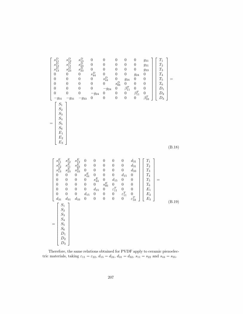
sD11 sD12 sD13 0 0 0 0 0 g31
sD12 sD11 sD23 0 0 0 0 0 g31
sD13 sD23 sD33 0 0 0 0 0 g33
0 0 0 sD44 0 0 0 g24 00 0 0 0 sD44 0 g24 0 00 0 0 0 0 sD66 0 0 00 0 0 0 −g24 0 βT11 0 00 0 0 −g24 0 0 0 βT11 0−g31 −g31 −g33 0 0 0 0 0 βT33
T1
T2
T3
T4
T5
T6
D1
D2
D3
=
=
S1
S2
S3
S4
S5
S6
E1
E2
E3
(B.18)
sE11 sE12 sE13 0 0 0 0 0 d31
sE12 sE11 sE23 0 0 0 0 0 d31
sE13 sE23 sE33 0 0 0 0 0 d33
0 0 0 sE44 0 0 0 d15 00 0 0 0 sE44 0 d15 0 00 0 0 0 0 sE66 0 0 00 0 0 0 d15 0 εT11 0 00 0 0 d15 0 0 0 εT11 0d31 d31 d33 0 0 0 0 0 εT33
T1
T2
T3
T4
T5
T6
E1
E2
E3
=
=
S1
S2
S3
S4
S5
S6
D1
D2
D3
(B.19)
Therefore, the same relations obtained for PVDF apply to ceramic piezoelec-tric materials, taking ε11 = ε22, d15 = d24, d31 = d32, s11 = s22 and s44 = s55.
207

208

Appendix C
ElectromechanicalPiezoelectric Model fordifferent Working Modes
Two equivalent piezoelectric coupling circuits that relate mechanical and electri-cal magnitudes of the piezoelectric phenomenon are presented. This Appendixshow the relations between the parameters that make together the electrome-chanical piezoelectric model for the case of PVDF materials with working modes31 and 33. Moreover, two different sets of state variables are presented for theelectromechanical piezoelectric models.
C.1 Electromechanical coupling circuits for mode31 and state variables F , ν, V and I
Figures C.1(a) and C.1(b) show an electromechanical piezoelectric model, [101],[105], [12] and [102], where the state variables are F , ν, V , and I. From piezo-electric constitutive equations, the following expressions are obtained:
F
1:n1
C'p V
I
Ft
C
m
υ
(a) (b)
Figure C.1: Piezoelectric coupling circuits, relating mechanical and electricalmagnitudes with state variables F , ν, V , and I.
209

∆LL = sE11
F1Wtc
+ d31V3tc
Q3WL = εT33
V3t + d31
F1Wtc
(C.1)
∆L = LsE11F1Wtc
+ d31Ltc
V3
Q3 = εT33WLtc
V3 + d31Ltc
F1
(C.2)
∆L = Cm31F1 + d31LtcV3
Q3 = CpV3 + d31LtcF1
(C.3)
Thus, the value of Cm31 is:
Cm31 =LsE11
Wtc(C.4)
Thus, the value of Cp is:
Cp =εT33A
tc(C.5)
Doing the derivative of Equation (C.3), it is obtained:
ν1 = jωCm31F1 + jωd31LtcV3
I3 = jωd31LtcF1 + jωCpV3
(C.6)
From this equation it is obtained the value of F1 and V3:
F1 =ν
jωCm31− d31L
Cm31tcV3 (C.7)
V3 =I
jωCp− d31L
tcCpF1 (C.8)
The following equations are obtained from the analysis of the circuits shownin Figures C.1(a) and C.1(b)
F1 =ν
jωCm31+ Ft (C.9)
V3 =I
jωCp+ Vt (C.10)
Next, it is calculated the transformer ratio for the electromechanical piezo-electric circuit shown in Figures C.1(a) and C.1(b) comparing Equations (C.7)and (C.8) with the previous equations.
n1 =V3
Ft= −Cm31tc
d31L(C.11)
n2 =VtF1
= −d31L
tcCp(C.12)
210

The electrical variable I of the two equivalent circuits is analyzed and com-pared to establish the relation between C ′p and Cp.
I3 = jωC ′pV3 + νLd31
tcCm31= jωd31
L
tcF1 + jωCpV3 (C.13)
Substituting F1 in the previous expression for its value in Equation (C.7), itis obtained:
jωC ′pV3 = jωCpV3 − jωd2
31L2
t2cCm31V3 (C.14)
Therefore, C ′p and Cp are related by the electromechanical piezoelectric co-efficient, k31.
C ′p = Cp −d2
31L2
t2cCm31= Cp
(1− d2
31
sE11εT33
)= Cp
(1− k2
31
)(C.15)
Another possible coupling piezolectric model consists in the Norton equiv-alent circuit of the mechanical part shown in Figure C.1(b) instead of workingwith the Norton equivalent circuit of the electrical part. The electrical partof the circuit is analyzed and compared with Equation (C.6) to determine therelation between C′m31 and Cm31.
ν1 = jωCm31F1 + jωd31L
tcV3 = jωC′m31F1 + I
d31L
tcCp(C.16)
jωC′m31F1 = jωCm31F1 − jωL2d2
31
t2cCpF1 (C.17)
Therefore, C′m31 and Cm31 are also related by the electromechanical coefficientk31.
C′m31 = Cm31
(1− L2d2
31
t2cCpCm31
)= Cm31
(1− k2
31
)(C.18)
The relation between the variables of the two equivalent piezoelectric cou-pling circuits have been determined, as well as, the transformer ratio.
C.1.1 Connection of a Load to the Electromechanical Cou-pling Circuit
The objective of this section is to determine under which conditions it is achievedthe maximum average power of a piezoelectric PVDF film when it is connectedto a resistive load, see Figure C.2. Thus, it will be calculated the value of V3
for the case that a load is connected to the piezoelectric material.The current flowing through the transformer, It, is equal to the current
flowing through the resistor, I, and the current flowing through the capacitorIC′p .
It = I + IC′p (C.19)
211

F
1:n1
C'p V
I
Ft
C
m
υ
R
Figure C.2: Piezoelectric coupling circuits, relating mechanical and electricalmagnitudes.
It is substituted by the product of the transfer ratio of the transformer andν1d31 and I and IC′p for the division between its voltage and electrical impedance.
ν1d31L
Cm31tc=V3
R+ jωC ′pV3 (C.20)
Then, the expression for V3 is:
V3 =ν1d31LR
Cm31tc(1 + jωC ′pR
) (C.21)
Substituting in Equation (C.21), ν1 and Cm31 for Equation (C.4) and jω∆L,respectively, it is obtained:
V3 =jω∆LRd31L
LsE11/ (Wtc) tc(1 + jωRC ′p
) =jωRAS1Y11d31
1 + jωRεT33Atc
(1− k231)
(C.22)
The average dissipated power on the load resistor is expressed by Equa-tion (C.23) for a piezoelectric beam with average strain S1, under a sinusoidalmechanical excitation of angular frequency ω, that gives rise to a sinusoidalvoltage waveform with amplitude |V3|.
〈P31〉 =
∣∣V 23
∣∣2R
=(d31S1Aω)2
R
2sE11
(1 + ω2R2C ′2p
) (C.23)
This expression has a maximum when Equation (C.24) is verified, corre-sponding to a resistor matching the internal impedance of the piezoelectric film.
R =1
ωC ′p=
1ωεT33 (1− k2
31)A/tc(C.24)
Equation (C.25) expresses the value for the maximum average power.
〈Pmax31〉 =d2
31S21A
2ω
4sE11C′p
(C.25)
212

C.2 Electromechanical coupling circuits for mode33 and state variables F , ν, V and I
The state variables employed in the analysis of this section are F , ν, V , andI instead of the state variables T , S, E, and D. The analysis of this sectionis made when the force applied to the piezoelectric element is done along axis3 instead of along axis 1. The electromechanical equivalent circuit employed isthe same shown in Section C.1. From piezoelectric constitutive equation, thefollowing expressions are derived:
∆tctc
= sE33F3A + d33
V3tc
Q3A = εT33
V3t + d33
F3A
(C.26)
Arranging the previous expressions, it is obtained:
∆tc = tcsE33F3A + d33V3
Q3 = εT33AV3tc
+ d33F3(C.27)
Doing the derivative of Equation (C.27), it is obtained:
ν3 = jωtcsE33F3A + jωd33V3
I3 = εT33AV3tc
+ d33F3(C.28)
Comparing the previous equations with the following expressions calculatedfrom the analysis of the electromechanical equivalent circuit, the expressions forCm33 and Cp are deduced.
ν3 = jωCm33F3 + jωd33V3
I = jωd33F3 + jωCpV3(C.29)
Thus, the value of Cm33 is:
Cm33 =tcs
E33
A(C.30)
The value of Cp is:
Cp =εT33A
tc(C.31)
From these equations, it is obtained the expression for F3 and V3:
F3 =ν
jωCm33− d33V3
Cm33(C.32)
V3 =I
jωCp− d33F3
Cp(C.33)
Next, it is calculated the transformer turn ratios for the electromechani-cal piezoelectric circuit comparing equations C.32 and C.33 with the followingequations obtained from the analysis of the circuit.
213

F3 =ν
jωCm33+ Ft (C.34)
V3 =I
jωCp+ Vt (C.35)
The transformer turn ratio for the electromechanical equivalent circuit ofFigure C.1(a) in working mode 33 is:
n1 =V3
Ft= −Cm33
d33(C.36)
The transformer turn ratio for the electromechanical equivalent circuit ofFigure C.1(b) in working mode 33 is:
n2 =VtF3
= −d33
Cp(C.37)
The electrical part of the two equivalent electromechanical circuits is ana-lyzed and compared to determine the relation between C ′p and Cp.
I = jωC ′pV3 + νd33
Cm33= jωd33F3 + jωCpV3 (C.38)
Reorganizing the previous expression and substituting ν for its value in Equa-tion (C.29), the relation is found.
C ′p = Cp −d2
33
Cm33= Cp
(1− d2
33
sεT33
)= Cp
(1− k2
33
)(C.39)
The mechanical part of the two equivalent electromechanical circuits is an-alyzed and compared to determine the relation between C ′m33 and Cm33.
ν = jωCm33F3 + jωd33V3 = jωC′m33F3 + Id33
Cp(C.40)
The value of I is replaced by its value in Equation (C.29) to obtain therelation.
C′m33 = Cm33
(1− d2
33
CpCm33
)= Cm33
(1− d2
33tcA
εAtcsE33
)= Cm33
(1− d2
33
εsE33
)=
= Cm33
(1− k2
33
)
(C.41)
The electromechanical coupling coefficient relates both sets of variables asin the working mode 31.
214

C.2.1 Connection of a Load to the Electromechanical Cou-pling Circuit
Next, it will be calculated the value of V3 for the case that a load is connectedto the piezoelectric material. The Kirchoff analysis of the current flowing inthe electrical part of the electromechanical coupling circuit gives the followingexpression:
It = I + IC′p (C.42)
where It, I and IC′p are the current flowing through the transformer, the resistiveload and C ′p, respectively.
It is substituted by the product of the transfer ratio of the transformer andν3d33 and I and IC′p for the division between its voltage and electrical impedance.
ν3d33
Cm33=V3
R+ jωC ′pV3 (C.43)
Substituting in Equation (C.43), ν3 and Cm33 for Equation (C.30) and jω∆tc,respectively, it is obtained:
V3 =jω∆tcRd33A
sE33/tc(1 + jωRC ′p
) =jωRAS3Y33d33
1 + jωRεT33Atc
(1− k233)
(C.44)
The dissipated power on the load resistor is expressed by Equation (C.45) fora piezoelectric beam with average strain S3, under a sinusoidal mechanical ex-citation of angular frequency ω, that gives rise to a sinusoidal voltage waveformwith amplitude |V3|.
〈P33〉 =
∣∣V 23
∣∣2R
=(d33S3Aω)2
R
2sE33
(1 + ω2R2C ′2p
) (C.45)
This expression has a maximum when Equation (C.46) is verified, corre-sponding to a resistor matching the internal impedance of the piezoelectric film.
R =1
ωC ′p=
1ωεT33 (1− k2
33)A/tc(C.46)
Equation (C.47) expresses this value of the maximum average power.
〈Pmax33〉 =d2
33S23A
2ω
4sE33C′p
(C.47)
C.3 Electromechanical piezoelectric model formode 31 and state variables T , S, E andD
Figures C.3(a) and C.3(b) show an electromechanical piezoelectric model wherethe state variables are F , ν, V , and I. The transformer relates mechanical
215
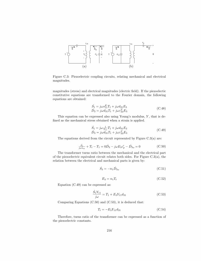
T
1:n
ε'p E
DS Do
Tt
T
1:n
DS
E
εp
s'm
(a) (b)
Figure C.3: Piezoelectric coupling circuits, relating mechanical and electricalmagnitudes.
magnitudes (stress) and electrical magnitudes (electric field). If the piezoelecticconstitutive equations are transformed to the Fourier domain, the followingequations are obtained:
S1 = jωsE11T1 + jωd31E3
D3 = jωd31T1 + jωεT33E3(C.48)
This equation can be expressed also using Young’s modulus, Y , that is de-fined as the mechanical stress obtained when a strain is applied.
S1 = jω 1Y11
T1 + jωd31E3
D3 = jωd31T1 + jωεT33E3(C.49)
The equations derived from the circuit represented by Figure C.3(a) are:
S1jωsm
+ Tt − T1 = 0D3 − jωE3ε′p − D3o = 0 (C.50)
The transformer turns ratio between the mechanical and the electrical partof the piezoelectric equivalent circuit relates both sides. For Figure C.3(a), therelation between the electrical and mechanical parts is given by:
S3 = −n1D3o (C.51)
E3 = n1Tt (C.52)
Equation (C.49) can be expressed as:
S1Y11
jω= T1 + E3Y11d31 (C.53)
Comparing Equations (C.50) and (C.53), it is deduced that:
Tt = −E3Y11d31 (C.54)
Therefore, turns ratio of the transformer can be expressed as a function ofthe piezoelectric constants.
216

n1 =E3
Tt= − 1
Y11d31(C.55)
The value of sm can be easily determined from Equation (C.50).
sm =1Y31
(C.56)
The value ofdotD3o is calculated combining Equations (C.55) and (C.51):
D3o = S1Y11d31 (C.57)
The expression of ε′p as a function of the piezoelectric constants is calcu-lated employing the following expression that is derived from the analysis of theelectrical part of the circuit of Figure C.1(a).
D3 = jωE3ε′p + S1Y11d31 (C.58)
Substituting in the previous Equation the value of D3 by the value given byEquation (C.49), it is obtained:
jωE3ε′p = jωεT33E3 + jωd31T1 − S1Y11d31 (C.59)
Reordering the previous equation and employing the first expression of Equa-tion (C.49), it is deduced:
jωE3ε′p = jωεT33E3 + d31Y11 (−jωd31E3) (C.60)
Thus, the value for ε′p is calculated using the relation between piezoelectric
constants d231sE11ε
T33
= k231 that appears in Table 3.3.
ε′p = εT33 − d231Y11 = εT33
(1− d2
31Y11
εT33
)=
= εT33
(1− d2
31
sE11εT33
)= εT33
(1− k2
31
) (C.61)
Another possibility for the representation of the piezoelectric coupling cir-cuit is shown in Figure C.3(b). The relation of the components of this circuitand the piezoelectric constants are calculated below. Moreover, it is also calcu-lated its relation with the components of the equivalent circuit represented inFigure C.3(a).The turns ratio of the transformer, n2, is calculated employingthe equations extracted from the analysis of the circuit shown in Figure C.3(b).
S1 = jωs′mT1 − n2D3
E3 = jωεpD3 + n2T1(C.62)
The previous equation can be also expressed as:
217

D3 = jωεpE3 − jωεT33n2T1 (C.63)
Comparing the above expression with the value of D from Equation (C.49),it is obtained that the value of the transformer ratio is:
n2 = −d31/εT33 (C.64)
The value of εp is:εp = εT33 (C.65)
The component εp of the circuit of Figure C.3(b) is related with the compo-nent ε′p of the circuit of Figure C.3(a).
εp = ε′p(1− k2
31
)(C.66)
In order to determine the value of s′m, it is employed the expression for S1
of Equation (C.62).
S1 = jωT1s′m +
d31
εT33
D3 (C.67)
When the above expression is equaled to the expression of S1 given in Equa-tion (C.49), it is gotten the value of s′m as a function of the piezoelectric con-stants.
jωT1s′m +
d31
εpD3 = jω
T1
Y11+ jωd31E3 (C.68)
Reordering the previous expression and employing the second expressionthat appears in Equation (C.49), the value of s′m is obtained.
s′m =1Y11− d2
31
ε=
1Y11
(1− d2
31Y11
εT33
)=
1Y11
(1− k2
31
)(C.69)
Comparing Equation (C.56) and Equation (C.69), it is deduced that sm ands′m are related as the other components of the two equivalent circuits throughthe electromechanical coupling coefficient.
s′m = sm(1− k2
31
)(C.70)
C.3.1 Connection of a Load to the Electromechanical Cou-pling Circuit
The objective of this section is to determine under which conditions it is achievedthe maximum average power of a piezoelectric PVDF film when it is connectedto a resistive load, see Figure C.4. Thus, it will be calculated the value of V3
for the case that a load is connected to the piezoelectric material. From theanalysis of the circuit, the following equations are deduced.
218

T
1:n
E
DS Do
Tt
R'ε'p
sm
Figure C.4: Piezoelectric coupling circuit relating mechanical and electricalmagnitudes with a resistive load.
−(D − Do
)Cp + D3R
′ = Do (C.71)
S1Y11d31 = −E3ε′p −
E3
R′(C.72)
Then, the expression for V3 taking into account the relation E3 = V3/tc andusing Equation (C.72) and Equation (C.72) is calculated.
V3 = − jωR′S1Y11d31tcjωR′εT33 (1− k2
31) + 1(C.73)
Since the state variables in the electrical part of the circuit are E, and Dinstead of V and I, the load is represented as R′. There is a relation between R′
and the resistive load R. This relation is calculated comparing Equation (C.75)derived from the circuit of Figure C.2 and Equation (C.74) derived from Fig-ure C.4.
E3
=− D3R
′ (C.74)
V3 = −I3R (C.75)
In the previous equation, the state variables V and I are substituted for Eand D, respectively.
D3 = −E3tcRA
(C.76)
where A = WL.Therefore, comparing Equation (C.74) with Equation (C.76), the existing
relation between R′ and R is found.
R′ = RA
tc(C.77)
Substituting the result obtained from R′ in Equation (C.73), it is obtained:
219

V3 = − jωRAS1Y11d31
jωRA/tcεT33 (1− k231) + 1
= − jωRAS1e31
jωRA/tcεT33 (1− k231) + 1
(C.78)
The optimum value of R, Ropt, is given by the following expression. WhenR = Ropt the value of V3 is maximum.
Hence, the same results are obtained employing state variables T , S, E, andD instead of state variables F , ν, V , and I, demonstrating that both modelsare equivalents.
C.4 Electromechanical piezoelectric model formode 33 and state variables T , S, E andD
If the piezoelectic constitutive equations are transformed to the Fourier domain,the following equations are obtained:
S3 = jωsD33T3 + jωd33E3
D3 = jωd33T3 + jωεT33E3(C.79)
The first equation can be expressed using Young’s modulus, Y , instead ofthe compliance sD.
S3 = jω 1Y33
T3 + jωd33E3
D3 = jωd33T3 + jωεT33E3(C.80)
The transformer between the mechanical and the electrical part of the piezo-electric equivalent circuit is calculated in the same way that in the previoussection. The result obtained is:
n2 = − 1Y33d33
(C.81)
The value of sm is:
sm =1Y33
(C.82)
The value of ε′p:
ε′p = εT33 − d233Y33 = εT33
(1− d2
33Y33
εT33
)= εT33
(1− d2
33
sE33εT33
)=
= εT33
(1− k2
33
) (C.83)
where k33 is the mechanical coupling factor for the thickness expansion work-ing mode.
220

Therefore,
k233 =
d233Y33
εT33
(C.84)
Another possibility for the representation of the piezoelectric coupling circuitis shown in Figure C.3(b). In this case, the turns ratio of the transformer, n2,is:
n2 = −d33/εT33 (C.85)
The component εp of the electromechanical circuit expressed as a functionof the piezoelectric constants is:
εp = εT33 (C.86)
εp and ε′p are related through the electromechanical coupling coefficient.
εp = ε′p(1− k2
33
)(C.87)
In order to determine the value of s′m, it is employed the following expressionthat is extracted from the analysis of the circuit represented by Figure C.3(b):
S = jωTs′m +d
εD (C.88)
The value of s′m as a function of Y33 is:
s′m =1Y33− d2
33
ε=
1Y33
(1− d2
33Y33
εT33
)=
1Y33
(1− k2
33
)(C.89)
sm and s′m are related through the electromechanical coupling coefficient inworking mode 33, k33.
s′m = sm(1− k2
33
)(C.90)
The analysis of the connection of a resistive load to the electromechanicalcoupling circuit is not done since it has been demonstrated in Section C.3.1 thatthis calculation is equivalent to the one done for working mode 33 employingstate variables F , ν, V , and I.
221

222

Appendix D
Acceleration Measurementson the Human Body
Figure D.1 shows the acceleration measurements of X-axis and Y-axis of anaccelerometer placed on an ankle while a person was walking. Figure D.2 andFigure D.3 show a zoom of the previous figure for X-axis and Y-axis, respec-tively. Figures D.4 and D.5 show the acceleration spectrum for the same activityand location for X-axis and Y-axis, respectively, obtained applying a Hammingwindow and the FFT algorithm to the measured data. The two main peaks ofthe acceleration spectrum are at a frequency of 0.8 Hz and 1.6 Hz for both axis.
0 50 100 150 200 250
-40
-20
0
20
40
60
acce
lera
tion
(m/s
2 )
time (s) X-axis Y-axis
Walking
Descending and ascending stairs
Figure D.1: Acceleration measurements obtained by placing the sensor node onthe ankle while a person was walking and descending and ascending stairs withTs=0.013s.
223

52.0 52.5 53.0 53.5 54.0 54.5 55.0 55.5 56.0-5
0
5
10
15
20
25
30
acce
lera
tion
(m/s
2 )
time (s)
Figure D.2: X-axis acceleration measurements obtained by placing the sensornode on the ankle while a person was walking with Ts=0.013s.
Figure D.6 shows the acceleration measurements of X-axis and Y-axis ofan accelerometer placed on a wrist while a person was walking. Figure D.7and Figure D.8 show a zoom of the previous figure for X-axis and Y-axis, re-spectively.Figure D.9 shows the spectrum of the acceleration measurements ofY-axis. The highest peak is at 0.8 Hz.
224

52.0 52.5 53.0 53.5 54.0 54.5 55.0 55.5 56.0-20
-15
-10
-5
0
5
10
15
20
acce
lera
tion
(m/s
2 )
time (s)
Figure D.3: Y-axis acceleration measurements obtained by placing the sensornode on the ankle while a person was walking with Ts=0.013s.
Figure D.4: Acceleration spectrum calculated from measurements obtainedby placing an accelerometer on the ankle of a person that was walking withTs=0.013s for X-direction.
225

Figure D.5: Acceleration spectrum calculated from measurements obtainedby placing an accelerometer on the ankle of a person that was walking withTs=0.013s for Y-direction.
0 20 40 60 80 100
-20
-10
0
10
20
acce
lera
tion
(m/s
2 )
time (s) X-axis Y-axis
Figure D.6: Acceleration measurements obtained by placing the sensor node onthe wrist while a person was walking with Ts=0.013s.
226

42.0 42.5 43.0 43.5 44.0 44.5 45.0
6
8
10
12
14
acce
lera
tion
(m/s
2 )
time (s)
Figure D.7: X-axis acceleration measurements obtained by placing the sensornode on the wrist while a person was walking with Ts=0.013s.
42.0 42.5 43.0 43.5 44.0 44.5 45.0
0
2
4
acce
lera
tion
(m/s
2 )
time (s)
Figure D.8: Y-axis acceleration measurements obtained by placing the sensornode on the wrist while a person was walking with Ts=0.013s.
227

Figure D.9: Acceleration spectrum calculated from measurements obtainedby placing an accelerometer on the wrist of a person that was walking withTs=0.013s for Y-direction.
228

Appendix E
Characterization ofThermoelectric Modules(TEMs)
Table E.1 and Table E.2 show the measurement obtained employing two differentthermogenerators. The thermogenerators were connected to different resistiveloads: R2, R3, R4 and R5 while the hot side of the TEG was heated. The datashown has been obtained after waiting two hours in order to assure stabilizedtemperatures at both sides of the TEG [132]. The parameters measured werethe voltage of the TEG in open circuit, Voc, the voltages on the resistive loadsconnected to the TEG (V2, V3, V4 and V5) as well as the temperature at the hotside, TH , and cold side, TC .
Table E.1: Measurements obtained from the 17 A 1015 H 200 Peltron thermo-generator.R2 (Ω) 2.26 2.25 2.25 2.25 2.25 2.25R3 (Ω) 11.03 11.03 11.02 11.03 11.03 11.03R4 (Ω) 113.90 113.89 113.89 113.89 113.89 113.89R5 (Ω) 1185.13 1185.12 1185.15 1185.14 1185.12 1185.11Voc (mV ) 55.09 83.43 110.17 132.46 167.49 214.74V2 (mV ) 33.82 50.81 66.46 79.13 99.11 126.06V3 (mV ) 50.07 75.67 99.71 119.59 150.86 193.03V4 (mV ) 54.56 82.61 109.06 131.10 165.71 212.41V5 (mV ) 55.03 83.33 110.04 132.30 167.28 214.47TH (C) 38.93 48.93 58.86 68.79 78.74 88.69TC (C) 30.32 34.87 39.59 45.22 49.60 54.23
From these tables, it can be deduced the value of the parameters αm andRm. The values of these parameters is not constant and depend on the absolute
229

Table E.2: Mesurements obtained from the 128 A 1030 Peltron thermogenerator.R2 (Ω) 2.25 2.26 2.26 2.26 2.26 2.26R4 (Ω) 113.89 113.89 113.89 113.90 113.90 113.90R5 (Ω) 1185.13 1185.13 1185.11 1185.10 1185.11 1185.12Voc (mV ) 333.70 530.66 743.18 960.17 1178.59 1394.76V2 (mV ) 47.50 72.91 98.70 123.38 146.71 168.38V4 (mV ) 306.240 485.29 677.36 872.27 1067.17 1258.80V5 (mV ) 330.55 525.43 735.58 950.02 1165.71 1379.03TH (C) 39.06 49.09 59.13 69.16 79.18 89.23TC (C) 32.35 37.73 42.58 47.44 52.26 57.17
temperature of one side and on the temperature gradient.
Table E.3: Parameters calculated from the measurements obtained for the17 A 1015 H 200 Peltron thermogenerator.
α (V/K) Rm (Ω) TH (C) TC (C) ∆T0.00643 1.418 38.928 30.321 8.6070.00593 1.443 48.929 34.870 14.0590.00572 1.476 58.860 39.589 19.2710.00562 1.516 68.793 45.217 23.5760.00575 1.554 78.737 49.603 29.1350.00623 1.586 88.688 54.234 34.454
Table E.4: Parameters calculated from the measurements obtained for the128 A 1030 Peltron thermogenerator.
α (V/K) Rm (Ω) TH (C) TC (C) ∆T0.04971 10.213 39.058 32.345 6.7130.0467 10.649 49.093 37.728 11.3640.04489 11.066 59.132 42.578 16.5540.04421 11.478 69.158 47.442 21.7160.04377 11.891 79.182 52.256 26.9260.04351 12.302 89.227 57.173 32.054
Tables E.5 and E.6 show the data given by the manufacturer for the 17 A 1015 H 200and 128 A 1030 Peltron TEGs, respectively.
230

Table E.5: Electrical and thermal parameters for the TEG 17 A 1015 H200.Symbol Description Value UnitsQmax Maximum amount of heat that
can that can be absorbed atTEMs cold plate at Imax and∆T=0.
3.5 W
∆Tmax Largest temperature differentialbetween the hot and cold sideplates of a TEM for the givenvalue of Th
67 K
Vmax DC voltage that delivers the∆Tmax at the supplied Imax
2.1 V
Imax Input current that produces∆Tmax across a TEM
2.5 A
Tmax Maximum temperature at thehot side
473 K
Ri Internal resistance 0.7 Ωαm Seebecks coefficient 0.0065 V/Kkm Thermal conductance 0.039 W/KΘm Thermal resistance 25.57 K/WCm Heat capacity 0.61 J/KZ Figure of Merit 1.54e-3 K−1
Dimensions 11.5x11.5x3.2
231

Table E.6: Electrical and thermal parameters for the TEG PKE 128 A 1030.Symbol Description Value UnitsQmax Maximum amount of heat that
can that can be absorbed atTEMs cold plate at Imax and∆T=0.
14 W
∆Tmax Largest temperature differentialbetween the hot and cold sideplates of a TEM for the givenvalue of Th
65 K
Vmax DC voltage that delivers the∆Tmax at the supplied Imax
15 V
Imax Input current that produces∆Tmax across a TEM
1.5 A
Tmax Maximum temperature at thehot side
398 K
Ri Internal resistance 7.7 Ωαm Seebecks coefficient 0.049 V/Kkm Thermal conductance 0.157 W/KΘm Thermal resistance 6.38 K/WZ Figure of Merit 1.99e-3 K−1
Dimensions 25x25x5.2 mmWeight 10 g
232

Appendix F
Battery
The design of the power management system to power portable devices fromenergy harvesting sources is complicated due to the low voltage ranges in thecase of thermoelectric and inductive transducers or due to the low current rangesin the case of piezoelectric generators. If a battery requires to be charged withenergy harvesting transducers, it is necessary an accurate battery model topredict its behaviour and to give information about the state of charge (SOC)of the battery. The SOC of the battery is employed to estimate if the energyharvesting system is working in energy neutral operation. As it is explained inChapter 6, next sections enter into more detail in the battery electrical modeland the state of charge topics. Moreover, the measurement procedure to extractthe parameters of the battery electrical model is also detailed.
F.1 State of Charge
The SOC is defined as the percentage of the maximum possible charge that ispresent inside the battery [91]. The main methods for the determination of theSOC are:
1. Direct measurement. The most used direct measurement method is thebattery voltage measurement. This method implies the measurement ofthe voltage on the battery and is less expensive and requires less computingpower than the coulomb counting method. It is the method employed forexample in mobile phone applications. While it is true that a given cell’svoltage level will continually drop during discharge, the voltage level’s re-lationship to remaining charge varies greatly over cell temperature anddischarge rate [133]. Therefore, this method is not appropriate for exam-ple for Li-ion and NiMH cells since the voltage on the battery at a givenSOC varies with the value of the discharge current as can be seen in Fig-ures F.5 and F.6. The error in SOC estimation can be corrected, if thetemperature and the discharge rate of the battery are also measured and
233

compared with previously memorized data using look-up tables or func-tions [91]. However, this will make the SOC estimation more complicatedand expensive than the coulomb counting method without providing anysignificant advantages.
2. Coulomb counting. This method implies an accurate measurement ofthe current flowing into or out of the battery and an integration of thiscurrent to calculate the SOC [91, 95, 133]. Therefore, this method takesinto account that the capacity of a battery changes with the dischargecurrent. If it is considered that the current is constant, then the SOC isdefined as [95]:
SOC =ICA− CEMPTY
CFULL − CEMPTY× 100 (F.1)
where ICA = I × t is the charge accumulated or removed from the bat-tery, CFULL is the capacity of the battery when it is charged completelyCEMPTY is the capacity that remains in the battery when it is consideredthat is discharged completely. In this case the battery is first charged atconstant current, 1C, until it reaches the maximum voltage on the bat-tery and then it is charged at constant voltage until the charge current fellbelow C/20. In [95], the ICA register is reset to the value of CEMPTY
when the battery is fully discharged and it is reset to the value of CFULLwhen the battery is fully charged. Summarizing, if ICA = CEMPTY , theSOC = 0% and if ICA = CFULL, the SOC = 100%.
If it is considered that CEMPTY = 0, then CFULL = CAV AILABLE andEquation (F.1) can be expressed as Equation (F.2). Moreover, the avail-able capacity depends on the temperature and the value of the currentwhen it is charged or discharged and this is the reason for expressingCAV AILABLE as a function of these two variables in Equation (F.2).
SOC =I × t
CAV AILABLE(I, T )× 100 (F.2)
h where CAV AILABLE(I, T ) is the available capacity of the battery whenit has been completely charged at 1C and then discharged with a constantcurrent value I at a temperature T , I is the constant current employed tocharge or discharge the battery and t is the time employed for the process.
An improvement of Equation (F.2) is done with Equation (F.3) since it ispossible to calculate the SOC when different currents and temperaturesare employed in the process of charging or discharging the battery withthe introduction of a new variable, the initial state of charge, SOCinitial.
SOC = SOCinitial +I × t
CAV AILABLE(I, T )× 100 (F.3)
234

where SOCinitial is the previous state of charge of the battery, I is thecurrent flowing into (positive sign) or out of the battery (negative sign),and t is the time employed to charge or discharge the battery with acurrent I. The sign of I is positive when the battery is being charged andis negative when the battery is being discharged.Temperature and discharge rates have high effects in the capacity of aLi-Ion battery. Other effects like the self-discharge of the battery are notrelevant with this kind of chemistry.[91] presents a new algorithm to predict the SOC of a battery based on theCoulomb counting method. The proposed algorithm operates in five dif-ferent states: initial state, equilibrium state, transitional state, dischargestate and charge state.
3. Adaptive systems. This method is based on a comparison that is madewhenever possible between the estimated values with observed batterybehavior [91].
A topic related with the calculation of the state of charge of batteries is thecapacity of the cells that, as it is explained and observed in Section F.3 for thecase of the Lithium-Ion cells, varies greatly depending on the temperature anddischarge rate. Moreover, it is only necessary to keep track of the present celltemperature and discharge rate when determining remaining capacity [95] sincemost other conditions like heat losses during charging process or self-dischargehave little or no effect on charge capacity. Thus, all these conditions can beignored for the calculus of the capacity.
Theoretically, the capacity should be independent of the discharge rate sincean identical amount of energy is dispensed during different times. Due to energyloss that occurs inside the battery and a drop in voltage that causes the bat-tery to reach the low-end voltage cut-off sooner with high discharge rates, thecapacity reading is lower in these cases. The discrepancy in capacity readingswith different C-rates largely depends on the internal resistance of the battery.
The temperature is also an important factor that modifies the capacity ofthe battery. At room and high temperatures, the lithium cells have a greatcapacity. At low temperatures the capacity decrease drastically.
F.2 Electrical Models
This section gives a summary of different equivalent circuits that model thebehavior of batteries and it is focused specially in the model proposed by Chenet al. in [3] since it is the model implemented in [13] (Chapter 13). Thesemodels are a combination of voltage sources, resistors and capacitors and areclassified in three different categories: Thevenin, impedance, and runtime-basedmodels [3].
The right circuit shown in Figure F.1 is a Thevenin battery model. Theelectrical components and signals of this circuit are: Voc, the battery open-circuit voltage, VBatt,the battery voltage, Ibat, the battery current, Rseries, the
235
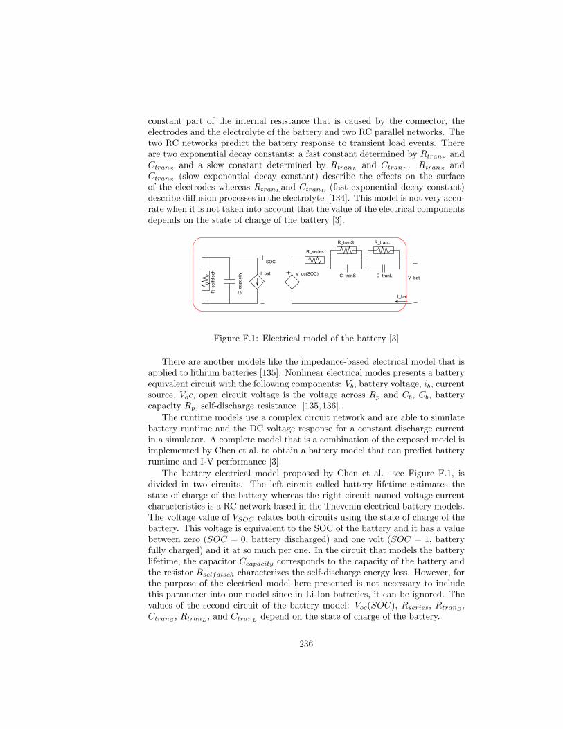
constant part of the internal resistance that is caused by the connector, theelectrodes and the electrolyte of the battery and two RC parallel networks. Thetwo RC networks predict the battery response to transient load events. Thereare two exponential decay constants: a fast constant determined by RtranS
andCtranS
and a slow constant determined by RtranLand CtranL
. RtranSand
CtranS(slow exponential decay constant) describe the effects on the surface
of the electrodes whereas RtranLand CtranL
(fast exponential decay constant)describe diffusion processes in the electrolyte [134]. This model is not very accu-rate when it is not taken into account that the value of the electrical componentsdepends on the state of charge of the battery [3].
Figure F.1: Electrical model of the battery [3]
There are another models like the impedance-based electrical model that isapplied to lithium batteries [135]. Nonlinear electrical modes presents a batteryequivalent circuit with the following components: Vb, battery voltage, ib, currentsource, Voc, open circuit voltage is the voltage across Rp and Cb, Cb, batterycapacity Rp, self-discharge resistance [135,136].
The runtime models use a complex circuit network and are able to simulatebattery runtime and the DC voltage response for a constant discharge currentin a simulator. A complete model that is a combination of the exposed model isimplemented by Chen et al. to obtain a battery model that can predict batteryruntime and I-V performance [3].
The battery electrical model proposed by Chen et al. see Figure F.1, isdivided in two circuits. The left circuit called battery lifetime estimates thestate of charge of the battery whereas the right circuit named voltage-currentcharacteristics is a RC network based in the Thevenin electrical battery models.The voltage value of VSOC relates both circuits using the state of charge of thebattery. This voltage is equivalent to the SOC of the battery and it has a valuebetween zero (SOC = 0, battery discharged) and one volt (SOC = 1, batteryfully charged) and it at so much per one. In the circuit that models the batterylifetime, the capacitor Ccapacity corresponds to the capacity of the battery andthe resistor Rselfdisch characterizes the self-discharge energy loss. However, forthe purpose of the electrical model here presented is not necessary to includethis parameter into our model since in Li-Ion batteries, it can be ignored. Thevalues of the second circuit of the battery model: Voc(SOC), Rseries, RtranS
,CtranS
, RtranL, and CtranL
depend on the state of charge of the battery.
236
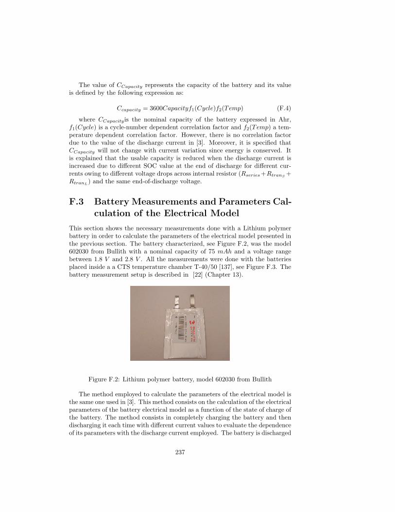
The value of CCapacity represents the capacity of the battery and its valueis defined by the following expression as:
Ccapacity = 3600Capacityf1(Cycle)f2(Temp) (F.4)
where CCapacityis the nominal capacity of the battery expressed in Ahr,f1(Cycle) is a cycle-number dependent correlation factor and f2(Temp) a tem-perature dependent correlation factor. However, there is no correlation factordue to the value of the discharge current in [3]. Moreover, it is specified thatCCapacity will not change with current variation since energy is conserved. Itis explained that the usable capacity is reduced when the discharge current isincreased due to different SOC value at the end of discharge for different cur-rents owing to different voltage drops across internal resistor (Rseries+RtranS
+RtranL
) and the same end-of-discharge voltage.
F.3 Battery Measurements and Parameters Cal-culation of the Electrical Model
This section shows the necessary measurements done with a Lithium polymerbattery in order to calculate the parameters of the electrical model presented inthe previous section. The battery characterized, see Figure F.2, was the model602030 from Bullith with a nominal capacity of 75 mAh and a voltage rangebetween 1.8 V and 2.8 V . All the measurements were done with the batteriesplaced inside a a CTS temperature chamber T-40/50 [137], see Figure F.3. Thebattery measurement setup is described in [22] (Chapter 13).
Figure F.2: Lithium polymer battery, model 602030 from Bullith
The method employed to calculate the parameters of the electrical model isthe same one used in [3]. This method consists on the calculation of the electricalparameters of the battery electrical model as a function of the state of charge ofthe battery. The method consists in completely charging the battery and thendischarging it each time with different current values to evaluate the dependenceof its parameters with the discharge current employed. The battery is discharged
237

Figure F.3: Measurement setup for battery characterization including a climatechamber.
with constant current in order to observe the voltage drop and the exponentialresponse to extract the value of the parameters of the electrical model. Whenthe battery is being discharged, the SOC varies, and so do, the parameters ofthe electrical model. For this reason, the parameters of the electrical modelare calculated at different values of SOC when it is constant (in the relaxationtime, when the current is equal to zero). Therefore, the first measurementsto do consist on the charge and discharge of the battery at different dischargecurrents in order to calculate the available capacity for each discharge current.The usual method to fully charge a Lithium battery consists first in charge thebattery with a constant current (between 0.1C to 1C) until it reaches a valueequal to its maximum voltage. Then, the battery is charged with a constantvoltage until the current reaches a value lower than 0.1C. At this moment, itis considered that the battery is completely charged. Figure F.4 shows howthe 602030 Lithium polymer battery from Bullith is first charged at 1C untilit reaches its maximum voltage of 2.8 V and then it is charged at this voltageuntil the charge current is equal to 7.5 mA. The figure also shows the dischargecurve of the voltage on the battery when the discharge current is 75 mA.
238

-0.15
-0.10
-0.05
0.00
0.05
0.10
0.15
0.0 0.5 1.0 1.5 2.0 2.5
1.8
2.0
2.2
2.4
2.6
2.8
3.0
I bat (A
)
V
bat (V
)
time (h) Vbat
Ibat
Charge at constantvoltage
Charge at constant current
Discharge at 1C
Figure F.4: Li-Ion battery charging and discharging stages.
Figures F.5 and F.6 show the measured discharging characteristics with dif-ferent curves, each one with a different discharge current value (2C, 1C and0.5C), of the battery voltage as a function of the nominal capacity at 20 C fortwo different batteries. Figure F.7 shows two different curves of voltage as afunction of nominal capacity for 2C and 1C discharge current at 0 C.
The Bullith battery is charged with 1C in the temperature chamber at 20 C.A discharge profile is configured to discharge the battery with every pulse atdifferent discharge currents and obtain several points of the parameters as afunction of the state of charge. It is necessary to assure that the relaxation timeis at least equal to the slow time constant value to obtain an appropriate fitting.Also, during a time at least equal to the fast time constant it is necessary tostore enough data in order to be able to realize the fitting process. Some of theresults obtained are shown in Figures F.8 and F.9.
From the analysis of the electrical battery model of Figure F.1, it is deducedEquation (F.5). The fitting process is realized employing Matlab [138] and theEasyFit toolbox [139] employing a known expression, that contains a voltagedrop and two exponential expressions where the coefficients have to be calcu-lated. The results obtained are shown from Figure F.10 to Figure F.15 withdifferent discharge currents at 20 C as a function of the state of charge of thebattery.
239

0 10 20 30 40 50 60 70 80 90 1001.8
2.0
2.2
2.4
2.6
2.8
3.0
Vba
t (V)
Nominal Capacity (%) Ibat
=2C I
bat=1C
Ibat
=0.5C
Figure F.5: Capacity that can be extracted from one battery sample at 20 C.
Vbat = Voc + IbatRseries + IbatRtranS
(e−t/τtranS − 1
)
+ IbatRtranL
(e−t/τtranL − 1
)(F.5)
The open circuit voltage of the battery, Voc, as a function of the state ofcharge of the battery is shown in Figure F.10. Six different waveforms fromtwo different batteries are represented with discharge current values of 2C, 1Cand 0.5C. When the state of charge of the battery decreases, the open circuitvoltage also decreases. Figure F.11 shows the series resistance of the batteryas a function of its state of charge. The series resistance is almost constantfrom state of charge 0.9 to 0.2. RtranS
as a function of the state of charge isdisplayed in Figure F.12 with an approximately constant value from a state ofcharge of 0.1 to fully charge and a similar value for all the discharge currentsunder consideration.
Figure F.13 shows RtranLversus the state of charge. The value of this com-
ponent is almost constant from a state of charge of 0.4 to 0.9 for the differentdischarge currents and batteries used. Nevertheless, this value is not approxi-mately equal for the different discharge currents and batteries.
Figures F.14 and F.14 show the response of CtranSand CtranL
versus the
240

0 10 20 30 40 50 60 70 80 90 1001.8
2.0
2.2
2.4
2.6
2.8
3.0
Vba
t (V)
Nominal Capacity (%) Ibat
=2C I
bat=1C
Ibat
=0.5C
Figure F.6: Capacity that can be extracted from one battery sample at 20 C.
state of charge of the battery. The value of these two components of the electricalmodel of the battery depends strongly on the discharge current employed.
This measurements allow to create a Verilog-A model for this battery thatcan be employed in energy harvesting system simulations like the ones done inChapters 6 and 13 allowing to have realistic simulations and predict which isthe minimum capacity of the battery and which is its minimum state of charge.
241

0 10 20 30 40 50 60 70 80 90 1001.8
2.0
2.2
2.4
2.6
2.8
3.0
Figure F.7: Capacity that can be extracted from one battery sample at 0 C.
-0.35
-0.30
-0.25
-0.20
-0.15
-0.10
-0.05
0.00
0.05
0.10
0.15
0.20
0.0 0.5 1.0 1.5 2.0 2.5 3.0 3.5 4.01.8
1.9
2.0
2.1
2.2
2.3
2.4
2.5
2.6
2.7
2.8
2.9I ba
t (V)
Vba
t (V)
Time (h) Vbat
Ibat
Figure F.8: Battery voltage and current during charge stage and dischargepulses at 1C.
242

-0.35
-0.30
-0.25
-0.20
-0.15
-0.10
-0.05
0.00
0.05
0.10
0.15
0.20
0.0 0.5 1.0 1.5 2.0 2.5 3.0 3.5 4.01.8
1.9
2.0
2.1
2.2
2.3
2.4
2.5
2.6
2.7
2.8
2.9
I bat (A
)
Vba
t (V)
Time (h) Vbat
Ibat
Figure F.9: Battery voltage and current during charge stage and dischargepulses at 2C.
Figure F.10: Voc extracted parameter for the Bullith lithium battery 602030 at20 C.
243

Figure F.11: Rseries extracted parameter for the Bullith lithium battery 602030at 20 C.
Figure F.12: RtranSextracted parameter for the Bullith lithium battery 602030
at 20 C.
244

Figure F.13: RtranLextracted parameter for the Bullith lithium battery 602030
at 20 C.
Figure F.14: CtranSextracted parameter for the Bullith lithium battery 602030
at 20 C.
245

Figure F.15: CtranLextracted parameter for the Bullith lithium battery 602030
at 20 C.
246

Bibliography
[1] J. A. Chavez, J. A. Ortega, J. Salazar, A. Turo, and M. J. Garcia,““SPICE model of thermoelectric elements including thermal effects”,”Instrumentation and Measurement Technology Conference, 2000. IMTC2000. Proceedings of the 17th IEEE, vol. 2, pp. 1019–1023, May 2000.
[2] S. Lineykin and S. Ben-Yaakov, ““SPICE compatible equivalent circuitof the energy conversion processes in thermoelectric modules”,” Electricaland Electronics Engineers in Israel, 2004. Proceedings. 2004 23rd IEEEConvention of, pp. 346–349, September 2004.
[3] M. Chen and G. Rincon-Mora, “Accurate electrical battery model capa-ble of predicting runtime and I-V performance,” IEEE Transactions onEnergy Conversion, vol. 21, no. 2, pp. 504–511, June 2005.
[4] T. Starner, “The challenges of wearable computing: Part 1,” Micro, IEEE,vol. 21, no. 4, pp. 44–52, 2001.
[5] ——, “The challenges of wearable computing: Part 2,” Micro, IEEE,vol. 21, no. 4, pp. 54–67, 2001.
[6] T. Zimmerman, “Personal area networks (PAN): Near-field intra-bodycommunication,” Master’s thesis, Massachusetts Institute of Technology,September 1995.
[7] ——, “Personal area networks: Near-field intrabody communication,”IBM Systems Journal, vol. 35, no. 3&4, pp. 609–617, 1996.
[8] F. Gesellschaft, Body Area Network. [Online]. Available:http://www.ban.fraunhofer.de/
[9] P. Lukowicz, H. Junker, M. Stager, T. von Buren, and G. Troster, “Wear-NET: A Distributed Multi-Sensor System for Context Aware Wearables,”in Proceedings of the 4th International Conference on Ubiquitous Comput-ing, Ubicomp 2002, September 2002, pp. 361–370.
[10] I. Oppermann, L. Stoica, A. Rabbachin, Z. Shelby, and J. Haapola, “Uwbwireless sensor networks: Uwen - a practical example,” IEEE Communi-cations Magazine, vol. 42, no. 12, pp. S27–S32, 2004.
247

[11] S. Roundy, E. Leland, J. Baker, E. Carleton, E. Reilly, E. Lai, B. Otis,J. Rabaey, P. Wright, and V. Sundararajan, “Improving power output forvibration-based energy scavengers,” Pervasive Computing, IEEE, vol. 4,no. 1, pp. 28–36, 2005.
[12] S. Roundy, P. K. Wright, and J. M. Rabaey, Energy scavenging for wire-less sensor networks with special focus on vibrations. Kluwer AcademicPublishers, 2004.
[13] L. Mateu and F. Mol, “System-level simulation of a self-powered sensorwith piezoelectric energy harvesting,” in Proceedings for the SENSOR-COMM 2007 Conference, Valencia, October 2007.
[14] F. Pecheux, C. Lallement, and A. Vachoux, ““VHDL-AMS and Verilog-AMS as alternative hardware description languages for efficient modelingof multidiscipline systems”,” Computer-Aided Design of Integrated Cir-cuits and Systems, IEEE Transactions on, vol. 24, no. 2, pp. 204–225,2005.
[15] Ptolemy Project, http://ptolemy.eecs.berkeley.edu.
[16] Nordic Semiconductor., http://www.nvlsi.no.
[17] Enocean, http://www.enocean.com.
[18] L. Mateu and F. Moll, “Review of Energy Harvesting Techniques for Mi-croelectronics,” in Proceedings of SPIE Microtechnologies for the new mil-lenium, May 2005, pp. 359–373.
[19] ——, “Optimum piezoelectric bending beam structures for energy harvest-ing using shoe inserts,” J. of Intelligent Material Systems and Structures,vol. 16, no. 10, pp. 835–845, 2005.
[20] ——, “Appropriate charge control of the storage capacitor in a piezoelec-tric energy harvesting device for discontinuous load operation,” Sensorsand Actuators A: Physical, vol. 132, no. 1, pp. 302–310, 2006.
[21] L. Mateu, C. Villavieja, and F. Moll, “Physics-Based Time-Domain Modelof a Magnetic Induction Microgenerator,” Magnetics, IEEE Transactionson, vol. 43, no. 3, pp. 992–1001, March 2007.
[22] L. Mateu, C. Codrea, N. Lucas, M. Pollak, and P. Spies, “Human BodyEnergy Harvesting Thermogenerator for Sensing Applications,” in Pro-ceedings for the SENSORCOMM 2007 Conference, October 2007.
[23] A. Reinders, “Options for photovoltaic solar energy systems in portableproducts,” in proceedings of TCME 2002, Fourth International sympo-sium, 22-26 April 2002, pp. –.
248

[24] M. Veefkind and S. F. J. Flipsen, “Gathering data on the energy to beharvested with portable consumer products, method and equipment,” inProceedings of the ISES EuroSun Congress, 2004, pp. –.
[25] M. Veefkind, “Industrial design and PV-power, challenges and barrieres,”in Proceedings of the ISES Solar World Congress, 2003, pp. –.
[26] k. Lin, J. Yu, J. Hsu, S. Zahedi, D. Lee, J. Friedman, A. Kansal, V. Raghu-nathan, and M. Srivastava, “Demo abstract: Heliomote: Enabling long-lived sensor networks through solar energy harvesting,” in In Proceedingsof ACM SenSys 2005, November 2005.
[27] ATA LABS. [Online]. Available: http://atlalabs.com/
[28] E. de Benito, “”inventores espanoles desarrollan un marcapasos solar”,”El Paıs, September 2004.
[29] P. Fairley, “Solar-cell rollout,” Technology Review, pp. 35–40, July-August2004.
[30] A. Kansal, J. Hsu, S. Zahedi, and M. B. Srivastava, “Power management inenergy harvesting sensor networks,” Networked and Embedded SystemsLaboratory, UCLA, Tech. Rep. TR-UCLA-NESL-200603-02, 2006.[Online]. Available: http://nesl.ee.ucla.edu/fw/kansal/kansal tecs.pdf
[31] P. D. Mitcheson, T. C. Green, E. M. Yeatman, and A. S. Holmes, ““Ar-chitectures for vibration-driven micropower generators”,” J. of Microelec-tromechanical Systems, vol. 13, no. 3, June 2004.
[32] C. V. C. Bouten, K. T. M. Koekkoek, M. Verduin, R. Kodde, and J. D.Janssen, “A triaxial accelerometer and portable data processing unit forthe assessment of daily physical activity,” IEEE Trans. on BiomedicalEngineering, vol. 44, no. 3, pp. 136–147, March 1997.
[33] C. Williams, C. Shearwood, M. Harradine, P. Mellor, T. Birch, andR. Yates, “Development of an electromagnetic micro-generator,” Circuits,Devices and Systems, IEE Proceedings, vol. 148, no. 6, pp. 337–342, De-cember 2001.
[34] W. Li, Z. Wen, P. Wong, G. Chan, and P. Leong, “A micromachinedvibration-induced power generator for low power sensors of robotic sys-tems,” in Proceedings of Eight International Symposium on Robotics withApplications, June 2000, pp. 16–21.
[35] N. N. H. Ching, G. M. H. Chan, W. J. Li, H. Y. Wong, and P. H. W.Leong, “PCB integrated micro generator for wireless systems,” in Intl.Symp. on Smart Structures and Microsystems, 19-21 October 2000.
[36] R. Amirtharajah and A. Chandrakasan, “Self-powered low power signalprocessing,” in Proceedings of the Symposium on VLSI Circuits Digest ofTechnical Papers, 1997.
249

[37] S. Yuen, J. Lee, W. Li, and P. Leong, “An AA-sized vibration-basedmicrogenerator for wireless sensors,” IEEE Pervasive Computing, vol. 6,no. 1, pp. 64–72, January-March 2007.
[38] S. Meninger, J. Mur-Miranda, R. Amirtharajah, A. P. Chandrasakan,and J. H. Lang, “Vibration to electric energy conversion,” IEEE Trans.on VLSI, vol. 9, no. 1, February 2001.
[39] S. Roundy, P. Wright, and J. Rabaey, “A study of low level vibrationsas a power source for wireless sensor nodes,” Computer Communications,vol. 26, no. 11, pp. 1131–1144, 2003.
[40] S. Roundy, B. P. Otis, Y.-H. Chee, J. M. Rabaey, and P. Wright, “A1.9 ghz rf tansmit beacon using environmentally scavenged energy,” inProceedings of the ISPLED 2003, 2003.
[41] S. Roundy, P. Wright, and K. Pister, “Micro-electrostatic vibration-to-electricity converters,” in Proceedings of ASME International MechanicalEngineering Congress and Exposition IMECE2002, vol. 220, November2002, pp. 17–22.
[42] T. Sterken, K. Baert, R. Puers, and S. Borghs, “Power extraction fromambient vibration,” in Proceedings of the Workshop on SemiconductorSensors, Nov. 2002, pp. 680–683.
[43] M. Miyazaki, H. Tanaka, T. N. G. Ono, N. Ohkubo, T. Kawahara, andK. Yano, “Electric-energy generation using variable-capacitive resonatorfor power-free lsi: efficiency analysis and fundamental experiment,” inProceedings of the ISLPED 03, 25-27 August 2003, pp. 193–198.
[44] H. Hu, H. Xue, and Y. Hu, “A spiral-shaped harvester with an improvedharvesting element and an adaptive storage circuit,” IEEE Transactionson Ultrasonics, Ferroelectrics and Frequency Control, vol. 54, no. 6, pp.1177–1187, June 2007.
[45] G. Ottman, H. Hofmann, A. Bhatt, and G. Lesieutre, “Adaptive piezo-electric energy harvesting circuit for wireless remote power supply,” IEEETrans. on Power Electronics, vol. 17, no. 2, pp. 669–676, September 2002.
[46] G. Ottman, H. Hofmann, and G. Lesieutre, “Optimized piezoelectric en-ergy harvesting circuit using step-down converter in discontinuous con-duction mode,” IEEE Trans. on Power Electronics, vol. 18, no. 2, pp.696–703, March 2003.
[47] P. Mitcheson, T. Green, and E. Yeatman, “Power processing circuitsfor electromagnetic, electrostatic and piezoelectric inertial energy scav-engers,” Microsystem Technologies, vol. 13, no. 11, pp. 1629–1635, 2007.
250

[48] B. Stark, P. Mitcheson, P. Miao, T. Green, E. Yeatman, and A. Holmes,“Power processing issues for micro-power electrostatic generators,” inPower Electronics Specialists Conference, 2004.PESC 04.2004 IEEE 35thAnnual, vol. 6, 2004, pp. 4156–4162.
[49] S. Angrist, Direct Energy Conversion. Allyn & Bacon, 1982.
[50] Thermoelectrics.com, http://www.thermoelectrics.com.
[51] M. A. Ryan and J.-P. Fleurial, “Where there is heat, there is a way. ther-mal to electric power conversion using thermoelectric microconverters,”The Electromechanical Society Interface, vol. 11, no. 2, pp. 30–33, 2002.
[52] T. Starner, ““Human-powered Wearable Computing”,” IBM SystemsJournal, vol. 35, no. 3&4, 1996.
[53] V. Leonov and P. Fiorini, “Thermal Matching of a Thermoelectric En-ergy Scavenger with the Ambience,” in Proceedings of the 5th EuropeanConference on Thermoelectrics, September 2007.
[54] V. Leonov, T. Torfs, P. Fiorini, and C. Van Hoof, “Thermoelectric Con-verters of Human Warmth for Self-Powered Wireless Sensor Nodes,” Sen-sors Journal, IEEE, vol. 7, no. 5, pp. 650–657, 2007.
[55] D.T.S. GmbH, http://www.dts-generator.com.
[56] M. Stordeur and I. Stark, “Low power thermeoelctric generator - self-sufficient energy supply for micro systems,” in Proceedings of the 16thInternational Conference on Thermoelectrics, 1997, pp. 575–577.
[57] I. Stark and M. Stordeur, “’new micro thermoelectric devices based onbismuth telluride-type thin solid films’,” in Proceedings of the 18th Inter-national Conference on Thermoelectronics, 1999, pp. 465–472.
[58] J. Stevens, “Optimized thermal design of small δt thermoelectric gener-ators,” in Proceedings of the 34th Intersociety Energy Conversion Engi-neering Conference, 1999.
[59] Seiko Instruments Inc., http://www.sii.co.jp/info/eg/thermic main.html.
[60] M. Kishi, H. Nemoto, T. Hamao, M. Yamamoto, S. Sudou, M. Mandai,and S. Yamamoto, “Micro thermoelectric modules and their applicationto wristwatchesas an energy source,” Thermoelectrics, 1999. EighteenthInternational Conference on, pp. 301–307, 1999.
[61] I. Stark, “Thermal energy harvesting with thermo life,” in Proceedingsof the International Workshop on Wearable and Implantable Body SensorNetworks (BSN’06), 2006.
251

[62] C. Tsui, H. Shao, W. Ki, and F. Su, “Ultra-low voltage power managementcircuit and computation methodology for energy harvesting applications,”Proceedings of the 2006 conference on Asia South Pacific design automa-tion, pp. 96–97, 2006.
[63] J. Damaschke, “Design of a low-input-voltage converter for thermoelectric-generator,” Industry Applications, IEEE Transactions on, vol. 33, no. 5,pp. 1203–1207, 1997.
[64] B. Strassner and K. Chang, “A circularly polarized rectifying antennaarray for wireless microwave power transmission with over 78% efficiency,”in Microwave Symposium Digest, 2002 IEEE MTT-S International, vol. 3,2–7 June 2002, pp. 1535–1538.
[65] J. Hagerty, F. Helmbrecht, W. McCalpin, R. Zane, and Z. Popovic, “Recy-cling ambient microwave energy with broad-band rectenna arrays,” IEEETransactions on microwave theory and techniques, vol. 52, no. 3, March2004.
[66] A. Lal and J. Blanchard, “The daintiest dynamos,” IEEE Spectrum,vol. 41, no. 9, pp. 36–41, September 2004.
[67] T. Jones, “Triboelectric charging common objects,” 2004,http://www.ece.rochester.edu/ jones/demos/charging.html.
[68] V. Kaajakari and A. Lal, “Electrostatic batch assembly of surface MEMSusing ultrasonictriboelectricity,” in Micro Electro Mechanical Systems,2001. MEMS 2001. The 14th IEEE International Conference on, 2001,pp. 10–13.
[69] Berkeley mica motes, http://www.xbow.com.
[70] Berkeley Operating System for motes, http://www.btinyos.net.
[71] Advances in Human-Powered Energy Systems in Consumer Products. IN-TERNATIONAL DESIGN CONFERENCE - DESIGN 2004, 18-21 May2004.
[72] A. Applewhite, “It takes a village,” IEEE Spectrum, pp. 40–45, September2003.
[73] Windstream Power Systems Inc., http://www.windstreampower.com/.
[74] J. Drake, “The greatest shoe on earth,” wired, vol. 9, no. 02, pp. 90–100,Feb. 2001.
[75] R. J. Kuipers, “Engineering a human powered mp3 player,” Master’s the-sis, Delft University of Technology, 2003.
[76] Freeplay, http://www.freeplayenergy.com/.
252

[77] A. Stevels and A. J. Jansen, ““Renewable energy in portable radios: anenvironmental benchmarking study”,” The Journal of Sustainable ProductDesign, January 1998.
[78] Atkin Design and Development Ltd., http://www.atkin.info.
[79] T. Starner, “Wearable computing for the developing world,” PervasiveComputing, IEEE, vol. 4, no. 3, pp. 87–91, 2005.
[80] T. Starner and J. Paradiso, “Human generated power for mobile electron-ics,” in Low-Power Electronics, C. Piguet, Ed. CRC Press, 2005, no. 45,pp. –.
[81] F. Moll and A. Rubio, “An approach to the analysis of wearable body-powered systems,” in Mixed Signal Design Workshop, June 2000.
[82] N. S. Shenck, “A demonstration of useful electric energy generation frompiezoceramics in a shoe,” Master’s thesis, Massachussets Institute of Tech-nology, 1997.
[83] N. Shenck and J. Paradiso, “Energy scavenging with shoe-mounted piezo-electrics,” Micro, IEEE, vol. 21, no. 3, pp. 30–42, 2001.
[84] R. Pelrine, R. Kornbluh, Q. Pei, and J. Joseph, “High-speed electricallyactuated elastomers with strain greater than 100%,” Science Magazine,vol. 287, pp. 836–839, February 2000.
[85] S. Ashley, “Artificial muscles,” Scientific American, vol. 289, no. 4, pp.52–59, October 2003.
[86] J. Kymissis, C. Kendall, J. Paradiso, and N. Gershenfeld, “Parasitic powerharvesting in shoes,” in Second IEEE International Conference on Wear-able Computing, 1998, pp. 132–139.
[87] J. Y. Hayashida, “Unobtrusive integration of magnetic generator systemsinto common footwear,” Master’s thesis, Massachusetts Institute of Tech-nology, 2000.
[88] T. von Buren, P. Mitcheson, T. Green, E. Yeatman, A. Holmes, andG. Troster, “Optimization of inertial micropower Generators for humanwalking motion,” Sensors Journal, IEEE, vol. 6, no. 1, pp. 28–38, 2006.
[89] J. Paradiso, “Renewable energy sources for the future of mobile and em-bedded computing,” in Invited talk given at the Intel Computing Contin-uum Conference, San Francisco, California.
[90] Thermo Life Energy Corp. [Online]. Available:http://www.poweredbythermolife.com/
253

[91] V. Pop, H. Bergveld, P. Notten, and P. Regtien, “State-of-the-art of bat-tery state-of-charge determination,” Measurement Science and Technol-ogy, vol. 16, pp. R93–R110(1), December 2005.
[92] Z. Chen, “High pulse power system through engineering battery-capacitorcombination,” vol. 2, 2000, pp. 752–755.
[93] Battery University, http://www.batteryuniversity.com/parttwo-55.htm.
[94] D. Linden and T. Reddy, Handbook of Batteries. 3rd ed. McGraw-Hill,2001, vol. 3.
[95] M. D. Semiconductor, “Application note 131. lithium-ion cell fuel gaugingwith dallas semiconductor battery monitor ics.” Maxim Dallas Semicon-ductor” Application Note, March 2001.
[96] S. Davis, “Battery power management: Optimal battery performancecalls for different soulutions in different applications,” June 2004. [Online].Available: http://electronicdesign.com/Files/29/8079/8079 01.pdf
[97] S. Park, A. Savvides, and M. Srivastava, “Battery capacity measurementand analysis using lithium coin cell battery.” ACM Press New York, NY,USA, 2001, pp. 382–387.
[98] Y.-S. Hwang, S.-C. Wang, F.-C. Yang, and J.-J. Chen, “New compactcmos li-ion battery charger using charge-pump technique for portable ap-plications,” IEEE Transactions on Circuits and Systems- I: Regular Pa-pers, vol. 54, no. 4, pp. 705–712, April 2007.
[99] I. Buchmann, Batteries in a portable world; a handbook on rechargeablebatteries for non-engineers. Burnaby: Cadex Electronics, 1997.
[100] P. Barrade, “Energy storage and applications with supercapacitors,” 2003.
[101] M. Rossi, Acoustics and Electroacoustics. Norwood, MA: Artech House,Inc., 1988.
[102] S. Platt, S. Farritor, and H. Haider, “On low-frequency electric powergeneration with pzt ceramics,” Mechatronics, IEEE/ASME Transactionson, vol. 10, no. 2, pp. 240–252, April 2005.
[103] A. D. Aguil, “Sistema d’adquisici d’ones generades per lminespiezoelctriques al caminar,” Master’s thesis, ETS Enginyeria de Teleco-municaci, UPC, May 2007.
[104] Piezo Film Sensors Technical Manual, Measurement Specialities,http://www.msiusa.com.
[105] S. Roundy, “Energy scavenging for wireless sensor nodes with a focuson vibration to electricity conversion,” Ph.D. dissertation, niversity ofCalifornia, 2003.
254

[106] W. Li, T. Ho, G. Chan, P. Leong, and H. Y. Wong, ““Infrared signal trans-mission by a laser-micromachined, vibration-induced power generator”,”in Circuits and Systems, 2000. Proceedings of the 43rd IEEE MidwestSymposium on, vol. 1, 2000, pp. 236–239 vol.1.
[107] T. von Buren, P. Mitcheson, T. Green, E. Yeatman, A. Holmes, andG. Troster, ““Optimization of inertial micropower Generators for humanwalking motion”,” Sensors Journal, IEEE, vol. 6, no. 1, pp. 28–38, 2006.
[108] R. Amirtharajah and A. Chandrakasan, “Self-powered signal processingusing vibration-based power generation,” Solid-State Circuits, IEEE Jour-nal of, vol. 33, no. 5, pp. 687–695, 1998.
[109] “Adxl202 low-cost pm2g dual-axis accelerometer withduty cycle output,” October 2000. [Online]. Available:http://www.analog.com/en/prod/0,2877,ADXL202,00.html
[110] J. Matson, “Application note - calibrating the adxl210 accelerometer,”Tech. Rep., December 1999.
[111] P. Lukowicz, H. Junker, and G. Troster, “Automatic calibration of bodyworn acceleration sensors,” Proceedings of the second international Per-vasive Computing conference, pp. 176–181, 2004.
[112] A. Krohn, M. Beigl, C. Decker, U. Kochendorfer, P. Robinson, and T. Zim-mer, “Inexpensive and Automatic Calibration for Acceleration Sensors,”LECTURE NOTES IN COMPUTER SCIENCE, vol. 3598, p. 245, 2005.
[113] Thermoelectrics.com, http://www.thermoelectrics.com/introduction.htm.
[114] D. Mitrani, J. Tome, J. Salazar, A. Turo, M. Garcia, and J. Chavez,“Methodology for extracting thermoelectric module parameters,” Instru-mentation and Measurement, IEEE Transactions on, vol. 54, no. 4, pp.1548–1552, August 2005.
[115] S. Lineykin and S. Ben-Yaakow, “Analysis of thermoelectric coolers by aspice-compatible equivalent-circuit model,” IEEE Power Electronics Let-ters, vol. 3, no. 2, pp. 63–66, June 2005.
[116] Peltron GmbH Peltier-Technik, http://www.peltron.de.
[117] “Texas instruments,” http://www.ti.com/.
[118] L. Mateu, C. Codrea, N. Lucas, M. Pollak, and P. Spies, “Energy Har-vesting for Wireless Communication Systems Using Thermogenerators,”in Proceedings of the XXI Conference on Design of Circuits and IntegratedSystems (DCIS), november 2006.
[119] L. Mateu, M. Pollak, and P. Spies, “Electrical characterization of a piezo-electric film-based power generator for autonomous wearable devices,” inProcedings of the PowerMEMS Conference, November 2007.
255
[120] T. Torfs, V. Leonov, C. Van Hoof, and B. Gyselinckx, “Body-Heat Pow-ered Autonomous Pulse Oximeter,” in Sensors, 2006. 5th IEEE Confer-ence on, October 2007, pp. 427–430.
[121] V. Leonov, T. Torfs, N. Kukhar, C. V. Hoof, and R. Vullers, “Small-size BiTe Thermopiles and a Thermoelectric Generator for Wearable Sen-sor Nodes,” in Proceedings of the 5th European Conference on Thermo-electrics, September 2007.
[122] Sanyo Eneloop Ready to use Rechargeable Battery,http://www.eneloop.info.
[123] Bullith Batteries, http://www.bullith.de.
[124] A. Kansal, D. Potter, and M. B. Srivastava, “Performance aware taskingfor environmentally powered sensor networks,” in SIGMETRICS ’04/Per-formance ’04: Proceedings of the joint international conference on Mea-surement and modeling of computer systems. New York, NY, USA: ACMPress, 2004, pp. 223–234.
[125] Advanced Linear Devices, Inc., http://www.aldinc.com.
[126] NXP founded by Philips, http://www.nxp.com/pip/BSH105.html.
[127] A. Omole, “Analysis, Modeling and Simulation of Optimal Power Trackingof Multiple-Modules of Paralleled Solar Cell Systems,” Master’s thesis,Florida State University, College of Engineering, 2006.
[128] Y. Lim and D. Hamill, “Simple maximum power point tracker for photo-voltaic arrays,” Electronics Letters, vol. 36, no. 11, pp. 997–999, 2000.
[129] C. Villavieja, I. Gelado, N. Navarro, M. Gil, L. Mateu, F. Martorell, andF. Moll, “Experimental Runtime Power Consumption Measurements inWSN,” in Proceedings of the UCAMI, vol. 5, 2005.
[130] T. Ikeda, Fundamentals of Piezoelectricity. Oxford: Oxford Science Pub-lications, 1990.
[131] A. Moulson and J. Herbert, Electroceramics. Materials Properties Ap-plications. London: Chapman & Hall, 1997.
[132] A. Jacquot, “Bilder vom thg-aufbau,” 2006.
[133] M. D. Semiconductor, “Inaccuracies of estimating remaining cell capacitywith voltage measurements alone,” Maxim Dallas Semiconductor,” Appli-cation Note, April 2001.
[134] B. Schweighofer, K. Raab, and G. Brasseur, “Modeling of high powerautomotive batteries by the use of an automated test system,” Instru-mentation and Measurement, IEEE Transactions on, vol. 52, no. 4, pp.1087–1091, 2003.
256

[135] S. Buller, M. Thele, R. De Doncker, and E. Karden, “Impedance-based simulation models of supercapacitors and Li-ion batteries for powerelectronic applications,” Industry Applications, IEEE Transactions on,vol. 41, no. 3, pp. 742–747, 2005.
[136] Z. Salameh, M. Casacca, and W. Lynch, “A mathematical model for lead-acid batteries,” Energy Conversion, IEEE Transactions on, vol. 7, no. 1,pp. 93–98, 1992.
[137] Clima Temperatur Systeme CTS,http://www.cts-umweltsimulation.de.
[138] The MathWorks, http://www.mathworks.com/.
[139] EasyFit:: Distribution Fitting Made Easy,http://www.mathwave.com/products/easyfit.html.
257


![Passive design[1]](https://static.fdokumen.com/doc/165x107/63215c9580403fa2920cb59b/passive-design1.jpg)