
Electronic Building Blocks - Dynamic DNS
76
WIN A MICROCHIP MPLAB STARTER KIT FOR PIC24F TEACH-IN 2015, INTERFACE, CIRCUIT SURGERY, NET WORK, AUDIO OUT, TECHNO TALK, READOUT, COOL BEANS & PIC n ’ MIX COURTESY LED LIGHTS DELAY FOR CARS Add a touch of class with this handy design PLUS OPTO-THEREMIN – PART 2 Construction, testing and adjustment • 10 effects to choose, including echo, reverb, vibrato and overdrive • Echo up to 1.2 seconds • Low noise and two power supply options • Optional headphone output DIGITAL EFFECTS PROCESSOR FOR GUITARS AND MUSICAL INSTRUMENTS Electronic Building Blocks OCT 2015 £4.40
-
Upload
khangminh22 -
Category
Documents
-
view
0 -
download
0
Transcript of Electronic Building Blocks - Dynamic DNS

WIN A MICROCHIP MPLAB STARTER KIT FOR PIC24F
TEACH-IN 2015, INTERFACE, CIRCUIT SURGERY, NET WORK, AUDIO OUT, TECHNO TALK, READOUT, COOL BEANS & PIC n’ MIX
COURTESY LED LIGHTS DELAY FOR CARSAdd a touch of class with this handy design
PLUS
OPTO-THEREMIN – PART 2Construction, testing and adjustment
• 10 effects to choose, including echo, reverb, vibrato and overdrive • Echo up to 1.2 seconds • Low noise and two power supply options• Optional headphone output
DIGITAL EFFECTS PROCESSOR FOR GUITARS AND MUSICAL INSTRUMENTS
Electronic Building Blocks
OCT 2015 £4.40
OCT 2015 Cover V3.indd 1 10/08/2015 23:18

150710_IDEA_EPE_UK.indd 1 7/6/15 10:49 AM
Digi-Key AUGUST 2015.indd 1 21/07/2015 11:49

Everyday Practical Electronics, October 2015 1
Projects and CircuitsDIGITAL EFFECTS PROCESSOR FOR GUITARS 12AND MUSICAL INSTRUMENTSby Nicholas VinenOne unit – but ten effects! Build this superb digital processor with every populareffect from echo and reverb to fuzz, flanging and phasing.
OPTO-THEREMIN – PART 2 20by John ClarkeNow comes the fun part! We complete construction and describe the test andadjustment procedure for our modern take on a classic electronic instrument.
COURTESY LED LIGHTS DELAY FOR CARS 26by John ClarkeA circuit specifically designed to suit LED lamps. It keeps the interior lights ofyour car lit for a preset time after you shut the car doors.
Series and FeaturesTECHNO TALK by Mark Nelson 11Lateral thought
TEACH-IN 2015 – DISCRETE LINEAR CIRCUIT DESIGN 34by Mike and Richard TooleyPart 9: Bringing it all together
NET WORK by Alan Winstanley 42When content is king... Taking TenFlat Earth society... Out in a Flash
INTERFACE by Robert Penfold 45Raspberry Pi PWM
CIRCUIT SURGERY by Ian Bell 48Current mirrors and transistor matching
PIC n’ MIX by Mike O’Keeffe 52Passing of the torch and concluding the LPLC Oscilloscope
AUDIO OUT by Jake Rothman 56RIAA equalisation – Part 4
MAX’S COOL BEANS by Max The Magnificent 60Tri-colour LEDs – Part 3... Introducing the WS2812... Using the Arduino 5V pin
ELECTRONIC BUILDING BLOCKS by Julian Edgar 669W Stereo Amplifier
Regulars and ServicesSUBSCRIBE TO EPE and save money 4
EDITORIAL 7Putting our ‘regulars’ in the spotlight!... Welcome Mike O’Keeffe
NEWS – Barry Fox highlights technology’s leading edge 8Plus everyday news from the world of electronics
MICROCHIP READER OFFER 25EPE Exclusive – Win a Microchip MPLAB Starter Kit for PIC24F
CD-ROMS FOR ELECTRONICS 62A wide range of CD-ROMs for hobbyists, students and engineers
READOUT – Matt Pulzer addresses general points arising 68
EPE PCB SERVICE 70PCBs for EPE projects
ADVERTISERS INDEX 71
NEXT MONTH! – Highlights of next month’s EPE 72
INCORPORATING ELECTRONICS TODAY INTERNATIONAL
www.epemag.com
ISSN 0262 3617
PROJECTS THEORY NEWS COMMENT POPULAR FEATURES
VOL. 44. No 10 October 2015
Readers’ Services • Editorial and Advertisement Departments 7
© Wimborne Publishing Ltd 2015. Copyright in all drawings, photographs and articles published in EVERYDAY PRACTICAL ELECTRONICS is fully protected, and reproduction or imitations in whole or in part are expressly forbidden.
Our November 2015 issue will be published on Thursday 1 October 2015, see page 72 for details.
Electronic Building BlocksBy Julian
Edgar
Contents-Oct15.indd 1 10/08/2015 22:27

PIC Programmer & Experimenter Board PIC Programmer & Experi-menter Board with test buttons and LED indicators to carry out educational experiments such as the supplied programming examples. Includes a 16F627 Flash Microcontroller that can be reprogrammed up to 1000 times. Software to compile and program your source code is included. Supply: 12-15Vdc. Kit Order Code: K8048 - £23.94 Assembled Order Code: VM111 - £39.12
USB Experiment Interface Board 5 digital input chan-nels and 8 digital out-put channels plus two analogue inputs and two analogue outputs with 8 bit resolution. Kit Order Code: K8055N - £25.19 Assembled Order Code: VM110N - £40.20 2-Channel High Current UHF RC Set State-of-the-art high securi-ty. 2 channel. Momentary or latching relay output rated to switch up to 240Vac @ 10 Amps. Range up to 40m. Up to 15 Tx’s can be learnt by one Rx (kit includes one Tx but more available separately). 3 indicator LEDs. Rx: PCB 88x60mm, supply 9-15Vdc. Kit Order Code: 8157KT - £49.95 Assembled Order Code: AS8157 - £54.95 Computer Temperature Data Logger
Serial port 4-channel tem-perature logger. °C or °F. Continuously logs up to 4 separate sensors located 200m+ from board. Wide
range of free software applications for stor-ing/using data. PCB just 45x45mm. Powered by PC. Includes one DS1820 sensor. Kit Order Code: 3145KT - £19.95 Assembled Order Code: AS3145 - £26.95 Additional DS1820 Sensors - £4.95 each Remote Control Via GSM Mo-bile Phone Place next to a mobile phone (not included). Allows toggle or auto-timer control of 3A mains rated output relay from any location
Quasar Electronics Limited PO Box 6935, Bishops Stortford CM23 4WP, United Kingdom Tel: 01279 467799 Fax: 01279 267799 E-mail: [email protected] Web: www.quasarelectronics.co.uk
All prices INCLUDE 20.0% VAT. Free UK delivery on orders over £50 Postage & Packing Options (Up to 0.5Kg gross weight): UK Standard 3-7 Day Delivery - £3.95; UK Mainland Next Day Delivery - £8.95; Europe (EU) - £12.95; Rest of World - £14.95 (up to 0.5Kg). Order online for reduced price Postage (from just £1!) Payment: We accept all major credit/debit cards. Make PO’s payable to Quasar Electronics Limited. Please visit our online shop now for full details of over 1000 electronic kits, projects, modules and publications. Discounts for bulk quantities.
Card
Sales Line
USB & Serial Port PIC Programmer USB or Serial connection. Header cable for ICSP. Free Windows software. See website for PICs sup-ported. ZIF Socket & USB lead extra. 16-18Vdc.
Kit Order Code: 3149EKT - £49.95 Assembled Order Code: AS3149E - £64.95 Assembled with ZIF socket Order Code: AS3149EZIF - £74.95 USB PIC Programmer and Tutor Board This tutorial project board is all you need to take your first steps into Microchip PIC programming using a PIC16F882 (included). Later you can use it for more advanced programming. It programs all the devices a Microchip PICKIT2® can! You can use the free Microchip tools for the PICKit2™ and the MPLAB® IDE environment. Order Code: EDU10 - £55.96 ATMEL 89xxxx Programmer Uses serial port and any standard terminal comms program. 4 LED’s display the status. ZIF sockets not included. 16Vdc. Kit Order Code: 3123KT - £28.95 Assembled Order Code: AS3123 - £39.95 Introduction to PIC Programming Go from complete beginner to burning a PIC and writing code in no time! Includes 49 page step-by-step PDF Tutorial Manual + Program-ming Hardware (with LED test section) + Windows Software (Program, Read, Verify & Erase) + a rewritable PIC16F84A. 4 detailed examples provided for you to learn from. PC parallel port. 12Vdc. Kit Order Code: 3081KT - £16.95 Assembled Order Code: AS3081 - £24.95 PIC Programmer Board Low cost PIC program-mer board supporting a wide range of Micro-chip® PIC™ microcon-trollers. Serial port. Free Windows software. Kit Order Code: K8076 - £29.94
PIC & ATMEL Programmers
We have a wide range of low cost PIC and ATMEL Programmers. Complete range and documentation available from our web site.
Programmer Accessories: 40-pin Wide ZIF socket (ZIF40W) £9.95 18Vdc Power supply (661.121) £25.95 Leads: Parallel (LDC136) £3.95 / Serial (LDC441) £3.95 / USB (LDC644) £2.95
4-Ch DTMF Telephone Relay Switcher Call your phone num-ber using a DTMF phone from anywhere in the world and re-motely turn on/off any of the 4 relays as de-sired. User settable Security Password, Anti-Tamper, Rings to Answer, Auto Hang-up and Lockout. Includes plastic case. 130 x 110 x 30mm. Power: 12Vdc. Kit Order Code: 3140KT - £79.95 Assembled Order Code: AS3140 - £94.95 8-Ch Serial Port Isolated I/O Relay Module Computer controlled 8 channel relay board. 5A mains rated relay outputs and 4 opto-isolated digital inputs (for monitoring switch states, etc). Useful in a variety of control and sensing applications. Programmed via serial port (use our new Windows interface, termi-nal emulator or batch files). Serial cable can be up to 35m long. Includes plastic case 130x100x30mm. Power: 12Vdc/500mA. Kit Order Code: 3108KT - £74.95 Assembled Order Code: AS3108 - £89.95 Infrared RC 12–Channel Relay Board
Control 12 onboard relays with included infrared remote con-trol unit. Toggle or momentary. 15m+ range. 112 x 122mm. Supply: 12Vdc/0.5A
Kit Order Code: 3142KT - £64.95 Assembled Order Code: AS3142 - £74.95
Audio DTMF Decoder and Display Detect DTMF tones from tape recorders, receivers, two-way radios, etc using the built-in mic or direct from the phone line. Char-acters are displayed on a
16 character display as they are received and up to 32 numbers can be displayed by scroll-ing the display. All data written to the LCD is also sent to a serial output for connection to a computer. Supply: 9-12V DC (Order Code PSU375). Main PCB: 55x95mm. Kit Order Code: 3153KT - £37.95 Assembled Order Code: AS3153 - £49.95 3x5Amp RGB LED Controller with RS232 3 independent high power channels. Preprogrammed or user-editable light se-quences. Standalone op-tion and 2-wire serial inter-face for microcontroller or PC communication with simple command set. Suitable for common anode RGB LED strips, LEDs and incandescent bulbs. 56 x 39 x 20mm. 12A total max. Supply: 12Vdc. Kit Order Code: 8191KT - £29.95 Assembled Order Code: AS8191 - £39.95
Controllers & Loggers
Here are just a few of the controller and data acquisition and control units we have. See website for full details. 12Vdc PSU for all units: Order Code 660.446UK £11.52
Most items are available in kit form (KT suffix) or pre-assembled and ready for use (AS prefix).
Solutions for Home, Education & Industry Since 1993
APRIL 2015.indd 1 16/02/2015 10:41:38

Secure Online Ordering Facilities Full Product Listing, Descriptions & Photos Kit Documentation & Software Downloads
130-in-1 Electronic Project Lab Get started on the road to a great hobby or career in electronics. Con-tains all the parts and instructions to assemble 130 educational and fun experi-ments and circuits. Build a radio, AM broad-cast station, electronic organ, kitchen timer, logic circuits and more. Built-in speaker, 7-segment LED display, two integrated circuits and rotary controls. Manual has individual circuit explanations, schematic and connec-tion diagrams. Requires 6 x AA batteries (not included). Suitable for age 14+. Order Code EPL130 - £55.95 Also available: 30-in-1 £24.95, 50-in-1 £33.95, 75-in-1 £45.95, 200-in-1 £65.95, 300-in-1 £89.95, 500-in-1 £199.95
Advanced Personal Scope 2 x 240MS/s Features 2 input chan-nels - high contrast LCD with white backlight - full auto set-up for volt/div and time/div - recorder roll mode, up to 170h per screen - trigger mode: run - normal - once - roll ... - adjustable trig-ger level and slope and much more. Order Code: APS230 - £374.95 £249.95 Handheld Personal Scope with USB Designed by electronics enthusiasts for elec-tronics enthusiasts! Powerful, compact and USB connectivity, this sums up the features of this oscilloscope. 40 MHz sampling rate, 12 MHz analog bandwith, 0.1 mV sensitivity, 5mV to 20V/div in 12 steps, 50ns to 1 hour/div time base in 34 steps, ultra fast full auto set up option, adjustable trigger level, X and Y posi-tion signal shift, DVM readout and more... Order Code: HPS50 - £289.96 £203.95
See website for more super deals!
DC Motor Speed Controller (100V/7.5A) Control the speed of almost any common DC motor rated up to 100V/7.5A. Pulse width modulation output for maximum motor torque at all speeds. Supply: 5-15Vdc. Box supplied. Dimensions (mm): 60Wx100Lx60H. Kit Order Code: 3067KT - £19.95 Assembled Order Code: AS3067 - £27.95 Bidirectional DC Motor Speed Controller Control the speed of most common DC motors (rated up to 32Vdc/10A) in both the forward and reverse direction. The range of control is from fully OFF to fully ON in both directions. The direction and speed are con-trolled using a single potentiometer. Screw terminal block for connections. Kit Order Code: 3166v2KT - £23.95 Assembled Order Code: AS3166v2 - £33.95 Computer Controlled / Standalone Unipo-lar Stepper Motor Driver Drives any 5-35Vdc 5, 6 or 8-lead unipolar stepper motor rated up to 6 Amps. Provides speed and direc-tion control. Operates in stand-alone or PC-controlled mode for CNC use. Connect up to six 3179 driver boards to a single parallel port. Board supply: 9Vdc. PCB: 80x50mm. Kit Order Code: 3179KT - £17.95 Assembled Order Code: AS3179 - £24.95 Computer Controlled Bi-Polar Stepper Motor Driver Drive any 5-50Vdc, 5 Amp bi-polar stepper motor using externally supplied 5V lev-els for STEP and DIREC-TION control. Opto-isolated inputs make it ideal for CNC applications using a PC running suitable software. Board supply: 8-30Vdc. PCB: 75x85mm. Kit Order Code: 3158KT - £24.95 Assembled Order Code: AS3158 - £34.95 AC Motor Speed Controller (600W) Reliable and simple to install project that allows you to adjust the speed of an electric drill or 230V AC single phase induction motor rated up to 600 Watts. Simply turn the potentiometer to adjust the motors RPM. PCB: 48x65mm. Not suita-ble for use with brushless AC motors. Kit Order Code: 1074KT - £15.95 Assembled Order Code: AS1074 - £23.95
See website for lots more DC, AC and stepper motor drivers!
Motor Speed Controllers
Here are just a few of our controller and driver modules for AC, DC, Unipolar/Bipolar stepper motors and servo motors. See website for full details.
4-Channel Serial Port Temperature Monitor & Controller Relay Board 4 channel computer serial port tempera-ture monitor and relay controller. Four inputs for Dallas DS18S20 or DS18B20 digital thermometer sensors (£3.95 each). Four 5A rated relay outputs are independent of sensor channels allowing flexibility to setup the linkage in any way you choose. Simple text string commands for reading tempera-ture and relay control via RS232 using a comms program like Windows HyperTermi-nal or our free Windows application. Kit Order Code: 3190KT - £84.95 Assembled Order Code: AS3190 - £99.95 40 Second Message Recorder Feature packed non-volatile 40 second mul-ti-message sound re-corder module using a high quality Winbond sound recorder IC. Standalone operation using just six onboard buttons or use onboard SPI inter-face. Record using built-in microphone or external line in. 8-24Vdc powered. Change a resistor for different recording dura-tion/sound quality. Sampling frequency 4-12 kHz. (120 second version also available) Kit Order Code: 3188KT - £29.95 Assembled Order Code: AS3188 - £37.95 Bipolar Stepper Motor Chopper Driver Get better performance from your stepper motors with this dual full bridge motor driver based on SGS Thompson chips L297 & L298. Motor cur-rent for each phase set using on-board potentiom-eter. Rated to handle motor winding currents up to 2 Amps per phase. Operates on 9-36Vdc supply volt-age. Provides all basic motor controls in-cluding full or half stepping of bipolar step-pers and direction control. Allows multiple driver synchronisation. Perfect for desktop CNC applications. Kit Order Code: 3187KT - £39.95 Assembled Order Code: AS3187 - £49.95 Video Signal Cleaner Digitally cleans the video signal and removes un-wanted distortion in video signal. In addition it stabi-lises picture quality and luminance fluctuations. You will also benefit from improved picture quality on LCD monitors or projectors. Kit Order Code: K8036 - £24.70 Assembled Order Code: VM106 - £36.53
Hot New Products! Here are a few of the most recent products added to our range. See website or join our email Newsletter for all the latest news.
Electronic Project Labs
Great introduction to the world of electron-ics. Ideal gift for budding electronics expert!
The Electronic Kit Specialists Since 1993
Tools & Test Equipment
We stock an extensive range of soldering tools, test equipment, power supplies, inverters & much more - please visit web-site to see our full range of products.
APRIL 2015.indd 2 16/02/2015 10:41:52

4 Everyday Practical Electronics, October 2015
UK readers you can SAVE 81p on every issue of EPE
How would you like to pay £3.59 instead of £4.40 for your copy of EPE ?
Assembling our ‘blow-your-socks-off’ portAble pA loudspeAker system
PortaPaL-D – Part 2
Practically SPeaking, net work, readout Pic n’ MiX, circuit Surgery, techno talk
‘fritzing’ cAd softwAre And rAspberry pi b+ expert product reviews
“tiny tim” stereo Amplifier – pArt 1• transform your tv’s audio • easy to build with common, low-cost parts• Suits 4-8Ω speakers, 8-600Ω headphones• Very low distortion and noise
sidrAdio and sdrs using your softwAre-defined rAdio for dAb+ dmr
WIN A MICROCHIP PICDEM LAb
DEVELOPMENT KIT
PluS: JaN 2015 £4.40
JAN 2015 Cover V2.indd 1 17/11/2014 09:36:44
CONTINUE YOUR STROll dOwN mEmORY laNE wITh EPE
50th birthday edition – Part 2
INTERFACE, NET woRk, PIC N’ MIX, CIRCuIT SuRgERy AND TEChNo TAlk
ElECTRONIC BEllBIRd mImIC ThE BEll-lIkE SOUNd Of a REal BEllBIRd
PORTaPal-d – PaRT 1• Powerful, portable Pa loudspeaker system• Class d low-distortion amplifier• 12V Li-Po battery power• Guitar and two microphone inputs
makE YOUR OwN PCB – PaRT 4 UsinG EaGLECaD softwarE
WIN A MICROCHIP
REMOTE CONTROL
DEMO BOARD WITH
ZENA WIRELESS ADAPTOR
PluS: deC 2014 £4.40
DEC 14 Cover.indd 1 16/10/2014 17:46:27
WIN A
MICROCHIP
bluetOOtH AudIO
evAluAtION kIt
Stroll down memory lane with ePe – a faScinating look at our early yearS
50th birthday edition
plus: practically speaking, net work, pic n’ MiX, auDio out, circuit surgery anD techno talk
gPS tracker workS with google earthreSolution of a few metreSPreciSely record your journeySStore a lifetime of travel on an Sd card
hi-fi Stereo headPhone amPlifier – Part 2Building and teSting
make your own PcB – Part 3 uSing eaglecad Software
noV 2014 £4.40
NOV 14 Cover V2.indd 1 15/09/2014 09:41:39
Well you can – just take out a one year subscription and save 81p an issue, or £9.80 over the year.You can even save £1.08 an issue if you subscribe for two years – a total saving of £26.10.
Overseas rates also represent exceptional value.You also: • Avoid any cover price increase for the duration of your subscription • Get your magazine delivered to your door each month • Ensure your copy, even if the newsagents sell out
Order by phone or fax with a credit card or by post with a cheque or postal order, or buy online from www.epemag.com (go to the Online Shop).
SUBSCRIPTION PRICESSubscriptions for delivery direct to any address in the UK: 6 months £23.50, 12 months £43.00, two years £79.50; Europe Airmail: 6 months £27.00, 12 months £50.00, 24 months £95.00; Rest Of The World Airmail: 6 months £37.00, 12 months £70.00, 24 months £135.00.Cheques or bank drafts (in £ sterling only) payable to Everyday Practical Electronics and sent to EPE Subs. Dept., Wimborne Publishing Ltd., 113 Lynwood Drive, Merley, Wimborne, Dorset, BH21 1UU. Tel: 01202 880299. Fax: 01202 843233. Email: [email protected]. Also via the Web at: www.epemag.com. Subscriptions start with the next available issue. We accept MasterCard, Maestro or Visa. (For past issues see the Back Issues page.)
ONLINE SUBSCRIPTIONSOnline subscriptions, for reading the magazine via the Internet, £19.99 for one year, visit www.epemag.com for more details.
SUBSCRIPTION ORDER FORM
6 Months: UK £23.50, Europe £27.00 (Airmail), Rest Of The World £37.00 (Airmail)
1 Year: UK £43.00, Europe £50.00 (Airmail), Rest Of The World £70.00 (Airmail)
2 Years: UK £79.50, Europe £95.00 (Airmail), Rest Of The World £135.00 (Airmail)
To: Everyday Practical Electronics,Wimborne Publishing Ltd., 113 Lynwood Drive, Merley,
Wimborne, Dorset BH21 1UUTel: 01202 880299 Fax: 01202 843233
E-mail: [email protected]
I enclose payment of £ .............. (cheque/PO in £ sterling only), payable to Everyday Practical Electronics
Please charge my Visa/Mastercard/Maestro
My card number is: .......................................................................Please print clearly, and check that you have the number correct
Signature ......................................................................................
Card Security Code .................. Valid From Date........................(The last 3 digits on or just under the signature strip)
Card Ex. Date ...................................Maestro Issue No. ..............
Name ............................................................................................
Address ........................................................................................
Post code .................................. Tel. ...........................................Subscriptions can only start with the next available issue.
300
300
300
300
600
365
157
201 201
E IS 300mm LONG STRIP OF 18 x 18 DAR PINE
300mmLONG CLEAT
(12 x 12)
A
B
C
D
A & B ARE 296mm LONG STRIPS OF 18 x 18 DAR PINE
C & D ARE 600mm LONG STRIPS OF 18 x 18 DAR PINE
E
45mm LONGSTRIPS OF 12 x 12DAR PINE ATTACHED
TO EACH SIDE
25
19
90
193
CL
193
205(REBATE
DIAMETER)
REBATES6mm DEEP
HOLE DIAMETER182
HOLE DIAMETER182
HOLE DIAMETER182
ALL MATERIAL 16mm THICK MDFUNLESS SPECIFIED
ALL DIMENSIONS IN MILLIMETRES
RIGHT HAND SIDE
(300 x 600, 1
6mm MDF)
NOT SHOWN FO
R
CLARITYRIGHT H
AND SIDE
(300 x 600, 1
6mm MDF)
NOT SHOWN FO
R
CLARITY
300mmLONG CLEAT
(12 x 12)
35mm HOLEFOR TOP HAT(IF REQUIRED)
NEW SERIES
Build the circuit and power supply
“TINy TIm” STEREo AmplIfIER – pART 2
interface, net work, audio out, Pic n’ MiX, circuit Surgery, techno talk
audio delay for pa systems add a delay and Banish audio aural confusion!
portapal-d – part 3 final assemBly, ready to make lots of Beautiful music!
PluS:
raspberry pi interfacing review of a digital input Board
teach-in 2015• understand discrete linear circuit design • learn with ‘tina’ – modern cad software• Design simple, but elegant circuits
WIN A MICROCHIP MultIMedIA
exPANsION bOARd & PIC32
stARteR kIt
fEB 2015 £4.40
FEB 2015 Cover V2.indd 1 08/12/2014 09:04:51
Subs page.indd 4 10/08/2015 22:27

MIKROELEKTRONIKA JULY 2015.indd 1 19/05/2015 15:44:42

07/11
Prices INCLUDE Delivery* & VAT.*Delivery to any UK Mainland address,
please call for delivery options forHighland & Island, Northern Ireland,Ireland, Isle of Man, Isle of Wight &
Channel Islandswww.esr.co.uk
ESR Electronic Components LtdStation Road,
Cullercoats, Tyne &Wear. NE30 4PQ
Tel: 0191 2514363Fax: 0191 [email protected]
2.4GHz Frequency Counter0.01Hz to 2.4GHz8 Digit LED DisplayGate Time: 100ms to 10s2 Channel Operating modePower Supply: 110-220Vac 5WQuote: EPE24G
£81.00Inc Delivery* & VAT
2.4GHz Frequency Counter0.01Hz to 2.4GHz8 Digit LED DisplayGate Time: 100ms to 10s2 Channel Operating modePower Supply: 110-220Vac 5WQuote: EPE24G
Breadboard & Components Starter PackA High Quality Large Breadboard with binding posts, a140 piece Jump Wire Kit and 6 Component Packs withover 1100 components. Quote: EPEBCS
£77.62 Inc Delivery* & VAT
Capacitors
Capacitors
LEDs
Diodes
Resistors
Transistors
Build your own OscilloscopeA new self assembly kit, ideal for education and way to visualisesignals. Features: Markers, Frequency, dB, True RMS readoutsTimebase range:10µs-500ms/division (15 steps)Input sensitvity:100mV-5V/division (6 steps)Max Input voltage: 30VppMax Sample Rate:1ms/s repetitive signal,100ks/s real time signalDim: 80 x 115 x 40mm
Quote: EPESCOPE£50.10
Inc Delivery* & VAT
£86.86 Inc Delivery* & VAT
30V 5A Programmable PSUDual LED (Voltage & Current) DisplaysCourse & Fine V /A Adjustment5 Programmable MemoriesPC Link via USB or RS232Output: 0-30Vdc 0-5A
Quote: EPEPSU
Over 1100 Components
09/15
Velleman LAB1 & LAB2 Bench Instruments3in1 bench equipment, all you need in a single unit.
LAB1- Multimeter, Power Supply & Soldering Station LAB2 - Oscilloscope, Function Generator & PSU
Quote: EPEBLAB1 Quote: EPEBLAB2
£109.20 Inc Delivery* & VAT
£146.22 Inc Delivery* & VAT
USB PIC ProgrammerA PICKit™2 Development Programmer.Features on board sockets for many typesof PIC® µcontrollers. Also provided is anICSP connector, to program youronboard device. USB Powered.
Quote: EPEUSBP
£40.15 Inc Delivery* & VAT
Offical Arduino Dealer.Call for best prices
KitsBoardsShieldsAccessories
Arduino Starter KitOfficial Starter kit including 170page Book, Uno Board Rev3,Breadboard, Components andcables. Everything to get yougoing with 15 Projects tocontrol the physical world!.
Quote: EPEARDSK
£69.90 Inc Delivery* & VAT
ESR - SEPT 2015.indd 1 21/07/2015 12:05

Editorial Offices:EVERYDAY PRACTICAL ELECTRONICS EDITORIAL Wimborne Publishing Ltd., 113 Lynwood Drive, Merley, Wimborne, Dorset, BH21 1UUPhone: 01202 880299. Fax: 01202 843233.Email: [email protected]: www.epemag.comSee notes on Readers’ Technical Enquiries below – we regret technical enquiries cannot be answered over the telephone.Advertisement Offices:Everyday Practical Electronics Advertisements113 Lynwood Drive, Merley, Wimborne, Dorset, BH21 1UUPhone: 01202 880299 Fax: 01202 843233Email: [email protected]
Editor: MATT PULZERSubscriptions: MARILYN GOLDBERGGeneral Manager: FAY KEARNGraphic Design: RYAN HAWKINSEditorial/Admin: 01202 880299Advertising and Business Manager: STEWART KEARN 01202 880299On-line Editor: ALAN WINSTANLEYContributing Editor: MIKE HIBBETT
Publisher: MIKE KENWARD
READERS’ TECHNICAL ENQUIRIESEmail: [email protected] are unable to offer any advice on the use, purchase, repair or modification of commercial equipment or the incorporation or modification of designs published in the magazine. We regret that we cannot provide data or answer queries on articles or projects that are more than five years’ old. Letters requiring a personal reply must be accompanied by a stamped self-addressed envelope or a self-addressed envelope and international reply coupons. We are not able to answer technical queries on the phone.
PROJECTS AND CIRCUITSAll reasonable precautions are taken to ensure that the advice and data given to readers is reliable. We cannot, however, guarantee it and we cannot accept legal responsibility for it.
A number of projects and circuits published in EPE employ voltages that can be lethal. You should not build, test, modify or renovate any item of mains-powered equipment unless you fully understand the safety aspects involved and you use an RCD adaptor.
COMPONENT SUPPLIESWe do not supply electronic components or kits for building the projects featured, these can be supplied by advertisers.
We advise readers to check that all parts are still available before commencing any project in a back-dated issue.
ADVERTISEMENTSAlthough the proprietors and staff of EVERYDAY PRACTICAL ELECTRONICS take reasonable precautions to protect the interests of readers by ensuring as far as practicable that advertisements are bona fide, the magazine and its publishers cannot give any undertakings in respect of statements or claims made by advertisers, whether these advertisements are printed as part of the magazine, or in inserts.
The Publishers regret that under no circumstances will the magazine accept liability for non-receipt of goods ordered, or for late delivery, or for faults in manufacture.
TRANSMITTERS/BUGS/TELEPHONEEQUIPMENTWe advise readers that certain items of radio transmitting and telephone equipment which may be advertised in our pages cannot be legally used in the UK. Readers should check the law before buying any transmitting or telephone equipment, as a fine, confiscation of equipment and/or imprisonment can result from illegal use or ownership. The laws vary from country to country; readers should check local laws.
E D I T O R I A L
Putting our ‘regulars’ in the spotlight!I often focus on projects in my editorials, but that does rather sell short our excellent columnists. So this month, I have decided to focus on our regular features. We have some fascinating articles for you in this issue. Mark Nelson’s Techno Talk provides some illuminating insights into the latest light-based technology – from solar power to novel LED fabrication technology.
Net Work is the usual must-read compendium of news, technology, tips and advice. I do wonder how Alan finds time to cram all his activities into what must be a very busy schedule that includes looking after our website, helping Chat Zone forum members and writing Net Work.
Continuing his Interface series using the popular Raspberry Pi, Robert Penfold looks at the powerful technique of pulse-width modulation (PWM). From electric motors to LEDs, this elegant and simple technique is a great way to control the analogue world with digital techniques.
Ian Bell’s Circuit Surgery is a wonderful combination of in-depth analysis coupled with practical down-to-earth design, and this month focuses on current mirrors; helping a reader understand why real-word circuits can depart from their idealised versions. Naturally, LTSpice is on hand to take the drudgery out of endless calculations and error-prone manual modelling. If you have yet to take the plunge with LTSpice then you really should promise yourself to make its acquaintance, it is an absorbing and invaluable tool.
In Audio Out, Jake Rothman has completed his four-part series on RIAA filters – even if audio is not your passion, Jakes’s columns are well worth reading for their tips and insight into high-quality analogue design.
Max and his passion for flashing lights receives a boost in Cool Beans, as he explains his latest foray into smart tri-coloured LEDs. The combination of Arduino controllers and a neat little package called the NeoPixel is a gift for any light-based project designer.
Welcome Mike O’KeeffeLast month, we had to bid a fond farewell to long-term PIC n’ Mix columnist Mike Hibbett. As promised, this month, stepping into Mike’s 32-bit-sized boots is another Mike – Mike O’Keeffe – who has completed Mike Hibbett’s excellent LPLC Oscilloscope project. This is a most-promising start for our new PIC n’ Mix scribe, and we wish him well as he settles into his new role.
Passive DI projectOur eyes were bigger than our belly page-wise this month, so our apologies for the lack of the promised Passive Direct Injection Box – we just couldn’t squeeze it in! Fear not, it is a good project and we will include it in an upcoming issue.
7
VOL. 44 No. 10 OCTOBER 2015
EPE Editorial_100144WP.indd 7 10/08/2015 22:28

Fast charging
New low-cost smartphones from Motorola boast a feature called
‘Turbopower’, claimed to make them ‘the world’s fastest charging smartphones’, with 10 hours of power stored from a mains charger in just 15 minutes. As Motorola demonstrated, in a comparative test staged at the London end of a teleconference link with Brazil, Turbopower far exceeds the charging speed of a Samsung Galaxy S6.
OperationFinding anyone at the London event who could explain how the technol-ogy works, without risk of damage to the lithium ion batteries – or even fire caused by overheating – proved sur-prisingly difficult.
But persistence – and a magnifying glass on the microscopically small print on the charger itself – revealed that to use the feature the user must purchase an extra charger (made in China) which has a standard micro USB plug, but stepped DC output. Step 1 sends the normal 5V to the phone, but at high current (2.85A). Step 2, called ‘Turbo 1’, sends 9V (also at 2.85A), and Step 3, called ‘Turbo 2’, sends 12V at 2.15A.
Fast-charge-phone modelsWhen connected to a conventional phone, the charger defaults to safe 5V working. However, when connected to a new Moto X Style or X Play phone, the charger handshakes with the phone via the USB data wires, and sends 12V. After partial charging is complete the chargers step down to 9V. Moto X Play will be available from the end of August and will cost £299; Moto X Style follows later this year with pricing as yet undecided. Details of availability and pricing for the Turbo chargers were unavailable.
in Mumbai, India, was captured in performance in March 2015 with six Sony F55 cameras.
At a press preview screening in central London, Kevin Styles, UK & Ireland MD, Vue Entertainment, told how ‘Event Cinema’, theatre and sport on a big screen, is now Vue’s ‘fastest growing business, doubling year on year’.
Rufus Norris, of the National The-atre, said that screened theatre had doubled their audiences since the first 2K productions in 2009.
Colour space and qualitySony says the colour space cap-tured with the Sony F55s is far in excess of the Rec.709 standard for HD TV. The material is mastered in UHD (3840x2160 resolution) and a 4K DCP (digital cinema package) file created for cinema projection (4096x2160)
The 4K image clarity is certainly impressive, and the experience rewarding and enjoyable. But it is very different from attending the National Theatre’s venues on the South Bank of the Thames in Lon-don – and not just because few people can afford seats that are close enough to the stage to com-pare with a screen experience. The use of close-ups and focus-pulling between characters is quite unlike live theatre, even as seen from the front row of the stalls, especially as 4K resolution heightens the defo-cussing effect.
On a non-technical level, the sec-ond half of the play at the press screening was more captivating than the first, simply because Vue had given everyone at the preview event a bag of noisy popcorn. Any-one munching loudly in a South Bank theatre would be quickly shushed and then ejected.
A roundup of the latest Everyday News from the world of
electronics
NEWS
8 Everyday Practical Electronics, October 2015
Cinema innovates with 4K – report by Barry Fox
Slowly but very surely, digital projection has become the norm
in cinemas. Only a few diehards still think they prefer 35mm or 70mm film, and occasionally a few specialist cinemas oblige with a screening. Unless the print is brand new, the dirt, scratches, jitter and flicker serve as a useful reminder of how much better digital projection is for everyday cinema.
Widescreen weekendFor serious film buffs, the Nation-al Media Museum, in Bradford, is holding a Widescreen Weekend (15-18 October). Bradford is one of only three venues in the world capable of screening 70mm widescreen, three-strip Cinerama and 35mm film for-mats under one roof. The weekend will celebrate the 60th anniversary of the Todd-AO* 70mm widescreen process with ‘Oklahoma!’ (1955), as well as staging a 70mm screening of Stanley Kubrick’s ‘2001: A Space Odyssey’ (1968) and a three-projec-tor Cinerama screening of ‘How the West Was Won’ (1962) from an au-thentic Technicolor print.
4K digital cinemasBack in the real world, cinema chain Vue International recently equipped all its 83 screens in the UK and Ireland with Sony Digital Cinema 4K projection systems, and is using them to screen ‘live’ plays from the UK’s National Theatre, shot and post-produced in 4K.
Finding new marketsAfter 4K tests with the stage pro-duction of ‘War Horse’ in February 2014, the first end-to-end 4K pro-duction was ‘Behind the Beautiful Forevers’. The play, by David Hare and based on Pulitzer Prize-winner Katherine Boo’s book on slum life
News (MP 1st) – OCT 2015.indd 8 10/08/2015 22:30

Everyday Practical Electronics, October 2015 9
Digital temperature control at the touch of a button from Antex’s new TCS230 soldering iron
Intel’s three-dimensional memory architec-ture delivers up to 1000-time speed increase
Wireless charging for metal-body devices
Braille smartwatch
Breakthrough memory from Intel
Antex TCS230 launched
A Korean company has created ‘Dot’ – the first smartwatch for the
visually impaired. Dot has four sets of six dots, which raise to produce four braille characters at a time. New characters can rise at speeds ranging from 1-100 per second, which should suit all skill levels. See: http://fingerson.strikingly.com
Intel and Micron Technology have unveiled their new 3D XPoint
technology, a non-volatile memory that has the potential to revolutionise any device, application or service that benefits from fast access to large sets of data. Now in production, 3D XPoint technology is a major breakthrough in memory process technology and the first new memory category since the introduction of NAND flash in 1989.
XPoint is up to 1,000 times faster and has up to 1,000 times greater en-durance than NAND, and is 10 times denser than conventional memory.
The performance benefits of 3D XPoint technology could also
New Antex digital soldering iron delivers the best of both worlds – Alan Winstanley reports
Every electronics constructor has an electric soldering iron in
their toolbox, and many discerning enthusiasts choose a variable-temperature soldering station that offers more flexibility to cope with a wider variety of tasks. Soldering iron manufacturer Antex (Electronics) Ltd has launched a brand new concept in soldering irons that offers users the best of both worlds. The new Antex TCS230 is a mains-powered pencil-style soldering iron with a digital temperature control built into a new ergonomically shaped handle, which totally eliminates the need for a bulky bench-top station.
A backlit digital LCD temperature display and twin push buttons with-in the handle enable temperatures over the range 200 to 450°C (392 to 842°F) to be programmed directly into the iron at the touch of a button. The 230V, 50W rating is ample for all routine electronic and maintenance tasks, including lead-free solder-ing. A high-grade ceramic element
Mobile phones that have metal bodies will soon be able to
wirelessly charge themselves thanks to a new Qualcomm technology.
Wireless charging technologies that use induction heat metal, mak-ing them incompatible with any metal cases. Qualcomm’s approach uses magnetic resonance, which is much more tolerant of metal items. It creates a charge over a small three-dimensional space so that coins, keys and other metal items in that space are unaffected by the charge.
It taps into a technology known as ‘WiPower’, which conforms to a standard called ‘Rezence’. WiPow-er’s magnetic resonance can operate at a frequency better able to handle metal objects without affecting the charging process. With this latest innovation, Qualcomm’s WiPower can charge an entire device made of metal. According to Qualcomm, WiPower can charge devices that require as much as 22W at speeds that match or exceed those of other wireless charging technologies.
enhance the PC experience, allowing consumers to enjoy faster interac-tive social media and collaboration as well as more immersive gaming experiences. The non-volatile na-ture of the technology also makes it a great choice for a variety of low-latency storage applications since data is not erased when the device is powered off.
The innovative, transistor-less cross point architecture creates a three-dimensional checkerboard where memory cells sit at the inter-section of word lines and bit lines, allowing the cells to be addressed individually. As a result, data can be
offers very high insulation proper-ties with leakage claimed as low as 5µA, making the Antex TCS230 suitable for working with sensi-tive microelectronics. Included as standard is their new-style slide-on, tool-free 2.3mm nickel-plated bit that makes the TCS230 ideal for general purpose use, and a full range of nine bits from a pinpoint 0.12mm to 6mm is available from Antex. A silicone mains cable protects against accidental damage, making the iron ideal for student or trainee use, and Antex offers a choice of UK or Euro-pean mains plugs. A matching com-pact bench stand with sponge (the ST6A) is also available.
The new digital soldering iron will be the ideal solution for hobbyists and professionals seeking a pow-erful space-saving soldering iron with variable temperature and LCD display. The Antex TCS230 retails at £69.99 and is available from An-tex and their distributors. Contact Antex (Electronics) Ltd, Westbridge Industrial Estate, Tavistock, Devon PL19 8DE, UK. Tel: +44 (0)1822 613565. Online, visit: www.antex.co.uk or email [email protected] for more information.
written and read in small sizes, lead-ing to faster and more efficient read/write processes.
News (MP 1st) – OCT 2015.indd 9 10/08/2015 22:31

microchipDIRECT off ers access to the world’s largest inventory of Microchip products
and the most comprehensive online resource for pricing and support directly from
Microchip Technology. We invite you as a valued Microchip customer to experience our
service 24 hours a day, 7 days per week.
Visit www.microchipDIRECT.com and enjoy the confi dence and convenience of buying
from microchipDIRECT and take advantage of the following features:
Direct stock from factory
Direct customer service
Secure ordering
Volume pricing
Credit lines
Long-term orders and scheduling
Programming and value add services
Ability to adjust open orders
Ship to your sites globally
Online order status and notifi cations
The Microchip name and logo, the Microchip logo are registered trademarks of Microchip Technology Incorporated in the U.S.A. and other countries. All other trademarks are the property of their registered owners. © 2015 Microchip Technology Inc. All rights reserved. DS40001752B. MEC2010Eng04/15
www.microchipDIRECT.com
OCT 2015 Page 1.indd 1 10/08/2015 23:33

Everyday Practical Electronics, October 2015 11
Mark NelsonLateral thought
2.9%. The university’s professor Erik Bakkers explains the breakthrough is not simply about the yield, conceding there is still plenty of scope for improvement. But, he stresses: ‘For the nanowires we needed ten-thousand times less of the precious GaP material than for cells with a flat surface. That makes nanowire cells potentially a great deal cheaper. In addition, GaP is also able to extract oxygen from the water – so you then actually have a fuel cell in which you can temporarily store your solar energy. In short, for a solar fuel’s future we cannot ignore gallium phosphide any longer.’
which enables much more flexibility for manufacturing. This property has never been reported before in any other material, he told the journal Light: Science and Applications. ‘By changing the number of layers we can tightly control the band gap, which determines the material’s properties, such as the colour of LED it would make. Under the microscope you can see quite clearly the different colours of the sample, which tells you how many layers are there,’ concludes Dr Lu.
Solar Paper is here alreadyDr Lu’s team is still working on his ultra-thin solar cells, but a solar design start-up company in South Korea plans to have them on sale by the time you read this article – allegedly, anyway. As the techinasia.com website reports, a couple of green entrepreneurs plan to make solar power accessible to smartphone users, and since January of this year they have been working on making a portable solar charger that’s as thin, powerful and aesthetically appealing as possible.
Called ‘Solar Paper’, the product fits snugly between the pages of a notebook and weighs just four ounces. In sunshine it can reliably charge your smartphone in about 2.5 hours, just like a wall charger. The basic model supplies 5W and if you need more power to revitalise a tablet or to charge on a cloudy day, you can click additional panels into place using their built-in magnets. Outdoorsy types can clip it to a backpack with carabiner clips supplied and charge while hiking. Urban adventurers can easily slip the panel into a jacket pocket or notebook. You can even see how the panel performs under different weather conditions, using a built-in LCD ammeter that shows exactly how much current is flowing into your device at any given time.
Retail price for the basic model has been set at around £77 and Solar Paper has its own web page at https://www.kickstarter.com/projects/1398120161/solar-paper-the-worlds-thinnest-and-lightest-solar where you can see how chic it looks, discover its ingenious features and place orders. Alternatively, go to YouTube.com and enter ‘Solar Paper’ (with the quote marks) to watch no fewer than ten videos on this imaginative device.
HAVE YOU EVER STOPPED YOUR car to ask for directions, and
received the following reply? ‘If I were going there, I certainly wouldn’t start from here...’ Not very helpful, but it displays a refreshingly alternative line of thought. Precisely the same kind of lateral thinking applies to a remarkable new development in solar power – outputting fuel rather than electricity. The fuel is hydrogen gas that can be employed in the chemical industry or combusted in fuel cells – in cars for example – to drive engines. The principle has been demonstrated in working prototype form in the Netherlands, where it was devised by researchers at Eindhoven University of Technology. Solar fuels are a hugely promising replacement for fuels that pollute the environment, and if the process can be operated economically, the benefits are potentially enormous. So how does it work?
Nannoo, nannoo!Remember this catchphrase from ‘Mork and Mindy’? No? Nor do I, because I never watched the programme. It’s no longer relevant anyway, because the new deal is ‘nano, nano’ – ‘nano’, as in nanowire. Nanowires, about 10 to 500nm (nanometres) in diameter – where 1nm is one thousandth of a micrometre, or a millionth of a millimetre – came up last month in connection with LEDs. Nanowires can also produce fuel from sunlight, by ‘splitting’ liquid water into its constituent hydrogen and oxygen parts using the electricity that is generated photovoltaically. You might assume that there’s nothing special about the electrolysis process, but actually that’s the clever part. To produce hydrogen gas from water, the solar panels use the material gallium phosphide (GaP), specifically in the form of very small nanowires. Using nanowires for this task is novel and helps to boost the yield by a factor of ten – and using ten-thousand times less precious material.
GaP has good electrical properties, but its drawback is that it cannot easily absorb light when a large flat surface is used in GaP solar cells. The researchers overcame this problem by making a grid of very small GaP nanowires, measuring 500nm long and 90nm thick. This immediately boosted the yield of hydrogen by a factor of ten to
Solar power, one of the cleanest sources of renewable energy, may be poised to take a fundamentally new direction. Generating just volts may not be the best way of turning sunlight into power. This and other radical new trends in solar electronics are discussed by Mark Nelson.
Choose your own colours for LEDsGraphene, an atomically thin and perfectly crystalline form of carbon, was featured in last month’s article. This time, the spotlight is on phosphorene, a layer of phosphorus also one atom thick. The similarity ends there, however, because unlike graphene, phosphorene is a semiconductor, just like silicon, which is the basis of almost all of today’s electronic technology. In Australia, scientists studying thin layers of phosphorus have discovered surprising properties that could open the door to ultrathin and ultralight solar cells and LEDs. It also shows very promising light-emission properties, states lead researcher Dr Yuerui (Larry) Lu, from the Australian National University (ANU).
‘Because phosphorene is so slender and wispy, it opens possibilities for making lots of interesting devices,’ he says. As well as creating semiconductors much thinner and lighter than silicon, phosphorene has light-emission properties that vary widely with the thickness of the layers,
TechnoTalk (MP 1st & AE) – OCT 2015.indd 11 10/08/2015 22:32

Constructional Project Constructional Project
WANT TO SPICE up your guitar performances? Build this Digital
Effects Processor into a guitar amplifier and you will get many different effects to play with, without needing to lug around and wire up many different effects pedals. It can apply the major-ity of common effects to a line-level signal, and you can adjust them to suit your needs.
We can’t promise that this will re-place all your effects units but it cer-tainly gives a lot of different options, which suit a variety of instruments, performers and musical styles. The
idea is to build it into a guitar amplifier by connecting it between the pream-plifier and amplifier sections. It can be powered directly from an ampli-fier supply rail, assuming a suitable DC voltage is available, or the supply rail can be derived, creating one very convenient package!
But it is not just intended for use with guitars. It is suitable for use with a large variety of other musical instruments, whether they are key-boards or instruments with pickups. And they can be used to enhance vocals as well.
Basically, if you want to add some pizazz to your performance, this Digital Effects Processor is a great way to do it.
Digital effectsThe available effects are shown in Table 1. For each effect, there are two param-eters that can be set using potentiome-ters VR3 and VR4. Those parameters are also listed in the table and described in the list of effects below.
Note that when one of the enabled effects causes a reduction in signal level (eg, echo or reverb), the level for all effects is reduced, as well as the
By NICHOLAS VINEN
Digital effects processor for guitars and musical instruments
This deceptively simple unit provides 10 different musical instrument effects, including echo, reverb, tremolo, fuzz, compression, flanging and phasing. Each effect is adjustable and can be defeated with a foot pedal switch. It’s designed for use with electric guitars but will work with other instruments and vocals too.
12 Everyday Practical Electronics, October 2015
Digital Effects Unit1014 (MP 1st & SK).indd 12 10/08/2015 22:33

Constructional Project Constructional Project
level when no effect is selected, in order to prevent noticeable changes in signal when switching between them.
The available effects are as follows:• Echo: delays / attenuates the incom-
ing signal, then mixes it back in for the output. VR3 adjusts the delay between (nearly) 0ms and 1200ms with an exponential curve, to make it less sensitive at the shorter end, which is more useful. VR4 adjusts the attenuation level; at higher settings, the echo is louder. Note: as the echo becomes louder, the original signal becomes quieter to prevent overload.
• Reverb: the same as echo, except that many extra short echoes are added to simulate reflections from multiple hard surfaces in close proximity.
• Tremolo: the output volume is modulated by a sinusoidal wave-form. VR3 adjusts the amount of modulation (ie, ‘depth’) while VR4 changes the frequency.
• Vibrato: the output frequency is modulated by a sinusoidal wave-form. VR3 adjusts the amount of modulation (ie, ‘depth’) while VR4 changes the frequency. Note that this is performed by slightly speeding up and slowing down the audio signal, although the change in delay that this causes should be imperceptible.
• Overdrive: this provides adjustable clipping for the signal. VR3 adjusts the gain applied to the signal and once the amplitude is high enough, it clips. VR4 adjusts how progressively the clipping occurs; at minimum set-ting it is hard, resulting in a square wave, while at higher settings for VR4, the clipping is more progressive and the waveform becomes rounded.
• Fuzz: the same as overdrive, except that the gain is applied asymmetri-cally, in order to inject extra distor-tion into the signal.
• Compression: the gain is slowly in-creased until the output reaches 90% of maximum. If the output exceeds 90%, the gain is decreased. VR3 sets the rate of increase while VR4 sets the rate of decrease. The scale for VR4 is different for VR3 as the rate of decrease is normally much higher.
• Noise gate: similar to but not quite the opposite of compression. When the input signal is below the threshold, there is no output. When the input goes above the threshold, it is sent to the output. VR3 adjusts the threshold while VR4 adjusts the
hysteresis, to prevent the output from fluctuating on and off with a signal near the threshold.
• Flanger: this mixes the input signal with a version of the signal that has slight vibrato applied, causing a dis-tinctive ‘comb filter’ Doppler effect.
• Phaser: similar to flanger but mixes the signal with a version that has a modulated phase shift, causing a ‘rip-pling’ effect which makes the sound seem artificial.
ModesThe effects are selected using a 4- position rotary switch (a slide switch could also be used). The second posi-tion selects no effect and the other three positions can each select one of the 10 effects listed above. We’ve made the second position the ‘off’ position to make it easy to switch between two commonly used effects and none.
A pushbutton is used to change which effect is selected by each switch
position and is also used when adjust-ing the two knobs, so that different settings can be used for each effect and they don’t have to be reset each time a different effect is used.
The same effect can be used with different settings for each switch position. If you don’t need three ef-fects, the switch can be limited to fewer positions. There is also a sim-ple fall-back mode available; if the pushbutton is permanently shorted out (say, on the PCB) then the three effects selected by the rotary switch are always echo, reverb and tremolo, and VR3 and VR4 can be adjusted at any time.
A defeat switch (eg, a foot switch) can be added and this has the same effect as switching the rotary switch to the ‘off’ position as long as it is held down. Or you can wire it the other way around, so that effects are only applied when the switch is held down.
Features & Specifications• 10 effects to choose from: echo, reverb, tremolo, vibrato, overdrive, fuzz,
compression, noise gate, flanger and phaser
• Each effect has two adjustable parameters
• Maximum echo/reverb delay: 1.2 seconds
• Four-position switch selects between three effects and no effect with seamless transitions
• Optional defeat switch (eg, foot pedal)
• Low noise and distortion: THD+N typically <0.02%, signal-to-noise ratio >76dB
• Two power supply options: 3.5-6V DC / 7.5-12V DC; current drain 60-80mA
• Optimal input signal range: 0.5-2V RMS
• Line output signal: typically 1V RMS
• Input impedance: 4-6kΩ• Optional headphone output
• Optional microphone preamplifier
Table 1: Effects controls# Effect VR3 VR4
1 Echo Echo delay Echo fall-off2 Reverb Reverb delay Reverb fall-off3 Tremolo Amplitude Rate4 Vibrato Amplitude Rate5 Overdrive Gain Softness6 Fuzz Gain Softness7 Compression Attack Decay8 Noise Gate Threshold Hysteresis9 Flanger Amplitude Rate
10 Phaser Amplitude Rate
Everyday Practical Electronics, October 2015 13
Digital Effects Unit1014 (MP 1st & SK).indd 13 10/08/2015 22:33

Constructional Project Constructional Project
ADJ
IN OUT
λ
1
2
3
4
5
6
7
8
9
10
11
12
13
14
1516
17
18
19
20 21
22
23
24
25
26
27
28
MODELLINEIN
RLINEIN
MICIN
MICBIAS
XTI/MCLK
XTO
SCLK
SDIN
AGND
AVdd
CLKOUT
DCVddDBVddHPVdd
LHPOUT
RHPOUT
LOUT
ROUT
CSB
BCLK
DACDAT
DACLRC
ADCDAT
ADCLRC
VMID DGNDHPGND
IC3WM8731
IC3WM8731
1k
VR65k
2 x100nFMMC
2 x100nFMMC
2 x100 Fµ
2 x100 Fµ1000 Fµ
CON1
INPUT
1 Fµ MMC
1 Fµ MMC
1nF
4.7Ω
FB1
+3.3V
10k
MIC
33pF 33pF
X112MHz
22 Fµ 100nFMMC
FB2
ANALOGGND
DIGITALGND
47k
100Ω
CON2
OUTPUT
+3.3V
DIGITAL EFFECTS PROCESSOR
CON3
7.5 – 12VDC INPUT
REG1 LM317D1 1N4004
D2 1N4004
3.3Ω
10k
1000 Fµ
200Ω
120Ω
LED1POWER
+3.3VA
A
A
K
K
K
S1
POWER
L1 100 Hµ
10k
+3.3V4x
100nF100nF
CON7
ICSPSKT
+3.3V
VR310k
VR410k
DELAY
DEPTH
10 Fµ
100nF
AUX4(PIN 1, CON5)
AUX1
TO OPTIONALMIC INPUT
LED1
AK
ADJ OUT
OUT IN
LM317T
1N4004
PGED
PGED
PGEC
PGEC
1
2
3
4
5POT1
POT2
V+
BIAS
OPTIONAL STEREO HEADPHONE OUTPUT
220 F 10Vµ
220 F 10Vµ
47k
47k
CON8
HEADPHONES1
2
3
S4
DEFEAT SWITCH
CON5
1
2
3
4
5
6
7
8
9
10
AUX4
SDO
SCK
V+
+5V
+3.3V
AUX1
EXPANSION SOCKET
CODECCODEC
680Ω
Rmic1 FµMMC
47k 220pF
1
2
CON9OPTIONALMIC INPUT
20 41SC
K
A
NO
NC
TO PIN 62, IC1
+3.3V
VR7TO IC1PIN 11
IC1PIC3 MX470-2
F512H
IC1PIC32MX470-
F512H
123
456
7
8
9
10
11
12
1415
16
17
RB9/PMA7
RB14/PMA1
RB10/PMA13
RB0/PMA6
RB1
MCLRVdd Vdd Vdd Vdd
Vcap
RB2
D–
RB3
RB15/PMA0
D+
RB11/PMA12RB12/PMA11
AVss Vss Vss Vss
18
19
20
21
222324
25
26
13
PGED2PGEC2
VBUS
RB13/PMA10
AVdd
RB4
272829
3334
35
3637
38
3940
41
43
4445
4647
49
5051
56
57
58
59
6061
646362
VUSB3V3
USBID
RF1
CLKI/RC12
SCK1/RD2RPD3/RD3
AN8/RB8AN24/RD1
RD0RC13
RF0/RPF0RD9/RPD9
VBUSON
PMD0/RE0PMD1/RE1PMD2/RE2PMD3/RE3PMD4/RE4PMD5/RE5PMD6/RE6PMD7/RE7
RG6/PMA5RG7/PMA4RG8/PMA3RG9/PMA2
42
48
5253
5455
30
3132
RF4/PMA9RF5/PMA8
RD10/PMA15RD11/PMA14
CLKO/RC15
RD6RD7RD8
RC14
PMWR/RD4PMRD/RD5
D31N4004
100 Fµ
100 Fµ
A
K
S3MODEEFFECT 2
EFFECT 1
OFF
NOT MOUNTED ON PCB
EFF. 3
D4 & D51N4148
S2CHANGEEFFECT
1N4148
K
A
DIGITAL EFFECTS PROCESSOR
14 Everyday Practical Electronics, October 2015
Digital Effects Unit1014 (MP 1st & SK).indd 14 10/08/2015 22:34

Constructional Project Constructional Project
Fig.1: the basic Digital Effects Processor circuit. The incoming audio analogue signal at CON1 is digitised by CODEC IC2 and then fed to IC1 where it is processed and then sent back across the same digital audio bus to IC2. A DAC in IC3 then converts it back into an analogue signal, which is fed to the output (CON2).
OptionsThis Digital Effects Processor uses the same hardware as the Stereo Echo & Reverb Unit (March 2015) and the Dual Channel Audio Delay (February 2015). However, we have removed a number of components which aren’t needed. For example, most musical instruments are not stereo, so components are only fitted for one channel (and indeed, the software only supports one channel).
As with those earlier designs, it is possible to add extra components to provide a microphone input or stereo headphone output. The processed mono signal is sent simultaneously to both headphone output channels.
The headphone output could be useful for monitoring purposes. It’s up to you whether you want to install the few extra components required, which are shown in the circuit diagram at upper-right and on the overlay diagram, labelled in green.
The microphone input is less useful as its signal-to-noise ratio is only average. For a musical performance, you would be better off using an external micro-phone preamplifier such as our High-Performance Microphone Preamplifier from the June 2012 issue, which can run from the same DC voltage source as the Digital Effects Processor unit.
SoftwareIn adding these new effects to the software, we have made some other changes at the same time. By making it process only a mono signal, this doubles the maximum echo to 1.2 sec-onds without needing an external RAM chip. This is more than long enough for instrumental work and so we haven’t even bothered to provide the option of extra RAM in the software.
We’ve also gone to some effort to make changes between effects and changes in effect settings ‘seamless’, so that clicks and pops are not generated during a performance, even if settings such as echo delay are adjusted live.
Circuit descriptionThe circuit diagram of the Digital Ef-fects Processor is shown in Fig.1. As
stated earlier, this is a simplified ver-sion of the circuit for the Stereo Echo & Reverberation Unit from the March 2015 issue, with unnecessary compo-nents removed. That’s why there are so many unconnected pins on IC1; those originally used for interfacing with the unused SRAM chip and USB socket are not connected to anything.
A line-level signal, from a guitar preamp or mic preamp is fed into CON1 (connector tip). RF signals that may have been picked up are rejected by a low-pass filter comprising a 1kΩ series resistor and 1nF capacitor to ground, while 5kΩ trimpot VR6 is used to reduce the level to no more than 1V RMS, the limit of what the CODEC can handle.
The signal is then AC-coupled to the right channel input of the CODEC (IC3) via a 1µF DC-blocking capacitor. A half-supply (~1.65V) DC bias for this input is provided by the IC itself
Alternatively, a microphone signal can be applied to a 3.5mm jack socket connected to pin header CON9 and this is coupled to IC3’s microphone input pin (pin 18) via a 1µF capacitor and optional series resistor (Rmic) which reduces the amount of gain if fitted; otherwise it is linked out. IC3 can supply a bias current for electret microphones and this is fed via a 680Ω series resistor. The associated 220pF capacitor provides some RF filtering for the microphone signal.
The microphone input is selected when the RE2 input of IC1 (pin 62) is pulled low. This is wired to the mi-crophone socket so that the sleeve of the mono jack plug shorts it to ground when it is inserted. When this line is open-circuit, the line input is the active input. If the microphone input is not needed, the components in the pink box at left do not need to be installed.
CODEC operationWhichever signal is selected, it is digitised by IC3 with a sampling rate of around 40kHz, and the resulting PCM digital audio signal is transmit-ted to PIC32 microcontroller IC1 via an I2S bus. This appears at pins 3, 5 and 6 of IC3, which are the serial bit clock, sample clock and serial data line respectively. These connect to the audio CODEC-compatible SPI peripheral in IC1.
IC1 reads the digital audio data from the CODEC, processes it to add the se-lected effect (depending on the mode) and also stores it within its 128KB
ADJ
IN OUT
λ
1
2
3
4
5
6
7
8
9
10
11
12
13
14
1516
17
18
19
20 21
22
23
24
25
26
27
28
MODELLINEIN
RLINEIN
MICIN
MICBIAS
XTI/MCLK
XTO
SCLK
SDIN
AGND
AVdd
CLKOUT
DCVddDBVddHPVdd
LHPOUT
RHPOUT
LOUT
ROUT
CSB
BCLK
DACDAT
DACLRC
ADCDAT
ADCLRC
VMID DGNDHPGND
IC3WM8731
IC3WM8731
1k
VR65k
2 x100nFMMC
2 x100nFMMC
2 x100 Fµ
2 x100 Fµ1000 Fµ
CON1
INPUT
1 Fµ MMC
1 Fµ MMC
1nF
4.7Ω
FB1
+3.3V
10k
MIC
33pF 33pF
X112MHz
22 Fµ 100nFMMC
FB2
ANALOGGND
DIGITALGND
47k
100Ω
CON2
OUTPUT
+3.3V
DIGITAL EFFECTS PROCESSOR
CON3
7.5 – 12VDC INPUT
REG1 LM317D1 1N4004
D2 1N4004
3.3Ω
10k
1000 Fµ
200Ω
120Ω
LED1POWER
+3.3VA
A
A
K
K
K
S1
POWER
L1 100 Hµ
10k
+3.3V4x
100nF100nF
CON7
ICSPSKT
+3.3V
VR310k
VR410k
DELAY
DEPTH
10 Fµ
100nF
AUX4(PIN 1, CON5)
AUX1
TO OPTIONALMIC INPUT
LED1
AK
ADJ OUT
OUT IN
LM317T
1N4004
PGED
PGED
PGEC
PGEC
1
2
3
4
5POT1
POT2
V+
BIAS
OPTIONAL STEREO HEADPHONE OUTPUT
220 F 10Vµ
220 F 10Vµ
47k
47k
CON8
HEADPHONES1
2
3
S4
DEFEAT SWITCH
CON5
1
2
3
4
5
6
7
8
9
10
AUX4
SDO
SCK
V+
+5V
+3.3V
AUX1
EXPANSION SOCKET
CODECCODEC
680Ω
Rmic1 FµMMC
47k 220pF
1
2
CON9OPTIONALMIC INPUT
20 41SC
K
A
NO
NC
TO PIN 62, IC1
+3.3V
VR7TO IC1PIN 11
IC1PIC3 MX470-2
F512H
IC1PIC32MX470-
F512H
123
456
7
8
9
10
11
12
1415
16
17
RB9/PMA7
RB14/PMA1
RB10/PMA13
RB0/PMA6
RB1
MCLRVdd Vdd Vdd Vdd
Vcap
RB2
D–
RB3
RB15/PMA0
D+
RB11/PMA12RB12/PMA11
AVss Vss Vss Vss
18
19
20
21
222324
25
26
13
PGED2PGEC2
VBUS
RB13/PMA10
AVdd
RB4
272829
3334
35
3637
38
3940
41
43
4445
4647
49
5051
56
57
58
59
6061
646362
VUSB3V3
USBID
RF1
CLKI/RC12
SCK1/RD2RPD3/RD3
AN8/RB8AN24/RD1
RD0RC13
RF0/RPF0RD9/RPD9
VBUSON
PMD0/RE0PMD1/RE1PMD2/RE2PMD3/RE3PMD4/RE4PMD5/RE5PMD6/RE6PMD7/RE7
RG6/PMA5RG7/PMA4RG8/PMA3RG9/PMA2
42
48
5253
5455
30
3132
RF4/PMA9RF5/PMA8
RD10/PMA15RD11/PMA14
CLKO/RC15
RD6RD7RD8
RC14
PMWR/RD4PMRD/RD5
D31N4004
100 Fµ
100 Fµ
A
K
S3MODEEFFECT 2
EFFECT 1
OFF
NOT MOUNTED ON PCB
EFF. 3
D4 & D51N4148
S2CHANGEEFFECT
1N4148
K
A
Everyday Practical Electronics, October 2015 15
Digital Effects Unit1014 (MP 1st & SK).indd 15 10/08/2015 22:34

Constructional Project Constructional Project
01110131Stereo Audio Delay/
DSP Board 24bit/96kHz
CON3 DC7.5 –12V
D1
D2D3
4004
4004
4004
++
100 Fµ
100 Fµ
10 Fµ
CON2 CON1
INPUTOUTPUT
LED1POWER
K AIC
3W
M87
31L
100nF
100n
F100nF
100nF
REG1LM317REG1
LM317
1
IC1IC1PIC32MX470FPIC32MX470F
100nF100nF
100n
F
100nF
100n
F10
0nF
VR6 5k
DELAY DEPTH
+
+
100 Fµ
100 Fµ100 Fµ
100 Fµ
+
+
+
22 Fµ
33pF
33pF
X14.7ΩFB1
FB2
47k
100Ω
10k
1k
120Ω200Ω
10k
10k
3.3Ω
S1
POWER
100 HµL1
1
5 +
+
1000 Fµ
1000 Fµ
1nF 1nF
1Fµ
VR3 VR4IC
3W
M87
31L
220pF
47k
680Ω 0Ω
MICCON9
+
47k
47k
220 Fµ+
220 Fµ
+
PHONESCON8
L
GN
D
R
1 Fµ
S2DEFEAT
S2DEFEAT
CON5
CON7ICSP
CON7ICSP
1 Fµ
R
T
R
S
VR7HEADPHONE
VOLUME
HEADPHONEOUTPUT
MICROPHONEINPUT
T
R
S
TO FOOTSWITCH
A
23
4
5
67 8 9
10
11
121
D2D3D2D3
OFF
EFFECT 2EFFECT 2
OFF
S3
4148
EFFECT 1EFFECT 1
4148
D4
D5
S2CHANGE EFFECT
T
S
RAM, for the echo and reverb effects. Processed audio data is sent back over the same I2S bus, this time to pin 4 of IC3 but timed using the same clock lines. The CODEC then converts this digital stream back to analogue audio data, which it transmits from its line out (pin 13) and headphone out (pins 9 and 10).
These signals are all AC-coupled to the respective output connectors, to remove the 1.65V DC bias, via a 1µF capacitor for the line output and 220µF capacitors for the headphone outputs. The reason the headphone output needs much larger capacitors is that the headphones will have a much lower impedance than the line input of other equipment; 8-600Ω for head-phones compared to several kilohms for a line input.
The line output also includes a 100Ω series resistor, both to prevent cable capacitance from causing instability in the output drivers of IC3 and to protect IC3 against a shorted output.
IC3 also contains a digital volume control which adjusts the headphone amplifier output. If VR7 is fitted to the board, IC1 detects this and sends com-mands to IC3 to set the headphone volume depending on the voltage at VR7’s wiper. If VR7 is not fitted, the headphone outputs are disabled and in that case, the other components in the pink box may be omitted.
Controls and power supplyPots VR3 and VR4 are used to change the effect parameters. These form voltage dividers across the 3.3V sup-ply rail, and the wiper voltage is read by IC1 using its internal analogue-to-digital converter (ADC).
The power supply is quite sim-ple. D1 provides reverse polarity protection while REG1 drops the incoming 7.5-12V rail to a regulated 3.3V, as required by IC1 and IC3. LED1 indicates when power is applied. IC1 and IC3 have 100nF bypass capacitors
for each pair of supply pins, plus a 10µF capacitor for IC1’s internal core regulator (on pin 56, Vcap).CODEC IC3 also has 100µF bypass
capacitors for each supply pin to ensure a low supply impedance and thus good performance. Its analogue and digital grounds are separated by ferrite bead FB2 to minimise digital noise coupled into the analogue ground, where it could otherwise reach signal paths. A 4.7Ω series resistor also provides audio-frequency low-pass filtering for the analogue supply, in conjunction with the 1200µF capacitance on the analogue supply rail (ie, 1000µF plus 2 × 100µF).
5V operationAs with the Echo & Reverb unit, you can change some components to oper-ate the unit from a 5V supply, such as is available from a USB port. This ar-rangement is shown in Fig.3. Basically, REG1 and its associated components are deleted and an LM3940 low-drop-out 3.3V linear regulator is substituted. This is necessary because the LM317 used for higher voltage supplies drops
Fig.2: follow this layout diagram to build the PCB and complete the wiring. The parts labelled in blue and green are for the optional microphone and headphone features.
16 Everyday Practical Electronics, October 2015
Reproduced by arrangement with SILICON CHIP
magazine 2015.www.siliconchip.com.au
Digital Effects Unit1014 (MP 1st & SK).indd 16 11/08/2015 12:57

Constructional Project Constructional Project
too much voltage and can’t operate from 5V. Also, D1 is replaced with a 1N5819 Schottky diode, which has a much lower forward voltage.
ConstructionFig.2 shows the PCB (available from the EPE PCB Service, code 01110131) parts layout. If building the 5V-pow-ered version, refer also to Fig.4 for the necessary changes to fit the different regulator and Schottky diode (D1).
Start by fitting SMDs IC1 and IC3 (IC2 is left out). In each case, place the IC alongside its pads, right-side up and identify pin 1 (there should be a depres-sion in one corner but magnification may be required to spot it). A pin 1 dot is also shown on the overlay diagram and PCB.
Apply a very small amount of solder to one of the corner pads. If you are right-handed, it’s easiest to start with the top pad on the right side, or if left-handed,
with the top pad on the left side. Avoid getting any solder on the adjacent pad.
Now, pick up the part with a fine-tipped pair of angled tweezers and while heating this pad, gently slide the IC into place. Check the part’s align-ment under a magnifying lamp. All the pins must be centred fairly accurately over their respective pads.
If they aren’t, don’t panic, it’s just a matter of re-melting the solder on that one joint and carefully nudging the IC in the required direction, then re-inspecting it. It may take a few attempts to get it correct. Care and patience are a virtue here, the goal being to even-tually get it properly aligned without spreading solder onto any more pins or pads and without heating the PCB or IC enough to damage them.
Once the part is in place, solder the diagonally opposite pin, then re-check the alignment under magnification as it may have moved slightly. If it has, you can reheat this second pad and gently twist the IC back into alignment. Once you’re happy, proceed to solder the remaining pins without worrying too much about bridging them (it’s hard to avoid). Remember to refresh that first pin you soldered.
Now spread a thin layer of flux paste along all the pins and gently press down on them with solder wick and a hot iron to suck up the excess solder. If done correctly, this will leave you with neatly soldered pins and no solder bridges. Go over all the pins once with the solder wick, then check under a magnifier for any remaining bridges. If there are any, add a dab of flux paste and go back over them with the solder wick.
With all the joints looking good, you can install the other SMD IC using the
This photo shows the completed PCB with the rotary Mode switch (S3) and the Change Effect switch (S2) wired to CON5.
• Raspberry Pi specific• Arduino specific• plastic• die-cast aluminium• many designs and sizes
Enclosuresfor the hobbyist
+ 44 1256 812812 • [email protected] • www.hammondmfg.com
Everyday Practical Electronics, October 2015 17
Digital Effects Unit1014 (MP 1st & SK).indd 17 11/08/2015 12:57

Constructional Project Constructional Project
same procedure. Note that a hot-air gun/toaster oven and solder paste can also be used for these ICs.
Once you’ve checked that the ICs are all soldered properly, follow with the SMD ceramic capacitors, using a similar procedure; ie, add solder to one pad, heat and slide the part into place,
then solder the other pad and refresh the initial joint. Don’t get the 10µF capacitor mixed up with the others.
You do need to be careful to wait about 10 seconds after soldering one side of a capacitor before applying solder to the other side though. The capacitors are so small that the solder
Parts List1 double-sided PCB, available
from the EPE PCB Service, coded 01110131, 148 × 80mm
1 12MHz HC-49 crystal (X1)1 100µH axial RF inductor (L1)2 10kΩ 9mm horizontal
potentiometer (VR3,VR4)1 5kΩ mini horizontal trimpot
(VR6)2 6.35mm PCB-mount stereo
switched jack sockets (CON1,CON2)
1 10-way pin header, 2.54mm pitch (CON5)
1 5-way pin header, 2.54mm pitch (CON7) (optional)
1 PCB-mount SPDT right-angle toggle switch (S1)
1 chassis-mount NO momentary pushbutton switch (S2)
1 4-position rotary or slide switch (S3)
1 3-way pin header, 2.54mm pitch (for S4)
1 foot switch with cable (S4, optional)1 DC plugpack, 7.5-12V, 100mA+1 PCB-mount switched DC socket
to suit plugpack2 4mm ferrite suppression beads9 M3 × 6mm machine screws1 M3 nut4 tapped spacers
1 metal case (optional)Light duty hook-up wire/ribbon
cable
Semiconductors1 PIC32MX470F512H-I/PT 32-bit
microcontroller programmed with 0120914A.hex (IC1) (the software to programme your own PIC is available from our website www.epemag.com, alternatively pre-programmed PICs are available from www.siliconchip.com.au)
1 WM8731SEDS 24-bit 96kHz stereo CODEC (IC3)
3 1N4004 diodes (D1-D3)2 1N4148 diodes (D4,D5)1 LM317T adjustable regulator
(REG1) (refer to text for parts required for 5V DC operation)
1 3mm blue LED (LED1)
Capacitors2 1000µF 25V electrolytic6 100µF 16V electrolytic1 22µF 16V electrolytic1 10µF 6.3V 0805 SMD ceramic1 1µF 50V monolithic ceramic11 100nF 6.3V 0805 SMD ceramic1 1nF MKT2 33pF ceramic disc
Resistors (0.25W, 1%)1 47kΩ 1 120Ω5 10kΩ 1 100Ω1 1kΩ 1 4.7Ω 0.5W 5%1 200Ω 1 3.3Ω 0.5W 5%
Extra parts for headphone output1 panel-mount stereo jack socket1 10kΩ linear potentiometer,
panel mount (VR7)1 small knob to suit2 220µF 10V electrolytic
capacitors2 47kΩ 0.25W resistors1 3-way pin header1 100mm length 2-core shielded
cable or 3-strand ribbon cable
1 100mm length 3-strand ribbon cable
Extra parts for microphone input1 3.5mm panel-mount stereo
jack socket1 1µF multi-layer ceramic
capacitor1 220pF ceramic capacitor1 47kΩ 0.25W resistor1 680Ω 0.25W resistor1 2-way pin header1 length shielded cable1 length light-duty hookup wire
joint can remain molten for quite some time. If you try to solder the opposite pad too early, the capacitor will move out of alignment and it’s frustrating to re-align capacitors when this happens, especially if solder has taken to the other pad too.
So take it slowly and be careful not to short any of the adjacent IC pins when soldering the pads; the capaci-tors have been placed quite close for performance reasons. A fine soldering iron tip will make this easier.
Through-hole partsProceed now with the low-profile com-ponents such as resistors and diodes – remember to slip a ferrite bead over the 4.7Ω resistor lead before soldering it in place. It’s best to check each resis-tor value with a DMM before fitting it as the colour bands can be difficult to read. The diodes are all the same type and all have their cathode bands facing to the top or right edge of the board.
For FB2, slip another bead over a resistor lead off-cut and then solder it
GND
IN OUT
λ
CON3
4-6VDC INPUT
REG3 LM3940IT-3.3D1 1N58193.3Ω
10k
470 Fµ
LED1POWER
+3.3VA
A
K
K
S1
POWER
LED1
AK
IN GND
GND OUT
LM3940
V+
1N5819K
A
100 Fµ
DIGITAL EFFECTS PROCESSOR20 41SC
5V POWER SUPPLY OPTIONFig.3: the unit can be powered from a 4-6V DC supply by replacing REG1 with an LM3940IT-3.3 low-dropout regulator and changing D1 to a 1N5819.
DIGITAL EFFECTS PROCESSOR5V POWER SUPPLY OPTION
18 Everyday Practical Electronics, October 2015
Digital Effects Unit1014 (MP 1st & SK).indd 18 11/08/2015 13:30

Constructional Project Constructional Project
01110131Stereo Audio Delay/
DSP Board 24bit/96kHz
CON3 DC4-6V
D15819
+
100 Fµ
10 Fµ
CON2 CON1
INPUTOUTPUT
LED1POWER
K A
IC3
WM
8731
L
100nF
100n
F100nF
100nF
REG3LM3940IT-3.3
1
IC1IC1PIC32MX470FPIC32MX470F
100nF100nF
100n
F
100nF
100n
F10
0nF
VR6 5k
DELAY 1 DELAY 2
ALTERNATIVE SUPPLY ARRANGEMENT FOR 4-6V DC
+
+
100 Fµ
100 Fµ100 Fµ
100 Fµ
+
+
+
22 Fµ
33pF
33pF
X14.7ΩFB1
FB2
47k
100Ω
10k
1k
10k
10k
3.3Ω
S1
POWER
100 HµL1
1
CON7ICSP
+
+
470 Fµ
1000 Fµ
1 Fµ1nF 1nF
1Fµ
VR3 VR4
IC3
WM
8731
L
220pF
47k
680Ω 0Ω
MIC
+47
k47
k
220 Fµ+
220 Fµ
+
PHONES
L
GN
D
R
DEFEAT
1 Fµ
LinkLink
Fig.4: follow this PCB parts layout diagram to install the parts for the 5V power supply option. Note that D1 must be changed to a 1N5819 Schottky type.
to the board. You can also mount axial inductor L1 at this point. Then fit REG1 or REG3 (depending on supply volt-age); bend its leads down about 6mm from its body, feed them through the holes, screw its tab to the PCB tightly and then solder and trim the leads.
Horizontal trimpot VR6 can go in next, followed by the ceramic capaci-tors (disc and monolithic multilayer) and then pin headers CON5 and CON7, plus the one for S4. You will also have to fit CON8/CON9 if you are us-ing those optional features. Note that CON7 is not required if you have a pre-programmed microcontroller.
Now solder the DC socket in place, followed by VR3 and VR4. Note that you could mount all these components off-board (eg, chassis mount them) and run them back to the pads via flying leads, if that suits your application. This would be the way to fit the unit into a guitar amplifier, for example.
You can then fit crystal X1 and the electrolytic capacitors, of which there are three different values (four if using the headphone outputs). As usual, the longer lead is positive and this should go in the hole marked with the ‘+’ symbol on the overlay, ie, towards the top edge of the board.
Next, fit power switch S1 and the power LED. The latter should have its lead bent at right angles 4mm from the base of the lens and then soldered so that the centre of the lens (and thus this short lead section) is 6.5mm above the top surface of the PCB. This aligns the centre LED with the centre of the switch. When bending the leads, pay attention to the ‘A’ and ‘K’ markings on the PCB – the longer (anode) lead of LED1 must be soldered to the anode pad.
S1 and the power LED could also be chassis-mounted if you wish.
The PCB assembly can now be com-pleted by soldering jack sockets CON1 and CON2 in place. You will also need to wire up a rotary or slide switch (S3) and a momentary pushbutton switch (S2) to a pin header socket, as shown in Fig.2.
If using the foot (defeat) switch, headphone or microphone options, wire them up too. We’ve shown the foot switch connected via a 3.5mm phono socket, but you could use a 6.35mm socket or some other connec-tor instead.
Checking it outIf you used a blank PIC32 chip, program it now. The circuit can be powered from
a PICkit3 at 3.3V. In fact, the whole unit will operate normally from this supply, so you can test the audio signal path immediately after programming the chip. Use the firmware for the Digital Effects Processor which is available from our website www.epemag.com named ‘0120914A.hex’.
If you don’t have a PICkit3, you will need to power the unit from a DC plug-pack for testing. In this case, connect a voltmeter across the 3.3Ω resistor next to D1. Small alligator clip leads (or other test probe clips) are very useful for this purpose as you can switch the unit on while watching the meter read-ing and switch it off quickly should the voltage across this resistor rise too high.
Expect a reading in the range of 0.2-0.3V, depending on the exact resistor value and how you have configured the unit. Much less than 0.2V indicates that there is an open circuit somewhere, while much more than 0.3V indicates a likely short circuit. If the reading is outside the expected range, switch off immediately and check for faults.
The most likely faults would be pins on the SMD chips bridged to an adja-cent pin or not properly soldered to the PCB pad, followed by incorrect device orientation (primarily ICs, diodes and electrolytic capacitors) or poor/bridged through-hole solder joints.
Assuming all is OK, connect S3, set it to position 2 (no effect) and feed a signal into the input; if it’s a stereo
plug, the left channel will be shorted out. Connect the output to some sort of amplifier. You should hear clear, undistorted audio with no effects. You can then try out the effects to check that they operate as expected.
Using effectsInitially, the effect for switch position #1 is echo, position #3 is reverb and position #4 is tremolo, so you can easily try these out. To adjust the parameters, hold down S2 and then rotate VR3 and/or VR4. Once you release S2, turning VR3 and VR4 will have no effect, so you can’t accidentally change the settings.
To assign a different effect to one of these switch positions, select that position and then give S2 a brief press without turning either VR3 or VR4. The unit will switch to the next effect and will emit a series of ‘pips’ from the audio output; one pip for effect #1 (echo), two for effect #2 (reverb) and so on. If you press S2 when effect #10 (phaser) is selected, it will switch back to #1 (echo).
The settings are remembered even when power is removed; they’re stored in Flash memory. If you press S2 in order to adjust VR3/VR4 and then decide against it, hold S2 down for a short period before releasing it to prevent an undesired change in the selected effect. Any press longer than about half a second will not cause the selected effect to change.
Everyday Practical Electronics, October 2015 19
Digital Effects Unit1014 (MP 1st & SK).indd 19 11/08/2015 12:58

Constructional Project Constructional Project
THE OPTO-THEREMIN’S main PCB is housed in a black UB1
plastic utility box measuring 158 × 95 × 53mm. This box is supported on a timber plinth (or base) using threaded rods and three 50mm lengths of 10mm ID aluminium tubing.
The first step is to prepare the box by drilling the various holes. We’ve prepared a template (in PDF format) to make this job easy. This can be downloaded from the EPE website and printed onto plain paper.
While you are there, download the front panel artwork and the drilling templates for the timber plinth and the smaller UB5 case. These can also be printed onto plain paper, but for a better result, print the panel artwork onto photographic paper.
Next, cut the case template sheet into its various sections, then attach the templates to the case (eg, using
By JOHN CLARKE
adhesive tape) and drill the holes to the dimensions indicated. Use a small pilot drill to start the larger holes, then carefully enlarge them to their correct sizes using larger drills and a tapered reamer.
Be careful not to over-enlarge the 10mm-diameter hole for the antenna. The aluminium antenna tube should be a tight fit into this hole.
Once the holes have all been drilled, the main label can be affixed to the lid using silicone sealant or a suitable adhesive. Allow the adhesive to dry, then cut out the various holes using a sharp craft knife. The speaker can then be secured to the inside of the lid by smearing a suitable adhesive (eg, super glue) around its outside metal frame.
Once the speaker is in place, it can be fitted with a short figure-8 connect-ing cable terminated in a 2-way header plug at the far end.
Complet ing, test ing and adjust ing the . . .
The main PCB is fitted into the box by first tilting it down at the front, so that the pot shafts and the switch can be slid into their respective holes. The rear of the PCB can then be pushed down into the case, after which the
BOX
M3 NUT
M3 TAPPED9mm SPACER
PCB
M3 x 6mm SCREW
M3 x 10mm SCREW
In Part 1 last month, we described how the Opto-Theremin works and gave the assembly details for the two PCBs. This month, we complete the construction and describe the test and adjustment procedure.
Fig.7: here’s how to install the rear spacer assemblies. No spacers are required at the front of the case, since the PCB is supported along this edge by the two pot shafts.
Opto-Theremin – Part 2
20 Everyday Practical Electronics, October 2015
OptoTheremin1014 (MP 1st & SK).indd 20 10/08/2015 22:36

Constructional Project Constructional Project
assembly should be secured in posi-tion by attaching the nuts to the pots. Do the nuts up firmly, then mark out the positions of the two rear mount-ing holes on the base of the case (eg, by hand-twisting a 3mm drill through the PCB holes).
That done, remove the PCB and drill these holes in the base out to 3mm. There’s no need for corresponding front mounting holes, since the PCB is supported on this side by the pot shafts.
The rear spacer assemblies can now be installed, as shown in Fig.7. First, an M3 × 6mm screw is inserted up through the bottom of the case. This is then secured with an M3 nut, after which an M3 × 9mm tapped spacer is fitted.
Don’t reinstall the PCB yet – that step comes later, after attaching the case to the timber plinth.
Making the timber plinthA piece of 151 × 90 × 19mm DAR (dressed all round) pine timber is used to make the base – see Fig.8. Note that Fig.8 is not to scale, so you should download the full-size diagram from the EPE website and print it out to use as a template.
Cut the timber plinth to size, then round off the edges and the corners using sandpaper. The paper template can then be attached to the base and the three holes drilled to accept either M5 or 3/16-inch threaded steel rod (zinc-plated).
Countersink the holes on the under-side to allow the nuts to be recessed. Fig.8 shows the cross-sectional view (two rods only shown).
The timber base is now used as a template to mark out the correspond-ing holes in the bottom of the case. Drill these to suit the threaded rod, then cut the threaded steel rod into three 75mm lengths. You will also need to cut three 50mm lengths of 10mm-diameter aluminium tubing, to serve as spacers.
It’s a good idea to paint the timber base black to match the box colour. After that, it’s just a matter of attaching it to the case using the 75mm threaded rods, 50mm aluminium tube spacers and nuts, as shown in Fig.8.
Take care to ensure that the threaded rod protrudes no further into the box than the nut, otherwise it may later short against the tracks on the under-side of the PCB.
The PCB can now be reinstalled in the case and secured to the previously
M5 OR 3/16"NUTS
M5 OR 3/16"NUTS
M5 OR 3/16"NUTS
M5 OR 3/16"THREADED RODS
3 x 50mmLENGTHS OF
10mm ODALUMINIUM
TUBING
HOLES COUNTERBORED TO INSET NUTS
CL
CL
PINE TIMBER PLINTH MEASURING 151 x 90 x 19mm
NOTE: NOT TO SCALE
50mm DIAMETER CIRCLE
50mm DIAMETER CIRCLE
(UB1 BOX & LID)(UB1 BOX & LID)
installed rear spacers using M3 × 6mm machine screws. Tighten these screws down firmly, then install the pot nuts and fit the two knobs. If the knob pointers are in the wrong positions, prise the end caps off and refit them so that they are correct.
Volume control caseThe volume control PCB is housed in a transparent blue UB5 plastic utility box measuring 83 × 54 × 31mm. A rectangular cut-out has to be made in the base (which becomes the top) to
accept the distance sensor, while five holes have to be drilled in one end for the external wiring connections and two threaded mounting rods.
As with the larger case, it’s just a matter of attaching the drilling template downloaded earlier and then drilling the holes to the sizes indicated. The rectangular cut-out is made by drilling small holes around the inside perimeter, then knocking out the centre piece and filing to shape.
Be sure to make this cut-out in the base (not the lid). The case is later
Fig.8: this diagram shows how the timber plinth is attached to the base of the case using three 50mm lengths of 10mm-diameter aluminium tubing and M5 or 3/16-inch threaded rods. Note that this diagram is not to scale. A full-size version can be down loaded from the EPE website and used as a drilling template for the plinth.
Everyday Practical Electronics, October 2015 21
OptoTheremin1014 (MP 1st & SK).indd 21 10/08/2015 22:36

Constructional Project Constructional Project
attached to the main case with the base facing upwards and the lid on the bottom.
Refer now to Fig.9 to see how the volume control case is attached to the main case. The first job is to cut two 62mm lengths of M5 or 3/16-inch threaded rod plus two lengths of 10mm OD aluminium tube. These aluminium tube pieces should be 50mm long
minus the width of the nuts used (eg, if the nuts are 4mm wide, then cut two 46mm tube lengths).
Once you have all the pieces, attach the two threaded rods to the volume control case, as shown in Fig.9; ie, for each rod, use a nut inside the case and another outside the case. We used ny-lon lock nuts (metal nuts with a nylon thread insert) because they each have a rounded end that the aluminium
rod fits over and because they don’t come undone.
The next step is to fit three straight 88mm lengths of 1mm-diameter steel wire to CON5 on the volume control PCB. These wires are then slid into the holes in the end of the case (between the nuts securing the threaded rods) and the PCB clipped into place (ie, into the integral ribs).
If you can’t get steel wire, use 1mm-diameter tinned copper wire. This can be straightened by clamping one end in a vice and then stretching it slightly by pulling on the other end with a pair of pliers.
Final assemblyThe volume control case assembly can now be attached to the main case as follows:1) Cover the front threaded rod (ie, at
the bottom in Fig.9) with a length of 6mm-diameter heatshrink tubing. This heatshrink layer should cover the entire length of the thread and can be trimmed to size after shrink-ing it down.
2) Cut another length of heatshrink tubing about 3mm shorter than the aluminium tubing and add this to the rod. Push it all the way up
The PCB is installed in the case by first angling it down at the front and sliding the pot shafts and the switch actuator into their respective holes. The rear of the board is then slid down into position and the PCB secured by doing up the pot nuts and fitting the screws to the rear spacer assemblies.
The speaker is secured to the inside of the lid by smearing super glue or silicone around its outside metal frame.
22 Everyday Practical Electronics, October 2015
OptoTheremin1014 (MP 1st & SK).indd 22 10/08/2015 22:36

Constructional Project Constructional Project
against the nut at the volume control case end before shrinking it down.
3) Repeat step 2, add more heatshrink layers until the aluminium tube is a firm fit over this threaded rod.
4) With the aluminium tubes in place, insert the three wires and the threaded rods into the main case, with the ends of the wires going into CON2. The heatshink-covered rod should be a tight fit into its hole.
5) Secure the other threaded rod with a nut on the inside of the main case.
6) Tighten CON2’s screws to secure the three wires in place.
Making the pitch antennaThe pitch control antenna is also made from 10mm-diameter aluminium
tubing. You also need an M4 × 10mm nylon (or polycarbonate) screw and two M4 nylon (or polycarbonate) nuts.
First, cut a 450mm length of the tub-ing and clean up the ends with a file to remove any metal burrs. That done, gently file each corner of one of the M4 nuts until it fits tightly into one end (ie, the top) of the antenna. Once it’s in position, wind the second M4 nut all the way onto the screw and then screw this into the captive nut in the antenna.
This translucent ‘top piece’ provides the blue glow at the top of the antenna
when lit by LED3 on the main PCB (ie, the blue LED that shines up the antenna tube).
The other three blue LEDs (LEDs1, 2 and 4) light the base of the antenna. As an option, these three LEDs can be covered with a translucent, hemi-spherical, half of a hollow ball that’s slid over the antenna and pushed down onto the lid of the main case.
A ball salvaged from an empty can of roll-on deodorant is suitable. All you have to do is cut the ball in half using a fine-blade hacksaw, file the ends to
This close-up view shows how the end of one of the threaded rods is covered in heatshrink tubing so that it is a tight fit into its matching hole in the main case – see Fig.9.
The volume control PCB is clipped into the UB5 plastic case with the three 1mm-diameter wires exiting through holes at one end.
SHA
RPG
P2Y0
A41
SK0F CON5CON5 CON2CON2
(MAIN PCB INSIDEUB1 BOX)
(MAIN PCB INSIDEUB1 BOX)
M5 OR 3/16" NUTS
M5 OR 3/16"THREADED RODS
M5 OR 3/16"THREADED RODS
M5 OR 3/16" NUTS
10mm DIAMETERALUMINIUM TUBING
1mm DIAMETER WIRES
THREAD COVERED IN SLEEVING TO FITTIGHTLY IN HOLE – NO NUT USED
50mm
(LID OF UB5 BOX UNDERNEATH)
(VOLUME CONTROL PCB INSIDE UB5 BOX)(VOLUME CONTROL PCB INSIDE UB5 BOX)
Fig.9: the volume control case is attached to the main case using two lengths of 10mm-diameter aluminium tubing and M5 (or 3/16-inch) threaded rods and nuts (see text). Three 88mm lengths of 1mm-diameter steel wire are then fitted to CON5 on the volume control PCB, after which the board is clipped into the case, with the wires exiting via three holes between the threaded rod assemblies. These wires feed into matching holes in the main case and are terminated in CON2. It’s a good idea to insulate the middle wire with heatshrink tubing.
Everyday Practical Electronics, October 2015 23
OptoTheremin1014 (MP 1st & SK).indd 23 10/08/2015 22:37

Constructional Project Constructional Project
a smooth finish and drill a 10mm hole in the top. It’s then simply slid over the antenna.
As previously stated, the bottom end of the antenna is connected into the circuit by sliding it into the two fuse clips on the main PCB. It may be necessary to squeeze the lugs of these fuse clips together slightly so that the antenna makes a good contact. Rotating the antenna a few times will also clean the contacts if they oxidise over time.
For the time being, leave the lid off the case and simply support the antenna in its fuse clips. You are now ready for the setting-up procedure.
Setting upThe adjustment procedure is as follows:Step 1: fit link LK1 (near the equalising coil) to the TEST position and LK2 to the MAX position.Step 2: connect a 9VAC plugpack or a 12V DC source, switch on and check that all the LEDs light. If they don’t
light, check that they are oriented correctly. Step 3: connect a DMM set to read DC volts between TPS (near IC2) and TP GND and adjust trimpot VR4 for a reading of 1.7V.Step 4: connect the DMM between TP1 and TP GND and adjust the slug in transformer T1 for a minimum read-ing (note: do not use a screwdriver as this could crack the ferrite core. Either use the correct plastic alignment tool or grind down an old screwdriver so that its blade is thicker than normal and snugly fits the slot in the slug).
If you are unable to find the mini-mum, then either coil L1 has been incorrectly wound or its leads haven’t been soldered. Check the solder joints and check also that the nylon washer spacers have been installed to provide the required 2.5mm gap between the two core halves.Step 5: move your hand very close to the antenna (but don’t touch it) and ad-just T1’s slug so that the voltage slightly increases. When it does, move your hand away from the antenna and check that the voltage increases even further.
If the voltage decreases instead, then the slug needs to be rotated the other way. On the prototype Opto-Theremin, we adjusted T1’s slug for 1.1V with the hand close to the antenna and 1.7V with the hand away from the antenna. Step 6: move jumper LK1 to the NOR-MAL position, connect the loudspeak-er to CON4, set VR1 to mid-position and set VR2 fully clockwise.Step 7: adjust transformer T2 until a tone is heard and set it for a low fre-quency. This tone should then change if you move your hand away from T2 (and away from the antenna), so this may take some trial and error.Step 8: rotate VR2 anticlockwise and check that the pitch can be adjusted to just reach a point where there is no sound. The frequency should then become audible again and increase as a hand is brought close to the antenna. If not, reset VR2 fully clockwise again and repeat Step 7, this time adjusting T2’s slug in the opposite direction.
Note that these adjustments require patience and you may need to repeat the process several times before you get it right.Step 9: adjust VR1 fully clockwise, then adjust trimpot VR3 to limit the volume so that it isn’t high enough to cause spurious vibrations or notice-able distortion.
Voicing adjustmentTrimmer capacitor VC1 must now be adjusted to set the voicing. It’s just a matter of tweaking it to obtain the required sound from the Theremin.
Note that there will be a point where, at the lowest frequencies, there’s a ‘snap-on’ effect whereby either no frequency is produced or the tone sud-denly snaps on and becomes audible with hand movement. This occurs because inter-coupling between the pitch and reference oscillators causes both oscillators to track together, and if there’s no frequency difference be-tween them, there’s no audible output from the mixer. However, as a hand is brought closer to the antenna, the pitch oscillator’s tuning changes and it is eventually ‘pulled’ far enough to suddenly produce a different frequency to the reference oscillator.
Hand volume adjustmentThe hand volume adjustments are all done on the main PCB as follows:Step 1: move jumper LK2 back to the NORMAL position, then check that the volume control has a suitable hand-movement range. The volume should increase as the hand is moved away from the sensor and vice versa.Step 2: if you want to change the range, connect a DMM between TPS and TP GND and adjust trimpot VR4 for a reading that differs from the 1.7V set earlier. Note, however, that if VR4 is set to give maximum volume too far away from the sensor, the volume will rise again at close range (ie, as the hand is brought below 40mm). This is a quirky effect of the sensor itself and is cured simply by backing off the setting for VR4.
That completes the adjustments. You can now complete the unit by attaching the lid to the main case and reinstalling the antenna, with the translucent dome slid all the way down so that it covers the three LEDs. Take care when fitting the lid to ensure that the four LEDs go through their corresponding holes. You will find it easier to do this if you apply power so that the LEDs are lit.
Finally, fit the lid to the underside of the volume control box and your Opto-Theremin is ready for action.
An M4 nylon (or polycarbonate) nut is pushed into the top of the pitch antenna, after which a nylon M4 screw with captive nut is fitted. This translucent assembly glows blue when lit by the LED shining up the aluminium tube.
The pitch antenna is pushed into the two fuse clips on the main PCB assembly (usually after the lid is in place). LED3 is between the two fuse clips and shines up the antenna tube to light the translucent screw assembly at the top.
Reproduced by arrangement with SILICON CHIP
magazine 2015.www.siliconchip.com.au
24 Everyday Practical Electronics, October 2015
OptoTheremin1014 (MP 1st & SK).indd 24 10/08/2015 22:37

EVERYDAY PRACTICAL ELECTRONICS is offerring its readers the chance to win an MPLAB Starter Kit For PIC2F4. The MPLAB® Starter Kit for PIC24F (DM240015) Intelligent Integrated Analog is a comprehensive develop-ment kit featuring the PIC24F ‘GC’ family of 16-bit microcontrollers. This family features advanced Integrated Analog
which reduces bill of materials cost, lowers noise, and has faster throughput. The board demonstrates the features of the PIC24FJ128GC010 microcontroller: direct LCD drive, 16-bit sigma-delta ADC, 12-bit pipeline ADC, 10-bit DAC, op amps, CTMU, DMA, USB, and XLP low-power consumption.
The demonstration code includes: LCD display including scrolling text with icons, sinewave audio output, light sensor, temperature sensor, resistive sensor, watch crystal-based time display, mTouch™ user input control with visual feed-back, bar graph display of sensor and microphone input, and data logging of 16-bit ADC data to USB drive. The board also features an analogue connector designed to insert into a breadboard for easy access to analogue peripherals, and an expansion area for adding RF connectivity.
The board features an analogue header, allowing clean analogue signals to be accessed, preserving signal integrity. To complement the header, the board also features on-board sensors such as light sensor, potentiometer, microphone, temperature, and capacitive touch.
Additional features include USB host and device support, RF expandability, audio output via headphone jack, and on-board debugger/programmer.
KEY FEATURES• 16-bit sigma-delta analogue to digital converter • 12-bit pipeline 10 Msps analogue-to-digital converter • 10-bit 1 Msps digital-to-analogue converter (2) • operational amplifiers (2) • comparators (3) • voltage references (3) • charge-time measurement unit (CTMU)
WORTH$122.50(approx. £78.50)EACH
CLOSING DATEThe closing date for this offer is 31 October 2015.
HOW TO ENTERFor your chance to win a MPLAB® Starter Kit for PIC24F Demo Board, log onto http://www.microchip-comps.com/epe-mplab-pic24f and enter your details onto the online entry form.
Win a Microchip MPLAB Starter Kit
for PIC24F
June 2015 ISSUE WINNERMr Colin Wedgbury, who works at Suetronics, UK.He won a PIC32 Bluetooth Starter Kit valued at £53.
EXCLUSIVE OFFER
Microchip offer V2 - SEPT 2015.indd 19 10/08/2015 22:37


Constructional Project Constructional Project
A K
C1470 Fµ
470Ω C247 Fµ 1M
100k
22k
10k
100nF
Q2
Q1
+ DOORSWITCH
– DOORSWITCH
D11N4004
G
S
D
CB
E
λ
λ
λ
λ
LAMP
LAMP
LEDLAMP
LEDLAMP
+12V +12V
DOORSWITCH
DOORSWITCH
+
+
+
+
–
–
–
–
(a) (b)
By JOHN CLARKE
using a Schottky diode. We do not get the expected 3.8V because of the volt-age drop across the current-limiting resistor in the LED lamp.
Now, 3.13V is too low to fully switch on most MOSFETs, including typical logic-level types that can conduct (at least partially) with a 3V gate-to-source voltage but switch off below 2.5V. This means that LED lamps will not be cor-rectly switched on by the circuit of Fig.1. Even if we substitute a MOSFET with a very low on-threshold voltage, it would be difficult to get a consistent delay period due to the low capacitor voltages compared to this threshold.
It’s unfortunate that the filament-type circuit doesn’t work with LED lighting because it has several desir-able features. First, there’s no need to
connect it directly to the vehicle’s 12V supply; you just connect across a door switch (in a vehicle with incandescent interior lamps) and it works. In addi-tion, the circuit will operate regardless as to whether the door switch is on the negative side of the lamp (Fig.2a) or the positive side (Fig.2b). Provided it’s con-nected with the correct polarity across the door switch, the circuit works in exactly the same manner for both ‘high-side’ and ‘low-side’ switching.
So how do we design a circuit to oper-ate with LEDs? In this case, we need to connect our new circuit directly to the 12V supply as well as to a door switch. And if we want the interior lamps to switch off when the parking lights or ignition are turned on, then these too need to be monitored by the circuit.
LED versionOur Courtesy LED Lights Delay circuit is shown in Fig.3. Unlike the filament circuit, it also monitors the ignition as well as the exterior lights. Monitoring the parking lights or tail lights is only useful for night-time driving, since you are unlikely to use the lights during the
day. By monitoring the ignition line, the courtesy lamps will immediately go out if the car is started rather than having to wait for the delay period to expire.
As with our previous circuit, the Courtesy LED Lights Delay operates with the door switch in either con-figuration (ie, high-side or low-side). Again, it’s only necessary to wire the circuit to a door switch with the cor-rect polarity. It’s not necessary to know how the door switch is connected in the vehicle; you just have to identify its positive and negative leads.
The other connections to the circuit are to +12V, chassis (0V), ignition and the switched supply for the vehicle’s exterior lights. The lights connection can be regarded as optional; in many cases, it will be sufficient to simply monitor the ignition line to automati-cally turn the interior lamps off before the delay period has ended (ie, when the car is started). The lights input connects across the parking lights or tail lights (but not the stop lights) and can be connected with either polarity.
If the courtesy lights use a low-side switching arrangement, MOSFET Q1’s
Fig.1: the basic design concept of a filament lamp courtesy light delay. It relies on current flowing through the lamp filaments to charge capacitors C1 and C2 immediately after the door switch is opened.
Fig.2: the door switch can either be on the chassis side of the interior lamp (a) or on the +12V side (b). Both the filament-lamp circuit and the new circuit described here work with either configuration.
Other usesThis PCB module is not just confined to vehicle use. Its cir-cuit can also be used for timed lighting, such as in a hallway, provided you use 12V LEDs run from a 12V DC supply. A pushbut-ton momentary switch would be used to switch the lights on and they would then turn off automati-cally at the end of the preset period.
This would also be ideal for a stairwell with one or several pushbutton start switches (eg, one on each floor). With a 12V supply, up to 36W (3A) of lighting can be controlled and these could be powered from a 3A 12V power brick or similar (or use a 2A plug-pack for up to 24W of lighting).
Note that the pushbutton switch needs to be rated for the total cur-rent drawn by the LED lighting.
Everyday Practical Electronics, October 2015 27
CourtesyLED Delay1014 (MP 1st & SK).indd 27 10/08/2015 22:39

Constructional Project Constructional Project
GN
D
INO
UT
C
C
B
B
E
E
1
1
2
2
3 4
4
5
5
6
6
7λ
IC1
PIC
12F6
75–I
/PIC1
PIC
12F6
75–I
/P1
2
3
4
5
6 7
8
MC
LR/G
P3
GP0
GP5
GP2
GP4
AN
1/G
P1
Vss
Vdd
100Ω
ZD1
30V
1W
D6
100n
F
100n
F
100n
F
REG
1 LM
2936
-5.0
10Fµ
1M1
Fµ
20 41SC
10k 1n
F
1Fµ
1Fµ
VR1
100k
AA
AA
A
A
A
KK
KK
K
K
K
GSD
Q1
STP6
0–N
F06
T1
9T24
TD
1
D2 D3
D4
D5
10k
1k
Q3
BC33
7
TIM
EO
UT
10k
1k
Q2
BC33
7
4.7k
BR1
W04
OPT
O1:
4N
25
1k
CO
N1 SW
ITC
H +
SWIT
CH
–
CO
N1
+12V 0V
IGN
ITIO
N
LIGH
TS
LIGH
TS~~
+–
+5V
COUR
TESY
LED
LIG
HTS
DELA
YC
E
B
BC7
33
GD
D
SO
UT
GN
DIN
LM29
36
W04 +– ~~
STP6
0NF0
6
KA
KA
D1–
D4:
1N
4148
D5,
D6:
1N
4004
source terminal will be connected to ground via SWITCH–. But this won’t be the case with high-side switching.
You might expect that this could be solved by driving Q1 with an IR2125 (or similar) MOSFET driver, which could produce a suitable gate drive above the MOSFET’s source voltage, whether that rises to the 12V supply (for a high-side connected MOSFET) or 0V (for a low-side connected MOSFET).
However, in the high-side config-uration, this scheme relies on a low-impedance source load such as a light bulb to charge the boost capacitor during the MOSFET’s off-time. This capacitor is subsequently used to gen-erate a voltage above the 12V supply when the MOSFET switches on, so that it remains in conduction.
Once again, using LEDs for the load will mean that the capacitor will only charge to 12V minus the voltage drop of the LEDs. Ultimately, we would still be restricted to only a couple of volts for the MOSFET gate supply, so it won’t work for the same reasons outlined earlier. Another problem is that the IR2125’s quiescent current is rather high, at up to 1.2mA.
To get around this problem, our circuit is based on a PIC12F675-I/P microcontroller (IC1) and this drives MOSFET (Q1) via transformer T1. IC1 produces a 1MHz square-wave to drive the transformer and it provides a timing function to switch off this signal after a set period (the delay). This delay period can be adjusted us-ing trimpot VR1.
In operation, microcontroller IC1 detects when a door switch is opened to start the delay period. It also moni-tors when the ignition or lights are switched on to cancel the delay period.
Because the circuit is always con-nected to the vehicle’s 12V battery, it’s vital that microcontroller IC1 has a low quiescent supply current. As a result, IC1 is normally in ‘sleep’ mode and draws negligible current (up to
Fig.3: the circuit uses PIC microcontroller IC1 to set the delay period. It also monitors the door switches, exterior lights and ignition. When a door switch is opened, IC1’s GP4 output drives MOSFET Q1 (and thus the lamps) via transformer T1 and bridge rectifier D1-D4 for the delay period, as set by VR1. If the ignition or exterior lights are switched on, GP5 is pulled low (either by Q2 or OPTO1) and this immediately puts the micro to sleep and turns the interior lamps off.
CO
UR
TESY
LED
LIG
HTS
DEL
AY
28 Everyday Practical Electronics, October 2015
CourtesyLED Delay1014 (MP 1st & SK).indd 28 10/08/2015 22:39

Constructional Project Constructional Project
2µA maximum). In fact, most of the quiescent current is drawn by 3-termi-nal regulator REG1, as described later.
IC1’s GP2 input indirectly moni-tors the door switch, which is wired across the MOSFET. As shown, Q1’s drain connects to the positive side of the switch, while its source connects to the negative terminal.
GP2 is normally held high via an internal pull-up resistor. When the door switch is in the ground side (see Fig.2a), a closed switch pulls GP2 low via a 1kΩ resistor and diode D5. At the same time, transistor Q3 will be off since Q1’s source is at ground and so Q3’s base is held at 0V.
Alternatively, if the door switch is connected in the positive side of the supply, as in Fig.2b, a closed switch drives Q3’s base via a 10kΩ resistor. As a result, Q3 turns on and pulls GP2 low. In this case, diode D5 is reverse biased as Q1’s drain is connected to the positive supply.
So, for either connection of the door switch, IC1’s GP2 input is high when the switch is open and goes low when the switch closes. IC1 is configured to generate an interrupt on a positive edge at input GP2 and when the door switch subsequently opens again, this interrupt wakes IC1 from its sleep mode. The microcontroller’s firmware then starts an internal oscillator and this produces a 1MHz clock output at pin 3. This then drives transformer T1 via a 100nF capacitor.
Diodes D1-D4 rectify the voltage from T1’s secondary and the resulting DC is filtered by a 1µF capacitor. This in turn switches on MOSFET Q1 to drive the interior lights, just as if a door switch was closed. Note that D1-D4 are 1N4148s because a standard bridge rectifier would not work at 1MHz.
The end result is that Q1’s gate is charged sufficiently above its source to ensure it switches on, regardless of whether the source voltage is actually 0V or 12V. This configuration is known as a ‘floating gate supply’.
At the same time as Q1 is switched on, IC1’s GP0 output is taken low (to 0V) and this connects a 5V supply across trimpot VR1 (100kΩ). The set-ting at VR1’s wiper is then read via IC1’s AN1 input. The GP0 output is then taken high to stop the current flowing through VR1 and this is done to minimise the current drain, particu-larly during sleep mode.
IC1 goes to sleep again at the end of the time-out period, as set by VR1. This stops the 1MHz drive to trans-former T1 and MOSFET Q1 then quickly dims the interior lights over a nominal one-second period as its 1µF gate capacitor discharges via a parallel 1MΩ resistor. Basically, the MOSFET’s internal impedances rises in response to decreasing gate voltage, thereby dimming the lights until they are ultimately completely off.
Interrupting the delayIC1 monitors the ignition and tail-lights circuits via its GP5 input at pin 2. If either the ignition or lights are switched on during the time-out period, the PIC immediately goes to sleep and the interior lights go out.
In greater detail, GP5 is normally held high via an internal pull-up resis-tor. If the ignition is switched on (eg, when the car is started), it drives the base of Q2 via a 10kΩ resistor. Q2 thus turns on and pulls GP5 (pin 2) of IC1 low to put the micro to sleep.
Alternatively, if the external lights are switched on, the resulting 12V DC supply is fed through bridge rectifier BR1 and drives the LED in optocoupler OPTO1. This in turn switches on OPTO1’s output transistor, again pull-ing GP5 (pin 2) of IC1 low and putting the micro to sleep.
BR1 and optocoupler OPTO1 en-sure that the lights circuit will work regardless of how they are switched in the vehicle. It doesn’t matter whether the lights are ground connected and switched to positive or connected to positive and switched to ground.
SpecificationsDelay period: adjustable from 1-133 secondsDim down period: 1s (can be extended – change 1µF gate capacitor on Q1)Quiescent current: 17µA maximum, 9µA typical, 7.6µA measured (sleep mode, lamp off)Current when running: 36mA plus LED lamp current
Parts List1 double-sided PCB, available from
the EPE PCB Service, coded 05109141, 71 × 47mm
1 UB5 jiffy box, 83 × 54 × 31mm1 panel-mount cable gland for
6.5mm diameter cable1 ferrite toroid ring core, L8
material, 18mm OD, 10mm ID, 6mm high
1 8-pin DIL IC socket1 3-way PCB-mount screw terminal
block (5.08mm spacing) (CON1)2 2-way PCB-mount screw term inal
blocks (5.08mm spacing) (CON1)1 M3 × 6mm tapped nylon spacer1 M3 × 12mm machine screw1 M3 nut2 100mm cable ties1 700mm length of 0.8mm
enamelled copper wire1 100kΩ miniature horizontal
trimpot (VR1)
Semiconductors1 PIC12F675-E/P microcontroller
programmed with 0510914A.hex (IC1) (the software to programme your own PIC is available from our website www.epemag.com, alternatively pre-programmed PICs are available from www.siliconchip.com.au)
1 4N25 or 4N28 optocoupler (OPTO1)
1 LM2936-5.0 low dropout 5V regulator (REG1)
1 STP60NF06 60V N-channel Mosfet or similar (Q1)
2 BC337 NPN transistors (Q2,Q3)1 W04 400V 1.2A bridge rectifier
(BR1)4 1N4148 diodes (D1-D4)2 1N4004 1A diodes (D5,D6)1 30V 1W zener diode (ZD1)
Capacitors1 10µF 16V electrolytic1 1µF 16V electrolytic2 1µF monolithic multi-layer
ceramic 3 100nF MKT (code 100n or 104)1 1nF MKT (code 1n or 102)
Resistors (0.25W, 1%)1 1MΩ 3 1kΩ2 10kΩ 1 100Ω1 4.7kΩ
MiscellaneousAutomotive wire, crimp connectors, quick splice connectors
Everyday Practical Electronics, October 2015 29
CourtesyLED Delay1014 (MP 1st & SK).indd 29 11/08/2015 13:38

Constructional Project Constructional Project
Q1Q1M3 x 6mmNYLONSPACER
M3 NUT
PCB
LEADS BENTDOWN BY 90°
M3 x 15mm SCREW
LIGHTS
IGN
0V
+12V
-
+SWITCH
05109141
Q2
Q1
BR1
+
–
~
~
CON1
4.7k
100Ω
10k
1k
1k
10k
1M
10k
1k
1 Fµ10 Fµ
1nF
1 Fµ 1 Fµ
100n
F
100n
F
100nF
VR1
REG1
D4D3 D2D1
D6
ZD1
D5
Q3
TIMEOUT
C 2
014
1
BC33
7
-
+
+12V0V
SWITC
HLIG
HTS
IGN
.
T1
100k
BC337
~~~~––
++
W04W04
4148
4148
4148
4148
3 V0
4004
4004
4N28
4N28
OPT
O1
OPT
O1
PIC
12F6
75PI
C12
F675
IC1
IC1
9T9T
24T24T
SWITCH +
SWITCH –
+12V
0V
IGNITION
LIGHTS
Power supplyPower for the PIC microcontroller is derived from the vehicle’s 12V supply via an LM2936 5V automotive regula-tor (REG1). This regulator can handle a reversed supply input and has voltage transient clamping. Diode D6, zener diode ZD1 and the 100Ω resistor are included to add extra protection. The overall quiescent current of the circuit is very low at around 9µA typical and is mainly due to the minimum current drawn by REG1.
SoftwareNot much is required in the way of software for IC1. As stated, it includes a rising-edge interrupt handler that wakes the PIC from sleep whenever a door switch is opened from its closed position. The PIC’s internal oscillator is then automatically started and it gener-ates the 1MHz clock signal at pin 3.
The delay counter is set from 1-133s, depending on the 8-bit ADC reading from AN1 and this period is timed us-ing the overflow period of the internal 16-bit timer (timer 1), which occurs every 524ms.
When the delay counter reaches zero, the PIC is placed back into sleep mode so that it draws minimal power and the 1MHz clock signal ceases. During the delay period, the GP5 input is moni-tored and if this goes low, the processor is immediately placed in sleep mode and the LED lights quickly dim to off.
ConstructionThe Courtesy LED Lights Delay is built on a double-sided PCB, available from the EPE PCB Service, coded 05109141 and measuring 71 × 47mm. This clips neatly into the side channels of a UB5 plastic case and there is sufficient room to install a cable gland at the terminal block end.
Fig.4 shows the parts layout on the PCB. Install the resistors first, followed
by diodes D1-D6 and zener diode ZD1. Check each resistor with a multime-ter before soldering it in position and make sure that the diodes and zener diode go in with the correct polarity. The zener diode is a 30V type and will probably be marked as a 1N4751.
OPTO1, the 4N25 optocoupler, is installed next, along with an 8-pin DIL socket for IC1. Be sure to orient these parts as shown on the overlay (ie, pin 1 at top left). Transistors Q2 and Q3, regulator REG1 and bridge rectifier BR1 can now go in. Check that the LM2950-5.0 device goes in the REG1 position and check that BR1 is cor-rectly oriented and sits flush against the PCB before soldering its leads.
The capacitors are next on the list. Watch the orientation of the electro-lytics and make sure that their tops are no more than 12.5mm above the PCB, otherwise they will later foul the lid of the case. The parts list shows the codes used for the 100nF and 1nF capacitors.
Connector CON1 is made up using one 3-way and two 2-way screw termi-nal blocks. These should be dovetailed together to form a 7-way block which is then mounted on the PCB with the wire entry holes facing towards the adjacent edge. Make sure that this 7-way connector sits flush against the PCB before soldering the pins.
Table 1: Resistor Colour Codes o No. Value 4-Band Code (1%) 5-Band Code (1%) o 1 1MΩ brown black green brown brown black black yellow brown o 2 10kΩ brown black orange brown brown black black red brown o 1 4.7kΩ yellow violet red brown yellow violet black brown brown o 3 1kΩ brown black red brown brown black black brown brown o 1 100Ω brown black brown brown brown black black black brown
Fig.4: follow this diagram and the photo at left to build the Courtesy LED Lights Delay. The connection to the exterior lights circuit is optional.
Fig.5: MOSFET Q1 is mounted horiz-ontally, with its tab secured to an M3 x 6mm nylon spacer.
Be sure to feed the M3 × 15mm screw that secures Q1’s tab to the spacer up through the bottom of the PCB.
30 Everyday Practical Electronics, October 2015
CourtesyLED Delay1014 (MP 1st & SK).indd 30 11/08/2015 13:38

Constructional Project Constructional Project
MOSFET Q1 is mounted horizon-tally on the PCB with its metal tab secured to an M3 × 6mm nylon spacer. To do this, first bend the MOSFET’s leads down through 90° about 1mm from its body, then fit the MOSFET in position and slide the nylon spacer into position under its tab. The assem-bly is then secured to the PCB using an M3 × 12mm screw and nut – see Fig.5.
Note that this screw must be in-serted from the underside of the PCB, so that the nut goes on top of Q1’s tab. That’s because the screw head is small enough not to foul adjacent PCB tracks, whereas the larger nut would run the risk of shorting out an adjacent 1µF capacitor. Do the screw up firmly to secure the assembly, then solder the MOSFET’s leads to the PCB.
Winding T1The PCB assembly can now be com-pleted by winding and installing trans-former T1. This transformer consists of two windings on a ferrite ring core, as shown in Fig.4. The first winding con-sists of nine turns of 0.8mm enamelled copper wire, while the second consists of 24 turns of 0.8mm enamelled copper wire. They are wound on opposite sec-tions of the core and it doesn’t matter in which direction they are wound.
Once the windings are in place, position the toroid on the PCB. The 9-turn winding goes through pads at the lower righthand side of the PCB, while the 24-turn winding goes to a pad just to the right of Q3 and to a pad at top right. Push the toroid all the way down onto the PCB, then secure it in position using a couple of cable ties. These pass through the centre hole of the toroid and through adjacent holes on either side.
Note that the enamel coating will need to be scraped off the wires before soldering them to the PCB.
TestingBefore installing the PIC micro, con-nect a 12V supply to CON1 and check that there is about 5V (4.85-5.15V) between pins 1 and 4 of IC1’s socket. If this voltage is correct, disconnect the power and install IC1 with its pin 1 to the top left. If the voltage is incorrect, check the orientation of D6, the value of the series 100Ω resistor and that REG1 is an LM2936-5.0.
If you have a spare 12V LED lamp, this can be used to test the circuit before installing it in the vehicle. Do not use a
white LED on its own. It must be a LED lamp with a limiting resistor to keep the current to a safe level for the LEDs.
Assuming you have a spare LED lamp, connect it between the switch minus terminal (pin 2 of CON1) and 0V (pin 4 of CON1). Note that the polar-ity is important here – the anode or positive side of the LED lamp must go to the switch minus terminal.
Now reapply power – the LED lamp should light for a second or so, then quickly dim to off. If that checks out, momentarily bridge the switch termi-nals on CON1 (pins 1 and 2). The LED lamp should now light for the length of time set by trimpot VR1 (note: timing begins when the door switch opens; ie, when the door is closed).
Assuming it works as expected, VR1 can now be adjusted to set the required delay. This ranges from 1-133s but note that the circuit’s response to the trimpot setting is non-linear. The fully anticlockwise to mid-position setting has the range of 1-33s, while the next half of the travel is divided into two equal sections. The first section has a range from 33-66s, while the remain-ing clockwise section sets the delay from 66-133s.
Having set the delay period, you can test that the ignition input works. That’s done by first triggering the delay period, then connecting the ignition input (pin 5 of CON1) to +12V us-ing a wire link. When you do this, the lamp should extinguish after one second or so.
Note that you will need to set a rea-sonably long delay time for this test, to give yourself time to connect the ignition input to the +12V terminal.
Similarly, you can check that the lights inputs work by triggering the delay and connecting either pin 6 or pin 7 of CON1 to +12V and the other pin to ground. Again, the LED lamp should turn off after a second or so.
If you wish, you can increase this 1s dim-down period by increasing the 1µF electrolytic capacitor value at the Q1 gate. It will be around 10s with a 10µF capacitor. Note that this dimming period is additional to the time-out or delay period. So if the time-out is set at 15s, the overall LED ‘on-period’ will be 15s plus the dimming period. For 1s dimming, the total time-out will be 16s.
Final assemblyIf it all works as expected, drill a 12.5mm hole in the end of the UB5 box
for the cable gland. This hole should be positioned 13mm down from the top of the box and centred horizontally. Drill a small pilot hole to begin with, then carefully enlarge it to size using a tapered reamer and mount the cable gland in position.
The assembled PCB is now simply clipped into the UB5 box with CON1 adjacent to the cable gland. This gland clamps the external wiring cable to prevent the connecting wires from being pulled out of CON1.
InstallationTo connect the unit, you will need to access one of the door switches, +12V power, the ignition line and either the tail light or parking light connections. Alternatively, you may wish to just use the ignition input and not bother with the lights input.
Note that some door switches will have two wires while others have only a single wire connection. In the latter case, one contact is connected directly to chassis at the switch mounting position.
It’s important to get the door switch connections to the unit the right way around. The positive door switch con-nection must go to the switch positive of the Courtesy LED Light Delay. You can quickly determine which is the positive door switch connection by using a multimeter to measure the voltage across the door switch when it is pushed open.
Note that if there’s only a single wire running to the switch, this will be the positive (assuming the chassis connection is negative).
For the +12V supply rail, you will need to find a source of +12V that re-mains on when the ignition is off. This +12V supply rail must be protected by a fuse in the vehicle’s fusebox and is best derived at the fusebox itself. The 0V lead can be run to an eyelet con-nector that’s screwed to the chassis.
The lights terminals on the Courtesy LED Lights Delay are connected across one of the tail lights or parking lights. You can access this wiring either di-rectly at the lights socket wiring, at the lights switch or in the fusebox. It doesn’t matter which way around you connect them, since the bridge rectifier automatically caters for both polarities.
Once you have found the relevant wiring points, it’s a good idea to dis-connect the vehicle’s battery before running the wiring, to guard against
Everyday Practical Electronics, October 2015 31
CourtesyLED Delay1014 (MP 1st & SK).indd 31 11/08/2015 13:39

Constructional Project Constructional Project
any inadvertent short circuits. Note that all wiring should be run using proper automotive cable and connectors.
Once the wiring is complete, recon-nect the battery and check that the courtesy lights remain on after the door is closed. Now turn the ignition (or the exterior lights) on and the courtesy lights should quickly dim to off (over 1s or so).
Finally, the unit can be mounted in any convenient location under the dashboard. It’s up to you how you se-cure it, since a suitable position will vary from vehicle to vehicle.
Existing delay circuitWhat if your vehicle already has a courtesy lights delay? This may work fine if you substitute LED interior lamps for your car’s original incan-descent lamps, but there’s always a possibility that it may not. In that case, you may wish to use the Courtesy LED Lights Delay instead.
One problem here is that the door switches will probably be connected to the existing delay circuit rather than directly to the interior lamps. Bypass-ing this delay circuit will therefore involve disconnecting all the door switches and wiring them directly to the interior lamps instead.
That’s too complicated (and time consuming) to be practical in most cases, but there is a way around this – keep the original delay circuit and simply add the Courtesy LED Lights Delay unit to the existing installation. That’s done by connecting the delay unit in parallel with the existing unit across one of the door switches.
There’s just one wrinkle to watch out for here – the original delay circuit may pull one side of the door switch to +5V rather than +12V. This should be checked using a multimeter and if it does go to +5V, the 1kΩ pull-down re-sistor connected to Q3’s base will have to be increased to 10kΩ (otherwise the transistor won’t turn on).
Note that, depending on the circuit used, the original delay period may be added to the delay introduced by the Courtesy LED Lights Delay unit. That won’t be a problem, however, since the Courtesy LED Lights Delay period can be adjusted down to as low as 1s.
Note also that connecting the Cour-tesy LED Lights Delay in parallel with an existing delay circuit may not work in all cases. It will very much depend on the vehicle and the circuit used.
TroubleshootingIf the courtesy lights are always on, the door switch terminals have probably been connected to CON1 (at pins 1 and 2) with reverse polarity. If that happens, the courtesy lights turn on via the in-trinsic reverse diode inside MOSFET Q1 and simply swapping the leads to the door switch will fix the problem.
Finally, if the interior lights switch off immediately after the door is closed (and the connections are correct), check that there is no voltage applied to either the lights terminals or the ignition ter-minal on CON1 (pin 5, 6 and 7).
This is the view inside the completed Courtesy LED Light Delay. It’s best to make the external wiring connections to CON1 with the PCB out of the case. The wires are then pushed back out through the cable clamp as the PCB is clipped into position.
Reproduced by arrangement with SILICON CHIP
magazine 2015.www.siliconchip.com.au
32 Everyday Practical Electronics, October 2015
CourtesyLED Delay1014 (MP 1st & SK).indd 32 11/08/2015 13:39

PEAK – SEPT 2015.indd 1 21/07/2015 11:59


Everyday Practical Electronics, October 2015 35
nature of the voice coil which, as mentioned earlier, was measured at 130µH. Fig.9.2b shows how this reactance varies with frequency. You should note that this curve rises from zero to about 8Ω at 10kHz and closely resembles the curve shown in Fig.9.2a. In practical terms, the upshot of this is that, due to the increase in impedance the current (and therefore also the power delivered to the loudspeaker) will become progressively reduced at frequencies above 4kHz. This problem can be partly offset by the addition of a tweeter – a speaker dedicated to higher frequencies – which helps to increase the sound pressure at high frequencies.
Equivalent circuit of a loudspeakerFig.9.3 shows the evolution of a loudspeaker as a load. In Fig.9.3b we have simply replaced the loudspeaker by a resistor having a DC resistance that is the same as the nominal impedance of the loudspeaker. This, as we mentioned
earlier, is far from satisfactory in terms of modelling a loudspeaker’s behaviour.
Fig.9.3c shows an improved equivalent circuit in which we’ve added the voice coil inductance. The impedance can be calculated at any frequency for this circuit using:
Fig.9.3d takes our equivalent circuit one
step further. The circuit comprises a series network of R1 (the voice coil resistance), L1 (the voice coil inductance), and a parallel network comprising L2, C1, and R2. These three components are not ‘real’ physical components, but we have shown them here to account for the resonant peak in the impedance characteristic that we discussed earlier. Fig.9.4 shows the complete equivalent circuit of our Sharp XL-60H 40W loudspeaker with the values that we obtained by measurement and calculation.
Zobel networksFortunately, the steady increase in impedance of a loudspeaker that results from the inductance of its voice coil can be counteracted by nothing more than a simple C-R network connected in parallel with the driver. This network is designed so that it exhibits an impedance which is equal and opposite to that of the voice coil. The result is a load that appears to be almost purely resistive at all frequencies. This clever idea came from the work of Otto Zobel, an engineer who was employed by the American telecommunications company, AT&T. A French electrical engineer, Paul Boucherot, who was then working for the French railway company, Chemin de Fer du Nord, had a similar idea, although his application was intended more for electrical power distribution than for use in the audio/communications sector.
Fig.9.5 shows a Zobel network connected in parallel with a loudspeaker. The values required for RZ and CZ (which essentially balance the ‘bridge’ circuit) can be calculated from:
and
Multiple speaker systemsGood quality loudspeaker systems usually comprise several speakers within each speaker enclosure, and these are dedicated to different frequency ranges. Low-frequency driver units (woofers) generally cover from about 20Hz to 200Hz, while mid-range and high-frequency drivers (tweeters) usually cover the frequency range 200Hz to 20kHz. It then becomes necessary to separate the audio range into different bands so that each of the speakers is presented with an appropriate range of signals. This is usually achieved with the use of a ‘cross-over network’ of passive components arranged as simple second- or third-order L-C filters. Fig.9.6 shows how this works in the case of a dual loudspeaker system.
Fig.9.2. Impedance/frequency characteristic for the Sharp XL-60H loudspeaker system
1
( )22 2 2L 2 fLZ R X R π= + = +
1RZ R=
2
11
LCZR
=
3
V 3
6 100 101 1 115 10 10
RAR
×= + = + =
×
3
V 3
6 100 101 1 115 10 10
RAR
×= + = + =
×
1 6 3
0.159 0.159 3.4 Hz2 5 4.7 10 10 10
fC R −
= = =× × × ×
2 12 3
0.159 0.159 34 kHz3 6 47 10 100 10
fC R −
= = =× × × ×
1
( )22 2 2L 2 fLZ R X R π= + = +
1RZ R=
2
11
LCZR
=
3
V 3
6 100 101 1 115 10 10
RAR
×= + = + =
×
3
V 3
6 100 101 1 115 10 10
RAR
×= + = + =
×
1 6 3
0.159 0.159 3.4 Hz2 5 4.7 10 10 10
fC R −
= = =× × × ×
2 12 3
0.159 0.159 34 kHz3 6 47 10 100 10
fC R −
= = =× × × ×
1
( )22 2 2L 2 fLZ R X R π= + = +
1RZ R=
2
11
LCZR
=
3
V 3
6 100 101 1 115 10 10
RAR
×= + = + =
×
3
V 3
6 100 101 1 115 10 10
RAR
×= + = + =
×
1 6 3
0.159 0.159 3.4 Hz2 5 4.7 10 10 10
fC R −
= = =× × × ×
2 12 3
0.159 0.159 34 kHz3 6 47 10 100 10
fC R −
= = =× × × ×
Fig.9.3. Evolution of a loudspeaker equivalent circuit
Fig.9.4. Complete equivalent circuit of our test loudspeaker system
Fig.9.5. A Zobel network connected to a driver
TI-MP-Oct15.indd 37 10/08/2015 22:41

36 Everyday Practical Electronics, October 2015
A second-order high-pass filter, C1/L1, is interspersed between the amplifier output and the high-range unit, LS1, while a second-order low-pass filter, L2/C2, is interspersed between the output and the low-range unit, LS2.
The design of the filters used in a cross-over network assumes that the
loudspeaker (particularly the low-frequency driver) is well-behaved and has a constant impedance over the frequency range. As we’ve just shown, this is never the case, so one or more Zobel networks are invariably added, as shown in Fig.9.6. Note that CZ and RZ are fitted directly across the loudspeaker, not as part of the amplifier circuitry.
Using Tina Design Suite to model a loudspeakerThe performance of a loudspeaker, with and without a Zobel network fitted, can be easily modelled using Tina Design Suite, as
shown in Fig.9.7. Note that Tina cannot plot impedance directly, so instead you use Tina’s Signal Analyzer tool to plot voltage against frequency. In Fig.9.8 we plotted the voltage/frequency characteristic when the loudspeaker (without an added Zobel network) was supplied with 1V from a source having an internal impedance of 4Ω. In this graph,
a voltage of 500mV corresponds to a load impedance of 4Ω. This is the case at 10Hz and 1kHz but, as expected, the impedance rises to a peak at around 150Hz and also rises progressively towards the high end of the spectrum.
In Fig.9.9 we used Tina’s Signal Analyzer to plot the response of the system with a Zobel network present. In this case, RZ was 4Ω and CZ was 8µF, but please feel free to check these values by calculation (use the formula that we showed earlier). Note that the resonant peak is still present but, above a few hundred Hz the impedance does remain substantially constant at almost exactly 4Ω, clearly demonstrating the usefulness of Zobel’s work.
Improving stabilityEarlier in this series we showed how the stability of an amplifier can be improved by adding negative feedback. But, as we’ve just demonstrated, there’s always a degree of uncertainty concerning the load to which an amplifier is connected. This load can often have significant reactance and because of this, additional precautions are usually necessary to ensure that an amplifier remains unconditionally stable.
A typical output network for a high-power audio amplifier is shown in Fig.9.10. R1 and R2 are low-value emitter resistors that add some series current feedback to help maintain the operating conditions of TR1 and TR2. They also help ensure that the amplifier has a measure of protection against a short circuit at its output. R1 and R2 must be suitably rated. In the case of an amplifier rated at a fairly modest 10W into 4Ω, an RMS output current of around 1.5A will be produced and so R1 and R2 will need to be rated for a power of at least 1W.
The series network formed by R3 and C1 connected in parallel with the output is not, as it might first appear, a Zobel network for correcting the rising impedance characteristic of the loudspeaker (see earlier). Instead, it ensures that the amplifier is always loaded at frequencies outside the normal audio frequency range. This is
Fig.9.6. A typical loudspeaker system with high- and low-range units and with Zobel and cross-over networks fitted
Fig.9.7. Using Tina Design Suite to model the behavior of the Sharp XL-60H loudspeaker system
Fig.9.8. Using Tina’s Signal Analyzer to plot the network response without a Zobel network fitted
Fig.9.9. Using Tina’s Signal Analyzer to plot the network with a Zobel network fitted
TI-MP-Oct15.indd 38 10/08/2015 22:41

sometimes necessary due to an inherent susceptibility of emitter-follower output stages to oscillate at frequencies well outside the audio spectrum. With the values shown in Fig.9.8 the network ensures that the amplifier sees a load of around 5Ω at a frequency of 1MHz. In addition, the parallel network formed by L1 and R4 connected in series with the output helps to increase the impedance of the output at high frequencies (the reactance of L1 is about 14Ω at 1MHz).
Over-current and short-circuit protectionWith high power amplifiers and due to the vagaries of load impedances and, more importantly, the possibility of
an inadvertent short circuit at the output, it is desirable to incorporate some form of over-current protection in the output stage. A typical arrangement is shown in Fig.9.11. TR1, TR2, TR3 and TR4 form a complementary ca scaded emi t t e r-follower output stage (see last month). The voltage across the two emitter resistors, R5 and R6, will be directly proportional to the emitter currents of TR3 and TR4 respectively. If the voltage dropped across R5 or R6 should e v e r e x c e e d t h e base-emitter voltage threshold (around 0.6V) for TR5 and TR6, the respective transistor will conduct heavily, effectively clamping the base bias voltage applied to TR1 or TR2. This, in turn, will have the effect of limiting the output current to about 2A with the values shown in Fig.9.11. Short-circuiting the output terminals under driven conditions will then only have the effect of
limiting the output current and voltage swing (at which point the output waveform will become severely clipped).
Thermal protectionEarlier in Part 7 (August 2015, EPE) we discussed heat and heat dissipation, and described some practical heatsink arrangements that can be used with audio power amplifiers, the aim being to prolong component life and avoid early failure. A properly designed heatsink mounted in a ventilated enclosure will help limit the temperature of the output devices but, due to the vagaries of the environment in which an amplifier
operates (particularly as regards ambient temperature), it may become necessary to incorporate an electronic means of limiting the rise in temperature experienced by the output transistors. We can do this easily by incorporating thermal feedback into our design. The best place to apply such feedback is in the stage that sets the bias for the output devices.
Thermal feedback is based on sensing the temperature of the output devices in order to regulate the amount of bias voltage applied to them. There are several ways of doing this, but one of the most effective makes use of the positive temperature coefficient that is exhibited by conventional bipolar junction transistors. When the junction temperature increases the base-emitter threshold voltage, VBE, will fall at a rate of about 2mV per °C.
As an example, a BC847 transistor operating with a collector current of 10mA will exhibit a base-emitter threshold voltage of 700mV at 25°C but, at 75°C this will have fallen to around 600mV (see Fig.9.12).
As temperature increases, the falling threshold voltage will produce an increase in base current. If this sounds a little counterintuitive it is worth recalling that the base connection of a VBE multiplier is fed from a potential divider (see Fig.9.13). If the base-emitter threshold voltage falls, more base current will flow and, in turn, this produces a corresponding increase in collector current. As a result, the collector-emitter voltage (VBIAS in Fig.9.13) will fall. The reduction in VBIAS will result in a decrease in base bias current applied to both the driver and output transistors and, as a result, the power dissipation will be reduced and the temperature of the output devices will fall.
The device used for the VBE multiplier stage should be mounted in very close proximity to one or both of the output devices (ie, it should have close thermal coupling). In some cases the sensing device is attached directly to the case of one of the output transistors, but in others it is simply clamped onto the heatsink between the final output pair. Last, it
Fig.9.11. Typical complementary emitter-follower output stage incorporating over-current protection
Fig.9.10. Output network showing typical component values
Fig.9.13. VBE multiplier with thermal feedback from output stageFig.9.12. Base-emitter voltage as a function of temperature for a collector current of 10mA
Everyday Practical Electronics, October 2015 37
TI-MP-Oct15.indd 39 10/08/2015 22:41

38 Everyday Practical Electronics, October 2015
is worth noting that in Fig.9.13, pre-set potentiometer RV1 has been included in the lower section of the VBE multiplier’s potential divider. This helps to ensure that, in the event of this component failing in an open-circuit condition, the output stage is biased completely off.
You can easily check the operation of a VBE multiplier as a temperature sensing device using Tina Design Suite, as shown in Fig.9.14. We used Tina’s virtual multimeter to display the output voltage, VBIAS. Fig.9.15 shows Tina’s transistor parameter dialogue in which the ambient
realise a complete modular audio system. When we originally discussed this series with editor Matt Pulzer, I suggested that it would be possible to produce a simple low-cost audio amplifier based on discrete components that would out-perform existing designs based on integrated circuits. This is the culmination of our Get Real practical projects; an amplifier capable of excellent performance at a reasonable cost. Our original minimum design specification for the amplifier is given in Table 9.1.
Circuit descriptionThe complete circuit of the high-quality audio amplifier is shown in Fig.9.17. The amplifier uses eight commonly available low-cost silicon transistors. The input stage, comprising TR1 and TR2, is connected in differential configuration with a constant current source (the ‘tail’) formed by TR3 and associated components. This device supplies the combined emitter current for the differential pair, TR1 and TR2. A PNP device, TR4, acts as a common-emitter driver stage, while TR5 and associated components connected in the collector circuit of TR4 act as a VBE multiplier, which defines and stabilises the bias applied to the output stage formed by TR6, TR7 and TR8. The output stage comprises a quasi-complementary configuration in which a Sziklai compound feedback pair, TR7 and TR8, replaces the single PNP device that might otherwise have been fitted as a complement to the NPN emitter-follower stage, TR6. To help you understand the circuit, Fig.9.17 shows the five functional stages shaded together with the negative feedback path from the output stage back to the differential amplifier.
Gain and frequency responseThe input signal is coupled into the pre-amplifier by means of C1 but, apart from this, the amplifier is entirely DC coupled. This ensures excellent low-frequency response. DC negative feedback from the output is provided by means of R6. This helps to regulate the DC conditions within the amplifier. AC negative feedback is used to define the overall voltage gain and frequency response. The overall mid-band voltage gain is approximately given by:
temperature can be set. Note the tick in the checkbox which allows the scroll arrows (on the right) to be used for adjusting the ambient temperature. Finally, Fig.9.16 shows the results of our investigation plotted as a graph. This clearly shows how the bias voltage falls from about 1.44V at 20°C to around 1.25V at 80°C.
Get Real: A high-performance 10W audio power amplifier
Our final Get Real project is designed to satisfy the need for a simple, low-cost power amplifier that can be used with other modules in this series to
Fig.9.15. Setting transistor parameters and ambient temperature in Tina Design Suite
Fig.9.14. Testing the VBE multiplier at different temperatures
Device Emitter
Voltage gain 10 (approx.)
Frequency response Better than 10Hz to 20kHz at –1dB
Input impedance 50kΩ (approx.)
Output load impedance 3Ω to 15Ω (4Ω nominal)
Output power 10W into 4Ω at 1kHz at less than 1% THD
Phase shift 0° at 1kHz (ie, output non-inverted)
Supply voltage 12V to 18V (15V nominal)
Supply current 50mA (no signal), 1A (max.)
Distortion Better than 0.5% THD at 5W output into 4Ω
Table 9.1 Outline design specification for the high-quality 10W audio amplifier
Fig.9.16. Variation of output stage bias voltage with temperature
TI-MP-Oct15.indd 40 10/08/2015 22:42

The lower-cut-off frequency is largely defined by the parallel network formed by R6 and C3, while the upper cut-off frequency is mainly defined by the series network formed by R5 and C2. The overall mid-band voltage gain, AV, is approximately given by:
The lower cut-off frequency, f1, is thus approximately:
While the upper cut-off frequency, f2, is thus approximately:
Where necessary, an external volume control (for example, a good quality 100kΩ logarithmic-law carbon potentiometer) can be fitted at the input of the amplifier.
Bias adjustmentTwo adjustments are required; RV1 sets the symmetry and allows the output voltage to be set to zero in the absence of a signal, while RV2 sets the standing bias current in the two output devices, TR6 and TR7. The correct adjustment of these two pre-set controls is crucial in determining the overall performance of the amplifier.
The setting of RV1 determines the collector current of the constant current source, TR3. This, in turn, impacts on the collector voltage of TR1. If this voltage
falls, TR4 will conduct more heavily and, as a result, the voltage at the base of TR6 will rise. This, in turn, will cause the output voltage (at the junction of R10 and R11) to increase. Conversely, if TR4’s collector voltage rises, TR4 will conduct less heavily and, as a result, the voltage at the base of TR6 will fall. This, in turn, will cause the output voltage (at the junction of R10 and R11) to fall.
The setting of RV2 determines the collector-emitter voltage of the VBE multiplier formed by TR5 and associated components. This voltage also acts as the base bias voltage applied to TR6 and TR7. This voltage should be nominally around 1.2V to bias the two base-emitter junctions for linear operation but, as we explained earlier, the voltage will be dependent on the ambient temperature and thus will also provide some thermal feedback to protect the output stage. C5 simply ensures that the same signal voltage is applied (in-phase) to the base of TR6 and TR7.
Finally, it’s worth noting that these two low-value resistors have been included to provide some protection for TR6 and TR8. As the current flowing in R10 and R11 increases, the base-emitter voltages for TR6 and TR7 will be correspondingly reduced. So, for example, if the emitter current in TR6 or TR8 was to increase, by say 50mA, the respective base bias voltage would be reduced by 50mV, opposing the original change and helping to stabilise the emitter current.
SuppliesThe positive and negative supply rails are derived from an external supply of nominally ±15V. In practice, any symmetrical voltage supply of between
Everyday Practical Electronics, October 2015 39
±12V and ±17V rated at 1.5A can be used, but the maximum output power will fall to about 8W with supplies of less than about ±13.5V. Decoupling of the positive and negative power rails is provided by C7 and C8 respectively. Note that these two components will effectively appear in parallel with the larger smoothing/reservoir capacitors present in the power supply (more of this next month) and so their use here is primarily to decouple signals that might otherwise appear on the supply rails.
Components
1 PCB, code 909 available from the EPE PCB Service, size 163mm × 56mm2 PCB mounting 2-way terminal blocks1 PCB mounting 3-way terminal block2 Heatsinks (see text) Resistors1 100kΩ 0.25W (R1)1 470Ω 0.25W (R2)1 3.9kΩ 0.25W (R3)3 100Ω 0.25W (R4, R7, R8)1 10kΩ 0.25W (R5)1 100kΩ 0.25W (R6)1 560Ω 0.5W (R9)2 1Ω 1W (R10 and R11)1 4.7Ω 1W (R12)1 500Ω miniature skeleton pre-set (RV1)1 100Ω miniature skeleton pre-set (RV2)
Capacitors1 1µF (C1)1 4.7µF (C2)1 47pF (C3)1 220pF (C4)1 220µF (C5)1 100nF (C6)2 10µF (C7, C8)
Fig.9.17. Complete circuit of the high-quality 10W audio amplifier showing functional stages
1
( )22 2 2L 2 fLZ R X R π= + = +
1RZ R=
2
11
LCZR
=
3
V 3
6 100 101 1 115 10 10
RAR
×= + = + =
×
3
V 3
6 100 101 1 115 10 10
RAR
×= + = + =
×
1 6 3
0.159 0.159 3.4 Hz2 5 4.7 10 10 10
fC R −
= = =× × × ×
2 12 3
0.159 0.159 34 kHz3 6 47 10 100 10
fC R −
= = =× × × ×
1
( )22 2 2L 2 fLZ R X R π= + = +
1RZ R=
2
11
LCZR
=
3
V 3
6 100 101 1 115 10 10
RAR
×= + = + =
×
3
V 3
6 100 101 1 115 10 10
RAR
×= + = + =
×
1 6 3
0.159 0.159 3.4 Hz2 5 4.7 10 10 10
fC R −
= = =× × × ×
2 12 3
0.159 0.159 34 kHz3 6 47 10 100 10
fC R −
= = =× × × ×
1
( )22 2 2L 2 fLZ R X R π= + = +
1RZ R=
2
11
LCZR
=
3
V 3
6 100 101 1 115 10 10
RAR
×= + = + =
×
3
V 3
6 100 101 1 115 10 10
RAR
×= + = + =
×
1 6 3
0.159 0.159 3.4 Hz2 5 4.7 10 10 10
fC R −
= = =× × × ×
2 12 3
0.159 0.159 34 kHz3 6 47 10 100 10
fC R −
= = =× × × ×
1
( )22 2 2L 2 fLZ R X R π= + = +
1RZ R=
2
11
LCZR
=
3
V 3
6 100 101 1 115 10 10
RAR
×= + = + =
×
3
V 3
6 100 101 1 115 10 10
RAR
×= + = + =
×
1 6 3
0.159 0.159 3.4 Hz2 5 4.7 10 10 10
fC R −
= = =× × × ×
2 12 3
0.159 0.159 34 kHz3 6 47 10 100 10
fC R −
= = =× × × ×
TI-MP-Oct15.indd 41 10/08/2015 22:42

40 Everyday Practical Electronics, October 2015
Semiconductors4 BC337 (TR1, TR2, TR3, TR5)2 BC327 (TR4, TR7)2 TIP41 (TR6, TR8)2 1N4148 (D1, D2)
HeatsinksThe two power transistors, TR6 and TR8, need to be fitted to individual heatsinks rated at 8.3°C/W or better. These heatsinks should be isolated from the rest of the circuit as this will allow the transistors to be bolted directly to
the heatsink surface without the need to use insulating washers and bushes (see EPE August 2015). The heatsinks used in the prototype were PP50BPHC units manufactured by ABL. They were supplied pre-drilled for TO220, TO218 and TO247 devices. The heatsinks measure 13 × 35.6 × 50mm and are supported by two solder pins, spaced at 25.4 mm (1 inch). Many other heatsinks are suitable, provided they can be fitted within the available area on the PCB and that they are suitably rated. Under no
circumstances should a heatsink rated at worse than 8.5°C/W be used. Please also note that the heatsinks should be of the ‘notched’ variety with a cut-out so that the three transistor leads can be positioned in line with the two mounting pins when the heatsink is mounted flush with the PCB.
Choice of transistorWe selected low-cost BC337 transistors for use as the low-power NPN stages (TR1, TR2, TR3 and TR5) and BC327
Fig.9.18. Circuit of the 10W amplifier displayed in Circuit Wizard
Fig.9.19. PCB component layout
Fig.9.20. PCB track layout
TI-MP-Oct15.indd 42 10/08/2015 22:42

Everyday Practical Electronics, October 2015 41
devices for use in the PNP stages, TR4 and TR7. These devices are rated for an absolute maximum collector power dissipation of 625mW, which should be de-rated above 25°C by 5mW/°C. Many other devices with current gains in the range 100 to 250 can be substituted (such as BC548 and BC557 devices for the NPN and PNP transistors respectively). Note that the BC548 has a maximum collector power dissipation of 500mW and the quiescent power dissipation for TR3 will be around 400mW in normal operation.
The two output transistors, TR6 and TR8, should have similar current gains (hFE) but, as mentioned last month, devices taken from the same manufacturer’s batch will usually be reasonably closely matched. Many other NPN power transistors with similar ratings can be substituted for the specified devices but, as always, it is essential to check on the device pin-out before making any substitution.
ConstructionOur prototype PCB was designed to be built into a small enclosure or incorporated into a larger enclosure along with other circuitry. It measures just 163mm × 56mm. In common with all of our Get Real projects, the PCB component layout and copper track layout was produced using Circuit Wizard – shown in Fig.9.19 and 9.20 respectively. The printed circuit can be purchased, ready drilled, from the EPE PCB Service, code 909. Our finished prototype, ready for testing, is shown in Fig.9.21. Finally, Fig.9.22 shows our pre-prototype version assembled on matrix board. We used this version to carry out performance checks before finalising the design and committing to the final printed circuit layout.
Assembly is straightforward, but we suggest fitting the components to the printed circuit board in the following order: terminal blocks (3), links (2), fixed resistors (12), pre-set resistors (2), diodes (2), non-electrolytic capacitors
Device Emitter Base Collector
TR1 –1.0V –0.4V +16.7V
TR2 –1.0V –0.4V +17.1V
TR3 –16.2V –15.6V –1.0V
TR4 +17.1V +16.7V +0.6V
TR5 –0.6V 0V +0.6V
TR6 +0.03V +0.6V +17.1V
TR7 –0.03V –0.6V –16.45V
TR8 –17.1V –16.45V –0.03V
Table 9.2 Test voltages(5), electrolytic capacitors (5), NPN small-signal transistors (4), PNP small-signal transistors (2), power transistors (2, pre-mounted on two heatsinks). Note that it is essential to observe the correct polarity of the diodes and electrolytic capacitors and the correct orientation of transistors.
Setting-upBefore testing it is worth carrying out a careful visual check of the board and components, checking the underside of the PCB for solder bridges between tracks. You will need a digital multi-meter and a fused (or electronically protected) DC power supply with symmetrical outputs of nominally ±15V at 1A (see earlier) connected to CN3, taking care to ensure that the polarity is correct. You will also need a loudspeaker of nominally 4Ω to act as a load, but if this is not available, three parallel-connected 15Ω 5-10W resistors can be used to replace the loudspeaker.
1. Set RV1 to mid-position and RV2 fully clockwise.
2. Connect the digital multi-meter (on the 2V DC range) to read the DC voltage appearing across the output at CN2 (the negative meter lead should be taken to the terminal that appears closest to TR8). Switch the power supply ‘on’ and carefully adjust RV1 for a reading of less than ±10mV.
3. Re-connect the digital multi-meter (on the 2V DC range) so that it reads the DC voltage appearing across R10 (the negative meter lead should be taken to the junction of R10 and R11 near C6 on the printed circuit board). Switch the power supply on and adjust RV1 for a reading of between 25mV and 35mV (corresponding to a standing bias current of between 25mA and 35mA).
4. Reconnect the digital multi-meter (on the 2V DC range) to once again read the DC voltage appearing across the output at CN2 (the negative meter
lead should be taken to the terminal that appears closest to TR8). Switch the power supply ‘on’ and readjust RV1 for a reading of less than ±10mV. Note that there is some interaction between the two pre-set adjustments and so further adjustment might be necessary.
5. Wait for about 10 minutes in order to allow the amplifier to reach normal operating temperature and then repeat steps 2 to 4. The aim of the adjustment procedure is to ensure that, with no signal applied, the output voltage is less than ±10mV and that the standing (quiescent) bias current in the output stage is approximately 30mA.
Finally, our measured test voltages are shown in Table 9.2.
Next monthIn the final instalment of Teach-In 2015, Discover will examine practical aspects relating to measurement, adjustment and fault-finding in power amplifiers. Knowledge Base will look at power supplies, and Get Real will explain the procedure for measuring the performance of our high-quality 10W amplifier and we reveal whether or not it met or exceeded our original design specification.
Fig.9.21. Completed 10W amplifier ready for testingFig.9.22 The pre-prototype 10W amplifier built on low-cost matrix board
TI-MP-Oct15.indd 43 10/08/2015 22:42

BRITISH Telecommunications (BT) claims to be the world’s oldest communications company, tracing its heritage all the way back to 1846. At a local
conference some 15 years ago, BT sought to squeeze more from its broadband by pleading with developers and web designers to take full advantage of the then-new ADSL by providing more multimedia content for end users; the network speed was there, but online content that could fully utilise that speed had yet to arrive. Today, with high-speed VDSL now on offer over its phone lines, BT wants a greater stake in building today’s ‘information age’ and it has the financial firepower to do it. In 2013, BT paid nearly £900 million ($1.4 billion) for the rights to stream three years’ worth of live Champions League and Europa League football. BT’s website rubs it in when bragging about its online programming, reminding us that ‘BT Sport is the only place to watch all the UEFA Champions League live. These matches are no longer shown on ITV or Sky Sports.’ Not resting on its laurels, the telecoms titan recently announced a new BT TV Ultra HD service as well, that they claim includes Europe’s first live sports Ultra HD (4K) channel. So now you can watch a football being kicked around with four times the definition of HD.
If BT wants to captivate us with online content then it faces plenty of competition. Amazon continues its very aggressive bid to grab more market share with the news that the former BBC TV ‘Top Gear’ team has been signed up to produce three series exclusively for Amazon Prime. The hugely popular Top Gear motoring programme had been a BBC TV staple and the brand was sold very successfully worldwide, but the series fell apart after presenter Jeremy Clarkson took a swing at a TV producer after a tough day’s filming. The orphaned programme had been looking for a new home and rumours were rife about switching to a
When content is king
42 Everyday Practical Electronics, October 2015
streaming service. In an extremely deft move, a new series will premier on Amazon Prime in 2016, and its success is assured. Amazon Prime in the UK currently costs £79 a year and it bundles TV and movies with a one-day delivery service on much of its merchandise. Amazon has also introduced Prime Music, offering a million songs at no extra charge for its Prime members.
Taking TenAs the joke goes, you can spend more time on Netflix looking for movies than actually watching them, and I have rented my share of duff films that were a waste of money. After an evening of sifting through endless choices of online movies, Microsoft Studios’ Halo 4: Forward Unto Dawn finally burst onto my TV screen. Featuring the characters first seen in the Halo Xbox video games, the movie gave the nod to an interactive artificial intelligence called Cortana that conversed with our armour-plated hero. The holographic Cortana first appeared in Halo on Xbox in 2001, but it’s also the name for Microsoft’s digital assistant found in Windows 10 and Windows Phone.
The Get Windows 10 app appears in the system tray of Windows 7 (SP1) or higher. Check Windows Update if it is missing
BBC’s former Top Gear programme moves to a new format on Amazon Prime in 2016. Picture credit: Amazon Prime Video
Microsoft’s latest release of its ubiquitous Windows desktop operating system formally bowed in on 29 July, and is being made available as a free upgrade until July 2016. Qualifying users of Windows 7 (SP1) and Windows 8.1 might have already seen a teasing new Windows icon – the ‘Get Windows 10 app’ – appearing in the system tray as a symbol heralding better things to come. The ‘Check my PC’ option in the app runs a gamut of compatibility checks to reveal whether or not the PC and its software is upgradeable to Windows 10. Clicking the Get Windows feature initiates your Windows 10 reservation and a mighty 3GB upgrade will be downloaded onto your PC as a matter of course. Windows 10 is then yours to enjoy for free.
If the tantalising Get Windows 10 app has not appeared on your PC then Windows Update is probably disabled or Microsoft Windows Update has already decided that your PC cannot run it. The icon should still have appeared automatically on the due date in July, primarily to help users figure out what was needed to make their system compliant, if they chose to do so. The author duly ran Windows Update manually and the Windows 10 icon put in an appearance after rebooting. On the big day itself, a new popup report confirmed that my PC was fully compatible with Windows
Network - New layout.indd 50 10/08/2015 22:43

Everyday Practical Electronics, October 2015 43
10. Like many users, though, I remain perfectly content with Windows 7, and feel no need to upgrade straight away.
Among other benefits, Windows 10 brings back the Start button and menu, the user interface (UI) first introduced 20 years ago in Windows 95 and foolishly omitted in the unloved Windows 8.0. Windows 10 also introduces Microsoft Edge, their new, leaner, faster web browser that promises to be everything that Internet Explorer is not (fast, secure and reliable). It has a two-dimensional characterless styling first mooted by Google Chrome, but Microsoft Edge integrates with Cortana to provide voice interaction in the same way that Google, Apple’s Siri and Amazon’s Alexa offer voice control for their users. Users can also ‘write’ on web pages in Edge and share notes with others.
There is no doubt that the stakes could not be higher for Microsoft’s latest operating system, and downloading the free upgrade to Windows 10 within the next twelve months will be the best choice for PC users wanting to move with the times and keep their system as secure as possible. Maybe users may not be ready to upgrade just yet, but Microsoft has graciously allowed a year to think about it. Future upgrades of Windows 10 will be incremental: there will be no new release and instead Microsoft will enhance Windows in the same way that many operating systems and apps update themselves on a rolling basis.
Flat Earth societyWindows users are not alone when it comes to the need to update operating systems. Owners of Android handsets and tablets bear witness to the drudgery of apps, sometimes several dozen of them at a time, being patched to the latest versions. To add insult to injury, the author’s Android phone updated itself one evening, which resulted in its Do Not Disturb (DND) function disappearing. The DND feature stops the smartphone from sounding at inconvenient times. Consequently, the newly-updated phone woke the writer at 3am with the sound of new email arriving, and 4am saw him stuffing it under a pillow and googling to find out how to silence the wretched thing – now running Android Lollipop – when it’s supposed to stay silent overnight. For some reason, following the Android update, DND had become ‘Interruptions’, accessible via the phone’s volume controls. The option to silence it automatically on Sundays had scrolled off the bottom of the Android screen, tucked out of sight. Hence the phone would wake the writer on Sunday nights, beeping incessantly with new email until eventually the hidden ‘Sunday’ tick-box was found on the calendar menu, and weekend bliss was finally restored.
This fashion for flat, bland styling is creeping into UI design on websites, PCs and touchscreens everywhere, and a counter-intuitive and featureless landscape of coloured tiles and oversized text with few usage cues is all too commonplace these days. Traditional Windows-type sliders and controls are being usurped by flat, touchscreen-type navigation, begging you to scroll up or down with your thumb. This lack of a recognisable slider knob is typical of the over-simplified 2D user-interface beloved of the current generation of website and touchscreen designers. Furthermore, the need to re-learn a user interface following an Android update and get to grips with any changes is becoming a very annoying and time-consuming aspect of device ownership.
In recent years – until the touchscreen came along – the vast increases in computer graphics and monitor performance had seen more attractive 3D graphics, alpha blending and transparency, drop shadows and high-resolution icons (eg the Windows Aero interface) that made computer use both intuitive and attractive. The information age has now gone ‘flat earth’ and users are presented with expanses of flat colour tiles and often poorly-contrasting icons. Maybe you will spot the odd ‘X’ to close a window if you’re lucky, but operating systems, software and apps are all heading the same way. Hand in hand with this is the fashion for the so-called ‘hero image’ – a term borrowed from the print design industry for a very large graphic or background image that dominates a page. Full-screen hero
images often have no menu or navigation at all, but are only feasible due to improved Internet bandwidth and larger computer screens.
Out in a FlashRegular Net Work readers will know how I constantly nag about the need to keep software updated, mainly to defend a system against vulnerabilities that could be exploited by hackers. A ‘zero day’ vulnerability is one that is currently unpatched by vendors, which leaves the product susceptible to attack. Most software houses release updates fairly swiftly and users would have to be quite unlucky to suffer any problem directly, but heading my list of likely targets are Adobe Reader and Adobe Flash Player. They offer many opportunities for hackers to exploit, either by opening an infected document on your PC or by visiting a website that exploits weaknesses in your software.
The latest Adobe Acrobat Reader DC (Document Cloud) is best known as a standalone PDF viewer that also has a web browser plugin. It includes some useful features, such as Toner/Ink Saving, which saves up to 15% by economising on the amount of ink or toner printed onto paper. (The Ryman Eco typeface from www.ryman.co.uk/ryman-eco/ can be used in your own documents to reduce by 33% the volumes of ink or toner needed to print them.) The free Adobe Reader DC also tantalises users with useful tools such as rubber-stamping or overprinting PDFs, but some tools such as Convert (files) to PDF head off to an Adobe subscription sign-up webpage costing up to £100 a year!
A large ‘hero image’ dominates a web page and is an increasing trend in web design
Adobe Acrobat Reader DC has a printing economiser function that it claims saves up to 15% of ink or toner when printing PDFs
Network - New layout.indd 51 10/08/2015 22:44

44 Everyday Practical Electronics, October 2015
So-called ‘Flash’ is the technology that delivers motion graphics, video and audio over the web. In recent weeks both Firefox and Google web browsers decided to block Flash altogether due to perceived security risks. This is now resulting in web pages failing to load inline content such as Google adverts and banners or multimedia presentations. Users can manually allow Flash to run, but this can be such a nuisance that web surfers prefer to simply ignore the Flash plugin warning and not bother activating Flash at all. The most advanced media websites are gradually adopting the latest web standards – HTML5 – which avoids the need for Flash altogether. For now though, users may have to make their own judgments about whether to allow Flash to run on a particular web page, and you can be sure that Firefox and Google Chrome will put obstacles in the way of displaying these multimedia elements.
That’s all for this month’s Net Work. You can contact the writer at [email protected]
Firefox now blocks by default the Flash plugin unless you activate it
Upgrade your Programmable Electronics to the Next Generationwith
TinyDuinoAs powerful as the Arduino Uno but smaller than a 2 pence coin.
Programmable Electronics
All the power of the Arduino in a fraction of the space, greatfor building intelligence in to your projects.
www.eshop.icsat.co.uk
As an authorised reseller with an educational andtraining focus we can support all aspects of thisoutstanding piece of kit!
Get yours today via our eShop
Complete with a wide and growing rangeof TinyShields - where will your nextproject take you?
Move up to the Next Generation!
Fantastic for schools especially D&T andComputing, meets the new requirements
Network - New layout.indd 52 10/08/2015 22:46

By Robert Penfold
Raspberry Pi PWM
USING the Raspberry Pi to produce a controllable out-put voltage with the aid of a digital-to-analogue con-verter (DAC) has been covered in previous Interface
articles. This method is the best approach for many applica-tions, but is less than ideal for others. The alternative ap-proach of using pulse-width modulation (PWM) is preferable for some applications, such as controlling the speed of DC electric motors, and the brightness of filament bulbs or LEDs. PWM often requires simpler and cheaper hardware, and in power-control applications it is more efficient.
PWM basicsPWM does not provide a variable DC output voltage, but in-stead delivers a pulse signal that has a variable duty cycle. It is the average output voltage that is controlled, although with suitable filtering a DC voltage equal to the average out-put potential can be provided. Fig.1 shows some example waveforms that help to explain the way in which PWM oper-ates. In the top waveform there is a 1:1 mark-space ratio, and the output is switched off for 50 percent of the time. The av-erage output potential is therefore equal to half the ‘on’ volt-age. In the middle waveform the mark-space ratio is 4:1, and the average output potential is therefore 4/5 or 80 percent of the ‘on’ voltage. The lower waveform is the inverse of this, with a 1:4 mark-space ratio, and an average output potential equal to 1/5 or 20 percent of the ‘on’ voltage. Most PWM controllers use a fixed frequency and a variable duty cycle, as in the example waveforms, but much the same effect can be obtained using a fixed pulse width and a variable frequency.
Efficiency is high with a PWM controller because the out-put transistor operates as a switch, and it provides either the full output potential or no output voltage at all. In theory, there is no power wasted in the control circuit. The switch passes a high current when it is closed, but the voltage drop is zero, giving zero power loss. No output current at all flows when the switch is open, and the output power is therefore zero. Of course, theoretical perfection is one thing and real-world electronics is another. Although there is a totally in-significant current flow when a switching transistor is turned off, there is a significant voltage drop when a transistor is switched on, especially when high currents are involved. PWM is still much more efficient than using some form of
variable resistance, where the power wasted in the control-ling element will sometimes exceed that supplied to the load.
Of course, in its basic form with no output filtering, pulse control is not suitable for all applications. Where it is suitable, due care has to be taken when selecting the pulse frequency. Using a very low frequency is unlikely to be successful. LEDs and filament bulbs would be seen to flash on and off rather than dim. Similarly, a DC electric motor would operate in a ‘fits and starts’ fashion rather than operating at a set speed. High pulse frequencies could give problems with some types of load, for example, inductive types. There could also be problems with the generation of strong radio frequency inter-ference (RFI). A frequency in the region of 50 to 200Hz is suit-able for most practical applications of pulse control.
Software PWMPWM can be achieved using hardware or software. The hard-ware method has been covered in previous Interface articles, and one method is to output values to a digital-to-analogue converter (DAC). The output voltage of the converter is fed to a circuit that is comprised of a triangular waveform gen-erator and a voltage comparator. Much simpler and cheaper hardware is required with the software method, because all the hard work is done in the program. This generates the re-quired waveforms on a digital output of the computer, and the hardware simply has to provide voltage amplification and buffering so that the load can be driven properly.
The Raspberry Pi has PWM software available via Python and the RPi.GPIO module. This enables a PWM controller to be implemented very easily using minimal hardware. The software is very simple as well, because the wave generation is handled by the RPi.GPIO module, and the control pro-gram simply has to instigate the required changes in the duty cycle via the appropriate Python program instruction. Any of the GPIO input/output pins can be used as a PWM output, and it is possible to have two or more PWM outputs operat-ing simultaneously. Any line used as a PWM output must first be set to the output mode in the normal way.
One problem with software PWM is that the accuracy might be impaired by the processor servicing interrupts and handling other tasks that keep the computer running prop-erly. In practice, Raspberry Pi software PWM works well, but it is probably best to keep the operating frequency quite low. Higher frequencies involve shorter pulse durations that are more vulnerable to brief processing interruptions. Also, there is a limit to the minimum pulse duration that can be provided, and the maximum available resolution of the sys-tem is therefore better at low output frequencies.
PWM instructionsThere are several instructions available for use with a PWM output:
p = GPIO.PWM(channel, frequency)Here, p is the name given to the PWM output, and it is ef-fectively the variable used to control it, and channel is the number of the GPIO line that is being used to output the PWM signal. The frequency is specified in hertz (Hz).
p.start(duty cycle)This instruction starts the PWM output signal and sets the initial duty cycle. The value used here is from 0 (always low) to 100 (always high), and the value does not have to be an
Fig.1. With PWM it is the average output voltage of the signal that is of importance. In these examples, from top to bottom, the average output potentials are 50, 80 and 20 percent of the V+ level
Everyday Practical Electronics, October 2015 45
Interface.indd 45 10/08/2015 22:47

integer. This value is setting the percentage of the time that the PWM output is in the high state.
p.ChangeDutyCycle(duty cycle)Once the PWM output has started operating, this instruction is used to alter the duty cycle. It should be noted that the capitalised letters in the instruction are required. Using (say) changedutycycle will not work.
p.ChangeFrequency(frequency)In a normal PWM application it is not necessary to change the initial operating frequency, but it can be achieved using this instruction. Again, the capitalisation of some letters is required for the instruction to work.
p.stop()The PWM signal should be terminated using this instruction prior to the program ending. The GPIO.cleanup() instruc-tion should still be used at the end of the program in the usual way.
SoftwareThe simple Python program of Listing 1 can be used to test the PWM instructions. The first part of the program imports the RPi.GPIO and time modules. The latter is needed because the program uses the sleep function of the time module to provide delays. The main section of the program sets pin 26 of the GPIO port as an output, designates it as a PWM output, sets the initial operating frequency at 100Hz, and then starts the output signal with a duty cycle of 50 percent. After an eight-second delay, the output frequency is increased to 200Hz, and after a further eight-second delay, the duty cycle is changed to ten percent. The PWM signal is switched off after a further eight-second delay, and the program then terminates.
Ideally, an oscilloscope is needed in order to check the output signal properly. Figs.2a to 2c show the output waveforms obtained with duty cycle values of 50, 80, and 20 respectively. There are simpler ways of checking the output signal. Connecting the output signal to a crystal earphone or the input of an amplifier/speaker will enable the changes in the signal to be heard. An analogue multi-meter set to a low DC voltage range should show a reading of about 1.65V initially, or in other words, about half the 3.3V high logic level of the output. The reading should drop to about 0.33V when the signal switches to a duty cycle of ten percent. This will also work with most digi-tal multimeters, but some will not respond to the average voltage of a pulsed signal.
Another way is to use the simple LED driver circuit of Fig.3. This uses a common-emitter switching transistor Tr1
import RPi.GPIO as GPIOimport time
GPIO.setmode(GPIO.BOARD)GPIO.setup(26,GPIO.OUT)p=GPIO.PWM(26,100)p.start(50)time.sleep(8)p.ChangeFrequency(200)time.sleep(8)p.ChangeDutyCycle(10)time.sleep(8)p.stopGPIO.cleanup()
Listing 2import RPi.GPIO as GPIOimport time
GPIO.setmode(GPIO.BOARD)GPIO.setup(18, GPIO.IN, pull_up_
down=GPIO.PUD_DOWN)GPIO.setup(22, GPIO.IN, pull_up_
down=GPIO.PUD_DOWN)GPIO.setup(24, GPIO.IN, pull_up_
down=GPIO.PUD_DOWN)GPIO.setup(26,GPIO.OUT)p=GPIO.PWM(26,100)p.start(0)dutcyc = 0x = 1print ("Started")
while (x == 1): if GPIO.input(18): x = 2 if GPIO.input(22): dutcyc = dutcyc + 1 if dutcyc == 101: dutcyc = 100 if GPIO.input(24): dutcyc = dutcyc - 1 if dutcyc == -1: dutcyc = 0 p.ChangeDutyCycle(dutcyc) time.sleep(0.1) p.stopprint ("finished")GPIO.cleanup()
Listing 1
Fig.2. Output waveforms from the Raspberry Pi with duty cycle values of 50 (a), 80 (b) and 20 (c), at an output frequency of 200Hz. Values of 0 and 100 respectively set the output continu-ously low or high
46 Everyday Practical Electronics, October 2015
Interface.indd 46 10/08/2015 22:47

to drive an LED (D1) via current-limiting resistor R3. The ‘on’ current is about 20mA. Any NPN transistor having a reasonably high current gain will suffice for Tr1, and any LED that operates in the visible light part of the spectrum will do for D1. Connection details for the 40-pin version of the GPIO port are provided in Fig.5. The 26-pin version is essentially the same, but it has pins 27 to 40 omitted.
Variable controlFor practical applications it is necessary to have an easy way of varying the output signal. The program of Listing 2, in conjunction with the extra hardware of Fig.4, provides control of the output signal by way of three pushbutton switches. These switches are normally open types that do not latch when oper-ated. The initial part of the program sets pin 26 of the GPIO port as the output for the PWM signal, but it also sets pins 18, 22 and 24 as inputs that have iner-nal pull-down resistors. Each of these inputs is there-fore at the low state under normal conditions, but an input can be taken high by operating the appropriate switch. The duty cycle is set at zero initially, or con-tinuously low in other words. The duty cycle of the PWM signal is controlled by the value in the variable called dutcyc, and this is set at a starting value of zero. Variable x is set at a value of 1 initially, and this is used to control, a while… loop that operates until x is set to a different value. The word Starting is printed on the screen to confirm that the program is going into the main routine.
The loop checks the states of the three input lines in turn using if… statements. If pin 18 goes high, x is made equal to 2. The loop then terminates and the PWM signal is switched off. Pin 22 going high re-sults in dutcyc being increased by one on each loop of the program, gradually ramping it up to a value of 100. Taking pin 24 high has the opposite effect, with dutcyc being reduced by one on each loop. Two additional if… statements provide error check-ing that prevent the value in dutcyc going out of range. A potential problem with the program is that it would loop so fast that even momentary operation of S2 or S3 would almost instantly set the output at maximum or minimum. A time.sleep instruc-tion is therefore used to provide a 0.1s delay in each loop so that the speed at which the output changes is more controllable. More on PWM next time, includ-ing more powerful driver circuits.
Fig.3. A simple LED driver circuit based on a common-emitter switch (Tr1). The ‘on’ current of the LED is set at about 20mA with the specified value for R3
Fig.4. Three pushbutton switches plus suitable software can provide control of the PWM signal. S1 to S3 are simple, normally open, non-locking pushbutton switches
Fig.5. Connection details for the 40 pin version of the GIO port. The 26 pin version is the same, but with pins 27 to 40 omitted
Everyday Practical Electronics, October 2015 47
Interface.indd 47 10/08/2015 22:47

Current mirrors and transistor matching
Circuit SurgeryRegular Clinic by Ian Bell
CURRENT source circuits seem to be a popular topic this year; a
few months ago we looked at op-amp-based current sources and also at the output characteristics of transistor current sources. User james posted the following question on the EPE Chat Zone forum.
‘I recently breadboarded the discrete current mirror circuit in Fig.1. My understanding of a current mirror is that a current, I1 is programmed by R1, which because of the identical Vbe values of the two transistors, should lead to an identical current, I2 in the second transistor. My results are as follow:
R2 = 100Ω, Vce = 4.10V, I2 = 59.0mAR2 = 470Ω, Vce = 3.37V, I2 = 14.1mAR2 = 680Ω, Vce = 2.22V, I2 = 11.5mAR2 = 1000Ω, Vce = 0.80V, I2 = 9.2mA
‘I2 varies significantly with Vce and is only similar to I2 when the two Vce values are similar. I selected two transistors that have similar values of hFE measured on a meter with an hFE measuring facility. I appreciate that hFE varies slightly with Vce, but this effect is too small to cause the wide variation in I2 that I am seeing. It appears, at first sight, that using discrete transistors like this is not a practical way to build a current mirror – or am I doing something wrong? Why am I seeing such a wide variation in I2 as the load (R2) varies? My interest in this area was sparked by Robert Penfold’s use of a discrete current mirror in August’s Interface article.’
james’s questions raises some issues not discussed in previous articles, particularly in relation to the accuracy of the current mirroring behaviour of the circuit. The current output (I2 in Fig.1) is a copy of the reference current (I1 in Fig.1). If the circuit was a perfect current mirror then these two currents would always be exactly equal, but of course in a real circuit this may not be the case. The circuit’s output (from the collector of Q2 in Fig.1) acts as a current source. If I1 is constant, which it should be if R1 and the supply do not change, then Q2 acts as a constant current source.
Before looking at james’s question in more detail, we will briefly recap/introduce current sources and explain the current mirror operation of the circuit in Fig.1. For further background on current sources, please look at Circuit Surgery in the March 2015 issue of EPE.
then by Ohm’s law it must develop a large voltage across the resistor. For example, if we connect a 1MΩ resistor across a 1mA current source it would have to produce 1000V across the resistor to maintain the required current, impossible in the circuit of in Fig.1 due to the limited supply voltage.
The internal resistance, Rint, of an otherwise ideal current source, IS, limits its output voltage, Vout, to ISRint (Fig.2), at which point Iout is zero – so this is the open-circuit output voltage. The larger the value of Rint, the larger the maximum output voltage. For truly ideal current sources, the open-circuit output voltage is infinite and Rint is infinite – these do not exist in reality, but are a useful mathematical model. If we short-circuit a current source (R = 0 in Fig.2) the output current is equal to IS and there is zero voltage across the source.
Real current sources also have a limited range of voltages over which they can operate (called ‘compliance’), often determined by factors other than the internal resistance, for example when the transistors in the circuit switch off, change operating mode as their bias conditions change, or reach their operating limits.
Current mirrorsIn the circuit in Fig.1 the collector and base of Q1 are shorted together; so we are left with the base-emitter PN junction – the transistor acts as a diode (Fig.3a). We can bias this diode to carry any reasonable forward current by connecting a resistor from the supply, as shown in Fig.3b. The forward voltage drop of the ‘diode’ will be the VBE of the transistor with the collector current set by the resistor.
If we wire this diode-connected transistor to another transistor –
Fig.1. james’ current mirror circuit
48 Everyday Practical Electronics, October 2015
CS1Oct1553mm x 1 COL
Q2BC337
10V
Q1BC337
R11kΩ R2I1
9.3mA I2
CS2Oct1535mm x 1 COL
CURRENT SOURCE LOAD
Rint
Iout
VoutIS R
Current sourcesAn ideal current source outputs a particular current irrespective of the voltage across it. Real current sources have internal resistance (see Fig.2), which can be modelled as being in parallel with an ideal current source. The larger the internal resistance, the better the current source. Compare this with a voltage source, where the internal resistance is in series and the smaller the resistance, the more ideal the source.
If we connect a large resistance across an ideal current source,
CS3Oct1541mm x 1.5 COL
Q1 Q1
a)
Iin
VC
R
Q1
b)
Iin
VBE
Fig.2. Internal resistance of a real current source
Fig.3. Diode-connected transistor
Circuit Surgery.indd 58 10/08/2015 22:49

emitter-to-emitter and base-to-base – they will both have the same VBE (see Fig.3). If the transistors have equal characteristics, then whatever current is set for the first transistor will also flow in the second (Icopy = Iin in Fig.4). This is a basic current mirror circuit.
To get a constant current source (rather than a current mirror) we supply a fixed input current through the diode-connected transistor, as in Fig.1. To calculate the value of R we can assume that the base-emitter voltage of the transistor VBE is fixed, and in the range 0.6-0.7V, the output current is then:
R = (VCC – VBE) / Iout
If we have more details of the transistor, such as the VBE vs IC curve then we can set this more accurately.
Current mirrors are very important in electronic circuit design; they are to be found inside almost every complex analogue IC (such as operational amplifiers) where they have widespread general use for biasing and as active loads.
IE = (1 + β)IB, together with application of Kirchoff’s current law at the wire junctions. Thus, from Fig.5 we have:
Everyday Practical Electronics, October 2015 49
Iref =β + 2β +1
!
"#
$
%& IE
and Iout =ββ +1!
"#
$
%& IE
So Iout =β
β + 2!
"#
$
%& Iref ≈ Iref
That is Iout is approximately equal to Iref if is much greater than one. For a ‘rule of thumb’, with a of 100, the output is about 98% of the reference current. We don’t know what gain James’s transistors had, but the BC337-25 model in the LTSpice circuit simulator (which we will use shortly) has = 292.4. Using this in the above equation with Iref = 9.3mA from Fig.1 we get Iout = 9.2mA, which is consistent with James’s result for the 1kΩ load. Of course, this does not explain the other measured values. Simulation set up We can simulate the circuit in Fig.1 in LTSpice using the circuit in Fig.6. Before showing the results we will discuss some details of how this simulation is set up. The simulation we are performing is an operating point analysis. This simply calculates the DC currents and voltages in the circuit – capacitors are treated as open circuits and inductors as short circuits; we do not get any waveforms or frequency response curves. The output from SPICE is just a text listing of the DC currents and voltages. In Fig.6 we have extended the basic operating point calculation by adding a parametric sweep, that is, we instruct LTSpice to run the same simulation many times with different values of one or more component values. In this case we are using values of R2 from 2Ω to 1000Ω in steps of 5Ω, as defined by the Spice directive, .step param R 2 1000 5 The reistance parameter R is declared by the SPICE directive, .param R 1k, which sets its default value to 1kΩ. The value of R2 is set to R which is SPICE syntax for referring to a parameter value. Using a parameter sweep allows us to plot a graph of other circuit values (eg, current) against the parameter value. We can easily switch between running a simple operating point simulation and the full parameter sweep by right clicking on the .sweep directive and selecting ‘Comment’ rather than ‘SPICE directive’. The .sweep text is shown blue when it is just a comment and R2 takes the default value of parameter R. Models Another point to note about the schamtic in Fig.6 is that we have include a SPICE .model statement directly on the schematic. This model provides characteristics for the transistor (in this case, the BC337 used by James). LTSpice provides this model as part of its download. When you right click a bipolar transistor you can select BC337-25 or BC337-40 (versions with different gains) from the list of real transisor models provided with LTSpice. The models are defined in a text file, standard.bjt, in the lib folder tree, within the LTSpice
CS4Oct1540mm x 1 COL
R
VCC
Q1 Q2
Icopy
Iout
Iin
Iout
Iout = (VCC – Vbe) / R
==
Fig.4. The current mirror
CS5Oct1547mm x 1 COL
Q1 Q2
Iref Iout
(β + 2)IE
(β + 1)
βIE
(β + 1)βIE
(β + 1)
IE IE
βIE
(β + 1)
IE
(β + 1)IE
(β + 1)
Fig.5. Currents in the basic current mirror
Mirror accuracyFig.5 shows an analysis of currents in the basic current mirror. This starts with the assumption that the transistors are exactly equal in terms of both characteristics and environment. So we can assume they both have the same forward current gain β (= hFE) and just use β in our calculations, rather than distinguishing, say β1 and β2.
Given that the two transistors have the same VBE (from the way the circuit is wired), they must also have the same IE (because the characteristics are the same). So currents in the circuit can be determined using IC = βIB and
and
so
That is Iout is approximately equal to Iref if β is much greater than two. For a ‘rule of thumb’, value of β of 100, the output is about 98% of the reference current.
We don’t know what gain james’s transistors had, but the BC337-25 model in the LTSpice circuit simulator (which we will use shortly) has β = 292.4. Using this in the above equation with Iref = 9.3mA from Fig.1 we get Iout = 9.2mA, which is consistent with james’s result for the 1kΩ load. Of course, this does not explain the other measured values.
Simulation set upWe can simulate the circuit in Fig.1 in LTSpice using the circuit in Fig.6. Before showing the results we will discuss some details of how this simulation is set up. The simulation we are performing is an operating point analysis. This simply calculates the DC currents and voltages in the circuit – capacitors are treated as open circuits and inductors as short circuits; we do not get any waveforms or frequency response curves. The output from SPICE is just a text listing of the DC currents and voltages.
In Fig.6 we have extended the basic operating point calculation by adding a parametric sweep, that is, we instruct LTSpice to run the same simulation many times with different values of one or more component values. In this case we are using values of R2 from 2Ω to 1000Ω in steps of 5Ω, as defined by the Spice directive, .step param R 2 1000 5
CS6Oct1550mm x 1 COL
+
–
VCC
10
Q2BC337-25X
Q1BC337-25X
B
C
.param R 1k
.step param R 2 1000 5
.op
R21k
R1R
.model BC337-25 NPN(IS=4.13E-14 ... mfg=Philips)
Fig.6. LTSpice schematic for simulating Fig.1
The reistance parameter R is declared by the SPICE directive, .param R 1k, which sets its default value to 1kΩ. The value of R2 is set to R which is SPICE syntax for referring to a parameter value. Using a parameter sweep allows us to plot a graph of other circuit values (eg, current) against the parameter value.
We can easily switch between running a simple operating point simulation and the full parameter sweep by right clicking on the .sweep directive and selecting ‘Comment’ rather than ‘SPICE directive’. The .sweep text is shown blue when it is just a comment and R2 takes the default value of parameter R.
ModelsAnother point to note about the schematic in Fig.6 is that we have include a SPICE .model statement directly on the schematic. This model provides characteristics for the transistor (in this case, the BC337 used by james). LTSpice provides this model as part of its download. When you right click a bipolar transistor you can select BC337-25 or BC337-40 (versions with different gains) from the list of real transisor models provided with LTSpice. The models are defined in a text file, standard.bjt, in the lib folder tree, within the LTSpice installation. Typically, the location will be something like: C:\Program Files (x86)\LTC\LTspiceIV\lib\cmp.
Here, the .model directive was simply copied from the BC337-25 .model directive in standard.bjt, pasted into a SPICE directive, the model name was changed to BC337-25X and the directive placed on the schematic. The transistor type value was set to BC337-25X to match the model name. This approach allows us to change the model parameters in our simulations and quickly have access to the full model. The full model text is not shown on the schematic, it is:
.model BC337-25 NPN(IS=4.13E-14 NF=0.9822 ISE=3.534E-15 NE=1.35 BF=292.4 IKF=0.9 VAF=145.7 NR=0.982 ISC=1.957E-13 NC=1.3 BR=23.68 IKR=0.1 VAR=20 RB=60 IRB=2.00E-04 RBM=8 RE=0.1129 RC=0.25 XTB=0 EG=1.11 XTI=3 CJE=3.799E-11 VJE=0.6752 MJE=0.3488 TF=5.4E-10 XTF=4 VTF=4.448 ITF=0.665 PTF=90 CJC=1.355E-11 VJC=0.3523 MJC=0.3831 XCJC=0.455 TR=3.00E-08 CJS=0 VJS=0.75 MJS=0.333 FC=0.643 Vceo=45 Icrating=500m mfg=Philips)
SimulationThe results from the LTSpice sweep simulation are shown in Fig.7. Here we see that the currents are generally not equal and the output current varies with the value of the load, R2.
Circuit Surgery.indd 59 10/08/2015 22:49

Ideally, the output current should be independent of R2 – if the current mirror output behaved as a true constant current source. The non-ideal behaviour is due to the Early effect in transistor Q2, the effect of which is for the transistor to behave as a current source with non-infinite output resistance (see discussion relating to Fig.2 earlier). We discussed this aspect of current sources in more detail in Circuit Surgery in EPE May 2015.
At the moment, we are interested in other aspects of the transistor and can idealise the transistor model with respect to output resistance by setting the Early voltage to zero. To do this we can edit the .model directive and change VAF=145.7 to VAF=0. Resimulating with the Early voltage
transistors have exactly the same base, emitter and collector currents, but the resistor currents are slightly different. Putting Iref = 0.0093322 and β = 292.4 into the current mirror equation above gives 0.00926880, very similar to the R2 current listed above.
MismatchWe now have a simulation of the current mirror working well, but no explanation for the high currents observed by james. One aspect of reality, which is important here, but which has not been included in the simulation is the fact that the two transistors are not identical. In the simulation, the transistors both have the same model (BC337-25X) and hence exactly the same characteristics. We can fix this by giving them different models. We can cut and paste the existing .model directive on the schematic to create a copy, and then edit the two to have different names (eg, BC337-25X1 and BC337-25X2), then we edit the transistor type names so each has a different one of the two new model names. After this we can change the parameters for the individual transistors and resimulate.
If we set the gain for Q2 to 100 (BF=100 in the model) we get the following results:
--- Operating Point ---
V(c): 1.47173 voltageV(b): 0.66763 voltageV(supply): 10 voltageIc(Q1): 0.00920909 device_currentIb(Q1): 3.35816e-005 device_currentIe(Q1): -0.00924268 device_currentIc(Q2): 0.00852827 device_currentIb(Q2): 8.9692e-005 device_currentIe(Q2): -0.00861796 device_currentI(R1): 0.00933237 device_currentI(R2): 0.00852827 device_currentI(Vcc): -0.0178606 device_current
Here we see that the transistors’ base, collector and emitter currents are no longer equal and the R2 current is not so close to the R1 current. Observant readers may have realised that we could contrive to make the resistor currents equal by selecting exactly the right gain for Q2, but this is not really a constructive exercise because we do not have such precise control over the gain of our real transistors.
Getting hotterAnother observation from experimenting with varying Q2’s gain is that we cannot achieve the levels of current observed by james with realistic values of gain, so it is not gain mismatch which is the cause of the high currents he observed. We stated earlier in our analysis of the current mirror that we assumed that the transistors are exactly equal in terms of both characteristics and environment. Usually, the most important environment parameter is temperature.
SPICE sets a default temperature of 27°C for all components unless otherwise instructed. We can set the temperature for all components using the SPICE directive .OPTION temp=value but in this case we need to set the temperature of an individual transistor. To change the temperature of a transistor we right click the type/model name text and add temp=value after the model name, for example, for Q2, with model BC337-25X2 at 65°C the transistor type label becomes BC337-25X2 temp=65
If we set the transistor gains back to their default value, but keep the Early voltage at zero and resimulate using a sweep of R, as before, but with Q2 at 65°C we get the results shown in Fig.9. There are a couple of key things we need to discuss regarding these results.
ResultsFirst, we can see that the current values are not exactly the same as james’s values, but they are consistent with
50 Everyday Practical Electronics, October 2015
Fig.7. Currents in R1 and R2 in the circuit in Fig.6 against the value of R2 in ohms
Fig.8. Currents in R1 and R2 in the circuit in Fig.6 against the value of R2 in ohms with the transistor Early voltage set to zero
set to zero gives the results shown in Fig.8.The current values now do not change and simulating the
model without the sweep gives the following results, which is more convenient for reading the numerical values.
--- Operating Point ---
V(c): 0.73537 voltageV(b): 0.667799 voltageV(supply): 10 voltageIc(Q1): 0.00926463 device_currentIb(Q1): 3.37854e-005 device_currentIe(Q1): -0.00929842 device_currentIc(Q2): 0.00926463 device_currentIb(Q2): 3.37854e-005 device_currentIe(Q2): -0.00929842 device_currentI(R1): 0.0093322 device_currentI(R2): 0.00926463 device_currentI(Vcc): -0.0185968 device_current
This matches with our calculations in Fig.5 – the two
Circuit Surgery.indd 60 10/08/2015 22:49

them (we don’t know the precise value of gain and other parameters of his transistors or their temperatures, so we cannot expect to be exact). This indicates that a mismatch in transistor temperature is probably the cause of the poor current mirroring observed by james. The idea that temperature mismatch was the probable cause was raised by another regular Chat Zone contributor, bowden_p, in the discussion thread following james’s post. If the reference current is set lower (james reported on this later in the thread) the self-heating will be significantly lower, and the transistors are more likely to remain at more or less the same temperature.
Second, we can see in Fig.9 that the constant current behaviour of the circuit breaks down for resistor values above about 170Ω. This is due to Q2’s collector-emitter voltage dropping below its saturation voltage (VCEsat). The transistor is then not operating in forward-active mode and does not have constant current output as the collector-emitter voltage varies. The larger the current and the higher the value of R2, the greater the voltage drop across R2, and hence the lower the collector-emitter voltage. This issue was discussed in depth in the May 2015 Circuit Surgery, so we will not go into further details here.
Everyday Practical Electronics, October 2015 51
Fig.9. Currents in R1 and R2 in the circuit in Fig.6 against the value of R2 in ohms with the transistor Early voltage set to zero. Temperature of Q2 is 65°C
Fig.10. Currents in R1 and R2 in the circuit in Fig.6 against the value of R2 in ohms with the transistor Early voltage set to zero. Temperature of both transistors is 65°C
An issue raised in the Chat Zone discussion was how does the mirror get into the state where one transistor is hotter then than the other, given that they start at the same temerature at power up. The answer is that they both self-heat as they dissipate power, which will tend to cause the collector currents to increase. This current is ultimately limited by the collector load resistors – it is not possible for the collector current to be larger than the supply voltage divided by the load resistance. With R1 = 1kΩ and R2 = 100Ω these limits are 10mA and 100mA respectively. If the transistors are not held in thermal equilibrium, then the mirroring breaks down, and they are free to self-heat and increase their currents independly within these limits. If are they forced to have the same temperature then this cannot happen and the current in Q2 will be set by the current in Q1.
MatchedMatched transistors are often used in IC designs in current mirrors and other circuits. IC designers use layout techniques to ensure the transistors are closely matched, both in terms of charateristics and temperature. Two transistors close togeter on the same chip are likely to be at similar temperatures, but gradients in temperature across the chip are still possible. One approach to countering this, which is not applicable to discrete transistors, is to split each transisor into two parts and and place them on the silicon so that they have a common ‘centre of gravity’; this is known as common centroid layout. Using this approach, any linear gradients (eg, in temperature and dopant levels) will have, on average, equal effect on both transistors, ensuring a close match.
CS11Oct1540mm x 1 COL
Q1 Q2
IoutIref
Q3Fig.11. Wilson current mirror
The BV502 and BV508 is a PIC32 (PIC32MX170F256D)
• Speed 40MHz• RAM 64 kB
• Flash 256 kB• SPI,I2C,2 x UARTS, ADC
• Touch pad interface (CTMU)• 5 Timers, 3 Comparators
• Built in 3.3V regulator
Both have pre-installed ByPic, the interactive operating system.
The BV502 is a small board that will plug directly into a breadboard. The BV508 comes complete with an ESP8266 that will enable direct communication with the internet via
a home router. Control things from anywhere, join the Internet of Things revolution. The ByPic operating system makes this easy to do.
ByVac introduces ByPic and Internet of Things
See what all the fuss is about at: www.byvac.com
One point worth checking is that the circuit still works correctly with both transistors at an elevated temperature. If we set them both to 65°C we get the results shown in Fig.10. Here we see that the mirroring, and constant current output, is working as before, with only a slight increase in current in both transistors. If the transistors are both at the same temperature the mirror works correctly. In practical terms, with discrete transistors, we could clamp them both close together on the same heatsink to help achieve this.
Even if the transistors are well matched, the circuit in Fig.1 does not produce a very accurate copy of the reference current. However, there are better circuits available, for example the Wilson current mirror (see Fig.11), which uses three transistors and has better matching and better output charateristics (higher current-source internal resistance).
Circuit Surgery.indd 61 10/08/2015 22:49


Everyday Practical Electronics, October 2015 53
Trigger levelNow we look at what we want on the screen. We’ll need an on-screen trig-ger level. We create a function LCD_DrawTriggerLine() and a global variable TRIGGER_LINE to draw the line on the screen. This function will be called every time a new capture is available. Now all we have to do is in-crement/decrement the TRIGGER_LINE variable and the change will be seen next time a capture is available. Listing 2 (below) is the code for the function. In the function, we must remove whatever line we had previously. I’ve also added the trigger-level value to the bottom-right of the screen in mV. So, now we can set and see the trigger-level value.
It’s also nice to have a measurement line, which will indicate the voltage level where this line sits. This is just the same code as in Listing 2, except we use the MEASURE_LINE variable in-stead of TRIGGER_LINE.
Rising/falling-edge triggersNow we want to see a transition from high to low or low to high (also known as rising and falling edges). This is one of the most useful aspects of any oscil-loscope, as it allows us to see if a signal is behaving as it should. From the code above, we now have a TRIGGER_LINE variable, which we can use to see if a value has gone from high to low.
Lets create a variable called EDGE_SAMPLE, which indicates we want a rising edge when it is 1 and we want a falling edge when it is 0.
Now, in order to find a rising or fall-ing edge, we need to look at the ADC values we’re capturing. We edit the function handle_int_ADC in lplc_adc.c and add the following lines in-side the if(!samples_ready) state-ment. What we want to do here is look at the previous ADC value, compare it against the new ADC value and see if it is either a rising or falling edge. If either are seen, we assert the RISING_EDGE and FALLING_EDGE global variables – see Listing 3. We will come back to this later to bring it all together.
Automatic/normal samplingAnother useful feature of the oscillo-scope is the Automatic or Normal sam-pling features. Automatic is just a free running sampling mode, which updates the screen every time a new sample is ready. However, the Normal sampling feature is much more useful, in that
Listing 1
void CheckforButtonPress(void) if (PORTCbits.RC6) // Hold Sampling Button // Assert HOLD_SAMPLING if not already asserted // and stop writing to screen // Clear Screen and start sampling again if // HOLD_SAMPLING is already asserted if (HOLD_SAMPLING) LCD_Clear(BLACK); POINT_COLOR = GRAY; LCD_DrawRectangle(10,10,239,319); LCD_DrawScreenWords(BUTTON_SELECT); HOLD_SAMPLING = 0; else HOLD_SAMPLING = 1; delayms(500);
// Select Screen words code if (PORTCbits.RC7) // Checks Button Select // Increment button selected, LCDDrawScreenWords // function chooses colour of on screen selection if (BUTTON_SELECT == 3) BUTTON_SELECT = 0; else BUTTON_SELECT++; LCD_DrawScreenWords(BUTTON_SELECT); delayms(500);
// Check if Up Button has been pressed and increment // values if needed and debounce button // Check if Down Button has been pressed and decrement
// values if needed and debounce button
Listing 2
void LCD_DrawTriggerLine(void) // Initialise variables for function, calculate mV line unsigned char trig_char[16]; unsigned long int trig_temp = TRIGGER_LINE-11; trig_temp = trig_temp * 190; trig_temp = trig_temp / 10; sprintf(trig_char, “%d mV”, trig_temp);
// Check if TRIGGER_LINE has been selected, // if selected colour is yellow, red if not // Write our new line to the screen
Listing 3
// Take the last sample value and store it in prev_sample, // Increment the sample_index to store new adc valueprev_sample = samples[current_buff][sample_index];samples[current_buff][sample_index++] = 11 + ((current_adc << 1)/13);// scale the sample to our range of 11-238, or 11 + 0-227, // Take latest sample and store in next_samplenext_sample = samples[current_buff][sample_index];
// Compare previous sample and current sample versus our // TRIGGER_LINE global variableif((prev_sample <= (TRIGGER_LINE)) && (next_sample >= TRIGGER_LINE) && (!RISING_EDGE)) FALLING_EDGE = 1;if((prev_sample >= (TRIGGER_LINE)) && (next_sample <= TRIGGER_LINE) && (!FALLING_EDGE)) RISING_EDGE = 1;
Pic n Mix (MP 1st).indd 53 10/08/2015 22:50

54 Everyday Practical Electronics, October 2015
something with those buttons. We’ve added edge-sample triggering for free running (AUTO sampling) and triggered running (NORMAL sampling). We’ve also added a stop but-ton and infinite persistence. We bring it altogether and now we can look at various signal inputs connected to our PIC. Fig.2 shows a poor rise time from the output of a function generator. Alternatively, we could output a pulse-width modulation signal from one our of CCP (Capture/Compare/PWM) pins and connect it up to our input PORTA0.
To improve on this design, there are a few things we could add. One of the inherent problems with the current PIC is we assume we know the value and consistency of the PIC’s VDD input voltage – after all, this is what our ADC values are based on. If this changes, then our measurements will be incorrect. In order to measure our own voltage without using any exter-nal measuring circuits, we could use the band gap reference that other PIC microcontrollers use (like the PIC24F family). This is a stable, internally regulated voltage reference at 1.2V. We could use this reference to measure input voltages.
We could also add improved circuit protection against ESD and damaging voltage spikes. We will come back to our DIY LPLC Oscilloscope design later in the year with a bigger and better PIC and use it to increase the sample rate into the MHz range.
Next monthIn November’s issue we’ll take a look at MikroElektronika’s ‘mikroMedia for PIC32’. This board uses the same size screen as our LPLC Oscilloscope, but includes a touch screen inter-face. It uses the PIC32MX460F512L and a stereo MP3 codec chip that allows us to develop multimedia apps with ease.
we only want to update the screen when a trigger event has happened. Something like our RISING_EDGE and FALLING_EDGE triggers mentioned earlier.
Ideally, we would like our transitioning signal to occur in the middle of the screen, but I think we will just stick to trig-gering anywhere on the screen. We need some Boolean alge-bra here – we want to enter this if statement if the following conditions are true:
1) It is not the first sample2) AND auto sampling is not enabled3) OR a falling edge has been seen when EDGE_SAMPLE is a logic 0 4) OR a rising edge has been seen when EDGE_SAMPLE is a logic 1
if ((!first_sample) && ((!AUTO_SAMPLE) || ((FALLING_EDGE && !EDGE_SAMPLE) || (RISING_EDGE && EDGE_SAMPLE)))) ...
Stop Sampling and HOLD current sample on screenSuppose we want to capture a signal doing something on the screen, but we keep losing it. What we need is the abil-ity to press ‘stop’ on a signal we’ve just captured and have a look at it. Using a unique button dedicated to holding a signal, we can easily capture our on-screen signal. First, we grab ourselves a global variable, HOLD_SAMPLING. When it is 0, we let the sampling run free under whatever condi-tions it’s in. When it is a 1, we stop writing to the screen. We don’t necessarily have to stop the ADC from running (we could if we wanted to and thus save some power). We can implement this change in the exact same place as earlier when we change from automatic to normal sampling. We just add a Boolean AND to our if statement and we’re good to go. When we press the button again, the hold is released and we continue writing to the screen, see below:
if ((!first_sample) && (HOLD_SAMPLING) && ((!AUTO_SAMPLE) || ((FALLING_EDGE && !EDGE_SAMPLE) || (RISING_EDGE && EDGE_SAMPLE))))
...
I also thought it would be nice to remark on the fact that we are not running, by printing the word ‘HOLD’ in big bold red letters, top right of the screen.
Infinite PersistenceInfinite persistence is another useful feature. It’s where the sample line persists on screen or doesn’t go away. This is actually very easy to do. At the moment, we draw over our last samples in black and draw our new samples in green (in effect deleting our last line). Instead of deleting our previ-ous lines, we can just leave them there and draw our new samples wherever they may lie. In the main loop, when we write over our existing green line, we add a simple if state-ment and we have our infinite persistence.
When is infinite persistence actually useful? Imagine we want to see how a voltage rail into our device behaves? May-be we’ve added a Wi-Fi or GSM module to our device. Both of these technologies cause regular instantaneous 2A current draws when trying to connect. If there isn’t sufficient current or it doesn’t provide the current fast enough, then we will get a voltage drop. This is when infinite persistence becomes particularly useful. We can capture our voltage minimums, maximums and any spurious voltage spikes.
if(!INFINITE_PERSISTENCE) POINT_COLOR = BLACK; LCD_DrawLine(old_samples[lpy-1],
10+lpy, old_samples[lpy], 11+lpy );
Wrapping it all upSo, we’ve connected buttons to allow us to interface with our board – plus, we’ve written the code to allow us do
Fig.2. LPLC Oscilloscope showing a stopped rising-edge trigger
Not all of Mike’s technology tinkering and discus-sion makes it to print. You can follow the rest of it on Twitter at @MikePOKeeffe, and from his blog at mikepokeeffe.blogspot.com
Pic n Mix (MP 1st).indd 54 10/08/2015 22:51

眀椀爀攀氀攀猀猀琀栀椀渀最猀⸀渀攀琀攀瀀攀ⴀ漀昀昀攀爀
䤀渀琀攀爀渀攀琀 漀昀 吀栀椀渀最猀㼀
圀椀爀攀氀攀猀猀 搀攀瘀椀挀攀猀 昀爀漀洀 ꌀ㤀⸀㤀㤀 椀渀挀 嘀䄀吀
Ciseco – OCT 2015.indd 1 10/08/2015 22:55
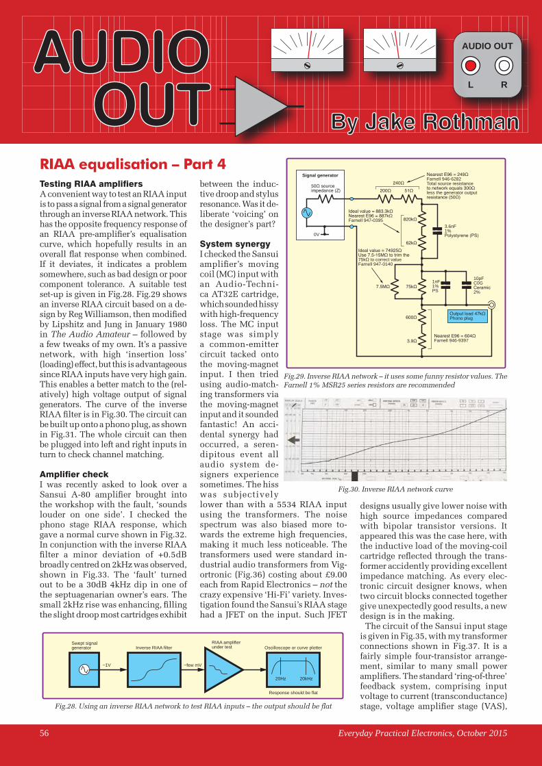
AUDIO OUT
L RAUDIO
OUT By Jake Rothman
56 Everyday Practical Electronics, October 2015
Testing RIAA amplifiersA convenient way to test an RIAA input is to pass a signal from a signal generator through an inverse RIAA network. This has the opposite frequency response of an RIAA pre-amplifier’s equalisation curve, which hopefully results in an overall flat response when combined. If it deviates, it indicates a problem somewhere, such as bad design or poor component tolerance. A suitable test set-up is given in Fig.28. Fig.29 shows an inverse RIAA circuit based on a de-sign by Reg Williamson, then modified by Lipshitz and Jung in January 1980 in The Audio Amateur – followed by a few tweaks of my own. It’s a passive network, with high ‘insertion loss’ (loading) effect, but this is advantageous since RIAA inputs have very high gain. This enables a better match to the (rel-atively) high voltage output of signal generators. The curve of the inverse RIAA filter is in Fig.30. The circuit can be built up onto a phono plug, as shown in Fig.31. The whole circuit can then be plugged into left and right inputs in turn to check channel matching.
Amplifier checkI was recently asked to look over a Sansui A-80 amplifier brought into the workshop with the fault, ‘sounds louder on one side’. I checked the phono stage RIAA response, which gave a normal curve shown in Fig.32. In conjunction with the inverse RIAA filter a minor deviation of +0.5dB broadly centred on 2kHz was observed, shown in Fig.33. The ‘fault’ turned out to be a 30dB 4kHz dip in one of the septuagenarian owner’s ears. The small 2kHz rise was enhancing, filling the slight droop most cartridges exhibit
between the induc-tive droop and stylus resonance. Was it de-liberate ‘voicing’ on the designer’s part?
System synergyI checked the Sansui amplifier’s moving coil (MC) input with an Audio-Techni-ca AT32E cartridge, which sounded hissy with high-frequency loss. The MC input stage was simply a common-emitter circuit tacked onto the moving-magnet input. I then tried using audio-match-ing transformers via the moving-magnet input and it sounded fantastic! An acci-dental synergy had occurred, a seren-dipitous event all audio system de-signers experience sometimes. The hiss was subjectively lower than with a 5534 RIAA input using the transformers. The noise spectrum was also biased more to-wards the extreme high frequencies, making it much less noticeable. The transformers used were standard in-dustrial audio transformers from Vig-ortronic (Fig.36) costing about £9.00 each from Rapid Electronics – not the crazy expensive ‘Hi-Fi’ variety. Inves-tigation found the Sansui’s RIAA stage had a JFET on the input. Such JFET
RIAA equalisation – Part 4
designs usually give lower noise with high source impedances compared with bipolar transistor versions. It appeared this was the case here, with the inductive load of the moving-coil cartridge reflected through the trans-former accidently providing excellent impedance matching. As every elec-tronic circuit designer knows, when two circuit blocks connected together give unexpectedly good results, a new design is in the making.
The circuit of the Sansui input stage is given in Fig.35, with my transformer connections shown in Fig.37. It is a fairly simple four-transistor arrange-ment, similar to many small power amplifiers. The standard ‘ring-of-three’ feedback system, comprising input voltage to current (transconductance) stage, voltage amplifier stage (VAS), Fig.28. Using an inverse RIAA network to test RIAA inputs – the output should be flat
AO-riaa-Fig2826mm x 2 COL
~1V ~few mV
Response should be flat
Oscilloscope or curve plotterRIAA amplifierunder testInverse RIAA filter
Swept signalgenerator
20kHz20Hz
Fig.29. Inverse RIAA network – it uses some funny resistor values. The Farnell 1% MSR25 series resistors are recommended
AO-riaa-Fig2982mm x 1.5 COL
200Ω240Ω
Nearest E96 = 249ΩFarnell 946-6282Total source resistanceto network equals 300Ωless the generator outputresistance (50Ω)
Nearest E96 = 604ΩFarnell 946-9397
Ideal value = 74925ΩUse 7.5-15MΩ to trim the75kΩ to correct valueFarnell 947-0140
Ideal value = 883.3kΩNearest E96 = 887kΩFarnell 947-0395
0V
51Ω
3.6nF1%Polystyrene (PS)
1nF1%PS
50Ω sourceimpedance (Z)
Signal generator
820kΩ
62kΩ
75kΩ
600Ω
7.5MΩ
3.9Ω
10pFC0GCeramic2%
Output load 47kΩPhono plug
Fig.30. Inverse RIAA network curve
Audio Out (MP 1st, JR & SK) – OCT 2015.indd 2 10/08/2015 22:56

AUDIO OUT
L RAUDIO
OUT By Jake Rothman
Everyday Practical Electronics, October 2015 57
common-emitter stage and output stage. There are some variations to the standard theme, the input transistor is a JFET, the VAS stage is ‘upside down’ using a PNP device, enabling a more common N-channel JFET to be used. Finally, the output stage is a class-AB push-pull, emitter-follower design. This will not generate crossover distor-tion on normal signal levels, but will have the current capacity to deal with nasty scratches without overloading by going momentarily into class B. This will sound less objectionable than a hard-clipped class A.
FET frenzyUnfortunately, as with most Japanese audio circuits, the Sansui used unu-sual semiconductors. The 2SK163, (marked K163) JFET from NEC was difficult to source. The other devic-es were all easily substituted. The K163 and other rare audio JFETs are available as NOS ‘new old stock’ from Donberg Electronics in Ireland. I measured the transconductance (gfs) of the K163 with the Peak DCA75 and found it to be in accordance with the data sheet at 17mA/V. This is much higher than standard JFETs,
Fig.31. Photo of ‘hard-wired’ inverse RIAA network – it plugs into an RIAA amplifier input
Fig.32. Sansui A80 RIAA response curve
Fig.34. Sansui A-80 amplifier
such as the 2N5457, which typically achieve 3-4mA/V. This would reduce
Fig.33. Sansui RIAA input fed by all inverse RIAA network. Note slight response bump at 2kHz
2kHz
the open-loop gain of the circuit by around four times and increase the noise level, since the second stage would have to do more work. The
Fig.35. Sansui A-80 RIAA input stage – a simple discrete JFET input design, with a few minor changes and transformers added. The switch on the transformer ground allows the left minus right signal to be listened to, which allows the anti-skating force on the pickup to be set to opti-mum by minimising distortion on vocal sibilants
AO-riaa-Fig35104mm x 2 COL
0V
0V
T1
25K163(25K117)(25K209)
To otherchannel
25A992(BC556)
1
22kΩ
27kΩ
330pF
XLR input
12
3
L-R switch
Output
Zobelnetwork
3
2
4
4
3.9kΩ 3.3kΩ
1mA
150µF6.3V3.3V
56Ω
–0.35V
–20V
–1.8V
33Ω1.5kΩ
33Ω25A992
25C1845(BC546)
100kΩ 3.3nF
18kΩ
3.9kΩ
0.8mA
2mA1mA
65mV
+10µF
68pF
27nF
2.7kΩ
560Ω
33kΩ
1nF100nF
+
0V
10µF+
+
0V
0V470µF6.3V 10µF
25V+
10µF+
+23V
–23V
NC
Audio Out (MP 1st, JR & SK) – OCT 2015.indd 3 10/08/2015 22:56

58 Everyday Practical Electronics, October 2015
K163 is one of those rare 1980s audio JFETs that uses a finely interdigitated channel (see Fig.38) to achieve the high transconductance and low noise. Other suitable types are the 2SK117 and 2SK170. If a P-channel JFET is used, such as the 2SJ74, the circuit could be made to work on a single +48V rail. One side effect is high ca-pacitance, but this is not a problem in this application. Another advantage of FETs is that no input capacitor is needed in this circuit.
Toshiba still make some audio FETs, albeit only in surface mount packs, such as the 2SK209-Y which is designed for condenser microphone head amps. These cost around 25p from Mouser UK and meet all the specs. I expect to pay commodity prices for my parts and I have no truck with the ‘antique-dealer’ pricing en-demic in the audio parts industry. The K163 has an unusually high maximum
Fig.37. Wiring for a Vigortronix VTX-101-003 moving-coil step-up transformer (pin view)
AO-riaa-Fig3652mm x 1 COL
0V
4
Screen pin(solder to can)
Solder baseplate to can
To RIAAamplifer
3
2
1
1
2
3
4
From XLR socketpin 2 (signal)
From XLR socketpin 3 (0V)
Input can be from balanced XLRwith pin 1 to ground
Primarywindings A
Secondarywindings B
Fig.36. Vigortronix 003 transformers used for converting moving-magnet to moving-coil inputs. Note the essential mumetal screening can to prevent hum pick-up
channel voltage of 50V, but the device is only exposed to 17.5V if the rails are ramped up slowly. This allows 30V TO92 package devices to be used. For those interested in all things JFET, Erno Borbely is the circuit designer to watch.
Wind upFinally, to end on a ‘sad’ note, a friend of mine gave me his de-funct £500 mov-ing-coil cartridge that had only last-ed for ten plays. In an attempt to prevent ‘extrane-ous resonance’ from a casing, the designer had left the coils exposed – typical Hi-Fi
Fig.38. An example of an ‘interdigitated’ JFET – an early low-noise audio design, the BFW10 – from Field-Effect Transisors, Mullard Ltd, 1972; Plate A p13 Fig.40. Ceramic cartridge – the two bi-morph elements are visible
Fig.39. Sumiko Blackbird moving-coil cartridge with broken wire. The 4-coil armature can be seen
madness. The inevitable happened, one of the fine wires got caught and broke. In a failed attempt to repair the unit, I was able to take a photos show-ing the inner workings of a moving-coil in Fig.39, and just for interest, there is a ceramic cartridge internal structure shown in Fig.40.
Audio Out (MP 1st, JR & SK) – OCT 2015.indd 4 10/08/2015 22:56

138 The Street, Little Clacton, Clacton-on-sea,Essex, CO16 9LS. Tel 01255 862308
Mail order address:
The Brunning Software P931 PIC Training Course
We start by learning to use a relatively simple 8 bit PIC microcontroller. We make our connections directly to the input and output pins of the chip and we have full control of the internal facilities of the chip. We work at the grass roots level.
The first book starts by assuming you know nothing about PICs but instead of wading into the theory we jump straight in with four easy experiments. Then having gained some experience we study the basic principles of PIC programming., learn about the 8 bit timer, how to drive the alphanumeric liquid crystal display, create a real time clock, experiment with the watchdog timer, sleep mode, beeps and music. Then there are two projects to work through. In the space of 24 experiments two project and 56 exercises we work through from absolute beginner to experienced engineer level using the latest 16F and 18F PICs.
The second book introduces the C programming language in very simple terms. The third book Experimenting with Serial Communications teaches Visual C# programming for the PC (not PIC) so that we can create PC programmes to control PIC circuits.
In the fourth book we learn to programme 32 bit MX PICs using fundamental C instructions. Most of the code is the same as already used with the 8 bit PICs so the same experiments are easily adapted. Then life gets more complex as we delve into serial communications with the final task being to create an audio oscilloscope with advanced triggering and adjustable scan rate. (To programme 32 bit PICs you will need to plug on a PICkit3 which you need to buy from Microchip, Farnell or RS for £38).
P931 course including UK carriage..... £158.00 Experimenting with Serial Coms..... £31.00 Experimenting with 32 bit PIC C..... £46.00
P942 PIC Training CourseThe P942 PIC training course offers exactly the same training as the
P931 but the P942 has the ability to verify the data in the PIC at high voltage, normal voltage and low voltage. Verifying that the code in the PIC can be read at high and low voltage is usually recommended if the PIC is to be used in a permanent circuit. For training and experimental work high and low verification is not necessary. P942 course including UK carriage..... £183.00 Experimenting with Serial Coms..... £31.00 Experimenting with 32 bit PIC C..... £46.00
P955 PIC Training CourseThe P955 PIC training course also offers exactly the same training as
the P931 but the P955 has a permanent socket for 28 pin 32 bit PICs which makes it more convenient if experimenting with 32 bit PICs is your main interest. (The fourth book Experimenting with 32 bit PIC C can be used with the P931 and P942 using a special adaptor which fits into the 40 pin ZIF socket). P955 course including UK carriage..... £170.00 Experimenting with Serial Coms..... £31.00 Experimenting with 32 bit PIC C..... £31.00
Web site:- www.brunningsoftware.co.uk
Brunning OCT 2015.indd 1 10/08/2015 22:57

60 Everyday Practical Electronics, August 2015
Tri-colour LEDs – Part 3As I always say: ‘Show me a flashing LED, and I’ll show you a man drooling.’ This phenomenon is even more pronounced in the case of tri-color LEDs. In my first column on these little scamps (EPE, July 2015), I con-sidered a traditional tri-colored device with a common-cathode terminal and three anode terminals – one each for the red, green, and blue sub-LEDs. As part of this, we noted that if we limited ourselves to simply turning these LEDs on and off, then we can achieve 2^3 = 8 dif-ferent colour combinations (assuming the all-off = black combination is a colour). These colours are black, red, green, blue, yellow (red + green), cyan (green + blue), magenta (red + blue), and white (red + green + blue). The big problem with these little rascals is that each tri-color LED requires three microcontroller (MCU) pins to drive it.
In Part 2 of this mini-series (EPE, August 2015), we discussed driving each LED terminal using a pulse-width modulated (PWM) MCU output. In the case of the Arduino, we have 8-bit PWMs, which theoretically allows us to achieve 2^8 = 256 different brightness val-ues, from 0 (fully off) to 255 (fully on). Since we can do this for each sub-LED, this means that we can theoreti-cally achieve 2^8 * 2^8 * 2^8 = 16,777,216 different colours. This is all jolly nice, but we are still faced with the fact that each tri-color LED requires three micro-controller (MCU) pins to drive it, which does tend to limit you as to what you can achieve. Happily, there is a way by which we can drive hundreds of tri-coloured LEDs using a single MCU pin... so, how do we do that? – read on!
Introducing the WS2812A couple of years ago, a company called Worldsemi introduced a device called the ‘WS2812’. This little beauty is presented in a 5mm × 5mm square package that contains super-bright red, green, and blue LEDs, along with an associated control chip and current-lim-iting circuitry.
The great thing about these devices is that they have only four pins: 0V (ground), 5V (power), Data-In, and Data-Out. This means that they can be daisy-chained together, with the MCU driving the Data-In of the first element, the Data-Out from the first element driving the
Data-In of the second, and so forth, as illus-trated in Fig.2.
Different companies have used these de-vices as the basis for a wide variety of prod-ucts. For example, the folks at Adafruit have a whole range of WS2812-based products that they call NeoPixels. These range from strips to
Max’s Beans
By Max The Magnificent
60 Everyday Practical Electronics, October 2015
rings to panels to ... all sorts of things – see: http://bit.ly/1gr71a3.
I’ve been using NeoPixels a lot in my hobby projects, such as my Bodacious Acoustic Diagnostic Astound-ingly Superior Spectromatic (BADASS) display and my Vetinari Clock – check out these YouTube videos, respectively at: http://bit.ly/1I5ncTc and http://bit.ly/195JKWR. The great thing about Adafruit is that they give you a NeoPixel software library along with a bunch of examples on how to use it.
One thing that can confuse beginners is that the Adafruit library includes a function called setPixel-Color(), but this doesn’t actually update the physical pixel itself. Take my BADASS display, for example. Sup-pose we use the Adafruit library to declare a string of 256 NeoPixels called myNeos (these will be numbered from 0 to 255). Now suppose I use the following statement, where the three parameters of 255 are associated with that pixel’s red, green, and blue channels, respectively:
for (int i = 0, i < 256; i++) myNeos.setPixelColor(i,255,255,255);
What do you think will happen on the display? The an-swer is ‘not a lot.’ This is due to the fact that, when we first declare our NeoPixels, the system creates an array in the Arduino’s memory. This array contains one main element for each NeoPixel, and this main element is comprised of three byte-sized sub-elements to contain that pixel’s red, green, and blue values. The setPix-elColor() function actually modifies the values in this array. When we are ready to update the display, we would use the show() function; for example:
for (int i = 0, i < 256; i++) myNeos.setPixelColor(i,255,255,255);
myNeos.show();
The show() function streams the entire contents of the array from the Arduino’s memory into the NeoPixel string. In the above example, this means that all of the pixels will turn fully on simultaneously. Now, assuming that all of the pixels are already on, how would we turn them off one at a time with a tenth of a second (100ms) delay between each one? Well, we could achieve this as follows:
for (int i = 0, i < 256; i++) myNeos.setPixelColor(i,0,0,0);
myNeos.show(); delay(100);
As you can see, we’ve moved the show() function in-side the for() loop, and we’ve also added a delay() function inside the loop so that we can see the pixels being extinguished one after another.Fig.1. A WS2812 tri-colour LED
Cool Beans (MP & Max) – OCT 2015.indd 60 10/08/2015 22:58

How much power?!Now, one thing you have to consider is how you’re go-ing to power the little ragamuffins. Your knee-jerk reac-tion may be along the lines of ‘LEDs are very efficient and they don’t consume much power.’ Well, that’s as may be, but the power starts mounting up when you use a lot of LEDs. Adafruit’s website states that each NeoPixel can consume up to 60mA when its red, green, and blue channels are all fully on. In the case of my BADASS display, I have a 16 × 16 = 256 array of NeoPixels, which equates to 256 × 60mA = (approx) 15.5A (I actually use a 20A supply to give myself some ‘wriggle room’).
You may decide to power your NeoPixels using a separate power supply to that used to power your Ar-duino. In this case, it’s very important to ensure that the ground (GND, 0V) of this power supply is connected to the Arduino’s GND pin. It’s also a good idea to mount a 1,000µF electrolytic capacitor across the power supply rails, as illustrated in Fig.3.
Furthermore, it’s a good idea to insert a resistor in series with the data signal coming from the Arduino. This resistor, which is used to dampen overshoot and undershoot on the signal, should be mounted close to the first element in the NeoPixel chain (ie, not at the
Everyday Practical Electronics, October 2015 61
Arduino end of the signal path). Adafruit’s website says the value of this resistor should be 300Ω to 500Ω; I typi-cally use a 390Ω resistor. (NeoPixels are also prone to being damaged by electrostatic discharge (aka ESD) so you should take appropriate earthing precautions while using them.)
In the case of my projects, I typically modify my Ar-duino so that it works from a 5V supply (the unmodi-fied Arduino requires a 7V to 12V supply, which is subsequently regulated down to 5V), and then I use the same regulated supply to power both the Arduino and the NeoPixels. However, this involves removing and bypassing the Arduino’s on-board regulator and tweaking a few resistor values, so it’s not for the faint of heart.
Using the Arduino 5V pinThe other alternative is to power the NeoPixels from the Arduino’s own 5V supply pin, but this means you are limited as to how many NeoPixels you can use. For example, I’m teaching a young lad called Jacob about using microcontrollers – he comes into my office for an hour each week. Not surprisingly, Jacob would like his own BADASS display, so we built him a mini version, as shown in Fig.4 (check out this YouTube video http://bit.ly/1UalHbP).
Now, Jacob powers his Arduino from his PC’s USB port, which is only specified to provide 0.5A (500mA). When running at full pelt, an Arduino Uno R3 draws around 45mA, and the spectrum analyzer shield only consumes about 3mA, so if we assume a worst-case of 50mA, this leaves us with 450mA to play with.
Although Adafruit says that each NeoPixel can draw up to 60mA when fully on (20mA each for the red, green, and blue sub-pixel LEDs), we’ve actually put a string of NeoPixels on the test bench and measured them as drawing an average of 43mA full on, which we rounded up to 45mA (or 15mA per color). So... in the case of Jacob’s mini display, we calculated that if we have three columns per channel – one each for the base, middle, and treble – and if each column has five NeoPixels – and if each NeoPixel is used to display only one colour (red, green, or blue), then we end up with 6 × 5 × 15mA = 450mA (I love it when a plan comes together).
‘Ah ha!’ I can hear you say, ‘but Fig.4 shows you using red, blue, and yellow (which is composed of red and green) – how can this be?’ The answer is really simple – so simple, in fact, that I’ll leave you to work it out for yourselves!
Any comments or questions? – please feel free to send me an email at: [email protected]
Fig.4. Jacob’s mini-BADASS display
Fig.2. WS2812s can be daisy-chained together
Fig.3. Using a separate supply for the NeoPixels
CB2-Oct1547mm x 3 COL
Data in Data out Data in Data out Data in Data out
+5V
FromMCU
To nextpixel
0V
CB3-Oct1541mm x 1.5 COL
From Arduinodigital output pin
+5V
1000µF390Ω
To PSU
VERY IMPORTANT!Make sure the GND (ground) of thepower supply (PSU) is connected tothe Arduino’s GND pin.
0V / GND
+
Cool Beans (MP & Max) – OCT 2015.indd 61 10/08/2015 22:58

EPE IS PLEASED TO BE ABLE TO OFFER YOU THESE
ELECTRONICS CD-ROMS
ELECTRONICS TEACH-IN BUNDLE –SPECIAL BUNDLE PRICE £14 FOR PARTS 1, 2 & 3
ELECTRONICS TEACH-IN 3 CD-ROM
The three sections of this CD-ROM cover a very wide range of subjects that will interest everyone involved in electronics, from hobbyists and students to professionals. The first 80-odd pages of Teach-In 3 are dedicated to Circuit Surgery, the regular EPE clinic dealing with readers’ queries on circuit design problems – from voltage regulation to using SPICE circuit simulation software.
The second section – Practically Speaking – covers the practical aspects of electronics construction. Again, a whole range of subjects, from soldering to avoiding problems with static electricity and indentifying components, are covered. Finally, our collection of Ingenuity Unlimited circuits provides over 40 circuit designs submitted by the readers of EPE.
The CD-ROM also contains the complete Electronics Teach-In 1 book, which provides a broad-based introduction to electronics in PDF form, plus interactive quizzes to test your knowledge, TINA circuit simulation software (a limited version – plus a specially written TINA Tutorial).
The Teach-In 1 series covers everything from Electric Current through to Microprocessors and Microcontrollers and each part includes demonstration circuits to build on breadboards or to simulate on your PC. CD-ROM Order code ETI3 CD-ROM £8.50
ELECTRONICS TEACH-IN 2 CD-ROMUSING PIC MICROCONTROLLERS A PRACTICAL INTRODUCTIONThis Teach-In series of articles was originally published in EPE in 2008 and, following demand from readers, has now been collected together in the Electronics Teach-In 2 CD-ROM.
The series is aimed at those using PIC microcontrollers for the first time. Each part of the series includes breadboard layouts to aid understanding and a simple programmer project is provided.
Also included are 29 PIC N’ Mix articles, also republished from EPE. These provide a host of practical programming and interfacing information, mainly for those that have already got to grips with using PIC microcontrollers. An extra four part beginners guide to using the C programing language for PIC microcontrollers is also included.
The CD-ROM also contains all of the software for the Teach-In 2 series and PIC N’ Mix articles, plus a range of items from Microchip – the manufacturers of the PIC microcontrollers. The material has been compiled by Wimborne Publishing Ltd. with the assistance of Microchip Technology Inc.
CD-ROMs Order code ETI BUN Bundle Price £14.00
ELECTRONICS TEACH-IN 4
ELECTRONICS TEACH-IN 4 CD-ROM
A Broad-Based Introduction to Electronics.The Teach-In 4 CD-ROM covers three of the most important electronics units that are currently studied in many schools and colleges. These include, Edexcel BTEC level 2 awards and the electronics units of the new Diploma in Engineering, Level 2.
The CD-ROM also contains the full Modern Electronics Manual, worth £29.95. The Manual contains over 800 pag-es of electronics theory, projects, data, assembly instruc-tions and web links.
A package of exceptional value that will appeal to all those interested in learning about electronics or brushing up on their theory, be they hobbyists, students or professionals.
CD-ROM Order code ETI4 CD-ROM £8.99
CD-ROM Order code ETI2 CD-ROM £9.50
Order code ETIBUNDLE
ELECTRONICS TEACH-IN 2
ELECTRONICS TEACH-IN 3
Analogue, Digital, Symbolic, RF, MCU and Mixed-Mode Circuit Simulation and PCB Design with TINA
TINA Design Suite V10 is a powerful yet affordable software package for analysing, designing and real time testing analogue, digital, MCU, and mixed electronic circuits and their PCB layouts. You can also analyse RF, communication, optoelectronic circuits, test and debug microcontroller applications.
Enter and analyse any circuit up to 100 nodes (student), or 200 with the Basic (Hobbyist) version within minutes with TINA’s easy-to-use schematic editor. Enhance your schematics by adding text and graphics. Choose components from the large library containing more than 10,000 manufacturer models. Analyse your circuit through more than 20 different analysis modes or with 10 high tech virtual instruments.
Present your results in TINA’s sophisticated diagram windows, on virtual instruments, or in the live interactive mode where you can even edit your circuit during operation.
Customise presentations using TINA’s advanced drawing tools to control text, fonts, axes, line width, colour and layout. You can create and print documents directly inside TINA or cut and paste your results into your favourite word procesing or DTP package.
TINA includes the following Virtual Instruments: Oscilloscope, Function Generator, Multimeter, Signal Analyser/Bode Plotter, Network Analyser, Spectrum Analyser, Logic Analyser, Digital Signal Generator, XY Recorder.
This offer gives you a CD-ROM – the software will need registering (FREE) with Designsoft (TINA), details are given within the package.Get TINA Basic V10 (Hobbyist) for £129 or Student V10 version for £49
Prices include VAT and UK postage+ get a 1 year free subscription for TINACloud the breakthrough cloud version of TINA which you can run on most operating systems and computers, including PCs, Macs, thin clients iPads and other tablets – even on many smart phones, smart TVs and e-book readers.
To order please either fill out and return the order form, or call us on 01202 880299 Alternatively you can order via our secure online shop at: www.epemag.com
TINA Design Suite V10From £49.00
FEATURED IN OUR TEACH-IN 2015 SERIES
62 Everyday Practical Electronics, October 2015
CD-ROMs Pages.indd 62 10/08/2015 22:59

PICmicro TUTORIALS AND PROGRAMMINGPICmicro Multiprogrammer Board
and Development BoardSuitable for use with the three software packages
listed below
This flexible PICmicro microcontroller programmer board and combination board allows students and professional engineers to learn how to program PICmicro microcontrollers as well as program a range of 8, 18, 28 and 40 pin devices from the 12, 16 and 18 series PICmicro ranges. For experienced programmers all programming software is included in the MLoader utility that is free to download when you buy the multiprogrammer board. For those who want to learn, choose one or all of the packages below to use with the hardware.
• Makes it easier to develop PICmicro projects• Supports low cost Flash-programmable PICmicro devices• Fully featured integrated displays – 16 individual LEDs, quad 7-segment display and alphanumeric LCD display• Supports PICmicro microcontrollers with A/D converters• Fully protected expansion bus for project work• USB programmable• Compatible with the E-blocks range of accessories
ASSEMBLY FOR PICmicro V5
(Formerly PICtutor)Assembly for PICmicro microcontrollers V3.0 (previously known as PICtutor) by John Becker contains a complete course in programming the PIC16F84 PICmicro microcontroller from Arizona Microchip. It starts with fundamental concepts and extends up to complex programs including watchdog timers, interrupts and sleep modes.
The CD makes use of the latest simulation techniques which provide a superb tool for learning: the Virtual PICmicro microcontroller, this is a simulation tool that allows users to write and execute MPASM assembler code for the PIC16F84 microcontroller on-screen. Using this you can actually see what happens inside the PICmicro MCU as each instruction is executed, which enhances understanding.• Comprehensive instruction through 45 tutorial
sections • Includes Vlab, a Virtual PICmicro microcontroller: a fully functioning simulator • Tests, exercises and projects covering a wide range of PICmicro MCU applications • Includes MPLAB assembler • Visual representation of a PICmicro showing architecture and functions • Expert system for code entry helps first time users • Shows data flow and fetch execute cycle and has challenges (washing machine, lift, crossroads etc.) • Imports MPASM files.
‘C’ FOR 16 Series PICmicroVersion 5
The C for PICmicro microcontrollers CD-ROM is designed for students and professionals who need to learn how to program embedded microcontrollers in C. The CD-ROM contains a course as well as all the software tools needed to create Hex code for a wide range of PICmicro devices – including a full C compiler for a wide range of PICmicro devices.
Although the course focuses on the use of the PICmicro microcontrollers, this CD-ROM will provide a good grounding in C programming for any microcontroller.• Complete course in C as well as C
programming for PICmicro microcontrollers • Highly interactive course • Virtual C PICmicro improves understanding • Includes a C compiler for a wide range of PICmicro devices • Includes full Integrated Development Environment • Includes MPLAB software • Compatible with most PICmicro programmers • Includes a compiler for all the PICmicro devices.
FLOWCODE FOR PICmicro V6
£167 including VAT and postage, supplied with USB cable and free to download programming software
HARDWARE
SOFTWARE
Hobbyist/Student . . . . . . . . . . . . . . . . . . . . . . . . . . . . . . £58 .80 inc VATProfessional (Schools/HE/FE/Industry) . . . . . . . . . . . . £150 plus VATProfessional 10 user (Network Licence) . . . . . . . . . . . £499 plus VATSite Licence . . . . . . . . . . . . . . . . . . . . . . . . . . . . . . . . . . £999 plus VAT
Flowcode (choose PIC, AVR, ARM, dsPIC, PIC24) . . . £94 .80 plus VAT
PRICESPrices for each of the CD-ROMs above are:
(Order form on next page)
(UK and EU customers add VAT to ‘plus VAT’ prices)
Minimum system requirements for these items: Pentium PC running, 2000, ME, XP; CD-ROM drive; 64MB RAM; 10MB
hard disk space.Flowcode will run on XP or later
operating systems
Flowcode is a very high level language programming system based on flowcharts. Flowcode allows you to design and simulate complex systems in a matter of minutes. A powerful language that uses macros to facilitate the control of devices like 7-segment displays, motor controllers and LCDs. The use of macros allows you to control these devices without getting bogged down in understanding the programming. When used in conjunction with the development board this provides a seamless solution that allows you to program chips in minutes.
• Requires no programming experience • Allows complex PICmicro applications to be
designed quickly• Uses international standard flow chart symbols • Full on-screen simulation allows debugging and
speeds up the development process.• Facilitates learning via a full suite of
demonstration tutorials • Produces ASM code for a range of 18, 28 and
40-pin devices • 16-bit arithmetic strings and string manipulation • Pulse width modulation • I2C.
Please note: Due to popular demand, Flowcode PICmicro, AVR, DSPIC, PIC24 & ARM V6 are now available as a download. Please include your email address and a username (of your choice) on your order. A unique download code will then be emailed to you. If you require the CDROM as a back-up then please add an extra £14 to the price.
Everyday Practical Electronics, October 2015 63
CD-ROMs Pages.indd 63 10/08/2015 22:59

By integrating the entire design process, Circuit Wizard provides you with all the tools necessary to produce an electronics project from start to finish – even including on-screen testing of the PCB prior to construction!
* Circuit diagram design with component library (500 components Standard,1500 components Professional) * Virtual instruments (4 Standard, 7 professional)* On-screen animation * Interactive circuit diagram simulation * True analogue/digital simulation * Simulation of component destruction * PCB Layout * Interactive PCB layout simulation * Automatic PCB routing * Gerber export * Multi-level zoom (25% to 1000%) * Multiple undo and redo * Copy and paste to other software * Multiple document support
CIRCUIT WIZARD
Please send me: CD-ROM ORDER FORM
Assembly for PICmicro V5 ‘C’ for 16 Series PICmicro V5
Flowcode for PICmicro V6 (DOWNLOAD ONLY) Flowcode for AVR V6 (DOWNLOAD ONLY) Flowcode for ARM V6 (DOWNLOAD ONLY) Flowcode for dsPIC V6 (DOWNLOAD ONLY) Flowcode for PIC24 V6 (DOWNLOAD ONLY)
Email: . . . . . . . . . . . . . . . . . . . . . . . . . . . . . . Username: . . . . . . . . . . . . . . . . . . . . . . . . . .
PICmicro Multiprogrammer Board and Development Board V4 (hardware)
Circuit Wizard – Standard Circuit Wizard – Professional GCSE Electronics
TINA Design Suite V10 Basic (Hobbyist) TINA Design Suite V10 (Student)
Full name: . . . . . . . . . . . . . . . . . . . . . . . . . . . . . . . . . . . . . . . . . . . . . . . . . . . . . . . . . . . . . . . . .
Address: . . . . . . . . . . . . . . . . . . . . . . . . . . . . . . . . . . . . . . . . . . . . . . . . . . . . . . . . . . . . . . . . . .. . . . . . . . . . . . . . . . . . . . . . Post code: . . . . . . . . . . . . . . . . . Tel. No: . . . . . . . . . . . . . . . . . . .
Signature: . . . . . . . . . . . . . . . . . . . . . . . . . . . . . . . . . . . . . . . . . I enclose cheque/PO in £ sterling payable to WIMBORNE PUBLISHING LTD for £ . . . . . . . . . Please charge my Visa/Mastercard/Maestro: £ . . . . . . . . . . Valid From: . . . . . . . . . . Card expiry date: . . . . . . . . . . . . . Card No: . . . . . . . . . . . . . . . . . . . . . . . . . . . . . . . . . . . . . . . . Maestro Issue No. . . . . . . . . .Card Security Code . . . . . . . . . . (The last 3 digits on or just under the signature strip)
Note: The software on each version is the same, only the licence for use varies.
Minimum system requirements for these CD-ROMs: Pentium PC, CD-ROM drive, 32MB
RAM, 10MB hard disk space. Windows 2000/ME/XP, mouse, sound card, web browser.
ORDERINGALL PRICES INCLUDE UK
POSTAGE
Standard/Student/Basic (Hobbyist) Version price includes postage to most
countries in the worldEU residents outside the UK add £5 for
airmail postage per order
Professional, Multiple User and Site License Versions – overseas readers add £5 to the basic price of each order for airmail postage (do not add VAT unless you live in an EU (European Union) country, then add VAT at 20% or provide your official VAT registration number).
Send your order to:Direct Book Service
Wimborne Publishing Ltd113 Lynwood Drive, Merley,
Wimborne, Dorset BH21 1UU
To order by phone ring
01202 880299. Fax: 01202 843233Goods are normally sent within seven days
E-mail: [email protected] shop:
www.epemag.com
Circuit Wizard is a revolutionary software system that combines circuit design, PCB design, simulation and CAD/CAM manufacture in one complete package.
Two versions are available, Standard or Professional.
This software can be used with the Jump Start and Teach-In 2011 series (and the Teach-In 4 book).
Standard £61.25 inc. VAT. Professional £75 plus VAT.
Suitable for any student who is serious about studying and who wants to achieve the best grade possible. Each program’s clear, patient and structured delivery will aid understanding of electronics and assist in developing a confident approach to
answering GCSE questions. The CD-ROM will be invaluable to anyone studying electronics, not just GCSE students.
* Contains comprehensive teaching material to cover the National Curriculum syllabus * Regular exercises reinforce the teaching points * Retains student interest with high quality animation and graphics * Stimulates learning through interactive exercises * Provides sample examination ques-tions with model solutions * Authored by practising teachers * Covers all UK examination board syllabuses * Caters for all levels of ability * Useful for self-tuition and revision
GCSE ELECTRONICS
£12.50 inc. VAT and P&P
SUBJECTS COVEREDElectric Circuits – Logic Gates – Capacitors & Inductors – Relays – Transistors – Electric Transducers – Operational Amplifiers – Radio Circuits – Test Instruments
Over 100 different sections under the above headings
Version required: Hobbyist/Student Professional Professional 10 user Site licence
Teach-In 2 Teach-In 3 Teach-In 4 Teach-In BundleNEW
64 Everyday Practical Electronics, October 2015
CD-ROMs Pages.indd 64 10/08/2015 22:59

Everyday Practical Electronics, October 2015 65
www.electronicsworld.co.uk
REGULAR COLUMN: ARDUINO PROJECTS l 37
if (brightness == 0 || brightness == 255) fadeAmount = -fadeAmount ; // wait for 30 milliseconds to see the dimming effect delay(30);
Upload this sketch to the board, and if everything has uploaded successfully, the LED fades from off to full brightness and then back off again. If you don’t see any fading, double-check the wiring:
l Make sure the correct pin numbers are being used.l Check the LED is correctly positioned, with its long leg
connected by a wire to pin 9 and the short leg connected via the resistor and a wire to GND.
l Check the connections on the breadboard. If the jumper wires or components are not connected using the correct rows in the breadboard, they will not work. l
More on this and other Arduino projects can be found in the
‘Arduino For Dummies’ book by John Nussey.
John Nussey is a creative technologist based in London. He teaches interaction design and prototyping at the Goldsmiths College and the Bartlett School of Architecture among others.We have a couple of copies of this book to give away. To enter please supply your name, address and email to the Editor at [email protected]. The winner will be drawn at random and announced at the end of the series.
WIN THE ‘ARDUINO FOR DUMMIES’ BOOK BY JOHN NUSSEYFigure 2: Layout diagram
for the project
www.stewart-of-reading.co.ukCheck out our website, 1,000’s of items in stock
IFR 2025Fluke/Philips PM3092HP34401AAgilent E4407B HP3325AHP3561AHP3581AHP3585BHP53131AHP5361BHP54600BHP54615BHP6032AHP6622AHP6624AHP6632BHP6644AHP6654AHP8341AHP83731AHP8484AHP8560AHP8560EHP8563AHP8566BHP8662AHP8970BHP33120AMarconi 2022EMarconi 2024Marconi 2030Marconi 2305Marconi 2440Marconi 2945Marconi 2955Marconi 2955AMarconi 2955BMarconi 6200Marconi 6200AMarconi 6200BIFR 6204BMarconi 6210Marconi 6960B withMarconi TF2167Tektronix TDS3012
Signal Generator 9kHz - 2.51GHZ Opt 04/11Oscilloscope 2+2 Channel 200MHZ Delay etcDigital Multimeter 6.5 digitSpectrum Analyser 100HZ - 26.5GHZSynthesised Function GeneratorDynamic Signal AnalyserWave Analyser 15HZ - 50KHZ Spectrum Analyser 20HZ - 40MHZUniversal Counter 3GHZ Pulse/Microwave Counter 26.5GHZOscilloscope 100MHZ 20MS/SOscilloscope 2 Channel 500MHZ 1GS/SPSU 0-60V 0-50A 1000WPSU 0-20V 4A Twice or 0-50V 2A TwicePSU 4 Outputs PSU 0-20V 0-5APSU 0-60V 3.5APSU 0-60V 0-9ASynthesised Sweep Generator 10MHZ-20GHZSynthesised Signal Generator 1-20GHZPower Sensor 0.01-18GHZ 3nW-10uWSpectrum Analyser Synthesised 50HZ - 2.9GHZSpectrum Analyser Synthesised 30HZ - 2.9GHZSpectrum Analyser Synthesised 9KHZ-22GHZSpectrum Analsyer 100HZ-22GHZRF Generator 10KHZ - 1280MHZNoise Figure MeterFunction Generator 100 microHZ-15MHZ - no moulding handleSynthesised AM/FM Signal Generator 10KHZ-1.01GHZSynthesised Signal Generator 9KHZ-2.4GHZSynthesised Signal Generator 10KHZ-1.35GHZModulation MeterCounter 20GHZCommunications Test Set Various OptionsRadio Communications Test SetRadio Communications Test SetRadio Communications Test SetMicrowave Test SetMicrowave Test Set 10MHZ-20GHZMicrowave Test Set Microwave Test Set 40GHZReflection Analyser for 6200 Test Sets6910 Power MeterRF Amplifier 50KHZ - 80MHZ 10WOscilloscope 2 Channel 100MHZ 1.25GS/S
£1,250£295£325£5,000£195£650£250£1,500£600£1,250from £125£650£750£350£350£195£400£500£2,000£2,500£125£1,950£2,400£2,750£1,600£1,000£750£295£325£800£750£250£295£2,500£595£725£850£1,950£2,500£3,000£10,000£1,250£295£75£800
Tektronix 2430ATektronix 2465BR&S APN62R&S DPSPR&S SMR40Cirrus CL254Farnell AP60/50Farnell H60/50Farnell B30/10Farnell B30/20Farnell XA35/2TFarnell LF1Racal 1991Racal 2101Racal 9300Racal 9300BBlack Star OrionBlack Star 1325Ferrograph RTS2Fluke 97Fluke 99BFluke PM5420Gould J3BGould OS250BGigatronics 7100Panasonic VP7705APanasonic VP8401BPendulum CNT90Seaward NovaSolartron 7150Solartron 7150 PlusSolatron 7075Solatron 1253Tasakago TM035-2Thurlby PL320Thurlby TG210Wavetek 296
Oscilloscope Dual Trace 150MHZ 100MS/SOscilloscope 4 Channel 400MHZSyn Function Generator 1HZ-260KHZRF Step Attenuator 139dBSignal Generator 10MHZ - 40GHZ with OptionsSound Level Meter with CalibratorPSU 0-60V 0-50A 1KW Switch ModePSU 0-60V 0-50APSU 30V 10A Variable No MetersPSU 30V 20A Variable No MetersPSU 0-35V 0-2A Twice DigitalSine/sq Oscillator 10HZ-1MHZCounter/Timer 160MHZ 9 DigitCounter 20GHZ LEDTrue RMS Millivoltmeter 5HZ-20MHZ etcAs 9300Colour Bar Generator RGB & VideoCounter Timer 1.3GHZTest SetScopemeter 2 Channel 50MHZ 25MS/SScopemeter 2 Channel 100MHZ 5GS/STV Gen Multi OutputsSine/sq Oscillator 10HZ-100KHZ Low DistortionOscillator Dual Trace 15MHZSynthesised Signal Generator 10MHZ-20GHZWow & Flutter MeterTV Signal Generator Multi OutputsTimer Counter Analyser 20GHZPAT Tester6 1/2 Digit DMM True RMS IEEEas 7150 plus Temp MeasurementDMM 7 1/2 DigitGain Phase Analyser 1mHZ-20KHZPSU 0-35V 0-2A 2 MetersPSU 0-30V 0-2A DigitalFunction Generator 0.002-2MHZ TTL etc Kenwood BadgedSynthesised Function Generator 2 Channel 50MHZ
£350£600£225£300£13,000£40£195£500£45£75£75£45£150£295£45£75£30£85£50£75£125£600£60£50£1,950£60£75£995£125£65£75£60£750£30£50£65£450
RadioBygones
The magazine for all vintage radio enthusiasts.
Covers:· Domestic radio and TV· Amateur radio· Military, aeronautical or marine communications· Radar or radio navigation · Broadcasting· Radio sytems
www.radiobygones.com
April/May 2014Issue No. 148
ISSN 0956-974X
www.radiobygones.com
The Lafayette HE-80 Communications Receiver
Sound Sales Ltd., And The ‘DX Plus Three’ TunerThe Roberts P5A Transportable RadioAVO TFM Portable AM/FM Signal Generator
RB Front Cover.indd 1
12/03/2014 16:07:50
Tel: 01202 880299 or visit:
Subscribe to Radio Bygones (available by postal subscription):
1 year (6 issues)UK £27.00
Europe £29.00Rest of the World £34.00
OR Download your PDF copies,
only £12.00 for one year
June/July 2014Issue No. 149
ISSN 0956-974X
www.radiobygones.com
A Very Large Eddystone Receiver
Kolster-Brandes 840The Writings Of Francis George Rayer, G3OGR – Part 1
The Valve Era: A Whistful Backwards Glance
RB Front Cover.indd 1
30/04/2014 11:45:13
Page 65.indd 66 10/08/2015 23:10

Electronic Building Blocks
Quick and easy Construction
Great results on a low budget
By JulianEdgar
9W Stereo AmplifierLarge complex projects are fun, but they take time and can be expensive. Sometimes you just want a quick result at low cost. That’s where this series of Electronic Building Blocks fits in. We use ‘cheap as chips’ compo-nents bought online to get you where you want to be... FAST! These projects range from around £15 to under a fiver... bargains!
9W Stereo AmplifierNeed a cheap audio amplifier – perhaps as a test bench amplifier or for a kid’s MP3 sound system? Well it doesn’t get much cheaper than this – try under £4 for the prebuilt amplifier module, including postage to your UK letterbox!
So what do you get for your measly £4? Well, it isn’t exactly ‘Hi-Fi’ – but then again, neither is it anywhere near as nasty as you might first think! (See Fig.1) The module uses a Tripath TA2024 integrated circuit that delivers 9W per channel into a 4Ω load at a total harmonic distortion of 0.04%. Crank it up to 15W per channel and distortion rises very substantially to 10% – so you don’t want to overdo it! Dynamic range is 89dB. The module comes fully built and is 92mm x 53mm in size.
Fig.2. Speaker and power terminals Fig.3. The input connector terminal
ConnectionsAt one end of the module is a termi-nal strip to allow connection of the two speakers, and power and ground (Fig.2). The board is spec’d at 12V, but it will work down to 7V. Note that it is not reverse-polarity protected.
At the other end of the board is a three-terminal connector for left, right and ground audio inputs (Fig.3). A
short input cable is supplied with an appropriate plug and lead.
At 10W audio output power, the manufacturer rates the efficiency of the IC at about 78% (with 4Ω speakers), so the chip does not need a heat sink. In fact, in our testing, it stayed relatively cool even when running continuously at full power on audio material. The cheapest and easiest approach to pow-ering the module is to use a discarded mains-powered plugpack. Any design with a DC output of around 8-12V will work fine.
Driving the ampMany people will want to run the module from a phone or other MP3 player. Cheapest is to get an old pair of earphones (or any other discarded cord) that has a 1/8-inch stereo plug already wired into place. Just cut off the lead and make the connections to the input cable supplied with the module (Fig.5).
Fig.1. Fantastic value – a 9W stereo amplifier for under £4. It won’t challenge high-end Hi-Fi, but performs respectably when driven adequately and paired with a couple of 4Ω speakers
66 Everyday Practical Electronics, October 2015
Julian Edgar Article (MP 1st, JE & SK) – OCT 2015.indd 66 10/08/2015 23:10

Fig.4. The heart of the beast – a Tripath TA2024 IC
Next month – an electronic stethoscope
Fig.5. Connecting up the input
The conductor that connects to the tip of the plug goes to the red input wire of the module; the central conductor on the plug to the white input lead; and the base of the plug to the black input. Connect speakers to the appropriate screw terminals, switch on power and listen to music! The output level of an iPhone that we used to test the module worked well – the amp input was not overloaded at even full phone output.
Battery powered?What about running the module off a 9V battery? At 9V and driving both channels from an iPhone, we meas-ured an average current draw of just
Next monthFancy an electronic stethoscope? Here is a really neat device that will allow you to listen to all sorts of strange noises in machines and other mechanical devices. Just add some headphones and shielded microphone cable. All this is in our next Electronic Building Block article.
60mA at a low listening level, 80mA at a moderate level, and 185mA at a loud level. That makes battery operation entirely feasible.
ConclusionAs I said at the beginning, don’t even pretend that this is a full-blooded Hi-Fi amplifier that will shake the house. But where you need a utility low-pow-ered amplifier, at just £4 plus an old plugpack, it’s pretty hard to go wrong.
SourcingAt the time of writing, a typical online unit is eBay item 351092217368 at a very reasonable £3.88 incl delivery.
Everyday Practical Electronics, October 2015 67
CRICKLEWOODELECTRONICS
Visit our shop at:40-42 Cricklewood BroadwayLondon NW2 3ET020 8452 0161
Frustrated with your suppier?Visit our component packed
website for a vast range ofparts - old and new,
many unavailable elsewhere!www.cricklewoodelectronics.com
10001000’s OF PRICES REDUCED!
Alternatively phone us on020 8452 0161 with your
requirements.
Visit our Shop, Call or Buy online at:www.cricklewoodelectronics.com
Established 1981
supplier?
Cricklewood - MAR09.indd 1 28/01/2009 11:08:21
Julian Edgar Article (MP 1st, JE & SK) – OCT 2015.indd 67 10/08/2015 23:11

68 Everyday Practical Electronics, October 2015
Matt Pulzer addresses some of the general points readers have raised. Have you anything interesting to say?Drop us a line!
WIN AN ATLAS LCR ANALYSER WORTH £79An Atlas LCR Passive Component Analyser, kindly donated by Peak Electronic Design
Ltd, will be awarded to the author of the Letter Of The Month. The Atlas LCR
automatically measures inductance from 1mH to 10H, capacitance from 1pF to 10,000F
and resistance from 1 to 2M with a basic accuracy of 1%. www.peakelec.co.uk
READOUTAll letters quoted here have previously been replied to directly Email: [email protected]
L E T T E R O F T H E M O N T H Valve-based hearing aid
Dear editorThere’s no need to ‘...imagine a valve hearing aid!’ (EPE, June 2015, Audio Out, Ge-mania – Part 3, p.52) because here’s a picture of me modelling one (my thanks to Christine Mlynek for the photo). The Medresco (MEDical RESearch COuncil) OL35A was one of the first NHS hearing aid patterns. The OL15A is slightly earlier, but the differences are subtle. I haven’t an ear moulding so the earpiece is hooked loosely round my left ear. The dangling leads are for the heater and HT (‘high tension’) batteries, again I have no originals, but they were probably larger than the aid itself. It does work, an AA cell with a touch of series resistance provides the heater supply and a 23A compact 12V battery is sufficient for the HT, even though slightly lower in voltage than specified. Remember that the zinc-carbon cells of the day dropped from their rated potential difference quite quickly, and so circuits had to be tolerant of a lower supply. Also shown is a photo of the circuitry.
The sub-miniature valves are wire-ended and originally intended for guidance/fusing in late wartime ordinance. This is far smaller than the more commonly accepted miniature B7G and B9A valves. The remaining picture shows one of the wire-ended valves (second from right) with an OC59 (still in original package), as also seen in Jake’s Ge-mania, Part 3 article in Fig.26 – the transistor replaced valves in smaller aids. Valve designers were aiming to make valves smaller still, one more place to the left is a 6CW4 Nuvistor in its shiny metal can.
Jake mentions Sinclair’s transistors rescued from disposal by Plessey. Clive Sinclair claimed to have involvement in the novel microalloy devices – they were actually the poor-spec Plessey throw-outs with a crude paper label bearing his own non-standard MAT type numbers (a MAT100 still in its packet is seen at the far left of the photo). Transistors didn’t start this way, of course. The very first offerings were point contact, as exemplified by the rare GET1 seen at the far right of the picture – sadly, non-working (do not confuse with GE numbered devices).
Tumbling audio caps!On a completely different tack, I’ve just had to replace the motor-run capacitor in my tumble dryer (which stopped tumbling when the capacitor failed for no obvious reason!). What’s that to do with audio? These are non-polarised (not electrolytic) caps in a range of values in the several µF class. ESR measurements are very low. Lateral thinking: could they be used for audio? They’re big, but not massive. Available in a metal screening can which is isolated from the terminals.
Godfrey Manning G4GLM, Edgware
Jake Rothman replies:I thank Godfrey for his extra information, and I have appreciated his letters to Practical Wireless in the past. The photo of the GET1 point-contact transistor is an especially useful addition, since I couldn’t get one. I did try making a point-contact transistor with a couple of needles probing a germanium slice recovered from a shattered OA10 diode. I think I got
Readout - New layout v2.indd 68 10/08/2015 23:12

Everyday Practical Electronics, October 2015 69
WIN AN ATLAS LCR ANALYSER WORTH £79An Atlas LCR Passive Component Analyser, kindly donated by Peak Electronic Design
Ltd, will be awarded to the author of the Letter Of The Month. The Atlas LCR
automatically measures inductance from 1mH to 10H, capacitance from 1pF to 10,000F
and resistance from 1 to 2M with a basic accuracy of 1%. www.peakelec.co.uk
Email: [email protected]
IF YOU HAVE A SUBJECT YOU WISH TO DISCUSS IN READOUT
PLEASE EMAIL US AT:
Getting back into electronics
Dear editorI have worked in many different electronic disciplines, but have not had ‘hands on’ experience, including hobby projects, for over 40 years. Somehow, the advent of integrated circuits removed the magic of construction.
Recently, however, having almost reached the age of seventy-nine, I was struck with an urge to build something again. Quite by chance I discovered a copy of your January 2015 issue, on a market stall, containing an article on constructing the Tiny Tim Amplifier; this seemed the ideal project to satisfy my construction urge.
How things have changed! I’ve spent countless hours trying to understand, what is new to me, the various acronyms, trying to source individual components, as firms supplying kits of parts, common in my past, seem to have disappeared – but the biggest stumbling block has proved to be a source for the specified heat-sinks. Neither Farnell nor Radiospares, the two suppliers of Element14 parts, recognise the part number or description quoted in the parts list! Unless you can supply me with your source details I shall have to abandon the project and return to gardening!
Finally, I mentioned that I discovered the magazine on a market stall; I have been unable to find the February issue in my local newsagents’ shops (including WHSmith). Also, the editorial speaks of 50 Golden Years of publication, yet I cannot remember seeing or knowing of it before. I do, however, remember Practical Electronics and other titles. Is Everyday Practical Electronics descended from these?
GJ Gillson, by email
EPE Online Editor Alan Winstanley replies:Most of our projects are sourced from Australia’s Silicon Chip magazine, so component ID queries crop up from time to time. Unfortunately, EPE cannot promise 1:1 close technical support, as this would require immense resources on our part. The best place to ask for technical help is in the EPE Chat Zone forum – www.chatzones.co.uk – where many readers are very happy to offer support. A section called ‘Shop Talk’ highlights any late-breaking news or component-sourcing Q&As.
It is very common these days to source parts by mail order/ Internet from suggested sources in Australia or eBay for example. Sometimes, full kits are available online (eg see Jaycar or Altronics websites). Delivery to the UK is never a problem.
The exact TO-220 12°C/W heatsink appears to be available from Jaycar Australia. Jaycar is a reputable, recommended mail order supplier, who ship constantly to the UK. Go to www.jaycar.com.au and search for Cat No HH8504
Drawings are available from Jaycar to enable users to make a substitution. These are only small TO-220 type power transistor heatsinks and appear to be nothing special. In my experience they can be freestanding, clip-on or some have extra PCB pillars. A wide range is also listed on eBay.
As the Tiny Tim Amplifier evolved from the earlier Hi-Fi Stereo Headphone Amplifier project (October 2014 issue et seq.) I wanted to point out that it is probably much less straightforward to build the Tiny Tim ‘out of the box’. This is not really a cut and dried project, but one for the experienced audio enthusiast who would need to be resourceful and adaptable. The project articles contain some intensive close technical details and unfortunately there is no short-cut to digesting them. It may be useful to refer to the earlier Headphone Amplifier project, and also some extra hardware parts are highlighted in Part 2 (Feb 2015, page 28). I say this just to explain in advance that some construction head-scratching and puzzling over parts are to be expected!
EPE is indeed 50 years old and our November and December 2014 issues contained special supplements that I wrote, charting our heritage from the 1964 Practical Electronics issue No. 1 to the present day. Everyday Electronics was spun out of PE to appeal to newcomers. For well-documented reasons both titles went their separate ways before merging to become EPE, owned by the present publishers.
Back issues of EPE magazine can be bought from us online or over the phone, please see www.epemag.com for details. Your local WHSmith should be able to order a copy for you, but the best (cheapest) way is to order a subscription from us for direct delivery to your door. I’m afraid it’s a sign of the times – it is ever harder to get a niche title onto the newsagent shelves. Please contact us if you have difficulties with your local newsagent.
a gain of four for a few minutes before contamination killed it.
Interesting to see the MAT100 in its packet. Maybe we could build a Sinclair TR750 as discussed in John Ellis’s letter? I’m surprised it has an ft of 60 MHz, but I couldn’t see that it had anything to make it unique for an audio application.
The valve hearing aid is fascinating – so small! I imagined a metal chassis weighing a kilo with an accompanying 90V high-tension battery the size of a large book. I had forgotten there was once 12V valve technology. I used the 12V series of valves (made for car radios of the early 1960s when transistors could only do audio) for Theremins during their 1990s craze. I employed the ECH83 triode/heptode valve where the heptode section made an excellent mixer stage with minimal oscillator coupling, giving a pure sinewave bass I’ve never bettered with solid-state. The final stage of valve development was the Nuvistor – as seen in Godfrey’s photo – not much bigger than a TO5 transistor, but much more resistant to high voltage pulses.
Maybe ‘older engineers’ like ourselves should pool together our collections of historical electronic bits for permanent exhibition, perhaps at MOSI, the Museum of Science and Industry in Manchester. It has some of the best examples I’ve seen and they are normally switched on.
I’m glad Godfrey fixed his tumble dryer, so much better to repair than crush and recycle. I often use motor-start capacitors for audio work. Most have a polypropylene dielectric, which is considered one of the lowest distortion materials. I recently bought some 100µF 600V units from Colin Rich at Breconjess, which made very effective tweeter protectors for a PA system I built. These capacitors prevent low-frequency thumps and hum bursts from damaging the delicate two-inch horn drivers. They are also useful for high-tension filtering in valve circuitry, avoiding the use of electrolytic capacitors, which regularly dry out with time and often cost more. Motor-start capacitors do tend to be very big, but this is not a problem when used in huge loudspeaker cabinets or valve equipment.
Readout - New layout v2.indd 69 10/08/2015 23:12

70 Everyday Practical Electronics, October 2015
Basic printed circuit boards for most recent EPE constructional projects are available from the PCB Service, see list. These are fabricated in glass fibre, and are drilled and roller tinned, but all holes are a standard size. They are not silk-screened, nor do they have solder resist. Double-sided boards are NOT plated through hole and will require ‘vias’ and some components soldering to both sides. * NOTE: PCBs from the July 2013 issue with eight digit codes have silk screen overlays and, where applicable, are double-sided, plated through-hole, with solder masks, they are similar to the photos in the relevent project articles.
All prices include VAT and postage and packing. Add £2 per board for airmail outside of Europe. Remittances should be sent to The PCB Service, Everyday Practical Electronics, Wimborne Publishing Ltd., 113 Lynwood Drive, Merley, Wimborne, Dorset BH21 1UU. Tel: 01202 880299; Fax 01202 843233; Email: [email protected]. On-line Shop: www.epemag.com. Cheques should be crossed and made payable to Everyday Practical Electronics (Payment in £ sterling only).NOTE: While 95% of our boards are held in stock and are dispatched within seven days of receipt of order, please allow a maximum of 28 days for delivery – overseas readers allow extra if ordered by surface mail.Back numbers or photocopies of articles are available if required – see the Back Issues page for details. WE DO NOT SUPPLY KITS OR COMPONENTS FOR OUR PROJECTS.
PCB SERVICE CHECK US OUT ON THE WEB
PROJECT TITLE ORDER CODE COST
JUNE ’15Burp Charge Your BatteriesTeach-In 2015 – Part 5
JULY ’15L-o-o-o-n-g Gating Times For The 12-Digit High-Resolution CounterThreshold Voltage SwitchTouch-Screen Digital Audio Recorder – Part 2
AUG ’15Nirvana Valve Simulator – Main PCB – Front PanelTempMasterMK3Teach-In 2015 – Part 7
SEPT ’15Opto-Theremin – Part 1 – Main Theremin – Volume Control Board
Mini-D Stereo 10W/Channel Class-D Audio AmplifierWideband, Active Differential Oscilloscope Probe – Main PCB – Screening PCB
OCT ’15Digital Effects Processor For Guitars And Musical InstrumentsCourtesy LED Lights Delay For CarsTeach-In 2015 – Part 9
EPE PRINTED CIRCUIT BOARD SERVICEOrder Code Project Quantity Price
. . . . . . . . . . . . . . . . . . . . . . . . . . . . . . . . . . . . . . . . . . . . . .Name . . . . . . . . . . . . . . . . . . . . . . . . . . . . . . . . . . . . . . . .Address . . . . . . . . . . . . . . . . . . . . . . . . . . . . . . . . . . . . . .. . . . . . . . . . . . . . . . . . . . . . . . . . . . . . . . . . . . . . . . . . . . . .Tel. No. . . . . . . . . . . . . . . . . . . . . . . . . . . . . . . . . . . . . . . .I enclose payment of £ . . . . . . . . . . . . . . (cheque/PO in £ sterling only)
to:
Everyday PracticalElectronics
Card No. . . . . . . . . . . . . . . . . . . . . . . . . . . . . . . . . . . . . .Valid From . . . . . . . . . . . . . Expiry Date . . . . . . . . . . . .Card Security No. . . . . . . . Maestro Issue No. . . . . . .
Signature . . . . . . . . . . . . . . . . . . . . . . . . . . . . . . . . . . . . .
Note: You can also order PCBs by phone, Fax or Email or via the Shop on our website on a secure server:
http://www.epemag.com
PROJECT TITLE ORDER CODE COST
JULY ’14Verstile 10-Channel Remote Control ReceiverIR to 433MHz UHF TransceiverLi’l Pulser Model Train Controller Main PCB – Front & Rear Panel Set
AUG ’14Active RF Detector Probe For DMMsInfrared To UHF ConverterUHF To Infrared ConverterRevised 10-Channel Remote Control ReceiverPCBirdiesUSB Port Voltage CheckeriPod Charger Adaptor
SEPT ’14Build An AM RadioLED LadybirdLifesaver For Lithium or SLA BatteriesDo Not Disturb Phone Timer
OCT ’14SiDRADIO – Main PCB – Front & Rear Panel Set
Hi-Fi Stereo Headphone Amplifier – Part 1
NOV ’14GPS Tracker
DEC ’14PortaPAL-D – Main PCB – Microphone Input – Guitar InputElectronic Bellbird
JAN ’15“Tiny Tim” Stereo Amplifier – Power supply
FEB ’15Audio Delay For PA SystemsTeach-In 2015 – Part 1
MARCH ’15Stereo Echo & Reverb UnitSuper Smooth, Full-range, 10A/230V Speed Controller for Universal Motors
APRIL ’15A Rubidium Frequency Standard For A SongUSB/RS-232C InterfaceTeach-In 2015 – Part 3
MAY ’15Deluxe Fan Speed ControllerRGB LED Strip DriverLow-cost Precision 10V DC Reference For Checking DMMs
Please check price and availability in the latest issue. A large number of older boards are listed on, and can be ordered from, our website.Boards can only be supplied on a payment with order basis.
* See NOTE left regarding PCBs with eight digit codes *1510613115106132091071340910713209107133
£16.66£9.10£16.66
£17.20
04107131151071311510713215106133081041312410713114108131
£8.02£5.86£9.64£16.66£9.64£5.86£5.86
06101121081031311110813112104131
£9.10£6.94£5.32£9.10
06109131061091320610913301309111
£24.75£19.35
£16.65
05112131 £13.15
EPE SOFTWARE All software programs for EPE Projects marked with a star, and others
previously published can be downloaded free from the Library on our website, accessible via our home page at: www.epemag.com
PCB MASTERSPCB masters for boards published from the March ’06 issue onwards can
also be downloaded from our website (www.epemag.com); go to the ‘Library’ section.
£33.9401111131011111320111113308112131 £11.53
0130911118110131
01110131905
£16.65£11.80
£13.42£9.33
14103141907
041061419910614101105141
011061410110614221108141908
2310814123108142
01110141
0410714104107142
0111013105109141909
£13.40£8.55
£11.55£10.15£13.70
£15.05£8.30£12.00£8.75
£14.25£6.95
£7.45
£11.80
£16.40£8.55£10.70
01110131
10102141
£13.42
£11.80
0410514107103141906
£8.02£7.48£8.75
1010414116105141
04104141
£10.72£8.56
£7.48
PCB Service.indd 70 10/08/2015 23:13

Everyday Practical Electronics, October 2015 71
If you want your advertisements to be seen by the largest readership at the most economical price our classified page offers excellent value. The rate for semi-display space is £10 (+VAT) per centimetre high, with a minimum height of 2·5cm. All semi-display adverts have a width of 5.5cm. The prepaid rate for classified adverts is 40p (+VAT) per word (minimum 12 words).
All cheques, postal orders, etc., to be made payable to Everyday Practical Electronics. VAT must be added. Advertisements, together with remittance, should be sent to Everyday Practical Electronics Advertisements, 113 Lynwood Drive, Merley, Wimborne, Dorset, BH21 1UU. Phone: 01202 880299. Fax: 01202 843233. Email: [email protected]. For rates and information on display and classified advertising please contact our Advertisement Manager, Stewart Kearn as above.
BETA LAYOUT. . . . . . . . . . . . . . . . . . . . . . . . . . . . . . . . . . . . 72BRUNNING SOFTWARE . . . . . . . . . . . . . . . . . . . . . . . . . . . . 59BY-VAC . . . . . . . . . . . . . . . . . . . . . . . . . . . . . . . . . . . . . . . . . 51CRICKLEWOOD ELECTRONICS . . . . . . . . . . . . . . . . . . . . . . 67DIGI-KEY . . . . . . . . . . . . . . . . . . . . . . . . . . . . . . . . . . . Cover (ii)ESR ELECTRONIC COMPONENTS . . . . . . . . . . . . . . . . . . . . . 6HAMMOND ELECTRONICS Ltd . . . . . . . . . . . . . . . . . . . . . . 17iCSAT . . . . . . . . . . . . . . . . . . . . . . . . . . . . . . . . . . . . . . . . . . 44JPG ELECTRONICS . . . . . . . . . . . . . . . . . . . . . . . . . . . . . . . . 72LABCENTER . . . . . . . . . . . . . . . . . . . . . . . . . . . . . . . . Cover (iv)LASER BUSINESS SYSTEMS . . . . . . . . . . . . . . . . . . . . . . . . . . 67L-TEK POSCOPE . . . . . . . . . . . . . . . . . . . . . . . . . . . . . . . . . . 32MICROCHIP . . . . . . . . . . . . . . . . . . . . . . . . . . . .Cover (iii) & 10MIKROELEKTRONIKA . . . . . . . . . . . . . . . . . . . . . . . . . . . . . . . 5
NIGELS COMPUTER REPAIRS . . . . . . . . . . . . . . . . . . . . . . . . 67PEAK ELECTRONIC DESIGN . . . . . . . . . . . . . . . . . . . . . . . . . 33PICO TECHNOLOGY . . . . . . . . . . . . . . . . . . . . . . . . . . . . . . 44QUASAR ELECTRONICS . . . . . . . . . . . . . . . . . . . . . . . . . . . . 2/3STEWART OF READING . . . . . . . . . . . . . . . . . . . . . . . . . . . . 65WIRELESS THINGS . . . . . . . . . . . . . . . . . . . . . . . . . . . . . . . . 55
ADVERTISEMENT OFFICES:113 LYNWOOD DRIVE, MERLEY, WIMBORNE, DORSET BH21 1UUPHONE: 01202 880299 FAX: 01202 843233EMAIL: [email protected] WEB: www.epemag.comFor editorial address and phone numbers see page 7
VALVES AND ALLIED COMPONENTS IN STOCK. Phone for free list. Valves, books and magazines wanted. Geoff Davies (Radio), tel. 01788 574774.
BOWOOD ELECTRONICS LTDSuppliers of Electronic Components
Place a secure order on our website or call our sales lineAll major credit cards accepted
Web: www.bowood-electronics.co.ukUnit 10, Boythorpe Business Park, Dock Walk, Chesterfield,
Derbyshire S40 2QR. Sales: 01246 200222Send 60p stamp for catalogue
Bowood - Jan 09.indd 1 17/11/2008 16:12:31
CANTERBURY WINDINGSUK manufacturer of toroidal transformers
(10VA to 3kVA)All transformers made to order. No design fees.
No minimum order.www.canterburywindings.co.uk
01227 450810
Everyday Practical Electronics reaches more UK readers than any other UK monthly hobby
electronics magazine, our sales figures prove it.
We have been the leading monthly magazine in this
market for the last twenty-six years.
KITS, TOOLS, COMPONENTS. S.A.E. Catalogue. SIR-KIT ELECTRONICS, 52 Severn Road, Clacton, CO15 3RB, http://sir-kit.webs.com
PIC DEVELOPMENT KITS, DTMF kits and modules, CTCSS Encoder and Decoder/Display kits. Visit www.cstech.co.uk
MISCELLANEOUS
If you would like to advertise on the Classified page then please call Stewart Kearn on:
01202 880299
or email [email protected]
MULTICORE CABLE For full range Visit Section 1
www.partridgeelectronics.co.uk
EPE Classifieds_100144WP.indd 71 11/08/2015 14:33

Open Monday to Friday 9am to 5:30pm And Saturday 9:30am to 5pm
• Aerials, Satellite Dishes & LCD Brackets• Audio Adaptors, Connectors & Leads• BT, Broadband, Network & USB Leads• Computer Memory, Hard Drives & Parts• DJ Equipment, Lighting & Supplies• Extensive Electronic Components - ICs, Project Boxes, Relays & Resistors• Raspberry Pi & Arduino Products• Replacement Laptop Power Supplies• Batteries, Fuses, Glue, Tools & Lots more...
T: 01246 211 202E: [email protected] Electronics, Shaw’s Row,Old Road, Chesterfield, S40 2RBW: www.jpgelectronics.com
Welcome to JPG ElectronicsSelling Electronics in Chestereld for 29 Years
Open Monday to Friday 9am to 5:30pm And Saturday 9:30am to 5pm
• Aerials, Satellite Dishes & LCD Brackets• Audio Adaptors, Connectors & Leads• BT, Broadband, Network & USB Leads• Computer Memory, Hard Drives & Parts• DJ Equipment, Lighting & Supplies• Extensive Electronic Components
Welcome to JPG ElectronicsWelcome to JPG ElectronicsWelcome to JPG ElectronicsWelcome to JPG ElectronicsWelcome to JPG ElectronicsWelcome to JPG ElectronicsWelcome to JPG ElectronicsWelcome to JPG ElectronicsWelcome to JPG ElectronicsWelcome to JPG ElectronicsWelcome to JPG ElectronicsWelcome to JPG ElectronicsWelcome to JPG ElectronicsWelcome to JPG ElectronicsWelcome to JPG ElectronicsWelcome to JPG ElectronicsWelcome to JPG ElectronicsWelcome to JPG ElectronicsWelcome to JPG ElectronicsWelcome to JPG ElectronicsWelcome to JPG ElectronicsWelcome to JPG ElectronicsWelcome to JPG ElectronicsWelcome to JPG ElectronicsWelcome to JPG ElectronicsSelling Electronics in Chestereld for 29 YearsSelling Electronics in Chestereld for 29 YearsSelling Electronics in Chestereld for 29 YearsSelling Electronics in Chestereld for 29 YearsSelling Electronics in Chestereld for 29 YearsSelling Electronics in Chestereld for 29 YearsSelling Electronics in Chestereld for 29 YearsSelling Electronics in Chestereld for 29 YearsSelling Electronics in Chestereld for 29 YearsSelling Electronics in Chestereld for 29 YearsSelling Electronics in Chestereld for 29 YearsSelling Electronics in Chestereld for 29 YearsSelling Electronics in Chestereld for 29 YearsSelling Electronics in Chestereld for 29 YearsSelling Electronics in Chestereld for 29 YearsSelling Electronics in Chestereld for 29 YearsSelling Electronics in Chestereld for 29 YearsSelling Electronics in Chestereld for 29 YearsSelling Electronics in Chestereld for 29 YearsWelcome to JPG ElectronicsSelling Electronics in Chestereld for 29 Years
Retail & Trade Welcome • Free Parking • Google St View Tour: S40 2RB
Johnsons
JPG Electronics
Old
Hal
l Roa
d
Chatsworth Road
Maison Mes Amis
Sparks
Britannia Inn
Morrisons
Old Road
Shaw
’s Ro
w
Rose & Crown
Published on approximately the first Thursday of each month by Wimborne Publishing Ltd., 113 Lynwood Drive, Merley, Wimborne, Dorset BH21 1UU. Printed in England by Acorn Web Offset Ltd., Normanton, WF6 1TW. Distributed by Seymour, 86 Newman St., London W1T 3EX. Subscriptions INLAND: £23.50 (6 months); £43.00 (12 months); £79.50 (2 years). EUROPE: airmail service, £27.00 (6 months); £50.00 (12 months); £95.00 (2 years). REST OF THE WORLD: airmail service, £37.00 (6 months); £70.00 (12 months); £135.00 (2 years). Payments payable to “Everyday Practical Electronics’’, Subs Dept, Wimborne Publishing Ltd. Email: [email protected]. EVERYDAY PRACTICAL ELECTRONICS is sold subject to the following conditions, namely that it shall not, without the written consent of the Publishers first having been given, be lent, resold, hired out or otherwise disposed of by way of Trade at more than the recommended selling price shown on the cover, and that it shall not be lent, resold, hired out or otherwise disposed of in a mutilated condition or in any unauthorised cover by way of Trade or affixed to or as part of any publication or advertising, literary or pictorial matter whatsoever.
Next MonthThe Currawong – 2 × 10W Stereo Valve Amplifier – Part 1Well, you’ve asked for it, and here it is – a high quality, practical valve amplifier. Tried and tested, the Currawong Amplifier’s circuit has been designed for components readily available in 2015. Each channel uses two 12AX7 twin triodes for the preamp and phase splitter stages, and two 6L6 beam power tetrodes in the class-AB ultra-linear output stage. It performs very well, with low distortion and noise.
Programmable Mains Timer With Remote SwitchingRemote-controlled mains switches are very convenient, but what if you could add a versatile easy-to-program timer to one of these units? Well, now you can. This Remote Switch Timer can be programmed to switch the power on and off after a set period, or to switch the power on and off at set times.
48V Dual Phantom Power Supply for DI boxes & Condenser MicrophonesLots of audio equipment needs phantom power. As well as condenser mikes, it’s also required for active DI boxes, preamplifiers and effects units. This phantom power supply runs from a 24V AC plugpack transformer and delivers a regulated 48V DC via XLR sockets.
Teach-In 2015 – Part 10November’s Teach-In 2015 is the final part of the series. We will examine practical measurement, adjustment and fault-finding in power amplifiers. The Knowledge Base section will examine power supplies, and Get Real will explain the procedure for measuring the performance of our high-quality 10W amplifier.
Custom Front Panels
PANEL
-POOL®
is a
reg
iste
red
trad
emar
k of
Bet
a LA
YOUT
Gm
bH
www.panel-pool.com
Free Design Software
Digital printing
NOVEMBER ’15 ISSUE ON SALE 1 OCTOBER 2015
Content may be subject to change
CarryOver – OCT 2015.indd 72 10/08/2015 23:15

The Microchip name and logo, the Microchip logo and MPLAB are registered trademarks of Microchip Technology Incorporated in the U.S.A. and other countries. All other trademarks are the property of theirregistered owners. © 2015 Microchip Technology Inc. All rights reserved. DS40001796B. MEC2019Eng05/15
Code Interoperability
Modular architecture allows drivers
and libraries to work together with
minimal eff ort
Faster Time to Market
Integrated single platform enables
shorter development time
Improved Compatibility
Scalable across PIC32 Microchip
parts to custom fi t new project
requirements
Quicker Support
One stop support for all of your
design needs, including third party
solutions
Easy Third Party Software
Integrates third party solutions into
the software framework seamlessly
GUI Project Confi guration
Fast, accurate project creation and
confi guration, including third parties
www.microchip.com/get/euharmony
Be the Conductor!Faster PIC32 Development with Fewer Resources
OCT 2015 Page 2.indd 1 10/08/2015 23:34

Labcenter AUGUST 2015.indd 1 15/06/2015 12:59:19