Electrical properties of extended defects in III-nitrides
8
Electrical properties of extended defects in III-nitrides Albert Minj, a,1 Daniela Cavalcoli, a,⇑ Geeta Rani Mutta Popuri, a,b Arantxa Vilalta-Clemente, b,2 Pierre Ruterana b and Anna Cavallini a a Department of Physics and Astronomy, University of Bologna, Italy b CIMAP, UMR 6252, CNRS-ENSICAEN-CEA-UCBN, 6, Bd Mare ´chal Juin, 14050 Caen Cedex 4, France Received 16 October 2014; revised 19 January 2015; accepted 25 January 2015 Abstract—Electrical and structural properties of extended defects including threading dislocations/V-defects and nanopipes in unintentionally doped GaN, InGaN (50 nm)/GaN and AlInN (33 nm)/AlN(1 nm)/GaN heterostructures have been investigated by means of various scanning probe (Kelv- in probe and conductive-Atomic Force Microscopy) and electron beam (electron beam induced current and transmission electron microscopy) micro- scopy methods. Due to low energy measurements of Kelvin probe force microscopy, charge state of the dislocations have been correctly identified where threading dislocations (TDs) with screw-component are negatively charged, while pure-edge type TDs are neutral in InGaN/GaN. It is explained how various factors such as indium segregation, surface termination, presence of vacancies and/or impurities affect the electrical charge, conductivity and recombination properties of the extended defects. They are found to be strongly correlated to the type of dislocations as identified from TEM. Ó 2015 Acta Materialia Inc. Published by Elsevier Ltd. All rights reserved. Keywords: III-Nitrides; Dislocations; V-defects; Electrical activity of extended defects; AFM 1. Introduction The III–V nitrides constitute a unique semiconductor material family with outstanding properties [1–4], however, this goes along with the possible structural and chemical problems due to the differences in their intrinsic physical properties [5–7]. As the fabrication of devices needs the deposition of heterostructures, extended defects may play a major role in their performance. They have been identi- fied as threading dislocations (TDs) [8–12], inversion domains [13–16], stacking faults [17–20], nanopipes [21,22] and V-defects [23,24]. They form during the epi- taxial growth process in order to accommodate lattice and thermal mismatch, and they are detrimental to III-ni- tride based devices [25,26]. In particular, TDs often termi- nate on the surface as inverted pyramidal structures, which are also known as V-defects [27]. It has been shown that only those TDs that have a screw-component in AlInN and InGaN form V-defects, while pure edge-type TDs do not form V-defects [28]. Notwithstanding many studies published in the last years on dislocations and V-defects, a general consensus on their electrical and optical properties has not been achieved. In references [29–30], it is experimentally demonstrated that dislocations are negatively charged using the Coulomb scattering model to justify the temperature dependence of mobility (l) in n-type GaN (10 16 –10 20 cm 3 ). Look et al. [31] modeled the scatter- ing mechanism of free carriers with charged dislocations in GaN and obtained a very good agreement with experimen- tal data of free carrier concentration and mobility over a wide range of temperatures. In a previous report [32], we demonstrated that this effect is particularly important in AlInN/GaN based heterostructures when the threading dis- location density (TDD) exceeds 10 8 cm 2 . In their Density Functional Theory (DFT) theoretical calculations, Elsner et al. [33] reported that TDs, both edge and screw, may be electrically inactive and do not form deep gap states in wurtzite GaN, while screw dislocations in full-core con- figuration could form deep gap states due to the associated large bond distortions. Using atomic resolution Z-contrast imaging Xin et al. reported that pure edge and mixed dislo- cations in GaN exhibited an eightfold ring core structure and pointed out that screw dislocations could exist both as full core and open core structures [34]. Apart from the- oretical and indirect determination of the charge state of dislocations, direct experimental observations were also performed, such as Electron Holography (EH) and Ballistic Electron Emission Microscopy (BEEM). However, these techniques have given contradictory results, as fixed nega- tive and positive charges were reported by EH and BEEM, respectively [35,36]. From the above mentioned reports, it is http://dx.doi.org/10.1016/j.actamat.2015.01.061 1359-6462/Ó 2015 Acta Materialia Inc. Published by Elsevier Ltd. All rights reserved. ⇑ Corresponding author. 1 Present address: Institute of Materials Science, University of Valencia, Spain. 2 Present address: Department of Materials, University of Oxford, Oxford OX1 3PH, United Kingdom. Available online at www.sciencedirect.com ScienceDirect Acta Materialia 89 (2015) 290–297 www.elsevier.com/locate/actamat
Transcript of Electrical properties of extended defects in III-nitrides
Available online at www.sciencedirect.com
ScienceDirectActa Materialia 89 (2015) 290–297
www.elsevier.com/locate/actamat
Electrical properties of extended defects in III-nitrides
Albert Minj,a,1 Daniela Cavalcoli,a,⇑ Geeta Rani Mutta Popuri,a,b Arantxa Vilalta-Clemente,b,2
Pierre Ruteranab and Anna Cavallinia
aDepartment of Physics and Astronomy, University of Bologna, ItalybCIMAP, UMR 6252, CNRS-ENSICAEN-CEA-UCBN, 6, Bd Marechal Juin, 14050 Caen Cedex 4, France
Received 16 October 2014; revised 19 January 2015; accepted 25 January 2015
Abstract—Electrical and structural properties of extended defects including threading dislocations/V-defects and nanopipes in unintentionally dopedGaN, InGaN (50 nm)/GaN and AlInN (33 nm)/AlN(1 nm)/GaN heterostructures have been investigated by means of various scanning probe (Kelv-in probe and conductive-Atomic Force Microscopy) and electron beam (electron beam induced current and transmission electron microscopy) micro-scopy methods. Due to low energy measurements of Kelvin probe force microscopy, charge state of the dislocations have been correctly identifiedwhere threading dislocations (TDs) with screw-component are negatively charged, while pure-edge type TDs are neutral in InGaN/GaN. It isexplained how various factors such as indium segregation, surface termination, presence of vacancies and/or impurities affect the electrical charge,conductivity and recombination properties of the extended defects. They are found to be strongly correlated to the type of dislocations as identifiedfrom TEM.� 2015 Acta Materialia Inc. Published by Elsevier Ltd. All rights reserved.
Keywords: III-Nitrides; Dislocations; V-defects; Electrical activity of extended defects; AFM
1. Introduction
The III–V nitrides constitute a unique semiconductormaterial family with outstanding properties [1–4], however,this goes along with the possible structural and chemicalproblems due to the differences in their intrinsic physicalproperties [5–7]. As the fabrication of devices needs thedeposition of heterostructures, extended defects may playa major role in their performance. They have been identi-fied as threading dislocations (TDs) [8–12], inversiondomains [13–16], stacking faults [17–20], nanopipes[21,22] and V-defects [23,24]. They form during the epi-taxial growth process in order to accommodate latticeand thermal mismatch, and they are detrimental to III-ni-tride based devices [25,26]. In particular, TDs often termi-nate on the surface as inverted pyramidal structures,which are also known as V-defects [27]. It has been shownthat only those TDs that have a screw-component in AlInNand InGaN form V-defects, while pure edge-type TDs donot form V-defects [28]. Notwithstanding many studiespublished in the last years on dislocations and V-defects,a general consensus on their electrical and optical
http://dx.doi.org/10.1016/j.actamat.2015.01.0611359-6462/� 2015 Acta Materialia Inc. Published by Elsevier Ltd. All rights
⇑Corresponding author.1 Present address: Institute of Materials Science, University of
Valencia, Spain.2 Present address: Department of Materials, University of Oxford,
Oxford OX1 3PH, United Kingdom.
properties has not been achieved. In references [29–30], itis experimentally demonstrated that dislocations arenegatively charged using the Coulomb scattering model tojustify the temperature dependence of mobility (l) in n-typeGaN (1016–1020 cm�3). Look et al. [31] modeled the scatter-ing mechanism of free carriers with charged dislocations inGaN and obtained a very good agreement with experimen-tal data of free carrier concentration and mobility over awide range of temperatures. In a previous report [32], wedemonstrated that this effect is particularly important inAlInN/GaN based heterostructures when the threading dis-location density (TDD) exceeds 108 cm�2. In their DensityFunctional Theory (DFT) theoretical calculations, Elsneret al. [33] reported that TDs, both edge and screw, maybe electrically inactive and do not form deep gap states inwurtzite GaN, while screw dislocations in full-core con-figuration could form deep gap states due to the associatedlarge bond distortions. Using atomic resolution Z-contrastimaging Xin et al. reported that pure edge and mixed dislo-cations in GaN exhibited an eightfold ring core structureand pointed out that screw dislocations could exist bothas full core and open core structures [34]. Apart from the-oretical and indirect determination of the charge state ofdislocations, direct experimental observations were alsoperformed, such as Electron Holography (EH) and BallisticElectron Emission Microscopy (BEEM). However, thesetechniques have given contradictory results, as fixed nega-tive and positive charges were reported by EH and BEEM,respectively [35,36]. From the above mentioned reports, it is
reserved.
A. Minj et al. / Acta Materialia 89 (2015) 290–297 291
worth noting that: (i) the origin of charge states at TDs inwurtzite GaN and GaN alloys is still unclear; (ii) indeed,theory predicts that pure edge and screw dislocations areelectrically inactive with no deep states in the gap, andthe experimental reports suggest an electrical activity anddeep level states for TDs in wurtzite GaN. Of course onepoint may be that the studied configurations are not com-pletely identical which may explain the data difference. Itis certain that in these materials, not only for binary butalso for ternary and quaternary alloys, atomic structureand impurity segregation would play a strong role and thiswill probably depend on the growth conditions, which mayhave been different from one report to the other.
The present study aims at clarifying the role of electricalcharge, indium segregation and presence of impurities atextended defects in GaN, InGaN and AlInN layers. In par-ticular, electrical properties of V-defects and TDs are stud-ied by mapping the electrical properties of III-N basedalloys at the nanoscale by scanning Kelvin probe micro-scopy (SKPM), conductive AFM (C-AFM) and electronbeam induced current (EBIC). The results are correlatedto structural analyses carried out by Transmission ElectronMicroscopy (TEM).
In Section 2, the experimental details on samples andexperimental methods are reported. In Section 3 the resultsare presented and discussed for each sample set examinedand finally in Section 4 the conclusions are drawn.
2. Experimental methods
Three sets of samples have been investigated: uninten-tionally doped n type-GaN (3-lm) samples (set 1),InGaN/(50 nm)/GaN (3 lm) heterostructures with varyingIn% (set 2) and AlInN (33 nm)/AlN(1 nm)/GaN(3 lm)heterostructures (set 3). The details on the investigatedAlInN/GaN heterostructures can be found in reference[37]. All the heterostructures were grown by MetalorganicChemical Vapor Deposition (MOCVD). The GaN sub-strate was grown at 1050 �C on sapphire using a low tem-perature (�530 �C) GaN nucleation layer. In AlInN/AlN/GaN heterostructures, AlN and AlInN were both grownat �780 �C and InGaN/GaN layers were grown between�720 �C and �730 �C. Indium percentage in InGaN/GaNsamples as assessed by High resolution X ray diffractionis around 17%.
The electrical conductivity, surface potential and recom-bination properties of extended defects have been investi-gated by Scanning Probe methods including C-AFM,SKPM and EBIC. AFM measurements were performedwith NT-MDT Solver-Pro 47 instrument in ambient condi-tions. The C-AFM maps are obtained in contact mode bymeasuring simultaneously the current while a constant biasis applied between the conductive tip and the groundedsample. SKPM measurements were performed in two-passmodes. In the first pass, topography is obtained in con-stant-Amplitude tapping mode. In the second pass, Kelvinpotential is obtained where the AFM tip is AC biased with1.5 V. Doped-diamond tips with resonance frequen-cy = 210 kHz, force constant = 72 N/m were used. Due tothe moderate value of force constant, the same tip was usedboth in static and dynamic modes, allowing for simultane-ous SKPM and C-AFM mapping. Ohmic contacts wereobtained by indium soldering. EBIC studies were carried
out on Schottky contact fabricated by vacuum evaporationof a 50 nm thick gold layer. In order to avoid electrodiffu-sion phenomena no annealing procedure has been appliedto obtain the junction and the EBIC measurements werecarried out without any applied bias.
The heterostructures were examined in cross sections byTEM to determine the nature and the type of dislocations,along with their relationship with V-defects. To this end,the TEM specimens were prepared using conventionalmechanical polishing followed by Ar+ milling at 5.0 keVwith the beam angle at 5� incidence. In order to minimizethe ion beam damage, the samples were maintained at theliquid nitrogen temperature during ion milling and a finalcleaning step of 0.7 keV was applied. The specimens wereobserved in conventional TEM using JEOL-2010 micro-scope operated at 200 keV.
3. Results and discussion
3.1. Scanning probe studies of GaN layers
Fig. 1(a) shows a 60 � 60 lm2 AFM topography map ofGaN surface. The surface is composed by step terraces andnano-dimension TDs (not visible in topography mapFig. 1a), and up to micro-size V-shape defects. Step terracesare typical of smooth MOCVD Ga-polar GaN surface [38].The root mean square (rms) roughness, as measured over ascan area of 5 � 5 lm2, was �0.35 nm. Fig. 1(b) is the cor-responding C-AFM map obtained at a bias of +6 voltsapplied to AFM tip. Here, it can be noted that at every sin-gle V-shaped defect, a higher local conductivity is mea-sured. In certain cases, the one-to-one correlation withthe map in Fig. 1(a) is not very clear, which is only dueto lack of contrast in the topography image. Local currentat the V-defect facets increases up to a maximum of500 pA, while the background current at the same appliedbias in defect-free area is lower than 56 pA (close to theminimum detectable current). Since the AFM tip-surfacecontact can be considered as metal–semiconductor Schot-tky junction with barrier height /B the current I in forwardbias V depends exponentially on /B by the relation:
I ¼ AA� exp � q/B
kT
� �expð qV
nkTÞ � 1
� �ð1Þ
with A contact area, A* Richardson’s constant, n diode ide-ality factor, k Boltzman constant, T temperature and q theelectronic charge.
The current increment at the V-defects can be explainedby the reduction of the surface barrier height at V-defectfacets in comparison to the defect-free surface, as seen inthe surface potential map in Fig. 1c, obtained on the samearea of Fig. 1a. A significant reduction in the surface poten-tial at each V defects, even up to a maximum of 1.2 V, isclearly visible. This value is 6–12 times higher than thechange in surface potential due to charged dislocations inGaN reported in the literature [38]. This local decrease inthe surface potential is directly related to the surface down-ward band bending and cannot be associated to negativelycharged dislocations emerging at the V-defects, as negative-ly charged dislocations typically induce an upward bandbending in n-type material [36]. Two observations can bepointed out. First, the reduction in Kelvin potential isindependent of V-defect dimensions, which rules out any
Fig. 1. 60 � 60 lm2 topography (a) and its corresponding C-AFM map (b) obtained at +6V and SKPM map(c) of unintentionally doped 3 lm GaN.(d) Height (z), current (I) and Kelvin potential (Vs) profile across the two V-defects of different sizes marked with the dashed line in a, b and c.
Fig. 2. EBIC map obtained at 3.5 kV. Dark contrast is due to lowerbarrier height at V-defects and recombination at dislocations.
292 A. Minj et al. / Acta Materialia 89 (2015) 290–297
topography-coupled artifacts. Second, a strong correlationbetween magnitudes of increased conductivity and reducedsurface potential is observed. The comparison of surfacemorphology, current and surface potential across two V-defects (marked as 1 and 2) of a different dimension isshown in Fig. 1(d). The huge lowering in surface potentialmeasured at the V-defects in GaN can be explained by theN-termination of V-shaped defects. If Ga-terminated,(1�101) surfaces (or r-plane) of the V-defect facets wouldconstitute a higher density of dangling bonds �16.0 nm�2
in comparison to other possible surfaces formed at thesame site with lower density of dangling bonds,(11.4 nm�2 for Ga-terminated (0 001) and 12.1 nm�2 for(1�100) surfaces) [39], surfaces with higher density of dan-gling bonds are energetically unfavorable. As observed byHiramatsu et al. [39], the formation of (1�101) surfacesassociated with V-defects facets can only be explained ifthey are N-terminated. Furthermore, first principle calcula-tions and experimental analysis by Grossner et al. [40] andRosa et al. [41] showed that the N-termination of the sur-faces of GaN leads to a significant increment in electronaffinity by 2–3 eV. This increment in the electron affinitythat would reduce the potential barrier height at the V-de-fects, is in good agreement with the model proposed byLochthofen et al. [42].
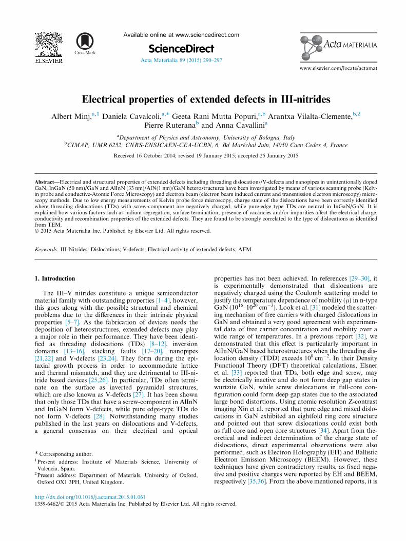
EBIC maps were obtained on the GaN sample, oneexample for an incident beam energy of 3.5 keV is shownin Fig. 2. The energy dissipation volume, as extracted fromMonte Carlo simulation, shows that at this bias the maxi-mum amount of energy is dissipated within a layer 55 nmdeep from the Au/GaN interface. Dark EBIC contrast cor-responds to local enhancement of electron hole recombina-tion, i.e. in the present case, it should occur at TDs.However, the TDs are no larger than few nm, well beyondthe sensitivity limit of the method. Therefore, EBIC
contrast can here be related mainly to local variations inthe barrier height. As proposed in reference [43], the EBICcurrent gain G (defined as the ratio of the EBIC currentdivided by the beam current) for an incident electron beamenergy E is given by:
G ¼ E2e
1þ a2ð3� aÞ4
� �ð2Þ
where a ¼ 2WRP
with W the depletion width and Rp the mean
electron range. The depletion width W for a Schottky junc-tion is given by:
W ¼ffiffiffiffiffiffiffiffiffiffiffiffi2eS/B
qN d
sð3Þ
A. Minj et al. / Acta Materialia 89 (2015) 290–297 293
here es is the static dielectric permittivity of GaN, /B is theSchottky barrier height and Nd is the donor concentration(�1017 cm�3). For a /B of �1.6 eV in a defect free area anda reduced /B of �0.6 eV at the V-defect, from Eq. (3) thedepletion width is assessed to be 62% lower at the V-defect.Thus, one would obtain a significant lowering of the cur-rent gain at the V defect with respect to the defect-free sur-face. This suggests that V-shaped defects, whose spatialextension is larger than TDs, can be the main cause of verylow surface potential and localized high conductivity inGaN.
3.2. Scanning probe studies on InxGa1 � xN
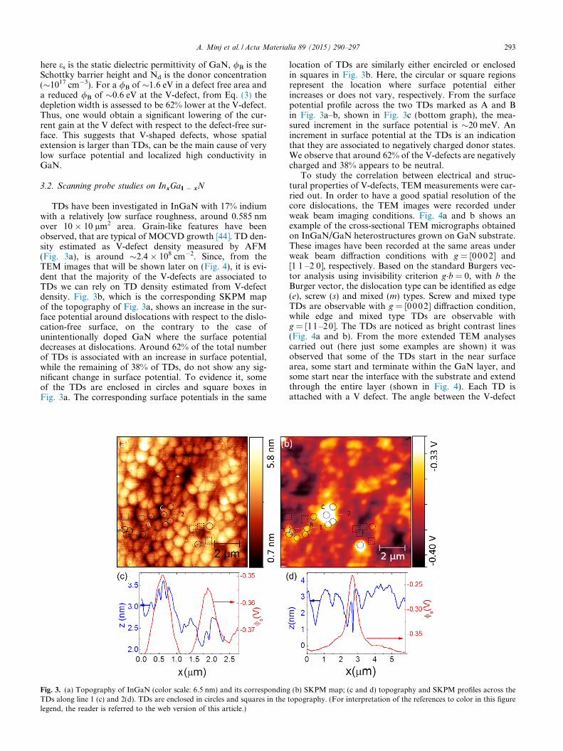
TDs have been investigated in InGaN with 17% indiumwith a relatively low surface roughness, around 0.585 nmover 10 � 10 lm2 area. Grain-like features have beenobserved, that are typical of MOCVD growth [44]. TD den-sity estimated as V-defect density measured by AFM(Fig. 3a), is around �2.4 � 108 cm�2. Since, from theTEM images that will be shown later on (Fig. 4), it is evi-dent that the majority of the V-defects are associated toTDs we can rely on TD density estimated from V-defectdensity. Fig. 3b, which is the corresponding SKPM mapof the topography of Fig. 3a, shows an increase in the sur-face potential around dislocations with respect to the dislo-cation-free surface, on the contrary to the case ofunintentionally doped GaN where the surface potentialdecreases at dislocations. Around 62% of the total numberof TDs is associated with an increase in surface potential,while the remaining of 38% of TDs, do not show any sig-nificant change in surface potential. To evidence it, someof the TDs are enclosed in circles and square boxes inFig. 3a. The corresponding surface potentials in the same
Fig. 3. (a) Topography of InGaN (color scale: 6.5 nm) and its correspondingTDs along line 1 (c) and 2(d). TDs are enclosed in circles and squares in thelegend, the reader is referred to the web version of this article.)
location of TDs are similarly either encircled or enclosedin squares in Fig. 3b. Here, the circular or square regionsrepresent the location where surface potential eitherincreases or does not vary, respectively. From the surfacepotential profile across the two TDs marked as A and Bin Fig. 3a–b, shown in Fig. 3c (bottom graph), the mea-sured increment in the surface potential is �20 meV. Anincrement in surface potential at the TDs is an indicationthat they are associated to negatively charged donor states.We observe that around 62% of the V-defects are negativelycharged and 38% appears to be neutral.
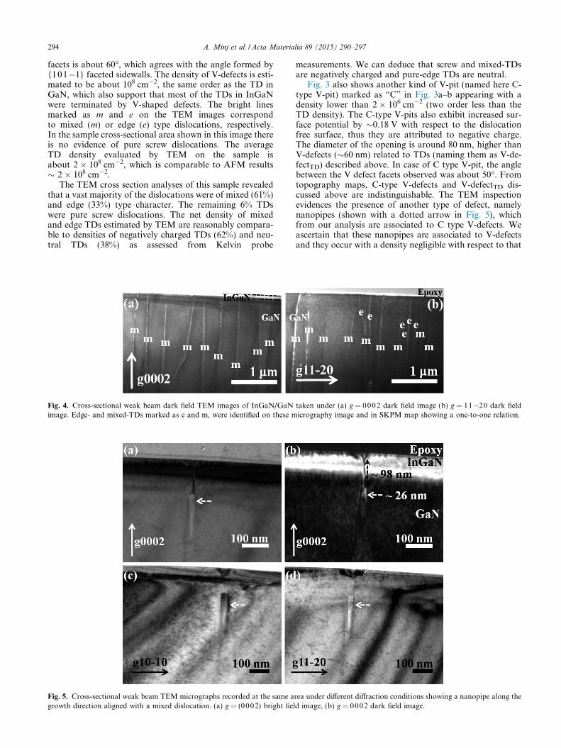
To study the correlation between electrical and struc-tural properties of V-defects, TEM measurements were car-ried out. In order to have a good spatial resolution of thecore dislocations, the TEM images were recorded underweak beam imaging conditions. Fig. 4a and b shows anexample of the cross-sectional TEM micrographs obtainedon InGaN/GaN heterostructures grown on GaN substrate.These images have been recorded at the same areas underweak beam diffraction conditions with g = [0002] and[1 1 –2 0], respectively. Based on the standard Burgers vec-tor analysis using invisibility criterion g�b = 0, with b theBurger vector, the dislocation type can be identified as edge(e), screw (s) and mixed (m) types. Screw and mixed typeTDs are observable with g = [0002] diffraction condition,while edge and mixed type TDs are observable withg = [11–20]. The TDs are noticed as bright contrast lines(Fig. 4a and b). From the more extended TEM analysescarried out (here just some examples are shown) it wasobserved that some of the TDs start in the near surfacearea, some start and terminate within the GaN layer, andsome start near the interface with the substrate and extendthrough the entire layer (shown in Fig. 4). Each TD isattached with a V defect. The angle between the V-defect
(b) SKPM map; (c and d) topography and SKPM profiles across thetopography. (For interpretation of the references to color in this figure
294 A. Minj et al. / Acta Materialia 89 (2015) 290–297
facets is about 60�, which agrees with the angle formed by{101�1} faceted sidewalls. The density of V-defects is esti-mated to be about 108 cm�2, the same order as the TD inGaN, which also support that most of the TDs in InGaNwere terminated by V-shaped defects. The bright linesmarked as m and e on the TEM images correspondto mixed (m) or edge (e) type dislocations, respectively.In the sample cross-sectional area shown in this image thereis no evidence of pure screw dislocations. The averageTD density evaluated by TEM on the sample isabout 2 � 108 cm�2, which is comparable to AFM results� 2 � 108 cm�2.
The TEM cross section analyses of this sample revealedthat a vast majority of the dislocations were of mixed (61%)and edge (33%) type character. The remaining 6% TDswere pure screw dislocations. The net density of mixedand edge TDs estimated by TEM are reasonably compara-ble to densities of negatively charged TDs (62%) and neu-tral TDs (38%) as assessed from Kelvin probe
Fig. 4. Cross-sectional weak beam dark field TEM images of InGaN/GaNimage. Edge- and mixed-TDs marked as e and m, were identified on these m
Fig. 5. Cross-sectional weak beam TEM micrographs recorded at the same agrowth direction aligned with a mixed dislocation. (a) g = (0002) bright fiel
measurements. We can deduce that screw and mixed-TDsare negatively charged and pure-edge TDs are neutral.
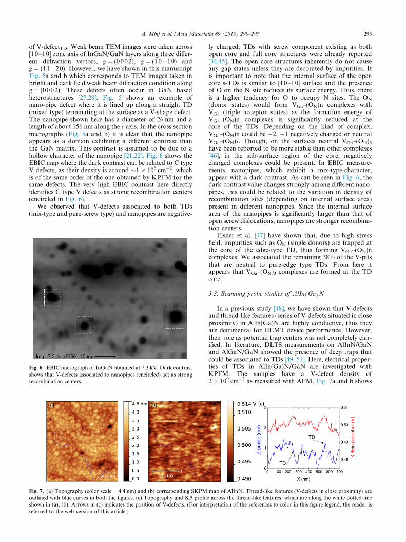
Fig. 3 also shows another kind of V-pit (named here C-type V-pit) marked as “C” in Fig. 3a–b appearing with adensity lower than 2 � 106 cm�2 (two order less than theTD density). The C-type V-pits also exhibit increased sur-face potential by �0.18 V with respect to the dislocationfree surface, thus they are attributed to negative charge.The diameter of the opening is around 80 nm, higher thanV-defects (�60 nm) related to TDs (naming them as V-de-fectTD) described above. In case of C type V-pit, the anglebetween the V defect facets observed was about 50�. Fromtopography maps, C-type V-defects and V-defectTD dis-cussed above are indistinguishable. The TEM inspectionevidences the presence of another type of defect, namelynanopipes (shown with a dotted arrow in Fig. 5), whichfrom our analysis are associated to C type V-defects. Weascertain that these nanopipes are associated to V-defectsand they occur with a density negligible with respect to that
taken under (a) g = 0002 dark field image (b) g = 11�20 dark fieldicrography image and in SKPM map showing a one-to-one relation.
rea under different diffraction conditions showing a nanopipe along thed image, (b) g = 0002 dark field image.
A. Minj et al. / Acta Materialia 89 (2015) 290–297 295
of V-defectTD. Weak beam TEM images were taken across[10–10] zone axis of InGaN/GaN layers along three differ-ent diffraction vectors, g = (0002), g = (10�10) andg = (11�20). However, we have shown in this manuscriptFig. 5a and b which corresponds to TEM images taken inbright and dark field weak beam diffraction condition alongg = (0002). These defects often occur in GaN basedheterostructures [27,28]. Fig. 5 shows an example ofnano-pipe defect where it is lined up along a straight TD(mixed type) terminating at the surface as a V-shape defect.The nanopipe shown here has a diameter of 26 nm and alength of about 156 nm along the c axis. In the cross sectionmicrographs (Fig. 5a and b) it is clear that the nanopipeappears as a domain exhibiting a different contrast thanthe GaN matrix. This contrast is assumed to be due to ahollow character of the nanopipe [21,22]. Fig. 6 shows theEBIC map where the dark contrast can be related to C typeV defects, as their density is around �1 � 106 cm�2, whichis of the same order of the one obtained by KPFM for thesame defects. The very high EBIC contrast here directlyidentifies C type V defects as strong recombination centers(encircled in Fig. 6).
We observed that V-defects associated to both TDs(mix-type and pure-screw type) and nanopipes are negative-
Fig. 6. EBIC micrograph of InGaN obtained at 7.3 kV. Dark contrastshows that V-defects associated to nanopipes (encircled) act as strongrecombination centers.
Fig. 7. (a) Topography (color scale = 4.4 nm) and (b) corresponding SKPMoutlined with blue curves in both the figures. (c) Topography and KP profilshown in (a), (b). Arrows in (c) indicates the position of V-defects. (For intereferred to the web version of this article.)
ly charged. TDs with screw component existing as bothopen core and full core structures were already reported[34,45]. The open core structures inherently do not causeany gap states unless they are decorated by impurities. Itis important to note that the internal surface of the opencore s-TDs is similar to [10–10] surface and the presenceof O on the N site reduces its surface energy. Thus, thereis a higher tendency for O to occupy N sites. The ON
(donor states) would form VGa–(ON)n complexes withVGa (triple acceptor states) as the formation energy ofVGa–(ON)n complexes is significantly reduced at thecore of the TDs. Depending on the kind of complex,VGa–(ON)n could be �2, �1 negatively charged or neutralVGa–(ON)3. Though, on the surfaces neutral VGa–(ON)3
have been reported to be more stable than other complexes[46], in the sub-surface region of the core, negativelycharged complexes could be present. In EBIC measure-ments, nanopipes, which exhibit a mix-type-character,appear with a dark contrast. As can be seen in Fig. 6, thedark-contrast value changes strongly among different nano-pipes, this could be related to the variation in density ofrecombination sites (depending on internal surface area)present in different nanopipes. Since the internal surfacearea of the nanopipes is significantly larger than that ofopen screw dislocations, nanopipes are stronger recombina-tion centers.
Elsner et al. [47] have shown that, due to high stressfield, impurities such as ON (single donors) are trapped atthe core of the edge-type TD, thus forming VGa–(ON)ncomplexes. We associated the remaining 38% of the V-pitsthat are neutral to pure-edge type TDs. From here itappears that VGa–(ON)3 complexes are formed at the TDcore.
3.3. Scanning probe studies of AlIn(Ga)N
In a previous study [48], we have shown that V-defectsand thread-like features (series of V-defects situated in closeproximity) in AlIn(Ga)N are highly conductive, thus theyare detrimental for HEMT device performance. However,their role as potential trap centers was not completely clar-ified. In literature, DLTS measurements on AlInN/GaNand AlGaN/GaN showed the presence of deep traps thatcould be associated to TDs [49–51]. Here, electrical proper-ties of TDs in AlIn(Ga)N/GaN are investigated withKPFM. The samples have a V-defect density of2 � 109 cm�2 as measured with AFM. Fig. 7a and b shows
map of AlInN. Thread-like features (V-defects in close proximity) aree across the thread-like features, which are along the white dotted-linerpretation of the references to color in this figure legend, the reader is
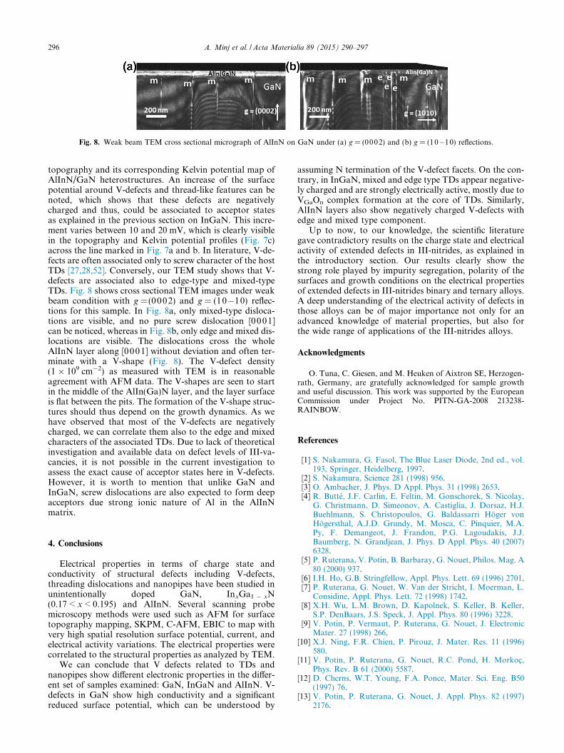
Fig. 8. Weak beam TEM cross sectional micrograph of AlInN on GaN under (a) g = (0002) and (b) g = (10�10) reflections.
296 A. Minj et al. / Acta Materialia 89 (2015) 290–297
topography and its corresponding Kelvin potential map ofAlInN/GaN heterostructures. An increase of the surfacepotential around V-defects and thread-like features can benoted, which shows that these defects are negativelycharged and thus, could be associated to acceptor statesas explained in the previous section on InGaN. This incre-ment varies between 10 and 20 mV, which is clearly visiblein the topography and Kelvin potential profiles (Fig. 7c)across the line marked in Fig. 7a and b. In literature, V-de-fects are often associated only to screw character of the hostTDs [27,28,52]. Conversely, our TEM study shows that V-defects are associated also to edge-type and mixed-typeTDs. Fig. 8 shows cross sectional TEM images under weakbeam condition with g =(0 002) and g = (10�10) reflec-tions for this sample. In Fig. 8a, only mixed-type disloca-tions are visible, and no pure screw dislocation [0001]can be noticed, whereas in Fig. 8b, only edge and mixed dis-locations are visible. The dislocations cross the wholeAlInN layer along [0001] without deviation and often ter-minate with a V-shape (Fig. 8). The V-defect density(1 � 109 cm�2) as measured with TEM is in reasonableagreement with AFM data. The V-shapes are seen to startin the middle of the AlIn(Ga)N layer, and the layer surfaceis flat between the pits. The formation of the V-shape struc-tures should thus depend on the growth dynamics. As wehave observed that most of the V-defects are negativelycharged, we can correlate them also to the edge and mixedcharacters of the associated TDs. Due to lack of theoreticalinvestigation and available data on defect levels of III-va-cancies, it is not possible in the current investigation toassess the exact cause of acceptor states here in V-defects.However, it is worth to mention that unlike GaN andInGaN, screw dislocations are also expected to form deepacceptors due strong ionic nature of Al in the AlInNmatrix.
4. Conclusions
Electrical properties in terms of charge state andconductivity of structural defects including V-defects,threading dislocations and nanopipes have been studied inunintentionally doped GaN, InxGa1 � xN(0.17 < x < 0.195) and AlInN. Several scanning probemicroscopy methods were used such as AFM for surfacetopography mapping, SKPM, C-AFM, EBIC to map withvery high spatial resolution surface potential, current, andelectrical activity variations. The electrical properties werecorrelated to the structural properties as analyzed by TEM.
We can conclude that V defects related to TDs andnanopipes show different electronic properties in the differ-ent set of samples examined: GaN, InGaN and AlInN. V-defects in GaN show high conductivity and a significantreduced surface potential, which can be understood by
assuming N termination of the V-defect facets. On the con-trary, in InGaN, mixed and edge type TDs appear negative-ly charged and are strongly electrically active, mostly due toVGaOn complex formation at the core of TDs. Similarly,AlInN layers also show negatively charged V-defects withedge and mixed type component.
Up to now, to our knowledge, the scientific literaturegave contradictory results on the charge state and electricalactivity of extended defects in III-nitrides, as explained inthe introductory section. Our results clearly show thestrong role played by impurity segregation, polarity of thesurfaces and growth conditions on the electrical propertiesof extended defects in III-nitrides binary and ternary alloys.A deep understanding of the electrical activity of defects inthose alloys can be of major importance not only for anadvanced knowledge of material properties, but also forthe wide range of applications of the III-nitrides alloys.
Acknowledgments
O. Tuna, C. Giesen, and M. Heuken of Aixtron SE, Herzogen-rath, Germany, are gratefully acknowledged for sample growthand useful discussion. This work was supported by the EuropeanCommission under Project No. PITN-GA-2008 213238-RAINBOW.
References
[1] S. Nakamura, G. Fasol, The Blue Laser Diode, 2nd ed., vol.193, Springer, Heidelberg, 1997.
[2] S. Nakamura, Science 281 (1998) 956.[3] O. Ambacher, J. Phys. D Appl. Phys. 31 (1998) 2653.[4] R. Butte, J.F. Carlin, E. Feltin, M. Gonschorek, S. Nicolay,
G. Christmann, D. Simeonov, A. Castiglia, J. Dorsaz, H.J.Buehlmann, S. Christopoulos, G. Baldassarri Hoger vonHogersthal, A.J.D. Grundy, M. Mosca, C. Pinquier, M.A.Py, F. Demangeot, J. Frandon, P.G. Lagoudakis, J.J.Baumberg, N. Grandjean, J. Phys. D Appl. Phys. 40 (2007)6328.
[5] P. Ruterana, V. Potin, B. Barbaray, G. Nouet, Philos. Mag. A80 (2000) 937.
[6] I.H. Ho, G.B. Stringfellow, Appl. Phys. Lett. 69 (1996) 2701.[7] P. Ruterana, G. Nouet, W. Van der Stricht, I. Moerman, L.
Considine, Appl. Phys. Lett. 72 (1998) 1742.[8] X.H. Wu, L.M. Brown, D. Kapolnek, S. Keller, B. Keller,
S.P. DenBaars, J.S. Speck, J. Appl. Phys. 80 (1996) 3228.[9] V. Potin, P. Vermaut, P. Ruterana, G. Nouet, J. Electronic
Mater. 27 (1998) 266.[10] X.J. Ning, F.R. Chien, P. Pirouz, J. Mater. Res. 11 (1996)
580.[11] V. Potin, P. Ruterana, G. Nouet, R.C. Pond, H. Morkoc,
Phys. Rev. B 61 (2000) 5587.[12] D. Cherns, W.T. Young, F.A. Ponce, Mater. Sci. Eng. B50
(1997) 76.[13] V. Potin, P. Ruterana, G. Nouet, J. Appl. Phys. 82 (1997)
2176.
A. Minj et al. / Acta Materialia 89 (2015) 290–297 297
[14] J. Jasinski, Z. Liliental-Weber, Q.S. Paduano, D.W. Wey-burne, Appl. Phys. Lett. 83 (2003) 2811.
[15] V. Potin, G. Nouet, P. Ruterana, Appl. Phys. Lett. 74 (1999)947.
[16] J. Jasinski, Z. Liliental-Weber, H. Lu, W.J. Schaff, Appl.Phys. Lett. 85 (2004) 233.
[17] V. Potin, P. Ruterana, G. Nouet, J. Phys. Condens. Matter 12(2000) 10301.
[18] P. Vermaut, P. Ruterana, G. Nouet, H. Morkoc, Philos. Mag.A 75 (1997) 239.
[19] P. Ruterana, B. Barbaray, A. Bere, P. Vermaut, A. Hairie, E.Paumier, G. Nouet, A. Salvador, A. Botchkarev, H. Morkoc,Phys. Rev. B 59 (1999) 15917–15925.
[20] P. Vermaut, G. Nouet, P. Ruterana, Appl. Phys. Lett. 74(1999) 694.
[21] F. Pailloux, J. Colin, J.F. Barbot, J. Grilhe, Appl. Phys. Lett.86 (2005) 131908.
[22] M.E. Hawkridge, Z. Liliental-Weber, H.J. Kim, S. Choi, D.Yoo, J.-H. Ryou, R.D. Dupuis, Appl. Phys. Lett. 94 (2009)171912.
[23] C.J. Sun, M. Zubair Anwar, Q. Chen, J.W. Yang, M. AsifKhan, M.S. Shur, A.D. Bykhovski, Z. Liliental-Weber, C.Kisielowski, M. Smith, J.Y. Lin, H.X. Xiang, Appl. Phys.Lett. 70 (1997) 2978.
[24] A. Hangleiter, F. Hitzel, C. Netzel, D. Fuhrmann, U.Rossow, G. Ade, P. Hinze, Phys. Rev. Lett. 95 (2005) 127402.
[25] Y.-Y. Wong, E.Y. Chang, T.-H. Yang, J.-R. Chang, J.-T. Ku,M.K. Hudait, W.-C. Chou, M. Chen, K.-L. Lin, J. Elec-trochem. Soc. 157 (7) (2010) H746–H749.
[26] D.S. Li, H. Chen, H.B. Yu, H.Q. Jia, Q. Huang, J.M. Zhou, J.Appl. Phys. 96 (2004) 1111.
[27] A. Mouti, J.L. Rouviere, M. Cantoni, J.F. Carlin, E. Feltin,N. Grandjean, P. Stadelmann, Phys. Rev. B 83 (2011) 195309.
[28] Th. Kehagias, G.P. Dimitrakopulos, J. Kioseoglou, H.Kirmse, C. Giesen, M. Heuken, A. Georgakilas, W. Neu-mann, Th. Karakostas, Ph. Komninou, Appl. Phys. Lett. 95(2009) 071905.
[29] H.M. Ng, D. Doppalapudi, T.D. Moustakas, N.G. Weimann,L.F. Eastman, Appl. Phys. Lett. 73 (1998) 821–823.
[30] Nils G. Weimann, Lester F. Eastman, Dharanipal. Doppala-pudi, Hock M. Ng, Theodore D. Moustakas, J. Appl. Phys.83 (1998) 3656.
[31] D.C. Look, J.R. Sizelove, Phys. Rev. Lett. 82 (1999) 1237.[32] S. Pandey, D. Cavalcoli, A. Minj, B. Fraboni, A. Cavallini, D.
Skuridina, P. Vogt, M. Kneissl, Acta Mater. 60 (2012) 3176–3180.
[33] J. Elsner, R. Jones, P.K. Sitch, V.D. Porezag, M. Elstner, Th.Frauenheim, M.I. Heggie, S. Oberg, P.R. Briddon, Phys. Rev.Lett. 79 (1997) 3672.
[34] Y. Xin, S.J. Pennycook, N.D. Browning, S. Sivananthan, F.Omne’s, B. Beaumont, J.P. Faurie, P. Gibart, Appl. Phys.Lett. 72 (1998) 2680.
[35] H.-J. Im, Y. Ding, J.P. Pelz, B. Heying, J.S. Speck, Phys. Rev.Lett. 87 (2001) 106802.
[36] D. Cherns, C.G. Jiao, Phys. Rev. Lett. 87 (2001) 205504.[37] A. Vilalta-Clemente, M.A. Poisson, H. Behmenburg, C.
Giesen, M. Heuken, P. Ruterana, Phys. Stat. Solidi A 207(2010) 1105–1108.
[38] B.S. Simpkins, D.M. Schaadt, E.T. Yu, R.J. Molnar, J. Appl.Phys. 91 (2002) 9924.
[39] K. Hiramatsu, K. Nishiyama, A. Motogaito, H. Miyake, Y.Iyechika, T. Maeda, Phys. Stat. Solidi (A) 176 (1999) 535.
[40] U. Grossner, J. Furthmueller, F. Bechstedt, Phys. Stat. Solidi(B) 216 (1999) 675.
[41] A.L. Rosa, J. Neugebauer, Phys. Rev. B 73 (2006) 205346.[42] A. Lochthofen, W. Mertin, G. Bacher, L. Hoeppel, S. Bader,
J. Off, B. Hahn, Appl. Phys. Lett. 93 (2008) 022107.[43] J.M. Gibson, D.C. Joy, R.T. Tung, J.L. Ellison, C. Pimentel,
A.F.J. Levi, Mater. Res. Soc. Symp. Proc. 56 (1986) 163.[44] R.A. Oliver, M.J. Kappers, C.J. Humphreys, G. Andrew, D.
Briggs, J. Appl. Phys. 97 (2005) 013707.[45] W. Qian, G.S. Rohrer, M. Skowronski, K. Doverspike, L.B.
Rowland, D.K. Gaskill, Appl. Phys. Lett. 67 (1995) 2284.[46] J. Elsner, R. Jones, M. Haugk, R. Gutierrez, Th. Frauenheim,
M.I. Heggie, S. Uberg, P.R. Briddon, Appl. Phys. Lett. 73(1998) 3530.
[47] J. Elsner, R. Jones, M.I. Heggie, P.K. Sitch, M. Haugk, Th.Frauenheim, S. Oberg, P.R. Briddon, Phys. Rev. B 58 (1998)12571–12574.
[48] A. Minj, D. Cavalcoli, A. Cavallini, Appl. Phys. Lett. 97(2010) 132114.
[49] W. Chikhaoui, J.-M. Bluet, M.-A. Poisson, N. Sarazin, C.Dua, C. Bru-Chevallier, Appl. Phys. Lett. 96 (2010) 072107.
[50] Z.-Q. Fang, D.C. Look, D.H. Kim, I. Adesida, Appl. Phys.Lett. 87 (2005) 182115.
[51] Z.-Q. Fang, B. Claflin, D.C. Look, D.S. Green, R. Vetury, J.Appl. Phys. 108 (2010) 063706.
[52] L. Zhou, M.R. McCartney, D.J. Smith, A. Mouti, E. Feltin,J.F. Carlin, N. Grandjean, Appl. Phys. Lett. 97 (2010)161902.