Electrical overstress (EOS) power profiles: A guideline to qualify EOS hardness of semiconductor...
16
Journal of Electrostatics, 31 (1993) 161-176 161 Elsevier Electrical overstress (EOS) power profiles: A guideline to qualify EOS of semiconductor devices hardness Carlos Diaz, a Sung-Mo Kang a, a University of Illinois at Urbana-Champaign, Coordinated Science Laboratory, 1308 West Main Street, Urbana, IL 61801, USA Charvaka Duvvury b and Larry Wagner b bTexas Instruments Incorporated, M/S 461, P.O. Box 655012, Dallas, TX 75265, USA (Received October 13, 1992; accepted in revised form April 6, 1993) Summary We propose the power-to-failure vs. time-to-failure relationship (power profile) as a measure to determine the EOS hardness of integrated circuits. Bipolar integrated circuits with different I/O ESD protection designs were characterized for HBM-ESD and EOS under unipolar stress conditions. Measured power profiles indicate that good ESD performance is not a sufficient condition to assure EOS robustness. Furthermore, experimentally measured power profiles together with failure analysis techniques can pinpoint layout design weak- nesses. 1. Introduction Semiconductor devices have a limited ability to survive electrical overstress (EOS). EOS embodies a broad category of electrical threats to semiconductor devices including electromagnetic pulses (EMP), electrostatic discharge (ESD), system transients, lightning, etc, EOS-related failures in semiconductor devices can be classified according to their primary failure mechanisms into (i) thermally induced failures and (ii) high-field related failures [1, 2]. In general, thermally induced failures are related to the device area and the junction depth while electric field induced failures are related to the oxide thickness. Therefore, device susceptibility to EOS increases as the device size is shrunk. © 1992. Reprinted with permission, after revision, from Electrical Overstress/Electrostatic Discharge Symposium Proceedings, EOS-14, Dallas, TX, USA, September 16-18, 1992. 0304-3886/93/$06.00 © 1993 Elsevier Science Publishers B.V. All rights reserved.
-
Upload
udistrital -
Category
Documents
-
view
1 -
download
0
Transcript of Electrical overstress (EOS) power profiles: A guideline to qualify EOS hardness of semiconductor...
Journal of Electrostatics, 31 (1993) 161-176 161 Elsevier
Electrical overstress (EOS) power profiles: A guideline to qualify EOS of semiconductor devices
hardness
Car los Diaz, a Sung-Mo K a n g a,
a University of Illinois at Urbana-Champaign, Coordinated Science Laboratory, 1308 West Main Street, Urbana, IL 61801, USA
C h a r v a k a D u v v u r y b and L a r r y W a g n e r b
bTexas Instruments Incorporated, M/S 461, P.O. Box 655012, Dallas, TX 75265, USA
(Received October 13, 1992; accepted in revised form April 6, 1993)
S u m m a r y
We propose the power-to-failure vs. time-to-failure relationship (power profile) as a measure to determine the EOS hardness of integrated circuits. Bipolar integrated circuits with different I/O ESD protection designs were characterized for HBM-ESD and EOS under unipolar stress conditions. Measured power profiles indicate that good ESD performance is not a sufficient condition to assure EOS robustness. Furthermore, experimentally measured power profiles together with failure analysis techniques can pinpoint layout design weak- nesses.
1. Introduct ion
S e m i c o n d u c t o r devices have a l imited abi l i ty to su rv ive e lec t r ica l overs t ress (EOS). EOS embodies a b road ca t ego ry of e lec t r ica l t h r e a t s to s emiconduc to r devices inc lud ing e l ec t romagne t i c pulses (EMP), e l ec t ros ta t i c d i scharge (ESD), sys tem t rans ien t s , l ightn ing, etc, EOS-re la ted fa i lures in s emiconduc to r devices can be classified accord ing to the i r p r i m a r y fa i lu re m e c h a n i s m s into (i) t h e r m a l l y induced fa i lures and (ii) high-field r e l a t ed fa i lures [1, 2]. In genera l , t h e r m a l l y induced fa i lures a re r e l a t ed to the device a r ea and the j unc t ion dep th whi le e lect r ic field induced fa i lures a re re la ted to the oxide th ickness . Therefore , device suscept ib i l i ty to EOS inc reases as the device size is sh runk .
© 1992. Reprinted with permission, after revision, from Electrical Overstress/Electrostatic Discharge Symposium Proceedings, EOS-14, Dallas, TX, USA, September 16-18, 1992.
0304-3886/93/$06.00 © 1993 Elsevier Science Publishers B.V. All rights reserved.

162 C. D~az et al./EOS hardness of integrated Circuits
At present, EOS is one of the major causes for IC failure [3, 4]. Published reports on IC failures in military equipment indicate that nearly 50% of them can be attributed to EOS events. Hence, it is imperative for industry to account for the EOS threat early in the design process. Among the EOS categories, ESD has been a major concern in the IC industry since the mid 70s. Extensive research in ESD phenomena has led to the standardization in 1980 of test methods to evaluate ESD sensitivity based on the Human Body Model (HMB) [5]. ESD protection is achieved by on-chip special purpose circuits located in the chip I/O frame. The ESD-HBM failure thresholds for these structures have increased from nearly 2 kV in the early 80's [6] to approximately 6 kV by 1990 [7, 8]. The adoption of the HBM-ESD standard has served as a driving force for improved on-chip ESD protection.
Unfortunately, ESD-HBM events represent only a small portion of the whole EOS phenomena. Characteristic failure times for EOS events might be as high as several tenths of a millisecond compared to ESD-HBM time constant that falls in the sub-microsecond domain. Therefore, even with the best on-chip ESD protection structures available today, one cannot expect to have adequate overall EOS protection. In other words, although stringent ESD specifications are important they are not sufficient to assure that devices are also EOS resistant. Thus, there is a need for a measure of EOS robustness for integrated circuits.
A fundamental understanding of EOS and ESD failures is very much re- quired nowadays. In our ongoing EOS/ESD project [4], we have taken a step by step approach to the problem. We began looking for EOS/ESD related domain failure mechanisms across the various IC product families. Then, a set of EOS/ESD susceptible devices that could be tested in volume (low cost) was defined. A test method was specified to consistently reproduce observed field failures in those devices. We chose to begin our study with unipolar positive stress waveforms applied to the input and output protection transistors present in those ICs. One reason for this is that under reverse bias conditions the protection transistors have the highest power dissipation (self-heating) condi- tions that eventually might lead to thermal runaway and device failure. Another reason is that if one intends to unveil and understand the failure process under any bipolar stress event, one first needs to know precisely the phenomena leading to device failure for each stress polarity independently. Thus, all the results reported in this paper are based on unipolar positive stress events applied to the I/O protection transistors found in ICs fabricated in a primary bipolar technology. In this paper, we propose that the failure power profile be used as the design specification that accounts for the IC susceptibil- ity to EOS events. This proposal is based on the results of the following three main tasks: (i) EOS/ESD failure mode distribution studies across different products, (ii) feasibility studies to reproduce EOS related field fail- ures, and (iii) qualification of the power-to-failure vs. time-to-failure relation- ship [9] as a figure of merit to quantify EOS/ESD hardness of semiconductor devices.

C. Dfaz et al./EOS hardness of integrated Circuits 163
2. Distribution of EOS/ESD-related failures
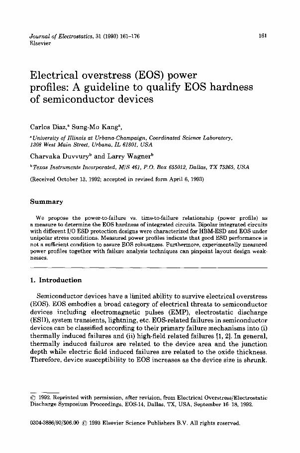
The impact of EOS/ESD phenomena on different IC products was quantified using extensive failure analysis (FA) data compiled at Texas Instruments Inc. The analysis of the database was done at different levels, namely (i) product group level, (ii) product subgroup level, and (iii) device type level. To illustrate the analysis done, we present two particular views of the database at the product level. The impact of EOS/ESD phenomena on the failure rates for each product group was measured as the ratio between the number of EOS/ESD- related failures and the total number of failures. Figure I shows the percentage of the failures that can be attributed to EOS/ESD for various product groups. This figure reveals the relative magnitude of the EOS/ESD problem when compared to assembly, wafer-fab, design, and other sources of failures. For example, Fig. 1 indicates that nearly 27% of the failures in the product family A were attributed to EOS/ESD. The database also allowed us to identify the percentage of EOS/ESD-related cases that received FA per customer request. Figure 2 shows a typical result from this type of analysis at the product group level. For example, for product family A nearly 65% out of the total 27% EOS/ESD failures received FA originated by a customer request.
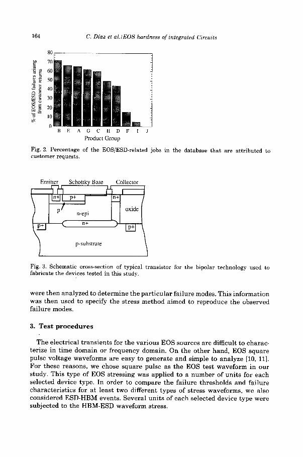
Similar analyses were done at the device type level. A ranking of products (by device-type) was obtained by querying the database at the device level to identify those most affected by EOS/ESD. This and the constraint of low part cost to allow volume testing, led to identification of four different device types (C1, C2, C3, and C4) from a representative product group (C) as the test vehicles for this study. These devices are fabricated in a standard bipolar process. A schematic corss-section of a typical bipolar transistor in this process is shown in Fig. 3.
For the selected devices, database information revealed that junction burn- out was the dominant EOS-related failure mechanism. The detailed FA reports
30
25
20
~ 10
5
0 A B C D E F G H I J
Product Group
Fig. 1. Relative impact of EOS/ESD phenomena on product group failure mechanisms.
164 C. Diaz et al./EOS hardness of integrated Circuits
8O
=~ 70 i N
50 ~ ~ 40
l 0 0
B E A G C H D F I J Product Group
Fig. 2. Percentage of the EOS/ESD-related jobs in the database that are attributed to customer requests.
Emitter
° ' p!
(
Schottky Base Collector
P+ ] ' ~ oxide n-epi
n+
p-substrate
Fig. 3. Schemat ic cross-sect ion of typica l t r a n s i s t o r for the b ipo la r t echno logy used to fabr ica te the devices tes ted in th i s study.
were then analyzed to de te rmine the pa r t i cu l a r fa i lure modes. This in format ion was then used to specify the stress me thod aimed to reproduce the observed fa i lure modes.
3. Test procedures
The e lect r ica l t r ans ien t s for the var ious EOS sources are difficult to charac- terize in t ime domain or f requency domain. On the o the r hand, EOS square pulse vol tage waveforms are easy to genera te and simple to ana lyze [10, 11]. For these reasons, we chose square pulse as the EOS test waveform in our study. This type of EOS stressing was applied to a number of uni ts for each selected device type. In order to compare the fa i lure thresholds and fa i lure charac te r i s t i c s for at least two different types of stress waveforms, we also cons idered ESD-HBM events. Severa l uni ts of each selected device type were subjected to the HBM-ESD waveform stress.
C. Diaz et al./EOS hardness of integrated Circuits 165
Both EOS-square-pulse and HBM-ESD tests were performed on unpowered devices only, with all unstressed pins left floating. The stress polarity was always positive with respect to GND or VSS. HBM-ESD experiments were conducted using a KeyTek tester. Square pulse testing was done using either a HP214B pulse generator or a charged transmission line [TL] [12] as EOS sources. In particular, TL was used whenever high current (more than 2A) short duration pulses were required.
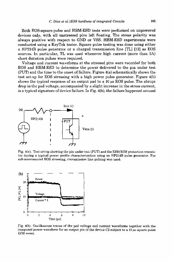
Voltage and current waveforms at the stressed pins were recorded for both EOS and HBM-ESD to determine the power delivered to the pin under test (PUT) and the time to the onset of failure. Figure 4(a) schematically shows the test set-up for EOS stressing with a high power pulse generator. Figure 4(b) shows the typical response of an output pad to a 10 #s EOS pulse. The abrupt drop in the pad voltage, accompanied by a slight increase in the stress current, is a typical signature of device failure. In Fig. 4(b), the failure happened around
Ieos (t) ( a )
/
+
Veos (t)
Fig. 4(a). Test set-up showing the pin under test (PUT) and the ESD/EOS protect ion transis- tor dur ing a typical power profile character iza t ion using an HP214B pulse generator. For sub-microsecond EOS stressing, t ransmission l ine pulsing was used.
(b) I 20 __ Power..., - -
10 .. . . . . . . .
0 0 2 4 6 8 10
Time [ps]
Fig. 4(b). Oscil loscope traces of the pad vol tage and current waveforms together wi th the computed power waveform for an output pin of the device C2 subject to a 10 #s square pulse EOS event.
166 C. Dfaz et al./EOS hardness of integrated Circuits
5.8 ps with a stress power level of approximately 19.8 W. Device failure was defined as a curve trace (CT) softening or short to VCC or GND of the stressed pin characteristics. It is important to mention that each zap was followed by a CT evaluation of the pin even if no failure signature was detected in the stress waveforms.
4. Measured power profiles
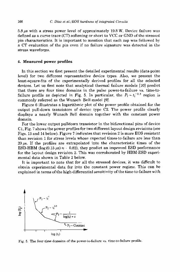
In this section we first present the detailed experimental results (data-point level) for two different representative device types. Also, we present the least-square-fits of the experimentally derived profiles for all the selected devices. Let us first note that analytical thermal failure models [10] predict that there are four time domains in the pulse power-to-failure vs. time-to- failure profile as depicted in Fig. 5. In particular, the P f ~ tf -°'5 region is commonly referred as the Wunsch-Bell model [9].
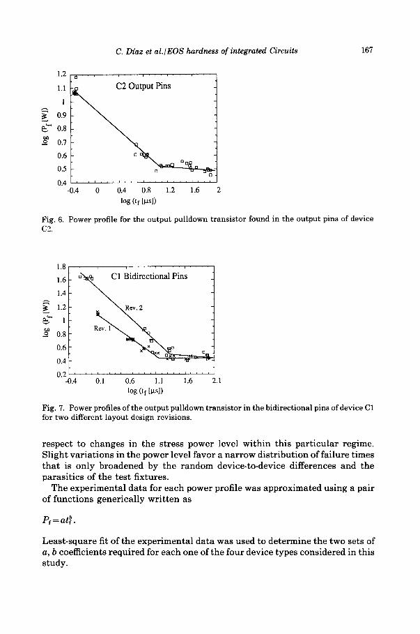
Figure 6 illustrates a logarithmic plot of the power profile obtained for the output pull-down transistors of device type C2. The power profile clearly displays a nearly Wunsch-Bell domain together with the constant power domain.
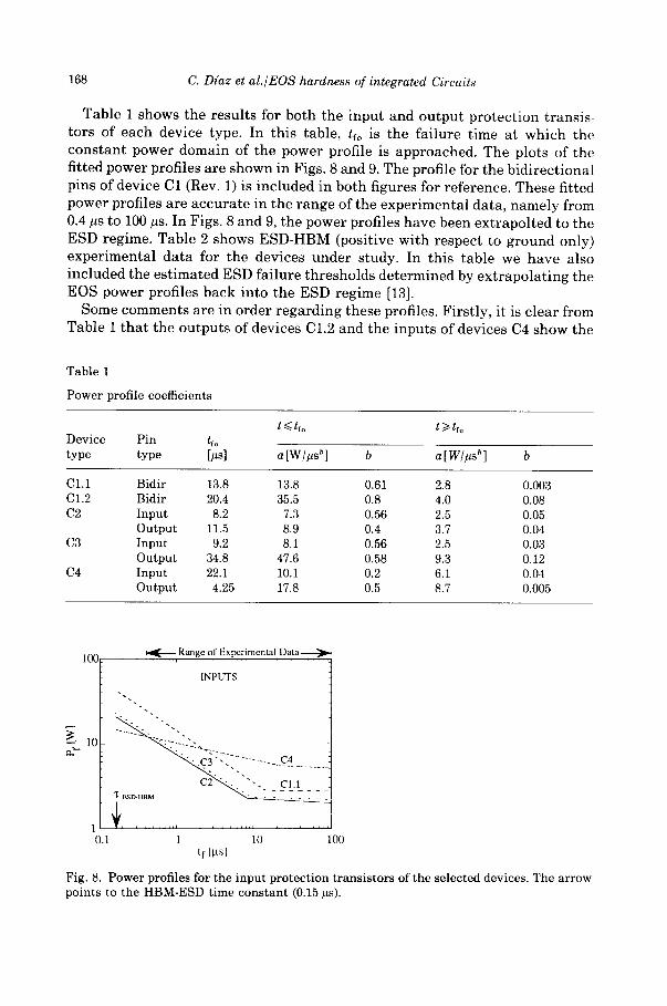
For the lower output pulldown transistor in the bidirectional pins of device C1, Fig. 7 shows the power profiles for two different layout design revisions (see Figs. 13 and 14 below). Figure 7 indicates that revision 2 is more EOS resistant than revision 1 for stress levels whose expected times-to-failure are less than 20#s. If the profiles are extrapolated into the characteristic times of the ESD-HBM (log (0.15 its)~ -0.82), they predict an improved ESD performance for the layout design revision 2. This was corroborated by HBM-ESD experi- mental data shown in Table 2 below.
It is important to note that for all the stressed devices, it was difficult to obtain experimental data far into the constant power regime. This can be explained in terms of the high-differential sensitivity of the time-to-failure with
P f - ti °5
-- log(tf)
Pf - Constant
' l o g ( t f ) I
Fig. 5, The four t ime d o m a i n s o f t h e power - to - f a i lu re vs. t ime- to - fa i lu re profile.
C. Dfaz et al./EOS hardness of integrated Circuits 167
1.1 ~ C2 Output Pins
1
0.9
~" 0.8
0.7
0.6
0.5
0.4 . . . . . . . . . . . . . . . . . . . . . . . -0.4 0 0.4 0.8 1.2 1.6
log (tf [Its])
Fig. 6. Power profile for the output pulldown transistor found in the output pins of device C2.
1 . 8 . . . . . . . . . . . . . . . . . . .
1.6 a ~ C1 Bidirectional Pins
1.4
0.8
0.6
0.4
0 . 2 , , , , i , ~ J , J , , i , , . . , . . . .
-0.4 0.1 0.6 1.1 1.6 2.1 log (tf [Its])
Fig. 7. Power profiles of the output pulldown transistor in the bidirectional pins of device C1 for two different layout design revisions.
respect to changes in the stress power level wi th in this par t i cu la r regime. Sl ight var ia t ions in the power level favor a na r row dis t r ibut ion of fai lure times tha t is only broadened by the r andom device-to-device differences and the paras i t ics of the test fixtures.
The exper imenta l da ta for each power profile was approximated using a pair of funct ions gener ica l ly wri t ten as
Pf=at~.
Least -square fit of the experimental da ta was used to determine the two sets of a, b coefficients required for each one of the four device types considered in this study.
168 C. Diaz et a l . /EOS hardness of integrated Circuits
Table 1 shows the results for both the input and output protection transis- tors of each device type. In this table, tfo is the failure time at which the constant power domain of the power profile is approached. The plots of the fitted power profiles are shown in Figs. 8 and 9. The profile for the bidirectional pins of device C1 (Rev. 1) is included in both figures for reference. These fitted power profiles are accurate in the range of the experimental data, namely from 0.4 ps to 100 ps. In Figs. 8 and 9, the power profiles have been extrapolted to the ESD regime. Table 2 shows ESD-HBM (positive with respect to ground only) experimental data for the devices under study. In this table we have also included the estimated ESD failure thresholds determined by extrapolating the EOS power profiles back into the ESD regime [13].
Some comments are in order regarding these profiles. Firstly, it is clear from Table 1 that the outputs of devices C1.2 and the inputs of devices C4 show the
Table 1
Power profile coefficients
t <. tfo t>~tfo Device Pin tfo type type [ps] a [W/ps b] b a[W/#s b] b
C1.1 Bidir 13.8 13.8 0.61 2.8 0.003 C1.2 Bidir 20.4 35.5 0.8 4.0 0.08 C2 Input 8.2 7.3 0.56 2.5 0.05
Output 11.5 8.9 0.4 3.7 0.04 C3 Input 9.2 8.1 0.56 2.5 0.03
Output 34.8 47.6 0.58 9.3 0.12 C4 Input 22.1 10.1 0.2 6.1 0.04
Output 4.25 17.8 0.5 8.7 0.005
100 ~q~----,Range of Experimental Data------~
INPUTS
C2
/
1 ~ ' ¢ . . . . . . . . ' . . . . . . . . ' . . . . . . .
0.1 1 10 100 tf [Its]
Fig. 8. Power profiles for the input protect ion transistors of the selected devices. The arrow points to the HBM-ESD time constant (0.15 #s).

C. Diaz et al./EOS hardness of integrated Circuits 169
1000 ~4~---,Range of Experimental Data----~l
OUTPUTS
+" " ~ e s i g n target"
10 ~ " "'::L'-~. - ..... " " " " " " ~ - - - - ~ - - : - . - - - - _ - w
~ E S D - H B M . . . . . . .
1 ~ , . . . . . . . t . . . . . . . . , . . . . . . .
0.1 1 10 100 tf [~ts]
Fig. 9. Power profiles of the output pulldown transistors for selected devices of the C product group.
Table 2
HBM-ESD failure thresholds
Input pins Output/Bidir pins
Device Measured Estimated" Measured Estimated a type [kV] [kV] [kV] [kV]
C1.1. 10.5 - - 6.5 6.9 C1.2 10.5 - - > 10 - - C2 3.2 3.0 3.5 2.7 C3 2.7 3.4 9.5 12.1 C4 2.0 1.0 7.0 8.6
"Assuming current follows a similar relationship as the power does.
l a rges t dev ia t ions f rom the typ ica l W u n s c h - B e l l dependence where the para- m e t e r b is expec ted to be a round - 0 . 5 . As shown by fa i lure analys is , the s t ressed t r ans i s t o r s in these pins exhibi t more t h a n one d o m i n a n t fa i lure m e c h a n i s m s thus exp la in ing the observed power profile behav iour . Secondly, Figs. 8 and 9 p rov ide us wi th an a s sessmen t of the re la t ive r e s i s t ance to EOS/ESD events by the di f ferent I /O c i rcui ts unde r the specified s t ress condi- t ions. Fo r example , in t e rms of the ou t pu t pin EOS/ESD robus tness , the pul l -down t r ans i s t o r s of device C3 requ i re h ighe r power levels in order to r each the onse t of fa i lu re wi th in t ime f rames less t h a n 20 gs. Thirdly , compar i son of ou tpu t and inpu t power profi les per device type ind ica tes t h a t the inpu t p ro t ec t ion c i rcui ts a re genera l ly more suscept ib le to the EOS/ESD d a m a g e t h a n the i r ou tpu t coun te rpa r t s . This is mos t ly due to the fact t h a t the dimen- s ions of the input p ro t ec t i on t r a n s i s t o r a re genera l ly smal le r t h a n the
170 C. Diaz et al./EOS hardness of integrated Circuits
corresponding output pulldown transistor dimensions in these particular devi- ces. Finally, these power profiles suggest that high ESD failure thresholds do not warrant EOS robustness. This is particularly true for devices whose power profiles exhibit a large roll-off slope before reaching the constant power regime as is the case for the inputs of device CI.1. One can see also from data in Table 2 and Fig. 9 that although the ESD performance for the lower output pulldown transistors in devices CI.1 and C4 is similar, the EOS performance is not and that indeed the output transistors in C4 outperform those in CI.1 for the EOS regime.
The thick solid line in Fig. 9 exemplifies a possible design target for overall EOS/ESD device resistance. For example, let us assume that the I/O protection circuits considered here undergo a design change aimed to improve EOS/ESD performance. Then, one can measure the goodness of the design change by checking how much the power profiles of the revised versions moved towards the design target. Going above the line would imply that the design change has exceeded the goal.
5. Failure analysis
Two main objectives were pursued with the FA work. These were (i) to determine the ability with which the test procedure was able to reproduce the observed dominant failure mechanisms found in the selected device types, and (ii) to determine any tendencies in the EOS and ESD failure mechanisms in terms of layout style and stress waveform parameters. For each device type considered, several units were submitted to FA to assure statistically valid results.
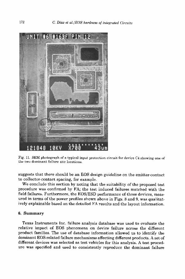
As expected, EOS/ESD damage site locations were layout dependent. For layout styles like the one shown in Fig. 10, both EOS and ESD damage locations were generally located on the emitter contact edge facing the col- lector contact. ESD failures showed up as small damaged areas located exclus- ively at the corners of the emitter contact while EOS failures appeared as relatively large spots with the specific location dependent on the stress level used. In particular, failure site location moved away from the corner along the said emitter edge as the stress level decreased (time-to-failure increased). Under low-level long-duration stress, there is time for more uniform distribu- tion of the stress across the transistor area. It is important to point out that failures involving the collector contact and the grounded guard ring were also seen in transistors with a similar layout style but of different dimensions. In particular, Fig. 11 shows a SEM photograph of a typical input protection circuit for device C4 that shows this type of failure. It was found that whenever more than one failure mode exists in a given transistor, the corresponding power profile departed greatly from the Wunsch-Bell relation. This was the case for the output pulldown transistor of device type C1 and the input protection transistor of device type C4.
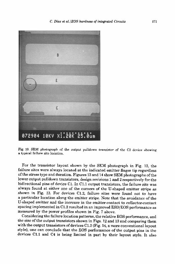
C. Diaz et al./ EOS hardness of integrated Circuits 171
Fig. 10. SEM photograph of the output pulldown transistor of the C2 device showing a typical failure site location.
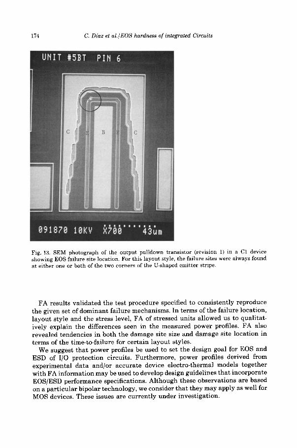
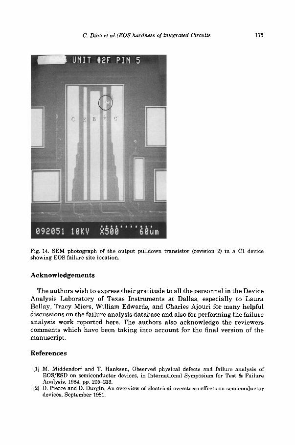
For the transistor layout shown by the SEM photograph in Fig. 12, the failure sites were always located at the indicated emitter finger tip regardless of the stress type and duration. Figures 13 and 14 show SEM photographs of the lower output pulldown transistors, design revisions 1 and 2 respectively for the bidirectional pins of device C1. In C1.1 output transistors, the failure site was always found at either one of the corners of the U-shaped emitter stripe as shown in Fig. 13. For devices C1.2, failure sites were found not to have a part icular location along the emitter stripe. Note that the avoidance of the U-shaped emitter and the increase in the emitter-contact to col lec tor-contact spacing implemented in C1.2 resulted in an improved ESD/EOS performance as measured by the power profiles shown in Fig. 7 above.
Considering the failure location patterns, the relative EOS performance, and the size of the output transistors shown in Figs. 12 and 13 and comparing them with the output transistors of devices C1.2 (Fig. 14, a more conventional layout style), one can conclude that the EOS performance of the output pins in the devices CI.1 and C4 is being limited in part by their layout style. It also
172 C. Diaz et al./EOS hardness of integrated Circuits
Fig. 11. SEM photograph of a typical input protection circuit for device C4 showing one of the two dominant failure site locations.
suggests that there should be an EOS design guideline on the emitter-contact to collector-contact spacing, for example.
We conclude this section by noting that the suitability of the proposed test procedure was confirmed by FA; the test induced failures matched with the field failures. Furthermore, the EOS/ESD performance of those devices, meas- ured in terms of the power profiles shown above in Figs. 8 and 9, was qualitat- ively explainable based on the detailed FA results and the layout information.
6. Summary
Texas Instruments Inc. failure analysis database was used to evaluate the relative impact of EOS phenomena on device failure across the different product families. The use of database information allowed us to identify the dominant EOS-related failure mechanisms affecting different products. A set of different devices was selected as test vehicles for this analysis. A test proced- ure was specified and used to consistently reproduce the dominant failure

C. Dfaz et al./ EOS hardness of integrated Circuits 173
Fig. 12. SEM photograph of the output pulldown transistor of a C4 device showing EOS failure site location. Devices with this layout style and dimensions were found to fail at the emitter finger tip closest to the collector contact.
mechanisms observed in the field for the selected set of devices. Two kinds of un ipo la r s tresses were used, square pulse tes t ing and HBM-ESD. Stressing a number of uni ts for each selected device type al lowed us to de te rmine the power profiles for individual devices. Detai led FA was done on stressed uni ts to de te rmine the fa i lure mechanisms and to provide in format ion useful to the qua l i t a t ive exp lana t ion of the differences observed among the measured power profiles.
A good qua l i t a t ive co r re l a t ion was found be tween the l ayou t s tyle and the device abi l i ty to sus ta in EOS/ESD stress as measured by the power profiles. It was shown tha t good IC ESD-HBM per formance does not necessar i ly imply adequa te EOS robustness . Design changes of I/O pro tec t ion s t ruc tu res can readi ly be eva lua ted in terms of the power profiles. Rela t ive device EOS per formance , as indica ted by the power profiles, can also be used to set design revis ion priori t ies .
174 C. Diaz et al./ EOS hardness of integrated Circuits
Fig. 13. SEM photograph of the output pulldown transistor (revision 1) in a C1 device showing EOS failure site location. For this layout style, the failure sites were always found at either one or both of the two corners of the U-shaped emitter stripe.
FA results validated the test procedure specified to consistently reproduce the given set of dominant failure mechanisms. In terms of the failure location, layout style and the stress level, FA of stressed units allowed us to qualitat- ively explain the differences seen in the measured power profiles. FA also revealed tendencies in both the damage site size and damage site location in terms of the time-to-failure for certain layout styles.
We suggest that power profiles be used to set the design goal for EOS and ESD of I/O protection circuits. Furthermore, power profiles derived from experimental data and]or accurate device electro-thermal models together with FA information may be used to develop design guidelines that incorporate EOS/ESD performance specifications. Although these observations are based on a part icular bipolar technology, we consider that they may apply as well for MOS devices. These issues are current ly under investigation.
C. Diaz et al./EOS hardness of integrated Circuits 175
Fig. 14. SEM photograph of the output pulldown transistor (revision 2) in a C1 device showing EOS failure site location.
A c k n o w l e d g e m e n t s
The a u t h o r s wish to express the i r g ra t i t ude to all the pe r sonne l in the Device Ana lys i s L a b o r a t o r y of Texas I n s t r u m e n t s a t Dallas , espec ia l ly to L a u r a Bellay, T r a c y Miers, Wi l l iam Edwards , and Char les Ajour i for m a n y helpful d iscuss ions on the fa i lure ana lys i s da t abas e and also for pe r fo rming the fa i lure ana lys i s work r epor t ed here. The a u t h o r s also acknowledge the rev iewers c o m m e n t s which have been t a k i n g into a c c o u n t for the final ve r s ion of the manusc r ip t .
References
[1] M. Middendorf and T. Hanksen, Observed physical defects and failure analysis of EOS/ESD on semiconductor devices, in International Symposium for Test & Failure Analysis, 1984, pp. 205-213.
[2] D. Pierce and D. Durgin, An overview of electrical overstress effects on semiconductor devices, September 1981.
176 C. Diaz et al./ EOS hardness of integrated Circuits
[3] T. Green and W. Denson, A review of EOS/ESD field failures in military equipment, September 1988.
[4] C. Diaz and S. Kang, Electrical overstress project, Tech. Rep. TI-3Q-91, Texas Instru- ments Incorporated, 1991.
[5] MIL-STD-883C, Electrostatic discharge sensitivity classification, Tech. Rep. Notice 8, DOD, March 1989.
[6] C. Duvvury, R. Rountree and L. White, A summary of most effective electrostatic discharge protection circuits for MOS memories and their observed failure modes, in Proceedings of the EOS/ESD Symposium, September 1983, pp. 181-184.
[7] A. Chatterjee and T. Polgreen, A low-voltage Triggering SCR for on-chip ESD protec- tion at output and input pads, IEEE Electron Device Letters, EDL-12, (January 1991) 21-22.
[8] C. Duvvury and C. Diaz, Dynamic gate coupling of NMOS for efficient output ESD protection, March 1992.
[9] D. Wunsch and R. Bell, Determination of threshold failure levels of semiconductor diodes and transistors due to pulse power voltages, IEEE Transactions on Nuclear Science, TNS-15 (1968) 244-259.
[10] V. Dwyer, A. Frankl in and D. Campbell, Thermal failure in semiconductor devices, Solid State Electronics, 33 (May 1990) 553-560.
[11] D. Pierce, W. Shiley, B. Mulcahy, K. Wagner and M. Wunder, Electrical overstress testing of a 256K UVEPROM to rectangular and double exponential pulses, September 1988.
[12] T. Maloney and N. Khurana, Transmission line pulsing techniques for circuit modeling of ESD phenomena, September 1985.
[13] V. Dwyer, A. Frankl in and D. Campbell, ESD thermal failure in semiconductor devices, IEEE Transactions on Electron Devices, ED-37 (November 1990) 2345-2354.