EhEEEEmo..EEE - DTIC
163
FD-A163 853 THIN FILM TECHNOLOGY OF HIGH-CRITICAL-TENPERATJRE SUPERCONDUCTING ELECTRO..(U) WESTINGHOUSE RESEARCH AND DEVELOPMENT CENTER PITTSBURGH PA J TALVACCHIO ET AL UNCASSFIE itDEC 85 85-9C9-TUDEv-Ri NOBS14-82-C-8617 F/G 9/5 M I EhEEEEmo..EEE
-
Upload
khangminh22 -
Category
Documents
-
view
3 -
download
0
Transcript of EhEEEEmo..EEE - DTIC

FD-A163 853 THIN FILM TECHNOLOGY OF HIGH-CRITICAL-TENPERATJRESUPERCONDUCTING ELECTRO..(U) WESTINGHOUSE RESEARCH ANDDEVELOPMENT CENTER PITTSBURGH PA J TALVACCHIO ET AL
UNCASSFIE itDEC 85 85-9C9-TUDEv-Ri NOBS14-82-C-8617 F/G 9/5 M
I EhEEEEmo..EEE
W,,
Q2
L
1.25 L.A 1~.6
MICROCOPY RESOLUTION TEST CHART
NATiONAL BURAU OF STANDARDS 1963-A
.:j
" ." " ° " ",. ""
Z-S iiLL '"AIt

Final Report ,THIN FILM TECHNOLOGY OF
HIGH-CRITICAL-TEMPERATURE
SUPERCONDUCTING ELECTRONICS
0 August 1, 1982 to September 30, 1985
By CBy ~ELECTE
J.Talvacchio, A. I. Braginski, ~A * 3 g ~v;
J.R. Gavaler adMA.Janocko
Westinghouse Electric Corporation
Research and Development Center
Pittsburgh, Pennsylvania 15235
office of Naval Research Contract No. N00014-82-C-0617
SApprovd f0r pube lc IasqDistribution UnzaiiedJ
. Westinghouse R&D Center
1310 Beulah Road 06 ~ 2067 '
Pittsburgh, Pennsylvania 15235

Final Report
THIN FILM TECHNOLOGY OF
HIGH-CRITICAL-TEMPERATURE
SUPERCONDUCTING ELECTRONICS
August 1, 1982 to September 30, 1985
By
J. Talvacchio, A. I. Braginski,
J. R. Gavaler and M. A. Janocko
Westinghouse Electric Corporation
Re search and Development Center
Pittsburgh, Pennsylvania 15235
office of Naval Research Contract No. N00014-82-C-0617
O Westinghouse R&D Center1310 Beulah RoadPittsburgh, Pennsylvania 15235

REPORT DOCUMENTATION PAGE
2& SEC01ITv CLASSIFICATION AUTI4ORITY 3 1TIUI~AALSLT FRPR
20 ZECI.ASSI 0 CAT, ON, 0OWNGAAOiNG SCb"EOULff
4 21APOPIMING ORGANIZATION REPORT NuM8611IS3 S. MONITORING ORGANIZATION REPORT NuMSEIS)
85-99- TUDE V-RiG& NAME OFP ERPORNMING ORGANIZATION I. OPFICE SYMBOL 74L NAME OF MONITOIRING2 ORGANIZATION
Westinghouse Research and efapebeDevelopment Center OCASMA Pittsburgh
6.. AGOReS3 Cit), State and ZIP Code# 7b. 1 ~~ ae
.41310 Beulah Road IT Iddecea zl ingPittsburgh, Pennsylvania 15235 1000 Liberty Avenue
_____________________ __________ Pittsburgh, PA 15222
&L. NAME OF PUNOING/SPONSORING W61 OPP ICE SYMBOL . PROCUREMENT INSTRUMENT IOENTIPICATION NUMBERORGANIZATION j(if OWPh~ciiiie
Office ofNaval__Research _______ _____________________em. LOORESS 'City. stage Mnd ZIP Cod., 10. SOURCE OF FUNDING NO$.
PROGRAM PROJECT TASK WORK UNIT
ELEMENT NO. NO. NO. NO.w,-
11T:TLA Inciud. See.it'Camfication,
THIN FILM TECHNOLOGY OF HIGH-CRITICAL-TEMPERATURE SUPERCONDUCTING ELECTRONICS1.PPOAL AUTMORCI
'29 rfacchio, J.; Braginski, A. I.; Gavaler, J. R.; and Janocko, M. A.13&TVP1 OF REPORT 120. Time COVIRIO It OATE OFREPORT(Y.M.Devi IS. "at COUNT
Final PROM A--2 .-- 851211 14916. SUPPLEMENTARY NO0TATION
17 COSATI C009S 14L SUBJECT TERMS iXonesawu on F.17.r if neceasu,7 and identif, by black numbar
0IL is GROU wi - SUe. GR.
19. AEV !ACTContsnue on vewe. if wiesea and identify by bloqk munibor
-The objective of this three-year program was to develop a technology ofJosephson tunnel junctions capable of operating at temperatures above 10K. Thesuperconducting electrode materials investigated were V3Si, Nb3Sn and Mo-Re.Tunnel barriers were formed mostly by oxidizing metallic overlayers of Al and Y.Superconductor/barrier interfaces were characterized by surface-analyticaltechniques. The results of characterization permitted fabricated of junctionswith Nb3Sn and Mo-Re base electrodes and Pb, Pb-Bi and Ma-Re counterelectrodeshaving nearly ideal current-voltage characteristics. -These counterelectrodeswere deposited at temperatures not exceeding T = 100'C. The Mo-Re counterelectrodeformed at low T had a critical temperature, Tc, of only 8K. A high-critical- -
temperature Nb3Sn counterelectrode requiring high deposition temperatures could not4 be fabricated successfully. The main cause of this negative result was the
nonuniform coverage of the base with overlayers which contained thin or defective20L DISTRIOUTION/AvAiLASILITY OF ABSTRACT 21. ABSTRACT SECURITY cLASSIICATIONi
UNCLASSIP*EO/UNLIMITEO SAME AS aRP= oTic useRS
22. NAME OF RESPONSIBLE INDIVIDUAL 22b. TELEP04ONE NUMBER1 22.. OPP ICI SYMBOL
00 FOAM 1473,83 APR IDITION OF I jAN 72 13 OBSOLETE. UcasfSECURITY CLASiPICATriON OF TNeIS PAGE

Uncl assif ieLdSICLJ PiTY CLASSIPICATIOP4 OP Twig PAGE
* -.,spots. In contrast to Nb3Sn, high-Tc NbN counterelectrodes were successfullyfabricatedf anid sumgap voltages exceedng 5 mV were measured at 4.2K. The reportcontains new information on artifical barriers and on Mo-Re and Nb3Sn supercon-ducting films.
Unlasiie35U4T LA IIA1%OP.I AI

TABLE OF CONTENTS4.
ABSTRACT .,..................,.... . . . . . . ., . , ., , . .i i
LIST OF FIGURES .... oo... o, ...... .......... .. o., iv
1. Program .. e.v.... ...... ...................... 1
1.2 Approach ....... 2
1.3 Summary.ot Results.. ......................... ...... 4>7'14 Notation .... 6
2. EXPERIMENTAL APPARATUS AND METHODS..,..,,, ............... 7. 2.1 Film Deposition* .. .. ............... 7
,. 2.2 Analytical Methods .......................... , ........ 7
2.3 Junction Fabrication anTestin...................... 8
3. RESULTS AND DISCUSSION... ..... ... ....... ............... 15
3.1 Task 1 - Superconauctor/Barrier Interfaces............ 15
3.2 Task 2 - Analogue to SNAP Process..................... 21
3.3 Task 3 - ReterenceJunctions.......................... 26
3.4 TabK 4 - Approach to High-Tc Counterelectrodes........ 413.5 Task 5 - Fabrication and Testing of High-T Junctions 59
4. CONCLUSIONS. ........... .,...c..... ............... 63
5. ACKNOWLEDGEMENTS ....... ........................... 66
. .-° . .

6REFERENCES... .... *.*...*...*........... 67
-.' APPENDICES
A. J. Talvacchio, M. A. Janocko, J. R. Gavaler, and A. I.
Braginski, "In-situ deposition and analysis of superconductor
tnin tilms," to be published in Advances in Crvogenic En-
ylneerino - Materials, edited by A. F. C.ark and R. P. Reed
(Plenum, New York, 1986)
B. J. Talvacchio, A. I. Braginski, M. A. Janocko, and S. J.
Bendin9, "Tunneling and interface structure of oxidized metal
barriers on A15 superconductors," IEEE Trans, Magn. MAG-
21(2), p521, 1985
C. A. I. Braginski, J. R. Gavaler, M. A. Janocko, and J. Talvac-
chio, "New materials for refractory tunnel junctions: Fun-
damental Aspects," presentea at the Third International
Conterence of Superconaucting Quantum Devices, Berlin, June,
1985
D. J. Talvaccio, J. R. Gavaler, A. I. Braginski, and M. A.
Janocko, "Artificial Oxide Barriers for NbN Tunnel
Junctions," accepted for publication in J. Appl. Phys.
'-'." - ii -
,,, ! = .' " *,'" f * '7. '*" ' "" - -Z' , .' ' . , , ." . . * , ', = .. % " * " ' - ' , - • .. "

.. ABSTRACT
The objective of this three-year program was to develop a
technology of Josephson tunnel junctions capable of operating at
temperatures above 10K. The superconducting electrode materials
investigated were V3Si, Nb3Sn and Mo-Re. Tunnel barriers were
formed mostly by oxidizing metallic overlayers of Al and Y.
Superconauctor/barrier interfaces were characterized by surface-
analytical techniques. The results of characterization permitted
rabrication of 3unctions with Nb 3Sn and Mo-Re base electrodes and
* Pb, PO-Bi and Mo-Re counterelectrodes having nearly ideal
current-voltage characteristics. These counterelectrodes were
ueositea at temperatures not exceeding T = 100 0C. The Mo-Re
counterelectrode formed at low T had a critical temperature, Tc,
ot only 8K. A high-critical-temperature Nb3Sn counterelectrode
requiring nigh deposition temperatures could not be fabricated
successfully. The main cause of this negative result was the
nonuniform coverage of the base with overlayers which contained
tiin or detective spots. In contrast to Nb3Sn, high-Tc NbN coun-
terelectrodes were successfully fabricated and sumgap voltages
exceeding 5 mV were measured at 4.2K. The report contains new
intormation on artificial barriers and on Mo-Re and Nb Sn super-3
conducting tilms.
, .% - iii -
SVo * ..

LIST OF FIGURES
Fig. 2.1 Geometry of a single 6.4 x 6.4 mm sample prepared fortunneling in a top view and in cross section.
Fig. 2.2 Processing steps to form a tunnel junction from atrilayer formed in situ.
Fig. 3.1 Example of RIE etch rate calibration. The etching gasand power were CCIF -15% Ar gas at 75 mtorr and 0.4W/cm No aaditional etching time was needed to removethe ative oxides of NbN and Si, but an additional 4minutes were needed to remove 2.0 nm of oxidized Al.
Fig. 3.2 Quasiparticle tunneling characteristics of four Nb /oxioizea-Al / Pb-Bi junctions with barriers of dif-terent morphologies measured at 4.2K. (a) Highly-textured evaporated Al (b) Amorphous barrier, ionmillea after evaporation (c) Highly-textured sputteredAl (d) Randomly-oriented, fine-grained Al grown onsputtered polycrystalline Nb.
Fig. 3.3 The barrier height inferred from the curvature of theI-V curve in the region 0.1 < V < 0.4 volts, versus logQ. The solid line is a rough fit to the data.
Fi-j. 3.4 I-V curve for a tunnel junction with a single-crystalNb base, sputtered and then oxidized Al barrier, and anevaporated Nb counterelectrode.
Fig. 3.5 I-V curve for a Mo Re / oxidized-Al / Pb tunneljunction with Q = 98 masured at 4.2K.
Fig. 3.6 The quasiparticle I-V characteristics of twoNb Sn-basea junctions. (a) Evaporated (oxidized) Aloatrier (b) Evaporated (oxidized Y barrier.
Fig. 3.7 (a) Superconductive transition temper8 ture of Mo-Re bccalloys grown by co-evaporation at 100 C plotted as arunction of composition and compared with data frombulk samples reported in Ref. 55. The error bars indi-cate 5% and 95% of the resistive transition. (b) Theelectron-phonon coupling strength plotted as a functionof composition and compared with the weak-coupling, BCSvalue.
Fig. 3.8 The normal-state resistivity of Mo-Re bcc-alloy andAl5-compound films measured just above the superconduc-tive transition temperature.
Fig. 3.9 A comparison of the properties of sputtered andevaporated Mo-Re (approximately 35 at. % Re) alloysuperconductors as a function of film thickness. (a)Transition temp8 rature and (b) Resistivity ratio,on (300 C)/Pn (15 C).
-iv-

Fig. 3.10 In-s1U RHEED patterns of Mo-Re films. (a) Diffuserings characteristic of randomly-oriented, highly-
'S disoraerea grains in a thin film grown at low tempera-ture. (b) Pattern characteristic of a polycrystallinetilm with some texture. (c) Sharp lines indicated thatthe film was a relatively smooth (two-dimensionalreciprocal lattice) single crystal.
Fig. 3.11 XPS aata for (a) Re and (b) Mo photoelectrons. The"exposed" Mo-Re, pug Re, and puig Mo films weremeasured after lohg-term oxidation in air. The"protectea No-Re had an overlayer of Al 2.0 nm thickdepositea immeoiately after the Mo-Re film and withoutbreaking vacuum.
Fig. 3.12 XPS spectra recorded in situ for a 7.5 nm-thck Nb Snfilm aeposited on an oxidized Al film at 925 C. (a?
Spectra of photoelectrons with four different kineticenergies. (b) The expanded Nb photoelectron peakshows no chemical shitt and, Nerefore, no indicationof a reaction with the oxidized Al.
Fig. 3.13 Composition or Nb Sn co-evaporated films as a functionof sample positioa on a block which was not rotated
'C. ouring aekosition. The lcomposition-lockingl observedfor suostrate temperatures > 850 C was due to re-evaporation of tin from the Nb6Sn5 phase.
Fig. 3.14 The superconauctive transition temperature for co-evaporated Nb Sn filmsin the range of compositionbelow the Ocoiposition-locked" phase boundary at 25 at.% Sn. The comparison with Stanford data (Ref. 56) showsthe neea for fast-response Nb rate control.
Fiu. 3.15 Tunneling I-V curve for a Mo-Re / oxidized Al / Mo-Rejunction measured at 4.2K. The gap voltage of thecounterelectrooe corresponaed to a T = 8K.c
LIST OF TABLES '
Table 3.1 The temperature at which reaction pro"uts of RIE havea vapor pressure of 1 torr.
Tabie 3.2 Typical etch rates and etchinc ,rameters for RIE.Accesion For
NTIS CRP,0', IC TAB -U. ano':vcCd L
D,t i1). i , -- - -- -
Availablhlty Codes
Di.t IAvaii a.d_,orDi . S p ,C iCd 1
F.£ ', ,.. ,' . .'. , ' .f.,' . .- - . Z .,C. .,. -.. ....,,...,: ... - .' ...". . . .,A-1" ',...

1. INTRODUCTION
1.1 Program Objective
Tne overall objective of this program was to develop a
tecnnology of thin-film Josephson tunnel junctions capable of
operating at temperatures, T > 10 kelvin, compatible with theop,
performance of small closed-cycle refrigerators. The availability
of such junctions would make it possible to incorporate supercon-
ducting electronics into mobile/airborne electronic warfare and
auvanced radar systems.
The specific objective was to demonstrate the technical
feasibility of thin film tunnel junctions with electrodes fabri-
catea from A15 compounds and/ur hard alloy superconductorsp such
as Mo-Re, having critical temperatures, Tc, sufficiently high to
achieve useful device characteristics at temperatures exceeding
10 kelvin. This would permit a comparison with high-Tc, Bl struc-
ture NbN and NbCN junctions that are under active development in
several R&D organizations in the United States and overseas.
Tne program tasks defined in the Statement of Work were:
TasK 1. Investigate A15/rare-earth oxide and Mo-Re/oxide
interfaces to identity the oxide species and their
depth profiles.
Task 2. Develop a selective anodization process for A15 and
Mo-Re films.
'V-- -

Task 3. Fabricate and characterize A15 and Mo-Re reference
tunnel junctions with low-Tc soft alloy and Nb
counterelectrodes.
Task 4. Determine the preferred approach to high-Tc
counterelectrode fabrication.
Task 5. Fabricate and test high-operating-temperature (> 10K)
prototype tunnel junctions.
The objectives of this program were complementary to those of
the more basic program on "Superconducting Electronic Film Struc-
tures" aimed at laying scientific foundations for the high-
operating-temperature junction technology. That program is sup-
ported in part by the Air Force Office of Scientific Research
(AFOSR) under Contract No. F49620-85-C-0043 (and preceding
contracts). It will be referred to in this report as the "AFOSR
program.'
1.2 AQrach
The approach was based on the use of a novel ultra-high-
vacuum (UHV) closed system referred to as the Westinghouse Super-
lattice Deposition and Analytical Facility (SDAF). This has made
it possible to deposit, process and characterize bilayered and
multilayered film structures without breaking the vacuum. From
tnese film structures, which incorporated the superconducting
electrode(s) and the tunneling barrier, junctions and/or junction
componentE could be patterned.
The dominant approach to the formation of superconducting
tnin films was to co-evaporate the elemental components of the
• '. '. -.., .e ' '. '# " '.,. . '; '. . • . , ..- , .- .. -, ..., -, . . "2

A15-structure compound or an alloy in an UHV environment.
Svutter-aeposition was also used, but to a lesser extent.
*The dominant approach to the formation of tunneling barriers
" has been to deposit on the superconducting base electrode and to
• .oxialze a thin overlayer of a metal which forms a ch3emically,
mechanically and thermally stable oxide, without suboxides, upon
exposure to an oxygen-containing atmosphere. Direct deposition of
an oxide was also attempted in the final phase of the program.
Metal overlayers were either evaporated or dc magnetron-
sputtered. Direct oxide deposition was by rf magnetron sputter-
,'". ing,•[+..
The key problems to be solved were:
1. To tina an artificial tunneling barrier that would perform
well with high-Tc electrodes. This requires that there be no
chemical interaction and no interdiffusion with the
electrodes at whatever processing temperature is necessary to
synthesize a high-Tc superconductor. A compatibility with the
crystalline structure of the counterelectrode may also be
required.
2. To form a counterelectrode having a high Tc within a
coherence length, s of the barrier/counterelectrode inter-
face (the s is of the order of 3 to 5 nm in high-Tc, type II
superconductors). For the A15-compound films, this requires a
high Qegree ot crystalline order in the initial deposit.
Consequently, the choice was made to study and use crystal-
.. line and epitaxial barriers on which ordered counterelectrode
-ilms could be grown.
-3-| .*. .
" . - 3....

The 1o-Re superconducting alloy counterelectrode was proposed
as a possible solution to both problems. Indeed, we found that it
can be formed near the room temperature, thus minimizing the
thermally activated interdiffusion with the barrier, and it does*1'
not oxidize reaaily so that it should not reduce the barrier.
Also, the Tc in Mo-Re is relatively insensitive to disorder so
that the second problem coula be minimized. However, with a Tc of
,~J only up to 12K, the bcc-structure alloy is clearly inferior to
the Bl-structure NbN or NbCN compound which can exhibit Tc's up
to 16 ana 17K.
1.3 Summary of Results
Most signiticant results and conclusions obtained in each
tasK are listed below.
Task 1. The Y/Y203 overlayer (representing the rare-earths)
was found by X-ray photoelectron spectroscopy (XPS)
and tunneling to form an excessively thick self-
limited oxide layer resulting in very high barrier
resistances. Consequently, Al/A1203 and Mg/MgO over-
layers having lesser self-limited oxide thicknesses
were investigated in more detail. The XPS has shown
that the Al/AI203 overlayer can retain its integrity
up to 750 degrees centigrade and can be compatible
with the high processing temperatures required for
A15 counterelectrodes. Yttrium was found, however, to
ditfuse less than Al into the base electrode.
Task 2. The reactive iOn etching (RIE) process was used,
4
-.- ; ' '"- -~i .: -:i -:i -. "F. . -i: ___._._.-____._.._-i'i - . .. -. :... : . :.' / i. : '.

instead of anodization, to pattern the junctions. It
was found that thin Al203 and MgO barrier layers
represent convenient etch-stop points thus facilitat-
ing the control of this process. Aperture (stencil)
masks were also used to form counterelectrodes in an
ex-situ junction fabrication sequence.
Task 3. Low subyap conductance tunnel junctions were fabri-W catea with Nb, Nb3Sn, and Mo-Re base electrodes,
Al/A1203 or Y/Y203 overlayer barriers and lead or Pb-
Bi counterelectrodes.
Task 4. The preferred approach to high-Tc counterelectrode
formation was determined to be that of epitaxial
growth. This approach was believed necessary since
even in the Mo-Re counterelectrode the gap voltage
near the interface with the barrier was depressed
from 12K to 8K.
Task 5. The goal of this task was not attained since high-Tc
A15 or Mo-Re counterelectrodes could not be
aemonstrated ana high-operating-temperature tunnel
3unctions were not fabricated with such coun-
terelectrodes. In contrast, high-Ta NbCN coun-
terelectrodes were obtained recently under the AFOSR
program, using the approach defined in Task 4. Ear-
lier in 1985, high-T NbN or NbCN counterelectrodesc
were also obtained in two other laboratories: ETL in
Japan and NRL in USA.
-5-
. , ...i:.'.. ,:: ." .. ..-.'.. w "" ...i: . .. ' a .. .". . .."... . *- -"--

The overall conclusion derived from this program is that the
approach to tne problem remains correct but the A15 high-Tc
*counterelectrodes are much more difficult to obtain than those of
- NbN or NbCN. The difficulty is largely related to the necessary
use or crystalline and epitaxial tunnel barriers having a low
subyap conouctance and crystalline compatibility with the A15
structure. Such barriers were not obtained to date. Consequently,
hign-operating-temperature junctions with NbN or NbCN electrodes
represent the only short-term option available. More work is
requirea to attain all-A15 high-Top junctions. The feasibility of
such junctions was, however, not disproved.
Throughout this text a layered film structure fabricated to
torm a tunnel junction is defined in the sequence of depositing
-the layers: substrate/base/overlayer (barrier)/counterelectrode.
-6-
,:.- O,

2. EXPERIMENTAL APPARATUS AND METHODS
. 2.1 Film Deposition
Preliminary film deposition experiments under this program,
wnic preceded the implementation of the present equipment, were
1-ertormea using a dc diode sputtering system . Its description
*> is not reproduced here since it has little archival value. Since
May 1983, sputtered superconductor and barrier films were
aeposited in the four-magnetron-gun vacuum chamber. Its present
version is described in Appenaix A. Description of the first
version is given in 2 In early 1984 that chamber was integrated
- into the SDAF (Appendix A). Co-evaporation of superconducting
films and evaporation of metallic overlayers have been performed
only in the SDAF.
2.2 Analytical Methods
X-ray photoelectron spectroscopy (XPS) was used extensively
-. throughout this program. The SDAF is presently equipped with a
-. Riber MAC-i electron energy analyzer having a limited sensitivity
and poor energy resolution of, at best, 1.5 to 2.0 eV. The angle
between the normal to the sample and the detector, e, is fixed
and ill-defined. Consequently, this XPS apparatus was used mostly
for qualitative, in-situ analysis. The quantitative and angle-
depenuent XPS was carried out mostly ex-situ, in an ESCALAB Mark
4I
,. °-
7 -

II (VG Scientific) equipped with a hemispherical electron energy
analyzer. The MYK . and AlK radiation was used without a
monocnromator. Many films analyzed were deposited on sapphire
substrates ana were not electrically grounded. Consequently,
shifts in the kinetic/binding energy up to 10 eV were observed.
However, in the ex-situ procedure the analysed films were always
exposea to air ana enough carbon was present on the surface to
calibrate all other photoelectron energies to the known energy of
C ls. High resolution spectra have been recorded with an analyzer
pass energy of 20 eV which corresponds to 1.2 eV resolution. The
angle, e, was detined to ±60 since the entrance aperture of the
analyzer subtends a 12 aegrees arc. The analysis could be per-
tormea at temperatures between ambient and approximately 800 C.
The typical operating vacuum level was 10 to 1010 torr.
A scanning electron microscope (Cambridge, Model MK 150-2)
equipped with an analyzer (Kevex 7000) for energy dispersion
spectroscopy (EDS) and an electron microprobe (ARL, Model SEMQ)
capable of measuring oxygen content have been used for determin-
ing chemical composition. An X-ray diffractometer (Scintag PAD 2)
has been used for phase identification and lattice constant
measurement. The qualitative, in-situ determination of the film
crystallinity has been performed in the SDAF by reflection high
energy electron diffraction (RHEED).
2.3 Junction Fabrication and Testing
Two methods of junction fabrication have been used: ex-situ
and in-situ. In the ex-situ process, an A15 or Mo-Re supercon-
4. ducting base was deposited on 6.4 x 6.4 mm sapphire substrates.
-8-

*Up to 17 (typically 7) substrates were clamped to a molybdenum
olock which served as the transfer vehicle and specimen table
within the SDAF. The clamps helped to insure an adequate thermal
contact to the block and delineated an approximately 4 mm wide
deposit strip centered on the substrate. The barrier overlayer
was deposited on the base and oxidized thermally or by an ion-
beam-assisted process without breaking the vacuum. The completed
bilayer was removed from SDAF and briefly exposed to air. The
base electrode width was defined either by the width of the
deposit strip itself or by hand-painting insulating Q-dope or
-notoresist over a part of the strip surface. The painted layer
f lped also to protect the base step-edges from shorting to the
counterelectrode. Subsequently, the bilayer was placed under an
aperture mask defining the 0.25 mm wide counterelectrode strip
ana a counterelectrode film deposited. The four counterelectrode
contact pads were positioned on the uncoated part of the sub-
strate as shown in Fig. 2.1. Lead and Pb-Bi soft coun-
terelectrodes were deposited in separate evaporation or sputter-
ing tacilities.
Retractory counterelectrodes were deposited in the SDAF. In
this case, the aperture mask was mounted on a Mo-block. This
process resulted in four large-area junctions (approximately 0.052
mm .) per substrate chip. Due to this large junction size only
cquasiparticle current-voltage (I-V) characteristics could be
V determined. The main advantage and principal reason for wide
utilization of this process was a very short turn-around time.
The in-situ process consisted of a sequential deposition of
all three layers (base/barrier/counterelectrode) without breaking
-9-

Dwg. 9353A60
-00jm 0Oi 0 6mm
C rossPb Counterelectrode
View Base Electrode-BarrierBilayer
Photoresist
Base Electrode
A 12 03 Substrate
Fig. 2.1 Geometry of a single 6.4 x 6.4 mm sample prepared fortunneling in a top view and in cross section.
-10-
%

the vacuum. The barrier oxidation, thermal or ion-beam-assisted
was performed in the SDAF prior to depositing the counter-
electrode. A simple process with turn-around times of 2 to 3 days
was used to delineate junction areas from trilayers upon removal
from the SDAF. Figure 2.2a shows the trilayer covering the entire
substrate except for the area under the clamps. The four coun-
tereiectroae areas (20 x 20) micrometers were protected by pat-
ternea photoresist while the counterelectrode was etched. Both
wet etching and reactive ion etching (RIE) were used in the
course of the program. In the latter case Freon 12 was used as
the etching gas. The etched sample is shown in Fig. 2.2b. The
Al203 and especially MgO oxide served as an effective etch-stop
so that only a small fraction of the base thickness was removed
even with a very relaxed etch-rate control. A second layer of
inotoresist was patterned as shown in Fig. 2.2c and left in place
to insulate the base electrode from the metallization layer shown
in Fig. 2.2a. This layer, usually Pb-Bi, permitted one to make
contact with the patterned counterelectrode. The metallization
layer was deposited through an aperture mask identical to those
used in the ex-situ process.
Three measuring probes have been used. All have press-contact
electrical connections to the sample for rapid turn-around. One
probe permits a resistive measurement of transition temperature
3-, and van der Pauw measurement of resistivity as a function of
temperature, in a liquid helium storage dewar with a 12.8 mm (1/2
inch) neck. A calibrated germanium thermometer is used for tem-
ferature measurement, and the height of the sample/thermometer
block above the level of helium liquid is used for temperature

Dwj. 9379A58
Depostion ounterelectrole
a) Base Electrode
In sulation ii Photoresist
(c)
Electrical Conduct Electrical Contact toto Base Electrode Counterelectrode
d) .*.~* .a--Contact Layer
Fig. 2.2 Processing steps to form a tunnel junction from atrilayer formed izi..A±j",
-12 -
%I . :~.:

control. The estimated accuracy of the measurement is ±0.1 kel-
vin. An air-lock allows the sample to be warmed from cryogenic to
room temperature in dry nitrogen gas. The second probe has ten
press contacts configured for four-point measurements of the I-V
characteristic of four junctions on one standard (6.4 mm x 6.4
mm) chip. This probe is also compatible with the air-lock-
equipped liquid helium storage dewar and is intended for measure-
ments at 4.2K. The third probe accommodates four standard sub-
strate chips. Sixteen contacts are made to each chip, thus per-
mitting a tour-point measurement of the I-V characteristic of
,each tunnel 3unction and the resistivity of the base electrode.
Liquid He must be transferred to a 4-inch dewar. The temperature
of the samples is controllable because a vacuum space isolates
tne probe from the liquid helium.
Electrical characterization of tunnel junctions was limited
to quasiparticle I-V characteristics, as already mentioned above.
The large junction areas in most of fabricated samples resulted
in sutticient self-shielding to preclude a reliable determination
o the 3unction critical current, Ico Hence, the standard junc-
tion quality parameters, the IcRN product (where R. is the normal
resistance of the junction above the gap voltage) and Vm = IcRS
(wnere R is the subgap resistance) could not be determined
* directly. Insteau, the ratio of currents at fixed voltages above
ano below the gap: Q INIS was used as a quantitative indicator
ot tne 3unction quality at 4.2 K. For junctions with a sum of
base and counterelectrode gap voltages less than 4 mV the ratio Q
- (4 mV)/I(2 my) was used. For 3unctions with a sum of gap
voltages > 4 mV, the ratio was Q 1 1(6 mV)/I(3 mY). As shown in
-13-

Rer. 7, Q is related to Vm By making the ratio of fixed
reference voltages above and below the gap to always equal 2, the
estimatea value of Vm is:
Vm = 1/2 (IcRN)thQ (1)
where (IcRN)th is the maximum theoretical value of the product at
a temperature T in the absence of any proximity layer. Assuming
tne BCS relation = 1.76 kBTc one obtains at zero kelvin:
(IcRN)th = 240 Tc (microvolts). For T/Tc < 0.3 the zero kelvin
value holas. For Nb (Tc - 9.2 K, T/Tc = 0.46) the value must be
calculated from the theoretical BCS expression 4 and is ap-
proximately 15 % lower. Substituting the zero kelvin value into
(l)one obtains:
Vm - 0.12 TcQ (mV) (2)
Proximity effect will reduce Vm However, for high sum gap volt-
ages one will usually obtain Vm > Q.
The sum of gap voltages wds determined from the I-V charac-
teristics by taking the maximum derivative (highest inflection)
point on the curve. To obtain the base electrode gap voltage, the
PO or soft alloy gap (well-defined by the composition) was sub-
stracted. For all-refractory junctions the separation was not
possible.
-' -14-. . . * ** . **
* -h-.-- --...- '- 4 -

L' ; : , 3. RESULTS AND DISCUSSION
*. ,.
3.1. Task 1 - Suerconductor/Barrier Interfaces
3.1.1. Qb.civ
The objective of this task was to determine requirements for
fabricating tunnel junctions with the base electrode gap voltage
approaching the bulk material value, unaffected by adverse
physico-chemical effects occuring at the base/artificial barrier
interface. These effects depend upon the barrier type and the
*method of its fabrication. The complementary objective was thus
to investigate some of the barrier fabrication parameters. Fur-4n.e cnaracterization of barriers is included in the description
of Tasks 3 to 5. Under Task 1 results were obtained in the fol-
lowing problem areas:
1. Surface segregation in A15 superconductor base.
- 2. Interaiffusion between the base and the artificial
JA barrier overlayer.
3. Barrier overlayer thickness uniformity.
4. Oxioation of metallic barrier overlayers.
Stuaies of the superconductor/barrier interface were
originally scheduled for the first year of performance under the
tnree-years' program. They continued, however, until its comple-
5)15'J" - 15 -
• . % - . .. .'.-.,' $,-".. . ° '.".s ,.., .'-• . . * - . . .. . . . . . . . . . . . . -

tion since the barrier properties and the resulting junction
performance critically depend upon the investigated interface.
3.1.2. Surface Segregation
Atomic segregation near the A15 superconductor's surface can
signiticantly alter its composition over depths comparable to the
coherence length. The Tc ana the energy gap, , decrease by 10 to
15% per each atomic percent deviation from the stoichiometric 3:1
composition. Consequently, a degraded proximity layer may define
the base electrode gap voltage if segregation occurs due native
or artificial oxide barrier formation. The first systematic XPS
study of the surface segregation of A15 compound surfaces which
is inaucea by the presence of oxygen on the surface was performed
5by Inara and coworkers. Work under this program, performed at
the same time, concentrated on the comparison of V3Si, Nb3Sn and
V3 Ga. The V3Si was originally chosen as the representative A15
material for this program. The results of the XPS study are
summarized in Appendix B, and a general discussion of the effect
is given in Appendix C. Upon surface oxidation, the segregation
o0 the Nb3Sn was found to be less dramatic than that of V 3Si. In
contrast to V3Si, no change in the composition of Nb-Sn at the
interface with its oxides could be observed within the resolution
o0 the ESCALAB XPS apparatus. A direct consequence of these
rindings was the replacement of V3Si by Nb3Sn to serve as the
representative, stable A15 material for junction fabrication and
studies. The growth conditions for Nb3 Sn films are presented
below, under Task 4.
Minimal oxidation and no surface segregation were found in
-16-
4,,.. , , , .? -,.. . - -,., ,- -.-.-.... ., ., . • .'.'...''.'' ....' *. *. *. 4.. ', 2 .o .,2 -,N ' °.:.2, , ..:. .. -

-7:
Mo-Re. Tnese results are also presented in conjunction with Task
4. It surfices to state here that the Mo-Re/barrier interface
presented no real problems except one. Since Mo-Re does not
oxidize readily, the pinholes in the barrier, if present, cannot
- be sealed by the native oxide. Yields of junctions with the Mo-Re
base and soft electrodes were consistently lower than those for
Nb 3Sn and especially NbN base. This indicated that pinholes were
present in the barriers under investigation. Mo-Re is, therefore,
a suitable test material for studies of the barrier integrity.
3.1.3. Interciffusion
In the case of metallic overlayers deposited on the base
electroae to form a barrier, and oxidized after the deposition,
an intertace is initially formed between the base surface and the
metal. If the overlayer is thick enough a thin unoxidized metal
layer may remain even after the oxide is formed. Kwo and
coworkers were the first to observe by XPS that the thickness of
this residual layer is less than expected from the deposition
rate and measured oxide thickness. They attributed this "loss"
to the thermally activated grain boundary diffusion of the over-
layer metal (Al) into the polycrystalline base film (Nb). Inter-
diftusion or this type may cause the degradation of the
superconductor's gap energy, especially if higher processing
temperatures are involved which will be necessary for junctions
- with A15 counterelectrodes. Under this program, XPS was used to
- .investigate the effect of temperature on the diffusion of Al and
Y overlayers into Nb ano V Si base electrode. The results are3
presented in Appendix C. Under the AFOSR program diffusion of Mg
-17 -
. . . .• . . . .. . - -.. . ...- - . - . . .. ...-. .. . , ..... -- - . .i i . .-.
4t ' ' ' ' . '' .; ) ? '', ?' : : ' _. ' ' . ' , -,:. ;-; ' . '. ;~ ' .,.i ' '. .; L ? ' .

into NbN was also investigated (Appendix B and C). The most
important conclusions referring to comparable conditions of
experiments are:
1. Yttrium ciffuses less into the base than Al due to a
larger atomic radius of Y.
2. Diffusion of Y and Al into polycrystalline V 3Si
is less pronounced than into polycrystalline Nb.
3. Diffusion of Al into single-crystal Nb is not observed
up to 750 0C. This proves that it occurs along the
. grain boundaries of the base.
4. The Al/A 2 0 3 overlayer on single-crystal and
even polycrystalline Nb retains its XPS-defined
integrity up to 7500 C. This overlayer is thus
potentially compatible with high-temperature
processing.
5. Magnesium diffuses into and/or reacts with NbN above
300 to 5000C.
6. No deleterious effect on the base gap voltage or
subgap conductance was observed as a result of Al or
Y diffusion along grain boundaries of the base.
In contrast, Mg diffusing into NbN increased the
subgap conductance of the latter.
3.1.4. The Overlaver Thickness Uniformity
The rationale for concentrating on oxidized metallic over-
layer barriers was provided by the observation of Rowell and
coworkers that even extremely thin metallic overlayers of Al are
capable of coating the Nb base such that upon thermal oxidation
- "--18- - .-

the barrier properties are Al203-likew rather than
RNb 205 -like".7 The proposed explanation of this effect was that a
few monolayers of Al are capable of completely "wettingn the Nb
base.8 Calculations based on a theoretical wetting model9 indi-
cated that no major differences in wetting of Nb or V by all
metallic overlayers considered in this program should be ex-
pectea. Consequently, their use should result in an adequate
coverage of the base assuming that the surface properties of
Al5's are not too different from those of their major metallic
component (Nb or V). A discussion of wetting is included in
Appendix C. It was thought that metallic overlayers will cover
the base better than a directly deposited oxide.
No prediction can be made of the overlayer thickness unifor-
mity. Consequently, an XPS evaluation of that uniformity was
performed under this program. Appendix C shows XPS results that
indicate that even in the case of best-wetting amorphous Si on
extremely smooth amorphous Mo-Ge the overlayer thickness fluctua-
tion was comparable to the thickness itself. Single crystal Nb-
surface was covered more uniformly by Al than a polycrystalline
Nb-f im. The conclusion from this work is that thin or "weak"
spots are likely to be present in all overlayers investigated
here and that this problem will be aggravated by the base rough-
ness and grain boundaries. A micro- or single-crystalline A15
oase would permit a relatively best overlayer uniformity. A
coarse-grained base will be least suitable.
3.1.5. Barrier Oxidation
Thermal growth of oxides on metal overlayers such as Al, Y,
-19 -

or Mg is self-limiting. To permit the ex-situ junction process-
ing, and to obtain an easy control and reproducibility of the
barrier thickness in the in-situ process (Section 2.3) the use of
self-limiting oxide thicknesses was preferable in this program.
Appendix C (Table 3) shows the self-limiting thicknesses deter-
aminea by XPS and the corresponding junction resistances. Room
temperature oxidation of yttrium produced an approximately 4 nm
thick oxide, ana, correspondingly, very high, rather impractical
]unction resistances of 102 ohm-cm 2 . This high junction resis-
tance, ana the strong tendency of Y to form hydroxides (Appendix
C and Ref. 1) that complicate the ex-situ processing resulted in
the Y/Y203 barrier to be de-emphasized in this program in favor
of Al/A1203.
Ion-beam assisted oxidation was used for the first time to
form artificial barriers. This process, discussed in Appendix D,
produced Al/AI203 barriers with an increased thickness and bar-
rier height that were suitable for NbN-counterelectrodes dis-
cussed under Task 5 but not for A15. Thermally oxidized barriers
worked satisfactorily only for Pb, Pb-Bi and Mo-Re coun-
terelectroces (Task 5).
3.1.6. General Conclusions From Task 1
Work under Task 1 permitted one to determine conditions
suitable for obtaining an A15 (Nb3Sn or V3Si) base electrode
protected from degradation by a metal/oxide overlayer. For Al-
an Y-overlayers this should be possible as long as some un-
oxidized metal is left between the base and the oxide. XPS was an
indispensable tool for obtaining the results.
- 20 -

3.2 Task 2- Analogue to SNAP Process
Some process was needed for patterning base/barrier/-
counterelectrode trilayers formed in situ in analogy to the
Selective Niobium Anodization Process (SNAP) developed at Sperry" 10Research Center for Nb/Si/Nb junctions. The motivation for such
a process was to achieve more uniformity in junction parameters
by protecting the barrier from exposure to air, dust,
photoresist, and wet chemicals. An outline of the process that
was used during this program was presented in Section 2.3 and
Figure 2.2. Background information and details of that process
will be presented here.
At the beginning of this program, private information was
obtainea from Sperry that anodization does not work well with Nb-
based compounds such as NbN. At the same time, Gurvitch et al.
aemonstrated the use of plasma etching (SNFP) to define Nb coun-
terelectroae areas. Plasma etching utilizes a reactive gas,
usually fluorine or chlorine-based, to form volatile reaction
products. Thus it is a highly-selective process which is effec-
tive for all of the high-T0 superconductors of interest, but
cannot etcn through an entire trilayer containing an Al203 or MgO2-
barrier.
The temperature at which the vapor pressure reaches 1 torr
is listea in Table 3.1 for a number of the reaction products
createa by plasma etching. Those which are volatile at low tem-
peratures include such products of the etching of high-Tc super-
conductors as NbF5 and MoF3. Those which are stable at room
temperature include the products of several barrier materials
such as AlF3 and MgF2 . I-21-

Table 3.1 -The temperature at which RIEreaction products have avapor pressure of 1 torr
Compound Temperature (*C)
A1F3 1240
A1C13 100
MgF2 - 1000
MgCl2 640
MoF6 - 70
NbFS 90
NbCl5 -100
SiF 4 -150
C:.SiCl14 60
SnClz. 310
-22-
L A t'

Reactive Ion Etching (RIE) is distinguished from plasma
etchiny in that there is also a physical ion bombardment as-
sociateu with the chemical processes which slowly removes
material ot any vapor pressure by sputtering. The difference
arises from the tact that samples are placed on the powered
electrode in RIE and are placed on a grounded or floating poten-
tial for plasma etching.
Etch rates and parameters for RIE (Table 3.2) were estab-
lished for Nb, Nb3Sn, and Mo-Re for this program, and for other
materials, such as NbN, independent of this program. Figure 3.1
clearly shows how the etched step height of NbN, plotted as a
function ot etching time, can be affected by a thin, oxidized
overlayer of aluminum. An extra 4.5 minutes, enough time to
remove 250 nm of NbN, was needed to etch through a 2.0 nm thick
Al203 barrier. The native oxides of NbN and Si on the surfaces of
the other samples aid not affect the rate since the step-height
data for those samples extrapolated to the origin of the plot.
Table 3.2 includes etch rates from two different RIE sys-
tems. An Anelva system was used for the second year and half of
the third year of the program. A Semi Group 1000 TP, available in
the last 6 months of the program, was a dedicated system for
superconducting devices.
Therefore, RIE permitted the delineation of counterelectrode
areas and the patterning of an entire trilayer with large
tolerances in the required etch times. This control over process
end-points was peculiar to the particular materials being studied
for high-Top tunnel junctions. It is a fortuitous advantage that
is in addition to the usual advantages of RIE.
-23-. S ..::i:. ..-. .., ..... ._.. .... .- ...- ..- .. _..... .. .. .. .. . . .. ..-.....-.... .-.. ...... .-.... ::i
F:-:: "'; '; : , : ;;, :- -::'-::%:: ,. ';: -' : - ;;. . :: . "/ )i S -- . .; -; ;" -:)--.- .

Curve 7517?12-A
Si
300NbE
* ,- --
//= = 200
* ""100 /,MAI
0 2 4 6 8 10 12Etch Time ( min)
Fiy. 3,1 Example of RIE etch rate calibration. The etching gasand power were CCIF 2-15% Ar gas at 75 mtorr and 0.4W/cm . No aaditionil etching time was needed to removethe Rative oxioes ot NbN and Si, but an additional 4minutes were needed to remove 2.0 nm of oxidized Al.
424
"-'.-- 24 -
• .•

- - - - - - -- - - - -- - - - -
Table 3.2 -Typical etch rates and etchingparameters f or RIE
~1tra.Etch Rate RIE Etching Pressure Power
(nm/mmn) System Gas (millitorr) (W/cm)
Nb 28 Anelva CF4 30 0.2
Mo-Re 40 Anelva CF. 30 0.2
10 SEMI CCl2F2-15% Ar 75 0.6
Nb3Sn 95 SEMI CC12F2-15% Ar 75 0.6
NbN 35 Anelva, CF4 30 0.2
50 SEMI CCl2F2-15% Ar 75 0.6
25 SEMI NE3 75 0.6
A1203 0.5 SEMI CC1 2F2-15% Ar 75 0.6
MgO -0.3 SEMI CCl2F2-15% Ar 75 0.6
Si 35 SEMI CCl 2F2-15% Ar 75 0.6
-25-

.
3,3 Task 3 - Reference Tunnel Junctions
* 3.3.1 Obiective
The objective of this task was to demonstrate that the
results of Task 1 permit one to fabricate tunnel junctions withunaegraded high-T c base electrode gap voltages and low leakage
barriers when using lead, soft alloy, or Nb counterelectrodes.
The specific goals were to:
1. Verify that adequate coverage of the base by the
overlayer and protection from oxidation were achieved.
2. Verify that the base/overlayer interdiffusion did not
affect the base gap voltage.
3. Determine the homogeneity of superconducting base
films within a coherence length from the
base/overlayer interface.
4. Characterize the barrier itself.
The original intention was to separate the issues concerning
the base electrode/barrier interface and the barrier itself from
those specific to the barrier/counterelectrode interface and the
high-Tc counterelectrode. Results obtained later under Tasks 4
and 5 nave shown that such separation was not justified.
3.3.2 Niobium-Base Junctions
The Nb-base junctions were fabricated and characterized to
perform a preliminary barrier test prior to investigating the
high-Ta and counterelectrooe material candidates. Polycrystalline
Nb films were ac-magnetron sputtered on sapphire substrates.
Highly textured and single crystal Nb films were e-beam
.........- 2 6

evaworatea on epitaxially polished sapphire, usually having a
.> (1120) orientation. The corresponding orientation of Nb was
(110). Electron-beam evaporated and dc-magnetron sputtered Al-
overlayers and e-beam evaporated Y overlayers were oxidized and
characterized. Thermal oxidation was performed by exposing the
overlayer to 100 mtorr of dry oxygen for up to 1 hour at room
temperature. The oxidized sample was exposed to air of unknown
numidity for at least 10 min prior to the deposition of a soft
counterelectrode. The effect of short exposure to humid air on
the barrier properties remained largely unknown. Long exposures,
of several days duration, were found to significantly degrade the
Q of Al-oxide barrier junctions. Ronay and Latta found, however,
that exposure to humidity was crucial for obtaining low-leakage
Y/Y203 barriers.12
Figure 3.2 summarizes the experience gained with Al/AI203
barriers on Nb. Current-voltage characteristics are compared for
barriers ano base electrodes fabricated by different methods
which resulted in differences in the barrier crystallinity. No
differences between these junctions appeared in XPS characteriza-
tion of the oxidized Nb/Al bilayers. All had a layer of AI203
approximately 2 nm thick, a layer of unoxidized Al underneath
that was slightly less than 1 nm thick, and a Nb surface which
snowed no signs of oxidation - even with the XPS energy analyzer
(ESCALAB) at a glancing angle.
"8 Aluminum overlayers e-beam evaporated at a rate of 3 nm/min
8- (Fig. 3.2a,b, samples R84-21-B3 and R84-35-B2) were grown on a
(110) single crystal Nb that had an atomically smooth surface
according to RHEED, ana a high resistivity ratio (up to 150).
- 27 -
4e,.

- Curve 7512; 1-A
Nb/Al2 0 3/PbBi (a)23. Sample No.
R84-21-B3
b)R84-35- B2
CC._____R84-31-A5
C
_ _ (d)M83-18-C2
1 2 3 4 5Voltage ( mv)
Fig. 3.2 Quasiparticle tunneling characteristics of four Nb /oxicizea-Al / Pb-Bi junctions with barriers of dif-
- v tferent morphologies measured at 4.2K. (a) Highly-texture* evaporated Al (b) Amorphous barrier, ionmillea after evaporation (c) Highly-textured sputteredAl (d) Randomly-oriented, fine-grained Al grown onsputtered polycrystalline Nb.
- 28 -
°'.~~ ~ . . .. ... . . . . . . . . .. • ... . . -
S '','' - . % . ". - ' ' ,', ' , ' - " ' ' '
' ' ' ,. - - - "• . - - - ' . ". ' " "' % '' - . ' . . ",

oqr.
The Al deposited on such surfaces was always epitaxial, and
V, exhibited a single crystal RHEED pattern. Upon thermal oxidation
the aittraction pattern still indicated a strong texture that in
some samples was sufficient to induce (110) orientation in the Nb
counterelectrode (Appendix C). The I-V curve of sample R84-21-B3
(Fig. 3.2a) exhibiting a very high subgap conductance was repre-
sentative of several experiments, always producing the same
result. The analogous sample R84-35-B2, used for Fig. 3.2b, was
ion-milled after oxidation which made the oxide amorphous or
highly disordered. The ion-beam energy was 600 eV, the current
2density 250 nA/cm2 , and the exposure time 15 min at ambient
temperature. After ion-milling the thermal oxidation was
repeated. These processing steps significantly reduced the
leakage current (Q = 15 instead of 3), although no change in the
oxide thickness was observed by XPS. The proposed interpretation
of the ion-milling effect (see Also Appendix C) is that it
causes: (a) oxide thickness homogenization and improved coverage
due to atomic displacements induced by ion-bombardment, (b)
partial elimination of stoichiometry defects present in the
highly crystalline oxide, ana (c) partial elimination of grain
boundaries along which an enhanced diffusion of the coun-
terelectrode atoms may occur.
Figure 3.2c shows the I-V curve of sample R84-31-A5 having
the Al overlayer dc-magnetron sputtered (standard rate of 0.3 to
0.4 nm/mmn) on the Nb single crystal. This overlayer was also
epitaxiai, as in case 3.2a, but the subgap conductance was
dramatically reduced, with Q = 34 compared to Q - 3 in 3.2a. This
result suggested that thermalized sputtering of Al atoms having
-29-
L . *-,-,- . . . .-. * * .. .- . * . - V. .... ' x

random incident angles produced a much more uniform coverage of
Nb than the straight-line evaporation. Finally, Fig. 3.2d shows
the I-V curve of sample M83-18-C2 having the Al overlayer dc-
magnetron sputtered on polycrystalline Nb that was also sput-
tered at ambient temperature. The RHEED pattern of Al had diffuse
concentric rings characteristic of a microcrystalline film and
the tunneling properties were nearly ideal, with Q > 60. While no
RHEED pattern of the Al-oxide is available, it is believed to be
microcrystalline or amorphous. The result of Fig. 3.2d suggests
that all three causes of excessive subgap conductance evoked to
explain Fig. 3.2a might be of significance. Of these causes,
nowever, the uniformity of coverage appears to be the most criti-
cal, at least in the case of soft counterelectrodes.
A correlation between the the subgap conductance and the Al-
oxide barrier height, 0, was observed. The average barrier height
and its electrical width, s, were obtained by polynomial fitting
to the theoretical expression for the barrier conductance below
the gap given by Simmons (Appendix B). Figure 3.3 shows as
function of log Q. With increasing subgap leakage the barrier
height is decreasing. This result is consistent with the inter-
pretation of 0 variation proposed by Halbritter for native Nb-
, oxide barriers. 13 A real barrier is inhomogeneous and its height
is defined by a parallel connection of regions with nearly ideal
., characteristic of the barrier material itself, with narrow
defective tunnels having a very low 4. In the present case, the
Al-oxiae barrier height is in excess of 2 eV. Defective regions
result from nonuniform coverage and their barrier height, < 1
eV, is defined by the native Nb-oxide plugging the pinholes. The
-30-
...............................................-.....-........... ,--......"."........• ,>' " '"' -' ; '*:'' - " " '' ' "." ;" ' ' '" "' " " :;,K, :4" ... "I:§-", ",," 'jK",r " K "K.-"",

Curve 7517?-
I 0
S=2± 0.5 nm
2.0-V
S1.5
16.
1.0 o 0Nb
* Mo- Re
A Nb 3S n0.5 f
5 10 50 100Q (I /I)
Fig. 3.3 The barrier height inferred from the curvature of theI-V curve in the region 0.1 < V < 0.4 voltst versus logQThe solid line is a rough fit to the data.
-31-

sensitivity of XPS is not sufficient to detect minute amount of
oxide in these pinholes.
In contrast to the results obtained with soft counter-
electrodes, there was essentially no reduction of the subgap
conductance of all-niobium junctions when Al-overlayer sputtering
replaced the e-beam evaporation. The I-V curve of Fig. 3.4 is
that of a representative junction formed on a single crystal Nb
base. The Al-overlayer was sputtered, thermally oxidized, and a
counterelectrooe consisting of 4 nm sputtered Al plus evaporated
Nb was subsequently formed in-situ. The junction was patterned by
the method depicted in Fig. 2.2. The Q-value was only 5. Exposing
the oxidized barrier to moist air prior to the counterelectrode
deposition did not improve the Q. Since it is known that
Nb/Al-Al203-AI/Nb junctions with nominally amorphous barriers can2 3 Alb
have excellent, high-Q I-V characteristics (Ref. 8), the follow-
ing tentative conclusion was reached. In the case of refractory
counterelectrodes, the high subgap conductance is due to one or
both of the two causes:
(1) The crystallinity of the oxide, through the mechanism
(c) proposed in the discussion of Fig. 3.2a.
(2) Electrochemical interactions between the refractory
counterelectrode atoms and the native oxide in
pinholes (Appendix C) reduce the barrier height of
these channels.
10
3.3.3 Junctions with a Mo-Re Base
The polycrystalline Mo-Re base, 70 to 100 nm thick, was
typically deposited at 1000C, and strongly textured as shown by
- 32 -

Curv.' 7 1'-
0.5
- 0.4 NbAl/N 0 fAl/NbE T 4.2K
S0.3
0.2
0. 1Sample R84-48-B32
1 2 3 4 5 6Voltage (mV)
Ficj. 3.4 I-V curve for a tunnel junction with a single-crystalNb base, sputterea and then oxidized Al barrier, and anevaporated Nb counterelectrode.
-33-

the RHELED pattern of Fig. 3.10b. Aluminum overlayers evaporated
on such base films and oxidized thermally, as described for
overlayers on Nb-base, resulted in junctions that even with soft
electrodes exhibited microshorts and a very high subgap conduc-
tance. Sputtered Al overlayers produced similar results. In
contrast, on a 20 nm thick disordered (microcrystalline) Mo-Re
exhibiting the RHEED pattern of Fig. 10a, the sputtered Al over-
layer barrier resulted in the excellent I-V characteristics, Q >
60, shown in Fig. 3.5. The Al-oxide was 2 rnm thick, and the
unoxidized Al that remained was 1.3 nm thick, according to XPS.
The Al-oxide barrier height exceeded 2 eV (Fig. 3.3). With the
very thin base electrode (nominally one coherence length thick)
the unoxidized Al-layer resulted in a proximity-effect knee seen
in Fig. 3.4 just above the gap. The sharp current rise at the gap
voltage showed that the thin base film was homogeneous. In the
case of a dc-magnetron sputtered, polycrystalline Mo-Re base, 40
nm thick, the subgap leakage was also reasonably low, with Q = 20
(sample M84-32-B2).
The preparation and superconductivity of Mo-Re are further
discussed under Task 4. The tentative conclusion drawn here from
the Mo-Re reference junction results is that the base electrode
smoothness critically affects the barrier integrity and the
subgap conductance. Texturea, crystalline deposits of ap-
proximately 100 nm thickness are much rougher than very thin
microcrystalline films. Since Mo-Re does not oxidize readily, the
native oxide of the base is less likely than in the case of Nb-
base to plug pinholes that may be enhanced by the nonuniform
coverage of a rough surface.
-34-
4_,., - > ., , ., ,- , . ., . . . -. ,. ,,. ,.. . . -. 's .-. '.- -. '. .' , ,. - .. . .... ,. . . .. , . .

Curvc 751,711-A
Mo0 6 Re /Al '203 /Pb-Bi
5
T =4.2K
0 1 2 3 4 5 6Voltage (mV)
Fig. 3.5 i-v curve for a mo Re /oxidized-Al /Pb tunnel3unction with Q 18~ maksured at 4.2K.
-35-

3.3.4 Junctions with a Nb Sn Base3
In contrast to reference junctions with single crystal Nb or
textured Mo-Re base, the evaporated and thermally oxidized Al
overlayer permitted one to fabricate excellent reference Junc-
tions on single crystal Nb3Sn when using soft counterelectrodes.
Conseuently, sputtered overlayers were not investigated in any
detail. The fabrication of Nb3Sn films is described below under
Task 4, and the reference junction properties are discussed in
Appendix B. It is important to note, however, that these films
were typically grown on randomly oriented or (IiT0) sapphire with
the "phase locked" stoichiometric composition. The thickness was
ot the order ot 200 nm, and the RHEED patterns were indicating a
single crystal or highly textured deposit. According to RHEED the
surface of films deposited on unoriented sapphire was usually
highly faceted and, therefore, quite rough. The surface of films
on (1120) sapphire was usually less faceted. Using X-ray diffrac-
tion, these films were found to be (100) single crystals of good
quality as indicated by the X-ray rocking curve linewidth of only
0.4 degrees.
The Al overlayers e-beam evaporated on the films described
above at a rate of up to 3 nm/min were nominally 3 to 4 nm thick,
epitaxial, single crystal or highly textured. The thermal oxide,
obtained in conditions described for Nb-base junctions, was
typically 2 nm thick (by XPS), crystalline and textured. Even on
mtost faceted surfaces, however, the Al-oxide barriers had consis-
tently a low subyap conductance with junction Q values between 30
and 80. The fit to the equation derived by Simmons gave barrier
thicknesses ot 1.5 to 2 nm, in a reasonable agreement with XPS
t y - 36-
. - -" . .. .. . .

data, and a barrier height of 0.9 to 2.0 eV (Fig. 3.3). The base
electrode gap voltage (midpoint) was 3.25 to 3.55 eV at 4.2 K.
According to XPS spectra, niobium in the superconductor was
usually protected from oxidation but some Sn-oxide was present in
spite of the fact that the unoxidized Al (proximity) layer was
approximately 1.2 run thick.
According to RHEED, yttrium overlayers e-beam evaporated on
Nb 3Sn ana nominally 4 nm thick, were polycrystalline and less
textured than those of Al. The diffraction patterns observed
after oxidation were very diffuse with some indication of tex-
ture. The Q-values did not exceed 10 (Table 3.2 in Ref. 2 er-
roneously gives Q = 45). The fit to Simmons' equation gave a 4 nm
barrier thickness and a barrier height of only 0.4 eV. The gap
voltage at 4.2K was only 3.15 eV, lower than in the case of the
Al overlayer. This could be explained by the thickness of Y being
comparable to the self-limited oxide thickness and thus insuffi-
cient to fully protect Nb3Sn. Indeed, XPS confirmed ample
presence of Nb ana Sn oxides. However, unoxidized Y was also
prominent and the XPS thickness of the Y-oxide was only .5 nm. An
unambiguous interpretation of these results is that the Y-
overlayer covered Nb3Sn much less uniformly than the Al-
overlayer. Consequently, the average barrier height was defined
by the native oxide areas (rather than just pinholes) while lumps
of unoxidized Y remained. Indeed, in the case of the Nb base =
1.9 eV was obtained for Y-oxiae suggesting that wetting was
'. better in this case. The results described above provided addi-
tional justification for de-emphasizing Y overlayer barriers. A
comparison of I-V curves of Nb 3Sn junctions with Al and Y over-
37. - 37 -
S.. .: . : .. .. : - . io .-. - " - . .'- ." S" - ' . S , " . -.'- v -.- . . ,S' , ' ! '
"' ' . . < " ' ' " t * 'o - . " . ' S S .* S" S" -' S" S " S. ' ,

layers is shown in Fig. 3.6.
The comparison ot the Nb3Sn-base reference junction
properties with those of 3unctions with Nb and Mo-Re base leads
to the clear-cut conclusion that the native oxides of this super-
conductor (mostly Sn-oxide) effectively plug pinholes and thin
regions in the Al-overlayer barrier that result from nonuniform
coverage by the overlayer and are more prominent in barriers on
rough base surfaces. Consequently, sputtered Al overlayers do not
otter any noticeable advantages. This conclusion is supported by
the XPS data. Results obtained with Nb counterelectrodes are
presented under Task 5.
3.3.5 Conclusions Prom Task 3
The following conclusions were drawn from the results of Task
3 in con3unction with those of Task 1.
1. The coverage with metallic overlayers and their oxides
was nonuniform. This nonuniformity was enhanced by the
base electrode surface roughness and inadequate wetting.
2. The pinholes and thin areas resulting from nonuniform
coverage were plugged by native oxides. The native oxide
of Nb Sn (presumably dominated by Sn-oxide) has better3electrical properties than the Nb-oxide. Since Mo-Re does
not oxidize readily, nonuniform coverage of this base
resulted in shorts.
3. The barrier height is averaged over the artificial bar-
rier oxide and the native, possibly defective oxide in
pinholes and thin regions.
-38-C,. - - - - - -

Curv' 71.-17-A
4.2 K
(a) Nb 3Sn/Al 20 3/PbBi
C
SampleR84-32- B3
0
(b) Nb3Sn/Y 203/PbBi
R84-46- B6
00 1 2 3 4 5 6 7 8 9
Voltage ( mV)
F14. 3.6 The quasiparticle I-V characteristics of twoNb Sn-baseo junctions. (a) Evaporated (oxidized) A1balrier (b) Evaporated (oxidizea Y barrier.
, 39 -
. . .. . .. . . &-j-. .- ---- -- :

4. Artificial barrier crystallinity and texture did not
affect its electrical properties as long as the coverage
was sufficiently uniform and a soft counterelectrode was
usea. In the case of refractory (Nb) counterelectrode,
however, the presence of grain boundaries in the barrier
could be the cause of increased subgap conductance.
5. Niobium ana Mo-Re base films were uniform as indicated by
the narrow gap region in the I-V curve. A wider gap
region in Nb3Sn junctions was consistent with Rudman's
aata (Appendix B) and remained unexplained. The Nb3Sn
base was at least representative of the results by
others.
6. No indication of significant base/overlayer interdiffu-
sion was obtained from junction electrical properties.
o . .0
- 0

3.4 Task 4 - Apuroach to Hiah-T Counterelectrodes
3.4.1 Obeciv
The objective of this task was to determine an approach for
j. obtaining a Tc > 10K within a coherence length of the
Darrier/counterelectroe intertace. This task represented the
core ot the entire program. The materials which were investigated
in the second and third years of the program were Mo-Re and
Nb 3Sn. The emphasis on Mo-Re was reduced in the third year for
two reasons:
- Low-leakage junctions with NbN counterelectrodes had been
successzully tabricated in this laboratory under an
AFOSR/Westinghouse program and reports of greater progress with
NbN at ETL ana ONR were published.1 4'15 Although the first junc-
tions with NbN counterelectrodes aid not have a Tc > 10K (coun-mc" - terelectrode gap energy > 1.8 eV at 4.2K), the results were
-romising enough that even a complete success with Mo-Re risked
being oversnaaowed by the higher Tc of NbN.
- Tne earliest Mo-Re counterelectrodes fabricated and measured
as jart of Task 5 aid not have a Tc > 10K within a coherence
length ot the barrier.
In light of these developments, more emphasis was placed on
the much more difficult task or using high-T A15 compoundsc
represented by Nb3Sn (Tc = 18K).
3.4.2 Low-temperature growth
The only candidate material tor low temperature formation of
a countereLectrode was Mo-Re because its T was expected to beC
-41-
-- .--41

relatively insensitive to disorder. In contrast, Nb3Sn grown at <
500 C would be amorphous,16 and not superconducting. In the
composition range or 30 to 40 atomic percent Re, the stable No-Re
pliase is a bcc alloy with a Tc - 12K. 17 Mo-Re in this composition
range has also been stabilized in the Mo 3Re A15 structure.18 The
higaest Tc ot 15K was obtained for 35 atomic percent Re, with the
excess Re atoms occupying Mo sites. Higher Tc A15 materials such
as Nb Sn exhibit a aecrease in Tc for much smaller levels of3
antisite disorder.
The speculation that Mo-Re films, with Tc s as high as bulk
samples, could be grown at low temperature was verified by the
data in Figure 3.7a. Samples which were prepared by co-
evaporation at 100°C, had a bcc structure and Tc values in agree-
ment with the data of Ref. 17. The electron-phonon coupling
strengtn, 2A /kTc , plotted in Figure 3.7b, was based on tunnel
junction I-V curves (Pb counterelectrodes) similar to the one in
Figure 3.5, but with higher subgap conductances. While resistive
Tc measurements might preferentially measure a single high-Tc
Lath, ana tunneling measurements alone might preferentially
sample the area or the surface with the lowest energy gap, a
ratio as nigh as 3.5 ana the sharp rise in the conductance of
junctions observea at the gap voltage, indicated that the samples
were homogeneous. Since 2A /kTc was not greater than 3.5, bcc-
phase Mo-Re can be identified, for the first time, as a weak-
coueling, BCS superconductor.I.-! Efforts to stabilize the AI5 phase were successful, but Tc
values snowed little increase over the bcc alloy. The onset of
superconductivity was increased to 13.0K, but the resistive
K: 42

-. .. - - - - - - - - -: ,-= -. -= .. -, - - : - crcrw- w-.: . rr r L- . r-: -- - r' r; : r'' . ' a: -, -"d , .r - S -
urv( %12?O-A
14 1 1
T= 1000 C t = 1000
~12
S10
o .0
8
Bulk SamplesI I I I I
4 -
3.5 B CS -
315 20 25 30 35 40 45
Atomic Percent Rhenium
Fig. 3.7 (a) Superconductive transition tempereture of Mo-Re bccalloys grown by co-evaporation at 100 C plotted as a.unction of composition and compared with data frombulk samples reported in Ref. 55. The error bars indi-cate 5% and 95% of the resistive transition. (b) Theelectron-phonon coupling strength plotted as a functionof composition and compared with the weak-coupling, BCSvalue.
- 43 -
,, .",, .- , ,._ ..... _ ... . , ', - , . , - . '. • . . . -. , .. • - -

transitions were somewhat broader ( 1K wide) than for the alloy
frlms. The A15 phase was found when films were deposited by co-
evaporation at 1000 0C in a pressure > 109 torr instead of the
normal pressure of < 10-10 torr (the chamber had not been fully
Qeyassea). Postnikov et al. reported that the Al5 phase was
stabilizea in Mo-Re films deposited by evaporation at 9500 to
1300 C in a pressure of 10-6 torr. 19 Subsequent experiments
tendea to support the role ot high temperature over impurity
stabilization. For example, a series of films deposited at 800°C
grew with a bcc lattice, and films grown in somewhat better
vacuum (1 x 10¹⁰ torr) at 1000°C were still A15. However, fur-
thier experimental work was considered to be outside the scope of
this program since the nigh temperatures needed to obtain the A15
phase obviated the advantages Mo-Re of fered over Nb Sn.3
Two additional developments concerning the A15 structure of
Mo-Re snoula De noted. First, both the 8000C bcc alloy and 1000°C
Al5-structure films grew as single crystals on (1120) sapphire as
observea by in-situ RHEED. The A15 film had a (100) growth direc-
tion, the same as observed in Nb3 Sn films grown on this orienta-
20tion of sapphire. The bcc film had a (110) growth direction, as
in tne case of bcc films of Nb grown on this orientation of
sapphire. 21 The x-ray diffraction rocking-curve width of 0.30 for
the latter film confirmed the quality of the crystal. Secondly,
the normal-state resistivity at 15K, as plotted in Figure 3.8,
was a good indicator of crystal structure. It was nearly inde-
pendent of composition for the bcc films, as expected for an
alloy. However, the resistivity was 3 to 6 times higher and
variea witn composition for the A15 compound.
- 44 -

Curve 751-15-A
75 1
A15
650V
~25
bcc-A A
0 _.j24 27 30 33 36 39 42
Atomic Percent Rhenium
Fig. 3.8 The normal-state resistivity of Mo-Re bcc-alloy andA15-compound films measured just above the superconduc-
.l*-*. ~.tive transition temperature,
-45-
C.

Achieving a Tc equivalent to bulk samples in thick films at
* low temperature does not indicate whether the full Tc can be
obtained within a coherence length of the
*:. barrier/counterelectrode interface. The limitation is less
serious tor Mo-Re than for high-Tc A15 compounds because the
coherence length for Mo-Re is approximately 20 nm compared to 3
nm tor Nb3 Sn. Films as thin as 20 nm were grown on sapphire to
simulate the material formed in the first coherence length of the
counterelectroe.
00The results or T and resistivity ratio, o (300 C)/P (150C),c n nmeasurements on evaporated and dc-magnetron-sputtered films, are
shown in Figure 3.9 as a function of film thickness. The sput-
tered films had much lower T and resistivity ratios for thinc
rilms than for films > 100 nm thick. The evaporated films, grown
in a lower bacKground pressure, showed a negligible change in
these properties between 20 nm and 100 nm thickness. The only
caveat concerning the use of the evaporated films for coun-
terelectrooes came from the RHEED patterns reproduced in Figure
3.10. The pattern in Figure 3.10a shows diffuse rings charac-
teristic or a highly-disordered 20 nm-thick film. Figure 3.10b
shows that the 100 nm thick film exhibited a pattern characteris-
tic ot polycrystalline tilms with some texturing. For comparison,
a RHEED pattern or an A15 Mo-Re single crystal is reproduced in
Figure 3.10c. The disorder in the 20 nm thick polycrystalline Mo-
Re shown in Figure 3.10a, suggested that a film grown at 100 0C on
a substrate which was less favorable to epitaxial growth than
sapphire might be amorphous, and thus posess a depressed energy
. gap.
- 46 -
rX .X , . * - - " , .' ' ,V , - ,

Curve 751 ?I-A
12 Evaporated
001 -Sputtered
=1.8 /
1.6 -1.4 //
eI0, 1.2 - -puttered
•0 500 1000 1500 2000Film Thickness (A)
Fig. 39 A comparison of the properties of sputtered andeva1o.atea Mo-Re (apoximately 35 at. % Re) alloy
superconductors as a function of film thi&ckness. (a)Transition tempgrature and (b) Resistivity ratio#(300 /p (15 C).
. - 47-
. " % " " . -'%' .., .% . . -. % , . . % ,. . . ../. -
,,;- ',' -..'.L.C,' ~ r-; , v . ,."- ,...- '.'. . .'- --.- -..i..'.-". .'.'." -- ";.i - -- ..= .
IT -""""- , "' rVT, c',"."'' 1 " ' . "" -'"Sputtered". /'.i"':".'- .".i '" ".L '>""_; ''"" -, ,.: ..

Mo65Re35 -9 kV RHEED
200 A thickTs = 1000C
-000 A thickTS 1000 C
- i000 A thick
Ts = 1000 C
Fijg. 3.10 In=&= RHEED patterns of Mo-Re films. (a) Diffuserings characteristic of randomly-oriented, highly-aisoroere grains in a thin film grown at low tempera-ture. (b) Pattern characteristic of a polycrystallinefilm with some texture. (c) Sharp lines indicated thatthe film was a relatively smooth (two-dimensionalrecilerocal lattice) single crystal.
-48-RM-8547
-. -. .. .,.. .. - -. - 'L A. . . . . --

The reaction of Mo-Re surtaces with oxygen was mentioned in
Section 3.3.3 in connection with the sealing of barrier pinholes
with the native oxide. However, for the barrier/counterelectrode
intertace, it woula be better to have a superconductor that does
not react with oxygen. Figure 3.11 shows that a Mo-Re surface
protected by an Al overlayer has nearly the same XPS spectra for
Re4t and Mo3a photoelectrons as a Mo-Re surface exposed to air
ror several months. The fraction of photoelectrons with a chemi-
cal shift inaicative of the oxides of Re and Mo, corresponded to
a thickness of the oxide of approximately 0.2 nm for the exposed
surface. For comparison, single-element films of Re and Mo were
grown ana exposed to air for two months. The Re oxide grew to a
thickness ot 0.6 nm and the Mo oxide to approximately 7 nm. This
indication of the chemical stability of Mo-Re relative to other
high-Tc superconductors was not fully exploited since a decision
haa been made to form Mo-Re counterelectrodes only at low tem-
peratures where chemical reaction was less likely to occur.
3.4.3 High-temperature growth
A fundamental concern with regard to high temperature
processing ot tunnel junctions is that the barrier material might
airuse into, or react with, one of the electrodes, as discussed
in Section 3.1. Thus the emphasis in this program on refractory
oxides wnich do not form stable suboxides at the processing
temperatures. As part of Task 1, XPS measurements of Nb/oxidized-
A! bilayers were mace at temperatures up to 750 C (Section 3.1)
without apparent damage to the Al203. The same measurements on
LbN/oxiaized-Ai bilayers (Appendix A) also showed no change in
-49-
,.- .. .". -" . .. . , .. ' ...' .' . , ,...., -.. ...... .'.'. . U." ". , , ". . , - , , ..,. . .

- NN
A6
4,,~ -4
.4.4~*
4.000,
-Ik
.4Cr.
4-0 %
oleli jufl) O3 wjoV pzleO
'4 2. . 3 11 IP ca a or ( a Re~ and b ) RO p bO tO 5 were
e.X~~d~seit noR, e films Wr
measure 0 O9 Pte l~ term oxidation n i.Teane ov r a e f &Ji . 0 m thick
sur aft r lafte r the r 01-R film and WithOut
*4,4 meakn I acuum
14o-R - 50c e-oR
"pi4et4. yafert
'P s i e i m e d a t
aeac um
br'--n V_
-Z~.- 4 ..- 4-..-.4:. 50
" OF, 4 .4 .

the Al2 03 up to 850 0C. It aitfusion into these base electrodes
haa been observed, a clear upper limit to the processing tempera-
ture woula have been established.
Several experiments were performed to look for diffusion or
chemical reduction at the barrier/counterelectrode interface at
nigh temperatures. A layer of Nb3Sn 7.5 nm thick was evaporated
on (1120) sapphire at 850 C and on an oxidized Al underlayer at
both 850°C and 925 0C. fl itu XPS was used to look for reduction
ot the Al203 by Nb or Sn. Since the coherence length of Nb3Sn is
only 4 nm, XPS could be used to study the substrate/film inter-
tace even for a film twice as thick as the coherence length.
As an example of the technique, Figure 3.12a shows the four
major photoelectron peaks from the sample for which interdiffu-
sion was most likely, the Nb3Sn film grown on oxidized Al at
' 925 °C. The two Al eaks are from AI 2 03 and from metallic Al
. under the oxioe. The Nb 3d and Sn30 peaks are 3d3/2 and 3d5/ 2 spin
doublets which indicated that only metallic Nb and Sn were
present. Figure 3.12b shows more detail of the Nb3d spectrum. The
chemical shift of photoelectrons from Nb atoms in Nb205 is 5.0
eV. Therefore, one can say with certainty that no Nb 205 was
opresent. However, NbO has a shift of only 1.0 eV so the presence
of some NbO could be masked by the large number of counts from
the Nb3Sn. Nevertheless, no evidence of interdiffusion or reac-
tion could be found with XPS, even at 925°C.
The reason for wanting to deposit Nb 3Sn counterelectrodes at
> 900°C is to take advantage of "composition locking". Figure
3.13 is a plot ot the composition of Nb-Sn films deposited at
three temperatures without rotation of the substrate holder, i.e.
-- 51'S?
.~ *.-''.S-

C urveo71 7 -A
1.0
C)
Al 0 NbSn2p Isb 3d 3da
8000
p6500
-Nbat3d5000
1035 1040 1045 1050 1055 1060Kinetic Energy (eV)
Fig. 3.12 IPS spiectra recorded iLn s4iu for a 7.5 nm-t1~ck Mb Snfilm ceposited on an oxidized Al film at 925 C. (al
* Spectra 0± photoelectrons with four different kineticenergies, (b) The expanded Nb photoelectron peakshown no chemical shirt and, erefore, no indicationof a reaction with the oxidized Al.
-52-

Curve 751216-A
28
26 Substrate
W63 24
E:;I.?22 --950 *
0
0 I 2 3 4 5 6 7 8Sample Position Number
Fig. 3.13 Comosition of Nb Sn co-evaporated films as a functiono sample positioa on a block which was not rotatedduring deposition. The "composit on-lockingg observedfor suostrate temperatures > 850 C was due to re-evaporation of tin from the Nb 6 Sn S phase.
r, .
..... . -. 53 -

the "phase spread" con .guration. Samples 4 to 7 deposited at
850°C nave an excess of tin that remains in the film as a Nb6Sn5
p nase. Samples 4 to 7 deposited at > 9000C have exactly 25 atomic
. -.. ercent tin ana are single-phase AI5 films because the excess tin
re-evaporates.
One way to ensure that only the AIS phase formed was to make
samples with < 25 atomic percent tin. The drawbacks of that
approach are lower and broader Tc's. Figure 3.14 shows a com-
parison or the Tc of Nb3Sn samples deposited at Westinghouse with
the miapoints ot the superconductive transitions of samples
evaporated at Stanford. By using heat capacity measurements,Hellman et al. have shown that the Stanford films had Tc's as
broaa as the single-crystal Westinghouse films and speculated
that it was because the off-stoichiometry samples were
23polycrystalline. The large transition width for the off-
stoichiometry Westinghouse films appears to be the result of two
factors related to the current limitations of the SDAF:
- Fluctuations in the Nb evaporation rate were large (±5%)
because a fast-response rate control technique for electron-beam
evaporation developed by Hammond has not been fully
implementea.24
- The relatively slow sample rotation (20 rpm), compared to the
aewosition rate, resulted in fluctuations in compositions of up
to 7 atomic percent tin (for edge samples) with a periodicity of
approximately 2 nm in the growth direction.
The results of Tc measurements of the 7.5 nm-thick Nb Snc 3films inaicated that at 925°C there probably was some interdiffu-
0sion which could not be detected by XPS. At 850 C, the films on
- 54 -
... "*w.......

C urve I~A ';-A
20
~15
~10
L.0
Stanford
0 I16 18 20 22 24 26 28
Atomic Percent Tin
Fig. 3.14 The sukoerconductive transition temperature for co-evaporated Nb Sn films in the range of compositionbelow the Ocolijosition-1ockez' phase boundary at 25 at.%Sn. The comparison with Stanford data (Ref. 56) shows
the neea for fast-response Nb rate control.
-55-
~~rc; -:WA

sapphire haa Tc = 12.0-9.9K (5% ana 95% of the transition). The
tilms grown on oxidized Al had Tc = 11.5-7.0K. The relatively low
STc 's were expected because the films contained < 25 at.% Sn
(probably 22-23 at.%) to ensure that they were single-phase. The
,. difterence between the results on the two types of substrates was
saiall enough to be explained by the fact that one grew as a
single-crystal and the other had a randomly-oriented polycrystal-
line morphology. However, the films grown on oxidized Al at 925 C
were expected to have a higher Tc because composition-locking was
used to obtain 25 at.% Sn. Instead, the Tc Is were very broad with
5% ot the transition at 9.5K and the midpoint < 4.2K. The
aecrease was presumably due to contamination from the oxidized Al
substrate.
The conclusions drawn from the experiments with thin Nb3Sn
rilms grown at nigh temperatures were:
1. The upper temperature limit for the growth of Nb3Sn coun-
terelectroues on polycrystalline AI2 03 tunnel barriers is
less than the temperature needed for composition-locking.
2. XPS was insuificiently sensitive to detect the reaction
between a thin superconductive overlayer and a barrier. The
reaction was significant enough to result in a decreased Tc
ana is assumea to be detrimental to barrier integrity.
3. Nb3Sn counterelectrodes should be grown with < 25 at.% Sn to
ensure that they are single-phase A15 films. However, im-
.rovements are needed in deposition rate control and unifor-
mity in composition across the substrate, if a high-Tc junc-
tion with a sharp gap is to be attained. The highest Tc
- 56 -

obtained for a single-phase, Nb-rich film was 12-10K in a
thickness twice the coherence length.
3.4.4 Counterelectrode fogmation by solid-state reaction
A nybrid approach to Nb3 Sn counterelectrodes was considered
wnicn combinea low-temperature deposition and high-temperature
annealing to form the A15 phase. The background experiments for25
this approach, reported in Ref. 2 were performed as part of the
AFOSR program in an effort to understand the formation of stable
A15 compounds.
It was established that A15 Nb3Sn would form by annealing
amorphous Nb-Sn at temperatures as low as 650 0C on a polycrystal-
line oxide substrate. The specific approach was to first fabri-
cate and test an S-I-N junction, and then to anneal the sample in
a number of steps at progressively higher temperatures. The
results of the fabrication and testing of junctions formed by all
three of the approaches which were developed, are given in Sec-
.. tion 3.5.
3.4.5 Conclusions from Task 4
Tnree approaches to the formation of a counterelectrode for
a nign-Top junction were developea. Conclusions regarding the
implementation of each approach are listed below.
1. Low-temperature growth of Mo-Re counterelectrodes: bcc-alloy
films with a Tc = 12K can be grown within a coherence length
of a sappaire substrate at 100°C even though the first 20 nm
or the tilm are highly-disordered.
2. High-temperature growth of Nb3Sn counterelectrodes: The
-57-
.,

temperature or aeposition on oxidized Al must be lower than
".- tne 1.nase-lockinq temperature. Improved control over fluctua-
tions in composition is needed so that single-phase films can
be obtainea without signiticantly reducing the Tc* Alterna-
tively, a aitterent barrier must be formed to permit Nb3Sn
j.fnase-locKin. without any barrier/counterelectroae interac-
tion.
3. Low-temperature deposition of Nb-Sn followed by annealing:
This approach involves the implicit assumption that refrac-
tory counterelectrodes can be formed at low temperatures as
normal conauctors without damage to the barrier. Then, forma-
tion of a high-T superconductor by solid-state reaction canc
be monitored.
-58 -
--. ," --

3.5 Task 5 - Fabrication and Testing of High-TatLions
3.5.1 Q-iecti
Task 5 was to oe an integration ot the other four tasks
penainy the development of a promising approach in Task 4. The
two approaches describea in the last section which involved low-
temperature counterelectroae deposition were tested.
3.5.2 Mo-Re iunctions
Figure 3.15 shows an I-V curve for a Mo-Re / oxidized-Al /
Mo-Re tunnel junction measured at 4.2K. The evaporated Al layer
tor the barrier was exceptionally thick, 6.0 nm. Only the top 2.0
nm oxidized. These were probably the lowest-leakage of the all-
Mo-Re junctions because the thick Al overlayer covered com-
pletely. However, the unoxidized Al was also the most likely
cause of the large "knee" in the I-V curve just below the gap
voltaye.
The I-V curve was measured as a function of temperature for
this set of Mo-Re junctions. The "junction Tc was approximately
8K. The Mo-Re counterelectroae had been evaporated in a pressure
of 4 x 10⁻¹⁰ torr at 100 0C. Although a RHEED pattern of the top
surface of the 60 nm-thick counterelectrode showed a series of
rings from a polycr~stalline film, the first 20 nm must have been
at least as aisordered as the 20 nm films grown on sapphire. In
view or the RHEED pattern ot Figure 3.10a, and the Tc of the
junction, we believe that the material within the first coherence
length of the barrier/counterelectroe interface was amorphous.
The T of amorphous Mo-Re can be as high as 9K.26
c
- 59 -
,7% 1.

Curvo 7-1 214-A
T=4 .2K'.4 ~' o-Re/AI( Oxidized) /AI/Mo-Re
0 12
Votg V
3uctonmesre a 42. heg oltage of the
counterelectrooe corresponded to a T -8K.C
-60-

3,5.3 Nb-Sn junctions
The Nb-Sn counterelectrodes which were tested, grown on
eitner Nb 3Sn or NbN base electrodes, were deposited at relatively
low temperatures. The resulting junctions, expected to be S-I-N
junctions until high-temperature annealing was completed, in-
variably nad very high subgap conductance and were often com-
kletely shorted. In almost every case, the problem appeared to be
relatea to poor coverage by a barrier which, based on Pb
reference junctions (Task 3) and analytical criteria developed in
Task 1, appeared to cover the base electrode. In each of these
cases, oxidized Al, Y, Mg, Si, and rf-sputtered MgO, it was
necessary to return to Tasks 1 and 3 for modifications to the
process of barrier formation.
The exceptions to the problems with poor coverage were the
ion-milled barriers. In particular, the Al203 formed by ion-beam
oxidation (Appendix D) for the AFOSR program, provided adequate
coverage on either NbN or Nb3Sn base electrodes. Coun-
terelectrooes of NbN or Pb deposited on Nb3Sn/ion-beam oxidized
Al bilayers formed low-leakage junctions at zero bias (I-V curve
in Appendix A). However, the subgap conductance increased sharply
above the NbN or Pb gap due to damage to the Nb3Sn from the 300 V
Ar-O 2 ion beam. The ion-beam oxidized Al and M9 barriers are now
used exclusively for NbN base electrodes which are less sensitive
to disorder in the surface layer than Nb3Sn.
3.5.4 Conclusions from Task 5
The following conclusions were drawn from the testing of
tunnel junctions made with counterelectrodes of high-Tc supercon-
-61-
.................................... n- .%

auctors:
1. Mo-Re counterelectrodes films grown at low temperature were
amorphous for the first 20 nm and thus had a Tc of only 8K.
To obtain crystalline material in the first layer deposited,
either the deposition temperature must be raised, or an
epitaxial substrate, such as sapphire, must be simulated by
the tunnel barrier.
2. Nb-Sn counterelectrodes cannot be fabricated at this time,
even at low temperature. However, the current problem results
from the properties of the tunnel barrier rather than from
the counterelectrode deposition.
3. NbN tunnel junctions are the only high-Top junctions that can
be made given the current status of tunnel barrier develop-
ment.
". °
-62
L'' - 6

4. CONCLUSIONS
Detailed conclusions specific to each task are given in
subsections at the end of each corresponding part of Section 3.
Below are given conclusions from all five tasks that are believed
to be most the important.
1. Oxidized metallic overlayers of Al are capable of
protecting the Nb and A15 Nb3Sn base electrode from
oxidation and the resulting degradation of gap voltage.
The Mo-Re surface does not oxidize readily.
2. The Al/Al-oxide barrier is more suitable than the Y/Y203
barrier due to lesser self-limited oxide thickness and
better wetting properties.
3. The Al/Al-oxiae layer can withstand heating up to 7500 C
without disintegration and is, therefore, a promising
candidate for high-temperature junction fabrication
processes. Electrical performance of barriers heated
-J above 300 C remains to be evaluated.
4. The single most important cause of high subgap conduc-
tance and of junction shorts or microshorts is the non-
unitorm coverage of the base by the overlayer. Rough base
4.- surfaces result in a less uniform coverage.
-63

5. The native oxides of Nb3Sn (mostly the Sn-oxide) are more
effective in plugging the pinholes due to nonuniform
coverage than is the native Nb-oxide.
6. Nearly ideal I-V junction characteristics were obtained
using the Al/Al-oxide barrier on Nb, Mo-Re and Nb3Sn
surfaces but only in the case of Pb, Pb-Bi and Mo-Re
electrodes.
7. Barrier crystallinity and texture do not enhance the
subgap leakage current in the case of soft coun-
terelectrodes. The results with refractory coun-
terelectrodes did not permit any firm conclusion on the
effect of the barrier crystallinity.
8. Hard (refractory) Mo-Re bcc alloy counterelectrode
aeposited at low temperature on thermal Al-oxide did not
attain gap voltages higher than those of Nb. This was
probably due an amorphous layer within a coherence length
from the barrier.
9. High-Tc A15 counterelectrodes were not demonstrated since
all A15 films deposited on Al/AI2 03 and MgO barriers
resulted in shorts or microshorts. The main goal of this
project, therefore, was not attained. In contrast,
high-Tc NbN counterelectrodes were formed successfully on
similar barriers.
10. The main reason for the failure to obtain high-Tc A15
counterelectrodes is believed to be the insufficiently
uniform coverage of the base by the metal/oxide or oxide
-64-.4-
. .

overlayer, combined with the electrochemical interaction
between the barrier and counterelectrode atoms. This
problem is, in-part, process- and equipment-related, and
can be solved.
11. The approach to high-Tc counterelectrode and high T
junction fabrication remains to be that of ordered,
epitaxial growth of the counterelectrode on a crystalline
barrier conforming to the high-T base structure. Cor-C
rectness of this approach was demonstrated for
* . NbN/MgO/NbN epitaxial tunnel junctions having sumgap
voltages exceeding 5 mV at 4.2 K. High processing tem-
peratures, up to 9200 C, will be necessary, however, to
implement this approach in all-Nb3 Sn junctions. For other
high-Tc A15 compounds the processing temperatures will
also be high.
* 12. High-operating-temperature junctions with NbN or NbCN
counterelectrodes represent the only short-term option
*-available. The use of AI5, high-Ta base electrodes is
possible if clear advantages are indicated.
-65--.. . . .. . . . . . . .. .. . . . *... -". . . ., -' ,

5. ACKNOWLEDGEMENTS
The authors acknowledge the collaboration with R. D.
Blaugher and J. Buttyan in the area of junction pattern-
ing and fabrication. They are also indebted to H. C. Pohl.
for his assistance in film sputtering and T C measure-
mets
-66-

6. REFERENCES
1. J. Talvacchio, A. I. Braginski, J. R. Gavaler, M. A. Janocko,A. S. Manocha and R. D. Blaugher, Thin Film Technology ofHigh-Critical-Temperature Superconducting Electronics, FirstAnnual Report under ONR Contract No. N00014-82-C-0617, Decem-ber 1983.
2. J. Talvacchio, A. I. Braginski and M. A. Janocko, Thin FilmTecnnology ot High-Critical-Temperature SuperconductingElectronics, Second Annual Report under ONR Contract No.N000-82-C-0617, December 1984.
3. L. J. van der Pauw, "A Method of Measuring Resistivity andHall Eftect on Discs of Arbitrary shape", Philips Res. Reptsa1, 1 (1958).
4. V. Ambegaokar and A. Baratoff, "Tunneling BetweenSuperconductors," Phys. Rev. Lett. Ia, 486 (1963) and erratum11, 104 (1963).
5. H. Ihara, Y. Kimura, H. Okumura, K. Senzaki and S. Gonda,"Oxidation Mechanism of the Surface of A15 Superconductors,"in Aav. Cryo. Eng., A. F. Clark and F. P. Reed, editors, vol.30 - Materials, p.58 9, Plenum (1984).
6. J. Kwo, G. K. Wertheim, M. Gurvitch and D. N. E. Buchanan,"X-ray Photoelectron Study of Surface Oxidation of Nb/AlOverlayer Structures", Appl. Phys. Lett. A, 675 (1982).
7. J. M. Roweil, M. Gurvitch and J. Geerk, "Modification ofTunneling Barriers on Nb by a Few Monolayers of Al", Phys.Rev. B 24, 2278 (1981).
8. M. Gurvitch and J. Kwo, "Tunneling and Surface Properties ofOxidized Metal Overlayers on Nb", in Adv. Czyo. Eng. (A. F.Clark and R. P. Reed, eds.), vol. 30, p. 509 (1984).
9. A. R. Miedema and F. J. A. den Broeder, "On the InterfacialEnergy in Solid-Liquid and Solid-Solid Metal Combinations,"Z. Metallkunae U., 14 (1979).
* 10. H. Kroger, L. N. Smith, and D. W. Jillie, "Selective NiobiumAnooization Process for Fabricating Josephson TunnelJunctions," Appl. Phys. Lett. U9(3), 280 (1981).
11. M. Gurvitca, M. A. Washington, H. A. Huggins, and J. M.Rowell, "Preparation and Properties of Niobium JosephsonJunctions with Thin Al Layers," IEEE Trans. Magn. A19(3),
- 67 -

791 (1983).
12. M. Ronay and E, E. Latta, "Interaction of Nb Coun-terelectrodes with Aluminum Oxide and Rare-earth Oxide TunnelBarriers,." Phys. Rev. B 21, 1605 (1983).
13. J. Halbritter, uPotential Barrier Model Incorporating Local-izea States Explaining Tunnel Anomaliesm, J. Appl. Phys. U,1320 (1985).
14. S. Kosaka, A. Sho3i, M. Aoyagi, F. Shinoki, S. Tahara, H.Onigasni, H. Nakagawa, S. Takada, and H. Hayakawa, "An in-tegration of all-refracrory Josephson logic LSI circuit,"IEEE Trans. Magn. MAG-21(2), 102 (1985).
15. E. J. Cukauskas and M. Nisenoff, "All-refractory high-TcJosephson device technology," to be published in Aance.=*Cryogenic Engineering - Materials, edited by A. F. Clark andR. P. Reed (Plenum, New York, 1986)
16. R. H. Hammond, private communication.
17. R. D. Blaugher, A. Taylor, and J. K. Hulm, "The Superconduc-tivity of Some Intermetallic Compounds," IBM J. of Res. andDev. j(l), 116 (1962).
18. J. R. Gavaler, M. A. Janocko, and C. K. Jones, "A15 StructureMo-Re Superconductor," Appl. Phys. Lett. 21(4), 179 (1972).
19. V. S. Postnikov, V. V. Postnikov, and V. S. Zheleznyi, "Su-perconductivity in Mo-Re system alloy films produced byelectron beam evaporation in high vacuum," Phys. StatusSolidi A 39, K21 (1977).
20. J. R. Gavaler, A. I. Braginski, M. A. Janocko, and J. Talvac-cnio, "Epitaxial Growth of High-T Superconducting Films,"presented at the International Co ference on the Materialsand Mechanisms of Superconductivity, Ames, Iowa, May, 1985.
21. S. M. Durbin, J. E. Cunningham, and C. P. Flynn, "Growth ofsingle-crystal metal superlattices in chosen orientations,"J. Phys. F: Met. Phys. 12(1), L75 (1982).
22. D. A. Rudman, F. Hellman, R. H. Hammond, and M. R. Beasley,"A15 Nb-Sn Tunnel Junction Fabrication and Properties," J.Appl. Pays., 55(10), 3544 (1984).
23. F. Hellmuan, J. Talvacchio, T. H. Geballe, and A. F. Marshall,"A new look at the growth of thin films of Nb-Sn," to bepublished in Advances in Cryogenic Engineerina - Materials,ecitea by A. F. Clark and R. P. Reed (Plenum, New York,1986).
24. R.H. Hammond, "Electron Beam Evaporation Synthesis of A15Superconducting Compounds: Accomplishments and Prospects,"IEEE Trans. Magn. MAG-11(2), 201 (1975).
68-

25. A. I. Braginski, J. R. Gavaler, and K. Schultze "Formation ofA15 phase in epitaxial and polycrystalline Nb-Sn and Nb-Aldiffusion couples," to be published in Advances in CryogenicEn~ineerini - Materials, edited by A. F. Clark and R. P. Reed(Plenum, New York, 1986).
26. M. M. Coliver and R. H. Hammond, wSuperconductivity in amor-- - plous transition-metal alloy films*, Phys. Rev. Lett. "0(3),
92 (1973).
6..9
4 .. -
**• .o
" -69
I .. : ' - ', " " ' - " , - - ' - . ', - - . • .: "' ' -' . : ? ' '" " -- " , - " -, - -' - ' .:- ."

APPENDIX A
UHV DEPOSITION AND IN-SITU ANALISIS OF THIN-FILM SUPERCONDUCTORS
J. Talvacchio, M. A. Janocko, J. R. Gavaler,and A. I. Braginski
Westinghouse R&D CenterPittsburgh, Pennsylvania
.ABSTRACT
The application of a UHV deposition and surface analysis facility tothe fabrication of high-transition-temperature superconducting films for
Vi studies of epitaxial growth and development of refractory tunnel junctionsis discussed. A description is given of the vacuum system with some detailof the chambers used for co-evaporation and reactive dc magnetron sputter-ing. Specific examples presented to illustrate the effect of MBE-likedeposition conditions, and the role of RKEED, XPS, and, to a lesser ex-tent, other surface-sensitive probes, are: (a) the preparatlon of cleanand damage-free sapphire and Nb3 1r substrates, (b) the epitaxial relation-ships in a number of superconductor-insulator systems such as sapphire andNbN, Nb3Sn, and Mo-Re, (o) the development of CaF2 and ion-bean oxidizedAl and Mg tunnel barriers, and (d) the deposition of refractory coun-terelectrodes. Correlations are made with tunneling characteristics forappropriate examples.
INTRODUCTION
The fundamental aspects of Molecular Beam Epitaxy (MBE) have beenestablished In the study of semiconductor thin films. We have attempted toprepare and characterize superconductor films in an analogous fashion.Some similarities to the growth of semiconductor film by MBE which aredesirable are:
1. The use of single-rysJtal substrates with surfaces that are charac-terized with respect to structure (periodicity), composition, andcontaminants.
2. Low (< 001 nm/sec) deposition rates without having film propertiesdominated by background impurities which are incorporated into thefilms.
3. Precise control of composition by achieving stable deposition rates.
, A UHV environment which allows sufficient time for oharaterization
before surfaces are contaminated.

The realization of these growth conditions for hIgh-Te superconduc-
tor3 is different from semiconductors not just due to the different growthproperties of metals and semiconductors. The high-Tc superconductors areall composed of at least one refractory element. Whereas effusion cellscan be used to evaporate most of the elements needed for semiconductors,refractory metals must be deposited by electron-beam evaporation or bysputtering. Vacuum chambers must be designed so that there is no com-promise in the level of contaminants due to the presence of a plasma forsputtering, or due to a greater heat load from higher source and substratetemperatures. Evaporation rates from electron-gun sources are inherentlyles stable than from effusion cells. Rate fluctuations are particularlysignificant for compounds with structural or superconducting propertieswhich are sensitive to composition such as the A15 compounds.1
This paper is organized as follows: The capabilities of our vacuumsystem will be described with an emphasis on the conditions necessary for
, MBE-type growth and analysis of metallic films. Examples will be given ofthe manner in which surface analytical tools are used to help prepare andto investigate epitaxial high-To superconducting films and refractorytunnel junctions. The examples are in the areas of substrate preparation,niobum nitride, nlobium-tin, and molybdenum-rhenium.
AN INTEGRATED DEPOSITION AND ANALISI- FACILITT
The four chambers of the UHV deposition and analysis facility atWestinghouse are shown schematically in Figure I. Three of the chamberswere designed and fabricated by ISA/Riber. The prototype design was based,in part, on specifications and concepts developed by future users. Themagnetron sputtering chamber was designed and assembled by Westinghouse.Samples as large an 2-inch wafers are clamped to molybdenum blocks beforeInsertion to the system. The molybdenum blocks can be transferred betweenchambers, without exposure to atmosphere, through gate valves using trans-fer rods which are magnetically coupled to the exterior of the system.
Each chamber has two positions on its manpulator which hold theblocks - one heated stage and one unheated stage. The blocks have a smallcavity on the back into which a fixed W-Re thermocouple is inserted as theb'ock is mounted on a heated stage. A larger cavity in the molybdenumb-ock surrounds the fixed heater filament. The transfer mechanism andheater configurations are standard Riber equipment although the 12500Cheaters were designed for this system.
E~vaDorstion Chamber
Figures 2a and 2b show vertical and horizontal cross sections, drawnto scale, of the evaporation chamber. The levels labeled in Figure 2a arethe transfer level, substrate and RHEED (Reflection High-Energy ElectronDiffraction) level, rate monitor sensor and -ai shutter level, and effu-sion cell and electron-beam source level. The walls of the chamber arelargely shielded from radiation from the electron guns by liquid-nitrogen-filled cryopanels (stippled areas). Figure 2b shows the arrangement ofevaporation sources at the level of the electron-beam guns. Guns #1 and #2have 4Q cc hearths and are mounted on the same flange. Gun #3 has 4
hearths in-line, each with a 7 co capacity. Gun #4 has 3 small in-linehearths. The position available for effusion cell #1 currently has astandard evaporation boat mounted in place of a third effusion cell.
Shuttered vibrating-crystal rate monitors are mounted above guns #1,- #2, and #3. A fourth crystal monitor is positioned as close to the sample
block an possible on the substrate level. Rate information from the crys-tal monitors is use in a feedback loop to control the filament current for
-k , .' ' ' -. , . . . . . .- ' " ,, ' - ' #, - .' ' ' . - - '. "... 6 " %. .

SPUTTERING2 40 cc. E- Beam Sources CHAM BER1 3-Hearth E-Beam Source 4
1 3-Herth EBeam Surce 00C Substrate Heater2 Effusion Cells Oscillating Substrate125,03C Rotating Substrate/
TrasfeeRo
wi.e Heater pectivo S t o b. . . . R H E E D/
ae ValveANALSISINTRODUCTION
oeArER pd Transfer RodIon illnglFast Pumpdown
a 2T ib i cr12000C Substrate l
of a 2 Depth Prulngi p ohltrlyad ogtdnly olwn
at i oaHeater-. "Im.ging Ion-C;leaning
a t f se oSample Entry Port
Fi. 1. hemat c o the West nhouse depositon and nuryss facln ty.
r 3 and 4 . Sentite rate mOi00 s made by e yboa d-terawui/hfh e ont" which use Electron Impact E-Imssion Spectroscopy (EMF.) to obtain a photon
' . count proportional to the lux of evaporant, are postioned above guns #1and #2. The vbratang-rystal rate montors are used to ocaibrate the i... Sentinel sensors before each evaporation. The beam position on the hearth
of a 40 cc un lt swept both laterally and lonitudinally. Follown.g."'- Hammond, 1 the signa from the rate monitor can be used to control the
empeitude of te sweep n one cirtalon for a faster response to flutua-tan t h can be ach eved by chanset to the f ament urrent alonee Theesponse time is limiLted to 100 mseo, the period at which= the Sentinelupdates its output signal. One reason that the Sentinel rate monitors are i
-"-'" used in place of crystal monitors over the large souces is that there is .no accumulated deposit to require frequent periodic mainteance. Our
:: experience indicates tht replaci" crystals, removin flakes and debris, ",::-::and replenishing sources ]has to be performed every 10 to 14 weeks.,

(a)
z~ ~4 T CEL #1 0 0 __ ') #
•-.-E-GUS 41 D#2 E-G.N #3
:.,, Fig. 2. Scale drawings of the evaporation chamber in (a) vertical'.L, section and (b) horizontal section at the source level.
"-'-'Evaporation rates from the effusion cells are controlled indirectly.- by using the temperature of the ell to control cell beater current. The~~short-term rates are inherently stable due to the thermal mass of the,,.,,cell. Several minutes are needed for the temperature of the cell to equt-"-'-"librate after its shutter is opened, but the Min shutter remains Closed="- -during that time. Changes in the level of the charge in the cell have not~been great enough in typical 10-14 week periods to affect the
reproducibility of rates versus temperature.
The evaporation char is pumped by a 400 fliter/sec ion pump and a.' -'- titanium sublimation pump. The normal base pressure (aryopanels cold) is <
l.,.i. 3 .. 10-9 Pa. Typical background pressure during evaporation of a filmI S using. a 40 cc electron-beam source is 2 x 10⁻⁸ Pa. The background pressure% iis somewhat lower if only the small guns or effusion cells are used.t Substrates can be rotated during deposition and heated up to 12500C.
' ," -Sputtering Chambjer
%-.. A horizontal cross-aaction of the sputtering chamber at the level of.. - tJe substrates and sputtering tar'gets is shown in Figure 3. Thee are four' '-sputter guns which accommodate 2-inch tagets. Three of the guns are do. ,. .magnetron sources and the fourth, an rf magnetron gun, hUs been added" " recently. The substrates can be rotated to face any source, oscillated-.. .300 in front of a single source to promote uniform coverage, or ocil--...- lated _0 oQ between two guns for co-depositions.
-.".,A base pressure in the mid 10-7 Pa range is reached with a cryopump,titanium sublimation pump, and a 100 1iter/seC ion PUMP. With the oryopump
I pumping thr'ough a nearly-closed throttle valve, just before adding the,,.sputterin gas, the pressure is about 1 x 10"6 Pa. The level of impurities~duo to the backg~round pressure is lower than th level intrduced by
researc-grade argon with a pressure of. I Pa. However, clean surfaces~~become contaminated with about a monolayer of oxygen in 10-30 minutes -. after deposition. T1he presence of a plasma apparently increases the out-

2" Sputter-.\i., /Target
Heated SampleUn-eated Holder;.' - " -"-" -TransferSample 1 , ,RodHolder /Ro
2''" "- - Water
Gate 1 CMValve Fig. 3. Horizontal cross section
chamber at the level of the/ / , tar'gets and substrates.
gassing rate from the chamber walls. To qualify as an analogue to MBEsystems, this chamber should have a liquid-nitrogn-filled cryopanelsimilar to the evaporation chamber or the sputtering system described inreference 2.
;," - " ,Anal1ysis Chamber"
The most important of the surface analysis techniques available inthe analysis chamber has been X-ray Photoelectron Spectroscopy (IPS). Theprimary advantage of Auger Electron Spectroscopy (A) over UPS is thepossibility of focusing the beam to analyze a small area. However, for
-.- analysis of fresbly-deposited films which cover large areas, UPS is, preferred because the chemical shifts are more easily interpreted. AES is
more frequently used in conjunction with ion milling to obtain depthprofiles so that only a small area needs to be milled. However, with
.deposition and analysis capabilities both present in UHV, the uncer-tai-,ties of ion-induced chemical change and uneven milling rates can beavo-ded by obtaining Rdepth profile3 information as a multilayer structureis being formed.
The analysis chamber is pumped by a 200 liter/sec ion pump and atitanium sublimator. Typical pressure is 5 x 10⁻⁹ Pa, without cooling thesublimator cryoshroud. The electron spectrometer is a Riber MAC-1.
"""' Tntr-oduption C hamber,
The introduction chamber is the only one which is not baked each timeit is vented. It has one 6n port, normally sealed with a viton o-ring,which can be quickly opened and closed for loading samples into the sys-tem. A rough vacuum is obtained with sorption pumps, and the chamber ispumped with a cryopump. The pressure can be reduced from 1 ata to < 5 x01 Pa in 20 min. Then the sample block can be transferred to the sput-
tering or analysis chamber without deteriorating the vacuum level in thosechambers. Pumping overnight reduces the pressure to about 1 x 0-T7 Pa.
The introduction chamber is used for operations which would com-promise the cleanliness of the other chambers such as an initial degassingof sampl blocks, thermal oxidation in oxygen pressures up to 10 Pa, low-energy ion beam leaning, and ion-beam oxidation in an argon/oxygen back-ground.
."* -~ - * * * - * * * * - ~ 'I -. . .. , - . ,. .-

SUBSTRATE PREPARATION
An essential preliminary step to the growth of epitaxial films is thepreparation of single-crys3tal substrates with clean and damage-free sur-faces. A procedure for preparing the surface must be developed andevaluated without removing the sample from vacuum. In principle, theprocedure may be developed in one vacuum system and then repeated in thedeposition system without characterizing its effect. However, we have
. found that the application of published cleaning processes, even one, .developed by us in a different vacuum system, may require some modifica-
tion such as a longer ion-milling time or higher annealing temperature toobtain equivalent results. Some examples of substrate preparation arepresented below with an emphasis placed on the role of in-situ charac-
terization.
Sapphire (a -A1203) surfaces with a commercial epitaxial-grade polishhave a layer of adsorbed carbon on the surface. Sinharoy has shown thatthe carbon AES signal from the (0001) surface can be reduced by thermaldesorption up to looooc. 3 Therefore, sapphire substrates are routinelypre-heated to 900-10000 C even for low-temperature depositions and thenbrought to the deposition temperature. No carbon has been detected by in-situ IPS after beating. RHEE patterns show that the surface is smooth andcrystalline in contrast to sapphire with a fine, non-epitaxial polish. Thesamples with the lower-grade polish exhibit a RHEED pattern characteristicof an amorphous surface. Single-crys3tal and polyrys3talline Nb films havebeen grown side-by-side on sapphires with the different polishes fordiffusion-couple experiments investigating the formation of A15 phaseMb35n and Nb3Al.
4
Single crystals of A15 Vb3 Ir, grown by E. Walker at the Universite deGeneve, have been used for the epitaxial growth of Mb3 Ge. The cleaningprocedure, developed in a separate surface analysis system, used an ionheat treatment, that is, a 500 eV argon ion milling while the sample wasmaintained at a temperature of > 7000C.5 This combination was more effec-tive than heating alone or ion milling followed by heating, in renovingoxygen from the surface. Oxygen-free (100) and (111) surfaces exhibitedunreconstructed (lxl) Low-Energy Electron Diffraction (LEED) patterns.Only the (110) surface exhibited a reconstructed surface when there was nooxygen contamination.
The prescribed ion heat treatment for Nb3 Ir was repeated in thedeposition and analysis system. Although there were some differences inthe apparatus compared with the vacuum system where the recipe wasdeveloped (such as a 450 incidence for the ion beam instead of normalincidence), it was surprising to find that two cycles of the ion beattreatment at 800 0C followed by annealing at 10000C were needed to removeall oxygen from the surface as determined by IPS. UPS and AES sampledcomparable distances of about 1.5 am into the film in this case becausethe 0(Is) photoelectrons and O(ZVY) Auger electrons have comparablekinetic energies. This experience emphasized the necessity of in-situcharacterization of the actual substrate to be used for film growth.
Single crystals of MgO were polished with Syton (0.035 micron silicaparticles in a basic solution), degreased, and heated to 7000C to removeadsorbed gases. Without additional treatment, LEED patterns were observedand the surface was free of carbon.6
N OBIUM NITRIDE
All NbN films have been prepared by reactive do magnetron sputtering.-pitaxial, single-crystal films have been grown on several orientations of
-. ",9T> >'"," ,. ." "" " . . '',,," ," " . -"- -" -"; ''" ''-' -"" ' ' ' ' " ' . . ..,-" "' ' ' " " "

sapphire and MgO substrates, 7 following Noskov st al. and Oya and
Onodera. 8 ,9 Details of the deposition parameters and the role of epitaxyin stabilizing the high-Te composition of NbN are reported in reference 7.
The epitaxial relationship between the substrate and film can beeasily observed with RHEED. Figure 4a Is a HREED pattern of a (100) Mg0crystal. The azimuthal angle of the electron beam with respect to thecrystal was adjusted by rotating the sample block until a high-symmetrypattern was observed. In this case, the beam is parallel to the (010)direction. After a 100 am thick NbN film was deposited at 7000 C in thesputtering chamber, the block was transferred back to the evaporationchamber and the azimuthal angle was set to the value used for the sub-strate (±t 10). The pattern in Figure 4b was observed. The presence ofstreaks instead of spots, Kikuchi lines, and the ring of lines at thebottom of the photograph, indicates that the film is a smooth sin&lecrystal. 1 0
The RHFED patterns are more difficult to interpret for epitaxial.* relationships between crystals with different structures such as ibi grown
on sapphire, although x-ray diffraction can be used for thick enoughfilms. Figures 4lc and 4d show RHEED patterns, at a fixed azimuthal angle,
"-- of an (0001) sapphire substrate and a 100 a= thick KbN film deposited at7000. In this case, the growth direction was easily identified by com-parison with the RHEED pattern of a (111) Nb film (Figure 4f) grown at
(a) (c) Ce)
(b) (d)()
Fig. 4I. Pairs of ROWE patterns for substrate and f'ilm with a fixedazimuthal angle. (a) (100) KgO substrate and (b) (100) ibM filmdeposited at 700°C; (o) (0001) sapphire substrate and (d)K(111) HbV film deposited at 7000C; (e) (111) MgO substrateand (f) (111) IbM film deposited at 3000C.

300 C on a (111) MgO substrate (Figure 4e). For the (111) NbN films, the, RHEE patterns exhibited larrowheadn-shaped spots rather than streaks. The
spot pattern indicated that the electron beam was diffracted by a three-dimensional crystal caused by the roughness of the surface or the film.The shape of the spots was a signature of a faceted surface.1 1
' These samples provide an opportunity to study fundamental supercon-ductIng properties of NbN that may be anisotropic, such as tunneling
• -2 F( w ) and H.2. We have used XPS to measure the anisotropic growth of* the native oxide of (100), (111), and randomly-oriented polycrystalline
surfaces at room temperature.12 After three days exposure to air, therespective thicknesses were 1.5 fm, 1.9 nm, and 1.8 nm based on assump-tions of a uniform thickness for the oxide layer and a photoelectronescape depth of 2.0 nm. A number of groups have successfully used thethermally-grown native oxide for tunnel barriers°13-16 We have also madelow-leakage junctions with the native oxide of polycrystalline films usingPb-Bi counterelectrodes. The ratio of the current at 5 mV (above the gap)to the current below the gap, i(5)/i(2.5), was as high as 110 at 4.2K.However, the oxide that formed on the (100) and (111) surfaces had muchdifferent barrier properties. The relatively thin oxide of the (100)surface formed a low-leakage barrier that had a resistance 2 orders ofmagnitude higher than the oxide of the polyory stalline film. The thickeroxide of the (111) surface had a similarly high resistance but the tunneljunctions bad high leakage currents, perhaps related to the faceted sur-face observed with SMEED. The native oxide grown thermally on single-crystal Nb fiM has also been reported to have properties as a tunnelbarrier that were different from the oxide grown on polycrystalline Nb.17
The oxides of thin overlayers of Al and Mg have also been used tomake low-leakage NbN / oxide / Pb-Bi tunnel junctions with higher resis-tances, than the native oxide. 18 H1owever, just as with the native oxide,attempts to make tunnel junctions with NbN counterelectrodes resulted inshorted barriers. One solution was to use a low-energy (300 V was optimum)argon-oxygen ion beam to make the Al or Mg oxide thicker (determined byXPS) and, perhaps, more uniform. The effect of the ion beam was to removematerial from the surface while oxidizing in an analogue to tne Greinerprocess. 19 Ion-beam oxidation has been used to form the native oxide of Nbfilms,20" 22 but has not been used before with an artificial barrier. Therole of in-situ IPS was crucial in determining the end-point of theprocess, the point at which a minimum of unoxidized Al or Mg remained and
the MbN was not yet oxidized. A typical sequence of spectra for the A12pPS peak from a NbN / ion-beam-oxidized-Al bilayer is shown in Figure 5.Comparison of the photoelectron count from oxidized (chemically-shifted)Al with unoxidized Al and with Nb (not shown) gives the thickness of theA1203 . The tunneling data are reported in reference 18.
There have been several published observations of the diffusion of a* *.thin metal overlayer into the grain boundaries of a metal base, even at
room temperature.23-25 We have measured the thicknesses of oxidized Al andMg overlayers on polycrystalline NbN by XPS as a function of analysistemperature (Figures 6a and 6b). The purpose of such measurements was toobserve possible diffusion of the overlayr into the base and possiblechanges in the chemistry of the oxides at temperatures which would bedesirable for counterelectrde deposition. The thickness of the unoxidizedmetal layer was initially two to four times greater than for samples usedfor tunnel Junctions so that diffusion would be ea&ser to observe. Thesamples were maintained at each temperature for 15 minutes before collect-ing the XPS spectra during an additional hour. In the case of the oxidizedAl overlayer, there was no observable change in the oxide thickness or
10' chemical shift up to 8000C. The thickness of the unoxidized Al layerdecreased to only half of its room temperature value at 800oC, above the

4-s.p
;0Fig. 5. IPS spectra for A2p
.E photoelectrons used for
0 monitoring the effect,-0 of ion-beam oxidation.
The first spectrum was.' A1, 03 A__ __.-._ _ -recorded after an ini-
tial thermal oxidationat room temperature for
78 75 72 69 15 min in 13 Pa oxygen.an, g DWqY (eV)
melting point of Al. However, for the oxidized Mg overlayer, the un-oxidized M& thickness started to decrease at 3000 C and disappeared by500 0C. So changes were seen in the MgO.
The results suggest that high temperatures might be used for coun-terelectrode growth, particularly for oxidized Al barriers. We havedeposited NbN counterelectrodes on MbN / oxidized Al bilayers at tempera-tur0es up to 3000C. The leakage currents for junctions formed at 3000C werecomparable to junctions with NbN counterelectrodes deposited at roomtemperature. Tunnel junctions with oxidized Mg barriers had a lower Vmcompared to junctions with oxidized Al barriers due to smearing of the NbHgap rather than higher leakage at zero bias.18 We attribute the smearing
47 ito the diffusion of Mg into the NbM base electrode. Since the ionic radiusof Mg is larger than that of Al, the diffusion of Mg may be accompanied bya reaction forming magnesium nitride which does not occur in the case ofAl. We have not been able to determine with IPS whether there was a reac-tion.
(a).(b)
4 0I I I I I I I I I I
40
-"0- 82000203 00h'0 ne00 802
4.0 -
.Ai ysts Tewatu'e ('] AnadySs Tenvoevre ( CI
Fig. 6. The thicknesses of (a) A12 03 and Al and, (b) M and Mg
.**4 as a f'unctiLon of UPS analysis temperatureJ for thin oxidizedoverlayera of Al and Mg on polyctystalline MbM.
, , -- ./, - i- . -A - - ., :- .to

NIOBIUM-TIN
A15-structure Nb Sn films have been formed by co-evaporation. The tinwas evaporated from efusion cell #2 and the naobum from electron beangun #1. A series of films were deposited at 850, 900, and 9500C withoutrotating the sample block. Plots of Sn composition versus sample positionon the block showed a $composition lockingm (re-evaporation of excess Snfrom the Nb6Sn5 phase) at 25 atomic percent Sn, as reported by Rudman etal., 2 6 for all but the 8500 C films. The Nb3 Sn film used for studies ofepitaxial growth and for tunnel junctions were deposited with a slightexcess of Sn and at > 900 0C.
Epita ial films of Nb33n have been grown oan (1120) and (0001) sap-phire. BREED patterns cannot be observed during evaporation from anelectron-beam source or if the substrate temperature is > TO0°C due toback&round light on the RHEED screen. However, the deposition of a (100)film was interrupted after 6.0 a accumulation and the sample blockcooled. We observed a BHEED pattern similar to that from a 200 m thicks1n&le-crystal (x-ray rocking curve width of 0.40) fila, but with morediffuse spots.2 7 There was no evidence that crystallites with anotherorientation were competing with the single crystal matrix as reported byMarshall et al. for a film grown on (1T02) sapphire.2 8
Figure 7 contains RREED patterns of a 200 anm thick Nb 3 Sn film and an8.0 na thick overlayer of CaF2 observed from the same azimuthal angle. TheCal 2 was evaporated from a standard evaporation boat mounted in the posi-tion for effusion cell #1 in the evaporation ciamber while the substrateswere maintained at room temperature. The Nb 3 Sn film was a smooth singlecrystal with an (100) growth direction. The RHEED pattern of the CaF2overlayer contains both rings and a pattern of focussed spots, suggestingthat there was a mixture of randomly-oriented grains and an epitaxialmatrix. Although the existence of an epitaxial relation between thesestructures has not been firmly established, both Ib 3 Sn and CaF2 have cubicstructures and a lattice mismatch of only 3% (0.529 and 0.546 am). Growthof CaP2 at higher temperatures may provide an epitaxial insulator-superconductor system analogous to MgO-NbN which could promote the forma-tion of a high-To layer in tunnel junction counterelectrodes within acoherence length of the barrier. The best epitaxial layers of CaP2 grownon Si have been formed at 600_i25C6.2 9
Tunnel Junctions were made using the Nb3Sn / CaF2 samples by trans-ferring them to another vacuum system to deposit Pb-Si counterelectrodes.
(a) (b)
49 4
Fig. 7. BHEED patterns of (a) a 200 am thick film of Nb Sn grown4', at 900°C, and (b) an 8.0 no thick overlayer of8 a 2
deposited at 20C.:
II;' ,-..'. '- -'." , . .. .. .. ,. . .. .. .. .. ..... .~. -. . ,. ,, -.. , ..... . . . , ,. .-- . ... . , ..,, . .. :
.1**4 _ *_,**.... ..... .. . . ....... ....... .. . . .. ,_b - .tk W ... 4 . . ,; .. 4 ,._.

(a) (b)
NbN 8.0 Am CaF 2 / Pb-Bi NbN /8.0 Im CaF2/ NbN
08"
I'm
0
ON
I I
0 1 2 3 4 6 6 7 0 1 2 3 4 6
Vap (mV) V ,ltag (MV)
Fig. 8. Quaiparticle I-V curves for (a) NbN / CaF 2 / Pb-Bi and(b) NbN / Ca. 2 / NbH tunnel junctions. The surface of thebase electrode was oxidized prior to the Ca? 2 deposition.
We measured samples with a range of thicknesses of the CalP2 layer from 6.0to 10.0 am (based on evaporation rates and confirmed by XPS). All June-tions had I-V curves characteristic of superconducting microbridges eventhough one might expect that the exposure to air just prior to depositingthe countereleotrode would oxidize any area of the base electrode that wasleft exposed by pinholes in the CaF 2 .-. 0 Similar I-V characteristics wereobserved for Nb / CaF2 / Pb-Bi tunnel junctions.
In a second exper'ment with NbH base electrodes, a native oxidebarrier was formed, prior to the deposition of 8.0 na of Ca? 2 , by bleedingoxygen into the introduction chamber. The quasipartcl. I-V curves for thelatter set of samples, shown in Figure 8a for a Pb-Bi counterelectrode andFigure 8b for a NhN counterelectrode, indicated that the pinholes weresealed. The resistances of the junctions with Pb-Bi counterelectrodes were
v approximately 5 x I0-3 ohs-cm2 , two orders of agnitude higher than wetypically obtained for the native oxide alone. The higher leakage at zerovoltage for the Junctions with NbN counterelectrodes was consistent withthe fact, stated earlier, that the thermally-grown native oxide barrierwas always shorted during the deposition of an NbN overlayer. The CaF 2deT posited on NbN was polyerystalltne with randomly-oriented grains. Asanoet al. have reported the successful use of amorphous ZrF 4 and AlF3 tunnel
.. barriers with Mb / Pb junctions.3 1 They also had a low-resistance barrier,formed by cleaning in an Lr/CF4 rf plasma, underneath the artificialfluoride barrier. Unresolved issues are whether the composite barrier
- -"structure is necessary for all of the fluoride compounds and whether thepresence of pinholes is related to tie evaporation of such compounds asundi3ssociated molecular units.32
Figure 9a shows the I-V curve of a typical junction formed on a Nb3 Snbase with a thermally-oxidized Al barrier and a Pb-Si counterelectrode.The tunnel junctions with thermally-oxidized barriers established that thetop layer of the Nb3 Sn film wais homogeneous with a high Tc,27 but thethermal-oxide barrier was shorted by the deposition of refractory coun-tereleotrodes. Figure 9b shows the I-V curve of a tunnel junction of the~form, Rb Sn / A120 3 / NbN, which was fabricated with the ion-beam oxidized
Al tunne barriers discussed in the previous section and in reference 18.The subgap conductance was primarily due to damage to the Nb3Sn by the300 V Ar-02 ion beam an indicated by the rise in conductance at the NbNgap.
'.. .

' a) (b)
-X 1003/' -- 3S I203/I
" Nb Sn/Al 0 /PbBi = Nb n/A NbN3b 23 3n2 3 /
4.2 K 4.2 K0 0
1 2 3 4 5 7 0 1 2 3 4 57
Voltage (mV) Voltage (mV)
Fig. 9. I-V curves for Nb3 Sn-based tunnel junctions with oxidizedAl barriers. (a) Thermal oxide and Pb-Bi counterelectrode.(b) Oxide formed by ion-beam treatment and NbN counterelectrodedeposited at room temperature. The rise in conductance at theNbN gap, 1.2 mV, was from damage to the Nb3 Sn surface causedby the ion milling.
MOLXBDENUM-RHENIUM
We have studied the No-Re system in the range of 30 to 40 atomicpercent Re for the following reasons:
1. A15 structure Mo3Re provides an opportunity to study thestabilization ofan A15 compound which does not exist in equilibriumat any composition.33
2. With a To of 121 for the bba alloy and up to 15K for the A15struoture,34 Mo-Re provides an alternative high-Tc materialfor refractory tunnel junctions.
3. In either the boo or A15 structure, the Tc of Mo-Re is relativelyinsensitive to disorder. The coherence length, 20 nm, estimated fromnoral-state and superconducting properties in the literature, 3 5, 36
is 4 to 5 times longer than for other high-To superconductors.Both are desirable properties for obtaining the Tc of the bulkmaterial within a coherence length of a tunnel barrier /counterelectrode interface, particularly at low temperatures.
Single crystal films of bee (a -Mo) structure Mo65Re 35 with a (110)orientation and an x-ray rocking curve width of 0.30 have been grown byevaporation at 8000 C on (11"0) sapphire. The Me source was electron-beamgun #2 and the Re source was gun #3. Although gun #3 is not equipped for
- higri-frequency rate control, tunnel junctions made on these films with
if-. 100
0o.0saP.0A2C/ft
Fig. 10. Tunneling into a 20.0 nmthlck M06 5Ae35 film witha polyrys3talline boostructure. The width and
T 4 .2K value of the gap voltageshowed that the film was
0 1 6 homogeneous withV0',o (W) To a 11.5K.
,,; ~~~~~~~~~~~~~~~~~~~~~~~~.'.¢,... '... ...... .... ....... ........ ,,:..,.,. .,.:...a. .. .. . . ', ':, , -..- .,. . -..

oxidized Al barriers and Vb counterelectrodes showed that the samples werehomogeneous with a gap voltage only 0.2 ueV wide. Films grown at 1000C hada polycrystalline bee structure. The To0 s of the film agreed with valuesreported for bulk samples 121) independent of substrate temperature inthe range of 100 - I0000C.33 The TO decreased by 0051 for films grown bothat low temperature (100 0C) and only 20.0 m thick, and were stillhomogeneous based on tunneling measurements (Figure 10).
A set of Ho-Re films were deposited at 10000C in a background pres-sure of 6 x 10⁻⁷ Pa, oonsisting of mostly methane and nitrogen, and typi-cal for the first set of films made after the evaporation chamber has beenopened for maintenance, pumped out, and baked. Although other samplesgrown at the same temperature in a background of < 2 x 10- 8 Pa had asingle-crystal bec structure, x-ray diffraction showed that the films grewwith an A15 structure in a (100) orientation. The RHEED pattern showed atimes-3 surface reconstruction that had not been seen for other Mo-Refilm. A study of another single-crystal transition metal Al5 compound,
Nb3 fr, found that the (100) surface also exhibited a (34) reconstructionwhen contaminated by oxygen and carbon.5
The formation of the A15 structure by evaporation has been reportedby Postnikov et al. for comparable substrate temperatures but in a back-ground pressure of about l0; Pa. 3 7 In contrast to the earlier 115 Ho-Refilms formed by evaporation or sputtering, the single-crystal films had Tevalues of approximately 12J. The onset of the transition for one film was12.73, 0.51 higher than found in any of the bee samples. These resultssuggest that the impurities are needed not just to stabilize the A15phase, but can also affect the To.
CONCLUSIONS
The growth of films of high-Tm superconductor materials in UHV hasproduced, with the appropriate choice and preparation of substrates,
S". single-crystal samples for all superconducting materials that have beentested. For stable superoonductors which have been grown as bulk singlecrystals, the existence of thin-film single crystals expands the number ofcharacterization techniques which can be used to investigate themechinisms of superconductivity, to include, for example, tunneling.Epitixial tbin-film growth is the only way to obtain single crystals ofmetastable compounds such as AIS Mo-Re and stoichiometrie Nb3Ge.
The combination of UHV film growth with in-eitu surface treatment andanalysis makes feasible the development of all-epitaxial tunnel junctionsfor high-operating-temperature circuit applications with low-loss trans-mission lines. At the least, clean, well-characterized interfaces andtunnel barriers used with homogeneous superconducting electrodes can serveas model systems for the study of barrier physics, metal-surface physics,nucleation and growth in metal-insulator epitaxial systems, and superlat-tices.
ACZOWLEDGMENTS
This work was supported in part by AFOSR Contract No. FP49620-TS-C-
0031 and ONR Contract No. NOOOI4-82-C-0617. The authors would like toacknowledge IS/Riber and especially M. Picault for their role in buildingthe vacuum apparatus for this work. J. Bevk of Bell Laboratoies and C. H.Falco and 1. 1. Schuller of Argonne National Laboratory contributed to thedesign of the evaporation chamber. H. Poh and A. L. Foley have con-tributed to the installation and operation of the facility.
Mw2

REFERESCES
1. R. H. Hammond, Electron beam evaporation synthesis of A15* superconducting compounds: Accomplishments and prospects,* TEEE Trans.. Magn. MAG-11(2):201 (1975).
2. J. M. Lumley, R. E. Somekh, J. E. Evetta, and J. H. James, High*quality all refractory tunnel junctions for SQUID applications,
IEE -- Tran.. Maz. MAG-21(2):539 (1985).3. S. Sinbaroy, LEED and Auger studies of the structure and composition
of the (0001) surface of sapphire, submitted to J- Surface Science.4. A. I. Braginski, J. H. Gavaler, and K. Schultze, Formation of A15
phase in epitaxial and polycrystalline Nb-Sn and Nb-Al diffusion*couples, presented at the International Cryogenic Materials
Conference, Boston, 1985.5. S. Sinharoy, A. I. Braqginski, J. Talvacchio, and E. Walker,
A LEED, AS, and XIS study of single-crystal Nb3Ir surfaces,submitted to _
6. 5. Sinharoy, private communication7. J. N. Gavaler, J. Talvacchio, and A. I. Braginski, Epitaxial
growth of AbM film., presented at the InternationalCryogenics Materials Conference, Boston, 1985.
8. V. L. Uoakov, 7. 1. Titenko, F. 1. [orzhinskii, R. L. Zelenkevich,and V. A. Komahko, Heteroepitaxial layers of niobium nitride onsapphire, k. Phjvs_ Crvstallogr. 25(4):504 (1980).
9. G. Oya and 7. Onadera, Transition temperatures and crystalstructures of saingle-crystal and polyrystalline NbN films,.1..:J. A,,,.. Pn. 15(3):1389 (1974).
10. M. G. Lagally, Diffraction techniques, In: *Methods of ExperimentalPhysics, Vol.22,9 1. L. Park and M. 0. Lagally, eds.,Academic Press, New York (1983), pp. 237-298.
11. B. A. Joyce, J. H. leave, P. J. Dobson, and P. 1. Larsen, Analysisof reflection high-energy electron-diffraction data from recon-structed semiconductor surfaces, Phys Rev. B 29(2);814 (1984).
12. J. R. Gavaler, A. I. Braginski, M. A. Janocko, and J. Talvacchio,Epitaxial growth of hi~h-T superconducting films, presentedat the International Conference on the Materials and Hechanismsof Superconductivity, Ame*, Iowa, May, 1985.
13. J. C. Villegler, L. Vieux-Roohaz, M. Goniche, P. Renard, and M. Vabre,NbM tunnel junctions, IE Trans. Ma~n. MAG-21(2):498 (1985).
14. R. B. van Dover, D. D. Bacon, and W. R. Sinclair, Superconductive" tunneling into IbM deposited near room temperature, Annl...2vm-
"Ltt 4 1(8):764 (1982).
15. V. M. Pan, V. P. Gorisbhyak, E. M. Rudeako, V. E. Shaternik, M. V.Belous, S. A. [oziychuk, and F. I. Xorzhin3ky, Investigationof the properties of niobium nitride films, 2BSL2A23(5):258 (1983).
16. M. Igarashi, X. Nikita, and 1. Takei, Barrier/electrode interfacestructure and I-V characteristics of ibN Josephson junctions, in:"Advances in Cryogenic Engineering - Materials,' Vol. 30,Plenum Press, ev York (1984), p. 535.
17. S. Celaschi, T. H. Geballe, and W. P. Love, Tunneling properties ofsingle crystal Nb / Nb205 / Pb Josephson Junctions,
.- N Anni. Phys. Lett- 43(8):794 (1983).
18. J. Talvacchio, J. H. Gavaler, A. I. Braginski, and M. A. Janocko,Artificial oxide barriers for ibN tunnel junctions,submitted to J. Anl. P)ys.
19. J. H. Greiner, Oxidation of Pb films by rf sputter etching in anoxygen plasma, J- lonE Phys. 45(l):32 (1974).
20. R. Herwig, Ion-beam oxidation of Nb-based Josephson junctions,Electron. Let. 16:850 (1980).

21. A. W. Kleinsasser and R. A. Buhrman, High-quality submicron Nbtunnel junctions with reactive ion-beam oxidation, nLatt. 37(9):841 (1980).
22. S. S. Pei and R. B. van Dover, Ion beam oxidation for Josephsoncircuit applications, A22j. Phvs. Let. 44I(7):703 (19841).
23. J. Kwo, G. 1. Wertheim, M. Gurvitch, and D. N. I. Buchanan, X-rayphotoelectron study of surface oxidation of Mb/A1 overlayerstructures, AnD.. PhYs. Lett. 40(8):675 (1982).
24. J. Kwo, G. K. Wertheim, M. Gurvitch, and D. N. E. Buchanan, IPSand tunneling study of air-oxidized overlayer structures of Nbwith thin Mg, Y, and Er, ITVEE Trans. a-. MAG-19(3):795 (1983).
25. A. I. Braginski, J. R. Gavaler, H. A. Janocko, and J. Talvacchio,New materials for refractory tunnel junctions: Fundamentalaspects, presented at the Third International Conference ofSuperconducting Quantum Devices, Berlin, June, 1985.
26. D. A. Budan, F. Hellman, R. H. Hamond, and M. R. Beasley, A15Nb-Sn Tunnel Junction Fabrication and Properties, _P 55(10):3544-3553 (1984).
27. J. Talvacchio, A. I. Braginak, H. A. Janocko, and S. J. Bending,Tunneling and interface structure of oxidized metal barriers onA15 superconductors, I -Trans. Matn. HAG-21(2):521 (1985).
28. A. F. Marshall, F.. Helluan, and B. Oh, Epitaxy of Nb 3Sn filmson sapphire, in: 'Layered structures, Epitaxy, and Interfaces,0Materials Research Society, Pittsburgh (1985), P. 517.
29. J. M. Phillips, Recent progress in epitaxial fluoride growth onsemiconductors, in: gLayered structures, Epitaxy, and Interfaces,'Materials Research Society, Pittsburgh (1985), p. 143.
30. D. A. Budman and M. R. Beasley, Oxidized amorphous-siliconsuperconductung tunnel junction barriers, Anol. Phvs. Lett.36(12):1010-1013 (1980).
31. B. sano, K. Tanabe, 0. Michikaml, M. Igarasbi, and M. Beasley,Fluoride barriers in Nb/Pb tunnel Junctions, Ja.AnnE.-h-s. 24:289 (1985).
32. B. F. C. Farrow, P. W. Sullivan, G. M. Williams, G. B. Jones, andD. C. Cameron, MBE-grown fluoride films: A new class of epitaxialdielectrics, J. Vae. Sai, Technol. 19(3):415 (1981).
33. R. D. Blaugher, A. Taylor, and J. K. Hulm, The superccnductivityof some intermetallic compounds, AM J- of Res. and Dy.6(1):116 (1962).
34. J. R. Gavaler, M. A. Janocko, and C. K. Jones, A15 Structure Mo-Resuperconductor, Anol. Phv. Lett. 21(4):179 (1972).
35. F. J. Morin and J. P. Maita, Specific heats of transition metalsuperconductors, £hxa Rev. 129(3):1115 (1963).
36. A. Echarri, M. J. Witcomb, D. Dew-Hughes, and A. V. Narlikar,Dependence of the lower critical field on normal state resistivityIn superconducting alloys, P 18:1089 (1968).
37. V. S. Postnikov, V. V. Postnikov, and V. S. Zheleznyi, Superconduc-I-.. tivity in Mo-Re system alloy films produced by electron beam
evaporation in high vacuum, Phys. Status Soldi A 39:K21 (1977)
• - . . . . . - - .. . . . . . . . • -

APPENDIX B
TUNNELING AND INTERFACE STRUCTURE OF OXIDIZEDMETAL BARRIERS ON AlS SUPERCONDUCTORS
J. Talvacchio, A. I. Braginski,* M. A. Janocko*Westinghouse R&D Center, Pittsburgh. PA 15235F4
and S. J. BendingHansen Laboratories, Stanford University, Stanford, CA 94305
Abstract They were kept in a controlled-humidity atmosphere(40%) during the 10 minutes required to paint on an
A15-based tunnel junctions have been prepared with insulating layer and load the samples for evaporationbarriers of oxidized Al, Si, and Y. Properties of the of a PbBi counterelectrode through an aperture mask.-superconductor/barrier interface which are crucial forlow-leakage junctions were established by correlating The V3Ga films were evaporated by one of us (SJB) atXPS spectra of oxidized bilayers and RHEED patterns of Stanford with a similar procedure but using siliconthe surface of each layer with tunneling characteris- barriers oxidized in air.tics. Comparisons were made between oxidized Al bar-rier properties for Nb and Nb3Sn base electrodes. Some Atomic Segregation at Oxidized A1S Surfacesdifferences between evaporated and dc magnetron sput-tered barriers have emerged. The native oxides of A15 superconductors tsually
form poor tunneling barriers.2 Ihara et al. have shownIntroduction qualitatively using X-ray Photoelectron Spectroscopy
(XPS) that an atomic segregation of the constituents ofRecent work by Gurvitch and Kwo has correlated the an A15 compound occurred when the surface was oxidized.3
physical properties of oxidized metal overlayers on Nb Our data for Nb3Sn, V3Si, and VGa are shown in Table 1.with electrical pro erties of the overlayers used as The compositions listed in Table 1 which were derivedtunneling barriers.? Our objective has been to extend from XPS measurements were based on elemental sensiti-that type of study to A15-based tunnel junctions. Our vities compiled by the analyzer manufacturer modifiedchoice of Al and Y as the focus of the study was based by our own measurements of elemental standards.on Gurvitch and Kwoms evidence that Al and Y layers< 20 A thick provide complete coverage of a Nb surface, The layer thicknesses were calculated using theand some requirements which are more important for integrated area of each photoelectron peak followingA15-based junctions than for Nb. The use of high-T c Carlson and McGuire for the structure shown insuperconductors as counterelectrodes will probably Figure 1.' Their equations were based on the assumptionrequire high temperature processing. Both A120 and that each layer had a uniform thickness and was on aY203 are stable oxides at temperatures of interest fla; substrate. A photoelectron escape depth of x -(< 1000*C) without suboxides. Yttrium and the rare 20 A was used for the tabulated fata. The calculationsearth elements which have a similar chemistry were con- have been repeated using k - 16 A for metallic layerssidered because the diffusion rates of such massive and x - 27 A for oxide layers following Ermolleff et al.atoms are lower, without any qualitative difference in the results.5
p" -Bulk densities were assumed in the calculation of layerThe crystallinity of the tunneling barrier may be thicknesses.
more important for A15 junctions than for Nb becauseatomic order in the first 50 A (about one coherencelength) of an A15 counterelectrode is more critical Oxidiz barrierthan for Nb with its longer coherence length.
% -. UnoxillZea Barrier
Sample Preparation'" A OXioes + 9 oxioes* Deposition of Nb3Sn and V3Si base electrodes was
carried out in a multiple-chamber UHV system with faci- A35lities for deposition and in situ surface analysis.Sapphire substrates were clamped to a molybdenum blockheated to 800 to 9000C as measured by a W-5% Re/W-26%Re thermocouple inserted in a cavity in the block. The Figure 1 - The structure used to calculate layer thick-molybdenum block was rotated at about 20 rpm in the nesses from XPS.case of evaporation or oscillated in front of thetarget at 20 cycles per minute in the case of dc magne- A greater limitation for our application of thetron sputtering. After the samples cooled to < 200C, Carlson and McGuire formulation was their restrictionbarrier layers of Al or Y were either sputtered or to photoelectron peaks with similar kinetic energies.evaporated without removal from vacuum. Some varia- Penn found that V2p photoelectrons with a kinetictions in the oxidation procedure will be discussed but energy of 742 eV (Mg Ka X-rays) has x - 15 A.' Thegenerally the samples were exposed to 100 mlllitorr of other relevant photoelectrons have kinetic energiesdry oxygen for an hour before removal from the system. between 1000 eV and 1200 eV with A a 18 to 21 A. If_ _ _ _this difference was important, the lowest layer whichm contained V should have shown the greatest attenuation.Supported by ONR Contract No. N00014-82-C-0617. However, the first row of Table I shows that the number
inprb SRCnratN.of Vip photoelectrons detected even through a 100 A*Supported in part by AFOSR Contract No. barrier is sufficient to give a composition whichF49620-78-C-0031. agrees with the bulk composition from electron micro-
probe..Supported in part by DOE Contract No. DE-ATO3-76ER71043and ONR Contract No. N00014-83-K-0391. The entries in Table I for each AlS compound were
ordered by increasing thickness of the oxidized A15Manuscript received September 10, 1984. layer. The oxidation occurred either because there was

Table 1 - Surface Segreoation of A15 Comoouncs
Comound Somole Barre, Oxidlzed A15 A15 Meta:
A-B A I Thickness (A) Thickness (A) I B Oxide at. ' B (XPS) ot. ZB (bu1l
v3sl 9-B5 100 0 -- 24 273-B5 1 37 2 i 100 30 Y4-B5 20 9 100 P 3-,8-2 0 73 62 47 29-0 >100 1 72 -- 2
Nb3Sn 18-B5 50 0 -- 21 2'33-B6 1 26 4 i 48 7.113-B4 0 33 39 23 23
V3Go 138-AlO 20 0 3-- 2 23114-Al 1 25 0 -- 22 2:11'4-BI 25 11 1 45 1 22 2
no barrier or a very thin one, or in some cases because co-workers.8 The midpoint of the Nb3Sn gap, 3.25 meV,,there was some exposure to oxygen before barrier deposi- corresponded to 2/kTc= 4.3 which was also in agreementtion. The column which lists the percentage of B ele- with data in reference 8. Although there was somement oxide shows the extent of segregation which leakage current even below the PbBi gap, the ratio ofoccurred during oxidation. It is the number density of 1(6 mV)/I(3 mV) = 60. Junctions which had similar XPSB atoms in an oxide environment compared with the total data had ratios from 35 to 80 which were comparable tonumber of A and B atoms which emit photoelectrons with Rudman's Nb3Sn-based junctions with oxidized silicon
- a chemical shift characteristic of the oxide. By this barriers but with higher leakage below the PbBi gap anddefinition, an A3B compound which was completely oxi- perhaps lower excess conductance below the sum of thedized would have an entry of 25%. gaps.u
When V3Si oxidized, SiO 2 formed first and a number ofsamples have also shown an increased silicon concentra- NNSn/A /3PbBition in the metal underneath. There must have been aV-rich layer left behind which would be deep enough com-pared to the coherence length of 40 A to affect tunnel- 4.2 King properties. Sample 8-B4 had an oxide layer whichwas too thick to measure because it was dipped in waterand left to dry in air.
The background pressure in the magnetron sputtering . x 10. system where V3Si samples were made was typically
I x 10-8 torr with the pumping line throttled for intro-duction of argon. About 20 minutes were needed toreturn to this pressure after the base electrode wasdeposited. However, the sample block needed 30 minutesto cool to < 2000C and deposited films always showed 2to 5 A of surface oxide growth after that time. Aliquid nitrogen-cooled quenching block was assembledwhich pressed against the edges of the sample blockduring the time between base electrode and barrier depo-sitions to cut the cooling time to < 10 minutes. Thisprocedure has led to an order of magnitude reduction insubgap currents. However, the V3 Si transition tempera- -I
tures have been less than 15K with correspondingly low 0 1 2 3 4 5 6 7 8 9gap values. We were limited to deposition rates VoltageImV)(25 A/min.) which were probably too low for a materialwhich getters as well as vanadium. Figure 2 - Quasiparticle tunneling characteristic for a
Nb3Sn junction with an oxidized, evaooratedThe segregation of Nb3Sn was less dramatic than for Al barrier and a PbBi counterelectrode.
V3Si. Nb2Os forms at the same time as SnO 2 but in aconcentration less than 75%. In contrast to V3Si, no In contrast to the samples which underwent a standardchange in the composition of the superconductor at the oxidation, identical bilayers which were left for sev-interface with its oxide was observed within the resolu- eral days in humid air before counterelectrode deposi-
.... tion of our measurements which is consistent with the tion had barriers with 25 of A1203 and 15 A of a
fact that excellent tunnel junctions have sometimes been mixture of niobium and tin oxides. Values of 1(6 mY)/etaomade with the native oxide of Nb3Sn.7 Nevertheless, we 1(3 mV) were 3 to 5. Despite having a thicker barrier,
observed higher subgap currents in tunnel junctions with there was no increase in the junction resistance abovesome base electrode oxidation due to exposure to humid the sum of the gaps, Rn. Therefore, the additional
" air. oxidation affected the electrical prooerties of thebarrier as well as the surface of the Nb3Sn.
Figure 2 shows the current-voltageocharacteristic ofan evaporated Nb3Sn junction with 20 A of A1203 , 12 A of The V3Ga samples had surface compositions similar toAl, and no base electrode oxides. The transition tem- the bulk except for the sample with 11 A of oxideperature of this particular sample was about O.1K wide growth. The oxide layer was deficient in vanadium oxideat 17.5K. However, the width of the gap, 0.6 mV, was and the adjacent superconductor showed a small increasetypical of our junctions and those made by Rudman and in Ga concentration. Junctions formed on samples 114-Al
*.,

and 81 had similar characteristics. However, the XPS highly textured. Polycrystalline patterns and patternsmeasurements were made after the counterelectrode and indicative of amorphous surface layers are labeled PCinsulator layers were stripped in acetic acid and ace- and AM, respectively. Overlayers formed on superconduc-tone so oxidation of the V3Ga probably occured only tors with HT surfaces had a diffraction pattern showingafter the junctions were measured. The tunneling data a single orientation but with spacings characteristic ofwill be published separately. the overlayer crystal structure. After oxidation there
was still a single orientation but the pattern reflectedThe importance of avoiding the deleterious effects of the oxide's structure.
.' A15 oxidation is analogous to the same need for Nb-basedjunctions. We observed a degradation of tunneling char-acteristics when Al barriers were too thin to protectunderlying Nb base electrodes or when some oxidationoccurred before the Al was deposited in agreement with anumber of others such as Wolf.'0 However, the mechanismwhich leads to a weakly superconducting surface layer inseveral A15 materials is an atomic segregation rather Elthan the suboxide formation that occurs at a niobium/niobium oxide interface.
Tunneling Barrier Structure
XPS measurements have been useful but not sufficientindicators of junction quality. Some of our tunnelingresults have depended strongly on the crystallinity ofthe barrier which was a function of the base electrode (a) (tstructure and the deposition technique. Amorphous andcrystalline oxide barriers have appeared to be identical 60 A NbSn 2000 A NbSrby XPS analysis but consistently produced different tun-neling results. Figure 3a is a Reflection High EnergyElectron Diffraction (RHEED) pattern from the surface of Figure 3 - (a) RHEED pattern of the surface of a highly-60 A of Nb3Sn evaporated on epitaxial-grade sapphire of textured 60 A thick Nb3Sn film grown onunknown orientation at gO0 °C. Figure 3b shows that the epitaxial-grade sapphire. (b) RHEED patternpattern did not change except that the spots became of the surface of the same film after 2000 Asharper after 2000 A were deposited. The single orien- were deposited.tation which we have tentatively identilied as (111)indicated that the film was very highly textured even Single-orientation Al barriers evaporated on Nb madeafter just 60 A were grown. The probable reason we poor tunneling barriers in a number of experimentsobtained such well-ordered material was that the pres- although they worked well for Nb3 Sn and appeared fromsure during evaporation was < 10 9 torr. XPS measurements to be identical to sputtered barriers.
On the other hand, sputtered Al barriers have workedThin overlayers of Al or Y which were deposited on well on Nb regardless of their structure. The surface
such highly textured films of either Nb or Nb3Sn gene- of one group of evaporated Nb/Al bilayers was bombardedrally displayed RHE D patterns such as that shown in after oxidation with 600 eV argon ions for 15 minutes atFigure 4a for a 30 A thick Al layer deposited at 750 C on 0.5 uA/cm 2. The A1203 became amorphous and the subgapNbSn. The I-V curve in Figure 2 was from this type of currents were lower. There was no change in the XPSstructure. The RHEED pattern in Figure 4b was from a spectra due to the ion milling. A similar treatment of40 A polycrystalline Al layer deposited on a polycry- yttrium oxide barriers has not yet been tried.
., stalline Nb base.The last columns of Table 2 compare the oxide barrier
The type of RHEED patterns obtained and their rela- thickness from XPS with parameters fitted to the auanturtion to subgap tunneling currents for a number of base mechanical tunneling theory derived by Simmons." Theelectrode/barrier configurations are summarized in ratio of the current to the voltage should be linear inTable 2. The ratio 1(6 mV)/I(3 mV) is used as a measure the voltage squared if the low-voltage limit of Simmons'of junction quality [1(4 mV)/I(2 mV) for Nb]. Patterns model is used. The tunneling current was fitted to asuch as the one shown in Figure 4a are designated HT for two-term polynomial function of voltage up to 0.4V. The
Table 2 - Relation between RHEED Patterns and Junction Cuality
Base arrier .ED Oxide I Barrierrcterial/ before after 1(6 mV)/ Thickness (A) _Hem-,
RHEE' Oxldation/ Oxilatlon 1(3 mV) XPS S(S ons) (ev).r. _____________ RHEED IXS Ssmcs
4, ev. Nb3Sn/HT ev. AI/HT HT 30 toD0 20 16 1.s . A/NT HT -- 20 .-.
ev. Nb/HT ev. Al/HT I HT 2 to 5 I 18 ...
ev. AI/NT I At;4 15 i 18 27 1.0ev. Y/HT HT 2 to 4 43 I 16 1.9SO. AI/HT HT 30 is 14 2.4
so. Nb/PC so. A/PC 30 to 60 18 14 2.0
" Sn 5 phase Present in these samles.
lon-milled after oxidation,
.:... .v . ... ... . • . *..........

AD-R163 853 THIN FILM TECHNOLOGY OF HIGH-CRITICAL-TEMPERATURE 2:SUPERCONDUCTING ELECTRO (U) NESTINGHOUSE RESEARCH ANDDEVELOPMENT CENTER PITTSBURGH PA J TALVRCCHIO ET AL.
I NLSSIFIED li DEC 85 85-9C9-TUDEV-Ri N8881 -82-C-0617 F/G 9/5 M
MEEEEONEE

'o~lt
1.21 11 .4 -11.
MICROCOPY RESOLUTION TEST CHART
NATInNAL BUREAU OF STANDARDS- 1963-A
"-•.:, ".
-,.

barrier height, ;, and barrier width, S, were calculated glancing angle XPS. The samples with evaporated A1203from the fitting parameters following Simmons. An indi- barriers which were milled with an ion beam to make themcation of how well a rectangular barrier simulated real amorphous had a broad (27 A), low (1.0 eV) barrier.barriers is given in Figure 5 for a highly textured Al Ruggiero and co-workers suggested that such a barrier
V barrier on Nb3Sn where a plot of I/V versus V2 is shown shape indicates the presence of a degraded base elec-
to be a reasonably straight line. At voltages greater trode surface layer. 4 The samples with amorphous bar-than O.4V where the low-voltage limit no longer applies, riers had higher leakages than those with sputteredthe current rises faster than V3. An asymmetry about barriers but had no decrease in the size of the gap.zero bias was observed for all samples but was small The barrier width calculated for evaporated Y should beenough that it will not be discussed here. Rowell found considered as a lower limit of the value which might beS 14 A and i * 1.95 eV for A1203 barriers on Al.
1 2 Our obtained for a low-leakage junction.samples had a range of barrier heights with values whichwere significantly higher for sputtered barriers than Conclusionsfor evaporated barriers.
1. Atomic segregation of the components of AIS con-pounds upon oxidation causes a degradation of AlS-basedtunnel junctions.
2. Evaporated, highly textured Al overlayers produceow-leakage barriers on A15 Nb3Sn. In contrast, Al
, A. evaporated on Nb results in high leakage currents.
i3. Barriers formed by oxidation of A] evaporated onNb9Sn exhibit a barrier height lower than those of Alsputtered on Nb.
4. The crystallinity of Al sputtered on Nb does not
affect the leakage current.
5. Although neither is sufficient by itself, XPS and
(a) (b) RHEED indicate the quality of artificial tunneling bar-riers during fabrication on A15 base electrodes.
Highly textured Polycrystalline Acknowledgements30 A thick Al barrier Al barrier
The authors want to acknowledge the assistance ofFigure 4 - (a) RHEED pattern of a highly-textured Al K. Goodwill with V3SI depositions and Mrs. M. B. Cross
film 30 A thick evaporated on Nb3Sn. with preparation of this manuscript.(b) RHEED patlern of a polycrystalline Aloverlayer 40 A thick with no preferred orien- Referencestation.
C,,, 7479S7-A 1. M. Gurvitch and J. Kwo, in Adv. in Cry. Eng. -Mat.,30, p. 509, 1984.
2. D. A. Rudman and M. R. Beasley, Appl. Phys. Lett.,36(12), p. 1010, 1980.
3. H. Ihara, Y. Kimura, H. Okumura, K. Senzaki, and28 S. Gonda, Adv. in Cry. Eng. -Mat., 30, p. 589,
1984.4. T. A. Carlson and G. E. McGuire, J. Elec. Spec. and
Related Phen., 1, p. 161, 1972.26 5. A. Ermolieff, M. Girard, C. Raoul, C. Bertrand, and-- T. Minh-duc, presented at the 6th Syrup. on Appl.
Surface Anal., Dayton, Ohio, 1984.6. D. R. Penn, Elec. Spec. and Related Phen., 9(1),
246 p. 29, 1976.7. D. A. Rudman, R. E. Howard, D. F. Moore, R. B.
Zubeck, and M. R. Beasley, IEEE Trans., MAG-15(1),p. 148, 1979.",,22L--- _, ,! _ 8. D. A. Rudman, F. Hellman, R. H. Hammond, and M. R.0 0.5 0.1 0.15 Beasley, J. Appl. Phys., 55(10). p. 3544, 1984.
V Searodi V2) 9. D. A. Rudman, Ph.D. Thesis, Stanford Univ., 1982.10. E. L. Wolf, J. Zasadzinski, J. W. Osmun, and G. 8.
Figure 5 - I/V versus V2 for a Nb3Sn junction with an Arnold, J. of Low Temp. Phys., Vol. 40(1,2), p. 19,oxidized, evaporated Al barrier fitted by a 1980.straight line following Simmons' low-voltage 11. J. G. Simmons, J. Appl. Phys., 34, p. 238, 1963.limit for tunneling through a rectangular 12. J. M. Rowell in Tunneling Phenomena in Solids, ed.barrier. E. Burstein and S. Lundqvist, Plenum Press, New
York, 1969.For Al, the barrier widths from Simmons' model were 13. J. Talvacchio, A. I. Braginski, and M. A. Janocko,
slightly smaller than those measured by XPS. XPS meas- presented at March Mtg. of the APS, Detroit, 1984.urements of barrier thickness taken with the detector at 14. S. T. Ruggiero, G. B. Arnold, E. Track, and D. E.glancing angles to the sample surface indicated that the Prober, Proc. 17th Intl. Conf. on Low Temp. Phys., -,barriers may not have been of uniform thickness, parti- North-Holland, Amsterdam, 1984.cularly for sputtered overlayers.13 Although theSimmons' model should have reflected the thinner partsof the barrier and the XPS data measured an averagethickness, the differences were too small to confirm the 4I ,-I

APPENDIX C
NEW MATERIALS FOR REFRACTORY TUNNEL JUNCTIONS:
FUNDAMENTAL ASPECTS *
A.nI. Braginski, J. R. Gavaler, M. A. Janocko,
and2 J. Talvacchio
Westingnouse R & D Center, Pittsburgh, Pennsylvania 15235
Introduction
The status in 1980 of material issues and related-fabrication
tecnniques for Josephson junction electronics was presented
in a comprehensive background paper by Beasley and Kircher
(1). Since tnat time the research and development activit-
ies in several countries have been focussed mostly on tunnel
junctions with refractory-metal electrodes (niobium, alloy or
compound) that are free of the thermal cycling instability.
This instability, characteristic of Pb-alloy electrodes, was
.4.discussed in Ref.l. A concise 1984 review of progress in
fabrication of tunnel junctions with refractory electrodes
was given by Raider (2). He concentrated on niobium electr-
ode junction problems, and provided a very complete list of
references. The purpose of our paper is to review the fund-
amental material problems specific to tunnel junctions with
high-critical-temperature refractory electrodes fabricated of
materials such as niobium nitride and Nb- or V-based A15
structure compounds. The superconductor itself and the
barrier material are addressed, while device and circuit
fabrication by photolithographic and other techniques is not
treated. The now more-familiar niobium-based junction
material aspects (2) are referred to for comparison. We also
report on our approach to the development of junction device
technology. In this approach, the crystalline structure,
composition and physical uniformity of films and substrates
-oSupported in part by the AFOSR, ContractNo. 49620-85-C-0043. Part of past worksupported by ONR, Contract No. N00014-82-C-0617.
: "" . ,. - . " - ' ' : '. ' " '." ) '.i. , .. " .". " ', .' -' - ' . 4. ;. . . ' -2, . ' . ,, .- - ,-'-

are investigated JU &1" by surface analytical methods, prior
to the deposition of the subsequent layer(s) and usually
without breaking the vacuum. The feasibility of all-epitax-
ial junctions is probed.
.' Important Physical Parameters
Superconductors
The superconductor electrical parameters most important to
tunnel junction performance are: critical temperature [Tc] ,
energy gap [A 1, superconducting coherence length [ sI and
penetration depth [Xl. The Tc within the coherence length
from the barrier interface determines the maximum operating
temperature: Top < Tc/2, which is desired to be as high as
possible. The energy gap is probed by the tunneling effect
within the distance s from the barrier, and a high A valueis desired in almost all applications. The coherence lengthsets the film-depth scale for tunneling, and should be as
high as possible to minimize the deleterious effect on Tc andA of various phenomena occuring at or near the interfacewith the barrier. Gap degradation within s from the in-terface will invariably result in an increased subgap con-ductance. The magnetic field penetration depth should be the
.. lowest possible, to minimize flux trapping in tunnel junct-ions, and to maximize the signal propagation velocity insuperconducting transmission strip lines that connect the
-. junction devices.
It is clear from the list of requirements given above that
all high-Tc, high-/ , type II superconductors, which haveintrinsically . , suffer from a common and seriousproblem of short s and long X . In the Ginzburg-Landau dirty
limit: t.(Oc (p. TY!and X(O) Cc (Pn1 )1/2 Only to theextent that . and X are dependent on the normal- state
resistivity,P~,p a h ai be maximized by fab-ricating the material close to the clean limit, with as longan electron mean free path as possible. The normal electronscattering by impurities, voids, grain boundaries, and crys-talline disorder all conspire to make it a difficult task,
.'d'o"," . . .

especially for the counterelectrode superconductor deposited
on the barrier. Table 1 compares typical superconducting
* - parameters of selected B1 and A15 materials with those of Nb
and Pb. The ranges in Tc and a (4.2) values are delimited by
typical and best experimental results obtained in polycrys-
talline thin base electrodes of a tunnel junction. The
ranges in and X are delimited by either experimentallyobserved high and low resistivities (3) or a direct measure-
ment of
Tabl.e 1. Superconducting Parameters of Selected Materials
Material Tc , K &(4.2), meV S (4.2), nm x(4.2), nm
NbN 14 to 16 2.4 to 3.0 4 to 7 600 to 300
Nb Sn 17 to 18 3.0 to 3.4 90 g to 60Nb3Ge 18 to 21 3.4 to 3.8 - 3 ?
V3Si 15 to 16 2.5 to 2.6 - 3 110 to 60
Mo-Re 12 to 15 1.7 to ? 20(bcc) 80 to 60
Nb 9to 9.3 1.3 to 1.6 1to30 85
Pb 7.2 1.3 90 ? 40
Barriers
The rectangular barrier approximation is used here for the
description of material properties (4). This approximationdoes not apply to barriers which are inhomogeneous or which
vary in some way as the barrier thickness is traversed, butit does apply to most single material, uniform barriers
investigated thus far. The barrier properties important to
junction performance are: the average barrier height (e ),
its width (S), the leakage current below the gap voltage, thelow frequency 1/f noise, and the specific capacitance. The
average height is determined by the electron work function(s)
of the two electrodes for the insulator used. For a given S,
-" defines the tunneling resistance above the gap voltage,
pa, usually given as R - RnA, where A is the junction area.
° . . . . . . ..°*

.. .. - . . - - - , - - -, - | t ,-, , - - - --- - i-" ,
The insulating barrier width (S) is usually comparable to its
physical thickness (s). Since the junction critical current,
•c , is an exponential function of S, and practical S valuesare in the range of 1 to 10 nm (at least for oxides), the
control of s and S to. attain narrow Ic tolerances is the
single biggest challenge of current junction fabrication
-. technologies. For low barrier height materials, the control
of barrier thickness may not need to be as precise. Both
e and S can be obtained by fitting the experimental I-V
data to Simmons' theoretical low (intermediate) voltage
equation (4).
Mechanisms of the subgap leakage and 1/f noise, that origi-nate in the barrier itself, are presently under intense
investigation and are not'yet fully understood. The most
frequent sources of leakage are resistive microshorts, typi-cal of a thin barrier layer with a highly nonuniform thick-
ness. Conducting microchannels are also attributed to de-
fects producing electron states localized within the barrierand/or at its interfaces. In some cases, these states can
trigger the resonant tunneling mechanism (5,6). It was
proposed most recently that the low frequency noise is alsocorrelated with the single defect states (7), and the re-
sulting leakage. A barrier quality factor (Q) can thus be
*j.;.*, defined as the ratio of junction currents at specified vol-
tages above and below the gap. Finally,the specific capaci-
tance or the dielectric constant of the insulator is a mater-ial property that depends upon the chemistry, crystallinityand morphology.
Most of the recent systematic barrier studies concentrated on'nativeO oxides formed by oxidizing the Nb base electrode.For reasons discussed below, however, junctions of high-Tccompounds are and will be fabricated, in most cases, withartificial "-b deposited barriers. Elemental overlayers oflow-e0 , amorphous silicon (a-Si), hydrogenated a-Si:H, and
*I crystalline Ge can be deposited to form relatively thicker,
or low-R. barriers (8,9). Higher-ef, thin insulator bar-
riers can be deposited either directly in their final form,as oxides (10), nitrides (11) and fluorides (12), or aselemental Si (13) or metallic overlayers (14) subsequently

subjected to a surface oxidation treatment. In this last-case an unoxidized elemental/metallic proximity underlayer is
usually allowed to remain after the oxidation process. Ifnot, the base can become partly oxidized.
Table 2 shows examples of experimentally determined propert-ies of cifferent low-leakage (Q > 10) barriers on NbN baseelectrode, and with either Pb-alloy or NbN counterelectrode.A few examples of the effect of alternative base supercond-uctors are also included. The resistance and barrier height
Table 2. Examples of Barrier Properties
Base/ Resistance Barrier Barrier Specific' Bariera Thickness Height Capacitance ReferenceBarrier Material (nm) (eV) (uF/cmZ)
-. *-Pb (Allox
Countei ectrode
NbCxN /native oxide 10.6 to 10"5 1.9 < < 0.25 (10)
NbN/native oxide 10'4 to 10.3 1.9 0.25 (10)
NbN/A1203 10.3 to 10.2 1.8 0.8 (6) (15)
NbN/MgO 10"1 to 10+0 2.5 1.0 (5) (16)
NbN/Y203 10+2 4.1 0.4
NbN
.. nterel ectrode
NbN/native oxide 2 x 10⁶ 1.9 ? 10 (17)
NbN/S10 2 (18) 10.8 to 10.2 < 5 1.2 2 (18)
NbN/A1203 103 to 102 2.4 0.4 (6)
NbN/MgO 10. to 102 2.3 0.5 (5)
NbN/Nb2Os/4g0 (10) 2 to 5 x 10⁻⁶ 0.7 ? 8 (10)
NbN/a-Si C/Nb] (19) 10 6 to 10's 4 to 5 0.1 4 (19)
NbN/Ge [/Nb] (9) ,0'6 to 10"5 3 to 6 ? 2 to 5 (9)
Pb (Alloy)
Countereectrode
Nb/A1203 10-2 to 10"1 1.6 2.0 (6)
NbN/A1203 I03 to 102 1.8 0.8 (6)
Nb3Sn/A1203 101 to 10 1 2.0 1.2 (6)
. ......... ... .... . o.... ... .' .

data are derived from our measurements, except where a refer-
ence is indicated in the first column. Specific capacitances
in brackets are estimates, usually based on Fiske steps
determinations by various authors. The variation of resist-ance over eight orders-of magnitude reflects the effect ofbarrier height and the thickness variation, the latter typi-
cally within a factor of 2 to 3.
Fundamental Material Problems
General film properties such as density, crystallinity,morphology and smoothness, and thermal expansion compatibil-
ity with the substrate and other layers, are of obvious
importance to the junction fabrication, independent of the
material type used. Many fundamental problems, however, are
strongly related to surface and interface effects in the thin
film superconductor and the barrier layer. We intend toconcentrate on these, especially when specific to compoundsuperconductors. We begin, however, with a look on theubulkO compositional and phase homogeneity problem since it
is specific to compound or alloy superconductors. We then
proceed with other questions, as they emerge in the baseelectrode/barrier/counterelectrode fabrication sequence.
Superconductor Homogeneity
During the deposition of binary and multicomponent systems,
fluctuation of the atomic species ratio is occuring in timeand space thus leading to local variations in the film comp-
osition and properties, on both gross and fine scales, that
are not eliminated by interdiffusion. The consequence for atunnel junction is a broadening of the gap width in the I-V
characteristic, .and an increase in the conductance above the
gap of the other electrode. Within the bulk phase stability
field of high-Ta A15 (A3B, where A is Nb or V, and B - Sn,
Al, Ga, Ge, Si) or B1 (AB, where A is Nb and B the sum of4' nonmetallic components: N, CN, or OCN) phases, the Tc and
decrease by 10 to 15% per each atomic percent deviation from
stoichiometry toward higher A/B values. When the preset
.°.. "

* atomic ratio fluctuates toward too low A/B values, the. boun-
dary of superconducting phase stability is usually traversed
and a second phase(s) precipitates. The presence of such
precipitates in the film surface is likely to cause surfaceroughness leading to perforations in the barrier overlayer
that are prone to short the junction, as observed for Nb6Sn5
precipitates in Nb3Sn (20).
Typical apparatus- and process-related causes of the fluctu-
ation are: the limited sensitivity and accuracy of the depos-
ition rate control when depositing from separate atomic
sources, or a broadly defined inhomogeneity of a composite
source. The first effect can be dominant when co-evaporatingA15 compounds from elemental electron-beam (e-beam) sources.
The best result to date is the ± 1 at.% control attainedthrough the use of Hammond's sophisticated e-gun feedback
loop control (21). More typical is ± 3 to 5 at.%. Compos-ite sources such as powder-metallurgical, arc-melted orsegmented A15 sputtering targets may lead to film compositionvariations of many at.%. The homogeneity of sputtered
deposits is relatively best when obtained by reactive sput-tering from an elemental target. This consideration clearly
favors reactively sputtered NbN over co-sputtered A15 films.
Independent of these and other apparatus and process-relatedinhomogeneity causes, off-stoichiometric Nb3Sn (22), V3Si
(23), and metastable Al5's such as Nb3Ge exhibit local inho-mogeneities due to not yet understood thermodynamic instabil-
ity effects.
While it is not always possible to attribute the gap broaden-
ing in high-T c tunnel junctions to a specific, dominantcause, and effects such as the gap anisotropy may also becontributing, the best reported gap widths at 4.2K are: 0.5
to 0.7 mV in "phase locked" Nb3Sn (20,24), or V3Si (13)and, typically, over 1 mY in Nb3 Ge (25). These data con-
trast with < 0.3 eV in NbN-base junctions (8,26), and < 0.1
mV in Nb-base junctions (27). We refer to junctions withoutany pronounced proximity effect that could obscure the broad-
ening (28). The contrast is seen in Fig. 1, which comparesI-V characteristics of "the very best" Nb3Ge (25,29), with
those of Nb3Sn and NbN-base junctions. At this time the only
.:; . .---.- .-- -.-:- ?.;- d,;. -.j.A . ,. :--:-- ?:.:-.::.? ?. ;z .) ;?..-.-,:... . . . . ..........-.... . . . . . .,.... .-.. . ..-. ..-. ... .. --.-.-.- '

Curve 750276-A
V...:.b
KCNb
. Nb3Ge Nb3Sn NbN
SO.25-,-.~ ~ ,-, 0. 7 mY-V-- -.- 0.8 mV -4
:" I
:,,r_ _ -r
3 4 5 6 3 4 5 3 4 5Voltage (mV)
Fig. 1 Comparison of a quasiparticle I-V characteristic ofubestm Nb Ge (after Kihlstrom (25), see also Michikami
g (293fl with those of typical Nb3 Sn and NbN: (a)Nb3Ge/SiOx/Pb, (b) Nb3Sn/A1203/Pb, (c) NbN/Al203/Pb-Bi.
oovious course toward the A15 homogeneity improvement is
through better control of co-deposition rates and other
process parameters, most notably the substrate wafer temper-
ature uniformity (25). Future research into A15 phase sta-
bility may shed more light on intrinsic limitations of A15
film homogeneity.
Surface atomic segregation
The x-ray photoelectron spectroscopy (XPS) study by Ihara
2e a (30), followed by our own work (24), has shown conclu-sively that the room-temperature surface oxidation of binary
A15 compounds results in an atomic surface segregation suchthat atoms having a stronger affinity to oxygen migrate
preferentially to the surface where they form oxides. Conse--- quently, the layer underneath can be enriched in the other
constituent beyond the A15 phase stability limit, as shown
schematically in Fig. 2a. A major degradation of the energy
..*-

Dwg. 9375A45
AdsorbedOxygen 0 0 0
* -t,' f-1 o1 .1 , ,, xzA -7 T-
+NbO Ge nmNb~ 3-x
Nb Ge3, Nb3Ge x - 1
a.
Adsorbed*-Oxygen 0 0 0
0 0 0 /1Nb2O5 L5nm
S, SnO_++Nb Sn\
,,Nb3Sn Nb3Sn
,'b.
AdsorbedOxygen 0 0 0
0 0 0 0
,..-A- I//A20 3 "
Nb" 4 -.5 nm
C. Nb3 AI
Pig. 2 Schematic diagrams of surface segregation cases derivedfrom XPS results (after Ihara e al (30)].
• I, .y"; s .> ,-, ,c - '-' ": - . .- . ' . . x' , . . . . • -.. .,. ... ". ... . . .- * ..,, , ,+ , , , ,,, .. .. ... .. ... ... . . .... . . ... ... . .. .. ... .. ... .. .. . , .-

gap and/or a formation of a proximity layer may thus resultwithin the depth comparable to the coherence length. Theuse of a native oxide barrier would not be desirable insuch a case. The effect of surface segregation can be ex-
plained by the Mott-Cabrera oxidation theory (31). Accor-ding to the observations of Ihara &t a, the extent of thesegregation depends upon the difference in oxygen affinities
(ionization potentials) of the constituent atoms. Strongestsegregation was observed in V3Si and Nb3Ge. Much less pro-
nounced segregation was seen in Nb3Sn (Fig. 2b) and V3Ga
(24). A special case seemed to be that of Nb3Al (Fig.2c)where a double (segregated) layer of oxides formed withoutany measurable segregation in the superconducting underlayer
(30), so that a native oxide barrier could be contemplatedhere. Segregation may also be prevented or reduced by anintermediate compound layer formed on an A15 surface byreactive cleaning prior to oxidation (29). Generally, how-ever, the segregation effect makes the formation of artif-icial, possibly non-oxide barriers in A15- base junctions
" very desirable. In contrast, no surface segregation isobserved in NbN upon oxidation. The nitrogen escapes and a(predominantly) Nb205 layer remains. A native Nb-oxidebarrier on NbN is, in fact, perfectly viable, although itslow resistance, high capacitance, and a residual lower oxideunderlayer make an artificial barrier preferable in mostcases. We also found no surface segregation in Mo-Re alloysthat crystallize in both CI-Mo and A15 structures with Tcsup to 13 to 15K (32). According to our XPS data, however,almost no surface oxide forms on this superconductor, so thatthe use of an artificial barrier appears necessary (33).Wetting and uniformity of coating
Excellent uniformity of the base electrode coating with anartificial barrier overlayer, 1 to 10 nm thick, is necessaryto prevent the occurrence of pinholes capable of shorting the
junction. Rowell 2Z al showed that an extremely thin alumi-num overlayer sputtered on clean Nb at ambient temperature
" "and thermally oxidized, modifies the resulting barrier prop-
erties from Nb-oide-like to A 203-liker (14). Thicknes-ses below 1 amn, down to two monolayers, were found eff ec-

tive. Gurvitch and Kwo (27) interpreted this as an evidence
of excellent Nb surface "wetting" by Al in accord with
Miedema's interfacial energy model for a solid/liquid inter-
face (34). Figure 3 shows direct XPS spectra evidence that
-*. upon oxidation a 1 to 4 nm thick Al overlayer suffices to
fully suppress the formation of Nb-oxides underneath Al 03Pand possibly even scavenge oxygen from the Nb (35). Gur-
vitch and Kwo also obtained similar tunneling and XPS results
for oxidized overlayers of Mg, Y and Er on clean Nb (36).
Others obtained good tunneling characteristics with over-
layers of oxidized a-Si on clean Al5's (13,20), a-Si and
a-Si:H on Nb and NbN (8,19), Ge on NbN (9) and oxidized Lu on
A15 (37). Calculations based on (34) show indeed that the
overlayer's tendency to wet Nb (and V) decreases in the
order: Si, Ge, Al, Mg and Y but the differences in the inter-
facial energy are fairly small, and could be insignificant.
Qualitatively, this may also be true for Nb- or V-containing
compound surfaces although no model calculations exist for
the compound/metal or compound/compound interface.
It should be recognized, however, that wetting is very strong-
ly dependent upon the cleanliness of the wetted surface (34),
and, therefore upon the deposition method and its parameters.
Ultra-high-vacuum (UHV) conditions, as well as other means
promoting the uniformity of coating, should be benefical.
For example, the results quoted above for Al, Mg, and Y wereobtained by sputtering on substrates rotating or oscillating
with a period much shorter than the time of one monolayer
deposition. Such substrate motion is clearly improving the
uniformity of the barrier, and may be critical for small
sputtering sources, at typical background vacuum levels
of 10-6 to 10-5 Pa. Another effect of possible significance
is that of grain boundaries in the wetted base, and thecrystallinity of the wetting metal. Miedema's model assumes a
liquid, best approximated by an amorphous overlayer.Angle-dependent XPS analysis makes it possible to estimate
either the overlayer's thickness fluctuation, on a perfectlysmooth substrate, or the roughness of the substrate with a
smooth overlayer. Grundner h.i modeled both cases for the
XPS-measured thickness, s, as a function of 9 , the angle
-. " . . ... . . . . .

' Cu rve 750191+-A
:;;-"5/25/2 Nb 3d
3/25/2
3/2
(a)
= <Oxide
-- - b)
i=
"C)
Metal
214 210 206 202 198Binding Energy (eV). .. ',
Fig. 3 The XPS spectra of Nb: (a) air-oxidized polycrystallineNb, (b) air-oxidized Nb/Al; Al is .9 to 3.8rim thick, (c)clean polycrystalline Nb [after Kwo e a (35)1]
4-

between normal to the film and the electron energy spectrom-
eter (38). A perfectly smooth overlayer on a smooth sub-
strate gives s independent of G. Roughness increases s at
low 1 < 45, and decreases at high 890 Thickness variation
produces only the latter effect. Unfortunately, the signa-
tures of these two effects can be convoluted when both are
present. we thus determined the thickness fluctuation in a
sputtered thin layer of the best-wetting, amorphous Si sput-
tered by Graybeal on an amorphous Mo-Ge thin film of extremesmoothness inferred from the electrical resistivity data
(39). The XPS estimate, inferred from the thickness vs.edependence shown in Pig. 4, indicated that the amplitude ofthe fluctuation was comparable to the Si-film thickness.
Thin Si, Al, and Y barrier overlayers sputtered or evaporatedon polycrystalline V3 Si, Nb3Sn, V3Ga and Nb all showed larger
Curve 750277-A
1.0M Unifo- - - -- - -- r m. Sm° -"--"
. .8a
.-
0
0 II I
0 10 20 30 40 50 60 70 80XPS Detection Angle. e
Fig. 4 Overlayer thickness vs XPS detection angle: (a) calcul-ation for a Gaussian distribution of thickness, - 1,(b) Si overlayer on MoGe base prepared by Graybeal, (c)Al overlayer on polycrystalline, 300 n= thick Nb base,(d) Al overlayer on single crystal Nb film.
~~~K9:- :K'-i-.-:.. - -'%, --, . - -,/. -. . .. .-. , ,, .. . . . .. . , -. . . . . --- -- - -.-- - -,-- - -.-- - - -.-.-.- •- -...-

thickness fluctuations and/or base roughness. Within this
group, the least effect was seen in overlayers on singlecrystal, atomically smooth Nb films thus indicating that
roughness of the polycrystalline base was indeed obscuring*the overlayer thickness variation. Although the XPS results
could give only an upper bound to this variation, the
Si/Mo-Ge XPS experiment has shown convincingly that overlayerbarriers are not uniform in thickness. Consequently, tunnel-
ing could be largely determined by the thinnest regions.Would their thickness approach zero then the junction will
either be shorted by pinholes or defined, in part, by thenative oxide of the base, with a resulting inhomogeneous,RpatchyO barrier. Indeed, in the case of oxidized Al-over-
layers we observe a high incidence of shorts in junctions- with No-Re base that does not oxidize. In contrast, with
Pb-Bi counterelectrodes, the same overlayers on NbN give anearly 100% yield of high-quality junctions. The Mo-Re thus
serves as a test vehicle for the overlayer uniformity. The
importance of optimizing the thin overlayer uniformity by
process parameters such as the partial pressure of impuritiesduring deposition, the size of the source (target), substrate
motion, and also its temperature, is critical for junctions
with narrow Ic tolerances.
.' Interface diffusion and reactionsFor artificial barriers, strong. bonds between the base elec-trode and the overlayer are necessary to make wetting pos-
sible (34). An excessive interdiffusion, and a chemical
reaction, however, will degrade the energy gap in the baseand may also result in a deteriorated barrier. The latter is
perhaps less of a problem for oxidized metal overlayers, as
the interdiffusion occurs between the base and the metallic. proximity underlayer left after the oxidation, without neces-
sarily affecting the oxide itself. Kwo t. al inferred
from XPS thickness data that a part of the Al- or
Mg-overlayer deposited on Nb at an ambient temperature was
-lost* by thermally activated diffusion along the Nb-basegrain boundaries (35,27). The loss was, indeed, much reducedon coarse-grained Nb. Our XPS measurement of oxide (A1203)
and Al-underlayer thickness on a Nb single crystal film

heated at 10-7 Pa (Fig. 5) showed no measurable loss of
Al, thus no bulk diffusion, up to 400-500 C, and no change in
the oxide thickness up to 750 C. This illustrates the stur-
diness of the oxide, and suggests that such barriers could becompatible with high-temperature processing, necessary for
A15-counterelectrode junctions. In contrast, in-situ XPS of
thermal Nb205 on Nb showed that heating to 850 C in 1078 Pa
eliminates the oxide entirely.
Curve 750275-A
2.5
2.0
tA
S1.5
1.0__ _ _ _ _
A0I- -43
S0.5 A
Nb
0 1 -0 200 400 600 800
XPS Analysis Temperature (°C)
Fig. 5 Thickness of partly oxidized Al overlayer on singlecrystal Nb vs the XPS analysis temperature.
No deterioration of the energy gap in Nb with in-diffused Al
or Mg was observed, due to the long coherence length of Nb
(27). We observed, however such a deterioration in NbN(short t.) with Mg-overlayers. Figure 6 compares our typical
, . .* *. ' * - ** , . ' ,* .y ,* .. . . . . . . . , .,

Curve 750016-A
(a) Al 03 Barrier
22x~ 10x1
Z
0 T=4.2 K
(b) MgO0 Bar ri er
0 1
o T=4.2 K
Voltage (mV)
Fig. 6 Comparison of quasiparticle I-V characteristics ofNbN-base junctions with Pb-Si counterelect rode: (a)Al/A.1 203 barrier, (b) IMg/MgO barrier.
quasiparticle I-V characteristics of NbN/Al/oxide/pb-Bi and
NbN/14g/ozide/Pb-Bi junctions-fabricated at room temperature.
The high subgap leakage current in the latter is not due tothe barrier itself, since the r-V slope is nearly zero at
Z. N IP* . . . . .

zero bias. That the magnesium either diffuses into or reactswith NbN at a rate higher than that of Al, was confirmed byXPS. The Mg-peak in XPS spectra of NbN/Mg/MgO disappearedupon heating in-situ to 300 C, leaving only MgO and NbN(Fig. 7) while in NbN/Al/A1203 no loss of Al was observed.Atomic radius of Al (0.14 rnm) is smaller than that of Mg(0.16 nm), and Al is soluble in Nb while Mg is not (40).Hence, a chemical reaction is more probable than the physicalinterdiffusion. Van Vechten and Liebman discussed a reactionof Al with NbN to form AIN as likely to degrade the NbN gap
(41). A reaction of metallic Mg with NbN to form MgN iseven more feasible thermodynamically. To avoid it, thedeposition of oxide is preferable, as indicated by the mostrecent results by Shoji et al who fabricated all-NbN junc-tions with rf-sputtered MgO barriers (10). It is not clear,
however, whether the uniformity of coverage could be as goodfor oxide deposits as it is for metallic overlayers.Generally, the interdiffusion will be reduced for metallicoverlayers having a large atomic radius, r. Lack of solidstate solubility is also desirable. Yttrium meets both thesecriteria. We thus compared by XPS the metallic overlayerloss vs temperature for Al (r - 0.14 nm) and Y (r - 0.18 nm)on polycrystalline Nb and V3Si. Figure 8 shows no loss of Yat room temperature and a lesser loss than that of Al at250 C. The Y-oxide barrier may thus become especially at-tractive for high-temperature fabrication of A15 junctions.On the other hand, however, Kroger U. al showed that Ge andSi, having smaller atomic and ionic radii, can be chemical-vapor-deposited (CVD) on NbN at temperatures up to 800 and600 C, respectively, without Robvious signs of reactionw(9). Alternative approaches to the interface diffusionand/or reaction problem are, therefore, feasible.
Barrier oxidation, hydroxides
Grundner, Halbritter, and others performed extensive studiesof thermal (room temperature) native oxide formation onpolycrystalline niobium using XPS as the main experimentaltool (42,43). Phenomenologically, the essence of theirresults is that, underneath the surface Nb205, an underlayerof lower oxides is forming by oxygen diffusion into niobium.

Curve 750198-9
21.56 t MgO+~202 MgO Mg
19.00 NbN
S17.72 Mga.
16.45128.313.9 307.6 301 4 295.0289
Binding Enecgy We)
C4J+ 6Z 80
.~56.89
-50.97
b.45.06
313.9 307.6 301.4 295.0 288.9Binding Energy (eV)
52.66
Ci
C 44.024
39. 69C.
L35.371
313.9 307.6 301.4 295.0 288.9Binding Energy (eV)
Fig. 7 XPS spectra of Mg/14gO (Auger KLL electrons) on NbN: (a)ion-beam oxidized Mg overlayer, (b) after an additionalion-beam treatment, (c) after heating to 300 C.
6.

Curve 750281-0
I I I I I I
4- Single-Crystal/. 1150C
a)i Nb/Al
0
C6(b) V3 /AI
0
4.4-
- .(c) V 3SiY l
61
V~~~~~~~~~~d Si atvrosSeprtre:IhNasneo
eqalsy tTatinfereds from deponRts Iinrte
Fig. Difusio ofmetllical nd Yovelayr ino N an
Vd i t vaiou temeraures in he bsene o
d ffso th ovra. thcns eemndb.p
equas tat nferedfro deoito rate.

The self-limited oxide thickness is 6nm, lower oxides add
another 2 nm. Underneath this crust oxygen dissolves in Nb
over the range comparable to the Nb coherence length. The
proximity layer thus formed under the Nb205 barrier degrades
the energy gap and increases the subgap conductance. A
comparative XPS study of thermal oxide formation on Nb and
NbN between 20 and 200 C (44) has shown (Fig. 9) that in NbN
the Nb2 05 thickness saturates at about 2 nm, and the lower
oxide/suboxide underlayer at 1 rm, only 15 to 20% of The
final product of NbN oxidation is also much less dependent
upon the presence of surface impurities than are oxides on
Curve 750195-A
Total Oxide.I Thickness
2.0 / /N
E 1.5 Lower Oxide(s)./ Underlayer
1.
"C.,.- . /
// " /
1.0 /Y
,. .. .'I I I I I I
3050 100 150 168 200Temperature OC
Fig. 9 Thermal oxide thickness on Nb and NbN (determined byXPS) vs temperature of formation [after Ermolieff at al(44)).

metallic Nb. Native oxide barriers on NbN are, therefore,
easier to fabricate reproducibly than those on Nb. Thedegradation of NbN, due to the thin underlayer, is slight,
although noticeable. Most recently, the phase composition of
that underlayer was identified by Halbritter and Darlinski
(45). Note that the high quality amorphous Nb20 5 barriers
produced on Nb by the Greiner rf-plasma process (46), and
largely free of the lower oxide/suboxide underlayer, were
grown on a diffusion barrier of NbCO that was created first,due to the presence of C-impurities during plasma pre-clean-
ing (2). Similarly, the best native barriers on AlS's wereformed by Michikami &t al using rf-plasma oxidation of amixed fluoride surface layer created by reactive plasma
cleaning with CF4 that preceded the rf-plasma oxidation (29),and apparently prevented the A15 surface from segregating
upon oxidation.
Thermal growth of oxides on metal overlayers of Al, Mg, Yetc. is self-limiting, in agreement with the Cabrera-Motttheory. The overlayers thus passivate upon reaching anequilibrium oxide thickness determined by the oxidationparameters, especially temperature and humidity. Table 3shows examples of these passivation thicknesses and corre-sponding tunneling resistances for Al, Mg and Y that weoxidized in dry oxygen at room temperature.
Table 3. Saturated Surface-Oxide Growth
Oxide JunctionMaterial Thickness Resistance
(nm)
NbN 1.9 10 4 to 10.3
Al 2.0 10"3 to 10.2
Mg 3.2 10" to 100
Y 4.3 102-J
-'o.~'- ' - -- .- :---

The tendency to form hydroxides upon oxidation in humid
air is specific to metallic overlayers of metals such as Al,
Mg, and especially Y or other rare earths. According to
(47) the presence of hydroxide is necessary to plug pinholes
in Y203 barriers. This point has not yet been confirmed by
others. Moisture also increases the oxide growth rate and
passivation thickness, making the process control difficult.
For example, ambient humidity should not exceed 50 to 55% to
form good junctions with air-oxidized Al barriers (27).
These barriers appear to contain the Al-hydroxide. The
effect of hydroxides on the barrier properties and interac-
tion with the counterelectrode is not well known and under-
stood. It deserves further investigation for the sake of
ex-situ junction fabrication technologies, while it is of no
consequence for the in-situ trilayer formation where the
oxidation can be carried out in controlled, dry 02 atmo-
sphere.Ruggiero e reported rec ently a decrease in barrier
height with increasing S that appears specific to thermally
oxidized barriers, native and artificial (48). They explained
this dependence in terms of metal oxidation theory (31).
Since the mechanism of growth is changing with thickness froman initial, field-aided (nonlinear) ionic diffusion to the
much slower, thermally activated (linear) process, the quan-
tum-mechanical properties of the barrier change accordingly.
For barriers of nonuniform thickness the e vs S dependence
will attenuate the dominance of the thinnest regions thus
producing an averaging effect. Another consequence is a
wide range of • data for a given electrode/barrier/electrode
sandwich, and the need to quote S as a reference parameter.
No thickness dependence of eo is expected, however, in depos-
ited-oxide barriers.
In the case of oxidized Al we recently observed a simultanous
increase in e and S of a thermally pre-oxidized barrier upon
subjecting it to an additional ion-beam oxidation process
(49). This suggests that ion-mobility enhancement by bom-bardment makes the oxide more uniform. Kinetic energies of a
few hundred eV can, however, be high enough to facilitateintoerdiffusion and/or chemical reactions at the base/barrier

interface, especially in the thinnest barrier regions. Anindication of an enhanced reaction between NbN and Mg to form
Mg-nitride was inferred from the subgap conductance in
NbN/Mg/MgO/Pb-Bi junctions. Ion-beam oxidation systemati-
cally resulted in a higher subgap conductance than that injunctions with thermal barriers while the zero-bias value wasunchanged (49). No such effect was seen in
NbN/AI/A1203/Pb-Bi junctions.
Barrier Crystallinity
Most literature data on low-leakage oxide and Schottky tunnel
junction barriers identify these as amorphous, although, supporting electron diffraction evidence is scarce. Amor-
phous thin layers are expected to form when the densityof nucleation centers is high, and atomic surface mobility
low during the deposition or oxidation. Amorphous or
fine-crystalline base electrode/metallic overlayer, surface
impurities, co-presence of two or more atomic species in that
overlayer (50), and a low formation temperature, all promoteamorphicity. A notable exception in the junction barrier
literature is that of polycrystalline Ge on NbN that yieldedvery low subgap conductance (9). In an inelastic electron
tunneling (IETS) study Liehr compared amorphous and micro-• -crystalline oxidized Al-barriers (51). The oxide formed as
*- -. amorphous or crystalline, depending upon the Al-crystallite
size. The IETS spectra were obtained using the Pb counter-electrode. Crystalline barriers exhibited a significantly
reduced Pb work-function (barrier height), higher leakage and
noise. Liehr ascribed these to a higher ionic mobility,
*. possible localized states at the Fermi surface, and stoichi-
ometry defects (free Al-atoms). Halbritter analyzed Liehr's
data in terms of localized states at the Al-oxide/Pb inter-face causing resonant tunneling (52). This analysis suggests
• -that all crystalline oxide barriers might have undesirable
electronic properties. On the other hand, we have beenfabricating low-leakage-current (Q up to 100) junctions such
as Nb3Sn/Al/oxide/Pb-Bi, NbN/Al/oxide/Pb-Bi, and NbN/Mg/ox-ide/Pb-Bi with polycrystalline, often highly textured oxides(24,49), characterized by in-situ RHEED. High leakage, when
observed, was usually traceable to the overlayer thickness
A. .' -L,21.

'-74
nonuniformity rather than crystallinity. The presence ofgrain boundaries in polycrystalline oxides could however
facilitate ionic diffusion of the refractory counterelectrode
metal through the barrier, and thus the formation of shorts,
as discussed in the next section. The problem of barrier
crystallinity clearly deserves further studies. The technol-
ogical rationale for crystalline barriers will be given
below.
The barrier/counterelectrode interface
The literature of all-refractory junctions includes several
reports on shorts created when depositing a niobium counter-
electrode on the native Nb-oxide barrier. The practical
solution found was to deposit a very thin, probably discon-
tinuous layer of a less reactive metal, Cu (53) or Au (2,54)
separating the oxide from Nb. No need for an analogous
approach has been reported for Nb205/NbN, a-Si/Nb, a-Si/-
NbN, and A1203/Nb. It is generally recognized, however,
that low-leakage junctions with a refractory base and soft
(Pb) alloy counterelectrode are much easier to fabricate
* than those with refractory counterelectrodes, and that thedifficulties can be traced to interactions occuring at thebarrier/counterelectrode interface. The mechanisms of these
interactions are still rather obscure. Nevertheless, some
evidence exists of surface chemical reactions, diffusion
through the barrier, and damage due to energetic particles.
The IETS represents here a particularly useful diagnostic
tool. A clear signature of reaction between adsorbate
A1203.H 20 or AI(OH)3 barrier surface and Cu (counterelec-trode) that is unfeasible thermodynamically in the bulk wasobtained in IETS vibrational spectra where peaks character-
istic of Cu(OH) 2 were identified, as shown in Fig. 10 (55).
The Cu(OH)3 heat of formation is -450 KJ/mole, compared with-1980 and -1276 KJ/mole for the hydrated oxide and hydroxide,respectively. For the Pb-counterelectrode the hydroxide
'peaks are barely discernible in Fig. 10. Niobium is muchmore electropositive than Cu so that an analogous reaction
with an oxide/hydroxide barrier surface is even more likely.
-- * In fact, the formation of a Cu/Nb or Au/Nb couple represent-ing a high electrochemical potential barrier was proposed as
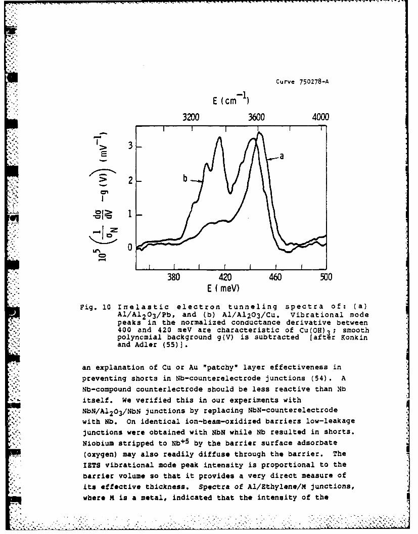
Curve 750278-A
E (cm
3200 3600 4000
3 S a
> 2 -b
I 1UI% 0
380 420 460 500E (meV)
Fig. 10 Inelastic electron tunneling spectra of: (a)Al/A1203/Pb, and (b) Al/Al203/Cu. Vibrational modepeaks in the normalized conductance derivative between400 and 420 meV are characteristic of Cu(OH) ; smoothpolynomial background g(V) is subtracted [aftir Konkinand Adler (55)].
an explanation of Cu or Au *patchy" layer effectiveness in
preventing shorts in Nb-counterelectrode junctions (54). A
Nb-compound counterlectrode should be less reactive than Nb
itself. We verified this in our experiments with
NbN/A1203/NbN junctions by replacing NbN-counterelectrode
with Nb. On identical ion-beam-oxidized barriers low-leakage
junctions were obtained with NbN while Nb resulted in shorts.
Niobium stripped to Nb+5 by the barrier surface adsorbate
(oxygen) may also readily diffuse through the barrier. The
IETS vibrational mode peak intensity is proportional to the
barrier volume so that it provides a very direct measure of
its effective thickness. Spectra of Al/Ethylene/M junctions,
where M is a metal, indicated that the intensity of the
-- -,- . ., . . .:-.- . . . ,. .. -! . . i - .. - . : - ii! :: i : i i" :: .

characteristic 360 meV peak is proportional to the ionic
radius of M, as shown in Fig. 11 (56). The counterelectrode-
diffusion into the barrier was thus demonstrated convinc-
*: ingly. The Nb+5 radius is 0.069 nm, and by extrapolating the
plot of Fig. 11 to this value one expects an effective ethyl-
ene barrier under Nb that is an order of magnitude thinner
than that under the Pb-electrode, a dramatic difference.
Curve 750280-A
0.03AI-Ethylene-Mx
0.02.+1
€-g-- n+2
i n-° + 3 S n 2
-,--":":0. 01 In
-. n+2 A u+3
0 , P
.07 .08 .09 .10 .11 .12 .13 .14Ionic Radius (nm)
Fig. 11 The intensity of IETS vibrational mode ethylene peaks vsthe ionic radius of the counterelectrode metal M (afterMagno V (56)).
Thermally activated diffusion through the barrier is enhanc-
ed if grain boundaries are present. In Liehr's experiments
quoted above, the in-situ fabricated and tested Al/A1203/Pb
junctions with crystalline barriers invariably shorted upon
thermal cycling to only 50 K, while those with a-A1203 could
be cycled up to 500 K (51). To minimize the interdiffusionand occuzence of shorts in thin barriers, two extremes are,
therefore, recommended: either an amorphous or a single--
F*~~~~**; V.:f..~

crystal barrier.The kinetic energy of cae deposited counterelectrode atomic
or ionic species will assist the interdiffusion and mixing
with the barrier. In thermalized magnetron sputter-deposit-ion, at practical target-to-substrate distances, the energydistribution cutoff is typically of the order of a few eV(57). The presence of a low fraction of more energeticparticles cannot, however, be excluded. From this point of
view, evaporation of refractory counterelectrodes is prefer-aole since the kinetic energies involved are well below 1eV. For NbN, however, reactive sputter-deposition is almostuniversally employed. A magnetron gun system, either dc orrf, should be used in this case as it minimizes the bombard-ment of the substrate by energetic particles.The effects reviewed above can sconsume" the upper part ofthe barrier. The thinnest regions are at risk to be consumedentirely, thus resulting in shorts.
Counterelectrode Gap DegradationCounterelectrode energy gap values approaching those of bulksuperconductors have not been attained, except in the mostrecent work by Shoji t al (10), and yet unpublished studyby Yamashita (58). These exceptions will be discussed
later.Interactions at the barrier/counterelectrode interface, thathave been discussed above, can degrade the counterelectrodeenergy gap over a depth scale comparable to that of barrierdegradation. In Bl and Al5 compounds that depth may repres-ent a fraction of the coherence length. Consequently, the gapvoltage may be reduced, the subgap conductance increased, andproximity effect features in the I-V characteristic accen-tuated. Systematic studies of the counterelectrode degrada-tion problem have not been published to date. We believe,
however, that the dominant effect is that of crystallinestructure and morphology of the counterelectrode near theinterface, rather than electrochemistry. This belief isbased on the Tc dependences upon the film thickness.Measurements by many authors, and'our own data for Nb3Gefilms on sapphire substrates, show that in A15 films the bulkTc value is attained only at thicknesses exceeding the coher-

ence lengths (Table 1) by an order of magnitude or more. For
Nb and NbN the bulk Tc is practically attained within 2 to 4P coherence lengths, depending upon the substrate (59). This
' is illustrated in Fig. 12 where Tc/Tc bulk is plotte. vs.
the normalized thickness of polycrystalline film, x/es The
-.. Tc decrease at x < s is theoretically expected (60) and of
-' no consequence here. The plots are, in fact, limited to
X/s > 1. The different behavior of Al5's, exemplified by
Curve 750279-A
1.0;:-'")i ::Nbi
-J S (rm) :S0.5-
Nb NbN Nb3Ge
20 5 3
001 i2,""10 0 101 102
Fig. 12 Normalized critical temperature vs normalized filmthickness [Nb on Si data after Kodama a, (59), NbN onSi and Nb3Ge on sapphire- our data].
• .. _- ' . - .- . , .-. , ; , , , ,: " ., , " , - - . , , - . -. . . . , . . , , , - . . . ...3

Nb3Ge, can only be explained by their Tc's susceptibility to
crystalline disorder. It is well known, for example, that
upon disordering by fast-neutron irradiation all high-TcAlh's degrade dramatically at dqses that hardly alter the Tcof NbN or Nb (61,62). That the Tc degradation in thin films
is due to disorder is proven by the fact that epitaxial*' deposition of very thin films, x-ujs, results in Tc's ap-
proaching the bulk value. This was shown for Nb3Ge and also
for Nb (63,59). Epitaxy, if feasible, thus offers a radical
solution to the counterelectrode gap degradation. Experience
shows that both single-crystal and polycrystalline epitaxycan be effective.
In non-epitaxial films, additional degradation may also be
due to the film morphology. High number density of 3 nmvoids (low density regions) is a. standard feature of very
thin films when the nucleation density is high and the adatom
surface mobility low (64). The voids are separating 1-3 nmclusters of dense deposit. At low deposition temperatures
this microstructure will persist near the substrate /filminterface even if the film grows thicker. The energy gap of
an aggregate of clusters smaller than s , and weakly con-
nected, is lower than that of a bulk superconductor. This*problem is not likely to occur in epitaxial, especially
single-crystalline counterelectrodes, where the described
morphological features are absent.
The high gap voltages of Yamashita's NbN counterelectodes areexplained by epitaxy on textured MgO barriers (58). Shoji at
al obtained slightly lower gap voltages, up to 2.4-2.5 mY,when depositing NbN counterelectrodes on amorphous MgO bar-
riers (10). We believe that short-range order in MgO, unde-
tected by reflection high energy electron diffraction (RHEED),was sufficient in this case to induce polycrystalline, ordered
-.(1... epitaxial) growth of NbN. In our opinion, epitaxiallayered film structures represent the most promising approach
to high-gap counterelectrode fabrication, and thus to a
technology of tunnel junctions capable of operating at tem-
p.ratures up to T 10 K with NbN electrodes, and evenhigher with A15 q.. Nb3Ge electrodes. It is not clear yet,
whether polycrystalline epitaxy will be sufficient, or

single-crystal layered structures required. In either case,
this approach provides a rationale for investigating the
properties of crystalline barriers.
Epitaxial Growth of Electrodes and BarriersWe are conducting a systematic study of epitaxial growth of
,junction electrodes and barriers, with the goal to develop a
technology of epitaxial BI and A15 tunnel junctions. Use ismade of an ultra-high-vacuum (UHV) deposition and surface
analysis system designed especially for this purpose, and. analogous to molecular-beam-epitaxy (MBE) systems (65). In
addition to standard effusion cells, it is equipped with fourelectron gun sources (nine hearths), and four magnetron-sput-
ter-guns in a separate chamber. The UHV environment of <
10-8 Pa permits evaporation/co-evaporation of refractory
metals and compounds at low rates, < 0.1 to 1 nm/min, thatfacilitate epitaxy, without incorporating many impurities.The near-surface structure of a deposited films can be ana-
lysed by RREED, and low energy electron diffraction (LEED)prior to depositing a subsequent layer, and without breakingthe vacuum. The near-surface film phases, composition,
impurities, and overlayer thicknesses can be determined byXPS and, to lesser extent, Auger electron spectroscopy
(AES).
We found that in the UHV environment many metals and comp-ounds of interest tend to grow epitaxially, even on substrat-es of different structure that offer an only very approximatematch of atomic positions and spacings (66). This can beexplained by a low nucleation rate, and high adatom surface
mobility on clean single crystal substrate surfaces. Our
present results can be summarized as follows:1. Epitaxial growth of NbN occurs on MgO single crystal
(111) and (100) surfaces, on polycrystalline MgO and onsapphire of several orientations (67,68). Epitaxy helps
stabilize the Bl phase closer to stoichiometry, so that theTc of NbN (and its energy gap near the substrate) is higherthan on non-epitaxial substrates. In a given set of experi-
* mental conditions, and with a deposition temperature of 300
"5 C. the 50 na thick (111) NbN films on (111) MgO exhibited a
' 5 ' " . . .5-" .5-5 . -. "' '. ".". . . . . . . . .. .' ' '' ' ' ' ° ' '''' ' '' - "

Tc of 16.3 K, approximately 15 K on polycrystalline MgO, and
only 13 K on (110) sapphire. Homoepitaxial growth on poly-
crystalline, textured NbN resulted in a Tc of 16.5 K in 50
nm films grown at a temperature of only 90 C. This shows the
importance of a cloae lattice parameter match that eliminates
the Tc -reducing strains and dislocations present in mis-
matched films.
2. Epitaxial growth of A15 Nb3Sn and Nb3Ge occurs on (1120)
and (0001) sapphire surfaces. An example is shown in
Fig. 13, where RHEED patterns of (100) Nb3Sn show order after
only 6 nm of growth i.e. within approximately two coherence
lengths from the interface with (ll20)sapphire. The qualityof the single crystal, 200 nm thick film is shown by the
narrow X-ray rocking curve width of 0.4 degrees. Single
. crystal (ill) and (100) Nb3Ge films were grown on (111) and
.- (100) stoichiometric Nb3ir with a perfect lattice parameter
match.3. A five-layer all-epitaxial structure was fabricated thatexhioited tunneling characteristics. Starting with (1110)
sapphire, and (ll0)Nb base electrode, a Nb/Al/Al203/Al/Nb
sandwich was deposited with the structure of every layer"* determined by in-situ RHEED. The oxide was formed by oxidiz-
%-* ' -..
Fig. 13 RHEED patterns of (100)Nb3 Sn on (1120) sapphire: (a) 6run thick, (b) 200 nm thick.

ing the first, 3 nm thick Al-overlayer. A diffraction pat-
tern similar to that of Al indicated that the oxide was verythin. The Nb-counterelectrode retained the (110) orientationof the base. The epitaxial barrier was extremely leaky,
however, so that a high sum-gap voltage of approximately 3 mV
could only be guessed.In view of our results, the need to investigate epitaxial and
single-crystal barriers is understandable. Already at thisstage, the feasibility of high-Tc epitaxial B1 and A15 elec-
trodes appears assured. Finding barriers that would exhibita sufficient crystalline match, and the required tunneling
characteristics represents a problem. So far, the only
plausible candidate is MgO for NbN junctions, although the
lattice parameter mismatch is 4% in this case. No suchcandidate material has yet been found for A15 junctions.
Fabrication and Material Alternatives
The selective review of material problems specific to high-Tcrefractory electrodes leads us to a discussion of fabrication
and material alternatives th4 we consider crucial.The first alternative is that of low vs. high processing
temperature, TF, to be used in the whole fabrication
sequence. A low TF, close to ambient, offers the advantage
of a relatively easy control of the previously
discussed,adverse physico- and electrochemical effects that
are particularly troublesome with thin metal oxide barriers.
In this respect, especially important is the possibility offorming amorphous or microcrystalline barriers that are
sufficiently uniform. An additional advantage resides in the
flexibility of patterning. For example, lift-off photoresistcan be used to pattern the counterelectrode in 21-M=t fabri-cation sequences. The disadvantage of low TF is the impos-
sibility to attain the highest Tc,, s/X and also Top via
epitaxy. To date, the low-TF alternative has been chosen by,
virtually all workers in the field, although Kroger at a

indicated the feasibility of high TF -for NbN/Ge/Nb junctions
(9). Niobium nitride, and specifically the NbN/MgO/NbN
configuration are particularly attractive for low tempera-
ture fabrication, as they permit one to exploit epitaxy, at
least to some extent.
The use of high-TF's appears inescapable if one wants to
fabricate high-Tc A15 counterelectrodes or attain the best
superconducting parameters of NbN. It is doubtful whether
oxide barriers could be employed in this case. Elemental or
other, especially molecular compound barriers, however, could
be considered.A related alternative is, therefore, that of thin, large-bar-
rier-height oxides vs composite, low e barriers, and tai-
lored barriers discussed at this Conference (69). Histori-
cally, oxide barriers were used, as thermal, native oxide
barriers formed spontaneously on many base electrodes, and
the Greiner plasma process provided later a high degree of
control of properties, i.e. narrow tolerances of Ic. with
the advent of artificial barriers, however, different ap-
proaches to control of properties should be considered. Theadvantage of thin, artificial oxide barriers is chiefly the
very low subgap conductance, demonstrated in several material
systems. The disadvantage resides in the difficulty of
controlling Ic and Rn to narrow tolerances, unless a
Greiner-type process is used (either plasma or ion-beamoxidation). In this case, a relatively thick metal underlay-
er must be included in the design, not only to protect thebase but also to allow a safety margin for the oxidation
process. This is undesirable, as the junction Ic.Rn product
initially decreases exponentially with the increasing proxim-
ity layer thickness (70). Also, a metallic underlayer, andthe plasma process itself, do not promote epitaxy of the
counterelectrodeo
Thus far, the most successful example of a practical, low-eObarrier is that of composite SiOx/a-Si:H/SiOx, and Ge/SiOx
investigated by the former Sperry group (8,9,19). The role
of a few monolayers of oxide is limited here to plugging thepinholes in the amorphous or crystalline, low resistance
layer that can thus be made relatively thick (Table 2), with
po.7,

N
its Ic and Rn easier to control. An intriguing property
reported on the amorphous Zr-fluoride on Nb base is that, in
spite of a relatively high e - 0.5 eV, it exhibited a very
long wave-function decay length (6.5 nm vs typically 0.2 nm
in oxides) (12). Consequently, the Rn increase with thick-ness was very gradual, and the fabrication of thicker bar-
riers possible. It is probable that this barrier was in
reality a NbF2/ZrF 4 composite, where the ultrathin Nb-fluor-ide, formed in the CF4 cleaning process, plugged pinholes in
ZrF 4. We have observed an analogous situation with the
Nb2O5/CaF 2 barrier on NbN. In this case the thin native oxide
effectively plugged pinholes in CaF 2 (66). Examples, dis-cussed earlier, of using carbide or fluoride protective
layers (2,29) amounted to composite barriers with a native
oxide as the main material. Once a protective layer is in
place, however, a degree of freedom is obtained in the selec-
tion of barrier materials with a variety of desired elec-
trical and electrochemical properties, and without worriesabout the nonuniformity of coverage. So far, this freedom
has been exercised only very timidly. We believe that an
alternative route superior to the thorny path towards thin,
uniform, single-material thin barriers resides in composite,
multilayered, mostly non-oxide barriers that do not have to
be very thin, and in which each layer is consciously assigned
a separate role. Protecting electrodes and the barrier
against adverse electrochemical effects can be separated from
tailoring the electrical (also novel) characteristics within
required tolerances.
It is conceivable, that even the role of epitaxially seedinga polycrystalline, high-T-counterelectrode could be assigned
to a separate, very thin layer. Only the single-crystal epi-
taxy approach appears incompatible with the composite barrier
concept. Too little is known to decide that it will be
* impossible.
The choice of best electrode material, Bl (NbN) vs. A1S, isonly a function of the feasir . of alternatives discussed
above. High TF, interface proc.ition, and polycrystalline
epitaxy may make the use of A15 counterelectrodes possible
and advantageous in the future.
% o°. ° . . _ "., . . . - . - . ,- . .,

We hope that through this discussion of technological alter-
natives we have indicated promising directions for research
that may result in high-Top tunnel junctions, and can also
contribute to the quest for three-terminal, superconducting
devices.
Conclusions
1. Today, the best potential technology is that of all-nio-
bium nitride tunnel junctions with amorphous or microcrystal-
line barriers, processed at low temperatures and possibly ex-
ploiting polycrystalline epitaxy.
2. Longer range barrier research should concentrate oncomposite, mostly non-oxide barriers that will be electro-
chemically compatible with electrodes, and will permit flex-
ibility in tailoring of junction characteristics.
3. Longer range electrode material research should concen-trate on A15 compounds, especially Nb3Sn, Nb3AI and Nb3Ge,
and their growth by polycrystalline and single-crystal epi-
taxy on non-A15 substrates which could be suitable for bar-
rier use. Single-crystal Bl electrodes also deserve atten-
tion.
4. Main problem areas for research are: barrier physics, andphysics and electrochemistry of surfaces and interfaces.
~J. References
1. Beasley, M. R. and C. J. Kircher. 1981. In: Supercond-uctor Materials Science (S. Foner and B. B. Schwartz,eds.). Plenum Press, p. 605.
2. Raider, S. I.. 1985. IEEE Trans. on Magnetics AQ-21,110.
3. Orlando, T. P., E. J. McNiff, S. Foner and M. R. Beas-
ley. 1979. Phys. Rev. B 11, 4545.
4. Simmons, J. G.. 1963. J. Appl. Phys. 34, 1793.
. . . . . ..°

4**..o
5. Halbritter, J.. 1982. Surf. Sci 122, 80. Also:1985. IEEE Trans. on Magnetics M-21, 858, andthis Conference.
6. Bending, S. J. and M. R. Beasley. 1985.Phys. Rev. Lett. U 324.
7. Rogers, C. T. and R. A. Buhrman. 1984. Proc LT-17.(U. Eckern, W. Weber and H. Wuehl, eds.) North-Holland,p. EP14.
8. Smith, L. N., J. B. Thaxter, D. W. Jillie and H. Krog-er. 1982. IEEE Trans. on Magnetics, UU-11, 1571.Also: H. Kroger,. L. N. Smith, D. W. Jillie andJ. a. Thazter. 1983. Ibid. H-11# 783.
9. Kroger, H., D. W. Jillie, L. N. Smith, L. E. Phaneuf,C. N. Potter, D. M. Shaw, E. J. Cukauskas andM. Nisenoff. 1984. Appl. Phys. Lett. A, 562.
10. Shoji, A., M. Aoyagi, S. Kosaka, F. Shinoki andH. Hayakawa. 1985. Appl. Phys. Lett. 4, 1098. Also:this Conference.
[ 11. Gavaler, J. R.. 1985. (Westinghouse R&D Center). Un-pub. ished results.
12. Asano, H., K. Tanabe, 0. Michikami, M. Igarashi andM. R. Beasley. 1985. Jap. J. Appl. Phys. ZA, 289.
13. Moore, D. F.. 1978. Dissertation, Stanford Univ.Also: D. A. Rudman and M. R. Beasley. 1981. Appl.Phys. Lett. 31, 1010.
14. Rowell, J. 4., M7 . Gurvitch and J. Geerk. 1981. Phys.Rev. B, 2A, 2278.
15. Gurvitch, M., M. A. Washington, H. A. Huggins andJ. M. Rowell. 1983. IEEE Trans. on Magnetics MAQ-19,791.
16. Based on the dielectric constant of bulk MgO and themeasured thickness.
17. Shoji, A., S. Kosaka, P. Shinoki, M. Aoyagi andH. Hayakawa. 1983. IEEE Trans. on Magnetics MAQ-19,827.
18. Shinoki, F., A. Shoji, S. Kosaka, S. Takada and
H. Hayakawa. 1981. Appl. Phys. Lett. 3A, 285.
19. Jillie, D. W., H. Kroger, L. N. Smith, E, J, Cukauskasand M. Nisenoff. 1982. Appl. Phys. Lett. , 747.
20. Rudman, D. A.. 1982. Dissertation, Stanford Univ.G. L. Rept. No. 3509, p. 72. Also: 1984. D. A.Rudman, F. Hellman, R. H. Hammond and M. R. Beasley,J. Appl. Phys. 1, 3544.
21. Hammond, R. H.. 1978. J. Vacuum Sci. Tech. 15, 382.
22. Hellman, P. A., A. F. Marshall and T. F. Geballe.1985. Bull. Am. Phys. Soc. 3, 607.
23. Greggi, J. and J. R. Gavaler. Ibid., 608.
24. Talvacchio, J., A. I. Braginski and M. A. Janocko.1985. IEEE Trans. on Magnetics MAQ-U1 521.
25. Kihlstrom, K. E.. 1982. Dissertation, Stanford Univ.,G. L. Rept. No. 3467. Also: Kihlstrom, K. E.,R. H. Hammond, J. Talvacchio and T. H. Geballe. 1982. -J. Appl. Phys. U, 8907.
26. Igarashi, M., M. Hikita and K. Takei. 1984. In: Adv. -
Cryo. Eng. (A. F. Clark and R. P. Reed, eds.) 34, p. 535.
27. Gurvitch, M. and J. Kwo. Ibid. p. 509.
28. Arnold, G. B.. 1978. Phys. Rev. 8U8, 1076: E. L. Wolfand G. B. Arnold. 1982. Phys. Repts. U1, 31.
29. Michikami, 0., K. Tanabe, Y. Kato and H. Takenaka. -1985. IEEE Trans. on Magnetics AQ-21j, 528.
30. Ihara, H., Y. Kimura, H. Okumura, K. Senzaki andS. Gonda. 1984. In: Adv. Cryo. Eng. (A. F. Clark andR. P. Reed eds.) 3U, p. 589.
31. Fromhold, A. T., jr. 1976. Theory of Metal Oxidation,Vol. 1. North-Holland Publ. Co., N.Y.
32. Gavaler, J. R., M. A. Janocko and C. K. Jones. 1974.In: Low Temperature Physics - LT13 ( K. D. Timmerhaus,W. J. Sullivan and E. F. Hammel, eds.), Plenum Co., 3,p. 559.
33. Talvacchio, J., M. A. Janocko and A. I. Braginski.1985. Bull. Am. Phys. Soc. IQ, 280.
34. Miedema, A. R. and F. J. A. den Broeder. 1979. Z. Met-allkunde, 71, 14.
35. Kwo, J., G. K. Wertheim, M. Gurvitch andD. N. E. Buchanan. 1982. Appl. Phys. Lett. 4Q, 675.
36. Kwo, J., G. K. Wertheim, M. Gurvitch and D. N. E.Buchanan. 1983. IEEE Trans. on Magnetics, MAQ-19, 795.
37. Umbach, C. P., A. M. Goldman and L. E. Toth.
1982. Appl. Phys. Lett. in, 81.
. - . .* .- =* *- .

38. Grundner, M. 1977. Proc 3rd Int. Conf. SolidSurf. (Dobrozemsky et al. eds.) Vol. 21 p. 2237.Also: 1977. Nuclear Center Karlsruhe (KfK) Rept. 2565.
39. Graybeal, J. M. and M. R. Beasley. 1984. Phys. Rev. B2., 4167.
40. Shunk, F. A. 1969. Constitution of Binary Alloys,Second Supplement, McGraw-Hill Book Co., p. 189.
41. Van Vechten, D. and J. F. Liebman. 1985. J. Vac. Sci.Tech. A 3, 1881.
42. Grundner, M. and J. Halbritter. 1984. Surf. Sci. l..,144, and references therein.
43. Sanz, J. M. and S. Hofmann. 1983. J. Less CommonMet. 92, 317.
44. Ermolieff, A., M. Girard, C. Raoul, C. Bertrand andT. Minh Duc. 1984. Presented at the 6th Symp. on
* Appl. Surface Analysis, Dayton, Ohio (unpublished).
45. Halbritter, J. 1985. Unpublished research report (Nucl-
"* ear Center Karlsruhe).
46. Greiner, J. H. 1971. J. Appl. Phys. 42, 5151.
47. Ronay, M. and E. E. Latta. 1983. Phys. Rev. B 27, 1605.
48. Ruggiero, S. T., G. B. Arnold, E. Track and D. E.Prober. 1984. IEEE Trans. on Magnetics UAi-21, 850.
49. Talvacchio, J, J. R. Gavaler, A. I. Braginski andM. A. Janocko. 1985. Submitted to J. Appl. Phys.
50. Schneider, U., J. Geerk and H. Rietchel. 1984. Proc-eedings of LT-17 (U. Eckern, A. Schmid, W. Weber andH. Wuhl, eds.), North-Holland, p. 489.
51. Liehr, M. 1982. Dissertation, Aachen Univ., (unpublish-ed). Also: M. Liehr and S. Ewert. 1982. Z. Phys. -
--.- Condensed Matter iZ, 95.
52. Halbritter, J. 1984. Private communication.
53. Hawkins, G. and J. Clarke. 1976. J. Appl. Phys. 47,1616.
54. Bain, R. J. P. and G. B. Donaldson. 1985. Trans. IEEEon Magnetics sag-2, 543.
55. Konkin, M. K. and J. G. Adler. 1983. J. Phys. Chem. 8,2477.
56. Magno, R., M. K. Konkin and J. G. Adler.1977. Surf. Science 69, 437.
- - -:,i .i , " -A . I _11

57. Meyer, K., I. K, Schuller and c. M. Falco. 1981.J. Appi. Phys. UZ, 5803.
58. Yamashita, T. 1985. To be published in Adv. Cryo. Eng.(Proceedings of the 1985 CEC-ICMC, Boston, August1985).
59. Kodama, J., M. Itoh and H. Hirai. 1983.J. Appi. Phys. 5A, 4050.
- -60. Cooper, L. N. 1961. Phys. Rev. Lett. ~,689.
61. Sweedler, A. R., C. L. Snead and D. E. Cox. 1979.In: Treatise on Materials Science and Technology,1.4,(T. Luhman and D. Dew-Hughes, eds.). Academic Press,p. 349.
62. Dew-Hughes, D. and R. Jones. 1980. Appi. Phys. Lett.~.,856.
63. Gavaler, J. R., A. I. Braginski, M. Ashkin andA. T. Santhanam. 1980. In: Superconductivity in d- andf-band Metals (H. Suhi and M. B. Maple, eds.) AcademicPress, p. 25.
64. Messier, R., A. P. Gini and R. A. Roy. 1984. J. Vac.Sci. Technol. &Z, 500.
65. Talvacchio, J., M. A. Janocko, J. R. Gavaler andA. I. Braginski. 1985. Submitted to Adv. Cryo. Eng. U2,
66. Gavaler, J. R., A. I. Braginski, M. A. Janocko andJ. Talvacchio. 1985. In: Materials and Mechanisms ofSuperconductivity ( E. Wolf, ed.). In press.
67. Gavaler, J. R., J. Talvacchio and A. I. Braginski.1985. Submitted to Adv. Cryo. Eng. 12,67.
68. Gavaler, J. R., J. Greggi and J. Schreurs. 1984.In: Proceedings of LT-17(U. Eckern, A. Schmid, W. Weberand H. Wuhl, eds), p. 115.
69. Klapwijk, T. M., this Conference.
70. Gallagher, W. J.. 1981. Physica. I= 825.

APPENDIX D
Artificial oxide barriers for NbN tunnel junctionsa)
,-" J. Talvacchio, J. R. Gavaler, A. I. Braginski, and
M. A. Janocko
Westinghouse R & D Center, Pittsburgh, Pennsylvania 15235
(Received
Superconducting tunnel junctions have been prepared with NbN
base electrodes, oxidized Al or Mg tunnel barriers, and NbN or Pb
.. counterelectrodes. The tunnel barriers were formed either by
thermal oxidation at room temperature or by subjecting the thin
overlayers of Al or Mg to a low-energy ion beam in an argon-5%
oxygen background. High-quality junctions with Pb coun-
terelectrodes were produced by either method. However, for junc-
tions with NbN counterelectrodes deposited at room temperature,
',. the thermal oxidation resulted in shorts and the ion-beam oxida-
tion resulted in low-leakage junctions. XPS measurements of the
NbN/artificial-oxide bilayers showed that the Ion-beam treatment
increased the aluminum oxide thickness by the minimum detectable
increment, approximately 0.2 nm, and increased the MgO thickness
by 1 nm. The superconducting energy gap inferred for NbN coun-
terelectrodes was typically half as large as the gap of the NbN
base. Limitations on the values of NbN counterelectrodes grown on
these barriers were established by measuring the energy gap of
films as thin as 7.5 nm.
%-1-

INTRODUCTION
interest in superconducting tunnel junctions with NbN
electrodes stems from the desirability of operating circuits
based on Josephson junctions at a temperature greater than 10K.
* -. "Shoji et al. have reported that Josephson currents in NbN / rf-
sputtered MgO / NbN junctions were greater than zero at tempera-
S. tures up to 15K.1 A comparison will be made in this paper betwee.
two additional methods of forming Al 2 0 3 and MgO barriers for NbN
junctions: thermal oxidation and ion-beam oxidation of thin
overlayers of Al and Mg.
The oxidized Al and Mg tunnel barriers have potential
benefits as substrates for growth of the counterelectrode when
compared with the native oxide and amorphous silicon barriers
which have also been used successfully in junctions measured at
4.2K. 2 - 6 One advantage is that both Al203 and MgO are refractory
materials which may be able to withstand higher counterelectrode
deposition temperatures. In addition, MgO is a suitable substrate
for polycrystalline epitaxial growth of NbN. A utudy of the
growth of NbN on (100) and (111) single-crysti MgO substrates
has established the epitaxial relationship.7' 8 The critical
temperatures of thin films of NbN (< 50 nm) grown on polycrystal-
line MgO are systematically higher than for films grown on sap-
phire or silicon.8
WH The artificial-oxide barriers were formed by depositing a
thin metallic overlayer followed by oxidation rather than
.. - 2
.I - *.-*uj*.*- <mK -y .: m • :.--

depositing the oxide directly by electron-beam evaporation or rf
sputtering. The rationale was to achieve a more uniform coverage
by the overlayer due to the tendency of one metal to wet
9another. It was also assumed that the oxide thickness would be
more uniform since the oxidation of Al and Mg metal surfaces are
self-limiting. The oxidation process should mitigate the effects
*, of any pinholes in the overlayer by forming the native oxide of
NbN in the pinholes.
An advantage of an artificial barrier over the native oxide
is that it may be useful with other high-Ta superconductors.
During the deposition of an rf-sputtered artificial oxide bar-
rier, oxygen from the sputtering target or added to the sputter
gas to achieve a stoichiometric insulating layer can oxidize the
surface of the base supei anductor before the base is covered by
a barrier. The usefulness of the composite native-oxide /
artificial-oxide barrier which results is limited to superconduc-
tors which do not form a degraded surface layer upon oxidation.
In particular, the A15 compounds exhibit an atomic segregation at
a surface exposed to oxygen. 10 '1 1
The use of an Ar-O 2 ion beam to oxidize tunnel barriers has
been reported by several groups for native-oxide barriers on Nb
base electrodes.12-14 In that case, the ion-beam oxidation was
needed to produce low-leakage junctions, with Pb-alloy coun-
terelectrodes, which could not be formed using a thermal oxide of
Nb. In this work, however, the thermal oxides of Al and Mg formed
excellent tunnel barriers with Pb counterelectrodes. The motiva-
tion for using ion-beam oxidation was to test whether the thick-
ness or thickness uniformity of the oxides could be modified.
,3-
'~~ ~F~~s~V~~d~v . v -C~V ***-

SAMPLE PREPARATION
With the exception of Pb counterelectrodes evaporated in a
separate system, the samples described in this paper were all
made by dc magnetron sputtering in one of the chambers of an oil-
free 4-chamber deposition and analysis facility described
elsewhere. X-ray Photoelectron Spectroscopy (XPS) and Reflec-
tion High-Energy Electron Diffraction (RHEED) measurements, ion
milling, oxidation in a partial pressure of oxygen, and sputter-
ing were all performed without exposing the sample to air.
However, the samples were exposed to air after barrier formation
to change aperture masks for counterelectrode cross-strips. There
is no a priori reason to believe that similar results would not
be obtained if the entire NbN / overlayer (oxide) / NbN trilayer
was deposited in situ and a process analogous to the Selective Nb
Etching Process (SNEP) was used to define the junctions areas.16
The sequence of sputtered layers and oxidation steps was as
follows: Si substrate / 5.0 nm Mg / thermal oxidation / 50 to 100
nm NbN / 3.0 to 8.0 nm Al or Mg / thermal oxidation / (ion-beam
oxidation) / mask change / NbN. The importance of the MgO under-
layer is examined in Ref. 8. The NbN base electrode was deposited
at 300 0 C. The differences between barriers formed by thermal and
ion-beam oxidation versus those formed just by thermal oxidation
of the Al or Mg overlayer is the primary focus of this paper and
will be explained in detail.
The thermal oxidation was performec at room temperature.
After transferring the samples in vacuum to an adjacent chamber,
100 millitorr of 02 was bled into the chamber and pumped out 15
minutes later. Based on XPS measurements of the thickness of the
-4-

7 .
thermal oxide, no further oxide growth occurred in the subsequent
10 to 15 minute exposure to air while an aperture mask was
mounted on the samples for counterelectrode deposition.
The samples which were subjected to ion bombardment were
oxidized thermally first. This was done to establish a minimum
thickness for the oxide with the intent that exposure to a low
energy Ar-5Z 02 ion beam would increase the thickness. The ion
milling was done in an Ar + 02 pressure of 5x1O - 5 torr at an
energy of 200 V. The current density was only 100 nA/cm so
milling times were up to 1 hour.
Figures la and lb show the Al2p photoelectron peaks from a
NbN film with an Al overlayer after thermal oxidation and after
ion-beam oxidation, respectively. The peak intensity at a binding
energy with a chemical shift characteristic of photoelectrons
emitted from Al 20 3 increased relative to the unshifted metallic
Al peak after the ion-beam treatment. However, the Nb 3 d
photoelectron intensity also increased after ion milling. A
calculation of layer thicknesses based on peak intensities, the
assumption of smooth, uniform layers of A1 2 03 and Al on top of
NbN, and an escape depth of 2.0 nm, showed that the oxide thick-
ness increased by about 0.2 nm. The oxide thickness after thermal
oxidation was 2.1 nm and the unoxidized Al thickness was 1.7 nm.
After the ion milling, the oxide was 2.3 nm thick, but the un-
oxidized layer thickness was only 0.5 nm. There was no evidence
of any Nb oxides either before or after ion milling.
The absolute accuracy of the thickness measurements depended
-*' on the validity of the assumptions listed above. In particular,
all thicknesses scaled with the value used for the photoelectron
-5-
-w':

escape depth. However, the relative accuracy from one measurement
of a NbN / Al / A1 2 03 multilayer sample to another was about 0.1
nm, just small enough leave no doubt that the increase in oxide
thickness due to the ion-beam treatment was real.
The effect of the process was similar to that achieved by
Greiner who formed native-oxide barriers on Nb and Pb with an
argon-oxygen rf-induced plasma which simultaneously oxidized and
'-:'17sputtered the surface. The significant differences were our use
of an artificial barrier and of in-situ XPS to determine an end
point for the process.
RESULTS AND DISCUSSION
A. Junctions with barriers formed by thermal oxidation
Typical quasiparticle I-V characteristics measured at 4.2K
for NbN / thermally oxidized Al or Mg / Pb tunnel Junctions are
shown in Fig. 2. The Josephson current was not measured because
the Junctions had large areas, typically 0.005 cm2 , which result
in self-shielding. The quality of the Junctions, normally ex-
pressed in terms of Vm, can be determined by considering the
ratio of the current measured at 5 mV to the current measured at
2.5 mV, i(5)/i(2.5). The ratio i(5)/i(2.5) was typically 100 and
as large as 110 for oxidized Al barriers and as large as 40 for
* oxidized Mg barriers. An estimate of Vm at 2.5 mV can be made
from the theoretical icRN product.18 Depending on the thickness
of a possible proximity layer, Vm expressed in mV is 0.5 to 1.0
times i(5)/i(2.5). The proximity layer evident as a "knee" at the
gap voltage in Fig. 2 is probably due to the 0.5 to 1.0 nm layer
of unoxidized Al or Mg detected by XPS. The thickness of the Al
-6-am- 6 - *.* .
.-.~i,:-. -...°-

or Mg layer could be decreased to reduce the thickness of the
unreacted layer.
A conservative estimate of Vm at 2.5 mV for the junctions
with thermally oxidized Al is 60. A comparison of Figures 2a and
2b shows that the junctions with oxidized Mg barriers have a
lower Vm due to a smearing of the NbN gap voltage rather than
higher leakage at zero bias. Van Vechten and Liebman have
proposed that Al and NbN react at the interface to form AlN. 1 9
While we have no evidence for such a reaction for Al, the same
mechanism could explain the excess conductance above the Pb gap
for junctions with oxidized Mg barriers. An alternative explana-
tion is that Mg has diffused into the grain boundaries of the NbN
to a greater extent than did Al. Kwo et al. have identified the
role of grain boundary diffusion even at room temperature for the
Nb / Al and Nb / Mg systems. 2 0 The unoxidized Mg layer protected
by the thermal oxide disappeared when a test sample was heated to
300OC leaving only MgO and NbN detectable by XPS. An NbN / Al /
Al 20 3 sample showed no loss of Al at that temperature.
" -The superconducting gap energy inferred for NbN from Fig.
2(a) was ANbN " 2.45.05 meV. The resistive Tc of the film was
13.3-12.8K. The highest Tc of any polycrystalline films made at
300*C was 15K. The ratio, 24 /kBTcs was typically 4.3.
The resistances of tunnel junctions with artificial barriers
formed by thermal oxidation are compared with the resistance of
native oxide barriers in Table 1. The resistance of tunnel bar-
riers using the native oxide decreased sharply when carbon was
introduced into the NbN by adding methane to the sputter gas, but
8the resistance of artificial-oxide barriers did not change. The
-7-

values reported in Table I are for the case where no methane was
used. Oxidized Al barriers were approximately one order of mag-
nitude higher in resistance than the native oxide barriers and
oxidized MgO was three orders of magnitude higher.
The barrier width and height were calculated by modeling the
barrier as a rectangular potential following Simmons and fitting
the conductance to a quadratic function of voltage in the range
21of 0.1 to 0.4 V. The values shown in Table 1 for the fitted
barrier width agree with the thickness of the oxide calculated
from XPS peak intensities to within 0.7 nm. The higher resistance
of the artificial oxide barriers compared with the native oxide
was due to a greater barrier height rather than an increased
width. The barrier heights and, therefore, the junction resis-
tances for thermal oxides of Al grown on Nb or Nb3 Sn were higher
than for the A12 03 barriers on NbN, with barrier heights ranging
, between 1.0 and 2.0 eV depending on the crystal structure of the
oxide.
A number of different counterelectrode materials were
deposited on the NbN / Al (thermal oxide) and NbN / Mg (thermal
oxide) bilayers. NbN counterelectrodes were formed by reactive
sputtering at room temperature both at the same sputtering condi-
tions as the base and at a higher total pressure of the sputter-
ing gas for better thermalization of the sputtered atoms. Nb was
sputtered and evaporated with the bilayers held at room tempera-
ture, and evaporated with the bilayers cooled to 77K. All of
these attempts resulted in junctions which were shorts up to
currents of 100 to 200 mA at which point the samples heated
beyond their transition temperature. The variety of physical
-8-*.. :c..,.,.... ii
... ,......'*" ..-. . ......."............................"-.-...........-.."...-...•......... "......-..-...-.-........ ....-.......

deposition parameters which were studied without altering the
outcome suggested that there was a chemical reduction of the
barriers, probably at the thinnest spots, which shorted the
electrodes.
B. Junctions with barriers formed by ion-beam oxidation
The I-V characteristics of reference Junctions, that is,
junctions with Pb counterelectrodes, for the ion-beam oxidized
barriers are shown in Fig. 3. For ion-beam oxidized Al,
i(5)/i(2.5) - 90 at 4.2K, so the leakage was negligibly higher
than for junctions with thermal oxide barriers. The ion-beam
oxidized Mg barriers, however, had high leakage currents and
i(5)/i(2.5) - 6. RHEED patterns showed that the thermal oxides of
both Al and Mg were composed of randomly-oriented polycrystalline
material. The crystallinity of the oxidized metallic overlayers
"' was in contrast to the result of Shoji et al. who found that much
thinner layers of rf-sputtered MgO were amorphous. After ion-
beam oxidation, the sharp ring patterns became more diffuse
although several rings were still resolved. An effect of the
disorder introduced into the polycrystalline A1 203 by ion-beam
oxidation was an increase in the junction resistance by more than
an order of magnitude. An order of magnitude increase in resis-
tance might appear to be consistent with the increase in oxide
thickness of 0.2 nm observed by XPS, but the increase occurred
because both the average barrier height and width increased
slightly (Table 1).
Figure 4 shows the I-V curve of a NbN / ion-beam oxidized Al
bilayer with a NbN counterelectrode deposited at room tempera-
-9-
~~~~~. ... ...... _.......... , - " .. -. .. .:-"'.".'..... -.-. . . -.. . . .. " -., ./ . ,' -,i : -. :" .. . . , . . - . ..... " .- ": , .1...."".: . . . .

ture. The ratio 1(5)/1(2.5) - 17. The analogous junctions with
ion-beam oxidized Hg barriers had 1(5)/i(2.5) - 3 with most of
the subgap conductance due to a spread in the gap voltage rather
than leakage at zero bias.
The barrier widths inferred from the curvature of the I-V
characteristics and the oxide thicknesses measured directly by
XPS were much greater than the thickness of 0.7 nm of rf-
sputtered MgO used by Shoji et al. The product of the junction
resistance and area was between 1x10 6 and 5x10 6fS.-cm2 for
* . junctions made by Shoji et al., three orders of magnitude lower
than the values in Table I obtained with ion-beam oxidation, and
consistent with the difference in thickness.
C. NbN counterelectrode deposition on oxide barriers
Although junctions such as the one shown in Fig. 4 were
sufficient to demonstrate the properties of the ion-beam oxidized
barriers, the gap voltage of the counterelectrode was only about
half of the gap voltage of the base electrode. In this section,
we consider the limitations of the value of the gap energy of NbN
counterelectrodes grown on polycrystalline MgO. Since it has a BI
structure, MgO should be a more favorable barrier than A1 2 03 for
high gap values of counterelectrodes. Some limit below bulk
values of the energy gap can be expected due to low-temperature
deposition and the short coherence length of NbN, 4 to 5 nm.
The tunnel junctions shown in Fig. 5 were made with Pb
counterelectrodes on four different types of NbN films to
evaluate the homogeneity of the films rather than the properties
of the barrier. All four NbN films were deposited on a 20 am
- 10 -
%..-.", . . . '" ",'. ... , " , ... . . . ...-."... ..... . ..", . , o4.: ;'.: -.. ' ,"" - -" ."""' -" . ''-

underlayer of MgO. The junction in Fig. 5a was made on a 50 nm
thick film deposited at room temperature. The sharp gap, 0.2 meV
wide, indicated that the NbN film was homogeneous. Comparison
with the energy gap of a film of the same thickness grown at
300 0C (Fig. 5b), shows that the gap voltage can be raised by 0.6
mV with the 300C substrate temperature. Preliminary measurements
on tunnel junctions with a NbN counterelectrode deposited at
300*C showed that the ion-beam oxidized barriers remain intact
but the resistance of the junctions were too low to measure the
full I-V curve.
The tunnel junction formed on a 7.5 nm film, which is also
shown in Fig. 5b, had a broader gap, 0.4 meV, and a lower gap,
1.9 meV, than the junctions on the 15 am or 50 am films. The
thickness approximates the first 1 to 2 coherence lengths of a
counterelectrode deposited at 3000C on an MgO barrier so the gap
energy represents an upper limit to the energy gap of a NbN
counterelectrode unless higher temperatures or new sputtering
parameters are used. The junction characteristics in Fig. 5b show
that the gap voltage does not continue to increase for films
thicker than 15 nm.
CONCLUSIONS
The effectiveness of either thermally oxidized or ion-beam
oxidized Al or Mg barriers has been demonstrated for NbN-based
tunnel junctions with Pb counterelectrodes. The deposition of
refractory counterelectrodes on the thermal oxides resulted in
shorted tunnel barriers.
Ion-beam oxidation has enabled the use of NbN coun-
...... ~' . . . . .. 4
. 4.4

terelectrodes by increasing the oxide thickness and perhaps
forming an oxide of more uniform thickness. The junctions with
oxidized Al barriers have lower subgap conductances than com-
parable MgO barriers for thermal oxidation or ion-beam oxidation,
and with either Pb or NbN counterelectrodes, probably due to the
greater tendency of unoxidized Mg to diffuse into the base
electrode. Nevertheless, polycrystalline MgO barriers have the
advantage of providing a suitable substrate for the epitaxial
growth of a NbN counterelectrode.
ACKNOWLEDGMENTS
The authors would like to thank H. C. Pohl for his assis-
tance with thin film deposition and characterization.
The artificial oxide barriers, used with superconductors
other than NbN, were developed in part under Office of Naval
Research contract No. N00014-82-C-0617.
1
J12
"- 12""
.. . . . .. . . .. . . . . . . . .. . . . . . . . .

REFERENCES
a) Supported in part by Air Force Office of Scientific Research
Contract No. F49620-83-C-0035.
1. A. Shoji, M. Aoyagi, S. Kosaka, F. Shinoki, and H. Hayakawa,
Appi. Phys. Lett. 46(11), 1098 (1985).
2. A. Shoji, S. Kosaka, F. Shinoki, M. Aoyaki, and HI. Hayakawa,
IEEE Trans. Mag. MAG-19(3), 827 (1983).
3. E. J. Cukauskas, W. L. Carter, S. B. Qadri, and E. F. Skel-
ton, IEEE Trans. Hag. MAG-21(2), 505 (1985).
4. Masaru Igarashi, Makoto Hikita, and Koji Takei, in Advances
in Cryogenic Engineering - Materials, Vol. 30, edited by A.
F. Clark and R. P. Reed (Plenum, New York, 1984), p. 535.
5. J. C. Villegier, L. Vieux-Rochaz, M. Goniche, P. Renard, and
- M. Vabre, IEEE Trans. Mag. tAG-11(2), 498 (1985).
F. Shinoki, A. Shoji, S. Kosaka, S. Takada, and H. Hayakawa,
Appl. Phys. Lett. 38(4), 285 (1981).
7. G. Oya and Y. Onodera, J. Appl. Phys. 45(3), 1389 (1974).
8. J. R. Gavaler, 3. Talvacchio, and A. 1. Braginski, to be
published in Advances in Cryogenic Engineering - Materials,
Vol. 32, edited by A. F. Clark and R. P. Reed (Plenum, New
York, 1986).
9. J. Kwo, G. D. Wertheim, M. Gurvitch, and D. N. E. Buchanan,
Appi. Phys. Lett. 40(8), 675 (1982).
- 13 -

10. H. Ihara, Y. Kimura, H. Okumura, K. Senzaki, and S. Gonda, in
Adv. in Cryogenic Engineering - Materials, Vol. 30, edited by
A. F. Clark and R. P. Reed (Plenum, New York, 1984), p. 589.
11. J. Talvacchio, A. I. Braginski, M. A. Janocko, and S. 3.
Bending, IEEE Trans. Hag. IIAG-21(2), 521 (1985).
12. A. W. Kl.einsasser and R. A. Buhrman, Appl. Phys. Lett. 37(9),
841 (1980).
13. R. Herwig, Electron. Lett. 16, 850 (1980).
14. S. S. Pei and R. B. van Dover, Appl. Phys. Lett. 44(7), 703
(1984).
15. J. Talvacchio, M. A. Janocko, A. I. Bragineki, and J. R.
Gavaler, to be published in Advances in Cryogenic Engineering
-. Materials., Vol. 32, edited by A. F. Clark and R. P. Reed
(Plenum, New York, 1986).
16. M. Gurvitch, M. A. Washington, H. A. Huggins, and J. M.
Rowell, IEEE Trans. Mag. MjAG-19(3), 791 (1983).
17. J. H. Greiner, 3. Appl. Phys. 45(1), 32 (1974).
18. M. Gurvitch and J. Kwo, in Advances in Cryogenic Engineering
-.Materials, Vol. 30, edited by A. F. Clark and R. P. Reed
(Plenum, New York, 1984), p. 509.
19. D. Van Vechten and J. F. Liebman, J. Vac Sci. Techno. A 3
(1985).
20. J. Kwo, G. K. Wertheim, H. Gurvitch, and D. N. E. Buchanan,
- 14 -
P1%

IEEE Trans. Mag. MAG-19(3), 795 (1983).
21. J. G. Simmons, J. Appl. Phys. 34, 238 (1963).
-15-
"Y.A

0n C ( l - C%'-
LUC)U - 4LAo D C q U
CD 0 C)J 0D C)
cc~~~ 0~j%0-0 0e - 0
ccoU0
1.v I
0
0 C%0
4J 0 001 4-4- 00 4
(U) 0 0 0D 0D 0D
0 0 0t 0
S- C -(D Er(U o 4J 2aM4) c
100 4J 0) c'oUUr_toC F- 'U 'U0 - U
W h. 40 i- U) mU a,.C 1 % .C Q 0 4- 0
CD gm VIA-- c ,
@1 4 '~- LA (V z V

, FIGURE CAPTIONS
Fig. 1 The normalized XPS spectra for Al2p photoelectrons (a)
after thermal oxidation and (b) after ion-beam oxidation
showing the relative decrease of Al and increase of A1 2 03
due to the ion-beam treatment.
Fig. 2 Typical quasiparticle I-V characteristics for NbN /
thermally oxidized overlayer / Pb tunnel junctions. Fig.
2(a) is for an oxidized Al overlayer and (b) is for an
oxidized Mg overlayer.
Fig. 3 Typical I-V curves for NbN / ion-beam oxidized overlayer
/ Pb tunnel junctions. Fig. 3(a) shows the characteris-
tics for an Al overlayer and Fig. 3(b) shows the charac-
teristics for an Mg overlayer.
Fig. 4 The quasiparticle I-V characteristics of a NbN / ion-beam
oxidized Al / NbN tunnel junction. The NbN coun-
terelectrode was deposited at room temperature.
Fig. 5 The quasiparticle I-V curves for tunnel junctions with a
thin NbN base electrode deposited on MgO at (a) room
temperature and (b) 300 0C. The junction characteristics
show that the NbN films deposited at 300 C have a higher
gap voltage than films grown at room temperature. Films
with a thickness of 7.5 nm have a lower and broader gap4..,.
voltage than comparable films 15 nm or 50 nm thick.
- 17-
* '&

Curve 750017-A
(a) Thermal Oxidation
Al~
22
Al 20 3 Al
81 78 75 72 69 66Binding Energy (eV)
t.d. -jd 6-20- 85 CFurv 7501
4.n

Curve 750016-A
'.,"I I I I 1 I
x"10 x10 (a) Al203 Barrier
E
,,,:0 - "T =4.2 K _
,,,,.-, .- I II , I ,
b): MgOBarex 10
z
0 T=4.2 K
I -
. dod. 6 8r.04
-M.l (
oo Ta=4.2hiK
c~t d.- j - oVoltage (my)e 7
- ,*. , ", .' ' . . . " • . - - ... - * ,., . . _ , . X . . ,.,rw r, -/,,,,. ,,, -,,,, ,,,,,,.,,, .,.,, ,.,; .. . . . ., . • . *' :. .: .,...,. ,. .... , . .:.... ... - . ... .. - .'-.,,.- .--

Curve 750013-A
(a) AI203 Barrier
0xlO
~(b) MgO Barrier
x01
E
EP'2':'...
0 T=4.2 K
':0 1 2 3 4 5 6 7; Voltage {mV)
5,'%.
m .d:- ~ 6-20-85 C urve 750013,. .. ,. .. _: -,. ?- .. -. .,. . . ... . ., .. .... ..... .... ..... ., .... . .. .. .. ......... ..... .... ...
2 IJ . LI" m ., L q I I " I .tI "I I")' ,:, ,' ,.,' , . .. , . .-.- .;.,- .".".,.,,:, .: .-. . ,.,- .. ;,. 0" ,, ' . . : .. ,' . . :, : . ,, .- .

.-. . -
Curve 750014-A
"' ,, "I '1iII
x 10 Al203 Barrier
z..
0 T=4.2 KI, - I , I I ! ,I,
0 1 2 3 4 5 6 7Voltage (mV)
- . o
'.J. Talvacchlo
c.td.- jd 6-20-85 rJ-T-Curve 7506L4,*°

Curve 750015-A
(a) T=220C
E
7.5N=Snn
0
0 T1. K
J.(b Talv=300c;.t .- jd 6-2 -8
Cu re 5015Il

FILMED
W .- g rom - -