Effects of Nitrogen Incorporation on Structural and Optical ...
31
Effects of Nitrogen Incorporation on Structural and Optical Properties of GaNAsP Nanowires Mattias Jansson, Shula Chen, Rui La, Jan Eric Stehr, Charles W. Tu, Weimin Chen and Irina Buyanova Journal Article N.B.: When citing this work, cite the original article. Original Publication: Mattias Jansson, Shula Chen, Rui La, Jan Eric Stehr, Charles W. Tu, Weimin Chen and Irina Buyanova, Effects of Nitrogen Incorporation on Structural and Optical Properties of GaNAsP Nanowires, The Journal of Physical Chemistry C, 2017. 121(12), pp.7047-7055. http://dx.doi.org/10.1021/acs.jpcc.7b00985 Copyright: American Chemical Society http://pubs.acs.org/ Postprint available at: Linköping University Electronic Press http://urn.kb.se/resolve?urn=urn:nbn:se:liu:diva-136889
-
Upload
khangminh22 -
Category
Documents
-
view
1 -
download
0
Transcript of Effects of Nitrogen Incorporation on Structural and Optical ...

Effects of Nitrogen Incorporation on Structural and Optical Properties of GaNAsP Nanowires
Mattias Jansson, Shula Chen, Rui La, Jan Eric Stehr, Charles W. Tu, Weimin Chen and Irina Buyanova
Journal Article
N.B.: When citing this work, cite the original article.
Original Publication:
Mattias Jansson, Shula Chen, Rui La, Jan Eric Stehr, Charles W. Tu, Weimin Chen and Irina Buyanova, Effects of Nitrogen Incorporation on Structural and Optical Properties of GaNAsP Nanowires, The Journal of Physical Chemistry C, 2017. 121(12), pp.7047-7055. http://dx.doi.org/10.1021/acs.jpcc.7b00985 Copyright: American Chemical Society
http://pubs.acs.org/
Postprint available at: Linköping University Electronic Press
http://urn.kb.se/resolve?urn=urn:nbn:se:liu:diva-136889

1
Effects of Nitrogen Incorporation on Structural and Optical Properties of GaNAsP Nanowires Mattias Jansson†, Shula Chen†, Rui La‡, Jan E. Stehr†, Charles W. Tu‡,§, Weimin M. Chen†, and
Irina A. Buyanova*†
†Department of Physics, Chemistry and Biology, Linköping University, 58183 Linköping,
Sweden.
‡Graduate Program of Material Science and Engineering, University of California, San Diego,
California 92093.
§Department of Electrical and Computer Engineering, University of California, San Diego,
California 92093.
* e-mail: [email protected], tel: +46 13 281745

2
Abstract
In this work we carry out a comprehensive investigation of structural and optical effects in
GaNAsP nanowires (NWs), which are novel materials promising for advanced photovoltaic
applications. Despite a significant mismatch in electronegativity between N and As/P atoms, we
show that incorporation of nitrogen does not degrade structural quality of the nanowires and the
fabricated NW arrays have excellent compositional uniformity among individual wires. From
temperature-dependent photoluminescence (PL) measurements, statistical fluctuations of the
alloy composition are shown to lead to localization of photo-excited carriers at low temperatures
but do not affect material properties at room temperature. According to time-resolved PL
measurements, the room-temperature carrier lifetime increases in the GaNAsP NWs as compared
with the GaAsP NWs, which indicates reduced non-radiative recombination. Moreover, in spite
of the very low N content in the studied NWs (up to 0.16 %), their bandgap energy can be tuned
by more than 100 meV. This is accompanied by about 30% reduction in the temperature
dependence of the bandgap energy. The presented results demonstrate that alloying of GaAsP
with nitrogen provides an additional means of design optimization, beneficial for, e.g., NW-based
intermediate band solar cells that are highly dependent on the optimum bandgap structure.
Keywords:
Dilute nitrides, GaNAsP, nanowire, photoluminescence, Raman scattering
3
Introduction
III-V semiconductor nanowires (NWs) have in recent years attracted an increasing research
interest owing both to their interesting fundamental properties1 and to the prospects of numerous
potential applications in electronics, optoelectronics and photovoltaics.2,3 III-V materials are
highly relevant to these applications due to their high electron mobility and often a direct
bandgap. The NW geometry itself also has numerous advantages over the traditional bulk and
epilayer geometries. For example, it relaxes lattice-matching constrains, which enables the
integration of the III-V NWs with lattice-mismatched materials like Si. Additionally, it lowers
fabrication costs due to reduced material consumption. Despite a small material volume in NW
arrays as compared with that in an epilayer geometry, it has been shown that optical absorption
efficiency is not reduced - even a sparse NW array can absorb nearly 100% of the incident light, a
property that is very promising for photovoltaic applications.4,5
Recently there has been a rising interest in ternary III-III-V or III-V-V alloys, where the
incorporation of an additional element provides a degree of freedom for, e.g., bandgap tuning.
These types of alloys have been successfully implemented in NWs based on InGaAs6,7, AlGaAs8
and GaAsP9. The latter is of particular interest for photovoltaic applications, since its bandgap
can be varied between 1.4 eV and 2.3 eV, which is useful for development of multi-junction solar
cells involving a bottom Si junction. Traditionally, GaAsP NWs have been grown using a gold
droplet catalyst.10,11 However, gold is known to introduce defects in III-V materials that degrade
their optical quality.12,13 Gold is also not compatible with the silicon technology, as it forms
centers of efficient non-radiative recombination in Si detrimental for device performance.14 A
combination of these effects makes gold-catalyzed NWs a less viable option for photovoltaic
applications, prompting investigations into other growth methods. Recently it has become

4
possible to grow GaAsP NWs using self-catalyzed growth, where gold droplets are replaced by
gallium droplets,15 thereby eliminating the detrimental effects caused by gold incorporation. This
has led to the development of single-junction GaAsP NW solar cells with the efficiency
exceeding 10 %, which were fabricated on a Si substrate.15,16
To further increase the solar cell efficiency above that of a standard single-junction cell, various
so-called third generation solar cell designs have been suggested.17 One such example is the
intermediate-band solar cell (IBSC),18 where an intermediate energy band within the bandgap
facilitates not only direct but also two-step two-photon transitions enabling absorption of low-
energy photons. The intermediate band can originate from either confined states in quantum
dots19-22 or from impurity states in the bandgap.23-25 Theoretically, the efficiency of IBSC is
expected to reach as high as 63% even for a cell based on a single junction,26 which by far
exceeds the Shockley-Queisser limit.27 The highest efficiency is predicted for IBSC with a total
bandgap energy of 1.95 eV, which splits into two sub-gaps of 0.71 and 1.24 eV respectively.18
One promising material which can be tuned to the optimum band structure is the GaNAsP alloy
belonging to the so-called dilute nitrides.28,29 These materials have a number of fascinating
properties, including splitting of the conduction band (CB) into the two separate E- and E+ bands
that diverge with increasing nitrogen composition. This splitting is promising for IBSC, where
the E- and E+ bands serve as the intermediate band and conduction band, respectively.23
Growth of GaNAsP in the form of epilayers30 and stacked quantum well structures31 has been
demonstrated and two-photon absorption via the intermediate band has been shown to occur in
such materials.32 Most recently GaNAsP was also fabricated in the NW geometry,33 which opens
a door for integration of the IBSC concept with the promising NW architecture. To enable this
new technology, the effects caused by introducing nitrogen in GaAsP NWs must be thoroughly

5
understood, yet are hitherto largely unknown. In this work, we address these important issues
based on comprehensive structural and optical characterization studies.
Experimental Methods
The studied GaAsP and GaNAsP NWs were grown on Si (111) substrates by plasma assisted
molecular beam epitaxy (MBE) using Ga droplets as a catalyst. Thermally cracked PH3 and AsH3
were used as P and As sources, respectively, while Ga atoms were supplied from a solid Ga-
source through an effusion cell. Nitrogen in GaNAsP was supplied using an RF nitrogen plasma,
which was excited with powers in the range of 200-250 W. The plasma was ignited after 60
seconds of the GaAsP NW growth. Full details of the growth procedure can be found in Ref. 33.
Four structures were studied including reference GaAsP NWs and GaNAsP NWs grown with
increasing nitrogen flux (denoted as N1, N2 and N3, respectively). Growth parameters of the
investigated structures are summarized in Table 1.
Table 1: Growth parameters of the investigated GaAsP and GaNAsP NWs.
Sample GaAsP GaNAsP (N1) GaNAsP (N2) GaNAsP (N3)
Ga flux (ml/sec) 0.6 0.6 0.6 0.6
AsH3 flux (sccm) 3 3 3 3
PH3 flux (sccm) 4 4 4 4
N flux (sccm) 0 0.3 0.6 0.9

6
The NW morphology was investigated using a LEO 1550 Gemini scanning electron microscope
(SEM), operated with an extraction voltage in the range of 2-4 kV. The crystallographic structure
and alloy composition were analyzed using transmission electron microscopy (TEM) and energy
dispersive X-ray spectroscopy (EDXS) performed with a FEI Tecnai G2 transmission electron
microscope. For these purposes, the NWs were mechanically transferred to a TEM grid. The
TEM images were obtained using a CCD camera, while scanning TEM (STEM) images were
acquired by a high-angle annular dark-field detector.
Optical properties and lattice dynamics of NWs were extensively characterized using micro-
photoluminescence (µPL) and µ-Raman spectroscopies. For measurements on individual wires,
the NWs were mechanically transferred to a Si substrate, where the individual NWs could be
resolved using an optical microscope. Both µPL and µ-Raman measurements were performed in
a backscattering geometry using solid state lasers emitting at 532 or 660 nm for excitation. The
laser beam was focused to an estimated spot diameter of 0.5-1 µm on a sample, using 50x (0.5
NA) or 100x (0.9 NA) objective lenses. The emitted (or scattered) light was dispersed using a
grating monochromator and detected using a CCD camera. Photoluminescence excitation (PLE)
measurements were performed with a tunable Ti:Sapphire laser as an excitation source. Transient
photoluminescence studies were done at room temperature for NW arrays, excited by a
frequency-doubled pulsed Ti:Sapphire laser at 440 nm with a pulse width of 2 ps. The PL signal
was detected using a streak camera in combination with a single grating monochromator.
Results and Discussion
Electron microscopy

7
Effects of nitrogen incorporation on the NW morphology can be seen from Figures 1a-c, where
representative SEM images of the NW arrays grown on Si substrates are shown. The GaAsP
NWs are found to be uniform in both length (l) and diameter (d), with average values of
approximately 2 µm and 90 nm, respectively- see Figure 1a. The average NW diameter does not
Figure 1: Tilted view SEM images of the GaAsP (a) and GaNAsP N1-N3 (b)-(d) NWs. Top view SEM images of single GaAsP (e) and GaNAsP N3 (f) NWs. (g) and (h) are TEM images of single GaAsP and GaNAsP (N3) NW, respectively. The scale bars in (e)-(h) are 100 nm.

8
significantly change for the N1 (N2) GaNAsP wires grown with a nitrogen flux up to 0.6 sccm
(Fig 1b,c), whereas a further increase in the N flux causes severe NW tapering accompanied by
shortening of their lengths (Fig. 1d). This is attributed to the formation of strong Ga-N bonds,33
which limits the mobility and diffusion length of the Ga adatoms and accelerates consumption of
the Ga droplet. After the Ga droplet was consumed, the initial axial growth via the vapor-liquid-
solid (VLS) mechanism was terminated leading to the dominance of a radial vapor-solid (VS)
epitaxial growth and, thus, enlargement of the NW sidewalls. With the highest N flux, the fast
depletion of the Ga droplet may also promote the tapering, as the NW base can be expanded due
to the transition from the VLS to VS epitaxial growth whereas the tip is unaffected by the VS
growth and stays constant in diameter. All wires, however, retain a hexagonal cross-section
characteristic for the axial growth along the <111> direction. This can be clearly seen from
Figures 1e-f, where the top-view SEM images of single GaAsP and GaNAsP (N3) NWs are
shown. The changes of the NW morphology with increasing N flux can also be seen by
comparing the TEM images of single GaAsP and GaNAsP (N3) NWs shown in Figures 1g and h,
respectively.
In contrast to the N-induced changes in the NW morphology, the incorporation of N does not
affect the crystalline structure of the wires. Both GaAsP and GaNAsP wires are found to
crystallize in the zinc-blende (ZB) lattice structure. The lower part of the NWs contains only a
small number of rotational twin planes (seen as horizontal lines in Figures 1g and h), whereas in
the upper part a significant increase in the twin plane density and minor inclusions of wurtzite
segments are observed.
To evaluate effects of alloying with nitrogen on the alloy composition of the wires, we have
performed scanning EDXS measurements and the representative results are shown in Figure 2.

9
1.5 2.0 8.5 9.0 9.5 10.0 10.5 11.0
X-r
ay in
ten
sity
(a.
u.)
GaAs
P
X-ray in
tensity (a
.u.)
(b) GaAsP
GaAs
P
(c) GaNAsP (N3)
GaK
CuK
AsK
GaK
X-r
ay i
nte
nsi
ty (
a.u
.)
Energy (keV)
PK
SiK
GaAsP
GaNAsP
(a)
Figure 2: (a) EDXS spectra, acquired from a single GaAsP and GaNAsP NW. The Gaussian fits of the Kα- peaks, used to estimate alloy content, are shown by the filled areas for one of the spectra. (b) and (c) show the EDXS line scans of the Kα-peak intensities for the GaAsP and GaNAsP NW, respectively. The corresponding TEM images of these NWs are shown in the low part of the figures. The scale bar is 500 nm.

10
The EDX signal was acquired by scanning the electron beam along the axial direction of the
nanowire. Figure 2a shows the detected Kα-peaks from a single GaNAsP (N3) and GaAsP NW,
where the signal has been integrated over the whole scan length and normalized to the Ga Kα-
peak intensity. It can be seen that the relative peak intensities of the P-, As- and Ga-peaks are
similar between the two samples. A slight increase (decrease) of the As (P) peak is seen with
incorporation of nitrogen, but the change is close to the experimental accuracy. We, therefore,
conclude that for the investigated N concentrations, the As/P ratio is not appreciably changed
upon the formation of the GaNAsP alloy. This in turn implies that the N content in the GaNAsP
NWs is rather low, i.e. below the detection limit of around 2%. Consistently, no N Kα-peak can
be detected in the EDXS spectra. Based on the measured intensity ratios between the Kα-peaks,
the P composition can be roughly estimated to be about 24 ± 3 %, which is in agreement with [P]
= 24 % deduced from the Raman and PL measurements to be discussed below. Moreover, within
the experimental accuracy, the alloy composition is found to be practically constant along the
nanowires suggesting that the nitrogen induced tapering does not appreciably affect the As/P
ratio. This can be seen from Figures 2b and c, where the Kα peak intensities as a function of the
scan position along the NW are shown together with the corresponding STEM images. The
results of the EDXS study, therefore, show that alloying GaAsP with nitrogen results in no
measurable change in the composition of the host material.
Raman scattering
To obtain evidence for N incorporation in the N1-N3 nanowires, and also to get further insight
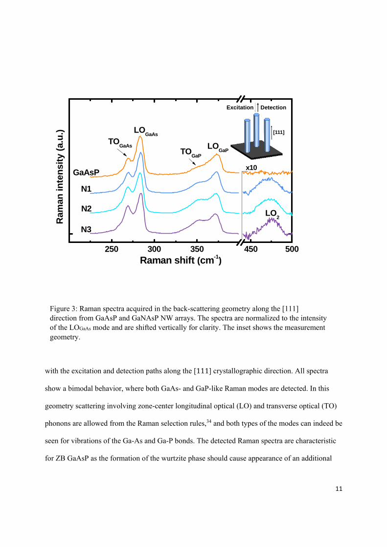
into the crystalline quality of the GaNAsP alloys, Raman spectroscopy was performed. Figure 3
shows unpolarized Raman spectra acquired from the studied NW arrays, which were performed
11
with the excitation and detection paths along the [111] crystallographic direction. All spectra
show a bimodal behavior, where both GaAs- and GaP-like Raman modes are detected. In this
geometry scattering involving zone-center longitudinal optical (LO) and transverse optical (TO)
phonons are allowed from the Raman selection rules,34 and both types of the modes can indeed be
seen for vibrations of the Ga-As and Ga-P bonds. The detected Raman spectra are characteristic
for ZB GaAsP as the formation of the wurtzite phase should cause appearance of an additional
250 300 350 450 500
DetectionExcitation
[111]
N3
N2
Ram
an in
ten
sity
(a.
u.)
Raman shift (cm-1)
x10GaAsP
N1
TOGaAs
LOGaAs
TOGaP
LOGaP
LO2
Figure 3: Raman spectra acquired in the back-scattering geometry along the [111] direction from GaAsP and GaNAsP NW arrays. The spectra are normalized to the intensity of the LOGaAs mode and are shifted vertically for clarity. The inset shows the measurement geometry.

12
optical mode. In GaAs1-xPx the spectral positions of the TO and LO modes are known to reflect
the alloy composition, x.35-37 Based on the results reported by Im et al for GaAsP NWs, the alloy
composition of our GaAs1-xPx wires can be estimated as x = 24 ± 4 %.36
Previous Raman studies of dilute nitride GaNP and GaNAs alloys have shown that the
incorporation of nitrogen into the host lattice may cause several effects on Raman spectra.38-42
They include: (i) shifts of the TO and LO modes caused by changes in lattice stiffness; (ii)
appearance of an additional local mode representing vibrations of the Ga-N bonds; and also (iii)
breaking of Raman selection rules and broadening of the Raman modes due to activation of
forbidden scattering involving zone edge phonons in alloys with a high degree of lattice
disorder.43 From Figure 3, the spectral positions of both TO and LO modes do not change in the
GaNAsP NWs, which again suggests that the N content is rather low. It also indicates that the
As/P-ratio does not change appreciably with nitrogen incorporation, in agreement with the EDXS
results. The incorporation of nitrogen in the N1-N3 wires, however, can be confirmed based on
the appearance on an additional mode centered at approximately 473 cm-1 (labelled as LO2 in
Figure 3). Its observation only in the GaNAsP NWs is a clear indication that the mode
appearance is an effect of nitrogen incorporation. The spectral position of the LO2 mode is very
close to that for the local mode due to the Ga-N bond vibrations in GaAs.39-40,42 On the other
hand, the corresponding mode in GaNP has been reported at around 500 cm-1,41,44 which is not
observed in the present study. The fact that the LO2 position corresponds almost exactly to that
reported in GaNAs epilayers and NWs suggests that the local surroundings of N atoms is
predominantly As-rich, which would result in the GaAs-like vibrations of the Ga-N bonds.

13
Finally it should be noted that the width of the Raman peaks, which is a measure of the structural
disorder, is very similar in the GaAsP and GaNAsP NWs. This suggests that the structural quality
does not deteriorate with nitrogen incorporation. This is further confirmed based on Raman
measurement performed on single GaNAsP (a) and GaAsP (b) NWs transferred to a Si substrate.
Figure 4: GaAs-like Raman modes acquired from a single GaNAsP (a) and GaAsP (b) NW lying on a Si substrate, vertically shifted for clarity. The spectra were measured by focusing the excitation beam on one side of the nanowire, with the excitation and detection beams being incident on the (110) facet of the NWs as schematically illustrated in the inset. The dotted curves represent the Lorentzian fits of the TO and LO modes. The inset shows a schematic of the measurement geometry.

14
The corresponding results are shown in Figures 4a and b, respectively. The measurements were
performed with the excitation and detection beams directed along the [110] crystallographic
direction as shown in the inset in Figure 4. In this geometry, the LO mode is forbidden following
the Raman selection rules in the ZB lattice.34 Accordingly, the LO mode is significantly
suppressed as evident from a comparison of the TO/LO intensity ratios in the Raman spectra
shown in Figures 4 and 3. However, the forbidden LO mode, although suppressed, is still visible
in the spectra measured from the lying wires. This effect has been previously observed e.g. in
polymorphic GaAs NWs and was attributed to the formation of (111) NW facets on the NW
surface caused by the presence of rotational twins,34 which permits the LO scattering. The same
mechanism is also applicable to the studied NWs. We, therefore, conclude that the Raman
scattering generally obeys the selection rules in both GaAsP and GaNAsP NWs which implies
that their crystalline quality is reasonably high.
Photoluminescence spectroscopy
To further understand effects of N incorporation on alloy properties and carrier recombination,
we have performed detailed temperature-dependent PL and transient PL studies.
2a. Origin of the PL emission
Figure 5a shows PL spectra acquired at 4.5 K from the GaAsP and GaNAsP NW arrays. It is
evident that alloying GaAsP with nitrogen leads to a significant red shift in the emission energy,
that is characteristic for dilute nitrides due to the giant bandgap bowing effect. This red shift
increases in the wires grown with a higher nitrogen flux, suggesting that the higher flux leads to a
higher nitrogen content. The same conclusion can also be reached based on the performed PLE

15
measurements – see Figure 5b, where PLE-spectra acquired at 4.5 K from the three GaNAsP NW
arrays are shown. (The bandgap energy of the GaAsP NWs was unfortunately outside the energy
range of a tunable laser used for the PL excitation, which prevented us from performing the PLE
studies of this N-free sample). Since absorption transitions in semiconductor alloys mainly
involve extended band states with a higher density, the onset of the PLE spectrum corresponds to
Figure 5: (a) PL spectra acquired at 4.5K from the GaAsP and GaNAsP (N1-N3) NW arrays grown with increasing N flux. The spectra are normalized to the same peak intensity and are shifted vertically for clarity. The inset shows the normalized µPL-spectra acquired from a single GaAsP and GaNAsP (N1) NW. (b) PLE-spectra detected from the GaNAsP NWs, plotted as the square of the PL-intensity (IPL). The dotted lines are linear fits of the IPL
2 dependences on the excitation energy, which were used to determine the onset of the PL signals corresponding to the alloy bandgaps Eg with the given values for the N1-N3 NW arrays.

16
the alloy bandgap. Taking into account that the studied alloys have a direct bandgap, their
bandgap energies can be determined by linearly extrapolating the squared PL intensity ( ) as a
function of excitation photon energy (shown by the dotted lines in Figure 5b). This yields the
bandgap energies of 1.70, 1.70 and 1.68 eV for the structures N1, N2 and N3, respectively.
From Figure 5 it is apparent that incorporation of nitrogen also leads to a broader and more
asymmetric lineshape of the monitored PL emission, with a tail extending to the low energy side
of the PL spectra. This broadening does not arise chiefly from variations in N compositions
between individual wires within the NW array as it is also observed in µPL spectra acquired from
single wires – see the inset in Figure 5a, where µPL spectra of a single GaAsP and GaNAsP (N1)
NWs are shown. The asymmetric PL lineshape and related broadening are characteristic for
dilute nitrides.29, 31,45-47 Previous studies of GaNAsP quantum well structures have shown that the
emission at low temperatures is completely dominated by localized exciton (LE) recombination,
where the excitons are localized within band tail states arising from compositional
fluctuations.31,47 Similar results have also been reported in GaAs/GaNAs core/shell NWs.48 The
observed large Stokes shift between the PL and PLE spectra provide further evidence that the
low-temperature PL emission in the GaNAsP NWs entirely stems from the LE recombination.
Results of µPL measurements show that, whereas the PL spectrum of the GaAsP wire consists of
a single peak, the GaNAsP emission contains numerous sharp lines superimposed on a broad
background. We have previously reported a similar behavior in GaAs/GaNAs core/shell NWs,
where the sharp lines are attributed to quantum dot-like potential confinement of the excitons due
to short-range alloy fluctuations in N composition.49
To further investigate the localization potential within a single wire, temperature-dependent µPL
studies were performed on individual GaAsP and GaNAsP (N2) NWs. Figure 6a shows the

17
resulting spectra from the GaNAsP NW. It is seen that the LE peak position redshifts with
increasing temperature, T, due to exciton de-trapping from the localized states. At around 180 K,
a new feature due to free exciton (FE) and/or free carrier recombination starts to appear at the
high-energy side of the PL spectra, and becomes dominant at T > 250 K. The FE emission also
shifts to lower energies with increasing T due to thermal variation of the bandgap of the alloy.
Similar behavior is found for the GaAsP NWs (not shown here), which means that at low
Figure 6: (a) Temperature-dependent µPL spectra acquired from a single GaNAsP (N2) NW. (b) Peak positions of the LE (dots) and FE/carrier (triangles) emissions detected from the single GaAsP (filled orange symbols) and GaNAsP (blue open symbols) NWs. The star denotes the PLE onset in the GaNAsP NW, taken from Figure 4b. The dotted lines show the transition from the LE- to FE-dominated emission. The solid lines are the best fits to the experimental data using the Varshni equation for the GaAsP NW and the BAC model for the GaNAsP NW.

18
temperatures the emission spectra of both the ternary and quaternary alloys are dominated by the
LE recombination, while thermal depopulation of the localized states at room temperature leads
to the predominance of the FE/carrier emission. Figure 6b shows the peak positions of the two
peaks as a function of temperature. The dark blue circles (triangles) represent the maximum
positions of the LE (FE) emission from the GaNAsP NW, whereas the orange circles (triangles)
show the peak positions of the corresponding PL bands from the GaAsP NW. The filled symbols
indicate which recombination process is dominating. The star symbol shows the PLE onset. The
transition of the dominant PL emission from the LE to FE emission with increasing T, combined
with the temperature-dependent redshift of these PL bands, leads to the so-called ‘S-shape’ of the
PL maximum position vs. temperature. It can be seen that the energy difference is
larger for the GaNAsP wires and that the transition between the LE- and FE/carrier emission
occurs at a higher temperature in GaNAsP as compared to that in GaAsP. These findings suggest
that the localization potential becomes deeper due to alloying with nitrogen. Taking into account
that the low-energy tail I(E) of the LE emission reflects an exponential density distribution of the
localized states, the localization potential (E0) can be quantified from the slope of the PL tail
as:29,45
ln (1).
The E0 values can be estimated to be about 20 and 70 meV for the GaAsP and GaNAsP NWs,
respectively. These values are comparable to that reported previously in dilute nitride alloys.29
The observed increase in the localization potential in the N-containing wires is probably not
surprising, since under the giant bowing effect of the bandgap energy in dilute nitrides a small
variation in the nitrogen composition can lead to a large change of the bandgap energy.

19
2b. Alloy composition
The aforementioned results from the temperature-dependent PL measurements allow us to further
verify the As/P ratio in the studied wires and also to accurately determine the N composition.
Based on previous studies of dilute nitrides, temperature dependence of the bandgap energy
in these materials can be accurately reproduced using the so-called band anticrossing
(BAC) model50 as
4 (2).
Here is the temperature-dependent bandgap of the GaAsP host matrix, EN is the
energy position of the nitrogen level in GaAsP, V is the parameter describing the interaction
between the host and nitrogen states and y is the nitrogen content. Both EN and V are assumed to
be temperature-independent. The parameters EN and V are well known for both GaNAs and
GaNP,51 and can be obtained for GaNAsP by a linear interpolation of the corresponding values as
discussed in detail in Ref. 28 and 30. The and values are experimentally
determined based on the measured peak positions of the FE/carrier emission and the PLE onset.
This also allows us to verify the P composition x as the bandgap of GaAs1-xPx and its temperature
dependence can be computed using the Vegard’s rule as
1 1 , (3)
where β=0.19 is the bowing parameter of GaAsP52 and and are the
temperature dependent bandgaps of GaAs and GaP, respectively, which were taken from Ref. 52.
The best fit to the experimental data using Eq. 2 and 3 (shown by the solid lines in Figure 6b)

20
yields x = 24 % for the GaAsP NW, in accordance with both EDXS and Raman results. Taking
into account that the As/P ratio is not appreciably affected by the presence of nitrogen, the
nitrogen composition for the GaNAsP (N2) NWs can then be determined as y=0.14 %, whereas it
is found to be 0.12 and 0.16 % in the N1 and N3 NWs, respectively. We note that, in spite of the
very low N compositions, the bandgap energy of the GaNAsP nanowires can be varied by more
than 100 meV. It also becomes less sensitive to variations in the measurement temperature, as can
be seen by comparing the dependences for the GaAsP and GaNAsP wires shown in
Figure 6b. Both of these properties are highly beneficial for future optoelectronic and photonic
applications of such structures.
2c. Compositional uniformity between different nanowires
As discussed above, the band gap energy and emission characteristics of the studied wires
critically depend on their alloy composition. Therefore, for the material system to be viable for
applications, the composition uniformity among the NWs is of significant importance. To
investigate deviations in the alloy composition among nanowires belonging to the same NW
array, we have performed room-temperature µPL spectroscopy on 50 GaAsP and 50 GaNAsP
(N2) NWs. Figure 7 shows the obtained histograms of the PL peak position, where the striped
blue and solid orange columns represent the results from the GaNAsP (N2) and GaAsP NWs,
respectively. By fitting the GaAsP data with a normal distribution function (shown by the solid

21
line in Figure 7), we find the mean value µ = 1.71 eV, the bandgap energy which corresponds to
the P-composition of x = 24 %. We also obtain σ = 3.4 meV, meaning that within one standard
deviation σ, the compositional variation of As and P among the GaAsP NWs within the
fabricated NW array is ± 0.3 %. The fitting parameters for the GaNAsP (N2) NWs are µ = 1.63
eV and σ = 9.2 meV. Here σ is slightly larger than that for the GaAsP sample, which is to be
expected as the variation here is a combined effect of the compositional variation of three
elements: As, P and N. If we assume that the fluctuation in the As/P ratio is not affected by the
Figure 7: Histograms showing statistical distributions of the peak positions in the µPL spectra measured at room temperature from 50 GaAsP (solid orange) and GaNAsP (striped blue) NWs. The data were fitted using a normal Gaussian distribution function as shown by the solid curves. The pink dotted curve shows the calculated energy fluctuations expected in the GaNAsP NW assuming the complete uniformity in the N content.

22
presence of nitrogen, it is possible to estimate the compositional variation of N. The nitrogen
content among the GaNAsP (N2) wires is found to be 0.14 ± 0.02 %. To illustrate the effect of
the nitrogen related compositional non-uniformity, the variance of the GaNAsP emission energy
was also computed assuming complete uniformity in nitrogen composition between the NWs.
This is illustrated by the pink curve in Figure 7. The results of the statistical analysis show that
the GaAsP NW array has excellent compositional uniformity, which also remains reasonably
high within the GaNAsP NW array.
2d. Carrier lifetime
Carrier lifetime is a very important parameter of semiconductors as it reflects contributions of
different radiative and non-radiative processes in the material and, therefore, its optical
efficiency, and also determines transport properties. The carrier lifetime in III-V materials at
room temperature is usually limited by the fast non-radiative recombination, which mainly stems
from surface recombination in the NW geometry53-55 due to a large surface-to-volume ratio. To
gain insights into effects of N incorporation on the lifetime of photo-excited carriers, we
performed time-dependent PL measurements on the NW arrays. The results are summarized in
Figure 8a, where time decays of the integrated PL intensity are shown. It can clearly be seen that
the PL emission from the GaAsP NWs decays faster as compared with the three GaNAsP
samples and the latter exhibit very similar transient characteristics. The transient PL decays can
be fitted by a single exponential function,
exp , (4)
where τpl is the PL lifetime and is given by 1/τpl= 1/τr+1/τnr, with τr (τnr) being the radiative (non-

23
radiative) lifetime. By fitting the data in Figure 8a by Eq. (4), we find the PL lifetimes in the
GaAsP and GaNAsP NWs to be 5 and 10 ps, respectively. The results of this fitting are shown by
the solid lines in Figure 8a. The radiative lifetime in GaAs-based alloys is known to be of the
order of ns even at low temperatures56,57 and is expected to further increase at elevated
temperatures57 as the investigated NWs have too large diameters to experience quantum
confinement effects. This means that the non-radiative lifetime in our structures controls the total
Figure 8: (a) Decays of the integrated PL emission measured at room temperature from the GaAsP (orange squares) and GaNAsP NW arrays. The solid lines correspond to single exponential functions with the PL lifetimes of 5 and 10 ps for the GaAsP and GaNAsP NWs, respectively. Histograms of the integrated µPL intensity acquired at room temperature from 50 GaAsP (b) and GaNAsP (c) NWs. The data were fitted using a normal Gaussian distribution function with the corresponding mean values (µ) displayed in the figures.

24
PL lifetime and that the increase in the PL lifetime upon nitrogen incorporation is an effect of
reduced non-radiative recombination. Such behavior is opposite to that detected previously in
dilute nitride epilayers and quantum structures, where alloying with nitrogen facilitated formation
of various point detects acting as centers of efficient non-radiative recombination and controlling
carrier lifetime.58-60 A similar decrease in non-radiative recombination has previously been seen
in GaAs/GaNAs core/shell NW structures, however, where the incorporation of nitrogen also led
to an increase in lifetime of the GaNAs-related emission. This was attributed to unintentional
nitridation of the NW surface leading to the passivation of non-radiative surface states.56 The
same effect may contribute to the PL lifetime increase in the GaNAsP wires seen in Figure 8a,
which also suggests that it may be common for dilute nitride nanowires. Consistently, the
GaNAsP NWs are found to be on average brighter than their GaAsP counterpart. This can be
seen from Figures 8b and c, where the statistical distributions of integrated PL intensity of 50
NWs from each type of the structures are shown.
Conclusions
In summary, we have performed a comprehensive analysis of structural and optical properties of
novel GaNAsP NWs using electron microscopy and a number of optical characterization
techniques. Despite a significant mismatch in electronegativity between N and As/P atoms, the
performed TEM and Raman studies show that alloying with nitrogen does not degrade the
structural quality of the GaAsP NWs, though the high N flow during the growth promotes
tapering. The statistical study of 50 GaAsP and GaNAsP NWs have revealed excellent
compositional uniformity among the NWs constituting the NW arrays, which only slightly

25
deteriorates after nitrogen incorporation. From temperature-dependent PL measurements,
statistical fluctuations of the alloy compositions are shown to lead to localization of photo-excited
carriers at low temperatures, evident from the predominance of the LE emission in both GaAsP
and GaNAsP NWs. The localization potential significantly increases upon nitrogen incorporation,
promoted by the giant bandgap bowing in dilute nitrides. The room-temperature PL emission
from both types of NWs, however, is dominated by free exciton/carrier recombination due to
thermal activation of the photo-excited carriers from the localized tail states to extended band
states. According to the time-resolved PL measurements, the carrier lifetime increases in the
GaNAsP NWs, which indicates a reduced non-radiative recombination likely due to in-situ
surface passivation with nitrogen. Moreover, in spite of the very low N content in the studied
NWs (i.e. up to 0.16%), the bandgap energy of the GaNAsP nanowires can be tuned from 1.81
down to 1.68 eV (at 4 K). This is accompanied by a reduction in the temperature dependence of
the bandgap energy, which is about 30% within the temperature range of 4.5 - 300K. Our study,
therefore, demonstrates that alloying GaAsP with nitrogen represents a viable and attractive
approach of bandgap engineering, which allows efficient tuning of the electronic properties of the
GaNAsP NWs as required for future optoelectronic and photonic applications.
Acknowledgements
Financial support by the Swedish Energy Agency (grant # P40119-1) and the Swedish Research
Council (grant # 2015-05532) is greatly appreciated. IB acknowledges financial support from the
Swedish Government Strategic Research Area in Materials Science on Functional Materials at
Linköping University (Faculty Grant SFO-Mat-LiU No 2009 00971). The NW growth was
partially supported by the National Science Foundation under Grant No. DMR-1106369.
26
References 1. Joyce, H. J.; Gao, Q.; Tan, H. H.; Jagadish, C.; Kim, Y.; Zou, J.; Smith, L. M.; Jackson,
H. E.; Yarrison-Rice, J. M.; Parkinson, P. et al. III-V Semiconductor Nanowires for Optoelectronic Device Applications. Progress in Quantum Electronics 2011, 35, 23-75.
2. Advances in III-V Semiconductor Nanowires and Nanodevices, Li, J., Wang, D., LaPierre, R. R., Eds.; Bentham Science Publishers Ltd: Oak Park, IL. 2011.
3. LaPierre, R. R.; Chia, A. C. E.; Gibson, S. J.; Haapamaki, C. M.; Boulanger, J.; Yee, R.; Kuyanov, P.; Zhang, J.; Tajik, N.; Rahman, K. M. A. III-V Nanowire Photovoltaics: Review of Design for High Efficiency. Phys. Status Solidi RRL 2013, 7, 815-830.
4. Klezenberg, M. D.; Boettcher, S. W.; Petykiewicz, J. A.; Turner-Evans, D. B.; Putnam, M. C.; Warren, E. L.; Spurgeon, J. M.; Briggs, R. M.; Lewis, N. S.; Atwater, H. A. Enhanced Absorption and Carrier Collection in Si Wire Arrays for Photovoltaic Applications. Nat. Mater. 2010, 9, 239-244.
5. Wallentin, J.; Anttu, N.; Asoli, D.; Huffman, M.; Åberg, I.; Magnusson, M. H.; Siefer, G.; Fuss-Kailuweit, P.; Dimroth, F.; Witzigmann, B. et al. InP Nanowire Array Solar Cells Achieving 13.8% Efficiency by Excieeding the Ray Optics Limit. Science 2013, 339, 1057-1060.
6. Sato, T.; Motohisa, J.; Noborisaka, J.; Hara, S.; Fukui, T. Growth of InGaAs Nanowires by Selective-Area Metalorganic Vapor Phase Epitaxy. J. Chrystal Growth 2008, 310, 2359-2364.
7. Shin, J. C.; Kim, K. H.; Yu, K. J.; Hu, H.; Yin, L.; Ning, C.-Z.; Rogers, J. A.; Zuo, J.-M.; Li, X. InxGa1-xAs Nanowires on Silicon: One-Dimensional Heterogeneous Epitaxy, Bandgap Engineering, and Photovoltaics. Nano Lett. 2011, 11, 4831-4838.
8. Wu, Z. H.; Sun, M.; Mei, X. Y.; Ruda, H. E. Growth and Photoluminescence Characteristics of AlGaAs Nanowires. Appl. Phys. Lett. 2004, 85, 657-659.
9. Zhang, Y.; Aagesen, M.; Holm, J. V.; Jørgensen, H. I.; Wu, J.; Liu, H. Self-Catalyzed GaAsP Nanowires Grown on Silicon Substrates by Solid-Source Molecular Beam Epitaxy. Nano Lett. 2013, 13, 3897-3902.
10. Chen. C.; Plante, M. C.; Fradin, C.; LaPierre, R. R. Layer-by-Layer and Step-Flow Growth Mechanisms in GaAsP/GaP Nanowire Heterostrucutres. J. Mater. Res. 2006, 21, 2801-2809.
11. Mohseni, P. K.; Rodrigues, A. D.; Galzerani, J. C.; Pusep, Y. A.; LaPierre, R. R. Structural and Optical Analysis of GaAsP/GaP Core-Shell Nanowires. J. Appl. Phys. 2009, 106, 124306.
12. Bar-Sadan, M.; Barthel, J.; Shtrikman, H.; Houben, L. Direct Imaging of Single Au Atoms within GaAs Nanowires. Nano Lett. 2012, 12, 2352-2356.
13. Breuer, S.; Pfüller, C.; Fissikowski, T.; Brandt, O.; Grahn, H. T.; Geelhaar, L.; Riechert, H. Suitability of Au- and Self-Assisted GaAs Nanowires for Optoelectronic Applications. Nano Lett. 2011, 11, 1276-1279.
14. Dubois, S.; Palais, O.; Pasquinelli, M.; Martinuzzi, S.; Jaussaud, C. Influence of Substitutional Metallic Impurities on the Performance of p-type Crystalline Silicon Solar Cells: The Case of Gold. J. Appl Phys. 2006, 100, 123502.
15. Holm, J. V.; Jørgensen, H. I.; Krogstrup, P.; Nygård, J.; Liu, H.; Aagesen, M. Surface-Passivated GaAsP Single-Nanowire Solar Cells Exceeding 10% Efficiency Grown on Silicon. Nat. Communications 2013, 4, 1498-1502.
27
16. Tchernycheva, M.; Rigutti, L.; Jacopin, G.; de Luna Bugallo, A.; Lavenus, P.; Julien, F. H.; Timofeeva, M.; Bourlavleeuv, A. D.; Cirlin, G. E.; Dhaka, V. et al. Photovoltaic Properties of GaAsP Core-Shell Nanowires on Si(001) Substrate. Nanotechnology 2012, 23, 265402.
17. Green, M. A. Third Generation Photovoltaics: Ultra-high Conversion Efficiency at Low Cost. Prog. Photovolt: Res. Appl. 2001, 9, 123-135.
18. Luque, A.; Marti, A.; Stanley, C. Understanding Intermediate-Band Solar Cells. Nat. Photonics 2012, 6, 146-152.
19. Luque, A.; Marti, A.; Stanley, C.; Lopez, N.; Cuadra, L.; Zhou, D.; Pearson, J. L.; McKee, A. General Equivalent Circuit for Intermediate Band Devices: Potentials, Currents and Electroluminescence. J. Appl. Phys. 2004, 96, 903-909.
20. Blockhin, S. A.; Sakharov, A. V.; Nadthochy, A. M.; Pauysov, A. S.; Maximov, M. V.; Ledentsov, N. N.; Kovsh, A. R.; Mikhrin, S. S.; Lantratov, V. M.; Mintairov, S. A. et al. AlGaAs/GaAs Photovoltaic Cells with an Array of InGaAs QDs, Semiconductors 2009, 43, 514-518.
21. Bailey, C. G.; Forbes, D. V.; Raffaelle, R. P.; Hubbard, S. M. Near 1 V Open Circuit Voltage InAs/GaAs Quantum Dot Solar Cells. Appl. Phys. Lett. 2011, 98, 163105.
22. Popescu, V.; Bester, G.; Hanna, M. C.; Norman, A. G.; Zunger, A. Theoretical and Experimental Examination of the Intermediate-Band Concept for Strain-Balanced (In,Ga)As/Ga(As,P) Quantum Dot Solar Cells. Phys. Rev. B 2008, 78, 205321.
23. López, N.; Reichertz, L. A.; Yu, K. M.; Campman, K.; Walukiewicz, W. Engineering the Electronic Band Structure for Multiband Solar Cells. Phys. Rev. Lett. 2011, 106, 028701.
24. Yu, K. M.; Walukiewicz, W.; Ager, J. W. III.; Bour, D.; Farshchi, R.; Dubon, O. D.; Li, S. X.; Sharp, I. D.; Haller, E. E. Multiband GaNAsP Quaternary Alloys. Appl. Phys. Lett. 2006, 88, 092110.
25. Gonzalez-Diaz, G.; Olea, J.; Martil, I.; Pastor, D.; Marti, A.; Antolin, E.; Luque, A. Intermediate Band Mobility in Heavily Titanium-Doped Silicon Layers. Solar Energy Mater. & Solar Cells 2009, 93, 1668-1673.
26. Luque, A.; Marti, A. Increasing the Efficiency of Ideal Solar Cells by Phonon Induced Transitions at Intermediate Levels. Phys. Rev. Lett. 1997, 78, 5014-5017.
27. Shockley, W.; Queisser, H. J. Detailed Balance Limit of Efficiency of p-n Junction Solar Cells. J. Appl. Phys. 1961, 32, 510-519.
28. Kudrawiec, R.; Luce, A. V.; Gladysiewicz, M.; Ting, M.; Kuang, Y. J.; Tu, C. W.; Dubon, O. D.; Yu, K. M.; Walukiewicz, W. Electronic Band Structure of GaNxPyAs1-x-y Highly Mismatched Alloys: Suitability for Intermediate-Band Solar Cells, Phys. Rev. Appl. 2014, 1, 034007.
29. For a review of dilute nitride materials, see e.g.: Physics and Applications of Dilute Nitrides, Buyanova, I. A., Chen, W. M., Eds.; Taylor & Francis Books, Inc: New York, 2004.
30. Kuang, Y. J.; Yu, K. M.; Kudrawiec, R.; Luce, A. V.; Ting, M.; Walukiewicz, W.; Tu, C. W. GaNAsP: An Intermediate Band Semiconductor Grown by Gas-Source Molecular Beam Epitaxy. Appl. Phys. Lett. 2013, 102, 112105.
31. Karcher, C.; Grüning, H.; Güngerlich, M.; Klar, P. J.; Volz, K.; Stolz, W.; Heimbrodt, W. Optical Properties of Ga(NAsP) Lattice Matched to Si. Phys. Status Solidi C 2009, 6, 2638-2643.

28
32. Jussila, H.; Kivisaari, P.; Lemettinen, J.; Tanaka, T.; Sopanen, M. Two-Photon Absorption in GaAs1-x-yPyNx Intermediate-Band Solar Cells. Phys. Rev. Appl. 2015, 3, 054007.
33. La, R.; Pan, J. L.; Bastiman, F.; Tu, C. W. Self-Catalyzed Ga(N)AsP Nanowires and GaAsP/GaNAsP Core-Shell Nanowires Grown on Si (111) by Gas-Source Molecular Beam Epitaxy. J. Vacuum Sci. & Tech. 2016, 34, 02L108.
34. Zardo, I.; Conesa-Boj, S.; Peido, F.; Morante, J. R.; Arbiol, J.; Uccelli, E.; Abstreiter, G.; Fontcuberta i Morral, A. Raman Spectroscopy of Wurtzite and Zinc-Blende GaAs Nanowires: Polarization Dependence, Selection Rules and Strain Effects. Phys. Rev. B 2009, 80, 245324.
35. Pistol, M-. E.; Liu, X. Quantum-Well Structures of Direct-Band-Gap GaAs1-xPx/GaAs Studied by Photoluminescence and Raman Spectroscopy. Phys. Rev. B 1992, 45, 4312-4319.
36. Im, H. S.; Jung, C. S.; Park, K.; Jang, D. M.; Lim, Y. R.; Park, J. Bandgap Tuning of Twinned GaAsP Ternary Nanowires. Phys. Chem. C 2014, 118, 4546-4552.
37. Pagès, O.; Souhabi, J.; Postnikov, A. V.; Chafi, A. Percolation Versus Cluster Models for Multimode Vibration Spectra of Mixed Crystals: GaAsP as a Case Study. Phys. Rev. B 2009, 80, 035204.
38. Prokofyeva, T.; Sauncy, T.; Seon, M.; Holtz, M.; Qiu, Y.; Nikishin, S.; Temkin, H. Raman Studies of Nitrogen Incorporation in GaAs1-xNx. Appl. Phys. Lett. 1998, 73, 1409-1411.
39. Wagner, J.; Köhler, K.; Ganser, P.; Herres, N. GaAsN Interband Transitions Involving Localized and Extended States Probed by Resonant Raman Scattering and Spectroscopic Elipsometry, Appl. Phys. Lett. 2000, 77, 3592-3594.
40. Filippov, S.; Ishikawa, F.; Chen, W. M.; Buyanova, I. A. Structural Properties of GaNAs Nanowires Probed by Micro-Raman Spectroscopy. Semiconductor Sci. Tech. 2016, 31, 025002.
41. Buyanova, I. A.; Chen, W. M.; Goldys, E. M.; Xin, H. P.; Tu, C. W. Structural Properties of a GaNxP1-x Alloy: Raman Studies. Appl. Phys. Lett. 2001, 78, 3959-3961.
42. Mintairov, A. M.; Blagnov, P. A.; Melehin, V. G.; Faleev, N. N.; Merz, J. L.; Qiu, Y.; Nikishin, S. A.; Temkin, H. Ordering Effects in Raman Spectra of Coherently Strained GaAs1-xNx. Phys. Rev. B 1997, 56, 15836-15841.
43. Parayanthal, P.; Pollak, F. H. Raman Scattering in Alloy Semiconductors: “Spatial Correlation” Model. Phys. Rev. Lett. 1984, 52, 1822-1825.
44. Yoon, S.; Seong, M. J.; Geisz, J. F.; Duda, A.; Mascarenhas, A. Evolution of Eleoctronic States in GaP1-xNx Studied by Resonant Raman Scattering Spectroscopy. Phys. Rev. B 2003, 67, 235209.
45. Buyanova, I. A.; Chen, W. M.; Pozina, G.; Bergman, J. P.; Xin, H. P.; Tu, C. W. Mechanism for Low-Temperature Photoluminescence in GaNAs/GaAs Structures Grown by Molecular-Beam Epitaxy, Appl. Phys. Lett. 1999, 75, 501-503.
46. Grenouillet, L.; Bru-Chevallier, C.; Guillot, G.; Gilet, P.; Duvaut, P.; Vannuffel, C.; Million, A.; Chenevas-Paule A. Evidence of Strong Carrier Localization Below 100 K in a GaInNAs/GaAs Single Quantum Well, Appl. Phys. Lett. 2000, 76, 2241-2243.
47. Kunert, B.; Volz, K.; Nemeth, I.; Stolz, W. Luminescence Investigations of the GaP-Based Dilute Nitride Ga(NAsP) Material System. J. Luminescence 2006, 121, 361-364.

29
48. Chen, S. L.; Filippov, S.; Ishikawa, F.; Chen, W. M.; Buyanova, I. A. Origin of Radiative Recombination and Manifestations of Localized Effects in GaAs/GaNAs Core/Shell Nanowires. Appl. Phys. Lett. 2014, 105, 253106.
49. Filippov, S.; Jansson, M.; Stehr, J. E.; Palisaitis, J.; Persson, P. O. Å.; Ishikawa, F.; Chen, W. M.; Buyanova, I. A. Strongly Polarized Quantum-Dot Like Emitters Embedded in GaAs/GaNAs Core/Shell Nanowires. Nanoscale 2016, 8, 15939-15947.
50. Shan, W.; Walukiewicz, W.; Ager, J. W. III.; Haller, E. E.; Geisz, J. F.; Friedman, D. J.; Olson, J. M.; Kurtz, S. R. Band Anticrossing in GaInNAs Alloys. Phys. Rev. Lett. 1999, 82, 1221-1224.
51. Vurgaftman, I.; Meyer, J. R. Band Parameters for Nitrogen-Containing Semiconductors. J. Appl. Phys. 2003, 94, 3675-3696.
52. Vurgaftman, I.; Meyer, J. R.; Ram-Mohan, L. R. Band Parameters for III-V Compound Semiconductors and their Alloys. J. Appl. Phys. 2001, 89, 5815-5875.
53. Demichel, O.; Heiss, M.; Bleuse, J.; Mariette, H.; Fontcuberta i Morral, A. Impact of Surfaces on the Optical Properties of GaAs Nanowires, Appl. Phys. Lett. 2010, 97, 201907.
54. Perera, S.; Fickenscher, M. A.; Jackson, H. E.; Smith, L. M.; Yarrison-Rice, J. M.; Joyce, H. J.; Gao, Q.; Tan, H. H.; Jagadish, C.; Zhang, X.; Zou, J. Nearly Intrinsic Exciton Lifetimes in Single Twin-Free GaAs/AlGaAs Core-Shell Nanowire Heterostructures. Appl. Phys. Lett. 2008, 93, 053110.
55. Chang, C.-C.; Chi, C.-Y.; Yao, M.; Huang, N.; Chen, C.-C.; Theiss, J.; Bushmaker, A. W.; LaLumondiere, S.; Yeh, T.-W.; Povinelli, M. L. et al. Electrical and Optical Characterization of Sufrace Passivation in GaAs Nanowires. Nano Lett. 2012, 12, 4484-4489.
56. Chen, S. L.; Chen, W. M.; Ishikawa, F.; Buyanova, I. A. Suppression of Non-radiative Surface Recombination by N Incorporation in GaAs/GaNAs Core/Shell Nanowires. Scientific Reports 2013, 5, 11653.
57. ’t Hooft, G. W.; van der Poel, W. A. J. A.; Molenkamp, L. W.; Foxon, C. T. Giant Oscillator Strength of Free Excitons in GaAs. Phys. Rev. B 1987, 35, 8281-8284.
58. Thinh, N. Q.; Buyanova, I. A.; Hai, P. N.; Chen, W. M.; Xin, H. P.; Tu, C. W. Signature of an Intrinsic Point Defect in GaNxAs1-x. Phys. Rev. B 2001, 63, 033203.
59. Wang, X. J.; Puttisong, Y.; Tu, C. W.; Ptak, A. J.; Kalevich, V. K.; Egorov, A. Y.; Geelhaar, L.; Riechert, H.; Chen, W. M.; Buyanova, I. A. Dominant Recombination Centers in Ga(In)NAs Alloys: Ga Interstitials. Appl. Phys. Lett. 2009, 95, 241904.
60. Thinh, N. Q.; Vorona, I. P.; Buyanova, I. A.; Chen, W. M.; Limpijumnong, S.; Zhang, S. B.; Hong, Y. G.; Xin, H. P.; Tu, C. W.; Utsumi, A. et al. Properties of Ga-Interstitial Defects in AlxGa1-xNyP1-y. Phys. Rev. B 2005, 71, 125209.

30
TOC graphic