DXC-390/390P Service Manual - (PDF) files
110
3CCD COLOR VIDEO CAMERA DXC-390 DXC-390P SERVICE MANUAL 1st Edition
-
Upload
khangminh22 -
Category
Documents
-
view
5 -
download
0
Transcript of DXC-390/390P Service Manual - (PDF) files

3CCD COLOR VIDEO CAMERA
DXC-390DXC-390PSERVICE MANUAL
1st Edition

DXC-390/390P
! WARNINGThis manual is intended for qualified service personnel only.To reduce the risk of electric shock, fire or injury, do not perform any servicing other than thatcontained in the operating instructions unless you are qualified to do so. Refer all servicing toqualified service personnel.
! WARNUNGDie Anleitung ist nur für qualifiziertes Fachpersonal bestimmt.Alle Wartungsarbeiten dürfen nur von qualifiziertem Fachpersonal ausgeführt werden. Um dieGefahr eines elektrischen Schlages, Feuergefahr und Verletzungen zu vermeiden, sind beiWartungsarbeiten strikt die Angaben in der Anleitung zu befolgen. Andere als die angegebenWartungsarbeiten dürfen nur von Personen ausgeführt werden, die eine spezielle Befähigungdazu besitzen.
! AVERTISSEMENTCe manual est destiné uniquement aux personnes compétentes en charge de l’entretien. Afinde réduire les risques de décharge électrique, d’incendie ou de blessure n’effectuer que lesréparations indiquées dans le mode d’emploi à moins d’être qualifié pour en effectuer d’autres.Pour toute réparation faire appel à une personne compétente uniquement.

1 (E)DXC-390/390P
Table of Contents
Manual Structure
Purpose of this manual ........................................................................................ 3 (E)
Related manuals................................................................................................... 3 (E)
1. Operating Instructions
2. Service Overview
2-1. Board location .......................................................................................2-1 (E)
2-2. Removal of cabinet ...............................................................................2-1 (E)
2-3. Removal of CCD block .........................................................................2-2 (E)
2-4. How to use an extension board .............................................................2-2 (E)
2-5. Input/output signals of connectors ........................................................2-4 (E)
3. Circuit Operation Description
3-1. VA-193 Board .......................................................................................3-1 (E)
3-2. DP-313 Board........................................................................................3-1 (E)
3-3. EN-142 Board .......................................................................................3-2 (E)
3-4. SG-265 Board........................................................................................3-3 (E)
3-5. MB-875 Board ......................................................................................3-4 (E)
4. Electrical Alignment
4-1. Preparation ............................................................................................4-1 (E)4-1-1. Adjustment Fixture and Measurement Equipment ..............4-1 (E)4-1-2. Equipment Connection .........................................................4-1 (E)4-1-3. Description of Side Panel Sheet Switches ...........................4-2 (E)4-1-4. Super Reset (data initialization) ...........................................4-2 (E)
4-2. Adjustment ............................................................................................4-2 (E)4-2-1. VCO Adjustment 0(original oscillator adjustment) .............4-2 (E)4-2-2. Built-in Color Bars Adjustment (adjustment from DSP) .....4-2 (E)4-2-3. CCD OUT Adjustment .........................................................4-3 (E)
5. Spare Parts
5-1. Notes on Repair Parts .................................................................................. 5-1
5-2. Exploded View ............................................................................................ 5-2

2 (E) DXC-390/390P
5-3. Electrical Parts List ..................................................................................... 5-4
5-4. Packing Materials & Supplied Accessories .............................................. 5-20
6. Semiconductor Pin Assignments
index ............................................................................................................ 6-1
IC ................................................................................................................. 6-3
7. Block Diagrams
DP-313 ........................................................................................................ 7-1
EN-142 ........................................................................................................ 7-2
MB-875 ....................................................................................................... 7-3
SG-265 ........................................................................................................ 7-4
VA-193 ........................................................................................................ 7-5
8. Schematic Diagrams
Frame........................................................................................................... 8-2
CN-1938 ...................................................................................................... 8-4
PA-236 ........................................................................................................ 8-5
DP-313 ........................................................................................................ 8-6
EN-142 ........................................................................................................ 8-8
SG-265 (1/2) .............................................................................................. 8-10
SG-265 (2/2) .............................................................................................. 8-12
VA-193 (1/2) ............................................................................................. 8-14
VA-193 (2/2) ............................................................................................. 8-15
MB-875 (1/3) ............................................................................................ 8-16
MB-875 (2/3) ............................................................................................ 8-17
MB-875 (3/3) ............................................................................................ 8-18
9. Board Layouts
CN-1938 ...................................................................................................... 9-1
PA-236 ........................................................................................................ 9-1
DP-313 ........................................................................................................ 9-2
EN-142 ........................................................................................................ 9-3
MB-875 ....................................................................................................... 9-4
SG-265 ........................................................................................................ 9-5
VA-193 ........................................................................................................ 9-6

3 (E)DXC-390/390P
Purpose of this manualThis manual is the Service Manual of the 3CCD color video camera DXC-390/390P.This manual contains the operating instructions, service overview, functions,electrical alignment, spare parts, semiconductor pin assignments, block diagrams,schematic diagrams and board layouts.
Related manualsIn addition to this Service Manual, the following manuals are provided for this unit.
..... Operation Manual (Supplied with the DXC-390/390P)This manual is required for the proper operation and application of this unit.Part of the Operation Manual is included also in this Service Manual, in Section 1,“Operating Instructions” .Part number: 3-203-786-11
..... “Semiconductor Pin Assignments” CD-ROM (Available on request)This “Semiconductor Pin Assignments” CD-ROM allows you to search forsemiconductors used in Communication System Solutions Network Companyequipment.Semiconductors that cannot be searched for on this CD-ROM are listed in theservice manual for the corresponding unit. The service manual contains a com-plete list of all semiconductors and their ID Nos., and thus should be used togetherwith the CD-ROM.Part number: 9-968-546-XX
Manual Structure


1-1 (E)DXC-390/390P
Section 1Operating Instructions
This section is extractedfrom operation manual.
2000 Sony Corporation
3-203-786-11(1)
Instructions for Use
DXC-390DXC-390P
3CCD Color Video CameraGB
(DXC-390P only)
DX
C-390/390P

1-2 (E) DXC-390/390P
2 (GB)
Owner’s RecordThe model and serial numbers are located at the bottom.Record these numbers in the spaces provided below.Refer to these numbers whenever you call upon your Sonydealer regarding this product.
Model No. Serial No.
WARNING
To prevent fire or shock hazard, do not expose the unit torain or moisture.
To avoid electrical shock, do not open the cabinet. Referservicing to qualified personnel only.
For the customers in the U.S.A.This equipment has been tested and found to comply withthe limits for a Class A digital device, pursuant to Part 15 ofthe FCC Rules. These limits are designed to providereasonable protection against harmful interference when theequipment is operated in a commercial environment.This equipment generates, uses, and can radiate radiofrequency energy and, if not installed and used inaccordance with the instruction manual, may cause harmfulinterference to radio communications. Operation of thisequipment in a residential area is likely to cause harmfulinterference in which case the user will be required to correctthe interference at his own expense.
English
You are cautioned that any changes or modifications notexpressly approved in this manual could void your authorityto operate this equipment.
The shielded interface cable recommended in this manualmust be used with this equipment in order to comply with thelimits for digital device pursuant to Subpart B of Part 15 ofFCC Rules.
For the customers in Europe (for DXC-390P only)This product with the CE marking complies with the EMCDirective (89/336/EEC) issued by the Commission of theEuropean Community.Compliance with this directive implies conformity to thefollowing European standards:• EN55103-1: Electromagnetic Interference (Emission)• EN55103-2: Electromagnetic Susceptibility (Immunity)This product is intended for use in the followingElectromagnetic Environment(s):E1 (residential), E2 (commercial and light industrial), E3(urban outdoors) and E4 (controlled EMC environment, ex.TV studio)
3 (GB)
Important safeguards/notices for use in the medicalenvironments
1. All the equipments connected to this unit shall be certifiedaccording to Standard IEC60601-1, IEC60950, IEC60065or other IEC/ISO Standards applicable to the equipments.
2. When this unit is used together with other equipment inthe patient area*, the equipment shall be either poweredby an isolation transformer or connected via an additionalprotective earth terminal to system ground unless it iscertified according to Standard IEC60601-1.
* Patient Area
3. The leakage current could increase when connected toother equipment.
R 1.5
m
4. This equipment generates, uses, and can radiatefrequency energy. If it is not installed and used inaccordance with the instruction manual, it may causeinterference to other equipment. If this unit causesinterference (which can be determined by unplugging thepower cord from the unit), try these measures: Relocatethe unit with respect to the susceptible equipment. Plugthis unit and the susceptible equipment into differentbranch circuit. Consult your dealer.
(According to Standard EN60601-1-2 and CISPR11, ClassB, Group 1)
CautionWhen you dispose of the unit or accessories, you mustobey the law in the relative area or country and theregulation in the relative hospital.
English
GB

1-3 (E)DXC-390/390P
4 (GB)
Table of Contents
Table of Contents
Chapter 1Overview
Features .................................................................... 6Location and Functions of Parts and Controls ..... 8
Front Panel/Top Panel/Bottom Panel ..................... 8Right Side Panel (Control Panel) ........................... 9Rear Panel ............................................................ 11
Chapter 2Operation
Adjusting snd Setting with Menus ....................... 12Menu Configuration ............................................. 12Operation through Menus .................................... 14Function of Menus ............................................... 16Initial Setting of the Menus ................................. 31
Shooting.................................................................. 32Adjusting the Flange Focal Length ...................... 32Basic Shooting Procedure .................................... 35Adjusting the Iris, Focus and Zoom..................... 36Adjusting the Black Balance................................ 38Adjusting the White Balance ............................... 39Adjusting the Picture Tone in a Multi-Camera
System ............................................................ 41
Chapter 3Installation and Connections
Installation .............................................................. 42Applicable Lens ................................................... 42Mounting the Lens ............................................... 43Mounting a Microscope Adaptor ......................... 45Mounting on a Tripod .......................................... 45Mounting to a Wall or Ceiling ............................. 45
Basic System Connection ..................................... 47Connecting to Video Equipment with Composite
Video Input Connectors .................................. 48Connecting to Video Equipment with RGB or
S-Video Inputs ................................................ 50Connecting Two or More Cameras—Multi-Camera
System ............................................................ 51Connecting to a Remote Control Unit .................. 52
Operating the Camera with the RM-C950 RemoteControl Unit ................................................... 53
Connecting to a Computer .................................... 54Connections for Long Exposure Shooting .......... 55Connections for Shooting Using a Flash ............. 56
5 (GB)
Chapter 4Appendix
Precautions............................................................. 57Typical CCD Phenomena ....................................... 58List of Messages .................................................... 59Specifications ......................................................... 60Optional Accessories ............................................ 64
Table of Contents

1-4 (E) DXC-390/390P
6 (GB) Chapter 1 Overview
Chapter 1
Features
Chapter 1
High-quality images
• The high density 1/3 type, three-chip Exwave HADTM1)
CCD2), containing some 380,000 (DXC-390) or 430,000(DXC-390P) effective picture elements (pixels), offerssuperior picture quality: 800 TV lines of high horizontalresolution, high sensitivity of F8 at 2,000 lx, an excellentsignal-to-noise ratio of 62 dB (DXC-390) or 61 dB (DXC-390P) and a low smear level.
• The adoption of the LSI digital signal processingtechnology reproduces a finer, more detailed picture.
• DynaLatitude processing enables you to adjust contrastfinely according to the luminance signal level of eachpicture element.
1) Exwave HADTM: Exwave Hole-Accumulated Diode“Exwave HADTM” is a trademark of Sony Corporation.
...........................................................................................................................................................................................................................................................
Overview
• The DCC+ (Dynamic Contrast Control plus) functionminimizes the phenomena whereby the whole screen turnswhite or a part of the image becomes colorless whenshooting a very bright object.
• The Partial Enhance function enables you to adjust thesharpness and tint of only a specified color.
Wide Range of Exposure Control
The AGC (Auto Gain Control) function and CCD IRISTM3)
function automatically adjust a wide range of incoming lightlevels. When the lighting condition is poor, the AGCfunction automatically increases the gain up to 16 times.When incoming light is excessive, the CCD IRIS functionautomatically adjusts shutter speed to cut exposure to the
2) CCD: Charge-Coupled Device3) “CCD IRISTM” is a trademark of Sony Corporation.
Chapter 1 Overview 7 (GB)
Chapter 1
RS-232C interface
The camera can be controlled from a computer via the RS-232C interface.For details, contact your authorized Sony dealer.
Compact and lightweight
The camera is compact (56 × 50 × 128 mm (2 1/4 × 2 × 5 1/8inches)) and very light (approx. 370 g (13 oz)), allowingeasy installation even where space is a problem.Following are some sample applications:• As a permanent fixture in theaters, concert halls, etc.• As a bird’s-eye view camera for special events• As a video conference system camera• As a camera for microscopes• As a rooftop weather-monitoring camera• As a laboratory monitor camera
equivalent of up to 10 aperture stops. When using the videocamera in a fixed location or for a microscope system, theAGC, CCD IRIS and auto-iris controls automatically adjusta wide range of incoming light levels. The desired AEwindow can be set by using the AE AREA MANUALfunction.
Wide range of electronic shutter modes
The wide range of speeds for the electronic shutterminimizes blurring in fast-moving objects and producesacceptably bright still images of objects shot in poor light.• Flickerless mode: This mode allows you to obtain
flickerless images shot even under fluorescent light.• Clear scan mode: This mode reduces horizontal bands
appearing in computer displays when shooting the displaywith the conventional video camera.
Versatile use with external equipment
• The video camera is equipped with three types of outputs:composite, Y/C and RGB outputs. The camera offers ahigh-quality picture on a connected monitor or VCR.
• The camera can be remotely controlled with the RM-C950remote control unit (not supplied).

1-5 (E)DXC-390/390P
8 (GB) Chapter 1 Overview
Chapter 1
Location and Functions of Parts and Controls
2 Screw holes (M3)
Front Panel/Top Panel/Bottom Panel 1 Lens Mount (C-mount)Attach a C-mount lens or microscope adaptor.
Note
Be sure to use a lens whose projected part from the lensmount surface is less than 4.3 mm. Mounting the lens with aprojected part greater than 4.3 mm may damage the internalmechanism of the camera.
2 Screw holesUse these holes (M3, depth: 4 mm (3/16 inches)) to attach thesupplied tripod adaptor to the camera for mounting thecamera on a wall, ceiling or tripod.For how to install the tripod adaptor, see “Mounting on aTripod” on page 45.
1 Lens mount
2 Screw holes (M3)
Chapter 1 Overview 9 (GB)
Chapter 1
Right Side Panel (Control Panel)
1 MENU button
2 V/BLACK button
3 b/ WHITE button
4 BARS button
5 ENTER button
6 v button
7 B/FILE SELECT button
8 FLANGE BACK (flange focallength) adjustment ring
1 MENU buttonDisplays the MAIN menu on a monitor screen. Press againto exit the menu. When a setting menu is displayed, pressthis button to return to the MAIN menu.For menu operations, see “Operation through Menus” onpage 14.
2 V/BLACK (black balance) buttonWhile the menu is displayed: Moves the menu cursor
upward. Also use this button for an AE window setting,etc.
While the normal screen is displayed: Activates theautomatic black balance adjustment.
3 b/ WHITE (white balance) buttonWhile the menu is displayed: Increases the setting value or
changes the setting. Also use this button for an AEwindow setting, etc.
While the normal screen is displayed: Activates theautomatic white balance adjustment when MODE is setto AWB in WHITE BALANCE menu.

1-6 (E) DXC-390/390P
10 (GB) Chapter 1 Overview
Chapter 1
Location and Functions of Parts and Controls
4 BARS (color bars output) buttonOutputs the color bar signal. Press again to revert to videosignal output.For monitor adjustment, contact your authorized Sonydealer.
5 ENTER buttonSelects a setting menu in the MAIN menu. Also use thisbutton for an AE window setting, etc.
6 v buttonMoves the menu cursor downward. Also use this button foran AE window setting, etc.
7 B/FILE SELECT buttonWhile the menu is displayed: Decreases the setting value
or changes the setting. Also use this button for an AEwindow setting, etc.
While the normal screen is displayed: Switches the userpreset file between A and B.
8 FLANGE BACK (flange focal length) adjustmentring
Adjusts the flange focal length of a lens which is notequipped with this function.For details on flange focal length adjustment, see“Adjusting the Flange Focal Length” on page 32.
Chapter 1 Overview 11 (GB)
Chapter 1
Rear Panel
VIDEO OUTDC IN/VBS
REMOTE
LENSTRIG IN
MENU LOCK
OFF ON
RGB/SYNC
1 MENU LOCK ON/OFF switch
2 DC IN/VBS connector
3 TRIG IN connector
4 LENS connector
5 VIDEO OUT connector
6 REMOTE connector
7 RGB/SYNC connector
1 MENU LOCK ON/OFF switchWhen this switch is set to ON, the menu is not displayed onthe screen even if you press the MENU button.
2 DC IN/VBS (DC input/video signal output)connector (12-pin)
Connects to the CMA-D2/D2MD/D2CE/D2MDCE cameraadaptor. Inputs the DC power and outputs the video signal.
3 TRIG IN connector (BNC type)Connects to a commercially available slave unit byconverting to BNC type in strobe mode.
4 LENS connector (6-pin)Connects to a lens control cable when attaching the zoomlens especially designed for this camera.
5 VIDEO OUT connector (BNC type)Outputs a composite video signal.
6 REMOTE connector (mini DIN 8-pin)Connects to the RM-C950 remote control unit (notsupplied).
7 RGB/SYNC connector (D-sub 9-pin)Outputs RGB signals and their respective sync signals.Use the CCXC-9DB/CCXC-9DD/CCMC-9DS connectingcable for the connections.

1-7 (E)DXC-390/390P
12 (GB) Chapter 2 Operation
Chapter 2
About on-screen menus
This section explains how to read the on-screen menu beforestarting menu operation.
Camera operational settings can be changed through simpleadjustment of the settings on the on-screen menus. Settingscan be adjusted to get the best possible results for the givenshooting conditions or to enhance the image with specialeffects.
Menu Configuration
Before starting menu operation, make sure that the MENULOCK ON/OFF switch on the rear panel is set to OFF.To display a menu, press the MENU button on the right sidepanel. The MAIN menu is displayed on the monitor screen.The setting menu will be displayed by selecting the desiredsetting menu item with the V or v button and pressing theENTER button.
Adjusting and Setting with Menus
Chapter 2Operation
<MAIN>>EXPOSURE CONTRAST WHITE BALANCE ENHANCER GENERAL SYSTEM SCENE FILE
[A]
ExitSelect MENUNextENTER
1
2
3
4
MAIN menu
Chapter 2 Operation 13 (GB)
Chapter 2
1 CursorSelects a setting menu or setting item.Move the cursor up or down using the V or v button.
2 Setting menu itemsWhen you select the desired item with the V or v buttonand press the ENTER button, the setting menu foradjustment and setting is displayed.
3 User preset fileYou can store two types of preset adjustments into files Aand B. Indicates the currently selected preset file (A or B).
4 Operational messageIndicates how to operate the currently displayed menu.
5 Setting menuIndicates the currently selected setting menu.
6 Setting itemsIndicates the items that can be adjusted in each settingmenu.Select the item by moving the cursor beside it with the V orv button.
7 Set valuesThe currently set values are displayed.Change the values using the B or b button.
<EXPOSURE>>GAIN STEP SHUTTER
LENS IRIS AE LEVEL AE AREA
[A] STEP
0dBOFF
REMOTEAUTO
0MULTI
+_
BackSelect MENU
15
6
3
7
4
Setting menu

1-8 (E) DXC-390/390P
14 (GB) Chapter 2 Operation
Chapter 2
Adjusting and Setting with Menus
Operation through Menus
Menu operation buttons
Operate the menu with the buttons on the right side panel.
The following table shows the functions of the buttons.
MENU BLACK
BARS
ENTER
FILESELECT WHITE
B buttonV button
v button ENTER button
Button
MENU
V button
v button
B button
b button
Function
Displays the MAIN menu.
Moves the cursor upward.
Moves the cursor downward.
Changes the setting/decreases the value.
Changes the setting/increases the value.
Menu operation procedure
To change the settings on the menu, proceed as follows.
1 Press the MENU button.The MAIN menu appears.
<MAIN>>EXPOSURE CONTRAST WHITE BALANCE ENHANCER GENERAL SYSTEM SCENE FILE
[A]
ExitSelect MENUNextENTER
1 2,3 2
b button
MENU button MENU BLACK
BARS
ENTER
FILESELECT WHITE
4
Cursor
Setting menu
Chapter 2 Operation 15 (GB)
Chapter 2
2 Move the cursor to the menu item to be set by pressingthe V or v button, then press the ENTER button.The setting menu is displayed.
<EXPOSURE>>GAIN STEP SHUTTER
LENS IRIS AE LEVEL AE AREA
[A] STEP
0dBOFF
REMOTEAUTO
0MULTI
+_
BackSelect MENU
3 Move the cursor to the item to be adjusted by pressingthe V or v button.
<EXPOSURE>GAIN
STEP>SHUTTER
LENS IRIS AE LEVEL AE AREA
[A] STEP
0dBOFF
REMOTEAUTO
0MULTI
+_
BackSelect MENU
Setting item
Set value
4 Change the value by pressing the B or b button.Holding down the button changes the value quickly.
<EXPOSURE> GAIN STEP>SHUTTER SPEED LENS IRIS AE LEVEL AE AREA
[A] STEP
0dBSTEP
OFFREMOTE
AUTO0
MULTI
BackSelect MENU
+_
To reset to the initial set valueSelect the item to be reset, then press the B and b buttonssimultaneously.For the initial set value on each item, see “Initial Setting ofthe Menus” on page 31.
To return to the normal screenPress the MENU button while the MAIN menu is displayed.While each setting menu is displayed, press the MENUbutton to return to the MAIN menu, then press it again toreturn to the normal screen.

1-9 (E)DXC-390/390P
16 (GB) Chapter 2 Operation
Chapter 2
Function of Menus
EXPOSURE menuAdjusts the items relating to exposure, such as gain andshutter mode.
Setting items on the EXPOSURE menuSetting item
GAIN
STEP
SHUTTER
LENS
IRIS
AE LEVEL
AE AREA
Contents of setting
Adjusts video gain.
Sets gain level.
Sets the modes for the electronicshutter.
Sets the iris mode.
Adjusts the iris automatically ormanually.
Finely adjusts the focusing point of autoexposure adjustment.
Sets the AE window in AGC, CCD IRISor auto iris adjustment mode.
Ref. page
16
16
16
18
19
19
19
GAINAdjusts the video gain.
SHUTTER (electronic shutter)Selects the electronic shutter modes.This function enables you to obtain blur-free images of fast-moving objects and acceptably bright still images of objectsshot in poor lighting conditions.
Selection
STEP
AGC
HYPER
Function
Sets the video gain to the desired level. Use thissetting for shooting in an extremely dark placewhere even fully opening the lens iris still does notproduce an acceptably bright image. The gain levelcan be set in the range from 0 to 24 dB in units of 1dB.
Automatic gain control. Automatically adjusts thegain according to the brightness of the object to beshot. This setting is useful for shooting when lightingconditions may change.You can select the maximum gain level to beadjusted to 6, 12, 18 or 24 dB with the LIMIT setting.
Increases the video gain to about 30 dB. Thissetting is useful when the lighting condition is verydark.
<EXPOSURE>>GAIN STEP SHUTTER
LENS IRIS AE LEVEL AE AREA
[A] STEP
0dBOFF
REMOTEAUTO
0MULTI
+_
BackSelect MENU
Adjusting and Setting with Menus
Chapter 2 Operation 17 (GB)
Chapter 2
Selection
OFF
STEP
Function
Any electronic shutter mode does not function.
Sets the shutter speed to any of 15 steps in long-exposure mode and 11 steps in high-speed mode.
Select SPEED and set the shutter speed fromamong the following values:Long-exposure mode: 0.1, 0.2, 0.3, 0.5, 1.0, 1.5,
2.0, 2.5, 3.0, 3.5, 4.0, 5.0, 6.0, 7.0, and 8.0 sec.To set the speed, display OFF by pressing the Band b buttons simultaneously, then select thedesired value by pressing the b button. Each presschanges the speed in the order as shown above.High-speed mode: FL (flickerless), 1/125, 1/250,
1/500, 1/1000, 1/2000, 1/4000, 1/10000, 1/20000,1/40000, 1/100000
To set the speed, display OFF by pressing the Band b buttons simultaneously, then select thedesired value by pressing the B button. Each presschanges the speed in the order as shown above.When using the camera in a 50 Hz lighting area(DXC-390) or in a 60 Hz lighting area (DXC-390P),the FL setting offers flickerless images even underfluorescent light.
Selection
VARIABLE
Function
Use for fine adjustment of the video output level inlong exposure mode (low-speed mode) or in clearscan mode (high-speed mode).
Long exposure modeYou can set the SPEED value in units of 1 frame.For example, if you set to 50 frames (about 1.7seconds), the video signal produced during this settime is output in the form of one complete frame atintervals of about 1.7 seconds. These pictures,which contain 50 frames of video information, aremuch brighter than normal one-frame images. Thismode is useful for shooting a poorly illuminatedobject in a dark place.
To set the shutter speed1 Display OFF by pressing the B and b buttons
simultaneously.2 Select the SPEED value by pressing the b
button. Each time you press the button, the valuechanges in units of 1 frame.
To convert the value into the shutter speedExample: When the value is set to 5 frames
5 × 1/30 = 0.1666 seconds (DXC-390)5 × 1/25 = 0.2000 seconds (DXC-390P)
Notes
• Do not use AGC, CCD-IRIS, ATW, DCC+ andDYNALATITUDE functions in long exposuremode.
• When you set the shutter speed to 1 second orhigher, set the gain level to 0 dB.
(Continued)

1-10 (E) DXC-390/390P
18 (GB) Chapter 2 Operation
Chapter 2
Adjusting and Setting with Menus
Selection
CCD-IRIS(Continued)
Function
For example, this function is useful for microscopeapplications. When shooting with a microscope notequipped with the auto-iris lens, the luminance levelthat is just right for the human eye is often too brightfor the video camera.When CCD-IRIS is selected, the electronic shutterautomatically decreases excessive incident light toan appropriate level for the video camera. Thisfunction is also useful for cutting out excessiveincident light that is not cut out by the auto-iris lensin scenes containing very bright patches (such assnow, or sea water reflecting sunlight).You can select the highest limit value of the variablerange of the shutter speed. Select LIMIT, then setthe speed to 1/250, 1/500, 1/1000, 1/2000, 1/4000,1/10000, 1/20000,1/40000 or 1/100000.
Note
You cannot use CCD-IRIS mode when using a lensthat automatically adjusts the iris control accordingto the video signal input.
Selection
VARIABLE(Continued)
CCD-IRIS
Function
Clear scan modeYou can set the shutter speed in units of 1H(horizontal scanning time: 63.56 µs for DXC-390,64.00 µs for DXC-390P).Select SPEED, then select the value from 1/525H to262/525H (DXC-390) or 1/625H to 312/625H (DXC-390P). This mode can be used for shootingcomputer displays with reduced horizontal bandsappearing across the display screen.
To set the shutter speed1 Display OFF by pressing the B and b buttons
simultaneously.2 Select the SPEED value by pressing the b button
while observing the noise on the monitor screenso that you can obtain the image with minimumnoise. Each time you press the button, the valuechanges in units of 1H.
To convert the value into the shutter speedExample: When the value is set to 250H
DXC-390:250 × 63.56 µs (1H) + 34.9 µs (constant)= 15924.9 µs = Approx. 0.016 secondsDXC-390P:250 × 64.00 µs (1H) + 35.0 µs (constant)= 16035.0 µs = Approx. 0.016 seconds
Automatically adjusts the luminance level foroptimum output level. When incoming light isexcessive, this function automatically adjusts theshutter speed to cut exposure equivalent to up to 10aperture stops.
LENSSelects the iris mode.
Selection
VIDEO
REMOTE
Function
Select when you use a lens that automaticallyadjusts the iris according to the input video signal.Select AE LEVEL, then adjust the auto exposurefocusing point in the range from –127 to +127.
Select when you use a lens that adjusts the irisaccording to the DC power supplied.
Chapter 2 Operation 19 (GB)
Chapter 2
IRISAppears when you set LENS to REMOTE.Selects how to adjust the iris. You can select AUTO orMANUAL.AUTO: Adjusts the iris automatically.MANUAL: Adjusts the iris with the IRIS control on the
RM-C950 remote control unit.
Selection
AE LEVEL
AE AREA
Function
Sets auto exposure focusing point in the range from–127 to +127.
Sets the AE (Auto Exposure) window when thecamera is set to AGC, CCD IRIS or auto-iris controlmode.MULTI: Divides the screen into 9 sections and
adjusts auto exposure according to theluminance level in each section. Normally set tothis position.
LARGE, MID, SPOT and SLIT: Displays thefollowing AE windows and adjusts auto exposureaccording to the luminance level in each area.
LARGE
MID
SLIT
SPOT
Selection
AE AREA(Continued)
Function
MANUAL: Sets the AE window with the desired sizeand position on the screen.Follow the steps below.
1 Select MANUAL and press the ENTER button.
Move Cross Cursor Set Top-Left Point
CancelMENU NextENTER
2 Move the cross cursor appearing at the left topcorner with the B, b, V or v button to set theupper and left side size, then press the ENTERbutton.
Move Cross Cursor Set Bottom-Right Point
CancelMENU BackBARSNextENTER
(Continued)
Crosscursor
Crosscursor

1-11 (E)DXC-390/390P
20 (GB) Chapter 2 Operation
Chapter 2
Adjusting and Setting with Menus
Selection
AE AREA(Continued)
AE SPEED
AE DETECT
Function
3 Move the cross cursor appearing at the rightbottom corner with the B, b, V or v button to setthe lower and right side size, then press theENTER button.
Move Cross Cursor Move Window
CancelMENU BackBARSFixENTER
4 Move the AE window to the desired position withthe B, b, V or v button, then press the ENTERbutton.
NoteTo cancel the setting before completing theprocedure, press the MENU button.
Sets auto exposure focusing speed in AGC, CCDIRIS or auto-iris control mode.Selects from MID (normal speed), FAST (fast speed)and SLOW (slow speed).Note
If lens hunting occurs, adjust with AE SPEED.
Selects the detection method of the luminance levelof the selected AE window.AVERAGE: Selects to detect the average luminance
level of the whole AE window.PEAK: Selects to detect the part with the highest
luminance level.
CONTRAST menu
Adjusts the contrast of the image.
Setting items in the CONTRAST menu
<CONTRAST>>EFFECT KNEE POINT BLACK STRETCH GAMMA LEVEL MASTER PEDESTAL R. PEDESTAL B. PEDESTAL
Select
[A] MANUAL
MID0
ON0000
BackMENU
+_
+_
+_
+_
+_
Setting item
EFFECT
KNEE POINT
BLACKSTRETCH
GAMMA
LEVEL
MASTERPEDESTAL
R./B.PEDESTAL
Contents of setting
Adjusts the picture contrast inaccordance with the incidentluminance level.
Sets the knee point.
Adjusts the luminance of a darkportion of the screen.
Activates gamma compensation.
Adjusts the gamma level.
Sets the pedestal level of the outputsignal.
Finely adjust the pedestal level.
Ref. page
21
21
21
21
21
21
22
Chapter 2 Operation 21 (GB)
Chapter 2
Selection
MANUAL
DCC+
DYNA-LATITUDE
EFFECTSelects the setting suitable for the incident luminance levels.
GAMMAActivates gamma compensation.
MASTER PEDESTALThe pedestal levels of the G, B and R output signals can beadjusted simultaneously.Adjusts the darkness level of the black part of the image.Use this function to bring out details in heavily shadedareas. The adjustable range is from –127 to +127. Normallyset to ±0.Use of a waveform monitor allows easier adjustment.
Function
Selects KNEE POINT setting or BLACK STRETCH.
KNEE POINTSets the knee point according to the incoming lightlevels.OFF: Knee processing does not function.HIGH: Sets the knee point to the highest level.MID: Normally, select this position.LOW: Sets the knee point to the lowest level.
BLACK STRETCHAdjusts the luminance of the dark portion of thescreen.You can set the value within the range from –10 to+10. The higher the setting, the brighter the screen.
When shooting a very bright object, the wholescreen may white out or a part of the image may becolorless. This setting minimizes these phenomena.
Adjusts the contrast according to the luminancelevel of each picture element. The setting is usefulfor shooting scenes mixed with bright and darkparts.You can set the level within the range from –10 to+10.
Selection
OFF
ON
Function
Outputs the video signal linearly without gammacompensation. Use this setting when you want toproduce images for image processing or imageanalysis.
Compensates the reproduction characteristics of acathode-ray tube of a monitor to produce natural-tone image.Select LEVEL, then adjust so that you can obtainnatural-tone image. Adjustable range is from –10 to+10.
(Continued)

1-12 (E) DXC-390/390P
22 (GB) Chapter 2 Operation
Chapter 2
Setting item
MODER./B. PAINT
WHITE BALANCE menu
Adjusts the white balance.
Setting items in the WHITE BALANCE menu
Contents of setting
Selects the white balance modes.Finely adjusts the white balance (AWB,ATW).
Ref. page
2323
<WHITE BALANCE>>MODE R. PAINT B. PAINT
[A] AWB
00
+_+_
Select BackMENU
Adjusting and Setting with Menus
Adjustingdirection
+
–
Effect
The whole screen becomes whiter.
The whole screen becomes blacker.
R. (red) PEDESTAL, B. (blue) PEDESTALUse these items to finely adjust the pedestal level of eachcolor. Adjust while watching the monitor screen. The itemscan be finely adjusted within the range from –127 to +127.
Chapter 2 Operation 23 (GB)
Chapter 2
Selection
AWB
ATWNORMALor ATWWIDE
Function
Adjusts the white balance atutomatically (auto whitebalance).When this item is selected, R. PAINT and B. PAINTare displayed. Use these items for fine adjustment.Adjust them while watching the monitor screen.R. PAINT: Finely adjusts the red in the range from
–100 to +100.B. PAINT: Finely adjusts the blue in the range from
–100 to +100.For details, see “Adjusting the White Balance” on page 39.
Activates auto-tracing white balance. This mode issuitable for shooting when the light source changes.The white balance is automatically adjusted as thecolor temperature changes.Normally, set to ATW NORMAL.The ATW WIDE setting can cope with a wider range ofcolor temperature changes.When these items are selected, R. PAINT, B. PAINT,AREA and SPEED are displayed. Use these items forfine adjustment. Adjust them while watching themonitor screen. The adjusted values are stored inmemory other than AWB values.R. PAINT: Finely adjusts the red in the range from
–10 to +10.B. PAINT: Finely adjusts the blue in the range from
–10 to +10.
MODESelects the white balance modes.
Selection
ATWNORMALor ATWWIDE(Continued)
MANUAL
3200K
5600K
Function
AREA: A detecting window appears on the monitorscreen. Normally set to NORMAL to detect theaverage luminance level on the whole screen. Ifyou want to display the desired window, set toMANUAL and follow the steps below.
1 Press the ENTER button.2 Move the left top cross cursor with the B, b, V or
v button to set the upper and left side size, andpress the ENTER button.
3 Move the right bottom cross cursor with the B, b,V or v button to set the lower and right side size,and press the ENTER button.
4 Move the window to the desired position on thescreen with the B, b, V or v button, and pressthe ENTER button.
SPEED: Sets the focusing speed. You can selectSLOW (slow speed), MID (normal speed) or FAST(fast speed).
Use for manual adjustment of white balance.When this item is selected, R. GAIN and B. GAIN aredisplayed. Adjust them while watching the monitorscreen.R. GAIN: Finely adjusts the red gain in the range from
–127 to +127.B. GAIN: Finely adjusts the blue gain in the range
from –127 to +127.
Selects for indoor shooting. (Color temperature:3200K)
Selects for outdoor shooting. (Color temperature:5600K)

1-13 (E)DXC-390/390P
24 (GB) Chapter 2 Operation
Chapter 2
DETAILEnables or disables adjustment of the sharpness of the imageoutline.
When you set DETAIL to ON, LEVEL and FREQUENCYare displayed.Adjust the sharpness of the image outline in accordance withyour shooting purpose and your taste.
Selection
LEVEL
FREQUENCY
Function
Adjusts the level in the range from –127 to +127.The lower level decreases the sharpness of the imageoutline and makes the image softer.The higher level increases the sharpness of the imageoutline and makes the image sharper.
Selects the frequency level with which the imageoutline is adjusted from LOW (lower frequency level),MID (middle frequency level) or HIGH (higherfrequency level). Higher setting provides a sharperoutline of detailed images.
Selection
ON
OFF
Function
Enables adjustment of the sharpness of the imageoutline.
Disables adjustment of the sharpness of the imageoutline.
Adjusting and Setting with Menus
ENHANCER menu
Adjusts the sharpness of the image outline and the colortone (hue).
Setting items in the ENHANCER menuSetting item
DETAIL
LEVEL
FREQUENCY
LINEAR MATRIX
MODE
TARGET COLOR
Contents of setting
Enables or disables to adjust thesharpness of the image outline.
Adjusts the sharpness of the imageoutline.
Adjusts the sharpness of thedetailed image outline.
Enables or disables processing of acolor matrix.
Finely adjusts the color tone.
Specifies the color for DETAIL orLINEAR MATRIX adjustments.
<ENHANCER>>DETAIL LEVEL FREQUENCY LINEAR MATRIX MODE
TARGET COLOR
[A] ON
0MIDON
STANDARD
ALL
+_
Select BackMENU
Ref. page
24
24
24
25
25
25
Chapter 2 Operation 25 (GB)
Chapter 2
LINEAR MATRIXProcesses an image with a color matrix to change thechroma saturation and hue in order to reproduce naturalcolor.
When you set LINEAR MATRIX to ON, MODE isdisplayed. You can adjust the color suitable for an object.When you set MODE to MANUAL, R. PAINT, G. PAINTand B. PAINT appear.
Selection
ON
OFF
Function
Corrects the color to reproduce natural color.
Color correction does not function. Use when you wantto process the image.
Selection
STANDARD
R ENHANCE
B ENHANCE
G ENHANCE
MANUAL
Function
Normally, select this setting.
Enhances the red.
Enhances the blue.
Enhances the green.
Adjusts each color finely.R. PAINT: Finely adjusts the red in the range from –30
to +30.G. PAINT: Finely adjusts the green in the range from
–30 to +30.B. PAINT: Finely adjusts the blue in the range from
–30 to +30.
TARGET COLORSelect when adjusting DETAIL or LINEAR MATRIX for aspecific color.
How to specify a color
1 Select IN or OUT and press the ENTER button.
2 Move the cross cursor () appearing in the center ofthe screen to the desired color with the B, b, V or vbutton so that the cross cursor square covers the desiredcolor, then press the ENTER button.When you select IN, you can adjust the color indicatedby the cross cursor ().When you select OUT, you can adjust colors other thanthat with the cross cursor.
Selection
ALL
IN
OUT
Function
Adjusts DETAIL or LINEAR MATRIX for the wholeimage. Normally, set to this position.
Adjusts DETAIL or LINEAR MATRIX for a specificcolor.With the RANGE setting you can finely adjust the areain the range from –10 to +10.
Adjusts DETAIL or LINEAR MATRIX for colors otherthan a specified one.

1-14 (E) DXC-390/390P
26 (GB) Chapter 2 Operation
Chapter 2
CCD MODESelects the CCD read-out mode.
SHADING COMP. (Shading compensation)Eliminates green or magenta color which may appear at thetop or bottom of the screen, when the camera is used with anoptical instrument.
When SHADING COMP. is set to ON, LEVEL isdisplayed. Adjust while watching the screen so that the coloris eliminated. Adjustable range is from –127 to +127.
Selection
FIELD
FRAME
Function
Accumulates charges in field units. Use to shoot amoving object.
Accumulates charges in frame units. Provides theimage with the highest possible vertical resolution.Use to shoot a still object.
Selection
OFF
ON
Function
Color elimination does not function.
If green or magenta color appears at the top or bottomof the screen when the camera is attached to amicroscope, etc., select this setting.
Adjustingdirection
+
–
Effect
Green at the top and magenta at the bottom will beeliminated.
Magenta at the top and green at the bottom will beeliminated.
Adjusting and Setting with Menus
GENERAL menu
Sets the general items.
Setting items in the GENERAL menu
<GENERAL>>CCD MODE SHADING COMP.
TRIGGER
NEGA FLICKER CANCELLER
[A] FIELD
OFF
OFF
OFFOFF
Select BackMENU
Setting item
CCD MODE
SHADINGCOMP.
TRIGGER
NEGA
FLICKERCANCELLER
Contents of setting
Selects the CCD read-out mode.
Eliminates color at the top and bottomof the screen.
Sets the polarity when connecting aslave unit to synchronize with astroboscope.
Reverses the output image to negative.
Reduces flicker when SHUTTER is setto CCD IRIS or OFF.
Ref. page
26
26
27
27
27
Chapter 2 Operation 27 (GB)
Chapter 2
TRIGGERSet when you use a slave unit connected to the TRIG INconnector and synchronize the camera with a stroboscope.
NEGAReverses the output image to negative/positive.
FLICKER CANCELLERWhen using the camera in a 50 Hz lighting area (DXC-390)or in a 60 Hz lighting area (DXC-390P), you can obtainimages with less flicker under fluorescent light even whenSHUTTER is set to CCD IRIS or OFF. Set this item to OFFwhen you want to set NEGA to ON.
Selection
OFF
ON
Function
Select when you do not connect a slave unit.
Select when you connect a slave unit.Select POLARITY, and set it to the same polarity asthe input pulse signal.
: Falling edge: Rising edge
Selection
OFF
ON
Function
Outputs the image normally.
Outputs the image reversed to negative/positive.
Selection
OFF
ON
Function
Disables the FLICKER CANCELLER function.
Reduces flicker.
SYSTEM menu
Sets the items relating to the system of the camera andselection of output signals.
Setting items in the SYSTEM menu
Setting item
BAUD RATE
D-SUB VIDEO
D-SUB SYNC
RGB SYNC
12PCONNECTOR
Contents of setting
Selects the baud rate.
Switches the video signal output fromthe RGB/SYNC connector (D-sub 9-pin).
Switches the sync signal output fromthe RGB/SYNC connector (D-sub 9-pin).
Adds a sync signal to the RGB output.
Switches the input and output of the DC IN/VBS connector and
selects the output signal.
Ref. page
28
28
28
28
29
<SYSTEM>>BAUD RATE D-SUB VIDEO D-SUB SYNC
RGB SYNC 12P CONNECTOR
[A] 9600VBS
C.SYNC
GIN
Select BackMENU
(Continued)

1-15 (E)DXC-390/390P
28 (GB) Chapter 2 Operation
Chapter 2
D-SUB SYNCSwitches the sync signal output from the RGB/SYNCconnector (D-sub 9-pin) at the rear panel.
RGB SYNCAdds a sync signal to the G signal or R, G and B signalsoutput from the RGB/SYNC connector.
Selection
C.SYNC
WEN
Function
Outputs the composite sync signal.
Outputs the WEN signal. When connecting peripheralequipment, the signal is used as trigger pulse output tothe equipment.Select the polarity of the WEN signal with thePOLARITY setting.
: Negative: Positive
Selection
OFF
G
RGB
Function
No sync signal is added to an output signal.
Adds a sync signal to the G signal output from the RGB/SYNC connector.
Adds sync signals added to the G, B and R signalsoutput from the RGB/SYNC connector.
Adjusting and Setting with Menus
Setting item
(VBS lock)H. PHASE*SC. PHASE ROUGH*SC. PHASE FINE*
(HD/VD lock)H. PHASE*
Contents of setting
Adjusts the horizontal phase andSC (subcarrier) phase duringexternal synchronization (withVBS signal input).
Adjusts the horizontal phaseduring external synchronization(with HD/VD signal input).
Ref. page
29
30
* Displayed only when an external sync signal is input.
BAUD RATESwitches the baud rate of the REMOTE connector at therear panel.Sets to any of 19200, 9600, 4800, 2400 and 1200.Normally, set to 9600 when the RM-C950 remote controlunit is connected to the REMOTE connector.
D-SUB VIDEOSwitches the video signal output from the RGB/SYNCconnector (D-sub 9-pin) at the rear panel.
Selection
VBS
Y/C
Function
Outputs VBS signal.
Outputs Y/C signal.
Chapter 2 Operation 29 (GB)
Chapter 2
12P CONNECTORSwitches the input and output of the DC IN/VBS connector (12-pin). Selects the output signal from thisconnector when OUT is selected.
VBS lockAppears only when an external reference sync signal (VBSsignal) is input. Adjusts the horizontal phase and SC(subcarrier) phase to synchronize the camera operation withthe reference signal.
Selection
IN
OUT
Function
Functions as the input connector.
Functions as the output connector.Select the output signal with the SIGNAL setting.HD/VD: Outputs the HD/VD signal.C. SYNC: Outputs the composite sync signal.
Selection
H.PHASE
SC.PHASEROUGH
SC.PHASEFINE
Function
Adjusts the horizontal phase within the range from–20 to +127.
Roughly adjusts the subcarrier phase by setting to 0°or 180°.
Finely adjusts the subcarrier phase within the rangefrom –127 to +127.
HD/VD lockAppears only when an external reference sync signal (HD/VD signal) is input. Adjusts the horizontal phase tosynchronize the camera operation with the reference signal.Select H.PHASE, then adjust the level within the range from–20 to +127.

1-16 (E) DXC-390/390P
30 (GB) Chapter 2 Operation
Chapter 2
Adjusting and Setting with Menus
FILE SELECTSelects the file A or B.
LOADSets the setting to be stored into the file which you selectwith FILE SELECT, and stores the setting.
Storing the setting
1 Select A or B into which the setting is stored in theFILE SELECT setting.
2 Press the V or v button to select LOAD.
3 Press the B or b button to select the desired setting tobe stored, and press the ENTER button.“Overwrite OK?” appears.
4 Press the ENTER button.If you do not want to store the setting, press the MENUbutton.
SCENE FILE menu
Sets the preset menu settings.The camera has two memory files (A or B) for storing themenu settings. You can store a different type of setting intoeach file, and switch to the file most suitable for theshooting conditions quickly. The currently selected memoryfile is shown in the upper right corner of the on-screenmenu.
Setting items in the SCENE FILE menu
<SCENE FILE>>FILE SELECT LOAD
[A] A
Select BackMENU
Selection
STANDARD
MICROSCOPE
FULL AUTO
STROBE
FILE B (or A)
Type of setting
Suitable for a camera used as a permanent fixture.
Suitable for a camera for a microscope.
Automatically adjusts settings.
Suitable for stroboscopic shooting.
When copying the settings between two files.
Setting item
FILE SELECT
LOAD
Contents of setting
Selects the file into which you storethe setting.
Selects the type of setting to bestored, and loads it.
Ref. page
30
30
Chapter 2 Operation 31 (GB)
Chapter 2
Setting menu
EXPOSURE
CONTRAST
Initial Setting of the Menus
If you want to reset the settings and values to the initialsettings, press the B and b buttons simultaneously.
Initial setting
STEP
0 dB
OFF
OFF
REMOTE
MANUAL
± 0
MULTI
MANUAL
MID
± 0
ON
± 0
± 0
± 0
± 0
Setting item
GAIN
STEP
SHUTTER
STEP
LENS
IRIS
AE LEVEL
AE AREA
EFFECT
KNEE POINT
BLACK STRETCH
GAMMA
LEVEL
MASTER PEDESTAL
R. PEDESTAL
B. PEDESTAL
Setting menu
WHITE BALANCE
ENHANCER
GENERAL
SYSTEM
Initial setting
AWB
± 0
± 0
ON
± 0
MID
ON
STANDARD
ALL
FIELD
OFF
OFF
OFF
OFF
9600
VBS
C.SYNC
G
IN
± 0
0°
± 0
Setting item
MODE
R. PAINT
B. PAINT
DETAIL
LEVEL
FREQUENCY
LINEAR MATRIX
MODE
TARGET COLOR
CCD MODE
SHADING COMP.
TRIGGER
NEGA
FLICKER CANCELLER
BAUD RATE
D-SUB VIDEO
D-SUB SYNC
RGB SYNC
12P CONNECTOR
H. PHASE*
SC PHASE ROUGH*
SC PHASE FINE*
* Displayed only when an external sync signal is input.

1-17 (E)DXC-390/390P
32 (GB) Chapter 2 Operation
Chapter 2
Adjusting the Flange Focal Length
This section explains how to adjust the flange focal length(distance from the lens mounting plane to an object).Adjustment method varies with the lens you use.
When you use the VCL-610WEA zoom lens
Shooting
Desired shootingdistance to the objector about 3 m (10 feet)
Object, such as letters, finepatterns, etc., on which youcan observe the focuscondition distinctly
RM-C950 remotecontrol unit
The following is an example of flange focal lengthadjustment using the RM-C950 remote control unit. Adjustit using the FLANGE BACK (flange focal length)adjustment ring on the camera.
Note
Be sure to set the iris fully open before adjusting the flangefocal length.
1 Point the camera to an object at the desired shootingdistance or about 3 m (10 feet) away.
2 Set the IRIS AUTO/MANUAL knob to MANUAL, andturn the IRIS knob to OPEN as far as it goes.
3 Turn the ZOOM knob to TELE (telephoto) as far as itgoes.
4 Adjust the focus on the object used in step 1 by turningthe FOCUS knob.
5 Turn the ZOOM knob to WIDE (wide-angle) as far as itgoes.
6 Adjust the focus on the object used in step 1 by turningthe FLANGE BACK (flange focal length) adjustmentring on the camera.
7 Repeat steps 3 to 6 until you achieve sharp focus both inthe telephoto and wide-angle positions.
Now the flange focal length adjustment is completed.You do not need to readjust the flange focal length unlessyou replace the lens.
4
3, 5
1
6
2
Chapter 2 Operation 33 (GB)
Chapter 2
When you use the VCL-614WEA zoom lens
You do not need to use the FLANGE BACK (flange focallength) adjustment ring on the camera.
OPERATION MODEZOOMFOCUS IRISMyAMyA MyA
Desired shootingdistance to the object orabout 3 m (10 feet)
Object, such asletters, fine patterns,etc., on which you canobserve the focuscondition distinctly FOCUS
ZOOMIRIS
1
65, 63
4, 5, 8
2, 9
Note
Be sure to set the iris fully open before adjusting the flangefocal length.
1 Point the camera to an object at the desired shootingdistance or about 3 m (10 feet) away.
2 Set the FOCUS, ZOOM, IRIS M/A switches on the lensto M (Manual) position using a pointed object.
3 Turn the iris ring to 1.4 (open).
4 Turn the fixing screw for the F.f adjustment ringcounterclockwise to loosen it.
5 Turn the ZOOM ring clockwise to align 5.5 (wide-angle) with the white line, then turn the F.f adjustmentring by holding the F.f fixing screw to adjust the focuson the object used in step 1.
6 Turn the ZOOM ring counterclockwise to align 77(telephoto) with the white line, then adjust the focus onthe object.
7 Repeat steps 5 and 6 until you achieve sharp focus bothin the telephoto and wide-angle positions.
8 Turn the fixing screw for the F.f adjustment ringclockwise to tighten it firmly.
9 Set the FOCUS, ZOOM, IRIS M/A switches on the lensto A (Auto) position.
Now the flange focal length adjustment is completed.You do not need to readjust the flange focal length unlessyou replace the lens.

1-18 (E) DXC-390/390P
34 (GB) Chapter 2 Operation
Chapter 2
When you use a zoom lens not equipped withthe flange focal length adjustment function
Adjust the flange focal length using the FLANGE BACK(flange focal length) adjustment ring on the camera.
1 Set the iris fully open if the lens is equipped with theiris ring.If you use the auto iris lens, illuminate the objectappropriately so that the iris is open.
2 Point the camera to an object at the desired shootingdistance or about 3 m (10 feet) away.
3 Turn the zoom ring to TELE (telephoto) as far as itgoes.
4 Adjust the focus on the object used in step 2 by turningthe focus lens on the lens.
5 Turn the zoom ring to WIDE (wide-angle) as far as itgoes.
6 Adjust the focus on the object used in step 2 by turningthe FLANGE BACK (flange focal length) adjustmentring on the camera.Do not turn the focus ring on the lens duringadjustment.
7 Repeat steps 3 to 6 until you achieve sharp focus bothin the telephoto and wide-angle positions.
Now the flange focal length adjustment is completed.You do not need to readjust the flange focal length unlessyou replace the lens.
Desired shootingdistance to the objector about 3 m (10 feet)
Object, such as letters, finepatterns, etc., on which youcan observe the focuscondition distinctly
1, 3, 4, 5
2
6
Shooting
Chapter 2 Operation 35 (GB)
Chapter 2
Basic Shooting Procedure 1 Turn on the power of the camera and all connecteddevices.
2 Illuminate an object with proper lighting.
3 Point the camera at the object and adjust the iris, focusand zoom.For details, see “Adjusting the Iris, Focus And Zoom”on pages 36 to 37.
4 Adjust the white balance.For details, see “Adjusting the White Balance” on page39.
5 Adjust the settings as required.For details, see “Adjusting And Setting with Menus” onpage 12.
6 Start shooting.
2
3 4, 5

1-19 (E)DXC-390/390P
36 (GB) Chapter 2 Operation
Chapter 2
Adjusting the Iris, Focus and Zoom
The following is an example of the iris, focus and zoomadjustments using the RM-C950 remote control unit.For details, refer to the Operating Instructions supplied withthe RM-C950.
When you use the VCL-610WEA zoom lens
Adjusting the iris automaticallySet the IRIS AUTO/MANUAL switch on the RM-C950 toAUTO.
Note
You cannot adjust the iris manually with the VCL-610WEA.
Adjusting the focusAdjust the focus by turning the FOCUS knob on the RM-C950.
ZoomingTurn the ZOOM knob on the RM-C950 as required.
IRIS AUTO/MANUALselect switch
IRIS knob
FOCUS knob
ZOOM knobRM-C950
Shooting
Chapter 2 Operation 37 (GB)
Chapter 2
When you use the VCL-614WEA zoom lens Adjusting the iris
1 Set the IRIS M/A select switch on the lens to A (Auto),and the IRIS AUTO/MANUAL switch on the remotecontrol unit to MANUAL.
2 Adjust the iris by turning the IRIS knob on the remotecontrol unit.
Adjusting the focus
1 Set the FOCUS M/A select switch on the lens to A(Auto).
2 Adjust the focus by turning the FOCUS knob on theremote control unit.
Zooming
1 Set the ZOOM M/A select switch on the lens to A(Auto).
2 Turn the ZOOM knob on the remote control unit.
Note
When adjusting the iris, focus and zoom manually using therings on the lens, make sure to set the IRIS, FOCUS andZOOM M/A select switches to M (Manual) beforeoperating the iris, focus and zoom.Manual operations with the switch set to A may causedamage to the lens.
OPERATION MODEZOOMFOCUS IRISMyAMyA MyA
FOCUS/ZOOM/IRISM/A select switch
IRIS AUTO/MANUAL switch
IRIS knob
FOCUS knob
ZOOM knobRM-C950
FOCUS
ZOOMIRIS

1-20 (E) DXC-390/390P
38 (GB) Chapter 2 Operation
Chapter 2
Shooting
Adjusting the Black Balance
Be sure to adjust the black balance when you use the camerafor the first time, or after you have not used it for a longperiod of time, or if there is a sudden change in thetemperature.
231
Operation procedure
1 If any menu is displayed on the screen, press the MENUbutton to remove it.
2 If a color bar signal is displayed on the screen, press theBARS button to remove it.
3 Press the BLACK button.The lens iris control is automatically closed, and theblack balance is adjusted. If you use a manual-iris lens,close the iris then press the BLACK button.While adjusting, the bars are displayed. When theadjustment is completed, the message “BLACK: OK”appears on the screen.The adjusted black level is stored in the memory andremains even after the power is turned off.
Black balance adjustment errorsIf the black balance adjustment is not successful, themessage “BLACK: NG” appears on the screen. If thishappens, take the necessary measures and perform steps 1through 3 again.For details, see “List of Messages” on page 59.
MENU BLACK
BARS
ENTER
FILESELECT WHITE
Chapter 2 Operation 39 (GB)
Chapter 2
Adjusting the White Balance
Each time the lighting condition changes, be sure to adjustthe white balance so that optimum color reproduction isobtained.
1, 3 BARS button
Operation procedure
1 Press the MENU button to display the MAIN menu.
2 Select the WHITE BALANCE menu, and set MODE toAWB.
<WHITE BALANCE>>MODE R. PAINT B. PAINT
[A] AWB
00
+_+_
Select BackMENU
For menu operation, see “Operation through Menus(Menu operation procedure)” on page 14.
3 Press the MENU button twice to remove the menu.
4 Display the camera image on the monitor screen.
Note
If a color bar signal is displayed on the screen, press theBARS button to turn it off.
5 Set the lens iris control as follows:When using an auto-iris lens: Set to auto-iris control.When using a manual-iris lens: Set to an appropriateiris opening value.
(Continued)
MENU BLACK
BARS
ENTER
FILESELECT WHITE
2 7 2

1-21 (E)DXC-390/390P
40 (GB) Chapter 2 Operation
Chapter 2
6 Place a white object (white pattern, white cloth, etc.) inthe same light as that falling on the object to be shot,then zoom in on the white object to fill the screen asfollows.
The white object can be a white wall near the object tobe shot.
Notes
• Do not include highly reflective objects in the picture.• Always shoot the image under suitable lighting
conditions.
Shooting
Error message
The whiteobject must filla rectangle ofthis size.(Avoid verybrighthighlightswithin therectangle.)
15% ofscreenwidth
35% of screen height
10% of screen height
15% ofscreenwidth
7 Press the WHITE button.During adjustment the bars appear. The message“WHITE: OK” appears on the screen when theadjustment is done.The adjusted white level is automatically stored inmemory and remains even if the camera’s power isturned off.To shoot under the same conditions, the stored whitebalance is recalled by setting MODE to AWB in theWHITE BALANCE menu.
White balance adjustment errorsIf the auto white balance adjustment is not successful, anerror message appears on the screen. If this happens, takethe necessary measures and perform steps 1 through 7 again.For more details, see “List of Messages” on page 59.
WHITE: NG XXXXX
Chapter 2 Operation 41 (GB)
Chapter 2
Adjusting the Picture Tone in a Multi-Camera System
When configuring a multi-camera system, adjust all camerasto prevent camera-to-camera variations in picture tone.Before making the adjustments outlined below, input thesame sync signal to all cameras.For connections, see “Connecting Two or More Cameras –Multi Camera System” on page 51.
Connecting the cameras to video equipmentwith phase indication capability
When connecting to a special-effects generator, a chroma-key unit, or other video equipment with phase indicationcapability, the basic adjustment procedure is as follows:
1 Turn on the phase indication capability of the connectedvideo equipment.
2 Adjust the horizontal phase using the menu.Select H. PHASE from the SYSTEM menu.For more details, see “Operation through Menu” onpage 14.
3 Adjust the subcarrier phase using the menu.Select SC. PHASE from the SYSTEM menu.First adjust the subcarrier phase roughly with SC.PHASE ROUGH by setting to between 0° and 180°,then adjust it finely using SC. PHASE FINE.For more details, refer to the instruction manual of theconnected video equipment with phase indicationcapability.
Connecting the cameras to video equipmentwithout phase indication capability
Use one of the cameras as a reference camera and adjust theother cameras to the reference camera one by one.
1 Adjust the horizontal phase. Select H. PHASE from theSYSTEM menu, and adjust so that the reference videosignal and the output signal have the same horizontalsync phase. Use a waveform monitor or an oscilloscopeto check the phase.
2 Adjust the subcarrier phase. Select SC. PHASE from theSYSTEM menu.First adjust the subcarrier phase roughly with SC.PHASE ROUGH by setting to between 0° and 180°,then adjust it finely using SC. PHASE FINE so that thereference video signal and the output video signal havethe same subcarrier phase. Use a vectorscope or thewiping function of a special-effects generator to displaythe images of both the reference camera and the camerato be adjusted simultaneously on the screen.

1-22 (E) DXC-390/390P
42 (GB) Chapter 3 Installation and Connections
Chapter 3 Installation
Chapter 3Installation and Connections
Applicable Lens
C-mount lenses with the following lens mount surface canbe attached to the camera.
4.3 mm or less
Lens mount surface
Note
Be sure to use a lens whose projected part from the lensmount surface is less than 4.3 mm. Mounting the lens with aprojected part greater than 4.3 mm may damage the internalmechanism of the camera.
Chapter 3 Installation and Connections 43 (GB)
Chapter 3
Mounting the Lens
Mounting the VCL-610WEA Zoom Lens
1 Remove the mount caps of the camera and lens.
2 Align the threaded portion of the lens mount with that ofthe camera mount, and slowly rotate the lens clockwiseto fix to the camera.
3 Connect the lens control cable to the LENS connectoron the camera.
To adjust the position of the lensAfter fixing the lens to the camera, rotate the lens furtherclockwise. When the lens mount is slipped, rotate the lens inthe desired direction.
Lens control cable
3
1
1
2 2

1-23 (E)DXC-390/390P
44 (GB) Chapter 3 Installation and Connections
Chapter 3
Installation
Mounting the VCL-614WEA Zoom Lens 1 Remove the mount caps of the camera and lens.
2 Align the threaded portion of the lens mount with that ofthe camera mount, and turn the mount lock ringclockwise as far as it goes to fix the lens to the camera.
3 Connect the lens control cable to the LENS connectoron the camera.
To adjust the position of the lensAfter tightening the mount lock ring, loosen it by turning itcounterclockwise by approximately 90º. Then rotate the lensto adjust the position, and tighten the mount lock ringsecurely.
Mounting C-mount lens other than the VCL-610WEA and VCL-614WEA other
Also refer to the instruction manual supplied with the lens.
1 Remove the mount caps of the camera and lens.
2 Align the threaded portion of the lens mount with that ofthe camera mount, and slowly rotate the lens clockwiseto fit to the camera.
To adjust the position of the lensRefer to the instruction manual supplied with the lens.
Lens control cable
1
1
322
Chapter 3 Installation and Connections 45 (GB)
Chapter 3
Attaching the supplied tripod adaptor
Following is an example of attaching the tripod adaptor tothe bottom panel of the camera. You can also attach thetripod adaptor to the top panel of the camera.
Mounting to a Wall or Ceiling
Attach the camera with the tripod adaptor to the mountingbracket or suspension bracket using the appropriate screws(U1/4”, 20 UNC) that fit the tripod holes of the adaptor.
Mounting a Microscope Adaptor
To attach the camera to a microscope, an operatingmicroscope, etc., it is necessary to mount an appropriateadaptor. The method for mounting the adaptor is the same asfor the lens.For details, refer to the instruction manual for eachadaptor.
Mounting on a Tripod
Install the supplied tripod adaptor using the three screwholes (M3) on the top or bottom panel. Then attach thetripod to the adaptor using the following mounting screws:
U1/4”, 20 UNC4 = 4.5 mm ± 0.2 mm (ISO standard)
(Continued)
M3 screws
Tripod adaptor
e.g. Attaching on the bottom panel

1-24 (E) DXC-390/390P
46 (GB) Chapter 3 Installation and Connections
Chapter 3
Reference dimensions for attaching a tripod
Installation
45.5 (1 13/16)
14 (9/16)
23.5(15/16)
∅5 Hole (depth: 5 (7/32))
Tripod screw (depth: 7 (9/32))
Unit: mm (inches)
40 (1 5/8)
14 (9/16)
18(23/32)
∅5 Hole (depth: 5 (7/32))
Tripod screw (depth: 7 (9/32))
Unit: mm (inches)
Top
Side
Bottom
Tripod adaptor
Tripod adaptor
32.6
(1 5 /
16)
32.5
(1 5 /
16)
Chapter 3 Installation and Connections 47 (GB)
Chapter 3
Basic System Connection
To supply power to the camera, use the CMA-D2/D2MD/D2CE/D2MDCE camera adaptor.
There are two methods for connecting the camera and thecamera adaptor.• Using the CCDC cable which only supplies power to the
camera (For connecting method, see page 48.)• Using the CCMC cable which supplies power to the
camera and transmits video signals to the camera adaptor(For connecting method, see page 49.)
The camera adaptor you can use with your camera varieswith the signal systems and uses.
System Use
Medical
Non-medical
EIA standard, NTSCcolor system
CMA-D2MD
CMA-D2
CCIR standard,PAL color system
CMA-D2MDCE
CMA-D2CE
Note on use of camera adaptors
Be sure to use one camera adaptor for each DXC-390/390Punit.Although the camera adaptor has two CAMERA connectors(4-pin and 12-pin), the power consumption of the camera issuch that two camera units cannot be connected at the sametime.
Note on connections
Be sure to turn off the power supply for all equipmentbefore making any connections.
1-25 (E)DXC-390/390P
48 (GB) Chapter 3 Installation and Connections
Chapter 3
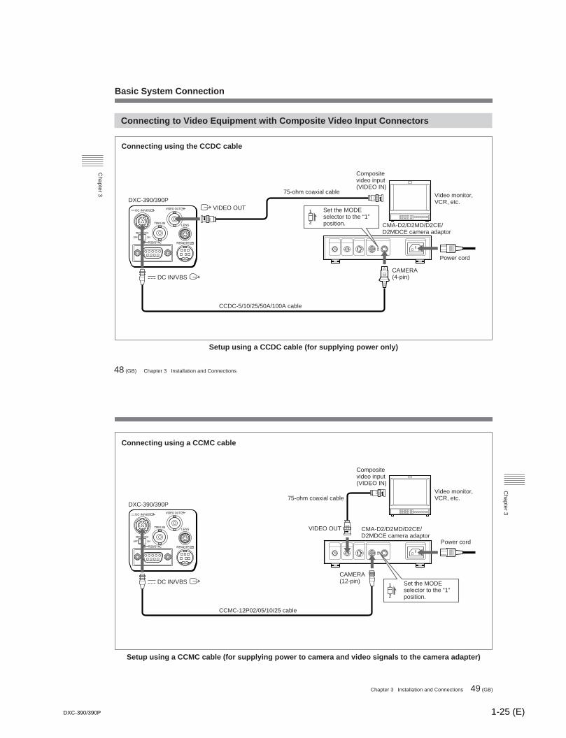
Basic System Connection
Connecting to Video Equipment with Composite Video Input Connectors
Setup using a CCDC cable (for supplying power only)
VIDEO OUTDC IN/VBS
REMOTE
LENSTRIG IN
MENU LOCK
OFF ON
RGB/SYNC
1
2
Connecting using the CCDC cable
DXC-390/390P
DC IN/VBS
VIDEO OUT
CCDC-5/10/25/50A/100A cable
75-ohm coaxial cable
Compositevideo input(VIDEO IN)
Set the MODEselector to the “1”position. CMA-D2/D2MD/D2CE/
D2MDCE camera adaptor
CAMERA(4-pin)
Video monitor,VCR, etc.
Power cord
Chapter 3 Installation and Connections 49 (GB)
Chapter 3
Setup using a CCMC cable (for supplying power to camera and video signals to the camera adapter)
VIDEO OUTDC IN/VBS
REMOTE
LENSTRIG IN
MENU LOCK
OFF ON
RGB/SYNC
1
2
Connecting using a CCMC cable
DXC-390/390P
DC IN/VBS
CCMC-12P02/05/10/25 cable
Compositevideo input(VIDEO IN)
Set the MODEselector to the “1”position.
CMA-D2/D2MD/D2CE/D2MDCE camera adaptor
CAMERA(12-pin)
Video monitor,VCR, etc.
Power cord
VIDEO OUT
75-ohm coaxial cable

1-26 (E) DXC-390/390P
50 (GB) Chapter 3 Installation and Connections
Chapter 3
Basic System Connection
Connecting to Video Equipment with RGB or S-Video Inputs
VIDEO OUTDC IN/VBS
REMOTE
LENSTRIG IN
MENU LOCK
OFF ON
RGB/SYNC
1
2
DXC-390/390P
DC IN/VBS
CCDC-5/10/25/50A/100A cable orCCMC-12P02/05/10/25 cable*
Camera cable: CCXC-9DB (D-sub 9-piny BNC connectors), or CCMC-9DS (D-sub 9-pin y BNC, S-video connectors)
RGB/SYNC
or
Camera cable CCXC-9DD(D-sub 9-pin y D-sub 9-pin)
Set the MODE selectorto the “1” position. CMA-D2/D2MD/D2CE/
D2MDCE camera adaptor
CAMERA (4-pin or 12-pin)
R input
G input
B input
Sync input1)
Composite video (BNC) orS-video input (4-pin)2)
Computer, imageprocessor etc.
RGB monitor,image processor,etc.
*If a CCMC cable is used, the S-video signal is also output from the S-video output of the CMA-D2/D2MD/D2CE/D2MDCE.
1) When using a video monitor without a sync signal input connector, thecamera can be set to output a sync signal with the G signal or RGBsignals.For details, see “SYSTEM menu” on page 27.
2) This setup is for connecting to a composite video (VBS) connector. Tooutput separated Y/C signals to the S-video input of video equipment,use a CCMC-9DS camera cable.For details on switching camera output between VBS (composite video) andY/C, see “SYSTEM menu” on page 27.
RGB/SYNC input
Power cord
Chapter 3 Installation and Connections 51 (GB)
Chapter 3
Connecting Two or More Cameras—Multi-Camera System
Notes on multi-camera systemPerform the following to prevent flicker when switchingbetween two or more cameras connected to a videoswitcher:• Supply the same sync signal to the GENLOCK IN
connectors on each camera adaptor (see below).• Adjust the subcarrier and horizontal synchronization
phases for all cameras.For more details, see “Adjusting the Picture Tone in aMulti-Camera System” on page 41.
VIDEO OUTDC IN/VBS
REMOTE
LENSTRIG IN
MENU LOCK
OFF ON
RGB/SYNC
VIDEO OUTDC IN/VBS
REMOTE
LENSTRIG IN
MENU LOCK
OFF ON
RGB/SYNC
1
2
1
2
Sync signal generator
Sync (VBS orBS) output
VBS OUT
Switcher, etc.
VIDEO IN
VBS OUT VIDEO IN
Video monitor,VTR, etc.
75-ohm coaxial cable
DXC-390/390P
VIDEOOUT
DC IN/VBS
CCMC-12P02/05/10/25 cable
GENLOCK IN
CAMERA (12-pin)
Set the MODE selectorto the “1” position.
CMA-D2/D2MD/D2CE/D2MDCEcamera adaptor
CMA-D2/D2MD/D2CE/D2MDCEcamera adaptor
Power cord
Power cord
75-ohm coaxial cable
Set the MODE selectorto the “1” position.
CCMC-12P02/05/10/25 cable
DXC-390/390P
VIDEOOUT
GENLOCK IN
CAMERA (12-pin)
DC IN/VBS

1-27 (E)DXC-390/390P
52 (GB) Chapter 3 Installation and Connections
Chapter 3
Connecting to a Remote Control Unit
You can connect the RM-C950 remote control unit.
VIDEO OUTDC IN/VBS
REMOTE
LENSTRIG IN
MENU LOCK
OFF ON
RGB/SYNC
1
2
DXC-390/390P
DC IN/
VBS
VIDEO OUT
75-ohm coaxial cable
RM-C950 remote control unit
REMOTE
Camera cable(supplied with RM-C950)
CCDC cable: CAMERA (4-pin)CCMC cable: CAMERA (12-pin)
CCDC-5/10/25/50A/100A cableorCCMC-12P02/05/10/25 cable
Composite video input
Video monitor,VCR, etc.
Set the MODEselector to the “1”position.
CMA-D2/D2MD/D2CE/D2MDCEcamera adaptor
Power cord
CAMERA
Chapter 3 Installation and Connections 53 (GB)
Chapter 3
Operating the Camera with the RM-C950 Remote Control Unit
When the RM-C950 remote control unit is used with thiscamera, the names and functions of the PRINT, FLASH,LONG EXPOSURE and FUNCTION buttons and the GAINcontrol change as follows, in accordance with the functionsof the camera.
Functions of the PRINT, FLASH, LONGEXPOSURE and FUNCTION buttons and GAINcontrol on the RM-C950
Buttons/controlon the RM-C950
FLASH
LONGEXPOSUREJ j
Button/controlnames when usedwith the camera
ENTER
FILE SELECT
SHUTTER SPEED
Function
Use when displaying thesetting menu selected inthe MAIN menu, or use toset the AE window, etc.manually in the menus.
Use to switch a preset filebetween A and B.
Use to set the shutterspeed without displayingthe menu whenSHUTTER is set to STEPor VARIABLE in themenu.
Attaching the supplied name sheet
The sheet for the button names when the camera is usedwith the remote control unit is supplied with the camera.Attach the name sheet to the control panel of the RM-C950.
1 Before attaching, clean the control panel of the RM-C950.
2 Peel off the adhesive sheet at the back of the name sheetand attach the name sheet to the panel.
Buttons/controlon the RM-C950
GAIN 2
FUNCTION J
Button/controlnames when usedwith the camera
GAIN
BLACK
Function
Use to change thevariable range of gainlevels to 0–24 dB.
Use to start the auto blackbalance adjustment.

1-28 (E) DXC-390/390P
54 (GB) Chapter 3 Installation and Connections
Chapter 3
Connecting to a Computer
System for controlling the camera with a computer using an RS-232C command
VIDEO OUTDC IN/VBS
REMOTE
LENSTRIG IN
MENU LOCK
OFF ON
RGB/SYNC
1
2
DC IN/VBS
VIDEO OUT
REMOTE
Set the MODEselector to the “1”position.
CMA-D2/D2MD/D2CE/D2MDCE camera adaptor
CAMERA(4-pin or 12-pin)
Power cord
DXC-390/390P
CCDC-5/10/25/50A/100A cableorCCMC-12P02/05/10/25 cable
Serial interfaceconnector
Connecting cable1)
Video input connector
Video monitor,VCR, etc.
Computer
1) Use the shielded connecting cable for connecting to a computer. For more details on RS-232C protocols and cables for connection to acomputer, contact your authorized Sony dealer.
Chapter 3 Installation and Connections 55 (GB)
Chapter 3
Connections for Long Exposure Shooting
System for shooting using long exposure in VARIABLE mode for electronic shutter
VIDEO OUTDC IN/VBS
REMOTE
LENSTRIG IN
MENU LOCK
OFF ON
RGB/SYNC
1
2
Set the MODEselector to the “1”position.
CMA-D2/D2MD/D2CE/D2MDCE camera adaptor
CAMERA(4-pin or 12-pin)
CCDC-5/10/25/50A/100A cableorCCMC-12P02/05/10/25 cable
DC IN/VBS
Power cord
DXC-390/390P
RGB/SYNC
Video monitor, VCR, etc.
Video inputconnector
Image processor orframe memory unit
Video input connector
CCMC-9DSMN/CCMC-9DS/CCXC-9DB camera cable
Video outputconnector
External controlconnector
Note
When shooting with long exposure, set D-SUB SYNC toWEN and RGB SYNC to G (or RGB) in the SYSTEMmenu (page 28).

1-29 (E)DXC-390/390P
56 (GB) Chapter 3 Installation and Connections
Chapter 3
Connections for Shooting Using a Flash
Note
When connecting a flash unit, set TRIGGER to ON in theGENERAL menu (page 27) and D-SUB SYNC to WEN inthe SYSTEM menu (page 28).
VIDEO OUTDC IN/VBS
REMOTE
LENSTRIG IN
MENU LOCK
OFF ON
RGB/SYNC
1
2
Synchronization cable
Video inputconnector
Video monitor, VCR, etc.
Video outputconnector
Image processor
Flash
Slave unit
DXC-390/390P
TRIG IN
Remote connector
Video inputconnector
DC IN/VBS
RGB/SYNC
CCMC-9DSMN/CCMC-9DS/CCXC-9DB camera cable
CMA-D2/D2MD/D2CE/D2MDCE camera adaptor
Set the MODEselector to the “1”position.
CAMERA(4-pin or 12-pin)
CCDC-5/10/25/50A/100A cableorCCMC-12P02/05/10/25 cable
Power cord
Chapter 4 Appendix 57 (GB)
Chapter 4
Precautions
Chapter 4Appendix
Operating or storage location
Operating or storing the camera in the following locationsmay cause damage to the camera:• Extremely hot or cold places (Operating temperature: –5°C
to +45°C [23°F to 113°F])• Exposed in direct sunlight for a long time, or close to
heating equipment (e.g., near heaters)• Close to sources of strong magnetism• Close to sources of powerful electromagnetic radiation,
such as radios or TV transmitters• Locations subject to strong vibration or shock
Ventilation
To prevent heat buildup, do not block air circulation aroundthe camera.
Transportation
When transporting the camera, repack it as originally packedat the factory or in materials equal in quality.
Cleaning
• Use a blower to remove dust from the lens or optical filter.• Use a soft, dry cloth to clean the external surfaces of the
camera. Stubborn stains can be removed using a soft clothdampened with a small quantity of detergent solution, thenwipe dry.
• Do not use volatile solvents such as alcohol, benzene orthinners as they may damage the surface finishes.

1-30 (E) DXC-390/390P
58 (GB) Chapter 4 Appendix
Chapter 4
Typical CCD Phenomena
The following phenomena may appear on the monitor screenwhile you are using the DXC-390/390P color video camera.These phenomena stem from the high sensitivity of the CCDimage sensors, and do not indicate a fault within the camera.
Vertical smear
A “smear” may appear to extend vertically from very brightsubjects, as shown below.
This phenomenon is common to CCD imaging elementsusing an interline transfer system, and is caused whenelectric charge induced by infrared radiation deep within thephoto sensor is transferred to the resistors.
Aliasing
When shooting fine stripes, straight lines or similar patterns,the lines may become slightly jagged.
Blemishes
A CCD image sensor consists of an array of individualpicture elements (pixels). A malfunctioning sensor elementwill show up as a single pixel blemish in the image. This isgenerally not a problem.
White speckles
When you shoot a poorly illuminated object at a hightemperature, small white dots may appear all over the entirescreen image.
Video monitorscreen
Pale verticalsmear
Very bright subject(such as an electriclamp, fluorescentlamp, sunlight, orstrong reflected light)
Chapter 4 Appendix 59 (GB)
Chapter 4
List of Messages
The following messages may appear on the screen. Take thenecessary measures shown below.
Messages while adjusting the white balanceautomatically
Message
WHITE: OK
WHITE: NGLEVEL LOW
WHITE: NGLEVEL HIGH
WHITE: NGTEMP LOW
Meaning/remedies
Automatic white balance adjustment hassucceeded.
The video level of the image is too low.• Increase the illumination.• Widen the iris opening.• Increase the video gain.Take the measures above, then press the
WHITE button.
The video level of the image is too high.• Remove any brightly illuminated objects.• Decrease the illumination.• Close the iris opening.• Decrease the video gain.Take the measures above, then press the
WHITE button.
Color temperature is too low.Change the color temperature of the object tothe appropriate level.
Messages while adjusting the white balanceautomatically (continued)
Message
WHITE: NGTEMP HIGH
WHITE: NGTRY AGAIN
Meaning/remedies
Color temperature is too high.Change the color temperature of the object tothe appropriate level.
The camera has failed to adjust the whitebalance.Add white part to the object shot.Take the measures above, then try again. Ifthe message appears even if you repeatadjustment, the camera needs to be checked.Consult your authorized Sony dealer.
Messages while adjusting the black balanceautomatically
Message
BLACK: OK
BLACK: NGIRIS close?
Meaning/remedies
Automatic black balance adjustment hassucceeded.
The camera has failed to adjust the blackbalance.Close the iris opening, than press the BLACKbutton.

1-31 (E)DXC-390/390P
60 (GB) Chapter 4 Appendix
Chapter 4
Specifications
Image system/optical system
Image device1/3 type CCD, interline transfer type
Effective picture elementsDXC-390: 768 (horizontal) × 494 (vertical)DXC-390P: 752 (horizontal) × 582 (vertical)
Lens mount C-mount
Video system
SynchronizationInternal/external synchronization (VBS, HD/
VD), switched automaticallySignal format
DXC-390: NTSC standard format (EIAstandard)
DXC-390P: PAL standard format (CCIRstnadard)
Scanning DXC-390: 525 lines, 2:1 interlaceDXC-390P: 625 lines, 2:1 interlace
Scanning frequencyDXC-390: 15.734 kHz (horizontal), 59.94 Hz
(vertical)DXC-390P: 15.625 kHz (horizontal), 50.00
Hz (vertical)
Functions/performance
Horizontal resolution800 TV lines
Sensitivity 2000 lux (F8, 3,200K)Signal-to-noise ratio
DXC-390: 62 dBDXC-390P: 61 dB
Gain control AGC: Automatic Gain ControlSTEP: 0–24 dB (in units of 1 dB)HYPER
White balanceAWB: R. PAINT, B. PAINTMANUAL: R. GAIN, B. GAINATW: R. PAINT, B. PAINT3200K5600K
Electronic shutter speedAdjustable in the range from 1/100000 to
about 8.0 sec. (adjustable with CCD IRIS)Linear matrix
ON/OFF switchableGamma compensation
ON/OFF switchableCharge accumulation mode
Switchable between field and frame mode
Chapter 4 Appendix 61 (GB)
Chapter 4
Inputs/outputs
Video input/output signalsComposite video: 1 Vp-p (75 ohms)R/G/B: 1.0 Vp-p (75 ohms at R/G/B on Sync)Y: 1 Vp-p (75 ohms)Y/C: 1 Vp-p, same level as VBS chroma,
75 ohmsSYNC: 2 Vp-p, 75 ohms
External sync inputVBS/BS, HD/VD (VBS 1 Vp-p or Burst
0.3 Vp-p, SYNC 0.3 Vp-p or HD/VD4.0 Vp-p, 75 ohms)
Input/output connectorsVIDEO OUT: BNC, 75 ohms, unbalancedDC IN/VBS: 12-pinREMOTE: mini DIN 18-pinTRIG IN: BNC, TTLRGB/SYNC: D-sub 9-pinLENS: 6-pin connector for the zoom lens
especially designed for this camera
General
Power supply12 V DC
Power consumptionApprox. 7.6 W
Operating temperature–5°C to +45°C (23°F to +113°F)
Storage and transport temperature–20°C to +60°C (–4°F to +140°F)
Operating humidity20% to 80% (free of condensation)
Storage and transport humidity20% to 90% (free of condensation)
Dimensions 56 × 50 × 128 mm (2 1/4 × 2 × 5 1/8 inches)(w/h/d) (not including the projecting parts)
Mass Approx. 370 g (13 oz)Supplied accessories
Lens mount cap (1)Tripod adaptor (1)Name sheet for the buttons on the RM-C950
(1)Instructions for Use (1)Warranty card (1) (DXC-390 only)Sales companies’ guide (1) (DXC-390P only)
(Continued)

1-32 (E) DXC-390/390P
62 (GB) Chapter 4 Appendix
Chapter 4
Demensions
Front
Side
56 (2 1/4)
28(1 1/8)
50 (
2)
28(1 1/8)
25 (
1)25
(1)
C-mount
140.7 (5 5/8)
128 (5 1/8)12.7(1/2)
50 (
2)
Unit: mm (inches)
Specifications
Medical specifications
Protection against electric shockClass I
Protection against harmful ingress of waterOrdinary
Degree of safety in the presence of flammable anesthetics oroxygen
Not suitable for use in the presenceof flammable anesthetics or oxygen
Mode of operationContinuous
Design and specifications are subject to change withoutnotice.
Chapter 4 Appendix 63 (GB)
Chapter 4
Top
Bottom
16.5 (21/32) 40 (1 5/8)
25 (
1)25
(1)
40 (1 5/8)11 (7/16)
Screw hole (M3, depth: 4 (3/16))
Unit: mm (inches)
Screw hole (M3, depth: 4 (3/16))

1-33 (E)DXC-390/390P
64 (GB) Chapter 4 Appendix
Chapter 4
Optional Accessories
Lenses
VCL-614WEA zoom lens (14 ×, f = 5.5 – 77 mm)VCL-610WEA zoom lens (10 ×, f = 6.5 – 65 mm)
Camera adaptor
CMA-D2 camera adaptor (for NTSC format)CMA-D2MD camera adaptor (for NTSC format, medical
use)CMA-D2CE camera adaptor (for PAL format)CMA-D2MDCE camera adaptor (for PAL format, medical
use)
Remote control unit
RM-C950 remote control unit (connecting cable supplied)
Power supply cable
CCDC series (length: 5 m [16 ft], 10 m [32 ft], or 25 m[82 ft])
CCDCA series (length: 50 m [164 ft], or 100 m [328 ft])CCMC series (length: 2 m [7 ft], 5 m [16 ft], 10 m [32 ft], or
25 m [82 ft])
Camera cable
CCXC-9DB (D-sub y BNC × 5)CCXC-9DD (D-sub y D-sub)CCMC-9DS (D-sub y BNC × 4, S-video connector)CCMC-9DSMN (D-sub y BNC × 3, phono jack,
S-video connector)
Chapter 4 Appendix 65 (GB)
Chapter 4
Printed in Japan


2-1 (E)DXC-390/390P
Section 2Service Overviw
2-1. Board location 2-2. Removal of cabinet
1. Remove the seven screws (P2 x 3) and then removethe upper case.
2. Remove the two screws (P2 x 3) and then remove thestay.
3. Remove the two screws (P2 x 3) and then remove therear panel.Remove the flat cable from the rear panel.
4. Loosen the three screws (B3 x 8) and then remove thetripod adaptor. (These screws cannot be removedbecause of stoppers.)
5. Remove the CCD block, referring to the Section2-3.“Removal of CCD block”.
6. Remove the flat cable from the SG-265/265P board.7. Remove the four screws (P2 x 3) on the MB-875/875P
board and then remove the lower case.
nDo not damage the flat cable.
DP-313/313Pboard
VA-193/193Pboard
EN-142/142Pboard SG-265/265P
board
CN-1938 board
MB-875/875Pboard
PA-236 board
*1
*1
P2 x 3
Lower case
Upper case
Stay
CCD block
VA-193/193Pboard
SG-265/265Pboard
P2 x 3
B3 x 8
Rear panel
Flat cable
P2 x 3P2 x 3
P2 x 3
P2 x 3
Tripod adaptor
MB-875/875P board
*2
*2
*3
*3
*4
*4
P2 x 3
Flat cable
B3 x 8

2-2 (E) DXC-390/390P
2-3. Removal of CCD block
1. Remove the upper case and stay, referring to theSection 2-2. “ Removal of cabinet ”.
2. Remove the flat cable from the VA-193/193P board.
3. Loosen the three screws (B3 x 8) and then remove thetripod adaptor. (These screws cannot be removedbecause of stoppers.)
4. Remove the two screws and draw the CCD block.5. Remove the flat cable from the MB-875/875P board
and then remove the CCD block.
n. Do not damage the flat cable.. Pay carefull attention not to give the stress in the PA-236
board and prism block, since it may cause damage them.
2-4. How to use an extension board
Extension boards are not in use for adjustment.These are in use for check of VA-193/193P, DP-313/313P,EN-142/142P, SG-265/265P boards.
Extension board. EX-747 : J-6432-130-A. EX-748 : J-6432-140-A. EX-749 : J-6432-150-A. EX-750 : J-6432-160-A
. . . . . In cases of the VA-193/193P board
. . . . . In cases of the DP-313/313P board
VA-193/193P board
Flat cable
Lower case
Flat cable
CCD block
+P2 x 3
MB-875/875Pboard
B3 x 8Tripod adaptor
B3 x 8
VA-193/193P board
Extension boardEX-748
Extension boardEX-747
DP-313/313P board
Extension boardEX-750
Extension boardEX-749

2-3 (E)DXC-390/390P
. . . . . In cases of the EN-142/142P board
. . . . . In cases of the SG-265/265P board
EN-142/142P board
Extension boardEX-748
Extension boardEX-747
SG-265/265P board
Extension boardEX-750
Extension boardEX-749

2-4 (E) DXC-390/390P
LENS connector (6-pin)Pin No. Signal
1 Focus control
2 Zoom control
3 GND
4 Iris close
5 Iris control/video (signal)
6 +12V
REMOTE connector (8-pin)Pin No. Signal
1 HSK output
2 HSK input
3 TXD__
4 GND
5 RXD__
6 TXD_+
7 UNREG_+
8 RXD_+
RGB/SYNC connector (D-sub 9-pin)Pin No. Signal
1 VBS output (GND)
2 RGB output (GND)
3 R/VBS output
4 G/Y output
5 B/C output
6 VBS/Y output
7 SYNC/WEN output (signal)
8 SYNC output (GND)
9 _/C output
DC IN/VBS connector (12-pin)Pin No. External sync mode Internal sync mode
HD/VD VBS
1 GND GND GND
2 +12V +12V +12V
3 VBS/Y output (GND) VBS/Y output (GND) VBS/Y output (GND)
4 VBS/Y output (signal) VBS/Y output (signal) VBS/Y output (signal)
5 EXT HD input (GND) _ HD output (GND)
6 EXT HD input (signal) _ _/HD output (signal)
7 EXT VD input (signal) EXT VBS input (signal) SYNC/VD output (signal)
8 _/C output (GND) _/C output (GND) _/C output (GND)
9 _/C output (signal) _/C output (signal) _/C output (signal)
10 GND GND GND
11 +12V +12V +12V
12 EXT VD input (GND) EXT VBS input (GND) SYNC/VD output (GND)
2-5. Input/output signals of connectors
VIDEO OUTDC IN/VBS
REMOTE
LENSTRIG IN
MENU LOCK
OFF ON
RGB/SYNC
LENS
1
2
34
5
6
DXC-390/390P REAR PANEL
(External view)
REMOTE
12
345
678
(External view)
DC IN/VBS
1
2
3
45
6
7
8
9
10
11 12
(External view)
RGB/SYNC
12345
6789
(External view)

3-1 (E)DXC-390/390P
Section 3Circuit Operation Description
3-1. VA-193 Board
The VA-193 board consists of the circuit blocks describedbelow.
. S/H, AGC Circuit and Pre-amplifier (Main circuit : CXA1757R). Processing circuit. Shading correcting circuit. Signal generator circuit for lens control
(1) S/H, AGC Circuit and Pre-amplifier(Main circuit : CXA1757R)In CXA1757R (IC901), RGB signal that is input fromthe PA-236 board, is separated signal using correlativedouble sampling processing. There is sampling-hold byinput XSHD and XSHP sampling pulses, is processed.The separated signal is amplified by a AGC amplifier.This AGC amplifier can control gain by voltage.This voltage is input from IC902, is changed by everygain mode.The signal that is through the AGC amplifier, is inputto the pre-amplifier circuit. In the pre-amplifier, givesa gain to R-channel and B-channel signals, suppressessensitive uneven between RGB. After that, is outputfrom IC901 via blanking process and clamp circuit.The black output level is approximately 1.8V.
(2) Processing CircuitThe RGB signal that is output from IC901 eliminatesthe 14 MHz component by the trap filter after throughthe buffer. After that, it is input to the white-balanceamplifier (from IC910 to IC912).This amplifier can be controlled a gain by a voltage(VCA), VCA gain of R-channel and B-channel iscon-trolled by a voltage giving from IC906 and the white-balance processing is performed.And VCA of G-channel is given the signal for com-pensation from the shading compensation circuit, it isperformed compensation by controlling a gain of G-channel. The signal after performing white-balance,after through a pre-knee circuit and a white-clipcircuit, is clamped OPB part by the feedback clampcircuit (from IC915 to IC918) to approximately 2.1Vdc, is output to the DP-313 board.
(3) Shading Compensation CircuitV-periodic delta wave is generated, it uses the voltagefor VCA gain control, so that shading compensationfunction is realized.The generated delta wave is adjusted so that the wavecenter will be around the center on the screen.The delta wave slant, central adjustment value, offsetadjustment value and delta wave generating on/off areset in IC903 and IC906.
(4) Lens Control Signal Generator circuitSignals for controlled lens iris, focus and zoom aregenerated. About iris, the signals for video servo andDC control are alternated (IC913). The video servosignal makes the Y-signal from the RGB signal ofprevious AGC in IC901 and is input to VCA (IC907)via gain amplifier and clamp circuit. This VCA sets again according to convergence level from IC903. Thecontrol signal for DC control, that is set voltage inIC903, is output after adjusted gain. The voltage rangeof the signal is approximately from 2.5 V to 7.5 V. TheZOOM and FOCUS control signals are the same setvoltage in IC903, are output after adjusted gain. Thevoltage range is the same approximately from 2.5 V to7.5 V. A voltage of IC903 is controlled from a micro-processor, and then a lens is controlled.
3-2. DP-313 Board
The DP-313 board consists of the circuit blocks describedbelow.
. A/D converter circuit for video signal
. Around CXD9117R
. CXD9087R and its surrounding circuits
. D/A converter circuit for video signal
. Clock phase control circuit

3-2 (E) DXC-390/390P
(1) A/D converter circuit for video signalThe analog signal (RGB) that is processed every kindat the VA-193 board, is converted to 10-bit digitalsignal at CXD2310AR (from IC401 to IC403).Sampling frequency is 14 MHz. The top referencevoltage (approximately 4V) and bottom referencevoltage (approximately 2V) that are the standardvoltage, are set in IC406 (D/A converter), are input viabuffer (IC411). Also, calibration pulse for IC401,IC402 and IC403 is input after mixing inside betweengenerated in hard ware (around IC420) and generatedin software via IC406.
(2) CXD9117R and its surrounding circuitThe digital converted RGB signals are input toCXD9117R (IC404), digital signal processing per-forms. The IC inside setting is performs by the serialcommunication (BUSY, PRN-CS, SDI-3, SDO-3 andSCLK-3) from a microprocessor. Also, a data commu-nication with EEROM (IC405) is controlled byCXD9117R.
(3) CXD9087R and its surrounding circuit10-bit digital signal after processing in CXD9117R isinput to CXD9087R, performs digital signal process-ing. The IC inside setting is performed by the serialcommunication (CS, SDCK and SDA0-SDA3) from amicroprocessor. The output signal is Y and colordifferential signal (Y, CR and CB, every 10-bit). Also,AHD and AVD that are output at the same time, aresent to the MB-875 board and ECK is sent to the SG-265 board.
(4) D/A converter circuit for video signalY, CR and CB (every 10-bit) that are output fromCXD9087R, are input to CXD2307R and are convert-ed to analog signals. The clock frequency for conver-sion is 28 MHz.And, an output amplitude can be set independently Y,CR and CB by setting a reference voltage from IC406.
(5) Clock phase control circuit14 MHz and 28 MHz clock pulses that is input fromthe MB-875 board, are performed phase adjustmentand are output via buffer to each IC (A/D converter forvideo circuit, CXD9117R, CXD9087R and D/Aconverter for video circuit).For CXD9117R and CXD9087R, 3.3 V amplitude isoutput after converted from 5 V amplitude.
3-3. EN-142 Board
The EN-142 board generates the composite signal (VBSand Y/C) by the encoder IC from Y, CR (R-Y) and CB (B-Y) that are output from the DP-313 board.In the another system, RGB signals are also generated bythe discrete circuit.These output signals are output through the driver circuits.
..... Encode (IC704)The color differential signals (Y, R-Y and B-Y) are inputto IC704, then encode, VBS and Y/C signals are generat-ed.The input Y signal gain is performed at gain controlamplifier in IC704, and also the input R-Y and B-Ysig-nals gain are performed at GCA in IC703.Each level setting (Y, SYNC, BURST, SETUP andWhite-clip) is performed by IC701.The title signal from the DP-313 board can be alsomixed to a final output signal of IC704 turning the S701switchon.
..... RGB generator circuitRGB signals are made from color differential signals (Y,R-Y and B-Y) output the DP-313 board. SYNC additionindependently controls ON/OFF for R/B and G.
..... Video signal driver circuitVBS, Y, C, R, G and B signals output via 75-ohm drivercircuit. HD, VD, C, SYNC and WEN signals also outputvia driver circuit.Also, HD line and VD line using both input and outputare change-controlled by two-way buffer IC712.

3-3 (E)DXC-390/390P
3-4. SG-265 Board
The microprocessor communicates a data with each board,and controls a camera.And, by external sync circuit around the Gen.Lock IC,sync mode is discriminated and sync source signal isseparated. These construct 4fsc clock PLL.
..... Microprocessor IC107 (uPD70F3017)This is 32-bit RISC microprocessor of a flash type. Theclock frequency uses 17 MHz (X101).Program write terminal is common use with the commu-nication terminal (UART), a change connection performsbetween software rewrite in IC102 and normal commu-nication.IC101 is EEPROM stored camera setting data.
..... Character generator blockThe clock uses 7 MHz that is divided 14 MHz to half inIC103.The character and Key signal are made in IC111, areinput to CXD9087R.
..... External communication blockOne is RS232C, communicates with external throughdriver circuit (IC112).Another is CCU protocol, takes on sending in Q102 andreceiving in Q101.
. . . . . Iris value converter blockIn the exclusive lens for DXC-390, an iris value gets asvoltage.Its voltage is adapted for a dynamic range of A/D convert-er of the microprocessor in IC115, is taken the micropro-cessor.
. . . . . Sync signal generator (IC231)Each kind sync signal (HD, VD, FLD, LALT, BF andOBLK) is output.
. . . . . External sync signal (VBS and HD/VD)Sync mode is discriminated by a input sync source signalfrom external. SYNC and BURST are separated from itssignal and input to IC230, compare phase with theinternal HD and SC signals.In the VBS external sync mode, 4fsc clock signal issynchronized in SC-PLL whichever NTSC and PALsystems. In the HD/VD external sync mode, it is syn-chronized only PAL system.In the internal sync mode and HD/VD external syncmode of NTSC system, PLL is not consisted, VCXO isgenerated by a fixed voltage.HD and SC phase on those external sync mode are ad-justed.And, a sync source signal is changed amplitude to 5 Vp-pafter through buffer and separated.

3-4 (E) DXC-390/390P
3-5. MB-875 Board
The MB-875 board is installed the oscillator circuit formaster clock, the timing generator for the CCD drivingpulse, the IC generated detection boundary and the DC-DCconverter.
..... 28 MHz oscillating circuitThis circuit consists of the P-COMP (HD phase compar-ative output) signal and PLL in VCO.When the internal sync and VBS external sync, it iscrys-tal type VCO, HD and VD. When the external sync, it isgenerated 28 MHz of the master clock in the LC typeVCO oscillator.Both oscillator circuits do not operate simultaneously.The oscillator clock improves the duty ratio in IC635,IC636 and its around circuit.
..... Timing generator (IC611)28 MHz and AHD/AVD from the DP-313 board areinput, each pulse for driving the CCD is generated.. V1, V2, V3 and V4 Vertical transfer pulse. H1 and H2 Horizontal transfer pulse. VSUB Electric charge sweep out pulse. RG Reset gate pulseThe transfer pulse is sent via H-driver circuit (IC612)and V-driver circuit (IC601, IC604 and IC607) to the PAboard, the sample and hold pulse are sent to the VA-193board.
. . . . . CXD9115AR (IC606)The window signal for detection frame is generated.H-Window and V-Window signals are mixed in IC628and IC629, are output to the DP-313 board.A CCD accumulative time is realized according to atrigger input.
..... DC-DC converter (DD601)The voltages of +15V, +9V, +5V (A), +5V (D), +3.3Vand _7.5V are generated from the external input powersupply UNREG (+), so that supply to each board.Independently, UNREG (+) is passed through a filter, itis supplied as UNREG (LENS).

4-1 (E)DXC390/390P
Section 4Electrical Alignment
4-1. Preparation
4-1-1. Adjustment Fixture and MeasurementEquipment
J-6029-140-B Pattern box PTB-500
. Light source for adjustment chart Power supply from 90 to 240VAC
J-6026-130-B Grayscale chart
. For video level adjustment, etc.
Commercially Available Products
. Vectorscope
. Waveform monitor
. Frequency counter
. Signal generator
. Digital voltmeter
. Color monitor
. Lens (C-mount type and manual iris type)
4-1-2. Equipment Connection
VIDEO OUTDC IN/VBS
REMOTE
LENSTRIG IN
MENU LOCK
OFF ON
RGB/SYNC
Video cameraDXC-390/390P
Waveform monitor (WFM)
Camera adaptor CMA-D2/D2CE
Termination(75Z)
Vectorscope
Color monitor
Termination (75Z)

4-2 (E) DXC-390/390P
4-1-3. Description of Side Panel SheetSwitches
Adj. no. is selected by the arrow t (up) or the arrowT(down).Data is adjusted by the arrow R(up) or the arrowr(down).
Side Panel Sheet Switch
4-1-4. Super Reset (data initialization)
1.Pressing the S101 switch on the SG-265 board and turnthe power on.
2.After fifteen seconds, the initial data is written and thepicture appears.
3.Turn the S102 switch on the SG-265 to the ADJ side(down side).
4.The ADJ picture is displayed.
Adjust number XX is shown data XX.
4-2. Adjustment
4-2-1. VCO Adjustment(original oscillator adjustment)
Equipment : Monitor screenPreparation : Input the VBS OUT on a camera to
the EXT IN on a signal generator.Input the SC output on a signalgenerator to a frequency counter.
Adjustment Procedure : Adjust Adj61 (NTSC) or Adj14(PAL) so that the SC frequencybecomes the specification.
Specification : 3.579545 MHz ±5 Hz (NTSC): 4.433618 MHz ±5 Hz (PAL)
4-2-2. Built-in Color Bars Adjustment(adjustment from DSP)
Equipment : Waveform monitor and vectorscopePreparation : Press the BARS button to the
built-in color bars side...... R/G/B OUT Adjustment Adjust Adj31 so that the white
level becomes the specification A...... R OUT Adjustment Adjust Adj32 so that the wave-
form becomes the specification B...... B OUT Adjustmen t Adjust Adj33 so that the wave-
form becomes the specification C.Specification : A=75 IRE ±1 IRE (NTSC)
700 mV ±7 mV (PAL)B : The waveform becomes flat.C : The waveform becomes flat.
MENU BLACK
WHITE
ENTER
BARS
FILESELECT
Adj no. XX XXdata.
Monitor Screen
RBG
DXC-390
DXC-390P
B, CA
RBG
B, CA

4-3 (E)DXC390/390P
..... VBS OUT AdjustmentAdjustment Procedure . Adjust Adj72 and Adj73 so that
the chroma level becomes thespecification D.
. Adjust Adj74 so that the burstlevel becomes the specification E.
. Adjust Adj75 so that the set uplevel becomes the specification F.
. Adjust Adj76 so that the Y levelbecomes the specification G.
. Adjust Adj77 so that the SYNClevel becomes the specification H.
Specification : D : Adjust each color spot withinthe frame on a vectorscope.E = 40 IRE ±1 IRE (NTSC)
300 mV ±7 mV (PAL)F = 0 IRE (NTSC)
0 mV (PAL)G = 75 IRE ±1 IRE (NTSC)
700 mV ±7 mV (PAL)H = 40 IRE ±1 IRE (NTSC)
300 mV ±7 mV (PAL)
4-2-3. CCD OUT Adjustment
Equipment: Waveform monitor and vectorscopeAdjustment Procedure1. Press the BARS button, the built-in color bars will be
OFF.2. Shut the lens iris.3. Turn the S102 switch on the SG-265 board to the OPE
side (up side).
. Pedestal Adjustment4. Press the BLACK button ( R ).5. Confirm the specification A.Specification : A : Confirm that BLACK OK is displayed.
. Pre-white Balance Adjustment6. Shoot the grayscale chart, adjust the VBS OUT level
by the lens iris to approximately 80 % level.7. Turn the S102 switch on the SG-265 board to the ADJ
side (down side).8. Press the MENU button to show the DSP ADJ display.9. Make settings the DSP Adj549 to the data01.10. Turn the S102 switch on the SG-265 board to the OPE
side (up side).11. Press the WHITE button (t).12. Confirm the specification B.Specification : B : Confirm that PRE WB OK is
displayed.13. Turn the S102 switch on the SG-265 board to the ADJ
side (down side).14. Return the DSP Adj549 to the data00.15. Press the MENU button to show the ADJ display.
. Target Color Setting16. Make settings the Adj98 data to 004.17. Make settings the Adj99 data to 002.18. Make settings the Adj100 data to 024.19. Turn the S102 switch on the SG-265 board to the OPE
side (up side).
G
E
F
H
DXC-390
G
E
F
H
DXC-390P


5-1DXC-390/390P
5-1. Notes on Repair Parts
1. Safety Related Components WarningwComponents marked ! are critical to safe operation.Therefore, specified parts should be used in the case ofreplacement.
2. Standardization of PartsSome repair parts supplied by Sony differ from thoseused for the unit. These are because of parts common-ality and improvement.Parts list has the present standardized repair parts.
3. Stock of PartsParts marked with “o” at SP (Supply Code) column ofthe spare parts list may not be stocked. Therefore, thedelivery date will be delayed.
4. HarnessHarnesses with no part number are not registered asspare parts.In need of repair, get components shown in the list andrepair using them.
Section 5Spare Parts
5-1.

5-2 DXC-390/390P
5-2. Exploded View
*1
*1
26
26
26
3 4
5
8
14
7
1
23
24
26
13
1926
279
22
10
26 2
28
11
26
21
6
2517
16
1518 20 18
12
26
*2
*2

5-3DXC-390/390P
NO. Part No. SP Description
1 A-8325-284-A o PANEL ASSY,REAR 2 A-8325-287-A o MOUNTED CIRCUIT BOARD,PA-236 3 A-8325-288-A o MOUNTED CIRCUIT BOARD,VA-193 4 A-8325-289-A o MOUNTED CIRCUIT BOARD,DP-313[for UC,J] A-8325-309-A o MOUNTED CIRCUIT BOARD,DP-313P[for CE]
5 A-8325-290-A o MOUNTED CIRCUIT BOARD,EN-142[for UC,J] A-8325-310-A o MOUNTED CIRCUIT BOARD,EN-142P[for CE] 6 A-8325-292-A o MOUNTED CIRCUIT BOARD,MB-875[for UC,J] A-8325-312-A o MOUNTED CIRCUIT BOARD,MB-875P[for CE] 7 A-8325-293-A o MOUNTED CIRCUIT BOARD,CN-1938
8 A-8325-909-A o MOUNTED CIRCUIT BOARD,SG-265[for UC,J] A-8325-910-A o MOUNTED CIRCUIT BOARD,SG-265P[for CE] 9 A-8326-195-A s CHU COMPLETE ASSY[for UC,J] A-8326-196-A s CHU COMPLETE ASSY[for CE] 10 X-3605-837-1 o GUIDE ASSY, ADJUSTER SCREW
11 X-3605-838-1 s ADAPTOR ASSY,TRIPOD 12 X-3605-839-1 o CASE ASSY,UPPER 13 X-3605-840-1 o CASE ASSY,LOWER 14 X-3605-841-1 o STAY ASSY 15 1-562-222-21 s RECEPTACLE,CONNECTOR 6P[LENS]
16 1-562-381-00 s CONNECTOR,ROUND TYPE 12P[DC IN/VBS] 17 1-580-090-11 s SOCKET,D-SUB CONNECTOR 9P[RGB/SYNC] 18 1-580-724-21 s CONNECTOR,BNC[VIDEO OUT, TRIG IN] 19 1-771-944-11 s SWITCH,SHEET 20 1-774-806-11 s CONNECTOR,ROUND TYPE(8PIN)[REMOTE]
21 1-792-595-11 s CABLE,FLEXIBLE FLAT(30 CORE) 22 2-042-385-00 s CAP,C MOUNT 23 3-626-695-01 o PANEL,REAR 24 3-626-707-01 o RUBBER(10X60X4) 25 3-737-536-03 o LUG,GROUND,CONNECTOR
26 3-968-729-81 s SCREW (M2),LOCK ACE,P2( +P2X3) 27 7-623-923-11 s WASHER 2.6, NYLON 28 7-682-548-04 s SCREW +B3X8

5-4 DXC-390/390P
-------------CN-1938 BOARD------------- Ref. No. or Q'ty Part No. SP Description
1pc A-8325-293-A o MOUNTED CIRCUIT BOARD, CN-1938
C001 1-164-858-11 s CAPACITOR,CERAMIC 22PF/16V 1005 C002 1-164-858-11 s CAPACITOR,CERAMIC 22PF/16V 1005 C003 1-164-858-11 s CAPACITOR,CERAMIC 22PF/16V 1005 C004 1-164-858-11 s CAPACITOR,CERAMIC 22PF/16V 1005 C005 1-164-858-11 s CAPACITOR,CERAMIC 22PF/16V 1005
C006 1-164-858-11 s CAPACITOR,CERAMIC 22PF/16V 1005 C007 1-164-858-11 s CAPACITOR,CERAMIC 22PF/16V 1005 C008 1-107-820-11 s CAPACITOR,CHIP CERAMIC 0.1MF F C009 1-164-858-11 s CAPACITOR,CERAMIC 22PF/16V 1005 C010 1-107-820-11 s CAPACITOR,CHIP CERAMIC 0.1MF F
C011 1-164-882-11 s CAPACITOR,CERAMIC 220PF/16V CH C012 1-164-858-11 s CAPACITOR,CERAMIC 22PF/16V 1005 C013 1-164-858-11 s CAPACITOR,CERAMIC 22PF/16V 1005 C014 1-164-858-11 s CAPACITOR,CERAMIC 22PF/16V 1005 C015 1-164-882-11 s CAPACITOR,CERAMIC 220PF/16V CH
C016 1-164-939-11 s CAPACITOR,CHIP CERAMIC 2200PF C017 1-164-939-11 s CAPACITOR,CHIP CERAMIC 2200PF C018 1-164-882-11 s CAPACITOR,CERAMIC 220PF/16V CH C019 1-164-882-11 s CAPACITOR,CERAMIC 220PF/16V CH C020 1-164-858-11 s CAPACITOR,CERAMIC 22PF/16V 1005
C021 1-164-943-11 s CAPACITOR,CHIP CERAMIC 0.01MF C022 1-107-820-11 s CAPACITOR,CHIP CERAMIC 0.1MF F C023 1-107-820-11 s CAPACITOR,CHIP CERAMIC 0.1MF F C024 1-107-820-11 s CAPACITOR,CHIP CERAMIC 0.1MF F C025 1-164-870-11 s CAPACITOR,CHIP CERAMIC 68PF/16
C026 1-164-870-11 s CAPACITOR,CHIP CERAMIC 68PF/16 C027 1-107-820-11 s CAPACITOR,CHIP CERAMIC 0.1MF F C028 1-164-878-11 s CAPACITOR,CHIP CERAMIC 150PF C029 1-164-858-11 s CAPACITOR,CERAMIC 22PF/16V 1005 C030 1-164-858-11 s CAPACITOR,CERAMIC 22PF/16V 1005
C031 1-164-858-11 s CAPACITOR,CERAMIC 22PF/16V 1005 C032 1-164-858-11 s CAPACITOR,CERAMIC 22PF/16V 1005 C033 1-164-882-11 s CAPACITOR,CERAMIC 220PF/16V CH
CN007 1-573-370-21 s CONNECTOR,FFC/FPC 30P
D001 8-719-510-30 s DIODE D2FL20
F001 ! 1-533-483-11 s FUSE CHIP 1.6A/125V (6125)
FB003 1-500-215-11 s BEAD, FERRITE (CHIP) FB004 1-500-215-11 s BEAD, FERRITE (CHIP) FB005 1-500-215-11 s BEAD, FERRITE (CHIP) FB006 1-500-215-11 s BEAD, FERRITE (CHIP)
FL001 1-234-066-11 s FILTER, CHIP EMI
L001 1-410-981-31 s CHIP INDUCTOR 0.1UH (2012) L002 1-410-981-31 s CHIP INDUCTOR 0.1UH (2012) L003 1-410-981-31 s CHIP INDUCTOR 0.1UH (2012) L004 1-410-981-31 s CHIP INDUCTOR 0.1UH (2012) L005 1-410-981-31 s CHIP INDUCTOR 0.1UH (2012)
L006 1-410-981-31 s CHIP INDUCTOR 0.1UH (2012) L007 1-410-981-31 s CHIP INDUCTOR 0.1UH (2012) L008 1-410-981-31 s CHIP INDUCTOR 0.1UH (2012) L009 1-410-981-31 s CHIP INDUCTOR 0.1UH (2012) L010 1-410-981-31 s CHIP INDUCTOR 0.1UH (2012)
L011 1-410-981-31 s CHIP INDUCTOR 0.1UH (2012) L012 1-410-981-31 s CHIP INDUCTOR 0.1UH (2012) L013 1-410-981-31 s CHIP INDUCTOR 0.1UH (2012)
5-3. Electrical Parts List
(CN-1938 BOARD)
Ref. No. or Q'ty Part No. SP Description
L014 1-410-981-31 s CHIP INDUCTOR 0.1UH (2012) L015 1-410-981-31 s CHIP INDUCTOR 0.1UH (2012) L016 1-410-981-31 s CHIP INDUCTOR 0.1UH (2012)
R001 1-218-665-11 s RESISTOR,CHIP 75 1/16W (1608) R002 1-218-665-11 s RESISTOR,CHIP 75 1/16W (1608) R003 1-218-665-11 s RESISTOR,CHIP 75 1/16W (1608) R004 1-218-665-11 s RESISTOR,CHIP 75 1/16W (1608)
S001 1-571-738-11 s SWITCH,SLIDE (2-2-2)

5-5DXC-390/390P
------------DP-313 BOARD------------ Ref. No. or Q'ty Part No. SP Description
1pc A-8325-289-A o MOUNTED CIRCUIT BOARD, DP-313 [for UC,J] 1pc A-8325-309-A o MOUNTED CIRCUIT BOARD, DP-313P [for CE]
C401 1-104-851-11 s CAPACITOR,TANTALUM 10MF/10V C402 1-107-820-11 s CAPACITOR,CHIP CERAMIC 0.1MF F C403 1-113-985-11 s CAPACITOR,TANTALUM 10MF/20V C404 1-107-820-11 s CAPACITOR,CHIP CERAMIC 0.1MF F C405 1-104-851-11 s CAPACITOR,TANTALUM 10MF/10V
C406 1-107-820-11 s CAPACITOR,CHIP CERAMIC 0.1MF F C407 1-107-820-11 s CAPACITOR,CHIP CERAMIC 0.1MF F C408 1-107-820-11 s CAPACITOR,CHIP CERAMIC 0.1MF F C409 1-107-820-11 s CAPACITOR,CHIP CERAMIC 0.1MF F C410 1-107-820-11 s CAPACITOR,CHIP CERAMIC 0.1MF F
C411 1-135-210-11 s CAPACITOR,TANTALUM 4.7MF/10V C412 1-135-210-11 s CAPACITOR,TANTALUM 4.7MF/10V C413 1-107-820-11 s CAPACITOR,CHIP CERAMIC 0.1MF F C414 1-107-820-11 s CAPACITOR,CHIP CERAMIC 0.1MF F C415 1-107-820-11 s CAPACITOR,CHIP CERAMIC 0.1MF F
C416 1-107-820-11 s CAPACITOR,CHIP CERAMIC 0.1MF F C417 1-107-820-11 s CAPACITOR,CHIP CERAMIC 0.1MF F C418 1-104-851-11 s CAPACITOR,TANTALUM 10MF/10V C422 1-107-820-11 s CAPACITOR,CHIP CERAMIC 0.1MF F C425 1-104-851-11 s CAPACITOR,TANTALUM 10MF/10V
C427 1-107-820-11 s CAPACITOR,CHIP CERAMIC 0.1MF F C428 1-104-851-11 s CAPACITOR,TANTALUM 10MF/10V C433 1-164-937-11 s CAPACITOR,CHIP CERAMIC 1000PF C434 1-164-937-11 s CAPACITOR,CHIP CERAMIC 1000PF C435 1-107-820-11 s CAPACITOR,CHIP CERAMIC 0.1MF F
C437 1-164-937-11 s CAPACITOR,CHIP CERAMIC 1000PF C439 1-107-820-11 s CAPACITOR,CHIP CERAMIC 0.1MF F C440 1-135-259-11 s CAPACITOR,TANTALUM 10MF/6.3V F C441 1-107-820-11 s CAPACITOR,CHIP CERAMIC 0.1MF F C442 1-135-259-11 s CAPACITOR,TANTALUM 10MF/6.3V F
C443 1-107-820-11 s CAPACITOR,CHIP CERAMIC 0.1MF F C444 1-135-259-11 s CAPACITOR,TANTALUM 10MF/6.3V F C445 1-107-820-11 s CAPACITOR,CHIP CERAMIC 0.1MF F C446 1-107-820-11 s CAPACITOR,CHIP CERAMIC 0.1MF F C447 1-125-839-11 s CAPACITOR,TANTALUM 47MF/6.3V
C448 1-125-839-11 s CAPACITOR,TANTALUM 47MF/6.3V C451 1-107-820-11 s CAPACITOR,CHIP CERAMIC 0.1MF F C452 1-135-259-11 s CAPACITOR,TANTALUM 10MF/6.3V F C453 1-107-820-11 s CAPACITOR,CHIP CERAMIC 0.1MF F C454 1-135-208-11 s CAPACITOR,TANTALUM 1MF/10V
C456 1-107-820-11 s CAPACITOR,CHIP CERAMIC 0.1MF F C457 1-107-820-11 s CAPACITOR,CHIP CERAMIC 0.1MF F C459 1-107-820-11 s CAPACITOR,CHIP CERAMIC 0.1MF F C460 1-107-820-11 s CAPACITOR,CHIP CERAMIC 0.1MF F C461 1-125-839-11 s CAPACITOR,TANTALUM 47MF/6.3V
C462 1-125-839-11 s CAPACITOR,TANTALUM 47MF/6.3V C463 1-125-839-11 s CAPACITOR,TANTALUM 47MF/6.3V C464 1-125-839-11 s CAPACITOR,TANTALUM 47MF/6.3V C465 1-107-820-11 s CAPACITOR,CHIP CERAMIC 0.1MF F C468 1-107-820-11 s CAPACITOR,CHIP CERAMIC 0.1MF F
C469 1-104-851-11 s CAPACITOR,TANTALUM 10MF/10V C470 1-107-820-11 s CAPACITOR,CHIP CERAMIC 0.1MF F C471 1-107-820-11 s CAPACITOR,CHIP CERAMIC 0.1MF F C472 1-107-820-11 s CAPACITOR,CHIP CERAMIC 0.1MF F C473 1-107-820-11 s CAPACITOR,CHIP CERAMIC 0.1MF F
(DP-313 BOARD)
Ref. No. or Q'ty Part No. SP Description
C474 1-107-820-11 s CAPACITOR,CHIP CERAMIC 0.1MF F C475 1-107-820-11 s CAPACITOR,CHIP CERAMIC 0.1MF F C476 1-104-851-11 s CAPACITOR,TANTALUM 10MF/10V C477 1-107-820-11 s CAPACITOR,CHIP CERAMIC 0.1MF F C478 1-107-820-11 s CAPACITOR,CHIP CERAMIC 0.1MF F
C479 1-107-820-11 s CAPACITOR,CHIP CERAMIC 0.1MF F C480 1-107-820-11 s CAPACITOR,CHIP CERAMIC 0.1MF F C482 1-104-851-11 s CAPACITOR,TANTALUM 10MF/10V
CN401 1-794-307-11 o CONNECTOR,BOARD TO BOARD
IC401 8-752-376-32 s IC CXD2310AR IC402 8-752-376-32 s IC CXD2310AR IC403 8-752-376-32 s IC CXD2310AR IC404 8-759-661-32 o IC CXD9117R IC405 8-759-662-10 s IC AT28BV64-30TC
IC406 8-759-064-36 s IC MB88346BPFV IC409 8-759-661-30 o IC CXD9087R IC410 8-752-363-60 s IC CXD2307R-T4 IC411 8-759-669-45 s IC TL062CPWR-12 IC414 8-759-531-92 s IC TC7WH04FU(TE12R)
IC415 8-759-523-95 s IC TC74VHC74FT(EL) IC416 8-759-491-46 s IC TC74VHCT04AFT(EL) IC420 8-759-101-12 s IC UPC311G2 IC421 8-759-058-62 s IC TC7S08FU-TE85R IC423 8-759-523-81 s IC TC74VHC08FT(EL)
L401 1-412-029-11 s CHIP INDUCTOR 10UH (3225) L402 1-412-029-11 s CHIP INDUCTOR 10UH (3225) L403 1-412-029-11 s CHIP INDUCTOR 10UH (3225) L404 1-412-029-11 s CHIP INDUCTOR 10UH (3225) L405 1-412-029-11 s CHIP INDUCTOR 10UH (3225)
L406 1-412-028-11 s CHIP INDUCTOR 4.7UH (3225) L407 1-412-029-11 s CHIP INDUCTOR 10UH (3225) L408 1-412-029-11 s CHIP INDUCTOR 10UH (3225)
Q401 8-729-117-32 s TRANSISTOR 2SC4177 Q402 8-729-117-16 s TRANSISTOR 2SA1611M6
R403 1-219-600-11 s RESISTOR,CHIP 56K 1/16W(1005) R404 1-219-598-11 s RESISTOR,CHIP 47K 1/16W(1005) R405 1-218-945-11 s RESISTOR,CHIP 220 1/16W(1005) R408 1-218-929-11 s RESISTOR,CHIP 10 1/16W (1005) R409 1-218-945-11 s RESISTOR,CHIP 220 1/16W(1005)
R410 1-218-929-11 s RESISTOR,CHIP 10 1/16W (1005) R411 1-218-945-11 s RESISTOR,CHIP 220 1/16W(1005) R412 1-218-929-11 s RESISTOR,CHIP 10 1/16W (1005) R415 1-218-989-11 s RESISTOR,CHIP 1M 1/16W (1005) R416 1-218-989-11 s RESISTOR,CHIP 1M 1/16W (1005)
R417 1-218-941-11 s RESISTOR,CHIP 100 1/16W (1005) R418 1-218-941-11 s RESISTOR,CHIP 100 1/16W (1005) R419 1-218-990-11 s RESISTOR,CHIP 0 1/16W (1005) R422 1-218-990-11 s RESISTOR,CHIP 0 1/16W (1005) R423 1-218-990-11 s RESISTOR,CHIP 0 1/16W (1005)
R425 1-218-990-11 s RESISTOR,CHIP 0 1/16W (1005) R426 1-218-949-11 s RESISTOR,CHIP 470 1/16W R427 1-218-989-11 s RESISTOR,CHIP 1M 1/16W (1005) R428 1-218-989-11 s RESISTOR,CHIP 1M 1/16W (1005) R429 1-218-989-11 s RESISTOR,CHIP 1M 1/16W (1005)
R430 1-218-941-11 s RESISTOR,CHIP 100 1/16W (1005) R442 1-218-990-11 s RESISTOR,CHIP 0 1/16W (1005) R443 1-218-965-11 s RESISTOR,CHIP 10K 1/16W [for CE]

5-6 DXC-390/390P
(DP-313 BOARD)
Ref. No. or Q'ty Part No. SP Description
R444 1-218-965-11 s RESISTOR,CHIP 10K 1/16W [for UC,J] R446 1-218-965-11 s RESISTOR,CHIP 10K 1/16W R458 1-218-965-11 s RESISTOR,CHIP 10K 1/16W R459 1-218-965-11 s RESISTOR,CHIP 10K 1/16W R462 1-218-965-11 s RESISTOR,CHIP 10K 1/16W
R463 1-218-965-11 s RESISTOR,CHIP 10K 1/16W R465 1-218-941-11 s RESISTOR,CHIP 100 1/16W (1005) R476 1-218-941-11 s RESISTOR,CHIP 100 1/16W (1005) R477 1-218-941-11 s RESISTOR,CHIP 100 1/16W (1005) R478 1-218-965-11 s RESISTOR,CHIP 10K 1/16W
R479 1-218-957-11 s RESISTOR,CHIP 2.2K 1/16W(1608) R480 1-218-959-11 s RESISTOR,CHIP 3.3K 1/16W R487 1-218-941-11 s RESISTOR,CHIP 100 1/16W (1005) R488 1-218-965-11 s RESISTOR,CHIP 10K 1/16W R489 1-218-941-11 s RESISTOR,CHIP 100 1/16W (1005)
R490 1-218-990-11 s RESISTOR,CHIP 0 1/16W (1005) R491 1-218-990-11 s RESISTOR,CHIP 0 1/16W (1005) R492 1-218-953-11 s RESISTOR,CHIP 1K 1/16W R494 1-218-941-11 s RESISTOR,CHIP 100 1/16W (1005) R497 1-218-941-11 s RESISTOR,CHIP 100 1/16W (1005)
R498 1-218-941-11 s RESISTOR,CHIP 100 1/16W (1005) R500 1-218-941-11 s RESISTOR,CHIP 100 1/16W (1005) R501 1-218-941-11 s RESISTOR,CHIP 100 1/16W (1005) R502 1-218-953-11 s RESISTOR,CHIP 1K 1/16W R503 1-218-953-11 s RESISTOR,CHIP 1K 1/16W
R504 1-218-953-11 s RESISTOR,CHIP 1K 1/16W R505 1-218-953-11 s RESISTOR,CHIP 1K 1/16W R506 1-218-953-11 s RESISTOR,CHIP 1K 1/16W R509 1-218-953-11 s RESISTOR,CHIP 1K 1/16W R510 1-218-953-11 s RESISTOR,CHIP 1K 1/16W
R511 1-218-965-11 s RESISTOR,CHIP 10K 1/16W R513 1-218-965-11 s RESISTOR,CHIP 10K 1/16W R514 1-218-965-11 s RESISTOR,CHIP 10K 1/16W R516 1-218-953-11 s RESISTOR,CHIP 1K 1/16W R517 1-218-977-11 s RESISTOR,CHIP 100K 1/16W(1005)
R518 1-218-977-11 s RESISTOR,CHIP 100K 1/16W(1005) R519 1-218-990-11 s RESISTOR,CHIP 0 1/16W (1005) R522 1-218-965-11 s RESISTOR,CHIP 10K 1/16W R524 1-218-965-11 s RESISTOR,CHIP 10K 1/16W R531 1-218-990-11 s RESISTOR,CHIP 0 1/16W (1005)
R532 1-218-965-11 s RESISTOR,CHIP 10K 1/16W R535 1-218-990-11 s RESISTOR,CHIP 0 1/16W (1005) R536 1-218-990-11 s RESISTOR,CHIP 0 1/16W (1005) R537 1-218-959-11 s RESISTOR,CHIP 3.3K 1/16W R538 1-218-959-11 s RESISTOR,CHIP 3.3K 1/16W
R539 1-218-959-11 s RESISTOR,CHIP 3.3K 1/16W R540 1-218-945-11 s RESISTOR,CHIP 220 1/16W(1005) R541 1-218-945-11 s RESISTOR,CHIP 220 1/16W(1005) R542 1-218-945-11 s RESISTOR,CHIP 220 1/16W(1005) R543 1-208-719-11 s RESISTOR,CHIP 33K 1/16W (1005)
R544 1-208-719-11 s RESISTOR,CHIP 33K 1/16W (1005) R545 1-208-719-11 s RESISTOR,CHIP 33K 1/16W (1005) R546 1-208-721-11 s RESISTOR,CHIP 39K 1/16W (1005) R547 1-208-715-11 s RESISTOR,CHIP 22K 1/16W (1005) R548 1-208-715-11 s RESISTOR,CHIP 22K 1/16W (1005)
R549 1-208-715-11 s RESISTOR,CHIP 22K 1/16W (1005) R550 1-208-721-11 s RESISTOR,CHIP 39K 1/16W (1005) R551 1-208-721-11 s RESISTOR,CHIP 39K 1/16W (1005) R552 1-218-941-11 s RESISTOR,CHIP 100 1/16W (1005)
(DP-313 BOARD)
Ref. No. or Q'ty Part No. SP Description
R555 1-218-990-11 s RESISTOR,CHIP 0 1/16W (1005) R556 1-218-953-11 s RESISTOR,CHIP 1K 1/16W R557 1-218-953-11 s RESISTOR,CHIP 1K 1/16W R558 1-218-941-11 s RESISTOR,CHIP 100 1/16W (1005) R559 1-218-941-11 s RESISTOR,CHIP 100 1/16W (1005)
R560 1-218-941-11 s RESISTOR,CHIP 100 1/16W (1005) R561 1-218-971-11 s RESISTOR,CHIP 33K 1/16W (1005) R562 1-218-965-11 s RESISTOR,CHIP 10K 1/16W R563 1-218-971-11 s RESISTOR,CHIP 33K 1/16W (1005) R564 1-218-965-11 s RESISTOR,CHIP 10K 1/16W
R567 1-218-941-11 s RESISTOR,CHIP 100 1/16W (1005) R568 1-218-941-11 s RESISTOR,CHIP 100 1/16W (1005) R569 1-218-990-11 s RESISTOR,CHIP 0 1/16W (1005) R570 1-218-941-11 s RESISTOR,CHIP 100 1/16W (1005) R571 1-218-965-11 s RESISTOR,CHIP 10K 1/16W
R572 1-218-965-11 s RESISTOR,CHIP 10K 1/16W R575 1-218-941-11 s RESISTOR,CHIP 100 (1005) R576 1-218-941-11 s RESISTOR,CHIP 100 1/16W (1005) R577 1-218-941-11 s RESISTOR,CHIP 100 1/16W (1005) R578 1-218-941-11 s RESISTOR,CHIP 100 1/16W (1005)
R581 1-218-990-11 s RESISTOR,CHIP 0 1/16W (1005) R582 1-216-864-11 s RESISTOR,CHIP 0 1/16W (1608) R583 1-216-864-11 s RESISTOR,CHIP 0 1/16W (1608) R584 1-216-864-11 s RESISTOR,CHIP 0 1/16W (1608) R585 1-216-864-11 s RESISTOR,CHIP 0 1/16W (1608)
R586 1-216-864-11 s RESISTOR,CHIP 0 1/16W (1608) R587 1-216-864-11 s RESISTOR,CHIP 0 1/16W (1608) R588 1-216-864-11 s RESISTOR,CHIP 0 1/16W (1608) R589 1-216-864-11 s RESISTOR,CHIP 0 1/16W (1608) R590 1-218-965-11 s RESISTOR,CHIP 10K 1/16W
R592 1-218-965-11 s RESISTOR,CHIP 10K 1/16W R593 1-218-965-11 s RESISTOR,CHIP 10K 1/16W R594 1-218-990-11 s RESISTOR,CHIP 0 1/16W (1005) R595 1-218-990-11 s RESISTOR,CHIP 0 1/16W (1005) R596 1-218-990-11 s RESISTOR,CHIP 0 1/16W (1005)
R597 1-216-864-11 s RESISTOR,CHIP 0 1/16W (1608)
TP401 1-535-757-11 s CHIP, CHECKER (CONNECTOR) TP402 1-535-757-11 s CHIP, CHECKER (CONNECTOR) TP403 1-535-757-11 s CHIP, CHECKER (CONNECTOR) TP404 1-535-757-11 s CHIP, CHECKER (CONNECTOR) TP405 1-535-757-11 s CHIP, CHECKER (CONNECTOR)

5-7DXC-390/390P
------------EN-142 BOARD------------ Ref. No. or Q'ty Part No. SP Description
1pc A-8325-290-A o MOUNTED CIRCUIT BOARD, EN-142 [for UC,J] 1pc A-8325-310-A o MOUNTED CIRCUIT BOARD, EN-142P [for CE]
C701 1-113-642-11 s CAPACITOR,TANTALUM 47MF/10V C702 1-107-820-11 s CAPACITOR,CHIP CERAMIC 0.1MF F C703 1-107-820-11 s CAPACITOR,CHIP CERAMIC 0.1MF F C704 1-107-820-11 s CAPACITOR,CHIP CERAMIC 0.1MF F C705 1-107-820-11 s CAPACITOR,CHIP CERAMIC 0.1MF F
C706 1-107-820-11 s CAPACITOR,CHIP CERAMIC 0.1MF F C707 1-107-820-11 s CAPACITOR,CHIP CERAMIC 0.1MF F C708 1-164-844-11 s CAPACITOR,CHIP 4PF/16V (1005) C709 1-164-844-11 s CAPACITOR,CHIP 4PF/16V (1005) C710 1-164-844-11 s CAPACITOR,CHIP 4PF/16V (1005)
C711 1-164-380-11 s CAPACITOR,CERAMIC 51PF CH (M-) C712 1-104-851-11 s CAPACITOR,TANTALUM 10MF/10V C713 1-164-380-11 s CAPACITOR,CERAMIC 51PF CH (M-) C714 1-104-851-11 s CAPACITOR,TANTALUM 10MF/10V C715 1-164-380-11 s CAPACITOR,CERAMIC 51PF CH (M-)
C716 1-104-851-11 s CAPACITOR,TANTALUM 10MF/10V C717 1-164-852-11 s CAPACITOR,CHIP CERAMIC 12PF/16V C718 1-104-851-11 s CAPACITOR,TANTALUM 10MF/10V C719 1-107-820-11 s CAPACITOR,CHIP CERAMIC 0.1MF F C720 1-113-682-11 s CAPACITOR,TANTALUM 33MF/10V
C721 1-107-820-11 s CAPACITOR,CHIP CERAMIC 0.1MF F C722 1-107-820-11 s CAPACITOR,CHIP CERAMIC 0.1MF F C723 1-107-820-11 s CAPACITOR,CHIP CERAMIC 0.1MF F C724 1-113-682-11 s CAPACITOR,TANTALUM 33MF/10V C725 1-135-259-11 s CAPACITOR,TANTALUM 10MF/6.3V F
C726 1-107-820-11 s CAPACITOR,CHIP CERAMIC 0.1MF F C727 1-164-848-11 s CAPACITOR,CERAMIC 8PF/16V(1005) C728 1-164-845-11 s CAPACITOR,CERAMIC 5PF/16V(1005) C729 1-107-820-11 s CAPACITOR,CHIP CERAMIC 0.1MF F C730 1-107-685-11 s CAPACITOR,TANTALUM 15MF/6.3V
C731 1-107-820-11 s CAPACITOR,CHIP CERAMIC 0.1MF F C732 1-107-685-11 s CAPACITOR,TANTALUM 15MF/6.3V C733 1-107-820-11 s CAPACITOR,CHIP CERAMIC 0.1MF F C734 1-107-820-11 s CAPACITOR,CHIP CERAMIC 0.1MF F C735 1-107-820-11 s CAPACITOR,CHIP CERAMIC 0.1MF F
C736 1-107-820-11 s CAPACITOR,CHIP CERAMIC 0.1MF F C737 1-107-820-11 s CAPACITOR,CHIP CERAMIC 0.1MF F C738 1-104-912-11 s CAPACITOR,TANTALUM 3.3MF/16V C739 1-104-912-11 s CAPACITOR,TANTALUM 3.3MF/16V C740 1-104-852-11 s CAPACITOR,TANTALUM 22MF/10V
C741 1-107-820-11 s CAPACITOR,CHIP CERAMIC 0.1MF F C742 1-104-912-11 s CAPACITOR,TANTALUM 3.3MF/16V C744 1-107-820-11 s CAPACITOR,CHIP CERAMIC 0.1MF F C745 1-164-848-11 s CAPACITOR,CERAMIC 8PF/16V(1005) C746 1-104-912-11 s CAPACITOR,TANTALUM 3.3MF/16V
C747 1-104-852-11 s CAPACITOR,TANTALUM 22MF/10V C748 1-107-820-11 s CAPACITOR,CHIP CERAMIC 0.1MF F C749 1-164-848-11 s CAPACITOR,CERAMIC 8PF/16V(1005) C750 1-107-820-11 s CAPACITOR,CHIP CERAMIC 0.1MF F C751 1-107-820-11 s CAPACITOR,CHIP CERAMIC 0.1MF F
C752 1-107-820-11 s CAPACITOR,CHIP CERAMIC 0.1MF F C753 1-107-820-11 s CAPACITOR,CHIP CERAMIC 0.1MF F C754 1-107-820-11 s CAPACITOR,CHIP CERAMIC 0.1MF F C755 1-107-820-11 s CAPACITOR,CHIP CERAMIC 0.1MF F C756 1-107-820-11 s CAPACITOR,CHIP CERAMIC 0.1MF F
(EN-142 BOARD)
Ref. No. or Q'ty Part No. SP Description
C757 1-107-820-11 s CAPACITOR,CHIP CERAMIC 0.1MF F C758 1-107-820-11 s CAPACITOR,CHIP CERAMIC 0.1MF F C759 1-164-874-11 s CAPACITOR,CHIP CERAMIC 100PF C760 1-104-912-11 s CAPACITOR,TANTALUM 3.3MF/16V C761 1-164-852-11 s CAPACITOR,CHIP CERAMIC 12PF/16V
C762 1-164-848-11 s CAPACITOR,CERAMIC 8PF/16V(1005) C763 1-107-820-11 s CAPACITOR,CHIP CERAMIC 0.1MF F C764 1-107-820-11 s CAPACITOR,CHIP CERAMIC 0.1MF F C765 1-107-820-11 s CAPACITOR,CHIP CERAMIC 0.1MF F C767 1-107-820-11 s CAPACITOR,CHIP CERAMIC 0.1MF F
C768 1-104-852-11 s CAPACITOR,TANTALUM 22MF/10V C769 1-107-820-11 s CAPACITOR,CHIP CERAMIC 0.1MF F C770 1-107-820-11 s CAPACITOR,CHIP CERAMIC 0.1MF F C771 1-104-752-11 s CAPACITOR,TANTALUM 33MF/6.3V C772 1-104-752-11 s CAPACITOR,TANTALUM 33MF/6.3V
C773 1-104-752-11 s CAPACITOR,TANTALUM 33MF/6.3V C774 1-104-752-11 s CAPACITOR,TANTALUM 33MF/6.3V C775 1-104-752-11 s CAPACITOR,TANTALUM 33MF/6.3V C776 1-113-682-11 s CAPACITOR,TANTALUM 33MF/10V C777 1-104-752-11 s CAPACITOR,TANTALUM 33MF/6.3V
C778 1-107-820-11 s CAPACITOR,CHIP CERAMIC 0.1MF F C779 1-113-682-11 s CAPACITOR,TANTALUM 33MF/10V C780 1-107-820-11 s CAPACITOR,CHIP CERAMIC 0.1MF F C781 1-113-682-11 s CAPACITOR,TANTALUM 33MF/10V C782 1-113-682-11 s CAPACITOR,TANTALUM 33MF/10V
C783 1-107-820-11 s CAPACITOR,CHIP CERAMIC 0.1MF F C784 1-107-820-11 s CAPACITOR,CHIP CERAMIC 0.1MF F C785 1-104-851-11 s CAPACITOR,TANTALUM 10MF/10V C786 1-104-851-11 s CAPACITOR,TANTALUM 10MF/10V C787 1-104-851-11 s CAPACITOR,TANTALUM 10MF/10V
C789 1-113-642-11 s CAPACITOR,TANTALUM 47MF/10V C790 1-164-874-11 s CAPACITOR,CHIP CERAMIC 100PF C791 1-107-820-11 s CAPACITOR,CHIP CERAMIC 0.1MF F C792 1-104-851-11 s CAPACITOR,TANTALUM 10MF/10V C793 1-107-820-11 s CAPACITOR,CHIP CERAMIC 0.1MF F
C794 1-104-851-11 s CAPACITOR,TANTALUM 10MF/10V C795 1-107-820-11 s CAPACITOR,CHIP CERAMIC 0.1MF F C796 1-104-851-11 s CAPACITOR,TANTALUM 10MF/10V C797 1-104-851-11 s CAPACITOR,TANTALUM 10MF/10V C798 1-104-851-11 s CAPACITOR,TANTALUM 10MF/10V
C799 1-104-851-11 s CAPACITOR,TANTALUM 10MF/10V C800 1-104-851-11 s CAPACITOR,TANTALUM 10MF/10V C801 1-107-820-11 s CAPACITOR,CHIP CERAMIC 0.1MF F C802 1-104-851-11 s CAPACITOR,TANTALUM 10MF/10V C803 1-107-820-11 s CAPACITOR,CHIP CERAMIC 0.1MF F
C804 1-107-820-11 s CAPACITOR,CHIP CERAMIC 0.1MF F C805 1-164-882-11 s CAPACITOR,CERAMIC 220PF/16V CH C806 1-164-882-11 s CAPACITOR,CERAMIC 220PF/16V CH
CN701 1-794-204-11 o CONNECTOR,BOARD TO BOARD
DL701 1-411-935-11 s DELAY LINE
FL701 1-234-503-11 s FILTER, LOW PASS (14MHZ) FL702 1-234-503-11 s FILTER, LOW PASS (14MHZ) FL703 1-234-503-11 s FILTER, LOW PASS (14MHZ) FL704 1-234-178-11 s FILTER, BAND PASS (3.58MHZ) [for UC,J] FL704 1-234-150-11 s FILTER, BAND PASS 4.48MHZ [for CE]
IC3 8-759-523-02 s IC TC74HC4053AFT(EL)

5-8 DXC-390/390P
(EN-142 BOARD)
Ref. No. or Q'ty Part No. SP Description
IC4 8-759-523-02 s IC TC74HC4053AFT(EL) IC701 8-759-064-36 s IC MB88346BPFV IC702 8-759-058-62 s IC TC7S08FU-TE85R IC703 8-759-196-69 s IC BA7655AF-E2 IC704 8-752-056-59 s IC CXA1592R
IC705 8-759-064-36 s IC MB88346BPFV IC706 8-759-082-61 s IC TC4W53FU IC707 8-759-082-61 s IC TC4W53FU IC708 8-759-392-35 s IC LT1361CS8-E2 IC709 8-759-392-33 s IC LT1362CS-E2
IC710 8-759-392-33 s IC LT1362CS-E2 IC711 8-759-058-62 s IC TC7S08FU-TE85R IC712 8-759-435-08 s IC MAX314CSE-TE2 IC844 8-759-485-79 s IC TC7SET08FU(TE85L) IC848 8-759-082-58 s IC TC7W08FU
IC849 8-759-485-79 s IC TC7SET08FU(TE85L)
L701 1-412-030-11 s INDUCTOR,CHIP 22UH (3225) L702 1-412-030-11 s INDUCTOR,CHIP 22UH (3225) L704 1-412-030-11 s INDUCTOR,CHIP 22UH (3225) L705 1-412-030-11 s INDUCTOR,CHIP 22UH (3225)
Q701 8-729-117-16 s TRANSISTOR 2SA1611M6 Q702 8-729-117-16 s TRANSISTOR 2SA1611M6 Q703 8-729-117-16 s TRANSISTOR 2SA1611M6 Q704 8-729-117-16 s TRANSISTOR 2SA1611M6 Q705 8-729-117-16 s TRANSISTOR 2SA1611M6
Q706 8-729-117-16 s TRANSISTOR 2SA1611M6 Q707 8-729-117-32 s TRANSISTOR 2SC4177 Q708 8-729-926-19 s TRANSISTOR 2SC4103-Q Q709 8-729-117-32 s TRANSISTOR 2SC4177 Q710 8-729-402-19 s TRANSISTOR XN6501
Q711 8-729-117-32 s TRANSISTOR 2SC4177 Q712 8-729-122-63 s TRANSISTOR 2SA1226-E4 Q713 8-729-117-32 s TRANSISTOR 2SC4177 Q714 8-729-402-19 s TRANSISTOR XN6501 Q715 8-729-122-63 s TRANSISTOR 2SA1226-E4
Q716 8-729-117-32 s TRANSISTOR 2SC4177 Q717 8-729-402-19 s TRANSISTOR XN6501 Q718 8-729-122-63 s TRANSISTOR 2SA1226-E4 Q719 8-729-117-32 s TRANSISTOR 2SC4177 Q720 8-729-926-19 s TRANSISTOR 2SC4103-Q
Q721 8-729-117-32 s TRANSISTOR 2SC4177 Q722 8-729-117-16 s TRANSISTOR 2SA1611M6 Q723 8-729-117-16 s TRANSISTOR 2SA1611M6 Q724 8-729-117-16 s TRANSISTOR 2SA1611M6 Q725 8-729-117-16 s TRANSISTOR 2SA1611M6
Q726 8-729-117-16 s TRANSISTOR 2SA1611M6 Q727 8-729-117-16 s TRANSISTOR 2SA1611M6 Q728 8-729-117-16 s TRANSISTOR 2SA1611M6 Q729 8-729-117-16 s TRANSISTOR 2SA1611M6 Q730 8-729-117-16 s TRANSISTOR 2SA1611M6
Q731 8-729-117-32 s TRANSISTOR 2SC4177 Q732 8-729-117-32 s TRANSISTOR 2SC4177 Q733 8-729-117-32 s TRANSISTOR 2SC4177 Q734 8-729-117-32 s TRANSISTOR 2SC4177 Q735 8-729-117-32 s TRANSISTOR 2SC4177
Q736 8-729-117-32 s TRANSISTOR 2SC4177 Q737 8-729-117-32 s TRANSISTOR 2SC4177 Q738 8-729-117-32 s TRANSISTOR 2SC4177
(EN-142 BOARD)
Ref. No. or Q'ty Part No. SP Description
Q739 8-729-117-32 s TRANSISTOR 2SC4177
R701 1-218-990-11 s RESISTOR,CHIP 0 1/16W (1005) R702 1-218-990-11 s RESISTOR,CHIP 0 1/16W (1005) R703 1-218-990-11 s RESISTOR,CHIP 0 1/16W (1005) R704 1-218-945-11 s RESISTOR,CHIP 220 1/16W(1005) R705 1-218-945-11 s RESISTOR,CHIP 220 1/16W(1005)
R706 1-218-945-11 s RESISTOR,CHIP 220 1/16W(1005) R707 1-218-961-11 s RESISTOR,CHIP 4.7K 1/16W R708 1-218-961-11 s RESISTOR,CHIP 4.7K 1/16W R709 1-218-961-11 s RESISTOR,CHIP 4.7K 1/16W R710 1-218-955-11 s RESISTOR,CHIP 1.5K 1/16W
R711 1-218-955-11 s RESISTOR,CHIP 1.5K 1/16W R712 1-218-955-11 s RESISTOR,CHIP 1.5K 1/16W R713 1-218-961-11 s RESISTOR,CHIP 4.7K 1/16W R714 1-218-957-11 s RESISTOR,CHIP 2.2K 1/16W(1608) R715 1-218-957-11 s RESISTOR,CHIP 2.2K 1/16W(1608)
R716 1-218-960-11 s RESISTOR,CHIP 3.9K 1/16W R717 1-218-961-11 s RESISTOR,CHIP 4.7K 1/16W R718 1-218-953-11 s RESISTOR,CHIP 1K 1/16W R719 1-218-953-11 s RESISTOR,CHIP 1K 1/16W R720 1-208-688-11 s RESISTOR,CHIP 1.6K 1/16W 1005
R721 1-220-881-11 s RESISTOR,CHIP 30 1/16W (1005) R722 1-208-691-11 s RESISTOR,CHIP 2.2K 1/16W(1005) R723 1-208-861-81 s RESISTOR,CHIP 82 1/16W (1005) R724 1-208-687-11 s RESISTOR,CHIP 1.5K 1/16W (1005) R725 1-208-699-11 s RESISTOR,CHIP 4.7K 1/16W(1005)
R726 1-218-990-11 s RESISTOR,CHIP 0 1/16W (1005) R727 1-208-683-11 s RESISTOR,CHIP 1K 1/16W (1005) R728 1-208-683-11 s RESISTOR,CHIP 1K 1/16W (1005) R729 1-218-990-11 s RESISTOR,CHIP 0 1/16W (1005) R730 1-218-969-11 s RESISTOR,CHIP 22K 1/16W (1608)
R731 1-218-969-11 s RESISTOR,CHIP 22K 1/16W (1608) R732 1-218-959-11 s RESISTOR,CHIP 3.3K 1/16W R733 1-218-953-11 s RESISTOR,CHIP 1K 1/16W R734 1-208-899-11 s RESISTOR,CHIP 3.3K 1/16W(1005) R735 1-208-699-11 s RESISTOR,CHIP 4.7K 1/16W(1005)
R736 1-218-990-11 s RESISTOR,CHIP 0 1/16W (1005) R737 1-208-899-11 s RESISTOR,CHIP 3.3K 1/16W(1005) R738 1-220-168-11 s RESISTOR,CHIP 62 1/16W R739 1-208-691-11 s RESISTOR,CHIP 2.2K 1/16W(1005) R740 1-218-990-11 s RESISTOR,CHIP 0 1/16W (1005)
R741 1-208-687-11 s RESISTOR,CHIP 1.5K 1/16W (1005) R742 1-208-699-11 s RESISTOR,CHIP 4.7K 1/16W(1005) R743 1-218-990-11 s RESISTOR,CHIP 0 1/16W (1005) R744 1-208-683-11 s RESISTOR,CHIP 1K 1/16W (1005) R745 1-208-899-11 s RESISTOR,CHIP 3.3K 1/16W(1005)
R746 1-208-862-11 s RESISTOR,CHIP 91 1/16W(1005) R747 1-218-953-11 s RESISTOR,CHIP 1K 1/16W [for CE] R748 1-208-899-11 s RESISTOR,CHIP 3.3K 1/16W(1608) R749 1-218-990-11 s RESISTOR,CHIP 0 1/16W (1005) [for UC,J] R750 1-208-699-11 s RESISTOR,CHIP 4.7K 1/16W(1005)
R751 1-208-671-11 s RESISTOR,CHIP 330 1/16W (1005) R752 1-218-864-11 s RESISTOR,CHIP 5.1K 1/16W(1608) R753 1-218-990-11 s RESISTOR,CHIP 0 1/16W (1005) R754 1-208-671-11 s RESISTOR,CHIP 330 1/16W (1005) R755 1-218-864-11 s RESISTOR,CHIP 5.1K 1/16W(1608)
R756 1-218-990-11 s RESISTOR,CHIP 0 1/16W (1005)

5-9DXC-390/390P
(EN-142 BOARD)
Ref. No. or Q'ty Part No. SP Description
R757 1-208-688-11 s RESISTOR,CHIP 1.6K 1/16W 1005 R758 1-208-663-11 s RESISTOR,CHIP 150 1/16W (1005) R759 1-218-953-11 s RESISTOR,CHIP 1K 1/16W R760 1-218-990-11 s RESISTOR,CHIP 0 1/16W (1005) [for CE] R761 1-218-990-11 s RESISTOR,CHIP 0 1/16W (1005) [for UC,J]
R762 1-208-674-11 s RESISTOR,CHIP 430 1/16W (1005) R763 1-208-683-11 s RESISTOR,CHIP 1K 1/16W (1005) R764 1-208-687-11 s RESISTOR,CHIP 1.5K 1/16W (1005) R765 1-208-699-11 s RESISTOR,CHIP 4.7K 1/16W(1005) R766 1-208-689-11 s RESISTOR,CHIP 1.8K 1/16W(1005)
R767 1-208-652-11 s RESISTOR,CHIP 51 1/16W (1005) R768 1-208-683-11 s RESISTOR,CHIP 1K 1/16W (1005) R770 1-218-953-11 s RESISTOR,CHIP 1K 1/16W R771 1-208-899-11 s RESISTOR,CHIP 3.3K 1/16W(1005) R772 1-220-179-11 s RESISTOR,CHIP 510 1/16W(1005)
R773 1-208-661-11 s RESISTOR,CHIP 120 1/16W (1005) R774 1-218-953-11 s RESISTOR,CHIP 1K 1/16W R775 1-208-899-11 s RESISTOR,CHIP 3.3K 1/16W(1005) R776 1-208-699-11 s RESISTOR,CHIP 4.7K 1/16W(1005) R777 1-218-967-11 s RESISTOR,CHIP 15K 1/16W (1608)
R778 1-218-953-11 s RESISTOR,CHIP 1K 1/16W R779 1-208-701-11 s RESISTOR,CHIP 5.6K 1/16W(1005) R780 1-218-965-11 s RESISTOR,CHIP 10K 1/16W R781 1-208-671-11 s RESISTOR,CHIP 330 1/16W (1005) R782 1-208-689-11 s RESISTOR,CHIP 1.8K 1/16W(1005)
R783 1-208-671-11 s RESISTOR,CHIP 330 1/16W (1005) R784 1-208-691-11 s RESISTOR,CHIP 2.2K 1/16W(1005) R785 1-208-697-11 s RESISTOR,CHIP 3.9K 1/16W(1005) R786 1-208-699-11 s RESISTOR,CHIP 4.7K 1/16W(1005) R787 1-218-959-11 s RESISTOR,CHIP 3.3K 1/16W
R788 1-218-959-11 s RESISTOR,CHIP 3.3K 1/16W R789 1-218-959-11 s RESISTOR,CHIP 3.3K 1/16W R790 1-218-959-11 s RESISTOR,CHIP 3.3K 1/16W R791 1-218-959-11 s RESISTOR,CHIP 3.3K 1/16W R792 1-218-959-11 s RESISTOR,CHIP 3.3K 1/16W
R793 1-218-959-11 s RESISTOR,CHIP 3.3K 1/16W R794 1-218-959-11 s RESISTOR,CHIP 3.3K 1/16W R795 1-218-959-11 s RESISTOR,CHIP 3.3K 1/16W R796 1-218-965-11 s RESISTOR,CHIP 10K 1/16W R797 1-218-959-11 s RESISTOR,CHIP 3.3K 1/16W
R798 1-218-959-11 s RESISTOR,CHIP 3.3K 1/16W R799 1-218-959-11 s RESISTOR,CHIP 3.3K 1/16W R800 1-218-959-11 s RESISTOR,CHIP 3.3K 1/16W R801 1-218-959-11 s RESISTOR,CHIP 3.3K 1/16W R802 1-218-971-11 s RESISTOR,CHIP 33K 1/16W (1005)
R803 1-218-971-11 s RESISTOR,CHIP 33K 1/16W (1005) R804 1-218-971-11 s RESISTOR,CHIP 33K 1/16W (1005) R805 1-218-971-11 s RESISTOR,CHIP 33K 1/16W (1005) R806 1-218-971-11 s RESISTOR,CHIP 33K 1/16W (1005) R807 1-218-959-11 s RESISTOR,CHIP 3.3K 1/16W
R808 1-208-899-11 s RESISTOR,CHIP 3.3K 1/16W(1005) R809 1-208-691-11 s RESISTOR,CHIP 2.2K 1/16W(1005) R810 1-218-971-11 s RESISTOR,CHIP 33K 1/16W (1005) R811 1-208-899-11 s RESISTOR,CHIP 3.3K 1/16W(1005) R812 1-208-691-11 s RESISTOR,CHIP 2.2K 1/16W(1005)
R813 1-208-899-11 s RESISTOR,CHIP 3.3K 1/16W(1006) R814 1-208-691-11 s RESISTOR,CHIP 2.2K 1/16W(1005)
(EN-142 BOARD)
Ref. No. or Q'ty Part No. SP Description
R815 1-208-675-11 s RESISTOR,CHIP 470 1/16W (1005) R816 1-208-679-11 s RESISTOR,CHIP 680 1/16W (1005) R817 1-208-679-11 s RESISTOR,CHIP 680 1/16W (1005) R818 1-218-990-11 s RESISTOR,CHIP 0 1/16W (1005) R819 1-208-679-11 s RESISTOR,CHIP 680 1/16W (1005)
R820 1-208-679-11 s RESISTOR,CHIP 680 1/16W (1005) R821 1-208-679-11 s RESISTOR,CHIP 680 1/16W (1005) R822 1-218-990-11 s RESISTOR,CHIP 0 1/16W (1005) R823 1-208-679-11 s RESISTOR,CHIP 680 1/16W (1005) R824 1-218-990-11 s RESISTOR,CHIP 0 1/16W (1005)
R825 1-218-990-11 s RESISTOR,CHIP 0 1/16W (1005) R826 1-218-990-11 s RESISTOR,CHIP 0 1/16W (1005) R827 1-218-990-11 s RESISTOR,CHIP 0 1/16W (1005) R828 1-208-668-11 s RESISTOR,CHIP 240 1/16W(1005) R829 1-218-990-11 s RESISTOR,CHIP 0 1/16W (1005)
R830 1-208-679-11 s RESISTOR,CHIP 680 1/16W (1005) R831 1-208-679-11 s RESISTOR,CHIP 680 1/16W (1005) R832 1-208-679-11 s RESISTOR,CHIP 680 1/16W (1005) R833 1-218-951-11 s RESISTOR,CHIP 680 1/16W R834 1-218-951-11 s RESISTOR,CHIP 680 1/16W
R835 1-218-951-11 s RESISTOR,CHIP 680 1/16W R836 1-208-679-11 s RESISTOR,CHIP 680 1/16W (1005) R837 1-208-679-11 s RESISTOR,CHIP 680 1/16W (1005) R838 1-218-951-11 s RESISTOR,CHIP 680 1/16W R839 1-218-665-11 s RESISTOR,CHIP 75 1/16W (1608)
R840 1-218-665-11 s RESISTOR,CHIP 75 1/16W (1608) R841 1-218-665-11 s RESISTOR,CHIP 75 1/16W (1608) R842 1-218-665-11 s RESISTOR,CHIP 75 1/16W (1608) R843 1-218-951-11 s RESISTOR,CHIP 680 1/16W R844 1-218-951-11 s RESISTOR,CHIP 680 1/16W
R845 1-218-666-11 s RESISTOR,CHIP 82 1/16W (1608) R846 1-218-666-11 s RESISTOR,CHIP 82 1/16W (1608) R847 1-218-666-11 s RESISTOR,CHIP 82 1/16W (1608) R848 1-218-666-11 s RESISTOR,CHIP 82 1/16W (1608) R849 1-218-672-11 s RESISTOR,CHIP 150 1/16W(1608)
R850 1-218-672-11 s RESISTOR,CHIP 150 1/16W(1608) R851 1-218-941-11 s RESISTOR,CHIP 100 1/16W (1005) R852 1-208-643-11 s RESISTOR,CHIP 22 1/16W (1005) R853 1-208-643-11 s RESISTOR,CHIP 22 1/16W (1005) R854 1-218-962-11 s RESISTOR,CHIP 5.6K 1/16W
R855 1-218-962-11 s RESISTOR,CHIP 5.6K 1/16W R856 1-218-962-11 s RESISTOR,CHIP 5.6K 1/16W R857 1-218-948-11 s RESISTOR,CHIP 390 1/16W (1005) R858 1-208-707-11 s RESISTOR,CHIP 10K 1/16W (1005) R859 1-218-990-11 s RESISTOR,CHIP 0 1/16W (1005)
S701 1-771-795-11 s SWITCH, SLIDE
TP701 1-535-757-11 s CHIP, CHECKER (CONNECTOR) TP702 1-535-757-11 s CHIP, CHECKER (CONNECTOR) TP703 1-535-757-11 s CHIP, CHECKER (CONNECTOR) TP704 1-535-757-11 s CHIP, CHECKER (CONNECTOR) TP705 1-535-757-11 s CHIP, CHECKER (CONNECTOR)
TP706 1-535-757-11 s CHIP, CHECKER (CONNECTOR)

5-10 DXC-390/390P
------------MB-875 BOARD------------ Ref. No. or Q'ty Part No. SP Description
1pc A-8325-292-A o MOUNTED CIRCUIT BOARD, MB-875 [for UC,J] 1pc A-8325-312-A o MOUNTED CIRCUIT BOARD, MB-875P [for CE]
C601 1-113-981-11 s CAPACITOR,TANTALUM 22MF/20V C602 1-107-820-11 s CAPACITOR,CHIP CERAMIC 0.1MF F C603 1-104-920-11 s CAPACITOR,TANTALUM 4.7MF/35V C604 1-164-156-11 s CAPACITOR,CERAMIC 0.1MF/25V F C605 1-164-874-11 s CAPACITOR,CHIP CERAMIC 100PF
C606 1-104-851-11 s CAPACITOR,TANTALUM 10MF/10V C607 1-164-156-11 s CAPACITOR,CERAMIC 0.1MF/25V F C608 1-107-820-11 s CAPACITOR,CHIP CERAMIC 0.1MF F C609 1-104-914-11 s CAPACITOR,CHIP TANTALUM 22MF/16V C610 1-107-820-11 s CAPACITOR,CHIP CERAMIC 0.1MF F
C611 1-107-820-11 s CAPACITOR,CHIP CERAMIC 0.1MF F C612 1-113-682-11 s CAPACITOR,TANTALUM 33MF/10V C613 1-135-149-21 s CAPACITOR,TANTALUM 2.2MF/10V C614 1-107-820-11 s CAPACITOR,CHIP CERAMIC 0.1MF F C615 1-104-852-11 s CAPACITOR,TANTALUM 22MF/10V
C616 1-113-682-11 s CAPACITOR,TANTALUM 33MF/10V C617 1-113-981-11 s CAPACITOR,TANTALUM 22MF/20V C618 1-107-820-11 s CAPACITOR,CHIP CERAMIC 0.1MF F C619 1-135-210-11 s CAPACITOR,TANTALUM 4.7MF/10V C620 1-104-920-11 s CAPACITOR,TANTALUM 4.7MF/35V
C621 1-164-156-11 s CAPACITOR,CERAMIC 0.1MF/25V F C622 1-104-851-11 s CAPACITOR,TANTALUM 10MF/10V C623 1-164-156-11 s CAPACITOR,CERAMIC 0.1MF/25V F C625 1-107-820-11 s CAPACITOR,CHIP CERAMIC 0.1MF F C626 1-107-820-11 s CAPACITOR,CHIP CERAMIC 0.1MF F
C627 1-107-820-11 s CAPACITOR,CHIP CERAMIC 0.1MF F C628 1-107-820-11 s CAPACITOR,CHIP CERAMIC 0.1MF F C629 1-107-820-11 s CAPACITOR,CHIP CERAMIC 0.1MF F C630 1-164-937-11 s CAPACITOR,CHIP CERAMIC 1000PF C631 1-164-937-11 s CAPACITOR,CHIP CERAMIC 1000PF
C632 1-107-820-11 s CAPACITOR,CHIP CERAMIC 0.1MF F C633 1-107-820-11 s CAPACITOR,CHIP CERAMIC 0.1MF F C634 1-107-820-11 s CAPACITOR,CHIP CERAMIC 0.1MF F C635 1-113-981-11 s CAPACITOR,TANTALUM 22MF/20V C636 1-107-820-11 s CAPACITOR,CHIP CERAMIC 0.1MF F
C637 1-107-820-11 s CAPACITOR,CHIP CERAMIC 0.1MF F C638 1-107-820-11 s CAPACITOR,CHIP CERAMIC 0.1MF F C639 1-107-820-11 s CAPACITOR,CHIP CERAMIC 0.1MF F C640 1-107-820-11 s CAPACITOR,CHIP CERAMIC 0.1MF F C641 1-104-920-11 s CAPACITOR,TANTALUM 4.7MF/35V
C642 1-164-156-11 s CAPACITOR,CERAMIC 0.1MF/25V F C643 1-164-156-11 s CAPACITOR,CERAMIC 0.1MF/25V F C644 1-107-820-11 s CAPACITOR,CHIP CERAMIC 0.1MF F C645 1-164-860-11 s CAPACITOR,CHIP CERAMIC 27PF/16V C649 1-164-858-11 s CAPACITOR,CERAMIC 22PF/16V 1005
C650 1-164-858-11 s CAPACITOR,CERAMIC 22PF/16V 1005 C651 1-164-156-11 s CAPACITOR,CERAMIC 0.1MF/25V F C652 1-110-398-11 s CAPACITOR,TANTALUM 15MF/35V C653 1-113-642-11 s CAPACITOR,TANTALUM 47MF/10V C654 1-107-820-11 s CAPACITOR,CHIP CERAMIC 0.1MF F
C655 1-164-156-11 s CAPACITOR,CERAMIC 0.1MF/25V F C656 1-110-398-11 s CAPACITOR,TANTALUM 15MF/35V C657 1-115-709-11 s CAPACITOR,ELECT 680MF / 6.3V C658 1-164-156-11 s CAPACITOR,CERAMIC 0.1MF/25V F C659 1-164-156-11 s CAPACITOR,CERAMIC 0.1MF/25V F
(MB-875 BOARD)
Ref. No. or Q'ty Part No. SP Description
C660 1-113-682-11 s CAPACITOR,TANTALUM 33MF/10V C661 1-115-705-11 s CAPACITOR,ELECT 150MF / 6.3V C662 1-113-682-11 s CAPACITOR,TANTALUM 33MF/10V C663 1-113-682-11 s CAPACITOR,TANTALUM 33MF/10V C664 1-164-156-11 s CAPACITOR,CERAMIC 0.1MF/25V F
C665 1-115-778-11 s CAPACITOR,ELECT 82MF/25V(105C) C666 1-164-156-11 s CAPACITOR,CERAMIC 0.1MF/25V F C667 1-113-981-11 s CAPACITOR,TANTALUM 22MF/20V C669 1-115-757-11 s CAPACITOR,ELECT 330MF/16V(105C) C670 1-113-981-11 s CAPACITOR,TANTALUM 22MF/20V
C671 1-164-156-11 s CAPACITOR,CERAMIC 0.1MF/25V F C672 1-104-852-11 s CAPACITOR,TANTALUM 22MF/10V C673 1-110-398-11 s CAPACITOR,TANTALUM 15MF/35V C674 1-113-981-11 s CAPACITOR,TANTALUM 22MF/20V C675 1-107-820-11 s CAPACITOR,CHIP CERAMIC 0.1MF F
C676 1-162-970-11 s CAPACITOR,CERAMIC 0.01MF/25V B C677 1-113-981-11 s CAPACITOR,TANTALUM 22MF/20V C678 1-110-398-11 s CAPACITOR,TANTALUM 15MF/35V C679 1-164-943-11 s CAPACITOR,CHIP CERAMIC 0.01MF C680 1-162-966-11 s CAPACITOR,CERAMIC 2200PF/50V B
C681 1-104-851-11 s CAPACITOR,TANTALUM 10MF/10V C682 1-104-910-11 s CAPACITOR,TANTALUM 15MF/10V C683 1-107-820-11 s CAPACITOR,CHIP CERAMIC 0.1MF F C684 1-164-943-11 s CAPACITOR,CHIP CERAMIC 0.01MF C685 1-164-856-11 s CAPACITOR,CERAMIC 18PF/16V CH
C686 1-164-856-11 s CAPACITOR,CERAMIC 18PF/16V CH C687 1-164-866-11 s CAPACITOR,CHIP CERAMIC 47PF/16V C689 1-107-820-11 s CAPACITOR,CHIP CERAMIC 0.1MF F C690 1-104-851-11 s CAPACITOR,TANTALUM 10MF/10V C691 1-164-843-11 s CAPACITOR,CHIP CERAMIC 3PF/16V
C694 1-107-820-11 s CAPACITOR,CHIP CERAMIC 0.1MF F C695 1-107-820-11 s CAPACITOR,CHIP CERAMIC 0.1MF F C696 1-107-820-11 s CAPACITOR,CHIP CERAMIC 0.1MF F
CN601 1-750-360-21 s CONNECTOR,FFC/FPC (ZIF) 24P CN602 1-794-306-11 o CONNECTOR,BOARD TO BOARD 70P CN603 1-770-677-11 o CONNECTOR,BOARD TO BOARD 50P CN604 1-794-306-11 o CONNECTOR,BOARD TO BOARD 70P CN605 1-770-677-11 o CONNECTOR,BOARD TO BOARD 50P
CN606 1-766-360-21 s CONNECTOR,FFC/FPC (LIF) 30P
D601 8-719-059-51 s DIODE MA3J142E0LSO D602 8-719-059-51 s DIODE MA3J142E0LSO D603 8-719-059-51 s DIODE MA3J142E0LSO D604 8-719-420-77 s DIODE MA724 D605 8-719-420-77 s DIODE MA724
D606 8-719-974-98 s DIODE HVM17-01(VARI-CAP)
DD601 1-476-017-11 s CONVERTER UNIT, DC-DC
IC601 8-752-372-14 s IC CXD1267AN IC602 8-759-064-36 s IC MB88346BPFV IC603 8-759-082-61 s IC TC4W53FU IC604 8-752-372-14 s IC CXD1267AN IC606 8-759-661-31 s IC CXD9115AR
IC607 8-752-372-14 s IC CXD1267AN IC608 8-759-058-58 s IC TC7S04FU-TE85R IC609 8-759-058-58 s IC TC7S04FU-TE85R IC611 8-752-351-03 s IC CXD1256AR IC612 8-759-491-46 s IC TC74VHCT04AFT(EL)

5-11DXC-390/390P
(MB-875 BOARD)
Ref. No. or Q'ty Part No. SP Description
IC614 8-759-257-96 s IC TC7S14FU(TE85R) IC615 8-759-195-81 s IC TC7S86FU IC616 8-759-058-62 s IC TC7S08FU-TE85R IC619 8-759-566-06 s IC TC7WH08FU(TE12R) IC621 8-759-447-77 s IC TC7WH74FU(TR12R)
IC625 8-759-082-59 s IC TC7W32FU IC627 8-759-058-64 s IC TC7S32FU-TE85R IC628 8-759-196-97 s IC TC7SH32FU(TE85R) IC629 8-759-196-97 s IC TC7SH32FU(TE85R) IC630 8-759-196-96 s IC TC7SH08FU(TE85R)
IC631 8-759-196-97 s IC TC7SH32FU(TE85R) IC632 8-759-524-19 s IC TC74VHC164FT(EL) IC633 8-759-058-54 s IC TC7S00FU-TE85R IC634 8-759-058-54 s IC TC7S00FU-TE85R IC635 8-759-271-86 s IC TC7SH04FU
IC636 8-759-271-86 s IC TC7SH04FU
L601 1-412-030-11 s INDUCTOR,CHIP 22UH (3225) L602 1-412-030-11 s INDUCTOR,CHIP 22UH (3225) L603 1-412-030-11 s INDUCTOR,CHIP 22UH (3225) L604 1-412-030-11 s INDUCTOR,CHIP 22UH (3225) L605 1-412-030-11 s INDUCTOR,CHIP 22UH (3225)
L606 1-412-026-11 s INDUCTOR,CHIP 1UH (3225) L607 1-424-673-11 s COIL, CHOKE 4.7UH L608 1-424-673-11 s COIL, CHOKE 4.7UH L609 1-424-673-11 s COIL, CHOKE 4.7UH L610 1-424-673-11 s COIL, CHOKE 4.7UH
L611 1-424-673-11 s COIL, CHOKE 4.7UH L612 1-424-673-11 s COIL, CHOKE 4.7UH L613 1-424-673-11 s COIL, CHOKE 4.7UH L614 1-424-673-11 s COIL, CHOKE 4.7UH L615 1-412-030-11 s INDUCTOR,CHIP 22UH (3225)
L616 1-412-177-11 s MICRO INDUCTOR L617 1-412-030-11 s INDUCTOR,CHIP 22UH (3225) L618 1-412-030-11 s INDUCTOR,CHIP 22UH (3225)
Q602 8-729-141-53 s TRANSISTOR 2SK94-X2X3X4 Q603 8-729-117-16 s TRANSISTOR 2SA1611M6
R601 1-218-990-11 s RESISTOR,CHIP 0 1/16W (1005) R602 1-218-941-11 s RESISTOR,CHIP 100 1/16W (1005) R605 1-218-975-11 s RESISTOR,CHIP 68K 1/16W(1608) R606 1-218-965-11 s RESISTOR,CHIP 10K 1/16W R608 1-218-990-11 s RESISTOR,CHIP 0 1/16W (1005)
R609 1-218-953-11 s RESISTOR,CHIP 1K 1/16W R610 1-218-965-11 s RESISTOR,CHIP 10K 1/16W R611 1-218-990-11 s RESISTOR,CHIP 0 1/16W (1005) R612 1-218-961-11 s RESISTOR,CHIP 4.7K 1/16W R613 1-218-990-11 s RESISTOR,CHIP 0 1/16W (1005)
R614 1-218-941-11 s RESISTOR,CHIP 100 1/16W (1005) R616 1-218-969-11 s RESISTOR,CHIP 22K 1/16W (1608) R617 1-218-969-11 s RESISTOR,CHIP 22K 1/16W (1608) R619 1-218-941-11 s RESISTOR,CHIP 100 1/16W (1005) R621 1-218-990-11 s RESISTOR,CHIP 0 1/16W (1005)
R624 1-218-941-11 s RESISTOR,CHIP 100 1/16W (1005) R625 1-218-941-11 s RESISTOR,CHIP 100 1/16W (1005) R626 1-218-941-11 s RESISTOR,CHIP 100 1/16W (1005) R627 1-218-965-11 s RESISTOR,CHIP 10K 1/16W [for CE] R628 1-218-965-11 s RESISTOR,CHIP 10K 1/16W [for UC,J]
R629 1-218-941-11 s RESISTOR,CHIP 100 1/16W (1005)
(MB-875 BOARD)
Ref. No. or Q'ty Part No. SP Description
R630 1-218-965-11 s RESISTOR,CHIP 10K 1/16W R632 1-218-953-11 s RESISTOR,CHIP 1K 1/16W R633 1-218-953-11 s RESISTOR,CHIP 1K 1/16W R635 1-218-990-11 s RESISTOR,CHIP 0 1/16W (1005) R637 1-218-990-11 s RESISTOR,CHIP 0 1/16W (1005)
R638 1-218-989-11 s RESISTOR,CHIP 1M 1/16W (1005) R639 1-218-989-11 s RESISTOR,CHIP 1M 1/16W (1005) R640 1-218-990-11 s RESISTOR,CHIP 0 1/16W (1005) R641 1-218-950-11 s RESISTOR,CHIP 560 1/16W R642 1-218-941-11 s RESISTOR,CHIP 100 1/16W (1005)
R643 1-208-643-11 s RESISTOR,CHIP 22 1/16W (1005) R644 1-218-990-11 s RESISTOR,CHIP 0 1/16W (1005) R646 1-218-941-11 s RESISTOR,CHIP 100 1/16W (1005) R647 1-218-941-11 s RESISTOR,CHIP 100 1/16W (1005) R648 1-218-990-11 s RESISTOR,CHIP 0 1/16W (1005)
R649 1-218-941-11 s RESISTOR,CHIP 100 1/16W (1005) R650 1-218-941-11 s RESISTOR,CHIP 100 1/16W (1005) R651 1-218-941-11 s RESISTOR,CHIP 100 1/16W (1005) R652 1-218-945-11 s RESISTOR,CHIP 220 1/16W(1005) R653 1-218-945-11 s RESISTOR,CHIP 220 1/16W(1005)
R654 1-218-953-11 s RESISTOR,CHIP 1K 1/16W R658 1-218-990-11 s RESISTOR,CHIP 0 1/16W (1005) [for CE] R659 1-218-990-11 s RESISTOR,CHIP 0 1/16W (1005) [for UC,J] R660 1-218-990-11 s RESISTOR,CHIP 0 1/16W (1005) R661 1-216-798-11 s RESISTOR,CHIP 12 1/16W 1608
R662 1-216-798-11 s RESISTOR,CHIP 12 1/16W 1608 R663 1-216-798-11 s RESISTOR,CHIP 12 1/16W 1608 R664 1-216-798-11 s RESISTOR,CHIP 12 1/16W 1608 R665 1-218-990-11 s RESISTOR,CHIP 0 1/16W (1005) R666 1-218-965-11 s RESISTOR,CHIP 10K 1/16W
R667 1-218-965-11 s RESISTOR,CHIP 10K 1/16W R668 1-218-965-11 s RESISTOR,CHIP 10K 1/16W R669 1-218-965-11 s RESISTOR,CHIP 10K 1/16W R670 1-218-953-11 s RESISTOR,CHIP 1K 1/16W R671 1-218-957-11 s RESISTOR,CHIP 2.2K 1/16W(1608)
R672 1-218-977-11 s RESISTOR,CHIP 100K 1/16W(1005) R673 1-218-989-11 s RESISTOR,CHIP 1M 1/16W (1005) R674 1-218-990-11 s RESISTOR,CHIP 0 1/16W (1005) R676 1-218-990-11 s RESISTOR,CHIP 0 1/16W (1005) R677 1-218-990-11 s RESISTOR,CHIP 0 1/16W (1005)
R678 1-218-990-11 s RESISTOR,CHIP 0 1/16W (1005) R679 1-218-941-11 s RESISTOR,CHIP 100 1/16W (1005) R680 1-218-990-11 s RESISTOR,CHIP 0 1/16W (1005) R681 1-218-990-11 s RESISTOR,CHIP 0 1/16W (1005) R682 1-218-990-11 s RESISTOR,CHIP 0 1/16W (1005)
R683 1-218-990-11 s RESISTOR,CHIP 0 1/16W (1005) R684 1-218-990-11 s RESISTOR,CHIP 0 1/16W (1005) R685 1-218-990-11 s RESISTOR,CHIP 0 1/16W (1005) R686 1-218-990-11 s RESISTOR,CHIP 0 1/16W (1005) R687 1-218-990-11 s RESISTOR,CHIP 0 1/16W (1005)
R688 1-218-990-11 s RESISTOR,CHIP 0 1/16W (1005) R689 1-218-990-11 s RESISTOR,CHIP 0 1/16W (1005) R690 1-218-990-11 s RESISTOR,CHIP 0 1/16W (1005) R691 1-218-990-11 s RESISTOR,CHIP 0 1/16W (1005) R692 1-218-990-11 s RESISTOR,CHIP 0 1/16W (1005)
R693 1-218-965-11 s RESISTOR,CHIP 10K 1/16W

5-12 DXC-390/390P
(MB-875 BOARD)
Ref. No. or Q'ty Part No. SP Description
TP601 1-535-757-11 s CHIP, CHECKER (CONNECTOR)
X601 1-767-618-11 s OSCILLATOR, CRYSTAL [for UC,J] X601 1-767-620-11 s OSCILLATOR, CRYSTAL [for CE]
------------PA-236 BOARD------------ Ref. No. or Q'ty Part No. SP Description
1pc A-8325-287-A o MOUNTED CIRCUIT BOARD, PA-236
C101 1-107-826-11 s CAPACITOR,CHIP CERAMIC 0.1MF C102 1-107-826-11 s CAPACITOR,CHIP CERAMIC 0.1MF C104 1-104-823-11 s CAPACITOR,CHIP TANTALUM 47MF/16V C105 1-162-970-11 s CAPACITOR,CERAMIC 0.01MF/25V B C106 1-107-826-11 s CAPACITOR,CHIP CERAMIC 0.1MF
C107 1-104-478-11 s CAPACITOR,TANTALUM 10MF/35V C108 1-162-970-11 s CAPACITOR,CERAMIC 0.01MF/25V B C201 1-107-826-11 s CAPACITOR,CHIP CERAMIC 0.1MF C202 1-107-826-11 s CAPACITOR,CHIP CERAMIC 0.1MF C204 1-104-823-11 s CAPACITOR,CHIP TANTALUM 47MF/16V
C205 1-162-970-11 s CAPACITOR,CERAMIC 0.01MF/25V B C206 1-107-826-11 s CAPACITOR,CHIP CERAMIC 0.1MF C207 1-104-478-11 s CAPACITOR,TANTALUM 10MF/35V C208 1-162-970-11 s CAPACITOR,CERAMIC 0.01MF/25V B C301 1-107-826-11 s CAPACITOR,CHIP CERAMIC 0.1MF
C302 1-107-826-11 s CAPACITOR,CHIP CERAMIC 0.1MF C304 1-104-823-11 s CAPACITOR,CHIP TANTALUM 47MF/16V C305 1-162-970-11 s CAPACITOR,CERAMIC 0.01MF/25V B C306 1-107-826-11 s CAPACITOR,CHIP CERAMIC 0.1MF C307 1-104-478-11 s CAPACITOR,TANTALUM 10MF/35V
C308 1-162-970-11 s CAPACITOR,CERAMIC 0.01MF/25V B
Q101 8-729-117-32 s TRANSISTOR 2SC4177 Q201 8-729-117-32 s TRANSISTOR 2SC4177 Q301 8-729-117-32 s TRANSISTOR 2SC4177
R101 1-216-857-11 s RESISTOR,CHIP 1M 1/16W 1608 R102 1-216-809-11 s RESISTOR,CHIP 100 1/16W 1608 R103 1-216-830-11 s RESISTOR,CHIP 5.6K 1/16W 1608 R201 1-216-857-11 s RESISTOR,CHIP 1M 1/16W 1608 R202 1-216-809-11 s RESISTOR,CHIP 100 1/16W 1608
R203 1-216-830-11 s RESISTOR,CHIP 5.6K 1/16W 1608 R301 1-216-857-11 s RESISTOR,CHIP 1M 1/16W 1608 R302 1-216-809-11 s RESISTOR,CHIP 100 1/16W 1608 R303 1-216-830-11 s RESISTOR,CHIP 5.6K 1/16W 1608

5-13DXC-390/390P
------------SG-265 BOARD------------ Ref. No. or Q'ty Part No. SP Description
1pc A-8325-909-A o MOUNTED CIRCUIT BOARD, SG-265 [for UC,J] 1pc A-8325-910-A o MOUNTED CIRCUIT BOARD, SG-265P [for CE]
C101 1-107-820-11 s CAPACITOR,CHIP CERAMIC 0.1MF F C102 1-107-820-11 s CAPACITOR,CHIP CERAMIC 0.1MF F C104 1-107-820-11 s CAPACITOR,CHIP CERAMIC 0.1MF F C106 1-113-642-11 s CAPACITOR,TANTALUM 47MF/10V C107 1-164-943-11 s CAPACITOR,CHIP CERAMIC 0.01MF
C108 1-107-820-11 s CAPACITOR,CHIP CERAMIC 0.1MF F C109 1-104-852-11 s CAPACITOR,TANTALUM 22MF/10V C110 1-164-852-11 s CAPACITOR,CHIP CERAMIC 12PF/16V C111 1-164-852-11 s CAPACITOR,CHIP CERAMIC 12PF/16V C112 1-135-259-11 s CAPACITOR,TANTALUM 10MF/6.3V F
C113 1-107-820-11 s CAPACITOR,CHIP CERAMIC 0.1MF F C114 1-107-820-11 s CAPACITOR,CHIP CERAMIC 0.1MF F C115 1-107-820-11 s CAPACITOR,CHIP CERAMIC 0.1MF F C116 1-113-642-11 s CAPACITOR,TANTALUM 47MF/10V C117 1-107-820-11 s CAPACITOR,CHIP CERAMIC 0.1MF F
C120 1-164-874-11 s CAPACITOR,CHIP CERAMIC 100PF C121 1-164-874-11 s CAPACITOR,CHIP CERAMIC 100PF C122 1-107-820-11 s CAPACITOR,CHIP CERAMIC 0.1MF F C123 1-113-642-11 s CAPACITOR,TANTALUM 47MF/10V C124 1-104-851-11 s CAPACITOR,TANTALUM 10MF/10V
C125 1-107-820-11 s CAPACITOR,CHIP CERAMIC 0.1MF F C126 1-135-070-00 s CAPACITOR,TANTALUM 0.1MF/35V C127 1-104-851-11 s CAPACITOR,TANTALUM 10MF/10V C128 1-164-943-11 s CAPACITOR,CHIP CERAMIC 0.01MF C129 1-104-851-11 s CAPACITOR,TANTALUM 10MF/10V
C130 1-135-177-21 s CAPACITOR,TANTALUM 1MF/25V C131 1-135-070-00 s CAPACITOR,TANTALUM 0.1MF/35V C132 1-135-070-00 s CAPACITOR,TANTALUM 0.1MF/35V C133 1-135-070-00 s CAPACITOR,TANTALUM 0.1MF/35V C134 1-164-943-11 s CAPACITOR,CHIP CERAMIC 0.01MF
C135 1-164-937-11 s CAPACITOR,CHIP CERAMIC 1000PF C136 1-107-820-11 s CAPACITOR,CHIP CERAMIC 0.1MF F C137 1-104-852-11 s CAPACITOR,TANTALUM 22MF/10V C138 1-113-642-11 s CAPACITOR,TANTALUM 47MF/10V C139 1-107-820-11 s CAPACITOR,CHIP CERAMIC 0.1MF F
C140 1-107-820-11 s CAPACITOR,CHIP CERAMIC 0.1MF F C141 1-107-820-11 s CAPACITOR,CHIP CERAMIC 0.1MF F C142 1-104-852-11 s CAPACITOR,TANTALUM 22MF/10V C143 1-107-820-11 s CAPACITOR,CHIP CERAMIC 0.1MF F C144 1-107-820-11 s CAPACITOR,CHIP CERAMIC 0.1MF F
C145 1-104-852-11 s CAPACITOR,TANTALUM 22MF/10V C146 1-107-820-11 s CAPACITOR,CHIP CERAMIC 0.1MF F C148 1-107-820-11 s CAPACITOR,CHIP CERAMIC 0.1MF F C149 1-107-820-11 s CAPACITOR,CHIP CERAMIC 0.1MF F C150 1-107-820-11 s CAPACITOR,CHIP CERAMIC 0.1MF F
C151 1-107-820-11 s CAPACITOR,CHIP CERAMIC 0.1MF F C152 1-107-820-11 s CAPACITOR,CHIP CERAMIC 0.1MF F C153 1-107-820-11 s CAPACITOR,CHIP CERAMIC 0.1MF F C154 1-107-820-11 s CAPACITOR,CHIP CERAMIC 0.1MF F C155 1-107-820-11 s CAPACITOR,CHIP CERAMIC 0.1MF F
C156 1-107-820-11 s CAPACITOR,CHIP CERAMIC 0.1MF F C230 1-164-943-11 s CAPACITOR,CHIP CERAMIC 0.01MF C231 1-113-642-11 s CAPACITOR,TANTALUM 47MF/10V C232 1-107-820-11 s CAPACITOR,CHIP CERAMIC 0.1MF F C233 1-164-943-11 s CAPACITOR,CHIP CERAMIC 0.01MF
(SG-265 BOARD)
Ref. No. or Q'ty Part No. SP Description
C234 1-164-943-11 s CAPACITOR,CHIP CERAMIC 0.01MF C235 1-113-642-11 s CAPACITOR,TANTALUM 47MF/10V C236 1-107-820-11 s CAPACITOR,CHIP CERAMIC 0.1MF F C237 1-164-874-11 s CAPACITOR,CHIP CERAMIC 100PF C238 1-164-858-11 s CAPACITOR,CERAMIC 22PF/16V 1005
C239 1-107-820-11 s CAPACITOR,CHIP CERAMIC 0.1MF F C240 1-107-820-11 s CAPACITOR,CHIP CERAMIC 0.1MF F C241 1-164-866-11 s CAPACITOR,CHIP CERAMIC 47PF/16V C242 1-164-866-11 s CAPACITOR,CHIP CERAMIC 47PF/16V C243 1-104-851-11 s CAPACITOR,TANTALUM 10MF/10V
C244 1-164-874-11 s CAPACITOR,CHIP CERAMIC 100PF C245 1-164-874-11 s CAPACITOR,CHIP CERAMIC 100PF C246 1-104-851-11 s CAPACITOR,TANTALUM 10MF/10V C247 1-104-851-11 s CAPACITOR,TANTALUM 10MF/10V C248 1-113-682-11 s CAPACITOR,TANTALUM 33MF/10V
C249 1-113-682-11 s CAPACITOR,TANTALUM 33MF/10V C250 1-107-820-11 s CAPACITOR,CHIP CERAMIC 0.1MF F C251 1-164-858-11 s CAPACITOR,CERAMIC 22PF/16V 1005 C252 1-135-333-11 s CAPACITOR,TANTALUM 1MF/16V C253 1-107-820-11 s CAPACITOR,CHIP CERAMIC 0.1MF F
C254 1-164-739-11 s CAPACITOR,CERAMIC 560PF (1608) C255 1-107-820-11 s CAPACITOR,CHIP CERAMIC 0.1MF F C256 1-135-070-00 s CAPACITOR,TANTALUM 0.1MF/35V C257 1-107-820-11 s CAPACITOR,CHIP CERAMIC 0.1MF F C258 1-107-820-11 s CAPACITOR,CHIP CERAMIC 0.1MF F
C259 1-107-820-11 s CAPACITOR,CHIP CERAMIC 0.1MF F C260 1-107-819-11 s CAPACITOR,CERAMIC 22000PF/16V(1005) C261 1-104-851-11 s CAPACITOR,TANTALUM 10MF/10V C262 1-104-852-11 s CAPACITOR,TANTALUM 22MF/10V C263 1-164-943-11 s CAPACITOR,CHIP CERAMIC 0.01MF
C264 1-107-820-11 s CAPACITOR,CHIP CERAMIC 0.1MF F C265 1-107-820-11 s CAPACITOR,CHIP CERAMIC 0.1MF F C266 1-104-913-11 s CAPACITOR,CHIP TANTALUM 10MF/16V C267 1-135-210-11 s CAPACITOR,TANTALUM 4.7MF/10V C268 1-107-689-21 s CAPACITOR,TANTALUM 1MF/35V
C269 1-164-943-11 s CAPACITOR,CHIP CERAMIC 0.01MF C270 1-164-943-11 s CAPACITOR,CHIP CERAMIC 0.01MF C271 1-107-820-11 s CAPACITOR,CHIP CERAMIC 0.1MF F C272 1-164-864-11 s CAPACITOR,CHIP CERAMIC 39PF/16V C273 1-107-820-11 s CAPACITOR,CHIP CERAMIC 0.1MF F
C274 1-164-866-11 s CAPACITOR,CHIP CERAMIC 47PF/16V C275 1-164-943-11 s CAPACITOR,CHIP CERAMIC 0.01MF C276 1-107-820-11 s CAPACITOR,CHIP CERAMIC 0.1MF F C277 1-164-870-11 s CAPACITOR,CHIP CERAMIC 68PF/16V [for UC,J] C277 1-164-862-11 s CAPACITOR,CHIP CERAMIC 33PF/16V [for CE]
C278 1-104-913-11 s CAPACITOR,CHIP TANTALUM 10MF/16V C279 1-104-913-11 s CAPACITOR,CHIP TANTALUM 10MF/16V C280 1-104-913-11 s CAPACITOR,CHIP TANTALUM 10MF/16V C281 1-104-913-11 s CAPACITOR,CHIP TANTALUM 10MF/16V C282 1-164-858-11 s CAPACITOR,CERAMIC 22PF/16V 1005
C283 1-104-851-11 s CAPACITOR,TANTALUM 10MF/10V C284 1-107-820-11 s CAPACITOR,CHIP CERAMIC 0.1MF F C285 1-107-820-11 s CAPACITOR,CHIP CERAMIC 0.1MF F C286 1-107-820-11 s CAPACITOR,CHIP CERAMIC 0.1MF F C287 1-164-943-11 s CAPACITOR,CHIP CERAMIC 0.01MF
C288 1-107-820-11 s CAPACITOR,CHIP CERAMIC 0.1MF F C289 1-107-820-11 s CAPACITOR,CHIP CERAMIC 0.1MF F

5-14 DXC-390/390P
(SG-265 BOARD)
Ref. No. or Q'ty Part No. SP Description
C290 1-104-913-11 s CAPACITOR,CHIP TANTALUM 10MF/16V C291 1-113-981-11 s CAPACITOR,TANTALUM 22MF/20V C292 1-104-851-11 s CAPACITOR,TANTALUM 10MF/10V C293 1-107-820-11 s CAPACITOR,CHIP CERAMIC 0.1MF F C294 1-164-858-11 s CAPACITOR,CERAMIC 22PF/16V 1005
C295 1-164-943-11 s CAPACITOR,CHIP CERAMIC 0.01MF C296 1-107-820-11 s CAPACITOR,CHIP CERAMIC 0.1MF F C297 1-164-854-11 s CAPACITOR,CERAMIC 15PF/16V CH C298 1-107-820-11 s CAPACITOR,CHIP CERAMIC 0.1MF F C299 1-107-820-11 s CAPACITOR,CHIP CERAMIC 0.1MF F
C300 1-104-852-11 s CAPACITOR,TANTALUM 22MF/10V C301 1-113-682-11 s CAPACITOR,TANTALUM 33MF/10V C302 1-104-913-11 s CAPACITOR,CHIP TANTALUM 10MF/16V C303 1-104-913-11 s CAPACITOR,CHIP TANTALUM 10MF/16V C304 1-107-820-11 s CAPACITOR,CHIP CERAMIC 0.1MF F
C305 1-107-820-11 s CAPACITOR,CHIP CERAMIC 0.1MF F C306 1-107-820-11 s CAPACITOR,CHIP CERAMIC 0.1MF F C307 1-113-985-11 s CAPACITOR,TANTALUM 10MF/20V C308 1-164-856-11 s CAPACITOR,CERAMIC 18PF/16V CH C309 1-104-851-11 s CAPACITOR,TANTALUM 10MF/10V
C310 1-113-991-11 s CAPACITOR,TANTALUM 33MF/16V C311 1-164-943-11 s CAPACITOR,CHIP CERAMIC 0.01MF C312 1-164-856-11 s CAPACITOR,CERAMIC 18PF/16V CH C313 1-164-856-11 s CAPACITOR,CERAMIC 18PF/16V CH C314 1-164-882-11 s CAPACITOR,CERAMIC 220PF/16V CH
CN101 1-774-710-41 o CONNECTOR,BOARD TO BOARD 20P CN102 1-766-210-21 s HOUSING, CONNECTOR 8P CN103 1-794-307-11 o CONNECTOR, BOARD TO BOARD
D101 8-719-073-01 s DIODE MA111-(K8).S0 D230 8-719-059-51 s DIODE MA3J142E0LSO D231 8-719-059-52 s DIODE MA3J14300LSO D232 8-719-059-51 s DIODE MA3J142E0LSO
FB101 1-500-215-11 s BEAD, FERRITE (CHIP) FB102 1-500-215-11 s BEAD, FERRITE (CHIP) FB103 1-500-215-11 s BEAD, FERRITE (CHIP) FB104 1-500-215-11 s BEAD, FERRITE (CHIP) FB105 1-500-215-11 s BEAD, FERRITE (CHIP)
FB106 1-500-215-11 s BEAD, FERRITE (CHIP) FB107 1-500-215-11 s BEAD, FERRITE (CHIP)
IC101 8-759-589-29 s IC X24645S8I-2.7T2 IC102 8-759-082-61 s IC TC4W53FU IC103 8-759-083-94 s IC TC7W74FU IC106 8-759-524-50 s IC TC74VHC541FT(EL) IC107 8-759-663-37 s IC UPD70F3017AYGC-8EU
IC108 8-759-490-41 s IC TC74VHCT541AFT(EL) IC109 8-759-548-91 s IC S-80830ALUP-EAT-T2 IC111 8-759-662-75 s IC UPD6466GS-541-E2 IC112 8-759-441-99 s IC MAX3232CSE-TE2 IC113 8-759-058-58 s IC TC7S04FU-TE85R
IC115 8-759-198-34 s IC TA75S558F IC230 8-752-335-47 s IC CXD1216M IC231 8-752-341-58 s IC CXD1217Q IC232 8-759-058-58 s IC TC7S04FU-TE85R IC233 8-759-524-19 s IC TC74VHC164FT(EL)
IC234 8-759-058-58 s IC TC7S04FU-TE85R IC235 8-759-058-58 s IC TC7S04FU-TE85R IC236 8-759-064-36 s IC MB88346BPFV IC237 8-759-058-62 s IC TC7S08FU-TE85R
(SG-265 BOARD)
Ref. No. or Q'ty Part No. SP Description
IC238 8-759-101-12 s IC UPC311G2 IC239 8-759-195-81 s IC TC7S86FU IC240 8-759-058-62 s IC TC7S08FU-TE85R IC241 8-759-058-58 s IC TC7S04FU-TE85R IC242 8-759-702-08 s IC NJM360M
IC243 8-759-523-02 s IC TC74HC4053AFT(EL) IC244 8-759-523-04 s IC TC74HC4538AFT IC245 8-759-669-45 s IC TL062CPWR-12 IC246 8-759-523-02 s IC TC74HC4053AFT(EL) IC247 8-759-510-71 s IC BA10358F-E2
IC248 8-759-523-97 s IC TC74VHC123AFT(EL) IC249 8-759-058-62 s IC TC7S08FU-TE85R
L101 1-412-030-11 s INDUCTOR,CHIP 22UH (3225) L102 1-412-030-11 s INDUCTOR,CHIP 22UH (3225) L103 1-412-030-11 s INDUCTOR,CHIP 22UH (3225) L104 1-412-030-11 s INDUCTOR,CHIP 22UH (3225) L230 1-412-957-11 s INDUCTOR,33UH (2520)
L231 1-412-031-11 s INDUCTOR,CHIP 47UH (3225) L232 1-410-656-11 s INDUCTOR,CHIP 150UH (3225) [for UC,J] L232 1-410-393-11 s INDUCTOR,CHIP 100UH (3225) [for CE] L233 1-412-030-11 s INDUCTOR,CHIP 22UH (3225) L234 1-412-030-11 s INDUCTOR,CHIP 22UH (3225)
L235 1-412-030-11 s INDUCTOR,CHIP 22UH (3225)
Q101 8-729-117-32 s TRANSISTOR 2SC4177 Q102 8-729-117-32 s TRANSISTOR 2SC4177 Q103 8-729-117-32 s TRANSISTOR 2SC4177 Q104 8-729-104-25 s TRANSISTOR 2SB804-AV Q230 8-729-117-16 s TRANSISTOR 2SA1611M6
Q231 8-729-117-16 s TRANSISTOR 2SA1611M6 Q232 8-729-117-32 s TRANSISTOR 2SC4177 Q233 8-729-402-84 s TRANSISTOR XN4601 Q234 8-729-403-29 s TRANSISTOR XN6435 Q235 8-729-402-19 s TRANSISTOR XN6501
Q236 8-729-117-16 s TRANSISTOR 2SA1611M6 Q237 8-729-403-29 s TRANSISTOR XN6435 Q238 8-729-402-84 s TRANSISTOR XN4601 [for UC,J] Q239 8-729-402-19 s TRANSISTOR XN6501 Q240 8-729-117-16 s TRANSISTOR 2SA1611M6
Q241 8-729-117-32 s TRANSISTOR 2SC4177
R101 1-218-990-11 s RESISTOR,CHIP 0 1/16W (1005) R102 1-218-990-11 s RESISTOR,CHIP 0 1/16W (1005) R103 1-218-965-11 s RESISTOR,CHIP 10K 1/16W R106 1-218-953-11 s RESISTOR,CHIP 1K 1/16W R107 1-218-965-11 s RESISTOR,CHIP 10K 1/16W
R108 1-218-953-11 s RESISTOR,CHIP 1K 1/16W R109 1-218-965-11 s RESISTOR,CHIP 10K 1/16W R110 1-218-965-11 s RESISTOR,CHIP 10K 1/16W R111 1-218-965-11 s RESISTOR,CHIP 10K 1/16W R112 1-218-965-11 s RESISTOR,CHIP 10K 1/16W
R113 1-218-965-11 s RESISTOR,CHIP 10K 1/16W R114 1-218-965-11 s RESISTOR,CHIP 10K 1/16W R115 1-218-965-11 s RESISTOR,CHIP 10K 1/16W R116 1-218-965-11 s RESISTOR,CHIP 10K 1/16W R117 1-218-965-11 s RESISTOR,CHIP 10K 1/16W
R118 1-218-965-11 s RESISTOR,CHIP 10K 1/16W

5-15DXC-390/390P
(SG-265 BOARD)
Ref. No. or Q'ty Part No. SP Description
R119 1-218-965-11 s RESISTOR,CHIP 10K 1/16W R120 1-218-965-11 s RESISTOR,CHIP 10K 1/16W R121 1-218-965-11 s RESISTOR,CHIP 10K 1/16W R122 1-218-953-11 s RESISTOR,CHIP 1K 1/16W [for CE] R123 1-218-953-11 s RESISTOR,CHIP 1K 1/16W [for UC,J]
R124 1-218-971-11 s RESISTOR,CHIP 33K 1/16W (1005) R125 1-218-965-11 s RESISTOR,CHIP 10K 1/16W R126 1-218-965-11 s RESISTOR,CHIP 10K 1/16W R127 1-218-965-11 s RESISTOR,CHIP 10K 1/16W R128 1-218-990-11 s RESISTOR,CHIP 0 1/16W (1005)
R129 1-218-965-11 s RESISTOR,CHIP 10K 1/16W R130 1-218-990-11 s RESISTOR,CHIP 0 1/16W (1005) R131 1-218-953-11 s RESISTOR,CHIP 1K 1/16W R133 1-218-965-11 s RESISTOR,CHIP 10K 1/16W R134 1-218-990-11 s RESISTOR,CHIP 0 1/16W (1005)
R135 1-218-969-11 s RESISTOR,CHIP 22K 1/16W (1608) R136 1-218-953-11 s RESISTOR,CHIP 1K 1/16W R137 1-218-965-11 s RESISTOR,CHIP 10K 1/16W R138 1-218-965-11 s RESISTOR,CHIP 10K 1/16W R139 1-218-965-11 s RESISTOR,CHIP 10K 1/16W
R141 1-218-973-11 s RESISTOR,CHIP 47K 1/16W (1005) R142 1-218-953-11 s RESISTOR,CHIP 1K 1/16W R143 1-218-973-11 s RESISTOR,CHIP 47K 1/16W (1005) R144 1-218-965-11 s RESISTOR,CHIP 10K 1/16W R145 1-218-965-11 s RESISTOR,CHIP 10K 1/16W
R146 1-218-965-11 s RESISTOR,CHIP 10K 1/16W R147 1-218-990-11 s RESISTOR,CHIP 0 1/16W (1005) R148 1-218-965-11 s RESISTOR,CHIP 10K 1/16W R149 1-218-965-11 s RESISTOR,CHIP 10K 1/16W R150 1-218-990-11 s RESISTOR,CHIP 0 1/16W (1005)
R151 1-218-990-11 s RESISTOR,CHIP 0 1/16W (1005) R152 1-218-990-11 s RESISTOR,CHIP 0 1/16W (1005) R153 1-218-965-11 s RESISTOR,CHIP 10K 1/16W R154 1-218-965-11 s RESISTOR,CHIP 10K 1/16W R155 1-218-969-11 s RESISTOR,CHIP 22K 1/16W (1608)
R156 1-218-965-11 s RESISTOR,CHIP 10K 1/16W R157 1-218-953-11 s RESISTOR,CHIP 1K 1/16W R158 1-218-960-11 s RESISTOR,CHIP 3.9K 1/16W R159 1-218-965-11 s RESISTOR,CHIP 10K 1/16W R160 1-218-965-11 s RESISTOR,CHIP 10K 1/16W
R161 1-218-962-11 s RESISTOR,CHIP 5.6K 1/16W R162 1-218-965-11 s RESISTOR,CHIP 10K 1/16W R163 1-208-713-11 s RESISTOR,CHIP 18K 1/16W (1005) R164 1-208-697-11 s RESISTOR,CHIP 3.9K 1/16W(1005) R165 1-218-965-11 s RESISTOR,CHIP 10K 1/16W
R166 1-218-965-11 s RESISTOR,CHIP 10K 1/16W R167 1-208-697-11 s RESISTOR,CHIP 3.9K 1/16W(1005) R168 1-208-713-11 s RESISTOR,CHIP 18K 1/16W (1005) R169 1-208-707-11 s RESISTOR,CHIP 10K 1/16W (1005) R170 1-208-707-11 s RESISTOR,CHIP 10K 1/16W (1005)
R171 1-208-707-11 s RESISTOR,CHIP 10K 1/16W (1005) R172 1-218-990-11 s RESISTOR,CHIP 0 1/16W (1005) R173 1-218-965-11 s RESISTOR,CHIP 10K 1/16W R174 1-218-965-11 s RESISTOR,CHIP 10K 1/16W R175 1-218-965-11 s RESISTOR,CHIP 10K 1/16W
R176 1-218-965-11 s RESISTOR,CHIP 10K 1/16W R177 1-218-965-11 s RESISTOR,CHIP 10K 1/16W R178 1-218-965-11 s RESISTOR,CHIP 10K 1/16W R180 1-218-965-11 s RESISTOR,CHIP 10K 1/16W
(SG-265 BOARD)
Ref. No. or Q'ty Part No. SP Description
R183 1-218-953-11 s RESISTOR,CHIP 1K 1/16W R184 1-208-707-11 s RESISTOR,CHIP 10K 1/16W (1005) R185 1-208-703-11 s RESISTOR,CHIP 6.8K 1/16W(1005) R186 1-218-941-11 s RESISTOR,CHIP 100 1/16W (1005) R187 1-218-941-11 s RESISTOR,CHIP 100 1/16W (1005)
R188 1-218-941-11 s RESISTOR,CHIP 100 1/16W (1005) R230 1-218-941-11 s RESISTOR,CHIP 100 1/16W (1005) R231 1-218-941-11 s RESISTOR,CHIP 100 1/16W (1005) R232 1-218-953-11 s RESISTOR,CHIP 1K 1/16W [for CE] R233 1-218-953-11 s RESISTOR,CHIP 1K 1/16W [for UC,J]
R234 1-218-941-11 s RESISTOR,CHIP 100 1/16W (1005) R235 1-218-965-11 s RESISTOR,CHIP 10K 1/16W [for UC,J] R236 1-218-965-11 s RESISTOR,CHIP 10K 1/16W [for CE] R237 1-218-953-11 s RESISTOR,CHIP 1K 1/16W R238 1-218-953-11 s RESISTOR,CHIP 1K 1/16W [for CE]
R239 1-216-833-11 s RESISTOR,CHIP 10K 1/16W (1608) [for UC,J] R240 1-218-953-11 s RESISTOR,CHIP 1K 1/16W [for CE] R241 1-218-953-11 s RESISTOR,CHIP 1K 1/16W R242 1-218-965-11 s RESISTOR,CHIP 10K 1/16W [for CE] R243 1-218-965-11 s RESISTOR,CHIP 10K 1/16W [for UC,J]
R244 1-218-953-11 s RESISTOR,CHIP 1K 1/16W R245 1-218-990-11 s RESISTOR,CHIP 0 1/16W (1005) [for CE] R247 1-218-990-11 s RESISTOR,CHIP 0 1/16W (1005) [for UC,J] R248 1-218-967-11 s RESISTOR,CHIP 15K 1/16W (1608) R249 1-218-947-11 s RESISTOR,CHIP 330 1/16W
R250 1-218-977-11 s RESISTOR,CHIP 100K 1/16W(1005) R251 1-218-941-11 s RESISTOR,CHIP 100 1/16W (1005) R252 1-218-941-11 s RESISTOR,CHIP 100 1/16W (1005) R253 1-218-967-11 s RESISTOR,CHIP 15K 1/16W (1608) R254 1-218-967-11 s RESISTOR,CHIP 15K 1/16W (1608)
R255 1-218-975-11 s RESISTOR,CHIP 68K 1/16W(1608) R256 1-218-981-11 s RESISTOR,CHIP 220K 1/16W(1005) R257 1-218-975-11 s RESISTOR,CHIP 68K 1/16W(1608) R258 1-218-981-11 s RESISTOR,CHIP 220K 1/16W(1005) R259 1-218-961-11 s RESISTOR,CHIP 4.7K 1/16W
R260 1-218-954-11 s RESISTOR,CHIP 1.2K 1/16W R261 1-218-941-11 s RESISTOR,CHIP 100 1/16W (1005) R262 1-218-970-11 s RESISTOR,CHIP 27K 1/16W (1005) R263 1-218-971-11 s RESISTOR,CHIP 33K 1/16W (1005) R264 1-218-941-11 s RESISTOR,CHIP 100 1/16W (1005)
R265 1-218-953-11 s RESISTOR,CHIP 1K 1/16W [for UC,J] R266 1-218-953-11 s RESISTOR,CHIP 1K 1/16W [for CE] R267 1-218-947-11 s RESISTOR,CHIP 330 1/16W R268 1-218-953-11 s RESISTOR,CHIP 1K 1/16W [for UC,J] R269 1-208-899-11 s RESISTOR,CHIP 3.3K 1/16W(1005)
R270 1-218-941-11 s RESISTOR,CHIP 100 1/16W (1005) R271 1-219-606-11 s RESISTOR,CHIP 100K 1/16W(1005) R272 1-218-953-11 s RESISTOR,CHIP 1K 1/16W R273 1-208-707-11 s RESISTOR,CHIP 10K 1/16W (1005) R274 1-208-692-11 s RESISTOR,CHIP 2.4K 1/16W(1005)
R275 1-208-707-11 s RESISTOR,CHIP 10K 1/16W (1005) R276 1-208-699-11 s RESISTOR,CHIP 4.7K 1/16W(1005) R277 1-208-707-11 s RESISTOR,CHIP 10K 1/16W (1005) R278 1-218-989-11 s RESISTOR,CHIP 1M 1/16W (1005) R280 1-218-953-11 s RESISTOR,CHIP 1K 1/16W
R281 1-218-980-11 s RESISTOR CHIP 180K 1/16W(1005)

5-16 DXC-390/390P
(SG-265 BOARD)
Ref. No. or Q'ty Part No. SP Description
R282 1-208-703-11 s RESISTOR,CHIP 6.8K 1/16W(1005) R283 1-218-957-11 s RESISTOR,CHIP 2.2K 1/16W(1608) R284 1-218-953-11 s RESISTOR,CHIP 1K 1/16W R285 1-218-953-11 s RESISTOR,CHIP 1K 1/16W R286 1-208-922-11 s RESISTOR,CHIP 30K 1/16W (1005)
R287 1-218-970-11 s RESISTOR,CHIP 27K 1/16W (1005) R288 1-218-953-11 s RESISTOR,CHIP 1K 1/16W R289 1-218-953-11 s RESISTOR,CHIP 1K 1/16W R290 1-208-701-11 s RESISTOR,CHIP 5.6K 1/16W(1005) R291 1-208-702-11 s RESISTOR,CHIP 6.2K 1/16W(1005)
R292 1-218-977-11 s RESISTOR,CHIP 100K 1/16W(1005) R293 1-218-959-11 s RESISTOR,CHIP 3.3K 1/16W R294 1-218-957-11 s RESISTOR,CHIP 2.2K 1/16W(1608) R295 1-218-965-11 s RESISTOR,CHIP 10K 1/16W R296 1-208-703-11 s RESISTOR,CHIP 6.8K 1/16W(1005)
R297 1-218-941-11 s RESISTOR,CHIP 100 1/16W (1005) R298 1-208-707-11 s RESISTOR,CHIP 10K 1/16W (1005) R299 1-218-953-11 s RESISTOR,CHIP 1K 1/16W R300 1-218-955-11 s RESISTOR,CHIP 1.5K 1/16W R301 1-218-953-11 s RESISTOR,CHIP 1K 1/16W
R302 1-218-961-11 s RESISTOR,CHIP 4.7K 1/16W R303 1-218-957-11 s RESISTOR,CHIP 2.2K 1/16W(1608) R304 1-218-965-11 s RESISTOR,CHIP 10K 1/16W R305 1-219-606-11 s RESISTOR,CHIP 100K 1/16W(1005) R306 1-218-941-11 s RESISTOR,CHIP 100 1/16W (1005)
R307 1-208-715-11 s RESISTOR,CHIP 22K 1/16W (1005) R308 1-218-969-11 s RESISTOR,CHIP 22K 1/16W (1608) R310 1-218-959-11 s RESISTOR,CHIP 3.3K 1/16W R311 1-208-707-11 s RESISTOR,CHIP 10K 1/16W (1005) R312 1-208-719-11 s RESISTOR,CHIP 33K 1/16W (1005)
R313 1-208-715-11 s RESISTOR,CHIP 22K 1/16W (1005) R314 1-218-980-11 s RESISTOR,CHIP 180K 1/16W(1005) R315 1-218-965-11 s RESISTOR,CHIP 10K 1/16W R316 1-218-973-11 s RESISTOR,CHIP 47K 1/16W (1005) [for UC,J] R317 1-218-965-11 s RESISTOR,CHIP 10K 1/16W
R318 1-218-954-11 s RESISTOR,CHIP 1.2K 1/16W R319 1-218-965-11 s RESISTOR,CHIP 10K 1/16W [for UC,J] R320 1-218-958-11 s RESISTOR,CHIP 2.7K 1/16W(1005) R321 1-218-955-11 s RESISTOR,CHIP 1.5K 1/16W [for UC,J] R321 1-218-959-11 s RESISTOR,CHIP 3.3K 1/16W [for CE]
R322 1-218-941-11 s RESISTOR,CHIP 100 1/16W (1005) R323 1-218-965-11 s RESISTOR,CHIP 10K 1/16W [for UC,J] R324 1-218-965-11 s RESISTOR,CHIP 10K 1/16W R325 1-218-969-11 s RESISTOR,CHIP 22K 1/16W (1608) R326 1-218-953-11 s RESISTOR,CHIP 1K 1/16W
R327 1-218-943-11 s RESISTOR,CHIP 150 1/16W [for CE] R328 1-218-957-11 s RESISTOR,CHIP 2.2K 1/16W(1608) R329 1-218-959-11 s RESISTOR,CHIP 3.3K 1/16W R330 1-218-954-11 s RESISTOR,CHIP 1.2K 1/16W R331 1-218-947-11 s RESISTOR,CHIP 330 1/16W
R333 1-218-968-11 s RESISTOR,CHIP 18K 1/16W R334 1-218-961-11 s RESISTOR,CHIP 4.7K 1/16W R335 1-218-953-11 s RESISTOR,CHIP 1K 1/16W R336 1-218-953-11 s RESISTOR,CHIP 1K 1/16W R337 1-218-957-11 s RESISTOR,CHIP 2.2K 1/16W(1608)
R338 1-218-848-11 s RESISTOR,CHIP 1.1K 1/16W(1608) R339 1-218-977-11 s RESISTOR,CHIP 100K 1/16W(1005) R340 1-218-969-11 s RESISTOR,CHIP 22K 1/16W (1608)
(SG-265 BOARD)
Ref. No. or Q'ty Part No. SP Description
R341 1-218-969-11 s RESISTOR,CHIP 22K 1/16W (1608) R342 1-208-899-11 s RESISTOR,CHIP 3.3K 1/16W(1005) R343 1-218-969-11 s RESISTOR,CHIP 22K 1/16W (1608) R344 1-218-969-11 s RESISTOR,CHIP 22K 1/16W (1608) R345 1-208-689-11 s RESISTOR,CHIP 1.8K 1/16W(1005)
R346 1-218-941-11 s RESISTOR,CHIP 100 1/16W (1005) R347 1-218-965-11 s RESISTOR,CHIP 10K 1/16W R348 1-218-954-11 s RESISTOR,CHIP 1.2K 1/16W R349 1-218-990-11 s RESISTOR,CHIP 0 1/16W (1005)
S101 1-572-473-11 s SWITCH, TACTIL S102 1-771-795-11 s SWITCH, SLIDE
TP105 1-535-757-11 s CHIP, CHECKER (CONNECTOR) TP106 1-535-757-11 s CHIP, CHECKER (CONNECTOR) TP107 1-535-757-11 s CHIP, CHECKER (CONNECTOR) TP230 1-535-757-11 s CHIP, CHECKER (CONNECTOR) TP231 1-535-757-11 s CHIP, CHECKER (CONNECTOR)
TP232 1-535-757-11 s CHIP, CHECKER (CONNECTOR) TP233 1-535-757-11 s CHIP, CHECKER (CONNECTOR) TP234 1-535-757-11 s CHIP, CHECKER (CONNECTOR)
X101 1-781-839-11 s VIBRATOR, CRYSTAL X230 1-767-617-11 s OSCILLATOR, CRYSTAL [for UC,J] X230 1-767-619-11 s OSCILLATOR, CRYSTAL [for CE]

5-17DXC-390/390P
------------VA-193 BOARD------------ Ref. No. or Q'ty Part No. SP Description
1pc A-8325-288-A o MOUNTED CIRCUIT BOARD, VA-193
C901 1-107-820-11 s CAPACITOR,CHIP CERAMIC 0.1MF F C902 1-113-642-11 s CAPACITOR,TANTALUM 47MF/10V C903 1-107-820-11 s CAPACITOR,CHIP CERAMIC 0.1MF F C904 1-107-820-11 s CAPACITOR,CHIP CERAMIC 0.1MF F C905 1-135-333-11 s CAPACITOR,TANTALUM 1MF/16V
C906 1-135-333-11 s CAPACITOR,TANTALUM 1MF/16V C907 1-135-333-11 s CAPACITOR,TANTALUM 1MF/16V C908 1-135-333-11 s CAPACITOR,TANTALUM 1MF/16V C909 1-135-333-11 s CAPACITOR,TANTALUM 1MF/16V C910 1-135-333-11 s CAPACITOR,TANTALUM 1MF/16V
C911 1-164-943-11 s CAPACITOR,CHIP CERAMIC 0.01MF C912 1-104-851-11 s CAPACITOR,TANTALUM 10MF/10V C913 1-104-851-11 s CAPACITOR,TANTALUM 10MF/10V C914 1-107-820-11 s CAPACITOR,CHIP CERAMIC 0.1MF F C915 1-164-937-11 s CAPACITOR,CHIP CERAMIC 1000PF
C916 1-107-820-11 s CAPACITOR,CHIP CERAMIC 0.1MF F C917 1-107-820-11 s CAPACITOR,CHIP CERAMIC 0.1MF F C918 1-107-820-11 s CAPACITOR,CHIP CERAMIC 0.1MF F C919 1-104-851-11 s CAPACITOR,TANTALUM 10MF/10V C920 1-104-851-11 s CAPACITOR,TANTALUM 10MF/10V
C921 1-107-820-11 s CAPACITOR,CHIP CERAMIC 0.1MF F C922 1-104-851-11 s CAPACITOR,TANTALUM 10MF/10V C923 1-107-820-11 s CAPACITOR,CHIP CERAMIC 0.1MF F C924 1-104-851-11 s CAPACITOR,TANTALUM 10MF/10V C925 1-107-820-11 s CAPACITOR,CHIP CERAMIC 0.1MF F
C926 1-104-851-11 s CAPACITOR,TANTALUM 10MF/10V C927 1-107-820-11 s CAPACITOR,CHIP CERAMIC 0.1MF F C928 1-135-070-00 s CAPACITOR,TANTALUM 0.1MF/35V C929 1-135-070-00 s CAPACITOR,TANTALUM 0.1MF/35V C930 1-135-070-00 s CAPACITOR,TANTALUM 0.1MF/35V
C931 1-135-181-21 s CAPACITOR,TANTALUM 4.7MF/6.3V C932 1-135-181-21 s CAPACITOR,TANTALUM 4.7MF/6.3V C933 1-135-181-21 s CAPACITOR,TANTALUM 4.7MF/6.3V C934 1-104-851-11 s CAPACITOR,TANTALUM 10MF/10V C935 1-104-851-11 s CAPACITOR,TANTALUM 10MF/10V
C936 1-107-820-11 s CAPACITOR,CHIP CERAMIC 0.1MF F C938 1-107-686-11 s CAPACITOR,CHIP TANTALUM 4.7MF/16V C939 1-110-569-11 s CAPACITOR,CHIP TANTALUM 47MF/6.3V C940 1-164-874-11 s CAPACITOR,CHIP CERAMIC 100PF C941 1-104-752-11 s CAPACITOR,TANTALUM 33MF/6.3V
C943 1-104-851-11 s CAPACITOR,TANTALUM 10MF/10V C944 1-107-820-11 s CAPACITOR,CHIP CERAMIC 0.1MF F C946 1-104-851-11 s CAPACITOR,TANTALUM 10MF/10V C947 1-107-820-11 s CAPACITOR,CHIP CERAMIC 0.1MF F C949 1-104-851-11 s CAPACITOR,TANTALUM 10MF/10V
C950 1-107-820-11 s CAPACITOR,CHIP CERAMIC 0.1MF F C951 1-164-874-11 s CAPACITOR,CHIP CERAMIC 100PF C952 1-107-820-11 s CAPACITOR,CHIP CERAMIC 0.1MF F C953 1-104-851-11 s CAPACITOR,TANTALUM 10MF/10V C954 1-104-851-11 s CAPACITOR,TANTALUM 10MF/10V
C955 1-107-820-11 s CAPACITOR,CHIP CERAMIC 0.1MF F C956 1-104-851-11 s CAPACITOR,TANTALUM 10MF/10V C957 1-107-820-11 s CAPACITOR,CHIP CERAMIC 0.1MF F C958 1-135-259-11 s CAPACITOR,TANTALUM 10MF/6.3V F C959 1-107-820-11 s CAPACITOR,CHIP CERAMIC 0.1MF F
C960 1-135-259-11 s CAPACITOR,TANTALUM 10MF/6.3V F C961 1-107-820-11 s CAPACITOR,CHIP CERAMIC 0.1MF F
(VA-193 BOARD)
Ref. No. or Q'ty Part No. SP Description
C962 1-113-985-11 s CAPACITOR,TANTALUM 10MF/20V C963 1-113-985-11 s CAPACITOR,TANTALUM 10MF/20V C964 1-113-985-11 s CAPACITOR,TANTALUM 10MF/20V C965 1-104-851-11 s CAPACITOR,TANTALUM 10MF/10V C966 1-113-985-11 s CAPACITOR,TANTALUM 10MF/20V
C967 1-113-985-11 s CAPACITOR,TANTALUM 10MF/20V C968 1-107-820-11 s CAPACITOR,CHIP CERAMIC 0.1MF F C969 1-107-820-11 s CAPACITOR,CHIP CERAMIC 0.1MF F C970 1-107-820-11 s CAPACITOR,CHIP CERAMIC 0.1MF F C971 1-107-820-11 s CAPACITOR,CHIP CERAMIC 0.1MF F
C973 1-107-820-11 s CAPACITOR,CHIP CERAMIC 0.1MF F C974 1-104-851-11 s CAPACITOR,TANTALUM 10MF/10V C975 1-104-851-11 s CAPACITOR,TANTALUM 10MF/10V C976 1-104-851-11 s CAPACITOR,TANTALUM 10MF/10V C977 1-104-851-11 s CAPACITOR,TANTALUM 10MF/10V
C978 1-104-851-11 s CAPACITOR,TANTALUM 10MF/10V C979 1-104-851-11 s CAPACITOR,TANTALUM 10MF/10V C980 1-135-210-11 s CAPACITOR,TANTALUM 4.7MF/10V C981 1-135-210-11 s CAPACITOR,TANTALUM 4.7MF/10V C982 1-135-208-11 s CAPACITOR,TANTALUM 1MF/10V
C983 1-107-820-11 s CAPACITOR,CHIP CERAMIC 0.1MF F C984 1-107-820-11 s CAPACITOR,CHIP CERAMIC 0.1MF F C985 1-135-210-11 s CAPACITOR,TANTALUM 4.7MF/10V C986 1-135-210-11 s CAPACITOR,TANTALUM 4.7MF/10V C987 1-135-208-11 s CAPACITOR,TANTALUM 1MF/10V
C988 1-135-210-11 s CAPACITOR,TANTALUM 4.7MF/10V C989 1-135-210-11 s CAPACITOR,TANTALUM 4.7MF/10V C990 1-135-208-11 s CAPACITOR,TANTALUM 1MF/10V C991 1-104-851-11 s CAPACITOR,TANTALUM 10MF/10V C992 1-135-333-11 s CAPACITOR,TANTALUM 1MF/16V
C993 1-135-333-11 s CAPACITOR,TANTALUM 1MF/16V C994 1-135-333-11 s CAPACITOR,TANTALUM 1MF/16V C995 1-104-851-11 s CAPACITOR,TANTALUM 10MF/10V C996 1-107-820-11 s CAPACITOR,CHIP CERAMIC 0.1MF F C997 1-104-851-11 s CAPACITOR,TANTALUM 10MF/10V
C998 1-107-820-11 s CAPACITOR,CHIP CERAMIC 0.1MF F C999 1-107-820-11 s CAPACITOR,CHIP CERAMIC 0.1MF F C1000 1-107-820-11 s CAPACITOR,CHIP CERAMIC 0.1MF F C1001 1-104-851-11 s CAPACITOR,TANTALUM 10MF/10V C1002 1-113-985-11 s CAPACITOR,TANTALUM 10MF/20V
C1003 1-113-642-11 s CAPACITOR,TANTALUM 47MF/10V C1004 1-107-820-11 s CAPACITOR,CHIP CERAMIC 0.1MF F C1005 1-113-985-11 s CAPACITOR,TANTALUM 10MF/20V C1006 1-107-820-11 s CAPACITOR,CHIP CERAMIC 0.1MF F C1007 1-104-851-11 s CAPACITOR,TANTALUM 10MF/10V
C1008 1-107-820-11 s CAPACITOR,CHIP CERAMIC 0.1MF F C1009 1-113-985-11 s CAPACITOR,TANTALUM 10MF/20V C1010 1-107-820-11 s CAPACITOR,CHIP CERAMIC 0.1MF F C1011 1-104-851-11 s CAPACITOR,TANTALUM 10MF/10V C1012 1-107-820-11 s CAPACITOR,CHIP CERAMIC 0.1MF F
C1013 1-113-985-11 s CAPACITOR,TANTALUM 10MF/20V C1014 1-107-820-11 s CAPACITOR,CHIP CERAMIC 0.1MF F C1015 1-104-851-11 s CAPACITOR,TANTALUM 10MF/10V C1016 1-107-820-11 s CAPACITOR,CHIP CERAMIC 0.1MF F C1017 1-104-851-11 s CAPACITOR,TANTALUM 10MF/10V
C1018 1-107-820-11 s CAPACITOR,CHIP CERAMIC 0.1MF F C1019 1-104-851-11 s CAPACITOR,TANTALUM 10MF/10V C1020 1-107-820-11 s CAPACITOR,CHIP CERAMIC 0.1MF F C1025 1-107-820-11 s CAPACITOR,CHIP CERAMIC 0.1MF F

5-18 DXC-390/390P
(VA-193 BOARD)
Ref. No. or Q'ty Part No. SP Description
C1026 1-104-852-11 s CAPACITOR,TANTALUM 22MF/10V C1027 1-104-851-11 s CAPACITOR,TANTALUM 10MF/10V C1028 1-104-851-11 s CAPACITOR,TANTALUM 10MF/10V C1029 1-104-851-11 s CAPACITOR,TANTALUM 10MF/10V C1030 1-104-851-11 s CAPACITOR,TANTALUM 10MF/10V
C1031 1-107-820-11 s CAPACITOR,CHIP CERAMIC 0.1MF F C1032 1-104-851-11 s CAPACITOR,TANTALUM 10MF/10V C1033 1-107-820-11 s CAPACITOR,CHIP CERAMIC 0.1MF F C1034 1-104-851-11 s CAPACITOR,TANTALUM 10MF/10V C1035 1-107-820-11 s CAPACITOR,CHIP CERAMIC 0.1MF F
C1036 1-164-874-11 s CAPACITOR,CHIP CERAMIC 100PF C1037 1-164-874-11 s CAPACITOR,CHIP CERAMIC 100PF C1038 1-164-874-11 s CAPACITOR,CHIP CERAMIC 100PF
CN901 1-794-204-11 o CONNECTOR,BOARD TO BOARD CN902 1-691-346-11 s CONNECTOR,FFC/FPC 8P
D901 8-719-421-69 s DIODE MA133
FL901 1-234-504-11 s FILTER, TRAP (14.3MHZ) FL902 1-234-504-11 s FILTER, TRAP (14.3MHZ) FL903 1-234-504-11 s FILTER, TRAP (14.3MHZ)
IC901 8-752-064-37 s IC CXA1757R IC902 8-759-064-36 s IC MB88346BPFV IC903 8-759-064-36 s IC MB88346BPFV IC904 8-759-669-45 s IC TL062CPWR-12 IC905 8-759-076-06 s IC TL064CPW
IC906 8-759-064-36 s IC MB88346BPFV IC907 8-759-196-69 s IC BA7655AF-E2 IC908 8-759-082-61 s IC TC4W53FU IC909 8-759-058-58 s IC TC7S04FU-TE85R IC910 8-759-661-29 s IC LT1251CS-E2
IC911 8-759-661-29 s IC LT1251CS-E2 IC912 8-759-661-29 s IC LT1251CS-E2 IC913 8-759-082-61 s IC TC4W53FU IC914 8-759-700-95 s IC NJM1496M IC915 8-759-062-66 s IC TC7S66F
IC916 8-759-062-66 s IC TC7S66F IC917 8-759-062-66 s IC TC7S66F IC918 8-759-076-06 s IC TL064CPW IC919 8-759-082-61 s IC TC4W53FU IC920 8-759-058-62 s IC TC7S08FU-TE85R
L901 1-412-030-11 s INDUCTOR,CHIP 22UH (3225) L902 1-412-030-11 s INDUCTOR,CHIP 22UH (3225) L903 1-412-030-11 s INDUCTOR,CHIP 22UH (3225) L904 1-412-030-11 s INDUCTOR,CHIP 22UH (3225)
Q901 8-729-117-32 s TRANSISTOR 2SC4177 Q902 8-729-117-32 s TRANSISTOR 2SC4177 Q903 8-729-117-32 s TRANSISTOR 2SC4177 Q904 8-729-117-32 s TRANSISTOR 2SC4177 Q905 8-729-117-16 s TRANSISTOR 2SA1611M6
Q906 8-729-117-16 s TRANSISTOR 2SA1611M6 Q907 8-729-117-16 s TRANSISTOR 2SA1611M6 Q908 8-729-117-16 s TRANSISTOR 2SA1611M6 Q909 8-729-117-32 s TRANSISTOR 2SC4177 Q910 8-729-117-32 s TRANSISTOR 2SC4177
Q911 8-729-117-32 s TRANSISTOR 2SC4177 Q912 8-729-117-32 s TRANSISTOR 2SC4177 Q913 8-729-402-84 s TRANSISTOR XN4601 Q914 8-729-117-32 s TRANSISTOR 2SC4177
(VA-193 BOARD)
Ref. No. or Q'ty Part No. SP Description
Q915 8-729-402-84 s TRANSISTOR XN4601 Q916 8-729-402-84 s TRANSISTOR XN4601 Q917 8-729-402-84 s TRANSISTOR XN4601 Q918 8-729-402-84 s TRANSISTOR XN4601 Q919 8-729-402-84 s TRANSISTOR XN4601
Q920 8-729-402-84 s TRANSISTOR XN4601 Q921 8-729-402-84 s TRANSISTOR XN4601 Q922 8-729-117-32 s TRANSISTOR 2SC4177 Q923 8-729-402-84 s TRANSISTOR XN4601 Q924 8-729-117-32 s TRANSISTOR 2SC4177
Q925 8-729-402-84 s TRANSISTOR XN4601 Q926 8-729-117-32 s TRANSISTOR 2SC4177
R901 1-218-990-11 s RESISTOR,CHIP 0 1/16W (1005) R902 1-218-990-11 s RESISTOR,CHIP 0 1/16W (1005) R903 1-218-990-11 s RESISTOR,CHIP 0 1/16W (1005) R904 1-218-990-11 s RESISTOR,CHIP 0 1/16W (1005) R905 1-218-990-11 s RESISTOR,CHIP 0 1/16W (1005)
R906 1-218-990-11 s RESISTOR,CHIP 0 1/16W (1005) R907 1-218-990-11 s RESISTOR,CHIP 0 1/16W (1005) R908 1-218-990-11 s RESISTOR,CHIP 0 1/16W (1005) R909 1-218-990-11 s RESISTOR,CHIP 0 1/16W (1005) R910 1-218-990-11 s RESISTOR,CHIP 0 1/16W (1005)
R911 1-218-990-11 s RESISTOR,CHIP 0 1/16W (1005) R912 1-218-990-11 s RESISTOR,CHIP 0 1/16W (1005) R913 1-218-990-11 s RESISTOR,CHIP 0 1/16W (1005) R914 1-218-971-11 s RESISTOR,CHIP 33K 1/16W (1005) R915 1-218-971-11 s RESISTOR,CHIP 33K 1/16W (1005)
R916 1-218-990-11 s RESISTOR,CHIP 0 1/16W (1005) R917 1-208-719-11 s RESISTOR,CHIP 33K 1/16W (1005) R918 1-208-715-11 s RESISTOR,CHIP 22K 1/16W (1005) R919 1-218-965-11 s RESISTOR,CHIP 10K 1/16W R920 1-218-965-11 s RESISTOR,CHIP 10K 1/16W
R921 1-218-957-11 s RESISTOR,CHIP 2.2K 1/16W(1608) R922 1-218-957-11 s RESISTOR,CHIP 2.2K 1/16W(1608) R923 1-218-957-11 s RESISTOR,CHIP 2.2K 1/16W(1608) R924 1-218-937-11 s RESISTOR,CHIP 47 1/16W R925 1-218-937-11 s RESISTOR,CHIP 47 1/16W
R926 1-218-937-11 s RESISTOR,CHIP 47 1/16W R927 1-218-955-11 s RESISTOR,CHIP 1.5K 1/16W R928 1-218-957-11 s RESISTOR,CHIP 2.2K 1/16W(1608) R929 1-218-957-11 s RESISTOR,CHIP 2.2K 1/16W(1608) R930 1-218-953-11 s RESISTOR,CHIP 1K 1/16W
R931 1-218-957-11 s RESISTOR,CHIP 2.2K 1/16W(1608) R932 1-218-957-11 s RESISTOR,CHIP 2.2K 1/16W(1608) R933 1-218-953-11 s RESISTOR,CHIP 1K 1/16W R934 1-218-957-11 s RESISTOR,CHIP 2.2K 1/16W(1608) R935 1-218-953-11 s RESISTOR,CHIP 1K 1/16W
R936 1-218-957-11 s RESISTOR,CHIP 2.2K 1/16W(1608) R937 1-218-953-11 s RESISTOR,CHIP 1K 1/16W R938 1-218-990-11 s RESISTOR,CHIP 0 1/16W (1005) R939 1-218-990-11 s RESISTOR,CHIP 0 1/16W (1005) R940 1-208-719-11 s RESISTOR,CHIP 33K 1/16W (1005)
R941 1-208-719-11 s RESISTOR,CHIP 33K 1/16W (1005) R942 1-218-959-11 s RESISTOR,CHIP 3.3K 1/16W R943 1-218-961-11 s RESISTOR,CHIP 4.7K 1/16W R944 1-218-953-11 s RESISTOR,CHIP 1K 1/16W

5-19DXC-390/390P
(VA-193 BOARD)
Ref. No. or Q'ty Part No. SP Description
R947 1-218-957-11 s RESISTOR,CHIP 2.2K 1/16W(1608) R948 1-218-972-11 s RESISTOR,CHIP 39K 1/16W (1005) R949 1-218-957-11 s RESISTOR,CHIP 2.2K 1/16W(1608) R950 1-218-972-11 s RESISTOR,CHIP 39K 1/16W (1005) R951 1-218-957-11 s RESISTOR,CHIP 2.2K 1/16W(1608)
R952 1-218-959-11 s RESISTOR,CHIP 3.3K 1/16W R953 1-218-953-11 s RESISTOR,CHIP 1K 1/16W R954 1-218-961-11 s RESISTOR,CHIP 4.7K 1/16W R955 1-218-965-11 s RESISTOR,CHIP 10K 1/16W R956 1-218-953-11 s RESISTOR,CHIP 1K 1/16W
R957 1-218-958-11 s RESISTOR,CHIP 2.7K 1/16W(1005) R958 1-218-955-11 s RESISTOR,CHIP 1.5K 1/16W R959 1-218-945-11 s RESISTOR,CHIP 220 1/16W(1005) R960 1-218-951-11 s RESISTOR,CHIP 680 1/16W R961 1-218-965-11 s RESISTOR,CHIP 10K 1/16W
R962 1-218-953-11 s RESISTOR,CHIP 1K 1/16W R963 1-218-958-11 s RESISTOR,CHIP 2.7K 1/16W(1005) R964 1-218-955-11 s RESISTOR,CHIP 1.5K 1/16W R965 1-218-945-11 s RESISTOR,CHIP 220 1/16W(1005) R966 1-218-951-11 s RESISTOR,CHIP 680 1/16W
R967 1-218-965-11 s RESISTOR,CHIP 10K 1/16W R968 1-218-953-11 s RESISTOR,CHIP 1K 1/16W R969 1-218-958-11 s RESISTOR,CHIP 2.7K 1/16W(1005) R970 1-218-951-11 s RESISTOR,CHIP 680 1/16 R971 1-218-955-11 s RESISTOR,CHIP 1.5K 1/16W
R972 1-218-945-11 s RESISTOR,CHIP 220 1/16W(1005) R973 1-219-605-11 s RESISTOR,CHIP 91K 1/16W(1005) R974 1-208-719-11 s RESISTOR,CHIP 33K 1/16W (1005) R975 1-208-719-11 s RESISTOR,CHIP 33K 1/16W (1005) R976 1-218-953-11 s RESISTOR,CHIP 1K 1/16W
R977 1-218-953-11 s RESISTOR,CHIP 1K 1/16W R978 1-218-953-11 s RESISTOR,CHIP 1K 1/16W R979 1-218-990-11 s RESISTOR,CHIP 0 1/16W (1005) R980 1-218-947-11 s RESISTOR,CHIP 330 1/16W R981 1-218-953-11 s RESISTOR,CHIP 1K 1/16W
R982 1-218-953-11 s RESISTOR,CHIP 1K 1/16W R983 1-218-953-11 s RESISTOR,CHIP 1K 1/16W R984 1-218-990-11 s RESISTOR,CHIP 0 1/16W (1005) R985 1-218-947-11 s RESISTOR,CHIP 330 1/16W R986 1-218-953-11 s RESISTOR,CHIP 1K 1/16W
R987 1-218-953-11 s RESISTOR,CHIP 1K 1/16W R988 1-218-953-11 s RESISTOR,CHIP 1K 1/16W R989 1-218-947-11 s RESISTOR,CHIP 330 1/16W R990 1-218-990-11 s RESISTOR,CHIP 0 1/16W (1005) R991 1-219-598-11 s RESISTOR,CHIP 47K 1/16W(1005)
R992 1-218-970-11 s RESISTOR,CHIP 27K 1/16W (1005) R993 1-218-947-11 s RESISTOR,CHIP 330 1/16W R994 1-218-990-11 s RESISTOR,CHIP 0 1/16W (1005) R995 1-218-947-11 s RESISTOR,CHIP 330 1/16W R996 1-218-990-11 s RESISTOR,CHIP 0 1/16W (1005)
R997 1-218-947-11 s RESISTOR,CHIP 330 1/16W R998 1-218-990-11 s RESISTOR,CHIP 0 1/16W (1005) R999 1-218-967-11 s RESISTOR,CHIP 15K 1/16W (1608) R1000 1-218-954-11 s RESISTOR,CHIP 1.2K 1/16W R1001 1-218-953-11 s RESISTOR,CHIP 1K 1/16W
R1002 1-218-953-11 s RESISTOR,CHIP 1K 1/16W R1003 1-218-973-11 s RESISTOR,CHIP 47K 1/16W (1005) R1004 1-218-966-11 s RESISTOR,CHIP 12K 1/16W R1005 1-218-967-11 s RESISTOR,CHIP 15K 1/16W (1608)
(VA-193 BOARD)
Ref. No. or Q'ty Part No. SP Description
R1006 1-208-713-11 s RESISTOR,CHIP 18K 1/16W (1005) R1007 1-220-196-11 s RESISTOR,CHIP 13K 1/16W (1005) R1008 1-219-600-11 s RESISTOR,CHIP 56K 1/16W (1005) R1009 1-218-970-11 s RESISTOR,CHIP 27K 1/16W (1005) R1010 1-218-959-11 s RESISTOR,CHIP 3.3K 1/16W
R1011 1-208-643-11 s RESISTOR,CHIP 22 1/16W (1005) R1012 1-218-947-11 s RESISTOR,CHIP 330 1/16W R1013 1-218-957-11 s RESISTOR,CHIP 2.2K 1/16W(1608) R1014 1-218-959-11 s RESISTOR,CHIP 3.3K 1/16W R1015 1-208-643-11 s RESISTOR,CHIP 22 1/16W (1005)
R1016 1-218-947-11 s RESISTOR,CHIP 330 1/16W R1017 1-218-957-11 s RESISTOR,CHIP 2.2K 1/16W(1608) R1018 1-218-947-11 s RESISTOR,CHIP 330 1/16W R1019 1-218-959-11 s RESISTOR,CHIP 3.3K 1/16W R1020 1-208-643-11 s RESISTOR,CHIP 22 1/16W (1005)
R1021 1-218-957-11 s RESISTOR,CHIP 2.2K 1/16W(1608) R1022 1-218-961-11 s RESISTOR,CHIP 4.7K 1/16W R1023 1-218-954-11 s RESISTOR,CHIP 1.2K 1/16W R1024 1-218-962-11 s RESISTOR,CHIP 5.6K 1/16W R1025 1-218-961-11 s RESISTOR,CHIP 4.7K 1/16W
R1026 1-208-713-11 s RESISTOR,CHIP 18K 1/16W (1005) R1027 1-220-196-11 s RESISTOR,CHIP 13K 1/16W (1005) R1028 1-219-600-11 s RESISTOR,CHIP 56K 1/16W(1005) R1029 1-218-970-11 s RESISTOR,CHIP 27K 1/16W (1005) R1030 1-218-990-11 s RESISTOR,CHIP 0 1/16W (1005)
R1031 1-218-990-11 s RESISTOR,CHIP 0 1/16W (1005) R1032 1-218-990-11 s RESISTOR,CHIP 0 1/16W (1005) R1033 1-208-713-11 s RESISTOR,CHIP 18K 1/16W (1005) R1034 1-219-600-11 s RESISTOR,CHIP 56K 1/16W (1005) R1035 1-218-970-11 s RESISTOR,CHIP 27K 1/16W (1005)
R1036 1-220-196-11 s RESISTOR,CHIP 13K 1/16W (1005) R1037 1-208-899-11 s RESISTOR,CHIP 3.3K 1/16W(1005) R1038 1-208-691-11 s RESISTOR,CHIP 2.2K 1/16W(1005) R1039 1-208-719-11 s RESISTOR,CHIP 33K 1/16W (1005) R1040 1-218-990-11 s RESISTOR,CHIP 0 1/16W (1005)
R1041 1-218-990-11 s RESISTOR,CHIP 0 1/16W (1005) R1042 1-208-899-11 s RESISTOR,CHIP 3.3K 1/16W(1005) R1043 1-208-691-11 s RESISTOR,CHIP 2.2K 1/16W(1005) R1044 1-208-719-11 s RESISTOR,CHIP 33K 1/16W (1005) R1045 1-208-899-11 s RESISTOR,CHIP 3.3K 1/16W(1005)
R1046 1-208-719-11 s RESISTOR,CHIP 33K 1/16W (1005) R1047 1-218-990-11 s RESISTOR,CHIP 0 1/16W (1005) R1048 1-208-691-11 s RESISTOR,CHIP 2.2K 1/16W(1005) R1049 1-218-965-11 s RESISTOR,CHIP 10K 1/16W R1050 1-218-965-11 s RESISTOR,CHIP 10K 1/16W
R1051 1-218-990-11 s RESISTOR,CHIP 0 1/16W (1005) R1053 1-218-990-11 s RESISTOR,CHIP 0 1/16W (1005) R1057 1-218-864-11 s RESISTOR,CHIP 5.1K 1/16W(1608) R1058 1-218-864-11 s RESISTOR,CHIP 5.1K 1/16W(1608) R1059 1-218-864-11 s RESISTOR,CHIP 5.1K 1/16W(1608)
R1060 1-218-864-11 s RESISTOR,CHIP 5.1K 1/16W(1608) R1061 1-218-864-11 s RESISTOR,CHIP 5.1K 1/16W(1608) R1062 1-218-864-11 s RESISTOR,CHIP 5.1K 1/16W(1608)
TP901 1-535-757-11 s CHIP, CHECKER (CONNECTOR) TP902 1-535-757-11 s CHIP, CHECKER (CONNECTOR) TP903 1-535-757-11 s CHIP, CHECKER (CONNECTOR) TP904 1-535-757-11 s CHIP, CHECKER (CONNECTOR) TP905 1-535-757-11 s CHIP, CHECKER (CONNECTOR)

5-20 DXC-390/390P
(VA-193 BOARD)
Ref. No. or Q'ty Part No. SP Description
TP906 1-535-757-11 s CHIP, CHECKER (CONNECTOR) TP907 1-535-757-11 s CHIP, CHECKER (CONNECTOR) TP908 1-535-757-11 s CHIP, CHECKER (CONNECTOR) TP909 1-535-757-11 s CHIP, CHECKER (CONNECTOR) TP910 1-535-757-11 s CHIP, CHECKER (CONNECTOR)
TP911 1-535-757-11 s CHIP, CHECKER (CONNECTOR) TP912 1-535-757-11 s CHIP, CHECKER (CONNECTOR)
-----FRAME----- Ref. No. or Q'ty Part No. SP Description
1pc 1-562-222-21 s RECEPTACLE,CONNECTOR 6P 1pc 1-562-381-00 s CONNECTOR (RECEPTACLE) 12P 1pc 1-580-090-11 s SOCKET, D-SUB CONNECTOR 9P 2pcs 1-580-724-21 s CONNECTOR, BNC 1pc 1-771-944-11 s SWITCH, SHEET 1pc 1-774-806-11 s CONNECTOR, ROUND TYPE 1pc 1-792-595-11 s CABLE, FLEXIBLE FLAT (30 CORE)
5-4. Packing Materials & SuppliedAccessories
Ref. No. or Q'ty Part No. SP Description
1pc 3-203-786-01 s MANUAL, INSTRUCTION [for J] 1pc 3-203-786-11 s MANUAL, INSTRUCTION [for UC,CE] 1pc 3-626-916-01 o SEAL FOR REMOTE CONTROL 1pc X-3605-838-1 s ADAPTOR ASSY,TRIPOD 3pcs 7-623-923-11 s WASHER PLASTIC (2.6X0.3)
3pcs 7-682-548-04 s SCREW +B3X8(EP-FE/CU,NI,CR)

6-1DXC-390/390P
DIODE Page or ID No.
Section 6Semiconductor Pin Assignments
D2FL20 ............................................................................ DC007-01D2FL20U-TA .................................................................... DC007-01
HVM17-01 ........................................................................ DC001-03HVM17-01-TL .................................................................. DC001-03
MA111-(K8).S0 ................................................................ DC008-01MA111-TX ........................................................................ DC008-01MA133 .............................................................................. DC001-01MA133-TX ........................................................................ DC001-01MA3J142E0LSO .............................................................. DC001-03MA3J14300LSO ............................................................... DC001-01MA724 .............................................................................. DC004-03MA724-TX ........................................................................ DC004-03
TRANSISTOR Page or ID No.
2SA1226-E4 ..................................................................... TC001-012SA1226-T1E4 ................................................................ TC001-012SA1611-M6 .................................................................... TC001-012SA1611-T1M6 ................................................................ TC001-012SB804-AV ...................................................................... TC002-012SB804-T1AVAU ............................................................. TC002-012SC4103-Q ...................................................................... TC001-022SC4103T106-Q .............................................................. TC001-022SC4177-L6 ..................................................................... TC001-022SC4177-T1L5L6 ............................................................. TC001-022SK94-T1X2X3X4 ............................................................ TC001-052SK94-X2X3X4 ................................................................ TC001-05
XN4601 ............................................................................ TC006-06XN4601-TW ..................................................................... TC006-06XN6435 ............................................................................ TC006-01XN6435-TW ..................................................................... TC006-01XN6501 ............................................................................ TC006-02XN6501-TW ..................................................................... TC006-02
The following describes the semiconductor types used inthis unit.For semiconductors marked with page numbers in theindex, refer to the corresponding pages in this section.However, in some cases incompatible types are also listed,therefore, when a part is to be replaced, also refer to theSpare Parts section.In addition, for semiconductors with ID Nos., refer to theseparate CD-ROM titled “Semiconductor Pin Assignments”(Sony Part No. 9-968-546-xx) that allows searching forparts by semiconductor type or ID No.The semiconductors in the manual or on the CD-ROM arelisted by equivalent types. Thus the external view or theindex mark indication may differ from the actual type.Pin assignments and block diagrams are based on the ICmanufacturer’s data book.
Index

6-2 DXC-390/390P
Index
IC Page or ID No.
AT28BV64-30TC ...................................................AT28C64B-15TC
BA10358F-E2 ..................................................................... RC4558BA7655AF-E2 ................................................................. BA7655AF
CXA1592R ..................................................................... CXA1392RCXA1592R-TH ............................................................... CXA1392RCXA1757R-T6 ............................................................................. 6-3CXD1216M ....................................................................CXD1216MCXD1216M-TH ..............................................................CXD1216MCXD1217Q ..................................................................... CXD1217QCXD1217Q-T4 ............................................................... CXD1217QCXD1256AR ............................................................................... 6-4CXD1256AR-T6 .......................................................................... 6-4CXD1267AN-T4 ............................................................. CXD1267NCXD2307R-T6 ............................................................... CXD2307RCXD2310AR-T4 ............................................................. CXD2310R
ICX258AL-1 ................................................................................ 6-5ICX259AL-1 ................................................................................ 6-5
LT1251CS-E2 ............................................................................. 6-5LT1361CS8-E2 ................................................................... RC4558LT1362CS-E2 ................................................................. LT1359CS
MAX314CSE-TE2 ....................................................... MAX314CSEMAX3232CSE-TE2 ........................................... MAX3232CSE-TE2MB88346BPFV .......................................................... MB88346APFMB88346BPFV-EF .................................................... MB88346APF
NJM1496M ....................................................................... MC1496PNJM1496M-TE2 ............................................................... MC1496PNJM360M ............................................................................LM360NNJM360M-TE2 .................................................................... LM360N
S-80830ALUP-EAT-T2 ............................................ S-8054ALR-LN
TA75S558F ..................................................................... TA75S01FTA75S558F(TE85R) ....................................................... TA75S01FTC4W53FU ................................................................... TC4W53FUTC4W53FU(TE12R) ..................................................... TC4W53FUTC74HC4053AFT(EL) ............................................ MC74HC4053FTC74HC4538AFT(EL) ............................................ MC74HC4538NTC74VHC04FT(EL) ..................................................... TC74HC04PTC74VHC08FT(EL) ..................................................... TC74HC08PTC74VHC123AFT(EL) ............................................... TC74HC123PTC74VHC164FT(EL) ................................................. TC74HC164PTC74VHC541FT(EL) ................................................ MC74HC541NTC74VHC74FT(EL) ..................................................... TC74HC74PTC74VHCT541AFT(EL) ............................................ MC74HC541NTC74VHCT574F(EL) ................................................. TC74HC574PTC7S00FU(TE85R) .......................................................... TC7S00FTC7S04FU(TE85R) .......................................................... TC7S04FTC7S08FU(TE85R) .......................................................... TC7S08FTC7S14FU(TE85R) ....................................................... TC7S14FUTC7S32FU(TE85R) .......................................................... TC7S32FTC7S66F .........................................................................SC14S66FTC7S66F(TE85R) ........................................................... SC14S66FTC7S86FU ..................................................................... TC7S86FUTC7S86FU(TE85R) ....................................................... TC7S86FU
TC7SET08FU(TE85R) ...................................................... TC7S08FTC7SH04FU ..................................................................... TC7S04FTC7SH04FU-TE85R ......................................................... TC7S04FTC7SH08FU-TE85R ......................................................... TC7S08FTC7SH32FU-TE85R ......................................................... TC7S32FTC7W08FU ...................................................................... TC7W08FTC7W08FU(TE12R) ........................................................ TC7W08FTC7W32FU ................................................................... TC7W32FUTC7W32FU(TE12R) ..................................................... TC7W32FUTC7W74FU ................................................................... TC7W74FUTC7W74FU(TE12R) ..................................................... TC7W74FUTC7WH04FU(TE12R) ...................................................... TC7W04FTC7WH08FU(TE12R) ...................................................... TC7W08FTC7WH74FU(TE12R) ................................................... TC7W74FUTC7WH74FU(TR12R) ................................................... TC7W74FUTL062CPW ......................................................................... RC4558TL062CPWR ....................................................................... RC4558TL064CPW ................................................................ XRA10324AFTL064CPW-E05 ......................................................... XRA10324AF
UPC311G2 ....................................................................... UPC311CUPC311G2-E2 ................................................................. UPC311CUPC358G2-E2 .................................................................... RC4558UPD6466GS-541-E2 ......................................UPD6466GS-502-E2
X24645S8I-2.7T2 ....................................................... TC74HC574P
IC Page or ID No.

6-3DXC-390/390P
49505152535455565758596061626364
32313029282726252423222120191817
48 47 46 45 44 43 42 41 40 39 38 37 36 35 34 33
1 2 3 4 5 6 7 8 9 10 11 12 13 14 15 16
HEAD AMP FOR MULTI CCD DIGITAL CAMERA—TOP VIEW—
12345678910111213141516
III
—
——
——
I
I
I——OOI
AGCMAXAGCCONT
CSHINC
WCCONTNCNC
IOUTCONTGND
VRBCONTGND
VCC
VCC
VRBVRT
OFFSET
17181920212223242526272829303132
——OOOOOO——IIIII
—
GNDGND
BOUTBCLP
GCLPGOUTRCLPROUT
VCC
VCC
CLPCBCLPCG
CLPCRBGAINRGAINGND
33343536373839404142434445464748
—————
——
IIIIII
II
—
BTP2GTP2RTP2BTP1GTP1RTP1GNDBDINBPINGDINGPINRDINRPIN
XSHPXSHDVCC
49505152535455565758596061626364
II
II
II
I
—II
IIII
—
CLPDM
PLTPPLTG
PLTCR1PLTCR2PLTCB1PLTCB2
VCC
PLTTPLTBGNDXRS
CLPBLPBLK
CLPOBVCC
PINNO. I/O SIGNAL
PINNO. I/O SIGNAL
PINNO. I/O SIGNAL
PINNO. I/O SIGNAL
—
CXA1757R-T6 (SONY)
CLP
PILOT
GAINCONTROL
WHITECLIP
WHITECLIP
WHITECLIP
SAMPLEHOLD
SAMPLEHOLD
SAMPLEHOLD
BLK
CLP
CLP
BLK
BLK
CORRELATEDDOUBLESAMPLING
CORRELATEDDOUBLESAMPLING
CORRELATEDDOUBLESAMPLING
AGC
AGC
AGC
30
40, 41
42, 43
44, 45
47, 48, 49
50, 51
1, 2
63
5
3, 60
62
BGAIN
BDIN, BPIN
GDIN, GPIN
RDIN, RPIN
XSHD, XSHP, CLPDM
PLTG, PLTP57, 58PLTT, PLTB
AGCMAX, AGCCONT
CLPOB
WCCONT
CSHI, XRS
PBLK
38
37
36
35
34
33
20
22
24
RTP1
GTP1
BTP1
RTP2
GTP2
BTP2
BOUT
GOUT
ROUT
DRIVER
DRIVER
DRIVER
61
8, 16CLPLB
IOUTCONT, OFFSET
23
21
19
RCLP
GCLP
BCLP
CLP
CLP
CLP
31RGAIN
REFBOTTOM
REFTOP
11VRBCONT
14
15
VRB
VRT
PREAMP
PREAMP
PREAMP
IC
[|IC|]
INPUTSAGCCONTAGCMAXBDINBGAINBPINCLPBLCLPCBCLPCGCLPCRCLPDMCLPOBCSHIGDINGPINIOUTCONTOFFSETPBLKPLTBPLTCB1PLTCB2PLTCR1PLTCR2PLTGPLTPPLTTRDINRGAINRPINVRBCONTWCCONTXRSXSHDXSHP
OUTPUTSBCLPBOUTGCLPGOUTRCLPROUTVRBVRT
OTHERSBTP1BTP2GTP1GTP2RTP1RTP2NC
: AGC GAIN CONTROL: MAX AGC GAIN CONTROL: B CHANNEL CCD SIGNAL: B GAIN CONTROL: B CHANNEL CCD SIGNAL: CLAMP PULSE: AGC CLAMP: AGC CLAMP: AGC CLAMP: CLAMP PULSE: CLAMP PULSE: A/D S/H SLEW RATE CONTROL: G CHANNEL CCD SIGNAL: G CHANNEL CCD SIGNAL: INPUT CLAMP SIGNAL CONTROL: CLAMP SIGNAL VOLTAGE CONTROL: PREBLANKING PULSE: AGC GAIN MATCHING PULSE: AGC GAIN MATCHING CAPACITOR: AGC GAIN MATCHING CAPACITOR: AGC GAIN MATCHING CAPACITOR: AGC GAIN MATCHING CAPACITOR: AGC GAIN MATCHING PULSE: AGC GAIN MATCHING PULSE: AGC GAIN MATCHING PULSE: R CHANNEL CCD SIGNAL: R GAIN CONTROL: R CHANNEL CCD SIGNAL: VRB CONTROL: WHITE CLIP VOLTAGE CONTROL: S/H PULSE (A/D CONVERTER): S/H PULSE: S/H PULSE
: B SIGNAL CLAMP: B SIGNAL: G SIGNAL CLAMP: G SIGMAL: R SIGNAL CLAMP: R SIGNAL: A/D REFERENCE VOLTAGE: A/D REFERENCE VOLTAGE
: B CHANNEL CDS SIGNAL TEST POINT: B CHANNEL AGC SIGNAL TEST POINT: G CHANNEL CDS SIGNAL TEST POINT: G CHANNEL AGC SIGNAL TEST POINT: R CHANNEL CDS SIGNAL TEST POINT: R CHANNEL AGC SIGNAL TEST POINT: NO CONNECTION

6-4 DXC-390/390P
IC
CXD1256AR (SONY)
49505152535455565758596061626364
32313029282726252423222120191817
48 47 46 45 44 43 42 41 40 39 38 37 36 35 34 33
1 2 3 4 5 6 7 8 9 10 11 12 13 14 15 16
TIMING GENERATOR FOR CCD CAMERA —TOP VIEW—
12345678910111213141516
OIIIIII
—IOIIIIOO
OSCOOSCI
EFED0ED1ED2
SMD1GNDSMD2
VCTD1D2D3D4A5A4
17181920212223242526272829303132
OOOO—OO
——OO—OOOO
A3A0A1A2
GNDRGLH1VCC
VCC
H1H2
GND
SUBV2V1SG1
33343536373839404142434445464748
OOOIOOO—OOOOOOOO
V3SG2V4
TEST2MCK
SHPSHDGND
SP1SP2SH1SH2DL1DL2BFGCLP1
49505152535455565758596061626364
I/OI/OOOOOI
—OIIIIIOI
CLP2CLP3CLP4PBLK
IDWENGMVCC
CLPSHDVD
HTSGTEST
CKCK
PINNO. I/O SIGNAL
PINNO. I/O SIGNAL
PINNO. I/O SIGNAL
PINNO. I/O SIGNAL
INPUTSCKD1D2D3D4ED0 - ED2EFGMHDHTSGOSCIPSSMD1, SMD2VD
OUTPUTSA0 - A5BFG
CK CLCLP1, CLP4
DL1, DL2 H1, H2ID
MCKOSCOPBLKRG
SG1, SG2 SH1, SH2 SHD, SHD SHP, SHP SP1, SP2 SUB V1 - V4 VCT WEN
INPUT/OUTPUTCLP2, CLP3
OTHERTEST, TEST2
: NTSC (1820 fH)/PAL (1816 fH) CLOCK: NORMALLY FIX TO “LOW” LEVEL: COLOR/BW SELECT: FIELD/FRAME SELECT: NTSC (EIA) /PAL (CCIR) SELECT: SHUTTER SPEED SETTING: (NOT IN USE): ANALOG PROCESSING/DIGITAL PROCESSING: HORIZONTAL SYNC: XSG1, XSG2 CONTROL: INVERTER FOR OSCILLATOR: SHUTTER SPEED SELECT (SERIAL/PARALLEL) : SHUTTER MODE SETTING: VERTICAL SYNC
: (NOT IN USE): ENCODER/CHROMA MODULATOR PULSE: NTSC (1820 fH)/PAL (1816 fH) CLOCK: NTSC (910 fH)/PAL (908 fH) CLOCK: CLAMP PULSE: CLOCK FOR DELAY LINE: CCD HORIZONTAL REGISTER DRIVE CLOCK: LINE IDENTIFICATION
LH1 : CLOCK FOR LAST CCD VERTICAL REGISTER: NTSC (910 fH)/PAL (908 fH) CLOCK: INVERTER FOR OSCILLATOR: BLANKING CLEANING PULSE: RESET GATE PULSE: CCD ELECTRIC CHARGE READ OUT PULSE: SELECTION: DATA S/H PULSE: PRE-CHARGE LEVEL S/H PULSE: COLOR SEPARATION S/H PULSE: CCD ELECTRIC CHARGE SUBSTRATE PULSE: CCD VERTICAL REGISTER DRIVE CLOCK: (NOT IN USE): WRITE ENABLE
: CLAMP PULSE
: TEST
HIGH PULSEGENERATOR
CIRCUIT
ADR. COUNT
1/2H ROM
LATCH
ADR. COUNT
V ROM
LATCH
GATE
DRIVER
GATE CONTROL
GATE COUNTER DECODERSHUTROM
ADR. COUNT
ROG ROM
LATCH GATE
DECODE
VDINITIALIZE
MODESET
HDINITIALIZE
SP1, SP241, 42
SH1
SH2
DL1, DL2
RG
MCK
SHP
SHD
43
44
45, 46
22
37
38
39
VD60
HD59
CK63
CK64
CL57
SG1, SG232, 34
HTSG61
V1 - V430, 31, 33, 35
ED0 - ED24 - 6
7, 9
58SMD1, SMD2
PS
D1 - D411 - 14
EF
A0 - A5
GM
OSCO
3
15 - 20
55
1
OSCI2
VCT10
BFG
CLP1, CLP4
CLP2, CLP3
PBLK
ID
47
48, 51
49, 50
52
53
H1, H226, 27
LH123

6-5DXC-390/390P
1
2
3
4
5
6
7
8
V4
V3
V2
V1
GND
NC
NC
VOUT
16
15
14
13
12
11
10
9
H2
H1
NC
RG
VL
SUB
GND
VDD
INPUTSH1, H2RGSUBVLV1 - V4
OUTPUTVOUT
OTHERNC
: HORIZONTAL REGISTER TRANSFER CLOCK: RESET GATE CLOCK: OVERFLOW DRAIN: PROTECTION TRANSISTOR BIAS: VERTICAL REGISTER TRANSFER CLOCK
: SIGNAL OUTPUT
: NO CONNECTION
1/3-INCH CCD IMAGE BLOCK—TOP VIEW—
VERTICAL SHIFT REGISTER
OUTPUTAMP
HORIZONTAL SHIFT REGISTER
13
4
3
2
1
11
V1
V2
V3
V4
SUB
15
16
12
H1
H2
VL
8VOUT
RG
V
V
CC
14
13
12
11
10
9
8GND
VIDEO FADER AND DC GAIN CONTROL AMPLIFIER—TOP VIEW—
1
2
3
4
5
6
7 OUT
+_
+_
+_
CONTROL
+_
IN2
FB2
VFS
IFS
RFS
IN1
FB1
VC
IC
RC
NULL
ICX258AL (SONY)ICX259AL (SONY)
LT1251CS (LINEAR TECH)
IC


7-1DXC-390/390P 7-1
DP-313DP-313
VIDEO A/D CONV .
VIDEO A/D
CONV .
VIDEO A/D
CONV .
VIDEO D/A CONV. IC410
CXD9087R IC409
CXD9117R
IC404
GCH
BCH
EEPROM IC405
D /A
CONV.
IC406
5V to 3.3V
TRANSFER
IC423
RCH
CLOCK
PHASE RECT .
IC415(2/3), IC416
OUTPUT ENABLE
Y,CR,CB REF.
EVR03-CSSDATA-5SCLK-5
FLD/FRM CONT
AD VRT
AD VRB
AD RST
14MHz CLOCK
G(10bit)
R(10bit)
B(10bit)
G
R
B
Y
CR
CB
RESETPULSE GEN. IC420
IC411(1/2)
IC411(2/2)
IC421
IC401
IC402
IC403
28MHz CLOCK
14
+
+
M
14M 28M ADR I/O WE OE RDY
SCLK-3SDO-3SDI-3 NIC-CSNIC-BUSY
SDA2 27SDA1 29SDA0 31
WDISPLAYBCN401
48
AVD_5CN401
54AHD 56ECK 38
YCN401
16CR 12CB 8
WDISPLAY 46CDTAR 44DTAR 42VD 28HD 26TTLB 32TTL 30SRST 52
14MCN401
6628M 64
SDA3 25SDCK 23CS-DSP
CN401
21OBLK 50
CN70163
CN401353739
CN40155
47
CN40159
414345
CN40149
Section 7Block Diagrams
DP-313

7-2 DXC-390/390P7-2
EN-142EN-142
LPF
LPF
LPF
Y
CR
CB
DL
AMP
AMP
CXA1592R
ENCODER
BPF
R-CALCR
B
G
VBS
Y
C
Driver
Driver
Driver
Driver
Driver
Driver
VBS
VBS/Y
_ /C
R/VBS
G/Y
B/C
EXT HD
HDIN/HDOUT
VDIN/VDOUT
EXT VBS/VD
Driver
Driver
Driver SYNC/WEN
D/ACONV
D/ACONV
SCLK-5SDATA-5
EVR07-CS
EVR01-CS
HD
SYNC
R/B SYNC
R/B SYNC
B-Y GAIN
R-Y GAIN
BURST LEVEL
SETUP LEVEL
Y LEVEL
SYNC LEVEL
WC LEVEL
CMA
VBS Y/C
HD/VD IN/OUT
SYNC/WEN
SYNC
LALTINTSCBF
4 FSCOBLKCLP4
TTL
TTLB
VD/SYNC
IC704
FL701
BUFF
BUFF
BUFF
Q701,704
FL702
FL703
Q702,705
Q703,706
DL701
IC701
IC703
FL704
B-CALC
G-CALCG SYNC
Q710,712,713
Q714,715,716
Q717,718,719
GND
+5
1/3
2/3
1/3
3/5
3/3
(2/2)
(1/2)
4/5
2/3
1/5
2/5
VS701IC844
IC849
IC708
IC709
IC3
IC4
IC705
IC711
IC707
IC706
IC710
IC712
Y
R-Y
B-Y
CN701
CN701
9
19
37
38
CN701
CN701
CN701
CN701
CN701
CN701
CN701
CN701
20158
1475
28
CN70132
CN70127
CN701242122
10
WENCN7016
11
VD12
CN701
CN701
CN701
CN701
23
42
41
46
45
CN701
CN701
CN701
CN701
CN701
17
33
34
18
31
EN-142

7-3DXC-390/390P 7-3
MB-875MB-875
V Dr (R)
V Dr (G)
V Dr (B)
TIMINGPULSEGEN.
CXD9115AR
28MHzVCO(X'tal )
28MHzVCO(LC)
D/ACONV
RECT
H Dr (R)
H Dr (G)
H Dr (B)
DL
DC-DC CONVERTER
LPF
LPF
MIX
MIX
MIX
SDATA-5SCLK-5KIS-CSKIS-STB
RESRT5
28M
P-COMTXSHP
XSHD
CLPOB
CLPDM
PBLK
14M
RG(B)
RECT
14 MAHDAVD-5
XSUB
FLDHD
RECT
HDDET
VOC_CONT
28 M
XRS
CLP4
KIC-FLFR
EVR06-CS
TG-CS
UNREG(+)UNREG(G)
+ 15V
_ 7.5V
+ 9V
+ 5V(A)
+ 5V(D)
+ 3.3V
FILTER UNREG(LENS)
WDISPLAY
W2_DISP
CP_DISP
W2_BLK
CP_BLK
W0_H
W0_V
W1_H
W1_V
WDISPLAYB
DTARCDTAR
WENTG
WEN
XSUBT
XV2XV4XSG1XSG2
XV2KXV4KXSG1TXSG2T
V3(R),V4(R), XV1,XV3VSUB(R)
V1(G),V2(G),
V1(B),V2(B),
V3(G),V4(G),VSUB(G)
V1(B)V2(B)V3(B)V4(B)
V3(B),V4(B),VSUB(B)
VSUB(B)
H1(R),H2(R)
H2(B)H1(B)
RG(G)
RG(R)
V1(G)V2(G)V3(G)V4(G)
VSUB(G)
H2(G)H1(G)
RG(R),RG(G),RG(B)
V1(R)V2(R)V3(R)V4(R)
VSUB(R)
H2(R)H1(R)
H1(G),H2(G)
H1(B),H2(B)
H1,H2
RECTTRIGGER
28M ADJ
W2_OECP_OE
WIN_OE
WEPH
WECHANGE
WEPOLWE_NORM
MIX
IC629(1/2)
IC628(1/2)
IC619(1/3,2/3)
IC614(1/2),615(1/2),616(1/2)
IC606
IC602
IC632
IC630,631
IC607
IC604
IC601
IC612
IC621
IC611
IC635
IC636
IC608
IC609
IC633,D606
IC634
X601,IC627,Q603
IC603 Q602
DL
DLIC625(2/3)
IC625(1/3)
DD601
CN604
CN604
CN604
CN602
_ 5V
+ 5V(A)
+ 5V(A)
+ 5V(D)
+ 3.3V
_ 5V
_ 5V
_ 5V
+ 9V
+ 9V
46
48
4244
3962
11CN606
CN605
CN605
CN605
CN601123456789
10
1213
15161718192021222324
14
11
15
16
19
6
53
52
19
66
64
60
63
64
5958
5
5654
32
21
22
23
1,2,3,4
12,14
1,3,5,51
1,3
11,13
2,4,62
2,4
31,32
68,70
39,41
6,57
67,69
48,50
47-50
333416
20
23
24,25,2628,29,30
CN602
CN603
CN606
CN606
CN605
CN604
CN602
CN605
CN604
CN603
CN604
CN602
CN604
CN602
CN605
CN604
CN603
CN602
CN602
CN604
CN605
CN605
CN605
CN603
CN604
CN602
CN602
CN602MB-875

7-4 DXC-390/390P7-4
SG-265SG-265
SYNC
CXD1217Q
GEN.GENLOCK
CXD1216M
DRIVER
SYNC/SCSEPARATOR
HDDETECTOR
EXT_HDHDDET
EXT_SYNC
H PHASEGEN.
SC PHASECONTROL
&SC 0/180
SELECTOR
ECK
INT_HD
INT_SC
INT/EXT EXT
LALTR LALTR
VRVRI
X230
CLIN
EXT_VBS/VD
EXT_SC
RECT
VCO 4FSCIN
HCOMOUT HCOMOUT
P-COMT
RECT
LPF
D/ACONV
SC FREQ
FLDLALTBFOBLKSYNCHDVD
0/PAI
H PHASE
SC PHASE
IRIS-CLOSEADBIAS1
SCLK-5SDATA-5
SYNC IN
OFH
4FSC
4FSCOUT
CLOUT
EXT_VD
EXT_HD
EVR02-CS
VCO_CONT
EXT_SC
IC230IC243(2/3)
IC243(1/3)
IC243(3/3)
IC246
IC238,241,Q241,240,239Q237,236,235,234,233
(1/3)
IC246(2/3)
IC246(3/3)
IC231
IC237
IC232
IC233,234,Q230,232
IC232,244(1/3)
IC235,249,Q231
IC236
IC244(2/3),245(2/2)
IC239,247,248(3/3),242
INTSC
IC245(1/2)
+5V
N:10kP:NM
N:NM
NM: NO MOUNT
P:1k
N: NTSC (DXC-390)P: PAL (DXC-390P)
N:1kP:NM
N:NMP:1k
IC115
CN10347
CN10364
CN10346
CN10351
CN10353
CN10344
63
CN103
CN10360
CN10359575654555861
CN10348
IC107
20
CN10319
GND
SG-265

7-5DXC-390/390P 7-5
VA-193VA-193
S/H, AGC
CXD1757R
14M TRAPFILTER
VCA
PRE KNEE
YMTX AMP CLAMP
AMP
AMP
AMP
VCA WHITE CLIP
S/H
14M TRAPFILTER
PRE KNEE VCA
WHITE CLIP
S/H
14M TRAPFILTER
PRE KNEE VCA
WHITE CLIP
S/H
D/A CONV.
D/A CONV.
R
G
B
D/A CONV.
SHADINGCOMP.PULSEGEN.
MIX LEVEL ,CENTER POINT
RECT.
IRIS
FOCUS
ZOOM
R VA
G VA
B VA
CLPOPB
PBLKCLPBLXRS
X SHDX SHPCLPDM
R PA
G PA
B PA
29
EVR04-CS
28
EVR08-CS
27
EVR05-CS
25 SCLK-526 SDATA-5
30 AVD_5
AGC CONT
WB CONT
PRE KNEE LEVEL CONT
WHITE CLIP LEVEL CONT
OFF SET
CENTER SET
BIAS
G SHADE
CLAMP LEVEL CONT
R GAIN
B GAIN
R CDS OUT
G CDS OUT
B CDS OUT
IRIS OPEN
IRIS OPEN
Y GAIN CONT
IRISGND
FOCUS
ZOOM
Y/DCSELECT
IC 901
IC 920(1/2)
IC 909(1/2)
Q901,Q902, Q903,Q904,Q905
IC905(1/4) Q909
Q914(1/3),IC907(2/3)
IC905(2/4)
IC905(4/4)
IC905(3/4)
BUF
BUF
BUF
Q906
Q907
Q908
FL 901
FL 902
FL 903
Q910, IC910
Q911, IC911
Q912, IC912
Q915, Q916
Q917, Q918
Q919, Q920
Q921,Q922
Q923,Q924
Q925,Q926
IC 916
IC 917
IC 915
IC902IC906
IC903
IC904,IC919,Q913IC914
IC908
IC913
CMP
CMP
CMP IC 918(1/4)
IC 918(4/4)
IC 918(3/4)
CN90146
CN90143
CN90142
33
34
CN901
CN901
CN901
35
CN901
CN901
22
212019231516
CN9021
CN9026
CN902
CN901
CN901
CN901
CN901
8
VA-193


8-1DXC-390/390P 8-1
2
3
4
5
1
A B C D E F G H
Section 8Schematic Diagrams

8-2 DXC-390/390P8-2
2
3
4
5
A B C D E F G H
1
FrameFrame
GND(
A)
GND(
A)
NC
GND(
A)
B VA
VBS/
Y
X SH
P
H2(R)
GND(
A)
GND(
A)
G VA
+15V
GND(
A)
V4(R)
VBS
NC
VSUB(R)
GND(
A)
GND(
A)
R VA
PA-236
-7.5
V
V3(R)
V1(B)
GND(
A)
GND(
A)
GND(
A)
SYNC
/WEN
H1(R)
-5V
GND(
A)
GND(
A)
+15V
VA-193
GND(
A)
GND(
A)
V2(B)
GND(
A)
GND(
A)
Y
GND(
A)
H2(R)
-7.5
V
NC
GND(
A)
V3(B)
+15V
GND(
A)
CB
V4(R)
CLPD
M
NC
GND(
A)
GND(
A)
V4(B)
-7.5V
CLPO
PB
V3(R)
EVR0
7-CS
-5V
GND(
A)
GND
H2(G)
PBLK
H2(B)
GND(
A)
GND(
A)
GND(
A)
V1(R)
SDAT
A-5
ZOOM
EN-142
GNDGND
CLPB
L
H1(B)
FOCU
S
GND(
A)
VSUB(G)
SCLK
-5
PA(B)
XRS
NC
RG(B)
IRIS
GND
RG(G)
TTL
X SH
D
GND(
A)
+5V(
A)
GND(
A)
VSUB(B)
PA(G)
H1(G)
TTLB
+5V(
A)
AVD_
5
GND(
A)
V1(G)
V2(R)
V3(G)
INTS
C
EVR0
8-CS
NC
GND(
A)
V2(G)
XSHD
V1(R)
-5V
EVR0
5-CS
V2(G)
4FSC
XRS
VSUB(G)
-5V
V3(G)
EVR0
4-CS
VSUB(B)
+5V(
A)
MB-875
CLPB
L
RG(G)
-5V
NC
SDAT
A-5
NC
V4(G)
RG(B)
+5V(
A)
PBLK
GND(
A)
H1(G)
-5V
SCLK
-5
GND(
A)
GND(
A)
VSUB(R)
GND
CLPO
B
G/Y
H1(B)
+5V(
A)
GND(
A)
GND(
A)
B PA
CLPD
M
B/C
VDIN
/VDO
UT
GND(
A)
H2(B)
+5V(
A)
+15V
NC
GND(
A)
G PA
GND(
A)
SCLK
-5
-7.5
V
-5V
HDIN
/HDO
UT
AVD_
5
V3(B)
CLP4
GND(
A)
-7.5V
R PA
SDAT
A-5
+15V
GND(
A)
+5V(
A)
GND(
A)
-5V
EXT
HD
PA(R)
V4(B)
WEN
EVR0
4-CS
-7.5
V
NC
+5V(
A)
GND
-5V
EVR0
5-CS
+15V
EXT
VBS/
VD
V2(B)
OBLK
GND(
A)
IRIS
_CON
T/VI
DEO
EVR0
8-CS
XSHP
-5V
-5V
BF
FOCU
S_CO
NT
GND(
A)
GND(
A)
NC
+9V
G/Y
ZOOM
_CON
T
GND(
A)
LALT
GND(
A)
+9V
RCH
GND(
A)
B/C
NC
SYNC
GND(
A)
GND(
A)
GCH
GND(
A)
-/CHD
GND(
A)
+9V
GND(
A)
BCH
RG(R)
GND(
A)
R/VB
S
+9V
VD
-5V
H1(R)
CN101
-/C
H2(G)
CN902
VD_I
N/VD
_OUT
VBS/
Y
INTS
C
OBLK
+5V(
A)
V1(B)
SDAT
A-5
TTLB
CN90
1
HD_I
N/HD
_OUT
V1(G)
+5V(
A)
CN102
CR
4FSCHD TTL
BF VD
V2(R)
EVR0
1-CS
LALT
EVR0
7-CS
CB
CN60
3
R/VB
S
WEN
RG(R)
+5V(
A)
CN601
CN70
1
SCLK
-5
SYNC
EVR0
1-CS
SYNC
/WEN
CR
EXT_
HD
CN60
5
V4(G)
Y
+5V(
A)
CLP4
VBS
EXT_
VBS/
VD
24
23
22
21
20
19
18
17
16
15
14
13
12
11
10
9
8
7
6
5
4
3
2
1
8
7
6
5
4
3
2
1
5049484746454443424140393837363534333231302928272625242322212019181716151413121110987654321
8
7
6
5
4
3
2
1
5049484746454443424140393837363534333231302928272625242322212019181716151413121110987654321
24
23
22
21
20
19
18
17
16
15
14
13
12
11
10
9
8
7
6
5
4
3
2
1
5049484746454443424140393837363534333231302928272625242322212019181716151413121110987654321
5049484746454443424140393837363534333231302928272625242322212019181716151413121110987654321

8-3DXC-390/390P 8-3
2
3
4
5
1
A B C D E F G H
FrameFrame
FrameGS-SKX-1150_FRAME_001_102
MB-875
FOCUS CONT
HSK_O
+3.3
V
NIS-
CS
14M
EVR0
3-CS
KIC-
STB
10
VBS
GND
5
23
+3.3
V
HSK_
O
EVR0
3-CS
TRIG
2 6
GND(
D)
GCH
BCH
REMOTE
NIC-
BUSY
-/C_X
FOCUS_CONT
28M
TTLB
SRST
9
VBS/Y
NC
14M
4
CN-1938
22
4FSC
+3.3
V
TTLB
1 5
EVR0
1-CS
SDAT
A-5
+5V(
D)
/SYNC
GND(
A)
SYNC_G
GND(
A)
NC
BCH
SDA0
TTLB
WRG
BCH0
UNREG(G)
8
VBS/Y
GND
3
21
TTL
4
SCLK
-5
UNREG(LENS)
EVR0
3-CS
RCH
GND(
A)
RGB
TTL
GND(
D)
SYNC/WEN_OUT_X
+5V(
D)
SDA0
WRG
BCH1
7
TRIGGER
DOW
N_SW
2
20
GND(
D)
EVR0
8-CS UNREG(G)
SDA1
3
-5V
UNREG(LENS)
EVR0
4-CS
WB_
AE
+5V(
A)
/VBSEV
R07-
CS
RCH
TTL
BECO
L
VBS/Y/_X
6
TRIGGER
1
19
ENTE
R_SW
UNREG(G)
VD
-5V
2
KIC_
FLFR
HD IN/HD OUT
AHD
EVR0
5-CS
DC INEV
R06-
CS
+5V(
A)
SDA1
WB_
AE
B/C_X
5
PW CONT
GND(
A)
8
18
GND(
D)
BECO
L
SDA2
RIGH
T_SW
1
UNREG(G)
GCH
HD_IN/HD_OUT
BARS
EVR0
6-CS
-5V
AHD
VD
PBLK
DSP
WRG
BCH1
TTL
G/Y_X
4
PW_CONT
7
17
GND(
D)
HD
LEFT
_SW
20
UNREG(G)
AVD_
5
-5V
ENTE
R
GND(
A)
VD IN/VD OUT
WRG
BCH0
EVR0
7-CS
GCH
SDA2
GND(
D)
TTLB
R/VBS_X
3
CMADATA
6
16
SDA3
UP_S
W
19
GND(
A)
UNREG(G)
SRST
+9V
L/D
SW
GND(
D)
VD_IN/VD_OUT
EVR0
8-CS
+9V
SBLK
HD
GND(
A)
4FSC
R/G/B_G
2
5
15
CMA_DATA
BECO
L
BARS
_SW
14M
18
KIC-
STB
GND(
A)
PROTECT
SRST
R/U
SW
GND(
D)
NC
NC
SCLK
-5
SRST
SYNC/WEN
SDA3
NC
GND(
D)
1
TRIG
GER
4
14
VBS/Y/C_G
RXDATA
KIC-
CS
SDCK
MEN
U_SW
17
+3.3
V
UNREG(+)
TMS_
IN
+5V(
D)
GND(
A)
HDDE
T
CLOS
E
SDAT
A-5
+3.3
V
BECO
L
TG-C
S
INTS
C
3
SYNC/WEN
13
RX_DATA
SYNC/VD_G
CS-D
SP
16
UNREG(+)
+3.3
V
OBLK
TCK_
IN
ECK
UNREG(+)
CS-D
SP
VCO_
CONT
OBLK
SDCK
NIC_
BUSY
INTS
C
2
GND
12
CLPD
SP
TXDATA
UNREG_+
WRG
BCH1
15
IRIS CONT/VIDEO
EXT_
HD
SDCK
RESE
T5
NIC-
BUSY
SENS
E_JIG
UNREG(+)
GND(
D)
BUSY
CS-D
SP
NIS_
CS
PROT
ECT
1
GND
11
TX_DATA
GND(
D)
UNREG_G
WRG
BCH0
GND(
D)
14
SDA3 VD
IRIS CLOSE
WDI
SPLA
YB
+3.3
V_OU
T
UNREG(+)
WRG
BCH1
GND(
D)
SDO-
3
GND(
A)
PROT
ECT
WDI
SPLA
YB
9
B/C
EVR0
9-CS
10
HSK_I
P-CO
MP
-/C_G
Y
13
UNREG(G)
NIC-
CS
CLPD
SP
EXT_
VBS/
VD
RX23
2_IN
WRG
BCH0
FLD
SCLK
-3
UNREG(+)
+3.3
V
PRN-
CS
8B/C
9
HSK_I
-/C_X
WB_
AE
EVR0
5-CS
12
AVD
+9V
ZOOM CONTHD
WDI
SPLA
Y
Y
SDI-3
+5V(
D)
7G/Y
TX23
2_OU
T
EVR0
4-CS
8
UNREG(+)
HSK_O
WDI
SPLA
Y
CR
11
SYNC/VD_X
PKDE
T
OBLK
LALT
FOCUS CONT
EVR0
3-CS
SDI-3
WB_
AE
SDA0
+3.3
V
6
G/YPR
ESET
7
PROTECT
HSK_O
SDI-3CB
GND(
D)
SYNC
10
-/HD_X
BF
GND(
D)
EVR0
1-CS
RXD_+
CDTA
R
CR
SDA1
+5V(
D)
5
R/VBSM
ENU
BF
6
30
CDTA
R
SYNC
+5V(
A)
IRIS CONT/VIDEO
9
-/HD_G
GND(
A)
NC
HSK_
O
UNREG_+
LALT
SDO-
3
CB
OBLK
SDA2
PW_C
ONT
4
R/VBSOP
E/AD
J
5
29
SDO-
3
+5V(
D)
HSK_
I
8
VBS/Y_X
IRIS_CONT/VIDEO
HD
+9V TXD_+
DTAR
+5V(
A)
SDA3
3
GNDGN
D
TX_D
ATA
4
28
SDA2
CMA_
DATA
DTAR
+5V(
D)
7
VBS/Y_G
IRIS CLOSE
FLD
TO SHEET SWITCH
GND(
A)
EXT_
VBS/
VD
FLAT CABLE 30P
RXD_-
RX_D
ATA
SCLK
-3
SDA1
+5V(
D)
SDCK
2
GND
RXD
GND(
D)
3
27
SCLK
-3
+3.3
V
UNRE
G(+)
P-CO
MP
6
UNREG_+
EVR0
9-CS
IRIS_CLOSE
TRIG IN-5
V
UNRE
G(+)
SDA0
NC
UNREG_G
SCLK
-5
+5V(
D)
SG-265
CS-D
SP1
-/C
TXD
VD
2
26
SCLK
-5
GND(
D)
+3.3
V
RX_D
ATA
5
UNREG_G
DP-313
NC
CMA_
DATA
SDI-3
SBLK
-5V
ZOOM CONT
VIDEO OUT
TXD_-
RESE
T5
ECK
-5V
NC
EXT_
HD
TG-C
S
12
-/C
RESE
T
1
25
ECK
GND(
A)
GND(
A)
+3.3
V
TX_D
ATA
PW_C
ONT
4 8
SCLK
-3
14M
PBLK
DSP
VCO_
CONT
SERVICE
ZOOM_CONT
ECK
HSK_I
SDAT
A-5
-5V
KIC-
CS
11
VBS
VPP_
IN
+5V(
D)
6
24
GND(
D)
SDO-
3
SDAT
A-5
+3.3
V
HSK_
I
3 7HD
DET
IRIS
_CLO
SE
28M
LENS
CN002
CN001
CN60
2
CN606
CN10
1
CN40
1
CN003
CN10
2
CN007
CN004
CN005
CN60
4CN
103
CN006
70696867666564636261605958575655545352515049484746454443424140393837363534333231302928272625242322212019181716151413121110987654321
70696867666564636261605958575655545352515049484746454443424140393837363534333231302928272625242322212019181716151413121110987654321
30
29
28
27
26
25
24
23
22
21
20
19
18
17
16
15
14
13
12
11
10
9
8
7
6
5
4
3
2
1
70696867666564636261605958575655545352515049484746454443424140393837363534333231302928272625242322212019181716151413121110987654321
70696867666564636261605958575655545352515049484746454443424140393837363534333231302928272625242322212019181716151413121110987654321

8-4 DXC-390/390P8-4
2
3
4
5
A B C D E F G H
1
CN-1938GS-SKX-1150_CN-1938_011_001
CN-1938CN-1938
NM: NO MOUNT
UNREG(G)
UNREG(+)
GND
ON/OFFPROTECT
TRIG IN
PROTECT
TRIGGER
UNREG(LENS)
IRIS CONT/VIDEO
IRIS CLOSE
ZOOM CONT
FOCUS CONT
PW CONT
CMADATA
RXDATA
TXDATA
HSK_I
HSK_O
SYNC/WEN
RN-C
RN-C
B/C
_/CRN-C
G/Y
R/VBS
GND
VBS
VBS/Y
VD IN/VD OUT
HD IN/HD OUT
UNREG(+)
UNREG(+)
UNREG(G)
UNREG(G)
RN-C
VIDEO OUT
C033220pF22pF
C03222pFC031
22pFC030
22pFC029
C028150pF
C0270.1
C02668pF
C02568pF
C0240.1
C0230.1
FB006
FB001 NM
FL001
L0160.1uH
L015 0.1uH
L014 0.1uH
L013 0.1uH
L012 0.1uH
L0110.1uH
L0100.1uH
L0090.1uH
L0080.1uH
L0070.1uH
L006 0.1uH
L005 0.1uH
L004 0.1uH
L003 0.1uH
L0020.1uH
L0010.1uH
(26/30)CN007
(25/30)CN007
(24/30)CN007
(27/30)CN007
(23/30)CN007
(30/30)CN007
(29/30)CN007
(28/30)CN007
(22/30)CN007
(21/30)CN007
(20/30)CN007
(19/30)CN007
(18/30)CN007
(17/30)CN007
(16/30)CN007
(15/30)CN007
(14/30)CN007
(13/30)CN007
(12/30)CN007
(11/30)CN007
(10/30)CN007
(9/30)CN007(8/30)CN007(7/30)CN007
(6/30)CN007(5/30)CN007
(4/30)CN007
(3/30)CN007
(2/30)CN007
(1/30)CN007
S001
C0210.01uF
C02022pF
C011220pF
C015220pF
C018220pF
C019220pF
C0220.1uF
CN005
C00622pF
R00275
C0080.1uF
C00422pF
C0160.0022uF
C00322pF
FB005
R00175
R00375
CN004
FB002 NM
C00222pF
D001D2FL20U-TA
C0170.0022uF
CN002
C00122pF
F0011.6A
CN003
C0100.1uF
FB004
C01422pF
C00922pF
R00475
C00522pF C013
22pF
C01222pF
FB003
CN001
C00722pF
CN006
10
1211
9
2
4
6
87
5
3
1
13
14
26
25
24
27
23
30
29
28
22
21
20
19
18
17
16
15
14
13
12
11
10
9
8
7
6
5
4
3
2
1
87G1
6
54
3
21
UNREG(+) 6
IRIS CONT/VIDEO 5
IRIS CLOSE 4
UNREG(G) 3
ZOOM CONT 2
FOCUS CONT 1
1211
RXD_+ 8
UNREG_+ 7
109
TXD_+ 6
RXD__ 5
UNREG_G 4
TXD__ 3
HSK_I 2
HSK_O 1
SYNC/VD_G 12
UNREG_+ 11
UNREG_G 10
_/C_X 9
_/C_G 8
SYNC/VD_X 7
_/HD_X 6
_/HD_G 5
VBS/Y_X 4
VBS/Y_G 3
UNREG_+ 2
UNREG_G 1
_/C_X 9
SYNC_G 8
SYNC/WEN_OUT_X 7
VBS/Y/_X 6
B/C_X 5
G/Y_X 4
R/VBS_X 3
R/G/B_G 2
VBS/Y/C_G 1
LENS
REMOTE
RGB/SYNC
DC IN/VBS
!

8-5DXC-390/390P 8-5
2
3
4
5
1
A B C D E F G H
PA-236PA-236
PA-236GS-SKX-1150_PA-236_011_001
R
G
B
(FLEXIBLE)(FLEXIBLE)
VSUB(R)
RG(R)
V1(R)
V4(R)
H1(R)
H2(R)
V3(R)
V2(R)
VSUB(G)
RG(G)
H2(G)
V3(G)
V4(G)
H1(G)
V2(G)
V1(G)
VSUB(B)
RG(B)
PA(R)
PA(G)
_7.5V
+15V
PA(B)
GND
GND
GND
H1(B)
H2(B)
V4(B)
V3(B)
V2(B)
V1(B)CN102
C1080.01uFCN101
# IC301ICX258AL-1 (N)ICX259AL-1 (P)
# IC201ICX258AL-1 (N)ICX259AL-1 (P)
# IC101ICX258AL-1 (N)ICX259AL-1 (P)
R3035.6k
C30710uF35V
NMC303
Q3012SC4177-T1L5L6
R3011M
C3010.1uF
C3080.01uF
C30447uF16V
C3060.1uF
C3050.01uF
R302100
C3020.1uF
C20710uF35V
C20447uF16V
R2011M
C2080.01uF
C2060.1uF
C2050.01uF
NMC203
R202100
C2010.1uF
R2035.6k
C2020.1uF
Q2012SC4177-T1L5L6
TA
C10710uF35V
Q1012SC4177-T1L5L6
R1035.6k
R102100
R1011M
C1050.01uF
C10447uF16V
NMC103
C1010.1uF
C1020.1uF
C1060.1uF
8
7
6
5
4
3
2
1
24
23
22
21
20
19
18
17
16
15
14
13
12
11
10
9
8
7
6
5
4
3
2
1
9
VDD 8VOUT
12VL
14CSUB
10
GND2
5
GND1
16H2
15H1
1V4
2V3
3V2
4V1
13RG
11SUB
9
VDD 8VOUT
12VL
14CSUB
10
GND2
5
GND1
16H2
15H1
1V4
2V3
3V2
4V1
13RG
11SUB
9
VDD 8VOUT
12VL
14CSUB
10GND2
5GND1
16H2
15H1
1V4
2V3
3V2
4V1
13RG
11SUB
8
7
4
3
2
1
6
5
8
7
4
3
2
1
6
5
2
1
6
5
7
8
3
4
5
6
7
8
4
3
2
1
B3
5
6
7
8
4
3
2
1
B2
5
6
7
8
4
3
2
1
B1
(N) : NTSC (DXC-390) UC, J(P) : PAL (DXC-390P) CENM : NO MOUNT

8-6 DXC-390/390P8-6
2
3
4
5
A B C D E F G H
1
DP-313DP-313
DAVRB
(1608)
RN-C
FLD/FRM
RN-C
OE
A/D
NM(P)
CS3
(1608)
CK1D
A/D
(1608)
CK1
(1608)
AD CLOCK
(1608)
(1608)
(1608)
RN-C
DA CLOCK
(1608)
A/D
RN-C
RN-C
(1608)
RN-C
C4070.1uF
R597 0
(3/6)IC416TC74VHC04FT(EL)
(9/70)CN401
R430100
C4020.1uF
C4270.1uF
TP402
(5/6)IC416TC74VHC04FT(EL)
CL410
NMC436
C4114.7uF10V
R56333k
CL408
R4420
C42510uF10V
R583 0
(3/5)IC423TC74VHC08FT(EL)
Q4022SA1611-T1M6
NM (N)# R443
10k(P)
C4330.001uF
R4161M
R45910k
C4530.1uF
(4/70)CN401
C4124.7uF10V
(37/70) CN401
NMR460
IC404CXD9117R
IC402CXD2310AR-T4
(66/70)CN401
R477 100
(47/70)CN401
(1/70)CN401
R5950
(67/70)CN401
NMC481
(53/70)CN401
R56410k
R567100
R426470
(3/3)IC415TC74VHC74FT(EL)
(40/70)CN401
C4220.1uF
(35/70) CN401
(64/70)CN401
NMR461
NMR420
R585 0
(7/70)CN401
R5810
# R44410k(N)
NMR406
R418100
R46310k
(55/70)CN401
NMC483
C40110uF10V
R4281M
R4291M
(36/70)CN401
(62/70)CN401
C4160.1uF
R46210k
(59/70)CN401
L40410uH
IC421TC7S08FU(TE85R)
R465100
(18/70)CN401
(3/70)CN401
(39/70) CN401
C4350.1uF
R584 0
R4190
C41810uF10V
IC420UPC311G2-E2
R40810
R4792.2k
NM(1/2)IC422
(68/70)CN401
(50/70)CN401
CL407
NMR401
C4080.1uF
(10/70)CN401
C44847uF6.3V
NMC432
R5940
C4370.001uF
R588 0
R5690
L40110uH
C4460.1uF
R44610k
R417100
TP401
R4151M
R476 100
C4390.1uF
C4430.1uF
(6/6)IC416TC74VHC04FT(EL)
(2/3)IC415TC74VHC74FT(EL)
C45210uF6.3V
R41010
R587 0
C4541uF10V
C4090.1uF
R409220
(49/70)CN401
R5571k
(70/70)CN401
R568100
C42810uF10V
(43/70)CN401
Q4012SC4177-T1L5L6
NMR407
R56210k
IC405AT28BV64-30TC
(65/70)CN401
(5/70)CN401
(14/70)CN401
R40356k
L40210uH
R4250
R5561k
NMR464
(1/6)IC416TC74VHC04FT(EL)
C4170.1uF
R56133k
C44747uF6.3V
C4130.1uF
R560100
(1/3)IC415TC74VHC74FT(EL)
R427 1M
R5960
R558100
C44210uF6.3V
(45/70)CN401
C4510.1uF
R59310k
R411220
R552 100
(69/70)CN401
L4064.7uH
(1/2)IC411TL062CPWR
R41210
(4/6)IC416TC74VHC04FT(EL)
C4060.1uF
R570100
C40510uF10V
IC403CXD2310AR-T4
NMR445
R559100
IC401CXD2310AR-T4
NM(2/2)IC422
R586 0
R423NM
NMR402
C4100.1uF
(63/70)CN401
(61/70)CN401
R4803.3k
R582 0
L40310uH
C4140.1uF
C44010uF6.3V
C4340.001uF
C4040.1uF
(41/70)CN401
(2/70)CN401
C438NM
R589 0
IC406MB88346BPFV-EF
C48210uF10V
(11/70)CN401
NMR457
CL412
C44410uF6.3V
NMR421
(2/6)IC416TC74VHC04FT(EL)
C4450.1uF
R45810k
R40447k (2/2)IC411
TL062CPWR
C4150.1uF R590
10k
R4220
R405220
C4410.1uF
R423
(51/70)CN401
C40310uF20V
L40510uH
CL411
R5550
65
GND(D)9
1011
8
10
9
+5V(D)4
SDATA-5 37
144
GND1
614
3GN
D15
142
CLKI
141
VDD1
214
0XR
ESET
139
SOT
138
SCK
137
SIN
136
AMC
135
SMC
134
NC2
133
PROG
RESS
132
HDVS
131
NT/P
AL13
0FR
AME
129
CKDI
V12
8CU
R_LV
L112
7CU
R_LV
L012
6BL
INK1
125
BLIN
K012
4GN
D14
123
FLDO
122
VBLK
O12
1HB
LKO
120
CBLK
I/FLD
I11
9VD
I/VBL
KI11
8HD
I/HBL
KI11
7GN
D13
116
VDD1
111
5BU
SY11
4SI
113
SO11
2XS
CK11
1XC
E11
0GN
D12
109
GND1
1
108VDD10
107GO9
106GO8
105GO7
104GO6
103GO5
102GO4
101GO3
100GO2
99GO1
98GO0
97VDD9
96GND10
95RO9
94RO8
93RO7
92RO6
91RO5
90RO4
89RO3
88RO2
87RO1
86RO0
85VDD8
84GND9
83BO9
82BO8
81BO7
80BO6
79BO5
78BO4
77BO3
76BO2
75BO1
74BO0
73VDD7
72GN
D8
71GN
D7
70TS
T0
69TS
T1
68TS
T2
67NC
1
66EE
P_XO
E
65EE
P_XW
E
64EE
P_RD
Y
63GN
D6
62VD
D6
61D0
60D1
59D2
58D3
57D4
56D5
55D6
54D7
53VD
D5
52GN
D5
51AD
0
50AD
1
49AD
2
48AD
3
47AD
4
46AD
5
45AD
6
44AD
7
43AD
8
42AD
9
41AD
10
40AD
11
39AD
12
38GN
D4
37GN
D3
36VDD4
35BD0
34BD1
33BD2
32BD3
31BD4
30BD5
29BD6
28BD7
27BD8
26BD9
25VDD3
24GND2
23RD0
22RD1
21RD2
20RD3
19RD4
18RD5
17RD6
16RD7
15RD8
14RD9
13GND1
12VDD2
11GD0
10GD1
9GD2
8GD3
7GD4
6GD5
5GD6
4GD7
3GD8
2GD9
1VDD1
40NC4
46NC5
47NC6
33NC3
32NC2
31NC1
18
AVDD
1
37TSTR
42TS
14TIN
38AT
13TO
1D0
2D1
3D2
4D3
5D4
8D5
9D6
10D7
11D8
48
DVSS
3
16
DVSS
2
6
DVSS
1
44
AVSS
5
43
AVSS
4
36AV
SS3
28AV
SS2
24CE
23OE
22CLK
19TESTMODE
21MINV
15RESET
17SEL
41CAL
35VRB2
34VRB1
39VIN
30VRT2
27
AVSS
1
25
AVDD
2
20LINV
45
DVDD
2
7
DVDD
1
12D9
26
AVDD
3
29VRT1
14M66
PRN_CS47
+3.3V1
-5V67
+9V53
VCC
14
GND
7
GND(D)40
EVR03-CS 35
28M64
GND(D)7
GCH55
GND(D)36
+5V(D)62
RCH59
5
VCC 4Y
3
GND
1B
2A
GND(A)18
+3.3V3
SCLK-5 39
6
BAL23
IN2
5
BAL1
1
GND
8
V+
7OUT
4
V-
2IN1
7
PR 5Q
3Q
6CLR
1 CK
2D
GND(D)68
OBLK50
GND(A)10
1213
10
PR 9Q
8Q
13CLR
11 CK
12D
BUSY49
GND(D)70
SDO-343
18IO0
19IO1
20IO2
22IO3
23IO4
24IO5
25IO6
8RDY/BSY
6WE
1OE
17A0
16A1
15A2
14A3
13A4
12A5
11A6
10A7
4A8
3A9
28A10
2A11
27CE
26IO7
7
VCC
21
GND
9A12
GND(A)65
+3.3V5
GND(A)14
7
1421
4
PR 5Q
6Q
1CLR
3 CK
2D
SDI-345
-5V69
7
6 _
5+
89
40NC4
46NC5
47NC6
33NC3
32NC2
31NC1
18
AVDD
1
37TSTR
42TS
14TIN
38AT
13TO
1D0
2D1
3D2
4D3
5D4
8D5
9D6
10D7
11D8
48
DVSS
3
16
DVSS
2
6
DVSS
1
44
AVSS
5
43
AVSS
4
36
AVSS
3
28
AVSS
2
24CE
23OE
22CLK
19TESTMODE
21MINV
15RESET
17SEL
41CAL
35VRB2
34VRB1
39VIN
30VRT2
27
AVSS
1
25
AVDD
2
20LINV
45
DVDD
2
7
DVDD
1
12D9
26
AVDD
3
29VRT1
40NC4
46NC5
47NC6
33NC3
32NC2
31NC1
18
AVDD
1
37TSTR
42TS
14TIN
38AT
13TO
1D0
2D1
3D2
4D3
5D4
8D5
9D6
10D7
11D8
48DV
SS3
16DV
SS2
6DV
SS1
44AV
SS5
43AV
SS4
36AV
SS3
28AV
SS2
24CE
23OE
22CLK
19TESTMODE
21MINV
15RESET
17SEL
41CAL
35VRB2
34VRB1
39VIN
30VRT2
27AV
SS1
25
AVDD
2
20LINV
45
DVDD
2
7
DVDD
1
12D9
26
AVDD
3
29VRT1
VCC
8
GND
4
BCH63
GND(A)61
SCLK-341
+5V(D)2
15LD
13AO12
12AO11
9AO10
8AO9
7AO8
6AO7
5AO6
4AO5
3AO4
2AO3
19AO2
16CLK
1VSS
10VDD
14DO
18AO1
11
VCC
20
GND
17DI
GND(D)11
43
8
1
4
2 _
3+
+3.3V51
5
G9
G8
G7
G6
G5
G4
G3
G2
G1
G0
R9
R8
R7
R6
R5
R4
R3
R2
R1
R0
B9
B8
B7
B6
B5
B4
B3
B2
B1
B0
G9G8
G7
G6
G5
G4
G3
G2
G1
G0
R9R8
R7
R6
R5
R4
R3
R2
R1
R0
B9B8
B7
B6
B5
B4
B3
B2
B1
B0
1
2
3
2
1
3
ADVRT
ADVRB
ADRST
DAVRY
DAVRR
A12A11
A10
A9
A8
A7
A6
A5
A4
A3
A2
A1
A0
D7
D6
D5
D4
D3
D2
D1
D0
E1
E2
E3
E1
1
2
G4
BUS2
G9
3
G5
R0
G6
B0
R1
G7
B1
R2
B2
G8
R3
B3
B7
B4
B8
B5
B9
B6
A0A1A2 D1A3 D2A4 D3A5 D4A6 D5
R8
ADVRT
A7 D6
4
R9
ADVRB
A8 D7
5
BUS1
A9
B1
1
A10
4
A11
R4
G0
3
A12
D0
R5
E3
G1
R6
G2
E2
R7
G3
2
BUS4
(N) : NTSC (DXC-390) UC,(P) : PAL (DXC-390P) CENM : NO MOUNT
0

8-7DXC-390/390P 8-7
2
3
4
5
1
A B C D E F G H
DP-313DP-313
DP-313GS-SKX-1150_DP-313_011_101
RN-C
ECK
WRGBCH0
WDISPLAY
DTAR
GND(A)
RN-C
TTLB
RN-C
TTL
RN-C
CDTAR
RN-C
SRST
AHD
CLP1
AVD
RN-C
D/A
DSP
RN-C
WB_AE
RN-C
BECOL
RN-C
WRGBCH1
R492
1k
(34/70) CN401
(15/70) CN401
R576100
R538
3.3k
R51110k
(6/70) CN401
R55139k
NMC467
C4730.1uF
R54333k
C4770.1uF
(60/70) CN401
R537
3.3k
(16/70) CN401
R55039k
C4750.1uF
(30/70) CN401
CL40
3
C4570.1uF
(19/70) CN401
L40810uH
R54922k
TP405
R53210k
(58/70) CN401
C471
0.1u
F
R57210k
C4590.1uF
NMR515
NMR5
27
(42/70) CN401
C4790.1uF
R5190
R539
3.3k
R4900
R541220
R497
100
R54722k
C46447uF6.3V
NMC485
(57/70) CN401
R505
1k
NMR533
R578100
(27/70) CN401
R5091k
IC409CXD9087R
R5350
NMC455
R57110k
(46/70) CN401
R54822k
(56/70) CN401
(22/70) CN401
R5101k
CL409
C46910uF10V
NMR493R592
10k
(3/4)IC414TC7WH04FU(TE12R)
NMR591
(17/70) CN401
C46147uF6.3V
TP404
C4720.1uF
R52210k
(1/5)IC423TC74VHC08FT(EL)
C4700.1uF
TP403
R54533k
NMR5
28
(5/5)IC423TC74VHC08FT(EL)
R51410k
C4800.1uF
(29/70) CN401
(23/70) CN401
R48810k
C4600.1uF
(4/5)IC423TC74VHC08FT(EL)
R575100
NMR508
(31/70) CN401
CL405
CL406
C4780.1uF
(54/70) CN401
IC410CXD2307R-T6
C46347uF6.3V
C47610uF10V
R54433k
C4650.1uF
R498
100
R5360
(4/4)IC414TC7WH04FU(TE12R)
(24/70) CN401
R502
1k
R506
1k
C4680.1uF
C46247uF6.3V
C4740.1uF
R51310k
R517100k
NMR5
29
R4910
(21/70) CN401
R540220
R487100
R542220
(33/70) CN401
R501
100
(38/70) CN401
R577100
R52410k
R516
1k
NMR5
26
(8/70) CN401
(32/70) CN401
(1/4)IC414TC7WH04FU(TE12R)
R500
100
C4560.1uF
(44/70) CN401
(48/70) CN401
(20/70) CN401
NMR5
25
(25/70) CN401
R5310
(26/70) CN401
NMR512
CL404
NMR507
(13/70) CN401
NMR534
(52/70) CN401
NMC486
R503
1k
NMC458
R54639k
R489100
(28/70) CN401
(2/5)IC423TC74VHC08FT(EL)
R47810k
(2/4)IC414TC7WH04FU(TE12R)
L40710uH
R504
1k
NMR573
(12/70) CN401
NM(2/2)IC424
R494
100
R518100k
NMR574
NMR5
30
NMC484
NM(1/2)IC424
NC 34
NC 15
+5V(A) 6
CLPDSP 60
Y 16
TTL 30
WRGBCH1 19
PBLKDSP 58
DTAR 42
+5V(A) 57
SDA2 27
176GND21
175GND20
174B1H0
173B1H1
172B1H2
171B1H3
170B1H4
169B1H5
168B1H6
167B1H7
166B1H8
165B1H9
164BIH10
163B1H11
162GND19
161GND18
160R0H0
159R0H1
158R0H2
157R0H3
156R0H4
155R0H5
154R0H6
153R0H7
152R0H8
151R0H9
150R0H10
149R0H11
148GND17
147GND16
146G0H0
145G0H1
144G0H2
143G0H3
142G0H4
141G0H5
140G0H6
139G0H7
138G0H8
137G0H9
136G0H10
135G0H11
134GND15
133GND14
132
VDD1
413
1VD
D13
130
SKTN
112
9NC
912
8NC
812
7NC
712
6NC
612
5NC
512
4NC
412
3NC
312
2TE
STAD
V12
1W
INDO
WB
120
TTL2
119
TTL1
118
TEST
111
7TE
ST2
116
TEST
311
5NT
EST2
114
NTES
T111
3BU
NRI
112
GND1
311
1GN
D12
110
VDD1
210
9VD
D11
108
SDCK
CNT
107
NC2
106
SIOS
105
WRG
BCH0
104
WRG
BCH1
103
BECO
L10
2PK
DET
101
WB_
AE10
0VF
099
VF1
98VF
297
VF3
96VF
495
VF5
94VF
693
VF7
92VF
891
VF9
90VD
D10
89VD
D9
88GND11
87GND10
86PBLK
85SBLK
84GND9
83CB0
82CB1
81CB2
80CB3
79CB4
78CB5
77CB6
76CB7
75CB8
74CB9
73CB10
72VDD8
71VDD7
70CR0
69CR1
68CR2
67CR3
66CR4
65CR5
64CR6
63CR7
62CR8
61CR9
60CR10
59GND8
58GND7
57Y0
56Y1
55Y2
54Y3
53Y4
52Y5
51SOT
50SIN
49SMC
48AMC
47SCK
46GND6
45GND5
44VD
D6
43VD
D5
42NC
1
41Y6
40Y7
39Y8
38Y9
37Y1
0
36GN
D4
35EC
K
34CL
P1
33SK
TN
32HD
LC
31CH
AR
30CH
ARB
29AV
D
28AH
D
27HR
EF
26AD
DONO
FF
25TE
ST
24GN
D3
23GN
D2
22VD
D4
21VD
D3
20SD
A0
19SD
A1
18SD
A2
17SD
A3
16CS
15SD
CK
14W
INDO
W
13CD
TAR
12DT
AR
11TT
LB
10TT
L
9VD
8HD
7OE
6SR
ST
5GN
D1
4CK
1D
3CK
1
2VD
D2
1VD
D1
WDISPLAY 46
AHD 56
NC 22
53
WRGBCH0 17
32
1
VCC
14
GND
7
SDA1 29
SDCK 23
1113
12
SDA0 31
AVD 54
48VGB
47ROB
46VGG
45ROG
44VGR
43ROR
59BO
58BO
55GO
54GO
51RO
50RO
40VRR
41VRG
49
AVSS
2
36
AVSS
1
39
IRB
38
IRG
37
IRR
35
VB
30
CE
29
BLK
28B9
27B8
26B7
25B6
24B5
23B4
22B3
21B2
20B1
19B0
18G9
17G8
16G7
15G6
14G5
13G4
12G3
11G2
10G1
9G0
8R9
7R8
6R7
5R6
4R5
3R4
2R3
1R2
64R1
61
AVDD
1
60
AVDD
2
57
AVDD
3
56
AVDD
4
53
AVDD
5
52
AVDD
6
33
BCK
32
GCK
31
RCK
34
DVSS
62
DVDD63
R042
VRB
VCC
8
GND
4
BECOL 24
CS-DSP 21
NC 33
ECK 38
CB 8
TTLB 32
71
CDTAR 44
WDISPLAYB 48
SBLK 20
SDA3 25
HD 26
WB_AE 13
SRST 52
VD 28
65
4
26
CR 12
VCC
5
GND
3
41
2
BH
CR4R3
B7
CR5
R4
B8
CB9
CR6
R5
B9
BE
5
CB10
CR7
R6
YB
B2
R7
B3
CB4
SDA0
B4
CB5
CB4
SDA1
G8
B5
CB6
CB5
SDA3
YB6
SDA2
G7
1
B6
DAVR
Y
CB7
CB6
SDA1
YB7
CS3
G6
2
DAVR
R
CB8
CB7
SDA0
YB8
SDCK
4
G5
3
DAVR
B
CR3
CB9
CB8YB
9
SDA3
5
CR4
CB10R
SDA2
6
CR5
SDA1
YB1
BF
SDCK
CR6
1
SDA0
R8
G4
YB2
CR7
CS
YB10
2
5
G3
R9
G
B
YB3
SDA3
YB7
6
G2
B0
YB4
YB8
5
G1
B1
YB5
CB1
G0
CR1
R0
CB2
YB1
WDISPLAYB
R1
CB3
CR8
YB6
R2
CR91
YB2
2
CR102
YB4
1
CR1
YB10
CB1
CS
YB3
4
G9
CR2
CB2
SDCK
YB5
3
3
CB3
SDA2
YB9
CR8
CB
CR9
CR10
CR2
CR
CR3

8-8 DXC-390/390P8-8
2
3
4
5
A B C D E F G H
1
EN-142EN-142
RN-C RN-C
RN-C
_5V
+5V(A)
Y
_5V
+5V(A)
RN-C
(1608)
GND(A)
CR
RN-C
GND(A)
RN-C
RN-C2
RN-C
3
4FSC
5
RN-C
RN-C
RN-C
Y
+5V(A)
_5V
1
BF
5
RN-C
RN-C
4.43M (P)(1608)
R-Y
B-Y
INTSC
RN-C
RN-C
RN-C
LALT
R-Y
RN-C
RN-C
RN-C
CS7
RN-C
NM (P)
Y
RN-C
RN-C
RN-C
TTL
RN-C
RN-C
1
NM(P)
RN-C
6
RN-C
B-Y
OFF
4
GND(A)
TTLB
RN-C
+5V(A)
SDATA-5
SYNC
RN-C
CLP4
EVR07-CS
RN-C
RN-C
R/B SYNC
RN-C
RN-C
3.58M (N)
BURST
RN-C
RN-C
RN-C
R-Y
RN-C
B-Y
SETUP
6
WC
4
(1608)
RN-C
RN-C
RN-C RN-C
_5V
2
RN-C
3
RN-C
OBLK
ON
RN-C
G SYNC
SYNC
RN-C RN-C
RN-C
RN-C
2
EVR01-CS
3
Y
RN-C
RN-C
1
SCLK-5
5 6
CB
4
R7094.7k
R7174.7k
C7500.1uF
(24/50)CN701Q713
2SC4177-T1L5L6
R7392.2k
C7510.1uF
R7842.2k
L70222uH
R7222.2k
C7603.3uF6.3V
R7701k
C78510uF10V
C72033uF10V
(20/50)CN701
L70122uH
R851100
C76112pF
C79710uF10V
C7230.1uF
(49/50)CN701
R704220
(2/3)IC848TC7W08FU(TE12R)
Q717XN6501-TW
Q7122SA1226-T1E4
R857390
R781330
Q7212SC4177-T1L5L6
C7560.1uF
(1/2)IC844TC7SET08FU(TE85R)
C70147uF10V
# R7490 (N)
R7411.5k
R85810k
(32/50)CN701
R7354.7k
NMC788
R7343.3k
(47/50)CN701
R7560
(28/50)CN701
R7271k
C7440.1uF
(22/50)CN701
R7821.8k
R7101.5k
C7340.1uF
R7121.5k
C71551pF
C79810uF10V
(27/50)CN701
C7360.1uF
C7084pF
R7254.7k
(4/50)CN701
R77715k
Q7062SA1611-T1M6
R7571.6k
R7631k
C78610uF10V
Q7082SC4103T106-Q
Q7202SC4103T106-Q
Q7162SC4177-T1L5L6
IC701MB88346BPFV-EF
R7074.7k
Q7042SA1611-T1M6
R762430
Q7072SC4177-T1L5L6
C7630.1uF
R7483.3k
C71210uF10V
C7104pF
Q7382SC4177-T1L5L6
C7290.1uF
(1/50)CN701
C74722uF10V
C7020.1uF
R7290
R72382
R7641.5k
Q7372SC4177-T1L5L6
C73015uF6.3V
C7580.1uF
C73215uF6.3V
(2/2)IC844TC7SET08FU(TE85R)
C7540.1uF
R8555.6k
R7453.3k
C78947uF10V
R7152.2k
C78710uF10V
C71810uF10V
C7220.1uF
(48/50)CN701
FL701
LPF
R7654.7k
C7423.3uF16V
TP702
R706220
IC703BA7655AF-E2
C7550.1uF
R7142.2k
Q7052SA1611-T1M6
TP706C727
8pF
R7201.6k
(15/50)CN701
R73022k
R7181k
NM (N)# R747
1k (P)
R7864.7k
R7795.6k
R7191k
(21/50)CN701
R773120
(3/50)CN701
C7210.1uF
Q714XN6501-TW
R76751
R7323.3k
R7084.7k
Q7092SC4177-T1L5L6
C7530.1uF
C7463.3uF6.3V
R7010
R758150
C7520.1uF
Q7152SA1226-T1E4
Q7022SA1611-T1M6
C71610uF10V
C759100pF
(30/50)CN701
R73122k
(19/50)CN701
R73862
C74022uF
10V
R7764.7k
IC702TC7S08FU(TE85R)
R7741k
C7050.1uF
R7360
C71151pF
(2/2)IC849TC7SET08FU(TE85R)
R7781k
C7410.1uF
C7060.1uF
(10/50)CN701
C790100pF
C71351pF
C7628pF
R74691
C71712pF
C7070.1uF
TP701
C806220pF
C7285pF
NM (N)# R760
0 (P)
R754330
R7753.3k
C738 3.3uF 16V
FL703
LPF
Q710XN6501-TW
(23/50)CN701
C739 3.3uF 16V
C7370.1uF
R759 1k
R8565.6k
C72510uF6.3V
R7331k
C7350.1uF
R7530
Q7032SA1611-T1M6
(1/2)IC849TC7SET08FU(TE85R)
# R7610 (N)
(2/50)CN701
C766NM
C7030.1uF
(8/50)CN701
R705220
R7241.5k
FL702
LPF
R8545.6k
(9/50)CN701
Q7192SC4177-T1L5L6
(5/50)CN701
TP703
S701
Q7112SC4177-T1L5L6
R7681k
R7441k
Q7182SA1226-T1E4
R783330
R7661.8k
R7111.5k
(29/50)CN701
C7498pF
R7400
R751330
R7424.7k
IC704CXA1592R-TH
R7020
# FL704
BPF
C805220pF
(14/50)CN701
(1/3)IC848TC7W08FU(TE12R)
C7260.1uF
C79910uF10V
R7525.1k
C7480.1uF
Q7392SC4177-T1L5L6
C7458pF
R7853.9k
(3/3)IC848TC7W08FU(TE12R)
R7030
R78010k
DL701
DL
R7430
C72433uF10V
C7094pF
R772510
R7713.3k
TP705
R7373.3k
C7310.1uF
R7555.1k
R7281k
Q7012SA1611-T1M6
(50/50)CN701
R7134.7k
C7190.1uF
C7330.1uF
C7040.1uF
(13/50)CN701
R8590
C7570.1uF
R7260
C7640.1uF
R7163.9k
(7/50)CN701
R7504.7k
TP704
R72130
C71410uF10V
C7650.1uF
24
20
49
36
5
45
3 6
21
41
2
32
47
28
22
27
4
15LD
13AO12
12AO11
9AO10
8AO9
7AO8
6AO7
5AO6
4AO5
3AO4
2AO3
19AO2
16CLK
1VSS
10VDD
14DO
18AO1
11
VCC
20
GND
17DI
1
VCC
5
GND
3
48
GND3
OUT 2IN1
5OUT2
6CTL2
7IN2
2CTL1
8
VCC
4
GND
1IN1
3OUT1
15
21
3
45
3 6
21
30
19
5
VCC 4Y
3
GND
1B
2A
VCC
5
GND
3
10
GND3
OUT 2IN1
45
3 6
21
23
41
2
2
8
GND3
OUT 2IN1
9
5
3
21
29
48B_YCLP
47BY_IN
46BLEVEL
45CLP2
44CLP4
43AGND
42YL_YHIN
41YL_YHCLP
40YHIN
39YHCLP
38NOISESLICE
37YTBLK
36
SHPL
EVEL
35
DLE
34
SHPC
LP1
33
DLD
32
SHPC
LP2
31
SHPO
UT
30
YLEV
EL
29
FADE
RMOD
E
28
FADE
RSIG
27
SETU
PLEV
EL
26
SYNC
LEVE
L
25
SYNC
24WCLEVEL
23SETUPCLP
22YOUT
21VOUT
20CHROMA
19DGND
18CIN
17AVCC
16COUT
15CSY
14CSAGC
13MODE
12
CTBL
K
11
CBLK
10
BF
9
BFG
8
FSCO
UT
7
NC2
6
NC1
5
LALT
4
4FSC
IN
3
DVCC
2
R_YC
LP
1
R_YIN
GND3
OUT 2IN1
14
72
1
VCC
8
GND
4
OUT 2
GND3
IN1
50
13
7
(N) : NTSC (DXC-390) UC, J(P) : PAL (DXC-390P) CENM : NO MOUNT

8-9DXC-390/390P 8-9
2
3
4
5
1
A B C D E F G H
EN-142EN-142
EN-142GS-SKX-1150_EN-142_011_101
B
RN-C
EXT VBS/VD
(1608)
(1608)
RN-C(1608)
RN-C
VBS Y/C
RN-C(1608)
RN-C
HDIN/HDOUT
RN-C
RN-C
SYNC/WEN
RN-C
GND(A)
B
GND(A)
VDIN/VDOUT
RN-C
RN-C(1608)
NC
WEN
RN-C
NC
VD
G/Y
GND(A)
RN-C
B/C
(1608)
RN-C
RN-C
RN-C
VBS
GND(A)
HD
VBS/Y
RN-C(1608)
(1608)
RN-C
RN-C(1608)
RN-C
EXT HD
CMA
RN-C
CS1
RN-C
RN-C
-/C
RN-C
RN-C
R/VBS
RN-C
RN-C
GND(A)
RN-C
RN-C
GND(A)GND(A)
VBS
B
RN-C(1608)
B
(41/50)CN701
C77533uF6.3V
R8180
R816680 R842
75
R8260
C7670.1uF
R84582
(11/50)CN701
(26/50)CN701
Q7262SA1611-T1M6
R8122.2k
C79610uF10V
C77333uF6.3V
IC712 (4/5)MAX314CSE-TE2
Q7242SA1611-T1M6
Q7292SA1611-T1M6
C8030.1uF
R8220
R84075
R80333k
IC711 (2/2)TC7S08FU(TE85R)
(1/3)IC3TC74HC4053AFT(EL)
R8240
L70522uH
R7953.3k
R80233k
C78133uF10V
R835680
R85322
C77433uF6.3V
R7883.3k
(31/50)CN701
C7780.1uF
IC707TC4W53FU(TE12R)
C77233uF6.3V
(6/50)CN701
R80633k
IC712 (1/5)MAX314CSE-TE2
R7983.3k (42/50)CN701
(43/50)CN701
IC712 (3/5)MAX314CSE-TE2
C7690.1uF
IC712 (2/5)MAX314CSE-TE2
R84175
C7910.1uF
R821680
R7973.3k
Q7322SC4177-T1L5L6
(34/50)CN701
IC712 (5/5)MAX314CSE-TE2
R819680
Q7332SC4177-T1L5L6
C77633uF10V
(37/50)CN701
R838680
C8010.1uF
IC709LT1362CS-E2
(33/50)CN701
R79610k
R815470
R7893.3k
(46/50)CN701
R833680
C7830.1uF
(2/3)IC4TC74HC4053AFT(EL)
R836680
Q7282SA1611-T1M6
R84882
R8133.3k
(40/50)CN701
(25/50)CN701
R8250
R823680
C7930.1uF
IC4 (3/3)TC74HC4053AFT(EL)
R84682
R834680
(17/50)CN701
C7700.1uF
Q7352SC4177-T1L5L6
R8270
R83975
R7873.3k
R8113.3k
R7993.3k
Q7342SC4177-T1L5L6
R8083.3k
R830680
(35/50)CN701
R7943.3k
R831680
C80210uF10V
R832680
IC711 (1/2)TC7S08FU(TE85R)
C7950.1uF
C78233uF10V
R849150
R8013.3k
C77133uF6.3V
R7923.3k
R843680
C76822uF10V
C7840.1uF
(2/3)IC3TC74HC4053AFT(EL)
R8092.2k
(39/50)CN701
(45/50)CN701
R7903.3k
C8040.1uF
R828240
Q7312SC4177-T1L5L6
R8290
R81033k
R85222
Q7302SA1611-T1M6
C7800.1uF
L70422uH
C80010uF10V
R820680
Q7232SA1611-T1M6
C77933uF10V
R8073.3k
R7913.3k
Q7252SA1611-T1M6
IC706TC4W53FU(TE12R)
Q7272SA1611-T1M6
(18/50)CN701
(36/50)CN701
R80433k
R850150
C79210uF10V
R817680
(16/50)CN701
R84782
(12/50)CN701
Q7222SA1611-T1M6
IC708LT1361CS8-E2
IC705MB88346BPFV-EF
R80533k
Q7362SC4177-T1L5L6
R8003.3k
(1/3)IC4TC74HC4053AFT(EL)
C79410uF10V
(38/50)CN701
(44/50)CN701
R8142.2k
R837680
IC710LT1362CS-E2
(3/3)IC3TC74HC4053AFT(EL)
R7933.3k
C77733uF6.3V
R844680
41
11
26
6
8
7
VCC
5
GND
3
10SEL
15COM
20
11
31
3VEE
4VSS
8VDD
5A
1
2INH
7
6
6
3
1
2
42
43
11
9
10
14
16
15
34
GND
5
13
4
VL
12
37
15-IND
14+IND
11-INC
12+INC
6-INB
5+INB
2-INA
4
V+ 1OUTA
7OUTB
10OUTC
16OUTD
13
V-
3+INA
33
46
9SEL
4COM
50
31
40
25
7
VEE
16
VCC 14COM
8
GND
6INH
11SEL
131
120
17
35
41
2
9SEL
4COM
50
31
39
45
3VEE
4VSS
8VDD
5A
1
2INH
7
6
18
36
16
12
6 -INB
5 +INB
2 -INA
8
V+ 1OUTA
7OUTB
4
V-
3 +INA
15LD
13AO12
12AO11
9AO10
8AO9
7AO8
6AO7
5AO6
4AO5
3AO4
2AO3
19AO2
16CLK
1VSS
10VDD
14DO
18AO1
11
VCC
20
GND
17DI
10SEL
15COM
20
11
38
44
15-IND
14+IND
11-INC
12+INC
6-INB
5+INB
2-INA
4
V+ 1OUTA
7OUTB
10OUTC
16OUTD
13
V-
3+INA
7
VEE
16
VCC 14COM
8
GND
6INH
11SEL
131
120

8-10 DXC-390/390P8-10
2
3
4
5
A B C D E F G H
1
SG-265 (1/2)SG-265 (1/2)
2
8 9
Super reset
RN-C
ope/48J
RN-C
HD
VD
SYSTEM RESET OUT
R10710k
(18/70)CN103
R13522k
R144 10k
R1010
R110 10k
IC106TC74VHC541FT(EL)
C1460.1uF
R112 10k
(33/70)CN103
R18410k
R14147k
NM (N), 1K (P)# R122
C11112pF
NM(1/2)IC114
S102
C120 100pF
C10922uF10V
R12910k
R17510k
R147 0
R1280
(62/70) CN103
IC101X24645S8I-2.7T2
C1140.1uF
(65/70)CN103
R117 10k
C122 0.1uF
R114 10k
R142
OPE
ADJ
1kR106
1k
TP107
IC103TC7W74FU(TE12R)
IC107UPD70F3017AYGC-8EU
R1361k
(15/70)CN103
2/2 EVR02-CS
IC115TA75S558F(TE85R)
R120 10k
C1400.1uF
(12/70)CN103
R13710k
R148 10k
S101
C10647uF10V
R116 10k
R14347k
2/2 IRIS-CLOSE
(50/70)CN103
R17810k
R111 10k
C1490.1uF
C123 47uF 10V
R13310k
(32/70)CN103
R126 10k
IC102TC4W53FU(TE12R)
R1340
C116 47uF 10V
# R123 1k (N), NM (P)
NM
R1040
C1020.1uF
2/2 VD
R145 10k
R125 10kTP105
R18010k
NMC147
(20/70) CN103
TP106
R118 10k
(66/70)CN103
R1831k
C121 100pF
R1856.8k
R12710k
C1040.1uF
R17410k
2/2 FLD
C1150.1uF
C1130.1uF
D101MA111-TX
(14/70)CN103
(64/70)CN103
(17/70)CN103
NM(2/2)IC114
X10117.000MHz
R17310k
C11012pF
2/2SCLK-5
2/2 HD
C1500.1uF
2/2 HDDET
R1081k
R119 10k
(34/70)CN103
R17610k
IC109S-80830ALUP-EAT-T2
C117 0.1uF
R1300
R149 10k
C1010.1uF
R115 10k
R12433k
C1070.01uF
NMR105
R177 10k
R13910k
2/2SDATA-5
R10310k
2/2 ADBIAS1
2/2 INT/EXT
R121 10k
R1311k
(19/70) CN103
IC108TC74VHCT541AFT(EL)
(16/70)CN103
R1020
R13810k
C11210uF6.3V
NMR179
C1480.1uF
R146 10k
(13/70)CN103
C1080.1uF
(46/70)CN103
R113 10k
R109 10k
EVR08-CS18
20
Vcc
18
Y1
17
Y2
16
Y3
15
Y4
14
Y5
13
Y6
12
Y7
11
Y8
10
GND
9
A8
1
G1
19
G2
8
A7
7
A6
6
A5
5
A4
4
A3
3
A2
2
A1
KIC-CS33
42
3
2
1
RESET5 62
1NC
7WP
3S2
2S1
4
VSS
5SDA
8
VCC
6SCL
TRIG65
8VCC7
PR
6CLR
5Q
4GND
3Q
2D
1
100
P20/
SI2
99
P15/
SCK1
/ASC
K0
98
P14/
SO1/
TXD0
97
P13/
SI1/
RXD0
96
P12/
SCK0
/SCL
95
P11/
SO0
94
P10/
SI0/
SDA
93
P07/
INTP
6
92
P06/
INTP
5/RT
PTRG
91
P05/
INTP
4/AD
TRG
90
P04/
INTP
3
89
P03/
INTP
2
88
P02/
INTP
1
87
P01/
INTP
0
86
P00/
NMI
85
P83/
ANI1
1
84
P82/
ANI1
0
83
P81/
ANI9
82
P80/
ANI8
81
P77/
ANI7
80
P76/
ANI6
79
P75/
ANI5
78
P74/
ANI4
77
P73/
ANI3
76
P72/
ANI2
75P71/ANI1
74P70/ANI0
73AVREF
72AVSS
71AVDD
70P65/AD21
69P64/AD20
68P63/AD19
67P62/AD18
66P61/AD17
65P60/AD16
64P57/AD15
63P56/AD14
62P55/AD13
61P54/AD12
60P53/AD11
59P52/AD10
58P51/AD9
57P50/AD8
56BVSS
55BVDD
54P47/AD7
53P46/AD6
52P45/AD5
51P44/AD4
50
P43/
AD3
49
P42/
AD2
48
P41/
AD1
47
P40/
AD0
46
P96/
HLDR
Q
45
P95/
HLDA
K
44
P94/
ASTB
43
P93/
DSTB
/RD
42
P92/
R/W
/WRH
41
P91/
UBEN
40
P90/
LBEN
/WRL
39
P120
/WAI
T
38
CLKO
UT
37
VSS2
36
X1
35
X2
34
VDD2
33
XT2
32
P114
/XT1
31
RESE
T
30
P113
/A4
29
P112
/A3
28
P111
/A2
27
P110
/A1
26
P107
/RTP
7/A1
2
25P106/RTP6/A11
24P105/RTP5/A10
23P104/RTP4/A9
22P103/RTP3/A8
21P102/RTP2/A7
20P101/RTP1/A6
19P100/RTP0/A5
18VPP
17P37/TI5/TO5
16P36/TI4/TO4/A15
15P35/TO1/A14
14P34/TO0/A13
13P33/TI11
12P32/TI10
11P31/TI01
10P30/TI00
9P27/TI3/TO3
8P26/TI2/TO2
7VSS1
6VDD1
5P25/ASCK1
4P24/TXD1
3P23/RXD1
2P22/SCK2
1P21/SO2
EVR05-CS15
5
4
2
3 IN-
1IN+
EVR01-CS12
EVR09-CS50
TG-CS32
3VEE
4VSS
8VDD
5A
1
2INH
7
6
SDATA-5 20
14M66
EVR04-CS14
HDDET64
EVR07-CS17
VCC
5
GND
3
KIC-STB34
3
VSS
2VDD
1OUT
SCLK-5 19
20
VCC
18
Y1
17
Y2
16
Y3
15
Y4
14
Y5
13
Y6
12
Y7
11
Y8
10
GND
9
A8
1
G1
19
G2
8
A7
7
A6
6
A5
5
A4
4
A3
3
A2
2
A1
EVR06-CS16
EVR03-CS13
CLOSE46
1
2
1
3
4
4
7
3
5
5
1
3
6
2
6
6
4
2
5
7
2
B9 8
5
1
B2
2
7
12
15
3
1
1
8
2
4
2
7
3
B1
3
6
1
3
6
2
11
3
2
14
4
8
4
5 13
5
6
B3
2
2
7
1
6
9
2
8
1
1
9
4
5
1
8
(N) : NTSC (DXC-390) UC, J(P) : PAL (DXC-390P) CENM : NO MOUNT

8-11DXC-390/390P 8-11
2
3
4
5
1
A B C D E F G H
SG-265 (1/2)SG-265 (1/2)
SG-265 (1/2)GS-SKX-1150_SG-265_011_101
RN-C
RN-C
RN-C
A
RN-C
A
A
A
A
A
RN-C
RN-C
D GND
RN-C
SERVICE CONNECTOR
A
Q1022SC4177-T1L5L6
R1720
R188100
(36/70) CN103
C1530.1uF
(11/70) CN103
C1410.1uF
IC112MAX3232CSE-TE2
(41/70) CN103
(43/70) CN103
R1673.9k
(8/70) CN103
L10222uH
FB104
C12410uF10V
C1430.1uF
(29/70) CN103
C1510.1uF
C14522uF10V
C1310.1uF35V
(26/70) CN103
C1301uF25V
(70/70) CN103
R1510
R16510k
(3/70) CN103
(7/70) CN103
C12910uF10V
(67/70) CN103
R15610k
L10122uH
(22/70) CN103
FB101
FB106Q1032SC4177-T1L5L6
C1320.1uF35V
CN101
(37/70) CN103
(4/70) CN103
L10422uH
R1520
C1560.1uF
C1390.1uF
(35/70) CN103
R16318k
C1350.001uF
(10/70) CN103
(31/70) CN103
(5/70) CN103
C1360.1uF
C1540.1uF
R1583.9k
L10322uH
C13847uF10V
(28/70) CN103
Q1012SC4177-T1L5L6
FB103
R187100
C1330.1uF35V
(25/70) CN103
(68/70) CN103
C1520.1uF
C14222uF10V
2/2-5V
(1/70) CN103
R1571k
C1260.1uF35V
(39/70) CN103
R1615.6k
(49/70) CN103
R16910k
C1440.1uF
R16610k
(21/70) CN103
(38/70) CN103
C1280.01uF
R15410k
(2/70) CN103
FB105
(42/70) CN103
2/2GND(D)
C13722uF10V
R17110k
(9/70) CN103
R15522k
R15910k
C12710uF10V
(30/70) CN103
R17010k
(6/70) CN103
C1250.1uF
R16010k
R186100
R1500
(27/70) CN103
2/2+5V(D)
IC113TC7S04FU(TE85R) R168
18k
R15310k
(24/70) CN103
IC111UPD6466GS-541-E2
C1340.01uF
CN102
FB102
FB107
R16210k
R1643.9k
C1550.1uF
(69/70) CN103
(23/70) CN103
Q1042SB804-T1AVAU
(40/70) CN103
(45/70) CN103
WRGBCH0 36
HSK_O 11
6V-
5C2
-4
C2+
8
R2IN
13
R1IN
7
T2OU
T
2
V+
3
C1-
1
C1+
9R2
OUT
12
R1OU
T
10
T2IN
14
T1OU
T
16
VCC
11
T1IN
15
GND
TTL 41
PROTECT 43
RX_DATA 8
SDA3 29
SDA0 26
-5V 70
+3.3V 3
UNREG(+) 7
GND(A) 67
NIC_CS 22
BARS 20
ENTER 19
L/D SW 18
R/U SW 17
TMS_IN 16
TCK_IN 15
SENSE_JIG 14
+3.3V_OUT 13
RX232-IN 12
TX232_OUT 11
PRESET 10
MENU 9
OPE/ADJ 8
GND 7
RXD 6
TXD 5
RESET 4
VPP_IN 3
GND 2
NC 1
WRGBCH1 37
+5V(D) 4
SRST 35
HSK_I 10
CS-DSP 31
PW_CONT 5
SDA2 28
SDI-3 25
-5V 68
+3.3V 1
PKDET 39
GND(D) 49
NIC_BUSY 21
BECOL 38
+5V(D) 2
TTLB 42
TX_DATA 9
SDCK 30
CMA_DATA 6
SDA1 27
4Y
2A
5
VCC
3
GND
SCLK-3 24
13BLK2
14VC2
11BLK1
12VC1
15VBLK
18VB
17VG
7OSCO
8OSCI
19VSYNC
20HSYNC
4PCL
2CS
9TEST
1CLK
5
VDD 16VR
10
GND
6CMDCT
3DATA
GND 8
DOWN_SW 7
ENTER_SW 6
RIGHT_SW 5
LEFT_SW 4
UP_SW 3
BARS_SW 2
MENU_SW 1
GND(A) 69
SDO-3 23
WB_AE 40
GND(D) 45
15
9
1
B8
6
4
3
1
11
3
2
8
8
4
B7
14
2
71
3
5
1
7
1
2
B6
B4
6
2
13
2
9
2
6
B5
4
5
1
2
1
2
7
3
9
1
5
3
5
12
8
6

8-12 DXC-390/390P8-12
2
3
4
5
A B C D E F G H
1
SG-265 (2/2)SG-265 (2/2)
(P)
(P)
(P)
(P)
(N)
(P)
(N)
NM
(P)
(P)
(P)
(P)
(N)
(N)
NM
(N)
(N)
(P)
SG
(P)
NM(N)
NM
(N)
(N)
NM
(N)
(N)
# R2331k
1/2 HD
R234100
(2/3)IC243TC74HC4053AFT(EL)
R256220k
Q2312SA1611-T1M6
# R2470
1/2 HDDET
C23822pF
IC233TC74VHC164FT(EL)
(47/70)CN103
C2360.1uF
1/2 INT/EXT
# R23510k
R2594.7k
C2330.01uF
(61/70)CN103
(1/2)IC249TC7S08FU(TE85R)
C2320.1uF
(3/3)IC243TC74HC4053AFT(EL)
R252100
NMR350
(60/70)CN103
C24247pF
NMR246
C237100pF
IC234TC7S04FU(TE85R)
R2601.2k
(56/70)CN103
NM# R242
10k
C24933uF10V
R258220k
(58/70)CN103
C23147uF10V
C24710uF10V
1/2 FLD
C2390.1uF
C314220pF
C245100pF
# R23910k
1/2 VD
(51/70)CN103
2SC4177-T1L5L6Q232
R2411k
R25315k
IC231CXD1217Q-T4
C24147pF
R26333k
R261100
R24815k
TP231
IC230CXD1216M-TH
NM# R238
1k
R34710k
C244100pF
NM# R232
1k
Q2302SA1611-T1M6
R2371k
C2400.1uF
R3490
R230 100
C24310uF10V
(1/3)IC244TC74HC4538AFT(EL)
1/2 SCLK-5
C23547uF10V
C2340.01uF
C2300.01uF
(48/70)CN103
R25768k
R231 100
IC232TC7S04FU(TE85R)
IC235TC7S04FU(TE85R)
C24610uF10V
R26227k
1/2 EVR02-CS
(63/70)CN103
NM# R245
0
R2441k
C24833uF10V
R251100
R25415k
(57/70)CN103
NM# R236
10k
NM# R240
1k
1/2 IRIS-CLOSE
(2/2)IC249TC7S08FU(TE85R)
(59/70)CN103
R249330
# R24310k
R264100
R25568k
TP230
(1/3)IC243TC74HC4053AFT(EL)
1/2 SDATA-5
R250100k
10SEL
15COM
20
11
14
VCC3QA
4QB
5QC
6QD
10QE
11QF
12QG
13QH
7
GND
9CLR
8CK
2B
1A
ECK47
VD61
41
2
9SEL
4COM
50
31
P-COMP60
4Y
2A
5
VCC
3
GND
BF56
HD58
EXT_VBS/VD51
15O2FH
26OFH
6OHD
10OVD
2OSYNC
4OBLK
31OBF/COLB
5OLALT
3OFLD
30OFLD1
22HCOMOUT
17OSC
23CLOUT
74FSCOUT
29 VRI
21HRI
13LALTRI
18EXT
20 MODE2
19MODE1
24CLIN
14TEST
8 4FSCIN
28VDD
12
VSS
13NC2
3NC1
1SCCOMOUT
8VR
11INT/EXT
19LALTR
9HCOMOUT
2VDD
14 CLOCK
6 MODE2
5 MODE1
12 LALTIN
10 HCOMIN
4 ESCIN
18 ISCIN
15 HDIN
17 SYNCIN
16
VSS
7HR
20TGC
1
T1
2
T26Q
7Q
3
CD
4
5
EXT_HD48
4Y
2A
5
VCC
3
GND
4Y
2A
5
VCC
3
GND
VCO_CONT63
LALT57
VCC
5
GND
3
FLD59
7
VEE
16
VCC14COM
8
GND
6INH
11SEL
131
120
SDATA-5
B11
SCLK-5
1
2

8-13DXC-390/390P 8-13
2
3
4
5
1
A B C D E F G H
SG-265 (2/2)SG-265 (2/2)
SG-265 (2/2)GS-SKX-1150_SG-265_011_102
(P)150(P)
55
NM
1
7
H
(N)
(P)
6RN-C
RN-C
RN-C
1
RN-C
SC PHASE
RN-C
4
RN-C
(P)
(P)
(1608)
6
(N)
2
(P)
2
RN-C
100uH
6
3.3K
1
RN-C
NM
3
3
RN-C
NM
(N)
4
8
RN-C
RN-C
RN-C
RN-C
6
4
(N)
(N)
5
4
3
33pF
L 1
RN-C
1
2
17.734475MZ
(N)
NM
(P)
RN-C2
RN-C
(P)
3
2
4
5
(P)
(N)
3
(P)
2
SC FREQ
NM
5
(N)
H PHASE
RN-C
(N)
(N)
RN-C
3 5
4
6
(P)
CS2
NM
6
(N)
RN-C
O/FAI
14
(P)
RN-C
RN-C
(N)
RN-C
1
1
R322100
# R32310k
IC242NJM360M-TE2
1/2-5V
C2890.1uF
R3301.2k
R31710k
R3011k
C28110uF16V
R3351k
(3/3)IC244TC74HC4538AFT(EL)
C26610uF16V
R3451.8k
C29422pF
C28222pF
R2801k
C27447pF
# L232150uH
C30910uF10V
C2840.1uF
C3110.01uF
R3481.2k
(2/2)IC245TL062CPWR
C2590.1uF
R339100k
(2/2)IC247UPC358G2-E2
# R2651k
IC236MB88346BPFV-EF
IC239TC7S86FU(TE85R)
(54/70) CN103
C2880.1uF
R314180k
C2650.1uF
R33318k
NMR332
R267330
R292100k
IC240TC7S08FU(TE85R)
(2/3)IC248TC74VHC123AFT(EL)
R3293.3k
R27310k
C25122pF
(55/70) CN103
R3344.7k
C30133uF10V
C31318p
R270100
C2600.022uF
C2990.1uF
R34322k
R2916.2k
1/2ADBIAS1
(2/3)IC246TC74HC4053AFT(EL)
C27810uF16V
C2560.1uF35V
R30822k
C2681uF35V
(3/3)IC248TC74VHC123AFT(EL)
C29122uF20V
C2690.01uF
C2750.01uF
R3024.7k
Q2402SA1611-T1M6
Q2362SA1611-T1M6
R2905.6k
R2933.3k
R32522k
L23033uH
C30710uF20V
R2826.8k
C2710.1uF
C2530.1uF
(3/3)IC246TC74HC4053AFT(EL)
R271100k
C2580.1uF
L23147uH
R2966.8k
IC238UPC311G2-E2
R2851k
R2781M
C2930.1uF
C2760.1uF
C26110uF10V
R3372.2k
C2960.1uF
R2991k
NMR309 C292
10uF10V
Q233XN4601-TW
R34122k
D230MA3J142E0LSO
Q234XN6435-TW
C254560pF
C3040.1uF
C31218p
R346100
C2950.01uF
R34422k
TP233
R3103.3k
IC241TC7S04FU(TE85R)
R281180k
Q2412SC4177-T1L5L6
C2674.7uF10V
R305100k
(53/70) CN103
R27510k
NM# R327
R31233k
R3423.3k
R3001.5k
Q239XN6501-TW
C2640.1uF
(1/2)IC247UPC358G2-E2
# R2681k
R3282.2k
R32410k
1/2+5V(D)C30210uF16V
R2721k
R3181.2k
R3261k
C30310uF16V
R331330
C29715pF
(44/70) CN103
R30410k
NM# R266
1k
(2/3)IC244TC74HC4538AFT(EL)
C2630.01uF
# Q238XN4601-TW
R3032.2k
NMR279
1/2GND(D)
R2764.7k
R2891k
Q237XN6435-TW
(52/70) CN103
R2832.2k
R3202.7k
R297100
C30022uF10V
L23522uH
R2742.4k
# R3211.5k
D231MA3J14300LSO
R28630k
C2700.01uF
# R31647k
C26222uF10V
R34022k
C28310uF10V
IC237TC7S08FU(TE85R)
C2850.1uF
(1/2)IC245TL062CPWR
L23322uH
R2841k
C2730.1uF
C2860.1uF
C27910uF16V
C3050.1uF
(1/3)IC248TC74VHC123AFT(EL)
R31110k
(1/3)IC246TC74HC4053AFT(EL)
C27239pF
TP232
R3381.1k
# X23014.31818MHz
D232MA3J142E0LSO
R2942.2k
C2521uF16V
R306100
TP234
C2870.01uF
R27710k
R3361k
R2693.3k
R31510k
# R31910k
C31033uF16V
C29010uF16V
#68pF
C277
R29810k
R29510k
R28727k
C2550.1uF
C2980.1uF
C28010uF16V
C2500.1uF
R2881k
R31322k
L23422uH
C3060.1uF
R30722k
C2570.1uF
C30818p
Q235XN6501-TW
4
-V
2IN-
5
GND
7OUT+
6OUT-
3IN+
8
+V
VCC
16
GND
8
8
1
4
2 _
3+
7
6 _
5+
15LD
13AO12
12AO11
9AO10
8AO9
7AO8
6AO7
5AO6
4AO5
3AO4
2AO3
19AO2
16CLK
1VSS
10VDD
14DO
18AO1
11
VCC
20
GND
17DI
1B
4Y
5
VCC
3
GND
2A
OBLK 54
5
VCC 4Y
3
GND
1B
2A
6
C
7
CR5Q
12Q
11
CLR
10
9
SYNC 55
10SEL
15COM
20
11
VCC
16
GND
8
9SEL
4COM
50
31
6
BAL2 3
IN2
5
BAL1
1
GND
8
V+
7OUT
4
V_
2IN1
52
4
61
3
21
3
65
1 4
23
4Y
2A
5
VCC
3
GND
INTSC 53
45
3 6
21
8
1
4
2 _
3+
4FSC 44
15
T1
14
T2 10Q
9Q
13
CD
12
11
52
4
61
3
65
1 4
23
+9V 52
3
2
1
5
VCC 4Y
3
GND
1B
2A
7
6 _
5+
14
C
15
CR13Q
4Q
3
CLR
2
1
7
VEE
16
VCC 14COM
8
GND
6INH
11SEL
131
120
Vdd4
Fout 3
Vss2
VC1
2 1
3
45
3 6
21
SDATA-5
SCLK-5
B10
2
1
(N) : NTSC (DXC-390) UC, J(P) : PAL (DXC-390P) CENM : NO MOUNT

8-14 DXC-390/390P8-14
2
3
4
5
A B C D E F G H
1
VA-193 (1/2)GS-SKX-1150_VA-193_011_101
VA-193 (1/2)VA-193 (1/2)
NM: NO MOUNT
1 3
4
5
2
3
RN-C
5
RN-C
4
RN-C
1
RN-C
2
RN-C
5
RN-C
RN-C
3
IRIS_OPEN
RN-C
G VA
SCLK-5
GND(A)
GND(A)
21 1
RN-C
4
B VA
6
RN-C RN-C
+5V(A)
XRS
3
4
2
5
5
3
RN-C
6
1
CLPOPB
4
R VA
6
X SHD
3
PBLK
5
66
-5V
EVR04_CS
-5V
X SHP
GND(A)4
5
6
CS4
6
RN-C RN-C
GND(A)
2
GND(A)
2
1
GND(A)
1
1
1
4
4
6
2
23
CLPDM
53
64
2
RN-C
3
RN-C
5
+5V(A)
RN-C
CLPBL
SDATA-5
2/2128
2/21272/2126
2/2BUS1
2/2 BUS4
2/2 BUS32/2 125
2/2 1242/2 123
2/2 122
2/2 121
2/2 120
2/2 119
2/2 118
2/2 117
2/2 116
2/2112
2/2114
2/2113
2/2115
2/2 111
2/2 109
2/2 102
2/2 106
2/2 103
2/2 108
2/2 104
2/2 107
2/2 110
2/2 105
2/2 101
C10140.1uF
R9781k
C9230.1uF
R995330
R105010k
R10510
R10172.2k
R92647
R10625.1k
R94639k
C9901uF10V
(15/50)CN901
R9351k
R91733k
R9940
R9572.7k
R970680
(19/50)CN901
C100347uF10V
NMR1054
C10120.1uF
(23/50)CN901
R10400
C103210uF10V
IC917TC7S66F(TE85R)
C95610uF10V
R915 33k
FL903BPF
Q9062SA1611-T1M6
R9881k
C102910uF10V
(27/50)CN901
TP907
R9790
R904 0
Q920XN4601-TW
R91822k
R9771k
(31/50)CN901
R9821k
C10350.1uF
(2/4)IC918TL064CPW-E05
C97610uF10V
C9061uF16V
Q9262SC4177-T1L5L6
C94910uF10V
(2/2)IC920TC7S08FU(TE85R)
C96310uF20V
C9150.001uF
R9900
R1018330
IC911LT1251CS-E2
(41/50) CN901
C9690.1uF
C96410uF20V
TP912
C100710uF10V
C91910uF10V
R96110k
R102022
(45/50) CN901
R9621k
C10250.1uF
R10470
C9101uF16V
R9472.2k
R10585.1k
R912 0
(49/50) CN901
FL902BPF
C9931uF16V
R104910k
C9334.7uF6.3V
R985330
C101310uF20V
C9520.1uF
R10453.3k
Q9102SC4177-T1L5L6
C9210.1uF
Q9082SA1611-T1M6
Q921XN4601-TW
R9160
TP906
C9030.1uF R987
1k
R9342.2k
R9711.5k
C9804.7uF10V
R959220
R10615.1k
IC912LT1251CS-E2
Q917XN4601-TW
(22/50)CN901
NMC942
R925 47
IC902MB88346BPFV-EF
R972220
C100910uF20V
C97510uF10V
(26/50)CN901
R907 0
C91310uF10V
R997330
TP911
R903 0
C102810uF10V
C9884.7uF10V
R1016330
Q9122SC4177-T1L5L6
Q9222SC4177-T1L5L6
Q919XN4601-TW
C9830.1uF
C9091uF16V
C9140.1uF
R9512.2k C1015
10uF10V
R913 0
IC916TC7S66F(TE85R)
C96210uF20V
C10310.1uF
(39/50) CN901
C9040.1uF
R9980
R10103.3k
R10482.2k
R965220
R104433k
(44/50) CN901
C103410uF10V
R10320
R10373.3kC1005
10uF20V
C9941uF16V
C928 0.1uF 35V
(1/4)IC918TL064CPW-E05
TP905
(4/4)IC918TL064CPW-E05
C9440.1uF
R909 0
C9110.01uF
R989330
C94610uF10V
IC915TC7S66F(TE85R)
L90422uH
C9871uF10V
Q9242SC4177-T1L5L6
R10575.1k
R9331k
C95410uF10V
C95310uF10V
R95039k
C929 0.1uF 35V
C9550.1uF
R9492.2k
Q918XN4601-TW
L90122uH
R96710k
R9561k
C9010.1uF
(21/50)CN901
R10423.3k
R914 33k
R9641.5k
R10382.2kC931 4.7uF 6.3V
(25/50)CN901
R9960
C9814.7uF10V
R906 0
R980330
C92210uF10V
R10605.1k
R902 0
R9840
C10100.1uF
IC910LT1251CS-E2
R9811k
C102710uF10V
C9921uF16V
R91910k
R993330
TP904
(40/50) CN901
C945NM
C9051uF16V
C9894.7uF10V
R911 0
R10410
C9821uF10V
R9632.7k
(43/50) CN901
C9180.1uF
C9500.1uF
C10160.1uF
R10432.2k
C9700.1uF
Q925XN4601-TW
R910 0
(47/50) CN901
R9581.5k
R103933k
C103010uF10V
C9840.1uF
TP909
C10060.1uF
NMR1052
R10300
R10132.2k
C91210uF10V
C94310uF10V
R9861k
R9322.2k
C9160.1uF
C10330.1uF
R9371k
R960680
C9470.1uF
C101110uF10V
(16/50)CN901
C10040.1uF
R9831k
C930 0.1uF 35V
R9681k
Q915XN4601-TW
Q9072SA1611-T1M6
(3/4)IC918TL064CPW-E05
(20/50)CN901
R9692.7k
C932 4.7uF 6.3V
C920
10uF
10V
C9081uF16V
Q923XN4601-TW
(24/50)CN901
R10193.3k
R9761k
C90247uF10V
R905 0
R924 47
C9854.7uF10V
NM(1/2)IC921
R901 0
L90222uH
R1012330
IC901CXA1757R-T6
(32/50)CN901
R9362.2k
R10310
C9864.7uF10V
Q916XN4601-TW
R10595.1k
C102622uF10V
C10080.1uF
R10212.2k
R94839k
R101122
R10143.3k
TP908
C9071uF16V
(42/50) CN901
R92010k
R966680
R104633k
R908 0
Q9112SC4177-T1L5L6
(46/50) CN901
R101522
R95510k
C9170.1uF
FL901BPF
C9680.1uF
C948NM
15
19
23
5
43
GND2 1
GND3
OUT 2IN1
27
5 2
4
6 1
3
31
8
9_
10+
VCC 5
GND3
11IFS
5RC
10RFS
7
V-
6NULL
8VOUT
9
V+
12VFS
4IC
3VC
13FB2
14IN2
2FB1
1IN1
41
45
49
GND3
OUT 2IN1
5 2
4
6 1
3
11IFS
5RC
10RFS
7
V-
6NULL
8VOUT
9
V+
12VFS
4IC
3VC
13FB2
14IN2
2FB1
1IN1
5 2
4
6 1
3
22
15LD
13AO12
12AO11
9AO10
8AO9
7AO8
6AO7
5AO6
4AO5
3AO4
2AO3
19AO2
16CLK
1VSS
10VDD
14DO
18AO1
11
VCC
20GND
17DI
26
5 2
4
6 1
3
5
43
GND2 1
39
44
7
6_
5+
4
1
11
2_
3+
5
43
GND2 1
5 2
4
6 1
3
21
25
11IFS
5RC
10RFS
7
V-
6NULL
8VOUT
9
V+
12VFS
4IC
3VC
13FB2
14IN2
2FB1
1IN1
40
43
5 2
4
6 1
3
47
16
5 2
4
6 1
3
14
13_
12+
20
5 2
4
6 1
3
24
42
64VCC3
63CLPOB
62PBLK
61CLPBL
60XRS
59GND2
58PLTB
57PLTT
56VCC2
55PLTCB2
54PLTCB1
53PLTCR2
52PLTCR1
51PLTP
50PLTG
49CLPDM
48
XSHP
47
XSHD
46
VCC1
45
RPIN
44
RDIN
43
GPIN
42
GDIN
41BP
IN40
BDIN
39
GND1
38
RTP1
37
GTP1
36
BTP1
35
RTP2
34
GTP2
33
BTP2
32GND5
31RGAIN
30BGAIN
29CLPCR
28CLPCG
27CLPCB
26VCC5
25VCC6
24ROUT
23RCLP
22GOUT
21GCLP
20BOUT
19BCLP
18GND6
17GND4
16
OFFS
ET
15
VRT
14
VRB
13
VCC4
12
VCC7
11
VRBC
ONT
10
GND7
9
GND3
8
IOUT
CONT
7
NC3
6
NC2
5
WCC
ONT
4
NC1
3
CSHI
2
AGCC
ONT
1
AGCM
AX
32
5 2
4
6 1
3 42
46
GND3
OUT 2IN1
8
8
7
7
6
6
5
5
4
4
3
3
2
2
1
1 BUS3
R_PR
E_KN
EE
R_FB_CLP
B_WHT
G_WHT
R_WHT
B_PR
E_KN
EE
G_FB_CLP
B_FB_CLP
BUS4
G_CL
IPB_
CLIP
G_PR
E_KN
EE
R_CL
IP

8-15DXC-390/390P 8-15
2
3
4
5
1
A B C D E F G H
VA-193 (2/2)VA-193 (2/2)
VA-193 (2/2)GS-SKX-1150_VA-193_011_102
CS5
4
CS81
RN-C
RN-C
RN-C
RN-C
RN-C
RN-C
RN-C
RN-C
+15V
ZOOM
-7.5V
GND(A)
+9V
+5V(A)
IRIS
EVR08-CS
EVR05-CS
GND(A)
RN-C
+9V
RN-C
RN-C
2
RN-C
6
-7.5V
RN-C
RN-C
RN-C
5
GND(A)
RN-C
+15V
NC
RN-C
GND(A)
NC
FOCUS
AVD_5
3
IC913TC4W53FU(TE12R)
(3/3)IC907BA7655AF-E2
(3/4)IC905TL064CPW-E05
(1/2)IC904TL062CPWR
C95810uF6.3V
C99710uF10V
R10254.7k
R94510k
1/2 116
C100110uF10V
Q9012SC4177-T1L5L6
1/2115
R100618k
R9301k
1/2 103
C9960.1uF
R99915k
NMC972
IC919TC4W53FU(TE12R)
C1037100pF
(28/50)CN901
TP903
R100856k
1/2 117
C97710uF10V
R9232.2k
1/2 122
C99110uF10V
R9271.5k
R9282.2k
Q913XN4601-TW
R102856k
R94033k
L90322uH
C10000.1uF
1/2121
1/2113
(2/3)IC907BA7655AF-E2
(11/50)CN901
1/2119
R102927k
R103613k
R97433k
C9980.1uF
1/2112
(1/3)IC907BA7655AF-E2
C9990.1uF
Q9092SC4177-T1L5L6
(2/2)IC904TL062CPWR
IC908TC4W53FU(TE12R)
1/2126
R103527k
(7/50) CN901
TP910
C99510uF10V
1/2 102
C100210uF20V
C9570.1uF
C96510uF10V
R10245.6k
(37/50) CN901
C93410uF10V
1/2 124
C1019
10uF10V
R97391k
(38/50) CN901
R9292.2k
NMC1023
R99227k
Q9052SA1611-T1M6
D901MA133-TX
R9523.3k
R102713k
R9544.7k
1/2127
1/2 110
(17/50)CN901
NM(2/2)IC921
(35/50) CN901
1/2 111
C9384.7uF16V
C1038100pF
R9441k
Q9042SC4177-T1L5L6
TP901
R10530
C96610uF20V
R100515k
1/2128
R10011k
(4/50) CN901
(36/50) CN901
NMR1055
1/2 125
C9250.1uF
R103318k
IC903MB88346BPFV-EF
C93510uF10V
R9423.3k
IC914NJM1496M-TE2
R9380
R10231.2k
(2/50) CN901
(1/50) CN901
1/2 106
1/2 123
(6/50) CN901
R9531k
R9222.2k
R9312.2k
NMR1056
C97910uF10V
(1/2)IC909TC7S04FU(TE85R)
C9360.1uF
(2/2)IC909TC7S04FU(TE85R)
(48/50) CN901
R9434.7k
(14/50)CN901
R9212.2k
1/2BUS3
C101710uF10V
R10224.7k
1/2BUS1
R94133k
R10021k
R100347k
1/2 109
NMC937
R102618k
(10/50) CN901
C940100pF
R100927k
1/2 108
NMC1021
(1/2)IC920TC7S08FU(TE85R)
(29/50)CN901
(12/50)CN901
C92410uF10V
R103456k
(4/4)IC905TL064CPW-E05
NMC1024
(3/50) CN901
C93947uF6.3V
TP902
CN902
C97810uF10V
C94133uF6.3V
(13/50)CN901
(34/50) CN901
C92610uF10V
(33/50) CN901
1/2 105
R100412k
Q9022SC4177-T1L5L6
(18/50)CN901
(9/50) CN901
1/2BUS4
(30/50)CN901
Q9032SC4177-T1L5L6
1/2 104
C96710uF20V
(50/50) CN901
C10180.1uF
C10200.1uF
R100713k
C9610.1uF
C1036100pF
(5/50) CN901
C97410uF10V
(2/4)IC905TL064CPW-E05
C951100pF
1/2 107
IC906MB88346BPFV-EF
1/2120
(8/50) CN901
C96010uF6.3V
C9730.1uF
C9710.1uF
R9390
(1/4)IC905TL064CPW-E05
R97533k
1/2 118
Q9142SC4177-T1L5L6
C9590.1uF
C9270.1uF
R10001.2k
NMC1022
1/2 101
1/2114
R99147k
3VEE
4VSS
8VDD
5A
1
2INH
7
6
VCC
8
GND
4
14
13 _
12+
7
6 _
5+
3VEE
4VSS
8VDD
5A
1
2INH
7
6
28
52
4
61
3
5
6
CTL7
IN
11
3
2
CTL1
IN
8
1
4
2 _
3+
3VEE
4VSS
8VDD
5A
1
2INH
7
6
GND(A) 7
37
38
3
2
1
17
VCC
5
GND
3
35
GND(A) 4
36
15LD
13AO12
12AO11
9AO10
8AO9
7AO8
6AO7
5AO6
4AO5
3AO4
2AO3
19AO2
16CLK
1VSS
10VDD
14DO
18AO1
11
VCC
20GND
17DI
5
BIAS
10CIN-
8CIN+
3GAN2
4IN-
2GAN1
14V-
12OUT-
6OUT+
1IN+
GND(A) 2
GND(A) 1
GND(A) 6
42
VCC
5
GND
3
48
14
NC 10
41
2
29
12
4
1
11
2 _
3+
GND(A) 3
B PA8
GND7
G PA6
GND5
+15V4
-7.5V3
GND2
R PA1
13
34
33
18
NC 9
30
50
GND(A) 5
8
9 _
10+
15LD
13AO12
12AO11
9AO10
8AO9
7AO8
6AO7
5AO6
4AO5
3AO4
2AO3
19AO2
16CLK
1VSS
10VDD
14DO
18AO1
11
VCC
20GND
17DI
GND(A) 8
7
6 _
5+
B_WHT
Y/DC
B_PRE_KNEE
ZOOM
R_CLIP
G_SHAD
B_CLIP
YGAI
N2
BUS2
R_WHT2
R_WHT
B_WHT2
R_FB_CLP
CENTER_SET
G_CLIP
OFF_SET
G_PRE_KNEE
Y/DC
R_PRE_KNEE
YGAI
N1
G_WHT
B_FB_CLP
ZOOM
BIAS
FOCUS
IRIS
G_FB_CLP
YGAIN2
YGAIN1
IRIS
FOCU
S

8-16 DXC-390/390P8-16
2
3
4
5
A B C D E F G H
1
MB-875 (1/3)GS-SKX-1150_MB-875_011_101
MB-875 (1/3)MB-875 (1/3)
(1608)
(1608)
R
(1608)
(1608)
NM (P)
G
(1608)
(1608)
(1608)
(1608)
(1608)
(1608)
(1608)(1608)
(1608)
(1608)
B (1608) (1608)
(1608)
(1608)
(1608)
(1608)
2/3B7
2/3 112
2/3111
2/3110
2/3109
2/3108
2/3107
2/3106
2/3105
2/3 104
2/3 B6
2/3 B5
2/3 103
2/3 102
2/3 101
C6250.1uF
(1/2)IC614TC7S14FU(TE85R)
D605MA724-TX
C6280.1uF
D602MA3J142E0LSO
C6940.1uF
C63522uF20V
(2/2)IC615TC7S86FU(TE85R)
D601MA3J142E0LSO
L610 4.7uH
IC632TC74VHC164FT(EL)
(1/2)IC628TC7SH32FU-TE85R
C66582uF25V
NMC698
3/3 VSUB(B)
L614 4.7uH
(2/2)IC629TC7SH32FU-TE85R
3/3 KIC_FLFR
C60122uF20V
R6130
3/3 V2(G)
NMR603
C66233uF10V
L6074.7uH
C67422uF20V
L60522uH
C6440.1uF
R688 0
C6290.1uF
3/3 TRIGGER
C605100pF
L60122uH
3/3 KIC-CS
3/3 V4(B)
C6510.1uF
3/3 V2(B)
1/3,3/3+5V(D)
R677 0
R635 0
R621 0
C61722uF20V
(2/2)IC631TC7SH32FU-TE85R
1/3, 3/3 +15V
R66112
C6070.1uF
R602100
C6380.1uF
R689 0
R637 0
C6100.1uF
C65615uF35V
C67315uF35V
L612 4.7uH
(1/3)IC619TC7WH08FU(TE12R)
C6180.1uF
1/3, 3/3 +5V(D)
NMC700
R666 10k
C6040.1uF
1/3, 3/3 _7.5V
R6920
L60222uH
(2/2)IC630TC7SH08FU-TE85R
C6034.7uF35V
C6210.1uF
D604MA724-TX
L609 4.7uH
3/3 FLD
R687 0
(1/2)IC630TC7SH08FU-TE85R
3/3WDISPLAY
R665 0
3/3 V1(B)
R63010k
C6430.1uF
3/3 V3(G)
C6414.7uF35V
3/3 +5V(A)
C61633uF10V
C66033uF10V
3/3 +9V
C669330uF16V
C6390.1uF
C6550.1uF
3/3 V4(R)
(1/2)IC615TC7S86FU(TE85R)
R690 0
IC604CXD1267AN-T4
(2/2)IC614TC7S14FU(TE85R)
L61822uH
(1/2)IC616TC7S08FU(TE85R)
3/3 V1(G)
NMQ601
L613 4.7uH
(1/2)IC631TC7SH32FU-TE85R
L608 4.7uH
3/3 V3(B)
C6960.1uF
C67815uF35V
C65215uF35V L611 4.7uH
3/3 UNREG(G)
C6420.1uF
C6020.1uF
TP601
R66212
3/3 V4(G)
2/3, 3/3 GND
NMC697
C61233uF10V
R6800
C67722uF20V
1/3, 3/3+3.3V
(1/2)IC629TC7SH32FU-TE85R
R626 100
1/3,3/3 +15V
R629 100
R619 100
C6370.1uF
R611 0
C6800.0022uF
IC606CXD9115AR
C6950.1uF
C6760.01uF
D603MA3J142E0LSO
C6320.1uF
3/3 RESET5
3/3DTAR
1/3, 3/3 +3.3V
# R62810k (N)
C6660.1uF
3/3 HD
3/3 V1(R)
3/3 _5V
C6580.1uF
NMC699
R691 03/3 KIC-STB
C6230.1uF
3/3 UNREG(+)
L6061uH
R625100
(2/2)IC616TC7S08FU(TE85R)
NMR604
R686 0
IC607CXD1267AN-T4
(2/2)IC628TC7SH32FU-TE85R
1/3,3/3 _7.5V
C67022uF20V
R667 10k
3/3 VSUB(G)
R60568k
(2/3)IC619TC7WH08FU(TE12R)
R678 0
3/3 V3(R)
3/3 VSUB(R)
3/3 SDATA-5
C6710.1uF
3/3 UNREG(LENS)
IC601CXD1267AN-T4
3/3WDISPLAYB
C657680uF6.3V
R624 100
R6400
C66333uF10V
3/3VD_IN/VD_OUT
1/3, 3/3 +5V(D)
R679 100
3/3 V2(R)
R66312
DD601
C661150uF6.3V
C6790.01uF
3/3CDTAR
C6590.1uF
R6010
R66412
3/3HD_IN/HD_OUT
NM (N)# R627
10k (P)
3/3 WEN
C6270.1uF
(3/3)IC619TC7WH08FU(TE12R)
C6204.7uF35V
C66722uF20V
C6640.1uF
C6140.1uF
3/3 SCLK-5
C6340.1uF
R69310k
42
42
31
2 1
3
VCC
5
GND
3
2 1
3
14
VCC 3QA
4QB
5QC
6QD
10QE
11QF
12QG
13QH
7GND
9CLR
8CK
2B
1A
41
2
VCC
5
GND
3
VCC
5
GND3
72
1
VCC
5
GND3
42
31
41
2
42
1
1CPP3
19CPP2
20CPP1
11V4
12V3
15V2
14V1
17VSHT
16VL
10XV4
9XSG2
8XV3
5XV2
7XSG1
6XV1
4XSHT
18DCOUT
2
VH
13
GND
3DCIN
VCC
5
GND
3
41
2
41
2
41
2
64XV4
63TEST2
62TEST1
61TEST0
60XV2
59XSG2T
58VDD4
57VSS7
56XSG1T
55XV4K
54WEN
53XSUBT
52XV2K
51CP_BLK
50CP_DISP
49W2_BLK
48
W2_
DISP
47
W2_
V
46
W2_
H
45
W1_
BLK
44
VDD3
43VS
S642
VSS5
41
W1_
DISP
40
W1_
V
39
W1_
H
38
W0_
BLK
37
W0_
DISP
36
W0_
V
35
W0_
H
34
XSUB
33
GATE
32HSUB
31VSS4
30WE_NORM
29TRIG
28WEPOL
27WECHANGE
26VDD2
25WEPH
24WENTG
23WIN_OE
22VSS3
21CP_OE
20W2_OE
19W1_OE
18W0_OE
17PAL_NTS
16
XFLD
_FRM
15
XRST
14
XSG2
13
XSG1
12
SGHD
11
FLD
10
VSS2
9
TGVD
8
TGHD
7
VDD1
6
SYSC
K
5
VSS1
4
STRO
BE
3
CS
2
SCK
1
SIN
2 1
3
VCC
5
GND
3
1CPP3
19CPP2
20CPP1
11V4
12V3
15V2
14V1
17VSHT
16VL
10XV4
9XSG2
8XV3
5XV2
7XSG1
6XV1
4XSHT
18DCOUT
2
VH
13
GND
3DCIN
VCC
5
GND
3
36
5
1CPP3
19CPP2
20CPP1
11V4
12V3
15V2
14V1
17VSHT
16VL
10XV4
9XSG2
8XV3
5XV2
7XSG1
6XV1
4XSHT
18DCOUT
2
VH
13
GND
3DCIN
9GND2
4UNREG_GND2
3UNREG_GND1
13 +15V10 +9V5 +5V_A6 +5V_D7 +3.3V
2UNREG2
12 -5.0V11 -7.5V
8GND1
1UNREG1
VCC
8
GND
4
7
B5
B4
9
2
10
5
11
8
3
12
9
10
9
1
9
2
6
2
9
8 8
12
4
7
13
B5
13
5
B5
14
5
7
14
7
15
15
B4
TRIG
_ON/
OFF
6
3
TRIG
_CON
T
B6
4
8
5
3
2
6
8
3
7
9
7
4
1
3
B5
4
11
5
5
7
322
3
1
4
8
45
B4
6
8
DC-DC CONV.
(N) : NTSC (DXC-390) UC, J(P) : PAL (DXC-390P) CENM : NO MOUNT

8-17DXC-390/390P 8-17
2
3
4
5
1
A B C D E F G H
MB-875 (2/3)MB-875 (2/3)
MB-875 (2/3)GS-SKX-1150_MB-875_011_102
B7
8
(P)(N)
NM (P)
TG
CS6
28.375MHz
FLD/FRAM
28M VCO
CS
(2/2)IC633TC7S00FU(TE85R)
R6820
1/3111
3/3H2(G)
1/3 B6
L60322uH
C68747pF
C6840.01uF
3/3 AHD
R6331k
(2/2)IC635TC7SH04FU-TE85R
L61722uH
CL602
3/3 XSHD
C68618p
3/3 XRS
R643 22
NMC648
1/3 101
1/3106
1/3 B7
C65022pF
3/3 CLPOB
3/3 CLP4
C6890.1uF
NMC692
3/3CLPBL
C68518pF
3/3 HDDET
R6321k
# R6590 (N)
R641560
R649100
3/3TG-CS
1/3 112
3/3 P-COMP
R650 100
R6712.2k
R6124.7k
R672100k
1/3B5
NMC646
NMR607
1/3107
IC602MB88346BPFV-EF
R61010k
(2/2)IC627TC7S32FU(TE85R)
1/3 104
L60422uH
3/3 VCO_CONT
3/3 CLPDM
R614100
C6830.1uF
R6740
3/3RG(B)
C60922uF16V
R6480
L61522uH
IC612TC74VHC04FT(EL)
R6830
1/3 102
(1/2)IC627TC7S32FU(TE85R)
R646100
R652220C611
0.1uF
3/3RG(R)
NMIC613
(1/2)IC636TC7SH04FU-TE85R
R651 100
R6760
R6850C682
15uF10V
3/3H1(B)
3/3H1(G)
C68110uF10V
3/3H1(R)
1/3105
C6080.1uF
R6701k
IC609TC7S04FU(TE85R)
(2/2)IC636TC7SH04FU-TE85R
R60610k
3/3 XSHP
3/3H2(R)
R644 0
(1/2)IC633TC7S00FU(TE85R)
3/3H2(B)
IC603TC4W53FU(TE12R)
CL601
NMC647
Q6032SA1611-T1M6
1/3109
R66910k
IC625 (3/3)TC7W32FU(TE12R)
C64527pF
C6300.001uF
(1/3)IC625TC7W32FU(TE12R)
C65347uF10V
L6162.2uH
3/3RG(G)
R6080
C69010uF10V
C60610uF10V
C6330.1uF
3/3 14M
C6260.1uF
#28.63636MHz
X601
(2/3)IC625TC7W32FU(TE12R)
NM (N)# R658
0 (P)
R66810k
Q6022SK94-T1X2X3X4
(1/2)IC621TC7WH74FU(TE12R)
1/3, 3/3 GND
R6541k
C67222uF10V
R61622k
C6194.7uF10V
C6913pF
1/3 103
C6400.1uF
R6391M
NMC693
3/3 AVD_5
R6731M
C6310.001uF
(2/2)IC621TC7WH74FU(TE12R)
(2/2)IC634TC7S00FU(TE85R)
C62210uF10V
C61522uF10V
R6091k
R6840
C64922pF
R6600
3/3 28M
NMC668
3/3 EVR06-CS
C6132.2uF10V
R638 1M
R61722k
(1/2)IC634TC7S00FU(TE85R)
R642100
C6750.1uFR647
100
IC611CXD1256AR-T6
IC608TC7S04FU(TE85R)
1/3110
R6810
1/3108
(1/2)IC635TC7SH04FU-TE85R
C6540.1uF
D606HVM17-01-TL
R653220
3/3 PBLK
C6360.1uF
VCC
5
GND
3
VCC
5
GND
3
15LD
13AO12
12AO11
9AO10
8AO9
7AO8
6AO7
5AO6
4AO5
3AO4
2AO3
19AO2
16CLK
1VSS
10VDD
14DO
18AO1
11
VCC
20
GND
17DI
VCC
5
GND3
14VCC 2
1Y4
2Y6
3Y8
4Y10
5Y12
6Y
7
GND
136A
115A
94A
53A
32A
11A
41
2
134B
124A
103B
93A
52B
42A
14
VCC 31Y
62Y
83Y
114Y
7
GND
21B
11A
42
4Y
2A
5
VCC
3
GND
VCC
5
GND3
41
2
3VEE
4VSS
8VDD
5A
1
2INH
7
6
VCC
8
GND
4
72
1
Vdd4
Fout 3
Vss2
VC1
36
5
S
7
PR5Q
3Q
6CLR
1CK
2D
VCC
8
GND
4
VCC
5
GND
3
41
2
64CK
63XCK
62TEST
61HTSG
60VD
59HD
58PS
57CL
56VDD3
55GM
54WEN
53ID
52PBLK
51CLP4
50CLP3
49CLP2
48
CLP1
47
BFG
46
XDL2
45
XDL1
44
XSH2
43
XSH1
42
XSP2
41
XSP1
40
VSS3
39
XSHD
38
XSHP
37
MCK
36
TEST
2
35
XV4
34
XSG2
33
XV3
32XSG1
31XV1
30XV2
29XSUB
28VSS2
27H2
26H1
25VDD2
24VDD1
23LH1
22RG
21VEE
20A2
19A1
18A0
17A3
16
A4
15
A5
14
D4
13
D3
12
D2
11
D1
10
XVCT
9
SMD2
8
VSS1
7
SMD1
6
ED2
5
ED1
4
ED0
3
EF
2
OSCI
1
OSCO
4Y
2A
5
VCC
3
GND
42
1
32
TRIG_CONT
7
6
5
4
2
PBLK
XSHP
B5
B5
BH2
BRG
GH1
XSHD
B2
2
PBLK
1
BH1
GH2
RH2
RH1
TRIG_ON/OFF
GRG
GH1RH2
2
BH2
RRG
1
6
XSHDCLPOB
B1
GH2
XSHD
BRG
CLPDM
1
CLPOB
XSHP
CLPDM
6
RRG
XSHP
2
BH1
RH1
4
B3B8
B8
GRG
(N) : NTSC (DXC-390) UC, J(P) : PAL (DXC-390P) CENM : NO MOUNT

8-18 DXC-390/390P8-18
2
3
4
5
A B C D E F G H
1
MB-875 (3/3)GS-SKX-1150_MB-875_011_103
MB-875 (3/3)MB-875 (3/3)
GND(A)
GND(A)
GND(A)
GND(A)
GND(A)
GND(A)
GND(A)
NC
GND(A)
NC
GND(A)GND(A)
GND(D)
NC
NC
GND(A)
GND(D)
GND(A)
GND(A)
NC
GND(D)
EN-142
GND(A)
GND(A)
SBLK
NC
GND(A)
GND(A)
GND(D)
GND(A)
CN-1938
PBLKDSP
GND(D)
GND(A)
NC
GND(A)
NC
GND(A)
GND(A)
GND(A)
GND(D)
GND(A)
PA-236GND(A)
VA-193
CLPDSP
EVR09-CS
GND(A)
GND(D)
GND(A)
GND(D)
GND(A)
NC
GND(D)
GND(A)
DP-313GND(A)
GND(A)
GND(A)
NC
SG-265
GND(A)
GND(A)
XSHD
SDO-3
TRIG
GER
EXT_HD
HD_I
N/HD
_OUT
UNRE
G(G)
-/C
-7.5V
UNRE
G(LE
NS)
INTSC
TTL
HSK_I
WDISPLAYB
TG-CS
EVR04-CS
UNRE
G(G)
GND
EXT_VBS/VD
SRST
HD_IN/HD_OUT
G/Y
EXT_HD
CLPOB
SYNC
+3.3V
H1(G
)
SDA3
-5V
TX_DATA
CS-DSP
HSK_
O
VBS
UNRE
G(G)
-5V
WRGBCH1
SYNC/WEN
AVD_5
HD
WB_AE
SCLK-3
NIC-BUSY
UNRE
G(+)
SYNC
14M
EVR05-CS
PBLK
TTLB
ZOOM
_CON
T
+5V(D)
RG(R
)
+3.3V
CS-DSP
ZOOM_CONT
IRIS_CONT/VIDEO
+3.3V
VCO_CONT
SRST
INTSC
+5V(A)
TTL
4FSC
LALT
G/Y
H1(B
)
V4(B
)
-7.5V
WDISPLAY
RG(B
)
BECOL
VD
-5V
FOCUS_CONT
FOCU
S_CO
NT
H2(G
)
BECOL
HDDET
WRGBCH1
SCLK-3
V1(G
)
V4(G
)
TTLB
+9V
+5V(A)
RESET5
GCH
WRGBCH0
EVR08-CS
H2(R
)
+3.3V
+5V(A)
CN606
TTL
HSK_O
SDCK
RCH
VBS/Y
14M
VBS/
Y
LALT
OBLK
IRIS
_CLO
SE
EVR06-CS
SDATA-5
CN604
VSUB
(G)
CB
P-COMP
EVR01-CS
H1(R
)
BCH
SDA2
SDA1
V1(R
)
XSHP
PW_C
ONT
GCH
SDA1
+5V(A)
+15V
WEN
AHD
+9V
+5V(D)
Y
RCH
OBLK
SDA0
+5V(D)
PROT
ECT
H2(B
)
SDA0
+15V
SDA2
R/VB
S
+5V(D)
+5V(A)
FLD
V3(R
)
+3.3V
EVR07-CS
SDI-3
KIC-STB
Y
V1(B
)
-5V
-5V
CLPBL
TRIGGER
+9V
RX_DATA
EVR08-CS
EVR04-CS
V3(G
)
CN603
R/VBS
IRIS
_CON
T/VI
DEO
HSK_
I
SDA3
UNRE
G(+)
B/C
CN605
-/C
CR
PROTECT
4FSC
+5V(A)
CB
VSUB
(R)
VSUB
(B)
EVR03-CS
NIC-CS
-5V
PW_CONT
TX_D
ATA
CN601-5V
EXT_VBS/VD
-5V
SCLK-5
CDTAR
CLPDM
RG(G
)
OBLK
SCLK-5
KIC_FLFR
EVR05-CS
SDI-3
IRIS_CLOSE
SDO-3
VD_IN/VD_OUT
SCLK-5
-5V
CMA_
DATA
BF
EVR03-CS
EVR01-CS
XRS
SYNC
/WEN
VD
HD
UNREG(+)
+5V(D)
CR
V2(R
)
SDATA-5
UNRE
G(+)
-5V
V4(R
)
+3.3V
NIC-BUSY
AVD_5
CLP4
SDATA-5
SCLK-5
DTAR
V3(B
)
GND
ECK
NIC-CS
+5V(A)
WRGBCH0
TTLB
HD
RX_D
ATA
+9V
VD_I
N/VD
_OUT
BF
EVR07-CS
SDCK
CN602
28M
B/C
CMA_DATA +5V(A)
VBS
KIC-CS
V2(G
)
VD
WB_AE
ECK
BCH
SDATA-5
V2(B
)
30 29 28 27 26 25 24 23 22 21 20 19 18 17 16 15 14 13 12 11 10 9 8 7 6 5 4 3 2 1
70
69
68
67
66
65
64
63
62
61
60
59
58
57
56
55
54
53
52
51
50
49
48
47
46
45
44
43
42
41
40
39
38
37
36
35
34
33
32
31
30
29
28
27
26
25
24
23
22
21
20
19
18
17
16
15
14
13
12
11
10
9
8
7
6
5
4
3
2
1
50
49
48
47
46
45
44
43
42
41
40
39
38
37
36
35
34
33
32
31
30
29
28
27
26
25
24
23
22
21
20
19
18
17
16
15
14
13
12
11
10
9
8
7
6
5
4
3
2
1
50
49
48
47
46
45
44
43
42
41
40
39
38
37
36
35
34
33
32
31
30
29
28
27
26
25
24
23
22
21
20
19
18
17
16
15
14
13
12
11
10
9
8
7
6
5
4
3
2
1
24 23 22 21 20 19 18 17 16 15 14 13 12 11 10 9 8 7 6 5 4 3 2 170
69
68
67
66
65
64
63
62
61
60
59
58
57
56
55
54
53
52
51
50
49
48
47
46
45
44
43
42
41
40
39
38
37
36
35
34
33
32
31
30
29
28
27
26
25
24
23
22
21
20
19
18
17
16
15
14
13
12
11
10
9
8
7
6
5
4
3
2
1

9-1DXC-390/390P 9-1
CN-1938, PA-236CN-1938, PA-236
CN-1938 -A side-
SUFFIX: -11
Section 9Board Layouts
CN-1938 -B side-
SUFFIX: -11 PA-236 -A side-
SUFFIX: -11
PA-236 -B side-
SUFFIX: -11
CN-1938 -A side-
SUFFIX: -11
CN-1938 -B side-
SUFFIX: -11
PA-236 -A side-
SUFFIX: -11
PA-236 -B side-
SUFFIX: -11

9-2 DXC-390/390P9-2
DP-313DP-313
DP-313 -A SIDE-
SUFFIX: -11
DP-313 -B SIDE-
SUFFIX: -11
DP-313 -A SIDE-
SUFFIX: -11
DP-313 -B SIDE-
SUFFIX: -11

9-3DXC-390/390P 9-3
EN-142EN-142
EN-142 -A SIDE-
SUFFIX: -11
EN-142 -B SIDE-
SUFFIX: -11
EN-142 -A SIDE-
SUFFIX: -11
EN-142 -B SIDE-
SUFFIX: -11

9-4 DXC-390/390P9-4
MB-875MB-875
MB-875 -A SIDE-
SUFFIX: -11
MB-875 -B SIDE-
SUFFIX: -11
MB-875 -A SIDE-
SUFFIX: -11
MB-875 -B SIDE-
SUFFIX: -11

9-5DXC-390/390P 9-5
SG-265SG-265
SG-265 -A SIDE-
SUFFIX: -11
SG-265 -B SIDE-
SUFFIX: -11
SG-265 -A SIDE-
SUFFIX: -11
SG-265 -B SIDE-
SUFFIX: -11

9-6 DXC-390/390P9-6
VA-193VA-193
VA-193 -A SIDE-
SUFFIX: -11
VA-193 -B SIDE-
SUFFIX: -11
VA-193 -A SIDE-
SUFFIX: -11
VA-193 -B SIDE-
SUFFIX: -11


Printed in Japan
Sony Corporation 2000. 4 26
Communication System Solutions Network Company ©2000
DXC-390 (J, UC)
DXC-390P (CE) J, E
9-955-208-01